
Hydrogen silsesquioxane-based hybrid electron beam and optical lithography for high density circuit...
6
Hydrogen silsesquioxane-based hybrid electron beam and optical lithography for high density circuit prototyping M. Guillorn, J. Chang, N. Fuller, J. Patel, M. Darnon, A. Pyzyna, E. Joseph, S. Engelmann, J. Ott, J. Newbury, D. Klaus, J. Bucchignano, P. Joshi, C. Scerbo, E. Kratschmer, W. Graham, B. To, J. Parisi, Y. Zhang, and W. Haensch Citation: Journal of Vacuum Science & Technology B 27, 2588 (2009); doi: 10.1116/1.3246357 View online: http://dx.doi.org/10.1116/1.3246357 View Table of Contents: http://scitation.aip.org/content/avs/journal/jvstb/27/6?ver=pdfcov Published by the AVS: Science & Technology of Materials, Interfaces, and Processing Articles you may be interested in Nanostructuring of free-standing, dielectric membranes using electron-beam lithography J. Vac. Sci. Technol. B 31, 06F402 (2013); 10.1116/1.4820019 Sub- 30 nm hybrid lithography (electron beamdeep ultraviolet) and etch process for fully depleted metal oxide semiconductor transistors J. Vac. Sci. Technol. B 25, 2030 (2007); 10.1116/1.2798731 Gate etch process model for static random access memory bit cell and FinFET construction J. Vac. Sci. Technol. B 24, 1810 (2006); 10.1116/1.2210001 Hydrogen silsesquioxane for direct electron-beam patterning of step and flash imprint lithography templates J. Vac. Sci. Technol. B 20, 2896 (2002); 10.1116/1.1515311 Low energy electron-beam proximity projection lithography: Discovery of a missing link J. Vac. Sci. Technol. B 17, 2897 (1999); 10.1116/1.591092 Redistribution subject to AVS license or copyright; see http://scitation.aip.org/termsconditions. Download to IP: 129.34.20.23 On: Wed, 16 Apr 2014 18:12:47
-
Upload
independent -
Category
Documents
-
view
4 -
download
0
Transcript of Hydrogen silsesquioxane-based hybrid electron beam and optical lithography for high density circuit...

Hydrogen silsesquioxane-based hybrid electron beam and optical lithography for highdensity circuit prototypingM. Guillorn, J. Chang, N. Fuller, J. Patel, M. Darnon, A. Pyzyna, E. Joseph, S. Engelmann, J. Ott, J. Newbury,
D. Klaus, J. Bucchignano, P. Joshi, C. Scerbo, E. Kratschmer, W. Graham, B. To, J. Parisi, Y. Zhang, and W.
Haensch
Citation: Journal of Vacuum Science & Technology B 27, 2588 (2009); doi: 10.1116/1.3246357 View online: http://dx.doi.org/10.1116/1.3246357 View Table of Contents: http://scitation.aip.org/content/avs/journal/jvstb/27/6?ver=pdfcov Published by the AVS: Science & Technology of Materials, Interfaces, and Processing Articles you may be interested in Nanostructuring of free-standing, dielectric membranes using electron-beam lithography J. Vac. Sci. Technol. B 31, 06F402 (2013); 10.1116/1.4820019 Sub- 30 nm hybrid lithography (electron beamdeep ultraviolet) and etch process for fully depleted metal oxidesemiconductor transistors J. Vac. Sci. Technol. B 25, 2030 (2007); 10.1116/1.2798731 Gate etch process model for static random access memory bit cell and FinFET construction J. Vac. Sci. Technol. B 24, 1810 (2006); 10.1116/1.2210001 Hydrogen silsesquioxane for direct electron-beam patterning of step and flash imprint lithography templates J. Vac. Sci. Technol. B 20, 2896 (2002); 10.1116/1.1515311 Low energy electron-beam proximity projection lithography: Discovery of a missing link J. Vac. Sci. Technol. B 17, 2897 (1999); 10.1116/1.591092
Redistribution subject to AVS license or copyright; see http://scitation.aip.org/termsconditions. Download to IP: 129.34.20.23 On: Wed, 16 Apr 2014 18:12:47

Redistr
Hydrogen silsesquioxane-based hybrid electron beam and opticallithography for high density circuit prototyping
M. Guillorn,a� J. Chang, N. Fuller, J. Patel, M. Darnon, A. Pyzyna, E. Joseph,S. Engelmann, J. Ott, J. Newbury, D. Klaus, J. Bucchignano, P. Joshi, C. Scerbo,E. Kratschmer, W. Graham, B. To, J. Parisi, Y. Zhang, and W. HaenschIBM Research, IBM T.J. Watson Research Center, Yorktown Heights, New York 10598
�Received 9 July 2009; accepted 14 September 2009; published 1 December 2009�
The authors report on a hybrid lithography process that integrates electron beam lithography �EBL�and optical photolithography. To maximize resolution and density, the EBL exposure is performedusing a hydrogen silsesquioxane-based resist, while the photolithographic exposure is performedusing standard positive or negative tone 248 nm photoresists. Both exposures take place on acommon underlayer consisting of an antireflective coating �ARC�. During pattern transfer into theARC layer, a composite image of the two lithographic exposures is formed creating a robust andversatile etch mask for further pattern transfer into the substrate. They demonstrate the utility of thistechnique by using it to pattern the active, gate, and wiring levels of complementary metal oxidesemiconductor devices and circuits consisting of trigated Fin-based field effect transistors. Thesedevices have a minimum active area pitch of 50 nm, minimum gate pitch of 90 nm, and achievedensities suitable for 15 nm node static random access memory cells. Details of the exposureprocess and device fabrication are discussed along with electrical results from the resulting devicesand circuits built using this technique. © 2009 American Vacuum Society.
�DOI: 10.1116/1.3246357�I. INTRODUCTION
Hybrid lithography is a term broadly applied to the use oftwo or more lithography techniques to create a compositepattern. A variety of methods to combine photolithographyand electron beam lithography �EBL� in a common layer ofchemically amplified resist have been reported.1–5 Thesetechniques leverage the flexibility and high resolution pat-terning capabilities of EBL while capitalizing on the highthroughput nature of photolithography. The presence of bothimages in the same layer of resist enables the use of a singleprocess for pattern transfer into the underlying substrate.This avoids any increase in process integration complexityafter lithography relative to process flows involving a singlelithographic exposure technique. For these reasons, hybridlithography has proven particularly useful in the prototypingof advanced complementary metal oxide semiconductor�CMOS� devices and circuits1–3 as well as devices for datastorage.5
Using a chemically amplified resist for hybrid lithographyis not without limitation. Identifying a process windowwhere both exposures are optimized can be challenging. Fur-thermore, the use of chemically amplified resists limits theultimate resolution and density of the EBL patterning whencompared to less sensitive, higher contrast materials. In par-ticular, recent reports of ultrahigh resolution EBL exposuresin resists based on hydrogen silsesquioxane �HSQ� haveshown results that far surpass what is possible using chemi-cally amplified resist materials.6
a�
Electronic mail: [email protected]2588 J. Vac. Sci. Technol. B 27„6…, Nov/Dec 2009 1071-1023/2009
ibution subject to AVS license or copyright; see http://scitation.aip.org/term
Optical exposures of HSQ-based resists have been re-ported using 157 nm �Ref. 7� and extreme ultraviolet �EUV�sources.8 Unfortunately, lithography tools operating at thesewavelengths are not in widespread use at this time, limitingthe pursuit of this approach. To circumvent this dilemma, wereport a strategy for integrating EBL exposures performedwith HSQ-based resists and photolithographic exposures per-formed in commercial positive or negative tone photoresists.Both resist processes are performed on a common underlayerconsisting of an antireflective coating �ARC�, resulting in theformation of a composite image during pattern transfer. Thecomposite image provides a robust and versatile etch maskfor further pattern transfer that can be removed using con-ventional wet and dry polymer stripping techniques. More-over, this process integrates both lithography techniqueswithout compromising the resolution of either one or in-creasing the complexity of the postlithography pattern trans-fer process. We demonstrate the utility of this technique byusing it to pattern the active, gate, and wiring levels ofCMOS devices and circuits consisting of trigated Fin-basedfield effect transistors �FinFETs�. Details of the exposureprocess and device fabrication are presented along with theelectrical data obtained from the resulting devices andcircuits.
II. HYBRID LITHOGRAPHY PROCESS
An overview of the HSQ-based hybrid lithography pro-cess is shown in Fig. 1. Substrates used in this work con-sisted of 200 mm diameter Si or Si on insulator �SOI� wafersthat were patterned with an alignment mark level composedof 1 �m deep etched features. This layer was necessary to
register the EBL and optical exposures to each other for2588/27„6…/2588/5/$25.00 ©2009 American Vacuum Society
sconditions. Download to IP: 129.34.20.23 On: Wed, 16 Apr 2014 18:12:47

2589 Guillorn et al.: Hydrogen silsesquioxane-based hybrid electron beam and optical lithography 2589
Redistr
single or multiple patterning events. The substrates werecoated with an ARC. This layer served as a common mediumfor mixing the subsequent EBL and optical lithography ex-posures during postlithography pattern transfer.
Three ARC materials were evaluated for this study, a248 nm polymer ARC �AR3G, Rohm and Haas�, a 248 nmSi containing polymer ARC �SiARC, SHBA 470, Shinetsu�,and a proprietary plasma deposited ARC composed of amor-phous carbon nitride �ACN�. A summary of their propertiesis provided in Table I. The selection of this layer is governedby many factors including pattern resolution requirements,substrate topography, and the postlithography pattern transferprocess. For the purposes of this discussion AR3G will beused as an example.
AR3G was spin cast onto the substrate and subjected to atwo-step postapply bake �PAB� of 140 °C for 60 s, followedby 225 °C for 60 s. A HSQ-based EBL resist �XR1541, DowCorning, Fig. 1�a�� was deposited onto the substrates by spincasting. HSQ films ranging from 20 to 40 nm were selected
FIG. 1. ��a�–�f�� Overview of the HSQ-based hybrid lithography process. �g�SEM images of a composite pattern printed using HSQ �1� and UV110G �2�on AR3G. The scale bar corresponds to 4 �m. The region of interest �ROI�highlighted in �g� is shown in �h�. The CD of the HSQ line is 25 nm. Thescale bar in �h� corresponds to 200 nm. �i� SEM image showing an exampleof a two-level pattern after pattern transfer printed using HSQ and TDURN700 showing �3� probing pads and �4� coarse interconnects printed byphotolithography. The ROI highlighted in �i� is shown in �j�, displaying �5�interconnects printed by EBL and �6� fill features printed by photolithogra-phy. The ROI in �j� is shown in �k�, displaying �7� active area and �8� gatelevel features patterned with EBL. The scale bars in �i�–�j� are 10, 2, and0.1 �m, respectively.
TABLE I. Summary of ARC properties evaluated for
Material Deposition Conformality
AR3G Spin casting PlanarizingSiARC Spin casting PlanarizingACN PECVD Nonplanariazing
JVST B - Microelectronics and Nanometer Structures
ibution subject to AVS license or copyright; see http://scitation.aip.org/term
for this work. Substrates were exposed using a Vistec VB6operated at 100 keV with a 5 nm pixel size and a 600 �mmain field size. All exposures were performed using proxim-ity effect corrected patterns prepared using the method de-scribed by Rooks et al.9 Typical feature doses ranged from12 to 16 mC /cm2. Consequently, a beam current of 10 nAwas selected to enhance exposure throughput. This choice ofbeam current had no noticeable impact on the resolution ofexposures with features ranging in pitch from 40 to 200 nm.Following exposure, the substrates were developed using astandard 0.26N developer �OPD 7262, Fujifilm, Fig. 1�b�� for4 min in a double puddle process on a conventional trackcoat and bake system �Mark 8, Tokyo Electron Limited�. Tomaximize contrast, a PAB and postexposure bake �PEB� forthe HSQ were omitted.10
The integration of broadband photoresist with previouslyexposed HSQ patterns formed directly on a substrate withoutan underlayer was demonstrated by Baek et al.11 In thatwork, it was found that the photoresist processing had neg-ligible interaction with the underlying HSQ pattern. In thepresent work, we found this also to be true for commerciallyavailable positive and negative tone 248 nm resists. While anumber of resists were explored for this work, we will limitthe discussion to a single resist of each tone. UV110G�Rohm and Haas� was used for positive tone exposures. A450 nm thick film was deposited and processed with a PABof 135 °C for 60 s and a PEB of 130 °C for 90 s. TDURN700 �TOK� was used for negative tone exposures. A700 nm thick film was deposited and processed with a PABof 100 °C for 60 s and a PEB of 110 °C for 90 s �Fig. 1�c��.All optical patterns were exposed using an ASML PAS 5500248 nm stepper �Fig. 1�d��. The presence of the ARCavoided the need for additional substrate preparation prior tophotoresist coating and enabled the resists to be processedwithout modifying the baking, exposure, or develop condi-tions practiced for standard photolithographic exposures.
Postlithographic pattern transfer was performed using re-active ion etching �RIE�. The ARC layer was etched using aN2 /O2 /C2H4 RIE chemistry. This chemistry is selective tothe HSQ layer, allowing it to serve as an etch mask duringthe AR3G etch. Although this chemistry is not selective tophotoresist, the thickness of the resist was sufficient to sur-vive this process. Pattern transfer into the substrate usingadditional RIE processes was performed at this time �Figs.1�e� and 1�f��. The composite HSQ/ARC bilayer provides arobust mask for the etching of a variety of semiconductor,dielectric, and metal materials similar to the scheme demon-strated by Van Delft et al. using a HSQ/novolak resinbilayer.12 Post-RIE removal of any remaining masking mate-
-based hybrid lithography.
HSQ adhesion Pattern transfer
Good for CD�15 nm Selective to HSQExcellent Non selective to HSQExcellent Selective to HSQ
HSQ
sconditions. Download to IP: 129.34.20.23 On: Wed, 16 Apr 2014 18:12:47
2590 Guillorn et al.: Hydrogen silsesquioxane-based hybrid electron beam and optical lithography 2590
Redistr
rials was conducted using a conventional O2-based dry strip-ping process. The HSQ layer was typically consumed duringRIE into the substrate or undercut by the removal of the ARClayer during the dry stripping process. Consequently, wet ordry stripping processes specifically tailored for HSQ removalwere not required.
An example of a composite pattern consisting of HSQ andUV110G is shown in Figs. 1�g�–1�i� patterned with a brightfield mask. An example of a two-level field effect transistor�FET� structure fabricated using the HSQ-based hybrid li-thography scheme is shown in Figs. 1�g�–1�i� where the pho-tolithography was performed using dark field masks andTDUR N700.
III. DEVICE FABRICATION
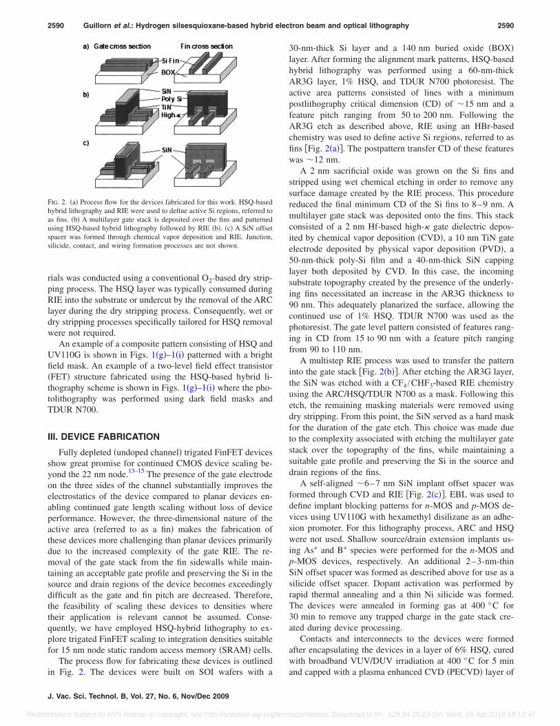
Fully depleted �undoped channel� trigated FinFET devicesshow great promise for continued CMOS device scaling be-yond the 22 nm node.13–15 The presence of the gate electrodeon the three sides of the channel substantially improves theelectrostatics of the device compared to planar devices en-abling continued gate length scaling without loss of deviceperformance. However, the three-dimensional nature of theactive area �referred to as a fin� makes the fabrication ofthese devices more challenging than planar devices primarilydue to the increased complexity of the gate RIE. The re-moval of the gate stack from the fin sidewalls while main-taining an acceptable gate profile and preserving the Si in thesource and drain regions of the device becomes exceedinglydifficult as the gate and fin pitch are decreased. Therefore,the feasibility of scaling these devices to densities wheretheir application is relevant cannot be assumed. Conse-quently, we have employed HSQ-hybrid lithography to ex-plore trigated FinFET scaling to integration densities suitablefor 15 nm node static random access memory �SRAM� cells.
The process flow for fabricating these devices is outlined
FIG. 2. �a� Process flow for the devices fabricated for this work. HSQ-basedhybrid lithography and RIE were used to define active Si regions, referred toas fins. �b� A multilayer gate stack is deposited over the fins and patternedusing HSQ-based hybrid lithography followed by RIE �b�. �c� A SiN offsetspacer was formed through chemical vapor deposition and RIE. Junction,silicide, contact, and wiring formation processes are not shown.
in Fig. 2. The devices were built on SOI wafers with a
J. Vac. Sci. Technol. B, Vol. 27, No. 6, Nov/Dec 2009
ibution subject to AVS license or copyright; see http://scitation.aip.org/term
30-nm-thick Si layer and a 140 nm buried oxide �BOX�layer. After forming the alignment mark patterns, HSQ-basedhybrid lithography was performed using a 60-nm-thickAR3G layer, 1% HSQ, and TDUR N700 photoresist. Theactive area patterns consisted of lines with a minimumpostlithography critical dimension �CD� of �15 nm and afeature pitch ranging from 50 to 200 nm. Following theAR3G etch as described above, RIE using an HBr-basedchemistry was used to define active Si regions, referred to asfins �Fig. 2�a��. The postpattern transfer CD of these featureswas �12 nm.
A 2 nm sacrificial oxide was grown on the Si fins andstripped using wet chemical etching in order to remove anysurface damage created by the RIE process. This procedurereduced the final minimum CD of the Si fins to 8–9 nm. Amultilayer gate stack was deposited onto the fins. This stackconsisted of a 2 nm Hf-based high-� gate dielectric depos-ited by chemical vapor deposition �CVD�, a 10 nm TiN gateelectrode deposited by physical vapor deposition �PVD�, a50-nm-thick poly-Si film and a 40-nm-thick SiN cappinglayer both deposited by CVD. In this case, the incomingsubstrate topography created by the presence of the underly-ing fins necessitated an increase in the AR3G thickness to90 nm. This adequately planarized the surface, allowing thecontinued use of 1% HSQ. TDUR N700 was used as thephotoresist. The gate level pattern consisted of features rang-ing in CD from 15 to 90 nm with a feature pitch rangingfrom 90 to 110 nm.
A multistep RIE process was used to transfer the patterninto the gate stack �Fig. 2�b��. After etching the AR3G layer,the SiN was etched with a CF4 /CHF3-based RIE chemistryusing the ARC/HSQ/TDUR N700 as a mask. Following thisetch, the remaining masking materials were removed usingdry stripping. From this point, the SiN served as a hard maskfor the duration of the gate etch. This choice was made dueto the complexity associated with etching the multilayer gatestack over the topography of the fins, while maintaining asuitable gate profile and preserving the Si in the source anddrain regions of the fins.
A self-aligned �6–7 nm SiN implant offset spacer wasformed through CVD and RIE �Fig. 2�c��. EBL was used todefine implant blocking patterns for n-MOS and p-MOS de-vices using UV110G with hexamethyl disilizane as an adhe-sion promoter. For this lithography process, ARC and HSQwere not used. Shallow source/drain extension implants us-ing As+ and B+ species were performed for the n-MOS andp-MOS devices, respectively. An additional 2–3-nm-thinSiN offset spacer was formed as described above for use as asilicide offset spacer. Dopant activation was performed byrapid thermal annealing and a thin Ni silicide was formed.The devices were annealed in forming gas at 400 °C for30 min to remove any trapped charge in the gate stack cre-ated during device processing.
Contacts and interconnects to the devices were formedafter encapsulating the devices in a layer of 6% HSQ, curedwith broadband VUV/DUV irradiation at 400 °C for 5 min
and capped with a plasma enhanced CVD �PECVD� layer ofsconditions. Download to IP: 129.34.20.23 On: Wed, 16 Apr 2014 18:12:47

2591 Guillorn et al.: Hydrogen silsesquioxane-based hybrid electron beam and optical lithography 2591
Redistr
SiO2. The total stack thickness was �150 nm at the conclu-sion of this process. Contact vias were patterned using atrilayer masking scheme consisting of a 175 nm organic pla-narizing layer �NFC-1400, JSR�, a 20 nm PECVD SiO2 filmdeposited at 200 °C, and a proprietary positive tone resist.Contact via etching was conducted using an Ar /C2F6 /C4FRIE chemistry that removes oxide selective to SiN, Si, andNi silicide. The vias were filled using a CVD TiN/CVD Wfill process. W was removed from the field area by chemicalmechanical polishing. A 100-nm-thick refractory metalmultilayer stack was deposited onto the substrates usingPVD. HSQ-based hybrid lithography was performed on thislayer to define wiring patterns. For this application, a 60 nmthick AR3G layer was used in combination with a 2% HSQfilm and TDUR N700. Once the AR3G etch was completed,the target stack was etched with a Cl2 /BCl3 /O2-based RIEchemistry.
IV. DEVICE RESULTS
Transmission electron microscope �TEM� and scanningelectron microscope �SEM� images of completed devices areshown in Figs. 3�a�–3�d�. Electrical results from singlep-FET and n-FET devices are shown working independentlyand in concert as a CMOS inverter circuit �Figs. 4�a�–4�c��.These results were obtained from devices arranged in a 6TSRAM cell configuration with a cell area of 0.045 �m2. ASEM image of this layout is shown in Fig. 4�d�. An image ofthe completed test cell showing interconnects and contacts isshown in Fig. 4�e�. The fabricated devices show good shortchannel effect control but limited drive current due to high
FIG. 3. TEM and SEM images of completed devices. �a� Gate cross sectionobtained from devices with a 90 nm gate pitch showing �1� BOX, �2� poly-Si, �3� SiN, �4� SOI fin, and �5� NiSi. The gate wraps around the fin, causinga projection of both the gate and fin in the channel regions. The gate lengthis �22 nm. �b� Cross section through the fins in the gate stack region show-ing �6� TiN and high-� gate dielectric stack. �c� Cross section through thefins in the source/drain region. �d� SEM image taken at 30° tilt from normalincidence with 45° substrate degree rotation revealing the intersection of thegate and the fin. The cross section locations of �a�–�c� are shown by �7�–�9�,respectively. The scale bars shown in �c� and �d� are 50 and 100 nm, respec-tively. Images �a�–�c� are shown at the same scale.
parasitic resistance. This is caused in part by the doping limi-
JVST B - Microelectronics and Nanometer Structures
ibution subject to AVS license or copyright; see http://scitation.aip.org/term
tations imposed by the presence of the parasitic spacer on thefin sidewall �Fig. 3�d�� and the limited silicide-to-Si contactarea. Fully functioning SRAM cells were not achieved in thiswork. However, this result clearly demonstrates the feasibil-ity of trigated FinFET CMOS scaling to densities suitable for15 nm node SRAM integration.
V. CONCLUSION
We have demonstrated a hybrid lithography scheme com-bining EBL and photolithography that leverages the high res-olution printing capability of HSQ-based EBL resists andconventional 248 nm optical photoresists. This scheme wasused to fabricate fully functioning CMOS devices and cir-cuits with CD and feature pitch requirements that exceedwhat can currently be accessed using previously demon-strated hybrid lithography schemes. The device fabricationprocess flow presented in this work demonstrates that thispatterning scheme creates a composite masking layer that issuitable for pattern transfer into Si, SiN, and refractory met-
FIG. 4. Source current, Is, vs gate voltage, Vg, at a 1 V and 50 mV drain-to-source bias, Vds, from �a� p-MOS and �b� n-MOS devices working at a90 nm gate pitch. The width-to-length ratio of both transistors is 70 /22 nm.�c� Transfer curve from a CMOS inverter circuit contained within a 6 TSRAM bit cell with a cell area of 0.045 �m2. The cell was operated atVdd=1 V. This cell features a 90 nm gate pitch and a minimum fin pitch of50 nm. �d� SEM image showing the layout of �1� p-MOS and �2� n-MOSdevices from an inverter within a 0.045 �m2 SRAM cell. �e� SEM imageshowing the wiring and contacts for the 0.045 �m2 SRAM bit cell. Theinput �4�, Vdd �5�, output �6�, and ground �7� terminals for a single inverterare shown. The scale bar corresponds to 100 nm.
als. While this work focused on the use of 248 nm optical
sconditions. Download to IP: 129.34.20.23 On: Wed, 16 Apr 2014 18:12:47

2592 Guillorn et al.: Hydrogen silsesquioxane-based hybrid electron beam and optical lithography 2592
Redistr
resists and ARC layers, there is no fundamental reason whythis technique cannot be applied to i-line, 193 nm or EUVimaging materials.
The primary drawback of this technique is that the lowsensitivity of HSQ results in long exposure times comparedto processes using more sensitive chemically amplified re-sists. Consequently, a balance between throughput and pat-terned area must be reached. The presence of the photolitho-graphicaly printed patterns on each die is sufficient forfeature loading requirements for both RIE and CMP. Thisenables flexibility in the choice of the number of die popu-lated with EBL features. For research purposes, throughput isnot a limitation, making this technique ideally suited for de-vice and circuit prototyping where density is a primary mo-tivating factor.
ACKNOWLEDGMENTS
The authors wish to thank H. Kawasaki, F. Rizzo, and M.Rooks for helpful discussions. The authors also wish to thankR. Viswanathan, G. Shahidi, and T. C. Chen for supportingthis work. These devices were fabricated in the Microelec-
tronics Research Laboratory �MRL� at the IBM TJ WatsonJ. Vac. Sci. Technol. B, Vol. 27, No. 6, Nov/Dec 2009
ibution subject to AVS license or copyright; see http://scitation.aip.org/term
Research facility. The authors are grateful to the MRL stafffor contributing to the success of this work.
1S. E. Steen et al., Proc. SPIE 5751, 26 �2005�.2S. Pauliac-Vaujour, P. Brianceau, S. Landis, J. Chiaroni, and O. Faynot, J.Vac. Sci. Technol. B 25, 2030 �2007�.
3S. Pauliac-Vaujour, C. Comboroure, C. Vizioz, S. Barnola, P. Brianceau,V. Maffini Alvaro, C. Dupré, and T. Ernst, J. Vac. Sci. Technol. B 26,2583 �2008�.
4C. Hohle, C. Arndt, K.-H. Choi, J. Kretz, L. Lutz, and F. Thrum, J. Vac.Sci. Technol. B 25, 2038 �2007�.
5S. Xiao and X. Yang, J. Vac. Sci. Technol. B 24, 2940 �2006�.6J. Yang and K. Berggren, J. Vac. Sci. Technol. B 25, 2025 �2007�.7J. Bloomstein et al., J. Vac. Sci. Technol. B 23, 2617 �2005�.8J. Junarsa and P. Nealey, J. Vac. Sci. Technol. B 22, 2685 �2004�.9M. J. Rooks, N. Belic, E. Kratschmer, and R. Viswanathan, J. Vac. Sci.Technol. B 23, 2769 �2005�.
10F. Van Delft, W. Ketelaars, M. Kroon, and J. Lambregts, J. Vac. Sci.Technol. B 20, 2763 �2002�.
11I.-B. Baek, J.-H. Yang, W.-J. Cho, C.-G. Ahn, K. Im, and S. Lee, J. Vac.Sci. Technol. B 23, 3120 �2005�.
12F. C. M. J. M. van Delft, J. P. Weterings, A. K. van Langen-Suurling, andH. Romijn, J. Vac. Sci. Technol. B 18, 3419 �2000�.
13W. Haensch et al., IBM J. Res. Dev. 50, 339 �2006�.14H. Kawasaki et al., Proceedings of the IEEE International Electron De-
vice Meeting, 2008 �unpublished�.15J. Kavalieros et al., Proceedings of the IEEE Conference on VLSI Tech-
nology, 2006 �unpublished�.
sconditions. Download to IP: 129.34.20.23 On: Wed, 16 Apr 2014 18:12:47