Hybrid Mesoporous and Microporous Materials Characterisation
111
1 Università degli Studi di Cagliari PHD DEGREE Physics Cycle XXXI TITLE OF THE PHD THESIS Hybrid Mesoporous and Microporous Materials Characterisation Scientific Disciplinary Sector FIS/01 PhD student: MariaVitalia Tiddia Coordinator of the PhD Programme: Paolo Ruggerone Supervisor: Guido Mula Final exam. Academic Year 2017-2018 Thesis defence: January-February 2019 Session
-
Upload
khangminh22 -
Category
Documents
-
view
0 -
download
0
Transcript of Hybrid Mesoporous and Microporous Materials Characterisation
1
Università degli Studi di Cagliari
PHD DEGREE
Physics
Cycle XXXI
TITLE OF THE PHD THESIS
Hybrid Mesoporous and Microporous
Materials Characterisation
Scientific Disciplinary Sector
FIS/01
PhD student: MariaVitalia Tiddia
Coordinator of the PhD Programme: Paolo Ruggerone
Supervisor: Guido Mula
Final exam. Academic Year 2017-2018
Thesis defence: January-February 2019 Session

2

3
Preface
This thesis is an account of the work carried out by the author at the Università degli Studi di Cagliari,
Sardinia, in the PoroSiLab @ Dipartimento di Fisica and at the National Physical Laboratory in
Teddington, between 2015 and 2018, under the supervision of Prof. Guido Mula (Università degli Studi
di Cagliari), Dott. Rasmus Havelund and Prof. Ian Gilmore (National Physical Laboratory). No part of
this work has been previously used for a thesis or a degree at this or any other university. The work of
the authors is acknowledged in the text. A list of references has been included at the end of the
manuscript. The majority of this thesis has been submitted and published as articles. A list of these
appear in chronological order.
Tiddia, M.; Mula, G.; Sechi, E.; Vacca, A.; Cara, E.; De Leo, N.; Fretto, M.; Boarino, L. 4-
Nitrobenzene Grafted in Porous Silicon: Application to Optical Lithography. Nanoscale Res. Lett.
2016, 11 (1), 436.
Tiddia, M.; Mula, G.; Mascia, M.; Sechi, E.; Vacca, A. Porous Silicon–polyaniline Hybrid
Composites Synthesized through Electroreduction of an Aryldiazonium Salt: Preparation and
Photocurrent Properties. RSC Adv. 2016, 6 (104), 101880–101887.
Cardia, R.; Cappellini, G.; Pinna, E.; Tiddia, M. V.; Mula, G. Optical and Electronic Properties of
Monomers of Eumelanin: A DFT and TD-DFT Computational Study. Opt. Photonics J. 2016, 06
(08), 41–47.
Mouton, I.; Printemps, T.; Grenier, A.; Gambacorti, N.; Pinna, E.; Tiddia, M.; Vacca, A.; Mula, G.
Toward an Accurate Quantification in Atom Probe Tomography Reconstruction by Correlative
Electron Tomography Approach on Nanoporous Materials. Ultramicroscopy 2017, 182.
Havelund, R.; Seah, M. P.; Tiddia, M.; Gilmore, I. S. SIMS of Organic Materials—Interface
Location in Argon Gas Cluster Depth Profiles Using Negative Secondary Ions. J. Am. Soc. Mass
Spectrom. 2018, 29 (4), 774–785.
Tiddia, M.; Seah, M. P.; Shard, A. G.; Mula, G.; Havelund, R.; Gilmore, I. S. Argon Cluster Cleaning
of Ga + FIB-Milled Sections of Organic and Hybrid Materials. Surf. Interface Anal. 2018, DOI:
10.1002/sia.6522.
Tiddia, M.; Seah, M. P.; Mihara, I.; Trindade, G.F.; Kollmer, F.; Roberts, C.; Hague, R.; Mula, G.;
Gilmore, I; Havelund, R. FIB-SIMS for Hybrid Materials – Cleaning the FIB Damaged Organic
Material with Argon Gas Cluster Ions. (submitted)

4
The research presented in this thesis has also previously been presented at national and international
conferences, and a list of these appear below:
SIMS Europe (2018):
Oral presentation: Chemical imaging of buried interfaces in hybrid organic-inorganic
devices using FIB-TOF-SIMS
E-MRS spring meeting (2018):
Oral presentation: Chemical imaging of buried interfaces in hybrid devices using FIB-
ToF-SIMS
UKSAF 2018:
Poster: Chemical imaging of buried interfaces in hybrid devices using FIB-ToF-SIMS
SIMS21 conference (2017):
Poster: Organic signal recovery after focused ion beam irradiation using an Argon
cluster ion beam
IUVSTA 78 workshop (2017):
Poster: Polymers signal recovery using an Argon cluster ion beam
PSST 2016 conference:
Oral presentation: 4-nitrobenzene grafted in porous silicon: application to optical
lithography
Posters: pH-switching of photocurrent in Polyaniline/Porous Silicon hybrids diffused
heterojunction and Visible Light-Induced photocurrents in eumelanin-porous Si
hybrids.
EMRS spring meeting (2016):
Poster: Controlling the polyaniline/porous Si junction: a pH-driven photocurrent
switching
67th Annual Meeting ISE International society of electrochemistry (2016):
Poster: Hybrid PANI/PSi electrodes: preparation and photocurrent performances at
different wavelength
2nd E3 Mediterranean Symposium: Electrochemistry for Environment and Energy (2016):
Poster: Preparation of Polyaniline/Porous Silicon Hybrids for photovoltaic applications

5
Acknowledgment (ringraziamenti)
Here we are at the end of this deadly-fantastic-disgusting-astonishing-exausting-endless-amazing adventure. Yes, this is what it is: a hotchpotch of every possible feeling. I am so grateful I’ve done with it now but without it I could never be the person I actually am.
First of all my thanks go to my supervisor Doc. Guido Mula. Without him I could have still been doing my 3rd year of university, working in an awful place just to pay some taxes. He is basically the best guide you can have if you get lost. So for this reason thanks a lot to him and to his wife Doc. Susanna Setzu who showed me what being a successful woman means!
Second big thanks goes to Professor Ian Gilmore who, falling in love with Sardinia, my land, met my supervisor Guido and introduced me to the possibility of joining is group at NPL to “conclude my PhD”. It was fantastic to have the opportunity to carry out the majority of my research in your facilities. What a cracking place to work!
Thanks to all the people of NPL that supported me in these years and made me laugh when I wanted to dig a hole and jump in. A particular thanks goes to Rasmus Havelund, my supervisor at NPL and Ichiro Mihara that first introduced me to the Focused Ion Beam world; to Jean-Luc, Natalie, David, Matthias and Melissa that welcomed me as friends even knowing that I was just a PhD student and that I could not understand one world of their perfect spoken English.
To my parents, brothers and friends that always supported me even in my crazy-depressive moments during these 3 years.
Thanks Barry for tolerating me, walking with me on this adventurous path and be my biggest supporter.
Un enorme grazie va alle mie amiche Roberta, Emanuela e Valentina che mi ricordano sempre da che bellissimo posto provengo e che genuinamente (povere loro) sono contente di avere una amica scienziato!
Un ultimo e special Grazie a Mamma e Babbo, perche’ se sono qui e’ solo perche’ mi avete fatto forte abbastanza e grazie Marco e Giuseppe perche’ i fratelli sono come la Nutella, che mondo sarebbe senza!

6

7
To those who are not here anymore……

8

9
Contents
Introduction ................................................................................. 11
1.1 State of the art ...................................................................................................................... 11
1.2 Hybrid materials .................................................................................................................... 12
Materials and methods ................................................................ 17
2.1 Polymers ............................................................................................................................... 17
2.1.1 Polyaniline ..................................................................................................................... 18
2.1.2 Eumelanin ..................................................................................................................... 19
2.1.3 Poly(styrene) ................................................................................................................. 20
2.1.4 Poly (methyl methacrylate) ........................................................................................... 21
2.2 Porous matrices ................................................................................................................... 21
2.2.1 Porous silicon ................................................................................................................ 21
2.2.2 Microchannel plate ....................................................................................................... 25
2.3 Electrochemical techniques .................................................................................................. 26
2.3.1 Cyclic voltammetry ........................................................................................................ 26
2.3.2 Electrochemical impedance spectroscopy .................................................................... 27
2.4 Photocurrent measurements ................................................................................................ 30
2.4.1 Spectral dependence using low pass filters .................................................................. 30
2.4.2 Photoconductive atomic force microscope (PC-AFM) .................................................. 31
2.5 Secondary ion mass spectrometry (SIMS) ............................................................................ 32
2.5.1 Primary beam: LMIG .................................................................................................... 34
2.5.2 Focused Ion Beam: FIB ................................................................................................ 35
2.5.3 Depth profiling and gas cluster .................................................................................. 35
2.5.4 Mass filters ................................................................................................................... 37
2.5.5 Instrumentation ........................................................................................................... 39
Mesoporous hybrid material experimental results ........................ 41
3.1 Introduction .......................................................................................................................... 41
3.2 NBD grafting procedure and EIS analysis .............................................................................. 42
3.3 Optical characterisation ........................................................................................................ 49
3.4 Spectral dependence of the photocurrent ........................................................................... 56
3.5 Photoconductive AFM results ............................................................................................... 59

10
3.6 Optical lithography ................................................................................................................ 64
3.7 Summary ............................................................................................................................... 66
Microporous hybrid material experimental results ....................... 69
4.1 Challenge to address ............................................................................................................. 69
4.2 Experimental setup design .................................................................................................... 70
4.3 Application to pure polymer ................................................................................................. 74
4.4 Application to empty MCP .................................................................................................... 79
4.5 A bit of theory ....................................................................................................................... 80
4.6 Application on the hybrid microporous system .................................................................... 83
4.7 FIB milling with Bi+ and Bi3+ as alternative to Ga+ ................................................................. 85
4.8 Application: Membrane Electrode Assembly and strain sensor ........................................... 91
4.8.1 3D inkjet printed encapsulated strain sensor ............................................................... 91
4.8.2 Sintered copper tracks on a flexible polymer substrate ............................................... 93
4.9 Summary ............................................................................................................................... 94
Conclusions and future work perspective ...................................... 97

11
1 Introduction
This thesis project is aimed at the study and characterisation of interfaces between organic and
inorganic materials. The two classes of material are coupled together in order to develop hybrid
systems and they are described in 2.2. The need for more accurate and explicit analytical solutions for
hybrid material interfaces analysis and related novel experimental characterisation techniques derives
from the potential of these complex interfaces for the development of new devices in a large variety
of application fields such as optics and electronics 1 2.
1.1 State of the art
The research on hybrid material has been conducted using a multifaceted approach: from theoretical
physics and chemistry 3 to various material and device characterisation methods 4.
The interest in hybrid materials has led to a significant research effort also through both academic
and manufacturing research and development 4. For the fabrication and characterisation of organic-
inorganic devices, prototypes have to be built using a mixture of materials with properties tailored for
a significant role in the scientific development and the instrumental uptake of these materials. These
materials are the key ingredients necessary to provide resistance, flexibility, durability and good
processability in electronic devices, industrial material and bio-applications 5. The various organic and
inorganic bulk materials can be obtained by using evaporation techniques, beam deposition 6 7 or
inkjet printing 8 9 , methods that allow simplified and faster production. The procedure of device
preparation often generates structural defects 10, inhomogeneity in the deposition or in the filling
degree (in case of the insertion of material in porous structures) 11 . Industries and research in general
need to obtain information about the quality of the processes and about the structural nature of any
final device. This characterisation is carried out by using several techniques having as common target
the understanding of the variations induced by the fabrication process. Specifically, for applications
as organic light-emitting diodes (OLED), photovoltaic cells and nanoparticles for drug delivery, the
analysis of interfaces is a critical step for the further development of these systems 12 13.
Research on organic–inorganic devices requires the cooperation among research groups with
different and complementary expertise. For this reason, this study involved a collaboration between
Cagliari University and NPL. The aim was to resolve fundamental problems present in the porous
silicon structure used in Cagliari University by utilising mass spectrometry expertise at NPL. This is an

12
example where two different fields can find a common way to interact about organic-inorganic hybrid
devices.
This thesis research is undertaken to address the following challenges: a) the effect of the insertion
of polymer in porous material via an electrochemical process, b) the analysis of the photocurrent
generated by developing a hybrid p-n junction, c) the stability and the resistance added to the pristine
material by the process and d) the definition of a protocol for mass spectrometry analysis of porous
materials and buried interfaces. Two popular analysis techniques, electrochemistry and mass
spectrometry, have been used to analyse the organic-inorganic hybrid materials and interfaces using
different polymers and different inorganic substrates.
In chapter 1 and 2, the importance of hybrid materials and polymers will be discussed, underlining
some of their characteristic and properties that can be exploited.
In sections 2.3 and 2.4, electrochemical and optical studies made on porous silicon grafted with a
conducting polymer will be presented. Properties as the resistance to chemical corrosion by harsh
basic solutions and the photocurrent generation will be studied and explained. The possibility to
understand how the polymer is attached to the pore walls is investigated by mass spectrometry
imaging. This technique requires refinement of measurement parameters for this class of materials, a
study that has been implemented by using Si materials with similar composition and geometry
although on a larger scale. To do this, in chapter 4 the use of focused ion beam (FIB) for milling the
surface of a porous micrometric matrix and the cleaning procedure to recover the damaged polymeric
component will be described. This method will be applied to other devices to highlight the
effectiveness of this technique, in section 4.8. These studies provide the essential metrological
foundation to address frontier issues in surface and nanoanalysis and extend the measurement
capabilities of secondary ion mass spectrometry.
In the last chapter, a summary of all the analysis and future development will be presented.
1.2 Hybrid materials
Organic-inorganic hybrids are a relatively recent alternative choice in cases where it is required to
have materials with new and unusual features 4. This is related to their diphasic structures, leading to
multifunctional materials 4. For the most part, these structure are synthesized in low temperature
processes allowing for variability even in the compound design 14. Physics and chemistry play an
important role in the fabrication and control of these structures, having complementary information
useful for their preparation and for the control of their properties 15.

13
The combination of inorganic and organic components in one material to achieve improved
properties is as old as history. Combinations of this nature were developed because of a shortage in
the required material characteristics in the traditional choice of available materials, which could only
be filled by merging two totally different single components. Applying this approach, one can find
many examples in antiquity. One impressive case is the old dye Maya blue, which is a mixture of a clay
mineral and the organic dye indigo, and shows remarkable high stability, which indigo alone does not
16. This material is often considered one of the first hybrid materials 17 18. Another example is
combining straw, an organic fibre, and clay as an inorganic matrix for house building. This mixture is
solid, durable, non-toxic, and can be used in structural elements. In addition, it is a reasonably good
thermal insulator and a thermal storage medium 19. We would not really call this material a hybrid
material in a scientific context, more realistically it would count as a composite material.
The challenge of combining organic and inorganic materials in a unique new material continued
during the industrial era, for example in paints, by using TiO2 as a pigment, suspended in a mixture
composed of an organic solvent and surfactants 20. While the concept of hybrid materials didn’t exist
at the time, since the beginning of the 20th century scientists were already noticing the potential for
the use of polymers in this way. Clay, talc, and minerals have been added to polymers to improve
resistance, durability and malleability modifying the melting point 21 22. “Hybrid” as a term to describe
these structured materials has been introduced relatively recently in terms of materials innovation
and advancement, in areas such as solar cells, fuel cells, strain sensors, biosensors and drug delivery
systems 23–29. Many modern materials we encounter in our everyday life, e.g. glass- and carbon fibers-
reinforced polymers address our current view on the beneficial combination of two different materials
that generate a novel compounds showing superior properties if compared to the characteristics of
the pristine components 30 31.
Different characteristics arise for the hybrids, depending on the strength of the bonds within the
new materials. Hybrid composites are considered biphasic when the organic and inorganic phases are
mixed on the nanoscale 4. On that scale, the properties of the materials are not the sum of those of
the individual components, but the inner interfaces also play a dominant role in the properties of the
new structures 32 33. In other cases, the organic and inorganic phases are embedded and only weak
bonds (hydrogen, van der Waals or ionic bonds) give the cohesion to the whole structure 34. In further
combinations, the two phases are linked together through strong chemical bonds (covalent or ion-
covalent bonds). The organic component is generally considered more fragile due to a lower thermal
stability with respect to the inorganic counterpart 15 5.
The current definition of “Hybrid” materials is given by the IUPAC nomenclature as follows:

14
“A hybrid material is composed of an intimate mixture of inorganic components, organic
components, or both types of component. Note: The components usually interpenetrate on scale of
less than 1 μm” 35.
By using that definition, the idea of hybrid materials covers polymer blends at every scale, and many
types of inorganic crystalline materials, giving a large range of possible uses. A description, often used
by scientists in literature regarding hybrid material, is that they are made by a minimum two
component materials, one organic and one inorganic, dispersed at the molecular level 34. Following
this definition, hybrid materials are a special case of composites showing a mixture of the different
components on the molecular length scale 15.
In hybrid materials, even when the two components are transparent to a given wavelength range,
the different components don’t allow necessarily a high degree of transparency of the material. This
is caused by the scattering of light that derives from the spatial dispersion of the various components
with different refractive indices, in particular when the impinging light wavelength is comparable with
the hybrid material dispersion length scale. In the case where this length scale is smaller than the light
wavelength, the light scattering is minimized and the material can be considered transparent.
Depending on the transparency degree, the added value of the high flexibility of fabrication processes
for hybrids with respect traditional glasses has raised interest in the building of new optoelectronics
devices from hybrid materials, for instance for their use in photolithographic processes 36. The hybrid
materials can be functionalized so that their chemical and physical properties can be tailored to an
optimal interaction response to light, electrical and thermal stimulations: for example waveguides,
photodetectors, gratings and micro optical devices can be built from these classes of materials 37–39.
Another relevant field where hybrid materials are being widely used is the electronic industry, given
the continuous need to improve integrated circuits performance while reducing the size of
components through scaling 40. In this field, lithography tools and photoresist materials are
approaching their physical limits with standard materials. To be able to continue, the scaling process
will require the introduction of new materials that can be easily tuned to overcome the present
limitations. Hybrid materials are particularly suited for electronic applications, since their components
can be purified to a very high degree 4. By using specific chemical approaches in order to minimize the
influence of the chemical impurities on the electronic performance, the process results can be
optimized to be highly reproducible 41 42. Silicon-based materials typically play a major role in hybrid
composites, therefore there are no clear limits in the potential for integration of Si-based hybrid
materials in future device technologies. Aside from this small overview of technological applications
of hybrid materials, there is a large variety of other promising applications. My thesis work describes
how I fabricated various kinds of hybrid materials starting from a porous material, which was then

15
impregnated with an organic material, and subsequently investigated the resulting optical and
electrochemical properties. In order to do this, it was necessary to deal with critical characterisation
issues due to partially destructive aspects of the structural analysis on organic-inorganic hybrids. The
results on porous silicon grafted with polyaniline will show how it is possible to increase light
absorption of the pristine porous material by the addition of the polymer. Also, a porous structure
consisting of a microchannel plate filled with polystyrene and polymethylmethacryilate (PMMA) will
be used to investigate signal recovery during time-of-flight secondary ion mass spectrometry (ToF-
SIMS) measurements after the damage to the structure that has been induced by using a FIB. These
samples will provide a basis for the study of general hybrid composite materials for future
applications.

16

17
2 Materials and methods
2.1 Polymers
As mentioned in the introduction, this thesis work is based on the coupling of an inorganic and an
organic materials in a hybrid structure. In the case of the inorganic material, this consist of porous
silicon or a Si multichannel plate, while the organic part is a polymer. A polymer is a macromolecule
composed of a high number of small structural units, of same or different composition, called
monomers and kept together by covalent bonding in a process called polymerisation 43. For example,
the commercially important material poly vinyl chloride (PVC) is made from the monomer vinyl
chloride. The repeated unit in the polymer usually corresponds to the monomer from which the
polymer was made. There are exceptions to this where, before fabricating the polymer, there is need
to prepare a new molecule starting from the monomer and then, via a chemical or electrochemical
processes, obtain the polymerisation by attaching different chemicals units to the pristine monomer
units.
The size of a polymer molecule is defined by its mass and by the number of repeated units in the
final molecule. The indicator of the polymer size is called the degree of polymerisation. The vast
majority of polymers in commercial use are organic: this means that they are based on covalent
compounds of carbon. Other elements may be included in polymer chemistry as hydrogen, fluorine,
sulphur and all other elements able to form covalent bonds with carbon. Hydrogen bonding, which
arises from an intense dipole associated to hydrogen atoms attached to electronegative elements
such as oxygen and nitrogen, is important in the process of formation of protein. Polymerisation
mainly refers to substances which form the building blocks for life, such as DNA and proteins, but they
have obtained an important role in technological progress in the last decades. Next to natural
polymers, there exist classes of synthetic polymers that we use daily, as is the case of polyethylene
(PE), polystyrene (PS), PMMA, and poly-tetrafluoroethylene (PTFE). In some cases, by modifying the
chemical structure of the monomer it is possible to tune the physical properties of the polymer.
Conducting polymers are part of this class of tuneable materials, and they are precious in the fields of
microelectronics and microchip development, for example PEDOT:PSS and S-P3MEET:PHOST 44 45.
These polymers can be perfectly adapted to be used in the aerospace, automotive, and construction
industries due to their physical property such high durability, heat resistance, flexibility and resistance
to harsh chemical solutions 46–48.

18
Conducting polymers are identified by the high molecular weight that gives them mechanical
properties more valuable than typical industrial materials. Conducting polymers present in some case
a higher crystallinity degree: crystallinity means the percentage of material with a crystal structure
within the polymer. High crystallinity degree typically means harder material, more resistant and
opaquer 49 50. In some cases, the crystallinity degree allows polymers to have comparable properties
with respect to metal: for instance, as is the case for instance Kevlar, they can have a resistance to
traction higher than steel. One of the major applications for conducting polymers is in the batteries
field, in particular rechargeable batteries for portable device 51 52. Polymers indeed present properties
suitable for use in other fields such as electronic circuits, LEDs, diodes and transistors, biosensor,
catalyst and gas sensor 53. Studies on emerging energy sources have also focused attention on
polymers for next generation photovoltaics, or multilayer structures of easy fabrication as in
perovskite solar cells, since they have lower electrical resistance with respect to metals and
semiconductors 54 55.
In my research, I used different polymers in order to develop different hybrid devices: from
commonly used polymers such as PS and PMMA, to a conductive polymer like polyaniline (PANI).
Those polymers have been combined with inorganic porous matrices in order to study the interactions
between the polymers and the inorganic matrix.
PANI has been electrochemically grafted on porous silicon, and PS and PMMA were inserted with a
mechanical process within the channels of microchannel plates. The hybrid structure properties have
been studied by optical, electrochemical, photocurrent generation and mass spectrometry
characterisation techniques.
2.1.1 Polyaniline
Polyaniline or PANI is a conductive polymer discovered by Alan MacDiarmid during experiments on
the electrochemical nature of aniline 56. PANI is synthesised from the aniline monomer via redox
reaction using a electrochemical method 57. It is present in three main different states that are
obtained from units coming from reduced (y) and oxidized (1-y) blocks, depending on the use of acidic
or basic environment for the synthesis used for the polymerisation. In Figure 1 it is possible to observe
the aniline monomer.

19
Figure 1. Part of the structural formula of PANI (source Wikipedia).
The redox state of the polymer is determined by the value of y, which may vary continuously from
zero to unity. At у = 0, PANI is in its fully oxidized form called pernigraniline with a characteristic blu-
violet colour, at y = 0.5, PANI is in the form of emeraldine and has a green colour while у = 1
corresponds to the fully reduced form called leucoemeraldine, a form with a clear and colourless
characteristic 58.
2.1.2 Eumelanin
Melanins are a class of natural pigments responsible for the colorations of human skin and hair. Their
unique status among natural pigments is due to their socioeconomic and biomedical relevance,
encompassing racial pigmentation, skin photoprotection, sun tanning, and pigmentary disorders 59 60.
Moreover, they display a quite unusual set of physicochemical properties such as broadband mono-
tonic absorption in the ultraviolet-visible 61. These features have suggested the possible use of
synthetic (artificial) eumelanins in the development of a new generation of bioinspired electrically
active devices. More recently, eumelanin biopolymers have also been proposed for optoelectronic
and photovoltaic applications 62. Eumelanin polymerisation is a complex process that starts from the
basic structural formula shown in Figure 2, where the arrow denotes where the polymer continues.

20
Figure 2. Part of the structural formula of eumelanin (source Wikipedia).
Eumelanin will be used in the photoconductive atomic force microscopy (PC-AFM) measurements
section, and it was introduced in the porous Si matrix first by insertion of the constituting monomer
via spin coating followed then by a polymerisation step in NH3 atmosphere, as described by Pinna et
al 63.
2.1.3 Poly(styrene)
Poly(styrene) or PS is a polymer derived from the monomer styrene, a derivative of benzene
represented in Figure 3.
Figure 3. Structural formula of the PS (source Sigma Aldrich website).
The polymer is based on a simple head-to-tail arrangement of monomer units and is amorphous,
since the specific position of the benzene rings is variable and hence inhibits crystallisation, making it

21
easy to form and mould. It finds widespread use in many applications, on account of its desirable
properties, combined with its relative cheapness.
2.1.4 Poly (methyl methacrylate)
Poly (methyl methacrylate) or PMMA is the most important of the commercial acrylic polymers and
it is also known as acrylic glass. It is a transparent thermoplastic often used in sheet form as a
lightweight or shatter-resistant alternative to glass.
Figure 4. Structural formula of the PMMA (source Sigma Aldrich website).
This polymer is formally derived from poly (acrylic) acid by the replacement of the tertiary hydrogen
atom by a methyl group, CH3. In Figure 4 it is represented its monomeric structural formula.
2.2 Porous matrices
2.2.1 Porous silicon
Porous silicon (PSi) was discovered in 1956 by Uhlir and co-workers 64 while performing electro-
polishing experiments on silicon wafers using a solution containing hydrofluoric acid (HF). They found
that by applying a current, the silicon surface showed an irregular corrosion where a porous structure,
propagating primarily in the <100> direction in the wafer, was formed. In the period between the
1970s and 1990s the interest on PSi increased in spectroscopic studies because of the high surface
areas developed 65–67, as a precursor to generate thick oxide layers on silicon68, and therefore as a
dielectric layer in capacitance-based chemical sensors 69.

22
In the 1990s, Leigh Canham published his results on red-luminescence 70 71 from porous silicon,
describing this phenomenon in terms of quantum confinement of carriers in silicon nano-crystals
within the pores walls. After Canham’s work, the research interest in porous silicon increased and
started to be used in different fields.
Efficient visible light emission made PSi a perfect candidate for silicon-based optoelectronics
switches, displays and lasers 71. During the last twenty years, the optical properties of PSi have become
a very intense area of research 72–74. Aside from its light-emission properties, PSi is also a very
promising material due to its mechanical and thermal properties suitable for microelectronics devices
75. Its large surface area within a small volume, its controllable pore sizes, its convenient surface
chemistry and the ability to modulate its refractive index as a function of depth 76 make PSi also a
suitable dielectric material for the formation of multilayers 77–79.
The presence of open pores allow the penetration of polymeric and biological substances within the
matrix, and it is possible to understand the changes in the filled structure by comparing the optical
behaviour changes, induced by the pores infiltration, with respect to the original system. These effects
inspired research into different applications fields such as optical sensing applications, drug delivery
systems and photovoltaic devices 80 81.
The electrochemical reaction takes place in an electrochemical cell, as showed in Figure 5.
Figure 5. Schematic representation of the electrochemical cell used for the preparation of the PSi layer.
The silicon wafers are cut into 1.5 cm × 1.5 cm samples, that are then inserted in the electrochemical
cell where their backside is contacted with a metallic sample holder, while the surface where the

23
porous layer will be formed is in contact with the etching solution. A second electrode (usually
platinum) is then immersed in the electrochemical solution. A voltage is applied between the two
electrodes realising a contact trough the HF solution, starting the electrochemical corrosion that leads
to the porosification of the crystalline Si. The studies of porous silicon formation started with
electrochemical characterisation of its current-voltage (i-V) relationships, where the Schottky diode
model based on the semiconductor/electrolyte interface played a predominant role 71. Although
additional analysis techniques have been used recently to study porous silicon, the understanding of
PSi formation still comes from the I-V relationships, and a basic knowledge of silicon electrochemistry
is essential to understand the fundamentals of pore formation 82.
The electrochemical process is the same for n-type and p-type silicon. Under cathodic polarization
(negative voltage) the silicon is stable and the only reaction that takes place is the reduction of water
at the silicon/HF interface with the subsequent formation of hydrogen in a gaseous state under high
cathodic potential. For anodic voltages (positive) the silicon dissolution starts with the pore formation
and becomes electropolishing (full dissolution) for higher potentials.
Figure 6 shows the characteristic I-V curve for n and p-doped silicon. The range of pore formation
regimes is indicated. The value that has the physical meaning in this process is the current density (j)
at the interface between the electrolyte and the silicon interface.
Figure 6. I-V characteristic for n-type and p-type PSi formation.

24
The most accepted chemical reaction that occurs in porous structure formation is described by the
following anodic semi-reaction:
𝑆𝑖 + 6𝐻𝐹𝐻 → 𝐻2𝑆𝑖𝐹6 +𝐻2 + 2𝐻+ + 2𝑒−
The silicon product after this reaction is H2SiF6. A further dissolution happens when more holes are
available at the pore tips, giving a directionality in the pore formation in the depth. This direction is
given by the anodic current path in the silicon. After the pore formation regime, a further increase in
the formation current leads to the electropolishing regime, where silicon is fully dissolved.
In Figure 7, we can see an example of PSi prepared in the PoroSiLab at the University of Cagliari for
these thesis experiments: a mesoporous silicon matrix formed from heavily n-doped Si wafers.
Figure 7. SEM image of a PSi cross section obtain by etching in HF 15% with a current of 25mA.
It is possible conclude that the PSi formation process (and the corresponding current and voltage
curves) depends on:
- The HF concentration: higher concentrations lead to smaller pore size;
- The solvent in which the HF is diluted: the use of ethanol as a surfactant gives higher homogeneity,
considering that the porous silicon is hydrophobic but at the same time organophilic;
- The type and level of silicon wafer doping. For example, the use of low n-type doping levels require
illumination to supply hole carriers, and the average pore size depends on the type and level of doping;
- The etching time: in the normal pore formation regime, the porous layer thickness is directly
proportional to the formation time.

25
2.2.2 Microchannel plate
Organic-inorganic test devices used in chapter 4 were made using a Long-Life™ MCP-10
microchannel plate (MCP) (Photonis, US), commonly used in ToF detection systems 83. The MCP (see
Figure 8) consists of a regular array of hexagonal close packed open tubes with 10 μm hole diameter
and a centre-to-centre separation of 12 μm. These holes are tilted at 12° to the surface normal. The
MCP is made from glass tubes sintered together with a rubidium-containing Nichrome coating for
secondary electron emission. The holes are subsequently filled with either PS or PMMA using a 4-step
procedure summarized in Figure 8 and described by Steinhart et al 84.
The tubes are filled by melting the polymers and pressing them into the tubes in a vacuum oven.
This regular structure of organic and inorganic phases is suitable for evaluating the lateral resolution,
the organic material damage effects and the data validity during measurement.
As reported in Figure 8 (top line), first, the MCP was degreased in a bath of 20% nitric acid (Sigma-
Aldrich, UK) for more than 24 hours and subsequently rinsed with purified water and acetone (Sigma-
Aldrich, UK). The dried MCP (bottom line from right side) was placed in a glass Petri dish and the
surface of the MCP was covered with powdered polystyrene (molecular weight 2430, Sigma Aldrich,
UK) or PMMA (molecular weight 340000, Sigma Aldrich, UK). A metal weight of 500 g was placed on
the polystyrene. Keeping this arrangement, the polymer was annealed to 200 °C for 5 h in a vacuum
oven allowing the polymer to melt and fill the channels in the MCP. In Figure 8, on the bottom line, at
the left hand end is an optical image of the filled MCP after the filling procedure.

26
Figure 8. Schematic representation of the 4-steps filling procedure of the MCP.
2.3 Electrochemical techniques
2.3.1 Cyclic voltammetry
Electrochemistry is a powerful technique to test reactions that involve electron transfer, electron
flow and chemical changes in a substrate. In this work, it has been used for the grafting of the PANI to
the PSi. The advantage of electrochemistry resides in the simplicity with which thermodynamic and
kinetic parameters can be measured. The PSi grafting process described in section 3.2 involves
different electrochemical techniques such as cyclic voltammetry and potentiostatic measurements 85
86. Cyclic voltammetry is a technique widely used to investigate the Redox process of molecular species
and electron transfer-initiated chemical reactions as catalysis. CV data are usually reported by using
the IUPAC convention as shown in Figure 9.

27
Figure 9. Schematic representation of a cyclic voltammogram. The arrow indicates the process direction..
The dashed line on the Figure 9 is a typical voltammogram or cyclic voltammogram, where the x axis
is the applied potential (E), and the y axis is the response in term of the resulting current (I) or current
density (J) passing through the system: for negative current values or densities it is possible to register
oxidation reactions, while for positive values of current it is possible to observe peaks related to
chemical reduction processes. The arrow indicates the sweep direction for the potential range. An
important parameter that has to be taken into account is the scan rate, which is the constant variation
rate of the applied potential during the experiment.
2.3.2 Electrochemical impedance spectroscopy
In this section we will describe the behaviour observed during the early stages of grafting by using
electrochemical impedance spectroscopy (EIS). One of the relevant properties of porous samples,
including PSi, is a large developed area that is complex to characterise in detail. By using EIS, it is
possible to obtain information on the inner pores surface and on its modifications, by recording the
system response (the phase variation) to a solicitation given by applying a current intensity
(galvanostatic regime) or voltage (potentiostatic regime) oscillating at frequencies distributed in a
several orders of magnitude wide range 87.
For our EIS measurements, we chose the galvanostatic regime (Galvanostatic EIS, GEIS), consisting
in the perturbation of the system through sinusoidal currents of small amplitude (mostly from 5 to 10
mA) overlapped to a continuous current to observe the response of the system to the perturbation 85.

28
The data interpretation, generally made by using a model circuit whose behaviour reproduces the
experimental one, gives indication on the modifications incurring at the interfaces between different
phases. Those interfaces may exist directly inside the semiconductor itself (as for instance when
derived from different morphologies, or between different distinctive crystalline phases), or between
the solid phase and the medium where the semiconductor is placed, as is the case with an electrolytic
solution.
The samples response is generally due to the rearrangement of the electrical charge, following the
oscillating perturbation, in the various interphases. The data interpretation is performed by using
equivalent electrical circuits, that is an electronic circuit with a certain number of circuital elements
combined in series and/or in parallel and exposed to the same alternate signal is used to stimulate the
experimental system. The data fitting with equivalent circuit gives, under the simulated experimental
conditions, a signal response that is overlapped to the experimental response measured from the real
system. The correct data interpretation comes from circuits whose elements are correctly
representing the samples parts that are responding to the electrical stimulations (interfaces, ions
moving within an electrochemical solution, …). In fact, in an electrochemical cell, the kinetics at the
electrodes, the chemical reactions and the diffusion processes can affect the electron flux and can be
therefore modelled by resistors, condensers and inductors. In conclusion, with EIS analysis, based on
the knowledge of the physical and chemical phenomena that rules the examined process, it is possible
give a physical meaning to the electrical equivalent circuit and to the chosen circuital parameters.
If the use of a given equivalent circuit leads to a good fit of the experimental data, it can be
considered consistent and accurate. It is also important consider that it does not exist one only one
equivalent circuit able to describe the behaviour of the system. For this reason, the best choice of the
equivalent circuit is the one that gives the best fit while having the most consistent real physical
description of the system.
In Figure 10, Figure 11 and Figure 12 are shown an example of the representation of EIS impedance
results by using the three standard graph types:
Nyquist plot: shows the relation between the real (|Z Re| or Z’) and the imaginary part (|Z
im| or Z’’) of the impedance (Figure 10).
Bode plot: real part of the impedance vs. frequency (Figure 11);
Bode2 plot: the phase (ϑ) in radians or degrees vs. frequency (Figure 12).

29
Figure 10. Nyquist curve of PSi
Figure 11. Bode-impedence curve of PSi.
Figure 12. Bode-phase curve for PSi.
The phase is directly related to the impedance by the relation expressed in the formula:
𝜃 = arctan(−|𝑍𝑖𝑚|
|𝑍𝑅𝑒|)

30
In our case, the circuital choice and the curve simulations have been performed by using the EISSA
software (Electrochemical Impedance Spectroscopy Spectrum Analyser,
http://www.abc.chemistry.bsu.by/vi/analyser/).
2.4 Photocurrent measurements
2.4.1 Spectral dependence using low-pass filters
To study the behaviour of the PSi sample grafted with PANI, the photoconductive characterisation
has been carried out by first depositing sputtered semi-transparent gold contacts on the samples
surfaces and then using low-pass filters to characterize the spectral behaviour of the samples. To
investigate the local photoconductive behaviour of the samples, PC-AFM measurements were also
performed.
Optical low-pass filters, also known as anti-aliasing or “blur” filter, were designed by camera
manufacturers to eliminate the problem of patterns that occur when a scene or an object that is being
photographed contains repetitive details (such as lines, dots, etc.) that exceed the sensor resolution,
by blurring what actually reaches the sensor. Optical filters can be considered as devices that transmit
light selecting a cutoff wavelength/frequency. They are usually implemented as glass or plastic sheets
in the optical path. Low-pass filters (Figure 13) transmit only the light having energy below the cut-off
energy and absorb or reflect the rest.
Figure 13. Optical filter used in the photocurrent generation experiments.

31
2.4.2 Photoconductive atomic force microscope (PC-AFM)
The standard method used to analyse the photocurrent generated from of PSi and PSi/polymer gives
a response originated from a wide porous surface, because the illumination of the sample is over a
large circular area. However, it is important, for an optimization of the samples behaviour, to
understand how the photocurrent generation behaves locally, at the pores diameter length scale.
Therefore, a suitable method is needed to identify the pores and register the current under
illumination in a single pore. These information can be obtained by using a PC-AFM.
The PC-AFM is a type of scanning probe microscopy (SPM) analysis method developed for property
analysis of photovoltaic elements. With a technique based on the principles of a standard AFM
equipped with a conductive tip, PC-AFM employs an additional attached light source to shine light
onto the photosensitive element. Normally, the light source is located beneath the specimen, and light
is shone onto the specimen through a transparent conductive oxide layer (e.g. Indium tin oxide). In
our case the sample is not transparent to the light, so we modified the system in order to have the
light source focused on the top of the sample, as shown in Figure 14.
Figure 14. Schematic representation of the PC-AFM configuration.
Through the use of PC-AFM, the conversion efficiency of the sample can be analysed at the nanoscal
level, and visual analysis of phase separation, charge generation, and charge transport can be
performed 88. The light source is a green laser with wavelength = 532 nm, chosen to give the
maximum response from the polymer. This method is especially useful in studying the relationship
between morphology, material composition, and light wavelength that impacts the photocurrent
generation of the specimen 89.

32
2.5 Secondary ion mass spectrometry (SIMS)
The growing interest in hybrid organic-inorganic devices and materials generates a need for methods
suitable for their characterization. High-resolution chemical imaging using SIMS in combination with
a FIB milling is a promising method to investigate buried interfaces in hybrid materials. However, there
is a lack of guidance for analysts on how to achieve reliable and reproducible FIB-SIMS measurements.
SIMS is a mass spectrometry technique that detects ionized particles emitted from a solid surface
bombarded by energetic primary particles, such as electrons and ions. Based on mass spectrometry
principles, SIMS is used to investigate the molecular, elemental and isotopic composition localized in
the microscopic scale in solid samples and thin films. A primary ion beam, impacting on the surface of
the region of interest, generates a cascade of secondary ions that are then analysed by a mass
spectrometer. Primary particles can be atomic species, for example Bi+, Ga+, Cs+ or small clusters and
polyatomic ion species such as Arn+, Bi3+, C60
+, while secondary charged particles can be electrons,
molecules, polymer fragments or neutral atom species.
The first example of SIMS measurements, made possible by the use of ultra-high vacuum pump
technology, was in the 1949 by Herzog and Viehböck 90, at the University of Vienna, Austria. Later, in
early 70s, two different projects in USA and France brought the development of the first instruments
based on a magnetic double focusing sector field mass spectrometers and the possibility to use Argon
as primary ion beam. By 1975, K. Wittmaackand and C. Magee developed a quadrupole mass analyzer
for the SIMS 91 92. At the same time, A. Benninghoven introduced the still commonly used method of
static SIMS, which allows surface analysis to be performed by using a primary ion current density small
enough that only a negligible fraction (typically 1%) of the first surface layer contributes to the
measurement 93. The first commercial SIMS system was developed by the company CAMECA S.A.S and
had an immediate impact on materials science and surface science. Instruments of this type use pulsed
primary ion sources and time-of-flight mass spectrometers and were developed by Benninghoven,
Niehuis and Steffens at the University of Münster, Germany and by Charles Evans & Associates. The
instruments that we used in this work have been developed and built by IONTOF Gmbh, Germany.
In SIMS, a primary ion beam impinges on the surface of a sample The secondary ions generation
process that follows the impact of the primary ions beam involves a dynamic part, where monoatomic
and polyatomic clusters are desorbed from the surface of the sample, and an ionization process, in
which a fraction of the sputtered particles become positively or negatively charged (see schematic
representation in Figure 15).

33
Figure 15. Schematic of secondary species emission.
The secondary ions are collected, filtered and focused by the secondary ions column, composed by
a system of lenses and deflectors for energy and mass filtering. Secondary ions generation is a complex
mechanism that includes the sputtering and the ionization that both finally result in the emission of
the secondary ions species being measured. For any sputtered surface, the species measurement
depends on the secondary ion yield, that is by the number of ions produced by sputtered ions or
molecule (analyte for simplicity) and is strongly influenced by the electronic states that affect the
quantitative analysis. The basic equation that describes SIMS process is:
𝐼𝑠𝑚 = 𝐼𝑝𝑦𝑚𝛼
±𝜃𝑚𝜂
Where 𝐼𝑠𝑚is the primary ions current relative to the species m, 𝑦𝑚is the sputter yield defined as the
number of secondary analyte particles sputtered by one primary ion particle, 𝛼±is the ionization
probability for the sputtered positive or negatives analytes, 𝜃𝑚 is the fractional concentration of m on
the surface of the sample that is being analysed and𝜂is the ion transmission efficiency of the
instrument, from the specimen, through the various lenses, mass analyser and apertures, up to the
detector. The product 𝛼±𝜂is referred to as s, the useful yield, that is the number of analyte particles
detected per analyte particle sputtered.
Sputtering of singular species has been predicted by the Sigmund sputter theory, based on the model
of impact cascade and the interaction potential between the atoms in the target material 94. With this
theory, it is possible to quantitatively predict sputter yields and their dependence on primary ions
properties such as energy, angle of incidence, and mass.
SIMS mainly has two operation modes that depend on the primary ion dose that is acceptable during
the analysis: static and dynamic SIMS. For static SIMS, the data collected are obtained from less than
1% of the outermost monolayer of the sample under examination and the acceptable limit for the
primary ion dose is <1013. By contrast, in dynamic SIMS the data is collected from many atomic layers
situated at and below the outermost sample surface and the minimum dose is around 1017 ions/cm2.

34
2.5.1 Primary beam: LMIG
A liquid metal ion gun (LMIG) is used to provide primary ion beam for the ToF-SIMS system used in
this work. The best-known sources are bismuth and gallium. LMIGs can provide an atomic beam or a
cluster beam. The choice of the beam depends on the nature of the material to be analysed. A
schematic drawing of the LMIG is shown in Figure 16.
The LMIG is essentially constituted by 3 parts:
- Support leg that also works as an electrical contact;
- Emitter constituted by a needle and a reservoir coated with the metal used for generation of
ions;
- Extractor for the extraction of the metal ions and cluster ions.
The liquid metal reservoir is in contact with and wets a sharp tungsten tip, while a high excitation
field pulls out ions to a cone with a radius on the range of tens of nm. Ions are emitted by field
ionization and accelerated down the ion column. The extractor works with a potential range typically
between -5 and -10 keV with respect to the source. An intense electric field around the tip generates
an electrostatic force that allows the movement of positive ions forward while electrons move
backwards to the needle. The principal ion sources used are Ga+ and Bin+ because they tend to
introduce minimal chemical effects into the substrate under study and hence have a minimal effect
on the secondary ions yields.
Other ions can be produced by heating the source to the melting point of the alloy as happens for
the Manganese and the Bismuth produced from the BiMn alloy and then selecting the required ion
cluster or metal through careful control of the pulse timings, which will be different depending on the
mass of the ions required.
Figure 16. Schematic representation of the LMIG.

35
2.5.2 Focused Ion Beam: FIB
The Focused Ion Beam (FIB) uses a beam of positively charged ions of high atomic mass (commonly
Ga+) following the same principle of emission and interface interaction explained for the LMIG in
section 2.5.1 . Although a FIB may be used as a primary ion beam in SIMS, FIB here refers to an ion
beam which is primarily used to mill samples for subsequent analysis. This use of FIBs is common in
electron microscopy.
A common choice of ion source is the liquid-metal Ga+ ion source, because Ga has a low melting
temperature, low volatility, easily distinguishable ions in post imaging and the weight is adequate to
mill both organic and inorganic materials and, above all, to mill heavier elements. The liquid Ga+ source
works as shown in Figure 16.
The FIB operates by raster scanning the focused beam across the surface of the sample with a
determined pixel size and dwell time. The crater size can be determined from the beginning by the
acquisition of a secondary electron image of the area to analyse.
The most important parameter of the FIB is the accuracy of the ion milling and the focus. The
accuracy of the ion mill is important to control, as inconsistencies in the ion mill degrades the
cutting/shaping. If the process is repeated by imposing different numbers of scans, the deterioration
often propagates through the protocol.
The ion beam has a current profile with a focused core and a Gaussian current density distribution,
whose long tails decrease with distance. This beam profile limits the accuracy of the mill, that can still
achieve submicron cutting with enough precision without the use of any particular lenses 95.
2.5.3 Depth profiling and gas cluster
Depth profiling provides SIMS with the ability to examine the substrates of interest at different
depths within a sample. The depth profiling goal is to assess the result of process steps such as ion
implantation, thermal annealing, epitaxial growth and multilayer material distribution in general,
buried interfaces, and contaminants. Essentially, a depth profile is a plot of the two signals recorded
by the instruments: the intensity of the ion signals (or concentrations) and the sputtering time (or in
case of known sputter rates or yields, the depth). The important characteristic needed to perform the
depth profile is given by the depth resolution. This is the measure of the ability to localize a certain
concentration at a certain depth, distinguishing between adjacent features at different depths. It is
mostly defined as the depth over which a signal from a given layer suddenly rises from 16% of its

36
maximum intensity to 84%. The same is valid in the opposite case in case of signal decaying. One of
the most used method to perform depth profiling is the so-called dual beam mode (Figure 17).
Figure 17. Dual beam ToF-SIMS schematic configuration
This configuration represents a major development in ToF-SIMS, and has been developed by the
Benningoven group in the University of Münster 96. In dual beam SIMS, a sputtering beam with a high
flux density and long pulse length, about 80-90 µs, is interlaced with a sampling beam (usually the
primary ion beam coming from an LMIG, which is tightly focused) with a dose in the range of the static
SIMS and a short pulse length of about 1-50 ns. The ToF extraction is performed in a time range of 5-
10 µs, that is between the analysis gun pulse and the sputter gun pulse. The most important
parameters for high performance depth profiling derive from the ability to reject the sputtered
material from the walls of the carter and from the sample surface, determining in this way the dynamic
range and the profile shape in the low dose regime. The sputtering beam is usually oxygen, caesium
or argon. In this thesis work, we used as a sputter beam an Argon Gas Cluster Ion Beam (GCIB)
obtained by injecting and condensing the single gas atoms into neutral atom clusters 97. The gas is
then inserted inside a nozzle with a pressure gradient. The difference in pressure facilitates the cluster
formation. In Figure 18 a schematic representation of the gas travel and focusing is shown.

37
Figure 18. GCIB gas cluster formation procedure.
The atoms and cluster have no charge and they keep their velocity and direction outside the nozzle
chamber. The cluster is then ionized, extracted, accelerated and focused in order to produce a beam
apt to impact on the sample surface with an energy in the 2-40 keV range.
2.5.4 Mass filters
To analyse, collect, filter and focus the secondary species emitted from the sample surface there is
a dedicated secondary ion column. The mass filters used within the secondary ion column define the
capability of the SIMS instrument used. The most important mass filters in commercial use are:
- the quadrupole mass filter
- the magnetic sector mass filter
- The time-of-flight mass filter.
The first filter (quadrupole mass filter) takes its name from the use of combination of a DC and a
radio frequency electric (RF) fields applied to 4 parallel rods. In this way, it is possible separate the
ions based on their mass-to-charge ratio. The quadrupole mass analyser is tuned to obtain the
transmission of secondary ions while providing constant resolution m/Δm through the mass range,
with the advantage of being able to switch to different masses at a much faster rate than magnetic
sector mass filters, but the transmission usually falls with increasing mass order as ~m-1.
The magnetic sector mass filter was the first filter used in conventional mass spectrometry and it is
based on the measure of the curvature radius of the path taken by an ion that passes through a
magnetic field. Ions are extracted and accelerated by a potential of ~5 keV. Traversing a magnetic
field, a charged particle experiences a force field orthogonal to the magnetic flux lines and its original

38
trajectory then adopts a circular path. This is indicated in the Lorentz force law and described by the
equation:
𝑅 =1
𝐵(2𝑚𝑉
𝑧)
1
2
where R is the radius of curvature for an ion with mass to charge m/z, B is the magnetic field and V
is the acceleration potential. By using this type of filter, it is possible to generate a secondary ion image
that can be shown in real time on a fluorescent screen or with computer software via a position-
sensitive detector. The major disadvantages associated with this kind of filter are mostly due to the
large size of the instruments, the degradation in the detection limits when implementing high-mass
resolution above some limits and the relatively limited accessible mass range in commercially available
SIMS instruments.
The last one in the list, the time-of-flight filter, is the one used in this thesis work. Conceptually, it is
the easiest to install in a mass spectrometer. With this filter, the secondary species are accelerated to
a given potential between 2 and 8 keV. The higher the mass-to-charge-ratio (m/z) of the particles and
ions, the lower will be the travel velocity along the path. The time the ions take, for a select applied
voltage V, to travel across the flight tube path length (L) is given by the equation:
𝑡 = 𝐿 (𝑚
2𝑧𝑉)
1
2
ToF-based instruments are able to perform the quasi-simultaneous collection of all secondary ions.
Following the analysis via computer software it is possible to select and analyse specific ions. The fact
that all the data are saved over a wide m/z range is a really unique advantage in cases where the signal
of interest is not detected during the measurements, as is the case for the quadrupole and the
magnetic sector detectors, where the signals of interest need to be specified from the beginning.
Some issues do affect this kind of filter, as the impossibility, in case of contamination, to bake the
instrument without modifying the magnetic properties in the analyser, the large data files produced
per analysis, or the dependence of the mass resolution and the m/z ration on the surface quality (ToF
is primarily useful just in case of smooth surfaces however delayed extraction processes are able to
help with this).

39
2.5.5 Instrumentation
In this study, a TOF-SIMS 5 (ION-TOF GmbH, Germany) system was used. This consists of a ToF
analyser normal to the sample surface, a dual Ga+ FIB and Ar+ GCIB sputter profiling ion source
mounted at 45° to the sample surface and a BiMn LMIG. The dual source ion column provides a 20
keV Ar+ GCIB or a 30 keV Ga+ FIB ion beam aligned in the same direction. The dwell time used for the
FIB was 25 ms/pixel and sample cross sections were generated using 1, 2 and 3 passes of the milling.
SIMS analysis is made using a 30 keV Bi3+ ion beam, also at 45° to the sample surface but in an azimuth
at 90° to the Ga+ and Ar+ GCIB beam. Low energy electrons are used for charge neutralization and are
provided by a flood gun delivering a current of 5 μA with an energy of 20 eV, mounted at an angle of
57o to the sample normal. The secondary ion and electron imaging of the cross section are made using
a mass separated 30 keV Bi32+ DC beam in the high lateral resolution, “Fast Imaging”, mode operating
with the analyser in delayed extraction mode.

40

41
3 Mesoporous hybrid material experimental results
In this chapter I will present the work published in the papers:
Tiddia, M.; Mula, G.; Sechi, E.; Vacca, A.; Cara, E.; De Leo, N.; Fretto, M.; Boarino, L. 4-Nitrobenzene
Grafted in Porous Silicon: Application to Optical Lithography. Nanoscale Res. Lett. 2016, 11 (1),
436.
Tiddia, M.; Mula, G.; Mascia, M.; Sechi, E.; Vacca, A. Porous Silicon–polyaniline Hybrid Composites
Synthesized through Electroreduction of an Aryldiazonium Salt: Preparation and Photocurrent
Properties. RSC Adv. 2016, 6 (104), 101880–101887.
3.1 Introduction
In this section of the thesis, the work on the hybrid structure obtained from porous silicon and
polymers is presented, and the results of an experimental study focusing on the electrochemical and
photocurrent properties of porous silicon (PSi) coated with polyaniline (PANI) is described. The
fabrication of a stable and uniform coating is obtained by a 3-steps approach. In the first step, PSi
electrodes were functionalized by electrochemical reduction of 4-nitrobenzenediazonium (NBD) salts
in an acetonitrile media. In the second step, the nitro groups were electrochemically reduced to amino
groups. In the last step, aniline polymerisation was performed on the surface of the aminophenyl-
modified PSi. The effect of the grafting on porous silicon has been compared by analysing samples
prepared by direct polymerisation of aniline on the PSi surface skipping the first 2 steps.
By stopping the process at the first step of grafting, we observe that the porous silicon resistance to
alkaline solution attacks is improved by the pore functionalization with the electrochemical reduction
of 4-nitrobenzendiazonium salt. This method provides porous silicon with strong resistance to the
etching solutions used in optical lithography and allows the fabrication of tailored metallic contacts
on its surface 86. The samples maintained open pores after the grafting, making them suitable for
further treatments (as the PANI electrochemical deposition). This is clearly a mandatory property to
allow for the remaining two further steps of polymerisation to be feasible. Optical lithography was
performed on the functionalized samples, and electrochemical characterisation results will be shown.
The samples were characterised by reflectivity and photocurrent measurements. With the sample
3-steps process, we will also show the modified absorption spectrum of the NBD-modified hybrid
structures is greater than those of the pristine PSi. Depending on the wavelength, it is possible to
record an increase of the photocurrent generation capability, which shows increases in the range of

42
the 20% to the 30%, and also extends to wavelengths where pristine PSi does not absorb and does not
show any photo-generation behaviour. The entire process can be explained by the formation of a p-n
junction between the porous silicon and the polymer.
In the last decade, there have been many attempts to fabricate hybrid organic/inorganic structures
to obtain materials with optimal electrical and optoelectronic properties for several kinds of devices,
such as light-emitting devices, solar cells, sensors and biosensors 98. To this end, conducting polymers
(CPs) have attracted significant interest and remarkable effort has been put into the understanding
their conduction mechanisms and properties 99–101. A large varieties of CPs, with different structures
and compositions have been proposed, such as polyacetylene (PA), polyaniline(PANI), polythiophene
(PT) and polypyrrole (PPy) 102. CPs show good conductivities, although lower than metals, maintaining
the mechanical properties of a polymer. Moreover, CPs can switch their conductivity from p-type
(electron-acceptor) to n-type (electron-donor) and vice versa 103. In particular, PANI possesses
outstanding properties such as a wide range of conductivity (from insulating to metallic regime),
unique redox tunability, good environmental stability, low cost and ease of synthesis, as well as
electrical conductivity significantly higher than that of a standard polymer 104. Researchers have
explored the applications of PANI in solar cells, capacitors and supercapacitors, as well as ion and gas
sensors 105–109.
Among the methods to synthesize PANI, different electrochemical techniques such as cyclic
voltammetry 110, potentiostatic 111 112 and galvanostatic measurements 113 114 have been successfully
adopted. Depending on its redox state, PANI can be obtained in different forms: leucoemeraldine (LE),
emeraldine (E) and pernigraniline (PNA). The only conducting form of polyaniline is emeraldine salt,
obtained by doping or protonation of emeraldine base with the imine nitrogens protonated by acids
115. The electrochemical growth and redox mechanisms of PANI have been widely investigated 116 117.
The process starts with the formation of dimeric species from nucleophilic attack of the aniline on the
nitrene cation radical, resulting in three dimerization products, as well as competitive degradation
reactions 118. To realize hybrid nanocomposite materials a porous matrix can be coupled with this
highly conductive organic conjugated polymer 119 120.
3.2 NBD grafting procedure and EIS analysis
PSi was prepared by using highly phosphorous-doped Si wafers (Siltronix) using a HF:H2O:EtOH
solution with a 15:15:70 proportion, respectively, and a current density of −50 mA/cm2 121. The
electrochemical experiments were performed at room temperature using an AUTOLAB PGSTAT302N

43
(Metrohm, Switzerland) potentiostat/galvanostat equipped by a frequency response analyser. The
electrodeposition of 4-NBD on PSi surface has been obtained using an can solution containing 2 mM
4-NBD and 0.1 M (TBAPF6) as supporting electrolyte. The current density was calculated with respect
to the external surface of the samples. As shown in Figure 19, an irreversible diazonium reduction
peak is present in the first cathodic scan at −0.7 V, indicating the cleavage of dinitrogen and the
subsequent one-electron covalent reaction between the silicon and nitrobenzene radicals. As the
number of cycles increases (see Figure 19 and Figure 20), the reduction peak becomes less evident
and a shift towards negative potentials is observed.
Figure 19. Cyclic voltammetries of PSi electrode in 2 mM NBD + 0.1 M (TBAPF6) at 10 mV s^-1.
Figure 20. Example of current density vs potential for five cyclic voltammograms used for grafting process.
As previously reported in the literature 115 120 122, the modification of monocrystalline H-terminated
silicon can be recognized by a well-defined reduction peak during the first voltammetric cycle,
indicating a fast and easy reduction of aryl diazonium cations to aryl radicals that can be grafted on
the surface (aryl will be indicated with Ar). In the second scan, the peak disappears nearly completely,
and this is indicative of the blocking effect of a dense monolayer which hinders further reduction at
the surface. In our case, given the large developed surface of PSi, the diazonium reduction peak is still

44
visible after five cycles, indicating that the density of grafted molecules is not high enough in the first
cycle. In fact, the porous structure of silicon offers a very large surface and during subsequent cycles,
further electron transfer is possible. The negative shift of the reduction peak can be attributed to
exchange of electrons between the silicon and diazonium molecules that are reduced on the already
grafted molecules allowing the formation of a multilayer structure. Figure 21 shows the time evolution
of the potentiostatic current during the 4-NBD deposition. The applied constant voltage was −1.1 V.
As can be seen, current intensity is reduced by about one order of magnitude after about 2 min,
indicating a complete passivation of the surface.
Figure 21. Current density vs time for potentiostatic method used for grafting process.
In order to gain information about the nitrophenyl layer, whose thickness can be estimated as 1–2
nm from the reduction of the average pore opening diameter in the case of 12 CV cycles samples, EIS
measurements have been performed at OCP in a 4-NBD-free solution. Figure 22 shows the Nyquist
and Bode plots for PSi modified using five voltammetric cycles (Figure 22 (b), (d), (f) ) and
potentiostatic mode (Figure 22 (a), (c), (e)): in both cases, the deposition of the organic layer produces
a significant increase of the impedance (blue curves) with respect to unmodified pristine PSi (purple
curves).

45
Figure 22. Nyquist and bode plots for pristine PSi in purple vs grafted PSi in blue (a c and e in case of potentiostatic approach and b d f in case of CV)
As shown in the Bode phase plots in Figure 22, the modification of the silicon surface allows the
increase of the phase angle at high frequencies for both deposition techniques, being higher for the
sample grafted with five CV cycles. The second phase maximum present in pristine PSi is shifted
towards lower frequencies after the grafting process: moreover, the sample modified by cyclic
voltammetries shows a new overlapped wave indicating the characteristic parameters of the
electrodes. The impedance spectra of unmodified PSi have been modelled with the equivalent circuit
proposed for porous silicon electrodes (see inset in Figure 22 (e)).The following elements have been
inserted in the circuit: the solution resistance (RS), a parallel combination of the charge transfer
resistance (RCT) and a constant phase element (CPE) instead of double layer capacitance (Cdl) for
considering roughness effects and variation in the composition of the surface. The CPE exponent, n, is
generally associated with surface imperfections 123. The second parallel combination (Rp and Cp) has
been introduced to account for the resistance and capacitance of the porous layer. The impedance
spectra obtained for PSi modified by the potentiostatic mode have been modelled with the same
equivalent circuit, but using a CPE for the porous layer while for the sample modified with five CV
cycles, a third parallel combination has been added (see inset in Figure 22 (f)). RL and CL elements can
be related to the presence of an organic layer with high degree of coverage of the overall surface. A
good fit of the impedance spectra (χ2 < 8 × 10⁻⁴) has been obtained with these equivalent circuits. The
fitting parameters are presented in Table 1. RCT increases after the grafting process, while the
capacitance of the CPE element decreases indicating an increase in the thickness of the electronic

46
double layer. Both the effects can be related to the presence of the phenyl layer on the surface. The
exponent of the constant phase element associated with the pores (np) is indicative of the presence
of inhomogeneity or variation in the composition of the surface inside the pore. For the sample
modified by potentiostatic mode, np approaches to 1, which can be related to a poor modification
inside the pore structure, while for the sample modified by five CV cycles, we obtain np << 1. Indication
of higher degree of coverage in the surface inside and outside the porous structure is given by the RC
parallel combination required to model the sample modified by five CV cycles.
The cyclic voltammetries related to the second electrochemical step of nitro group reduction to
amine are presented in Figure 23: a wide reduction peak is present in the first potential scan, while in
the reverse scan an anodic shoulder can be appreciated between -0.7 V and -0.6 V. Well-shaped redox
peaks are visible when the reduction is performed at 10 mV/s of scan rate (see inset of Figure 23).
Figure 23. Cyclic voltammograms of PSi sample modified with NBD in water/ethanol media containing 0.1 M KNO3, scan rate: 100 mV s?-1. Inset: cyclic voltammograms of PSi sample modified with NBD in water/ethanol media containing 0.1 M KNO3, scan rate: 10 mV s-1.
The common accepted mechanism for the reduction of nitrophenyl moieties in protic medium
involves the formation of the redox reversible couple nitrous/hydroxylamine (NO/NHOH), followed by
the irreversible amination of the hydroxylamine group 124 125. According to this mechanism, the wave
visible in the first cathodic scan can be related both to the formation of hydroxylamine intermediate
and the irreversible reduction to NH2 groups, while the anodic wave indicates the formation of the
nitrous group from the hydroxylamine intermediate.
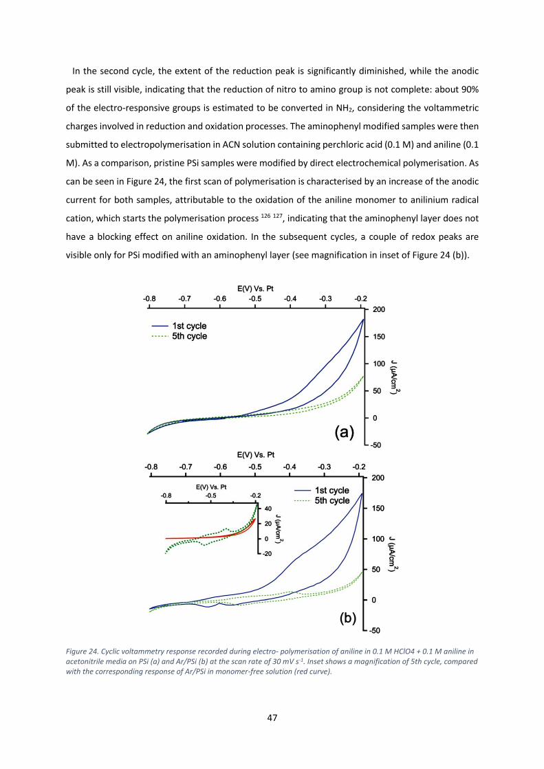
47
In the second cycle, the extent of the reduction peak is significantly diminished, while the anodic
peak is still visible, indicating that the reduction of nitro to amino group is not complete: about 90%
of the electro-responsive groups is estimated to be converted in NH2, considering the voltammetric
charges involved in reduction and oxidation processes. The aminophenyl modified samples were then
submitted to electropolymerisation in ACN solution containing perchloric acid (0.1 M) and aniline (0.1
M). As a comparison, pristine PSi samples were modified by direct electrochemical polymerisation. As
can be seen in Figure 24, the first scan of polymerisation is characterised by an increase of the anodic
current for both samples, attributable to the oxidation of the aniline monomer to anilinium radical
cation, which starts the polymerisation process 126 127, indicating that the aminophenyl layer does not
have a blocking effect on aniline oxidation. In the subsequent cycles, a couple of redox peaks are
visible only for PSi modified with an aminophenyl layer (see magnification in inset of Figure 24 (b)).
Figure 24. Cyclic voltammetry response recorded during electro- polymerisation of aniline in 0.1 M HClO4 + 0.1 M aniline in acetonitrile media on PSi (a) and Ar/PSi (b) at the scan rate of 30 mV s-1. Inset shows a magnification of 5th cycle, compared with the corresponding response of Ar/PSi in monomer-free solution (red curve).

48
In order to check if these peaks could still be the response of residuals NO/NHOH groups of the
reduced NBD layer in the acidic medium, cyclic voltammetries have been performed in a monomer-
free solution before the electropolymerisation. As can be seen, no appreciable signals can be detected
in the polymerisation range. The two peaks detected during the electropolymerisation can be related
to the redox transitions of PANI from leucoemeraldine to emeraldine and from emeraldine to
pernigraniline 128. In the case of electropolymerisation on pristine PSi samples, the redox couples are
not visible neither in the fifth cycle, indicating that the polymerisation process is more effective on the
aminophenyl modified electrode. Similar behaviour has been reported for gold and carbon based
electrodes modified with PANI with and without an aminophenyl layer 129 130. The polymerisation of
PANI is a self-catalytic head-to-tail process: the presence of aminophenyl layers grafted onto the PSi
can promote the oxidative radicalic polymerisation process and, due to the similarity of the organic
layer to aniline, it can offer a large number of starting points for the aniline polymerisation, allowing
us to obtain a more strongly adherent coating 131. The lower efficiency of polymerisation observed
with bare PSi may be due to concentration gradients between the porous layer and the bulk of the
solution during the process. The concentration of aniline inside the pores (i.e. the concentration of
reactant) is lowered by the formation of the anilinium radical cation. The monomer must then diffuse
from the bulk to the porous layer, adding a mass-transfer resistance to the process. When the
underlayer is present, the anilinium radicals may instead react with grafted phenylamine, which does
not present diffusion limitations. The presence of an electroactive PANI layer on the PANI/Ar/PSi can
be evidenced by cyclic voltammetries in monomer-free solutions. Figure 25 shows the
voltammograms recorded in ACN solution containing HClO4 0.1 M: the typical peaks related to doping
and undoping of protons and anions in the polymeric film, as well as the transformation between
different forms of PANI, are visible at high values of scan rate 132.

49
Figure 25. Cyclic voltammetries performed on PANI/Ar/PSi electrodes in ACN monomer-free solutions containing HClO4 0.1 M at different scan rates.
3.3 Optical characterisation
The optical characterisation of the porous silicon impregnated with polymers has been performed
by using reflectivity spectra.
The reflectivity spectrum of a thin layer of porous silicon corresponds physically to a thin layer with
plane and parallel faces. The thin-layer interference pattern derived from this material, also called
Fabry-Pérot fringes, are due to an overlapping of reflection from the surface of the porous silicon with
the one coming from the interface between porous silicon and the bulk. A typical example of a porous
silicon reflectivity spectrum is shown in red in Figure 26. For wavelengths shorter than about 400 nm
it is possible observe two peaks related to the bulk silicon: they will be present in every spectrum
unless the presence of another material covers the sample surface. The intensity, position, and
number of the fringes depends on the product of the refractive index n and the real thickness of the
porous layer d, also called optical thickness.
The porous layer is seen by light as a homogenous layer (the pore diameter is about 10-20 nm while
the average wavelength is 500 nm). Under that condition, the refractive index is a combination of the
refractive index of the crystalline Si skeleton and the refractive index of the medium inside the pores.
For a fresh sample, the air is the medium inside the pores. After the process of polymer grafting and
impregnation, the refractive index within the pores is that of the polymer, so the total refractive index
changes and the shape and the position of the interference fringes is modified.

50
To measure the reflectivity spectrum, a UV-Vis-NIR spectrophotometer has been used, capable to
measure the optical properties as reflectivity, absorption and transmission in a range of wavelength
from 180 to 2500 nm. By using a special module called URA (Universal Reflectance Accessory), the
spectrophotometer allow the measure of direct reflection with an angle of incidence in the 8°-63°
interval in the wavelength range of 250-2500 nm.
Functionalized PSi layers were immersed in aqueous NaOH since it is well known that the dissolution
of pristine PSi after immersion in a NaOH solution takes place very quickly 133 134. Concentrated
aqueous solutions of NaOH can be used to test the chemical resistance of our grafted samples to harsh
chemical environments. We used two solutions with two different concentrations: 0.5 and 0.1 M. The
samples have been left immersed in the solution twice for 10 s, and then depending on the sample
resistance the immersion duration was varied from 2.5 to 5 minutes until total dissolution.
In order to characterise the improved resistance of grafted samples to alkaline etching, we
monitored the optical reflectivity after each etching step. The reflectivity spectra were measured in
the 250–2500 nm wavelength range. Any modification of the PSi layer will lead to a modification of its
overall refractive index and then of the thin-layer interference fringes. Observing the variations in the
thin-layer interference fringes amplitude and position, together with the Si reflectivity peaks, it is
possible to follow the modifications of the layer with respect to initial freshly grafted PSi layer. In
Figure 26, as a reference, we show the effect on a pristine PSi layer of a 10 s dipping in a 0.5M NaOH
aqueous solution. The red curve represents the porous silicon reflectivity, and the typical Fabry-Pérot
fringes related to the thin-layer interferences are clearly visible for wavelengths longer than about 400
nm. After 10 s dipping (blue curve), as expected, the interference fringes are no longer visible due to
the almost complete dissolution of the porous layer.

51
Figure 26. Absolute reflectivityspectrum of the pristine Psi in red vs the absolute reflectivity spectrum of PSi after total dissolution inNaOH 0.5 M aqueous solution.
The behaviour of grafted PSi samples is markedly different. During the initial dipping, it was possible
to visibly observe that the portion of the PSi layer outside the nitrobenzene-grafted area (that is the
external surface region near the bulk Si—porosified Si separation border) was immediately dissolved
while the grafted area appeared unmodified throughout the process. To characterise the resistance
of the layers, as for the pristine PSi layer, we used optical reflectivity measurements. For all samples,
we measured the reflectivity of both pristine and grafted layers, as a reference. In
Figure 27, we show the evolution of the reflectivity as a function of the total dipping time for a PSi
sample whose grafting has been realized using the potentiostatic method. The pristine and freshly
grafted samples are also shown (red and black curves, respectively). The decreased reflectivity of the
Si-related double peak and the interference fringes displacement demonstrate both the Si covering
and the modification of the average refractive index of the porous layer induced by the nitrobenzene
grafting.

52
Figure 27. Reflectivity evolution of PSi grafted by the potentiostatic method with 4-NBD. The sample has been immersed in NaOH 0.5 M . The spectra are vertically shifted with respect each other by a 30% offset. The bottom spectrum has no vertical shift.
We observe that the shape of the spectra in Figure 27, remains unmodified after about 5 min of
NaOH dipping. For comparison, it is worth noting that the portion of PSi layer not covered by
diazonium was immediately dissolved in the alkaline bath while the covered area stayed stable for
much longer in the process. After 10 min, the reflectivity started to change and, after 15 min dipping,
no trace of the porous layer is observed, indicating a full PSi dissolution. The potentiostatic grafting
method has then clearly improved the chemical resistance of the PSi layer, that remains unmodified
for two order of magnitude longer times with respect the pristine porous silicon.
Using the same scheme, we studied the behaviour of samples whose grafting has been performed
by cyclic voltammetry. Since the PSi coverage depends on the number of CV cycles (as shown in Figure
19), we tested the chemical resistance of the samples grafted using different numbers of CV cycles.
In Figure 28, we show the evolution of the reflectivity spectra of a PSi grafted with 5 CV cycles as a
function of the dipping time. We observe a significant increase by a factor of 2 to 4 with respect the
functionalization in the potentiostatic regime: after 20 min etch, while clearly partially degraded, the
thin film interference fringes were still visible, indicating that the porous layer was still present.

53
Figure 28. Reflectivity evolution of PSi grafted with five CV cycles. The sample has been immersed in NaOH 0.5 M . The spectra are vertically shifted with respect each other by a 30% offset. The bottom spectrum has no vertical shift.
We performed the chemical resistance test on samples modified with different numbers of CV cycles
since, as shown in Figure 19, after five CV cycles the reduction peak is still present. For less than five
CV cycles, the chemical resistance, while still higher than that observed for potentiostatic grafted
samples, was decreased with respect to that obtained for the sample of
Figure 28. For more than five CV cycles, instead, an increase of the chemical resistance is observed.
In Figure 29, we show the evolution of the reflectivity spectra for a PSi sample grafted with eight CV
cycles.

54
Figure 29. Reflectivity evolution of PSi grafted with eight CV cycles. The sample has been immersed in NaOH 0.5 M . The spectra are vertically shifted with respect each other by a 30% offset. The bottom spectrum has no vertical shift.
In this case, it is clear that there is a significant improvement with respect to the five CV cycles
grafting: after 38 min, the PSi structure is only slightly modified. Further increasing the number of
cycles does not significantly improve the chemical resistance, even if the reduction peak is visible up
to the 12th cycle.
The number and the position of the fringes depend on the optical thickness of the porous layer. The
refractive index of PSi depends on the porosity and, once that is fixed, on the pores content. When
filling the pores, the air is progressively replaced by the polymer, changing then the overall refractive
index of the porous matrix. It is worth noting that since the pore size is more than one order of
magnitude smaller than the shortest wavelength in the spectrum, therefore all light scattering effects
can be neglected.
The comparison of the spectra in Figure 30 (a) and (b) is interesting in view of understanding the
different behaviours induced in the PANI and PSi composite, with and without the presence of the aryl
under-layer. Figure 30 (a) shows the PSi layer where PANI has been inserted without the aryl under-
layer. It is evident that the PANI/PSi composite (green curve) does not show major differences with
respect to the PSi reflectivity without PANI (black curve). This is not the same when the aryl layer is
inserted before PANI, as shown in Figure 30 (b): PANI/Ar/PSi (green curve) shows a reflectivity
spectrum where the thin layer interference fringes are significantly modified with respect to the
pristine PSi layer (black curve).

55
Figure 30. Reflectivity spectra: PSi and PANI/PSi (a); PSi and PANI/Ar/ PSi (b).
The presence of PANI also induces a significant reduction of the Si doublet peak, since the silicon
surface is progressively covered. The displacement of the fringes is indicative of a modification of the
optical thickness of the layer. Since the absence of features of a double layer excludes the possibility
of a thick PANI layer on the external PSi surface, the modification of the periodicity of the fringes can
only be attributed to the presence of PANI within the pores, demonstrating the effectiveness of the
filling process.
Figure 31 shows the spectra of crystalline silicon, crystalline silicon with PANI and crystalline silicon
with Ar/PANI: no interference fringes can be observed, while changes in the reflectivity are present in
the region of wavelengths shorter than 1100 nm, which can be attributed to the optical response of
PANI. We analysed the reflectivity data in Figure 30 and Figure 31, modelling the presence of PANI
within the porous layer.

56
Figure 31. Absolute reflectivity of the cristalline silicon vs. PANI/Ar/Si and PANI/Si.
Our analyses show that PANI is present in the whole layer both with and without the aryl underlayer,
even if there is a gradient in the PANI concentration along the sample’s thickness. The gradient is
expected as it is common in all thin pores filling processes. In our case, for PANI/Ar/PSi, the
concentration gradient is such that the bottom concentration can be estimated to be about one third
of the surface concentration. On a homogeneous layer fitting, i.e. without considering concentration
gradients, the PANI filling can be evaluated as filling about 80% of the pores inner volume. This also
can be expected since, given the dendritic structure of the PSi pores, it is difficult for the aniline to fill
every available volume portion. In summary, the reflectivity data fitting confirm the presence of the
PANI in the whole structure and that a concentration gradient is also found. A comparison of the
PANI/PSi results with the analysis of the reflectivity spectra of PANI/Ar/PSi shows a reduction of the
PANI content when the underlayer is not present. Although a reliable quantitative evaluation of the
PANI content is difficult with only the simulation of reflectivity spectra, a rough estimate suggests that
the amount of PANI in PANI/PSi is less than two times that in the corresponding PANI/Ar/PSi. These
results confirm that for aminophenyl-modified PSi the polymerisation process is more effective.
3.4 Spectral dependence of the photocurrent
By using the low pass filter described in Material and Methods in section 2.4.1, we performed
photocurrent measurements. The light has been provided by a full spectrum lamp. The filters have
been placed under the light and the corresponding photocurrent generated has been recorded. The
results are shown in Figure 32. The p–n junction between the organic layer and PSi improves the light
absorption in the visible range compared to the empty porous silicon (Figure 32 (a)). The absolute
white-light photocurrent was also higher for the hybrid junction. The PANI/Ar/PSi samples show a
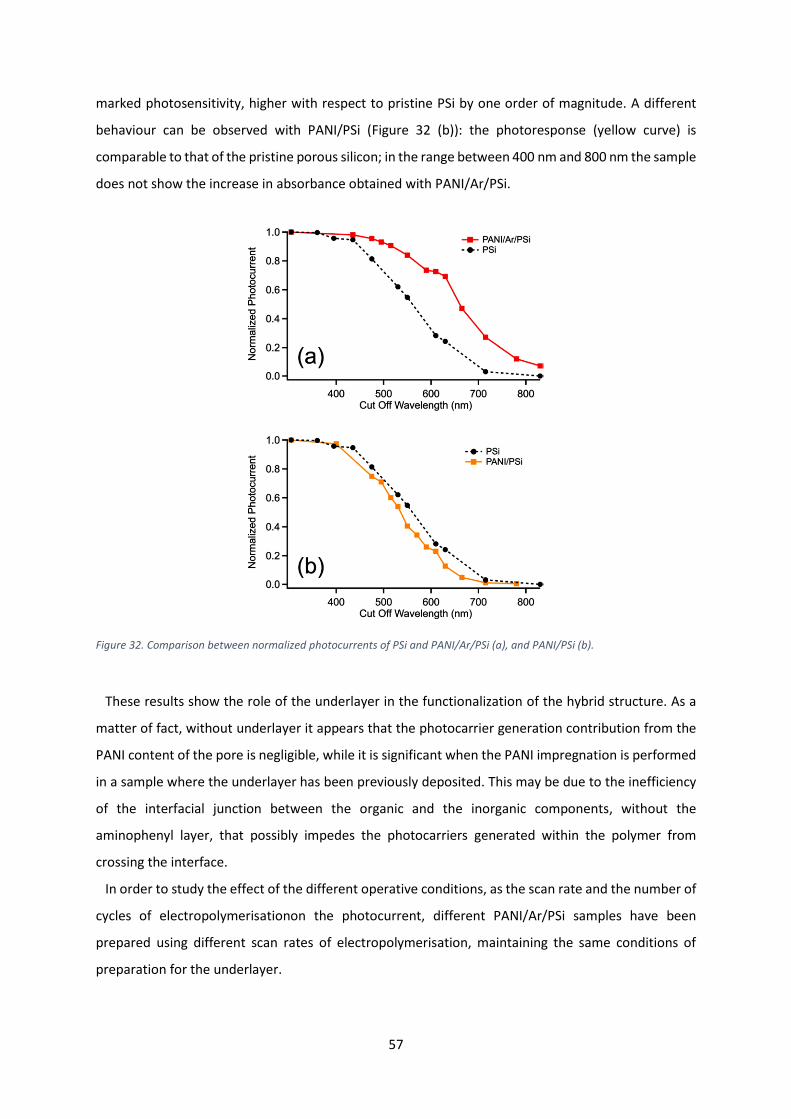
57
marked photosensitivity, higher with respect to pristine PSi by one order of magnitude. A different
behaviour can be observed with PANI/PSi (Figure 32 (b)): the photoresponse (yellow curve) is
comparable to that of the pristine porous silicon; in the range between 400 nm and 800 nm the sample
does not show the increase in absorbance obtained with PANI/Ar/PSi.
Figure 32. Comparison between normalized photocurrents of PSi and PANI/Ar/PSi (a), and PANI/PSi (b).
These results show the role of the underlayer in the functionalization of the hybrid structure. As a
matter of fact, without underlayer it appears that the photocarrier generation contribution from the
PANI content of the pore is negligible, while it is significant when the PANI impregnation is performed
in a sample where the underlayer has been previously deposited. This may be due to the inefficiency
of the interfacial junction between the organic and the inorganic components, without the
aminophenyl layer, that possibly impedes the photocarriers generated within the polymer from
crossing the interface.
In order to study the effect of the different operative conditions, as the scan rate and the number of
cycles of electropolymerisationon the photocurrent, different PANI/Ar/PSi samples have been
prepared using different scan rates of electropolymerisation, maintaining the same conditions of
preparation for the underlayer.

58
Figure 33 shows the second polymerisation cycle at different scan rate: as can be seen the current
intensity of redox peaks of PANI polymerisation are visible and they increase with the scan rate,
indicating that PANI growth occurs under each examined condition.
Figure 33. Cyclic voltammograms (2nd cycle) recorded during electro-polymerisation of aniline in 0.1 M HClO4 + 0.1 M aniline in acetonitrile media on PSi electrode after NBD reduction at the scan rate of 30, 50, 70 and 100 mV s-1.
Figure 34 (a) and (b) show photocurrents obtained for PANI/Ar/PSi samples with different scan rates
and number of voltammetric cycles. As can be seen, differences in the absolute value of the
photocurrent are clearly visible: in particular, the photocurrent increases when the scan rate
decreases and, when the scan rate is fixed the photocurrent increases with the number of cycles. It is
well known that characteristics such as morphology, conductivity and rate of the polyaniline growth
are strongly dependent on the operating conditions 135.
When potentiodynamic electrodeposition is used, the scan rate can play an important role. The
growth mechanism of PANI may occur via three different dimerization paths (i.e., head-to-head, head-
to-tail, and tail to-tail), as well as competitive degradation reactions 135. Depending on the scan rate,
the formation of polyaniline can be controlled by the fastest reaction (i.e., head-to-tail polymerisation)
or by the secondary reactions (e.g., tail-to-tail, head-to head polymerisations, degradation reactions)
118. In our case, further issues complicate the process, since the polymerisation occurs in a porous
structure, where diffusion effects overlap the kinetic aspects. The number of CV cycles also affects the
overall efficiency of the system, as shown in Figure 34 (b) for a series of samples prepared with a scan
rate of 30 mV s-1, which increases the number of CV cycles.

59
Figure 34. Photocurrent registered for different scan rate (a) and different number of CV (b).
3.5 Photoconductive AFM results
In this study, PC-AFM, a recent noteworthy method for nanoscale characterisation of photovoltaic
elements, was used for direct measurements of the photocurrent generation properties at the
nanoscale with respect to standard millimetre-size areas. The effects of changes in the current
intensity were observed. The PC-AFM analysis described hereafter has been performed on a PSi
sample impregnated with eumelanin with the methodology described in 63.
In PC-AFM, the tip used plays a fundamental role. The tip needs to be coated to be conductive and
that significantly increases the tip radius. The porous silicon pores used for all the experiments
described earlier were too small to allow detection of any local pore-dependent current given the
difficulty in selecting a specific region of interest. For those reasons, we fabricate PSi layers whose
pores were significantly larger, reaching about 60nm diameter. The samples were prepared using the

60
Electrochemical NanoLithography technique, developed in the PoroSiLab, that allows to control the
distribution and density of pores by an electrochemical etching process that leaves small indentation
on the Si surface acrting as seeds for the nucleation of the pores. In Figure 35 is shown the top view
SEM image of the sample prepared with this technique that we used in our PC-AFM experiment. The
advantage of these samples is that thanks to the larger pores geometry the photoconductive
behaviour showed a significantly longer temporal stability (several weeks as compared to a couple of
days), a parameter that is obviously extremely relevant for the PC-AFM experiments.
Figure 35. SEM image of the new sample with large pores.
The first step of the analysis consists in finding what is the most appropriate tip for photoconductive
measurements, that can at the same time resolve the porous structure. In Figure 36 an AFM
topographic image of a PSi sample is shown similar to the one shown in Figure 35. The tip used in this
case, an ARROW-CONT-Pt, with a Platinum coating has tip radius of <30nm. This tip has been used in
contact mode and the pore feature were not visible. The image shows the impossibility to distinguish
individual pores.

61
Figure 36. AFM image of the sample by using contact mode. First test.
For those reasons we decided to use an alternative tip as shown in Figure 37: an OPUS 240 AC-NA.
This tip has a radius of <7 nm and is made for tapping mode scans in case of photoconductive material
with particularly hard surface. By using the Opus tip, it has been possible to resolve the porous
structure with the AFM (Figure 38).
Figure 37. AFM tip used for better resolving the porous structure of the PSi.
Figure 38. AFM images of the surface of the PSi sample for 50 total scans of imaging.
By monitoring the scanning along the surface, we noticed the tendency of the pores in the image to
blur. Making more tests, as the one shown in Figure 39, we discovered that the PSi surface is able to

62
relatively quickly deteriorate the probe tip, creating as a result the difficulty to acquire more than one
image of a small area at a time.
The images in Figure 40 are obtained by focusing on a smaller area of 10 μm x 10 μm and
subsequently zooming in an area of 200 nm x 200 nm. As it is possible observe, the pores are not
plugged and this confirms that the filling procedure doesn’t modify the top surface of the PSi.
Figure 40. AFM images of the PSi/eumelanin sample (left) and a smaller area (right).
By zooming further, topography and current maps have been performed after the procedure of laser
beam focusing. From the images in Figure 41 (a) and (b), it is possible to observe some well-defined
pores. In Figure 41 (c) and (d) the current map is shown, and the corresponding current is recorded in
proximity to the pore. The two curves are aligned in order to demonstrate that the current peak
registered corresponds to the hole in the topographic image.
Figure 39. AFM image test of the sample surface for a total image acquisition.
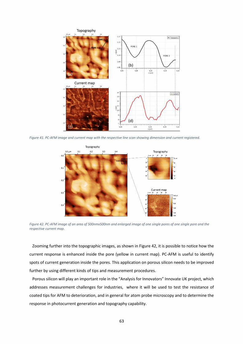
63
Figure 41. PC-AFM image and current map with the respective line scan showing dimension and current registered.
Figure 42. PC-AFM image of an area of 500nmx500nm and enlarged image of one single pores of one single pore and the respective current map.
Zooming further into the topographic images, as shown in Figure 42, it is possible to notice how the
current response is enhanced inside the pore (yellow in current map). PC-AFM is useful to identify
spots of current generation inside the pores. This application on porous silicon needs to be improved
further by using different kinds of tips and measurement procedures.
Porous silicon will play an important role in the “Analysis for Innovators” Innovate UK project, which
addresses measurement challenges for industries, where it will be used to test the resistance of
coated tips for AFM to deterioration, and in general for atom probe microscopy and to determine the
response in photocurrent generation and topography capability.
(a)
(b)
(c)
(d)

64
3.6 Optical lithography
Optical lithography is an important part in semiconductor and manufacturing technology. It refers
to a lithographic process that uses visible or ultraviolet light to form patterns onto a semiconductor
surface by using a mask that reacts with the light: the mask can be a photomask or a light sensitive
resist distributed onto the surface called a photoresist. The photoresist needs a developer that is
usually an alkaline solution, usually containing NaOH, to form the desired pattern on the surface after
the illumination 136. This solution, as mentioned before, cannot be used for PSi because it causes a
dissolution of the silicon matrix. Since the NBD makes PSi resistant to dissolution induced even by
harsh alkaline solutions, this means that it is possible to perform optical lithography on porous silicon
without its degradation after NBD functionalisation of the porous layers. The SEM image in Figure 43
after the NBD functionalization shows that that the pores are not plugged even after 12 CV cycles,
where the diazonium reduction peak is almost not present anymore.
Figure 43. SEM image of porous silicon grafted sample (top view)
The lithography process was performed using a positive photoresist in which the portion exposed to
the light become soluble to the developer solution. In the first step the photoresist AZ5214E has been
spin coated on the porous silicon sample surface. To allow the total evaporation of the solvent
contained in the photoresist, the sample has been softly baked making it photosensitive. The device
matrix applied to the sample is a 50 × 50 µm2 pattern of metallic squares. This metal mask was
patterned on the sample exposing the resist-coated surface to UV light of high intensity. After the UV
exposure the photoresist has been developed in a solution 1:1 volume containing deionized water and

65
a sodium based basic AZ developer and removed by using a lift-off technique. After the metallic pads
pattern was successfully obtained on the sample surface, the contacts were deposited by electron
beam evaporation of a 5 nm thick layer of of Ti followed by a 90 nm layer of Au. This allows to perform
some basic electrical resistance measurements on the porous silicon sample and to compare the
electrical behaviour of the grafted PSi with the pristine PSi.
In Figure 44 (a), it is possible to observe in the right side of the optical microscope image residual
photoresist removal after a bath in acetone on silicon bulk and the pattern on the porous region
delimited by the O-ring (used to define the region of the sample where the Psi is being generated) by
the dashed line. In Figure 44 (b), a SEM image of the final gold contacts deposited on the sample
surface is shown.
Figure 44. Optical image (a) and SEM image (b) of the grid after deposition.
The effectiveness of the NBD deposition in protecting the Psi layer from the NaOH based alkaline
developing solution needed for photolithographic process is evidenced by the optical and SEM images
shown in Figure 44.
In Figure 45 (a) (cross section) and (b) (top view), is possible to notice how the porous structure is
fully preserved as well the open pores in the top view.
(b) (a)

66
Figure 45. SEM images after litographic process from the PSi/NBD cross section (a) and surface(b).
This demonstrates that the NBD functionalization of the porous matrix by using cyclic voltammetry
effectively protects the PSi from dissolution by contact with chemical alkaline solutions.
Further I-V characterisation of the PSi (black curve) and the PSi grafted with NBD (green curve) shown
in Figure 46 shows that there are no significant differences in the current response behaviour between
the two samples apart from a slight variation of the resistance in the grafted sample. This shift can be
due to small variations in the porous silicon layer.
Figure 46. I-V characteristic curve of PSi vs the PSi grafted with 15 cycles of NBD.
3.7 Summary
The PSi grafted and impregnated with conducting polymer has been characterised by using different
techniques. All these techniques show consistent results and help to explain what is happening to the
sample and at the interface between the two materials. The samples response to harsh chemical
(a) (b)

67
agents changes dramatically, becoming significantly more resistant after the NBD grafting. Moreover,
the pores are not plugged, meaning that it is possible to further proceed to PANI grafting, as we
discussed, and also that this opens the way to possible uses of the grafted samples in electronic
devices directly or with further functionalization (e.g. for sensors) without having to deal with the
issue of porous matrix dissolution.
Characterisation of hybrid materials always poses significant challenges due to the significant
difference in physical and chemical properties of organic and inorganic materials. In this study, we
approached the structural characterisation of these kind of materials by mass spectrometry. Given the
growing interest in mass spectrometry and in its capability to analyse the components of organic
compounds in term of molecular fragments from buried interfaces and from macroporous materials,
we explored the use of the secondary ion mass spectrometry (SIMS) technique on Si-polymer hybrid
samples, and the results of this study will be presented in the next chapter.
However, to analyse buried interfaces in multilayer samples, or interfaces between organic and
inorganic materials with SIMS, the first mandatory step is to obtain a clean cross section in-situ by
using a focused ion beam mounted on a SIMS instrument. This step is difficult to calibrate when using
organic/inorganic hybrids, given the huge differences in the properties of these two types of materials.
The first challenge for these studies by SIMS is finding two types of materials that can act as a proxy
for a hybrid material system. For this reason, due to the nanoscale nature of the PSi/polymer
structures, which would initially be disproportionally complex to understand due to difficulties in the
data interpretation, a preliminary study on a similar hybrid system having a larger scale, that can mimic
the porous silicon system, is necessary. For this reason, we used a microchannel plate filled with two
different well-known polymers as a reference material. This structure will be used as reference for
enabling the development of a protocol suitable for the study of hybrid heterojunctions in smaller
scales, as in the case for PSi. As we will see in the next chapter, the identification of the best
measurement parameters is far from straightforward, and basic issues related to the degradation of
the organic material have to be dealt with. The SIMS-based work for this thesis has been done under
the international 3DMetChemIT project 137.

68

69
4 Microporous hybrid material experimental results
In this chapter I will present the work published in the papers:
Tiddia, M.; Seah, M. P.; Shard, A. G.; Mula, G.; Havelund, R.; Gilmore, I. S. Argon Cluster Cleaning
of Ga + FIB-Milled Sections of Organic and Hybrid Materials. Surf. Interface Anal. 2018, DOI:
10.1002/sia.6522.
Tiddia, M.; Seah, M. P.; Mihara, I.; Trindade, G.F.; Kollmer, F.; Roberts, C.; Hague, R.; Mula, G.;
Gilmore, I; Havelund, R. FIB-SIMS for Hybrid Materials – Cleaning the FIB Damaged Organic
Material with Argon Gas Cluster Ions. (submitted)
4.1 Challenges to be addressed
Chemical characterisation at organic-inorganic interfaces is challenging, in particular if these are
buried. SIMS is well suited for this purpose, but accessing buried interfaces is often difficult. Standard
depth profiling as described in Chapter 2 is problematic because the inorganic phases sputter more
slowly that the organic phases. An alternative approach is the use of FIB milling to prepare section for
SIMS analysis.
SIMS has been used for many years with FIB to provide analysis through very local sections of
materials to depths of many micrometres 138–142 . The FIB sections are generally made using a focussed
Ga+ ion beam provided with the smallest spot sizes, 139 143 with reasonable beam currents and
sputtering rates. Ga+ ions during the milling remove material and are implanted in the surface of the
remaining material and they can be easily detected by the SIMS. Excellent examples of the method
for inorganic samples have been shown by Whitby et al, 141 Schneider et al 142 and many others, but in
case of organic-inorganic hybrid materials, the FIB-SIMS analysis becomes strongly challenging. This is
mainly because the FIB damages the organic material. Methods are needed to minimize or remove
the FIB damage for successful FIB-SIMS analysis. A recent work by Iida et al 144 reports how an organic
material that has been damaged by a FIB can be removed by using Ar GCIB sputtering 144 (notice that,
in this chapter, Ar refers to the chemical element argon as opposed to Aryl used in chapter 3). Here,
we present a study of FIB-SIMS using three different FIB sources Ga+, Bi and Bi3+. First, a simple sample
of polystyrene and PMMA spin coated on silicon and as sheets has been analyzed and subsequently
an inorganic-organic test device has been developed, consisting of a regular pattern of a polymer,

70
either PMMA or PS, and silicon. This is used to study and optimize the FIB-SIMS parameters and the
FIB damage cleanup procedure.
We focus the attention on two categories of samples; the first group is used to study implantation
effects on flat surfaces and the second group is used to study the behaviour in FIB-milled sectioning.
The first category consisted of high purity Goodfellow PS sheets, 1.2 mm thick, used to study the effect
of the Ga+ ion angle of incidence. The second category of samples is inorganic-organic structures
suitable as archetypes for analysis. These samples were made by pressing either PS or (PMMA) into
the MCP surface 84 and then annealing it at 210 °C under load in a vacuum oven for 5 hours as
described in section2.2.2. The MCP is made from sintered glass tubes, with a hole diameter of 10 μm,
in a hexagonal array tilted at 12° to the MCP surface normal. The hot pressing fills these tubes with
polymer. The inner surfaces of the tubes have a surface coating to enhance the electron multiplication
required for its original application. Studies were also made of unfilled MCPs. The glass of the MCP
occupies 37% of the volume with the remainder either unfilled (vacuum) or filled with polymer.
4.2 Experimental setup design
To prepare a cross section for analysis, a Ga FIB is used with an energy of 30 keV (20 nA) to mill out
a crater size of 120 μm in the x-direction and 80 μm in the y-direction (see Table1 for the beam
parameters). The milling is monitored using the Bi32+ beam with a field of view of 200 μm by 200 μm
containing 512 × 512 pixels. This configuration is shown in Figure 47 (a). The crater wall prepared for
SIMS imaging is the top wall, closest to the Ga+ source, at an angle of approximately 45° to the MCP
surface normal. The beam follows a sawtooth raster pattern with the scan direction being from left to
right in the images, starting from the bottom and moving to the top in each scan as showed in Figure
47 (b).

71
Figure 47. Schematic representation of the FIB-ToF-SIMS geometry. (a) FIB and LMIG (b) Sample milling and FIB scan direction. (c) Cleaning process by using the GCIB with a 180° rotation of the sample.

72
Focused Ion Beam Parameters
Type Energy Crater size Current Pixel FOV Milling pass Dwell time
Ga+ 30 keV 120 µm × 80
µm 20 nA
512 x 512
300 µm × 300 µm
1, 2, 3 25 ms/pixel
Table 1. FIB parameters
To optimize the lateral resolution of the secondary ion image, after the cleaning procedure, the
sample is further rotated 90°. In that orientation, the Bi32+ beam is normal to the FIB section surface
to give the optimal lateral resolution.
The removal of the damaged layer on the FIB section by Ar GCIB is performed with the sample
rotated by 180° (see Figure 47 (c)). This clean-up procedure leads to the recovery of the characteristic
organic secondary ion signals from the milled wall (at approximately 45°, as we shall see later). The Ar
GCIB was an Ar2500+ beam at 10 keV (4 eV/atom) with a beam current of 6 nA and was rastered over a
500 μm × 500 μm area. Secondary ion images are recorded during the Ar GCIB clean-up to follow the
recovery of the correct organic signals using the Bi32+ beam with a current of 0.02 pA.
A schematic of this sample with a FIB-milled surface is shown in Figure 48 (a). To reduce damage and
re-deposition on the final cross section wall, the FIB-milling is made with a raster that starts at the
lower left in Figure 48 (a) and finishes at the top right of the final sectional surface to be studied.
Section surfaces are made with 1, 2 and 3 passes of the full raster to extend the depth of the cut but,
in the present context, we see no differences between these final surfaces except for the depth over
which they extend.
All of the FIB-milled sections discussed in this work relate to the hybrid MCP samples. An imaginary
slice through the FIB-milled surface is shown in Figure 48 (b) rotated clockwise through 45°, so that
the Ga+ beam is now vertical. The implanted Ga+ ions may be deposited to a certain depth which may
be calculated using the SRIM program 145.
SRIM calculations were carried out in collaboration with Dr Martin Seah at the National Physical
Laboratory. Used directly, SRIM allows the implantation of many ions but each new ion is into the
same pure undamaged polymer. In the continuum process of milling the section, this deposition will
have occurred many times, associated with the overlayer removal, so that the SRIM calculations
below, whilst correct for small doses, need modification for high doses.
In practice, the cutting may be associated with some roughening. Long wavelength roughening is not
a problem, but the development of cone-like structures would require much more extensive cleaning
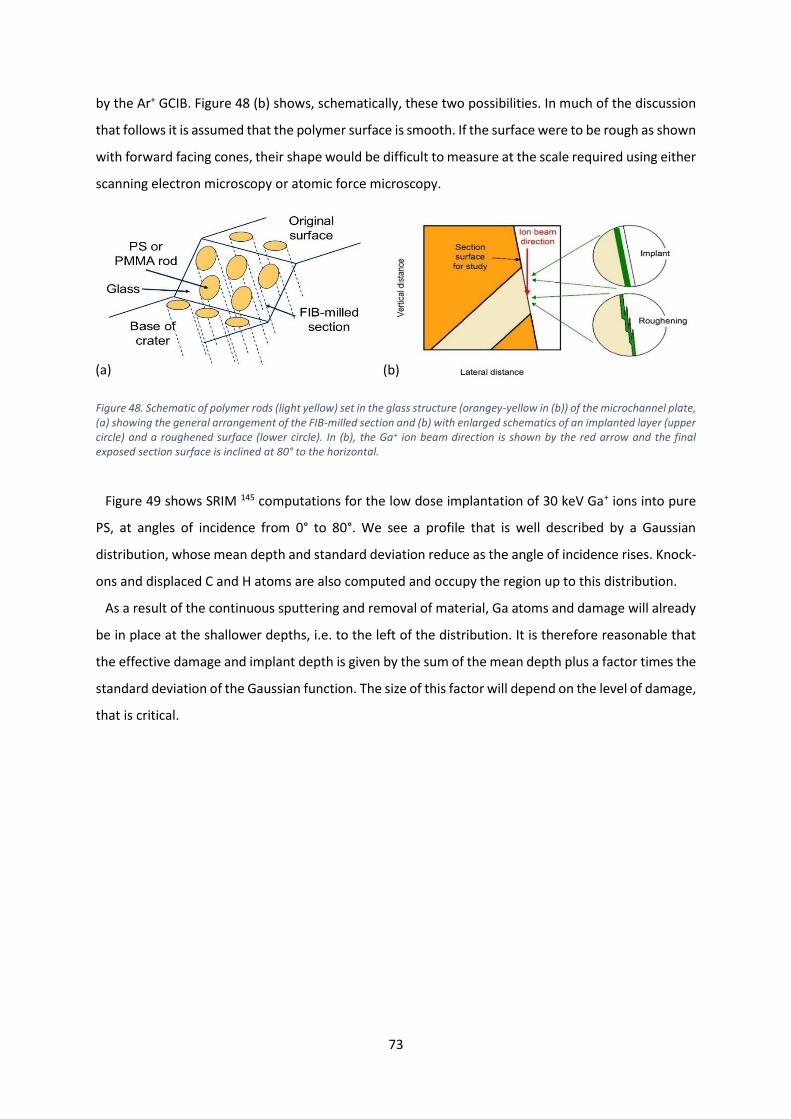
73
by the Ar+ GCIB. Figure 48 (b) shows, schematically, these two possibilities. In much of the discussion
that follows it is assumed that the polymer surface is smooth. If the surface were to be rough as shown
with forward facing cones, their shape would be difficult to measure at the scale required using either
scanning electron microscopy or atomic force microscopy.
Figure 49 shows SRIM 145 computations for the low dose implantation of 30 keV Ga+ ions into pure
PS, at angles of incidence from 0° to 80°. We see a profile that is well described by a Gaussian
distribution, whose mean depth and standard deviation reduce as the angle of incidence rises. Knock-
ons and displaced C and H atoms are also computed and occupy the region up to this distribution.
As a result of the continuous sputtering and removal of material, Ga atoms and damage will already
be in place at the shallower depths, i.e. to the left of the distribution. It is therefore reasonable that
the effective damage and implant depth is given by the sum of the mean depth plus a factor times the
standard deviation of the Gaussian function. The size of this factor will depend on the level of damage,
that is critical.
Figure 48. Schematic of polymer rods (light yellow) set in the glass structure (orangey-yellow in (b)) of the microchannel plate, (a) showing the general arrangement of the FIB-milled section and (b) with enlarged schematics of an implanted layer (upper circle) and a roughened surface (lower circle). In (b), the Ga+ ion beam direction is shown by the red arrow and the final exposed section surface is inclined at 80° to the horizontal.
(a) (b)

74
4.3 Application to pure polymer
Many profiles of the Ga+ implanted flat PS surfaces were recorded for Ga+, C7H7+ and other positive
secondary ions for different conditions. Example profiles are shown in Figure 50 for an implanted dose
of 85 Ga+ ions/nm2 into PS surfaces at 0°, 60° and 80° incidence angles. The C7H7+ secondary ions are
taken to be indicative of relatively undamaged material.
Figure 50. Measured depth profiles for Ga+ and C7H7+ secondary ions from samples of PS implanted with 85 Ga+ ions/nm2 at
30 keV as a function of 10 keV Ar2500 cleaning dose at 45° incidence angle. The colour scheme is the same as Figure 51 with black, orange and purple for 0°, 60° and 80° incidence angles, respectively. The solid lines joining circles are for Ga+ and the
dashed lines joining triangles for C7H7+ ions.
From the data reported in Figure 50 it is possible to determine the dose needed to remove the
implanted and damaged layer. We may calculate the sputtering yield of pure PS, Y in nm3, for this
condition and using the equation 146
0
0.2
0.4
0.6
0.8
1
1.2
0 15 30 45 60 75 90
Depth, nm
Norm
aliz
ed
Ga
im
pla
nta
tio
n d
en
sity
0
30
40
50
60
70
80
, deg =80
o0
o
0
0.2
0.4
0.6
0.8
1
1.2
0 20 40 60 80 100
Ar GCIB ion dose/nm2
Norm
alli
ze
d in
ten
sity
Ga+ C7H7
+
80o
0o
60o
Figure 49. SRIM computations for the implantation depth distributions, each for 5000 trajectories of 30 keV Ga+ ions into
pure PS for many angles of incidence, .

75
𝑌
𝑛=
𝐵(𝐸/𝐴𝑛)𝑞
1 + (𝐸/𝐴𝑛)(𝑞−1)(1)
where E is the Ar+ GCIB of 10000 eV and n is the cluster size (2500 atoms in our case). For PS, the
parameters A, B and q are 2.36 eV, 0.011 nm3 and 3.4, respectively. Thus, Y = 37 nm3. The dose to
remove the Ga+ and for the C7H7+ signal to reach 50% for 0° implantation is about 60 Ar+ GCIB ions/nm2.
This, combined with the sputtering yield of 37 nm3, would remove over 2 µm of pure PS rather than
the 60 nm. This high GCIB dose could be due to micro-topography or to a strongly reduced sputtering
yield. We shall analyse the latter here.
The observed behaviour originates from the fact that the PS being removed is not at all pure: it is
highly damaged and contains a high level of Ga atoms. Both of these effects reduce the sputtering
yield. Our earlier analysis of both organic and inorganic materials 146 shows that at E/n = 4, the
transition from organic to inorganic results in a reduction in sputtering rate of about 1000. The present
situation indicates an interim position that we need to analyse more fully.
Figure 51 shows that, at a dose of about the median of the Ga+ distribution plus two times its sigma,
the C7H7+ intensity has risen significantly in each case. We compute this for a rise of the PS signal to
50%, since that gives the mean effective cleaning dose. For a pure PS spectrum, significantly more
cleaning may be required but the extent of that will depend on the depth resolution obtained. We
cannot calculate the effective damage depth using SRIM but the depth equal to the Ga+ implant depth
plus two times the standard deviation width may be calculated directly, to represent a mean cleaning
dose, and this is shown in Figure 51. This depth is indicated with the symbol Z.
Further measurements on PS implanted at 45° but with a much lower dose of 1.14 ions/nm2 give the
green circle at the low G value shown in Figure 52, where the data obtained through the PS data are
0
10
20
30
40
50
60
70
0 15 30 45 60 75 90
Angle of incidence, degrees
Dep
th,
nm
Z = mean + 2 sigma
mean
sigma
W = mean + sigma
Figure 51. Depths of the Ga+ parameters from SRIM calculations at various angle of incidence in PS.

76
indicated by the purple curve, a guide the eye based upon equation (1) with the effective bond energy
related term A increasing with G. The term A starts at the value for pure PS at G = 0 of 2.34 eV and
then increases with log(G), following an integrated exponential to a value near 9 eV at G = 5 at/nm3.
In Figure 52 we show the measurements extracted from Figure 51 and from detailed study for
poly(carbonate) (PC) of Iida et al 144 (orange line). These are shown as orange circles and are relative
to a cleaning procedure performed using 20 keV Ar2500+ at 40° incidence. Data given as circles are for
implanting and cleaning on flat polymer surfaces, whereas the square symbols are for the cleaning of
FIB-milled sections for PS. The purple data are for PS surfaces implanted with 85 ions/nm2, whereas
the green circle is at the low dose of 1.14 ions/nm2. The yellow and blue squares are for a FIB-milled
sections of PS, whereas the pink-red square is for FIB-milled section of PMMA.
The solid lines are descriptions using equation (1) with the parameter A increasing with G as
described in the text. The dashed pink curve is the estimate for PMMA. For this condition, the
sputtering yield of pure PC is 60 nm3 147 148 . The remainder of the computation is as described above.
The orange curve is a guide for eyes, as is the purple curve, but in this case the A value starts at 4.2 eV
for pure PC.
Figure 52. Fractional sputtering yields versus the effective Ga density
The square symbols in Figure 52 are from FIB-milled sections of the hybrid glass and polymer samples
shown in Figure 48, rather than implanted flat surfaces. Note that the slope of the FIB-milled section
means that these surfaces are not cleaned with the Ar GCIB at 45° but with that beam at near normal
incidence. At normal incidence, the sputtering yield is reduced by a factor ~1.8 149 compared with that
at 45°. In Figure 52, the FIB-sectioned data are for PS (yellow and blue) and PMMA (pink-red) and are
all computed for the Ar GCIB normal to the local surface. The effective Ga density is calculated from
0.001
0.01
0.1
1
0.01 0.1 1 10 100
G , effective Ga at/nm3
fractional sputt
ering y
ield
, Y
*/Y
PS
PS
Iida PC
FIB PMMA
FIB PS
FIB PS
Low dose
45o
0o
60o
80o
PS
PC
PMMAChain scission
Cross-linking

77
the total implanted dose, here 40900 ions/nm2, divided by the total depth of the cut, here 19000 nm
depth for PS and 33000 nm depth for PMMA. The total depth of the cut can be measured directly from
the SIMS images. For the fractional sputtering yield, we need to determine the depth sputtered and
the dose. The implant depth is calculated using SRIM 150 on the basis of no roughening and for the final
surface inclined at 10° to the Ga+ FIB beam, i.e. the Ga+ angle of incidence is 80°. We use Z, which is
the total depth of the mean of the SRIM-calculated implant Gaussian plus two times sigma since that
represents the depth of the mean of the PS signal recovery dose. We need Z rather than W since, in
our FIB-milled section, we cannot use the Ga+ signal, dominated by signal from the FIB-milled glass
area, and must use instead the signal for the PS recovery as shown. Figure 53 illustrates the recovery
of different PS signals for ions with 100 <m/z< 150. The Ga+ and other signals that arise strongly from
the FIB-milled glass surface are not shown. Cleaning the glass using Ar+ GCIB is significantly slower
than the cleaning of the PS 147. The calculated Z values are 23.5 nm for PS and 27 nm for PMMA. It may
well be that these FIB Ga+ contents are significant underestimated, since the depths sputtered are
probably governed by the glass region rather than the polymer filling. However, the ordinate is
insensitive to G in this region.
Figure 53. Depth profile showing PS secondary ions from the sloping wall of the FIB-milled hybrid PS-glass sample as a function of the 10 keV Ar2500
+ ion dose. Note that this beam is set nearly normal to the local surface. The profiles show the groups CxHy+
with 8 x 11 and 7 y 11 as shown in the legend. The black line is a cumulative Gaussian fit with its mean at 31.5 ions/nm2 and which gives the yellow square in Figure 52.
The effect of gallium bombardment on polymer chemistry shown in Figure 52 has not been studied
in detail. The mechanisms would be expected to follow the general trends observed for other types
of ionising radiation 151. Such radiation induces bond scission and the generation of both excited states
and free radicals. The resulting effects depend upon their lifetimes, their mobility in the polymer and
the propensity to form low molecular weight, volatile products. Cross-linking generally occurs when
two radicals on adjacent chains are close enough to form a bond. In all cases, both chain scission and
cross-linking occur. PS is a well-studied polymer in this regard. It is able to form a long lived, stable
0
0.2
0.4
0.6
0.8
1
1.2
0 10 20 30 40 50
Dose, ion/nm2
Norm
aliz
ed inte
nsity
C8H7+
C8H9+
C9H7+
C9H8+
C9H9+
C10H8+
C10H11+
C11H9+
fit
m /z

78
benzylic radical without carbon-carbon bond scission. The radical has high mobility because of the
numerous adjacent sites both within the chain and on neighbouring chains. PS therefore tends to
cross-link after exposure to radiation. It has been shown that the introduction of water vapour during
Ga+ ion bombardment of PS maintains a high sputtering rate, presumably due to the reaction of water
with radical species and the prevention of cross-linking 151.
PMMA undergoes a number of reactions resulting in the loss of volatile species and the scission of
the main chain. PC is also reported to predominantly undergo chain scission following irradiation,
although it is less clear that this is true under ion bombardment. Mahoney 152 classes PC as a Type I
cross-linking polymer along with PS, whereas PMMA is a Type II degrading polymer involving random
chain scission processes. In agreement with this, Cumpson et al 153 demonstrate that X-ray exposure
during sputtering increases the sputtering rate of PMMA but not PS and PC. This latter study provides
a direct comparison with PS and PMMA, showing that its behaviour under combined X-ray and argon
cluster beam sputtering is close to PS.
The study by Cristaudo et al 154 also shows how changing the bonding leads to a greater effect per
bond in PS than PMMA. In the analysis by Seah 155 it is shown that the A value of PS changes 1.445
times faster than that for PMMA for each added monomer. As the density of the end groups (no
covalent bond to the next molecule) reduces, the A value increases. Equivalently, as the number of
strong bonds increases, A will increase. If the above factor is used to convert the purple curve for PS
to one for PMMA, by reducing the total change in A by this factor, we obtain the dashed pink curve
that passes very close to the measured result for PMMA. This confirms the major effect of the adding
or subtraction of bonds in changing these sputtering rates.
The difference between PS and PMMA in Figure 52 can also be explained in terms of the greater
cross-linking propensity of PS under Ga irradiation. The relative sputtering yield of Ga-irradiated PC in
the same figure is shown to be even lower than that of PS, which is not expected. This may be a result
of the presence of gallium in the bombarded polymer changing the dominant mechanism of radiation
damage. Gallium oxide, for example has a highly exothermic enthalpy of formation (-1089 kJ mol-1)
and the removal of oxygen from the polymer could disturb the balance between chain scission and
cross linking. We note that PS contains no oxygen and that gallium does not form a stable carbide. The
categorizations of Mahoney 152 and Cumpson et al 153 may thus be a rough first guide to the effects for
many other polymers in Figure 52.
Measurements involving implantation on polymer surfaces have been reported occasionally in the
past. Miyayama et al 156 studying polyimide (PI), show, for a dose of 100 Ar+ ions/nm2, that the recovery
dose using 10 keV Ar2500+ ions is ~13E ions/nm2 where E is the energy of the implanted Ar+ ions in keV.
These are similar recovery doses to those shown in Figure 53 but, of course, there are no Ga atoms to

79
remove. The easier removal of Ar may be offset by greater cross-linking in the PI. Similar
measurements are reported by Yamamoto et al 157 for the damage caused by 1 ion/nm2 of 10 keV
normally incident Ar+ implanted into PS. They find that there is a surface damaged layer of ~30 nm
with a sputtering yield of 0.23 times of undamaged PS. This damage thickness agrees with SRIM
calculations of W and gives a result, in the counterpart of Figure 52 for Ar content, that is just above
the purple line. It is likely that the implantation of Ga+, rather than Ar+ which may escape before
analysis, accounts for this difference. Some very interesting data for 60 keV implantation of Bi3++ into
PS have been given recently by Kawashima et al 158. For a Bi3++ dose of 0.05 ions/nm2 into PS, they
show how the sputtering yield falls by a factor of 3 as the PS molecular weight reduces to 1200 Da.
This low molecular weight material has a higher yield than fully polymerised PS 154 155 and so this
greater change is expected. The data for high molecular weights, when plotting versus Bi content, lie
close to the purple curve, moving slowly to the left as the molecular weight reduces. These results for
Ar+ and Bi3++ indicate that our analysis in Figure 52 may be applicable for all implanted species, not just
Ga+.
What Figure 52 shows is that the data from the smooth surfaces and the FIB-milled sections agree,
indicating that the upper simple implant model in Figure 48 is appropriate and we do not need to
consider the roughening. It also shows that the cleaning requires a much greater dose than generally
expected – but one that varies significantly with the organic material.
4.4 Application to empty MCP
Part of this work consisted of the observation of how the number of milling scans affects the milled
depth and the required cleaning. By using 1, 2 and 3 milling scans, we linearly increase the Ga+ beam
dose. As a first step we observe, in Figure 54 (a), (b) and (c), how the milled depth develops in case of
the empty MCP matrix and in Figure 54 (d), (e) and (f) the MCP matrix filled with PS. This increase of
depth with dose appears to be near-linear and is very similar in the filled MCP and in the empty MCP
since the sputtering of the polymer occurs at a much higher rate than the sputtering of the inorganic
MCP 147.
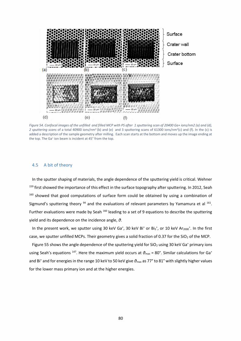
80
Figure 54. Confocal images of the unfilled and filled MCP with PS after 1 sputtering scan of 20400 Ga+ ions/nm2 (a) and (d), 2 sputtering scans of a total 40900 ions/nm2 (b) and (e) and 3 sputtering scans of 61300 ions/nm2(c) and (f). In the (c) is added a description of the sample geometry after milling. Each scan starts at the bottom and moves up the image ending at the top. The Ga+ ion beam is incident at 45° from the top.
4.5 A bit of theory
In the sputter shaping of materials, the angle dependence of the sputtering yield is critical. Wehner
159 first showed the importance of this effect in the surface topography after sputtering. In 2012, Seah
160 showed that good computations of surface form could be obtained by using a combination of
Sigmund’s sputtering theory 94 and the evaluations of relevant parameters by Yamamura et al 161.
Further evaluations were made by Seah 160 leading to a set of 9 equations to describe the sputtering
yield and its dependence on the incidence angle, θ.
In the present work, we sputter using 30 keV Ga+, 30 keV Bi+ or Bi3+, or 10 keV Ar2000+. In the first
case, we sputter unfilled MCPs. Their geometry gives a solid fraction of 0.37 for the SiO2 of the MCP.
Figure 55 shows the angle dependence of the sputtering yield for SiO2 using 30 keV Ga+ primary ions
using Seah’s equations 147. Here the maximum yield occurs at θmax = 80°. Similar calculations for Ga+
and Bi+ and for energies in the range 10 keV to 50 keV give θmax as 77° to 81° with slightly higher values
for the lower mass primary ion and at the higher energies.

81
Figure 55. Calculated angular dependence of the sputtering yield of SiO2 using 30 keV Ga+.
At 45° incidence to the MCP surface, the sputtering yield is 6.74 atoms/ion. In our 3 craters, we have
used doses of 20400, 40900 and 61300 ions/nm2 so we would expect depths of 4.8, 9.7 and 14.6 μm
allowing for the 37% solid fraction. Actually, the depths measured by confocal microscopy are 13.5,
25.5 and 31 μm, some 2.4 times higher. The reason for this is that whilst the average MCP surface is
at 45° to the beam, the local surface being sputtered is not at 45° to the beam. The sputtering is
conducted as a raster scan where the beam has an approximately Gaussian profile with a full width at
half maximum of 0.8 μm on the sample surface and the pixel-to-pixel interval is 0.156 μm. Thus, the
first application of the beam at 45° to the MCP surface digs a small hole but at the next pixel, there is
an increased slope on the side being sputtered, so that the yield rises and a slightly deeper hole is
made and so on until the angle of the FIB-milled slope at the side of the hole is approximately θmax. It
may locally increase beyond this value as a result of changes to other pixels. At 70° to the FIB-milled
surface, the predicted vertical depths are 12.5, 25.1 and 37.7 μm, not very different from those
observed using the confocal microscopy. The average angle of the beam to the FIB-milled surface may
be less than θmax since the sputtering takes some time to equilibrate and also the fringes of the beam
are sputtering surfaces that are at lower angles, or it may be higher as discussed above. Thus, the
measurements of the depth milled are consistent with the model proposed.
Note that here we have assumed an average solid fraction of 37% which would be valid if the holes
were random. However, we can see in Figure 54 that the alignment of the holes means that, for the
beam mid-way between the holes, the solid fraction is 100% whereas when aligned at the centres of
the holes it is only 17%. This causes the unevenness observed of both the crater floor and the
important back wall of the craters (see Figure 54).
0
10
20
30
0 15 30 45 60 75 90
Y(
)
30 keV Ga+ on SiO2
max = 80o
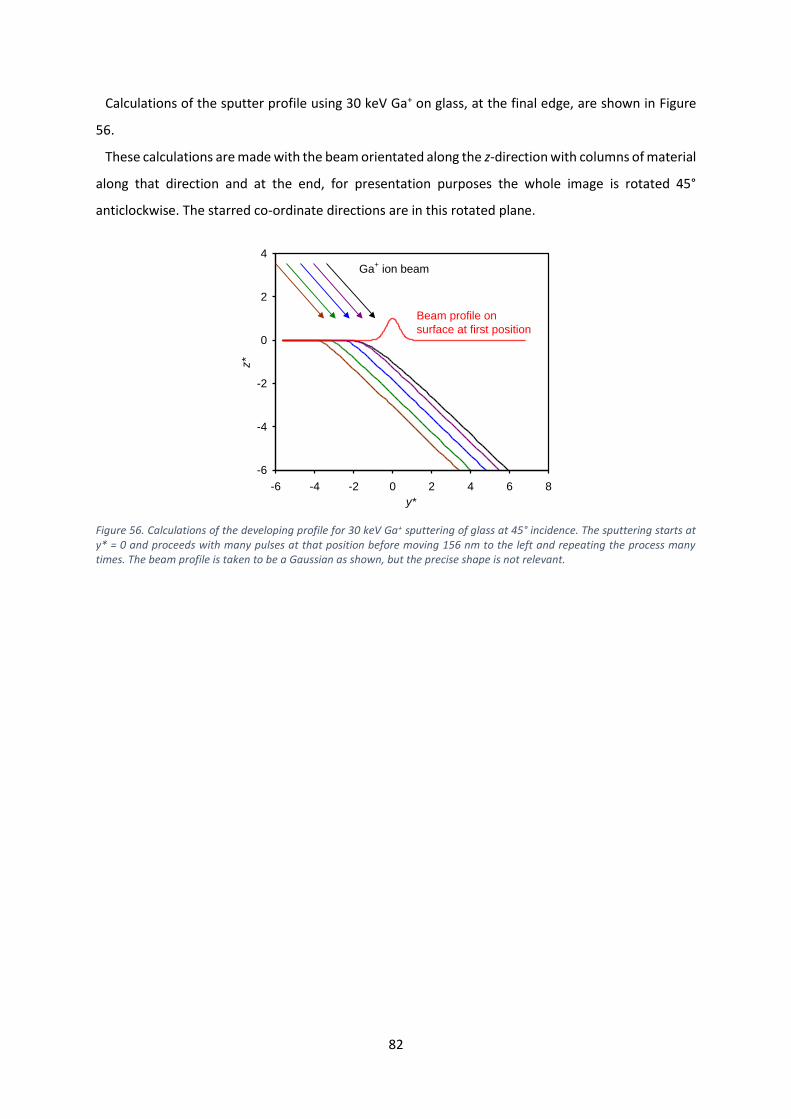
82
Calculations of the sputter profile using 30 keV Ga+ on glass, at the final edge, are shown in Figure
56.
These calculations are made with the beam orientated along the z-direction with columns of material
along that direction and at the end, for presentation purposes the whole image is rotated 45°
anticlockwise. The starred co-ordinate directions are in this rotated plane.
Figure 56. Calculations of the developing profile for 30 keV Ga+ sputtering of glass at 45° incidence. The sputtering starts at y* = 0 and proceeds with many pulses at that position before moving 156 nm to the left and repeating the process many times. The beam profile is taken to be a Gaussian as shown, but the precise shape is not relevant.
-6
-4
-2
0
2
4
-6 -4 -2 0 2 4 6 8
y*
z*
Ga+ ion beam
Beam profile on
surface at first position

83
4.6 Application on the hybrid microporous system
The recovery of characteristic polymer fragment ion signals from the 45° milled wall of both PS and
PMMA filled MCPs is shown as a function of the Ar GCIB sputter dose in Figure 57. The characteristic
ion signal is seen to rise after a certain dose similar to that previously reported for ion and electron
beam damage 158,162–164.
After FIB milling, a high Ga+ signal is detected on the sloping surface and the organic signals are very
weak, presumably, due to polymer crosslinking and carbonisation. The damage provided by a FIB dose
of 4.08 × 10⁴ ions/nm2 was removed by approximately 10 ions/nm2 10keV Ar2500+ for PMMA and 60
ions/nm2 for PS as shown in Figure 57. The faster recovery of the signal from PMMA is expected as
this polymer is not of the type that cross-links when exposed to ionizing radiation.
In Figure 58 (a) and (b), we observe respectively a SE image of the crater obtained providing a total
dose of 4.09 × 10⁴ ions/nm2 for MCP filled, respectively, with PMMA and PS. Below, in Figure 58 (c)
and (d) we show the secondary ion images after the clean-up process for both filled specimens.
Figure 57. Recovery of characteristic fragment ions from PS (C7H7+, red) and PMMA (C4H5O+, blue) during GCIB clean-up.
0
0.5
1
1.5
2
0 10 20 30 40 50 60 70
Ar2500+ dose, ions/nm
2
Norm
arised I
nte
nsity
PS
C7H7+
PMMA
C4H5O+
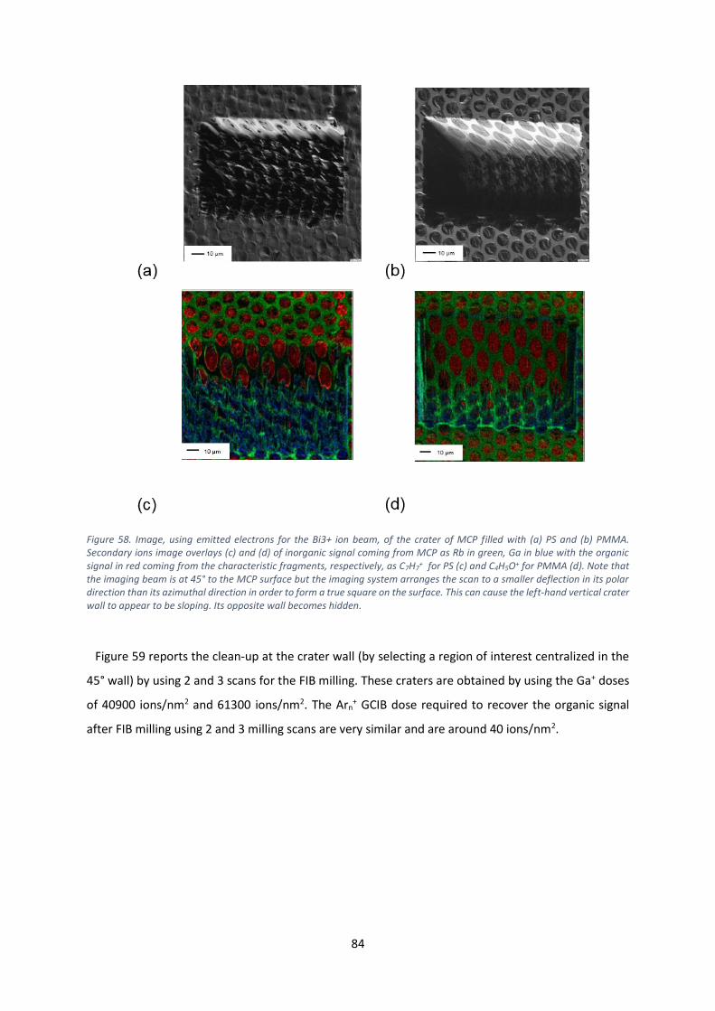
84
Figure 58. Image, using emitted electrons for the Bi3+ ion beam, of the crater of MCP filled with (a) PS and (b) PMMA. Secondary ions image overlays (c) and (d) of inorganic signal coming from MCP as Rb in green, Ga in blue with the organic signal in red coming from the characteristic fragments, respectively, as C7H7
+ for PS (c) and C4H5O+ for PMMA (d). Note that the imaging beam is at 45° to the MCP surface but the imaging system arranges the scan to a smaller deflection in its polar direction than its azimuthal direction in order to form a true square on the surface. This can cause the left-hand vertical crater wall to appear to be sloping. Its opposite wall becomes hidden.
Figure 59 reports the clean-up at the crater wall (by selecting a region of interest centralized in the
45° wall) by using 2 and 3 scans for the FIB milling. These craters are obtained by using the Ga+ doses
of 40900 ions/nm2 and 61300 ions/nm2. The Arn+ GCIB dose required to recover the organic signal
after FIB milling using 2 and 3 milling scans are very similar and are around 40 ions/nm2.

85
Figure 59. C7H7
+ fragment signal recovery for 2 milling pass per scan and 3 milling pass per scan FIB craters in the PS filled MCP.
In cleaning the MCP we showed that a dose of 38 ions/nm2 would largely clean the surface. It is
shown elsewhere 165 that the sputtering yield of pure PS using 10 keV Ar2500+ is 21 nm3. However, in
sputtering the Ga-implanted PS, the yield is reduced to 0.6 nm3, a reduction of 60 times so that the 38
ions/nm2 is required to remove the remaining 23 nm of damaged and implanted PS 165. If we were to
overclean by a further 38 ions/nm2, we should remove a further 1.4 micrometres of pure PS which
would lead to blurring at the edges of included phases by significantly more than this figure since the
yield rises strongly at edges. Even if one limited the overclean dose to just 10%, the spatial resolution
would begin to be compromised. Different polymers are affected to different extents, so that the
correct dose for both cleaning and retaining optimum spatial resolution will depend on the organic
material analysed. It is, therefore, recommended to measure the signals for the organic materials
anticipated in the sample and to stop the sputtering for imaging the sample at, or soon after, the signal
has reached 90-95% of its final value.
4.7 FIB milling with Bi+ and Bi3+ as alternative to Ga+
Gallium is the most widely used source for FIB milling. The National Physical Laboratory is equipped
with a 3D OrbiSIMS instrument with a 30 keV bismuth liquid metal ion source equipped with a Wien
filter, so that mass selected direct current beams of Bi+ or Bi3+ can be used instead of the Ga source.
This provides an interesting possibility, since cluster beams are known to create less damage in organic
materials and therefore may be more suitable for inorganic-organic materials. Bi+ and Ga+ have much
the same effect on glass in terms of the theory given above.
0
0.2
0.4
0.6
0.8
1
1.2
0 10 20 30 40 50
Ar2500+ dose, ions/nm
2
Norm
aliz
ed inte
nsity
3 milling pass per scan
2 millling pass per scan

86
Before applying the Bi3+ as a FIB on the MCP/PS, we made some tests using AFM and confocal
microscopy on pure polystyrene to see the effect in terms of milling depth for same doses of ion beam.
The craters made using the Bi3+ were obtained by using 1 nA current and the one made with Ga by
using the standard 20 nA beam. In Figure 60 (a) and (b) it is possible observe the craters created using
Bi3 and Ga beam for the milling procedure.
Figure 60. Confocal images of the the craters made on by using Bi (a) and Ga (b) as ion beam.
The confocal analysis on the crater made by using the Bi3+ beam was possible because of the limited
depth of the crater. To give an idea of what is possible to achieve using the confocal analysis, a
standard output is reported in Figure 61 showing the crater made using the lower dose of Bi3 of 204000
ions/nm2.
Figure 61. Confocal images and x and y scan of the FIB crator depth after millin by using a Bi3+ dose of 204000 ions/nm2.

87
Using that method it is also possible to obtain information about the crater depth. We also use a 3D
image from the AFM to confirm the depth value obtained with the confocal image reconstruction,
here 1.7 μm. In Figure 62 is shown an example of image generated with the SPIPTM AFM software 166 .
Figure 62. AFM 3D image reconstruction of a crater made by using a Bi3 dose of 204000 ions/nm2.
The respective depth calculated by SPIP software is reported in Figure 63 and is given as 1.366 μm.
Figure 63. AFM profile of the crater in Figure 62.

88
This analysis has been performed on all the craters shown in Figure 60, and the depth of every crater
is determined. To study the efficiency of these sources, we use the PS filled test device. Figure 64
shows secondary electron images of craters milled using Ga+ (ToF-SIMS V) and Bi3+ (OrbiSIMS).
Figure 64. Emitted electron image using Bi3++ ions in the SIMS instrument of craters formed using (a) Ga+ and (b) Bi3+ sputtering ions. The sloping face is at the top. The left wall looks sloping but is vertical and this arises since the imaging beam comes from the right and the image surface geometry is “corrected” by expanding the x-direction by a factor of 20.5.
The results for Bi+ (not shown) are very similar, but consistently poorer than those for Ga+. The results
for Bi3+ are very much poorer and this arises partly due to the very different angular dependence of
the sputtering of cluster ions compared with monatomic ions 167 149. The value of θmax for Bi3+ is much
lower than for Ga+ as the ions do not penetrate so far or so linearly. This leads to a slope closer to 30°
with the ions no longer at the very grazing incidence into the polymer in the MCP holes.
To measure the slope of the FIB milled section of the MCP, AFM measurements has been performed.

89
Figure 65. AFM images of the crater edge for empty MCP milled by using a dose of 20400 (a), 40900 (c), 61300 (e) ions/nm2 and respective profile (b, d, f).
Figure 65 shows the AFM images (a, c, d) and the measured graph (b, e, f) of the slope of the edges
of the crater of the milled empty MCP samples. AFM measurements over 5 μm from the upper edge
were possible before the tip lost contact in the low region. We selected the relevant region in Figure
54 (a), (b) and (c), we choose an average of several traces shown in Figure 65 (b), (d) and (f) that avoid
holes and we also obtained the trace of the FIB-crater wall shown in Figure 66 (a). From that trace,
the slope of the local surface due to the milling can be determined, as shown in Figure 66 (b). This
slope starts at around 30° near the surface, rising eventually to around 40° further down the slope.
The precise results here are affected by the enhanced sputtering around the holes but it is clear that

90
the final slope will be close to, but less than, 45°. The divergence from 45° is important since any
polymer filling the MCP holes, for which the FIB-milled cross section is important, is shielded by the
upper edge of the hole as shown in Figure 66 (a) and is sputtered at that effective angle of incidence.
This region, being sputtered more rapidly than the glass of the MCP will suffer more shape distortion
and be more prone to the development of roughness as this divergence increases. This allows a
greater physical roughness to develop there and may explain the poor results for Bi3+.
Figure 66. (a) Average trace from AFM down the slope in Figure 65, avoiding the holes and (b) the local slope of the trace as an angle of the surface from the original surface. The dashed line shows the data at the end of the trace where the tip loses contact with the sample.
Observation of the columnar structure would indicate that, at best, some 2 to 3 μm of organic
material needs to be removed to clean up the surface. If this were pure polystyrene, this would need
the high dose of 70 ions/nm2 for 10 keV Ar2500, but if the removal of damaged polymer is one to two
orders of magnitude slower 163 158, this figure is raised by that factor and be impossible to remove in a
practical time. Cleaning of FIB section using Bi3+ is very difficult whereas that using Ga+ will be much
easier. Therefore, this is a negative result for Bi3+ FIB milling of organic-inorganic materials.

91
4.8 Application: Membrane Electrode Assembly and strain sensor
The FIB-TOF-SIMS methodology is evaluated for two additive manufactured devices, an
encapsulated strain sensor containing silver tracks embedded in a polymeric material and a copper
track on a flexible polymeric substrate created using a novel nanoparticle sintering technique.
Additive Manufacturing (AM) is at heart an interface problem where multiple layers of material are
consecutively deposited to build up a physical 3D object from digital data. This interface challenge
with AM will be further extended with emergence of next-generation AM that seeks to combine both
structural and functional materials together in a single build. For future 3D-printed electronics, this
will necessitate the contemporaneous co-deposition of both dielectric (organic) materials alongside
conductive (inorganic) metallics that will create complex organic-inorganic interfaces both inter and
intra layer 168.
4.8.1 3D inkjet-printed encapsulated strain sensor
A prototype encapsulated strain sensor containing silver tracks embedded in a polymeric material
was manufactured by 3D inkjet printing of two different inks. The organic ink is made in-house and
based on tri (propylene glycol) diacrylate (TPGDA) and the silver nanoparticles ink was purchased from
Advanced Nano Products (SilverJet DGP-40LT-15C). Both polymer and silver layers were printed and
cured/sintered contemporaneously by a LED-based UV source connected to the print-heads of a
PixDro LP50 printer. More details of the ink formulations and printing process are described elsewhere
26. The analysed volume of the sample contains, from bottom to top, 15 layers of polymer, 10 layers
of silver and 5 layers of polymer. Based on previous studies, each polymer layer has approximately 10
µm and each silver layer has between 300 nm and 700 nm (see Figure 67).
(a) (b)
Figure 67. (a) Structure of the 3D inject printed strain sensor and (b) example of bio-application.
(a) (b)

92
The sample has been milled from the upper polymer layer following the methodology described
earlier. Figure 68 (a) shows the total secondary ion images of the FIB crater after GCIB cleaning with a
dose of 18.7 ions/nm2. Figure 68 (b) shows a 45 µm x 45 µm map with an overlay of the signals for
polymer ions and silver. After removal of the implanted gallium, the interface between the two
materials is clearly distinguishable. To improve the signal to noise, an integrated intensity profile is
created by summing the horizontal line scans between the regions. Owing to a tilt in the sample, a
small horizontal offset is applied to each line scan to align them. Using the 16-84 % definition of profile
resolution 169, the silver signal intensity across the interface (Figure 68 (c)) gives an organic-inorganic
interface width as 440 nm.
Figure 68. (a) Total ion image of the FIB crater after cleaning and several imaging acquisition, (b) secondary ion image of a selected area with an overlay of the sum of every signal coming from the polymer TPGD (in green) and from Silver (in red) and (c) interface determination by scanning the area of the polymer and the silver layers.
Above the interface, we see a small quantity of Ag (see the area in the black rectangle in Figure 68
(c)). This could be interpreted as atomic diffusion whilst the overlayers are deposited or it could be
from very small particles of Ag. Analysis of the SIMS spectra shows significant populations of Ag3+ and
Ag5+ within the polymer, consistent with very small particulates, whilst none of the Ag adducts that
would be expected for atomic or organically bonded Ag were observable. The populations are slightly
smaller than for bulk Ag.
(a) (b)
(c)

93
The milling-cleaning protocol applied to the strain sensor to study the buried interface between a
track of sintered silver nanoparticles and a UV-cured polymer in a 3D inkjet-printed prototype
encapsulated strain sensor shows that the two materials, after ink-jetting process, have a
intermixing/diffusion at the interface.
4.8.2 Sintered copper tracks on a flexible polymer substrate
A sample of copper track deposited on a flexible polymeric substrate is created using a novel
nanoparticle sintering technique. The device and its schematic structure are shown in Figure 69 (a)
and (b). The SE image of the FIB crater is shown Figure 69 (c).
The Cu on the polymeric track is a good test case for our method, since the copper material is friable.
The sample was milled with a Ga dose of 40900 ions/nm2 and the characteristic PET fragment C8H5O3+
signal has been recovered with a GCIB dose of 12 ions/nm2. In this specific case, the interface has been
determined in two steps. An image for the copper distribution is acquired directly after milling (Figure
69 c) using the intense CuO2+ signal, since this signal intensity reduces under GCIB cleaning and our
instrument is not equipped with an oxygen gas leak that would be used to recover the copper ion
yield. Following the GCIB cleaning, the interface is re-imaged and the characteristic PET fragment,
C8H5O3+ used to define the PET layer. As previously, average linescans (125 lines) are used to show the
interface (Figure 69 d). The method shows a well-defined interface between the copper and PET
layers, with no evidence of PET signal in the copper track.

94
Figure 69. FIB-TOF-SIMS analysis of copper track on PET. (a) Optical Image of the device and (b) schematic of the layer structure. (c) SE image of milled crater with the area selected for the imaging in yellow. (d) Normalized secondary ion intensity profiles (average as before) centred at the interface, for CuO2
+ characteristic of the copper track (green) and C8H5O3+
characteristic of PET (red). Ion images of these ions are shown inset using the same colour scheme.
4.9 Summary
A protocol has been developed for FIB-TOF-SIMS analysis of buried interfaces. It is shown that this is
a useful method for chemical imaging of organic and inorganic interfaces.
However, the FIB milling preferentially damages organic surfaces, which limits the application for
important organic-inorganic systems. The use of a GCIB clean-up cycle can remove this damage, but a
systematic study was lacking. In order to address this aspect, we have developed a test device based
on a microchannel plate consisting of a regular honeycomb array of tubes of 10 µm diameter. The
tubes are filled with either PMMA or PS. Using this device, we were able to determine that a 10 keV

95
Ar2500+
dose on the order of 10 ions/nm2 and 60 ions/nm2 are required to recover the organic signal
for PMMA and PS respectively.
Since Bi3+ has a higher sputtering yield than Ga+
for organics, the effects of damage on organic
materials may be less. We use the test-device to evaluate this for FIB milling with 30 keV Ga+, Bi+ and
Bi3+. We found that the reverse is in fact the case, and we explain our results in terms of a theory based
on the angular-dependent sputtering yield. In this theory, the angle of incidence evolves from the
initial 45o geometrical angle with the fresh surface to stabilize at near θmax as the milling proceeds.
Since θmax differs substantially between atomic (approximately grazing) and cluster projectiles
(approximately 45o) then the ability to successfully mill through materials with vastly different
sputtering rates is affected. Therefore, our results indicate that gallium is recommended for milling
organic-inorganic hybrid materials.

96

97
5 Conclusions and future work perspective
In this thesis, we studied the behaviour of silicon-based organic-inorganic hybrids, where their
complex interfaces play a key role in the development of new technologies. The fields of interest are
various and interdisciplinary. We approached these materials by studying their synthesis,
characterisation and properties on the meso- and micro-scale. The inorganic matrix for the meso-scale
matrix was porous silicon. The PSi samples were synthesized and grafted with polymers by means of
electrochemical procedures that allow a high degree of control, thanks to the several adjustable
parameters. Only in the case of Si-eumelanin hybrids, chemical methods were used. The
characterisation of the PSi/PANI has also been carried out by means of electrochemical techniques as
cyclic voltammetry and electrochemical impedance spectroscopy.
We were able to demonstrate that the grafting of diazonium on the inner pores surface transformed
the easy-to-dissolve PSi matrix into a highly resistant material that could withstand chemical solutions
as harsh as a 1M NaOH acqueous solution for about one hour without measurable modifications. This
is an important result, since the feeble resistance of PSi matrices to chemical agents has been a
constant problem for the use of PSi in acidic or basic environments, as is the case for biosensing
applications or the fabrication process where optical lithography requires the use of corrosive
solutions in the developing of the photoresist.
The strong chemical resistance shows that the diazonium is attached to the walls by stable chemical
bonds. The samples chemical resistance in terms of capability to stay unmodified was tested using
optical reflectivity of thin (about 1µm thick) porous layers, a technique highly sensitive to the
modification of the optical properties of the layers under investigation. The AFM and SEM images of
the samples show that after the diazonium grafting the pores are still not plugged, which is mandatory
for the PANI grafting that follows the diazonium coverage.
After the PANI grafting, the hybrid samples ability to generate photocurrent was tested both at the
macroscopic scale and at the nanoscale. The effect of the grafted polymer to improve the optical
absorption and then the range where the photocurrent can be generated has been tested. We show
that a p-n junction between the polymer and the porous matrix is obtained, and that the absorption
of the PSi matrix is improved by the PANI grafting. At the nanoscale, to study the single-pore behaviour
of the grafted porous layers we resorted to photoconductive AFM (PC-AFM), a technique able to give
highly spatially resolved information on the photogeneration behaviour. Our results show that the
current under illumination mainly comes from inside the pores and that the overall current intensity
measured under illumination is the sum of the contribution given by every single pore.

98
To study the hybrids with structures at the microscale, we used a microchannel plate (MCP). This Si
matrix has a number of advantages that allowed our study to be more effective. First, the micron-
sized holes of the matrix are easily measurable by the FIB-SIMS technique. Second, the matrix is very
regular. Third, MCP is relatively easier to fill with a polymer with respect to mesoporous PSi. Starting
from these advantages, we developed a specific protocol for the analysis of organic-inorganic
interfaces in MCPs filled with PS and PMMA after FIB milling.
Our protocol demonstrates how it is possible to recover the proper ion signal signature from the
polymer inside the MCP pores thanks to Ar2500clusters with energy of 4 eV per atom.
The FIB procedure has been studied on the pristine polymer to determine the doses and the limit of
cross linking of the materials. Angle of incidence, dose density for milling, dose density for recovery
and different beams for milling have been investigated. We demonstrate that the procedure can be
also applied to other kinds of samples of a wider interest in technology and biomedical application
such additive manufactured devices. The effectiveness of the method applied to different devices also
proves the possibility to use the MCP as a reference sample in the study of the signal recovery. The
applications on the strain sensor and on the sintered Cu tracks a polymeric substrate opens the door
to further applications on different materials of interest in research and industry to determine, for
instance, the homogeneity of a layer or the composition and the localization of the organic material
in a hybrid composite sample.
Future perspective
Thanks to the results obtained in this thesis, new roads towards the understanding and optimization
of the pores filling degree can be investigated. The optimal fabrication of porous structures with
polymers requires that the pores are uniformly filled so that the effect of inhomogeneities can be
avoided. However, the use of standard optical studies and photocurrent measurements alone do not
allow a nanoscale and microscale understanding of the details of the pores filling. The next step
towards a good understanding of these properties will then be the use of a combined approach where
different techniques are used to determine the level of polymer filling in the pores. For example,
Ellipsometry can give precise information in the depth profiling of the samples using polarized light
and can be a powerful complement to the structural characterisation tools used in this thesis.
Ellipsometry has been widely and successfully used for research on inhomogeneous layers, and we
already performed preliminary in the filled and empty porous silicon layers. The major challenge is still
the development of a reliable model for the fitting of the data, given the complexity of a nanoscale-

99
structured porous layer. Its development is clearly a very interesting route for further understanding
of filled PSi sample.
From the structural characterisation techniques point of view, mass spectrometry where depth
profiling is performed with a GCIB to clean the surface from degraded material and an LMIG for the
imaging is powerful tool to obtain plane images or 3D reconstructions of the samples during profiling.
Unfortunately, while for MCP the parameters have been optimized in our work, in the case of PSi the
energies of the GCIB used up to now (from 5 to 20 keV) are still too high for the PSi, and further steps
towards the optimisation of this process are needed. The use of a bevel cut, for instance, allowing the
measure of an “enlarged” cross section of the sample may be a possible solution to this issue. The
cross sectioning in situ can be made by using a ToF-SIMS equipped with a FIB. Moreover, since FIB
damages every organic material and facilitates the cross linking of a wide range of polymers, the
general protocol we have defined and optimized for MCP has to be further optimized for the case of
mesoporous silicon.

100

101
Bibliography
(1) Hong, M. Inorganic−Organic Hybrid Coordination Polymers: A New Frontier for Materials Research. 2006.
(2) Sanchez, C.; Shea, K. J.; Kitagawa, S. Recent Progress in Hybrid Materials Science. Chem. Soc. Rev. 2011, 40 (2), 471.
(3) Braun, S.; Salaneck, W. R.; Fahlman, M. Energy-Level Alignment at Organic/Metal and Organic/Organic Interfaces. Adv. Mater. 2009, 21 (14–15), 1450–1472.
(4) Judeinstein, P.; Sanchez, C. Hybrid Organic–inorganic Materials: A Land of Multidisciplinarity. J. Mater. Chem. 1996, 6 (4), 511–525.
(5) Mammeri, F.; Bourhis, E. Le; Rozes, L.; Sanchez, C. Mechanical Properties of Hybrid Organic–inorganic Materials. J. Mater. Chem. 2005, 15 (35–36), 3787.
(6) Forrest, S. R. Ultrathin Organic Films Grown by Organic Molecular Beam Deposition and Related Techniques. 1997.
(7) Mitzi, D. B.; Chondroudis, K.; Kagan, C. R. Organic-Inorganic Electronics. IBM J. Res. Dev. 2001, 45 (1), 29–45.
(8) Lee, H.-H.; Chou, K.-S.; Huang, K.-C. Inkjet Printing of Nanosized Silver Colloids. Nanotechnology 2005, 16 (10), 2436–2441.
(9) Chang, S.-C.; Liu, J.; Bharathan, J.; Yang, Y.; Onohara, J.; Kido, J. Multicolor Organic Light-Emitting Diodes Processed by Hybrid Inkjet Printing. Adv. Mater. 1999, 11 (9), 734–737.
(10) Panjan, P.; Čekada, M.; Panjan, M.; Kek-Merl, D. Growth Defects in PVD Hard Coatings. Vacuum 2009, 84 (1), 209–214.
(11) King, J. S.; Heineman, D.; Graugnard, E.; Summers, C. J. Atomic Layer Deposition in Porous Structures: 3D Photonic Crystals. Appl. Surf. Sci. 2005, 244 (1–4), 511–516.
(12) Donley, C.; Dunphy, D.; Paine, D.; Carter, C.; Nebesny, K.; Lee, P.; Dana Alloway, A.; Neal R. Armstrong. Characterization of Indium−Tin Oxide Interfaces Using X-Ray Photoelectron Spectroscopy and Redox Processes of a Chemisorbed Probe Molecule: Effect of Surface Pretreatment Conditions. 2001.
(13) Jouane, A.; Moubah, R.; Schmerber, G.; Larde, R.; Odarchenko, Y.; Ivanov, D.; Lassri, H.; Chapuis, Y.-A.; Jouane, Y. Morphological and Structural Interface Characterization in Multilayer Inverted Polymer Solar Cells. In 2016 International Renewable and Sustainable Energy Conference (IRSEC); IEEE, 2016; pp 70–77.
(14) Alahmadi, S. M.; Mohamad, S.; Jamil Maah, M. Preparation of Organic-Inorganic Hybrid Materials Based on MCM-41 and Its Applications. Adv. Mater. Sci. Eng. 2013, 2013, 1–8.
(15) Delville, M.-H.; Taubert, A. Hybrid Organic-Inorganic Interfaces : Towards Advanced Functional Materials; 2018.
(16) Jose-Yacaman; Rendon; Arenas; Serra Puche MC. Maya Blue Paint: An Ancient

102
Nanostructured Material. Science 1996, 273 (5272), 223–225.
(17) Gómez-Romero, P.; Sanchez, C. Hybrid Materials. Functional Properties. From Maya Blue to 21st Century Materials. New J. Chem. 2005, 29 (1), 57–58.
(18) Kickelbick, G. Hybrid Materials – Past, Present and Future. Hybrid Mater. 2014, 1 (1), 39–51.
(19) Illampas, R.; Loizou, V. G.; Ioannou, I. Effect of Straw Fiber Reinforcement on the Mechanical Properties of Adobe Bricks. In Poromechanics VI; American Society of Civil Engineers: Reston, VA, 2017; pp 1331–1338.
(20) Amorim, S. M.; Suave, J.; Andrade, L.; Mendes, A. M.; José, H. J.; Moreira, R. F. P. M. Towards an Efficient and Durable Self-Cleaning Acrylic Paint Containing Mesoporous TiO2 Microspheres. Prog. Org. Coatings 2018, 118, 48–56.
(21) Khan, M. I.; Abbas, Y. M.; Fares, G. Review of High and Ultrahigh Performance Cementitious Composites Incorporating Various Combinations of Fibers and Ultrafines. J. King Saud Univ. - Eng. Sci. 2017, 29 (4), 339–347.
(22) Mir, S. H.; Nagahara, L. A.; Thundat, T.; Mokarian-Tabari, P.; Furukawa, H.; Khosla, A. Review—Organic-Inorganic Hybrid Functional Materials: An Integrated Platform for Applied Technologies. J. Electrochem. Soc. 2018, 165 (8), B3137–B3156.
(23) Kagan, C. R.; Mitzi, D. B.; Dimitrakopoulos, C. D.; Wudl, F.; Heeger, A. J. Organic-Inorganic Hybrid Materials as Semiconducting Channels in Thin-Film Field-Effect Transistors. Science 1999, 286 (5441), 945–947.
(24) Rajashekara, K. Hybrid Fuel-Cell Strategies for Clean Power Generation. IEEE Trans. Ind. Appl. 2005, 41 (3), 682–689.
(25) Morrison, O.; Seal, M.; West, E.; Connelly, W. Use of a Thermophotovoltaic Generator in a Hybrid Electric Vehicle; 1999; pp 488–496.
(26) Saleh, E.; Zhang, F.; He, Y.; Vaithilingam, J.; Fernandez, J. L.; Wildman, R.; Ashcroft, I.; Hague, R.; Dickens, P.; Tuck, C. 3D Inkjet Printing of Electronics Using UV Conversion. Adv. Mater. Technol. 2017, 2 (10), 1700134.
(27) Bingquan Wang; Bin Li; Qing Deng, A.; Dong, S. Amperometric Glucose Biosensor Based on Sol−Gel Organic−Inorganic Hybrid Material. 1998.
(28) Yao, K. De; Yin, Y. J.; Xu, M. X.; Wang, Y. F. Investigation of PH-Sensitive Drug Delivery System of Chitosan/Gelatin Hybrid Polymer Network. Polym. Int. 1995, 38 (1), 77–82.
(29) Aminabhavi, T. M.; Dharupaneedi, S. P. Production of Chitosan-Based Hydrogels for Biomedical Applications. In Chitosan Based Biomaterials Volume 1; Elsevier, 2017; pp 295–319.
(30) E. Bekyarova; Thostenson, E. T.; Yu, A.; Kim, H.; Gao, J.; Tang, J.; Hahn, H. T.; Chou, T.-W.; M. E. Itkis, A.; R. C. Haddon. Multiscale Carbon Nanotube−Carbon Fiber Reinforcement for Advanced Epoxy Composites. 2007.
(31) Wright, T. M.; Fukubayashi, T.; Burstein, A. H. The Effect of Carbon Fiber Reinforcement on Contact Area, Contact Pressure, and Time-Dependent Deformation in Polyethylene Tibial Components. J. Biomed. Mater. Res. 1981, 15 (5), 719–730.
(32) Goh, C.; Scully, S. R.; McGehee, M. D. Effects of Molecular Interface Modification in Hybrid Organic-Inorganic Photovoltaic Cells. J. Appl. Phys. 2007, 101 (11), 114503.

103
(33) Yin, Y.; Alivisatos, A. P. Colloidal Nanocrystal Synthesis and the Organic–inorganic Interface. Nature 2005, 437 (7059), 664–670.
(34) AZoM. Definitions and Categories of Hybrid Materials https://www.azom.com/article.aspx?ArticleID=4845 (accessed Sep 21, 2018).
(35) Alemán, J. V.; Chadwick, A. V.; He, J.; Hess, M.; Horie, K.; Jones, R. G.; Kratochvíl, P.; Meisel, I.; Mita, I.; Moad, G.; et al. Definitions of Terms Relating to the Structure and Processing of Sols, Gels, Networks, and Inorganic-Organic Hybrid Materials (IUPAC Recommendations 2007). Pure Appl. Chem. 2007, 79 (10), 1801–1829.
(36) Serbin, J.; Egbert, A.; Ostendorf, A.; Chichkov, B. N.; Houbertz, R.; Domann, G.; Schulz, J.; Cronauer, C.; Fröhlich, L.; Popall, M. Femtosecond Laser-Induced Two-Photon Polymerization of Inorganic–organic Hybrid Materials for Applications in Photonics. Opt. Lett. 2003, 28 (5), 301.
(37) Houbertz, R.; Domann, G.; Cronauer, C.; Schmitt, A.; Martin, H.; Park, J.-U.; Fröhlich, L.; Buestrich, R.; Popall, M.; Streppel, U.; et al. Inorganic–organic Hybrid Materials for Application in Optical Devices. Thin Solid Films 2003, 442 (1–2), 194–200.
(38) Wang, J.-J.; Wang, Y.-Q.; Cao, F.-F.; Guo, Y.-G.; Wan, L.-J. Synthesis of Monodispersed Wurtzite Structure CuInSe 2 Nanocrystals and Their Application in High-Performance Organic−Inorganic Hybrid Photodetectors. J. Am. Chem. Soc. 2010, 132 (35), 12218–12221.
(39) Innocenzi, P.; Lebeau, B. Organic–inorganic Hybrid Materials for Non-Linear Optics. J. Mater. Chem. 2005, 15 (35–36), 3821.
(40) ITRS report (international technology roadmap for semiconductors) Executive summary https://www.dropbox.com/s/k8mllgrc4vzzpbf/2013ExecutiveSummary.pdf?dl=0.
(41) Liu, P.-T.; Chang, T.-C.; Su, H.; Mor, Y.-S.; Yang, Y.-L.; Chung, H.; Hou, J.; Sze, S.-M. Improvement in Integration Issues for Organic Low-k Hybrid-Organic-Siloxane-Polymer. J. Electrochem. Soc. 2001, 148 (2), F30.
(42) Pan, G. Polyhedral Oligomeric Silsesquioxane (POSS). In Physical Properties of Polymers Handbook; Springer New York: New York, NY, 2007; pp 577–584.
(43) What are polymers? - IUPAC | International Union of Pure and Applied Chemistry https://iupac.org/polymer-edu/what-are-polymers/ (accessed Sep 21, 2018).
(44) Li, Z.; Qin, F.; Liu, T.; Ge, R.; Meng, W.; Tong, J.; Xiong, S.; Zhou, Y. Optical Properties and Conductivity of PEDOT:PSS Films Treated by Polyethylenimine Solution for Organic Solar Cells. Org. Electron. 2015, 21, 144–148.
(45) Tang, C. G.; Ang, M. C. Y.; Choo, K.-K.; Keerthi, V.; Tan, J.-K.; Syafiqah, M. N.; Kugler, T.; Burroughes, J. H.; Png, R.-Q.; Chua, L.-L.; et al. Doped Polymer Semiconductors with Ultrahigh and Ultralow Work Functions for Ohmic Contacts. Nature 2016, 539 (7630), 536–540.
(46) Feng, P. Y.; Kennedy, J. W. Electrical and Chemical Effects of β-Radiation in Polystyrene 1. J. Am. Chem. Soc. 1955, 77 (4), 847–851.
(47) Krishnamurthy, V. N. Polymers in Space Environments. In Polymers and Other Advanced Materials; Springer US: Boston, MA, 1995; pp 221–226.
(48) Ashcroft, W. R. Industrial Polymer Applications : Essential Chemistry and Technology; 2016.
(49) Yuan, M.-C.; Chiu, M.-Y.; Liu, S.-P.; Chen, C.-M.; Wei, K.-H. A Thieno[3,4- c ]Pyrrole-4,6-Dione-Based Donor−Acceptor Polymer Exhibiting High Crystallinity for Photovoltaic Applications.

104
Macromolecules 2010, 43 (17), 6936–6938.
(50) Su, Y.-W.; Liu, C.-M.; Jiang, J.-M.; Tsao, C.-S.; Cha, H.-C.; Jeng, U.-S.; Chen, H.-L.; Wei, K.-H. Structural Evolution of Crystalline Conjugated Polymer/Fullerene Domains from Solution to the Solid State in the Presence and Absence of an Additive. J. Phys. Chem. C 2015, 119 (6), 3408–3417.
(51) Idris, N. H.; Rahman, M. M.; Wang, J.-Z.; Liu, H.-K. Microporous Gel Polymer Electrolytes for Lithium Rechargeable Battery Application. J. Power Sources 2012, 201, 294–300.
(52) Dearborn, S. Power Management in Portable Applications: Charging Lithium-Ion/Lithium-Polymer Batteries. Microchip Technol. Inc. 2004, No. Ds00947A.
(53) Using Polymers in Electrical Applications | Smithers Rapra https://www.smithersrapra.com/resources/2017/august/using-polymers-in-electrical-applications (accessed Sep 12, 2018).
(54) Chen, J.; Cao, Y. Development of Novel Conjugated Donor Polymers for High-Efficiency Bulk-Heterojunction Photovoltaic Devices. Acc. Chem. Res. 2009, 42 (11), 1709–1718.
(55) Isakova, A.; Topham, P. D. Polymer Strategies in Perovskite Solar Cells. J. Polym. Sci. Part B Polym. Phys. 2017, 55 (7), 549–568.
(56) Macdiarmid, A. G.; Chiang, J. C.; Richter, A. F.; Epstein, A. J. Polyaniline: A New Concept in Conducting Polymers. Synth. Met. 1987, 18 (1–3), 285–290.
(57) Shirakawa, H.; Louis, E. J.; MacDiarmid, A. G.; Chiang, C. K.; Heeger, A. J. Synthesis of Electrically Conducting Organic Polymers: Halogen Derivatives of Polyacetylene, (CH) X. J. Chem. Soc. Chem. Commun. 1977, 0 (16), 578.
(58) Masters, J. G.; Sun, Y.; MacDiarmid, A. G.; Epstein, A. J. Polyaniline: Allowed Oxidation States. Synth. Met. 1991, 41 (1–2), 715–718.
(59) Thody, A. J.; Higgins, E. M.; Wakamatsu, K.; Ito, S.; Burchill, S. A.; Marks, J. M. Pheomelanin as Well as Eumelanin Is Present in Human Epidermis. J. Invest. Dermatol. 1991, 97 (2), 340–344.
(60) Del Bino, S.; Duval, C.; Bernerd, F. Clinical and Biological Characterization of Skin Pigmentation Diversity and Its Consequences on UV Impact. Int. J. Mol. Sci. 2018, 19 (9), 2668.
(61) Chen, C.-T.; Chuang, C.; Cao, J.; Ball, V.; Ruch, D.; Buehler, M. J. Excitonic Effects from Geometric Order and Disorder Explain Broadband Optical Absorption in Eumelanin. Nat. Commun. 2014, 5 (1), 3859.
(62) Mula, G.; Manca, L.; Setzu, S.; Pezzella, A. Photovoltaic Properties of PSi Impregnated with Eumelanin. Nanoscale Res. Lett. 2012, 7 (1), 377.
(63) Pinna, A.; Simbula, F.; Marongiu, D.; Pezzella, A.; d’Ischia, M.; Mula, G. Boosting, Probing and Switching-off Visible Light-Induced Photocurrents in Eumelanin-Porous Silicon Hybrids. RSC Adv. 2015, 5 (70), 56704–56710.
(64) Uhlir, A. Electrolytic Shaping of Germanium and Silicon. Bell Syst. Tech. J. 1956, 35 (2), 333–347.
(65) Pickering, C.; Beale, M. I. J.; Robbins, D. J.; Pearson, P. J.; Greef, R. Optical Studies of the Structure of Porous Silicon Films Formed in P-Type Degenerate and Non-Degenerate Silicon. J. Phys. C Solid State Phys. 1984, 17 (35), 6535–6552.

105
(66) Goodes, S. R.; Jenkins, T. E.; Beale, M. I. J.; Benjamin, J. D.; Pickering, C. The Characterisation of Porous Silicon by Raman Spectroscopy. Semicond. Sci. Technol. 1988, 3 (5), 483–487.
(67) Lightowlers, E. C. Photoluminescence Assessment of MBE Silicon. Semicond. Sci. Technol. 1990, 5 (12), 1161–1167.
(68) Unagami, T. Oxidation of Porous Silicon and Properties of Its Oxide Film. Jpn. J. Appl. Phys. 1980, 19 (2), 231–241.
(69) Stewart, M. P.; Buriak, J. M. Chemical and Biological Applications of Porous Silicon Technology. Adv. Mater. 2000, 12 (12), 859–869.
(70) Canham, L. T. Silicon Quantum Wire Array Fabrication by Electrochemical and Chemical Dissolution of Wafers. Appl. Phys. Lett. 1990, 57 (10), 1046–1048.
(71) Cullis, A. G.; Canham, L. T.; Calcott, P. D. J. The Structural and Luminescence Properties of Porous Silicon. J. Appl. Phys. 1998, 82 (3), 909.
(72) Sanders, G. D.; Chang, Y.-C. Theory of Optical Properties of Quantum Wires in Porous Silicon. Phys. Rev. B 1992, 45 (16), 9202–9213.
(73) Lin, H.; Gao, T.; Fantini, J.; Sailor, M. J. A Porous Silicon−Palladium Composite Film for Optical Interferometric Sensing of Hydrogen. Langmuir 2004, 20 (12), 5104–5108.
(74) Strashnikova, M. I.; Voznyi, V. L.; Reznichenko, V. Y.; Gaivoronskii, V. Y. Optical Properties of Porous Silicon. J. Exp. Theor. Phys. 2001, 93 (2), 363–371.
(75) Zou, C.; Zhang, C.; Li, B.; Wang, S.; Cao, F. Microstructure and Properties of Porous Silicon Nitride Ceramics Prepared by Gel-Casting and Gas Pressure Sintering. Mater. Des. 2013, 44, 114–118.
(76) Billat, S.; Thönissen, M.; Arens-Fischer, R.; Berger, M. .; Krüger, M.; Lüth, H. Influence of Etch Stops on the Microstructure of Porous Silicon Layers. Thin Solid Films 1997, 297 (1–2), 22–25.
(77) De Stefano, L.; Malecki, K.; Della Corte, F.; Moretti, L.; Rea, I.; Rotiroti, L.; Rendina, I.; De Stefano, L.; Malecki, K.; Della Corte, F. G.; et al. A Microsystem Based on Porous Silicon-Glass Anodic Bonding for Gas and Liquid Optical Sensing. Sensors 2006, 6 (6), 680–687.
(78) Sohn, M.; Lee, D. G.; Park, H.-I.; Park, C.; Choi, J.-H.; Kim, H. Microstructure Controlled Porous Silicon Particles as a High Capacity Lithium Storage Material via Dual Step Pore Engineering. Adv. Funct. Mater. 2018, 28 (23), 1800855.
(79) Lugo, J. E.; Lopez, H. A.; Chan, S.; Fauchet, P. M. Porous Silicon Multilayer Structures: A Photonic Band Gap Analysis. J. Appl. Phys. 2002, 91 (8), 4966–4972.
(80) McInnes, S. J.; Voelcker, N. H. Silicon–polymer Hybrid Materials for Drug Delivery. Future Med. Chem. 2009, 1 (6), 1051–1074.
(81) Lai, Y.; Thompson, J. R.; Dasog, M. Metallothermic Reduction of Silica Nanoparticles to Porous Silicon for Drug Delivery Using New and Existing Reductants. Chem. - A Eur. J. 2018, 24 (31), 7913–7920.
(82) Granitzer, P.; Rumpf, K. Porous Silicon-a Versatile Host Material. Materials (Basel). 2010, 3 (2), 943–998.
(83) SIS. TOF Microchannel Plate Detectors https://www.sisweb.com/ms/tof-platedetectors.htm (accessed Sep 22, 2018).
(84) Steinhart, M.; Wendorff, J. H.; Greiner, A.; Wehrspohn, R. B.; Nielsch, K.; Schilling, J.; Choi, J.;

106
Gösele, U. Polymer Nanotubes by Wetting of Ordered Porous Templates. Science (80-. ). 2002, 296 (5575), 1997.
(85) Tiddia, M.; Mula, G.; Mascia, M.; Sechi, E.; Vacca, A. Porous Silicon–polyaniline Hybrid Composites Synthesized through Electroreduction of an Aryldiazonium Salt: Preparation and Photocurrent Properties. RSC Adv. 2016, 6 (104), 101880–101887.
(86) Tiddia, M.; Mula, G.; Sechi, E.; Vacca, A.; Cara, E.; De Leo, N.; Fretto, M.; Boarino, L. 4-Nitrobenzene Grafted in Porous Silicon: Application to Optical Lithography. Nanoscale Res. Lett. 2016, 11 (1), 436.
(87) Park, S.-M.; Yoo, J.-S. Electrochemical Impedance Spectroscopy for Better Electrochemical Measurements. Anal. Chem. 2003, 75, 455 A-461 A.
(88) David C. Coffey; Obadiah G. Reid; Deanna B. Rodovsky; Glenn P. Bartholomew, A.; Ginger, D. S. Mapping Local Photocurrents in Polymer/Fullerene Solar Cells with Photoconductive Atomic Force Microscopy. 2007.
(89) Heo, J. Characterization of Wavelength Effect on Photovoltaic Property of Poly-Si Solar Cell Using Photoconductive Atomic Force Microscopy (PC-AFM). Trans. Electr. Electron. Mater. 2013, 14 (3), 160–163.
(90) Herzog, R. F. K.; Viehböck, F. P. Ion Source for Mass Spectrography. Phys. Rev. 1949, 76 (6), 855–856.
(91) Wittmaack, K.; K. Pre-Equilibrium Variation of the Secondary Ion Yield. Int. J. Mass Spectrom. Ion Phys. 1975, 17 (1), 39–50.
(92) Magee, C. W.; Harrington, W. L.; Honig, R. E. Secondary Ion Quadrupole Mass Spectrometer for Depth Profiling—design and Performance Evaluation. Rev. Sci. Instrum. 1978, 49 (4), 477–485.
(93) Benninghoven, A. Analysis of Submonolayers on Silver by Negative Secondary Ion Emission. Phys. status solidi 1969, 34 (2), K169–K171.
(94) Sigmund, P. Theory of Sputtering. I. Sputtering Yield of Amorphous and Polycrystalline Targets. Phys. Rev. 1969, 184 (2), 383–416.
(95) Kenji Garno. Nanofabrication by FIB. Microelectron. Eng. 1996, 32 (1–4 .), 159–171.
(96) Iltgen, K.; Bendel, C.; Benninghoven, A.; Niehuis, E. Optimized Time-of-Flight Secondary Ion Mass Spectroscopy Depth Profiling with a Dual Beam Technique. J. Vac. Sci. Technol. A Vacuum, Surfaces, Film. 1997, 15 (3), 460–464.
(97) Ninomiya, S.; Ichiki, K.; Yamada, H.; Nakata, Y.; Seki, T.; Aoki, T.; Matsuo, J. Precise and Fast Secondary Ion Mass Spectrometry Depth Profiling of Polymer Materials with Large Ar Cluster Ion Beams. Rapid Commun. Mass Spectrom. 2009, 23 (11), 1601–1606.
(98) Kango, S.; Kalia, S.; Celli, A.; Njuguna, J.; Habibi, Y.; Kumar, R. Surface Modification of Inorganic Nanoparticles for Development of Organic–inorganic Nanocomposites—A Review. Prog. Polym. Sci. 2013, 38 (8), 1232–1261.
(99) Diaz, A. F.; Logan, J. A. Electroactive Polyaniline Films. J. Electroanal. Chem. Interfacial Electrochem. 1980, 111 (1), 111–114.
(100) Rivnay, J.; Inal, S.; Collins, B. A.; Sessolo, M.; Stavrinidou, E.; Strakosas, X.; Tassone, C.; Delongchamp, D. M.; Malliaras, G. G. Structural Control of Mixed Ionic and Electronic Transport in Conducting Polymers. Nat. Commun. 2016, 7, 11287.

107
(101) Bredas, J. L.; Street, G. B. Polarons, Bipolarons, and Solitons in Conducting Polymers. Acc. Chem. Res. 1985, 18 (10), 309–315.
(102) MacDiarmid, A. G. “Synthetic Metals”: A Novel Role for Organic Polymers (Nobel Lecture). Angew. Chemie Int. Ed. 2001, 40 (14), 2581–2590.
(103) Wessling, B.; Srinivasan, D.; Rangarajan, G.; Mietzner, T.; Lennartz, W. Dispersion-Induced Insulator-to-Metal Transition in Polyaniline. Eur. Phys. J. E 2000, 2 (3), 207–210.
(104) Macdiarmid, A. G.; Chiang, J.-C.; Halpern, M.; Huang, W.-S.; Mu, S.-L.; Nanaxakkara, L. D.; Wu, S. W.; Yaniger, S. I. “Polyaniline”: Interconversion of Metallic and Insulating Forms. Mol. Cryst. Liq. Cryst. 1985, 121 (1–4), 173–180.
(105) Hou, W.; Xiao, Y.; Han, G.; Fu, D.; Wu, R. Serrated, Flexible and Ultrathin Polyaniline Nanoribbons: An Efficient Counter Electrode for the Dye-Sensitized Solar Cell. J. Power Sources 2016, 322, 155–162.
(106) Wang, D.; Buriak, J. M. Trapping Silicon Surface-Based Radicals. Langmuir 2006, 22 (14), 6214–6221.
(107) Su, H.; Wang, T.; Zhang, S.; Song, J.; Mao, C.; Niu, H.; Jin, B.; Wu, J.; Tian, Y. Facile Synthesis of Polyaniline/TiO2/Graphene Oxide Composite for High Performance Supercapacitors. Solid State Sci. 2012, 14 (6), 677–681.
(108) Cavallo, P.; Frontera, E.; Acevedo, D. F.; Olejnik, R.; Slobodian, P.; Saha, P.; Barbero, C. A. Functionalized Polyanilines Made by Nucleophilic Addition Reaction, Applied in Gas Sensors Field. Synth. Met. 2016, 215, 127–133.
(109) Vacca, A.; Mascia, M.; Rizzardini, S.; Corgiolu, S.; Palmas, S.; Demelas, M.; Bonfiglio, A.; Ricci, P. C. Preparation and Characterisation of Transparent and Flexible PEDOT:PSS/PANI Electrodes by Ink-Jet Printing and Electropolymerisation. RSC Adv. 2015, 5 (97), 79600–79606.
(110) Eftekhari, A.; Afshani, R. Electrochemical Polymerization of Aniline in Phosphoric Acid. J. Polym. Sci. Part A Polym. Chem. 2006, 44 (10), 3304–3311.
(111) Gupta, V.; Miura, N. Large-Area Network of Polyaniline Nanowires Prepared by Potentiostatic Deposition Process. Electrochem. commun. 2005, 7 (10), 995–999.
(112) Rajendran, V.; Gopalan, A.; Vasudevan, T.; Chen, W.-C.; Wen, T.-C. Growth Behaviour of Polyaniline Films Deposited by Pulse Potentiostatic Method. Mater. Chem. Phys. 2000, 65 (3), 320–328.
(113) Hermas, A. A.; Nakayama, M.; Ogura, K. Formation of Stable Passive Film on Stainless Steel by Electrochemical Deposition of Polypyrrole. Electrochim. Acta 2005, 50 (18), 3640–3647.
(114) Popkirov, G. S.; Barsoukov, E.; Schindler, R. N. Investigation of Conducting Polymer Electrodes by Impedance Spectroscopy during Electropolymerization under Galvanostatic Conditions. J. Electroanal. Chem. 1997, 425 (1–2), 209–216.
(115) Fedorko, P.; Trznadel, M.; Pron, A.; Djurado, D.; Planès, J.; Travers, J. P. New Analytical Approach to the Insulator–metal Transition in Conductive Polyaniline. Synth. Met. 2010, 160 (15–16), 1668–1671.
(116) Hu, C.-C.; Chu, C.-H. Electrochemical Impedance Characterization of Polyaniline-Coated Graphite Electrodes for Electrochemical Capacitors — Effects of Film Coverage/Thickness and Anions. J. Electroanal. Chem. 2001, 503 (1–2), 105–116.
(117) Aoki, K.; Kawase, M. Introduction of a Percolation Threshold Potential at Polyaniline-Coated

108
Electrodes. J. Electroanal. Chem. 1994, 377 (1–2), 125–129.
(118) Kim, Y.-T.; Yang, H.; Bard, A. J. Electrochemical Control of Polyaniline Morphology as Studied by Scanning Tunneling Microscopy. J. Electrochem. Soc. 1991, 138 (12), L71.
(119) Guarino, V.; Zuppolini, S.; Borriello, A.; Ambrosio, L. Electro-Active Polymers (EAPs): A Promising Route to Design Bio-Organic/Bioinspired Platforms with on Demand Functionalities. Polymers (Basel). 2016, 8 (5), 185.
(120) Palmas, S.; Mascia, M.; Vacca, A.; Llanos, J.; Mena, E. Analysis of Photocurrent and Capacitance of TiO 2 Nanotube–polyaniline Hybrid Composites Synthesized through Electroreduction of an Aryldiazonium Salt. RSC Adv. 2014, 4 (46), 23957–23965.
(121) Kim, Y.-T. Electrochemical Control of Polyaniline Morphology as Studied by Scanning Tunneling Microscopy. J. Electrochem. Soc. 1991, 138 (12), L71.
(122) Pavesi, L.; Dal Negro, L.; Mazzoleni, C.; Franzò, G.; Priolo, F. Optical Gain in Silicon Nanocrystals. Nature 2000, 408 (6811), 440–444.
(123) Fan, J. Y.; Wu, X. L.; Li, H. X.; Liu, H. W.; Huang, G. S.; Siu, G. G.; Chu, P. K. Si-Based Solid Blue Emitters from 3C-SiC Nanocrystals. Appl. Phys. A 2006, 82 (3), 485–487.
(124) Ortiz, B.; Saby, C.; Champagne, G. Y.; Bélanger, D. Electrochemical Modification of a Carbon Electrode Using Aromatic Diazonium Salts. 2. Electrochemistry of 4-Nitrophenyl Modified Glassy Carbon Electrodes in Aqueous Media. J. Electroanal. Chem. 1998, 455 (1–2), 75–81.
(125) Richard, W.; Evrard, D.; Gros, P. New Insight into 4-Nitrobenzene Diazonium Reduction Process: Evidence for a Grafting Step Distinct from NO2 Electrochemical Reactivity. J. Electroanal. Chem. 2012, 685, 109–115.
(126) Pekmez, N.; Pekmez, K.; Arca, M.; Yildiz, A. The Effect of Monomer and Acid Concentrations on Electrochemical Polyaniline Formation in Acetonitrile. J. Electroanal. Chem. 1993, 353 (1–2), 237–246.
(127) Trchová, M.; Šeděnková, I.; Konyushenko, E. N.; Stejskal, J.; Holler, P.; Ćirić-Marjanović, G. Evolution of Polyaniline Nanotubes: The Oxidation of Aniline in Water. J. Phys. Chem. B 2006, 110 (19), 9461–9468.
(128) Kang, E. Polyaniline: A Polymer with Many Interesting Intrinsic Redox States. Prog. Polym. Sci. 1998, 23 (2), 277–324.
(129) Vacca, A.; Mascia, M.; Rizzardini, S.; Palmas, S.; Mais, L. Coating of Gold Substrates with Polyaniline through Electrografting of Aryl Diazonium Salts. Electrochim. Acta 2014, 126, 81–89.
(130) Pilan, L.; Raicopol, M.; Pruna, A.; Branzoi, V. Polyaniline/Carbon Nanotube Composite Films Electrosynthesis through Diazonium Salts Electroreduction and Electrochemical Polymerization. Surf. Interface Anal. 2012, 44 (8), 1198–1202.
(131) Budnikov, H. C.; Evtugyn, G. A.; Porfireva, A. V. Electrochemical DNA Sensors Based on Electropolymerized Materials. Talanta 2012, 102, 137–155.
(132) Massari, A. M.; Stevenson, K. J.; Hupp, J. T. Development and Application of Patterned Conducting Polymer Thin Films as Chemoresponsive and Electrochemically Responsive Optical Diffraction Gratings. J. Electroanal. Chem. 2001, 500 (1–2), 185–191.
(133) Björkqvist, M.; Salonen, J.; Paski, J.; Laine, E. Characterization of Thermally Carbonized Porous Silicon Humidity Sensor. Sensors Actuators A Phys. 2004, 112 (2–3), 244–247.

109
(134) Hamm, D.; Sakka, T.; Ogata, Y. H. Etching of Porous Silicon in Basic Solution. Phys. status solidi 2003, 197 (1), 175–179.
(135) Ameen, S.; Shaheer Akhtar, M.; Husain, M. A Review on Synthesis Processing, Chemical and Conduction Properties of Polyaniline and Its Nanocomposites. Sci. Adv. Mater. 2010, 2 (4), 441–462.
(136) Ohmukai, M.; Okada, K.; Tsutsumi, Y. Patterned Porous Silicon Formed with Photolithography. J. Mater. Sci. 2005, 16 (2), 119–121.
(137) 3D MetChemIT http://empir.npl.co.uk/3dmetchemit/ (accessed Sep 24, 2018).
(138) McMahon, G.; Nxumalo, J.; Phaneuf, M. W. Applications of a Novel FIB-SIMS Instrument in SIMS Image Depth Profiling. Microsc. Microanal. 2002, 8 (S02), 1212–1213.
(139) McPhail, D. S.; Li, L.; Chater, R. J.; Yakovlev, N.; Seng, H. From FIB-SIMS to SIMS-FIB. The Prospects for a 10 Nm Lateral Resolution SIMS Instrument with Full FIB Functionality. Surf. Interface Anal. 2011, 43 (1–2), 479–483.
(140) Giannuzzi, L. A.; Utlaut, M. A Review of Ga+ FIB/SIMS. Surf. Interface Anal. 2011, 43 (1–2), 475–478.
(141) Whitby, J. A.; Östlund, F.; Horvath, P.; Gabureac, M.; Riesterer, J. L.; Utke, I.; Hohl, M.; Sedláček, L.; Jiruše, J.; Friedli, V.; et al. High Spatial Resolution Time-of-Flight Secondary Ion Mass Spectrometry for the Masses: A Novel Orthogonal ToF FIB-SIMS Instrument with In Situ AFM. Adv. Mater. Sci. Eng. 2012, 2012, 1–13.
(142) Schneider, C.; Weigand, H.; Rohnke, M. Improving SIMS Imaging of FIB Bevel Cuts with an Elaborate Sample Holder. J. Vac. Sci. Technol. B, Nanotechnol. Microelectron. Mater. Process. Meas. Phenom. 2018, 36 (3), 03F101.
(143) McPhail, D. S.; Chater, R. J.; Li, L. Applications of Focused Ion Beam SIMS in Materials Science. Microchim. Acta 2008, 161 (3–4), 387–397.
(144) Iida, S.; Carr, D. M.; Fisher, G. L.; Miyayama, T. Accurate and Reproducible In-Depth Observation of Organic–inorganic Hybrid Materials Using FIB-TOF-SIMS. J. Vac. Sci. Technol. B, Nanotechnol. Microelectron. Mater. Process. Meas. Phenom. 2018, 36 (3), 03F107.
(145) Ziegler JF, Ziegler MD, B. J. James Ziegler - SRIM & TRIM http://www.srim.org/ (accessed Sep 10, 2018).
(146) Seah, M. P. Universal Equation for Argon Gas Cluster Sputtering Yields. J. Phys. Chem. C 2013, 117 (24), 12622–12632.
(147) Seah, M. P. Universal Equation for Argon Gas Cluster Sputtering Yields. J. Phys. Chem. C 2013, 117 (24), 12622–12632.
(148) Rading, D.; Moellers, R.; Cramer, H.-G.; Niehuis, E. Dual Beam Depth Profiling of Polymer Materials: Comparison of C 60 and Ar Cluster Ion Beams for Sputtering. Surf. Interface Anal. 2013, 45 (1), 171–174.
(149) Seah, M. P.; Spencer, S. J.; Shard, A. G. Angle Dependence of Argon Gas Cluster Sputtering Yields for Organic Materials. J. Phys. Chem. B 2015, 119 (7), 3297–3303.
(150) Tutorial; Srim. Tutorial # 4 - Calculations of Target Damage. Energy 1–8.
(151) Ivanov, V. S. Radiation Chemistry of Polymers; VSP, 1992.
(152) Mahoney, C. M. Cluster Secondary Ion Mass Spectrometry of Polymers and Related Materials.

110
Mass Spectrom. Rev. 2009, 29 (2), n/a-n/a.
(153) Cumpson, P. J.; Portoles, J. F.; Sano, N. Observations on X-Ray Enhanced Sputter Rates in Argon Cluster Ion Sputter Depth Profiling of Polymers. Surf. Interface Anal. 2013, 45 (2), 601–604.
(154) Cristaudo, V.; Poleunis, C.; Czerwinski, B.; Delcorte, A. Ar Cluster Sputtering of Polymers: Effects of Cluster Size and Molecular Weights. Surf. Interface Anal. 2014, 46 (S1), 79–82.
(155) Seah, M. P. Argon Cluster Size-Dependence of Sputtering Yields of Polymers: Molecular Weights and the Universal Equation. Surf. Interface Anal. 2015, 47 (1), 169–172.
(156) Miyayama, T.; Sanada, N.; Bryan, S. R.; Hammond, J. S.; Suzuki, M. Removal of Ar+ Beam-Induced Damaged Layers from Polyimide Surfaces with Argon Gas Cluster Ion Beams. Surf. Interface Anal. 2010, 42 (9), 1453–1457.
(157) Yamamoto, Y.; Ichiki, K.; Seki, T.; Aoki, T.; Matsuo, J. Ion-Induced Damage Evaluation with Ar Cluster Ion Beams. Surf. Interface Anal. 2013, 45 (1), 167–170.
(158) Kawashima, T.; Morita, H.; Fukumoto, N.; Kurosawa, T.; Aoyagi, S. Examination of Ion Beam Induced Damage on Polymer Surface Using Ar Clusters. Surf. Interface Anal. 2016, 48 (11), 1175–1180.
(159) Wehner, G.; Gottfried. Influence of the Angle of Incidence on Sputtering Yields. J. Appl. Phys. 1959, 30 (11), 1762–1765.
(160) Seah, M. P. Topography Effects and Monatomic Ion Sputtering of Undulating Surfaces, Particles and Large Nanoparticles: Sputtering Yields, Effective Sputter Rates and Topography Evolution. Surf. Interface Anal. 2012, 44 (2), 208–218.
(161) Yamamura, Y.; Itikawa, Y.; Itoh, N. Angular Dependence of Sputtering Yields of Monoatomic Solids; 1983.
(162) Miyayama, T.; Sanada, N.; Bryan, S. R.; Hammond, J. S.; Suzuki, M. Removal of Ar+ Beam-Induced Damaged Layers from Polyimide Surfaces with Argon Gas Cluster Ion Beams. Surf. Interface Anal. 2010, 42 (9), 1453–1457.
(163) Yamamoto, Y.; Ichiki, K.; Seki, T.; Aoki, T.; Matsuo, J. Ion-Induced Damage Evaluation with Ar Cluster Ion Beams. Surf. Interface Anal. 2013, 45 (1), 167–170.
(164) Havelund, R.; Seah, M. P.; Shard, A. G.; Gilmore, I. S. Electron Flood Gun Damage Effects in 3D Secondary Ion Mass Spectrometry Imaging of Organics. J. Am. Soc. Mass Spectrom. 2014, 25 (9), 1565–1571.
(165) Tiddia, M.; Seah, M. P.; Shard, A. G.; Mula, G.; Havelund, R.; Gilmore, I. S. Argon Cluster Cleaning of Ga + FIB-Milled Sections of Organic and Hybrid Materials. Surf. Interface Anal. 2018.
(166) SPIP.Microscope Image Analysis Software | Image Metrology https://www.imagemet.com/ (accessed Sep 27, 2018).
(167) Seah, M. P.; Spencer, S. J.; Shard, A. G. Depth Resolution, Angle Dependence, and the Sputtering Yield of Irganox 1010 by Coronene Primary Ions. J. Phys. Chem. B 2013, 117 (39), 11885–11892.
(168) EPSRC Programme Grant: Enabling Next Generation Additive Manufacturing http://gow.epsrc.ac.uk/NGBOViewGrant.aspx?GrantRef=EP/P031684/1 (accessed Aug 13, 2018).

111
(169) Hofmann, S.; Schubert, J. Determination and Application of the Depth Resolution Function in Sputter Profiling with Secondary Ion Mass Spectroscopy and Auger Electron Spectroscopy. J. Vac. Sci. Technol. A Vacuum, Surfaces, Film. 1998, 16 (3), 1096.