Highly NO2 sensitive caesium doped graphene oxide conductometric sensors
9
1073 Highly NO 2 sensitive caesium doped graphene oxide conductometric sensors Carlo Piloto 1 , Marco Notarianni 1 , Mahnaz Shafiei 1 , Elena Taran 2 , Dilini Galpaya 1 , Cheng Yan 1 and Nunzio Motta *1 Full Research Paper Open Access Address: 1 Institute for Future Environments and School of Chemistry, Physics, and Mechanical Engineering, Queensland University of Technology, Brisbane, QLD 4001, Australia and 2 The University of Queensland, Australian Institute for Bioengineering and Nanotechnology, Australian National Fabrication Facility - QLD Node, Brisbane, QLD 4072, Australia Email: Nunzio Motta * - [email protected] * Corresponding author Keywords: caesium; conductometric; doping; drop casting; gas sensor; graphene oxide; highly sensitive; nitrogen dioxide Beilstein J. Nanotechnol. 2014, 5, 1073–1081. doi:10.3762/bjnano.5.120 Received: 16 March 2014 Accepted: 24 June 2014 Published: 17 July 2014 This article is part of the Thematic Series "Nanostructures for sensors, electronics, energy and environment II". Associate Editor: P. Ziemann © 2014 Piloto et al; licensee Beilstein-Institut. License and terms: see end of document. Abstract Here we report on the synthesis of caesium doped graphene oxide (GO-Cs) and its application to the development of a novel NO 2 gas sensor. The GO, synthesized by oxidation of graphite through chemical treatment, was doped with Cs by thermal solid-state reaction. The samples, dispersed in DI water by sonication, have been drop-casted on standard interdigitated Pt electrodes. The response of both pristine and Cs doped GO to NO 2 at room temperature is studied by varying the gas concentration. The developed GO-Cs sensor shows a higher response to NO 2 than the pristine GO based sensor due to the oxygen functional groups. The detec- tion limit measured with GO-Cs sensor is ≈90 ppb. 1073 Introduction Graphene is a single layer of carbon atoms arranged in a honey- comb lattice [1,2]. Intrinsic low noise structure, large specific surface area and extraordinary mobility of carriers are the unique properties that make graphene-based materials excellent candidates for a wide variety of electrical applications [3]. One of the most promising applications is chemical sensing with detection limit down to ppb level [4-11]. Such ultrahigh sensi- tivity can play a crucial role in applications including health care, gas alarms, safety and environmental monitoring [12]. Theoretical [13,14] and experimental [15-19] studies have revealed that functionalization of graphene can improve signifi- cantly its gas sensing performance [20]. The presence of dopants or defects in the graphene lattice can increase the
Transcript of Highly NO2 sensitive caesium doped graphene oxide conductometric sensors
1073
Highly NO2 sensitive caesium doped graphene oxideconductometric sensorsCarlo Piloto1, Marco Notarianni1, Mahnaz Shafiei1, Elena Taran2, Dilini Galpaya1,Cheng Yan1 and Nunzio Motta*1
Full Research Paper Open Access
Address:1Institute for Future Environments and School of Chemistry, Physics,and Mechanical Engineering, Queensland University of Technology,Brisbane, QLD 4001, Australia and 2The University of Queensland,Australian Institute for Bioengineering and Nanotechnology,Australian National Fabrication Facility - QLD Node, Brisbane, QLD4072, Australia
Email:Nunzio Motta* - [email protected]
* Corresponding author
Keywords:caesium; conductometric; doping; drop casting; gas sensor; grapheneoxide; highly sensitive; nitrogen dioxide
Beilstein J. Nanotechnol. 2014, 5, 1073–1081.doi:10.3762/bjnano.5.120
Received: 16 March 2014Accepted: 24 June 2014Published: 17 July 2014
This article is part of the Thematic Series "Nanostructures for sensors,electronics, energy and environment II".
Associate Editor: P. Ziemann
© 2014 Piloto et al; licensee Beilstein-Institut.License and terms: see end of document.
AbstractHere we report on the synthesis of caesium doped graphene oxide (GO-Cs) and its application to the development of a novel NO2
gas sensor. The GO, synthesized by oxidation of graphite through chemical treatment, was doped with Cs by thermal solid-state
reaction. The samples, dispersed in DI water by sonication, have been drop-casted on standard interdigitated Pt electrodes. The
response of both pristine and Cs doped GO to NO2 at room temperature is studied by varying the gas concentration. The developed
GO-Cs sensor shows a higher response to NO2 than the pristine GO based sensor due to the oxygen functional groups. The detec-
tion limit measured with GO-Cs sensor is ≈90 ppb.
1073
IntroductionGraphene is a single layer of carbon atoms arranged in a honey-
comb lattice [1,2]. Intrinsic low noise structure, large specific
surface area and extraordinary mobility of carriers are the
unique properties that make graphene-based materials excellent
candidates for a wide variety of electrical applications [3]. One
of the most promising applications is chemical sensing with
detection limit down to ppb level [4-11]. Such ultrahigh sensi-
tivity can play a crucial role in applications including health
care, gas alarms, safety and environmental monitoring [12].
Theoretical [13,14] and experimental [15-19] studies have
revealed that functionalization of graphene can improve signifi-
cantly its gas sensing performance [20]. The presence of
dopants or defects in the graphene lattice can increase the
Beilstein J. Nanotechnol. 2014, 5, 1073–1081.
1074
adsorption energy, i.e., the gas molecules can absorb more
strongly on the doped or defective graphene than the pristine
graphene resulting in an enhancement of the sensitivity or selec-
tivity.
Recently, graphene oxide (GO), a graphene layer decorated
with oxygen functional groups, has been subject to extensive
research [8,21-24], as the synthesis of GO is the first step to
easily obtain functionalized graphene [25]. GO can be synthe-
sized from colloidal suspensions of graphite derivatives [26-29],
e.g., graphite oxide, a method significantly cheaper and scal-
able than most of the common processes to make pristine
graphene sheets, like chemical vapour deposition, epitaxial
growth or mechanical exfoliation [30-33].
By dispersion and sonication of graphite oxide in aqueous solu-
tion or organic solvent, a colloidal suspension of GO sheets is
produced. The density of oxygen functional groups can be
easily controlled [28,34-38] making this process a good candi-
date for graphene functionalization. The oxygen groups of the
resulting GO lead to the disruption of the graphitic structure,
thus making the material electrically too much insulating for
resistive gas sensing applications. However, the partial removal
of oxygen groups, leading to reduced GO can be achieved by
chemical [38,39], thermal [40,41] or ultraviolet-assisted process
[42]. The conductivity and gas sensing performance of the
reduced GO is comparable or superior to that of the pristine
graphene [43], due to the oxygen defects that act as low energy
adsorption sites.
To further enhance its gas sensing properties, reduced GO can
be doped with alkali metals [18], similarly to what has been
done in other carbon materials, to tune up the electronic prop-
erties for sensing applications [44].
Different research groups have reported high gas sensing
performance of conductometric devices based on GO
[25,35,45], reduced GO (rGO) [15,23,24,29,46,47] and func-
tionalized rGO [18,48-50]. Prezioso et al. [25] have measured
the NO2 sensing performance of GO drop casted on standard
interdigitated Pt electrodes. They reported a very low detection
limit (20 ppb), which is attributed to the high quality of their
GO samples (large and highly oxidized flakes). Robinson et al.
[46] demonstrated that by increasing the level of reduction it is
possible to improve the response time and 1/f noise. It has also
been proven by Yuan et al. [50] that reducing the thickness of
the sensing layer below 5 nm results in a significant enhance-
ment of the sensitivity [50]; although other authors claim that
very thin layers would result in a not uniform conducting path
[18]. The decoration of rGO with Pd nanoparticles using sput-
tering or by alternating current dielectrophoresis has shown an
improvement in the sensitivity to NO by a factor of 5 (down to
2 ppb at room temperature) [15] as well as selectivity to
hydrogen [18].
Increasing air pollution and global warming raised the demand
for highly sensitive and portable NO2 gas sensors. To this
purpose, metal oxide materials have been investigated reaching
the lowest detection threshold of 0.1 ppm [51]. The high oper-
ating temperature of these devices, in the range of 200–400 °C,
is a serious drawback that makes their utilization difficult in the
field, where power consumption is a critical parameter. Carbon-
based materials, such as graphene and chemically derived
graphene, offer high sensitivity to cost ratio even when oper-
ating at room temperature [52].
In this article, we report for the first time the fabrication, char-
acterization and gas sensing performance of a caesium-doped
GO (GO-Cs) based conductometric sensor. Due to the reported
catalytic activity of Cs, we believe that the sensing perfor-
mance of the GO can be improved significantly [53]. Both pris-
tine GO and Cs doped GO sensors have been tested towards
different concentrations of NO2 gas at room temperature. The
detection limit measured with GO-Cs sensor is ≈90 ppb.
ExperimentalDevice fabricationGO materials were prepared by oxidation of graphite flakes
following the method reported by Marcano et al. [54]. Commer-
cially available graphite flake was purchased from Sigma-
Aldrich. All other chemical used, (99.99% H2SO4, 85% H3PO4,
35% HCl, 30% H2O2, KMnO4) in this study were analytical
grade and supplied by Sigma-Aldrich. Analytical grade ethanol,
acetone and diethyl ether were used as solvents.
The graphite mixed with KMnO4 (ratio of 1:6) was combined
with a mixture of H2SO4:H3PO4 (540:60 mL) acids. The reac-
tion was stirred at 50 °C for 12 h. Subsequently, the resulting
mixture, cooled at room temperature, was poured onto ice with
3 mL of 30% H2O2 and sifted through a 250 µm sieve. The
filtrate was centrifuged at 4000 rpm for 30 min. The obtained
material was washed with DI water, HCl and ethanol. After
each wash, the mixture was sieved and centrifuged for 30 min at
4000 rpm. The final precipitate was coagulated with diehyl
ether. Coagulated solid was dissolved in DI water and soni-
cated for 1 h. The resulting GO aqueous dispersion was cooled
down for 24 h followed in a de-freezer and subsequently for
72 h in a freezer dryer at −51 °C under vacuum.
In order to synthesize GO doped with caesium (GO-Cs), the GO
was diluted in water and mixed with Cs2CO3, following the
method suggested by Liu et al. [55]. The obtained solution was
Beilstein J. Nanotechnol. 2014, 5, 1073–1081.
1075
stirred at room temperature for 30 min and sieved with a
polyvinylidene fluoride membrane (0.2 μm). The precipitate
was then added to water (30 mL) and filtered. The process was
repeated twice to obtain dark solid GO-Cs.
Finally, the gas sensors were fabricated by drop casting of the
prepared GO and GO-Cs materials onto 2 × 2 mm2 transducers
and then they were placed in oven at 60 °C for 12 h. The trans-
ducers consisted of Pt interdigitated electrodes (IDT) (200 µm
separation) deposited on 0.25 mm thick alumina substrates.
Material characterisationsThe structure and the composition of the synthesized GO and
GO-Cs were analysed by field emission scanning electron
microscopy (FESEM), X-ray photoelectron spectroscopy
(XPS), atomic force microscopy (AFM), Raman spectroscopy
and Kelvin probe force microscopy (KPFM).
XPS data were acquired using a Kratos Axis ULTRA X-ray
photoelectron spectrometer incorporating a 165 mm hemispher-
ical electron energy analyser. The incident radiation was mono-
chromatic Al Kα X-rays (1486.6 eV) at 225 W (15 kV, 15 mA).
Survey (wide) scans were taken at analyser pass energy of
160 eV and multiplex (narrow) high resolution scans at 20 eV.
Survey scans were carried out over 1200–0 eV binding energy
range with 1.0 eV steps and a dwell time of 100 ms.
Narrow high-resolution scans were run with 0.05 eV steps and
250 ms dwell time. Base pressure in the analysis chamber was
kept at 1.0 × 10⁻⁹ Torr and during sample analysis
1.0 × 10⁻⁸ Torr. Peak fitting of the high-resolution data was
also carried out using the CasaXPS software.
Raman spectroscopy was performed by using an ‘‘inVia
Renishaw Raman microscope’’ with λ = 532 nm operated at
35 mW, with a 1 μm spot size, to investigate bond changes and
defects in the material.
The KPFM was performed with a commercial AFM (Cypher-
Asylum Research) equipped with an air temperature controller
(ATC). The ATC flows temperature regulated, HEPA (High-
Efficiency Particulate Absorption) filtered air through the
Cypher enclosure. Closed-loop temperature control isolates the
AFM from room temperature variations, minimizing thermal
drift for imaging. During measurements the temperature was
kept constant at 26 °C.
For all KPFM data shown here, we used conductive (Pt coated)
AFM probes (NSG03 model from NT-MDT) with a nominal
resonant frequency between 50 and 150 kHz. The GO and
GO-Cs samples were deposited on gold-coated mica substrates
from a liquid suspension (5 μg/mL). The Kelvin voltage was
maintained with an integral gain of 4, no proportional gain, and
an AC-voltage applied to the tip of 3 V.
Gas sensing measurementsThe GO and GO-Cs sensors response to NO2 was evaluated
using a high precision multi-channel gas testing system,
including a 1100 cc volume test chamber capable of testing four
sensors in parallel, 8 high precision mass flow controllers (MKS
1479A) to regulate the gas mixture, 8 channel MFC processing
unit (MKS 647C), a picoammeter (Keithley 6487) and a
climatic chamber to control the temperature. The measurements
were performed at room temperature with a mixture of syn-
thetic air and NO2 gas in different concentrations (up to a
maximum of 12.2 ppm of NO2 balanced in synthetic air). The
right concentration of NO2 gas in air was obtained by adjusting
the respective flow rates via the MFCs, while maintaining a
total constant flow rate of 200 SCCM (mL/min). The response
upon gas exposure was evaluated by measuring the sensors
resistance variation with bias voltage of 3 V.
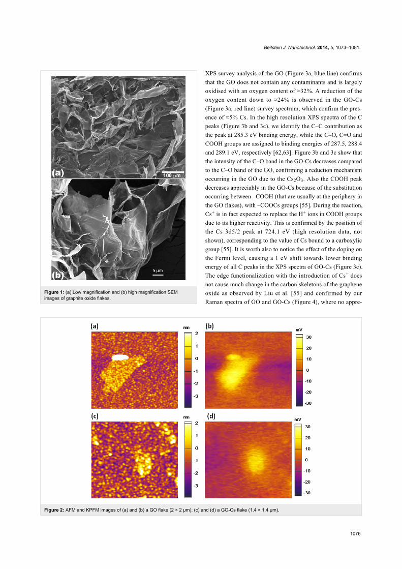
Results and DiscussionMaterial characterisationsThe morphology of the synthesized graphite oxide powder was
investigated by FESEM (Figure 1). It is evident that the thin
and aggregated flakes are stacked to each other with lateral
sizes ranging from several hundred nanometers to several
microns.
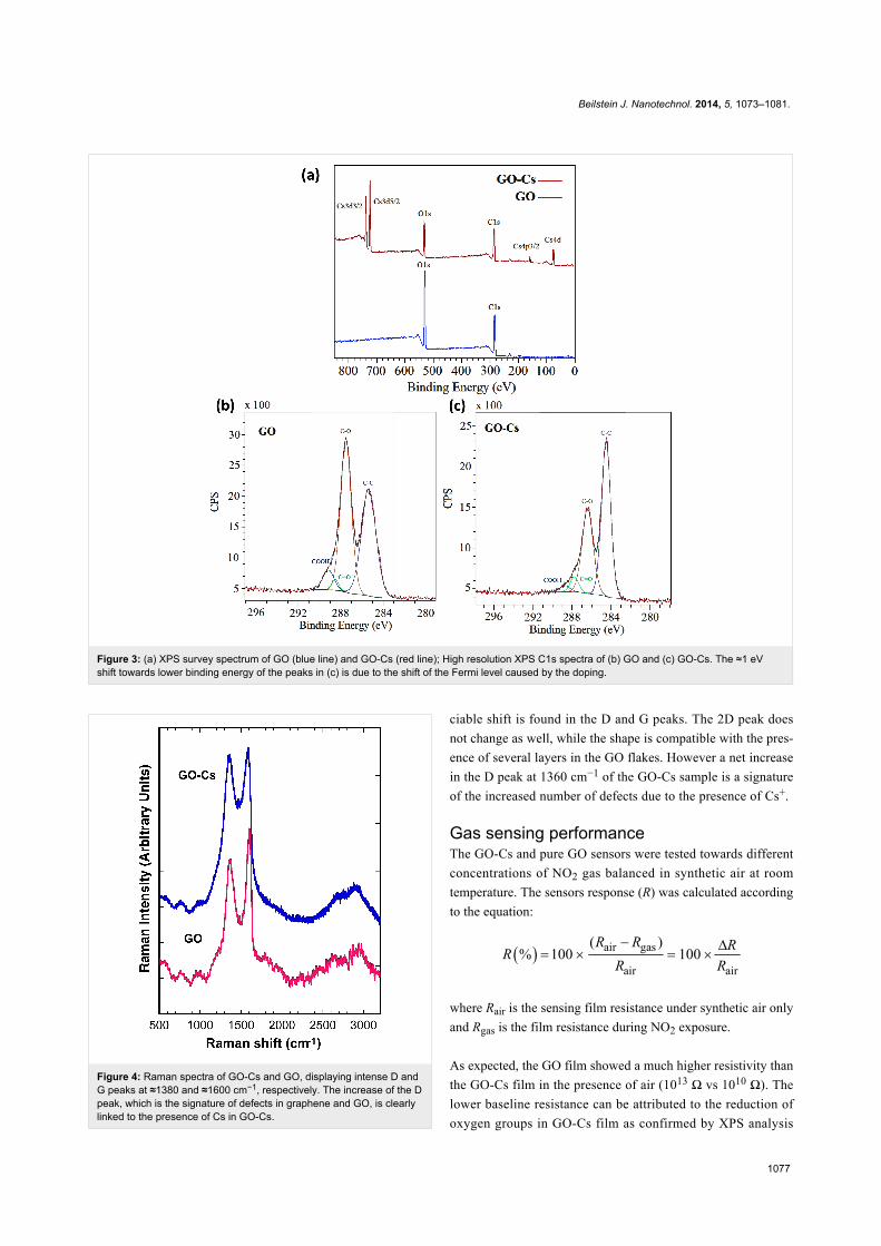
AFM images (Figure 2a and 2c) confirm that most of GO and
GO-Cs flakes are approx. 1 nm thick, corresponding to one
monolayer, with a lateral size in the range of hundred nano-
meters [56,57]. The thickness of each GO layer is usually
higher than the pristine graphene sheet because of the orthogo-
nally bonded oxygen groups coming out from the surface
[28,57,58].
Electrical characterizations were carried out with KPFM
providing a potential map of the samples with a resolution of
few mV. Figure 2b and 2d show a comparison of pristine GO
and GO-Cs KPFM signals.
The measurements collected from several samples and on
different flakes show a net difference in the potential map of
GO (see Figure 2b) and GO-Cs flakes (see Figure 2d), with a
drop of the average potential on a flake from 30 ± 3 mV in the
GO to 19 ± 3 mV in the GO-Cs. We attribute this drop to the
chemical reduction of the GO caused by the Cs2CO3 that tends
to decrease the work function as observed by [55,59-61]. This
result suggests that doped GO may have good performance as a
gas sensing material.
Beilstein J. Nanotechnol. 2014, 5, 1073–1081.
1076
Figure 2: AFM and KPFM images of (a) and (b) a GO flake (2 × 2 μm); (c) and (d) a GO-Cs flake (1.4 × 1.4 μm).
Figure 1: (a) Low magnification and (b) high magnification SEMimages of graphite oxide flakes.
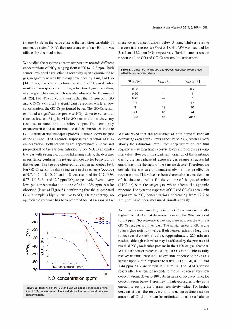
XPS survey analysis of the GO (Figure 3a, blue line) confirms
that the GO does not contain any contaminants and is largely
oxidised with an oxygen content of ≈32%. A reduction of the
oxygen content down to ≈24% is observed in the GO-Cs
(Figure 3a, red line) survey spectrum, which confirm the pres-
ence of ≈5% Cs. In the high resolution XPS spectra of the C
peaks (Figure 3b and 3c), we identify the C–C contribution as
the peak at 285.3 eV binding energy, while the C–O, C=O and
COOH groups are assigned to binding energies of 287.5, 288.4
and 289.1 eV, respectively [62,63]. Figure 3b and 3c show that
the intensity of the C–O band in the GO-Cs decreases compared
to the C–O band of the GO, confirming a reduction mechanism
occurring in the GO due to the Cs2O3. Also the COOH peak
decreases appreciably in the GO-Cs because of the substitution
occurring between –COOH (that are usually at the periphery in
the GO flakes), with –COOCs groups [55]. During the reaction,
Cs+ is in fact expected to replace the H+ ions in COOH groups
due to its higher reactivity. This is confirmed by the position of
the Cs 3d5/2 peak at 724.1 eV (high resolution data, not
shown), corresponding to the value of Cs bound to a carboxylic
group [55]. It is worth also to notice the effect of the doping on
the Fermi level, causing a 1 eV shift towards lower binding
energy of all C peaks in the XPS spectra of GO-Cs (Figure 3c).
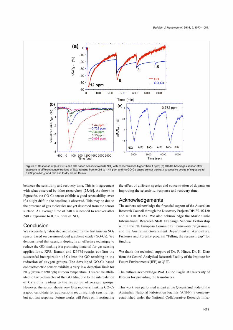
The edge functionalization with the introduction of Cs+ does
not cause much change in the carbon skeletons of the graphene
oxide as observed by Liu et al. [55] and confirmed by our
Raman spectra of GO and GO-Cs (Figure 4), where no appre-
Beilstein J. Nanotechnol. 2014, 5, 1073–1081.
1077
Figure 3: (a) XPS survey spectrum of GO (blue line) and GO-Cs (red line); High resolution XPS C1s spectra of (b) GO and (c) GO-Cs. The ≈1 eVshift towards lower binding energy of the peaks in (c) is due to the shift of the Fermi level caused by the doping.
Figure 4: Raman spectra of GO-Cs and GO, displaying intense D andG peaks at ≈1380 and ≈1600 cm−1, respectively. The increase of the Dpeak, which is the signature of defects in graphene and GO, is clearlylinked to the presence of Cs in GO-Cs.
ciable shift is found in the D and G peaks. The 2D peak does
not change as well, while the shape is compatible with the pres-
ence of several layers in the GO flakes. However a net increase
in the D peak at 1360 cm−1 of the GO-Cs sample is a signature
of the increased number of defects due to the presence of Cs+.
Gas sensing performanceThe GO-Cs and pure GO sensors were tested towards different
concentrations of NO2 gas balanced in synthetic air at room
temperature. The sensors response (R) was calculated according
to the equation:
where Rair is the sensing film resistance under synthetic air only
and Rgas is the film resistance during NO2 exposure.
As expected, the GO film showed a much higher resistivity than
the GO-Cs film in the presence of air (1013 Ω vs 1010 Ω). The
lower baseline resistance can be attributed to the reduction of
oxygen groups in GO-Cs film as confirmed by XPS analysis
Beilstein J. Nanotechnol. 2014, 5, 1073–1081.
1078
Figure 5: Response of the GO and GO-Cs based sensors as a func-tion of NO2 concentration. The inset shows the response at very lowconcentrations.
(Figure 3). Being the value close to the resolution capability of
our source meter (10 fA), the measurements of the GO film was
affected by electrical noise.
We studied the response at room temperature towards different
concentrations of NO2, ranging from 0.090 to 12.2 ppm. Both
sensors exhibited a reduction in resistivity upon exposure to the
gas, in agreement with the theory developed by Tang and Cao
[14]: a negative charge is transferred to the NO2 molecules,
mostly in correspondence of oxygen functional group, resulting
in a p-type behaviour, which was also observed by Prezioso et
al. [25]. For NO2 concentrations higher than 3 ppm both GO
and GO-Cs exhibited a significant response, while at low
concentrations the GO-Cs performed better. The GO-Cs sensor
exhibited a significant response to NO2, down to concentra-
tions as low as ≈91 ppb, while GO sensor did not show any
response to concentrations below 3 ppm. This sensitivity
enhancement could be attributed to defects introduced into the
GO-Cs films during the doping process. Figure 5 shows the plot
of the GO and GO-Cs sensors response as a function of NO2
concentration. Both responses are approximately linear and
proportional to the gas concentration. Since NO2 is an oxida-
tive gas with strong electron-withdrawing ability, the decrease
in resistance confirms the p-type semiconductor behaviour of
the sensors, like the one observed for carbon nanotubes [64].
For GO-Cs sensor a relative increase in the response (RGO-Cs)
of 0.7, 1, 2, 4.4, 10, 24 and 40% was recorded for 0.18, 0.36,
0.73, 1.5, 3, 6.1 and 12.2 ppm NO2, respectively. Even at very
low gas concentrations, a slope of about 3% ppm can be
observed (inset of Figure 5), confirming that the as-prepared
GO-Cs sample is highly sensitive to NO2. On the contrary, no
appreciable response has been recorded for GO sensor in the
presence of concentrations below 3 ppm, while a relative
increase in the response (RGO) of 18, 41, 65% was recorded for
3, 6.1 and 12.2 ppm NO2, respectively. Table 1 summarises the
response of the GO and GO-Cs sensors for comparison.
Table 1: Comparison of the GO and GO-Cs response towards NO2with different concentrations.
NO2 [ppm] RGO [%] RGO-Cs [%]
0.18 — 0.70.36 — 10.73 — 21.5 — 4.43 18 10
6.1 41 2412.2 65 39.6
We observed that the resistance of both sensors kept on
decreasing even after 20 min exposure to NO2, reaching very
slowly the saturation state. From deep saturation, the film
required a very long time exposure to dry air to recover its orig-
inal value. However, the significant variation of the resistance
during the first phase of exposure can ensure a successful
employment on the field of the sensing device. Therefore, we
consider the exposure of approximately 4 min as an effective
response time. This value has been chosen also in consideration
of the time required to fill the volume of the gas chamber
(1100 cc) with the target gas, which affects the dynamic
response. The dynamic responses of GO and GO-Cs upon 4 min
exposure to NO2 concentrations decreasing from 12.2 to
1.5 ppm have been measured simultaneously.
As it can be seen from Figure 6a, the GO response is initially
higher than GO-Cs, but decreases more rapidly. When exposed
to 1.5 ppm, GO response is not anymore appreciable while a
GO-Cs reaction is still evident. The noisier curves of GO is due
to its higher resistivity value. Both sensors exhibit a long time
to recover their initial value. Approximately 220 min are
needed, although this value may be affected by the presence of
residual NO2 molecules present in the 1100 cc gas chamber.
While GO sensor recovers faster, GO-Cs is not able to fully
recover its initial baseline. The dynamic response of the GO-Cs
sensor upon 4 min exposure to 0.091, 0.18, 0.36, 0.732 and
1.44 ppm NO2 are shown in Figure 6b. The GO-Cs sensor
reacts after few tens of seconds to the NO2 even at very low
concentrations, down to 180 ppb. In terms of recovery time, for
concentrations below 1 ppm, few minute exposures to dry air is
enough to restore the original resistivity value. For higher
concentrations, the recovery is longer, suggesting that the
amount of Cs doping can be optimized to make a balance
Beilstein J. Nanotechnol. 2014, 5, 1073–1081.
1079
Figure 6: Response of (a) GO-Cs and GO based sensors towards NO2 with concentrations higher than 1 ppm; (b) GO-Cs based gas sensor afterexposure to different concentrations of NO2 ranging from 0.091 to 1.44 ppm and (c) GO-Cs based sensor during 3 successive cycles of exposure to0.732 ppm NO2 for 4 min and to dry air for 15 min.
between the sensitivity and recovery time. This is in agreement
with what observed by other researchers [25,46]. As shown in
Figure 6c, the GO-Cs sensor exhibits a good repeatability, even
if a slight drift in the baseline is observed. This may be due to
the presence of gas molecules not yet desorbed from the sensor
surface. An average time of 540 s is needed to recover after
240 s exposure to 0.732 ppm of NO2.
ConclusionWe successfully fabricated and studied for the first time an NO2
sensor based on caesium-doped graphene oxide (GO-Cs). We
demonstrated that caesium doping is an effective technique to
reduce the GO, making it a promising material for gas sensing
applications. XPS, Raman and KPFM results confirm the
successful incorporation of Cs into the GO resulting in the
reduction of oxygen groups. The developed GO-Cs based
conductometric sensor exhibits a very low detection limit for
NO2 (down to ≈90 ppb) at room temperature. This can be attrib-
uted to the p-character of the GO film, due to the intercalation
of Cs atoms leading to the reduction of oxygen groups.
However, the sensor shows very long recovery, making GO-Cs
a good candidate for applications requiring high sensitivities,
but not fast response. Future works will focus on investigating
the effect of different species and concentration of dopants on
improving the selectivity, response and recovery time.
AcknowledgementsThe authors acknowledge the financial support of the Australian
Research Council through the Discovery Projects DP130102120
and DP110101454. We also acknowledge the Marie Curie
International Research Staff Exchange Scheme Fellowship
within the 7th European Community Framework Programme,
and the Australian Government Department of Agriculture,
Fisheries and Forestry program “Filling the research gap” for
funding.
We thank the technical support of Dr. P. Hines, Dr. H. Diao
from the Central Analytical Research Facility of the Institute for
Future Environments (IFE) at QUT.
The authors acknowledge Prof. Guido Faglia at University of
Brescia for providing the transducers.
This work was performed in part at the Queensland node of the
Australian National Fabrication Facility (ANFF); a company
established under the National Collaborative Research Infra-
Beilstein J. Nanotechnol. 2014, 5, 1073–1081.
1080
structure Strategy to provide nano and microfabrication facili-
ties for Australia’s researchers.
References1. Geim, A. K.; Novoselov, K. S. Nat. Mater. 2007, 6, 183–191.
doi:10.1038/nmat18492. Castro Neto, A. H.; Guinea, F.; Peres, N. M. R.; Novoselov, K. S.;
Geim, A. K. Rev. Mod. Phys. 2009, 81, 109–162.doi:10.1103/RevModPhys.81.109
3. Chang, H.; Wu, H. Energy Environ. Sci. 2013, 6, 3483–3507.doi:10.1039/c3ee42518e
4. Schedin, F.; Geim, A. K.; Morozov, S. V.; Hill, E. W.; Blake, P.;Katsnelson, M. I.; Novoselov, K. S. Nat. Mater. 2007, 6, 652–655.doi:10.1038/nmat1967
5. Basu, S.; Bhattacharyya, P. Sens. Actuators, B 2012, 173, 1–21.doi:10.1016/j.snb.2012.07.092
6. Qazi, M.; Koley, G. Sensors 2008, 8, 7144–7156.doi:10.3390/s8117144
7. Arsat, R.; Breedon, M.; Shafiei, M.; Spizziri, P. G.; Gilje, S.;Kaner, R. B.; Kalantar-zadeh, K.; Wlodarski, W. Chem. Phys. Lett.2009, 467, 344–347. doi:10.1016/j.cplett.2008.11.039
8. Fowler, J. D.; Allen, M. J.; Tung, V. C.; Yang, Y.; Kaner, R. B.;Weiller, B. H. ACS Nano 2009, 3, 301–306. doi:10.1021/nn800593m
9. Al-Mashat, L.; Shin, K.; Kalantar-zadeh, K.; Plessis, J. D.; Han, S. H.;Kojima, R. W.; Kaner, R. B.; Li, D.; Gou, X.; Ippolito, S. J.;Wlodarski, W. J. Phys. Chem. C 2010, 114, 16168–16173.doi:10.1021/jp103134u
10. Siegal, M. P.; Yelton, W. G.; Overmyer, D. L.; Provencio, P. P.Langmuir 2004, 20, 1194–1198. doi:10.1021/la034460s
11. Shafiei, M.; Spizzirri, P. G.; Arsat, R.; Yu, J.; du Plessis, J.; Dubin, S.;Kaner, R. B.; Kalantar-zadeh, K.; Wlodarski, W. J. Phys. Chem. C2010, 114, 13796–13801. doi:10.1021/jp104459s
12. Geim, A. K. Science 2009, 324, 1530–1534.doi:10.1126/science.1158877
13. Zhang, Y.-H.; Chen, Y.-B.; Zhou, K.-G.; Liu, C.-H.; Zeng, J.;Zhang, H.-L.; Peng, Y. Nanotechnology 2009, 20, 185504.doi:10.1088/0957-4484/20/18/185504
14. Tang, S.; Cao, Z. J. Chem. Phys. 2011, 134, 044710.doi:10.1063/1.3541249
15. Li, W.; Geng, X.; Guo, Y.; Rong, J.; Gong, Y.; Wu, L.; Zhang, X.; Li, P.;Xu, J.; Cheng, G.; Sun, M.; Liu, L. ACS Nano 2011, 5, 6955–6961.doi:10.1021/nn201433r
16. Wei, X.-L.; Chen, Y.-P.; Liu, W.-L.; Zhong, J.-X. Phys. Lett. A 2012,376, 559–562. doi:10.1016/j.physleta.2011.10.055
17. Niu, F.; Liu, J.-M.; Tao, L.-M.; Wang, W.; Song, W.-G.J. Mater. Chem. A 2013, 1, 6130–6133. doi:10.1039/c3ta11070b
18. Pandey, P. A.; Wilson, N. R.; Covington, J. A. Sens. Actuators, B 2013,183, 478–487. doi:10.1016/j.snb.2013.03.089
19. Dan, Y.; Lu, Y.; Kybert, N. J.; Luo, Z.; Johnson, A. T. C. Nano Lett.2009, 9, 1472–1475. doi:10.1021/nl8033637
20. Novoselov, K. S. Rev. Mod. Phys. 2011, 83, 837–849.doi:10.1103/RevModPhys.83.837
21. Dreyer, D. R.; Park, S.; Bielawski, C. W.; Ruoff, R. S. Chem. Soc. Rev.2010, 39, 228–240. doi:10.1039/b917103g
22. Zhu, Y.; Murali, S.; Cai, W.; Li, X.; Suk, J. W.; Potts, J. R.; Ruoff, R. S.Adv. Mater. 2010, 22, 3906–3924. doi:10.1002/adma.201001068
23. Lu, G.; Ocola, L. E.; Chen, J. Appl. Phys. Lett. 2009, 94, 083111.doi:10.1063/1.3086896
24. Jung, I.; Dikin, D.; Park, S.; Cai, W.; Mielke, S. L.; Ruoff, R. S.J. Phys. Chem. C 2008, 112, 20264–20268. doi:10.1021/jp807525d
25. Prezioso, S.; Perrozzi, F.; Giancaterini, L.; Cantalini, C.; Treossi, E.;Palermo, V.; Nardone, M.; Santucci, S.; Ottaviano, L. J. Phys. Chem. C2013, 117, 10683–10690. doi:10.1021/jp3085759
26. Stankovich, S.; Dikin, D. A.; Dommett, G. H. B.; Kohlhaas, K. M.;Zimney, E. J.; Stach, E. A.; Piner, R. D.; Nguyen, S. T.; Ruoff, R. S.Nature 2006, 442, 282–286. doi:10.1038/nature04969
27. Gilje, S.; Han, S.; Wang, M.; Wang, K. L.; Kaner, R. B. Nano Lett.2007, 7, 3394–3398. doi:10.1021/nl0717715
28. Stankovich, S.; Dikin, D. A.; Piner, R. D.; Kohlhaas, K. A.;Kleinhammes, A.; Jia, Y.; Wu, Y.; Nguyen, S. T.; Ruoff, R. S. Carbon2007, 45, 1558–1565. doi:10.1016/j.carbon.2007.02.034
29. Gómez-Navarro, C.; Weitz, R. T.; Bittner, A. M.; Scolari, M.; Mews, A.;Burghard, M.; Kern, K. Nano Lett. 2007, 7, 3499–3503.doi:10.1021/nl072090c
30. Sutter, P. W.; Flege, J.-I.; Sutter, E. A. Nat. Mater. 2008, 7, 406–411.doi:10.1038/nmat2166
31. Novoselov, K. S.; Geim, A. K.; Morozov, S. V.; Jiang, D.; Zhang, Y.;Dubonos, S. V.; Grigorieva, I. V.; Firsov, A. A. Science 2004, 306,666–669. doi:10.1126/science.1102896
32. Dato, A.; Radmilovic, V.; Lee, Z.; Phillips, J.; Frenklach, M. Nano Lett.2008, 8, 2012–2016. doi:10.1021/nl8011566
33. Berger, C.; Song, Z.; Li, X.; Wu, X.; Brown, N.; Naud, C.; Mayou, D.;Li, T.; Hass, J.; Marchenkov, A. N.; Conrad, E. H.; First, P. N.;de Heer, W. A. Science 2006, 312, 1191–1196.doi:10.1126/science.1125925
34. Park, S.; Ruoff, R. S. Nat. Nanotechnol. 2009, 4, 217–224.doi:10.1038/nnano.2009.58
35. Parades, J. I.; Villar-Rodil, S.; Martínez-Alonso, A.; Tascón, J. M. D.Langmuir 2008, 24, 10560–10564. doi:10.1021/la801744a
36. Park, S.; Lee, K.-S.; Bozoklu, G.; Cai, W.; Nguyen, S. T.; Ruoff, R. S.ACS Nano 2008, 2, 572–578. doi:10.1021/nn700349a
37. Stankovich, S.; Piner, R. D.; Chen, X.; Wu, N.; Nguyen, S. T.;Ruoff, R. S. J. Mater. Chem. 2006, 16, 155–158.doi:10.1039/b512799h
38. Stankovich, S.; Piner, R. D.; Nguyen, S. T.; Ruoff, R. S. Carbon 2006,44, 3342–3347. doi:10.1016/j.carbon.2006.06.004
39. Tung, V. C.; Allen, M. J.; Yang, Y.; Kaner, R. B. Nat. Nanotechnol.2009, 4, 25–29. doi:10.1038/nnano.2008.329
40. McAllister, M. J.; Li, J.-L.; Adamson, D. H.; Schniepp, H. C.;Abdala, A. A.; Liu, J.; Herrera-Alonso, M.; Milius, D. L.; Car, R.;Prud'homme, R. K.; Aksay, I. A. Chem. Mater. 2007, 19, 4396–4404.doi:10.1021/cm0630800
41. Schniepp, H. C.; Li, J.-L.; McAllister, M. J.; Sai, H.; Herrera-Alonso, M.;Adamson, D. H.; Prud'homme, R. K.; Car, R.; Saville, D. A.;Aksay, I. A. J. Phys. Chem. B 2006, 110, 8535–8539.doi:10.1021/jp060936f
42. Williams, G.; Seger, B.; Kamat, P. V. ACS Nano 2008, 2, 1487–1491.doi:10.1021/nn800251f
43. Pei, S.; Cheng, H.-M. Carbon 2012, 50, 3210–3228.doi:10.1016/j.carbon.2011.11.010
44. Zhao, J.; Han, J.; Lu, J. P. Phys. Rev. B 2002, 65, 193401.doi:10.1103/PhysRevB.65.193401
45. Yu, M.-R.; Wu, R.-J.; Suyambrakasam, G.; Joly, J.; Chavali, M.Adv. Sci. Lett. 2012, 16, 53–57. doi:10.1166/asl.2012.4264
46. Robinson, J. T.; Perkins, F. K.; Snow, E. S.; Wei, Z.; Sheehan, P. E.Nano Lett. 2008, 8, 3137–3140. doi:10.1021/nl8013007
47. Lipatov, A.; Varezhnikov, A.; Wilson, P.; Sysoev, V.; Kolmakov, A.;Sinitskii, A. Nanoscale 2013, 5, 5426–5434. doi:10.1039/c3nr00747b
Beilstein J. Nanotechnol. 2014, 5, 1073–1081.
1081
48. Hu, N.; Wang, Y.; Chai, J.; Gao, R.; Yang, Z.; Kong, E. S.-W.;Zhang, Y. Sens. Actuators, B 2012, 163, 107–114.doi:10.1016/j.snb.2012.01.016
49. Dua, V.; Surwade, S. P.; Ammu, S.; Agnihotra, S. R.; Jain, S.;Roberts, K. E.; Park, S.; Ruoff, R. S.; Manohar, S. K.Angew. Chem., Int. Ed. 2010, 49, 2154–2157.doi:10.1002/anie.200905089
50. Yuan, W.; Liu, A.; Huang, L.; Li, C.; Shi, G. Adv. Mater. 2013, 25,766–771. doi:10.1002/adma.201203172
51. Tricoli, A.; Righettoni, M.; Teleki, A. Angew. Chem., Int. Ed. 2010, 49,7632–7659. doi:10.1002/anie.200903801
52. Llobet, E. Sens. Actuators, B 2013, 179, 32–45.doi:10.1016/j.snb.2012.11.014
53. Thomas, B.; Benoy, S.; Radha, K. K. Sens. Actuators, B 2008, 133,404–413. doi:10.1016/j.snb.2008.02.050
54. Marcano, D. C.; Kosynkin, D. V.; Berlin, J. M.; Sinitskii, A.; Sun, Z.;Slesarev, A.; Alemany, L. B.; Lu, W.; Tour, J. M. ACS Nano 2010, 4,4806–4814. doi:10.1021/nn1006368
55. Liu, J.; Xue, Y.; Gao, Y.; Yu, D.; Durstock, M.; Dai, L. Adv. Mater. 2012,24, 2228–2233. doi:10.1002/adma.201104945
56. Chen, D.; Feng, H.; Li, J. Chem. Rev. 2012, 112, 6027–6053.doi:10.1021/cr300115g
57. Glover, A. J.; Adamson, D. H.; Schniepp, H. C. J. Phys. Chem. C 2012,116, 20080–20085. doi:10.1021/jp305717v
58. Mkhoyan, K. A.; Contryman, A. W.; Silcox, J.; Stewart, D. A.; Eda, G.;Mattevi, C.; Miller, S.; Chhowalla, M. Nano Lett. 2009, 9, 1058–1063.doi:10.1021/nl8034256
59. Liscio, A.; Veronese, G. P.; Treossi, E.; Suriano, F.; Rossella, F.;Bellani, V.; Rizzoli, R.; Samori, P.; Palermo, V. J. Mater. Chem. 2011,21, 2924–2931. doi:10.1039/c0jm02940h
60. Palermo, V.; Palma, M.; Samori, P. Adv. Mater. 2006, 18, 145–164.doi:10.1002/adma.200501394
61. Jaafar, M.; López-Polín, G.; Gómez-Navarro, C.; Gómez-Herrero, J.Appl. Phys. Lett. 2012, 101, 263109. doi:10.1063/1.4773357
62. Yang, D.; Velamakanni, A.; Bozoklu, G.; Park, S.; Stoller, M.;Piner, R. D.; Stankovich, S.; Jung, I.; Field, D. A.; Ventrice, C. A., Jr.;Ruoff, R. S. Carbon 2009, 47, 145–152.doi:10.1016/j.carbon.2008.09.045
63. Ganguly, A.; Sharma, S.; Papakonstantinou, P.; Hamilton, J.J. Phys. Chem. C 2011, 115, 17009–17019. doi:10.1021/jp203741y
64. Kong, J.; Franklin, N. R.; Zhou, C.; Chapline, M. G.; Peng, S.; Cho, K.;Dai, H. Science 2000, 287, 622–625.doi:10.1126/science.287.5453.622
License and TermsThis is an Open Access article under the terms of the
Creative Commons Attribution License
(http://creativecommons.org/licenses/by/2.0), which
permits unrestricted use, distribution, and reproduction in
any medium, provided the original work is properly cited.
The license is subject to the Beilstein Journal of
Nanotechnology terms and conditions:
(http://www.beilstein-journals.org/bjnano)
The definitive version of this article is the electronic one
which can be found at:
doi:10.3762/bjnano.5.120