Hardware Design Considerations for MKW39A/38A/37A/38Z ...
15
1 Introduction This application note describes Printed Circuit Board (PCB) design considerations for the MKW39A/38A/37A/38Z/37Z 48-pin QFN (HVQFN-7 × 7 Pitch 0.5 mm) wettable flank package. Included are layouts of the component copper layer, solder mask, and solder paste stencil. These recommendations are guidelines only and may need to be modified depending on the assembly house used and the other components on the board. 2 QFN component coppoer layer 2.1 48-pin HVQFN Figure 1 shows a recommended component copper layer. This layer is also referred to as the top metal layer and is the layer to which the components are soldered. The footprint for the 48-pin Wettable HVQFN package (7 × 7 × 0.85 mm) consists of 48 IC contact pads, and nine centered ground pads. The copper pattern is as shown in Figure 1. Use 0.25 mm via holes to connect to the ground plane layers. These are required for RF grounding and help to prevent solder float. Contents 1 Introduction............................................ 1 2 QFN component coppoer layer.............. 1 3 QFN package dimensions..................... 4 4 QFN soldering profile............................. 6 5 Design and board layout considerations..................................... 7 AN12518 Hardware Design Considerations for MKW39A/38A/37A/38Z/37Z Bluetooth LE Devices Rev. 0 — April 2020 Application Note
-
Upload
khangminh22 -
Category
Documents
-
view
1 -
download
0
Transcript of Hardware Design Considerations for MKW39A/38A/37A/38Z ...

1 IntroductionThis application note describes Printed Circuit Board (PCB) designconsiderations for the MKW39A/38A/37A/38Z/37Z 48-pin QFN (HVQFN-7 × 7Pitch 0.5 mm) wettable flank package. Included are layouts of the componentcopper layer, solder mask, and solder paste stencil.
These recommendations are guidelines only and may need to be modifieddepending on the assembly house used and the other components on theboard.
2 QFN component coppoer layer
2.1 48-pin HVQFNFigure 1 shows a recommended component copper layer. This layer is also referred to as the top metal layer and is the layer towhich the components are soldered. The footprint for the 48-pin Wettable HVQFN package (7 × 7 × 0.85 mm) consists of 48 ICcontact pads, and nine centered ground pads. The copper pattern is as shown in Figure 1.
Use 0.25 mm via holes to connect to the ground plane layers. These are required for RF grounding and help to prevent solder float.
Contents
1 Introduction............................................ 1
2 QFN component coppoer layer..............1
3 QFN package dimensions..................... 4
4 QFN soldering profile.............................6
5 Design and board layoutconsiderations..................................... 7
AN12518Hardware Design Considerations for MKW39A/38A/37A/38Z/37ZBluetooth LE DevicesRev. 0 — April 2020 Application Note
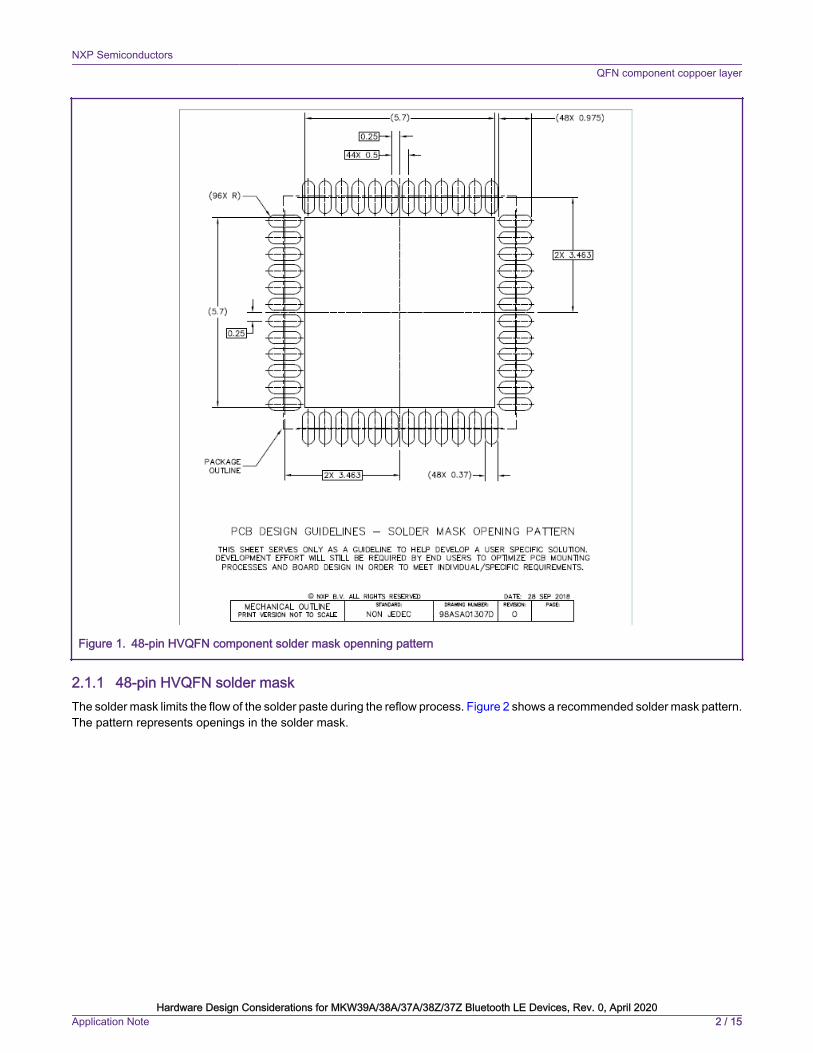
Figure 1. 48-pin HVQFN component solder mask openning pattern
2.1.1 48-pin HVQFN solder maskThe solder mask limits the flow of the solder paste during the reflow process. Figure 2 shows a recommended solder mask pattern.The pattern represents openings in the solder mask.
NXP SemiconductorsQFN component coppoer layer
Hardware Design Considerations for MKW39A/38A/37A/38Z/37Z Bluetooth LE Devices, Rev. 0, April 2020Application Note 2 / 15
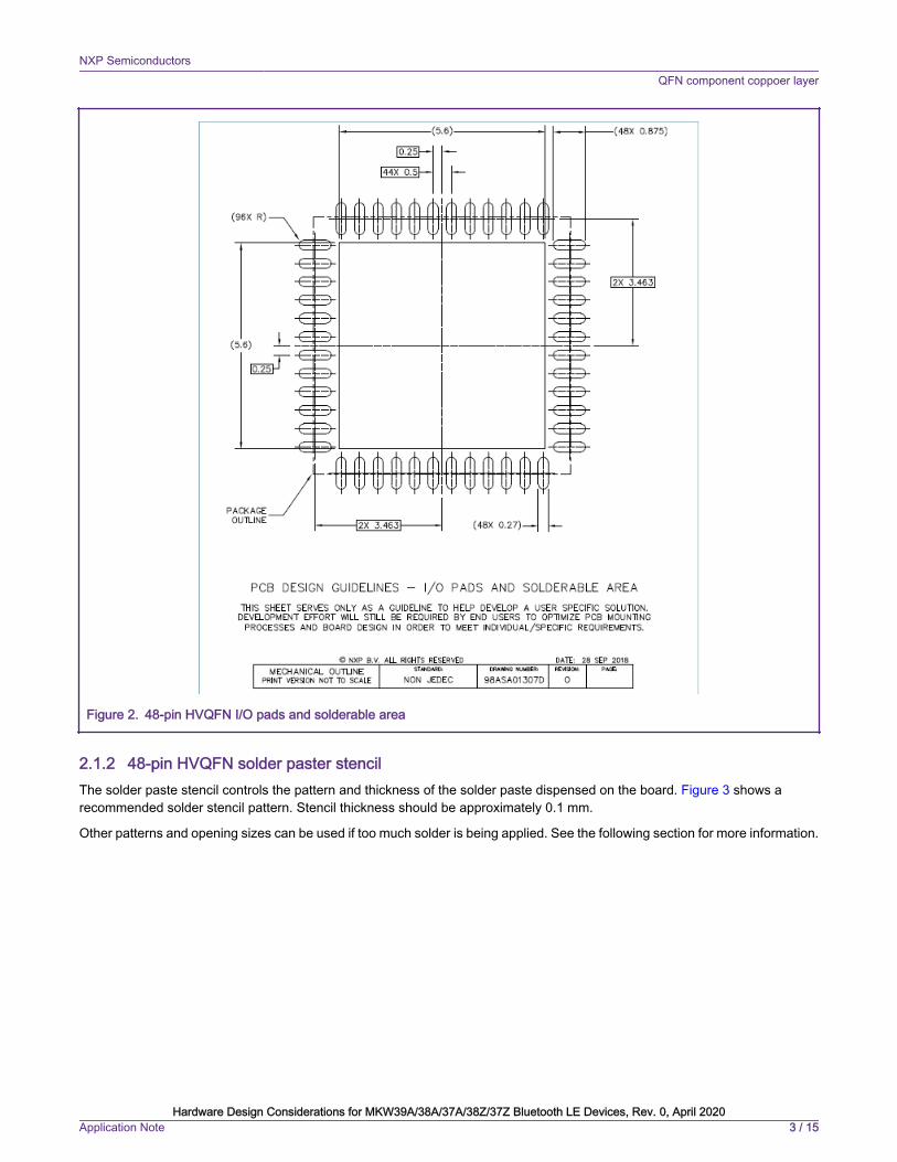
Figure 2. 48-pin HVQFN I/O pads and solderable area
2.1.2 48-pin HVQFN solder paster stencilThe solder paste stencil controls the pattern and thickness of the solder paste dispensed on the board. Figure 3 shows arecommended solder stencil pattern. Stencil thickness should be approximately 0.1 mm.
Other patterns and opening sizes can be used if too much solder is being applied. See the following section for more information.
NXP SemiconductorsQFN component coppoer layer
Hardware Design Considerations for MKW39A/38A/37A/38Z/37Z Bluetooth LE Devices, Rev. 0, April 2020Application Note 3 / 15

Figure 3. 48-pin HVQFN solder paste stencil
2.2 QFN problems with excess solderExcess solder may cause the QFN to float or bridge between the package contacts. To use the correct amount of solder pasteapplied to the PCB, take into consideration the following:
• Stencil thickness
• Other components mounted on the PCB
• Manufacturing equipment
• Assembly house experience
3 QFN package dimensionsFigure 4 shows the 48-pin HVQFN package dimensions.
NXP SemiconductorsQFN package dimensions
Hardware Design Considerations for MKW39A/38A/37A/38Z/37Z Bluetooth LE Devices, Rev. 0, April 2020Application Note 4 / 15
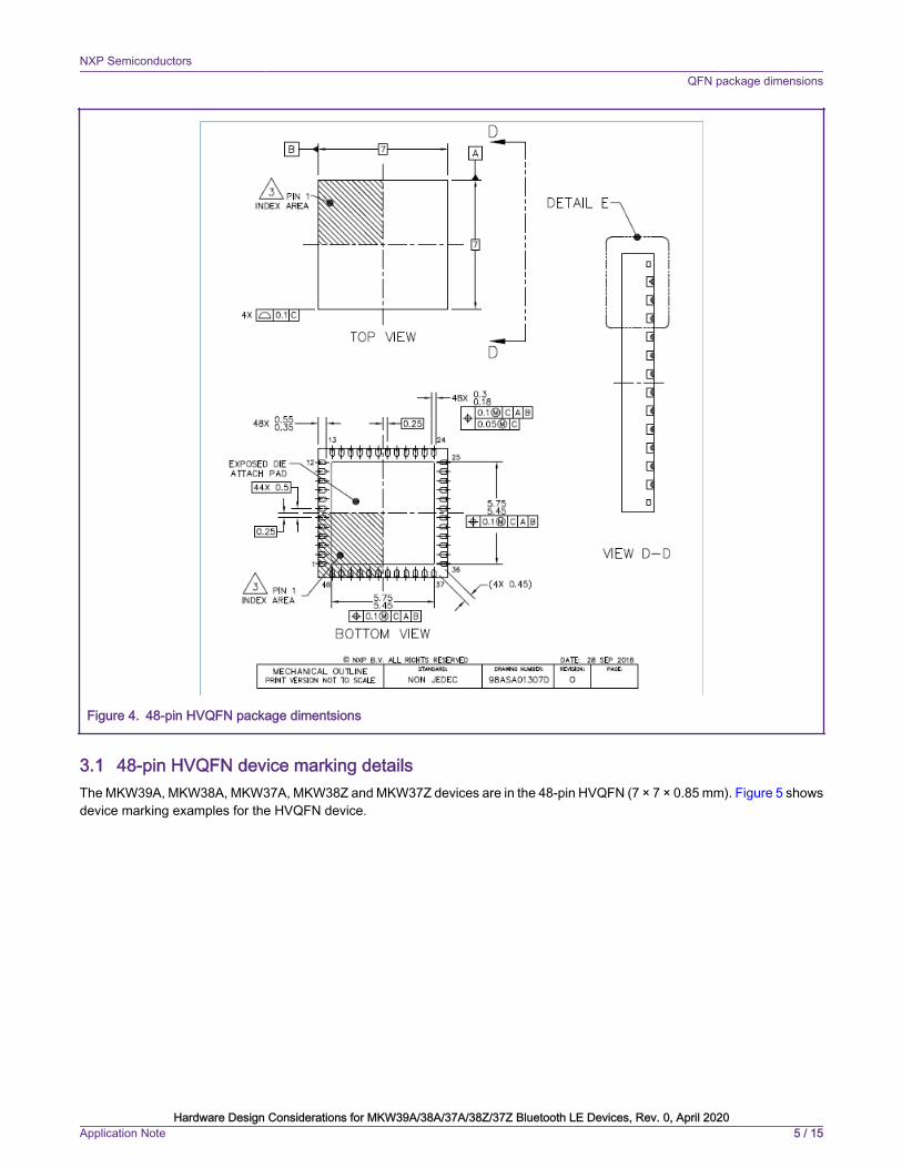
Figure 4. 48-pin HVQFN package dimentsions
3.1 48-pin HVQFN device marking detailsThe MKW39A, MKW38A, MKW37A, MKW38Z and MKW37Z devices are in the 48-pin HVQFN (7 × 7 × 0.85 mm). Figure 5 showsdevice marking examples for the HVQFN device.
NXP SemiconductorsQFN package dimensions
Hardware Design Considerations for MKW39A/38A/37A/38Z/37Z Bluetooth LE Devices, Rev. 0, April 2020Application Note 5 / 15
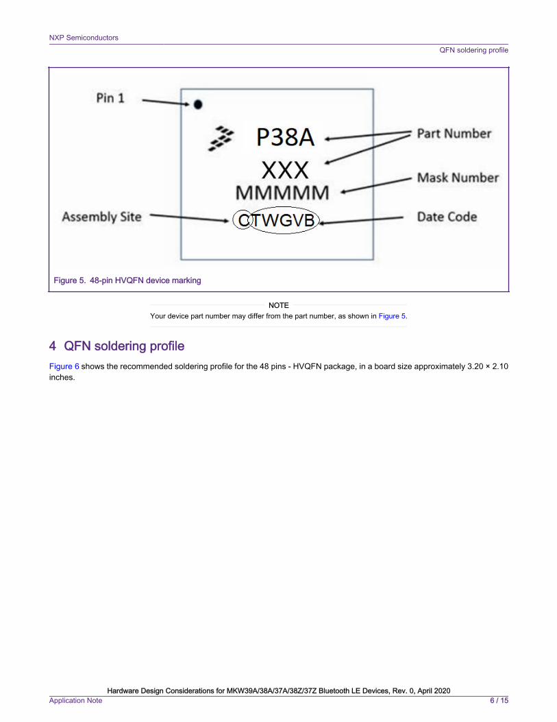
Figure 5. 48-pin HVQFN device marking
Your device part number may differ from the part number, as shown in Figure 5.
NOTE
4 QFN soldering profileFigure 6 shows the recommended soldering profile for the 48 pins - HVQFN package, in a board size approximately 3.20 × 2.10inches.
NXP SemiconductorsQFN soldering profile
Hardware Design Considerations for MKW39A/38A/37A/38Z/37Z Bluetooth LE Devices, Rev. 0, April 2020Application Note 6 / 15

Figure 6. QFN soldering profile
5 Design and board layout considerationsTo have successful wireless hardware development, the proper device footprint, RF layout, circuit matching, antenna design,and RF measurement capability are essential. RF circuit design, layout, and antenna design are specialties requiring investmentin tools and experience. With available hardware reference designs from NXP, RF design considerations, and the guidelinescontained in this application note, hardware engineers can successfully design BLE radio boards with good performance levels. Figure 7 shows the FRDM-KW38 development board. It contains the MKW38A device and all necessary I/O connections.
NXP SemiconductorsDesign and board layout considerations
Hardware Design Considerations for MKW39A/38A/37A/38Z/37Z Bluetooth LE Devices, Rev. 0, April 2020Application Note 7 / 15
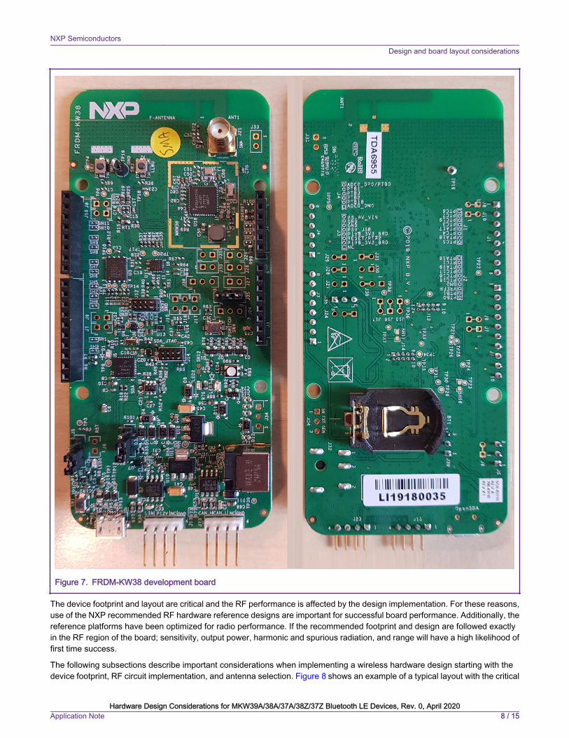
Figure 7. FRDM-KW38 development board
The device footprint and layout are critical and the RF performance is affected by the design implementation. For these reasons,use of the NXP recommended RF hardware reference designs are important for successful board performance. Additionally, thereference platforms have been optimized for radio performance. If the recommended footprint and design are followed exactlyin the RF region of the board; sensitivity, output power, harmonic and spurious radiation, and range will have a high likelihood offirst time success.
The following subsections describe important considerations when implementing a wireless hardware design starting with thedevice footprint, RF circuit implementation, and antenna selection. Figure 8 shows an example of a typical layout with the critical
NXP SemiconductorsDesign and board layout considerations
Hardware Design Considerations for MKW39A/38A/37A/38Z/37Z Bluetooth LE Devices, Rev. 0, April 2020Application Note 8 / 15

RF section which must be copied exactly for optimal radio performance. The less critical layout area can be modified withoutreducing radio performance.
Exact dimensions are not given in this document, but can be found in the design files for the FRDM-KW38 board.
NOTE
Figure 8. Critical layout areas
5.1 MKW38A device footprintThe performance of the wireless link is largely influenced by the device’s footprint. As a result, a great deal of care has been putinto creating a footprint so that receiver sensitivity and output power are optimized to enable board matching and minimalcomponent count. NXP highly recommends copying the die flag exactly as shown in Figure 9. This includes via locations as well.Deviation from these parameters can cause performance degradation.
SOT917 is a recommendation.
NXP SemiconductorsDesign and board layout considerations
Hardware Design Considerations for MKW39A/38A/37A/38Z/37Z Bluetooth LE Devices, Rev. 0, April 2020Application Note 9 / 15

Figure 9. Critical layout of die flag area
Figure 9 shows the critical areas of the device die flag. These are the following:
• Ground viasand locations
• RF output and ground traces
• Die flag shape
• Test pins
As shown in Figure 9 regarding transmission lines, it is important to copy not just the physical layout of the circuit, but also thePCB stackup. Any small change in the thickness of the dielectric substrate under the transmission line will have a significantchange in impedance, all this information can be found on the fabrication notes for each board design. As an illustration, considera 50 Ω trace that is 18 mils wide over 10 mils of FR4. If that thickness of FR4 is changed from 10 to 6 mils, the impedance willonly be about 36.
When the top layer dielectric becomes too thin, the layers will not act as a true transmission line; even though all the dimensionsare correct. There is not universal industry agreement on which thickness at which this occurs, but NXP prefers to use a top layerthickness of no less than 8-10 mils. The use of a correct substrate like the FR4 with a dielectric constant of 4.3 will assist you inachieving a good RF design.
Recommendation to reach acceptable EMC during the radio certification:
• A specific attention must be taken on 4 pins PTC1, 2, 3 & 4 if they are used on application.
• Four decoupling capacitors of 3pF are mandatory on those pins and be positioned closely to the KW38 pins.
• Wires from those four pins must be underlayer
• NXP recommend to put the vias under the KW38 package in case of the customer HW design rules allows it.
Find an example of the recommended layout:
NXP SemiconductorsDesign and board layout considerations
Hardware Design Considerations for MKW39A/38A/37A/38Z/37Z Bluetooth LE Devices, Rev. 0, April 2020Application Note 10 / 15

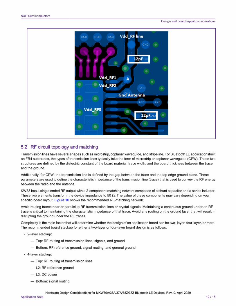
Recommendation to perform a good Vdd_RF supply layout:
• Vdd_RF1 and Vdd_RF2 lines must have the same length as possible linked to pointA (Y connection).
• 12 pF decoupling capacitor from Vdd_RF wire must be connected to the Ground Antenna. Purpose is to get the path asshort as possible from Vdd_RF1/Vdd_RF2 to the ground antenna.
• 12 pF decoupling capacitor from Vdd_RF3 pin must be as close as possible. Return to ground must be as short aspossible. So vias (2 in image below) must be placed near to the decoupling capacitor to get close connection to theground layer.
NXP SemiconductorsDesign and board layout considerations
Hardware Design Considerations for MKW39A/38A/37A/38Z/37Z Bluetooth LE Devices, Rev. 0, April 2020Application Note 11 / 15
5.2 RF circuit topology and matchingTransmission lines have several shapes such as microstrip, coplanar waveguide, and stripeline. For Bluetooth LE applicationsbuilton FR4 substrates, the types of transmission lines typically take the form of microstrip or coplanar waveguide (CPW). These twostructures are defined by the dielectric constant of the board material, trace width, and the board thickness between the traceand the ground.
Additionally, for CPW, the transmission line is defined by the gap between the trace and the top edge ground plane. Theseparameters are used to define the characteristic impedance of the transmission line (trace) that is used to convey the RF energybetween the radio and the antenna.
KW38 has a single ended RF output with a 2-component matching network composed of a shunt capacitor and a series inductor.These two elements transform the device impedance to 50 Ω. The value of these components may vary depending on yourspecific board layout. Figure 10 shows the recommended RF-matching network.
Avoid routing traces near or parallel to RF transmission lines or crystal signals. Maintaining a continuous ground under an RFtrace is critical to maintaining the characteristic impedance of that trace. Avoid any routing on the ground layer that will result indisrupting the ground under the RF traces.
Complexity is the main factor that will determine whether the design of an application board can be two- layer, four-layer, or more.The recommended board stackup for either a two-layer or four-layer board design is as follows:
• 2-layer stackup:
— Top: RF routing of transmission lines, signals, and ground
— Bottom: RF reference ground, signal routing, and general ground
• 4-layer stackup:
— Top: RF routing of transmission lines
— L2: RF reference ground
— L3: DC power
— Bottom: signal routing
NXP SemiconductorsDesign and board layout considerations
Hardware Design Considerations for MKW39A/38A/37A/38Z/37Z Bluetooth LE Devices, Rev. 0, April 2020Application Note 12 / 15
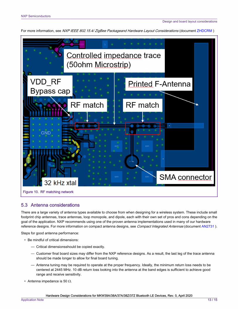
For more information, see NXP IEEE 802.15.4/ ZigBee Packageand Hardware Layout Considerations (document ZHDCRM )
Figure 10. RF matching network
5.3 Antenna considerationsThere are a large variety of antenna types available to choose from when designing for a wireless system. These include smallfootprint chip antennas, trace antennas, loop monopole, and dipole, each with their own set of pros and cons depending on thegoal of the application. NXP recommends using one of the proven antenna implementations used in many of our hardwarereference designs. For more information on compact antenna designs, see Compact Integrated Antennas (document AN2731 ).
Steps for good antenna performance:
• Be mindful of critical dimensions:
— Critical dimensionsshould be copied exactly.
— Customer final board sizes may differ from the NXP reference designs. As a result, the last leg of the trace antennashould be made longer to allow for final board tuning.
— Antenna tuning may be required to operate at the proper frequency. Ideally, the minimum return loss needs to becentered at 2445 MHz. 10 dB return loss looking into the antenna at the band edges is sufficient to achieve goodrange and receive sensitivity.
• Antenna impedance is 50 Ω.
NXP SemiconductorsDesign and board layout considerations
Hardware Design Considerations for MKW39A/38A/37A/38Z/37Z Bluetooth LE Devices, Rev. 0, April 2020Application Note 13 / 15

— This is maintained from RF matched port/pin to antenna feed.
— The example uses microstrip topology but co-planer waveguide with ground can also be used if desired. In this casethe dimensions will change so care should be taken when changing from one topology to another.
• The antenna should be reasonably clear of metallic objects and oriented properly with the ground plane.
• Always check the antenna in its final environment, including the PCB, components, case enclosure, hand effects (ifappropriate), and battery. Plastic and other materials in the near-field may cause detuning.
• Actual antenna performance can be evaluated in a variety of ways, such as range testing, measuring radiated signal levelunder controlled conditions, and characteristic testing in an anechoic chamber.
NXP SemiconductorsDesign and board layout considerations
Hardware Design Considerations for MKW39A/38A/37A/38Z/37Z Bluetooth LE Devices, Rev. 0, April 2020Application Note 14 / 15
How To Reach Us
Home Page:
nxp.com
Web Support:
nxp.com/support
Information in this document is provided solely to enable system and software implementers touse NXP products. There are no express or implied copyright licenses granted hereunder todesign or fabricate any integrated circuits based on the information in this document. NXPreserves the right to make changes without further notice to any products herein.
NXP makes no warranty, representation, or guarantee regarding the suitability of its products forany particular purpose, nor does NXP assume any liability arising out of the application or useof any product or circuit, and specifically disclaims any and all liability, including without limitationconsequential or incidental damages. “Typical” parameters that may be provided in NXP datasheets and/or specifications can and do vary in different applications, and actual performancemay vary over time. All operating parameters, including “typicals,” must be validated for eachcustomer application by customer's technical experts. NXP does not convey any license underits patent rights nor the rights of others. NXP sells products pursuant to standard terms andconditions of sale, which can be found at the following address: nxp.com/SalesTermsandConditions.
While NXP has implemented advanced security features, all products may be subject tounidentified vulnerabilities. Customers are responsible for the design and operation of theirapplications and products to reduce the effect of these vulnerabilities on customer’s applicationsand products, and NXP accepts no liability for any vulnerability that is discovered. Customersshould implement appropriate design and operating safeguards to minimize the risks associatedwith their applications and products.
NXP, the NXP logo, NXP SECURE CONNECTIONS FOR A SMARTER WORLD, COOLFLUX,EMBRACE, GREENCHIP, HITAG, I2C BUS, ICODE, JCOP, LIFE VIBES, MIFARE, MIFARECLASSIC, MIFARE DESFire, MIFARE PLUS, MIFARE FLEX, MANTIS, MIFARE ULTRALIGHT,MIFARE4MOBILE, MIGLO, NTAG, ROADLINK, SMARTLX, SMARTMX, STARPLUG, TOPFET,TRENCHMOS, UCODE, Freescale, the Freescale logo, AltiVec, C‑5, CodeTEST, CodeWarrior,ColdFire, ColdFire+, C‑Ware, the Energy Efficient Solutions logo, Kinetis, Layerscape, MagniV,mobileGT, PEG, PowerQUICC, Processor Expert, QorIQ, QorIQ Qonverge, Ready Play,SafeAssure, the SafeAssure logo, StarCore, Symphony, VortiQa, Vybrid, Airfast, BeeKit,BeeStack, CoreNet, Flexis, MXC, Platform in a Package, QUICC Engine, SMARTMOS, Tower,TurboLink, UMEMS, EdgeScale, EdgeLock, eIQ, and Immersive3D are trademarks of NXP B.V.All other product or service names are the property of their respective owners. AMBA, Arm,Arm7, Arm7TDMI, Arm9, Arm11, Artisan, big.LITTLE, Cordio, CoreLink, CoreSight, Cortex,DesignStart, DynamIQ, Jazelle, Keil, Mali, Mbed, Mbed Enabled, NEON, POP, RealView,SecurCore, Socrates, Thumb, TrustZone, ULINK, ULINK2, ULINK-ME, ULINK-PLUS, ULINKpro,µVision, Versatile are trademarks or registered trademarks of Arm Limited (or its subsidiaries) inthe US and/or elsewhere. The related technology may be protected by any or all of patents,copyrights, designs and trade secrets. All rights reserved. Oracle and Java are registeredtrademarks of Oracle and/or its affiliates. The Power Architecture and Power.org word marksand the Power and Power.org logos and related marks are trademarks and service markslicensed by Power.org.
© NXP B.V. 2020. All rights reserved.
For more information, please visit: http://www.nxp.comFor sales office addresses, please send an email to: [email protected]
Date of release: April 2020Document identifier: AN12518