
M89 Hardware Design - AURORA EVERNET
77
M89 Hardware Design GSM/GPRS Module Series Rev. M89_Hardware_Design_V1.1 Date: 2018-08-08 Status: Released www.quectel.com
-
Upload
khangminh22 -
Category
Documents
-
view
1 -
download
0
Transcript of M89 Hardware Design - AURORA EVERNET
M89 Hardware Design
GSM/GPRS Module Series
Rev. M89_Hardware_Design_V1.1
Date: 2018-08-08
Status: Released
www.quectel.com
GSM/GPRS Module Series M89 Hardware Design
M89_Hardware_Design 1 / 76
Our aim is to provide customers with timely and comprehensive service. For any
assistance, please contact our company headquarters:
Quectel Wireless Solutions Co., Ltd.
7th Floor, Hongye Building, No.1801 Hongmei Road, Xuhui District, Shanghai 200233, China
Tel: +86 21 5108 6236
Email: [email protected]
Or our local office. For more information, please visit:
http://www.quectel.com/support/sales.htm
For technical support, or to report documentation errors, please visit:
http://www.quectel.com/support/technical.htm
Or Email to: [email protected]
GENERAL NOTES
QUECTEL OFFERS THE INFORMATION AS A SERVICE TO ITS CUSTOMERS. THE INFORMATION
PROVIDED IS BASED UPON CUSTOMERS’ REQUIREMENTS. QUECTEL MAKES EVERY EFFORT
TO ENSURE THE QUALITY OF THE INFORMATION IT MAKES AVAILABLE. QUECTEL DOES NOT
MAKE ANY WARRANTY AS TO THE INFORMATION CONTAINED HEREIN, AND DOES NOT ACCEPT
ANY LIABILITY FOR ANY INJURY, LOSS OR DAMAGE OF ANY KIND INCURRED BY USE OF OR
RELIANCE UPON THE INFORMATION. ALL INFORMATION SUPPLIED HEREIN IS SUBJECT TO
CHANGE WITHOUT PRIOR NOTICE.
COPYRIGHT
THE INFORMATION CONTAINED HERE IS PROPRIETARY TECHNICAL INFORMATION OF QUECTEL
WIRELESS SOLUTIONS CO., LTD. TRANSMITTING, REPRODUCTION, DISSEMINATION AND
EDITING OF THIS DOCUMENT AS WELL AS UTILIZATION OF THE CONTENT ARE FORBIDDEN
WITHOUT PERMISSION. OFFENDERS WILL BE HELD LIABLE FOR PAYMENT OF DAMAGES. ALL
RIGHTS ARE RESERVED IN THE EVENT OF A PATENT GRANT OR REGISTRATION OF A UTILITY
MODEL OR DESIGN.
Copyright © Quectel Wireless Solutions Co., Ltd. 2018. All rights reserved.

GSM/GPRS Module Series M89 Hardware Design
M89_Hardware_Design 2 / 76
About the Document
History
Revision Date Author Description
1.0 2018-06-12 Tiger CHENG Initial
1.1 2018-08-08 Tiger CHENG
1. Modified the voltage domain of pin 27/28/37/38
to 2.8V.
2. Removed I2C function.
GSM/GPRS Module Series M89 Hardware Design
M89_Hardware_Design 3 / 76
Contents
About the Document ................................................................................................................................ 2
Contents .................................................................................................................................................... 3
Table Index ............................................................................................................................................... 5
Figure Index .............................................................................................................................................. 6
1 Introduction ....................................................................................................................................... 8
1.1. Safety Information .................................................................................................................... 9
2 Product Concept ............................................................................................................................. 10
2.1. General Description ................................................................................................................ 10
2.2. Key Features .......................................................................................................................... 10
2.3. Functional Diagram ................................................................................................................ 12
2.4. Evaluation Board .................................................................................................................... 13
3 Application Interfaces ..................................................................................................................... 14
3.1. General Description ................................................................................................................ 14
3.2. Pin Assignment ....................................................................................................................... 15
3.2.1. Pin Description ............................................................................................................. 16
3.3. Operating Modes .................................................................................................................... 21
3.4. Power Supply ......................................................................................................................... 22
3.4.1. Power Features of the Module ..................................................................................... 22
3.4.2. Decrease Voltage Drop ................................................................................................ 23
3.4.3. Reference Design for Power Supply ............................................................................ 23
3.4.4. Monitor Power Supply .................................................................................................. 24
3.5. Turn On and off Scenarios ...................................................................................................... 24
3.5.1. Turn On Module Using the PWRKEY .......................................................................... 24
3.5.2. Turn off Module ............................................................................................................ 26
3.5.2.1. Turn off Module Using the PWRKEY Pin .......................................................... 26
3.5.2.2. Turn off Module Using AT Command ................................................................ 27
3.5.2.3. Under-voltage Warning ..................................................................................... 28
3.5.3. Restart the Module ...................................................................................................... 28
3.6. Power Saving ......................................................................................................................... 29
3.6.1. Minimum Functionality Mode ....................................................................................... 29
3.6.2. Sleep Mode.................................................................................................................. 30
3.6.3. Wake up Module from Sleep Mode .............................................................................. 30
3.6.4. Summary of Operating Modes Transition .................................................................... 30
3.7. RTC Backup ........................................................................................................................... 31
3.8. UART Interfaces ..................................................................................................................... 32
3.8.1. UART0 Port ................................................................................................................. 35
3.8.1.1. UART0 Port Features ........................................................................................ 35
3.8.1.2. DCE & DTE Connection via UART0 .................................................................. 36
3.8.1.3. Firmware Upgrade ............................................................................................ 37
3.8.2. UART1 Port ................................................................................................................. 38

GSM/GPRS Module Series M89 Hardware Design
M89_Hardware_Design 4 / 76
3.9. Audio Interfaces ..................................................................................................................... 39
3.9.1. Decrease TDD Noise and Other Noise ........................................................................ 40
3.9.2. Microphone Interfaces Design ..................................................................................... 41
3.9.3. Loud Speaker Interface Design.................................................................................... 41
3.9.4. Earphone Interface Design .......................................................................................... 42
3.9.5. Audio Characteristics ................................................................................................... 42
3.10. (U)SIM Interface ..................................................................................................................... 43
3.11. ADC ........................................................................................................................................ 45
3.12. GPIO Interfaces ...................................................................................................................... 45
3.13. PWM Interfaces*..................................................................................................................... 47
3.14. Behaviors of RI ....................................................................................................................... 47
4 Antenna Interface ............................................................................................................................ 49
4.1.1. RF Antenna Reference Design .................................................................................... 49
4.2. Reference Design of RF Layout ............................................................................................. 50
4.3. Antenna Requirements ........................................................................................................... 52
4.3.1. RF Output Power ......................................................................................................... 52
4.3.2. RF Receiving Sensitivity .............................................................................................. 53
4.3.3. Operating Frequencies ................................................................................................ 53
4.3.4. RF Cable Soldering ..................................................................................................... 53
5 Electrical, Reliability and Radio Characteristics .......................................................................... 55
5.1. Absolute Maximum Ratings .................................................................................................... 55
5.2. Operation and Storage Temperatures ..................................................................................... 55
5.3. Power Supply Ratings ............................................................................................................ 56
5.4. Current Consumption ............................................................................................................. 57
5.5. Electrostatic Discharge ........................................................................................................... 59
6 Mechanical Dimensions.................................................................................................................. 60
6.1. Mechanical Dimensions of the Module ................................................................................... 60
6.2. Recommended Footprint ........................................................................................................ 62
6.3. Design Effect Drawings of the Module .................................................................................... 63
7 Storage, Manufacturing and Packaging ........................................................................................ 64
7.1. Storage ................................................................................................................................... 64
7.2. Manufacturing and Soldering .................................................................................................. 65
7.3. Packaging ............................................................................................................................... 66
8 Appendix A References .................................................................................................................. 69
9 Appendix B GPRS Coding Schemes ............................................................................................. 74
10 Appendix C GPRS Multi-slot Classes ............................................................................................ 76

GSM/GPRS Module Series M89 Hardware Design
M89_Hardware_Design 5 / 76
Table Index
TABLE 1: MODULE KEY FEATURES ............................................................................................................... 10
TABLE 2: CODING SCHEMES AND MAXIMUM NET DATA RATES OVER AIR INTERFACE ........................ 12
TABLE 3: IO PARAMETERS DEFINITION ........................................................................................................ 16
TABLE 4: PIN DESCRIPTION ........................................................................................................................... 16
TABLE 5: OVERVIEW OF OPERATING MODES ............................................................................................. 21
TABLE 6: SUMMARY OF OPERATING MODES TRANSITION ....................................................................... 30
TABLE 7: PIN DEFINITION OF THE UART INTERFACES .............................................................................. 33
TABLE 8: LOGIC LEVELS OF THE UART0 INTERFACE (VDIG CONNECTED TO VIO28) ........................... 34
TABLE 9: LOGIC LEVELS OF THE UART0 INTERFACE (VDIG CONNECTED TO VIO18) ........................... 34
TABLE 10: LOGIC LEVELS OF THE UART1 INTERFACE .............................................................................. 34
TABLE 11: PIN DEFINITION OF AUDIO INTERFACES ................................................................................... 39
TABLE 12: AOUT OUTPUT CHARACTERISTICS ............................................................................................ 40
TABLE 13: TYPICAL ELECTRET MICROPHONE CHARACTERISTICS ......................................................... 42
TABLE 14: TYPICAL SPEAKER CHARACTERISTICS .................................................................................... 42
TABLE 15: PIN DEFINITION OF THE (U)SIM INTERFACE ............................................................................. 43
TABLE 16: PIN DEFINITION OF THE ADC ...................................................................................................... 45
TABLE 17: CHARACTERISTICS OF THE ADC ................................................................................................ 45
TABLE 18: PIN LIST FOR GPIO INTERFACES ................................................................................................ 45
TABLE 19: MULTIPLEXED FUNCTIONS OF GPIO INTERFACES .................................................................. 46
TABLE 20: PIN DEFINITION OF PWM INTERFACES ..................................................................................... 47
TABLE 21: MULTIPLEXED FUNCTIONS OF PWM INTERFACES .................................................................. 47
TABLE 22: BEHAVIORS OF RI ......................................................................................................................... 47
TABLE 23: PIN DEFINITION OF THE RF_ANT ................................................................................................ 49
TABLE 24: ANTENNA CABLE REQUIREMENTS ............................................................................................. 52
TABLE 25: ANTENNA REQUIREMENTS .......................................................................................................... 52
TABLE 26: RF OUTPUT POWER ..................................................................................................................... 52
TABLE 27: RF RECEIVING SENSITIVITY ........................................................................................................ 53
TABLE 28: THE MODULE OPERATING FREQUENCIES ................................................................................ 53
TABLE 29: ABSOLUTE MAXIMUM RATINGS .................................................................................................. 55
TABLE 30: OPERATION AND STORAGE TEMPERATURES .......................................................................... 55
TABLE 31: MODULE POWER SUPPLY RATINGS ........................................................................................... 56
TABLE 32: CURRENT CONSUMPTION ........................................................................................................... 57
TABLE 33: ELECTROSTATIC DISCHARGE CHARACTERISTICS (TEMPERATURE: 25ºC, HUMIDITY: 45%)
................................................................................................................................................................... 59
TABLE 34: RECOMMENDED THERMAL PROFILE PARAMETERS ............................................................... 65
TABLE 35: RELATED DOCUMENTS ................................................................................................................ 69
TABLE 36: TERMS AND ABBREVIATIONS ...................................................................................................... 70
TABLE 37: DESCRIPTION OF DIFFERENT CODING SCHEMES .................................................................. 74
TABLE 38: GPRS MULTI-SLOT CLASSES ...................................................................................................... 76
GSM/GPRS Module Series M89 Hardware Design
M89_Hardware_Design 6 / 76
Figure Index
FIGURE 1: MODULE FUNCTIONAL DIAGRAM ............................................................................................... 13
FIGURE 2: PIN ASSIGNMENT ......................................................................................................................... 15
FIGURE 3: VOLTAGE RIPPLE DURING TRANSMITTING .............................................................................. 22
FIGURE 4: REFERENCE CIRCUIT FOR THE VBAT INPUT ........................................................................... 23
FIGURE 5: REFERENCE CIRCUIT OF POWER SUPPLY .............................................................................. 24
FIGURE 6: TURN ON THE MODULE USING DRIVING CIRCUIT ................................................................... 25
FIGURE 7: TURN ON THE MODULE USING A KEYSTROKE ........................................................................ 25
FIGURE 8: TIMING OF TURNING ON THE MODULE ..................................................................................... 26
FIGURE 9: TIMING OF TURNING OFF THE MODULE ................................................................................... 27
FIGURE 10: TIMING OF RESTARTING THE MODULE ................................................................................... 28
FIGURE 11: REFERENCE CIRCUIT OF EMERG_RESET BY USING DRIVING CIRCUIT ............................ 29
FIGURE 12: REFERENCE CIRCUIT OF EMERG_RESET BY USING A BUTTON ......................................... 29
FIGURE 13: VRTC IS POWERED BY A NON-CHARGEABLE BATTERY ....................................................... 31
FIGURE 14: VRTC IS POWERED BY A RECHARGEABLE BATTERY ........................................................... 32
FIGURE 15: VRTC IS POWERED BY A CAPACITOR ...................................................................................... 32
FIGURE 16: REFERENCE CIRCUIT OF UART0 PORT WITH FULL-FUNCTION .......................................... 36
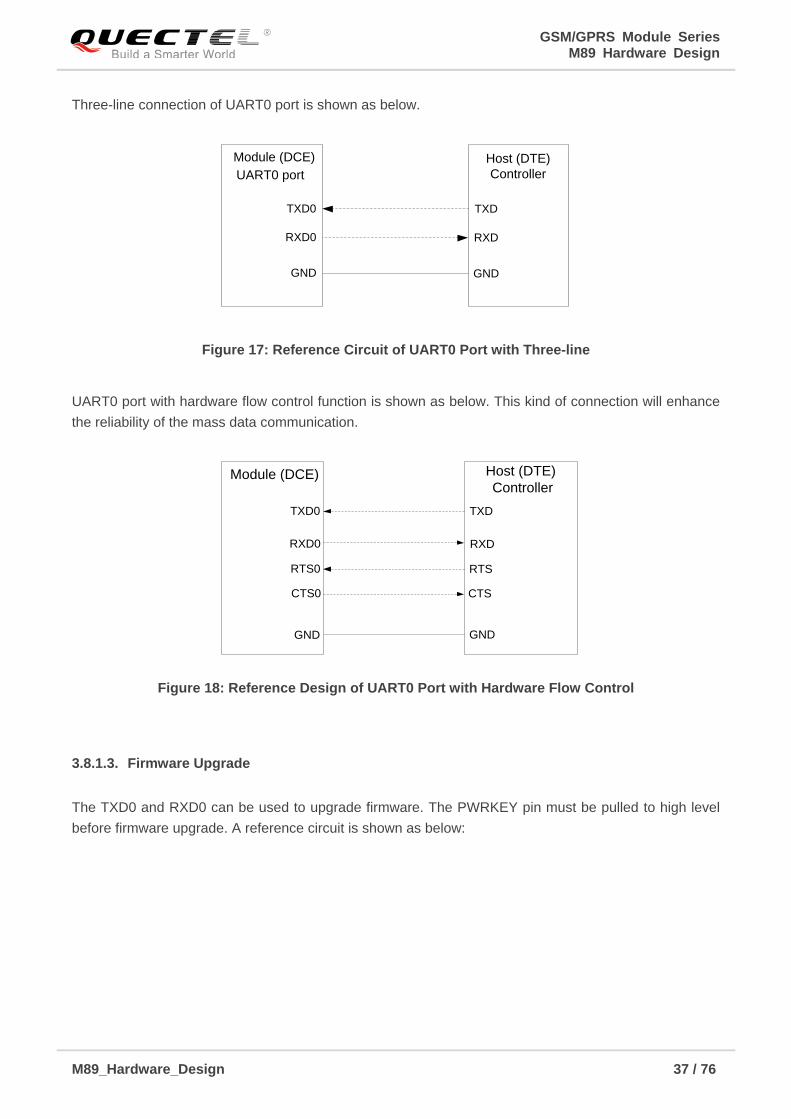
FIGURE 17: REFERENCE CIRCUIT OF UART0 PORT WITH THREE-LINE .................................................. 37
FIGURE 18: REFERENCE DESIGN OF UART0 PORT WITH HARDWARE FLOW CONTROL ..................... 37
FIGURE 19: REFERENCE CIRCUIT OF UART0 PORT FOR FIRMWARE UPGRADE .................................. 38
FIGURE 20: REFERENCE CIRCUIT OF UART1 PORT WITH THREE-LINE .................................................. 38
FIGURE 21: REFERENCE CIRCUIT OF UART1 PORT WITH HARDWARE FLOW CONTROL .................... 39
FIGURE 22: REFERENCE CIRCUIT FOR MICROPHONE .............................................................................. 41
FIGURE 23: REFERENCE CIRCUIT FOR LOUD SPEAKER .......................................................................... 41
FIGURE 24: REFERENCE CIRCUIT FOR EARPHONE .................................................................................. 42
FIGURE 25: REFERENCE CIRCUIT OF (U)SIM INTERFACE WITH A 6-PIN (U)SIM CARD CONNECTOR . 43
FIGURE 26: REFERENCE CIRCUIT OF (U)SIM INTERFACE WITH AN 8-PIN (U)SIM CARD CONNECTOR
................................................................................................................................................................... 44
FIGURE 27: BEHAVIORS OF RI WHEN A CALL IS RECEIVED ...................................................................... 48
FIGURE 28: BEHAVIORS OF RI WHEN ESTABLISHING A CALL .................................................................. 48
FIGURE 29: BEHAVIORS OF RI WHEN A URC OR SMS MESSAGES IS RECEIVED .................................. 48
FIGURE 30: REFERENCE DESIGN FOR GSM ANTENNA INTERFACE ........................................................ 49
FIGURE 31: MICROSTRIP LINE DESIGN ON A 2-LAYER PCB ...................................................................... 50
FIGURE 32: COPLANAR WAVEGUIDE LINE DESIGN ON A 2-LAYER PCB .................................................. 50
FIGURE 33: COPLANAR WAVEGUIDE LINE DESIGN ON A 4-LAYER PCB (LAYER 3 AS REFERENCE
GROUND) .......................................................................................................................................................... 51
FIGURE 34: COPLANAR WAVEGUIDE LINE DESIGN ON A 4-LAYER PCB (LAYER 4 AS REFERENCE
GROUND) .......................................................................................................................................................... 51
FIGURE 35: RF CABLE SOLDERING EXAMPLE ............................................................................................ 54
FIGURE 36: TOP AND SIDE DIMENSIONS (UNIT: MM) .................................................................................. 60
FIGURE 37: BOTTOM DIMENSIONS (UNIT: MM) ........................................................................................... 61
FIGURE 38: RECOMMENDED FOOTPRINT (UNIT: MM) ................................................................................ 62
GSM/GPRS Module Series M89 Hardware Design
M89_Hardware_Design 7 / 76
FIGURE 39: TOP VIEW OF THE MODULE ...................................................................................................... 63
FIGURE 40: BOTTOM VIEW OF THE MODULE .............................................................................................. 63
FIGURE 41: RECOMMENDED RAMP-SOAK-SPIKE REFLOW PROFILE ..................................................... 65
FIGURE 42: TAPE DIMENSIONS ..................................................................................................................... 67
FIGURE 43: REEL DIMENSIONS ..................................................................................................................... 68
FIGURE 44: RADIO BLOCK STRUCTURE OF CS-1, CS-2 AND CS-3 ........................................................... 74
FIGURE 45: RADIO BLOCK STRUCTURE OF CS-4 ....................................................................................... 75

GSM/GPRS Module Series M89 Hardware Design
M89_Hardware_Design 8 / 76
1 Introduction
This document defines the M89 module and describes its air interface and hardware interfaces which are
connected with the customers’ applications.
This document can help customers quickly understand module interface specifications, electrical and
mechanical details, as well as other related information of the module. Associated with application note
and user guide, customers can use M89 module to design and set up mobile applications easily.
GSM/GPRS Module Series M89 Hardware Design
M89_Hardware_Design 9 / 76
1.1. Safety Information
The following safety precautions must be observed during all phases of the operation, such as usage,
service or repair of any cellular terminal or mobile incorporating M89 module. Manufacturers of the
cellular terminal should send the following safety information to users and operating personnel, and
incorporate these guidelines into all manuals supplied with the product. If not so, Quectel assumes no
liability for the customers’ failure to comply with these precautions.
Full attention must be given to driving at all times in order to reduce the risk of an
accident. Using a mobile while driving (even with a handsfree kit) causes
distraction and can lead to an accident. You must comply with laws and regulations
restricting the use of wireless devices while driving.
Switch off the cellular terminal or mobile before boarding an aircraft. Make sure it is
switched off. The operation of wireless appliances in an aircraft is forbidden, so as
to prevent interference with communication systems. Consult the airline staff about
the use of wireless devices on boarding the aircraft, if your device offers an
Airplane Mode which must be enabled prior to boarding an aircraft.
Switch off your wireless device when in hospitals, clinics or other health care
facilities. These requests are designed to prevent possible interference with
sensitive medical equipment.
Cellular terminals or mobiles operating over radio frequency signal and cellular
network cannot be guaranteed to connect in all conditions, for example no mobile
fee or with an invalid (U)SIM card. While you are in this condition and need
emergent help, please remember using emergency call. In order to make or
receive a call, the cellular terminal or mobile must be switched on and in a service
area with adequate cellular signal strength.
Your cellular terminal or mobile contains a transmitter and receiver. When it is ON,
it receives and transmits radio frequency energy. RF interference can occur if it is
used close to TV set, radio, computer or other electric equipment.
In locations with potentially explosive atmospheres, obey all posted signs to turn
off wireless devices such as your phone or other cellular terminals. Areas with
potentially explosive atmospheres include fuelling areas, below decks on boats,
fuel or chemical transfer or storage facilities, areas where the air contains
chemicals or particles such as grain, dust or metal powders, etc.
GSM/GPRS Module Series M89 Hardware Design
M89_Hardware_Design 10 / 76
2 Product Concept
2.1. General Description
M89 is a Quad-band GSM/GPRS engine that works at frequencies of GSM850, EGSM900, DCS1800 and
PCS1900. It features GPRS multi-slot class 12 and supports the GPRS coding schemes CS-1, CS-2,
CS-3 and CS-4. For more details about GPRS multi-slot classes and coding schemes, please refer to the
Appendix B & C.
With a compact profile of 18.8mm × 27.6mm × 2.3mm, the module can meet almost all the requirements
for M2M applications, including vehicles and personal tracking, security system, wireless POS, industrial
PDA, wearable devices, telematics, smart metering and remote maintenance & control, etc.
M89 is an SMD type module with LGA package, which can be easily embedded into applications.
Designed with power saving technique, the current consumption of M89 is as low as 2.8mA in sleep mode
when DRX is 5.
M89 is integrated with Internet service protocols, such as TCP/UDP, FTP and PPP. Extended AT
commands have been developed for customers to use these Internet service protocols easily.
The module fully complies with the RoHS directive of the European Union.
2.2. Key Features
The following table describes the detailed features of M89 module.
Table 1: Module Key Features
Feature Implementation
Power Supply Supply voltage: 3.3V~4.6V
Typical supply voltage: 4.0V
Power Saving Mode Typical power consumption in sleep mode:
TBD @DRX=5
GSM/GPRS Module Series M89 Hardware Design
M89_Hardware_Design 11 / 76
TBD @DRX=9
Frequency Bands
Quad-band: GSM850, EGSM900, DCS1800, PCS1900.
The module can search these frequency bands automatically
The frequency bands can be set by AT command
Compliant to GSM Phase 2/2+
GSM Class Small MS
Transmitting Power Class 4 (2W) at GSM850 and EGSM900
Class 1 (1W) at DCS1800 and PCS1900
GPRS Connectivity
GPRS multi-slot class 12 (default)
GPRS multi-slot class 1~12 (configurable)
GPRS mobile station class B
Data GPRS
GPRS data downlink transfer: max. 85.6kbps
GPRS data uplink transfer: max. 85.6kbps
Coding scheme: CS-1, CS-2, CS-3 and CS-4
Support the protocols PAP (Password Authentication Protocol)
usually used for PPP connections
Internet service protocols: TCP, UDP, PPP, FTP, HTTP(S), POP3,
SMTP(S), USSD, QNTP, QPING, SSL
Support Packet Broadcast Control Channel (PBCCH)
Support Unstructured Supplementary Service Data (USSD)
Temperature Range
Operation temperature range: -35°C ~ +75°C 1)
Extended temperature range: -40°C ~ +85°C 2)
Storage temperature range: -40°C ~ +90°C
SMS Text and PDU mode
SMS storage: (U)SIM card
(U)SIM Interface Support (U)SIM card: 1.8V, 3.0V
Audio Features
Speech codec modes:
Half Rate (ETS 06.20)
Full Rate (ETS 06.10)
Enhanced Full Rate (ETS 06.50/06.60/06.80)
Adaptive Multi-Rate (AMR)
Echo Suppression
Noise Reduction
UART Interfaces
UART0 Port:
Eight lines on UART0 port
Used for AT command communication, data transmission and
firmware upgrade
Support autobaud from 4800bps to 115200bps
UART1 Port:
Four lines on UART1 port
Used for software debugging
GSM/GPRS Module Series M89 Hardware Design
M89_Hardware_Design 12 / 76
1. 1) Within operation temperature range, the module is 3GPP compliant.
2. 2) Within extended temperature range, the module remains the ability to establish and maintain a
voice, SMS, data transmission, emergency call, etc. There is no unrecoverable malfunction. There
are also no effects on radio spectrum and no harm to radio network. Only one or more parameters
like Pout might reduce in their value and exceed the specified tolerances. When the temperature
returns to the normal operating temperature levels, the module will meet 3GPP specifications again.
Table 2: Coding Schemes and Maximum Net Data Rates over Air Interface
2.3. Functional Diagram
The following figure shows a block diagram of M89 and illustrates the major functional parts.
Radio frequency part
Power management
Only support 460800bps baud rate
Phonebook Management Support phonebook types: SM, ME, ON, MC, RC, DC, LD, LA
SIM Application Toolkit Support SAT class 3, GSM 11.14 Release 99
Real Time Clock Supported
Physical Characteristics
Size: (18.8±0.15)mm × (27.6±0.15)mm × (2.3±0.2)mm
Package: LGA
Weight: Approx. 2.15g
Firmware Upgrade Firmware upgrade via UART0 Port
Antenna Interface Connected to antenna pad with 50Ω impedance control
Coding Scheme 1 Timeslot 2 Timeslot 4 Timeslot
CS-1 9.05kbps 18.1kbps 36.2kbps
CS-2 13.4kbps 26.8kbps 53.6kbps
CS-3 15.6kbps 31.2kbps 62.4kbps
CS-4 21.4kbps 42.8kbps 85.6kbps
NOTES

GSM/GPRS Module Series M89 Hardware Design
M89_Hardware_Design 13 / 76
Peripheral interfaces
-- Power supply
-- UART interfaces
-- Audio interfaces
-- (U)SIM interface
-- ADC interface
-- RF interface
BB&RF
RF PAM
26MHzRF Transceiver
RTC
Audio
Serial
Interface
(U)SIM
Interface
RF_ANT
VBAT
PWRKEY
VRTC
UART0
(U)SIM Interface
ESD
PMU
Memory
GPIO
Audio
ADC ADC
VIO28VIO28
VIO18VIO18
VDIGVDIG
GPIO/PWM*
UART1
EMERG_RESET
Figure 1: Module Functional Diagram
"*" means under development.
2.4. Evaluation Board
In order to help customers develop applications with M89, Quectel supplies an evaluation board (EVB),
USB to RS-232 to USB converter cable, power adapter, earphone, antenna and other peripherals to
control or test the module. For details, please refer to the document [11].
NOTE
GSM/GPRS Module Series M89 Hardware Design
M89_Hardware_Design 14 / 76
3 Application Interfaces
3.1. General Description
M89 module is equipped with 106 LGA pads. The following chapters provide detailed descriptions about
these pins.
Power supply
UART interfaces
Audio interfaces
(U)SIM interface
ADC interface
GPIO interface
PWM interfaces*
"*" means under development.
NOTE

GSM/GPRS Module Series M89 Hardware Design
M89_Hardware_Design 15 / 76
3.2. Pin Assignment
The following figure shows the pin assignment of M89 module.
65
64
63
62
61
60
59
58
28
27
26
25
24
23
22
21
20
13
12
11
10
9
8
7
6
5
4
3
2
1 52
51
50
49
48
47
46
45
44
43
42
41
40
PWRKEY
ADC
VBAT
VMIC
GND
GND
VIO18
MIC
N
SIM
_V
DD
14
15
16
17
18
19
29
30
33
31
32
56
55
54
53
39
38
37
36
35
34
73
72
71
70
69
84 88 92
83 87 91
80
79
78
77
76
75
74
90
81 85 89
99
98
97
96
95
106
105
104
103
102
101
100
68
67
94
93
82 86
66
GND
GND
GND
GND
GND
GND
GND
GND
GND
GND
GND
GND
LOUDSPK_N
VDIG
RXD0
CTS0
TXD0
RING0
RTS0
SIM_PRESENCE
SIM_RST
VRTC
SIM_DATA
SIM
_C
LK
VIO
28
RE
SE
RV
ED
1
DS
R0
DT
R0
DC
D0
GP
IO9
GP
IO1
0
TX
D1
RX
D1
RT
S1
CT
S1
EM
ER
G_
RE
SE
T
MIC
P
AG
ND
GN
D
RF
_A
NT
VB
AT
GPIO8
GPIO7/PWM1*
GPIO6/PWM2*
GPIO5
GPIO4
GPIO3
GPIO2
GPIO1
LOUDSPK_P
GN
D
GN
D
GN
D
GN
D
GN
D
GN
D
GN
D
GN
DRESERVED2GND
GND
GND
GND
GND
GND
GND
GND
GND
GND
GND
GND
GND
GND
GND
GND
GND
GND
GND
GND
GND
GND
GND
GND
GND
GND
GND GND GND
GND GND GND
GND GND GND
GND GND GND
57
RESERVEDGNDAudio RFPower UART Others(U)SIM GPIO
Figure 2: Pin Assignment
GSM/GPRS Module Series M89 Hardware Design
M89_Hardware_Design 16 / 76
1. Keep all RESERVED pins open.
2. "*" means under development.
3.2.1. Pin Description
Table 3: IO Parameters Definition
Table 4: Pin Description
Type Description
IO Bidirectional
DI Digital input
DO Digital output
PI Power input
PO Power output
AI Analog input
AO Analog output
Power Supply
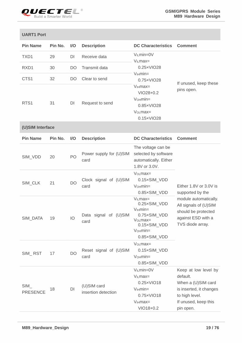
Pin Name Pin No. I/O Description DC Characteristics Comment
VBAT
5
PI
Power supply of module
baseband part VImax=4.6V
VImin=3.3V
VInorm=4.0V
It must be able to
provide sufficient
current up to 1.6A in
a burst transmission. 53
Power supply of module
RF part
VDIG 10 PI Power supply for UART0
VImin=1.7V
VImax=2.9V
IImax=50mA
Connect to the
external power
supply voltage VIO18
or VIO28.
VRTC 16 IO
Power supply for RTC
when VBAT is not used
to supply power for the
module.
Charging for a backup
VImax=3.3V
VImin=1.5V
VInorm=2.8V
VOmax=3V
VOmin=2V
If unused, keep this
pin open.
NOTES
GSM/GPRS Module Series M89 Hardware Design
M89_Hardware_Design 17 / 76
battery or supercapacitor
when the VBAT is used
to supply power for the
module.
VOnorm=2.8V
IOmax=2mA
Iin≈10uA
VIO28 22 PO Power supply for an
external circuit.
VOmax=2.9V
VOmin=2.7V
VOnorm=2.8V
IOmax=20mA
A 2.2uF~4.7uF
bypass capacitor is
recommended to be
added when it is used
for power supply.
If unused, keep this
pin open.
VIO18 35 PO Power supply for an
external circuit.
VOmax=1.9V
VOmin=1.7V
VOnorm=1.8V
IOmax=20mA
A 2.2uF~4.7uF
bypass capacitor is
recommended to be
added when it is used
for power supply.
If unused, keep this
pin open.
GND
4, 6
9, 34
44-52
54-58
60-63
67-97
99-106
Ground
Turn ON/OFF
Pin Name Pin No. I/O Description DC Characteristics Comment
PWRKEY 8 DI
Power on/off key.
PWRKEY should be
pulled to high level for at
least 1s to turn on/off the
module.
VILmax=0.4V
VIHmin=0.8V
VIHmax=5V
EMERG_
RESET 33 DI
Emergency reset. Pulling
down for at least 40ms
will reset the module in
case of turning off the
module by AT+QPOWD
command and PWRKEY
failed.
VILmax=0.45V
VIHmin=1.35V
Open drain/ collector
driver required in
cellular device
applications.
If unused, keep this
pin open.
Audio Interfaces
Pin Name Pin No. I/O Description DC Characteristics Comment

GSM/GPRS Module Series M89 Hardware Design
M89_Hardware_Design 18 / 76
MICP 65
AI Positive and negative
voice input
Please refer to
Chapter 3.9.5.
If unused, keep these
pins open. MICN 66
LOUDSPK_
P 3
AO Positive and negative
voice output Support both voice
and ringtone output.
If unused, keep these
pins open.
LOUDSPK_
N 2
VMIC 1 AO
Bias circuit for
microphone power
supply
AGND 64
Analog ground.
Form a pseudo-
differential pair with
LOUDSPK_P
If unused, keep this
pin open.
UART0 Port
Pin Name Pin No. I/O Description DC Characteristics Comment
TXD0 13 DI Receive data VDIG connected to
VIO28:
VILmin=0V
VILmax=
0.25×VIO28
VIHmin=
0.75×VIO28
VIHmax=
VIO28+0.2
VOHmin=
0.85×VIO28
VOLmax=
0.15×VIO28
VDIG connected to
VIO18:
VILmin=0V
VILmax=
0.25×VIO18
VIHmin=
0.75×VIO18
VIHmax=
VIO18+0.2
VOHmin=
0.85×VIO18
VOLmax=
0.15×VIO18
If only use TXD0,
RXD0 and GND to
communicate, it is
recommended to
connect RTS0 to
GND via a 0R resistor
and keep other pins
open.
RXD0 11 DO Transmit data
DTR0 25 DI Data terminal ready
RING0 14 DO Ring indication
DCD0 26 DO Data carrier detection
DSR0 24 DO Data set Ready
CTS0 12 DO Clear to send
RTS0 15 DI Request to send
GSM/GPRS Module Series M89 Hardware Design
M89_Hardware_Design 19 / 76
UART1 Port
Pin Name Pin No. I/O Description DC Characteristics Comment
TXD1 29 DI Receive data VILmin=0V
VILmax=
0.25×VIO28
VIHmin=
0.75×VIO28
VIHmax=
VIO28+0.2
VOHmin=
0.85×VIO28
VOLmax=
0.15×VIO28
If unused, keep these
pins open.
RXD1 30 DO Transmit data
CTS1 32 DO Clear to send
RTS1 31 DI Request to send
(U)SIM Interface
Pin Name Pin No. I/O Description DC Characteristics Comment
SIM_VDD 20 PO Power supply for (U)SIM
card
The voltage can be
selected by software
automatically. Either
1.8V or 3.0V.
Either 1.8V or 3.0V is
supported by the
module automatically.
All signals of (U)SIM
should be protected
against ESD with a
TVS diode array.
SIM_CLK 21 DO Clock signal of (U)SIM
card
VOLmax=
0.15×SIM_VDD
VOHmin=
0.85×SIM_VDD
SIM_DATA 19 IO Data signal of (U)SIM
card
VILmax= 0.25×SIM_VDD
VIHmin=
0.75×SIM_VDD VOLmax=
0.15×SIM_VDD
VOHmin=
0.85×SIM_VDD
SIM_ RST 17 DO Reset signal of (U)SIM
card
VOLmax=
0.15×SIM_VDD
VOHmin=
0.85×SIM_VDD
SIM_
PRESENCE 18 DI
(U)SIM card
insertion detection
VILmin=0V
VILmax=
0.25×VIO18
VIHmin=
0.75×VIO18
VIHmax=
VIO18+0.2
Keep at low level by
default.
When a (U)SIM card
is inserted, it changes
to high level.
If unused, keep this
pin open.

GSM/GPRS Module Series M89 Hardware Design
M89_Hardware_Design 20 / 76
VOHmin=
0.85×VIO18
VOLmax=
0.15×VIO18
ADC
Pin Name Pin No. I/O Description DC Characteristics Comment
ADC 7 AI General purpose analog
to digital converter.
Voltage range:
0V to 2.8V
If unused, keep this
pin open.
GPIO
Pin Name Pin No. I/O Description DC Characteristics Comment
GPIO1 43 IO
General purpose
input/output
interface
VILmin=0V
VILmax=
0.25×VIO18
VIHmin=
0.75×VIO18
VIHmax=
VIO18+0.2
VOHmin=
0.85×VIO18
VOLmax=
0.15×VIO18
GPIO2 42 IO
GPIO3 41 IO
GPIO4 40 IO
GPIO5 39 IO
GPIO8 36 IO
General purpose
input/output
interface
GPIO6/
PWM2* 38 IO
General purpose
input/output interface/
Pulse width modulation
interface
VILmin=0V
VILmax=
0.25×VIO28
VIHmin=
0.75×VIO28
VIHmax=
VIO28+0.2
VOHmin=
0.85×VIO28
VOLmax=
0.15×VIO28
GPIO7/
PWM1* 37 IO
GPIO9 27 IO
General purpose
input/output interface
GPIO10 28 IO
Antenna Interface
Pin Name Pin No. I/O Description DC Characteristics Comment
RF_ANT 59 IO GSM antenna pad 50Ω impedance
Other Interface
GSM/GPRS Module Series M89 Hardware Design
M89_Hardware_Design 21 / 76
"*" means under development.
3.3. Operating Modes
The table below briefly summarizes the various operating modes in the following chapters.
Table 5: Overview of Operating Modes
Pin Name Pin No. I/O Description DC Characteristics
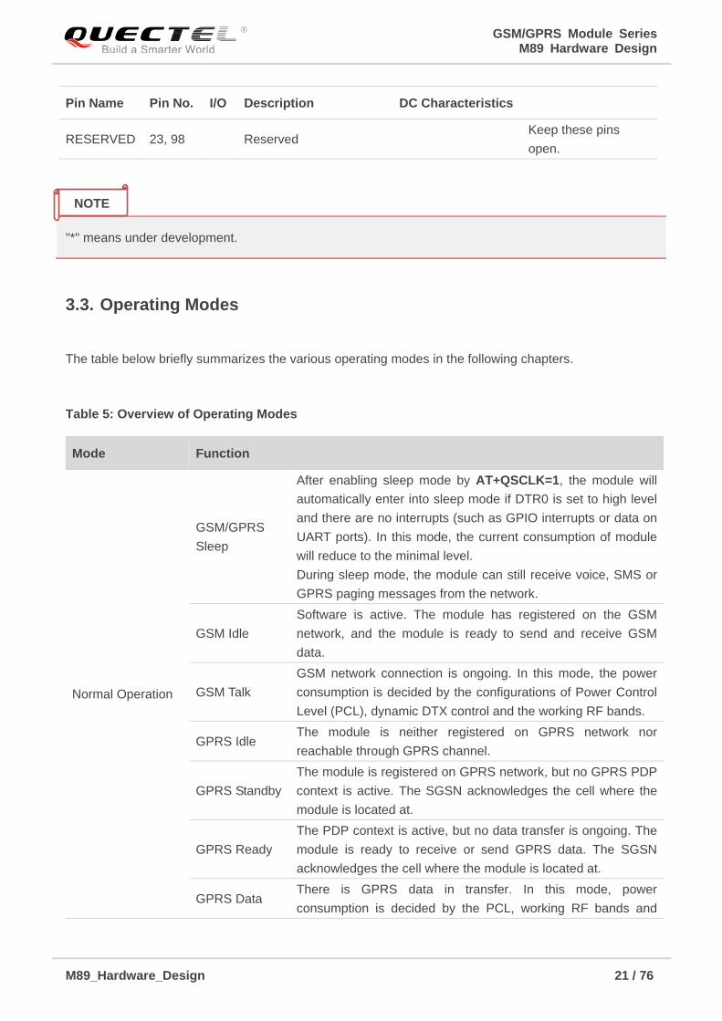
RESERVED 23, 98 Reserved Keep these pins
open.
Mode Function
Normal Operation
GSM/GPRS
Sleep
After enabling sleep mode by AT+QSCLK=1, the module will
automatically enter into sleep mode if DTR0 is set to high level
and there are no interrupts (such as GPIO interrupts or data on
UART ports). In this mode, the current consumption of module
will reduce to the minimal level.
During sleep mode, the module can still receive voice, SMS or
GPRS paging messages from the network.
GSM Idle
Software is active. The module has registered on the GSM
network, and the module is ready to send and receive GSM
data.
GSM Talk
GSM network connection is ongoing. In this mode, the power
consumption is decided by the configurations of Power Control
Level (PCL), dynamic DTX control and the working RF bands.
GPRS Idle The module is neither registered on GPRS network nor
reachable through GPRS channel.
GPRS Standby
The module is registered on GPRS network, but no GPRS PDP
context is active. The SGSN acknowledges the cell where the
module is located at.
GPRS Ready
The PDP context is active, but no data transfer is ongoing. The
module is ready to receive or send GPRS data. The SGSN
acknowledges the cell where the module is located at.
GPRS Data There is GPRS data in transfer. In this mode, power
consumption is decided by the PCL, working RF bands and
NOTE

GSM/GPRS Module Series M89 Hardware Design
M89_Hardware_Design 22 / 76
3.4. Power Supply
3.4.1. Power Features of the Module
The power supply is one of the key issues in designing GSM terminals. Due to the 577us radio burst in
GSM every 4.615ms, the power supply must be able to deliver high current peaks in a burst period.
During these peaks, drops on the supply voltage must not exceed minimum working voltage of the
module.
For M89 module, the max current consumption could reach to 1.6A during a burst transmission. It will
cause a large voltage drop on the VBAT. In order to ensure stable operation of the module, it is
recommended that the max voltage drop during the burst transmission does not exceed 400mV.
Vdrop
4.615ms
577us
IBAT
VBAT
Burst:1.6A
Figure 3: Voltage Ripple during Transmitting
GPRS multi-slot configuration.
Power Down Mode
Normal shutdown by sending the AT+QPOWD=1 command or pulling the
PWRKEY pin to high level. The power management unit shuts down the power
supply from the baseband part of the module, and only the power supply for the
RTC is remained. Software is not active. The UART ports are not accessible.
Operating voltage (connected to VBAT) remains applied.
Minimum
Functionality Mode
(without removing
power supply)
AT+CFUN=0 command can set the module to a minimum functionality mode
without removing the power supply. In this case, either RF function or (U)SIM card
is invalid, or neither of them is invalid, but the UART porta are still accessible.
GSM/GPRS Module Series M89 Hardware Design
M89_Hardware_Design 23 / 76
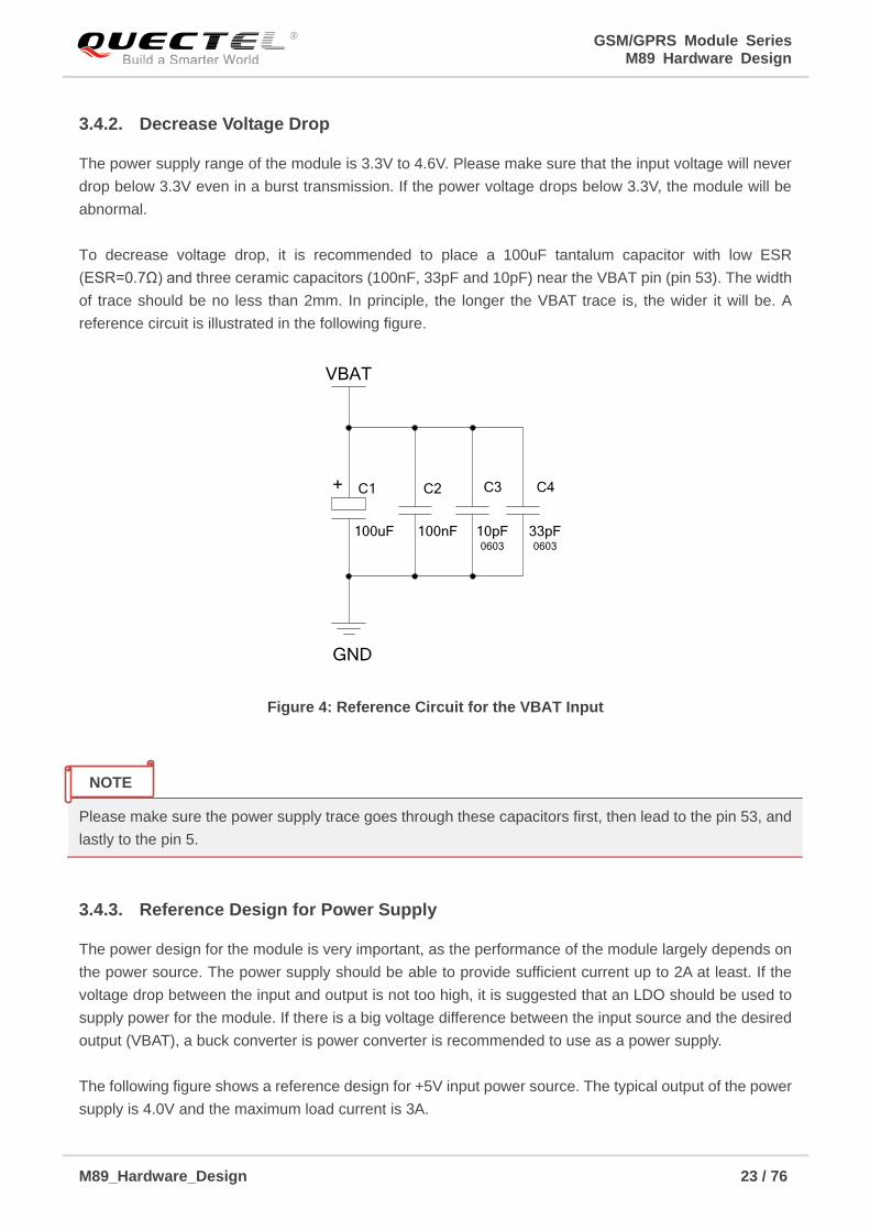
3.4.2. Decrease Voltage Drop
The power supply range of the module is 3.3V to 4.6V. Please make sure that the input voltage will never
drop below 3.3V even in a burst transmission. If the power voltage drops below 3.3V, the module will be
abnormal.
To decrease voltage drop, it is recommended to place a 100uF tantalum capacitor with low ESR
(ESR=0.7Ω) and three ceramic capacitors (100nF, 33pF and 10pF) near the VBAT pin (pin 53). The width
of trace should be no less than 2mm. In principle, the longer the VBAT trace is, the wider it will be. A
reference circuit is illustrated in the following figure.
VBAT
C2C1+ C3 C4
GND
100uF 100nF 10pF0603
33pF0603
Figure 4: Reference Circuit for the VBAT Input
Please make sure the power supply trace goes through these capacitors first, then lead to the pin 53, and
lastly to the pin 5.
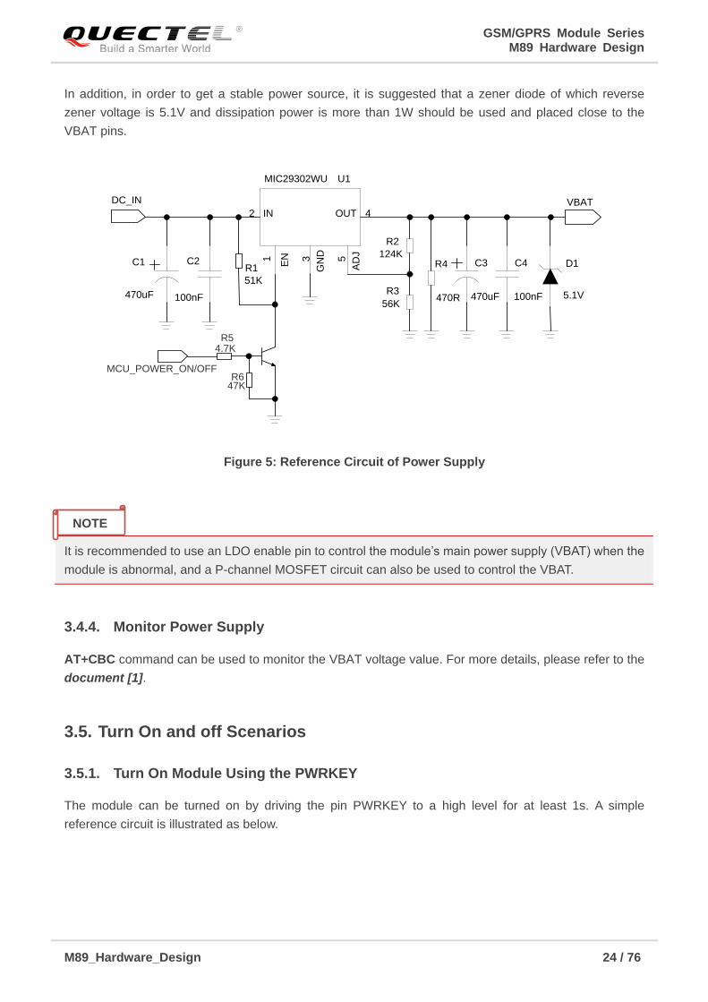
3.4.3. Reference Design for Power Supply
The power design for the module is very important, as the performance of the module largely depends on
the power source. The power supply should be able to provide sufficient current up to 2A at least. If the
voltage drop between the input and output is not too high, it is suggested that an LDO should be used to
supply power for the module. If there is a big voltage difference between the input source and the desired
output (VBAT), a buck converter is power converter is recommended to use as a power supply.
The following figure shows a reference design for +5V input power source. The typical output of the power
supply is 4.0V and the maximum load current is 3A.
NOTE
GSM/GPRS Module Series M89 Hardware Design
M89_Hardware_Design 24 / 76
In addition, in order to get a stable power source, it is suggested that a zener diode of which reverse
zener voltage is 5.1V and dissipation power is more than 1W should be used and placed close to the
VBAT pins.
DC_IN
C1 C2
MIC29302WU U1
IN OUT
EN
GN
D
AD
J
2 4
1 3 5
VBAT
100nF
C3
470uF
C4
100nF
R2
D1124K
56K
R3470uF 5.1V
R4
470R
MCU_POWER_ON/OFF
47K
4.7KR5
R6
R1
51K
Figure 5: Reference Circuit of Power Supply
It is recommended to use an LDO enable pin to control the module’s main power supply (VBAT) when the
module is abnormal, and a P-channel MOSFET circuit can also be used to control the VBAT.
3.4.4. Monitor Power Supply
AT+CBC command can be used to monitor the VBAT voltage value. For more details, please refer to the
document [1].
3.5. Turn On and off Scenarios
3.5.1. Turn On Module Using the PWRKEY
The module can be turned on by driving the pin PWRKEY to a high level for at least 1s. A simple
reference circuit is illustrated as below.
NOTE

GSM/GPRS Module Series M89 Hardware Design
M89_Hardware_Design 25 / 76
Turn on pulse
PWRKEY
Module
Figure 6: Turn on the Module Using Driving Circuit
1. M89 module is set to autobaud mode (AT+IPR=0) by default. In the autobaud mode, URC RDY will
not be reported to the host controller after the module is powered on, and the module will receive AT
commands after a delay of 2s~3s once being powered on. Therefore, it is recommended to set a
fixed baud rate and enable the report of URC string each time when the module is powered on
through following configurations: the host controller first sends an AT string to the module to detect
the baud rate, and continues to send the AT strings until OK is received, then enters AT+IPR=x;&W
to set a fixed baud rate and save the configuration to flash memory of the module. For more details,
refer to the AT+IPR command in document [1].
2. When AT command is responded, it indicates the module is turned on successfully.
The other way to control the PWRKEY is using a button directly. When pressing the key, electrostatic
strike may generate from finger. Therefore, a TVS component is indispensable to be placed nearby the
button for ESD protection. A reference circuit is shown in the following figure.
PWRKEY
S1
Close to
S1
TVS
VRTC or VBAT
Figure 7: Turn on the Module Using a Keystroke
NOTES
s

GSM/GPRS Module Series M89 Hardware Design
M89_Hardware_Design 26 / 76
The turn-on scenario is illustrated as the following figure.
VIO28(OUTPUT)
VIL<0.1*VBAT
VIH > 0.6*VBAT
VBAT
PWRKEY(INPUT)
54ms
>1s
T1
OFF BOOTINGMODULE
STATUSRUNNING
Figure 8: Timing of Turning on the Module
Please make sure that VBAT is stable before pulling up PWRKEY pin. The time of T1 is recommended to
be 100ms.
3.5.2. Turn off Module
The following procedures can be used to turn off the module:
Normal power down procedure: Turn off module using the PWRKEY pin.
Normal power down procedure: Turn off module using AT+QPOWD command.
Under-voltage automatic shutdown: Take effect when under-voltage is detected.
3.5.2.1. Turn off Module Using the PWRKEY Pin
Driving the PWRKEY to high level for at least 1s will turn off the module. The power-down scenario is
illustrated below.
NOTE
GSM/GPRS Module Series M89 Hardware Design
M89_Hardware_Design 27 / 76
VBAT
PWRKEY(INPUT)
VIO28 (OUTPUT)
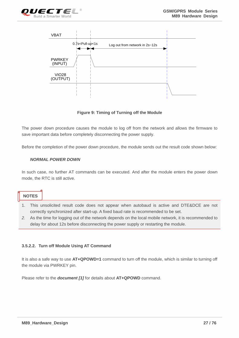
Log out from network in 2s~12s0.7s<Pull-up<1s
Figure 9: Timing of Turning off the Module
The power down procedure causes the module to log off from the network and allows the firmware to
save important data before completely disconnecting the power supply.
Before the completion of the power down procedure, the module sends out the result code shown below:
NORMAL POWER DOWN
In such case, no further AT commands can be executed. And after the module enters the power down
mode, the RTC is still active.
1. This unsolicited result code does not appear when autobaud is active and DTE&DCE are not
correctly synchronized after start-up. A fixed baud rate is recommended to be set.
2. As the time for logging out of the network depends on the local mobile network, it is recommended to
delay for about 12s before disconnecting the power supply or restarting the module.
3.5.2.2. Turn off Module Using AT Command
It is also a safe way to use AT+QPOWD=1 command to turn off the module, which is similar to turning off
the module via PWRKEY pin.
Please refer to the document [1] for details about AT+QPOWD command.
NOTES
GSM/GPRS Module Series M89 Hardware Design
M89_Hardware_Design 28 / 76
3.5.2.3. Under-voltage Warning
The power supply range of the module is 3.3V to 4.6V. The module will constantly monitor the voltage
applied on the VBAT. If the voltage is not greater than 3.5V, the following URC will be presented:
UNDER_VOLTAGE WARNING
This unsolicited result code does not appear when autobaud is active and DTE&DCE are not correctly
synchronized after start-up. A fixed baud rate is recommended to be set.
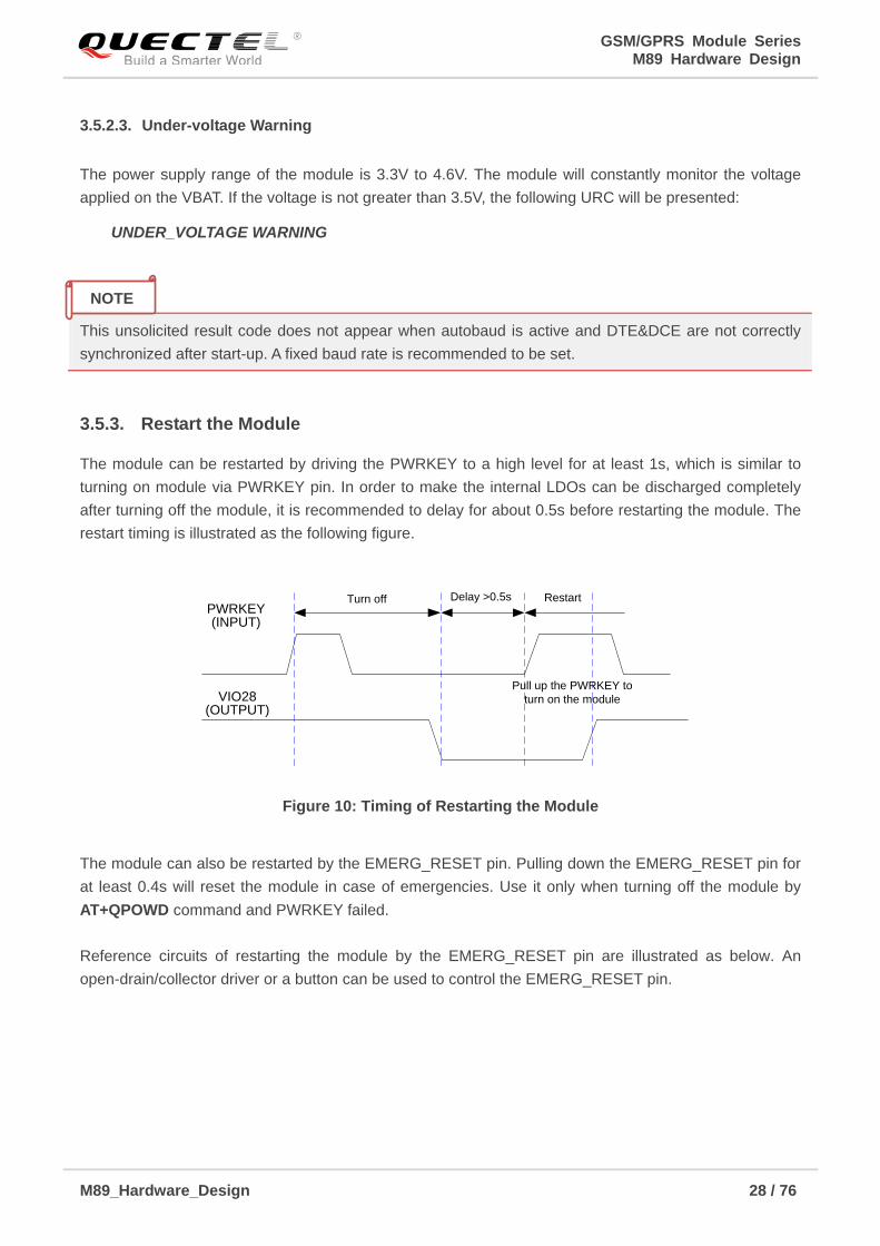
3.5.3. Restart the Module
The module can be restarted by driving the PWRKEY to a high level for at least 1s, which is similar to
turning on module via PWRKEY pin. In order to make the internal LDOs can be discharged completely
after turning off the module, it is recommended to delay for about 0.5s before restarting the module. The
restart timing is illustrated as the following figure.
PWRKEY(INPUT)
VIO28(OUTPUT)
Turn off Restart
Pull up the PWRKEY to
turn on the module
Delay >0.5s
Figure 10: Timing of Restarting the Module
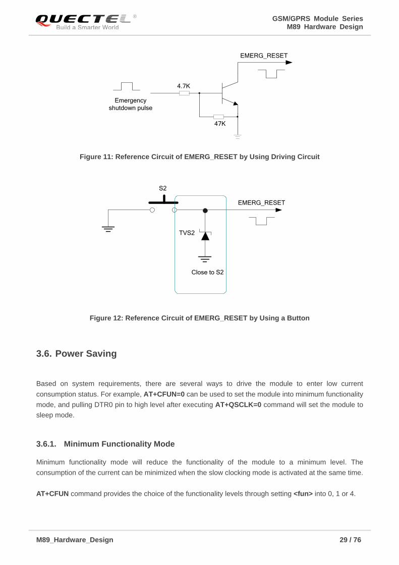
The module can also be restarted by the EMERG_RESET pin. Pulling down the EMERG_RESET pin for
at least 0.4s will reset the module in case of emergencies. Use it only when turning off the module by
AT+QPOWD command and PWRKEY failed.
Reference circuits of restarting the module by the EMERG_RESET pin are illustrated as below. An
open-drain/collector driver or a button can be used to control the EMERG_RESET pin.
NOTE
GSM/GPRS Module Series M89 Hardware Design
M89_Hardware_Design 29 / 76
Emergency
shutdown pulse
4.7K
47K
EMERG_RESET
Figure 11: Reference Circuit of EMERG_RESET by Using Driving Circuit
S2
TVS2
Close to S2
EMERG_RESET
Figure 12: Reference Circuit of EMERG_RESET by Using a Button
3.6. Power Saving
Based on system requirements, there are several ways to drive the module to enter low current
consumption status. For example, AT+CFUN=0 can be used to set the module into minimum functionality
mode, and pulling DTR0 pin to high level after executing AT+QSCLK=0 command will set the module to
sleep mode.
3.6.1. Minimum Functionality Mode
Minimum functionality mode will reduce the functionality of the module to a minimum level. The
consumption of the current can be minimized when the slow clocking mode is activated at the same time.
AT+CFUN command provides the choice of the functionality levels through setting <fun> into 0, 1 or 4.
GSM/GPRS Module Series M89 Hardware Design
M89_Hardware_Design 30 / 76
AT+CFUN=0: Minimum functionality mode; both (U)SIM and RF functions are disabled; the UART
ports are still accessible.
AT+CFUN=1: Full functionality mode (by default).
AT+CFUN=4: RF function is disabled; the UART ports are still accessible.
After the module is set by AT+CFUN=0 or AT+CFUN=4, it can be configured to full functionality mode by
AT+CFUN=1.
For detailed information about AT+CFUN, please refer to the document [1].
3.6.2. Sleep Mode
The sleep mode is disabled (AT+QSCLK=0) by default in firmware. When AT+QSCLK=1 is set on the
module (sleep mode is enabled), the DTR0 pin can be used to control the module to enter into or exit from
the sleep mode. When DTR0 is set to high level, and there are no on-air or hardware interrupts, such as
GPIO interrupts or data on UART ports, the module will enter into sleep mode automatically.
In this mode, the module can still receive voice, SMS or GPRS paging messages from the network, but
the UART ports are not accessible
3.6.3. Wake up Module from Sleep Mode
The module can be woken up from the sleep mode by any of the following methods:
Driving the DTR0 pin to low level, the UART ports will be active in 20ms.
A voice or data call is received from the network.
An SMS message is received from the network.
In order to ensure a stable communication between DTE and the module, the DTR0 pin should always be
kept at low level.
3.6.4. Summary of Operating Modes Transition
Table 6: Summary of Operating Modes Transition
Current Mode
Next Mode
Power Down Normal Mode Sleep Mode
Power Down Pull PWRKEY to high level
NOTE
GSM/GPRS Module Series M89 Hardware Design
M89_Hardware_Design 31 / 76
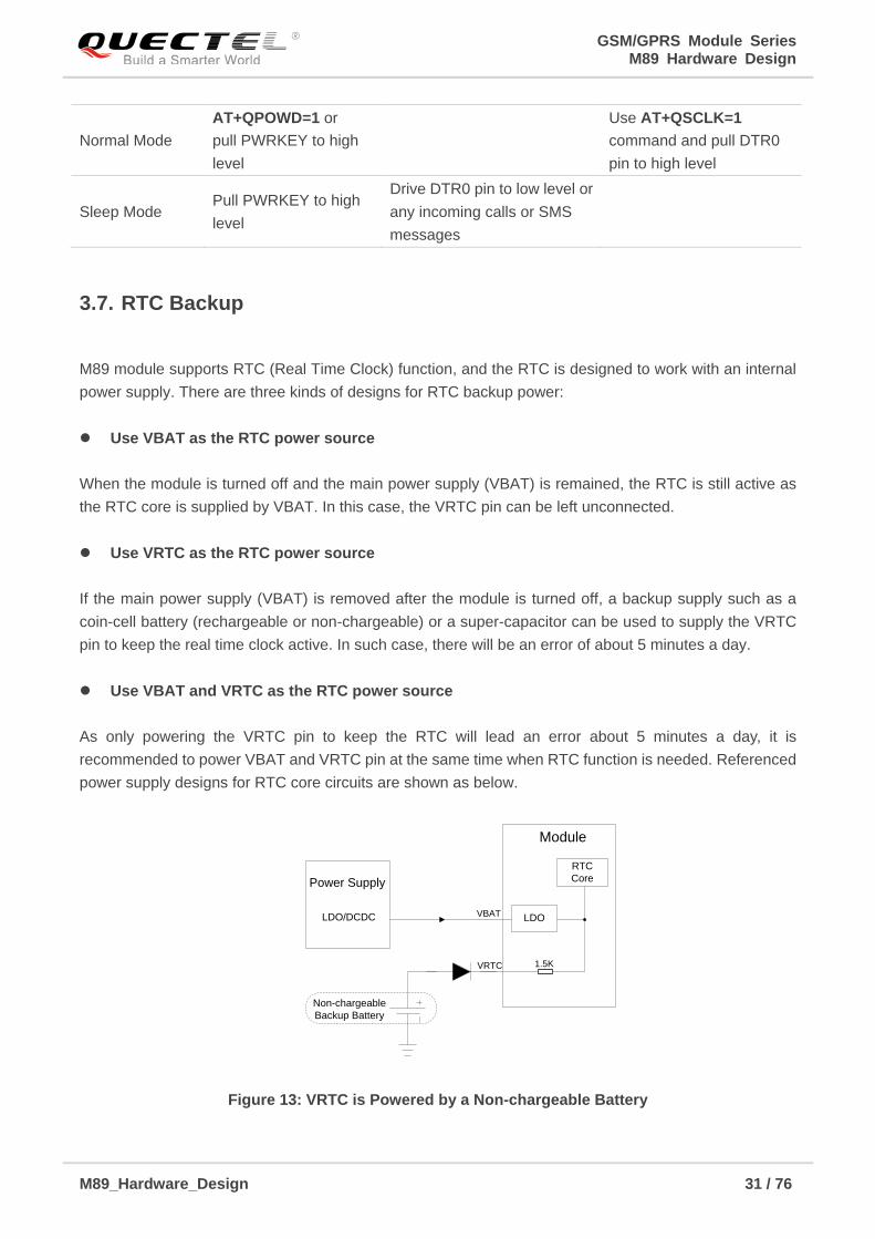
3.7. RTC Backup
M89 module supports RTC (Real Time Clock) function, and the RTC is designed to work with an internal
power supply. There are three kinds of designs for RTC backup power:
Use VBAT as the RTC power source
When the module is turned off and the main power supply (VBAT) is remained, the RTC is still active as
the RTC core is supplied by VBAT. In this case, the VRTC pin can be left unconnected.
Use VRTC as the RTC power source
If the main power supply (VBAT) is removed after the module is turned off, a backup supply such as a
coin-cell battery (rechargeable or non-chargeable) or a super-capacitor can be used to supply the VRTC
pin to keep the real time clock active. In such case, there will be an error of about 5 minutes a day.
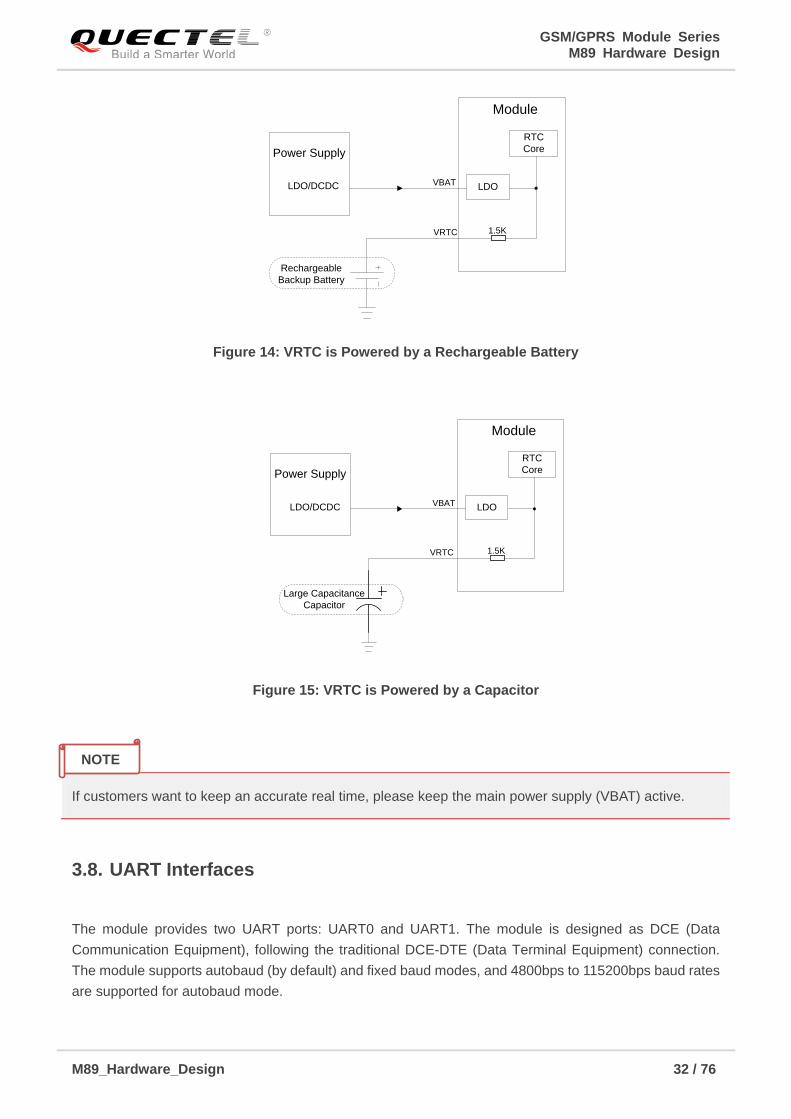
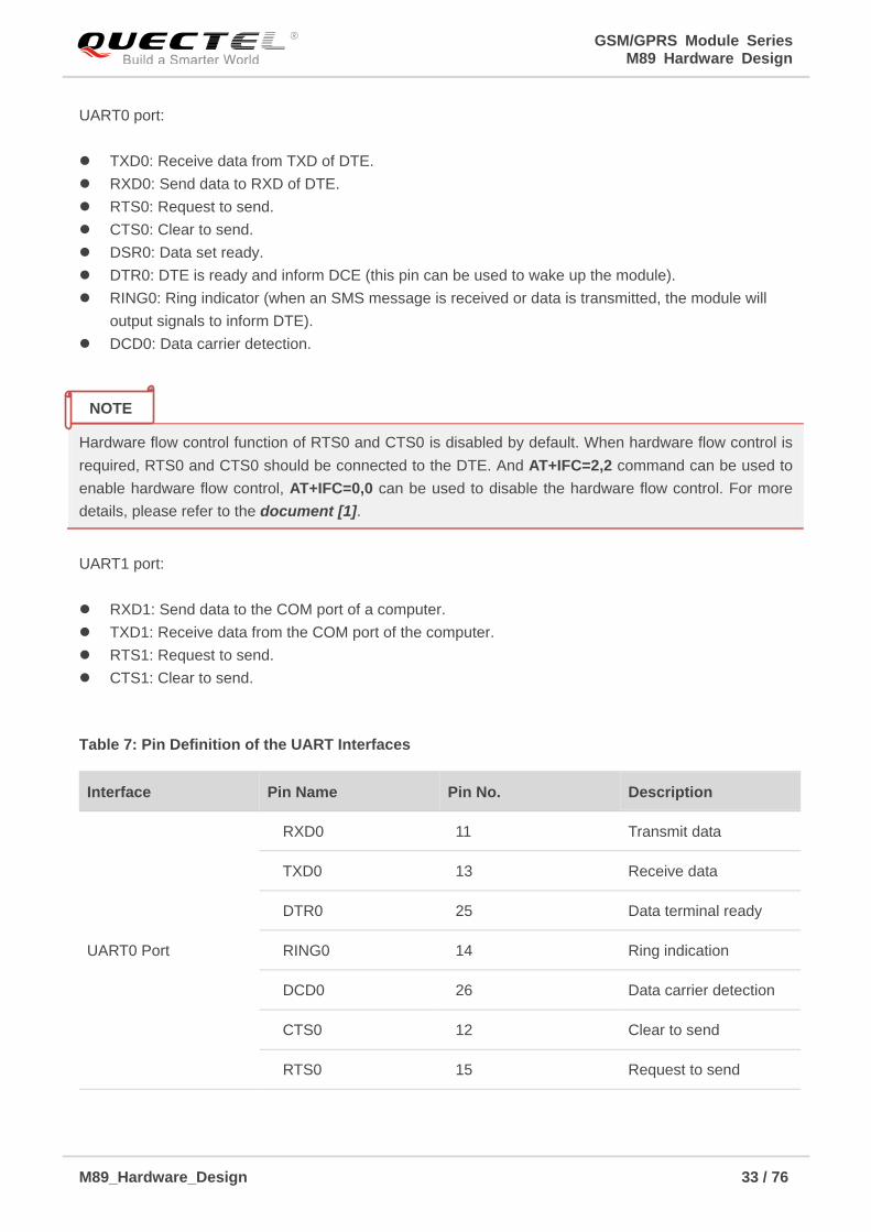
Use VBAT and VRTC as the RTC power source
As only powering the VRTC pin to keep the RTC will lead an error about 5 minutes a day, it is
recommended to power VBAT and VRTC pin at the same time when RTC function is needed. Referenced
power supply designs for RTC core circuits are shown as below.
Non-chargeable
Backup Battery
Module
RTC
Core
VBAT
Power Supply
LDO/DCDC LDO
VRTC 1.5K
Figure 13: VRTC is Powered by a Non-chargeable Battery
Normal Mode
AT+QPOWD=1 or
pull PWRKEY to high
level
Use AT+QSCLK=1
command and pull DTR0
pin to high level
Sleep Mode Pull PWRKEY to high
level
Drive DTR0 pin to low level or
any incoming calls or SMS
messages
GSM/GPRS Module Series M89 Hardware Design
M89_Hardware_Design 32 / 76
Rechargeable
Backup Battery
Module
RTC
Core
VBAT
Power Supply
LDO/DCDC LDO
VRTC 1.5K
Figure 14: VRTC is Powered by a Rechargeable Battery
Module
RTC
Core
VBAT
Power Supply
LDO/DCDC LDO
VRTC 1.5K
Large Capacitance
Capacitor
Figure 15: VRTC is Powered by a Capacitor
If customers want to keep an accurate real time, please keep the main power supply (VBAT) active.
3.8. UART Interfaces
The module provides two UART ports: UART0 and UART1. The module is designed as DCE (Data
Communication Equipment), following the traditional DCE-DTE (Data Terminal Equipment) connection.
The module supports autobaud (by default) and fixed baud modes, and 4800bps to 115200bps baud rates
are supported for autobaud mode.
NOTE
GSM/GPRS Module Series M89 Hardware Design
M89_Hardware_Design 33 / 76
UART0 port:
TXD0: Receive data from TXD of DTE.
RXD0: Send data to RXD of DTE.
RTS0: Request to send.
CTS0: Clear to send.
DSR0: Data set ready.
DTR0: DTE is ready and inform DCE (this pin can be used to wake up the module).
RING0: Ring indicator (when an SMS message is received or data is transmitted, the module will
output signals to inform DTE).
DCD0: Data carrier detection.
Hardware flow control function of RTS0 and CTS0 is disabled by default. When hardware flow control is
required, RTS0 and CTS0 should be connected to the DTE. And AT+IFC=2,2 command can be used to
enable hardware flow control, AT+IFC=0,0 can be used to disable the hardware flow control. For more
details, please refer to the document [1].
UART1 port:
RXD1: Send data to the COM port of a computer.
TXD1: Receive data from the COM port of the computer.
RTS1: Request to send.
CTS1: Clear to send.
Table 7: Pin Definition of the UART Interfaces
Interface Pin Name Pin No. Description
UART0 Port
RXD0 11 Transmit data
TXD0 13 Receive data
DTR0 25 Data terminal ready
RING0 14 Ring indication
DCD0 26 Data carrier detection
CTS0 12 Clear to send
RTS0 15 Request to send
NOTE
GSM/GPRS Module Series M89 Hardware Design
M89_Hardware_Design 34 / 76
The logic levels are described in the following table.
Table 8: Logic Levels of the UART0 Interface (VDIG Connected to VIO28)
Table 9: Logic Levels of the UART0 Interface (VDIG Connected to VIO18)
Table 10: Logic Levels of the UART1 Interface
DSR0 24 Data set Ready
UART1 Port
TXD1 29 Receive data
RXD1 30 Transmit data
RTS1 31 Request to send
CTS1 32 Clear to send
Parameter Min. Max. Unit
VIL 0 0.25×VIO28 V
VIH 0.75×VIO28 VIO28+0.2 V
VOL 0 0.15×VIO28 V
VOH 0.85×VIO28 VIO28 V
Parameter Min. Max. Unit
VIL 0 0.25×VIO18 V
VIH 0.75×VIO18 VIO18+0.2 V
VOL 0 0.15×VIO18 V
VOH 0.85×VIO18 VIO18 V
Parameter Min. Max. Unit
VIL 0 0.25×VIO28 V
VIH 0.75×VIO28 VIO28+0.2 V

GSM/GPRS Module Series M89 Hardware Design
M89_Hardware_Design 35 / 76
3.8.1. UART0 Port
3.8.1.1. UART0 Port Features
Eight lines on UART0 interface: data lines TXD0 and RXD0; hardware flow control lines RTS0 and
CTS0; other control lines DTR0, DCD0, DSR0 and RING0.
Used for AT command and data transmission.
Supports following baud rates: 300bps, 600bps, 1200bps, 2400bps, 4800bps, 9600bps, 14400bps,
19200bps, 28800bps, 38400bps, 57600bps and 115200bps.
Autobaud mode is supported by default with following baud rates: 4800bps, 9600bps, 19200bps,
38400bps, 57600bps and 115200bps.
Hardware flow control function is disabled by default, and it can be enabled by AT+IFC=2,2
command.
After setting a fixed baud rate or autobaud, please send AT string to confirm whether the port is ready.
Autobaud allows the module to detect the baud rate by receiving the string AT or at from the host or PC
automatically, which gives flexibility without considering which baud rate is used by the host controller.
Autobaud is enabled by default on the module. The following factors should be considered when applying
the autobaud function:
Synchronization between DTE and DCE
M89 module is set to autobaud mode (AT+IPR=0) by default. In the autobaud mode, URC RDY will not be
reported to the host controller after the module is powered on, and the module will receive AT commands
after a delay of in 2s~3s once being powered on. Therefore, it is recommended to set a fixed baud rate
and enable the report of URC string each time when the module is powered on through following
configurations: the host controller first sends an AT string to the module to detect the baud rate, and
continues to send the AT strings until OK is received, then enters AT+IPR=x;&W to set a fixed baud rate
and save the configuration to flash memory of the module. For more details, please refer to the AT+IPR
command in document [1].
When DCE (the module) is powered on with the autobaud mode enabled, it is recommended to wait for
2s~3s before sending the first AT string. After receiving the OK response, DTE and DCE are correctly
synchronized.
If the host controller needs a URC in autobaud mode, DTE and DCE must be synchronized first.
Otherwise the URC will be discarded.
VOL 0 0.15×VIO28 V
VOH 0.85×VIO28 VIO28 V

GSM/GPRS Module Series M89 Hardware Design
M89_Hardware_Design 36 / 76
Restrictions on autobaud configuration
1) The UART0 port has to be operated at 8 data bits, no parity and 1 stop bit (factory setting).
2) Only the strings AT or at can be detected (neither At nor aT).
3) If DTE and DCE are not synchronized, then URCs such as RDY, +CFUN: 1 and +CPIN: READY will
not be reported when the module is turned on with autobaud enabled.
4) Any other URCs will be sent at the previous baud rate before the module detects the new baud rate
by receiving the first “AT” or “at” string. The DTE may receive unknown characters after switching to
new baud rate.
5) It is not recommended to switch to autobaud from a fixed baud rate.
To ensure reliable communication and avoid any problems caused by undetermined baud rates between
DCE and DTE, it is strongly recommended to configure a fixed baud rate and save the configuration to
flash memory after start-up. For more details, please refer to the AT+IPR in document [1].
3.8.1.2. DCE & DTE Connection via UART0
Three ways of connection between the DCE and DTE are illustrated as below for UART0 port.
A reference design for full-function UART0 connection is shown as below when it is applied in
modulation-demodulation.
TXD0
RXD0
RTS0
CTS0
DTR0
DCD0
RING0
TXD
RXD
RTS
CTS
DTR
DCD
RING
Module (DCE)
Serial portUART0 port
GND GND
PC (DTE)
DSR0 DSR
Figure 16: Reference Circuit of UART0 Port with Full-function
NOTE
GSM/GPRS Module Series M89 Hardware Design
M89_Hardware_Design 37 / 76
Three-line connection of UART0 port is shown as below.
TXD0
RXD0
GND
UART0 port
TXD
RXD
GND
Module (DCE) Host (DTE)
Controller
Figure 17: Reference Circuit of UART0 Port with Three-line
UART0 port with hardware flow control function is shown as below. This kind of connection will enhance
the reliability of the mass data communication.
RTS0
CTS0
RTS
CTS
GND
RXD0
TXD0 TXD
RXD
GND
Module (DCE) Host (DTE)
Controller
Figure 18: Reference Design of UART0 Port with Hardware Flow Control
3.8.1.3. Firmware Upgrade
The TXD0 and RXD0 can be used to upgrade firmware. The PWRKEY pin must be pulled to high level
before firmware upgrade. A reference circuit is shown as below:

GSM/GPRS Module Series M89 Hardware Design
M89_Hardware_Design 38 / 76
IO Connector
TXD
RXD
GND
PWRKEY
Module (DCE) UART port
TXD0
RXD0
GND
PWRKEY
VRTC or VBAT
Figure 19: Reference Circuit of UART0 Port for Firmware Upgrade
It is recommended to reserve these pins in the host board for firmware upgrade.
3.8.2. UART1 Port
Four lines: TXD1/RXD1/CTS1/RTS1.
It outputs log information automatically.
UART1 is only used for software debugging and only 460800bps is supported.
Two ways of connection between the DCE and DTE are illustrated as below for UART1 port.
Three-line connection of UART1 port is shown as below
Peripheral
TXD
RXD
GND
Module
TXD1
RXD1
GND
Figure 20: Reference Circuit of UART1 Port with Three-line
NOTE

GSM/GPRS Module Series M89 Hardware Design
M89_Hardware_Design 39 / 76
UART1 port with hardware flow control is shown as below. This kind of connection will enhance the
reliability of the mass data communication.
RTS1
CTS1
RTS
CTS
GND
RXD1
TXD1 TXD
RXD
GND
Module (DCE) Host (DTE)
Controller
Figure 21: Reference Circuit of UART1 Port with Hardware Flow Control
It is highly recommended to add a resistor divider circuit on the UART1 signal lines when the voltage of
the host is higher than 1.8V or 2.8V. For a higher voltage level system, a level translator should be used
between the host and the module. For more details about UART circuit design, please refer to document
[10].
3.9. Audio Interfaces
The module provides one analog input channels and one analog output channels.
Table 11: Pin Definition of Audio Interfaces
Interface Pin Name Pin No. Description
AIN/AOUT
VMIC 1 Bias circuit for microphone power supply
MICP 65 Microphone positive input
MICN 66 Microphone negative input
LOUDSPK_P 3 Channel 2 audio positive output
LOUDSPK_N 2 Channel 2 audio negative output
NOTE
GSM/GPRS Module Series M89 Hardware Design
M89_Hardware_Design 40 / 76
AIN can be used as the microphone input or analog audio signal input. An electret microphone is usually
used. AIN are differential input channels.
AOUT is used for loudspeaker output as it is embedded with an amplifier of class AB whose maximum
drive power is 800mW. AOUT is a differential channel.
AOUT can also be used for earphone output. It is a single-ended and mono-channel. LOUDSPKP and
AGND can establish a pseudo differential mode.
AT+QMIC can be used to adjust the input gain level of microphone for each channel. AT+CLVL can be
used to adjust the output gain level of receiver and speaker, and AT+QSIDET can be used to set the
side-tone gain level. For more details, please refer to the document [1].
Table 12: AOUT Output Characteristics
3.9.1. Decrease TDD Noise and Other Noise
Audio signals could be interfered by RF signals. Coupling noise could be filtered by adding a 33pF or
10pF capacitor to audio line. The 33pF capacitor can be applied for filtering out 900MHz RF interference
when the module is transmitting at EGSM900, and the 10pF capacitor is used for filtering out 1800MHz
RF interference. Please note that the resonant frequency point of a capacitor largely depends on the
material and production technique. Therefore, it is suggested that customers confirm with their capacitor
vendor to choose the most suitable capacitor for filtering out EGSM900 and DCS1800 interference
separately.
The severity degree of the RF interference in the audio channel during GSM transmitting period largely
depends on the application designs. Customers should develop the filter solution according to field test
results. Meanwhile, the capacitor for filtering should be placed close to the audio components. The traces
for audio lines should be as short as possible.
In order to decrease radio or other signal interference, the layout of audio lines should be far away from
RF cable, antenna and VBAT pins.
AGND 64
Analog ground.
Form a pseudo-differential pair with
LOUDSPK_P
Item Condition Min. Typ. Max. Unit
RMS Power
8Ω load
VBAT=4.0V
THD+N=1%
800 mW
GSM/GPRS Module Series M89 Hardware Design
M89_Hardware_Design 41 / 76
The differential audio traces have to be placed according to the differential signal layout principles.
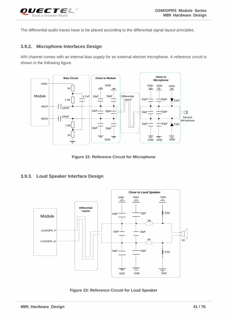
3.9.2. Microphone Interfaces Design
AIN channel comes with an internal bias supply for an external electret microphone. A reference circuit is
shown in the following figure.
MICP
Differential
LayoutModule
10pF 33pF
33pF
33pF
GND
GND
Electret
Microphone
GND
GND
10pF
10pF
GND
GND
ESD
ESD
Close to Module
MICN
GND
GND
Close to
Microphone
33pF
33pF
33pF10pF
10pF
10pF
VMIC
100nF
100nF
4.7uF
1.5K
1.5K
1K
1K
Bias Circuit
Figure 22: Reference Circuit for Microphone
3.9.3. Loud Speaker Interface Design
LOUDSPK_N
0R
0R
LOUDSPK_P
8Ω
Module
GND GNDGND
Close to Loud Speaker
10pF 33pF
33pF10pF
10pF 33pF
GND GNDGND
Differential
Layout
ESD
ESD
Figure 23: Reference Circuit for Loud Speaker
GSM/GPRS Module Series M89 Hardware Design
M89_Hardware_Design 42 / 76
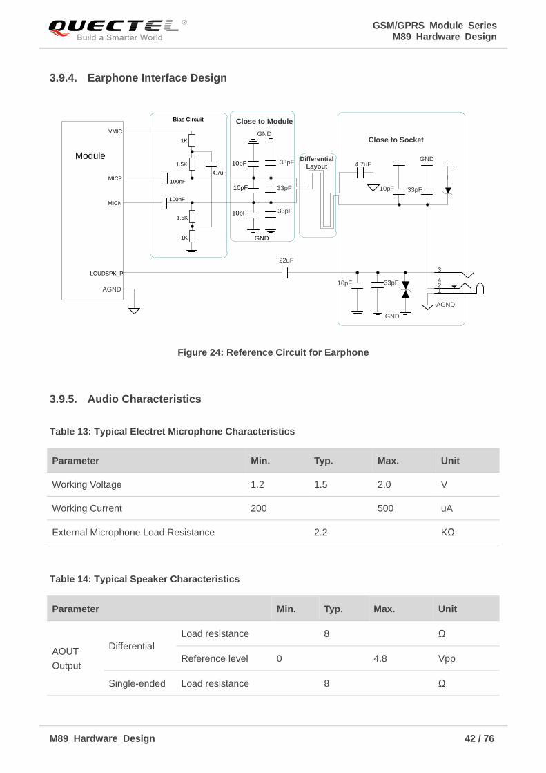
3.9.4. Earphone Interface Design
124
3
22uF
33pF
GND
AGND
Close to Socket
33pF10pF
GND
AGND
4.7uF
Close to Module
GND
33pF
33pF
Differential
Layout33pF
10pF
GND
10pF
10pF
10pF
100nF
100nF
1.5K
1.5K
1K
1K
Bias Circuit
Module
MICN
VMIC
MICP
LOUDSPK_P
4.7uF
Figure 24: Reference Circuit for Earphone
3.9.5. Audio Characteristics
Table 13: Typical Electret Microphone Characteristics
Table 14: Typical Speaker Characteristics
Parameter Min. Typ. Max. Unit
Working Voltage 1.2 1.5 2.0 V
Working Current 200 500 uA
External Microphone Load Resistance 2.2 KΩ
Parameter Min. Typ. Max. Unit
AOUT
Output
Differential
Load resistance 8 Ω
Reference level 0 4.8 Vpp
Single-ended Load resistance 8 Ω
GSM/GPRS Module Series M89 Hardware Design
M89_Hardware_Design 43 / 76
3.10. (U)SIM Interface
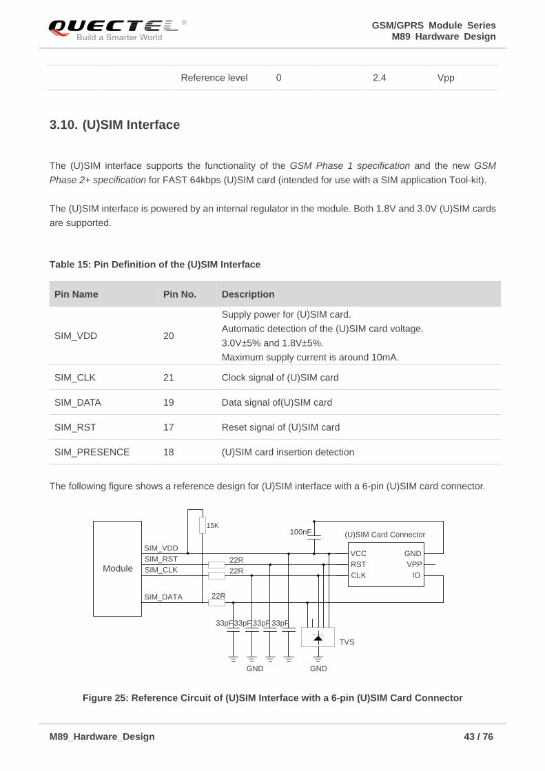
The (U)SIM interface supports the functionality of the GSM Phase 1 specification and the new GSM
Phase 2+ specification for FAST 64kbps (U)SIM card (intended for use with a SIM application Tool-kit).
The (U)SIM interface is powered by an internal regulator in the module. Both 1.8V and 3.0V (U)SIM cards
are supported.
Table 15: Pin Definition of the (U)SIM Interface
The following figure shows a reference design for (U)SIM interface with a 6-pin (U)SIM card connector.
Module
SIM_VDD
SIM_RST
SIM_CLK
SIM_DATA 22R
22R
22R
100nF (U)SIM Card Connector
GND
TVS
33pF33pF 33pF
VCC
RST
CLK IO
VPP
GND
GND
33pF
15K
Figure 25: Reference Circuit of (U)SIM Interface with a 6-pin (U)SIM Card Connector
Reference level 0 2.4 Vpp
Pin Name Pin No. Description
SIM_VDD 20
Supply power for (U)SIM card.
Automatic detection of the (U)SIM card voltage.
3.0V±5% and 1.8V±5%.
Maximum supply current is around 10mA.
SIM_CLK 21 Clock signal of (U)SIM card
SIM_DATA 19 Data signal of(U)SIM card
SIM_RST 17 Reset signal of (U)SIM card
SIM_PRESENCE 18 (U)SIM card insertion detection

GSM/GPRS Module Series M89 Hardware Design
M89_Hardware_Design 44 / 76
The following figure shows a reference design for (U)SIM interface with an 8-pin (U)SIM card connector.
Module
22R
22R
22R
100nF
GND
VIO18
TVS
33pF33pF 33pF 33pF
VCC
RST
CLK IO
VPP
GND
GND
(U)SIM Card Connector
SIM_VDD
SIM_RST
SIM_CLK
SIM_PRESENCE
SIM_DATA
15K
Figure 26: Reference Circuit of (U)SIM Interface with an 8-pin (U)SIM Card Connector
In order to enhance the reliability and availability of the (U)SIM card in applications, please follow the
criteria below in (U)SIM circuit design:
Keep placement of (U)SIM card connector as close to the module as possible. Keep the trace length
as less than 200mm as possible.
Keep (U)SIM card signal away from RF and VBAT traces.
Assure the ground between the module and the (U)SIM card connector short and wide. Keep the
trace width of ground no less than 0.5mm to maintain the same electric potential. The decouple
capacitor of SIM_VDD should be less than 1uF and must be placed near to the (U)SIM card
connector.
To avoid cross-talk between SIM_DATA and SIM_CLK, keep them away from each other and shield
them with surrounded ground.
In order to offer good ESD protection, it is recommended to add a TVS diode array. For more
information of TVS diodes, please visit http://www.onsemi.com. The most important rule is to place
the ESD protection device close to the (U)SIM card connector and make sure the (U)SIM card
interface signal lines being protected will go through the ESD protection device first and then lead to
module. The 22Ω resistors should be added in series between the module and the (U)SIM card to
suppress the EMI spurious transmission and enhance the ESD protection. Please note that the
(U)SIM peripheral circuit should be close to the (U)SIM card connector.
Place the RF bypass capacitors (33pF) close to the (U)SIM card connector on all signal lines to
improve EMI suppression.
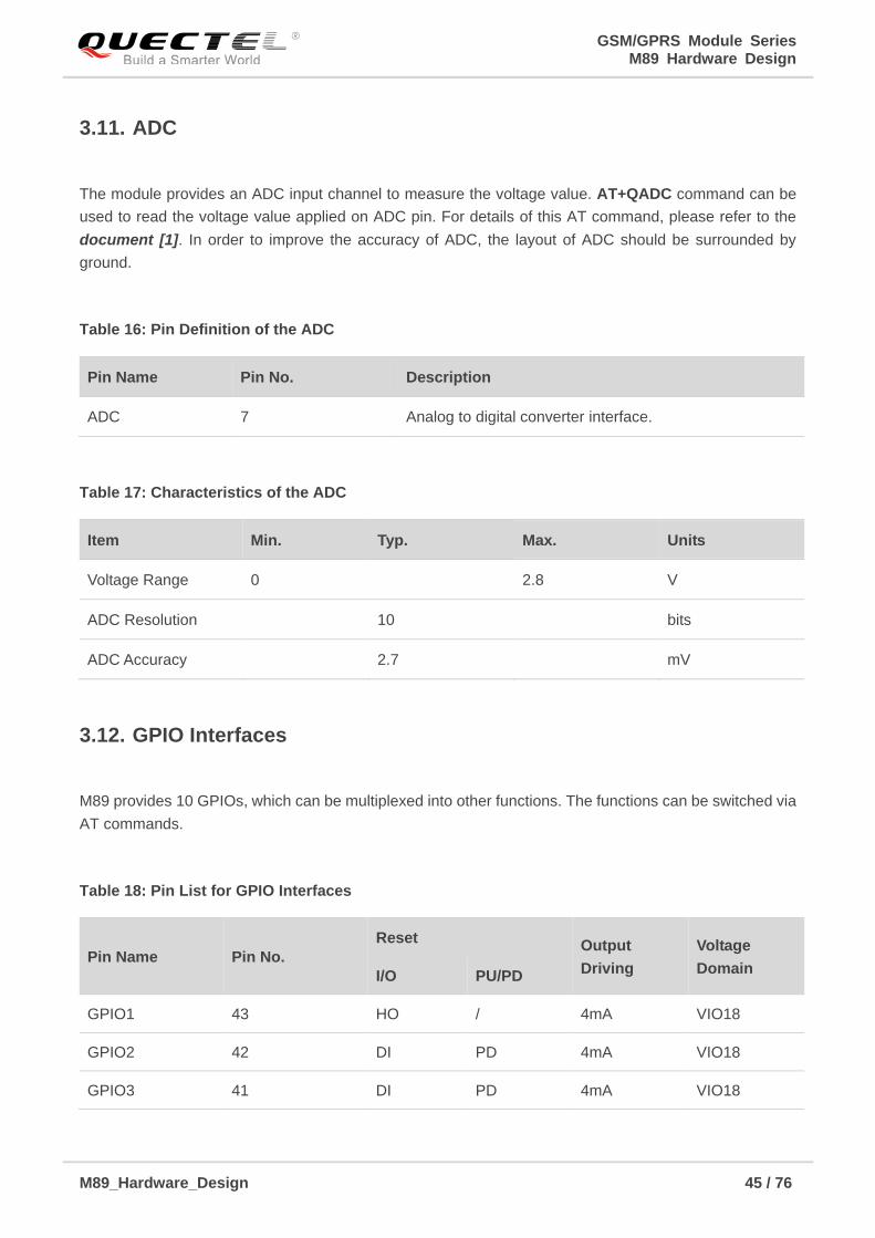
GSM/GPRS Module Series M89 Hardware Design
M89_Hardware_Design 45 / 76
3.11. ADC
The module provides an ADC input channel to measure the voltage value. AT+QADC command can be
used to read the voltage value applied on ADC pin. For details of this AT command, please refer to the
document [1]. In order to improve the accuracy of ADC, the layout of ADC should be surrounded by
ground.
Table 16: Pin Definition of the ADC
Table 17: Characteristics of the ADC
3.12. GPIO Interfaces
M89 provides 10 GPIOs, which can be multiplexed into other functions. The functions can be switched via
AT commands.
Table 18: Pin List for GPIO Interfaces
Pin Name Pin No. Description
ADC 7 Analog to digital converter interface.
Item Min. Typ. Max. Units
Voltage Range 0 2.8 V
ADC Resolution 10 bits
ADC Accuracy 2.7 mV
Pin Name Pin No.
Reset Output
Driving
Voltage
Domain I/O PU/PD
GPIO1 43 HO / 4mA VIO18
GPIO2 42 DI PD 4mA VIO18
GPIO3 41 DI PD 4mA VIO18
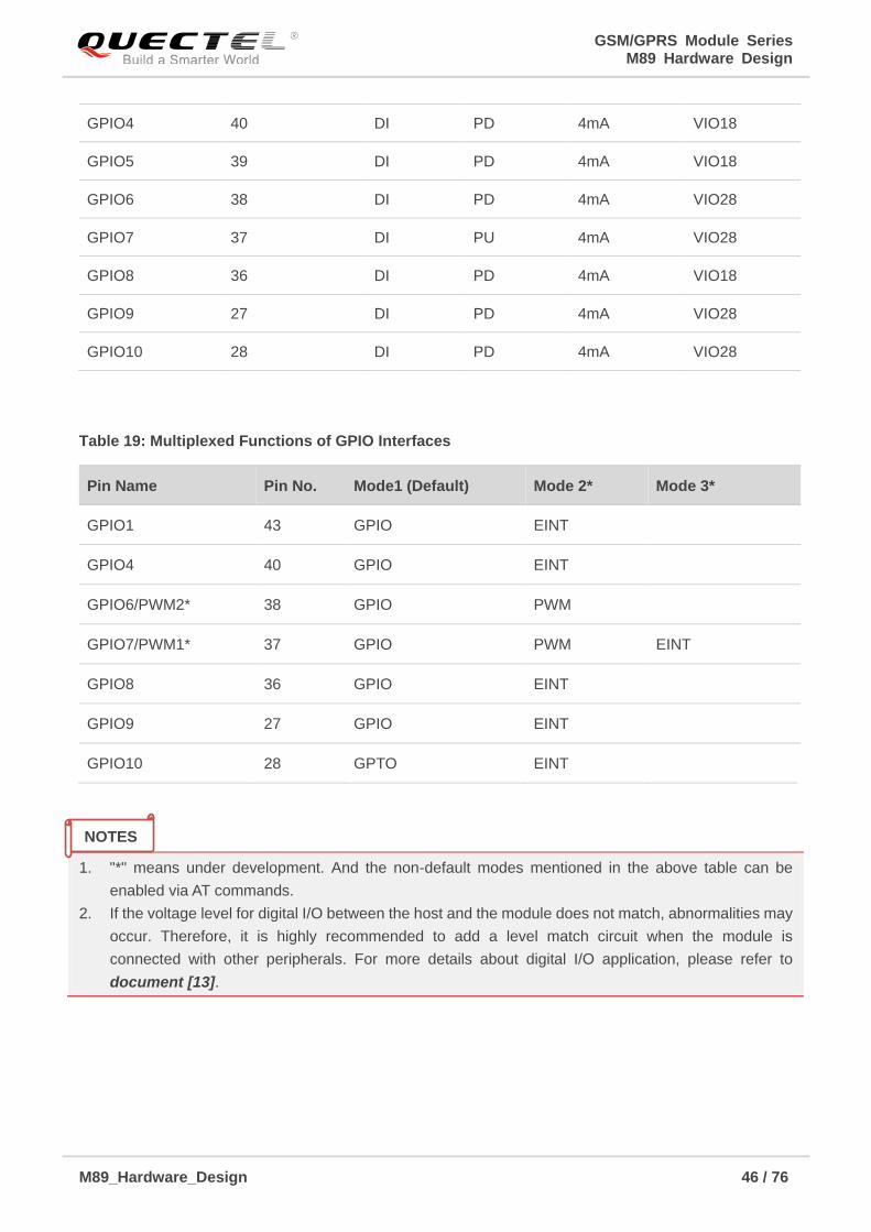
GSM/GPRS Module Series M89 Hardware Design
M89_Hardware_Design 46 / 76
Table 19: Multiplexed Functions of GPIO Interfaces
1. "*" means under development. And the non-default modes mentioned in the above table can be
enabled via AT commands.
2. If the voltage level for digital I/O between the host and the module does not match, abnormalities may
occur. Therefore, it is highly recommended to add a level match circuit when the module is
connected with other peripherals. For more details about digital I/O application, please refer to
document [13].
GPIO4 40 DI PD 4mA VIO18
GPIO5 39 DI PD 4mA VIO18
GPIO6 38 DI PD 4mA VIO28
GPIO7 37 DI PU 4mA VIO28
GPIO8 36 DI PD 4mA VIO18
GPIO9 27 DI PD 4mA VIO28
GPIO10 28 DI PD 4mA VIO28
Pin Name Pin No. Mode1 (Default) Mode 2* Mode 3*
GPIO1 43 GPIO EINT
GPIO4 40 GPIO EINT
GPIO6/PWM2* 38 GPIO PWM
GPIO7/PWM1* 37 GPIO PWM EINT
GPIO8 36 GPIO EINT
GPIO9 27 GPIO EINT
GPIO10 28 GPTO EINT
NOTES
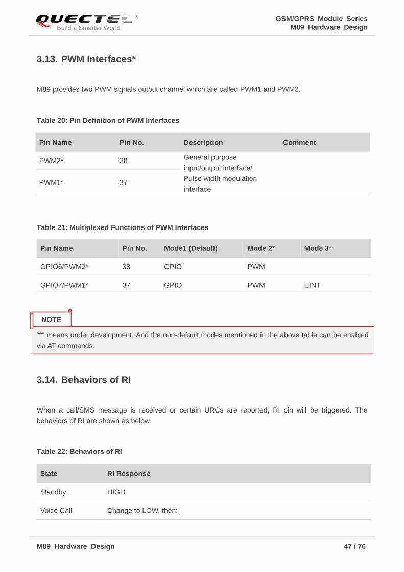
GSM/GPRS Module Series M89 Hardware Design
M89_Hardware_Design 47 / 76
3.13. PWM Interfaces*
M89 provides two PWM signals output channel which are called PWM1 and PWM2.
Table 20: Pin Definition of PWM Interfaces
Table 21: Multiplexed Functions of PWM Interfaces
"*" means under development. And the non-default modes mentioned in the above table can be enabled
via AT commands.
3.14. Behaviors of RI
When a call/SMS message is received or certain URCs are reported, RI pin will be triggered. The
behaviors of RI are shown as below.
Table 22: Behaviors of RI
Pin Name Pin No. Description Comment
PWM2* 38 General purpose
input/output interface/
Pulse width modulation
interface
PWM1* 37
Pin Name Pin No. Mode1 (Default) Mode 2* Mode 3*
GPIO6/PWM2* 38 GPIO PWM
GPIO7/PWM1* 37 GPIO PWM EINT
State RI Response
Standby HIGH
Voice Call Change to LOW, then:
NOTE
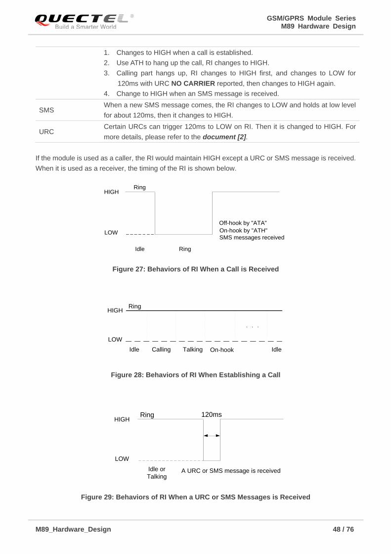
GSM/GPRS Module Series M89 Hardware Design
M89_Hardware_Design 48 / 76
If the module is used as a caller, the RI would maintain HIGH except a URC or SMS message is received.
When it is used as a receiver, the timing of the RI is shown below.
Ring
Idle Ring
Off-hook by "ATA"
On-hook by "ATH"
HIGH
LOWSMS messages received
Figure 27: Behaviors of RI When a Call is Received
Ring
Idle Calling On-hookTalking
HIGH
LOW
Idle
Figure 28: Behaviors of RI When Establishing a Call
Ring
Idle or
Talking A URC or SMS message is received
HIGH
LOW
120ms
Figure 29: Behaviors of RI When a URC or SMS Messages is Received
1. Changes to HIGH when a call is established.
2. Use ATH to hang up the call, RI changes to HIGH.
3. Calling part hangs up, RI changes to HIGH first, and changes to LOW for
120ms with URC NO CARRIER reported, then changes to HIGH again.
4. Change to HIGH when an SMS message is received.
SMS When a new SMS message comes, the RI changes to LOW and holds at low level
for about 120ms, then it changes to HIGH.
URC Certain URCs can trigger 120ms to LOW on RI. Then it is changed to HIGH. For
more details, please refer to the document [2].
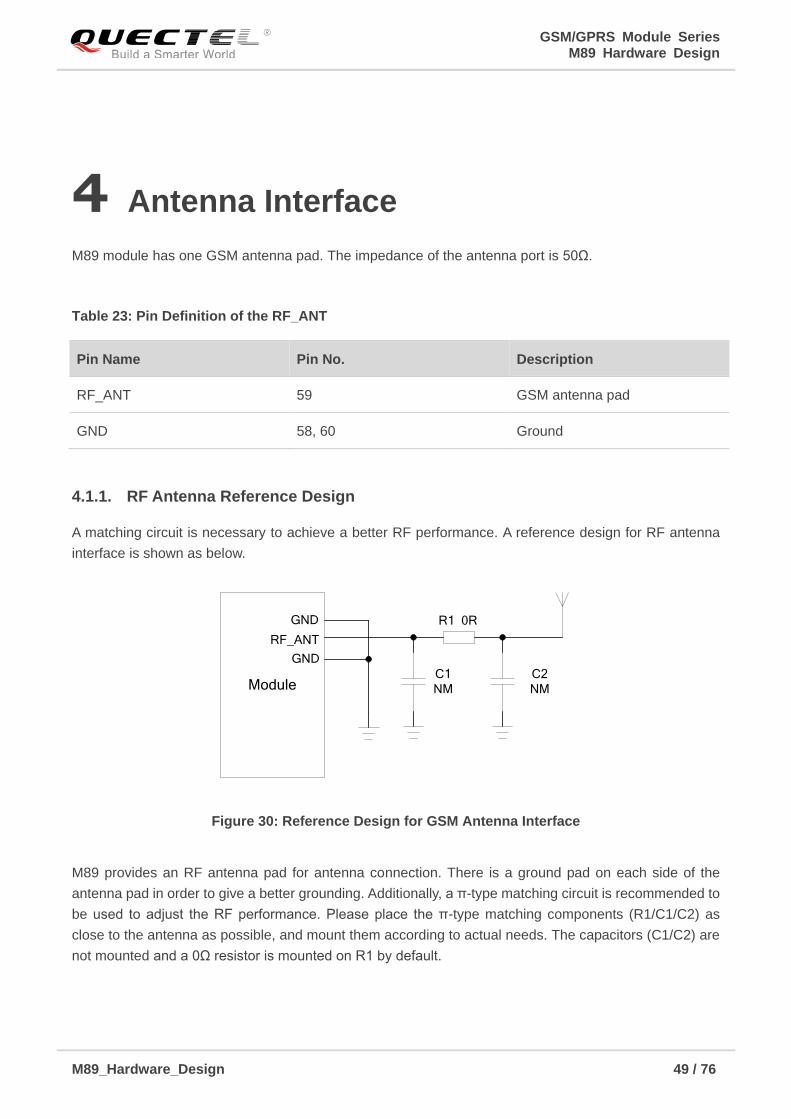
GSM/GPRS Module Series M89 Hardware Design
M89_Hardware_Design 49 / 76
4 Antenna Interface
M89 module has one GSM antenna pad. The impedance of the antenna port is 50Ω.
Table 23: Pin Definition of the RF_ANT
4.1.1. RF Antenna Reference Design
A matching circuit is necessary to achieve a better RF performance. A reference design for RF antenna
interface is shown as below.
Module
RF_ANT
R1 0R
C1
NM
C2
NM
GND
GND
Figure 30: Reference Design for GSM Antenna Interface
M89 provides an RF antenna pad for antenna connection. There is a ground pad on each side of the
antenna pad in order to give a better grounding. Additionally, a π-type matching circuit is recommended to
be used to adjust the RF performance. Please place the π-type matching components (R1/C1/C2) as
close to the antenna as possible, and mount them according to actual needs. The capacitors (C1/C2) are
not mounted and a 0Ω resistor is mounted on R1 by default.
Pin Name Pin No. Description
RF_ANT 59 GSM antenna pad
GND 58, 60 Ground

GSM/GPRS Module Series M89 Hardware Design
M89_Hardware_Design 50 / 76
4.2. Reference Design of RF Layout
For user’s PCB, the characteristic impedance of all RF traces should be controlled as 50Ω. The
impedance of the RF traces is usually determined by the trace width (W), the materials’ dielectric constant,
the distance between signal layer and reference ground (H), and the clearance between RF trace and
ground (S). Microstrip line or coplanar waveguide line is typically used in RF layout for characteristic
impedance control. The following are reference designs of microstrip line or coplanar waveguide line with
different PCB structures.
Figure 31: Microstrip Line Design on a 2-layer PCB
Figure 32: Coplanar Waveguide Line Design on a 2-layer PCB

GSM/GPRS Module Series M89 Hardware Design
M89_Hardware_Design 51 / 76
Figure 33: Coplanar Waveguide Line Design on a 4-layer PCB (Layer 3 as Reference Ground)
Figure 34: Coplanar Waveguide Line Design on a 4-layer PCB (Layer 4 as Reference Ground)
In order to ensure RF performance and reliability, the following principles should be complied with in RF
layout design:
Use impedance simulation tool to control the characteristic impedance of RF traces as 50Ω.
The GND pins adjacent to RF pins should not be designed as thermal relief pads, and should be fully
connected to ground.
The distance between the RF pins and the RF connector should be as short as possible, and all the
right angle traces should be changed to curved ones.
There should be clearance area under the signal pin of the antenna connector or solder joint.
The reference ground of RF traces should be complete. Meanwhile, adding some ground vias around
RF traces and the reference ground could help to improve RF performance. The distance between
the ground vias and RF traces should be no less than two times the width of RF signal traces (2*W).
For more details about RF layout, please refer to document [14].
GSM/GPRS Module Series M89 Hardware Design
M89_Hardware_Design 52 / 76
4.3. Antenna Requirements
The following table shows the requirements on GSM antenna.
Table 24: Antenna Cable Requirements
Table 25: Antenna Requirements
4.3.1. RF Output Power
Table 26: RF Output Power
Type Requirements
GSM850/EGSM900 Cable insertion loss: <1dB
DCS1800/PCS1900 Cable insertion loss: <1.5dB
Type Requirements
Frequency Range Depending on frequency band(s) provided by the network operator
VSWR ≤ 2
Efficiency > 30%
Max Input Power (W) 50
Input Impedance (Ω) 50
Frequency Max. Min.
GSM850 33dBm±2dB 5dBm±5dB
EGSM900 33dBm±2dB 5dBm±5dB
DCS1800 30dBm±2dB 0dBm±5dB
PCS1900 30dBm±2dB 0dBm±5dB

GSM/GPRS Module Series M89 Hardware Design
M89_Hardware_Design 53 / 76
In GPRS 4 slots Tx mode, the max output power is reduced by 2.5dB. This design conforms to the GSM
specification as described in Section 13.16 of 3GPP TS 51.010-1.
4.3.2. RF Receiving Sensitivity
Table 27: RF Receiving Sensitivity
4.3.3. Operating Frequencies
Table 28: The Module Operating Frequencies
4.3.4. RF Cable Soldering
Proper RF cable soldering will reduce the loss on the path of RF. The following example illustrates how to
solder the RF cable to the RF pad.
Frequency Receiving Sensitivity
GSM850 < -109dBm
EGSM900 < -109dBm
DCS1800 < -109dBm
PCS1900 < -109dBm
Frequency Receive Transmit ARFCH
GSM850 869MHz~894MHz 824MHz~849MHz 128MHz~251MHz
EGSM900 925MHz~960MHz 880MHz~915MHz 0MHz~124MHz,
975MHz~1023MHz
DCS1800 1805MHz~1880MHz 1710MHz~1785MHz 512MHz~885MHz
PCS1900 1930MHz~1990MHz 1850MHz~1910MHz 512MHz~810MHz
NOTE
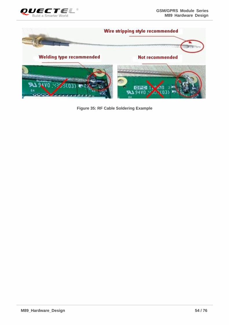
GSM/GPRS Module Series M89 Hardware Design
M89_Hardware_Design 54 / 76
Figure 35: RF Cable Soldering Example
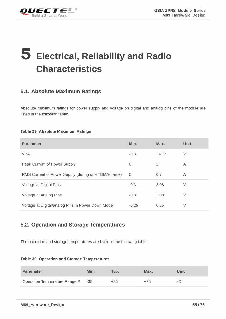
GSM/GPRS Module Series M89 Hardware Design
M89_Hardware_Design 55 / 76
5 Electrical, Reliability and Radio
Characteristics
5.1. Absolute Maximum Ratings
Absolute maximum ratings for power supply and voltage on digital and analog pins of the module are
listed in the following table:
Table 29: Absolute Maximum Ratings
5.2. Operation and Storage Temperatures
The operation and storage temperatures are listed in the following table:
Table 30: Operation and Storage Temperatures
Parameter Min. Max. Unit
VBAT -0.3 +4.73 V
Peak Current of Power Supply 0 2 A
RMS Current of Power Supply (during one TDMA-frame) 0 0.7 A
Voltage at Digital Pins -0.3 3.08 V
Voltage at Analog Pins -0.3 3.08 V
Voltage at Digital/analog Pins in Power Down Mode -0.25 0.25 V
Parameter Min. Typ. Max. Unit
Operation Temperature Range 1) -35 +25 +75 ºC

GSM/GPRS Module Series M89 Hardware Design
M89_Hardware_Design 56 / 76
1. 1) Within operation temperature range, the module is 3GPP compliant.
2. 2) Within extended temperature range, the module remains the ability to establish and maintain a
voice, SMS, data transmission, emergency call, etc. There is no unrecoverable malfunction. There
are also no effects on radio spectrum and no harm to radio network. Only one or more parameters
like Pout might reduce in their value and exceed the specified tolerances. When the temperature
returns to the normal operating temperature levels, the module will meet 3GPP specifications again.
5.3. Power Supply Ratings
Table 31: Module Power Supply Ratings
Extended Temperature Range 2) -40 +85 ºC
Storage Temperature Range -40 +90 ºC
Parameter Description Conditions Min. Typ. Max. Unit
VBAT
Supply voltage
The actual input voltages must
stay between the minimum and
maximum values.
3.3 4.0 4.6 V
Voltage drop
during burst
transmission
Maximum power control level at
GSM850 and EGSM900. 400 mV
IVBAT Average
supply current
Power down mode
Sleep mode @DRX=5
Sleep mode @DRX=9
118
TBD
TBD
uA
mA
mA
AT+CFUN=0
Idle mode
Sleep mode
AT+CFUN=4
Idle mode
Sleep mode
TBD
TBD
TBD
TBD
mA
mA
mA
mA
Talk mode
GSM850/EGSM900 1)
DCS1800/PCS1900 2)
217/233
162/158
mA
mA
Data mode, GPRS (3 Rx, 2 Tx)
GSM850/EGSM900 1)
DCS1800/PCS1900 2)
361/392
254/249
mA
mA
Data mode, GPRS (2 Rx, 3 Tx)
GSM850/EGSM900 1)
419/461
mA
NOTES
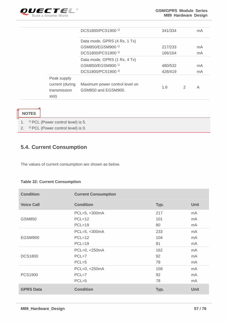
GSM/GPRS Module Series M89 Hardware Design
M89_Hardware_Design 57 / 76
1. 1) PCL (Power control level) is 5.
2. 2) PCL (Power control level) is 0.
5.4. Current Consumption
The values of current consumption are shown as below.
Table 32: Current Consumption
DCS1800/PCS1900 2) 341/334 mA
Data mode, GPRS (4 Rx, 1 Tx)
GSM850/EGSM900 1)
DCS1800/PCS1900 2)
217/233
166/164
mA
mA
Data mode, GPRS (1 Rx, 4 Tx)
GSM850/EGSM900 1)
DCS1800/PCS1900 2)
480/532
428/419
mA
mA
Peak supply
current (during
transmission
slot)
Maximum power control level on
GSM850 and EGSM900. 1.6 2 A
Condition Current Consumption
Voice Call Condition Typ. Unit
GSM850
PCL=5, <300mA
PCL=12
PCL=19
217
101
80
mA
mA
mA
EGSM900
PCL=5, <300mA
PCL=12
PCL=19
233
104
81
mA
mA
mA
DCS1800
PCL=0, <250mA
PCL=7
PCL=5
162
92
78
mA
mA
mA
PCS1900
PCL=0, <250mA
PCL=7
PCL=5
158
92
78
mA
mA
mA
GPRS Data Condition Typ. Unit
NOTES

GSM/GPRS Module Series M89 Hardware Design
M89_Hardware_Design 58 / 76
GPRS Class 12 is the default setting. The module can be configured from GPRS Class 1 to Class 12.
Setting to lower GPRS class would make it easier to design the power supply of the module.
Data Mode, GPRS (3 Rx, 2 Tx) Class 12
GSM850 PCL=5, <550mA 361 mA
EGSM900 PCL=5, <550mA 392 mA
DCS1800 PCL=0, <450mA 254 mA
PCS1900 PCL=0, <450mA 249 mA
Data Mode, GPRS (2 Rx, 3 Tx) Class 12
GSM850 PCL=5, <640mA 419 mA
EGSM900 PCL=5, <600mA 461 mA
DCS1800 PCL=0, <490mA 341 mA
PCS1900 PCL=0, <480mA 334 mA
Data Mode, GPRS (4 Rx, 1 Tx) Class 12
GSM850 PCL=5, <350mA 217 mA
EGSM900 PCL=5, <350mA 233 mA
DCS1800 PCL=0, <300mA 166 mA
PCS1900 PCL=0, <300mA 164 mA
Data Mode, GPRS (1 Rx, 4 Tx) Class 12
GSM850 PCL=5, <660mA 480 mA
EGSM900 PCL=5, <660mA 532 mA
DCS1800 PCL=0, <530mA 428 mA
PCS1900 PCL=0, <530mA 419 mA
NOTE
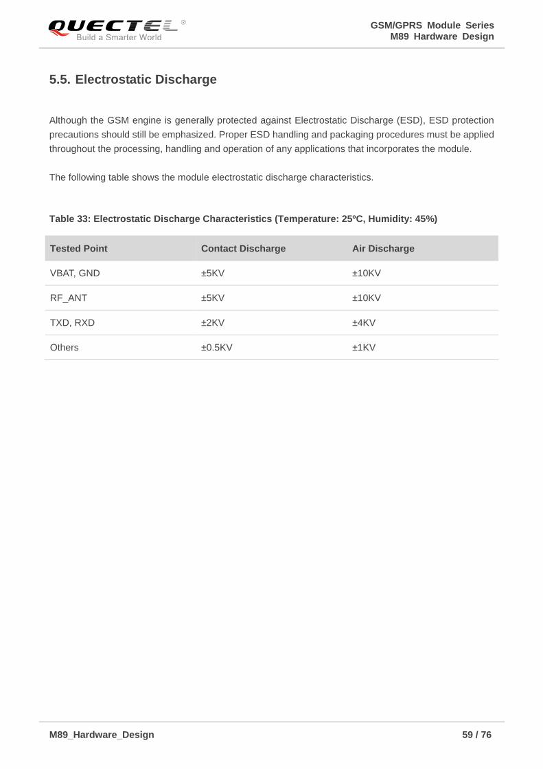
GSM/GPRS Module Series M89 Hardware Design
M89_Hardware_Design 59 / 76
5.5. Electrostatic Discharge
Although the GSM engine is generally protected against Electrostatic Discharge (ESD), ESD protection
precautions should still be emphasized. Proper ESD handling and packaging procedures must be applied
throughout the processing, handling and operation of any applications that incorporates the module.
The following table shows the module electrostatic discharge characteristics.
Table 33: Electrostatic Discharge Characteristics (Temperature: 25ºC, Humidity: 45%)
Tested Point Contact Discharge Air Discharge
VBAT, GND ±5KV ±10KV
RF_ANT ±5KV ±10KV
TXD, RXD ±2KV ±4KV
Others ±0.5KV ±1KV
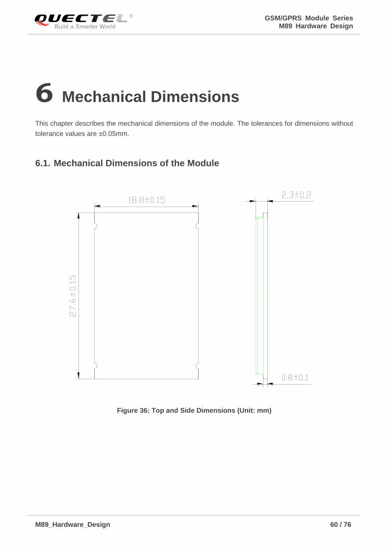
GSM/GPRS Module Series M89 Hardware Design
M89_Hardware_Design 60 / 76
6 Mechanical Dimensions
This chapter describes the mechanical dimensions of the module. The tolerances for dimensions without
tolerance values are ±0.05mm.
6.1. Mechanical Dimensions of the Module
Figure 36: Top and Side Dimensions (Unit: mm)

GSM/GPRS Module Series M89 Hardware Design
M89_Hardware_Design 61 / 76
Figure 37: Bottom Dimensions (Unit: mm)
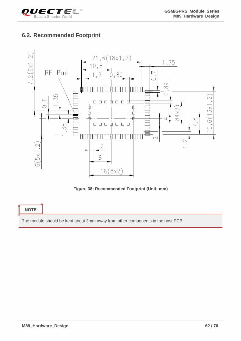
GSM/GPRS Module Series M89 Hardware Design
M89_Hardware_Design 62 / 76
6.2. Recommended Footprint
Figure 38: Recommended Footprint (Unit: mm)
The module should be kept about 3mm away from other components in the host PCB.
NOTE
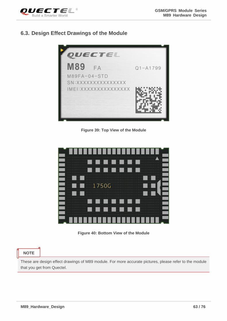
GSM/GPRS Module Series M89 Hardware Design
M89_Hardware_Design 63 / 76
6.3. Design Effect Drawings of the Module
Figure 39: Top View of the Module
Figure 40: Bottom View of the Module
These are design effect drawings of M89 module. For more accurate pictures, please refer to the module
that you get from Quectel.
NOTE

GSM/GPRS Module Series M89 Hardware Design
M89_Hardware_Design 64 / 76
7 Storage, Manufacturing and
Packaging
7.1. Storage
M89 module is stored in a vacuum-sealed bag. It is rated at MSL 3, and its storage restrictions are listed
below.
1. Shelf life in the vacuum-sealed bag: 12 months at < 40ºC/90%RH.
2. After the vacuum-sealed bag is opened, devices that will be subjected to reflow soldering or other
high temperature processes must be:
Mounted within 168 hours at the factory environment of ≤ 30ºC/60%RH.
Stored at <10% RH.
3. Devices require baking before mounting, if any circumstance below occurs:
When the ambient temperature is 23ºC±5ºC and the humidity indicator card shows the humidity
is >10% before opening the vacuum-sealed bag.
Device mounting cannot be finished within 168 hours at factory conditions of ≤30ºC/60% RH.
4. If baking is required, devices may be baked for 8 hours at 120ºC±5ºC.
As the plastic package cannot be subjected to high temperature, it should be removed from devices
before high temperature (120ºC) baking. If shorter baking time is desired, please refer to
IPC/JEDECJ-STD-033 for baking procedure.
NOTE
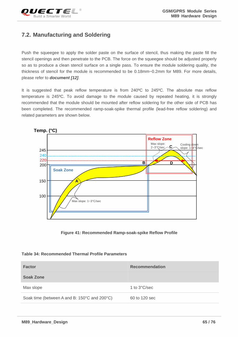
GSM/GPRS Module Series M89 Hardware Design
M89_Hardware_Design 65 / 76
7.2. Manufacturing and Soldering
Push the squeegee to apply the solder paste on the surface of stencil, thus making the paste fill the
stencil openings and then penetrate to the PCB. The force on the squeegee should be adjusted properly
so as to produce a clean stencil surface on a single pass. To ensure the module soldering quality, the
thickness of stencil for the module is recommended to be 0.18mm~0.2mm for M89. For more details,
please refer to document [12].
It is suggested that peak reflow temperature is from 240ºC to 245ºC. The absolute max reflow
temperature is 245ºC. To avoid damage to the module caused by repeated heating, it is strongly
recommended that the module should be mounted after reflow soldering for the other side of PCB has
been completed. The recommended ramp-soak-spike thermal profile (lead-free reflow soldering) and
related parameters are shown below.
Temp. (°C)
Reflow Zone
Soak Zone
245
200
220
240
C
DB
A150
100
Max slope: 1~3°C/sec
Cooling down slope: 1~4°C/sec
Max slope:
2~3°C/sec
Figure 41: Recommended Ramp-soak-spike Reflow Profile
Table 34: Recommended Thermal Profile Parameters
Factor Recommendation
Soak Zone
Max slope 1 to 3°C/sec
Soak time (between A and B: 150°C and 200°C) 60 to 120 sec

GSM/GPRS Module Series M89 Hardware Design
M89_Hardware_Design 66 / 76
1. During manufacturing and soldering, or any other processes that may contact the module directly,
NEVER wipe the module’s shielding can with organic solvents, such as acetone, ethyl alcohol,
isopropyl alcohol, trichloroethylene, etc. Otherwise, the shielding can may become rusted.
2. The shielding can for the module is made of Cupro-Nickel base material. It is tested that after 12
hours’ Neutral Salt Spray test, the laser engraved label information on the shielding can is still clearly
identifiable and the QR code is still readable, although white rust may be found.
7.3. Packaging
M89 module is packaged in tape and reel carriers. One reel is 11.8m long and contains 250 modules.
The following figures show the packaging details, measured in mm.
Reflow Zone
Max slope 2 to 3°C/sec
Reflow time (D: over 220°C) 40 to 60 sec
Max temperature 240°C~245°C
Cooling down slope 1 to 4°C/sec
Reflow Cycle
Max reflow cycle 1
NOTES
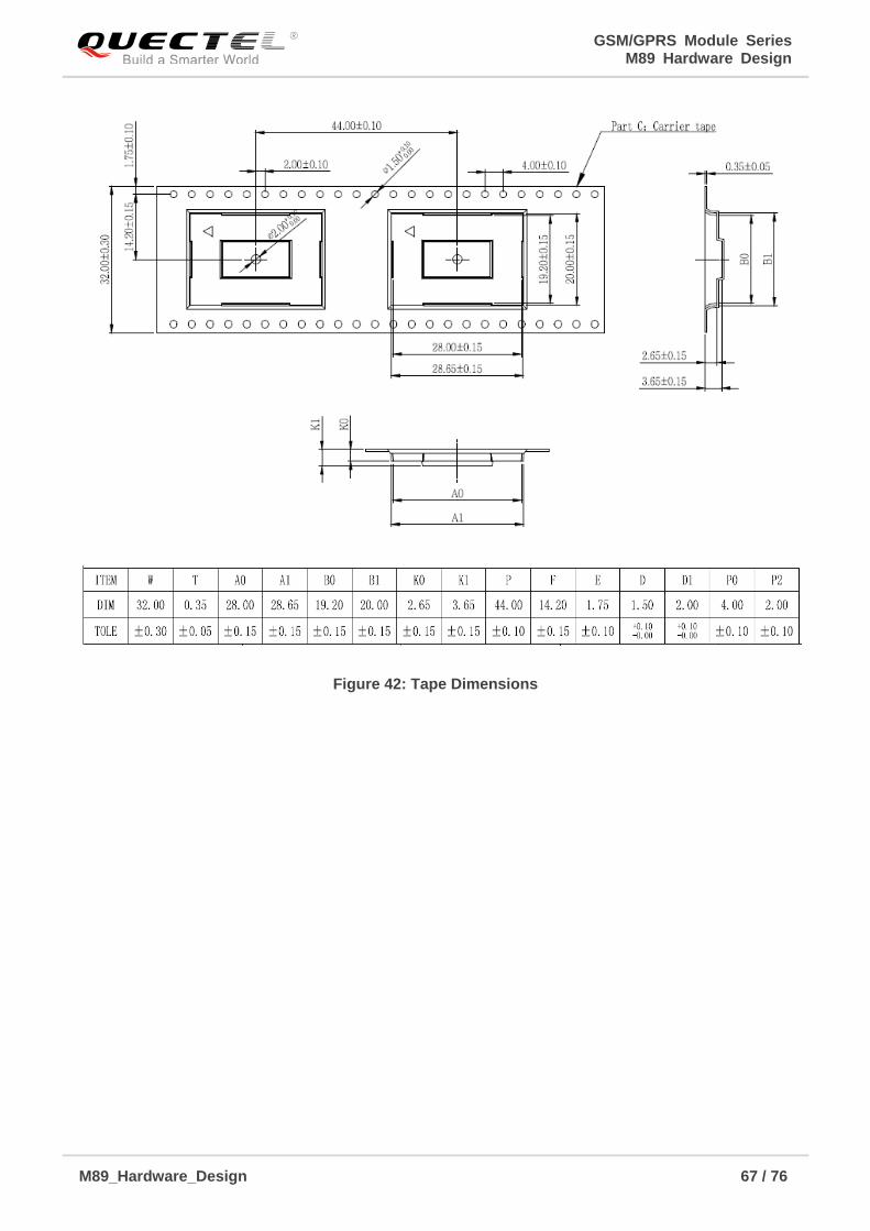
GSM/GPRS Module Series M89 Hardware Design
M89_Hardware_Design 67 / 76
Figure 42: Tape Dimensions

GSM/GPRS Module Series M89 Hardware Design
M89_Hardware_Design 68 / 76
Figure 43: Reel Dimensions
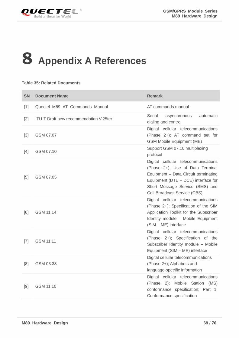
GSM/GPRS Module Series M89 Hardware Design
M89_Hardware_Design 69 / 76
8 Appendix A References
Table 35: Related Documents
SN Document Name Remark
[1] Quectel_M89_AT_Commands_Manual AT commands manual
[2] ITU-T Draft new recommendation V.25ter Serial asynchronous automatic
dialing and control
[3] GSM 07.07
Digital cellular telecommunications
(Phase 2+); AT command set for
GSM Mobile Equipment (ME)
[4] GSM 07.10 Support GSM 07.10 multiplexing
protocol
[5] GSM 07.05
Digital cellular telecommunications
(Phase 2+); Use of Data Terminal
Equipment – Data Circuit terminating
Equipment (DTE – DCE) interface for
Short Message Service (SMS) and
Cell Broadcast Service (CBS)
[6] GSM 11.14
Digital cellular telecommunications
(Phase 2+); Specification of the SIM
Application Toolkit for the Subscriber
Identity module – Mobile Equipment
(SIM – ME) interface
[7] GSM 11.11
Digital cellular telecommunications
(Phase 2+); Specification of the
Subscriber Identity module – Mobile
Equipment (SIM – ME) interface
[8] GSM 03.38
Digital cellular telecommunications
(Phase 2+); Alphabets and
language-specific information
[9] GSM 11.10
Digital cellular telecommunications
(Phase 2); Mobile Station (MS)
conformance specification; Part 1:
Conformance specification
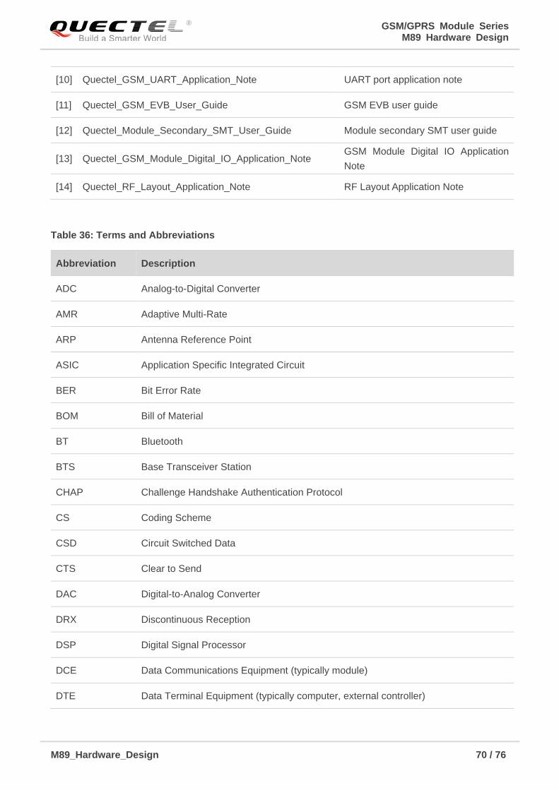
GSM/GPRS Module Series M89 Hardware Design
M89_Hardware_Design 70 / 76
Table 36: Terms and Abbreviations
[10] Quectel_GSM_UART_Application_Note UART port application note
[11] Quectel_GSM_EVB_User_Guide GSM EVB user guide
[12] Quectel_Module_Secondary_SMT_User_Guide Module secondary SMT user guide
[13] Quectel_GSM_Module_Digital_IO_Application_Note GSM Module Digital IO Application
Note
[14] Quectel_RF_Layout_Application_Note RF Layout Application Note
Abbreviation Description
ADC Analog-to-Digital Converter
AMR Adaptive Multi-Rate
ARP Antenna Reference Point
ASIC Application Specific Integrated Circuit
BER Bit Error Rate
BOM Bill of Material
BT Bluetooth
BTS Base Transceiver Station
CHAP Challenge Handshake Authentication Protocol
CS Coding Scheme
CSD Circuit Switched Data
CTS Clear to Send
DAC Digital-to-Analog Converter
DRX Discontinuous Reception
DSP Digital Signal Processor
DCE Data Communications Equipment (typically module)
DTE Data Terminal Equipment (typically computer, external controller)

GSM/GPRS Module Series M89 Hardware Design
M89_Hardware_Design 71 / 76
DTR Data Terminal Ready
DTX Discontinuous Transmission
EFR Enhanced Full Rate
EGSM Enhanced GSM
EMC Electromagnetic Compatibility
ESD Electrostatic Discharge
ETS European Telecommunication Standard
FCC Federal Communications Commission (U.S.)
FDMA Frequency Division Multiple Access
FR Full Rate
GMSK Gaussian Minimum Shift Keying
GPRS General Packet Radio Service
GSM Global System for Mobile Communications
HR Half Rate
I/O Input/Output
IC Integrated Circuit
IMEI International Mobile Equipment Identity
IOmax Maximum Output Load Current
kbps Kilo Bits Per Second
LED Light Emitting Diode
Li-Ion Lithium-Ion
MO Mobile Originated
MOQ Minimum Order Quantity
MP Manufacture Product
MS Mobile Station (GSM engine)

GSM/GPRS Module Series M89 Hardware Design
M89_Hardware_Design 72 / 76
MT Mobile Terminated
PAP Password Authentication Protocol
PBCCH Packet Switched Broadcast Control Channel
PCB Printed Circuit Board
PDU Protocol Data Unit
PPP Point-to-Point Protocol
RF Radio Frequency
RMS Root Mean Square (value)
RTC Real Time Clock
RX Receive Direction
(U)SIM (Universal) Subscriber Identification Module
SMS Short Message Service
TDMA Time Division Multiple Access
TE Terminal Equipment
TX Transmitting Direction
UART Universal Asynchronous Receiver & Transmitter
URC Unsolicited Result Code
USSD Unstructured Supplementary Service Data
VSWR Voltage Standing Wave Ratio
VOmax Maximum Output Voltage Value
VOnorm Normal Output Voltage Value
VOmin Minimum Output Voltage Value
VIHmax Maximum Input High Level Voltage Value
VIHmin Minimum Input High Level Voltage Value
VILmax Maximum Input Low Level Voltage Value
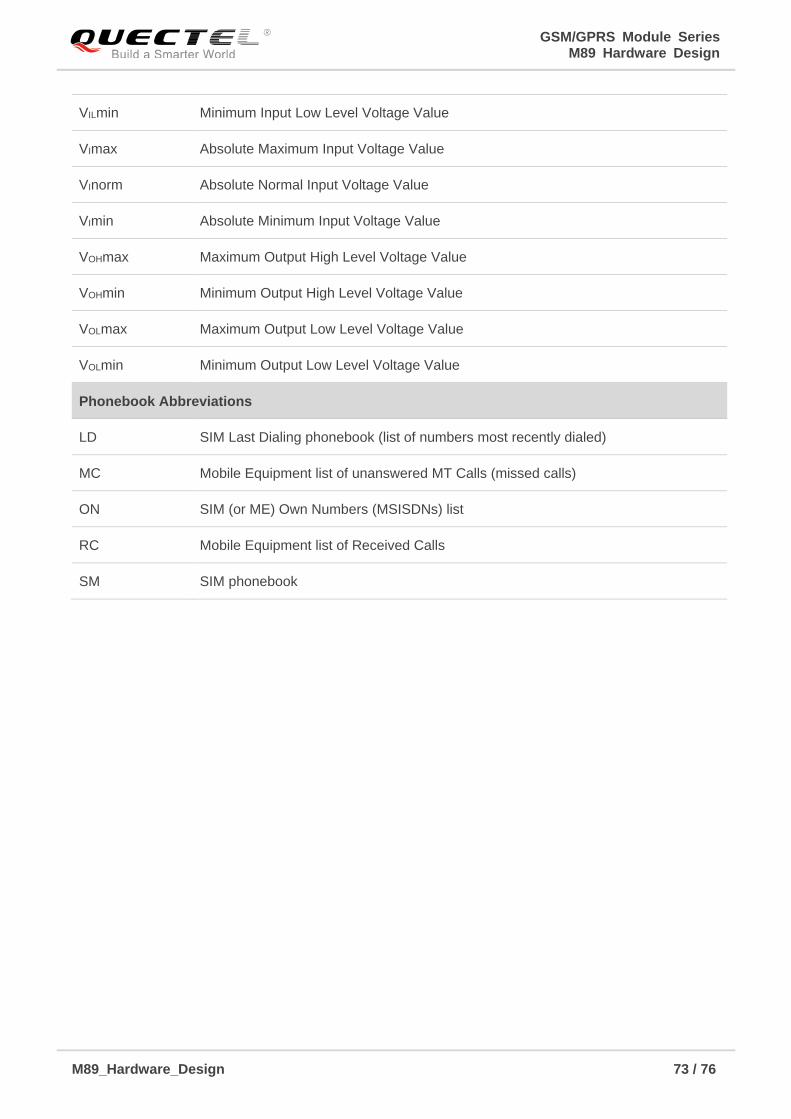
GSM/GPRS Module Series M89 Hardware Design
M89_Hardware_Design 73 / 76
VILmin Minimum Input Low Level Voltage Value
VImax Absolute Maximum Input Voltage Value
VInorm Absolute Normal Input Voltage Value
VImin Absolute Minimum Input Voltage Value
VOHmax Maximum Output High Level Voltage Value
VOHmin Minimum Output High Level Voltage Value
VOLmax Maximum Output Low Level Voltage Value
VOLmin Minimum Output Low Level Voltage Value
Phonebook Abbreviations
LD SIM Last Dialing phonebook (list of numbers most recently dialed)
MC Mobile Equipment list of unanswered MT Calls (missed calls)
ON SIM (or ME) Own Numbers (MSISDNs) list
RC Mobile Equipment list of Received Calls
SM SIM phonebook
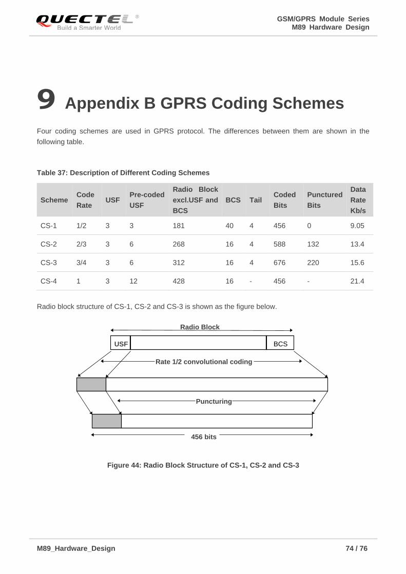
GSM/GPRS Module Series M89 Hardware Design
M89_Hardware_Design 74 / 76
9 Appendix B GPRS Coding Schemes
Four coding schemes are used in GPRS protocol. The differences between them are shown in the
following table.
Table 37: Description of Different Coding Schemes
Scheme Code
Rate USF
Pre-coded
USF
Radio Block
excl.USF and
BCS
BCS Tail Coded
Bits
Punctured
Bits
Data
Rate
Kb/s
CS-1 1/2 3 3 181 40 4 456 0 9.05
CS-2 2/3 3 6 268 16 4 588 132 13.4
CS-3 3/4 3 6 312 16 4 676 220 15.6
CS-4 1 3 12 428 16 - 456 - 21.4
Radio block structure of CS-1, CS-2 and CS-3 is shown as the figure below.
Figure 44: Radio Block Structure of CS-1, CS-2 and CS-3
Rate 1/2 convolutional coding
Puncturing
456 bits
USF BCS
Radio Block
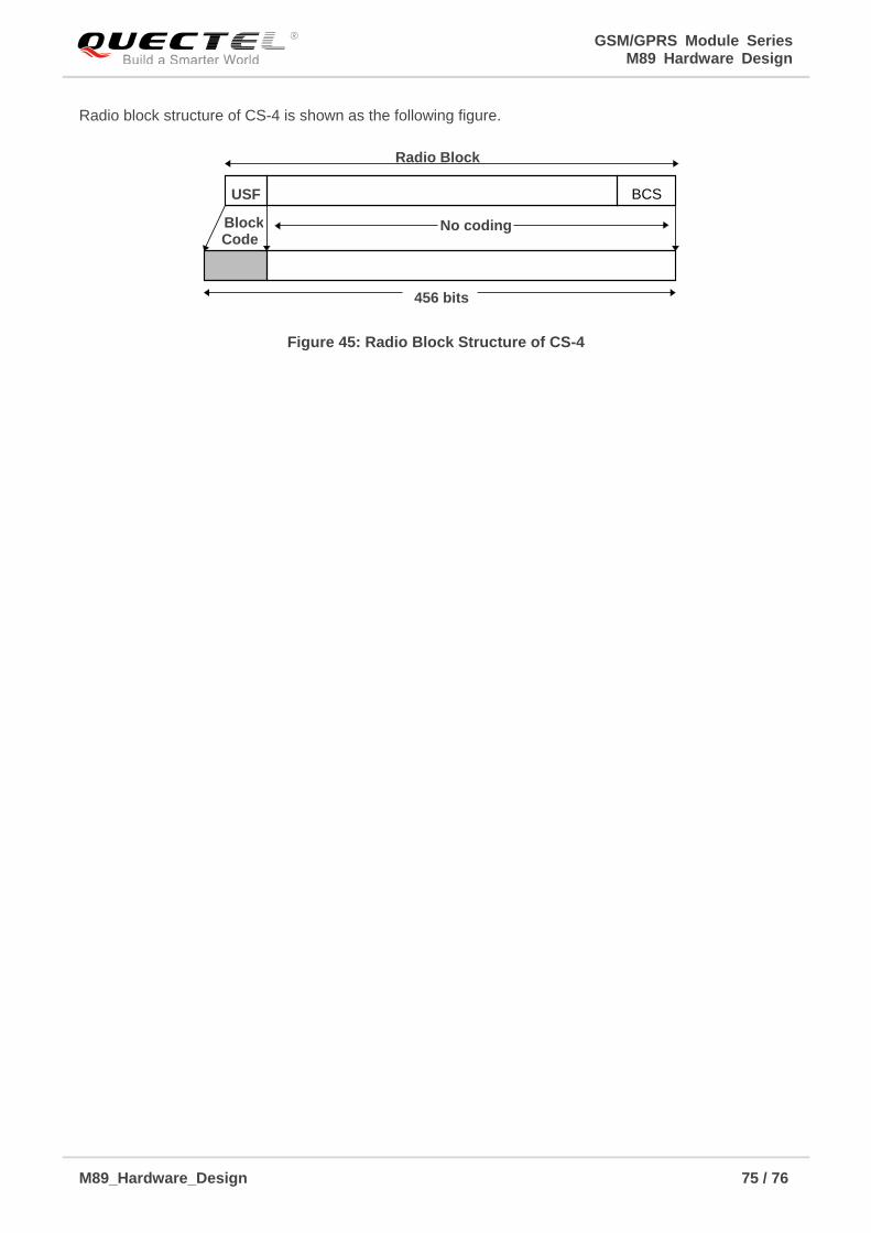
GSM/GPRS Module Series M89 Hardware Design
M89_Hardware_Design 75 / 76
Radio block structure of CS-4 is shown as the following figure.
Figure 45: Radio Block Structure of CS-4
Block Code
No coding
456 bits
USF BCS
Radio Block
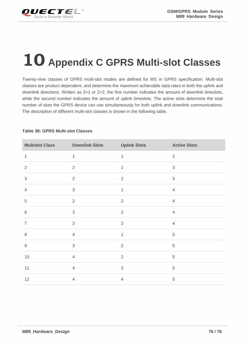
GSM/GPRS Module Series M89 Hardware Design
M89_Hardware_Design 76 / 76
10 Appendix C GPRS Multi-slot Classes
Twenty-nine classes of GPRS multi-slot modes are defined for MS in GPRS specification. Multi-slot
classes are product dependent, and determine the maximum achievable data rates in both the uplink and
downlink directions. Written as 3+1 or 2+2, the first number indicates the amount of downlink timeslots,
while the second number indicates the amount of uplink timeslots. The active slots determine the total
number of slots the GPRS device can use simultaneously for both uplink and downlink communications.
The description of different multi-slot classes is shown in the following table.
Table 38: GPRS Multi-slot Classes
Multislot Class Downlink Slots Uplink Slots Active Slots
1 1 1 2
2 2 1 3
3 2 2 3
4 3 1 4
5 2 2 4
6 3 2 4
7 3 3 4
8 4 1 5
9 3 2 5
10 4 2 5
11 4 3 5
12 4 4 5