QCPU User's Manual (Hardware Design, Maintenance and ...
734
QCPU User's Manual (Hardware Design, Maintenance and Inspection) -Q00(J)CPU -Q13UDVCPU -Q01CPU -Q13UDPVCPU -Q02(H)CPU -Q20UD(E)HCPU -Q06HCPU -Q26UD(E)HCPU -Q12HCPU -Q26UDVCPU -Q25HCPU -Q26UDPVCPU -Q02PHCPU -Q50UDEHCPU -Q06PHCPU -Q100UDEHCPU -Q12PHCPU -Q25PHCPU -Q12PRHCPU -Q25PRHCPU -Q00U(J)CPU -Q01UCPU -Q02UCPU -Q03UD(E)CPU -Q03UDVCPU -Q04UD(E)HCPU -Q04UDVCPU -Q04UDPVCPU -Q06UD(E)HCPU -Q06UDVCPU -Q06UDPVCPU -Q10UD(E)HCPU -Q13UD(E)HCPU
-
Upload
khangminh22 -
Category
Documents
-
view
1 -
download
0
Transcript of QCPU User's Manual (Hardware Design, Maintenance and ...

QCPU User's Manual(Hardware Design, Maintenance and Inspection)
-Q00(J)CPU -Q13UDVCPU-Q01CPU -Q13UDPVCPU-Q02(H)CPU -Q20UD(E)HCPU-Q06HCPU -Q26UD(E)HCPU-Q12HCPU -Q26UDVCPU-Q25HCPU -Q26UDPVCPU-Q02PHCPU -Q50UDEHCPU-Q06PHCPU -Q100UDEHCPU-Q12PHCPU-Q25PHCPU-Q12PRHCPU-Q25PRHCPU-Q00U(J)CPU-Q01UCPU-Q02UCPU-Q03UD(E)CPU-Q03UDVCPU-Q04UD(E)HCPU-Q04UDVCPU-Q04UDPVCPU-Q06UD(E)HCPU-Q06UDVCPU-Q06UDPVCPU-Q10UD(E)HCPU-Q13UD(E)HCPU


SAFETY PRECAUTIONS(Read these precautions before using this product.)
Before using this product, please read this manual and the relevant manuals carefully and pay full attention to safety to handle the product correctly.
In this manual, the safety precautions are classified into two levels: " WARNING" and " CAUTION".
Under some circumstances, failure to observe the precautions given under " CAUTION" may lead to serious consequences.Observe the precautions of both levels because they are important for personal and system safety.Make sure that the end users read this manual and then keep the manual in a safe place for future reference.
[Design Precautions]
WARNING● Configure safety circuits external to the programmable controller to ensure that the entire system
operates safely even when a fault occurs in the external power supply or the programmable controller. Failure to do so may result in an accident due to an incorrect output or malfunction.(1) Configure external safety circuits, such as an emergency stop circuit, protection circuit, and
protective interlock circuit for forward/reverse operation or upper/lower limit positioning.(2) The programmable controller stops its operation upon detection of the following status, and the
output status of the system will be as shown below.
All outputs may turn on when an error occurs in the part, such as I/O control part, where the CPU module cannot detect any error. To ensure safety operation in such a case, provide a safety mechanism or a fail-safe circuit external to the programmable controller. For a fail-safe circuit example, refer to Page 682, Appendix 9.
(3) Outputs may remain on or off due to a failure of an output module relay or transistor. Configure an external circuit for monitoring output signals that could cause a serious accident.
WARNING
CAUTION
Indicates that incorrect handling may cause hazardous conditions,resulting in death or severe injury.
Indicates that incorrect handling may cause hazardous conditions, resulting in minor or moderate injury or property damage.
Overcurrent or overvoltage protection ofthe power supply module is activated.
The CPU module detects an error such as awatchdog timer error by the self-diagnostic function.
All outputs are turned off All outputs are turned off
All outputs are turned offAll outputs are held or turned offaccording to the parameter setting.
Q series module AnS/A series module
1

[Design Precautions]
[Design Precautions]
[Security Precautions]
WARNING● In an output module, when a load current exceeding the rated current or an overcurrent caused by a
load short-circuit flows for a long time, it may cause smoke and fire. To prevent this, configure an external safety circuit, such as a fuse.
● Configure a circuit so that the programmable controller is turned on first and then the external power supply. If the external power supply is turned on first, an accident may occur due to an incorrect output or malfunction.
● For the operating status of each station after a communication failure, refer to relevant manuals for the network. Incorrect output or malfunction due to a communication failure may result in an accident.
● When changing data of the running programmable controller from a peripheral connected to the CPU module or from a personal computer connected to an intelligent function module, configure an interlock circuit in the sequence program to ensure that the entire system will always operate safely.For program modification and operating status change, read relevant manuals carefully and ensure the safety before operation. Especially, in the case of a control from an external device to a remote programmable controller, immediate action cannot be taken for a problem on the programmable controller due to a communication failure. To prevent this, configure an interlock circuit in the sequence program, and determine corrective actions to be taken between the external device and CPU module in case of a communication failure.
CAUTION● Do not install the control lines or communication cables together with the main circuit lines or power
cables. Keep a distance of 100mm or more between them. Failure to do so may result in malfunction due to noise.
● When a device such as a lamp, heater, or solenoid valve is controlled through an output module, a large current (approximately ten times greater than normal) may flow when the output is turned from off to on. Take measures such as replacing the module with one having a sufficient current rating.
● After the CPU module is powered on or is reset, the time taken to enter the RUN status varies depending on the system configuration, parameter settings, and/or program size. Design circuits so that the entire system will always operate safely, regardless of the time.
WARNING● To maintain the security (confidentiality, integrity, and availability) of the programmable controller and
the system against unauthorized access, denial-of-service (DoS) attacks, computer viruses, and other cyberattacks from external devices via the network, take appropriate measures such as firewalls, virtual private networks (VPNs), and antivirus solutions.
2

[Installation Precautions]
[Wiring Precautions]
CAUTION● Use the programmable controller in an environment that meets the general specifications in this
manual. Failure to do so may result in electric shock, fire, malfunction, or damage to or deterioration of the product.
● To mount the module, while pressing the module mounting lever in the lower part of the module, fully insert the module fixing projection(s) into the hole(s) in the base unit and press the module until it snaps into place. Incorrect mounting may cause malfunction, failure, or drop of the module. When using the programmable controller in an environment of frequent vibrations, fix the module with a screw. Tighten the screw within the specified torque range. Undertightening can cause drop of the screw, short circuit or malfunction. Overtightening can damage the screw and/or module, resulting in drop, short circuit, or malfunction.
● When using an extension cable, connect it to the extension cable connector of the base unit securely. Check the connection for looseness. Poor contact may cause incorrect input or output.
● When using a memory card, fully insert it into the memory card slot. Check that it is inserted completely. Poor contact may cause malfunction.
● When using an SD memory card, fully insert it into the SD memory card slot. Check that it is inserted completely. Poor contact may cause malfunction.
● When using an extended SRAM cassette, fully insert it into the connector for cassette connection of the CPU module. Close the cassette cover after inserting to avoid looseness of the extended SRAM cassette. Poor contact may cause malfunction.
● Shut off the external power supply (all phases) used in the system before mounting or removing the module. Failure to do so may result in damage to the product. A module can be replaced online (while power is on) on any MELSECNET/H remote I/O station or in the system where a CPU module supporting the online module change function is used. Note that there are restrictions on the modules that can be replaced online, and each module has its predetermined replacement procedure. For details, refer to this manual and in the manual for the corresponding module.
● Do not directly touch any conductive part of the module, the memory card, the SD memory card, or the extended SRAM cassette. Doing so can cause malfunction or failure of the module.
● When using a Motion CPU module and modules designed for motion control, check that the combinations of these modules are correct before applying power. The modules may be damaged if the combination is incorrect. For details, refer to the user's manual for the Motion CPU module.
WARNING● Shut off the external power supply (all phases) used in the system before wiring. Failure to do so may
result in electric shock or damage to the product.● After installation and wiring, attach the included terminal cover to the module before turning it on for
operation. Failure to do so may result in electric shock.
3

[Wiring Precautions]
CAUTION● Individually ground the FG and LG terminals of the programmable controller with a ground resistance
of 100 or less. Failure to do so may result in electric shock or malfunction.● Use applicable solderless terminals and tighten them within the specified torque range. If any spade
solderless terminal is used, it may be disconnected when the terminal screw comes loose, resulting in failure.
● Check the rated voltage and terminal layout before wiring to the module, and connect the cables correctly. Connecting a power supply with a different voltage rating or incorrect wiring may cause a fire or failure.
● Connectors for external connection must be crimped or pressed with the tool specified by the manufacturer, or must be correctly soldered. Incomplete connections could result in short circuit, fire, or malfunction.
● Install the connector to the module securely. Poor contact may cause malfunction.● Do not install the control lines or communication cables together with the main circuit lines or power
cables. Keep a distance of 100mm or more between them. Failure to do so may result in malfunction due to noise.
● Place the wires or cables in a duct or clamp them. If not, dangling cable may swing or inadvertently be pulled, resulting in damage to the module or cables or malfunction due to poor connection.
● Connect the cable correctly after confirming the interface type to be connected. Connecting to the wrong interface or incorrect wiring can result in a failure of the module or external devices.
● Tighten the terminal screw within the specified torque range. Undertightening can cause short circuit, fire, or malfunction. Overtightening can damage the screw and/or module, resulting in drop, short circuit, or malfunction.
● Prevent foreign matter such as dust or wire chips from entering the module. Such foreign matter can cause a fire, failure, or malfunction.
● A protective film is attached to the top of the module to prevent foreign matter, such as wire chips, from entering the module during wiring. Do not remove the film during wiring. Remove it for heat dissipation before system operation.
● Do not pull the cable section of a cable for disconnection. When disconnecting a cable with a connector, hold the connector and pull it. When disconnecting a cable on a terminal block, loosen the terminal screw before disconnection. Pulling the connected cable can result in malfunction or damage of the module or the cable.
● Mitsubishi Electric programmable controllers must be installed in control panels. Connect the main power supply to the power supply module in the control panel through a relay terminal block. Wiring and replacement of a power supply module must be performed by maintenance personnel who is familiar with protection against electric shock. (For wiring methods, refer to Page 105, Section 4.8.1.)
4

[Startup and Maintenance Precautions]
[Startup and Maintenance Precautions]
WARNING● Do not touch any terminal while power is on. Doing so will cause electric shock.● Correctly connect the battery connector. Do not charge, disassemble, heat, short-circuit, solder, or
throw the battery into the fire, or apply liquid or a strong shock to the battery. Doing so will cause the battery to produce heat, explode, ignite, or liquid spill, resulting in injury and fire.
● Shut off the external power supply (all phases) used in the system before cleaning the module or retightening the terminal screws, connector screws, or module fixing screws. Failure to do so may result in electric shock or cause the module to fail or malfunction.
CAUTION● Before performing online operations (especially, program modification, forced output, and operation
status change) for the running CPU module from the peripheral connected, read relevant manuals carefully and ensure the safety. Improper operation may damage machines or cause accidents.
● Do not disassemble or modify the modules. Doing so may cause failure, malfunction, injury, or a fire.● Use any radio communication device such as a cellular phone or PHS (Personal Handy-phone
System) more than 25cm away in all directions from the programmable controller. Failure to do so may cause malfunction.
● Shut off the external power supply (all phases) used in the system before mounting or removing the module. Failure to do so may cause the module to fail or malfunction. A module can be replaced online (while power is on) on any MELSECNET/H remote I/O station or in the system where a CPU module supporting the online module change function is used. Note that there are restrictions on the modules that can be replaced online, and each module has its predetermined replacement procedure. For details, refer to this manual and the manual for the corresponding module.
● After the first use of the product, do not perform each of the following operations more than 50 times (IEC 61131-2/JIS B 3502 compliant). Exceeding the limit may cause malfunction.
• Mounting/removing the module to/from the base unit • Inserting/removing the extended SRAM cassette to/from the CPU module • Mounting/removing the terminal block to/from the module
● After the first use of the product, do not mount/remove the SD memory card more than 500 times. Exceeding the limit of 500 times may cause malfunction.
● Do not drop or apply shock to the battery to be installed in the module. Doing so may damage the battery, causing the battery fluid to leak inside the battery. If the battery is dropped or any shock is applied to it, dispose of it without using.
● Before handling the module, touch a grounded metal object to discharge the static electricity from the human body. Failure to do so may cause the module to fail or malfunction.
5

[Computer Connection Precautions]
[Disposal Precautions]
[Transportation Precautions]
CAUTION● When connecting a personal computer to a CPU module having an RS-232 or a USB interface,
observe the following precautions as well as the instructions described in the manual for the personal computer used. Failure to do so may cause the CPU module to fail.(1) When the personal computer is AC-powered
When the personal computer has a 3-pin AC plug or an AC plug with a grounding wire, connect the plug to a grounding receptacle or ground the grounding wire. Ground the personal computer and the CPU module with a ground resistance of 100 ohms or less.When the personal computer has a 2-pin AC plug without a ground wire, connect the computer to the CPU module by following the procedure below. For power supplied to the personal computer and the CPU module, using the same power source is recommended.1.Unplug the personal computer from the AC receptacle.2.Check that the personal computer is unplugged. Then, connect the personal computer to the CPU module with an RS-232 or a USB cable.3.Plug the personal computer into the AC receptacle.
(2) When the personal computer is battery-poweredThe personal computer can be connected to the CPU module without taking specific measures.
For details, refer to the following.Cautions When Using Mitsubishi Programmable Controllers or GOTs Connected to a Personal Computer With the RS-232/USB Interface (FA-A-0298)When the USB cable used is the GT09-C30USB-5P manufactured by Mitsubishi Electric, specific measures are not required to connect the AC-powered personal computer to the CPU module. However, note that the signal ground (SG) is common for the CPU module and its RS-232 or USB interface. Therefore, if an SG potential difference occurs between the CPU module and the connected devices, it causes failures of the CPU module and the connected devices.
CAUTION● When disposing of this product, treat it as industrial waste. When disposing of batteries, separate
them from other wastes according to the local regulations. (For details of the Battery Directive in EU countries, refer to Page 690, Appendix 12.)
CAUTION● When transporting lithium batteries, follow the transportation regulations. (For details of the regulated
models, refer to Page 689, Appendix 11.)
6

CONDITIONS OF USE FOR THE PRODUCT(1) MELSEC programmable controller ("the PRODUCT") shall be used in conditions;
i) where any problem, fault or failure occurring in the PRODUCT, if any, shall not lead to any major or serious accident; and ii) where the backup and fail-safe function are systematically or automatically provided outside of the PRODUCT for the case of any problem, fault or failure occurring in the PRODUCT.
(2) The PRODUCT has been designed and manufactured for the purpose of being used in general industries.MITSUBISHI ELECTRIC SHALL HAVE NO RESPONSIBILITY OR LIABILITY (INCLUDING, BUT NOT LIMITED TO ANY AND ALL RESPONSIBILITY OR LIABILITY BASED ON CONTRACT, WARRANTY, TORT, PRODUCT LIABILITY) FOR ANY INJURY OR DEATH TO PERSONS OR LOSS OR DAMAGE TO PROPERTY CAUSED BY the PRODUCT THAT ARE OPERATED OR USED IN APPLICATION NOT INTENDED OR EXCLUDED BY INSTRUCTIONS, PRECAUTIONS, OR WARNING CONTAINED IN MITSUBISHI ELECTRIC USER'S, INSTRUCTION AND/OR SAFETY MANUALS, TECHNICAL BULLETINS AND GUIDELINES FOR the PRODUCT. ("Prohibited Application")Prohibited Applications include, but not limited to, the use of the PRODUCT in;• Nuclear Power Plants and any other power plants operated by Power companies, and/or any other cases in which the
public could be affected if any problem or fault occurs in the PRODUCT.• Railway companies or Public service purposes, and/or any other cases in which establishment of a special quality
assurance system is required by the Purchaser or End User.• Aircraft or Aerospace, Medical applications, Train equipment, transport equipment such as Elevator and Escalator,
Incineration and Fuel devices, Vehicles, Manned transportation, Equipment for Recreation and Amusement, and Safety devices, handling of Nuclear or Hazardous Materials or Chemicals, Mining and Drilling, and/or other applications where there is a significant risk of injury to the public or property.
Notwithstanding the above restrictions, Mitsubishi Electric may in its sole discretion, authorize use of the PRODUCT in one or more of the Prohibited Applications, provided that the usage of the PRODUCT is limited only for the specific applications agreed to by Mitsubishi Electric and provided further that no special quality assurance or fail-safe, redundant or other safety features which exceed the general specifications of the PRODUCTs are required. For details, please contact the Mitsubishi Electric representative in your region.
(3) Mitsubishi Electric shall have no responsibility or liability for any problems involving programmable controller trouble and system trouble caused by DoS attacks, unauthorized access, computer viruses, and other cyberattacks.
7

INTRODUCTIONThis manual provides hardware specifications, maintenance and inspection of the system, and troubleshooting of the CPU modules, power supply modules, and base units required for operating the Q series programmable controllers.
Before using this product, please read this manual and the relevant manuals carefully and develop familiarity with the functions and performance of the Q series programmable controller to handle the product correctly.When applying the program examples introduced in this manual to the actual system, ensure the applicability and confirm that it will not cause system control problems.
Relevant CPU module
Precautions when using the Q series CPU module for the first time
Memory must be formatted using a programming tool before first use of the CPU module.For details of memory formatting, refer to the following.
Operating manual for the programming tool used
Precautions for batteries(1) When resuming operation with the CPU module which has been stored without battery:
The CPU module memory must be formatted using a programming tool. ( Page 271, Section 13.4)
RemarkThis manual does not describe the functions of the CPU module.For the functions, refer to the following.
Manuals for the CPU module used. (Function Explanation, Program Fundamentals)For multiple CPU systems, refer to the following.
QCPU User's Manual (Multiple CPU System)For redundant systems, refer to the following.
QnPRHCPU User's Manual (Redundant System)
CPU module Model Basic model QCPU Q00(J)CPU, Q01CPU
High Performance model QCPU Q02(H)CPU, Q06HCPU, Q12HCPU, Q25HCPU
Process CPU Q02PHCPU, Q06PHCPU, Q12PHCPU, Q25PHCPU
Redundant CPU Q12PRHCPU, Q25PRHCPU
Universal model QCPU
Q00U(J)CPU, Q01UCPU, Q02UCPU, Q03UD(E)CPU, Q03UDVCPU, Q04UD(E)HCPU, Q04UDVCPU, Q04UDPVCPU, Q06UD(E)HCPU, Q06UDVCPU, Q06UDPVCPU, Q10UD(E)HCPU, Q13UD(E)HCPU, Q13UDVCPU, Q13UDPVCPU, Q20UD(E)HCPU, Q26UD(E)HCPU, Q26UDVCPU, Q26UDPVCPU, Q50UDEHCPU, Q100UDEHCPU
8

Memo
9

CONTENTS
10
CONTENTS
SAFETY PRECAUTIONS . . . . . . . . . . . . . . . . . . . . . . . . . . . . . . . . . . . . . . . . . . . . . . . . . . . . . . . . . . . . . 1CONDITIONS OF USE FOR THE PRODUCT . . . . . . . . . . . . . . . . . . . . . . . . . . . . . . . . . . . . . . . . . . . . . 7INTRODUCTION . . . . . . . . . . . . . . . . . . . . . . . . . . . . . . . . . . . . . . . . . . . . . . . . . . . . . . . . . . . . . . . . . . . . 8MANUALS . . . . . . . . . . . . . . . . . . . . . . . . . . . . . . . . . . . . . . . . . . . . . . . . . . . . . . . . . . . . . . . . . . . . . . . . 15MANUAL PAGE ORGANIZATION . . . . . . . . . . . . . . . . . . . . . . . . . . . . . . . . . . . . . . . . . . . . . . . . . . . . . . 19TERMS . . . . . . . . . . . . . . . . . . . . . . . . . . . . . . . . . . . . . . . . . . . . . . . . . . . . . . . . . . . . . . . . . . . . . . . . . . 21PACKING LIST . . . . . . . . . . . . . . . . . . . . . . . . . . . . . . . . . . . . . . . . . . . . . . . . . . . . . . . . . . . . . . . . . . . . 24DISCONTINUED MODELS . . . . . . . . . . . . . . . . . . . . . . . . . . . . . . . . . . . . . . . . . . . . . . . . . . . . . . . . . . . 25
CHAPTER 1 OVERVIEW 26
1.1 Features . . . . . . . . . . . . . . . . . . . . . . . . . . . . . . . . . . . . . . . . . . . . . . . . . . . . . . . . . . . . . . . . . . 26
CHAPTER 2 SYSTEM CONFIGURATION 33
2.1 Overall Configuration . . . . . . . . . . . . . . . . . . . . . . . . . . . . . . . . . . . . . . . . . . . . . . . . . . . . . . . . 34
2.2 Component List. . . . . . . . . . . . . . . . . . . . . . . . . . . . . . . . . . . . . . . . . . . . . . . . . . . . . . . . . . . . . 35
2.3 Precautions for System Configuration . . . . . . . . . . . . . . . . . . . . . . . . . . . . . . . . . . . . . . . . . . . 39
2.3.1 Bus connection of GOT . . . . . . . . . . . . . . . . . . . . . . . . . . . . . . . . . . . . . . . . . . . . . . . . . . . . . .48
2.3.2 Peripheral device configuration . . . . . . . . . . . . . . . . . . . . . . . . . . . . . . . . . . . . . . . . . . . . . . . .52
CHAPTER 3 CPU MODULE START-UP PROCEDURES 58
CHAPTER 4 INSTALLATION AND WIRING 60
4.1 Installation Environment and Installation Position . . . . . . . . . . . . . . . . . . . . . . . . . . . . . . . . . . 60
4.1.1 Installation environment . . . . . . . . . . . . . . . . . . . . . . . . . . . . . . . . . . . . . . . . . . . . . . . . . . . . . .60
4.1.2 Installation position. . . . . . . . . . . . . . . . . . . . . . . . . . . . . . . . . . . . . . . . . . . . . . . . . . . . . . . . . .61
4.2 Mounting a Module . . . . . . . . . . . . . . . . . . . . . . . . . . . . . . . . . . . . . . . . . . . . . . . . . . . . . . . . . . 64
4.2.1 Mounting precautions. . . . . . . . . . . . . . . . . . . . . . . . . . . . . . . . . . . . . . . . . . . . . . . . . . . . . . . .64
4.2.2 Base unit installation . . . . . . . . . . . . . . . . . . . . . . . . . . . . . . . . . . . . . . . . . . . . . . . . . . . . . . . .66
4.2.3 Installation and removal of module . . . . . . . . . . . . . . . . . . . . . . . . . . . . . . . . . . . . . . . . . . . . .73
4.3 Connecting an Extension Base Unit . . . . . . . . . . . . . . . . . . . . . . . . . . . . . . . . . . . . . . . . . . . . . 80
4.3.1 Setting the extension base number . . . . . . . . . . . . . . . . . . . . . . . . . . . . . . . . . . . . . . . . . . . . .80
4.3.2 Connection and disconnection of extension cable . . . . . . . . . . . . . . . . . . . . . . . . . . . . . . . . . .87
4.3.3 Extension cable specifications . . . . . . . . . . . . . . . . . . . . . . . . . . . . . . . . . . . . . . . . . . . . . . . . .89
4.3.4 Voltage drop when an extension base unit is used . . . . . . . . . . . . . . . . . . . . . . . . . . . . . . . . .90
4.4 Mounting and Removing a Terminal Block . . . . . . . . . . . . . . . . . . . . . . . . . . . . . . . . . . . . . . . . 96
4.5 Installing and Removing a Memory Card . . . . . . . . . . . . . . . . . . . . . . . . . . . . . . . . . . . . . . . . . 97
4.6 Installing and Removing an SD Memory Card . . . . . . . . . . . . . . . . . . . . . . . . . . . . . . . . . . . . 101
4.7 Installing and Removing an Extended SRAM Cassette . . . . . . . . . . . . . . . . . . . . . . . . . . . . . 103
4.8 Wiring . . . . . . . . . . . . . . . . . . . . . . . . . . . . . . . . . . . . . . . . . . . . . . . . . . . . . . . . . . . . . . . . . . . 105
4.8.1 Wiring power supplies . . . . . . . . . . . . . . . . . . . . . . . . . . . . . . . . . . . . . . . . . . . . . . . . . . . . . .105
4.8.2 Wiring of 18-point screw terminal block . . . . . . . . . . . . . . . . . . . . . . . . . . . . . . . . . . . . . . . . . 111
4.8.3 Wiring to connectors . . . . . . . . . . . . . . . . . . . . . . . . . . . . . . . . . . . . . . . . . . . . . . . . . . . . . . .113
4.8.4 Grounding . . . . . . . . . . . . . . . . . . . . . . . . . . . . . . . . . . . . . . . . . . . . . . . . . . . . . . . . . . . . . . .118

CHAPTER 5 GENERAL SPECIFICATIONS 119
CHAPTER 6 CPU MODULE 121
6.1 Part Names. . . . . . . . . . . . . . . . . . . . . . . . . . . . . . . . . . . . . . . . . . . . . . . . . . . . . . . . . . . . . . . 121
6.1.1 Basic model QCPU . . . . . . . . . . . . . . . . . . . . . . . . . . . . . . . . . . . . . . . . . . . . . . . . . . . . . . . .121
6.1.2 High Performance model QCPU, Process CPU and Redundant CPU . . . . . . . . . . . . . . . . .127
6.1.3 Universal model QCPU . . . . . . . . . . . . . . . . . . . . . . . . . . . . . . . . . . . . . . . . . . . . . . . . . . . . .132
6.2 Specifications . . . . . . . . . . . . . . . . . . . . . . . . . . . . . . . . . . . . . . . . . . . . . . . . . . . . . . . . . . . . . 147
6.2.1 Basic model QCPU . . . . . . . . . . . . . . . . . . . . . . . . . . . . . . . . . . . . . . . . . . . . . . . . . . . . . . . .147
6.2.2 High Performance model QCPU . . . . . . . . . . . . . . . . . . . . . . . . . . . . . . . . . . . . . . . . . . . . . .150
6.2.3 Process CPU . . . . . . . . . . . . . . . . . . . . . . . . . . . . . . . . . . . . . . . . . . . . . . . . . . . . . . . . . . . . .154
6.2.4 Redundant CPU . . . . . . . . . . . . . . . . . . . . . . . . . . . . . . . . . . . . . . . . . . . . . . . . . . . . . . . . . . .158
6.2.5 Universal model QCPU . . . . . . . . . . . . . . . . . . . . . . . . . . . . . . . . . . . . . . . . . . . . . . . . . . . . .162
6.3 Switch Operation at the Time of Writing Program. . . . . . . . . . . . . . . . . . . . . . . . . . . . . . . . . . 187
6.3.1 Basic model QCPU and Universal model QCPU . . . . . . . . . . . . . . . . . . . . . . . . . . . . . . . . . .187
6.3.2 High Performance model QCPU, Process CPU and Redundant CPU . . . . . . . . . . . . . . . . .188
6.4 Reset Operation . . . . . . . . . . . . . . . . . . . . . . . . . . . . . . . . . . . . . . . . . . . . . . . . . . . . . . . . . . . 189
6.4.1 Basic model QCPU and Universal model QCPU . . . . . . . . . . . . . . . . . . . . . . . . . . . . . . . . . .189
6.4.2 High Performance model QCPU, Process CPU and Redundant CPU . . . . . . . . . . . . . . . . .190
6.5 Latch Clear Operation. . . . . . . . . . . . . . . . . . . . . . . . . . . . . . . . . . . . . . . . . . . . . . . . . . . . . . . 191
6.5.1 Basic model QCPU and Universal model QCPU . . . . . . . . . . . . . . . . . . . . . . . . . . . . . . . . . .191
6.5.2 High Performance model QCPU, Process CPU and Redundant CPU . . . . . . . . . . . . . . . . .191
6.6 Automatic Write to the Standard ROM . . . . . . . . . . . . . . . . . . . . . . . . . . . . . . . . . . . . . . . . . 192
CHAPTER 7 POWER SUPPLY MODULE 194
7.1 Part Names and Settings . . . . . . . . . . . . . . . . . . . . . . . . . . . . . . . . . . . . . . . . . . . . . . . . . . . . 195
7.1.1 Base unit that can be used in combination with power supply module . . . . . . . . . . . . . . . . .201
7.2 Specifications . . . . . . . . . . . . . . . . . . . . . . . . . . . . . . . . . . . . . . . . . . . . . . . . . . . . . . . . . . . . . 203
7.2.1 Power supply module specifications . . . . . . . . . . . . . . . . . . . . . . . . . . . . . . . . . . . . . . . . . . .203
7.2.2 Specifications . . . . . . . . . . . . . . . . . . . . . . . . . . . . . . . . . . . . . . . . . . . . . . . . . . . . . . . . . . . . .220
7.2.3 Selecting the power supply module . . . . . . . . . . . . . . . . . . . . . . . . . . . . . . . . . . . . . . . . . . . .222
7.2.4 Precautions on power supply capacity. . . . . . . . . . . . . . . . . . . . . . . . . . . . . . . . . . . . . . . . . .225
7.2.5 Life detection power supply module. . . . . . . . . . . . . . . . . . . . . . . . . . . . . . . . . . . . . . . . . . . .226
CHAPTER 8 BASE UNIT 230
8.1 Part Names. . . . . . . . . . . . . . . . . . . . . . . . . . . . . . . . . . . . . . . . . . . . . . . . . . . . . . . . . . . . . . . 230
8.2 Extension Base Units that can be Combined with the Main Base Unit. . . . . . . . . . . . . . . . . . 237
8.3 Specification Table . . . . . . . . . . . . . . . . . . . . . . . . . . . . . . . . . . . . . . . . . . . . . . . . . . . . . . . . . 238
CHAPTER 9 MEMORY CARD 242
9.1 Part Names. . . . . . . . . . . . . . . . . . . . . . . . . . . . . . . . . . . . . . . . . . . . . . . . . . . . . . . . . . . . . . . 242
9.1.1 List of usable memory cards . . . . . . . . . . . . . . . . . . . . . . . . . . . . . . . . . . . . . . . . . . . . . . . . .243
9.2 Specifications . . . . . . . . . . . . . . . . . . . . . . . . . . . . . . . . . . . . . . . . . . . . . . . . . . . . . . . . . . . . . 244
9.2.1 Memory card specifications . . . . . . . . . . . . . . . . . . . . . . . . . . . . . . . . . . . . . . . . . . . . . . . . . .244
11

12
9.2.2 Specifications of the memory card battery . . . . . . . . . . . . . . . . . . . . . . . . . . . . . . . . . . . . . . .246
9.3 Handling . . . . . . . . . . . . . . . . . . . . . . . . . . . . . . . . . . . . . . . . . . . . . . . . . . . . . . . . . . . . . . . . . 247
9.3.1 Battery installation into the memory card . . . . . . . . . . . . . . . . . . . . . . . . . . . . . . . . . . . . . . . .248
CHAPTER 10 SD MEMORY CARD 250
10.1 Part Names. . . . . . . . . . . . . . . . . . . . . . . . . . . . . . . . . . . . . . . . . . . . . . . . . . . . . . . . . . . . . . . 250
10.2 Specifications . . . . . . . . . . . . . . . . . . . . . . . . . . . . . . . . . . . . . . . . . . . . . . . . . . . . . . . . . . . . . 251
10.3 Handling . . . . . . . . . . . . . . . . . . . . . . . . . . . . . . . . . . . . . . . . . . . . . . . . . . . . . . . . . . . . . . . . . 251
10.4 Forcibly Disabling the SD Memory Card. . . . . . . . . . . . . . . . . . . . . . . . . . . . . . . . . . . . . . . . . 252
CHAPTER 11 EXTENDED SRAM CASSETTE 253
11.1 Part Names. . . . . . . . . . . . . . . . . . . . . . . . . . . . . . . . . . . . . . . . . . . . . . . . . . . . . . . . . . . . . . . 253
11.2 Specifications . . . . . . . . . . . . . . . . . . . . . . . . . . . . . . . . . . . . . . . . . . . . . . . . . . . . . . . . . . . . . 254
11.3 Handling . . . . . . . . . . . . . . . . . . . . . . . . . . . . . . . . . . . . . . . . . . . . . . . . . . . . . . . . . . . . . . . . . 254
CHAPTER 12 BATTERY 255
12.1 Specifications . . . . . . . . . . . . . . . . . . . . . . . . . . . . . . . . . . . . . . . . . . . . . . . . . . . . . . . . . . . . . 255
12.2 Application . . . . . . . . . . . . . . . . . . . . . . . . . . . . . . . . . . . . . . . . . . . . . . . . . . . . . . . . . . . . . . . 255
12.3 Installation Procedure. . . . . . . . . . . . . . . . . . . . . . . . . . . . . . . . . . . . . . . . . . . . . . . . . . . . . . . 256
CHAPTER 13 MAINTENANCE AND INSPECTION 260
13.1 Daily Inspection . . . . . . . . . . . . . . . . . . . . . . . . . . . . . . . . . . . . . . . . . . . . . . . . . . . . . . . . . . . 260
13.2 Periodic Inspection . . . . . . . . . . . . . . . . . . . . . . . . . . . . . . . . . . . . . . . . . . . . . . . . . . . . . . . . . 261
13.3 Battery Replacement Procedure. . . . . . . . . . . . . . . . . . . . . . . . . . . . . . . . . . . . . . . . . . . . . . . 262
13.3.1 CPU module battery replacement procedure. . . . . . . . . . . . . . . . . . . . . . . . . . . . . . . . . . . . .262
13.3.2 SRAM card battery replacement procedure. . . . . . . . . . . . . . . . . . . . . . . . . . . . . . . . . . . . . .268
13.4 Operating the Programmable Controller that Has been Stored . . . . . . . . . . . . . . . . . . . . . . . 271
CHAPTER 14 MODULE CHANGE DURING SYSTEM OPERATION 272
14.1 Online Module Change . . . . . . . . . . . . . . . . . . . . . . . . . . . . . . . . . . . . . . . . . . . . . . . . . . . . . . 272
14.2 Change of Redundant Power Supply Module. . . . . . . . . . . . . . . . . . . . . . . . . . . . . . . . . . . . . 282
CHAPTER 15 TROUBLESHOOTING 283
15.1 Visual Inspection. . . . . . . . . . . . . . . . . . . . . . . . . . . . . . . . . . . . . . . . . . . . . . . . . . . . . . . . . . . 284
15.1.1 When the POWER LED does not turn on . . . . . . . . . . . . . . . . . . . . . . . . . . . . . . . . . . . . . . .285
15.1.2 When the POWER LED does not turn on in green . . . . . . . . . . . . . . . . . . . . . . . . . . . . . . . .285
15.1.3 When the LIFE LED does not turn on in green or orange . . . . . . . . . . . . . . . . . . . . . . . . . . .286
15.1.4 When the MODE LED does not turn on . . . . . . . . . . . . . . . . . . . . . . . . . . . . . . . . . . . . . . . . .287
15.1.5 When the RUN LED does not turn on . . . . . . . . . . . . . . . . . . . . . . . . . . . . . . . . . . . . . . . . . .288
15.1.6 When the BOOT LED flickers . . . . . . . . . . . . . . . . . . . . . . . . . . . . . . . . . . . . . . . . . . . . . . . .288
15.2 Checking the Error Details . . . . . . . . . . . . . . . . . . . . . . . . . . . . . . . . . . . . . . . . . . . . . . . . . . . 289
15.3 Checking for Functional Errors . . . . . . . . . . . . . . . . . . . . . . . . . . . . . . . . . . . . . . . . . . . . . . . . 292

15.3.1 Write to PLC and Read from PLC . . . . . . . . . . . . . . . . . . . . . . . . . . . . . . . . . . . . . . . . . . . . .293
15.3.2 Boot operation . . . . . . . . . . . . . . . . . . . . . . . . . . . . . . . . . . . . . . . . . . . . . . . . . . . . . . . . . . . .294
15.3.3 Errors caused by hardware . . . . . . . . . . . . . . . . . . . . . . . . . . . . . . . . . . . . . . . . . . . . . . . . . .295
15.3.4 Ethernet communication . . . . . . . . . . . . . . . . . . . . . . . . . . . . . . . . . . . . . . . . . . . . . . . . . . . .296
15.3.5 Socket communication function . . . . . . . . . . . . . . . . . . . . . . . . . . . . . . . . . . . . . . . . . . . . . . .301
15.3.6 Simple PLC communication function . . . . . . . . . . . . . . . . . . . . . . . . . . . . . . . . . . . . . . . . . . .302
15.3.7 MC protocol function . . . . . . . . . . . . . . . . . . . . . . . . . . . . . . . . . . . . . . . . . . . . . . . . . . . . . . .304
15.3.8 Predefined protocol function . . . . . . . . . . . . . . . . . . . . . . . . . . . . . . . . . . . . . . . . . . . . . . . . .305
15.3.9 Transmission from an external device . . . . . . . . . . . . . . . . . . . . . . . . . . . . . . . . . . . . . . . . . .306
15.3.10 Operating status of the CPU module . . . . . . . . . . . . . . . . . . . . . . . . . . . . . . . . . . . . . . . . . . .306
15.3.11 Errors caused by SFC program instruction . . . . . . . . . . . . . . . . . . . . . . . . . . . . . . . . . . . . . .307
15.3.12 I/O module . . . . . . . . . . . . . . . . . . . . . . . . . . . . . . . . . . . . . . . . . . . . . . . . . . . . . . . . . . . . . . .308
15.3.13 Power supply module. . . . . . . . . . . . . . . . . . . . . . . . . . . . . . . . . . . . . . . . . . . . . . . . . . . . . . .309
15.4 Saving Data . . . . . . . . . . . . . . . . . . . . . . . . . . . . . . . . . . . . . . . . . . . . . . . . . . . . . . . . . . . . . . 312
APPENDICES 316
Appendix 1 Error Codes. . . . . . . . . . . . . . . . . . . . . . . . . . . . . . . . . . . . . . . . . . . . . . . . . . . . . . . . . . 316
Appendix 1.1 Error codes . . . . . . . . . . . . . . . . . . . . . . . . . . . . . . . . . . . . . . . . . . . . . . . . . . . . . . . .317
Appendix 1.2 Reading error codes . . . . . . . . . . . . . . . . . . . . . . . . . . . . . . . . . . . . . . . . . . . . . . . . .317
Appendix 1.3 List of error codes (1000 to 1999) . . . . . . . . . . . . . . . . . . . . . . . . . . . . . . . . . . . . . . .318
Appendix 1.4 List of error codes (2000 to 2999) . . . . . . . . . . . . . . . . . . . . . . . . . . . . . . . . . . . . . . .338
Appendix 1.5 List of error codes (3000 to 3999) . . . . . . . . . . . . . . . . . . . . . . . . . . . . . . . . . . . . . . .367
Appendix 1.6 List of error codes (4000 to 4999) . . . . . . . . . . . . . . . . . . . . . . . . . . . . . . . . . . . . . . .387
Appendix 1.7 List of error codes (5000 to 5999) . . . . . . . . . . . . . . . . . . . . . . . . . . . . . . . . . . . . . . .403
Appendix 1.8 List of error codes (6000 to 6999) . . . . . . . . . . . . . . . . . . . . . . . . . . . . . . . . . . . . . . .405
Appendix 1.9 List of error codes (7000 to 10000) . . . . . . . . . . . . . . . . . . . . . . . . . . . . . . . . . . . . . .414
Appendix 1.10 Clearing an error . . . . . . . . . . . . . . . . . . . . . . . . . . . . . . . . . . . . . . . . . . . . . . . . . . . .422
Appendix 1.11 Error codes returned to request source during communication with CPU module
. . . . . . . . . . . . . . . . . . . . . . . . . . . . . . . . . . . . . . . . . . . . . . . . . . . . . . . . . . . . . . . . . .423
Appendix 2 List of Special Relay Areas . . . . . . . . . . . . . . . . . . . . . . . . . . . . . . . . . . . . . . . . . . . . . . 468
Appendix 3 List of Special Register Areas . . . . . . . . . . . . . . . . . . . . . . . . . . . . . . . . . . . . . . . . . . . . 517
Appendix 4 Battery Life . . . . . . . . . . . . . . . . . . . . . . . . . . . . . . . . . . . . . . . . . . . . . . . . . . . . . . . . . . 610
Appendix 4.1 Display of battery consumption and reduction measures of the consumption . . . . . .611
Appendix 4.2 Battery lives of CPU modules . . . . . . . . . . . . . . . . . . . . . . . . . . . . . . . . . . . . . . . . . .613
Appendix 4.3 SRAM card battery life . . . . . . . . . . . . . . . . . . . . . . . . . . . . . . . . . . . . . . . . . . . . . . . .641
Appendix 5 Checking Serial Number and Function Version . . . . . . . . . . . . . . . . . . . . . . . . . . . . . . 643
Appendix 5.1 Applicable software versions . . . . . . . . . . . . . . . . . . . . . . . . . . . . . . . . . . . . . . . . . . .645
Appendix 5.2 GX Configurator versions applicable to a single CPU system . . . . . . . . . . . . . . . . . .646
Appendix 6 Added or Changed Functions . . . . . . . . . . . . . . . . . . . . . . . . . . . . . . . . . . . . . . . . . . . . 648
Appendix 6.1 Basic model QCPU upgrade . . . . . . . . . . . . . . . . . . . . . . . . . . . . . . . . . . . . . . . . . . .648
Appendix 6.2 High Performance model QCPU upgrade . . . . . . . . . . . . . . . . . . . . . . . . . . . . . . . . .650
Appendix 6.3 Precautions for using older versions of the High Performance model QCPU . . . . . .652
Appendix 6.4 Process CPU upgrade . . . . . . . . . . . . . . . . . . . . . . . . . . . . . . . . . . . . . . . . . . . . . . . .656
Appendix 6.5 Redundant CPU upgrade. . . . . . . . . . . . . . . . . . . . . . . . . . . . . . . . . . . . . . . . . . . . . .657
Appendix 6.6 Universal model QCPU upgrade . . . . . . . . . . . . . . . . . . . . . . . . . . . . . . . . . . . . . . . .658
Appendix 7 Specifications of L1MEM-2GBSD and L1MEM-4GBSD . . . . . . . . . . . . . . . . . . . . . . . . 662
13

14
Appendix 8 EMC and Low Voltage Directives . . . . . . . . . . . . . . . . . . . . . . . . . . . . . . . . . . . . . . . . . 663
Appendix 8.1 Requirements for compliance with the EMC Directive . . . . . . . . . . . . . . . . . . . . . . . .663
Appendix 8.1.1 Standards relevant to the EMC Directive . . . . . . . . . . . . . . . . . . . . . . . . . . . .664
Appendix 8.1.2 Installation instructions for EMC Directive . . . . . . . . . . . . . . . . . . . . . . . . . . .666
Appendix 8.1.3 Cables . . . . . . . . . . . . . . . . . . . . . . . . . . . . . . . . . . . . . . . . . . . . . . . . . . . . . .667
Appendix 8.1.4 Installation environment of the CC-Link/LT module and the AS-i module . . .674
Appendix 8.1.5 Power supply part of the power supply module, Q00JCPU, and Q00UJCPU
. . . . . . . . . . . . . . . . . . . . . . . . . . . . . . . . . . . . . . . . . . . . . . . . . . . . . . . . . . . .674
Appendix 8.1.6 Precautions when using a MELSEC-A series module . . . . . . . . . . . . . . . . . .675
Appendix 8.1.7 Others. . . . . . . . . . . . . . . . . . . . . . . . . . . . . . . . . . . . . . . . . . . . . . . . . . . . . . .677
Appendix 8.2 Requirements to compliance with the Low Voltage Directive . . . . . . . . . . . . . . . . . .679
Appendix 8.2.1 Standard applied for MELSEC-Q series programmable controller. . . . . . . . .679
Appendix 8.2.2 MELSEC-Q series programmable controller selection . . . . . . . . . . . . . . . . . .679
Appendix 8.2.3 Power supply . . . . . . . . . . . . . . . . . . . . . . . . . . . . . . . . . . . . . . . . . . . . . . . . .680
Appendix 8.2.4 Control panel . . . . . . . . . . . . . . . . . . . . . . . . . . . . . . . . . . . . . . . . . . . . . . . . .680
Appendix 8.2.5 External wiring . . . . . . . . . . . . . . . . . . . . . . . . . . . . . . . . . . . . . . . . . . . . . . . .681
Appendix 9 General Safety Requirements. . . . . . . . . . . . . . . . . . . . . . . . . . . . . . . . . . . . . . . . . . . . 682
Appendix 10Calculating Heat Generation of Programmable Controller . . . . . . . . . . . . . . . . . . . . . . 686
Appendix 11 Precautions for Battery Transportation . . . . . . . . . . . . . . . . . . . . . . . . . . . . . . . . . . . . . 689
Appendix 12Handling of Batteries and Devices with Built-in Batteries in EU Member States . . . . . 690
Appendix 12.1 Disposal precautions . . . . . . . . . . . . . . . . . . . . . . . . . . . . . . . . . . . . . . . . . . . . . . . . .690
Appendix 12.2 Exportation precautions . . . . . . . . . . . . . . . . . . . . . . . . . . . . . . . . . . . . . . . . . . . . . . .691
Appendix 13Type Approval Certificates for Ship Classifications . . . . . . . . . . . . . . . . . . . . . . . . . . . . 692
Appendix 14External Dimensions . . . . . . . . . . . . . . . . . . . . . . . . . . . . . . . . . . . . . . . . . . . . . . . . . . . 693
Appendix 14.1 CPU modules. . . . . . . . . . . . . . . . . . . . . . . . . . . . . . . . . . . . . . . . . . . . . . . . . . . . . . .693
Appendix 14.2 Power supply modules. . . . . . . . . . . . . . . . . . . . . . . . . . . . . . . . . . . . . . . . . . . . . . . .700
Appendix 14.3 Main base units . . . . . . . . . . . . . . . . . . . . . . . . . . . . . . . . . . . . . . . . . . . . . . . . . . . . .704
Appendix 14.4 Extension base units . . . . . . . . . . . . . . . . . . . . . . . . . . . . . . . . . . . . . . . . . . . . . . . . .710
Appendix 14.5 Other optional items. . . . . . . . . . . . . . . . . . . . . . . . . . . . . . . . . . . . . . . . . . . . . . . . . .717
INDEX 720
REVISIONS . . . . . . . . . . . . . . . . . . . . . . . . . . . . . . . . . . . . . . . . . . . . . . . . . . . . . . . . . . . . . . . . . . . . . . 723WARRANTY . . . . . . . . . . . . . . . . . . . . . . . . . . . . . . . . . . . . . . . . . . . . . . . . . . . . . . . . . . . . . . . . . . . . . 729TRADEMARKS . . . . . . . . . . . . . . . . . . . . . . . . . . . . . . . . . . . . . . . . . . . . . . . . . . . . . . . . . . . . . . . . . . . 730

MANUALSTo understand the main specifications, functions, and usage of the CPU module, refer to the basic manuals. Read other manuals as well when using a different type of CPU module and its functions.Order each manual as needed, referring to the following lists.
The numbers in the "CPU module" and the respective modules are as follows.
● : Basic manual, : Other CPU module manuals/Use them to utilize functions.
(1) CPU module user's manual
Number CPU module1) Basic model QCPU
2) High Performance model QCPU
3) Process CPU
4) Redundant CPU
5) Universal model QCPU
Manual name< Manual number (model code) >
DescriptionCPU module
1) 2) 3) 4) 5)QnUCPU User's Manual (Function Explanation, Program Fundamentals)
<SH-080807ENG, 13JZ27>
Functions, methods, and devices for programming
●
Qn(H)/QnPH/QnPRHCPU User's Manual (Function Explanation, Program Fundamentals)
<SH-080808ENG, 13JZ28>
Functions, methods, and devices for programming
● ● ● ●
QCPU User's Manual (Multiple CPU System)
<SH-080485ENG, 13JR75>
Information on building multiple CPU systems (system configurations, I/O numbers, communications between CPU modules, and communications with I/O modules and intelligent function modules)
QnPRHCPU User's Manual (Redundant System)
<SH-080486ENG, 13JR76>
Redundant system configuration, functions, communication with external devices, and troubleshooting
●
QnUCPU User's Manual (Communication via Built-in Ethernet Port)
<SH-080811ENG, 13JZ29>
Detailed description of communication via the built-in Ethernet ports of the CPU module
QnUDVCPU/LCPU User's Manual (Data Logging Function)
<SH-080893ENG, 13JZ39>
Detailed description of the data logging function of the CPU module
15

(2) Programming manual
(3) Operating manual
Manual name< Manual number (model code) >
DescriptionCPU module
1) 2) 3) 4) 5)MELSEC-Q/L Programming Manual (Common Instruction)
<SH-080809ENG, 13JW10>
Detailed description and usage of instructions used in programs
● ● ● ● ●
MELSEC-Q/L/QnA Programming Manual (SFC)
<SH-080041, 13JF60>
System configuration, specifications, functions, programming, and error codes for SFC (MELSAP3) programs
MELSEC-Q/L Programming Manual (MELSAP-L)
<SH-080076, 13JF61>
System configuration, specifications, functions, programming, and error codes for SFC (MELSAP-L) programs
MELSEC-Q/L Programming Manual (Structured Text)
<SH-080366E, 13JF68>
System configuration and programming using structured text language
MELSEC-Q/L/QnA Programming Manual (PID Control Instructions)
<SH-080040, 13JF59>Dedicated instructions for PID control
MELSEC-Q Programming/Structured Programming Manual (Process Control Instructions)
<SH-080316E, 13JF67>Dedicated instructions for process control
Manual name< Manual number (model code) >
DescriptionCPU module
1) 2) 3) 4) 5)
GX Works2 Version 1 Operating Manual (Common)
<SH-080779ENG, 13JU63>
System configuration, parameter settings, and online operations of GX Works2, which are common to Simple projects and Structured projects
● ● ● ● ●
GX Developer Version 8 Operating Manual
<SH-080373E, 13JU41>
Operating methods of GX Developer, such as programming, printing, monitoring, and debugging
16

(4) Intelligent function module manual
Manual name< Manual number (model code) >
DescriptionCPU module
1) 2) 3) 4) 5)MELSEC-Q CC-Link IE Controller Network Reference Manual
<SH-080668ENG, 13JV16>
Specifications, procedures and settings before system operation, parameter setting, programming, and troubleshooting of the CC-Link IE Controller Network module
MELSEC-Q CC-Link IE Field Network Master/Local Module User's Manual
<SH-080917ENG, 13JZ47>
Specifications, procedures and settings before system operation, parameter setting, programming, and troubleshooting of the CC-Link IE Field Network module
Q Corresponding MELSECNET/H Network System Reference Manual (PLC to PLC network)
<SH-080049, 13JF92>
Specifications, procedures and settings before system operation, parameter setting, programming, and troubleshooting of a MELSECNET/H network system (PLC to PLC network)
Q Corresponding MELSECNET/H Network System Reference Manual (Remote I/O network)
<SH-080124, 13JF96>
Specifications, procedures and settings before system operation, parameter setting, programming, and troubleshooting of a MELSECNET/H network system (remote I/O network)
Q Corresponding Ethernet Interface Module User's Manual (Basic)
<SH-080009, 13JL88>
Specifications, procedures for data communication with external devices, line connection (open/close), fixed buffer communication, random access buffer communication, and troubleshooting of the Ethernet module
MELSEC-Q/L Ethernet Interface Module User's Manual (Application)
<SH-080010, 13JL89>
E-mail function, programmable controller CPU status monitoring function, communication via CC-Link IE Controller Network, CC-Link IE Field Network, MELSECNET/H, or MELSECNET/10, communication using the data link instructions, and file transfer function (FTP server) of the Ethernet module
MELSEC-Q CC-Link System Master/Local Module User's Manual
<SH-080394E, 13JR64>
System configuration, performance specifications, functions, handling, wiring, and troubleshooting of the QJ61BT11N
Q Corresponding Serial Communication Module User's Manual (Basic)
<SH-080006, 13JL86>
Overview, system configuration, specifications, procedures before operation, basic data communication method with external devices, maintenance and inspection, and troubleshooting for using the serial communication module
MELSEC-Q/L Serial Communication Module User's Manual (Application)
<SH-080007, 13JL87>
Special functions (specifications, usage, and settings) and data communication method with external devices of the serial communication module
17

(5) Others
Manual name< Manual number (model code) >
DescriptionCPU module
1) 2) 3) 4) 5)iQ Sensor Solution Reference Manual
<SH-081133ENG, 13JV28>Operating methods of iQ Sensor Solution, such as programming and monitoring
CC-Link IE Field Network Basic Reference Manual
<SH-081684ENG, 13JX62>
Specifications, procedures before operation, system configuration, programming, functions, parameter settings, and troubleshooting of CC-Link IE Field Network Basic
18

MANUAL PAGE ORGANIZATIONIn this manual, pages are organized and the symbols are used as shown below.The following page illustration is for explanation purpose only, and is different from the actual pages.
*1 The mouse operation example is provided below. (For GX Works2)
The section of the current page is shown.
The chapter of the current page is shown.
"" is used for screen names and items.
[ ] is used for items in the menu bar and the project window.
shows operating procedures.
shows reference manuals.
shows notes that requires attention.
shows mouse operations.*1
shows reference pages.
shows setting or operating examples.Ex.
shows useful information.
19

Icon
DescriptionBasic modelQCPU
HighPerformancemodel QCPU
ProcessCPU
RedundantCPU
Universal modelQCPU
Icons indicate that specifications described on the page contain some precautions.
A window selected in the view selection area is displayed.
View selection area
[Online] [Write to PLC...]Select [Online] on the menu bar, and then select [Write to PLC...].
Project window [Parameter][PLC Parameter]Select [Project] from the view selection area to open the Project window.
Menu bar
Ex.
Ex.
In the Project window, expand [Parameter] and select [PLC Parameter].
Basic Highperformance Process Redundant Universal
20

TERMS
Unless otherwise specified, this manual uses the following generic terms and abbreviations.* indicates a part of the model or version. (Example): Q33B, Q35B, Q38B, Q312B Q3B
Term Description CPU module type
CPU moduleGeneric term for the Basic model QCPU, High Performance model QCPU, Process CPU, Redundant CPU, and Universal model QCPU
Basic model QCPU Generic term for the Q00JCPU, Q00CPU, and Q01CPU
High Performance model QCPU Generic term for the Q02CPU, Q02HCPU, Q06HCPU, Q12HCPU, and Q25HCPU
Process CPU Generic term for the Q02PHCPU, Q06PHCPU, Q12PHCPU, and Q25PHCPU
Redundant CPU Generic term for the Q12PRHCPU and Q25PRHCPU
Universal model QCPU
Generic term for the Q00UJCPU, Q00UCPU, Q01UCPU, Q02UCPU, Q03UDCPU, Q03UDVCPU, Q03UDECPU, Q04UDHCPU, Q04UDVCPU, Q04UDPVCPU, Q04UDEHCPU, Q06UDHCPU, Q06UDVCPU, Q06UDPVCPU, Q06UDEHCPU, Q10UDHCPU, Q10UDEHCPU, Q13UDHCPU, Q13UDVCPU, Q13UDPVCPU, Q13UDEHCPU, Q20UDHCPU, Q20UDEHCPU, Q26UDHCPU, Q26UDVCPU, Q26UDPVCPU, Q26UDEHCPU, Q50UDEHCPU, and Q100UDEHCPU
Built-in Ethernet port QCPU
Generic term for the Q03UDVCPU, Q03UDECPU, Q04UDVCPU, Q04UDPVCPU, Q04UDEHCPU, Q06UDVCPU, Q06UDPVCPU, Q06UDEHCPU, Q10UDEHCPU, Q13UDVCPU, Q13UDPVCPU, Q13UDEHCPU, Q20UDEHCPU, Q26UDVCPU, Q26UDPVCPU, Q26UDEHCPU, Q50UDEHCPU, and Q100UDEHCPU
High-speed Universal model QCPUGeneric term for the Q03UDVCPU, Q04UDVCPU, Q06UDVCPU, Q13UDVCPU, and Q26UDVCPU
Universal model Process CPU Generic term for the Q04UDPVCPU, Q06UDPVCPU, Q13UDPVCPU, and Q26UDPVCPU
Motion CPUGeneric term for the Mitsubishi Electric motion controllers: Q172CPUN, Q173CPUN, Q172HCPU, Q173HCPU, Q172CPUN-T, Q173CPUN-T, Q172HCPU-T, Q173HCPU-T, Q172DCPU, Q173DCPU, Q172DCPU-S1, Q173DCPU-S1, Q172DSCPU, and Q173DSCPU
PC CPU moduleGeneric term for the MELSEC-Q series-compatible PC CPU modules manufactured by CONTEC Co., Ltd.: PPC-CPU686(MS)-64, PPC-CPU686(MS)-128, and PPC-CPU852(MS)-512
C Controller moduleGeneric term for the C Controller modules: Q06CCPU-V, Q06CCPU-V-B, Q12DCCPU-V, Q24DHCCPU-V, and Q24DHCCPU-LS
High-speed Universal model QCPUGeneric term for the Q03UDVCPU, Q04UDVCPU, Q06UDVCPU, Q13UDVCPU, and Q26UDVCPU
Built-in Ethernet port QCPUGeneric term for the Q03UDVCPU, Q03UDECPU, Q04UDVCPU, Q04UDEHCPU, Q06UDVCPU, Q06UDEHCPU, Q10UDEHCPU, Q13UDVCPU, Q13UDEHCPU, Q20UDEHCPU, Q26UDVCPU, Q26UDEHCPU, Q50UDEHCPU, and Q100UDEHCPU
CPU module model
QnU(D)(H)CPUGeneric term for the Q00UJCPU, Q00UCPU, Q01UCPU, Q02UCPU, Q03UDCPU, Q04UDHCPU, Q06UDHCPU, Q10UDHCPU, Q13UDHCPU, Q20UDHCPU, and Q26UDHCPU
QnUDVCPUGeneric term for the Q03UDVCPU, Q04UDVCPU, Q06UDVCPU, Q13UDVCPU, and Q26UDVCPU
QnUDPVCPU Generic term for the Q04UDPVCPU, Q06UDPVCPU, Q13UDPVCPU, and Q26UDPVCPU
QnUDE(H)CPUGeneric term for the Q03UDECPU, Q04UDEHCPU, Q06UDEHCPU, Q10UDEHCPU, Q13UDEHCPU, Q20UDEHCPU, Q26UDEHCPU, Q50UDEHCPU, and Q100UDEHCPU
21

Term Description Base unit type
Base unitGeneric term for the main base unit, extension base unit, slim type main base unit, redundant power main base unit, redundant power extension base unit, redundant type extension base unit base unit, and multiple CPU high speed main base unit
Main base unit Generic term for the Q3B, Q3SB, Q3RB, and Q3DB
Extension base unitGeneric term for the Q5B, Q6B, Q6RB, Q6WRB, QA1S5B, QA1S6B, QA1S6ADP+A1S5B/A1S6B, QA6B, and QA6ADP+A5B/A6B
Slim type main base unit Another term for the Q3SB
Redundant power main base unit Another term for the Q3RB
Redundant power extension base unit Another term for the Q6RB
Redundant type extension base unit Another term for the Q6WRB
Multiple CPU high speed main base unit
Another term for the Q3DB
Redundant base unitGeneric term for the redundant power main base unit, redundant power extension base unit, and redundant type extension base unit
Redundant power supply base unit Generic term for the redundant power main base unit and redundant power extension base unit
Base unit model
Q3B Generic term for the Q33B, Q35B, Q38B, and Q312B main base units
Q3SB Generic term for the Q32SB, Q33SB, and Q35SB slim type main base units
Q3RB Another term for the Q38RB main base unit for redundant power supply system
Q3DB Generic term for the Q35DB, Q38DB and Q312DB multiple CPU high speed main base units
Q5B Generic term for the Q52B and Q55B extension base units
Q6B Generic term for the Q63B, Q65B, Q68B, and Q612B extension base units
Q6RB Another term for the Q68RB extension base unit for redundant power supply system
Q6WRB Another term for Q65WRB extension base unit for redundant system
QA1S5B Another term for the QA1S51B extension base unit
QA1S6B Generic term for the QA1S65B and QA1S68B extension base units
QA6B Generic term for the QA65B and QA68B extension base units
A5B Generic term for the A52B, A55B, and A58B extension base units
A6B Generic term for the A62B, A65B, and A68B extension base units
QA6ADP+A5B/A6B Abbreviation for A large type extension base unit where the QA6ADP is mounted
QA1S6ADP+A1S5B/A1S6B Abbreviation for A small type extension base unit where the QA1S6ADP is mounted
Power supply module
Power supply moduleGeneric term for the Q series power supply module, AnS series power supply module, A series power supply module, slim type power supply module, redundant power supply module, and life detection power supply module
Q series power supply moduleGeneric term for the Q61P-A1, Q61P-A2, Q61P, Q61P-D, Q62P, Q63P, Q64P, and Q64PN power supply modules
AnS series power supply module Generic term for the A1S61PN, A1S62PN, and A1S63P power supply modules
A series power supply moduleGeneric term for the A61P, A61PN, A62P, A63P, A68P, A61PEU, and A62PEU power supply modules
Slim type power supply module Abbreviation for the Q61SP slim type power supply module
Redundant power supply module Generic term for the Q63RP, Q64RPN and Q64RP redundant power supply modules
Life detection power supply module Abbreviation for the Q61P-D life detection power supply module
22

Term Description Network module
CC-Link IE moduleGeneric term for the CC-Link IE Controller Network module and the CC-Link IE Field Network module
MELSECNET/H module Abbreviation for the MELSECNET/H network module
Ethernet module Abbreviation for the Ethernet interface module
CC-Link module Abbreviation for the CC-Link system master/local module
Network
CC-Link IE Generic term for the CC-Link IE Controller Network and the CC-Link IE Field Network
MELSECNET/H Abbreviation for the MELSECNET/H network system
Memory extension
Memory card Generic term for the SRAM card, Flash card, and ATA cards
SRAM cardGeneric term for the Q2MEM-1MBSN, Q2MEM-1MBS, Q2MEM-2MBSN, Q2MEM-2MBS, Q3MEM-4MBS, and Q3MEM-8MBS SRAM cards
Flash card Generic term for the Q2MEM-2MBF and Q2MEM-4MBF Flash cards
ATA card Generic term for the Q2MEM-8MBA, Q2MEM-16MBA, and Q2MEM-32MBA ATA cards
SD memory card
Generic term for the NZ1MEM-2GBSD, NZ1MEM-4GBSD, NZ1MEM-8GBSD, NZ1MEM-16GBSD, L1MEM-2GBSD, and L1MEM-4GBSD SD memory cards.A memory device which consists of flash memory (abbreviation for Secure Digital Memory Card)
Extended SRAM cassetteGeneric term for the Q4MCA-1MBS, Q4MCA-2MBS, Q4MCA-4MBS, and Q4MCA-8MBS extended SRAM cassette
Software package
Programming tool Generic term for GX Works2 and GX Developer
GX Works2Product name for the MELSEC programmable controller software package
GX Developer
PX Developer Product name for SWD5C-FBDQ process control FBD software package
Others
Control CPUA CPU module which controls each I/O module and intelligent function moduleIn a multiple CPU system, the CPU module which executes the control can be set for each module.
Controlled module I/O modules and intelligent function modules which are controlled by a control CPU
MC protocol
Abbreviation for the MELSEC communication protocol. The MELSEC communication protocol is a communication method to access from an external device to the CPU module according to the communication procedure for the Q series programmable controller (such as a serial communication module, Ethernet module).
QA6ADP Abbreviation for the QA6ADP QA conversion adapter module
QA1S6ADP Generic term for the QA1S6ADP and QA1S6ADP-S1 Q-AnS base unit conversion adapters
Extension cable Generic term for the QC05B, QC06B, QC12B, QC30B, QC50B, and QC100B extension cables
Tracking cable Generic term for the QC10TR and QC30TR tracking cables for the Redundant CPU
BatteryGeneric term for the Q6BAT, Q7BATN, Q7BAT, and Q8BAT CPU module batteries, Q2MEM-BAT SRAM card battery, and Q3MEM-BAT SRAM card battery
GOTGeneric term for Mitsubishi Electric Graphic Operation Terminal, GOT-A*** series, GOT-F*** series, GOT1000 series, and GOT2000 series
23

PACKING LISTThe following items are included in the package of this product. Before use, check that all the items are included.
(1) CPU module
(a) Q00JCPU or Q00UJCPU
(b) Other than Q00JCPU and Q00UJCPU
(2) Main base unit
*1 For the slim type main base unit, M4 × 12 screws are supplied.*2 Screws as many as the number of installation holes are supplied.
(3) Extension base unit
*3 Screws as many as the number of installation holes are supplied.
(4) Power supply module or I/O module
Item QuantityModule 1
Battery (Q6BAT) 1
Base unit installation screw (M4 × 14 screw) 4
Safety Guidelines (IB-0800423) 1
Item QuantityModule 1
Battery (Q6BAT) 1
Item QuantityUnit 1
Base unit installation screw (M4 × 14 screw*1) 4/5*2
Safety Guidelines (IB-0800423) 1
Item QuantityUnit 1
Base unit installation screw (M4 × 14 screw) 4/5*3
Item QuantityModule 1
24

DISCONTINUED MODELSThe following models are described in this manual, but have no longer been produced.For the onerous repair term after discontinuation of production, refer to "WARRANTY".
Model Production discontinuationQ61P-A1 March 2009
Q61P-A2 March 2009
Q64P February 2010
L1MEM-2GBSD July 2015
L1MEM-4GBSD July 2015
Q64RP September 2015
Q00JCPU September 2018
Q00CPU September 2018
Q01CPU September 2018
Q02CPU September 2018
Q02HCPU September 2018
Q06HCPU September 2018
Q12HCPU September 2018
Q25HCPU September 2018
25

CHAPTER 1 OVERVIEW
1.1 Features
This section describes the features of Q series CPU modules.
(1) Large number of I/O pointsThe Q Series CPU module supports the following number of actual I/O points accessible to the I/O modules mounted on the base unit.
(a) Basic model QCPU
Up to 2048 points (X/Y0 to 7FF) are supported as the number of I/O device points usable for refreshing the remote I/O of the CC-Link and link I/O (LX, LY) of the MELSECNET/H.
(b) High Performance model QCPUOne module can support 4096 points (X/Y0 to FFF).Up to 8192 points (X/Y0 to 1FFF) are supported as the number of I/O device points usable for the remote I/O stations in the MELSECNET/H remote I/O network, the CC-Link data link, and the MELSECNET/MINI-S3 data link.
(c) Process CPU and Redundant CPUOne module can support 4096 points (X/Y0 to FFF).Up to 8192 points (X/Y0 to 1FFF) are supported as the number of I/O device points usable for the remote I/O stations in the MELSECNET/H remote I/O network and CC-Link data link.
(d) Universal model QCPU
Up to 8192 points (X/Y0 to 1FFF) are supported as the number of I/O device points usable for the remote I/O stations in the MELSECNET/H remote I/O network and CC-Link data link.
• Q00JCPU: 256 points (X/Y0 to FF)• Q00CPU, Q01CPU: 1024 points (X/Y0 to 3FF)
• Q00UJCPU: 256 points (X/Y0 to FF)• Q00UCPU, Q01UCPU: 1024 points (X/Y0 to 3FF)• Q02UCPU: 2048 points (X/Y0 to 7FF)• Q03UD(E)CPU, Q03UDVCPU, Q04UD(E)HCPU,
Q04UDVCPU, Q04UDPVCPU, Q06UD(E)HCPU, Q06UDVCPU, Q06UDPVCPU, Q10UD(E)HCPU, Q13UD(E)HCPU, Q13UDVCPU, Q13UDPVCPU, Q20UD(E)HCPU, Q26UD(E)HCPU, Q26UDVCPU, Q26UDPVCPU, Q50UDEHCPU, Q100UDEHCPU: 4096 points (X/Y0 to FFF)
26

CHAPTER 1 OVERVIEW
1
1.1 Features
(2) Large selection of CPU modulesThe following lists the lineup of CPU available for various program size.
CPU module type Program size
Basic model QCPUQ00(J)CPU 8K steps
Q01CPU 14K steps
High Performance model QCPU
Q02(H)CPU 28K steps
Q06HCPU 60K steps
Q12HCPU 124K steps
Q25HCPU 252K steps
Process CPU
Q02PHCPU 28K steps
Q06PHCPU 60K steps
Q12PHCPU 124K steps
Q25PHCPU 252K steps
Redundant CPUQ12PRHCPU 124K steps
Q25PRHCPU 252K steps
Universal model QCPU
Q00U(J)CPU 10K steps
Q01UCPU 15K steps
Q02UCPU 20K steps
Q03UD(E)CPU, Q03UDVCPU 30K steps
Q04UD(E)HCPU, Q04UDVCPU, Q04UDPVCPU
40K steps
Q06UD(E)HCPU, Q06UDVCPU, Q06UDPVCPU
60K steps
Q10UD(E)HCPU 100K steps
Q13UD(E)HCPU, Q13UDVCPU, Q13UDPVCPU
130K steps
Q20UD(E)HCPU 200K steps
Q26UD(E)HCPU, Q26UDVCPU, Q26UDPVCPU
260K steps
Q50UDEHCPU 500K steps
Q100UDEHCPU 1000K steps
27

(3) High-speed processingHigh speed processing has been achieved.
The MELSEC Q series base unit high-speed system bus has achieved faster access to an intelligent function module and link refresh with a network module.
(a) Basic model QCPUMELSECNET/H link refreshing: 2.2ms/2K words*1
*1 The Q01CPU is used without using SB and SW, and the MELSECNET/H network module is mounted on the main base unit.
(b) High Performance model QCPU, Process CPU, Redundant CPU or Universal model QCPUAccess to the intelligent function module: 20µs/word (approximately 7 times*2)
MELSECNET/H link refreshing: 4.6ms/8K words (approximately 4.3 times*2)*2 These are the values resulted from the following comparison:
• Comparing Q02HCPU with Q2ASHCPU-S1• Comparing Q25PHCPU with Q4ARCPU• Comparing Q25PRHCPU with Q4ARCPU
CPU module type LD instruction processing speed
Basic model QCPU
Q00JCPU 200ns
Q00CPU 160ns
Q01CPU 100ns
High Performance model QCPUQ02CPU 79ns
Q02HCPU, Q06HCPU, Q12HCPU, Q25HCPU
34nsProcess CPU
Q02PHCPU, Q06PHCPU, Q12PHCPU, Q25PHCPU
Redundant CPU Q12PRHCPU, Q25PRHCPU
Universal model QCPU
Q00UJCPU 120ns
Q00UCPU 80ns
Q01UCPU 60ns
Q02UCPU 40ns
Q03UD(E)CPU 20ns
Q04UD(E)HCPU, Q06UD(E)HCPU, Q10UD(E)HCPU, Q13UD(E)HCPU, Q20UD(E)HCPU, Q26UD(E)HCPU, Q50UDEHCPU, Q100UDEHCPU
9.5ns
Q03UDVCPU, Q04UDVCPU, Q04UDPVCPU, Q06UDVCPU, Q06UDPVCPU, Q13UDVCPU, Q13UDPVCPU, Q26UDVCPU, Q26UDPVCPU
1.9ns
28

CHAPTER 1 OVERVIEW
1
1.1 Features
(4) Increase in debugging efficiency through high-speed communication with a programming toolHigh-speed communications at 115.2Kbps maximum are available by using RS-232 which reducing the time required for writing and reading of programs and monitoring. Also, the communication time efficiency of debugging has been increased.In addition, High Performance model QCPUs (except for the Q02CPU), Process CPUs, Redundant CPUs and Universal model QCPUs support USB, so that high-speed communications of 12Mbps are available.
(5) Use of AnS/A series I/O modules and special function modulesThe AnS/A series compatible extension base units (QA1S5B, QA1S6B, QA1S6ADP+A1S5B/A1S6B, QA6B, and QA6ADP+A5B/A6B) can be connected to the main base unit where the High Performance
model QCPU or Universal model QCPU*1 is mounted. This enables the use of AnS/A series I/O modules and special function modules.*1 The Universal model QCPU whose serial number (first five digits) is "13102" or later is applicable. (Except for the
QnUDPVCPU)
(6) Miniaturized modules (space-saving size)The installation space for the Q series has been reduced by approx. 60% compared with the AnS series.
0 10 20 30 40 50 60 70 80
Q25HCPU(USB)
Q25HCPU(RS-232)
Q2ASHCPU
A2USHCPU-S1
12
30
86
94
90 100 (Unit:s)
Q s
erie
s
AnS
serie
s
98m
m
5-slot main base unit: 245mm
8-slot main base unit: 328mm
12-slot main base unit: 439mm
(Depth: 98mm)
29

(7) Connection of up to 7 extension base unitsUp to seven extension base units can be connected to the Q series CPU module. The overall extension cable length is 13.2m, which allows flexible layout of base units.
(8) Memory extensionBy extending the memory capacity of a CPU module, large size files can be managed. Comments can be set to all data devices and old programs can be saved as correction history.
(a) Memory cardA memory card (maximum 32M bytes) can be installed. (The maximum size is available only for ATA cards.)Memory cards are used for the following operations.
• Boot operation • Restoring backup data • Writing programs to the ROM
Data that cannot be stored in the built-in memory of the CPU module, such as sampling trace data and file register data, can be stored as well.
(b) SD memory cardSD memory cards are used for the following operations.
• Boot operation • Restoring backup data • Data backup • Data logging
(c) Extended SRAM cassetteAn extended SRAM cassette extends the capacity of the standard RAM in a CPU module.
• An extended SRAM cassette can be used together with an SD memory card, allowing users to store data separately (for example, boot data in an SD memory card and device data in an extended SRAM cassette). This improves maintainability.
• With existing CPU modules, file register areas in the standard RAM and an SRAM card cannot be accessed sequentially, and the boundary needs to be considered at programming. If the standard RAM capacity is extended using an extended SRAM cassette, the device area can be extended without considering the boundary.
Remark
Memory extension methods differ depending on the CPU module. ( Page 35, Section 2.2)
30

CHAPTER 1 OVERVIEW
1
1.1 Features
(9) Automatic write to the standard ROM Note 1.1 Note 1.2Parameters and programs in a memory card or SD memory card can be written to the standard ROM of the CPU module without using a programming tool.If the boot operation is being performed from the standard ROM, parameters and programs in a memory card or SD memory card can be written to the standard ROM by inserting it to the CPU module. Users do not need a programming tool (personal computer) on hand to modify parameters and programs.
(10)External input/output forced on/off Forced on and off of external input and output is available using a programming tool even when the CPU module is running or program is being processed.Also, wiring test and operation test can be conducted without halting the CPU module by forcibly turning on or off the I/O.
(11)Remote password functionWhen the built-in Ethernet port QCPU, Ethernet module, or serial communication module is externally accessed, an access to the CPU module can be controlled by setting a remote password.
(12)Remote I/O network of MELSECNET/H A MELSECNET/H remote I/O system can be configured by installing a MELSECNET/H remote master station.
● The remote password can be set up when the Ethernet module, or serial communication module of function version B or later is used.
● The MELSECNET/H remote I/O network can be implemented when the MELSECNET/H network module of function version B or later is used.
(13)Support of multiple CPU systemsCPU module supports the multiple CPU system. Multiple CPU systems can be constructed in combination with CPU modules, motion CPU(s), PC CPU module(s), and C Controller module.For details of the multiple CPU system, refer to the following.
QCPU User's Manual (Multiple CPU System)
Note 1.1
The Basic model QCPU does not support the following functions. • Automatic write to the standard ROM• External input/output forced on/off• MELSECNET/H remote I/O network
Note 1.2
The Universal model QCPU does not support the following function.• Parameter setting of automatic write to the standard ROM
Note 1.1, Note 1.2
Basic
Universal
Note 1.1
Note 1.1
31

(14)Support of redundant power supply systemsThe redundant power supply system can be configured using a redundant base unit and redundant power supply modules.The system can continue operation even if one of the power supply modules fails, since the other will supply the power.
(15)Direct connection to Ethernet Note 1.3The Built-in Ethernet port QCPU module allows direct connections to Ethernet.For details of the functions, refer to the following.
QnUCPU User's Manual (Communication via Built-in Ethernet Port)
Note 1.3
Only the Built-in Ethernet port QCPU supports this function.
Note 1.3
Universal
32

CHAPTER 2 SYSTEM CONFIGURATION
2
CHAPTER 2 SYSTEM CONFIGURATION
This chapter describes system configurations, precautions, and components of the Q Series CPU module.
This section describes system configurations for a single CPU system with the Basic model QCPU, High Performance model QCPU, Process CPU, or Universal model QCPU, and a system configuration when using GOT by bus connection. For a multiple CPU system and redundant system (when using the Redundant CPU), refer to the following.
QCPU User's Manual (Multiple CPU System)
QnPRHCPU User's Manual (Redundant System)
33

2.1 Overall Configuration
The combination of modules depends on the devices used in the configuration.For the applicable combinations, refer to the following.
• CPU modules and base units, batteries, memory cards, SD memory cards, and/or extended SRAM
cassettes ( Page 35, Section 2.2)
• Base units and power supply modules ( Page 194, CHAPTER 7)
• Main base units and extension base units ( Page 230, CHAPTER 8)
• CPU modules and intelligent function modules or special function modules ( Page 39, Section 2.3)
To correctly configure a system, observe precautions described in Page 39, Section 2.3.
Battery for QCPU (Q7BATN)
Q7BATN-SET
Battery holder
Battery for QCPU (Q6BAT)
Battery for QCPU (Q8BAT)
Q8BAT-SET
Q8BAT connection cable
Power supply module/I/O module/Intelligent function module/Special function moduleExtension cable
Q3 B main base unitQ3 RB redundant power main base unitQ3 SB slim type main base unitQ3 DB multiple CPU high speed main base unit
Basic model QCPUHigh Performance model QCPUProcess CPUUniversal model QCPU
Memory card, SD memory card
Extended SRAM cassette
Q5 B extension base unitQ6 B extension base unitQ6 RB redundant power extension base unitQA1S5 B extension base unitQA1S6 B extension base unitQA6 B extension base unit
34

CHAPTER 2 SYSTEM CONFIGURATION
2
2.2 Com
ponent List
2.2 Component List
(1) Basic model QCPU
*1 The Q00JCPU does not require a power supply module and the main base unit since the module is an integrated combination of a power supply module and the main base unit.
Item Description
Applicable main base
unit*1
Main base unit Q33B, Q35B, Q38B, Q312B
Redundant power main base unit Q38RB
Slim type main base unit Q32SB, Q33SB, Q35SB
Multiple CPU high speed main base unit Q35DB, Q38DB, Q312DB
Applicable extension base unit
Model requiring no power supply module Q52B, Q55B
Model requiring a Q series power supply module Q63B, Q65B, Q68B, Q612B
Redundant power extension base unit Q68RB
Maximum number of connectable extension base units
Q00JCPU: 2Q00CPU, Q01CPU: 4
Maximum number of mountable modules
Q00JCPU: 16 (max. 16 slots)Q00CPU, Q01CPU: 24 (max. 24 slots)
Extension cable QC05B, QC06B, QC12B, QC30B, QC50B, QC100B
Total length of extension cables
13.2m
Memory extension ----
Applicable battery Q6BAT
35

(2) High Performance model QCPU
*1 The A/AnS series extension base units are applicable only when the Q3B is used as a main base unit.*2 When the QA1S6ADP+A1S5B/A1S6B is used, the maximum number of extension base units is 1, and the maximum
number of modules that can be mounted is 20 (with a maximum of 20 slots available). When the QA1S6ADP-S1+A1S5B/A1S6B is used, the maximum number of extension base units is 3, and the maximum number of modules that can be mounted is 36 (with a maximum of 36 slots available).
Item Description
Applicable main base unit
Main base unit Q33B, Q35B, Q38B, Q312B
Redundant power main base unit Q38RB
Slim type main base unit Q32SB, Q33SB, Q35SB
Multiple CPU high speed main base unit Q35DB, Q38DB, Q312DB
Applicable extension base unit
Model requiring no power supply module Q52B, Q55B
Model requiring a Q series power supply module Q63B, Q65B, Q68B, Q612B
Redundant power extension base unit Q68RB
Model requiring no AnS series power supply
module*1 QA1S51B, QA1S6ADP+A1S5B*2
Model requiring a AnS series power supply module*1 QA1S65B, QA1S68B, QA1S6ADP+A1S6B*2
Model requiring A series power supply module*1 QA65B, QA68B, QA6ADP+A6B
Model requiring no A series power supply module*1 QA6ADP+A5B
Maximum number of connectable extension base units
7
Maximum number of mountable modules
64 (max. 64 slots)
Extension cable QC05B, QC06B, QC12B, QC30B, QC50B, QC100B
Total length of extension cables
13.2m
Memory extension
SRAM cardQ2MEM-1MBSN, Q2MEM-1MBS, Q2MEM-2MBSN, Q2MEM-2MBS, Q3MEM-4MBS
Flash card Q2MEM-2MBF, Q2MEM-4MBF
ATA card Q2MEM-8MBA, Q2MEM-16MBA, Q2MEM-32MBA
Applicable battery Q6BAT, Q7BATN, Q7BAT, Q8BAT
36

CHAPTER 2 SYSTEM CONFIGURATION
2
2.2 Com
ponent List
(3) Process CPU
Item Description
Applicable main base unit
Main base unit Q33B, Q35B, Q38B, Q312B
Redundant power main base unit Q38RB
Multiple CPU high speed main base unit Q35DB, Q38DB, Q312DB
Applicable extension base unit
Model requiring no power supply module Q52B, Q55B
Model requiring a Q-series power supply module Q63B, Q65B, Q68B, Q612B
Redundant power extension base unit Q68RB
Maximum number of connectable extension base units
7
Maximum number of mountable modules
64 (max. 64 slots)
Extension cable QC05B, QC06B, QC12B, QC30B, QC50B, QC100B
Total length of extension cables
13.2m
Memory extension
SRAM cardQ2MEM-1MBSN, Q2MEM-1MBS, Q2MEM-2MBSN, Q2MEM-2MBS, Q3MEM-4MBS
Flash card Q2MEM-2MBF, Q2MEM-4MBF
ATA card Q2MEM-8MBA, Q2MEM-16MBA, Q2MEM-32MBA
Applicable battery Q6BAT, Q7BATN, Q7BAT, Q8BAT
37

(4) Universal model QCPU
*1 The Q00JCPU does not require a power supply module and the main base unit since the module is an integrated combination of a power supply module and the main base unit.
*2 Memory cards cannot be used in the Q00U(J)CPU and Q01UCPU.*3 The A/AnS series extension base units can be used when the following conditions are satisfied.
• The serial number (first five digits) of the Universal model QCPU used is "13102" or later.• The Q3B or Q3DB is used as a main base unit, or the Q00UJCPU is used.
*4 These base units cannot be used with the QnUDPVCPU.*5 When the QA1S6ADP+A1S5B/A1S6B is used, the maximum number of extension base units is 1, and the maximum
number of modules that can be mounted is 20 (with a maximum of 20 slots available). When the QA1S6ADP-S1+A1S5B/A1S6B is used, the maximum number of extension base units is 3, and the maximum number of modules that can be mounted is 36 (with a maximum of 36 slots available).
Item Description
Applicable main base unit*1
Main base unit Q33B, Q35B, Q38B, Q312B
Redundant power main base unit Q38RB
slim type main base unit*4 Q32SB, Q33SB, Q35SB
Multiple CPU high speed main base unit Q35DB, Q38DB, Q312DB
Applicable extension base unit
Model requiring no power supply module Q52B, Q55B
Model requiring a Q-series power supply module Q63B, Q65B, Q68B, Q612B
Redundant power extension base unit Q68RB
Model requiring no AnS series power supply
module*3*4 QA1S51B, QA1S6ADP+A1S5B*5
Model requiring an AnS series power supply
module*3*4 QA1S65B, QA1S68B, QA1S6ADP+A1S6B*5
Model requiring no A series power supply module*3*4 QA65B, QA68B, QA6ADP+A6B
Model requiring an A series power supply module*3*4 QA6ADP+A5B
Maximum number of connectable extension base units
Q00UJCPU: 2Q00UCPU, Q01UCPU, Q02UCPU: 4
Other than above: 7
Maximum number of mountable modules
Q00UJCPU: 16 (max. 16 slots)Q00UCPU, Q01UCPU: 24 (max. 24 slots)
Q02UCPU: 36 (max. 36 slots)Other than above: 64 (max. 64 slots)
Extension cable QC05B, QC06B, QC12B, QC30B, QC50B, QC100B
Total length of extension cables
13.2m
Memory extension
Other than QnUDVCPU and QnUDPVCPU*2
SRAM cardQ2MEM-1MBSN, Q2MEM-1MBS, Q2MEM-2MBSN, Q2MEM-2MBS, Q3MEM-4MBS, Q3MEM-8MBS
Flash card Q2MEM-2MBF, Q2MEM-4MBF
ATA card Q2MEM-8MBA, Q2MEM-16MBA, Q2MEM-32MBA
QnUDVCPU, QnUDPVCPU
SD memory cardNZ1MEM-2GBSD, NZ1MEM-4GBSD, NZ1MEM-8GBSD, NZ1MEM-16GBSD, L1MEM-2GBSD, L1MEM-4GBSD
Extended SRAM cassetteQ4MCA-1MBS, Q4MCA-2MBS, Q4MCA-4MBS, Q4MCA-8MBS
Applicable battery Q6BAT, Q7BATN, Q7BAT, Q8BAT
38

CHAPTER 2 SYSTEM CONFIGURATION
2
2.3 Precautions for System C
onfiguration
2.3 Precautions for System Configuration
This section describes restrictions on the system configuration using the Q series CPU module.
(1) Number of mountable modulesThe number of mountable modules and supported functions are restricted depending on the module type.
(a) When the Basic model QCPU is used
*1 The number is a total of the CC-Link IE Controller Network module and MELSECNET/H module.*2 Modules of function version B or later are available.*3 The number is for interrupt modules with no interrupt pointer setting.
With interrupt pointer setting, there is no restriction on the number of modules.For interrupt pointer setting, refer to the following.
Qn(H)/QnPH/QnPRHCPU User's Manual (Function Explanation, Program Fundamentals)*4 For the available GOT models, refer to the following.
GOT-A900 Series User's Manual (GT Works2 Version2/GT Designer2 Version2 Compatible Connection System Manual)
GOT1000 Series Connection Manual (Mitsubishi Electric Products) for GT Works3
GOT2000 Series Connection Manual (Mitsubishi Electric Products) For GT Works3 Version1*5 One module can be mounted for one control CPU.
Product ModelMaximum number of
modules/units per system
CC-Link IE Controller Network module• QJ71GP21-SX• QJ71GP21S-SX
Only 1 module*1
MELSECNET/H module
• QJ71LP21• QJ71BR11• QJ71LP21-25• QJ71LP21S-25• QJ71LP21G• QJ71LP21GE• QJ71NT11B
Ethernet module
• QJ71E71• QJ71E71-B2• QJ71E71-B5• QJ71E71-100
Only 1 module
CC-Link module• QJ61BT11• QJ61BT11N Up to 2 modules*2
DeviceNet master-slave module • QJ71DN91 No restriction*7
Interrupt module
• QI60*1
Only 1 module*3• QX40H*6
• QX70H*6
• QX80H*6
• QX90H*6
High speed data logger module • QD81DL96 Only 1 module*5
High speed data communication module • QJ71DC96 Only 1 module*5
GOT
• GOT-A900 Series (for bus
connection only)*4
• GOT1000 Series (for bus
connection only)*4
• GOT2000 Series (for bus
connection only)*4
Up to 5 units
39

*6 The module is available only when the interrupt module is selected by setting the function selector switch (SW2) to OFF.*7 Use the QJ71DN91 whose serial number (first five digits) is "03052" or later.
(b) When the High Performance model QCPU or Process CPU is used
*1 Only the High Performance model QCPU whose serial number (first five digits) is "09012" or later and Process CPU whose serial number (first five digits) is "10042" or later can be used.
*2 One CPU module can control the following number of modules by setting CC-Link network parameters in a programming tool.• CPU modules whose serial number (first five digits) is "08031" or earlier: up to 4 modules• CPU modules whose serial number (first five digits) is "08032" or later: up to 8 modulesThere is no restriction on the number of modules when the parameters are set with the CC-Link dedicated instructions. For the CC-Link system master/local modules whose parameters can be set by the dedicated instructions, refer to the following.
MELSEC-Q CC-Link System Master/Local Module User's Manual*3 The module is available only when the High Performance model QCPU is used.*4 For the available GOT models, refer to the following.
GOT-A900 Series User's Manual (GT Works2 Version2/GT Designer2 Version2 Compatible Connection System Manual)
GOT1000 Series Connection Manual (Mitsubishi Electric Products) for GT Works3
GOT2000 Series Connection Manual (Mitsubishi Electric Products) For GT Works3 Version1*5 The module is available only when the interrupt module is selected by setting the function selector switch (SW2) to OFF.
Product ModelMaximum number of modules/units
per systemCC-Link IE Controller Network
module*1• QJ71GP21-SX• QJ71GP21S-SX
Up to 2 modules
Up to 4 modules in total
MELSECNET/H module
• QJ71LP21• QJ71BR11• QJ71LP21-25• QJ71LP21S-25• QJ71LP21G• QJ71LP21GE• QJ71NT11B
Up to 4 modules
Ethernet module
• QJ71E71• QJ71E71-B2• QJ71E71-B5• QJ71E71-100
Up to 4 modules
CC-Link module• QJ61BT11• QJ61BT11N No restriction*2
MELSECNET/MINI-S3 data link
module*3• A1SJ71PT32-S3• A1SJ71T32-S3
No restriction(Auto refresh setting not allowed)
AnS Series special function
module*3
• A1SD51S• A1SD21-S1• A1SJ71J92-S3(When using GET/PUT service)• A1SJ71AP23Q• A1SJ71AR23Q• A1SJ71AT23BQ
Up to 6 modules in total
Interrupt module
• A1SI61*3
Only 1 module
• QI60
• QX40H*5
• QX70H*5
• QX80H*5
• QX90H*5
High speed data logger module • QD81DL96 Only 1 module*6
High speed data communication
module*7 • QJ71DC96 Only 1 module*6
GOT• GOT-A900 Series (only for bus connection)*4
• GOT1000 Series (only for bus connection)*4
• GOT2000 Series (for bus connection only)*4
Up to 5 units
40

CHAPTER 2 SYSTEM CONFIGURATION
2
2.3 Precautions for System C
onfiguration
*6 One module can be mounted for one control CPU.*7 The function version of the High-Performance model QCPU must be B or later.
(c) When the Redundant CPU is usedFor the modules with restriction on the number of mountable modules, refer to the following.
QnPRHCPU User's Manual (Redundant System)
(d) When the Universal model QCPU is used
*1 Only the CC-Link IE Controller Network module whose serial number (first five digits) is "09042" or later can be used.*2 The number is a total of the CC-Link IE Controller Network modules and MELSECNET/H network modules.*3 The number of mountable modules for the Q00UJCPU, Q00UCPU, and Q01UCPU is only one module, and two
modules for the Q02UCPU.
Product ModelMaximum number of
modules/units per systemCC-Link IE Controller Network
module*1• QJ71GP21-SX• QJ71GP21S-SX
Up to 4 modules*2*3
MELSECNET/H module
• QJ71LP21• QJ71BR11• QJ71LP21-25• QJ71LP21S-25• QJ71LP21G• QJ71LP21GE• QJ71NT11B
CC-Link IE Field network module • QJ71GF11-T2 No restriction*8
Ethernet module
• QJ71E71• QJ71E71-B2• QJ71E71-B5• QJ71E71-100
Up to 4 modules*3
CC-Link module• QJ61BT11• QJ61BT11N No restriction*4*5
MELSECNET/MINI-S3 data link
module*11• A1SJ71PT32-S3• A1SJ71T32-S3
No restriction(Auto refresh setting not allowed)
DeviceNet master-slave module • QJ71DN91 No restriction*13
AnS series special function module*11
• A1SD51S• A1SD21-S1• A1SJ71J92-S3
(When using GET/PUT service)• A1SJ71AP23Q• A1SJ71AR23Q• A1SJ71AT23BQ
Up to 6 modules in total
Interrupt module
• A1SI61*11
Only 1 module*6• QX40H*10
• QX70H*10
• QX80H*10
• QX90H*10
High speed data logger module*12 • QD81DL96 Only 1 module*9
High speed data communication module
• QJ71DC96 Only 1 module*9
GOT
• GOT1000 Series (only for bus
connection)*7
• GOT2000 Series (for bus connection
only)*7
Up to 5 units
41

*4 The function version of the Universal model QCPU must be B or later.*5 One CPU module can control the following number of modules by setting CC-Link network parameters in a programming
tool.• Q00UJCPU, Q00UCPU, Q01UCPU: up to 2 modules• Q02UCPU: up to 4 modules• CPU modules other than above: up to 8 modulesThere is no restriction on the number of modules when the parameters are set with the CC-Link dedicated instructions.For the CC-Link system master/local modules whose parameters can be set with the dedicated instructions, refer to the following.
MELSEC-Q CC-Link System Master/Local Module User's Manual*6 The number is for interrupt modules with no interrupt pointer setting.
With interrupt pointer setting, there is no restriction on the number of modules.For interrupt pointer setting, refer to the following.
QnUCPU User's Manual (Function Explanation, Program Fundamentals)*7 For the available GOT models, refer to the following.
GOT1000 Series Connection Manual (Mitsubishi Electric Products) for GT Works3GOT2000 Series Connection Manual (Mitsubishi Electric Products) For GT Works3 Version1
*8 One CPU module can control the following number of modules by setting CC-Link network parameters in a programming tool.• Q00UJCPU, Q00UCPU, Q01UCPU: up to 2 modules• Q02UCPU: up to 4 modules• CPU modules other than above: up to 8 modulesThere is no restriction on the number of modules when the parameters are set with the CC-Link IE Field Network dedicated instructions.For the CC-Link IE Field Network modules whose parameters can be set with the dedicated instructions, refer to the following.
MELSEC-Q CC-Link IE Field Network Master/Local Module User's Manual*9 One module can be mounted for one control CPU.*10 The module is available only when the interrupt module is selected by setting the function selector switch (SW2) to OFF.*11 This module is applicable only when the Universal model QCPU whose serial number (first five digits) is "13102" or later
is used. (Except for the QnUDPVCPU)*12 The High-speed Universal model QCPU and Universal model Process CPU support only the high speed data logger
module whose serial number (first five digits) is "14122" or later.*13 Use the QJ71DN91 whose serial number (first five digits) is "03052" or later.
42

CHAPTER 2 SYSTEM CONFIGURATION
2
2.3 Precautions for System C
onfiguration
(2) Modules with restrictions when used with the Built-in Ethernet port QCPUThe following table lists modules with restrictions when used with the Built-in Ethernet port QCPU.
*1 If the following conditions are all met, use the MELSECNET/H module whose serial number (first five digits) is "10042" or later.
(3) Number of available slotsEmpty slots are included in the number of available slots (modules) in the base unit. (One slot is occupied even when "empty" and "0 points" are set for the slot 2 as shown in the following figure.)The number of available slots (modules) varies depending on the base unit.
Page 230, CHAPTER 8For the assignment concepts of base units and I/O numbers, refer to the following.
User's manual for the CPU module used (Function Explanation, Program Fundamentals)
(4) Power capacityThe power may be insufficient depending on the combination of the mounted modules or the number of the mounted modules. When mounting modules, consider the power capacity.If the power is insufficient, change the combination of modules so that the power is sufficient.
Product Model Serial number (first five digits)
MELSECNET/H module
QJ71LP21-25
Some modules have restrictions depending on
the use conditions.*1
QJ71LP21S-25
QJ71LP21G
QJ71LP21GE
QJ71BR11
Serial communication module
QJ71C24N "10042" or later(No restrictions when used with the QnUDVCPU or QnUDPVCPU)
QJ71C24N-R2
QJ71C24N-R4
Web server module QJ71WS96 "10012" or later("14122" or later when used with the QnUDVCPU or QnUDPVCPU)MES interface module QJ71MES96
1) A multiple CPU system containing the Built-in Ethernet port QCPU is configured.2) A programming tool or GOT is connected to an Ethernet port of the Built-in Ethernet port QCPU.3) The programming tool or GOT connected accesses another station via the MELSECNET/H module controlled by
another CPU module.4) The access target CPU module on another station is A/QnA series.
Occupies 1 slot.
Number of slot points
16 points
16 points
16 points
16 points
0 point
0CPU 1 3 42
Input OutputEmptyInputInput
43

(5) External devices connected to Built-in Ethernet port QCPUWhen connecting external devices to Built-in Ethernet port QCPU, power off the module and the external devices before connecting.
44

CHAPTER 2 SYSTEM CONFIGURATION
2
2.3 Precautions for System C
onfiguration
(6) Precautions for the number of mountable modulesMount modules so that the total number of I/O points does not exceed the point range of the CPU module.Modules can be mounted in any slot within the available range.Even if the total number of slots of the main base unit and extension base units exceeds the number of available slots (for example, even if six12-slot base units are used), no error occurs as long as modules are mounted within the available range.If a module is mounted exceeding the available range, "SP.UNIT LAY ERR." (error code: 2124) occurs.
Power supply module
CPU module
Extension 1
Main base unit
Slot numberCPU 0 1 2 3 4 5 6 7 8 9 10 11
12 13 14 15 16 17 18 19 20 21 22 23
Extension 224 25 26 27 28 29 30 31 32 33 34 35
Extension 336 37 38 39 40 41 42 43 44 45 46 47
Extension 448 49 50 51 52 53 54 55 56 57 58 59
Extension 5
Proh
ibit
Proh
ibit
Proh
ibit
Proh
ibit
Proh
ibit
Proh
ibit
Proh
ibit
Proh
ibit
60 61 62 63
Extension base unit
Modules can be installed.
Modules cannot be installed. (Installing modules will result in error.)
Q312B
Q612B
Q612B
Q612B
Q612B
Q612B
When the GOT has been bus-connected, one slot of extension base 1 is used.Also one GOT occupies 16 I/O points.When using the GOT, consider the number of slots and the number of I/O points.Refer to the GOT Manual for details of busconnecting the GOT.
45

(7) Precautions when using AnS/A series modules
*1 Only multidrop link function can be used. The computer link function and printer function cannot be used.
1) When using the AnS series special function modules shown below, a limitation is placed on an accessible device range.• A1SJ71J92-S3 type JEMANET interface module• A1SD51S type intelligent communication module
Device Accessible device rangeInput (X), Output (Y) X/Y0 to 7FF
Internal relay (M), Latch relay (L) M/L0 to 8191
Link relay (B) B0 to FFF
Timer (T) T0 to 2047
Counter (C) C0 to 1023
Data register (D) D0 to 6143
Link register (W) W0 to FFF
Annunciator (F) F0 to 2047
2) The modules listed below cannot be used.
Product Model
MELSECNET/10 network moduleA1SJ71LP21, A1SJ71BR11, A1SJ71LR21, A1SJ71QLP21, A1SJ71QLP21S, A1SJ71QBR11, A1SJ71QLR21
MELSECNET(II), /B data link module A1SJ71AP21, A1SJ71AR21, A1SJ71AT21B
Ethernet moduleA1SJ71E71N-T, A1SJ71E71N3-T, A1SJ71E71N-B2(-B5), A1SJ71QE71N-T, A1SJ71QE71N3-T, A1SJ71QE71N-B2(-B5)
Serial communication module, computer link moduleA1SJ71UC24-R2(-PRF), A1SJ71QC24(-R2), A1SJ71QC24N(-R2), A1SJ71QC24N1(-R2)
Computer link/multidrop link module A1SJ71UC24-R4*1
CC-Link system master/local module A1SJ61BT11, A1SJ61QBT11
ME-NET interface module A1SJ71ME81
3) The AnS/A series dedicated instructions for the following modules cannot be used.Rewriting using the FROM or TO instruction is required.
Product ModelHigh speed counter module A1SD61, A1SD62, A1SD62D(-S1), A1SD62E
MELSECNET/MINI-S3 A1SJ71PT32-S3, A1SJ71T32-S3
Positioning module A1SD75P1-S3(P2-S3/P3-S3)
ID module A1SJ71ID1-R4, A1SJ71ID2-R4
46

CHAPTER 2 SYSTEM CONFIGURATION
2
2.3 Precautions for System C
onfiguration
4) System configurations and functions are partially restricted when writing the parameters set under the "High speed interrupt fixed scan interval" setting.For the restrictions, refer to the following.
User's manual for the CPU module used (Function Explanation, Program Fundamentals)
5) For the restrictions on mounting an AnS series module on the QA1S6ADP+A1S5oB/A1S6oB, refer to the following.
QA1S6ADP Q-AnS Base Unit Conversion Adapter User's Manual
QA1S6ADP-S1 Q-AnS Base Unit Conversion Adapter User's Manual6) For restrictions on mounting the A series module on the QA6B or QA6ADP+A5B/A6B, refer to the
following.
QA65B/QA68B Extension Base Unit User's Manual
QA6ADP QA Conversion Adapter Module User's Manual7) For restrictions on using varying AnS/A series compatible extension base units, refer to Page 80, Section
4.3.
47

2.3.1 Bus connection of GOT
In the system with the Q series CPU module, the GOT can be bus-connected using the extension cable connector of the main base unit or extension base unit.This section describes the system configuration when a GOT is bus-connected to the CPU module.For details of bus-connection of GOT, refer to the following.
GOT-A900 Series User's Manual (Connection)
GOT1000 Series Connection Manual (Mitsubishi Electric Products) for GT Works3
GOT2000 Series Connection Manual (Mitsubishi Electric Products) For GT Works3 Version1
(1) GOT recognized by CPU moduleWhen a GOT is bus-connected, the CPU module recognizes the GOT as an intelligent function module with 16 I/O points.For this reason, the I/O numbers must be assigned to the CPU module in the GOT setup.(When bus-connecting a GOT, one extension level (16 points x 10 slots) must be occupied.)For details of the GOT setup, refer to the following.
GOT-A900 Series Operating Manual (Extension Function /Option Function)
GT15 User's Manual
GT16 User's Manual (Basic Utility)
(2) Maximum number of GOTsUp to five GOTs can be bus-connected.
48

CHAPTER 2 SYSTEM CONFIGURATION
2
2.3 Precautions for System C
onfiguration2.3.1 Bus connection of G
OT
(3) Precautions • When a GOT is bus-connected to the CPU module, connect the GOT after the last base unit in the system.
Do not position the GOT between base units.
• Extension cables for connecting a GOT on the bus must be a maximum of 13.2m in total length. • A bus extension connector box (A9GT-QCNB) is required when a first GOT connected on the bus is installed
13.2m or more away from the main base unit. (Note that the bus extension connector box cannot be used for the Q00JCPU.)For details of the A9GT-QCNB, refer to the following.
A9GT-QCNB type Bus extension connector box User’s Manual • When a redundant base unit (Q3RB/Q6RB/Q6WRB) is used, a GOT cannot be bus-connected. • When the QA1S6B extension base unit is used, connect the GOT after the last extension base unit in the
system, but assign I/O numbers subsequent to those of the Q6B/Q5B.
• When the QA1S5B, QA1S6ADP+A1S5B/A1S6B, QA6B, or QA6ADP+A5B/A6B extension base unit is used, a GOT cannot be bus-connected.
• Before starting up the CPU module, set the extension level number and slot number (initial setting) in the GOT to be bus-connected.
• Apply the power to the CPU module and GOT by either of the following way.
• For the applicable GOT, refer to Page 39, Section 2.3 (1). • Ground the FG wire of the cable connecting the programmable controller and the GOT on the GOT side.
For the grounding method, refer to the manual for the GOT used.
1) Simultaneously power on the CPU module and GOT.2) Power on the CPU module first, and then the GOT.
Q38B main base unit 00 to 7F
Q68B extension base unit 80 to FF
GOT 100 to 19F
QA1S68B extension base unit 1A0 to 21F
I/O number
1
2
3
Extensionstage number
49

(4) Outline of system configuration
CPU module
Q35B (5 slots occupied)
Q68B (8 slots occupied)
Q65B (5 slots occupied)
00 to
0F
10 to
1F
20 to
2F
30 to
3F
40 to
4F
50 to
5F
60 to
6F
70 to
7F
80 to
8F
90 to
9F
A0 to
AF
B0 to
BF
C0
to C
F
D0
to D
F
E0 to
EF
F0 to
FF
100
to 1
0F
110
to 1
1F
CPU 0 1 2 3 4
5 6 7 8 9 10 11 12
13 14 15 16 17
Q series power supply module
No. of extension stages: 3slots No.: 0
Stage extension image for GOT connection viewed from CPU module
120
to 1
2F
130
to 1
3F
140
to 1
4F
150
to 1
5F
160
to 1
6F
18 19 20 21 22 23 24 25 26 27
1) 2) 3) 4) 5)
1) 2) 3) 4) 5)
No. of extension stages: 3 slots No.: 1
No. of extension stages: 3 slots No.: 2
No. of extension stages: 3 slots No.: 3
No. of extension stages: 3 slots No.: 4
Set on the GOT side.
Set to empty in "I/O assignment setting"of PLC parameter
GOT (No. of extension stages: 3)16 points ×10 slots occupied
Main base unit The figure shows the configuration when 16-point modules are loaded to each slot....
Extension base unit The figure shows the configuration when 16-point modules are loaded to each slot....
....
....
I/O number
Slot number
50

CHAPTER 2 SYSTEM CONFIGURATION
2
2.3 Precautions for System C
onfiguration2.3.1 Bus connection of G
OT
Note 2.1
Note 2.2
Maximum number of connectable extension base units (for GOT bus connection)
• Q00JCPU and Q00UJCPU: 2• Q00CPU, Q01CPU, Q00UCPU, Q01UCPU, or
Q02UCPU: 4• CPU modules other than above: 7
The final level is for GOT only.
Maximum number of mountable modules
• Q00JCPU or Q00UJCPU: 16 - (number of connected GOTs)• Q00CPU, Q01CPU, Q00UCPU, or Q01UCPU: 24 - (number of connected GOTs)• Q02UCPU: 36 - (number of connected GOTs)• CPU modules other than above: 64 - (number of connected GOTs)
Applicable main base unit
Q33B, Q35B, Q38B, Q312B, Q35DB, Q38DB, Q312DB
Applicable extension base unit
Model requiring no power supply module Q52B, Q55B
Model requiring a Q-series power supply module Q63B, Q65B, Q68B, Q612B
Model requiring a AnS series power supply
moduleQA1S65B, QA1S68B
Applicable extension cable
QC05B, QC06B, QC12B, QC30B, QC50B, QC100B
Q series power supply module Q61P-A1, Q61P-A2, Q61P, Q61P-D, Q62P, Q63P, Q64P, Q64PN
AnS series power supply module A1S61PN, A1S62PN, A1S63P
Note 2.1
Since the Q00JCPU and Q00UJCPU are modules integrated with a power supply module and main base unit, the main base unit (Q3B) and Q series power supply module are not required.
Note 2.2
Only the High Performance model QCPU or the Universal model QCPU whose serial number (first five digits) is "13102" or later supports the use of these base units/modules. (However, the QnUDPVCPU does not support the use of them.)
Note 2.2
Note 2.1
Note 2.2
Basic Universal
Highperformance Universal
51

2.3.2 Peripheral device configuration
This section describes peripheral devices that can be used in a system where the Basic model QCPU, High Performance model QCPU, Process CPU, or Universal model QCPU is installed.
(1) When the Basic model QCPU is used
*1 For the versions of GX Works2, GX Developer, and GX Configurator that can be used with the Basic model QCPU, refer to Page 645, Appendix 5.1.
Basic model QCPU
RS-232 cablePersonal Computer (GX Works2, GX Developer, GX Configurator) *1
52

CHAPTER 2 SYSTEM CONFIGURATION
2
2.3 Precautions for System C
onfiguration2.3.2 Peripheral device configuration
(2) When the High Performance model QCPU is used
*1 Format ATA cards by a programming tool only. ( Page 247, Section 9.3)*2 Not applicable to the Q02CPU.*3 For the writing method to a memory card and USB cables, refer to the following.
Operating manual for the programming tool used*4 For the GX Works2, GX Developer and GX Configurator versions that can be used with the High Performance model
QCPU, refer to Page 645, Appendix 5.1.*5 For inquiries and orders of a programming unit (EPU01) and connection cable (EPU20R2CBL), please contact your
local Mitsubishi Electric Engineering Co., Ltd. sales office.*6 Programming units cannot be used when the "High speed interrupt fixed scan interval" parameter is written to the High
Performance model QCPU whose serial number (first five digits) is “04012” or later.
RS-232 cable
USB cable(Connector type B)*2, *3
High Performance model QCPU
Personal Computer(GX Works2, GX Developer, GX Configurator)*4
Programming unit, connection cable*5, *6
Memory card*1
Memory card*1 PC cardadapter
53

(3) When the Process CPU is used
*1 Format ATA cards by a programming tool only. ( Page 247, Section 9.3)*2 For the writing method to a memory card and USB cables, refer to the following.
Operating manual for the programming tool used*3 For the GX Works2, GX Developer, GX Configurator, and PX Developer versions that can be used with the Process
CPU, refer to Page 645, Appendix 5.1.
Memory card*1
Memory card*1
PC cardadapter
RS-232 cable
USB cable(Connector type B)*2
Personal Computer(GX Works2, GX Developer, GX Configurator, PX Developer)*3
Process CPU
54

CHAPTER 2 SYSTEM CONFIGURATION
2
2.3 Precautions for System C
onfiguration2.3.2 Peripheral device configuration
(4) When the Universal model QCPU is used
(a) QnU(D)(H)CPU
*1 Format ATA cards by a programming tool only. ( Page 247, Section 9.3)*2 For the writing method to a memory card and USB cables, refer to the following.
Operating manual for the programming tool used*3 For the GX Works2, GX Developer and GX Configurator versions that can be used with the Universal model QCPU,
refer to Page 645, Appendix 5.1.
Universal model QCPU
Memory card*1 PC card adapter
Personal Computer(GX Works2, GX Developer, GX Configurator)*3
USB cable(Connector type B)*2
Memory card*1
RS-232 cable
55

(b) QnUDVCPU, QnUDPVCPU
*1 For the writing method to an SD memory card, refer to the following.GX Works2 Version 1 Operating Manual (Common)
*2 For USB cables, refer to the following.
GX Works2 Version 1 Operating Manual (Common)*3 For the GX Works2 versions that can be used with the Universal model QCPU, refer to Page 645, Appendix 5.1.*4 Use the following Ethernet cables.
• For 10BASE-T connection: Cables compliant to Ethernet standards, category 3 or higher (STP/UTP cables (In an environment subject to electric noise, use shielded twisted pair (STP) cables.))
• For 100BASE-TX connection: Cables compliant to Ethernet standards, category 5 or higher (STP cables)
1SD memory card
Universal model QCPU
USB cable(Connector type miniB)
2
Ethernet cable 4
Personal Computer(GX Works2) 3
Extended SRAM cassette
56

CHAPTER 2 SYSTEM CONFIGURATION
2
2.3 Precautions for System C
onfiguration2.3.2 Peripheral device configuration
(c) QnUDE(H)CPU
*1 Format ATA cards by a programming tool only. ( Page 247, Section 9.3)*2 For the writing method to a memory card and USB cables, refer to the following.
Operating manual for the programming tool used*3 For the GX Works2, GX Developer and GX Configurator versions that can be used with the Universal model QCPU,
refer to Page 645, Appendix 5.1.*4 Use the following Ethernet cables
• For 10BASE-T connection: Cables compliant to Ethernet standards, category 3 or higher (STP/UTP cables (In an environment subject to electric noise, use shielded twisted pair (STP) cables.))
• For 100BASE-TX connection: Cables compliant to Ethernet standards, category 5 or higher (STP cables)
Universal model QCPU
Memory card*1
Memory card*1 PC card adapter
Personal Computer(GX Works2, GX Developer, GX Configurator) *3 Ethernet cable*4
USB cable(Connector type miniB)
*2
57

CHAPTER 3 CPU MODULE START-UP PROCEDURES
This chapter provide the start-up procedure for the Q Series CPU module on the assumption that programs and parameters have been created separately.For the start-up procedures for a redundant system configured with a Redundant CPU, refer to the following.
QnPRHCPU User's Manual (Redundant System)
Module installation • • • Page 60, CHAPTER 4Install any of the following modules required for the system configuration to the base unit.• Power supply module• CPU module (Install a memory card, SD memory card, or extended SRAM
cassette as needed.)• Intelligent function module and/or special function module• Network module• I/O module
Wiring/connection • • • Page 60, CHAPTER 4, Page 250, CHAPTER 10,Page 253, CHAPTER 11
1) Wire the power supply to the power supply module.2) Wire external device(s) to intelligent function module(s), special function
module(s), and/or I/O module(s).3) Install wiring between network modules.4) Install the battery to the CPU module.5) Connect the main base unit to an extension base unit and also between
extension base units by extension cables and then set the number of bases to extension base units.
Module initial settings • • • Page 121, CHAPTER 61) Halt the CPU module.2) Set up switches of the intelligent function module(s) and/or special function
module(s).3) Set up switches of the network module.
System power on • • • Page 121, CHAPTER 6,Page 194, CHAPTER 7,Page 60, CHAPTER 4
Confirm the following items of the system, and then power on the system.• Wiring of the power supply• Power supply voltage• Operating status of the CPU module: Stop status (reset canceled)• Connection between the CPU module and a personal computer on which a
programming tool has been installed
Computer power onPower on the personal computer on which the programming tool has been installed (the personal computer connected to the CPU module).
Start
(To next page)
58

CHAPTER 3 CPU MODULE START-UP PROCEDURES
3
*1 The following types of diagnostics are available.• PLC diagnostics• Ethernet diagnostics• CC IE Control diagnostics• CC IE Field diagnostics• MELSECNET diagnostics• CC-Link and CC-Link/LT diagnostics
*2 CPU modules with a large-capacity program memory may require time before they go into the RUN status.*3 The Basic model QPCU of the function version B or later does not require formatting the standard RAM, but it requires
clearing the standard RAM. For clearing the standard RAM (file register), refer to the following.Qn(H)/QnPH/QnPRHCPU User's Manual (Function Explanation, Program Fundamentals)
For details of the wiring, connection, and initial settings of intelligent function modules, special function modules, and network modules, refer to manuals for intelligent function modules, special function modules, and network module used.
Programming tool start-up • • • Operating manual for the programming tool usedStart up the programming tool that has been installed on the personal computer
connected to the CPU module.
Memory formatting • • • Operating manual for the programming tool usedFormat the memory to be used by the "PC Memory Formatting" of Programming
tool.*3
Writing the parameters and programs • • • Operating manual for the programming tool usedWrite the parameters and programs created by the programming tool into the
CPU module.
System reboot • • • Page 121, CHAPTER 6Turn off and on the system power supply, or reset the CPU module.
Error check • • • Page 283, CHAPTER 15Confirm that the ERR.LED of the CPU module is off.If the ERR.LED is on or flashing, identify the error cause by the system monitor
or diagnostics of the programming tool*1 to eliminate the error cause.If the error is related to the parameters or programs, correct them.
Running of the CPU module*2 • • • Page 121, CHAPTER 6
Run the CPU module, and then confirm that the RUN LED of the CPU module turns on.
(From previous page)
Completed
59

CHAPTER 4 INSTALLATION AND WIRING
4.1 Installation Environment and Installation Position
4.1.1 Installation environment
Install the programmable controller according to the installation environment shown in the general specifications.
( Page 119, CHAPTER 5)Do not install the programmable controller to the place where:
• An ambient temperature is outside the range of 0 to 55°C; • Ambient humidity is outside the range of 5 to 95%RH, • Condensation occurs due to rapid temperature change; • Corrosive gas or combustible gas is present; • Conductive powder such as dust and iron powder, oil mist, salinity, or organic solvent is filled; • The programmable controller is exposed to direct sunlight; • A strong electric field or strong magnetic field is generated; and • The programmable controller is subject to vibration and shock.
60

CHAPTER 4 INSTALLATION AND WIRING
4
4.1 Installation Environment and Installation Position
4.1.2 Installation position
4.1.2 Installation position
When installing the programmable controller to a control panel, fully consider its operability, maintainability, and environmental resistance.
(1) Installation positionTo ensure good ventilation and ease module change, provide clearance between the module top/bottom and structures/parts as shown below.
(a) In case of main base unit or extension base unit
*1 30mm or more when a wiring duct with a height of 50mm or less is used. In other cases, 40mm or more.*2 20mm or more when the adjacent module is not removed and the extension cable is connected.*3 80mm or more for the connector type. 140mm or more for installing a tracking cable when using a Redundant CPU.
80mm or more for installing the Q8BAT cable when using the Q8BAT.*4 50mm or more when the Q7BATN is mounted, and 45mm or more when the Q7BAT is mounted.*5 30mm or more from the top and bottom of the Q8BAT when the Q8BAT is mounted.*6 5mm or more from the right and left of the Q8BAT when the Q8BAT is mounted.
*4
Indicates the control panel top, wiring duct or any part position.
*5, *630mm or more *1, *5
Programmable controller
DoorControl panel
20mm or more *330mm or
more *4, *5
5mm or more *65mm or more *2, *6
61

(b) In case of slim type main base unit
*1 30mm or more when using a wiring duct with a height of 50mm or less. In other cases, 40mm or more.*2 The cable of the power supply module of the slim type main base unit protrudes out of the left end of the module. Install
the module while reserving 17mm or more wiring space. If the cable sheath is susceptible to damage caused by a structural object or part on the left side of the module, take a protective measure with spiral tube or a similar insulator.
*3 80mm or more for the connector type. 80mm or more for installing the Q8BAT cable when using the Q8BAT.*4 50mm or more when the Q7BATN is mounted, and 45mm or more when the Q7BAT is mounted.*5 30mm or more from the top and bottom of the Q8BAT when the Q8BAT is mounted.*6 5mm or more from the right and left of the Q8BAT when the Q8BAT is mounted.
(2) Module mounting orientation • To ensure good ventilation for heat dispassion, install the programmable controller in the orientation as
shown below.
• Do not mount the programmable controller in the orientations as shown below.
*4
Indicates the control panel top, wiring duct or any part position.
Control panel
30mm or more *4, *5
Programmable controller
Door
30mm or more *1, *5
5mm or more *617mm or more *2, *6
20mm or more *3
*5, *6
Horizontal installationVertical mounting
62

CHAPTER 4 INSTALLATION AND WIRING
4
4.1 Installation Environment and Installation Position
4.1.2 Installation position
(3) Installation surfaceInstall the base unit on a flat surface. If the surface where the base unit is installed is not even, this may strain the printed circuit boards and cause malfunctions.
(4) Installation in an area where other devices are installedDo not install a base unit in proximity to vibration sources such as large magnetic contractors and no-fuse circuit breakers. Install a base unit on a separate control panel or away from vibration sources.
(5) Distances from other devicesIn order to avoid the effects of radiated noise and heat, provide the clearances indicated below between the programmable controller and devices that generate noise or heat (contactors and relays).
• Required clearance in front of programmable controller : at least 100mm*1
• Required clearance on the right and left of programmable controller : at least 50mm
*1 When using a Redundant CPU, keep a distance of 100mm or more between the programmable controller and the tracking cable.
Contactor, relay, etc.
At least50mm
At least50mm
At least100mm*1
63

4.2 Mounting a Module
4.2.1 Mounting precautions
This section describes precautions for handling CPU modules, I/O modules, intelligent function modules, power supply modules, and base units.
• Do not drop or apply strong shock to the module case, memory card, SD memory card, extended SRAM cassette, terminal block connector, and pin connector.
• Do not remove the printed-circuit board of a module or extended SRAM cassette from the case.Doing so may cause failure of the module and/or printed-circuit board.
• Do not use module fixing screws on a base unit without mounting modules. Doing so may damage the base unit.
• Tighten the module fixing screws and terminal block screws within the specified torque range shown in the following table.
*1 Use screws (M2 × 12) with a spring washer (diameter: 5.5, thickness: 0.7) or a plain washer (diameter: 6, thickness: 0.5) (JIS B 1188 compliant screws).
• Be sure to install a power supply module in the power supply installation slot of Q3B, Q3SB, Q3RB, Q3DB, Q6B, Q6RB, Q6WRB, QA1S6B or QA6B.Even if the power supply module is not installed, when the I/O modules and intelligent function module installed on the base units are of light load type, the modules may be operated. In this case, because a voltage becomes unstable, we cannot guarantee the operation.
• When using an extension cable or a tracking cable, keep it away from the main circuit cable (high voltage and large current).Keep a distance of 100mm or more from the main circuit.
• The following are precautions on use in combination with a module whose depth is 130mm or more (such as Q66DA-G).
Screw Tightening torque range
Module fixing screw (M3 × 12)*1 0.36 to 0.48N•m
I/O module terminal block screw (M3) 0.42 to 0.58N•m
I/O module terminal block fixing screw (M3.5) 0.66 to 0.89N•m
Power supply module terminal screw (M3.5) 0.66 to 0.89N•m
1) A module that is less than 130mm in depth cannot be mounted between modules that are 130mm or more in depth.
2) A module that is less than 130mm in depth cannot be mounted on the right side of a module that is 130mm or more in depth.
3) When the power supply module Q64P(N) is used and a module that is 130mm or more in depth is mounted in slot 0, it may be difficult to mount/remove a CPU module or insert/remove a memory card.Although there is no problem with the system operation, if it is inconvenient, mount a module that is less than 130mm in depth in slot 0 or leave the slot empty.
64

CHAPTER 4 INSTALLATION AND WIRING
4
4.2 Mounting a M
odule4.2.1 M
ounting precautions
In case of using the QA1S6B, when installing the base unit to DIN rail in an environment of frequent vibration, use a vibration-proofing bracket (A1S-PLT-D). Mounting the vibration-proofing bracket (A1S-PLT-D) enhances the resistance to vibration.Depending on the environment to install the base unit, it is also recommended to secure the base unit directly to the control panel.
65

4.2.2 Base unit installation
(1) Installing a base unit on a control panelInstall a main base unit, Q00JCPU, and Q00UJCPU (by screwing) in the following procedure.
1. Fit the two base unit top installation screws into the enclosure.
2. Place the right-hand side notch of the base unit onto the right-hand side screw.
3. Place the left-hand side pear-shaped hole onto the left-hand side screw.
4. Fit the installation screws into the holes at the bottom of the base unit, and then retighten all the installation screws.
● Install the main base unit, Q00JCPU, and Q00UJCPU on the panel while no module is mounted in the right-end slot on the base.When removing the base from the panel, remove the module mounted on the right-end slot first and then the base unit.
● The installation screws that provided with the slim type main base unit differ from those provided with other types of the base unit. For installation screws for the slim type main base unit, order "cross recessed head bind screw M4 x 12 (black)".
Panel
Panel
Panel
66

CHAPTER 4 INSTALLATION AND WIRING
4
4.2 Mounting a M
odule4.2.2 Base unit installation
(2) Mounting a base unit on a DIN railNote the following when mounting a DIN rail.Mounting a DIN rail needs special adaptors (optional), which are user-prepared.
(a) Applicable adaptor types
(b) Adaptor installation methodThe following figures show how to attach DIN rail adaptors to the base unit.
(c) Applicable DIN rail types (IEC 60715/JIS C 2812)TH35-7.5FeTH35-7.5AlTH35-15Fe
For Q38B, Q312B, Q68B, Q612B, Q38RB, Q68RB,Q65WRB, Q38DB, Q312DB : Q6DIN1For Q35B, Q35DB, Q65B, Q00JCPU, Q00UJCPU : Q6DIN2For Q33B, Q52B, Q55B, Q63B, Q32SB, Q33SB, Q35SB : Q6DIN3
DIN rail adaptorQuantity of included parts
Adaptor(Large) Adaptor(small)Mounting screw
(M5 × 10)Square washer Stopper
Q6DIN1 2 4 3 3 2
Q6DIN2 2 3 2 2 2
Q6DIN3 1 2 2 2 2
Base unit rear
Place the hook of the adaptor (small) in the lower hole.
Push the top of the adaptor (small) far enough until it "clicks".
Insert the adaptor (large) into the grooves of the base unit from below.
Push the bottom of the adaptor (large) far enough until it "clicks".
67

(d) Distance between DIN rail mounting screwsWhen using DIN rail, DIN rail mounting screws must be inserted in 200mm distances or less in order to ensure that the rail has sufficient strength.
When installing the DIN rail in a frequent vibration and/or shock prone environment, insert the mounting screws in 200mm intervals or less by the following method show below.
• For Q38B, Q312B, Q68B, Q612B, Q38RB, Q68RB, Q65WRB, Q38DB or Q312DB typeScrew the DIN rail in three places using the mounting screws and square washers included with the DIN rail adaptors (hereafter referred to as the adaptors) in 'Position A' (bottom of base unit).
35mm
P=200mm or less
DIN rail DIN rail mounting screw (obtained by user)
P P P
DIN rail
35mm
PP P PStopper
Stopper
A *2B *3 B *3
P=200mm or less
Mounting screws (included with adaptors)Square washers necessary *1
Mounting screws (obtained by user)No square washers
68

CHAPTER 4 INSTALLATION AND WIRING
4
4.2 Mounting a M
odule4.2.2 Base unit installation
• For Q00JCPU, Q00UJCPU, Q33B, Q35B, Q35DB, Q65B, Q52B, Q55B, Q63B, Q32SB, Q33SB or Q35SB typeScrew the DIN rail in two places using the mounting screws and square washers included with the adaptors in 'Position A' (bottom of base unit).
*1 The following shows where to position the square washers.
*2 Screw the DIN rail to a control panel using the mounting screws and square washers included with the adaptors in 'Position A' (bottom of base unit).
*3 Screw the DIN rail with mounting screws(obtained by user) in 'Position B' (Where the base unit is not installed). In this method the supplied mounting screws and square washers are not used.
● Use only one washer for each mounting screw. Use only the square washers supplied with the adaptors.If two or more washers are used together for one mounting screw, the screw may interfere with the base unit.
● Make sure to align the square washer sides with the DIN rail.
● Use the DIN rail that is compatible with M5 size screws.
DIN rail
35mm
P
P=200mm or less
P PStopper
Stopper
A *2B *3 B *3Mounting screws (included with adaptors)Square washers necessary*1
Mounting screws (obtained by user)No square washers
DIN rail
Mounting screws(M5 10)
Square washer
Side view A
DIN railMounting screws
square washer Mounting side(e.g. Control panel)
Side view A
DIN railsquare washer DIN railsquare washer
69

(e) Stopper mountingWhen using the DIN rail in the environment with frequent vibration, use stoppers included with the DIN rail adaptor shown in (a).
An example of the use of the DIN rail stopper is described in the following procedure. Fix the module according to the manual of the DIN rail stopper used.
4)
5)
Stopper
(Left side)
4)
5)
Stopper
(Right side)
2)
3)
1)StopperHook
Hook
Stopper Stopper
Hitch hook to top of DIN rail
Hitch hook to bottom of DIN rail
DIN rail
DIN rail
Complete
1)
2)
3)
4)
Loosen the screw at the top of the stopper. (2 stoppers)
Hitch the lower hook of the stopper to the bottom of the DIN rail. Install the stopper with the arrowhead side facing up.
Hitch the upper hook of the stopper to the top of the DIN rail.
Slide the stopper to the end of the base unit so that they are fully in contact. Pay attention when the DIN rail has been installed on the right side. The stopper needs to be attached upside down.
Make sure that the left and right stoppers are fixed securely to the DIN rail.
5) Press the stopper toward the opposite direction from the arrow incised on the stopper. Then tighten the screw with a screwdriver.(Tightening torque 1.00 to 1.35N m)
70

CHAPTER 4 INSTALLATION AND WIRING
4
4.2 Mounting a M
odule4.2.2 Base unit installation
In addition, when three or more modules with 130mm or more in depth (such as Q66DA-G etc.) are mounted, or when the base unit is used in the environment with extremely frequent vibration, use the Q6DIN1A Q-type base DIN rail adaptor (vibration-proofing bracket kit) where the large mounting bracket is included. The large mounting bracket enables to enhance the resistance to vibration. Depending on the environment, it is recommended to mount the base unit directly on the control panel.
When stoppers are used, the dimension of stoppers need to be considered in the unit installation dimensions. For the base unit dimensions (W), refer to Page 238, Section 8.3.
1) Q6DIN1A applicable modelsQ00JCPU, Q00UJCPU, Q33B, Q35B, Q38B, Q312B, Q32SB, Q33SB, Q35SB, Q38RB, Q35DB, Q38DB, Q312DB, Q52B, Q55B, Q63B, Q65B, Q68B, Q612B, Q68RB, Q65WRB
DIN rail adaptor (Vibration-proofing
bracket kit)
Quantity of included parts
Adaptor(Large)
Adaptor(small)
Module mounting
screw(M4 × 10)
Square washer
StopperMounting bracket L
Mounting bracket R
Mounting screw
(M5 × 10)
Q6DIN1A 2 4 4 3 2 1 1 3
W+18
Base unit width : W DIN rail center
35 98
Stopper Stopper
Unit: mm
4949
Base unit
DIN rail
71

(f) Dimensions when DIN rail is attached (Side view).
Unit: mm
7.5D
3
DIN rail depth (D)Control board side
DIN rail adaptor
Base unit
Example) Q64PN Power supply module = 115
Power supply module
DIN rail: TH35-7.5Fe,TH35-7.5Al,TH35-15Fe
TH35-7.5Fe, TH35-7.5Al:7.5TH35-15Fe:15
35 98
(49)
(49)
5
72

CHAPTER 4 INSTALLATION AND WIRING
4
4.2 Mounting a M
odule4.2.3 Installation and rem
oval of module
4.2.3 Installation and removal of module
This section explains how to install and remove a power supply, CPU, I/O, intelligent function or another module to and from the base unit.
(1) Installation and removal of the module on/from Q3B, Q3SB, Q3RB, Q3DB, Q5B, Q6B, Q6RB and Q6WRB
(a) Installation of module on Q3B, Q3SB, Q3RB, Q3DB, Q5B, Q6B, Q6RB and Q6WRB
*1 If the module has two module fixing projections, insert the two module fixing projections on the right and left into the module fixing holes so that they are not misaligned.
*2 If the module has two module fixing hooks on its top, push the center top of the module so that the two module fixing hooks on the right and left are securely engaged with the base unit hooks.
Module fixing hole
Module fixing projection
Base unit
Module mounting lever
Make sure that the module is inserted in the base unit securely.
Completed
Module
module fixing hook (*2)
Base unit
Module fixing hole
Modulemounting lever
Module fixing projection (*1)
Base unit
Module connector
Securely insert the module fixing projection (*1) into the module fixing hole so that the latch is not misaligned.
Using the module fixing hole as a supporting point, push the module in the direction of arrow until it clicks.
Q63RP
Push
Base unit hook Module fixing hook
Center top
73

● When mounting the module, always insert the module fixing projection into the module fixing hole of the base unit.At that time, securely insert the module fixing projection so that it does not come off from the module fixing hole.Failure to do so may damage the module connector and module.
● When using the programmable controller in an environment of frequent vibration or impact, secure the module to the base unit using screws.Module fixing screw : M3 × 12 (user-prepared)
● After first use of the product, do not perform the following operation more than 50 times (IEC 61131-2/JIS B 3502 compliant). Exceeding the limit may cause malfunction.
• Mounting/removing the module to/from the base unit
74

CHAPTER 4 INSTALLATION AND WIRING
4
4.2 Mounting a M
odule4.2.3 Installation and rem
oval of module
(b) Removal of module from Q3B, Q3SB, Q3RB, Q3DB, Q5B, Q6B, Q6RB, and Q6WRB
*1 If the module has two module fixing hooks on its top, push the two modules fixing hooks on the right and left of the module top simultaneously with your fingers until they stop.
*2 If the module has two module fixing projections, remove the two module fixing projections on the right and left of the module bottom from the module fixing holes.
● When removing the module which is secured by module fixing screw, remove the module fixing screw first and then module fixing projection off the module fixing hole of the base unit. Failure to do so may damage the module fixing projection.
● Please do not touch the module during turning on electricity and immediately after power supply interception. There is fear of a burn.
Completed
Module
Module connector
Module fixing hole
Base unit
Push
Module fixing hook
Lifting
1
Pull the module straight toward you supporting it at its bottom while pressing the module fixing hook (*1).
While lifting the module, take off the module fixing projection (*2) from the module fixing hole.
Support the module with both hands and securely press the module fixing hook(*1) with your finger.
Push simultaneously
Module fixing hook
75

(2) Installation and removal of the module on/from QA1S5B and QA1S6B
(a) Installation of module on QA1S5B and QA1S6B
● Make sure to mount the module with the module fixing projection inserted into the module fixing hole, using the module mounting screws.Failure to do so may damage the module connector and module.
● Attach a provided dustproof cover on the left side of the module that is to be mounted to the QA1S5B. If not, foreign matter will get in the module and cause failure.
Base unit
Module connector
Module fixing hole
Module
Module fixing projection
Module mounting screw
ModuleBase unit
Completed
Make sure that the module is firmly inserted in the base unit. Then, secure it with the module mounting screw.
Insert the module fixing projections into the module fixing hole in the base unit.
Using the module fixing hole as a support, install the module onto the base unit by pushing it in the direction of arrow.
76

CHAPTER 4 INSTALLATION AND WIRING
4
4.2 Mounting a M
odule4.2.3 Installation and rem
oval of module
(b) Removal of module from QA1S5B and QA1S6B
When removing the module which is secured by module mounting screw, remove the module mounting screw first and then module fixing projection off the module fixing hole of the base unit.Failure to do so may damage the module fixing projection.
Base unit
Module
Completed
Lift the module upwards and remove the module fixing projection from the module fixing hole.
Remove the module mounting screw, and using the bottom of the module as a support, pull the top of the module toward you.
Module connector
Module fixing hole
77

(3) Installation and removal of on/from QA6B
(a) Installation of module on QA6B
For use in an environment with particularly frequent vibrations and/or shock, secure the module to the base with screws. Module fixing screw: M4 × 0.7 × 12mm (User-prepared)
Insert the two module fixing projections into the module fixing hole (B) in the base unit.
Check if the hook of the module is securely inserted in the module fixing hole (A) in the base unit.
Mount the module into the base unit by pushing it in the direction of the arrow.
Completed
Module fixing hole (A)
Hook
Module fixing hole (B)
Two module fixing
projections
Module
Base unit
Module connector
78
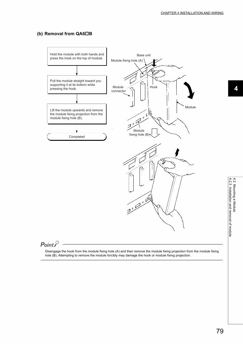
CHAPTER 4 INSTALLATION AND WIRING
4
4.2 Mounting a M
odule4.2.3 Installation and rem
oval of module
(b) Removal from QA6B
Disengage the hook from the module fixing hole (A) and then remove the module fixing projection from the module fixing hole (B). Attempting to remove the module forcibly may damage the hook or module fixing projection.
Hold the module with both hands and press the hook on the top of module.
Pull the module straight toward you supporting it at its bottom while pressing the hook.
Lift the module upwards and remove the module fixing projection from the module fixing hole (B).
Completed
Base unit
Module connector
Module
Module fixing hole (A)
Hook
Module fixing hole (B)
79

4.3 Connecting an Extension Base Unit
When using two or more extension base units, the base number must be set with their base number setting
connectors.*1
(The number of extension bases is set to 1 by factory default.)*1 Since the Q6WRB is fixed to the extension 1, extension base No. setting is not required.
4.3.1 Setting the extension base number
Set the extension base number in the following procedure.
1. The base number setting connector of the extension base unit is located under the IN side base cover. First, loosen the upper and lower screws in the IN side base cover and remove the base cover from the extension base unit.
Flat blade screwdriver
Base cover
Extension base unit
Fixing screw
Base cover
80

CHAPTER 4 INSTALLATION AND WIRING
4
4.3 Connecting an Extension Base U
nit4.3.1 Setting the extension base num
ber
2. Insert the connector pin in the required base number location of the connector (PIN1) existing between the IN and OUT sides of the extension cable connector.
*1 If these base numbers are set, "BASE LAY ERROR" (error code: 2010) occurs.*2 The extension base unit can be connected only when the serial number (first five digits) of the Redundant CPU is
"09012" or later and the redundant system is configured.The extension base unit cannot be connected when the serial number (first five digits) of the Redundant CPU is "09011" or earlier.
*3 Connect the Q6WRB to the first extension base. Since the Q6WRB is fixed to the first extension base, base number setting is not required.
*4 The Q6WRB cannot be connected to the second extension base or later bases. Use the Q6RB for the second extension base or later bases.
CPU module
Number setting for extension basesExtension
1Extension
2Extension
3Extension
4Extension
5Extension
6Extension
7
Q12PRHCPU*2, Q25PRHCPU*2Setting not
available*3 Setting available*4
Q00JCPU, Q00UJCPU Setting available Setting prohibited*1
Q00CPU, Q01CPU, Q00UCPU, Q01UCPU, Q02UCPU
Setting available Setting prohibited*1
Modules other than above Setting available
Connector pin
81

3. Install the base cover to the extension base unit and tighten the base cover screw. (Tightening torque: 0.36 to 0.48N•m)
● Set extension base numbers in the order of connection, starting from the extension base unit connected to the main base unit.
● Set correct extension base number for the base number setting connector. Do not set the same extension base number for two or more extension base units and do not skip extension base number setting. Doing so may cause incorrect input or incorrect output.
Flat blade screwdriverBase cover
Base cover
Extension base unit
Fixing screw
82

CHAPTER 4 INSTALLATION AND WIRING
4
4.3 Connecting an Extension Base U
nit4.3.1 Setting the extension base num
ber
(1) Precautions for setting the extension base numbers
(a) Setting orderSet the extension base number consecutively.In Auto mode, when any extension base number is skipped, no slots will be allocated to an empty extension base so that the slots cannot be reserved.For details of the base mode, refer to the following.
Manuals for the CPU module used (Function Explanation, Program Fundamentals)
Power supply module CPU module
Extension 1
Main base unit
Slot numberCPU 0 1 2 3 4 5 6 7 8 9 10 11
12 13 14 15 16 17 18 19
Extension 20 0 0 0 0 0 0 0
Extension 320 21 22 23 24 25 26 27
Extension base unit
Skipped stage number
Q312B
Q68B
Q68B
Q68B
83

(b) When the same number is setThe same extension number cannot be set for multiple extension base unit.
Power supply module CPU module
Extension 1
Main base unit
Slot numberCPU 0 1 2 3 4 5 6 7 8 9 10 11
Extension 1
Extension base unit
Q312B
Q68B
Q68BThe same extension stage number cannot be set!
Extension stage number setting connector
84

CHAPTER 4 INSTALLATION AND WIRING
4
4.3 Connecting an Extension Base U
nit4.3.1 Setting the extension base num
ber
(c) When connector pins are connected in more than 2 positions, or no pin is usedThe extension base unit cannot be used when connector pins for base number setting are inserted in more than two positions and when not using any connector pin.
(d) Position of the AnS/A series-compatible extension base unit (QA1S6ADP+A1S5B/A1S6B) in the systemFor precautions when using the QA1S6ADP+A1S5B/A1S6B in the system, refer to the following.
QA1S6ADP Q-AnS Base Unit Conversion Adapter User's Manual
QA1S6ADP-S1 Q-AnS Base Unit Conversion Adapter User's Manual
Power supply module CPU module
Extension 1
Main base unit
Slot numberCPU 0 1 2 3 4 5 6 7 8 9 10 11
Extension 2
Extension base unit
Q312B
Q68B
Q68B
Connector pin must be inserted!
Connector pins must not be inserted in 2 or more positions!
85

(e) Extension base positioning for AnS/A series-compatible extension base units (QA1S5B, QA1S6B, QA6B, and QA6ADP+A5B/A6B)When using AnS/A series-compatible extension base units in combination, follow the instructions described below.
• Connect the units in order of Q5B/Q6B, QA1S5B/QA1S6B, QA6B, and QA6ADP+A5B/A6B from the nearest position of the main base unit.
• The QA1S6B and QA6ADP+A5B/A6B cannot be used in combination. • The QA1S51B, which does not have an extension cable connector (OUT), cannot be used with the
QA6B or QA6ADP+A5B/A6B.
*1 When using the QA6ADP+A5B/A6B, connect it below the QA6B.
CPU 0 1 2 3 4 5 6 7 8 9 10 11
12 13 14 15 16 17 18 19
20 21 22 23 24 25 26 27
28 29 30 31 32 33 34 35
Q312B
Q68B
QA1S68
QA68B
Main base unit
Slot number
Power supply module CPU module
Extension base unit
Extension base unit for mounting the Q series-compatible module(Q5 B/Q6 B is connected to the main base unit or Q5 B/ Q6 B.)
Extension base unit for mounting the A series-compatible module*1 (QA6 B is connected to the main base unit, the end of the Q5 B/Q6 B/QA1S6 B or QA6 B)
Extension 1
Extension 2
Extension 3
Extension base unit for mounting the AnS series-compatible module (QA1S5 B/QA1S6 B is connected to the main base unit, the end of the Q5 B/Q6 B or QA1S6 B)
86

CHAPTER 4 INSTALLATION AND WIRING
4
4.3 Connecting an Extension Base U
nit4.3.2 C
onnection and disconnection of extension cable
4.3.2 Connection and disconnection of extension cable
(1) Instructions for handling an extension cable • Do not step on an extension cable. • Connect the extension cable to the base unit with the base cover installed to the base unit.
(After you have set the extension number to the extension base unit, reinstall and screw the base cover.) • When laying an extension cable, secure 55mm or more as the minimum cable bending radius.
If it is less than 55mm, a malfunction may occur due to characteristic deterioration, cable disconnection or the like.
• The overall length of extension cables must be up to 13.2m. • Do not install extension cables with the main circuit (high voltage and large current) line. • When connecting or disconnecting an extension cable, do not hold the ferrite cores mounted at both ends of
the cable.Hold the connector part of the cable for connection or disconnection.
Holding the ferrite core may cause the cable disconnection in the connector.Also, if the ferrite core position is shifted, the characteristic will change. When handling the cable, do not to shift the ferrite core position.
Main base unit
Connector
Extension cable
Ferrite core
87

(2) Connection of extension cable
When connecting an extension base unit to the main base unit with an extension cable, plug the OUT side connector of the main base unit and the IN side connector of the extension base unit with an extension cable. The system will not operate properly if the extension cable is connected in the form of IN to IN, OUT to OUT or IN to OUT.When connecting two or more extension base units, plug the OUT side connector of the first extension base unit and the IN side connector of the second extension base unit with an extension cable.
1. To connect an extension cable to the main base unit, remove the portion under the OUT characters on the base cover with a tool such as a flat blade screwdriver (5.5 × 75, 6 × 100). This also applies to a case where an extension cable is connected to the OUT side connector of the extension base unit. When connecting an extension cable to the Q00JCPU and Q00UJCPU, remove the base cover manually. To remove the base cover, insert the tip of a screwdriver into a clearance below the base cover and pry it up. Be careful not to damage the connector when inserting the screw driver since a connector is located inside the base cover.
2. To connect the extension cable to the next extension base unit, remove the seal put under the IN characters on the base cover.
Main base unit
Base cover
Flat blade screwdriver
Cut at 2 places of thin wall
Extension base unit
Flat blade screwdriver
OUT side of base cover
Cut at 2 places of thin wall
Extension base unit
Seal
IN side of base cover
88

CHAPTER 4 INSTALLATION AND WIRING
4
4.3 Connecting an Extension Base U
nit4.3.3 Extension cable specifications
3. When plugging the extension cable to any base unit, hold the connector part of the extension cable.
4. After fitting the extension cable, always tighten the extension cable connector fixing screws. (Tightening torque: 0.20N•m)
(3) Disconnection of extension cableWhen disconnection the extension cable, hold and pull the connector part of the extension cable after confirming that the fixing screws have been completely removed.
4.3.3 Extension cable specifications
The extension cables are connected to transfer signals between a main base unit and an extension base unit or between extension base units.
When the extension cables are used in combination, overall distance of the combined cable must be 13.2m or less.
ItemType
QC05B QC06B QC12B QC30B QC50B QC100BCable length 0.45m 0.6m 1.2m 3.0m 5.0m 10.0m
Conductor resistance value 0.044 0.051 0.082 0.172 0.273 0.530
Weight 0.15kg 0.16kg 0.22kg 0.40kg 0.60kg 1.11kg
Main base unit
Connector
Extension cable
Flat blade screwdriver
Main base unit
Fixing screw
89

4.3.4 Voltage drop when an extension base unit is used
Since the extension base unit (Q5B or QA1S5B) is supplied with 5VDC from the power supply module on the main base unit, a voltage drop occurs at extension cables. Improper I/O may occur if the specified voltage (4.75VDC or higher) is not supplied to the "IN" connector of the Q5B or QA1S5B.When using the Q5B or QA1S5B, make sure that the "IN" connector of the Q5B or QA1S5B is supplied with 4.75VDC or higher.And it is recommended to connect either of the extension base units as close as possible to the main base unit by using the short extension cable, so as to minimize the effects of voltage drop.
(1) When only the Q5B or QA1S5B is connected to the extension base unit
(a) Selection condition4.75VDC or higher must be supplied to the "IN" connector of the Q5B or QA1S5B in the final extension base.
90

CHAPTER 4 INSTALLATION AND WIRING
4
4.3 Connecting an Extension Base U
nit4.3.4 Voltage drop w
hen an extension base unit is used
(b) How to calculate voltage to "IN" connectorThe 5VDC output voltage of the power supply module on the main base unit is set to at least 4.90VDC.Therefore, the Q5B or QA1S5B can be used if the voltage drop at the extension cable is 0.15VDC or lower (4.9VDC - 4.75VDC = 0.15VDC).
.
*1 Sum total of currents consumed by Q5B, QA1S5B and currents consumed by the I/O modules, intelligent function modules mounted on the Q5B, QA1S5B. The symbols including "I" (I1 to I7) vary with the modules mounted on the Q5B, QA1S5B. For details of the symbol, refer to the user's manuals for the modules used.
Extension cable typeExtension cable conductor
resistanceQC05B 0.044QC06B 0.051QC12B 0.082QC30B 0.172QC50B 0.273
QC100B 0.530
Symbol DescriptionV1 Voltage drop at the extension cable between the main base unit and extension base unit (Q5B, QA1S5B)
VnVoltage drop at the extension cable between the extension base unit (Q5B, QA1S5B) (extension stage n-1) and extension base unit (Q5B, QA1S5B) (extension stage n)
R1 Extension cable resistance between the main base unit and extension base unit (Q5B, QA1S5B)
RnExtension cable resistance between the extension base unit (Q5B, QA1S5B) (extension stage n-1) and extension base unit (Q5B, QA1S5B) (extension stage n)
l1 to l7 5VDC current consumption among extension base 1 to 7*1
Extension stage 1
Extension stage 2
Extension stage 7
V1
V2
V7
R1
R2
R7
Main base unit
I1
I2
I7
Power supply module
Extension base unit (Q5 B)
Extension base unit (Q5 B)
Extension base unit (Q5 B, QA1S5 B)
91

The voltage supplied to "IN" connector of the Q5B or QA1S5B in the final extension base reaches 4.75 VDC or higher on the condition that the sum total of voltage drop to "IN" connector of Q5B or QA1S5B (V) is 0.15V or lower.
Q5B, QA1S5B Installation
position
Voltage drop at extension cable on corresponding extension unit Sum total of voltage drops to "IN" connector
of Q5B or QA1S5B (V)
V1 V2 V3 V4 V5 V6 V7
Extension 1 R1•I1 ---- ---- ---- ---- ---- ---- V=V1
Extension 2 R1 (I1+I2) R2•I2 ---- ---- ---- ---- ---- V= V1+V2
Extension 3 R1 (I1+I2+I3) R2 (I2+I3) R3•I3 ---- ---- ---- ---- V=V1+V2+V3
Extension 4 R1 (I1+I2+I3+I4) R2 (I2+I3+I4) R3 (I3+I4) R4•I4 ---- ---- ---- V=V1+V2+V3+V4
Extension 5 R1 (I1+I2+I3+I4+I5) R2 (I2+I3+I4+I5) R3 (I3+I4+I5) R4 (I4+I5) R5•I5 ---- ----V=V1+V2+V3+V4+V5
Extension 6R1 (I1+I2+I3+I4+I5+I6)
R2 (I2+I3+I4+I5+I6)
R3 (I3+I4+I5+I6)
R4 (I4+I5+I6) R5 (I5+I6) R6•I6 ----V=V1+V2+V3+V4+V5+V6
Extension 7R1 (I1+I2+I3+I4+I5+I6+I7)
R2 (I2+I3+I4+I5+I6+I7)
R3 (I3+I4+I5+I6+I7)
R4 (I4+I5+I6+I7)
R5 (I5+I6+I7) R6 (I6+I7) R7•I7V=V1+V2+V3+V4+V5+V6+V7
92

CHAPTER 4 INSTALLATION AND WIRING
4
4.3 Connecting an Extension Base U
nit4.3.4 Voltage drop w
hen an extension base unit is used
(2) When the Q6B or QA1S6B is connected between the main base unit and the Q5B or QA1S5B
(a) Selection condition4.75VDC or higher must be supplied to the "IN" connector of the Q5B or QA1S5B in the final extension base.
(b) How to calculate voltage to "IN" connectorThe 5VDC output voltage of the power supply module on the main base unit is set to at least 4.90VDC.Therefore, the Q5B or QA1S5B can be used if the voltage drop at the extension cable is 0.15VDC or lower (4.9VDC - 4.75VDC = 0.15VDC).
The voltage supplied to the "IN" connector of the Q5B or QA1S5B reaches 4.75 VDC or higher on the condition that the voltage drop (V) at the extension cable between the main base unit and Q5B or QA1S5B is 0.15 VDC or lower.
[When the Q5B or QA1S5B is connectedto Extension stage 2]
Extension cable typeExtension cable conductor
resistanceQC05B 0.044QC06B 0.051QC12B 0.082QC30B 0.172QC50B 0.273
QC100B 0.530
Symbol DescriptionV Voltage drop at the extension cable between the main base unit and extension base unit (Q5B, QA1S5B)
In
5VDC current consumption when the extension base unit (Q5B, QA1S5B) is used as Extension stage n+1n = 1 to 6, n: Extension number of extension base unit (Q6B) connected(Sum total of currents consumed by Q5B, QA1S5B and currents consumed by the I/O modules, intelligent function modules mounted on the Q5B, QA1S5B.)
RnExtension cable resistance between the main base unit and the extension base unit (Q6B, QA1S6B) or the extension base unit (Q6B, QA1S6B) and the extension base unit (Q6B, QA1S6B)
Rn+1 Extension cable resistance between the extension base unit (Q6B, QA1S6B) and extension base unit (Q5B, QA1S5B)
Position of extension base unit Voltage drop caused by extension cable from the main base unit to IN connector of the Q5B or QA1S5B (V)Q6B, QA1S6B Q5B, QA1S5B
Extension1 Extension 2 V=(R1+R2)I1
Extension 1, Extension 2 Extension 3 V=(R1+R2+R3)I2
Extension 1 to 3 Extension 4 V=(R1+R2+R3+R4)I3
Extension 1 to 4 Extension 5 V=(R1+R2+R3+R4+R5)I4
Extension 1 to 5 Extension 6 V=(R1+R2+R3+R4+R5+R6)I5
Extension 1 to 6 Extension 7 V=(R1+R2+R3+R4+R5+R6+R7)I6
Extension stage 1
Extension stage 2
V
R1
R2
I1
Power supply module
Power supply module
Main base unit
Extension base unit (Q6 B, QA1S6 B)
Extension base unit (Q5 B, QA1S5 B)
93

(3) When the GOT is bus-connected
(a) Selection condition4.75VDC or higher should be supplied to the "IN" connector of the Q5B in the final extension.
(b) How to calculate voltage to "IN" connectorThe 5VDC output voltage of the power supply module on the main base unit is set to at least 4.90VDC.Therefore, the Q5B can be used if the voltage drop is 0.15VDC or lower (4.9VDC -4.75VDC = 0.15VDC).
Extension cable typeExtension cable conductor
resistanceQC05B 0.044QC06B 0.051QC12B 0.082QC30B 0.172QC50B 0.273
QC100B 0.530
Symbol DescriptionV Voltage drop at the extension cable between the main base unit and extension base unit (Q5B)
In5VDC current consumption when the extension base unit (Q5B) is used as Extension n+1, n = 1 to 5, n: Extension number of the extension base unit (Q6B) connected(Sum total of current consumed by Q5B and currents consumed by I/O, intelligent function modules loaded on the Q5B)
Im5VDC current consumption of the GOT (current consumption per GOT is 255mA)• Im = 255 × c (c: Number of GOTs connected (c: 1 to 5))
RnExtension cable resistance between the main base unit and extension base unit (Q6B) or the extension base unit (Q6B) and extension base unit (Q6B)
Rn+1 Extension cable resistance between the extension base unit (Q6B) and extension base unit (Q5B)
R1
V
R2
Im
GOT GOT
Power supply module
Power supply module
Extension stage 1
I1Extension stage 2
Extension stage 3
[When the Q5�B is connected to Extension stage 2.]
Main base unit
Extension base unit (Q6�B)
Extension base unit (Q5�B)
Number of connectable GOTs: up to 5
94

CHAPTER 4 INSTALLATION AND WIRING
4
4.3 Connecting an Extension Base U
nit4.3.4 Voltage drop w
hen an extension base unit is used
The voltage supplied to the "IN" connector of the Q5B reaches 4.75 VDC or higher on the condition that the voltage drop (V) at the extension cable between the main base unit and Q5B is 0.15 VDC or lower.
When connecting GOT by extension cable that is 13.2m or longer, the bus extension connector box A9GT-QCNB is required.Since the A9GT-QCNB is supplied with 5VDC from the power supply module loaded on the main base unit, 30mA must be added to "Im" as the current consumption of the A9GT-QCNB.For details of the method for GOT bus connection, refer to the following.
GOT-A900 Series User's Manual (Connection)GOT1000 Series Connection Manual (Mitsubishi Electric Products) for GT Works3GOT2000 Series Connection Manual (Mitsubishi Electric Products) For GT Works3 Version1
Position of extension base unit Number of bases for GOT bus connection
Voltage drop caused by extension cable from the main base unit to the Q5B IN connector (V)Q6B Q5B
Extension 1 Extension 2 Extension 3 V=(R1+R2)(I1+Im)
Extension 1, Extension 2 Extension 3 Extension 4 V=(R1+R2+R3)(I2+Im)
Extension 1 to 3 Extension 4 Extension 5 V=(R1+R2+R3+R4)(I3+Im)
Extension 1 to 4 Extension 5 Extension 6 V=(R1+R2+R3+R4+R5)(I4+Im)
Extension 1 to 5 Extension 6 Extension 7 V=(R1+R2+R3+R4+R5+R6)(I5+Im)
95

4.4 Mounting and Removing a Terminal Block
This section describes a procedure for mounting and removing an 18-point terminal block.
(1) Removal procedure
(2) Mounting procedurePlace the terminal block in position, and then tighten the two terminal block mounting screws (upper and lower).
For mounting and removal of other terminal blocks, refer to the user's manual for the module used.
1. Open the terminal cover and loosen the terminal block mounting screw.
2. Remove the terminal block.
Terminal block mounting screw
96

CHAPTER 4 INSTALLATION AND WIRING
4
4.5 Installing and Rem
oving a Mem
ory Card
4.5 Installing and Removing a Memory Card
This section describes a procedure for installing and removing a memory card. Note 4.1
(1) For Q2MEM type memory cards
(a) Installing a memory cardPay attention to the direction of a memory card.Insert the card securely into the connector of a CPU module until the height of the card reaches that of the memory card EJECT button.
(b) Removing a memory cardPress the memory card EJECT button and pull out the memory card.
Note 4.1
The Basic model QCPU, Q00U(J)CPU, Q01UCPU, QnUDVCPU, and QnUDPVCPU do not support the use of a memory card.
Note 4.1
Basic Universal
Memory card EJECT button
Memory card
CPU module
Insertion direction check( mark)
Memory card
Push
Memory card EJECT button
CPU module
97

(2) For Q3MEM type memory cards
(a) Installing a memory cardPay attention to the direction of a memory card and install the card according to the following procedure.
Install the memory card
Completed
CPU module
Projection
CPU moduleMemory card EJECT button
Memory card
CPU module
Power off the CPU module, and remove the cover from the module.
Insert a memory card into the memory card slot.
Attach a memory card protective cover to the CPU module.
Remove the cover, slightly bending the center of the cover to make space between the projection and the mounting hole.
*Check the insertion direction. ( mark)
98

CHAPTER 4 INSTALLATION AND WIRING
4
4.5 Installing and Rem
oving a Mem
ory Card
(b) Removing a memory cardWhen removing a memory card from the CPU module, remove a memory card protective cover and press the EJECT button to pull out the memory card.Remove a memory card protective cover, press the memory card EJECT button, and pull out the memory card.
(3) Removing a memory card during power-onCheck that the corresponding special relay areas (SM604 and SM605) are off.
• The memory card cannot be removed while "SM604" is on because the CPU module is using the card. • Turn off "SM605" if it is on.
When both "SM604" and "SM605" are off, remove the memory card according to the following procedure.
1. Turn on the special relay "SM609" using the sequence program or by the device test of a programming tool.
2. By monitoring the programming tool, check that the special relay "SM600" is turned off.
3. Remove the memory card.
(4) Installing a memory card during power-on1. Install a memory card.
2. Check that the special relay "SM600" is on by monitoring the programming tool.
SM600 (Memory card usable flag) : The system turns on this flag when a memory card is ready to be used.
SM604 (Memory card in-use flag) : The system turns on this flag when a memory card is being used.
SM605 (Memory card remove/insert prohibit flag)
: The user turns on this flag to disable insertion/removal of a memory card.
Remove the memory card
Completed
Power off the CPU module, and remove the memory card protective cover.
Press the EJECT button to remove the memory card.
CPU module
Remove the protective cover, pressing the fixing claws located on the top and bottom of the cover.
CPU modulePush
Memory cardEJECT button
99

Observe the following precautions when installing or removing a memory card while power is on.
● Note that the data in a memory card may be damaged if the above procedure is not followed. If the operating status of the CPU module at the time of an error is set to "Stop" in parameter, the CPU module stops its operation upon the occurrence of "ICM.OPE.ERROR".
● When a memory card is installed, the scan time of the CPU module increases by several 10ms (maximum). The scan time increases for only one scan where the CPU module performs the mount processing.
● Poor insertion of the memory card may result in "ICM.OPE.ERROR".
● Using the tweezers below is effective when the memory card cannot be removed smoothly.
Product Model namePlastic tweezers NK-2539
100

CHAPTER 4 INSTALLATION AND WIRING
4
4.6 Installing and Rem
oving an SD M
emory C
ard
4.6 Installing and Removing an SD Memory Card
This section describes a procedure for installing and removing an SD memory card. Note 4.2
(1) Installing an SD memory cardPay attention to the direction of an SD memory card and install the card according to the following procedure.
1. Insert an SD memory card straight into the SD memory card slot.The notch part of the SD memory card must be on the lower side.After installing the SD memory card, check that it is inserted completely. Poor contact may cause malfunction.
2. The SD CARD LED starts flashing, and turns on when the card is ready to be used.
3. Check that the SD CARD LED remains on.
If the SD CARD LED does not turn on even after an SD memory card is installed, check that SM606 (SD memory card forced disable instruction) and SM607 (SD memory card forced disable status flag) are off.
Note 4.2 The Basic model QCPU, High Performance model QCPU, Process CPU, and Redundant CPU do not support the use of SD memory cards. For the Universal model QCPU, only the QnUDVCPU and QnUDPVCPU support the use of SD memory cards.
Note 4.2
Basic Highperformance Process Redundant Universal
101

(2) Removing an SD memory cardPull out the SD memory card according to the following procedure.
1. Disable the access to the SD memory card in either of the following. The SD CARD LED flashes during the access-disabling processing, and turns off when the processing is completed.
• Press the SD memory card lock switch on the CPU module for over one second. • Turn on SM609 (Memory card remove/insert enable flag).
When removing the SD memory card while the power is on, check that the SD CARD LED is off.
2. Push the SD memory card once, and pull out the card straight.
● Do not remove the SD memory card while any function using the card is being executed.
● When the SD card installation/removal is prohibited or the card is being used, the SD CARD LED does not turn off.Check the following items to check that the SD card installation/removal is prohibited or the card is being used.
• SM605 (Memory card remove/insert prohibit flag) is off. • All points in SD604 (Memory card use conditions) are off.
SD604 (Memory card use conditions) turns off when the file in the SD memory card is not used. When SD604 does not turn off, use SM606 (SD memory card forced disable instruction) and SM607 (SD memory card forced disable status flag) to forcibly disable the use of the SD memory card.( Page 252, Section 10.4)
SD memory card lock switch
102

CHAPTER 4 INSTALLATION AND WIRING
4
4.7 Installing and Rem
oving an Extended SRAM
Cassette
4.7 Installing and Removing an Extended SRAM Cassette
This section describes a procedure for installing and removing an extended SRAM cassette. Note 4.3
(1) Installing an extended SRAM cassetteInsert an extended SRAM cassette while the power is off.
1. Open the cassette cover on the side of the CPU module.
2. Hold the top and the bottom of the knob of the extended SRAM cassette, and insert it straight into the cassette connector.The notch part of the extended SRAM cassette must be on the right side.After installing the cassette, check that it is inserted completely.
3. Close the cassette cover.
Note 4.3 The Basic model QCPU, High Performance model QCPU, Process CPU, and Redundant CPU do not support the use of extended SRAM cassettes. For the Universal model QCPU, only the QnUDVCPU and QnUDPVCPU support the use of extended SRAM cassettes.
Note 4.3
Basic Highperformance Process Redundant Universal
Cassette cover
Extended SRAM cassette
Tab
103

● The data stored in the standard RAM before an extended SRAM cassette is installed are retained even after the cassette is installed.
● The capacity of the standard RAM after installation can be checked on the "Online Data Operation" window.
[Online] [Read from PLC]
(2) Removing an extended SRAM cassetteRemove an extended SRAM cassette while the power is off.
1. Read the data stored in the standard RAM (including the extended SRAM cassette) using GX Works2 in advance.Removing the extended SRAM cassette deletes all the data stored in the standard RAM (including the cassette).
2. Turn off the power supply of the CPU module.
3. Remove the CPU module from the base unit.
4. Open the cassette cover on the side of the CPU module.
5. Hold the top and the bottom of the tab of the extended SRAM cassette, and pull it out straight from the connector.
6. Close the cassette cover.
104

CHAPTER 4 INSTALLATION AND WIRING
4
4.8 Wiring
4.8.1 Wiring pow
er supplies
4.8 Wiring
4.8.1 Wiring power supplies
(1) Precautions for wiring power supplies • Wire cables of the programmable controller power supply, I/O power supply, and motor power supply
separately as shown below.
• If there is much noise, such as lightning surge, connect an isolation transformer.For details on the isolation transformer, refer to the following.
Page 663, Appendix 8.1 • Taking rated current or inrush current into consideration when wiring the power supply, connect a breaker or
an external fuse that have proper blown and detection.When using a single programmable controller, a 10A breaker or an external fuse are recommended for wiring protection.
• Do not connect the 24VDC outputs of two or more power supply modules in parallel to supply power to one I/O module. Parallel connection will damage the power supply modules.
• 100VAC, 200VAC and 24VDC wires must be twisted as dense as possible. Connect the modules with the shortest distance.
Also, to reduce the voltage drop to the minimum, use the thickest wires possible (maximum 2mm2). • Do not bundle the 100VAC and 24VDC wires with, or run them close to, the main circuit (high voltage, large
current) and I/O signal lines (including common line). Reserve a distance of at least 100mm from adjacent wires.
100VAC200VAC
T1
Main power supply
Relay terminal block
I/O power supply
I/O equipment
Inside a control panel
Programmablecontroller powersupply
Isolationtransformer
Programmablecontroller
Motor power supply
Motor equipment
Power supply module I/O module
24VDC
24VDC
Power supply module I/O module
24VDC External power supply
105

• Momentary power failure may be detected or the CPU module may be reset due to serge caused by lightning.As measures against a noise caused by surge, connect a surge absorber for lightning as shown in the following figure.Using the surge absorber for lightning can reduce the influence of lightning.
• Use an online UPS (uninterruptible power supply) with power distortion factor of 5% or less or line-interactive UPS. For a standby system UPS, use Mitsubishi small-capacity UPS "FREQUPS FW-F series" (hereafter
abbreviated as FW-F series).*1 (Example: FWF10-0.3K/0.5K)Do not use any standby system UPS other than the FW-F series.
*1 Use a FW-F series UPS with the serial number starts with P or later or ends with HE.
● Separate the ground of the surge absorber for lightning (E1) from that of the programmable controller (E2).
● Select a surge absorber for lightning whose power supply voltage does no exceed the maximum allowable circuit voltage even at the time of maximum power supply voltage elevation.
AC
E1
E2
Surge absorber for lightning
Programmablecontroller
I/O equipment
Starts with "P" or later
Ends with "HE"
106

CHAPTER 4 INSTALLATION AND WIRING
4
4.8 Wiring
4.8.1 Wiring pow
er supplies
(2) Wiring examplesThe following figures show wiring examples of cables such as power cables and ground wires to the main base unit and extension base units.
(a) Single power supply system
*1 The operation of the ERR terminal is as follows:<When the power supply module is mounted on the main base unit>The terminal turns off (opens) when the AC power is not input, a CPU module stop error (including a reset) occurs, or the fuse of the power supply module is blown.<When the power supply module is mounted on the extension base unit>The terminal is always off (opened).
*2 Ground the LG and FG terminals by using a ground wire as thick and short as possible (2mm in diameter).
● Use the thickest possible (max. 2mm2) wires for the 100/200VAC and 24VDC power cables. Twist these wires starting at the connection terminals. Use a solderless terminal for wiring a terminal block. To prevent short-circuit due to loosening screws, use the solderless terminals with insulation sleeves of 0.8mm or less. Note that up to two solderless terminals can be connected per terminal block.
● When LG and FG terminals are connected, ground the wires.If not, the programmable controller may become susceptible to noise.Since the LG terminal has a half of the input voltage, touching this terminal may result in electric shock.
● No system error can be detected by the ERR terminal of an extension base unit. (The ERR terminal is always set to off.)
AC
ACDC
100/110VAC
24VDC
Q61P
Q61P I/O module
100VAC
FG*2
LG*2
INPUT100-240VAC
FG*2
LG*2
INPUT100-240VAC
Fuse
Connect to 24VDC terminals of I/O module that requires 24VDC internally.
Extension cable
Ground wire
Grounding
Main base unit(Q38B)
CPU module
Extension base unit(Q68B)
ERR*1
ERR*1
Terminal blockSolderless terminalswith insulation sleeves
107

(b) Redundant power supply system • Q64RPN
*1 The operation of the ERR terminal is as follows:<When the redundant power supply module is mounted on the redundant power main base unit>The terminal turns off (opens) when the AC power is not input, a CPU module stop error (including a reset) occurs, the redundant power supply module fails, or the fuse of the redundant power supply module is blown.<When the redundant power supply module is mounted on the redundant power extension base unit>The terminal turns off (opens) when the AC power is not input, the redundant power supply module fails, or the fuse of the redundant power supply module is blown.
*2 When input power is supplied to the redundant power supply module mounted on the redundant power main base unit and the redundant power supply module mounted on the redundant power extension base unit simultaneously, the ON (short) timing of the ERR terminal on the redundant power main base unit is later than that of the ERR terminal on the redundant power extension base unit by the initial processing time of the CPU module.
*3 Ground the LG and FG terminals by using a ground wire as thick and short as possible (2mm in diameter).
AC
100V/200VAC
AC
100V/200VAC FG*3
LG*3
Ground wire
Extension cable
Grounding
CPU module
I/O module
FG*3
LG*3
INPUT
Redundant power main base unit(Q38RB)
Redundant power extension base unit (Q68RB)
FG*3
LG*3
INPUT
INPUT INPUT
FG*3
LG*3
AC
100V/200VAC
AC
100V/200VAC
System BSystem A
ERR*1, *2
ERR*1, *2 ERR*1, *2
ERR*1, *2
Ground wire
Grounding
Q64RPN Q64RPN
Q64RPN Q64RPN
100-240VAC 100-240VAC
100-240VAC 100-240VAC
108

CHAPTER 4 INSTALLATION AND WIRING
4
4.8 Wiring
4.8.1 Wiring pow
er supplies
• Q64RP
*4 The operation of the ERR terminal is as follows:<When the redundant power supply module is mounted on the redundant power main base unit>The terminal turns off (opens) when the AC power is not input, a CPU module stop error (including a reset) occurs, the redundant power supply module fails, or the fuse of the redundant power supply module is blown.<When the redundant power supply module is mounted on the redundant power extension base unit>The terminal turns off (opens) when the AC power is not input, the redundant power supply module fails, or the fuse of the redundant power supply module is blown.
*5 When input power is supplied to the redundant power supply module mounted on the redundant power main base unit and the redundant power supply module mounted on the redundant power extension base unit simultaneously, the ON (short) timing of the ERR terminal on the redundant power main base unit is later than that of the ERR terminal on the redundant power extension base unit by the initial processing time of the CPU module.
*6 Ground the LG and FG terminals by using a ground wire as thick and short as possible (2mm in diameter).
AC
100V/200VAC
AC
100V/200VACFG*6
LG*6
Q64RP
Ground wire
Grounding
CPU module
I/O moduleQ64RP
FG*6
LG*6
INPUT
Q64RP
Redundant power main base unit(Q38RB)
Redundant power extension base unit (Q68RB)
FG*6
LG*6
INPUT
INPUT INPUT
FG*6
LG*6
Q64RP
AC
100V/200VAC
AC
100V/200VAC
System BSystem A
ERR*4*5
ERR*4*5 ERR*4*5
ERR*4*5
Ground wire
Grounding
100-120/200-240VAC
100-120/200-240VAC
100-120/200-240VAC
100-120/200-240VAC
Extension cable
109

● Use the thickest possible (max. 2mm2) wires for the 100/200VAC and 24VDC power cables. Twist these wires starting at the connection terminals. Use a solderless terminal for wiring a terminal block. To prevent short-circuit due to loosening screws, use the solderless terminals with insulation sleeves of 0.8mm or less. Note that up to two solderless terminals can be connected per terminal block.
● Supply power to two redundant power supply modules individually (redundant power supply system).
● When two redundant power supply modules (Q64RPN, and Q64RP) are placed together and operated as a redundant power supply system, it is recommended to use one of them as an AC power input and connect the other to an uninterruptible power supply to the other.
● When the LG and FG terminals are connected, ground the wires.If not, the programmable controller may become susceptible to noise.The LG terminal has a half of the input voltage.
Terminal blockSolderless terminalswith insulation sleeves
110

CHAPTER 4 INSTALLATION AND WIRING
4
4.8 Wiring
4.8.2 Wiring of 18-point screw
terminal block
4.8.2 Wiring of 18-point screw terminal block
(1) Precautions • Insulation-sleeved crimping terminals cannot be used with the terminal block.
It is recommended to cover the wire connections of the crimping terminals with mark or insulation tubes.
• The wires used for connection to the terminal block must be 0.3 to 0.75mm2 in core and 2.8mm max. in outside diameter.
• Run the input and output lines away from each other. • When the lines cannot be run away from the main circuit and power lines, use a batch-shielded cable and
ground it on the programmable controller side.In some cases, ground it in the opposite side.
• Where wiring runs through piping, ground the piping. • Run the 24VDC input line away from the 100VAC and 200VAC lines. • Wiring of 200m or longer will raises current leakage due to the line capacity, resulting in a fault. • To prevent electric shock or malfunction, provide the external power supply for the module to be changed
online with means that can turn the power supply off individually, e.g. a switch. ( Page 272, CHAPTER 14)
• As a countermeasure against the power surge due to lightning, separate the AC wiring and DC wiring and connect a surge absorber for lightning as shown in Page 105, Section 4.8.1.
• Failure to do so increases the risk of I/O device failure due to lightning.
For screw terminal blocks other than the 18-point screw terminal block, refer to the user's manual for the module used.
DC
RA
Programmablecontroller
Shield cable
Input
Output Shield jacket
111

(2) Wiring method
(a) Wiring to an 18-point screw terminal block
1. Strip the insulating coating from the cable.
2. Connect a solderless terminal to the stripped part of the cable.For applicable solderless terminals, refer to the specifications of each module.
3. Wire the solderless terminals to the 18-point screw terminal block.For terminal layout, refer to the specifications of each module.
Screwdriver
112

CHAPTER 4 INSTALLATION AND WIRING
4
4.8 Wiring
4.8.3 Wiring to connectors
4.8.3 Wiring to connectors
(1) Precautions • Connectors for external devices (A6CON) must be crimped, pressed, or correctly soldered. • Plug connectors for external devices (A6CON) securely to the module and tighten the two screws. • Use copper wires having temperature rating of 75°C or more for the connectors. • Tighten the connector screws within the following specified torque range.
• Place the cables in a duct or clamp them. If not, dangling cable may swing or inadvertently be pulled, resulting in damage to the module or cables or malfunction due to poor connection.
To make the wiring comply with the EMC and Low Voltage Directives, refer to Page 663, Appendix 8.Even when compliance with the EMC Directive and Low Voltage Directives is not required, configuring the system that complies with the EMC Directive may reduce external noise.
(2) Applicable connectors The following tables list the crimp tool, pressure-displacement tools, and the types of connectors used for modules.
(a) 40-pin connector
(b) Crimp tool and pressure-displacement tools for 40-pin connectors
For wiring of the connectors and usage of the crimp tool and pressure-displacement tools, contact FUJITSU COMPONENT LIMITED.
Screw type Tightening torque rangeConnector screw (M2.6) 0.20 to 0.29N•m
Type Model Applicable wire size
Soldering connector(straight out type)
A6CON10.088 to 0.3mm2 (28 to 22 AWG) (stranded)Use cables with outside diameter of 1.3mm or shorter to connect 40 cables to the connector.
Crimp connector(straight out type)
A6CON2 0.088 to 0.24mm2 (28 to 24 AWG) (stranded)
Pressure-displacement connector(straight out type) A6CON3
28 AWG (stranded)30 AWG (solid)Flat cable of 1.27mm pitch
Soldering connector(both for straight out and 45-degree types)
A6CON40.088 to 0.3mm2 (28 to 22 AWG) (stranded)Use cables with outside diameter of 1.3mm or shorter to connect 40 cables to the connector.
Type Model ContactCrimp tool FCN-363T-T005/H
FUJITSU COMPONENT LIMITEDwww.fujitsu.com/jp/group/fcl/en/
Pressure-displacement tool
FCN-367T-T012/H (locator plate)
FCN-707T-T001/H (cable cutter)
FCN-707T-T101/H (hand press)
113

(3) Wiring method
(a) A6CON1, A6CON4
1. Loosen the four fixing screws on the connector and remove the screws. Open the connector cover from the connector side.
2. Solder the wires and coat them with heat shrinkable tubes.
3. Check the terminal layout and install the wires to the connector.When the connector is plugged into an I/O module, an FG wire needs not to be installed.
Heat shrinkable tube
114

CHAPTER 4 INSTALLATION AND WIRING
4
4.8 Wiring
4.8.3 Wiring to connectors
4. Place the connector on one side of the connector cover and put the fixing screws through the screw holes. Cover the other connector cover onto the connector.
5. Tighten the four screws.
115

(b) A6CON2The following table lists the specifications of the FCN-363T-T005/H used for the A6CON2.
Wiring of the A6CON2 requires special tools.For usage and adjustment of the tools, contact FUJITSU COMPONENT LIMITED.
(c) A6CON3Wiring of the A6CON3 requires special tools.For usage and adjustment of the tools, contact FUJITSU COMPONENT LIMITED.
Arrangement for a flat cable is in the order of A1B1A2•••••.(The following figure shows a connector seen from the plug-in side.)
Applicable wire size
Cross-section area of wire
Crimp heightOutside
diameter of coated wire
Length of stripped wire part
24 AWG 0.20 to 0.24mm2 1.25 to 1.30 1.2 or less 3.0 to 4.0
26 AWG 0.13 to 0.16mm2 1.20 to 1.25 1.2 or less 3.0 to 4.0
28 AWG 0.088 to 0.096mm2 1.15 to 1.20 1.2 or less 3.0 to 4.0
1. Check the terminal layout and press the wires against the connector.
A20 A19 A18 A17 A16 A15 A14 A13 A12 A11 A10 A09 A08 A07 A06 A05 A04 A03 A02 A01
B20 B19 B18 B17 B16 B15 B14 B13 B12 B11 B10 B09 B08 B07 B06 B05 B04 B03 B02 B01
116

CHAPTER 4 INSTALLATION AND WIRING
4
4.8 Wiring
4.8.3 Wiring to connectors
(4) Plugging a connector
(a) Installation procedure
(b) Removal procedureLoosen the two connector screws, and then pull out the connector horizontally to the module.
1. Plug the connector into the slot on the module.
2. Tighten the two connector screws (M2.6).
Connector screw
117

4.8.4 Grounding
For grounding, perform the following: • Use a dedicated grounding wire as far as possible. (Grounding resistance of 100 or less.) • When a dedicated grounding cannot be provided, use (2) Shared grounding shown below.
• Use thick cables up to 2mm2. Bring the grounding point close to the programmable controller as much as possible so that the ground cable can be shortened.
(3) Common grounding Not allowed
Programmable controller
Programmable controller
Programmable controllerEquipment Equipment Equipment
(1) Independent grounding Recommended (2) Shared grounding Allowed
Groundresistance of 100 or less
Groundresistance of 100 or less
118

CHAPTER 5 GENERAL SPECIFICATIONS
5
CHAPTER 5 GENERAL SPECIFICATIONS
The following table lists the general specifications of the programmable controller.
*1 This indicates the section of the power supply to which the equipment is assumed to be connected between the public electrical power distribution network and the machinery within premises.Category II applies to equipment for which electrical power is supplied from fixed facilities. The surge voltage withstand level for up to the rated voltage of 300V is 2500V.
*2 This index indicates the degree to which conductive material is generated in terms of the environment in which the equipment is used.Pollution level 2 is when only non-conductive pollution occurs. A temporary conductivity caused by condensing must be expected occasionally.
*3 The storage ambient temperature is -20 to 75°C if the system includes the AnS/A series modules.*4 The operating ambient humidity and storage ambient humidity are 10 to 90%RH if the system includes the AnS/A series
modules.*5 Do not use or store the programmable controller under pressure higher than the atmospheric pressure of altitude 0m.
Doing so may cause malfunction. When using the programmable controller under pressure, please consult your local Mitsubishi Electric representative.
Item SpecificationsOperating ambient temperature
0 to 55°C
Storage ambient temperature -25 to 75°C*3
Operating ambient humidity
5 to 95%RH*4, non-condensingStorage ambient humidity
Vibration resistanceCompliant withJIS B 3502 and
IEC 61131-2
FrequencyConstant
accelerationHalf amplitude Sweep count
Under intermittent
vibration
5 to 8.4Hz ---- 3.5mm10 times each in X, Y, Z directions8.4 to 150Hz 9.8m/s2 ----
Under continuous vibration
5 to 8.4Hz ---- 1.75mm----
8.4 to 150Hz 4.9m/s2 ----
Shock resistance Compliant with JIS B 3502 and IEC 61131-2 (147 m/s2, 3 times each in 3 directions X, Y, Z)
Operating atmosphere
No corrosive gases
Operating altitude*5 0 to 2000m
Installation location Inside a control panel
Overvoltage
category*1 II or less
Pollution degree*2 2 or less
Equipment class Class I
119

Memo
120

CHAPTER 6 CPU MODULE
6
6.1 Part Nam
es6.1.1 Basic m
odel QC
PU
CHAPTER 6 CPU MODULE
6.1 Part Names
6.1.1 Basic model QCPU
(1) Q00JCPU
When opening the cover, put your finger here.
6)5)4)
OUT
1)
8)
2)
7)
When opening the cover, put your finger here.
5VDC3AOUTPUT50/60Hz 105VA
INPUT100-240VAC
INPUT100-240VACINPUT
L
N
OUT
12) 13)
15) 16)
14)
11)
10) 9)3)
121

No. Name Application1) Base unit installation hole Pear-shaped hole for installing the unit on a panel such as a control panel. (For M4 screw)
2) CoverProtective cover for extension cable connector. Remove this cover when connecting an extension base unit.
3) Extension cable connectorConnector for transferring signals to or from the extension base unit. Connect an extension cable.
4) POWER LED Power indicator LED for 5VDC. Turns on in green during normal output of 5VDC.
5) RUN LED
Indicates the operating status of the CPU module.On: During operation with the RUN/STOP/RESET switch set to "RUN"Off: During stop with the RUN/STOP/RESET switch set to "STOP"
When the error that stops operation is detectedFlash:
When parameters/program is written during STOP and the RUN/STOP/RESET switch is moved from "STOP" to "RUN".To turn on the RUN LED after writing the program, perform the following operations.• Set the RUN/STOP/RESET switch from "STOP" to "RUN" to "STOP" to "RUN".
• Perform reset with the RUN/STOP/RESET switch. ( Page 189, Section 6.4.1)• Power on the programmable controller again.To turn on the RUN LED after writing the parameters, perform the following operations.• Perform reset with the RUN/STOP/RESET switch.• Power on the programmable controller again. (If the RUN/STOP/RESET switch is set from "RUN" to "STOP" to "RUN" after changing the parameter values, the new values are not reflected on the parameters related to the intelligent function module, such as the network parameters.)
6) ERR. LED
On: When the self-diagnostic error that will not stop operation is detected.• When continuation of operation at error detection is set in the parameter.• When the annunciator (F) is turned on by the SET/OUT instruction.• When battery low occurs.
Off: NormalFlash:
When the error that stops operation is detected.When reset operation is performed with the RUN/STOP/RESET switch.
7) Module connectorConnector used for mounting an I/O module or intelligent function module.(To the connector of the spare space where no module is mounted, fit the accessory connector cover or the blank cover module (QG60) to prevent dust from entering.)
8) DIN rail adaptor mounting holes Holes for mounting a DIN rail adaptor.
9) FG terminal Ground terminal connected with the shield pattern of the printed circuit board.
10) LG terminal Power filter ground having a half potential of the input voltage.
11) Power input terminals Power input terminals for connection of a 100VAC to 200VAC power supply.
12) BatteryBackup battery for use of the program memory, standard RAM, clock function and backup power time function.
13) Battery fixing hook Hook for holding the battery.
14) Battery connector pinFor connection of the battery lead wires.(Lead wires are disconnected from the connector when shipping to prevent the battery from consuming.)
122

CHAPTER 6 CPU MODULE
6
6.1 Part Nam
es6.1.1 Basic m
odel QC
PU
*1 When a cable is connected to the RS-232 connector at all times, clamp the cable to prevent a poor connection, moving, and disconnection by unintentional pulling.The Q6HLD-R2 type RS-232 connection disconnection prevention holder is available as a clamp for RS-232 connector.
*2 Operate the RUN/STOP/RESET switch with your fingertips.To prevent the switch from being damaged, do not use any tool such as screw driver.
No. Name Application
15) RS-232 connector*1Connector for connecting a peripheral device by RS-232.Can be connected by the RS-232 connection cable (QC30R2).
16) RUN/STOP/RESET switch*2
RUN: Executes sequence program operation.STOP: Stops sequence program operation.RESET:
Performs hardware reset, operation error reset, operation initialization or like.
( Page 189, Section 6.4.1)
Fixing screw
Q6HLD-R2
CPU module
RS-232 cable
123

(2) Q00CPU, Q01CPU
1)
2)3)
4)
When opening the cover, put your finger here.
7)
8)
6)5)
9)
10)
11)12)
124

CHAPTER 6 CPU MODULE
6
6.1 Part Nam
es6.1.1 Basic m
odel QC
PU
No. Name Application1) Module fixing hook Hook used to fix the module to the base unit. (Single-motion installation)
2) RUN LED
Indicates the operating status of the CPU module.On: During operation with the RUN/STOP/RESET switch set to "RUN".Off: During stop with the RUN/STOP/RESET switch set to "STOP".
When the error that stops operation is detected Flash:
When parameters/program is written during STOP and the RUN/STOP/RESET switch is set from "STOP" to "RUN".To turn on the RUN LED after writing the program, perform the following operations.• Move the RUN/STOP/RESET switch from "STOP" to "RUN" to "STOP" to "RUN".
• Perform reset with the RUN/STOP/RESET switch. ( Page 189, Section 6.4.1)• Power on the programmable controller againTo turn on the RUN LED after writing the parameters, perform the following operations.• Perform reset with the RUN/STOP/RESET switch.• Power on the programmable controller again. (If the RUN/STOP/RESET switch is set from "RUN" to "STOP" to "RUN" after changing the parameter values, the new values are not reflected on the parameters related to the intelligent function module, such as the network parameters.)
3) ERR. LED
On: When the self-diagnostic error that will not stop operation is detected.• When continuation of operation at error detection is set in the parameter.• When the annunciator (F) is turned on by the SET/OUT instruction.• When battery low occurs.
Off: NormalFlash:
When the error that stops operation is detected.When reset operation is performed with the RUN/STOP/RESET switch.
4) Serial number display Shows the serial number printed on the rating plate.
5) BatteryBackup battery for use of the program memory, standard RAM, and backup power time function.
6) Battery fixing hook Hook for holding the battery.
7) Battery connector pinFor connection of the battery lead wires. (Lead wires are disconnected from the connector when shipping to prevent the battery from consuming.)
8) RUN/STOP/RESET switch*2
RUN: Executes sequence program operation.STOP: Stops sequence program operation.RESET:
Performs hardware reset, operation error reset, operation initialization or like.
( Page 189, Section 6.4.1)
9) RS-232 connector*1Connector for RS-232 connectionCan be connected by the RS-232 connection cable (QC30R2).
10) Module fixing screw hole Hole for the screw used to fix to the base unit. (M3 × 12 screw)
11) Module fixing projection Projection used to secure the module to the base unit.
12) Module mounting lever Lever used to mount the module to the base unit.
125

*1 When a cable is connected to the RS-232 connector at all times, clamp the cable to prevent a poor connection, moving, and disconnection by unintentional pulling.The Q6HLD-R2 type RS-232 connection disconnection prevention holder is available as a clamp for RS-232 connector.
*2 Operate the RUN/STOP/RESET switch with your fingertips.To prevent the switch from being damaged, do not use any tool such as screw driver.
Fixing screw
Q6HLD-R2
CPU module
RS-232 cable
126

CHAPTER 6 CPU MODULE
6
6.1 Part Nam
es6.1.2 H
igh Performance m
odel QC
PU, Process C
PU and R
edundant CPU
6.1.2 High Performance model QCPU, Process CPU and Redundant CPU
(1) Q02CPU, Q02HCPU, Q06HCPU, Q12HCPU, Q25HCPU, Q02PHCPU, Q06PHCPU, Q12PHCPU, Q25PHCPU
*1 Not provided for Q02CPU.
Q02HCPUQ02HCPU
RS-232
USB
MODERUNERR.
USERBAT.
BOOT
PULL
MODERUNERR.
USERBAT.
BOOT
SWON
54321
RUNSTOP
L.CLRRESET
When opening the cover, put your finger here.
1)
2)
8)
3)4)5)6)7)
10)
11)
12)
13)
14)
15)
*1
9)
16)
17)20)19)
18)
127

(2) Q12PRHCPU, Q25PRHCPU
Q12PRHCPUQ12PRHCPU
MODERUNERR.
USERBAT.
BOOT
USB
PULL
TRACKING
BACKUP
SYSTEM BSYSTEM ACONTROL
RUNSTOP
MODERUNERR.
USERBAT.
BOOT
54321
SWON
L.CLRRESET
TRACKING
BACKUP
SYSTEM BSYSTEM ACONTROL
1)
3)
4)
5)
6)
7)
2)
When opening the cover, put your finger here.
21)
22)
23)
24)
25)
9)
10)
11)
12)
8)
13)
14)
15)
17)
19)
18)
16)
20)
128

CHAPTER 6 CPU MODULE
6
6.1 Part Nam
es6.1.2 H
igh Performance m
odel QC
PU, Process C
PU and R
edundant CPU
No. Name Application1) Module fixing hook Hook used to secure the module to the base unit. (Single-motion installation)
2) MODE LEDIndicates the mode of the CPU module.On (green): Q modeFlash (green): Forced on and off for external I/O registered
3) RUN LED
Indicates the operating status of the CPU module.On: The RUN/STOP switch is set to "RUN".Off: The RUN/STOP switch is set to "STOP".
(The standby system Redundant CPU module in the backup mode does not turn on even when the RUN/STOP switch is set to "RUN" but the module is stopped.)When an error is detected and operation must be halted due to the error
Flash: Parameters or programs are written with the RUN/STOP switch set to "STOP" and then the RUN/STOP switch is turned from "STOP" to "RUN."When the operation mode is changed from the backup mode to the separate mode in the Redundant CPU system, the RUN LED of the standby system side CPU module flashes.To turn on the RUN LED after writing the program, perform the following operations.• Set the RUN/STOP switch from "RUN" "STOP" "RUN".• Reset with the RESET/L. CLR switch.• Restart the programmable controller power.To turn on the RUN LED after writing the parameters, perform the following operations.• Reset with the RESET/L. CLR switch.• Restart the programmable controller power. (If the RUN/STOP switch is set from "RUN" "STOP" "RUN" after changing the parameters, network parameters and intelligent function module parameters will not be updated.)
4) ERR. LED
On: Detect on of self-diagnosis error which will not stop operation, except battery error.(When operation continued at error detection is set in the parameter setting.)
Off: NormalFlash:
Detection of the error that stops operation.When automatic write to the standard ROM is completed normally. (The BOOT LED flashes together.)
5) USER LEDOn: Error detected by CHK instruction or annunciator (F) turned ONOff: NormalFlash: Execution of latch clear
6) BAT. LEDOn: Battery error due to reduction in battery voltages of CPU module or memory card.Off: Normal
7) BOOT LED
On: Start of boot operationOff: Non-execution of boot operationFlash:
When automatic write to the standard ROM is completed normally. (The ERR. LED flashes together.)
8) Serial number display Shows the serial number printed on the rating plate.
9) Memory card EJECT button Used to eject the memory card from the CPU module.
10) Memory card installing connector Connector used for installing the memory card to the CPU module.
11) USB connector*1Connector for connection with USB-compatible peripheral device. (Connector type B)Can be connected by USB-dedicated cable.(Not available for Q02CPU.)
12) RS-232 connector*1Connector for connecting a peripheral device by RS-232.Can be connected by RS-232 connection cable (QC30R2).
129

13)
DIP switches*2
Used to set the items for operation of the CPU module.For the system protection and the valid parameter drives of the DIP switches, refer to the following.
Qn(H)/QnPH/QnPRHCPU User's Manual (Function Explanation, Program Fundamentals)
SW1 : Used to set system protection. Inhibits all the writing and control instructions to the CPU module. (Factory-default is off)Off: No protectionOn: Protection
SW2, SW3 : Used to specify parameter-valid drive.(Both SW2 and SW3 are preset to off as factory default)
SW2 SW3 Parameter Drive
OFF OFF Program memory (Drive 0)
ON OFF SRAM card (Drive 1)
OFF ON Flash card/ATA card (Drive 2)
ON ON Standard ROM (Drive 4)
(Parameters cannot be stored in standard RAM (Drive 3).)
SW4: Must not be used. Normally off. (Factory default: Off)
SW5: Must not be used. Normally off. (Factory default: Off)
14) RUN/STOP switch*3 RUN: Executes sequence program operation.STOP: Stops sequence program operation.
15) RESET/L. CLR switch*3
RESET:Used to perform hardware reset, operation fault rest, operation initialization, etc.(If this switch is left in the RESET position, the whole system will be reset and the system will not operate properly. After performing reset, always return this switch to the neutral position.)
L. CLR:Used to turn "Off" or clear to "zero" all latch area data set in the parameter.Used to clear the sampling trace settings.
16) Module fixing screw hole Hole for the screw used to fix to the base unit. (M3 × 12 screw)
17) Module fixing projection Projection used to fix the module to the base unit.
18) Battery connector pinFor connection of battery lead wires.(Lead wires are disconnected from the connector when shipping to prevent the battery from consuming.)
19) BatteryBackup battery for use of program memory, standard RAM, and the backup power time function.
20) Module mounting lever Lever used to mount the module to the base unit.
21) BACKUP LED*4
Indicates the backup or separate mode while the system is running normally.On (green): Backup modeOn (red):The status in which control (RUN) cannot be continued by system switchingOn (orange):Separate modeOff: Debug modeThe LED indication is as listed below when the memory copy from control system to standby system is executed.
For the memory copy from control system to standby system, refer to the following.
QnPRHCPU User's Manual (Redundant System)
No. Name Application
1
2
3
4
5
ON SW
In backup mode In separate mode
Memory copy executing
Memory copy normallycompleted
Control system Standby system Control system Standby system
ON (red) ON (orange)
ON (red) ON (orange)
Flashing (red) Flashing (orange)
ON (red) ON (orange)
130

CHAPTER 6 CPU MODULE
6
6.1 Part Nam
es6.1.2 H
igh Performance m
odel QC
PU, Process C
PU and R
edundant CPU
*1 When a cable is connected to the RS-232 connector at all times, clamp the cable to prevent a poor connection, moving, and disconnection by unintentional pulling.The Q6HLD-R2 type RS-232 connector disconnection prevention holder is available as a clamp for RS-232 connector.
*2 Because the DIP switches are located out of reach of fingertips, operate it with a tool such as screwdriver. Careful attention must be paid to prevent the switch part from being damaged.
*3 Operate the RUN/STOP switch and RESET/L. CLR switch with your fingertips.To prevent the switch from being damaged, do not use any tool such as screw driver.
*4 Applicable only to the Redundant CPU.
22) CONTROL LED*4
Indicates the CPU module operates as control system or standby system.On: Control system (The standby system is normal and system switching is available.)Off: Standby systemNote that this LED turns on in the debug mode.
23) SYSTEM A LED*4
The LED of the CPU module on the system A side turns on.On: System AFlash:
When the tracking cable is disconnected while the system runs normally as the system A.(It lasts until the system A side tracking cable is connected.)
Off: System B (The SYSTEM B LED turns on.)Note that this LED turns on in the debug mode.
24) SYSTEM B LED*4
The LED of the CPU module on the system B side turns on.On: System BFlash:
When the tracking cable is disconnected while the system runs normally as the system B(It lasts until the system B side tracking cable is connected.)
Off: System A (The SYSTEM A LED turns on.)Note that this LED turns off in the debug mode.
25) TRACKING connector*4 Connector for connecting system A or B with the tracking cable.
No. Name Application
Fixing screwQ6HLD-R2
CPU module
RS-232 cable
131

6.1.3 Universal model QCPU
(1) Q00UJCPU
10) 11) 12)
2)
1) 4) 5) 6) 7) 8) 9)
When opening the cover, put your finger here.
17)16)
5VDC3AOUTPUT50/60Hz 105VA
INPUT100-240VAC
INPUT100-240VACINPUT
L
N
OUT
12) 13)
15) 16)
14)
11)
10) 9)3)
132

CHAPTER 6 CPU MODULE
6
6.1 Part Nam
es6.1.3 U
niversal model Q
CPU
No. Name Application1) Base unit installation hole Pear-shaped hole for installing the unit on a panel such as a control panel. (For M4 screw)
2) CoverProtective cover for extension cable connector. Remove this cover when connecting an extension base unit.
3) Extension cable connectorConnector for transferring signals to or from the extension base unit. Connect an extension cable.
4) POWER LED Power indicator LED for 5VDC. Turns on in green during normal output of 5VDC.
5) MODE LED
Indicates the mode of the CPU module.On: Q modeFlash:
Executional conditioned device test is being executed.External input/output forced on/off function is being executed.
6) RUN LED
Indicates the operating status of the CPU module.On: During operation with the RUN/STOP/RESET switch set to "RUN"Off: During stop with the RUN/STOP/RESET switch set to "STOP"
When the error that stops operation is detected.Flash:
When parameters or a program is written during STOP and the RUN/STOP/RESET switch is moved from "STOP" to "RUN".To turn on the RUN LED after writing the program, perform the following operations.• Shift the RUN/STOP/RESET switch from "RUN" to "STOP" to "RUN".• Perform reset with the RUN/STOP/RESET switch.• Power on the programmable controller again.To turn on the RUN LED after writing the parameters, perform the following operations.• Perform reset with the RUN/STOP/RESET switch.• Power on the programmable controller again. (If the RUN/STOP/RESET switch is shifted from "RUN" to "STOP" to "RUN" after changing the parameter values, the new values are not reflected on the parameters related to the intelligent function module, such as the network parameters.)
7) ERR. LED
On: When the self-diagnostic error (other than a battery error) that will not stop operation is detected.(When continuation of operation at error detection is set in the parameter)
Off: NormalFlash:
When the error that stops operation is detected.When reset operation is performed with the RUN/STOP/RESET switch.
8) USER LEDOn: Annunciator (F) turned on.Off: Normal
9) BAT. LED
Flash (yellow): Battery error due to voltage drop of the CPU module battery.On (green):
Keeps on for 5 seconds after competing of restoring the data that are backed up by the latch data backup function to the standard ROM.
Flash (green): When data are backed up to the standard ROM by the latch data backup function
Off: Normal
10) Serial number display Shows the serial number printed on the rating plate.
11) Module connectorConnector used for mounting an module or intelligent function module.(To the connector of the spare space where no module is mounted, fit the accessory connector cover or the blank cover module (QG60) to prevent dust from entering.)
12) DIN rail adopter mounting holes Holes for mounting a DIN rail adaptor.
13) FG terminal Ground terminal connected with the shield pattern of the printed circuit board.
14) LG terminal Power filter ground having a half potential of the input voltage.
15) Power input terminals Power input terminals for connection of a 100VAC to 200VAC power supply.
16) Battery Backup battery for use of the standard RAM and battery power time function.
133

*1 When leaving a cable connected to a USB connector or RS-232 connector, clamp the cable.The Q6HLD-R2 type RS-232 connector disconnection prevention holder is available as a clamp for the RS-232 connector.
*2 Operate the RUN/STOP/RESET switch with your fingertips.To prevent the switch from being damaged, do not use any tool such as screw driver.
17) Battery connector pinFor connection of the battery lead wires.(Lead wires are disconnected from the connector when shipping to prevent the battery from consuming.)
18) USB connector*1Connector for connection with USB-compatible peripheral devices. (Connector type miniB)Can be connected by USB-dedicated cable.
19) RS-232 connector*1Connector for connecting a peripheral device by RS-232.Can be connected by RS-232 connection cable. (QC30R2)
20) RUN/STOP/RESET switch*2
RUN: Executes sequence program operation.STOP: Stops sequence program operation.RESET:
Performs hardware reset, operation error reset, operation initialization or like.
( Page 189, Section 6.4.1)
No. Name Application
Fixing screwQ6HLD-R2
CPU module
RS-232 cable
134

CHAPTER 6 CPU MODULE
6
6.1 Part Nam
es6.1.3 U
niversal model Q
CPU
(2) Q00UCPU, Q01UCPU
Q00UCPU
When opening the cover, put your finger here.
7)
2)
3)
4)
6)5)
1)
11)
12)
10)
13)
14)15)
8)9)
135

No. Name Application1) Module fixing hook Hook used to fix the module to the base unit. (Single-motion installation)
2) MODE LED
Indicates the mode of the CPU module.On: Q modeFlash:
Executional conditioned device test is being executed.External input/output forced on/off function is being executed.
3) RUN LED
Indicates the operating status of the CPU module.On: During operation with the RUN/STOP/RESET switch set to "RUN"Off: During stop with the RUN/STOP/RESET switch set to "STOP"
When an error that stops operation is detected.Flash:
Parameters or programs are written with the RUN/STOP/RESET switch set to "STOP", and then the RUN/STOP/RESET switch is turned from "STOP" to "RUN."To turn on the RUN LED after writing the program, perform the following operations.• Set the RUN/STOP/RESET switch in the order of "RUN" "STOP" "RUN".• Perform reset with the RUN/STOP/RESET switch.• Power on the programmable controller again.To turn on the RUN LED after writing the parameters, perform the following operations.• Perform reset with the RUN/STOP/RESET switch.• Power on the programmable controller again. (If the RUN/STOP/RESET switch is set in the order of "RUN" "STOP" "RUN" after changing the parameters, network parameters and intelligent function module parameters will not be updated.)
4) ERR. LED
On: Detection of self-diagnosis error which will not stop operation, except battery error. (When operation continued at error detection is set in the parameter setting.)Off: NormalFlash:
Detection of the error that stops operation.When reset operation becomes valid with the RUN/STOP/RESET switch.
5) USER LEDOn: Annunciator (F) turned on.Off: Normal
6) BAT. LED
On (yellow): Battery error due to battery voltage drop of the CPU module.On (green):
Turned on for 5 seconds after restoring of data backed up to the standard ROM by the latch data backup is completed.
Flash (green):Flashes when backup of data to the standard ROM by latch data backup is completed.
Off: Normal
7) Serial number display Shows serial number printed on the rating plate.
8) Battery Backup battery for use of the standard RAM and backup power time function.
9) Battery connector pinFor connection of battery lead wires.(Lead wires are disconnected from the connector when shipping to prevent the battery from consuming.)
10) RUN/STOP/RESET switch*2
RUN: Executes sequence program operationSTOP: Stops sequence program operationRESET:
Performs hardware reset, operation error reset, operation initialization, and like.
( Page 189, Section 6.4.1)
11) USB connector*1Connector for connection with USB-compatible peripheral device. (Connector type miniB)Can be connected by USB-dedicated cable.
12) RS-232 connector*1Connector for connecting a peripheral device by RS-232.Can be connected by RS-232 connection cable (QC30R2).
13) Module fixing holes Hole for the screw used to fix to the base unit. (M3 × 12 screw)
136

CHAPTER 6 CPU MODULE
6
6.1 Part Nam
es6.1.3 U
niversal model Q
CPU
*1 When leaving a cable connected to a USB connector or RS-232 connector, clamp the cable to prevent a poor connection, moving, and disconnection by unintentional pulling.The Q6HLD-R2 type RS-232 connector disconnection prevention holder is available as a clamp for the RS-232 connector.
*2 Operate the RUN/STOP/RESET switch with your fingertips.To prevent the switch from being damaged, do not use any tool such as screw driver.
14) Module fixing projection Projection used to secure the module to the base unit.
15) Module mounting lever Lever used to mount the module to the base unit.
No. Name Application
Fixing screwQ6HLD-R2
CPU module
RS-232 cable
137

(3) Q02UCPU, Q03UDCPU, Q04UDHCPU, Q06UDHCPU, Q10UDHCPU, Q13UDHCPU, Q20UDHCPU, Q26UDHCPU
1)
When opening the cover, put your finger here.
2)
3)
4)
6)
7)
5)
8)
9)
10)
11)
12)
13)
14)
15)18)17)
16)
138

CHAPTER 6 CPU MODULE
6
6.1 Part Nam
es6.1.3 U
niversal model Q
CPU
No. Name Application1) Module fixing hook Hook used to fix the module to the base unit. (Single-motion installation)
2) MODE LED
Indicates the mode of the CPU module.On: Q modeFlash:
Executional conditioned device test is being executed.External input/output forced on/off function is being executed.CPU module change function with memory card is being executed.
3) RUN LED
Indicates the operating status of the CPU module.On: During operation with the RUN/STOP/RESET switch set to "RUN"Off: During stop with the RUN/STOP/RESET switch set to "STOP"When an error that stops operation is detectedFlash: Parameters or programs are written with the RUN/STOP/RESET switch set to "STOP", and then the RUN/STOP/RESET switch is turned from "STOP" to "RUN."To turn on the RUN LED after writing the program, perform the following operations.• Set the RUN/STOP/RESET switch in the order of "RUN" "STOP" "RUN".• Perform reset with the RUN/STOP/RESET switch.• Power on the programmable controller again.
To turn on the RUN LED after writing the parameters, perform the following operations.• Perform reset with the RUN/STOP/RESET switch.• Power on the programmable controller again.
(If the RUN/STOP/RESET switch is set in the order of "RUN" "STOP" "RUN" after changing the parameters, network parameters and intelligent function module parameters will not be updated.)
4) ERR. LED
On: Detection of self-diagnosis error which will not stop operation, except battery error.(When operation continued at error detection is set in the parameter setting.) Off: NormalFlash: Detection of the error that stops operation.When reset operation becomes valid with the RUN/STOP/RESET switch.
5) USER LEDOn: Annunciator (F) turned on.Off: Normal
6) BAT. LED
On (yellow): Battery error due to battery voltage drop of the memory card.Flash (yellow): Battery error due to voltage drop of the CPU module battery.On (green): Turned on for 5 seconds after restoring of data backed up to the standard ROM by the latch data backup is completed.Flash (green): Flashes when backup of data to the standard ROM by latch data backup is completed.Off: Normal
7) BOOT LEDOn: Start of boot operationOff: Non-execution of boot operation
8) Serial number display Shows the serial number printed on the rating plate.
9) Memory card EJECT button Used to eject the memory card from the CPU module.
10) Memory card installing connector Connector used for installing the memory card to the CPU module.
11) USB connector*1Connector for connection with USB-compatible peripheral device. (Connector type miniB)Can be connected by USB-dedicated cable.
12) RS-232 connector*1Connector for connecting a peripheral device by RS-232.Can be connected by RS-232 connection cable (QC30R2).
13) RUN/STOP/RESET switch*2
RUN: Executes sequence program operation.STOP: Stops sequence program operation.RESET: Performs hardware reset, operation error reset, operation initialization or like.
( Page 189, Section 6.4.1)
14) Module fixing screw hole Hole for the screw used to secure to the base unit. (M3 × 12 screw)
15) Module fixing projection Projection used to secure the module to the base unit.
139

*1 When a cable is connected to the USB connector and RS-232 connector at all times, clamp the cable to prevent a poor connection, moving, and disconnection by unintentional pulling. The Q6HLD-R2 type RS-232 connector disconnection prevention holder is available as a clamp for RS-232 connector.
*2 Operate the RUN/STOP/RESET switch with your fingertips. To prevent the switch from being damaged, do not use any tool such as screw driver.
16) Battery connector pinFor connection of battery lead wires.(Lead wires are disconnected from the connector when shipping to prevent the battery from consuming.)
17) Battery Backup battery for use of standard RAM and backup power time function.
18) Module mounting lever Lever used to mount the module to the base unit.
No. Name Application
Fixing screw
Q6HLD-R2
CPU module
RS-232 cable
140

CHAPTER 6 CPU MODULE
6
6.1 Part Nam
es6.1.3 U
niversal model Q
CPU
(4) Q03UDVCPU, Q04UDVCPU, Q04UDPVCPU, Q06UDVCPU, Q06UDPVCPU, Q13UDVCPU, Q13UDPVCPU, Q26UDVCPU, Q26UDPVCPU
*1 Do not remove this sticker since it is for Mitsubishi maintenance.
10)
13)
14)
*1
12)
11)
1)
2)3)4)
6)7)8)
5)
9)
16)
15)
20)21)
22)23)
18)
19)
17)
141

No. Name Application1) Module fixing hook Hook used to fix the module to the base unit. (Single-motion installation)
2) MODE LED
Indicates the mode of the CPU module.On: Q modeFlash:
Executional conditioned device test is being executed.External input/output forced on/off function is being executed.CPU module change function with memory card is being executed.CPU module data backup/restoration function is being executed (Automatic restoration is being executed).
3) RUN LED
Indicates the operating status of the CPU module.On: During operation with the RUN/STOP/RESET switch set to "RUN"Off: During stop with the RUN/STOP/RESET switch set to "STOP"When an error that stops operation is detected.Flash: Parameters or programs are written with the RUN/STOP/RESET switch set to "STOP", and then the RUN/STOP/RESET switch is turned from "STOP" to "RUN."To turn on the RUN LED after writing the program, perform the following operations.• Set the RUN/STOP/RESET switch in the order of "RUN" "STOP" "RUN".• Perform reset with the RUN/STOP/RESET switch.• Power on the programmable controller again.
To turn on the RUN LED after writing the parameters, perform the following operations.• Perform reset with the RUN/STOP/RESET switch.• Power on the programmable controller again.
(If the RUN/STOP/RESET switch is set in the order of "RUN" "STOP" "RUN" after changing the parameters, network parameters and intelligent function module parameters will not be updated.)
4) ERR. LED
• On: Detection of self-diagnosis error which will not stop operation, except battery error. (When operation continued at error detection is set in the parameter setting.)
• Off: Normal• Flash: Detection of the error that stops operation.
When reset operation becomes valid with the RUN/STOP/RESET switch.
5) USER LED• On: Annunciator (F) turned on.• Off: Normal
6) BAT. LED
Indicates the battery status and latch data backup status of the CPU module.• Flash (yellow): Battery error due to voltage drop of the CPU module battery.• On (green): Turned on for 5 seconds after restoring of data backed up to the standard ROM
by the latch data backup is completed.• Flash (green): Flashes when backup of data to the standard ROM by latch data backup is
completed.• Off: Normal
7) BOOT LEDOn: Start of boot operationOff: Non-execution of boot operation
8) SD CARD LED
• On (green): An SD memory card is being used.• Flash (green): An SD memory card is being prepared or performing stop processing. Or,
logging processing has completed.• Off: An SD memory card is not used.
9) Serial number display Shows the serial number printed on the rating plate.
10) SD memory card slot Slot for an SD memory card
11) SD memory card lock switch
Switch to disable access to an SD memory card during installation or removal of the card.When the switch is pressed for over one second, the SD CARD LED flashes and then turns on, disabling access to the card.
( Page 102, Section 4.6 (2))
142

CHAPTER 6 CPU MODULE
6
6.1 Part Nam
es6.1.3 U
niversal model Q
CPU
*1 When a cable is connected to the USB connector at all times, clamp the cable to prevent a poor connection, moving, and disconnection by unintentional pulling.
*2 Operate the RUN/STOP/RESET switch with your fingertips. To prevent the switch from being damaged, do not use any tool such as screw driver.
12) RUN/STOP/RESET switch*2
• RUN: Executes sequence program operation.• STOP: Stops sequence program operation.• RESET: Performs hardware reset, operation error reset, operation initialization or like.
( Page 189, Section 6.4.1)
13) USB connector*1Connector for connection with USB-compatible peripheral device. (Connector type miniB)Can be connected by USB-dedicated cable.
14) Ethernet connector Connector for connecting an Ethernet device (RJ45 connector)
15) 100M LEDOn: Connected at 100Mbps.Off: Connected at 10Mbps. Or disconnected.
16) SD/RD LEDOn: Data being sent/receivedOff: No data being sent/received
17) Module fixing screw hole Hole for the screw used to secure to the base unit. (M3 × 12 screw)
18) Cassette cover Cover for the cassette connector ( Page 103, Section 4.7)
19) Cassette connector Connector for an extended SRAM cassette ( Page 103, Section 4.7)
20) Module fixing projection Projection used to secure the module to the base unit.
21) Module mounting lever Lever used to mount the module to the base unit.
22) BatteryBackup battery for the standard RAM (including an extended SRAM cassette) and the use of the backup power function
23) Battery connector pinFor connection of battery lead wires.(Lead wires are disconnected from the connector when shipping to prevent the battery from consuming.)
No. Name Application
143

(5) Q03UDECPU, Q04UDEHCPU, Q06UDEHCPU, Q10UDEHCPU, Q13UDEHCPU, Q20UDEHCPU, Q26UDEHCPU, Q50UDEHCPU, Q100UDEHCPU
1)
When opening the cover, put your finger here.
2)3)4)
6)7)
5)
8)
21)
20)
9)
10)
11)
19)
13)
15)18)
17)16)
14)
144

CHAPTER 6 CPU MODULE
6
6.1 Part Nam
es6.1.3 U
niversal model Q
CPU
No. Name Application1) Module fixing hook Hook used to fix the module to the base unit. (Single-motion installation)
2) MODE LED
Indicates the mode of the CPU module.On: Q modeFlash:
Executional conditioned device test is being executed.External input/output forced on/off function is being executed.CPU module change function with memory card is being executed.
3) RUN LED
Indicates the operating status of the CPU module.On: During operation with the RUN/STOP/RESET switch set to "RUN"Off: During stop with the RUN/STOP/RESET switch set to "STOP"
When an error that stops operation is detectedFlash:
Parameters or programs are written with the RUN/STOP/RESET switch set to "STOP", and then the RUN/STOP/RESET switch is turned from "STOP" to "RUN."To turn on the RUN LED after writing the program, perform the following operations.• Set the RUN/STOP/RESET switch in the order of "RUN" "STOP" "RUN".• Perform reset with the RUN/STOP/RESET switch.• Power on the programmable controller again.To turn on the RUN LED after writing the parameters, perform the following operations.• Perform reset with the RUN/STOP/RESET switch.• Power on the programmable controller again.(If the RUN/STOP/RESET switch is set in the order of "RUN" "STOP" "RUN" after changing the parameters, network parameters and intelligent function module parameters will not be updated.)
4) ERR. LED
On: Detection of self-diagnosis error which will not stop operation, except battery error.(When operation continued at error detection is set in the parameter setting.)
Off: NormalFlash:
Detection of the error that stops operation.When reset operation becomes valid with the RUN/STOP/RESET switch.
5) USER LEDOn: Annunciator (F) turned onOff: Normal
6) BAT. LED
On (yellow):Battery error due to battery voltage drop of the memory card.Flash (yellow):Battery error due to voltage drop of the CPU module battery.On (green):
Turned on for 5 seconds after restoring of data backed up to the standard ROM by the latch data backup is completed.
Flash (green):Flashes when backup of data to the standard ROM by latch data backup is completed.
Off: Normal
7) BOOT LEDOn: Start of boot operationOff: Non-execution of boot operation
8) Serial number display Shows the serial number printed on the rating plate.
9) Memory card EJECT button Used to eject the memory card from the CPU module.
10) Memory card installing connector Connector used for installing the memory card to the CPU module.
11) USB connector*1Connector for connection with USB-compatible peripheral device. (Connector type miniB)Can be connected by USB-dedicated cable.
12) RS-232 connector*1Connector for connecting a peripheral device by RS-232.Can be connected by RS-232 connection cable (QC30R2).
145

*1 When a cable is connected to the USB connector at all times, clamp the cable to prevent a poor connection, moving, and disconnection by unintentional pulling.
*2 Operate the RUN/STOP/RESET switch with your fingertips. To prevent the switch from being damaged, do not use any tool such as screw driver.
13) RUN/STOP/RESET switch*2
RUN: Executes sequence program operation.STOP: Stops sequence program operation.RESET:
Performs hardware reset, operation error reset, operation initialization or like.
( Page 189, Section 6.4.1)
14) Module fixing screw hole Hole for the screw used to secure to the base unit. (M3 × 12 screw)
15) Module fixing projection Projection used to secure the module to the base unit.
16) Battery connector pinFor connection of battery lead wires.(Lead wires are disconnected from the connector when shipping to prevent the battery from consuming.)
17) Battery Backup battery for use of standard RAM and backup power time function.
18) Module mounting lever Lever used to mount the module to the base unit.
19) Ethernet connector Connector for connecting an Ethernet device (RJ45 connector)
20) 100M LEDOn: Connected at 100Mbps.Off: Connected at 10Mbps. Or disconnected.
21) SD/RD LEDOn: Data being sent/receivedOff: No data being sent/received
No. Name Application
146

CHAPTER 6 CPU MODULE
6
6.2 Specifications6.2.1 Basic m
odel QC
PU
6.2 Specifications
The following table lists performance specifications of CPU modules.
6.2.1 Basic model QCPU
*1 The size unit of the files stored in the memory area differs depending on the CPU module. For details, refer to the following.
Qn(H)/QnPH/QnPRHCPU User's Manual (Function Explanation, Program Fundamentals)*2 The maximum number of executable sequence steps is obtained by the following formula.
(Program size) - (File header size (Default: 34 steps))For details of the program size and files, refer to the following.
Qn(H)/QnPH/QnPRHCPU User's Manual (Function Explanation, Program Fundamentals)
*3 The size has been increased by the function upgrade of the CPU module. ( Page 648, Appendix 6)*4 Data in the CPU shared memory is not latched.
Data in the CPU shared memory is cleared when the programmable controller is powered on or the CPU module is reset.
QCPU User's Manual (Multiple CPU System)
ItemBasic model QCPU
Q00JCPU Q00CPU Q01CPUControl method Stored program cyclic operation
I/O control mode Refresh mode (Direct access I/O is available by specifying direct access I/O (DX, DY).)
Program language
Sequence control language
Relay symbol language, logic symbolic language, MELSAP3 (SFC), MELSAP-L, function block, and structured text (ST)
Process control language
----
Processing speed(sequence instruction)
LD X0 200ns 160ns 100ns
MOV D0 D1 700ns 560ns 350ns
Processing speed(redundant function)
Tracking execution time(increased scan time)
----
Constant scan(Function for keeping regular scan time)
1 to 2000ms(Setting available in 1ms unit.) (Setting by parameters.)
Program size*1*2 8K steps (32K bytes) 14K steps (56K bytes)
Memory size*1
Program memory(drive 0)
58K bytes 94K bytes
Memory card (RAM)(drive 1)
----
Memory card (ROM)(drive 2)
----
Standard RAM(drive 3)
0 128K bytes*3
Standard ROM(drive 4)
58K bytes 94K bytes
CPU shared memory*3*4
---- 1K byte
147

ItemBasic model QCPU
Q00JCPU Q00CPU Q01CPU
Max. number of files stored
Program memory 6*5
Memory card (RAM) ----
Memory card (ROM)
Flash card
----
ATA card ----
Standard RAM ---- 1
Standard ROM 6*5
Maximum number of intelligent function module parameters
Initial setting
512
Refresh 256
No. of times of writing data into the standard ROM
Max. 100000 times
No. of I/O device points(No. of points usable on program)
2048 points (X/Y0 to 7FF)
No. of I/O points(No. of points accessible to the actual I/O module)
256 points (X/Y0 to FF)
1024 points (X/Y0 to 3FF)
No.
of d
evic
e po
ints
Internal relay [M]*6 8192 points by default (M0 to 8191) (changeable)
Latch relay [L]*6 2048 points by default (L0 to 2047) (changeable)
Link relay [B]*6 2048 points by default (B0 to 7FF) (changeable)
Timer [T]*6
512 points by default (T0 to 511)(Sharing of low- and high-speed timers) (changeable)
The low- and high-speed timers are specified by the instructions.The measurement unit of the low- and high-speed timers is set up by parameters.(Low-speed timer: 1 to 1000ms, 1ms unit, 100ms by default)(High-speed timer: 0.1 to 100.0ms, 0.1ms unit, 10.0ms by default)
Retentive timer [ST]*6
0 point by default (sharing of the low- and high-speed retentive timers) (changeable)The low- and high-speed retentive timers are specified by the instructions.The measurement unit of the low- and high-speed retentive timers is set up by parameters.(Low-speed retentive timer: 1 to 1000ms, 1ms unit, 100ms by default)(High-speed retentive timer: 0.1 to 100.0ms, 0.1ms unit, 10.0ms by default)
Counter [C]*6Normal counter: 512 points by default (C0 to 511) (changeable)Interrupt counter: 128 points max.(0 points by default, setting by parameters)
Data register [D]*6 11136 points by default (D0 to 11135) (changeable)
Link register [W]*6 2048 points by default (W0 to 7FF) (changeable)
Annunciator [F]*6 1024 points by default (F0 to 1023) (changeable)
Edge relay [V]*6 1024 points by default (V0 to 1023) (changeable)
File register
[R],[ZR]----
R: The following number of device points can be used by switching blocks (in increments of 32768 points (R0 to 32767)).
ZR: The following number of device points can be used without switching blocks.
Standard RAM
---- 65536 points (The number of device points is fixed.)
Link special relay [SB] 1024 points (SB0 to 3FF) (The number of device points is fixed.)
Link special register [SW] 1024 points (SW0 to 3FF) (The number of device points is fixed.)
148

CHAPTER 6 CPU MODULE
6
6.2 Specifications6.2.1 Basic m
odel QC
PU
*5 Each of parameter, intelligent function module parameter, sequence program, SFC program, device comment, and initial device value files can be stored.
*6 The number of points can be changed within the setting range.( Qn(H)/QnPH/QnPRHCPU User's Manual (Function Explanation, Program Fundamentals)
*7 The step relay is a device for the SFC function.*8 The value is for the CPU module and base unit together.*9 The value includes the CPU module, base unit, and power supply module.
RemarkFor the general specifications, refer to Page 119, CHAPTER 5.
No.
of d
evic
e po
ints
Step relay [S]*7 2048 points (S0 to 127/block) (The number of device points is fixed.)
Index register [Z] 10 points (Z0 to 9) (The number of device points is fixed.)
Pointer [P] 300 points (P0 to 299) (The number of device points is fixed.)
Interrupt pointer [I]
128 points (I0 to 127) (The number of device points is fixed.)The cyclic interval of system interrupt pointers I28 to 31 can be set up by parameters.(2 to 1000ms, 1ms unit)Default values I28: 100ms, I29: 40ms, I30: 20ms, I31: 10ms
Special relay [SM] 1024 points (SM0 to 1023) (The number of device points is fixed.)
Special register [SD] 1024 points (SD0 to 1023) (The number of device points is fixed.)
Function input [FX] 16 points (FX0 to F) (The number of device points is fixed.)
Function output [FY] 16 points (FY0 to F) (The number of device points is fixed.)
Function register [FD] 5 points (FD0 to 4) (The number of device points is fixed.)
No. of device tracking words ----
Link direct deviceDevice for accessing the link device of a network module directlySpecified form: J\X, J\Y, J\W, J\B, J\SW, J\SB
Intelligent function module deviceDevice for accessing the buffer memory of the intelligent function module directly.Specified form: U\G
Latch rangeL0 to 2047 (default)
(Latch range can be set up for B, F, V, T, ST, C, D, and W.) (Setting by parameters.)
RUN/PAUSE contact One contact can be set up in X0 to 7FF for each of RUN and PAUSE. (Setting by parameters.)
Clock function
Year, month, date, hour, minute, second and day of the week(Automatic leap year detection)Accuracy: -3.2 to +5.27s(TYP.+1.98s)/d at 0°CAccuracy: -2.57 to +5.27s(TYP.+2.22s)/d at 25°CAccuracy: -11.68 to +3.65s(TYP.-2.64s)/d at 55°C
Allowable momentary power failure time
20ms or less (100VAC or more)
Varies depending on the power supply module.
5VDC internal current consumption 0.26A*8 0.25A 0.27A
External dimensionsH 98mm 98mm
W244.4mm*9 27.4mm
D 89.3mm
Weight 0.66kg*9 0.13kg
ItemBasic model QCPU
Q00JCPU Q00CPU Q01CPU
149

6.2.2 High Performance model QCPU
*1 The size unit of the files stored in the memory area differs depending on the CPU module. For details, refer to the following.
Qn(H)/QnPH/QnPRHCPU User's Manual (Function Explanation, Program Fundamentals)*2 The maximum number of executable sequence steps is obtained by the following formula.
(Program size) - (File header size (Default: 34 steps))For details of the program size and files, refer to the following.
Qn(H)/QnPH/QnPRHCPU User's Manual (Function Explanation, Program Fundamentals)*3 The size has been increased by the function upgrade of the CPU module. ( Page 648, Appendix 6)*4 Data in the CPU shared memory is not latched.
Data in the CPU shared memory is cleared when the programmable controller is powered on or the CPU module is reset.
QCPU User's Manual (Multiple CPU System)*11 For the CPU module whose serial number (first five digits) is "16020" or earlier, the maximum memory card size is 2M
bytes.
ItemHigh Performance model QCPU
Q02CPU Q02HCPU Q06HCPU Q12HCPU Q25HCPUControl method Stored program cyclic operation
I/O control modeRefresh mode
(Direct access I/O is available by specifying direct access I/O (DX, DY).)
Program language
Sequence control language
Relay symbol language, logic symbolic language, MELSAP3 (SFC), MELSAP-L, function block, and structured text (ST)
Process control language
----
Processing speed(sequence instruction)
LD X0 79ns 34ns
MOV D0 D1 237ns 102ns
Processing speed(redundant function)
Tracking execution time(increased scan time)
----
Constant scan(Function for keeping regular scan time)
0.5 to 2000ms(Setting available in 0.5ms unit.) (Setting by parameters.)
Program size*1*2 28K steps(112K bytes)
60K steps (240K bytes)
124K steps(496K bytes)
252K steps (1008K bytes)
Memory size*1
Program memory(drive 0)
112K bytes 240K bytes 496K bytes 1008K bytes
Memory card (RAM)(drive 1)
Size of the installed memory card
(4M bytes max.)*11
Memory card (ROM)(drive 2)
Size of the installed memory card(Flash card: 4M bytes max., ATA card: 32M bytes max.)
Standard RAM(drive 3)
64K bytes 128K bytes*3 256K bytes*3
Standard ROM(drive 4)
112K bytes 240K bytes 496K bytes 1008K bytes
CPU shared
memory*3*4 8K bytes
150

CHAPTER 6 CPU MODULE
6
6.2 Specifications6.2.2 H
igh Performance m
odel QC
PU
*5 The CPU module can execute up to 124 programs. Any program exceeding 124 cannot be executed.*6 The number has been increased by the function upgrade of the CPU module.
( Qn(H)/QnPH/QnPRHCPU User's Manual (Function Explanation, Program Fundamentals))*7 The number of points can be changed within the setting range.
( Qn(H)/QnPH/QnPRHCPU User's Manual (Function Explanation, Program Fundamentals)*12 When the Q2MEM-2MBS is used, the maximum number of files stored is 287 for the CPU module whose serial number
(first five digits) is "16020" or earlier.
ItemHigh Performance model QCPU
Q02CPU Q02HCPU Q06HCPU Q12HCPU Q25HCPU
Max. number of files stored
Program memory 28 60 124 252*5
Memory card (RAM) 319 (When the Q3MEM-4MBS is used)*12
Memory card (ROM)
Flash card
288
ATA card 512
Standard RAM 3*6
Standard ROM 28 60 124 252
Max. number of intelligent function module parameters
Initial setting
512
Refresh 256
No. of times of writing data into the standard ROM
Max. 100000 times
No. of I/O device points(No. of points usable on program)
8192 points (X/Y0 to 1FFF)
No. of I/O points(No. of points accessible to the actual I/O module)
4096 points (X/Y0 to FFF)
No.
of d
evic
e po
ints
*7
Internal relay [M] 8192 points by default (M0 to 8191) (changeable)
Latch relay [L] 8192 points by default (L0 to 8191) (changeable)
Link relay [B] 8192 points by default (B0 to 1FFF) (changeable)
Timer [T]
2048 points by default (T0 to 2047) (sharing of low- and high-speed timers) (changeable)
The low- and high-speed timers are specified by the instructions.The measurement unit of the low- and high-speed timers is set up by parameters.(Low-speed timer: 1 to 1000ms, 1ms unit, 100ms by default)(High-speed timer: 0.1 to 100.0ms, 0.1ms unit, 10.0ms by default)
Retentive timer [ST]
0 point by default (sharing of the low- and high-speed retentive timers) (changeable)The low- and high-speed retentive timers are specified by the instructions.The measurement unit of the low- and high-speed retentive timers is set up by parameters.(Low-speed retentive timer: 1 to 1000ms, 1ms unit, 100ms by default)(High-speed retentive timer: 0.1 to 100.0ms, 0.1ms unit, 10.0ms by default)
Counter [C]Normal counter, 1024 points by default (C0 to 1023) (changeable)Interrupt counter: 256 points max. (0 point by default, setting by parameters)
Data register [D] 12288 points by default (D0 to 12287) (changeable)
Link register [W] 8192 points by default (W0 to 1FFF) (changeable)
Annunciator [F] 2048 points by default (F0 to 2047) (changeable)
Edge relay [V] 2048 points by default (V0 to 2047) (changeable)
151

*8 When a Flash card is used, only reading is possible. ATA cards cannot be used.*9 The step relay is a device for the SFC function.*13 The card can be used for the CPU module whose serial number (first five digits) is "16021" or later.
ItemHigh Performance model QCPU
Q02CPU Q02HCPU Q06HCPU Q12HCPU Q25HCPU
No.
of d
evic
e po
ints
File
register*8[R],[ZR]
R: The following number of device points can be used by switching blocks (in increments of 32768 points (R0 to 32767)).
ZR: The following number of device points can be used without switching blocks.
Standard RAM
32768 points 65536 points 131072 points
SRAM card (1M byte)
517120 points
SRAM card (2M bytes)
1041408 points
SRAM card
(4M bytes)*13 1042432 points
Flash card (2M bytes)
1041408 points
Flash card (4M bytes)
1042432 points
Link special relay [SB] 2048 points (SB0 to 7FF) (The number of device points is fixed.)Link special register [SW] 2048 points (SW0 to 7FF) (The number of device points is fixed.)
Step relay [S]*9 8192 points (S0 to 8191) (The number of device points is fixed.)
Index register [Z] 16 points (Z0 to 15) (The number of device points is fixed.)
Pointer [P]4096 points (P0 to 4095) (The number of device points is fixed.), The use ranges of the local
pointers and common pointers can be set up by parameters.
Interrupt pointer [I]
256 points (I0 to 255) (The number of device points is fixed.)The constant cyclic interval of system interrupt pointers I28 to 31 and I49 can be set up by parameters.(I28 to 31: 0.5 to 1000ms, in 0.5ms unit, I49: 0.2 to 1.0ms, in 0.1ms unit)Default values I28: 100ms, I29: 40ms, I30: 20ms, I31: 10ms, I49: Blank
Special relay [SM] 2048 points (SM0 to 2047) (The number of device points is fixed.)
Special register [SD] 2048 points (SD0 to 2047) (The number of device points is fixed.)
Function input [FX] 16 points (FX0 to F) (The number of device points is fixed.)
Function output [FY] 16 points (FY0 to F) (The number of device points is fixed.)
Function register [FD] 5 points (FD0 to 4) (The number of device points is fixed.)
No. of device tracking words ----
Link direct deviceDevice for accessing the link device of a network module directlySpecified form: J\X, J\Y, J\W, J\B, J\SW, J\SB
Intelligent function module deviceDevice for accessing the buffer memory of the intelligent function module directly.Specified form: U\G
152

CHAPTER 6 CPU MODULE
6
6.2 Specifications6.2.2 H
igh Performance m
odel QC
PU
RemarkFor the general specifications, refer to Page 119, CHAPTER 5.
ItemHigh Performance model QCPU
Q02CPU Q02HCPU Q06HCPU Q12HCPU Q25HCPU
Latch rangeL0 to 8191 (default)
(Latch range can be set up for B, F, V, T, ST, C, D, and W.) (Setting by parameters.)
RUN/PAUSE contact One contact can be set up in X0 to 1FFF for each of RUN and PAUSE. (Setting by parameters.)
Clock function
Year, month, date, hour, minute, second, and day of the week(Automatic leap year detection)Accuracy: -3.18 to +5.25s(TYP.+2.12s)/d at 0°CAccuracy: -3.93 to +5.25s(TYP.+1.90s)/d at 25°CAccuracy: -14.69 to +3.53s(TYP.-3.67s)/d at 55°C
Allowable momentary power failure time
Varies depending on the power supply module.
5VDC internal current consumption 0.60A 0.64A
External dimensionsH 98mm
W 27.4mm
D 89.3mm
Weight 0.20kg
153

6.2.3 Process CPU
*1 The size unit of the files stored in the memory area differs depending on the CPU module. For details, refer to the following.
Qn(H)/QnPH/QnPRHCPU User's Manual (Function Explanation, Program Fundamentals)*2 The maximum number of executable sequence steps is obtained by the following formula.
(Program size) - (File header size (Default: 34 steps))For details of the program size and files, refer to the following.
Qn(H)/QnPH/QnPRHCPU User's Manual (Function Explanation, Program Fundamentals)*3 Data in the CPU shared memory is not latched.
Data in the CPU shared memory is cleared when the programmable controller is powered on or the CPU module is reset.
QCPU User's Manual (Multiple CPU System)*10 For the CPU module whose serial number (first five digits) is "16020" or earlier, the maximum memory card size is 2M
bytes.
ItemProcess CPU
Q02PHCPU Q06PHCPU Q12PHCPU Q25PHCPUControl method Stored program cyclic operation
I/O control modeRefresh mode
(Direct access I/O is available by specifying direct access I/O (DX, DY).)
Program language
Sequence control language
Relay symbol language, logic symbolic language, MELSAP3 (SFC), MELSAP-L, function block and structured text (ST)
Process control language
FBD for process control (Programming by PX Developer)
Processing speed(sequence instruction)
LD X0 34ns
MOV D0 D1 102ns
Processing speed(redundant function)
Tracking execution time(increased scan time)
----
Constant scan(Function for keeping regular scan time)
0.5 to 2000ms (Setting available in 0.5ms unit.) (Setting by parameters)
Program size*1*2 28K steps(112 bytes)
60K steps(240 bytes)
124K steps(496 bytes)
252K steps (1008 bytes)
Memory size*1
Program memory(drive 0)
112K bytes 240K bytes 496K bytes 1008K bytes
Memory card (RAM)(drive 1)
Size of the installed memory card (4M bytes max.)*10
Memory card (ROM)(drive 2)
Size of the installed memory card(Flash card: 4M bytes max., ATA card: 32M bytes max.)
Standard RAM(drive 3)
128K bytes 256K bytes
Standard ROM(drive 4)
112K bytes 240K bytes 496K bytes 1008K bytes
CPU shared
memory*3 8K bytes
154

CHAPTER 6 CPU MODULE
6
6.2 Specifications6.2.3 Process C
PU
*4 The CPU module can execute up to 124 programs. Any program exceeding 124 cannot be executed.*5 The number has been increased by the function upgrade of the CPU module.
( Qn(H)/QnPH/QnPRHCPU User's Manual (Function Explanation, Program Fundamentals))*6 The number of points can be changed within the setting range.
( Qn(H)/QnPH/QnPRHCPU User's Manual (Function Explanation, Program Fundamentals))*11 When the Q2MEM-2MBS is used, the maximum number of files stored is 287 for the CPU module whose serial number
(first five digits) is "16020" or earlier.
ItemProcess CPU
Q02PHCPU Q06PHCPU Q12PHCPU Q25PHCPU
Max. number of files stored
Program memory 28 60 124 252*4
Memory card (RAM) 319 (When the Q3MEM-4MBS is used)*11
Memory card (ROM)
Flash card
288
ATA card 512
Standard RAM 3*5
Standard ROM 28 60 124 252
Max. number of intelligent function module parameters
Initial setting
512
Refresh 256
No. of times of writing data into the standard ROM
Max. 100000 times
No. of I/O device points(No. of points usable on program)
8192 points (X/Y0 to 1FFF)
No. of I/O points(No. of points accessible to the actual I/O module)
4096 points (X/Y0 to FFF)
No.
of d
evic
e po
ints
*6
Internal relay [M] 8192 points by default (M0 to 8191) (changeable)
Latch relay [L] 8192 points by default (L0 to 8191) (changeable)
Link relay [B] 8192 points by default (B0 to 1FFF) (changeable)
Timer [T]
2048 points by default (T0 to 2047) (sharing of low- and high-speed timers) (changeable)
The low- and high-speed timers are specified by the instructions.The measurement unit of the low- and high-speed timers is set up by parameters.(Low-speed timer: 1 to 1000ms, 1ms unit, 100ms by default)(High-speed timer: 0.1 to 100.0ms, 0.1ms unit, 10.0ms by default)
Retentive timer [ST]
0 point by default (sharing of low- and high-speed retentive timers) (changeable)The low- and high-speed retentive timers are specified by the instructions.The measurement unit of the low- and high-speed retentive timers is set up by parameters.(Low-speed retentive timer: 1 to 1000ms, 1ms unit, 100ms by default)(High-speed retentive timer: 0.1 to 100.0ms, 0.1ms unit, 10.0ms by default)
Counter [C]Normal counter, 1024 points by default (C0 to 1023) (changeable)Interrupt counter: 256 points max. (0 points by default, setting by parameters)
Data register [D] 12288 points by default (D0 to 12287) (changeable)
Link register [W] 8192 points by default (W0 to 1FFF) (changeable)
Annunciator [F] 2048 points by default (F0 to 2047) (changeable)
Edge relay [V] 2048 points by default (V0 to 2047) (changeable)
155

*7 When a Flash card is used, only reading is possible. ATA cards cannot be used.*8 The step relay is a device for the SFC function.*12 The card can be used for the CPU module whose serial number (first five digits) is "16021" or later.
ItemProcess CPU
Q02PHCPU Q06PHCPU Q12PHCPU Q25PHCPU
No.
of d
evic
e po
ints
File
register*7[R],[ZR]
R: The following number of device points can be used by switching blocks (in increments of 32768 points (R0 to 32767)).
ZR: The following number of device points can be used without switching blocks.
Standard RAM
65536 points 131072 points
SRAM card (1M byte)
517120 points
SRAM card (2M bytes)
1041408 points
SRAM card
(4M bytes)*12 1042432 points
SRAM card (2M bytes)
1041408 points
Flash card (2M bytes)
1041408 points
Flash card (4M bytes)
1042432 points
Link special relay [SB] 2048 points (SB0 to 7FF) (The number of device points is fixed.)
Link special register [SW] 2048 points (SW0 to 7FF) (The number of device points is fixed.)
Step relay [S]*8 8192 points (S0 to 8191) (The number of device points is fixed.)
Index register [Z] 16 points (Z0 to 15) (The number of device points is fixed.)
Pointer [P]4096 points (P0 to 4095) (The number of device points is fixed.), The use ranges of the local
pointers and common pointers can be set up by parameters.
Interrupt pointer [I]
256 points (I0 to 255) (The number of device points is fixed.)The constant cyclic interval of system interrupt pointers I28 to 31 can be set up by parameters.(0.5 to 1000ms, 0.5ms unit)Default values I28: 100ms, I29: 40ms, I30: 20ms, I31: 10ms
Special relay [SM] 2048 points (SM0 to 2047) (The number of device points is fixed.)
Special register [SD] 2048 points (SD0 to 2047) (The number of device points is fixed.)
Function input [FX] 16 points (FX0 to F) (The number of device points is fixed.)
Function output [FY] 16 points (FY0 to F) (The number of device points is fixed.)
Function register [FD] 5 points (FD0 to 4) (The number of device points is fixed.)
No. of device tracking words ----
Link direct deviceDevice for accessing the link device of a network module directlySpecified form: J\X, J\Y, J\W, J\B, J\SW, J\SB
Intelligent function module deviceDevice for accessing the buffer memory of the intelligent function module directly.Specified form: U\G
156

CHAPTER 6 CPU MODULE
6
6.2 Specifications6.2.3 Process C
PU
RemarkFor the general specifications, refer to Page 119, CHAPTER 5.
ItemProcess CPU
Q02PHCPU Q06PHCPU Q12PHCPU Q25PHCPU
Latch rangeL0 to 8191 (default)
(Latch range can be set up for B, F, V, T, ST, C, D, and W.) (Setting by parameters)
RUN/PAUSE contact One contact can be set up in X0 to 1FFF for each of RUN and PAUSE. (Setting by parameters)
Clock function
Year, month, date, hour, minute, second, and day of the week(Automatic leap year detection)
Accuracy: -3.18 to +5.25s(TYP.+2.12s)/d at 0°CAccuracy: -3.93 to +5.25s(TYP.+1.90s)/d at 25°CAccuracy: -14.69 to +3.53s(TYP.-3.67s)/d at 55°C
Allowable momentary power failure time
Varies depending on the power supply module.
5VDC internal current consumption 0.64A
External dimensionsH 98mm
W 27.4mm
D 89.3mm
Weight 0.20kg
157

6.2.4 Redundant CPU
*1 The size unit of the files stored in the memory area differs depending on the CPU module. For details, refer to the following.
Qn(H)/QnPH/QnPRHCPU User's Manual (Function Explanation, Program Fundamentals)*2 The maximum number of executable sequence steps is obtained by the following formula.
(Program size) - (File header size (Default: 34 steps))For details of the program size and files, refer to the following.
Qn(H)/QnPH/QnPRHCPU User's Manual (Function Explanation, Program Fundamentals)*9 For the CPU module whose serial number (first five digits) is "16020" or earlier, the maximum memory card size is 2M
bytes.
ItemRedundant CPU
Q12PRHCPU Q25PRHCPUControl method Stored program cyclic operation
I/O control modeRefresh mode
(Direct access I/O is available by specifying direct access I/O (DX, DY).)
Program language
Sequence control language
Relay symbol language, logic symbolic language, MELSAP3 (SFC), MELSAP-L, function block and structured text (ST)
Process control language
FBD for process control (Programming by PX Developer)
Processing speed(sequence instruction)
LD X0 34ns
MOV D0 D1 102ns
Processing speed(redundant function)
Tracking execution time(increased scan time)
Device memory 48k words: 10msDevice memory 100k words: 15ms
( QnPRHCPU User's Manual (Redundant System))
Constant scan(Function for keeping regular scan time)
0.5 to 2000ms (Setting available in 0.5ms unit) (Setting by parameters)
Program size*1*2 124K steps(496 bytes)
252K steps (1008 bytes)
Memory size*1
Program memory(drive 0)
496K bytes 1008K bytes
Memory card (RAM)(drive 1)
Size of the installed memory card (4M bytes max.)*9
Memory card (ROM)(drive 2)
Size of the installed memory card(Flash card: 4M bytes max., ATA card: 32M bytes max.)
Standard RAM(drive 3)
256K bytes
Standard ROM(drive 4)
496K bytes 1008K bytes
CPU shared memory
----
158

CHAPTER 6 CPU MODULE
6
6.2 Specifications6.2.4 R
edundant CPU
*3 The CPU module can execute up to 124 programs. Any program exceeding 124 cannot be executed.*4 The number has been increased by the function upgrade of the CPU module.
( Qn(H)/QnPH/QnPRHCPU User's Manual (Function Explanation, Program Fundamentals))*5 The number of points can be changed within the setting range.
( Qn(H)/QnPH/QnPRHCPU User's Manual (Function Explanation, Program Fundamentals))*10 When the Q2MEM-2MBS is used, the maximum number of files stored is 287 for the CPU module whose serial number
(first five digits) is "16020" or earlier.
ItemRedundant CPU
Q12PRHCPU Q25PRHCPU
Max. number of files stored
Program memory 124 252*3
Memory card (RAM) 319 (When the Q3MEM-4MBS is used)*10
Memory card (ROM)
Flash card
288
ATA card 512
Standard RAM 3*4
Standard ROM 124 252
Max. number of intelligent function module parameters
Initial setting
512
Refresh 256
No. of times of writing data into the standard ROM
Max. 100000 times
No. of I/O device points(No. of points usable on program)
8192 points (X/Y0 to 1FFF)
No. of I/O points(No. of points accessible to the actual I/O module)
4096 points (X/Y0 to FFF)
No.
of d
evic
e po
ints
*5
Internal relay [M] 8192 points by default (M0 to 8191) (changeable)
Latch relay [L] 8192 points by default (L0 to 8191) (changeable)
Link relay [B] 8192 points by default (B0 to 1FFF) (changeable)
Timer [T]
2048 points by default (T0 to 2047) (sharing of low- and high-speed timers) (changeable)
The low- and high-speed timers are specified by the instructions.The measurement unit of the low- and high-speed timers is set up by parameters.(Low-speed timer: 1 to 1000ms, 1ms unit, 100ms by default)(High-speed timer: 0.1 to 100.0ms, 0.1ms unit, 10.0ms by default)
Retentive timer [ST]
0 point by default (sharing of low- and high-speed retentive timers) (changeable)The low- and high-speed retentive timers are specified by the instructions.The measurement unit of the low- and high-speed retentive timers is set up by parameters.(Low-speed retentive timer: 1 to 1000ms, 1ms unit, 100ms by default)(High-speed retentive timer: 0.1 to 100.0ms, 0.1ms unit, 10.0ms by default)
Counter [C]Normal counter, 1024 points by default (C0 to 1023) (changeable)Interrupt counter: 256 points max. (0 points by default, setting by parameters)
Data register [D] 12288 points by default (D0 to 12287) (changeable)
Link register [W] 8192 points by default (W0 to 1FFF) (changeable)
Annunciator [F] 2048 points by default (F0 to 2047) (changeable)
Edge relay [V] 2048 points by default (V0 to 2047) (changeable)
159

*6 When a Flash card is used, only reading is possible. ATA cards cannot be used.*7 The step relay is a device for the SFC function.*11 The card can be used for the CPU module whose serial number (first five digits) is "16021" or later.
ItemRedundant CPU
Q12PRHCPU Q25PRHCPU
No.
of d
evic
e po
ints
File
register*6[R],[ZR]
R: The following number of device points can be used by switching blocks (in increments of 32768 points (R0 to 32767)).
ZR: The following number of device points can be used without switching blocks.
Standard RAM
131072 points
SRAM card (1M byte)
517120 points
SRAM card (2M bytes)
1041408 points
SRAM card
(4M bytes)*11 1042432 points
Flash card (2M bytes)
1041408 points
Flash card (4M bytes)
1042432 points
Link special relay [SB] 2048 points (SB0 to 7FF) (The number of device points is fixed.)
Link special register [SW] 2048 points (SW0 to 7FF) (The number of device points is fixed.)
Step relay [S]*7 8192 points (S0 to 8191) (The number of device points is fixed.)
Index register [Z] 16 points (Z0 to 15) (The number of device points is fixed.)
Pointer [P]4096 points (P0 to 4095) (The number of device points is fixed.), The use ranges of the local
pointers and common pointers can be set up by parameters.
Interrupt pointer [I]
256 points (I0 to 255) (The number of device points is fixed.)The constant cyclic interval of system interrupt pointers I28 to 31 can be set up by parameters.(0.5 to 1000ms, 0.5ms unit)Default values I28: 100ms, I29: 40ms, I30: 20ms, I31: 10ms
Special relay [SM] 2048 points (SM0 to 2047) (The number of device points is fixed.)
Special register [SD] 2048 points (SD0 to 2047) (The number of device points is fixed.)
Function input [FX] 16 points (FX0 to F) (The number of device points is fixed.)
Function output [FY] 16 points (FY0 to F) (The number of device points is fixed.)
Function register [FD] 5 points (FD0 to 4) (The number of device points is fixed.)
No. of device tracking wordsMax. 100k words
( QnPRHCPU User's Manual (Redundant System))
Link direct deviceDevice for accessing the link device of a network module directlySpecified form: J\X, J\Y, J\W, J\B, J\SW, J\SB
Intelligent function module deviceDevice for accessing the buffer memory of the intelligent function module directlySpecified form: U\G
160

CHAPTER 6 CPU MODULE
6
6.2 Specifications6.2.4 R
edundant CPU
RemarkFor the general specifications, refer to Page 119, CHAPTER 5.
ItemRedundant CPU
Q12PRHCPU Q25PRHCPU
Latch rangeL0 to 8191 (default) (Setting by parameters)
(Latch range can be set up for B, F, V, T, ST, C, D, and W.)
RUN/PAUSE contact One contact can be set up in X0 to 1FFF for each of RUN and PAUSE. (Setting by parameters)
Clock function
Year, month, date, hour, minute, second, and day of the week(Automatic leap year detection)Accuracy: -3.2 to +5.27s (TYP.+2.07s)/d at 0°CAccuracy: -2.77 to +5.27s (TYP.+2.22s)/d at 25°CAccuracy: -12.14 to +3.65s (TYP.-2.89s)/d at 55°C
Allowable momentary power failure time
Varies depending on the power supply module.
5VDC internal current consumption 0.89A
External dimensionsH 98mm
W 55.2mm
D 89.3mm
Weight 0.30kg
161

6.2.5 Universal model QCPU
(1) Q00UJCPU, Q00UCPU, Q01UCPU, Q02UCPU
*1 The size unit of the files stored in the memory area differs depending on the CPU module.For details, refer to the following.
QnUCPU User's Manual (Function Explanation, Program Fundamentals)*2 The maximum number of executable sequence steps is obtained by the following formula.
(Program size) - (File header size (Default: 34 steps))For details of the program size and files, refer to the following.
QnUCPU User's Manual (Function Explanation, Program Fundamentals)*3 Data in the CPU shared memory is not latched.
Data in the CPU shared memory is cleared when the programmable controller is powered on or the CPU module is reset.
QCPU User's Manual (Multiple CPU System)
ItemUniversal model QCPU
Q00UJCPU Q00UCPU Q01UCPU Q02UCPUControl method Stored program cyclic operation
I/O control modeRefresh mode
(Direct access I/O is available by specifying direct access I/O (DX, DY).)
Program language
Sequence control languageRelay symbol language, logic symbolic language, MELSAP3 (SFC),
MELSAP-L, function block and structured text (ST)
Process control language ----
Processing speed(sequence instruction)
LD X0 120ns 80ns 60ns 40ns
MOV D0 D1 240ns 160ns 120ns 80ns
Processing speed(redundant function)
Tracking execution time(increased scan time)
----
Constant scan(Function for keeping regular scan time)
0.5 to 2000ms(Setting available in 0.5ms unit) (Setting by parameters)
Program size*1*2 10K steps(40K bytes)
15K steps(60K bytes)
20K steps(80K bytes)
Memory size*1
Program memory (drive 0) 40K bytes 60K bytes 80K bytes
Memory card (RAM) (drive 1) ----Size of the installed
memory card(8M bytes max.)
Memory card (ROM) (drive 2) ----
Size of the installed memory card(Flash card:
4M bytes max., ATA card:
32M bytes max.)
Standard RAM (drive 3) ---- 128K bytes
Standard ROM (drive 4) 256K bytes 512K bytes
CPU shared memory*3
---- 8K bytes
Multiple CPU high speed transmission area
----
162

CHAPTER 6 CPU MODULE
6
6.2 Specifications6.2.5 U
niversal model Q
CPU
ItemUniversal model QCPU
Q00UJCPU Q00UCPU Q01UCPU Q02UCPU
Max. number of files stored
Program memory 32*7 64*7
Memory card (RAM) ----319 (When the
Q3MEM-8MBS is used)
Memory card (ROM)
Flash card ---- 288
ATA card ---- 511
Standard RAM ----4 files (each one of the following files: file register file, local device
file, sampling trace file, and module error collection file)
Standard ROM 128
Max. number of intelligent function module parameters
Initial setting
512 2048
Refresh 256 1024
No. of times of writing data into the program memory Max. 100000 times*4
No. of times of writing data into the standard ROM Max. 100000 times*5
No. of I/O device points(No. of points usable on program)
8192 points (X/Y0 to 1FFF)
No. of I/O points(No. of points accessible to the actual I/O module)
256 points (X/Y0 to FF)
1024 points (X/Y0 to 3FF)
2048 points (X/Y0 to 7FF)
No.
of d
evic
e po
ints
Internal relay [M]*6 8192 points by default (M0 to 8191) (changeable)
Latch relay [L]*6 8192 points by default (L0 to 8191) (changeable)
Link relay [B]*6 8192 points by default (B0 to 1FFF) (changeable)
Timer [T]*6
2048 points by default (T0 to 2047) (changeable)(Sharing of low- and high-speed timers)
The low- and high-speed timers are specified by the instructions.The measurement unit of the low- and high-speed timers is set up by parameters.
(Low-speed timer: 1 to 1000ms, 1ms unit, 100ms by default)(High-speed timer: 0.01 to 100ms, 0.01ms unit, 10.00ms by default)
Retentive timer [ST]*6
0 points by default (sharing of the low- and high-speed retentive timers) (changeable)The low- and high-speed retentive timers are specified by the instructions.
The measurement unit of the low- and high-speed retentive timers is set up by parameters.
(Low-speed retentive timer: 1 to 1000ms, 1ms unit, 100ms by default)(High-speed retentive timer: 0.01 to 100ms, 0.01ms unit, 10.00ms by default)
Counter [C]*6 Normal counter, 1024 points by default (C0 to 1023) (changeable)
Data register [D]*6 12288 points by default (D0 to 12287) (changeable)
Extended data register [D] ---- 0 points by default (changeable)
Link register [W]*6 8192 points by default (W0 to 1FFF) (changeable)
Extended link register [W] ---- 0 points by default (changeable)
Annunciator [F]*6 2048 points by default (F0 to 2047) (changeable)
Edge relay [V]*6 2048 points by default (V0 to 2047) (changeable)
Link special relay [SB]*6 2048 points by default (SB0 to 7FF) (changeable)
Link special register [SW]*6 2048 points by default (SW0 to 7FF) (changeable)
163
*4 A single write operation may not be counted as one.The count of writing into the program memory can be checked with the special register (SD682 and SD683).
*5 A single write operation may not be counted as one.The count of writing into the standard ROM can be checked with the special register (SD687 and SD688).
*6 The number of points can be changed within the setting range. ( QnUCPU User's Manual (Function Explanation, Program Fundamentals))
*7 The number of executable programs differs depending on the CPU module. • Q00UJCPU, Q00UCPU, Q01UCPU: up to 32 programs • Q02UCPU: up to 64 programs
164

CHAPTER 6 CPU MODULE
6
6.2 Specifications6.2.5 U
niversal model Q
CPU
*8 When a Flash card is used, only reading is possible. ATA cards cannot be used.*9 The step relay is a device for the SFC function.*10 For the Universal model QCPU whose serial number (first five digits) is "10042" or later, the number of device points can
be changed to zero.*15 For the Universal model QCPU whose serial number (first five digits) is "12052" or later, a step relay can be set in
increments of 1k point and up to 8192 points. ( Page 658, Appendix 6.6)
ItemUniversal model QCPU
Q00UJCPU Q00UCPU Q01UCPU Q02UCPU
No.
of d
evic
e po
ints
File
register*8[R],[ZR]
----
R: The following number of device points can be used by switching blocks (in increments of 32768 points (R0 to 32767)).
ZR: The following number of device points can be used without switching blocks.
Standard RAM ---- 65536 points
SRAM card (1M byte)
---- 517120 points
SRAM card (2M bytes)
---- 1041408 points
SRAM card (4M bytes)
---- 2087936 points
SRAM card (8M bytes)
---- 4184064 points
Flash card (2M bytes)
---- 1041408 points
Flash card (4M bytes)
---- 2087936 points
Step relay [S]*9 8192 points (S0 to 8191) (The number of device points is fixed.)*10*15
Index register /Standard device register [Z]
max. 20 points (Z0 to 19)
Index register [Z](32-bit modification specification of ZR device)
----max. 10 points (Z0 to 18)
(Index register (Z) is used in double words.)
Pointer [P]512 points (P0 to 511), The use ranges of the local
pointers and common pointers can be set up by parameters.
4096 points (P0 to 4095), The use ranges of the local pointers and common
pointers can be set up by parameters.
Interrupt pointer [I]
128 points (I0 to 127)The constant cyclic interval of system interrupt pointers I28 to 31 can be set up by parameters.
(0.5 to 1000ms, 0.5ms unit)Default values I28: 100ms, I29: 40ms, I30: 20ms, I31:
10ms
256 points (I0 to 255)The constant cyclic interval of system
interrupt pointers I28 to 31 can be set up by parameters.
(0.5 to 1000ms, 0.5ms unit)Default values I28: 100ms, I29: 40ms,
I30: 20ms, I31: 10ms
Special relay [SM] 2048 points (SM0 to 2047) (The number of device points is fixed.)
Special register [SD] 2048 points (SD0 to 2047) (The number of device points is fixed.)
Function input [FX] 16 points (FX0 to F) (The number of device points is fixed.)
Function output [FY] 16 points (FY0 to F) (The number of device points is fixed.)
Function register [FD] 5 points (FD0 to 4) (The number of device points is fixed.)
No. of device tracking words ----
Link direct deviceDevice for accessing the link device of a network module directly
Specified form: J\X, J\Y, J\W, J\B, J\SW, J\SB
Intelligent function module deviceDevice for accessing the buffer memory of the intelligent function module directly
Specified form: U\G
165

*11 For the Built-in Ethernet port QCPU*12 The number is a total of TCP/IP and UDP/IP.*13 The value is for the CPU module and base unit together.*14 The value includes the CPU module, power supply module, and base unit.
RemarkFor the general specifications, refer to Page 119, CHAPTER 5.
ItemUniversal model QCPU
Q00UJCPU Q00UCPU Q01UCPU Q02UCPU
Specifi-cations of built-in Ethernet port CPU
module*11
Data transmission speed ----
Communication mode ----
Transmission method ----
Max. distance between hub and node
----
Max. number of connectable nodes
10BASE-T ----
100BASE-TX
----
Number of
connections*12 ----
Latch rangeL0 to 8191 (8192 points by default)
(Latch range can be set up for B, F, V, T, ST, C, D, and W.) (Setting by parameters)
RUN/PAUSE contact One contact can be set up in X0 to 1FFF for each of RUN and PAUSE. (Setting by parameters)
Clock function
Year, month, date, hour, minute, second, and day of the week
(Automatic leap year detection)Accuracy: -2.96 to +3.74s (TYP.+1.24s)/d at 0°CAccuracy: -2.34 to +3.74s (TYP.+1.63s)/d at 25°CAccuracy: -11.48 to +2.12s (TYP.-3.03s)/d at 55°C
Year, month, date, hour, minute, second, and day of the week
(Automatic leap year detection)Accuracy: -2.96 to +3.74s
(TYP.+1.42s)/d at 0°CAccuracy: -3.18 to +3.74s
(TYP.+1.50s)/d at 25°CAccuracy: -13.20 to +2.12s
(TYP.-3.54s)/d at 55°C
Allowable momentary power failure time
20ms or less (100VAC or
more)Varies depending on the power supply module.
5VDC internal current consumption 0.37A*13 0.33A 0.23A
External dimensions
H 98mm 98mm
W 244.4mm*14 27.4mm
D 98mm 89.3mm
Weight 0.70kg*14 0.15kg 0.20kg
166

CHAPTER 6 CPU MODULE
6
6.2 Specifications6.2.5 U
niversal model Q
CPU
(2) Q03UD(E)CPU, Q04UD(E)HCPU, Q06UD(E)HCPU, Q10UD(E)HCPU, Q13UD(E)HCPU
*1 The size unit of the files stored in the memory area differs depending on the CPU module.For details, refer to the following.
QnUCPU User's Manual (Function Explanation, Program Fundamentals)*2 The maximum number of executable sequence steps is obtained by the following formula.
(Program size) - (File header size (Default: 34 steps))For details of the program size and files, refer to the following.
QnUCPU User's Manual (Function Explanation, Program Fundamentals)*3 Data in the CPU shared memory is not latched.
Data in the CPU shared memory is cleared when the programmable controller is powered on or the CPU module is reset.
QCPU User's Manual (Multiple CPU System)
ItemUniversal model QCPU
Q03UDCPU Q04UDHCPU Q06UDHCPU Q10UDHCPU Q13UDHCPUQ03UDECPU Q04UDEHCPU Q06UDEHCPU Q10UDEHCPU Q13UDEHCPU
Control method Stored program cyclic operation
I/O control mode Refresh mode (Direct access I/O is available by specifying direct access I/O (DX, DY).)
Program language
Sequence control languageRelay symbol language, logic symbolic language, MELSAP3 (SFC),
MELSAP-L, function block and structured text (ST)
Process control language ----
Processing speed(sequence instruction)
LD X0 20ns 9.5ns
MOV D0 D1 40ns 19ns
Processing speed(redundant function)
Tracking execution time(increased scan time)
----
Constant scan(Function for keeping regular scan time)
0.5 to 2000ms (Setting available in 0.5ms unit) (Setting by parameters)
Program size*1*2 30K steps(120K bytes)
40K steps(160K bytes)
60K steps (240K bytes)
100K steps(400K bytes)
130K steps(520K bytes)
Memory
size*1
Program memory (drive 0) 120K bytes 160K bytes 240K bytes 400K bytes 520K bytes
Memory card (RAM) (drive 1)
Size of the installed memory card (8M bytes max.)
Memory card (ROM) (drive 2)
Size of the installed memory card (Flash card: 4M bytes max., ATA card: 32M bytes max.)
Standard RAM(drive 3)
192K bytes 256K bytes 768K bytes 1024K bytes
Standard ROM(drive 4)
1024K bytes 2048K steps
CPU shared memory*3
8K bytes
MultipleCPU highspeed transmission area
32K bytes
167

ItemUniversal model QCPU
Q03UDCPU Q04UDHCPU Q06UDHCPU Q10UDHCPU Q13UDHCPUQ03UDECPU Q04UDEHCPU Q06UDEHCPU Q10UDEHCPU Q13UDEHCPU
Max. number of files stored
Program memory 124*4 252*4
Memory card (RAM) 319 (When the Q3MEM-8MBS is used)
Memory card (ROM)
Flash card 288
ATA card 511
Standard RAM4 files (each one of the following files: file register file, local device file,
sampling trace file, and module error collection file)
Standard ROM 256
Max. number of intelligent function module parameters
Initial setting
4096
Refresh 2048
No. of times of writing data into the program memory Max. 100000 times*5
No. of times of writing data into the standard ROM Max. 100000 times*6
No. of I/O device points(No. of points usable on program)
8192 points (X/Y0 to 1FFF)
No. of I/O points(No. of points accessible to the actual I/O module)
4096 points (X/Y0 to FFF)
No.
of d
evic
e po
ints
Internal relay [M]*7 8192 points by default (M0 to 8191) (changeable)
Latch relay [L]*7 8192 points by default (L0 to 8191) (changeable)
Link relay [B]*7 8192 points by default (B0 to 1FFF) (changeable)
Timer [T]*7
2048 points by default (T0 to 2047) (changeable)(Sharing of low- and high-speed timers)
The low- and high-speed timers are specified by the instructions.The measurement unit of the low- and high-speed timers is set up by parameters.
(Low-speed timer: 1 to 1000ms, 1ms unit, 100ms by default)(High-speed timer: 0.01 to 100ms, 0.01ms unit, 10.00ms by default)
Retentive timer [ST]*7
0 points by default (sharing of the low- and high-speed retentive timers) (changeable)The low- and high-speed retentive timers are specified by the instructions.
The measurement unit of the low- and high-speed retentive timers is set up by parameters.(Low-speed retentive timer: 1 to 1000ms, 1ms unit, 100ms by default)
(High-speed retentive timer: 0.01 to 100ms, 0.01ms unit, 10.00ms by default)
Counter [C]*7 Normal counter, 1024 points by default (C0 to 1023) (changeable)
Data register [D]*7 12288 points by default (D0 to 12287) (changeable)
Extended data register [D] 0 points by default (changeable)
Link register [W]*7 8192 points by default (W0 to 1FFF) (changeable)
Extended link register [W] 0 points by default (changeable)
Annunciator [F]*7 2048 points by default (F0 to 2047) (changeable)
Edge relay [V]*7 2048 points by default (V0 to 2047) (changeable)
Link special relay [SB]*7 2048 points by default (SB0 to 7FF) (changeable)
Link special register [SW]*7 2048 points by default (SW0 to 7FF) (changeable)
168

CHAPTER 6 CPU MODULE
6
6.2 Specifications6.2.5 U
niversal model Q
CPU
*4 The number of executable programs differs depending on the CPU module. • Q03UD(E)CPU, Q04UD(E)HCPU, Q06UD(E)HCPU: up to 124 programs • Q10UD(E)HCPU, Q13UD(E)HCPU: up to 124 programs (125 or more programs cannot be executed.)
*5 A single write operation may not be counted as one.The count of writing into the program memory can be checked with the special register (SD682 and SD683).
*6 A single write operation may not be counted as one.The count of writing into the standard ROM can be checked with the special register (SD687 and SD688).
*7 The number of points can be changed within the setting range. ( QnUCPU User's Manual (Function Explanation, Program Fundamentals))
169

*8 When a Flash card is used, only reading is possible. ATA cards cannot be used.*9 The step relay is a device for the SFC function.*10 For the Universal model QCPU whose serial number (first five digits) is "10042" or later, the number of device points can
be changed to zero.*16 For the Universal model QCPU whose serial number (first five digits) is "12052" or later, a step relay can be set in
increments of 1k point and up to 16384 points. ( Page 648, Appendix 6)
ItemUniversal model QCPU
Q03UDCPU Q04UDHCPU Q06UDHCPU Q10UDHCPU Q13UDHCPUQ03UDECPU Q04UDEHCPU Q06UDEHCPU Q10UDEHCPU Q13UDEHCPU
No.
of d
evic
e po
ints
File
register*8[R],[ZR]
R: The following number of device points can be used by switching blocks (in increments of 32768 points (R0 to 32767)).
ZR: The following number of device points can be used without switching blocks.
Standard RAM 98304 points 131072 points 393216 points 524288 points
SRAM card (1M byte)
517120 points
SRAM card (2M bytes)
1041408 points
SRAM card (4M bytes)
2087936 points
SRAM card (8M bytes)
4184064 points
Flash card (2M bytes)
1041408 points
Flash card (4M bytes)
2087936 points
Step relay [S]*9 8192 points (S0 to 8191) (The number of device points is fixed.)*10*16
Index register /Standard device register [Z]
Max. 20 points (Z0 to 19)
Index register [Z](32-bit modification specification of ZR device)
Max. 10 points (Z0 to 18)(Index register (Z) is used in double words.)
Pointer [P]4096 points (P0 to 4095),
The use ranges of the local pointers and common pointers can be set up by parameters.
Interrupt pointer [I]
256 points (I0 to 255)The constant cyclic interval of system interrupt pointers I28 to 31 can be set up by parameters.
(0.5 to 1000ms, 0.5ms unit)Default values I28: 100ms, I29: 40ms, I30: 20ms, I31: 10ms
Special relay [SM] 2048 points (SM0 to 2047) (The number of device points is fixed.)
Special register [SD] 2048 points (SD0 to 2047) (The number of device points is fixed.)
Function input [FX] 16 points (FX0 to F) (The number of device points is fixed.)
Function output [FY] 16 points (FY0 to F) (The number of device points is fixed.)
Function register [FD] 5 points (FD0 to 4) (The number of device points is fixed.)
No. of device tracking words ----
Link direct deviceDevice for accessing the link device of a network module directly
Specified form: J\X, J\Y, J\W, J\B, J\SW, J\SB
Intelligent function module deviceDevice for accessing the buffer memory of the intelligent function module directly
Specified form: U\G
170

CHAPTER 6 CPU MODULE
6
6.2 Specifications6.2.5 U
niversal model Q
CPU
*11 For the Built-in Ethernet port QCPU*12 The number is a total of TCP/IP and UDP/IP.*13 The value is 0.46A for the Q03UDECPU.*14 The value is 0.49A for the Q04UDEHCPU, Q06UDEHCPU, Q10UDEHCPU, and Q13UDEHCPU.*15 For Q03UDECPU, Q04UDEHCPU, Q06UDEHCPU, Q10UDEHCPU, and Q13UDEHCPU, the external dimensions and
the weight are as follows. • External dimensions (D): 115mm • Weight: 0.22kg
*17 This is the number of connectable levels when a repeater hub is used. For the number of connectable levels when a switching hub is used, contact the manufacturer of the switching hub used.
RemarkFor the general specifications, refer to Page 119, CHAPTER 5.
ItemUniversal model QCPU
Q03UDCPU Q04UDHCPU Q06UDHCPU Q10UDHCPU Q13UDHCPUQ03UDECPU Q04UDEHCPU Q06UDEHCPU Q10UDEHCPU Q13UDEHCPU
Specifi-cations of Ethernet port built in the CPU
module*11
Data transmission speed
100/10Mbps
Communication mode Full-duplex/Half-duplex
Transmission method Base band
Max. distance between hub and node
100m
Max. number of connectable nodes
10BASE-T Maximum number of cascade connection: four levels*17
100BASE-TX Maximum number of cascade connection: two levels*17
Number of
connections*12 16 for a total of socket communication, MELSOFT connection, and MC protocol and 1 for FTP
Latch rangeL0 to 8191 (8192 points by default)
(Latch range can be set up for B, F, V, T, ST, C, D, and W.) (Setting by parameters)
RUN/PAUSE contact One contact can be set up in X0 to 1FFF for each of RUN and PAUSE. (Setting by parameters)
Clock function
Year, month, date, hour, minute, second, and day of the week(Automatic leap year detection)
Accuracy: -2.96 to +3.74s (TYP.+1.42s)/d at 0°CAccuracy: -3.18 to +3.74s (TYP.+1.50s)/d at 25°CAccuracy: -13.20 to +2.12s (TYP.-3.54s)/d at 55°C
Allowable momentary power failure time
Varies depending on the power supply module.
5VDC internal current consumption 0.33A*13 0.39A*14
External dimensions
H 98mm
W 27.4mm
D 89.3mm*15
Weight 0.20kg*15
171

(3) Q20UD(E)HCPU, Q26UD(E)HCPU, Q50UDEHCPU, Q100UDEHCPU
*1 The size unit of the files stored in the memory area differs depending on the CPU module.For details, refer to the following.
QnUCPU User's Manual (Function Explanation, Program Fundamentals)*2 The maximum number of executable sequence steps is obtained by the following formula.
(Program size) - (File header size (Default: 34 steps))For details of the program size and files, refer to the following.
QnUCPU User's Manual (Function Explanation, Program Fundamentals)*3 Data in the CPU shared memory is not latched.
Data in the CPU shared memory is cleared when the programmable controller is powered on or the CPU module is reset.
QCPU User's Manual (Multiple CPU System)
ItemUniversal model QCPU
Q20UDHCPU Q26UDHCPUQ50UDEHCPU Q100UDEHCPU
Q20UDEHCPU Q26UDEHCPUControl method Stored program cyclic operation
I/O control mode Refresh mode (Direct access I/O is available by specifying direct access I/O (DX, DY).)
Program language
Sequence control languageRelay symbol language, logic symbolic language, MELSAP3 (SFC),
MELSAP-L, function block and structured text (ST)
Process control language ----
Processing speed(sequence instruction)
LD X0 9.5ns
MOV D0 D1 19ns
Processing speed(redundant function)
Tracking execution time(increased scan time)
----
Constant scan(Function for keeping regular scan time)
0.5 to 2000ms (Setting available in 0.5ms unit) (Setting by parameters)
Program size*1*2 200K steps(800K bytes)
260K steps(1040K bytes)
500K steps(2000K bytes)
1000K steps (4000K bytes)
Memory
size*1
Program memory (drive 0) 800K bytes 1040K bytes 2000K bytes 4000K bytes
Memory card (RAM) (drive 1) Size of the installed memory card (8M bytes max.)
Memory card (ROM) (drive 2) Size of the installed memory card (Flash card: 4M bytes max., ATA card: 32M bytes max.)
Standard RAM (drive 3) 1280K bytes 1536K bytes 1792K bytes
Standard ROM (drive 4) 4096K steps 8192K bytes 16384K bytes
CPU shared
memory*3
8K bytes
Multiple CPU high speed transmission area
32K bytes
172

CHAPTER 6 CPU MODULE
6
6.2 Specifications6.2.5 U
niversal model Q
CPU
ItemUniversal model QCPU
Q20UDHCPU Q26UDHCPUQ50UDEHCPU Q100UDEHCPU
Q20UDEHCPU Q26UDEHCPU
Max. number of files stored
Program memory 252*4
Memory card (RAM) 319 (When the Q3MEM-8MBS is used)
Memory card (ROM)
Flash card 288
ATA card 511
Standard RAM4 files (each one of the following files: file register file, local device file,
sampling trace file, and module error collection file)
Standard ROM 256 512
Max. number of intelligent function module parameters
Initial setting
4096
Refresh 2048
No. of times of writing data into the program memory Max. 100000 times*5
No. of times of writing data into the standard ROM Max. 100000 times*6
No. of I/O device points(No. of points usable on program)
8192 points (X/Y0 to 1FFF)
No. of I/O points(No. of points accessible to the actual I/O module)
4096 points (X/Y0 to FFF)
No.
of d
evic
e po
ints
Internal relay [M]*7 8192 points by default (M0 to 8191) (changeable)
Latch relay [L]*7 8192 points by default (L0 to 8191) (changeable)
Link relay [B]*7 8192 points by default (B0 to 1FFF) (changeable)
Timer [T]*7
2048 points by default (T0 to 2047) (changeable)(Sharing of low- and high-speed timers)
The low- and high-speed timers are specified by the instructions.The measurement unit of the low- and high-speed timers is set up by parameters.
(Low-speed timer: 1 to 1000ms, 1ms unit, 100ms by default)(High-speed timer: 0.01 to 100ms, 0.01ms unit, 10.00ms by default)
Retentive timer [ST]*7
0 points by default (sharing of the low- and high-speed retentive timers) (changeable)The low- and high-speed retentive timers are specified by the instructions.
The measurement unit of the low- and high-speed retentive timers is set up by parameters.(Low-speed retentive timer: 1 to 1000ms, 1ms unit, 100ms by default)
(High-speed retentive timer: 0.01 to 100ms, 0.01ms unit, 10.00ms by default)
Counter [C]*7 Normal counter, 1024 points by default (C0 to 1023) (changeable)
Data register [D]*7 12288 points by default (D0 to 12287) (changeable)
Extended data register [D] 0 points by default (changeable) 131072 points by default (changeable)
Link register [W]*7 8192 points by default (W0 to 1FFF) (changeable)
Extended link register [W] 0 points by default (changeable)
Annunciator [F]*7 2048 points by default (F0 to 2047) (changeable)
Edge relay [V]*7 2048 points by default (V0 to 2047) (changeable)
Link special relay [SB]*7 2048 points by default (SB0 to 7FF) (changeable)
Link special register [SW]*7 2048 points by default (SW0 to 7FF) (changeable)
173

*4 The number of executable programs differs depending on the CPU module. • Q20UD(E)HCPU, Q26UD(E)HCPU: up to 124 programs (125 or more programs cannot be executed.) • Q50UDEHCPU, Q100UDEHCPU: up to 252 programs
*5 A single write operation may not be counted as one.The count of writing into the program memory can be checked with the special register (SD682 and SD683).
*6 A single write operation may not be counted as one.The count of writing into the standard ROM can be checked with the special register (SD687 and SD688).
*7 The number of points can be changed within the setting range. ( QnUCPU User's Manual (Function Explanation, Program Fundamentals))
174

CHAPTER 6 CPU MODULE
6
6.2 Specifications6.2.5 U
niversal model Q
CPU
*8 When a Flash card is used, only reading is possible. ATA cards cannot be used.*9 The step relay is a device for the SFC function.*10 For the Universal model QCPU whose serial number (first five digits) is "10042" or later, the number of device points can
be changed to zero.*15 For the Universal model QCPU whose serial number (first five digits) is "12052" or later, a step relay can be set in
increments of 1k point and up to 16384 points. ( Page 648, Appendix 6)
ItemUniversal model QCPU
Q20UDHCPU Q26UDHCPUQ50UDEHCPU Q100UDEHCPU
Q20UDEHCPU Q26UDEHCPU
No.
of d
evic
e po
ints
File
register*8[R],[ZR]
R: The following number of device points can be used by switching blocks (in increments of 32768 points (R0 to 32767)).
ZR: The following number of device points can be used without switching blocks.
Standard RAM 655360 points 786432 points 917504 points
SRAM card (1M byte)
517120 points
SRAM card(2M bytes)
1041408 points
SRAM card (4M bytes)
2087936 points
SRAM card(8M bytes)
4184064 points
Flash card(2M bytes)
1041408 points
Flash card (4M bytes)
2087936 points
Step relay [S]*9 8192 points (S0 to 8191) (The number of device points is fixed.)*10*15
Index register/Standard device register [Z]
Max. 20 points (Z0 to 19)
Index register [Z](32-bit modification specification of ZR device)
Max. 10 points (Z0 to 18)(Index register (Z) is used in double words.)
Pointer [P]4096 points (P0 to 4095), The use ranges of the local pointers and common pointers can
be set up by parameters.
8192 points (P0 to 8191), The use ranges of the local pointers and common pointers can
be set up by parameters.
Interrupt pointer [I]
256 points (I0 to 255)The constant cyclic interval of system interrupt pointers I28 to 31 can be set up by parameters.
(0.5 to 1000ms, 0.5ms unit)Default values I28: 100ms, I29: 40ms, I30: 20ms, I31: 10ms
Special relay [SM] 2048 points (SM0 to 2047) (The number of device points is fixed.)
Special register [SD] 2048 points (SD0 to 2047) (The number of device points is fixed.)
Function input [FX] 16 points (FX0 to F) (The number of device points is fixed.)
Function output [FY] 16 points (FY0 to F) (The number of device points is fixed.)
Function register [FD] 5 points (FD0 to 4) (The number of device points is fixed.)
No. of device tracking words ----
Link direct deviceDevice for accessing the link device of a network module directly
Specified form: J\X, J\Y, J\W, J\B, J\SW, J\SB
Intelligent function module deviceDevice for accessing the buffer memory of the intelligent function module directly
Specified form: U\G
175

*11 For the Built-in Ethernet port QCPU*12 The number is a total of TCP/IP and UDP/IP.*13 The value is 0.49A for the Q20UDEHCPU and Q26UDEHCPU.*14 For Q20UDEHCPU and Q26UDEHCPU, the external dimensions and the weight are as follows.
• External dimensions (D):115mm • Weight: 0.22kg
*16 This is the number of connectable levels when a repeater hub is used. For the number of connectable levels when a switching hub is used, contact the manufacturer of the switching hub used.
RemarkFor the general specifications, refer to Page 119, CHAPTER 5.
ItemUniversal model QCPU
Q20UDHCPU Q26UDHCPUQ50UDEHCPU Q100UDEHCPU
Q20UDEHCPU Q26UDEHCPU
Specifications of Ethernet port built in the
CPU module*11
Data transmission speed
100/10Mbps
Communication mode Full-duplex/Half-duplex
Transmission method Base band
Max. distance between hub and node
100m
Max. number of connectable nodes
10BASE-T Maximum number of cascade connection: four levels*16
100BASE-TX Maximum number of cascade connection: two levels*16
Number of
connections*12 16 for a total of socket communication, MELSOFT connection, and MC protocol and 1 for FTP
Latch rangeL0 to 8191 (8192 points by default)
(Latch range can be set up for B, F, V, T, ST, C, D, and W.) (Setting by parameters)
RUN/PAUSE contact One contact can be set up in X0 to 1FFF for each of RUN and PAUSE. (Setting by parameters)
Clock function
Year, month, date, hour, minute, second, and day of the week(Automatic leap year detection)
Accuracy: -2.96 to +3.74s (TYP.+1.42s)/d at 0°CAccuracy: -3.18 to +3.74s (TYP.+1.50s)/d at 25°CAccuracy: -13.20 to +2.12s (TYP.-3.54s)/d at 55°C
Allowable momentary power failure time Varies depending on the power supply module.
5VDC internal current consumption 0.39A*13 0.50A
External dimensions
H 98mm
W 27.4mm
D 89.3mm*14 115mm
Weight 0.20kg*14 0.24kg
176

CHAPTER 6 CPU MODULE
6
6.2 Specifications6.2.5 U
niversal model Q
CPU
(4) Q03UDVCPU, Q04UDVCPU, Q06UDVCPU, Q13UDVCPU, Q26UDVCPU
*1 The maximum number of executable sequence steps is obtained by the following formula.(Program size) - (File header size (Default: 34 steps))For details of the program size and files, refer to the following.
QnUCPU User's Manual (Function Explanation, Program Fundamentals)*2 When the QnUD(H)CPU or QnUDE(H)CPU is replaced with the QnUDVCPU, the number of steps in the program may
change (increase or decrease). • For details of the change, refer to the "Precautions for Replacing QnUD(E)(H)CPU with
QnUDVCPU/QnUDPVCPU" section in the following manual.QnUCPU User's Manual (Function Explanation, Program Fundamentals)
• For the number of steps of each instruction, refer to the “INSTRUCTION TABLES” chapter in the following manual.
MELSEC-Q/L Programming Manual (Common Instruction)*3 Data in the CPU shared memory cannot be latched. Data in the CPU shared memory is cleared when the programmable
controller is powered on or the CPU module is reset.QCPU User's Manual (Multiple CPU System)
*10 Logic symbolic language cannot be used because GX Works2 does not support this language.
ItemUniversal model QCPU
Q03UDVCPU Q04UDVCPU Q06UDVCPU Q13UDVCPU Q26UDVCPU
Control method Stored program cyclic operation
I/O control modeRefresh mode
(Direct access I/O is available by specifying direct access I/O (DX, DY).)
Programlanguage
Sequence control language Relay symbol language, logic symbolic language*10, MELSAP3 (SFC),MELSAP-L, function block, and structured text (ST)
Process control language ----
Processing speed (sequence instruction)
LD X0 1.9ns
MOV D0 D1 3.9ns
Processing speed (redundant function)
Tracking execution time (increased scan time)
----
Constant scan(Function for keeping regular scan time)
0.5 to 2000ms (Setting available in 0.1ms unit) (Setting by parameters)
Program size*1*2 30K steps(120K bytes)
40K steps(160K bytes)
60K steps(240K bytes)
130K steps(520K bytes)
260K steps(1040K bytes)
Memory size
Program memory (drive 0) 120K bytes 160K bytes 240K bytes 520K bytes 1040K bytes
Memory card (RAM) (drive 1) ----
Memory card (SD) (drive 2) Depends on the SD memory card (SD or SDHC type) used. (Max. 32G bytes)
Standard RAM (drive 3)
Without an extended SRAM cassette
192K bytes 256K bytes 768K bytes 1024K bytes 1280K bytes
With an extended SRAM cassette
Capacities of the memory in the module + extended SRAM cassette(The maximum capacity of an extended SRAM cassette is 8M bytes.)
Standard ROM (drive 4) 1025.5K bytes 2051K bytes 4102K bytes
CPU shared
memory*3
8K bytes
Multiple CPU high speed transmission area
32K bytes
177

ItemUniversal model QCPU
Q03UDVCPU Q04UDVCPU Q06UDVCPU Q13UDVCPU Q26UDVCPU
Max. number of files stored
Program memory 124*4 252*4
Memory card (SD)
SDRoot directory: 512 files (maximum)*11
Subdirectory: 65534 files (maximum)*11
SDHCRoot directory: 65535 files (maximum)*11
Subdirectory: 65534 files (maximum)*11
Standard RAM
Without an extended SRAM cassette 323With an extended SRAM cassette
Standard ROM 256Max. number of intelligent function module parameters
Initial setting 4096
Refresh 2048
No. of times of writing data into the program memory Max. 100000 times*5
No. of times of writing data into the standard ROM Max. 100000 times*5
No. of I/O device points(No. of points usable on program)
8192 points (X/Y0 to 1FFF)
No. of I/O points(No. of points accessible to the actual I/O module)
4096 points (X/Y0 to FFF)
178

CHAPTER 6 CPU MODULE
6
6.2 Specifications6.2.5 U
niversal model Q
CPU
No.
of d
evic
e po
ints
Internal relay [M]*6
9216 points by default
(M0 to 9215) (changeable)
15360 points by default (M0 to 15359) (changeable)
28672 points by default (M0 to 28671) (changeable)
Latch relay [L]*6 8192 points by default (L0 to 8191) (changeable)
Link relay [B]*6 8192 points by default (B0 to 1FFF) (changeable)
Timer [T]*6
2048 points by default (T0 to 2047) (changeable)(Sharing of low- and high-speed timers)
The low- and high-speed timers are specified by the instructions.The measurement unit of the low- and high-speed timers is set up by parameters.
(Low-speed timer: 1 to 1000ms, 1ms unit, 100ms by default)(High-speed timer: 0.01 to 100ms, 0.01ms unit, 10.00ms by default)
Retentive timer [ST]*6
0 points by default (sharing of the low- and high-speed retentive timers) (changeable)The low- and high-speed retentive timers are specified by the instructions.
The measurement unit of the low- and high-speed retentive timers is set up by parameters.(Low-speed retentive timer: 1 to 1000ms, 1ms unit, 100ms by default)
(High-speed retentive timer: 0.01 to 100ms, 0.01ms unit, 10.00ms by default)
Counter [C]*6 Normal counter, 1024 points by default (C0 to 1023) (changeable)
Data register [D]*6
13312 points by default
(D0 to 13311) (changeable)
22528 points by default (D0 to 22527) (changeable)
41984 points by default (D0 to 41983) (changeable)
Extended data register [D]*6 0 points by default (changeable)
Link register [W]*6 8192 points by default (W0 to 1FFF) (changeable)
Extended link register [W]*6 0 points by default (changeable)
Annunciator [F]*6 2048 points by default (F0 to 2047) (changeable)
Edge relay [V]*6 2048 points by default (V0 to 2047) (changeable)
Link special relay [SB]*6 2048 points by default (SB0 to 7FF) (changeable)
Link special register [SW]*6 2048 points by default (SW0 to 7FF) (changeable)
ItemUniversal model QCPU
Q03UDVCPU Q04UDVCPU Q06UDVCPU Q13UDVCPU Q26UDVCPU
179

*4 The number of executable programs in the CPU module is up to 124.*5 A single write operation may not be counted as one. The count of writing to the program memory or standard ROM can
be checked with the special register (SD682 and SD683, or SD687 and SD688, respectively).*6 The number of points can be changed within the setting range. For the setting range, refer to the following.
QnUCPU User's Manual (Function Explanation, Program Fundamentals)*7 The step relay is a device for the SFC function.*11 The numbers are total numbers of files that can be created when a file or folder name length is 13 characters or fewer
(including an extension). If the file or folder name length is over 13 characters or the name includes lower-case characters, the maximum number of files is decreased.
ItemUniversal model QCPU
Q03UDVCPU Q04UDVCPU Q06UDVCPU Q13UDVCPU Q26UDVCPU
No.
of d
evic
e po
ints
File register
[R], [ZR]
R: The following number of device points can be used by switching blocks (in increments of 32768 points (R0 to 32767)).
ZR: The following number of device points can be used without switching blocks.
Standard RAM
Without an extended SRAM cassette
98304 points 131072 points 393216 points 524288 points 655360 points
With an extended SRAM cassette (1M bytes)
622592 points 655360 points 917504 points1048576
points1179648
points
With an extended SRAM cassette (2M bytes)
1146880 points
1179648 points
1441792 points
1572864 points
1703936 points
With an extended SRAM cassette (4M bytes)
2195456 points
2228224 points
2490368 points
2621440 points
2752512 points
With an extended SRAM cassette (8M bytes)
4292608 points
4325376 points
4587520 points
4718592 points
4849664 points
Step relay [S]*7 8192 points (S0 to 8191) (changeable)
Index register/Standard device register [Z]
Max. 20 points (Z0 to 19)
Index register [Z](32-bit modification specification of ZR device)
Max. 10 points (Z0 to 18)(Index register (Z) is used in double words.)
Pointer [P]4096 points (P0 to 4095),
The use ranges of the local pointers and common pointers can be set up by parameters.
Interrupt pointer [I]
256 points (I0 to 255)The constant cyclic interval of system interrupt pointers I28 to 31 and I49
can be set up by parameters.(I28 to 31: 0.5 to 1000ms, in 0.5ms unit, I49: 0.2 to 1.0ms, in 0.1ms unit)Default values I28: 100ms, I29: 40ms, I30: 20ms, I31: 10ms, I49: Blank
Special relay [SM] 2048 points (SM0 to 2047) (The number of device points is fixed.)
Special register [SD] 2048 points (SD0 to 2047) (The number of device points is fixed.)
Function input [FX] 16 points (FX0 to F) (The number of device points is fixed.)
Function output [FY] 16 points (FY0 to F) (The number of device points is fixed.)
Function register [FD] 5 points (FD0 to 4) (The number of device points is fixed.)
No. of device tracking words ----
Link direct deviceDevice for accessing the link device of a network module directly
Specified form: J\X, J\Y, J\W, J\B, J\SW, J\SB
180

CHAPTER 6 CPU MODULE
6
6.2 Specifications6.2.5 U
niversal model Q
CPU
*8 This is the number of connectable levels when a repeater hub is used. For the number of connectable levels when a switching hub is used, contact the manufacturer of the switching hub used.
*9 The number is a total of TCP/IP and UDP/IP.
RemarkFor the general specifications, refer to Page 119, CHAPTER 5.
ItemUniversal model QCPU
Q03UDVCPU Q04UDVCPU Q06UDVCPU Q13UDVCPU Q26UDVCPU
Intelligent function module deviceDevice for accessing the buffer memory of the intelligent function module directly.
Specified form: U\G
Specifications of Ethernet port built in the CPU module
Data transmission speed 100/10Mbps
Communication mode Full-duplex/Half-duplex
Transmission method Base band
Max. distance between hub and node
100m
Max. number of connectable nodes
10BASE-T Maximum number of cascade connection: four levels*8
100BASE-TX Maximum number of cascade connection: two levels*8
Number of connections*9 16 for a total of socket communication, MELSOFT connection, and MC protocol, and 1 for FTP
Latch rangeL0 to 8191 (8192 points by default)
(Latch range can be set up for B, F, V, T, ST, C, D, and W.) (Setting by parameters)
RUN/PAUSE contactOne contact can be set up in X0 to 1FFF for each of RUN and PAUSE.
(Setting by parameters)
Clock function
Year, month, date, hour, minute, second, and day of the week(Automatic leap year detection)
Accuracy: -2.97 to +3.75s (TYP.+0.39s)/d at 0°CAccuracy: -2.97 to +3.75s (TYP.+0.39s)/d at 25°CAccuracy: -12.77 to +2.13s (TYP.-5.32s)/d at 55°C
Allowable momentary power failure time Varies depending on the power supply module.
5VDC internal current consumption 0.58A (only CPU module), 0.6A (with an extended SRAM cassette)
External dimensions
H 98mm
W 27.4mm
D 115mm
Weight 0.20kg
181

(5) Q04UDPVCPU, Q06UDPVCPU, Q13UDPVCPU, Q26UDPVCPU
*1 The maximum number of executable sequence steps is obtained by the following formula.(Program size) - (File header size (Default: 34 steps))For details of the program size and files, refer to the following.
QnUCPU User's Manual (Function Explanation, Program Fundamentals)*2 When the QnPHCPU is replaced with the QnUDPVCPU, the number of steps in the program may change (increase or
decrease). • For details of the change, refer to the "Precautions for Replacing QnPHCPU with QnUDPVCPU" section in the
following manual. QnUCPU User's Manual (Function Explanation, Program Fundamentals)
• For the number of steps of each instruction, refer to the "INSTRUCTION TABLES" chapter in the following manual.
MELSEC-Q/L Programming Manual (Common Instruction)*3 Data in the CPU shared memory cannot be latched. Data in the CPU shared memory is cleared when the programmable
controller is powered on or the CPU module is reset.
QCPU User's Manual (Multiple CPU System)*10 Logic symbolic language cannot be used because GX Works2 does not support this language.
ItemUniversal model QCPU
Q04UDPVCPU Q06UDPVCPU Q13UDPVCPU Q26UDPVCPU
Control method Stored program cyclic operation
I/O control modeRefresh mode
(Direct access I/O is available by specifying direct access I/O (DX, DY).)
Programlanguage
Sequence control language Relay symbol language, logic symbolic language*10, MELSAP3 (SFC),MELSAP-L, function block, and structured text (ST)
Process control language FBD for process control (Programming by PX Developer)
Processing speed(sequenceinstruction)
LD X0 1.9ns
MOV D0 D1 3.9ns
Processing speed(redundant function)
Tracking execution time (increased scan time)
----
Constant scan(Function for keeping regular scan time)
0.5 to 2000ms (Setting available in 0.1ms unit) (Setting by parameters)
Program size*1*2 40K steps(160K bytes)
60K steps(240K bytes)
130K steps(520K bytes)
260K steps(1040K bytes)
Memory size
Program memory (drive 0) 160K bytes 240K bytes 520K bytes 1040K bytes
Memory card (RAM) (drive 1) ----
Memory card (SD) (drive 2) Depends on the SD memory card (SD or SDHC type) used. (Max. 32G bytes)
Standard RAM(drive 3)
Without an extended SRAM cassette
256K bytes 768K bytes 1024K bytes 1280K bytes
With an extended SRAM cassette
Capacities of the memory in the module + extended SRAM cassette(The maximum capacity of an extended SRAM cassette is 8M bytes.)
Standard ROM (drive 4) 1025.5K bytes 2051K bytes 4102K bytes
CPU shared
memory*3
8K bytes
Multiple CPUhigh speed transmissionarea
32K bytes
182

CHAPTER 6 CPU MODULE
6
6.2 Specifications6.2.5 U
niversal model Q
CPU
ItemUniversal model QCPU
Q04UDPVCPU Q06UDPVCPU Q13UDPVCPU Q26UDPVCPU
Max. number of files stored
Program memory 124*4 252*4
Memory card (SD)
SDRoot directory: 512 files (maximum)*11
Subdirectory: 65534 files (maximum)*11
SDHCRoot directory: 65535 files (maximum)*11
Subdirectory: 65534 files (maximum)*11
Standard RAM
Without an extended SRAM cassette 323With an extended SRAM cassette
Standard ROM 256
Max. number of intelligent function module parameters
Initial setting 4096
Refresh 2048
No. of times of writing data into the program memory Max. 100000 times*5
No. of times of writing data into the standard ROM Max. 100000 times*5
No. of I/O device points (No. of points usable on program)
8192 points (X/Y0 to 1FFF)
No. of I/O points (No. of points accessible to the actual I/O module)
4096 points (X/Y0 to FFF)
183

No.
of d
evic
e po
ints
Internal relay [M]*615360 points by default
(M0 to 15359) (changeable)28672 points by default
(M0 to 28671) (changeable)
Latch relay [L]*6 8192 points by default (L0 to 8191) (changeable)
Link relay [B]*6 8192 points by default (B0 to 1FFF) (changeable)
Timer [T]*6
2048 points by default (T0 to 2047) (changeable)(Sharing of low- and high-speed timers)
The low- and high-speed timers are specified by the instructions.The measurement unit of the low- and high-speed timers is set up by parameters.
(Low-speed timer: 1 to 1000ms, 1ms unit, 100ms by default)(High-speed timer: 0.01 to 100ms, 0.01ms unit, 10.00ms by default)
Retentive timer [ST]*6
0 points by default (sharing of the low- and high-speed retentive timers) (changeable)The low- and high-speed retentive timers are specified by the instructions.
The measurement unit of the low- and high-speed retentive timers is set up by parameters.(Low-speed retentive timer: 1 to 1000ms, 1ms unit, 100ms by default)
(High-speed retentive timer: 0.01 to 100ms, 0.01ms unit, 10.00ms by default)
Counter [C]*6 Normal counter, 1024 points by default (C0 to 1023) (changeable)
Data register [D]*622528 points by default
(D0 to 22527) (changeable)41984 points by default
(D0 to 41983) (changeable)
Extended data register [D]*6 0 points by default (changeable)
Link register [W]*6 8192 points by default (W0 to 1FFF) (changeable)
Extended link register [W]*6 0 points by default (changeable)
Annunciator [F]*6 2048 points by default (F0 to 2047) (changeable)
Edge relay [V]*6 2048 points by default (V0 to 2047) (changeable)
Link special relay [SB]*6 2048 points by default (SB0 to 7FF) (changeable)
Link special register [SW]*6 2048 points by default (SW0 to 7FF) (changeable)
ItemUniversal model QCPU
Q04UDPVCPU Q06UDPVCPU Q13UDPVCPU Q26UDPVCPU
184

CHAPTER 6 CPU MODULE
6
6.2 Specifications6.2.5 U
niversal model Q
CPU
*4 The number of executable programs in the CPU module is up to 124. *5 A single write operation may not be counted as one. The count of writing to the program memory or standard ROM can
be checked with the special register (SD682 and SD683, or SD687 and SD688, respectively).*6 The number of points can be changed within the setting range. For the setting range, refer to the following.
QnUCPU User's Manual (Function Explanation, Program Fundamentals)*7 The step relay is a device for the SFC function.*11 The numbers are total numbers of files that can be created when a file or folder name length is 13 characters or fewer
(including an extension). If the file or folder name length is over 13 characters or the name includes lowercase characters, the maximum number of files is decreased.
ItemUniversal model QCPU
Q04UDPVCPU Q06UDPVCPU Q13UDPVCPU Q26UDPVCPU
No.
of d
evic
e po
ints
File register
[R], [ZR]
R: The following number of device points can be used by switching blocks (in increments of 32768 points (R0 to 32767)).
ZR: The following number of device points can be used without switching blocks.
Standard RAM
Without an extended SRAM cassette
131072 points 393216 points 524288 points 655360 points
With an extended SRAM cassette (1M bytes)
655360 points 917504 points 1048576 points 1179648 points
With an extended SRAM cassette (2M bytes)
1179648 points 1441792 points 1572864 points 1703936 points
With an extended SRAM cassette (4M bytes)
2228224 points 2490368 points 2621440 points 2752512 points
With an extended SRAM cassette (8M bytes)
4325376 points 4587520 points 4718592 points 4849664 points
Step relay [S]*7 8192 points (S0 to 8191) (changeable)
Index register/ Standard device register [Z]
Max. 20 points (Z0 to 19)
Index register [Z] (32-bit modification specification of ZR device)
Max. 10 points (Z0 to 18)(Index register (Z) is used in double words.)
Pointer [P]4096 points (P0 to 4095)
The use ranges of the local pointers and common pointers can be set up by parameters.
Interrupt pointer [I]
256 points (I0 to 255)The constant cyclic interval of system interrupt pointers I28 to 31 and 49 can be set
up by parameters.(I28 to 31: 0.5 to 1000ms, in 0.5ms unit, I49: 0.1 to 1.0ms, in 0.1ms unit)Default values I28: 100ms, I29: 40ms, I30: 20ms, I31: 10ms, I49: Blank
Special relay [SM] 2048 points (SM0 to 2047) (The number of device points is fixed.)
Special register [SD] 2048 points (SD0 to 2047) (The number of device points is fixed.)
Function input [FX] 16 points (FX0 to F) (The number of device points is fixed.)
Function output [FY] 16 points (FY0 to F) (The number of device points is fixed.)
Function register [FD] 5 points (FD0 to 4) (The number of device points is fixed.)
No. of device tracking words ----
Link direct deviceDevice for accessing the link device of a network module directly
Specified form: J\X, J\Y, J\W, J\B,J\SW, J\SB
185

*8 This is the number of connectable levels when a repeater hub is used. For the number of connectable levels when a switching hub is used, contact the manufacturer of the switching hub used.
*9 The number is a total of TCP/IP and UDP/IP.
RemarkFor the general specifications, refer to Page 119, CHAPTER 5.
ItemUniversal model QCPU
Q04UDPVCPU Q06UDPVCPU Q13UDPVCPU Q26UDPVCPU
Intelligent function module deviceDevice for accessing the buffer memory of the intelligent function module directly.
Specified form: U\G
Specifications of Ethernet port built in the CPU module
Data transmission speed 100/10Mbps
Communication mode Full-duplex/Half-duplex
Transmission method Base band
Max. distance between hub and node
100m
Max. number of connectable nodes
10BASE-T Maximum number of cascade connection: four levels*8
100BASE-TX Maximum number of cascade connection: two levels*8
Number of connections*9 16 for a total of socket communication, MELSOFT connection, and MC protocol,and 1 for FTP
Latch rangeL0 to 8191 (8192 points by default)
(Latch range can be set up for B, F, V, T, ST, C, D, and W.) (Setting by parameters)
RUN/PAUSE contactOne contact can be set up in X0 to 1FFF for each of RUN and PAUSE.
(Setting by parameters)
Clock function
Year, month, date, hour, minute, second, and day of the week(Automatic leap year detection)
Accuracy: -2.97 to +3.75s (TYP.+0.39s)/d at 0°CAccuracy: -2.97 to +3.75s (TYP.+0.39s)/d at 25°CAccuracy: -12.77 to +2.13s (TYP.-5.32s)/d at 55°C
Allowable momentary power failure time Varies depending on the power supply module.
5VDC internal current consumption 0.58A (only CPU module), 0.6A (with an extended SRAM cassette)
External dimensions
H 98mm
W 27.4mm
D 115mm
Weight 0.20kg
186

CHAPTER 6 CPU MODULE
6
6.3 Switch O
peration at the Time of W
riting Program6.3.1 Basic m
odel QC
PU and U
niversal model Q
CPU
6.3 Switch Operation at the Time of Writing Program
6.3.1 Basic model QCPU and Universal model QCPU
This section explains the switch operation after a program is written using programming tool.
(1) When writing program with CPU module set to "STOP"*1
(a) To set to RUN status with device memory data cleared1. Set the RUN/STOP/RESET switch to the RESET position once (Approximately 1 second) and return
it to the STOP position.2. Set the RUN/STOP/RESET switch to the RUN position.
3. The CPU module is placed in the RUN status (RUN LED: On).
(b) To set to RUN status with device memory data not cleared (held)1. Set the RUN/STOP/RESET switch to the RUN position.
2. The RUN LED flashes.
3. Set the RUN/STOP/RESET switch to the STOP position.
4. Set the RUN/STOP/RESET switch to the RUN position again.
5. The CPU module is placed in the RUN status (RUN LED: On).
(2) When a program is written while CPU module is running (online change)*2No operation is needed for the RUN/STOP/RESET switch of the CPU module. At this time, the device memory data are not cleared.*1 When a program was written to the program memory during boot operation, also write the program to the boot source
memory. If the program is not written to the boot source memory, the old program will be executed at the next boot operation.
*2 When a program is written online in the ladder mode, the changed program is written to the program memory.When performing boot operation, also write the program to the boot source memory after online change. If the program is not written to the boot source memory, the old program will be executed at the next boot operation.
For details of the boot operation, refer to the following.
QnUCPU User's Manual (Function Explanation, Program Fundamentals)
When the CPU module is placed in the STOP status by the remote STOP operation of programming tool, it can be set in the RUN status by the remote RUN operation of programming tool after program write. In that case, no operation is needed for the RUN/STOP/RESET switch of the CPU module. For details of programming tool, refer to the following.
Operating manual for the programming tool used
187

6.3.2 High Performance model QCPU, Process CPU and Redundant CPU
This section explains the switch operation after a program is written using programming tool.
(1) When writing program with CPU module set to "STOP"*1
(a) To set to RUN status with device memory data cleared1. Set the RESET/L. CLR switch to the RESET position once and return it to the original neutral
position.2. Set the RUN/STOP switch to RUN.
3. The CPU module is placed in the RUN status (RUN LED: On).
(b) To set to RUN status with device memory data not cleared (held)1. Set the RUN/STOP switch to RUN.
2. The RUN LED flashes.
3. Set the RUN/STOP switch to STOP.
4. Set the RUN/STOP switch to RUN again.
5. The CPU module is placed in the RUN status (RUN LED: On).
(2) When a program is written while CPU module is running(online change)*2No operation is needed for the RUN/STOP switch and RESET/L. CLR switch of the CPU module.At this time, the device memory data are not cleared.*1 When a program was written to the program memory during boot operation, also write the program to the boot source
memory.If the program is not written to the boot source memory, the old program will be executed at the next boot operation.
*2 When a program is changed online in the ladder mode, the changed program is written to the program memory.When performing boot operation, also write the program to the boot source memory after online change. If the program is not written to the boot source memory, the old program will be executed at the next boot operation.
For details of the boot operation, refer to the following.
Qn(H)/QnPH/QnPRHCPU User's Manual (Function Explanation, Program Fundamentals)
● Before writing a program to the CPU module, perform the following operation. • Set the system protect setting switch (DIP switch: SW1) of the CPU module to off (not protected). • Cancel the registered password on programming tool.
● When the CPU module is placed in the STOP status by the remote STOP operation of programming tool, it can be put in the RUN status by the remote RUN operation of programming tool after program write. In that case, No operation is needed for the RUN/STOP switch and RESET/L. CLR switch of the CPU module.
● For details of programming tool, refer to the following.Operating manual for the programming tool used
188

CHAPTER 6 CPU MODULE
6
6.4 Reset O
peration6.4.1 Basic m
odel QC
PU and U
niversal model Q
CPU
6.4 Reset Operation
6.4.1 Basic model QCPU and Universal model QCPU
For the Universal model QCPU, the RUN/STOP/RESET switch of the CPU module is used to switch between the RUN status and STOP status and to perform RESET operation.When using the RUN/STOP/RESET switch to reset the CPU module, setting the RUN/STOP/RESET switch to the reset position will not reset it immediately.
Hold the RUN/STOP/RESET switch in the RESET position until reset processing is complete (the flashing ERR. LED turns off).If you release your hand from the RUN/STOP/RESET switch during reset processing (the ERR. LED is flashing), the switch will return to the STOP position and reset processing cannot be completed.
Perform reset operation using the RUN/STOP/RESET switch as shown in the following flowchart.
Start
Completed
Hold the RUN/STOP/RESET switch in the "RESET" position (1 second or more).
Reset operation is started using the RUN/STOP/RESET switch.
.......................
Reset is accepted and reset processing is performed.
.......................
Reset is completed........................
Reset is canceled........................
Releasing your hand from the RUN/STOP/RESET switch returns it to the STOP position.
RESET RUN
STOPRUN/STOP/RESET switch
flashes.
Goes off.
The ERR. LED flashes several times (3 to 4 times).
The "ERR. LED" goes off.
Return the RUN/STOP/RESET switch to the "STOP" position.*
RUN/STOP/RESET switch
RESET RUN
STOP
* :
MODERUNERR.
USERBAT.
BOOT
MODERUNERR.
USERBAT.
BOOT
189

Operate the RUN/STOP/RESET switch with your fingertips.To prevent the switch from being damaged, do not use any tool such as screw driver.
6.4.2 High Performance model QCPU, Process CPU and Redundant CPU
Reset operation is performed by turning the RESET/L. CLR switch of the CPU module to the RESET side for the High Performance model QCPU, Process CPU, and Redundant CPU.
Be sure to return the RESET/L. CLR switch to the neutral position after resetting. When the system is left with the RESET/L. CLR switch set to the RESET, the entire system is reset, not operated normally.
190

CHAPTER 6 CPU MODULE
6
6.5 Latch Clear O
peration6.5.1 Basic m
odel QC
PU and U
niversal model Q
CPU
6.5 Latch Clear Operation
6.5.1 Basic model QCPU and Universal model QCPU
To clear latch data, perform either of the following. • Remote latch clear using a programming tool
• Latch clear by using the special relay and special register areas Note 6.1
● The latch data cannot be cleared using a switch of the CPU module.
● The valid/invalid for latch clear in the clear range of latch clear operation can be set for each device. The setting can be made in the device setting of the PLC parameter.
● For details of the latch clear operation, refer to the following.User's Manual (Function Explanation, Program Fundamentals) for the CPU module used
6.5.2 High Performance model QCPU, Process CPU and Redundant CPU
To perform latch clear, operate the RESET/L. CLR switch in the following procedure.
1. RUN/STOP switch: STOP
2. RESET/L. CLR switch: Set the switch to the L. CLR position several times until the USER LED flashes. USER LED: Flash (Ready for latch clear)
3. RESET/L. CLR switch: Set the switch to the L. CLR position one more time.USER LED: Off (Latch clear complete)
● The valid/invalid for latch clear in the clear range of latch clear operation can be set for each device. The setting can be configured in the device setting of the PLC parameter.
● In addition to the way of using the RESET/L. CLR switch for latch clear, remote latch clear may be performed from programming tool.For details of remote latch clear operation by programming tool, refer to the following.
Qn(H)/QnPH/QnPRHCPU User's Manual (Function Explanation, Program Fundamentals)
Note 6.1
Only the High-speed Universal model QCPU whose serial number (first five digits) is "15043" or later and the Universal model Process CPU whose serial number (first five digits) is "15072" or later support this type of latch clear operation.
Note 6.1
Universal
191

6.6 Automatic Write to the Standard ROM
The High Performance model QCPU, Process CPU and Redundant CPU allow data in the memory card to be written into the standard ROM automatically.Note 6.1For details, refer to the following.
Qn(H)/QnPH/QnPRHCPU User's Manual (Function Explanation, Program Fundamentals)
(1) Procedures for automatic write to the standard ROMAutomatic write to the standard ROM is performed with the following procedures.
(a) Operation with programming tool (setting automatic write to the standard ROM)
Project window [Parameter] [PLC Parameter] [Boot File]
1. Check the "Auto Download All Data from Memory Card to Standard ROM".
2. Set the parameter and program to be booted in the "Boot File" tab.(Set the "Transfer from" to "Standard ROM".)
3. Store the set parameters and programs to be booted in the memory card.
Note 6.1
For the Basic model QCPU and Universal model QCPU, automatic write to the standard ROM is not available.
Note 6.1
Basic Universal
Check "Auto Download All Data from Memory Card to Standard ROM ".
Set "Transfer from" to "Standard ROM".
192

CHAPTER 6 CPU MODULE
6
6.6 Automatic W
rite to the Standard RO
M
(b) Operations on CPU module (automatic write to the standard ROM)1. Power off the programmable controller.
2. Insert the memory card that contains the parameters and programs to be booted onto the CPU module.
3. Set the DIP switches on the CPU module so that the valid parameter drive is matched with the memory card to be installed.
4. Power on the programmable controller.Boot the file specified in the memory card into the program memory, and write the program in the memory to the standard ROM after completion of the boot.
5. The BOOT LED will flash when automatic write to the standard ROM is completed, and the CPU module will be in the stop error status.
6. Power off the programmable controller.
7. Remove the memory card, and then set the valid parameter drive to the standard ROM with the CPU module's DIP switches.
8. The parameters and programs will be booted from the standard ROM to the program memory when the programmable controller is powered on.
• When a SRAM card is installed: SW2 : OnSW3 : Off
• When a Flash card/ATA card is installed: SW2 : OffSW3 : On
• Standard ROM: SW2 : OnSW3 : Off
193

CHAPTER 7 POWER SUPPLY MODULE
This chapter describes the specifications of the power supply modules applicable for the programmable controller system (The Q Series power supply module, slim type power supply module, redundant power supply module and AnS/A Series power supply module) and how to select the most suitable module.
194

CHAPTER 7 POWER SUPPLY MODULE
7
7.1 Part Nam
es and Settings
7.1 Part Names and Settings
This section describes part names of each power supply module.
Q61P-A1 (100 to 120VAC input, 5VDC 6A output) Q61P-A2 (200 to 240VAC input, 5VDC 6A output) Q61P (100 to 240VAC input, 5VDC 6A output) Q62P (100 to 240VAC input, 5VDC 3A/24VDC 0.6A output) Q63P (24VDC input, 5VDC 6A output) Q64P (100 to 120VAC/200 to 240VAC input, 5VDC 8.5A output) Q64PN (100 to 240VAC input, 5VDC 8.5A output)
1), 2)11)
12)
11)
4)
6)
7)
15)
12)
8)
7)6)
4)
10)
9)
13), 14), 15), 17)
(Q62Ponly)
Q61P-A1, Q61P-A2, Q61P, Q62P, Q64P, Q64PN
7)6)
4)
10)
9)
16)
Q63P
15)
9)12)
10)
4)
6)
7)
1)3)
11)
5)
Q61P-D (100 to 240VAC input, 5VDC 6A output) Q61SP (100 to 240VAC input, 5VDC 2A output)
195

No. Name Application
1) POWER LED*2
On (green): Normal (5VDC output, momentary power failure within 20ms)Off:• AC power supply is on but the power supply module is out of order.
(5VDC error, overload, internal circuit failure, or blown fuse)• AC power supply is not on.• Power failure (including an momentary power failure of 20ms or more)
2) POWER LED
On (green): Normal (5VDC output, momentary power failure within 10ms)Off:• DC power supply is on but the power supply module is out of order.
(5VDC error, overload, internal circuit failure, or blown fuse)• DC power supply is not on.• Power failure (including an momentary power failure of 10ms or more)
3) LIFE LED
On (green): When operation has startedOn (orange): Remaining life of the module approx. 50%Flash (orange): • On for 5 seconds and off for 1 second:
Module remaining life is approx. 1 year• At intervals of 0.5 seconds:
Module remaining life is approx. 6 monthsOff:• Module life expired• Ambient temperature is out of range (Ambient temperature of the module is exceeding the
specification and also the life detection function is stopped.)On (red):
Ambient temperature out of range (Ambient temperature of the module is exceeding the specification)
Flash(red): Function failure (at intervals of 1 second)
4) ERR. terminal
• Turns on when the entire system operates normally.• Turns off (opens) when the power is not supplied, a stop error (including reset) occurs in the
CPU module, or the fuse is blown.• In a multiple CPU system, turns off when a stop error occurs in any of the CPU modules.
Normally off when mounted on an extension base unit.
5) LIFE OUT terminal
• Output signal of the terminal turns off (opens) when the life is detected. (Applicable only when the remaining life is 1 year or less.)
• Flicker-OFF (opens) when the life diagnostics error (including detection error) is detected.*1
• Flicker-OFF (opens) when the ambient temperature is detected out of range.• Output signal of the terminal turns off (opens) when the watchdog timer error is detected in
the module.The above operations are available when the module is mounted on an extension base unit.
6) FG terminal Ground terminal connected to the shield pattern of the printed circuit board.
7) LG terminalGrounding for the power supply filter. For AC input, it has one-half the potential of the input voltage.
8) +24V, 24G terminalsUsed to supply 24VDC power to inside the output module (using external wiring).
9) Terminal screw M3.5 × 7 screw
10) Terminal cover Protective cover of the terminal block
11) Module fixing screw holeUsed to secure the module to the base unit. M3 × 12 screw (user-prepared) (Tightening torque range : 0.36 to 0.48N•m)
12) Module mounting lever Used to mount the module onto the base unit.
13) Power input terminals Power input terminals for Q61P-A1 and connected to a 100VAC power supply.
14) Power input terminals Power input terminals for Q61P-A2 and connected to a 200VAC power supply.
15) Power input terminalsPower input terminals for Q61P, Q61P-D, Q61SP, Q62P, Q64PN and connected to a power supply of 100VAC to 200VAC.
196

CHAPTER 7 POWER SUPPLY MODULE
7
7.1 Part Nam
es and Settings
*1 Flicker-OFF indicates that the output signal of the terminal turns off and on at intervals of one second for three times and then off (opens).
*2 When using the Q61P-D in the system configured with an extension base unit, the POWER LED of the Q61P-D on the extension base unit may turn on in dull red when the module is turned off. Note that this does not indicate an error.
● The Q61P-A1 is dedicated for inputting a voltage of 100 VAC.Do not input a voltage of 200 VAC into it or trouble may occur on the Q61P-A1.
● Q64P automatically switches the input range 100/200VAC.Therefore, it cannot be used in the intermediate voltage (133 to 169VAC).The CPU module may not work normally if the above intermediate voltage is applied.
● Individually ground the LG and FG terminals with a ground resistance of 100 or less.
● When the Q61P-A1, Q61P-A2, Q61P-D, Q61P, Q62P, Q63P, Q64P or Q64PN is mounted on the extension base unit, a system error cannot be detected by the ERR. terminal. (The ERR. terminal is always off.)
● Cables for the ERR. contact and LIFE OUT contact must be up to 30m and installed in the control panel.
16) Power input terminals Power input terminals for Q63P and connected to a 24VDC power supply.
17) Power input terminals Power input terminals for Q64P and connected to a 100VAC/200VAC power supply.
Power supply module
Supply power voltage100VAC 200VAC
Q61P-A1 Operates normally. Power supply module causes trouble.
Q61P-A2Power supply module does not cause trouble.CPU module cannot be operated.
Operates normally.
No. Name Application
197

198

CHAPTER 7 POWER SUPPLY MODULE
7
7.1 Part Nam
es and Settings
*1 Although the POWER LED turns on in red for a moment immediately after the power supply is turned on or off,redundant power supply modules is not faulty.
● Q64RP automatically switches the input range 100/200VAC.Therefore, it cannot be used in the intermediate voltage (133 to 169VAC).The CPU module may not work normally if the above intermediate voltage is applied.
● Supply power to redundant power supply modules from separate power sources (a redundant power supply system).
● Individually ground the LG and FG terminals with a ground resistance of 100 or less.
No. Name Application
1) POWER LED*1
On (green): Normal operation (5V DC output, momentary power failure of 10ms or less)On (red):
DC power is input but the Q63RP is faulty. (5V DC error, overload, or internal circuit failure)Off: DC power not input, blown fuse, power failure (including momentary power failure of 10ms or more)
2) POWER LED*1
On (green): Normal (5V DC output, momentary power failure within 20ms)On (red):
AC power supply is on but Q64RPN, or Q64RP is out of order.(5V DC error, overload, or internal circuit failure)
Off: AC power supply is not on, blown fuse, power failure (including momentary power failure of 20ms or more)
3) ERR. terminal
<When power supply is mounted on redundant power main base unit (Q3RB)>• Turns on when the system on the redundant power main base unit operates normally.• Turns off (open) when the Q63RP fails, the DC power supply is not input, a CPU module stop error (including
a reset) occurs, or the fuse is blown.• Turns off (open) when a stop error occurs in any of the CPU modules in a multiple CPU system.
<When power supply is mounted on redundant power extension base unit (Q6RB) or redundant type extension base unit (Q6WRB)>• Turns on when the Q63RP operates normally.• Turns off (open) when the Q63RP fails, the DC power supply is not input, or the fuse is blown.
4) FG terminal Ground terminal connected to the shield pattern of the printed circuit board.
5) LG terminalGrounding for the power supply filter. The potential of AC input (Q64RPN, or Q64RP) terminal is 1/2 of the input voltage.
6) Power input terminals Connect direct current of 24 VDC with the power input terminal.
7) Power input terminalsPower input terminals for Q64RPN and connected to a 100VAC to 200VAC power supply.Power input terminals for Q64RP and connected to a 100VAC/200VAC power supply.
8) Terminal screw M3.5 × 7 screw
9) Terminal cover Protective cover of the terminal block
10) Module fixing screw holeScrew hole for securing a module to the base unit.M3 × 12 screw (user-prepared) (Tightening torque : 0.36 to 0.48N•m)
11) Module mounting lever Used to mount a module on the base unit.
199

● Do not wire to those terminals for which NC is stamped on the terminal block.
● Individually ground the LG and FG terminals with a ground resistance of 100 or less.
No. Name Application
1) POWER LED
On (green): Normal (5VDC output, momentary power failure within 20ms)Off:• AC power supply is on but the power supply module is out of order.
(5VDC error, overload, internal circuit failure, or fuse blown)• AC power supply is not on• Power failure (including an momentary power failure of 20ms or more)
2) POWER LED
On (green): Normal (5VDC output, momentary power failure within 10ms)Off:• DC power supply is on but the power supply module is out of order.
(5VDC error, overload, internal circuit failure, or fuse blown)• DC power supply is not on.• Power failure (including an momentary power failure of 10ms or more)
3) +24V, 24G terminals Used to supply 24VDC power to inside the output module (using external wiring).
4) FG terminals Ground terminal connected to the shield pattern of the printed circuit board.
5) LG terminalsGrounding for the power supply filter. The potential of A1S61PN or A1S62PN terminal is 1/2 of the input voltage.
6) Power input terminals Used to connect a 100VAC to 200VAC power supply.
7) Power input terminals Used to connect a 24VDC power supply.
8) Terminal screw M3.5 × 7 screw
9) Terminal cover Protective cover of the terminal block
10) Module fixing screw holeUsed to secure the module to the base unit.(M4 screw, tightening torque : 0.66 to 0.89N•m)
3) 4) 5) 6) 8)4) 5) 6) 8)
10)
4) 5) 7) 8)
9)
1) 1) 2)
9)
10)
9)
10)
A1S63PA1S61PN A1S62PN
200

CHAPTER 7 POWER SUPPLY MODULE
7
7.1 Part Nam
es and Settings7.1.1 Base unit that can be used in com
bination with pow
er supply module
7.1.1 Base unit that can be used in combination with power supply module
This section describes the base unit that can be used in combination with the power supply module respectively.For details of the CPU modules and base units, refer to the following.
CPU modules: Page 121, CHAPTER 6
Base units: Page 230, CHAPTER 8
For details on the system configuration, refer to Page 33, CHAPTER 2.
(1) Main base unit: Combination available, ×: Combination not available
Power supply module
Main base unitQ33BQ35BQ38B
Q312B
Q32SBQ33SBQ35SB
Q38RBQ35DBQ38DB
Q312DB
Q61P-A1Q61P-A2Q61PQ61P-DQ62PQ63PQ64PQ64PN
× ×
Q61SP × × ×
Q63RPQ64RPNQ64RP
× × ×
201

(2) Extension base unit: Combination available, ×: Combination not available
*1 When mounting the Q64RP to the Q65WRB, use the Q64RP whose serial number (first six digits) is "081103" or later.The vibration condition described in the general specifications may not be met if the serial number (first six digits) of the Q64RP is "081102" or earlier is mounted.
*2 The same specifications are applied to the QA6ADP+A6B.*3 The same specifications are applied to the QA1S6ADP+A1S6B.
Power supply module
Extension base unit
Q52BQ55B
Q63BQ65BQ68B
Q612B
Q68RB Q65WRB QA1S51BQA1S65BQA1S68B
*3
QA65BQA68B
*2
Q61P-A1Q61P-A2Q61PQ61P-DQ62PQ63PQ64PQ64PN
× × × × × ×
Q61SP × × × × × × ×
Q63RPQ64RPNQ64RP
× × *1 × × ×
A1S61PNA1S62PNA1S63P
× × × × × ×
A61PA61PNA62PA63PA61PEUA62PEU
× × × × × ×
202

CHAPTER 7 POWER SUPPLY MODULE
7
7.2 Specifications7.2.1 Pow
er supply module specifications
7.2 Specifications
7.2.1 Power supply module specifications
The following table lists specifications of power supply modules.
ItemPerformance Specifications
Q61P-A1 Q61P-A2 Q61P Q62PMounting position Power supply module mounting slot
Applicable base unit Q3B, Q3DB, Q6B
Input power supply 100 to 120VAC
(85 to 132VAC)
200 to 240VAC
(170 to 264VAC)
100 to 240VAC
(85 to 264VAC)
Input frequency 50/60Hz ±5%
Input voltage distortion factor Within 5% ( Page 105, Section 4.8.1)
Max. input apparent power
105VA 120VA 105VA
Max. input power ----
Inrush current*1 20A within 8ms
Rated output current
5VDC 6A 3A
24VDC ---- 0.6A
External output voltage ---- 24VDC ±10%
Overcurrent
protection*1
5VDC 6.6A or more 3.3A or more
24VDC ---- 0.66A or more
Overvoltage
protection*1
5VDC 5.5 to 6.5V
24VDC ----
Efficiency 70% or more 65% or more
Allowable momentary
power failure time*1 Within 20ms
Dielectric withstand voltage
2300VAC per minute (altitude 0 to 2000m)Between the combined "line input/LG terminals" and the "FG terminal and output"
Insulation resistance10MΩ or higher by 500VDC insulation resistance testerBetween the combined "line input/LG terminals" and the "FG terminal and output", the line input and LG terminals, the output and FG terminals
Noise durability• By noise simulator of 1500Vp-p noise voltage, 1µs noise width and 25 to 60Hz noise frequency• Noise voltage IEC 61000-4-4, 2KV
Operation indication LED indication (Normal: On (green), Error: Off)
Fuse Built-in (User-unchangeable)
+10%-15%
+10%-15%
+10%-15%
203

*1 For the descriptions of the specification items, refer to Page 220, Section 7.2.2.
Con
tact
out
put s
ectio
n
Application ERR. contact ( Page 195, Section 7.1)
Rated switching voltage, current
24VDC, 0.5A
Minimum switching load
5VDC, 1mA
Response time OFF to ON: 10ms max., ON to OFF: 12ms max.
LifeMechanical : More than 20 million times
Electrical : More than 100 thousand times at rated switching voltage, current
Surge suppressor
None
Fuse None
Terminal screw size M3.5
Applicable wire size 0.75 to 2mm2
Applicable solderless terminal
RAV1.25 - 3.5, RAV2 - 3.5, thickness 0.8mm or less. Two solderless terminals can be connected to one terminal.
Applicable tightening torque
0.66 to 0.89N•m
External dimensions
H 98mm
W 55.2mm
D 90mm
Weight 0.31kg 0.40kg 0.39kg
ItemPerformance Specifications
Q61P-A1 Q61P-A2 Q61P Q62P
204

CHAPTER 7 POWER SUPPLY MODULE
7
7.2 Specifications7.2.1 Pow
er supply module specifications
*1 For the description of the specifications, refer to Page 220, Section 7.2.2.
ItemPerformance Specifications
Q63PMounting position Power supply module mounting slot
Applicable base unit Q3B, Q3DB, Q6B
Input power supply 24VDC
(15.6 to 31.2VDC)
Input frequency ----
Input voltage distortion factor
----
Max. input power 45W
Inrush current 100A within 1ms (at 24VDC input)
Rated output current
5VDC 6A
24VDC ----
External output voltage ----
Overcurrent
protection*1
5VDC 6.6A or more
24VDC ----
Overvoltage
protection*1
5VDC 5.5 to 6.5V
24VDC ----
Efficiency 70% or more
Allowable momentary
power failure time*1Within 10ms
(at 24VDC input)
Dielectric withstand voltage510VAC per minute (altitude 0 to 2000m)
Between the combined "line input/LG terminals" and the "FG terminal and output"
Insulation resistance 10M or more by insulation resistance tester
Noise durability By noise simulator of 500Vp-p noise voltage, 1µs noise width and 25 to 60Hz noise frequency
Operation indication LED indication (Normal: On (green), Error: Off)
Fuse Built-in (User-unchangeable)
Con
tact
out
put s
ectio
n
Application ERR. contact ( Page 195, Section 7.1)
Rated switching voltage, current
24VDC, 0.5A
Minimum switching load
5VDC, 1mA
Response time OFF to ON: 10ms max. ON to OFF: 12ms max.
LifeMechanical : More than 20 million times
Electrical : More than 100 thousand times at rated switching voltage, current
Surge suppressor None
Fuse None
Terminal screw size M3.5
Applicable wire size 0.75 to 2mm2
Applicable solderless terminal
RAV1.25 - 3.5, RAV2 - 3.5, thickness 0.8mm or less. Two solderless terminals can be connected to one terminal.
Applicable tightening torque 0.66 to 0.89N•m
External dimensions
H 98mm
W 55.2mm
D 90mm
Weight 0.33kg
+30%-35%
205

ItemPerformance Specifications
Q64P Q64PNMounting position Power supply module mounting slot
Applicable base unit Q3B, Q3DB, Q6B
Input power supply 100 to 120VAC/200 to 240VAC
(85 to 132VAC/170 to 264VAC)
100 to 240VAC
(85 to 264VAC)
Input frequency 50/60Hz ±5%
Input voltage distortion factor Within 5% ( Page 105, Section 4.8.1)
Max. input apparent power
160VA
Inrush current*1 20A within 8ms
Ratedoutput current
5VDC 8.5A
24VDC ----
Overcurrent
protection*1
5VDC 9.9A or more
24VDC ----
Overvoltage
protection*1
5VDC 5.5 to 6.5V
24VDC ----
Efficiency 70% or more
Allowable momentary
power failure time*1 Within 20ms
Dielectric withstand voltage
2300VAC per minute (altitude 0 to 2000m)Between the combined "line input/LG terminals" and the "FG terminal and output"
Insulation resistance10MΩ or higher by 500VDC insulation resistance tester
Between the combined "line input/LG terminals" and the "FG terminal and output", the line input and LG terminals, the output and FG terminals
Noise durability• By noise simulator of 1500Vp-p noise voltage, 1µs noise width and 25 to 60Hz noise frequency• Noise voltage IEC 61000-4-4, 2KV
Operation indication LED (Normal: On (green), Error: Off)*2 LED (Normal: On (green), Error: Off)
Fuse Built-in (User-unchangeable)
Con
tact
out
put s
ectio
n
Application ERR. contact ( Page 195, Section 7.1)
Rated switching voltage, current
24VDC, 0.5A
Minimum switching load
5VDC, 1mA
Response time OFF to ON: 10ms max. ON to OFF: 12ms max.
LifeMechanical : More than 20 million times
Electrical : More than 100 thousand times at rated switching voltage, current
Surge suppressor
None
Fuse None
Terminal screw size M3.5 screw
Applicable wire size 0.75 to 2mm2
Applicable solderless terminal
RAV1.25 - 3.5, RAV2 - 3.5, thickness 0.8mm or less. Two solderless terminals can be connected to one terminal.
Applicable tightening torque
0.66 to 0.89N•m
+10%-15%
+10%-15%
206

CHAPTER 7 POWER SUPPLY MODULE
7
7.2 Specifications7.2.1 Pow
er supply module specifications
*1 For the descriptions of the specification items, refer to Page 220, Section 7.2.2.*2 During the operation, do not allow the input voltage to change from 200VAC level (170 to 264VAC) to 100VAC level (85
to 132VAC). (If changed, the POWER LED of the module turns off and the system operation stops.)
External dimensions
H 98mm
W 55.2mm
D 115mm
Weight 0.40kg 0.47kg
ItemPerformance Specifications
Q64P Q64PN
207

ItemPerformance Specifications
Q61SPMounting position Power supply module mounting slot
Applicable base unit Q3SB
Input power supply 100 to 240VAC
(85 to 264VAC)
Input frequency 50/60Hz ±5%
Input voltage distortion factor Within 5% ( Page 105, Section 4.8.1)
Max. input apparent power
40VA
Inrush current*1 40A within 8ms
Rated output current
5VDC 2A
24VDC ----
Overcurrent
protection*1
5VDC 2.2A or more
24VDC ----
Overvoltage
protection*1
5VDC 5.5 to 6.5V
24VDC ----
Efficiency 70% or more
Allowable momentary
power failure time*1 Within 20ms (AC100VAC or more)
Dielectric withstand voltage
2300VAC per minute (altitude 0 to 2000m)Between the combined "line input/LG terminals" and the "FG terminal and output"
Insulation resistance10MΩ or higher by 500VDC insulation resistance tester
Between the combined "line input/LG terminals" and the "FG terminal and output", the line input and LG terminals, the output and FG terminals
Noise durability• By noise simulator of 1500Vp-p noise voltage, 1µs noise width and 25 to 60Hz noise frequency• Noise voltage IEC 61000-4-4, 2KV
Operation indication LED indication (Normal: On (green), Error: Off)
Fuse Built-in (User-unchangeable)
Con
tact
out
put s
ectio
n
Application ERR. contact ( Page 195, Section 7.1)
Rated switching voltage, current
24VDC, 0.5A
Minimum switching load
5VDC, 1mA
Response time OFF to ON: 10ms max. ON to OFF: 12ms max.
LifeMechanical : More than 20 million times
Electrical : More than 100 thousand times at rated switching voltage, current
Surge suppressor
None
Fuse None
Terminal screw size M3.5 screw
Applicable wire size 0.75 to 2mm2
Applicable solderless terminal
RAV1.25 - 3.5, RAV2 - 3.5, thickness 0.8mm or less. Two solderless terminals can be connected to one terminal.
Applicable tightening torque
0.66 to 0.89N•m
+10%-15%
208

CHAPTER 7 POWER SUPPLY MODULE
7
7.2 Specifications7.2.1 Pow
er supply module specifications
*1 For the descriptions of the specification items, refer to Page 220, Section 7.2.2.
External dimensions
H 98mm
W 27.4mm
D 104mm
Weight 0.18kg
ItemPerformance Specifications
Q61SP
209

*1 For the descriptions of the specification items, refer to Page 220, Section 7.2.2.*2 Although the POWER LED momentarily turns on in red immediately after the power supply is turned on or off, the
Q63RP is not faulty.
ItemPerformance Specifications
Q63RPBase unit position Power supply module mounting slot
Applicable base unit Q3RB, Q3RB, Q6WRB
Input power supply 24V DC(-35%/+30%) (15.6 to 31.2V DC)
Max. input power 65W
Inrush current 150A within 1ms
Rated output current
5VDC 8.5A
24VDC ----
Overcurrent
protection*1
5VDC 9.35A or more
24VDC ----
Overvoltage
protection*1
5VDC 5.5 to 6.5V
24VDC ----
Efficiency 65% or more
Allowable momentary
power failure time*1 Within 10ms (at 24V DC input)
Dielectric withstand voltage
510VAC per minute (altitude 0 to 2000m)Between the combined "line input/LG terminals" and the "FG terminal and output"
Insulation resistance 10M or more by insulation resistance tester
Noise durabilityBy noise simulator of 500Vp-p
noise voltage, 1µs noise width and 25 to 60Hz noise frequency
Operation indication LED indication*2 (Normal operation: On (green) Error: Off (red)
Fuse Built-in (User-unchangeable)
Con
tact
out
put s
ectio
n
Application ERR. contact ( Page 195, Section 7.1)
Rated switching voltage, current
24VDC, 0.5A
Minimum switching load
5VDC, 1mA
Response time OFF to ON: 10ms max. ON to OFF: 12ms max.
LifeMechanical : More than 20 million times
Electrical : More than 100 thousand times at rated switching voltage, current
Surge suppressor None
Fuse None
Terminal screw size M3.5 Screw
Applicable wire size 0.75 to 2mm2
Applicable solderless terminal
R1.25-3.5, R2-3.5, RAV1.25-3.5, RAV2-3.5, thickness 0.8mm or less. Two solderless terminals can be connected to one terminal.
Applicable tightening torque
0.66 to 0.89N•m
External dimensions
H 98mm
W 83mm
D 115mm
Weight 0.60kg
210

CHAPTER 7 POWER SUPPLY MODULE
7
7.2 Specifications7.2.1 Pow
er supply module specifications
ItemPerformance Specifications
Q64RPN Q64RPMounting position Power supply module mounting slot
Applicable base unit Q3RB, Q6RB, Q6WRB*3
Input power supply 100 to 240VAC
(85 to 264VAC)
100 to 120VAC/200 to 240VAC
(85 to 132VAC/170 to 264VAC)
Input frequency 50/60Hz ±5%
Input voltage distortion factor Within 5% ( Page 105, Section 4.8.1)
Max. input apparent power
160VA
Inrush current*1 20A within 8ms
Rated output current
5VDC 8.5A
24VDC ----
Overcurrent
protection*1
5VDC 9.35A or more
24VDC ----
Overvoltage
protection*1
5VDC 5.5 to 6.5V
24VDC ----
Efficiency 70% or more 65% or more
Allowable momentary
power failure time*1 Within 20ms
Dielectric withstand voltage
2300VAC per minute (altitude 0 to 2000m)Between the combined "line input/LG terminals" and the "FG terminal and output"
Insulation resistance10MΩ or higher by 500VDC insulation resistance tester
Between the combined "line input/LG terminals" and the "FG terminal and output", the line input and LG terminals, the output and FG terminals
Noise durability• By noise simulator of 1500Vp-p noise voltage, 1µs noise width and 25 to 60Hz noise frequency• Noise voltage IEC 61000-4-4, 2kV
Operation indication LED indication (Normal: ON (green), Error: ON (red))*2*4
Fuse Built-in (User-unchangeable)
Con
tact
out
put s
ectio
n
Application ERR. contact ( Page 195, Section 7.1)
Rated switching voltage, current
24VDC, 0.5A
Minimum switching load
5VDC, 1mA
Response time OFF to ON: 10ms max. ON to OFF: 12ms max.
LifeMechanical : More than 20 million times
Electrical : More than 100 thousand times at rated switching voltage, current
Surge suppressor
None
Fuse None
Terminal screw size M3.5 screw
Applicable wire size 0.75 to 2mm2
Applicable solderless terminal
R1.25-3.5, R2-3.5, RAV1.25-3.5, RAV2-3.5
Applicable tightening torque
0.66 to 0.89N•m
+10%-15%
+10%-15%
211

*1 For the descriptions of the specification items, refer to Page 220, Section 7.2.2.*2 Although the POWER LED momentarily turns on in red immediately after the power supply is turned on or off, the
Q64RPN or Q64RP are not faulty.*3 When mounting the Q64RP to the Q65WRB, use the Q64RP whose first 6 digits of serial No. is "081103" or later. The
vibration condition described in the general specifications may not be met if the serial number (first six digits) of the Q64RP is "081102" or earlier is mounted.
*4 During the operation for the Q64RP, do not allow the input voltage to change from 200VAC level (170 to 264VAC) to 100VAC level (85 to 132VAC). (If changed, the POWER LED of the module turns red and the system operation stops.)
External dimensions
H 98mm
W 83mm
D 115mm
Weight 0.49kg 0.47kg
ItemPerformance Specifications
Q64RPN Q64RP
212

CHAPTER 7 POWER SUPPLY MODULE
7
7.2 Specifications7.2.1 Pow
er supply module specifications
ItemPerformance Specifications
Q61P-DMounting position Power supply module mounting slot
Applicable base unit Q3B, Q3DB, Q6B
Input power supply*2 100 to 240VAC
(85 to 264VAC)
Input frequency 50/60Hz ±5%
Input voltage distortion factor Within 5% ( Page 105, Section 4.8.1)
Max. input apparent power
130VA
Max. input power ----
Inrush current*1 20A within 8ms
Rated output current
5VDC 6A
24VDC ----
External output voltage ----
Overcurrent
protection*1
5VDC 6.6A or more
24VDC ----
Overvoltage
protection*1
5VDC 5.5 to 6.5V
24VDC ----
Efficiency 70% or more
Allowable momentary
power failure time*1 Within 20ms
Dielectric withstand voltage
2300VAC per minute (altitude 0 to 2000m)Between the combined "line input/LG terminals" and the "FG terminal and output"
Insulation resistance10MΩ or higher by 500VDC insulation resistance tester
Between the combined "line input/LG terminals" and the "FG terminal and output", the line input and LG terminals, the output and FG terminals
Noise durability• By noise simulator of 1500Vp-p noise voltage, 1µs noise width and 25 to 60Hz noise frequency• Noise voltage IEC 61000-4-4, 2KV
Operation indication LED indication (POWER LED, LIFE LED) ( Page 226, Section 7.2.5)
Fuse Built-in (User-unchangeable)
Con
tact
out
put s
ectio
n
Application ERR. contact, LIFE OUT contact ( Page 195, Section 7.1)
Rated switching voltage, current
24VDC, 0.5A
Minimum switching load
5VDC, 1mA
Response time OFF to ON: 10ms max. ON to OFF: 12ms max.
LifeMechanical : More than 20 million times
Electrical : More than 100 thousand times at rated switching voltage, current
Surge suppressor
None
Fuse None
Terminal screw size M3.5
Applicable wire size 0.75 to 2mm2
Applicable solderless terminal
RAV1.25 - 3.5, RAV2 - 3.5, thickness 0.8mm or less. Two solderless terminals can be connected to one terminal.
+10%-15%
213

*1 For the descriptions of the specification items, refer to Page 220, Section 7.2.2.*2 When using the Q61P-D in the system configured with an A/AnS series module, the power supply modules mounted on
the main base unit and extension base unit must be turned on and off simultaneously.
Applicable tightening torque
0.66 to 0.89N•m
External dimensions
H 98mm
W 55.2mm
D 90mm
Weight 0.45kg
ItemPerformance Specifications
Q61P-D
214

CHAPTER 7 POWER SUPPLY MODULE
7
7.2 Specifications7.2.1 Pow
er supply module specifications
*1 For the descriptions of the specification items, refer to Page 220, Section 7.2.2.
ItemPerformance Specifications
Q00JCPU (Power supply part) Q00UJCPU (Power supply part)
Input power supply 100 to 240VAC
(85 to 264VAC)
Input frequency 50/60Hz ±5%
Input voltage distortion factor Within 5% ( Page 105, Section 4.8.1)
Max. input apparent power
105VA
Inrush current*1 40A within 8ms
Rated output current
5VDC 3A
Overcurrent
protection*1 5VDC 3.3A or more
Overvoltage
protection*1 5VDC 5.5 to 6.5V
Efficiency 65% or more
Allowable momentary
power failure time*1 Within 20ms (100VAC or more)
Dielectric withstand voltage
2300VAC per minute (altitude 0 to 2000m)Between the combined "line input/LG terminals" and the "FG terminal and output"
Insulation resistance10MΩ or higher by 500VDC insulation resistance tester
Between the combined "line input/LG terminals" and the "FG terminal and output", the line input and LG terminals, the output and FG terminals
Noise durability• By noise simulator of 1500Vp-p noise voltage, 1µs noise width and 25 to 60Hz noise frequency• Noise voltage IEC61000-4-4, 2KV
Operation indication LED indication (The POWER LED of the CPU part: Normal: On (green), Error: Off)
Fuse Built-in (User-unchangeable)
Contact output section None
Terminal screw size M3.5×7
Applicable wire size 0.75 to 2mm2
Applicable solderless terminal
RAV1.25 - 3.5, RAV2 - 3.5, thickness 0.8mm or less. Two solderless terminals can be connected to one terminal.
Applicable tightening torque
0.66 to 0.89N•m
External dimensions Page 147, Section 6.2
Weight
+10%-15%
215

*1 For the descriptions of the specification items, refer to Page 220, Section 7.2.2.
ItemPerformance Specifications
A1S61PN A1S62PN A1S63PMounting position Power supply module mounting slot
Applicable base unit QA1S6B
Input power supply 100 to 240VAC
(85 to 264VAC)
24VDC
(15.6 to 31.2VDC)
Input frequency 50/60Hz ±5% ----
Input voltage distortion factor Within 5% ( Page 105, Section 4.8.1) ---
Max. input apparent power
105VA ----
Max. input power ---- 41W
Inrush current 20A within 8ms*1 81A within 1ms
Rated output current
5VDC 5A 3A 5A
24VDC ---- 0.6A ----
Overcurrent
protection*1
5VDC 5.5A or more 3.3A or more 5.5A or more
24VDC ---- 0.66A or more ----
Overvoltage
protection*1
5VDC 5.5 to 6.5V
24VDC ----
Efficiency 65% or more
Allowable momentary
power failure time*1 Within 20msWithin 10ms
(at 24VDC input)
Dielectric withstand voltage
2300VAC per minute (altitude 0 to 2000m)Between the combined "line input/LG terminals" and
the "FG terminal and output"
510VAC per minute (altitude 0 to 2000m)Between the combined "line input/LG terminals" and the "FG terminal and output"
Insulation resistanceBetween inputs and outputs (LG and FG separated), between inputs and LG/FG, between outputs and FG/LG 10M or more by 500VDC insulation
resistance tester
5M or more by insulation resistance tester
Noise durability• By noise simulator of 1500Vp-p noise voltage, 1µs noise width and 25 to
60Hz noise frequency• Noise voltage IEC 61000-4-4, 2KV
By noise simulator of 500Vp-p noise voltage, 1µs noise width and 25 to 60Hz noise frequency
Operation indication LED indication (Normal: On (green), Error: Off)
Fuse Built-in (User-unchangeable)
Contact output section None
Terminal screw size M3.5 screw
Applicable wire size 0.75 to 2mm2
Applicable solderless terminal
RAV1.25 - 3.5, RAV2 - 3.5, thickness 0.8mm or less. Two solderless terminals can be connected to one terminal.
Applicable tightening torque
0.66 to 0.89N•m
External dimensions
H 130mm
W 55mm
D 93.6mm
Weight 0.60kg 0.50kg
+10%-15%
+30%-35%
216

CHAPTER 7 POWER SUPPLY MODULE
7
7.2 Specifications7.2.1 Pow
er supply module specifications
*1 For the descriptions of the specification items, refer to Page 220, Section 7.2.2.
ItemPerformance Specifications
A61P A61PN A62P A63PMounting position Power supply module mounting slot
Applicable base unit QA6B
Input power supply
100VAC to 120VAC
(85VAC to 132VAC) 24VDC
(15.6VDC to 31.2VDC)200VAC to 240VAC
(170VAC to 264VAC)
Input frequency 50/60Hz ±5% –
Input voltage distortion Within 5% ( Page 105, Section 4.8.1) –
Max. input apparent power
160VA 155VA 65W
Inrush current 20A, 8ms or less*1 100A, 1ms or less
Rated output current
5VDC 8A 5A 8A
24VDC – 0.8A –
Overcurrent
protection*1
5VDC 8.8A or more 5.5A or more 8.5A or more
24VDC – 1.2A or more –
Overvoltage
protection*1
5VDC 5.5 to 6.5V 5.5 to 6.5V 5.5 to 6.5V
24VDC –
Efficiency 65% or more
Dielectric withstand voltage
Between AC external terminals and ground, 1500V AC, 1 minuteBetween DC external terminals and ground, 500V AC, 1 minute
Noise durability By noise simulator of 1500Vp-p noise voltage, noise width 1µs, and 25 to 60Hz
noise frequency
By noise simulator of 500Vp-p noise voltage,
noise width 1µs, and 25 to 60Hz noise frequency
Insulation resistance Between AC external terminals and ground, 5M or higher by 500VDC insulation resistance tester
Power indicator LED indication of power supply
Terminal screw size M4 × 0.7 × 6
Applicable wire size 0.75 to 2mm2
Applicable solderless terminal
R1.25-4, R2-4RAV1.25, RAV2-4
Applicable tightening torque
78 to 118N•cm
External dimensions
H 250mm
W 55mm
D 121mm
Weight 0.98 kg 0.75 kg 0.94 kg 0.8 kg
Allowable momentary power failure time
20ms or less 1ms or less
+10%-15%
+30%-35%
+10%-15%
217

*1 For the descriptions of the specification items, refer to Page 220, Section 7.2.2.
ItemPerformance specifications
A61PEU A62PEUMounting position Power supply module mounting slot
Applicable base unit QA6B
Input power supply 100 to 120/200 to 240VAC +10%/-15%
Input frequency 50/60Hz ±5%
Input voltage distortion Within 5% ( Page 105, Section 4.8.1)
Max. input apparent power 130VA 155VA
Inrush current*1 20A, 8ms or less
Rated output current
5VDC 8A 5A
24VDC – 0.8A
Overcurrent
protection*1
5VDC 8.8A or more 5.5A or more
24VDC – 1.2A or more
Overvoltage
protection*1
5VDC 5.5 to 6.5V –
24VDC –
Efficiency 65% or more
Dielectric withstand voltage
Between primary side and FG
2300VAC/1min (at a height of 0 to 2000m above sea level)
Noise durabilityBy noise simulator of noise voltage IEC 801-4, 2KV, 1500Vp-p,
noise width 1µs, and noise frequency 25 to 60Hz
Power indicator LED indication of power supply
Terminal screw size M4 × 0.7 × 6
Applicable wire size 0.75 to 2mm2
Applicable solderless terminal RAV1.25-4, RAV2-4
Applicable tightening torque 98 to 137N•cm
External dimensions
H 250mm
W 55mm
D 121mm
Weight 0.8 kg 0.9 kg
Allowable momentary power failure
time*1 20ms or less
218

CHAPTER 7 POWER SUPPLY MODULE
7
7.2 Specifications7.2.1 Pow
er supply module specifications
*1 The overcurrent protection shuts off the +15VDC circuit if a current higher than the specified value flows in the circuit and: • Both +15VDC and -15VDC are switched off if overcurrent has occurred at +15V; or • -15VDC is switched off but +15V remains output if overcurrent has occurred at -15V; and • The power supply module LED is switched off or dimly lit due to ±15VDC voltage drop. If this device is activated, turn off the input power supply and eliminate the cause such as insufficient current capacity or short before restarting the system.
ItemPerformance Specifications
A68PMounting position I/O module slot
Number of occupied points 2 slots occupied, 1 slot 16 points
Input voltage
100 to 120V AC
(85 to 132V AC)
200 to 240V AC
(170 to 264V AC)
Input frequency 50/60Hz ±5%
Max. input apparent power 95VA
Inrush current 20A, within 8ms
Rated output current
+15VDC 1.2A
-15VDC 0.7A
Overcurrent
protection*1
+15VDC 1.64A or more
-15VDC 0.94A or more
Efficiency 65% or more
Power indicator Power LED display (Normal: On (green), error: Off)
Power ON output
Contact output
Switched on if +15V DC output is +14.25V or higher or -15V DC output is -14.25V or lower.
Min. contact switching load: 5V DC, 10mAMin. contact switching load: 264V AC (R load)
Terminal screw size M3 × 0.5 × 6
Applicable wire size 0.75 to 2mm2
Solderless terminal V1.25 - 4, V2 - YS4A, V2 - S4, V2 - YS4A
Applicable tightening torque 68N•cm
External dimensions
H 250mm
W 75.5mm
D 121mm
Weight 0.9kg
+10%-15%
+10%-15%
219

7.2.2 Specifications
(1) Overcurrent protectionThe overcurrent protection device shuts off the 5V, 24VDC circuit and stops the system if the current flowing in the circuit exceeds the specified value. The LED of the power supply module turns off or turns on in dim green when voltage is lowered. (As for the redundant power supply module, the LED turns off or turns on in red.) If this device is activated, switch the input power supply off and eliminate the cause such as insufficient current capacity or short. Then, a few minutes later, switch it on to restart the system. The initial start for the system takes place when the current value becomes normal.
(2) Overvoltage protectionThe overvoltage protection device shuts off the 5VDC circuit and stops the system if a voltage of 5.5VDC is applied to the circuit. When this device is activated, the power supply module LED turns off. If this happens, switch the input power off, then a few minutes later on. This causes the initial start for the system to take place. The power supply module must be changed if the system is not booted and the LED remains off (As for the redundant power supply module, the LED turns on in red).
(3) Allowable momentary power failure timeFor AC input power supply
• If the momentary power failure time is within 20ms, the system detects an AC down and suspends the operation processing. However, the system continues operations after the power comes back.
• If the momentary power failure time exceeds 20ms, the system either continues or initially starts the operations depending on the power supply load. In case that the operation processing is continued, the system operates the same as when the momentary power failure time is within 20ms.
• Supplying the same amount of AC to both the power supply module and an AC input module (such as the QX10) can prevent a connected sensor from being turned off due to the momentary power failure.However, if only the power supply module and an AC input module are connected on the AC line, an AC down detection in the power supply module may be delayed due to the internal capacitor of the AC input module.To avoid this delaying, connect a load of approximately 30mA per AC input module on the AC line.
• During the system operation with two redundant power supply modules, the system does not initially start operations when the momentary power failure of 20ms or longer occurs in one of the AC input power supplies.However, the system may initially start operations when the momentary power failure of 20ms or longer occurs simultaneously in both AC input power supplies.
For DC input power supply
• If the momentary power failure time is within 10ms*1, the system detects a 24VDC down and suspends the operation processing. However, the system continues operations after the power comes back.
• If the momentary power failure time exceeds 10ms*1, the system either continues or initially starts the operations depending on the power supply load. In case that the operation processing is continued, the system operates the same as when the momentary power failure time is within 10ms.
*1 This is the time when 24VDC is input. If the input is less than 24VDC, the time will be less than 10ms.
220

CHAPTER 7 POWER SUPPLY MODULE
7
7.2 Specifications7.2.2 Specifications
(4) Inrush currentWhen power is switched on again immediately (within 5 seconds) after power-off, an inrush current of more than the specified value (2ms or less) may flow. Reapply power 5 or more seconds after power-off. When selecting a fuse and breaker in the external circuit, take account of the blowout, detection characteristics and above matters.
221

7.2.3 Selecting the power supply module
The power supply module is selected according to the total of current consumption of the base units, I/O modules, intelligent function module, special function module, and peripheral devices supplied by its power supply module.For the internal current consumption of 5VDC of the base unit, refer to Page 230, CHAPTER 8.For the internal current consumption of 5VDC of the I/O modules, intelligent function module, special function module, and peripheral devices, refer to the Manuals of their respective modules. For the devices obtained by a user, see the manual for the respective device.
(1) When the base unit is Q3B, Q3DB or Q6B:
*1 The CPU module is mounted on the main base unit.
Keep the current consumption of the base unit (Q3B, Q3DB, and Q6B) below the 5VDC rated output current of the Q series power supply module.
(a) Precaution on using the extension base unit (Q5B, QA1S5B)When the Q5B or QA1S5B is used, a power of 5VDC is supplied from the power supply module on the main base unit through an extension cable.Therefore, to use the Q5B or QA1S5B, pay attention to the following.
• Select a proper power supply module of 5VDC rated output current to be installed to the main base unit so that it will cover the current used by the Q5B or QA1S5B.For example, if current consumption is 3.0A on the main base unit and 1.0A on the Q5B or QA1S5B, any of the power supply modules shown in a table below must be mounted on the main base unit.
• Because 5VDC is supplied to the Q5B or QA1S5B through an extension cable, voltage is lowered in the extension cable.The power supply module and extension cable must be selected so that a voltage of 4.75VDC or higher is supplied to the "IN" connector of the Q5B or QA1S5B.For details of the voltage drop, refer to Page 90, Section 4.3.4.
5VDC rated output current Type6.0A Q61P-A1, Q61P-A2, Q61P, Q61P-D, Q63P
3.0A Q62P
8.5A Q64P, Q64PN
5VDC rated output current Type6.0A Q61P-A1, Q61P-A2, Q61P, Q61P-D, Q63P
8.5A Q64P, Q64PN
Q series power supplymodule (such as Q61P and Q62P)
Base unit (such as Q35B and Q65B)
CPU module*1 (such as Q02(H)CPU and Q06HCPU)
I/O module (such as QX10 and QY10)
Intelligent function module (such as Q64AD and QJ71LP21-25)
Peripheral, converter, cable (for connecting a CPU module with a personal computer)
222

CHAPTER 7 POWER SUPPLY MODULE
7
7.2 Specifications7.2.3 Selecting the pow
er supply module
(b) Methods for reducing voltage dropsThe following methods are effective to reduce voltage drops at the extension cables.
(2) When the base unit is Q3SB:
Keep the current consumption of the slim type main base unit (Q3SB) not exceeding the 5VDC rated output current of the slim type power supply module (Q61SP).
(3) When the base unit is Q3RB or Q6RB
*2 The CPU module is mounted on the main base unit.
1) Changing the module loading positionsLoad large current consumption modules on the main base unit.Load small current consumption modules on the extension base unit (Q5B).
2) Using short extension cablesThe shorter the extension cable is, the smaller the resistance and voltage drops will be.Use the shortest possible extension cables.
5VDC Rated output current Type2.0A Q61SP
5VDC rated output current Type
8.5AQ63RP
Q64RPNQ64RP
Slim type power supply module (Q61SP)
Slim type main base unit (Q32SB, Q33SB, or Q35SB)
CPU module (such as Q02(H)CPU and Q06HCPU)
Peripheral, converter, cable (for connecting a CPU module with a personal computer)
I/O module (such as QX10 and QY10)
Intelligent function module (such as Q64AD and QJ71LP21-25)
Two redundant power supply modules
Redundant power supply base unit (Q3�RB or Q6�RB)
Peripheral, converter, cable (for connecting a CPU module with a personal computer)
CPU module*2 (such as Q02(H)CPU and Q06HCPU)
I/O module (such as QX10 and QY10)
Intelligent function module (such as Q64AD and QJ71LP21-25)
223

When a redundant power supply system is configured and one redundant power supply module has failed, the system is operated using the other redundant power supply module only during replacement of the failed redundant power supply module.Therefore, keep the current consumption of the redundant power supply base unit (Q3RB/Q6RB/Q6WRB) within the 5VDC rated output current (8.5A) for one redundant power supply module.
(a) Cautions for using the extension base unit (Q5B)When Q5B is used, a power of 5VDC is supplied from the redundant power supply module on the redundant power main base unit (Q3RB) through an extension cable.Pay attentions to the following to use Q5B.
• Keep the sum of the current consumption on Q3RB and Q5B not exceeding the 5VDC rated output current for one redundant power supply module.
• Because 5VDC is supplied to Q5B through an extension cable, voltage drop occurs in the extension cable.Select an appropriate extension cable so that a voltage of 4.75VDC or more is supplied at the "IN" connector of Q5B.For details of the voltage drop, refer to Page 90, Section 4.3.4.
(b) Methods for reducing voltage dropsThe following methods are effective to reduce voltage drops at the extension cables.
(4) When the base unit is QA1S6B:
Select the power supply module also in consideration of the current consumption of the peripheral devices connected to the special function module.For example, when the AD75TU is connected to the AD75P1-S3, the current consumption of the AD75TU must also be taken into account.
1) Changing the module mounting positionsMount a module with large current consumption on the redundant power main base unit (Q3RB).Mount small current consumption modules on the extension base unit (Q5B).
2) Using short extension cablesThe shorter the extension cable is, the smaller the resistance and voltage drops are.Use the shortest possible extension cables.
AnS series power supply module (A1S61PN, A1S62PN, or A1S63P)
Base unit (QA1S65B or QA1S68B)
I/O module (such as AX10 and AY10)
Special function module (such as AD61 and AD75P1-S3)
Peripheral (AD75TU)
224

CHAPTER 7 POWER SUPPLY MODULE
7
7.2 Specifications7.2.4 Precautions on pow
er supply capacity
(5) When the base unit is QA6B:
Select the power supply module also in consideration of the current consumption of the peripheral devices connected to the special function module.For example, when the AD75TU is connected to the AD75P1-S3, the current consumption of the AD75TU must also be taken into account.
7.2.4 Precautions on power supply capacity
Select a power supply having enough power for a power supply module. (For an AC power supply module, the power capacity should be twice or more as great as the current consumption of the power supply module, and four times or more for a DC power supply module.)
(1) When the Q64RP or Q64P is usedThe Q64RP and Q64P automatically recognize the rated input voltage waveform to switch the input voltage between 100VAC and 200VAC.If the power supply of insufficient power capacity is selected, the power supply module might fail when 200VAC power is supplied.
A series power supply module (A61P, A61PN, A62P, or A63P)
Base unit (QA65B or QA68B)
I/O module (such as AX10 and AY10)
Special function module (such as AD61 and AD75P1-S3)
Peripheral (AD75TU)
225

7.2.5 Life detection power supply module
The Life detection power supply module estimates its remaining life internally and indicates the life. The remaining life of the module can be checked by the LIFE LED located on the front of the module and on/off of the LIFE OUT terminals.
(1) LED indication and module status during operationThe following table lists the LED indication and module status during operation.
*1 The remaining life of the module varies depending on the ambient temperature.(If the ambient temperature rose by 10°C, the remaining life of the module will be shortened by half.)
(2) Monitoring module life by using the LIFE OUT terminalThe module life can be monitored in either of the following way by using outputs of the LIFE OUT terminal
• Connecting the terminal to an external display device • Obtaining the output status into an input module and monitoring it by GOT
LEDLIFE OUT terminal Module
POWER LIFE
Off Off Off
• Power supply module failure• AC power is not input• Power failure (including momentary power
failure for 20ms or more)
On (green) On (green)
On
• Normal operation
On (green) On (orange)• Normal operation (Remaining life approx.
50%)*1
On (green)Flash (orange)(On for 5 sec. and off for 1 sec.)
Off
• Normal operation (Remaining life approx. 1
year)*1
Replacement of the module is recommended
On (green)Flash (orange)(At intervals of half a sec.)
• Normal operation (Remaining life approx. 6
months)*1
On (green) Off • Life expired
On (green) On (red)
Turns off and on three times at intervals of 1 second and then off
• Ambient temperature is out of range (Ambient temperature is exceeding the specification)
On (green)Flash (red) (At intervals of 1 sec.)
• Function failure (Normal processing is not available due to a failure of the life diagnostics circuit in the module)
On (green) Off
• Ambient temperature is out of range (Ambient temperature is exceeding the specification and also the life detection function has stopped.)
Flash (orange) Off Off • Watchdog timer error in the module
226

CHAPTER 7 POWER SUPPLY MODULE
7
7.2 Specifications7.2.5 Life detection pow
er supply module
(a) Connecting the terminal to an external display deviceConnecting the LIFE OUT terminal allows indication of the remaining life of the module to an external display, device such as external LED, by turning it off when the life is one year or less.When the external display device turned off, the remaining life can be checked by the LIFE LED of the Q61P-D located in the control panel.
(b) Obtaining the output status into an input module and monitoring it by GOTObtaining the LIFE OUT terminal status into an input module allows monitoring of the module remaining life in a sequence program.The following indicates how to monitor the remaining life of the power supply module in the sequence program by using GOT.1) System configuration
Model name Start XYQ02HPU -
QX40 0000H
Control panelExternal LED
LIFE OUT terminal
The LIFE LED turns on in orange→ Remaining life is 1 year or less
GOT
Q61P-D
227

When the life detection function of the Q61P-D is faulty, the LIFE OUT terminal repeats on and off for three times when the module is started.Depending on the system, this behavior (on and off) of the LIFE OUT terminal may not be obtained to the input module due to delay of the sequence program start after the Q61P-D has started.In this program example, M11 turns on even though the life detection function is faulty when powered on since the remaining life is regarded as one year.
2) Conditions of a programThe following tables list devices used in a program for monitoring the module life.
Signal Device FunctionMonitoring clear command X0F Resets the life monitoring processing
Life warning signal M11Turns on when the remaining life of the Q61P-D is one year or less
Error signal M12Turns on when the life detection function of the Q61P-D is faulty
Signal Device FunctionLIFE OUT signal X00 LIFE OUT terminal status of the Q61P-D
Monitoring clear request M0An internal signal for resetting the life monitoring processing
Monitoring start flag M1An internal signal for detecting offs of the LIFE OUT terminal
Time monitoring flag M2An internal signal for counting on and off of the LIFE OUT terminal
ON/OFF monitoring timer T0On and off of the LIFE OUT terminal are counted while this timer is enabled (6 seconds)
ON/OFF counter D100 Counts on and off of the LIFE OUT terminal
228

CHAPTER 7 POWER SUPPLY MODULE
7
7.2 Specifications7.2.5 Life detection pow
er supply module
3) Program example
Monitoring for 6 seconds
The life is 1 year or less if remains off
Monitoring continues if turned on
Faulty if repeats off and on
229

CHAPTER 8 BASE UNIT
This chapter describes base units that can be used in a programmable controller system.Base units are to mount CPU modules, power supply modules, I/O modules, and intelligent function modules.
8.1 Part Names
The part names of the base units are described below.
(1) Main base unit (Q33B, Q35B, Q38B, Q312B)
No. Name Application
1) Extension cable connectorConnector for connecting an extension cable (for signal communications with the extension base unit)
2) Base coverProtective cover of extension cable connector. Before an extension cable is connected, the area of the base cover surrounded by the groove under the word "OUT" on the base cover must be removed with a tool such as nippers.
3) Module connector
Connector for installing the Q series power supply module, CPU module, I/O modules, and intelligent function module.To the connectors located in the spare space where these modules are not installed, attach the supplied connector cover or the blank cover module (QG60) to prevent entry of dirt.
4) Module fixing screw hole Screw hole for fixing the module to the base unit. Screw size: M3 × 12
5) Base unit installation hole Hole for installing this base unit on a panel such as a control panel (for M4 screw)
6) DIN rail adapter mounting hole Hole for mounting DIN rail adapter
1)
2)
5) 4)
3) 6)
I/O9 I/O10 I/O11I/O8I/O7I/O6IO5I/O4I/O3I/O2I/O1I/O0CPUPOWER
5V
SG
FG
OUT
230

CHAPTER 8 BASE UNIT
8
8.1 Part Nam
es
(2) Slim type main base unit (Q32SB, Q33SB, Q35SB)
(3) Redundant power main base unit (Q38RB)
No. Name Application
1) Module connector
Connector for installing the Q series power supply module, CPU module, I/O modules, and intelligent function module.To the connectors located in the spare space where these modules are not installed, attach the supplied connector cover or the blank cover module (QG60) to prevent entry of dirt.
2) Module fixing screw hole Screw hole for fixing the module to the base unit. Screw size: M3 × 12
3) Base unit installation hole Hole for installing this base unit on a panel such as a control panel (for M4 screw)
4) DIN rail adapter mounting hole Hole for mounting DIN rail adapter
No. Name Application
1) Extension cable connectorConnector for connecting an extension cable (for signal communications with the extension base unit)
2) Base coverProtective cover of extension cable connector. Before an extension cable is connected, the area surrounded by the groove under the word "OUT" must be removed with a tool such as a flat head screwdriver.
3) Module connector
Connector for connecting a redundant power supply module, CPU module, I/O module and intelligent function moduleTo the connectors unused, attach the supplied connector cover or the blank cover module (QG60) to prevent entry of dirt.
4) Module fixing screw hole Screw hole for fixing the module to the base unit. Screw size: M3 × 12
5) Base unit installation hole Hole for installing this base unit on a panel such as a control panel (for M4 screw)
6) DIN rail adapter mounting hole Hole for mounting DIN rail adapter
1)
2)3)
4)
SG
OUT
I/O7I/O6I/O5I/O4I/O3
5V
FG
SG
I/O2I/O1I/O0
5V
FGCPU
SG
1)
2)
5) 4)
3) 6)
231

(4) Multiple CPU high speed main base unit (Q35DB, Q38DB, Q312DB)
No. Name Application
1) Extension cable connectorConnector for connecting an extension cable (for signal communications with the extension base unit)
2) Base coverProtective cover of extension cable connector. Before an extension cable is connected, the area of the base cover surrounded by the groove under the word "OUT" on the base cover must be removed with a tool such as nippers.
3) Module connector
Connector for installing the Q series power supply module, CPU module, I/O modules, and intelligent function module.To the connectors located in the spare space where these modules are not installed, attach the supplied connector cover or the blank cover module (QG60) to prevent entry of dirt.
4) Module fixing screw hole Screw hole for fixing the module to the base unit. Screw size: M3 × 12
5) Base unit installation hole Hole for installing this base unit on a panel such as a control panel (for M4 screw)
6) DIN rail adapter mounting hole Hole for mounting DIN rail adapter
OUT
FG
SG
5V
I/O11I/O10I/O9I/O8I/O7I/O6I/O5I/O4I/O3I/O2I/O1I/O0CPUPOWER
b1a1
1)
2)
5) 4)
3) 6)
232

CHAPTER 8 BASE UNIT
8
8.1 Part Nam
es
(5) Extension base unit (Q5B, Q6B, QA1S5B, QA1S6B, QA6B)
Q52B, Q55B
Q63B, Q65B, Q68B, Q612B
QA1S51B
QA1S65B, QA1S68B
I/O2I/O1I/O0 I/O3 I/O4
OUTIN
3)
2)
1)
7) 4)
5)6)
3)
5)
2)
4) 7)
I/O11I/O10I/O9I/O8I/O7I/O6I/O5I/O4I/O3I/O2I/O1I/O0POWER
5V
SG
1)
OUTIN
6)
5)
4)
6)
3)
2)
1)
I/O0 I/O7I/O6I/O5I/O4I/O3I/O2I/O1
6)
3)
2)
1)
5)
4)
5V
SG
FG
IN OUT
233

QA65B, QA68B
No. Name Application
1) Extension cable connectorConnector for connecting an extension cable (for signal communications with the main base unit or other extension base unit)
2) Base coverProtective cover of extension cable connector.Before connecting an extension cable, the part under OUT on the base cover must be removed with a tool such as a flat blade screwdriver.
3) Base No. setting connectorConnector for setting the number of bases of the extension base unit.
( Page 80, Section 4.3.1)
4) Module connector
Connectors for installing the power supply module, I/O modules, and intelligent function module/ special function module.To those connectors located in the spare space where these modules are not installed, apply the supplied connector cover or the blank cover module to prevent entry of dirt.Blank cover module applicable to Q52B, Q55B, Q63B, Q65B, Q68B and Q612B: QG60Blank cover module applicable to QA1S51B, QA1S65B and QA1S68B: A1SG60Blank cover module applicable to QA65B and QA68B: AG60
5) Module fixing screw holeScrew hole for fixing the module to the base unit.Q52B, Q55B, Q63B, Q65B, Q68B and Q612B............................................Screw size: M3 × 12QA1S51B, QA1S65B, QA1S68B, QA65B and QA68B................................Screw size: M4 × 12
6) Base unit installation holeHole for installing this base unit on a panel such as a control panel.Q52B, Q55B, Q63B, Q65B, Q68B and Q612B.......................................................For M4 screwQA1S51B, QA1S65B, QA1S68B, QA65B and QA68B...........................................For M5 screw
7) DIN rail adapter mounting hole DIN rail adapter mounting hole.
8) Module fixing hole Cut out to accept projection and hook at rear of modules.
8)
1)
5)
5)3) 4)
2)
6)
8)
234

CHAPTER 8 BASE UNIT
8
8.1 Part Nam
es
(6) Redundant power extension base unit (Q68RB)
No. Name Application
1) Extension cable connectorConnector for connecting an extension cable (for signal communications with the redundant power main base unit or other extension base unit)
2) Base coverProtective cover of extension cable connector.Before connecting an extension cable, the part under OUT on the base cover must be removed with a tool such as a flat blade screwdriver.
3) Base No. setting connectorConnector for setting the number of bases of redundant power extension base units.
( Page 80, Section 4.3.1)
4) Module connector
Connector for installing a redundant power supply module, I/O module and intelligent function module.To the connectors unused, attach the supplied connector cover or the blank cover module (QG60) to prevent entry of dirt.
5) Module fixing screw hole Screw hole for fixing the module to the base unit. Screw size: M3 × 12
6) Base unit installation hole Hole for installing this base unit on a panel such as a control panel. (For M4 screw)
7) DIN rail adapter mounting hole DIN rail adapter mounting hole.
FG
SG
5V5V
SG
FGI/O0 I/O1 I/O2 I/O3 I/O4 I/O5 I/O6 I/O7
OUTIN
3)
5)
2)
1)
6)
4) 7)
235

(7) Redundant extension base unit (Q65WRB)
No. Name Application
1) Extension cable connectorConnector for connecting an extension cable (for signal communications with the main base unit or extension base unit of the redundant system)
2) Base coverProtective cover of extension cable connector.Before connecting an extension cable, the part under OUT on the base cover must be removed with a tool such as a flat blade screwdriver.
3) Module connector
Connector for installing a redundant power supply module, I/O module and intelligent function module.To the connectors unused, attach the supplied connector cover or the blank cover module (QG60) to prevent entry of dirt.
4) Module fixing screw hole Screw hole for fixing the module to the base unit. Screw size: M3 × 12
5) Base unit installation hole Hole for installing this base unit on a panel such as a control panel. (For M4 screw)
6) DIN rail adapter mounting hole DIN rail adapter mounting hole.
POWER 2
SG
5V5V
SG
POWER 1 I/O0 I/O1 I/O2 I/O3 I/O4
IN2 OUTIN1
5)
1)
4)
6)3)
2)
236

CHAPTER 8 BASE UNIT
8
8.2 Extension Base Units that can be C
ombined w
ith the Main Base U
nit
8.2 Extension Base Units that can be Combined with the Main Base Unit
This section introduces extension base units that can be combined with the main base unit.
For details of the CPU module and power supply modules, refer to the following.
CPU module: Page 121, CHAPTER 6
Power supply modules: Page 194, CHAPTER 7
For details on the system configuration, refer to Page 33, CHAPTER 2.: Combination available, ×: Combination not available
*1 Applicable only in a redundant system.*2 The same specifications are applied to the QA6ADP+A6B.*3 Available only for the 2nd extension base unit or later in a redundant system where the Redundant CPU whose serial
number (first five digits) is "09012" or later is used.*4 Available only when the serial number (first five digits) of the Q00UJCPU is "13102" or later is used.*5 Available for the High Performance model QCPU and Universal model QCPU. When the Universal model QCPU is
used, available only when the serial number (first five digits) is "13102" or later is used. (Not available for the QnUDPVCPU.)
*6 Available only when the Universal model QCPU whose serial number (first five digits) is "13102" or later is used. (Not available for the QnUDPVCPU.) Not available for the High Performance QCPU.
*7 The same specifications are applied to the QA1S6ADP+A1S5B/A1S6B.
Slim type main base units do not have a connector for extension cable. Therefore, connection of extension base units and GOT by bus is not available.
Main base unit
Extension base unit
Q52BQ55B
Q63BQ65BQ68B
Q612B
Q68RB Q65WRB*1 QA1S51BQA1S65BQA1S68B
*7
QA65BQA68B
*2
Q00JCPU × × × × ×
Q00UJCPU × × *4 *4 *4
Q33BQ35BQ38BQ312B
*3 *5 *5 *5
Q32SBQ33SBQ35SB
× × × × × × ×
Q38RB × × × ×
Q35DBQ38DBQ312DB
× × *6 *6 *6
237

8.3 Specification Table
(1) Main base unit
*1 The Q38B and Q312B manufactured in August 2006 or later have five base unit installation holes.Base unit installation screws equal to the number of holes are provided with the unit.
(2) Slim type main base unit
ItemType
Q33B Q35B Q38B Q312BNumber of I/O modules installed
3 5 8 12
Possibility of extension Extendable
Applicable module Q series modules
5VDC internal current consumption
0.11A 0.12A 0.13A
Installation hole size M4 screw hole or 4.5 hole (for M4 screw)
External dimensions
H 98mm
W 189mm 245mm 328mm 439mm
D 44.1mm
Weight 0.21kg 0.27kg 0.36kg 0.47kg
Attachment Installation screw M4 × 14, 4 pieces*1 (DIN rail adapter is sold separately.)
DIN rail adapter type Q6DIN3 Q6DIN2 Q6DIN1
ItemType
Q32SB Q33SB Q35SBNumber of I/O modules installed
2 3 5
Possibility of extension Not extendable
Applicable module Q series modules
5VDC internal current consumption
0.09A 0.10A
Installation hole size M4 screw hole or 4.5 hole (for M4 screw)
External dimensions
H 98mm
W 114mm 142mm 197.5mm
D 18.5mm
Weight 0.12kg 0.15kg 0.21kg
Attachment Installation screw M4 × 14, 4 pieces*1 (DIN rail adapter is sold separately.)
DIN rail adapter type Q6DIN3
238

CHAPTER 8 BASE UNIT
8
8.3 Specification Table
(3) Redundant power main base unit
(4) Multiple CPU high speed main base unit
ItemType
Q38RBNumber of I/O modules installed
8
Possibility of extension Extendable
Applicable module Q series modules
5VDC internal current consumption
0.12A
Installation hole size M4 screw hole or 4.5 hole (for M4 screw)
External dimensions
H 98mm
W 439mm
D 44.1mm
Weight 0.47kg
Attachment Installation screw M4 × 14, 5 pieces (DIN rail adapter is sold separately.)
DIN rail adapter type Q6DIN1
ItemType
Q35DB Q38DB Q312DBNumber of I/O modules installed
5 8 12
Possibility of extension Extendable
Applicable module Q series modules
5VDC internal current consumption
0.23A 0.23A 0.24A
Installation hole size M4 screw hole or 4.5 hole (for M4 screw)
External dimensions
H 98mm
W 245mm 328mm 439mm
D 44.1mm
Weight 0.32kg 0.41kg 0.54kg
AttachmentInstallation screw M4 × 14, 4
pieces (DIN rail adapter is sold separately.)
Installation screw M4 × 14, 5 pieces (DIN rail adapter is sold separately.)
DIN rail adapter type Q6DIN2 Q6DIN1
239

(5) Extension base unit (Type not requiring power supply module)
(6) Extension base unit (Type requiring power supply module)
*1 The Q68B and Q612B manufactured in August 2006 or later have five base unit installation holes.Base unit installation screws equal to the number of holes are provided with the unit.
ItemType
Q52B Q55B QA1S51BNumber of I/O modules installed
2 5 1
Possibility of extension Extendable Not extendable
Applicable module Q series modules AnS series modules
5VDC internal current consumption
0.08A 0.10A 0.12A
Installation hole size M4 screw hole or 4.5 hole (for M4 screw)M5 screw hole or 5.5 hole (for M5
screw)
External dimensions
H 98mm 130mm
W 106mm 189mm 100mm
D 44.1mm 50.7mm
Weight 0.14kg 0.23kg 0.23kg
Attachment Installation screw M4 × 14, 4 pieces (DIN rail adapter is sold separately.)Installation screw M5 × 25, 3
pieces
DIN rail adapter type Q6DIN3 ----
ItemType
Q63B Q65B Q68B Q612B QA1S65B QA1S68B QA65B QA68BNumber of I/O modules installed
3 5 8 12 5 8 5 8
Possibility of extension
Extendable
Applicable module Q series modules AnS series modules A series module
5VDC internal current consumption
0.11A 0.12A 0.13A 0.12A
Installation hole sizeM4 screw hole or 4.5 hole
(for M4 screw)M5 screw hole or 5.5 hole
(for M5 screw)
External dimensions
H 98mm 130mm 250mm
W 189mm 245mm 328mm 439mm 315mm 420mm 352mm 466mm
D 44.1mm 51.2mm 46.6mm
Weight 0.23kg 0.28kg 0.38kg 0.48kg 0.75kg 1.00kg 1.60kg 2.00kg
Attachment Installation screw M4 × 14 , 4 pieces*1
(DIN rail adapter is sold separately.)Installation screw M5 × 25
4 pieces----
DIN rail adapter type Q6DIN3 Q6DIN2 Q6DIN1 ---- ---- ---- ----
240

CHAPTER 8 BASE UNIT
8
8.3 Specification Table
(7) Redundant power extension base unit
(8) Redundant extension base unit
ItemType
Q68RBNumber of I/O modules installed
8
Possibility of extension Extendable
Applicable module Q series modules
5VDC internal current consumption
0.12A
Installation hole size M4 screw hole or 4.5 hole (for M4 screw)
External dimensions
H 98mm
W 439mm
D 44.1mm
Weight 0.49kg
Attachment Installation screw M4 × 14, 5 pieces (DIN rail adapter is sold separately.)
DIN rail adapter type Q6DIN1
ItemType
Q65WRBNumber of I/O modules installed
5
Possibility of extension Extendable
Applicable module Q series modules
5VDC internal current consumption
0.16A
Installation hole size M4 screw hole or 4.5 hole (for M4 screw)
External dimensions
H 98mm
W 439mm
D 44.1mm
Weight 0.52kg
Attachment Installation screw M4 × 14, 5 pieces (DIN rail adapter is sold separately.)
DIN rail adapter type Q6DIN1
241

CHAPTER 9 MEMORY CARD
This chapter describes the specifications of memory cards installed to CPU modules. Note 9.1
A memory card is used to store programs, file register data, and debug data of the trace function.A memory card is also used to store file register data exceeding the number of points that can be stored in the
standard RAM. ( Page 147, Section 6.2)
9.1 Part Names
The part names of memory cards are described below.
*1 The battery holder fixing switch is returned automatically from the RELEASE to LOCK position when the battery holder is disconnected.
Note 9.1
The Basic model QCPU, Q00U(J)CPU, Q01UCPU, QnUDVCPU, and QnUDPVCPU do not support the use of a memory card.
No. Name Application1) Connector area An area connected to a CPU module
2) Battery holder Used to set the lithium battery for data backup of the SRAM memory (SRAM card only)
3)Battery holder fixing
switch*1
Switch for fixing the battery holder to the memory card. Locked at: LOCK position (write protect switch side)LOCK: Locked, RELEASE: Unlocked(SRAM card only)
4) Write protect switch
Prevents the data in a memory card from being erased or modified.(Factory default: Off, SRAM card and Flash card only)On: Write-protectedOff: Not write-protected (Data can be written to a memory card.)
Note 9.1
Basic Universal
Write protect ON
2)
1)
4)
3)
2)
3)
1)
4)
"RELEASE""LOCK"
"LOCK""RELEASE"
Write protect ON
242

CHAPTER 9 MEMORY CARD
9
9.1 Part Nam
es9.1.1 List of usable m
emory cards
9.1.1 List of usable memory cards
Three types of memory cards (SRAM card, Flash card, and ATA card) are available.Memory cards available for each CPU module are shown in the following table.
: Usable, ×: Not usable
*1 Only one memory card can be installed for each CPU module.*2 CPU modules whose serial number (first five digits) of "16020" or earlier do not support the Q3MEM-4MBS.
Storable data vary depending on the type of memory card.For the data that can be stored on memory cards, refer to the following.
Manuals for the CPU module used (Function Explanation, Program Fundamentals)
Memory card*1
CPU module
Q00JCPUQ00CPUQ01CPU
Q02CPUQ02HCPUQ06HCPUQ12HCPUQ25HCPU
Q02PHCPUQ06PHCPUQ12PHCPUQ25PHCPU
Q12PRHCPUQ25PRHCPU
Q00UJCPUQ00UCPUQ01UCPU
Q02UCPUQ03UD(E)CPU
Q04UD(E)HCPUQ06UD(E)HCPUQ10UD(E)HCPUQ13UD(E)HCPUQ20UD(E)HCPUQ26UD(E)HCPUQ50UDEHCPUQ100UDEHCPU
SRAM card
Q2MEM-1MBSNQ2MEM-1MBS
× ×
Q2MEM-2MBSNQ2MEM-2MBS
× ×
Q3MEM-4MBS × *2 *2 *2 ×
Q3MEM-8MBS × × × × ×
Flash cardQ2MEM-2MBF × ×
Q2MEM-4MBF × ×
ATA card
Q2MEM-8MBA × ×
Q2MEM-16MBA × ×
Q2MEM-32MBA × ×
243

9.2 Specifications
9.2.1 Memory card specifications
The specifications of memory cards applicable for CPU modules are compliant with those of PCMCIA small PC cards.
(1) SRAM card
(2) Flash card
ItemType
Q2MEM-1MBSNQ2MEM-1MBS
Q2MEM-2MBSNQ2MEM-2MBS
Q3MEM-4MBS Q3MEM-8MBS
Capacity after formatted 1011.5K bytes 2034K bytes 4078K bytes 8172K bytes
Number of storable files 255 287 319
Number of insertions and removals 5000 times
External dimensions
H 45mm 74mm
W 42.8mm
D 3.3mm 8.1mm
Weight 15g 30g 31g
ItemType
Q2MEM-2MBF Q2MEM-4MBFCapacity 2035K bytes 4079K bytes
Number of storable files 288
Number of insertions and removals 5000 times
Number of writings 100000 times
External dimensions
H 45mm
W 42.8mm
D 3.3mm
Weight 15g
244

CHAPTER 9 MEMORY CARD
9
9.2 Specifications9.2.1 M
emory card specifications
(3) ATA card
*1 The size of ATA cards after formatting will be as follows when the manufacturer control number of the card is E or earlier.Manufacturer control number E: Q2MEM-8MBA: 7948K bytes, Q2MEM-16MBA: 15948K bytesManufacturer control number D or earlier: Q2MEM-8MBA: 7940k bytes, Q2MEM-16MBA: 15932K bytesFor the manufacturer control number, refer to "POINT" in this section.
*2 Up to 511 files can be stored in the Universal model QCPU.
When the ATA card is used, the value stored in the special register SD603 differs depending on the manufacturer control number and CPU module type.When the CPU module is the Universal model QCPU, the ATA card size is stored in SD603 in units of K bytes.When the module is not the Universal model QCPU, 8000, 16000, or 32000 is stored in SD603, and the value depends on the manufacturer control number and CPU module type.
The manufacturer control number (the third digit from the left) of the ATA card is described in the label on the back of the ATA card. (Refer to the following figure.)When character string including the manufacturer control number is 4 digits, the third digit from the left is the manufacturer control number, and when it is 3 digits, the manufacturer control number is "B".
ItemType
Q2MEM-8MBA Q2MEM-16MBA*2 Q2MEM-32MBA
Capacity after formatted 7982K bytes*1 15982K bytes*1 31854K bytes
Number of storable files 512*2
Number of insertions and removals 5000 times
Number of writings 1000000 times
External dimensions
H 45mm
W 42.8mm
D 3.3mm
Weight 15g
Manufacturer control No. and ATA card type
Value stored in special register SD603Other than the Universal model QCPU
Universal model QCPUSerial No. (first 5 digits)
is 09011 or earlierSerial No. (first 5 digits)
is 09012 or later
"" and "D" or
earlier
Q2MEM-8MBA 8000 8000
ATA card size(K bytes)
Q2MEM-16MBA 16000 16000
Q2MEM-32MBA 32000 32000
"E"
Q2MEM-8MBA 16000 8000
Q2MEM-16MBA 16000 16000
Q2MEM-32MBA 32000 32000
"F" or later
Q2MEM-8MBA 32000 16000
Q2MEM-16MBA 32000 32000
Q2MEM-32MBA 32000 32000
Manufacturercontrol number
245

9.2.2 Specifications of the memory card battery
This section describes the specifications of the battery used for the memory card (SRAM card).
Remark • For the life of the memory card battery, refer to Page 641, Appendix 4.3. • For the battery directive in EU member states, refer to Page 690, Appendix 12.
ItemType
Q2MEM-BAT Q3MEM-BATClassification Graphite fluoride lithium primary battery Manganese dioxide lithium primary battery
Initial voltage 3.0V 3.0V
Nominal current 48mAh 550mAh
Battery life when stored Actually 5 years (room temperature)
Battery life when used Page 641, Appendix 4.3
Lithium content 0.014g 0.150g
ApplicationPower failure backup for SRAM card
(for Q2MEM-1MBSN, Q2MEM-1MBS, Q2MEM-2MBSN, and Q2MEM-2MBS)
Power failure backup for SRAM card(for Q3MEM-4MBS and Q3MEM-8MBS)
246

CHAPTER 9 MEMORY CARD
9
9.3 Handling
9.3 Handling
(1) Formatting a memory cardAn SRAM or ATA card must have been formatted to be installed to the CPU module.Since the SRAM or ATA card purchased is not yet formatted, format it using a programming tool before use.(Formatting is not necessary for Flash cards.)For formatting, refer to the following.
Operating manual for the programming tool used
Do not format an ATA card other than by the programming tool.(If formatted using format function of Microsoft® Windows® Operating System, the ATA card may not be usable in a CPU module.)
(2) Installing a battery to an SRAM cardA battery used to backup for power failure is supplied with the SRAM card.Before using the SRAM card, install the battery.
Note that the SRAM card memory is not backed up by the CPU module battery only. Also, the program memory, standard RAM, and latch devices of the CPU module are not backed up by the battery installed on the SRAM card.
(3) Storable filesFor the files that can be stored on each memory card, refer to the following.
Manuals for the CPU module used (Function Explanation, Program Fundamentals)
(4) Precautions for installing/removing a memory card during power-onNote that the data in a memory card may be damaged if the procedures described in Page 99, Section 4.5 (3) and Page 99, Section 4.5 (4) are not followed. If the operating status of the CPU module at the time of an error is set to "Stop" in parameter, the CPU module stops its operation upon the occurrence of "ICM.OPE.ERROR".
247

9.3.1 Battery installation into the memory card
Installation method of the battery for the memory card (SRAM card)The battery for the SRAM card is removed from the battery holder when shipping.Before inserting the SRAM card into the CPU module, set the battery holder as shown in the following flowchart.
(1) For Q2MEM-1MBSN, Q2MEM-1MBS, Q2MEM-2MBSN, and Q2MEM-2MBS
Insert or remove the battery in the horizontal direction along the battery holder fixing guide.Failure to do so may damage the latches of the battery holder.
Set the battery holder's locking switch to the "RELEASE" position.
Set the battery onto the battery holder with the "plus" face up.
Insert the battery holder with which the battery is installed firmly, into the SRAM card.
Confirm that the battery holder's locking switch is set to the "LOCK" position.
Completed
......
......
......
......
......
Side with "product name"
RELEASE position
Battery holder
"LOCK" The battery holder's locking switch is set automatically to the "LOCK" position when the battery holder is removed. In its position, insert the battery holder firmly.
Remove the battery holder from the SRAM card.
Battery holder's locking switch
' ' sign
Battery fixing guide
Battery holder
Battery holder latches
248

CHAPTER 9 MEMORY CARD
9
9.3 Handling
9.3.1 Battery installation into the mem
ory card
(2) For Q3MEM-4MBS and Q3MEM-8MBS
*1 The following shows the direction of a battery.
Completed
Set the battery holder fixing switch to the RELEASE position.
Pull out the battery holder of the SRAM card.
Set the battery on the holder with the positive (+) side facing up.
Place the holder back to the SRAM card.
Set the battery holder fixing switch to the LOCK position.
RELEASEpositionBattery holder
fixing switch Positive (+) side*1
Battery holder
LOCKposition
Product number(The number differs depending on the date of manufacture.)
Maker name
Positive (+) side Negative (-) side
Model
Polarity
Voltage
249

CHAPTER 10SD MEMORY CARD
This chapter describes the specifications and handling of SD memory cards inserted to the CPU module.
Note 10.1
10.1 Part Names
The part names of an SD memory card are described below.
Note 10.1 The Basic model QCPU, High Performance model QCPU, Process CPU, and Redundant CPU do not support the use of SD memory cards. For the Universal model QCPU, only the QnUDVCPU and QnUDPVCPU support the use of SD memory cards.
No. Name Descriptions
(1) Write protect switchPrevents the data in an SD memory card from being erased or modified by setting this switch to the LOCK position.
Note 10.1
Basic Highperformance Process Redundant Universal
(1)
250

CHAPTER 10 SD MEMORY CARD
10
10.2 Specifications
10.2 Specifications
This section describes the specifications of SD memory cards.
For the specifications of the L1MEM-GBSD, refer to Page 662, Appendix 7.
10.3 Handling
This section describes how to handle an SD memory card.
• Use an SD memory card manufactured by Mitsubishi (NZ1MEM-GBSD).*1
Using a non-Mitsubishi SD memory card may cause a problem, such as damage of data in the SD memory card and system stop.
• SD memory cards manufactured by Mitsubishi conform to IEC 61131-2 when being used in a CPU module. • SDHC memory cards can be used only with CPU modules that are compatible with them. (An SDHC logo is
printed on each of these CPU modules or the manuals of them.) Note that SDHC memory cards cannot be used with the CPU modules that are compatible with SD only.
• All SD memory cards to be used in the CPU module need to be formatted.SD memory cards manufactured by Mitsubishi are already formatted at the factory. When using other SD memory cards that are not formatted, format the cards before use.
• Use the programming tool to format SD memory cards. (Do not use a personal computer.) ( Operating manual for the programming tool used)
• Performing any of the following operations, powering off the system, resetting the CPU module, or removing the SD memory card, while the SD memory card is being accessed may damage data in the SD memory
card. Stop access to the SD memory card, and then perform these operations. ( Page 102, Section 4.6 (2))Using SM606 (SD memory card forced disable instruction) and SM607 (SD memory card forced disable status flag) can disable the SD memory card or check the SD memory card disabled status.
• Regularly back up important data by saving them to other media, such as a CD and DVD.
*1 If commercially available SD memory cards are used, operation under the environment described in the general specifications ( Page 119, CHAPTER 5) is not guaranteed. Ensure that such SD memory cards do not affect the control of the target system before use.
Item NZ1MEM-2GBSD NZ1MEM-4GBSD NZ1MEM-8GBSD NZ1MEM-16GBSDType SD SDHC
Capacity 2G bytes 4G bytes 8G bytes 16G bytes
Number of writings 60000 times 100000 times
External dimensions
H 32mm
W 24mm
D 2.1mm
Weight 2g
251

10.4 Forcibly Disabling the SD Memory Card
The SD memory card can be disabled before the CPU module is powered off regardless of the status of SD604 (Memory card use conditions).
(1) How to disable the SD memory card forcibly1. Turn on SM606 (SD memory card forced disable instruction). The SD memory card inserted to the
CPU module is disabled regardless of the status of SD604 (Memory card use conditions).Check the SD memory card disabled status in SM607 (SD memory card forced disable status flag).
2. The SD CARD LED turns off.
(2) How to enable the disabled SD memory cardThe SD memory card forcibly disabled status can be canceled by the following operations.
• Powering off and then on the CPU module • Resetting the CPU module
• Turning off SM606 (SD memory card forced disable instruction)*1
*1 The status of SM606 (SD memory card forced disable instruction) cannot be changed until SM607 (SD memory card forced disable status flag) turns on after SM606 is turned on.
(3) Precautions • When the SD memory card is accessed after it has been disabled forcibly, the CPU module operates in the
same way when the SD memory card is not inserted. Note, however, that no processing is performed when the SD memory card is accessed by the FREAD, FWRITE, COMRD(P), or QCDSET(P) instruction.
• When SM606 (SD memory card forced disable instruction) is on and an SD memory card is inserted, turning off SM606 can enables the SD memory card.
• If the SD memory card is forcibly disabled while a file is written from an external device to the card, the writing may fail. Cancel the SD memory card disabled status and try the writing again.
Forced disable instruction by on status
OFFON
(SM606 status is valid.) (SM606 status is valid.)(SM606 status is invalid.)
SM606 (SD memory card forced disable instruction)
SM607 (SD memory card forced disable status flag)
Forced enable instruction by off status
OFFON
ON
252

CHAPTER 11 EXTENDED SRAM CASSETTE
11
11.1 Part Nam
es
CHAPTER 11 EXTENDED SRAM CASSETTE
This chapter describes the specifications of extended SRAM cassettes installed to CPU modules.
Note 11.1
11.1 Part Names
The part names of the extended SRAM cassette are described below.
Note 11.1 The Basic model QCPU, High Performance model QCPU, Process CPU, and Redundant CPU do not support the use of extended SRAM cassettes. For the Universal model QCPU, only the QnUDVCPU and QnUDPVCPU support the use of extended SRAM cassettes.
No. Name Application
1) Knob for cassette insertion/removalA part which is held when an extended SRAM cassette is installed or removed
Note 11.1
Basic Highperformance Process Redundant Universal
1)
253

11.2 Specifications
This section describes the specifications of extended SRAM cassettes.
11.3 Handling
(1) Installing an extended SRAM cassette • Insert the extended SRAM cassette at power-off. ( Page 103, Section 4.7 (1)) • The data that is stored in a standard RAM before the extended SRAM cassette is installed is retained after
the extended SRAM cassette is installed as well.
(2) Removing an extended SRAM cassette • Remove the extended SRAM cassette at power-off. ( Page 104, Section 4.7 (2)) • Removing the extended SRAM cassette deletes all the data stored in the standard RAM (including the
extended SRAM cassette).
Item Q4MCA-1MBS Q4MCA-2MBS Q4MCA-4MBS Q4MCA-8MBSCapacity 1M bytes 2M bytes 4M bytes 8M bytes
External dimensions
H 49mm
W 32mm
D 18.5mm
Weight 0.02kg
254

CHAPTER 12 BATTERY
12
12.1 Specifications
CHAPTER 12BATTERY
This chapter describes the specifications of the batteries to install in the CPU module and how to handle them.
Note 12.1
12.1 Specifications
This section describes the specifications of the battery used for the CPU module.
*1 A battery holder is included with a Q7BATN-SET and a Q7BAT-SET. Note that the Q7BAT battery holder cannot be used for the Q7BATN.
*2 A Q8BAT connection cable is included with the purchase of a Q8BAT-SET.*3 The lithium content of batteries manufactured in July 2017 or earlier differs from this list. For details, refer to the
following.
Changes in battery parts (FA-A-0242)*4 The lithium content of batteries manufactured in November 2017 or earlier differs from this list. For details, refer to the
following.
Changes in battery parts (FA-A-0242)
Remark • For the battery life, refer to Page 613, Appendix 4.2. • For the battery directive in EU member states, refer to Page 690, Appendix 12. • The Universal model QCPU has a function that can extend battery life: the battery life-prolonging function. This
function extends the life of battery installed in the CPU module by restricting data to be held by the battery to clock data only. For details of the data to be held, refer to the following. QnUCPU User's Manual (Function Explanation, Program Fundamentals)
12.2 Application
A battery is used as the backup power for the standard RAM, the device/label for which the latches are enabled, and clock data.
Note 12.1
The Basic model QCPU does not support the use of the Q7BATN, Q7BAT, or Q8BAT.
ItemType
Q6BAT Q7BATN*1 Q7BAT*1 Q8BAT*2
Classification Manganese dioxide lithium primary batteryManganese dioxide lithium primary
battery (assembled battery)
Initial voltage 3.0V
Nominal current 1800mAh 6000mAh 5000mAh 18000mAh (1800mAh × 10 pieces)
Battery life when stored Actually 5 years (room temperature)
Battery life when used Page 613, Appendix 4.2
Lithium content 0.57g*3 1.8g 1.55g 5.7g*4
Note 12.1
Basic
255

12.3 Installation Procedure
(1) Q6BAT installation procedureThe battery connector of the Q6BAT is disconnected when shipping.Before using the CPU module, connect the connector as follows.For how to replace the battery, refer to Page 262, Section 13.3.
(a) Basic model QCPU
(b) High Performance model QCPU, Process CPU, Redundant CPU and Universal model QCPU
Firmly push the connector all the way.
CPU module
ConnectorCompleted
Insert the battery connector into the connector pin on the case. Be sure that the insertion direction is correct.
Open the CPU module front cover.
Confirm that the battery is loaded correctly.
Completed
Insert the battery connector into the connector pin on the case. Be sure that the insertion direction is correct.
Open the CPU module bottom cover.
Confirm that the battery is loaded correctly. Battery
Connector
Connectorstopper
CPU module
256

CHAPTER 12 BATTERY
12
12.3 Installation Procedure
(2) Q7BATN-SET/Q7BAT-SET installation procedureWhen changing the battery of the CPU module from the Q6BAT to the Q7BATN/Q7BAT, install the battery and connect its connector in the following procedure.
*1 Be careful not to let the battery cable get caught between the Q7BATN-SET/Q7BAT-SET and the CPU module when attaching the battery holder.
Firmly push the connector all the way.
Open the CPU module bottom cover.
Attach the Q7BATN-SET/Q7BAT-SET to the CPU module.*1
Completed
Disconnect the connector connecting the Q6BAT to the CPU module.
Remove the Q6BAT and cover from the CPU module.
Connect the Q7BATN-SET/Q7BAT-SET to the battery connector of the CPU module and set it into the connector stopper of the battery holder.
Battery holder
CPU module
Connector
Connector stopper
257

(3) Q8BAT-SET installation procedureWhen changing the battery of the CPU module from the Q6BAT to the Q8BAT, install the battery and connect its connector in the following procedure.
Open the cover of the CPU module's bottom.
(To next page)
Connector of CPU module
Q6BAT
CPU module
Connectorof cable
Q8BAT connection cable
Q8BAT connection cover
Disconnect the connector connecting the Q6BAT to the CPU module.
Insert the connector of Q8BAT connection cable (included in the Q8BAT-SET) into the connector of CPU module while confirming the orientation of each connector.
Remove the Q6BAT and cover from the CPU module.
Attach the Q8BAT connection cover to the CPU module.
Connector of battery
Connector of CPU module
CPU module
Q8BAT connection cover
Q8BAT connection cable
CPU module
258

CHAPTER 12 BATTERY
12
12.3 Installation Procedure
• Clamp the Q8BAT connection cable.Failure to do so may damage the Q8BAT connection cover, connector, or the cable due to unintentional swinging and shifting or accidental pulling of the cable.
• Provide 10mm or more of the bending radius for the Q8BAT connection cable.If the bending radius is less than 10mm, malfunction may occur due to characteristic deterioration and wire breakage.
• For details of the module mounting position, refer to the following. Page 61, Section 4.1.2
• Firmly push the connector all the way. • When installing the Q8BAT for the Universal model QCPU, use the connection cable with "A" printed.
Mount the CPU module onto the main base unit, so that the Q8BAT connection cable connected to the CPU module will not interfere with the other devices.
Fix the Q8BAT onto the control panel. (Screws or DIN rail is applicable.)
(From previous page)
Attach the connector of Q8BAT connection cable to the Q8BAT while confirming the orientation of the connector.
Completed
Q8BAT
Control panel
Q8BAT connection cable
Q8BAT
R (bending radius)10mm or more
A Sticker
259

CHAPTER 13MAINTENANCE AND INSPECTION
This chapter describes items that must be maintained or inspected daily or periodically to properly use a programmable controller in optimal condition at all times.
13.1 Daily Inspection
This section describes items that must be inspected daily.
*1 For the Q00JCPU and Q00UJCPU, check the POWER LED on the CPU module side.*2 When the Life detection power supply module is used, check the LIFE LED.*3 The Basic model QCPU does not have the MODE LED.*4 The Basic model QCPU does not have the BAT. LED.
No. Inspection item Inspection details Criteria Action
1 Installation of base unitCheck that installation screws are not loose and the cover is not dislocated.
The screws and cover must be installed securely. Retighten the screws.
2 Installation of I/O module
Check that the module is not dislocated and the module fixing hook is engaged securely.
The module fixing hook must be engaged and installed securely.
Securely engaged the module fixing hook.
3 Connecting conditions
Check for loose terminal screws.
Screws must not be loose.Retighten the terminal screws.
Check for distance between solderless terminals.
The proper clearance must be provided between solderless terminals.
Correct.
Check that the cable connector is not loose.
Connections must no be loose.Retighten the connector fixing screws.
4
Mod
ule
indi
catio
n LE
D
Power supply module
POWER LED*1 Check that the LED is on.The LED must be on (green). (Error if the LED is off or on (red)).
Page 284, Section 15.1
Power supply module LIFE
LED*2 Check that the LED is on.The LED must be on (green or orange) or flashing (orange).(Error if the LED is off, on (red), or flashing (red))
CPU module MODE LED*3 Check that the LED is on.The LED must be on (green).(Error if the LED is off or flashing.)
CPU module RUN LEDCheck that the LED is on in the RUN status.
The LED must be on. (Error if the LED is off.)
CPU module ERR. LED Check that the LED is off.The LED must be off. (Error if the LED is on or flashing.)
CPU module BAT. LED*4 Check that the LED is off. The LED must be off. (Error if the LED is on.)
Input module Input LEDCheck that the LED turns on and off.
The LED must be on when the input power is turned on.The LED must be off when the input power is turned off.(Error if the LED does not turn on or turn off as indicated above.)
Output module Output LEDCheck that the LED turns on and off.
The LED turns on when the output power is turned on.The LED must be off when the output power is turned off.(Error if the LED does not turn on or turn off as indicated above.)
260

CHAPTER 13 MAINTENANCE AND INSPECTION
13
13.2 Periodic Inspection
13.2 Periodic Inspection
The items that must be inspected one or two times every 6 months to 1 year are listed below.When the equipment has been relocated or modified, or wiring layout has been changed, perform this inspection.
*1 When an AnS/A Series module is used in the system, the criteria will be from 10 to 90%RH.*2 The ambient temperature is the temperature inside the control panel where the programmable controller is installed.
No. Inspection item Inspection details Criteria Action
1
Ambi
ent e
nviro
nmen
t Ambient temperature*2
Measure with a thermometer and a hygrometer.Measure corrosive gas.
0 to 55°C
Ensure that the ambient environment meets the criteria.
Ambient humidity 5 to 95%RH*1
AtmosphereCorrosive gas must not be present.
2 Power voltageMeasure a voltage between the terminals of 100/200VAC and 24VDC.
85 to 132VAC
Change the power supply.170 to 264VAC
15.6 to 31.2VDC
3
Inst
alla
tion Looseness, rattling
Move the module to check for looseness and rattling.
The module must be installed securely.
Retighten the screws.If the CPU, I/O, or power supply module is loose, fix it with screws.
Adhesion of dirt and foreign matter
Check visually.Dirt and foreign matter must not be present.
Remove and clean.
4
Con
nect
ion
Looseness of terminal screws
Try to further tighten screws with a screwdriver.
Screws must not be loose. Retighten the terminal screws.
Proximity of solderless terminals to each other
Check visually.Solderless terminals must be positioned at proper intervals.
Correct.
Looseness of connectors
Check visually. Connectors must not be loose.Retighten the connector fixing screws.
5 Battery
Check the BAT. LED at the front side of the CPU module.
The LED must be off.Replace the battery when the BAT. LED is on.
Check the length of term after purchasing the battery.
Must not be used more than 5 years.
Replace the battery if it has been used more than 5 years.
Check that SM51 or SM52 is turned off using a programming tool in monitor mode.
Must be turned off.Replace the battery when SM51 or SM52 is on.
6 PLC diagnostics Check the Error log.The Error log must not be updated. Page 289, Section 15.2
7 Maximum scan time
Check the values of SD526 and SD527 using a programming tool in the monitor mode.
Maximum scan time must be within the allowable range given in the specification of the system.
Specify factors that increase the scan time.(Check the operation status of the trigger signal that passes through a loop if loop positions exist in the sequence program.)
261

13.3 Battery Replacement Procedure
13.3.1 CPU module battery replacement procedure
Replace the battery of the CPU module by the following procedures when it comes to the end of its life.The programmable controller power must be on for 10 minutes or longer before dismounting the battery.Data in the memory are backed up for a while by a capacitor even after the battery is removed. However, since data in the memory may be erased if the time for replacement exceeds the backup time, replace the battery quickly.
(1) Q6BAT replacement procedure (Basic model QCPU)
Backup time3 minutes
Open the CPU module front cover.
Remove the old battery from its holder.
Insert a new battery into the holder in the correct orientation. Connect the lead connector to the connector.
Close the CPU module front cover.
ON
OFF
Bit 0: ON
Bit 0: OFF
Failure of CPU module battery Completed
Check the status of SM51 (on/off).
Check if bit 0 of SD52 is on.
Replacing battery
CPU module
Connector CPU module side
Connector battery side
Backup the program and the data.
Power off the programmable controller.
Power on the programmable controller.
262

CHAPTER 13 MAINTENANCE AND INSPECTION
13
13.3 Battery Replacem
ent Procedure13.3.1 C
PU m
odule battery replacement procedure
(2) Q6BAT replacement procedure (High Performance model QCPU, Process CPU, Redundant CPU and Universal model QCPU)
*1 When disconnecting the battery connector, hold the connector part so that the cables are not damaged.
Backup time3 minutes
Open the CPU module bottom cover.
Close the CPU module bottom cover.
Failure of CPU module battery
Bit 0: ON
Bit 0: OFF
OFF
ON
Mount the CPU module on the base unit.
Disconnect the battery connector, and remove the old battery from its holder.*1
Remove the CPU module from the base unit.
Insert a new battery into the holder in the correct orientation. Connect the lead connector to the connector.
Completed
Check the status of SM51 (on/off).
Check if bit 0 of SD52 is on.
Battery Q6BAT
Connector CPU module side
Connector battery side
CPU module
Backup the program and the data.
Replacing battery
Power off the programmable controller.
Power on the programmable controller.
263
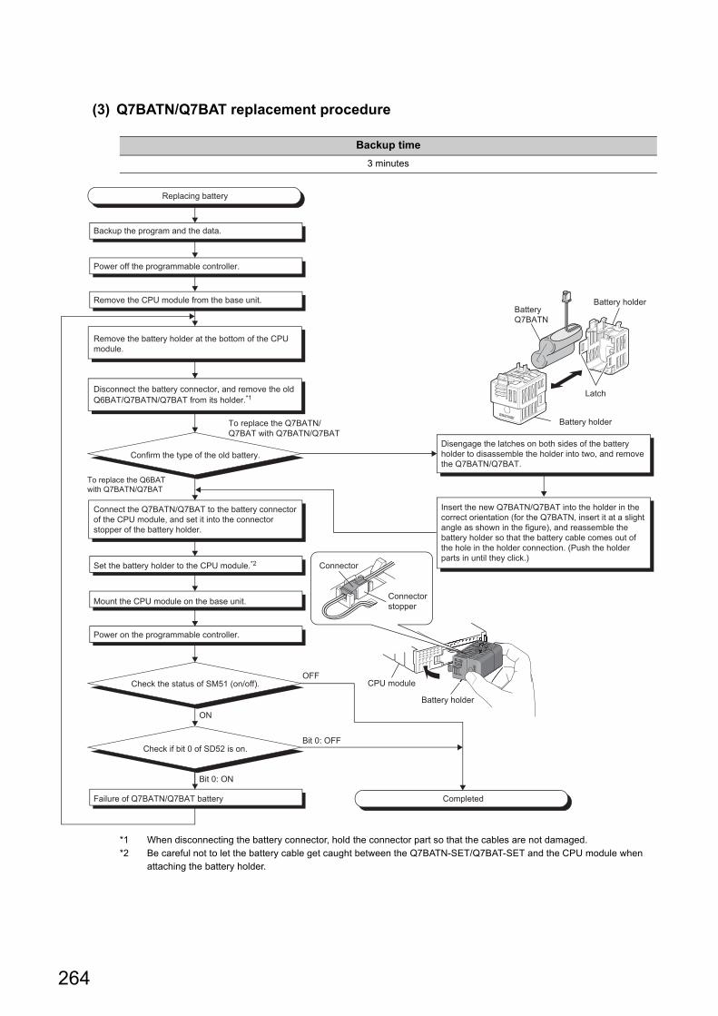
(3) Q7BATN/Q7BAT replacement procedure
*1 When disconnecting the battery connector, hold the connector part so that the cables are not damaged.*2 Be careful not to let the battery cable get caught between the Q7BATN-SET/Q7BAT-SET and the CPU module when
attaching the battery holder.
Backup time3 minutes
ON
OFF
Replacing battery
Backup the program and the data.
Power off the programmable controller.
Remove the CPU module from the base unit.
Remove the battery holder at the bottom of the CPU module.
Disconnect the battery connector, and remove the old Q6BAT/Q7BATN/Q7BAT from its holder.*1
Confirm the type of the old battery.
To replace the Q6BAT with Q7BATN/Q7BAT
Connect the Q7BATN/Q7BAT to the battery connector of the CPU module, and set it into the connector stopper of the battery holder.
Mount the CPU module on the base unit.
Set the battery holder to the CPU module.*2
Power on the programmable controller.
Check the status of SM51 (on/off).
Check if bit 0 of SD52 is on.
Bit 0: ON
Failure of Q7BATN/Q7BAT battery
To replace the Q7BATN/Q7BAT with Q7BATN/Q7BAT
Disengage the latches on both sides of the battery holder to disassemble the holder into two, and remove the Q7BATN/Q7BAT.
Insert the new Q7BATN/Q7BAT into the holder in the correct orientation (for the Q7BATN, insert it at a slight angle as shown in the figure), and reassemble the battery holder so that the battery cable comes out of the hole in the holder connection. (Push the holder parts in until they click.)
Connector
Connector stopper
CPU module
Battery holder
Bit 0: OFF
Completed
Battery holder
Battery holder
BatteryQ7BATN
Latch
264

CHAPTER 13 MAINTENANCE AND INSPECTION
13
13.3 Battery Replacem
ent Procedure13.3.1 C
PU m
odule battery replacement procedure
(4) Q8BAT replacement procedure
*1 When disconnecting the battery connector, hold the connector part so that the cables are not damaged.
Backup time3 minutes
Replacing battery
Power off the programmable controller.
To replace the Q8BAT with Q8BAT
To replace the Q6BAT/Q7BATN/Q7BAT with Q8BAT
Remove the Q8BAT from the control panel.
Remove the CPU module from the base unit.
Remove the cover/battery holder at the bottom of the CPU module.
Disconnect the battery connector, and remove the old Q6BAT/Q7BATN/Q7BAT from its holder.*1
Connect the Q8BAT connection cable to the connector of the CPU module.
Check the type of the old battery.
(To next page)
1)
2)
Backup the program and the data.
Connector of battery
Connector of CPU module
Q6BAT
CPU module Connector of cable
Connector of CPU module
CPU module
Q8BAT connectioncable
Q8BAT connectioncover
Install the new Q8BAT to the control panel.*2 (Fixing with a mounting screw or with the DIN rail is available.
Connect the Q8BAT connection cable to the new Q8BAT.
Remove the Q8BAT connection cable from the Q8BAT.
265

*2 For the module mounting position, refer to the following.
Page 61, Section 4.1.2*3 Clamp the Q8BAT connection cable. If not being clamped, the Q8BAT connection cover, connector, and cable, may be
damaged by a loose cable connection, shifting, or pulling due to carelessness, etc.*4 Secure 10mm or more as the minimum cable bend radius.
If it is less than 10mm, malfunction may occur due to characteristic deterioration, open cable or the like.
Completed
Bit 0: ON
ON
Bit 0: OFF
OFF
Failure of Q8BAT
Fix the Q8BAT connection cable to the control panel.*3
Mount the CPU module on the base unit.
Check the status of SM51 (on/off).
Check if bit 0 of SD52 is on.
(From previous page)
2)
1)
Install the Q8BAT connection cover to the CPU module.
Install the Q8BAT to the control panel.*2 (Fixing with a mounting screw or with the DIN rail is available.)
Connect the Q8BAT connection cable to the Q8BAT.
Power on the programmable controller.
Q8BAT connection cable
CPU module
Q8BAT connection cover
Q8BAT
Control panel
Q8BAT connection cable
Q8BAT
R (bending radius)*4
10mm or more
266

CHAPTER 13 MAINTENANCE AND INSPECTION
13
13.3 Battery Replacem
ent Procedure13.3.1 C
PU m
odule battery replacement procedure
● After replacing a battery, write the date for next battery replacement on the sticker on the back side of the front cover.Write the proper date by checking the battery life. ( Page 613, Appendix 4.2)
● When replacing the battery of a CPU module, pay attention to the following: • Back up the data in the CPU module by a programming tool before starting replacement. • When replacing a battery of a Redundant CPU, back up the memory data such as programs by the memory copy
from the control system to the standby system, and then replace the battery of the CPU module that was changed into the standby status by the system switching function.For the memory copy from control system to standby system and system switching function, refer to the manual below.
QnPRHCPU User's Manual (Redundant System) • When the MELSEC-Q series is used as a UL-certified product, the Q6BAT, Q7BATN, Q7BAT, and Q8BAT
batteries must be replaced by service personnel.The service personnel are defined as experienced technicians who have been sufficiently educated and trained, and are capable of perceiving and avoiding operational hazard.
267

13.3.2 SRAM card battery replacement procedure
Replace the SRAM card battery in the following procedure.
(1) Replacing Q2MEM-1MBSN, Q2MEM-1MBS, Q2MEM-2MBSN, and Q2MEM-2MBS
Bit 1 and bit 2 are OFF.
Replacing battery
Open the front cover while the programmable controller power supply is on.
Remove the battery holder from the SRAM card.
Remove the old battery from its holder.
Insert a new battery into the holder in the correct direction.
Check that the battery holder fixing switch is set to the LOCK position.
With a flat-blade screwdriver, etc., remove the battery holder locking switch from the LOCK position.
Completed
OFF
ON
Bit 1 and bit 2 are ON.
Deeply insert the SRAM card into the battery holder.
Battery holder fixing switch
Flat blade screwdriver
Release direction
Battery holder
Battery holder Used battery
New battery
Put + toward you.
Backup the program and the data.
Failure of SRAM card battery
* The battery holder fixing switch is automatically set to the "LOCK" position when the battery holder is removed. In its position, insert the battery holder to the end.
Lockdirection
Battery holder fixing switch*
Clears the error.
Monitor SD52 to check if bit 1 and bit
2 are ON.
MonitorSM52 to verify on/off.
CPUmodule
CPUmodule
CPUmodule
CPUmodule
Page 422, Appendix 1.10
268

CHAPTER 13 MAINTENANCE AND INSPECTION
13
13.3 Battery Replacem
ent Procedure13.3.2 SR
AM card battery replacem
ent procedure
(2) Replacing Q3MEM-4MBS and Q3MEM-8MBS
Bit 1 and bit 2 are OFF.
Failure of SRAM card battery
OFF
ON
Bit 1 and bit 2 are ON.
Replacing battery
Completed
Backup the program and the data.
Remove the battery holder from the SRAM card.
Remove the old battery from its holder.
Insert a new battery into the holder in the correct direction.
Deeply insert the SRAM card into the battery holder.
Set a battery holder fixing switch to the LOCK position
Set the memory card protective cover on the CPU module.
Remove a memory card protective cover of the CPU module at power-on status of the programmable controller.
With a flat-blade screwdriver, etc., remove the battery holder locking switch from the LOCK position.
MonitorSD52 to check if bit 1 and bit
2 are ON.
Facing "+ (positive)" up, install the battery
LOCK
CPUmodule
Battery holder fixing switch
MonitorSM52 to verify on/off.
Remove a cover, pressing the top and bottom fixing claws.
CPUmodule
CPUmodule
Battery holder
Battery holder fixing switch
Releasedirection
Clears the error.Page 422, Appendix 1.10
269

Be careful about the following to replace the SRAM card battery.
● To back up the data, replace the SRAM card battery with the programmable controller power supply on and the SRAM card installed.
● Start replacement after backing up the CPU module data using a programming tool.
● Since replacement is made with the programmable controller power supply ON, take extreme care not to get an electric shock.
● When dismounting or mounting the battery holder on the SRAM card, take care so that the battery does not come out of the battery holder.
● When replacing the battery with the programmable controller power supply off, always back up the data before starting replacement.[Battery replacement procedure]1) Back up the SRAM card data using the programming tool.2) Replace the battery.3) Write the backed up data from the programming tool to the memory card.
Insert or remove the battery in the horizontal direction along the battery holder fixing guide. Failure to do so may damage the latches of the battery holder.
● If a battery of the SRAM card is hard to replace, use of the following tweezers is recommended.
Product Model namePlastic tweezers NK-2539
Battery fixing guide
Battery holder
Battery holder latches
270

271
CHAPTER 13 MAINTENANCE AND INSPECTION
13
13.4 Operating the Program
mable C
ontroller that Has been Stored
13.4 Operating the Programmable Controller that Has been Stored
When the programmable controller that has been stored with a battery removed or the programmable controller that has been stored with a battery exceeding the guaranteed life installed is operated, data in the following battery-backed-up-memories may be indefinite.
: Battery backed up, ×: Not battery backed up*1 The program memory of the Universal model QCPU does not require battery backup.
Before restarting the operation, format the battery-backed-up-memories listed in above table using a programming
tool. ( Operating manual for the programming tool used)After formatting the memories, write backup data to each memory.To format the program memory during boot operation, select the "Clear Program Memory" checkbox in the Boot File tab of the PLC parameter dialog box.
● Before storing a programmable controller, back up all the data stored in each memory. Write the data with a programming tool before restarting an operation.
● When the programmable controller is powered on or the CPU module is reset, the CPU module initializes all of the following data if an error is detected. Restarting an operation with initialized data may cause an unintended operation.
• Program memory data • Standard RAM data • Error history • Latch data (latch relay (L), devices in latch setting range set in the parameter, special relay SM900 to SM999,
special register SD900 to SD999) • Sampling trace data
● For the Universal model QCPU, when the latch data backup (to standard ROM) function is used, latch data such as device data and error history data in the CPU module can be backed up without using a battery. Therefore, when a programmable controller is stored with a battery removed, the stored data will not be lost.
MemoryBattery
Battery of a CPU ModuleBattery built
in a memory card
CPU module
Program memory *1 ×
Standard RAM(Including an extended SRAM cassette)
×
Standard ROM ---- (Battery backup not required)
Memory card
SRAM card ×
Flash card ---- (Battery backup not required)
ATA card ---- (Battery backup not required)
SD memory card ---- (Battery backup not required)

CHAPTER 14MODULE CHANGE DURING SYSTEM OPERATION
14.1 Online Module Change
An online module change is a function that allows the Q series module mounted on the main base unit or extension base unit to be changed during system control executed by the Process CPU or Redundant CPU.Note 14.1Using an online module change, the module that failed during control can be replaced with the module of the same model name.
● An online module change cannot add a module or change the current module for another module.
● When executing an online module change for the Process CPU in the multiple CPU system, it is necessary to specify "Enable Online Module Change with Another PLC" in the multiple CPU setting of the PLC parameter dialog box.Also, there are restrictions on the versions of the CPU modules that comprise the multiple CPU system. For details, refer to the following.
QCPU User's Manual (Multiple CPU System)
● Perform an online module change after confirming that the system outside the programmable controller will not malfunction.
● To prevent an electric shock, operating module malfunction, etc., provide a switch or similar individually cutting-off means for the external power supply of the module to be changed online.
● It is recommended to verify that the operations of the unchanged modules will not be affected by executing an online module change in an actual system beforehand to confirm the following.
• The means and structure that will cut off the connection with the external device are correct. • ON/OFF of switches, etc. has no influence.
● After first use of the product, do not perform the following operation more than 50 times (IEC 61131-2/JIS B 3502 compliant). Exceeding the limit may cause malfunction.
• Mounting/removing the module to/from the base unit
Note 14.1
The Basic model QCPU, High Performance model QCPU, and Universal model QCPU do not support this function.
Note 14.1
Basic Highperformance Universal
272

CHAPTER 14 MODULE CHANGE DURING SYSTEM OPERATION
14
14.1 Online M
odule Change
(1) System configuration that allows online module changeAn online module change can be performed under the following conditions.
(a) Modules that can be changed onlineThe following table lists modules that can be changed online.
*1 When using Redundant CPU and/or connecting an extension base unit, online module change cannot be performed to an intelligent function module mounted on the main base unit.
The modules other than listed above cannot be changed online.For whether the above intelligent function modules can be changed online or not and their changing procedures, refer to the manual of the used intelligent function module.
(b) Versions of a programming tool that supports online module changeA programming tool is required to perform an online module change.For versions of a programming tool, refer to the operating manual for the programming tool used.An online module change can also be performed from a programming tool via a network.
(c) Restrictions on base units • When the slim type main base unit (Q3SB) is used, an online module change cannot be performed. • When the extension base unit of the type that requires no power supply module (Q5B) is used, an online
module change cannot be performed for the modules mounted on all base units connected. • When the redundant type extension base unit (Q6WRB) is used, the online module change cannot be
performed to all modules connected to the main base unit.
Module type RestrictionsInput module
No restrictionsOutput module
I/O combined module
Intelligent function module
Analog-digital converter module
Supported by function version C.*1Digital-analog converter module
Temperature input module
Temperature control module
Pulse input module
273

(d) Control status of CPU moduleA module can be changed online when a stop error does not occur.The following table describes whether a module can be changed online or not depending on the control status of the CPU module.
*1 Including the case where a continue error has occurred in the RUN status.
An online module change can be continued even when the CPU module is set to the STOP or PAUSE status during the operation. In either of the following cases, however, online module change cannot be continued.
• When the CPU module is reset • When a stop error occurs
(e) Number of modules that can be changed onlineThe number of modules that can be changed online at one time is one for each CPU module.Multiple modules cannot be changed simultaneously.
Control status RUN status*1 STOP status PAUSE status At stop errorWhether online module change can be executed or not
Can be executed Can be executed Can be executed Cannot be executed
274

CHAPTER 14 MODULE CHANGE DURING SYSTEM OPERATION
14
14.1 Online M
odule Change
(2) Restrictions on online module changeThe following operations cannot be performed during an online module change.
• Issue an online module change request from multiple programming tools to one CPU module. • Write parameters to the CPU module during online module change.
The following message appears if an online module change request is issued from another programming tool to the CPU module during online module change. After confirming the message, select "Yes" or "No".
● When "Yes" is selectedOnline module change operation is switched to "Programming tool 2)" that issued the request later. (Operation is continued from the pre-switching status.)
● When "No" is selectedThe operation of online module change "Programming tool 2)" requested later is suspended. (Online module change "Programming tool 1)" executed first is continued.)
Online module changeexecution canceled
Online modulechange continued
Programming tool 1)Programming tool 2)
"Yes" selected
Programming tool 1)Programming tool 2)
"No" selected
Online modulechange suspended
Online module changeexecution continued
275

(3) Special relays and special register related to online module changeInformation during online module change is stored into the special relays (SM235, SM236) and special register (SD235).
• Whether the online module change of the corresponding CPU module is executed or not can be checked by monitoring SM235, SM236 and SD235.
• SM235: Online module change flag (turns on during online module change) • SM236: Flag that turns on only one scan after online module change (turns on only one scan after
completion of online module change) • SD235: Module being changed online (stores the starting I/O number of the module being changed
online10H)
Refer to Page 468, Appendix 2 for details of SM235 and SM236 and to Page 517, Appendix 3 for details of SD235.
OFF
ON
OFF
ONSM235
SD235
SM236
1 scan
Online module change start
Online module change completed
Starting I/O number of module being changed online 10H
276

CHAPTER 14 MODULE CHANGE DURING SYSTEM OPERATION
14
14.1 Online M
odule Change
(4) Online module change procedureThe following explains the online module change procedure of the I/O module.For the online module change procedure of the intelligent function module, refer to the manual of the used intelligent function module.
● It is recommended to turn off the output (Y) from the output module/I/O combined module to be changed online before it is changed.
● When making an online module change for the Redundant CPU, specify "No settings have been made (Default)", "System A" or "System B" as the target system in the "transfer setup" by a programming tool.Do not specify the "Control system" or "Standby system" as the target system.If the "Control system" or "Standby system" is specified in the transfer setup, the following error dialog appears at execution of an online module change.When the following error dialog is displayed, change the target system to "No settings have been made (Default)", "System A" or "System B", and then perform an online module change.
● When executing online module change for the module mounted on the extension base unit in the Redundant CPU, access cannot be made to a module mounted on the extension base unit from the standby system. Set [Transfer setup] in a programming tool, checking that the transfer target Redundant CPU module is the control system.
1. Online module change can be performed by the following operation.
[Diagnostics] [Online Module Change]
277

2. Double-click the module to be changed online. The Online Module Change screen appears.(The following table lists the communication status with the change-target module while the following screen is displayed.)
3. Click the "Execution" button to enable the online module change operation.(The following table lists the communication status with the target module for online module change when the following screen is displayed.)
4. Cut off the connection (I/O signal communication) with the external device using a switch.
5. Turn off the external power supply for the module. Power supply to the module is shut off.
6. Disconnect the terminal block or connector from the module.
7. Remove the module from the base unit. ( Page 73, Section 4.2.3)
8. Mount a new module on the same slot. ( Page 73, Section 4.2.3)
9. Connect the terminal block or connector to the new module.
10. Turn on the external power supply for the module. Power supply to the module is resumed.
11. Establish a connection (I/O signal communication) with the external device using a switch.
Target module, itemExecuted/Not
executedInput module refresh ExecutedOutput module refresh Executed
I/O hybrid moduleInput refresh ExecutedOutput refresh Executed
Intelligent function module
Input refresh ExecutedOutput refresh ExecutedFROM/TO instruction ExecutedInstruction using intelligent function module device
Executed
Intelligent dedicated instruction ExecutedIntelligent automatic refresh Executed
Buffer memory batch monitor Executed
Target module, itemExecuted/Not
executed
Input module refreshNot executed(Data held)
Output module refresh Not executed
I/O hybrid moduleInput refresh
Not executed(Data held)
Output refresh Not executed
Intelligent function module
Input refresh Not executedOutput refresh Not executedFROM/TO instruction No processingInstruction using intelligent function module device
No processing
Intelligent dedicated instruction No processingIntelligent automatic refresh No processing
Buffer memory batch monitorCommunication error
278

CHAPTER 14 MODULE CHANGE DURING SYSTEM OPERATION
14
14.1 Online M
odule Change
12.After changing the module, click the "Execution" button.(The following table lists the communication status with the change-target module while the following screen is displayed.)
When the initial settings of the intelligent function module have been made by GX Configurator, the set data are written to the intelligent function module.
13.Click the "Execution" button again to start control.
14. The screen that notifies the operation completion appears.(The following table lists the communication status with the change-target module while the following screen is displayed.)
Target module, itemExecuted/Not
executed
Input module refreshNot executed(Data held)
Output module refresh Not executed
I/O hybrid moduleInput refresh
Not executed(Data held)
Output refresh Not executed
Intelligent function module
Input refresh ExecutedOutput refresh ExecutedFROM/TO instruction No processingInstruction using intelligent function module device
No processing
Intelligent dedicated instruction No processingIntelligent automatic refresh No processing
Buffer memory batch monitor Executed
Target module, itemExecuted/Not
executedInput module refresh ExecutedOutput module refresh Executed
I/O hybrid moduleInput refresh ExecutedOutput refresh Executed
Intelligent function module
Input refresh ExecutedOutput refresh ExecutedFROM/TO instruction ExecutedInstruction using intelligent function module device
Executed
Intelligent dedicated instruction ExecutedIntelligent automatic refresh ExecutedBuffer memory batch monitor Executed
279

(5) Operation in case of system switching occurrence during online module change (When Redundant type extension base unit is used)The following describes the procedures to be taken when the system switching occurs during online module change is performed to the module mounted on the extension base unit in the Redundant CPU.
1. Connect GX Developer to the new control system.
2. Check the status of the module being replaced on the System monitor screen.(The online module change status can be checked with SM235 of the new control system and standby system.)
3. Select "Online module change" in the System monitor screen while the online module change is being performed. The following screen appears.
4. The operation that has been executed before the system was switched continues.
280

CHAPTER 14 MODULE CHANGE DURING SYSTEM OPERATION
14
14.1 Online M
odule Change
● If the "Execution" button is clicked on the condition that GX Developer is connected to the new control system, the following message may appear. Click "Yes" and continue the online module change operation.
● When the online module change operation is completed, the following error dialog box may appear. Even though the operation has been completed successfully.
281

14.2 Change of Redundant Power Supply Module
Following the flowchart shown below, change a faulty redundant power supply module online (with power on).(It is assumed that the other redundant power supply module is normally operating.)
● If either redundant power supply module fails, change it for a normal one earlier than usual (within 14 days as a guideline). If it does not fail, it is recommended to change the redundant power supply module for a new one after five years have elapsed.
● Change the redundant power supply module with extreme care, referring to Page 73, Section 4.2.3 (1). If the module fixing projection of the redundant power supply module comes off from the module fixing hole of the redundant base unit, an error will occur due to connector damage.
● When the redundant power supply system is used, a "continue" error will occur due to a redundant power supply module failure. Cancel the error after changing the faulty redundant power supply module for a normal one.
Note 14.2
● When the redundant power supply system is used, the failure status of the redundant power supply module can be checked by the system monitor of GX Developer (Version 8.18U or later) or the special relay SM1781/special register
SD1781. Note 14.3For details of the system monitor, refer to the following.
Operating manual for the programming tool used
Note 14.2
Failure of redundant power supply cannot be detected by the Basic model QCPU.
Note 14.3
When using the High Performance QCPU or the Process CPU, check the versions of the CPU module and programming
tool used. ( Page 648, Appendix 6)
Start
Completed
Check the redundant power supply module to be changed.
Power OFF the redundant power supply module to be changed.
Change the redundant power supply module.
Power ON the new redundant power supply module.
Make sure that the "POWER" LED is turned on green.
Note 14.2, Note 14.3
Basic
Note 14.2, Note 14.3
Highperformance Process
282

CHAPTER 15 TROUBLESHOOTING
15
CHAPTER 15TROUBLESHOOTING
This chapter describes errors that may occur during system operation, the error causes, and measures against the errors.For a redundant system (when the Redundant CPU is used), refer to the following.
QnPRHCPU User's Manual (Redundant System)
When the system has trouble, perform troubleshooting in the following order.
• Visual inspection ( Page 284, Section 15.1)
• Error checking and corrective actions ( Page 289, Section 15.2)
RemarkSaving the program and devices at the time of an error helps to analyze the error cause.( Page 312, Section 15.4)
283

15.1 Visual Inspection
Visually check the following.
(1) LED statusCheck if there is a hardware failure or not. Check the status of each LED in the following order.For the module status corresponding to the LED indication, refer to the "Part Names" section.
• CPU module ( Page 121, Section 6.1)
• Power supply module ( Page 195, Section 7.1)
1. Power on the system. Check the POWER LED status of the power supply module.If the POWER LED does not turn on even when power is supplied, perform the following troubleshooting.
Page 285, Section 15.1.1
2. Check the color of the POWER LED.When the POWER LED does not turn on in green, perform the following troubleshooting.
Page 285, Section 15.1.2
3. When using the Life detection power supply module, check the LIFE LED status.When the LIFE LED does not turn on in green or orange, perform the following troubleshooting.
Page 286, Section 15.1.3
4. Check the MODE LED status of the CPU module.When the MODE LED does not turn on, perform the following troubleshooting.
Page 287, Section 15.1.4
5. Check the RUN LED status of the CPU module.When the RUN LED does not turn on, perform the following troubleshooting.
Page 288, Section 15.1.5
6. When using the High Performance model QCPU, Process CPU, or Redundant CPU, check the BOOT LED status.When the BOOT LED flickers, perform the following troubleshooting.
Page 288, Section 15.1.6
7. Check the ERR. LED status of the CPU module.When the ERR. LED is on or flickering, an error exists.Check the error with the programming tool. ( Page 289, Section 15.2)
8. Check the BAT. LED status of the CPU module.When the BAT. LED is on, the battery voltage is low.Replace the battery. ( Page 262, Section 13.3)
(2) Communication cable and wiringCheck if any communication cable has a problem or not. Check also that connectors and terminal blocks are correctly mounted or wired.
Page 105, Section 4.8
284

CHAPTER 15 TROUBLESHOOTING
15
15.1 Visual Inspection15.1.1 W
hen the POW
ER LED
does not turn on
15.1.1 When the POWER LED does not turn on
Check the following.
If the POWER LED does not turn on even after taking the above actions, the possible cause is a hardware failure of the power supply module or base unit.Please consult your local Mitsubishi representative.
15.1.2 When the POWER LED does not turn on in green
Check the following items according to the POWER LED status.
(1) When the POWER LED turns on in redRemove the power supply module and mount it to the normal base unit. Resupply power to the system.If the POWER LED turns on in red after resupplying power, the power supply module is failed.If the POWER LED does not turn on even after the power is supplied during the above operation, also
check the items described in Page 285, Section 15.1.1.
(2) When the POWER LED flickers in orangeResupply power to the system. If the POWER LED flickers in orange after resupplying power, the power supply module is failed.If the POWER LED does not turn on even after the power is supplied during the above operation, also check the
items described in Page 285, Section 15.1.1.
Check item Corrective action
The MODE LED of the CPU module is on.The power supply module has failed. Replace the power supply module.
Power supply voltage is not appropriate.Supply power voltage within the specified range.
( Page 203, Section 7.2)
The internal current consumption for the entire system exceeds the rated output current of the power supply module.
Reexamine the system configuration so that the internal current consumption does not exceed the rated output current.
( Page 686, Appendix 10)
The POWER LED turns on when power is supplied again to the system after all modules, except for the power supply module, were removed.
Repeatedly supply power to the system, returning the modules back to the system one by one.The last module mounted immediately before the POWER LED turned off is failed.
285

15.1.3 When the LIFE LED does not turn on in green or orange
Check the following items according to the LIFE LED status.
(1) When the LIFE LED is offResupply power to the system. If the LIFE LED turns on in red for one second, replace the power supply module as the power supply module has reached its end of life.If the LIFE LED does not turn on or flicker after resupplying power, the power supply module should be replaced as the life diagnosis is impossible.
(2) When the LIFE LED turns on in red
(3) When the LIFE LED flickers in redSupply power to the system again. If the LIFE LED does not turn on in green or orange even after the power is supplied, check the wiring between LG and FG by referring to the following.
• Grounding a programmable controller ( Page 118, Section 4.8.4)
• Wiring a power cable and a ground wire ( Page 666, Appendix 8.1.2 (2))
• Grounding a power supply part ( Page 674, Appendix 8.1.5)If the symptom still remains after the check, replace the power supply module.
Check item Corrective actionThe operating ambient temperature is out of the range of 0 to 55°C.
Keep the operating ambient temperature within the range of 0 to 55°C.
The LIFE LED turns on in red after power is resupplied.
Stop the operation of the power supply module for a while, and resupply power to the system after the internal temperature of the module is lowered.If the LIFE LED does not turn on in green or orange after resupplying power, replace the power supply module.
286

CHAPTER 15 TROUBLESHOOTING
15
15.1 Visual Inspection15.1.4 W
hen the MO
DE LED
does not turn on
15.1.4 When the MODE LED does not turn on
Check the following items.
For the module that caused a problem, please consult your local Mitsubishi service representative.
Check item Corrective actionThe forced ON/OFF is set. Cancel the forced ON/OFF.
When the High Performance model QCPU, Process CPU, or Redundant CPU are used, RESET/L.CLR switch is not in the neutral position.
Set the RESET/L.CLR switch to the neutral position.
The MODE LED turns on when power is supplied to the system again after the power supply module was replaced.
The original power supply module has a problem.Please consult your local Mitsubishi representative.
The MODE LED does not turn on even when power is supplied to the system again after the power supply module was replaced.
The CPU module or any other module mounted has a problem.Repeatedly supply power to the system, returning the modules back to the system one by one.The last module mounted immediately before the MODE LED turned off is failed.
The POWER LED turns on when power is supplied again to the system after all modules, except for the power supply module, were removed.
Repeatedly supply power to the system, returning the modules back to the system one by one.The last module mounted immediately before the POWER LED turned off fails.
The connection direction of the extension cable is improper. (The connection direction is OUT-OUT.)
Connect the extension cable properly.
AC power is not supplied to the power supply module. Supply AC power to the power supply module.
287

15.1.5 When the RUN LED does not turn on
Check the following items.
15.1.6 When the BOOT LED flickers
Turn off the programmable controller and remove the memory card. Turn the DIP switches SW2 and SW3 to ON.When the BOOT LED turns on after power is resupplied, boot operation from the standard ROM starts.If the BOOT LED does not turn on, the possible cause is the hardware failure of the CPU module.Please consult your local Mitsubishi representative.
Check item Corrective actionThe RUN LED of the CPU module flickers. Reset the CPU module or set it to RUN from STOP.
The ERR. LED of the CPU module is on or flickering.Check the error details by the programming tool.
( Page 289, Section 15.2)
The RUN LED turns on when the CPU module is reset and set to RUN again.
The module is possibly affected by excessive noise. Take
noise reduction measures. ( Page 663, Appendix 8)If the same problem frequently occurs even after the noise reduction measures are taken, the programmable controller possibly has any defective part or poor connection.Please consult your local Mitsubishi representative.
288

CHAPTER 15 TROUBLESHOOTING
15
15.2 Checking the Error D
etails
15.2 Checking the Error Details
Error causes and corrective actions can be checked by the programming tool.
If the connection cannot be established, check that the settings in the programming tool are correct.
Operating manual for the programming tool used
When the programming tool and the CPU module are connected via Ethernet, check the error details by Ethernet
diagnostics and remove the error cause. ( Page 291, Section 15.2 (3))
(1) PLC diagnosticsWhen the ERR. LED turns on or flickers, check the error details in the PLC diagnostics of the programming tool and remove the error cause.
[Diagnostics] [PLC Diagnostics]
For details on the PLC diagnostics, refer to the following.
Operating manual for the programming tool used
289

(2) Module detailed informationWhen an error occurs in any intelligent function module, check the error details in System monitor of the programming tool and remove the error cause.
[Diagnostics] [PLC Diagnostics]
For details on the module detailed information, refer to the following.
User's manual for the intelligent function module used
1. Select the error module in "Main Base" and click the
button.
2. Detailed information of the selected module is displayed.
290

CHAPTER 15 TROUBLESHOOTING
15
15.2 Checking the Error D
etails
(3) Ethernet diagnosticsUsing the diagnostics function of the programming tool, the module status, parameter settings, communication status, and error history of the Built-in Ethernet port QCPU can be checked.
[Diagnostics] [Ethernet Diagnostics]
For details on the Ethernet diagnostics, refer to the following.
Operating manual for the programming tool used
The MELSOFT connection where User Datagram Protocol (UDP) is used is regarded as one connection in "Status of Each Connection".Therefore, even if multiple connections are used, the diagnostics result is displayed as one connection.
291

15.3 Checking for Functional Errors
If the module has a functional problem, check the following items and perform troubleshooting. If the ERR. LED is on
or flickering, remove the error cause by the programming tool. ( Page 289, Section 15.2)
Function Error status Reference
Write to PLCData cannot be written to the CPU module. Page 293, Section 15.3.1 (1)
The program is rewritten unintentionally. Page 293, Section 15.3.1 (2)
Read from PLC Data cannot be read from the CPU module. Page 293, Section 15.3.1 (3)
Boot operationA boot operation cannot be performed from a memory card or SD memory card. Page 294, Section 15.3.2
Error caused by hardwareUNIT VERIFY ERR. has occurred. Page 295, Section 15.3.3 (1)
CONTROL BUS ERR. has occurred. Page 295, Section 15.3.3 (2)
Ethernet communication
Direct connection is not possible. Page 296, Section 15.3.4 (1)
Ethernet communication is not possible when using a method other than direct connection.
Page 297, Section 15.3.4 (2)
Ethernet communication is not possible with the connected device. Page 297, Section 15.3.4 (3)
Clock data cannot be set by SNTP. Page 299, Section 15.3.4 (4)
Socket communication function
The connected device cannot receive data. Page 301, Section 15.3.5 (1)
Data cannot be received. Page 301, Section 15.3.5 (2)
The open processing is not completed. Page 301, Section 15.3.5 (3)
Simple PLC communication function
Communication with a communication target station is not possible. Page 302, Section 15.3.6 (1)
Communication with a communication target station is unstable. Page 302, Section 15.3.6 (2)
Communication is not performed at preset intervals. Page 303, Section 15.3.6 (3)
The update by reading and writing the device data is slow. Page 303, Section 15.3.6 (4)
MC protocol functionAn error has occurred during MC protocol communication. Page 304, Section 15.3.7
Errors caused by SFC program instruction
"OPERATION ERROR" has occurred at execution of the S(P).SFCSCOMR and S(P).SFCTCOMR instructions.
Page 307, Section 15.3.11 (1)
Comments cannot be read at execution of the S(P).SFCSCOMR and S(P).SFCTCOMR instructions.
Page 307, Section 15.3.11 (2)
I/O module
The LEDs of the output module do not turn on. Page 308, Section 15.3.12 (1)
I/O module does not operate normally. Page 308, Section 15.3.12 (2)
Wiring troubles I/O Module Type Building Block User's Manual
Power supply module
The LIFE OUT terminal has turned off (opened). Page 309, Section 15.3.13 (1)
The ERR. terminal has turned off (opened). Page 309, Section 15.3.13 (2)
292

CHAPTER 15 TROUBLESHOOTING
15
15.3 Checking for Functional Errors
15.3.1 Write to PLC
and Read from
PLC
15.3.1 Write to PLC and Read from PLC
(1) Write to PLCIf data cannot be written from the programming tool to the CPU module, check the following items.
If data cannot be written to the CPU module even after taking the above actions, the possible cause is a hardware failure.Please consult your local Mitsubishi representative.
(2) The program is rewritten unintentionallyThe CPU module possibly performs boot operation. Perform Read from PLC with the programming tool and check the boot file setting.When boot operation is not performed, the possible cause is a hardware failure.Please consult your local Mitsubishi representative.
For details on the boot operation, refer to the following.
User's manual (Function Explanation, Program Fundamentals) for the CPU module used
(3) Read from PLCIf data cannot be read from the CPU module to the programming tool, check if the target memory has been correctly set.After making sure that the target memory has been correctly set, reset the CPU module, and then read data from the CPU module again.When the RS-232 is used for connection, reduce transmission speed, and read data from the CPU module again.
If data cannot be read from the CPU module even after taking the above actions, the possible cause is a hardware failure.Please consult your local Mitsubishi representative.
CC-Link IE Field Network Basic functionAn error has occurred while the CC-Link IE Field Network Basic function was being used.
CC-Link IE Field Network Basic Reference Manual
Check item Corrective actionWhen the High Performance model QCPU, Process CPU, or Redundant CPU are used, the DIP switch SW1 is on.
Turn the DIP switch SW1 to OFF.
The data is password-protected. Unlock the password with the programming tool.
The write-target memory card or SD memory card is write-protected.
Cancel the protection.
The write-target memory card or SD memory card has not been formatted.
Format the card.
The size of data to be written is larger than the memory capacity.
• Secure sufficient free space in the memory.• Organize the target memory.
Function Error status Reference
293

15.3.2 Boot operation
If boot operation cannot be performed from the memory card or SD memory card, check the following items.
If a boot operation cannot be performed even after taking the above actions, the possible cause is a hardware failure.Please consult your local Mitsubishi representative.
Check item Corrective action
An error has occurred in the CPU module. Remove the error cause. ( Page 289, Section 15.2)
When the High performance model QCPU, Process CPU, or Redundant CPU are used, the DIP switches do not specify the valid parameter drives.
Specify the valid parameter drives with the DIP switches SW2 and SW3.
A file is not set with parameter boot file setup.Set the file.
A file is not set with parameter program setup.
A file to be used has not been stored in the memory card or SD memory card.
Store the file to be used.
294

CHAPTER 15 TROUBLESHOOTING
15
15.3 Checking for Functional Errors
15.3.3 Errors caused by hardware
15.3.3 Errors caused by hardware
(1) UNIT VERIFY ERR. has occurredIf UNIT VERIFY ERR. has occurred, check the following items.
If UNIT VERIFY ERR. occurs even after taking the above actions, perform the following actions sequentially for recovery to normal operation.
• Check the target slot No. in the common information (SD5) of the error code, and replace the corresponding module.
• Replace the CPU module. • Replace the base unit.
If UNIT VERIFY ERR. occurs even after taking the above actions, the possible cause is a hardware failure.Please consult your local Mitsubishi representative.
(2) CONTROL BUS ERR. has occurredIf CONTROL BUS ERR. has occurred, check the following items.
If CONTROL BUS ERR. occurs even after taking the above actions, perform the following actions sequentially for recovery to normal operation.
• Check the target slot No. in the common information (SD5) of the error code, and replace the corresponding module.
• Replace the CPU module. • Replace the base unit.
If CONTROL BUS ERR. occurs even after taking the above actions, the possible cause is a hardware failure.Please consult your local Mitsubishi representative.
Check item Corrective actionThe module was attached or detached during operation, or improperly mounted.
Mount the module properly and reset the CPU module.
When the extension base unit is used, the extension cable is improperly connected.
Connect the extension cable properly and reset the CPU module.
Check item Corrective actionThe module is improperly mounted. Mount the module properly and reset the CPU module.
When the extension base unit is used, the extension cable is improperly connected.
Connect the extension cable properly and reset the CPU module.
Noise affects the module. Take noise reduction measures. ( Page 663, Appendix 8)
295

15.3.4 Ethernet communication
(1) Direct connection is not possibleIf Ethernet communication is not possible through direct connection with the programming tool, check the following items.
If Ethernet communication cannot be performed even after taking the above actions, the possible cause is a hardware failure.Please consult your local Mitsubishi representative.
*1 When two or more Ethernet ports are enabled in the network connections setting on the personal computer, communication by direct connection is not possible. In the setting, leave only one Ethernet port enabled for direct connection and disable other Ethernet ports.
Check item Corrective actionThe CPU module is not directly connected to the programming tool with a single cable.
Directly connect the CPU module to the programming tool
with a single cable.*1
The setting on the connected device (personal computer) is incorrect.• Ethernet port setting• Firewall setting• Communication setting of security software
Correct the setting on the connected device.
In the Transfer Setup setting of the programming tool, "Ethernet Port Direct Connection" is not selected for the PLC side I/F PLC Module.
Correct the Transfer setup setting.
When parameters are read after switching to USB connection, "Disable direct connection to MELSOFT" is selected in the Built-in Ethernet port setting.
Correct the parameter.
In "Status of Each Connection" of "Ethernet Diagnostics", MELSOFT Direct Connection is set in forced deactivation status.
Disable the forced deactivation.
In the "Error History" of "Ethernet Diagnostics", an error for direct connection is detected.
Take corrective actions according to the error code.
Communication can be performed by increasing the value of communication time check period or number of retries in the detailed host station setting of "Transfer Setup"
• Adjust the value of communication time check period or number of retries.
• Check the condition of the cables, connected device (personal computer), and CPU module.
The connected device (personal computer) does not support the direct connection.
Connect a hub.
296

CHAPTER 15 TROUBLESHOOTING
15
15.3 Checking for Functional Errors
15.3.4 Ethernet comm
unication
(2) Ethernet communication is not possible when using a method other than direct connectionIf Ethernet communication is not possible in a method other than direct connection with the programming tool, check the following items.
If Ethernet communication cannot be performed even after taking the above actions, the possible cause is a failure of the connected device.
Check the items described in Page 297, Section 15.3.4 (3).
(3) Ethernet communication is not possible with the connected deviceIf Ethernet communication is not possible with the connected device, check the following items.
Check item Corrective action
IP addresses are overlapping.
• Check the duplicate IP addresses using the Find CPU function, and correct the IP addresses.
• Correct the IP address of the programming tool (personal computer) so that it differs from the address of the CPU module.
• Disconnect the device from the network, and ping the IP address of the disconnected device. If there is any response, the same IP address is used. Correct the IP address.
The specified protocol is incorrect.
Correct the Transfer Setup setting."Ethernet Port Direct Connection" is selected.
The specified IP address or host name is incorrect.
Check item Corrective actionAn error has occurred in a hub. Remove the error from the hub.*1
The setting on the connected device (personal computer) is incorrect.• IP address setting• Ethernet port setting• Firewall setting• Communication setting of security software
Correct the setting on the connected device.
The SD/RD LED of the CPU module is not flickering during communication.
Confirm the wiring.
IP addresses are overlapping.
• Correct the IP address of the connected device so that it differs from the address of the CPU module.
• Disconnect the device from the network, and ping the IP address of the disconnected device. If there is any response, the same IP address is used. Correct the IP address.
The ERR. LED turns on or flickers when power is resupplied. Remove the error cause. ( Page 289, Section 15.2)
When parameters are read after switching to USB connection, the Built-in Ethernet Port Setting is incorrect.
Correct the parameter.
In "Status of Each Connection" of "Ethernet Diagnostics", MELSOFT Direct Connection is set to the forced deactivation status.
Disable the forced deactivation.
In the "Error History" of "Ethernet Diagnostics", an error for direct connection is detected.
Take corrective actions according to the error code.
297

If Ethernet communication cannot be performed even after taking the above actions, the possible cause is a hardware failure.Please consult your local Mitsubishi representative.
*1 If the switching hub is reconnected to the personal computer or CPU module or is replaced with another, it may take time to read the MAC addresses. In that case, retry after a little while, or resupply power to the hub. If a dummy UDP message is sent by the socket communication function, the switching hub may learn the MAC addresses again.
*2 Devices on the Ethernet have the "ARP cache", which is the correspondence table of the IP address and MAC address. When a device on the network is replaced with the device of the same IP address, their MAC addresses stored in each "ARP cache" become inconsistent, which may cause abnormal communication.The "ARP cache" is updated by resetting the device or after a certain period of time. The time required for updating differs depending on devices.
The number of connections from the connected device (personal computer) exceeds the number of "MELSOFT connection" of the open setting (each number of connections of TCP and UDP).
Keep the number of connections of the connected device (personal computer) within the number in the open setting.
A device was powered off with the TCP/IP connection open.
The TCP/IP connection is left open.Perform the following:• Wait for about one minute, and retry after the connection is
closed by the alive check function of the CPU module.• Increase the number of connections in the setting to
reserve a spare connection.
Communication can be performed by increasing the value of communication time check period or number of retries in the detailed host station setting of "Transfer Setup".
• Adjust the value of communication time check period or number of retries.
• Check the condition of the cables, connected device (personal computer), and CPU module.
Any of the following settings is incorrect on the CPU module or connected device side.• Network address• Default router IP address• Subnet mask pattern• Router IP address• Subnet mask
Correct the setting.
When a router is used, an error has occurred in the router. Remove the error from the router.
When a router is used, the setting on the router is incorrect. Correct the setting on the router.
Any device on the network such as the CPU module, connected device (personal computer), hub, or router is replaced. (When replaced with the device of the same IP address)
Reset the devices on the network.*2
Communication is possible after replacement of the hub or router.
The hub or router may be faulty.Replace the hub or router.
Check item Corrective action
298

CHAPTER 15 TROUBLESHOOTING
15
15.3 Checking for Functional Errors
15.3.4 Ethernet comm
unication
(4) Clock data cannot be set by SNTPIf the clock data cannot be set by SNTP, refer to the following.
If the clock data cannot be set by SNTP even after taking the above actions, the possible cause is a failure of the connected device.
Check the items described in Page 297, Section 15.3.4 (3).
Check item Corrective action
The time setting function does not operate. (Check "Ethernet Diagnostics" or the special register (SD1270).)
Check the following on the time setting function.• SNTP is set to be used.• Input of the SNTP server IP address is correct.• Input of each executing condition is correct.• Input of a time zone is correct.
The time setting is failed. (Check "Ethernet Diagnostics" or the special register (SD1270).)
• Make sure the CPU parameter is normal.• Make sure the specified SNTP server operates normally.
For the multiple CPU system: CPU module for which the time is set is not No. 1.
Set the time for the CPU module No. 1.
The CPU module parameter is not normal. Correct the parameter.
The time is overwritten from a program or another device. Remove overwriting from a program or another device.
299

(5) Communication is slow or unstableIf communication is slow or unstable, check the following items.
Check item Corrective action
IP addresses are duplicate.
Correct the duplicate IP address. The duplicate IP addresses are checked in the following way.• Detect the IP address using the Find CPU function.• Remove the connected device from the network, and
perform PING with the IP address of the removed device. If any device responds, IP addresses are duplicate.
The number of connections of UDP exceeds the number set to "UDP" of the open setting (each number of connections of MELSOFT connection and the MC protocol).
Keep the number of connections of UDP within the number of the open setting.
Communication is based on UDP. Perform communication on TCP.
Communication is not retried.Retry communication.Increase the number of retries.
The hub, router, or cable has an error. Replace the hub, router, or cable.
Communication of devices other than the CPU module is not stable.
• Take noise reduction measures.• Check the amount of network traffic. If the traffic causes
instability, reduce the amount of traffic.
Many of unnecessary broadcast data are received.(The broadcast data volume can be checked in "Connection Status" in Ethernet diagnostics)
To reduce the Ethernet communication load of the CPU module, increase the service processing time in the service processing setting of the PC parameter.
Reduce the broadcast data volume on the network.• Identify a broadcasting device, and restrict the broadcast
data volume. (Devices such as personal computers or routers.)
• Use filtering of broadcast data with a router to prevent the CPU module from receiving them.
• Separate the network with frequent broadcasts from the network of the CPU module.
The Ethernet communication load of the CPU module is high.
• Increase the service processing time in the service processing setting of the PLC parameter.
• Reduce the number of connected devices.• Reduce the communication frequency per connection and
data volume.
The interrupt program is used.Reduce the frequency and process time of the interrupt program.
300

CHAPTER 15 TROUBLESHOOTING
15
15.3 Checking for Functional Errors
15.3.5 Socket comm
unication function
15.3.5 Socket communication function
For the details on the socket communication function, refer to the following.
QnUCPU User's Manual (Communication via Built-in Ethernet Port)
(1) The connected device cannot receive dataIf data is not delivered to the target device, check the following items.
(2) Data cannot be receivedIf the CPU cannot receive data from the connected device, check the following items.
(3) The open processing is not completedIf the open processing is not completed, check the following items.
(a) Passive open
(b) Active open
Check item Corrective actionThe connection has not been opened yet.(Check the corresponding bit in SD1282.)
Wait until the connection is completed.
An error is detected in Ethernet diagnostics. Remove the error cause.
A parameter or a setting data for SOCOPEN is incorrect. Correct the parameter or setting data.
The SOCSND instruction is not executed. (Check the start contact and error completion device.)
Correct the execution condition, or remove the error cause that is identified by the error code in the completion status area of the SOCSND instruction.
The connected device has an error. Correct the error of the connected device.
Check item Corrective actionThe connection has not been opened yet.(Check the corresponding bit in SD1282.)
Wait until the connection is completed.
An error is detected in Ethernet diagnostics. Remove the error cause.
A parameter or a setting data for SOCOPEN is incorrect. Correct the parameter or setting data.
The SOCRCV instruction was not executed. (Check the start contact and error completion device.)
Correct the execution condition, or remove the error cause that is identified by the error code in the completion status area of the SOCOPEN instruction.
The connected device has an error. Correct the error of the connected device.
Check item Corrective actionThe parameter is incorrect. Correct the parameter.
The connected device has an error. Correct the error of the connected device.
Check item Corrective actionAn error is detected in Ethernet diagnostics. Remove the error cause.
A parameter or a setting data for SOCOPEN is incorrect. Correct the parameter or setting data.
The SOCRCV instruction was not executed.(Check the start contact and error completion device.)
Correct the execution condition, or remove the error cause that is identified by the error code in the completion status area of the SOCRCV instruction.
The connected device has an error. Correct the error of the connected device.
301

15.3.6 Simple PLC communication function
For details on the simple PLC communication function, refer to the following.
QnUCPU User's Manual (Communication via Built-in Ethernet Port)
(1) Communication with a communication target station is not possible.If the specified device data cannot be communicated with a target station, check the following items.
If communication cannot be performed even after taking the above actions, the possible cause is a hardware failure.Please consult your local Mitsubishi representative.
(2) Communication with a communication target station is unstable.If communication with a target station is unstable, check the following items.
Check item Corrective action
An error was detected in the simple PLC communication status diagnostics, or Ethernet diagnostics (simple PLC communication status).
Remove the cause of the error. When communication is enabled by increasing the communication retry count and communication time-out period, revise the communication retry count and communication time-out period, or, check the status of devices (such as cables, hubs, and routers) on the Ethernet network, and confirm that the traffic on the communication line is not heavy.
The simple PLC communication status does not change from "Preparing".
Check that the cable between the CPU module and the hub is connected properly and that the hub operates normally.
After the simple PLC communication setting was changed, the CPU module has not been powered off and on or has not been reset.
Power off and on or reset the CPU module to which the setting is written.
Check item Corrective actionAn error was detected in the simple PLC communication status diagnostics, or Ethernet diagnostics (simple PLC communication status).
Remove the cause of the error.
The communication retry has occurred.Check the status of devices (such as cables, hubs, and routers) on the Ethernet network, and confirm that the traffic on the communication line is not heavy.
302

CHAPTER 15 TROUBLESHOOTING
15
15.3 Checking for Functional Errors
15.3.6 Simple PLC
comm
unication function
(3) Communication is not performed at preset intervals.If communication is not performed at preset intervals, check the following items.
(4) The update by reading and writing the device data is slow.If the update by reading and writing the device data is slow, check the following.
Check item Corrective action
Too many settings are configured for one communication target module in the simple PLC communication setting, or, a communication retry has occurred in communications with the same target module which has a different setting number.
• Reduce the number of settings for one communication target module. (Put several settings into one setting as much as possible.)
• Remove the cause of the communication retry that has occurred in communications with the same target module which has a different setting number.
Another Ethernet function is simultaneously executed in a CPU module which is set to perform the simple PLC communication.
Reconsider the Ethernet function which is simultaneously executed in the CPU module which is set to perform the simple PLC communication.
The service processing (such as monitoring) load is high or the scan time is long in the communication target CPU module.
• When the model of the communication target is the one supported by the service processing setting, increase the number or time of the service processing.
• When the communication target is the Q00(J)CPU, Q01CPU, Qn(H)CPU, or QnPHCPU, increase the value in Time reserved for communication processing (SM315 and SD315).
• When the communication target is the QnACPU, use separate Ethernet modules for the simple PLC communication function and the other functions (service processing). In the "PLC system" tab in "PLC parameter" of the destination QnACPU, increase the value of "General data processing".
• When the communication target supports the COM or CCOM instruction, use these instructions in the sequence program of the communication target.
• Revise the preset interval.
The load of Ethernet communication is high. Check the status of devices (such as cables, hubs, and routers) on the Ethernet network, and reduce the load or improve the communication quality.The quality of Ethernet communication is low.
The communication destination is an SLMP-compatible device (QnA-compatible 3E frame) and the response from the SLMP-compatible device is delayed.
• Check the function execution status of the communication destination.
• Revise the preset interval.
Check item Corrective actionThe scan time is long in the communication target CPU module which is set to perform the simple PLC communication.
Use the COM or CCOM instructions in the sequence program of the CPU module which is set to perform the simple PLC communication.
303

15.3.7 MC protocol function
If an error occurs during MC protocol communication, check the following items.
If an error occurs during MC protocol communication even after taking the above actions, the possible cause is a hardware failure.Please consult your local Mitsubishi representative.
*1 Two or more receive instructions may need to be executed to read the data sent by one send instruction since TCP does not have architecture for specifying data boundaries.For this reason, the received data size must be checked when receiving, and receive the remaining data if received data size is insufficient.For details, refer to the following.
QnUCPU User's Manual (Communication via Built-in Ethernet Port)
Check item Corrective actionThe connected device does not send a command. Send a command to the CPU module.
No response is returned from the device to which the command is sent.
Make sure the following:• The communication protocol (TCP/IP) is consistent
between the CPU module and the target device.• The command is sent to the port number specified in the
open setting of the CPU module.• The sent command matches with the Communication data
code setting (binary/ASCII).• The value of the sent sub-header is normal.• Data of the request data length is sent.• Requests from the multiple connected devices are
simultaneously sent to the single MC protocol port specified in the open setting.
If no response is returned from the connected device even though all items mentioned above are normal, communication with the connected device is possibly failed.
Check the items described in Page 297, Section 15.3.4 (3).
The end code of the response is not "0". According to the end code or error code, repair the error part.
The IP address specified in the command is not correct. Correct the IP address.
Command format specifications such as command type, device, or address are not correct.
Correct the command format.
( MELSEC Communication Protocol Reference Manual)
The length of the data to be received and the volume of actually received data are not the same when using TCP.
Provide the processing for receiving remaining data when the actual data is less than the response data length of the
receive message.*1
When the operation above is already performed, the possible cause is a hardware failure. Please consult your local Mitsubishi representative.
304

CHAPTER 15 TROUBLESHOOTING
15
15.3 Checking for Functional Errors
15.3.8 Predefined protocol function
15.3.8 Predefined protocol function
(1) Data communication is not possibleIf data communication through the predefined protocol function is not possible, check the following items.
(2) Reading or writing of the protocol setting is not possible.If reading or writing of the protocol setting is not possible, check the following items.
If communication is not possible even after taking the above actions, the possible cause is a hardware failure.Please consult your local Mitsubishi representative.
Check item Corrective action
The relevant connection has not been opened.Perform OPEN processing of the connection with the external device.
In "Open Settings" for "Built-in Ethernet port setting" in PLC parameter, "Predefined protocol" is not selected for "Open system".
Set the "Open system" to "Predefined protocol".
SM1354 (Predefined protocol ready) is not turned on.After the protocol setting is written, turn off and on the power, reset, or check the protocol setting.
Execution instruction for the predefined protocol is completed with an error.
Check the execution result in the completion status area of the predefined protocol execution instruction and eliminate the error cause.
In the control data of the predefined protocol execution instruction, the execution protocol number is not specified, or the specified protocol number is outside the range.
Specify the execution protocol number in the control data of the predefined protocol execution instruction.
Communication status of the external device is abnormal. Correct the error of the external device.
Check item Corrective action
(Reading)The protocol setting data cannot be read.
Check whether the protocol setting is written to the target drive.If the value for SD1359 to SD1362 (Predefined protocol setting data error information) is 0 and SD1363 (Number of protocols registered) is 0, protocol setting has not been written to the target drive.
(Writing)At power-on, reset or protocol setting check after the protocol setting is written to the CPU module, the protocol setting data error (error code) occurs.
Check that the written protocol setting is correct.Check SD1359 to SD1362 (Predefined protocol setting data error information) and correct the protocol where the protocol setting data error was detected (protocol number, packet number, component number). After correction, write the protocol setting again.
305

15.3.9 Transmission from an external device
If no response is returned from an external device, check the following items.
If communication cannot be performed even after taking the above actions, the possible cause is a hardware failure.Please consult your local Mitsubishi representative.
15.3.10 Operating status of the CPU module
If it takes time for the CPU module to switch the operating status, check the following items.
If communication cannot be performed even after taking the above actions, the possible cause is a hardware failure.Please consult your local Mitsubishi representative.
Check item Corrective action
More than one external device is communicating with the CPU module.
• Adjust the service processing time in parameter.• Adjust the value of communication time check period or
number of retries.• Check the condition of the cables, connected device
(personal computer), and CPU module.
The data logging function is used.Refer to the troubleshooting section of the following manual.
QnUDVCPU/LCPU User's Manual (Data Logging Function)
Check item Corrective action
The data logging function is used.Refer to the troubleshooting section of the following manual.
QnUDVCPU/LCPU User's Manual (Data Logging Function)
306
CHAPTER 15 TROUBLESHOOTING
15
15.3 Checking for Functional Errors
15.3.11 Errors caused by SFC program
instruction
15.3.11 Errors caused by SFC program instruction
(1) "OPERATION ERROR" has occurred at execution of the S(P).SFCSCOMR and S(P).SFCTCOMR instructionsCheck that the values of the following instruction devices are within the range.
• n1 (Block No.) • n2 (Number of reading comments) • n3 (Number of reading comments per scan)
When the values of the instruction devices shown above are within the range, set the comment file stored in the
memory other than ATA card*1 as "Comment file used in a command".
*1 Program memory, Standard ROM, SRAM card and Flash card.
(2) Comments cannot be read at execution of the S(P).SFCSCOMR and S(P).SFCTCOMR instructionsCheck the following items.
Check item Corrective action
The SFC program has not been run. (Check the special relay (SM331).)
• Run the SFC program.• Set the program execution type of the SFC program to
"SCAN".
The comment file to be used for instructions is not set with the "Comment file used in a command" setting of the parameter or with the QCDSET instruction.
• When performing the comment file setting with "Comment file used in a command", correct the parameter.
• When performing the comment file setting with the QCDSET instruction, execute the QCDSET instruction.
Though the "Comment file used in a command" setting of the parameter is set to "Use the same file name as the program", the file which has the same name as the SFC program file does not exist in the target memory.
Create a comment file which has the same name as the SFC program file and store it in the target memory.
The block specified with the S(P).SFCSCOMR and S(P).SFCTCOMR instructions is not activated.
Correct the block specified with the instruction or review the executing condition of instruction.(The comment of the active step or the comment of transfer condition associating with the active step cannot be read, since the block specified with the instruction is not activated.)
An activated step does not exist in the block specified with the S(P).SFCSCOMR and S(P).SFCTCOMR instructions.
Review the executing condition of instruction.(The comment of the active step or the comment of transfer condition associating with the active step cannot be read, since no activated step exists in the block specified with the instruction.)
307

15.3.12 I/O module
(1) The LEDs of the output module do not turn onWhen the LEDs of the output module or output side of the I/O combined module do not turn on, check the following items.
(2) Output load does not turn onWhen the output load of the output module or I/O combined module does not turn on, check the following items.
Check item Corrective actionThe corresponding output is OFF when monitored with the programming tool.
Reexamine the program.
The output number mismatches the module when checked with System monitor of the programming tool.
Change the output number.
The LED does not turn on even though the output of another I/O module is forcibly turned on. The CPU module, base unit, or extension cable has a
hardware error.Please consult your local Mitsubishi representative.The LED does not turn on even when it is forcibly turned on
after the module is replaced with another I/O module.
The LED turns on when it is forcibly turned on after the module is replaced with another I/O module.
The module has a hardware failure.Please consult your local Mitsubishi representative.
Check item Corrective action
The LED corresponding to the module is not on. Check the items described in Page 308, Section 15.3.12 (1).
Voltage for the power supply load is not added.Check the power supply load wiring and recover the power supply.
Voltage among the output COM terminals is 0V. Check the load wire and load, and recover the power supply.
The inrush current has exceeded the specified value when the maximum number of outputs turns on simultaneously.
Change the output relay number and keep the load maximum simultaneous on current within the specified value.
The module normally operates when replaced with another I/O module.
The module has a hardware failure.Please consult your local Mitsubishi representative.
308

CHAPTER 15 TROUBLESHOOTING
15
15.3 Checking for Functional Errors
15.3.13 Power supply m
odule
15.3.13 Power supply module
(1) The LIFE OUT terminal has turned off (opened)If the LIFE OUT terminal turns off at power-on or during operation of the programmable controller, check the LED status of the power supply module.
• LED indication and module status during operation ( Page 226, Section 7.2.5)
• Troubleshooting ( Page 284, Section 15.1)
(2) The ERR. terminal has turned off (opened)If the ERR. terminal turns off at power-on or during operation of the programmable controller, check the following items.
If the ERR. terminal turns off after taking the above actions, the possible cause is a hardware failure.Check the system operation in the order of size, the smallest system first. For the module that does not operate, please consult your local Mitsubishi representative.
If a CPU module stop error occurs during use of two redundant power supply modules, the error is output from the ERR. terminals of the two redundant power supply modules.For details on the ERR. terminals, refer to the following.
• Power supply module specifications ( Page 203, Section 7.2) • Wiring to power supply module ( Page 105, Section 4.8.1)
Check item Corrective action
The ERR. LED of the CPU module flickers. Remove the error cause. ( Page 289, Section 15.2)
Power of proper voltage is not supplied. Supply power of proper voltage.
The POWER LED does not turn on in green even after the power supply module are removed and mounted to the normal base unit.(Do not mount any modules other than the power supply module.)
The power supply module is failed.Replace the power supply module with a normal one.
The internal current consumption for the entire system exceeds the rated output current of the power supply module.
Reexamine the system configuration so that the internal current consumption does not exceed the rated output current.
( Page 686, Appendix 10)
309
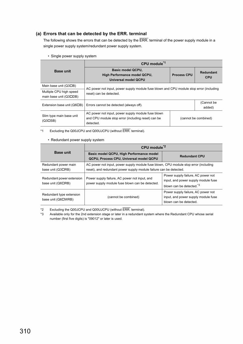
(a) Errors that can be detected by the ERR. terminalThe following shows the errors that can be detected by the ERR. terminal of the power supply module in a single power supply system/redundant power supply system.
• Single power supply system
*1 Excluding the Q00JCPU and Q00UJCPU (without ERR. terminal).
• Redundant power supply system
*2 Excluding the Q00JCPU and Q00UJCPU (without ERR. terminal).*3 Available only for the 2nd extension stage or later in a redundant system where the Redundant CPU whose serial
number (first five digits) is "09012" or later is used.
Base unit
CPU module*1
Basic model QCPU,High Performance model QCPU,
Universal model QCPUProcess CPU
Redundant CPU
Main base unit (Q3B)AC power not input, power supply module fuse blown and CPU module stop error (including reset) can be detected.Multiple CPU high speed
main base unit (Q3DB)
Extension base unit (Q6B) Errors cannot be detected (always off).(Cannot be
added)
Slim type main base unit (Q3SB)
AC power not input, power supply module fuse blown and CPU module stop error (including reset) can be detected.
(cannot be combined)
Base unitCPU module*2
Basic model QCPU, High Performance model QCPU, Process CPU, Universal model QCPU
Redundant CPU
Redundant power main base unit (Q3RB)
AC power not input, power supply module fuse blown, CPU module stop error (including reset), and redundant power supply module failure can be detected.
Redundant power extension base unit (Q6RB)
Power supply failure, AC power not input, and power supply module fuse blown can be detected.
Power supply failure, AC power not input, and power supply module fuse
blown can be detected.*3
Redundant type extension base unit (Q6WRB)
(cannot be combined)Power supply failure, AC power not input, and power supply module fuse blown can be detected.
310

CHAPTER 15 TROUBLESHOOTING
15
15.3 Checking for Functional Errors
15.3.13 Power supply m
odule
RemarkIn the redundant power supply system, the failure of the redundant power supply module can also be detected by using the
programming tool. Note 15.1Note 15.2 • Detection by PLC diagnostics • Detection by System monitor
For details on the PLC diagnostics and System monitor, refer to the following. Operating manual for the programming tool used
Note 15.1
Failure of redundant power supply module cannot be detected by the Basic model QCPU.
Note 15.2
When using the High Performance QCPU or Process CPU, check the versions of the CPU module and programming tool used.
High Performance model QCPU ( Page 650, Appendix 6.2)
Process CPU ( Page 656, Appendix 6.4)
Note 15.1, Note 15.2
Basic
Highperformance Process
311

15.4 Saving Data
By saving the following data immediately after trouble arises, the data can be useful for analyzing the error cause. • Programs and parameters • Device data and buffer memory data • System configuration data • Error history
(1) Saving programs and parametersThe following describes a procedure for saving data.
[Online] [Read from PLC]
1. Click the button.
2. Click the button to execute Read from PLC.
312

CHAPTER 15 TROUBLESHOOTING
15
15.4 Saving Data
(2) Saving device data and buffer memory dataThe following describes a procedure for saving data.
[Online] [Read from PLC]
When using a file register, also save file register data.
1. Select "Device Memory".
2. Click the button.
3. Fill in the "Device Data Name" field and select the checkboxes of devices to be saved.
4. Enter the start I/O number in the "Buffer Memory Start Address" field.
5. Click the button, and execute Read from PLC.
313

(3) Saving system configuration dataThe following describes a procedure for saving data.
[Diagnostics] [System Monitor]
1. Click the button.
2. Click the button.
314

CHAPTER 15 TROUBLESHOOTING
15
15.4 Saving Data
(4) Saving error historyThe following describes a procedure for saving data.
[Diagnostics] [System Monitor]
1. Click the button.
2. Click the button.
315
APPENDICESAppendix 1 Error Codes
When an error occurs at power-on, at switching from STOP to RUN or during RUN, the CPU module indicates the error (LED indication and a message on a display device) by the self-diagnostic function and stores the error information in the special relay (SM) and special register (SD).When an error occurs at communication request from a programming tool, intelligent function module, or network system to the CPU module, the CPU module returns the error code (4000H to 4FFFH) to the request source.
This section describes errors that may occur in the CPU module and corrective actions for the errors.
(1) How to read error code listsThe following describes how to read Appendix 1.3 Error code list (1000 to 1999) to Appendix 1.9 Error code list (7000 to 10000).Each list contains errors in QCPU and LCPU.
(a) Error code, common information, and individual informationThe error code is stored in SD0. The common information is stored in SD5 to SD15. The individual information is stored in SD16 to SD26.
(b) Corresponding CPU• QCPU: All the Q series CPU modules• Q00J/Q00/Q01: Basic model QCPU• Qn(H): High Performance model QCPU• QnPH: Process CPU• QnPRH: Redundant CPU• QnU: Universal model QCPU• QnUDV: High-speed Universal model QCPU• QnUDPV: Universal model Process CPU• Q00UJ/Q00U/Q01U: Q00UJCPU, Q00UCPU, and Q01UCPU• LCPU: All the L series CPU modules• CPU module model: Only the specified model (Example: Q02UCPU, L26CPU-BT)
316

APPX
A
Appendix 1 Error Codes
Appendix 1.1 Error codes
Appendix 1.1 Error codes
There are two types of errors: errors detected by the self-diagnostic function of the CPU module and errors detected during communication with the CPU module. The following table shows the relationship between the error detection pattern, error location, and error code.
*1 Error codes are classified into three levels.• Minor error: Errors that allow a CPU module to continue its operation, such as a battery error• Moderate error: Errors that may cause a CPU module to stop its operation, such as a WDT error (Error code:
1300 to 10000)• Major error: Errors that may cause a CPU module to stop its operation, such as a RAM error (Error code: 1000 to
1299)Whether the CPU module continues or stops its operation can be checked in the CPU Status column of the Error code list (Page 318, Appendix 1.3 to Page 414, Appendix 1.9).
*2 If an error code that is not described in the list is detected, please consult your local Mitsubishi representative.
Appendix 1.2 Reading error codes
Error codes can be read using a programming tool. For details on the operating method, refer to the following. Operating manual for the programming tool used
Error detection pattern Error location Error code Reference
By the self-diagnostic function of the CPU module
CPU module 1000 to 10000*1*2 Page 318, Appendix 1.3 to Page 414, Appendix 1.9
During communication with the CPU module
CPU module 4000H to 4FFFH Page 423, Appendix 1.11
Serial communication module, etc.
7000H to 7FFFH User's manuals for the serial communication module, etc.
CC-Link (including the built-in CC-Link function)
B000H to BFFFH User's manuals for the CC-Link system master/local module
Ethernet (including the built-in Ethernet function)
C000H to CFBFH
• User's manuals for the Ethernet interface module• QnUCPU User's Manual (Communication via Built-in Ethernet Port)• MELSEC-L CPU Module User's Manual (Built-in Ethernet Function)
CC-Link IE Field Network Basic
CFC0H to CFFFH Page 423, Appendix 1.11
CC-Link IE Field Network D000H to DFFFH User's manuals for the CC-Link IE Field Network module used
CC-Link IE Controller Network
E000H to EFFFH • Reference manuals for CC-Link IE Controller Network
MELSECNET/H F000H to FFFFH
• Reference manuals for the MELSECNET/H network system• Q Corresponding MELSECNET/H Remote I/O Module Reference
Manual (MELSECNET/10 Mode)
317

Appendix 1.3 List of error codes (1000 to 1999)
The following table shows the error messages, the error contents and causes, and the corrective actions for the error codes (1000 to 1999).
Error code
Error and cause Corrective actionLED status, CPU
statusCorresponding
CPU
1000
[MAIN CPU DOWN]Runaway or failure of the CPU module• Malfunction due to noise or other causes• Hardware failure
■Collateral information• Common information: -• Individual information: Failure information
(QnUDVCPU and QnUDPVCPU only)■Diagnostic timing• Always
• Take noise reduction measures.• Reset the CPU module and run it again. If
the same error code is displayed again, the cause is a hardware failure of the CPU module. Please consult your local Mitsubishi representative.
RUN: OffERR.:Flashing
CPU Status:Stop
QCPU
[CPU UNIT DOWN]Runaway or failure of the CPU module• Malfunction due to noise or other causes• Hardware failure
■Collateral information• Common information: -• Individual information: Failure information
■Diagnostic timing• Always
LCPU
1001
[MAIN CPU DOWN]Runaway or failure of the CPU module• Malfunction due to noise or other causes• Hardware failure• The devices outside the range was accessed
even though device checks are prohibited (SM237 is on). (This error occurs only when any of the BMOV, FMOV, or DFMOV instructions is executed. (Universal model QCPU only))
■Collateral information• Common information: -• Individual information: Failure information
(QnUDVCPU and QnUDPVCPU only)■Diagnostic timing• Always
• Take noise reduction measures.• Reset the CPU module and run it again. If
the same error code is displayed again, the cause is a hardware failure of the CPU module. Please consult your local Mitsubishi representative.
• Check the devices specified by BMOV, FMOV, and DFMOV instructions and correct the device settings. (Universal model QCPU only)
RUN: OffERR.:Flashing
CPU Status:Stop
QCPU
[CPU UNIT DOWN]Runaway or failure of the CPU module• Malfunction due to noise or other causes• Hardware failure• The devices outside the range was accessed
even though device checks are prohibited (SM237 is on). (This error occurs only when any of the BMOV, FMOV, or DFMOV instruction is executed.)
■Collateral information• Common information: -• Individual information: Failure information
■Diagnostic timing• Always
• Take noise reduction measures.• Reset the CPU module and run it again. If
the same error code is displayed again, the cause is a hardware failure of the CPU module. Please consult your local Mitsubishi representative.
• Check the devices specified by BMOV, FMOV, and DFMOV instructions and correct the device settings.
LCPU
318

APPX
A
Appendix 1 Error Codes
Appendix 1.3 List of error codes (1000 to 1999)
1002
[MAIN CPU DOWN]Runaway or failure of the CPU module• Malfunction due to noise or other causes• Hardware failure
■Collateral information• Common information: -• Individual information: Failure information
(QnUDVCPU and QnUDPVCPU only)■Diagnostic timing• Always
• Take noise reduction measures.• Reset the CPU module and run it again. If
the same error code is displayed again, the cause is a hardware failure of the CPU module. Please consult your local Mitsubishi representative.
RUN: OffERR.:Flashing
CPU Status:Stop
QCPU
[CPU UNIT DOWN]Runaway or failure of the CPU module• Malfunction due to noise or other causes• Hardware failure
■Collateral information• Common information: -• Individual information: Failure information
■Diagnostic timing• Always
LCPU
1003
[MAIN CPU DOWN]Runaway or failure of the CPU module• Malfunction due to noise or other causes• Hardware failure
■Collateral information• Common information: -• Individual information: Failure information
(QnUDVCPU and QnUDPVCPU only)■Diagnostic timing• Always
• Take noise reduction measures.• Reset the CPU module and run it again. If
the same error code is displayed again, the cause is a hardware failure of the CPU module. Please consult your local Mitsubishi representative.
RUN: OffERR.:Flashing
CPU Status:Stop
QCPU
[CPU UNIT DOWN]Runaway or failure of the CPU module• Malfunction due to noise or other causes• Hardware failure
■Collateral information• Common information: -• Individual information: Failure information
■Diagnostic timing• Always
LCPU
1004
[MAIN CPU DOWN]Runaway or failure of the CPU module• Malfunction due to noise or other causes• Hardware failure
■Collateral information• Common information: -• Individual information: -
■Diagnostic timing• Always
• Take noise reduction measures.• Reset the CPU module and run it again. If
the same error code is displayed again, the cause is a hardware failure of the CPU module. Please consult your local Mitsubishi representative.
RUN: OffERR.:Flashing
CPU Status:Stop
QCPU (except the QnUDV and QnUDPV)
[CPU UNIT DOWN]Runaway or failure of the CPU module• Malfunction due to noise or other causes• Hardware failure
■Collateral information• Common information: -• Individual information: Failure information
■Diagnostic timing• Always
LCPU
Error code Error and cause Corrective action
LED status, CPU status
Corresponding CPU
319

1005
[MAIN CPU DOWN]Runaway or failure of the CPU module• Malfunction due to noise or other causes• Hardware failure
■Collateral information• Common information: -• Individual information: -
■Diagnostic timing• Always
• Take noise reduction measures.• Reset the CPU module and run it again. If
the same error code is displayed again, the cause is a hardware failure of the CPU module. Please consult your local Mitsubishi representative.
RUN: OffERR.:Flashing
CPU Status:Stop
QCPU (except the QnUDV and QnUDPV)
[MAIN CPU DOWN]Boot operation was performed in the transfer destination without formatting.■Collateral information• Common information: -• Individual information: -
■Diagnostic timing• At power-on
Before performing boot operation by the parameter, select "Clear program memory" to clear the program memory.
Qn(H)QnPH
QnPRH
[CPU UNIT DOWN]Runaway or failure of the CPU module• Malfunction due to noise or other causes• Hardware failure
■Collateral information• Common information: -• Individual information: Failure information
■Diagnostic timing• Always
• Take noise reduction measures.• Reset the CPU module and run it again. If
the same error code is displayed again, the cause is a hardware failure of the CPU module. Please consult your local Mitsubishi representative.
LCPU
1006
[MAIN CPU DOWN]Runaway or failure of the CPU module• Malfunction due to noise or other causes• Hardware failure
■Collateral information• Common information: -• Individual information: Failure information
(QnUDVCPU and QnUDPVCPU only)■Diagnostic timing• Always
• Take noise reduction measures.• Reset the CPU module and run it again. If
the same error code is displayed again, the cause is a hardware failure of the CPU module. Please consult your local Mitsubishi representative.
RUN: OffERR.:Flashing
CPU Status:Stop
QCPU
[CPU UNIT DOWN]Runaway or failure of the CPU module• Malfunction due to noise or other causes• Hardware failure
■Collateral information• Common information: -• Individual information: Failure information
■Diagnostic timing• Always
LCPU
1007
[MAIN CPU DOWN]Runaway or failure of the CPU module• Malfunction due to noise or other causes• Hardware failure
■Collateral information• Common information: -• Individual information: -
■Diagnostic timing• Always
• Take noise reduction measures.• Reset the CPU module and run it again. If
the same error code is displayed again, the cause is a hardware failure of the CPU module. Please consult your local Mitsubishi representative.
RUN: OffERR.:Flashing
CPU Status:Stop
Qn(H)QnPH
QnPRH
1008
[MAIN CPU DOWN]Runaway or failure of the CPU module• Malfunction due to noise or other causes• Hardware failure
■Collateral information• Common information: -• Individual information: Failure information
(QnUDVCPU and QnUDPVCPU only)■Diagnostic timing• Always
• Take noise reduction measures.• Reset the CPU module and run it again. If
the same error code is displayed again, the cause is a hardware failure of the CPU module. Please consult your local Mitsubishi representative.
RUN: OffERR.:Flashing
CPU Status:Stop
Qn(H)QnPH
QnPRHQnUDV
QnUDPV
Error code Error and cause Corrective action
LED status, CPU status
Corresponding CPU
320

APPX
A
Appendix 1 Error Codes
Appendix 1.3 List of error codes (1000 to 1999)
1009
[MAIN CPU DOWN]• The voltage waveform that is outside the
specification is applied to the power supply module, and an error is detected.
• A failure was detected on the power supply module, CPU module, main base unit, extension base unit or extension cable.
• When using the redundant base unit, the redundant power supply module failure in both systems and/or the redundant base unit failure are detected.
■Collateral information• Common information: -• Individual information: Failure information
(QnUDVCPU and QnUDPVCPU only)■Diagnostic timing• Always
• Correct the voltage waveform applied to the power supply module.
• Reset the CPU module and run it again. If the same error code is detected again, the cause is a failure of the power supply module, CPU module, main base unit, extension base unit, or extension cable. Please consult your local Mitsubishi representative. RUN: Off
ERR.:Flashing
CPU Status:Stop
Q00J/Q00/Q01Qn(H)QnPH
QnPRHQnU
[CPU UNIT DOWN]• A failure was detected on the power supply
module or CPU module.• The voltage waveform that is outside the
specification is applied to the power supply module, and an error is detected.
■Collateral information• Common information: -• Individual information: Failure information
■Diagnostic timing• Always
• Correct the voltage waveform applied to the power supply module.
• Reset the CPU module and run it again. If the same error code is displayed again, the cause is a hardware failure of the power supply module or CPU module. Please consult your local Mitsubishi representative.
LCPU
1010
[END NOT EXECUTE]Entire program was executed without the execution of an END instruction.• When the END instruction is executed it is read
as another instruction code, e.g. due to noise.• The END instruction has been changed to
another instruction code somehow.■Collateral information• Common information: -• Individual information: -
■Diagnostic timing• When an END instruction executed
• Take noise reduction measures.• Reset the CPU module and run it again. If
the same error code is displayed again, the cause is a hardware failure of the CPU module. Please consult your local Mitsubishi representative.
RUN: OffERR.:Flashing
CPU Status:Stop
QCPULCPU
1020
[SFCP. END ERROR]The SFC program cannot be normally terminated due to noise or other reason.• The SFC program cannot be normally
terminated due to noise or any similar cause.• The SFC program cannot be normally
terminated for any other reason.■Collateral information• Common information: -• Individual information: -
■Diagnostic timing• When SFC program is executed
• Take noise reduction measures.• Reset the CPU module and run it again. If
the same error code is displayed again, the cause is a hardware failure of the CPU module. Please consult your local Mitsubishi representative.
RUN: OffERR.:Flashing
CPU Status:Stop
Q00J/Q00/Q01QnPHQnU
LCPU
Error code Error and cause Corrective action
LED status, CPU status
Corresponding CPU
321

1035
[MAIN CPU DOWN]Runaway or failure of the CPU module• Malfunction due to noise or other causes• Hardware failure
■Collateral information• Common information: -• Individual information: Failure information
(QnUDVCPU and QnUDPVCPU only)■Diagnostic timing• Always
• Take noise reduction measures.• Reset the CPU module and run it again. If
the same error code is displayed again, the cause is a hardware failure of the CPU module. Please consult your local Mitsubishi representative.
RUN: OffERR.:Flashing
CPU Status:Stop
QnU
[CPU UNIT DOWN]Runaway or failure of the CPU module• Malfunction due to noise or other causes• Hardware failure
■Collateral information• Common information: -• Individual information: Failure information
■Diagnostic timing• Always
LCPU
1036
[MAIN CPU DOWN]Runaway or failure of the CPU module• Malfunction due to noise or other causes• Hardware failure
■Collateral information• Common information: -• Individual information: -
■Diagnostic timing• At power-on/At reset
• Take noise reduction measures.• Reset the CPU module and run it again. If
the same error code is displayed again, the cause is a hardware failure of the CPU module. Please consult your local Mitsubishi representative.
RUN: OffERR.:Flashing
CPU Status:Stop
Q50UDEHCPUQ100UDEHCPU
1040
[CPU UNIT DOWN]Runaway or failure of the CPU module (built-in I/O)• Malfunction due to noise or other causes• Hardware failure
■Collateral information• Common information: -• Individual information: Failure information
■Diagnostic timing• Always
• Take noise reduction measures.• Reset the CPU module and run it again. If
the same error code is displayed again, the cause is a hardware failure of the CPU module. Please consult your local Mitsubishi representative.
RUN: OffERR.:Flashing
CPU Status:Stop
LCPU
1041
[CPU UNIT DOWN]Runaway or failure of the CPU module (built-in I/O)• Malfunction due to noise or other causes• Hardware failure
■Collateral information• Common information: -• Individual information: Failure information
■Diagnostic timing• Always
• Take noise reduction measures.• Reset the CPU module and run it again. If
the same error code is displayed again, the cause is a hardware failure of the CPU module. Please consult your local Mitsubishi representative.
RUN: OffERR.:Flashing
CPU Status:Stop
LCPU
1042
[CPU UNIT DOWN]Runaway or failure of the CPU module (built-in I/O)• Malfunction due to noise or other causes• Hardware failure
■Collateral information• Common information: -• Individual information: Failure information
■Diagnostic timing• Always
• Take noise reduction measures.• Reset the CPU module and run it again. If
the same error code is displayed again, the cause is a hardware failure of the CPU module. Please consult your local Mitsubishi representative.
RUN: OffERR.:Flashing
CPU Status:Stop
LCPU
1043
[MAIN CPU DOWN]Runaway or failure of the CPU module• Malfunction due to noise or other causes• Hardware failure
■Collateral information• Common information: -• Individual information: Failure information
■Diagnostic timing• Always
• Take noise reduction measures.• Reset the CPU module and run it again. If
the same error code is displayed again, the cause is a hardware failure of the CPU module. Please consult your local Mitsubishi representative.
RUN: OffERR.:Flashing
CPU Status:Stop
QnUDVQnUDPV
Error code Error and cause Corrective action
LED status, CPU status
Corresponding CPU
322

APPX
A
Appendix 1 Error Codes
Appendix 1.3 List of error codes (1000 to 1999)
1044
[MAIN CPU DOWN]Runaway or failure of the CPU module• Malfunction due to noise or other causes• Hardware failure
■Collateral information• Common information: -• Individual information: Failure information
■Diagnostic timing• Always
• Take noise reduction measures.• Reset the CPU module and run it again. If
the same error code is displayed again, the cause is a hardware failure of the CPU module. Please consult your local Mitsubishi representative.
RUN: OffERR.:Flashing
CPU Status:Stop
QnUDVQnUDPV
1045
[CPU UNIT DOWN](1) The module (built-in I/O or built-in CC-Link)
status differs from that obtained at power-on.(2) Runaway or failure of the CPU module (built-
in I/O, built-in CC-Link)• Malfunction due to noise or other causes• Hardware failure
■Collateral information• Common information: -• Individual information: Failure information
■Diagnostic timing• Always
• Take noise reduction measures.• Reset the CPU module and run it again. If
the same error code is displayed again, the cause is a hardware failure of the CPU module. Please consult your local Mitsubishi representative.
RUN: OffERR.:Flashing
CPU Status:Stop
LCPU
1101
[RAM ERROR]The sequence program storing program memory in the CPU module is faulty.■Collateral information• Common information: -• Individual information: -
■Diagnostic timing• At power-on/At reset/When an END instruction
executed
• Take noise reduction measures.• Reset the CPU module and run it again. If
the same error code is displayed again, the cause is a hardware failure of the CPU module. Please consult your local Mitsubishi representative.
RUN: OffERR.:Flashing
CPU Status:Stop
QCPULCPU
1102
[RAM ERROR]• The work area RAM in the CPU module is faulty.• The standard RAM in the CPU module is faulty.
■Collateral information• Common information: -• Individual information: -
■Diagnostic timing• At power-on/At reset/When an END instruction
executed
• Take noise reduction measures.• Reset the CPU module and run it again. If
the same error code is displayed again, the cause is a hardware failure of the CPU module. Please consult your local Mitsubishi representative.
RUN: OffERR.:Flashing
CPU Status:Stop
QCPULCPU
1103
[RAM ERROR]The device memory in the CPU module is faulty.■Collateral information• Common information: -• Individual information: -
■Diagnostic timing• At power-on/At reset/When an END instruction
executed
• Take noise reduction measures.• When indexing is performed, check the
value of index register to see if it is within the device range.
• Reset the CPU module and run it again. If the same error code is displayed again, the cause is a hardware failure of the CPU module. Please consult your local Mitsubishi representative.
RUN: OffERR.:Flashing
CPU Status:Stop
QCPULCPU
[RAM ERROR]• The device memory in the CPU module is faulty.• The device out of range is accessed due to
indexing, and the device for system is overwritten.
■Collateral information• Common information: -• Individual information: -
■Diagnostic timing• At power-on/At reset/When an END instruction
executed
Qn(H)QnPH
QnPRH
1104
[RAM ERROR]The address RAM in the CPU module is faulty.■Collateral information• Common information: -• Individual information: -
■Diagnostic timing• At power-on/At reset
• Take noise reduction measures.• Reset the CPU module and run it again. If
the same error code is displayed again, the cause is a hardware failure of the CPU module. Please consult your local Mitsubishi representative.
RUN: OffERR.:Flashing
CPU Status:Stop
Q00J/Q00/Q01Qn(H)QnPH
QnPRH
Error code Error and cause Corrective action
LED status, CPU status
Corresponding CPU
323

1105
[RAM ERROR]The CPU memory in the CPU module is faulty.■Collateral information• Common information: -• Individual information: -
■Diagnostic timing• At power-on/At reset
• Take noise reduction measures.• Reset the CPU module and run it again. If
the same error code is displayed again, the cause is a hardware failure of the CPU module. Please consult your local Mitsubishi representative.
RUN: OffERR.:Flashing
CPU Status:Stop
Q00J/Q00/Q01QnU
[RAM ERROR]The CPU shared memory in the CPU module is faulty.■Collateral information• Common information: -• Individual information: -
■Diagnostic timing• At power-on/At reset
Qn(H)QnPH
QnPRHQnU
1106
[RAM ERROR]The program memory was corrupted due to battery exhaustion.■Collateral information• Common information: -• Individual information: -
■Diagnostic timing• STOP RUN/When an END instruction
executed
• Check the battery to see if it is dead or not. If dead, replace the battery.
• Take measures to reduce noise.• Format the program memory, write all files
to the CPU module, and reset the module to run it again. If the same error code is displayed again, the cause is a hardware failure of the CPU module. Please consult your local Mitsubishi representative.
RUN: OffERR.:Flashing
CPU Status:Stop
Qn(H)QnPH
QnPRH
1107
[RAM ERROR]The work area RAM in the CPU module is faulty.■Collateral information• Common information: -• Individual information: -
■Diagnostic timing• At power-on/At reset
The cause is a hardware failure of the CPU module. Please consult your local Mitsubishi representative.
RUN: OffERR.:Flashing
CPU Status:Stop
QnPRH
1108
[RAM ERROR]The work area RAM in the CPU module is faulty.■Collateral information• Common information: -• Individual information: -
■Diagnostic timing• At power-on/At reset
The cause is a hardware failure of the CPU module. Please consult your local Mitsubishi representative.
RUN: OffERR.:Flashing
CPU Status:Stop
Qn(H)QnPH
QnPRH
1109
[RAM ERROR]The work area RAM in the CPU module is faulty.■Collateral information• Common information: -• Individual information: -
■Diagnostic timing• Always
The cause is a hardware failure of the CPU module. Please consult your local Mitsubishi representative.
RUN: OffERR.:Flashing
CPU Status:Stop
Qn(H)QnPH
QnPRH
1110
[TRK. CIR. ERROR]A fault was detected by the initial check of the tracking hardware.■Collateral information• Common information: -• Individual information: -
■Diagnostic timing• At power-on/At reset
The cause is a hardware failure of the CPU module. Please consult your local Mitsubishi representative.
RUN: OffERR.:Flashing
CPU Status:Stop
QnPRH
1111
[TRK. CIR. ERROR]A tracking hardware fault was detected.■Collateral information• Common information: -• Individual information: -
■Diagnostic timing• At power-on/At reset
The cause is a hardware failure of the CPU module. Please consult your local Mitsubishi representative.
RUN: OffERR.:Flashing
CPU Status:Stop
QnPRH
Error code Error and cause Corrective action
LED status, CPU status
Corresponding CPU
324

APPX
A
Appendix 1 Error Codes
Appendix 1.3 List of error codes (1000 to 1999)
1112
[TRK. CIR. ERROR]• A tracking hardware fault was detected during
running.• The tracking cable was disconnected and
reinserted without the standby system being powered off or reset.
• The tracking cable is not secured by the connector fixing screws.
• The error occurred at a startup since the redundant system startup procedure was not followed.
■Collateral information• Common information: -• Individual information: -
■Diagnostic timing• During running
• Check that the tracking cable is connected and start up the module. If the same error code is displayed again, the cause is a hardware failure of the tracking cable or CPU module. Please consult your local Mitsubishi representative.
• Confirm the redundant system startup procedure, and execute a startup again. For details, refer to the QnPRHCPU User's Manual (Redundant System).
RUN: OffERR.:Flashing
CPU Status:Stop
QnPRH
1113
[TRK. CIR. ERROR]• A tracking hardware fault was detected during
running.• The tracking cable was disconnected and
reinserted without the standby system being powered off or reset.
• The tracking cable is not secured by the connector fixing screws.
• The error occurred at a startup since the redundant system startup procedure was not followed.
■Collateral information• Common information: -• Individual information: -
■Diagnostic timing• During running
• Check that the tracking cable is connected and start up the module. If the same error code is displayed again, the cause is a hardware failure of the tracking cable or CPU module. Please consult your local Mitsubishi representative.
• Confirm the redundant system startup procedure, and execute a startup again. For details, refer to the QnPRHCPU User's Manual (Redundant System).
RUN: OffERR.:Flashing
CPU Status:Stop
QnPRH
1115
[TRK. CIR. ERROR]A fault was detected by the initial check of the tracking hardware.■Collateral information• Common information: -• Individual information: -
■Diagnostic timing• At power-on/At reset
The cause is a hardware failure of the CPU module. Please consult your local Mitsubishi representative.
RUN: OffERR.:Flashing
CPU Status:Stop
QnPRH
1116
[TRK. CIR. ERROR]• A tracking hardware fault was detected during
running.• The tracking cable was disconnected and
reinserted without the standby system being powered off or reset.
• The tracking cable is not secured by the connector fixing screws.
• The error occurred at a startup since the redundant system startup procedure was not followed.
■Collateral information• Common information: -• Individual information: -
■Diagnostic timing• During running
• Check that the tracking cable is connected and start up the module. If the same error code is displayed again, the cause is a hardware failure of the tracking cable or CPU module. Please consult your local Mitsubishi representative.
• Confirm the redundant system startup procedure, and execute a startup again. For details, refer to the QnPRHCPU User's Manual (Redundant System).
RUN: OffERR.:Flashing
CPU Status:Stop
QnPRH
1150
[RAM ERROR]The memory of the CPU module in the multiple CPU high speed transmission area is faulty.■Collateral information• Common information: -• Individual information: -
■Diagnostic timing• At power-on/At reset
• Take noise reduction measures.• Reset the CPU module and run it again. If
the same error code is displayed again, the cause is a hardware failure of the CPU module. Please consult your local Mitsubishi representative.
RUN: OffERR.:Flashing
CPU Status:Stop
QnU
Error code Error and cause Corrective action
LED status, CPU status
Corresponding CPU
325

1160
[RAM ERROR]The program memory in the CPU module is overwritten.■Collateral information• Common information: Program error location*5
• Individual information: -■Diagnostic timing• Always
• Take noise reduction measures.• Format the program memory, write all files
to the CPU module, and reset the module to run it again. If the same error code is displayed again, the cause is a hardware failure of the CPU module. Please consult your local Mitsubishi representative.
RUN: OffERR.:Flashing
CPU Status:Stop
QnULCPU
1161
[RAM ERROR]The data of the device memory built in the CPU module is overwritten.■Collateral information• Common information: Program error location*5
• Individual information: -■Diagnostic timing• Always
Take noise reduction measures. If the same error code is displayed again, the cause is a hardware failure of the CPU module. Please consult your local Mitsubishi representative.
RUN: OffERR.:Flashing
CPU Status:Stop
QnULCPU
1163
[RAM ERROR]The program memory in the CPU module is overwritten.■Collateral information• Common information: -• Individual information: -
■Diagnostic timing• When an instruction executed ("Always" for the
QnUDVCPU and QnUDPVCPU)
• Take noise reduction measures.• For GX Works2, select "Transfer cache
memory to program memory" in the Options window. For GX Developer, select "Online change T/C setting value change program memory transfer settings" in the Options window.
• Format the program memory, write all files to the CPU module, and reset the module to run it again. If the same error code is displayed again, the cause is a hardware failure of the CPU module. Please consult your local Mitsubishi representative.
RUN: OffERR.:Flashing
CPU Status:Stop
QnULCPU
1164
[RAM ERROR]The destruction of the data stored in the standard RAM is detected.■Collateral information• Common information: -• Individual information: -
■Diagnostic timing• When instruction executed
Take noise reduction measures. If the same error code is displayed again, the cause is a hardware failure of the CPU module. Please consult your local Mitsubishi representative.
RUN: OffERR.:Flashing
CPU Status:Stop
QnU*6
L26CPUL26CPU-P
L26CPU-BTL26CPU-PBT
1166
[RAM ERROR]The internal memory in the CPU module is faulty.■Collateral information• Common information: -• Individual information: -
■Diagnostic timing• Always
Take noise reduction measures. If the same error code is displayed again, the cause is a hardware failure of the CPU module. Please consult your local Mitsubishi representative.
RUN: OffERR.:Flashing
CPU Status:Stop
Q50UDEHCPU, Q100UDEHCPU
1170
[RAM ERROR]The RAM of the CPU module (built-in I/O) is faulty.■Collateral information• Common information: -• Individual information: Failure information
■Diagnostic timing• At power-on/At reset
Take noise reduction measures. If the same error code is displayed again, the cause is a hardware failure of the CPU module. Please consult your local Mitsubishi representative.
RUN: OffERR.:Flashing
CPU Status:Stop
LCPU
1171
[RAM ERROR]The RAM of the CPU module (built-in I/O) is faulty.■Collateral information• Common information: -• Individual information: Failure information
■Diagnostic timing• Always
Take noise reduction measures. If the same error code is displayed again, the cause is a hardware failure of the CPU module. Please consult your local Mitsubishi representative.
RUN: OffERR.:Flashing
CPU Status:Stop
LCPU
1172
[RAM ERROR]The RAM of the CPU module (built-in I/O) is faulty.■Collateral information• Common information: -• Individual information: Failure information
■Diagnostic timing• At power-on/At reset
Take noise reduction measures. If the same error code is displayed again, the cause is a hardware failure of the CPU module. Please consult your local Mitsubishi representative.
RUN: OffERR.:Flashing
CPU Status:Stop
LCPU
Error code Error and cause Corrective action
LED status, CPU status
Corresponding CPU
326

APPX
A
Appendix 1 Error Codes
Appendix 1.3 List of error codes (1000 to 1999)
1200
[OPE. CIRCUIT ERR.]The operation circuit for index modification in the CPU module does not operate normally.■Collateral information• Common information: -• Individual information: -
■Diagnostic timing• At power-on/At reset
The cause is a hardware failure of the CPU module. Please consult your local Mitsubishi representative.
RUN: OffERR.:Flashing
CPU Status:Stop
QCPULCPU
1201
[OPE. CIRCUIT ERR.]The hardware (logic) in the CPU module does not operate normally.■Collateral information• Common information: -• Individual information: -
■Diagnostic timing• At power-on/At reset
The cause is a hardware failure of the CPU module. Please consult your local Mitsubishi representative.
RUN: OffERR.:Flashing
CPU Status:Stop
QCPULCPU
1202
[OPE. CIRCUIT ERR.]The operation circuit for sequence processing in the CPU module does not operate normally.■Collateral information• Common information: -• Individual information: -
■Diagnostic timing• At power-on/At reset
The cause is a hardware failure of the CPU module. Please consult your local Mitsubishi representative.
RUN: OffERR.:Flashing
CPU Status:Stop
QCPULCPU
1203
[OPE. CIRCUIT ERR.]The operation circuit for index modification in the CPU module does not operate normally.■Collateral information• Common information: -• Individual information: -
■Diagnostic timing• When an END instruction executed
The cause is a hardware failure of the CPU module. Please consult your local Mitsubishi representative.
RUN: OffERR.:Flashing
CPU Status:Stop
QnPRH
1204
[OPE. CIRCUIT ERR.]The hardware (logic) in the CPU module does not operate normally.■Collateral information• Common information: -• Individual information: -
■Diagnostic timing• When an END instruction executed
The cause is a hardware failure of the CPU module. Please consult your local Mitsubishi representative.
RUN: OffERR.:Flashing
CPU Status:Stop
QnPRH
1205
[OPE. CIRCUIT ERR.]The operation circuit for sequence processing in the CPU module does not operate normally.■Collateral information• Common information: -• Individual information: -
■Diagnostic timing• When an END instruction executed
The cause is a hardware failure of the CPU module. Please consult your local Mitsubishi representative.
RUN: OffERR.:Flashing
CPU Status:Stop
QnPRH
Error code Error and cause Corrective action
LED status, CPU status
Corresponding CPU
327

1300
[FUSE BREAK OFF]There is an output module with a blown fuse.■Collateral information• Common information: Module No. (Slot No.)
[For Remote I/O network]Network No./Station No.• Individual information: -
■Diagnostic timing• Always
• Check the FUSE. LED of each output module, and replace the one whose LED is on.
• Read common information of the error using the programming tool to identify the numeric value (module No.). Replace the fuse of the output module corresponding to the value. Or, monitor SD1300 to SD1331 using the programming tool to identify the module whose data bit is "1". Replace the fuse of the corresponding module.
• When a GOT is bus-connected to the main base unit or extension base unit, check the connection status of the extension cable and the grounding status of the GOT.
RUN: Off/OnERR.:Flashing/On
CPU Status:
Stop/Continue*1
Qn(H)QnPH
QnPRHQnU
[FUSE BREAK OFF]There is an output module with a blown fuse.■Collateral information• Common information: Module No. (Slot No.)
[For Remote I/O network]Network No./Station No.• Individual information: -
■Diagnostic timing• Always
Check the ERR. LED of each output module, and replace the one whose LED is on. (A blown fuse can be identified with the programming tool. Check SD130 to SD137 to ensure that the bit for the module with a blown fuse is "1".)
Q00J/Q00/Q01
[FUSE BREAK OFF]There is an output module with a blown fuse on the LA1S extension base unit.■Collateral information• Common information: Module No. (Slot No.)• Individual information: -
■Diagnostic timing• Always
• Check the FUSE. LED of each output module, and replace the one whose LED is on.
• Read common information of the error using the programming tool to identify the numeric value (module No.). Replace the fuse of the output module corresponding to the value. Or, monitor SD1300 to SD1331 using the programming tool to identify the module whose data bit is "1". Replace the fuse of the corresponding module.
LCPU
1310
[I/O INT. ERROR]Although an interrupt request was detected, there is no interrupt factor.■Collateral information• Common information: -• Individual information: -
■Diagnostic timing• During interrupt
The cause is a hardware failure of any one of the mounted modules. Check the mounted modules and replace the faulty module. Please consult your local Mitsubishi representative.
RUN: OffERR.:Flashing
CPU Status:Stop
QCPU
[I/O INT. ERROR]An interruption occurred although none of the modules can issue an interruption (including an interruption from the built-in I/O).■Collateral information• Common information: -• Individual information: -
■Diagnostic timing• During interrupt
Reset the CPU module and run it again. If the same error code is displayed again, the cause is a hardware failure of the CPU module, I/O module, intelligent function module, END cover, branch module, or extension module. Please consult your local Mitsubishi representative.
RUN: OffERR.:Flashing
CPU Status:Stop
LCPU
Error code Error and cause Corrective action
LED status, CPU status
Corresponding CPU
328

APPX
A
Appendix 1 Error Codes
Appendix 1.3 List of error codes (1000 to 1999)
1311
[I/O INT. ERROR]An interrupt request was detected from the module for which Interrupt Pointer Setting has not been configured in "PLC Parameter".■Collateral information• Common information: -• Individual information: -
■Diagnostic timing• During interrupt
• Correct the interrupt pointer setting in the PLC System tab of "PLC Parameter".
• Take measures not to issue an interruption from the modules where the interrupt pointer setting is not configured in the PLC System tab of "PLC Parameter".
• Correct the interrupt setting of the network parameter.
• Correct the interrupt setting of the intelligent function module buffer memory.
• Correct the basic program of the QD51.
RUN: OffERR.:Flashing
CPU Status:Stop
Q00J/Q00/Q01QnPRH
QnU
• Correct the interrupt pointer setting in the PLC System tab of "PLC Parameter".
• Take measures not to issue an interruption from the modules where the interrupt pointer setting is not configured in the PLC System tab of "PLC Parameter".
• Correct the Interrupt Setting of the network parameter.
• Correct the interrupt setting of the intelligent function module buffer memory.
• Reset the CPU module and run it again. If the same error code is displayed again, the cause is a hardware failure of the CPU module, I/O module, intelligent function module, END cover, branch module, or extension module. Please consult your local Mitsubishi representative.
LCPU
1320
[LAN CTRL. DOWN]The H/W self-diagnostics detected a LAN controller failure.■Collateral information• Common information: -• Individual information: -
■Diagnostic timing• At power-on/At reset
The cause is a hardware failure of the CPU module. Please consult your local Mitsubishi representative.
RUN: OffERR.:Flashing
CPU Status:Stop
QnU*4
LCPU*4
1321
[LAN CTRL. DOWN]The H/W self-diagnostics detected a LAN controller failure.■Collateral information• Common information: -• Individual information: -
■Diagnostic timing• At power-on/At reset
The cause is a hardware failure of the CPU module. Please consult your local Mitsubishi representative.
RUN: OffERR.:Flashing
CPU Status:Stop
QnU*4
LCPU*4
Error code Error and cause Corrective action
LED status, CPU status
Corresponding CPU
329

1401
[SP. UNIT DOWN]• There was no response from the intelligent
function module/special function module in the initial processing.
• The size of the buffer memory of the intelligent function module/special function module is invalid.
• The unsupported module is mounted.• At power-on/reset, momentary power failure has
occurred.■Collateral information• Common information: Module No. (Slot No.)• Individual information: -
■Diagnostic timing• At power-on/At reset/When intelligent function
module is accessed
• Check the power supply.• If an unsupported module is mounted,
remove it. When only supported modules are mounted, the cause is a hardware failure of the intelligent function module/special function module, CPU module, or base unit. Please consult your local Mitsubishi representative. RUN: Off/On
ERR.:Flashing/On
CPU Status:
Stop/Continue*3
QCPU
[SP. UNIT DOWN]• There was no response from the intelligent
function module in the initial processing.• The buffer memory size of the intelligent
function module is invalid.• An unsupported module is connected.
■Collateral information• Common information: Module No. (Slot No.)• Individual information: -
■Diagnostic timing• At power-on/At reset/When intelligent function
module is accessed
If an unsupported module is connected, disconnect it.When only supported modules are connected, reset the CPU module to run it again. If the same error code is displayed again, the cause is a hardware failure of the CPU module, I/O module, intelligent function module, END cover, branch module, or extension module. Please consult your local Mitsubishi representative.
LCPU
1402
[SP. UNIT DOWN]The intelligent function module/special function module was accessed in the program, but there was no response.■Collateral information• Common information: Module No. (Slot No.)• Individual information: Program error location
■Diagnostic timing• When an intelligent function module access
instruction is executed
The cause is a hardware failure of the intelligent function module/special function module, CPU module, or base unit. Please consult your local Mitsubishi representative.
RUN: Off/OnERR.:Flashing/On
CPU Status:
Stop/Continue*3
QCPU
[SP. UNIT DOWN]The intelligent function module was accessed by the program, but there was no response.■Collateral information• Common information: Module No. (Slot No.)• Individual information: Program error location
■Diagnostic timing• When an intelligent function module access
instruction is executed
Reset the CPU module and run it again. If the same error code is displayed again, the cause is a hardware failure of the CPU module, I/O module, intelligent function module, END cover, branch module, or extension module. Please consult your local Mitsubishi representative.
LCPU
Error code Error and cause Corrective action
LED status, CPU status
Corresponding CPU
330

APPX
A
Appendix 1 Error Codes
Appendix 1.3 List of error codes (1000 to 1999)
1403
[SP. UNIT DOWN]• The unsupported module is mounted.
■Collateral information• Common information: Module No. (Slot No.)• Individual information: -
■Diagnostic timing• Always
If an unsupported module is mounted, remove it. When only supported modules are mounted, the cause is a hardware failure of the intelligent function module/special function module, CPU module, or base unit. Please consult your local Mitsubishi representative.
RUN: Off/OnERR.:Flashing/On
CPU Status:
Stop/Continue*3
QCPU
[SP. UNIT DOWN]• There was no response from the intelligent
function module/special function module when the END instruction is executed.
• An error is detected at the intelligent function module/special function module.
• The I/O module (including the intelligent function module/special function module) is nearly disconnected, removed, or mounted while the system is running.
■Collateral information• Common information: Module No. (Slot No.)• Individual information: -
■Diagnostic timing• Always
The cause is a failure of the CPU module, base unit, or the intelligent function module/special function module in the access destination. Please consult your local Mitsubishi representative.
[SP. UNIT DOWN]• There was no response from the intelligent
function module when the END instruction is executed.
• An error is detected in the intelligent function module.
• The I/O module (including the intelligent function module) is nearly disconnected or removed while the system is running.
■Collateral information• Common information: Module No. (Slot No.)• Individual information: -
■Diagnostic timing• Always
Reset the CPU module and run it again. If the same error code is displayed again, the cause is a hardware failure of the CPU module, I/O module, intelligent function module, END cover, branch module, or extension module. Please consult your local Mitsubishi representative.
LCPU
1411
[CONTROL-BUS ERR.]When I/O assignment parameters are set, the CPU module cannot access the intelligent function module/special function module during initial communications. (If an error occurs, the start I/O number of the corresponding intelligent function module/special function module is stored in the common information.)■Collateral information• Common information: Module No. (Slot No.)• Individual information: -
■Diagnostic timing• At power-on/At reset
Reset the CPU module and run it again. If the same error code is displayed again, the cause is a failure of the intelligent function module/special function module, CPU module, or base unit. Please consult your local Mitsubishi representative.
RUN: OffERR.:Flashing
CPU Status:Stop
QCPU
1412
[CONTROL-BUS ERR.]The FROM/TO instruction is not executable, due to a control bus error with the intelligent function module/special function module. (If an error occurs, the program error location is stored in the individual information.)■Collateral information• Common information: Module No. (Slot No.)• Individual information: Program error location
■Diagnostic timing• During execution of FROM/TO instruction set
Reset the CPU module and run it again. If the same error code is displayed again, the cause is a failure of the intelligent function module/special function module, CPU module, or base unit. Please consult your local Mitsubishi representative.
RUN: OffERR.:Flashing
CPU Status:Stop
QCPU
Error code Error and cause Corrective action
LED status, CPU status
Corresponding CPU
331

1413
[CONTROL-BUS ERR.]In a multiple CPU system, a CPU module incompatible with the multiple CPU system is mounted.■Collateral information• Common information: -• Individual information: -
■Diagnostic timing• Always
• Remove the CPU module from the main base unit if it does not support a multiple CPU system configuration. Alternatively, replace the CPU module that does not support a multiple system configuration with the one that does.
• The cause is a failure of the intelligent function module, CPU module, or base unit. Please consult your local Mitsubishi representative.
RUN: OffERR.:Flashing
CPU Status:Stop
Q00J/Q00/Q01Qn(H)QnPH
[CONTROL-BUS ERR.](1) An error is detected on the system bus.• Self-diagnostic error in the system bus• Self-diagnostic error in the CPU module
(2) In a multiple CPU system, the control CPU setting of other CPUs, configured in the I/O Assignment tab of "PLC Parameter", differs from that of CPU No.1.
■Collateral information• Common information: -• Individual information: -
■Diagnostic timing• Always
• Reset the CPU module and run it again. If the same error code is displayed again, the cause is a failure of the intelligent function module, CPU module, or base unit. Please consult your local Mitsubishi representative.
• Reconfigure the control CPU setting of other CPUs so that it can be the same as that of CPU No.1.
QCPU
1414
[CONTROL-BUS ERR.]• Fault of a loaded module was detected.• In a multiple CPU system, a CPU module
incompatible with the multiple CPU system is mounted.
■Collateral information• Common information: Module No. (Slot No.)• Individual information: -
■Diagnostic timing• Always
• Remove the CPU module from the main base unit if it does not support a multiple CPU system configuration. Alternatively, replace the CPU module that does not support a multiple system configuration with the one that does.
• Reset the CPU module and run it again. If the same error code is displayed again, the cause is a failure of the intelligent function module, CPU module, or base unit. Please consult your local Mitsubishi representative.
RUN: OffERR.:Flashing
CPU Status:Stop
Q00J/Q00/Q01Qn(H)QnPHQnU
[CONTROL-BUS ERR.]An error is detected on the system bus.■Collateral information• Common information: Module No. (Slot No.)• Individual information: -
■Diagnostic timing• Always
• Remove the CPU module from the main base unit if it does not support a multiple CPU system configuration. Alternatively, replace the CPU module that does not support a multiple system configuration with the one that does.
• Reset the CPU module and run it again. If the same error code is displayed again, the cause is a failure of the intelligent function module, CPU module, or base unit. Please consult your local Mitsubishi representative.
Q00J/Q00/Q01Qn(H)QnPH
QnPRHQnU
1415
[CONTROL-BUS ERR.]Fault of the main or extension base unit was detected.■Collateral information• Common information: Module No. (Base No.)• Individual information: -
■Diagnostic timing• Always
Reset the CPU module and run it again. If the same error code is displayed again, the cause is a failure of the intelligent function module, CPU module, or base unit. Please consult your local Mitsubishi representative.
RUN: OffERR.:Flashing
CPU Status:Stop
Q00J/Q00/Q01Qn(H)QnPH
QnPRHQnU
[CONTROL-BUS ERR.]Fault of the main or extension base unit was detected.■Collateral information• Common information: Module No. (Slot No.)• Individual information: -
■Diagnostic timing• At power-on/At reset/When an END instruction
executed
Qn(H)*7
QnPH*7
Error code Error and cause Corrective action
LED status, CPU status
Corresponding CPU
332

APPX
A
Appendix 1 Error Codes
Appendix 1.3 List of error codes (1000 to 1999)
1416
[CONTROL-BUS ERR.]An error was detected on the system bus.■Collateral information• Common information: Module No. (Slot No.)• Individual information: -
■Diagnostic timing• At power-on/At reset
Reset the CPU module and run it again. If the same error code is displayed again, the cause is a failure of the intelligent function module, CPU module, or base unit. Please consult your local Mitsubishi representative.
RUN: OffERR.:Flashing
CPU Status:Stop
Qn(H)QnPHQnU
[CONTROL-BUS ERR.]An error was detected on the system bus in the multiple CPU system.■Collateral information• Common information: Module No. (Slot No.)• Individual information: -
■Diagnostic timing• At power-on/At reset
Q00CPUQ01CPU
QnU
1417
[CONTROL-BUS ERR.]A reset signal error was detected on the system bus.■Collateral information• Common information: -• Individual information: -
■Diagnostic timing• Always
Reset the CPU module and run it again. If the same error code is displayed again, the cause is a failure of the intelligent function module, CPU module, or base unit. Please consult your local Mitsubishi representative.
RUN: OffERR.:Flashing
CPU Status:Stop
QnPRH
1418
[CONTROL-BUS ERR.]• In the debug mode, both the main base unit for
system A and the main base unit for system B are connected to an extension base unit.
• In the redundant system, the control system cannot access the extension base unit because it has failed to acquire an access right.
■Collateral information• Common information: -• Individual information: -
■Diagnostic timing• At power-ON/At reset/At Switching execution
• Check that both the main base unit for system A and the main base unit for system B are not connected to an extension base unit in the debug mode.
• Reset the CPU module and run it again. If the same error code is displayed again, the cause is a hardware failure of the CPU module, Q6WRB, or extension cable. Please consult your local Mitsubishi representative.
RUN: OffERR.:Flashing
CPU Status:Stop
QnPRH
1430
[MULTI-C.BUS ERR.]The error of host CPU is detected in the multiple CPU high speed transmission.■Collateral information• Common information: -• Individual information: -
■Diagnostic timing• At power-on/At reset
Reset the CPU module and run it again. If the same error code is displayed again, the cause is a hardware failure of the CPU module. Please consult your local Mitsubishi representative.
RUN: OffERR.:Flashing
CPU Status:Stop
QnU
1431
[MULTI-C.BUS ERR.]The communication error with other CPU is detected in the multiple CPU high speed transmission.■Collateral information• Common information: Module No. (CPU No.)• Individual information: -
■Diagnostic timing• At power-on/At reset
• Take noise reduction measures.• Check the main base unit mounting status
of the CPU module.• Reset the CPU module and run it again. If
the same error code is displayed again, the cause is a hardware failure of the CPU module. Please consult your local Mitsubishi representative.
RUN: OffERR.:Flashing
CPU Status:Stop
QnU
1432
[MULTI-C.BUS ERR.]The communication time out with other CPU is detected in the multiple CPU high speed transmission.■Collateral information• Common information: Module No. (CPU No.)• Individual information: -
■Diagnostic timing• At power-on/At reset
Reset the CPU module and run it again. If the same error code is displayed again, the cause is a hardware failure of the CPU module. Please consult your local Mitsubishi representative.
RUN: OffERR.:Flashing
CPU Status:Stop
QnU
Error code Error and cause Corrective action
LED status, CPU status
Corresponding CPU
333

1433
[MULTI-C.BUS ERR.]The communication error with other CPU is detected in the multiple CPU high speed transmission.■Collateral information• Common information: Module No. (CPU No.)• Individual information: -
■Diagnostic timing• Always
• Take noise reduction measures.• Check the main base unit mounting status
of the CPU module.• Reset the CPU module and run it again. If
the same error code is displayed again, the cause is a hardware failure of the CPU module. Please consult your local Mitsubishi representative.
RUN: OffERR.:Flashing
CPU Status:Stop
QnU
1434
[MULTI-C.BUS ERR.]The communication error with other CPU is detected in the multiple CPU high speed transmission.■Collateral information• Common information: Module No. (CPU No.)• Individual information: -
■Diagnostic timing• Always
• Take noise reduction measures.• Check the main base unit mounting status
of the CPU module.• Reset the CPU module and run it again. If
the same error code is displayed again, the cause is a hardware failure of the CPU module. Please consult your local Mitsubishi representative.
RUN: OffERR.:Flashing
CPU Status:Stop
QnU
1435
[MULTI-C.BUS ERR.]The communication error with other CPU is detected in the multiple CPU high speed transmission.■Collateral information• Common information: Module No. (CPU No.)• Individual information: -
■Diagnostic timing• Always
• Take noise reduction measures.• Check the main base unit mounting status
of the CPU module.• Reset the CPU module and run it again. If
the same error code is displayed again, the cause is a hardware failure of the CPU module. Please consult your local Mitsubishi representative.
RUN: OffERR.:Flashing
CPU Status:Stop
QnU
1436
[MULTI-C.BUS ERR.]The error of the multiple CPU high speed main base unit is detected. (An error of the multiple CPU high speed transmission is detected.)■Collateral information• Common information: -• Individual information: -
■Diagnostic timing• At power-on/At reset
Reset the CPU module and run it again. If the same error code is displayed again, the cause is a hardware failure of the CPU module. Please consult your local Mitsubishi representative.
RUN: OffERR.:Flashing
CPU Status:Stop
QnU
1437
[MULTI-C.BUS ERR.]The error of the multiple CPU high speed main base unit is detected. (An error of the multiple CPU high speed transmission is detected.)■Collateral information• Common information: -• Individual information: -
■Diagnostic timing• At power-on/At reset
• Take noise reduction measures.• Check the main base unit mounting status
of the CPU module.• Reset the CPU module and run it again. If
the same error code is displayed again, the cause is a hardware failure of the CPU module. Please consult your local Mitsubishi representative.
RUN: OffERR.:Flashing
CPU Status:Stop
QnU
1439
[MULTI-C.BUS ERR.]The error of the multiple CPU high speed main base unit is detected. (An error of the multiple CPU high speed transmission is detected.)■Collateral information• Common information: -• Individual information: -
■Diagnostic timing• At power-on/At reset
• Take noise reduction measures.• Reset the CPU module and run it again. If
the same error code is displayed again, the cause is a hardware failure of the CPU module. Please consult your local Mitsubishi representative.
RUN: OffERR.:Flashing
CPU Status:Stop
QnU
1500
[AC/DC DOWN]• A momentary power supply interruption has
occurred.• The power supply went off.
■Collateral information• Common information: -• Individual information: -
■Diagnostic timing• Always
Check the power supply.
RUN: OnERR.:Off
CPU Status:Continue
QCPULCPU
Error code Error and cause Corrective action
LED status, CPU status
Corresponding CPU
334

APPX
A
Appendix 1 Error Codes
Appendix 1.3 List of error codes (1000 to 1999)
1510
[SINGLE PS. DOWN]The power supply voltage of either of redundant power supply modules on the redundant base unit dropped.■Collateral information• Common information: Base No./Power supply
No.• Individual information: -
■Diagnostic timing• Always
Check the power supplied to the redundant power supply modules mounted on the redundant base unit.
RUN: OnERR.:On
CPU Status:Continue
Qn(H)QnPH
QnPRHQnU
1520
[SINGLE PS. ERROR]On the redundant base unit, the one damaged redundant power supply module was detected.■Collateral information• Common information: Base No./Power supply
No.• Individual information: -
■Diagnostic timing• Always
The cause is a hardware failure of the redundant power supply module. Please consult your local Mitsubishi representative.
RUN: OnERR.:On
CPU Status:Continue
Qn(H)QnPH
QnPRHQnU
1600
[BATTERY ERROR*2]• The battery voltage in the CPU module has
dropped below stipulated level.• The lead connector of the CPU module battery
is not connected.• The lead connector of the CPU module battery
is not securely engaged.■Collateral information• Common information: Drive Name• Individual information: -
■Diagnostic timing• Always
• Change the battery.• Engage the battery connector when a
program memory, standard RAM, or the back-up power function is used.
• Check the lead connector of the CPU module for looseness. Firmly engage the connector if it is loose.
RUN: OnERR.:Off
CPU Status:Continue
QCPULCPU
1601
[BATTERY ERROR*2]Voltage of the battery on memory card has dropped below stipulated level.■Collateral information• Common information: Drive Name• Individual information: -
■Diagnostic timing• Always
Change the battery.
RUN: OnERR.:Off
CPU Status:Continue
Qn(H)QnPH
QnPRHQnU (except the
QnUDV and QnUDPV)
1610
[FLASH ROM ERROR]The number of writes to flash ROM (standard ROM and system securement area) exceeds 100,000 times. (Number of writes > 100,000 times)■Collateral information• Common information: -• Individual information: -
■Diagnostic timing• When writing to ROM
Change the CPU module.
RUN: OnERR.:On
CPU Status:Continue
QnULCPU
1630
[MEM.ACCESS ERROR]Data cannot be written to the SD memory card because the write protect switch is locked.■Collateral information• Common information: -• Individual information: -
■Diagnostic timing• Always
Unlock the write protect switch of the SD memory card.
RUN: OnERR.:On
CPU Status:Continue
QnUDVQnUDPV
1700
[BUS TIMEOUT ERR.]An error was detected on the system bus.• Self-diagnosis error of the system bus• Self-diagnosis error of the CPU module
■Collateral information• Common information: -• Individual information: -
■Diagnostic timing• Always
Reset the CPU module and run it again. If the same error code is displayed again, the cause is a hardware failure of the CPU module, I/O module, intelligent function module, END cover, branch module, or extension module. Please consult your local Mitsubishi representative.
RUN: OffERR.:Flashing
CPU Status:Stop
LCPU
Error code Error and cause Corrective action
LED status, CPU status
Corresponding CPU
335

1710
[UNIT BUS ERROR]• An error was detected on the system bus.• An error was detected in the connected module.
■Collateral information• Common information: Module No. (Slot No.)• Individual information: -
■Diagnostic timing• Always
• Disconnect the extension block.• Do not use the LA1S extension base unit.• Reset the CPU module and run it again. If
the same error code is displayed again, the cause is a hardware failure of the CPU module, I/O module, intelligent function module, END cover, branch module, or extension module. Please consult your local Mitsubishi representative.
RUN: OffERR.:Flashing
CPU Status:Stop
LCPU
1711
[UNIT BUS ERROR]When I/O assignment parameters are set, the CPU module cannot access the special function module during initial communications. (If an error occurs, the start I/O number of the corresponding special function module is stored in the common information.)■Collateral information• Common information: Module No. (Slot No.)• Individual information: -
■Diagnostic timing• At power-on
Reset the CPU module and run it again. If the same error code is displayed again, the cause is a hardware failure of the LA1S extension base unit. Please consult your local Mitsubishi representative.
RUN: OffERR.:Flashing
CPU Status:Stop
LCPU
1712
[UNIT BUS ERROR]The FROM/TO instructions cannot be executed because of the error in the bus connecting with the special function module. (If an error occurs, the program error location is stored in the individual information.)■Collateral information• Common information: Module No. (Slot No.)• Individual information: Program error location
■Diagnostic timing• During execution of FROM/TO instruction set
Reset the CPU module and run it again. If the same error code is displayed again, the cause is a hardware failure of the LA1S extension base unit. Please consult your local Mitsubishi representative.
RUN: OffERR.:Flashing
CPU Status:Stop
LCPU
1720
[END COVER ERR.]A failure was detected on the END cover.■Collateral information• Common information: Module No. (Block No.)• Individual information: -
■Diagnostic timing• At power-on/At reset/When an END instruction
executed
• Securely connect the connector part of an extension cable to the module. (Insert the connector until it clicks.)
• Replace the END cover.• Reset the CPU module and run it again. If
the same error code is displayed again, the cause is a hardware failure of the CPU module, I/O module, intelligent function module, END cover, branch module, or extension module. Please consult your local Mitsubishi representative.
RUN: OffERR.:Flashing
CPU Status:Stop
LCPU
1730
[SYSTEM RST ERR.]• An extension cable is not securely connected.• An error was detected in the system bus.
■Collateral information• Common information: Module No. (Block No.)• Individual information: -
■Diagnostic timing• At power-on/At reset
• Securely connect the connector part of an extension cable to the module. (Insert the connector until it clicks.)
• Replace the END cover.• Reset the CPU module and run it again. If
the same error code is displayed again, the cause is a hardware failure of the CPU module, I/O module, intelligent function module, END cover, branch module, or extension module. Please consult your local Mitsubishi representative.
RUN: OffERR.:Flashing
CPU Status:Stop
LCPU
1740
[BRANCH UNIT ERR.]An error was detected in the branch module.■Collateral information• Common information: Module No. (Slot No.)• Individual information: -
■Diagnostic timing• Always
• Replace the branch module.• Reset the CPU module and run it again. If
the same error code is displayed again, the cause is a hardware failure of the CPU module, I/O module, intelligent function module, END cover, branch module, or extension module. Please consult your local Mitsubishi representative.
RUN: OffERR.:Flashing
CPU Status:Stop
LCPU
Error code Error and cause Corrective action
LED status, CPU status
Corresponding CPU
336

APPX
A
Appendix 1 Error Codes
Appendix 1.3 List of error codes (1000 to 1999)
*1 The operating status of the CPU module after an error has occurred can be set in parameter. (LED indication changes according to the status.)
*2 The BAT.ALM LED turns on or flashes if the BATTERY ERROR occurs.*3 The operating status of each intelligent function module after an error has occurred can be set in parameter (stop or
continue).*4 Built-in Ethernet port QCPU and Built-in Ethernet port LCPU*5 Universal model QCPU whose serial number (first five digits) is "13042" or later.*6 This applies to the Q10UD(E)HCPU, Q13UD(E)HCPU, Q20UD(E)HCPU, Q26UD(E)HCPU, Q50UDEHCPU, and
Q100UDEHCPU.*7 Modules whose serial number (first five digits) is "08032" or later When the CPU module is powered on or reset, the
error information is stored in SD6 (I/O No.).
1750
[EXTEND UNIT ERR.]An error was detected in the extension module.■Collateral information• Common information: Module No. (Block No.)• Individual information: -
■Diagnostic timing• At power-on/At reset
• Replace the extension module.• Reset the CPU module and run it again. If
the same error code is displayed again, the cause is a hardware failure of the CPU module, I/O module, intelligent function module, END cover, branch module, or extension module. Please consult your local Mitsubishi representative.
RUN: OffERR.:Flashing
CPU Status:Stop
LCPU
1760
[BASE UNIT ERR.]An error was detected in the LA1S extension base unit.■Collateral information• Common information: Module No. (Block No.)• Individual information: -
■Diagnostic timing• Always
Reset the CPU module and run it again. If the same error code is displayed again, the cause is a hardware failure of the LA1S extension base unit. Please consult your local Mitsubishi representative.
RUN: OffERR.:Flashing
CPU Status:Stop
LCPU
Error code Error and cause Corrective action
LED status, CPU status
Corresponding CPU
337

Appendix 1.4 List of error codes (2000 to 2999)
The following table shows the error messages, the error contents and causes, and the corrective actions for the error codes (2000 to 2999).
Error code
Error and cause Corrective actionLED status, CPU
statusCorresponding
CPU
2000
[UNIT VERIFY ERR.]In a multiple CPU system, a CPU module incompatible with the multiple CPU system is mounted.■Collateral information• Common information: Module No. (Slot No.)• Individual information: -
■Diagnostic timing• When an END instruction executed
Replace the CPU module incompatible with the multiple CPU system with a CPU module compatible with the multiple CPU system.
RUN: Off/OnERR.:Flashing/On
CPU Status:
Stop/Continue*1
Qn(H)QnPH
[UNIT VERIFY ERR.]The I/O module status is different from the I/O module information at power ON.• The I/O module (including the intelligent function
module) is nearly disconnected or removed while the system is running.
■Collateral information• Common information: Module No. (Slot No.)
[For Remote I/O network] and Network No./Station No.
• Individual information: -■Diagnostic timing• When an END instruction executed
• Read common information of the error using the programming tool to identify the numeric value (module No.). Check the module corresponding to the value and replace it as necessary.
• Monitor SD150 to SD157 using the programming tool to identify the module whose data bit is "1". Check the corresponding module and replace it as necessary.
Q00J/Q00/Q01
[UNIT VERIFY ERR.]The I/O module status is different from the I/O module information at power ON.• The I/O module (including the intelligent function
module/special function module) is nearly disconnected, removed, or mounted while the system is running.
■Collateral information• Common information: Module No. (Slot No.)
[For Remote I/O network] Network No./Station No.
• Individual information: -■Diagnostic timing• Always
• Read common information of the error using the programming tool to identify the numeric value (module No.). Check the module corresponding to the value and replace it as necessary.
• Monitor SD1400 to SD1431 using the programming tool to identify the module whose data bit is "1". Check the corresponding module and replace it as necessary.
• When a GOT is bus-connected to the main base unit or extension base unit, check the connection status of the extension cable and the grounding status of the GOT.
Qn(H)QnPH
QnPRHQnU
2001
[UNIT VERIFY ERR.]During operation, a module was mounted on the slot where the empty setting of the CPU module was made.■Collateral information• Common information: Module No. (CPU No.)• Individual information: -
■Diagnostic timing• Always
During operation, do not mount a module on the slot where the empty setting of the CPU module was made.
RUN: Off/OnERR.:Flashing/On
CPU Status:
Stop/Continue*1
Q00J/Q00/Q01QnU
2010
[BASE LAY ERROR]• More than applicable number of extension base
units have been used.• When a GOT was bus-connected, the CPU
module was reset while the power of the GOT was OFF.
■Collateral information• Common information: Base No.• Individual information: -
■Diagnostic timing• At power-on/At reset
• Use the allowable number of extension base units or less.
• Power on the programmable controller and GOT again.
RUN: OffERR.:Flashing
CPU Status:Stop
Q00J/Q00/Q01QnPRHQ00UJ
Q00UCPUQ01UCPUQ02UCPU
338

APPX
A
Appendix 1 Error Codes
Appendix 1.4 List of error codes (2000 to 2999)
2011
[BASE LAY ERROR]The QA1S3B, QA1S3B-E, QA1S5B, QA1S6B, QA1S6ADP+A1S5B/A1S6B, QA6B, or QA6ADP+A5B/A6B was used as the base unit.■Collateral information• Common information: Base No.• Individual information: -
■Diagnostic timing• At power-on/At reset
Do not use the QA1S3B, QA1S3B-E, QA1S5B, QA1S6B, QA1S6ADP+A1S5B/A1S6B, QA6B, or QA6ADP+A5B/A6B as the base unit.
RUN: OffERR.:Flashing
CPU Status:Stop
Q00J/Q00/Q01QnPH
QnPRHQnU
2012
[BASE LAY ERROR]The GOT is bus-connected to the main base unit of the redundant system.The following errors were detected in the redundant system.• The base unit other than the Q6WRB is
connected to the extension stage No.1.• The base unit is connected to any one of the
extension stages No.2 to No.7, although the Q6WRB does not exist in the extension stage No.1.
• The other system CPU module is incompatible with the extension base unit.
• The Q5B, QA1S5B, QA1S6B, QA1S6ADP+A1S5B/A1S6B, QA6B or QA6ADP+A5B/A6B is connected.
• The number of slots of the main base unit for both systems is different.
• Information of the Q6WRB cannot be read correctly.
■Collateral information• Common information: Base No.• Individual information: -
■Diagnostic timing• At power-on/At reset
• Remove the bus connection cable for the GOT connected to the main base unit.
• Use the Q6WRB (fixed to the extension stage No.1).
• Use the redundant CPU compatible with the extension base unit for the other system.
• Do not use the Q5B, QA1S5B, QA1S6B, QA1S6ADP+A1S5B/A1S6B, QA6B, or QA6ADP+A5B/A6B as the base unit.
• Use the main base unit which has the same number of slots.
• The cause is a hardware failure of the Q6WRB. Please consult your local Mitsubishi representative.
RUN: OffERR.:Flashing
CPU Status:Stop
QnPRH
2013
[BASE LAY ERROR]Stage number of the Q6WRB is recognized as other than extension stage No.1 in the redundant system.■Collateral information• Common information: Base No.• Individual information: -
■Diagnostic timing• At power-on/At reset
The cause is a hardware failure of the Q6WRB. Please consult your local Mitsubishi representative.
RUN: OffERR.:Flashing
CPU Status:Stop
QnPRH
2014
[BASE LAY ERROR]The branch module on the block before the LA1S5B is connected on the left of the END cover.■Collateral information• Common information: Module No. (Block No.)• Individual information: -
■Diagnostic timing• At power-on/At reset
• Replace the LA1S5B with the LA1S6B.• Connect the branch module on the
LA1S5B on the right of the CPU module or the extension module.
RUN: OffERR.:Flashing
CPU Status:Stop
LCPU
2020
[EXT.CABLE ERR.]The following errors were detected in the redundant system.• At power-on/reset, the standby system has
detected the error in the path between the control system and the Q6WRB.
• The standby system detected an error in the path to the Q6WRB in the END processing.
■Collateral information• Common information: -• Individual information: -
■Diagnostic timing• At power-on/At reset/When an END instruction
executed
Check to see if the extension cable between the main base unit and the Q6WRB is connected correctly. If not, connect it after turning OFF the main base unit where the extension cable will be connected.If the cable is properly connected, the cause is a hardware failure of the CPU module, Q6WRB, or extension cable. Please consult your local Mitsubishi representative.
RUN: OffERR.:Flashing
CPU Status:Stop
QnPRH
Error code Error and cause Corrective action
LED status, CPU status
Corresponding CPU
339

2030
[NO END COVER]• There is no END cover.• The LA1S extension base unit is used as an
extension base unit.■Collateral information• Common information: Module No. (Block No.)• Individual information: -
■Diagnostic timing• At power-on/At reset
• Attach an END cover.• Check that the modules are properly
connected with referring to the System Monitor window.
• Do not use the LA1S extension base unit.• Reset the CPU module and run it again. If
the same error code is displayed again, the cause is a hardware failure of the CPU module, I/O module, intelligent function module, END cover, branch module, or extension module. Please consult your local Mitsubishi representative.
RUN: OffERR.:Flashing
CPU Status:Stop
LCPU
2031
[NO END COVER]There is no END cover.■Collateral information• Common information: Module No. (Block No.)• Individual information: -
■Diagnostic timing• When an END instruction executed
• Attach an END cover.• Check that the modules are properly
connected with referring to the System Monitor window.
• Do not use the LA1S extension base unit.• Reset the CPU module and run it again. If
the same error code is displayed again, the cause is a hardware failure of the CPU module, I/O module, intelligent function module, END cover, branch module, or extension module. Please consult your local Mitsubishi representative.
RUN: OffERR.:Flashing
CPU Status:Stop
LCPU
2040
[UNIT BAD CONNECT](1) The I/O module status is different from the
I/O module information at power ON.(2) The I/O module (including the intelligent
function module) is nearly disconnected or removed while the system is running.
(3) An extension cable is not securely connected.
(4) Runaway or failure of the CPU module (built-in I/O, built-in CC-Link)
• Malfunction due to noise or other causes• Hardware failure
■Collateral information• Common information: Module No. (Slot No.)• Individual information: -
■Diagnostic timing• Always
• Read common information of the error using the programming tool to identify the numeric value (module No.). Check the module corresponding to the value and replace it as necessary.
• Monitor SD1400 to SD1431 using the programming tool to identify the module whose data bit is "1". Check the corresponding module and replace it as necessary.
• Securely connect the connector part of an extension cable to the module. (Insert the connector until it clicks.)
• Take noise reduction measures.• Reset the CPU module and run it again. If
the same error code is displayed again, the cause is a hardware failure of the CPU module, I/O module, intelligent function module, END cover, branch module, or extension module. Please consult your local Mitsubishi representative.
RUN: OffERR.:Flashing
CPU Status:Stop
LCPU
2050
[EXT. CABLE ERR.]An extension cable is disconnected.■Collateral information• Common information: Module No. (Block No.)• Individual information: -
■Diagnostic timing• When an END instruction executed
• Connect the extension cable.• Reset the CPU module and run it again. If
the same error code is displayed again, the cause is a hardware failure of the CPU module, I/O module, intelligent function module, END cover, branch module, or extension module. Please consult your local Mitsubishi representative.
RUN: OffERR.:Flashing
CPU Status:Stop
LCPU
Error code Error and cause Corrective action
LED status, CPU status
Corresponding CPU
340

APPX
A
Appendix 1 Error Codes
Appendix 1.4 List of error codes (2000 to 2999)
2100
[SP.UNIT LAY ERR.]The slot where the QI60 is mounted was assigned as other than an intelligent function module or interrupt module in the I/O assignment tab of "PLC Parameter".■Collateral information• Common information: Module No. (Slot No.)• Individual information: -
■Diagnostic timing• At power-on/At reset
Make setting again to match the PLC parameter I/O assignment with the actual loading status.
RUN: OffERR.:Flashing
CPU Status:Stop
Qn(H)QnPH
QnPRH
[SP.UNIT LAY ERR.]• In the I/O Assignment tab of "PLC Parameter",
"Intelligent" (intelligent function module) is set for the slot where an I/O module is mounted, and vice versa.
• In the I/O Assignment tab of "PLC Parameter", a module other than a CPU module or empty is set for the slot where a CPU module is mounted, and vice versa.
• In the I/O Assignment tab of "PLC Parameter", switch settings are configured for the module that does not support the setting.
• In the I/O Assignment tab of "PLC Parameter", the number of points assigned to the intelligent function module is less than that of the mounted module.
■Collateral information• Common information: Module No. (Slot No.)• Individual information: -
■Diagnostic timing• At power-on/At reset
• Set the I/O assignment again so that the setting matches with the mounting status of the intelligent function module or the CPU module.
• Delete the switch setting in the I/O assignment setting tab of "PLC parameter".
Qn(H)QnPH
QnPRHQnU
[SP.UNIT LAY ERR.]• In the I/O Assignment tab of "PLC Parameter",
"Intelligent" (intelligent function module) is set for the slot where an I/O module is mounted, and vice versa.
• In the I/O Assignment tab of "PLC Parameter", a module other than a CPU module or empty is set for the slot where a CPU module is mounted, and vice versa.
• In the I/O Assignment tab of "PLC Parameter", the number of points assigned to the intelligent function module is less than that of the mounted module.
■Collateral information• Common information: Module No. (Slot No.)• Individual information: -
■Diagnostic timing• At power-on/At reset
Set the I/O assignment again so that the setting matches with the mounting status of the intelligent function module or the CPU module.
Q00J/Q00/Q01
Error code Error and cause Corrective action
LED status, CPU status
Corresponding CPU
341

2100
[SP.UNIT LAY ERR.]• In the I/O Assignment tab of "PLC Parameter",
"Intelligent" (intelligent function module) or a branch module is set for the position where an I/O module is connected.
• In the I/O Assignment tab of "PLC Parameter", "Input" (input module), "Output" (output module), or a branch module is set for the position where an intelligent function module is connected.
• In the I/O Assignment tab of "PLC Parameter", "Input" (input module), "Output" (output module), or "Intelligent" (intelligent function module) is set for the position where a branch module is connected.
• In the I/O Assignment tab of "PLC Parameter", switch settings are configured for the module that does not support the setting.
• In the I/O Assignment tab of "PLC Parameter", the number of points assigned to the intelligent function module is less than that of the mounted module.
■Collateral information• Common information: Module No. (Slot No.)• Individual information: -
■Diagnostic timing• At power-on/At reset
• Set the I/O assignment again so that the setting matches with the mounting status of the intelligent function module, CPU module, or branch module.
• Delete the switch setting in the I/O assignment setting tab of "PLC parameter".
• Reset the CPU module and run it again. If the same error code is displayed again, the cause is a hardware failure of the CPU module, I/O module, intelligent function module, END cover, branch module, or extension module. Please consult your local Mitsubishi representative.
RUN: OffERR.:Flashing
CPU Status:Stop
LCPU
[SP.UNIT LAY ERR.]In the PLC parameter setting, setting content for the adapter type is different from the ones for the mounted adapter. Or no adapter has been set.■Collateral information• Common information: FFFFH (fixed)• Individual information: -
■Diagnostic timing• At power-on/At reset
• Make setting again to match the PLC parameter adapter type setting with the mounted adapter.
• Reset the CPU module and run it again. If the same error code is displayed again, the cause is a hardware failure of the CPU module, RS-232 adapter, and RS-422/485 adapter. Please consult your local Mitsubishi representative.
LCPU
2101
[SP.UNIT LAY ERR.]13 or more A-series special function modules (except for the A1SI61/AI61(-S1)) that can initiate an interrupt to the CPU module have been installed.■Collateral information• Common information: Module No. (Slot No.)• Individual information: -
■Diagnostic timing• At power-on/At reset
Reduce the number of A series special function modules (except the A1SI61/AI61(-S1)) that can start interrupt programs to the CPU module to 12 or less.
RUN: OffERR.:Flashing
CPU Status:Stop
Qn(H)
2102
[SP.UNIT LAY ERR.]Total of 7 or more MELSECNET, MELSECNET/B local station data link module (A1SJ71AP23Q, A1SJ71AR23Q, A1SJ71AT23BQ), A/QnA intelligent communication module (A1SD51, AD51(H)(-S3)), A/QnA JEMANET(JPCN-1) master module (A1SJ71J92-S3, AJ71J92-S3), A/QnA external failure diagnostics module (AD51FD-S3), and A/QnA paging interface module (A1SD21-S1) have been installed.■Collateral information• Common information: Module No. (Slot No.)• Individual information: -
■Diagnostic timing• At power-on/At reset
Reduce the total number of MELSECNET, MELSECNET/B local station data link modules, A/QnA intelligent communication modules, A/QnA JEMANET(JPCN-1) master modules, A/QnA external failure diagnostics modules, and A/QnA paging interface modules in the system to six or less.
RUN: OffERR.:Flashing
CPU Status:Stop
Qn(H)QnU (except the
QnUDPV)LCPU
Error code Error and cause Corrective action
LED status, CPU status
Corresponding CPU
342

APPX
A
Appendix 1 Error Codes
Appendix 1.4 List of error codes (2000 to 2999)
2103
[SP.UNIT LAY ERR.]• Two or more QI60/A1SI61/AI61(-S1) modules
are mounted in a single CPU system.• Two or more QI60/A1SI61/AI61(-S1) modules
are set to the same control CPU in a multiple CPU system.
• Two or more A1SI61/AI61(-S1) modules are loaded in a multiple CPU system.
■Collateral information• Common information: Module No. (Slot No.)• Individual information: -
■Diagnostic timing• At power-on/At reset
• Mount only one QI60/A1SI61/AI61(-S1) module in the single CPU system.
• Mount only one A1SI61/AI61(-S1) module in the single CPU system, and set an interrupt pointer to the QI60.
• Control only one QI60/A1SI61/AI61(-S1) module by the control CPU module in the multiple CPU system.
• Mount only one A1SI61/AI61(-S1) module in the multiple CPU system.
RUN: OffERR.:Flashing
CPU Status:Stop
Qn(H)QnPH
QnU*4
[SP.UNIT LAY ERR.]Two or more QI60, A1SI61 interrupt modules have been mounted.■Collateral information• Common information: Module No. (Slot No.)• Individual information: -
■Diagnostic timing• At power-on/At reset
Reduce the number of QI60 and A1SI61 modules to one each.
Qn(H)QnPRH
[SP.UNIT LAY ERR.]Two or more QI60 modules are mounted.■Collateral information• Common information: Module No. (Slot No.)• Individual information: -
■Diagnostic timing• At power-on/At reset
Mount only one QI60 module. Q00J/Q00/Q01
[SP.UNIT LAY ERR.]Two or more QI60 modules where interrupt pointer setting has not been made are mounted.■Collateral information• Common information: Module No. (Slot No.)• Individual information: -
■Diagnostic timing• At power-on/At reset
• Mount only one QI60 module.• Set an interrupt pointer to the second QI60
module and later.
Q00J/Q00/Q01QnU
[SP.UNIT LAY ERR.]• An interrupt pointer set in built-in I/O function
setting parameter and the interrupt pointer for the A1SI61 are overlapping.
• Two or more A1SI61 modules are mounted.■Collateral information• Common information: Module No. (Slot No.)• Individual information: -
■Diagnostic timing• At power-on/At reset
• Set interrupt pointers so that they do not overlap.
• Mount only one A1SI61 module.LCPU
Error code Error and cause Corrective action
LED status, CPU status
Corresponding CPU
343

2106
[SP.UNIT LAY ERR.]• Two or more MELSECNET/H and CC-Link IE
Controller Network modules in total are mounted in the entire system.
• Two or more Ethernet modules are mounted in the entire system.
■Collateral information• Common information: Module No. (Slot No.)• Individual information: -
■Diagnostic timing• At power-on/At reset
• Mount either MELSECNET/H module or CC-Link IE Controller Network module in the entire system.
• Mount only one Ethernet module in the entire system.
RUN: OffERR.:Flashing
CPU Status:Stop
Q00UJCPU
[SP.UNIT LAY ERR.]• Two or more MELSECNET/H and CC-Link IE
Controller Network modules in total are mounted in the entire system.
• Two or more Ethernet modules are mounted in the entire system.
■Collateral information• Common information: Module No. (Slot No.)• Individual information: -
■Diagnostic timing• At power-on/At reset
• Mount either MELSECNET/H module or CC-Link IE Controller Network module in the entire system.
• Mount only one Ethernet module in the entire system.
Q00UCPUQ01UCPU
[SP.UNIT LAY ERR.]• Three or more MELSECNET/H and CC-Link IE
Controller Network modules in total are mounted in the entire system.
• Three or more Ethernet interface modules are mounted in the entire system.
■Collateral information• Common information: Module No. (Slot No.)• Individual information: -
■Diagnostic timing• At power-on/At reset
• Reduce the number of MELSECNET/H and CCLink IE Controller Network modules to two or less in the entire system.
• Reduce the number of Ethernet modules to two or less in the entire system.
Q02UCPU
[SP.UNIT LAY ERR.]• Five or more MELSECNET/H and CC-Link IE
Controller Network modules in total are mounted in the entire system.
• Five or more Ethernet interface modules are mounted in the entire system.
■Collateral information• Common information: Module No. (Slot No.)• Individual information: -
■Diagnostic timing• At power-on/At reset
• Reduce the number of MELSECNET/H and CCLink IE Controller Network modules to four or less in the entire system.
• Reduce the number of Ethernet modules to four or less in the entire system.
QnU
[SP.UNIT LAY ERR.]• Three or more CC-Link IE Controller Network
modules are mounted in the entire system.• Five or more MELSECNET/H and CC-Link IE
Controller Network modules in total are mounted in the entire system.
■Collateral information• Common information: Module No. (Slot No.)• Individual information: -
■Diagnostic timing• At power-on/At reset
• Reduce the number of CC-Link IE Controller Network modules to two or less in the entire system.
• Reduce the number of MELSECNET/H and CCLink IE Controller Network modules to four or less in the entire system.
Qn(H)QnPH
QnPRH
Error code Error and cause Corrective action
LED status, CPU status
Corresponding CPU
344

APPX
A
Appendix 1 Error Codes
Appendix 1.4 List of error codes (2000 to 2999)
2106
[SP.UNIT LAY ERR.]• Five or more MELSECNET/H modules have
been installed.• Five or more Ethernet interface modules have
been installed.■Collateral information• Common information: Module No. (Slot No.)• Individual information: -
■Diagnostic timing• At power-on/At reset
• Reduce the number of MELSECNET/H modules to four or less.
• Reduce the number of Ethernet modules to four or less.
RUN: OffERR.:Flashing
CPU Status:Stop
Qn(H)QnPH
QnPRHQnUDPV
[SP.UNIT LAY ERR.]• Two or more MELSECNET/H modules were
installed.• Two or more Ethernet modules were installed.• Three or more CC-Link modules were installed.
■Collateral information• Common information: Module No. (Slot No.)• Individual information: -
■Diagnostic timing• At power-on/At reset
• Mount only one MELSECNET/H module.• Mount only one Ethernet module.• Reduce the number of CC-Link modules to
two or less.
Q00J/Q00/Q01
[SP.UNIT LAY ERR.]The same network number or same station number is duplicated in the MELSECNET/H network system.■Collateral information• Common information: Module No. (Slot No.)• Individual information: -
■Diagnostic timing• At power-on/At reset
Check the network number and station number.
Q00J/Q00/Q01Qn(H)QnPH
QnPRH
[SP.UNIT LAY ERR.]Two or more Ethernet modules were installed.■Collateral information• Common information: Module No. (Slot No.)• Individual information: -
■Diagnostic timing• At power-on/At reset
Mount only one Ethernet module.
L02SCPUL02SCPU-P
L02CPUL02CPU-P
[SP.UNIT LAY ERR.]Three or more Ethernet modules were installed.■Collateral information• Common information: Module No. (Slot No.)• Individual information: -
■Diagnostic timing• At power-on/At reset
Reduce the number of Ethernet modules to two or less.
L06CPUL06CPU-PL26CPU
L26CPU-PL26CPU-BT
L26CPU-PBT
2107
[SP.UNIT LAY ERR.]The start X/Y configured in the I/O Assignment tab of "PLC Parameter" is overlapped with that for another module.■Collateral information• Common information: Module No. (Slot No.)• Individual information: -
■Diagnostic timing• At power-on/At reset
Configure the I/O assignment setting of the PLC parameter again so that it is consistent with the actual status of the intelligent function modules, special function modules, and I/O modules.
RUN: OffERR.:Flashing
CPU Status:Stop
QCPU
[SP.UNIT LAY ERR.]The start X/Y configured in the I/O Assignment tab of "PLC Parameter" is overlapped with that for another module.■Collateral information• Common information: Module No. (Slot No.)• Individual information: -
■Diagnostic timing• At power-on/At reset
• Configure the start X/Y again in the I/O Assignment tab of "PLC Parameter" according to the intelligent function module and I/O modules connected.
• Reset the CPU module and run it again. If the same error code is displayed again, the cause is a hardware failure of the CPU module, I/O module, intelligent function module, END cover, branch module, or extension module. Please consult your local Mitsubishi representative.
LCPU
Error code Error and cause Corrective action
LED status, CPU status
Corresponding CPU
345

2108
[SP.UNIT LAY ERR.]• The A1SJ71LP21, A1SJ71LR21, A1SJ71BR11,
A1SJ71AP21, A1SJ71AR21, or A1SJ71AT21B network module dedicated for the A2USCPU is used.
• The A1SJ71QLP21, A1SJ71QLP21S, A1SJ71QLR21, or A1SJ71QBR11 network module dedicated for the Q2ASCPU is used.
• The AJ71LP21, AJ71LP21G, AJ71BR11, AJ71AP21, AJ71AR21, or AJ71AT21B network module dedicated for the A2UCPU is used.
• The AJ71QLP21, AJ71QLP21S, AJ71QLP21G or AJ71QBR11 network module dedicated for the Q2ACPU is used.
■Collateral information• Common information: Module No. (Slot No.)• Individual information: -
■Diagnostic timing• At power-on/At reset
Replace the network module for the A2USCPU, Q2ASCPU, A2UCPU, or Q2ACPU with the MELSECNET/H module.
RUN: OffERR.:Flashing
CPU Status:Stop
Qn(H)QnU (except the
QnUDPV)
[SP.UNIT LAY ERR.]• The A1SJ71LP21, A1SJ71LR21, A1SJ71BR11,
A1SJ71AP21, A1SJ71AR21, or A1SJ71AT21B network module dedicated for the A2USCPU is used.
• The A1SJ71QLP21, A1SJ71QLP21S, A1SJ71QLR21, or A1SJ71QBR11 network module dedicated for the Q2ASCPU is used.
■Collateral information• Common information: Module No. (Slot No.)• Individual information: -
■Diagnostic timing• At power-on/At reset
Disconnect the corresponding module. Use the CC-Link IE Field Network master/local module.
LCPU
2110
[SP. UNIT ERROR]• The location designated by the FROM/TO
instruction set is not the intelligent function module/special function module.
• The module that does not include buffer memory has been specified by the FROM/TO instruction.
• The intelligent function module/special function module, Network module being accessed is faulty.
• Station not loaded was specified using the instruction whose target was the CPU share memory.
■Collateral information• Common information: Module No. (Slot No.)• Individual information: Program error location
■Diagnostic timing• When instruction executed
• Read the individual information of the error using the programming tool to identify the numeric value (program error location). Correct the FROM/TO instruction corresponding to the value as necessary.
• The cause is a hardware fault of the intelligent function module/special function module in the access destination. Please consult your local Mitsubishi representative. RUN: Off/On
ERR.:Flashing/On
CPU Status:
Stop/Continue*1
Q00J/Q00/Q01Qn(H)QnPH
QnPRHQnU
[SP. UNIT ERROR]• A module other than intelligent function modules
is specified with the FROM/TO instruction.• The module specified with the FROM/TO
instruction does not have the buffer memory.• The intelligent function module being accessed
is faulty.■Collateral information• Common information: Module No. (Slot No.)• Individual information: Program error location
■Diagnostic timing• When instruction executed
• Read the individual information of the error using the programming tool to identify the numeric value (program error location). Correct the FROM/TO instruction corresponding to the value as necessary.
• Reset the CPU module and run it again. If the same error code is displayed again, the cause is a hardware failure of the CPU module, I/O module, intelligent function module, END cover, branch module, or extension module. Please consult your local Mitsubishi representative.
LCPU
Error code Error and cause Corrective action
LED status, CPU status
Corresponding CPU
346

APPX
A
Appendix 1 Error Codes
Appendix 1.4 List of error codes (2000 to 2999)
2111
[SP. UNIT ERROR]• The location designated by a link direct device
(J\) is not a network module.• The I/O module (including the intelligent function
module/special function module) is nearly disconnected, removed, or mounted while the system is running.
■Collateral information• Common information: Module No. (Slot No.)• Individual information: Program error location
■Diagnostic timing• When instruction executed
• Read the individual information of the error using the programming tool to identify the numeric value (program error location). Correct the FROM/TO instruction corresponding to the value as necessary.
• The cause is a hardware fault of the intelligent function module/special function module in the access destination. Please consult your local Mitsubishi representative. RUN: Off/On
ERR.:Flashing/On
CPU Status:
Stop/Continue*1
QCPU
[SP. UNIT ERROR]The location designated by a link direct device (J\) is not a network module.■Collateral information• Common information: Module No. (Slot No.)• Individual information: Program error location
■Diagnostic timing• When instruction executed/STOP RUN
• Read the individual information of the error using the programming tool to identify the numeric value (program error location). Correct the FROM/TO instruction corresponding to the value as necessary.
• Reset the CPU module and run it again. If the same error code is displayed again, the cause is a hardware failure of the CPU module, I/O module, intelligent function module, END cover, branch module, or extension module. Please consult your local Mitsubishi representative.
LCPU
2112
[SP. UNIT ERROR]• The module other than intelligent function
module/special function module is specified by the intelligent function module/special function module dedicated instruction. Or, it is not the corresponding intelligent function module/special function module.
• There is no network No. specified by the network dedicated instruction. Or the relay target network does not exit.
■Collateral information• Common information: Module No. (Slot No.)• Individual information: Program error location
■Diagnostic timing• When instruction executed
Read the individual information of the error using the programming tool to identify the numeric value (program error location). Check the intelligent function module/special function module dedicated instruction (instruction for a network) corresponding to the value and correct it as necessary.
RUN: Off/OnERR.:Flashing/On
CPU Status:
Stop/Continue*1
QCPU
[SP. UNIT ERROR]• The module other than intelligent function
module was specified with an intelligent function module dedicated instruction. Or there is no relevant intelligent function module.
• There is no network No. specified by the network dedicated instruction. Or the relay target network does not exit.
■Collateral information• Common information: Module No. (Slot No.)• Individual information: Program error location
■Diagnostic timing• When instruction executed/STOP RUN
• Read the individual information of the error using the programming tool to identify the numeric value (program error location). Check the intelligent function module dedicated instruction corresponding to the value and correct it as necessary.
• Reset the CPU module and run it again. If the same error code is displayed again, the cause is a hardware failure of the CPU module, I/O module, intelligent function module, END cover, branch module, or extension module. Please consult your local Mitsubishi representative.
LCPU
2113
[SP. UNIT ERROR]The module other than network module is specified by the network dedicated instruction.■Collateral information• Common information: FFFFH (fixed)• Individual information: Program error location
■Diagnostic timing• When instruction executed/STOP RUN
Read the individual information of the error using the programming tool to identify the numeric value (program error location). Check the intelligent function module/special function module dedicated instruction (instruction for a network) corresponding to the value and correct it as necessary.
RUN: Off/OnERR.:Flashing/On
CPU Status:
Stop/Continue*1
Qn(H)QnPH
Error code Error and cause Corrective action
LED status, CPU status
Corresponding CPU
347

2114
[SP. UNIT ERROR]An instruction, which on execution specifies other stations, has been used for specifying the host CPU. (An instruction that does not allow the host CPU to be specified).■Collateral information• Common information: Module No. (Slot No.)• Individual information: Program error location
■Diagnostic timing• When instruction executed
Read individual information of the error using the programming tool to identify the numeric value (program error location). Check the error step corresponding to the value and correct it as necessary.
RUN: Off/OnERR.:Flashing/On
CPU Status:Stop/Continue
Q00J/Q00/Q01Qn(H)QnPHQnU
2115
[SP. UNIT ERROR]An instruction, which on execution specifies the host CPU, has been used for specifying other CPUs. (An instruction that does not allow other stations to be specified).■Collateral information• Common information: Module No. (Slot No.)• Individual information: Program error location
■Diagnostic timing• When instruction executed/STOP RUN
Read individual information of the error using the programming tool to identify the numeric value (program error location). Check the error step corresponding to the value and correct it as necessary.
RUN: Off/OnERR.:Flashing/On
CPU Status:Stop/Continue
Q00J/Q00/Q01Qn(H)QnPH
2116
[SP. UNIT ERROR]• An instruction that does not allow the under the
control of another CPU to be specified is being used for a similar task.
• Instruction was executed for the A or QnA module under control of another CPU.
■Collateral information• Common information: Module No. (Slot No.)• Individual information: Program error location
■Diagnostic timing• When instruction executed
Read individual information of the error using the programming tool to identify the numeric value (program error location). Check the error step corresponding to the value and correct it as necessary.
RUN: Off/OnERR.:Flashing/On
CPU Status:Stop/Continue
Q00J/Q00/Q01Qn(H)QnPHQnU
2117
[SP. UNIT ERROR]A CPU module that cannot be specified in the instruction dedicated to the multiple CPU system was specified.■Collateral information• Common information: Module No. (Slot No.)• Individual information: Program error location
■Diagnostic timing• When instruction executed
Read individual information of the error using the programming tool to identify the numeric value (program error location). Check the error step corresponding to the value and correct it as necessary.
RUN: Off/OnERR.:Flashing/On
CPU Status:Stop/Continue
Q00J/Q00/Q01Qn(H)QnPHQnU
2118
[SP. UNIT ERROR]When the online module change setting is set to be "enabled" in the PLC parameter in a multiple CPU system, intelligent function module controlled by other CPU using the FROM instruction/intelligent function module device (U\G) is specified.■Collateral information• Common information: Module No. (Slot No.)• Individual information: Program error location
■Diagnostic timing• When instruction executed
• When performing the online module change in a multiple CPU system, correct the program so that access will not be made to the intelligent function module controlled by the other CPU.
• When accessing the intelligent function module controlled by the other CPU in a multiple CPU system, set the online module change setting to be "disabled" by parameter.
RUN: Off/OnERR.:Flashing/On
CPU Status:Stop/Continue
Qn(H)QnPHQnU
Error code Error and cause Corrective action
LED status, CPU status
Corresponding CPU
348

APPX
A
Appendix 1 Error Codes
Appendix 1.4 List of error codes (2000 to 2999)
2120
[SP.UNIT LAY ERR.]• The Q5B and Q6B, or the QA1S5B,
QA1S6B, QA1S6ADP+A1S5B/A1S6B, QA6B and QA6ADP+A5B/A6B are connected in the wrong order, or the setting of the extension level setting connector is incorrect.
• I/O numbers for Q series modules and A series modules are assigned in the wrong order.
■Collateral information• Common information: -• Individual information: -
■Diagnostic timing• At power-on/At reset
• Check and correct the connection order of the base units and the setting of the extension level setting connector.
• Assign I/O numbers in an order of: Q series modules A series modules or A series modules Q series modules.
RUN: OffERR.:Flashing
CPU Status:Stop
Q00J/Q00/Q01Qn(H)QnPHQnU
[SP.UNIT LAY ERR.]• The LA1S extension base unit is connected in
the wrong position, or the setting of the extension level setting connector is incorrect.
• I/O numbers for L series modules and AnS/QnAS series modules are assigned in the wrong order.
■Collateral information• Common information: -• Individual information: -
■Diagnostic timing• At power-on/At reset
• Check and correct the connecting position of the LA1S extension base unit and the setting of the extension level setting connector.
• Assign I/O numbers in an order of: L series modules AnS/QnAS series modules or AnS/QnAS series modules L series modules.
LCPU
2121
[SP.UNIT LAY ERR.]The CPU module is installed to other than the CPU slot and slots 0 to 2.■Collateral information• Common information: -• Individual information: -
■Diagnostic timing• At power-on/At reset
Check the loading position of the CPU module and reinstall it at the correct slot.
RUN: OffERR.:Flashing
CPU Status:Stop
Qn(H)QnPH
2122
[SP.UNIT LAY ERR.]The QA1S3B and QA1S3B-E are used as the main base unit.■Collateral information• Common information: -• Individual information: -
■Diagnostic timing• At power-on/At reset
Replace the main base unit with a usable one.
RUN: OffERR.:Flashing
CPU Status:Stop
Qn(H)QnPH
QnPRHQnU
Error code Error and cause Corrective action
LED status, CPU status
Corresponding CPU
349

2124
[SP.UNIT LAY ERR.]• A module is mounted on the 65th slot or later
slot.• A module is mounted on the slot whose number
is greater than the number of slots specified at [Slots] in [Standard setting] of the base setting.
• A module is mounted on the slot whose number of I/O points exceeds 4096 points.
• A module is mounted on the slot whose number of I/O points strides 4096 points.
■Collateral information• Common information: -• Individual information: -
■Diagnostic timing• At power-on/At reset
• Remove the module mounted on the 65th slot or later slot.
• Remove the module mounted on the slot whose number is greater than the number of slots specified at [Slots] in [Standard setting] of the base setting.
• Remove the module mounted on the slot whose number of I/O points exceeds 4096 points.
• Replace the last module with the one whose number of occupied points is within 4096.
RUN: OffERR.:Flashing
CPU Status:Stop
Qn(H)QnPH
QnPRHQnU
[SP.UNIT LAY ERR.]• A module is mounted on after the 25th slot (on
after the 17th slot for the Q00UJ).• A module is mounted on the slot whose number
is later than the one set in the "Base setting" on the I/O assignment tab of PLC parameter in GX Developer.
• A module is mounted on the slot for which I/O points greater than 1024 (greater than 256 for the Q00UJ) is assigned.
• A module is mounted on the slot for which I/O points is assigned from less than 1024 to greater than 1024 (from less than 256 to greater than 256 for the Q00UJ).
■Collateral information• Common information: -• Individual information: -
■Diagnostic timing• At power-on/At reset
• Remove the module mounted on after the 25th (on after the 17th slot for the Q00UJ).
• Remove the module mounted on the slot whose number is later than the one set in the "Base setting" on the I/O assignment tab of PLC parameter in GX Developer.
• Remove the module mounted on the slot for which I/O points greater than 1024 (greater than 256 for the Q00UJ) is assigned.
• Replace the last module with the one whose number of occupied points is within 1024 (within 256 for the Q00UJ).
Q00UJ/Q00U/Q01U
[SP.UNIT LAY ERR.]• A module is mounted on the 37th slot or later
slot.• A module is mounted on the slot whose number
is greater than the number of slots specified at [Slots] in [Standard setting] of the base setting.
• A module is mounted on the slot whose number of I/O points exceeds 2048 points.
• A module is mounted on the slot whose number of I/O points strides 2048 points.
■Collateral information• Common information: -• Individual information: -
■Diagnostic timing• At power-on/At reset
• Remove the module mounted on the 37th slot or later slot.
• Remove the module mounted on the slot whose number is greater than the number of slots specified at [Slots] in [Standard setting] of the base setting.
• Remove the module mounted on the slot whose number of I/O points exceeds 2048 points.
• Replace the last module with the one whose number of occupied points is within 2048.
Q02UCPU
Error code Error and cause Corrective action
LED status, CPU status
Corresponding CPU
350

APPX
A
Appendix 1 Error Codes
Appendix 1.4 List of error codes (2000 to 2999)
2124
[SP.UNIT LAY ERR.]• A module is mounted on the 25th slot or later
slot. (The 17th slot or later slot for the Q00J.)• A module is mounted on the slot whose number
is greater than the number of slots specified at [Slots] in [Standard setting] of the base setting.
• A module is mounted on the slot whose number of I/O points exceeds 1024 points. (256 points for the Q00J.)
• A module is mounted on the slot whose number of I/O points strides 1024 points. (256 points for the Q00J.)
■Collateral information• Common information: -• Individual information: -
■Diagnostic timing• At power-on/At reset
• Remove the module mounted on the 25th slot or later slot. (The 17th slot or later slot for the Q00J.)
• Remove the module mounted on the slot whose number is greater than the number of slots specified at [Slots] in [Standard setting] of the base setting.
• Remove the module mounted on the slot whose number of I/O points exceeds 1024 points (greater than or equal to 256 points for the Q00J).
• Replace the last module with the one whose number of occupied points is within 1024 (within 256 for the Q00J).
RUN: OffERR.:Flashing
CPU Status:Stop
Q00J/Q00/Q01
[SP.UNIT LAY ERR.]• The number of connectable modules has
exceeded 10.• A module is installed exceeding the I/O points of
4096.• A module is installed crossing the I/O points of
4096.■Collateral information• Common information: -• Individual information: -
■Diagnostic timing• At power-on/At reset
• Reduce the number of connectable modules to 10 or less.
• Remove the module whose number of points exceeds 4096 points.
• Replace the last module with the one whose number of occupied points is within 4096.
• Reset the CPU module and run it again. If the same error code is displayed again, the cause is a hardware failure of the CPU module, I/O module, intelligent function module, END cover, branch module, or extension module. Please consult your local Mitsubishi representative.
L26CPU-BTL26CPU-PBT
[SP.UNIT LAY ERR.]• The number of connectable modules has
exceeded 40.• A module is installed exceeding the I/O points of
4096.• A module is installed crossing the I/O points of
4096.■Collateral information• Common information: -• Individual information: -
■Diagnostic timing• At power-on/At reset
• Reduce the number of connectable modules to 40 or less.
• Remove the module whose number of points exceeds 4096 points.
• Replace the last module with the one whose number of occupied points is within 4096.
• Reset the CPU module and run it again. If the same error code is displayed again, the cause is a hardware failure of the CPU module, I/O module, intelligent function module, END cover, branch module, or extension module. Please consult your local Mitsubishi representative.
L06CPUL06CPU-PL26CPU
L26CPU-PL26CPU-BT
L26CPU-PBT
[SP.UNIT LAY ERR.]• The number of connectable modules has
exceeded 10.• A module is installed exceeding the I/O points of
1024.• A module is installed crossing the I/O points of
1024.■Collateral information• Common information: -• Individual information: -
■Diagnostic timing• At power-on/At reset
• Reduce the number of connectable modules to 10 or less.
• Remove the module whose number of points exceeds 1024 points.
• Replace the last module with the one whose number of occupied points is within 1024.
• Reset the CPU module and run it again. If the same error code is displayed again, the cause is a hardware failure of the CPU module, I/O module, intelligent function module, END cover, branch module, or extension module. Please consult your local Mitsubishi representative.
L02CPUL02CPU-P
Error code Error and cause Corrective action
LED status, CPU status
Corresponding CPU
351

2124
[SP.UNIT LAY ERR.]• The number of connectable modules has
exceeded 30.• A module is installed exceeding the I/O points of
1024.• A module is installed crossing the I/O points of
1024.■Collateral information• Common information: -• Individual information: -
■Diagnostic timing• At power-on/At reset
• Reduce the number of connectable modules to 30 or less.
• Remove the module whose number of points exceeds 1024 points.
• Replace the last module with the one whose number of occupied points is within 1024.
• Reset the CPU module and run it again. If the same error code is displayed again, the cause is a hardware failure of the CPU module, I/O module, intelligent function module, END cover, branch module, or extension module. Please consult your local Mitsubishi representative.
RUN: OffERR.:Flashing
CPU Status:Stop
L02SCPUL02SCPU-P
L02CPUL02CPU-P
2125
[SP.UNIT LAY ERR.]• A module which the QCPU cannot recognize
has been installed.• There was no response from the intelligent
function module/special function module.■Collateral information• Common information: Module No. (Slot No.)• Individual information: -
■Diagnostic timing• At power-on/At reset
• Install a usable module.• The intelligent function module/special
function module is experiencing a hardware fault. Please consult your local Mitsubishi representative.
RUN: OffERR.:Flashing
CPU Status:Stop
QCPU
[SP.UNIT LAY ERR.]• A module which the LCPU cannot recognize
has been connected.• There was no response from the intelligent
function module.■Collateral information• Common information: Module No. (Slot No.)• Individual information: -
■Diagnostic timing• At power-on/At reset
• Connect an applicable module.• Reset the CPU module and run it again. If
the same error code is displayed again, the cause is a hardware failure of the CPU module, I/O module, intelligent function module, END cover, branch module, or extension module. Please consult your local Mitsubishi representative.
LCPU
2126
[SP.UNIT LAY ERR.]The CPU module configuration in the multiple CPU system is either of the following.• There are empty slots between the QCPU and
QCPU/motion controller.• A module other than the High Performance
model QCPU/Process CPU (including the motion controller) is mounted on the left-hand side of the High Performance model QCPU/Process CPU.
■Collateral information• Common information: Module No. (Slot No.)• Individual information: -
■Diagnostic timing• At power-on/At reset
• Mount modules on the available slots so that the empty slots will be located on the right-hand side of the CPU module.
• Remove the modules mounted on the left of the High Performance model QCPU or Process CPU. Mount a High Performance model QCPU or Process CPU on those slots. Mount the motion CPU on the right-hand side of the High Performance model QCPU/Process CPU.
RUN: OffERR.:Flashing
CPU Status:Stop
Qn(H)QnPH
2128
[SP.UNIT LAY ERR.]The unusable module is mounted on the extension base unit in the redundant system.■Collateral information• Common information: Module No. (Slot No.)• Individual information: -
■Diagnostic timing• At power-on/At reset
Remove the unusable module from the extension base unit.
RUN: OffERR.:Flashing
CPU Status:Stop
QnPRH
2129
[SP.UNIT LAY ERR.]An A/QnA series module that cannot be used is mounted.■Collateral information• Common information: Module No. (Slot No.)• Individual information: -
■Diagnostic timing• At power-on/At reset
Remove the A/QnA series module that cannot be used.
RUN: OffERR.:Flashing
CPU Status:Stop
QnU (except the QnUDV and QnUDPV)
Error code Error and cause Corrective action
LED status, CPU status
Corresponding CPU
352

APPX
A
Appendix 1 Error Codes
Appendix 1.4 List of error codes (2000 to 2999)
2150
[SP. UNIT VER. ERR.]In a multiple CPU system, the control CPU of the intelligent function module incompatible with the multiple CPU system is set to other than CPU No.1.■Collateral information• Common information: Module No. (Slot No.)• Individual information: -
■Diagnostic timing• At power-on/At reset
• Change the intelligent function module for the one compatible with the multiple CPU system (function version B).
• Change the setting of the control CPU of the intelligent function module incompatible with the multiple CPU system to CPU No.1.
RUN: OffERR.:Flashing
CPU Status:Stop
Q00J/Q00/Q01QnPHQnU
2151
[SP. UNIT VER. ERR.]Either of the following modules incompatible with the redundant system has been mounted in a redundant system.• MELSECNET/H modules• Ethernet modules• CC-Link IE Controller Network modules
■Collateral information• Common information: Module No. (Slot No.)• Individual information: -
■Diagnostic timing• At power-on/At reset/At writing to programmable
controller
Ensure that the module supports the use in a redundant system when using any of the following modules.• MELSECNET/H modules• Ethernet modules• CC-Link IE Controller Network modules
RUN: OffERR.:Flashing
CPU Status:Stop
QnPRH
2170
[SYSTEM LAY ERR.]A module which the LCPU cannot recognize is connected.■Collateral information• Common information: -• Individual information: -
■Diagnostic timing• At power-on/At reset
• Disconnect the module that cannot be recognized.
• Reset the CPU module and run it again. If the same error code is displayed again, the cause is a hardware failure of the CPU module, I/O module, intelligent function module, END cover, branch module, or extension module. Please consult your local Mitsubishi representative.
RUN: OffERR.:Flashing
CPU Status:Stop
LCPU
2171
[SYSTEM LAY ERR.]• The branch module is not connected on the right
of the CPU module or the extension module.• The branch module is not connected on the left
of the END cover.■Collateral information• Common information: Module No. (Slot No.)• Individual information: -
■Diagnostic timing• At power-on/At reset
• Connect the branch module on the right of the CPU module or the extension module.
• Connect the branch module on the left of the END cover.
RUN: OffERR.:Flashing
CPU Status:Stop
LCPU
2172
[SYSTEM LAY ERR.]More than one branch module is connected on the same block.■Collateral information• Common information: Module No. (Slot No.)• Individual information: -
■Diagnostic timing• At power-on/At reset
Disconnect branch modules other than the first one.
RUN: OffERR.:Flashing
CPU Status:Stop
LCPU
2173
[SYSTEM LAY ERR.]• The number of modules connected in the main
block exceeds 10.• The number of modules connected in the
extension blocks exceeds 11.■Collateral information• Common information: Module No. (Block No.)• Individual information: -
■Diagnostic timing• At power-on/At reset
• Reduce the number of modules connected in the main block to 10 or less.
• Reduce the number of modules connected in the extension blocks to 11 or less.
RUN: OffERR.:Flashing
CPU Status:Stop
LCPU
Error code Error and cause Corrective action
LED status, CPU status
Corresponding CPU
353

2174
[SYSTEM LAY ERR.]The number of extension blocks exceeds 3.■Collateral information• Common information: Module No. (Block No.)• Individual information: -
■Diagnostic timing• At power-on/At reset
Reduce the number of extension blocks to 3 or less.
RUN: OffERR.:Flashing
CPU Status:Stop
L06CPUL06CPU-PL26CPU
L26CPU-PL26CPU-BT
L26CPU-PBT
[SYSTEM LAY ERR.]The number of extension blocks exceeds 2.■Collateral information• Common information: Module No. (Block No.)• Individual information: -
■Diagnostic timing• At power-on/At reset
Reduce the number of extension blocks to 2 or less.
L02SCPUL02SCPU-P
L02CPUL02CPU-P
2175
[SYSTEM LAY ERR.]An END cover that does not support an extension system is connected in an extension system.■Collateral information• Common information: Module No. (Block No.)• Individual information: -
■Diagnostic timing• At power-on/At reset
Replace the END cover with one that supports an extension system.
RUN: OffERR.:Flashing
CPU Status:Stop
LCPU
2176
[SYSTEM LAY ERR.]An extension cable is connected to the branch module during operation.■Collateral information• Common information: Module No. (Block No.)• Individual information: -
■Diagnostic timing• Always
Disconnect the extension cable connected during operation.
RUN: OffERR.:Flashing
CPU Status:Stop
LCPU
2200
[MISSING PARA.]There is no parameter file in the drive specified as valid parameter drive by the DIP switches.■Collateral information• Common information: Drive Name• Individual information: -
■Diagnostic timing• At power-on/At reset/STOP RUN
• Check and correct the valid parameter drive settings made by the DIP switches.
• Set the parameter file to the drive specified as valid parameter drive by the DIP switches.
RUN: OffERR.:Flashing
CPU Status:Stop
Qn(H)QnPH
QnPRH
[MISSING PARA.]There is no parameter file at the program memory.■Collateral information• Common information: Drive Name• Individual information: -
■Diagnostic timing• At power-on/At reset/STOP RUN
Set the parameter file to the program memory.
Q00J/Q00/Q01
[MISSING PARA.]Parameter file does not exist in all drives where parameters will be valid.■Collateral information• Common information: Drive Name• Individual information: -
■Diagnostic timing• At power-on/At reset/STOP RUN
Set a parameter file in a drive to be valid. QnU
[MISSING PARA.]• When using a parameter file in an SD memory
card, the SD memory card is being disabled by SM606 (SD memory card forced disable instruction).
• When using a parameter file in an SD memory card, the SD memory card cannot be used because the CPU module is locked.
■Collateral information• Common information: Drive Name• Individual information: -
■Diagnostic timing• At power-on/At reset/At writing to programmable
controller
• Cancel the SD memory card forced disable instruction.
• Set a parameter file in a drive other than an SD memory card.
QnUDVQnUDPV
Error code Error and cause Corrective action
LED status, CPU status
Corresponding CPU
354

APPX
A
Appendix 1 Error Codes
Appendix 1.4 List of error codes (2000 to 2999)
2200
[MISSING PARA.]• There is no parameter file in any drive.• When using a parameter file in an SD memory
card, the SD memory card is being disabled by SM606 (SD memory card forced disable instruction).
■Collateral information• Common information: Drive Name• Individual information: -
■Diagnostic timing• At power-on/At reset/STOP RUN
• Set a parameter file in a drive to be valid.• Cancel the SD memory card forced disable
instruction.
RUN: OffERR.:Flashing
CPU Status:Stop
LCPU
2210
[BOOT ERROR]The contents of the boot file are incorrect.■Collateral information• Common information: Drive Name• Individual information: -
■Diagnostic timing• At power-on/At reset
Check the boot setting.
RUN: OffERR.:Flashing
CPU Status:Stop
Q00J/Q00/Q01Qn(H)QnPH
QnPRHQnU
LCPU
2211
[BOOT ERROR]File formatting is failed at a boot.■Collateral information• Common information: Drive Name• Individual information: -
■Diagnostic timing• At power-on/At reset
• Reboot.• The cause is a hardware failure of the CPU
module. Please consult your local Mitsubishi representative.
RUN: OffERR.:Flashing
CPU Status:Stop
Qn(H)QnPRH
QnULCPU
2213
[BOOT ERROR]The file was booted from the SD memory card to the program memory or standard ROM but it was not booted to the CPU module due to either of the following reasons.• The passwords for the password 32 do not
match between transfer source file and destination file.
• The password 32 is not configured for the transfer source file while it is configured for the destination file.
■Collateral information• Common information: File name/Drive name• Individual information: -
■Diagnostic timing• At power-on/At reset
• Check the setting of the password 32 for the transfer source file and destination files.
• Delete the boot setting from the parameter file of the SD memory card.
RUN: OffERR.:Flashing
CPU Status:Stop
QnUDVQnUDPV
LCPU
2214
[BOOT ERROR]The CPU module is locked.■Collateral information• Common information: -• Individual information: -
■Diagnostic timing• At power-on/At reset
When using the CPU module change function with SD memory card, do not lock the CPU module.
RUN: OffERR.:Flashing
CPU Status:Stop
QnUDVQnUDPV
2220
[RESTORE ERROR]The device information (number of points) backed up by the device data backup function is different from that configured in "PLC Parameter".Perform a restoration per power-on and reset until the number of device points is identical to the value set in "PLC Parameter" or until the backup data are deleted.■Collateral information• Common information: File name/Drive name• Individual information: -
■Diagnostic timing• At power-on/At reset
• Set the number of device points at the time of backup to be identical to the device point value set in "PLC Parameter". Then turn off and on or reset the power supply.
• Delete the backed up data, turn the power supply from off to on, and reset.
RUN: OffERR.:Flashing
CPU Status:Stop
QnULCPU
Error code Error and cause Corrective action
LED status, CPU status
Corresponding CPU
355

2221
[RESTORE ERROR]The device information backed up by the device data backup function is incomplete. (The power may have been off or the CPU module may have been reset during performing the backup.)Do not return the data when this error occurs. Also, delete the incomplete device information at the time of this error occurrence.■Collateral information• Common information: File name/Drive name• Individual information: -
■Diagnostic timing• At power-on/At reset
Reset the CPU module and run it again.
RUN: OffERR.:Flashing
CPU Status:Stop
QnULCPU
2225
[RESTORE ERROR]The model name of the restoration destination CPU module is different from the one of the backup source CPU module.■Collateral information• Common information: -• Individual information: -
■Diagnostic timing• At power-on/At reset
Execute a restore for the CPU module whose name is same as the backup source CPU module.
RUN: OffERR.:Flashing
CPU Status:Stop
QnULCPU
2226
[RESTORE ERROR]• The backup data file is corrupted. (The backup
data file does not match the check code.)• Reading the backup data from the SRAM card
did not end successfully.• Since the write protect switch of the SRAM card
is set to on (write inhibited), the checked "Restore for the first time only" setting cannot be performed.
■Collateral information• Common information: -• Individual information: -
■Diagnostic timing• At power-on/At reset
• Since the backup data may have been corrupted, execute a restoration using other backup data.
• Set the write protect switch of the SRAM card to off (write enabled).
RUN: OffERR.:Flashing
CPU Status:Stop
QnU (except the QnUDV and QnUDPV)
[RESTORE ERROR]• The backup data file is corrupted. (The backup
data file does not match the check code.)• Reading the backup data from the SD memory
card did not end successfully.• The "Restore for the first time only" setting
cannot be enabled because the write protect switch of the SD memory card has been set to on (write-prohibited).
■Collateral information• Common information: -• Individual information: -
■Diagnostic timing• At power-on/At reset
• Since the backup data may have been corrupted, execute a restoration using other backup data.
• Set the write protect switch of the SD memory card to off (write-enabled).
QnUDVQnUDPV
LCPU
2227
[RESTORE ERROR]Writing the backup data to the restoration destination drive did not end successfully.■Collateral information• Common information: File name/Drive name• Individual information: -
■Diagnostic timing• At power-on/At reset
The possible cause is a failure of the CPU module. Execute data restoration to another CPU module.
RUN: OffERR.:Flashing
CPU Status:Stop
QnULCPU
2228
[RESTORE ERROR]Standard RAM capacity of the restoration-target CPU module is insufficient.■Collateral information• Common information: -• Individual information: -
■Diagnostic timing• At power-on/At reset
• Install an extended SRAM cassette.• Replace the extended SRAM cassette with
the one with larger capacity.
RUN: OffERR.:Flashing
CPU Status:Stop
QnUDVQnUDPV
Error code Error and cause Corrective action
LED status, CPU status
Corresponding CPU
356

APPX
A
Appendix 1 Error Codes
Appendix 1.4 List of error codes (2000 to 2999)
2229
[RESTORE ERROR]The CPU module is locked.■Collateral information• Common information: -• Individual information: -
■Diagnostic timing• At power-on/At reset
When using the CPU module change function with memory card or the CPU module data backup/restoration function, do not lock the CPU module.
RUN: OffERR.:Flashing
CPU Status:Stop
QnUDVQnUDPV
2230
[RESTORE ERROR]• The system file does not exist in the backup
data to be restored.• File(s) in the system file information does not
exist in the folder of the backed up data.■Collateral information• Common information: -• Individual information: -
■Diagnostic timing• At power-on/At reset
Restore with any other backup data because the backup data may have been corrupted.
RUN: OffERR.:Flashing
CPU Status:Stop
QnUDVQnUDPV
2231
[RESTORE ERROR]The data which is same as the one set the file password 32 is restored to the restoration destination CPU module.■Collateral information• Common information: -• Individual information: -
■Diagnostic timing• At power-on/At reset
To use the CPU module data backup/restoration function, delete the file password 32 setting and then execute the function.
RUN: OffERR.:Flashing
CPU Status:Stop
QnUDVQnUDPV
2232
[RESTORE ERROR]• The folder with the setting values of SD919 to
SD921 (Restoration target folder) does not exist in the SD memory card.
• The setting value of SD917 (Restoration target data setting) is out of range.
■Collateral information• Common information: -• Individual information: -
■Diagnostic timing• At power-on/At reset
• Check and correct the setting value of SD919 to SD921 (Restoration target folder), and then execute the processing again.
• Check and correct the setting value of SD917 (Restoration target data setting) and execute the processing again.
RUN: OffERR.:Flashing
CPU Status:Stop
QnUDVQnUDPV
2233
[RESTORE ERROR]Automatic restoration is executed while no SD memory card is inserted.■Collateral information• Common information: -• Individual information: -
■Diagnostic timing• At power-on/At reset
• Insert or re-insert the SD memory card and then execute the processing again.
• Check and correct the setting value of SD918 (Restoration function setting) and execute the processing again.
RUN: OffERR.:Flashing
CPU Status:Stop
QnUDVQnUDPV
2234
[RESTORE ERROR]• Automatic restoration is executed while the
memory size exceeds the maximum capacity of the CPU module.
• Automatic restoration is executed while the number of files exceeds the number of storable files of the CPU module.
■Collateral information• Common information: -• Individual information: -
■Diagnostic timing• At power-on/At reset
• Check the size of restoration target data so that it will not be larger than the memory capacity, and execute the processing again.
• Check the number of files so that it will not exceed the number of storable files, and execute the processing again.
RUN: OffERR.:Flashing
CPU Status:Stop
QnUDVQnUDPV
2235
[RESTORE ERROR]The CPU module status (such as programs, parameters, and file structure) of restoration destination is different from the status at the time of backup.■Collateral information• Common information: -• Individual information: -
■Diagnostic timing• At power-on/At reset
• Restore the data with the CPU module status at the time of backup.
• Set SD917 (Restoration target data setting) to all the target data of backup and restoration and then restore the data.
RUN: OffERR.:Flashing
CPU Status:Stop
QnUDVQnUDPV
Error code Error and cause Corrective action
LED status, CPU status
Corresponding CPU
357

2240
[LOAD ERROR]The model of the load-destination CPU module is different from that of the load-source CPU module.■Collateral information• Common information: -• Individual information: -
■Diagnostic timing• At power-on/At reset
Execute auto loading using the same model as that of the load-source CPU module.
RUN: OffERR.:Flashing
CPU Status:Stop
LCPU
2241
[LOAD ERROR]Reading of batch-save/load target data from the SD memory card failed.■Collateral information• Common information: -• Individual information: -
■Diagnostic timing• At power-on/At reset
Execute auto loading using any other data because the batch-save/load target data may be corrupted.
RUN: OffERR.:Flashing
CPU Status:Stop
LCPU
2242
[LOAD ERROR]A system file (SVLDINF.QSL) does not exist in the load-target folder.■Collateral information• Common information: -• Individual information: -
■Diagnostic timing• At power-on/At reset
Specify a folder where a system file (SVLDINF.QSL) is stored, and execute auto loading.
RUN: OffERR.:Flashing
CPU Status:Stop
LCPU
2243
[LOAD ERROR]The file password 32 of the load-destination file is different from that of the load-source file. Or, a file password 32 is not set to the load-source file while the load-destination file has a password.■Collateral information• Common information: -• Individual information: -
■Diagnostic timing• At power-on/At reset
Set the same file password 32 to the load-destination file and the load-source file, and execute auto loading.
RUN: OffERR.:Flashing
CPU Status:Stop
LCPU
2244
[LOAD ERROR]• When the folder number (1 to 99) is set in
SD909 (Auto loading target folder number), a folder with the corresponding number does not exist in the SD memory card.
• The folder number out of the setting range (other than 0 to 99) is set in SD909 (Auto loading target folder number).
■Collateral information• Common information: -• Individual information: -
■Diagnostic timing• At power-on/At reset
• Check that a folder with the number corresponding to the one set in SD909 exists in the SD memory card, and execute auto loading.
• Set the number in SD909 within the setting range, and execute auto loading.
RUN: OffERR.:Flashing
CPU Status:Stop
LCPU
2245
[LOAD ERROR]Loading data to the load-destination drive has failed.■Collateral information• Common information: -• Individual information: -
■Diagnostic timing• At power-on/At reset
The possible cause is a failure of the CPU module. Execute auto loading to another CPU module.
RUN: OffERR.:Flashing
CPU Status:Stop
LCPU
2246
[LOAD ERROR]• When the folder number (1 to 99) is set in
SD909 (Auto loading target folder number), an SD memory card is not inserted.
• When the folder number (1 to 99) is set in SD909 (Auto loading target folder number), the SD memory card access control switch of the CPU module is not slid down.
■Collateral information• Common information: -• Individual information: -
■Diagnostic timing• At power-on/At reset
• Insert an SD memory card, and execute auto loading.
• Slide up the SD memory card access control switch, and execute auto loading.
• Check and correct the setting value of SD909 (Auto loading target folder number) and execute the processing again.
RUN: OffERR.:Flashing
CPU Status:Stop
LCPU
Error code Error and cause Corrective action
LED status, CPU status
Corresponding CPU
358

APPX
A
Appendix 1 Error Codes
Appendix 1.4 List of error codes (2000 to 2999)
2247
[LOAD ERROR]• After auto loading, the memory size exceeds the
capacity of the CPU module or SD memory card.
• After auto loading, the number of stored files exceeds the number of files that can be stored in the CPU module or SD memory card.
■Collateral information• Common information: -• Individual information: -
■Diagnostic timing• At power-on/At reset
• Check the size of load-target data so that it will not be larger than the memory capacity, and execute auto loading.
• Check the number of files so that it will not exceed the number of storable files, and execute auto loading.
RUN: OffERR.:Flashing
CPU Status:Stop
LCPU
2248
[LOAD ERROR]Auto loading was executed to a write-protected SD memory card.■Collateral information• Common information: -• Individual information: -
■Diagnostic timing• At power-on/At reset
Cancel the write protection and execute the auto loading.
RUN: OffERR.:Flashing
CPU Status:Stop
LCPU
2290
[INIT.TIME OVER]Since an initial processing takes time, the host CPU module cannot respond to communication requests from other CPU modules in initial communications at a system configuration of a multiple CPU system and other CPU modules cannot be started up.■Collateral information• Common information: -• Individual information: -
■Diagnostic timing• At power-on/At reset
Shorten the initial processing time.• Check the restoration setting or reconsider
the number of files to be restored if the automatic restoration function of CPU module is executed.
RUN: OffERR.:Flashing
CPU Status:Stop
QnUDVQnUDPV
2300
[ICM. OPE. ERROR]• A memory card was removed without turning on
SM609 (Memory card remove/insert enable flag).
• A memory card was removed while SM600 (Memory card usable flags) is on.
■Collateral information• Common information: Drive Name• Individual information: -
■Diagnostic timing• When memory card is inserted or removed
• Turn on SM609 (Memory card remove/insert enable flag) and then remove the memory card.
• Check that SM600 (Memory card usable flags) is off and then remove the memory card.
RUN: Off/OnERR.:Flashing/On
CPU Status:
Stop/Continue*1
Qn(H)QnPH
QnPRHQnU (except the
QnUDV and QnUDPV)
[ICM. OPE. ERROR]An SD memory card was removed without the card being disabled.■Collateral information• Common information: Drive Name• Individual information: -
■Diagnostic timing• When SD memory card is inserted or removed
Disable the card, and then remove it.QnUDV
QnUDPVLCPU
Error code Error and cause Corrective action
LED status, CPU status
Corresponding CPU
359

2301
[ICM. OPE. ERROR]• The memory card or SD memory card has not
been formatted.• The formatting status of the memory card or SD
memory card is incorrect.■Collateral information• Common information: Drive Name• Individual information: -
■Diagnostic timing• When memory card is inserted or removed
• Format the memory card or SD memory card.
• Reformat the memory card or SD memory card.
If the memory card is a flash card, write data to the flash card in any of the following methods.1) Write program memory to the ROM.2) Write data to the CPU module (flash
ROM).3) Back up data to the flash card.4) Write image data to an external device,
such as a memory card writer.
If the same error code is displayed again, the cause is a failure of the memory card or SD memory card. Please consult your local Mitsubishi representative.
RUN: Off/OnERR.:Flashing/On
CPU Status:
Stop/Continue*1
Qn(H)QnPH
QnPRHQnU
LCPU
[ICM. OPE. ERROR]• Formatting an SD memory card is failed.• SD memory card failure is detected.
■Collateral information• Common information: Drive Name• Individual information: -
■Diagnostic timing• When memory card is inserted or removed
• Format the SD memory card.• Reformat the SD memory card.• Remove the SD memory card and insert it
again.• Replace the SD memory card.
QnUDVQnUDPV
[ICM. OPE. ERROR]The QCPU file does not exist in the Flash card.■Collateral information• Common information: Drive Name• Individual information: -
■Diagnostic timing• When memory card is inserted or removed
Write the QCPU file the Flash card
Qn(H)QnPH
QnPRHQnU
[ICM. OPE. ERROR]• SRAM card failure is detected. (It occurs when
automatic format is not set.)• Writing parameters was performed during
setting file registers.■Collateral information• Common information: Drive Name• Individual information: -
■Diagnostic timing• When memory card is inserted or
removed/When writing to the memory card
• Format SRAM card after changing battery of SRAM card.
• Before operation, set the parameter for the file register to "Not available" and write it to the CPU module.
QnU (except the QnUDV and QnUDPV)
2302
[ICM. OPE. ERROR]A memory card or SD memory card that cannot be used with a CPU module has been inserted.■Collateral information• Common information: Drive Name• Individual information: -
■Diagnostic timing• When memory card is inserted or removed
• Format the memory card or SD memory card.
• Reformat the memory card or SD memory card.
• Check the memory card or SD memory card.
RUN: Off/OnERR.:Flashing/On
CPU Status:
Stop/Continue*1
Qn(H)QnPH
QnPRHQnU
LCPU
2350
[CASSETTE ERROR]An extended SRAM cassette is inserted or removed while the CPU module is powered on.■Collateral information• Common information: -• Individual information: -
■Diagnostic timing• Always
• Do not insert or remove an extended SRAM cassette during operation.
• Check that the extended SRAM cassette is securely installed to the CPU module.
• If the same error code is displayed again, the cause is a failure of the extended SRAM cassette. Please consult your local Mitsubishi representative.
RUN: OffERR.:Flashing
CPU Status:Stop
QnUDVQnUDPV
Error code Error and cause Corrective action
LED status, CPU status
Corresponding CPU
360

APPX
A
Appendix 1 Error Codes
Appendix 1.4 List of error codes (2000 to 2999)
2351
[CASSETTE ERROR]A failure was detected in the inserted extended SRAM cassette.■Collateral information• Common information: -• Individual information: -
■Diagnostic timing• Always
• Check that the extended SRAM cassette is securely installed to the CPU module.
• If the same error code is displayed again, the cause is a failure of the extended SRAM cassette. Please consult your local Mitsubishi representative.
RUN: OffERR.:Flashing
CPU Status:Stop
QnUDVQnUDPV
2352
[CASSETTE ERROR]An unsupported extended SRAM cassette is inserted.■Collateral information• Common information: -• Individual information: -
■Diagnostic timing• At power-on/At reset
Replace the extended SRAM cassette with the one which is applicable for the QnUDVCPU and QnUDPVCPU.
RUN: OffERR.:Flashing
CPU Status:Stop
QnUDVQnUDPV
2400
[FILE SET ERROR]Automatic write to the standard ROM was performed on the CPU module that is incompatible with automatic write to the standard ROM. (Memory card where automatic write to the standard ROM was selected in the boot file was fitted and the parameter enable drive was set to the memory card.)■Collateral information• Common information: File name/Drive name• Individual information: -
■Diagnostic timing• At power-on/At reset
• Execute automatic write to the standard ROM on the CPU module which is compatible with automatic write to the standard ROM
• Write parameters and programs to the standard ROM using the programming tool.
• Change the memory card for the one where automatic write to the standard ROM has not been set, and perform boot operation from the memory card.
RUN: OffERR.:Flashing
CPU Status:Stop
Qn(H)QnPH
QnPRH
[FILE SET ERROR]The file specified with a parameter does not exist.■Collateral information• Common information: File name/Drive name• Individual information: Parameter number
■Diagnostic timing• At power-on/At reset/At writing to programmable
controller/STOP RUN
Read the individual information of the error using the programming tool to identify the numeric value (parameter No.). Check the drive name and file name of the parameter corresponding to the value, and correct it as necessary. Create the specified file and write it to the CPU module.
QCPU (except the QnUDV and QnUDPV)
[FILE SET ERROR]• The file specified with a parameter does not
exist.• When using a file in an SD memory card, the SD
memory card is being disabled by SM606 (SD memory card forced disable instruction).
■Collateral information• Common information: File name/Drive name• Individual information: Parameter number
■Diagnostic timing• At power-on/At reset/At writing to programmable
controller/STOP RUN
• Read the individual information of the error using the programming tool to identify the numeric value (parameter No.). Check the drive name and file name of the parameter corresponding to the value, and correct it as necessary. Create the specified file and write it to the CPU module.
• Cancel the SD memory card forced disable instruction.
QnUDVQnUDPV
LCPU
Error code Error and cause Corrective action
LED status, CPU status
Corresponding CPU
361

2401
[FILE SET ERROR]Program memory capacity was exceeded by performing boot operation or automatic write to the standard ROM.■Collateral information• Common information: File name/Drive name• Individual information: Parameter number
■Diagnostic timing• At power-on/At reset/At writing to programmable
controller
• Check and correct the parameters (boot setting).
• Delete unnecessary files in the program memory.
• Choose "Clear program memory" for boot in the parameter so that boot is started after the program memory is cleared.
RUN: OffERR.:Flashing
CPU Status:Stop
Qn(H)QnPH
QnPRH
[FILE SET ERROR]Program memory capacity was exceeded by performing boot operation.■Collateral information• Common information: File name/Drive name• Individual information: Parameter number
■Diagnostic timing• At power-on/At reset
• Check and correct the parameters (boot setting).
• Delete unnecessary files in the program memory.
• Choose "Clear program memory" for boot in the parameter so that boot is started after the program memory is cleared.
QnULCPU
[FILE SET ERROR]The file specified by parameters cannot be made.■Collateral information• Common information: File name/Drive name• Individual information: Parameter number
■Diagnostic timing• At power-on/At reset/At writing to programmable
controller/STOP RUN
• Read the individual information of the error using the programming tool to identify the numeric value (parameter No.). Check the drive name, file name, and size of the parameter corresponding to the value, and correct it as necessary.
• Format the drive.• Delete unnecessary files on the drive to
increase free space.
[FILE SET ERROR]• Although setting is made to use the device data
storage file, there is no empty capacity required for creating the device data storage file in the standard ROM.
• When the latch data backup function (to standard ROM) is used, there is no empty capacity required for storing backup data in standard ROM. (The parameter number "FFFFH" is displayed for the individual information of the error.)
■Collateral information• Common information: File name/Drive name• Individual information: Parameter number
■Diagnostic timing• At power-on/At reset/At writing to programmable
controller/STOP RUN
Secure the empty capacity of the standard ROM.
[FILE SET ERROR]• Standard RAM capacity is insufficient that error
history of the module cannot be stored.• Standard RAM capacity is insufficient that the
file register data cannot be stored.■Collateral information• Common information: File name/Drive name• Individual information: Parameter number
■Diagnostic timing• At power-on/At reset/At writing to programmable
controller/STOP RUN
Secure sufficient space in the standard RAM.
2406
[FILE SET ERROR]When the extended data register and extended link register are configured in the File Register Extended Setting in the Device tab of "PLC Parameter", the size of the file register file is smaller than that specified in the PLC File tab.■Collateral information• Common information: File name/Drive name• Individual information: Parameter number
■Diagnostic timing• STOP RUN
• Correct the size for the file register file in the PLC File tab of "PLC Parameter".
• Correct the setting for the "File Register Extended Setting" in the Device tab of "PLC Parameter".
RUN: OffERR.:Flashing
CPU Status:Stop
QnULCPU
Error code Error and cause Corrective action
LED status, CPU status
Corresponding CPU
362

APPX
A
Appendix 1 Error Codes
Appendix 1.4 List of error codes (2000 to 2999)
2410
[FILE OPE. ERROR]• The specified program does not exist in the
program memory.• This error may occur when the ECALL,
EFCALL, PSTOP, PSCAN, POFF or PLOW instruction is executed.
• The specified file does not exist.• A required file is not set in the PLC File tab of
"PLC Parameter".■Collateral information• Common information: File name/Drive name• Individual information: Program error location
■Diagnostic timing• When instruction executed
• Read individual information of the error using the programming tool to identify the numeric value (program error location). Check the error step corresponding to the value and correct it as necessary. Create the specified file and write it to the CPU module.
• If the specified file does not exist, write the file to the target memory. Or correct the file specification by a instruction.
• Set the required file in the PLC File tab of "PLC Parameter".
RUN: Off/OnERR.:Flashing/On
CPU Status:
Stop/Continue*1
Qn(H)QnPH
QnPRHQnU
LCPU
2411
[FILE OPE. ERROR]• The file cannot be specified by the program,
such as comment file.• The specified program exists in the program
memory, but has not been registered in the program setting of "PLC Parameter". This error may occur when the ECALL, EFCALL, PSTOP, PSCAN, POFF or PLOW instruction is executed.
■Collateral information• Common information: File name/Drive name• Individual information: Program error location
■Diagnostic timing• When instruction executed
Read individual information of the error using the programming tool to identify the numeric value (program error location). Check the error step corresponding to the value and correct it as necessary.
RUN: Off/OnERR.:Flashing/On
CPU Status:Stop/Continue*1
Qn(H)QnPH
QnPRHQnU
LCPU
2412
[FILE OPE. ERROR]This SFC program file cannot be specified with the program.■Collateral information• Common information: File name/Drive name• Individual information: Program error location
■Diagnostic timing• When instruction executed
Read individual information of the error using the programming tool to identify the numeric value (program error location). Check the error step corresponding to the value and correct it as necessary.
RUN: Off/OnERR.:Flashing/On
CPU Status:
Stop/Continue*1
Qn(H)QnPH
QnPRHQnU
LCPU
2413
[FILE OPE. ERROR]The file specified in the program was not written.■Collateral information• Common information: File name/Drive name• Individual information: Program error location
■Diagnostic timing• When instruction executed
Read individual information of the error using the programming tool to identify the numeric value (program error location). Check the error step corresponding to the value and correct it as necessary.Check to ensure that the designated file has not been write protected.
RUN: Off/OnERR.:Flashing/On
CPU Status:
Stop/Continue*1
Qn(H)QnPH
QnPRH
2500
[CAN'T EXE. PRG.]• Any of the program files are using a device that
is out of the range configured in the Device tab of "PLC Parameter".
• After changing the device setting in "PLC Parameter", only the parameters were written to the CPU module.
• Although an SFC program exists, the number of step relay points is insufficient in the Device tab of "PLC Parameter".
■Collateral information• Common information: File name/Drive name• Individual information: -
■Diagnostic timing• At power-on/At reset/STOP RUN
• Read the common information of the error using the programming tool to identify the numeric value (file name). Verify the device assignments of the program file corresponding to the value with its parameter setting, and correct them as necessary.
• Whenever a device setting is changed, write both the parameter and program file to the CPU module.
• To use the SFC program, set the number of step relay points to appropriate value.
RUN: OffERR.:Flashing
CPU Status:Stop
QCPULCPU
[CAN'T EXE. PRG.]• After changing the index modification setting in
"PLC Parameter", only the parameters were written to the CPU module.
■Collateral information• Common information: File name/Drive name• Individual information: -
■Diagnostic timing• At power-on/At reset/STOP RUN
• Whenever an index modification setting is changed in "PLC Parameter", batch-write the parameter and program file to the CPU module.
RUN: OffERR.:Flashing
CPU Status:Stop
QnULCPU
Error code Error and cause Corrective action
LED status, CPU status
Corresponding CPU
363

2501
[CAN'T EXE. PRG.]More than one program files exist although no program name is entered in the Program tab of "PLC Parameter".■Collateral information• Common information: File name/Drive name• Individual information: -
■Diagnostic timing• At power-on/At reset/STOP RUN
Enter the program names in the Program tab of "PLC Parameter".Or delete unnecessary programs.
RUN: OffERR.:Flashing
CPU Status:Stop
Qn(H)QnPH
QnPRHQnU
LCPU
[CAN'T EXE. PRG.]• There are three or more program files.• The program name differs from the program
contents.■Collateral information• Common information: File name/Drive name• Individual information: -
■Diagnostic timing• At power-on/At reset/STOP RUN
• Delete unnecessary program files.• Match the program name with the program
contents.Q00J/Q00/Q01
2502
[CAN'T EXE. PRG.]The program file is incorrect.Or the contents of the file are not programs.■Collateral information• Common information: File name/Drive name• Individual information: -
■Diagnostic timing• At power-on/At reset/STOP RUN
Ensure that the program version is ***.QPG and the file contents are programs.
RUN: OffERR.:Flashing
CPU Status:Stop
QCPULCPU
[CAN'T EXE. PRG.]The program file is not the one for the redundant CPU.■Collateral information• Common information: File name/Drive name• Individual information: -
■Diagnostic timing• At power-on/At reset/STOP RUN
Create a program with GX Developer or PX Developer specifying the redundant CPU (Q12PRH/Q25PRH) as the PLC type, and write it to the CPU module.
QnPRH
2503
[CAN'T EXE. PRG.]There are no program files at all.■Collateral information• Common information: File name/Drive name• Individual information: -
■Diagnostic timing• At power-on/At reset/STOP RUN
• Check program configuration.• Check parameters and program
configuration.
RUN: OffERR.:Flashing
CPU Status:Stop
QCPULCPU
2504
[CAN'T EXE. PRG.]Two or more SFC normal programs or control programs have been designated.■Collateral information• Common information: File name/Drive name• Individual information: -
■Diagnostic timing• At power-on/At reset/STOP RUN/When SFC
program is executed
• Check program configuration.• Check parameters and program
configuration.RUN: OffERR.:Flashing
CPU Status:Stop
Qn(H)QnPH
QnPRHQnU
LCPU
[CAN'T EXE. PRG.]There are two or more SFC programs.■Collateral information• Common information: File name/Drive name• Individual information: -
■Diagnostic timing• At power-on/At reset/STOP RUN
Reduce the SFC programs to one. Q00J/Q00/Q01
Error code Error and cause Corrective action
LED status, CPU status
Corresponding CPU
364

APPX
A
Appendix 1 Error Codes
Appendix 1.4 List of error codes (2000 to 2999)
2700
[REMOTE PASS.FAIL]The count of remote password mismatches reached the upper limit.■Collateral information• Common information: -• Individual information: -
■Diagnostic timing• Always
Check for illegal accesses. If any illegal access is identified, take actions such as disabling communication of the connection.If it was identified not illegal, clear the error and perform the following. (Clearing the error also clears the remote password mismatch counts.)• Check if the remote password sent is
correct.• Check if the remote password has been
locked.• Check if concurrent access was made from
multiple devices to one connection by UDP.• Check if the upper limit of the remote
password mismatch count is too low.
RUN: OnERR.:On
CPU Status:Continue
QnU*3
LCPU*3
2710
[SNTP OPE.ERROR]Time setting failed when the programmable controller was powered ON or reset.■Collateral information• Common information: -• Individual information: -
■Diagnostic timing• When time setting function is executed
• Check if the time setting function is set up correctly.
• Check if the specified SNTP server is operating normally, or if any failure has occurred on the network connected to the specified SNTP server computer.
RUN: Off/OnERR.:Flashing/On
CPU Status:
Stop/Continue*1
QnU*3
LCPU*3
2720
[KEY AUTHEN. ERR.]• The security key set to the file is corrupted and
does not match the one set to the CPU module.• The security key set to the CPU module is
corrupted and does not match the one set to the file.
■Collateral information• Common information: -• Individual information: -
■Diagnostic timing• At power-on/At reset/STOP RUN
• Rewrite the file to the CPU module.• The cause is a hardware failure of the CPU
module. Please consult your local Mitsubishi representative.
RUN: OffERR.:Flashing
CPU Status:Stop
QnUDVQnUDPV
2900
[DISPLAY ERROR]The display unit was attached or detached while the CPU module is on.■Collateral information• Common information: -• Individual information: -
■Diagnostic timing• Always
• Do not detach the display unit during operation.
• Ensure that the display unit is securely attached to the CPU module.
• Reset the CPU module and run it again. If the same error is displayed again, the CPU module or display unit is faulty. Please consult your local Mitsubishi representative.
RUN: OnERR.:On
CPU Status:Continue
LCPU
2901
[DISPLAY ERROR]A failure was detected in the display unit. (in a initial processing)■Collateral information• Common information: -• Individual information: -
■Diagnostic timing• At power-on/At reset
• Ensure that the display unit is securely attached to the CPU module.
• Reset the CPU module and run it again. If the same error is displayed again, the CPU module or display unit is faulty. Please consult your local Mitsubishi representative.
RUN: OnERR.:On
CPU Status:Continue
LCPU
2902
[DISPLAY ERROR]A failure was detected in the display unit. (during operation)■Collateral information• Common information: -• Individual information: -
■Diagnostic timing• Always
• Ensure that the display unit is securely attached to the CPU module.
• Reset the CPU module and run it again. If the same error is displayed again, the CPU module or display unit is faulty. Please consult your local Mitsubishi representative.
RUN: OnERR.:On
CPU Status:Continue
LCPU
2998
[CAN'T ACTIVATE]A device required for the license authentication does not exist.■Collateral information• Common information: -• Individual information: -
■Diagnostic timing• When instruction executed
Please consult your local Mitsubishi representative.
RUN: OffERR.:Flashing
CPU Status:Stop
QnUDVQnUDPV
LCPU
Error code Error and cause Corrective action
LED status, CPU status
Corresponding CPU
365

*1 The operating status of the CPU module after an error has occurred can be set in parameter. (LED indication changes according to the status.)
*2 The operating status of each intelligent function module after an error has occurred can be set in parameter (stop or continue).
*3 Built-in Ethernet port QCPU and Built-in Ethernet port LCPU*4 The QnUDPVCPU does not support the AnS series modules.
2999
[CAN'T ACTIVATE]The specified license key is incorrect.■Collateral information• Common information: -• Individual information: -
■Diagnostic timing• When instruction executed
Check the license key and specify correct one.
RUN: OffERR.:Flashing
CPU Status:Stop
QnUDVQnUDPV
LCPU
Error code Error and cause Corrective action
LED status, CPU status
Corresponding CPU
366

APPX
A
Appendix 1 Error Codes
Appendix 1.5 List of error codes (3000 to 3999)
Appendix 1.5 List of error codes (3000 to 3999)
The following table shows the error messages, the error contents and causes, and the corrective actions for the error codes (3000 to 3999).
Error code
Error and cause Corrective actionLED status, CPU
statusCorresponding
CPU
3000
[PARAMETER ERROR]In a multiple CPU system, the intelligent function module under control of another CPU is specified in the interrupt pointer setting of the PLC parameter.■Collateral information• Common information: File name/Drive name• Individual information: Parameter number
■Diagnostic timing• At power-on/At reset/STOP RUN
• Specify the start I/O number of the intelligent function module under control of the host CPU.
• Delete the interrupt pointer setting of the parameter.
RUN: OffERR.:Flashing
CPU Status:Stop
Qn(H)QnPHQnU
[PARAMETER ERROR]The PLC parameter settings for timer time limit setting, the RUN-PAUSE contact, the common pointer number, general data processing, number of empty slots, system interrupt settings, baud rate setting, and service processing setting are outside the range for the CPU module.■Collateral information• Common information: File name/Drive name• Individual information: Parameter number
■Diagnostic timing• At power-on/At reset/STOP RUN/At writing to
programmable controller
• Check that the I/O assignment setting of the PLC parameter and the mounted/connected modules match.
• Read the individual information of the error using the programming tool to identify the numeric value (parameter No.). Check the parameters corresponding to the value, and correct them as necessary.
• Rewrite corrected parameters to the CPU module, reload the CPU power supply and/or reset the module.
• If the same error occurs, the cause is a hardware failure. Please consult your local Mitsubishi representative.
QCPU
[PARAMETER ERROR]In a program memory check, the check capacity has not been set within the range applicable for the CPU module.■Collateral information• Common information: File name/Drive name• Individual information: Parameter number
■Diagnostic timing• At power-on/At reset/STOP RUN/At writing to
programmable controller
QnPHQnPRH
[PARAMETER ERROR]The parameter setting in the individual information of the error (SD16) is invalid.■Collateral information• Common information: File name/Drive name• Individual information: Parameter number
■Diagnostic timing• At power-on/At reset/STOP RUN/At writing to
programmable controller
QCPULCPU
[PARAMETER ERROR]The ATA card is set to the memory card slot when the specified drive for the file register is set to "memory card (ROM)" and [Use the following file] or [Use the same file name as the program] (either one is allowed) is set in the PLC file setting.■Collateral information• Common information: File name/Drive name• Individual information: Parameter number
■Diagnostic timing• At power-on/At reset/STOP RUN/At writing to
programmable controller
QnU (except the QnUDV and QnUDPV)
367

3000
[PARAMETER ERROR]Any of the values for the Timer Limit Setting, RUN-PAUSE Contacts, Common Pointer No., Points Occupied by Empty Slot, System Interrupt Setting, or Service Processing Setting option configured in "PLC Parameter" are outside the range of the CPU module.■Collateral information• Common information: File name/Drive name• Individual information: Parameter number
■Diagnostic timing• At power-on/At reset/STOP RUN/At writing to
programmable controller
• Read the individual information of the error using the programming tool to identify the numeric value (parameter No.). Check the parameters corresponding to the value, and correct them as necessary.
• If the error occurs even after the parameters are corrected, the cause is a failure of the program memory or standard RAM of the CPU module, or SD memory card. Please consult your local Mitsubishi representative.
RUN: OffERR.:Flashing
CPU Status:Stop
LCPU
3001
[PARAMETER ERROR]The parameter settings are corrupted.■Collateral information• Common information: File name/Drive name• Individual information: Parameter number
■Diagnostic timing• At power-on/At reset/STOP RUN/At writing to
programmable controller
• Check that the I/O assignment setting of the PLC parameter and the mounted/connected modules match.
• Read the individual information of the error using the programming tool to identify the numeric value (parameter No.). Check the parameters corresponding to the value, and correct them as necessary.
• Rewrite corrected parameters to the CPU module, reload the CPU power supply and/or reset the module.
• If the same error occurs, the cause is a hardware failure. Please consult your local Mitsubishi representative.
RUN: OffERR.:Flashing
CPU Status:Stop
QCPULCPU
[PARAMETER ERROR]Unsupported parameters exist.• Other than "1" is set for the group number in the
CC-Link IEF Basic setting.■Collateral information• Common information: File name/Drive name• Individual information: Parameter number
■Diagnostic timing• At power-on/At reset/STOP RUN/At writing to
programmable controller
Check the version of the CPU module used and use the CPU module that supports the parameter.Use the CPU module with parameters available to the CPU module used.• Set the network configuration so that the
total number of occupied stations is 16 or less and set "1" for the group number.
QnUDVQnUDPV
[PARAMETER ERROR]Unsupported parameters exist.• In the CC-Link IEF Basic setting, the total
number of occupied stations exceeds eight.■Collateral information• Common information: File name/Drive name• Individual information: Parameter number
■Diagnostic timing• At power-on/At reset/STOP RUN/At writing to
programmable controller
Check the version of the CPU module used and use the CPU module that supports the parameter.Use the CPU module with parameters available to the CPU module used.• Set the network configuration so that the
total number of occupied stations is eight or less.
LCPU
Error code Error and cause Corrective action
LED status, CPU status
Corresponding CPU
368

APPX
A
Appendix 1 Error Codes
Appendix 1.5 List of error codes (3000 to 3999)
3002
[PARAMETER ERROR]When "Use the following file" is selected for the file register in the PLC file setting of "PLC Parameter", the specified file does not exist although the file register capacity has been set.■Collateral information• Common information: File name/Drive name• Individual information: Parameter number
■Diagnostic timing• At power-on/At reset/STOP RUN/At writing to
programmable controller • Check that the I/O assignment setting of the PLC parameter and the mounted/connected modules match.
• Read the individual information of the error using the programming tool to identify the numeric value (parameter No.). Check the parameters corresponding to the value, and correct them as necessary.
• Rewrite corrected parameters to the CPU module, reload the CPU power supply and/or reset the module.
• If the same error occurs, the cause is a hardware failure. Please consult your local Mitsubishi representative.
RUN: OffERR.:Flashing
CPU Status:Stop
Qn(H)QnPH
QnPRH
[PARAMETER ERROR]When "Use the following file" is selected for File Register in the PLC File tab of "PLC Parameter" and "Capacity" is not set, the file register file does not exist in the specified memory.■Collateral information• Common information: File name/Drive name• Individual information: Parameter number
■Diagnostic timing• At power-on/At reset/STOP RUN/At writing to
programmable controllerQnU
LCPU[PARAMETER ERROR]When "Use the following file" is selected for a device data storage file in the PLC File tab of "PLC Parameter" and "Capacity" is not set, the device data storage file does not exist in the specified memory.■Collateral information• Common information: File name/Drive name• Individual information: Parameter number
■Diagnostic timing• At power-on/At reset/STOP RUN/At writing to
programmable controller
Error code Error and cause Corrective action
LED status, CPU status
Corresponding CPU
369

3003
[PARAMETER ERROR]The automatic refresh range of the multiple CPU system exceeded the file register capacity.■Collateral information• Common information: File name/Drive name• Individual information: Parameter number
■Diagnostic timing• When an END instruction or a COM instruction
executed
Change the file register file for the one that the entire target range can be refreshed.
RUN: OffERR.:Flashing
CPU Status:Stop
Qn(H)QnPHQnU
[PARAMETER ERROR]The number of device points set in the Device tab of "PLC Parameter" is outside the range of the specifications of the CPU module.■Collateral information• Common information: File name/Drive name• Individual information: Parameter number
■Diagnostic timing• At power-on/At reset/STOP RUN/At writing to
programmable controller
• Read the individual information of the error using the programming tool to identify the numeric value (parameter No.). Check the parameters corresponding to the value, and correct them as necessary.
• If the error occurs even after the parameters are corrected, the cause is a failure of the program memory, memory card, or SD memory card of the CPU module. Please consult your local Mitsubishi representative.
QCPULCPU
[PARAMETER ERROR]The setting of the CC-Link IE Field Network Basic refresh range crosses over the boundary between the internal user device and the extended data register (D) or extended link register (W).■Collateral information• Common information: File name/Drive name• Individual information: Parameter number
■Diagnostic timing• At power-on/At reset/STOP RUN/At writing to
programmable controller
Set the refresh range so that it does not cross over the boundary between the internal user device and the extended data register (D) or extended link register (W).
QnUDVQnUDPV
LCPU
[PARAMETER ERROR]The CC-Link IE Field Network Basic refresh range exceeded the file register capacity.■Collateral information• Common information: File name/Drive name• Individual information: Parameter number
■Diagnostic timing• At power-on/At reset/STOP RUN/At writing to
programmable controller/When an END instruction or a COM instruction executed
• Change the file register file for the one that the entire target range can be refreshed.
• Increase the file register capacity, or change the refresh settings.
QnUDVQnUDPV
LCPU
3004
[PARAMETER ERROR]The parameter file is incorrect.Alternatively, the contents of the file are not parameters.■Collateral information• Common information: File name/Drive name• Individual information: Parameter number
■Diagnostic timing• At power-on/At reset/STOP RUN/At writing to
programmable controller
Ensure that the parameter file version is ***.QPA and the file contents are parameters.
RUN: OffERR.:Flashing
CPU Status:Stop
QCPULCPU
3005
[PARAMETER ERROR]The contents of the parameter are broken.■Collateral information• Common information: File name/Drive name• Individual information: Parameter number
■Diagnostic timing• At power-on/At reset/STOP RUN
• Read the individual information of the error using the programming tool to identify the numeric value (parameter No.). Check the parameters corresponding to the value, and correct them as necessary.
• Write the modified parameter items to the CPU module again, and power-on the programmable controller or reset the CPU module.
• If the same error occurred, the cause is a hardware failure. Please consult your local Mitsubishi representative.
RUN: OffERR.:Flashing
CPU Status:Stop
Qn(H)QnPH
QnPRH
Error code Error and cause Corrective action
LED status, CPU status
Corresponding CPU
370

APPX
A
Appendix 1 Error Codes
Appendix 1.5 List of error codes (3000 to 3999)
3006
[PARAMETER ERROR]• The high speed interrupt is set in a Q02CPU.• The high speed interrupt is set in a multiple CPU
system.• The high speed interrupt is set when a
QA1S6B or QA6B is used.• No module is installed at the I/O address
designated by the high speed interrupt.■Collateral information• Common information: File name/Drive name• Individual information: Parameter number
■Diagnostic timing• At power-on/At reset/STOP RUN/At writing to
programmable controller
• Delete the setting of the Q02CPU' s high speed interrupt. To use high speed interrupts, change the CPU module to one of the Q02H/Q06H/Q12H/Q25HCPU.
• To use a multiple CPU system, delete the setting of the high-speed interrupt. To use high speed interrupts, change the system to a single CPU system.
• To use either the QA1S6B or QA6B, delete the setting of the high speed interrupt.
• To use high speed interrupts, do not use the QA1S6B/QA6B.
• Re-examine the I/O address designated by the high speed interrupt setting.
RUN: OffERR.:Flashing
CPU Status:Stop
Qn(H)
[PARAMETER ERROR]• No module is installed at the I/O address
designated by the high speed interrupt or the I/O address is outside the range.
• The CPU device setting for high speed buffer transfer is outside the range.
■Collateral information• Common information: File name/Drive name• Individual information: Parameter number
■Diagnostic timing• At power-on/At reset/STOP RUN/At writing to
programmable controller
• Re-examine the I/O address designated by the high speed interrupt setting.
• Re-examine the buffer range designated by the high speed interrupt setting.
QnUDVQnUDPV
3007
[PARAMETER ERROR]The parameter file in the drive specified as valid parameter drive by the DIP switches is inapplicable for the CPU module.■Collateral information• Common information: File name/Drive name• Individual information: Parameter number
■Diagnostic timing• At power-on/At reset/STOP RUN/At writing to
programmable controller
Create parameters using the programming tool and write them to the drive specified as a parameter-valid drive by the DIP switches.
RUN: OffERR.:Flashing
CPU Status:Stop
QnPRH
3009
[PARAMETER ERROR]In a multiple CPU system, the modules for AnS, A, Q2AS and QnA have been set to multiple control CPUs.■Collateral information• Common information: File name/Drive name• Individual information: Parameter number
■Diagnostic timing• At power-on/At reset
Re-set the parameter I/O assignment to control them under one CPU module. (Change the parameters of all CPUs in the multiple CPU system.)
RUN: OffERR.:Flashing
CPU Status:Stop
Qn(H)QnU (except the
QnUDPV)
3010
[PARAMETER ERROR]The parameter-set number of CPU modules differs from the actual number in a multiple CPU system.■Collateral information• Common information: File name/Drive name• Individual information: Parameter number
■Diagnostic timing• At power-on/At reset/STOP RUN/At writing to
programmable controller
The number of CPU modules in the multiple CPU system must be the same as the value derived as follows: (the number of CPU modules set in the multiple CPU setting) - (the number of PLC (empty) slots set in the I/O assignment).
RUN: OffERR.:Flashing
CPU Status:Stop
Qn(H)QnPH
3012
[PARAMETER ERROR]Multiple CPU setting or control CPU setting differs from that of the reference CPU settings in a multiple CPU system.■Collateral information• Common information: File name/Drive name• Individual information: Parameter number
■Diagnostic timing• At power-on/At reset/STOP RUN/At writing to
programmable controller
Match the multiple CPU setting or control CPU setting in the PLC parameter with that of the reference CPU (CPU No.1) settings.
RUN: OffERR.:Flashing
CPU Status:Stop
Q00/Q01Qn(H)QnU
Error code Error and cause Corrective action
LED status, CPU status
Corresponding CPU
371

3013
[PARAMETER ERROR]Multiple CPU auto refresh setting is any of the following in a multiple CPU system.• When a bit device is specified as a refresh
device, a number other than a multiple of 16 is specified for the refresh-starting device.
• The device specified is other than the one that may be specified.
• The number of send points is an odd number.■Collateral information• Common information: File name/Drive name• Individual information: Parameter number
■Diagnostic timing• At power-on/At reset/STOP RUN/At writing to
programmable controller
Check the following in the refresh setting in the multiple CPU settings window, and correct the setting.• When specifying the bit device, specify a
multiple of 16 for the refresh starting device.
• Specify the device that may be specified for the refresh device.
• Set the number of send points to an even number.
RUN: OffERR.:Flashing
CPU Status:Stop
Qn(H)QnPH
[PARAMETER ERROR]Multiple CPU auto refresh setting is any of the following in a multiple CPU system.• The total number of transmission points is
greater than the maximum number of refresh points.
■Collateral information• Common information: File name/Drive name• Individual information: Parameter number
■Diagnostic timing• At power-on/At reset/STOP RUN/At writing to
programmable controller
Check the following in the refresh setting in the multiple CPU settings window, and correct the setting.• The total number of transmission points is
within the maximum number of refresh points.
Q00/Q01
[PARAMETER ERROR]Multiple CPU auto refresh setting is any of the following in a multiple CPU system.• The device specified is other than the one that
may be specified.• The number of send points is an odd number.• The total number of send points is greater than
the maximum number of refresh points.• The setting of the refresh range crosses over
the boundary between the internal user device and the extended data register (D) or extended link register (W).
• No device is set in the host CPU send range.■Collateral information• Common information: File name/Drive name• Individual information: Parameter number
■Diagnostic timing• At power-on/At reset/STOP RUN/At writing to
programmable controller
Check the following in the refresh setting in the multiple CPU settings window, and correct the setting.• Specify the device that may be specified for
the refresh device.• Set the number of send points to an even
number.• Set the total number of send points within
the range of the maximum number of refresh points.
• Set the refresh range so that it does not cross over the boundary between the internal user device and the extended data register (D) or extended link register (W).
• For the send range of the host CPU, refresh target device must be specified. If a send range is not necessary, delete the applicable send range.
QnU
3014
[PARAMETER ERROR]• In a multiple CPU system, the online module
change parameter (multiple CPU system parameter) settings differ from those of the reference CPU.
• In a multiple CPU system, the online module change setting is enabled although the CPU module mounted does not support online module change parameter.
• In a multiple CPU system, online module change parameter was corrected and then it was written to the CPU module.
■Collateral information• Common information: File name/Drive name• Individual information: Parameter number
■Diagnostic timing• At power-on/At reset/At writing to programmable
controller
• Match the online module change parameter with that of the reference CPU.
• If the CPU module that does not support online module change is mounted, replace it with the CPU module that supports online module change.
RUN: OffERR.:Flashing
CPU Status:Stop
Qn(H)QnPHQnU
Error code Error and cause Corrective action
LED status, CPU status
Corresponding CPU
372

APPX
A
Appendix 1 Error Codes
Appendix 1.5 List of error codes (3000 to 3999)
3015
[PARAMETER ERROR]In a multiple CPU system configuration, the CPU verified is different from the one set in the parameter setting.■Collateral information• Common information: File name/Drive name• Individual information: Parameter number/CPU
No.■Diagnostic timing• At power-on/At reset/STOP RUN/At writing to
programmable controller
Read the individual information of the error using the programming tool to identify the numeric value (parameter No./CPU No.). Check the parameters and its configuration corresponding to the value, and correct them as necessary.
RUN: OffERR.:Flashing
CPU Status:Stop
QnU
3016
[PARAMETER ERROR]The CPU module incompatible with multiple CPU synchronized boot-up is set as the target for the synchronized boot-up in the [Multiple CPU synchronous startup setting].■Collateral information• Common information: File name/Drive name• Individual information: Parameter number/CPU
No.■Diagnostic timing• At power-on/At reset
Delete the CPU module incompatible with multiple CPU synchronized boot-up from the setting.
RUN: OffERR.:Flashing
CPU Status:Stop
QnU
3040
[PARAMETER ERROR]The parameter file is damaged.■Collateral information• Common information: -• Individual information: -
■Diagnostic timing• At power-on/At reset
Write the parameters configured in "PLC parameter" and "Network parameter" and remote password to a parameter-valid drive, and power on the system again or reset the CPU module.If the same error occurs, the cause is a hardware failure. Please consult your local Mitsubishi representative.
RUN: OffERR.:Flashing
CPU Status:Stop
Qn(H)QnPH
QnPRH
3041
[PARAMETER ERROR]Parameter file of intelligent function module is damaged.■Collateral information• Common information: -• Individual information: -
■Diagnostic timing• At power-on/At reset
Write the intelligent function module parameter to the parameter-valid drive, and power on the system again or reset the CPU module.If the same error occurs, the cause is a hardware failure. Please consult your local Mitsubishi representative.
RUN: OffERR.:Flashing
CPU Status:Stop
Qn(H)QnPH
QnPRH
3042
[PARAMETER ERROR]The system file that have stored the remote password setting information is damaged.■Collateral information• Common information: -• Individual information: -
■Diagnostic timing• At power-on/At reset
• Write the parameters configured in "PLC parameter" and "Network parameter" and remote password to a parameter-valid drive, and power on the system again or reset the CPU module. If the same error occurs, the cause is a hardware failure. Please consult your local Mitsubishi representative.
• When a valid drive for parameter is set to other than [program memory], set the parameter file (PARAM) at the boot file setting to be able to transmit to the program memory. Write the parameters configured in "PLC parameter" and "Network parameter" and remote password to a parameter-valid drive, and power on the system again or reset the CPU module. If the same error occurs, the cause is a hardware failure. Please consult your local Mitsubishi representative.
RUN: OffERR.:Flashing
CPU Status:Stop
Qn(H)QnPH
QnPRH
Error code Error and cause Corrective action
LED status, CPU status
Corresponding CPU
373

3100
[LINK PARA. ERROR]In a multiple CPU system, the CC-Link IE module controlled by another CPU is specified as the start I/O number of the CC-Link IE module.■Collateral information• Common information: File name/Drive name• Individual information: Parameter number
■Diagnostic timing• At power-on/At reset/STOP RUN
• Delete the network parameter of the CC-Link IE module controlled by another CPU.
• Change the setting to the start I/O number of the CC-Link IE module controlled by host CPU.
RUN: OffERR.:Flashing
CPU Status:Stop
Qn(H)QnPRH
QnU
[LINK PARA. ERROR]The network parameter of the CC-Link IE operating as the normal station is overwritten to the control station. Alternatively, the network parameter for the CC-Link IE module that is operating as a normal station has been changed to the control station. (The network parameter is updated on the module by resetting.)■Collateral information• Common information: File name/Drive name• Individual information: Parameter number
■Diagnostic timing• At power-on/At reset/STOP RUN
Reset the CPU module.
Qn(H)QnPH
QnPRHQnU
LCPU
[LINK PARA. ERROR]• The number of modules actually mounted is
different from that is set in Network parameter for the CC-Link IE module.
• The start I/O number of the actually mounted module is different from the one set in the network parameter of the CC-Link IE.
• Parameter-set data cannot be used.• The network type of CC-Link IE is overwritten
during power-on. (When changing the network type, switch RESET to RUN.)
■Collateral information• Common information: File name/Drive name• Individual information: Parameter number
■Diagnostic timing• At power-on/At reset/STOP RUN
• Check the network parameters and actual mounting status, and if they differ, make them matched. If any of the network parameters is corrected, write it to the CPU module.
• Check the set number of extension base units.
• Check the connection status of the extension base units and extension cables. Check the connection of the GOT if it is bus-connected to the main base unit or extension base unit.
If an error occurs even after taking the above measures, the cause is a hardware failure. Please consult your local Mitsubishi representative.
Error code Error and cause Corrective action
LED status, CPU status
Corresponding CPU
374

APPX
A
Appendix 1 Error Codes
Appendix 1.5 List of error codes (3000 to 3999)
3100
[LINK PARA. ERROR]• The CC-Link IE module is specified for the start
I/O number of network parameter in the MELSECNET/H.
• The MELSECNET/H module is specified for the start I/O number of network parameter in the CC-Link IE.
■Collateral information• Common information: File name/Drive name• Individual information: Parameter number
■Diagnostic timing• At power-on/At reset/STOP RUN
• Check the network parameters and actual mounting status, and if they differ, make them matched. If any of the network parameters is corrected, write it to the CPU module.
• Check the set number of extension base units.
• Check the connection status of the extension base units and extension cables. Check the connection of the GOT if it is bus-connected to the main base unit or extension base unit.
If an error occurs even after taking the above measures, the cause is a hardware failure. Please consult your local Mitsubishi representative.
RUN: OffERR.:Flashing
CPU Status:Stop
Qn(H)QnPH
QnPRHQnU
[LINK PARA. ERROR]• Although the CC-Link IE module is mounted,
network parameter for the CC-Link IE module is not set.
• Although the CC-Link IE and MELSECNET/H modules are mounted, network parameter for the MELSECNET/H module is not set.
■Collateral information• Common information: File name/Drive name• Individual information: Parameter number
■Diagnostic timing• At power-on/At reset/STOP RUN
• Check the network parameters and actual mounting status, and if they differ, make them matched. If any of the network parameters is corrected, write it to the CPU module.
• Check the set number of extension base units.
• Check the connection status of the extension base units and extension cables. Check the connection of the GOT if it is bus-connected to the main base unit or extension base unit.
If an error occurs even after taking the above measures, the cause is a hardware failure. Please consult your local Mitsubishi representative.
Qn(H)QnPH
QnPRHQnU
[LINK PARA. ERROR]• Although the CC-Link IE module is mounted,
network parameter for the CC-Link IE module is not set.
■Collateral information• Common information: File name/Drive name• Individual information: Parameter number
■Diagnostic timing• At power-on/At reset/STOP RUN
• Check the network parameters and actual mounting status, and if they differ, make them matched. If any of the network parameters is corrected, write it to the CPU module.
If an error occurs even after taking the above measures, the cause is a hardware failure. Please consult your local Mitsubishi representative.
LCPU
[LINK PARA. ERROR]In a multiple CPU system, the MELSECNET/H under control of another CPU is specified as the start I/O number in the network setting parameter of the MELSECNET/H.■Collateral information• Common information: File name/Drive name• Individual information: Parameter number
■Diagnostic timing• At power-on/At reset/STOP RUN
• Delete the MELSECNET/H network parameter of the MELSECNET/H under control of another CPU.
• Change the setting to the start I/O number of the MELSECNET/H under control of the host CPU.
Q00/Q01Qn(H)QnPHQnU
Error code Error and cause Corrective action
LED status, CPU status
Corresponding CPU
375

3100
[LINK PARA. ERROR]The network parameter of the MELSECNET/H operating as the normal station is overwritten to the control station. Or, the network parameter of the MELSECNET/H operating as the control station is overwritten to the normal station. (The network parameter is updated on the module by resetting.)■Collateral information• Common information: File name/Drive name• Individual information: Parameter number
■Diagnostic timing• At power-on/At reset/STOP RUN
Reset the CPU module.
RUN: OffERR.:Flashing
CPU Status:Stop
Qn(H)QnPH
QnPRHQnU
[LINK PARA. ERROR]• The number of modules actually mounted is
different from that is set in Network parameter for MELSECNET/H.
• The start I/O number of actually installed modules is different from that designated in the network parameter of MELSECNET/H.
• Parameter-set data cannot be used.• The network type of MELSECNET/H is
overwritten during power-on. (When changing the network type, switch RESET to RUN.)
• The mode switch of MELSECNET/H module is outside the range.
■Collateral information• Common information: File name/Drive name• Individual information: Parameter number
■Diagnostic timing• At power-on/At reset/STOP RUN
• Check the network parameters and actual mounting status, and if they differ, make them matched. If any of the network parameters is corrected, write it to the CPU module.
• Check the set number of extension base units.
• Check the connection status of the extension base units and extension cables. Check the connection of the GOT if it is bus-connected to the main base unit or extension base unit.
• Set the mode switch of MELSECNET/H module within the range.
If an error occurs even after taking the above measures, the cause is a hardware failure. Please consult your local Mitsubishi representative.
QCPU
[LINK PARA. ERROR]A CC-Link IE module with a version that does not support items set in the network parameter is mounted/connected.■Collateral information• Common information: File name/Drive name• Individual information: Parameter number
■Diagnostic timing• At power-on/At reset/STOP RUN
• Read the individual information of the error using the programming tool to identify the numeric value (parameter No.). Check the parameters corresponding to the value, and correct them as necessary.
• Mount/connect a CC-Link IE module with a version that supports items set in the network parameter.
QnULCPU
Error code Error and cause Corrective action
LED status, CPU status
Corresponding CPU
376

APPX
A
Appendix 1 Error Codes
Appendix 1.5 List of error codes (3000 to 3999)
3101
[LINK PARA. ERROR]The link refresh range exceeded the file register capacity.■Collateral information• Common information: File name/Drive name• Individual information: Parameter number
■Diagnostic timing• When an END instruction or a COM instruction
executed
• Change the file register file for the one that the entire target range can be refreshed.
• Increase the capacity of the file register, or reduce the link refresh range.
RUN: OffERR.:Flashing
CPU Status:Stop
Qn(H)QnPH
QnPRHQnU
LCPU
[LINK PARA. ERROR]• When the station number of the MELSECNET/H
module is 0, the PLC-to-PLC network parameter has been set.
• When the station number of the MELSECNET/H module is other than 0, the remote master parameter setting has been made.
■Collateral information• Common information: File name/Drive name• Individual information: Parameter number
■Diagnostic timing• At power-on/At reset/STOP RUN
Correct the type or station number of the MELSECNET/H module in the network parameter to meet the used system.
Qn(H)QnPH
QnPRHQnU
[LINK PARA. ERROR]The refresh parameter for the CC-Link IE module is outside the range.■Collateral information• Common information: File name/Drive name• Individual information: Parameter number
■Diagnostic timing• At power-on/At reset/STOP RUN
Set the refresh parameter within the range of device setting.
Qn(H)QnPH
QnPRHQnU
LCPU
[LINK PARA. ERROR]• The refresh parameter of MELSECNET/H and
MELSECNET/10 is outside the setting range.• The setting of the network refresh range
crosses over the boundary between the internal user device and the extended data register (D) or extended link register (W).
■Collateral information• Common information: File name/Drive name• Individual information: Parameter number
■Diagnostic timing• At power-on/At reset/STOP RUN
• Set the refresh parameter within the range of device setting.
• Set the network refresh range so that it does not cross over the boundary between the internal user device and the extended data register (D) or extended link register (W).
QCPU
[LINK PARA. ERROR]A multi-remote I/O network was configured using a module that does not support the MELSECNET/H multi-remote I/O network.■Collateral information• Common information: File name/Drive name• Individual information: Parameter number
■Diagnostic timing• At power-on/At reset/STOP RUN
Use a module that supports the MELSECNET/H multi-remote I/O network.
QnPH
[LINK PARA. ERROR]• The system A of the MELSECNET/H remote
master station has been set to other than Station No. 0.
• The system B of the MELSECNET/H remote master station has been set to Station No. 0.
■Collateral information• Common information: File name/Drive name• Individual information: Parameter number
■Diagnostic timing• At power-on/At reset/STOP RUN
• Set the system A of the MELSECNET/H remote master station to Station No. 0.
• Set the system B of the MELSECNET/H remote master station to any of Station No. 1 to 64.
QnPRH
Error code Error and cause Corrective action
LED status, CPU status
Corresponding CPU
377

3101
[LINK PARA. ERROR]Since the number of points of the B/W device set in [Device] of the PLC parameter is lower than the number of B/W refresh device points shown in the following table when parameters of the MELSECNET/H are not set, the refresh between the CPU module and the MELSECNET/H cannot be performed.
■Collateral information• Common information: File name/Drive name• Individual information: Parameter number
■Diagnostic timing• At power-on/At reset/STOP RUN
Set the refresh parameter of the MELSECNET/H in accordance with the number of points of B/W devices set in [Device] of the PLC parameter.
RUN: OffERR.:Flashing
CPU Status:Stop
Qn(H)QnPH
QnPRHQnU
[LINK PARA. ERROR]The setting of the network refresh range crosses over the boundary between the internal user device and the extended data register (D) or extended link register (W).■Collateral information• Common information: File name/Drive name• Individual information: Parameter number
■Diagnostic timing• At power-on/At reset/STOP RUN
Set the network refresh range so that it does not cross over the boundary between the internal user device and the extended data register (D) or extended link register (W).
QnULCPU
Error code Error and cause Corrective action
LED status, CPU status
Corresponding CPU
1
2
3
4
Refresh device No. of refresh devicepoints of B device
No. of refresh devicepoints of W device
No. ofmountednetworkmodules
8192 points(8192 points×1 module)
8192 points(8192 points×1 module)
8192 points(4096 points×2 modules)
8192 points(4096 points×2 modules)
6144 points(2048 points×3 modules)
6144 points(2048 points×3 modules)
8192 points(2048 points×4 modules)
8192 points(2048 points×4 modules)
378

APPX
A
Appendix 1 Error Codes
Appendix 1.5 List of error codes (3000 to 3999)
3102
[LINK PARA. ERROR]A CC-Link IE module parameter error was detected.■Collateral information• Common information: File name/Drive name• Individual information: Parameter number
■Diagnostic timing• At power-on/At reset/STOP RUN • Correct and write the network parameters.
• If an error occurs again even after it is corrected, the cause is a hardware failure. Please consult your local Mitsubishi representative.
RUN: OffERR.:Flashing
CPU Status:Stop
Qn(H)QnPH
QnPRHQnU
LCPU
[LINK PARA. ERROR]• The network module detected a network
parameter error.• A MELSECNET/H network parameter error was
detected.■Collateral information• Common information: File name/Drive name• Individual information: Parameter number
■Diagnostic timing• At power-on/At reset/STOP RUN
QCPU
[LINK PARA. ERROR]The station No. specified in pairing setting are not correct.• The stations are not numbered consecutively.• Pairing setting has not been made for the CPU
module at the normal station.■Collateral information• Common information: File name/Drive name• Individual information: Parameter number
■Diagnostic timing• At power-on/At reset/STOP RUN
Refer to the troubleshooting of the network module, and if the error is due to incorrect pairing setting, reexamine the pairing setting of the network parameter.
QnPRH
[LINK PARA. ERROR]The CC-Link IE Controller Network module whose first 5 digits of serial No. is "09041" or earlier is mounted.■Collateral information• Common information: File name/Drive name• Individual information: Parameter number
■Diagnostic timing• At power-on/At reset/STOP RUN
Mount the CC-Link IE Controller Network module whose first 5 digits of serial No. is "09042" or later.
QnU
[LINK PARA. ERROR]• Different network types are set between the
control station and the normal station (CC IE Control Ext. Mode/Normal Mode).
• The parameter in which "CC IE Control Ext. Mode" is set for "Network Type" was transferred to the CPU module that does not support the send points expansion function.
• The parameter in which "CC IE Control Ext. Mode" is set was backed up to a memory card or GOT and then restored to the CPU module that does not support the send points expansion function.
■Collateral information• Common information: File name/Drive name• Individual information: Parameter number
■Diagnostic timing• At power-on/At reset/STOP RUN
• Set the same network type (CC IE Control Ext. Mode/Normal Mode) for the control station and the normal station.
• Do not use the parameter in which "CC IE Control Ext. Mode" is set for "Network Type" for the CPU module that does not support the send points expansion function. Or, use the CPU module and the CC-Link IE Controller Network module that support the send points expansion function in the same network.
Error code Error and cause Corrective action
LED status, CPU status
Corresponding CPU
379

3102
[LINK PARA. ERROR]Group cyclic function in CC-Link IE Controller Network that does not correspond to group cyclic function is set.■Collateral information• Common information: File name/Drive name• Individual information: Parameter number
■Diagnostic timing• At power-on/At reset/STOP RUN
Set group cyclic function in function version D or later of CC-Link IE Controller Network.
RUN: OffERR.:Flashing
CPU Status:Stop
QnU
[LINK PARA. ERROR]Pairing setting in CC-Link IE Controller Network modules installed in CPUs except for redundant CPUs was performed.■Collateral information• Common information: File name/Drive name• Individual information: Parameter number
■Diagnostic timing• At power-on/At reset/STOP RUN
Examine the pairing setting for the network parameter in the control station.
RUN: OffERR.:Flashing
CPU Status:Stop
Q00J/Q00/Q01Qn(H)QnPHQnU
[LINK PARA. ERROR]A CC-Link IE module with a version that does not support items set in the network parameter is mounted/connected.■Collateral information• Common information: File name/Drive name• Individual information: Parameter number
■Diagnostic timing• At power-on/At reset/STOP RUN
• Correct and write the network parameters.• Mount/connect a CC-Link IE module with a
version that supports items set in the network parameter.
RUN: OffERR.:Flashing
CPU Status:Stop
QnU
[LINK PARA. ERROR]• LB/LW own station send range at LB/LW4000 or
later was set.• LB/LW setting (2) was performed.
■Collateral information• Common information: File name/Drive name• Individual information: Parameter number
■Diagnostic timing• At power-on/At reset/STOP RUN
Correct the network range assignments of the network parameter for the control station.
RUN: OffERR.:Flashing
CPU Status:Stop
Q00J/Q00/Q01
Error code Error and cause Corrective action
LED status, CPU status
Corresponding CPU
380

APPX
A
Appendix 1 Error Codes
Appendix 1.5 List of error codes (3000 to 3999)
3103
[LINK PARA. ERROR]In a multiple CPU system, Ethernet interface module under control of another station is specified to the start I/O number of the Ethernet network parameter.■Collateral information• Common information: File name/Drive name• Individual information: Parameter number
■Diagnostic timing• At power-on/At reset/STOP RUN
• Delete the Ethernet network parameter of Ethernet interface module under control of another station.
• Change the setting to the start I/O number of Ethernet interface module under control of the host station.
RUN: OffERR.:Flashing
CPU Status:Stop
Q00/Q01Qn(H)QnPHQnU
[LINK PARA. ERROR]• Although the number of modules has been set
to one or greater number in the Ethernet module count parameter setting, the number of actually mounted module is zero.
• The start I/O No. of the Ethernet network parameter differs from the I/O No. of the actually mounted module.
■Collateral information• Common information: File name/Drive name• Individual information: Parameter number
■Diagnostic timing• At power-on/At reset/STOP RUN
• Correct and write the network parameters.• If an error occurs again even after it is
corrected, the cause is a hardware failure. Please consult your local Mitsubishi representative.
QCPULCPU
[LINK PARA. ERROR]• In the redundant system, although "Ethernet
(Main base)" is selected for Network type, the Ethernet module is mounted on the extension base unit.
• In the redundant system, although "Ethernet (Extension base)" is selected for Network type, the Ethernet module is mounted on the main base unit.
■Collateral information• Common information: File name/Drive name• Individual information: Parameter number
■Diagnostic timing• At power-on/At reset/STOP RUN
QnPRH
3104
[LINK PARA. ERROR]• The Ethernet, MELSECNET/H and
MELSECNET/10 use the same network number.
• The network number, station number or group number set in the network parameter is out of range.
• The specified I/O number is outside the range of the used CPU module.
• The Ethernet parameter settings are incorrect.■Collateral information• Common information: File name/Drive name• Individual information: Parameter number
■Diagnostic timing• At power-on/At reset/STOP RUN
• Correct and write the network parameters.• If an error occurs again even after it is
corrected, the cause is a hardware failure. Please consult your local Mitsubishi representative.
RUN: OffERR.:Flashing
CPU Status:Stop
QCPU
[LINK PARA. ERROR]• The network number, station number or group
number of the Ethernet module set in the network parameter is out of range.
• The start I/O number of the Ethernet module set in the network parameter is out of range.
• The Ethernet parameter settings are incorrect.■Collateral information• Common information: File name/Drive name• Individual information: Parameter number
■Diagnostic timing• At power-on/At reset/STOP RUN
LCPU
Error code Error and cause Corrective action
LED status, CPU status
Corresponding CPU
381

3105
[LINK PARA. ERROR]In a multiple CPU system, the CC-Link module under control of another station is specified as the start I/O number of the CC-Link network parameter.■Collateral information• Common information: File name/Drive name• Individual information: Parameter number
■Diagnostic timing• At power-on/At reset/STOP RUN
• Delete the CC-Link network parameter of the CC-Link module under control of another station.
• Change the setting to the start I/O number of the CC-Link module under control of the host station.
RUN: OffERR.:Flashing
CPU Status:Stop
Q00/Q01Qn(H)QnPHQnU
[LINK PARA. ERROR]• Although one or more CC-Link modules were
configured in "Network Parameter", no CC-Link modules are installed in the system. The start I/O number in the common parameters is different from that of the actually mounted module.
• The station type of the CC-Link module count setting parameters is different from that of the actually mounted station.
■Collateral information• Common information: File name/Drive name• Individual information: Parameter number
■Diagnostic timing• At power-on/At reset/STOP RUN
• Correct and write the network parameters.• If an error occurs again even after it is
corrected, the cause is a hardware failure. Please consult your local Mitsubishi representative.
QCPUL02SCPU
L02SCPU-PL02CPU
L02CPU-PL06CPU
L06CPU-PL26CPU
L26CPU-P
[LINK PARA. ERROR]• Although two or more CC-Link modules were
configured in "Network Parameter", only one CC-Link modules are installed in the system. The start I/O number of the common parameter specified in "Network Parameter" does not correspond to the system.
• The station type specified in the Network Parameter dialog box for CC-Link does not correspond to the system.
■Collateral information• Common information: File name/Drive name• Individual information: Parameter number
■Diagnostic timing• At power-on/At reset/STOP RUN
L26CPU-BTL26CPU-PBT
[LINK PARA. ERROR]• CC-Link module whose station type is set to
"master station (compatible with redundant function)" is mounted on the extension base unit in the redundant system.
• CC-Link module whose station type is set to "master station (extension base)" is mounted on the main base unit in the redundant system.
■Collateral information• Common information: File name/Drive name• Individual information: Parameter number
■Diagnostic timing• At power-on/At reset/STOP RUN
• Correct and write the network parameters.• If an error occurs again even after it is
corrected, the cause is a hardware failure. Please consult your local Mitsubishi representative.
QnPRH
Error code Error and cause Corrective action
LED status, CPU status
Corresponding CPU
382

APPX
A
Appendix 1 Error Codes
Appendix 1.5 List of error codes (3000 to 3999)
3106
[LINK PARA. ERROR]The CC-Link link refresh range exceeded the file register capacity.■Collateral information• Common information: File name/Drive name• Individual information: Parameter number
■Diagnostic timing• At power-on/At reset/STOP RUN/When an
END instruction or a COM instruction executed
Change the file register file for the one that the entire target range can be refreshed.
RUN: OffERR.:Flashing
CPU Status:Stop
Qn(H)QnPH
QnPRHQnU
LCPU
[LINK PARA. ERROR]The network refresh parameter for CC-Link is out of range.■Collateral information• Common information: File name• Individual information: Parameter number
■Diagnostic timing• At power-on/At reset/STOP RUN/When an
END instruction or a COM instruction executed
Check the parameter setting.QCPULCPU
[LINK PARA. ERROR]The setting of the network refresh range crosses over the boundary between the internal user device and the extended data register (D) or extended link register (W).■Collateral information• Common information: File name• Individual information: Parameter number
■Diagnostic timing• At power-on/At reset/STOP RUN
Set the network refresh range so that it does not cross over the boundary between the internal user device and the extended data register (D) or extended link register (W).
QnULCPU
3107
[LINK PARA. ERROR]• The CC-Link parameter setting is incorrect.• The set mode is not allowed for the version of
the mounted CC-Link module.■Collateral information• Common information: File name• Individual information: Parameter number
■Diagnostic timing• At power-on/At reset/STOP RUN
Check the parameter setting.
RUN: OffERR.:Flashing
CPU Status:Stop
QCPULCPU
3150
[LINK PARA. ERROR]• When the CC-Link IE Field Network is used, the
network number set in "Network Parameter" and "Switch Setting" is duplicated.
• No "Network Parameter" and "Switch Setting" are configured, or the CC-Link IE Field Network module with an incorrect switch setting is mounted.
■Collateral information• Common information: File name/Drive name• Individual information: Parameter number
■Diagnostic timing• At power-on/At reset
• Check the parameter setting.• Configure "Network Parameter" and
"Switch Setting", and then write network parameters and the switch setting to the module.
RUN: OffERR.:Flashing
CPU Status:Stop
QnULCPU
3200
[SFC PARA. ERROR]• The parameter setting is illegal.• The block 0 does not exist although "Autostart
Block 0" was selected in the SFC tab in "PLC Parameter".
■Collateral information• Common information: File name/Drive name• Individual information: Parameter number
■Diagnostic timing• STOP RUN
Read the individual information of the error using the programming tool to identify the numeric value (parameter No.). Check the parameters corresponding to the value, and correct them as necessary.
RUN: OffERR.:Flashing
CPU Status:Stop
Q00J/Q00/Q01Qn(H)QnPH
QnPRHQnU
LCPU
3201
[SFC PARA. ERROR]The block parameter setting is illegal.■Collateral information• Common information: File name• Individual information: Parameter number
■Diagnostic timing• STOP RUN
Read the individual information of the error using the programming tool to identify the numeric value (parameter No.). Check the parameters corresponding to the value, and correct them as necessary.
RUN: OffERR.:Flashing
CPU Status:Stop
Qn(H)QnPH
QnPRH
Error code Error and cause Corrective action
LED status, CPU status
Corresponding CPU
383

3202
[SFC PARA. ERROR]The number of step relays specified in the device setting of "PLC Parameter" is less than that used in the program.■Collateral information• Common information: File name• Individual information: Parameter number
■Diagnostic timing• STOP RUN
Read the individual information of the error using the programming tool to identify the numeric value (parameter No.). Check the parameters corresponding to the value, and correct them as necessary.
RUN: OffERR.:Flashing
CPU Status:Stop
Qn(H)QnPH
QnPRH
3203
[SFC PARA. ERROR]Other than "Scan" and "Wait" is set for "Execute Type" in the Program tab of "PLC Parameter".■Collateral information• Common information: File name/Drive name• Individual information: Parameter number
■Diagnostic timing• At power-on/At reset/STOP RUN*2
Read the individual information of the error using the programming tool to identify the numeric value (parameter No.). Check the parameters corresponding to the value, and correct them as necessary.
RUN: OffERR.:Flashing
CPU Status:Stop
Qn(H)QnPH
QnPRHQnU
LCPU
3300
[SP. PARA ERROR]The start I/O number in the intelligent function module parameter set on GX Configurator differs from the actual I/O number.■Collateral information• Common information: File name/Drive name• Individual information: Parameter number*1
■Diagnostic timing• At power-on/At reset/STOP RUN
Check the parameter setting.
RUN: OffERR.:Flashing
CPU Status:Stop
QCPULCPU
3301
[SP. PARA ERROR]• The refresh setting of the intelligent function
module exceeded the file register capacity.• The intelligent function module set in GX
Configurator differs from the actually mounted module.
■Collateral information• Common information: File name/Drive name
• Individual information: Parameter number*1
■Diagnostic timing• When an END instruction or a COM instruction
executed
• Change the file register file for the one that the entire target range can be refreshed.
• Check the parameter setting.• Check the auto refresh setting.
RUN: OffERR.:Flashing
CPU Status:Stop
Q00J/Q00/Q01Qn(H)QnPH
QnPRHQnU
LCPU
[SP. PARA ERROR]The intelligent function module's refresh parameter setting is outside the available range.■Collateral information• Common information: File name/Drive name
• Individual information: Parameter number*1
■Diagnostic timing• When an END instruction or a COM instruction
executed
• Check the parameter setting.• Check the auto refresh setting.
QCPULCPU
[SP. PARA ERROR]The setting of the refresh parameter range crosses over the boundary between the internal user device and the extended data register (D) or extended link register (W).■Collateral information• Common information: File name/Drive name
• Individual information: Parameter number*1
■Diagnostic timing• When an END instruction or a COM instruction
executed
Set the refresh parameter range so that it does not cross over the boundary between the internal user device and the extended data register (D) or extended link register (W).
QnULCPU
3302
[SP. PARA ERROR]The intelligent function module's refresh parameter are abnormal.■Collateral information• Common information: File name/Drive name
• Individual information: Parameter number*1
■Diagnostic timing• At power-on/At reset/STOP RUN
Check the parameter setting.
RUN: OffERR.:Flashing
CPU Status:Stop
QCPULCPU
Error code Error and cause Corrective action
LED status, CPU status
Corresponding CPU
384

APPX
A
Appendix 1 Error Codes
Appendix 1.5 List of error codes (3000 to 3999)
3303
[SP. PARA ERROR]In a multiple CPU system, the automatic refresh setting or other parameter setting was made to the intelligent function module under control of another station.■Collateral information• Common information: File name/Drive name• Individual information: Parameter number
■Diagnostic timing• At power-on/At reset/STOP RUN
• Delete the automatic refresh setting or other parameter setting of the intelligent function module under control of another CPU.
• Change the setting to the automatic refresh setting or other parameter setting of the intelligent function module under control of the host CPU.
RUN: OffERR.:Flashing
CPU Status:Stop
Q00/Q01Qn(H)QnPHQnU
3400
[REMOTE PASS. ERR.]The start I/O number of the remote password target module is set to other than 0H to 0FF0H
■Collateral information• Common information: -• Individual information: -
■Diagnostic timing• At power-on/At reset/STOP RUN
Set the start I/O number within the range, 0H to 0FF0H.
RUN: OffERR.:Flashing
CPU Status:Stop
Qn(H)QnPH
QnPRHQnU
[REMOTE PASS. ERR.]The start I/O number of the remote password target module is set to other than 0H to 07E0H.■Collateral information• Common information: -• Individual information: -
■Diagnostic timing• At power-on/At reset/STOP RUN
Set the start I/O number within the range, 0H to 07E0H.
Q02UCPU
[REMOTE PASS. ERR.]The start I/O number of the remote password target module is not in the following range.• Q00JCPU: 0H to 1E0H
• Q00CPU/Q01CPU: 0H to 3E0H
■Collateral information• Common information: -• Individual information: -
■Diagnostic timing• At power-on/At reset/STOP RUN
Set the start I/O number within the following range.• Q00JCPU: 0H to 1E0H
• Q00CPU/Q01CPU: 0H to 3E0H
Q00J/Q00/Q01
[REMOTE PASS. ERR.]The start I/O number of the remote password target module is out of range.■Collateral information• Common information: -• Individual information: -
■Diagnostic timing• At power-on/At reset/STOP RUN
Correct the start I/O number. LCPU
Error code Error and cause Corrective action
LED status, CPU status
Corresponding CPU
385

*1 The parameter No. will be the number obtained by the formula: "start I/O number of the intelligent function module set in parameter using GX Configurator" 10H.
*2 The diagnostic timing of CPU modules other than the Universal model QCPU and LCPU is only when the status of the CPU module is switched from STOP to RUN.
3401
[REMOTE PASS. ERR.]There is a problem in the slot specified by the start I/O number of the remote password target module:• No module is mounted.• A module (such as I/O module) other than
intelligent function modules is mounted.• An intelligent function module other than a serial
communication module or Ethernet module is mounted.
• The function version of a serial communication module or Ethernet module mounted is A.
• An intelligent function module that does not support the use of remote password is mounted.
■Collateral information• Common information: -• Individual information: -
■Diagnostic timing• At power-on/At reset/STOP RUN
Mount the following modules in the slot specified by the start I/O number of the remote password target module.• Serial communication module whose
function version B or later• Ethernet module whose function version B
or later
RUN: OffERR.:Flashing
CPU Status:Stop
Qn(H)QnPH
QnPRHQnU
[REMOTE PASS. ERR.]There is a problem in the slot specified by the start I/O number of the remote password target module:• No module is mounted.• An intelligent function module other than a serial
communication module or Ethernet module is mounted.
■Collateral information• Common information: -• Individual information: -
■Diagnostic timing• At power-on/At reset/STOP RUN
Mount an intelligent function module that supports the use of remote password in the specified slot.
LCPU
[REMOTE PASS. ERR.]Any of the following modules is not mounted in the slot specified by the start I/O number of the remote password target module.• Serial communication module whose function
version B or later• Ethernet module whose function version B or
later■Collateral information• Common information: -• Individual information: -
■Diagnostic timing• At power-on/At reset/STOP RUN
Mount the following modules in the slot specified by the start I/O number of the remote password target module.• Serial communication module whose
function version B or later• Ethernet module whose function version B
or later
Q00J/Q00/Q01
[REMOTE PASS. ERR.]Serial communication module or Ethernet module of function version B or later controlled by another CPU was specified in a multiple CPU system.■Collateral information• Common information: -• Individual information: -
■Diagnostic timing• At power-on/At reset/STOP RUN
• Change it for the Ethernet module of function version B or later connected by the host CPU.
• Delete the remote password setting.
Qn(H)QnPHQnU
Error code Error and cause Corrective action
LED status, CPU status
Corresponding CPU
386

APPX
A
Appendix 1 Error Codes
Appendix 1.6 List of error codes (4000 to 4999)
Appendix 1.6 List of error codes (4000 to 4999)
The following table shows the error messages, the error contents and causes, and the corrective actions for the error codes (4000 to 4999).
Error code
Error and cause Corrective actionLED status, CPU
statusCorresponding
CPU
4000
[INSTRCT. CODE ERR]• The program contains an instruction code that
cannot be decoded.• An unusable instruction is included in the
program.■Collateral information• Common information: Program error location• Individual information: -
■Diagnostic timing• At power-on/At reset/STOP RUN/When
instruction executed• When instruction executed (SFC program) Read common information of the error using
the programming tool to identify the numeric value (program error location). Check the error step corresponding to the value, and correct it as necessary.
RUN: OffERR.:Flashing
CPU Status:Stop
QCPU
[INSTRCT. CODE ERR]• The program contains an instruction code that
cannot be decoded.• An unusable instruction is included in the
program.• The number of pointers used exceeds the
number of pointers set by the parameter.■Collateral information• Common information: Program error location• Individual information: -
■Diagnostic timing• At power-on/At reset/STOP RUN/When
instruction executed• When instruction executed (SFC program)
LCPU
4001
[INSTRCT. CODE ERR]The program contains a dedicated instruction for SFC although it is not an SFC program.■Collateral information• Common information: Program error location• Individual information: -
■Diagnostic timing• At power-on/At reset/STOP RUN/When
instruction executed
Read common information of the error using the programming tool to identify the numeric value (program error location). Check the error step corresponding to the value, and correct it as necessary.
RUN: OffERR.:Flashing
CPU Status:Stop
Q00J/Q00/Q01Qn(H)QnPH
QnPRHQnU
LCPU
4002
[INSTRCT. CODE ERR]• The name of dedicated instruction specified by
the program is incorrect.• The dedicated instruction specified by the
program cannot be executed by the specified module.
■Collateral information• Common information: Program error location• Individual information: -
■Diagnostic timing• At power-on/At reset/STOP RUN/When
instruction executed• When instruction executed (SFC program)
Read common information of the error using the programming tool to identify the numeric value (program error location). Check the error step corresponding to the value, and correct it as necessary.
RUN: OffERR.:Flashing
CPU Status:Stop
QCPULCPU
4003
[INSTRCT. CODE ERR]The number of devices for the dedicated instruction specified by the program is incorrect.■Collateral information• Common information: Program error location• Individual information: -
■Diagnostic timing• At power-on/At reset/STOP RUN/When
instruction executed• When instruction executed (SFC program)
Read common information of the error using the programming tool to identify the numeric value (program error location). Check the error step corresponding to the value, and correct it as necessary.
RUN: OffERR.:Flashing
CPU Status:Stop
QCPULCPU
387

4004
[INSTRCT. CODE ERR]The device which cannot be used by the dedicated instruction specified by the program is specified.■Collateral information• Common information: Program error location• Individual information: -
■Diagnostic timing• At power-on/At reset/STOP RUN/When
instruction executed• When instruction executed (SFC program)
Read common information of the error using the programming tool to identify the numeric value (program error location). Check the error step corresponding to the value, and correct it as necessary.
RUN: OffERR.:Flashing
CPU Status:Stop
QCPULCPU
4010
[MISSING END INS.]There is no END (FEND) instruction in the program.■Collateral information• Common information: Program error location• Individual information: -
■Diagnostic timing• At power-on/At reset/STOP RUN
Read common information of the error using the programming tool to identify the numeric value (program error location). Check the error step corresponding to the value, and correct it as necessary.
RUN: OffERR.:Flashing
CPU Status:Stop
QCPULCPU
4020
[CAN'T SET(P)]• The total points of the pointers used in the
program exceeded 4096 points.• The total points of the local pointers used in the
program exceeded the start number of the common pointer.
■Collateral information• Common information: Program error location• Individual information: -
■Diagnostic timing• At power-on/At reset/STOP RUN
Read common information of the error using the programming tool to identify the numeric value (program error location). Check the error step corresponding to the value, and correct it as necessary.
RUN: OffERR.:Flashing
CPU Status:Stop
Qn(H)QnPH
QnPRHQnU
LCPU
[CAN'T SET(P)]• The total points of the pointers used in the
program exceeded 512 points.• The total points of the local pointers used in the
program exceeded the start number of the common pointer.
■Collateral information• Common information: Program error location• Individual information: -
■Diagnostic timing• At power-on/At reset/STOP RUN
Q00UJ/Q00U/Q01U
4021
[CAN'T SET(P)]The same pointer number is assigned to common pointers or local pointers assigned to each file.■Collateral information• Common information: Program error location• Individual information: -
■Diagnostic timing• At power-on/At reset/STOP RUN
Read common information of the error using the programming tool to identify the numeric value (program error location). Check the error step corresponding to the value, and correct it as necessary.
RUN: OffERR.:Flashing
CPU Status:Stop
QCPULCPU
4030
[CAN'T SET(I)]The allocation pointer Nos. assigned by files overlap.■Collateral information• Common information: Program error location• Individual information: -
■Diagnostic timing• At power-on/At reset/STOP RUN
Read common information of the error using the programming tool to identify the numeric value (program error location). Check the error step corresponding to the value, and correct it as necessary.
RUN: OffERR.:Flashing
CPU Status:Stop
QCPULCPU
Error code Error and cause Corrective action
LED status, CPU status
Corresponding CPU
388

APPX
A
Appendix 1 Error Codes
Appendix 1.6 List of error codes (4000 to 4999)
4100
[OPERATION ERROR]The instruction cannot process the contained data.■Collateral information• Common information: Program error location• Individual information: -
■Diagnostic timing• When instruction executed
Read common information of the error using the programming tool to identify the numeric value (program error location). Check the error step corresponding to the value, and correct it as necessary.
RUN: Off/OnERR.:Flashing/On
CPU Status:
Stop/Continue*1
QCPULCPU
[OPERATION ERROR]An error has occurred in access to the ATA or SD memory card using an instruction.■Collateral information• Common information: Program error location• Individual information: -
■Diagnostic timing• When instruction executed
• Take noise reduction measures.• Reset the CPU module and run it again. If
the same error code is displayed again, the cause is a hardware failure of the ATA card or SD memory card. Please consult your local Mitsubishi representative.
Qn(H)QnPH
QnPRHQnU
LCPU
[OPERATION ERROR]• The file being accessed was accessed with the
SP.FWRITE instruction.• Writing was attempted to the write-protected SD
memory card with the SP.FWRITE instruction.■Collateral information• Common information: Program error location• Individual information: -
■Diagnostic timing• When instruction executed
• Do not execute the SP.FWRITE instruction to the file being accessed.
• Do not execute any other function and the SP.FWRITE instruction at the same time.
• Disable the write protect switch of the SD memory card.
QnULCPU
Error code Error and cause Corrective action
LED status, CPU status
Corresponding CPU
389

4101
[OPERATION ERROR]• The number of setting data dealt with the
instruction exceeds the applicable range.• The storage data and constant of the device
specified by the instruction exceeds the applicable range.
• When writing to the host CPU shared memory, the write prohibited area is specified for the write destination address.
• The range of storage data of the device specified by the instruction is duplicated.
• The device specified by the instruction exceeds the range of the number of device points.
• The interrupt pointer No. specified by the instruction exceeds the applicable range.
• A link direct device, intelligent function module device, and cyclic transmission area device are specified for both (S) and (D) with the BMOV instruction.
• The target station's network No. specified by the network dedicated instruction does not exist.
• There are no link direct devices (J\)■Collateral information• Common information: Program error location• Individual information: -
■Diagnostic timing• When instruction executed
Read common information of the error using the programming tool to identify the numeric value (program error location). Check the error step corresponding to the value, and correct it as necessary.
RUN: Off/OnERR.:Flashing/On
CPU Status:
Stop/Continue*1
QCPULCPU
[OPERATION ERROR]• Data stored in the file register specified by an
instruction exceeds the applicable range.• A file register has not been set. Or the set file
register does not store a file.■Collateral information• Common information: Program error location• Individual information: -
■Diagnostic timing• When instruction executed
QnULCPU
[OPERATION ERROR]• The block data that crosses over the boundary
between the internal user device and the extended data register (D) or extended link register is specified (including 32-bit binary, real number (single precision, double precision), indirect address, and control data).
■Collateral information• Common information: Program error location• Individual information: -
■Diagnostic timing• When instruction executed
Read common information of the error using the programming tool to identify the numeric value (program error location). Check the error step corresponding to the value, and correct it as necessary.
Error code Error and cause Corrective action
LED status, CPU status
Corresponding CPU
390

APPX
A
Appendix 1 Error Codes
Appendix 1.6 List of error codes (4000 to 4999)
4102
[OPERATION ERROR]In a multiple CPU system, the link direct device (J\) was specified for the network module under control of another station.■Collateral information• Common information: Program error location• Individual information: -
■Diagnostic timing• When instruction executed
• Delete from the program the link direct device which specifies the network module under control of another CPU.
• Using the link direct device, specify the network module controlled by the own station.
RUN: Off/OnERR.:Flashing/On
CPU Status:
Stop/Continue*1
Q00/Q01Qn(H)QnPHQnU
[OPERATION ERROR]• The module No./network No. /station No.
specified for the dedicated instruction is wrong.• The link direct device (J\) setting is
incorrect.• The module No./network No./number of
character strings exceeds the range that can be specified.
■Collateral information• Common information: Program error location• Individual information: -
■Diagnostic timing• When instruction executed
Read common information of the error using the programming tool to identify the numeric value (program error location). Check the error step corresponding to the value, and correct it as necessary.
QCPULCPU
[OPERATION ERROR]The character string (" ") specified by a dedicated instruction cannot be used for the character string.■Collateral information• Common information: Program error location• Individual information: -
■Diagnostic timing• When instruction executed
QnULCPU
4103
[OPERATION ERROR]The configuration of the PID dedicated instruction is incorrect.■Collateral information• Common information: Program error location• Individual information: -
■Diagnostic timing• When instruction executed
Read common information of the error using the programming tool to identify the numeric value (program error location). Check the error step corresponding to the value, and correct it as necessary.
RUN: Off/OnERR.:Flashing/On
CPU Status:
Stop/Continue*1
Q00J/Q00/Q01Qn(H)
QnPRHQnU
LCPU
4105
[OPERATION ERROR]PLOADP/PUNLOADP/PSWAPP instructions were executed while setting program memory check.■Collateral information• Common information: Program error location• Individual information: -
■Diagnostic timing• When instruction executed
• Delete the setting for the program memory check.
• When using the program memory check, delete PLOADP/PUNLOADP/PSWAPP instructions.
RUN: Off/OnERR.:Flashing/On
CPU Status:Stop/Continue
QnPH
4107
[OPERATION ERROR]33 or more multiple CPU dedicated instructions were executed from one CPU module.■Collateral information• Common information: Program error location• Individual information: -
■Diagnostic timing• When instruction executed
Using the multiple CPU dedicated instruction completion bit, provide interlocks to prevent one CPU module from executing 33 or more multiple CPU dedicated instructions.
RUN: Off/OnERR.:Flashing/On
CPU Status:
Stop/Continue*1
Q00/Q01Qn(H)QnPH
Q00UCPUQ01UCPUQ02UCPU
QnUDVQnUDPV
4109
[OPERATION ERROR]With high speed interrupt setting PR, PRC, UDCNT1, UDCNT2, PLSY or PWM instruction is executed.■Collateral information• Common information: Program error location• Individual information: -
■Diagnostic timing• When instruction executed
Delete the high-speed interrupt setting.When using high-speed interrupt, delete the PR, PRC, UDCNT1, UDCNT2, PLSY and PWM instructions.
RUN: Off/OnERR.:Flashing/On
CPU Status:
Stop/Continue*1
Qn(H)*2
Error code Error and cause Corrective action
LED status, CPU status
Corresponding CPU
391

4111
[OPERATION ERROR]An attempt was made to perform write/read to/from the CPU shared memory write/read disable area of the own station CPU module with the instruction.■Collateral information• Common information: Program error location• Individual information: -
■Diagnostic timing• When instruction executed
Read common information of the error using the programming tool to identify the numeric value (program error location). Check the error step corresponding to the value, and correct it as necessary.
RUN: Off/OnERR.:Flashing/On
CPU Status:
Stop/Continue*1
Q00/Q01QnU
4112
[OPERATION ERROR]The CPU module that cannot be specified with the multiple CPU dedicated instruction was specified.■Collateral information• Common information: Program error location• Individual information: -
■Diagnostic timing• When instruction executed
Read common information of the error using the programming tool to identify the numeric value (program error location). Check the error step corresponding to the value, and correct it as necessary.
RUN: Off/OnERR.:Flashing/On
CPU Status:
Stop/Continue*1
Q00/Q01QnU
4113
[OPERATION ERROR]• When the SP.DEVST instruction is executed,
the number of writing to the standard ROM of the day exceeds the value specified by SD695.
• The value outside the specified range is set to SD695.
■Collateral information• Common information: Program error location• Individual information: -
■Diagnostic timing• When instruction executed
• Check that the number of execution of the SP.DEVST instruction is proper.
• Execute the SP.DEVST instruction again on or after the following day. Or change the value in SD695.
• Correct the value of SD695 so that it does not exceed the range.
RUN: Off/OnERR.:Flashing/On
CPU Status:Stop/Continue
QnULCPU
4116
[OPERATION ERROR]A built-in I/O instruction that is disabled with a parameter was executed.■Collateral information• Common information: Program error location• Individual information: -
■Diagnostic timing• When instruction executed
• Enable the built-in I/O function with parameters.
• Prohibit executions of a built-in I/O instruction that is disabled with a parameter.
RUN: Off/OnERR.:Flashing/On
CPU Status:Stop/Continue
LCPU
4120
[OPERATION ERROR]Since the manual system switching enable flag (SM1592) is off, a manual system switching cannot be executed by the control system switching instruction (SP. CONTSW).■Collateral information• Common information: Program error location• Individual information: -
■Diagnostic timing• When instruction executed
To execute control system switching by the SP. CONTSW instruction, turn on the manual system switching enable flag (SM1592).
RUN: Off/OnERR.:Flashing/On
CPU Status:
Stop/Continue*1
QnPRH
4121
[OPERATION ERROR]• In the separate mode, the control system
switching instruction (SP. CONTSW) was executed in the standby system CPU module.
• In the debug mode, the control system switching instruction (SP. CONTSW) was executed.
■Collateral information• Common information: Program error location• Individual information: -
■Diagnostic timing• When instruction executed
• Reexamine the interlock signal for the SP. CONTSW instruction, and make sure that the SP. CONTSW instruction is executed in the control system only. (Since the SP. CONTSW instruction cannot be executed in the standby system, it is recommended to provide an interlock using the operation mode signal or like.)
• As the SP. CONTSW instruction cannot be executed in the debug mode, reexamine the interlock signal related to the operation mode.
RUN: Off/OnERR.:Flashing/On
CPU Status:
Stop/Continue*1
QnPRH
Error code Error and cause Corrective action
LED status, CPU status
Corresponding CPU
392

APPX
A
Appendix 1 Error Codes
Appendix 1.6 List of error codes (4000 to 4999)
4122
[OPERATION ERROR]• The dedicated instruction was executed to the
module mounted on the extension base unit in the redundant system.
• The instruction for accessing the intelligent function module mounted on the extension base unit from the standby system at separate mode was executed.
■Collateral information• Common information: Program error location• Individual information: -
■Diagnostic timing• When instruction executed
• Delete the dedicated instruction for the module mounted on the extension base unit.
• Delete the instruction for accessing the intelligent function module mounted on the extension base unit from the standby system.
RUN: Off/OnERR.:Flashing/On
CPU Status:Stop/Continue
QnPRH
4130
[OPERATION ERROR]Instructions to read SFC step comment (S(P).SFCSCOMR) and SFC transition condition comment (S(P).SFCTCOMR) are executed for the comment file in the ATA card or SD memory card.■Collateral information• Common information: Program error location• Individual information: -
■Diagnostic timing• When instruction executed/When an END
instruction executed
Set the comment file used in the instructions to the one not in the ATA card or SD memory card.
RUN: Off/OnERR.:Flashing/On
CPU Status:Stop/Continue
Qn(H)QnPH
QnPRHQnU
4131
[OPERATION ERROR]The SFC program is started up by the instruction while the other SFC program has not yet been completed.■Collateral information• Common information: Program error location• Individual information: -
■Diagnostic timing• When instruction executed
Check the SFC program specified by the instruction. Or, check the executing status of the SFC program.
RUN: Off/OnERR.:Flashing/On
CPU Status:Stop/Continue
QnULCPU
4140
[OPERATION ERROR]An Operation was performed with special values of input data (-0, subnormal number, NaN (not a number), ) is performed.■Collateral information• Common information: Program error location• Individual information: -
■Diagnostic timing• When instruction executed
Read common information of the error using the programming tool to identify the numeric value (program error location). Check the error step corresponding to the value, and correct it as necessary.
RUN: Off/OnERR.:Flashing/On
CPU Status:Stop/Continue
QnULCPU
4141
[OPERATION ERROR]• An overflow occurs during operation.• An error occurs during operation.
■Collateral information• Common information: Program error location• Individual information: -
■Diagnostic timing• When instruction executed
Read common information of the error using the programming tool to identify the numeric value (program error location). Check the error step corresponding to the value, and correct it as necessary.
RUN: Off/OnERR.:Flashing/On
CPU Status:Stop/Continue
QnULCPU
4150
[OPERATION ERROR]• The start I/O number of the module on the
station that cannot be specified using an instruction has been specified.
• A start I/O number not set in the network parameter has been specified using an instruction.
■Collateral information• Common information: Program error location• Individual information: -
■Diagnostic timing• When instruction executed
• Specify the start I/O number of the module on the master station.
• Specify the start I/O number set in the network parameter.
• Change the network parameter setting.
RUN: Off/OnERR.:Flashing/On
CPU Status:Stop/Continue
QnULCPU
Error code Error and cause Corrective action
LED status, CPU status
Corresponding CPU
393

4151
[OPERATION ERROR]• The refresh device of the module specified
using an instruction is not assigned in the network parameter.
• The number of device points specified using an instruction exceeds the range for one transfer setting assigned in the network parameter.
■Collateral information• Common information: Program error location• Individual information: -
■Diagnostic timing• When instruction executed
• Read common information of the error using the programming tool to identify the numeric value (program error location). Check the error step corresponding to the value, and correct it as necessary.
• Change the network parameter setting.
RUN: Off/OnERR.:Flashing/On
CPU Status:Stop/Continue
QnULCPU
4160
[OPERATION ERROR]A built-in Ethernet function instruction cannot be executed.■Collateral information• Common information: Program error location• Individual information: -
■Diagnostic timing• When instruction executed
• Check and correct the built-in Ethernet port setting parameters.
• Do not execute any unsupported built-in Ethernet function instruction.
RUN: Off/OnERR.:Flashing/On
CPU Status:Stop/Continue
LCPU
4161
[OPERATION ERROR]The SP.SLMPSND instruction was executed when the simple PLC communication function was set in "PLC Parameter".■Collateral information• Common information: Program error location• Individual information: -
■Diagnostic timing• When instruction executed
• Do not use the simple PLC communication function.
• Do not execute the SP.SLMPSND instruction.
RUN: Off/OnERR.:Flashing/On
CPU Status:Stop/Continue
QnUDVQnUDPV
LCPU
4200
[FOR-NEXT ERROR]The NEXT instruction was not executed although a FOR instruction has been executed.Alternatively, there are fewer NEXT instructions than FOR instructions.■Collateral information• Common information: Program error location• Individual information: -
■Diagnostic timing• When instruction executed
Read common information of the error using the programming tool to identify the numeric value (program error location). Check the error step corresponding to the value, and correct it as necessary.
RUN: OffERR.:Flashing
CPU Status:Stop
QCPULCPU
4201
[FOR-NEXT ERROR]The NEXT instruction was executed although no FOR instruction has been executed.Alternatively, there are more NEXT instructions than FOR instructions.■Collateral information• Common information: Program error location• Individual information: -
■Diagnostic timing• When instruction executed
Read common information of the error using the programming tool to identify the numeric value (program error location). Check the error step corresponding to the value, and correct it as necessary.
RUN: OffERR.:Flashing
CPU Status:Stop
QCPULCPU
4202
[FOR-NEXT ERROR]More than 16 nesting levels of the FOR instruction are programmed.■Collateral information• Common information: Program error location• Individual information: -
■Diagnostic timing• When instruction executed
Keep nesting levels at 16 or under.
RUN: OffERR.:Flashing
CPU Status:Stop
QCPULCPU
4203
[FOR-NEXT ERROR]A BREAK instruction was executed although no FOR instruction has been executed prior to that.■Collateral information• Common information: Program error location• Individual information: -
■Diagnostic timing• When instruction executed
Read common information of the error using the programming tool to identify the numeric value (program error location). Check the error step corresponding to the value, and correct it as necessary.
RUN: OffERR.:Flashing
CPU Status:Stop
QCPULCPU
Error code Error and cause Corrective action
LED status, CPU status
Corresponding CPU
394

APPX
A
Appendix 1 Error Codes
Appendix 1.6 List of error codes (4000 to 4999)
4210
[CAN'T EXECUTE(P)]The pointer specified in the instruction does not exist.■Collateral information• Common information: Program error location• Individual information: -
■Diagnostic timing• When instruction executed
Read common information of the error using the programming tool to identify the numeric value (program error location). Check the error step corresponding to the value, and correct it as necessary.
RUN: OffERR.:Flashing
CPU Status:Stop
QCPULCPU
4211
[CAN'T EXECUTE(P)]There was no RET instruction in the executed subroutine program.■Collateral information• Common information: Program error location• Individual information: -
■Diagnostic timing• When instruction executed
Read common information of the error using the programming tool to identify the numeric value (program error location). Check the error step corresponding to the value, and correct it as necessary.
RUN: OffERR.:Flashing
CPU Status:Stop
QCPULCPU
4212
[CAN'T EXECUTE(P)]• The RET instruction exists before the FEND
instruction of the main routine program.• The RET instruction is executed before the
NEXT instruction is executed in the executed subroutine program.
■Collateral information• Common information: Program error location• Individual information: -
■Diagnostic timing• When instruction executed
Read common information of the error using the programming tool to identify the numeric value (program error location). Check the error step corresponding to the value, and correct it as necessary.
RUN: OffERR.:Flashing
CPU Status:Stop
QCPULCPU
4213
[CAN'T EXECUTE(P)]More than 16 nesting levels of the CALL instruction are programmed.■Collateral information• Common information: Program error location• Individual information: -
■Diagnostic timing• When instruction executed
Keep nesting levels at 16 or under.
RUN: OffERR.:Flashing
CPU Status:Stop
QCPULCPU
4220
[CAN'T EXECUTE(I)]Though an interrupt input occurred, the corresponding interrupt pointer does not exist.■Collateral information• Common information: -• Individual information: -
■Diagnostic timing• When instruction executed
Check that the interrupt pointer No. set in parameter exists in the program.
RUN: OffERR.:Flashing
CPU Status:Stop
QCPULCPU
4221
[CAN'T EXECUTE(I)]An IRET instruction does not exist in the executed interrupt program.■Collateral information• Common information: Program error location• Individual information: -
■Diagnostic timing• When instruction executed
Read common information of the error using the programming tool to identify the numeric value (program error location). Check the error step corresponding to the value, and correct it as necessary.
RUN: OffERR.:Flashing
CPU Status:Stop
QCPULCPU
Error code Error and cause Corrective action
LED status, CPU status
Corresponding CPU
395

4223
[CAN'T EXECUTE(I)]The IRET instruction exists before the FEND instruction of the main routine program.■Collateral information• Common information: Program error location• Individual information: -
■Diagnostic timing• When instruction executed Read common information of the error using
the programming tool to identify the numeric value (program error location). Check the error step corresponding to the value, and correct it as necessary.
RUN: OffERR.:Flashing
CPU Status:Stop
QCPULCPU
[CAN'T EXECUTE(I)]• The IRET instruction was executed in the fixed
scan execution type program.• The STOP instruction was executed in the fixed
scan execution type program.■Collateral information• Common information: Program error location• Individual information: -
■Diagnostic timing• When instruction executed
QnULCPU
4225
[CAN'T EXECUTE(I)]The interrupt pointer for the module mounted on the extension base unit is set in the redundant system.■Collateral information• Common information: -• Individual information: -
■Diagnostic timing• At power-on/At reset
Delete the setting of interrupt pointer for the module mounted on the extension base unit, since it cannot be used.
RUN: OffERR.:Flashing
CPU Status:Stop
QnPRH
4230
[INST. FORMAT ERR.]The number of CHK and CHKEND instructions is not equal.■Collateral information• Common information: Program error location• Individual information: -
■Diagnostic timing• When instruction executed
Read common information of the error using the programming tool to identify the numeric value (program error location). Check the error step corresponding to the value, and correct it as necessary.
RUN: OffERR.:Flashing
CPU Status:Stop
Qn(H)QnPH
4231
[INST. FORMAT ERR.]The number of IX and IXEND instructions is not equal.■Collateral information• Common information: Program error location• Individual information: -
■Diagnostic timing• When instruction executed
Read common information of the error using the programming tool to identify the numeric value (program error location). Check the error step corresponding to the value, and correct it as necessary.
RUN: OffERR.:Flashing
CPU Status:Stop
Qn(H)QnPH
QnPRH
4235
[INST. FORMAT ERR.]The configuration of the check conditions for the CHK instruction is incorrect.Alternatively, a CHK instruction has been used in a low speed execution type program.■Collateral information• Common information: Program error location• Individual information: -
■Diagnostic timing• When instruction executed
Read common information of the error using the programming tool to identify the numeric value (program error location). Check the error step corresponding to the value, and correct it as necessary.
RUN: OffERR.:Flashing
CPU Status:Stop
Qn(H)QnPH
Error code Error and cause Corrective action
LED status, CPU status
Corresponding CPU
396

APPX
A
Appendix 1 Error Codes
Appendix 1.6 List of error codes (4000 to 4999)
4350
[MULTI-COM. ERROR]• The multiple CPU high-speed transmission
dedicated instruction used in the program specifies the wrong CPU module. Or, the setting in the CPU module is incompatible with the multiple CPU high-speed transmission dedicated instruction.
• The reserved CPU is specified.• The uninstalled CPU is specified.• The start I/O number of the target CPU 16 (n1)
is outside the range of 3E0H to 3E3H.• The CPU module where the instruction cannot
be executed is specified.• The instruction is executed in a single CPU
system.• The host CPU is specified.• The instruction is executed without setting the
"Use multiple CPU high speed communication".■Collateral information• Common information: Program error location• Individual information: -
■Diagnostic timing• When instruction executed
Read common information of the error using the programming tool to identify the numeric value (program error location). Check the error step corresponding to the value, and correct it as necessary.
RUN: OffERR.:Flashing
CPU Status:Stop
QnU
4351
[MULTI-COM. ERROR]• The multiple CPU high-speed transmission
dedicated instruction specified by the program cannot be executed to the specified target CPU module.
• The instruction name is wrong.• The instruction unsupported by the target CPU
module is specified.■Collateral information• Common information: Program error location• Individual information: -
■Diagnostic timing• When instruction executed
Read common information of the error using the programming tool to identify the numeric value (program error location). Check the error step corresponding to the value, and correct it as necessary.
RUN: OffERR.:Flashing
CPU Status:Stop
QnU
4352
[MULTI-COM. ERROR]The number of devices for the multiple CPU high-speed transmission dedicated instruction specified by the program is wrong.■Collateral information• Common information: Program error location• Individual information: -
■Diagnostic timing• When instruction executed
Read common information of the error using the programming tool to identify the numeric value (program error location). Check the error step corresponding to the value, and correct it as necessary.
RUN: OffERR.:Flashing
CPU Status:Stop
QnU
4353
[MULTI-COM. ERROR]The device which cannot be used for the multiple CPU high-speed transmission dedicated instruction specified by the program is specified.■Collateral information• Common information: Program error location• Individual information: -
■Diagnostic timing• When instruction executed
Read common information of the error using the programming tool to identify the numeric value (program error location). Check the error step corresponding to the value, and correct it as necessary.
RUN: OffERR.:Flashing
CPU Status:Stop
QnU
4354
[MULTI-COM. ERROR]The character string which cannot be handled by the multiple CPU high-speed transmission dedicated instruction is specified.■Collateral information• Common information: Program error location• Individual information: -
■Diagnostic timing• When instruction executed
Read common information of the error using the programming tool to identify the numeric value (program error location). Check the error step corresponding to the value, and correct it as necessary.
RUN: OffERR.:Flashing
CPU Status:Stop
QnU
Error code Error and cause Corrective action
LED status, CPU status
Corresponding CPU
397

4355
[MULTI-COM. ERROR]The number of read/write data (number of request/receive data) for the multiple CPU high-speed transmission dedicated instruction specified by the program is not valid.■Collateral information• Common information: Program error location• Individual information: -
■Diagnostic timing• When instruction executed
Read common information of the error using the programming tool to identify the numeric value (program error location). Check the error step corresponding to the value, and correct it as necessary.
RUN: OffERR.:Flashing
CPU Status:Stop
QnU
4400
[SFCP. CODE ERROR]No SFCP or SFCPEND instruction in SFC program.■Collateral information• Common information: Program error location• Individual information: -
■Diagnostic timing• STOP RUN
Write the program to the CPU module again using the programming tool.
RUN: OffERR.:Flashing
CPU Status:Stop
Qn(H)QnPH
QnPRH
4410
[CAN'T SET(BL)]The block number designated by the SFC program exceeds the range.■Collateral information• Common information: Program error location• Individual information: -
■Diagnostic timing• At power-on/At reset/STOP RUN
Write the program to the CPU module again using the programming tool.
RUN: OffERR.:Flashing
CPU Status:Stop
Q00J/Q00/Q01Qn(H)QnPH
QnPRHQnU
LCPU
4411
[CAN'T SET(BL)]Block number designations overlap in SFC program.■Collateral information• Common information: Program error location• Individual information: -
■Diagnostic timing• At power-on/At reset/STOP RUN
Write the program to the CPU module again using the programming tool.
RUN: OffERR.:Flashing
CPU Status:Stop
Q00J/Q00/Q01Qn(H)QnPH
QnPRHQnU
LCPU
4420
[CAN'T SET(S)]A step number designated in an SFC program exceeds the range.■Collateral information• Common information: Program error location• Individual information: -
■Diagnostic timing• At power-on/At reset/STOP RUN
Write the program to the CPU module again using the programming tool.
RUN: OffERR.:Flashing
CPU Status:Stop
Q00J/Q00/Q01Qn(H)QnPH
QnPRHQnU
LCPU
4421
[CAN'T SET(S)]The number of steps in the SFC program exceeds the total number of step relays.■Collateral information• Common information: Program error location• Individual information: -
■Diagnostic timing• At power-on/At reset/STOP RUN
Correct the program so that the number of steps in the SFC program may not exceed the total number of step relays.
RUN: OffERR.:Flashing
CPU Status:Stop
Q00J/Q00/Q01Qn(H)QnPH
QnPRHQnU
LCPU
Increase the total number of step relays in the Device tab of "PLC Parameter".
QnU
4422
[CAN'T SET(S)]Step number designations overlap in SFC program.■Collateral information• Common information: Program error location• Individual information: -
■Diagnostic timing• At power-on/At reset/STOP RUN
Write the program to the CPU module again using the programming tool.
RUN: OffERR.:Flashing
CPU Status:Stop
Q00J/Q00/Q01Qn(H)QnPH
QnPRHQnU
LCPU
4423
[CAN'T SET(S)]The total number of (maximum step No.+1) of each block exceeds the total number of step relays.■Collateral information• Common information: Program error location• Individual information: -
■Diagnostic timing• At power-on/At reset/STOP RUN
Correct the total number of step relays so that it does not exceed the total number of (maximum step No.+1) of each block. RUN: Off
ERR.:Flashing
CPU Status:Stop
Q00J/Q00/Q01QnU
LCPU
Increase the total number of step relays in the Device tab of "PLC Parameter".
QnU
Error code Error and cause Corrective action
LED status, CPU status
Corresponding CPU
398

APPX
A
Appendix 1 Error Codes
Appendix 1.6 List of error codes (4000 to 4999)
4430
[SFC EXE. ERROR]The SFC program cannot be executed.• The data of the block data setting is illegal.• The SFC data device of the block data setting is
beyond the device setting range set in "PLC Parameter".
■Collateral information• Common information: File name/Drive name• Individual information: -
■Diagnostic timing• At power-on/At reset/STOP RUN/When SFC
program is executed
• Write the program to the CPU module again using the programming tool.
• After correcting the setting of the SFC data device, write it to the CPU module.
• Correct the device setting range in "PLC Parameter", and write it to the CPU module.
RUN: OffERR.:Flashing
CPU Status:Stop
Q00J/Q00/Q01QnU
LCPU
4431
[SFC EXE. ERROR]The SFC program cannot be executed.• The block parameter setting is abnormal.
■Collateral information• Common information: File name/Drive name• Individual information: -
■Diagnostic timing• At power-on/At reset/STOP RUN
Write the program to the CPU module again using the programming tool.
RUN: OffERR.:Flashing
CPU Status:Stop
Q00J/Q00/Q01QnU
LCPU
4432
[SFC EXE. ERROR]The SFC program cannot be executed.• The structure of the SFC program is illegal.
■Collateral information• Common information: File name/Drive name• Individual information: -
■Diagnostic timing• At power-on/At reset/STOP RUN
Write the program to the CPU module again using the programming tool.
RUN: OffERR.:Flashing
CPU Status:Stop
Q00J/Q00/Q01QnU
LCPU
4500
[SFCP. FORMAT ERR.]The numbers of BLOCK and BEND instructions in an SFC program are not equal.■Collateral information• Common information: Program error location• Individual information: -
■Diagnostic timing• STOP RUN
Write the program to the CPU module again using the programming tool.
RUN: OffERR.:Flashing
CPU Status:Stop
Qn(H)QnPH
QnPRH
4501
[SFCP. FORMAT ERR.]The configuration of the STEP* to TRAN* to TSET to SEND instructions in the SFC program is incorrect.■Collateral information• Common information: Program error location• Individual information: -
■Diagnostic timing• STOP RUN
Write the program to the CPU module again using the programming tool.
RUN: OffERR.:Flashing
CPU Status:Stop
Qn(H)QnPH
QnPRH
4502
[SFCP. FORMAT ERR.]The structure of the SFC program is illegal.• STEPI* instruction does not exist in the block of
the SFC program.■Collateral information• Common information: Program error location• Individual information: -
■Diagnostic timing• At power-on/At reset/STOP RUN
Write the program to the CPU module again using the programming tool.
RUN: OffERR.:Flashing
CPU Status:Stop
Q00J/Q00/Q01Qn(H)QnPH
QnPRHQnU
LCPU
Error code Error and cause Corrective action
LED status, CPU status
Corresponding CPU
399
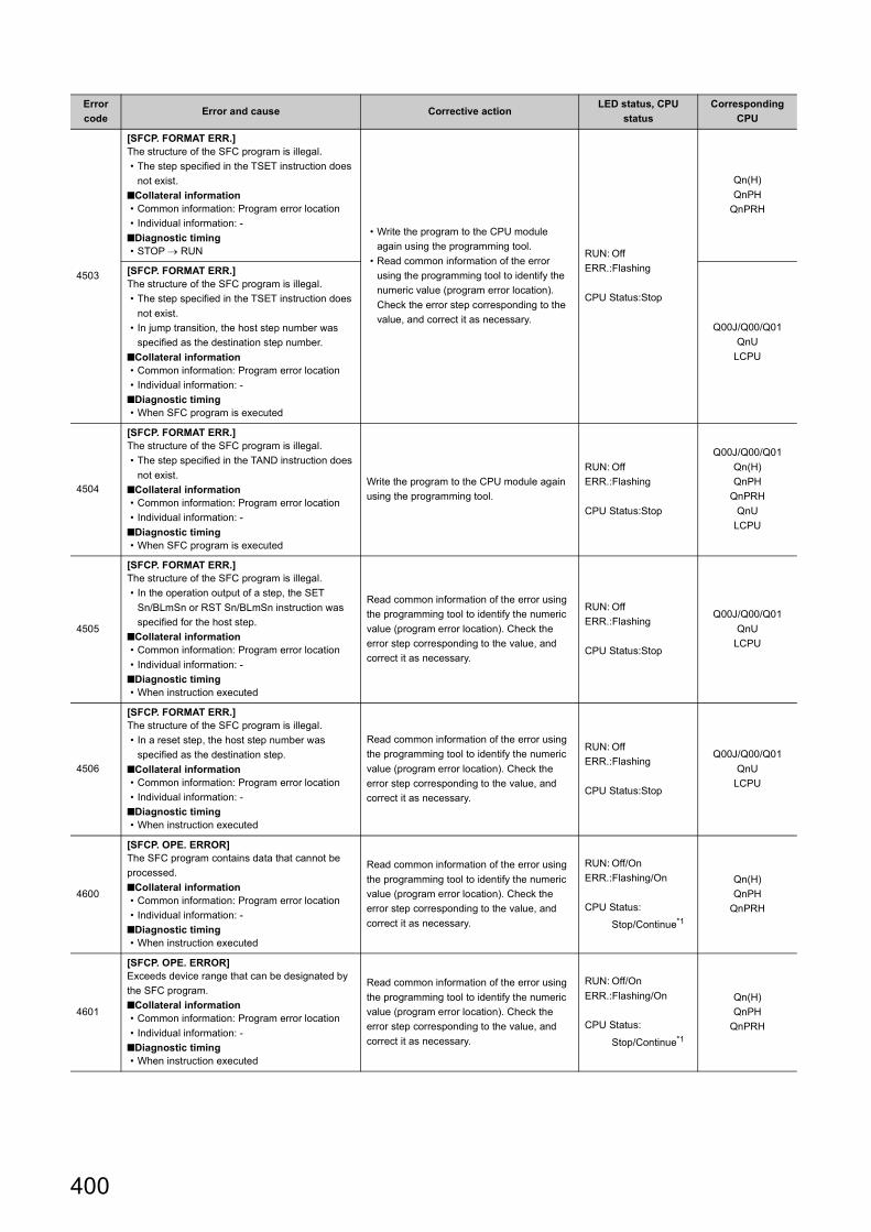
4503
[SFCP. FORMAT ERR.]The structure of the SFC program is illegal.• The step specified in the TSET instruction does
not exist.■Collateral information• Common information: Program error location• Individual information: -
■Diagnostic timing• STOP RUN
• Write the program to the CPU module again using the programming tool.
• Read common information of the error using the programming tool to identify the numeric value (program error location). Check the error step corresponding to the value, and correct it as necessary.
RUN: OffERR.:Flashing
CPU Status:Stop
Qn(H)QnPH
QnPRH
[SFCP. FORMAT ERR.]The structure of the SFC program is illegal.• The step specified in the TSET instruction does
not exist.• In jump transition, the host step number was
specified as the destination step number.■Collateral information• Common information: Program error location• Individual information: -
■Diagnostic timing• When SFC program is executed
Q00J/Q00/Q01QnU
LCPU
4504
[SFCP. FORMAT ERR.]The structure of the SFC program is illegal.• The step specified in the TAND instruction does
not exist.■Collateral information• Common information: Program error location• Individual information: -
■Diagnostic timing• When SFC program is executed
Write the program to the CPU module again using the programming tool.
RUN: OffERR.:Flashing
CPU Status:Stop
Q00J/Q00/Q01Qn(H)QnPH
QnPRHQnU
LCPU
4505
[SFCP. FORMAT ERR.]The structure of the SFC program is illegal.• In the operation output of a step, the SET
Sn/BLmSn or RST Sn/BLmSn instruction was specified for the host step.
■Collateral information• Common information: Program error location• Individual information: -
■Diagnostic timing• When instruction executed
Read common information of the error using the programming tool to identify the numeric value (program error location). Check the error step corresponding to the value, and correct it as necessary.
RUN: OffERR.:Flashing
CPU Status:Stop
Q00J/Q00/Q01QnU
LCPU
4506
[SFCP. FORMAT ERR.]The structure of the SFC program is illegal.• In a reset step, the host step number was
specified as the destination step.■Collateral information• Common information: Program error location• Individual information: -
■Diagnostic timing• When instruction executed
Read common information of the error using the programming tool to identify the numeric value (program error location). Check the error step corresponding to the value, and correct it as necessary.
RUN: OffERR.:Flashing
CPU Status:Stop
Q00J/Q00/Q01QnU
LCPU
4600
[SFCP. OPE. ERROR]The SFC program contains data that cannot be processed.■Collateral information• Common information: Program error location• Individual information: -
■Diagnostic timing• When instruction executed
Read common information of the error using the programming tool to identify the numeric value (program error location). Check the error step corresponding to the value, and correct it as necessary.
RUN: Off/OnERR.:Flashing/On
CPU Status:Stop/Continue*1
Qn(H)QnPH
QnPRH
4601
[SFCP. OPE. ERROR]Exceeds device range that can be designated by the SFC program.■Collateral information• Common information: Program error location• Individual information: -
■Diagnostic timing• When instruction executed
Read common information of the error using the programming tool to identify the numeric value (program error location). Check the error step corresponding to the value, and correct it as necessary.
RUN: Off/OnERR.:Flashing/On
CPU Status:
Stop/Continue*1
Qn(H)QnPH
QnPRH
Error code Error and cause Corrective action
LED status, CPU status
Corresponding CPU
400

APPX
A
Appendix 1 Error Codes
Appendix 1.6 List of error codes (4000 to 4999)
4602
[SFCP. OPE. ERROR]The START instruction in an SFC program is preceded by an END instruction.■Collateral information• Common information: Program error location• Individual information: -
■Diagnostic timing• When instruction executed
Read common information of the error using the programming tool to identify the numeric value (program error location). Check the error step corresponding to the value, and correct it as necessary.
RUN: Off/OnERR.:Flashing/On
CPU Status:
Stop/Continue*1
Qn(H)QnPH
QnPRH
4610
[SFCP. EXE. ERROR]The active step information at presumptive start of the SFC program is incorrect.■Collateral information• Common information: Program error location• Individual information: -
■Diagnostic timing• STOP RUN
Read common information of the error using the programming tool to identify the numeric value (program error location). Check the error step corresponding to the value, and correct it as necessary.The program is automatically subjected to an initial start.
RUN: OnERR.:On
CPU Status:Continue
Qn(H)QnPH
QnPRH
4611
[SFCP. EXE. ERROR]Key-switch was reset during RUN when presumptive start was designated for SFC program.■Collateral information• Common information: Program error location• Individual information: -
■Diagnostic timing• STOP RUN
Read common information of the error using the programming tool to identify the numeric value (program error location). Check the error step corresponding to the value, and correct it as necessary.The program is automatically subjected to an initial start.
RUN: OnERR.:On
CPU Status:Continue
Qn(H)QnPH
QnPRH
4620
[BLOCK EXE. ERROR]Startup was executed at a block in the SFC program that was already started up.■Collateral information• Common information: Program error location• Individual information: -
■Diagnostic timing• When instruction executed
Read common information of the error using the programming tool to identify the numeric value (program error location). Check the error step corresponding to the value, and correct it as necessary.
RUN: OffERR.:Flashing
CPU Status:Stop
Qn(H)QnPH
QnPRHQnU
4621
[BLOCK EXE. ERROR]Startup was attempted at a block that does not exist in the SFC program.■Collateral information• Common information: Program error location• Individual information: -
■Diagnostic timing• When instruction executed
• Read common information of the error using the programming tool to identify the numeric value (program error location). Check the error step corresponding to the value, and correct it as necessary.
• Turn on SM321 if it is off.
RUN: OffERR.:Flashing
CPU Status:Stop
Q00J/Q00/Q01Qn(H)QnPH
QnPRHQnU
LCPU
4630
[STEP EXE. ERROR]The step specified in the SFC program is already activated.■Collateral information• Common information: Program error location• Individual information: -
■Diagnostic timing• When instruction executed
Read common information of the error using the programming tool to identify the numeric value (program error location). Check the error step corresponding to the value, and correct it as necessary.
RUN: OffERR.:Flashing
CPU Status:Stop
Qn(H)QnPH
QnPRH
4631
[STEP EXE. ERROR]• Startup was attempted at the step that does not
exist in the SFC program. Or, the step that does not exist in the SFC program was specified for end.
• Forced transition was executed based on the transition condition that does not exit in the SFC program. Or, the transition condition for forced transition that does not exit in the SFC program was canceled.
■Collateral information• Common information: Program error location• Individual information: -
■Diagnostic timing• When instruction executed
• Read common information of the error using the programming tool to identify the numeric value (program error location). Check the error step corresponding to the value, and correct it as necessary.
• Turn on SM321 if it is off.
RUN: OffERR.:Flashing
CPU Status:Stop
Q00J/Q00/Q01Qn(H)QnPH
QnPRHQnU
LCPU
Error code Error and cause Corrective action
LED status, CPU status
Corresponding CPU
401

*1 The operating status of the CPU module after an error has occurred can be set in parameter. (LED indication changes according to the status.)
*2 Modules whose serial number (first five digits) is "04012" or later
4632
[STEP EXE. ERROR]There were too many simultaneous active steps in blocks that can be designated by the SFC program.■Collateral information• Common information: Program error location• Individual information: -
■Diagnostic timing• When instruction executed
Read common information of the error using the programming tool to identify the numeric value (program error location). Check the error step corresponding to the value, and correct it as necessary.
RUN: OffERR.:Flashing
CPU Status:Stop
Qn(H)QnPH
QnPRHQnU
LCPU
4633
[STEP EXE. ERROR]There were too many simultaneous active steps in all blocks that can be designated.■Collateral information• Common information: Program error location• Individual information: -
■Diagnostic timing• When instruction executed
Read common information of the error using the programming tool to identify the numeric value (program error location). Check the error step corresponding to the value, and correct it as necessary.
RUN: OffERR.:Flashing
CPU Status:Stop
Qn(H)QnPH
QnPRHQnU
LCPU
Error code Error and cause Corrective action
LED status, CPU status
Corresponding CPU
402

APPX
A
Appendix 1 Error Codes
Appendix 1.7 List of error codes (5000 to 5999)
Appendix 1.7 List of error codes (5000 to 5999)
The following table shows the error messages, the error contents and causes, and the corrective actions for the error codes (5000 to 5999).
Error code
Error and cause Corrective actionLED status, CPU
statusCorresponding
CPU
5000
[WDT ERROR]The scan time of the initial execution type program exceeded the initial execution monitoring time specified in the PLC RAS tab of "PLC Parameter".■Collateral information• Common information: Time (value set)• Individual information: Time (value actually
measured)■Diagnostic timing• Always
• Read the individual information of the error using the programming tool to identify the numeric value (time). Check the value and shorten the scan time.
• Change the initial execution monitoring time or the WDT value in the PLC RAS tab of "PLC Parameter".
• Resolve the endless loop caused by jump transition.
• If the error persists even after the actions mentioned above are taken, the possible cause is a hardware failure of the system. Please consult your local Mitsubishi representative.
RUN: OffERR.:Flashing
CPU Status:Stop
Qn(H)QnPH
QnPRHQnU
LCPU
[WDT ERROR]• The power supply of the standby system is
turned OFF.• The tracking cable is disconnected or connected
without turning off or resetting the standby system.
• The tracking cable is not secured by the connector fixing screws.
■Collateral information• Common information: Time (value set)• Individual information: Time (value actually
measured)■Diagnostic timing• Always
• Since power-off of the standby system increases the control system scan time, reset the WDT value, taking the increase of the control system scan time into consideration.
• If the tracking cable was disconnected during operation, securely connect it and restart the CPU module. If the same error code is displayed again, the cause is a hardware failure of the tracking cable or CPU module. Please consult your local Mitsubishi representative.
QnPRH
5001
[WDT ERROR]The scan time of the program exceeded the WDT value specified in the PLC RAS tab of "PLC Parameter".■Collateral information• Common information: Time (value set)• Individual information: Time (value actually
measured)■Diagnostic timing• Always
• Read the individual information of the error using the programming tool to identify the numeric value (time). Check the value and shorten the scan time.
• Change the initial execution monitoring time or the WDT value in the PLC RAS tab of "PLC Parameter".
• Resolve the infinite loop caused by jump sequence.
• Check the execution number of the interrupt program, and reduce the occurrence number of interruption.
• If the error persists even after the actions mentioned above are taken, the possible cause is a hardware failure of the system. Please consult your local Mitsubishi representative.
RUN: OffERR.:Flashing
CPU Status:Stop
QCPULCPU
[WDT ERROR]• The power supply of the standby system is
turned OFF.• The tracking cable is disconnected or connected
without turning off or resetting the standby system.
• The tracking cable is not secured by the connector fixing screws.
■Collateral information• Common information: Time (value set)• Individual information: Time (value actually
measured)■Diagnostic timing• Always
• Since power-off of the standby system increases the control system scan time, reset the WDT value, taking the increase of the control system scan time into consideration.
• If the tracking cable was disconnected during operation, securely connect it and restart the CPU module. If the same error code is displayed again, the cause is a hardware failure of the tracking cable or CPU module. Please consult your local Mitsubishi representative.
QnPRH
403

5002
[WDT ERROR]The execution time of one high-speed interrupt exceeded 100ms.■Collateral information• Common information: Time (value set)• Individual information: Time (value actually
measured)■Diagnostic timing• Always
• If the processing time of the high-speed interrupt program is long, review the program.
• Cancel sampling trace, data logging, scan time measurement, and step specification for executional conditional device test in the interrupt program.
RUN: OffERR.:Flashing
CPU Status:Stop
QnUDVQnUDPV
5010
[PRG. TIME OVER]The program scan time exceeded the constant scan time specified in the PLC RAS tab of "PLC Parameter".■Collateral information• Common information: Time (value set)• Individual information: Time (value actually
measured)■Diagnostic timing• Always
Review the constant scan setting time.
RUN: OnERR.:On
CPU Status:Continue
Qn(H)QnPH
QnPRHQnU
LCPU
[PRG. TIME OVER]The low speed program execution time set in the PLC RAS tab of "PLC parameter" exceeded the excess time of the constant scan.■Collateral information• Common information: Time (value set)• Individual information: Time (value actually
measured)■Diagnostic timing• Always
• Review the constant scan setting time.• To secure sufficient excess time, correct
the value for "Constant scanning" and "Low Speed Program Execution Time" in "PLC Parameter".
Qn(H)QnPH
QnPRH
[PRG. TIME OVER]The program scan time exceeded the constant scan setting time specified in the PLC RAS tab of "PLC parameter".■Collateral information• Common information: Time (value set)• Individual information: Time (value actually
measured)■Diagnostic timing• Always
Review the constant scan setting time in "PLC parameter" so that the excess time of constant scan can be fully secured.
Q00J/Q00/Q01
5011
[PRG. TIME OVER]The scan time of the low speed execution type program exceeded the low speed execution watch time specified in the PLC RAS tab of "PLC parameter".■Collateral information• Common information: Time (value set)• Individual information: Time (value actually
measured)■Diagnostic timing• Always
Read the individual information of the error using the programming tool to identify the numeric value (time). Check the value and shorten the scan time.Change the low speed execution watch time in the PLC RAS setting of "PLC Parameter".
RUN: OnERR.:On
CPU Status:Continue
Qn(H)QnPH
Error code Error and cause Corrective action
LED status, CPU status
Corresponding CPU
404

APPX
A
Appendix 1 Error Codes
Appendix 1.8 List of error codes (6000 to 6999)
Appendix 1.8 List of error codes (6000 to 6999)
The following table shows the error messages, the error contents and causes, and the corrective actions for the error codes (6000 to 6999).
Error code
Error and cause Corrective actionLED status, CPU
statusCorresponding
CPU
6000
[FILE DIFF.]In a redundant system, the control system and standby system do not have the same programs and parameters.The file type detected as different between the two systems can be checked by the file name of the error common information.• The program is different. (File name =
********.QPG)• The PLC parameters/network
parameters/redundant parameters are different. (File name = PARAM.QPA)
• The remote password is different. (File name = PARAM.QPA)
• The intelligent function module parameters are different. (File name = IPARAM.QPA)
• The device initial values are different. (File name = ********.QDI)
• The size of the area, which is used for enabling writing multiple program blocks to the CPU module during running, do not match. (File name = MBOC.QMB) (This can be detected from the standby system of the redundant system.)
■Collateral information• Common information: File name• Individual information: -
■Diagnostic timing• At power-on/At reset/At tracking cable
connection/At changing to backup mode/At completion of write during RUN/At system switching/At switching both systems into RUN
• Match the programs and parameters of the control system and standby system.
• Verify the CPU module by either of the following procedures 1) or 2) to clarify the differences between the files of both systems. Correct wrong files and write them to the CPU module again.
1) Read the programs and parameters of System A using GX Works2, GX Developer, or PX Developer, and verify them with those of System B.
2) Verify the programs and parameters saved in GX Works2, GX Developer, or PX Developer (offline environment) with those written to the CPU modules of both systems.
• When the size of the area, which is used for enabling writing multiple program blocks to the CPU module during running, do not match, perform either of corrective actions 1) or 2).
1) Using the memory copy function, copy the program memory from the control system to the standby system.
2) Format the CPU module program memories of both systems. (For both systems, specify the same values for the size of the area, which is used for enabling writing multiple program blocks to the CPU module during running.)
RUN: OffERR.:Flashing
CPU Status:Stop
QnPRH
6001
[FILE DIFF.]In the redundant system, the valid-parameter drive setting (SW2, SW3) set by the DIP switches differs between the control system and standby system.■Collateral information• Common information: -• Individual information: -
■Diagnostic timing• At power-on/At reset/At tracking cable
connection/At operation mode change
Match the valid-parameter drive settings (SW2, SW3) for both the control and standby systems using the DIP switches.
RUN: OffERR.:Flashing
CPU Status:Stop
QnPRH
6010
[OPE. MODE DIFF.]The operational status of the control system and standby system in the redundant system is not the same. (This can be detected from the standby system of the redundant system.)■Collateral information• Common information: -• Individual information: -
■Diagnostic timing• Always
Synchronize the operation statuses of the control system and standby system.
RUN: OnERR.:On
CPU Status:Continue
QnPRH
405

6020
[OPE. MODE DIFF.]At power-on/reset, the RUN/STOP switch settings of the control system and standby system are not the same in a redundant system. (This can be detected from the control system or standby system of the redundant system.)■Collateral information• Common information: -• Individual information: -
■Diagnostic timing• At power-on/At reset
Set the RUN/STOP switches of the control system and standby system to the same setting.
RUN: OffERR.:Flashing
CPU Status:Stop
QnPRH
6030
[UNIT LAY. DIFF.]• In a redundant system, the module configuration
differs between the control system and standby system.
• The network module mode setting differs between the two systems. (This can be detected from the control system or standby system of the redundant system.)
■Collateral information• Common information: Module No.• Individual information: -
■Diagnostic timing• At power-on/At reset/At tracking cable
connection/At operation mode change
• Match the module configurations of the control system and standby system.
• In the redundant setting of "Network parameter", match the mode setting of System B to that of System A.
RUN: OffERR.:Flashing
CPU Status:Stop
QnPRH
6035
[UNIT LAY. DIFF.]In a redundant system, the CPU module model name differs between the control system and standby system. (This can be detected from the standby system of the redundant system.)■Collateral information• Common information: -• Individual information: -
■Diagnostic timing• At power-on/At reset/At tracking cable
connection/At operation mode change
Match the model names of the control system and standby system.
RUN: OffERR.:Flashing
CPU Status:Stop
QnPRH
6036
[UNIT LAY. DIFF.]A difference in the remote I/O configuration of the MELSECNET/H multiplexed remote I/O network between the control system and standby system of a redundant system was detected. (This can be detected from the control system or standby system of the redundant system.)■Collateral information• Common information: Module No.• Individual information: -
■Diagnostic timing• Always
Check the network cables of the MELSECNET/H multiplexed remote I/O network for disconnection.
RUN: OffERR.:Flashing
CPU Status:Stop
QnPRH
6040
[CARD TYPE DIFF.]In the redundant system, the memory card insertion status (inserted/not inserted) differs between the control system and standby system.■Collateral information• Common information: -• Individual information: -
■Diagnostic timing• At power-on/At reset
Match the memory card insertion status (inserted/not inserted) of the control system and standby system.
RUN: OffERR.:Flashing
CPU Status:Stop
QnPRH
6041
[CARD TYPE DIFF.]In the redundant system, the memory card type differs between the control system and standby system.■Collateral information• Common information: -• Individual information: -
■Diagnostic timing• At power-on/At reset
Match the memory card types of the control system and standby system.
RUN: OffERR.:Flashing
CPU Status:Stop
QnPRH
Error code Error and cause Corrective action
LED status, CPU status
Corresponding CPU
406

APPX
A
Appendix 1 Error Codes
Appendix 1.8 List of error codes (6000 to 6999)
6050
[CAN'T EXE. MODE]The function inexecutable in the debug mode or operation mode (backup/separate mode) was executed. (This can be detected from the control system or standby system of the redundant system.)■Collateral information• Common information: -• Individual information: -
■Diagnostic timing• Always
Execute the function executable in the debug mode or operation mode (backup/separate mode).
RUN: OnERR.:On
CPU Status:Continue
QnPRH
6060
[CPU MODE DIFF.]In a redundant system, the operation mode (backup/separate) differs between the control system and standby system. (This can be detected from the standby system of the redundant system.)■Collateral information• Common information: -• Individual information: -
■Diagnostic timing• At power-on/At reset/At tracking cable
connection
Match the operation modes of the control system and standby system.
RUN: OffERR.:Flashing
CPU Status:Stop
QnPRH
6061
[CPU MODE DIFF.]In a redundant system, the operation mode (backup/separate) differs between the control system and standby system. (This can be detected from the standby system of the redundant system.)■Collateral information• Common information: -• Individual information: -
■Diagnostic timing• When an END instruction executed
Match the operation modes of the control system and standby system.
RUN: OffERR.:Flashing
CPU Status:Stop
QnPRH
6062
[CPU MODE DIFF.]Both System A and B are in the same system status (control system). (This can be detected from the system B of the redundant system.)■Collateral information• Common information: -• Individual information: -
■Diagnostic timing• At power-on/At reset/At tracking cable
connection
Power the CPU module (System B) which resulted in a stop error, OFF and then ON.
RUN: OffERR.:Flashing
CPU Status:Stop
QnPRH
6100
[TRK. TRANS. ERR.]• An error (e.g. retry limit exceeded) occurred in
tracking (data transmission). (This error may be caused by tracking cable removal or other system power-off (including reset).)
• The error occurred at a startup since the redundant system startup procedure was not followed.
■Collateral information• Common information: Tracking transmission
data classification• Individual information: -
■Diagnostic timing• Always
• Check the CPU module or tracking cable. If the same error occurs, the cause is a failure of the CPU module or tracking cable. Please consult your local Mitsubishi representative.
• Confirm the redundant system startup procedure, and execute a startup again.
RUN: OnERR.:On
CPU Status:Continue
QnPRH
Error code Error and cause Corrective action
LED status, CPU status
Corresponding CPU
407

6101
[TRK. TRANS. ERR.]• A timeout error occurred in tracking (data
transmission). (This error may be caused by tracking cable removal or other system power-off (including reset).)
• The error occurred at a startup since the redundant system startup procedure was not followed.
(This can be detected from the control system or standby system of the redundant system.)■Collateral information• Common information: Tracking transmission
data classification• Individual information: -
■Diagnostic timing• Always
• Check the CPU module or tracking cable. If the same error occurs, the cause is a failure of the CPU module or tracking cable. Please consult your local Mitsubishi representative.
• Confirm the redundant system startup procedure, and execute a startup again.
RUN: OnERR.:On
CPU Status:Continue
QnPRH
6102
[TRK. TRANS. ERR.]A data sum value error occurred in tracking (data reception). (This can be detected from the control system or standby system of the redundant system.)■Collateral information• Common information: -• Individual information: -
■Diagnostic timing• Always
• Check the CPU module or tracking cable. If the same error occurs, the cause is a failure of the CPU module or tracking cable. Please consult your local Mitsubishi representative.
• Confirm the redundant system startup procedure, and execute a startup again.
RUN: OnERR.:On
CPU Status:Continue
QnPRH
6103
[TRK. TRANS. ERR.]• A data error (other than sum value error)
occurred in tracking (data reception). (This error may be caused by tracking cable removal or other system power-off (including reset).)
• The error occurred at a startup since the redundant system startup procedure was not followed.
(This can be detected from the control system or standby system of the redundant system.)■Collateral information• Common information: -• Individual information: -
■Diagnostic timing• Always
• Check the CPU module or tracking cable. If the same error occurs, the cause is a failure of the CPU module or tracking cable. Please consult your local Mitsubishi representative.
• Confirm the redundant system startup procedure, and execute a startup again.
RUN: OnERR.:On
CPU Status:Continue
QnPRH
6105
[TRK. TRANS. ERR.]• An error (e.g. retry limit exceeded) occurred in
tracking (data transmission). (This error may be caused by tracking cable removal or other system power-off (including reset).)
• The error occurred at a startup since the redundant system startup procedure was not followed.
(This can be detected from the control system or standby system of the redundant system.)■Collateral information• Common information: Tracking transmission
data classification• Individual information: -
■Diagnostic timing• Always
• Check the CPU module or tracking cable. If the same error occurs, the cause is a failure of the CPU module or tracking cable. Please consult your local Mitsubishi representative.
• Confirm the redundant system startup procedure, and execute a startup again.
RUN: OnERR.:On
CPU Status:Continue
QnPRH
Error code Error and cause Corrective action
LED status, CPU status
Corresponding CPU
408

APPX
A
Appendix 1 Error Codes
Appendix 1.8 List of error codes (6000 to 6999)
6106
[TRK. TRANS. ERR.]• A timeout error occurred in tracking (data
transmission). (This error may be caused by tracking cable removal or other system power-off (including reset).)
• The error occurred at a startup since the redundant system startup procedure was not followed.
(This can be detected from the control system or standby system of the redundant system.)■Collateral information• Common information: Tracking transmission
data classification• Individual information: -
■Diagnostic timing• Always
• Check the CPU module or tracking cable. If the same error occurs, the cause is a failure of the CPU module or tracking cable. Please consult your local Mitsubishi representative.
• Confirm the redundant system startup procedure, and execute a startup again.
RUN: OnERR.:On
CPU Status:Continue
QnPRH
6107
[TRK. TRANS. ERR.]A data sum value error occurred in tracking (data reception). (This can be detected from the control system or standby system of the redundant system.)■Collateral information• Common information: -• Individual information: -
■Diagnostic timing• Always
• Check the CPU module or tracking cable. If the same error occurs, the cause is a failure of the CPU module or tracking cable. Please consult your local Mitsubishi representative.
• Confirm the redundant system startup procedure, and execute a startup again.
RUN: OnERR.:On
CPU Status:Continue
QnPRH
6108
[TRK. TRANS. ERR.]• A data error (other than sum value error)
occurred in tracking (data reception). (This error may be caused by tracking cable removal or other system power-off (including reset).)
• The error occurred at a startup since the redundant system startup procedure was not followed.
(This can be detected from the control system or standby system of the redundant system.)■Collateral information• Common information: -• Individual information: -
■Diagnostic timing• Always
• Check the CPU module or tracking cable. If the same error occurs, the cause is a failure of the CPU module or tracking cable. Please consult your local Mitsubishi representative.
• Confirm the redundant system startup procedure, and execute a startup again.
RUN: OnERR.:On
CPU Status:Continue
QnPRH
6110
[TRK. SIZE ERROR]The tracking capacity exceeded the allowed range. (This can be detected from the control system or standby system of the redundant system.)■Collateral information• Common information: Reason(s) for tracking
size excess error• Individual information: -
■Diagnostic timing• When an END instruction executed
Reexamine the tracking capacity.
RUN: OnERR.:On
CPU Status:Continue
QnPRH
6111
[TRK. SIZE ERROR]The control system does not have enough file register capacity for the file registers specified in the tracking settings. (This can be detected from the control system or standby system of the redundant system.)■Collateral information• Common information: -• Individual information: -
■Diagnostic timing• When an END instruction executed
Switch to the file registers of which capacity is greater than the file registers specified in the tracking settings.
RUN: OnERR.:On
CPU Status:Continue
QnPRH
Error code Error and cause Corrective action
LED status, CPU status
Corresponding CPU
409

6112
[TRK. SIZE ERROR]File registers greater than those of the standby system were tracked and transmitted from the control system. (This can be detected from the standby system of the redundant system.)■Collateral information• Common information: -• Individual information: -
■Diagnostic timing• When an END instruction executed
Switch to the file registers of which capacity is greater than the file registers specified in the tracking settings.
RUN: OnERR.:On
CPU Status:Continue
QnPRH
6120
[TRK. CABLE ERR.]• A start was made without the tracking cable
being connected.• A start was made with the tracking cable faulty.• As the tracking communication hardware of the
CPU module was faulty, the CPU module could not communicate with the other system through the tracking cable.
(This can be detected from the control system or standby system of the redundant system.)■Collateral information• Common information: -• Individual information: -
■Diagnostic timing• At power-on/At reset
Connect a tracking cable and start up the module. If the same error occurs, the cause is a failure of the tracking cable or the tracking communication hardware of the CPU module. Please consult your local Mitsubishi representative.
RUN: OffERR.:Flashing
CPU Status:Stop
QnPRH
6130
[TRK. DISCONNECT]• The tracking cable was removed.• The tracking cable became faulty while the CPU
module is running.• The tracking communication hardware of the
CPU module became faulty.(This can be detected from the control system or standby system of the redundant system.)■Collateral information• Common information: -• Individual information: -
■Diagnostic timing• Always
• If the tracking cable was removed, connect the tracking cable to the connectors of the CPU modules of the two systems.
• If the error remains even after the above action is taken, the cause is a failure of the tracking cable or the tracking communication hardware of the CPU module. Please consult your local Mitsubishi representative.
RUN: OnERR.:On
CPU Status:Continue
QnPRH
6140
[TRK.INIT. ERROR]• The other system did not respond during initial
communication at power-on/reset.• The error occurred at a startup since the
redundant system startup procedure was not followed.
(This can be detected from the control system or standby system of the redundant system.)■Collateral information• Common information: -• Individual information: -
■Diagnostic timing• At power-on/At reset
• Power off and on or reset the CPU module that detects the error. If the same error occurs, the cause is a hardware failure of the CPU module. Please consult your local Mitsubishi representative.
• Confirm the redundant system startup procedure, and execute a startup again.
RUN: OffERR.:Flashing
CPU Status:Stop
QnPRH
Error code Error and cause Corrective action
LED status, CPU status
Corresponding CPU
410

APPX
A
Appendix 1 Error Codes
Appendix 1.8 List of error codes (6000 to 6999)
6200
[CONTROL EXE.]The standby system has been switched to the control system in a redundant system. (Detected by the CPU that was switched from the standby system to the control system.)Since this error code does not indicate the error information of the CPU module but indicates its status, the error code and error information are not stored into SD0 to 26, but are stored into the error log every system switching. (To check the error information, obtain the error log using the programming tool.)■Collateral information• Common information: Reason(s) for system
switching• Individual information: -
■Diagnostic timing• Always
RUN: OnERR.:Off
CPU Status:No error
QnPRH
6210
[STANDBY]The control system has been switched to the standby system in a redundant system. (Detected by the CPU that was switched from the control system to the standby system.)Since this error code does not indicate the error information of the CPU module but indicates its status, the error code and error information are not stored into SD0 to 26, but are stored into the error log every system switching. (To check the error information, obtain the error log using the programming tool.)■Collateral information• Common information: Reason(s) for system
switching• Individual information: -
■Diagnostic timing• Always
RUN: OnERR.:Off
CPU Status:No error
QnPRH
6220
[CAN'T SWITCH]The system cannot be switched due to a standby system error, tracking cable failure, or online module change being executed in the separate mode. Causes for switching system at control system are as follows:• System switching by SP.CONTSW instruction• System switching request from network module
■Collateral information• Common information: Reason(s) for system
switching• Individual information: Reason(s) for system
switching failure■Diagnostic timing• At switching execution
• Check the status of the standby system and resolve the error.
• Complete the online module change.
RUN: OnERR.:On
CPU Status:Continue
QnPRH
6300
[STANDBY SYS. DOWN]Any of the following errors was detected in the backup mode.• The standby system has not started up in the
redundant system.• The standby system has developed a stop error
in the redundant system.• The CPU module in the debug mode was
connected to the operating control system.(This can be detected from the control system of the redundant system.)■Collateral information• Common information: -• Individual information: -
■Diagnostic timing• Always
• Check whether the standby system is on or not, and if it is not on, power it on.
• Check whether the standby system has been reset or not, and if it has been reset, unreset it.
• Check whether the standby system has developed a stop error or not, and if it has developed the error, remove the error factor and restart it.
• When the CPU module in the debug mode was connected to the control system operating in the backup mode, make connection so that the control system and standby system are combined correctly.
RUN: OnERR.:On
CPU Status:Continue
QnPRH
Error code Error and cause Corrective action
LED status, CPU status
Corresponding CPU
411

6310
[CONTROL SYS. DOWN]Any of the following errors was detected in the backup mode.• The control system has not started up in the
redundant system.• The control system has developed a stop error
in the redundant system.• The CPU module in the debug mode was
connected to the operating standby system.• The error occurred at a startup since the
redundant system startup procedure was not followed.
(This can be detected from the standby system of the redundant system.)■Collateral information• Common information: -• Individual information: -
■Diagnostic timing• Always
• The standby system exists but the control system does not exist.
• Check whether the system other than the standby system is on or not, and if it is not on, power it on.
• Check whether the system other than the standby system has been reset or not, and if it is has been reset, unreset it.
• Check whether the system other than the standby system has developed a stop error or not, and if has developed the error, remove the error factor, set the control system and standby system to the same operating status, and restart.
• When the CPU module in the debug mode was connected to the control system operating in the backup mode, make connection so that the control system and control system are combined correctly.
• Confirm the redundant system startup procedure, and execute a startup again.
RUN: OffERR.:Flashing
CPU Status:Stop
QnPRH
6311
[CONTROL SYS. DOWN]• As consistency check data has not transmitted
from the control system in a redundant system, the other system cannot start as a standby system.
• The error occurred at a startup since the redundant system startup procedure was not followed.
(This can be detected from the standby system of the redundant system.)■Collateral information• Common information: -• Individual information: -
■Diagnostic timing• At power-on/At reset
• Replace the tracking cable. If the same error occurs, the cause is a hardware failure of the CPU module. Please consult your local Mitsubishi representative.
• Confirm the redundant system startup procedure, and execute a startup again.
RUN: OffERR.:Flashing
CPU Status:Stop
QnPRH
6312
[CONTROL SYS. DOWN]• As consistency check data has not transmitted
from the control system in a redundant system, the other system cannot start as a standby system.
• The error occurred at a startup since the redundant system startup procedure was not followed.
(This can be detected from the standby system of the redundant system.)■Collateral information• Common information: -• Individual information: -
■Diagnostic timing• At power-on/At reset
• Replace the tracking cable. If the same error occurs, the cause is a hardware failure of the CPU module. Please consult your local Mitsubishi representative.
• Confirm the redundant system startup procedure, and execute a startup again.
RUN: OffERR.:Flashing
CPU Status:Stop
QnPRH
6313
[CONTROL SYS. DOWN]The control system detected the error of the system configuration and informed it to the standby system (host system) in the redundant system.■Collateral information• Common information: -• Individual information: -
■Diagnostic timing• At power-on/At reset
Restart the system after checking that the connection between base unit and the system configuration (type/number/parameter of module) are correct.
RUN: OffERR.:Flashing
CPU Status:Stop
QnPRH
Error code Error and cause Corrective action
LED status, CPU status
Corresponding CPU
412

APPX
A
Appendix 1 Error Codes
Appendix 1.8 List of error codes (6000 to 6999)
6400
[PRG. MEM. CLEAR]The memory copy from control system to standby system was executed, and the program memory was cleared.■Collateral information• Common information: -• Individual information: -
■Diagnostic timing• At execution of the memory copy from control
system to standby system
After the memory copy from the control system to the standby system is completed, turn off and then on or reset the system.
RUN: OffERR.:Flashing
CPU Status:Stop
QnPRH
6410
[MEM. COPY EXE.]The memory copy from control system to standby system was executed. (This can be detected from the control system of the redundant system.)■Collateral information• Common information: -• Individual information: -
■Diagnostic timing• At execution of the memory copy from control
system to standby system
RUN: OnERR.:On
CPU Status:Continue
QnPRH
6500
[TRK. PARA. ERROR]The file register file specified in the tracking setting of "PLC Parameter" does not exist.■Collateral information• Common information: File name/Drive name• Individual information: Parameter number
■Diagnostic timing• At power-on/At reset
Read the individual information of the error using the programming tool. Check the drive name and file name and correct them, or create the specified file register file.
RUN: OffERR.:Flashing
CPU Status:Stop
QnPRH
6501
[TRK. PARA. ERROR]The file register range specified in the device detail setting of the tracking setting of "PLC Parameter" exceeded the specified file register file capacity.■Collateral information• Common information: File name/Drive name• Individual information: Parameter number
■Diagnostic timing• At power-on/At reset
Read the individual information of the error using the programming tool, and increase the file register capacity.
RUN: OffERR.:Flashing
CPU Status:Stop
QnPRH
Error code Error and cause Corrective action
LED status, CPU status
Corresponding CPU
413

Appendix 1.9 List of error codes (7000 to 10000)
The following table shows the error messages, the error contents and causes, and the corrective actions for the error codes (7000 to 10000).
Error code
Error and cause Corrective actionLED status, CPU
statusCorresponding
CPU
7000
[MULTI CPU DOWN]• In the operating mode of a multiple CPU
system, a CPU error occurred at the CPU where "All station stop by stop error of CPU " was selected.
• In a multiple CPU system, a CPU module incompatible with the multiple CPU system was mounted.
• Any CPU module other than CPU No.1 was disconnected from the base unit during operation. Or any CPU module other than CPU No.1 was reset.
• At power-on/reset, momentary power failure has occurred.
■Collateral information• Common information: Module No. (CPU No.)• Individual information: -
■Diagnostic timing• Always
• Read the common information of the error using the programming tool. Check the error in the CPU module, and eliminate the error cause.
• Remove the CPU module from the main base unit if it does not support the multiple CPU system configuration.
• Check the mounting status of CPU modules other than CPU No.1 and whether the CPU modules were reset.
• Check the power supply.• The cause is a hardware failure of the
power supply module. Please consult your local Mitsubishi representative.
RUN: OffERR.:Flashing
CPU Status:Stop
Q00/Q01Qn(H)QnPHQnU
[MULTI CPU DOWN]In a multiple CPU system, CPU other than CPU No.1 cannot be started up due to stop error of the CPU No.1 at power-on, which occurs to CPU No.2 to No.4.■Collateral information• Common information: Module No. (CPU No.)• Individual information: -
■Diagnostic timing• At power-on/At reset
Read the common information of the error using the programming tool. Check the error in the CPU module, and eliminate the error cause.
RUN: OffERR.:Flashing
CPU Status:Stop
Q00/Q01Qn(H)QnPHQnU
7002
[MULTI CPU DOWN]• There is no response from the target CPU
module in a multiple CPU system during initial communication.
• In a multiple CPU system, a CPU module incompatible with the multiple CPU system was mounted.
■Collateral information• Common information: Module No. (CPU No.)• Individual information: -
■Diagnostic timing• At power-on/At reset
• Reset the CPU module and run it again. If the same error code is displayed again, the cause is a hardware failure of any of the CPU modules. Please consult your local Mitsubishi representative.
• Remove the CPU module from the main base unit if it does not support a multiple CPU system configuration. Alternatively, replace the CPU module that does not support a multiple system configuration with the one that does.
RUN: OffERR.:Flashing
CPU Status:Stop
Q00/Q01Qn(H)QnPH
[MULTI CPU DOWN]There is no response from the target CPU module in a multiple CPU system during initial communication.■Collateral information• Common information: Module No. (CPU No.)• Individual information: -
■Diagnostic timing• At power-on/At reset
Reset the CPU module and run it again. If the same error code is displayed again, the cause is a hardware failure of any of the CPU modules. Please consult your local Mitsubishi representative.
QnU
7003
[MULTI CPU DOWN]There is no response from the target CPU module in a multiple CPU system at initial communication stage.■Collateral information• Common information: Module No. (CPU No.)• Individual information: -
■Diagnostic timing• At power-on/At reset
Reset the CPU module and run it again. If the same error code is displayed again, the cause is a hardware failure of any of the CPU modules. Please consult your local Mitsubishi representative.
RUN: OffERR.:Flashing
CPU Status:Stop
Q00/Q01Qn(H)QnPHQnU
414

APPX
A
Appendix 1 Error Codes
Appendix 1.9 List of error codes (7000 to 10000)
7004
[MULTI CPU DOWN]In a multiple CPU system, a data error occurred in communication between the CPU modules.■Collateral information• Common information: Module No. (CPU No.)• Individual information: -
■Diagnostic timing• Always
• Check the system configuration to see if modules are mounted in excess of the number of I/O points.
• If there is no problem in the system configuration, the cause is a hardware failure of the CPU module. Please consult your local Mitsubishi representative.
RUN: OffERR.:Flashing
CPU Status:Stop
Q00/Q01QnU
7010
[MULTI EXE. ERROR]• In a multiple CPU system, a faulty CPU module
was mounted.• In a multiple CPU system, a CPU module
incompatible with the multiple CPU system was mounted. (The CPU module compatible with the multiple CPU system was used to detect an error.)
• In a multiple CPU system, any of the CPU No. 2 to 4 was reset with power ON. (The CPU whose reset state was cancelled was used to detect an error.)
■Collateral information• Common information: Module No. (CPU No.)• Individual information: -
■Diagnostic timing• At power-on/At reset
• Read the common information of the error using the programming tool and replace the faulty CPU module.
• Replace the CPU module with the one compatible with the multiple CPU system.
• Do not reset any of the No. 2 to 4 CPU modules.
• Reset CPU No. 1 and restart the multiple CPU system.
RUN: OffERR.:Flashing
CPU Status:Stop
Q00/Q01Qn(H)QnPHQnU
[MULTI EXE. ERROR]In a multiple CPU system, the version of the
software package (PPC-DRV-01)*2 for the PC CPU module is 1.06 or earlier.■Collateral information• Common information: Module No. (CPU No.)• Individual information: -
■Diagnostic timing• At power-on/At reset
Change the software package (PPC-DRV-
01)*2 for the PC CPU module to the version 1.07 or later.
Q00/Q01
[MULTI EXE. ERROR]The Q172(H)CPU(N) or Q173(H)CPU(N) is mounted on the multiple CPU high-speed main base unit (Q3DB). (This may result in a module failure.)■Collateral information• Common information: Module No. (CPU No.)• Individual information: -
■Diagnostic timing• At power-on/At reset
Replace the Q172(H)CPU(N) and Q173(H)CPU(N) with the Motion CPU compatible with the multiple CPU high-speed main base unit.
Qn(H)QnPH
[MULTI EXE. ERROR]The Universal model QCPU (except Q02UCPU) and Q172(H)CPU(N) are mounted on the same base unit. (This may result in a module failure.)■Collateral information• Common information: Module No. (CPU No.)• Individual information: -
■Diagnostic timing• At power-on/At reset
Check the QCPU and Motion CPU that can be used in a multiple CPU system, and change the system configuration.
Error code Error and cause Corrective action
LED status, CPU status
Corresponding CPU
415

7011
[MULTI EXE. ERROR]Either of the following settings was made in a multiple CPU system.• Multiple CPU automatic refresh setting was
made for the inapplicable CPU module.• "I/O sharing when using multiple CPUs" setting
was made for the inapplicable CPU module.■Collateral information• Common information: Module No. (CPU No.)• Individual information: -
■Diagnostic timing• At power-on/At reset
• Correct the multiple CPU automatic refresh setting.
• Correct the "I/O sharing when using multiple CPUs" setting.
RUN: OffERR.:Flashing
CPU Status:Stop
Q00/Q01QnU
[MULTI EXE. ERROR]The system configuration for using the multiple CPU high speed transmission function is not met.• The Universal model QCPU (except Q00UCPU,
Q01UCPU, Q02UCPU) is not used for the CPU No.1.
• The multiple CPU high speed main base unit (Q3DB) is not used.
• Points other than 0 is set to the send range for the CPU module incompatible with the multiple CPU high speed transmission function.
• Points other than 0 are set to the auto refresh send range for the multiple CPU high-speed transmission area even though the CPU module does not support the use of this area.
■Collateral information• Common information: Module No. (CPU No.)• Individual information: -
■Diagnostic timing• At power-on/At reset
• Change the system configuration to meet the conditions for using the multiple CPU high speed transmission function.
• When auto refresh is performed for the multiple CPU high-speed transmission area, set 0 point to the auto refresh send range of the CPU module that does not support the use of this area.
QnU
7013
[MULTI EXE. ERROR]The Q172(H)CPU(N) or Q173(H)CPU(N) is mounted to the CPU slot or slots 0 to 2. (This may result in a module failure.)■Collateral information• Common information: Module No. (CPU No.)• Individual information: -
■Diagnostic timing• At power-on/At reset
• Check the QCPU and Motion CPU that can be used in a multiple CPU system, and change the system configuration.
• Remove the Motion CPU incompatible with the multiple CPU system.
RUN: OffERR.:Flashing
CPU Status:Stop
QnU
7020
[MULTI CPU ERROR]In a multiple CPU system, an error occurred in the CPU module where "All station stop by stop error of CPU" was not selected in the operating mode setting. (The CPU module where no error occurred was used to detect an error.)■Collateral information• Common information: Module No. (CPU No.)• Individual information: -
■Diagnostic timing• Always
Read the common information of the error using the programming tool. Check the error in the CPU module, and eliminate the error cause.
RUN: OnERR.:On
CPU Status:Continue
Q00/Q01Qn(H)QnPHQnU
7030
[CPU LAY ERROR]An assignment error occurred in the CPU-mountable slot (CPU slot, I/O slot 0, 1) in excess of the number of CPU modules specified in the multiple CPU setting of "PLC Parameter".■Collateral information• Common information: Module No. (CPU No.)• Individual information: -
■Diagnostic timing• At power-on/At reset
• Set the same value to the number of CPU modules specified in the multiple CPU setting of "PLC Parameter" and the number of mounted CPU modules (including CPU (empty)).
• Make the type specified in the I/O assignment setting of "PLC Parameter" consistent with the CPU module configuration.
RUN: OffERR.:Flashing
CPU Status:Stop
Q00J/Q00/Q01QnU
Error code Error and cause Corrective action
LED status, CPU status
Corresponding CPU
416

APPX
A
Appendix 1 Error Codes
Appendix 1.9 List of error codes (7000 to 10000)
7031
[CPU LAY ERROR]An assignment error occurred within the range of the number of CPUs specified in the multiple CPU setting of "PLC Parameter".■Collateral information• Common information: Module No. (CPU No.)• Individual information: -
■Diagnostic timing• At power-on/At reset
• Set the same value to the number of CPU modules specified in the multiple CPU setting of "PLC Parameter" and the number of mounted CPU modules (including CPU (empty)).
• Make the type specified in the I/O assignment setting of "PLC Parameter" consistent with the CPU module configuration.
RUN: OffERR.:Flashing
CPU Status:Stop
Q00J/Q00/Q01QnU
7032
[CPU LAY ERROR]The number of CPU modules mounted in a multiple CPU system is wrong.■Collateral information• Common information: Module No. (CPU No.)• Individual information: -
■Diagnostic timing• At power-on/At reset
Configure a system so that the number of mountable modules of each CPU module does not exceed the maximum number of mountable modules specified in the specification.
RUN: OffERR.:Flashing
CPU Status:Stop
Q00J/Q00/Q01QnU
7035
[CPU LAY ERROR]The CPU module has been mounted on the inapplicable slot.■Collateral information• Common information: Module No. (Slot No.)• Individual information: -
■Diagnostic timing• At power-on/At reset
• Mount the CPU module on the applicable slot.
• Remove the CPU module from the slot where a CPU module cannot be mounted.
RUN: OffERR.:Flashing
CPU Status:Stop
Q00J/Q00/Q01QnPRH
QnU
7036
[CPU LAY ERROR]The host CPU No. set by the multiple CPU setting and the host CPU No. determined by the mounting position of the CPU module are not the same.■Collateral information• Common information: Module No. (CPU No.)• Individual information: -
■Diagnostic timing• At power-on/At reset
• Mount the mounting slot of the CPU module correctly.
• Correct the host CPU No. set by the multiple CPU setting to the CPU No. determined by the mounting position of the CPU module.
RUN: OffERR.:Flashing
CPU Status:Stop
QnU
8031
[INCORRECT FILE]The error of stored file (enabled parameter file) is detected.■Collateral information• Common information: -• Individual information: File diagnostic
information■Diagnostic timing• At power-on/At reset/STOP RUN/At writing to
programmable controller
Write the files shown in SD17 to SD22 (individual information) to the drive shown in SD16 (L) (individual information). Turn off and then on or reset the CPU module.If the same error code is displayed again, the cause is a hardware failure of the CPU module. Please consult your local Mitsubishi representative.
RUN: OffERR.:Flashing
CPU Status:Stop
QnULCPU
9000
[F**** ]Annunciator (F) turned on. (The "****" portion of the error message indicates an annunciator number.)■Collateral information• Common information: Program error location• Individual information: Annunciator number
■Diagnostic timing• When instruction executed
Read the individual information of the error using the programming tool to identify the numeric value (annunciator number). Check the program corresponding to the value.
RUN: On
ERR.:On/Off*1
USER:On*3
CPU Status:Continue
QCPULCPU
Error code Error and cause Corrective action
LED status, CPU status
Corresponding CPU
417

9010
[<CHK>ERR ***-***]Error detected by the CHK instruction. (The "***" portion of the error message indicates the numbers of contact and coil that have been detected.)■Collateral information• Common information: Program error location• Individual information: Failure No.
■Diagnostic timing• When instruction executed
Read the individual information of the error using the programming tool to identify the numeric value (error number). Check the program corresponding to the value.
RUN: OnERR.:OffUSER:On
CPU Status:Continue
Qn(H)QnPH
QnPRH
9020
[BOOT OK]Storage of data onto ROM was completed normally in automatic write to the standard ROM. (The BOOT LED also flashes.)■Collateral information• Common information: -• Individual information: -
■Diagnostic timing• At power-on/At reset
Use the DIP switches to set the valid parameter drive to the standard ROM. Then, switch power on again, and perform boot operation from the standard ROM.
RUN: OffERR.:Flashing
CPU Status:Stop
Qn(H)QnPH
QnPRH
9100
[PID ERROR]A data error has occurred in control parameter because the sampling time (TS) setting is out of the range (TS0). Or, an error has occurred during PID operation.■Collateral information• Common information: Program error location• Individual information: -
■Diagnostic timing• When instruction executed
Check and correct the control parameter setting.
RUN: OnERR.:On
CPU Status:Continue
LCPUQnUDV
QnUDPV
9101
[PID ERROR]A data error has occurred in control parameter or during PID operation because the input filter constant () setting is out of the range (<0 or 100).■Collateral information• Common information: Program error location• Individual information: -
■Diagnostic timing• When instruction executed
Check and correct the control parameter setting.
RUN: OnERR.:On
CPU Status:Continue
LCPUQnUDV
QnUDPV
9102
[PID ERROR]A data error has occurred in control parameter or during PID operation because the proportional gain (KP) setting is out of the range (KP<0).■Collateral information• Common information: Program error location• Individual information: -
■Diagnostic timing• When instruction executed
Check and correct the control parameter setting.
RUN: OnERR.:On
CPU Status:Continue
LCPUQnUDV
QnUDPV
9103
[PID ERROR]A data error has occurred in control parameter or during PID operation because the integral time (TI) setting is out of the range (TI<0).■Collateral information• Common information: Program error location• Individual information: -
■Diagnostic timing• When instruction executed
Check and correct the control parameter setting.
RUN: OnERR.:On
CPU Status:Continue
LCPUQnUDV
QnUDPV
9104
[PID ERROR]A data error has occurred in control parameter or during PID operation because the derivative gain (KD) setting is out of the range (KD<0 or 201KD).■Collateral information• Common information: Program error location• Individual information: -
■Diagnostic timing• When instruction executed
Check and correct the control parameter setting.
RUN: OnERR.:On
CPU Status:Continue
LCPUQnUDV
QnUDPV
Error code Error and cause Corrective action
LED status, CPU status
Corresponding CPU
418

APPX
A
Appendix 1 Error Codes
Appendix 1.9 List of error codes (7000 to 10000)
9105
[PID ERROR]A data error has occurred in control parameter or during PID operation because the derivative time (TD) setting is out of the range (TD<0).■Collateral information• Common information: Program error location• Individual information: -
■Diagnostic timing• When instruction executed
Check and correct the control parameter setting.
RUN: OnERR.:On
CPU Status:Continue
LCPUQnUDV
QnUDPV
9106
[PID ERROR]The sampling time (TS) setting is shorter than the operation cycle.■Collateral information• Common information: Program error location• Individual information: -
■Diagnostic timing• When instruction executed
Set the sampling time (TS) so that it will be longer than the operation cycle.
RUN: OnERR.:On
CPU Status:Continue
LCPUQnUDV
QnUDPV
9107
[PID ERROR]The change rate of process value (PV) is out of the range, -32768 to 32767.■Collateral information• Common information: Program error location• Individual information: -
■Diagnostic timing• When instruction executed
Check the process value.
RUN: OnERR.:On
CPU Status:Continue
LCPUQnUDV
QnUDPV
9108
[PID ERROR]The error (EV) is out of the range, -32768 to 32767.■Collateral information• Common information: Program error location• Individual information: -
■Diagnostic timing• When instruction executed
Check the process value.
RUN: OnERR.:On
CPU Status:Continue
LCPUQnUDV
QnUDPV
9109
[PID ERROR]The integral result is out of the range, -32768 to 32767.■Collateral information• Common information: Program error location• Individual information: -
■Diagnostic timing• When instruction executed
• Check the process value.• Check and correct the control parameter
setting.
RUN: OnERR.:On
CPU Status:Continue
LCPUQnUDV
QnUDPV
9110
[PID ERROR]The derivative value has exceeded the limit because of the derivative gain (KD).■Collateral information• Common information: Program error location• Individual information: -
■Diagnostic timing• When instruction executed
• Check the process value.• Check and correct the control parameter
setting.
RUN: OnERR.:On
CPU Status:Continue
LCPUQnUDV
QnUDPV
9111
[PID ERROR]The derivative result is out of the range, -32768 to 32767.■Collateral information• Common information: Program error location• Individual information: -
■Diagnostic timing• When instruction executed
• Check the process value.• Check and correct the control parameter
setting.
RUN: OnERR.:On
CPU Status:Continue
LCPUQnUDV
QnUDPV
9112
[PID ERROR]The PID operation result is out of the range, -32768 to 32767.■Collateral information• Common information: Program error location• Individual information: -
■Diagnostic timing• When instruction executed
• Check the process value.• Check and correct the control parameter
setting.
RUN: OnERR.:On
CPU Status:Continue
LCPUQnUDV
QnUDPV
Error code Error and cause Corrective action
LED status, CPU status
Corresponding CPU
419

9113
[PID ERROR]The output upper limit setting value is smaller than the output lower limit setting value.■Collateral information• Common information: Program error location• Individual information: -
■Diagnostic timing• When instruction executed
Set the values so that the output upper limit setting value becomes larger than the output lower limit setting value.
RUN: OnERR.:On
CPU Status:Continue
LCPUQnUDV
QnUDPV
9114
[PID ERROR]The input or output change rate alarm setting value is smaller than 0.■Collateral information• Common information: Program error location• Individual information: -
■Diagnostic timing• When instruction executed
Set 0 or larger to the input or output change rate alarm setting value.
RUN: OnERR.:On
CPU Status:Continue
LCPUQnUDV
QnUDPV
9115
[PID ERROR]• The error at the start of auto tuning (step
response method) is 150 or less.• The error at the end of auto tuning (step
response method) is 1/3 or more of the error at the start of auto tuning.
■Collateral information• Common information: Program error location• Individual information: -
■Diagnostic timing• When instruction executed
Check the process value and set value, and execute auto tuning again.
RUN: OnERR.:On
CPU Status:Continue
LCPUQnUDV
QnUDPV
9116
[PID ERROR]The operating direction estimated from the process value at the start of auto tuning (step response method) does not match the actual operating direction output by auto tuning (step response method).■Collateral information• Common information: Program error location• Individual information: -
■Diagnostic timing• When instruction executed
Correct the relationship among the set value, manipulated value for auto tuning (step response method), and process value, and execute auto tuning again.
RUN: OnERR.:On
CPU Status:Continue
LCPUQnUDV
QnUDPV
9117
[PID ERROR]Auto tuning (step response method) does not operate properly.■Collateral information• Common information: Program error location• Individual information: -
■Diagnostic timing• When instruction executed
Set the sampling time so that it will be longer than the operation cycle, or set a larger value for the input filter constant.Change the settings, and execute auto tuning again.
RUN: OnERR.:On
CPU Status:Continue
LCPUQnUDV
QnUDPV
9118
[PID ERROR]The output upper limit (ULV) for auto tuning (limit cycle method) is smaller than the output lower limit (LLV).■Collateral information• Common information: Program error location• Individual information: -
■Diagnostic timing• When instruction executed
Set the values so that the output upper limit (ULV) becomes larger than the output lower limit (LLV).
RUN: OnERR.:On
CPU Status:Continue
LCPUQnUDV
QnUDPV
9119
[PID ERROR]The PV threshold (hysteresis) setting value for auto tuning (limit cycle method) is smaller than 0.■Collateral information• Common information: Program error location• Individual information: -
■Diagnostic timing• When instruction executed
Set 0 or larger to the PV threshold (hysteresis) setting value.
RUN: OnERR.:On
CPU Status:Continue
LCPUQnUDV
QnUDPV
Error code Error and cause Corrective action
LED status, CPU status
Corresponding CPU
420

APPX
A
Appendix 1 Error Codes
Appendix 1.9 List of error codes (7000 to 10000)
*1 For the Basic model QCPU, this LED can be turned on/off using the LED control function. (For the High Performance model QCPU, Process CPU, Redundant CPU, Universal model QCPU, and LCPU, the LED can only be turned off.)User's Manual (Function Explanation, Program Fundamentals) for the CPU module used
*2 The product name is the MELSEC- Q series compatible PC CPU module bus interface driver software package.*3 The Basic model QCPU does not have the USER LED.
9120
[PID ERROR]Data in the system area used for auto tuning (limit cycle method) have been overwritten.■Collateral information• Common information: Program error location• Individual information: -
■Diagnostic timing• When instruction executed
Check that data in the system area occupied by the PID instructions are not overwritten.
RUN: OnERR.:On
CPU Status:Continue
LCPUQnUDV
QnUDPV
9121
[PID ERROR]The operation result is abnormal because the auto tuning (limit cycle method) measurement time has exceeded. (ON>, ON<0, <0)■Collateral information• Common information: Program error location• Individual information: -
■Diagnostic timing• When instruction executed
Increase the difference between the output upper limit and lower limit (ULV-LLV) for auto tuning, or set a smaller value to the input filter constant () or the PV threshold (SHPV). Then, check the result again.
RUN: OnERR.:On
CPU Status:Continue
LCPUQnUDV
QnUDPV
9122
[PID ERROR]• The proportional gain (KP) resulted from auto
tuning (limit cycle method) is out of the range, 0 to 32767.
• The rate of change in the process value (PV) is smaller compared with that in the output value.
■Collateral information• Common information: Program error location• Individual information: -
■Diagnostic timing• When instruction executed
Multiply the process value (PV) by ten so that the rate of change in the PV increases during auto tuning.
RUN: OnERR.:On
CPU Status:Continue
LCPUQnUDV
QnUDPV
9123
[PID ERROR]• The integral time (TI) resulted from auto tuning
(limit cycle method) is out of the range, 0 to 32767.
• The auto tuning time is longer than necessary.■Collateral information• Common information: Program error location• Individual information: -
■Diagnostic timing• When instruction executed
Increase the difference between the output upper limit and lower limit (ULV-LLV) for auto tuning, or set a smaller value to the input filter constant () or the PV threshold (SHPV). Then, check the result again.
RUN: OnERR.:On
CPU Status:Continue
LCPUQnUDV
QnUDPV
9124
[PID ERROR]• The derivative time (TD) resulted from auto
tuning (limit cycle method) is out of the range, 0 to 32767.
• The auto tuning time is longer than necessary.■Collateral information• Common information: Program error location• Individual information: -
■Diagnostic timing• When instruction executed
Increase the difference between the output upper limit and lower limit (ULV-LLV) for auto tuning, or set a smaller value to the input filter constant () or the PV threshold (SHPV). Then, check the result again.
RUN: OnERR.:On
CPU Status:Continue
LCPUQnUDV
QnUDPV
10000
[CONT. UNIT ERROR]In the multiple CPU system, an error occurred in the CPU module other than the Process CPU and High Performance model QCPU.■Collateral information• Common information: -• Individual information: -
■Diagnostic timing• Always
To check the details of the error, connect a programming tool to the corresponding CPU module.
RUN: OffERR.:Flashing
CPU Status:Continue
Qn(H)QnPH
Error code Error and cause Corrective action
LED status, CPU status
Corresponding CPU
421

Appendix 1.10 Clearing an error
An error can be cleared as far as the CPU module continues its operation regardless of the error.
1. Remove the error cause.
2. Store the error code to be cleared in SD50.
3. Turn on SM50.
4. The error is cleared.
When the error in the CPU module is cleared, the special relay and special register or LEDs relating to the error return to the status before the error. If the same error occurs after clearing the error, the error will be registered to the error history again.When multiple annunciators are detected, only the first annunciator detected can be cleared. For details on clearing errors, refer to the following.User's Manual (Function Explanation, Program Fundamentals) for the CPU module used
422

APPX
A
Appendix 1 Error Codes
Appendix 1.11 Error codes returned to request source during comm
unication with C
PU m
odule
Appendix 1.11 Error codes returned to request source during communication with CPU module
If an error occurs at communication request from a programming tool, intelligent function module, or network system, the CPU module returns the error code to the request source.This error code is not stored in SD0 because the error is not the one detected by the self-diagnostic function of the CPU module.When the request source is a programming tool, a message and an error code are displayed on the programming tool. When the request source is an intelligent function module or network system, the CPU module returns an error code to the request source.
Error code (Hexadecimal) Error item Error details Corrective action
Corresponding CPU
0050HMC protocol related error
A code different from the one specified is set to the command/response type of the subheader.
• Check the command data of the MC protocol, etc.
• Execute again. If the same error code is displayed, please consult your local Mitsubishi representative.
QCPULCPU
4000H Common error Serial communication sum check error• Connect the serial communication cable
correctly.• Take measures to reduce noise.
QCPULCPU
4001H Common error Unsupported request was executed.
• Check the command data of the MC protocol, etc.
• Check the CPU module model name selected in the programming tool.
QCPULCPU
4002H Common error Unsupported request was executed.
• Check the command data of the MC protocol, etc.
• Check the CPU module model name selected in the programming tool.
• Execute again. If the same error code is displayed, please consult your local Mitsubishi representative.
QCPULCPU
4003H Common errorCommand for which a global request cannot be performed was executed.
Check the command data of the MC protocol, etc.QCPULCPU
4004H Common error
Any operation for the CPU module is prohibited by the system protect function provided against the following events.• The system protect switch is ON.• The CPU module is starting.
• Set the system protect switch of the CPU module to OFF.
• Perform operation again after the CPU module has completed starting.
QCPULCPU
4005H Common errorThe volume of data handled according to the specified request is too large.
Check the command data of the MC protocol, etc.QCPULCPU
4006H Common error Initial communication failed.
• When using serial communication, inquire of the external device manufacturer for support conditions.
• When using serial communication, check the CPU module model name selected in the programming tool.
• When using Ethernet communication, change the start timing of the communication.
QCPULCPU
4008H Common errorThe CPU module is BUSY. (The buffer is not vacant).
After the free time has passed, re-execute the request.
QCPU
4010H CPU mode errorSince the CPU module is running, the request contents cannot be executed.
Execute after setting the CPU module to STOP status.
QCPULCPU
4013H CPU mode errorSince the CPU module is not in a STOP status, the request contents cannot be executed.
Execute after setting the CPU module to STOP status.
QCPULCPU
4021HCPU file related error
The specified drive memory does not exist or there is an error.
• Check the specified drive memory status.• After backing up the data in the CPU module,
format the CPU memory.
QCPULCPU
4022HCPU file related error
The file with the specified file name or file No. does not exist.
Check the specified file name and file No.QCPULCPU
423

4023HCPU file related error
The file name and file No. of the specified file do not match.
Delete the file and then recreate the file.QCPULCPU
4024HCPU file related error
The specified file cannot be handled by a user.
Do not access the specified file.QCPULCPU
4025HCPU file related error
The specified file is processing the request from another programming tool.
Forcibly execute the request, or send the request again after the processing being performed ends.
QCPULCPU
4026HCPU file related error
The file password set in advance to the target drive (memory) must be specified.
Specify the file password set in advance, and then access to the drive (memory).
QCPULCPU
4027HCPU file related error
The specified range is larger than the file size range.
Check the specified range and access within that range.
QCPULCPU
4028HCPU file related error
The same file already exists.Forcibly execute the request, or change the file name and execute the request again.
QCPULCPU
4029HCPU file related error
The specified file capacity cannot be obtained.
Review the specified file capacity, or clean up the specified drive (memory) and execute the request again.
QCPULCPU
402AHCPU file related error
The specified file is abnormal.After backing up the data in the CPU module, format the CPU memory.
QCPULCPU
402BHCPU file related error
The request contents cannot be executed in the specified drive memory.
Execute again after setting the CPU module to the STOP status.Execute programmable controller memory arrangement to increase the continuous free space of the drive (memory).
QCPULCPU
402CHCPU file related error
The requested operation cannot be executed currently.
Execute again after a while.QCPULCPU
4030HCPU device specified error
• The specified device name cannot be handled.
• The device number of 65536 or greater is specified for the CPU module that does not support extended data register (D) and extended link register (W).
• Check the specified device name.• Use a CPU module that supports extended
data register (D) and extended link register (W).
QCPULCPU
4031HCPU device specified error
• The specified device No. is outside the range.
• The CPU module cannot handle the specified device.
• Check the specified device No.• Check the device assignment parameters of
the CPU module.• Check the specified device name.
QCPULCPU
4032HCPU device specified error
There is a mistake in the specified device qualification. The unusable device name must be specified in MC protocol random reading, random writing (word), monitor registration, and monitor command.
• Check the specified device qualification method.
• Check the specified device name.
QCPULCPU
4033HCPU device specified error
Writing cannot be done because the specified device is for system use.
Do not write the data in the specified device, and do not turn on or off.
QCPU
4034HCPU device specified error
Cannot be executed since the completion device for the dedicated instruction cannot be turned ON.
Since the completion device for the target station CPU module cannot be turned ON by the SREAD instruction/SWRITE instruction, execute again after setting the operating status of the target station CPU module to the RUN status.
QCPULCPU
4035HCPU device specified error
The request cannot be executed because a specified device range is write-protected from outside the CPU module.
• Do not write data to the specified device.• Check the status of the write-protect function
for device data (from outside the CPU module) in the request destination CPU module. Write data again to the device range where is not write-protected.
• Disable the write-protect function for device data (from outside the CPU module) in the request destination CPU module and execute the request again.
QnUDVQnUDPV
Error code (Hexadecimal) Error item Error details Corrective action
Corresponding CPU
424

APPX
A
Appendix 1 Error Codes
Appendix 1.11 Error codes returned to request source during comm
unication with C
PU m
odule
4036HCPU device specified error
The request cannot be executed because the write-protect function for device data (from outside the CPU module) is enabled.
• Correct the specification of the device and execute the request again.
Do not use the indirect specification or index modification.Change the device specification from R to ZR and execute the request again.
• Disable the write-protect function for device data (from outside the CPU module) in the request destination CPU module and execute the request again.
QnUDVQnUDPV
4037HCPU device specified error
Writing to the index register and index-modified devices cannot be executed with a single command because the write-protect function for device data (from outside the CPU module) is enabled.
• Separate the command to write the device data to the index register and each index-modified device separately.
• Disable the write-protect function for device data (from outside the CPU module) in the request destination CPU module and execute the request again.
QnUDVQnUDPV
4040H
Intelligent function module specification error
The request contents cannot be executed in the specified intelligent function module.
Check whether the specified module is the intelligent function module having the buffer memory.
QCPULCPU
4041H
Intelligent function module specification error
The access range exceeds the buffer memory range of the specified intelligent function module.
Check the header address and access number of points and access using a range that exists in the intelligent function module.
QCPULCPU
4042H
Intelligent function module specification error
The specified intelligent function module cannot be accessed.
• Check that the specified intelligent function module is operating normally.
• Check the specified module for a hardware fault.
QCPULCPU
4043H
Intelligent function module specification error
The intelligent function module does not exist in the specified position.
Check the I/O No. of the specified intelligent function module.
QCPULCPU
4044H
Intelligent function module specification error
A control bus error occurred during access to the intelligent function module.
Check that the specified intelligent function module, other modules, and base units have no hardware failure.
QCPU
A system bus error occurred during access to the special function module.
Check that the specified special function module, other modules, and LA1S extension base unit have no hardware failure.
LCPU
4048H
Intelligent function module specification error
An error occurred when the buffer memory of the MELSECNET, MELSECNET/B local station data link module was accessed.
Do not access the buffer memory of the MELSECNET, MELSECNET/B local station data link module since the access is prohibited.
QCPU
An error occurred when the buffer memory of the MELSECNET()/B local station module was accessed.
Do not access the buffer memory of the MELSECNET()/B local station module.
LCPU
4050H Protect error
The request contents cannot be executed because the write protect switch on the memory card or the protect switch on the SD memory card is on.
Turn off the write protect switch or the protect switch.
QCPULCPU
4051H Protect errorThe specified device memory cannot be accessed.
Check the following and make it countermeasures.• Is the memory one that can be used?• Is the specified drive memory correctly
installed?
QCPULCPU
4052H Protect errorThe specified file attribute is read only so the data cannot be written.
Do not write data in the specified file. Or change the file attribute.
QCPULCPU
4053H Protect errorAn error occurred when writing data to the specified drive memory.
Check the specified drive memory. Or reexecute write after changing the corresponding drive memory.
QCPULCPU
4054H Protect errorAn error occurred when deleting the data in the specified drive memory.
Check the specified drive memory. Or re-erase after replacing the corresponding drive memory.
QCPULCPU
Error code (Hexadecimal) Error item Error details Corrective action
Corresponding CPU
425

4060HOnline registration error
The online debug function (such as online change, sampling trace, and monitoring condition setting) and the data logging function are being executed with another programming tool.
• Finish the operation of another programming tool and then execute the function.
• If the operation of another programming tool is on hold, resume with that programming tool to complete the operation, and then execute the function again.
QCPULCPU
4061HOnline registration error
Communication of the online debug function was unsuccessful.
• Register an online debug function (such as online change, sampling trace, and monitoring condition setting) and then establish a communication.
• Execute again after checking the communication route such as the communication cable.
QCPULCPU
4063HOnline registration error
The registered number of locked files exceeded the maximum value.
Finish the file access from another programming tool, and then execute again.
QCPULCPU
4064HOnline registration error
Set data of the online debug function (such as the online change/sampling trace/settings of monitor condition), data logging function, or realtime monitor function are incorrect.
• Check the set data of the online debug function (such as the online change/sampling trace/settings of monitor condition), data logging function, and realtime monitor function.
• Execute again after checking the communication route such as the communication cable.
QCPULCPU
4065HOnline registration error
The device allocation information differs from the parameter.
Check the device assignment parameters of the CPU module or the device assignment of the request data.
QCPU
4066HOnline registration error
The specified file password is incorrect. Check and specify the correct file password.QCPULCPU
4067HOnline registration error
Monitor communication was unsuccessful.
• Check the system area capacity of the user setting specified when "format PLC memory" is executed.
• Execute again after checking the communication route such as the communication cable.
QCPULCPU
4068HOnline registration error
Operation is disabled because it is being performed with another programming tool.
Finish the operation of another programming tool and then execute again.
QCPULCPU
406AHOnline registration error
The drive (memory) number that cannot be handled (other than 0 to 4) was specified.
Check the specified drive and specify the correct drive.
QCPULCPU
406BHOnline registration error
Online operation was interrupted due to a CPU module error.
Check the status of the CPU module with the PLC diagnostics function, identify the error, and take a corrective action referring to the troubleshooting section.
QnUDVQnUDPV
4070H Circuit inquiry errorThe program not yet corrected and the one corrected by online program change are different.
Read the program from the CPU module to match it with that of the programming tool, and then execute online change again.
QCPULCPU
4080H Other error Request data error Check the request data that has been specified.QCPULCPU
4081H Other error The sort subject cannot be detected. Check the data to be searched.QCPULCPU
4082H Other errorThe specified command is executing and therefore cannot be executed.
Complete the processing for a request from another programming tool and then execute the command again.
QCPULCPU
4083H Other errorAn attempt was made to perform operation for the program not registered to the parameters.
Register the program to the parameters.QCPULCPU
4084H Other error The specified pointer (P or I) does not exist.Check if the specified pointer (P or I) exists in the data.
QCPULCPU
4085H Other errorThe pointer (P or I) cannot be specified because the program is not specified in parameter.
Register the program to be executed in parameter first, and specify the pointer (P or I).
QCPU
4086H Other errorThe specified pointer (P or I) has already been added.
Check and correct the pointer number to be added.
QCPULCPU
Error code (Hexadecimal) Error item Error details Corrective action
Corresponding CPU
426

APPX
A
Appendix 1 Error Codes
Appendix 1.11 Error codes returned to request source during comm
unication with C
PU m
odule
4087H Other errorThe number of pointers (P or I) exceeds its limit.
Check and correct the specified pointer (P or I).QCPULCPU
4088H Other error
• The specified step number is not at the head of the instruction.
• The program differs from that stored in the CPU module.
• Check and correct the specified step No.• Read the program from the CPU module to
match it with that of the programming tool, and then execute online change again.
QCPULCPU
4089H Other errorAn attempt was made to insert/delete the END instruction by online program change.
• Check the specified program file contents.• Write the program after setting the CPU module
to the STOP status.
QCPULCPU
408AH Other errorThe file capacity exceeded after the online change was executed.
• Check the capacity of the specified program file.
• Write the program after setting the CPU module to the STOP status.
QCPULCPU
408BH Other error The remote request cannot be executed.
• Re-execute after the CPU module is in a status where the mode request can be executed.
• For remote operation, set the parameter to "Enable remote reset".
QCPULCPU
408CH Other errorAn attempt was made to remote-start the program, which uses the CHK instruction, as a low speed program.
The program including the CHK instruction cannot be executed at low speed. Execute again after checking the program.
Qn(H)QnPH
QnPRH
408DH Other errorThe instruction code that cannot be handled exists.
• Check whether the model of the used CPU module is correct or not.
• The program where online change was attempted includes the instruction that cannot be handled by the CPU module specified for the project. Check the program and delete the instruction.
QCPULCPU
408EH Other error• The write step is illegal.• The program differs from that stored in the
CPU module.
• Write the program after setting the CPU module to the STOP status.
• The starting position of online program change is not specified with the correct program step No. Check whether the programming tool supports the model and version of the CPU module that is specified for the project.
• Read the program from the CPU module to match it with that of the programming tool, and then execute online change again.
QCPULCPU
40A0HSFC device specification error
A block No. outside the range was specified.Check the setting contents and make a correction.
QCPULCPU
40A1HSFC device specification error
A number of blocks that exceeds the range was specified.
Check the number of settings and make a correction.
QCPULCPU
40A2HSFC device specification error
A step No. that is outside the range was specified.
Check the setting contents and make a correction.
QCPULCPU
40A3HSFC device specification error
Step range limit exceededCheck the number of settings and make a correction.
QCPULCPU
40A4HSFC device specification error
The specified sequence step No. is outside the range.
Check the setting contents and make a correction.
Qn(H)QnPH
QnPRH
40A5HSFC device specification error
The specified device is outside the range.Check the number of settings and make a correction.
Qn(H)QnPH
QnPRH
40A6HSFC device specification error
The block specification pattern and step specification pattern were wrong.
Check the setting contents and make a correction.
Qn(H)QnPH
QnPRH
40B0HSFC file related error
The drive (memory) specified in SFC file operation is wrong.
Check the setting contents and make a correction.
QCPULCPU
40B1HSFC file related error
The SFC program specified in SFC file operation does not exist.
Check the specified file name and make a correction.
QCPULCPU
40B2HSFC file related error
The program specified in SFC file operation is not an SFC program.
Check the specified file name and make a correction.
QCPULCPU
Error code (Hexadecimal) Error item Error details Corrective action
Corresponding CPU
427

40B3HSFC file related error
Using online program change of SFC, an attempt was made to execute rewrite operation of the "SFC dedicated instruction", such as the "STEP start instruction or transition start instruction", that shows an SFC chart. (SFC dedicated instruction cannot be written during RUN.)
Switch the CPU module to the STOP status, and write the program.
Qn(H)QnPH
QnPRH
40B4HSFC file related error
Active blocks cannot be changed or deleted.After inactivating the target block, change or delete the block by executing the online change.
QCPULCPU
40B5HSFC file related error
The number of SFC steps after the program modification exceeds the maximum number.
Reduce the number of SFC steps to be added by executing the online change.
QCPULCPU
40B6HSFC file related error
The specified block does not exist.
• Execute the verify with PLC function for the unedited SFC program and the SFC program in the CPU module to check for the consistency. Then edit the SFC program and execute the online change.
• Edit the SFC program read from the CPU module by executing the read from PLC function, and execute the online change.
QCPULCPU
40B7HSFC file related error
The online change cannot be executed for the standby type SFC program.
Execute the online change (SFC inactive block) for the scan type SFC program.
QCPULCPU
40B8HSFC file related error
The device number of the SFC data device is outside the range.
Review the block data setting.QCPULCPU
40B9HSFC file related error
The modified SFC program is incorrect.Review the communication route (such as the cable connection status).
QCPULCPU
40BAHSFC file related error
The online change for each block cannot be executed for a SFC block whose number of sequence steps exceeds 32K.
• When executing the online change for each block, set the number of sequence steps of the target SFC block to 32K or less.
• Switch the CPU module to the STOP status, and write the SFC program by executing the write to PLC function.
QCPULCPU
40BBHSFC file related error
The online change cannot be executed because the data has just written or a program execution error exists.
• Execute the online change (SFC inactive block) after switching the CPU module from STOP to RUN. (To change the program during STOP, write the program by executing the write to PLC function.)
• If a program execution error (error code: 2504) exists, set the parameters so that the number of SFC programs to be set as the scan execution type program is one or none.
QCPULCPU
4100H Other error CPU module hardware fault Change the CPU module.QCPULCPU
4101H Other errorSerial communication connection was executed for a different CPU module series.
Check the CPU module series.QCPULCPU
4102H Other errorAn attempt was made to erase the Flash ROM during use of the file register.
Execute again after setting the CPU module to the STOP status.
QCPULCPU
4103H Other errorThe instruction written during RUN is wrong or illegal.
Execute online program change again, or write the program after setting the CPU module to the STOP status.
QCPULCPU
4105H Other error CPU module internal memory hardware fault Change the CPU module.Qn(H)QnPH
QnPRH
4106H Other errorThe command cannot be executed since the CPU module is performing system initialization processing.
Execute the operation again after the CPU module has started.
Qn(H)QnPH
QnPRH
4107H Other errorAn attempt was made to perform the operation of the function unavailable for the target CPU module model name.
Do not execute the function unsupported by the target CPU module.
Qn(H)QnPH
QnPRH
4108H Other errorThe CPU module detected that data was overwritten while device data was being read.
Overwrite the device data and read the data again.
QCPULCPU
Error code (Hexadecimal) Error item Error details Corrective action
Corresponding CPU
428

APPX
A
Appendix 1 Error Codes
Appendix 1.11 Error codes returned to request source during comm
unication with C
PU m
odule
4109H Other error
The specified operation cannot be executed since the monitoring, set the condition for other application in same computer, is in execution.
Execute the request again after deregistering the monitoring condition on the same screen.
QCPULCPU
410AH Other errorThe specified command cannot be executed because of online program change.
Execute the request again after the online program change.
QCPULCPU
410BH Other errorThe registration of monitoring condition was canceled because of online program change.
Execute the registration of monitoring condition again after the online program change.
QCPULCPU
410CH Other error Writing to the specified data is not supported.• Check that the version of the programming tool
used is correct.• Check the settings and make a correction.
QCPU
410DH Other errorWhen the program cache memory was read, it was detected that the program memory data had been overwritten.
• Write the file containing the overwritten data to the program cache memory again.
• Turn off and then on or reset the system, and transfer the program memory data to the program cache memory.
QCPULCPU
4110H CPU module errorSince the CPU module is in a stop error status, it cannot execute the request.
Execute the request again after resetting the CPU module.
Qn(H)QnPH
QnPRH
4111H CPU module error
The requested operation cannot be performed since the other CPU modules have not yet started in the multiple CPU system.
Execute the request again after the other CPU modules have started.
Qn(H)QnPH
QnPRH
4121H File-related errorThe specified drive (memory) or file does not exist.
Execute again after checking the specified drive (memory) or file.
QCPULCPU
4122H File-related errorThe specified drive (memory) or file does not exist.
Execute again after checking the specified drive (memory) or file.
QCPULCPU
4123H File-related error The specified drive (memory) is abnormal.
Execute programmable controller memory format to make the drive (memory) normal. In the case of the Flash ROM, check the data to be written to the Flash ROM, and write them to the Flash ROM.
QCPULCPU
4124H File-related error The specified drive (memory) is abnormal.
Execute programmable controller memory format to make the drive (memory) normal. In the case of the Flash ROM, check the data to be written to the Flash ROM, and write them to the Flash ROM.
QCPULCPU
4125H File-related errorThe specified drive (memory) or file is performing processing.
Execute again after a while.QCPULCPU
4126H File-related errorThe specified drive (memory) or file is performing processing.
Execute again after a while.QCPULCPU
4127H File-related error File password mismatch Execute again after checking the file password.QCPULCPU
4128H File-related errorFile password mismatch with copy destination
Execute again after checking the file password.QCPULCPU
4129H File-related errorCannot be executed since the specified drive (memory) is ROM.
Execute again after changing the target drive (memory).
QCPULCPU
412AH File-related errorCannot be executed since the specified drive (memory) is ROM.
Execute again after changing the target drive (memory).
QCPULCPU
412BH File-related errorThe specified drive (memory) is write-inhibited.
Execute again after changing the write inhibit condition or drive (memory).
QCPULCPU
412CH File-related errorThe specified drive (memory) is write-inhibited.
Execute again after changing the write inhibit condition or drive (memory).
QCPULCPU
412DH File-related errorThe specified drive (memory) does not have enough free space.
Execute again after increasing the free space of the drive (memory).
QCPULCPU
412EH File-related errorThe specified drive (memory) does not have enough free space.
Execute again after increasing the free space of the drive (memory).
QCPULCPU
412FH File-related errorThe drive (memory) capacity differs between the drive (memory) copy destination and copy source.
Execute again after checking the drive (memory) copy destination and copy source.
QCPULCPU
Error code (Hexadecimal) Error item Error details Corrective action
Corresponding CPU
429

4130H File-related errorThe drive (memory) type differs between the drive (memory) copy destination and copy source.
Execute again after checking the drive (memory) copy destination and copy source.
QCPULCPU
4131H File-related errorThe file name of the file copy destination is the same as that of the copy source.
Execute again after checking the file names.QCPULCPU
4132H File-related error The specified number of files does not exist. Execute again after checking the specified data.QCPULCPU
4133H File-related errorThe specified drive (memory) has no free space.
Execute again after increasing the free space of the drive (memory).
QCPULCPU
4134H File-related errorThe attribute specification data of the file is wrong.
Execute again after checking the specified data.QCPULCPU
4135H File-related errorThe date/time data of the peripheral device (personal computer) is beyond the range.
Execute again after checking the clock setting of the peripheral device (personal computer).
QCPULCPU
4136H File-related error The specified file already exists.Execute again after checking the specified file name.
QCPULCPU
4137H File-related error The specified file is read-only.Execute again after changing the condition of the specified file.
QCPULCPU
4138H File-related errorSimultaneously accessible files exceeded the maximum.
Execute again after decreasing file operations.QCPULCPU
4139H File-related errorThe size of the specified file has exceeded that of the existing file.
Execute again after checking the size of the specified file.
QCPULCPU
413AH File-related errorThe specified file has exceeded the already existing file size.
Execute again after checking the size of the specified file.
QCPULCPU
413BH File-related errorThe same file was simultaneously accessed from different programming tools.
Execute again after a while.QCPULCPU
413CH File-related error The specified file is write-inhibited. Execute again after changing the file condition.QCPULCPU
413DH File-related errorThe specified file capacity cannot be secured.
Execute again after increasing the capacity of the specified drive (memory).
QCPULCPU
413EH File-related errorOperation is disabled for the specified drive (memory).
Execute again after changing the target drive (memory).
QCPULCPU
413FH File-related errorThe file is inhibited from write to the standard RAM.
Execute again after changing the specified drive (memory).
QCPULCPU
414AH
Intelligent function module specification error
Operation was executed for the intelligent function module of the non-control group in the multiple CPU system.
Execute the operation again from the control CPU of the target module.
QCPU
414CH
Intelligent function module specification error
The I/O address of the specified CPU module is wrong.
Execute again after checking the I/O address of the specified CPU module.
QCPULCPU
4150H File-related errorAn attempt was made to format the drive protected by the system.
Do not format the target drive (memory) as it cannot be formatted.
QCPULCPU
4151H File-related errorAn attempt was made to delete the file protected by the system.
Do not delete the target file as it cannot be deleted.
QCPULCPU
4160HOnline registration error
The registered number of forced inputs/outputs exceeded the maximum value.
Deregister the unused forced inputs/outputs.QCPULCPU
4165HOnline registration error
The multiple-block online change system file does not exist.
Execute again after securing the area that enables multiple-block online change at the time of programmable controller memory format.
QCPU
4166HOnline registration error
Online change (files) is disabled because it is being executed from the same source.
Due to unsuccessful online change (files) previously occurred for some reason (example: communication failure), the processing is kept incomplete.Forcibly perform another online change (files).
Qn(H)QnPH
QnPRH
4167HOnline registration error
Online change (files) is disabled because it is being performed from another source.
Due to unsuccessful online change (files) from another source previously occurred for some reason (example: communication failure), the processing is kept incomplete.If online change (files) is not being performed by any other programming tool, forcibly perform another online change (files).
Qn(H)QnPH
QnPRH
Error code (Hexadecimal) Error item Error details Corrective action
Corresponding CPU
430

APPX
A
Appendix 1 Error Codes
Appendix 1.11 Error codes returned to request source during comm
unication with C
PU m
odule
4168HOnline registration error
The number of registered executional conditioned device test settings exceeds 32.
Disable the executional conditioned device test settings registered in the CPU module, or decrease the number of test settings registered for the same step number.
QCPULCPU
4169HOnline registration error
No executional conditioned device test settings are registered.
Check the number of executional conditioned device test settings registered in the CPU module, and disable the settings.
QCPULCPU
416AHOnline registration error
The specified executing condition does not exist.(Executional conditioned device test)
Check whether the specified executing conditions (program, step No. operation timing, device name) specified when the settings were disabled are registered.
QCPULCPU
416BHOnline registration error
The specified program is SFC program.(Executional conditioned device test)
Change the program specified when the executional conditioned device test settings are registered or disabled.
QCPULCPU
4170H Ethernet I/F Error The password is wrong.Check the specified remote password, then execute the lock/unlock processing of the remote password again.
QCPULCPU
4171H Ethernet I/F ErrorThe port for communication use is at remote password locking status.
Execute communication after unlocking the remote password processing.
QCPULCPU
4174H Ethernet I/F ErrorRequested for a wrong module to unlock remote password.
• Stop transmitting from several modules simultaneously when setting a remote password and using User Datagram Protocol (UDP) in MELSOFT connection.
• The MELSOFT connection can be used with Transmission Control protocol (TCP) when setting a remote password.
QCPULCPU
4176H Ethernet I/F ErrorCommunication error occurred in direct connection.
• Do not specify the direct connection when using other connection setting.
• Do not turn off the CPU power during communication, reset the power, and plug out the cable in direct connection.
QCPULCPU
4178H Ethernet I/F Error
• File operation is disabled because the File Transfer Protocol (FTP) function is in operation.
• Online operation requiring a file access is performed with a programming tool while the File Transfer Protocol (FTP) function is in operation.
Retry after the operation for FTP function is completed.
QCPULCPU
4180H Ethernet I/F ErrorSystem error. (The setting data in OS is abnormal.)
• Check that the power supply module and the CPU module are mounted/connected properly.
• Check that the system is operating within the general specifications of the CPU module.
• Check whether the power capacity is sufficient.• Reset the CPU module.• Execute again. If the same error code is
displayed, the cause is a hardware failure of the CPU module. Please consult your local Mitsubishi representative.
QnU*2
LCPU*2
Error code (Hexadecimal) Error item Error details Corrective action
Corresponding CPU
431

4181H Ethernet I/F ErrorTransmission to the receiving modules is unsuccessful.
• Check the external device operation.• Check the status of devices (such as cables,
hubs, and routers) on the line to the external devices.
• When another Ethernet function is executed simultaneously, reconsider the Ethernet function.
• When the line is congested with packets, set a longer time for the execution interval or communication timeout time.
• The receiving module may have no free space in receive area (TCP window size is small). Check whether the receiving module processes receive data, or whether the CPU module does not send unnecessary data.
• Check whether the settings of the subnet mask pattern and the default router IP address of the CPU module and the receiving modules are correct, or whether the class of the IP address is correct.
• Check whether the IP address specified as target is correct.
QnU*2
LCPU*2
4182H Ethernet I/F ErrorCommunication with receiving modules caused a timeout error.
• Check the external device operation.• Check the status of devices (such as cables,
hubs, and routers) on the line to the external devices.
• Revise the scan time of the communication target.
• When the model of the communication target is the one supported by the service processing setting, revise the setting.
• When another Ethernet function is executed simultaneously, reconsider the Ethernet function.
• When the line is congested with packets, set a longer time for the execution interval or communication timeout time.
• Check whether the target device supports the function executed.
QnU*2
LCPU*2
4183H Ethernet I/F ErrorCommunication with receiving modules was interrupted.
• Check the external device operation.• Check the status of devices (such as cables,
hubs, and routers) on the line to the external devices.
• This error may occur when Forced connection invalidation is executed to the connection under communication. In this case, clear the error because the error is not problematic.
QnU*2
LCPU*2
4184H Ethernet I/F Error
• Communication processing buffer has run out of space due to consecutive reception of request messages using the MC protocol.
• Communication processing buffer has run out of space because received data read is not performed or cannot keep up with the volume.
• Communication processing is disabled due to insufficient space in the communication processing buffer.
• For MC protocol, send a request after receiving a response to the previous request.
• For socket communication, enable received data read.
• For socket communication, decrease the number of data sent from the target device.
QnU*2
LCPU*2
4185H Ethernet I/F Error
• Connection to the target device is disconnected before sending a response using the MC protocol.
• Connection to the target device is disconnected during communication.
• For MC protocol, keep the connection until a response is sent.
• Keep the connection until a sequence of communication is completed.
• Other error such as 4184H may be the cause. If any other error has occurred, take corrective action of that error.
QnU*2
LCPU*2
Error code (Hexadecimal) Error item Error details Corrective action
Corresponding CPU
432

APPX
A
Appendix 1 Error Codes
Appendix 1.11 Error codes returned to request source during comm
unication with C
PU m
odule
4186H Ethernet I/F ErrorSystem error (The argument data in OS is abnormal.)
• Check that the power supply module and the CPU module are mounted/connected properly.
• Check that the system is operating within the general specifications of the CPU module.
• Check whether the power capacity is sufficient.• Reset the CPU module.• Execute again. If the same error code is
displayed, the cause is a hardware failure of the CPU module. Please consult your local Mitsubishi representative.
QnU*2
LCPU*2
4187H Ethernet I/F ErrorSystem error (The wait processing in OS is abnormal.)
• Check that the power supply module and the CPU module are mounted/connected properly.
• Check that the system is operating within the general specifications of the CPU module.
• Check whether the power capacity is sufficient.• Reset the CPU module.• Execute again. If the same error code is
displayed, the cause is a hardware failure of the CPU module. Please consult your local Mitsubishi representative.
QnU*2
LCPU*2
4188H Ethernet I/F ErrorSystem error (The data length in OS is abnormal.)
• Check that the power supply module and the CPU module are mounted/connected properly.
• Check that the system is operating within the general specifications of the CPU module.
• Check whether the power capacity is sufficient.• Reset the CPU module.• Execute again. If the same error code is
displayed, the cause is a hardware failure of the CPU module. Please consult your local Mitsubishi representative.
QnU*2
LCPU*2
4189H Ethernet I/F ErrorSystem error (The protocol information in OS is abnormal.)
• Check that the power supply module and the CPU module are mounted/connected properly.
• Check that the system is operating within the general specifications of the CPU module.
• Check whether the power capacity is sufficient.• Reset the CPU module.• Execute again. If the same error code is
displayed, the cause is a hardware failure of the CPU module. Please consult your local Mitsubishi representative.
QnU*2
LCPU*2
418AH Ethernet I/F ErrorSystem error (The address data of communicating module in OS is abnormal.)
• Check that the power supply module and the CPU module are mounted/connected properly.
• Check that the system is operating within the general specifications of the CPU module.
• Check whether the power capacity is sufficient.• Reset the CPU module.• Execute again. If the same error code is
displayed, the cause is a hardware failure of the CPU module. Please consult your local Mitsubishi representative.
QnU*2
LCPU*2
418BH Ethernet I/F ErrorSystem error (The protocol information in OS is abnormal.)
• Check that the power supply module and the CPU module are mounted/connected properly.
• Check that the system is operating within the general specifications of the CPU module.
• Check whether the power capacity is sufficient.• Reset the CPU module.• Execute again. If the same error code is
displayed, the cause is a hardware failure of the CPU module. Please consult your local Mitsubishi representative.
QnU*2
LCPU*2
Error code (Hexadecimal) Error item Error details Corrective action
Corresponding CPU
433
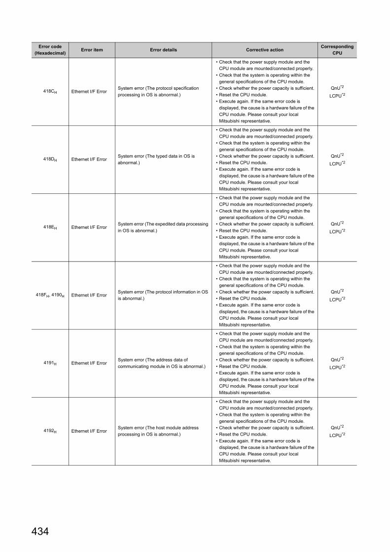
418CH Ethernet I/F ErrorSystem error (The protocol specification processing in OS is abnormal.)
• Check that the power supply module and the CPU module are mounted/connected properly.
• Check that the system is operating within the general specifications of the CPU module.
• Check whether the power capacity is sufficient.• Reset the CPU module.• Execute again. If the same error code is
displayed, the cause is a hardware failure of the CPU module. Please consult your local Mitsubishi representative.
QnU*2
LCPU*2
418DH Ethernet I/F ErrorSystem error (The typed data in OS is abnormal.)
• Check that the power supply module and the CPU module are mounted/connected properly.
• Check that the system is operating within the general specifications of the CPU module.
• Check whether the power capacity is sufficient.• Reset the CPU module.• Execute again. If the same error code is
displayed, the cause is a hardware failure of the CPU module. Please consult your local Mitsubishi representative.
QnU*2
LCPU*2
418EH Ethernet I/F ErrorSystem error (The expedited data processing in OS is abnormal.)
• Check that the power supply module and the CPU module are mounted/connected properly.
• Check that the system is operating within the general specifications of the CPU module.
• Check whether the power capacity is sufficient.• Reset the CPU module.• Execute again. If the same error code is
displayed, the cause is a hardware failure of the CPU module. Please consult your local Mitsubishi representative.
QnU*2
LCPU*2
418FH, 4190H Ethernet I/F ErrorSystem error (The protocol information in OS is abnormal.)
• Check that the power supply module and the CPU module are mounted/connected properly.
• Check that the system is operating within the general specifications of the CPU module.
• Check whether the power capacity is sufficient.• Reset the CPU module.• Execute again. If the same error code is
displayed, the cause is a hardware failure of the CPU module. Please consult your local Mitsubishi representative.
QnU*2
LCPU*2
4191H Ethernet I/F ErrorSystem error (The address data of communicating module in OS is abnormal.)
• Check that the power supply module and the CPU module are mounted/connected properly.
• Check that the system is operating within the general specifications of the CPU module.
• Check whether the power capacity is sufficient.• Reset the CPU module.• Execute again. If the same error code is
displayed, the cause is a hardware failure of the CPU module. Please consult your local Mitsubishi representative.
QnU*2
LCPU*2
4192H Ethernet I/F ErrorSystem error (The host module address processing in OS is abnormal.)
• Check that the power supply module and the CPU module are mounted/connected properly.
• Check that the system is operating within the general specifications of the CPU module.
• Check whether the power capacity is sufficient.• Reset the CPU module.• Execute again. If the same error code is
displayed, the cause is a hardware failure of the CPU module. Please consult your local Mitsubishi representative.
QnU*2
LCPU*2
Error code (Hexadecimal) Error item Error details Corrective action
Corresponding CPU
434

APPX
A
Appendix 1 Error Codes
Appendix 1.11 Error codes returned to request source during comm
unication with C
PU m
odule
4193H to 4196H Ethernet I/F ErrorSystem error (The transmission processing in OS is abnormal.)
• Check that the power supply module and the CPU module are mounted/connected properly.
• Check that the system is operating within the general specifications of the CPU module.
• Check whether the power capacity is sufficient.• Reset the CPU module.• Execute again. If the same error code is
displayed, the cause is a hardware failure of the CPU module. Please consult your local Mitsubishi representative.
QnU*2
LCPU*2
4197H, 4198H Ethernet I/F ErrorSystem error (The connection processing in OS is abnormal.)
• Check that the power supply module and the CPU module are mounted/connected properly.
• Check that the system is operating within the general specifications of the CPU module.
• Check whether the power capacity is sufficient.• Reset the CPU module.• Execute again. If the same error code is
displayed, the cause is a hardware failure of the CPU module. Please consult your local Mitsubishi representative.
QnU*2
LCPU*2
4199H Ethernet I/F ErrorSystem error (The connection termination processing is abnormal.)
• Check that the power supply module and the CPU module are mounted/connected properly.
• Check that the system is operating within the general specifications of the CPU module.
• Check whether the power capacity is sufficient.• Reset the CPU module.• Execute again. If the same error code is
displayed, the cause is a hardware failure of the CPU module. Please consult your local Mitsubishi representative.
QnU*2
LCPU*2
419AH Ethernet I/F ErrorSystem error (The connection processing in OS is abnormal.)
• Check that the power supply module and the CPU module are mounted/connected properly.
• Check that the system is operating within the general specifications of the CPU module.
• Check whether the power capacity is sufficient.• Reset the CPU module.• Execute again. If the same error code is
displayed, the cause is a hardware failure of the CPU module. Please consult your local Mitsubishi representative.
QnU*2
LCPU*2
419BH Ethernet I/F ErrorSystem error (The connection termination processing is abnormal.)
• Check that the power supply module and the CPU module are mounted/connected properly.
• Check that the system is operating within the general specifications of the CPU module.
• Check whether the power capacity is sufficient.• Reset the CPU module.• Execute again. If the same error code is
displayed, the cause is a hardware failure of the CPU module. Please consult your local Mitsubishi representative.
QnU*2
LCPU*2
419CH, 419DH Ethernet I/F ErrorSystem error (The processing order in OS is abnormal.)
• Check that the power supply module and the CPU module are mounted/connected properly.
• Check that the system is operating within the general specifications of the CPU module.
• Check whether the power capacity is sufficient.• Reset the CPU module.• Execute again. If the same error code is
displayed, the cause is a hardware failure of the CPU module. Please consult your local Mitsubishi representative.
QnU*2
LCPU*2
419EH Ethernet I/F ErrorConnection to the module was unsuccessful or interrupted.
• Check the external device operation.• Check the status of devices (such as cables,
hubs, and routers) on the line to the external devices.
QnU*2
LCPU*2
Error code (Hexadecimal) Error item Error details Corrective action
Corresponding CPU
435

419FH Ethernet I/F ErrorSystem error (The I/O control processing is abnormal.)
• Check that the power supply module and the CPU module are mounted/connected properly.
• Check that the system is operating within the general specifications of the CPU module.
• Check whether the power capacity is sufficient.• Reset the CPU module.• Execute again. If the same error code is
displayed, the cause is a hardware failure of the CPU module. Please consult your local Mitsubishi representative.
QnU*2
LCPU*2
41A0H Ethernet I/F ErrorData cannot be sent because the receive area of the external device does not have enough free space.
• Send the data again a little while later.• Check the external device operation.• Check whether the external device processes
receive data.• Check whether the CPU module does not send
unnecessary data.• Check the size and frequency of sent data and
reduce the amount of send data.• To send data again, close the connection and
discard data. Then, re-open the connection and send data.
QnU*2
LCPU*2
41A1H Ethernet I/F ErrorThe port number setting for the CPU module is incorrect.
Correct the port number.QnU*2
LCPU*2
41A2H Ethernet I/F ErrorThe port number setting for the target device is invalid.
Correct the port number.QnU*2
LCPU*2
41A3H Ethernet I/F Error
• The own station port number same as that of the MC protocol has been specified in TCP/IP.
• In TCP/IP, connection with the same own station port number and same communication destination port number has been used for the same communication destination.
• Specify a port number different from that used in the MC protocol.
• Change the port number of the CPU module or external device.
QnU*2
LCPU*2
41A4H Ethernet I/F Error
• For UDP/IP, the same Host station port No. is specified as MC protocol.
• For UDP/IP, the specified host station No. is duplicated.
• Specify a port number that is not duplicated with that of MC protocol.
• Correct the port number of the CPU module to avoid duplication.
QnU*2
LCPU*2
41A5H Ethernet I/F ErrorThe IP address setting of the target device for OPEN processing is invalid.
Correct the IP address. Specify A, B, or C for the class.
QnU*2
LCPU*2
41A6H Ethernet I/F ErrorConnection was not established in OPEN processing for TCP connection.
• Check the external device operation.• Check OPEN processing of the target device.• Correct the port number of the CPU module
and the IP address, port number, and open processing method of the target device.
• Check whether the cables are securely connected.
QnU*2
LCPU*2
41A8H Ethernet I/F Error
Data length is out of permissible range. (For the Built-in Ethernet port QCPU, the length should be 2046 bytes if the serial number (first five digits) is "12051" or earlier and 10238 bytes if the serial number is "12052" or later.)
• Correct the data length.• If the data is longer than the range, split the
data and send them.• When the data length is 2047 to 10238 bytes,
use the Built-in Ethernet port QCPU whose serial number (first five digits) is "12052" or later.
QnU*2
LCPU*2
Error code (Hexadecimal) Error item Error details Corrective action
Corresponding CPU
436

APPX
A
Appendix 1 Error Codes
Appendix 1.11 Error codes returned to request source during comm
unication with C
PU m
odule
41ABH Ethernet I/F ErrorTransmission failed due to timeout of retransmission.
• Review the IP address and Ethernet address of the target device.
• Check whether the target device has the ARP function. If not, communicate with the one that has the ARP function.
• Check the external device operation.• The line may be congested with packets.
Resend data after a while.• Check the status of devices (such as cables,
hubs, and routers) on the line to the external devices.
• Check that the target device completes initial processing and open processing.
• Check that a binary code is set for the communication data code of the target device.
• Review the latency time setting if the simple PLC communication function is used.
QnU*2
LCPU*2
41ACH Ethernet I/F Error
• The target device cannot be found.• The TCP connection is disconnected by
the target device.• The Fullpassive device rejects the
communication and the TCP connection is disconnected.
• Check the external device operation.• Check whether the cables are securely
connected.• Check whether the target IP address setting of
the Fullpassive device and the IP address of the Active device are matched.
QnU*2
LCPU*2
41ADH Ethernet I/F ErrorData cannot be send due to no connection or disconnection of the cable.
• Check whether the cables are securely connected.
• Check the line status by PING test from the target device.
• Reset the CPU module.
QnU*2
LCPU*2
41AEH Ethernet I/F ErrorConnection of the control port to the FTP server failed.
• Correct "IP address" in the Built-in Ethernet port tab.
• Correct "FTP server name" in the "FTP setting" window.
• Check connection with the FTP server.• Disconnect the user session on the FTP server.
QnU*2
LCPU*2
41AFH Ethernet I/F ErrorDisconnection of the control port to the FTP server failed.
• Correct the settings in the "FTP setting" window.
• Check connection with the FTP server.
QnU*2
LCPU*2
41B0H Ethernet I/F Error Login to the FTP server failed.
• Correct "Login user name" and "Login password" in the "FTP setting" window.
• Check the FTP server software settings (login user name and login password).
• Check communication logs of the FTP server software.
QnU*2
LCPU*2
41B1H Ethernet I/F ErrorExecution of the FTP command to the FTP server failed.
• Correct "Directory path" and "Data transfer mode" in the "FTP setting" window.
• Check that the user has a right to access (read/write) the FTP server or the specified file.
• Check that the directory path set in the "FTP setting" window exists.
• Check that the file set in the "FTP setting" window exists.
• Correct the FTP server software settings.• Check communication logs of the FTP server
software.• Correct the FTP command.
QnU*2
LCPU*2
41B2H Ethernet I/F ErrorConnection of the data transfer port to the FTP server failed.
• Check connection with the FTP server.• Correct "Data transfer mode" in the "FTP
setting" window.• When a firewall is active or the proxy server is
on the connection path, consult the network administrator about the settings.
QnU*2
LCPU*2
Error code (Hexadecimal) Error item Error details Corrective action
Corresponding CPU
437

41B3H Ethernet I/F ErrorDisconnection of the data transfer port to the FTP server failed.
• Check connection with the FTP server.• Correct "Data transfer mode" in the "FTP
setting" window.• When a firewall is active or the proxy server is
on the connection path, consult the network administrator about the settings.
QnU*2
LCPU*2
41B4H Ethernet I/F Error The connection number setting is invalid.
• Specify the connection No. within 1 to 16.• When using socket communication, check
whether "Socket communication" is selected for "Open system" parameter.
• When using predefined protocol function, check whether "Predefined protocol" is selected for "Open system" parameter.
QnU*2
LCPU*2
41B6H Ethernet I/F ErrorThe specified connection has already completed OPEN processing.
Perform CLOSE processing and then OPEN processing.
QnU*2
LCPU*2
41B7H Ethernet I/F ErrorThe specified connection has not completed OPEN processing.
Re-execute after OPEN processing is completed.QnU*2
LCPU*2
41B8H Ethernet I/F Error
When "MELSEC-A (Ethernet Module)/MELSEC-FX3 (Ethernet Block/Adapter)" was specified in "Destination" of the simple PLC communication function, the function was executed while CPU exchange timing setting (SW7) of the Ethernet module is off and the CPU module on the destination is in the RUN status.
• Turn on CPU exchange timing setting (SW7) of the destination.
• Set the CPU module on the destination to STOP and execute the function again.
QnUDVQnUDPV
LCPU*2
41B9H Ethernet I/F Error
• Contents of control data is not correct.• Open instruction was executed through
open settings parameter even though parameters are not set for "Open settings".
• Correct the contents of the control data.• Configure the open settings parameters or
execute the OPEN instruction through control data.
QnU*2
LCPU*2
41BAH Ethernet I/F ErrorAn error occurred during file transfer to the FTP server.
• Delete unnecessary files on the FTP server to increase free space.
• Check the connection status of the FTP server.• Correct the FTP command.
QnU*2
LCPU*2
41BBH Ethernet I/F ErrorMultiple file transfer function (FTP client) instructions are executed simultaneously.
After the processing of the file transfer function (FTP client) instruction being executed ends, execute another file transfer function (FTP client) instruction.
QnU*2
41BCH Ethernet I/F Error
When "MELSEC-A (Ethernet Module)/MELSEC-FX3 (Ethernet Block/Adapter)" was specified in "Destination" of the simple PLC communication function, communications between the CPU module and the Ethernet module failed. (After the Ethernet module normally receives a request from another node, communications between the CPU module and the Ethernet module ailed due to a noise or other causes.)
• Ensure that the operating environment for the system meets the general specifications of the CPU module.
• Reset the CPU module.• Execute again. If the same error code is
displayed, the cause is a hardware failure of the CPU module. Please consult your local Mitsubishi representative.
QnUDVQnUDPV
LCPU*2
41BDH Ethernet I/F Error
When "MELSEC-A (Ethernet Module)/MELSEC-FX3 (Ethernet Block/Adapter)" is specified in "Destination" of the simple PLC communication function, an incorrect device is specified.
• Check the specified device name.• Check the specified device No.• Check the device assignment parameters of
the CPU module (destination).
QnUDVQnUDPV
LCPU*2
Error code (Hexadecimal) Error item Error details Corrective action
Corresponding CPU
438

APPX
A
Appendix 1 Error Codes
Appendix 1.11 Error codes returned to request source during comm
unication with C
PU m
odule
41BEH Ethernet I/F Error
When "MELSEC-A (Ethernet Module)/MELSEC-FX3 (Ethernet Block/Adapter)" was specified in "Destination" of the simple PLC communication function, a system error occurred. (The possible cause is malfunction due to noise or other causes or hardware failure).
• Check that the power supply module and the CPU module are mounted/connected properly.
• Ensure that the operating environment for the system meets the general specifications of the CPU module.
• Check whether the power capacity is sufficient.• Reset the CPU module.• Execute again. If the same error code is
displayed, the cause is a hardware failure of the CPU module. Please consult your local Mitsubishi representative.
QnUDVQnUDPV
LCPU*2
41BFH Ethernet I/F Error
When "MELSEC-A (Ethernet Module)/MELSEC-FX3 (Ethernet Block/Adapter)" was specified in "Destination" of the simple PLC communication function, a system error occurred. (The possible cause is malfunction due to noise or other causes or hardware failure).
• Check that the power supply module and the CPU module are mounted/connected properly.
• Ensure that the operating environment for the system meets the general specifications of the CPU module.
• Check whether the power capacity is sufficient.• Reset the CPU module.• Execute again. If the same error code is
displayed, the cause is a hardware failure of the CPU module. Please consult your local Mitsubishi representative.
QnUDVQnUDPV
LCPU*2
41C1H File-related errorThe format information data of the specified drive (memory) is abnormal.
The file information data may be corrupted.After backing up the data in the CPU module, format the CPU memory.
QCPULCPU
41C2H File-related errorFile open specification data for file access is wrong.
Execute again after checking the specification data.
QCPULCPU
41C3H File-related errorSimultaneously accessible files exceeded the maximum.
Execute again after decreasing file operations.QCPULCPU
41C4H File-related errorSimultaneously accessible files exceeded the maximum.
Execute again after decreasing file operations.QCPULCPU
41C5H File-related error• The specified file does not exist.• The file does not exist in the valid drive.
• Execute again after checking the file.• Execute again after checking that the file exists
in the valid drive.
QCPULCPU
41C7H File-related errorThe specified file or drive (memory) does not exist.
Execute again after checking the file or drive (memory).
QCPULCPU
41C8H File-related errorThe size of the specified file has exceeded that of the existing file.
Execute again after checking the size of the specified file.If the error recurs after re-execution, the file information data may be corrupted.After backing up the data in the CPU module, format the CPU memory.
QCPULCPU
41C9H File-related errorAccess to the file sector was unsuccessful.The format information data of the target drive (memory) is abnormal.
After backing up the data in the CPU module, format the CPU memory.
QCPULCPU
41CAH File-related errorAccess to the file sector was unsuccessful.The format information data of the target drive (memory) is abnormal.
After backing up the data in the CPU module, format the CPU memory.
QCPULCPU
41CBH File-related error The file name is specified in a wrong method. Execute again after checking the file name.QCPULCPU
41CCH File-related errorThe specified file or subdirectory does not exist.
Execute again after checking the name of the file and subdirectory.
QCPULCPU
41CDH File-related error
An access inhibited with the attribute was made to the file.Or the file attribute was attempted to be changed to the inhibited one.
Check the attribute and open mode of the file.QCPULCPU
41CEH File-related errorThe file cannot be written because the specified file is read-only.
The specified file is write-protected. Execute again after checking the attribute.
QCPULCPU
41CFH File-related errorThe specified drive (memory) has been used exceeding the capacity.
Execute again after checking the drive (memory) capacity.
QCPULCPU
Error code (Hexadecimal) Error item Error details Corrective action
Corresponding CPU
439

41D0H File-related error
The specified drive (memory) has no free space. Or the number of files in the directory of the specified drive (memory) has exceeded the maximum.
• Execute again after increasing the free space of the drive (memory).
• Execute again after deleting file(s) in the drive (memory).
QCPULCPU
41D1H File-related error
• The file name is specified in a wrong method.
• The SD memory card is being disabled by SM606 (SD memory card forced disable instruction).
• Execute again after checking the file name. If the error recurs after re-execution, the file information data may be corrupted. After backing up the data in the CPU module, format the CPU memory.
• Cancel the SD memory card forced disable instruction.
QCPULCPU
41D3H File-related error Access into the SD memory card has failed.
• Check if the SD memory card is inserted, and execute the processing again.
• Replace the SD memory card, and execute the processing again.
• Execute the data backup, and format the PLC memory.
QnUDVQnUDPV
41D4H File-related errorThe size of the specified file has exceeded that of the existing file.
Execute again after checking the size of the specified file.If the error recurs after re-execution, the file information data may be corrupted.After backing up the data in the CPU module, format the CPU memory.
QCPULCPU
41D5H File-related error The file of the same name exists.Forcibly execute the request, or execute after changing the file name.
QCPULCPU
41D6H File-related errorThe format information data of the specified drive (memory) is abnormal.
The file information data may be corrupted.After backing up the data in the CPU module, format the CPU memory.
QCPULCPU
41D7H File-related errorThe format information data of the specified drive (memory) is abnormal.
The file information data may be corrupted.After backing up the data in the CPU module, format the CPU memory.
QCPULCPU
41D8H File-related error The specified file is being accessed. Execute again after a while.QCPULCPU
41DFH File-related errorThe specified drive (memory) is write-protected.
Execute again after canceling the write protect of the specified drive (memory).
QCPULCPU
41E0H File-related errorThe specified drive (memory) is abnormal or does not exist.
• Execute the operation again after checking that the memory card or SD memory card has been inserted.
• After backing up the data, execute programmable controller memory format.
QCPULCPU
41E1H File-related error Access to the flash ROM was unsuccessful.
• After backing up the data, execute write to PLC (Flash ROM).
• Execute the operation again after checking that the specified drive is a flash ROM and that the size of the memory card or SD memory card is correct.
QCPULCPU
41E4H File-related errorAccess to the memory card or SD memory card was unsuccessful.
• Execute the operation again after checking that the memory card or SD memory card has been inserted.
• Execute the operation again after replacing the memory card or SD memory card.
• After backing up the data, execute programmable controller memory format.
QCPULCPU
41E7H File-related errorThe format information data of the specified drive (memory) is abnormal.
The file information data may be corrupted.After backing up the data in the CPU module, format the CPU memory.
QCPULCPU
41E8H File-related errorThe format information data of the specified drive (memory) is abnormal.
The file information data may be corrupted.After backing up the data in the CPU module, format the CPU memory.
QCPULCPU
41E9H File-related error The specified file is being accessed. Execute again after a while.QCPULCPU
41EBH File-related error The file name is specified in a wrong method. Execute again after checking the file name.QCPULCPU
Error code (Hexadecimal) Error item Error details Corrective action
Corresponding CPU
440

APPX
A
Appendix 1 Error Codes
Appendix 1.11 Error codes returned to request source during comm
unication with C
PU m
odule
41ECH File-related errorThe file system of the specified drive (memory) is logically corrupted.
The file information data may have been corrupted.After backing up the data in the CPU module, format the CPU memory.
QCPULCPU
41EDH File-related error
The specified drive (memory) does not have continuous free space. (The free space for file is sufficient but the continuous free space is insufficient.)
Execute again after deleting unnecessary files or executing programmable controller memory arrangement.
QCPULCPU
41EFH File-related errorCreation of power failure backup for the specified drive (memory) was unsuccessful.
Execute the operation again after checking that the memory card or SD memory card has been inserted.
QCPULCPU
41F0H File-related errorThe power failure backup data of the specified drive (memory) are corrupted.
Execute the operation again after checking that the memory card or SD memory card has been inserted.
QCPULCPU
41F1H File-related errorThe power failure backup for the specified drive (memory) has a repair command.
Execute the operation again after checking that the memory card or SD memory card has been inserted.
QCPULCPU
41F2H File-related errorOperation cannot be performed since the specified drive (memory) is Flash ROM.
Execute again after checking the specified drive (memory).When performing operation for the Flash ROM, use write to PLC (Flash ROM).
QCPULCPU
41F3H File-related errorThe file size is larger than the following:The value to be acquired when 2byte is subtracted from 4Gbyte
Specify a smaller value for the file size when creating a file or changing the file size. Alternatively, divide the file so that each file size is smaller.
QnUDVQnUDPV
LCPU
41F4H File-related errorSince the operation prohibited by the system is performed, the requested processing cannot be performed.
Since the operation is prohibited by the system, the file operation is not performed.
QCPULCPU
41F6H File-related error
The following files cannot be written because the write-protect function for device data (from outside the CPU module) is enabled.• Initial label value file• File register file
• Do not write the specified file.• Disable the write-protect function for device
data (from outside the CPU module) and execute the request again.
QnUDVQnUDPV
41F8H File-related errorThe data is being accessed from another programming tool.
PLC write to the program memory or transfer to the backup memory is in execution.Access the data again after checking that the above-mentioned function has been completed.
QCPULCPU
41F9H File-related errorThe data is being accessed from another programming tool.
Another device data saving was executed during execution.Access the data again after the current one is completed.
QCPULCPU
41FAH File-related errorProgram was written beyond the area where the program can be executed.
Execute again after reducing either the already written program or newly written program.
QCPULCPU
41FBH File-related errorThe specified file is already being manipulated from the programming tool.
Execute again after the currently performed operation is completed.
QCPULCPU
41FCH File-related errorAn attempt was made to erase the drive (memory) being used.
The specified drive (memory) is being used and cannot be erased.
QCPULCPU
41FDH File-related error There are no data written to the Flash ROM.Write a file by executing write to PLC (Flash ROM).
QCPULCPU
41FEH File-related error
• The memory card or SD memory card has not been inserted.
• QnUDVCPU and QnUDPVCPU: The SD memory card is being disabled.
• LCPU: The SD memory card access control switch is not slid down.
• The SD memory card is being disabled by SM606 (SD memory card forced disable instruction).
• Insert or re-insert the memory card or SD memory card.
• QnUDVCPU and QnUDPVCPU: Remove the SD memory card and insert it again.
• LCPU: Slide the SD memory card access control switch down.
• Cancel the SD memory card forced disable instruction.
QCPULCPU
41FFH File-related errorThe type of the memory card or SD memory card differs.
Check the type of the memory card or SD memory card.
QCPULCPU
Error code (Hexadecimal) Error item Error details Corrective action
Corresponding CPU
441

4200H
Online module change-related error
The requested processing cannot be performed because online module change is disabled by parameter setting.
Do not send the request where this error occurred. Alternatively, enable online module change by parameter setting and send the request again.
QCPU
4201H
Online module change-related error
The requested processing cannot be performed because online module change is enabled by parameter setting.
Do not send the request where this error occurred. Alternatively, disable online module change by parameter setting and send the request again.
QCPU
4202H
Online module change-related error
The requested processing cannot be performed since an online module change is being performed.
Make a request again after completion of the online module change.
QCPU
4203H
Online module change-related error
The module mounted on the main base unit cannot be replaced online since the extension base unit is mounted.
Take following procedures to replace the module mounted on the main base unit.• Switch the system where the target module to
be replaced is mounted to the standby system.• Turn OFF power supply of the standby system.• Replace the target module.
QnPH
4204H
Online module change-related error
The specified module of the extension base unit cannot be replaced online since it is connected to the standby system.
Change the connection destination to the control system and perform the online module change again.
QnPH
4210H
Online module change-related error
The specified start I/O number is outside the range.
When making a request, specify the start I/O number of the module that will be changed online.
QnPH
4211H
Online module change-related error
An online module change request is abnormal.
Check the command used to make a request. QnPH
4212H
Online module change-related error
An online module change is already being made for other equipment.
Make a request again after completion of the online module change, or continue after changing the connection path.
QnPH
4213H
Online module change-related error
The specified start I/O number differs from the one registered for online module change.
When making a request, specify the start I/O number of the module being changed online.
QnPH
4214H
Online module change-related error
The specified module differs from the one changed online.
Make a request again after mounting the module that is the same as the one changed online.
QnPH
4215H
Online module change-related error
The specified module does not exist.
When making a request, specify the start I/O number of the module that will be changed online, or make a request again after mounting the module.
QnPH
4216H
Online module change-related error
The specified module is faulty. Make a request again after changing the module. QnPH
4217H
Online module change-related error
There is no response from the specified module.
Continue the online module changing operation. QnPH
4218H
Online module change-related error
The specified module is incompatible with online module change.
Do not make a request where an error occurred, or make a request again to the module compatible with online module change.
QnPH
4219H
Online module change-related error
The specified module is mounted on the extension base unit of the type that requires no power supply module.
Do not make a request to any modules mounted on the extension base unit of the type that requires no power supply module and the main base unit.
QnPH
421AH
Online module change-related error
The specified module is not in a control group.
Make a request to the CPU module that controls the specified module.
QnPH
421BH
Online module change-related error
An error occurred in the setting of the initial setting parameter of the intelligent function module.
Resume processing after checking the contents of the intelligent function module buffer memory.
QnPH
421CH
Online module change-related error
Cannot be executed as the parameter file has been rewritten.
Operation cannot be performed. Operation is interrupted.
QnPH
Error code (Hexadecimal) Error item Error details Corrective action
Corresponding CPU
442

APPX
A
Appendix 1 Error Codes
Appendix 1.11 Error codes returned to request source during comm
unication with C
PU m
odule
421DH
Online module change-related error
System switching occurs during the online module change.
Connect the programming tool to the new control system to check the status of the online module change. According to the status of online module change, take procedures for it.
QnPH
421EH
Online module change-related error
The information of the online module change cannot be sent to the standby system. When the system switching occurs during the online module change, the online module change may not be continued.
The tracking cable may be faulty or the standby system may have an error.• Check the mounting status of the tracking cable
or replace the tracking cable.• Check the status of the standby system. When
a stop error was detected by the standby system, perform troubleshooting.
QnPH
421FH
Online module change-related error
The module mounted on the extension base unit cannot be replaced online when the connection destination is set to the standby system in the separate mode.
• Set the connection destination of a programming tool to the present control system.
• Perform the online module change to the module mounted on the extension base unit again.
QnPH
4220H E-mail related errorThe number of characters exceeded the valid range when registering the e-mail addresses by using the SP.MLOPEADR instruction.
Reduce the number of e-mail addresses to be registered.
LCPU
4221H E-mail related errorAn unsupported character is used in the e-mail address to be registered by using the SP.MLOPEADR instruction.
Do not use any unsupported character in the e-mail address.
LCPU
4222H E-mail related errorThe e-mail address to be deleted by using the SP.MLOPEADR instruction has not been registered.
Check that the deletion target e-mail address is correct.
LCPU
4223H E-mail related error
The number of characters in the e-mail address read by using the SP.MLGETADR instruction exceeded the specified data length.
Check and correct the data length setting. LCPU
4224H E-mail related errorThe e-mail address backup by using the SP.MLOPEADR instruction has failed.
• Execute the instruction again.• If the same error code is displayed even after
executing the instruction again, the cause is a hardware failure of the CPU module. Please consult your local Mitsubishi representative.
LCPU
4225H E-mail related errorThe e-mail address backup file was not restored when the CPU module was powered on.
• Power off and on the CPU module. Or reset the CPU module.
• If the same error code is displayed again after powering off and on or reset the CPU module, the cause is a hardware failure of the CPU module. Please consult your local Mitsubishi representative.
LCPU
4226H E-mail related error System error (Reference error)
• Check that the power supply module and the CPU module are mounted/connected properly.
• Check that the system is operating within the general specifications of the CPU module.
• Check whether the power capacity is sufficient.• Reset the CPU module.• Execute again. If the same error code is
displayed, the cause is a hardware failure of the CPU module. Please consult your local Mitsubishi representative.
LCPU
4227H E-mail related error System error (Failed to read the port number)
• Check that the power supply module and the CPU module are mounted/connected properly.
• Check that the system is operating within the general specifications of the CPU module.
• Check whether the power capacity is sufficient.• Reset the CPU module.• Execute again. If the same error code is
displayed, the cause is a hardware failure of the CPU module. Please consult your local Mitsubishi representative.
LCPU
Error code (Hexadecimal) Error item Error details Corrective action
Corresponding CPU
443

4228H E-mail related error System error (Failed to create the command)
• Check that the power supply module and the CPU module are mounted/connected properly.
• Check that the system is operating within the general specifications of the CPU module.
• Check whether the power capacity is sufficient.• Reset the CPU module.• Execute again. If the same error code is
displayed, the cause is a hardware failure of the CPU module. Please consult your local Mitsubishi representative.
LCPU
4229H E-mail related error System error (State transition error)
• Check that the power supply module and the CPU module are mounted/connected properly.
• Check that the system is operating within the general specifications of the CPU module.
• Check whether the power capacity is sufficient.• Reset the CPU module.• Execute again. If the same error code is
displayed, the cause is a hardware failure of the CPU module. Please consult your local Mitsubishi representative.
LCPU
4230H
File transfer function (FTP client) error
A file cannot be transferred because a file with the same name exists on the FTP server.
Check that there is no file with the same name on the FTP server.
LCPU
4232H
File transfer function (FTP client) error
• The number of files to be transferred exceeded the valid range when the wild card was used in the file transfer function (FTP client) instruction.
• There is no corresponding file when the wild card is used in the file transfer function (FTP client) instruction.
Check and correct the wild card specification. LCPU
4233H
File transfer function (FTP client) error
DNS client response timeout error
• Check the DNS server address setting.• Check that the communications with the DNS
server is enabled by using the PING command.• Check that the own station IP address and the
DNS server IP address are in the same class. (If not, check the router setting.)
LCPU
4234H
File transfer function (FTP client) error
FTP response timeout error
• Check that the FTP server name is registered in the DNS.
• Change the FTP server name to the IP address, and check the operation.
• Check that the communications with the FTP server is enabled by using the PING command.
LCPU
4240HRedundant system-related error
Any of the following unsupported operations was executed for the standby system.• Operation mode change• System switching• Memory copy from control system to
standby system
Execute the operation again after changing the transfer setup to the control system.
QnPRH
4241HRedundant system-related error
Communication cannot be made since the standby system has been powered off or reset or is in a user watchdog timer error or CPU module hardware fault status.
Request communication after powering on the standby system or setting its Reset switch to the neutral position.
QnPRH
4242HRedundant system-related error
Communication with the standby system cannot be made since the tracking cable is faulty or disconnected.
Cannot be executed since the tracking cable is disconnected or faulty. Execute again after checking the tracking cable for disconnection or changing it for a normal one.
QnPRH
4243HRedundant system-related error
The command cannot be executed since the standby system is in stop error.
Execute again after removing the stop error of the standby system.
QnPRH
4244HRedundant system-related error
The command cannot be executed since the operation status differs from that of the standby system.
Execute again after placing the standby system in the same operation status (RUN/STOP) as the control system.
QnPRH
4245HRedundant system-related error
Other system CPU module status errorCheck that the other system CPU module has normally started up and that the tracking cable is connected.
QnPRH
Error code (Hexadecimal) Error item Error details Corrective action
Corresponding CPU
444

APPX
A
Appendix 1 Error Codes
Appendix 1.11 Error codes returned to request source during comm
unication with C
PU m
odule
4246HRedundant system-related error
The command cannot be executed since operation mode (separate/backup) change or system (control/standby system) switching is being executed.
Execute again after the operation mode change or system switching being executed is completed.
QnPRH
4247HRedundant system-related error
Memory copy from control system to standby system is already being executed.
Execute again after memory copy from control system to standby system is completed.Check the following and take corrective action.• Is SM1596 of the control system or standby
system ON? (ON: Memory copy being executed) Execute again after SM1596 has turned OFF since it is turned OFF by the system on completion of memory copy.
• Is SM1597 of the control system ON? (ON: Memory copy completed) Execute again after turning OFF SM1597 of the control system.
QnPRH
4248HRedundant system-related error
Communication was made during system switching.The system specified in the transfer setup (request destination module I/O number) does not exist.
• Execute again after system switching.• After checking whether the specified system
exists or not, restart communication.QnPRH
4249HRedundant system-related error
The redundant system is not established. (Control system/standby system or System A/System B not yet definite)
• Normally start the system as the redundant system. (Make communication again after establishing the system.)
• Execute again after changing the transfer setup (request destination module I/O number) to "No settings have been made" (03FFH).
QnPRH
424AHRedundant system-related error
A command that cannot be processed was executed when the control system or standby system is specified in the transfer setup (request destination module I/O number).
Execute the operation again after changing the transfer setup (request destination module I/O number) to No settings have been made (03FFH)/system A/system B.
QnPRH
424BHRedundant system-related error
The command cannot be executed since system switching is inhibited by the manual system switching enable flag (SM1592).
Manual system switching is inhibited by the manual system switching enable flag (SM1592). Execute again after turning ON SM1592.
QnPRH
424CHRedundant system-related error
The specified command cannot be executed during online program change operation.
Execute again after the online program change operation is finished.
QnPRH
424DHRedundant system-related error
The transfer setup or function unavailable for the debug mode was used.
• Execute again after changing to the backup mode.
• Execute again after changing the transfer setup (request destination module I/O number) to System A or control system.
QnPRH
424EHRedundant system-related error
The control system/standby system specifying method is not supported.
This function cannot be executed since it is not supported.
QnPRH
424FHRedundant system-related error
System switching was executed by the other condition during execution of system switching by the programming tool.
Although system switching was executed from the programming tool, system switching was executed first by the other condition. Check the system for any problem and execute the operation again as necessary.
QnPRH
4250HRedundant system-related error
Sum check error occurred in tracking communication.
Execute communication again after changing the tracking cable.If the same error occurs even after the tracking cable is changed, the cause is a hardware failure of the CPU module. Please consult your local Mitsubishi representative.
QnPRH
4251HRedundant system-related error
The command cannot be executed in the separate mode.
Execute again after changing to the backup mode.
QnPRH
4252HRedundant system-related error
System switching was not executed since an error occurred in the redundant system compatible network module of the standby system.
By monitoring SD1690 (other system network module No. that issued system switching request), identify the faulty redundant-compatible intelligent module of the standby system, then remove the module fault, and execute again.
QnPRH
Error code (Hexadecimal) Error item Error details Corrective action
Corresponding CPU
445

4253HRedundant system-related error
Since a communication error or system switching occurred during online program change to the control system CPU module, online program change to the standby CPU module cannot be executed.
Since a communication error or system switching occurred during execution of online program change to the control system CPU module, online program change redundant tracking was suspended.Execute online program change again after confirming that communication with the control system CPU module and standby system CPU module can be normally made.If it takes time for the communication between the programming tool and either the control system CPU module or standby system CPU module, change the value in SD1710 (standby system online start waiting time) so that errors may be avoided.
QnPRH
4254HRedundant system-related error
The command cannot be executed since an error was detected in the tracking communication hardware.
The tracking cable may not be connected correctly, or the tracking communication hardware of the CPU module may be faulty. Check the connection status of the tracking cable.If the condition is not restored to normal after the cable connection status is corrected, the possible cause is the hardware fault of the CPU module.
QnPRH
4255HRedundant system-related error
The command cannot be executed since tracking communication is being prepared.
Tracking communication is being prepared when it is connected. Execute the operation again after a while (about 1 second).
QnPRH
4256HRedundant system-related error
The command cannot be executed since a timeout error occurred in tracking communication.
The tracking cable may not be connected correctly, or the tracking communication hardware of the CPU module may be faulty. Check the connection status of the tracking cable.If the condition is not restored to normal after the cable connection status is corrected, the possible cause is the hardware fault of the CPU module.
QnPRH
4257HRedundant system-related error
The command cannot be executed since the host system CPU module is in a watchdog timer error or CPU module hardware fault status.
The command cannot be executed since the host system is in a watchdog timer error or CPU module hardware fault status. Execute again after checking the host system status.
QnPRH
4258HRedundant system-related error
Operation mode being changed (from backup mode to separate mode)
Change the operating status of the CPU module from STOP to RUN with the RUN/STOP switch of the module whose RUN LED is flashing or by remote operation, and end the operation mode change. Then, execute the command again.
QnPRH
4259HRedundant system-related error
Operation mode is being changed with another programming tool in the communication route different from the one currently used.
Execute again in the same communication route as the one where the operation mode change was executed.
QnPRH
425BHRedundant system-related error
Although the communication was made via the intelligent function module mounted on the extension base unit, the combination of the connection destination specification (Redundant CPU specification) and the command is unsupported.
Change the combination of the connection destination specification and the command to the supported combination.
QnPRH
425CHRedundant system-related error
System switching cannot be made since the module mounted on the extension base unit is being replaced online.
Switch systems after the online module change has been completed.
QnPRH
425DHRedundant system-related error
Operation mode cannot be changed since the module mounted on the extension base unit is being replaced online.
Change the operation mode after the online module change has been completed.
QnPRH
4270H Data logging*1Data logging is being performed (logging, saving the logging data, completing, on hold, or in error) with a different memory.
Register the data logging to the memory where a data logging is being performed. Alternatively, stop the data logging being performed and register again.
QnUDVQnUDPV
LCPU
4271H Data logging*1The specified data logging is already being performed (logging, saving the logging data, completing, on hold, or in error).
Stop the data logging. Alternatively, write, delete, or register to the setting number where no data logging is being performed.
QnUDVQnUDPV
LCPU
Error code (Hexadecimal) Error item Error details Corrective action
Corresponding CPU
446

APPX
A
Appendix 1 Error Codes
Appendix 1.11 Error codes returned to request source during comm
unication with C
PU m
odule
4272H Data logging*1
The trigger logging with "Device" specified as a trigger condition is being performed (logging, saving the logging data, completing, on hold, or in error).
Change the trigger condition. Alternatively, stop the trigger logging being performed (logging, saving the logging data, completing, on hold, or in error) with "Device" specified as the trigger condition, and then register.
QnUDVQnUDPV
LCPU
4273H Data logging*1The data logging function cannot be executed because the sampling trace function is being performed.
Hold the sampling trace to register the data logging.
QnUDVQnUDPV
LCPU
4274H Data logging*1Trigger loggings have registered exceeding the number of trigger loggings collectable in the data logging buffer.
• Increase the capacity of the data logging buffer.• Reduce the number of records set for the
trigger logging.
QnUDVQnUDPV
LCPU
4275H Data logging*1 Auto logging is being performed.After the auto logging, replace the SD memory card and execute again.
QnUDVQnUDPV
LCPU
4276H Data logging*1
The specified command cannot be executed because the data logging function is being performed (i.e. logging, saving the logging data, completing, on hold, or in error).
Stop the data logging and then execute the command.
QnUDVQnUDPV
LCPU
4277H Data logging*1 The number of stored files has exceeded the value set in advance.
The number of files stored in the storage destination memory has exceeded the setting value. Delete files or change the storage destination and then register.
QnUDVQnUDPV
LCPU
4278H Data logging*1 The number of stored files has reached to the maximum.
The number of stored files has reached to the maximum of FFFFFFFF. Delete files or change the storage destination and then register.
QnUDVQnUDPV
LCPU
427AH Data logging*1 Common setting file does not exist.
• Write the common settings to the target memory.
• Register the data logging to the memory where the common settings are stored.
QnUDVQnUDPV
LCPU
427BH Data logging*1
A data logging is being performed (logging in execution, logging data are being saved, completing, on hold, or in error) in the same file storage destination.
Stop the data logging destined for the same storage and then register.Alternatively, change the storage destination of the file and then register.
QnUDVQnUDPV
LCPU
427CH Data logging*1• Data logging file transfer function settings
are mistaken.• A data logging setting file is corrupt.
• Check settings of the data logging file transfer function.
• Write the settings using the CPU Module Logging Configuration Tool.
QnUDVQnUDPV
LCPU
427DH File-related error
• A data logging file to be transferred was deleted during transfer by file switching.
• Reading of a data logging file failed.• A data logging file was accessed while the
SD memory card has been forcibly set to be disabled.
• Correct "File switching timing" and "Number of saved files" in the "Save" screen.
• Check that data logging files are not deleted using the CPU Module Logging Configuration Tool.
• Check that an SD memory card is inserted.• When the SD memory card access control
switch is on the upper position, slide it down, and check that the SD LED turns on.
• If the SD memory card has been forcibly disabled, cancel the setting.
QnUDVQnUDPV
LCPU
427EH File-related error
• Since a file was switched before file transfer, a new data logging file is saved.
• Since a file was switched during a retry, a new data logging file is saved.
• Correct "File switching timing" in the "Save" screen to reduce the frequency of file switching.
• Correct the number of sampled data and "Sampling interval" in the "Sampling" screen to reduce the number of sampled data.
• Correct the settings in the "CSV output" screen to reduce the file size.
• Check connection with the FTP server.
QnUDVQnUDPV
LCPU
427FH File-related errorFile transfer failed due to the stop operation of file transfer.
Check that data logging is not started from the CPU Module Logging Configuration Tool before file transfer is completed.
QnUDVQnUDPV
LCPU
4280H File-related errorA file transfer test was executed from another CPU Module Logging Configuration Tool during execution of a file transfer test.
Execute the file transfer test again after the ongoing test is completed.
QnUDVQnUDPV
LCPU
Error code (Hexadecimal) Error item Error details Corrective action
Corresponding CPU
447

4281H File-related errorThe data logging setting for different programmable controller series was registered.
Set the data logging for the programmable controller series used.
QnUDVQnUDPV
4290H Realtime monitorThe total buffer capacity for realtime monitor and data logging exceeds the maximum limit.
• Correct the buffer capacity so that the total capacity for data logging and realtime monitor does not exceed the maximum limit. To change the buffer capacity for data logging, write the changed data (common setting) to the CPU module and start data logging again, or power off and on or reset the CPU module to restore the data logging function to the initial state.
• Stop the realtime monitor function, and restart data logging.
LCPU
4291H Realtime monitor
Online change was executed during execution of realtime monitor where a step number is specified as a timing condition or trigger condition.
After the online change processing has completed, check the step number, and execute the realtime monitor again.
LCPU
4292H Realtime monitorDuring the execution of realtime monitor, an attempt was made to start another realtime monitor.
Stop the realtime monitor being executed, and start another realtime monitor.
LCPU
4330H MaintenanceThe CPU module change function (backup/restoration) with memory card is being executed from the same source.
Check that the CPU module change function (backup/restoration) with memory card is not being executed, and communicate again.
QCPULCPU
4331H Maintenance User authentication is required.Disable the user authentication function, and communicate again.
QCPU
4332H Maintenance
The specified command cannot be executed because the CPU module change function (backup/restoration) with SD memory card is being executed.
After the CPU module change processing (backup/restoration) is completed, execute the command again.
QCPULCPU
4333H Maintenance Not ready for backup.Complete the preparation for backup and then execute again.
QCPULCPU
4334H Maintenance Backup file does not exist.Insert a memory card or SD memory card with a backup file and then execute again.
QCPU
4335H MaintenanceThe specified function cannot be executed because latch data are being backed up.
Complete the latch data backup function and then execute again.
QCPULCPU
4336H Maintenance
The specified function cannot be executed because a FTP client is being FTP-connected to the CPU module via the built-in Ethernet port.
Disconnect all FTP connections to the CPU module and then execute again.
QCPULCPU
4337H Maintenance Module error collection file does not exist.Power off and then on or reset the CPU module and then execute again.
QCPULCPU
4338H MaintenanceReadout of module error collection data has been failed when opening the screen to display the data or when updating the data.
• Retry the operation.• Increase the number of module error
collections to be stored.
QCPULCPU
4339H MaintenanceReadout of module error collection data was failed because the function is disabled by parameter settings.
Enable the module error collection function by parameter settings and then execute again.
QCPULCPU
433AH MaintenanceThe specified command cannot be executed because the project data batch save/load function is being executed.
After the batch save/load processing is completed, execute the command again.
LCPU
433BH MaintenanceThe CPU module change function (backup/restoration) with memory card was executed to the locked CPU module.
Execute the CPU module change function (backup/restoration) with memory card to the unlocked CPU module.
QnUDVQnUDPV
433DH MaintenanceThe specified command cannot be executed because the file transfer function (FTP client) is being executed.
Wait until the file transfer processing (FTP client) completes, and execute the command again.
LCPU
4400H SecurityA file protected by a password has been opened without unlocking the password.
Enter a correct password and perform password authentication.
QnUDVQnUDPV
LCPU
4401H Security• Read password authorization has failed
when required.• The password format is incorrect.
• Set a correct read password and perform password authentication.
• Access the file with the correct method.
QnUDVQnUDPV
LCPU
Error code (Hexadecimal) Error item Error details Corrective action
Corresponding CPU
448

APPX
A
Appendix 1 Error Codes
Appendix 1.11 Error codes returned to request source during comm
unication with C
PU m
odule
4402H Security• Write password authorization has failed
when required.• The password format is incorrect.
• Set a correct write password and perform password authentication.
• Access the file with the correct method.
QnUDVQnUDPV
LCPU
4403H SecurityBoth passwords for reading and for writing that are set upon Create, Change, Delete, or Disable do not match the previous ones.
Configure a correct password for both reading and for writing, authorize them, and then access.
QnUDVQnUDPV
LCPU
4404H SecurityA file error was detected before or after performing Create, Change, or Delete.
• Format the drive including the target file by formatting the CPU module memory.
• Write the target file to the CPU module again, and then register or cancel the file password again.
QnUDVQnUDPV
LCPU
4410H SecurityThe file of the locked CPU module is accessed without the security key authentication.
(1) Register the security key which locks the CPU module to the programming tool.
(2) When the project is opened, lock the project with the security key which locks the CPU module.
(3) When the CPU module is locked, the access control target file cannot be accessed using the following functions or external devices.
• FTP server function• MC protocol• GOT• EZSocket
QnUDVQnUDPV
4412H Security
The security key cannot be registered to the CPU module due to the failure of the internal memory where the security key is registered. Or the security key of the CPU module cannot be deleted.
The cause is a hardware failure of the CPU module.Replace the CPU module.
QnUDVQnUDPV
4413H Security
Since the CPU module is locked and 32 programming tools are reading and writing programs simultaneously, another programming tool cannot read or write programs.
Wait until the number of programming tools which are reading and writing programs decreases to 31 or less.
QnUDVQnUDPV
4414H SecuritySince the CPU module is locked, the requested processing cannot be performed.
Do not request any processing since the requested processing cannot be performed in this state.
QnUDVQnUDPV
4415H SecuritySince the CPU module is not locked, the requested processing cannot be performed.
Do not request any processing since the requested processing cannot be performed in this state.
QnUDVQnUDPV
4416H SecuritySince the CPU module is in locking or unlocking operation, the requested processing cannot be performed.
Request the processing after the locking or unlocking operation ends.
QnUDVQnUDPV
4426H SecurityThe prohibited operation was executed when "Execution Program Protection Setting" was enabled with a block password.
Unlock the block password and correct the setting.
QnUDVQnUDPV
LCPU
4800HiQ Sensor Solution related error
The specified command cannot be executed because the iQ Sensor Solution function (data backup/restoration) is being executed.
Execute the command again after the iQ Sensor Solution function (data backup/restoration) ends.
QnUDVQnUDPV
LCPU
4801HiQ Sensor Solution related error
• When the iQ Sensor Solution function (data backup/restoration) is executed, the target module does not exist.
• When the iQ Sensor Solution function (data backup/restoration) is executed, the specified backup folder does not exist.
• The setting value in the special register (SD) related to the iQ Sensor Solution function (data backup/restoration) is out of range.
Correct the setting value in the special register (SD), and execute the function again.
QnUDVQnUDPV
LCPU
4802HiQ Sensor Solution related error
The number of iQ Sensor Solution function (data backup/restoration) backup folders is the maximum.
• Delete the existing backup folders, and execute the function again.
• Set "Automatic specification (folder deletion supported)" in the folder number setting so that the oldest folder is automatically deleted.
QnUDVQnUDPV
LCPU
Error code (Hexadecimal) Error item Error details Corrective action
Corresponding CPU
449

4803HiQ Sensor Solution related error
The system file does not exist in the specified backup data, or the system file is broken.
Specify other backup data.QnUDV
QnUDPVLCPU
4804HiQ Sensor Solution related error
The backup file does not exist in the specified backup data, or the system file is broken.
Specify other backup data.QnUDV
QnUDPVLCPU
4805HiQ Sensor Solution related error
When the backup function of the iQ Sensor Solution function (data backup/restoration) is executed, no backup target device exists.
Correct the setting value in the special register (SD), and execute the function again.
QnUDVQnUDPV
LCPU
4806HiQ Sensor Solution related error
The SD memory card was removed while the function was being executed.
Do not remove the memory card while the function is being executed.
QnUDVQnUDPV
LCPU
4807HiQ Sensor Solution related error
Data cannot be communicated with external devices when the iQ Sensor Solution function (data backup/restoration) is executed.
• Check the external device operation.• Check the status of devices (such as cables,
hubs, and routers) on the line to the external devices.
• The line may be congested. Resend data after a while.
QnUDVQnUDPV
LCPU
4808HiQ Sensor Solution related error
• When the restoration of the iQ Sensor Solution function (data backup/restoration) is performed, the backup source device supporting iQ Sensor Solution and the restoration target device supporting iQ Sensor Solution do not match.
• The CPU module is not compatible with the CC-Link-AnyWireASLINK bridge module.
• Check the manufacturers, models, and versions of the specified backup source device supporting iQ Sensor Solution and the restoration target device supporting iQ Sensor Solution.
• Replace the CPU module with a CPU module that is compatible with the CC-Link-AnyWireASLINK bridge module.
QnUDVQnUDPV
LCPU
4809HiQ Sensor Solution related error
The function was executed to the module which does not support the iQ Sensor Solution function (data backup/restoration).
• Replace the module to the one which supports the iQ Sensor Solution function (data backup/restoration).
• Execute the function to the module which supports the iQ Sensor Solution function (data backup/restoration).
QnUDVQnUDPV
LCPU
480AHiQ Sensor Solution related error
The function was executed to the CC-Link module whose operating status has been switched from the standby master station to the master station.
Turn off and on the power supply for the master station and the standby master station, and execute the function again.
QnUDVQnUDPV
LCPU
480BHiQ Sensor Solution related error
The function was executed to the CC-Link module for which the "Read the model name of slave station" checkbox is not checked in parameter.
Check the "Read the model name of slave station" checkbox for the auto detect setting in parameter, and execute the function again.
QnUDVQnUDPV
LCPU
480CHiQ Sensor Solution related error
The specified command cannot be executed because the iQ Sensor Solution function (automatic detection of connected device) is being executed.
Execute the command again after the iQ Sensor Solution function (automatic detection of connected device) ends.
QnUDVQnUDPV
LCPU
480DHiQ Sensor Solution related error
The specified command cannot be executed because the iQ Sensor Solution function (communication setting reflection) is being executed.
Execute the command again after the iQ Sensor Solution function (communication setting reflection) ends.
QnUDVQnUDPV
LCPU
480EHiQ Sensor Solution related error
• The specified command cannot be executed because the iQ Sensor Solution function (monitoring) is being executed.
• The specified command cannot be executed because the iQ Sensor Solution function (sensor parameter read/write) is being executed.
• Execute the command again after a while.• Execute the command again after the iQ
Sensor Solution function (sensor parameter read/write) ends.
QnUDVQnUDPV
LCPU
4900H Other error
After the values in "Device" of "PLC Parameter" of the CPU module, where the simple PLC communication function had been set, were changed, the parameters were written to the CPU module from the "Write to PLC" window.
Power off and on the CPU module. Or reset the CPU module.
QnUDVQnUDPV
LCPU
Error code (Hexadecimal) Error item Error details Corrective action
Corresponding CPU
450

APPX
A
Appendix 1 Error Codes
Appendix 1.11 Error codes returned to request source during comm
unication with C
PU m
odule
4901H Other errorThe file register used for the simple PLC communication function became out of range.
Correct the device number of the file register. And power off and on the CPU module or reset the module.
QnUDVQnUDPV
LCPU
4902H Other error
The communication was stopped because an error occurred at the other setting No., for which the same destination device of the corresponding setting No. had been set.
Remove the error cause.QnUDV
QnUDPVLCPU
4903H Other error
The communication was stopped because a stop error occurred in the CPU module where the simple PLC communication function had been set.
Power off and on the CPU module. Or reset the CPU module.
QnUDVQnUDPV
LCPU
4904H Other errorThe specified command cannot be executed because a file or folder is being deleted using a display unit.
After the delete processing is completed, execute the command again.
LCPU
4A00H Link-related error
• Access to the specified station cannot be made since the routing parameters are not set to the start source CPU module and/or relay CPU module.
• For routing via a multiple CPU system, the control CPU of the network module for data routing has not started.
• When System A/System B is not yet identified in a redundant system configuration, communication was made with the other station via the network module.
• The Built-in Ethernet port QCPU or the Built-in Ethernet port LCPU that performs IP packet transfer is not the control CPU of the CC-Link IE module, which is on the path that an IP packet takes.
• Set to the related stations the routing parameters for access to the specified station.
• Retry after a while, or start communication after confirming that the system for data routing has started.
• In a redundant system configuration, connect the tracking cable, start System A/System B normally, and then restart communication.
• Set the Built-in Ethernet port QCPU or the Built-in Ethernet port LCPU that performs IP packet transfer as the control CPU of the CC-Link IE module, which is on the path that an IP packet takes.
QCPULCPU
• The network of the No. set to the routing parameters does not exist.
• The specified CPU module cannot be communicated through the network that is not supported by the CPU module.
• Check and correct the routing parameters set to the related stations.
• Set communication through the network that is supported by the specified CPU module.
QnUDVQnUDPV
4A01H Link-related error
• The network of the No. set to the routing parameters does not exist.
• The specified CPU module cannot be communicated through the network that is not supported by the CPU module.
• Check and correct the routing parameters set to the related stations.
• Set communication through the network that is supported by the specified CPU module.
QCPULCPU
4A02H Link-related errorAccess to the specified station cannot be made.
• Check the network module and the data link module for error or check that the modules are not in offline.
• Check to see if the network number/PC number setting has no mistake.
QCPULCPU
4A03H Link-related error A request for network test was issued. Check the request data of the MC protocol, etc.QCPULCPU
4A04H Link-related errorA request is executed to the CPU module which does not support all stations specification.
• Replace the CPU module to the one which supports all stations specification.
• Execute the request to the CPU module which supports all stations specification.
QnUDVQnUDPV
Error code (Hexadecimal) Error item Error details Corrective action
Corresponding CPU
451

4A20HIP communication test related error
• The upper 2 bytes of the IP addresses do not match between a CPU module and the request destination device on the same path that an IP packet takes.
• The upper 2 bytes of the IP addresses do not match between a CPU module and a CC-Link IE module on the same path that an IP packet takes.
• The upper 2 bytes of the IP addresses do not match between CC-Link IE modules on the same path that an IP packet takes.
• The upper 2 bytes of the IP addresses do not match between the request source device and the CPU module connected to the request destination device by Ethernet.
• Check and correct the IP address settings of the built-in Ethernet ports of the CPU module.
• Check and correct the IP address of the request destination device.
• Check and correct the IP address of the CC-Link IE module.
• Check and correct the IP address of the request source device.
QCPULCPU
4A21HIP communication test related error
• The 3rd byte (Network No.) or 4th byte (Station No.) of the IP address of the CPU module is the number that is not available for CC-Link IE.
• The 3rd byte (Network No.) or 4th byte (Station No.) of the IP address of the request destination device is the number that is not available for CC-Link IE.
• Check and correct the IP address settings of the built-in Ethernet ports of the CPU module.
• Check and correct the IP address of the request destination device.
QCPULCPU
4A22HIP communication test related error
The IP address is not set for a CC-Link IE module on the path that an IP packet takes.
• Set the IP address to the control station or master station of the CC-Link IE module.
• Check the communication status with the control station or master station if the CC-Link IE module is used as a normal station or local station.
• Replace the control station or master station with the one supporting the IP packet transfer function.
• Conduct the IP communication test again after the CC-Link IE module is started up.
• Check and correct the IP address of the request destination device.
QCPULCPU
4A23HIP communication test related error
• The CPU module on the path that an IP packet takes does not support the IP packet transfer function.
• Routing Parameters are set so that an IP packet is routed to the CPU module that does not support the IP packet transfer function.
• Replace the CPU module with the one supporting the IP packet transfer function.
• Correct Routing Parameters so that an IP packet is routed to the CPU module that supports the IP packet transfer function.
• Check and correct the IP address of the request destination device.
QCPULCPU
4A24HIP communication test related error
• A network module on the path that an IP packet takes does not support the IP packet transfer function.
• Routing Parameters are set so that an IP packet is routed to the network module that does not support the IP packet transfer function.
• The 3rd byte (Network No.) of the IP address of the device on the path that an IP packet takes overlapped with the network No. of the module that is mounted with the CPU module and does not support the IP packet transfer function.
• The 3rd byte (Network No.) of the IP address of the request destination device overlapped with the network No. of the module that is mounted with the CPU module and does not support the IP packet transfer function.
• Replace the CC-Link IE module with the one supporting the IP packet transfer function.
• Correct Routing Parameters so that an IP packet is routed to the CC-Link IE module that supports the IP packet transfer function.
• Check and correct the settings so that the 3rd byte (Network No.) of the IP address of the device on the path that an IP packet takes does not overlap with the network No. of the module that is mounted with the CPU module and does not support the IP packet transfer function.
• Check and correct the settings so that the 3rd byte (Network No.) of the IP address of the request destination device does not overlap with the network No. of the module that is mounted with the CPU module and does not support the IP packet transfer function.
• Check and correct the IP address of the request destination device.
QCPULCPU
Error code (Hexadecimal) Error item Error details Corrective action
Corresponding CPU
452

APPX
A
Appendix 1 Error Codes
Appendix 1.11 Error codes returned to request source during comm
unication with C
PU m
odule
4A25HIP communication test related error
• "IP packet transfer setting" in Built-in Ethernet Port Setting tab of "PLC parameter" is not set.
• Routing Parameters are set so that an IP packet is routed to the CPU module where IP packet transfer setting is not set.
• Select "Use" for IP packet transfer function in "IP packet transfer setting" in Built-in Ethernet Port Setting tab of "PLC parameter".
• Correct Routing Parameters so that an IP packet is routed to the CPU module where IP packet transfer setting is set.
• Check and correct the IP address of the request destination device.
QCPULCPU
4A26HIP communication test related error
The IP communication test was started from the CPU module other than the Built-in Ethernet port QCPU.
Correct the setting so that the IP communication test starts from the Built-in Ethernet port QCPU.
QCPU
4A27HIP communication test related error
The Built-in Ethernet port QCPU that performs IP packet transfer is not the control CPU of the CC-Link IE module, which is on the path that an IP packet takes.
Set the Built-in Ethernet port QCPU that performs IP packet transfer as the control CPU of the CC-Link IE module, which is on the path that an IP packet takes.
QCPU
4A28HIP communication test related error
• In the system where the CPU module is connected to the request destination device over Ethernet, the request path and the response path of IP packets differ.
• When multiple CC-Link IE modules with the same network number are connected in a multiple CPU system, the module mounted on the lowest slot number is not set as a controlled module that transfers IP packets.
• When multiple CC-Link IE modules with the same network number are connected in a single or multiple CPU system, the station number of the module mounted on the lowest slot number is not set as a relay station number in routing parameter.
• Correct the routing parameter setting so that IP packets use the same path for both request and response transmission.
• When multiple CC-Link IE modules with the same network number are connected in a multiple CPU system, set the module mounted on the lowest slot number as a controlled module that transfers IP packets.
• When multiple CC-Link IE modules with the same network number are connected in a single or multiple CPU system, set the station number of the module mounted on the lowest slot number as a relay station number in routing parameter.
QCPULCPU
4A29HIP communication test related error
The 3rd byte (Network No.) of the IP address of the request destination device overlapped with the 3rd byte of the IP address of the CPU module connected to the request source device by Ethernet.
• Check and correct the IP address settings of the built-in Ethernet ports of the CPU module.
• Check and correct the IP address of the request destination device.
QCPULCPU
4A2AHIP communication test related error
The IP address of a device on the CC-Link IE network, the Built-in Ethernet port QCPU, or the Built-in Ethernet port LCPU is not specified.
Specify the IP address of a device on the CC-Link IE network, the Built-in Ethernet port QCPU, or the Built-in Ethernet port LCPU.
QCPULCPU
4B00H Target-related error
• An error occurred in the access destination or relay station.
• The specified transfer setup (request destination module I/O number) is illegal.
• Take corrective action after checking the error that occurred at the specified access destination or the relay station to the accessed station.
• Check the transfer setup (request destination module I/O number or programmable controller number) in the request data of the MC protocol, etc.
• Check the occurring stop error and take the action.
QCPULCPU
4B01H Target-related errorThe target is not the No. 1 CPU of the multiple CPU system.
Execute the request for the No. 1 CPU of the multiple CPU system.
QCPU
4B02H Target-related errorThe request is not addressed to the CPU module.
Perform operation for the module that can execute the specified function.
QCPULCPU
4B03H Target-related error
• The specified route is not supported by the specified CPU module version.
• The communication target CPU module is not mounted.
• Devices that does not support the communications are connected on the specified route.
• Check whether the specified route is supported or not.
• Check whether the CPU module is mounted/connected or not.
• Check the occurring stop error and take the action.
QCPULCPU
4B04H Target-related errorThe specified transfer setup (request destination module I/O number) is not supported.
In the target setup, an illegal value is set as the start I/O number of the target module.
QCPU
Error code (Hexadecimal) Error item Error details Corrective action
Corresponding CPU
453

4C00HMultiple CPU-related error
The specified device is unavailable for the motion CPU or outside the device range.
Check the request data contents. QCPU
4C08HMultiple CPU-related error
There are a total of 33 or more DDWR and DDRD requests.
Execute again after reducing the number of DDWR and DDRD requests to be executed simultaneously.
QCPU
4C09HMultiple CPU-related error
The specification of the requested CPU module No. is illegal.
Check the request data contents. QCPU
4C10H
CPU module data backup/restoration function error
• Maximum storable capacity is exceeded.• Maximum number of storable files is
exceeded.• Storable upper limit of the backup folder
number is exceeded.
• Increase the free space of the SD memory card and CPU module, and then execute the processing again.
• Delete files in the SD memory card and CPU module, and then execute the processing again.
• Delete backup data in the SD memory card, and then execute the processing again.
QnUDVQnUDPV
4C11H
CPU module data backup/restoration function error
• No SD memory card is inserted.• Removal and insertion of the SD memory
card is being enabled by SM609 (Memory card remove/insert enable flag).
• The SD memory card is being disabled by SM606 (SD memory card forced disable instruction).
• Insert or re-insert the SD memory card, and then execute the processing again.
• Disable the removal and insertion of the SD memory card, and then execute the processing again.
• Enable the SD memory card operation and then execute the processing again.
QnUDVQnUDPV
4C12H
CPU module data backup/restoration function error
Writing/reading of backup data to/from the SD memory card failed.
• Check if the SD memory card is inserted, and execute the processing again.
• Replace the SD memory card, and execute the processing again.
• Restore with any other backup data because the backup data may have been corrupted.
QnUDVQnUDPV
4C13H
CPU module data backup/restoration function error
Reading/writing of data from/to the CPU built-in memory completed with an error.
• Back up data in the CPU built-in memory, format the CPU memory, and write the data back to the original memory. Then, execute the data backup/restoration function.
• The possible cause is a failure of the CPU module. Execute data restoration to another CPU module.
QnUDVQnUDPV
4C14H
CPU module data backup/restoration function error
• The function cannot be executed because the file password 32 is set to the data.
• The data which is same as the one set the file password 32 is restored to the restoration destination CPU module.
When using the CPU module data backup/restoration function, delete the file password 32 setting and then execute the function.
QnUDVQnUDPV
4C15H
CPU module data backup/restoration function error
The functions that cannot be executed simultaneously such as the file transfer function (FTP), data backup/restoration function (iQ Sensor Solution function), and IP address change function are executed.
Execute again after a while.QnUDV
QnUDPV
4C16H
CPU module data backup/restoration function error
• The automatic backup setting by specification of day and time is turned on while the setting value (automatic backup date and time) are out of range.
• The automatic backup setting by specification of time and day of the week is turned on while the setting value (automatic backup time and day of the week) are out of range.
• Review the setting value (automatic backup date and time) and turn on the automatic backup setting by specification of day and time.
• Review the setting value (automatic backup time and day of the week) and turn on the automatic backup setting by specification of time and day of the week.
QnUDVQnUDPV
4C17H
CPU module data backup/restoration function error
A restoration is executed while the model names of the CPU module differs between the backup source and the restoration target.
Execute a restoration again for the CPU module whose name is same as the backup source CPU module.
QnUDVQnUDPV
4C18H
CPU module data backup/restoration function error
A restoration is executed while the operating status of the CPU module is in RUN or PAUSE state.
Change the operating status of the CPU module to STOP state and then execute the restoration again.
QnUDVQnUDPV
Error code (Hexadecimal) Error item Error details Corrective action
Corresponding CPU
454

APPX
A
Appendix 1 Error Codes
Appendix 1.11 Error codes returned to request source during comm
unication with C
PU m
odule
4C19H
CPU module data backup/restoration function error
• A restoration is executed while the system files (BKUPINF.QSL and BKUPDAT.QBK) are not structured properly.
• File(s) in the system file information (BKUPINF.QSL) does not exist in the folder of backed up data.
• A restoration is executed with the folder of backed up data in which the system files (BKUPINF.QSL, BKUPDAT.QBK) do not exist.
Restore with any other backup data because the backup data may have been corrupted.
QnUDVQnUDPV
4C1AH
CPU module data backup/restoration function error
• The folder with the setting values of SD919 to SD921 (Restoration target folder) does not exist in the SD memory card.
• The setting value of SD917 (Restoration target data setting) is out of range.
• The value outside the specified range is set to SD919 to SD921.
• Check and correct the setting value of SD919 to SD921 and then execute the processing again.
• Check and correct the setting value of SD917 and then execute the processing again.
QnUDVQnUDPV
4C1BH
CPU module data backup/restoration function error
A restoration is executed while the CPU module status (such as programs, parameters, and file structure) of restoration destination is different from the status at the time of backup.
Check and correct the CPU module status to the one at the time of backup and then execute the restoration again. Change SD917 to all the target data of backup and restoration, and then execute the restoration again.
QnUDVQnUDPV
4C1CH
CPU module data backup/restoration function error
• No SD memory card is inserted.• Removal and insertion of the SD memory
card is being enabled by SM609 (Memory card remove/insert enable flag).
• The SD memory card is being disabled by SM606 (SD memory card forced disable instruction).
• The SD memory card is write-protected.
• Insert or re-insert the SD memory card, and then execute the processing again.
• Disable the removal and insertion of the SD memory card, and then execute the processing again.
• Enable the SD memory card operation and then execute the processing again.
• Cancel the write protection and then execute the processing again.
QnUDVQnUDPV
4C1DH
CPU module data backup/restoration function error
The CPU module is locked.When using the CPU module data backup/restoration function, unlock the CPU module and then execute the function.
QnUDVQnUDPV
4C1FH
CPU module data backup/restoration function error
The specified command cannot be executed because the CPU module data backup/restoration function is being executed.
After the CPU module data backup/restoration function is completed, execute the command again.
QnUDVQnUDPV
4C21H
CPU module data backup/restoration function error
The number of backup data stored in an SD memory card exceeds the upper limit value.
• Delete backup data in the SD memory card, and execute the function again.
• Check and correct the settings of the upper limit value of the number of backup data, and execute the function again.
QnUDVQnUDPV
4C22H
CPU module data backup/restoration function error
Bit5 of SD910 is turned on while the set value of SD1928 is out of the allowable range.
After check and correct the set value of SD1928, turn on bit5 of SD910.
QnUDVQnUDPV
4C23H
CPU module data backup/restoration function error
Upper limit value of the number of the backup data cannot be changed because a backup data folder already exists.
After deleting the backup data folder in the SD memory card and turning off bit5 of SD910 temporarily, turn on bit5 of SD910 again.
QnUDVQnUDPV
4C24H
CPU module data backup/restoration function error
The data cannot be backed up because more backup data than the upper limit value of the number of backup data exists in the SD memory card.
• Delete the backup data exceeding the upper limit value, and execute the function again.
• Check and correct the settings of the upper limit value, and execute the function again.
QnUDVQnUDPV
4C25H
CPU module data backup/restoration function error
The data cannot be backed up because a program with a block password for which "Execution Program Protection Setting" has been enabled exists.
Clear "Execution Program Protection Setting" of the block password and execute the function again.
QnUDVQnUDPV
4D00H E-mail related error
Execution of the MC protocol command has failed because of the following error.• Format error• Data size error• Data count error• Unsupported command error
Check and correct the contents of the MC protocol command mail.
LCPU
Error code (Hexadecimal) Error item Error details Corrective action
Corresponding CPU
455

4D01H E-mail related errorExecution of MC protocol command is disabled in parameter.
Check and correct the parameter setting. LCPU
4D20HSLMP frame send instruction error
The execution/error completion type setting of the dedicated instruction is incorrect.
• Correct the execution/error completion type setting in control data, and execute the instruction again.
• If an error still exists even after taking the above action, the possible cause is a hardware failure of the module. Please consult your local Mitsubishi representative.
QnUDVQnUDPV
LCPU
4D21HSLMP frame send instruction error
The external device IP address setting of the dedicated instruction is incorrect.
Correct the IP address of the external device, and execute the instruction again.
QnUDVQnUDPV
LCPU
4D22HSLMP frame send instruction error
The port number setting is incorrect. Check and correct the port number.QnUDV
QnUDPVLCPU
4D23HSLMP frame send instruction error
The number of resends is specified incorrectly.
Check and correct the number of resends.QnUDV
QnUDPVLCPU
4D24HSLMP frame send instruction error
The arrival monitoring time setting is incorrect.
Set the arrival monitoring time within the allowable range.
QnUDVQnUDPV
LCPU
4D25HSLMP frame send instruction error
Sending messages by using the SP.SLMPSND instruction has failed.
• Check the operation of the external device or switching hub.
• The line may be congested with packets. Resend data after a while.
• Check whether the cables are securely connected.
• Check that there is no connection failure with the switching hub.
• Execute a communication status test. If the test completes with an error, take an action to correct the error.
• Check the module for error by conducting the module communication test.
• Check whether the IP address specified as target is correct.
QnUDVQnUDPV
LCPU
4D26HSLMP frame send instruction error
The CPU module was not able to receive a response to the request.
• Check and correct the response waiting time.• Check the external device operation.• Check whether the external device supports the
function executed.
QnUDVQnUDPV
LCPU
4D27HSLMP frame send instruction error
The CPU module received a response with the data length out of the range, which was sent by the SP.SLMPSND instruction.
• Correct the request data so that the response data length will be within the specified range, and execute the instruction again.
• If the same error code is displayed again even after taking an action, please consult your local Mitsubishi representative.
QnUDVQnUDPV
LCPU
4D30HOperation history function error
Since the operation history clearing is disabled, the data cannot be cleared.
Uncheck the box of "Disable clearing operation history" in the PLC parameter.
QnUDVQnUDPV
4D31HOperation history function error
Since the operation history file is being accessed by other devices, the operation history clearing is failed.
Wait for a while and retry.QnUDV
QnUDPV
4D32HOperation history function error
Access to the operation history file is failed.
• Check that the SD memory card is properly inserted.
• Check that the SD memory card is not forcibly disabled.
• Check that the write protect switch is not locked.
QnUDVQnUDPV
Error code (Hexadecimal) Error item Error details Corrective action
Corresponding CPU
456

APPX
A
Appendix 1 Error Codes
Appendix 1.11 Error codes returned to request source during comm
unication with C
PU m
odule
4D33HOperation history function error
Displaying the operation history file is failed.
• Check that the SD memory card is properly inserted.
• Check that the SD memory card is not forcibly disabled.
• Check that an operation history file with a different capacity from the one set in the operation history setting does not exist in the saving destination memory.
QnUDVQnUDPV
4D34HOperation history function error
Since the operation history function is disabled, the operation history cannot be read.
Enable the operation history function and retry.QnUDV
QnUDPV
7D00H
Predefined protocol related error (built-in/adapter serial)
Setting value of protocol No. is out of range in the control data of S(P).CPRTCL instruction.
Check the setting value of protocol No. LCPU
7D02H
Predefined protocol related error (built-in/adapter serial)
• Protocol was executed while SM1332 is off.
• S(P).CPRTCL instruction was executed while the protocol setting data was checking.
• S(P).CPRTCL instruction was executed while error occurred in the protocol setting data.
• Protocol setting file has not been written to valid drive.
• Execute the S(P).CPRTCL instruction after SM1332 is turned on.
• Write the protocol setting data after turning the CPU to STOP so that S(P).CPRTCL instruction is not concurrently executed.
• Execute the S(P).CPRTCL instruction after rewriting protocol setting data to CPU.
• If the same error is displayed again after rewriting, the cause is a hardware failure of the CPU module. Please consult your local Mitsubishi representative.
LCPU
7D10H
Predefined protocol related error (built-in/adapter serial)
• Protocol No. which was not registered to CPU was specified at S(P).CPRTCL instruction control data.
• S(P).CPRTCL instruction was executed though the protocol setting data have not been written to CPU.
• Check whether the specified protocol No. is correct.
• Check whether the specified protocol No. has been registered by the value for the with/without protocol registration (SD1342 to SD1349).
• Execute the S(P).CPRTCL instruction again after rewriting the protocol setting data.
LCPU
7D12H
Predefined protocol related error (built-in/adapter serial)
• Transmission monitoring time was up.• Failed to send though the system retried to
send for the maximum number of retries.Check whether the cable is connected. LCPU
7D13H
Predefined protocol related error (built-in/adapter serial)
Receive wait time was up.
• Check whether the cable is connected.• Check whether any errors are found in the
target device.• Check whether the sending data from the target
device has not been interrupted.• Check whether any of data were lost because
of receive error.• Check whether the send data (packet) from the
target device is correct.
LCPU
7D16H
Predefined protocol related error (built-in/adapter serial)
• S(P).CPRTCL instruction ended abnormally because the cancel request was accepted during protocol execution.
• S(P).CPRTCL instruction ended abnormally because checking protocol setting data was executed during S(P).CPRTCL instruction execution.
• Check the canceled protocol in S(P).CPRTCL instruction control data (Number of executions), remove the cause of cancel operation.
• Write the protocol setting data after turning the CPU to STOP so that S(P).CPRTCL instruction is not concurrently executed.
LCPU
7D17H
Predefined protocol related error (built-in/adapter serial)
Received the packet of the data length over 2048 bytes.
• Check the send data from external devices.• If the data send from external devices exceed
2048 bytes, split it into several files and send them separately.
LCPU
7D18H
Predefined protocol related error (built-in/adapter serial)
The data (digit) corresponding to the conversion variables (variable number of data) was not enough when data was received in the protocol including the packet of conversion variables (variable number of data).
• Check the send data from external devices.• If protocol has been edited, check whether any
errors found for the digit setting value in the packet format of the target device.
LCPU
Error code (Hexadecimal) Error item Error details Corrective action
Corresponding CPU
457

7D19H
Predefined protocol related error (built-in/adapter serial)
The data corresponding to the conversion variables (fixed number of data and variable number of digits) was 0-bite or exceeded the maximum number of digits when data was received in the protocol including the packet of conversion variables (fixed number of data and variable number of digits).
• Check the send data from external devices.• If protocol has been edited, check whether any
errors found for the digit setting value in the packet format of the target device.
LCPU
7D1AH
Predefined protocol related error (built-in/adapter serial)
Data length does not match between the data length shown by length and the one of conversion variables in the received data from external devices.
• Check the send data from external devices.(1) Check whether the length value is correct.(2) Check whether any of data were lost in
conversion variables.• If protocol has been edited, check whether any
errors found for the conversion variables in the packet format of the target device.
LCPU
7D1BH
Predefined protocol related error (built-in/adapter serial)
The data corresponding to the conversion variables exceeded the CPU capable range when data was received in the protocol including the packet of conversion variables.
• Check the send data from external devices.• If protocol has been edited, check whether any
errors found for the conversion size setting in the packet format of the target device.
(1) If the value exceeds the word size, change the conversion size to the one of double word.
(2) If the value exceeds the double word size, change the elements to the non-conversion variables.
LCPU
7D20H
Predefined protocol related error (built-in/adapter serial)
Setting value in Data Length Storage Area, Data Quantity Storage Area is out of range.
• Check the maximum data length for Data Length Storage Area, reset a value within the range.
• Check the maximum number of data for Data Quantity Storage Area, reset a value within the range.
LCPU
7D21H
Predefined protocol related error (built-in/adapter serial)
• Decimal point position for variable point is out of range.
• Number of decimals is bigger than the one of Number of digits per data.
• Check the decimal point position.• Check the number of digits, set the decimal
point position to the one less than the number of digits.
LCPU
7F20H
Predefined protocol related error (built-in/adapter serial)
• Unable to convert the data to the binary one when data was received in the protocol including the packet of conversion variables.
• Unable to convert the data corresponding to check code to the binary one when data was received in the protocol including the packet of check code (ASCII Hexadecimal or ASCII Decimal).
• Communicate again after checking the send message, changing it.
• If protocol has been edited, check whether any errors found for the setting value of the contents, sign character, number of decimals, delimiter or digit in the packet format of the target device.
• If protocol has been edited, check whether any errors found for the type of check code or data length in the packet format of the target device.
LCPU
7F24H
Predefined protocol related error (built-in/adapter serial)
• Calculated sumcheck does not match the received one.
• Calculated horizontal parity code does not match the received one.
• Calculated check code does not match the received one.
• Check the sum check of the target device.• Check the horizontal parity code of the target
device.• Check the check code (sum check, horizontal
parity code, CRC-16) of the target device.• If protocol has been edited, check whether any
errors found for the process method of check code, code type, data length, data order, complement calculation and calculation range in the packet format of the target device.
LCPU
7F67H
Predefined protocol related error (built-in/adapter serial)
CPU received the next data before completing receiving process.
• Communicate again after slowing the communication speed.
• Check whether momentary power failure has not occurred at the station connected to CPU. (Able to check by SD1005 of special register) Remove the cause if momentary power failure has occurred.
LCPU
Error code (Hexadecimal) Error item Error details Corrective action
Corresponding CPU
458

APPX
A
Appendix 1 Error Codes
Appendix 1.11 Error codes returned to request source during comm
unication with C
PU m
odule
7F68H
Predefined protocol related error (built-in/adapter serial)
• Setting for stop bit is not correct.• Line could not establish a secure
connection by the ON/OFF operation of the Target Station.
• Noise is generated in line.• In multi-drop connection, data were
simultaneously sent from multiple devices.
• Match the setting between CPU and the target device.
• Take noise reduction measures.• Provide interlocks so that data are not
simultaneously sent from multiple devices in multi-drop connection.
LCPU
7F69H
Predefined protocol related error (built-in/adapter serial)
• Setting for parity bit is not correct.• Line could not establish a secure
connection by the ON/OFF operation of the Target Station.
• Noise is generated in line.• In multi-drop connection, data were
simultaneously sent from multiple devices.
• Match the setting between CPU and the target device.
• Take noise reduction measures.• Provide interlocks so that data are not
simultaneously sent from multiple devices in multi-drop connection.
LCPU
7F6AH
Predefined protocol related error (built-in/adapter serial)
Skipped the receive data because of the overflow of receive buffer.
Clear the receive buffer by executing the Predefined protocol with data receiving.
LCPU
7FC8H
Predefined protocol related error (built-in/adapter serial)
• Invalid setting was found in edited protocol.
• Unsupported function is included in the protocol setting data written to the CPU module.
• The protocol setting data written to the CPU module is corrupted.
Check the protocol setting data and register it again.
LCPU
7FF2H
Predefined protocol related error (built-in/adapter serial)
In executable instruction under the current predefined protocol setting.
Check the predefined protocol setting. LCPU
C055HiQ Sensor Solution related error
System error
• Check the operating status and connection status of each device supporting iQ Sensor Solution.
• Check the connection status of each Ethernet cable and the hub.
• Check the line status of Ethernet.• Reset the CPU module and devices supporting
iQ Sensor Solution, and execute the function again.
• If the same error code is displayed again even after the above actions are taken, please consult the manufacturer of the device supporting iQ Sensor Solution.
QnUDVQnUDPV
LCPU
C056HiQ Sensor Solution related error
System error
• Check the operating status and connection status of each device supporting iQ Sensor Solution.
• Check the connection status of each Ethernet cable and the hub.
• Check the line status of Ethernet.• Reset the CPU module and devices supporting
iQ Sensor Solution, and execute the function again.
• If the same error code is displayed again even after the above actions are taken, please consult the manufacturer of the device supporting iQ Sensor Solution.
QnUDVQnUDPV
LCPU
C059HiQ Sensor Solution related error
The function not supported by the target device supporting iQ Sensor Solution was executed.
Check the version of the device supporting iQ Sensor Solution.
QnUDVQnUDPV
LCPU
C05CHiQ Sensor Solution related error
• The communication setting value is out of the range.
• The communication setting item not supported by the target device supporting iQ Sensor Solution is set.
• The setting item required for the target device supporting iQ Sensor Solution is not set.
Review the settings, and execute the function again.
QnUDVQnUDPV
LCPU
Error code (Hexadecimal) Error item Error details Corrective action
Corresponding CPU
459

C061HiQ Sensor Solution related error
System error
• Check the operating status and connection status of each device supporting iQ Sensor Solution.
• Check the connection status of each Ethernet cable and the hub.
• Check the line status of Ethernet.• Reset the CPU module and devices supporting
iQ Sensor Solution, and execute the function again.
• If the same error code is displayed again even after the above actions are taken, please consult the manufacturer of the device supporting iQ Sensor Solution.
QnUDVQnUDPV
LCPU
C080H
MELSOFT connection extended setting related error
The target IP address is not obtained in MELSOFT connection extended setting.
Set the station number <-> IP information to the CPU module.
QnUDVQnUDPV
C086H
MELSOFT connection extended setting related error
A received message exceeds the receptible size.
Correct the size of the send message of request source.
QnUDVQnUDPV
C0C7H
Predefined protocol related error (Ethernet)
System error.
• Take countermeasures such as network isolation, reduction the number of data sends and the like, so that it reduces the load of Ethernet.
• Contact to network administrator to reduce the load of Ethernet line.
• Check the line status by PING test from the target device.
• Execute again. If the same error code is displayed, please consult your local Mitsubishi representative.
QnUDVQnUDPV
LCPU
C0D0H
MELSOFT connection extended setting related error
The data length is specified incorrectly.Check and correct the specified value of the data length.
QnUDVQnUDPV
C0D3H, C0D4H
MELSOFT connection extended setting related error
Number of relay stations of communications relayed thorough Ethernet, CC-Link IE Controller Network, CC-Link IE Field Network and MELSECNET/H exceeds the allowable number.
• Check the specified value of the communication destination.
• Check and correct the setting value of station No. <-> IP Information between host station and target of the communications.
QnUDVQnUDPV
C0D6H
MELSOFT connection extended setting related error
Network number and station number are specified incorrectly.
• Check and correct the specification detail of the communication destination.
• Check and correct the specified value of the communication destination.
QnUDVQnUDPV
C0DCH
MELSOFT connection extended setting related error
System error (OS has detected some error.)
• Check that the power supply module and the CPU module are mounted on the base unit properly.
• Check that the system is operating within the general specifications of the CPU module.
• Check whether the power capacity is sufficient.• Reset the CPU module.• Execute again. If the same error code is
displayed, the cause is a hardware failure of the CPU module. Please consult your local Mitsubishi representative.
QnUDVQnUDPV
C101H E-mail related error DNS client response timeout error
• Check the DNS server address setting.• Check that the communications with the DNS
server is enabled by using the PING command.• Check that the own station IP address and the
DNS server IP address are in the same class. (If not, check the router setting.)
LCPU
Error code (Hexadecimal) Error item Error details Corrective action
Corresponding CPU
460

APPX
A
Appendix 1 Error Codes
Appendix 1.11 Error codes returned to request source during comm
unication with C
PU m
odule
C111H E-mail related error DNS client response timeout error
• Check the connection status of each cable and the hub.
• Check that the communications with the DNS server is enabled by using the PING command.
LCPU
C119H E-mail related error There is no incoming mail.Check SM1662 if there is any incoming mail on the server.
LCPU
C11BH E-mail related errorAfter e-mail was sent, an error mail was returned from the destination mail server.
• Receive e-mail with unknown destination or unknown destination server from the SMTP server. (Received mail is stored.)
• Check that the e-mail address (local part or domain name) set in parameter or e-mail address table is correct.
• Check that the mail address (local part or domain name) is set to the destination mail server.
LCPU
C120H E-mail related errorConnection to the SMTP server cannot be opened. (TCP connection timeout error)
• Check the port number of the SMTP server.• Check that the communications with the SMTP
server is enabled by using the PING command.LCPU
C121H E-mail related errorThe CPU module cannot communicate with the SMTP server. (Error response) (TCP connection error)
Check that the SMTP server is not busy. LCPU
C124H E-mail related errorThe response from the SMTP server timed out. (SMTP state transition timeout error)
• Check that the SMTP server is operating correctly.
• Check that there is no load on the network.LCPU
C126H E-mail related errorConnection to the SMTP server cannot be closed. (Failed-to-close-connection error)
• Check that the SMTP server is operating correctly.
• Check that there is no load on the network.LCPU
C13DH E-mail related error SMTP server authentication error• Check that the account name and password of
the SMTP server are correctly set.• Check the operating status of the SMTP server.
LCPU
C13EH E-mail related errorSMTP server authentication unsupported error
• Check that the SMTP server supports SMTP Authentication.
• Change the authentication setting in parameter. (Deselect the "Authenticate" checkbox, or select "Use POP before SMTP").
LCPU
C140H E-mail related errorConnection to the POP3 server cannot be opened. (TCP connection timeout error)
• Check the port number of the POP3 server.• Check that the communications with the POP3
server is enabled by using the PING command.LCPU
C141H E-mail related errorThe CPU module cannot communicate with the POP3 server. (Error response) (TCP connection error)
Check that the POP3 server is not busy. LCPU
C144H E-mail related errorThe CPU module was not able to receive a response from the POP3 server. (POP3 state transition timeout error)
• Check that the POP3 server is operating correctly.
• Check that there is no load on the network.LCPU
C146H E-mail related errorConnection to the POP3 server cannot be closed. (Failed-to-close-connection error)
• Check that the POP3 server is operating correctly.
• Check that there is no load on the network.LCPU
C151H E-mail related error
The e-mail address set to the CPU module in E-mail Setting parameter differs from the account name set to the mailbox on the server side. (User mailbox specification error)
Correct the e-mail address set to the CPU module so that the account name matches the one set to the server.
LCPU
C152H E-mail related error
The password set to the CPU module in E-mail Setting parameter differs from the one set on the server side. (Password setting error)
Correct the password set to the CPU module so that it matches the one set to the server.
LCPU
C170H E-mail related error An error is returned from the DNS server.
• Check that the IP address of the DNS server is set correctly.
• Check that the mail server name (SMTP server name, POP server name) is set correctly.
• Check with a network manager if the server set as a DNS server is operating correctly.
LCPU
Error code (Hexadecimal) Error item Error details Corrective action
Corresponding CPU
461

C1B6H E-mail related errorThe destination number setting is incorrect. (Destination number setting error)
• Check and correct the destination number setting.
• Check and correct the e-mail address setting in parameter or e-mail address table.
LCPU
C400H
Predefined protocol related error (Ethernet)
• SP.ECPRTCL instruction was executed before the Predefined protocol ready (SM1354) is turned ON.
• SP.ECPRTCL instruction was executed while error occurred in the protocol setting data.
• Execute the SP.ECPRTCL instruction after the Predefined protocol ready (SM1354) is turned ON.
• Execute the SP.ECPRTCL instruction after rewriting protocol setting data to CPU.
• If the same error code is displayed again after rewriting, the cause is a hardware failure of the CPU module. Please consult your local Mitsubishi representative.
QnUDVQnUDPV
LCPU
C401H
Predefined protocol related error (Ethernet)
Executed protocol No. has not been registered.
• Execute the protocol again after checking the specified protocol No.
• Register the corresponding protocol to the specified protocol No.
QnUDVQnUDPV
LCPU
C402H
Predefined protocol related error (Ethernet)
Protocol setting data is invalid.Check the protocol setting data and register it again.
QnUDVQnUDPV
LCPU
C404H
Predefined protocol related error (Ethernet)
SP.ECPRTCL instruction ended abnormally because the cancel request was accepted during protocol execution.
Check the canceled protocol in SP.ECPRTCL instruction control data (number of executions) and remove the cause of cancel operation.
QnUDVQnUDPV
LCPU
C405H
Predefined protocol related error (Ethernet)
Setting value of protocol No. specified when protocol was executed is out of range.
Execute the protocol again after checking the specified protocol No.
QnUDVQnUDPV
LCPU
C410H
Predefined protocol related error (Ethernet)
Receive wait time was up.
• Check whether the cable is connected.• Check the setting of specified connection No.,
execute protocol again if there aren't any problem found.
• Check whether any errors are found in the target device.
• Check whether the sending data from the target device has not been interrupted.
• Check whether any of data were lost because of receive error.
• Check whether the send data (packet) from the target device is correct.
QnUDVQnUDPV
LCPU
C417H
Predefined protocol related error (Ethernet)
Setting value in Data Length Storage Area, Data Quantity Storage Area is out of range.
• Check the maximum data length for Data Length Storage Area, reset a value within the range.
• Check the maximum number of data for Data Quantity Storage Area, reset a value within the range.
QnUDVQnUDPV
LCPU
C430H
Predefined protocol related error (Ethernet)
Protocol setting data check occurred while SP.ECPRTCL instruction is executed.
• Cancel the instruction and check the protocol setting data while SP.ECPRTCL is being executed.
QnUDVQnUDPV
LCPU
C431H
Predefined protocol related error (Ethernet)
Connection close occurred while SP.ECPRTCL instruction is executed.
• Check the behavior of the target device.• Check the connection open status with the
target device.• Execute the instruction after opening the
connection again with the target device.
QnUDVQnUDPV
LCPU
CEE0HiQ Sensor Solution related error
While the automatic detection is being performed, the automatic detection or another iQ Sensor Solution function was executed by another peripheral.
Execute the function after the automatic detection that is currently being performed ends.
QnUDVQnUDPV
LCPU
Error code (Hexadecimal) Error item Error details Corrective action
Corresponding CPU
462

APPX
A
Appendix 1 Error Codes
Appendix 1.11 Error codes returned to request source during comm
unication with C
PU m
odule
CEE1HiQ Sensor Solution related error
System error
• Check the operating status and connection status of each device supporting iQ Sensor Solution.
• Check the connection status of each Ethernet cable and the hub.
• Check the line status of Ethernet.• Reset the CPU module and devices supporting
iQ Sensor Solution, and execute the function again.
• If the same error code is displayed again even after the above actions are taken, please consult the manufacturer of the device supporting iQ Sensor Solution.
QnUDVQnUDPV
LCPU
CEE2HiQ Sensor Solution related error
System error
• Check the operating status and connection status of each device supporting iQ Sensor Solution.
• Check the connection status of each Ethernet cable and the hub.
• Check the line status of Ethernet.• Reset the CPU module and devices supporting
iQ Sensor Solution, and execute the function again.
• If the same error code is displayed again even after the above actions are taken, please consult the manufacturer of the device supporting iQ Sensor Solution.
QnUDVQnUDPV
LCPU
CF10HiQ Sensor Solution related error
System error
• Check the operating status and connection status of each device supporting iQ Sensor Solution.
• Check the connection status of each Ethernet cable and the hub.
• Check the line status of Ethernet.• Reset the CPU module and devices supporting
iQ Sensor Solution, and execute the function again.
• If the same error code is displayed again even after the above actions are taken, please consult the manufacturer of the device supporting iQ Sensor Solution.
QnUDVQnUDPV
LCPU
CF20HiQ Sensor Solution related error
• The communication setting value is out of the range.
• The communication setting item not supported by the target device supporting iQ Sensor Solution is set.
• The setting item required for the target device supporting iQ Sensor Solution is not set.
Review the settings, and execute the function again.
QnUDVQnUDPV
LCPU
CF30HiQ Sensor Solution related error
A parameter not supported by the target device supporting iQ Sensor Solution was specified.
Check the version of the device supporting iQ Sensor Solution.
QnUDVQnUDPV
LCPU
CF31HiQ Sensor Solution related error
System error
• Check the operating status and connection status of each device supporting iQ Sensor Solution.
• Check the connection status of each Ethernet cable and the hub.
• Check the line status of Ethernet.• If the same error code is displayed again even
after the above actions are taken, please consult the manufacturer of the device supporting iQ Sensor Solution.
QnUDVQnUDPV
LCPU
Error code (Hexadecimal) Error item Error details Corrective action
Corresponding CPU
463

CF41HiQ Sensor Solution related error
The information required for monitoring cannot be read from the device supporting iQ Sensor Solution.
• Check the operating status and connection status of each device supporting iQ Sensor Solution.
• Reset the devices supporting iQ Sensor Solution, and execute the function again.
• If the same error code is displayed again even after the above actions are taken, please consult the manufacturer of the device supporting iQ Sensor Solution.
QnUDVQnUDPV
LCPU
CF50HiQ Sensor Solution related error
System error
• Check the operating status and connection status of each device supporting iQ Sensor Solution.
• Check the connection status of each Ethernet cable and the hub.
• Check the line status of Ethernet.• Reset the CPU module and devices supporting
iQ Sensor Solution, and execute the function again.
• If the same error code is displayed again even after the above actions are taken, please consult the manufacturer of the device supporting iQ Sensor Solution.
QnUDVQnUDPV
LCPU
CF51HiQ Sensor Solution related error
The function cannot be executed because the function from another peripheral is being executed.
Execute the function again after a while.QnUDV
QnUDPVLCPU
CF52HiQ Sensor Solution related error
The information required for monitoring cannot be read from the device supporting iQ Sensor Solution.
• Check the operating status and connection status of each device supporting iQ Sensor Solution.
• Reset the devices supporting iQ Sensor Solution, and execute the function again.
• If the same error code is displayed again even after the above actions are taken, please consult the manufacturer of the device supporting iQ Sensor Solution.
QnUDVQnUDPV
LCPU
CF53HiQ Sensor Solution related error
System error
• Check the operating status and connection status of each device supporting iQ Sensor Solution.
• Check the connection status of each Ethernet cable and the hub.
• Check the line status of Ethernet.• Reset the CPU module and devices supporting
iQ Sensor Solution, and execute the function again.
• If the same error code is displayed again even after the above actions are taken, please consult the manufacturer of the device supporting iQ Sensor Solution.
QnUDVQnUDPV
LCPU
CF54HiQ Sensor Solution related error
System error
• Check the operating status and connection status of each device supporting iQ Sensor Solution.
• Check the connection status of each Ethernet cable and the hub.
• Check the line status of Ethernet.• Reset the CPU module and devices supporting
iQ Sensor Solution, and execute the function again.
• If the same error code is displayed again even after the above actions are taken, please consult the manufacturer of the device supporting iQ Sensor Solution.
QnUDVQnUDPV
LCPU
Error code (Hexadecimal) Error item Error details Corrective action
Corresponding CPU
464

APPX
A
Appendix 1 Error Codes
Appendix 1.11 Error codes returned to request source during comm
unication with C
PU m
odule
CF55HiQ Sensor Solution related error
System error
• Check the operating status and connection status of each device supporting iQ Sensor Solution.
• Check the connection status of each Ethernet cable and the hub.
• Check the line status of Ethernet.• Reset the CPU module and devices supporting
iQ Sensor Solution, and execute the function again.
• If the same error code is displayed again even after the above actions are taken, please consult the manufacturer of the device supporting iQ Sensor Solution.
QnUDVQnUDPV
LCPU
CF56HiQ Sensor Solution related error
System error
• Check the operating status and connection status of each device supporting iQ Sensor Solution.
• Check the connection status of each Ethernet cable and the hub.
• Check the line status of Ethernet.• Reset the CPU module and devices supporting
iQ Sensor Solution, and execute the function again.
• If the same error code is displayed again even after the above actions are taken, please consult the manufacturer of the device supporting iQ Sensor Solution.
QnUDVQnUDPV
LCPU
CF60HiQ Sensor Solution related error
The backup processing does not start when the iQ Sensor Solution function (data backup) is executed.
• Check the operating status and connection status of each device supporting iQ Sensor Solution.
• Reset the CPU module and devices supporting iQ Sensor Solution, and execute the function again.
• If the same error code is displayed again even after the above actions are taken, please consult the manufacturer of the device supporting iQ Sensor Solution.
QnUDVQnUDPV
LCPU
CF61HiQ Sensor Solution related error
The backup processing does not start when the iQ Sensor Solution function (data backup) is executed.
• Check the operating status and connection status of each device supporting iQ Sensor Solution.
• Reset the CPU module and devices supporting iQ Sensor Solution, and execute the function again.
• If the same error code is displayed again even after the above actions are taken, please consult the manufacturer of the device supporting iQ Sensor Solution.
QnUDVQnUDPV
LCPU
CF62HiQ Sensor Solution related error
The backup processing does not stop after the iQ Sensor Solution function (data backup) is executed.
• Check the operating status and connection status of each device supporting iQ Sensor Solution.
• Reset the CPU module and devices supporting iQ Sensor Solution, and execute the function again.
• If the same error code is displayed again even after the above actions are taken, please consult the manufacturer of the device supporting iQ Sensor Solution.
QnUDVQnUDPV
LCPU
CF63HiQ Sensor Solution related error
When the restoration of the iQ Sensor Solution function (data backup/restoration) is performed, the backup source device and the restoration target device do not match.
• Check the manufacturers, models, and versions of the specified backup source device supporting iQ Sensor Solution and the restoration target device supporting iQ Sensor Solution.
QnUDVQnUDPV
LCPU
Error code (Hexadecimal) Error item Error details Corrective action
Corresponding CPU
465

CF64HiQ Sensor Solution related error
The restoration processing does not start when the iQ Sensor Solution function (data restoration) is executed.
• Check the operating status and connection status of each device supporting iQ Sensor Solution.
• Reset the CPU module and devices supporting iQ Sensor Solution, and execute the function again.
• If the same error code is displayed again even after the above actions are taken, please consult the manufacturer of the device supporting iQ Sensor Solution.
QnUDVQnUDPV
LCPU
CF65HiQ Sensor Solution related error
The restoration processing does not stop when the iQ Sensor Solution function (data restoration) is executed.
• Check the operating status and connection status of each device supporting iQ Sensor Solution.
• Reset the CPU module and devices supporting iQ Sensor Solution, and execute the function again.
• If the same error code is displayed again even after the above actions are taken, please consult the manufacturer of the device supporting iQ Sensor Solution.
QnUDVQnUDPV
LCPU
CF70HiQ Sensor Solution related error
An error has occurred on the Ethernet communication route.
• Check the operating status and connection status of each device supporting iQ Sensor Solution.
• Check the connection status of each Ethernet cable and the hub.
QnUDVQnUDPV
LCPU
CF71HiQ Sensor Solution related error
Timeout error
• Check the operating status and connection status of each device supporting iQ Sensor Solution.
• The line may be busy. Execute the function after a while.
QnUDVQnUDPV
LCPU
CFC0H
Cyclic transmission error (master station)
Cyclic transmission cannot be executed because multiple master stations exist in the same network address.
Check the existence of master stations on the network.
QnUDVQnUDPV
LCPU
CFC1H
Cyclic transmission error (master station)
Cyclic transmission cannot be executed because an error has occurred during cyclic transmission.
• Take measures to reduce noise.• Execute again. If the same error code is
displayed, please consult your local Mitsubishi representative.
QnUDVQnUDPV
LCPU
CFC8H
Cyclic transmission error (master station)
Cyclic transmission cannot be executed because a slave station controlled by another master station exists.
• Check the existence of master stations on the network.
• Check the slave station where the error has occurred.
QnUDVQnUDPV
LCPU
CFC9H
Cyclic transmission error (master station)
Cyclic transmission cannot be executed because slave stations having the same IP address exist in the same network address.
• Check the existence of slave stations on the network.
• Check the slave station where the error has occurred.
QnUDVQnUDPV
LCPU
CFD0H Master station errorThe port number (61450) used in CC-Link IE Field Network Basic has already been used.
Check and correct the port number used in the Ethernet function.
QnUDVQnUDPV
LCPU
CFD1H Master station errorAn invalid value has been set in subnet mask.
Check and correct the parameter setting.QnUDV
QnUDPVLCPU
CFD2H Master station errorCyclic transmission cannot be executed because any PLC parameter setting has been changed during cyclic transmission.
Reset the CPU module.QnUDV
QnUDPVLCPU
CFE0HCyclic transmission error (slave station)
The cyclic transmission was executed for the slave station controlled by another master station.
• Check the existence of master stations on the network.
• Check the slave station where the error has occurred.
QnUDVQnUDPV
LCPU
CFE1HCyclic transmission error (slave station)
The unusable number of occupied stations has been specified from master station.
Check the number of occupied stations setting in master station parameter (Network Configuration Settings).
QnUDVQnUDPV
LCPU
Error code (Hexadecimal) Error item Error details Corrective action
Corresponding CPU
466

APPX
A
Appendix 1 Error Codes
Appendix 1.11 Error codes returned to request source during comm
unication with C
PU m
odule
*1 To check the logging status, use the CPU Module Logging Configuration Tool. For how to use the CPU Module Logging Configuration Tool, refer to the following.QnUDVCPU/LCPU User's Manual (Data Logging Function)
*2 Built-in Ethernet port QCPU and Built-in Ethernet port LCPU
CFE8HCyclic transmission error (slave station)
There is no response from a slave station.
• Check the slave station disconnection detection setting in master station parameter (Network Configuration Settings).
• Check the existence of slave stations on the network.
• Check the disconnected slave station.• Take measures to reduce noise.
QnUDVQnUDPV
LCPU
CFE9HCyclic transmission error (slave station)
Slave stations having the same IP address exist in the same network address.
Check the slave station where the error has occurred.
QnUDVQnUDPV
LCPU
CFF0H Slave station error An error has occurred in a slave station.Check the slave station where the error has occurred.
QnUDVQnUDPV
LCPU
Error code (Hexadecimal) Error item Error details Corrective action
Corresponding CPU
467

Appendix 2 List of Special Relay Areas
The special relay (SM) is an internal relay whose application is fixed in the programmable controller. For this reason, the special relay cannot be used in the same way as other internal relays are used in sequence programs. However, the bit of the special relay can be turned on or off as needed to control the CPU module.The following table shows how to read the special relay list.
For details on the following items, refer to the following.• For network related items: Manuals for each network module• For SFC programs: MELSEC-Q/L/QnA Programming Manual (SFC)
Do not change the values of special relay set by system using a program or by test operation. Doing so may result in system down or communication failure.
Item Description
Number Special relay number
Name Special relay name
Meaning Contents of special relay
Explanation Detailed description of special relay
Set by (When Set)
Set side and set timing of special relay<Set by>• S: Set by system• U: Set by user (using a program, programming tool, GOT, or test operation from other external devices)• S/U: Set by both system and user
<When Set>The following shows the set timing when the special relay is set by system.• Every END processing: Set during every END processing• Initial: Set during initial processing (after power-on or status change from STOP to RUN)• Status change: Set when the operating status is changed• Error: Set if an error occurs• Instruction execution: Set when an instruction is executed• Request: Set when requested by a user (using the special relay)• When system is switched: Set when the system is switched (between the control system and the standby system)• At write: Set when data are written to the CPU module by a user• During END processing: Set during END processing
Corresponding CPU
CPU module supporting the special relay• QCPU: All the Q series CPU modules• Q00J/Q00/Q01: Basic model QCPU• Qn(H): High Performance model QCPU• QnPH: Process CPU• QnPRH: Redundant CPU• QnU: Universal model QCPU• QnUDV: High-speed Universal model QCPU• QnUDPV: Universal model Process CPU• Q00UJ/Q00U/Q01U: Q00UJCPU, Q00UCPU, and Q01UCPU• LCPU: All the L series CPU modules• CPU module model: Only the specified model (Example: Q02UCPU, L26CPU-BT)
Corresponding ACPUM9
• Special relay (M9) supported by the ACPU ("M9 format change" indicates the one whose application has been changed. Incompatible with the Q00J/Q00/Q01 and QnPRH.)
• "New" indicates the one added for the QCPU or LCPU.
468

APPX
A
Appendix 2 List of Special Relay Areas
(1) Diagnostic information
Number Name Meaning ExplanationSet by (When
Set)
Corresponding ACPU
M9
Corresponding CPU
SM0Diagnostic errors
OFF: No errorON: Error
• This relay turns on if an error is detected by diagnostics. (Also turns on if an error is detected by an annunciator or the CHK instruction.)
• This relay remains on even after the system returns to normal. S (Error) New
Qn(H)QnPH
QnPRH
• This relay turns on if an error is detected by diagnostics. (Also turns on if an error is detected by an annunciator.)
• This relay remains on even after the system returns to normal.
Q00J/Q00/Q01QnU
LCPU
SM1Self-diagnostic error
OFF: No errorON: Error
• This relay turns on if an error is detected by self-diagnostics. (Remains off if an error is detected by an annunciator or the CHK instruction.)
• This relay remains on even after the system returns to normal. S (Error)
M9008Qn(H)QnPH
QnPRH
• This relay turns on if an error is detected by self-diagnostics. (Remains off if an error is detected by an annunciator.)
• This relay remains on even after the system returns to normal.
NewQ00J/Q00/Q01
QnULCPU
SM5Error common information
OFF: No error common information
ON: Error common information
This relay turns on if error common information data exists when SM0 turns on.
S (Error) NewQCPULCPU
SM16Error individual information
OFF: No error individual information
ON: Error individual information
This relay turns on if error individual information data exists when SM0 turns on.
S (Error) NewQCPULCPU
SM50 Error reset OFF ON:Error clear Conducts error reset operation U NewQCPULCPU
SM51 Battery low latchOFF: NormalON: Battery low
• This relay turns on if the battery voltage of the CPU module or the memory card drops below the rated value.
• This relay remains on even after the battery voltage returns to normal.
• The on/off timing is synchronized with that of the BAT. LED.
S (Error)
M9007
Qn(H)QnPH
QnPRHQnU (except the
QnUDV and QnUDPV)
• This relay turns on if the battery voltage of the CPU module drops below the rated value.
• This relay remains on even after the battery voltage returns to normal.
• The on/off timing is synchronized with that of the BAT. LED.
NewQnUDV
QnUDPVLCPU
• This relay turns on if the battery voltage of the CPU module drops below the rated value.
• This relay remains on even after the battery voltage returns to normal.
• The on/off timing is synchronized with that of the ERR. LED.
New Q00J/Q00/Q01
SM52 Battery lowOFF: NormalON: Battery low
This relay has the same specifications as those of SM51 except that this relay turns off after the battery voltage returns to normal.
S (Error) M9006QCPULCPU
469

SM53AC/DC DOWN detection
OFF: AC/DC DOWN not detected
ON: AC/DC DOWN detected
This relay turns on if a momentary power failure within 20ms occurs during use of an AC power supply module. This relay is reset when the CPU module is powered off and then on.
S (Error) M9005
QCPU
This relay turns on if a momentary power failure within 10ms occurs during use of an AC power supply module. This relay is reset when the CPU module is powered off and then on.
LCPU
This relay turns on if a momentary power failure within 10ms occurs during use of a DC power supply module. This relay is reset when the CPU module is powered off and then on.
QCPULCPU
SM56 Operation errorOFF: NormalON: Operation error
• This relay turns on if an operation error occurs.
• This relay remains on even after the system returns to normal.
S (Error) M9011QCPULCPU
SM60Blown fuse detection
OFF: NormalON: Module with
blown fuse
• This relay turns on if there is at least one output module whose fuse has blown.
• This relay remains on even after the system returns to normal.
• Output modules on remote I/O stations are also checked.
S (Error) M9000QCPU
LCPU*4
SM61I/O module verify error
OFF: NormalON: Error
• This relay turns on if the status of the I/O module differs from that registered at power-on.
• This relay remains on even after the system returns to normal.
• I/O modules on remote I/O stations are also checked.
S (Error) M9002QCPULCPU
SM62Annunciator detection
OFF: Not detectedON: Detected
This relay turns on if at least one annunciator (F) turns on.
S (Instruction execution)
M9009QCPULCPU
SM80 CHK detectionOFF: Not detectedON: Detected
• This relay turns on if an error is detected by the CHK instruction.
• This relay remains on even after the system returns to normal.
S (Instruction execution)
NewQn(H)QnPH
QnPRH
SM84 Error clear OFF ON:Error clearThis relay is turned on to clear an error set to SD84 and SD85.
U NewQnUDV
QnUDPVLCPU
SM90
Startup of monitoring timer for step transition (Enabled only when SFC program exists)
OFF: Not started (monitoring timer reset)
ON: Started (monitoring timer started)
Corresponds to SD90
• Goes ON when measurement of step transition monitoring timer is commenced.
• Resets step transition monitoring timer when it goes OFF.
U
M9108
Qn(H)QnPH
QnPRH
SM91Corresponds to SD91
M9109
SM92Corresponds to SD92
M9110
SM93Corresponds to SD93
M9111
SM94Corresponds to SD94
M9112
SM95Corresponds to SD95
M9113
SM96Corresponds to SD96
M9114
SM97Corresponds to SD97
New
SM98Corresponds to SD98
New
SM99Corresponds to SD99
New
Number Name Meaning Explanation Set by (When Set)
Corresponding ACPU
M9
Corresponding CPU
470

APPX
A
Appendix 2 List of Special Relay Areas
*1 The following modules support this area:• Universal model QCPU whose serial number (first five digits) is "10012" or later• Q13UDHCPU, Q26UDHCPU
*2 The following modules having an RS-232 connector support these areas:• Universal model QCPU whose serial number (first five digits) is "13062" or later (For the Q02UCPU, the serial
number (first five digits) must be "10102" or later.)• Q00UJCPU, Q00UCPU, Q01UCPU
*3 The LCPU, except the L02SCPU and L02SCPU-P, whose serial number (first five digits) is "15102" or later*4 Modules whose serial number (first five digits) is "16112" or later
SM100
Serial communication function using flag
OFF: Not to be usedON: To be used
This relay stores whether the serial communication function is set to be used or not in PLC parameter.
S (Power-on or reset)
New
Q00/Q01
QnU*2
LCPU*3
SM101Communication protocol status flag
OFF: Other than MC protocol communication devices
ON: MC protocol communication device
This relay stores whether the communication-target device is an MC protocol communication device or not.
S (Being communicated via RS-232 or RS-422/485)
New
Q00/Q01
QnU*2
LCPU*3
SM110 Protocol errorOFF: NormalON: Error
• Turns on if a failed protocol was used to make communication in the serial communication function.
• This relay remains on even after the protocol returns to normal.
S (Error) New
Q00/Q01
QnU*2
LCPU*3
SM111Communication status
OFF: NormalON: Error
• Turns on if the mode used to make communication was different from the mode set in the serial communication function.
• This relay remains on even after the system returns to normal.
S (Error) NewQ00/Q01
QnU*2
LCPU*3
SM112Error information clear
ON: Cleared
This relay is turned on to clear error codes stored in SM110, SM111, SD110, and SD111. The error codes are cleared when this relay is turned on.
U New
Q00/Q01
QnU*2
LCPU*3
SM113 Overrun errorOFF: NormalON: Error
This relay turns on if an overrun error occurs in communication using the serial communication function.
S (Error) New
Q00/Q01
QnU*2
LCPU*3
SM114 Parity errorOFF: NormalON: Error
This relay turns on if a parity error occurs in communication using the serial communication function.
S (Error) New
Q00/Q01
QnU*2
LCPU*3
SM115 Framing errorOFF: NormalON: Error
This relay turns on if a flaming error occurs in communication using the serial communication function.
S (Error) New
Q00/Q01
QnU*2
LCPU*3
SM165
Program memory batch transfer execution status
OFF: CompletedON: Not being
executed or Not completed
• This relay turns on when data are written to the program cache memory.
• This relay turns off when program memory batch transfer is completed.
• This relay remains on when data written to the program cache memory are not batch-transferred to the program memory.
S (Status change)
New QnU*1
LCPU
Number Name Meaning Explanation Set by (When Set)
Corresponding ACPU
M9
Corresponding CPU
471

(2) System information
Number Name Meaning ExplanationSet by
(When Set)
Corresponding ACPU
M9
Corresponding CPU
SM202LED OFF command
OFF ON: LED OFFWhen this relay turns on from off, the LED corresponding to each bit in SD202 turns off.
U New
Qn(H)QnPH
QnPRHQnU
LCPU
SM203 STOP contact STOP statusThis relay is on when the module is in the STOP status.
S (Status change)
M9042QCPULCPU
SM204 PAUSE contact PAUSE statusThis relay is on when the module is in the PAUSE status.
S (Status change)
M9041QCPULCPU
SM206 PAUSE enable coilOFF: PAUSE
disabledON: PAUSE enabled
The status changes to PAUSE if this relay is on when the PAUSE contact turns on.
U M9040QCPULCPU
SM210Clock data set request
OFF: IgnoredON: Set request
Clock data stored in SD210 to SD213 are written to the CPU module after the END instruction execution in the scan where this relay is turned on.
U M9025QCPULCPU
SM211 Clock data errorOFF: No errorON: Error
This relay turns on if an error occurs in the clock data (SD210 to SD213), and is off while there is no error.
S (Request) M9026QCPULCPU
SM213Clock data read request
OFF: IgnoredON: Read request
This relay is turned on to read clock data and store them as BCD values into SD210 to SD213.
U M9028QCPULCPU
SM214
Write-protect status for device data (from outside the CPU module)
OFF: DisabledON: Enabled
This relay turns on when the write-protect function for device data (from outside the CPU module) is enabled.
S (Initial) NewQnUDV*13
QnUDPV*13
SM220CPU No.1 preparation completed
OFF: CPU No.1 preparation uncompleted
ON: CPU No.1 preparation completed
Turns on when an access to CPU No.1 from another CPU becomes possible after power-on or reset operation. This relay is used as an interlock for accessing CPU No.1 when the multiple CPU synchronous setting is set to asynchronous.
S (Status change)
New QCPU
SM221CPU No.2 preparation completed
OFF: CPU No.2 preparation uncompleted
ON: CPU No.2 preparation completed
Turns on when an access to CPU No.2 from another CPU becomes possible after power-on or reset operation. This relay is used as an interlock for accessing CPU No.2 when the multiple CPU synchronous setting is set to asynchronous.
S (Status change)
New QnU*7
SM222CPU No.3 preparation completed
OFF: CPU No.3 preparation uncompleted
ON: CPU No.3 preparation completed
Turns on when an access to CPU No.3 from another CPU becomes possible after power-on or reset operation. This relay is used as an interlock for accessing CPU No.3 when the multiple CPU synchronous setting is set to asynchronous.
S (Status change)
New QnU*7
SM223CPU No.4 preparation completed
OFF: CPU No.4 preparation uncompleted
ON: CPU No.4 preparation completed
Turns on when an access to CPU No.4 from another CPU becomes possible after power-on or reset operation. This relay is used as an interlock for accessing CPU No.4 when the multiple CPU synchronous setting is set to asynchronous.
S (Status change)
New QnU*5
SM235Online module change flag
OFF: Online module change is not in progress
ON: Online module change in progress
This relay is on during online module change. (for host CPU)
S (During online
module change)
New QnPH
472

APPX
A
Appendix 2 List of Special Relay Areas
SM236Online module change complete flag
OFF: Online module change incomplete
ON: Online module change complete
• This relay is on only for one scan after completion of online module change.
• This relay can be used only in the scan execution type program. (for host CPU)
S (When online
module change is complete)
New QnPH
SM237Device range check inhibit flag
OFF: Device range checked
ON: Device range not checked
Selects whether to check a device range during execution of the BMOV, FMOV or DFMOV instruction (only when the conditions for subset processing are established).
U New QnU*6
LCPU
SM240No. 1 CPU reset flag
OFF: No. 1 CPU reset cancel
ON: No. 1 CPU resetting
• Turns off when CPU No.1 is reset.• Turns on while CPU No.1 is being reset
(including the case where the CPU module is removed from the base unit). The other CPUs are also put in reset status.
S (Status change)
New
Q00/Q01*1
Qn(H)*1
QnPH
QnU*7
Reset status This relay is always off. (reset status)S (Status change)
New LCPU
SM241No. 2 CPU reset flag
OFF: No. 2 CPU reset cancel
ON: No. 2 CPU resetting
• Turns off when CPU No.2 is reset.• Turns on while CPU No.2 is being reset
(including the case where the CPU module is removed from the base unit). "MULTI CPU DOWN" (error code: 7000) is detected on the other CPUs.
S (Status change)
New
Q00/Q01*1
Qn(H)*1
QnPH
QnU*7
SM242No. 3 CPU reset flag
OFF: No. 3 CPU reset cancel
ON: No. 3 CPU resetting
• Turns off when CPU No.3 is reset.• Turns on while CPU No.3 is being reset
(including the case where the CPU module is removed from the base unit). "MULTI CPU DOWN" (error code: 7000) is detected on the other CPUs.
S (Status change)
New
Q00/Q01*1
Qn(H)*1
QnPH
QnU*7
SM243No. 4 CPU reset flag
OFF: No. 4 CPU reset cancel
ON: No. 4 CPU resetting
• Turns off when CPU No.4 is reset.• Turns on while CPU No.4 is being reset
(including the case where the CPU module is removed from the base unit). "MULTI CPU DOWN" (error code: 7000) is detected on the other CPUs.
S (Status change)
NewQn(H)*1
QnPH
QnU*5
SM244No. 1 CPU error flag
OFF: No. 1 CPU normal
ON: No. 1 CPU during stop error
• This relay is off when CPU No.1 is normal (including the case where a continuation error has occurred).
• This relay is on when CPU No.1 has a stop error.
S (Status change)
New
Q00/Q01*1
Qn(H)*1
QnPH
QnU*7
LCPU
SM245No. 2 CPU error flag
OFF: No. 2 CPU normal
ON: No. 2 CPU during stop error
• This relay is on when CPU No.2 is normal (including the case where a continuation error has occurred).
• This relay is on when CPU No.2 has a stop error.
S (Status change)
New
Q00/Q01*1
Qn(H)*1
QnPH
QnU*7
SM246No. 3 CPU error flag
OFF: No. 3 CPU normal
ON: No. 3 CPU during stop error
• This relay is off when CPU No.3 is normal (including the case where a continuation error has occurred).
• This relay is on when CPU No.3 has a stop error.
S (Status change)
New
Q00/Q01*1
Qn(H)*1
QnPH
QnU*7
SM247No. 4 CPU error flag
OFF: No. 4 CPU normal
ON: No. 4 CPU during stop error
• This relay is off when CPU No.4 is normal (including the case where a continuation error has occurred).
• This relay is on when CPU No.4 has a stop error.
S (Status change)
NewQn(H)*1
QnPH
QnU*5
SM250Max. loaded I/O read
OFF: IgnoredON: Read
When this relay turns on from off, the largest I/O number among those of the mounted modules is read into SD250.
U NewQn(H)QnPH
QnPRH
Number Name Meaning Explanation Set by (When Set)
Corresponding ACPU
M9
Corresponding CPU
473

SM254All stations refresh command
OFF: Refresh arrival station
ON: Refresh all stations
• Effective for the batch refresh (also effective for the low speed cyclic)
• Designate whether to receive arrival stations only or to receive all slave stations in the MELSECNET/H.
U New
Qn(H)QnPH
QnPRH
• Effective for the batch refresh (also effective for the low speed cyclic)
• Designate whether to receive arrival stations only or to receive all slave stations in the CC-Link IE Controller Network.
Qn(H)*2
QnPHQnPRH
• Effective for the batch refresh (also effective for the low speed cyclic)
• Specify whether to receive only arrival station or all stations in the MELSECNET/H or CC-Link IE Controller Network.
QnU
SM255
MELSECNET/10, MELSECNET/H module 1 information
OFF: Operative network
ON: Standby network
Turns on when it belongs to the standby network. (If no specification has been made, it is set to the operative network.)
S (Initial)
NewQn(H)QnPH
QnPRHSM256
OFF: ReadsON: Does not read
For refresh from the network module to the CPU module, set whether to read data from the network module to a device (such as B and W) or not.
U
SM257OFF: WritesON: Does not write
For refresh from the CPU module to the network module, set whether to write data in a device (such as B and W) to the network module or not.
SM260
MELSECNET/10, MELSECNET/H module 2 information
OFF: Operative network
ON: Standby network
Turns on when it belongs to the standby network. (If no specification has been made, it is set to the operative network.)
S (Initial)
NewQn(H)QnPH
QnPRHSM261
OFF: ReadsON: Does not read
For refresh from the network module to the CPU module, set whether to read data from the network module to a device (such as B and W) or not.
U
SM262OFF: WritesON: Does not write
For refresh from the CPU module to the network module, set whether to write data in a device (such as B and W) to the network module or not.
SM265
MELSECNET/10, MELSECNET/H module 3 information
OFF: Operative network
ON: Standby network
Turns on when it belongs to the standby network. (If no specification has been made, it is set to the operative network.)
S (Initial)
NewQn(H)QnPH
QnPRHSM266
OFF: ReadsON: Does not read
For refresh from the network module to the CPU module, set whether to read data from the network module to a device (such as B and W) or not.
U
SM267OFF: WritesON: Does not write
For refresh from the CPU module to the network module, set whether to write data in a device (such as B and W) to the network module or not.
Number Name Meaning Explanation Set by (When Set)
Corresponding ACPU
M9
Corresponding CPU
474

APPX
A
Appendix 2 List of Special Relay Areas
SM270
MELSECNET/10, MELSECNET/H module 4 information
OFF: Operative network
ON: Standby network
Turns on when it belongs to the standby network. (If no specification has been made, it is set to the operative network.)
S (Initial)
NewQn(H)QnPH
QnPRHSM271
OFF: ReadsON: Does not read
For refresh from the network module to the CPU module, set whether to read data from the network module to a device (such as B and W) or not.
U
SM272OFF: WritesON: Does not write
For refresh from the CPU module to the network module, set whether to write data in a device (such as B and W) to the network module or not.
SM280 CC-Link errorOFF: NormalON: Error
This relay turns on if a CC-Link error is detected in any of the CC-Link modules mounted, and turns off when the condition returns to normal.
S (Status change)
NewQn(H)QnPH
QnPRH
SM310Mounting status of RS-232, RS-442/485 adapter
OFF: No adapter mounted
ON: RS-232 or RS-422/485 adapter mounted
This relay stores whether the RS-232 or RS-422/485 adapter is mounted or not.The mounting status of the RS-232 or RS-422/485 adapter is checked during the initial processing, and if it is mounted, this relay turns on.The on/off status set during the initial processing is held until the CPU module is powered off and on again or is reset.
S (Initial) New LCPU
SM315
Communication reserved time delay enable/disable flag
OFF: Without delayON: With delay
• This flag is enabled when the time reserved for communication processing is set in SD315.
• Turns ON to delay the END processing by the time set in SD315 in order to perform communication processing. (The scan time increases by the period set in SD315.)
• Turns OFF to perform the END processing without a delay of the time set in SD315 when there is no communication processing. (Defaults to OFF)
U New Q00J/Q00/Q01
SM319Automatic CC-Link start
OFF: Not activatedON: Activated
• This relay indicates whether the CC-Link module is started and all the data are refreshed by the automatic CC-Link start function.
• This relay is on when all the data are refreshed by the automatic CC-Link start function.
• Then the automatic CC-Link start function is not activated, or when the refresh device range is insufficient, this relay is turned off. (If the refresh device range set for the automatic CC-Link start function is insufficient, all of the refresh is stopped.)
S (Initial processing and status change)
New LCPU
SM320Presence/absence of SFC program
OFF: SFC program absent
ON: SFC program present
• This relay is on if an SFC program is registered.
• This relay turns off if no SFC program is registered.
S (Initial) M9100
Q00J/Q00/Q01*1
Qn(H)QnPH
QnPRHQnU
LCPU
Number Name Meaning Explanation Set by (When Set)
Corresponding ACPU
M9
Corresponding CPU
475

SM321Start/stop SFC program
OFF: SFC program not executed (stop)
ON: SFC program executed (start)
• The same value as in SM320 is set as the initial value. (This relay turns on when an SFC program is registered.)
• Turning off this relay stops SFC program execution.
• Turning on this relay restarts SFC program execution.
S (Initial)/UM9101 format
change
Q00J/Q00/Q01*1
Qn(H)QnPH
QnPRHQnU
LCPU
SM322SFC program start status
OFF: Initial startON: Resume start
In the SFC tab of "PLC Parameter", "Initial start" is set for "SFC program start mode".• At initial start:OFF• At resume start:ON
S (Initial)/UM9102 format
change
Q00J/Q00/Q01*1
Qn(H)QnPH
QnPRHQnU
LCPU
SM323
Presence/absence of continuous transition for entire block
OFF: Continuous transition not effective
ON: Continuous transition effective
Set the presence/absence of continuous transition for the block where "Continuous transition bit" of the SFC data device has not been set.
U M9103
Q00J/Q00/Q01*1
Qn(H)QnPH
QnPRHQnU
LCPU
SM324Continuous transition prevention flag
OFF: When transition is executed
ON: When no transition
• This relay is off while the module is in the continuous transition mode or during continuous transition, and is on when continuous transition is not executed.
• This relay is always on while the CPU module is operating not in the continuous transition mode.
S (Instruction execution)
M9104
Q00J/Q00/Q01*1
Qn(H)QnPH
QnPRHQnU
LCPU
S (Status change)
New
Q00J/Q00/Q01*1
Qn(H)QnPH
QnPRHQnU
SM325Output mode at block stop
OFF: OFFON: Preserves
Select whether the coil outputs of the active steps are held or not at the time of a block stop.• The initial value is set to off when the
output mode at a block stop is off in the parameter setting, and it is set to on when the coil outputs are set to be held.
• When this relay is turned off, all coil outputs are turned off.
• When this relay is turned on, the coil output state is held.
S (Initial)/U M9196
Q00J/Q00/Q01*1
Qn(H)QnPH
QnPRHQnU
LCPU
SM326SFC device clear mode
OFF: Clear deviceON: Preserves
device
Select the device status at the time of switching from STOP to program write, and then to RUN. (All devices except the step relay)
U New
Q00J/Q00/Q01*1
Qn(H)QnPH
QnPRHQnU
LCPU
SM327Output during end step execution
OFF: Hold step output turned OFF (cleared)
ON: Hold step output held
If this relay is off, the coil output turns off when the step held after transition (SC, SE, or ST) reaches the end step.
S (Initial)/UNew
Qn(H)QnPH
QnPRHQnU
LCPU
U Q00J/Q00/Q01*1
Number Name Meaning Explanation Set by (When Set)
Corresponding ACPU
M9
Corresponding CPU
476

APPX
A
Appendix 2 List of Special Relay Areas
SM328Clear processing mode when end step is reached
OFF: Clear processing is performed.
ON: Clear processing is not performed.
Select whether clear processing will be performed or not if active steps other than the ones being held exist in the block when the end step is reached.• When this relay turns OFF, all active
steps are forcibly terminated to terminate the block.
• When this relay is ON, the execution of the block is continued as-is.
• If active steps other than the ones being held do not exist when the end step is reached, the steps being held are terminated to terminate the block.
U NewQ00J/Q00/Q01*1
QnULCPU
SM329Online change (inactive block) status flag
OFF: Not executedON: Being executed
This relay is on while online change (inactive block) is executed.
S (Status change)
NewQnU*8
L06/L26/L26CPU
-BT*12
SM330
Operation mode for low speed execution type program
OFF: Asynchronous mode
ON: Synchronous mode
Select whether the low speed execution type program will be executed in the asynchronous mode or in the synchronous mode.• Asynchronous mode (this relay is turned
off.) The operation of the low-speed execution type program is performed continuously within an excess time.
• Synchronous mode (this relay is turned on.) The operation of the low-speed execution type program is not performed continuously, but performed from the next scan, even if there is excess time.
U NewQn(H)QnPH
SM331Normal SFC program execution status
OFF: Not executedON: Being executed
• This relay stores the information on whether the normal SFC program is in execution or not.
• Used as an interlock for execution of the SFC control instruction.
S (Status change)
NewQn(H)*3
QnPH*4
QnPRH
SM332
Program execution management SFC program execution status
OFF: Not executedON: Being executed
• This relay stores the information on whether the SFC program for program execution management is in execution or not.
• Used as an interlock for execution of the SFC control instruction.
S (Status change)
NewQn(H)*3
QnPH*4
QnPRH
SM339Latch clear execution command
OFF ON:Latch clear executed
Except OFF ON: Latch clear not executed
The latch data is cleared while this relay is turned on in the STOP status. When 5A01H is set to SD339, this relay will be valid.
U NewQnUDV*10
QnUDPV*11
LCPU*9
SM386Operation history information loss flag
OFF: No information loss
ON: Information loss occurred
• This relay turns on when the operation history information loss has been occurred.
• This relay turns off after clearing the operation history.
S (Status change)
NewQnUDV*13
QnUDPV*13
SM390Access execution flag
ON indicates completion of intelligent function module access
• This relay stores the status information on the intelligent function module access instruction that was just executed. (This data is overwritten if the intelligent function module access instruction is executed again.)
• Used by the user in a program as a completion bit.
S (Status change)
NewQn(H)QnPH
QnPRH
SM391GINT instruction execution completion flag
OFF: Not executedON: Execution
completed
Stores the execution status of the S(P).GINT instruction.• Turns off before execution of the
instruction.• Turns on after completion of the
instruction.
S (Instruction execution)
New
Q00/Q01
Qn(H)*1
QnPH
QnU*7
Number Name Meaning Explanation Set by (When Set)
Corresponding ACPU
M9
Corresponding CPU
477

*1 Modules whose function version B or later*2 Modules whose serial number (first five digits) is "09012" or later*3 Modules whose serial number (first five digits) is "04122" or later*4 Modules whose serial number (first five digits) is "07032" or later*5 Universal model QCPU except the Q00UJCPU, Q00UCPU, Q01UCPU, and Q02UCPU*6 The following modules support this area:
• Universal model QCPU whose serial number (first five digits) is "10012" or later• Q13UDHCPU, Q26UDHCPU
*7 Universal model QCPU except the Q00UJCPU*8 Modules whose serial number (first five digits) is "12052" or later*9 Modules whose serial number (first five digits) is "15042" or later*10 Modules whose serial number (first five digits) is "15043" or later*11 Modules whose serial number (first five digits) is "15072" or later*12 Modules whose serial number (first five digits) is "15102" or later*13 Modules whose serial number (first five digits) is "19062" or later
(3) System clock/counter
Number Name Meaning Explanation Set by (When Set)
Corresponding ACPU
M9
Corresponding CPU
SM400 Always ON This relay is always on.S (Every
END processing)
M9036QCPULCPU
SM401 Always OFF This relay is always off.S (Every
END processing)
M9037QCPULCPU
SM402After RUN, ON for 1 scan only
• This relay turns on for one scan after the CPU module enters the RUN status.
• This relay can be used only in a scan execution type program.
• When an initial execution type program is used, this relay turns off at the END processing of the scan execution type program in the first scan after the CPU module enters the RUN status.
S (Every END
processing)
M9038
Qn(H)QnPH
QnPRHQnU
LCPU
This relay turns on for one scan after the CPU module enters the RUN status.
New Q00J/Q00/Q01
SM403After RUN, OFF for 1 scan only
• This relay turns off for one scan after the CPU module enters the RUN status.
• This relay can be used only in a scan execution type program.
• When an initial execution type program is used, this relay turns on at the END processing of the scan execution type program in the first scan after the CPU module enters the RUN status.
S (Every END
processing)
M9039
Qn(H)QnPH
QnPRHQnU
LCPU
This relay turns off for one scan after the CPU module enters the RUN status.
New Q00J/Q00/Q01
SM404
Low speed execution type program ON for 1 scan only after RUN
• This relay turns on for one scan after the CPU module enters the RUN status.
• This relay can be used only in a low-speed execution type program.
S (Every END
processing)New
Qn(H)QnPH
ONOFF
ONOFF
ONOFF
1 scan
ONOFF 1 scan of scan
execution type program
Initial execution
type program
ONOFF 1 scan
ONOFF
1 scan of scan execution type
program
Initial execution
type program
ONOFF
1 scan
478

APPX
A
Appendix 2 List of Special Relay Areas
SM405
Low speed execution type program OFF for 1 scan only after RUN
• This relay turns off for one scan after the CPU module enters the RUN status.
• This relay can be used only in a low-speed execution type program.
S (Every END
processing)New
Qn(H)QnPH
SM409 0.01 second clock
• This relay repeatedly turns on and off at 5-ms interval.
• This relay does not turn on/off per scan, but turns on/off whenever the specified time interval is reached.
• The initial state when the CPU module is powered on or reset is off.
S (Status change)
New
Qn(H)QnPH
QnPRHQnU
LCPU
SM410 0.1 second clock• This relay repeatedly turns on and off at
the specified interval.• This relay does not turn on/off per scan,
but turns on/off whenever the specified time interval is reached.
• The initial state when the CPU module is powered on or reset is off.
S (Status change)
M9030
QCPULCPU
SM411 0.2 second clock M9031
SM412 1 second clock• This relay repeatedly turns on and off at
the specified interval.• This relay does not turn on/off per scan,
but turns on/off whenever the specified time interval is reached.
• The initial state when the CPU module is powered on or reset is off.
S (Status change)
M9032
QCPULCPU
SM413 2 second clock M9033
SM414 2n second clock
• This relay repeatedly turns on and off at the interval specified in SD414 (unit: second). (If the value of SD414 is changed, the time that has passed after the previous ON/OFF interval of SM414 is counted as the next interval, and the ON/OFF status is changed at the next interval that is newly specified.)
Example: When the value of SD414 is changed from 3 to 10.
• This relay does not turn on/off per scan, but turns on/off whenever the specified time interval is reached.
• The initial state when the CPU module is powered on or reset is off.
S (Status change)
M9034 format change
QCPULCPU
SM415 2n (ms) clock
• This relay repeatedly turns on and off at the interval specified in SD415 (unit: ms). (If the value of SD415 is changed, the time that has passed after the previous ON/OFF interval of SM415 is counted as the next interval, and the ON/OFF status is changed at the next interval that is newly specified. SM415 operates in the same way as SM414.)
• This relay does not turn on/off per scan, but turns on/off whenever the specified time interval is reached.
• The initial state when the CPU module is powered on or reset is off.5
S (Status change)
New
Qn(H)QnPH
QnPRHQnU
LCPU
Number Name Meaning Explanation Set by (When Set)
Corresponding ACPU
M9
Corresponding CPU
ONOFF 1 scan
0.005s0.005s
0.05s0.05s
0.1s0.1s
0.5s0.5s
1s1s
nsns
SM414 OFF
3seconds
3seconds
The time that has passed after the previous ON/OFF interval of SM414 is counted as the next interval.
10seconds
10seconds
ON
SD414 3 10
Change of the value
n msn ms
479

(4) Scan information
(5) I/O refresh
*1 Modules whose function version B or later
SM420User timing clock No.0
• This relay repeatedly turns on and off at the specified scan intervals.
• This relay starts with off at power-on or reset of the CPU module. (For the redundant CPU, however, this relay will become always off after system switching.)
• The on/off scan intervals are set by the DUTY instruction.
n1: On scan intervaln2: Off scan interval
S (Every END
processing)
M9020
QCPULCPU
SM421User timing clock No.1
M9021
SM422User timing clock No.2
M9022
SM423User timing clock No.3
M9023
SM424User timing clock No.4
M9024
SM430User timing clock No.5
For use with SM420 to SM424 low speed programs
NewQn(H)QnPH
SM431User timing clock No.6
SM432User timing clock No.7
SM433User timing clock No.8
SM434User timing clock No.9
Number Name Meaning ExplanationSet by
(When Set)
Corresponding ACPU
M9
Corresponding CPU
SM510Low speed program execution flag
OFF: Completed or not executed
ON: Being executed
This relay is on while a low-speed execution type program is being executed.
S (Every END
processing)New
Qn(H)QnPH
SM551Reads module service interval
OFF: IgnoredON: Read
When this relay is turned on, the service interval of the module specified by SD550 is read to SD551 and SD552.
U NewQn(H)QnPH
QnPRH
Number Name Meaning ExplanationSet by
(When Set)
Corresponding ACPU
M9
Corresponding CPU
SM580Program to program I/O refresh
OFF: Not refreshedON: Refreshed
When this relay is turned on, I/O refresh is performed after execution of the first program, and then the next program is executed. When a sequence program and a SFC program are to be executed, the sequence program is executed, I/O refresh is performed, and then the SFC program is executed.
U NewQ00J/Q00/Q01*
1
Number Name Meaning Explanation Set by (When Set)
Corresponding ACPU
M9
Corresponding CPU
n1 scan
n2 scan n2 scan
DUTY n1 n2 SM420
480

APPX
A
Appendix 2 List of Special Relay Areas
(6) Drive information
Number Name Meaning ExplanationSet by
(When Set)
Corresponding ACPU
M9
Corresponding CPU
SM600Memory card usable flags
OFF: UnusableON: Usable
This relay turns on when the memory card becomes ready for use.
S (Status change)
New
Qn(H)QnPH
QnPRH
QnU*1 (except the QnUDV and
QnUDPV)
This relay turns on when the SD memory card becomes ready for use. (This relay turns on when a compatible SD memory card is inserted and set to be enabled.)
QnUDVQnUDPV
LCPU
SM601Memory card protect flag
OFF: Not protectedON: Protected
This relay is on while the write-protect switch of the memory card or SD memory card is on.
S (Status change)
New
Qn(H)QnPH
QnPRH
QnU*1
LCPU
SM602 Drive 1 flagOFF: No drive 1ON: Drive 1 present
This relay is on while a RAM is being inserted.This relay is always off when the QnUDVCPU or QnUDPVCPU is used.
S (Status change)
New
Qn(H)QnPH
QnPRH
QnU*1
SM603 Drive 2 flagOFF: No drive 2ON: Drive 2 present
This relay is on while a ROM is being inserted.
S (Status change)
New
Qn(H)QnPH
QnPRH
QnU*1 (except the QnUDV and
QnUDPV)
This relay is on while a SD memory card is being inserted. (This relay is on while a SD memory card is being inserted, regardless of the availability and the type of the card.)
QnUDVQnUDPV
LCPU
SM604Memory card in-use flag
OFF: Not usedON: In use
This relay is on while a memory card or SD memory card is being used.
S (Status change)
New
Qn(H)QnPH
QnPRH
QnU*1
LCPU
SM605Memory card remove/insert prohibit flag
OFF: Remove/insert enabled
ON: Remove/insert prohibited
This relay is turned on to disable the insertion and removal of a memory card.
U
New
Qn(H)QnPH
QnPRH
QnU*1 (except the QnUDV and
QnUDPV)
• This relay is turned on to disable the insertion and removal of an SD memory card.
• When this relay is turned on, the system turns on SM607 (SD memory card forced disable status flag), and then turns off this relay.
U/SQnUDV
QnUDPV
This relay is turned on to disable the insertion and removal of a memory card. (This relay turns on when a compatible SD memory card is inserted and set to be enabled with the SD memory card lock switch. This relay does not turn on while "ICM.OPE.ERROR" occurs.)
S (Status change)
LCPU
481

SM606
SD memory card forced disable instruction
OFF: SD memory card forced disable cancel instruction
ON: SD memory card forced disable instruction
• This relay is turned on to execute the SD memory card forced disable instruction. When there are any functions accessing to an SD memory card, the process of disablement is held until it is completed.
• This relay is turned off to cancel the SD memory card forced disable instruction.
U NewQnUDV
QnUDPVLCPU
SM607
SD memory card forced disable status flag
OFF: Not being disabled by the SD memory card forced disable instruction
ON: Being disabled by the SD memory card forced disable instruction
• This relay turns on when an SD memory card is disabled by turning on SM606 (SD memory card forced disable instruction).
• This relay turns off when the forced disable status of SD memory card is canceled by turning off SM606 (SD memory card forced disable instruction).
S (Status change)
NewQnUDV
QnUDPVLCPU
SM609Memory card remove/insert enable flag
OFF: Remove/insert prohibited
ON: Remove/insert enabled
• This relay is turned on to enable the insertion and removal of a memory card.
• Turned OFF by the system after the memory card is removed.
• This relay can be used while both SM604 and SM605 are off.
S/U New
Qn(H)QnPH
QnPRH
QnU*1
SM620Drives 3 and 4 usable flags
OFF: UnusableON: Usable
This relay is always on. S (Initial) NewQCPULCPU
SM621Drives 3 and 4 protection flag
OFF: Not protectedON: Protected
This relay is always off. S (Initial) NewQCPULCPU
SM622 Drive 3 flagOFF: No drive 3ON: Drive 3 present
This relay is always on. S (Initial) New
Q00J/Q00/Q01Qn(H)QnPH
QnPRH
QnU*2
LCPU
SM623 Drive 4 flagOFF: No drive 4ON: Drive 4 present
This relay is always on. S (Initial) NewQCPULCPU
SM624Drive 3/4 in-use flag
OFF: Not usedON: In use
This relay is on while a file stored in the drive 3 (standard RAM) or the drive 4 (standard ROM) is being used.
S (Status change)
New
Qn(H)QnPH
QnPRHQnU
LCPU
SM626Extended SRAM cassette insertion flag
OFF: Not insertedON: Inserted
This relay is on while an extended SRAM cassette is inserted.
S (Status change)
NewQnUDV
QnUDPV
SM634Project data batch save completion flag
OFF: Not completedON: Completed
This relay turns on upon completion of the batch save processing.
S (Status change)
New LCPU*4
SM636Project data batch load completion flag
OFF: Not completedON: Completed
This relay turns on upon completion of the batch load processing.
S (Status change)
New LCPU*4
SM638Directory batch delete flag
ON: Batch delete being executed
OFF: Batch delete not executed
This relay is on while the directory batch delete processing is being executed, and turns off when the processing ends.
S (Writing) NewQnUDV
QnUDPV
SM640 File register useOFF: File register not
usedON: File register in use
This relay is on while a file register is being used.
S (Status change)
New
Q00J/Q00/Q01Qn(H)QnPH
QnPRH
QnU*2
LCPU
SM650 Comment useOFF: File register not
usedON: File register in use
This relay is on while a comment file is being used.
S (Status change)
New
Qn(H)QnPH
QnPRHQnU
LCPU
Number Name Meaning Explanation Set by (When Set)
Corresponding ACPU
M9
Corresponding CPU
482

APPX
A
Appendix 2 List of Special Relay Areas
SM660 Boot operation
OFF: Internal memory execution
ON: Boot operation in progress
• This relay is on during boot operation.• This relay turns off when the boot
specification switch is turned off.S (Status change)
New
Qn(H)QnPH
QnPRH
OFF: Program memory execution
ON: Boot operation in progress
This relay is on during boot operation.Q00J/Q00/Q01
QnU*3
LCPU
SM671
Latch data backup to standard ROM completion flag
OFF: Not completedON: Completed
• This relay turns on when latch data backup to the standard ROM is completed.
• Time when the backup is completed is stored in SD672 or later.
S (Status change)
NewQnU
LCPU
SM672Memory card file register access range flag
OFF: Within access range
ON: Outside access range
• This relay turns on when an area outside a file register range in a memory card is accessed. (This relay is set at END processing.)
• This relay is reset from a program.
S/U NewQn(H)QnPH
QnPRH
SM675
Error completion of latch data backup to standard ROM
OFF: No errorON: Error
• This relay turns on if latch data backup to the standard ROM is not completed.
• This relay turns off when the backup is completed.
S NewQnU
LCPU
SM676
Specification of restoration repeated execution
OFF: Not specifiedON: Specified
• When latch data are backed up while this relay is on, the backup data will be restored at every power-on of the CPU module.
• The backup data will be restored at every power-on until the latch data are deleted or the latch data are backed up again.
U NewQnU
LCPU
SM680Program memory write error
ON: Write errorOFF: Write not
executed/normal
This relay turns on if a write error is detected during writing to the program memory (flash ROM). This relay turns off when a write command is given.
S (At write) NewQnU
LCPU
SM681Program memory writing flag
ON: During writingOFF: Write not executed
This relay is on during writing to the program memory (flash ROM) and turns off when the writing is completed.
S (At write) NewQnU
LCPU
SM682
Program memory overwrite count error flag
ON: Overwrite count is 100,000 or more
OFF: Overwrite count is less than 100,000
This relay turns on when overwrite count of the program memory (flash ROM) reaches to 100,000. (It is necessary to change CPU module.)
S (At write) NewQnU
LCPU
SM685Standard ROM write error
ON: Write errorOFF: Write not
executed/normal
This relay turns on if a write error is detected during writing to the standard ROM (flash ROM). This relay turns off when a write command is given.
S (At write) NewQnU
LCPU
SM686Standard ROM writing flag
ON: During overwritingOFF: Overwrite not
executed
This relay is on during writing to the standard ROM (flash ROM) and turns off when the writing is completed.
S (At write) NewQnU
LCPU
SM687Standard ROM overwrite count error flag
ON: Overwrite count is 100,000 or more
OFF: Overwrite count is less than 100,000
This relay turns on when overwrite count of the standard ROM (flash ROM) reaches to 100,000. (The CPU module requires to be replaced.)
S (At write) NewQnU
LCPU
SM691Backup start preparation status flag
OFF: Backup start preparation not completed
ON: Backup start preparation completed
Turns on when the backup preparation is completed.
S (Status change)
New QnU*1
LCPU
SM692Restoration complete flag
OFF: Restoration not completed
ON: Restoration completed
This relay turns on when restoration of backup data in a memory card or SD memory card is completed.
S (Status change)
New QnU*1
LCPU
Number Name Meaning Explanation Set by (When Set)
Corresponding ACPU
M9
Corresponding CPU
483
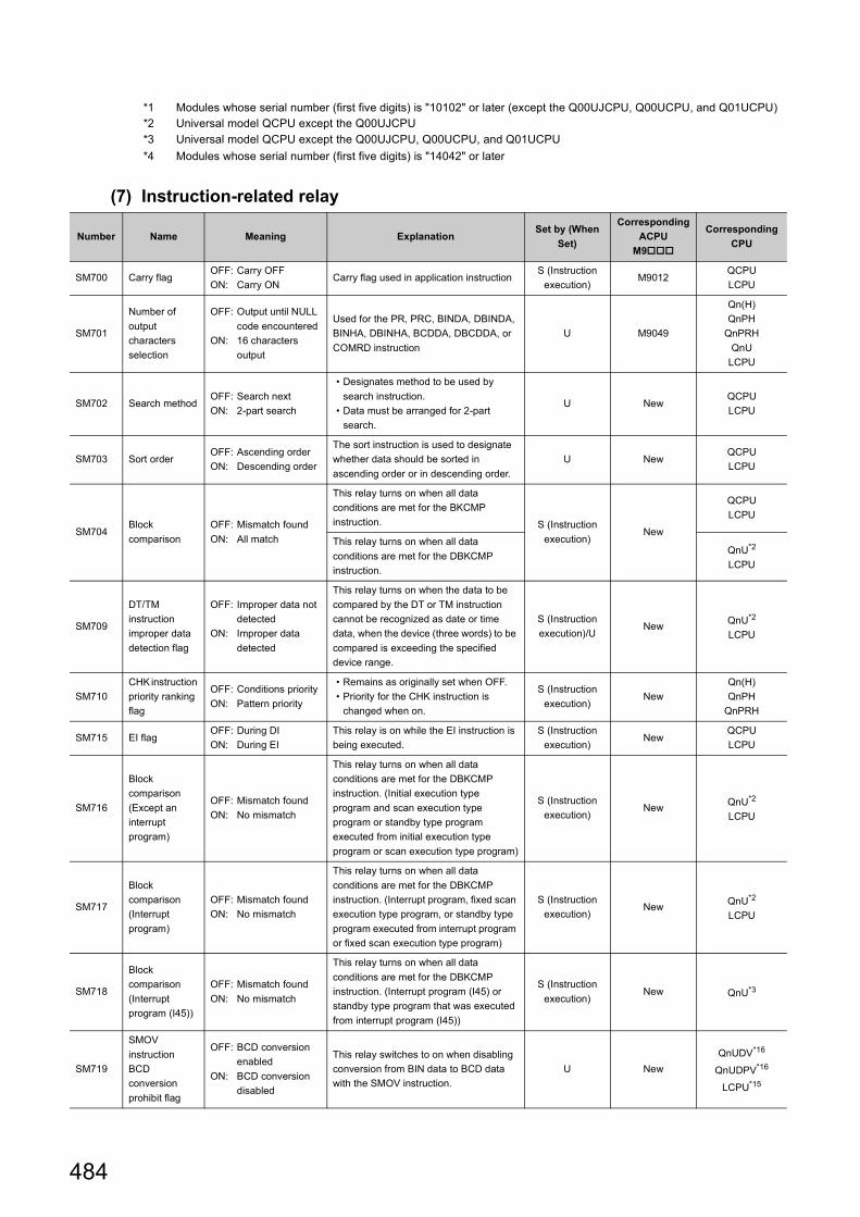
*1 Modules whose serial number (first five digits) is "10102" or later (except the Q00UJCPU, Q00UCPU, and Q01UCPU)*2 Universal model QCPU except the Q00UJCPU*3 Universal model QCPU except the Q00UJCPU, Q00UCPU, and Q01UCPU*4 Modules whose serial number (first five digits) is "14042" or later
(7) Instruction-related relay
Number Name Meaning ExplanationSet by (When
Set)
Corresponding ACPU
M9
Corresponding CPU
SM700 Carry flagOFF: Carry OFFON: Carry ON
Carry flag used in application instructionS (Instruction
execution)M9012
QCPULCPU
SM701
Number of output characters selection
OFF: Output until NULL code encountered
ON: 16 characters output
Used for the PR, PRC, BINDA, DBINDA, BINHA, DBINHA, BCDDA, DBCDDA, or COMRD instruction
U M9049
Qn(H)QnPH
QnPRHQnU
LCPU
SM702 Search methodOFF: Search nextON: 2-part search
• Designates method to be used by search instruction.
• Data must be arranged for 2-part search.
U NewQCPULCPU
SM703 Sort orderOFF: Ascending orderON: Descending order
The sort instruction is used to designate whether data should be sorted in ascending order or in descending order.
U NewQCPULCPU
SM704Block comparison
OFF: Mismatch foundON: All match
This relay turns on when all data conditions are met for the BKCMP instruction. S (Instruction
execution)New
QCPULCPU
This relay turns on when all data conditions are met for the DBKCMP instruction.
QnU*2
LCPU
SM709
DT/TM instruction improper data detection flag
OFF: Improper data not detected
ON: Improper data detected
This relay turns on when the data to be compared by the DT or TM instruction cannot be recognized as date or time data, when the device (three words) to be compared is exceeding the specified device range.
S (Instruction execution)/U
New QnU*2
LCPU
SM710CHK instruction priority ranking flag
OFF: Conditions priorityON: Pattern priority
• Remains as originally set when OFF.• Priority for the CHK instruction is
changed when on.
S (Instruction execution)
NewQn(H)QnPH
QnPRH
SM715 EI flagOFF: During DION: During EI
This relay is on while the EI instruction is being executed.
S (Instruction execution)
NewQCPULCPU
SM716
Block comparison (Except an interrupt program)
OFF: Mismatch foundON: No mismatch
This relay turns on when all data conditions are met for the DBKCMP instruction. (Initial execution type program and scan execution type program or standby type program executed from initial execution type program or scan execution type program)
S (Instruction execution)
New QnU*2
LCPU
SM717
Block comparison (Interrupt program)
OFF: Mismatch foundON: No mismatch
This relay turns on when all data conditions are met for the DBKCMP instruction. (Interrupt program, fixed scan execution type program, or standby type program executed from interrupt program or fixed scan execution type program)
S (Instruction execution)
New QnU*2
LCPU
SM718
Block comparison (Interrupt program (I45))
OFF: Mismatch foundON: No mismatch
This relay turns on when all data conditions are met for the DBKCMP instruction. (Interrupt program (I45) or standby type program that was executed from interrupt program (I45))
S (Instruction execution)
New QnU*3
SM719
SMOV instructionBCD conversion prohibit flag
OFF: BCD conversion enabled
ON: BCD conversion disabled
This relay switches to on when disabling conversion from BIN data to BCD data with the SMOV instruction.
U NewQnUDV*16
QnUDPV*16
LCPU*15
484

APPX
A
Appendix 2 List of Special Relay Areas
SM720Comment read completion flag
OFF: Comment read not completed
ON: Comment read completed
This relay turns on only during first scan after the processing of the COMRD or PRC instruction is completed. S (Status
change)New
Qn(H)QnPH
This relay turns on only during first scan after the processing of the COMRD instruction is completed.
QnPRHQnU
LCPU
SM721File being accessed
OFF: File not accessedON: File being
accessed
This relay is on while a file is being accessed by the SP.FWRITE, SP.FREAD, COMRD, PRC, or LEDC instruction.
S (Status change)
New
Qn(H)QnPH
This relay is on while a file is being accessed by the SP.FWRITE, SP.FREAD, COMRD, or LEDC instruction.
Qn(H)QnPH
QnPRH
This relay is on while a file is being accessed by the SP.FWRITE, SP.FREAD, COMRD, or SP.DEVST instruction.
QnU
• This relay is on while a file is being accessed by the SP.FWRITE, SP.FREAD, COMRD, or SP.DEVST instruction.
• This relay is on while the standard ROM is being accessed.
• This relay is on while the S(P).SFCSCOMR or S(P).SFCTCOMR instruction is being executed.
QnUDVQnUDPV
• This relay is on while a file is being accessed by the SP.FWRITE, SP.FREAD, COMRD, or SP.DEVST instruction.
• This relay is on while a SD memory card or the standard ROM is being accessed.
• This relay is on while the S(P).SFCSCOMR or S(P).SFCTCOMR instruction is being executed.
LCPU
This relay is on while an ATA card or the standard ROM is being accessed. QnU*4
This relay is on while the S(P).SFCSCOMR or S(P).SFCTCOMR instruction is being executed.
QnU*11
This relay is on while the SP.FTPPUT or SP.FTPGET instruction is being executed.
LCPU*17
SM722BIN/DBIN instruction error disabling flag
OFF: Error detection performed
ON: Error detection not performed
Turned ON when "OPERATION ERROR" is suppressed for BIN or DBIN instruction.
U NewQCPULCPU
SM734
XCALL instruction execution condition designation
OFF: Not executed by execution condition risen
ON: Executed by execution condition risen
• During OFF, XCALL instructions will not be executed even if execution condition is risen.
• During ON, XCALL instructions will be executed when execution condition is risen.
U New Qn(H)*4
SM735
SFC comment readout instruction in execution flag
OFF: Instruction not executed
ON: Instruction being executed
This relay turns on while a SFC step comment readout instruction (S(P).SFCSCOMR) or SFC transmission condition comment readout instruction (S(P).SFCTCOMR) is being executed.
S (Instruction execution/Every
END processing)
New
Qn(H)*5
QnPH*6
QnPRH*6
QnU*11
L06/L26/L26CPU
-BT*14
Number Name Meaning Explanation Set by (When Set)
Corresponding ACPU
M9
Corresponding CPU
485

SM738MSG instruction reception flag
OFF: Instruction not executed
ON: Instruction executed
This relay turns on when the MSG instruction is executed.
S (Instruction execution)
NewQn(H)
QnPRH
SM739
Refresh device write/read instruction in execution flag
OFF: Instruction not executed
ON: Instruction being executed
This relay is on while a refresh device writing/reading instruction (S(P).REFDVWRB, S(P).REFDVWRW, S(P).REFDVRDB, or S(P).REFDVRDW) is being executed. This relay turns off when the instruction is completed at END processing.
S (Instruction execution/Every
END processing)
NewQnU*13
LCPU*12
SM740Display unit availability flag
OFF: UnusableON: Usable
This relay is on while the display unit can be used.
S (Initial/Status change)
New LCPU
SM750
Scaling instruction search method setting
OFF: Search nextON: 2-part search
Specify a search method for the scaling instruction.
U New QnU*2
LCPU
SM772
Bit conversion mode for the CCD and CRC instructions
OFF: 16-bit conversion mode
ON: 8-bit conversion mode
Specify the bit conversion mode for the CCD and CRC instructions. Turn off to specify 16-bit conversion mode and turn on to specify 8-bit conversion mode.
U NewQnUDV*17
QnUDPV*17
LCPU*17
SM774
PID bumpless processing (for complete derivative)
OFF: MatchedON: Not matched
Specify whether to match the set value (SV) with the process value (PV) or not in manual mode.
U New
Q00J/Q00/Q01*1
Qn(H)QnPRH
QnULCPU
SM775
Selection of refresh processing during COM/CCOM instruction execution
OFF: Performs link refresh
ON: Performs no link refresh
Select whether link refresh processing will be performed or not when only communication with the CPU module is made at the execution of the COM instruction.
U New
Q00J/Q00/Q01Qn(H)QnPH
OFF: Performs refresh processes other than an I/O refresh
ON: Performs refresh set by SD778
Select whether to perform refresh processes other than an I/O refresh set by SD778 when the COM or CCOM instruction is executed.
Q00J/Q00/Q01*1
Qn(H)*7
QnPH*4
QnPRHQnU
LCPU
SM776Enable/disable local device at CALL
OFF: Local device disabled
ON: Local device enabled
Set whether the local device of the subroutine program called at execution of the CALL instruction is valid or invalid.
U New
Qn(H)QnPH
QnPRH
QnU*10
LCPU
SM777
Enable/disable local device in interrupt program
OFF: Local device disabled
ON: Local device enabled
Set whether the local device at execution of the interrupt program is valid or invalid.
U New
Qn(H)QnPH
QnPRH
QnU*10
LCPU
SM794
PID bumpless processing(for incomplete derivative)
OFF: MatchedON: Not matched
Specify whether to match the set value (SV) with the process value (PV) or not in manual mode.
U New
Q00J/Q00/Q01*1
Qn(H)*8
QnPRHQnU
LCPU
SM796
Block information using the multiple CPU high-speed transmission dedicated instruction (for CPU No.1)
OFF: Block is securedON: Block set by
SD796 cannot be secured
This relay turns on when the number of the remaining blocks in the dedicated instruction transmission area used for the multiple CPU high-speed transmission dedicated instruction (target CPU= CPU No.1) is less than the number of blocks specified in SD796. This relay is on when an instruction is executed, and is off while an END processing is being executed or when free space is available in the area.
S (Instruction execution/Every
END processing)
New QnU*9
Number Name Meaning Explanation Set by (When Set)
Corresponding ACPU
M9
Corresponding CPU
486

APPX
A
Appendix 2 List of Special Relay Areas
*1 Modules whose function version B or later*2 The following modules support these areas:
• Universal model QCPU whose serial number (first five digits) is "10102" or later• Q00UJCPU, Q00UCPU, Q01UCPU
*3 The following modules support this area:• Universal model QCPU whose serial number (first five digits) is "10102" or later• Q00UCPU, Q01UCPU
*4 Modules whose serial number (first five digits) is "07032" or later*5 Modules whose serial number (first five digits) is "06082" or later*6 Modules whose serial number (first five digits) is "07012" or later*7 Modules whose serial number (first five digits) is "04012" or later*8 Modules whose serial number (first five digits) is "05032" or later*9 Universal model QCPU except the Q00UJCPU, Q00UCPU, Q01UCPU, and Q02UCPU*10 Universal model QCPU except the Q00UJCPU*11 Modules whose serial number (first five digits) is "12052" or later*12 Modules whose serial number (first five digits) is "14072" or later*13 Following modules except the Q00UJCPU, Q00UCPU, Q01UCPU, and Q02UCPU.
• Modules whose serial number (first five digits) is "14072" or later other than the High-speed Universal model QCPU and Universal model Process CPU
• High-speed Universal model QCPU and Universal model Process CPU whose serial number (first five digits) is "16043" or later
*14 Modules whose serial number (first five digits) is "15102" or later*15 Modules whose serial number (first five digits) is "16042" or later*16 Modules whose serial number (first five digits) is "16043" or later*17 Modules whose serial number (first five digits) is "16112" or later
SM797
Block information using the multiple CPU high-speed transmission dedicated instruction (for CPU No.2)
OFF: Block is securedON: Block set by
SD797 cannot be secured
This relay turns on when the number of the remaining blocks in the dedicated instruction transmission area used for the multiple CPU high-speed transmission dedicated instruction (target CPU= CPU No.2) is less than the number of blocks specified in SD797. This relay is on when an instruction is executed, and is off while an END processing is being executed or when free space is available in the area.
S (Instruction execution/Every
END processing)
New QnU*9
SM798
Block information using the multiple CPU high-speed transmission dedicated instruction (for CPU No.3)
OFF: Block is securedON: Block set by
SD798 cannot be secured
This relay turns on when the number of the remaining blocks in the dedicated instruction transmission area used for the multiple CPU high-speed transmission dedicated instruction (target CPU= CPU No.3) is less than the number of blocks specified in SD798. This relay is on when an instruction is executed, and is off while an END processing is being executed or when free space is available in the area.
S (Instruction execution/Every
END processing)
New QnU*9
SM799
Block information using the multiple CPU high-speed transmission dedicated instruction (for CPU No.4)
OFF: Block is securedON: Block set by
SD799 cannot be secured
This relay turns on when the number of the remaining blocks in the dedicated instruction transmission area used for the multiple CPU high-speed transmission dedicated instruction (target CPU= CPU No.) is less than the number of blocks specified in SD799. This relay is on when an instruction is executed, and is off while an END processing is being executed or when free space is available in the area.
S (Instruction execution/Every
END processing)
New QnU*9
Number Name Meaning Explanation Set by (When Set)
Corresponding ACPU
M9
Corresponding CPU
487

(8) Debugging
Number Name Meaning ExplanationSet by (When
Set)
Corresponding ACPU
M9
Corresponding CPU
SM800Trace preparation
OFF: Not readyON: Ready
Turns on when the trace preparation is completed.
S (Status change)
New
Qn(H)QnPH
QnPRH
QnU*1
LCPU
SM801 Trace startOFF: SuspendON: Start
• When this relay is turned on while the CPU module is set to RUN, a trace will be started.
• When this relay is turned off, a trace is stopped. (The related special relays will all turn off)
S (Status change)/U
M9047
Qn(H)QnPH
QnPRH
QnU*1
LCPU
SM802Trace execution in progress
OFF: SuspendON: Start
This relay is on while a trace is being executed.
S (Status change)
M9046
Qn(H)QnPH
QnPRH
QnU*1
LCPU
SM803 Trace trigger OFF ON:Triggered
• This relay turns on when the specified trigger condition is met.
• This relay is turned on to meet the trigger condition.
S (Status change)/U
New
Qn(H)QnPH
QnPRH
QnU*1
LCPU
SM804 After trace triggerOFF: Not after triggerON: After trigger
Turns on after trace is triggered.S (Status change)
New
Qn(H)QnPH
QnPRH
QnU*1
LCPU
SM805 Trace completedOFF: Not completedON: Completed
This relay turns on when a trace is completed.
S (Status change)
M9043
Qn(H)QnPH
QnPRH
QnU*1
LCPU
SM826 Trace errorOFF: NormalON: Errors
This relay turns on if an error occurs during trace.
S (Status change)
New
Qn(H)QnPH
QnPRH
QnU*1
LCPU
SM829
Forced registration specification of trace setting
ON: Forced registration enabled
OFF: Forced registration disabled
When this relay is turned on and a sampling trace setting is registered using a programming tool, the sampling trace setting can be registered with the CPU module even when the trigger condition has been met.
U New QnU*1
LCPU
SM830Real-time monitor in progress
ON : Being executedOFF : Not executed
Turns on during real-time monitor in progress
S (Status change)
New LCPU*2
SM841 Auto loggingOFF: Not executedON: Being executed
This relay is on while the auto logging is being executed.This relay turns off when auto logging is completed and the SD memory card lock switch is pressed and held for 1 second or longer to stop access to the SD memory card. S (Status
change)New
QnUDV
This relay is on while auto logging is being executed.This relay turns off when auto logging is completed and the SD memory card lock switch is slid toward the module top to stop access to the SD memory card.
LCPU
488

APPX
A
Appendix 2 List of Special Relay Areas
*1 Universal model QCPU except the Q00UJCPU*2 Built-in Ethernet port LCPU whose serial number (first five digits) is "16072" or later
(9) Latch area
*1 Modules whose serial number (first five digits) is "17103" or later*2 The LCPU, except the L02SCPU and L02SCPU-P, whose serial number (first five digits) is "17102" or later*3 Modules whose serial number (first five digits) is "18052" or later
(10)Conversion from A series to Q or L seriesThe special relay (M9000 to M9255) for ACPU corresponds to the special relay (SM1000 to SM1255) for QCPU or LCPU after the A to Q/L conversion. (Note that the Basic model QCPU and Redundant CPU do not support the A to Q/L conversion.) All bits in this area of the special relay are turned on or off by system (cannot be turned on or off by user using a program). To turn on or off the bit by user, correct the program using the special relay for QCPU or LCPU. The special relay (M9084, M9200 to M9255), however, includes the areas that can be turned on or off by user. For those areas, the bit can be turned on or off by user in the converted special relay (SM1084, SM1200 to SM1255) as well. For details on the special relay for ACPU, refer to the following.User's manual for the CPU module usedType MELSECNET, MELSECNET/B Data Link System Reference Manual
To use the converted special relay in the High Performance model QCPU, Process CPU, Universal model QCPU, or LCPU, check "Use special relay/special register from SM/SD1000" under "A-PLC Compatibility Setting".
Project window [Parameter] [PLC Parameter] [PLC System]Note that the processing time will increase when the converted special relay is used.
Number Name Meaning ExplanationSet by (When
Set)
Corresponding ACPU
M9
Corresponding CPU
SM916Backup error check flag
OFF: No errorON: Error
This relay turns on if an error occurs at the execution of backup of the CPU module. This relay turns off at the start of backup.
S (Status change)
NewQnUDV*1
QnUDPV*1
SM922Restoration error check flag
OFF: No errorON: Error
This relay turns on if an error occurs at the execution of restoration of the CPU module. This relay turns off at the start of backup.
S (Status change)
NewQnUDV*1
QnUDPV*1
SM923
Upper limit setting flag for the number of backup data
OFF: Backup continuedON: Backup stopped
This relay specifies the operation of backup when the number of backup data reaches the upper limit. (Valid only when bit5 of SD944 is on)OFF: After deleting the oldest date stamp folder, the backup is continued.ON: The backup is not continued if the upper limit of the number of backup data is exceeded. (In this case, the backup is completed with an error.)
U NewQnUDV*3
QnUDPV*3
SM924Automatic backup retry failure flag
OFF: Retry not executed/Retry being executed
ON: Retry failed
This relay turns on when the retry of the automatic backup is failed even after the specified number of retries are attempted, and turns off at the start of the automatic backup. (This relay does not turn off when SM1926 is on.)
S (Status change)
NewQnUDV*3
QnUDPV*3
SM960Data logging error check flag
OFF: No errorON: Error
This relay turns on if an error occurs during the execution of data logging. This relay turns off when the data logging is restarted by turning on SM1938 (Data logging restart flag at error stop) or is started or stopped by using the CPU Module Logging Configuration Tool.
S (Error) NewQnUDV*1
QnUDPV*1
LCPU*2
489

[How to read the Special Relay for Modification column]• If the special relay number for QCPU or LCPU is provided, correct the program using it.
• means that the converted special relay can be used.
• means that the special relay cannot be used in QCPU or LCPU.
ACPU Special Relay
Special Relay after Conversion
Special Relay after
ModificationName Meaning Details
Corresponding CPU
M9000 SM1000 Fuse blownOFF: NormalON: Module with blown
fuse
• This relay turns on if there is at least one output module whose fuse has blown.
• This relay remains on even after the system returns to normal.
• Output modules on remote I/O stations are also checked.
Qn(H)QnPH
QnU*1
LCPU*4
M9002 SM1002 I/O module verify error
OFF: NormalON: Error
• This relay turns on if the status of the I/O module differs from that registered at power-on.
• This relay remains on even after the system returns to normal.
• I/O modules on remote I/O stations are also checked.
• This relay is reset only when SD1116 to SD1123 are reset.
Qn(H)QnPH
QnU*1
LCPU
M9005 SM1005 AC DOWN detection
OFF: AC DOWN not detected
ON: AC DOWN detected
• This relay turns on if a momentary power failure within 20ms occurs during use of an AC power supply module.
• This relay is reset when the CPU module is powered off and then on.
Qn(H)QnPH
QnU*1
• This relay turns on if a momentary power failure within 10ms occurs when using an AC power supply module.
• This relay is reset when the CPU module is powered off and then on.
LCPU
• This relay turns on if a momentary power failure within 10ms occurs during use of a DC power supply module.
• This relay is reset when the CPU module is powered off and then on.
Qn(H)QnPH
QnU*1
LCPU
M9006 SM1006 Battery lowOFF: NormalON: Battery low
• This relay turns on when the battery voltage drops to or below the specified.
• It turns off when the battery voltage returns to normal.
Qn(H)QnPH
QnU*1
LCPU
M9007 SM1007 Battery low latchOFF: NormalON: Battery low
• This relay turns on when the battery voltage drops to or below the specified.
• This relay remains on even after the battery voltage returns to normal.
Qn(H)QnPH
QnU*1
LCPU
M9008 SM1008 SM1Self-diagnostic error
OFF: No errorON: Error
This relay turns on if an error is detected by self-diagnostics.
Qn(H)QnPH
QnU*1
LCPU
M9009 SM1009 SM62Annunciator detection
OFF: No F number detected
ON: F number detected
• This relay turns on when the OUT F or SET F instruction is executed.
• It turns off when the SD1124 value is cleared to zero.
Qn(H)QnPH
QnU*1
LCPU
M9011 SM1011 SM56Operation error flag
OFF: No errorON: Error
• This relay turns on when an operation error occurs during execution of an application instruction.
• This relay remains on even after the system returns to normal.
Qn(H)QnPH
QnU*1 (except the QnUDPV)
M9012 SM1012 SM700 Carry flagOFF: Carry OFFON: Carry ON
Carry flag used in application instructionQn(H)QnPH
490

APPX
A
Appendix 2 List of Special Relay Areas
M9016 SM1016 Data memory clear flag
OFF: IgnoredON: Output cleared
When SM1016 turns on and remote RUN mode is activated from a computer, all the data memory including the latch range (except for the special relay and special register) is cleared.
Qn(H)QnPH
M9017 SM1017 Data memory clear flag
OFF: IgnoredON: Output cleared
When SM1017 turns on and remote RUN mode is activated from a computer, all the data memory that is not latched (except for the special relay and special register) is cleared.
Qn(H)QnPH
M9020 SM1020 User timing clock No.0
• This relay repeatedly turns on and off at the specified scan intervals.
• When the CPU module is powered on or reset, this relay is set to on from off to start the clock. Set the intervals of on/off by DUTY instruction.
n1: On scan intervaln2: Off scan interval
• When SM1020 to SM1024 are specified for the DUTY instruction in programs, if the CPU type is changed from the High Performance model QCPU or Process CPU to the Universal model QCPU or LCPU, they are replaced with SM420 to SM424. (For the Universal model QCPU and LCPU, SM1020 to SM1024 cannot be specified.)
Qn(H)QnPH
QnU*1
LCPU
M9021 SM1021 User timing clock No.1
M9022 SM1022 User timing clock No.2
M9023 SM1023 User timing clock No.3
M9024 SM1024 User timing clock No.4
M9025 SM1025 Clock data set request
OFF: IgnoredON: Set request
Clock data stored in SD1025 to SD1028 are written to the CPU module after the END instruction execution in the scan where SM1025 is turned on.
Qn(H)QnPH
QnU*1
LCPU
M9026 SM1026 Clock data errorOFF: No errorON: Error
This relay turns on if an error occurs in the clock data (SD1025 to SD1028), and is off while there is no error.
Qn(H)QnPH
QnU*1
LCPU
M9028 SM1028 Clock data read request
OFF: IgnoredON: Read request
This relay is turned on to read clock data and store them as BCD values into SD1025 to SD1028.
Qn(H)QnPH
QnU*1
LCPU
M9029 SM1029
Batch processing of data communications requests
OFF: Batch processing not conducted
ON: Batch processing conducted
• When this relay is turned on in the program, all the data communication requests accepted during one scan are processed in the END processing of that scan.
• The batch processing of data communication requests can be turned on or off during running.
• The default is OFF (processed one at a time for each END processing in the order in which data communication requests are accepted).
Qn(H)QnPH
ACPU Special Relay
Special Relay after Conversion
Special Relay after
ModificationName Meaning Details Corresponding
CPU
n1 scan
n2 scan n2 scan
DUTY n1 n2 SM1020
491

M9030 SM1030 0.1 second clock • 0.1-, 0.2-, 1-, and 2-second clocks are generated.
• The relay turns on or off not for each scan, but also during a scan if the time has elapsed.
• This relay does not turn on/off per scan, but turns on/off whenever the specified time interval is reached.
• The initial state when the CPU module is powered on or reset is off.
Qn(H)QnPH
QnU*1
LCPU
M9031 SM1031 0.2 second clock
M9032 SM1032 1 second clock
M9033 SM1033 2 second clock
M9034 SM1034 2n minute clock(1
minute clock)*2
• This relay repeatedly turns on and off according to the number of seconds specified in SD414. (Default: n = 30) (If the value of SD414 is changed, the time that has passed after the previous ON/OFF interval of SM1034 is counted as the next interval, and the ON/OFF status is changed at the next interval that is newly specified.)
Example: When the value of SD414 is changed from 3 to 10.
• This relay does not turn on/off per scan, but turns on/off whenever the specified time interval is reached.
• The initial state when the CPU module is powered on or reset is off.
Qn(H)QnPH
QnU*1
LCPU
M9036 SM1036 Always ON • This relay is used for initialization or as a dummy contact of application instructions in the program.
• SM1036 and SM1037 are turned on or off regardless of the switch setting on the front face of the CPU module. The states of SM1038 and SM1039 change depending on the switch setting. When it is set to STOP, the relay is off. When it is set to other than STOP, SM1038 is on for one scan only and SM1039 is off for one scan only.
Qn(H)QnPH
QnU*1
LCPU
M9037 SM1037 Always OFF
M9038 SM1038 ON for 1 scan only after RUN
M9039 SM1039
RUN flag(After RUN, OFF for 1 scan only)
M9040 SM1040 SM206PAUSE enable coil
OFF: PAUSE disabledON: PAUSE enabled
This relay is on when the CPU module is in PAUSE status or when the PAUSE contact is on.
Qn(H)QnPH
M9041 SM1041 SM204PAUSE status contact
OFF: PAUSE not in effectON: PAUSE in effect
Qn(H)QnPHQnU*1
LCPU
M9042 SM1042 SM203STOP status contact
OFF: STOP not in effectON: STOP in effect
This relay turns on when the RUN/STOP switch is set to STOP.
Qn(H)QnPHQnU*1
LCPU
M9043 SM1043 SM805Sampling trace completed
OFF: Sampling trace in progress
ON: Sampling trace completed
This relay turns on after execution of the TRACE instruction and upon completion of sampling trace performed the number of times preset by the parameter. Reset when TRACER instruction is executed.
Qn(H)QnPHQnU*1
LCPU
ACPU Special Relay
Special Relay after Conversion
Special Relay after
ModificationName Meaning Details Corresponding
CPU
0.05s0.05s
0.1s0.1s
0.5s0.5s
1s1s
nsns
SM1034 OFF
3seconds
3seconds
The time that has passed after the previous ON/OFF interval of SM1034 is counted as the next interval.
10seconds
10seconds
ON
SD414 3 10
Change of the value
ONOFF
ONOFF
ONOFF
1 scan
ONOFF 1 scan
492

APPX
A
Appendix 2 List of Special Relay Areas
M9045 SM1045 Watchdog timer (WDT) reset
OFF: Does not reset WDTON: Resets WDT
If SM1045 is turned on, the watchdog timer is reset when the ZCOM instruction and batch processing of data communication requests are executed. (Use this when scan time exceeds 200ms.)
Qn(H)QnPH
M9046 SM1046 SM802 Sampling traceOFF: Trace not in
progressON: Trace in progress
This relay is on during execution of sampling trace.
Qn(H)QnPH
QnU*1
LCPU
M9047 SM1047 SM801Sampling trace preparations
OFF: Sampling trace suspended
ON: Sampling trace started
Sampling trace is not executed unless SM1047 is turned ON. Sampling trace is cancelled when SM1047 turns off.
Qn(H)QnPH
M9049 SM1049 SM701Number of output characters selection
OFF: Output until NULL code encountered
ON: 16 characters output
• When SM1049 is off, characters up to NULL (00H) code are output.
• When SM1049 is ON, ASCII codes of 16 characters are output.
Qn(H)QnPH
M9051 SM1051 CHG instruction execution disable
OFF: EnabledON: Disable
• Switched ON to disable the CHG instruction.
• Turn this on when requesting program transfer. It is automatically turned off upon completion of the transfer.
Qn(H)QnPH
M9052 SM1052 SEG instruction switch
OFF: 7-SEG segment display
ON: I/O partial refresh
When SM1052 is on, the SEG instruction is used as an I/O part refresh instruction. When SM1052 is off, the SEG instruction is used as a 7-SEG display instruction.
Qn(H)QnPH
M9056 SM1056 Main side P, I set request
OFF: Other than when P, I set being requested
ON: P, I set being requested
While a program is running, upon completion of transfer of another program (for example, a subprogram when the main program is running), a P and I set request is turned on. This relay automatically turns off upon completion of P and I setting.
Qn(H)QnPH
M9057 SM1057 Sub side P, I set request
OFF: Other than when P, I set being requested
ON: P, I set being requested
M9058 SM1058 Main side P, I set completion
Momentarily ON at P, I set completion This relay turns on for a moment upon
completion of P and I setting, and immediately turns off.
Qn(H)QnPH
M9059 SM1059 Sub program P, I set completion
Momentarily ON at P, I set completion
M9060 SM1060 Sub program 2 P, I set request
OFF: Other than when P, I set being requested
ON: P, I set being requested
While a program is running, upon completion of transfer of another program (for example, a subprogram when the main program is running), a P and I set request is turned on. This relay automatically turns off upon completion of P and I setting.
Qn(H)QnPH
M9061 SM1061 Sub program 3 P, I set request
OFF: Other than when P, I set being requested
ON: P, I set being requested
M9070 SM1070
A8UPU/A8PUJ required search
time*3
OFF: Read time not shortened
ON: Read time shortened
When this is turned on, the search time in the A8UPU/A8PUJ can be shortened. (In this case, the scan time is extended by 10%.)
Qn(H)QnPH
M9084 SM1084 Error checkOFF: Error check
executedON: No error check
This relay sets whether or not to check the following errors at the time of the END instruction processing (for setting of the END instruction processing time).• Check for fuse blown• Check of battery• Collation check of I/O module
Qn(H)QnPH
M9091 SM1091 Operation error details flag
OFF: No errorON: Error
• This relay turns on when the detail factor of the operation error is stored into SD1091.
• This relay remains on even after the condition returns to normal.
Qn(H)QnPH
ACPU Special Relay
Special Relay after Conversion
Special Relay after
ModificationName Meaning Details Corresponding
CPU
493

M9100 SM1100 SM320Presence/absence of SFC program
OFF: SFC program absent
ON: SFC program present
This relay is on when an SFC program has been registered, and is off when no program is registered.
Qn(H)QnPH
M9101 SM1101 SM321Start/stop SFC program
OFF: SFC programs stopON: SFC programs start
• The same value as in SM1100 is set as the initial value. (This relay turns on when an SFC program is registered.)
• This relay is turned off to stop SFC program execution.
• This relay is turned on to resume the SFC program execution.
Qn(H)QnPH
M9102 SM1102 SM322SFC program start status
OFF: Initial startON: Resume start
In the SFC tab of "PLC parameter", "Initial start" is set for "SFC program start mode".• At initial start:OFF• At resume start:ON
Qn(H)QnPH
M9103 SM1103 SM323Presence/absence of continuous transition
OFF: Continuous transition not effective
ON: Continuous transition effective
Set whether to enable or disable continuous transition for the blocks where "continuous transition bit" of the SFC information device is not set.
Qn(H)QnPH
M9104 SM1104 SM324Continuous transition prevention flag
OFF: When transition is executed
ON: When no transition
• This relay is off while the module is in the continuous transition mode or during continuous transition, and is on when continuous transition is not executed.
• This relay is always on while the CPU module is operating not in the continuous transition mode.
Qn(H)QnPH
M9108 SM1108 SM90
Step transition monitoring timer start (equivalent of SD90)
OFF: Monitoring timer reset
ON: Monitoring timer reset start
The relay turns on when measurement by the step transition monitoring timer is started. The step transition monitoring timer is reset when the relay turns off.
Qn(H)QnPH
M9109 SM1109 SM91
Step transition monitoring timer start (equivalent of SD91)
M9110 SM1110 SM92
Step transition monitoring timer start (equivalent of SD92)
M9111 SM1111 SM93
Step transition monitoring timer start (equivalent of SD93)
M9112 SM1112 SM94
Step transition monitoring timer start (equivalent of SD94)
M9113 SM1113 SM95
Step transition monitoring timer start (equivalent of SD95)
M9114 SM1114 SM96
Step transition monitoring timer start (equivalent of SD96)
ACPU Special Relay
Special Relay after Conversion
Special Relay after
ModificationName Meaning Details Corresponding
CPU
494

APPX
A
Appendix 2 List of Special Relay Areas
*1 The following modules support these areas:• Universal model QCPU whose serial number (first five digits) is "10102" or later• Q00UJCPU, Q00UCPU, Q01UCPU
*2 The name, 1 minute clock, is for the special relay (M9034) of the ACPU.*3 The QCPU and LCPU do not support the use of the A8UPU/A8PUJ.*4 Modules whose serial number (first five digits) is "16112" or later
(11)Built-in Ethernet port QCPU, built-in Ethernet port LCPU, and built-in Ethernet function
M9196 SM1196 SM325Operation output at block stop
OFF: Coil output OFFON: Coil output ON
Selects the operation output when block stop is executed.• On: Retains the on or off status of the
coil used in the operation output of the step, which was being executed at the time of block stop.
• Off: Turns off all the coil outputs. (Operation output by the SET instruction is retained regardless of the on/off status of SM1196.)
Qn(H)QnPH
M9197 SM1197 Switch between blown fuse and I/O module verification error display
Switches I/O numbers between the fuse-blown module registers (SD1100 to SD1107) and I/O module verify error registers (SD1116 to SD1123) according to the on/off combination of SM1197 and SM1198.
Qn(H)QnPHM9198 SM1198
M9199 SM1199
Data recovery of online sampling trace/status latch
OFF: Data recovery disabled
ON: Data recovery enabled
• Recovers the setting data stored in the CPU module at restart when sampling trace/status latch is executed.
• Turn this on to re-execute the sampling trace or status latch. (Rewriting data using the programming tool is not required.)
Qn(H)QnPH
Number Name Meaning ExplanationSet by
(When Set)
Corresponding ACPU
M9
Corresponding CPU
SM1258
MELSOFT connection extended setting network number, station number enable flag
OFF: DisabledON: Enabled
This relay turns on when the network number and station number of built-in Ethernet port set in the MELSOFT connection extended setting are enabled. (Only when the MELSOFT connection extended setting is set to "Use".)
S (Initial) NewQnUDV*5
QnUDPV*5
SM1270Time setting function (SNTP client) execution
OFF: No time setting function (SNTP client) execution
ON: Time setting function (SNTP client) execution
This relay is turned on to perform the time setting function (SNTP client). (Turns on only when "Use" has been set for the time setting function in the time setting parameter.)
U NewQnU*1
LCPU*1
SM1273
Remote password mismatch count clear
OFF: NormalON: Clear
This relay is turned on to clear the accumulated number of mismatched remote password entries (SD979 to SD999).
U NewQnU*1
LCPU*1
SM1292IP address storage area write request
OFF ON:Write request
The IP address setting stored in SD1292 to SD1297 are written to the IP address storage area (flash ROM) of the CPU module when the END instruction is executed in the scan where this relay is turned on.
U NewQnU*2
LCPU*3
ACPU Special Relay
Special Relay after Conversion
Special Relay after
ModificationName Meaning Details Corresponding
CPU
OFF
ON
SM1197
OFF
SM1198
OFF
X/Y0 to 7F0
X/Y800 to FF0
OFF ON X/Y1000 to 17F0
ON ON X/Y1800 to 1FF0
I/O numbers to be displayed
495

*1 Built-in Ethernet port QCPU and Built-in Ethernet port LCPU*2 Built-in Ethernet port QCPU whose serial number (first five digits) is "11082" or later*3 Built-in Ethernet port LCPU whose serial number (first five digits) is "15102" or later*4 Built-in Ethernet port LCPU whose serial number (first five digits) is "16112" or later*5 Modules whose serial number (first five digits) is "17052" or later
SM1293IP address storage area write completion
OFF: Not completedON: Completed
• This relay turns on when writing to the IP address storage area (flash ROM) is completed.
• This relay turns off when the END instruction is executed in the scan where SM1292 is turned off.
S (Status change)
NewQnU*2
LCPU*3
SM1294IP address storage area write error
OFF: NormalON: Errors
• This relay turns on when writing to the IP address storage area (flash ROM) fails.
• This relay turns off when the END instruction is executed in the scan where SM1292 is turned off.
S (Status change)
NewQnU*2
LCPU*3
SM1295IP address storage area clear request
OFF ON:Clear request
The IP address storage area (flash ROM) is cleared when the END instruction is executed in the scan where this relay is turned on.
U NewQnU*2
LCPU*3
SM1296IP address storage area clear completion
OFF: Not completedON: Completed
• This relay turns on when clearing the IP address storage area (flash ROM) is completed.
• This relay turns off when the END instruction is executed in the scan where SM1295 is turned off.
S (Status change)
NewQnU*2
LCPU*3
SM1297IP address storage area clear error
OFF: NormalON: Errors
• This relay turns on when clearing the IP address storage area (flash ROM) fails.
• This relay turns off when the END instruction is executed in the scan where SM1295 is turned off.
S (Status change)
NewQnU*2
LCPU*3
SM1298FTP client connection status
OFF: Not connected (Disconnected)
ON: Connected
This relay turns on when the connection with the FTP server is established. This relay turns off when the connection with the FTP server is cut off.
S (Status change, END processing)
New LCPU*4
Number Name Meaning Explanation Set by (When Set)
Corresponding ACPU
M9
Corresponding CPU
496

APPX
A
Appendix 2 List of Special Relay Areas
(12)Predefined protocol function
*1 Built-in Ethernet port LCPU whose serial number (first five digits) is "15102" or later*2 Modules whose serial number (first five digits) is "15103" or later
Number Name Meaning ExplanationSet by
(When Set)
Corresponding ACPU
M9
Corresponding CPU
SM1332
Predefined protocol ready (for built-in/adapter serial communications)
OFF: Not readyON: Ready
The protocol setting file is checked when the CPU module is powered on or reset, or the check is requested. This relay turns on when the file is normal.
S (Status change)
New LCPU*1
SM1333
Predefined protocol setting check request (for built-in/adapter serial communications)
OFF: Not requestedON: Requested
The protocol setting file is checked when this relay turns on.The relay turns off when the check is completed.
S (Status change)/U
New LCPU*1
SM1334
RS-422/485 echo back specification (for built-in/adapter serial communications)
OFF: EnabledON: Disabled
When the RS-422/485 adapter is used, whether to receive an echo back of the data that has been sent can be specified.Echo back data are received when this relay is off, and are not received (discarded) when this relay is on.
U New LCPU*1
SM1354
Predefined protocol ready (for built-in Ethernet communications)
OFF: Not readyON: Ready
The protocol setting file is checked when the CPU module is powered on or reset, or the check is requested. This relay turns on when the file is normal.
S (Status change)
NewQnUDV*2
QnUDPV*2
LCPU*1
SM1355
Predefined protocol setting check request (for built-in Ethernet communications)
OFF: Not requestedON: Requested
The protocol setting file is checked when this relay turns on.The relay turns off when the check is completed.
S (Status change)/U
NewQnUDV*2
QnUDPV*2
LCPU*1
497

(13)iQ Sensor Solution
*1 Modules whose serial number (first five digits) is "17012" or later*2 Built-in Ethernet port LCPU whose serial number (first five digits) is "14112" or later*3 Modules whose serial number (first five digits) is "20042" or later
Number Name Meaning ExplanationSet by
(When Set)
Corresponding ACPU
M9
Corresponding CPU
SM1435iQ Sensor Solution backup/restoration execution enable
OFF ON:Enabled
Backup/restoration is enabled when this relay turns on.(Enabled only when SD1446 = 3H (completed), 11H (suspend (no error)), FEH (suspend (error)), FFH (error)).• This relay turns off when
backup/restoration can be executed.
S (Status change)/U
NewQnUDV*1
QnUDPV*1
LCPU*2
SM1436iQ Sensor Solution backup request
OFF ON:Backup request
Backup is executed for the target model set when this relay turns on. (Enabled only when SD1446 = 1H (in preparation))• This relay turns off when the use
authority is reserved or when backup/restoration can be executed.
S (Status change)/U
NewQnUDV*1
QnUDPV*1
LCPU*2
SM1437iQ Sensor Solution backup normal completion
OFF: Backup not completed
ON: Backup normally completed
This relay turns on when backup is completed normally.• This relay turns off when the use
authority is reserved.
S (Status change)
NewQnUDV*1
QnUDPV*1
LCPU*2
SM1438iQ Sensor Solution backup error completion
OFF: Backup not completed
ON: Backup completed with an error
This relay turns on when backup is completed with an error.• This relay turns off when the use
authority is reserved.The error code is stored into SD1452 or SD1453.
S (Status change)
NewQnUDV*1
QnUDPV*1
LCPU*2
SM1439iQ Sensor Solution restoration request
OFF ON:Restoration request
Restoration is executed for the target model set when this relay turns on. (Enabled only when SD1446 = 1H (in preparation))• This relay turns off when the use
authority is reserved.
S (Status change)/U
NewQnUDV*1
QnUDPV*1
LCPU*2
SM1440iQ Sensor Solution restoration normal completion
OFF: Restoration not completed
ON: Restoration normally completed
This relay turns on when restoration is completed normally.• This relay turns off when the use
authority is reserved.
S (Status change)
NewQnUDV*1
QnUDPV*1
LCPU*2
SM1441iQ Sensor Solution restoration error completion
OFF: Restoration not completed
ON: Restoration completed with an error
This relay turns on when restoration is completed with an error.• This relay turns off when the use
authority is reserved.The error code is stored into SD1452 or SD1453.
S (Status change)
NewQnUDV*1
QnUDPV*1
LCPU*2
SM1442iQ Sensor Solution backup/restoration suspend request
OFF ON:Backup/Restoration suspend request
Backup/restoration is suspended when this relay turns on. (Enabled only for SD1446=2H (execution))• This relay turns off when the use
authority is reserved or when backup/restoration can be executed.
S (Status change)
NewQnUDV*1
QnUDPV*1
LCPU*2
SM1445
Bridge area extension support status flag (iQ Sensor Solution backup/restoration)
OFF: Not supportedON: Supported
This flag indicates whether or not the CPU module used supports the bridge area extension for the iQ Sensor Solution backup/restoration.
S (Initial) NewQnUDV*3
QnUDPV*3
498

APPX
A
Appendix 2 List of Special Relay Areas
(14)Process control instruction
(15)Redundant system (host system CPU information*1)The special relay (SM1510 to SM1599) is valid only for redundant systems. All bits are set to off for stand-alone systems.
Number Name Meaning ExplanationSet by
(When Set)
Corresponding ACPU
M9
Corresponding CPU
SM1500
Hold modeOFF: No-holdON: Hold
Specifies whether or not to hold the output value when a range over occurs for the S.IN instruction range check.
U NewQnPH
QnPRHQnUDPV
SM1501Specifies whether or not the output value is held when a range over occurs for the S.OUT instruction range check.
Number Name Meaning ExplanationSet by
(When Set)
Corresponding ACPU
M9
Corresponding CPU
SM1510 Operation mode
OFF: Redundant system backup mode, stand-alone system
ON: Redundant system separate mode
This relay is on while the system is operating in the separate mode.
S (Every END
processing)New QnPRH
SM1511System A identification flag
• Distinguishes between system A and system B.• The flag status does not change even if the tracking cable is
disconnected.
S (Initial) New QnPRHSM1512
System B identification flag
SM1513Debug mode status flag
OFF: Not in debug mode
ON: Debug mode
This relay is on while the system is operating in the debug mode.
S (Initial) New QnPRH
SM1515Control system judgment flag
• Indicates operation system status.• The flag status does not change even if the tracking cable is
disconnected.S (Status change)
New QnPRHSM1516
Standby system judgment flag
SM1517CPU module startup status
OFF: Power supply on startup
ON: Operation system switch start up
Turns on when the CPU module is started up by the system switching (switching from the standby system to the control system). Remains OFF when the standby system is switched to the control system by a power-ON startup.
S (Status change)
New QnPRH
SM1518
Standby system to control system switching status flag
• This relay turns on during one scan after the standby system was switched to the control system.
• This relay can be used only in a scan execution type program.
S (Every END
processing)New QnPRH
SM1519
Previous Control System Identification Flag
When the previous control system is System B, this relay turns on during one scan in System A, following the RUN state after both Systems A and B were simultaneously turned on or were reset.
S (Every END
processing)New QnPRH
SM1511SM1512
ONOFF
System A
OFF
System B
ONOFFOFF
If TRK. CABLE ERR. (error code: 6210) occurred (Unknown)
SM1515SM1516
ONOFF
Controlsystem
OFF
Standbysystem
ONOFFOFF
If TRK. CABLE ERR. (error code: 6210) occurred (Unknown)
ONOFF
1 scan
ONOFF
1 scan
499

SM1520
Data tracking transfer trigger specification
OFF: No triggerON: Trigger
SM1520 Block 1
• When data is transferred based on the tracking setting of the Redundant parameter window, the target block is specified as trigger.
• When "Do auto forward Tracking block No.1" is selected for the tracking setting, SM1520 is turned on by the system at power-on or when the system is switched from STOP to RUN. In other cases, SM1520 to SM1583 are turned on by the user.
S (Initial)/U New QnPRH
SM1521 SM1521 Block 2
SM1522 SM1522 Block 3
SM1523 SM1523 Block 4
SM1524 SM1524 Block 5
SM1525 SM1525 Block 6
SM1526 SM1526 Block 7
SM1527 SM1527 Block 8
SM1528 SM1528 Block 9
SM1529 SM1529 Block 10
SM1530 SM1530 Block 11
SM1531 SM1531 Block 12
SM1532 SM1532 Block 13
SM1533 SM1533 Block 14
SM1534 SM1534 Block 15
SM1535 SM1535 Block 16
SM1536 SM1536 Block 17
SM1537 SM1537 Block 18
SM1538 SM1538 Block 19
SM1539 SM1539 Block 20
SM1540 SM1540 Block 21
SM1541 SM1541 Block 22
SM1542 SM1542 Block 23
SM1543 SM1543 Block 24
SM1544 SM1544 Block 25
SM1545 SM1545 Block 26
SM1546 SM1546 Block 27
SM1547 SM1547 Block 28
SM1548 SM1548 Block 29
SM1549 SM1549 Block 30
SM1550 SM1550 Block 31
SM1551 SM1551 Block 32
SM1552 SM1552 Block 33
SM1553 SM1553 Block 34
SM1554 SM1554 Block 35
SM1555 SM1555 Block 36
SM1556 SM1556 Block 37
SM1557 SM1557 Block 38
SM1558 SM1558 Block 39
SM1559 SM1559 Block 40
SM1560 SM1560 Block 41
SM1561 SM1561 Block 42
SM1562 SM1562 Block 43
SM1563 SM1563 Block 44
SM1564 SM1564 Block 45
Number Name Meaning Explanation Set by (When Set)
Corresponding ACPU
M9
Corresponding CPU
500

APPX
A
Appendix 2 List of Special Relay Areas
SM1565
Data tracking transfer trigger specification
OFF: No triggerON: Trigger
SM1565 Block 46 • When data is transferred based on the tracking setting of the Redundant parameter window, the target block is specified as trigger.
• When "Do auto forward Tracking block No.1" is selected for the tracking setting, SM1520 is turned on by the system at power-on or when the system is switched from STOP to RUN. In other cases, SM1520 to SM1583 are turned on by the user.
S (Initial)/U New QnPRH
SM1566 SM1566 Block 47
SM1567 SM1567 Block 48
SM1568 SM1568 Block 49
SM1569 SM1569 Block 50
SM1570 SM1570 Block 51
SM1571 SM1571 Block 52
SM1572 SM1572 Block 53
SM1573 SM1573 Block 54
SM1574 SM1574 Block 55
SM1575 SM1575 Block 56
SM1576 SM1576 Block 57
SM1577 SM1577 Block 58
SM1578 SM1578 Block 59
SM1579 SM1579 Block 60
SM1580 SM1580 Block 61
SM1581 SM1581 Block 62
SM1582 SM1582 Block 63
SM1583 SM1583 Block 64
SM1590
System switching enable/disable flag from network module
OFF: System switching request issuing module absent
ON: System switching request issuing module present
Turns on when a system switching request is issued from the network module. The module that issued the request can be checked in SD1590.Turns off when all bits of SD1590 are off.
S (Every END
processing)New QnPRH
SM1591
Standby system error detection disable flag at system switching
ON: Error is not detected by new standby system at system switching
OFF: Error is detected by new standby system at system switching
This flag is used when switching the system in any of the following sources to determine whether to detect "STANDBY" (error code 6210) in the new standby system:[Reason(s) for system switching]• System switching with a programming tool• System switching using dedicated
instruction• System switching by the intelligent
function module
U New QnPRH
SM1592Enable/disable user system switching
OFF: Disable user system switching
ON: Enable user system switching
This relay stores whether to enable manual switching using a programming tool or the system switching instruction (SP.CONTSW).
U New QnPRH
SM1593
Setting to access extension base unit of standby system CPU
OFF: ErrorON: Ignored
This relay sets the behavior of the system after the standby CPU in the separate mode accessed the buffer memory of an intelligent function module mounted on an extension base unit.• OFF: "OPERATION ERROR" (error code:
4112) is returned.• ON: No processing
U New QnPRH
SM1595Memory copy to other system start flag
OFF: Start memory copy
ON: No memory copy initiated
When SM1595 is turned on from off, memory copying from the control system to the standby system starts. Note that memory copy does not start even after SM1595 was turned on from off if the I/O No. of the copy destination (standby system CPU module: 3D1H) is not stored in SD1595.
U New QnPRH
Number Name Meaning Explanation Set by (When Set)
Corresponding ACPU
M9
Corresponding CPU
501

*1 The information of the host CPU module is stored.
(16)Redundant system (other system CPU information*1)The special relay (SM1600 to SM1649) is valid when the redundant system is in backup mode and is invalid in separate mode. All bits are set to off for stand-alone systems.
*1 Diagnostic information of the CPU module in the other system is stored.*2 Special relay areas (SM) for the CPU module in the host system
SM1596Memory copy to other system status flag
OFF: Memory copy not executed
ON: Memory copy executed
• This relay is on during memory copy from the control system to the standby system.
• This relay turns off when memory copy is complete.
S (Starting to copy/finish)
New QnPRH
SM1597Memory copy to other system completion flag
OFF: Memory copy not completed
ON: Memory copy completed
• This relay turns upon completion of memory copy from the control system to the standby system.
S (finish)/U New QnPRH
SM1598
Copy contents of standard ROM during memory copy
OFF: Copy standard ROM data
ON: Standard ROM data is not copied
• If set to on by user, the standard ROM data is not copied to the other system while memory copy is executing.
U New QnPRH
Number Name Meaning ExplanationSet by
(When Set)
Corresponding Host
SM*2
Corresponding CPU
SM1600Other system error flag
OFF: No errorON: Error
• This relay turns on if an error is detected by error check for redundant system. (This relay turns on when any of the SD1600 bits turns on.)
• This relay turns off when an error is cleared.
S (Every END
processing) QnPRH
SM1610Other system diagnostics error
OFF: No errorON: Error
• This relay turns on if a diagnostic error occurs in the CPU module in the other system. (Also turns off when an annunciator turns on and when an error is detected by the CHK instruction.)
• The SM0 status for the CPU module in the other system is reflected.
S (Every END
processing)SM0 QnPRH
SM1611Other systems self-diagnostics error
OFF: No errorON: Error
• This relay turns on if a self-diagnostics error occurred in the CPU module in the other system. (Excluding error detection by an annunciator and the CHK instruction.)
• The SM1 status for the CPU module in the other system is reflected.
S (Every END
processing)SM1 QnPRH
SM1615Other system common error information
OFF: No common error information present
ON: Common error information present
• This relay turns on when there is error common information data for an error occurred in the CPU module in the other system.
• The SM5 status for the CPU module in the other system is reflected.
S (Every END
processing)SM5 QnPRH
SM1626Error individual information for other systems
OFF: No individual error information present
ON: Individual error information present
• This relay turns on when there is error individual information for an error occurred in the CPU module in the other system.
• The SM16 status for the CPU module in the other system is reflected.
S (Every END
processing)SM16 QnPRH
SM1649Standby system cancel error flag
OFF ON:Cancels error of standby system
This relay is turned on from off to clear a continuation error occurred in the standby system. Use SD1649 to specify the error code of the error to be canceled.
U QnPRH
Number Name Meaning Explanation Set by (When Set)
Corresponding ACPU
M9
Corresponding CPU
502

APPX
A
Appendix 2 List of Special Relay Areas
(17)E-mail send/receive function
*1 Built-in Ethernet port LCPU whose serial number (first five digits) is "16112" or later
(18)Redundant system (tracking information)The special relay (SM1700 to SM1799) is valid when the redundant system is in backup mode or in separate mode. All bits are set to off for stand-alone systems.
Number Name Meaning ExplanationSet by
(When Set)
Corresponding ACPU
M9
Corresponding CPU
SM1659MC protocol command being processed flag
OFF: Not being processed
ON: Being processed
• This relay turns on while the MC protocol command is being processed.
• If the received mail is an MC protocol command mail, the relay turns off during the END processing of the scan where the command is processed and the return mail is sent.
S (Status change)
New LCPU*1
SM1660MC protocol command error flag
Turns on when an MC protocol command error is detected.
• This relay turns on when an MC protocol command error is detected. The relay also turns on when execution of MC protocol command is disabled in parameter.
• The relay turns off upon execution of the e-mail receive instruction.
S (Error) New LCPU*1
SM1661E-mail address backup processing flag
OFF: Not executedON: Being executed
• This relay turns on when the e-mail address backup processing starts.
• The relay turns off during the END processing of the scan where the processing completes.
S (Status change)
New LCPU*1
SM1662Incoming mail check flag
OFF: No incoming mail
ON: Mail arrived
• This relay turns on when there is incoming mail on the server when checked.
• The relay turns off during the END processing of the scan where the e-mail receive instruction processing completes.
S (Status change)
New LCPU*1
Number Name Meaning ExplanationSet by
(When Set)
Corresponding ACPU
M9
Corresponding CPU
SM1700Transfer trigger completion flag
OFF: Transfer uncompleted
ON: Transfer completed
This relay remains on for one scan upon completion of a transfer for any of the blocks 1 to 64.
S (Status change)
New QnPRH
SM1709
Manual system switching disable/enable setting during online program change redundant tracking
ON: Manual system switching enabled (Disable canceled)
OFF: Manual system switching disabled
(1) This relay is turned from off to on to enable the user to switch a system during online program change for redundancy. After the manual system switching disable status is canceled, the system automatically turns off SM1709.
(2) A system can be switched even the online program change for redundancy is being performed and regardless of the status of this relay, if the reason for the switching is any of the following:
• Power-off• Reset• Hardware failure• CPU stop error
(3) The system switching disable status can also be canceled by this relay during the following states.
• Multiple-block online program change redundant tracking execution status
• File batch online program change redundant tracking execution status
S (Request)/U
New QnPRH
503

SM1710
Transfer tracking data during online program change enable flag
OFF: No device tracking
ON: Transfer device memory
(1) This relay specifies whether to execute a tracking transfer for the following control data during online program change for redundancy.
• Device memory (Including SMs and SDs that automatically execute a tracking transfer)
• PIDINIT information, S.PIDINIT information, SFC information
(2) SM1710 can be also used to specify whether to enable a tracking transfer whole multiple-block online program change redundant tracking and while file batch online program change redundant tracking.
(3) SM1710 is transferred from the control system to the standby system by tracking transfer.
U New QnPRH
SM1712
Transfer trigger completion flag
OFF: Transfer uncompleted
ON: Transfer completed
SM1712 Block 1
This relay turns on only during one scan upon completion of a transfer for the relevant block.
S (Status change)
New QnPRH
SM1713 SM1713 Block 2
SM1714 SM1714 Block 3
SM1715 SM1715 Block 4
SM1716 SM1716 Block 5
SM1717 SM1717 Block 6
SM1718 SM1718 Block 7
SM1719 SM1719 Block 8
SM1720 SM1720 Block 9
SM1721 SM1721 Block 10
SM1722 SM1722 Block 11
SM1723 SM1723 Block 12
SM1724 SM1724 Block 13
SM1725 SM1725 Block 14
SM1726 SM1726 Block 15
SM1727 SM1727 Block 16
SM1728 SM1728 Block 17
SM1729 SM1729 Block 18
Number Name Meaning Explanation Set by (When Set)
Corresponding ACPU
M9
Corresponding CPU
504

APPX
A
Appendix 2 List of Special Relay Areas
SM1730
Transfer trigger completion flag
OFF: Transfer uncompleted
ON: Transfer completed
SM1730 Block 19
This relay turns on only during one scan upon completion of a transfer for the relevant block.
S (Status change)
New QnPRH
SM1731 SM1731 Block 20
SM1732 SM1732 Block 21
SM1733 SM1733 Block 22
SM1734 SM1734 Block 23
SM1735 SM1735 Block 24
SM1736 SM1736 Block 25
SM1737 SM1737 Block 26
SM1738 SM1738 Block 27
SM1739 SM1739 Block 28
SM1740 SM1740 Block 29
SM1741 SM1741 Block 30
SM1742 SM1742 Block 31
SM1743 SM1743 Block 32
SM1744 SM1744 Block 33
SM1745 SM1745 Block 34
SM1746 SM1746 Block 35
SM1747 SM1747 Block 36
SM1748 SM1748 Block 37
SM1749 SM1749 Block 38
SM1750 SM1750 Block 39
SM1751 SM1751 Block 40
SM1752 SM1752 Block 41
SM1753 SM1753 Block 42
SM1754 SM1754 Block 43
SM1755 SM1755 Block 44
SM1756 SM1756 Block 45
SM1757 SM1757 Block 46
SM1758 SM1758 Block 47
SM1759 SM1759 Block 48
SM1760 SM1760 Block 49
SM1761 SM1761 Block 50
SM1762 SM1762 Block 51
SM1763 SM1763 Block 52
SM1764 SM1764 Block 53
SM1765 SM1765 Block 54
SM1766 SM1766 Block 55
SM1767 SM1767 Block 56
SM1768 SM1768 Block 57
SM1769 SM1769 Block 58
SM1770 SM1770 Block 59
SM1771 SM1771 Block 60
SM1772 SM1772 Block 61
SM1773 SM1773 Block 62
SM1774 SM1774 Block 63
SM1775 SM1775 Block 64
Number Name Meaning Explanation Set by (When Set)
Corresponding ACPU
M9
Corresponding CPU
505

(19)Redundant power supply module information
*1 The "power supply 1" indicates the redundant power supply module mounted on the POWER 1 slot of the redundant base unit (Q38RB/Q68RB/Q65WRB).
*2 The "power supply 2" indicates the redundant power supply module mounted on the POWER 2 slot of the redundant base unit (Q38RB/68RB/Q65WRB).
*3 Modules whose serial number (first five digits) is "07032" or laterIn a multiple CPU system, the serial number (first five digits) of all the CPU modules must be "07032" or later.
*4 Modules whose serial number (first five digits) is "10042" or later
Number Name Meaning ExplanationSet by
(When Set)
Corresponding ACPU
M9
Corresponding CPU
SM1780Power supply off detection flag
OFF: No redundant power supply module with input power OFF detected
ON: Redundant power supply module with input power OFF detected
• Turns on when one or more redundant power supply modules with input power off are detected.
• Turns on if any of SD1780 bits is on.• Turns off if all bits of SD1780 are off.• This relay turns off when the main base
unit is not the redundant main base unit (Q38RB).
• When the multiple CPU system is configured, the flags are stored only to the CPU No.1.
S (Every END
processing)New
Qn(H)*3
QnPH*3
QnPRH
QnU*4
SM1781Power supply failure detection flag
OFF: No faulty redundant power supply module detected
ON: Faulty redundant power supply module detected
• Turns on when one or more faulty redundant power supply modules are detected.
• Turns on if any of SD1781 bits is on.• Turns off if all bits of SD1781 are off.• This relay turns off when the main base
unit is not the redundant main base unit (Q38RB).
• When the multiple CPU system is configured, the flags are stored only to the CPU No.1.
S (Every END
processing)New
Qn(H)*3
QnPH*3
QnPRH
QnU*4
SM1782
Momentary power failure detection flag for
power supply 1*1
OFF: No momentary power failure detected
ON: Momentary power failure detected
• Turns on when a momentary power failure of the input power supply to the power supply 1 or 2 is detected one or more times. After turning on, this relay remains on even if the power supply recovers from the momentary power failure.
• Turns off the flags (SM1782 and SM1783) of the power supply 1 and 2 when the CPU module starts.
• When the input power to one of the redundant power supply modules turns off, the corresponding flag turns off.
• This relay turns off when the main base unit is not the redundant main base unit (Q38RB).
• When the multiple CPU system is configured, the flags are stored only to the CPU No.1.
S (Every END
processing)New
Qn(H)*3
QnPH*3
QnPRH
QnU*4SM1783
Momentary power failure detection flag for
power supply 2*2
506

APPX
A
Appendix 2 List of Special Relay Areas
(20)CC-Link IE Field Network Basic function
*1 Modules whose serial number (first five digits) is "18112" or later*2 Built-in Ethernet port LCPU whose serial number (first five digits) is "18112" or later
(21)Built-in I/O function
Number Name Meaning ExplanationSet by (When
Set)
Corresponding ACPU
M9
Corresponding CPU
SM1700Cyclic transmission status
Off: Not performedOn: Being
performed
• This relay turns on when the cyclic transmission starts.
• This relay turns off when the cyclic transmission stops.
S (Every END processing)
NewQnUDV*1
QnUDPV*1
LCPU*2
SM1704 Data link status
Off: All stations normal
On: One or more faulty stations
• This relay turns on when an error exists even in one slave station.
• The status of each slave station can be checked in SD1540.
S (Every END processing)
NewQnUDV*1
QnUDPV*1
LCPU*2
SM1718
Reserved station specification status
Off: Not specifiedOn: Specified
• This relay turns on when even one slave station is specified as a reserved station in parameter.
• The station number that is specified as a reserved station can be checked in SD1718.
S (Initial) NewQnUDV*1
QnUDPV*1
LCPU*2
SM1741Diagnostic information display request
OffOn:Request issued
OnOff:Completed
• After the END instruction of the scan where the relay turns on, the diagnostic information of the slave station specified in SD1741 is read to SD1742 to SD1773.
• This relay turns off when reading of the diagnostic information has completed at END processing.
U/S (During END
processing)New
QnUDV*1
QnUDPV*1
LCPU*2
Number Name Meaning Explanation Set by (When Set)
Corresponding ACPU
M9
Corresponding CPU
SM1840 Axis 1 busyOFF: Not busyON: Busy
• This relay turns on when positioning control, OPR control, JOG operation, or absolute position restoration is started. This relay turns off when each control is completed. In positioning control, this relay turns off when the axis 1 decelerates and stops, and then "dwell time" elapsed. (This relay remains on while positioning control is being performed.)
• This relay turns off when each control is ended due to such as an error or stop operation.
S (Every END processing)
New LCPU
SM1841Axis 1 positioning completion
OFF: Not completedON: Completed
• This relay turns on when OPR control, position control, or absolute position restoration is completed.
• This relay turns off when OPR control, positioning control, absolute position restoration, or JOG operation is started.
• This relay remains off when JOG operation is completed.
• This relay remains off when position control is stopped.
S (Instruction execution/Status
change)New LCPU
SM1842Axis 1 OPR request
OFF: Machine OPR control completed
ON: Machine OPR control started
• This relay turns on when the CPU module is powered on, is reset, or is set from STOP to RUN; or the drive unit ready signal turns off; or machine OPR control is started.
• This relay turns off when machine OPR control is completed.
S (Every END processing)
New LCPU
507

SM1843Axis 1 OPR completion
OFF: Not completedON: Completed
• This relay turns on when machine OPR control is completed.
• This relay turns off when OPR control, positioning control, absolute position restoration, or JOG operation is started; or the CPU module is set from STOP to RUN; or the drive unit ready signal turns off.
S (Instruction execution/Status
change)New LCPU
SM1844 Axis 1 speed 0
OFF: Operating at speed other than 0
ON: Operating at speed 0
• This relay turns on when JOG operation or speed control in speed/position switching control set at a speed of "0" is started.
• This relay turns on when speed is changed with a new speed value of "0", and turns off when speed is changed with a new speed value other than "0".
• This relay turns off when SM1840 turns off.
S (Every END processing)
New LCPU
SM1845 Axis 1 errorOFF: No errorON: Error
• This relay turns on if an error occurs.• The present error can be checked by
SD1845.• This relay is turned off by turning on
SM1850.
S (Every END processing)
New LCPU
SM1846 Axis 1 warningOFF: No warningON: Warning
• This relay turns on if a warning occurs.• The present warning can be checked by
SD1846.• This relay is turned off by turning on
SM1850.
S (Every END processing)
New LCPU
SM1847Axis 1 start in busy status
OFF: No start attempted in busy status
ON: Start attempted in busy status
• This relay turns on when positioning control, OPR control, JOG operation, or absolute position restoration is attempted while the axis 1 is in the busy status. The executed start instruction will be ignored.
• This relay is reset by the user.
S (Instruction execution)/U
New LCPU
SM1848Axis 1 start instruction
OFF: Not executedON: Being executed
• This relay turns on when positioning control by the start instruction (IPPSTRT1(P), IPDSTRT1(P), IPSIMUL(P), IPABRST1), JOG operation by the JOG start instruction (IPJOG1), or OPR control by the OPR start instruction (IPOPR1(P)) is started.
• This relay turns off when positioning control, OPR control, or JOG operation is completed.
S (Instruction execution/Status
change)New LCPU
SM1850Axis 1 error reset
OFF ON:Resets the Axis 1 error.
OFF: Clears the reset status.
• Turning on this relay will turn off SM1845 and SM1846 and will clear the SD1845 and SD1846 values to "0".
• Even if this relay is turned on, SM1845 will not turn off and the SD1845 value will not be cleared to "0" until SM1840 turns off.
U New LCPU
SM1851Axis 1 OPR request off
OFF ON:Axis 1 OPR request
OFF: Cleared
Turning on this relay will forcibly turn off SM1842.
U New LCPU
SM1852Axis 1 speed/position switching
OFF: DisabledON: Enabled
This relay stores whether to enable switching from speed control to position control in speed/position switching control.
U New LCPU
Number Name Meaning Explanation Set by (When Set)
Corresponding ACPU
M9
Corresponding CPU
508

APPX
A
Appendix 2 List of Special Relay Areas
SM1860 Axis 2 busyOFF: Not busyON: Busy
• This relay turns on when positioning control, OPR control, JOG operation, or absolute position restoration is started. This relay turns off when each control is completed. In positioning control, this relay turns off when the axis 1 decelerates and stops, and then "dwell time" elapsed. (This relay remains on while positioning control is being performed.)
• This relay turns off when each control is ended due to such as an error or stop operation.
S (Every END processing)
New LCPU
SM1861Axis 2 positioning completion
OFF: Not completedON: Completed
• This relay turns on when OPR control, position control, or absolute position restoration is completed.
• This relay turns off when OPR control, positioning control, absolute position restoration, or JOG operation is started.
• This relay remains off when JOG operation is completed.
• This relay remains off when position control is stopped.
S (Instruction execution/Status
change)New LCPU
SM1862Axis 2 OPR request
OFF: Machine OPR control completed
ON: Machine OPR control started
• This relay turns on when the CPU module is powered on, is reset, or is set from STOP to RUN; or the drive unit ready signal turns off; or machine OPR control is started.
• This relay turns off when machine OPR control is completed.
S (Every END processing)
New LCPU
SM1863Axis 2 OPR completion
OFF: Not completedON: Completed
• This relay turns on when machine OPR control is completed.
• This relay turns off when OPR control, positioning control, absolute position restoration, or JOG operation is started; or the CPU module is set from STOP to RUN; or the drive unit ready signal turns off.
S (Instruction execution/Status
change)New LCPU
SM1864 Axis 2 speed 0
OFF: Operating at speed other than 0
ON: Operating at speed 0
• This relay turns on when JOG operation or speed control in speed/position switching control set at a speed of "0" is started.
• This relay turns on when speed is changed with a new speed value of "0", and turns off when speed is changed with a new speed value other than "0".
• This relay turns off when SM1860 turns off.
S (Every END processing)
New LCPU
SM1865 Axis 2 errorOFF: No errorON: Error
• This relay turns on if an error occurs.• The present error can be checked by
SD1865.• This relay is turned off by turning on
SM1870.
S (Every END processing)
New LCPU
SM1866 Axis 2 warningOFF: No warningON: Warning
• This relay turns on if a warning occurs.• The present warning can be checked by
SD1866.• This relay is turned off by turning on
SM1870.
S (Every END processing)
New LCPU
SM1867Axis 2 start in busy status
OFF: No start attempted in busy status
ON: Start attempted in busy status
• This relay turns on when positioning control, OPR control, JOG operation, or absolute position restoration is attempted while the axis 2 is in the busy status. The executed start instruction will be ignored.
• This relay is reset by the user.
S (Instruction execution)/U
New LCPU
Number Name Meaning Explanation Set by (When Set)
Corresponding ACPU
M9
Corresponding CPU
509

SM1868Axis 2 start instruction
OFF: Not executedON: Being executed
• This relay turns on when positioning control by the start instruction (IPPSTRT2(P), IPDSTRT2(P), IPSIMUL(P), IPABRST2), JOG operation by the JOG start instruction (IPJOG2), or OPR control by the OPR start instruction (IPOPR2(P)) is started.
• This relay turns off when positioning control, OPR control, or JOG operation is completed.
S (Instruction execution/Status
change)New LCPU
SM1870Axis 2 error reset
OFF ON:Resets the Axis 2 error.
OFF: Clears the reset status.
• Turning on this relay will turn off SM1865 and SM1866 and will clear the SD1865 and SD1866 values to "0".
• Even if this relay is turned on, SM1865 will not turn off and the SD1865 value will not be cleared to "0" until SM1860 turns off.
U New LCPU
SM1871Axis 2 OPR request off
OFF ON:Axis 2 OPR request
OFF: Cleared
Turning on this relay will forcibly turn off SM1862.
U New LCPU
SM1872Axis 2 speed/position switching
OFF: DisabledON: Enabled
This relay stores whether to enable switching from speed control to position control in speed/position switching control.
U New LCPU
SM1880CH1 counter value greater (No.1)
OFF: Coincidence point (No.1) or smaller
ON: Greater than coincidence point (No.1)
• This relay turns on when "current value of CH1 > coincidence output No.1 point setting value" is met.
• This relay turns off when "current value of CH1 coincidence output No.1 point setting value" is met.
S (Every END processing)
New LCPU
SM1881
CH1 counter value coincidence (No.1)
OFF: Not detectedON: Detected
• This relay turns on when "current value of CH1 = coincidence output No.1 point setting value" is met.
• This relay is turned off by turning on CH1 coincidence signal No.1 reset command.
S (Status change/Every
END processing)
New LCPU
SM1882CH1 counter value smaller (No.1)
OFF: Coincidence point (No.1) or greater
ON: Smaller than coincidence point (No.1)
• This relay turns on when "current value of CH1 < coincidence output No.1 point setting value" is met.
• This relay turns off when "current value of CH1 coincidence output No.1 point setting value" is met.
S (Every END processing)
New LCPU
SM1883CH1 counter value greater (No.2)
OFF: Coincidence point (No.2) or smaller
ON: Greater than coincidence point (No.2)
• This relay turns on when "current value of CH1 > coincidence output No.2 point setting value" is met.
• This relay turns off when "current value of CH1 coincidence output No.2 point setting value" is met.
S (Every END processing)
New LCPU
SM1884
CH1 counter value coincidence (No.2)
OFF: Not detectedON: Detected
• This relay turns on when "current value of CH1 = coincidence output No.2 point setting value" is met.
• This relay is turned off by turning on CH1 coincidence signal No.2 reset command.
S (Status change/Every
END processing)
New LCPU
SM1885CH1 counter value smaller (No.2)
OFF: Coincidence point (No.2) or greater
ON: Smaller than coincidence point (No.2)
• This relay turns on when "current value of CH1 < coincidence output No.2 point setting value" is met.
• This relay turns off when "current value of CH1 coincidence output No.2 point setting value" is met.
S (Every END processing)
New LCPU
SM1886
CH1 external preset (phase Z) request detection
OFF: Not detectedON: Detected
• This relay turns on when a preset request by phase Z (preset) terminal of CH1 is detected.
• This relay is turned off by turning on CH1 external preset (phase Z) request detection clear command.
S (Every END processing)
New LCPU
Number Name Meaning Explanation Set by (When Set)
Corresponding ACPU
M9
Corresponding CPU
510

APPX
A
Appendix 2 List of Special Relay Areas
SM1887 CH1 errorOFF: No errorON: Error
• This relay turns on if the CH1 error occurs.• This relay turns off when an error cause is
removed and CH1 error reset command is turned on.
S (Every END processing)
New LCPU
SM1888 CH1 warningOFF: No warningON: Warning
• This relay turns on if a warning occurs in CH1.
• This relay turns off when a warning cause is removed and CH1 error reset command is turned on.
S (Every END processing)
New LCPU
SM1890
CH1 coincidence signal No.1 reset command
Resets CH1 counter value coincidence No.1.
• This relay is turned on to reset CH1 counter value coincidence No.1.
• The command is valid while this relay is on.
• The on time must be held for at least 2ms.
U New LCPU
SM1891
CH1 coincidence signal No.2 reset command
Resets CH1 counter value coincidence No.2.
• This relay is turned on to reset CH1 counter value coincidence No.2.
• The command is valid while this relay is on.
• The on time must be held for at least 2ms.
U New LCPU
SM1892
CH1 coincidence output enable command
Controls outputs from CH1 coincidence output No.1 and No.2 terminals.
• This relay is turned on to perform coincidence output from CH1 coincidence output No.1 and CH1 coincidence output No.2 terminals.
• The command is valid while this relay is on.
U New LCPU
SM1893CH1 preset command
Presets the counter value.
• This relay is turned on to preset the counter value.
• The command is valid at the rise of this relay (off on).
• The on and off time must be held for at least 2ms.
U New LCPU
SM1894CH1 count down command
Counts down pulses.
• This relay is turned on to count down pulses.
• The command is valid while the Pulse input mode is either 1-phase multiple of n or 1-phase multiple of n (A phase only).
• The command is valid while this relay is on.
U New LCPU
SM1895CH1 count enable command
Starts counting.• This relay is turned on to start counting.• The command is valid while this relay is
on.U New LCPU
SM1896
CH1 counter function selection start command
Starts the selected counter function.
• This relay is turned on to start the selected counter function.
• When the count disabling function is selected, the command is valid while this relay is on.
• When the latch counter function or the sampling counter function is selected, the command is valid at the rise of this relay (off on). The on time must be held for at least 2ms.
• When the count disabling/preset function or the latch counter/preset function is selected, the command is invalid.
U New LCPU
SM1897
CH1 external preset (phase Z) request detection reset command
Resets CH1 external preset (phase Z) request detection.
• This relay is turned on to reset CH1 external preset (phase Z) request detection.
• The command is valid at the rise of this relay (off on).
• The on and off time must be held for at least 2ms.
U New LCPU
Number Name Meaning Explanation Set by (When Set)
Corresponding ACPU
M9
Corresponding CPU
511

SM1898CH1 pulse measurement start command
Starts pulse measurement.
• This relay is turned on to measure pulses.• The command is valid while this relay is
on.U New LCPU
SM1899CH1 error reset command
Resets the CH1 error.
• This relay is turned on to reset the CH1 error.
• The command is valid at the rise of this relay (off on).
• The on and off time must be held for at least 2ms.
U New LCPU
SM1900CH2 counter value greater (No.1)
OFF: Coincidence point (No.1) or smaller
ON: Greater than coincidence point (No.1)
• This relay turns on when "current value of CH2 > coincidence output No.1 point setting value" is met.
• This relay turns off when "current value of CH2 coincidence output No.1 point setting value" is met.
S (Every END processing)
New LCPU
SM1901
CH2 counter value coincidence (No.1)
OFF: Not detectedON: Detected
• This relay turns on when "current value of CH2 = coincidence output No.1 point setting value" is met.
• This relay is turned off by turning on CH2 coincidence signal No.1 reset command.
S (Status change/Every
END processing)
New LCPU
SM1902CH2 counter value smaller (No.1)
OFF: Coincidence point (No.1) or greater
ON: Smaller than coincidence point (No.1)
• This relay turns on when "current value of CH2 < coincidence output No.1 point setting value" is met.
• This relay turns off when "current value of CH2 coincidence output No.1 point setting value" is met.
S (Every END processing)
New LCPU
SM1903CH2 counter value greater (No.2)
OFF: Coincidence point (No.2) or smaller
ON: Greater than coincidence point (No.2)
• This relay turns on when "current value of CH2 > coincidence output No.2 point setting value" is met.
• This relay turns off when "current value of CH2 coincidence output No.2 point setting value" is met.
S (Every END processing)
New LCPU
SM1904
CH2 counter value coincidence (No.2)
OFF: Not detectedON: Detected
• This relay turns on when "current value of CH2 = coincidence output No.2 point setting value" is met.
• This relay is turned off by turning on CH2 coincidence signal No.2 reset command.
S (Status change/Every
END processing)
New LCPU
SM1905CH2 counter value smaller (No.2)
OFF: Coincidence point (No.2) or greater
ON: Smaller than coincidence point (No.2)
• This relay turns on when "current value of CH2 < coincidence output No.2 point setting value" is met.
• This relay turns off when "current value of CH2 coincidence output No.2 point setting value" is met.
S (Every END processing)
New LCPU
SM1906
CH2 external preset (phase Z) request detection
OFF: Not detectedON: Detected
• This relay turns on when a preset request by phase Z (preset) terminal of CH2 is detected.
• This relay is turned off by turning on CH2 external preset (phase Z) request detection clear command.
S (Every END processing)
New LCPU
SM1907 CH2 ErrorOFF: No errorON: Error
• This relay turns on if the CH2 error occurs.• This relay turns off when an error cause is
removed and CH2 error reset command is turned on.
S (Every END processing)
New LCPU
SM1908 CH2 warningOFF: No warningON: Warning
• This relay turns on if a warning occurs in CH2.
• This relay turns off when a warning cause is removed and CH2 error reset command is turned on.
S (Every END processing)
New LCPU
SM1910
CH2 coincidence signal No.1 reset command
Resets CH2 counter value coincidence No.1.
• This relay is turned on to reset CH2 counter value coincidence No.1.
• The command is valid while this relay is on.
• The on time must be held for at least 2ms.
U New LCPU
Number Name Meaning Explanation Set by (When Set)
Corresponding ACPU
M9
Corresponding CPU
512

APPX
A
Appendix 2 List of Special Relay Areas
SM1911
CH2 coincidence signal No.2 reset command
Resets CH2 counter value coincidence No.2.
• This relay is turned on to reset CH2 counter value coincidence No.2.
• The command is valid while this relay is on.
• The on time must be held for at least 2ms.
U New LCPU
SM1912
CH2 coincidence output enable command
Controls outputs from CH2 coincidence output No.1 and No.2 terminals.
• This relay is turned on to perform coincidence output from CH2 coincidence output No.1 and CH2 coincidence output No.2 terminals.
• The command is valid while this relay is on.
U New LCPU
SM1913CH2 preset command
Presets the counter value.
• This relay is turned on to preset the counter value.
• The command is valid at the rise of this relay (off on).
• The on and off time must be held for at least 2ms.
U New LCPU
SM1914CH2 count down command
Counts down pulses.
• This relay is turned on to count down pulses.
• The command is valid while the Pulse input mode is either 1-phase multiple of n or 1-phase multiple of n (A phase only).
• The command is valid while this relay is on.
U New LCPU
SM1915CH2 count enable command
Starts counting.• This relay is turned on to start counting.• The command is valid while this relay is
on.U New LCPU
SM1916
CH2 counter function selection start command
Starts the selected counter function.
• This relay is turned on to start the selected counter function.
• When the count disabling function is selected, the command is valid while this relay is on.
• When the latch counter function or the sampling counter function is selected, the command is valid at the rise of this relay (off on). The on time must be held for at least 2ms.
• When the count disabling/preset function or the latch counter/preset function is selected, the command is invalid.
U New LCPU
SM1917
CH2 external preset (phase Z) request detection reset command
Resets CH2 external preset (phase Z) request detection.
• This relay is turned on to reset CH2 external preset (phase Z) request detection.
• The command is valid at the rise of this relay (off on).
• The on and off time must be held for at least 2ms.
U New LCPU
SM1918CH2 pulse measurement start command
Starts pulse measurement.
• This relay is turned on to measure pulses.• The command is valid while this relay is
on.U New LCPU
SM1919CH2 error reset command
Resets the CH2 error.
• This relay is turned on to reset the CH2 error.
• The command is valid at the rise of this relay (off on).
• The on and off time must be held for at least 2ms.
U New LCPU
Number Name Meaning Explanation Set by (When Set)
Corresponding ACPU
M9
Corresponding CPU
513

(22)CPU module data backup/restoration function
*1 Modules whose serial number (first five digits) is "17103" or later*2 Modules whose serial number (first five digits) is "18052" or later
(23)Data logging
Number Name Meaning ExplanationSet by
(When Set)
Corresponding ACPU
M9
Corresponding CPU
SM1925Backup status flag
OFF: Not being executed
ON: Being executed
This relay turns on during execution of backup.
S (Status change)
NewQnUDV*1
QnUDPV*1
SM1926Backup execution request
OFF: Not requestedON: Requested
If this relay is turned off and then on, backup execution request is issued when the END processing of the scan is executed. This relay is turned off by the system after the backup is completed.
S (Status change)/U
NewQnUDV*1
QnUDPV*1
SM1928Restoration status flag
OFF: Not being executed
ON: Being executed
This relay turns on during execution of restoration
S (Status change)
NewQnUDV*1
QnUDPV*1
SM1929Restoration execution request
OFF: Not requestedON: Requested
If this relay is turned off and then on when the CPU module is in STOP state, restoration execution request is issued. This relay is turned off by the system after the restoration is completed.
S (Status change)/U
NewQnUDV*1
QnUDPV*1
SM1931Retry status flag for automatic backup
OFF: Not being executed
ON: Being executed
This relay turns on during the retry of the automatic backup. (This relay turns on at the start of the retry, and turns off when the automatic backup is triggered by the retry while the exclusive functions are not executed, or when the specified number of retries are attempted.)
S (Status change)
NewQnUDV*2
QnUDPV*2
Number Name Meaning Explanation Set by (When Set)
Corresponding ACPU
M9
Corresponding CPU
SM1938Data logging restart flag at error stop
OFF: Not restartedON: Restarted
When SM960 (Data logging error check flag) is ON, the data logging is restarted by turning off and then on this relay. This relay is turned off when the CPU module is powered off and then on or is reset.
U NewQnUDV*2
QnUDPV*2
LCPU*3
SM1940
Data logging setting No.1Data logging preparation
OFF: Not readyON: Ready
This relay turns on when the system is ready for data logging.This relay remains on even after data logging is suspended. However, this relay turns off when data logging is stopped.
S (Initial) NewQnUDV
QnUDPVLCPU
SM1941
Data logging setting No.1Data logging start
OFF: PauseON: Start
This relay is turned on to start data logging while the CPU module is set to RUN and is turned off to suspend data logging. (The related special relays will all turn off.)Even if this relay is turned on while the CPU module is set to STOP, data logging will not be started.
S (Status change)/U
NewQnUDV
QnUDPVLCPU
SM1942
Data logging setting No.1Data logging collection
OFF: Not being collected
ON: Being collected
This relay is on while data logging is being collected.
S (Status change)
NewQnUDV
QnUDPVLCPU
514

APPX
A
Appendix 2 List of Special Relay Areas
SM1943Data logging setting No.1Data logging end
OFF: Not endedON: Ended
This relay turns on when data logging is ended.[Continuous is set for Logging type]The corresponding bit turns on when data logging is ended after data have been written by the number of storable files (Stop is set for Operation occurring when number of saved files is exceeded).[Trigger is set for Logging type]The corresponding bit turns on when the trigger condition is met, data are collected by the number of set times, and then the data are written to the SD memory card.This relay also turns on if an error occurs during data logging (except data logging error occurred by the execution of online change).
S (Status change)
NewQnUDV
QnUDPVLCPU
SM1944
Data logging setting No.1Data logging trigger
OFF ON:Triggered
• This relay turns on when the specified trigger condition is met.
• This relay is turned on to meet the trigger condition.
S (Status change)/U
NewQnUDV
QnUDPVLCPU
SM1945
Data logging setting No.1After data logging trigger
OFF: Not after triggerON: After trigger
This relay turns on after trigger logging is triggered. This relay remains on even after data logging is completed. This relay turns off when trigger logging is suspended or stopped.
S (Status change)
NewQnUDV
QnUDPVLCPU
SM1946
Data logging setting No.1Data logging error
OFF: No errorON: Error
This relay turns on if a data logging error occurs.This relay is turned off by the registration of the setting or a stop command from the CPU Module Logging Configuration Tool.
S (Error) NewQnUDV
QnUDPVLCPU
SM1947
Data logging setting No.1Data storage in SD memory card
OFF: Not storedON: Being stored
This relay is on while buffer memory data are being stored to a SD memory card by data logging.
S (Status change)
NewQnUDV
QnUDPVLCPU
SM1948
Data logging setting No.1Data logging file transfer execution status flag
OFF: Not executedON: Being executed
• This relay turns on when the data logging file transfer function is started.
• This relay turns off when the data logging file transfer function is stopped.
S (Status change)
NewQnUDV
QnUDPV
LCPU*1
Number Name Meaning Explanation Set by (When Set)
Corresponding ACPU
M9
Corresponding CPU
515

*1 For the data logging file transfer execution status flag, modules whose serial number (first five digits) is "12112" or later support these areas.
*2 Modules whose serial number (first five digits) is "17103" or later*3 The LCPU, except the L02SCPU and L02SCPU-P, whose serial number (first five digits) is "17102" or later
SM1950 to SM1958
Data logging setting No.2
Same as in data logging setting No.1
Same as in data logging setting No.1 (SM1940 to SM1948)
Same as in data logging setting No.1
NewQnUDV
QnUDPV
LCPU*1
SM1960 to SM1968
Data logging setting No.3
SM1970 to SM1978
Data logging setting No.4
SM1980 to SM1988
Data logging setting No.5
SM1990 to SM1998
Data logging setting No.6
SM2000 to SM2008
Data logging setting No.7
SM2010 to SM2018
Data logging setting No.8
SM2020 to SM2028
Data logging setting No.9
SM2030 to SM2038
Data logging setting No.10
Number Name Meaning Explanation Set by (When Set)
Corresponding ACPU
M9
Corresponding CPU
516

APPX
A
Appendix 3 List of Special Register Areas
Appendix 3 List of Special Register Areas
The special register (SD) is an internal register whose application is fixed in the programmable controller. For this reason, the special register cannot be used in the same way as other internal registers are used in sequence programs. However, data can be written to the special register to control the CPU module as needed. Data is stored in binary format if not specified.The following table shows how to read the special register list.
For details on the following items, refer to the following.• For network related items: Manuals for each network module• For SFC programs: MELSEC-Q/L/QnA Programming Manual (SFC)
Do not change the values of special register set by system using a program or by test operation. Doing so may result in system down or communication failure.
Item Description
Number Special register number
Name Special register name
Meaning Contents of special register
Explanation Detailed description of special register
Set by (When Set)
Set side and set timing of special register<Set by>• S: Set by system• U: Set by user (using a program, programming tool, GOT, or test operation from other external devices)• S/U: Set by both system and user
<When Set>The following shows the set timing when the special register is set by system.• Every END processing: Set during every END processing• Initial: Set during initial processing (after power-on or status change from STOP to RUN)• Status change: Set when the operating status is changed• Error: Set if an error occurs• Instruction execution: Set when an instruction is executed• Request: Set when requested by a user (using the special relay)• When condition occurs: Set when the condition is triggered• When system is switched: Set when the system is switched (between the control system and the standby system)• When RUN/STOP/RESET switch changed: Set when the RUN/STOP/RESET switch is changed• Card removal: Set when a memory card is inserted or removed• At write: Set when data are written to the CPU module by a user• During END processing: Set during END processing
Corresponding CPU
CPU module supporting the special register• QCPU: All the Q series CPU modules• Q00J/Q00/Q01: Basic model QCPU• Qn(H): High Performance model QCPU• QnPH: Process CPU• QnPRH: Redundant CPU• QnU: Universal model QCPU• QnUDV: High-speed Universal model QCPU• QnUDPV: Universal model Process CPU• Q00UJ/Q00U/Q01U: Q00UJCPU, Q00UCPU, and Q01UCPU• LCPU: All the L series CPU modules• CPU module model: Only the specified model (Example: Q02UCPU, L26CPU-BT)
Corresponding ACPUD9
• Special register (D9) supported by the ACPU ("D9 format change" indicates the one whose application has been changed. Incompatible with the Q00J/Q00/Q01 and QnPRH.)
• "New" indicates the one added for the QCPU or LCPU.
517

(1) Diagnostic information
Number Name Meaning ExplanationSet by
(When Set)
Corresponding ACPU
D9
Corresponding CPU
SD0Diagnostic errors
Diagnosis error code
• This register stores the error code of an error detected by diagnostics.
• Contents identical to latest error history information.S (Error)
D9008 format change
QCPULCPU
SD1
Clock time for diagnosis error occurrence
Clock time for diagnosis error occurrence
This register stores the year (last two digits) and the month when the SD0 data is updated in 4-digit BCD.
S (Error) NewQCPULCPUSD2
This register stores the day and the hour when the SD0 data is updated in 4-digit BCD.
SD3
This register stores the minute and the second when the SD0 data is updated in 4-digit BCD.
b15 b7 b0b8to toYear (0 to 99) Month (1 to 12)
(Example) October, 1995
9510H
b15 b7 b0b8to toDay (1 to 31) Hour (0 to 23)
(Example) 10 a.m. on 25th
2510H
b15 b7 b0b8to toMinutes (0 to 59) Seconds (0 to 59)
(Example) 35 min. 48 sec.
3548H
518

APPX
A
Appendix 3 List of Special Register Areas
SD4Error information categories
Error information category code
• This register stores a category code indicating a type of the error information which is stored in the common information (SD5 to SD15) and the individual information (SD16 to SD26).
• The common information category codes store the following codes:
0: No error1: Module No. (QCPU: Slot No./CPU No./base No.,
LCPU: Slot No./Block No.)*1
2: File name/drive name3: Time (value set)4: Program error location5: Reason(s) for system switching (for the Redundant
CPU)6: Reason(s) for tracking size excess error (for the
Redundant CPU)7: Base No./power supply No. (This does not apply to the
Universal model QCPU and the LCPU with a serial number (first five digits) of "10041" or earlier.)
8: Tracking transmission data classification (for the Redundant CPU)
*1 For a multiple CPU system, the module No. or CPU No. (CPU No.1: 1, CPU No.2: 2, CPU No.3: 3, CPU No.4: 4) is stored according to an error. (For details, refer to each error code.)
• The individual information category codes store the following codes:
0: No error1: (Empty)2: File name/drive name3: Time (value actually measured)4: Program error location5: Parameter number6: Annunciator (F) No.7: CHK instruction failure No. (Except for the Basic model
QCPU, Universal model QCPU, and LCPU.)8: Reason(s) for system switching failure (for the
Redundant CPU)9: Failure information (for the QnUDVCPU, QnUDPVCPU,
and LCPU)12: File diagnostic information (for the Universal model
QCPU and the LCPU)13: Parameter No./CPU No. (for the Universal model
QCPU)
S (Error) NewQCPULCPU
Number Name Meaning Explanation Set by (When Set)
Corresponding ACPU
D9
Corresponding CPU
b15 b7 b0b8to toIndividual information category codes Common information category codes
519

SD5 to SD15
Error common information
Error common information
• This register stores common information corresponding to the error code stored in SD0.
• The following ten types of information are stored here:• The error common information type can be determined by
"common information category code" stored in SD4. (Values stored in "common information category code" correspond to the following 1) to 8).)
1) Module No.
*1 For a multiple CPU system, the module No. or CPU No. (CPU No.1: 1, CPU No.2: 2, CPU No.3: 3, CPU No.4: 4) is stored according to an error. (For details, refer to each error code.)
*2 If a fuse has been blown or an I/O module verify error occurs in a module on the MELSECNET/H remote I/O station, the network No. is stored in the upper 8 bits and the station No. is stored in the lower 8 bits. To determine a fuse-blown module or a module where an I/O module verify error occurs, check the I/O No.
*3 If an instruction is executed from the Basic model QCPU to a module mounted on the slot where no module should be mounted, "255" is stored in SD5.
*4 The definitions of the base No., slot No., and block No. are as follows:
[Base No.]This number indicates a base unit on which the CPU module is mounted.
[Slot No.]This number is used to identify the slot of each base unit and a module mounted on the slot.The "0" I/O slot (slot on the right of the CPU slot) on the main base unit is defined as "Slot No. = 0". The slot Nos. are assigned in sequence numbers in order of the main base unit and then the first extension base unit to 7th extension base unit. When the number of slots on base units has been set in the I/O Assignment tab of "PLC Parameter", the slot Nos. are assigned by the number of set slots.[Block No.]
S (Error) NewQCPULCPU
Number Name Meaning Explanation Set by (When Set)
Corresponding ACPU
D9
Corresponding CPU
SD5
SD6SD7SD8SD9
SD10SD11SD12SD13SD14SD15
I/O No. *6, *11
Slot No./CPU No./Base No./Block No. *1, *2, *3, *4, *5
Number Meaning
(Empty)
0
1 to 7
Base No.Indicates the main base unit where a CPU module is mounted.Indicates the extension base unit. The stage number setting made by the stage number setting connector on the extension base unit is the base No.
When stage number setting is extension 1: Base No. = 1When stage number setting is extension 7: Base No. = 7
Definition
0
1 to 3
Block No.Indicates the number of main block where a CPU module is mounted.Indicates the main block where a CPU module is mounted.
Definition
Extension block 1: Block No. = 1Extension block 2: Block No. = 2Extension block 3: Block No. = 3
520

APPX
A
Appendix 3 List of Special Register Areas
SD5 to SD15
Error common information
Error common information
*5 If a module is not mounted on any slots as set, FFH is stored.
*6 If FFFFH is stored in SD6 (I/O No.), this indicates that the I/O No. cannot be identified due to an error such as overlap of an I/O No. in the I/O Assignment tab of "PLC Parameter". In this case, identify the error location using SD5. FFFFH is also stored in SD6 for the branch module.
*11 The number found by dividing the start I/O number by 16 is stored.
2) File name/drive name
3) Time (value set)
4) Program error location
*7 For extension names, refer to the table on Page 522, Appendix 3 (1) (a).
*8 The description of the bit pattern is as follows:
S (Error) NewQCPULCPU
Number Name Meaning Explanation Set by (When Set)
Corresponding ACPU
D9
Corresponding CPU
SD5SD6SD7SD8SD9SD10SD11SD12SD13SD14SD15
2EH(.)7
ABCDEFGH. IJK
42H(B) 41H(A)44H(D) 43H(C)46H(F) 45H(E)48H(H) 47H(G)49H(I) 2EH(.)4BH(K) 4AH(J)
b15 to b8 b7 to b0
Number MeaningDrive
File name(ASCII code: 8 characters)
Extension (ASCII code: 3 characters)
(Empty)
(Example) File name =
SD5SD6SD7SD8SD9SD10SD11SD12SD13SD14SD15
Number MeaningTime : 1 s units (0 to 999 s)Time : 1ms units (0 to 65535ms)
(Empty)
SD5SD6SD7SD8SD9SD10SD11SD12SD13SD14SD15
7
8
Number Meaning
File name(ASCII code: 8 characters)
Extension 2EH(.)(ASCII code: 3 characters)
PatternBlock No.
Step No./transition conditionSequence step No. (L) Sequence step No. (H)
000 0 to0123415 14 to
(Not used)
(Bit number)
SFC block designation present (1)/absent (0)
SFC transition designation present (1)/absent (0)
SFC step designation present (1)/absent (0)
521

(a) Extension nameSDn SDn+1
Extension File typeUpper 8 bits Lower 8 bits Upper 8 bits
51H 50H 41H QPA Parameter
51H 50H 47H QPG Program
51H 43H 44H QCD Device comment
51H 44H 49H QDI Initial device value
51H 44H 52H QDR File register
51H 44H 4CH QDLLocal device (for the High Performance model QCPU, Process CPU, Redundant CPU, Universal model QCPU, and LCPU)
51H 54H 44H QTDSampling trace data (for the High Performance model QCPU, Process CPU, Redundant CPU, Universal model QCPU, and LCPU)
51H 46H 44H QFDError history data (for the High Performance model QCPU, Process CPU, and Redundant CPU)
51H 53H 54H QST SP.DEVST/S.DEVLD instruction file (for the Universal model QCPU and the LCPU)
51H 4FH 4CH QOLOperation history file (for the High-speed Universal model QCPU and Universal model Process CPU)
Number Name Meaning ExplanationSet by (When
Set)
Corresponding ACPU
D9
Corresponding CPU
SD5 to SD15
Error common information
Error common information
5) Reason(s) for system switching
*9 The following shows the description.
6) Reason(s) for tracking size excess errorThe following shows block Nos. when data size that can be tracked (100K) is exceeded in the bit pattern of the corresponding special relay.
S (Error) New QnPRH
SD5Number Meaning
System switching cause 9SD6SD7SD8SD9
SD10SD11SD12SD13SD14SD15
Control system switching instruction argument
(Empty)
1 : Power-OFF, reset, hardware failure, watchdog timer error
2 : Stop error(except watchdog timer error)
3 : System switching request by network module
16 : Control system switching instruction17 : Control system switching request from
a programming tool
0 : No system switching condition (default)
SD15
SD5
SD8
SD9
SD6
SD7
0 0 0 0 0 0 0 0 0 00 0 0 0 0 0
0
b15 b14
0
b13
0
b12
0
b11
0
b10
0
b9
0
b8 b0b7
0
b6
0
b5
0
b4
0
b3
0
b2
0
0 0 0 0 0 0 0 0 0 00 0 0 0 0 0
0 0 0 0 0 0 0 0 0 00 0 0 0 0 0
b1
0 0 0 0 0 0 0 0 0 0 0 0 0 0
0 0 0 0 0 0 0 0 0 00 0 0 0 0 0
1 (SM1535) (Block16)
1 (SM1528)
(Block9)
1 (SM1520)
(Block1)
1 (SM1583) (Block64)
1 (SM1568) (Block49)
522

APPX
A
Appendix 3 List of Special Register Areas
SD5 to SD15
Error common information
Error common information
7) Base No./power supply No.
S (Error) New
Qn(H)*1
QnPH*1
QnPRH
QnU*2
8) Tracking transmission data classificationThis register stores a data type during tracking.
*10 The description of the data type is as follows: QnPRH
Number Name Meaning ExplanationSet by (When
Set)
Corresponding ACPU
D9
Corresponding CPU
1: Power supply 1 fault2: Power supply 2 fault
Redundant power supply module mounted on POWER 2 slot of redundant base unit (Q38RB, Q68RB, Q65WRB)
"Power supply module 1":
Redundant power supply module mounted on POWER 1 slot of redundant base unit (Q38RB, Q68RB, Q65WRB)
"Power supply module 2":
SD5SD6SD7SD8SD9SD10SD11SD12SD13SD14SD15
Number MeaningBase No.
Power supply No.
(Empty)
SD5SD6SD7SD8SD9SD10SD11SD12SD13SD14SD15
Number MeaningData type 10
(Empty)
b15 b5 b4 b3 b2 b1 b0tob140
b6 Each bit
Device data
Signal flow
PIDINIT/S. PIDINIT instruction data
SFC execution data
System switchingrequestOperation mode change request
System data
0: Not sent1: Being sent
523

SD16 to SD26
Error individual information
Error individual information
• This register stores individual information corresponding to the error code stored in SD0.
• There are the following eight different types of information are stored.
• The error individual information type can be determined by "individual information category code" stored in SD4. (Values stored in "individual information category code" correspond to the following 1) to 9), 12), and 13).)
1) (Empty)2) File name/drive name
3) Time (value actually measured)
4) Program error location
*6 For extension names, refer to the table on Page 522, Appendix 3 (1) (a).
*7 The description of the bit pattern is as follows:
S (Error) NewQCPULCPU
Number Name Meaning ExplanationSet by (When
Set)
Corresponding ACPU
D9
Corresponding CPU
SD16SD17SD18SD19SD20SD21SD22SD23SD24SD25SD26
6
ABCDEFGH. IJK
42H(B) 41H(A)44H(D) 43H(C)46H(F) 45H(E)48H(H) 47H(G)49H(I) 2EH(.)4BH(K) 4AH(J)
b15 to b8 b7 to b0Number Meaning
Drive
File name(ASCII code: 8 characters)
Extension 2EH(.)(ASCII code: 3 characters)
(Empty)
(Example) File name =
SD16SD17SD18SD19SD20SD21SD22SD23SD24SD25SD26
Number MeaningTime : 1 s units (0 to 999 s)Time : 1ms units (0 to 65535ms)
(Empty)
SD16SD17SD18SD19SD20SD21SD22SD23SD24SD25SD26
Number Meaning
File name(ASCII code: 8 characters)
Extension 6 2EH(.)(ASCII code: 3 characters)
Pattern 7Block No.
Step No./transition No.Sequence step No. (L) Sequence step No. (H)
000 0 to0123415 14 to
(Not used)
(Bit number)
SFC block designation present (1)/absent (0)SFC step designation present (1)/absent (0)SFC transition designation present (1)/absent (0)
524

APPX
A
Appendix 3 List of Special Register Areas
SD16 to SD26
Error individual information
Error individual information
*8 For details on the parameter No., refer to the following: User's Manual (Function Explanation, Program Fundamentals) for the CPU module used
S (Error) New
QCPULCPU
8) Reason(s) for system switching failure
*9 The following shows the description.
QnPRH
Number Name Meaning ExplanationSet by (When
Set)
Corresponding ACPU
D9
Corresponding CPU
SD16SD17SD18SD19SD20SD21SD22SD23SD24SD25SD26
SD16SD17SD18SD19SD20SD21SD22SD23SD24SD25SD26
Number Meaning Number MeaningParameter No. 8 No.
(Empty) (Empty)
Annunciator number / CHK instruction malfunction number
6)Parameter No.5)7)
SD16SD17SD18SD19SD20SD21SD22SD23SD24SD25SD26
Number MeaningSystem switching prohibition condition 9
(Empty)
10 : Error detected by network module of standby system
7 : Operation differs between two systems (in backup mode only)
3 : Hardware failure, power OFF, reset or watchdog timer error occurring in control system
9 : Online program change
11 : System switching being executed12 : Online module change in progress
8 : During memory copy from control system to standby system
6 : Standby system is in stop error (except watchdog timer error)
4 : Preparing for tracking5 : Time limit exceeded
2 : Hardware failure, power OFF, reset or watchdog timer error occurring in standby system
0 : Normal switching completion (default)1 : Tracking cable fault (cable
removal, cable fault, internal circuit fault, hardware fault)
525

SD16 to SD26
Error individual information
Error individual information
9) Failure information
S (Error)
New
QnUDVQnUDPV
LCPU
12) File diagnostic information
*6 For extension names, refer to the table on Page 522, Appendix 3 (1) (a).
S (Error)
QnULCPU
13) Parameter No./CPU No.
*16 For details on the parameter No., refer to the following: User's Manual (Function Explanation, Program Fundamentals) for the CPU module used
QnU
SD50 Error resetError number that performs error reset
This register stores the error code where the error reset is performed.
U NewQCPULCPU
SD51Battery low latch
Bit pattern indicating where battery voltage drop occurred
• If a battery voltage drops, the corresponding bit stores "1" (turns on).
• This register remains on even after the battery voltage returns to normal.
*1 These bits are not available for the Basic model QCPU, High-speed Universal model QCPU, Universal model Process CPU, and LCPU. If an alarm occurs, data can be held within the time specified for battery low. The error indicates full discharge of a battery.
S (Error) NewQCPULCPU
Number Name Meaning ExplanationSet by (When
Set)
Corresponding ACPU
D9
Corresponding CPU
SD16SD17SD18SD19SD20SD21SD22SD23
Number Meaning
SD24SD25SD26
Failure information 1Failure information 2Failure information 3Failure information 4Failure information 5Failure information 6Failure information 7Failure information 8Failure information 9
Failure information 10Failure information 11
SD17SD18SD19SD20SD21SD22SD23SD24
SD16
SD25SD26
File name(ASCII: 8 characters)
drive No. (L)Failure information 1 (H)
Failure information 2(CRC value that is read)
Extension*6
(ASCII: 3 characters)
Failure information 3(CRC value that is calculated)
Number Meaning
2EH(.)
SD17SD18SD19SD20SD21SD22SD23SD24
SD16
SD25SD26
Parameter No.*16
(Empty)
Number Meaning
CPU No. (1 to 4)
b15 b3 b2 b1 b00to
SRAM card battery alarm
SRAM card battery error
Battery error for CPU module
*1
526

APPX
A
Appendix 3 List of Special Register Areas
SD52 Battery low
Bit pattern indicating where battery voltage drop occurred
• This register has the same bit pattern as that of SD51.• After an alarm is detected (the alarm bit turns on), the alarm
bit turns off if an error is detected (the error bit turns on). (Universal model QCPU only, except the QnUDVCPU and QnUDPVCPU)
• This register stores "0" (turns off) when the battery voltage returns to normal.
S (Error) NewQCPULCPU
SD53AC/DC DOWN detection
Number of times for AC/DC DOWN detection
• A value stored in this register is incremented by 1 whenever the input voltage falls to or below 85% (AC power)/65% (DC power) of the rating during operation of the CPU module.
• The counter repeats increment and decrement of the value; 0 32767 -32768 0
S (Error) D9005QCPULCPU
SD60Number of module with blown fuse
Number of module with blown fuse
This register stores the lowest I/O number of the module with a blown fuse.
S (Error) D9000QCPU
LCPU*9
SD61I/O module verify error number
I/O module verify error module number
This register stores the lowest I/O number of the module where the I/O module verify error has occurred.
S (Error) D9002QCPULCPU
SD62Annunciator number
Annunciator number
This register stores the number of the annunciator (F number) detected first.
S (Instruction execution)
D9009QCPULCPU
SD63Number of annunciators
Number of annunciators
This register stores the number of detected annunciators.S
(Instruction execution)
D9124QCPULCPU
SD64
Table of detected annunciator numbers
Annunciator detection number
When an annunciator (F) is turned on by the OUT F or SET F instruction, the F numbers are stored from SD64 to SD79 in chronological order.The number of an annunciator (F) turned off by the RST F instruction is deleted from SD64 to SD79, and F numbers stored later than the register where the deleted F number was stored are shifted upward.When the LEDR instruction is executed, the contents of SD64 to SD79 are shifted upward by 1. After 16 annunciators have been detected, detection of the 17th will not be stored from SD64 through SD79.
S (Instruction execution)
D9125
QCPULCPU
SD65 D9126
SD66 D9127
SD67 D9128
SD68 D9129
SD69 D9130
SD70 D9131
SD71 D9132
SD72
New
SD73
SD74
SD75
SD76
SD77
SD78
SD79
SD80 CHK number CHK numberError codes detected by the CHK instruction are stored as BCD code.
S (Instruction execution)
NewQn(H)QnPH
QnPRH
Number Name Meaning ExplanationSet by (When
Set)
Corresponding ACPU
D9
Corresponding CPU
(Number detected)(Number of annunciators detected)
(Number detected)
SD62
SD63
0 50 50 50 50 50 50
0 1 2 3 2 3 4
0 50 50 50 50 50 50
SD64SD65SD66SD67SD68SD69SD70SD71SD72SD73SD74SD75SD76SD77SD78SD79
0 0 25 25 99 99 990 0 0 99 0 15 150 0 0 0 0 0 700 0 0 0 0 0 00 0 0 0 0 0 00 0 0 0 0 0 000
0 0 0 0 0 00 0 0 0 0 0
0 0 0 0 0 0 00 0 0 0 0 0 00 0 0 0 0 0 00 0 0 0 0 0 00 0 0 0 0 0 00 0 0 0 0 0 00 0 0 0 0 0 0
50
5
50
9915706500000000000
99
4
99
157065000000000000
LEDRSETF50
SETF25
SETF99
RSTF25
SETF15
SETF70
SETF65
527

SD81Continuation error cause
Continuation error cause
This register stores a continuation error cause.
• QnUDVCPU and QnUDPVCPU: The b9 is fixed to 0.• LCPU: The b14 and b15 are fixed to 0.
S (Error) NewQnUDV
QnUDPVLCPU
SD82Continuation error cause
Continuation error cause
This register stores a continuation error cause.
(1)UNIT VERIFY ERR.(2)MULTI CPU ERROR(3)Fixed to 0• LCPU: All bits are fixed to 0.
S (Error) New
QnUDV*10
QnUDPV*10
LCPU*10
This register stores a continuation error cause.
(1)UNIT VERIFY ERR.(2)MULTI CPU ERROR(3)PID ERROR(4)Fixed to 0• LCPU: The b0 and b1 are fixed to 0.
QnUDV*9
QnUDPV*9
LCPU*9
SD84Continuation error clear
Continuation error clear
This register stores a continuation error to be cleared in bit pattern.For the LCPU, all bits are empty.
U NewQnUDV
QnUDPVLCPUSD85
SD90
Step transition monitoring timer setting value (Enabled only when SFC program exists)
F number for timer set value and time over error
Corresponds to SM90
• This register stores a value set for step transition monitoring timer and the number of an annunciator (F) that turns on if the monitoring timer times out.
• Turning on any of SM90 to SM99 while a step is running will start the timer, and if the transition condition for the step next to the active step is not met within the timer limit, the set annunciator (F) turns on.
U
D9108
Qn(H)QnPH
QnPRH
SD91Corresponds to SM91
D9109
SD92Corresponds to SM92
D9110
SD93Corresponds to SM93
D9111
SD94Corresponds to SM94
D9112
SD95Corresponds to SM95
D9113
SD96Corresponds to SM96
D9114
SD97Corresponds to SM97
NewSD98Corresponds to SM98
SD99Corresponds to SM99
Number Name Meaning ExplanationSet by (When
Set)
Corresponding ACPU
D9
Corresponding CPU
SD81b15 b11b12 b7b8 b3b4 b0
SP.UNIT DOWNAC/DC DOWNBATTERY ERRORFLASH ROM ERRORSP.UNIT ERRORICM.OPE.ERRORFILE OPE.ERRORREMOTE PASS.FAILSNTP OPE.ERRORDISPLAY ERROROPERATION ERRORPRG.TIME OVERF***(Annunciator)FUSE BREAK OFFSINGLE PS.DOWNSINGLE PS.ERROR
SD82b15 b11b12 b7b8 b3b4 b0
(3)
(1)(2)
SD82b15 b11b12 b7b8 b3b4 b0
(4)
(3) (1)(2)
b15 b7 b0b8
F number setting(0 to 255)
Timer time limit setting(1 to 255s:
(1s units))
to to
528

APPX
A
Appendix 3 List of Special Register Areas
SD100Transmission speed storage area
Transmission speed set in parameter
This register stores the transmission speed set in parameter when the serial communication function is used.12: 1200bps, 24: 2400bps, 48: 4800bps, 96: 9600bps, 192: 19200bps, 384: 38400bps, 576: 57600bps, 1152: 115200bps
S (Power-ON or reset)
New
Q00/Q01
QnU*4
LCPU*7
SD101Communication setting storage area
Communication setting set in parameter
This register stores the communication setting set in parameter when the serial communication function is used.
S (Power-ON or reset)
New
Q00/Q01
QnU*4
LCPU*7
SD102Transmission wait time storage area
Transmission wait time set in parameter
This register stores the transmission wait time set in parameter when the serial communication function is used.0: No waiting time10 to 150: Waiting time (unit: ms)
Default: 0
S (Power-ON or reset)
NewQ00/Q01
QnU*4
LCPU*7
SD105
CH1 transmission speed setting (RS-232)
Transmission speed (RS- 232)
This register stores a transmission speed. (If no external device is connected, the default value, 1152, is stored.)96: 9600bps, 192: 19200bps, 384: 38400bps, 576: 57600bps, 1152: 115200bps
S NewQn(H)QnPH
QnPRH
This register stores a transmission speed. (If no external device is connected, the default value, 1152, is stored.)This register stores a transmission speed set in parameter
when the serial communication function is used*8.96: 9600bps, 192: 19200bps, 384: 38400bps, 576: 57600bps, 1152: 115200bps
S New QnU*3
This register stores a transmission speed. (When the L02SCPU, L02SCPU-P, or RS-232 adapter is used, the default value, 1152, is stored.)This register stores a transmission speed set in parameter when the serial communication function is used.96: 9600bps, 192: 19200bps, 384: 38400bps, 576: 57600bps, 1152: 115200bps
S New LCPU
SD110Data sending result storage area
Data sending result
This register stores the error code if an error occurs during data transmission when the serial communication function is used.
S (Error) New
Q00/Q01
QnU*4
LCPU*7
SD111
Data receiving result storage area
Data receiving result
This register stores the error code if an error occurs during data reception when the serial communication function is used.
S (Error) New
Q00/Q01
QnU*4
LCPU*7
SD118Amount of battery consumption
Amount of battery consumption
This register stores a battery consumption rate.[Value range]• 1 or 2: Q00UJCPU, Q00UCPU, Q01UCPU, Q02UCPU,
Q03UD(E)CPU, Q04UD(E)HCPU, L02SCPU, L02SCPU-P, L02CPU, L02CPU-P
• 1 to 3: Q06UD(E)HCPU, L06CPU, L06CPU-P, L26CPU, L26CPU-P, L26CPU-BT, L26CPU-PBT
• 1 to 4: Q10UD(E)HCPU, Q20UD(E)HCPU, Q13UD(E)HCPU, Q26UD(E)HCPU
• 1 to 5: Q50UDEHCPU, Q100UDEHCPU
S (Status change)
New
QnU (except the QnUDV and
QnUDPV)LCPU
Number Name Meaning ExplanationSet by (When
Set)
Corresponding ACPU
D9
Corresponding CPU
b0tob3b4b5b6b15 to
Sumcheck presence0: Absent1: Present
0: Disabled1: Enabled
Write during RUN setting
Since this area is reserved for a system, storage data are variable.
Since this area is reserved for a system, storage data are variable.
529

SD119Battery life-prolonging factor
Battery life-prolonging factor
This register stores a value indicating a cause that has the battery life-prolonging function enabled. While this register is other than "0", the battery life-prolonging function is enabled.
S (Status change)
New
QnU (except the QnUDV and
QnUDPV)LCPU
SD130 to SD137
Fuse blown module
Bit pattern in units of 16 points, indicating the modules whose fuses have blown0: No
blown fuse
1: Blown fuse present
• This register stores the number of a fuse-blown output module (in units of 16 points) in the following bit pattern. (If the module numbers are set by parameter, the parameter-set numbers are stored.)
For a module whose number of output points exceeds 16 points, only the bit corresponding to the output module number within the number of output points occupied by the module (in increments of 16 points) turns on.Example: When a 64-point module is mounted on the slot 0, only b0 turns on when the fuse has blown.• Not cleared even if the blown fuse is replaced with a new
one. The storage value is cleared by clearing the error.
S (Error) New Q00J/Q00/Q01
SD150 to SD157
I/O module verification error
Bit pattern, in units of 16 points, indicating the modules with verify errors.0: No error1: Error
• If the status of the I/O module changes from that obtained at power-on, the module No. (unit: 16 points) is stored in the following bit pattern. (When I/O module numbers have been set by the parameter, the parameter-set numbers are stored.)
For a module whose number of I/O points exceeds 16 points, only the bit corresponding to the I/O module number within the number of I/O points occupied by the module (in increments of 16 points) turns on.Example: When a 64-point module is mounted on the slot 0, only b0 turns on when an error is detected.• Not cleared even if the blown fuse is replaced with a new
one. The storage value is cleared by clearing the error.
S (Error) New Q00J/Q00/Q01
SD180Latest volume of IP packet transferred data
Latest volume of IP packet transferred data (lower digits) The latest value of total IP packet size (byte), which was
transferred per unit time (1 second), is stored.Range: 0 to 4294967295 (FFFFFFFFH)
S (Status change)
NewQnU*5
LCPU*6
SD181
Latest volume of IP packet transferred data (upper digits)
Number Name Meaning ExplanationSet by (When
Set)
Corresponding ACPU
D9
Corresponding CPU
b15 b2 b1 b0
b0: CPU switch setting
0:No factor1:Foctor
b1: Backup in execution bylatch data backup function(to standard ROM)
toFixed to 0
b15 b14 b13 b12 b11b10 b9 b8 b7 b6 b5 b4 b3 b2 b1 b0
0 0 0 1(YC0) 0 0 0 0 0 0 0 0 0 0 01
(Y80)SD130
0 01(Y1F0) 0 0 0 0 0 0 0 0 0 01
(Y1A0)SD131 0 0
0 0 1(Y7B0) 0 0 0 0 0 0 0 0SD137 0 00 1
(Y730)0
Indicates a fuse blown state.
b15 b14 b13 b12 b11 b10 b9 b8 b7 b6 b5 b4 b3 b2 b1 b0
0 0 0 0 0 0 0 0 0 0 0 0 0SD150
0 0 0 0 0 0 0 0 0 0 0SD151 0 0
0 0 0 0 0 0 0 0 0SD157 0 000
0 0
00
001
( )X Y7E0
1( )X Y
0
1( )X Y190
Indicates an I/O module verify error.
530

APPX
A
Appendix 3 List of Special Register Areas
*1 Modules whose serial number (first five digits) is "07032" or later*2 Modules whose serial number (first five digits) is "10042" or later*3 Modules having an RS-232 connector (excluding the Q00UJCPU, Q00UCPU, and Q01UCPU)*4 The following modules having an RS-232 connector support these areas:
• Universal model QCPU whose serial number (first five digits) is "13062" or later (For the Q02UCPU, the serial number (first five digits) must be "10102" or later.)
• Q00UJCPU, Q00UCPU, Q01UCPU*5 Built-in Ethernet port QCPU whose serial number (first five digits) is "14022" or later*6 Built-in Ethernet port LCPU whose serial number (first five digits) is "14112" or later*7 Built-in Ethernet port LCPU whose serial number (first five digits) is "15102" or later*8 The following modules having an RS-232 connector support these areas:
• Universal model QCPU whose serial number (first five digits) is "13062" or later (For the Q02UCPU, the serial number (first five digits) must be "10102" or later.)
*9 Modules whose serial number (first five digits) is "16112" or later*10 Modules whose serial number (first five digits) is "16111" or earlier
SD182Maximum volume of IP packet transferred data
Maximum volume of IP packet transferred data (lower digits) The maximum value of total IP packet size (byte), which was
transferred per unit time (1 second), is stored.Range: 0 to 4294967295 (FFFFFFFFH)
S (Status change)
NewQnU*5
LCPU*6
SD183
Maximum volume of IP packet transferred data (upper digits)
Number Name Meaning ExplanationSet by (When
Set)
Corresponding ACPU
D9
Corresponding CPU
531

(2) System information
Number Name Meaning ExplanationSet by (When
Set)
Corresponding ACPU
D9
Corresponding CPU
SD200Status of switch
Status of CPU switch
• This register stores the status of the CPU module switches in the following bit pattern.
S (Every END
processing)
New
Qn(H)QnPH
QnPRH
This register stores the status of the CPU module switches in the following bit pattern.
Q00J/Q00/Q01
This register stores the status of the CPU module switches in the following bit pattern.
S (when RUN/STOP
/RESET switch
changed)
QnU (except the QnUDV and QnUDPV)
This register stores the status of the CPU module switches in the following bit pattern.
QnUDVQnUDPV
This register stores the status of the CPU module switches in the following bit pattern.
*1 For the L02SCPU and L02SCPU-P, 2) is fixed at "0".
LCPU
b15 b12 b11 b8 b7 b4 b3 b0
1)2)Empty3)
to tototo
1): CPU switch status0: RUN1: STOP2: L.CLR
2): Memory card switch Always OFF
3): DIP switch
b8 through b12 correspond to SW1 through SW5 of system setting switch 1.0: OFF, 1: ON.b13 through b15 are empty.
b15 b8 b7 b4 b3 b0
1)2)Empty
to toto
1): 0: RUN1: STOP
2):
CPU switch status
Memory card switch Always OFF
b15 b8 b7 b4 b3 b0
1)2)Empty
to toto
1): 0: RUN1: STOP
2):
CPU switch status
Memory card switch Always OFF
b15
1)2)Empty
to
1): 0: RUN1: STOP
2):
CPU switch status
SD memory card lock switch
b4 b3 b0tob6 b5
0: OFF 1: ON
b15
1)2)Empty
to
1): 0: RUN1: STOP
2):
CPU switch status
SD memory card switch *1
b4 b3 b0tob6 b5
0: Not usable1: Usable
532

APPX
A
Appendix 3 List of Special Register Areas
SD201 LED statusStatus of CPU-LED
• This register stores the LED status information on the CPU module in the following bit pattern.
• 0 is off, 1 is on, and 2 is flashing.
1): RUN, 2): ERR., 3): USER*1, 4): BAT.*1, 5): BOOT*1, 6):
Empty*1, 7): Empty*1, 8): MODE*1 (0: Off, 1: Green, 2: Orange)
*1 For the Basic model QCPU, 3) to 8) are left empty.
S (Status change)
New
Q00J/Q00/Q01Qn(H)QnPH
QnPRH
• This register stores the LED status information on the CPU module in the following bit pattern.
• 0 is off, 1 is on, and 2 is flashing.
1): RUN, 2): ERR., 3): USER, 4): BAT., 5): BOOT*1, 6): SD
CARD*2, 7): Empty, 8): MODE
*1 For the Q00UJCPU, Q00UCPU, and Q01UCPU, 5) is left empty.
*2 For the CPU module other than the QnUDVCPU and QnUDPVCPU, 6) is left empty.
QnU
• This register stores the LED status information on the CPU module in the following bit pattern.
• 0 is off, 1 is on, and 2 is flashing.
1): RUN, 2): ERR., 3): USER, 4): BAT., 5): Empty, 6): Empty, 7): I/O ERR., 8): MODE
LCPU
SD202LED off command
Bit pattern of LED that is turned off
• By specifying the LEDs in this register and turning SM202 from off to on, the LEDs can be turned off. The USER and
BOOT*1 LEDs can be specified.• The LED to be turned off can be specified in the following
bit pattern. (Setting "1" turns off the LED and setting "0" does not turn off the LED.)
*1 For the Q00UJCPU, Q00UCPU, and Q01UCPU, the BOOT LED cannot be specified.
U New
Qn(H)QnPH
QnPRHQnU
• By specifying the LEDs in this register and turning SM202 from off to on, the LEDs can be turned off. The USER LED can be specified.
• The LED to be turned off can be specified in the following bit pattern. (Setting "1" turns off the LED and setting "0" does not turn off the LED.) LCPU
Number Name Meaning ExplanationSet by (When
Set)
Corresponding ACPU
D9
Corresponding CPU
b15 b12b11 b8 b7 b4 b3 b0
1)2)4) 3)5)6)8) 7)
to tototo
b15 b12b11 b8 b7 b4 b3 b0
1)2)4) 3)5)6)8) 7)
to tototo
b15 b12b11 b8 b7 b4 b3 b0
1)2)4) 3)5)6)8) 7)
to tototo
b15 b8 b4 b0
USER LEDBOOT LED
Fixed to 0 Fixed to 0 Fixed to 0
b15 b8 b4 b0
USER LED
Fixed to 0 Fixed to 0
533

SD203Operating status of CPU
Operating status of CPU
This register stores the operating status of the CPU module in the following bit pattern.
*1 The item detected first is stored. (However, for the Universal model QCPU and LCPU, the latest cause after operation status change is stored.)
S (Every END
processing)
D9015 format change
QCPULCPU
SD204LED display color
CPU-LED display color
The LED display color of the LED status shown in SD201 1) to 8).
*1 For the Q00UJCPU, Q00UCPU, and Q01UCPU, 5) is left empty.
*2 For the CPU module other than the QnUDVCPU and QnUDPVCPU, 6) is left empty.
S (Status change)
New QnU
Number Name Meaning ExplanationSet by (When
Set)
Corresponding ACPU
D9
Corresponding CPU
b15 b12 b11 b8 b7 b4 b3 b0
1)
to to to to
2)
1): Operating status of CPU
0:2:3:
2): STOP/PAUSE cause
0:1:2:
3:4:
RUNSTOPPAUSE
SwitchRemote contactRemote operation from programming tool/serial communication, etc.Internal program instructionError
*1
b15 b12 b11 b8 b7 b4 b3 b0
1)RUN LED0: OFF1: Green
2)ERR. LED0: OFF1: Red
3)USER LED0: OFF1: Red
4)BAT. LED0: OFF1: Yellow2: Green
8)MODE LED0: OFF1: Green
5)BOOT LED0: OFF1: Green
7)Empty
*1
6)SD CARD LED 0: OFF1: Green
*2
534

APPX
A
Appendix 3 List of Special Register Areas
SD204LED display color
CPU-LED display color
The LED display color of the LED status shown in SD201 1) to 8).
S (Status change)
New LCPU
SD207
LED display priority ranking
Priorities 1 to 4 • The priority of the LED indication in the case of an error is set by a cause number. (For the Basic model QCPU, only the annunciator (cause number 7) is available.)
• For the Universal model QCPU and LCPU, specify whether to enable or disable LED indication of the error that has priority when an error occurs.
• The setting areas for priorities are as follows:
[Default value]SD207 = 4321H (0000H for Basic model QCPU) SD208 = 8765H (0700H for Basic model QCPU) (0765H for Redundant CPU)SD209 = 00A9H (0000H for Basic model QCPU) (0B09H for Redundant CPU, CBA9H for LCPU)• No indication if "0" is stored.• For the Basic model QCPU, the ERR. LED lights up upon
turn-on of the annunciator, if "7" is stored in any of Priorities 1 to 11.
• For the Basic model QCPU, the ERR. LED does not light up upon turn-on of the annunciator, if "7" is not stored in any of Priorities 1 to 11. However, even if "7" is stored, the error, which makes CPU module operation stop (including the error that is specified with a parameter), will be indicated with the LED without condition.
U
D9038
Q00J/Q00/Q01*1
Qn(H)QnPH
QnPRHQnU
LCPU
SD208 Priorities 5 to 8D9039
format change
SD209Priorities 9 to 12
New
SD210 Clock dataClock data (year, month)
This register stores the year (last two digits) and month in BCD as shown below.
S (Request)/
UD9025
QCPULCPU
Number Name Meaning ExplanationSet by (When
Set)
Corresponding ACPU
D9
Corresponding CPU
b15 b12 b11 b8 b7 b4 b3 b0
1)RUN LED0: OFF1: Green
2)ERROR LED0: OFF1: Red
3)USER LED0: OFF1: Red
4)BAT. LED0: OFF1: Yellow2: Green
8)MODE LED0: OFF1: Green
5)Empty
6)Empty
7)I/O ERR. LED0: OFF1: Red
SD207SD208SD209
b15 b12toPriority 4Priority 8
Priority 12(Priority 11 is valid when Redundant CPU is used.)
(Priority 12 is valid when LCPU is used.)
b11 b8toPriority 3Priority 7
b3 b0toPriority 1Priority 5Priority 9
b7 b4toPriority 2Priority 6
Priority 10Priority 11
b15 b12to b11 b8to b7 b4to b3 b0to Example: July, 1993
9307H
Year Month
535

SD211 Clock dataClock data (day, hour)
This register stores the day and hour in BCD as shown below.
S (Request)/
UD9026
QCPULCPU
SD212 Clock dataClock data (minute, second)
This register stores the minute and the second in BCD as shown below.
S (Request)/
UD9027
QCPULCPU
SD213 Clock data
Clock data (higher digits of year, day of week)
This register stores the year (first two digits) and day of week in BCD as shown below.
S (Request)/
UD9028
QCPULCPU
SD220
LED display data
LED display data
• LED display ASCII data (16 characters) stored here. For the Basic model QCPU, an error message (up to 16 ASCII characters) is stored. (Including a message for the case the annunciator is on)
• For the Basic model QCPU, Universal model QCPU or LCPU, HMI data at the time of CHK instruction execution are not stored.
S (When changed)
NewQCPULCPU
SD221
SD222
SD223
SD224
SD225
SD226
SD227
SD235
Module to which online module change is being performed
Start I/O number of the module that is being changed online 10H
This register stores the value obtained by dividing the start I/O number of the module that is being changed online with 10H.
S (During online
module change)
NewQnPH
QnPRH
SD240 Base mode
0: Automatic mode
1: Detail mode
This register stores the base mode. S (Initial) New QCPU
Number Name Meaning ExplanationSet by (When
Set)
Corresponding ACPU
D9
Corresponding CPU
b15 b12to b11 b8to b7 b4to b3 b0to
Day Hour
Example: 31st, 10 a.m.
3110H
b15 b12to b11 b8to b7 b4to b3 b0to
Example: 35 min, 48 s
3548H
SecondSecondMinute
b15 b12to b11 b8to b7 b4to b3 b0to
0123456
Example: 1993, Friday
1905H
Higher digits of year (19 or 20)Sunday
SaturdayFriday
ThursdayWednesday
TuesdayMonday
Day of the week
SD220SD221SD222SD223SD224SD225SD226SD227
b15 to b8 b7 to b015th character from the right 16th character from the right13th character from the right 14th character from the right11th character from the right 12th character from the right9th character from the right 10th character from the right7th character from the right 8th character from the right5th character from the right 6th character from the right3rd character from the right 4th character from the right1st character from the right 2nd character from the right
536

APPX
A
Appendix 3 List of Special Register Areas
SD241
Extension stage number
0: Main base only
1 to 7:Number of extension base units
This register stores the maximum number of extension base units installed.
S (Initial) New
QCPU
Number of extension blocks
0: Main only1 to 3:Number
of extension blocks
This register stores the maximum number of connected extension blocks. LCPU*9
SD242
A/Q base differentiation
Base type differentiation0: QA**B is
installed (A mode)
1: Q**B is installed (Q mode)
S (Initial) New
Qn(H)QnPH
QnPRH
Installed Q base presence/absence
Base type differentiation0: Base not
installed1: Q**B is
installed
Q00J/Q00/Q01
A/Q base differentiation
Base type differentiation0: QA1S**B,
QA1S6ADP+A1S*B, QA**B, and QA6ADP+ A**B are installed / Base not installed
1: Q**B is installed
• For the Q00UJCPU, the bits for the third to seventh extension bases are fixed to "0".
• For the Q00UCPU, Q01UCPU, and Q02UCPU, the bits for the fifth to seventh extension bases are fixed to "0".
QnU
Number Name Meaning ExplanationSet by (When
Set)
Corresponding ACPU
D9
Corresponding CPU
b0b1b2b7toFixed to 0
Main base unit1st extension base2nd extension base
to
7th extension base
Fixed to 0 when the base is not installed.
b0b1b2b4Fixed to 0
Main base unit1st extension base2nd extension base
4th extension base
to
to
b0b1b2b7toFixed to 0
Main base unit1st extension base2nd extension base
to
7th extension base
Fixed to 0 when the base is not installed.
537

SD243
No. of base slots
No. of base slots
• The number of base unit slots set in parameter is stored. When the number is not set in parameter, the number of base unit slots used is stored.
• For the Q00UJCPU, the bits for the third to seventh extension bases are fixed to "0".
• For the Q00UCPU, Q01UCPU, and Q02UCPU, the bits for the fifth to seventh extension bases are fixed to "0".
S (Initial) New
Qn(H)QnPH
QnPRHQnU
SD244
SD243
No. of base slots (Operation status)
The number of slots used is stored in the area corresponding to each base unit as shown below. (The number of slots set in the parameter setting.)
Q00J/Q00/Q01SD244
SD245
No. of base slots (Mounting status)
The number of slots where modules are actually mounted is stored in the area corresponding to each base unit as shown below.
Q00J/Q00/Q01*1SD246
SD250Loaded maximum I/O
Loaded maximum I/O No
When SM250 is turned on from off, the first two digits of the number, which is the last I/O number of the mounted modules plus 1, are stored.
S (Request END)
New
Qn(H)QnPH
QnPRH
The value obtained by adding 1 to the end I/O number of a mounted module and dividing by 16 is stored.Example 1:End I/O number 010F SD250 = 0011H
Example 2:End I/O number 0FFF SD250 = 0100H
S (Initial)Q00J/Q00/Q01
QnULCPU
SD254
MELSECNET/10, MELSECNET/H information
Number of mounted modules
Indicates the number of mounted MELSECNET/10 modules or MELSECNET/H modules.
S (Initial) New
QCPU
SD255
Info
rmat
ion
from
1st
mod
ule
I/O No.Indicates the I/O number of mounted MELSECNET/10 module or MELSECNET/H module.
SD256Network No.
Indicates the network No. of mounted MELSECNET/10 module or MELSECNET/H module.
SD257Group number
Indicates the group No. of mounted MELSECNET/10 module or MELSECNET/H module.
SD258 Station No.Indicates the station No. of mounted MELSECNET/10 module or MELSECNET/H module.
SD259Standby information
In the case of standby stations, the module number of the standby station is stored. (1 to 4) Qn(H)
QnPHQnPRH
QnU*2
SD260 to SD264
Information from 2nd module
Data configuration is the same as that of the 1st module (SD255 to SD259).
SD265 to SD269
Information from 3rd module
Data configuration is the same as that of the 1st module (SD255 to SD259). Qn(H)
QnPHQnPRH
QnU*3SD270 to SD274
Information from 4th module
Data configuration is the same as that of the 1st module (SD255 to SD259).
Number Name Meaning ExplanationSet by (When
Set)
Corresponding ACPU
D9
Corresponding CPU
SD243SD244
b15 to b12 b11 to b8 b7 to b4 b3 to b0Extension 3 Extension 2 MainExtension 1
Extension 7 Extension 6 Extension 4Extension 5
SD243SD244
b15 to b12 b11 to b8 b7 to b4 b3 to b0Extension 3 Extension 2 MainExtension 1
Fixed to 0 Fixed to 0 Extension 4Fixed to 0
SD245SD246
b15 to b12 b11 to b8 b7 to b4 b3 to b0Extension 3 Extension 2 MainExtension 1
Fixed to 0 Fixed to 0 Extension 4Fixed to 0
538

APPX
A
Appendix 3 List of Special Register Areas
SD280
CC-Link error
Error detection status
This register stores error detection status in the following bit pattern.
1): When Xn0 of a mounted CC-Link module turns on, the corresponding bit is set to 1 (on).
2): When either Xn1 or XnF of a mounted CC-Link module turns off, the corresponding bit is set to 1 (on).
3): When a mounted CC-Link module is not able to communicate with the CPU module, the corresponding bit is set to 1 (on).
The above modules are numbered in order of the start I/O numbers. (However, the one where no start I/O number is set in parameter is not counted.)
S (Error) New
Qn(H)QnPH
QnPRH
SD281
This register stores error detection status in the following bit pattern.
1): When Xn0 of a mounted CC-Link module turns on, the corresponding bit is set to 1 (on).
2): When either Xn1 or XnF of a mounted CC-Link module turns off, the corresponding bit is set to 1 (on).
3): When a mounted CC-Link module is not able to communicate with the CPU module, the corresponding bit is set to 1 (on).
The above modules are numbered in order of the start I/O numbers. (However, the one where no start I/O number is set in parameter is not counted.)
Qn(H)*4
QnPH*4
QnPRH*5
SD282
Device assignment
Points assigned to D (for internal device extension)
• The number of points assigned to D is stored with 32 bits. (except the number of extended data registers)
• The number of 32k or less points can be assigned to D.
S (Initial) NewQnUDV
QnUDPV
SD283
SD284 Points assigned to W (for internal device extension)
• The number of points assigned to W is stored with 32 bits. (except the number of extended link registers)
• The number of 32k or less points can be assigned to W.SD285
SD286
Device assignment
Points assigned to M (for extension)
• The number of points assigned to M is stored with 32 bits.• The number of 32k or less points can be assigned to M.
S (Initial) New QnU*6
LCPU
SD287
SD288 Points assigned to B (for extension)
• The number of points assigned to B is stored with 32 bits.• The number of 32k or less points can be assigned to B.SD289
Number Name Meaning ExplanationSet by (When
Set)
Corresponding ACPU
D9
Corresponding CPU
b0b3b4b7b8b11b12b15
3rd module4th module
Information of 2)
Information of 1)
to tototo
Information of 3)
Empty1st module2nd module
b0b3b4b7b8b11b12b15
7th module8th module
Information of 2)
Information of 1)
to tototo
Information of 3)
Empty
5th module6th module
539

SD290
Device assignment (Same as parameter contents)
Number of points assigned for X
Stores the number of points currently set for X devices.
S (Initial) NewQCPULCPU
SD291Number of points assigned for Y
Stores the number of points currently set for Y devices.
SD292Number of points assigned for M
Stores the number of points currently set for M devices.When 32769 or more points are assigned to M, 32768 (8000H) is stored.
SD293Number of points assigned for L
Stores the number of points currently set for L devices.
SD294Number of points assigned for B
Stores the number of points currently set for B devices.When 32769 or more points are assigned to B, 32768 (8000H) is stored.
SD295Number of points assigned for F
Stores the number of points currently set for F devices.
SD296
Number of points assigned for SB
Stores the number of points currently set for SB devices.
SD297Number of points assigned for V
Stores the number of points currently set for V devices.
SD298Number of points assigned for S
Stores the number of points currently set for S devices.
SD299Number of points assigned for T
Stores the number of points currently set for T devices.
SD300
Number of points assigned for ST
Stores the number of points currently set for ST devices.
SD301Number of points assigned for C
Stores the number of points currently set for C devices.
SD302Number of points assigned for D
Stores the number of points currently set for D devices. (The number of extended data register points is not included.)When 32769 or more points are assigned to D, 32768 (8000H) is stored.
SD303Number of points assigned for W
Stores the number of points currently set for W devices. (The number of extended link register points is not included.)When 32769 or more points are assigned to W, 32768 (8000H) is stored.
SD304
Number of points assigned for SW
Stores the number of points currently set for SW devices.
SD305
Device assignment (Index register)
16 bit modification of Number of points assigned for Z
• Stores the number of points of index register (Z) used for the 16-bit modification area. (Depending on the index modification setting for ZR in the parameter setting.)
• When "Use ZZ" is selected for "Indexing Setting for Device" in the Device tab of "PLC parameter", FFFFH is stored.
S (Initial) NewQnU
LCPU
SD306 Device assignment (Same as parameter contents)
Number of points assigned for ZR (for extension)
The number of points for ZR is stored (except the number of points of extended data register (D) and extended link register (W)). The number of points assigned to ZR is stored into this register only when 1k point or more is set for the extended data register (D) or extended link register (W).
S (Initial) New QnU*7
LCPUSD307
Number Name Meaning ExplanationSet by (When
Set)
Corresponding ACPU
D9
Corresponding CPU
540

APPX
A
Appendix 3 List of Special Register Areas
SD308 Device assignment (assignment including the number of points set to the extended data register (D) and extended link register (W))
Number of points assigned for D (for inside + for extension)
The total points of the data register (D) in the internal device memory area and the extended data register (D) are stored as a 32-bit binary value.
S (Initial) New QnU*7
LCPU
SD309
SD310Number of points assigned for W (for inside + for extension)
The total points of the link register (W) in the internal device memory area and the extended link register (W) are stored as a 32-bit binary value.SD311
SD315
Time reserved for communication processing
Time reserved for communication processing
• This register specifies the amount of processing time for communication with a programming tool or another module.
• The greater the value specified is, the shorter the response time for communication with another (such as a programming tool or serial communication module) is. However, scan time will increase by the specified time.
• Setting range: 1 to 100msA setting outside the above range is regarded as no setting.
U New
Q00J/Q00/Q01Qn(H)QnPH
QnPRH
SD329
Online change (inactive block) target block number
SFC block number
• While online change (inactive block) is executed (SM329 is on.), this register stores the target SFC block number.
• In other than the above status, this register stores FFFFH.
S (Status change)
NewQnU*8
LCPU*14
SD339Latch clear operation setting
Latch clear operation setting
When 5A01H is set to SD339, SM339 will be valid. After the latch clear processing ends, this register is cleared to 0.
S (Status change)/U
NewQnUDV*12
QnUDPV*13
LCPU*11
SD340
Ethernet information
Number of mounted modules
Indicates the number of mounted Ethernet modules.
S (Initial) New
QCPU
LCPU*10
SD341
Info
rmat
ion
of 1
st m
odul
e
I/O No. Indicates I/O No. of mounted Ethernet module.
SD342Network No.
Indicates network No. of mounted Ethernet module.
SD343 Group No. Indicates group No. of the mounted Ethernet module.
SD344 Station No. Indicates station No. of mounted Ethernet module.
SD345Empty
Empty (The IP address of the 1st Ethernet module is stored in the buffer memory.) Qn(H)
QnPHQnPRH
QnU*2
LCPU*10
SD346
SD347 EmptyEmpty (An error code of the 1st Ethernet module is read with the ERRRD instruction.)
SD348 to SD354
Information from 2nd module
Data configuration is the same as that of the 1st module (SD341 to SD347).
SD355 to SD361
Information from 3rd module
Data configuration is the same as that of the 1st module (SD341 to SD347). Qn(H)
QnPHQnPRH
QnU*3SD362 to SD368
Information from 4th module
Data configuration is the same as that of the 1st module (SD341 to SD347).
Number Name Meaning ExplanationSet by (When
Set)
Corresponding ACPU
D9
Corresponding CPU
541

SD380
Ethernet instruction reception status
Instruction reception status of 1st module
S (Instruction execution)
New QnPRH
SD381
Ethernet instruction reception status
Instruction reception status of 2nd module
Data configuration is the same as that of the 1st module (SD380).
S (Instruction execution)
New QnPRHSD382
Instruction reception status of 3rd module
Data configuration is the same as that of the 1st module (SD380).
SD383
Instruction reception status of 4th module
Data configuration is the same as that of the 1st module (SD380).
SD393
Multiple CPU system information
Number of multiple CPUs
The number of CPU modules that comprise the multiple CPU system is stored. (1 to 4, Empty also included)
S (Initial)
New
Q00/Q01*1
QnU
SD394CPU mounting information
This register stores information on the CPU module types of CPU No.1 to No.3 and whether or not the CPU modules are mounted.
Q00/Q01*1
SD395Multiple CPU number
In a multiple CPU system configuration, the CPU number of the host CPU is stored.CPU No. 1: 1, CPU No. 2: 2, CPU No. 3: 3, CPU No. 4: 4
Q00/Q01*1
Qn(H)*1
QnPHQnU
SD396No. 1 CPU operation status
The operation information of each CPU No. is stored. (The information on the number of multiple CPUs indicated in SD393 is stored.)
S (END processing
error)
Q00/Q01*1
QnU
SD397No. 2 CPU operation status Q00/Q01*1
QnU*7
SD398No. 3 CPU operation status
SD399No. 4 CPU operation status
QnU*3
Number Name Meaning ExplanationSet by (When
Set)
Corresponding ACPU
D9
Corresponding CPU
b0b1b2b3b4b5b6b7b8b15
0
Instruction reception status of channel 1
Instruction reception status of channel 2
Instruction reception status of channel 3
Instruction reception status of channel 4
Instruction reception status of channel 5
Instruction reception status of channel 6
Instruction reception status of channel 7
Instruction reception status of channel 8
ON: Received (Channel is being used.)
OFF: Not received (Channel is not used.)
Not used
to
b15 b8 b7b12 b11 b4 b3 b0SD394 Empty (0)
toto totoCPU No.2CPU No.3 CPU No.1
CPU module mounted or not mounted0: Not mounted1: Mounted
CPU module type0: Programmable controller CPU1: Motion CPU2: PC CPU module4: C Controller module
b15 b8 b7 b4 b3 b0b14 to totoEmpty Classification Operation status
4: InitialFH: ResetFH: Reset
0: Normal 1: Minor fault2: Medium fault3: Major fault
0: RUN2: STOP3: PAUSE
mounted0: Not mounted1: Mounted
542

APPX
A
Appendix 3 List of Special Register Areas
*1 Modules whose function version B or later*2 Universal model QCPU except the Q00UJCPU, Q00UCPU, and Q01UCPU*3 Universal model QCPU except the Q00UJCPU, Q00UCPU, Q01UCPU, and Q02UCPU*4 Modules whose serial number (first five digits) is "08032" or later*5 Modules whose serial number (first five digits) is "09102" or later*6 Modules whose serial number (first five digits) is "10042" or later*7 Universal model QCPU except the Q00UJCPU*8 Modules whose serial number (first five digits) is "12052" or later*9 Modules whose serial number (first five digits) is "13072" or later*10 Built-in Ethernet port LCPU whose serial number (first five digits) is "14112" or later*11 Modules whose serial number (first five digits) is "15042" or later*12 Modules whose serial number (first five digits) is "15043" or later*13 Modules whose serial number (first five digits) is "15072" or later*14 Modules whose serial number (first five digits) is "15102" or later (excluding the L02CPU, L02SCPU, L02CPU-P, and
L02SCPU-P)
(3) System clock/counter
Number Name Meaning ExplanationSet by
(When Set)
Corresponding ACPU
D9
Corresponding CPU
SD4121 second counter
Number of counts in 1-second units
• This register is incremented by 1 for each second after the CPU module is set to RUN.
• Count repeats from 0 to 32767 to -32768 to 0.
S (Status change)
D9022QCPULCPU
SD4142n second clock setting
2n second clock units
• Stores value n of 2n second clock (Default is 30).• Setting can be made between 1 and 32767.
U NewQCPULCPU
SD4152nms clock setting
2nms clock units
• Stores value n of 2nms clock (Default is 30).• Setting can be made between 1 and 32767.
U New
Qn(H)QnPH
QnPRHQnU
LCPU
SD420 Scan counterNumber of counts in each scan
• This register is incremented by 1 for each scan of a scan execution type program after the CPU module is set to RUN. (Not incremented for each scan of an initial execution type program.)
• Count repeats from 0 to 32767 to -32768 to 0.
S (Every END
processing)New
Qn(H)QnPH
QnPRHQnU
LCPU
• This register is incremented by 1 for each scan after the CPU module is set to RUN.
• Count repeats from 0 to 32767 to -32768 to 0.Q00J/Q00/Q01
SD430Low speed scan counter
Number of counts in each scan
• This register is incremented by 1 for each scan of a low-speed execution type program after the CPU module is set to RUN.
• Count repeats from 0 to 32767 to -32768 to 0.• Used only for low speed execution type programs.
S (Every END
processing)New
Qn(H)QnPH
543

(4) Scan information
Number Name Meaning ExplanationSet by
(When Set)
Corresponding ACPU
D9
Corresponding CPU
SD500Execution program No.
Program No. in execution
Program number of program currently being executed is stored as BIN value.
S (Status change)
New
Qn(H)QnPH
QnPRHQnU
LCPU
SD510Low speed execution type program No.
Low speed execution type program No. in execution
• Program number of low speed execution type program No. currently being executed is stored as BIN value.
• Enabled only when SM510 is ON.
S (Every END
processing)New
Qn(H)QnPH
SD520
Current scan time
Current scan time (ms value)
This register stores the current scan time. (The time is measured in increments of 100s.) (in increments of 1s for the Universal model QCPU and LCPU).)• SD520: Stores a ms value (storage range: 0 to
65535).• SD521: Stores a s value (storage range: 0 to 900 (0
to 999 for the Universal model QCPU and LCPU)).
Example: When the current scan time is 23.6ms, the following values are stored:
• SD520 = 23• SD521 = 600
A value in this register is cleared to "0" when the CPU module is set to STOP.
S (Every END
processing)
D9018 format change
QCPULCPU
SD521Current scan time (s value)
New
SD522
Initial scan time
Initial scan time (ms value)
This register stores the scan time of an initial execution type program. (The time is measured in increments of 100s.) (in increments of 1s for the Universal model QCPU and LCPU).)• SD522: Stores a ms value (storage range: 0 to
65535).• SD523: Stores a s value (storage range: 0 to 900 (0
to 999 for the Universal model QCPU and LCPU)).A value in this register is cleared to "0" when the CPU module is switched from STOP to RUN.
S (First END
processing)New
Qn(H)QnPH
QnPRHQnU
LCPUSD523
Initial scan time (s value)
SD524
Minimum scan time
Minimum scan time (ms value)
This register stores the minimum scan time. (The time is measured in increments of 100s.)• SD524: Stores a ms value (storage range: 0 to
65535).• SD525: Stores a s value (storage range: 0 to 900)
A value in this register is cleared to "0" when the CPU module is switched from STOP to RUN.
S (Every END
processing)New Q00J/Q00/Q01
SD525Minimum scan time (s value)
SD526
Maximum scan time
Maximum scan time (ms value)
This register stores the maximum scan time. (The time is measured in increments of 100s.)• SD526: Stores a ms value (storage range: 0 to
65535).• SD527: Stores a s value (storage range: 0 to 900)
A value in this register is cleared to "0" when the CPU module is switched from STOP to RUN.
S (Every END
processing)New Q00J/Q00/Q01
SD527Maximum scan time (s value)
SD524
Minimum scan time
Minimum scan time (ms value)
This register stores the minimum scan time except that of an initial execution type program. (The time is measured in increments of 100s.) (in increments of 1s for the Universal model QCPU and LCPU).)• SD524: Stores a ms value (storage range: 0 to
65535).• SD525: Stores a s value (storage range: 0 to 900 (0
to 999 for the Universal model QCPU and LCPU)).A value in this register is cleared to "0" when the CPU module is switched from STOP to RUN.
S (Every END
processing)
D9017 format change
Qn(H)QnPH
QnPRHQnU
LCPUSD525
Minimum scan time (s value)
New
544

APPX
A
Appendix 3 List of Special Register Areas
SD526
Maximum scan time
Maximum scan time (ms value)
This register stores the maximum scan time excluding the scan time of an initial execution type program. (The time is measured in increments of 100s.) (in increments of 1s for the Universal model QCPU and LCPU).)• SD526: Stores a ms value (storage range: 0 to
65535).• SD527: Stores a s value (storage range: 0 to 900 (0
to 999 for the Universal model QCPU and LCPU)).A value in this register is cleared to "0" when the CPU module is switched from STOP to RUN.
S (Every END
processing)
D9019 format change
Qn(H)QnPH
QnPRHQnU
LCPUSD527
Maximum scan time (s value)
New
SD528Current scan time for low speed execution type programs
Current scan time (ms value)
This register stores the current scan time of a low-speed execution type program. (The time is measured in increments of 100s.)• SD528: Stores a ms value (storage range: 0 to 65535)• SD529: Stores a s value (storage range: 0 to 900)
A value in this register is cleared to "0" when the CPU module is set to STOP.
S (Every END
processing)New
Qn(H)QnPH
SD529Current scan time (s value)
SD532Minimum scan time for low speed execution type programs
Minimum scan time (ms value)
This register stores the minimum scan time of a low-speed execution type program. (The time is measured in increments of 100s.)• SD532: Stores a ms value (storage range: 0 to 65535)• SD533: Stores a s value (storage range: 0 to 900)
A value in this register is cleared to "0" when the CPU module is switched from STOP to RUN.
S (Every END
processing)New
Qn(H)QnPH
SD533Minimum scan time (s value)
SD534Maximum scan time for low speed execution type programs
Maximum scan time (ms value)
This register stores the maximum scan time excluding the time taken to the first scan of a low-speed execution type program. (The time is measured in increments of 100s.)• SD534: Stores a ms value (storage range: 0 to 65535)• SD535: Stores a s value (storage range: 0 to 900)
A value in this register is cleared to "0" when the CPU module is switched from STOP to RUN.
S (Every END
processing)New
Qn(H)QnPH
SD535Maximum scan time (s value)
SD540END processing time
END processing time (ms value)
Stores the time from the end of a scan program to the start of the next scan. (The time is measured in increments of 100s.)• SD540: Stores a ms value (storage range: 0 to 65535)• SD541: Stores a s value (storage range: 0 to 900)
A value in this register is cleared to "0" when the CPU module is switched from STOP to RUN.
S (Every END
processing)New Q00J/Q00/Q01
SD541END processing time (s value)
SD540
END processing time
END processing time (ms value)
Stores the time from the end of a scan execution type program to the start of the next scan. (The time is measured in increments of 100s.) (in increments of 1s for the Universal model QCPU and LCPU).)• SD540: Stores a ms value (storage range: 0 to 65535)• SD541: Stores a s value (storage range: 0 to 900 (0
to 999 for the Universal model QCPU and LCPU)).A value in this register is cleared to "0" when the CPU module is switched from STOP to RUN.
S (Every END
processing)New
Qn(H)QnPH
QnPRHQnU
LCPUSD541END processing time (s value)
SD542
Constant scan wait time
Constant scan wait time (ms value)
This register stores wait time for constant scan. (The time is measured in increments of 100s.) (in increments of 1s for the Universal model QCPU and LCPU).)• SD542: Stores a ms value (storage range: 0 to 65535)• SD543: Stores a s value (storage range: 0 to 900 (0
to 999 for the Universal model QCPU and LCPU)).A value in this register is cleared to "0" when the CPU module is switched from STOP to RUN.
S (Every END
processing)New
QCPULCPU
SD543Constant scan wait time (s value)
Number Name Meaning Explanation Set by (When Set)
Corresponding ACPU
D9
Corresponding CPU
545

(5) Display unit information
*1 Modules whose serial number (first five digits) is "12112" or later
SD544Cumulative execution time for low speed execution type programs
Cumulative execution time for low speed execution type programs (ms value)
Stores the cumulative execution time of a low-speed execution type program. (The time is measured in increments of 100s.)• SD544: Stores a ms value (storage range: 0 to 65535)• SD545: Stores a s value (storage range: 0 to 900)
Cleared to 0 after the end of one scan of a low-speed execution type program.A value in this register is cleared to "0" when the CPU module is switched from STOP to RUN.
S (Every END
processing)New
Qn(H)QnPH
SD545
Cumulative execution time for low speed execution type programs (s value)
SD546Execution time for low speed execution type programs
Execution time for low speed execution type programs (ms value)
Stores the execution time of a low-speed execution type program in one scan. (The time is measured in increments of 100s.)• SD546: Stores a ms value (storage range: 0 to 65535)• SD547: Stores a s value (storage range: 0 to 900)
Stored every scan.A value in this register is cleared to "0" when the CPU module is switched from STOP to RUN.
S (Every END
processing)New
Qn(H)QnPH
SD547
Execution time for low speed execution type programs (s value)
SD548
Scan program execution time
Scan program execution time (ms value)
Stores the execution time of a scan program in one scan. (The time is measured in increments of 100s.) (in increments of 1s for the Universal model QCPU and LCPU).)• SD548: Stores a ms value (storage range: 0 to 65535)• SD549: Stores a s value (storage range: 0 to 900 (0
to 999 for the Universal model QCPU and LCPU)).Stored every scan.A value in this register is cleared to "0" when the CPU module is switched from STOP to RUN.
S (Every END
processing)New
Q00J/Q00/Q01QnU
LCPUSD549
Scan program execution time (s value)
SD548Scan execution type program execution time
Scan execution type program execution time (ms value)
Stores the execution time of a scan execution type program in one scan. (The time is measured in increments of 100s.)• SD548: Stores a ms value (storage range: 0 to 65535)• SD549: Stores a s value (storage range: 0 to 900)
Stored every scan.A value in this register is cleared to "0" when the CPU module is switched from STOP to RUN.
S (Every END
processing)New
Qn(H)QnPH
QnPRHSD549
Scan execution type program execution time (s value)
SD550Service interval measurement module
Module No.Sets I/O number for module that measures service interval.
U NewQn(H)QnPH
QnPRH
SD551Service interval time
Module service interval (ms value)
This register stores the service interval of a module specified by SD550 when SM551 is turned on. (The time is measured in increments of 100s.)• SD551: Stores a ms value (storage range: 0 to 65535)• SD552: Stores a s value (storage range: 0 to 900)
S (Request) NewQn(H)QnPH
QnPRHSD552
Module service interval (s value)
Number Name Meaning ExplanationSet by
(When Set)
Corresponding ACPU
D9
Corresponding CPU
SD581Displayed language information
Language used on a display unit
This register stores a value corresponding to the language used on a display unit. Either of the following is stored:• 1: English• 2: Japanese
S (Status change)
New LCPU*1
Number Name Meaning Explanation Set by (When Set)
Corresponding ACPU
D9
Corresponding CPU
546

APPX
A
Appendix 3 List of Special Register Areas
(6) Drive information
Number Name Meaning ExplanationSet by
(When Set)
Corresponding ACPU
D9
Corresponding CPU
SD600Memory card types
Memory card types
This register stores a value indicating the type of used memory card in the following bit pattern.
*1 For the Q00UJCPU, Q00UCPU, and Q01UCPU, the drive 1 (RAM) type and drive 2 (ROM) type are fixed at "0".
S (Initial and card removal)
New
Qn(H)QnPH
QnPRHQnU (except
the QnUDV and QnUDPV)
SD memory card types
This register stores a value indicating the type of used memory card in the following bit pattern.
QnUDVQnUDPV
LCPU
SD602
Drive 1 (Memory card RAM) capacity
Drive 1 capacity
This register stores the drive 1 storage capacity (unit: 1K byte). (Free space value after formatting is stored.)
S (Initial and card removal)
New
Qn(H)QnPH
QnPRH
QnU*2 (except the QnUDV and
QnUDPV)
SD603
Drive 2 (Memory card ROM) capacity Drive 2
capacity
This register stores the drive 2 storage capacity (unit: 1K
byte).*1
*1 For the Q2MEM-8MBA, a value stored to this register depends on the product control number of the ATA card. For details, refer to the following.
User's Manual (Hardware Design, Maintenance and Inspection) for the CPU module used
S (Initial and card removal)
New
Qn(H)QnPH
QnPRH
QnU*2 (except the QnUDV and
QnUDPV)
Drive 2 (Memory card SD) capacity
This register stores the drive 2 storage capacity (unit: 1K byte). (Free space value after formatting is stored.)If the capacity is 32768K bytes or more, the stored value will be 32767K bytes.
QnUDVQnUDPV
SD604Memory card use conditions
Memory card use conditions
This register stores the usage status of a memory card in the following bit pattern. (Each bit is on while the memory card is being used.)• b0: Boot operation (QBT)• b1: Parameters (QPA)• b2: Device comments (QCD)• b3: Device initial value (QDI)• b4: File register (QDR)• b5: Sampling trace (QTD)• b6 to b8: Not used• b9: Error history (QFD)• b10: Not used• b11: Local device (QDL)• b12 to b15: Not used
S (Status change)
NewQn(H)QnPH
QnPRH
b4 b3 b00
b8 b7b15
0: Does not exist(1: SRAM)
to to to
Drive 1 (RAM) type
Drive 2 (ROM) type
0: Does not exist1: SRAM card
2: ATA card3: Flash card
*1
*1
b4 b3 b00
b8 b7b15 to to to
Drive 1 (RAM) type
Drive 2 (SD) type
0: Does not exist (Fixed to 0)
0: Does not exist4: SD memory card
547

SD604Memory card use conditions
Memory card use conditions
This register stores the usage status of a memory card in the following bit pattern. (Each bit is on while the memory card is being used.)• b0: Boot operation (QBT) (This bit turns on at boot start and
turns off at the completion.)• b1: Parameters (QPA)• b2: Device comments (QCD)• b3: Device initial value (QDI) (This bit turns on when the
writing of initial device values is started and turns off at the completion.)
• b4: File register (QDR)• b5: Sampling trace (QTD)• b6: Not used• b7: Backup data (QBP)• b8 to b10: Not used• b11: Local device (QDL)• b12 to b15: Not used
S (Status change)
New
QnU*2 (except the QnUDV and
QnUDPV)
SD memory card use conditions
This register stores the usage status of a memory card in the following bit pattern. (Each bit is on while the memory card is being used.)• b0: Boot operation (QBT) (This bit turns on at boot start and
turns off at the completion.)• b1: Parameters (QPA)• b2: Device comments (QCD)• b3: Device initial value (QDI) (This bit turns on when the
writing of initial device values is started and turns off at the completion.)
• b4 to b6: Not used• b7: Backup data (QBP)• b8 to b11: Not used• b12: Predefined protocol setting (QPT) (This bit turns on
while checking the predefined protocol setting data and turns off at the completion.)
• b13: Data logging setting (QLG) (This bit turns on when data logging setting is registered and turns off at the completion or stop of data logging.)
• b14: Project data batch save/load*6 and iQ Sensor Solution data backup/restoration (This bit turns on while the project is batch-saved/loaded or the iQ Sensor Solution data backup/restoration is executed.)
• b15: Operation history (QOL)*7
QnUDVQnUDPV
LCPU
SD606Drive 2 (Memory card SD) capacity
Drive 2 storage capacity (lower bits) This register stores the drive 2 storage capacity (unit: 1M
byte). (Free space value after formatting is stored.)
S (Initial and card removal)
NewQnUDV
QnUDPVLCPU
SD607
Drive 2 storage capacity (upper bits)
SD616 Free space in drive 2 (Memory card SD)
Free space in drive 2 (lower bits) This register stores free space value in the drive 2 (unit: 1M
byte).S (Status change)
NewQnUDV
QnUDPVLCPU
SD617Free space in drive 2 (upper bits)
Number Name Meaning Explanation Set by (When Set)
Corresponding ACPU
D9
Corresponding CPU
548

APPX
A
Appendix 3 List of Special Register Areas
SD620Drive 3/4 types
Drive 3/4 types
This register stores the usage status of drives 3 and 4 in the following bit pattern.
S (Initial) New
Q00J/Q00/Q01
This register stores the usage status of drives 3 and 4 in the following bit pattern.
*1 For the Q00UJCPU, the drive 3 (Standard RAM) type is fixed at "0".
Qn(H)QnPH
QnPRHQnU
LCPU
SD622
Drive 3 (Standard RAM) capacity
Drive 3 capacity
This register stores the drive 3 storage capacity (unit: 1K byte).
S (Initial) New
Q00J/Q00/Q01
This register stores the drive 3 storage capacity (unit: 1K byte). (Free space value after formatting is stored.)
Qn(H)QnPH
QnPRHQnU
LCPU
SD623
Drive 4 (Standard ROM) capacity
Drive 4 capacity
This register stores the drive 4 storage capacity (unit: 1K byte).
S (Initial) New
Q00J/Q00/Q01
This register stores the drive 4 storage capacity (unit: 1K byte). (Free space value after formatting is stored.)
Qn(H)QnPH
QnPRHQnU
LCPU
SD624Drive 3/4 use conditions
Drive 3/4 use conditions
This register stores the usage status of the drives 3 and 4 in the following bit pattern.
S (Status change)
New
Q00J/Q00/Q01
This register stores the usage status of the drives 3 and 4 in the following bit pattern. (Each bit is on while the corresponding drive is being used.)• b0: Boot operation (QBT)• b1: Parameters (QPA)• b2: Device comments (QCD)• b3: Device initial value (QDI)• b4: File register (QDR)• b5: Sampling trace (QTD)• b6 to b8: Not used• b9: Error history (QFD)• b10: SFC trace (QTS)• b11: Local device (QDL)• b12 to b15: Not used
Qn(H)QnPH
QnPRH
Number Name Meaning Explanation Set by (When Set)
Corresponding ACPU
D9
Corresponding CPU
b4 b3 b00
b8 b7b15 to toto
Drive 3 (Standard RAM) type
Drive 4 (Standard ROM) type
0: Absent1: Present
"3 (FLASH ROM)"
0b7 b4 b0b15 b8 b3to to
Drive 3 (Standard RAM) type
Fixed to 1
Drive 4 (Standard ROM) type
Fixed to 3
to
*1
0b4 b0b15 b50 0 0 0 0
to to
Boot operation (QBT)0: Not used 1: In use
File register (QDR)0: Not used 1: In use
549

SD624Drive 3/4 use conditions
Drive 3/4 use conditions
This register stores the usage status of the drives 3 and 4 in the following bit pattern. (Each bit is on while the corresponding drive is being used.)• b0: Not used• b1: Parameters (QPA)• b2: Device comments (QCD)• b3: Device initial value (QDI) (This bit turns on when the
writing of initial device values is started and turns off at the completion.)
• b4: File register (QDR)• b5: Sampling trace (QTD)• b6 and b7: Not used• b8: Module error log (QIE)• b9 and b10: Not used• b11: Local device (QDL)• b12 to b15: Not used
S (Status change)
New
QnU*2 (except the QnUDV and
QnUDPV)
This register stores the usage status of the drives 3 and 4 in the following bit pattern. (Each bit is on while the corresponding drive is being used.)• b0: Not used• b1: Parameters (QPA)• b2: Device comments (QCD)• b3: Device initial value (QDI) (This bit turns on when the
writing of initial device values is started and turns off at the completion.)
• b4: File register (QDR)• b5: Sampling trace (QTD)• b6 and b7: Not used• b8: Module error log (QIE)• b9 and b10: Not used• b11: Local device (QDL)• b12: Predefined protocol setting (QPT) (This bit turns on
while checking the predefined protocol setting data and turns off at the completion.)
• b13: Data logging setting (QLG) (This bit turns on when data logging setting is registered and turns off at the completion or stop of data logging. For the L02SCPU and L02SCPU-P, this bit is fixed to off.)
• b14: Not used
• b15: Operation history (QOL)*7
QnUDVQnUDPV
LCPU
Number Name Meaning Explanation Set by (When Set)
Corresponding ACPU
D9
Corresponding CPU
550

APPX
A
Appendix 3 List of Special Register Areas
SD634Project data batch save error cause
Project data batch save error cause
This register stores the cause of an error occurred when the batch save function is executed.• 0H: No error• 100H: SD memory card not inserted• 101H: Use of SD memory card stopped• 200H: Save-target data size exceeded the capacity of
memory card• 201H: Number of save files out-of-range• 202H: Number of save folders out-of-range• 300H: Write protection set to SD memory card• 400H: SD memory card write error• 401H: SD memory card removed• 500H: Save-target data read error (program memory)• 503H: Save-target data read error (standard RAM)• 504H: Save-target data read error (standard ROM)• 505H: Save-target data read error (SD memory card)• 510H: Save-target data read error (system data)• 600H: The batch save function was executed during the
latch data backup to the standard ROM.• 601H: The batch save function was executed during online
change.• 602H: The batch save function was executed with an FTP
client connected to and communicated with the CPU module.
• 604H: The batch save function was executed while the CPU module change function with SD memory card was being executed.
• 607H: The batch save function was executed while the iQ Sensor Solution function (data backup/restoration) was being executed.
• 608H: The batch save function was executed while the file transfer function (FTP client) was being executed.
• 701H: The batch save function was executed to the program where "Execution Program Protection Setting" was enabled with a block password.
S (Error) New LCPU*5
SD635Project data batch save status
Project data batch save status
This register stores the current status of the batch save function.• 0H: Not executed• 1H: Being executed• 2H: Completed• FFH: Error
S (Status change)
New LCPU*5
Number Name Meaning Explanation Set by (When Set)
Corresponding ACPU
D9
Corresponding CPU
551

SD636Project data batch load error cause
Project data batch load error cause
This register stores the cause of an error occurred when the batch load function is executed.• 0H: No error• 800H: Mismatch of CPU module models• 801H: Batch-save/load-target data read error (SD memory
card)• 802H: SD memory card removed• 803H: No system file (SVLDINF.QSL) existed• 804H: Mismatch of file password 32• 805H: No specified folder existed or specified number out-
of-range• 810H: Load-destination drive write error• 820H: Load error of a file in use• 821H: Format was executed while a file that is being used
existed.• 900H: SD memory card not inserted• 901H: Use of SD memory card stopped• A00H: Load-target data size exceeded the capacity of drive
or memory card• B00H: Write protection set to SD memory card• C00H: The batch load function was executed during the
latch data backup to the standard ROM.• C01H: The batch load function was executed during online
change.• C02H: The batch load function was executed with an FTP
client connected to and communicated with the CPU module.
• C04H: The batch load function was executed while the CPU module change function with SD memory card was being executed.
• C07H: The batch load function was executed while the iQ Sensor Solution function (data backup/restoration) was being executed.
• C08H: The batch save function was executed while the file transfer function (FTP client) was being executed.
• C10H: CPU module in RUN or PAUSE status
S (Error) New LCPU*5
SD637Project data batch load status
Project data batch load status
This register stores the current status of the batch load function.• 0H: Not executed• 1H: Being executed• 2H: Completed• FFH: Error
S (Status change)
New LCPU*5
SD638
Directory batch delete completion status
Directory batch delete completion status
This register stores the completion status of the directory batch delete processing.0: Normally completedOther than 0: Error code
When the delete processing is instructed, "0" is set.
S (Writing) NewQnUDV
QnUDPV
SD639
Directory batch deletion status
Directory batch deletion status
The status of the directory batch delete processing is indicated in percentage (0 or 100 %).• When the delete processing is instructed, "0" is set.
S (Writing) NewQnUDV
QnUDPV
SD640File register drive
Drive number
This register stores the number of a drive storing a file
register.*1
*1 For the QnUDVCPU, QnUDPVCPU, or LCPU, this register is fixed at drive 3.
S (Status change)
New
Q00J/Q00/Q01Qn(H)QnPH
QnPRH
QnU*3
LCPU
Number Name Meaning Explanation Set by (When Set)
Corresponding ACPU
D9
Corresponding CPU
552

APPX
A
Appendix 3 List of Special Register Areas
SD641
File register file name
File register file name
This register stores the file name of a file register (MAIN.QDR) in ASCII code.
S (Initial)
New
Q00J/Q00/Q01
SD642
SD643
SD644
This register stores the file name of the file register selected by the parameter or the QDRSET instruction in ASCII code (with an extension).
S (Status change)
Qn(H)QnPH
QnPRH
QnU*3
SD645 This register stores the file name of the file register selected by the parameter in ASCII code (with an extension).
LCPUSD646
SD647File register capacity
File register capacity
This register stores the data size of the selected file register (unit: 1K word).
S (Status change) New
Qn(H)QnPH
QnPRH
QnU*3
LCPU
S (Initial) Q00J/Q00/Q01
SD648File register block number
File register block number
This register stores the block number of the selected file register.
S (Status
change)*4D9035
Q00J/Q00/Q01Qn(H)QnPH
QnPRH
QnU*3
LCPU
SD650Comment drive
Comment drive number
This register stores the drive number of the comment selected by the parameter or the QCDSET instruction.
S (Status change)
New
Qn(H)QnPH
QnPRHQnU
LCPU
Number Name Meaning Explanation Set by (When Set)
Corresponding ACPU
D9
Corresponding CPU
SD641SD642SD643SD644
SD645
SD646
b15 b8 b7 b0to to2nd character (A) 1st character (M)4th character (N) 3rd character (I)6th character ( ) 5th character ( )8th character ( ) 7th character ( )
2EH(.)
2nd character of the extension (D)
1st character of the extension (Q)3rd character of
the extension (R)
SD641SD642SD643SD644
SD645
SD646
b15 b8 b7 b0to to2nd character 1st character4th character 3rd character6th character 5th character8th character 7th character
2EH(.)
2nd character of the extension
1st character of extension
3rd character of the extension
SD641SD642SD643SD644
SD645
SD646
b15 b8 b7 b0to to2nd character 1st character4th character 3rd character6th character 5th character8th character 7th character
2EH(.)
2nd character of the extension
1st character of extension
3rd character of the extension
553

SD651
Comment file name
Comment file name
This register stores the file name of the comment selected by the parameter or the QCDSET instruction in ASCII code (with an extension).
S (Status change)
New
Qn(H)QnPH
QnPRHQnU
LCPU
SD652
SD653
SD654
SD655
SD656
SD660
Boot operation designation file
Boot designation file drive number
This register stores the number of a drive where the boot designation file (*.QBT) has been stored.
S (Initial) New
Qn(H)QnPH
QnPRH
QnU*2
LCPU
SD661
File name of boot designation file
This register stores the name of a boot designation file (*.QBT) in ASCII code (with an extension).SD662
SD663
SD664
SD665
SD666
SD670Parameter enable drive information
Parameter enable drive No.
This register stores the number of a drive where valid parameters have been stored.*1
■CPU modules other than the QnUDVCPU and QnUDPVCPU• 0: Drive 0 (program memory)• 1: Drive 1 (SRAM card)• 2: Drive 2 (Flash card/ATA card)• 4: Drive 4 (standard ROM)
■QnUDVCPU and QnUDPVCPU• 0: Drive 0 (program memory)• 2: Drive 2 (SD memory card)• 3: Drive 3 (standard RAM)• 4: Drive 4 (standard ROM)
*1 For the Q00UJCPU, Q00UCPU, and Q01UCPU, only drives 0 and 4 are parameter-valid drives.
S (Initial) New
QnU
This register stores the number of a drive where valid
parameters have been stored.*1
• 0: Drive 0 (program memory)• 2: Drive 2 (SD memory card)• 4: Drive 4 (standard ROM)
*1 For the L02SCPU and L02SCPU-P, only drives 0 and 4 are parameter-valid drives.
LCPU
Number Name Meaning Explanation Set by (When Set)
Corresponding ACPU
D9
Corresponding CPU
SD651SD652SD653SD654
SD655
SD656
b15 b8 b7 b0to to2nd character 1st character4th character 3rd character6th character 5th character8th character 7th character
2EH(.)
2nd character of the extension
1st character of the extension
3rd character of the extension
SD661SD662SD663SD664
SD665
SD666
b15 b8 b7 b0to to2nd character 1st character4th character 3rd character6th character 5th character8th character 7th character
2EH(.)
2nd character of the extension
1st character of the extension
3rd character of the extension
554

APPX
A
Appendix 3 List of Special Register Areas
SD671
Status of latch data backup function
Status display
This register stores the execution status of latch data backup in the following bit pattern.
*1 Indicates status immediately after restoration.*2 Indicates status after the CPU module is powered off
and then on while the CPU module is in the "2: Restore execution completion" status.
S (Status change)
NewQnU
LCPU
SD672
Backup information
Backup time (Year and month)
This register stores the year (last two digits) and the month when data were backed up in 2-digit BCD.
S (At write) NewQnU
LCPU
SD673Backup time (Day and hour)
This register stores the day and the hour when data were backed up in 2-digit BCD.
SD674Backup time (Minute and second)
This register stores the minute and the second when data were backed up in 2-digit BCD.
SD675Backup time (Year and day of week)
This register stores the year (first two digits) and the day of the week when data were backed up in BCD.
Number Name Meaning Explanation Set by (When Set)
Corresponding ACPU
D9
Corresponding CPU
0
1
2
3
4
Presence/absence of backup data
No backup data Absent Restoring not executed
Restore readycompletion
Present
Restoring executed in the next time power supply is turned ON
Restore executioncompletion Restoring not executed
Backup execution wait Restoring not executed
Restore repeatedexecution ready
completion
Restoring executed whenever power supply
is turned ON
StatusRestoration at turning
ON power supply in and after the next time
*1
*2
b15 b12 b11 b8 b7 b4 b3 b0to to to to Example: July, 1993
9307H
Year Month
b15 b12 b11 b8 b7 b4 b3 b0to to to to
Day Hour
Example: 31st, 10 a.m.
3110H
b15 b12 b11 b8 b7 b4 b3 b0to to to to
Example: 35 min., 48 sec.
3548H
SecondSecondMinute
0123456
b15 b12 b11 b8 b7 b4 b3 b0to to to to
Example: 1993, Friday
1905H
Higher digits of year (0 to 99)Sunday
SaturdayFriday
ThursdayWednesday
TuesdayMonday
Day of the week
555

SD676
Backup data restoration information
Restore time (Year and month)
This register stores the year (last two digits) and the month when data were restored in 2-digit BCD.
S (Initial) NewQnU
LCPU
SD677Restore time (Day and time)
This register stores the day and the hour when data were restored in 2-digit BCD.
SD678Restore time (Minute and second)
This register stores the minute and the second when data were restored in 2-digit BCD.
SD679Restore time (Year and day of week)
This register stores the year (first two digits) and the day of the week when data were restored in BCD.
SD681
Program memory write (transfer) status
Write (transfer) status display (percentage)
This register stores the progress of writing (transfer) to the program memory (flash ROM) in percentage (0 to 100%). When a write (transfer) command is given, "0" is stored in this register.
S (At write) NewQnU
LCPU
SD682
Program memory write count index
Write count index up to present
This register stores the index value of write count of the
program memory (flash ROM)*1 up to the present in 32-bit binary. When the index value exceeds 100 thousand times, "FLASH ROM ERROR" (error code: 1610) occurs. (The index value will be counted even after it exceeds 100 thousand.)
*1 The write count does not equal to the index value. (Since the maximum write count of the flash ROM has been increased by the system, 1 is added about every two writing operations.)
S (At write) NewQnU
LCPUSD683
SD686
Standard ROM write (transfer) status
Write (transfer) status display (percentage)
This register stores the progress of writing (transfer) to the standard ROM (flash ROM) in percentage (0 to 100%). When a write (transfer) command is given, "0" is stored in this register.
S (At write) NewQnU
LCPU
Number Name Meaning Explanation Set by (When Set)
Corresponding ACPU
D9
Corresponding CPU
b15 b12 b11 b8 b7 b4 b3 b0to to to to Example: July, 1993
9307H
Year Month
b15 b12 b11 b8 b7 b4 b3 b0to to to to
Day Hour
Example: 31st, 10 a.m.
3110H
b15 b12 b11 b8 b7 b4 b3 b0to to to to
Example: 35 min., 48 sec.
3548H
SecondSecondMinute
b15 b12 b11 b8 b7 b4 b3 b0
0123456
to to to to
Example: 1993, Friday
1905H
Higher digits of year (0 to 99)Sunday
SaturdayFriday
ThursdayWednesday
TuesdayMonday
Day of the week
556

APPX
A
Appendix 3 List of Special Register Areas
SD687
Standard ROM write count index
Write count index up to present
This register stores the index value of write count of the
standard ROM (flash ROM)*1 up to the present in 32-bit binary. When the index value exceeds 100 thousand times, "FLASH ROM ERROR" (error code: 1610) occurs. (The index value will be counted even after it exceeds 100 thousand.)
*1 The write count does not equal to the index value. (Since the maximum write count of the flash ROM has been increased by the system, 1 is added to the index value when the total write data size after the previous count-up reaches about 1M byte.)
S (At write) NewQnU
LCPUSD688
SD689Backup error factor
Backup error factor
This register stores the cause of an error that occurred during backup.• 0H: No error• 100H: Memory card or SD memory card not inserted• 200H: Backup data size exceeded• 300H: Write protection set to memory card or SD memory
card• 400H: Memory card or SD memory card write error• 500H: Backup data read error (program memory)• 503H: Backup data read error (standard RAM)• 504H: Backup data read error (standard ROM)• 510H: Backup data read error (system data)• 600H: Backup preparation was performed while latch data
was being backed up to the standard ROM.• 601H: Backup preparation was performed during online
change.• 602H: Backup preparation was performed with an FTP
client connected to and communicated with the CPU module.
• 603H: Backup preparation was performed while the data logging function was being executed.
• 605H: Backup preparation was performed while the project data batch save/load function was being executed.
• 606H: Backup preparation was performed while any specified file or folder was being deleted using a display unit.
• 607H: Backup preparation was performed while the iQ Sensor Solution function (data backup/restoration) was being executed.
• 608H: Backup preparation was performed while the file transfer function (FTP client) was being executed.
• 609H: Backup preparation was performed while the CPU module data backup function was being executed.
• 700H: A security key is set to the CPU module.• 701H: Backup preparation was performed when "Execution
Program Protection Setting" was enabled with a block password.
S (Error) New QnU*1
LCPU
SD690Backup status
Backup status
Stores the current backup status.• 0: Before backup• 1: Being prepared• 2: Ready• 3: Being executed• 4: Completed• FF: Backup error
S (Status change)
New QnU*1
LCPU
SD691Backup execution status
Backup execution status display (percentage)
• This register stores the progress of backup to the memory card or SD memory card in percentage (0 to 100%).
• "0" is stored at the start of backup.
S (Status change)
New QnU*1
LCPU
Number Name Meaning Explanation Set by (When Set)
Corresponding ACPU
D9
Corresponding CPU
557

*1 Modules whose serial number (first five digits) is "10102" or later (except the Q00UJCPU, Q00UCPU, and Q01UCPU)*2 Universal model QCPU except the Q00UJCPU, Q00UCPU, and Q01UCPU*3 Universal model QCPU except the Q00UJCPU*4 On the Basic model QCPU, data is set at STOP to RUN or the RESET instruction execution after parameter execution.*5 Modules whose serial number (first five digits) is "14042" or later*6 The function can be used with the LCPU only.*7 The function can be used with the High-speed Universal model QCPU and Universal model Process CPU only.
SD692Restoration error factor
Factor of error occurred in restoration
Stores the cause of an error that occurred in restoration.• 800H: The CPU module model name does not match.• 801H: The backup data file does not match or reading of
backup data from the memory card or SD memory card was not completed.
• 810H: Writing backup data to the restoration drive is not completed.
• 811H: The standard RAM capacity for the restoration is insufficient.
• 900H: A security key is set to the CPU module.
S (Error) New QnU*1
LCPU
SD693Restoration status
Current restoration status
Stores the current restoration status.• 0: Before restoration• 1: Being executed• 2: Completed• FF: Restoration error (In automatic restoration, "0: Before
restoration" is stored at the completion of restoration.)
S (Status change)
New QnU*1
LCPU
SD694Restoration execution status
Restoration execution status display (Percentage)
• This register stores the progress of restoration to the CPU module in percentage (0 to 100%).
• "0" is stored at the start of restoration. In automatic restoration, "0: Before restoration" is stored at the completion of restoration.
S (Status change)
New QnU*1
LCPU
SD695
Specification of writing to standard ROM instruction count
Specification of writing to standard ROM instruction count
• This register stores the maximum number of executions of the writing to standard ROM instruction (SP.DEVST) per day.
• When the number of executions of the writing to standard ROM instruction exceeds the number of times set by SD695, "OPERATION ERROR" (error code: 4113) occurs.
• The setting range of this register is 1 to 32767. If "0" or a value outside the range has been set, "OPERATION ERROR" (error code: 4113) occurs at execution of the writing to standard ROM instruction.
U NewQnU
LCPU
SD696 Available memory in memory card
Available memory in memory card
This register stores a free space value in a memory card in 32-bit binary.
S (Backup in
operation)New
QnU (except the QnUDV and
QnUDPV)*1SD697
SD696Free memory card space at backup
Free memory card space at backup (lower bits)
This register stores a free space value in a SD memory card if the free space is insufficient for storing the backup data and resulting in a backup error. (unit: byte) This register is cleared to "0" when backup is completed.
S (Backup in
operation)New
QnUDVQnUDPV
LCPUSD697
Free memory card space at backup (upper bits)
SD698Backup data capacity
Backup data size (lower bits)
This register stores backup data size in 32-bit binary.S (Backup
in operation)
New QnU*1
LCPUSD699
Backup data size (upper bits)
Number Name Meaning Explanation Set by (When Set)
Corresponding ACPU
D9
Corresponding CPU
558

APPX
A
Appendix 3 List of Special Register Areas
(7) Instruction-related register
Number Name Meaning ExplanationSet by (When
Set)
Corresponding ACPU
D9
Corresponding CPU
SD705
Mask pattern Mask pattern
Turning SM705 during a block operation enables all data in the block to be processed to masked values according to the mask patterns stored in SD705 (in SD705 and SD706 for double word data).
U New
Q00J/Q00/Q01Qn(H)QnPH
QnPRHSD706
SD710
String addition to data logging file name
b0 to b90: Disabled1: Enabled
b10 to b15Fixed to 0
• This register stores the status of string addition to data logging file names in the following bit pattern.
b0: Setting No.1b1: Setting No.2
tob9: Setting No.10• At execution of the SP.LOGFILES instruction (Adding a
string to data logging file names), when a valid string is specified, a bit corresponding to the relevant setting number turns on. When no character (empty) is specified, a bit corresponding to the relevant setting number turns off.
S (During execution)
NewQnUDV*7
QnUDPV*7
SD711
Instruction error (Adding a string to data logging file names)
b0 to b90: No error1: Error
b10 to b15Fixed to 0
• This register stores the error status of the SP.LOGFILES instruction (Adding a string to data logging file names) in the following bit pattern.
b0: Setting No.1b1: Setting No.2
tob9: Setting No.10• When the SP.LOGFILES instruction is executed, a bit
corresponding to the relevant setting number turns off. When an error occurs in the instruction, a bit corresponding to the relevant setting number turns on.
S (During execution/
Status change)
NewQnUDV*7
QnUDPV*7
SD712
Next execution of instruction (Adding a string to data logging file names)
b0 to b90: Executable1: Not executable
b10 to b15Fixed to 0
• This register stores the next execution status (whether the SP.LOGFILES instruction (Adding a string to data logging file names) is executable or not at the next execution time) in the following bit pattern.
b0: Setting No.1b1: Setting No.2
tob9: Setting No.10• After the SP.LOGFILES instruction is executed, a bit
corresponding to the relevant setting number turns on when the system accepts the execution of the instruction. When the first stack file is created and the set string is added to name of the data logging file, a bit corresponding to the relevant setting number turns off.
S (Status change)
NewQnUDV*7
QnUDPV*7
SD715
IMASK instruction mask pattern
Mask pattern
The mask patterns masked by the IMASK instruction are stored as follows.
S (During execution)
NewQCPULCPU
SD716
SD717
SD718Accumulator Accumulator
For use as replacement for accumulators used in A series programs.
S/U NewQCPULCPUSD719
b0b1b2b3b4b5b6b7b8b9
b0b1b2b3b4b5b6b7b8b9
b0b1b2b3b4b5b6b7b8b9
SD715
SD716
SD717
l15 l1 l0
l31
l47
l17
l33
l16
l32
b15 b0b1to
to
to
559

SD720
Program No. designation for PLOADP instruction
Program No. designation for PLOADP instruction
This register stores the program number of the program to read it with the PLOADP instruction. (Specified range: 1 to 124)
U NewQn(H)QnPH
SD738 to SD769
Message storage
Message storage
This register stores the message specified by the MSG instruction.
S (During execution)
New Qn(H)
SD774
PID limit setting (for complete derivative)
0: With limit1: Without
limit
This register stores the limit of each PID loop as shown below.
U New
Q00J/Q00
/Q01*1
SD774 to SD775
This register stores the limit of each PID loop as shown below. Qn(H)
QnPRHQnU
LCPU
Number Name Meaning ExplanationSet by (When
Set)
Corresponding ACPU
D9
Corresponding CPU
SD738SD739SD740SD741SD742SD743
b15 b8 b7 b0
SD744SD745SD746SD747SD748SD749SD750SD751SD752SD753SD754SD755SD756SD757SD758SD759SD760SD761SD762SD763SD764SD765SD766SD767SD768SD769
to to2nd character 1st character4th character 3rd character6th character 5th character8th character 7th character
10th character 9th character12th character 11th character14th character 13th character16th character 15th character18th character 17th character20th character 19th character22nd character 21st character24th character 23rd character26th character 25th character28th character 27th character30th character 29th character32nd character 31st character34th character 33rd character36th character 35th character38th character 37th character40th character 39th character42nd character 41st character44th character 43rd character46th character 45th character48th character 47th character50th character 49th character52nd character 51st character54th character 53rd character56th character 55th character58th character 57th character60th character 59th character62nd character 61st character64th character 63rd character
SD774b15 b1 b0b7b8to to
toLoop8 Loop2 Loop1
SD774
SD775
b15 b1 b0toto
to
Loop2
Loop18
Loop1
Loop17
Loop16
Loop32
560

APPX
A
Appendix 3 List of Special Register Areas
SD778
Refresh processing selection when the COM/CCOM instruction is executed
b0 to b140: Refresh not
performed1: Refresh
performedb150: Service
processing performed
1: Service processing not performed
• Selects whether or not the data is refreshed when the COM instruction is executed.
• Designation of SD778 is made valid when SM775 turns ON.
• Refresh between multiple CPUs by the COM instruction is performed under the following conditions.
Data reception from another CPU: When b4 of SD778 is "1"Data transmission from host CPU: When b15 of SD778 is "0"
U NewQ00J/Q00/Q01*1
Qn(H)*2
Refresh processing selection when the COM/CCOM instruction is executed
b0 to b140: Refresh not
performed1: Refresh
performedb150: Service
processing performed
1: Service processing not performed
• Select whether or not each processing is performed when the COM instruction is executed.
• Designation of SD778 is made valid when SM775 turns ON.
• Refresh between multiple CPUs by the COM instruction is performed under the following conditions.
Data reception from another CPU: When b4 of SD778 is "1"Data transmission from host CPU: When b15 of SD778 is "0"• When b2 of SD778 is 1, both CC-Link IE Controller
Network and MELSECNET/H perform a refresh. Therefore, when refresh point is large, processing time for the COM instruction is extended.
U NewQn(H)*4
QnPH*3
QnPRH
Number Name Meaning ExplanationSet by (When
Set)
Corresponding ACPU
D9
Corresponding CPU
b1b2b3b4b5b14b15
0SD778
b0to
CC-Link refresh
MELSECNET/H refreshAutomatic refresh of intelligent function modules
Automatic refresh of CPU shared memory (Fixed to "0" for Redundant CPU)Execution/non-execution of communication with programming tool
I/O refresh
b0b1b2b3b4b5b14b150SD778to
I/O refresh
CC-Link refresh
Automatic refresh of intelligent function modules
Refresh of CC-Link IE Controller Network and MELSECNET/H
Automatic refresh of CPU shared memory (Fixed to "0" for Redundant CPU)
Execution/non-execution of communication with programming tool
561

SD778
Refresh processing selection when the COM/CCOM instruction is executed
b0 to b6, b130: Refresh not
performed1: Refresh
performedb150: Service
processing performed
1: Service processing not performed
• Select whether to perform each processing or not when the COM/CCOM instruction is executed.
• The specification in this register is effective when SM775 is on.
(1)I/O refresh(2)CC-Link refresh(3)CC-Link IE Controller Network and MELSECNET/H refresh(4)Intelligent function module refresh(5)Auto refresh using the QCPU standard area and I/O sharing of the multiple CPU system(6)Auto refresh using the multiple CPU high speed transmission area of the multiple CPU system(7)CC-Link IE Field Network refresh(8)CC-Link IE Field Network Basic refresh(9)Service processing (data communications with the programming tool, GOT, or other external devices)
U New QnU
Refresh processing selection when the COM/CCOM instruction is executed
b0, b1, b3, b6, b13 (Default: 0)0: Refresh not
performed1: Refresh
performedb140: Data
communications with the display unit not performed
1: Data communications with the display unit performed
b150: Service
processing performed
1: Service processing not performed
• Select whether to perform each processing or not when the COM/CCOM instruction is executed.
• The specification in this register is effective when SM775 is on.
(1)I/O refresh(2)CC-Link refresh(3)Intelligent function module refresh(4)CC-Link IE Field Network refresh(5)CC-Link IE Field Network Basic refresh(6)Data communications with the display unit(7)Service processing (data communications with the programming tool, GOT, or other external devices)
U New LCPU
Number Name Meaning ExplanationSet by (When
Set)
Corresponding ACPU
D9
Corresponding CPU
b15 b0b1b2b3b4b5b6b7b14 ...
1/0 1/01/01/01/01/01/001/0 0b13 b121/0
(1)(2)(3)(4)(5)(6)(7)(8)(9)
(1)(2)(3)(4)(5)(6)(7)
b15 b0b1b2b3b4b14 b13 b120 01/0 1/0 1/01/0 1/0 1/01/0 00
b5b6b7...
562

APPX
A
Appendix 3 List of Special Register Areas
SD781 to SD785
Mask pattern of IMASK instruction
Mask pattern
The mask patterns masked by the IMASK instruction are stored as follows.
S (During execution)
New
Q00J/Q00/Q01
SD781 to SD793
The mask patterns masked by the IMASK instruction are
stored as follows.*1
*1: The Q00UJCPU, Q00UCPU, and Q01UCPU cannot use SD786 to SD793.
Qn(H)QnPH
QnPRHQnU
LCPU
SD794
PID limit setting (for incomplete derivative)
0: With limit1: Without
limit
This register stores the limit of each PID loop as shown below.
U New
Q00J/Q00
/Q01*1
SD794 to SD795
This register stores the limit of each PID loop as shown below. Qn(H)*4
QnPRHQnU
LCPU
Number Name Meaning ExplanationSet by (When
Set)
Corresponding ACPU
D9
Corresponding CPU
SD781
SD782
SD785
l63 l49 l48
l79
l127
l65
l113
l64
l112
b15 b0b1
to to
to
to
to
SD781
SD782
SD793
l63 l49 l48
l79
l255
l65
l241
l64
l240
b15 b0b1to
to
to
to
SD794b15 b1 b0b7b8
tototo
Loop8 Loop2 Loop1
SD794
SD795
b15 b1 b0toto
to
Loop16
Loop32
Loop2
Loop18
Loop1
Loop17
563

*1 Modules whose function version B or later*2 Modules whose serial number (first five digits) is "04012" or later*3 Modules whose serial number (first five digits) is "07032" or later*4 Modules whose serial number (first five digits) is "09012" or later*5 Universal model QCPU except the Q00UJCPU, Q00UCPU, Q01UCPU, and Q02UCPU*6 The range is 1 to 9 (default: 2) for the Q03UDCPU, Q04UDHCPU, and Q06UDHCPU whose serial number (first five
digits) is "10012" or earlier. If the number out of the range is set, the number 9 is set.*7 Modules whose serial number (first five digits) is "20073" or later
SD796
Maximum number of blocks used for the multiple CPU high-speed transmission dedicated instruction (for CPU No.1)
Range of the maximum number of blocks:1 to 7 (default: 2)
If the number out of the range is set, the number
7 is set.*6
Specifies the maximum number of blocks used for the multiple CPU high-speed transmission dedicated instruction (target CPU=CPU No.1). When the multiple CPU high-speed transmission dedicated instruction is executed to the CPU No.1, and the number of empty blocks of the dedicated instruction transmission area is less than the setting value of this register, SM796 is turned ON, which is used as the interlock signal for consecutive execution of the multiple CPU high-speed transmission dedicated instruction.
U (At 1 scan after
RUN)New QnU*5
SD797
Maximum number of blocks used for the multiple CPU high-speed transmission dedicated instruction (for CPU No.2)
Specifies the maximum number of blocks used for the multiple CPU high-speed transmission dedicated instruction (target CPU=CPU No.2). When the multiple CPU high-speed transmission dedicated instruction is executed to the CPU No.2, and the number of empty blocks of the dedicated instruction transmission area is less than the setting value of this register, SM797 is turned ON, which is used as the interlock signal for consecutive execution of the multiple CPU high-speed transmission dedicated instruction.
SD798
Maximum number of blocks used for the multiple CPU high-speed transmission dedicated instruction (for CPU No.3)
Specifies the maximum number of blocks used for the multiple CPU high-speed transmission dedicated instruction (target CPU=CPU No.3). When the multiple CPU high-speed transmission dedicated instruction is executed to the CPU No.3, and the number of empty blocks of the dedicated instruction transmission area is less than the setting value of this register, SM798 is turned ON, which is used as the interlock signal for consecutive execution of the multiple CPU high-speed transmission dedicated instruction.
SD799
Maximum number of blocks used for the multiple CPU high-speed transmission dedicated instruction for CPU No.4)
Specifies the maximum number of blocks used for the multiple CPU high-speed transmission dedicated instruction (target CPU=CPU No.4). When the multiple CPU high-speed transmission dedicated instruction is executed to the CPU No.4, and the number of empty blocks of the dedicated instruction transmission area is less than the setting value of this register, SM799 is turned ON, which is used as the interlock signal for consecutive execution of the multiple CPU high-speed transmission dedicated instruction.
Number Name Meaning ExplanationSet by (When
Set)
Corresponding ACPU
D9
Corresponding CPU
564

APPX
A
Appendix 3 List of Special Register Areas
(8) Debugging
*1 Modules whose serial number (first five digits) is "10042" or later*2 Built-in Ethernet port LCPU whose serial number (first five digits) is "16072" or later
(9) Latch area
Number Name Meaning ExplanationSet by
(When Set)
Corresponding ACPU
D9
Corresponding CPU
SD830
Real-time monitor free buffer capacity
Real-time monitor free buffer capacity (K bytes)
The free buffer capacity of realtime monitor is stored in units of K bytes. A smaller value leads to a higher probability of the occurrence of processing overflow.
S (Status change)
New LCPU*2
SD840Debug function usage
Debug function usage
This register indicates the status of the debug function usage as shown below.0: Forced on/off for external I/O1: Executional conditioned device test2 to 15: Empty (fixed at 0)
(0: Not used, 1: Used)
S (Status change)
New QnU*1
LCPU
Number Name Meaning ExplanationSet by
(When Set)
Corresponding ACPU
D9
Corresponding CPU
SD909
Auto loading target folder number
Auto loading target folder number
This register is used to specify the number of the folder targeted for auto loading.0 (default):"AutoLoad" folder1 to 99:"AutoLoad**" folder (The folder number can be
specified at ** (01 to 99).)The value 0 is stored upon successful completion of auto loading.
S (When auto
loading is completed)/
U
New LCPU*3
SD910
CPU module data backup/restoration function (backup function)
Backup function setting
Set the execution timing of automatic backup with bit pattern. (OFF: Invalid, ON: Valid)
b0: Automatic backup setting by specification of day and time
b1: Automatic backup setting by specification of time and day of the week
b5: Upper limit status setting for the number of backup
data*5
b10: Retry execution for the automatic backup*5
b15: Setting for the automatic backup at occurrence of the CPU stop error
(Multiple execution timings can be set.)
U NewQnUDV*4
QnUDPV*4
SD912
Day and time setting for automatic backup [day]
Set the day when an automatic backup by specification of day and time is operated in BCD.
(1) Fixed to 00(2) Day (1 to 31)Example:On the 15th of each month, SD912 = 0015H
0b15 b2 b1 b0to
Executional conditioned device test
Forced ON/OFF for external I/O
b15 b10 b5 b0b1
(1) (2)
b15 b12… b11 b8… b7 b4… b3 b0…
565

SD913
CPU module data backup/restoration function (backup function)
Day and time setting for automatic backup [hour and minute]
Set the hour and minute when an automatic backup by specification of the day and time is operated in BCD.
(1) Hour (0 to 23)(2) Minute (0 to 59)Example:For 8:30, SD913 = 0830H
U
NewQnUDV*4
QnUDPV*4
SD914
Time and day of the week setting for automatic backup [hour and minute]
Set the hour and minute when an automatic backup by specification of the time and day of the week is operated in BCD.
(1) Hour (0 to 23)(2) Minute (0 to 59)Example:For 8:30, SD914 = 0830H
SD915
Time and day of the week setting for automatic backup [day of the week]
Set the day of the week when an automatic backup by specification of the time and day of the week is operated in the following bit pattern. (OFF: Invalid, ON: Valid)
b0: Sunday, b1: Monday, b2: Tuesday, b3: Wednesday, b4: Thursday, b5: Friday, b6: Saturday(Multiple setting can be set simultaneously)
SD916Cause of error occurred at backup
This register stores the cause of an error that occurred during backup.0H: No errorOther than 0H: Error code (Page 423, Appendix 1.11)("0" is stored at start of a backup of the CPU module.)
S (Error)
SD917
CPU module data backup/restoration function (restoration function)
Restoration target data setting
Set the data to be restored.0: Whole target data1: Device data only2: Whole target data except for device data
U NewQnUDV*4
QnUDPV*4
SD918Restoration function setting
Set the restoration method with bit pattern. (OFF: Invalid, ON: Valid)
b0: Automatic restoration settingb1: Setting for the format at the automatic restorationb13: Restoration setting for the latest datab14: Restoration setting for the special relay and special
registerb15: Setting for the continuous operation from the state at
backup
SD919Restoration target folder [year]
Set the date stamp folder to be restored in BCD.
(1) Year (first two digits) (0 to 99)(2) Year (last two digits) (0 to 99)(3) Month (1 to 12)(4) Day (1 to 31)Example:For the date stamp folder "20150615", SD919 =
2015H, SD920 = 0615H.
SD920
Restoration target folder [month and day]
Number Name Meaning Explanation Set by (When Set)
Corresponding ACPU
D9
Corresponding CPU
(1) (2)
b15 b12… b11 b8… b7 b4… b3 b0…
(1) (2)
b15 b12… b11 b8… b7 b4… b3 b0…
b0b1b2b3b4b5b6
b0b1b15b14b13
b15 b7 b0b8… …(1) (2)
b15 b7 b0b8… …(3) (4)
SD919
SD920
566

APPX
A
Appendix 3 List of Special Register Areas
*1 Modules whose serial number (first five digits) is "13022" or later*2 Modules whose serial number (first five digits) is "13102" or later*3 Modules whose serial number (first five digits) is "14042" or later*4 Modules whose serial number (first five digits) is "17103" or later*5 Modules whose serial number (first five digits) is "18052" or later
SD921CPU module data backup/restoration function (restoration function)
Restoration target folder [Number]
Set the target folder to be restored.1 to 32767:Serial number of the backup folder in the date
stamp folder (00001 to 32767)U
NewQnUDV*4
QnUDPV*4
SD922Cause of error occurred during restoration
Store an error code of the error occurred during restoration.0H: No errorOther than 0H: Error code (Page 423, Appendix 1.11)("0" is stored at start of a restoration of the CPU module.)
S (Error)
SD923
Upper limit value status for the number backup data
This register stores the value (1 to 100) that is set to SD1928. If bit5 of SD910 is off, 0 is stored.
S (Status change)
NewQnUDV*5
QnUDPV*5
SD927
Device information during "RAM ERROR" (error code: 1161)
Device name
This register stores the device name that detected device memory data change.
S (Error) NewQnU*1
LCPU*2
SD928 Device number
This register stores the device number that detected device memory data change (lower word)
1) Word devices (SD, T (current value), ST (current value), C (current value), D, W, SW)
The device number that detected an error is stored.Example: When SD927 stores 20 and SD928 stores 10, "RAM ERROR" (error code: 1161) is detected at D10.
2) Bit devices (SM, X, Y, M, L, B, F, SB, V, S)The device number that detected an error is stored in units of
16 points.Example: When SD927 stores 9 and SD928 stores 48, "RAM ERROR" (error code: 1161) is detected at any of B30 to B3F.
3) T (contact, coil), ST (contact, coil), C (contact, coil)The device number that detected an error is stored in units of
8 points.Example: When SD927 stores 14 and SD928 stores 48, "RAM ERROR" (error code: 1161) is detected at any of T48 to T55.
4) When the device number cannot be determined"0" (fixed value) is stored.
Number Name Meaning Explanation Set by (When Set)
Corresponding ACPU
D9
Corresponding CPU
01234567
89
101112131415
16171819202122-1
Value Device nameundetected
Device used by system
SMSDXYM
Value Device nameL
B
SBF
VS
T (contact, coil)
ST (contact, coil)
Value Device nameC (contact, coil)
T (current value)
ST (current value)
C (current value)
DW
SWunidentified
B30B3F
Device number stored in SD928
An error is detected at any of them.
to
T48T55
Device number stored in SD928
An error is detected at any of them.
to
567

(10)Redundant CPU information (host system CPU information*1)
*1 The information of the host CPU module is stored.
(11)Remote password count
*1 Built-in Ethernet port QCPU and Built-in Ethernet port LCPU
Number Name Meaning ExplanationSet by
(When Set)
Corresponding ACPU
D9
Corresponding CPU
SD952
History of memory copy from control system to standby system
Latest status of memory copy from control system to standby system
This register stores a value indicating the completion status of the latest memory data copy from the control system to the standby system.1) The value same as the SD1596 value is stored at
completion or abend of the memory data copy from the control system to the standby system.
2) Since data have been backed up in case of power failure, this register holds the value indicating the latest memory data copy status from the control system to the standby system.
3) This register is cleared to 0 by latch clear.
S (Status change)
New QnPRH
Number Name Meaning ExplanationSet by
(When Set)
Corresponding ACPU
D9
Corresponding CPU
SD979Direct MELSOFT connection
Count of unlock processing failures
This register stores the number of mismatched password entries.Range: 0 to 0FFFEH (0FFFFH when the range is exceeded)
S (Status change)
NewQnU*1
LCPU*1
SD980 to SD995
Connection 1 to 16
SD997MELSOFT connection using UDP port
SD998MELSOFT connection using TCP port
SD999FTP communication port
568

APPX
A
Appendix 3 List of Special Register Areas
(12)Conversion from A series to Q or L seriesThe special register (D9000 to D9255) for ACPU corresponds to the special register (SD1000 to SD1255) for QCPU or LCPU after the A to Q/L conversion. (Note that the Basic model QCPU and Redundant CPU do not support the A to Q/L conversion.)All data in this area of the special register are set by system (cannot be set by user using a program). To set data by user, correct the program using the special register for QCPU or LCPU. The special register (D9200 to D9255), however, includes the areas that can be set by user. For those areas, data can be set by user in the converted special register (SD1200 to SD1255) as well. For details on the special register for ACPU, refer to the following.User's manual for the CPU module usedType MELSECNET, MELSECNET/B Data Link System Reference Manual
To use the converted special register in the High Performance model QCPU, Process CPU, Universal model QCPU, or LCPU, check "Use special relay/special register from SM/SD1000" under "A-PLC Compatibility Setting".
Project window [Parameter] [PLC Parameter] [PLC System]Note that the processing time will increase when the converted special register is used.
[How to read the Special Register for Modification column]• If the special register number for QCPU or LCPU is provided, correct the program using it.
• means that the converted special register can be used.
• means that the special register cannot be used in QCPU or LCPU.
ACPU special register
Special register
after conversion
Special register
after modification
Name Meaning ExplanationCorresponding
CPU
D9000 SD1000 Fuse blownNumber of module with blown fuse
• If a module with blown fuse is detected, the lowest first I/O number of the module is stored in hexadecimal. (Example: If a fuse blown is occurred in the output module with output number Y50 to Y6F, "50" is stored in hexadecimal.) To monitor the number by a programming tool, monitor in hexadecimal. (This register is cleared when contents in SD1100 to SD1107 are all reset to "0".)
• Output modules on remote I/O stations are also checked for blown fuse.
Qn(H)QnPHQnU*1
LCPU*2
D9001 SD1001 Fuse blownNumber of module with blown fuse
• If any fuse is blown, this register stores a number corresponding to each setting switch number or to slot number of the base unit.
• For the remote I/O station, the value of (module I/O No./10H) + 1 is stored.
Qn(H)QnPH
01234567
01234567
0123
4567
AJ02 I/O module Extension base unitSetting switch
Stored data
Base unit slot No.
Stored data
569

D9002 SD1002 I/O module verify error
I/O module verify error module number
• If the status of the I/O modules changes from that obtained at power-on, the lowest first I/O number of the module is stored in hexadecimal. (Example: If a module verification error is occurred on the output module with output numbers Y50 to Y6F, "50" is stored in hexadecimal.) To monitor the number by a programming tool, monitor in hexadecimal. (This register is cleared when contents in SD1116 to SD1123 are all reset to "0".)
• I/O module verification is conducted on I/O modules on remote I/O stations.
Qn(H)QnPH
QnU*1
LCPU
D9005 SD1005 -AC DOWN counter
Number of times for AC DOWN
• A value stored in this register is incremented by one whenever the input voltage falls to or below 85% (AC power) or 65% (DC power) of the rating during operation of the CPU module.
• The counter starts the routine: counts up from 0 to 32767, then counts down to -32768 and then again counts up to 0.
Qn(H)QnPH
QnU*1
LCPU
D9008 SD1008 SD0Self-diagnostic error
Self-diagnostic error number
This register stores the error code of an error detected by self-diagnostics.
Qn(H)QnPH
QnU*1
LCPUD9009 SD1009 SD62Annunciator detection
F number at which external failure has occurred
• When any of F0 to F2047 (default device setting) is turned on by the OUT F or SET F instruction, the F number that has been detected earliest among the F numbers that have turned on is stored in BIN code.
• SD1009 can be cleared by RST F or LEDR instruction. If another F number has been detected, the clearing of SD1009 causes the next number to be stored in SD1009.
D9010 SD1010
Error step
Step number at which operation error has occurred.
If an operation error occurred during execution of an application instruction, the number of the step having the error is stored. The contents of SD1010 are updated upon every operation error.
Qn(H)QnPH
D9011 SD1011
Step number at which operation error has occurred.
If an operation error occurred during execution of an application instruction, the number of the step having the error is stored. Because the step number is stored in SD1011 when SM1011 turns from off to on, the data in SD1011 are not updated unless SM1011 is cleared by a user program
D9014 SD1014 I/O control mode
I/O control mode number
The I/O control mode that has been set is returned in any of the following numbers.• 0:Both input and output in direct mode• 1:Input in refresh mode, output in direct mode• 3:Both input and output in refresh mode
Qn(H)QnPH
D9015 SD1015 SD203Operating status of CPU
Operating status of CPU
Operation status of a CPU module is stored as shown below.
*1 For the High Performance model QCPU and Process CPU, if the CPU module is running and SM1040 is off, the CPU module remains in the RUN status even though it is set to the PAUSE status.
Qn(H)QnPH
QnU*1
LCPU
ACPU special register
Special register
after conversion
Special register
after modification
Name Meaning ExplanationCorresponding
CPU
b15 b12 b11 b8 b7 b4 b3 b0
012
012
0123
0
1
to to to to
CPU module switch
Remote RUN/STOP by parameter setting
Remains the same in remote RUN/STOP mode.
Remote RUN/STOP by computer
Status in programExcept belowSTOP
Instruction execution
RUNSTOPPAUSE *1
RUNSTOPPAUSE *1
RUNSTOPPAUSE *1
STEP RUN
570

APPX
A
Appendix 3 List of Special Register Areas
D9016 SD1016 Program number
0: Main program (ROM)
1: Main program (RAM)
2: Subprogram 1 (RAM)
3: Subprogram 2 (RAM)
4: Subprogram 3 (RAM)
5: Subprogram 1 (ROM)
6: Subprogram 2 (ROM)
7: Subprogram 3 (ROM)
8: Main program
(E2PROM)9: Subprogram
1 (E2PROM)A: Subprogram
2 (E2PROM)B: Subprogram
3 (E2PROM)
This register stores any of the values from 0 to B, indicating which program is currently running.
Qn(H)QnPH
D9017 SD1017 SD524
Scan time
Minimum scan time (10ms units)
If a scan time value is smaller than the value in SD1017, the SD1017 value is updated in the END processing. Therefore the minimum value of scan time is stored in SD1017. Qn(H)
QnPH
QnU*1
LCPUD9018 SD1018 SD520
Scan time (10ms units)
This register stores a scan time in every END processing.
D9019 SD1019 SD526Maximum scan time (10ms units)
If a scan time value is greater than the value in SD1019, the SD1019 value is updated in END processing. Therefore the maximum value of scan time is stored in SD1019.
D9020 SD1020 Constant scanConstant scan time (User sets in 10ms units)
This register stores an interval value in units of 10ms to run a program at regular intervals.• 0: No constant scan function• 1 to 200: Constant scan function available (executing at
an interval of setting value 10ms)
Qn(H)QnPH
D9021 SD1021 Scan timeScan time (1ms units)
This register stores scan time in every END processing.
Qn(H)QnPH
QnU*1
LCPU
D9022 SD1022 SD4121 second counter
Count in units of 1s.
• The value is incremented by one every second after RUN.
• The counter starts the routine: counts up from 0 to 32767, then counts down to -32768 and then again counts up to 0.
Qn(H)QnPH
QnU*1
LCPU
D9025 SD1025 Clock dataClock data (year, month)
This register stores the year (last two digits) and month in BCD as shown below. Qn(H)
QnPHQnU*1
LCPU
ACPU special register
Special register
after conversion
Special register
after modification
Name Meaning ExplanationCorresponding
CPU
b15 b12 b11 b8 b7 b4 b3 b0to to to to Example: 1987, JulyH8707
Year Month
571

D9026 SD1026 Clock dataClock data (day, hour)
This register stores the day and hour in BCD as shown below. Qn(H)
QnPH
QnU*1
LCPU
D9027 SD1027 Clock dataClock data (minute, second)
This register stores the minute and the second in BCD as shown below. Qn(H)
QnPH
QnU*1
LCPU
D9028 SD1028 Clock dataClock data (day of week)
This register stores the day of the week in BCD as shown below.
Qn(H)QnPH
QnU*1
LCPU
D9035 SD1035 SD648Extension file register
Use block No.Stores the block No. of the extension file register being used in BCD code.
Qn(H)QnPH
QnU*1
LCPU
D9036 SD1036
Extension file register for designation of device number
Device number when individual devices from extension file register are directly accessed
Designate the device number for the extension file register for direct read and write in 2 words at SD1036 and SD1037 in BIN data. Use consecutive numbers beginning with R0 of block No. 1 to designate device numbers.
Qn(H)QnPHD9037 SD1037
D9038 SD1038 SD207
LED display priority ranking
Priorities 1 to 4 • This register stores priority of errors to be indicated by the ERROR LED (on or flashing).
• Configuration of the priority setting areas is as shown below.
• For details, refer to the following.User's manual of the CPU module used Type ACPU/QCPU-A (A Mode) Programming Manual (Fundamentals)
Qn(H)QnPHD9039 SD1039 SD208 Priorities 5 to 7
D9044 SD1044 For sampling trace
Step or time during sampling trace
To operate the STRA or STRAR instruction of a sampling trace by turning on or off SM803 with a programming tool, use the value stored in SD1044 as the sampling trace condition.• When "Each scan" is selected: 0• When a timing is specified: setting value (Unit: 10ms)
Qn(H)QnPH
ACPU special register
Special register
after conversion
Special register
after modification
Name Meaning ExplanationCorresponding
CPU
b15 b12b11 b8 b7 b4 b3 b0to to to to Example:31st, 10 a.m.H3110
Day Hour
b15 b12b11 b8 b7 b4 b3 b0to to to to Example:35 min, 48 sec.H3548
Minute Second
b15 b12 b11 b8 b7 b4 b3 b0
0
1
2
3
45
6
to to to to
H0005
Sunday
SaturdayFriday
ThursdayWednesday
Tuesday
Monday
Day of the week
Example: Friday
Always set "0"
0
16383
16384
SD1037,SD1036Device No. (BIN data)
to
to
to
Extension file register
Block No.1 area
Block No.2 area
SD207
SD208
b15 b12 b11 b8 b7 b4 b3 b0to to to toPriority 4 Priority 3
Priority 7 Priority 6
Priority 2
Priority 5
Priority 1
572

APPX
A
Appendix 3 List of Special Register Areas
D9049 SD1049 Work area for SFC
Block number of extension file register
• This register stores the block No. of the extended file register used as a work area for executing the SFC program.
• This register stores "0" when SM320 is off and when empty area of 16K bytes or smaller is used (16K byte or less is too small to be used as block No.1 for an extended file register).
Qn(H)QnPH
D9050 SD1050 SFC program error number
Error code generated by SFC program
This register stores an error code of the error occurred in the SFC program.• 0: No error• 80: SFC program parameter error• 81: SFC code error• 82: Number of steps of simultaneous execution
exceeded• 83: Block start error• 84: SFC program operation error
Qn(H)QnPH
D9051 SD1051 Error blockBlock number where error occurred
This register stores the number of the block in the SFC program where an error occurred. For error 83, the number of the block where the program was started is stored.
Qn(H)QnPH
D9052 SD1052 Error stepStep number where error occurred
• This register stores the number of the step in the SFC program where error 83 occurred.
• For error 80, 81, and 82, "0" is stored.• For error 83, the block starting step number is stored.
Qn(H)QnPH
D9053 SD1053 Error transition
Transition condition number where error occurred
This register stores the number of the transition condition in the SFC program where error code 84 occurred. For error codes 80, 81, 82, and 83, "0" is stored.
Qn(H)QnPH
D9054 SD1054 Error sequence step
Sequence step number where error occurred
This register stores the sequence step number of transfer condition and operation output in the SFC program where error 84 occurred.
Qn(H)QnPH
D9055 SD1055 SD812Status latch execution step number
Status latch execution step number
• This register stores the number of the step where a status latch was executed.
• When a status latch was executed in a main sequence program, the step No. is stored.
• When a status latch was executed in a SFC program, the block number and step number are stored.
Qn(H)QnPH
D9072 SD1072
PLC communication check
Data check of serial communication module
The serial communication module automatically reads and writes data in a single loopback test to perform communication check.
Qn(H)QnPH
D9085 SD1085
Register for setting time check value
1s to 65535s
Sets the time check time of the data link instructions (ZNRD, ZNWR) for the MELSECNET/10.• Setting range: 1s to 65535s (1 to 65535)• Unit: second• Default: 10s (If 0 has been set)
Qn(H)QnPH
D9090 SD1090
Microcomputer subroutine input data area start device number
Depends on microcomputer package.
For details, refer to the following. Manual for respective microcomputer package
Qn(H)QnPH
D9091 SD1091 Detailed error code
Self-diagnosis detailed error code
This register stores description of the error cause of an instruction error.
Qn(H)QnPH
QnU*1
LCPU
ACPU special register
Special register
after conversion
Special register
after modification
Name Meaning ExplanationCorresponding
CPU
Lower 8 bitsUpper 8 bits
Block No. (BIN)
Step No. (BIN)
573

D9094 SD1094 SD251
Start I/O number of I/O module to be replaced
Start I/O number of I/O module to be replaced
This register stores the first two digits of the start I/O number of an I/O module, which is to be removed and mounted online (with power on).Example) Input module with I/O No. X2F0 H2F
Qn(H)QnPH
D9095 SD1095 SD200DIP switch information
DIP switch information
This register stores a status of the DIP switch of the CPU module in the following format.• 0: OFF• 1: ON
Qn(H)QnPH
D9100 SD1100
Fuse blown module
Bit pattern in units of 16 points, indicating the modules whose fuses have blown
• The number of an output module whose fuse has blown is stored in the following bit pattern (in units of 16 points). (If the module numbers are set by parameter, the parameter-set numbers are stored.)
For a module whose number of output points exceeds 16 points, all bits corresponding to output module numbers within the number of output points occupied by the module (in increments of 16 points) turn on.Example: When a 64-point module is mounted on the slot 0, b0 to b3 turn on when the fuse has blown.• Output modules on remote I/O stations are also checked
for blown fuse. (This register must be cleared by a program because the bit status remains unchanged even after clearing the error.)
Qn(H)QnPH
QnU*1
LCPU*2
D9101 SD1101
D9102 SD1102
D9103 SD1103
D9104 SD1104
D9105 SD1105
D9106 SD1106
D9107 SD1107
D9108 SD1108
Step transfer monitoring timer setting
Timer setting valve and the F number at time out
• This register stores a value set for step transition monitoring timer and the number of an annunciator (F number) that turns on if the monitoring timer times out.
• Turning on any of registers SM1108 to SM1114 activates a monitoring timer. If the transition condition for the step is not established before the timeout time, the annunciator (F) turns on.
Qn(H)QnPH
D9109 SD1109
D9110 SD1110
D9111 SD1111
D9112 SD1112
D9113 SD1113
D9114 SD1114
ACPU special register
Special register
after conversion
Special register
after modification
Name Meaning ExplanationCorresponding
CPU
SW1SW2
b0b1b2b3b4b5b15
SW3SW4SW5
D9095 0to
b15 b14b13b12b11b10 b9 b8 b7 b6 b5 b4 b3 b2 b1 b0
000000001(Y80)
0001(YC0)000
0000000000000000
00000000000000 1Y7B0
1Y730
SD1100
SD1101
SD1107
Indicates a fuse blown state.
b15 b7 b0b8to to
(02 to 255)F number setting Timer time limit setting
(1 to 255s (1s units))
574

APPX
A
Appendix 3 List of Special Register Areas
*1 The following modules support these areas:• Universal model QCPU whose serial number (first five digits) is "10102" or later• Q00UJCPU, Q00UCPU, Q01UCPU
*2 Modules whose serial number (first five digits) is "16112" or later
D9116 SD1116
I/O module verification error
Bit pattern, in units of 16 points, indicating the modules with verification errors
• If the status of the I/O module changes from that obtained at power-on, the module No. (unit: 16 points) is stored in the following bit pattern. (When I/O module numbers have been set by the parameter, the parameter-set numbers are stored.)
For a module whose number of I/O points exceeds 16 points, all bits corresponding to I/O module numbers within the number of I/O points occupied by the module (in increments of 16 points) turn on.Example: When a 64-point module is mounted on the slot 0, b0 to b3 turn on when an error is detected.• I/O module verification is conducted on I/O modules on
remote I/O stations. (If normal status is restored, clear is not performed. Therefore, it is required to perform clear by user program.)
Qn(H)QnPH
QnU*1
LCPU
D9117 SD1117
D9118 SD1118
D9119 SD1119
D9120 SD1120
D9121 SD1121
D9122 SD1122
D9123 SD1123
D9124 SD1124 SD63Number of annunciator detections
Number of annunciator detections
When any of F0 to F2047 (default device setting) is turned on by the SET F instruction, a value in SD1124 is incremented by one (up to a maximum of 16). When the RST F or LEDR instruction is executed, it is decremented by one.
Qn(H)QnPH
QnU*1
LCPU
D9125 SD1125 SD64
Annunciator detection number
Annunciator detection number
When any of F0 to F2047 (default device setting) are turned on by the SET F instruction, the annunciator numbers (F numbers) that are turned on are stored in SD1125 to SD1132 in order.The F numbers turned off by the RST F instruction is deleted from this register, and the F numbers stored after the deleted F numbers are shifted to the previous registers. When the LEDR instruction is executed, the contents of SD1125 to SD1132 are shifted upward by 1.When there are eight annunciator detections, the next one is not stored in SD1125 to SD1132.
Qn(H)QnPH
QnU*1
LCPU
D9126 SD1126 SD65
D9127 SD1127 SD66
D9128 SD1128 SD67
D9129 SD1129 SD68
D9130 SD1130 SD69
D9131 SD1131 SD70
D9132 SD1132 SD71
ACPU special register
Special register
after conversion
Special register
after modification
Name Meaning ExplanationCorresponding
CPU
b15 b14 b13 b12 b11 b10 b9 b8 b7 b6 b5 b4 b3 b2 b1 b0
0000000000000
000000000000000
000000000000001
XY7B0
SD1116
SD1117
SD1123
1XY0
1XY190
0
0 0
Indicates an I/O module verify error
SD1009
SD1124
0 50 50 50 50 50 50
0 1 2 3 2 3 4
0 50 50 50 50 50 50
SD1125SD1126SD1127SD1128SD1129SD1130SD1131SD1132
0 0 25 25 99 99 990 0 0 99 0 15 150 0 0 0 0 0 700 0 0 0 0 0 00 0 0 0 0 0 00 0 0 0 0 0 00 0 0 0 0 0 0
50
5
50
99157065000
99
4
99
1570650000
LEDRSETF25
SETF99
RSTF25
SETF15
SETF70
SETF65
0 50 50 50 50 50 50
0 1 2 3 2 3 4
0 50 50 50 50 50 50
0 0 25 25 99 99 990 0 0 99 0 15 150 0 0 0 0 0 700 0 0 0 0 0 00 0 0 0 0 0 00 0 0 0 0 0 00 0 0 0 0 0 0
50
5
50
99157065000
99
4
99
1570650000
SETF50
(Number detected)(Number of annunciators detected)
(Number detected)
575

(13)Built-in Ethernet port QCPU, built-in Ethernet port LCPU, and built-in Ethernet function
Number Name Meaning ExplanationSet by
(When Set)
Corresponding ACPU
D9
Corresponding CPU
SD1256Total number of files to be processed
Total number of files to be processed by the file transfer function
This register stores the total number of files to be processed by the file transfer function (FTP client).The data is stored at the start of the transfer processing.
S (END processing)
New LCPU*7
SD1257Number of files processed
Number of files processed by the file transfer function
This register stores the number of files processed by the file transfer function (FTP client).The data is cleared to 0 at the start of the transfer processing. The data is incremented by one every time processing of a file is completed.
S (END processing)
New LCPU*7
SD1258
MELSOFT connection extended setting network number
Stores network numbers of the built-in Ethernet port
Network numbers of the built-in Ethernet port set in MELSOFT connection extended setting. (Valid when SM1258 is ON)• 0: Not set• 1 to 239: Network numbers
S (Initial) NewQnUDV*8
QnUDPV*8
SD1259
MELSOFT connection extended setting station number
Stores station numbers of the built-in Ethernet port
Station numbers of the built-in Ethernet port set in MELSOFT connection extended setting. (Valid only when SM1258 is ON)• 0: Not set• 1 to 64: Station numbers
S (Initial) NewQnUDV*8
QnUDPV*8
SD1260
IP address in-use
IP address (lower digits)
This register stores an IP address of the built-in Ethernet port.
S (Initial) NewQnU*3
LCPU*6
SD1261IP address (upper digits)
SD1262Subnet mask pattern (lower digits) • This register stores a subnet mask pattern of the built-in
Ethernet port.• When a subnet mask pattern is not set, "0" is stored.
SD1263
Subnet mask pattern (upper digits)
SD1264
Default router IP address (lower digits) • This register stores a default router IP address of the built-
in Ethernet port.• When a default router IP address is not stored, "0" is
stored.SD1265
Default router IP address (upper digits)
SD1266
MAC address
MAC address (5th and 6th bytes)
This register stores the MAC address of the built-in Ethernet ports.
S (Initial) NewQnU*5
LCPU*6SD1267
MAC address (3rd and 4th bytes)
SD1268
MAC address (1st and 2nd bytes)
576

APPX
A
Appendix 3 List of Special Register Areas
SD1270
Tim
e se
tting
func
tion
Operation result
Stores operation result.
This register stores the operation result of the time setting function.• 0: Not executed• 1: Success
0FFFFH: Failure
S (Status change)
NewQnU*1
LCPU*1
SD1271
Execution time
Stores time acquired with time setting function.
This register stores the year (last two digits) and the month that the time setting function was executed in 2-digit BCD.
SD1272
This register stores the day and the hour that the time setting function was executed in a 2-digit BCD.
SD1273
This register stores the minute and the second that the time setting function was executed in a 2-digit BCD.
SD1274
This register stores the year (first two digits) and the day of the week that the time setting was executed in 2-digit BCD.
SD1275Required response time
Stores time required for clock time acquisition.
This register stores the time required for a clock value to be set on the CPU after being sent to the SNTP server.• Range: A0 to 0FFFEH (Unit: ms)
0FFFFH when the above limit is exceeded.This register stores a value only when the operation is succeeded. (When failed, a previous value remains.)
Number Name Meaning Explanation Set by (When Set)
Corresponding ACPU
D9
Corresponding CPU
b15 b12 b11 b8 b7 b4 b3 b0to to to to Example: July, 1993
9307H
Year Month
b15 b12 b11 b8 b7 b4 b3 b0to to to to
Day Hour
Example: 31st, 10 a.m.
3110H
b15 b12 b11 b8 b7 b4 b3 b0to to to to Example: 35 min., 48 sec.
3548H
SecondMinute
b15 b12 b11 b8 b7 b4 b3 b0
0123
45
6
to to to to Example: 1993, Friday
1905H
Higher digits of year (0 to 99)Sunday
SaturdayFriday
ThursdayWednesday
Tuesday
Monday
Day of the week
577

SD1276
Forced connection invalidation
Specifies forced connection invalidation.
This register is specified to forcibly invalidate a connection by a program. After being specified invalid, the connection stops communication and does not respond. (When a remote password is used and frequent unlock processing errors occur on a connection, this register is useful for temporarily disabling access.)
• 0: Valid (default)• 1: Disabled
U NewQnU*2
LCPU*1SD1277
SD1282Open completion signal
Stores open completion status
This register stores the open completion status of a socket communication or predefined protocol connection ("Open System" parameter: "Socket Communication" or "Predefined Protocol"). Bits for connections other than that of socket communication or predefined protocol are always "0".
• 0: Open processing is not completed.• 1: Open processing is completed.
S (Status change)
NewQnU*2
LCPU*1
SD1284Open request signal
Stores open request status
This register stores the open request status of a socket communication or predefined protocol connection. Bits for connections other than that of socket communication or predefined protocol are always "0".
• 0: No open request• 1: In open request
S (Status change)
NewQnU*2
LCPU*1
SD1286Reception status signal
Stores reception status
This register stores the receive status of a socket communication connection. Bits for connections other than that of socket communication are always "0".
■TCP (standard receive mode)• 0: Data not received• 1: Data received
■TCP (fixed-length receive mode)• 0: Data not received or received data size is not the size of
receive buffer.• 1: Received data size reached to the receive buffer size.
■UDP• 0: Data not received• 1: Data received
S (Status change)
NewQnU*2
LCPU*1
Number Name Meaning Explanation Set by (When Set)
Corresponding ACPU
D9
Corresponding CPU
b15b14 b0b1SD1276
SD1277b15b14b13b12 b4 b3 b2 b1 b0
00 0 0
Connection 1
Direct connection to MELSOFT
MELSOFT communication port (TCP/IP)FTP communication port
to
to
MELSOFT communication port (UDP/IP)
toConnection 16Connection 15
Connection 2
b15b14 b0b1SD1282
Connection 1
to
to
Connection 16Connection 15
Connection 2
b15b14 b0b1SD1284
Connection 1
to
to
Connection 16Connection 15
Connection 2
b15b14 b0b1SD1286
Connection 1
to
to
Connection 16Connection 15
Connection 2
578

APPX
A
Appendix 3 List of Special Register Areas
SD1288
Built-in Ethernet port connection status
Stores connection status of built-in Ethernet port
This register stores a connection status of the built-in Ethernet port.
S (Status change)
NewQnU*2
LCPU*1
SD1289Ethernet basic time-out time
Basic timeout time setting for Ethernet processing
Specify the basic timeout time to be used for APR Response Wait in Ethernet processing.• 0: 500ms (default)• 1 to 65535: 1 to 65535ms
U NewQnU*1
LCPU*1
SD1292
IP address setting
IP address (lower digits)
• Specify an IP address to be stored in the IP address storage area (flash ROM).
Range: 00000001H to DFFFFFFEH (0.0.0.1 to 223.255.255.254)
• When writing to or clearing the IP address storage area (flash ROM) is completed, the values of the IP address stored in the IP address storage area (flash ROM) are stored.
S (Status change)/U
NewQnU*3
LCPU*6
SD1293IP address (upper digits)
SD1294Subnet mask pattern (lower digits)
• Specify a subnet mask pattern to be stored in the IP address storage area (flash ROM).
Range: C0000000H to FFFFFFFCH (192.0.0.0 to 255.255.255.252), 00000000H (blank)
• When writing to or clearing the IP address storage area (flash ROM) is completed, the values of the subnet mask pattern stored in the IP address storage area (flash ROM) are stored.
SD1295
Subnet mask pattern (upper digits)
SD1296
Default router IP address (lower digits)
• Specify a default router IP address to be stored in the IP address storage area (flash ROM).
Range: 00000001H to DFFFFFFEH (0.0.0.1 to 223.255.255.254), 00000000H (blank)
• When writing to or clearing the IP address storage area (flash ROM) is completed, the values of the default router IP address stored in the IP address storage area (flash ROM) are stored.
SD1297
Default router IP address (upper digits)
SD1298
IP address storage area write error factor
Stores error factor when failing to write to IP address storage area
This register stores an error factor occurred when writing to the IP address storage area (flash ROM). (Links with SM1294.)• 0H: No error• 100H: The values of SD1292 to SD1297 are out of the
setting range.• 200H: Write error• 300H: Writing is not available because other function is
being executed.• 400H: Writing is not available because the IP address
storage area is being cleared
S (Status change)
NewQnU*3
LCPU*6
SD1299
IP address storage area clear error factor
Stores error factor when failing to clear IP address storage area
This register stores an error factor occurred when clearing the IP address storage area (flash ROM). (Links with SM1297.)• 0H: No error• 200H: Clear error• 300H: Clearing is not available because other function is
being executed.• 400H: Clearing is not available because the IP address
storage area is being written.
S (Status change)
NewQnU*3
LCPU*6
Number Name Meaning Explanation Set by (When Set)
Corresponding ACPU
D9
Corresponding CPU
b15 b11 b101/0
b9 b0SD1288
to to
Connection status0 : Not connected to or disconnected from a hub or device1 : Connected to a hub or device
579

*1 Built-in Ethernet port QCPU and Built-in Ethernet port LCPU*2 Built-in Ethernet port QCPU whose serial number (first five digits) is "10102" or later*3 Built-in Ethernet port QCPU whose serial number (first five digits) is "11082" or later*4 Built-in Ethernet port QCPU whose serial number (first five digits) is "12072" or later*5 Built-in Ethernet port QCPU whose serial number (first five digits) is "12112" or later*6 Built-in Ethernet port LCPU whose serial number (first five digits) is "15102" or later*7 Built-in Ethernet port LCPU whose serial number (first five digits) is "16112" or later*8 Modules whose serial number (first five digits) is "17052" or later
SD1395Built-in Ethernet port counter
Number of times that data are not read due to receive buffer full
This register stores the number of times that packet data are not read due to receive buffer full.Range: 0 to 65535 (0000H to FFFFH)
S (Status change)
New QnU*4
Number Name Meaning Explanation Set by (When Set)
Corresponding ACPU
D9
Corresponding CPU
580

APPX
A
Appendix 3 List of Special Register Areas
(14)Predefined protocol function
Number Name Meaning ExplanationSet by
(When Set)
Corresponding ACPU
D9
Corresponding CPU
SD1337
Predefined protocol setting data error information (for built-in/adapter serial communications)
Stores information for identifying the error location of predefined protocol setting data.
The protocol number where an error has been detected is stored.• 0: No error• 1 to 128: Protocol number• 65535: Unidentifiable
If the value 65535 is stored, the following reasons are considered.• The setting that the current version of LCPU does not
support is written.• The protocol setting data is collapsed.
S (Error) New LCPU*1
SD1338
The setting type of the protocol setting data where an error has been detected is stored. (The value will be stored only when the written protocol number is within the range of 1 to 128.)• 0: Packet setting or component setting• 1: Protocol detailed setting• 65535: Unidentifiable
If the value 65535 is stored, the following reasons are considered.• The setting that the current version of LCPU does not
support is written.• The protocol setting data is collapsed.
SD1339
The packet number where an error has been detected is stored. (The value is stored only when the setting type is 0 (packet setting or component setting).)• 0: Transmitted packet• 1 to 16: Received packet number• 65535: Unidentifiable
If the value 65535 is stored, the following reasons are considered.• The setting that the current version of LCPU does not
support is written.• The protocol setting data is collapsed.
SD1340
The component number where an error has been detected is stored. (The value is stored only when the setting type is 0 (packet setting or component setting).)• 1 to 32: Component number• 65535: Unidentifiable
If the value 65535 is stored, the following reasons are considered.• The setting that the current version of LCPU does not
support is written.• The protocol setting data is collapsed.
SD1341
Number of protocols registered (for built-in/adapter serial communications)
Stores the number of protocols in the protocol setting data.
This register stores the number of protocols in the protocol setting data registered through the predefined protocol support function0: No registration1 to 128: Number of protocols
S (Status change)
New LCPU*1
581
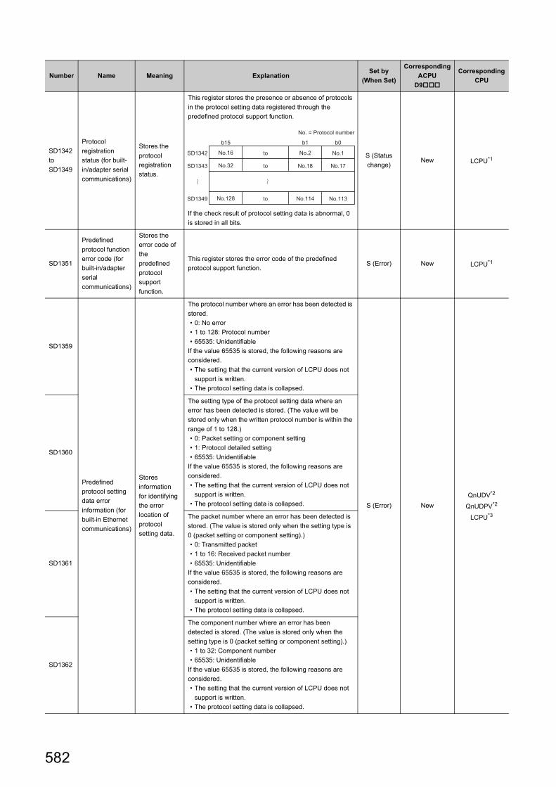
SD1342 to SD1349
Protocol registration status (for built-in/adapter serial communications)
Stores the protocol registration status.
This register stores the presence or absence of protocols in the protocol setting data registered through the predefined protocol support function.
If the check result of protocol setting data is abnormal, 0 is stored in all bits.
S (Status change)
New LCPU*1
SD1351
Predefined protocol function error code (for built-in/adapter serial communications)
Stores the error code of the predefined protocol support function.
This register stores the error code of the predefined protocol support function.
S (Error) New LCPU*1
SD1359
Predefined protocol setting data error information (for built-in Ethernet communications)
Stores information for identifying the error location of protocol setting data.
The protocol number where an error has been detected is stored.• 0: No error• 1 to 128: Protocol number• 65535: Unidentifiable
If the value 65535 is stored, the following reasons are considered.• The setting that the current version of LCPU does not
support is written.• The protocol setting data is collapsed.
S (Error) NewQnUDV*2
QnUDPV*2
LCPU*3
SD1360
The setting type of the protocol setting data where an error has been detected is stored. (The value will be stored only when the written protocol number is within the range of 1 to 128.)• 0: Packet setting or component setting• 1: Protocol detailed setting• 65535: Unidentifiable
If the value 65535 is stored, the following reasons are considered.• The setting that the current version of LCPU does not
support is written.• The protocol setting data is collapsed.
SD1361
The packet number where an error has been detected is stored. (The value is stored only when the setting type is 0 (packet setting or component setting).)• 0: Transmitted packet• 1 to 16: Received packet number• 65535: Unidentifiable
If the value 65535 is stored, the following reasons are considered.• The setting that the current version of LCPU does not
support is written.• The protocol setting data is collapsed.
SD1362
The component number where an error has been detected is stored. (The value is stored only when the setting type is 0 (packet setting or component setting).)• 1 to 32: Component number• 65535: Unidentifiable
If the value 65535 is stored, the following reasons are considered.• The setting that the current version of LCPU does not
support is written.• The protocol setting data is collapsed.
Number Name Meaning Explanation Set by (When Set)
Corresponding ACPU
D9
Corresponding CPU
SD1342
SD1343
SD1349
No.16 No.2 No.1
No.32
No.128
No.18
No.114
No.17
No.113
b15 b0b1
No. = Protocol number
to
to
to
582

APPX
A
Appendix 3 List of Special Register Areas
*1 Modules whose serial number (first five digits) is "15102" or later*2 Modules whose serial number (first five digits) is "15103" or later*3 Built-in Ethernet port LCPU whose serial number (first five digits) is "15102" or later
SD1363
Number of protocols registered (for built-in Ethernet communications
Stores the number of protocols in the protocol setting data.
This register stores the number of protocols in the protocol setting data registered through the predefined protocol support function• 0: No registration• 1 to 128: Number of protocols
S (Initial) NewQnUDV*2
QnUDPV*2
LCPU*3
SD1365 to SD1372
Protocol registration status (for built-in Ethernet communications)
Stores the protocol registration status.
This register stores the presence or absence of protocols in the protocol setting data registered through the predefined protocol support function.
If the check result of protocol setting data is abnormal, 0 is stored in all bits.
S (Initial) NewQnUDV*2
QnUDPV*2
LCPU*3
SD1381
Predefined protocol function error code (for built-in Ethernet communications)
Stores the error code of the predefined protocol support function.
This register stores the error code of the predefined protocol support function.
S (Error) NewQnUDV*2
QnUDPV*2
LCPU*3
Number Name Meaning Explanation Set by (When Set)
Corresponding ACPU
D9
Corresponding CPU
SD1365
SD1366
SD1372
No.16 No.2 No.1
No.32
No.128
No.18
No.114
No.17
No.113
b15 b0b1No. = Protocol number
to
to
to
583

(15)Fuse blown module
*1 Modules whose serial number (first five digits) is "16112" or later
(16)I/O module verification
Number Name Meaning ExplanationSet by
(When Set)
Corresponding ACPU
D9
Corresponding CPU
SD1300
Fuse blown module
Bit pattern in units of 16 points, indicating the modules whose fuses have blown0: No blown
fuse1: Blown
fuse present
• The number of an output module whose fuse has blown is stored in the following bit pattern (in units of 16 points). (If the module numbers are set by parameter, the parameter-set numbers are stored.)
• The status of the blown fuse of an output module on a remote station is also detected.
For a module whose number of output points exceeds 16 points, all bits corresponding to output module numbers within the number of output points occupied by the module (in units of 16 points) turn on.Example: When a 64-point module is mounted on the slot 0, b0 to b3 turn on when the fuse has blown.• Not cleared even if the blown fuse is replaced with a new
one. The storage value is cleared by clearing the error.
S (Error)
D9100
Qn(H)QnPH
QnPRHQnU
LCPU*1
SD1301 D9101
SD1302 D9102
SD1303 D9103
SD1304 D9104
SD1305 D9105
SD1306 D9106
SD1307 D9107
SD1308
New
SD1309 to SD1330
SD1331
Number Name Meaning ExplanationSet by
(When Set)
Corresponding ACPU
D9
Corresponding CPU
SD1400
I/O module verification error
Bit pattern, in units of 16 points, indicating the modules with verify errors.0: No error1: Error
• If the status of the I/O module changes from that obtained at power-on, the module No. is stored in the following bit pattern. (If the I/O numbers are set by parameter, the parameter-set numbers are stored.)
• The status of the I/O module on a remote station is also detected.
For a module whose number of I/O points exceeds 16 points, all bits corresponding to I/O module numbers within the number of I/O points occupied by the module (in increments of 16 points) turn on.Example: When a 64-point module is mounted on the slot 0, b0 to b3 turn on when an error is detected.• Not cleared even if the blown fuse is replaced with a new
one. This flag is cleared by error resetting operation.
S (Error)
D9116
Qn(H)QnPH
QnPRHQnU
LCPU
SD1401 D9117
SD1402 D9118
SD1403 D9119
SD1404 D9120
SD1405 D9121
SD1406 D9122
SD1407 D9123
SD1408
New
SD1409 to SD1430
SD1431
b15 b14 b13 b12 b11 b10 b9 b8 b7 b6 b5 b4 b3 b2 b1 b0
0 0 01
(YC0) 0 0 0 0 0 0 0 0 0 0 01
(Y80)SD1300
0 01
(Y1F0) 0 0 0 0 0 0 0 0 0 01
(Y1A0)SD1301 0 0
0 01
Y1FB0 0 0 0 0 0 0 0 0SD1331 0 00
1Y1F300
Indicates a fuse blown state.
b15 b14 b13 b12 b11 b10 b9 b8 b7 b6 b5 b4 b3 b2 b1 b0
0 0 0 0 0 0 0 0 0 0 0 0 0SD1400
0 0 0 0 0 0 0 0 0 0 0SD1401 0 0
0 0 0 0 0 0 0 0 0SD1431 0 000
0 0
00
00
1X Y0
1X Y190
1X Y
1FE0
Indicates an I/O module verification error
584

APPX
A
Appendix 3 List of Special Register Areas
(17)iQ Sensor Solution
Number Name Meaning ExplanationSet by
(When Set)
Corresponding ACPU
D9
Corresponding CPU
SD1435Use request (iQ Sensor Solution backup/restoration)
Requests the use of the backup/restoration function.
This register is used to acquire a right to use the backup/restoration function before its execution. A four-digit number (other than request number 0000H) shall be set.The number is determined according to the request source.1***H: when requested using a ladder programD***H: when requested from MELSOFT NavigatorE***H: when requested from GOTF***H: when requested from GX Works2• A value is cleared to "0" when the right is lost.
S (Status change)/U
NewQnUDV*1
QnUDPV*1
LCPU*2
SD1436
Right acquisition status (iQ Sensor Solution backup/restoration)
Stores the request source that has acquired a right to use the backup/restoration function.
This register stores the request source that has acquired a right to use the backup/restoration function.• A value is cleared to "0" when the right is lost.
S (Status change)
NewQnUDV*1
QnUDPV*1
LCPU*2
SD1437
Target module/execution unit setting (iQ Sensor Solution backup/restoration)
Sets the target module and execution unit for backup/restoration.
This register is used to set the target module and execution unit for backup/restoration.Lower 8 bits (target module)1H: AnyWireASLINK2H: CC-Link3H: Ethernet4H: CC-Link IE Field NetworkUpper 8 bits (execution unit)[AnyWireASLINK]1H: Module2H: ID[CC-Link, CC-Link IE Field Network]1H: Module2H: Station3H: Station sub-ID[Ethernet]1H: Module2H: IP address
U NewQnUDV*1
QnUDPV*1
LCPU*2
SD1438
Folder number setting (iQ Sensor Solution backup/restoration)
Sets the folder number for backup/restoration.
This register is used to set a number of a folder in which backup data is to be stored or a folder that contains data for restoration.0 to 99: Folder number specificationFFFEH: Automatic specification (folder deletion supported)FFFFH (default): Automatic specification
U NewQnUDV*1
QnUDPV*1
LCPU*2
SD1439
Target module setting (iQ Sensor Solution backup/restoration)
Sets a module targeted for backup/restoration.
This register is used to set a module targeted for backup/restoration.I/O No.: Module (Enter the value obtained by dividing the start I/O number by 16.)3FFH: Built-in Ethernet
U NewQnUDV*1
QnUDPV*1
LCPU*2
SD1440
Target device 1 setting (iQ Sensor Solution backup/restoration)
Sets devices targeted for backup/restoration.
This register is used to set a device targeted for backup/restoration.[AnyWireASLINK]ID number[CC-Link, CC-Link IE Field Network]Station number[Ethernet]IP address (lower 16 bits)(Example) If the IP address is 192.168.3.40, 3 equals to 3H and 40 equals to 28H.The stored value will be 0328H, that is, 808.
U NewQnUDV*1
QnUDPV*1
LCPU*2
585

SD1441
Target device 2 setting (iQ Sensor Solution backup/restoration)
Sets devices targeted for backup/restoration.
This register is used to set a device targeted for backup/restoration.[AnyWireASLINK]0 (Not used)[CC-Link, CC-Link IE Field Network]Station sub-ID number[Ethernet]IP address (upper 16 bits)(Example) If the IP address is 192.168.3.40, 192 equals to C0H and 168 equals to A8H.The stored value will be C0A8H, that is, 49320.
U NewQnUDV*1
QnUDPV*1
LCPU*2
SD1444Operation setting (iQ Sensor Solution backup/restoration)
Sets the operation status when a backup/restoration error occurs
This register stores the operation status of the CPU module when a backup/restoration error occurs.0: Continue1: Stop
U NewQnUDV*1
QnUDPV*1
LCPU*2
SD1445
Communication timeout time (iQ Sensor Solution backup/restoration)
Specifies the communication timeout time of backup/restoration.
This register is used to specify the communication timeout time of backup/restoration in increments of 100ms.0: 60000ms (default)1 to 65535 (100ms): 100 to 6553500ms
U NewQnUDV*1
QnUDPV*1
LCPU*2
SD1446Execution status (iQ Sensor Solution backup/restoration)
Stores the backup/restoration execution status.
This register stores the backup/restoration execution status.0H: Not executed1H: In preparation2H: Being executed3H: Completed10H: Wait11H: Cancelled (no error)FEH: Cancelled (error)FFH: Error
S (Status change)
NewQnUDV*1
QnUDPV*1
LCPU*2
SD1447
Total number of target devices (iQ Sensor Solution backup/restoration)
Stores the total number of devices targeted for backup/restoration.
This register stores the total number of devices targeted for backup/restoration for each execution unit.• A value is cleared to "0" when the right is
acquired.
S (Status change)
NewQnUDV*1
QnUDPV*1
LCPU*2
SD1448
Number of normally completed devices (iQ Sensor Solution backup/restoration)
Stores the number of devices where data are backed up or restored successfully.
This register stores the number of devices, for each execution unit, where data have been backed up or restored successfully.• A value is cleared to "0" when the right is
acquired.
S (Status change)
NewQnUDV*1
QnUDPV*1
LCPU*2
SD1449
Number of devices completed with an error (iQ Sensor Solution backup/restoration)
Stores the number of devices where data are not backed up or restored successfully.
This register stores the number of devices, for each execution unit, where data have not been backed up or restored successfully.• A value is cleared to "0" when the right is
acquired.
S (Status change)
NewQnUDV*1
QnUDPV*1
LCPU*2
SD1450
Progress per device (iQ Sensor Solution backup/restoration)
Stores the progress of the backup/restoration processing per device.
This register stores the progress of the backup/restoration processing per device in percentage (0 to 100%).• A value is cleared to "0" when the right is
acquired.
S (Status change)
NewQnUDV*1
QnUDPV*1
LCPU*2
SD1451Folder number (iQ Sensor Solution backup)
Stores the number of a folder in which backup data is stored.
This register stores the number of a folder in which backup data is stored.0 to 99: Folder numberFFFFH: Backup data not stored• FFFFH is stored when when the right is
acquired.
S (Status change)
NewQnUDV*1
QnUDPV*1
LCPU*2
Number Name Meaning Explanation Set by (When Set)
Corresponding ACPU
D9
Corresponding CPU
586

APPX
A
Appendix 3 List of Special Register Areas
SD1452
Error cause in a module (iQ Sensor Solution backup/restoration)
Stores the cause of the backup/restoration error detected in a module.
This register stores the cause of the backup/restoration error detected in a module.• When errors are detected in multiple devices,
the error detected first is stored.• A value is cleared to "0" when the right is
acquired.For details on the cause of the error that is stored, refer to the following.Page 423, Appendix 1.11 User's manual of the module that is targeted for data backup/restoration
S (Error/Status
change)New
QnUDV*1
QnUDPV*1
LCPU*2
SD1453
Error cause in a device (iQ Sensor Solution backup/restoration)
Stores the cause of the backup/restoration error detected in a device.
This register stores the cause of the backup/restoration error detected in a device.• When errors are detected in multiple devices,
the error detected first is stored.• A value is cleared to "0" when the right is
acquired.For details on the cause of the error that is stored, refer to the following.iQ Sensor Solution Reference Manual
S (Error/Status
change)New
QnUDV*1
QnUDPV*1
LCPU*2
SD1454
Error module/execution unit information (iQ Sensor Solution backup/restoration)
Stores the module and execution unit information when a backup/restoration error occurs.
This register stores the module and execution unit information when a backup/restoration error occurs.Lower 8 bits (target module)1H: AnyWireASLINK2H: CC-Link3H: Ethernet4H: CC-Link IE Field NetworkUpper 8 bits (execution unit)1H: AnyWireASLINK2H: CC-Link3H: Ethernet4H: CC-Link IE Field Network[AnyWireASLINK]1H: Module2H: ID[CC-Link, CC-Link IE Field Network]1H: Module2H: Station3H: Station sub-ID[Ethernet]1H: Module2H: IP address• A value is cleared to "0" when the right is
acquired.
S (Error/Status
change)New
QnUDV*1
QnUDPV*1
LCPU*2
SD1455
Error folder number information (iQ Sensor Solution backup/restoration)
Stores the target folder number when a backup/restoration error occurs.
This register stores the target folder number (0 to 99) when a backup/restoration error occurs.• When the folder number cannot be identified,
FFFFH is stored.• A value is cleared to "0" when the right is
acquired.
S (Error/Status
change)New
QnUDV*1
QnUDPV*1
LCPU*2
SD1456
Error module information (iQ Sensor Solution backup/restoration)
Stores the information of a module where a backup/restoration error is detected first.
This register stores the information of a module where a backup/restoration error occurs.I/O No.: Module (Enter the value obtained by dividing the start I/O number by 16.)3FFH: Built-in Ethernet• When errors are detected in multiple devices,
the information of a module where the error detected first is stored.
• A value is cleared to "0" when the right is acquired.
S (Error/Status
change)New
QnUDV*1
QnUDPV*1
LCPU*2
Number Name Meaning Explanation Set by (When Set)
Corresponding ACPU
D9
Corresponding CPU
587

*1 The QnUDVCPU whose serial number (first five digits) is "17012" or later supports the backup/restoration function for AnyWireASLINK and CC-Link.The QnUDVCPU whose serial number (first five digits) is "17052" or later supports the backup/restoration function for CC-Link IE Field Network.The QnUDVCPU whose serial number (first five digits) is "18072" or later supports the backup/restoration function for built-in Ethernet.
*2 Built-in Ethernet port LCPU whose serial number (first five digits) is "14112" or later
SD1457
Error device Information (device 1) (iQ Sensor Solution backup/restoration)
Stores the information of a device where a backup/restoration error is detected first.
This register stores the information of a device (device 1) where a backup/restoration error occurs.[AnyWireASLINK]ID number[CC-Link, CC-Link IE Field Network]Station number[Ethernet]IP address (lower 16 bits)(Example) If the IP address is 192.168.3.40, 3 equals to 3H and 40 equals to 28H.The stored value will be 0328H, that is, 808.• When errors are detected in multiple devices,
the information of a device (device 1) where the error detected first is stored.
• A value is cleared to "0" when the right is acquired. S
(Error/Status change)
NewQnUDV*1
QnUDPV*1
LCPU*2
SD1458
Error device Information (device 2) (iQ Sensor Solution backup/restoration)
This register stores the target-device (device 2) information for which a backup/restoration error occurs.[AnyWireASLINK]0 (Not used)[CC-Link, CC-Link IE Field Network]Station sub-ID number[Ethernet]IP address (upper 16 bits)(Example) If the IP address is 192.168.3.40, 192 equals to C0H and 168 equals to A8H.The stored value will be C0A8H, that is, 49320.• When errors are detected in multiple devices,
the information of a device (device 2) where the error detected first is stored.
• A value is cleared to "0" when the right is acquired.
Number Name Meaning Explanation Set by (When Set)
Corresponding ACPU
D9
Corresponding CPU
588

APPX
A
Appendix 3 List of Special Register Areas
(18)Process control instruction
(19)Redundant system (host system CPU information*1)The special register (SD1510 to SD1599) is valid only for redundant systems. All bits are set to "0" for stand-alone systems.
Number Name Meaning ExplanationSet by
(When Set)
Corresponding ACPU
D9
Corresponding CPU
SD1500, SD1501
Basic periodBasic period time
Set the basic period (1 second units) use for the process control instruction using floating point data.
U NewQnPH
QnPRHQnUDPV
SD1502
Process control instruction detail error code
Process control instruction detail error code
This register indicates the details of an error occurred by executing a process control instruction.
S (Error) NewQnPH
QnPRHQnUDPV
SD1503
Process control instruction generated error location
Process control instruction generated error location
Shows the error process block that occurred in the process control instruction.
S (Error) NewQnPH
QnPRHQnUDPV
SD1506, SD1507
Dummy device Dummy deviceUsed to specify dummy devices by a process control instruction.
U NewQnPH
QnPRHQnUDPV
SD1508
Function availability selection for process control instruction
b0Bumpless function availability setting for the S.PIDP instruction0: Enabled1: Disabled(Default: 0)
This register stores whether to enable functions for process control instructions.
U NewQnPH
QnPRHQnUDPV
Number Name Meaning ExplanationSet by
(When Set)
Corresponding ACPU
D9
Corresponding CPU
SD1585Redundant system LED status
4 LED states• BACKUP• CONTROL• SYSTEM A• SYSTEM B
The LED status of BACKUP, CONTROL, SYSTEM A, or SYSTEM B is stored in the following format:
S (Status change)
New QnPRH
SD1588Reason(s) for system switching
Reason(s) for system switching that occurred in host station
The reason(s) for system switching on the host system is stored. The following values are stored corresponding to the methods for system switching: This register is initialized with zero (0) stored when the system is powered on from off or is reset.0: Initial value (control system has never been
switched)1: Power off, Reset, H/W failure, WDT error2: CPU stop error (except WDT)3: System switching request from network module16: Control system switching instruction17: System switching request from a programming tool
S (when condition occurs)
QnPRH
SD1501 SD1500Floating points data =
b0b1b2b15 b1400SD1508 0 1/0
Bumpless function availability for the S.PIDP instruction
to
b0b2b3b4b5b6b7b8b10b9b150 0
SYSTEM B
SYSTEM ACONTROL
BACKUP
toto
0: Off1: On2: Flicker
0: Off1: On2: Flicker
0: Off1: On
0: Off1: On (red) 2:3: On(green)4: Flicker(green)
Flicker(red) 5: On (orange)6: Flicker(orange)
589

*1 The information of the host CPU module is stored.
SD1589
Reason(s) for system switching failure conditions
Reason(s) for system switching failure No
• When a system switching has failed, a value corresponding to the system switching failure cause is stored.
0: System switching complete (default)1: Tracking cable is not connected, tracking cable
failure, or internal circuit failure2: H/W failure, power-off, reset, watchdog timer error
on the standby system3: H/W failure, power-off, reset, WDT error on the
control system4: Preparing tracking communication5: Communication timeout6: Stop error on the standby system (except for
watchdog timer error)7: Operation differs between both systems (detected
only in the back up mode)8: During memory copy from control system to standby
system9: Performing program online change10: Detecting a failure of network module on the standby
system11: System is being switched
• The value is reset to "0" when host system is powered on.
• Zero is stored in this register upon completion of system switching.
S (when system is switched)
QnPRH
SD1590
Network module head address, which requested system switching
Network module head address, which requested system switching
• When system switching is requested from a network module in the host system, the bit corresponding to the module that received the request turns on.
b1 to b11: Slot No.1 to slot No.11 (Slot No.0 (b0) is invalid because the CPU module occupies two slots.)• The system turns off the bit after the error is removed by
a user.• For the number for modules where system switching is
requested from a network module in other system, refer to SD1690.
S (Error/Status
change)New QnPRH
SD1595Memory copy target I/O number
Memory copy target I/O number
• Before SM1595 is turned from off to on, the I/O No. of the memory copy destination (Standby system CPU module: 3D1H) is stored.
U New QnPRH
SD1596Memory copy status
Memory copy status
• The execution result of the memory copy function is stored.
0: Memory copy is complete4241H: Standby system power supply off4242H: Tracking cable is disconnected or is damaged4247H: Memory copy is being executed4248H: Unsupported memory copy destination I/O number
S (Status change)
New QnPRH
Number Name Meaning Explanation Set by (When Set)
Corresponding ACPU
D9
Corresponding CPU
b11 b1b0
590

APPX
A
Appendix 3 List of Special Register Areas
(20)Redundant system (other system CPU information*1)The special register (SD1600 to SD1650) is valid when the redundant system is in backup mode and is invalid in separate mode. The special register (SD1651 to SD1690) is valid when the redundant system is in backup mode or in separate mode. All bits in SD1600 to SD1690 are set to "0" for stand-alone systems.
Number Name Meaning ExplanationSet by
(When Set)
Corresponding host CPU SD*2
Corresponding CPU
SD1600System error information
System error information
• When an error is detected by the redundant system error check, the bit corresponding to the error turns on. The bit turns off when the error is cleared.
• If any of b0, b1, b2 and b15 is on, the other bits are off.• In the debug mode, b0, b1, b2 and b15 are all off.
S (Every END
processing) QnPRH
SD1601System switching results
System switching results
Reason(s) for system switching is stored.• When a system is switched, the reason for system
switching is stored in SD1601 of both systems.• This register is initialized with zero (0) stored when the
system is powered on from off or is reset.• The following shows the values stored in this register.
0: Initial value (control system has never been switched)
1: Power-off, reset, H/W failure, or watchdog timer error *1
2: Stop error (except for watchdog timer error)3: System switching request from network module16: Control system switching instruction17: System switching request from a programming tool
*1 When the system is switched upon the power-off or reset of the control system, "1" is not stored in SD1601 of the new standby system.
S (when system is switched)
QnPRH
SD1602
System switching dedicated instruction parameter
System switching dedicated instruction parameter
• When a system is switched by the SP.CONTSW instruction, the argument of the instruction is stored. (The argument is stored in SD1602 of both systems at the system switching.)
• SD1602 is only valid when "16" is stored in SD1601.• SD1602 is updated only when a system is switched by the
control system switching instruction.
S (when system is switched)
QnPRH
SD1610Other system diagnostic error
Diagnostic error code
• The code of the error occurred in the other system is stored.
• The value in SD0 of the CPU module on the other system is reflected.
S (Every END
processing)SD0 QnPRH
SD1611 to SD1613
Other system diagnostic error occurrence time
Diagnostic error occurrence time
• The date and time of the diagnostics error occurred in the other system are stored.
• Data format is the same as SD1 to SD3.• The values in SD1 to SD03 of the CPU module on the
other system are reflected.
S (Every END
processing)SD1 to SD3 QnPRH
b1 b0b15 b2Fixed to 0SD1600
Each bit0: OFF1: ON
Tracking cable is notconnected or damagedPower-OFF, reset,watchdog timer error orhardware failure occurredin other systemOther system stop error(except watchdog timererror)Bit turns on when failing toconnect with other system.The following causes areshown below: Tracking H/W failure Host system WDT error Cannot recognize other system therefore causing error
591

SD1614
Other system error information category
Error information category code
• The error information category codes for individual information and common information of the error occurred in the other system are stored.
• Data format is the same as SD4.• The value in SD4 of the CPU module on the other system
is reflected.
S (Every END
processing)SD4 QnPRH
SD1615 to SD1625
Other system error common information
Error common information
• Stores the common information corresponding to the error code stored in this system CPU.
• Data composition is the same as SD5 to SD15.• The values in SD5 to SD15 of the CPU module on the
other system are reflected.
S (Every END
processing)SD5 to SD15 QnPRH
SD1626 to SD1636
Other system error individual information
Error individual information
• The individual information of the error occurred in the other system is stored.
• Data composition is the same as SD16 to SD26.• The values in SD16 to SD26 of the CPU module on the
other system are reflected.
S (Every END
processing)SD16 to SD26 QnPRH
SD1649
Standby system error cancel command
Error code of the error to be cleared
• The code of the error to be cleared by the standby system error cancel command is stored.
• The standby system error is cleared by turning SM1649 from off to on after storing the error code of the error to clear.
• The least significant digit (ones place) of the error code in this register is ignored. (The errors corresponding to error codes 4100 to 4109 are cleared by storing 4100 in this register.)
S (Every END
processing) QnPRH
SD1650Other system operating information
Other system operating information
The operating information of the CPU module on the other system is stored in the following bit pattern.When communications with other systems are disabled or the system is in the debug mode, "00FFH" is stored.
Note:Communications are disabled in the following states.• The other system is powered off or is being reset.• A hardware failure has occurred on the host or the other
system.• A watchdog timer error has occurred on the host or the
other system.• Tracking cable is not connected. Tracking cable is broken
or failed.
S (Every END
processing) QnPRH
Number Name Meaning ExplanationSet by
(When Set)
Corresponding host CPU SD*2
Corresponding CPU
b15 b8 b4b7 b3 b00SD1650
0:No error1:Continue error2:Stop errorF:Communication with
other system disabled
0:RUN2:STOP3:PAUSEF:Communication with
other system disabled
1 Communication with other system disabled, debug mode
1
1
to to to
592

APPX
A
Appendix 3 List of Special Register Areas
*1 Diagnostic information of the CPU module in the other system is stored.*2 Special register areas (SD) for the CPU module in the host system
SD1690
Network module head address, which requested system switching on host (control) system
Network module head address, which requested system switching on host (control) system
• When system switching is requested from a network module in the other system, the bit corresponding to the module that received the request turns on.
b1 to b11: Slot No.1 to slot No.11 (Slot No.0 (b0) is invalid because the CPU module occupies two slots.)• The system turns off the bit after the error in the
corresponding module is removed by a user.• To find the number for the module where system switching
is requested from a network module in the host system, refer to SD1590.
S (Every END
processing) QnPRH
Number Name Meaning ExplanationSet by
(When Set)
Corresponding host CPU SD*2
Corresponding CPU
b11 b1b0
593

(21)E-mail send/receive function
*1 Built-in Ethernet port LCPU whose serial number (first five digits) is "16112" or later
(22)Redundant system (tracking information)The special register (SD1700 to SD1779) is valid only for redundant systems. All bits are set to "0" for stand-alone systems.
Number Name Meaning ExplanationSet by
(When Set)
Corresponding ACPU
D9
Corresponding CPU
SD1659Language information
Language information
This register stores language information of e-mail.• 0 or other than below: English/Japanese (default)• 2: Chinese (simplified Chinese characters)
U New LCPU*1
SD1660MC protocol command error code
Error code when an MC protocol command error is detected
• This register stores the error code when an MC protocol command error is detected. The error code is also stored when execution of MC protocol command is disabled in parameter.
• A value, 0, is set at execution of the e-mail receive instruction.
S (Error) New LCPU*1
Number Name Meaning ExplanationSet by
(When Set)
Corresponding ACPU
D9
Corresponding CPU
SD1700Tracking error detection count
Tracking error detection count
• A value in this register is incremented by one upon tracking error.
• The counter starts the routine: counts up from 0 to 32767, then counts down to -32767 and then again counts up to 0.
S (Error) New QnPRH
SD1710
Waiting time for online program change (standby system)
Waiting time for online program change (standby system)
• This register stores the waiting time required for starting the online program change in the standby system after completion of that in the control system. The value is specified in units of seconds.
• If online program change is not requested even after it is completed in the control system, the CPU modules in both of the system determine that it is a failure of an online program change for redundancy. In this case, both system CPU modules resume the consistency check for the systems that have been on hold during the online program change. Also, the control system is set to accept another request of online program change for redundancy.
• When both systems are powered on, 90 seconds are set to SD1710 as the default value.
• Set the value within the range 90 to 3600 seconds. When the setting is 0 to 89 seconds, it is regarded as 90 seconds for operation. If the setting is outside the allowed range, it is regarded other than 0 to 3600 seconds for operation.
• The waiting time for a start of online program change to the standby system CPU module is checked according to the SD1710 setting during online change of multiple blocks and online change of batch of files for redundancy.
S (Initial)/U New QnPRH
594

APPX
A
Appendix 3 List of Special Register Areas
(23)Redundant power supply module informationThe special register (SD1780 to SD1789) is valid only for redundant power supply systems.
Number Name Meaning ExplanationSet by
(When Set)
Corresponding ACPU
D9
Corresponding CPU
SD1780Power supply off detection status
Power supply off detection status
• This register stores the status of the redundant power supply module (Q63RP, Q64RPN, or Q64RP) with input power off, in the following bit pattern.
• In a multiple CPU system, the status is stored only to CPU module No.1.
S (Every END
processing)New
Qn(H)*3
QnPH*3
QnPRHQnU*4
SD1781
Power supply failure detection status
Power supply failure detection status
• This register stores the failure detection status of the redundant power supply module (Q63RP, Q64RPN, or Q64RP) in the following bit pattern. (After a failure is detected, the bit corresponding to the failed module is set to "0" upon powering off the module.)
• In a multiple CPU system, the status is stored only to CPU module No.1.
S (Every END
processing)New
Qn(H)*3
QnPH*3
QnPRH
QnU*4
SD1782
Momentary power failure detection counter for power supply
1*1
Momentary power failure detection count for power supply 1
• This register counts the number of times of momentary power failure of the power supply 1/2.
• This register monitors the status of the power supply 1/2 mounted on the redundant power main base unit (Q38RB) and counts the number of momentary power failures. The status of the power supply 1/2 mounted on the extension base unit for redundant power supply system and the redundant type extension base unit is not monitored.
• When the CPU module starts, the counter of the power supply 1/ 2 is cleared to 0.
• If the input power to one of the redundant power supply modules is turned off, the corresponding counter is cleared to "0".
• The counter is incremented by one upon momentary power failure on the power supply 1 or 2. (The counter repeats increment and decrement of the value; 0 32767 -32768 0. (The value is displayed within the range of 0 to 65535 in the system monitor screen of programming tool.))
• When the main base unit is not the redundant power main base unit (Q38RB), "0" is stored.
• In a multiple CPU system, the status is stored only to CPU module No.1.
S (Every END
processing)New
Qn(H)*3
QnPH*3
QnPRH
QnU*4
SD1783
Momentary power failure detection counter for power supply
2*2
Momentary power failure detection count for power supply 2
b0b7b8b15
SD1780
b9 b1
:
:
toto
toto
Input power OFF detection status of
power supply 2 Each bit0: Input power ON status/
No redundant power supply module
1: Input power OFF status
Input power OFF detection status of
power supply 11 1
Main base unit1st extension base
7th extension base
Main base unit1st extension base
7th extension base
b0b7b8 b1b9b15
SD1781
:
:
totototo
Failure detection status of power
supply 1
Failure detection status of power
supply 2 1 1
Each bit0: Redundant power
supply module failure not detected/No redundant power supply module
1: Redundant power supply module failure detected (Detectable for redundant power supply module only)
Main base unit1st extension base
7th extension base
Main base unit1st extension base
7th extension base
595

*1 The "power supply 1" indicates the redundant power supply module mounted on the POWER 1 slot of the redundant base unit (Q38RB/68RB/Q65WRB).
*2 The "power supply 2" indicates the redundant power supply module mounted on the POWER 2 slot of the redundant base unit (Q38RB/68RB/Q65WRB).
*3 Modules whose serial number (first five digits) is "07032" or later. In a multiple CPU system, the serial number (first five digits) of all the CPU modules must be "07032" or later.
*4 Modules whose serial number (first five digits) is "10042" or later
(24)CC-Link IE Field Network Basic function
Number Name Meaning ExplanationSet by
(When Set)
Corresponding ACPU
D9
Corresponding CPU
SD1700 to SD1703
Cyclic transmission status of each station
Cyclic transmission status of each station
The cyclic transmission status of each station is stored in the following bit pattern. (Off: Not performed, On: Being performed)■QnUDV, QnUDPV
■LCPU
The numbers in the figure indicate station numbers.(Condition)• Only the bit of the start station number turns on.• The status is not stored for the reserved stations and the
station numbers after the maximum station number.Use this register as an interlock for cyclic transmission. For details on the interlock program, refer to the following.CC-Link IE Field Network Basic Reference Manual
S (Every END
processing)New
QnUDV*1
QnUDPV*1
LCPU*2
SD1704 to SD1707
Data link status of each station
Data link status of each station
The data link status of each station is stored in the following bit pattern. (Off: Normally operating station, On: Faulty station)■QnUDV, QnUDPV
■LCPU
The numbers in the figure indicate station numbers.(Condition)• Only the bit of the start station number turns on.• The status is not stored for the reserved stations and the
station numbers after the maximum station number.This register can be used to monitor errors in slave stations, connected cables, and connected hubs.
S (Every END
processing)New
QnUDV*1
QnUDPV*1
LCPU*2
SD1716Total number of connected stations
Total number of connected stations
The total number of connected stations set in parameter is stored.
S (Initial) NewQnUDV*1
QnUDPV*1
LCPU*2
16 15 14 13 12 11 10 9 8 7 6 5 4 3 2 1
32 31 30 29 28 27 26 25 24 23 22 21 20 19 18 17
48 47 46 45 44 43 42 41 40 39 38 37 36 35 34 33
64 63 62 61 60 59 58 57 56 55 54 53 52 51 50 49
b15 b14 b13 b12 b11 b10 b9 b8 b7 b6 b5 b4 b3 b2 b1 b0SD1700
SD1701
SD1702
SD1703
16 15 14 13 12 11 10 9 8 7 6 5 4 3 2 1b15 b14 b13 b12 b11 b10 b9 b8 b7 b6 b5 b4 b3 b2 b1 b0
SD1700
16 15 14 13 12 11 10 9 8 7 6 5 4 3 2 1
32 31 30 29 28 27 26 25 24 23 22 21 20 19 18 17
48 47 46 45 44 43 42 41 40 39 38 37 36 35 34 33
64 63 62 61 60 59 58 57 56 55 54 53 52 51 50 49
b15 b14 b13 b12 b11 b10 b9 b8 b7 b6 b5 b4 b3 b2 b1 b0SD1704
SD1705
SD1706
SD1707
16 15 14 13 12 11 10 9 8 7 6 5 4 3 2 1b15 b14 b13 b12 b11 b10 b9 b8 b7 b6 b5 b4 b3 b2 b1 b0
SD1704
596

APPX
A
Appendix 3 List of Special Register Areas
SD1718 to SD1721
Reserved station specification status of each station
Reserved station specification status of each station
The reserved station specification status is stored in the following bit pattern. (Off: Other than the reserved station, On: Reserved station)■QnUDV, QnUDPV
■LCPU
The numbers in the figure indicate station numbers.(Condition)• Only the bit of the start station number turns on.• The status is not stored for the station numbers after the
maximum station number.
S (Initial) NewQnUDV*1
QnUDPV*1
LCPU*2
SD1722
Link scan information
Maximum link scan of group No.1
The maximum link scan time value during cyclic transmission is stored. (Unit: ms)
S (Status change)
NewQnUDV*1
QnUDPV*1
LCPU*2
SD1723Minimum link scan of group No.1
The minimum link scan time value during cyclic transmission is stored. (Unit: ms)
S (Status change)
NewQnUDV*1
QnUDPV*1
LCPU*2
SD1724Current link scan of group No.1
The current link scan time value during cyclic transmission is stored. (Unit: ms)
S (Status change)
NewQnUDV*1
QnUDPV*1
LCPU*2
SD1726Maximum link scan of group No.2
The maximum link scan time value during cyclic transmission is stored. (Unit: ms)
S (Status change)
NewQnUDV*3
QnUDPV*3
SD1727Minimum link scan of group No.2
The minimum link scan time value during cyclic transmission is stored. (Unit: ms)
S (Status change)
NewQnUDV*3
QnUDPV*3
SD1728Current link scan of group No.2
The current link scan time value during cyclic transmission is stored. (Unit: ms)
S (Status change)
NewQnUDV*3
QnUDPV*3
SD1730Maximum link scan of group No.3
The maximum link scan time value during cyclic transmission is stored. (Unit: ms)
S (Status change)
NewQnUDV*3
QnUDPV*3
SD1731Minimum link scan of group No.3
The minimum link scan time value during cyclic transmission is stored. (Unit: ms)
S (Status change)
NewQnUDV*3
QnUDPV*3
SD1732Current link scan of group No.3
The current link scan time value during cyclic transmission is stored. (Unit: ms)
S (Status change)
NewQnUDV*3
QnUDPV*3
SD1734Maximum link scan of group No.4
The maximum link scan time value during cyclic transmission is stored. (Unit: ms)
S (Status change)
NewQnUDV*3
QnUDPV*3
SD1735Minimum link scan of group No.4
The minimum link scan time value during cyclic transmission is stored. (Unit: ms)
S (Status change)
NewQnUDV*3
QnUDPV*3
SD1736Current link scan of group No.4
The current link scan time value during cyclic transmission is stored. (Unit: ms)
S (Status change)
NewQnUDV*3
QnUDPV*3
Number Name Meaning Explanation Set by (When Set)
Corresponding ACPU
D9
Corresponding CPU
16 15 14 13 12 11 10 9 8 7 6 5 4 3 2 1
32 31 30 29 28 27 26 25 24 23 22 21 20 19 18 17
48 47 46 45 44 43 42 41 40 39 38 37 36 35 34 33
64 63 62 61 60 59 58 57 56 55 54 53 52 51 50 49
b15 b14 b13 b12 b11 b10 b9 b8 b7 b6 b5 b4 b3 b2 b1 b0SD1718
SD1719
SD1720
SD1721
16 15 14 13 12 11 10 9 8 7 6 5 4 3 2 1b15 b14 b13 b12 b11 b10 b9 b8 b7 b6 b5 b4 b3 b2 b1 b0
SD1718
597

SD1741Diagnostic request information
Diagnostic request information
The diagnostic information display target slave station is specified.■QnUDV, QnUDPVRange: 1 to 64• For the High-speed Universal model QCPU and Universal
model Process CPU whose serial number (first five digits) is earlier than "19042", the range is 1 to 16.
■LCPURange: 1 to 16• For the Built-in Ethernet port LCPU whose serial number
(first five digits) is earlier than "19042", the range is 1 to 8.
U NewQnUDV*1
QnUDPV*1
LCPU*2
SD1742Diagnostic information status flag
Diagnostic information status flag
• After the END instruction in the scan where SM1741 turns on is executed, the status (valid or invalid) of diagnostic information (Diagnostic information 1, Diagnostic information 2) of the slave station specified in SD1741 is stored.
• If the station number of the slave station specified in SD1741 is the start station number of the occupied stations, 1 is stored in Diagnostic information 1 (b0 to b7) and Diagnostic information 2 (b8 to b15). (If the station is a reserved station, 0 is stored in Diagnostic information 2 (b8 to b15).)
• If parameters have not been set to the slave station specified in SD1741 or the station number of the slave station specified in SD1741 is not the start station number of the occupied stations, 0 is stored in Diagnostic information 0 (b0 to b7) and Diagnostic information 2 (b8 to b15).
b0 to b7: Diagnostic information 1 (0: Invalid, 1: Valid)b8 to b15: Diagnostic information 2 (0: Invalid, 1: Valid)• When b0 to b7 are 1 (valid), the number of occupied
stations, group number, IP address, the accumulated number of timeouts, and the accumulated number of disconnection detections are stored in SD1743 to SD1754.
• When b0 to b7 are 0 (invalid), 0 is stored in SD1743 to SD1754.
• When b8 to b15 are 1 (valid), the manufacturer code, model code, device version, module information, error code, and detailed module information are stored in SD1758 to SD1767.
• When b8 to b15 are 0 (invalid), 0 is stored in SD1758 to SD1767.
S (Status change)
NewQnUDV*1
QnUDPV*1
LCPU*2
Number Name Meaning Explanation Set by (When Set)
Corresponding ACPU
D9
Corresponding CPU
b15 b7 b0b8… …
598

APPX
A
Appendix 3 List of Special Register Areas
*1 Modules whose serial number (first five digits) is "18112" or later*2 Built-in Ethernet port LCPU whose serial number (first five digits) is "18112" or later*3 Modules whose serial number (first five digits) is "19042" or later*4 If the specified slave station is being disconnected, information immediately before the disconnection is stored.
SD1743
Diagnostic information
1*4
Number of occupied stations
After the END instruction in the scan where SM1741 turns on is executed, the number of occupied stations of the slave station specified in SD1741 is stored.
S (Status change)
NewQnUDV*1
QnUDPV*1
LCPU*2
SD1744 Group No.After the END instruction in the scan where SM1741 turns on is executed, the group number of the slave station specified in SD1741 is stored.
SD1745IP address (lower digits)
• After the END instruction in the scan where SM1741 turns on is executed, the IP address of the slave station specified in SD1741 is stored.
• When the IP address has not been set in parameter, 0 is stored.
1 to 4: First to fourth bytes
SD1746IP address (upper digits)
SD1753Accumulated number of timeouts
• After the END instruction in the scan where SM1741 turns on is executed, the accumulated number of timeouts occurred in the slave station specified in SD1741 is stored.
0: No timeouts1 to 65535: Number of timeouts (When the count exceeds 65535, counting is continued from 1 again.)
SD1754
Accumulated number of disconnection detections
• After the END instruction in the scan where SM1741 turns on is executed, the accumulated number of disconnections detected in the slave station specified in SD1741 is stored.
0: No disconnections1 to 65535: Number of disconnection detections (When the count exceeds 65535, counting is continued from 1 again.)
SD1758
Diagnostic information
2*4
Manufacturer code
After the END instruction in the scan where SM1741 turns on is executed, the manufacturer code of the slave station specified in SD1741 is stored.
S (Status change)
NewQnUDV*1
QnUDPV*1
LCPU*2
SD1760Model code (lower) After the END instruction in the scan where SM1741 turns on
is executed, the model code of the slave station specified in SD1741 is stored.SD1761
Model code (upper)
SD1762Device version
After the END instruction in the scan where SM1741 turns on is executed, the device version of the slave station specified in SD1741 is stored.
SD1764Module information
After the END instruction in the scan where SM1741 turns on is executed, the module information of the slave station specified in SD1741 is stored.
SD1765 Error codeAfter the END instruction in the scan where SM1741 turns on is executed, the error code of the slave station specified in SD1741 is stored.
SD1766
Detailed module information (lower) After the END instruction in the scan where SM1741 turns on
is executed, the detailed module information of the slave station specified in SD1741 is stored.
SD1767
Detailed module information (upper)
Number Name Meaning Explanation Set by (When Set)
Corresponding ACPU
D9
Corresponding CPU
3
1
4
2
b15 ... b8 b7 ... b0
SD1745SD1746
599

(25)CPU module data backup/restoration function
*1 Since the registers cannot be monitored while the automatic restoration function is executed, check the operating status of an automatic restoration with LED on the front side of the CPU module.
*2 Modules whose serial number (first five digits) is "17103" or later*3 Modules whose serial number (first five digits) is "18052" or later
(26)Built-in I/O function
Number Name Meaning ExplanationSet by
(When Set)
Corresponding ACPU
M9
Corresponding CPU
SD1925Number of backup/restoration uncompleted files
Stores the number of files which a backup or restoration is
uncompleted.*1
The number of files which a backup or restoration is uncompleted is stored.Total number of files is stored at start, and reduced one each time one file is backed up or restored. "0" is stored when a backup or restoration is completed.
S (Status change)
NewQnUDV*2
QnUDPV*2
SD1926Backup/restoration progression status
Stores the progression status of a backup or
restoration.*1
The progression status of a backup or restoration is stored in percentage. (0 to 100%) "0" is stored at start of a backup or restoration.
S (Status change)
NewQnUDV*2
QnUDPV*2
SD1928
Upper limit value setting for the number of backup data
Upper limit value for the number of backup data is set
Set the upper limit value (1 to 100) for the number of backup data with this register. This register set the value of SD923 at the timing when the CPU module is powered off and on or is reset.Bit5 of SD910 is off: 0Bit5 of SD910 is on: 1 to 100
S (Status change)/U
NewQnUDV*3
QnUDPV*3
Number Name Meaning Explanation Set by (When Set)
Corresponding ACPUD9
Corresponding CPU
SD1830 to SD1833
Functions selected for input signals
Functions selected for input signals
This register stores values indicating functions assigned for input signals. Each signal has 4-bit data.
Values are stored according to functions as follows:• 0: General-purpose input function• 1: Interrupt input function• 2: Pulse catch function• 3: Positioning function• 4: High-speed counter function
S (Every END
processing)New LCPU
SD1834, SD1835
Functions selected for output signals
Functions selected for output signals
This register stores values indicating functions assigned for output signals. Each signal has 4-bit data.
Values are stored according to functions as follows:• 0: General-purpose output function• 3: Positioning function• 4: High-speed counter function
S (Every END
processing)New LCPU
b12b15
X3
b8b11
X2
b4b7
X1
b0b3
X0
SD1830
b12b15
X7
b8b11
X6
b4b7
X5
b0b3
X4
SD1831
b12b15
XB
b8b11
XA
b4b7
X9
b0b3
X8
SD1832
b12b15
XF
b8b11
XE
b4b7
XD
b0b3
XC
SD1833
b12b15
Y3
b8b11
Y2
b4b7
Y1
b0b3
Y0
SD1834
b12b15
Y7
b8b11
Y6
b4b7
Y5
b0b3
Y4
SD1835
600

APPX
A
Appendix 3 List of Special Register Areas
SD1836
Operating status of positioning and high-speed counter functions
Operating status of positioning and high-speed counter functions
This register stores the operating status of the positioning function and high-speed counter function.
S (Every END
processing)New LCPU
SD1840, SD1841
Axis 1 current feed value
Current feed value
This register stores the current position value when the position where OPR control is completed is set as a base point."0" is stored at power-on or reset of the CPU module.An OP address is stored at the completion of machine OPR control.This register is cleared to "0" when speed control in speed/position switching control is started.• When the current feed value is changed, the value
after current value change is stored.• The current position read from a servo amplifier is
stored at the completion of absolute position
restoration.*1*2
*1 Range: -2147483648 to 2147483647 pulses*2 Since the internal update cycle of the storage
value is 1ms, the information of the current feed value may be older than the actual command position by 1ms at maximum depending on the refresh timing at END processing.
S (Every END
processing)New LCPU
SD1842, SD1843
Axis 1 current speed
Current speed
This register stores the current speed. (Fractions are not stored. If the current speed is slower than 1
pulse/s, "0" may be displayed.)*1*2
*1 Range: 0 to 200000 pulses*2 Since the internal update cycle of the storage
value is 1ms, the information of the current speed value may be older than the actual command position by 1ms at maximum depending on the refresh timing at END processing.
S (Every END
processing)New LCPU
SD1844Axis 1 axis operation status
Axis operation status
This register stores the axis operating status.• -1: Error occurring• 0: Standing by• 1: Stopped• 2: In JOG operation• 3: In OPR• 4: In position control• 5: In speed-position control (speed) (speed control
in speed/position switching control)• 6: In speed-position control (position) (position
control in speed/position switching control)• 7: Decelerating (axis stop ON)• 8: Decelerating (JOG start OFF)• 9: In high-speed OPR• 10: In speed control• 11: Analyzing
S (Every END
processing)New LCPU
Number Name Meaning ExplanationSet by
(When Set)Corresponding ACPUD9
Corresponding CPU
b0b1b2b4 b3b15
0 0/1 0/1 0/1 0/1
to
Positioning function Axis 10: Not used1: UsedPositioning function Axis 20: Not used1: UsedHigh-speed counter function CH10: Not used1: UsedHigh-speed counter function CH20: Not used1: UsedFixed to 0.
601

SD1845 Axis 1 error code Error code
• This register stores the error code of the present axis error.
• If another error occurs while an axis error occurs, the latest error code is not stored.
• This register is cleared to "0" by turning on SM1850.
S (Every END
processing)New LCPU
SD1846Axis 1 warning code
Warning code
• This register stores the warning code of the present axis warning.
• If another axis warning occurs, the latest warning code is written to this register.
• This register is cleared to "0" by turning on SM1850.
S (Every END
processing)New LCPU
SD1847Axis 1 external I/O signal
External I/O signals
• This register stores the on/off status of external I/O signals.
• When an OPR method with the OPR retry function (Near-point dog method, Count 1, Count 2) is performed, a value indicating the status of the upper limit signal or the lower limit signal is stored to the
external command signal.*1
*1 When an OPR method with the OPR retry function is performed even once, a value indicating the status of the upper limit signal or the lower limit signal will be stored until when speed/position switching control is started.
S (Every END
processing)New LCPU
SD1848, SD1849
Axis 1 movement amount after near-point dog ON
Movement amount after near-point dog ON
• This register stores "0" when machine OPR control is started.
• After machine OPR control is started, this register stores a travel distance from the point where the near-point dog signal turns on (The point is set to "0".) to the point where machine OPR control is completed.*1
• When an OPR method is set to Stopper 3, this register always stores "0".
*1 Range: 0 to 2147483647 pulses
S (Every END
processing)New LCPU
SD1850Axis 1 Data No. of positioning being executed
Data No. of positioning being executed
• This register stores the data No. of positioning being executed. (A storage value will be held until the next control starts.)
• "0" is stored when JOG operation or machine OPR control is started.
• "1" is stored when high-speed OPR control is started.
• "1" is stored when positioning control is started by the IPDSTRT1 or IPDSTRT2 instruction.
• If an error occurs at the start of positioning control, the previous value will be held.
S (Every END
processing)New LCPU
Number Name Meaning ExplanationSet by
(When Set)Corresponding ACPUD9
Corresponding CPU
b2 b1 b0b3b4b6 b5b15
0 0/1 0/1 0/1 0/1 0/1 0/1to
Lower limit signal0: OFF1: ONUpper limit signal0: OFF1: ONNear-point dog signal0: OFF1: ONDrive unit ready signal0: OFF1: ON
External command signal0: OFF1: ON
Zero signal0: OFF1: ONFixed to 0.
602

APPX
A
Appendix 3 List of Special Register Areas
SD1860, SD1861
Axis 2 current feed value
Current feed value
This register stores the current position value when the position where OPR control is completed is set as a base point."0" is stored at power-on or reset of the CPU module.An OP address is stored at the completion of machine OPR control.This register is cleared to "0" when speed control in speed/position switching control is started.• When the current feed value is changed, the value
after current value change is stored.• The current position read from a servo amplifier is
stored at the completion of absolute position restoration.*1*2
*1 Range: -2147483648 to 2147483647 pulses*2 Since the internal update cycle of the storage
value is 1ms, the information of the current feed value may be older than the actual command position by 1ms at maximum depending on the refresh timing at END processing.
S (Every END
processing)New LCPU
SD1862, SD1863
Axis 2 current speed
Current speed
This register stores the current speed. (Fractions are not stored. If the current speed is slower than 1
pulse/s, "0" may be displayed.)*1*2
*1 Range: 0 to 200000 pulses*2 Since the internal update cycle of the storage
value is 1ms, the information of the current speed value may be older than the actual command position by 1ms at maximum depending on the refresh timing at END processing.
S (Every END
processing)New LCPU
SD1864Axis 2 axis operation status
Axis operation status
This register stores the axis operating status.• -1: Error occurring• 0: Standing by• 1: Stopped• 2: In JOG operation• 3: In OPR• 4: In position control• 5: In speed-position control (speed) (speed control
in speed/position switching control)• 6: In speed-position control (position) (position
control in speed/position switching control)• 7: Decelerating (axis stop ON)• 8: Decelerating (JOG start OFF)• 9: In high-speed OPR• 10: In speed control• 11: Analyzing
S (Every END
processing)New LCPU
SD1865 Axis 2 error code Error code
• This register stores the error code of the present axis error.
• If another error occurs while an axis error occurs, the latest error code is not stored.
• This register is cleared to "0" by turning on SM1870.
S (Every END
processing)New LCPU
SD1866Axis 2 warning code
Warning code
• This register stores the warning code of the present axis warning.
• If another axis warning occurs, the latest warning code is written to this register.
• This register is cleared to "0" by turning on SM1870.
S (Every END
processing)New LCPU
Number Name Meaning ExplanationSet by
(When Set)Corresponding ACPUD9
Corresponding CPU
603

SD1867Axis 2 external I/O signals
External I/O signals
• This register stores the on/off status of external I/O signals.
When an OPR method with the OPR retry function (Near-point dog method, Count 1, Count 2) is performed, a value indicating the status of the upper limit signal or the lower limit signal is stored to the external command signal.*1
*1 When an OPR method with the OPR retry function is performed even once, a value indicating the status of the upper limit signal or the lower limit signal will be stored until when speed/position switching control is started.
S (Every END
processing)New LCPU
SD1868, SD1869
Axis 2 movement amount after near-point dog ON
Movement amount after near-point dog ON
• This register stores "0" when machine OPR control is started.
• After machine OPR control is started, this register stores a travel distance from the point where the near-point dog signal turns on (The point is set to "0".) to the point where machine OPR control is
completed. *1
• When an OPR method is set to Stopper 3, this register always stores "0".
*1 Range: 0 to 2147483647 pulses
S (Every END
processing)New LCPU
SD1870Axis 2 Data No. of positioning being executed
Data No. of positioning being executed
• This register stores the data No. of positioning being executed. (A storage value will be held until the next control starts.)
• "0" is stored when JOG operation or machine OPR control is started.
• "1" is stored when high-speed OPR control is started.
• "1" is stored when positioning control is started by the IPDSTRT1 or IPDSTRT2 instruction.
• If an error occurs at the start of positioning control, the previous value will be held.
S (Every END
processing)New LCPU
SD1880, SD1881
CH1 current valueCH1 current value
• This register stores the current counter value of CH1 at END processing.
• When the ICCNTRD1 instruction is executed, this register is updated by the current value at that moment.
The current value is updated at END processing and by the ICCNTRD1 instruction only when Normal Mode is set for Operation Mode Setting (high-speed counter function parameter). The range of a value that can be read is from -2147483648 to 2147483647.
S (Every END
processing/Instruction execution)
New LCPU
Number Name Meaning ExplanationSet by
(When Set)Corresponding ACPUD9
Corresponding CPU
b2 b1 b0b3b4b6 b5b15
0 0/1 0/1 0/1 0/1 0/1 0/1to
Lower limit signal0: OFF1: ONUpper limit signal0: OFF1: ONNear-point dog signal0: OFF1: ONDrive unit ready signal0: OFF1: ON
External command signal0: OFF1: ON
Zero signal0: OFF1: ON
Fixed to 0.
604

APPX
A
Appendix 3 List of Special Register Areas
SD1882CH1 status monitor
CH1 status monitor
This register stores each status of CH1.
S (Every END
processing)New LCPU
SD1883CH1 external I/O status monitor
CH1 external I/O status monitor
• This register stores a value indicating the external I/O signal status of CH1.
• Unused signal status is fixed at off.• When Normal Mode is set for Operation Mode
Setting (high-speed counter function parameter), a value according to the setting configured for Function Input Logic Setting (high-speed counter function parameter) is stored in the function input status. Therefore, when a voltage is applied to the function input terminal while Negative logic is set for Function input logic setting, this register turns off.
• When other than A Phase/B Phase is selected for Count Source Selection (high-speed counter function parameter), the phase A input status and phase B input status are fixed at off.
S (Every END
processing)New LCPU
SD1884CH1 operation mode monitor
CH1 operation mode monitor
This register stores a value indicating the operation mode for high-speed counter of CH1 set by the parameter.• 0: Not used• 1: Normal mode• 2: Frequency measurement mode• 3: Rotation speed measurement mode• 4: Pulse measurement mode• 5: PWM output mode
S (Every END
processing)New LCPU
Number Name Meaning ExplanationSet by
(When Set)Corresponding ACPUD9
Corresponding CPU
b2 b1 b0b3b4b8 b5b15
0 0/1 0/1 0/1 0/1 0/1 0/1
b6
0/1
b7
0/1
to
Addition/subtraction 0: Addition1: Subtraction
Underflow detection flag0: Not detected1: Detected
Overflow detection flag0: Not detected1: Detected
Sampling flag0: Not operating1: Operating
Frequency measurement flag0: Not operating1: OperatingRotation speed measurement flag0: Not operating1: OperatingPulse measurement flag0: Not operating 1: Operating
PWM output flag0: Not operating1: Operating
Fixed to 0.
b2 b1 b0b3b4b7 b5b15
0 0/1 0/1 0/1 0/1 0/1 0/1
b6
0/1
to
Phase Z input status0: OFF1: ON
Function input status0: OFF1: ONLatch counter input status0: OFF1: ONPhase A input status0: OFF1: ON
Phase B input status0: OFF1: ON
Coincidence output No.10: OFF1: ON
Coincidence output No.20: OFF1: ONFixed to 0.
605

SD1885CH1 counter type monitor
CH1 counter type monitor
This register stores a value indicating the counter type for high-speed counter of CH1 set by the parameter.Counter selection is disabled (fixed at "0") when a value stored to CH1 operation mode monitor (SD1884) is other than "1" (normal mode).• 0: Linear counter• 1: Ring counter
S (Every END
processing)New LCPU
SD1886CH1 selected counter function
CH1 selected counter function
This register stores a value indicating the selected counter function for high-speed counter of CH1 set by the parameter.Counter selection is disabled (fixed at "0") when a value stored to CH1 operation mode monitor (SD1884) is other than "1" (normal mode).• 0: Count disabling function• 1: Latch counter function• 2: Sampling counter function• 3: Count disabling/preset function• 4: Latch counter/preset function
S (Every END
processing)New LCPU
SD1887 CH1 error code CH1 error codeThis register stores the error code of an error occurred in CH1.
S (Every END
processing)New LCPU
SD1888 CH1 warning codeCH1 warning code
This register stores the warning code of a warning occurred in CH1.
S (Every END
processing)New LCPU
SD1900, SD1901
CH2 current valueCH2 current value
• This register stores the current counter value of CH2 at END processing.
• When the ICCNTRD2 instruction is executed, this register is updated by the current value at that moment.
The current value is updated at END processing and by the ICCNTRD2 instruction only when Normal Mode is set for Operation Mode Setting (high-speed counter function parameter). The range of a value that can be read is from -2147483648 to 2147483647.
S (Every END
processing/Instruction execution)
New LCPU
SD1902CH2 status monitor
CH2 status monitor
This register stores each status of CH2.
S (Every END
processing)New LCPU
Number Name Meaning ExplanationSet by
(When Set)Corresponding ACPUD9
Corresponding CPU
b2 b1 b0b3b4b8 b5b15
0 0/1 0/1 0/1 0/1 0/1 0/1
b6
0/1
b7
0/1to
Addition/subtraction 0: Addition1: SubtractionUnderflow detection flag0: Not detected1: Detected
Overflow detection flag0: Not detected1: Detected
Sampling flag0: Not operating1: Operating
Frequency measurement flag0: Not operating1: OperatingRotation speed measurement flag0: Not operating1: Operating
Pulse measurement flag0: Not operating1: Operating
PWM output flag0: Not operating1: OperatingFixed to 0.
606

APPX
A
Appendix 3 List of Special Register Areas
SD1903CH2 external I/O status monitor
CH2 external I/O status monitor
• This register stores a value indicating the external I/O signal status of CH2.
• Unused signal status is fixed at off.• When Normal Mode is set for Operation Mode
Setting (high-speed counter function parameter), a value according to the setting configured for Function Input Logic Setting (high-speed counter function parameter) is stored in the function input status. Therefore, when a voltage is applied to the function input terminal while Negative logic is set for Function input logic setting, this register turns off.
• When other than A Phase/B Phase is selected for Count Source Selection (high-speed counter function parameter), the phase A input status and phase B input status are fixed at off.
S (Every END
processing)New LCPU
SD1904CH2 operation mode monitor
CH2 operation mode monitor
This register stores a value indicating the operation mode for high-speed counter of CH2 set by the parameter.• 0: Unused• 1: Normal mode• 2: Frequency measurement mode• 3: Rotation speed measurement mode• 4: Pulse measurement mode• 5: PWM output mode
S (Every END
processing)New LCPU
SD1905CH2 counter type monitor
CH2 counter type monitor
This register stores a value indicating the counter type for high-speed counter of CH2 set by the parameter.Counter selection is disabled (fixed at "0") when a value stored to CH2 operation mode monitor (SD1904) is other than "1" (normal mode).• 0: Linear counter• 1: Ring counter
S (Every END
processing)New LCPU
SD1906CH2 selected counter function
CH2 selected counter function
This register stores a value indicating the selected counter function for high-speed counter of CH2 set by the parameter.Counter selection is disabled (fixed at "0") when a value stored to CH2 operation mode monitor (SD1904) is other than "1" (normal mode).• 0: Count disabling function• 1: Latch counter function• 2: Sampling counter function• 3: Count disabling/preset function• 4: Latch counter/preset function
S (Every END
processing)New LCPU
SD1907 CH2 error code CH2 error codeThis register stores the error code of an error occurred in CH2.
S (Every END
processing)New LCPU
SD1908 CH2 warning codeCH2 warning code
This register stores the warning code of a warning occurred in CH2.
S (Every END
processing)New LCPU
Number Name Meaning ExplanationSet by
(When Set)Corresponding ACPUD9
Corresponding CPU
b2 b1 b0b3b4b7 b5b15
0 0/1 0/1 0/1 0/1 0/1 0/1
b6
0/1
to
Phase Z input status0: OFF1: ON
Function input status0: OFF1: ONLatch counter input status0: OFF1: ONPhase A input status0: OFF1: ON
Phase B input status0: OFF1: ON
Coincidence output No.10: OFF1: ON
Coincidence output No.20: OFF1: ONFixed to 0.
607

(27)Data logging
Number Name Meaning ExplanationSet by
(When Set)
Corresponding ACPU
D9
Corresponding CPU
SD1940, SD1941
Data logging setting No.1Latest file No.
Latest file No.This register stores the latest file number. This register is cleared to "0" by a stop command from the CPU Module Logging Configuration Tool.
S (Status change)
NewQnUDV
QnUDPVLCPU
SD1942, SD1943
Data logging setting No.1Oldest file No.
Oldest file No.This register stores the oldest file number. This register is cleared to "0" by a stop command from the CPU Module Logging Configuration Tool.
S (Status change)
NewQnUDV
QnUDPVLCPU
SD1944
Data logging setting No.1Free buffer space
Free buffer space
This register stores free buffer space (unit: 1K byte).If the value is small, processing overflow may occur.For trigger logging, this register stores the buffer size until when data are collected by the number of records after trigger.This register is cleared to "0" by a stop command from the CPU Module Logging Configuration Tool.
S (Status change)
NewQnUDV
QnUDPVLCPU
SD1945
Data logging setting No.1Processing timeout count
Number of times processing overflow occurred
This register stores the number of times that data logging processing overflow occurred.If an overflow occurs, some data may not be collected. When the storage value reaches to 65535, count is resumed from "0".If Stop is specified for Operation occurring when number of saved files is exceeded, processing overflow may occur from when data collection by the number of specified storage files is completed and until when data logging is stopped.This register is cleared to "0" by the registration of the setting or a stop command from CPU Module Logging Configuration Tool.
S (Error) NewQnUDV
QnUDPVLCPU
SD1946
Data logging setting No.1Data logging error cause
Data logging error cause
This register stores the cause of an error that occurred during data logging.• 0: No error• Other than 0: For values stored at error occurrence,
refer to the errors that occurs in data logging described in the following. ( QnUDVCPU/LCPU User's Manual (Data Logging Function))
This register is cleared to "0" by the registration of the setting or a stop command from CPU Module Logging Configuration Tool.
S (Error) NewQnUDV
QnUDPVLCPU
SD1947
Data logging setting No.1Data logging file transfer function error code
Data logging file transfer function error code
This register stores the error code of the latest error detected during execution of the data logging file transfer function.• 0: No error• Other than 0: For values stored at error occurrence,
refer to the errors that occurs in data logging described in the following. ( QnUDVCPU/LCPU User's Manual (Data Logging Function))
This register is cleared to "0" by the data logging start command from the CPU Module Logging Configuration Tool.
S (Error) NewQnUDV
QnUDPV
LCPU*1
608

APPX
A
Appendix 3 List of Special Register Areas
*1 Modules whose serial number (first five digits) is "12112" or later support the data logging file transfer function error code areas.
SD1950 to SD1957
Data logging setting No.2
Same as in data logging setting No.1
Same as in data logging setting No.1 (SD1940 to SD1947)
Same as in data
logging setting No.1
NewQnUDV
QnUDPV
LCPU*1
SD1960 to SD1967
Data logging setting No.3
SD1970 to SD1977
Data logging setting No.4
SD1980 to SD1987
Data logging setting No.5
SD1990 to SD1997
Data logging setting No.6
SD2000 to SD2007
Data logging setting No.7
SD2010 to SD2017
Data logging setting No.8
SD2020 to SD2027
Data logging setting No.9
SD2030 to SD2037
Data logging setting No.10
Number Name Meaning Explanation Set by (When Set)
Corresponding ACPU
D9
Corresponding CPU
609

Appendix 4 Battery Life
The batteries installed on the CPU module and SRAM card are used to retain data in the program memory, standard RAM (including an extended SRAM cassette), and latch devices during the power failure. Special relays SM51 and SM52 turn on due to the battery voltage drop. Even if the special relays turn on, the program and retained data are not deleted immediately.After the special relay SM51 turns on, replace the battery quickly within the backup power time for three minutes.
SM51 turns on when the battery voltage drops below the specified value, and remains on even after the voltage is recovered to the normal value.SM52 turns on when the battery voltage drops below the specified value, and turns off when the voltage is recovered to the normal value.After SM51 and/or SM52 turns on, replace the battery quickly.
SM51 and SM52 turn on when the battery voltage of the CPU module or SRAM card is lowered.To identify the specific battery of the memory of which voltage is lowered, check the contents of the special resisters SD51 and SD52.
For details of SD51 and SD52, refer to Page 517, Appendix 3.
● As long as the programmable controller is powered on, the data is retained regardless of the installation status of a battery.
● A battery of the CPU module cannot retain data in the SRAM card.A battery of the SRAM card cannot retain data in the CPU module.
b3to b4 b2 b1 b0b15SD51, SD52 Fixed at 0
Battery error for CPU moduleBattery alarm for SRAM cardBattery error for SRAM card
When the battery voltage is low, the value is "1."
610

APPX
A
Appendix 4 Battery LifeAppendix 4.1 D
isplay of battery consumption and reduction m
easures of the consumption
Appendix 4.1 Display of battery consumption and reduction measures of the consumption
(1) Battery consumption The battery consumption represents consumption of the CPU module battery energy.*1Note Appx.1The larger the battery consumption value is, the more battery per time unit is consumed.
The battery consumption depends on the factors of (a) to (c) as follows.The following table shows the relationship of the factors and the battery consumption.
The following table shows the battery consumption when the module error log data are stored to the standard RAM by the module error collection function.
*1 Applicable to the Q02UCPU, Q03UDCPU, Q04UDHCPU, and Q06UDHCPU if the serial numbers (first five digits) are "10012" or later.The current consumption level can be checked by referring to SD118 where the battery consumption value is stored.
*2 For details of the battery life-prolonging function, refer to the following.QnUCPU User's Manual (Function Explanation, Program Fundamentals)
*3 For details of the module error log function, refer to the following.
QnUCPU User’s Manual (Function Explanation, Program Fundamentals)
Note Appx.1
The Basic model QCPU, High Performance model QCPU, Process CPU, Redundant CPU, High-speed Universal model QCPU, and Universal model Process CPU do not support this function.
Factor of battery consumptionBattery
consumption(a) Battery life-
prolonging
function*2
(b) Module error log in standard
RAM*3
(c) Size of file register file in standard RAM (SR)
<Unit: word>Set ---- ---- 1
Not setAbsent
No file registers or 0K < SR 128K 2
128K < SR 384K 3
384K < SR 640K 4
640K < SR 5
Present Refer to a table below.
(c) Size of file register file in standard
RAM (SR)<Unit: word>
Battery consumption
Q00U/Q01U/Q02U/Q03UD(E)/
Q04UD(E)HCPUQ06UD(E)HCPU
Q10UD(E)H/Q13UD(E)H/Q20UD(E)H/
Q26UD(E)HCPU
Q50UDEH/ Q100UDEHCPU
0K SR 128K 2 3 3 3
128K < SR 384K ---- 3 4 4
384K < SR 640K ---- ---- 4 5
640K < SR ---- ---- ---- 5
Note Appx.1
Basic Redundant Highperformance Process
611

(2) Reduction measures of battery consumptionThe following describes measures for reducing battery consumption.
• Enable the battery life-prolonging function. • When storing a file register in standard the RAM, minimize the file register file. • By performing the latch data backup function (to standard ROM), the battery life-prolonging function will be
enabled regardless of the parameter setting.*4
If not powering on the programmable controller for a long period of time for shipment or other reason, back up the data to the standard ROM.
*4 Except when the battery life-prolonging function has already been enabled.
612

APPX
A
Appendix 4 Battery LifeAppendix 4.2 Battery lives of C
PU m
odules
Appendix 4.2 Battery lives of CPU modules
(1) Battery lives of Basic model QCPUs
(a) Q6BAT
*1 The power-on time ratio indicates the ratio of programmable controller power-on time to one day (24 hours).(When the total power-on time is 12 hours and the total power-off time is 12 hours, the power-on time ratio is 50%.)
*2 The guaranteed value represents a battery life at 70°C, which is calculated based on the characteristic values of manufacturer-supplied memory (SRAM) and on the assumption of storage within the ambient temperature range of -25 to 75°C (operating ambient temperature of 0 to 55°C ).
*3 The actual service value (reference value) represents a battery life that is calculated based on the values measured at storage ambient temperature of 40°C. This value is intended for reference only, as it varies with characteristics of the memory.
*4 In the following status, the backup time after power off is 3 minutes. • The battery connector is disconnected. • The lead wire of the battery is broken.
CPU modulePower-on time
ratio*1
Battery lifeQ6BAT
Guaranteed
value*2Actual service value
(Reference value)*3
After SM52 turned on (Backup power time
after an alarm*4)
Q00JCPU
0%26,000 hours
2.96 years
43,800 hours5.00 years
710 hours30 days
30%37,142 hours
4.23 years
50%43,800 hours
5.00 years70%
100%
Q00CPU
0%26,000 hours
2.96 years
43,800 hours5.00 years
710 hours30 days
30%37,142 hours
4.23 years
50%43,800 hours
5.00 years70%
100%
Q01CPU
0%5,600 hours0.63 years
25,175 hours2.87 years
420 hours18 days
30%8,000 hours0.91 years
35,964 hours4.10 years
50%11,200 hours1.27 years
43,800 hours5.00 years
70%18,666 hours
2.13 years
100%43,800 hours
5.00 years
613

● Use the battery within the time shown by the guaranteed value of the battery life.
● If the battery may be used exceeding the time shown by the guaranteed battery life value, perform the following. • Perform boot operation to protect a program even if the battery dies at the programmable controller power-off. • Back up programs and data after SM52 turned on (within the backup power time after an alarm).
● When the battery is not connected to the CPU module, its service life is five years.
● When the battery-low special relay SM52 turns on, immediately change the battery.Even if an alarm has not yet occurred, it is recommended to replace the battery periodically according to the operating condition.
614

APPX
A
Appendix 4 Battery LifeAppendix 4.2 Battery lives of C
PU m
odules
(2) Battery lives of High Performance model QCPU, Process CPU, and Redundant CPU
(a) Q6BAT
CPU module Power-on time ratio*1
Battery life*5
Q6BAT
Guaranteed value*2Actual service value
(Reference value)*3
After SM52 turned on(Backup power time
after an alarm*4)
Q02CPU
0%30,000 hours
3.42 years
43,800 hours5.00 years
120 hours5 days
30%42,857 hours
4.89 years
50%43,800 hours
5.00 years70%
100%
Q02HCPUQ06HCPU
0%2,341 hours0.26 years
18,364 hours2.09 years
120 hours5 days
30%3,344 hours0.38 years
26,234 hours2.99 years
50%4,682 hours0.53 years
36,728 hours4.19 years
70%7,803 hours0.89 years 43,800 hours
5.00 years100%
43,800 hours5.00 years
Q02PHCPUQ06PHCPU
0%1,897 hours0.21 years
14,229 hours1.62 years
96 hours4 days
30%2,710 hours0.30 years
20,327 hours2.32 years
50%3,794 hours0.43 years
28,458 hours3.25 years
70%6,323 hours0.72 years 43,800 hours
5.00 years100%
43,800 hours5.00 years
Q12HCPUQ25HCPU
Q12PHCPUQ25PHCPU
Q12PRHCPUQ25PRHCPU
0%1,260 hours0.14 years
7,755 hours0.88 years
48 hours 2 days
30%1,800 hours0.20 years
11,079 hours1.26 years
50%2,520 hours0.28 years
15,510 hours1.77 years
70%4,200 hours0.47 years
25,850 hours2.95 years
100%43,800 hours
5.00 years43,800 hours
5.00 years
615

(b) Q7BATN/Q7BAT
CPU modulePower-on
time ratio*1
Battery life*5
Q7BATN Q7BAT
Guaranteed
value*2
Actual service value
(Reference
value)*3
After SM52 turned on(Backup
power time after an
alarm*4)
Guaranteed
value*2
Actual service value
(Reference
value)*3
After SM52 turned on(Backup
power time after an
alarm*4)
Q02CPU
0%
43,800 hours5.00 years
43,800 hours5.00 years
480 hours20 days
43,800 hours5.00 years
43,800 hours5.00 years
240 hours10 days
30%
50%
70%
100%
Q02HCPUQ06HCPU
0%12,926 hours
1.48 years
43,800 hours5.00 years
480 hours20 days
5,000 hours0.57 years
43,800 hours5.00 years
240 hours10 days
30%18,465 hours
2.11 years7,142 hours0.81 years
50%25,852 hours
2.95 years10,000 hours
1.14 years
70%43,086 hours
4.92 years16,666 hours
1.90 years
100%43,800 hours
5.00 years43,800 hours
5.00 years
Q02PHCPUQ06PHCPU
0%5,806 hours0.66 years
43,800 hours5.00 years
480 hours20 days
4,051 hours0.46 years
38,727 hours4.42 years
192 hours8 days
30%8,294 hours0.95 years
5,787 hours0.66 years
43,800 hours5.00 years
50%11,611 hours1.33 years
8,102 hours0.92 years
70%19,352 hours
2.21 years13,503 hours
1.54 years
100%43,800 hours
5.00 years43,800 hours
5.00 years
Q12HCPUQ25HCPU
Q12PHCPUQ25PHCPU
Q12PRHCPUQ25PRHCPU
0%10,850 hours
1.24 years24,276 hours
2.77 years
480 hours20 days
2,900 hours0.33 years
21,107 hours2.40 years
96 hours4 days
30%15,500 hours
1.77 years34,681 hours
3.96 years4,142 hours0.47 years
30,153 hours3.44 years
50%21,699 hours
2.48 years
43,800 hours5.00 years
5,800 hours0.66 years
42,214 hours4.81 years
70%36,166 hours
4.13 years9,666 hours1.10 years 43,800 hours
5.00 years100%
43,800 hours5.00 years
43,800 hours5.00 years
616

APPX
A
Appendix 4 Battery LifeAppendix 4.2 Battery lives of C
PU m
odules
(c) Q8BAT
*1 The power-on time ratio indicates the ratio of programmable controller power-on time to one day (24 hours).(When the total power-on time is 12 hours and the total power-off time is 12 hours, the power-on time ratio is 50%.)
*2 The guaranteed value represents a battery life at 70°C, which is calculated based on the characteristic values of manufacturer-supplied memory (SRAM) and on the assumption of storage ambient temperature range of -25 to 75°C (operating ambient temperature of 0 to 55°C).
*3 The actual service value (reference value) represents a battery life that is calculated based on the values measured at storage ambient temperature of 40°C. This value is intended for reference only, as it varies with characteristics of the memory.
*4 In the following status, the backup time after power off is 3 minutes. • The battery connector is disconnected. • The lead wire of the battery is broken.
*5 For the High Performance model QCPU, these values are applicable when the serial number (first five digits) of the CPU module is "05011" or later.For the battery life of the CPU module whose serial number (first five digits) is "05010" or earlier, refer to Page 652, Appendix 6.3.
CPU module Power-on time ratio*1
Battery life*5
Q8BAT
Guaranteed value*2Actual service value
(Reference value)*3
After SM52 turned on(Backup power time
after an alarm*4)
Q02CPU
0%
43,800 hours5.00 years
43,800 hours5.00 years
240 hours10 days
30%
50%
70%
100%
Q02HCPUQ06HCPU
0%20,498 hours
2.34 years
43,800 hours5.00 years
240 hours10 days
30%29,959 hours
3.42 years
50%41,785 hours
4.77 years
70% 43,800 hours5.00 years100%
Q02PHCPUQ06PHCPU
0%16,609 hours
1.89 years
43,800 hours5.00 years
192 hours8 days
30%23,727 hours
2.70 years
50%33,218 hours
3.79 years
70% 43,800 hours5.00 years100%
Q12HCPUQ25HCPU
Q12PHCPUQ25PHCPU
Q12PRHCPUQ25PRHCPU
0%11,038 hours
1.26 years29,609 hours
3.38 years
96 hours4 days
30%16,200 hours
1.80 years42,311 hours
4.83 years
50%22,075 hours
2.52 years
43,800 hours5.00 years
70%37,055 hours
4.23 years
100%43,800 hours
5.00 years
617

● Use the battery within the time shown by the guaranteed value of the battery life.
● If the battery may be used exceeding the time shown by the guaranteed battery life value, perform the following. • Perform boot operation to protect a program even if the battery dies at the programmable controller power-off. • Back up programs and data after SM52 turned on (within the backup power time after an alarm).
● When the battery is not connected to the CPU module, its service life is five years.
● When the battery-low special relay SM52 turns on, immediately change the battery.Even if an alarm has not yet occurred, it is recommended to replace the battery periodically according to the operating condition.
618

APPX
A
Appendix 4 Battery LifeAppendix 4.2 Battery lives of C
PU m
odules
(3) Battery lives of the Universal model QCPU (other than QnUDVCPU and QnUDPVCPU)
(a) Q6BAT
CPU moduleBattery
consumption*1Power-on
time ratio*2
Battery lifeQ6BAT
Guaranteed value*3Actual service value
(Reference value)*4
After SM52 turned on
(Backup power time
after an alarm*5)
Q00U(J)CPUQ01UCPUQ02UCPU
Q03UD(E)CPU
1
0%30,100 hours
3.44 years
43,800 hours5.00 years
600 hours25 days
30%43,000 hours
4.91 years
50%43,800 hours
5.00 years70%
100%
2
0%25,300 hours
2.89 years
43,800 hours5.00 years
600 hours25 days
30%36,100 hours
4.12 years
50%43,800 hours
5.00 years70%
100%
Q04UD(E)HCPU
1
0%30,100 hours
3.44 years
43,800 hours5.00 years
600 hours25 days
30%43,000 hours
4.91 years
50%43,800 hours
5.00 years70%
100%
2
0%4,300 hours0.49 years
32,100 hours3.66 years
384 hours16 days
30%6,100 hours0.70 years
43,800 hours5.00 years
50%8,600 hours0.98 years
70%14,300 hours
1.63 years
100%43,800 hours
5.00 years
619

Q06UD(E)HCPU
1
0%25,300 hours
2.89 years
43,800 hours5.00 years
600 hours25 days
30%36,100 hours
4.12 years
50%43,800 hours
5.00 years70%
100%
2
0%4,200 hours0.48 years
32,100 hours3.66 years
384 hours16 days
30%6,000 hours0.68 years
43,800 hours5.00 years
50%8,400 hours0.96 years
70%14,000 hours
1.60 years
100%43,800 hours
5.00 years
3
0%2,300 hours0.26 years
19,200 hours2.19 years
192 hours8 days
30%3,200 hours0.37 years
27,400 hours3.13 years
50%4,600 hours0.53 years
38,400 hours4.38 years
70%7,600 hours0.87 years 43,800 hours
5.00 years100%
43,800 hours5.00 years
CPU moduleBattery
consumption*1Power-on
time ratio*2
Battery lifeQ6BAT
Guaranteed value*3Actual service value
(Reference value)*4
After SM52 turned on
(Backup power time
after an alarm*5)
620

APPX
A
Appendix 4 Battery LifeAppendix 4.2 Battery lives of C
PU m
odules
Q10UD(E)HCPUQ13UD(E)HCPUQ20UD(E)HCPUQ26UD(E)HCPU
1
0%22,600 hours
2.58 years
43,800 hours5.00 years
600 hours25 days
30%32,200 hours
3.68 years
50%43,800 hours
5.00 years70%
100%
2
0%4,100 hours0.47 years
26,200 hours2.99 years
384 hours16 days
30%5,800 hours0.66 years
37,400 hours4.27 years
50%8,200 hours0.94 years
43,800 hours5.00 years
70%13,600 hours
1.55 years
100%43,800 hours
5.00 years
3
0%2,300 hours0.26 years
18,600 hours2.12 years
192 hours8 days
30%3,200 hours0.37 years
26,500 hours3.03 years
50%4,600 hours0.53 years
37,200 hours4.25 years
70%7,600 hours0.87 years 43,800 hours
5.00 years100%
43,800 hours5.00 years
4
0%1,500 hours0.17 years
13,800 hours1.58 years
144 hours6 days
30%2,100 hours0.24 years
19,700 hours2.25 years
50%3,000 hours0.34 years
27,600 hours3.15 years
70%5,000 hours0.57 years 43,800 hours
5.00 years100%
43,800 hours5.00 years
CPU moduleBattery
consumption*1Power-on
time ratio*2
Battery lifeQ6BAT
Guaranteed value*3Actual service value
(Reference value)*4
After SM52 turned on
(Backup power time
after an alarm*5)
621

Q50UDEHCPUQ100UDEHCPU
1
0%19,000 hours
2.16 years
43,800 hours5.00 years
600 hours25 days
30%27,100 hours
3.09 years
50%38,000 hours
4.33 years
70% 43,800 hours5.00 years100%
2
0%4,000 hours0.45 years
25,000 hours2.85 years
384 hours16 days
30%5,700 hours0.65 years
35,700 hours4.07 years
50%8,000 hours0.91 years
43,800 hours5.00 years
70%13,300 hours
1.51 years
100%43,800 hours
5.00 years
3
0%2,200 hours0.25 years
18,000 hours2.05 years
192 hours8 days
30%3,100 hours0.35 years
25,700 hours2.93 years
50%4,400 hours0.50 years
36,000 hours4.10 years
70%7,300 hours0.83 years 43,800 hours
5.00 years100%
43,800 hours5.00 years
4
0%1,500 hours0.17 years
13,500 hours1.54 years
144 hours6 days
30%2,100 hours0.24 years
19,200 hours2.19 years
50%3,000 hours0.34 years
27,000 hours3.08 years
70%5,000 hours0.57 years 43,800 hours
5.00 years100%
43,800 hours5.00 years
CPU moduleBattery
consumption*1Power-on
time ratio*2
Battery lifeQ6BAT
Guaranteed value*3Actual service value
(Reference value)*4
After SM52 turned on
(Backup power time
after an alarm*5)
622

APPX
A
Appendix 4 Battery LifeAppendix 4.2 Battery lives of C
PU m
odules
Q50UDEHCPUQ100UDEHCPU
5
0%1,160 hours0.13 years
10,800 hours1.23 years
120 hours5 days
30%1,600 hours0.18 years
15,400 hours1.75 years
50%2,300 hours0.26 years
21,600 hours2.46 years
70%3,800 hours0.43 years
36,000 hours4.10 years
100%43,800 hours
5.00 years43,800 hours
5.00 years
CPU moduleBattery
consumption*1Power-on
time ratio*2
Battery lifeQ6BAT
Guaranteed value*3Actual service value
(Reference value)*4
After SM52 turned on
(Backup power time
after an alarm*5)
623

(b) Q7BATN/Q7BAT
CPU moduleBattery
consumption*1
Power-on time
ratio*2
Battery life
Q7BATN Q7BAT
Guaranteed value*3
Actual service value
(Reference value)*4
After SM52 turned on(Backup
power time after an alarm*5)
Guaranteed value*3
Actual service value
(Reference value)*4
After SM52 turned on(Backup
power time after an alarm*5)
Q00U(J)CPUQ01UCPUQ02UCPU
Q03UD(E)CPU
1
0%
43,800 hours5.00 years
43,800 hours5.00 years
600 hours25 days
43,800 hours5.00 years
43,800 hours5.00 years
600 hours25 days
30%
50%
70%
100%
2
0%
43,800 hours5.00 years
43,800 hours5.00 years
600 hours25 days
43,800 hours5.00 years
43,800 hours5.00 years
600 hours25 days
30%
50%
70%
100%
Q04UD(E)HCPU
1
0%
43,800 hours5.00 years
43,800 hours5.00 years
600 hours25 days
43,800 hours5.00 years
43,800 hours5.00 years
600 hours25 days
30%
50%
70%
100%
2
0%12,422 hours
1.42 years
43,800 hours5.00 years
600 hours25 days
11,700 hours1.34 years
43,800 hours5.00 years
600 hours25 days
30%17,745 hours
2.03 years16,700 hours
1.91 years
50%24,844 hours
2.84 years23,400 hours
2.67 years
70%41,406 hours
4.73 years39,000 hours
4.45 years
100%43,800 hours
5.00 years43,800 hours
5.00 years
624

APPX
A
Appendix 4 Battery LifeAppendix 4.2 Battery lives of C
PU m
odules
Q06UD(E)HCPU
1
0%
43,800 hours5.00 years
43,800 hours5.00 years
600 hours25 days
43,800 hours5.00 years
43,800 hours5.00 years
600 hours25 days
30%
50%
70%
100%
2
0%12,231 hours
1.40 years
43,800 hours5.00 years
600 hours25 days
11,400 hours1.30 years
43,800 hours5.00 years
600 hours25 days
30%17,473 hours
1.99 years16,200 hours
1.85 years
50%24,462 hours
2.79 years22,800 hours
2.60 years
70%40,770 hours
4.65 years38,000 hours
4.34 years
100%43,800 hours
5.00 years43,800 hours
5.00 years
3
0%6,560 hours0.75 years
43,800 hours5.00 years
600 hours25 days
5,000 hours0.57 years
43,800 hours5.00 years
600 hours25 days
30%9,731 hours1.07 years
7,100 hours0.81 years
50%13,119 hours1.50 years
10,000 hours1.14 years
70%21,866 hours
2.50 years16,600 hours
1.89 years
100%43,800 hours
5.00 years43,800 hours
5.00 years
CPU moduleBattery
consumption*1
Power-on time
ratio*2
Battery life
Q7BATN Q7BAT
Guaranteed value*3
Actual service value
(Reference value)*4
After SM52 turned on(Backup
power time after an alarm*5)
Guaranteed value*3
Actual service value
(Reference value)*4
After SM52 turned on(Backup
power time after an alarm*5)
625

Q10UD(E)HCPUQ13UD(E)HCPUQ20UD(E)HCPUQ26UD(E)HCPU
1
0%
43,800 hours5.00 years
43,800 hours5.00 years
600 hours25 days
43,800 hours5.00 years
43,800 hours5.00 years
600 hours25 days
30%
50%
70%
100%
2
0%11,423 hours1.30 years
43,800 hours5.00 years
600 hours25 days
11,100 hours1.27 years
43,800 hours5.00 years
600 hours25 days
30%16,318 hours
1.86 years15,800 hours
1.80 years
50%22,845 hours
2.61 years22,200 hours
2.53 years
70%38,075 hours
4.35 years37,000 hours
4.22 years
100%43,800 hours
5.00 years43,800 hours
5.00 years
3
0%6,361 hours0.73 years
43,800 hours5.00 years
600 hours25 days
5,000 hours0.57 years
43,800 hours5.00 years
600 hours25 days
30%9,086 hours1.04 years
7,100 hours0.81 years
50%12,721 hours
1.45 years10,000 hours
1.14 years
70%21,202 hours
2.42 years16,600 hours
1.89 years
100%43,800 hours
5.00 years43,800 hours
5.00 years
4
0%4,421 hours0.50 years
43,800 hours5.00 years
480 hours20 days
3,700 hours0.42 years
36,100 hours4.12 years
432 hours18 days
30%6,316 hours0.72 years
5,200 hours0.59 years
43,800 hours5.00 years
50%8,843 hours1.01 years
7,400 hours0.84 years
70%14,738 hours
1.68 years12,300 hours
1.40 years
100%43,800 hours
5.00 years43,800 hours
5.00 years
CPU moduleBattery
consumption*1
Power-on time
ratio*2
Battery life
Q7BATN Q7BAT
Guaranteed value*3
Actual service value
(Reference value)*4
After SM52 turned on(Backup
power time after an alarm*5)
Guaranteed value*3
Actual service value
(Reference value)*4
After SM52 turned on(Backup
power time after an alarm*5)
626

APPX
A
Appendix 4 Battery LifeAppendix 4.2 Battery lives of C
PU m
odules
Q50UDEHCPUQ100UDEHCPU
1
0%
43,800 hours5.00 years
43,800 hours5.00 years
600 hours25 days
43,800 hours5.00 years
43,800 hours5.00 years
600 hours25 days
30%
50%
70%
100%
2
0%11,658 hours1.33 years
43,800 hours5.00 years
600 hours25 days
10,900 hours1.24 years
43,800 hours5.00 years
600 hours25 days
30%16,654 hours
1.90 years15,500 hours
1.76 years
50%23,315 hours
2.66 years21,800 hours
2.48 years
70%38,859 hours
4.44 years36,300 hours
4.14 years
100%43,800 hours
5.00 years43,800 hours
5.00 years
3
0%6,431 hours0.73 years
43,800 hours5.00 years
600 hours25 days
4,900 hours0.55 years
43,800 hours5.00 years
600 hours25 days
30%9,187 hours1.05 years
7,000 hours0.79 years
50%12,861 hours
1.47 years9,800 hours1.11 years
70%21,435 hours
2.45 years16,300 hours
1.86 years
100%43,800 hours
5.00 years43,800 hours
5.00 years
4
0%4,392 hours0.50 years
41,219 hours4.71 years
480 hours20 days
3,600 hours0.41 years
35,200 hours4.01 years
432 hours18 days
30%6,274 hours0.72 years
43,800 hours5.00 years
5,100 hours0.58 years
43,800 hours5.00 years
50%8,783 hours1.00 years
7,200 hours0.82 years
70%14,639 hours
1.67 years12,000 hours
1.36 years
100%43,800 hours
5.00 years43,800 hours
5.00 years
5
0%3,322 hours0.38 years
33,914 hours3.87 years
480 hours20 days
2,700 hours0.30 years
28,600 hours3.26 years
336 hours14 days
30%4,746 hours0.54 years
43,800 hours5.00 years
3,800 hours0.43 years
40,800 hours4.65 years
50%6,645 hours0.76 years
5,400 hours0.61 years
70%11,074 hours1.26 years
9,000 hours1.02 years
100%43,800 hours
5.00 years43,800 hours
5.00 years
CPU moduleBattery
consumption*1
Power-on time
ratio*2
Battery life
Q7BATN Q7BAT
Guaranteed value*3
Actual service value
(Reference value)*4
After SM52 turned on(Backup
power time after an alarm*5)
Guaranteed value*3
Actual service value
(Reference value)*4
After SM52 turned on(Backup
power time after an alarm*5)
627

(c) Q8BAT
CPU moduleBattery
consumption*1Power-on
time ratio*2
Battery lifeQ8BAT
Guaranteed value*3Actual service value
(Reference value)*4
After SM52 turned on
(Backup power time
after an alarm*5)
Q00U(J)CPUQ01UCPUQ02UCPU
Q03UD(E)CPU
1
0%
43,800 hours5.00 years
43,800 hours5.00 years
600 hours25 days
30%
50%
70%
100%
2
0%
43,800 hours5.00 years
43,800 hours5.00 years
600 hours25 days
30%
50%
70%
100%
Q04UD(E)HCPU
1
0%
43,800 hours5.00 years
43,800 hours5.00 years
600 hours25 days
30%
50%
70%
100%
2
0%38,800 hours
4.43 years
43,800 hours5.00 years
600 hours25 days
30%
43,800 hours5.00 years
50%
70%
100%
Q06UD(E)HCPU
1
0%
43,800 hours5.00 years
43,800 hours5.00 years
600 hours25 days
30%
50%
70%
100%
2
0%37,900 hours
4.33 years
43,800 hours5.00 years
600 hours25 days
30%
43,800 hours5.00 years
50%
70%
100%
3
0%20,500 hours
2.34 years
43,800 hours5.00 years
600 hours25 days
30%29,200 hours
3.33 years
50%41,000 hours
4.68 years
70% 43,800 hours5.00 years100%
628

APPX
A
Appendix 4 Battery LifeAppendix 4.2 Battery lives of C
PU m
odules
Q10UD(E)HCPUQ13UD(E)HCPUQ20UD(E)HCPUQ26UD(E)HCPU
1
0%
43,800 hours5.00 years
43,800 hours5.00 years
600 hours25 days
30%
50%
70%
100%
2
0%37,000 hours
4.22 years
43,800 hours5.00 years
600 hours25 days
30%
43,800 hours5.00 years
50%
70%
100%
3
0%20,200 hours
2.31 years
43,800 hours5.00 years
600 hours25 days
30%28,800 hours
3.29 years
50%40,400 hours
4.61 years
70% 43,800 hours5.00 years100%
4
0%14,000 hours
1.60 years
43,800 hours5.00 years
600 hours25 days
30%20,000 hours
2.28 years
50%28,000 hours
3.20 years
70% 43,800 hours5.00 years100%
CPU moduleBattery
consumption*1Power-on
time ratio*2
Battery lifeQ8BAT
Guaranteed value*3Actual service value
(Reference value)*4
After SM52 turned on
(Backup power time
after an alarm*5)
629

Q50UDEHCPUQ100UDEHCPU
1
0%
43,800 hours5.00 years
43,800 hours5.00 years
600 hours25 days
30%
50%
70%
100%
2
0%36,200 hours
4.13 years
43,800 hours5.00 years
600 hours25 days
30%
43,800 hours5.00 years
50%
70%
100%
3
0%20,000 hours
2.28 years
43,800 hours5.00 years
600 hours25 days
30%28,500 hours
3.25 years
50%40,000 hours
4.56 years
70% 43,800 hours5.00 years100%
4
0%13,900 hours
1.58 years
43,800 hours5.00 years
600 hours25 days
30%19,800 hours
2.26 years
50%27,800 hours
3.17 years
70% 43,800 hours5.00 years100%
5
0%10,400 hours
1.18 years
43,800 hours5.00 years
600 hours25 days
30%14,800 hours
1.68 years
50%20,800 hours
2.37 years
70%34,600 hours
3.94 years
100%43,800 hours
5.00 years
CPU moduleBattery
consumption*1Power-on
time ratio*2
Battery lifeQ8BAT
Guaranteed value*3Actual service value
(Reference value)*4
After SM52 turned on
(Backup power time
after an alarm*5)
630
APPX
A
Appendix 4 Battery LifeAppendix 4.2 Battery lives of C
PU m
odules
*1 For the battery consumption, refer to Page 610, Appendix 4.*2 The power-on time ratio indicates the ratio of programmable controller power-on time to one day (24 hours).
(When the total power-on time is 12 hours and the total power-off time is 12 hours, the power-on time ratio is 50%.)*3 The guaranteed value represents a battery life at 70°C, which is calculated based on the characteristic values of
manufacturer-supplied memory (SRAM) and on the assumption of storage ambient temperature range of -25 to 75°C (operating ambient temperature of 0 to 55°C).
*4 The actual service value (reference value) represents a battery life that is calculated based on the values measured at storage ambient temperature of 40°C. This value is intended for reference only, as it varies with characteristics of the memory.
*5 In the following status, the backup time after power off is 3 minutes. • The battery connector is disconnected. • The lead wire of the battery is broken.
● Use the battery within the time shown by the guaranteed value of the battery life.
● If the battery may be used exceeding the time shown by the guaranteed battery life value, perform the following. • Perform boot operation to protect a program even if the battery dies at the programmable controller power-off. • Back up programs and data After SM52 turned on (within the backup power time after an alarm).
● When the battery is not connected to the CPU module, its service life is five years.
● When the battery-low special relay SM52 turned on, immediately change the battery.Even if an alarm has not yet occurred, it is recommended to replace the battery periodically according to the operating condition.
631

(4) Battery lives of the Universal model QCPU (QnUDVCPU and QnUDPVCPU)
(a) Q6BATThe battery life differs depending on the use of an extended SRAM cassette and the power-on time ratio.
CPU moduleExtended SRAM
cassettePower-on
time ratio*1
Battery life
Q6BAT
Guaranteed value*2Actual service value(Reference value)*3
After SM52 turned on(Backup power time after
an alarm*4)
Q03UDVCPU
Unused
0%41,400 hours
4.72 years
43,800 hours5.00 years
600 hours25 days
30%
43,800 hours5.00 years
50%
70%
100%
Q4MCA-1MBS
0%26,600 hours
3.03 years
43,800 hours5.00 years
600 hours25 days
30%38,000 hours
4.33 years
50%43,800 hours
5.00 years70%
100%
Q4MCA-2MBS
0%23,100 hours
2.63 years
43,800 hours5.00 years
600 hours25 days
30%33,000 hours
3.76 years
50%43,800 hours
5.00 years70%
100%
Q4MCA-4MBS
0%17,400 hours
1.98 years
43,800 hours5.00 years
600 hours25 days
30%24,800 hours
2.83 years
50%34,800 hours
3.97 years
70% 43,800 hours5.00 years100%
Q4MCA-8MBS
0%11,000 hours1.25 years
43,800 hours5.00 years
600 hours25 days
30%15,700 hours
1.79 years
50%22,000 hours
2.51 years
70%36,600 hours
4.17 years
100%43,800 hours
5.00 years
632

APPX
A
Appendix 4 Battery LifeAppendix 4.2 Battery lives of C
PU m
odules
Q04UDVCPUQ04UDPVCPU
Not used
0%31,700 hours
3.61 years
43,800 hours5.00 years
600 hours25 days
30%
43,800 hours5.00 years
50%
70%
100%
Q4MCA-1MBS
0%22,000 hours
2.51 years
43,800 hours5.00 years
600 hours25 days
30%31,400 hours
3.58 years
50%43,800 hours
5.00 years70%
100%
Q4MCA-2MBS
0%19,600 hours
2.23 years
43,800 hours5.00 years
600 hours25 days
30%28,000 hours
3.19 years
50%39,200 hours
4.47 years
70% 43,800 hours5.00 years100%
Q4MCA-4MBS
0%15,300 hours
1.74 years
43,800 hours5.00 years
600 hours25 days
30%21,800 hours
2.48 years
50%30,600 hours
3.49 years
70% 43,800 hours5.00 years100%
Q4MCA-8MBS
0%10,100 hours
1.15 years
43,800 hours5.00 years
600 hours25 days
30%14,400 hours
1.64 years
50%20,200 hours
2.30 years
70%33,600 hours
3.83 years
100%43,800 hours
5.00 years
CPU moduleExtended SRAM
cassettePower-on
time ratio*1
Battery life
Q6BAT
Guaranteed value*2Actual service value(Reference value)*3
After SM52 turned on(Backup power time after
an alarm*4)
633

Q06UDVCPUQ06UDPVCPUQ13UDVCPU
Q13UDPVCPUQ26UDVCPU
Q26UDPVCPU
Not used
0%30,600 hours
3.49 years
43,800 hours5.00 years
600 hours25 days
30%43,700 hours
4.98 years
50%43,800 hours
5.00 years70%
100%
Q4MCA-1MBS
0%21,500 hours
2.45 years
43,800 hours5.00 years
600 hours25 days
30%30,700 hours
3.50 years
50%43,000 hours
4.90 years
70% 43,800 hours5.00 years100%
Q4MCA-2MBS
0%19,100 hours
2.18 years
43,800 hours5.00 years
600 hours25 days
30%27,200 hours
3.10 years
50%38,200 hours
4.36 years
70% 43,800 hours5.00 years100%
Q4MCA-4MBS
0%15,000 hours
1.71 years
43,800 hours5.00 years
600 hours25 days
30%21,400 hours
2.44 years
50%30,000 hours
3.42 years
70% 43,800 hours5.00 years100%
Q4MCA-8MBS
0%10,000 hours
1.14 years
43,800 hours5.00 years
600 hours25 days
30%14,200 hours
1.62 years
50%20,000 hours
2.28 years
70%33,300 hours
3.80 years
100%43,800 hours
5.00 years
CPU moduleExtended SRAM
cassettePower-on
time ratio*1
Battery life
Q6BAT
Guaranteed value*2Actual service value(Reference value)*3
After SM52 turned on(Backup power time after
an alarm*4)
634

APPX
A
Appendix 4 Battery LifeAppendix 4.2 Battery lives of C
PU m
odules
(b) Q7BATN/Q7BAT
CPU moduleExtended
SRAM cassette
Power-on time
ratio*1
Battery life
Q7BATN Q7BAT
Guaranteed value*2
Actual service value
(Reference value)*3
After SM52 turned on(Backup
power time after an alarm*4)
Guaranteed value*2
Actual service value
(Reference value)*3
After SM52 turned on(Backup
power time after an alarm*4)
Q03UDVCPU
Not used
0%
43,800 hours5.00 years
43,800 hours5.00 years
600 hours25 days
43,800 hours5.00 years
43,800 hours5.00 years
600 hours25 days
30%
50%
70%
100%
Q4MCA-1MBS
0%
43,800 hours5.00 years
43,800 hours5.00 years
600 hours25 days
43,800 hours5.00 years
43,800 hours5.00 years
600 hours25 days
30%
50%
70%
100%
Q4MCA-2MBS
0%
43,800 hours5.00 years
43,800 hours5.00 years
600 hours25 days
43,800 hours5.00 years
43,800 hours5.00 years
600 hours25 days
30%
50%
70%
100%
Q4MCA-4MBS
0%
43,800 hours5.00 years
43,800 hours5.00 years
600 hours25 days
43,800 hours5.00 years
43,800 hours5.00 years
600 hours25 days
30%
50%
70%
100%
Q4MCA-8MBS
0%33,289 hours
3.80 years
43,800 hours5.00 years
600 hours25 days
28,500 hours3.25 years
43,800 hours5.00 years
600 hours25 days
30%
43,800 hours5.00 years
40,700 hours4.64 years
50%43,800 hours
5.00 years70%
100%
635

Q04UDVCPUQ04UDPVCPU
Not used
0%
43,800 hours5.00 years
43,800 hours5.00 years
600 hours25 days
43,800 hours5.00 years
43,800 hours5.00 years
600 hours25 days
30%
50%
70%
100%
Q4MCA-1MBS
0%
43,800 hours5.00 years
43,800 hours5.00 years
600 hours25 days
43,800 hours5.00 years
43,800 hours5.00 years
600 hours25 days
30%
50%
70%
100%
Q4MCA-2MBS
0%
43,800 hours5.00 years
43,800 hours5.00 years
600 hours25 days
43,800 hours5.00 years
43,800 hours5.00 years
600 hours25 days
30%
50%
70%
100%
Q4MCA-4MBS
0%41,649 hours
4.75 years
43,800 hours5.00 years
600 hours25 days
36,600 hours4.17 years
43,800 hours5.00 years
600 hours25 days
30%
43,800 hours5.00 years
43,800 hours5.00 years
50%
70%
100%
Q4MCA-8MBS
0%31,720 hours
3.62 years
43,800 hours5.00 years
600 hours25 days
26,500 hours3.02 years
43,800 hours5.00 years
600 hours25 days
30%
43,800 hours5.00 years
37,800 hours4.31 years
50%43,800 hours
5.00 years70%
100%
CPU moduleExtended
SRAM cassette
Power-on time
ratio*1
Battery life
Q7BATN Q7BAT
Guaranteed value*2
Actual service value
(Reference value)*3
After SM52 turned on(Backup
power time after an alarm*4)
Guaranteed value*2
Actual service value
(Reference value)*3
After SM52 turned on(Backup
power time after an alarm*4)
636

APPX
A
Appendix 4 Battery LifeAppendix 4.2 Battery lives of C
PU m
odules
Q06UDVCPUQ06UDPVCPUQ13UDVCPU
Q13UDPVCPUQ26UDVCPU
Q26UDPVCPU
Not used
0%
43,800 hours5.00 years
43,800 hours5.00 years
600 hours25 days
43,800 hours5.00 years
43,800 hours5.00 years
600 hours25 days
30%
50%
70%
100%
Q4MCA-1MBS
0%
43,800 hours5.00 years
43,800 hours5.00 years
600 hours25 days
43,800 hours5.00 years
43,800 hours5.00 years
600 hours25 days
30%
50%
70%
100%
Q4MCA-2MBS
0%
43,800 hours5.00 years
43,800 hours5.00 years
600 hours25 days
43,100 hours4.92 years
43,800 hours5.00 years
600 hours25 days
30%
43,800 hours5.00 years
50%
70%
100%
Q4MCA-4MBS
0%39,640 hours
4.53 years
43,800 hours5.00 years
600 hours25 days
36,200 hours4.13 years
43,800 hours5.00 years
600 hours25 days
30%
43,800 hours5.00 years
43,800 hours5.00 years
50%
70%
100%
Q4MCA-8MBS
0%28,304 hours
3.23 years
43,800 hours5.00 years
600 hours25 dayss
24,800 hours2.83 years
43,800 hours5.00 years
600 hours25 days
30%40,434 hours
4.62 years35,400 hours
4.04 years
50%43,800 hours
5.00 years43,800 hours
5.00 years70%
100%
CPU moduleExtended
SRAM cassette
Power-on time
ratio*1
Battery life
Q7BATN Q7BAT
Guaranteed value*2
Actual service value
(Reference value)*3
After SM52 turned on(Backup
power time after an alarm*4)
Guaranteed value*2
Actual service value
(Reference value)*3
After SM52 turned on(Backup
power time after an alarm*4)
637

(c) Q8BAT
CPU moduleExtended SRAM
cassettePower-on
time ratio*1
Battery life
Q8BAT
Guaranteed value*2Actual service value(Reference value)*3
After SM52 turned on(Backup power time after
an alarm*4)
Q03UDVCPU
Not used
0%
43,800 hours5.00 years
43,800 hours5.00 years
600 hours25 days
30%
50%
70%
100%
Q4MCA-1MBS
0%
30%
50%
70%
100%
Q4MCA-2MBS
0%
30%
50%
70%
100%
Q4MCA-4MBS
0%
30%
50%
70%
100%
Q4MCA-8MBS
0%
30%
50%
70%
100%
638

APPX
A
Appendix 4 Battery LifeAppendix 4.2 Battery lives of C
PU m
odules
Q04UDVCPUQ04UDPVCPU
Not used
0%
43,800 hours5.00 years
43,800 hours5.00 years
600 hours25 days
30%
50%
70%
100%
Q4MCA-1MBS
0%
30%
50%
70%
100%
Q4MCA-2MBS
0%
30%
50%
70%
100%
Q4MCA-4MBS
0%
30%
50%
70%
100%
Q4MCA-8MBS
0%
30%
50%
70%
100%
CPU moduleExtended SRAM
cassettePower-on
time ratio*1
Battery life
Q8BAT
Guaranteed value*2Actual service value(Reference value)*3
After SM52 turned on(Backup power time after
an alarm*4)
639

*1 The power-on time ratio indicates the ratio of programmable controller power-on time to one day (24 hours).(When the total power-on time is 12 hours and the total power-off time is 12 hours, the power-on time ratio is 50%.)
*2 The guaranteed value represents a battery life at 70°C, which is calculated based on the characteristic values of manufacturer-supplied memory (SRAM) and on the assumption of storage ambient temperature range of -25 to 75°C (operating ambient temperature of 0 to 55°C).
*3 The actual service value (reference value) represents a battery life that is calculated based on the values measured at storage ambient temperature of 40°C. This value is intended for reference only, as it varies with characteristics of the memory.
*4 In the following status, the backup time after power off is 3 minutes. • The battery connector is disconnected. • The lead wire of the battery is broken.
● Use the battery within the time shown by the guaranteed value of the battery life.
● If the battery may be used exceeding the time shown by the guaranteed battery life value, perform the following. • Perform boot operation to protect a program even if the battery dies at the programmable controller power-off. • Back up programs and data After SM52 turned on (within the backup power time after an alarm).
● When the battery is not connected to the CPU module, its service life is five years.
● When the battery-low special relay SM52 turned on, immediately change the battery.Even if an alarm has not yet occurred, it is recommended to replace the battery periodically according to the operating condition.
Q06UDVCPUQ06UDPVCPUQ13UDVCPU
Q13UDPVCPUQ26UDVCPU
Q26UDPVCPU
Not used
0%
43,800 hours5.00 years
43,800 hours5.00 years
600 hours25 days
30%
50%
70%
100%
Q4MCA-1MBS
0%
30%
50%
70%
100%
Q4MCA-2MBS
0%
30%
50%
70%
100%
Q4MCA-4MBS
0%
30%
50%
70%
100%
Q4MCA-8MBS
0%
30%
50%
70%
100%
CPU moduleExtended SRAM
cassettePower-on
time ratio*1
Battery life
Q8BAT
Guaranteed value*2Actual service value(Reference value)*3
After SM52 turned on(Backup power time after
an alarm*4)
640

APPX
A
Appendix 4 Battery LifeAppendix 4.3 SR
AM card battery life
Appendix 4.3 SRAM card battery life
SRAM cardPower-on
time ratio*1
Battery life*3
Guaranteed value (MIN)
Actual service value
(Reference value)*4
After SM52 turned on
(Backup power time after an alarm)
Q2MEM-1MBS Manufacturing control
number "A"*2
0%690 hours0.07 years
6,336 hours0.72 years
8 hours100%
11,784 hours1.34 years
13,872 hours1.58 years
Q2MEM-1MBS Manufacturing control
number "B"*2
or
"B"*2
Q2MEM-1MBSN
0%2,400 hours0.27 years
23,660 hours2.7 years
20 hours30%
2,880 hours0.32 years
31,540 hours3.6 years
50%4,320 hours0.49 years
39,420 hours4.5 years
70%6,480 hours0.73 years 43,800 hours
5.0 years100%
43,800 hours5.0 years
50 hours
Q2MEM-2MBSNQ2MEM-2MBS
0%2,400 hours0.27 years
23,660 hours2.7 years
20 hours30%
2,880 hours0.32 years
31,540 hours3.6 years
50%4,320 hours0.49 years
39,420 hours4.5 years
70%6,480 hours0.73 years 43,800 hours
5.0 years100%
43,800 hours5.0 years
50 hours
Q3MEM-4MBS
0%
43,800 hours5.0 years
43,800 hours5.0 years
50 hours
30%
50%
70%
100%
Q3MEM-8MBS
0%36,300 hours
4.1 years
43,800 hours5.0 years
50 hours30%
43,800 hours5.0 years
50%
70%
100%
B or later
641

*1 The power-on time ratio indicates the ratio of programmable controller power-on time to one day (24 hours).(When the total power-on and power-off times are 12 hours for each, the power-on time ratio is 50%).
*2 The manufacturer control number is the third digit from the leftmost of the alphanumeric characters written on the label on the back of the SRAM card as shown below.
*3 For the High Performance model QCPU, these values are applicable when the serial number (first five digits) of the CPU module is "04012" or later.For the battery life of the CPU module with a serial number (first five digits) is "04011" or earlier, refer to Page 652, Appendix 6.3.
*4 The actual service value may vary depending on ambient temperature.
● Use the battery within the time shown by the guaranteed value of the battery life.
● If the battery may be used exceeding the time shown by the guaranteed battery life value, perform the following. • Perform boot operation to protect a program even if the battery dies at the programmable controller power-off. • Back up programs and data after SM52 turned on (within the backup time after an alarm).
● Note that the SRAM card battery is consumed even while the programmable controller is powered on with the CPU module battery connected.
● When the battery-low special relay SM52 turns on, immediately change the battery.Even if an alarm has not yet occurred, it is recommended to replace the battery periodically according to the operating condition.
● The SRAM card is not available for the Basic model QCPU.
Written in the upper right hand corner Written in the lower right hand corner
Manufacturer control number
Manufacturer control number
642

APPX
A
Appendix 5 Checking Serial N
umber and Function Version
Appendix 5 Checking Serial Number and Function Version
The serial number and function version of the CPU module can be checked on the rating plate, on the front of the module, and on the System monitor screen in programming tool.
(1) Checking on the rating plateThe rating plate is located on the side of the module.
(2) Checking on the front of the moduleThe serial number on the rating plate is printed on the front (at the bottom) of the module.This does not apply to the following CPU modules.
• Redundant CPUs and Q00JCPU
Serial number (first 5 digits)Function version
Relevant regulation standards
Serial numberFunction version
090911090910001-B
643

(3) Checking on the System monitor screen (Product information list screen)The serial number and function version of intelligent function modules can also be checked on the Product Information List screen.
[Diagnostics] [System Monitor] [Product Information List] button
[Serial No., Ver., and Product No.] • The serial number of the module is displayed in the "Serial No." column. • The function version of the module is displayed in the "Ver." column. • The serial number (product number) printed on the rating plate of the module is displayed in the "Product
No." column.*1
Note that "-" is displayed for a modules that does not support the product number display. • Information on the extended SRAM cassette inserted is also displayed for the QnUDVCPU and
QnUDPVCPU.Information on the memory card or SD memory card inserted to the CPU module are not displayed.
*1 The product number is displayed only for the Universal model QCPU.
● The individual module product information can be displayed by selecting a module in the "Main Block" area and clicking
the button on the System Monitor screen.GX Works2 Version 1 Operating Manual (Common)
● The serial number displayed on the Product Information List screen of the programming tool may differ from that on the rating plate or on the front of the module.
• The serial number on the rating plate or on the front of the module indicates the management information of the product.
• The serial number displayed on the Product Information List screen indicates the functional information of the product. The functional information of the product will be updated when a function is added.
SerialNo.
Functionversion
Productionnumber
644

APPX
A
Appendix 5 Checking Serial N
umber and Function Version
Appendix 5.1 Applicable software versions
Appendix 5.1 Applicable software versions
The following table lists the software versions applicable to a single CPU system. For versions applicable to a multiple CPU system or a redundant system, refer to the following.
QCPU User's Manual (Multiple CPU System)
QnPRHCPU User's Manual (Redundant System)
*1 To use PX Developer, use GX Works2 of Version 1.98C or later.*2 To use PX Developer, use GX Developer of Version 7.20W or later.
CPU moduleSoftware version
GX Works2 GX Developer PX DeveloperBasic model QCPU
1.15R or later 7.00A or later
N/AHigh Performance model QCPU 4.00A or later
Process CPU
Q02PHCPU, Q06PHCPU
1.87R or later8.68W or later 1.18U or later*1
Q12PHCPU, Q25PHCPU
7.10L or later 1.00A or later*1*2
Universal model QCPU
Q00UJCPU,Q00UCPU,Q01UCPU
1.15R or later
8.76E or later N/A
Q02UCPU,Q03UDCPU,Q04UDHCPU,Q06UDHCPU
8.48A or later N/A
Q10UDHCPU,Q20UDHCPU
8.76E or later N/A
Q13UDHCPU,Q26UDHCPU
8.62Q or later N/A
Q03UDVCPU, Q04UDVCPU, Q06UDVCPU, Q13UDVCPU, Q26UDVCPU
1.98C or later N/A N/A
Q04UDPVCPU, Q06UDPVCPU, Q13UDPVCPU, Q26UDPVCPU
1.492N or later N/A 1.38Q or later
Q03UDECPU,Q04UDEHCPU,Q06UDEHCPU,Q13UDEHCPU,Q26UDEHCPU
1.15R or later8.68W or later N/A
Q10UDEHCPU,Q20UDEHCPU
8.76E or later N/A
Q50UDEHCPU, Q100UDEHCPU
1.31H or later N/A N/A
645

Appendix 5.2 GX Configurator versions applicable to a single CPU system
The following table lists the GX Configurator versions applicable to a single CPU system.The applicable versions differ depending on the intelligent function module used.For the applicable versions, refer to the user's manual for the intelligent function module used.
(1) When Basic model QCPU, High Performance model QCPU, and Process QCPU are used
*1 When using the GX Configurator with the Q02PH/Q06PHCPU, use the Version 7.04E or later.
ProductSoftware version
Basic modelQCPU
High Performancemodel QCPU
Process CPU
GX Configurator-AD
Version 1.10L or later
SW0D5C-QADU 00A or later
Version 1.13P or later
GX Configurator-DA SW0D5C-QDAU 00A or later
GX Configurator-SC SW0D5C-QSCU 00A or later
GX Configurator-CT SW0D5C-QCTU 00A or later
GX Configurator-TI Version 1.00A or later
GX Configurator-TC SW0D5C-QCTU 00A or later
GX Configurator-FL SW0D5C-QFLU 00A or later
GX Configurator-QP Version 2.10L or later Version 2.00A or later Version 2.13P or later
GX Configurator-PT Version 1.10L or later Version 1.00A or laterVersion 1.13P or later
GX Configurator-AS Version 1.13P or later Version 1.13P or later
GX Configurator-MB Version 1.00A or laterVersion 1.00A or later
Version 1.00A or later
GX Configurator-DN Version 1.10L or later Version 1.13P or later
GX Configurator-DP Version 7.00A or later Version 7.00A or later Version 7.00A or later*1
646

APPX
A
Appendix 5 Checking Serial N
umber and Function Version
Appendix 5.2 GX C
onfigurator versions applicable to a single CPU
system
(2) When Universal model QCPU is used
*1 The software can be used by installing GX Developer Version 8.48A or later.*2 The software can be used by installing GX Developer Version 8.62Q or later.*3 The software can be used by installing GX Developer Version 8.68W or later.*4 The software can be used by installing GX Developer Version 8.78G or later.*5 GX Configurator-QP Version 2.29F can be used when connected via USB.*6 When using the GX Configurator with the Q50UDEH/Q100UDEHCPU, use the Version 7.07H or later.*7 When using the GX Configurator with the Q02UCPU, use the Version 7.03D or later.
Product
Software version
Q02U, Q03UD, Q04UDH, or Q06UDHCPU
Q13UDH or Q26UDHCPU
Q03UDE, Q04UDEH, Q06UDEH,
Q13UDEH, or Q26UDEHCPU
Q00U(J), Q01U, Q10UDH, Q20UDH,
Q10UDEH, or Q20UDEHCPU
GX Configurator-ADVersion 2.05F
or later*1Version 2.05F
or later*2
Version 2.05F
or later*3Version 2.05F
or later*4
GX Configurator-DAVersion 2.06G
or later*1Version 2.06G
or later*2
Version 2.06G
or later*3Version 2.06G
or later*4
GX Configurator-SCVersion 2.12N
or later*1Version 2.12N
or later*2Version 2.17T
or later*3Version 2.17T
or later*4
GX Configurator-CTVersion 1.25AB
or later*1Version 1.25AB
or later*2Version 1.25AB
or later*3Version 1.25AB
or later*4
GX Configurator-TIVersion 1.24AA
or later*1Version 1.24AA
or later*2Version 1.24AA
or later*3Version 1.24AA
or later*4
GX Configurator-TCVersion 1.23Z
or later*1Version 1.23Z
or later*2
Version 1.23Z
or later*3Version 1.23Z
or later*4
GX Configurator-FLVersion 1.23Z
or later*1Version 1.23Z
or later*2
Version 1.23Z
or later*3Version 1.23Z
or later*4
GX Configurator-QPVersion 2.25B
or laterVersion 2.29F
or laterVersion 2.30G
or later*5Version 2.32J
or later
GX Configurator-PTVersion 1.23Z
or later*1Version 1.23Z
or later*2
Version 1.23Z
or later*3Version 1.23Z
or later*4
GX Configurator-ASVersion 1.21X
or later*1Version 1.21X
or later*2Version 1.21X
or later*3Version 1.21X
or later*4
GX Configurator-MBVersion 1.08J
or later*1Version 1.08J
or later*2
Version 1.08J
or later*3Version 1.08J
or later*4
GX Configurator-DNVersion 1.23Z
or later*1Version 1.23Z
or later*2
Version 1.24AA
or later*3Version 1.24AA
or later*4
GX Configurator-DP*6Version 7.02C
or later*7Version 7.03D
or laterVersion 7.03D
or laterVersion 7.04E
or late
647

Appendix 6 Added or Changed Functions
Functions and specifications of the CPU module are added and/or changed at each version upgrade.Available functions and specifications differ depending on the function version and serial number of the CPU module.
Appendix 6.1 Basic model QCPU upgrade
(1) Specifications comparison: Usable/compatible, ×: Unusable/incompatible
SpecificationsSerial number (first 5 digits) of the CPU module
Function version A Function version B"04121" or earlier "04122" or later
Standard RAM capacity
Q00JCPU ×
Q00CPU 64K bytes 128K bytes
Q01CPU 64K bytes 128K bytes
CPU shared memory
Q00JCPU ×
Q00CPU ×
Q01CPU ×
648

APPX
A
Appendix 6 Added or Changed Functions
Appendix 6.1 Basic model Q
CPU
upgrade
(2) Added functions and supported CPU module and programming tool versions×: Not supported, ---: Not related to the programming tool
*1 When the CPU instruction installed by GX Developer Version 8 is read by GX Developer of Version 7 or earlier, it is processed as an "instruction code error" by GX Developer.
*2 Unsupported by the Q00JCPU.*3 For details, refer to the following.
Qn(H)/QnPH/QnPRHCPU User's Manual (Function Explanation, Program Fundamentals)
FunctionFunction version
Serial number (first
5 digits)
Programming tool version
GX Works2 GX Developer
Function block ( Operating manual (for function block) for the programming tool used)
A"04121" of
earlier
Version 1.15R or later
Version 8.00A or later
Structured text (ST) language ( MELSEC-Q/L Programming Manual (Structured Text))
MELSAP3 ( MELSEC-Q/L/QnA Programming Manual (PID Control Instructions))
B
"04122" or later
PID operation function*1 ( MELSEC-Q/L/QnA Programming Manual (PID Control Instructions))
Real number operation*1*3
Intelligent function module event interruption*3
Device initial value automatic setting function*3
Remote password setting function*3
E-mail parameter ( Manual of the module that supports the e-mail function)
Online change using pointer*3
Increased file register capacity (32K points to 64K points)*2*3 ---
Multiple CPU system ( QCPU User's Manual (Multiple CPU System)) Version 8.00A or
laterOnline change (multiple blocks)*3
CC-Link Remote network additional mode ( MELSEC-Q CC-Link System Master/Local Module User's Manual)
"06112" or laterVersion 8.03D or
later
649

Appendix 6.2 High Performance model QCPU upgrade
(1) Specifications comparison: Usable/compatible, ×: Unusable/incompatible
*1 For details of the SRAM card battery life, refer to Page 641, Appendix 4.3.
(2) Added functions and supported CPU module and programming tool versions×: Not supported, ---: Not related to the programming tool
Specifications
Serial number (first 5 digits) of the CPU moduleFunction version A Function version B
"02091" or earlier
"02092" or later
"02112" or later
"03051" or later
"04012" or later
"16021" or later
Standard RAM capacity
Q02CPU 64K bytes
Q02HCPU 64K bytes 128K bytes
Q06HCPU 64K bytes 128K bytes
Q12HCPU 64K bytes 256K bytes
Q25HCPU 64K bytes 256K bytes
CPU shared memory × ×
SRAM card battery life extension*1 × × × ×
SRAM card (2M bytes) × × × ×
SRAM card (4M bytes) × × × × ×
FunctionFunction version
Serial number (first
5 digits)
Programming tool version
GX Works2GX
Developer
Automatic write to the standard ROM*1
A"02092" or
later
Version 1.15R or later
Version 6 or later
External input/output forced on/off*1
Remote password setting*1
MELSECNET/H remote I/O network*1
Interrupt module (QI60)*1
Programming module ( Page 52, Section 2.3.2) ---
650

APPX
A
Appendix 6 Added or Changed Functions
Appendix 6.2 High Perform
ance model Q
CPU
upgrade
*1 For details, refer to the following.Qn(H)/QnPH/QnPRHCPU User's Manual (Function Explanation, Program Fundamentals)
*2 For details, refer to the following.
QCPU User's Manual (Multiple CPU System)*3 For details, refer to the following.
MELSEC-Q/L/QnA Programming Manual (PID Control Instructions)
Multiple CPU system*2
B
"02122" or later
Version 1.15R or later
Version 7 or later
Installation of a PC CPU module into a multiple CPU system*2 "03051" or laterVersion 7.10L or
later
High speed interrupt*1
"04012" or later
Version 8 or later
Index modification for module designation of dedicated
instruction ( Manuals of the intelligent function modules that support the use of dedicated instructions) ---
Selection of refresh item for COM instruction ( MELSEC-Q/L Programming Manual (Common Instruction))
Online change (files) of SFC programs*1"04122" or later
Version 1.15R or later
Version 8 or laterFile memory capacity change*1
CC-Link Remote network additional mode ( MELSEC-Q CC-Link System Master/Local Module User's Manual)
"05032" or laterVersion 8.03D
or laterIncomplete derivative PID operation function*3
Floating-point comparison instruction speedup
---Read of the SFC active step comment ( MELSEC-Q/L/QnA Programming Manual (SFC))
"07012" or later
Error detection in the redundant power supply system*1
"07032" or later
Version 1.15R or later
Version 8.23Z or later
Use of clock data of 1/1000 second*1 ---
Storage of sampling trace files in standard RAM*1
Version 1.15R or later
Version 8.23Z or laterIndividual setting of refresh device on multiple CPU system*2
Execution status selection of the fall instruction during online
change*1 "07092" or laterVersion 8.27D
or later
CC-Link block data assurance per station ( MELSEC-Q CC-Link System Master/Local Module User's Manual)
"08032" or laterVersion 8.32J or
laterSetting "8" for the number of modules in Network parameter for CC-Link
( MELSEC-Q CC-Link System Master/Local Module User's Manual)
CC-Link IE Controller Network ( MELSEC-Q CC-Link IE Controller Network Reference Manual) "09012" or later
Version 8.45X or later
ATA card ( Page 244, Section 9.2.1)---
SRAM card (4M bytes) ( Page 244, Section 9.2.1) "16021" or later
FunctionFunction version
Serial number (first
5 digits)
Programming tool version
GX Works2GX
Developer
651

Appendix 6.3 Precautions for using older versions of the High Performance model QCPU
(1) Battery lives when the serial number (first five digits) of the QCPU is "05010" or earlier
(a) Q6BAT
CPU module model
Power-on time ratio
Battery lifeQ6BAT
Guaranteed value(70°C)
Actual service value(Reference value) (40°C)
After SM52 turned on (Backup power time after
an alarm)
Q02CPU
0%5,433 hours0.62 years
43,800 hours5.00 years
120 hours5 days
30%7,761 hours.0.88 years
50%10,866 hours
1.24 years
70%18,110 hours2.06 years
100%43,800 hours
5.00 years
Q02HCPUQ06HCPU
0%2,341 hours0.26 years
14,550 hours1.66 years
120 hours5 days
30%3,344 hours0.38 years
20,786 hours2.37 years
50%4,682 hours0.53 years
29,100 hours3.32 years
70%7,803 hours0.89 years 43,800 hours
5.00 years100%
43,800 hours5.00 years
Q12HCPUQ25HCPU
0%1,260 hours0.14 years
6,096 hours0.69 years
48 hours2 days
30%1,800 hours0.20 years
8,709 hours0.99 years
50%2,520 hours0.28 years
12,192 hours1.39 years
70%4,200 hours0.47 years
20,320 hours2.31 years
100%43,800 hours
5.00 years43,800 hours
5.00 years
652

APPX
A
Appendix 6 Added or Changed Functions
Appendix 6.3 Precautions for using older versions of the High Perform
ance model Q
CPU
(b) Q7BATN/Q7BAT
CPU module model
Power-on time ratio
Battery lifeQ7BATN Q7BAT
Guaranteed value(70°C)
Actual service value
(Reference value) (40°C)
After SM52 turned on (Backup
power time after an alarm)
Guaranteed value(70°C)
Actual service value
(Reference value) (40°C)
After SM52 turned on (Backup
power time after an alarm)
Q02CPU
0%27,773 hours
3.17 years
43,800 hours5.00 years
480 hours20 days
13,000 hours1.48 years
43,800 hours5.00 years
240 hours10 days
30%39,676 hours
4.53 years18,571 hours
2.11 years
50%
43,800 hours5.00 years
26,000 hours2.96 years
70%43,333 hours
4.94 years
100%43,800 hours
5.00 years
Q02HCPUQ06HCPU
0%9,793 hours1.12 years
43,800 hours5.00 years
480 hours20 days
5,000 hours0.57 years
38,881 hours4.43 years
240 hours10 days
30%13,990 hours
1.60 years7,142 hours0.81 years
43,800 hours5.00 years
50%19,586 hours
2.24 years10,000 hours
1.14 years
70%32,643 hours
3.73 years16,666 hours
1.90 years
100%43,800 hours
5.00 years43,800 hours
5.00 years
Q12HCPUQ25HCPU
0%4,407 hours0.50 years
17,718 hours2.02 years
480 hours20 days
2,900 hours0.33 years
16,711 hours1.90 years
96 hours4 days
30%6,296 hours0.72 years
25,312 hours2.89 years
4,142 hours0.47 years
23,873 hours2.72 years
50%8,815 hours1.01 years
35,436 hours4.05 years
5,800 hours0.66 years
33,422 hours3.81 years
70%14,691 hours
1.68 years 43,800 hours5.00 years
9,666 hours1.10 years 43,800 hours
5.00 years100%
43,800 hours5.00 years
43,800 hours5.00 years
653

(c) Q8BAT
CPU module model
Power-on time ratio
Battery lifeQ8BAT
Guaranteed value(70°C)
Actual service value(Reference value) (40°C)
After SM52 turned on (Backup power time after
an alarm)
Q02CPU
0%
43,800 hours5.00 years
43,800 hours5.00 years
600 hours25 days
30%
50%
70%
100%
Q02HCPUQ06HCPU
0%20,498 hours
2.34 years
43,800 hours5.00 years
600 hours25 days
30%29,959 hours
3.42 years
50%41,785 hours
4.77 years
70% 43,800 hours5.00 years100%
Q12HCPUQ25HCPU
0%11,038 hours1.26 years
43,800 hours5.00 years
240 hours10 days
30%16,200 hours
1.80 years
50%22,075 hours
2.52 years
70%37,055 hours
4.23 years
100%43,800 hours
5.00 years
654

APPX
A
Appendix 6 Added or Changed Functions
Appendix 6.3 Precautions for using older versions of the High Perform
ance model Q
CPU
(2) SRAM card battery lives when the serial number (first five digits) of the QCPU is "04011" or earlier
(3) Number of file register points according to the serial number (first five digits)
SRAM cardPower-on time ratio
Battery lifeGuaranteed value (MIN)
Actual service value (Reference Value)
After SM52 turned on (Backup power time after an alarm)
Q2MEM-1MBSN, Q2MEM-1MBS, Q2MEM-2MBSN, Q2MEM-2MBS
0%690 hours0.07 years
6,336 hours0.72 years
8 hours100%
11,784 hours1.34 years
13,872 hours1.58 years
CPU module model name Number of file register pointsQ02CPU 32K points
Q02HCPUQ06HCPU
Serial number (first five digits) is "04011" or earlier 32K points
Serial number (first five digits) is "04012" or later 64K points
Q12HCPUQ25HCPU
Serial number (first five digits) is "02091" or earlier 32K points
Serial number (first five digits) is "02092" or later 128K points
655

Appendix 6.4 Process CPU upgrade
(1) Added functions and supported CPU module and GX Developer versions×: Not supported, ---: Not related to the programming tool
*1 For details, refer to the following.
Qn(H)/QnPH/QnPRHCPU User's Manual (Function Explanation, Program Fundamentals)
FunctionFunction version
Serial number (first
5 digits)
Programming tool version
GX Works 2 GX Developer
Index modification for module designation of the dedicated
instruction ( Manuals of the intelligent function modules that support the use of dedicated instructions)
C
"07032" or later
---Selection of refresh item for the COM instruction
( MELSEC-Q/L Programming Manual (Common Instruction))
Online change (files) of SFC programs*1
Version 1.87R or later
Version 8(Version 8.22Y
or earlier)
File memory capacity change*1
CC-Link remote network additional mode
( MELSEC-Q CC-Link System Master/Local Module User's Manual)
Program memory check function*1 Version 8.23Z or later
Read of the SFC active step comment ( MELSEC-Q/L/QnA Programming Manual (SFC))
---
Error detection in the redundant power supply system*1 Version 1.87R or later
Version 8.23Z or later
Use of clock data of 1/1000 second*1 ---
Storage of sampling trace files in standard RAM*1
Version 1.87R or later
Version 8.23Z or laterIndividual setting of refresh device on multiple CPU system
( QCPU User's Manual (Multiple CPU System))
Execution status selection of the fall instruction during online
change*1 "07092" or laterVersion 8.27D or
later
CC-Link block data assurance per station ( MELSEC-Q CC-Link System Master/Local Module User's Manual)
"08032" or laterVersion 8.32J or
laterSetting "8" for the number of modules in Network parameter
for CC-Link ( MELSEC-Q CC-Link System Master/Local Module User's Manual)
CC-Link IE Controller Network ( MELSEC-Q CC-Link IE Controller Network Reference Manual)
"10042" or laterVersion 8.68W
or later
SRAM card (4M bytes) ( Page 244, Section 9.2.1) "16021" or later ---
656

APPX
A
Appendix 6 Added or Changed Functions
Appendix 6.5 Redundant C
PU upgrade
Appendix 6.5 Redundant CPU upgrade
(1) Added functions and supported CPU module and GX Developer versions×: Not supported, ---: Not related to the programming tool
*1 For details, refer to the following.
Qn(H)/QnPH/QnPRHCPU User's Manual (Function Explanation, Program Fundamentals)
FunctionFunction version
Serial number (first
5 digits)
Programming tool version
GX Works 2 GX Developer
Read of the SFC active step comment ( MELSEC-Q/L/QnA Programming Manual (SFC))
D
"07032" or later---
Use of clock data of 1/1000 second*1
Storage of sampling trace files in standard RAM*1
Version 1.87R or later
Version 8.23Z or later
Execution status selection of the fall instruction during online
change*1 "07092" or laterVersion 8.27D or
later
Extension base unit (Q6WRB) ( QnPRHCPU User's Manual (Redundant System))
"09012" or laterVersion 8.45X or
later
Setting 8 for the number of modules in Network parameter for
CC-Link ( MELSEC-Q CC-Link System Master/Local Module User's Manual)
"09012" or laterVersion 8.58L or
later
CC-Link IE Controller Network ( MELSEC-Q CC-Link IE Controller Network Reference Manual)
"10042" or laterVersion 8.68W
or later
SRAM card (4M bytes) ( Page 244, Section 9.2.1) "16021" or later ---
657

Appendix 6.6 Universal model QCPU upgrade
(1) Added functions and supported CPU module and programming tool×: Not supported, ---: Not related to the programming tool
FunctionFunction version
Serial number (first 5 digits)
Programming tool version
GX Works2 GX Developer
Use of the PC CPU module*2 ( QCPU User's Manual (Multiple CPU System))
B
"09072" or later
Version 1.15R or later
---
Setting whether to use the local devices per program*1
*8
Version 8.62Q or later
Program memory batch transfer execution status check
(SM165)*1
---
Multiple CPU high-speed transmission dedicated instruction*2
( MELSEC-Q/L Programming Manual (Common Instruction))
Battery consumption display*2
( Page 611, Appendix 4.1)
Bit device extension*1
"10042" or laterVersion 8.68W
or later
Executional conditioned device test*1
Sampling trace auto start function*1*2
CC-Link IE group cyclic communication function
( CC-Link IE Controller Network Reference Manual)
Scan time measurement*1
External input/output forced on/off*1
Monitoring condition setting*1*2 Version 1.73B or later
Redundant power supply system*1*2
Version 1.15R or later
32-bit indexing with "ZZ" specification ( MELSEC-Q/L Programming Manual (Common Instruction))
Extended data register (D) and extended link register (W)*1*2"09042" or
later*3Version 8.70Y or
later
Serial communication function (Q02UCPU)*1
"10102" or laterVersion 8.76E or
later
CPU module change function with memory card*1*2
Local device setting of the index register*1*2
Communication using the A-compatible 1C/1E frame (MC
protocol)*4*5 ( MELSEC Communication Protocol Reference Manual)
A QnA converted special relay/special register (SM1000 to
SM1255, SD1000 to SD1255) ( Page 468, Appendix 2, Page 517, Appendix 3)
Socket communication function*2 ( QnUCPU User's Manual (Communication via Built-in Ethernet Port))
"11012" or laterVersion 8.78G
or later
Module model name read*1 "11043" or laterVersion 8.82L or
later
Module error collection function*1*2*6 "11043" or laterVersion 1.12N or
later×
658

APPX
A
Appendix 6 Added or Changed Functions
Appendix 6.6 Universal m
odel QC
PU upgrade
IP address change function ( QnUCPU User's Manual
(Communication via Built-in Ethernet Port))*1
B
"11082" or later --- ---
Local device batch read function*1
"12012" or laterVersion 1.31H or
later×CC-Link IE Field Network ( MELSEC-Q CC-Link IE Field
Network Master/Local Module User's Manual)
Send points expansion function (CC-Link IE Controller
Network module)*1*6
"12052" or later
Version 1.40S or later
×
Online change of inactive blocks (SFC) ( MELSEC-
Q/L/QnA Programming Manual (SFC))*2
Expansion of SFC step relay points*1*2
Operation mode setting at SFC double block START
( MELSEC-Q/L/QnA Programming Manual (SFC))*2
SFC comment readout instruction ( MELSEC-Q/L/QnA
Programming Manual (SFC))*2
---Data up to 10238 bytes can be exchanged with the SP.SOCSND/S(P).SOCRCV(S)/S(P).SOCRDATA instructions
( QnUCPU User's Manual (Communication via Built-in
Ethernet Port))*2
Parameter-valid drive information*1 ---Version 1.40S or
later×
Program cache memory auto recovery function*1 "12122" or later
--- ---
Extension of available index register range (Z0 to Z19) when Jn and Un are used in the dedicated instruction
( Manuals for the network modules and the intelligent function modules used) "13022" or later
Storage of device memory error information (Memory check
function) ( Page 565, Appendix 3 (9))
Storage of program error location (Memory check function)
( Page 518, Appendix 3 (1))"13042" or later
Serial communication function (Q03UD/Q04UDH/Q06UDH/Q10UDH/Q13UDH/Q20UDH/
Q26UDHCPU)*1"13062" or later
Version 1.62Q or later
×
SFC control target block switching ( MELSEC-Q/L/QnA Programming Manual (SFC))
"13102" or later
Version 1.73B or later
×
AnS/A series compatible extension base unit
--- ---Communication using the A-compatible 1E frame (MC
protocol) through built-in Ethernet port ( MELSEC Communication Protocol Reference Manual)
IP packet transfer function (for CC-Link IE Field Network) ( QnUCPU User's Manual (Communication via Built-in
Ethernet Port))*2*6"14022" or later
Version 1.77F or later
×
Own station number setting function for CC-Link IE Field
Network ( MELSEC-Q CC-Link IE Field Network Master/Local Module User's Manual)
"14042" or laterVersion 1.87R or
later×
FunctionFunction version
Serial number (first 5 digits)
Programming tool version
GX Works2 GX Developer
659

Writing/reading data to/from refresh devices by specifying a
station number*2
( MELSEC-Q/L Programming Manual (Common Instruction))
B
*12 --- ---
High-speed interrupt function*1*7 ---Version 1.98C or
later×
Data logging function*7 ( QnUDVCPU/LCPU User's Manual (Data Logging Function))
---Version 1.98C or
later×
IP packet transfer function (for CC-Link IE Controller Network)
( QnUCPU User's Manual (Communication via Built-in
Ethernet Port))*2*6
"14022" or laterVersion 1.98C or
later×
Use of file registers in communication using the A-compatible 1E frame (MC protocol) through built-in Ethernet port
( QnUCPU User's Manual (Communication via Built-in Ethernet Port))
*9
--- ---Increase in the number of routing parameters
( MELSEC-Q/L Programming Manual (Common
Instruction))*2*10
Latch clear by using the special relay and special register
areas*1*2 *11
Predefined protocol function "15103" or later 1.501X or later ×
Reading/writing device data from/to the CPU module on
another station by specifying an IP address ( QnUCPU User's Manual (Communication via Built-in Ethernet Port))
"16043" or later 1.513K or later ---
iQ Sensor Solution function (data backup/restoration only) for
AnyWireASLINK and CC-Link ( iQ Sensor Solution
Reference Manual)*2"17012" or later 1.530C or later ---
iQ Sensor Solution function (data backup/restoration only) for
CC-Link IE Field Network ( iQ Sensor Solution
Reference Manual)*2 "17052" or later
× ---
MELSOFT connection extended setting ( QnUCPU
User’s Manual (Communication via Built-in Ethernet Port))*21.535H or later ×
CPU module data backup/restoration function*1*7 "17103" or later --- ---
Upper limit value setting for the number of backup data (CPU
module data backup/restoration function)*1*7"18052" or later --- ---
Retrying the automatic backup (CPU module data
backup/restoration function)*1*7
iQ Sensor Solution function (automatic detection of connected device, system configuration check, communication setting reflection, sensor parameter read/write, monitoring, and data
backup/restoration) for built-in Ethernet ( iQ Sensor
Solution Reference Manual)*2
"18072" or later 1.550Y or later ---
CC-Link IE Field Network Basic function ( CC-Link IE
Field Network Basic Reference Manual)*7"18112" or later
1.555D or later ×
SLMP frame send instruction ( QnUCPU User's Manual
(Communication via Built-in Ethernet Port))*2--- ---
FunctionFunction version
Serial number (first 5 digits)
Programming tool version
GX Works2 GX Developer
660

APPX
A
Appendix 6 Added or Changed Functions
Appendix 6.6 Universal m
odel QC
PU upgrade
*1 For details, refer to the following.QnUCPU User's Manual (Function Explanation, Program Fundamentals)
*2 Some models do not support the function. For details, refer to the corresponding reference.*3 Data of the extended data register (D) and extended link register (W) can be retained in the standard ROM by using the
latch data backup function if the serial number (first five digits) of the Universal model QCPU is "10042" or later.*4 Communication using A-compatible 1E frame is available only via the Ethernet module. If the module is connected to the
Ethernet port built in the CPU, this function is not available.*5 Communication using the A-compatible 1C frame is available only via any serial communication module. If the module is
connected to the built-in RS-232 interface of the CPU module, this function is not available.*6 For the versions of the intelligent function modules that support the function, refer to the manual for the intelligent
function module used.*7 The QnUDVCPU and QnUDPVCPU support these functions.*8 The serial number (first five digits) differs depending on the CPU module.
Q13UDHCPU, Q26UDHCPU: "10011" or laterCPU modules other than above: "10012" or later
*9 The serial number (first five digits) differs depending on the CPU module.QnUDE(H)CPU: "14112" or laterQnUDVCPU: "15043" or laterQnUDPVCPU: "15072" or later
*10 The serial number (first five digits) differs depending on the CPU module.QnU(D)(H)CPU, QnUDE(H)CPU: "14112" or laterQnUDVCPU: "15043" or laterQnUDPVCPU: "15072" or later
*11 The serial number (first five digits) differs depending on the CPU module.QnUDVCPU: "15043" or laterQnUDPVCPU: "15072" or later
*12 The serial number (first five digits) differs depending on the CPU module.QnUDE(H)CPU: "14072" or laterQnUDVCPU and QnUDPVCPU: "16043" or later
Write-protect function for device data (from outside the CPU
module)*1*2
B
"19062" or later 1.566Q or later ×
Operation history function*1*2
Simple PLC communication function ( QnUCPU User's
Manual (Communication via Built-in Ethernet Port))*2"20042" or later 1.575Z or later ×
Simple PLC communication function for iQ-F series
( QnUCPU User's Manual (Communication via Built-in
Ethernet Port))*2"20102" or later 1.580E or later ×
FunctionFunction version
Serial number (first 5 digits)
Programming tool version
GX Works2 GX Developer
661

Appendix 7 Specifications of L1MEM-2GBSD and L1MEM-4GBSD
This sections describes the specifications of the SD memory cards.
For the handling of SD memory cards, refer to Page 250, CHAPTER 10.
Item L1MEM-2GBSD L1MEM-4GBSDType SD SDHC
Capacity 2G bytes 4G bytes
Number of writes 100000 times
External dimensions
H 32mm
W 24mm
D 2.1mm
Weight 2g
662

APPX
A
Appendix 8 EMC
and Low Voltage D
irectivesAppendix 8.1 R
equirements for com
pliance with the EM
C D
irective
Appendix 8 EMC and Low Voltage Directives
Compliance to the EMC Directive, which is one of the EU Directives, has been a legal obligation for the products sold in European countries since 1996 as well as the Low Voltage Directive since 1997.Manufacturers who recognize their products are compliant to the EMC and Low Voltage Directives are required to declare that print a "CE mark" on their products.
(1) Authorized representative in EuropeAuthorized representative in Europe is shown below.
Appendix 8.1 Requirements for compliance with the EMC Directive
The EMC Directive specifies that products placed on the market must be so constructed that they do not cause excessive electromagnetic interference (emissions) and are not unduly affected by electromagnetic interference (immunity)".This section summarizes the precautions for compliance with the EMC Directive of the machinery constructed with the MELSEC-Q series programmable controllers.These precautions are based on the requirements and the standards of the regulation, however, it does not guarantee that the entire machinery constructed according to the descriptions will comply with above-mentioned directive. The method and judgement for complying with the EMC Directive must be determined by the person who construct the entire machinery.
Name : MITSUBISHI ELECTRIC EUROPE B.V.Address: Mitsubishi-Electric-Platz 1, 40882 Ratingen, Germany
663

Appendix 8.1.1 Standards relevant to the EMC Directive
(1) Regulations regarding emission
*1 QP: Quasi-peak value, Mean: Average value*2 Programmable controllers are open-type devices (devices designed to be housed inside other equipment) and must be
installed inside a conductive control panel. The corresponding tests were conducted with the programmable controller installed inside a control panel.
Standard Test item Test description Value specified in standard
EN61131-2:2007
CISPR16-2-3
Radiated emission*2
Radio waves fromthe product aremeasured.
• 30M-230MHzQP: 40dB µ V/m (10m in
measurement range)*1
• 230M-1000MHzQP: 47dB µ V/m (10m in measurement range)
CISPR16-2-1,CISPR16-1-2
Conducted emission*2
Noise from the product to the power line is measured.
• 150k-500kHz
QP: 79dB, Mean: 66dB*1
• 500k-30MHzQP: 73dB, Mean: 60dB
664

APPX
A
Appendix 8 EMC
and Low Voltage D
irectivesAppendix 8.1 R
equirements for com
pliance with the EM
C D
irective
(2) Regulations regarding immunity
*1: Programmable controllers are open-type devices (devices designed to be housed inside other equipment) and must be installed inside a conductive control panel. The corresponding tests were conducted with the programmable controller installed inside a control panel.
*2 The accuracy of an analog-digital converter module may temporary vary within ±10%.
Standard Test item Test description Value specified in standard
EN61131-2:2007
EN61000-4-2Electrostatic discharge
immunity*1
Immunity test in which electrostatic is applied to thecabinet of the equipment.
• 8kV Air discharge• 4kV Contact discharge
EN61000-4-3Radiated,radio-frequency,electromagnetic field
immunity*1
Immunity test in which electric fields are irradiated to the product.
80% AM modulation@1kHz• 80M-1000MHz: 10V/m• 1.4G-2.0GHz: 3V/m• 2.0G-2.7GHz: 1V/m
EN61000-4-4Electrical fast
transient/burst immunity*1
Immunity test in which burst noise is applied to the power line and signal line.
• AC/DC main power, I/O power,AC I/O (unshielded): 2kV
• DC I/O, analog, communication: 1kV
EN61000-4-5
Surge immunity*1
Immunity test in which lightning surge is applied to the power line and signal line.
• AC power line, AC I/O power,AC I/O (unshielded): 2kV CM, 1kV DM
• DC power line, DC I/O power: 0.5kV CM, DM
• DC I/O, AC I/O (shielded),analog*2 , communication: 1kV CM
EN61000-4-6Immunity to conducteddisturbances, induced by
radio-frequency fields*1
Immunity test in which high frequency noise is applied to the power line and signal line
0.15M-80MHz, 80% AM modulation @1kHz, 10Vrms
EN61000-4-8Power-frequency
magnetic field immunity*1
Immunity test in which the product is installed in inductive magnetic field
50Hz/60Hz, 30A/m
EN61000-4-11Voltage dips and
interruption immunity*1
Immunity test in which power supply voltage is momentarily interrupted
• Apply at 0%, 0.5 cycles and zero-cross point
• 0%, 250/300 cycles (50/60Hz)• 40%, 10/12 cycles (50/60Hz)• 70%, 25/30 cycles (50/60Hz)
665

Appendix 8.1.2 Installation instructions for EMC Directive
Programmable controller is an open type device and must be installed inside a control panel for use.*1
This not only ensures safety but also ensures effective shielding of programmable controller-generated electromagnetic noise.
*1 Also, each network remote station needs to be installed inside the control panel. However, the waterproof type remote station can be installed outside the control panel.
(1) Control panel • Use a conductive control panel. • When attaching the control panel's top plate or base plate, mask painting and weld so that good surface
contact can be made between the panel and plate. • To ensure good electrical contact with the control panel, mask the paint on the installation bolts of the inner
plate in the control panel so that contact between surfaces can be ensured over the widest possible area. • Ground the control panel with a thick wire so that a low impedance connection to ground can be ensured
even at high frequencies. • Keep the diameter of the holes on the control panel to 10cm or less. If the diameter is larger than 10cm,
electromagnetic wave may leak.In addition, because electromagnetic wave leaks through a clearance between the control panel and its door, reduce the clearance as much as possible.Use of EMI gaskets (sealing the clearance) can suppress undesired radiated emissions.
The tests were conducted by Mitsubishi Electric Corporation using a control panel having damping characteristics of 37dB (maximum) and 30dB (average) (measured at 3m distance, 30 to 300MHz).
(2) Connection of power line and ground wireGround wire and power supply cable for the programmable controller system must be connected as described below.
• Provide an grounding point near the power supply module. Ground the power supply's LG and FG terminals (LG : Line Ground, FG : Frame Ground) with the thickest and shortest wire possible. (The wire length must be 30cm or shorter.) The LG and FG terminals function is to pass the noise generated in the programmable controller system to the ground, so an impedance that is as low as possible must be ensured. As the wires are used to relieve the noise, the wire itself carries a large noise content and thus short wiring means that the wire is prevented from acting as an antenna.
• The ground wire led from the grounding point must be twisted with the power supply wires. By twisting with the ground wire, noise flowing from the power supply wires can be relieved to the ground. However, if a filter is installed on the power supply wires, the wires and the ground wire may not need to be twisted.
666

APPX
A
Appendix 8 EMC
and Low Voltage D
irectivesAppendix 8.1 R
equirements for com
pliance with the EM
C D
irective
Appendix 8.1.3 Cables
The cables extracted from the control panel contain a high frequency noise component. On the outside of the control panel, therefore, they serve as antennas to emit noise. To prevent noise emission, use shielded cables for the cables which are connected to the I/O modules and intelligent function modules and may be extracted to the outside of the control panel.The use of a shielded cable also increases noise resistance. The signal lines (including common line) of the programmable controller, which are connected to I/O modules, intelligent function modules and/or extension cables, have noise durability in the condition of grounding their shields by using the shielded cables. If a shielded cable is not used or not grounded correctly, the noise resistance will not meet the specified requirements.
(1) Grounding of shield section of shielded cable • Ground the exposed shield section of the shielded cable close to the module. Confirm that the grounded
cables are not induced to electromagnetic from the cables, which are not yet grounded. • Ground the exposed shield section of the shielded cable to large area on the control panel.
A clamp fitting can be used as shown below.In this case, apply a cover on the painted inner wall surface of the control panel, which comes in contact with the clamp, to prevent the surface from being painted.
Note) The method of grounding with a vinyl-coated wire soldered onto the shielded section of the shielded cable as shown below is not recommended. Doing so will raise the high-frequency impedance, resulting in loss of the shielding effect.
Shield section
Screw
Clamp fitting
Shielded cablePaint mask
Shielded cableWireSolderless terminal, crimp contact
667

(2) Grounding cables using a cable clampUse shielded cables for external wiring of the following modules, and ground the shield section of the shielded cable to the control panel using the AD75CK cable clamp (Mitsubishi). (Ground the shield section within 20 to 30cm from the module.)
• CC-Link IE Field Network module • Positioning module • Channel isolated pulse input module • Multichannel high-speed counter module • Loop control module • Load cell input module • Temperature control module • 4Mpps capable high-speed counter module • Multi function counter/timer module • Analog I/O module
The AD75CK enables up to four cables to be grounded together if the outside diameter of the shielded cable is about 7mm.For details of the AD75CK, refer to the AD75CK-type Cable Clamping Instruction Manual.
(3) MELSECNET/H moduleAlways use a double-shielded coaxial cable (MITSUBISHI CABLE INDUSTRIES, LTD.: 5C-2V-CCY) for the coaxial cables MELSECNET/H module. Radiated noise in the range of 30HMz or higher can be suppressed by using double-shielded coaxial cables. Ground the double-shielded coaxial cable by connecting its outer shield to the ground.
Refer to (1) for the grounding of the shield.
AD75CK
Inside control box
Module
20 to 30cm
Ground hereShield
668

APPX
A
Appendix 8 EMC
and Low Voltage D
irectivesAppendix 8.1 R
equirements for com
pliance with the EM
C D
irective
(4) Built-in Ethernet port QCPU module, Ethernet module, FL-net module, Web server module, MES interface module, high speed data logger module, high speed data communication module, MODBUS/TCP interface modulePrecautions for using AUI cables, twisted pair cables and coaxial cables are described below.
• Always ground the AUI cables*1 connected to the 10BASE5 connectors. Because the AUI cable is a shielded type, strip part of the jacket as shown below and ground the exposed shield section to the ground as much as possible.
Refer to (1) for the grounding of the shield.*1 Make sure to install a ferrite core for the cable.
As a ferrite core, ZCAT2032 manufactured by TDK is recommended.
• Use a shielded twisted pair cable for connection to the 10BASE-T or 100BASE-TX connector.Strip a part of the jacket as shown below and ground the exposed shield section to the ground as much as possible.
Refer to (1) for the grounding of the shield.
• Always use double-shielded coaxial cables as the coaxial cables*2 connected to the 10BASE2 connectors. Ground the double-shielded coaxial cable by connecting its outer shield to the ground.
Refer to (1) for the grounding of the shield.
*2 Make sure to install a ferrite core for the cable.As a ferrite core, ZCAT3035 manufactured by TDK is recommended.
(5) CC-Link IE Field Network moduleThis section describes the precautions for using the CC-Link IE Field Network cable.
• Use the CC-Link IE Field Network cable (SCE5EW-S M). • Because the CC-Link IE Field Network cable is a shielded type, strip part of the jacket as shown below and
ground the exposed shield section to the ground as much as possible.
AUI cableShield
Shielded twisted pair cablesShield
Ground hereShield
CC-Link IE Field Network cableShield
669

(6) CC-Link module • Be sure to ground the cable shield that is connected to the CC-Link module close to the exit of control panel
or to any of the CC-Link stations within 30cm from the module or stations.The CC-Link dedicated cable is a shielded cable. Remove a part of the jacket as shown below and ground the exposed shield section to the ground as much as possible.
• Always use the specified CC-Link dedicated cable. • Use the FG terminals of the CC-Link module and CC-Link stations as shown below to connect to the FG line
inside the control panel.
• Use a CE-marked power supply to which the module power supply or external power supply is connected. Ground the FG terminals.
• Each power line connecting to the external power supply terminal or module power supply terminal must be 30m or less.
• Install a noise filter to the external power supply. Use the noise filter having an attenuation characteristic, MA1206 (TDK-Lambda) or equivalent. Note that a noise filter is not required if the module is used in Zone A defined in EN61131-2.
• Keep the length of signal cables connected to the analog input terminals of the following modules to 30m or less. Wire cables connected to the external power supply and module power supply terminal in the control panel where the module is installed.AJ65BT-64RD3AJ65BT-64RD4AJ65BT-68TD
• For the cable connected to the power supply terminal of the AJ65SBT-RPS, AJ65SBT-RPG or AJ65BT-68TD, install a ferrite core with attenuation characteristic equivalent to that of the ZCAT3035-1330 from TDK Corporation. Twist the cable around the ferrite core by one as shown below.
Power supply model name DLP75-24-1 DLP100-24-1 DLP120-24-1 DLP180-24-1 DLP240-24-1
Rated input voltage 100 to 240VAC
Rated outputVoltage 24VDC
Current 3.1A 4.1A 5.0A 7.5A 10.0A
CC-Link dedicated cable
Shield
Terminating resistor Terminating resistorDADBDGSLDFG
DADBDGSLDFG
(Blue)
(White)
(Yellow)
CC-Link dedicated
cable
CC-Link dedicated
cable
DADBDGSLDFG
Master module Remote module Local module
670

APPX
A
Appendix 8 EMC
and Low Voltage D
irectivesAppendix 8.1 R
equirements for com
pliance with the EM
C D
irective
• To supply the module power supply terminal of the AJ65BTB2-16R/16DR, AJ65SBTB2N-8A/8R/8S/16A/16R/16S with power using the AC/DC power supply, follow as shown below. • Install the AC/DC power supply in the control panel where the module is installed. • Use a CE-marked AC/DC power supply and ground the FG terminals.
(The AC/DC power supply used for the tests conducted by Mitsubishi: TDK-Lambda Corporation: DLP-120-24-1)
• For the cable connected to the AC input terminal and DC output terminals of the AC/DC power supply, attach a ferrite core. Twist the cable around the ferrite core by one as shown below.(Ferrite core used for the tests conducted by Mitsubishi: NEC TOKIN Corporation: ESD-SR-250)
(7) CC-Link/LT moduleTo supply the CL2DA2-B and CL2AD4-B with power using the CL1PAD1, keep the length of the power cable connected from the CL1PAD1 to the external power supply to 30m or less.
(8) Positioning module • Use the cables with following length when connecting a drive unit to the QD75.
• Use the cable whose length is 30m or less when connecting it to an external device for the QD75. (except for a pulse output)
(9) 4Mpps capable high-speed counter module • Keep the length of a power cable connected to the external coincidence output power supply terminal to 10m
or less. • Keep the length of a cable connected to an external device to 30m or less.
(10)Multi function counter/timer module • Install the DC power connected to the encoder inside the same control panel where the module is installed. • Install a ferrite core to each DC power cable connected to the module and the controller.
The ferrite core ZCAT3035-1330 (TDK Corporation) is recommended. • Keep the length of a cable connected to the encoder to 3m or less. • Keep the length of a cable connected to the controller or external output terminal to 30m or less. • Keep the length of a DC power cable connected to the external device to 3m or less.
• QD75PN/QD75P : 2m or less• QD75DN/QD75D : 10m or less
671

(11)Q68TD-G (-H01/-H02) type channel isolated thermocouple input module and Q68RD3-G type channel isolated RTD input moduleWiring as shown below is required.
• Use a shielded cable for connection between the external device connector and relay terminal block, and ground the shield section of the cable to the control panel. Keep the wiring length to 3m or less.
• Use a shielded cable for external wiring, and ground the shield section of the cable to the control panel using the AD75CK cable clamp (Mitsubishi). (Ground the shield section within 20 to 30cm from the relay terminal block.)
• Before handling the relay terminal block, touch a grounded metal object to discharge the static electricity from the human body.
In a control panel
20 to 30cm
AD75CK
Q68TD-G-H02(H01)
Relay terminalblock
A6CON4
Strip off the outer sheath
672

APPX
A
Appendix 8 EMC
and Low Voltage D
irectivesAppendix 8.1 R
equirements for com
pliance with the EM
C D
irective
(12)Analog I/O module • Install a ferrite core to the external power supply connection cable, keeping a distance of 4cm from the
module.Ferrite core: ZCAT3035-1330 manufactured by TDK Corporation
(13)Redundant CPUUse the QCTR tracking cable, and ground the shield section of the cable to the control panel using the AD75CK cable clamp (Mitsubishi). For the grounding method, refer to (2).
(14)I/O signal cables and other communication cables • For I/O signal cables (including common lines) and other communication cables (such as cables for RS-232,
RS-422, and CC-Link), ground the shield sections (in the same way as explained in (1)) when the cables are extended out of the control panel.
• To set the input response time of the input module and the interrupt module to 0.1ms or less, keep the each cable length of I/O signal cables (including common lines) to 30m or shorter.
(15)Extension cablesFor extension cables, ground the shield sections (in the same way as explained in (1)) when the cables are extended out of the control panel.
External power supply connectorExternal power supply connection cable
Ferrite core
4cm
Externally-connected power supply
24VDC
Pow
er s
uppl
y m
odul
e
QC
PU
Q64
AD2D
A
673

(16)Power cables for external power supply terminal • Use a CE-marked AC-DC power supply as an external power supply for the following modules. Install the
AC-DC power supply inside the same control panel where the module is installed. Keep the length of a power cable connected to the external power supply terminal to 30m or less.
• Use a CE-marked AC-DC power supply as an external power supply for the QJ71LP21S-25. • Use a CE-marked AC-DC power supply as an external power supply for the QJ71E71-B5 and QJ71FL71-
B5(-F01). Keep the length of a power cable to 3m or less.
(17)Peripheral cableInstall ferrite cores at both ends of a peripheral cable (RS-232 cable or USB cable) extended out of the control panel.(Ferrite core used for the tests conducted by Mitsubishi: TDK ZCAT3035-1330)
Appendix 8.1.4 Installation environment of the CC-Link/LT module and the AS-i module
(1) CC-Link/LT moduleUse the module under the environment of Zone A*1. For the applicable zone of the following products, refer to the manual came with each product.
• CL1Y4-R1B1 • CL1Y4-R1B2 • CL1XY4-DR1B2 • CL1XY8-DR1B2 • CL1PSU-2A
(2) AS-i moduleUse the module under the environment of Zone A*1.*1 Zone defines categories according to industrial environment, specified in the EMC and Low Voltage Directives,
EN61131-2.Zone C: Factory mains (isolated from public mains by dedicated transformer)Zone B: Dedicated power distribution, secondary surge protection (rated voltage: 300V or less)Zone A: Local power distribution, protected from dedicated power distribution by AC/DC converter and insulation transformer (rated voltage: 120V or less)
Appendix 8.1.5 Power supply part of the power supply module, Q00JCPU, and Q00UJCPU
Ground the LG and FG terminals by using a ground wire as thick and short as possible (2mm in diameter).
• Analog-digital converter module • Digital-analog converter module• Analog I/O module • Load cell input module• Temperature input module • Temperature control module• Loop control module • Pulse input module• High-speed counter module • Positioning module
674

APPX
A
Appendix 8 EMC
and Low Voltage D
irectivesAppendix 8.1 R
equirements for com
pliance with the EM
C D
irective
Appendix 8.1.6 Precautions when using a MELSEC-A series module
This section describes precautions when a MELSEC-A series module is used by connecting the QA1S5B, QA1S6B, QA1S6ADP+A1S5B/A1S6B, QA6B, or QA6ADP+A5B/A6B extension base unit to the system.
(1) Cable
(a) Grounding the shield section of shielded cableFor the grounding method, refer to, refer to Page 667, Appendix 8.1.3 (1).
(b) Positioning modulesPrecautions for configuring the machinery compliant with the EMC Directives using the A1SD75P-S3 (abbreviated as A1SD75 hereafter), AD75P-S3 (abbreviated as AD75 hereafter) are described below.1) When wiring cable of a 2m or less
• Ground the shield of the external device connection cable with a cable clamp. (Ground the shield at the closest location to the A1SD75/AD75 external wiring connector.)
• Wire external device connection cables to drive modules and external devices by the shortest distance.• Install the drive unit in the same panel.
2) When wiring with cable that exceeds 2m, but is 10m or less• Ground the shield of the external device connection cable with a cable clamp. (Ground the shield at the
closest location to the A1SD75/AD75 external wiring connector.)• Wire external device connection cables to drive modules and external devices by the shortest distance.• Install a ferrite core.
Shield section
Connector for external device connection
Cable clamp
External device connection cable (within 2 m)Pow
er s
uppl
y m
odul
e
Drive unit
A1SD
75
Connector for external device connection
Ferrite core
External device connection cable (over 2 m to less than 10 m)
Cable clamp
Pow
er s
uppl
y m
odul
e
Drive unit
A1SD
75
675

(c) I/O signal linesGround the shield section of an I/O signal cable (including common line) in the same way as explained in Page 667, Appendix 8.1.3 (1) when it is extended out of the control panel.
(d) Extension cableGround the shield section of an extension cable in the same way as explained in Page 667, Appendix 8.1.3 (1) when it is extended out of the control panel.
(2) Power supply moduleThe following table lists the precautions required for each power supply module. Always observe the items noted as precautions.
*1 Installing a filter to a power line is not required if the version of the A1S63P is F or later.Make sure to use the CE-marked 24VDC panel power equipment.
3) Ferrite core and cable clamp types• Cable clamp
Type: AD75CK (Mitsubishi)• Ferrite core
Type: ZCAT3035-1330 (TDK ferrite core)
Cable length Prepared partNumber of ferrite cores
1 axis 2 axes 3 axesWithin 2m AD75CK 1 1 1
2m to 10mAD75CK 1 1 1
ZCAT3035-1330 1 2 3
4) Cable clamp mounting position
Refer to Page 668, Appendix 8.1.3 (2).
Model PrecautionsA1S61P, A1S62P, A61P, A62P Not usable
A1S63P*1, A163P Use the CE marked 24VDC panel power equipment.
A1S61PEU, A1S62PEU, A1S61PN, A1S62PN, A61PN, A61PEU, A62PEU, A68P
Always ground the LG and FG terminals after short-circuiting them.
676

APPX
A
Appendix 8 EMC
and Low Voltage D
irectivesAppendix 8.1 R
equirements for com
pliance with the EM
C D
irective
Appendix 8.1.7 Others
(1) SD memory cardThe SD memory cards manufactured by Mitsubishi (NZ1MEM-GBSD and L1MEM-GBSD) conform to IEC 61131-2 when being used in a CPU module.
(2) Ferrite coreA ferrite core has the effect of reducing radiated noise in the 30MHz to 100MHz band. It is not required to fit ferrite cores to cables, but it is recommended to fit ferrite cores if shield cables pulled out of
the enclosure do not provide sufficient shielding effects.*1
Note that the ferrite cores must be fitted to the cables in the position immediately before they are pulled out of the enclosure. If the fitting position is improper, the ferrite will not produce any effect.
*1 For some models, a ferrite core needs to be installed on the appropriate position.
Page 667, Appendix 8.1.3
Page 675, Appendix 8.1.6
(3) Noise filter (power supply line filter)A noise filter is a component which has an effect on conducted noise.It is not required to attach the noise filter to the power supply line except the A61PEU, A62PEU power supply modules and some models, however, attaching it can suppress more noise.(The noise filter has the effect of reducing conducted noise of 10 MHz or less.)
The precautions required when installing a noise filter are described below. • Do not bundle the wires on the input side and output side of the noise filter. When bundled, the output side
noise will be induced into the input side wires from which the noise was filtered.
• Ground the noise filter grounding terminal to the control cabinet with the shortest wire possible (approx. 10cm).
Remark
Noise filter model name FN343-3/01 FN660-6/06 ZHC2203-11
Manufacturer SCHAFFNER SCHAFFNER TDK
Rated current 3A 6A 3A
Rated voltage 250V
Filter
Induction
Input side (power supply side)
Output side (device side)
Filter
Input side (power supply side)
Output side (device side)
The noise will be included when the input and output wires are bundled.
Separate and lay the input and output wires.
677

(4) Isolation transformerAn isolation transformer has an effect on reducing conducted noise (especially, lightning surge).Lightning surge may cause a malfunction of the programmable controller.As a measure against lightning surge, connect an isolation transformer as shown below.The use of an isolation transformer reduces an impact of lightning.
100VAC200VAC
T1
Main power supply
Relay terminal block
I/O power supply
I/O equipment
Inside a control panel
Programmablecontroller powersupply
Isolationtransformer
Programmablecontroller
Motor power supply
Motor equipment
678

APPX
A
Appendix 8 EMC
and Low Voltage D
irectivesAppendix 8.2 R
equirements to com
pliance with the Low
Voltage Directive
Appendix 8.2 Requirements to compliance with the Low Voltage Directive
The Low Voltage Directive requires each device that operates with the power supply ranging from 50 to 1000VAC and 75 to 1500VDC to satisfy the safety requirements.This section summarizes the precautions for installation and wiring of the MELSEC-Q series programmable controllers to comply with the Low Voltage Directive.These descriptions are based on the requirements and standards of the regulation, however, it does not guarantee that the entire machinery manufactured based on the descriptions complies with the above-mentioned directive. The method and judgment for the low voltage directive must be left to the manufacturer's own discretion.
Appendix 8.2.1 Standard applied for MELSEC-Q series programmable controller
The standard applied for MELSEC-Q series programmable controller is EN61131-2 safety of devices used in measurement rooms, control rooms, or laboratories.The MELSEC-Q series programmable controller which operate at the rated voltage of 50VAC/75VDC or above are also developed to conform to the above standard.The modules which operate at the rated voltage of less than 50VAC/75VDC are out of the Low Voltage Directive application range.For CE-marked products, please consult your local Mitsubishi representative.
Appendix 8.2.2 MELSEC-Q series programmable controller selection
(1) Power supply moduleThere are dangerous voltages (voltages higher than 42.4V peak) inside the power supply modules of the 100/200VAC rated I/O voltages. Therefore, the CE marked models are enhanced in insulation internally between the primary and secondary.
(2) I/O moduleThere are dangerous voltages (voltages higher than 42.4V peak) inside the I/O modules of the 100/200VAC rated I/O voltages. Therefore, the CE marked models are enhanced in insulation internally between the primary and secondary.The I/O modules of 24VDC or less rating are out of the Low Voltage Directive application range.
(3) CPU module, memory card, SD memory card, extended SRAM cassette, base unitUsing 5VDC circuits inside, the above modules are out of the Low Voltage Directive application range.
(4) Intelligent function modules (special function modules)The intelligent function modules such as analog-digital converter modules, digital-analog converter modules, network modules, and positioning modules (special function modules) are out of the scope of the low voltage directive because the rated voltage is 24VDC or less.
679

(5) Display deviceUse the CE marked display device.
Appendix 8.2.3 Power supply
The insulation specification of the power supply module was designed assuming installation category II. Be sure to use the installation category II power supply to the programmable controller. The installation category indicates the durability level against surge voltage generated by a thunderbolt. Category I has the lowest durability; category IV has the highest durability.
Category II indicates a power supply whose voltage has been reduced by two or more levels of isolating transformers from the public power distribution.
Appendix 8.2.4 Control panel
Programmable controller is an open type device (a device designed to be housed inside other equipment) and must be
installed inside a control panel for use.*1
*1 Also, each network remote station needs to be installed inside the control panel.However, the waterproof type remote station can be installed outside the control panel.
(1) Electrical shock preventionThe control panel must be handled as shown below to protect a person who does not have adequate knowledge of electricity from an electric shock.
• Lock the control panel so that only those who are trained and have acquired enough knowledge of electric facilities can open the control panel.
• The control panel must have a structure which automatically stops the power supply when the box is opened.
• For electric shock protection, use IP20 or greater control panel.
Category IV Category III Category II Category I
680

APPX
A
Appendix 8 EMC
and Low Voltage D
irectivesAppendix 8.2 R
equirements to com
pliance with the Low
Voltage Directive
(2) Dustproof and waterproof featuresThe control panel also has the dustproof and waterproof functions. Insufficient dustproof and waterproof features lower the insulation withstand voltage, resulting in insulation destruction. The insulation in our programmable controller is designed to cope with the pollution level 2, so use in an environment with pollution level 2 or below.
Pollution level 1: An environment where the air is dry and conductive dust does not exist.Pollution level 2: An environment where conductive dust does not usually exist, but occasional temporary
conductivity occurs due to the accumulated dust. Generally, this is the level for inside the control box equivalent to IP54 in a control room or on the floor of a typical factory.
Pollution level 3: An environment where conductive dust exits and conductivity may be generated due to the accumulated dust. An environment for a typical factory floor.
Pollution level 4: Continuous conductivity may occur due to rain, snow, etc. An outdoor environment.As shown above, the programmable controller can realize the pollution level 2 when stored in a control panel equivalent to IP54.
Appendix 8.2.5 External wiring
(1) Module power supply and external power supplyFor the remote module which requires 24VDC as module power supply, the 5/12/24/48VDC I/O module, and the intelligent function module (special function module) which requires the external power supply, use the 5/12/24/48VDC circuit which is doubly insulated from the hazardous voltage circuit or use the power supply whose insulation is reinforced.
(2) External devicesWhen a device with a hazardous voltage circuit is externally connected to the programmable controller, use a model whose circuit section of the interface to the programmable controller is intensively insulated from the hazardous voltage circuit.
(3) Reinforced insulationReinforced insulation means an insulation having the following withstand voltage.
Rated voltage of hazardous voltage areaSurge withstand voltage
(1.2/50µs)150VAC or lower 2500V
300VAC or lower 4000V
681

Appendix 9 General Safety Requirements
When the programmable controller is powered on and off, normal control output may not be done momentarily due to a delay or a start-up time difference between the programmable controller power supply and the external power supply (DC in particular) for the control target.For example, if the external power supply for the controlled object is switched on in a DC output module and then the programmable controller power supply is switched on, the DC output module may provide false output instantaneously at power-on of the programmable controller. Therefore, it is necessary to make up a circuit that can switch on the programmable controller power supply first.Also, malfunction may occur if an external power supply or the programmable controller is faulty.To prevent any malfunction which may affect the whole system and in a fail-safe viewpoint, provide an external circuit to the areas which can result in machine breakdown and accidents (e.g. emergency stop, protective and interlock circuits) must be constructed outside the programmable controller.The following page gives examples of system designing in the above viewpoint.
682

APPX
A
Appendix 9 General Safety R
equirements
(1) System design circuit example (when not using ERR. terminal of power supply module, or using Q00JCPU)
The power-on procedure is as follows: For AC For AC/DC1) Power on the programmable controller. 1) Power on the programmable controller.2) Set CPU to RUN. 2) Set CPU to RUN.3) Turn on the start switch. 3) When DC power is established, RA2 goes ON.4) When the magnetic contactor (MC)
comes on, the output equipment is powered and may be driven by the program.
4) Timer (TM) times out after the DC power reaches 100%. (The TM set value must be the period of time from when RA2 goes on to the establishment of 100% DC voltage. Set this value to approximately 0.5 seconds.)
5) Turn on the start switch.6) When the magnetic contactor (MC) comes on, the output equipment is
powered and may be driven by the program. (If a voltage relay is used at RA2, no timer (TM) is required in the program.)
MC
RA1
RA2XM
Ym
Yn
MC2
MC1
M10NO
MC MC
SM52SM52
SM403SM403
XM
TM
MC
MC2
MC1
Ym
Yn
MC
RA1
MC
MC
RA2
L
MC1
RA1
MC2
Ym
TM
MC1 NO M10
MC1
MC2
L
RA1
MC
Ym
Yn
(-)(+)
Yn
FOR AC FOR AC/DCPower supply
Power supply
Transformer
Fuse
CPU module
START SW
STOP SW
Input module
Output module
Output moduleLow battery alarm(Lamp or buzzer)
This relay turns on after the CPU module runs and SM403 turns off.
Power to output equipment is turned off when the STOP signal is given.
interlocked with RA1 (run monitor relay)
Input switched when power supply established.
RUN/STOP circuit
In the case of anemergency stop or a stop caused by a limit switch.
Interlock circuits
Transformer Transformer
Fuse Fuse
Fuse
CPU moduleDC power
Set time for DC power supply to be established.
Voltage relay is recommended
Low battery alarm(Lamp or buzzer)
This relay turns on after the CPU module runs and SM403 turns off.
Power to output equipment is turned off when the STOP signal is given.
In the case of anemergency stop or a stop caused by a limit switch.
START SW
STOP SW
Program
Program
Output module
Output module
Provide external interlock circuits for conflicting operations, such as forward rotation and reverse rotation, and for parts that could damage the machine or cause accidents .
683

(2) System design circuit example (when using ERR. terminal of power supply module)
The power-on procedure is as follows: For AC/DC1) Power on the programmable controller.2) Set CPU to RUN.3) When DC power is established, RA2 goes on.4) Timer (TM) times out after the DC power reaches 100%. (The TM set value must be the period of time from when RA2
goes ON to the establishment of 100% DC voltage. Set this value to approximately 0.5s.)5) Turn on the start switch.6) When the magnetic contactor (MC) comes on, the output equipment is powered and may be driven by the program. (If
a voltage relay is used at RA2, no timer (TM) is required in the program.)
Power supply FOR AC/DC
Transformer Transformer
CPU module
Input switched when power supply established.
RUN/STOP circuit
interlocked with RA1 (run monitor relay)
Fuse
FuseFuse
MC
RA1
RA2XM
Ym
MC2
MC1
M10
NO
MC MC
SM52
XM
TM
ERR
SM403
RA3
Yn
Power supply module
Interlock circuits as necessary.Provide external interlock circuits for conflicting operations, such as forward rotation and reverse rotation, and for parts that could damage the machine or cause accidents if no interlock were used.
START SW
STOP SW
Program
Output module
Output module
DC power
Set time for DC power supply to be established.
Voltage relay is recommended
Low battery alarm(Lamp or buzzer)
OFF at ERR contact OFF (stop error occurrence)
At an emergency stopAt a stop caused by a limit switchAt ERR contact OFF
MC
RA2
L
MC1
RA3
MC2
Ym
TM
MC1 NO M10
(-) (+)
Yn
RA1
Power OFF of output equipment at stop
684

APPX
A
Appendix 9 General Safety R
equirements
(3) Fail-safe measures against failure of the programmable controllerFailure of a CPU module or memory can be detected by the self-diagnostic function. However, failure of I/O control area may not be detected by the CPU module.In such cases, all I/O points turn on or off depending on a condition of problem, and normal operating conditions and operating safety cannot sometimes be maintained.Though Mitsubishi programmable controllers are manufactured under strict quality control, they may cause failure or abnormal operations due to unspecific reasons. To prevent the abnormal operation of the whole system, machine breakdown, and accidents, fail-safe circuitry against failure of the programmable controller must be constructed outside the programmable controller.A system configuration example and fail-safe circuit example are shown below.
*1 The output module for fail-safe purpose must be mounted in the last slot of the system. (Y80 to Y8F in the above system.)
*2 Y80 repeats turning on and then off at 0.5s intervals.Use a no-contact output module (transistor in the example shown above).
Exte
nsio
n ca
ble
Y80
to Y
8F
No. of slots
Output module for fail-safe purpose 1
16 points 16 points 16 points 16 points16 points
No. of slots 16 points 16 points 16 points16 points
Inpu
t
Out
put
Out
put
Empt
y
Out
put
Out
put
Out
put
Inpu
t
Inpu
t
Inpu
t
SM412
T11s
T21s
Load
MC
T2T1
24VDC
Y80
Y81
Y8F
24V
0V
Y80
Y80
0.5s0.5s
MC
Internal program
CPU module Output module
On delay timer
Off delay timer
External load
*2
Load
685

Appendix 10 Calculating Heat Generation of Programmable Controller
The ambient temperature inside the panel storing the programmable controller must be suppressed to an ambient temperature of 55°C or less, which is specified for the programmable controller.For the design of a heat releasing panel, it is necessary to know the average power consumption (heating value) of the devices and instruments stored inside.Here the method of obtaining the average power consumption of the programmable controller system is described.From the power consumption, calculate a rise in ambient temperature inside the panel.
The power consuming parts of the programmable controller are roughly classified into six blocks as shown below.
(1) Power consumption of power supply moduleThe power conversion efficiency of the power supply module is approx. 70 %, while 30 % of the output power is consumed as heat. As a result, 3/7 of the output power is the power consumption.Therefore the calculation formula is as follows.
In a redundant power supply system, the same calculation method is applied.(When 2 redundant power supply modules are placed in parallel, they run sharing the load current half-and-half.)
(2) Total power consumption for 5VDC logic circuits of all modules (including CPU module)The power consumption of the 5VDC output circuit section of the power supply module is the power consumption
of each module*1. (The current consumption of the base unit is included.)W5V = I5V × 5 (W)
*1 For the power consumption of the motion CPU and PC CPU module, refer to the user's manuals of the corresponding modules.
(3) Total of 24 VDC average power consumption of the output module(power consumption for simultaneous ON points)The average power of the 24VDC external power supply is the total power consumption of each module.W24V = I24V × 24 × Simultaneous ON rate (W)
How to calculate average power consumption
I5V : Current consumption of logic 5VDC circuit of each moduleI15V : Current consumption of 15VDC external power supply part of intelligent function moduleI24V : Average current consumption of 24VDC power supply for internal consumption of the output module
PW = 37 × {(I5V×5) + (I15V×15) + (I24V×24)} (W)W
686

APPX
A
Appendix 10 Calculating H
eat Generation of Program
mable C
ontroller
(4) Average power consumption due to voltage drop in the output section of the output module(power consumption for simultaneous ON points)WOUT = IOUT × Vdrop × Number of output points × Simultaneous ON rate (W)
IOUT : Output current (current in actual use) (A)Vdrop : Voltage drop in each output module (V)
(5) Average power consumption of the input section of the input module(power consumption for simultaneous ON points)WIN = IIN × E × Number of input points × Simultaneous ON rate (W)
IIN : Input current (effective value for AC) (A)E : Input voltage (voltage in actual use) (V)
(6) Power consumption of the external power supply section of the intelligent function moduleWS = I+15V × 15 + I-15V × 15 + I24V × 24 (W)
The total of the power consumption values calculated for each block is the power consumption of the entire programmable controller system.
According to the calculated power consumption (W), calculate the heating value and a rise in ambient temperature inside the panel.The outline of the calculation formula for a rise in ambient temperature inside the panel is shown below.
If the temperature inside the control panel is expected to exceed the specified range, it is recommended to install a heat exchanger to the panel to lower the temperature.If a normal ventilating fan is used, dust will be sucked into the programmable controller together with the external air, and it may affect the performance of the programmable controller.
W = WPW + W5V + W24V + WOUT + WIN + WS (W)
W : Power consumption of the entire programmable controller system (value obtained above)A : Surface area inside the control panel [m2]U : When the ambient temperature inside the panel is uniformed by a fan....................................6 When air inside the panel is not circulated................................................................................4
= CT UAW
687
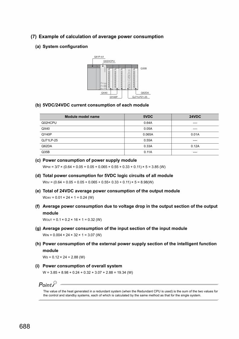
(7) Example of calculation of average power consumption
(a) System configuration
(b) 5VDC/24VDC current consumption of each module
(c) Power consumption of power supply moduleWPW = 3/7 × (0.64 + 0.05 + 0.05 + 0.065 + 0.55 + 0.33 + 0.11) × 5 = 3.85 (W)
(d) Total power consumption for 5VDC logic circuits of all moduleW5V = (0.64 + 0.05 + 0.05 + 0.065 + 0.55+ 0.33 + 0.11) × 5 = 8.98(W)
(e) Total of 24VDC average power consumption of the output moduleW24V = 0.01 × 24 × 1 = 0.24 (W)
(f) Average power consumption due to voltage drop in the output section of the output moduleWOUT = 0.1 × 0.2 × 16 × 1 = 0.32 (W)
(g) Average power consumption of the input section of the input moduleWIN = 0.004 × 24 × 32 × 1 = 3.07 (W)
(h) Power consumption of the external power supply section of the intelligent function moduleWS = 0.12 × 24 = 2.88 (W)
(i) Power consumption of overall systemW = 3.85 + 8.98 + 0.24 + 0.32 + 3.07 + 2.88 = 19.34 (W)
The value of the heat generated in a redundant system (when the Redundant CPU is used) is the sum of the two values for the control and standby systems, each of which is calculated by the same method as that for the single system.
Module model name 5VDC 24VDCQ02HCPU 0.64A ----
QX40 0.05A ----
QY40P 0.065A 0.01A
QJ71LP-25 0.55A ----
Q62DA 0.33A 0.12A
Q35B 0.11A ----
QX40 Q62DA
QY40P
Q35B
QJ71LP21-25
Q02HCPU
Q61P-A1
688

APPX
A
Appendix 11 Precautions for Battery Transportation
Appendix 11 Precautions for Battery Transportation
When transporting lithium batteries, follow the transportation regulations.
(1) Regulated modelsThe batteries for the CPU module (including memory cards) are classified as shown below.
(2) Transport guidelinesComply with IATA Dangerous Goods Regulations, IMDG code and the local transport regulations when transporting products after unpacking or repacking, while Mitsubishi ships products with packages to comply with the transport regulations.Also, consult with the shipping carrier.
Product name Model Product supply statusClassification for
transportation
Battery
Q8BAT Lithium battery (assembled battery)
Dangerous goods
Q8BAT-SETLithium battery (assembled battery) + Q8BAT connection cable
Q7BATN, Q7BAT Lithium battery
Q7BATN-SET, Q7BAT-SET Lithium battery with holder
Q6BAT Lithium battery
SRAM card batteryQ2MEM-BATQ3MEM-BAT
Lithium coin battery
Non-dangerous goodsMemory card
Q2MEM-1MBSN, Q2MEM-1MBSQ2MEM-2MBSN, Q2MEM-2MBS
Packed with lithium coin battery (Q2MEM-BAT)
Q3MEM-4MBSQ3MEM-8MBS
Packed with lithium coin battery (Q3MEM-BAT)
Q3MEM-4MBS-SETQ3MEM- 8MBS-SET
Packed with lithium coin battery (Q3MEM-BAT)+ Memory card protective cover
689

Appendix 12 Handling of Batteries and Devices with Built-in Batteries in EU Member States
This section describes the precautions for disposing of waste batteries in EU member states and exporting batteries and/or devices with built-in batteries to EU member states.
Appendix 12.1 Disposal precautions
In EU member states, there is a separate collection system for waste batteries. Dispose of batteries properly at the local community waste collection/recycling center.
The symbol shown below is printed on the batteries and packaging of batteries and devices with built-in batteries used for Mitsubishi Electric programmable controllers.
The symbol indicates that batteries need to be disposed of separately from other wastes.
Note: This symbol is for EU member states only.The symbol is specified in the new EU Battery Directive (2006/66/EC) Article 20 "Information for end-users" and Annex II.
690

APPX
A
Appendix 12 Handling of Batteries and D
evices with Built-in Batteries in EU
Mem
ber StatesAppendix 12.2 Exportation precautions
Appendix 12.2 Exportation precautions
The new EU Battery Directive (2006/66/EC) requires the following when marketing or exporting batteries and/or devices with built-in batteries to EU member states.
• To print the symbol on batteries, devices, or their packaging • To explain the symbol in the manuals of the products
(1) LabellingTo market or export batteries and/or devices with built-in batteries, which have no symbol, to EU member states on September 26, 2008 or later, print the symbol shown in Page 690, Appendix 12 on the batteries, devices, or their packaging.
(2) Explaining the symbol in the manualsTo export devices incorporating Mitsubishi programmable controller to EU member states on September 26, 2008 or later, provide the latest manuals that include the explanation of the symbol.If no Mitsubishi manuals or any old manuals without the explanation of the symbol are provided, separately attach an explanatory note regarding the symbol to each manual of the devices.
The requirements apply to batteries and/or devices with built-in batteries manufactured before the enforcement date of the new EU Battery Directive(2006/66/EC).
691

Appendix 13 Type Approval Certificates for Ship Classifications
MELSEC-Q series programmable controllers have acquired Type Approval Certificates from classification societies. Therefore, these programmable controllers can be used for machinery or devices for marine and offshore applications.For information on the models that have been approved by the classification societies, please consult your local Mitsubishi representative.
(1) Classification societies that issue the Type Approval CertificatesMELSEC-Q series have acquired the Type Approval Certificates from the following classification societies:
• American Bureau of Shipping (Abbreviation: ABS) • Bureau Veritas (Abbreviation: BV) • DNV GL (Abbreviation: DNV GL) • Lloyd's Register of Shipping (Abbreviation: LR) • Nippon Kaiji Kyokai (Abbreviation: NK) • Registro Italiano Navale (Abbreviation: RINA)
(2) Precautions for using the MELSEC iQ-R series programmable controller as the approved system
• The programmable controller must be installed in a control panel. • Use a shielded cable for a cable coming out of the control panel. • Make sure to attach a noise filter to the power cable. • Make sure to attach ferrite cores to all cables that are extended out of control panels, including power
cables.For details, refer to the following.
Precautions to acquire the Type Approval Certificate for each ship classification in ABS, BV, DNV GL, LR, NK, RINA (FA-A-0053)
692

APPX
A
Appendix 14 External Dim
ensionsAppendix 14.1 C
PU m
odules
Appendix 14 External Dimensions
Appendix 14.1 CPU modules
(1) Q00JCPU
(2) Q00UJCPU
Unit: mm
Unit: mm
244.4
987
98
80±0
.3
15.5 224.4±0.3
4-mounting screws (M4×14)
224.4±0.3244.4
80±0
.3
98
7
984
15.5
4-mounting screws (M4×14)
693

(3) Q00CPU, Q01CPU, Q00UCPU, Q01UCPU, Q02UCPU, Q03UDCPU, Q04UDHCPU, Q06UDHCPU, Q10UDHCPU, Q13UDHCPU, Q20UDHCPU, Q26UDHCPU
(4) Q02CPU, Q02HCPU, Q06HCPU, Q12HCPU, Q25HCPU
Unit: mm
Unit: mm
4
89.3
98
27.423
Q02HCPU
RS-232
USB
MODERUNERR.
USERBAT.
BOOT
PULL
89.3
98
27.4
234
694

APPX
A
Appendix 14 External Dim
ensionsAppendix 14.1 C
PU m
odules
(5) Q02PHCPU, Q06PHCPU, Q12PHCPU, Q25PHCPU
(6) Q03UDVCPU, Q04UDVCPU, Q04UDPVCPU, Q06UDVCPU, Q06UDPVCPU, Q13UDVCPU, Q13UDPVCPU, Q26UDVCPU, Q26UDPVCPU
Unit: mm
Unit: mm
89.398
27.4
234
27.4
23
984
115
695

(7) Q03UDECPU, Q04UDEHCPU, Q06UDEHCPU, Q10UDEHCPU, Q13UDEHCPU, Q20UDEHCPU, Q26UDEHCPU, Q50UDEHCPU, Q100UDEHCPU
(8) Q12PRHCPU, Q25PRHCPU
Unit: mm
Unit: mm
115 27.4
23498
Q12PRHCPU
MODERUNERR.
USERBAT.
BOOT
USB
PULL
TRACKING
BACKUP
SYSTEM BSYSTEM ACONTROL
4
89.3
98
55.250.8
2
696

APPX
A
Appendix 14 External Dim
ensionsAppendix 14.1 C
PU m
odules
(9) When the Q3MEM-4MBS or Q3MEM-8MBS is mounted on the CPU module
Unit: mm
98
89.3 24.5
27.4
5
118.8
697

(10)When the Q7BATN-SET is mounted on the CPU module
Unit: mm
Unit: mm
3498
89.3 27.4
34
89.3
98
27.42
698

APPX
A
Appendix 14 External Dim
ensionsAppendix 14.1 C
PU m
odules
(11)When the Q7BAT-SET is mounted on the CPU module
Unit: mm
Unit: mm
3098
89.3 27.4
30
89.3
98
27.42
699

Appendix 14.2 Power supply modules
(1) Q61P-A1, Q61P-A2, Q61P, Q61P-D, Q62P, Q63P
(2) Q64P
Unit: mm
Unit: mm
98
90 55.2
98
115 55.2
700

APPX
A
Appendix 14 External Dim
ensionsAppendix 14.2 Pow
er supply modules
(3) Q64PN
(4) Q61SP
Unit: mm
Unit: mm
98115 55.2
27.414
98
90
701

(5) Q63RP
(6) Q64RPN, Q64RP
Unit: mm
Unit: mm
98
83115
115 83
98
702

APPX
A
Appendix 14 External Dim
ensionsAppendix 14.2 Pow
er supply modules
(7) A1S61PN, A1S62PN, A1S63P
Unit: mm
6.5
130
93.6 54.5
703

Appendix 14.3 Main base units
(1) Q33B
(2) Q35B
Unit: mm
Unit: mm
7.5
I/O0CPUPOWER I/O2I/O1
44.115.5
98
7
189
5V
SG
FG80±0
.3
169±0.3
OUT
4-installation screws (M4×14)
OUT
FG
SG
5V
I/O4I/O3I/O1 I/O2POWER CPU I/O0
7.544.1
98
780
±0.3
15.5245
224.4±0.3
4-installation screws (M4×14)
704

APPX
A
Appendix 14 External Dim
ensionsAppendix 14.3 M
ain base units
(3) Q38B
(a) With 5 base unit installation holes
(b) With 4 base unit installation holesUnit: mm
Unit: mm
OUT
98
15.5
7
32844.17.5
FG
SG
5V
I/O7I/O6I/O5I/O4I/O3I/O2I/O1I/O0CPUPOWER
b1a1
170±0.3 138±0.3
80±0
.35-installation screws (M4×14)
I/O1I/O0CPU I/O5I/O4I/O3I/O2 I/O6 I/O7POWER
5V
SG
FG
OUT
7.544.1
98
780
±0.3
15.5328
308±0.3
4-installation screws (M4×14)
705

(4) Q312B
(a) With 5 base unit installation holes
(b) With 4 base unit installation holes
RemarkThe Q38B and Q312B manufactured in August 2006 or later have five base mounting holes.
Unit: mm
Unit: mm
OUT
FG
SG
5V
I/O11I/O10I/O9I/O8I/O7I/O6I/O5I/O4I/O3I/O2I/O1I/O0CPUPOWER
b1a1
44.1
7.5
987
80±0
.3
15.5
439
170±0.3 249±0.3
5-installation screws (M4×14)
OUT
44.17.5
987
80±0
.3
15.5439
419±0.3
4-installation screws (M4×14)
706

APPX
A
Appendix 14 External Dim
ensionsAppendix 14.3 M
ain base units
(5) Q32SB
(6) Q33SB
Unit: mm
Unit: mm
POWERCPU I/O1I/O0
5V
SG
7.5
987
80±0
.3
8.5114
101±0.3
4-installation screws (M4×12)
POWER CPU I/O1I/O0 I/O2
5V
SG
7.5
987
80±0
.3
8.5142
129±0.3
4-installation screws (M4×12)
707

(7) Q35SB
(8) Q38RB
(9) Q35DB
Unit: mm
Unit: mm
Unit: mm
SG5V
7.598
780
±0.3
8.5197.5
184.5±0.3
4-installation screws (M4×12)
OUT
I/O7I/O6I/O5I/O4I/O3
5V
FG
SG
I/O2I/O1I/O0
5V
FGCPU
SG
44.1
7.5
987
80±0
.3
15.5
439
170±0.3 249±0.3
5-installation screws (M4×14)
44.1
7.5
987
80±0
.3
15.5
245
224.5±0.3
4-installation screws (M4×14)
708

APPX
A
Appendix 14 External Dim
ensionsAppendix 14.3 M
ain base units
(10)Q38DB
(11)Q312DB
Unit: mm
Unit: mm
OUT
38DFG
SG
5V
I/O7I/O6I/O5I/O4I/O3I/O2I/O1I/O0CPUPOWER
b1a1
44.1
7.5
987
80±0
.3
15.5
328
170±0.3 138±0.3
5-installation screws (M4×14)
OUT
312DFG
SG
5V
I/O11I/O10I/O9I/O8I/O7I/O6I/O5I/O4I/O3I/O2I/O1I/O0CPUPOWER
b1a1
44.1
7.5
987
80±0
.3
15.5
439
170±0.3 249±0.3
5-installation screws (M4×14)
709

Appendix 14.4 Extension base units
(1) Q52B
(2) Q55B
(3) Q63B
Unit: mm
Unit: mm
Unit: mm
I/O0 I/O1
OUTIN
44.17.5
987
80±0
.315.5
10683.5±0.3
4-installation screws (M4×14)
I/O2I/O1I/O0 I/O3 I/O4
OUTIN
44.17.5
987
80±0
.3
15.5 189
167±0.3
4-installation screws (M4×14)
I/O0FG
I/O2I/O1POWER
5V
SG
OUTIN
44.17.5
987
80±0
.3
15.5 189
167±0.3
4-installation screws (M4×14)
710

APPX
A
Appendix 14 External Dim
ensionsAppendix 14.4 Extension base units
(4) Q65B
(5) Q68B
(a) With 5 base unit installation holes
(b) With 4 base unit installation holes
Unit: mm
Unit: mm
Unit: mm
IN OUT
SG
5V
POWER I/O4I/O3I/O1 I/O2FG
I/O0
44.17.5
987
80±0
.315.5
245222.4±0.3
4-installation screws (M4×14)
b1a1
5V
SG
FG
POWER I/O0 I/O1 I/O2 I/O3 I/O4 I/O5 I/O6 I/O7
IN OUT
44.1
7.5
987
80±0
.3
15.5
328
190±0.3 116±0.3
5-installation screws (M4×14)
I/O2I/O1I/O0POWER
FG
I/O5I/O4I/O3 I/O6 I/O7
5V
SG
OUTIN
44.17.5
987
80±0
.3
15.5 328
306±0.3
4-installation screws (M4×14)
711

(6) Q612B
(a) With 5 base unit installation holes
(b) With 4 base unit installation holes
RemarkThe Q68B and Q612B manufactured in August 2006 or later have five base mounting holes.
Unit: mm
Unit: mm
b1a1
5V
SG
FG
POWER I/O0 I/O1 I/O2 I/O3 I/O4 I/O5 I/O6 I/O7 I/O8 I/O9 I/O10 I/O11
IN OUT
44.17.5
987
80±0
.3
15.5 439
190±0.3 227±0.3
5-installation screws (M4×14)
I/O9I/O8I/O7I/O6I/O5I/O4I/O3I/O2I/O1I/O0POWER
FG
5V
SG
OUTIN
44.17.5
987
80±0
.3
15.5 439
417±0.3
4-installation screws (M4×14)
712

APPX
A
Appendix 14 External Dim
ensionsAppendix 14.4 Extension base units
(7) QA1S51B
(8) QA1S65B
Unit: mm
Unit: mm
50.716.4
130
1011
0±0.
3
(93)
17±0
.3
10100
80±0.3
3-installation screws (M5×25)
IN OUT
POWER
5V
SG
FG
I/O0 I/O1 I/O2 I/O3 I/O4
QA1S65B
51.216.4
130
1011
0±0.
3
10315
295±0.3
4-installation screws (M5×25)
713

(9) QA1S68B
(10)QA65B
Unit: mm
Unit: mm
I/O0 I/O7I/O6I/O5I/O4I/O3I/O2I/O1
QA1S68B
IN OUT
POWER
5V
SG
FG
51.216.4
130
1011
0±0.
3
10420
400±0.3
4-installation screws (M5×25)
46.6
250
200±
0.3
352332±0.3
4- 6 installation holes (M5 installation screw)
Base cover 2×6-M4 screw (for mounting module)
Hand hold
714

APPX
A
Appendix 14 External Dim
ensionsAppendix 14.4 Extension base units
(11) QA68B
(12) Q68RB
Unit: mm
Unit: mm
46.6
250
200±
0.3
466446±0.3
4- 6 installation holes (M5 installation screw)
Base cover 2×9-M4 screw (for mounting module)
Hand hold
FG
SG
5V5V
SG
FG
I/O0 I/O1 I/O2 I/O3 I/O4 I/O5 I/O6 I/O7
OUTIN
44.17.5
987
80±0
.3
15.5 439
170±0.3 247±0.3
5-installation screws (M4×14)
715

(13) Q65WRB
Unit: mm
POWER 2
SG
5V5V
SG
POWER 1 I/O0 I/O1 I/O2 I/O3 I/O4
IN2 OUTIN1
44.17.5
987
80±0
.3
15.5 439
170±0.3 247±0.3
5-installation screws (M4×14)
716

APPX
A
Appendix 14 External Dim
ensionsAppendix 14.5 O
ther optional items
Appendix 14.5 Other optional items
(1) Extension cablesQC05B, QC06B, QC12B, QC30B, QC50B, QC100B
(2) Tracking cableQC10TR, QC30TR
Unit: mm
Unit: mm
10.07.0
42.0
34.2 6.0
A A B B39
.7
12.4 33.5
717

(3) Q8BAT-SETQ8BAT
QC10BAT
Unit: mm
Unit: mm
Q8BAT
OUTPUT3VDC
98 89.8
4.5
49
87 55.2
5.8 47.1
4.5mounting screws (M4×14)
4.5×5.1mounting screws (M4×14)
QC10BAT
39 100055 30
718

APPX
A
Appendix 14 External Dim
ensionsAppendix 14.5 O
ther optional items
Memo
719

INDEX
0 to 9
5VDC internal current consumption . . . . . . . . . . . 149
A
A series power supply module . . . . . . . . . . . . . . . . 22A5B . . . . . . . . . . . . . . . . . . . . . . . . . . . . . . . . . 22A6B . . . . . . . . . . . . . . . . . . . . . . . . . . . . . . . . . 22Allowable momentary power failure time. . . . . . . . 149Annunciator [F] . . . . . . . . . . . . . . . . . . . . . . . . . 148AnS series power supply module . . . . . . . . . . . . . . 22ATA card. . . . . . . . . . . . . . . . . . . . . . . . . . . . . . 243Automatic write to the standard ROM . . . . . . . . . . 192
B
Backup mode . . . . . . . . . . . . . . . . . . . . . . . . . . 130Base unit
Extension. . . . . . . . . . . . . . . . . . . . . . . . . . . . . 22Extension stages . . . . . . . . . . . . . . . . . . . . . . 233External dimensions . . . . . . . . . . . . . . . . . . . . 704Installation and removal of module . . . . . . . . . . . 73Main . . . . . . . . . . . . . . . . . . . . . . . . . . . . . . . . 22Mounting dimensions . . . . . . . . . . . . . . . . . . . . 61Mounting orientation . . . . . . . . . . . . . . . . . . . . . 62Mounting position . . . . . . . . . . . . . . . . . . . . . . . 61Multiple CPU high speed main . . . . . . . . . . . . . . 22Redundant . . . . . . . . . . . . . . . . . . . . . . . . . . . . 22Redundant power extension. . . . . . . . . . . . . . . . 22Redundant power main . . . . . . . . . . . . . . . . . . . 22Redundant power supply . . . . . . . . . . . . . . . . . . 22Redundant type extension . . . . . . . . . . . . . . . . . 22Slim type main . . . . . . . . . . . . . . . . . . . . . . . . . 22
Basic model QCPU . . . . . . . . . . . . . . . . . . . . . . . 21Battery
Battery for QCPU . . . . . . . . . . . . . . . . . . . . . . 255Battery for SRAM card. . . . . . . . . . . . . . . . . . . 246Life . . . . . . . . . . . . . . . . . . . . . . . . . . . . . . . . 613Replacement procedure (CPU module) . . . . . . . 262Replacement procedure (SRAM card) . . . . . . . . 268Replacement reference period . . . . . . . . . . . . . 613
Boot operation . . . . . . . . . . . . . . . . . . . . . . . . . . 193
C
Calculating heat generation. . . . . . . . . . . . . . . . . 686Category II . . . . . . . . . . . . . . . . . . . . . . . . . . . . 680CE mark . . . . . . . . . . . . . . . . . . . . . . . . . . . . . . 663Circuit
Fail-safe circuit . . . . . . . . . . . . . . . . . . . . . . . . 685System design circuit . . . . . . . . . . . . . . . . . . . 683
Clock function . . . . . . . . . . . . . . . . . . . . . . . . . . 149Constant scan . . . . . . . . . . . . . . . . . . . . . . . . . . 147Control method . . . . . . . . . . . . . . . . . . . . . . . . . 147Control system. . . . . . . . . . . . . . . . . . . . . . . . . . 130Counter [C] . . . . . . . . . . . . . . . . . . . . . . . . . . . . 148
CPU moduleExternal dimensions . . . . . . . . . . . . . . . . . . . . 693Installation and removal. . . . . . . . . . . . . . . . . . . 73Specifications. . . . . . . . . . . . . . . . . . . . . . . . . 147
CPU shared memory . . . . . . . . . . . . . . . . . . . . . 147
D
Daily inspection . . . . . . . . . . . . . . . . . . . . . . . . . 260Data register [D] . . . . . . . . . . . . . . . . . . . . . . . . 148Debug mode . . . . . . . . . . . . . . . . . . . . . . . . . . . 130Device
Annunciator [F]. . . . . . . . . . . . . . . . . . . . . . . . 148Counter [C] . . . . . . . . . . . . . . . . . . . . . . . . . . 148Data register [D] . . . . . . . . . . . . . . . . . . . . . . . 148Edge relay [V] . . . . . . . . . . . . . . . . . . . . . . . . 148File register [R, ZR ] . . . . . . . . . . . . . . . . . . . . 148Function input [FX] . . . . . . . . . . . . . . . . . . . . . 149Function output [FY] . . . . . . . . . . . . . . . . . . . . 149Function register [FD] . . . . . . . . . . . . . . . . . . . 149Index register [Z] . . . . . . . . . . . . . . . . . . . . . . 149Intelligent function module device. . . . . . . . . . . 149Internal relay [M]. . . . . . . . . . . . . . . . . . . . . . . 148Interrupt pointer [I] . . . . . . . . . . . . . . . . . . . . . 149Latch relay [L] . . . . . . . . . . . . . . . . . . . . . . . . 148Link direct device . . . . . . . . . . . . . . . . . . . . . . 149Link register [W] . . . . . . . . . . . . . . . . . . . . . . . 148Link relay [B] . . . . . . . . . . . . . . . . . . . . . . . . . 148Link special register [SW] . . . . . . . . . . . . . . . . 148Link special relay [SB]. . . . . . . . . . . . . . . . . . . 148Pointer [P] . . . . . . . . . . . . . . . . . . . . . . . . . . . 149Retentive timer [ST] . . . . . . . . . . . . . . . . . . . . 148Special register [SD] . . . . . . . . . . . . . . . . . . . . 149Special relay [SM]. . . . . . . . . . . . . . . . . . . . . . 149Step relay [S] . . . . . . . . . . . . . . . . . . . . . . . . . 149Timer [T] . . . . . . . . . . . . . . . . . . . . . . . . . . . . 148
DIN railApplicable DIN rail . . . . . . . . . . . . . . . . . . . . . . 67DIN rail adapter type . . . . . . . . . . . . . . . . . . . . 238DIN rail mounting screw intervals . . . . . . . . . . . . 68
Drive . . . . . . . . . . . . . . . . . . . . . . . . . . . . . . . . 147
E
Edge relay [V] . . . . . . . . . . . . . . . . . . . . . . . . . . 148Ethernet . . . . . . . . . . . . . . . . . . . . . . . . . . . . . . . 23Extended scan time . . . . . . . . . . . . . . . . . . . . . . 147Extended SRAM cassette. . . . . . . . . . . . . . . . 23,253Extension
Base unit . . . . . . . . . . . . . . . . . . . . . . . . . . . . . 22Cable . . . . . . . . . . . . . . . . . . . . . . . . . . . . . . . 23
Extension base unit . . . . . . . . . . . . . . . . . . . . . . . 22External dimensions
CPU module . . . . . . . . . . . . . . . . . . . . . . . . . 693Extension base unit . . . . . . . . . . . . . . . . . . . . 710Extension cable . . . . . . . . . . . . . . . . . . . . . . . 717Main base unit . . . . . . . . . . . . . . . . . . . . . . . . 704Power supply module . . . . . . . . . . . . . . . . . . . 700Tracking cable . . . . . . . . . . . . . . . . . . . . . . . . 717
720

I
2
4
8
F
Fail-safeCircuit . . . . . . . . . . . . . . . . . . . . . . . . . . . . . . . 683Measures . . . . . . . . . . . . . . . . . . . . . . . . . . . . 685
Features . . . . . . . . . . . . . . . . . . . . . . . . . . . . . . . 26Ferrite core. . . . . . . . . . . . . . . . . . . . . . . . . . . . . 677File register [R, ZR ] . . . . . . . . . . . . . . . . . . . . . . 148Flash card . . . . . . . . . . . . . . . . . . . . . . . . . . . . . 243Forcibly Disabling the SD Memory Card . . . . . . . . 252Function input [FX] . . . . . . . . . . . . . . . . . . . . . . . 149Function output [FY] . . . . . . . . . . . . . . . . . . . . . . 149Function register [FD] . . . . . . . . . . . . . . . . . . . . . 149Function version . . . . . . . . . . . . . . . . . . . . . . . . . 643
G
GOT . . . . . . . . . . . . . . . . . . . . . . . . . . . . . . . . . . 23GX Developer. . . . . . . . . . . . . . . . . . . . . . . . . . . . 23
H
High Performance model QCPU . . . . . . . . . . . . . . . 21High-speed Universal model QCPU . . . . . . . . . . . . 21
I
I/O control mode . . . . . . . . . . . . . . . . . . . . . . . . . 147Index register [Z]. . . . . . . . . . . . . . . . . . . . . . . . . 149Installation environment . . . . . . . . . . . . . . . . . . . . . 60Installing and Removing an Extended SRAM Cassette . . . . . . . . . . . . . . . . . . . . . . . . . 103Installing and Removing an SD Memory Card . . . . 101Intelligent function module
Intelligent function module device . . . . . . . . . . . 149Intelligent function module parameter. . . . . . . . . 148
Internal current consumption . . . . . . . . . . . . . . . . 149Internal relay [M] . . . . . . . . . . . . . . . . . . . . . . . . . 148Interrupt pointer [I]. . . . . . . . . . . . . . . . . . . . . . . . 149Isolation transformer . . . . . . . . . . . . . . . . . . . . . . 678
L
Latch clear operation. . . . . . . . . . . . . . . . . . . . . . 191Latch range . . . . . . . . . . . . . . . . . . . . . . . . . . . . 149Latch relay [L]. . . . . . . . . . . . . . . . . . . . . . . . . . . 148LED
LEDs . . . . . . . . . . . . . . . . . . . . . . . . . . . . . . . 122Link direct device . . . . . . . . . . . . . . . . . . . . . . . . 149Link register [W] . . . . . . . . . . . . . . . . . . . . . . . . . 148Link relay [B] . . . . . . . . . . . . . . . . . . . . . . . . . . . 148Link special register [SW]. . . . . . . . . . . . . . . . . . . 148Link special relay [SB] . . . . . . . . . . . . . . . . . . . . . 148Low Voltage directive . . . . . . . . . . . . . . . . . . . . . 663
M
Main base unit . . . . . . . . . . . . . . . . . . . . . . . . . . . 22Max. number of files stored . . . . . . . . . . . . . . . . . 148MC protocol . . . . . . . . . . . . . . . . . . . . . . . . . . . . . 23MELSECNET/H . . . . . . . . . . . . . . . . . . . . . . . . . . 23Memory capacity. . . . . . . . . . . . . . . . . . . . . . . . . 147
Memory CardBattery Installation into the Memory Card . . . . . . 248Handling. . . . . . . . . . . . . . . . . . . . . . . . . . . . . 247List of usable memory cards . . . . . . . . . . . . . . . 243Loading/unloading procedures . . . . . . . . . . . . . . 97Part names . . . . . . . . . . . . . . . . . . . . . . . . . . . 242Specifications . . . . . . . . . . . . . . . . . . . . . . . . . 244Specifications of the battery . . . . . . . . . . . . . . . 246
Memory size . . . . . . . . . . . . . . . . . . . . . . . . . . . 150Module
Installation . . . . . . . . . . . . . . . . . . . . . . . . . . . . 73Removal . . . . . . . . . . . . . . . . . . . . . . . . . . . . . . 75
Module changeOnline . . . . . . . . . . . . . . . . . . . . . . . . . . . . . . 272Redundant power supply module . . . . . . . . . . . 282
Multiple CPU high speed main base unit . . . . . . . . . 22
N
Network module . . . . . . . . . . . . . . . . . . . . . . . . . . 39No. of device points . . . . . . . . . . . . . . . . . . . . . . 148No. of device tracking words . . . . . . . . . . . . . . . . 149No. of I/O device points . . . . . . . . . . . . . . . . . . . . 148No. of I/O points . . . . . . . . . . . . . . . . . . . . . . . . . 148Noise filter . . . . . . . . . . . . . . . . . . . . . . . . . . . . . 677
O
Online module change . . . . . . . . . . . . . . . . . . . . 272Operation mode change . . . . . . . . . . . . . . . . . . . 129
P
Part nameBase units. . . . . . . . . . . . . . . . . . . . . . . . . . . . 230Basic model QCPU . . . . . . . . . . . . . . . . . . . . . 121High Performance model QCPU, Process CPU and Redundant CPU . . . . . . . . . . . . . . . . . . . . 127Memory card. . . . . . . . . . . . . . . . . . . . . . . . . . 242Power supply module. . . . . . . . . . . . . . . . . . . . 195Universal model QCPU . . . . . . . . . . . . . . . . . . 132
Periodic inspection . . . . . . . . . . . . . . . . . . . . . . . 261Pointer [P] . . . . . . . . . . . . . . . . . . . . . . . . . . . . . 149Power supply module
A series . . . . . . . . . . . . . . . . . . . . . . . . . . . . . . 22AnS series . . . . . . . . . . . . . . . . . . . . . . . . . . . . 22Connecting to the power supply module. . . . . . . 107External dimensions. . . . . . . . . . . . . . . . . . . . . 700Life detection . . . . . . . . . . . . . . . . . . . . . . . . . . 22Names of Parts and Settings . . . . . . . . . . . . . . 195Q series . . . . . . . . . . . . . . . . . . . . . . . . . . . . . . 22Redundant . . . . . . . . . . . . . . . . . . . . . . . . . . . . 22Slim type . . . . . . . . . . . . . . . . . . . . . . . . . . . . . 22Specifications . . . . . . . . . . . . . . . . . . . . . . . . . 203
PrecautionConnection of GOT . . . . . . . . . . . . . . . . . . . . . . 49Design . . . . . . . . . . . . . . . . . . . . . . . . . . . . . . . . 1Disposal . . . . . . . . . . . . . . . . . . . . . . . . . . . . . . . 6Installation . . . . . . . . . . . . . . . . . . . . . . . . . . . . 64Precaution on installation . . . . . . . . . . . . . . . . . . 64Precautions for battery transportation . . . . . . . . 689Precautions for using coaxial cables . . . . . . . . . 669Startup and Maintenance . . . . . . . . . . . . . . . . . . . 5System configuration . . . . . . . . . . . . . . . . . . . . . 39
721

When only the Q5B is connected to the extension base unit . . . . . . . . . . . . . . . . . . . 90Wiring precautions . . . . . . . . . . . . . . . . . . . . . 105
Process control language . . . . . . . . . . . . . . . . . . 147Process CPU. . . . . . . . . . . . . . . . . . . . . . . . . . . . 21Processing speed . . . . . . . . . . . . . . . . . . . . . . . 147Program capacity . . . . . . . . . . . . . . . . . . . . . . . . 147Program language . . . . . . . . . . . . . . . . . . . . . . . 147Program size . . . . . . . . . . . . . . . . . . . . . . . . . . . 154
Q
Q series power supply module. . . . . . . . . . . . . . . . 22Q3B. . . . . . . . . . . . . . . . . . . . . . . . . . . . . . . . . 22Q3DB . . . . . . . . . . . . . . . . . . . . . . . . . . . . . . . 22Q3RB . . . . . . . . . . . . . . . . . . . . . . . . . . . . . . . 22Q3SB. . . . . . . . . . . . . . . . . . . . . . . . . . . . . . . . 22Q5B. . . . . . . . . . . . . . . . . . . . . . . . . . . . . . . . . 22Q6BAT . . . . . . . . . . . . . . . . . . . . . . . . . . . . . . . 255Q6B. . . . . . . . . . . . . . . . . . . . . . . . . . . . . . . . . 22Q6RB . . . . . . . . . . . . . . . . . . . . . . . . . . . . . . . 22Q6WRB . . . . . . . . . . . . . . . . . . . . . . . . . . . . . . 22Q7BAT . . . . . . . . . . . . . . . . . . . . . . . . . . . . . . . 255Q7BATN . . . . . . . . . . . . . . . . . . . . . . . . . . . . . . 255Q7BATN-SET . . . . . . . . . . . . . . . . . . . . . . . . . . 257Q7BAT-SET . . . . . . . . . . . . . . . . . . . . . . . . . . . 257Q8BAT . . . . . . . . . . . . . . . . . . . . . . . . . . . . . . . 255Q8BAT-SET . . . . . . . . . . . . . . . . . . . . . . . . . . . 258QA1S5B. . . . . . . . . . . . . . . . . . . . . . . . . . . . . . 22QA1S6ADP . . . . . . . . . . . . . . . . . . . . . . . . . . . . . 23QA1S6ADP+A1S5B/A1S6B . . . . . . . . . . . . . . 22QA1S6B. . . . . . . . . . . . . . . . . . . . . . . . . . . . . . 22QA6ADP. . . . . . . . . . . . . . . . . . . . . . . . . . . . . . . 22QA6ADP+A5B/A6B . . . . . . . . . . . . . . . . . . . . 22QA6B. . . . . . . . . . . . . . . . . . . . . . . . . . . . . . . . 22QnUD(H)CPU . . . . . . . . . . . . . . . . . . . . . . . . . . . 21
R
Redundant base unit . . . . . . . . . . . . . . . . . . . . . . 22Redundant CPU. . . . . . . . . . . . . . . . . . . . . . . . . . 21Redundant power extension base unit . . . . . . . . . . 22Redundant power main base unit. . . . . . . . . . . . . . 22Redundant power supply module. . . . . . . . . . . . . . 22Redundant power supply system . . . . . . . . . . . . . 108Redundant system
Backup mode . . . . . . . . . . . . . . . . . . . . . . . . . 130Debug mode. . . . . . . . . . . . . . . . . . . . . . . . . . 130Operation mode change . . . . . . . . . . . . . . . . . 129Separate mode. . . . . . . . . . . . . . . . . . . . . . . . 130
Redundant type extension base unit . . . . . . . . . . . 22Reinforced insulation . . . . . . . . . . . . . . . . . . . . . 681Reset operation . . . . . . . . . . . . . . . . . . . . . . . . . 189Retentive timer [ST] . . . . . . . . . . . . . . . . . . . . . . 148RUN/PAUSE contact . . . . . . . . . . . . . . . . . . . . . 149
S
SD memory card . . . . . . . . . . . . . . . . . . . . . . 23,250Separate mode . . . . . . . . . . . . . . . . . . . . . . . . . 130Serial number . . . . . . . . . . . . . . . . . . . . . . . . . . 643Single power supply system . . . . . . . . . . . . . . . . 107Slim type main base unit . . . . . . . . . . . . . . . . . . . . 22Slim type power supply module . . . . . . . . . . . . . . . 22
Special register [SD] . . . . . . . . . . . . . . . . . . . . . 149Special relay [SM] . . . . . . . . . . . . . . . . . . . . . . . 149Specifications
Battery . . . . . . . . . . . . . . . . . . . . . . . . . . . . . 255Battery for memory card . . . . . . . . . . . . . . . . . 246General . . . . . . . . . . . . . . . . . . . . . . . . . . . . . 119Memory card . . . . . . . . . . . . . . . . . . . . . . . . . 244Performance . . . . . . . . . . . . . . . . . . . . . . . . . 121Power supply module . . . . . . . . . . . . . . . . . . . 203
SRAM card . . . . . . . . . . . . . . . . . . . . . . . . . . . . 243Standard RAM. . . . . . . . . . . . . . . . . . . . . . . . . . 147Standard ROM . . . . . . . . . . . . . . . . . . . . . . . . . 147Standards
Low Voltage Directive . . . . . . . . . . . . . . . . . . . 663Standby system. . . . . . . . . . . . . . . . . . . . . . . . . 130Step relay [S] . . . . . . . . . . . . . . . . . . . . . . . . . . 149surge absorber for lightning . . . . . . . . . . . . . . . . 106System. . . . . . . . . . . . . . . . . . . . . . . . . . . . . . . 683
Control system . . . . . . . . . . . . . . . . . . . . . . . . 130Standby system . . . . . . . . . . . . . . . . . . . . . . . 130System A. . . . . . . . . . . . . . . . . . . . . . . . . . . . 131System B. . . . . . . . . . . . . . . . . . . . . . . . . . . . 131
System A . . . . . . . . . . . . . . . . . . . . . . . . . . . . . 131System B . . . . . . . . . . . . . . . . . . . . . . . . . . . . . 131System configuration
Applicable software. . . . . . . . . . . . . . . . . . . . . 645Bus connection of GOT . . . . . . . . . . . . . . . . . . . 48Outline . . . . . . . . . . . . . . . . . . . . . . . . . . . . . . 50Overall configuration . . . . . . . . . . . . . . . . . . . . . 34Peripheral device configuration . . . . . . . . . . . . . 52Precautions . . . . . . . . . . . . . . . . . . . . . . . . . . . 39Sequence control language . . . . . . . . . . . . . . . 147Single CPU . . . . . . . . . . . . . . . . . . . . . . . . . . . 34
System switching. . . . . . . . . . . . . . . . . . . . . . . . 130
T
Timer [T]. . . . . . . . . . . . . . . . . . . . . . . . . . . . . . 148Tracking cable. . . . . . . . . . . . . . . . . . . . . . . . . . . 23Tracking execution time . . . . . . . . . . . . . . . . . . . 147Troubleshooting
Basic measures . . . . . . . . . . . . . . . . . . . . . . . 284
U
Universal model Process CPU . . . . . . . . . . . . . . . 21Universal model QCPU . . . . . . . . . . . . . . . . . . . . 21
W
WeightBase unit . . . . . . . . . . . . . . . . . . . . . . . . . . . . 238CPU module . . . . . . . . . . . . . . . . . . . . . . . . . 149Extension cable . . . . . . . . . . . . . . . . . . . . . . . . 89Memory card . . . . . . . . . . . . . . . . . . . . . . . . . 244Power supply module . . . . . . . . . . . . . . . . 204,214
WiringExtension cables . . . . . . . . . . . . . . . . . . . . . . . 87I/O equipment . . . . . . . . . . . . . . . . . . . . . . . . 111I/O module. . . . . . . . . . . . . . . . . . . . . . . . . . . 111Power supply module . . . . . . . . . . . . . . . . . . . 107
Wiring of I/O module . . . . . . . . . . . . . . . . . . . . . 111
722

REVISIONS*The manual number is given on the bottom left of the back cover.
Print date *Manual number RevisionJun., 2004 SH(NA)-080483ENG-A First editionDec., 2004 SH(NA)-080483ENG-B
Section 12.2.21
CONTENTS, Section 2.1.5, 5.2.1, 5.3, 9.1.2, 9.2.4, 10.3.1, 10.4, 10.5, 10.6.1, 11.1, 11.3.1, 11.3.2, 11.4, 11.5, 12.2.1, 12.3.1, 12.3, 12.6, 12.7, Appendix 2.1, Appendix 2.2, Appendix 3.1
May, 2005 SH(NA)-080483ENG-C
Section 12.2.22, 12.2.23, 12.2.24, Appendix 2.4, Appendix 2.5
GENERIC TERMS AND ABBREVIATIONS, Chapter 1, Section 2.1.1, 2.1.2, 2.1.5, 2.2, 4.1, 5.2.1, 5.2.2, 5.3, 6.1.4, 7.2.1, 7.2.2, 9.1.3, 10.2, 10.3.2, 10.6.2, 11.3.1, 11.3.2, 11.3.3, 11.3.4, 11.4, 11.5, 12.2.1, 12.2.2, 12.2.3, 12.2.5, 12.2.7, 12.3.2, 12.4.1, 12.4.2, 12.6, 12.7, Appendix 1.5, Appendix 2.2, Appendix 2.3, Appendix 3
Aug., 2005 SH(NA)-080483ENG-D
SAFETY PRECAUTIONS, GENERIC TERMS AND ABBREVIATIONS, Section 2.1.1, 4.1, 5.1, 5.2.1, 5.2.2, 5.3, 7.1.2, 10.6.2, 11.3.3, 12.2.2, 12.3.1, 12.4.2, 12.6, 12.7, Appendix 1.2
Apr., 2006 SH(NA)-080483ENG-E
QA65B,QA68B
GENERIC TERMS AND ABBREVIATIONS, Section 1.1, 2.1.1, 2.1.2, 5.1, 5.2.1, 5.2.3, 6.1.1, 6.1.2, 9.1.3, 9.1.5, 9.1.6, 10.3.1, 10.3.3, 12.3.2, Appendix 1.4, Appendix 2.2, Appendix 2.4, Index
Aug., 2006 SH(NA)-080483ENG-F
SAFETY PRECAUTIONS, Section 2.1.5, 6.1.1, 6.1.2, 9.1.5, 10.2, 10.3.1, 12.5.1, 12.5.2, Appendix 1.3, 1.4
Sep., 2006 SH(NA)-080483ENG-G
GENERIC TERMS AND ABBREVIATIONS, Section 7.1.2, 9.1.6, 10.3.1, 11.3.3, 12.3.4, 12.3.6, 12.7
Oct., 2006 SH(NA)-080483ENG-H
Section 12.3.11
SAFETY PRECAUTIONS, Section 1.1, 2.1.1, Chapter3, Section 4.1, 4.2.1, 5.1, 5.2.1, 5.2.2, 5.3, 6.1.1, 9.1.1, 9.1.2, 9.1.3, 9.1.5, 9.2.3, 9.2.5, 10.2, 10.3.1, 10.6.1, 10.6.2, 11.3.1, 11.4, 11.5, 12.2.19, 12.3.2, 12.3.3, 12.3.5, 12.3.10, 12.6, 12.7, Appendix 1.2, Appendix 2.2
Addition
Partial correction
Addition
Partial correction
Partial correction
Model Addition
Partial correction
Partial correction
Partial correction
Addition
Partial correction
723

Apr., 2007 SH(NA)-080483ENG-I Universal model QCPU model addition,Revision involving High Performance model QCPU and Redundant CPU serial No.09012
Q02UCPU, Q03UDCPU, Q04UDHCPU, Q06UDHCPU, Q65WRB
Section 4.4, 12.2.25
SAFETY PRECAUTIONS, ABOUT MANUALS, GENERIC TERMS AND ABBREVIATIONS, Chapter 1, Section 1.1, 2.1, 2.1.1, 2.1.2, 2.1.3, 2.1.4, 2.1.5, 2.2, 4.1, 4.2.2, 4.3.2, 5.1, 5.2.1, 5.2.3, 6.1.1, 6.1.2, 6.1.3, 6.1.4, 7.1.1, 7.1.2, 7.1.3, 7.1.5, 7.1.6, 7.1.7, 7.2.2, 9.1.3, 9.1.5, 10.3.1, 10.3.3, 10.4, 10.6.1, 10.6.2, 11.1, 11.2, 11.3.1, 11.3.2, 11.3.3, 11.3.4, 11.4, 11.5, 12.1, 12.2.1, 12.2.2, 12.2.3, 12.2.10, 12.2.15, 12.2.21, 12.2.22, 12.2.23, 12.3.1, 12.3.2, 12.3.3, 12.3.4, 12.3.5, 12.3.6, 12.3.7, 12.3.8, 12.3.9, 12.3.11, 12.4.1, 12.5.1, 12.5.2, 12.6, 12.7, Appendix 1.1, Appendix 1.3, Appendix 1.4, Appendix 2.2, Appendix 3
Jan., 2008 SH(NA)-080483ENG-J Revision due to the support for Redundant CPU serial number 09102
QA6ADP, Q64PN
Appendix 2.6
SAFETY PRECAUTION, GENERIC TERMS AND ABBREVIATIONS, Section 1.1, 2.1.1, 2.1.2, 2.1.3, 2.1.5, 4.1, 4.2.1, 4.3.1, 4.4.1, Chapter 3, Section 5.1, 5.2.1, 5.2.2, 5.3, 6.1.2, 6.1.3, 9.1.1, 9.1.2, 9.1.5, 9.1.6, 9.2.3, 10.1, 10.3.1, 10.3.3, 10.6.1, 10.6.2, 11.2, 11.3.1, 11.3.4, 12.2.13, 12.2.22, 12.3.3, 12.3.4, 12.3.5, 12.3.9, 12.4.1, 12.4.2, 12.5.1, 12.5.2, 12.6, 12.7, Appendix 1.2, Appendix 2.5, Index
Mar., 2008 SH(NA)-080483ENG-K
Q13UDHCPU, Q26UDHCPU
Section 11.3.1
GENERIC TERMS AND ABBREVIATIONS, PRECAUTIONS FOR USE, Chapter 1, Section 1.1, 2.1.2, 2.1.4, 2.1.5, 4.1, 4.4.1, 5.2.1, 5.3, 6.1.1, 6.1.3, 7.1.1, 7.1.6, 7.2.1, 10.3.1, 11.1, 11.2, 11.3.1, 11.3.2, 11.3.4, 12.3.1, 12.3.3, 12.3.4, 12.3.5, 12.3.6, 12.6, 12.7, Appendix 1.1, Appendix 2.2, Appendix 2.3, Appendix 2.4, Appendix 2.5, Appendix 2.6
Section11.3.1 11.3.2, Section11.3.2 11.3.3, Section11.3.3 11.3.4, Section11.3.4 11.3.5
May, 2008 SH(NA)-080483ENG-L Revision due to the addition of Process CPU and Universal model QCPU.
Section 12.2.26, 12.2.27, 12.2.28, 12.2.29, 12.2.30, 12.2.31, 12.5.2
Chapter 1, Section 1.1, 2.1.2, 2.1.3, 2.1.4, 2.1.5, 2.2, 4.1, 4.3.1, 4.4.1, 6.1.3, 7.1.2, 11.3.2, 12.2.1, 12.3.3, 12.3.4, 12.3.5, 12.3.6, 12.3.9, 12.6, 12.7, Appendix1.1, Appendix 2, Appendix 2.4, Appendix 2.5, Appendix 2.6
Print date *Manual number Revision
Model Addition
Addition
Partial correction
Model Addition
Addition
Partial correction
Model Addition
Addition
Partial correction
Addition
Model Addition
724

Sep., 2008 SH(NA)-080483ENG-M
SAFETY PRECAUTION, Section 1.1, 2.2, 7.1.6, 7.2.1, 9.1.3, 9.1.5, Appendix 2.6
Appendix 4
Dec., 2008 SH(NA)-080483ENG-N Universal model QCPU model additionsRevision and overall review for support to the Universal model QCPU serial number "10101".
Q00UJCPU, Q00UCPU, Q01UCPU, Q10UDHCPU, Q10UDEHCPU, Q20UDHCPU, Q20UDEHCPU
Mar., 2009 SH(NA)-080483ENG-O Revision due to the support for Universal model QCPU serial number "11012".
SAFETY PRECAUTIONS, INTRODUCTION, GENERIC TERMS AND ABBREVIATIONS, Section 1.1, 2.1.3, 2.1.4, 4.1.3, 4.1.5, 4.3.1, 4.3.2, 4.3.5, 4.4.1, 5.2.1, 5.2.3, 5.2.4, 5.3, 6.1.1, 6.1.2, 7.1.2, 7.1.6, CHAPTER 8, Section 9.1.2, 9.1.3, 9.1.5, 9.2, 9.2.4, 10.1, 10.3.1, 10.3.3, CHAPTER 11, Section 11.3.1, 11.3.2, 11.3.3, 12.1, 12.2.1 to 12.2.12, 12.2.14 to 12.2.36, 12.3.11, 12.5.1, 12.6, 12.7, 12.8, Appendix 2.6
12.2.37 to 12.2.39
Jul., 2009 SH(NA)-080483ENG-P Revision because of function support by the Universal model QCPU having a serial number "11043" or later
GENERIC TERMS AND ABBREVIATIONS, Section 2.1.3, 2.1.6, 7.2.2, 11.3.1, 11.3.2, 11.3.3, 11.4, 11.5, 12.3.3, 12.3.4, 12.4, 12.7, 12.8, Appendix 2.6
Dec., 2009 SH(NA)-080483ENG-Q
SAFETY PRECAUTIONS, Section 5.3, 11.3.2, 11.3.4, 12.3.3, 12.7, 12.8
CONDITIONS OF USE FOR THE PRODUCT
Apr., 2010 SH(NA)-080483ENG-R Revision on the new models and functions of the Universal model QCPU (The added functions are supported in the module whose serial number is "12012" or later.)
Q50UDEHCPU, Q100UDEHCPU
SAFETY PRECAUTIONS, INTRODUCTION, MANUALS, MANUAL PAGE ORGANIZATION, GENERIC TERMS AND ABBREVIATIONS, Section 1.1, 2.1.2, 2.1.3, 2.1.4, 2.1.6, 4.1.5, 4.4.1, 5.2.1, 6.1.4, 7.1.1, CHAPTER 8, Section 9.1.3, 10.1, 10.3.3, CHAPTER 11, Section 11.3.1, 11.3.2, Appendix 1.1, Appendix 2.1, Appendix 2.2, Appendix 2.3, Appendix 2.4, Appendix 2.5, Appendix 2.6
Aug., 2010 SH(NA)-080483ENG-S Revision on the new functions of the Universal model QCPU whose serial number (first 5 digits) is "12052" or later
SAFETY PRECAUTIONS, Section 4.1.5, 9.1.2, 10.1, 12.3.1, 12.3.4, 12.3.5, 12.3.6, 12.3.9, Appendix 2.6
Jan., 2011 SH(NA)-080483ENG-T
SAFETY PRECAUTIONS, Section 2.1.1, 2.1.2, 6.1.1, 9.1, 9.2, 12.2.2, 12.3.3, 12.3.4, 12.3.11, 12.8, 12.9, Appendix 2.6
Print date *Manual number Revision
Partial correction
Addition
Model Addition
Partial correction
Addition
Partial correction
Partial correction
Addition
Model Addition
Partial correction
Partial correction
Partial correction
725

May, 2011 SH(NA)-080483ENG-U
GENERIC TERMS AND ABBREVIATIONS, Section 2.1.2, 2.1.3, 2.1.4, 2.1.8, CHAPTER 3, Section 5.1, 6.1.2, 6.1.3, 9.1.1, 10.3.1, 10.6.1, 12.3.3, 12.3.11, 12.9, Appendix 1.3, Appendix 2.6
Jul., 2011 SH(NA)-080483ENG-V Revision due to the layout change of the manual
Oct., 2011 SH(NA)-080483ENG-W Revision on the new functions of the Universal model QCPU whose serial number (first five digits) is "13102" or later
QA1S51B
ISAFETY PRECAUTIONS, NTRODUCTION, TERMS, Section 1.1, 2.1, 2.2, 2.3, 2.3.1, 4.1.2, 4.2.3, 4.3.1, 4.3.4, 4.6.1, CHAPTER 5, Section 6.1.1, 7.1.1, 7.2.1, 7.2.3, 8.1, 8.2, 8.3, 11.3.2, 13.1.4, 13.2, 13.3.4, Appendix 1.4, Appendix 1.5, Appendix 1.7, Appendix 1.9, Appendix 2, Appendix 3, Appendix 5, Appendix 5.2, Appendix 6.6, Appendix 7.1.6, Appendix 12.2, Appendix 12.4
Feb., 2012 SH(NA)-080483ENG-X Revision on the new functions of the Universal model QCPU whose serial number (first five digits) is "14022" or later
Section 2.3, 4.6.4, Appendix 1.3, Appendix 1.5, Appendix 1.11, Appendix 2, Appendix 3, Appendix 6.6, Appendix 7.1
May, 2012 SH(NA)-080483ENG-Y Motion CPU model additionRevision on the new functions of the Universal model QCPU whose serialnumber (first 5 digits) is "14042" or later
Q172DCPU-S1, Q173DCPU-S1, Q172DSCPU, Q173DSCPU
TERMS, Section 2.2, 2.3.2, 7.1, 7.2.2, 8.2, CHAPTER 12, Section 12.1, 12.2, 13.1.1, 13.1.4 to 13.1.6, 13.3.1 to 13.3.4, 13.3.6, 13.3.8, 13.3.9, Appendix 1.1 to 1.9, 1.11, 2, 3, 5.1, 6.4 to 6.6
Aug., 2012 SH(NA)-080483ENG-Z Revision on the new functions of the Universal model QCPU whose serial number (first 5 digits) is "14072" or later
Section 7.1, 11.3.1, Appendix 1.4, 1.5, 1.6, 1.11, 2, 3, 6.6, 7.2
Feb., 2013 SH(NA)-080483ENG-AA Revision on the new models of the Universal model QCPU
Q03UDVCPU, Q04UDVCPU, Q06UDVCPU, Q13UDVCPU, Q26UDVCPU
Sep., 2013 SH(NA)-080483ENG-AB Revision on the new model of the C Controller module, and the new functions of the Universal model QCPU whose serial number (first 5 digits) is "15043" or later
Jan., 2014 SH(NA)-080483ENG-AC Revision on the new functions of the Universal model QCPU whose serial number (first five digits) is "15103" or laterRevision on the new functions of the High Performance model QCPU, Process CPU, Redundant CPU whose serial number (first five digits) is "16021" or later
Section 2.2, 2.3, 2.3.2, 4.8.1, 4.8.3, 6.1.1, 6.1.2, 6.1.3, 6.2.2, 6.2.3, 6.2.4, 7.1, 7.2.1, 15.3.8, Appendix 1.6, 3, 5.1, 6.2, 6.4, 6.5, 6.6, 12.1, 12.2
Section 15.3.7
Feb., 2014 SH(NA)-080483ENG-AD
Section 9.1.1
Print date *Manual number Revision
Partial correction
Model Addition
Partial correction
Partial correction
Model Addition
Partial correction
Partial correction
Model Addition
Partial correction
Addition
Partial correction
726

Jul., 2014 SH(NA)-080483ENG-AE Revision on the new functions of the High-speed Universal model QCPU whose serial number (first five digits) is "16043" or later
QA1S6ADP
TERMS, Section 1.1, 2.2, 2.3, 2.3.1, 4.2.3, 4.3.1, 4.4, 4.8.3, 7.1.1, 8.2, 13.2, Appendix 1.4, 1.6, 1.11, 2, 3, 7.1.6
Sep., 2014 SH(NA)-080483ENG-AF Redundant power supply module model addition
Q64RPN
TERMS, 4.8.1, 7.1, 7.1.1, 7.2.1, 7.2.3, Appendix 3,12.2
Dec., 2014 SH(NA)-080483ENG-AG
Appendix 12.4
Jan., 2015 SH(NA)-080483ENG-AH Revision on the new functions of the High-speed Universal model QCPU whose serial number (first five digits) is "17012" or later
NZ1MEM-2GBSD, NZ1MEM-4GBSD, NZ1MEM-8GBSD, NZ1MEM-16GBSD
TERMS, Section 2.1, 2.2, 2.3, 2.3.1, 2.3.2, 2.3.4, 4.5, 6.1.2, 10.1, 10.2, 13.3.1, 15.1.4, Appendix 1.4, 1.6, 1.11, 2, 3, 6.2, 6.6, 8.1, 8.1.7, 13.1, 13.4
Appendix 7
Feb., 2015 SH(NA)-080483ENG-AI
Appendix 13
Mar., 2015 SH(NA)-080483ENG-AJ
Appendix 6.6
Jun., 2015 SH(NA)-080483ENG-AK Revision on the new functions of the High-speed Universal model QCPU whose serial number (first five digits) is "17052" or later
Appendix 1.11, 2, 3, 6.6
Dec., 2015 SH(NA)-080483ENG-AL Revision on the new functions of the High-speed Universal model QCPU whose serial number (first five digits) is "17103" or later
Section 6.1.3, 9.1, Appendix 1, 2, 3, 6, 13
Jul., 2016 SH(NA)-080483ENG-AM Revision on the new functions of the High-speed Universal model QCPU whose serial number (first five digits) is "18052" or later
Section 13.4, Appendix 1.5, 1.11, 2, 3, 6.6, 8.1.2
Oct., 2016 SH(NA)-080483ENG-AN Revision on the new functions of the High-speed Universal model QCPU whose serial number (first five digits) is "18072" or later
MANUALS, Appendix 1.11, 3, 6.6, 8, 8.1.3
Print date *Manual number Revision
Model Addition
Partial correction
Model Addition
Partial correction
Partial correction
Model Addition
Partial correction
Addition
Partial correction
Partial correction
Partial correction
Partial correction
Partial correction
Partial correction
727

Japanese manual version SH-080472-BF
© 2004 MITSUBISHI ELECTRIC CORPORATION
Jan., 2017 SH(NA)-080483ENG-AO Revision on the new functions of the High-speed Universal model QCPU whose serial number (first five digits) is "18112" or later
MANUALS, Section 15.3, Appendix 1, 2, 3, 6.6
Apr., 2017 SH(NA)-080483ENG-AP
Appendix 1
Aug., 2017 SH(NA)-080483ENG-AQ Revision on the new functions of the High-speed Universal model QCPU whose serial number (first five digits) is "19062" or later
Appendix 1.3, 1.5, 1.11, 2, 3, 6.6
Dec., 2017 SH(NA)-080483ENG-AR
Section 12.1, 15.3.12, Appendix 3
Sep., 2018 SH(NA)-080483ENG-AS • Revision on the new functions of the High-speed Universal model QCPU and Universal model Process CPU whose serial number (first five digits) is "20042" or later
• Revision on the new functions of the High-speed Universal model QCPU and Universal model Process CPU whose serial number (first five digits) is "20073" or later
Q04UDPVCPU, Q06UDPVCPU, Q13UDPVCPU, Q26UDPVCPU
Section 15.3.6, Appendix 1, 2, 3, 6.6, 13
Appendix 13
Dec., 2018 SH(NA)-080483ENG-AT
TERMS, Section 2.2, 9.1.1, 9.2.1, 9.2.2, 9.3.1, 13.3.2, Appendix 1.4, 4.3, 6.3, 6.6, 11
Apr., 2019 SH(NA)-080483ENG-AU
SAFETY PRECAUTIONS, TERMS, Section 2.1, 2.2, 2.3, 4.1.2, 4.2.3, 6.1.1, 6.1.3, 7.1, 7.2.5, 8.1, 12.1, 12.2, 13.3.1, 13.4, 14.1, Appendix 1.4, 1.9, 2, 3, 4.2, 4.3, 6.3, 8.1, 8.2, 11, 14.1
Jul., 2020 SH(NA)-080483ENG-AV
SAFETY PRECAUTIONS, Chapter 3, Section 10.3
Dec., 2020 SH(NA)-080483ENG-AW
Appendix 1.5, 2, 4.2, 6.3
Mar., 2021 SH(NA)-080483ENG-AX
SAFETY PRECAUTIONS
This manual confers no industrial property rights or any rights of any other kind, nor does it confer any patent licenses. Mitsubishi Electric Corporation cannot be held responsible for any problems involving industrial property rights which may occur as a result of using the contents noted in this manual.
Print date *Manual number Revision
Partial correction
Partial correction
Partial correction
Partial correction
Model Addition
Partial correction
Addition
Partial correction
Partial correction
Partial correction
Partial correction
Partial correction
728
729
WARRANTYPlease confirm the following product warranty details before using this product.1. Gratis Warranty Term and Gratis Warranty Range
If any faults or defects (hereinafter "Failure") found to be the responsibility of Mitsubishi occurs during use of the product within the gratis warranty term, the product shall be repaired at no cost via the sales representative or Mitsubishi Service Company.However, if repairs are required onsite at domestic or overseas location, expenses to send an engineer will be solely at the customer's discretion. Mitsubishi shall not be held responsible for any re-commissioning, maintenance, or testing on-site that involves replacement of the failed module.[Gratis Warranty Term]The gratis warranty term of the product shall be for one year after the date of purchase or delivery to a designated place.Note that after manufacture and shipment from Mitsubishi, the maximum distribution period shall be six (6) months, and the longest gratis warranty term after manufacturing shall be eighteen (18) months. The gratis warranty term of repair parts shall not exceed the gratis warranty term before repairs.[Gratis Warranty Range](1) The range shall be limited to normal use within the usage state, usage methods and usage environment, etc., which
follow the conditions and precautions, etc., given in the instruction manual, user's manual and caution labels on the product.
(2) Even within the gratis warranty term, repairs shall be charged for in the following cases.1. Failure occurring from inappropriate storage or handling, carelessness or negligence by the user. Failure caused
by the user's hardware or software design.2. Failure caused by unapproved modifications, etc., to the product by the user.3. When the Mitsubishi product is assembled into a user's device, Failure that could have been avoided if functions
or structures, judged as necessary in the legal safety measures the user's device is subject to or as necessary by industry standards, had been provided.
4. Failure that could have been avoided if consumable parts (battery, backlight, fuse, etc.) designated in the instruction manual had been correctly serviced or replaced.
5. Failure caused by external irresistible forces such as fires or abnormal voltages, and Failure caused by force majeure such as earthquakes, lightning, wind and water damage.
6. Failure caused by reasons unpredictable by scientific technology standards at time of shipment from Mitsubishi.7. Any other failure found not to be the responsibility of Mitsubishi or that admitted not to be so by the user.
2. Onerous repair term after discontinuation of production(1) Mitsubishi shall accept onerous product repairs for seven (7) years after production of the product is discontinued.
Discontinuation of production shall be notified with Mitsubishi Technical Bulletins, etc.(2) Product supply (including repair parts) is not available after production is discontinued.
3. Overseas serviceOverseas, repairs shall be accepted by Mitsubishi's local overseas FA Center. Note that the repair conditions at each FA Center may differ.
4. Exclusion of loss in opportunity and secondary loss from warranty liabilityRegardless of the gratis warranty term, Mitsubishi shall not be liable for compensation to:(1) Damages caused by any cause found not to be the responsibility of Mitsubishi.(2) Loss in opportunity, lost profits incurred to the user by Failures of Mitsubishi products.(3) Special damages and secondary damages whether foreseeable or not, compensation for accidents, and
compensation for damages to products other than Mitsubishi products.(4) Replacement by the user, maintenance of on-site equipment, start-up test run and other tasks.
5. Changes in product specificationsThe specifications given in the catalogs, manuals or technical documents are subject to change without prior notice.

730
TRADEMARKSMicrosoft and Windows are either registered trademarks or trademarks of Microsoft Corporation in the United States and/or other countries.The SD and SDHC logos are trademarks of SD-3C, LLC.The company names, system names and product names mentioned in this manual are either registered trademarks or trademarks of their respective companies.
In some cases, trademark symbols such as '' or '' are not specified in this manual.
SH(NA)-080483ENG-AX


SH(NA)-080483ENG-AX(2103)MEEMODEL: QCPU-U-HH-EMODEL CODE: 13JR73
Specifications subject to change without notice.
When exported from Japan, this manual does not require application to theMinistry of Economy, Trade and Industry for service transaction permission.
HEAD OFFICE : TOKYO BUILDING, 2-7-3 MARUNOUCHI, CHIYODA-KU, TOKYO 100-8310, JAPANNAGOYA WORKS : 1-14 , YADA-MINAMI 5-CHOME , HIGASHI-KU, NAGOYA , JAPAN