QCPU User's Manual(Hardware Design, Maintenance and ...
612
Programmable Controller User's Manual (Hardware Design, Maintenance and Inspection) QCPU MITSUBISHI ELECTRIC MITSUBISHI ELECTRIC 01072009 SH(NA)-080483 Version P INDUSTRIAL AUTOMATION
-
Upload
khangminh22 -
Category
Documents
-
view
2 -
download
0
Transcript of QCPU User's Manual(Hardware Design, Maintenance and ...

Programmable Controller
User's Manual(Hardware Design,
Maintenance and Inspection)
QCPU
MITSUBISHI ELECTRIC
MITSUBISHI ELECTRIC
01072009SH(NA)-080483Version P
INDUSTRIAL AUTOMATION


SAFETY PRECAUTIONS(Read these precautions before using this product.)
Before using this product, please read this manual and the relevant manuals carefully and pay fullattention to safety to handle the product correctly.
In this manual, the safety precautions are classified into two levels: " DANGER" and " CAUTION".
Under some circumstances, failure to observe the precautions given under " CAUTION" may lead toserious consequences.
Observe the precautions of both levels because they are important for personal and system safety.Make sure that the end users read this manual and then keep the manual in a safe place for future
reference.
DANGER
CAUTION
Indicates that incorrect handling may cause hazardous conditions,
resulting in death or severe injury.
Indicates that incorrect handling may cause hazardous conditions,
resulting in minor or moderate injury or property damage.
A - 1

[Design Precautions] DANGER
Configure safety circuits external to the programmable controller to ensure that the entire systemoperates safely even when a fault occurs in the external power supply or the programmablecontroller. Failure to do so may result in an accident due to an incorrect output or malfunction.
(1) Configure external safety circuits, such as an emergency stop circuit, protection circuit, andprotective interlock circuit for forward/reverse operation or upper/lower limit positioning.
(2) The programmable controller stops its operation upon detection of the following status, and theoutput status of the system will be as shown below.
All outputs may turn on when an error occurs in the part, such as I/O control part, where the CPUmodule cannot detect any error. To ensure safety operation in such a case, provide a safetymechanism or a fail-safe circuit external to the programmable controller. For a fail-safe circuitexample, refer to LOADING AND INSTALLATION in this manual.
(3) Outputs may remain on or off due to a failure of an output module relay or transistor. Configurean external circuit for monitoring output signals that could cause a serious accident.
Status
Overcurrent or overvoltage protection of
the power supply module is activated.
The CPU module detects an error such as
a watchdog timer error by the
self-diagnostic function.
All outputs are turned off All outputs are turned off
All outputs are turned off
All outputs are held or
turned off according to the
parameter setting.
Q series module AnS/A series module
A - 2

[Design Precautions] DANGER
In an output module, when a load current exceeding the rated current or an overcurrent caused by aload short-circuit flows for a long time, it may cause smoke and fire. To prevent this, configure anexternal safety circuit, such as a fuse.
Configure a circuit so that the programmable controller is turned on first and then the external powersupply.If the external power supply is turned on first, an accident may occur due to an incorrect output ormalfunction.
For the operating status of each station after a communication failure, refer to relevant manuals forthe network.Incorrect output or malfunction due to a communication failure may result in an accident.
When changing data of the running programmable controller from a peripheral connected to theCPU module or from a personal computer connected to an intelligent function module, configure aninterlock circuit in the sequence program to ensure that the entire system will always operate safely.For program modification and operating status change, read relevant manuals carefully and ensurethe safety before operation.Especially, in the case of a control from an external device to a remote programmable controller,immediate action cannot be taken for a problem on the programmable controller due to acommunication failure.To prevent this, configure an interlock circuit in the sequence program, and determine correctiveactions to be taken between the external device and CPU module in case of a communicationfailure.
CAUTIONDo not install the control lines or communication cables together with the main circuit lines or powercables.Keep a distance of 100mm (3.94 inches) or more between them.Failure to do so may result in malfunction due to noise.
When a device such as a lamp, heater, or solenoid valve is controlled through an output module, alarge current (approximately ten times greater than normal) may flow when the output is turned fromoff to on.Take measures such as replacing the module with one having a sufficient current rating.
A - 3

[Installation Precautions]
CAUTIONUse the programmable controller in an environment that meets the general specifications in thismanual.Failure to do so may result in electric shock, fire, malfunction, or damage to or deterioration of theproduct.
To mount the module, while pressing the module mounting lever located in the lower part of themodule, fully insert the module fixing projection(s) into the hole(s) in the base unit and press themodule until it snaps into place.Incorrect mounting may cause malfunction, failure or drop of the module.When using the programmable controller in an environment of frequent vibrations, fix the modulewith a screw.Tighten the screw within the specified torque range.Undertightening can cause drop of the screw, short circuit or malfunction.Overtightening can damage the screw and/or module, resulting in drop, short circuit, or malfunction.
When using an extension cable, connect it to the extension cable connector of the base unit securely.Check the connection for looseness.Poor contact may cause incorrect input or output.
When using a memory card, fully insert it into the memory card slot.Check that it is inserted completely.Poor contact may cause malfunction.
Shut off the external power supply for the system in all phases before mounting or removing themodule. Failure to do so may result in damage to the product.A module can be replaced online (while power is on) on any MELSECNET/H remote I/O station or inthe system where a CPU module supporting the online module change function is used.Note that there are restrictions on the modules that can be replaced online, and each module has itspredetermined replacement procedure.For details, refer to this manual and in the manual for the corresponding module.
Do not directly touch any conductive part of the module.Doing so can cause malfunction or failure of the module.
When using a Motion CPU module and modules designed for motion control, check that thecombinations of these modules are correct before applying power.The modules may be damaged if the combination is incorrect.For details, refer to the user's manual for the Motion CPU module.
A - 4

[Wiring Precautions] DANGER
Shut off the external power supply for the system in all phases before wiring.Failure to do so may result in electric shock or damage to the product.
After wiring, attach the included terminal cover to the module before turning it on for operation.Failure to do so may result in electric shock.
DANGERGround the FG and LG terminals to the protective ground conductor dedicated to the programmablecontroller.Failure to do so may result in electric shock or malfunction.
Use applicable solderless terminals and tighten them within the specified torque range. If any spadesolderless terminal is used, it may be disconnected when the terminal screw comes loose, resultingin failure.
Check the rated voltage and terminal layout before wiring to the module, and connect the cablescorrectly.Connecting a power supply with a different voltage rating or incorrect wiring may cause a fire orfailure.
Connectors for external connection must be crimped or pressed with the tool specified by themanufacturer, or must be correctly soldered. Incomplete connections could result in short circuit, fire, or malfunction.
Tighten the terminal screw within the specified torque range.Undertightening can cause short circuit, fire, or malfunction.Overtightening can damage the screw and/or module, resulting in drop, short circuit, or malfunction.
Prevent foreign matter such as dust or wire chips from entering the module.Such foreign matter can cause a fire, failure, or malfunction.
A - 5

[Wiring Precautions]
[Startup and Maintenance Precautions]
DANGERA protective film is attached to the top of the module to prevent foreign matter, such as wire chips,from entering the module during wiring.Do not remove the film during wiring.Remove it for heat dissipation before system operation.
Mitsubishi programmable controllers must be installed in control panels.Connect the main power supply to the power supply module in the control panel through a relayterminal block.Wiring and replacement of a power supply module must be performed by maintenance personnelwho is familiar with protection against electric shock. (For wiring methods, refer to this manual).
DANGERDo not touch any terminal while power is on.Doing so will cause electric shock.
Correctly connect the battery connector.Do not charge, disassemble, heat, short-circuit, solder, or throw the battery into the fire.Doing so will cause the battery to produce heat, explode, or ignite, resulting in injury and fire.
Shut off the external power supply for the system in all phases before cleaning the module orretightening the terminal screws or module fixing screws.Failure to do so may result in electric shock. Undertightening the terminal screws can cause short circuit or malfunction.Overtightening can damage the screw and/or module, resulting in drop, short circuit, or malfunction.
A - 6

[Startup and Maintenance Precautions]
CAUTIONBefore performing online operations (especially, program modification, forced output, and operationstatus change) for the running CPU module from the peripheral connected, read relevant manualscarefully and ensure the safety.Improper operation may damage machines or cause accidents.
Do not disassemble or modify the modules.Doing so may cause failure, malfunction, injury, or a fire.
Use any radio communication device such as a cellular phone or PHS (Personal Handy-phoneSystem) more than 25cm (9.85 inches) away in all directions from the programmable controller.Failure to do so may cause malfunction.
Shut off the external power supply for the system in all phases before mounting or removing themodule. Failure to do so may cause the module to fail or malfunction.A module can be replaced online (while power is on) on any MELSECNET/H remote I/O station or inthe system where a CPU module supporting the online module change function is used.Note that there are restrictions on the modules that can be replaced online, and each module has itspredetermined replacement procedure.For details, refer to this manual and the manual for the corresponding module.
After the first use of the product, do not mount/remove the module to/from the base unit, and theterminal block to/from the module more than 50 times (IEC 61131-2 compliant) respectively.Exceeding the limit of 50 times may cause malfunction.
Do not drop or apply shock to the battery to be installed in the module.Doing so may damage the battery, causing the battery fluid to leak inside the battery.If the battery is dropped or any shock is applied to it, dispose of it without using.
Before handling the module, touch a grounded metal object to discharge the static electricity fromthe human body.Failure to do so may cause the module to fail or malfunction.
A - 7
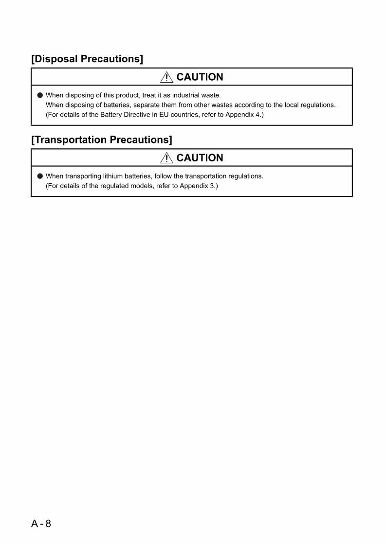
[Disposal Precautions]
[Transportation Precautions]
CAUTIONWhen disposing of this product, treat it as industrial waste.When disposing of batteries, separate them from other wastes according to the local regulations.(For details of the Battery Directive in EU countries, refer to Appendix 4.)
CAUTIONWhen transporting lithium batteries, follow the transportation regulations.(For details of the regulated models, refer to Appendix 3.)
A - 8

REVISIONS*The manual number is given on the bottom left of the back cover.
Japanese manual version SH-080472-S
2004 MITSUBISHI ELECTRIC CORPORATION
Print date Manual number RevisionJun., 2004 SH(NA)-080483ENG-A First editionDec., 2004 SH(NA)-080483ENG-B Addition
Section 12.2.21Partial correctionCONTENTS, Section 2.1.5, 5.2.1, 5.3, 9.1.2, 9.2.4, 10.3.1, 10.4, 10.5, 10.6.1, 11.1, 11.3.1, 11.3.2, 11.4, 11.5, 12.2.1, 12.3.1, 12.3, 12.6, 12.7, Appendix 2.1, Appendix 2.2, Appendix 3.1
May, 2005 SH(NA)-080483ENG-C AdditionSection 12.2.22, 12.2.23, 12.2.24, Appendix 2.4, Appendix 2.5Partial correctionGENERIC TERMS AND ABBREVIATIONS, Chapter 1, Section 2.1.1, 2.1.2, 2.1.5, 2.2, 4.1, 5.2.1, 5.2.2, 5.3, 6.1.4, 7.2.1, 7.2.2, 9.1.3, 10.2, 10.3.2, 10.6.2, 11.3.1, 11.3.2, 11.3.3, 11.3.4, 11.4, 11.5, 12.2.1, 12.2.2, 12.2.3, 12.2.5, 12.2.7, 12.3.2, 12.4.1, 12.4.2, 12.6, 12.7, Appendix 1.5, Appendix 2.2, Appendix 2.3, Appendix 3
Aug., 2005 SH(NA)-080483ENG-D Partial correctionSAFETY PRECAUTIONS, GENERIC TERMS AND ABBREVIATIONS, Section 2.1.1, 4.1, 5.1, 5.2.1, 5.2.2, 5.3, 7.1.2, 10.6.2, 11.3.3, 12.2.2, 12.3.1, 12.4.2, 12.6, 12.7, Appendix 1.2
Apr., 2006 SH(NA)-080483ENG-E Model additionQA65B,QA68BPartial correctionGENERIC TERMS AND ABBREVIATIONS, Section 1.1, 2.1.1, 2.1.2, 5.1, 5.2.1, 5.2.3, 6.1.1, 6.1.2, 9.1.3, 9.1.5, 9.1.6, 10.3.1, 10.3.3, 12.3.2, Appendix 1.4, Appendix 2.2, 2.4, Index
Aug., 2006 SH(NA)-080483ENG-F Partial correctionSAFETY PRECAUTIONS, Section 2.1.5, 6.1.1, 6.1.2, 9.1.5, 10.2, 10.3.1, 12.5.1, 12.5.2, Appendix 1.3, 1.4
Sep., 2006 SH(NA)-080483ENG-G Partial correctionGENERIC TERMS AND ABBREVIATIONS, Section 7.1.2, 9.1.6, 10.3.1, 11.3.3, 12.3.4, 12.3.6, 12.7
Oct., 2006 SH(NA)-080483ENG-H AdditionSection 12.3.11Partial correctionSAFETY PRECAUTIONS, Section 1.1, 2.1.1, Chapter3, Section 4.1, 4.2.1, 5.1, 5.2.1, 5.2.2, 5.3, 6.1.1, 9.1.1, 9.1.2, 9.1.3, 9.1.5, 9.2.3, 9.2.5, 10.2, 10.3.1, 10.6.1, 10.6.2, 11.3.1, 11.4, 11.5, 12.2.19, 12.3.2, 12.3.3, 12.3.5, 12.3.10, 12.6, 12.7, Appendix 1.2, Appendix 2.2
This manual confers no industrial property rights or any rights of any other kind, nor does it confer any patent licenses. Mit-subishi Electric Corporation cannot be held responsible for any problems involving industrial property rights which may occur as a result of using the contents noted in this manual.
C
A - 9

Print date Manual number RevisionApr., 2007 SH(NA)-080483ENG-I Universal model QCPU model addition,
Revision involving High Performance model QCPU and Redundant CPU serial No.09012Model additionQ02UCPU, Q03UDCPU, Q04UDHCPU, Q06UDHCPU, Q65WRBAdditionSection 4.4, 12.2.25Partial correctionSAFETY PRECAUTIONS, ABOUT MANUALS, GENERIC TERMS AND ABBREVIATIONS, Chapter 1, Section 1.1, 2.1, 2.1.1, 2.1.2, 2.1.3, 2.1.4, 2.1.5, 2.2, 4.1, 4.2.2, 4.3.2, 5.1, 5.2.1, 5.2.3, 6.1.1, 6.1.2, 6.1.3, 6.1.4, 7.1.1, 7.1.2, 7.1.3, 7.1.5, 7.1.6, 7.1.7, 7.2.2, 9.1.3, 9.1.5, 10.3.1, 10.3.3, 10.4, 10.6.1, 10.6.2, 11.1, 11.2, 11.3.1, 11.3.2, 11.3.3, 11.3.4, 11.4, 11.5, 12.1, 12.2.1, 12.2.2, 12.2.3, 12.2.10, 12.2.15, 12.2.21, 12.2.22, 12.2.23, 12.3.1, 12.3.2, 12.3.3, 12.3.4, 12.3.5, 12.3.6, 12.3.7, 12.3.8, 12.3.9, 12.3.11, 12.4.1, 12.5.1, 12.5.2, 12.6, 12.7, Appendix 1.1, Appendix 1.3, Appendix 1.4, Appendix 2.2, Appendix 3
Jan., 2008 SH(NA)-080483ENG-J Revision due to the support for Redundant CPU serial number 09102Model additionQA6ADP, Q64PNAdditionAppendix 2.6Partial correctionSAFETY PRECAUTION, GENERIC TERMS AND ABBREVIATIONS, Section 1.1, 2.1.1, 2.1.2, 2.1.3, 2.1.5, 4.1, 4.2.1, 4.3.1, 4.4.1, Chapter 3,Section 5.1, 5.2.1, 5.2.2, 5.3, 6.1.2, 6.1.3, 9.1.1, 9.1.2, 9.1.5, 9.1.6, 9.2.3, 10.1, 10.3.1, 10.3.3, 10.6.1, 10.6.2, 11.2, 11.3.1, 11.3.4, 12.2.13, 12.2.22, 12.3.3, 12.3.4, 12.3.5, 12.3.9, 12.4.1, 12.4.2, 12.5.1, 12.5.2, 12.6, 12.7, Appendix 1.2, Appendix 2.5, Index
Mar., 2008 SH(NA)-080483ENG-K Model additionQ13UDHCPU, Q26UDHCPUAdditionSection 11.3.1Partial correctionGENERIC TERMS AND ABBREVIATIONS, PRECAUTIONS FOR USE, Chapter 1, Section 1.1, 2.1.2, 2.1.4, 2.1.5, 4.1, 4.4.1, 5.2.1, 5.3, 6.1.1, 6.1.3, 7.1.1, 7.1.6, 7.2.1, 10.3.1, 11.1, 11.2, 11.3.1, 11.3.2, 11.3.4, 12.3.1, 12.3.3, 12.3.4, 12.3.5, 12.3.6, 12.6, 12.7, Appendix 1.1, Appendix 2.2, Appendix 2.3, Appendix 2.4, Appendix 2.5, Appendix 2.6
Section11.3.1 11.3.2, Section11.3.2 11.3.3, Section11.3.3 11.3.4, Section11.3.4 11.3.5
A - 10

Print date Manual number RevisionMay, 2008 SH(NA)-080483ENG-L Revision due to the addition of Process CPU and Universal model QCPU.
AdditionSection 12.2.26, 12.2.27, 12.2.28, 12.2.29, 12.2.30, 12.2.31, 12.5.2Model additionChapter 1, Section 1.1, 2.1.2, 2.1.3, 2.1.4, 2.1.5, 2.2, 4.1, 4.3.1, 4.4.1, 6.1.3, 7.1.2, 11.3.2, 12.2.1, 12.3.3, 12.3.4, 12.3.5, 12.3.6, 12.3.9, 12.6, 12.7, Appendix1.1, Appendix 2, Appendix 2.4, Appendix 2.5, Appendix 2.6
Sep., 2008 SH(NA)-080483ENG-M Partial correctionSAFETY PRECAUTION, Section 1.1, 2.2, 7.1.6, 7.2.1, 9.1.3, 9.1.5, Appendix 2.6 AdditionAppendix 4
Dec., 2008 SH(NA)-080483ENG-N Universal model QCPU model additionsRevision and overall review for support to the Universal model QCPU serial number "10101".Model additionQ00UJCPU, Q00UCPU, Q01UCPU, Q10UDHCPU, Q10UDEHCPU, Q20UDHCPU, Q20UDEHCPU
Mar., 2009 SH(NA)-080483ENG-O Revision due to the support for Universal model QCPU serial number "11012".Partial correctionSAFETY PRECAUTIONS, INTRODUCTION, GENERIC TERMS AND ABBREVIATIONS, Section 1.1, 2.1.3, 2.1.4, 4.1.3, 4.1.5, 4.3.1, 4.3.2, 4.3.5, 4.4.1, 5.2.1, 5.2.3, 5.2.4, 5.3, 6.1.1, 6.1.2, 7.1.2, 7.1.6, CHAPTER 8, Section 9.1.2, 9.1.3, 9.1.5, 9.2, 9.2.4, 10.1, 10.3.1, 10.3.3, CHAPTER 11, Section 11.3.1, 11.3.2, 11.3.3, 12.1, 12.2.1 to 12.2.12, 12.2.14 to 12.2.36, 12.3.11, 12.5.1, 12.6, 12.7, 12.8, Appendix 2.6Addition12.2.37 to 12.2.39
Jul., 2009 SH(NA)-080483ENG-P Revision because of function support by the Universal model QCPU having a serial number "11043" or laterPartial correctionGENERIC TERMS AND ABBREVIATIONS, Section 2.1.3, 2.1.6, 7.2.2, 11.3.1, 11.3.2, 11.3.3, 11.4, 11.5, 12.3.3, 12.3.4, 12.4, 12.7, 12.8, Appendix 2.6
A - 11

Memo
A - 12

A - 13
INTRODUCTION
This manual provides hardware specifications, maintenance and inspection of the system, and troubleshooting of the CPU modules, power supply modules, and base units required for operating the Q series programmable controllers.
This manual roughly comprises the following three parts.
Relevant CPU module
RemarkThis manual does not describe the functions of the CPU module.For the functions, refer to the following.
Manuals for the CPU module used. (Function Explanation, Program Fundamentals)
For multiple CPU systems, refer to the following. QCPU User's Manual (Multiple CPU System)
For redundant systems, refer to the following. QnPRHCPU User's Manual (Redundant System)
1) Chapter 1 and 2 Describes outline of the CPU module and the system configuration to help users understand features of the CPU module and fundamentals of system configuration.
2) Chapter 3 through 7 Describes the general specifications of operating environments for the CPU module, power supply module, and base units and performance specifications of respective modules.
3) Chapter 8 through 12 Describes overall maintenance such as installation of the CPU module, daily inspec-tions, and troubleshooting.
CPU module Model Basic model QCPU Q00(J)CPU, Q01CPU
High Performance model QCPU Q02(H)CPU, Q06HCPU, Q12HCPU, Q25HCPU
Process CPU Q02PHCPU, Q06PHCPU, Q12PHCPU, Q25PHCPU
Redundant CPU Q12PRHCPU, Q25PRHCPU
Universal model QCPUQ00UJCPU, Q00UCPU, Q01UCPU, Q02UCPU, Q03UD(E)CPU, Q04UD(E)HCPU, Q06UD(E)HCPU, Q10UD(E)HCPU, Q13UD(E)HCPU, Q20UD(E)HCPU, Q26UD(E)HCPU

CONTENTS
A -
SAFETY PRECAUTIONS......................................................................................................................A - 1REVISIONS ...........................................................................................................................................A - 9INTRODUCTION ...................................................................................................................................A - 13MANUALS .............................................................................................................................................A - 19MANUAL PAGE ORGANIZATION.........................................................................................................A - 22GENERIC TERMS AND ABBREVIATIONS ..........................................................................................A - 24USAGE NOTE .......................................................................................................................................A - 27
CHAPTER1 OVERVIEW 1-1 to 1-7
1.1 Features................................................................................................................................. 1 - 1
CHAPTER2 SYSTEM CONFIGURATION 2-1 to 2-26
2.1 System Configuration............................................................................................................. 2 - 12.1.1 Overall configuration .........................................................................................................2 - 22.1.2 Component list ..................................................................................................................2 - 32.1.3 Precautions for system configuration ................................................................................2 - 62.1.4 Bus connection of GOT.....................................................................................................2 - 132.1.5 Peripheral device configuration .........................................................................................2 - 172.1.6 Applicable softwares .........................................................................................................2 - 22
2.2 Checking Serial Number and Function Version ..................................................................... 2 - 25
CHAPTER3 GENERAL SPECIFICATIONS 3-1 to 3-2
CHAPTER4 HARDWARE SPECIFICATIONS OF THE CPU MODULE 4-1 to 4-55
4.1 Performance Specifications ................................................................................................... 4 - 14.1.1 Basic model QCPU ...........................................................................................................4 - 14.1.2 High Performance model QCPU .......................................................................................4 - 44.1.3 Process CPU.....................................................................................................................4 - 84.1.4 Redundant CPU ................................................................................................................4 - 124.1.5 Universal model QCPU .....................................................................................................4 - 16
4.2 Basic Model QCPU................................................................................................................ 4 - 264.2.1 Part names........................................................................................................................4 - 264.2.2 Switch operation at the time of writing program ................................................................4 - 314.2.3 Reset operation.................................................................................................................4 - 324.2.4 Latch clear operation.........................................................................................................4 - 33
4.3 High Performance Model QCPU, Process CPU and Redundant CPU .................................. 4 - 344.3.1 Part names........................................................................................................................4 - 344.3.2 Switch operation after writing program..............................................................................4 - 404.3.3 Reset operation.................................................................................................................4 - 414.3.4 Latch clear operation.........................................................................................................4 - 414.3.5 Automatic writing to standard ROM...................................................................................4 - 42
4.4 Universal Model QCPU.......................................................................................................... 4 - 43
14

4.4.1 Part names........................................................................................................................4 - 434.4.2 Switch operation after writing a program...........................................................................4 - 534.4.3 Reset operation.................................................................................................................4 - 544.4.4 Latch clear operation.........................................................................................................4 - 55
CHAPTER5 POWER SUPPLY MODULE 5-1 to 5-36
5.1 Base Unit that Can Be Used in Combination with Power Supply Module.............................. 5 - 1
5.2 Specifications ......................................................................................................................... 5 - 25.2.1 Power supply module specifications .................................................................................5 - 25.2.2 Selecting the power supply module ..................................................................................5 - 215.2.3 Life detection power supply module ..................................................................................5 - 265.2.4 Precaution when connecting the uninterruptive power supply ..........................................5 - 305.2.5 Precautions on power supply capacity ..............................................................................5 - 30
5.3 Part Names and Settings ....................................................................................................... 5 - 31
CHAPTER6 BASE UNIT AND EXTENSION CABLE 6-1 to 6-21
6.1 Base Unit ............................................................................................................................... 6 - 16.1.1 Extension base units that can be combined with the main base unit ................................6 - 16.1.2 Specification table .............................................................................................................6 - 26.1.3 Part names........................................................................................................................6 - 66.1.4 Setting extension bases ....................................................................................................6 - 146.1.5 Guideline for extension base units ....................................................................................6 - 16
6.2 Extension Cable..................................................................................................................... 6 - 216.2.1 Specification table .............................................................................................................6 - 21
CHAPTER7 MEMORY CARD AND BATTERY 7-1 to 7-17
7.1 Memory Card ......................................................................................................................... 7 - 17.1.1 List of usable memory cards .............................................................................................7 - 17.1.2 Memory card specifications...............................................................................................7 - 27.1.3 Part names of the memory card ........................................................................................7 - 47.1.4 Handling the memory card ................................................................................................7 - 57.1.5 Installing and removing a memory card ............................................................................7 - 67.1.6 Specifications of the memory card battery ........................................................................7 - 107.1.7 Battery Installation into the memory card ..........................................................................7 - 11
7.2 Battery (Q6BAT, Q7BAT, Q8BAT) ..........................................................................................7 - 137.2.1 Battery specifications ........................................................................................................7 - 137.2.2 Battery installation .............................................................................................................7 - 14
CHAPTER8 CPU MODULE START-UP PROCEDURES 8-1 to 8-3
A - 15

A -
CHAPTER9 EMC AND LOW VOLTAGE DIRECTIVES 9-1 to 9-18
9.1 Requirements for Compliance with the EMC Directive .......................................................... 9 - 19.1.1 Standards relevant to the EMC Directive ..........................................................................9 - 29.1.2 Installation instructions for EMC Directive.........................................................................9 - 39.1.3 Cables ...............................................................................................................................9 - 49.1.4 Power supply part of the power supply module, Q00JCPU, and Q00UJCPU...................9 - 89.1.5 When using MELSEC-A series modules...........................................................................9 - 89.1.6 Others ...............................................................................................................................9 - 13
9.2 Requirement to Compliance with the Low Voltage Directive ................................................. 9 - 159.2.1 Standard applied for MELSEC-Q series programmable controller....................................9 - 159.2.2 MELSEC-Q series programmable controller selection......................................................9 - 159.2.3 Power supply.....................................................................................................................9 - 169.2.4 Control panel .....................................................................................................................9 - 169.2.5 Grounding .........................................................................................................................9 - 189.2.6 External wiring...................................................................................................................9 - 18
CHAPTER10 LOADING AND INSTALLATION 10-1 to 10-46
10.1 General Safety Requirements................................................................................................ 10 - 1
10.2 Calculating Heat Generation of Programmable Controller..................................................... 10 - 7
10.3 Module Installation ................................................................................................................. 10 - 1010.3.1 Precaution on installation ..................................................................................................10 - 1010.3.2 Instructions for mounting the base unit .............................................................................10 - 1910.3.3 Installation and removal of module....................................................................................10 - 22
10.4 How to set the Base Number for the Extension Base Unit .................................................... 10 - 30
10.5 Connection and Disconnection of Extension Cable ............................................................... 10 - 36
10.6 Wiring..................................................................................................................................... 10 - 3910.6.1 Wiring precautions ............................................................................................................10 - 3910.6.2 Connecting to the power supply module ...........................................................................10 - 44
CHAPTER11 MAINTENANCE AND INSPECTION 11-1 to 11-35
11.1 Daily Inspection...................................................................................................................... 11 - 3
11.2 Periodic Inspection................................................................................................................. 11 - 4
11.3 Battery Life and Replacement Procedure .............................................................................. 11 - 511.3.1 Display of battery consumption and reduction measures of the consumption ..................11 - 611.3.2 Battery lives of CPU modules ...........................................................................................11 - 811.3.3 Replacement procedure of the CPU module battery ........................................................11 - 2311.3.4 SRAM card battery life ......................................................................................................11 - 2911.3.5 SRAM card CPU module battery replacement procedure.................................................11 - 31
11.4 When Programmable Controller Has Been Stored Without Battery....................................... 11 - 34
11.5 When Battery Has Gone Flat During Storage of Programmable Controller........................... 11 - 35
CHAPTER12 TROUBLESHOOTING 12-1 to 12-272
16

12.1 Troubleshooting Basics.......................................................................................................... 12 - 1
12.2 Troubleshooting ..................................................................................................................... 12 - 312.2.1 Troubleshooting flowchart .................................................................................................12 - 312.2.2 When the ERR. terminal (negative logic) has turned off (opened)....................................12 - 512.2.3 When the LIFE OUT terminal (negative logic) has turned off (opened) ............................12 - 912.2.4 When the MODE LED does not turn on ............................................................................12 - 1012.2.5 When the MODE LED is flickering ....................................................................................12 - 1112.2.6 When the POWER LED has turned off .............................................................................12 - 1212.2.7 When the POWER LED is flickering in orange .................................................................12 - 1412.2.8 When the POWER LED has turned on in red ...................................................................12 - 1512.2.9 When the LIFE LED has turned off ...................................................................................12 - 1612.2.10 When the LIFE LED has turned on in red .........................................................................12 - 1712.2.11 When the LIFE LED is flickering in red .............................................................................12 - 1712.2.12 When the RUN LED has turned off ...................................................................................12 - 1812.2.13 When the RUN LED is flickering .......................................................................................12 - 1912.2.14 When the ERR. LED has turned on or is flickering ...........................................................12 - 1912.2.15 When the USER LED has turned on .................................................................................12 - 2012.2.16 When the BAT. LED has turned on or is flickering.............................................................12 - 2012.2.17 When the BOOT LED is flickering .....................................................................................12 - 2112.2.18 When the LEDs of the output module do not turn on ........................................................12 - 2212.2.19 When output load of the output module does not turn on .................................................12 - 2312.2.20 When unable to read a program .......................................................................................12 - 2412.2.21 When unable to write a program .......................................................................................12 - 2512.2.22 When program is rewritten unintentionally ........................................................................12 - 2612.2.23 When unable to perform boot operation from the memory card .......................................12 - 2712.2.24 When “UNIT VERIFY ERR.” has occurred........................................................................12 - 2912.2.25 When “CONTROL BUS ERR.” has occurred ....................................................................12 - 3012.2.26 When the CPU module does not start...............................................................................12 - 3112.2.27 When “OPERATION ERROR” has occurred at execution of the S(P).SFCSCOMR and
S(P).SFCTCOMR instructions.............................................................................. 12 - 3212.2.28 When comments cannot be read at execution of the S(P).SFCSCOMR and S(P).SFCTCOMR
instructions ...................................................................................................... 12 - 3312.2.29 When “PARAMETER ERROR” has occurred at power on or reset...................................12 - 3512.2.30 When the CPU cannot communicate with GX Developer .................................................12 - 3912.2.31 When Ethernet communication is not available other than by direct connection to GX Developer
.................................................................................................................... 12 - 4112.2.32 When Ethernet communication with the target device is not available .............................12 - 4312.2.33 When Ethernet communication is not available by direct connection to GX Developer....12 - 4812.2.34 When Ethernet communication with CPU module is slow or unstable..............................12 - 5112.2.35 When an error has occurred during MC protocol communication .....................................12 - 5412.2.36 When clock data cannot be set by SNTP..........................................................................12 - 5712.2.37 When unable to receive data on the external device side by the Socket communication function
.................................................................................................................... 12 - 5912.2.38 When unable to receive data by the Socket communication function ...............................12 - 6012.2.39 When open process of the Socket communication function does not complete ...............12 - 61
12.3 Error Code List....................................................................................................................... 12 - 6212.3.1 Error codes........................................................................................................................12 - 63
A - 17

A -
12.3.2 Reading an error code ......................................................................................................12 - 6312.3.3 Error code list (1000 to 1999)............................................................................................12 - 6412.3.4 Error code list (2000 to 2999)............................................................................................12 - 7712.3.5 Error code list (3000 to 3999)............................................................................................12 - 9512.3.6 Error code list (4000 to 4999)............................................................................................12 - 11212.3.7 Error code list (5000 to 5999)............................................................................................12 - 12712.3.8 Error code list (6000 to 6999)............................................................................................12 - 12912.3.9 Error code list (7000 to 10000)..........................................................................................12 - 13912.3.10 Canceling of Errors ...........................................................................................................12 - 14412.3.11 Error codes returned to request source during communication with CPU module............12 - 146
12.4 Module Change during System Operation............................................................................. 12 - 16712.4.1 Online module change ......................................................................................................12 - 16712.4.2 Change of redundant power supply module .....................................................................12 - 178
12.5 I/O Module Troubleshooting................................................................................................... 12 - 18012.5.1 Input circuit troubleshooting ..............................................................................................12 - 18012.5.2 Output circuit troubleshooting ...........................................................................................12 - 183
12.6 Built-in Ethernet Port Diagnosis ............................................................................................. 12 - 187
12.7 SPECIAL RELAY LIST........................................................................................................... 12 - 195
12.8 SPECIAL REGISTER LIST....................................................................................................12 - 221
APPENDICES App-1 to App-37
Appendix 1 External Dimensions ................................................................................................... App- 1Appendix 1.1 CPU Module ............................................................................................App- 1Appendix 1.2 Power Supply Module ................................................................................ App- 6Appendix 1.3 Main Base Unit .........................................................................................App- 10Appendix 1.4 Extension Base Unit .................................................................................. App- 16Appendix 1.5 Extension Cable........................................................................................App- 22Appendix 1.6 Tracking cable ..........................................................................................App- 22Appendix 1.7 Q8BAT-SET .............................................................................................App- 23
Appendix 2 Functions Added or Changed by Version Upgrade.....................................................App- 24Appendix 2.1 Basic Model QCPU Upgrade .......................................................................App- 24Appendix 2.2 High Performance Model QCPU Upgrade ......................................................App- 26Appendix 2.3 Precautions for Using the High Performance Model QCPU of Older Versions........App- 28Appendix 2.4 Process CPU Upgrade ............................................................................... App- 31Appendix 2.5 Redundant CPU Upgrade ........................................................................... App- 32Appendix 2.6 Universal Model QCPU Upgrade ..................................................................App- 33
Appendix 3 Precautions for Battery Transportation........................................................................App- 35
Appendix 4 Handling of Batteries and Devices with Built-in Batteries in EU Member States ........ App- 36Appendix 4.1 Disposal precautions.................................................................................. App- 36Appendix 4.2 Exportation precautions .............................................................................. App- 37
INDEX Index-1 to Index-4
18

MANUALS
To understand the main specifications, functions, and usage of the CPU module, refer to the basic manuals. Read other manuals as well when using a different type of CPU module and its functions.Order each manual as needed, referring to the following lists.
The numbers in the "CPU module" and the respective modules are as follows.
: Basic manual, : Other CPU module manuals
Number CPU module1) Basic model QCPU
2) High Performance model QCPU
3) Process CPU
4) Redundant CPU
5) Universal model QCPU
Manual name< Manual number (model code) > Description
CPU module1) 2) 3) 4) 5)
User's manual
QCPU User's Manual (Hardware Design, Maintenance and Inspection)
< SH-080483ENG (13JR73) >
Specifications of the hardware (CPU modules, power supply modules, base units, extension cables, and memory cards), system maintenance and inspection, troubleshooting, and error codes
QnUCPU Users Manual (Function Explana-tion, Program Fundamentals)
< SH-080807ENG (13JZ27) >
Functions, methods, and devices for programming
Qn(H)/QnPH/QnPRHCPU User's Manual (Function Explanation, Program Fundamen-tals)
< SH-080808ENG (13JZ28) >
Functions, methods, and devices for programming
QCPU User's Manual (Multiple CPU System)
< SH-080485ENG (13JR75) >
Information for configuring a multiple CPU system (system configuration, I/O numbers, communication between CPU modules, and communication with the input/output modules and intelligent function modules)
QnPRHCPU User's Manual (Redundant System)
< SH-080486ENG (13JR76)) >
Redundant system configuration, functions, communication with external devices, and troubleshooting
QnUCPU User's Manual (Communication via Built-in Ethernet Port)
< SH-080811ENG (13JZ29) >
Functions for the communication via built-in Ethernet port of the CPU module
Programming manual
QCPU Programming Manual (Common Instructions)
< SH-080809ENG (13JW10) >
How to use sequence instructions, basic instructions, and application instructions
A - 19

QCPU (Q Mode)/QnACPU Programming Manual (SFC)
< SH-080041 (13JF60) >
System configuration, performance specifications, functions, programming, debugging, and error codes for SFC (MELSAP3) programs
QCPU (Q Mode) Programming Manual (MELSAP-L)
< SH-080076 (13JF61) >
Programming methods, specifications, and functions for SFC (MELSAP-L) programs
QCPU (Q Mode) Programming Manual (Structured Text)
< SH-080366E (13JF68) >
Programming methods using structured languages
QCPU (Q Mode) / QnACPU Programming Manual (PID Control Instructions)
< SH-080040 (13JF59) >
Dedicated instructions for PID control
QnPHCPU/QnPRHCPU Programming Manual (Process Control Instructions)
< SH-080316E (13JF67) >
Dedicated instructions for process control
Manual name< Manual number (model code) > Description
CPU module1) 2) 3) 4) 5)
A - 20

Other relevant manuals
Manual name DescriptionCC-Link IE Controller Network Reference Manual
< SH-080668ENG (13JV16) >
Specifications, procedures and settings before system operation, parameter setting, programming, and troubleshooting of the CC-Link IE controller network module
Q Corresponding MELSECNET/H Network System Reference Manual (PLC to PLC network)
< SH-080049 (13JF92) >
Specifications, procedures and settings before system operation, parameter setting, programming, and troubleshooting of a MELSECNET/H network system (PLC to PLC network)
Q Corresponding MELSECNET/H Network System Reference Manual (Remote I/O network)
< SH-080124 (13JF96) >
Specifications, procedures and settings before system operation, parameter setting, programming, and troubleshooting of a MELSECNET/H network system (remote I/O network)
Q Corresponding Ethernet Interface Module User's Manual (Basic)
< SH-080009 (13JL88) >
Specifications, procedures for data communication with external devices, line connection (open/close), fixed buffer communication, random access buffer communication, and troubleshooting of the Ethernet module
Q Corresponding Ethernet Interface Module User's Manual (Application)
< SH-080010 (13JL89) >
E-mail function, programmable controller CPU status monitoring function, communication via MELSECNET/H or MELSECNET/10, communication using the data link instructions, and file transfer function (FTP server) of the Ethernet module
CC-Link System Master/Local Module User's Manual
< SH-080394E (13JR64) >
System configuration, performance specifications, functions, handling, wiring, and troubleshooting of the QJ61BT11N
Q Corresponding Serial Communication Module User's Manual (Basic)
< SH-080006 (13JL86) >
Overview, system configuration, specifications, procedures before operation, basic data communication method with external devices, maintenance and inspection, and troubleshooting for using the serial communication module
Q Corresponding Serial Communication Module User's Manual (Application)
< SH-080007 (13JL87) >
Special functions (specifications, usage, and settings and data communication method with external devices of the serial communication module
Q Corresponding MELSEC Communication Protocol Reference Manual
< SH-080008 (13JF89) >
Communication method using the MC protocol, which reads/writes data to/from the CPU module via the serial communication module or Ethernet module
GX Developer Version 8 Operating Manual
< SH-080373E (13JU41) >Operating methods of GX Developer, such as programming and printout
A - 21

MANUAL PAGE ORGANIZATION
Icons
DescriptionBasic model QCPU
High Performance model QCPU
Process CPU Redundant CPUUniversal model
QCPU
Icons indicate that specifications described on the page contain some precautions.
Note (detailed explanation)
ReferenceNote (icon)
The section in this manual or
another relevant manual that can
be referred to is shown with .
The chapter of the current page can be
easily identified by this indication on the
right side.
Chapter
The detailed note corresponding to each icon
is described.
Section title
The section number and title of the current
page can be easily identified.
The detailed explanation of "Note . " is
provided under the corresponding
"Note . " at the bottom of the page.
Basic Highperformance Process Redundant Universal
A - 22

In addition, this manual uses the following types of explanations.
In addition to description of the page, notes or functions that require special attention are described here.
RemarkThe reference related to the page or useful information are described here.
A - 23

GENERIC TERMS AND ABBREVIATIONS
Unless otherwise specified, this manual uses the following generic terms and abbreviations.
* indicates a part of the model or version.
(Example): Q33B, Q35B, Q38B, Q312B Q3 B
Generic term/abbreviation DescriptionSeries Q series Abbreviation for Mitsubishi MELSEC-Q series programmable controller
AnS seriesGeneric term for compact types of Mitsubishi MELSEC-A Series Programmable Controller
A seriesGeneric term for large types of Mitsubishi MELSEC-A Series Programmable Controller
CPU module type
CPU moduleGeneric term for the Basic model QCPU, High Performance model QCPU, Process CPU, Redundant CPU, Universal model QCPU
Basic model QCPU Generic term for the Q00JCPU, Q00CPU, and Q01CPUHigh Performance model QCPU Generic term for the Q02CPU, Q02HCPU, Q06HCPU, Q12HCPU, Q25HCPUProcess CPU Generic term for the Q02PHCPU, Q06PHCPU, Q12PHCPU, Q25PHCPURedundant CPU Generic term for the Q12PRHCPU and Q25PRHCPU
Universal model QCPU
Generic term for the Q00UJCPU, Q00UCPU, Q01UCPU, Q02UCPU, Q03UDCPU, Q04UDHCPU, Q06UDHCPU, Q10UDHCPU, Q13UDHCPU, Q20UDHCPU, Q26UDHCPU, Q03UDECPU, Q04UDEHCPU, Q06UDEHCPU, Q10UDEHCPU, Q13UDEHCPU, Q20UDEHCPU, and Q26UDEHCPU
Built-in Ethernet port QCPUGeneric term for the Q03UDECPU, Q04UDEHCPU, Q06UDEHCPU, Q10UDEHCPU, Q13UDEHCPU, Q20UDEHCPU, and Q26UDEHCPU
Motion CPUGeneric term for Mitsubishi motion controllers, Q172CPUN, Q173CPUN, Q172HCPU, Q173HCPU, Q172CPUN-T, Q173CPUN-T, Q172HCPU-T, Q173HCPU-T, Q172DCPU, and Q173DCPU
PC CPU moduleGeneric term for MELSEC-Q series-compatible PC CPU module, PPC-CPU852(MS)-512, manufactured by CONTEC Co., Ltd.
C Controller moduleGeneric term for the Q06CCPU-V, Q06CCPU-V-B, and Q12DCCPU-V C Controller modules
CPU module model
QnU(D)(H)CPUGeneric term for the Q00UJCPU, Q00UCPU, Q01UCPU, Q02UCPU, Q03UDCPU, Q04UDHCPU, Q06UDHCPU, Q10UDHCPU, Q13UDHCPU, Q20UDHCPU, and Q26UDHCPU
Base unit type
Base unit
Generic term for the main base unit, extension base unit, slim type main base unit, redundant power main base unit, redundant power extension base unit, redundant power extension base unit, and multiple CPU high speed main base unit
Main base unit Generic term for the Q3 B, Q3 SB, Q3 RB, and Q3 DB
Extension base unitGeneric term for the Q5 B, Q6 B, Q6 RB, Q6 WRB, QA1S6 B, QA6 B, and QA6ADP+A5 B/A6 B
Slim type main base unit Another name for the Q3 SBRedundant power main base unit Another name for the Q3 RBRedundant power extension base unit Another name for the Q6 RB
Redundant type extension base unit Another name for the Q6 WRB
A - 24

Generic term/abbreviation DescriptionRedundant type extension base unit Another name for the Q6 WRB
Multiple CPU high speed main base unit Another name for the Q3 DB
Redundant base unitGeneric term for the redundant power main base unit, redundant power extension base unit, and redundant type extension base unit
Base unit model
Q3 B Generic term for the Q33B, Q35B, Q38B, and Q312B main base units
Q3 SB Generic term for the Q32SB, Q33SB, and Q35SB slim type main base units
Q3 RB Another name for the Q38RB redundant power main base unit
Q3 DB Generic term for the Q38DB and Q312DB multiple CPU high speed main base units
Q5 B Generic term for the Q52B and Q55B extension base units
Q6 B Generic term for the Q63B, Q65B, Q68B, and Q612B extension base units
Q6 RB Another name for the Q68RB redundant power extension base unit
Q6 WRB Another name for Q65WRB extension base unit for redundant system
QA1S6 B Generic term for the QA1S65B and QA1S68B
QA6 B Generic term for the QA65B and QA68B extension base units
A5 B Generic term for the A52B, A55B, and A58B extension base units
A6 B Generic term for the A62B, A65B, and A68B extension base units
QA6ADP+A5 B/A6 B Abbreviation for a large type extension base unit where the QA6ADP is mounted
Power supply module
Power supply moduleGeneric term for the Q series power supply module, slim type power supply mod-ule, and redundant power supply module
Q series power supply moduleGeneric term for the Q61P-A1, Q61P-A2, Q61P, Q61P-D, Q62P, Q63P, Q64P, and Q64PN power supply modules
AnS series power supply module Generic term for the A1S61PN, A1S62PN, and A1S63 power supply modules
A series power supply moduleGeneric term for the A61P, A61PN, A62P, A63P, A68P, A61PEU, and A62PEU power supply modules
Slim type power supply module Abbreviation for the Q61SP slim type power supply module
Redundant power supply module Generic term for the Q63RP and Q64RP redundant power supply modules
Life detection power supply module
Abbreviation for the Q61P-D life detection power supply module]
Network
MELSECNET/H Abbreviation for the MELSECNET/H network system
Ethernet Abbreviation for the Ethernet network system
CC-Link Abbreviation for the Control & Communication Link
Memory card
Memory card Generic term for the SRAM card, Flash card, and ATA card
SRAM cardGeneric term for the Q2MEM-1MBS, Q2MEM-2MBS, Q3MEM-4MBS, and Q3MEM-8MBS SRAM cards
Flash card Generic term for the Q2MEM-2MBF and Q2MEM-4MBF Flash cards
ATA cardGeneric term for the Q2MEM-8MBA, Q2MEM-16MBA, and Q2MEM-32MBA ATA cards
A - 25

Generic term/abbreviation Description
Others
GX Developer Product name for SW D5C-GPPW-E GPP function software package compatible with the Q series
PX Developer Product name for SW D5C-FBDQ process control FBD software package
QA6ADP Abbreviation for the QA6ADP QA conversion adapter module
Extension cableGeneric term for the QC05B, QC06B, QC12B, QC30B, QC50B, and QC100B extension cables
Tracking cableGeneric term for the QC10TR and QC30TR tracking cables for the Redundant module
BatteryGeneric term for the Q6BAT, Q7BAT, and Q8BAT CPU module batteries, Q2MEM-BAT SRAM card battery, and Q3MEM-BAT SRAM card battery
GOTGeneric term for Mitsubishi Graphic Operation Terminal, GOT-A*** series, GOT-F***series, and GOT1000 series
A - 26

USAGE NOTE
First use of the Q series CPU module
Memory must be formatted using GX Developer before first use of the CPU module.For details of memory formatting, refer to the following.
Operating manual for GX Developer
Batteries(1) When resuming operation with the CPU module which has been stored without battery:
The CPU module memory must be formatted using GX Developer. ( Section 11.4)(2) When resuming operation with the CPU module in which installed battery life had expired during storage:
The CPU module memory must be formatted using GX Developer. ( Section 11.5)
A - 27

CHAPTER1 OVERVIEW
1.1 Features
This section describes features of the Q series CPU module.
(1) Large number of I/O points that can be controlledThe Q Series CPU module supports the following number of actual I/O points accessible to the I/O modules mounted on the base unit.
(a) Basic model QCPU
Up to 2048 points (X/Y0 to 7FF) are supported as the number of I/O device points usable for refreshing the remote I/O of the CC-Link and link I/O (LX, LY) of the MELSECNET/H.
(b) High Performance model QCPUOne module can support 4096 points (X/Y0 to FFF).Up to 8192 points (X/Y0 to 1FFF) are supported as the number of I/O device points usable for the remote I/O stations in the MELSECNET/H remote I/O network, the CC-Link data link, and the MELSECNET/MINI-S3 data link.
(c) Process CPU and Redundant CPUOne module can support 4096 points (X/Y0 to FFF).Up to 8192 points (X/Y0 to 1FFF) are supported as the number of I/O device points usable for the remote I/O stations in the MELSECNET/H remote I/O network and CC-Link data link.
(d) Universal model QCPU
Up to 8192 points (X/Y0 to 1FFF) are supported as the number of I/O device points usable for the remote I/O stations in the MELSECNET/H remote I/O network and CC-Link data link.
• Q00JCPU: 256 points (X/Y0 to FF) : 256 points (X/Y0 to FF)• Q00CPU, Q01CPU: 1024 points : 1024 points (X/Y0 to 3FF)
• Q00UJCPU : 256 points (X/Y0 to FF)• Q00UCPU, Q01UCPU : 1024 points (X/Y0 to 3FF)• Q02UCPU : 2048 points (X/Y0 to 7FF)• Q03UD(E)CPU, Q04UD(E)HCPU,
Q06UD(E)HCPU, Q10UD(E)HCPU,Q13UD(E)HCPU, Q20UD(E)HCPU,Q26UD(E)HCPU : 4096 points (X/Y0 to FFF)
1 - 1

CHAPTER1 OVERVIEW
1
2
3
4
5
6
7
8
1.1 Features
(2) Lineup of CPUThe following lists the lineup of CPU available for various program size.
Table1.1 Program size for each CPU module
CPU module type Program size
Basic model QCPUQ00(J)CPU 8K steps
Q01CPU 14Ksteps
High Performance model QCPU
Q02(H)CPU 28K steps
Q06HCPU 60K steps
Q12HCPU 124K steps
Q25HCPU 252K steps
Process CPU
Q02PHCPU 28K steps
Q06PHCPU 60K steps
Q12PHCPU 124K steps
Q25PHCPU 252K steps
Redundant CPUQ12PRHCPU 124K steps
Q25PRHCPU 252K steps
Universal model QCPU
Q00U(J)CPU 10K steps
Q01UCPU 15K steps
Q02UCPU 20K steps
Q03UD(E)CPU 30K steps
Q04UD(E)HCPU 40K steps
Q06UD(E)HCPU 60K steps
Q10UD(E)HCPU 100K steps
Q13UD(E)HCPU 130K steps
Q20UD(E)HCPU 200K steps
Q26UD(E)HCPU 260K steps
1 - 2

(3) High speed processingHigh speed processing has been achieved.
The MELSEC Q series base unit high-speed system bus has achieved faster access to an intelligent function module and link refresh with a network module.
(a) Basic model QCPUMELSECNET/H link refreshing: 2.2ms/2K words*1
*1: The Q01CPU is used without using SB and SW, and the MELSECNET/H network module is mounted on the main base unit.
(b) High Performance model QCPU, Process CPU, Redundant CPU or Universal model QCPUAccess to the intelligent function module: 20 s/word (approximately 7 times*2)
MELSECNET/H link refreshing: 4.6ms/8K words (approximately 4.3 times*2)*2: These are the values resulted from the following comparison:
• Comparing Q02HCPU with Q2ASHCPU-S1• Comparing Q25PHCPU with Q4ARCPU• Comparing Q25PRHCPU with Q4ARCPU
Table1.2 Processing speed (LD instruction)
CPU module typeLD instruction processing
speed
Basic model QCPU
Q00JCPU 200ns
Q00CPU 160ns
Q01CPU 100ns
High Performance model QCPU
Q02CPU 79ns
Q02HCPU, Q06HCPU, Q12HCPU, Q25HCPU
34nsProcess CPU
Q02PHCPU, Q06PHCPU, Q12PHCPU, Q25PHCPU
Redundant CPU Q12PRHCPU, Q25PRHCPU
Universal model QCPU
Q00UJCPU 120ns
Q00UCPU 80ns
Q01UCPU 60ns
Q02UCPU 40ns
Q03UD(E)CPU 20ns
Q04UD(E)HCPU, Q06UD(E)HCPU, Q10UD(E)HCPU, Q13UD(E)HCPU, Q20UD(E)HCPU, Q26UD(E)HCPU
9.5ns
1 - 3

CHAPTER1 OVERVIEW
1
2
3
4
5
6
7
8
1.1 Features
(4) Increase in debugging efficiency through high-speed communication with GX DeveloperHigh speed communications at 115.2Kbps maximum are available by using RS-232 which reducing the time required for writing and reading of programs and monitoring. Also, the communication time efficiency of debugging has been increased.In addition, High Performance model QCPUs (except for the Q02CPU), ProcessCPUs, Redundant CPUs and Universal model QCPUs support USB, so that high-speed communications of 12Mbps are available.
(5) AnS/A series I/O modules and special function modules are availableThe AnS/A series compatible extension base units (QA1S6 B, QA6 B and QA6ADP+A5 B/A6 B) allow the High Performance model QCPU to use the AnS/A series I/O modules and special function modules.
(6) Saved space by downsizingThe installation space for the Q series has been reduced by approx. 60% compared with the AnS series.
Figure 1.1 26K step program transfer time
Figure 1.2 Installation area comparison between Q series and AnS series
0 10 20 30 40 50 60 70 80
Q25HCPU(USB)
Q25HCPU(RS-232)
Q2ASHCPU
A2USHCPU-S1
12
30
86
94
90 100 (Unit:s)
(depth:98mm(3.86inch))
98
mm
(3
.86
inch
)
Q s
erie
s
An
S s
erie
s
8 Slot Main Base Unit 328mm(12.92inch)
12 Slot Main Base Unit 439mm(17.28inch)
5 Slot Main Base Unit 245mm(9.65inch)
1 - 4

(7) Connection of up to 7 extension base units. Up to seven extension base units can be connected to the Q series CPU module. The overall extension cable length is 13.2m (43.31feet), which allows flexible layout of base units.
(8) Memory extension Note1.1 by memory cardNote1Memory card installation connector is incorporated so that a maximum 32M bytes of memory card can be connected. (32M bytes memory card can be connected only when an ATA card is used.) By installing a large size memory card, large size files can be managed such as comment setting to all data devices and saving old programs in a memory as correction data.Even when a memory card is not installed, a program can be stored into the standard ROM through the standard ROM incorporated in the CPU module, and file registers can be handled by the standard RAM.
For the High Performance model QCPU, the number of usable file register points differs depending on the function version and serial number.For details, refer to Appendix 2.2.
Note1
Note1.1The Basic model QCPU, Q00(J)CPU, and Q01UCPU do not support memory cards.
Basic
1 - 5

CHAPTER1 OVERVIEW
1
2
3
4
5
6
7
8
1.1 Features
(9) Automatic writing to standard ROM Note1.2, Note1.3Note1Parameters and programs can be written to the standard ROM of the CPU module without using GX Developer.When the boot operation is handled by the standard ROM, users do not need to have GX Developer (personal computer) on hand for modifications of parameters and programs since those can be stored in a memory card and written to the standard ROM of the CPU module.The Q Series CPU module enables writing the parameters or programs saved on a memory card into the standard ROM of the CPU modules without using GX Developer.
(10)Forced on and off of external I/O Note1.2
Forced on and off of external input and output is available using GX Developer even when the CPU module is running or program is being processed.Also, wiring test and operation test can be conducted without halting the CPU module by forcibly turning on or off the I/O.
(11)Remote password can be setWhen access to an Ethernet module, serial communication module, or modem interface module is made from the outside, whether access to the CPU module is enabled or not can be selected with a remote password.
(12)Remote I/O network of MELSECNET/H Note1.2
A MELSECNET/H remote I/O system can be configured by installing a MELSECNET/H remote master station.
● The remote password can be set up when the Ethernet module, serial communication module, or modem interface module of function version B or later is used.
● The MELSECNET remote I/O network can be implemented when the MELSECNET/H network module of function version B or later is used.
Note1
Note1.2The Basic model QCPU does not support the following functions. • Automatic writing into the standard ROM• Forced on/off of the external I/O• MELSECNET/H remote I/O network
Basic
Note1.3The Universal model QCPU does not support the following function.• Parameter setting of automatic write to standard ROM
Universal
1 - 6
(13)Supporting the multiple CPU system Multiple CPU systems can be constructed in combination with CPU modules, motion CPU(s), and PC CPU module(s).For details of the multiple CPU system, refer to the following.
QCPU User's Manual (Multiple CPU System)
(14)Supporting the redundant power supply systemThe redundant power supply system can be configured using a redundant base unit and redundant power supply modules.The system can continue operation even if one of the power supply modules fails, since the other will supply the power.
(15)Direct connection to Ethernet Note1.4Note1The Built-in Ethernet port QCPU module allows direct connections to Ethernet.For details of the functions, refer to the following.
QnUCPU User's Manual (Communication via Built-in Ethernet Port)
Note1
Note1.4Applicable only to the Built-in Ethernet port QCPU.
Universal
1 - 7

CHAPTER2 SYSTEM CONFIGURATION
1
2
3
4
5
6
7
8
2.1 System
Configuration
CHAPTER2 SYSTEM CONFIGURATION
This chapter describes system configurations, precautions, and components of the Q Series CPU module.
2.1 System Configuration
This section describes system configurations for a single CPU system with the Basic model QCPU, High Performance model QCPU, Process CPU, or Universal module, and a system configuration when using GOT by bus connection. For a multiple CPU system and redundant system (when using the Redundant CPU), refer to the following.
QCPU User's Manual (Multiple CPU System)
QnPRHCPU User's Manual (Redundant System)
2 - 1

2.1.1 Overall configuration
The combination of modules depends on the devices used in the configuration.For the applicable combinations, refer to the following.
• Combination of a CPU module and the base unit, battery, and memory card.
Section 2.1.2
• Combination of the base unit and power supply module. CHAPTER 5
• Combination of the main base unit and extension base unit. CHAPTER 6 • Combination of a CPU module and a intelligent function module or special function module.
User's manual for each module
Figure 2.1 System configuration
Battery for QCPU (Q7BAT)
Q7BAT-SET
Battery holder
Battery for QCPU (Q6BAT)
Battery for QCPU (Q8BAT)
Q8BAT-SET
Q8BAT connection cable
Power supply module/I/O module/Intelligent function module/Special function moduleExtension cable
Q3 B main base unit
Q3 RB redundant power main base unit
Q3 SB slim type main base unit
Q3 DB multiple CPU high speed main base unit
Q5 B extension base unit
Q6 B extension base unit
Q6 RB redundant power extension base unit
QA1S6 B extension base unit
QA1S6 B extension base unit
Basic model QCPU
High Performance model QCPU
Process CPU
Universal model QCPU
Memory card
2 - 2

CHAPTER2 SYSTEM CONFIGURATION
1
2
3
4
5
6
7
8
2.1 System
Configuration
2.1.2 Com
ponent list
2.1.2 Component list
(1) Basic model QCPU
*1: The Q00JCPU does not require a power supply module and the main base unit since the module is an integrated combination of a power supply module and the main base unit.
Table2.1 Configuration with the Basic model QCPU
Applicable main base
unit*1
Main base unit Q33B, Q35B, Q38B, Q312B
Redundant power main base unit Q38RB
Slim type main base unit Q32SB, Q33SB, Q35SB
Multiple CPU high speed transmission base unit Q38DB, Q312DB
Applicable extension base unit
Model requiring no power supply module Q52B, Q55B
Model requiring a Q series power supply module Q63B, Q65B, Q68B, Q612B
Redundant power extension base unit Q68RB
Maximum number of extension bases of extension base unit
Q00JCPU: 2 extension basesQ00CPU, Q01CPU: 4 extension bases
Maximum number of mounted I/O modules
Q00JCPU: 16 modulesQ00CPU, Q01CPU: 24 modules
Extension cable QC05B, QC06B, QC12B, QC30B, QC50B, QC100B
Total length of extension cables
13.2m (43.31 feet)
Applicable memory card ----
Applicable battery Q6BAT
2 - 3

(2) High Performance model QCPU
*1: The A/AnS series extension base units are applicable only when the main base unit (Q33B, Q35B, Q38B, Q312B) is used.
(3) Process CPU
Table2.2 Configuration with the High Performance model QCPU
Applicable main base unit
Main base unit Q33B, Q35B, Q38B, Q312B
Redundant power main base unit Q38RB
Slim type main base unit Q32SB, Q33SB, Q35SB
Multiple CPU high speed transmission base unit Q38DB, Q312DB
Applicable extension base unit
Model requiring no power supply module Q52B, Q55B
Model requiring a Q series power supply module Q63B, Q65B, Q68B, Q612B
Redundant power extension base unit Q68RB
Model requiring a AnS series power supply module*1 QA1S65B, QA1S68B
Model requiring A series power supply module*1 QA65B, QA68B, QA6ADP+A6 B
Model requiring no A series power supply module*1 QA6ADP+A5 B
Maximum number of extension bases of extension base unit
7 extension bases
Maximum number of mounted I/O modules
64 modules
Extension cable QC05B, QC06B, QC12B, QC30B, QC50B, QC100B
Total length of extension cables
13.2m (43.31 feet)
Applicable memory cardQ2MEM-1MBS, Q2MEM-2MBS, Q2MEM-2MBF, Q2MEM-4MBF, Q2MEM-8MBA, Q2MEM-16MBA, Q2MEM-
32MBA
Applicable battery Q6BAT, Q7BAT, Q8BAT
Table2.3 Configuration with the Process CPU
Applicable main base unit
Main base unit Q33B, Q35B, Q38B, Q312B
Redundant power main base unit Q38RB
Multiple CPU high speed transmission base unit Q38DB, Q312DB
Applicable extension base unit
Model requiring no power supply module Q52B, Q55B
Model requiring a Q-series power supply module Q63B, Q65B, Q68B, Q612B
Redundant power extension base unit Q68RB
Maximum number of extension bases of extension base unit
7 extension bases
Maximum number of mounted I/O modules
64 modules
Extension cable QC05B, QC06B, QC12B, QC30B, QC50B, QC100B
Total length of extension cables
13.2m (43.31 feet)
Applicable memory cardQ2MEM-1MBS, Q2MEM-2MBS, Q2MEM-2MBF, Q2MEM-4MBF, Q2MEM-8MBA, Q2MEM-16MBA, Q2MEM-
32MBA
Applicable battery Q6BAT, Q7BAT, Q8BAT
2 - 4

CHAPTER2 SYSTEM CONFIGURATION
1
2
3
4
5
6
7
8
2.1 System
Configuration
2.1.2 Com
ponent list
(4) Universal model QCPU
*1: The Q00JCPU does not require a power supply module and the main base unit since the module is an integrated combination of a power supply module and the main base unit.
*2: Memory cards cannot be used in the Q00U(J)CPU and Q01UCPU.
Table2.4 Configuration with the Universal model QCPU
Applicable main base
unit*1
Main base unit Q33B, Q35B, Q38B, Q312B
Redundant power main base unit Q38RB
slim type main base unit Q32SB, Q33SB, Q35SB
Multiple CPU high speed transmission base unit Q38DB, Q312DB
Applicable extension base unit
Model requiring no power supply module Q52B, Q55B
Model requiring a Q-series power supply module Q63B, Q65B, Q68B, Q612B, Q68RB
Redundant power extension base unit Q68RB
Maximum number of extension bases of extension base unit
Q00UJCPU: 2 extension basesQ00UCPU, Q01UCPU, Q02UCPU: 4 extension bases
Other than above: 7 extension bases
Maximum number of mounted I/O modules
Q00UJCPU: 16 modulesQ00UCPU, Q01UCPU: 24 modules
Q02UCPU: 36 modulesOther than above: 64 modules
Extension cable QC05B, QC06, QC12B, QC30B, QC50B, QC100B
Total length of extension cables
13.2m (43.31 feet)
Applicable memory card*2 Q2MEM-1MBS, Q2MEM-2MBS, Q3MEM-4MBS, Q3MEM-8MBS, Q2MEM-2MBF, Q2MEM-4MBF, Q2MEM-8MBA, Q2MEM-16MBA, Q2MEM-32MBA
Applicable battery Q6BAT, Q7BAT, Q8BAT
2 - 5

2.1.3 Precautions for system configuration
This section explains restrictions on configuring a system with the Q series CPU module.
(1) Number of modules that can be installedThe following tables indicate the number of modules that can be installed in a system and restrictions of functions.
(a) When using the Basic model QCPU
*1: The number is the total of the CC-Link IE controller network module and MELSECNET/H network module.*2: Applicable to the function version B or later.*3: The number indicates interrupt modules with no interrupt pointer setting.
No limitation is placed when the interrupt pointer settings have been completed.*4: For the applicable GOT models, refer to the following.
GOT-A900 Series User's Manual (GT Work2 Version2/GT Designer2 Version2 Compatible Connection System Manual)
GOT1000 Series Connection Manual
Table2.5 Number of modules (units) that can be installed
Product ModelNumber of modules (units) that can
be installed per system
CC-Link IE controller network module• QJ71GP21-SX• QJ71GP21S-SX
One module*1
MELSECNET/H network module
• QJ71LP21• QJ71BR11• QJ71LP21-25• QJ71LP21S-25• QJ71LP21G• QJ71NT11B
Q series Ethernet interface module
• QJ71E71• QJ71E71-B2• QJ71E71-B5• QJ71E71-100
One module
Q series CC-Link system master local module
• QJ61BT11• QJ61BT11N Up to 2 modules *2
Interrupt module • QI60 One module *3
GOT
• GOT-A900 Series (for bus
connection only)*4
• GOT1000 Series (for bus
connection only)*4
Up to 5 units
2 - 6

CHAPTER2 SYSTEM CONFIGURATION
1
2
3
4
5
6
7
8
2.1 System
Configuration
2.1.3 Precautions for system
configuration
(b) When using the High Performance model QCPU or Process CPU
*1: Only the High Performance model QCPU whose serial number (first five digits) is "09012" or later and Process CPU whose serial number (first five digits) is "10042" or later can be used.
*2: The following indicates the number of modules that can be controlled with the CC-Link network parameter set by GX Developer.• The CPU module whose serial number (first five digits) is "08031" or earlier: Up to four modules• The CPU module whose serial number (first five digits) is "08032" or later: Up to eight modulesWhen setting parameters with CC-Link dedicated instructions, the number of modules to install is not limited.For the CC-Link system master/local modules whose parameters can be set by the dedicated instructions, refer to the following.
CC-Link System Master/Local Module User's Manual*3: Applicable only when the High Performance model QCPU is used.*4: For applicable GOT modules, refer to the following.
GOT-A900 Series User's Manual (GT Work2 Version2/GT Designer2 Version2 Version2 Compatible Connection System Manual)
GOT1000 Series Connection Manual
Table2.6 Applicable number of modules (units)
Product ModelNumber of modules (units) that can be
installed per systemCC-Link IE controller network
module*1• QJ71GP21-SX• QJ71GP21S-SX
Up to 2 modules
Up to 4 modules in total
MELSECNET/H network module
• QJ71LP21• QJ71BR11• QJ71LP21-25• QJ71LP21S-25• QJ71LP21G• QJ71NT11B
Up to 4 modules
Q series Ethernet interface module
• QJ71E71• QJ71E71-B2• QJ71E71-B5• QJ71E71-100
Up to 4 modules
Q series CC-Link system master local module
• QJ61BT11• QJ61BT11N No limitation *2
MELSECNET/MINI-S3 data link
module*3• A1SJ71PT32-S3• A1SJ71T32-S3
No limitation(but auto refresh can not be set)
AnS Series special function
module*3
• A1SD51S• A1SD21-S1• A1SJ71J92-S3
(When using GET/PUT service)• A1SJ71AP23Q• A1SJ71AR23Q• A1SJ71AT23BQ
Up to 6 modules in total
Interrupt module• A1SI61*3
One in total• QI60
GOT
GOT-A900 Series (only for bus
connection)*4
GOT100 0Series (only for bus
connection)*4
Up to 5 units
2 - 7

(c) When using the Redundant CPUFor modules having a limit to the number of mountable modules, refer to the following.
QnPRHCPU User's Manual (Redundant System)
(d) When using the Universal model QCPU
*1: Only the CC-Link IE controller network module whose serial number (first five digits) is "09042" or later can be used.*2: The number is a total of the CC-Link IE controller network modules and MELSECNET/H network modules.*3: The applicable number of mountable module for the Q00UJCPU, Q00UCPU, and Q01UCPU is one in total, for the
Q02UCPU is two modules.*4: Applicable to the function version B or later.*5: The following indicates the number of modules that can be controlled by the CC-Link network parameter set by GX
Developer.• Q00UJCPU, Q00UCPU, Q01UCPU: Up to two modules• Q02UCPU: Up to four modules• Q03UD(E)CPU, Q04UD(E)HCPU, Q06UD(E)HCPU, Q10UD(E)HCPU
Q13UD(E)HCPU, Q20UD(E)HCPU, Q26UD(E)HCPU: Up to eight modulesWhen setting parameters with CC-Link dedicated instructions, the number of modules that can be installed is not limited.For the CC-Link system master/local modules whose parameters can be set with the dedicated instructions, refer to the following.
CC-Link System Master/Local Module User's Manual*6: The number indicates interrupt modules that have no interrupt pointer setting.
No limitation is placed when the interrupt pointer settings have been completed.*7: For the applicable GOT models, refer to the following.
GOT1000 Series Connection Manual
Table2.7 Applicable number of modules (units)
Product ModelNumber of modules (units) that can
be installed per system
CC-Link IE controller network module*1 • QJ71GP21-SX• QJ71GP21S-SX
Up to 4 modules*2 *3
MELSECNET/H network module
• QJ71LP21• QJ71BR11• QJ71LP21-25• QJ71LP21S-25• QJ71LP21G• QJ71NT11B
Q series Ethernet interface module
• QJ71E71• QJ71E71-B2• QJ71E71-B5• QJ71E71-100
Up to 4 modules*3
Q series CC-Link system master local module
• QJ61BT11• QJ61BT11N No limitation*4 *5
Interrupt module • QI60 Only one module*6
GOTGOT1000 Series (only for bus
connection)*7Up to 5 units
2 - 8

CHAPTER2 SYSTEM CONFIGURATION
1
2
3
4
5
6
7
8
2.1 System
Configuration
2.1.3 Precautions for system
configuration
(2) Modules with limitations when using a Built-in Ethernet port QCPUWhen using a Built-in Ethernet port QCPU, limitations are placed on the module listed in the Table2.8.
*1: If the MELSECNET module meets the following all conditions, use the MELSECNET/H module whose serial number (first five digits) is “10042” or later. 1. A multiple CPU system containing a Built-in Ethernet port QCPU is configured.2. To an Ethernet port of a Built-in Ethernet port QCPU, GX Developer or GOT is connected.3. From GX Developer or GOT, access is made to another station through a MELSECNET/H module controlled by another
CPU.4. The access target on another station is an A/QnA series CPU module.
(3) Number of available slotsEmpty slots are included in the number of available slots (modules) in the base unit. (A slot is occupied by setting the slot as "Empty, 0 point" as shown in Figure 2.2)The number of available slots (modules) varies depending on the base unit.
CHAPTER 6For the assignment concepts of base units and I/O numbers, refer to the following.
User's manual for the CPU module used (Function Explanation, Program Fundamentals)
Table2.8 Modules restricted when using a Built-in Ethernet port QCPU
Product Model First five digits of the serial number
MELSECNET/H module
QJ71LP21-25
Some modules have restrictions depending
on the use conditions.*1QJ71LP21S-25
QJ71LP21G
QJ71BR11
Serial communication module
QJ71C24N
"10042" or laterQJ71C24N-R2
QJ71C24N-R4
Modem interface module QJ71CMON
Web server module QJ71WS96"10012" or later
MES interface module QJ71MES96
Figure 2.2 Number of modules including empty slotsOccupies 1 slot.
Number of
slot points
16
points
16
points
16
points
16
points
0
point
0CPU 1 3 42
Input OutputEmptyInputInput
2 - 9

(4) Precautions for the number of modules to mountMount modules within the range of the number of available slots.When the total number of slots for the main base unit and extension base units exceeds the number of available slots (for example, six 12-slot base units are used), mount modules only on the available slots so that no error occurs.If a module is mounted on a invalid slot, "SP.UNIT LAY ERR." (error code: 2124) occurs.
Figure 2.3 Configuration example with the High Performance model QCPU
Power supply module
CPU module
Extension 1
Main base unit
Slot numberCPU 0 1 2 3 4 5 6 7 8 9 10 11
12 13 14 15 16 17 18 19 20 21 22 23
Extension 224 25 26 27 28 29 30 31 32 33 34 35
Extension 336 37 38 39 40 41 42 43 44 45 46 47
Extension 448 49 50 51 52 53 54 55 56 57 58 59
Extension 5
Pro
hib
it
Pro
hib
it
Pro
hib
it
Pro
hib
it
Pro
hib
it
Pro
hib
it
Pro
hib
it
Pro
hib
it
60 61 62 63
Extension base unit
Modules can be
installed.
Modules cannot be installed.
(Installing modules will result in error.)
Q312B
Q612B
Q612B
Q612B
Q612B
Q612B
When the GOT has been bus-
connected, one slot of extension
base 1 is used.
Also one GOT occupies 16 I/O
points.
When using the GOT, consider
the number of slots and the
number of I/O points.
Refer to the GOT Manual for
details of busconnecting the GOT.
2 - 10

CHAPTER2 SYSTEM CONFIGURATION
1
2
3
4
5
6
7
8
2.1 System
Configuration
2.1.3 Precautions for system
configuration
(5) Precautions when using AnS/A series modules1) When using the AnS series special function modules shown below, a limitation is placed on an accessible
device range. • A1SJ71J92-S3 type JEMANET interface module • A1SD51S type intelligent communication module
2) The modules listed below cannot be used.
*1: Only multidrop link function can be used. The computer link function and printer function cannot be used.
3) The QnA/A series dedicated instructions for the following modules cannot be used.Rewriting using the FROM or TO instruction is required.
4) System configurations and functions are partially restricted when writing the parameters set under the "High speed interrupt fixed scan interval" setting.For the restrictions, refer to the following.
User's manual for the CPU module used (Function Explanation, Program Fundamentals)
Table2.9 Accessible device range
Device Accessible device rangeInput (X), Output (Y) X/Y0 to 7FF
Internal relay (M), Latch relay (L) M/L0 to 8191
Link relay (B) B0 to FFF
Timer (T) T0 to 2047
Counter (C) C0 to 1023
Data register (D) D0 to 6143
Link register (W) W0 to FFF
Annumciator (F) F0 to 2047
Table2.10 Incompatible modules
Product Model
MELSECNET/10 network moduleA1SJ71LP21, A1SJ71BR11, A1SJ71QLP21, A1SJ71QLP21S, A1SJ71QBR11
MELSECNET(II), /B data link module A1SJ71AP21, A1SJ71AR21, A1SJ71AT21B
Ethernet interface module A1SJ71QE71N-B2(-B5), A1SJ71E71N-B2(-B5)
Serial communication module, computer link module A1SJ71QC24(N), A1SJ71UC24-R2(-PRF)
Computer link/multidrop link module A1SJ71UC24-R4*1
CC-Link system master/local module A1SJ61QBT11, A1SJ61BT11
Modem interface module A1SJ71CMO-S3
ME-NET interface module A1SJ71ME81
Table2.11 Modules requiring instruction rewriting
Product ModelHigh speed counter module A1SD61, A1SD62, A1SD62D(-S1), A1SD62E
MELSECNET/MINI-S3 A1SJ71PT32-S3, A1SJ71T32-S3
Positioning module A1SD75P1-S3(P2-S3/P3-S3)
ID module A1SJ71ID1-R4, A1SJ71ID2-R4
2 - 11
5) For restrictions on mounting the A series module on the QA6 B or QA6ADP+A5 B/A6 B, refer to the following.
QA65B/QA68B Extension Base Unit User's Manual
QA6ADP QA Conversion Adapter Module User's Manual
6) For restrictions on using varying AnS/A series compatible extension base units, refer to Section 10.4.
2 - 12

CHAPTER2 SYSTEM CONFIGURATION
1
2
3
4
5
6
7
8
2.1 System
Configuration
2.1.4 Bus connection of G
OT
2.1.4 Bus connection of GOT
In the system with the Q series CPU module, the GOT can be connected on the bus using the extension cable connector of the main base unit or extension base unit.This section describes the system configuration of a GOT on the bus.For details of bus connection of the GOT, refer to the following.
GOT-A900 Series User's Manual (Connection)
GOT1000 Series Connection Manual
(1) GOT recognized by CPU moduleWhen a GOT is connected by bus, the CPU module recognizes the GOT as an intelligent function module with 16 I/O points.Therefore, the I/O must be assigned to the CPU module in the GOT setup.(When connecting a GOT on the bus, one extension base (16 points x 10 slots) must be occupied by the GOT.)For details of the GOT setup, refer to the following.
GOT-A900 Series Operating Manual (Extension Function /Option Function)
GT15 User's Manual
(2) Maximum number of GOTsUp to five GOTs can be connected on the bus.
(3) Precautions • When connecting a GOT on the bus, position the GOT in the base subsequent to base units. Do not position
the GOT between base units.
• Extension cables for connecting a GOT on the bus must be a maximum of 13.2m (43.31 feet) in total length. • A bus extension connector box (A9GT-QCNB) is required when a first GOT connected on the bus is installed
13.2 m (43.31 feet) or more away from the main base unit. (Note that the bus extension connector box cannot be used for the Q00JCPU.)For details of the A9GT-QCNB, refer to the following.
A9GT-QCNB Type Bus Extension Connector Box User's Manual
• When using a redundant base unit (Q3 RB/Q6 RB/Q6 WRB) as the base unit, a GOT cannot be connected on the bus.)
Figure 2.4 Precaution for connecting GOT by bus
2 - 13
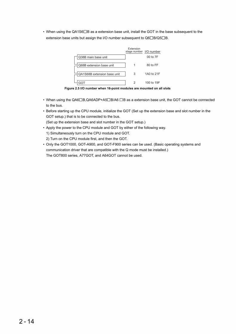
• When using the QA1S6 B as a extension base unit, install the GOT in the base subsequent to the
extension base units but assign the I/O number subsequent to Q6 B/Q5 B.
• When using the QA6 B,QA6ADP+A5 B/A6 B as a extension base unit, the GOT cannot be connected to the bus.
• Before starting up the CPU module, initialize the GOT (Set up the extension base and slot number in the GOT setup.) that is to be connected to the bus.(Set up the extension base and slot number in the GOT setup.)
• Apply the power to the CPU module and GOT by either of the following way.1) Simultaneously turn on the CPU module and GOT.2) Turn on the CPU module first, and then the GOT.
• Only the GOT1000, GOT-A900, and GOT-F900 series can be used. (Basic operating systems and communication driver that are compatible with the Q mode must be installed.)The GOT800 series, A77GOT, and A64GOT cannot be used.
Figure 2.5 I/O number when 16-point modules are mounted on all slots
Q38B main base unit 00 to 7F
Q68B extension base unit 80 to FF
GOT 100 to 19F
QA1S68B extension base unit 1A0 to 21F
I/O number
1
2
3
Extensionstage number
2 - 14
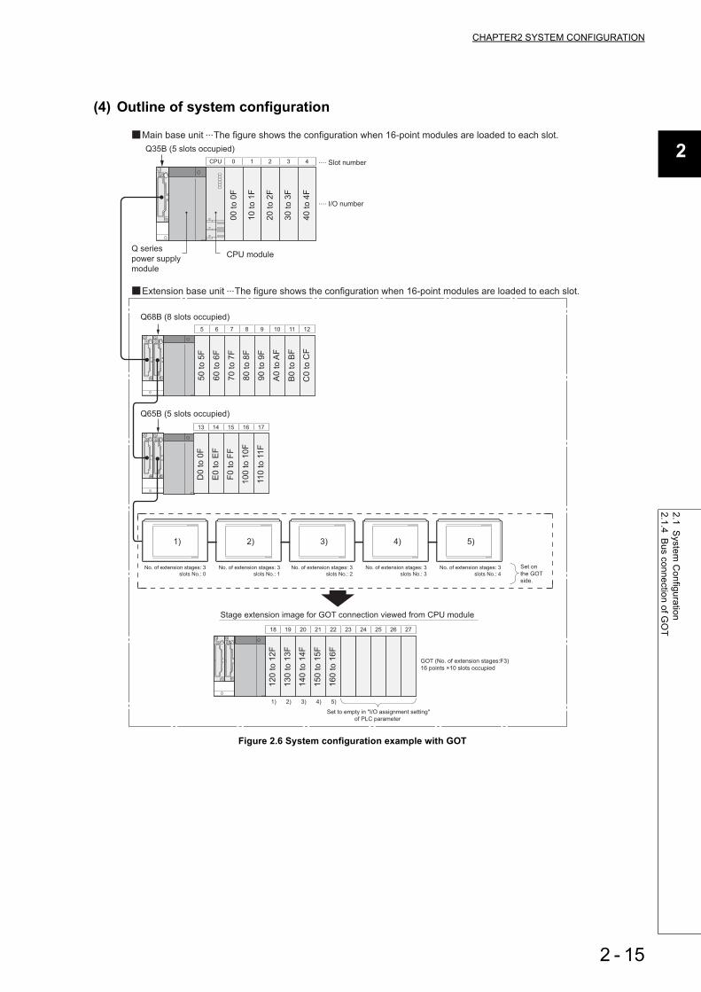
CHAPTER2 SYSTEM CONFIGURATION
1
2
3
4
5
6
7
8
2.1 System
Configuration
2.1.4 Bus connection of G
OT
(4) Outline of system configuration
Figure 2.6 System configuration example with GOT
CPU module
Q35B (5 slots occupied)
Q68B (8 slots occupied)
Q65B (5 slots occupied)
00 to 0
F
10 to 1
F
20 to 2
F
30 to 3
F
40 to 4
F
50 to 5
F
60 to 6
F
70 to 7
F
80 to 8
F
90 to 9
F
A0 to A
F
B0 to B
F
C0 to C
F
D0 to 0
F
E0 to E
F
F0 to F
F
100 to 1
0F
11
0 t
o 1
1F
CPU 0 1 2 3 4
5 6 7 8 9 10 11 12
13 14 15 16 17
Q series
power supply
module
No. of extension stages: 3
slots No.: 0
Stage extension image for GOT connection viewed from CPU module
12
0 t
o 1
2F
13
0 t
o 1
3F
14
0 t
o 1
4F
15
0 t
o 1
5F
16
0 t
o 1
6F
18 19 20 21 22 23 24 25 26 27
1) 2) 3) 4) 5)
1) 2) 3) 4) 5)
No. of extension stages: 3
slots No.: 1
No. of extension stages: 3
slots No.: 2
No. of extension stages: 3
slots No.: 3
No. of extension stages: 3
slots No.: 4
Set on
the GOT
side.
Set to empty in "I/O assignment setting"
of PLC parameter
GOT (No. of extension stages:F3)
16 points ×10 slots occupied
Main base unit The figure shows the configuration when 16-point modules are loaded to each slot....
Extension base unit The figure shows the configuration when 16-point modules are loaded to each slot....
....
....
I/O number
Slot number
2 - 15

Note1
Table2.12 Restrictions on the system configuration and applicable base units, extension cables and power supply modules
Maximum number of extension bases for bus connection of GOT
When using Q00JCPU or Q00UJCPU : 2When using Q00CPU, Q01CPU, Q00UCPU, Q01UCPU, or Q02UCPU : 4 When using High Performance model QCPU, Process CPU,Q03UD(E)CPU, Q04UD(E)HCPU, Q06UD(E)HCPU, Q10UD(E)HCPU, Q13UD(E)HCPU, Q20UD(E)HCPU, or Q26UD(E)HCPU : 7
Maximum number of I/O modules that can be mounted
When using Q00JCPU or Q00UJCPU : 16 - (No. of connected GOTs) modulesWhen using Q00CPU, Q01CPU, Q00UCPU, or Q01UCPU : 24 - (No. of connected GOTs) modulesWhen using Q02UCPU : 36 - (No. of connected GOTs) modulesWhen using High Performance model QCPU, Process CPU,Q03UD(E)CPU, Q04UD(E)HCPU, Q06UD(E)HCPU, Q10UD(E)HCPU,Q13UD(E)HCPU, Q20UD(E)HCPU, or Q26UD(E)HCPU : 64 - (No. of connected GOTs) modules
Applicable main base unit Q33B, Q35B, Q38B, Q312B, Q38DB, Q312DB
Applicable extension base unit
Model requiring no power supply module Q52B, Q55B
Model requiring a Q-series power supply module Q63B, Q65B, Q68B, Q612B
Model requiring a AnS series power supply
module Note2.2QA1S65B, QA1S68B
Applicable extension cable QC05B, QC06B, QC12B, QC30B, QC50B, QC100B
Q series power supply module
Note2.1Q61P-A1, Q61P-A2, Q61P, Q61P-D, Q62P, Q63P, Q64P, Q64PN
AnS series power supply module
Note2.2A1S61PN, A1S62PN, A1S63P
Note1
The final base is occupied byGOT
Note2.1Because the Q00JCPU and Q00UJCPU is the CPU module with a power supply module and main base unit
incorporated, the main base unit (Q3 B) and Q series power supply module are not required.
Basic Universal
Note2.2Usable only when the High Performance model QCPU is used.
Highperformance
2 - 16

CHAPTER2 SYSTEM CONFIGURATION
1
2
3
4
5
6
7
8
2.1 System
Configuration
2.1.5 Peripheral device configuration
2.1.5 Peripheral device configuration
This section describes peripheral devices that can be used in a system where the Basic model QCPU, High Performance model QCPU, Process CPU, or Universal model QCPU is installed.
(1) When using the Basic model QCPU
*1: For the versions of GX Developer and GX Configurator that can be used with the Basic model QCPU, refer to Section 2.1.6.
Figure 2.7 Configuration of peripheral devices
Basic model QCPU
RS-232 cablePersonal Computer (GX Developer, GX Configurator)
2 - 17

(2) When using High Performance model QCPU
*1: Format ATA cards by GX Developer only. ( Section 7.1.4)*2: Not applicable to the Q02CPU.*3: For writing to memory cards and USB cable details, refer to the following.
GX Developer operating manual*4: For the GX Developer and GX Configurator versions that can be used with the Process CPU, refer to Section 2.1.6.*5: For inquiries and orders of a programming unit (EPU01) and connection cable (EPU20R2CBL), please contact your local
Mitsubishi Electric Engineering Co., Ltd. sales office.*6: Programming units cannot be used when the "High speed interrupt fixed scan interval" parameter is written to the High
Performance model QCPU whose serial number (first five digits) is "04012".
Figure 2.8 Configuration of peripheral devices
1Memory card
1Memory card
PC cardadapter
High Performance model QCPU
4
Personal Computer
(GX Developer, GX Configurator)
RS-232 cable
2, 3USB cable(Connector type B)
2 - 18

CHAPTER2 SYSTEM CONFIGURATION
1
2
3
4
5
6
7
8
2.1 System
Configuration
2.1.5 Peripheral device configuration
(3) When using the Process CPU
*1: Format ATA cards by GX Developer only. ( Section 7.1.4)*2: For writing to memory cards and USB cable details, refer to the following.
GX Developer operating manual*3: For the GX Developer and GX Configurator versions that can be used with the Process CPU, refer to the Section 2.1.6.
Figure 2.9 Configuration of peripheral devices
1Memory card
1Memory card
PC cardadapter
3
Personal Computer
(GX Developer, GX Configurator,
PX Developer)
Process CPU
RS-232 cable
USB cable(Connector type B)
2
2 - 19
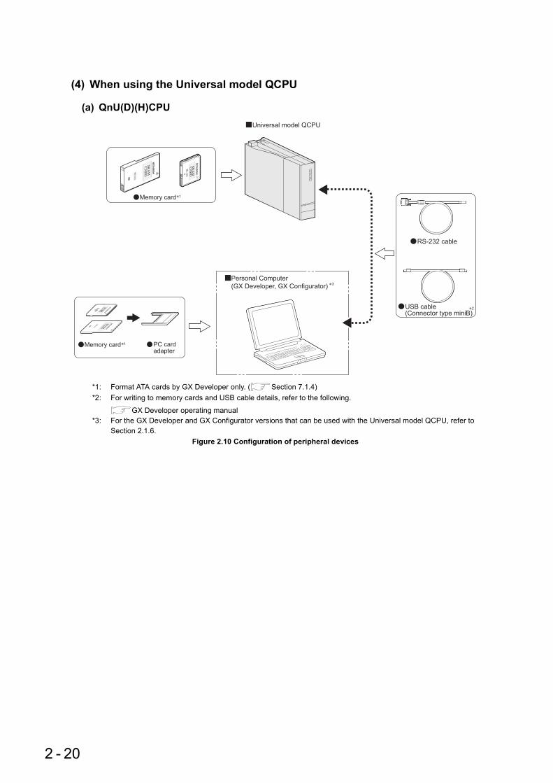
(4) When using the Universal model QCPU
(a) QnU(D)(H)CPU
*1: Format ATA cards by GX Developer only. ( Section 7.1.4)*2: For writing to memory cards and USB cable details, refer to the following.
GX Developer operating manual*3: For the GX Developer and GX Configurator versions that can be used with the Universal model QCPU, refer to
Section 2.1.6. Figure 2.10 Configuration of peripheral devices
1Memory card
1Memory card PC cardadapter
3
Personal Computer
(GX Developer, GX Configurator)
Universal model QCPU
USB cable(Connector type miniB)
2
RS-232 cable
2 - 20

CHAPTER2 SYSTEM CONFIGURATION
1
2
3
4
5
6
7
8
2.1 System
Configuration
2.1.5 Peripheral device configuration
(b) Built-in Ethernet QCPU
*1: Format ATA cards by GX Developer only. ( Section 7.1.4)*2: For writing to memory cards and USB cable details, refer to the following.
GX Developer operating manual*3: For the GX Developer and GX Configurator versions that can be used with the Universal model QCPU, refer to Section
2.1.6.*4: Use the following Ethernet cables
• For 10BASE-T connection: Cables compliant to Ethernet standards, category 3 or higher (STP/UTP cables).• For 100BASE-TX connection: Cables compliant to Ethernet standards, category 5 or higher (STP/UTP cables (In an
environment subject to electric noise, use shielded twisted pair (STP) cables)).Figure 2.11 Configuration of peripheral devices
1Memory card
1Memory card PC cardadapter
3
Personal Computer
(GX Developer, GX Configurator)
Universal model QCPU
Ethenet cable
USB cable(Connector type miniB)
2
4
2 - 21

2.1.6 Applicable softwares
The following table indicates software versions applicable to the system.
(1) GX Developer and PX Developer versions applicable to a single CPU system
*1: When using PX Developer, use GX Developer of Version 7.20W or later.
Table2.13 Applicable GX Developer and PX Developer
CPU moduleSoftware version
GX Developer PX DeveloperBasic model QCPU Version 7.00A or later
N/AHigh Performance model QCPU Version 4.00A or later
Process CPU
Q02PHCPUQ06PHCPU
Version 8.68W or later Version 1.18U or later
Q12PHCPUQ25PHCPU Version 7.10L or later*1 Version 1.00A or later
Universal model QCPU
Q02UCPUQ03UDCPUQ04UDHCPUQ06UDHCPU
Version 8.48A or later
N/A
Q13UDHCPUQ26UDHCPU
Version 8.62Q or later
Q03UDECPUQ04UDEHCPUQ06UDEHCPUQ13UDEHCPUQ26UDEHCPU
Version 8.68W or later
Q00UJCPUQ00UCPUQ01UCPUQ10UD(E)HCPUQ20UD(E)HCPU
Version 8.76E or later
2 - 22

CHAPTER2 SYSTEM CONFIGURATION
1
2
3
4
5
6
7
8
2.1 System
Configuration
2.1.6 Applicable softw
ares
(2) GX Configurator versions applicable to a single CPU systemThe table Table2.14 indicates software versions of GX Configurator applicable to a single CPU system.The applicable versions depend on a intelligent function module used.For the applicable versions of GX Configurator, refer to the user's manual for the intelligent function module used.
(a) When Basic model QCPU, Hogh Performance model QCPU, and Process QCPU are used
Table2.14 Applicable GX Configurator
CPU moduleSoftware version
Product name Version
Basic modelQCPU
GX Configurator-AD Version 1.10L or later
GX Configurator-DA Version 1.10L or later
GX Configurator-SC Version 1.10L or later
GX Configurator-CT Version 1.10L or later
GX Configurator-TI Version 1.10L or later
GX Configurator-TC Version 1.10L or later
GX Configurator-FL Version 1.10L or later
GX Configurator-QP Version 2.10L or later
GX Configurator-PT Version 1.10L or later
GX Configurator-AS Version 1.13P or later
GX Configurator-MB Version 1.00A or later
GX Configurator-DN Version 1.10L or later
High Performance model QCPU
GX Configurator-AD SW0D5C-QADU 00A or later
GX Configurator-DA SW0D5C-QDAU 00A or later
GX Configurator-SC SW0D5C-QSCU 00A or later
GX Configurator-CT SW0D5C-QCTU 00A or later
GX Configurator-TI Version 1.00A or later
GX Configurator-TC SW0D5C-QCTU 00A or later
GX Configurator-FL SW0D5C-QFLU 00A or later
GX Configurator-QP Version 2.00A or later
GX Configurator-PT Version 1.00A or later
GX Configurator-AS Version 1.13P or later
GX Configurator-MB Version 1.00A or later
GX Configurator-DN Version 1.00A or later
Process CPU
GX Configurator-AD Version 1.13P or later
GX Configurator-DA Version 1.13P or later
GX Configurator-SC Version 1.13P or later
GX Configurator-CT Version 1.13P or later
GX Configurator-TI Version 1.13P or later
GX Configurator-TC Version 1.13P or later
GX Configurator-FL Version 1.13P or later
GX Configurator-QP Version 2.13P or later
GX Configurator-PT Version 1.13P or later
GX Configurator-AS Version 1.13P or later
GX Configurator-MB Version 1.00A or later
GX Configurator-DN Version 1.13P or later
2 - 23

(b) When Universal model QCPU is used
*1: The software can be used by installing GX Developer Version 8.48A or later*2: The software can be used by installing GX Developer Version 8.62Q or later*3: The software can be used by installing GX Developer Version 8.68W or later*4: The software can be used by installing GX Developer Version 8.78G or later*5: The software can be used by connecting USB
Table2.15 Applicable GX Configurator
Product
Version used in combination with Universal model QCPU
Q02U,Q03UD,Q04UDH,or Q06UDHCPU in
use
Q13UDH or Q26UDHCPU
in use
Q03UDE,Q04UDEH,Q06UDEH,Q13UDEH, or Q26UDEHCPU in use
Q00U(J),Q01U,Q10UDH,Q20UDH,Q10UDEH,
or Q20UDEHCPU
GX DeveloperVersion 8.48A
or laterVersion 8.62Q
or laterVersion 8.68W
or laterVersion 8.78G
or later
GX Configurator-ADVersion 2.05F
or later*1Version 2.05F
or later*2Version 2.05F
or later*3Version 2.05F
or later*4
GX Configurator-DAVersion 2.06G
or later*1Version 2.06G
or later*2Version 2.06G
or later*3Version 2.06G
or later*4
GX Configurator-SCVersion 2.12N
or later*1Version 2.12N
or later*2Version 2.17T
or later*3Version 2.17T
or later*4
GX Configurator-CTVersion 1.25AB
or later*1Version 1.25AB
or later*2Version 1.25AB
or later*3Version 1.25AB
or later*4
GX Configurator-TIVersion 1.24AA
or later*1Version 1.24AA
or later*2Version 1.24AA
or later*3Version 1.24AA
or later*4
GX Configurator-TCVersion 1.23Z
or later*1Version 1.23Z
or later*2Version 1.23Z
or later*3Version 1.23Z
or later*4
GX Configurator-FLVersion 1.23Z
or later*1Version 1.23Z
or later*2Version 1.23Z
or later*3Version 1.23Z
or later*4
GX Configurator-QPVersion 2.25B
or laterVersion 2.29F
or laterVersion 2.29F
or later*5Not available
GX Configurator-PTVersion 1.23Z
or later*1Version 1.23Z
or later*2Version 1.23Z
or later*3Version 1.23Z
or later*4
GX Configurator-ASVersion 1.21X
or later*1Version 1.21X
or later*2Version 1.21X
or later*3Version 1.21X
or later*4
GX Configurator-MBVersion 1.08J
or later*1Version 1.08J
or later*2Version 1.08J
or later*3Version 1.08J
or later*4
GX Configurator-DNVersion 1.23Z
or later*1Version 1.23Z
or later*2Version 1.24AA
or later*3Version 1.24AA
or later*4
2 - 24

CHAPTER2 SYSTEM CONFIGURATION
1
2
3
4
5
6
7
8
2.2 Checking S
erial Num
ber and Function Version
2.2 Checking Serial Number and Function Version
The serial number and function version of the CPU module can be checked on the rating plate, on the front of the module, and on the System monitor screen in GX Developer.
(1) Checking on the rating plateThe rated plate is located on the side face of the CPU module.
(2) Checking on the front of the moduleThe serial number is shown on the rating plate located on the front (at the bottom) of the module.This does not apply to the following CPU modules.
• Modules manufactured in mid-September, 2007 or earlier. • Redundant CPUs manufactured in March 2008 or earlier. • Redundant CPUs and Q00JCPU.
Figure 2.12 Plate rated
Figure 2.13 Display on the front of the module
function version
Serial number (first 5 digits)
Relevant regulation standards
Serial number
090911090910001-B
2 - 25

RemarkAttaching a serial number label to the front of each Redundant CPU was started from March 2008.However, some of the modules manufactured at the beginning of it may not have the label.
(3) Checking on the System monitor screen (Product information list screen)To display the screen for checking the serial number and function version, select [Diagnostics] [System monitor] and click the Product Inf. List button in GX Developer.On the screen, the serial number and function version of intelligent function modules can also be checked.
[Serial No., Ver., and Product No.] • The serial number of the module is displayed in the "Serial No." column. • The function version of the module is displayed in the "Ver." column. • The serial number (product number) printed on the rating plate of the module is displayed in the "Product
No." column.*1
Note that "-" is displayed for a modules that does not support the product number display.*1: The product number is displayed only for the Universal model QCPU.
The serial number displayed on the Product information list screen of GX Developer may differ from that on the rating plate and on the front of the module.
• The serial number on the rating plate and on the front of the module indicates the management information of the product.
• The serial number displayed on the Product information list screen indicates the functional information of the product.The functional information of the product is upgraded when a new function is added.
Figure 2.14 System monitor
Serialnumber
Product number
Functionversion
2 - 26

CHAPTER3 GENERAL SPECIFICATIONS
1
2
3
4
5
6
7
8
CHAPTER3 GENERAL SPECIFICATIONS
The general specification of the programmable controller are shown in Table3.1.
*1: This indicates the section of the power supply to which the equipment is assumed to be connected between the public electrical power distribution network and the machinery within premises. Category II applies to equipment for which electrical power is supplied from fixed facilities.The surge voltage withstand level for up to the rated voltage of 300 V is 2500 V.
*2: This index indicates the degree to which conductive material is generated in terms of the environment in which the equipment is used.Pollution level 2 is when only non-conductive pollution occurs. A temporary conductivity caused by condensing must be expected occasionally.
*3: The storage ambient temperature is -20 to 75 if the system includes the AnS/A series modules.*4: The operating ambient humidity and storage ambient humidity are 10 to 90%RH if the system includes the AnS/A series modules.*5: Do not use or store the programmable controller under pressure higher than the atmospheric pressure of altitude 0m.
Doing so can cause a malfunction.When using the programmable controller under pressure, please contact your sales representative.
Table3.1 General specifications
Item SpecificationOperating ambient temperature 0 to 55
Storage ambient temperature -25 to 75 *3
Operating ambient humidity 5 to 95%RH *4, non-condensing
Storage ambient humidity 5 to 95%RH *4, non-condensing
Vibration resistanceCompliant withJIS B 3502 and
IEC 61131-2
Frequency Acceleration Amplitude Sweep count
Under intermittent
vibration
5 to 9Hz ----3.5mm
(0.14 inches) 10 times each in X, Y, Z directions
9 to 150Hz 9.8m/s2 ----
Under continuous vibration
5 to 9Hz ----1.75mm
(0.069 inches) ----
9 to 150Hz 4.9m/s2 ----
Shock resistance Compliant with JIS B 3502, IEC 61131-2 (147 m/s2, 3 times in each of 3 directions X, Y, Z)
Operating ambience No corrosive gases
Operating altitude*5 2000m (6562 feet) max.
Installation location Inside control panel
Overvoltage
category *1II max.
Pollution level *2 2 max.
Equipment category Class I
3 - 1

Memo
3 - 2

CHAPTER4 HARDWARE SPECIFICATIONS OF THE CPU MODULE
1
2
3
4
5
6
7
8
4.1 Perform
ance Specifications
4.1.1 Basic m
odel QC
PU
CHAPTER4 HARDWARE SPECIFICATIONS OF THE CPU MODULE
4.1 Performance Specifications
4.1.1 Basic model QCPU
Table4.1 to 4.5 show the performance specifications of the CPU module.
*1: The unit of the file size stored in the memory area varies depending on the CPU module. For details, refer to the following.
Qn(H)/QnPH/QnPRHCPU User's Manual (Function Explanation, Program Fundamentals)*2: The maximum number of executable sequence steps is as shown below.(Program size) - (File header size (default: 34 steps))
For details, refer to the following.
Qn(H)/QnPH/QnPRHCPU User's Manual (Function Explanation, Program Fundamentals)
*3: The size has been increased for the function upgrade of the CPU module. ( Appendix 2)*4: The CPU shared memory is not latched.
( QCPU User's Manual (Multiple CPU System)The CPU shared memory is cleared by turning on the programmable controller or resetting the CPU module.
Table4.1 Performance specifications
ItemBasic model QCPU
Q00JCPU Q00CPU Q01CPUControl method Stored program repeat operation
I/O control mode Refresh mode (Direct access I/O is available by specifying direct access I/O (DX , DY ).)
Program lan-guage
Sequence control lan-guage
Relay symbol language, logic symbolic language, MELSAP3 (SFC), MELSAP-L, function block, and structured text (ST)
Process control lan-guage
----
Processing speed(sequence instruction)
LD X0 200ns 160ns 100ns
MOV D0 D1 700ns 560ns 350ns
Processing speed(redundant function)
Tracking execution time(increased scan time)
----
Constant scan(Function for keeping regular scan time)
1 to 2000ms(Setting available in1ms unit.) (Setting by parameters.)
Program size *1, *2 8K steps (32K bytes) 14K steps (56K bytes)
Memory size*1
Program memory(drive 0)
58K bytes 94K bytes
Memory card (RAM)(drive 1)
----
Memory card (ROM)(drive 2)
----
Standard RAM(drive 3)
0 128K bytes *3
Standard ROM(drive 4)
58K bytes 94K bytes
CPU shared memory *3 , *4
---- 1K bytes
4 - 1

*5: Each of parameter, intelligent function module parameter, sequence program, SFC program, device comment, and device initial value files can be stored.
*6: The number of points can be changed within the setting range.
( Qn(H)/QnPH/QnPRHCPU User's Manual (Function Explanation, Program Fundamentals)
Table4.1 Performance specifications
ItemBasic model QCPU
Q00JCPU Q00CPU Q01CPU
Max. number of files stored
Program memory 6 *5
Memory card (RAM) ----
Memory card (ROM)
Flash card
----
ATA card ----
Standard RAM ---- 1
Standard ROM 6 *5
No. of times of writing data into the standard ROM
Max. 100000 times
No. of I/O device points(No. of points usable on program.)
2048 points (X/Y0 to 7FF)
No. of I/O points(No. of points accessible to the actual I/O module.)
256 points (X/Y0 to FF)
1024 points (X/Y0 to 3FF)
No.
of d
evic
e po
ints
Internal relay [M] 8192 points by default (M0-8191) (changeable)
Latch relay [L] 2048 points by default (L0 to 2047) (changeable)
Link relay [B] 2048 points by default (B0 to 7FF) (changeable)
Timer [T]
512 points by default (T0 to 511) (changeable)(Sharing of low- and high-speed timers)
The low- and high-speed timers are specified by the instructions.The measurement unit of the low- and high-speed timers is set up by parameters.(Low-speed timer: 1 to 1000ms, 1ms unit, 100ms by default)(High-speed timer: 0.1 to 100.0ms, 0.1ms unit, 10.0ms by default)
Retentive timer [ST]
0 point by default (sharing of the low- and high-speed retentive timers) (changeable)The low- and high-speed retentive timers are specified by the instructions.The measurement unit of the low- and high-speed retentive timers is set up by parameters.(Low-speed retentive timer: 1 to 1000ms, 1ms unit, 100ms by default)(High-speed retentive timer: 0.1 to 100.0ms, 0.1ms unit, 10.0ms by default)
Counter [C]
• Normal counter: 512 points by default (C0 to 511) (changeable)
• Interrupt counter: 128 points max.(0 point by default, setting by parameters)
Data register [D] 11136 points by default (D0 to 11135) (changeable)
Link register [W] 2048 points by default (W0 to 7FF) (changeable)
Annunciator [F] 1024 points by default (F0 to 1023) (changeable)
Edge relay [V] 1024 points by default (V0 to 1023) (changeable)
File register
[R] ----32768 points (R0 to 32767)/block
(The number of device points is fixed.)
[ZR] ----65536 points
(ZR0 to 65535) (The number of device points is fixed.)
Link special relay [SB] 1024 points (SB0 to 3FF) (The number of device points is fixed.)
Link special register [SW] 1024 points (SW0 to 3FF) (The number of device points is fixed.)
4 - 2

CHAPTER4 HARDWARE SPECIFICATIONS OF THE CPU MODULE
1
2
3
4
5
6
7
8
4.1 Perform
ance Specifications
4.1.1 Basic m
odel QC
PU
*7: The step relay is the device for the SFC function.*8: The value includes those of the CPU module and base unit.*9: The value includes those of the CPU module, base unit, and power supply module.
RemarkFor the general specifications, refer to CHAPTER 3.
Table4.1 Performance specifications
ItemBasic model QCPU
Q00JCPU Q00CPU Q01CPU
No.
of d
evic
e po
ints
Step relay [S] *7 2048 points (S0 to 127/block) (The number of device points is fixed.)Index register [Z] 10 points (Z0 to 9) (The number of device points is fixed.)Pointer [P] 300 points (P0 to 299) (The number of device points is fixed.)
Interrupt pointer [I]
128 points (I0 to 127) (The number of device points is fixed.)The cyclic interval of system interrupt pointers I28 to 31 can be set up by parameters.(2 to 1000ms, 1ms unit)Default values I28: 100ms, I29: 40ms, I30: 20ms, I31: 10ms
Special relay [SM] 1024 points (SM0 to 1023) (The number of device points is fixed.)
Special register [SD] 1024 points (SD0 to 1023) (The number of device points is fixed.)
Function input [FX] 16 points (FX0 to F) (The number of device points is fixed.)
Function output [FY] 16 points (FY0 to F) (The number of device points is fixed.)
Function register [FD] 5 points (FD0 to 4) (The number of device points is fixed.)
No. of device tracking words ----
Link direct device
Device for accessing the link device directly.Exclusively used for CC-Link IE controller network and MELSECNET/H.Specified form: J \X , J \Y , J \W , J \B ,
J \SW , J \SB
Intelligent function module deviceDevice for accessing the buffer memory of the intelligent function module directly.Specified form: U \G
Latch rangeL0 to 2047 (default)
(Latch range can be set up for B, F, V, T, ST, C, D, and W.) (Setting by parameters.)
RUN/PAUSE contact One contact can be set up in X0 to 7FF for each of RUN and PAUSE. (Setting by parameters.)
Clock function
Year, month, date, hour, minute, second and day of the week(Automatic leap year detection)Accuracy: -3.2 to +5.27s(TYP.+1.98s)/d at 0Accuracy: -2.57 to +5.27s(TYP.+2.22s)/d at 25Accuracy: -11.68 to +3.65s(TYP.-2.64s)/d at 55
Allowable momentary power failure time
20ms or less (100VAC or more)
Varies depending on the power supply module.
5VDC internal current consumption 0.26A *8 0.25A 0.27A
External dimensions
H 98mm(3.86 inches) 98mm(3.86 inches)
W 245mm(9.65 inches) *9 27.4mm(1.08 inches)
D 98mm(3.86 inches) 89.3mm(3.52 inches)
Weight 0.66kg *9 0.13kg
4 - 3
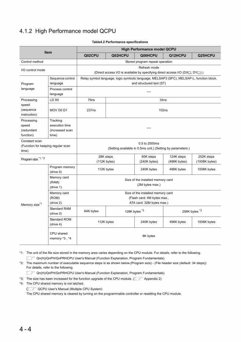
4.1.2 High Performance model QCPU
*1: The unit of the file size stored in the memory area varies depending on the CPU module. For details, refer to the following.
Qn(H)/QnPH/QnPRHCPU User's Manual (Function Explanation, Program Fundamentals)*2: The maximum number of executable sequence steps is as shown below.(Program size) - (File header size (default: 34 steps))
For details, refer to the following.
Qn(H)/QnPH/QnPRHCPU User's Manual (Function Explanation, Program Fundamentals)
*3: The size has been increased for the function upgrade of the CPU module. ( Appendix 2)*4: The CPU shared memory is not latched.
( QCPU User's Manual (Multiple CPU System)The CPU shared memory is cleared by turning on the programmable controller or resetting the CPU module.
Table4.2 Performance specifications
ItemHigh Performance model QCPU
Q02CPU Q02HCPU Q06HCPU Q12HCPU Q25HCPUControl method Stored program repeat operation
I/O control modeRefresh mode
(Direct access I/O is available by specifying direct access I/O (DX , DY ).)
Program language
Sequence control language
Relay symbol language, logic symbolic language, MELSAP3 (SFC), MELSAP-L, function block, and structured text (ST)
Process control language
----
Processing speed(sequence instruction)
LD X0 79ns 34ns
MOV D0 D1 237ns 102ns
Processing speed(redundant function)
Tracking execution time(increased scan time)
----
Constant scan(Function for keeping regular scan time)
0.5 to 2000ms(Setting available in 0.5ms unit.) (Setting by parameters.)
Program size *1, *2 28K steps(112K bytes)
60K steps (240K bytes)
124K steps(496K bytes)
252K steps (1008K bytes)
Memory size*1
Program memory(drive 0)
112K bytes 240K bytes 496K bytes 1008K bytes
Memory card (RAM)(drive 1)
Size of the installed memory card(2M bytes max.)
Memory card (ROM)(drive 2)
Size of the installed memory card(Flash card: 4M bytes max., ATA card: 32M bytes max.)
Standard RAM(drive 3)
64K bytes 128K bytes *3 256K bytes *3
Standard ROM(drive 4)
112K bytes 240K bytes 496K bytes 1008K bytes
CPU shared memory *3 , *4
8K bytes
4 - 4

CHAPTER4 HARDWARE SPECIFICATIONS OF THE CPU MODULE
1
2
3
4
5
6
7
8
4.1 Perform
ance Specifications
4.1.2 High P
erformance m
odel QC
PU
*5: The CPU module can execute up to 124 programs. The CPU module cannot execute 125 or more programs.
*6: Extended by the upgraded functions of CPU module ( Qn(H)/QnPH/QnPRHCPU User's Manual (Function Explanation, Program Fundamentals))
*7: The number of points can be changed within the setting range. ( Qn(H)/QnPH/QnPRHCPU User's Manual (Function Explanation, Program Fundamentals)
Table4.2 Performance specifications
ItemHigh Performance model QCPU
Q02CPU Q02HCPU Q06HCPU Q12HCPU Q25HCPU
Max. number of files stored
Program memory 28 60 124 252 *5
Memory card (RAM) 287(When the Q2MEM-2MBS is used)
Memory card (ROM)
Flash card
288
ATA card 512
Standard RAM 3 *6
Standard ROM 28 60 124 252
No. of times of writing data into the standard ROM
Max. 100000 times
No. of I/O device points(No. of points usable on program.)
8192 points (X/Y0 to 1FFF)
No. of I/O points(No. of points accessible to the actual I/O module.)
4096 points (X/Y0 to FFF)
No.
of d
evic
e po
ints
*7
Internal relay [M] 8192 points by default (M0-8191) (changeable)
Latch relay [L] 8192 points by default (L0 to 8191) (changeable)
Link relay [B] 8192 points by default (B0 to 1FFF) (changeable)
Timer [T]
2048 points by default (T0 to 2047) (sharing of low- and high-speed timers) (changeable)
The low- and high-speed timers are specified by the instructions.The measurement unit of the low- and high-speed timers is set up by parameters.(Low-speed timer: 1 to 1000ms, 1ms unit, 100ms by default)(High-speed timer: 0.1 to 100.0ms, 0.1ms unit, 10.0ms by default)
Retentive timer [ST]
0 point by default (sharing of the low- and high-speed retentive timers) (changeable)The low- and high-speed retentive timers are specified by the instructions.The measurement unit of the low- and high-speed retentive timers is set up by parameters.(Low-speed retentive timer: 1 to 1000ms, 1ms unit, 100ms by default)(High-speed retentive timer: 0.1 to 100.0ms, 0.1ms unit, 10.0ms by default)
Counter [C]
• Normal counter, 1024 points by default(C0 to 1023) (changeable)
• Interrupt counter: 256 points max.(0 point by default, setting by parameters)
Data register [D] 12288 points by default (D0 to 12287) (changeable)
Link register [W] 8192 points by default (W0 to 1FFF) (changeable)
Annunciator [F] 2048 points by default (F0 to 2047) (changeable)
Edge relay [V] 2048 points by default (V0 to 2047) (changeable)
4 - 5

*8: Read only when Flash card is used. ATA card is unusable.*9: The step relay is the device for the SFC function.
Table4.2 Performance specifications
ItemHigh Performance model QCPU
Q02CPU Q02HCPU Q06HCPU Q12HCPU Q25HCPU
No.
of d
evic
e po
ints
File
register*8
[R]
Standard RAM
32768 points(R0 to 32767)
32768 points(R0 to 32767)Up to 65536 points can be used by block switching in units of 32768 points
32768 points(R0 to 32767)Up to 131072 points can be used by block switching in units of 32768 points
SRAM card (1M bytes)
Up to 517120 points can be used by block switching in units of 32768 points (R0 to 32767).
SRAM card (2M bytes)
Up to 1041408 points can be used by block switching in units of 32768 points (R0 to 32767).
Flash card (2M bytes)
Up to 1041408 points can be used by block switching in units of 32768 points (R0 to 32767).
Flash card (4M bytes)
Up to 1042432 points can be used by block switching in units of 32768 points (R0 to 32767).
[ZR]
Standard RAM
32768 points(ZR0 to 32767)
65536 point (ZR0 to 65535) Block switching not required.
131072 points(ZR0 to 131071) Block switching not required.
SRAM card (1M bytes)
517120 points (ZR0 to 517119), Block switching not required.
SRAM card (2M bytes)
1041408 points (ZR0 to 1041407), Block switching not required.
Flash card (2M bytes)
1041408 points (ZR0 to 1041407), Block switching not required.
Flash card (4M bytes)
1042432 points (ZR0 to 1042431), Block switching not required.
Link special relay [SB] 2048 points (SB0 to 7FF) (The number of device points is fixed.)Link special register [SW] 2048 points (SW0 to 7FF) (The number of device points is fixed.)
Step relay [S] *9 8192 points (S0 to 8191) (The number of device points is fixed.)Index register [Z] 16 points (Z0 to 15) (The number of device points is fixed.)
Pointer [P]4096 points (P0 to 4095) (The number of device points is fixed.), The use ranges of the local
pointers and common pointers can be set up by parameters.
Interrupt pointer [I]
256 points (I0 to 255) (The number of device points is fixed.)The constant cyclic interval of system interrupt pointers I28 to 31 can be set up by parameters.(0.5 to 1000ms, 0.5ms unit)Default values I28: 100ms, I29: 40ms, I30: 20ms, I31: 10ms
4 - 6

CHAPTER4 HARDWARE SPECIFICATIONS OF THE CPU MODULE
1
2
3
4
5
6
7
8
4.1 Perform
ance Specifications
4.1.2 High P
erformance m
odel QC
PU
*10: For use of CC-Link IE controller network, check the versions of the CPU module and GX Developer.
( Appendix 2.2)
RemarkFor the general specifications, refer to CHAPTER 3.
Table4.2 Performance specifications
ItemHigh Performance model QCPU
Q02CPU Q02HCPU Q06HCPU Q12HCPU Q25HCPU
No.
of d
evic
e po
ints Special relay [SM] 2048 points (SM0 to 2047) (The number of device points is fixed.)
Special register [SD] 2048 points (SM0 to 2047) (The number of device points is fixed.)
Function input [FX] 16 points (FX0 to F) (The number of device points is fixed.)
Function output [FY] 16 points (FY0 to F) (The number of device points is fixed.)
Function register [FD] 5 points (FD0 to 4) (The number of device points is fixed.)
No. of device tracking words ----
Link direct device
Device for accessing the link device directly.
Dedicated to CC-Link IE controller network *10 and MELSECNET/H.Specified form: J \X , J \Y , J \W , J \B ,
J \SW , J \SB
Intelligent function module deviceDevice for accessing the buffer memory of the intelligent function module directly.Specified form: U \G
Latch rangeL0 to 8191 (default)
(Latch range can be set up for B, F, V, T, ST, C, D, and W.) (Setting by parameters.)
RUN/PAUSE contact One contact can be set up in X0 to 1FFF for each of RUN and PAUSE. (Setting by parameters.)
Clock function
Year, month, date, hour, minute, second, and day of the week(Automatic leap year detection)Accuracy: -3.18 to +5.25s(TYP.+2.12s)/d at 0Accuracy: -3.93 to +5.25s(TYP.+1.90s)/d at 25Accuracy: -14.69 to +3.53s(TYP.-3.67s)/d at 55
Allowable momentary power failure time
Varies depending on the power supply module.
5VDC internal current consumption 0.60A 0.64A
External dimensionsH 98mm (3.86 inches)
W 27.4mm (1.08 inches)
D 89.3mm (3.52 inches)
Weight 0.20kg
4 - 7

4.1.3 Process CPU
*1: The unit of the file size stored in the memory area varies depending on the CPU module. For details, refer to the following.
Qn(H)/QnPH/QnPRHCPU User's Manual (Function Explanation, Program Fundamentals)*2: The maximum number of executable sequence steps is as shown below.(Program size) - (File header size (default: 34 steps))
For details, refer to the following.
Qn(H)/QnPH/QnPRHCPU User's Manual (Function Explanation, Program Fundamentals)*3: The CPU shared memory is not latched.
( QCPU User's Manual (Multiple CPU System)The CPU shared memory is cleared by turning on the programmable controller or resetting the CPU module.
Table4.3 Performance specifications
ItemProcess CPU
Q02PHCPU Q06PHCPU Q12PHCPU Q25PHCPUControl method Stored program repeat operation
I/O control modeRefresh mode
(Direct access I/O is available by specifying direct access I/O (DX , DY ).)
Program language
Sequence control language
Relay symbol language, logic symbolic language, MELSAP3 (SFC), MELSAP-L, function block and structured text (ST)
Process control language
FBD for process control (Programming by PX Developer.)
Processing speed(sequence instruction)
LD X0 34ns
MOV D0 D1 102ns
Processing speed(redundant function)
Tracking execution time(increased scan time)
----
Constant scan(Function for keeping regular scan time)
0.5 to 2000ms (Setting available in 0.5ms unit.) (Setting by parameters.)
Program size *1, *2 28K steps(112 bytes)
60K steps(240 bytes)
124K steps(496 bytes)
252K steps (1008 bytes)
Memory size*1
Program memory(drive 0)
112K bytes 240K bytes 496K bytes 1008K bytes
Memory card (RAM)(drive 1)
Size of the installed memory card (2M bytes max.)
Memory card (ROM)(drive 2)
Size of the installed memory card(Flash card: 4M bytes max., ATA card: 32M bytes max.)
Standard RAM(drive 3)
128K bytes 256K bytes *3
Standard ROM(drive 4)
112K bytes 240K bytes 496K bytes 1008K bytes
CPU shared memory *3
8K bytes
4 - 8
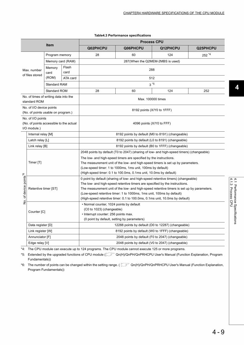
CHAPTER4 HARDWARE SPECIFICATIONS OF THE CPU MODULE
1
2
3
4
5
6
7
8
4.1 Perform
ance Specifications
4.1.3 Process C
PU
*4: The CPU module can execute up to 124 programs. The CPU module cannot execute 125 or more programs.
*5: Extended by the upgraded functions of CPU module ( Qn(H)/QnPH/QnPRHCPU User's Manual (Function Explanation, Program Fundamentals))
*6: The number of points can be changed within the setting range. ( Qn(H)/QnPH/QnPRHCPU User's Manual (Function Explanation, Program Fundamentals))
Table4.3 Performance specifications
ItemProcess CPU
Q02PHCPU Q06PHCPU Q12PHCPU Q25PHCPU
Max. number of files stored
Program memory 28 60 124 252 *4
Memory card (RAM) 287(When the Q2MEM-2MBS is used)
Memory card (ROM)
Flash card
288
ATA card 512
Standard RAM 3 *5
Standard ROM 28 60 124 252
No. of times of writing data into the standard ROM
Max. 100000 times
No. of I/O device points(No. of points usable on program.)
8192 points (X/Y0 to 1FFF)
No. of I/O points(No. of points accessible to the actual I/O module.)
4096 points (X/Y0 to FFF)
No.
of d
evic
e po
ints
*6
Internal relay [M] 8192 points by default (M0 to 8191) (changeable)
Latch relay [L] 8192 points by default (L0 to 8191) (changeable)
Link relay [B] 8192 points by default (B0 to 1FFF) (changeable)
Timer [T]
2048 points by default (T0 to 2047) (sharing of low- and high-speed timers) (changeable)
The low- and high-speed timers are specified by the instructions.The measurement unit of the low- and high-speed timers is set up by parameters.(Low-speed timer: 1 to 1000ms, 1ms unit, 100ms by default)(High-speed timer: 0.1 to 100.0ms, 0.1ms unit, 10.0ms by default)
Retentive timer [ST]
0 point by default (sharing of low- and high-speed retentive timers) (changeable)The low- and high-speed retentive timers are specified by the instructions.The measurement unit of the low- and high-speed retentive timers is set up by parameters.(Low-speed retentive timer: 1 to 1000ms, 1ms unit, 100ms by default)(High-speed retentive timer: 0.1 to 100.0ms, 0.1ms unit, 10.0ms by default)
Counter [C]
• Normal counter, 1024 points by default(C0 to 1023) (changeable)
• Interrupt counter: 256 points max.(0 point by default, setting by parameters)
Data register [D] 12288 points by default (D0 to 12287) (changeable)
Link register [W] 8192 points by default (W0 to 1FFF) (changeable)
Annunciator [F] 2048 points by default (F0 to 2047) (changeable)
Edge relay [V] 2048 points by default (V0 to 2047) (changeable)
4 - 9

*7: Read only when Flash card is used. ATA card is unusable.*8: The step relay is the device for the SFC function.
Table4.3 Performance specifications
ItemProcess CPU
Q02PHCPU Q06PHCPU Q12PHCPU Q25PHCPU
No.
of d
evic
e po
ints
File
register*7
[R]
Standard RAM
Up to 65536 points can be used by block switching in units of 32768 points (R0 to 32767).
Up to 131072 points can be used by block switching in units of 32768 points (R0 to 32767).
SRAM card (1M bytes)
Up to 517120 points can be used by block switching in units of 32768 points (R0 to 32767).
SRAM card (2M bytes)
Up to 1041408 points can be used by block switching in units of 32768 points (R0 to 32767).
Flash card (2M bytes)
Up to 1041408 points can be used by block switching in units of 32768 points (R0 to 32767).
Flash card (4M bytes)
Up to 1042432 points can be used by block switching in units of 32768 points (R0 to 32767).
[ZR]
Standard RAM
65536 points (ZR0 to 65535), block switching not required.
131072 points (ZR0 to 131071), block switching not required.
SRAM card (1M bytes)
517120 points (ZR0 to 517119), block switching not required.
SRAM card (2M bytes)
1041408 points (ZR0 to 1041407), block switching not required.
Flash card (2M bytes)
1041408 points (ZR0 to 1041407), block switching not required.
Flash card (4M bytes)
1042432 points (ZR0 to 1042431), block switching not required.
Link special relay [SB] 2048 points (SB0 to 7FF) (The number of device points is fixed.)Link special register [SW] 2048 points (SW0 to 7FF) (The number of device points is fixed.)
Step relay [S] *8 8192 points (S0 to 8191) (The number of device points is fixed.)Index register [Z] 16 points (Z0 to 15) (The number of device points is fixed.)
Pointer [P]4096 points (P0 to 4095) (The number of device points is fixed.), The use ranges of the local
pointers and common pointers can be set up by parameters.
Interrupt pointer [I]
256 points (I0 to 255) (The number of device points is fixed.)The constant cyclic interval of system interrupt pointers I28 to 31 can be set up by parameters.(0.5 to 1000ms, 0.5ms unit)Default values I28: 100ms, I29: 40ms, I30: 20ms, I31: 10ms
4 - 10

CHAPTER4 HARDWARE SPECIFICATIONS OF THE CPU MODULE
1
2
3
4
5
6
7
8
4.1 Perform
ance Specifications
4.1.3 Process C
PU
*9: For use of CC-Link IE controller network, check the versions of the CPU module and GX Developer. ( Appendix 2.2)
RemarkFor the general specifications, refer to CHAPTER 3.
Table4.3 Performance specifications
ItemProcess CPU
Q02PHCPU Q06PHCPU Q12PHCPU Q25PHCPU
No.
of d
evic
e po
ints Special relay [SM] 2048 points (SM0 to 2047) (The number of device points is fixed.)
Special register [SD] 2048 points (SD0 to 2047) (The number of device points is fixed.)
Function input [FX] 16 points (FX0 to F) (The number of device points is fixed.)
Function output [FY] 16 points (FY0 to F) (The number of device points is fixed.)
Function register [FD] 5 points (FD0 to 4) (The number of device points is fixed.)
No. of device tracking words ----
Link direct device
Device for accessing the link device directly.
Exclusively used for CC-Link IE controller network*9 and MELSECNET/H.Specified form: J \X , J \Y , J \W , J \B , J \SW , J \SB
Intelligent function module deviceDevice for accessing the buffer memory of the intelligent function module directly.Specified form: U \G
Latch rangeL0 to 8191(default)
(Latch range can be set up for B, F, V, T, ST, C, D, and W.) (Setting by parameters.)
RUN/PAUSE contact One contact can be set up in X0 to 1FFF for each of RUN and PAUSE. (Setting by parameters.)
Clock function
Year, month, date, hour, minute, second, and day of the week(Automatic leap year detection)
Accuracy: -3.18 to +5.25s(TYP.+2.12s)/d at 0
Accuracy: -3.93 to +5.25s(TYP.+1.90s)/d at 25
Accuracy: -14.69 to +3.53s(TYP.-3.67s)/d at 55
Allowable momentary power failure period
Varies depending on the power supply module.
5VDC internal current consumption 0.64A
External dimensions
H 98mm (3.86 inches)
W 27.4mm (1.08 inches)
D 89.3mm (3.52 inches)
Weight 0.20kg
4 - 11

4.1.4 Redundant CPU
*1: The unit of the file size stored in the memory area varies depending on the CPU module. For details, refer to the following.
Qn(H)/QnPH/QnPRHCPU User's Manual (Function Explanation, Program Fundamentals)*2: The maximum number of executable sequence steps is as shown below.(Program size) - (File header size (default: 34 steps))
For details, refer to the following.
Qn(H)/QnPH/QnPRHCPU User's Manual (Function Explanation, Program Fundamentals)
Table4.4 Performance specifications
ItemRedundant CPU
Q12PRHCPU Q25PRHCPUControl method Stored program repeat operation
I/O control modeRefresh mode
(Direct access I/O is available by specifying direct access I/O (DX , DY ).)
Program language
Sequence control language
Relay symbol language, logic symbolic language, MELSAP3 (SFC), MELSAP-L, function block and structured text (ST)
Process control language
FBD for process control (Programming by PX Developer.)
Processing speed(sequence instruction)
LD X0 34ns
MOV D0 D1 102ns
Processing speed(redundant function)
Tracking execution time(increased scan time)
Device memory 48k words: 10msDevice memory 100k words: 15ms
( QnPRHCPU User's Manual (Redundant System))
Constant scan(Function for keeping regular scan time)
0.5 to 2000ms (Setting available in 0.5ms unit.) (Setting by parameters.)
Program size *1, *2 124K steps(496 bytes)
252K steps (1008 bytes)
Memory size*1
Program memory(drive 0)
496K bytes 1008K bytes
Memory card (RAM)(drive 1)
Size of the installed memory card (2M bytes max.)
Memory card (ROM)(drive 2)
Size of the installed memory card(Flash card: 4M bytes max., ATA card: 32M bytes max.)
Standard RAM(drive 3)
Size of the installed memory card (2M bytes max.)
Standard ROM(drive 4)
496K bytes 1008K bytes
CPU shared memory
----
4 - 12

CHAPTER4 HARDWARE SPECIFICATIONS OF THE CPU MODULE
1
2
3
4
5
6
7
8
4.1 Perform
ance Specifications
4.1.4 Redundant C
PU
*3: The CPU module can execute up to 124 programs. The CPU module cannot execute 125 or more programs.
*4: Extended by the upgraded functions of CPU module ( Qn(H)/QnPH/QnPRHCPU User's Manual (Function Explanation, Program Fundamentals))
*5: The number of points can be changed within the setting range. ( Qn(H)/QnPH/QnPRHCPU User's Manual (Function Explanation, Program Fundamentals))
Table4.4 Performance specifications
ItemRedundant CPU
Q12PRHCPU Q25PRHCPU
Max. number of files stored
Program memory 124 252 *3
Memory card (RAM) 287(When the Q2MEM-2MBS is used)
Memory card (ROM)
Flash card
288
ATA card 512
Standard RAM 3 *4
Standard ROM 124 252
No. of times of writing data into the standard ROM
Max. 100000 times
No. of I/O device points(No. of points usable on program.)
8192 points (X/Y0 to 1FFF)
No. of I/O points(No. of points accessible to the actual I/O module.)
4096 points (X/Y0 to FFF)
No.
of d
evic
e po
ints
*5
Internal relay [M] 8192 points by default (M0 to 8191) (changeable)
Latch relay [L] 8192 points by default (L0 to 8191) (changeable)
Link relay [B] 8192 points by default (B0 to 1FFF) (changeable)
Timer [T]
2048 points by default (T0 to 2047) (sharing of low- and high-speed timers) (changeable)
The low- and high-speed timers are specified by the instructions.The measurement unit of the low- and high-speed timers is set up by parameters.(Low-speed timer: 1 to 1000ms, 1ms unit, 100ms by default)(High-speed timer: 0.1 to 100.0ms, 0.1ms unit, 10.0ms by default)
Retentive timer [ST]
0 point by default (sharing of low- and high-speed retentive timers) (changeable)The low- and high-speed retentive timers are specified by the instructions.The measurement unit of the low- and high-speed retentive timers is set up by parameters.(Low-speed retentive timer: 1 to 1000ms, 1ms unit, 100ms by default)(High-speed retentive timer: 0.1 to 100.0ms, 0.1ms unit, 10.0ms by default)
Counter [C]
• Normal counter, 1024 points by default(C0 to 1023) (changeable)
• Interrupt counter: 256 points max.(0 point by default, setting by parameters)
Data register [D] 12288 points by default (D0 to 12287) (changeable)
Link register [W] 8192 points by default (W0 to 1FFF) (changeable)
Annunciator [F] 2048 points by default (F0 to 2047) (changeable)
Edge relay [V] 2048 points by default (V0 to 2047) (changeable)
4 - 13

*6: Read only when Flash card is used. ATA card is unusable.*7: The step relay is the device for the SFC function.
Table4.4 Performance specifications
ItemRedundant CPU
Q12PRHCPU Q25PRHCPU
No.
of d
evic
e po
ints
File
register*6
[R]
Standard RAM
Up to 131072 points can be used by block switching in units of 32768 points (R0 to 32767).
SRAM card (1M bytes)
Up to 517120 points can be used by block switching in units of 32768 points (R0 to 32767).
SRAM card (2M bytes)
Up to 1041408 points can be used by block switching in units of 32768 points (R0 to 32767).
Flash card (2M bytes)
Up to 1041408 points can be used by block switching in units of 32768 points (R0 to 32767).
Flash card (4M bytes)
Up to 1042432 points can be used by block switching in units of 32768 points (R0 to 32767).
[ZR]
Standard RAM
131072 points (ZR0 to 131071), block switching not required.
SRAM card (1M bytes)
517120 points (ZR0 to 517119), block switching not required.
SRAM card (2M bytes)
1041408 points (ZR0 to 1041407), block switching not required.
Flash card (2M bytes)
1041408 points (ZR0 to 1041407), block switching not required.
Flash card (4M bytes)
1042432 points (ZR0 to 1042431), block switching not required.
Link special relay [SB] 2048 points (SB0 to 7FF) (The number of device points is fixed.)Link special register [SW] 2048 points (SW0 to 7FF) (The number of device points is fixed.)
Step relay [S] *7 8192 points (S0 to 8191) (The number of device points is fixed.)Index register [Z] 16 points (Z0 to 15) (The number of device points is fixed.)
Pointer [P]4096 points (P0 to 4095) (The number of device points is fixed.), The use ranges of the local
pointers and common pointers can be set up by parameters.
Interrupt pointer [I]
256 points (I0 to 255) (The number of device points is fixed.)The constant cyclic interval of system interrupt pointers I28 to 31 can be set up by parameters.(0.5 to 1000ms, 0.5ms unit)Default values I28: 100ms, I29: 40ms, I30: 20ms, I31: 10ms
4 - 14

CHAPTER4 HARDWARE SPECIFICATIONS OF THE CPU MODULE
1
2
3
4
5
6
7
8
4.1 Perform
ance Specifications
4.1.4 Redundant C
PU
*8: For use of CC-Link IE controller network, check the versions of the CPU module and GX Developer. ( Appendix 2.2)
RemarkFor the general specifications, refer to CHAPTER 3.
Table4.4 Performance specifications
ItemRedundant CPU
Q12PRHCPU Q25PRHCPU
No.
of d
evic
e po
ints Special relay [SM] 2048 points (SM0 to 2047) (The number of device points is fixed.)
Special register [SD] 2048 points (SD0 to 2047) (The number of device points is fixed.)
Function input [FX] 16 points (FX0 to F) (The number of device points is fixed.)
Function output [FY] 16 points (FY0 to F) (The number of device points is fixed.)
Function register [FD] 5 points (FD0 to 4) (The number of device points is fixed.)
No. of device tracking wordsMax. 100k words
( QnPRHCPU User's Manual (Redundant System))
Link direct device
Device for accessing the link device directly.
Exclusively used for CC-Link IE controller network*8 and MELSECNET/H.Specified form: J \X , J \Y , J \W , J \B , J \SW , J \SB
Intelligent function module deviceDevice for accessing the buffer memory of the intelligent function module directly.Specified form: U \G
Latch rangeL0 to 8191 (default) (Setting by parameters.)
(Latch range can be set up for B, F, V, T, ST, C, D, and W.)
RUN/PAUSE contact One contact can be set up in X0 to 1FFF for each of RUN and PAUSE. (Setting by parameters.)
Clock function
Year, month, date, hour, minute, second, and day of the week(Automatic leap year detection)Accuracy: -3.2 to +5.27s
(TYP.+2.07s)/d at 0Accuracy: -2.77 to +5.27s
(TYP.+2.22s)/d at 25Accuracy: -12.14 to +3.65s
(TYP.-2.89s)/d at 55
Allowable momentary power failure time
Varies depending on the power supply module.
5VDC internal current consumption 0.89A
External dimensions
H 98mm (3.86 inches)
W 55.2mm (2.17 inches)
D 89.3mm (3.52 inches)
Weight 0.30kg
4 - 15

4.1.5 Universal model QCPU
(1) Q00UJCPU, Q00UCPU, Q01UCPU, Q02UCPU, Q03UD(E)CPU
*1: The unit of the file size stored in the memory area varies depending on the CPU module. For details, refer to the following.
QnUCPU User's Manual (Function Explanation, Program Fundamentals)*2: The maximum number of executable sequence steps is as shown below.(Program size) - (File header size (default: 34 steps))
For details, refer to the following.
QnUCPU User's Manual (Function Explanation, Program Fundamentals)*3: The CPU shared memory is not latched.
( QCPU User's Manual (Multiple CPU System)The CPU shared memory is cleared by turning on the programmable controller or resetting the CPU module.
Table4.5 Performance specifications
ItemUniversal model QCPU
Q00UJCPU Q00UCPU Q01UCPU Q02UCPU Q03UDCPUQ03UDECPU
Control method Stored program repeat operation
I/O control modeRefresh mode
(Direct access I/O is available by specifying direct access I/O (DX , DY ).)
Program language
Sequence control language
Relay symbol language, logic symbolic language, MELSAP3 (SFC), MELSAP-L, function block and structured text (ST)
Process control language
----
Processing speed(sequence instruction)
LD X0 120ns 80ns 60ns 40ns 20ns
MOV D0 D1 240ns 160ns 120ns 80ns 40ns
Processing speed(redundant function)
Tracking execution time(increased scan time)
----
Constant scan(Function for keeping regular scan time)
0.5 to 2000ms(Setting available in 0.5ms unit.) (Setting by parameters.)
Program size *1, *2 10K steps(40K bytes)
15K steps(60K bytes)
20Ksteps(80K bytes)
30K steps(120K bytes)
Memory
size*1
Program memory(drive 0)
40K bytes 60K bytes 80K bytes 120K bytes
Memory card (RAM)(drive 1)
----Size of the installed memory card
(8M bytes max.)
Memory card (ROM)(drive 2)
----Size of the installed memory card
(Flash card: 4M bytes max., ATA card: 32M bytes max.)
Standard RAM(drive 3)
---- 128K bytes 192K bytes
Standard ROM(drive 4)
256K bytes 512K bytes 1024K bytes
CPU shared memory *3
QCPUstandardmemory
---- 8K bytes
MultipleCPU highspeed transmis-sion area
---- 32K bytes
4 - 16

CHAPTER4 HARDWARE SPECIFICATIONS OF THE CPU MODULE
1
2
3
4
5
6
7
8
4.1 Perform
ance Specifications
4.1.5 Universal m
odel QC
PU
*4: The one write operation may not be counted as one writing to a program memory.The number of writing to the program memory can be checked by the special register (SD682 and SD683).
*5: The one write operation may not be counted as one writing to the standard ROM.The number of writing to the standard ROM can be checked by the special register (SD687 and SD688).
*6: The number of points can be changed within the setting range. ( QnUCPU User's Manual (Function Explanation, Program Fundamentals))
Table4.5 Performance specifications
ItemUniversal model QCPU
Q00UJCPU Q00UCPU Q01UCPU Q02UCPUQ03UDCPU
Q03UDECPU
Max. number of files stored
Program memory 32 64 124
Memory card (RAM) ----319 (When the Q3MEM-8MBS is
used)
Memory card (ROM)
Flash card
---- 288
ATA card ---- 511
Standard RAM ----
Standard ROM 128 256
No. of times of writing data into the program memory Max. 100000 times*4
No. of times of writing data into the standard ROM Max. 100000 times*5
No. of I/O device points(No. of points usable on program.)
8192 points (X/Y0 to 1FFF)
No. of I/O points(No. of points accessible to the actual I/O module.)
256 points (X/Y0 to FF)
1024 points (X/Y0 to 3FF)
2048 points (X/Y0 to 7FF)
4096 points (X/Y0 to FFF)
No.
of d
evic
e po
ints
Internal relay [M]*6 8192 points by default (M0-8191) (changeable)
Latch relay [L]*6 8192 points by default (L0-8191) (changeable)
Link relay [B]*6 8192 points by default (B0 to 1FFF) (changeable)
Timer [T]*6
2048 points by default (T0 to 2047) (changeable)(Sharing of low- and high-speed timers)
The low- and high-speed timers are specified by the instructions.The measurement unit of the low- and high-speed timers is set up by parameters.(Low-speed timer: 1 to 1000ms, 1ms unit, 100ms by default)(High-speed timer: 0.1 to 100.0ms, 0.1ms unit, 10.0ms by default)
Retentive timer [ST]*6
0 point by default (sharing of the low- and high-speed retentive timers) (changeable)The low- and high-speed retentive timers are specified by the instructions.The measurement unit of the low- and high-speed retentive timers is set up by parameters.(Low-speed retentive timer: 1 to 1000ms, 1ms unit, 100ms by default)(High-speed retentive timer: 0.1 to 100.0ms, 0.1ms unit, 10.0ms by default)
Counter [C]*6 • Normal counter, 1024 points by default (C0 to 1023) (changeable)
Data register [D]*6 12288 points by default (D0 to 12287) (changeable)
Extended data register [D] ---- 0 points by default (changeable)
Link register [W]*6 8192 points by default (W0 to 1FFF) (changeable)
Extended link register [W] ---- 0 points by default (changeable)
Annunciator [F]*6 2048 points by default (F0 to 2047) (changeable)
Edge relay [V]*6 2048 points by default (V0 to 2047) (changeable)
Link special relay [SB]*6 2048 points by default (SB0 to 7FF) (changeable)
Link special register [SW]*6 2048 points by default (SW0 to 7FF) (changeable)
4 - 17

*7: Read only when a Flash card is used. ATA card is unusable.
Table4.5 Performance specifications
ItemUniversal model QCPU
Q00UJCPU Q00UCPU Q01UCPU Q02UCPUQ03UDCPU
Q03UDECPU
No.
of d
evic
e po
ints
File
register*7
[R]
Standard RAM
----32768 points (R0 to 32767) Up to 65536 points can be used by block switching in units of 32768 points
32768 points (R0 to 32767) Up to 98304 points can be used by block switching in units of 32768 points
SRAM card (1M bytes)
----32768 points (R0 to 32767) Up to 517120 points can be used by block switching in units of 32768 points
SRAM card (2M bytes)
----32768 points (R0 to 32767) Up to 1041408 points can be used by block switching in units of 32768 points
SRAM card (4M bytes)
----32768 points (R0 to 32767) Up to 2087936 points can be used by block switching in units of 32768 points
SRAM card (8M bytes)
----32768 points (R0 to 32767) Up to 4184064 points can be used by block switching in units of 32768 points
Flash card (2M bytes)
----32768 points (R0 to 32767) Up to 1041408 points can be used by block switching in units of 32768 points
Flash card (4M bytes)
----32768 points (R0 to 32767) Up to 2087936 points can be used by block switching in units of 32768 points
[ZR]
Standard RAM
---- 65536 points (ZR0 to 65535) Block switching not required.
98304 points (ZR0 to 98303) Block switching not required.
SRAM card (1M bytes)
----517120 points (ZR0 to 517119), Block switching not required.
SRAM card (2M bytes)
----1041408 points (ZR0 to 1041407), Block switching not required.
SRAM card (4M bytes)
----2087936 points (ZR0 to 2087935), Block switching not required.
SRAM card (8M bytes)
----4184064 points (ZR0 to 4184063), Block switching not required.
Flash card (2M bytes)
----1041408 points (ZR0 to 1041407), Block switching not required.
Flash card (4M bytes)
----2087936 points (ZR0 to 2087935), Block switching not required.
Step relay [S] *8 8192 points (S0 to 8191) (The number of device points is fixed.)*9
Index register /Standard devise register [Z]
max. 20 points (Z0 to 19)
Index register [Z](32-bit modification specification of ZR device)
----max. 10 points (Z0 to 18)
(Index register (Z) is used in double words.)
4 - 18

CHAPTER4 HARDWARE SPECIFICATIONS OF THE CPU MODULE
1
2
3
4
5
6
7
8
4.1 Perform
ance Specifications
4.1.5 Universal m
odel QC
PU
*8: The step relay is the device for the SFC function.*9: The device points can be changed to 0 for the Universal model QCPU if the serial number (first five digits) is "10042".*10: Applicable only to the Q03UDECPU.*11: The number indicates the total number of TCP/IP and UDP/IP protocols.
Table4.5 Performance specifications
ItemUniversal model QCPU
Q00UJCPU Q00UCPU Q01UCPU Q02UCPUQ03UDCPU
Q03UDECPU
No.
of d
evic
e po
ints
Pointer [P]512 points (P0 to 511), The use ranges of the local pointers
and common pointers can be set up by parameters
4096 points (P0 to 4095), The use ranges of the local pointers and
common pointers can be set up by parameters.
Interrupt pointer [I]
128 points (I0 to 127)The constant cyclic interval of system interrupt pointers I28 to 31 can be set up by parameters.(0.5 to 1000ms, 0.5ms unit)Default values I28: 100ms, I29: 40ms, I30: 20ms, I31: 10ms
256 points (I0 to 255)The constant cyclic interval of system interrupt pointers I28 to 31 can be set up by parameters.(0.5 to 1000ms, 0.5ms unit)Default values I28: 100ms, I29: 40ms, I30: 20ms, I31: 10ms
Special relay [SM] 2048 points (SM0 to 2047) (The number of device points is fixed.)
Special register [SD] 2048 points (SM0 to 2047) (The number of device points is fixed.)
Function input [FX] 16 points (FX0 to F) (The number of device points is fixed.)
Function output [FY] 16 points (FY0 to F) (The number of device points is fixed.)
Function register [FD] 5 points (FD0 to 4) (The number of device points is fixed.)
No. of device tracking words ----
Link direct device
Device for accessing the link device directly.Dedicated to CC-Link IE controller network and MELSECNET/H.Specified form: J \X , J \Y , J \W , J \B ,
J \SW , J \SB
Intelligent function module deviceDevice for accessing the buffer memory of the intelligent function module directly.Specified form: U \G
Specifications of built-in Ethernet port CPU module *10
Data transmission speed
---- 100/10Mbps
Communication mode ----Full-duplex/Half-
duplex
Transmission method ---- Base band
Max. distance between hub and node
----100m
(328.08 feet.)
Max. number of connectable nodes
10BASE-T
----Cascade
connection: Up to four bases
100BASE-TX
----Cascade
connection: Up to two bases
Number of
connections *11 ----
16 for a total of socket
communication, MELSOFT
connection, and MC protocol and 1
for FTP
4 - 19

*12: The value includes those of the CPU module and base unit.*13: The current consumption in the Q03UDECPU is 0.46A*14: The value includes those of the CPU module, base unit, and power supply module.*15: The values for the Q03UDECPU are as follows.
External dimensions (D): 115mm (4.53 inches)Weight: 0.22kg
RemarkFor the general specifications, refer to CHAPTER 3.
Table4.5 Performance specifications
Item
Universal model QCPU
Q00UJCPU Q00UCPU Q01UCPU Q02UCPUQ03UDCPU
Q03UDECPU
Latch rangeL0 to 8191 (8192 points by default)
(Latch range can be set up for B, F, V, T, ST, C, D, and W.) (Setting by parameters.)
RUN/PAUSE contact One contact can be set up in X0 to 1FFF for each of RUN and PAUSE. (Setting by parameters.)
Clock function
Year, month, date, hour, minute, second, and day of the week ( Automatic leap year detection)
Accuracy: -2.96 to +3.74s (TYP.+1.24s)/d at 0
Accuracy: -2.34 to +3.74s (TYP.+1.63s)/d at 25
Accuracy: -11.48 to +2.12s (TYP.-3.03s)/d at 55
Year, month, date, hour, minute, second, and day of the week(Automatic leap year detection)Accuracy: -2.96 to +3.74s
(TYP.+1.42s)/d at 0Accuracy: -3.18 to +3.74s
(TYP.+1.50s)/d at 25Accuracy: -13.20 to +2.12s
(TYP.-3.54s)/d at 55
Allowable instantaneous power failure period
20ms or less (100VAC or more)
Varies depending on the power supply module.
5VDC internal current 0.37A*12 0.33A 0.23A 0.33A*13
External dimensions
H98mm
(3.86 inches)98mm (3.86 inches)
W245mm
(9.65 inches)*1427.4mm (1.08 inches)
D98mm
(3.86 inches)89.3mm (3.52 inches)*15
Weight 0.70kg*14 0.15kg 0.20kg*15
4 - 20

CHAPTER4 HARDWARE SPECIFICATIONS OF THE CPU MODULE
1
2
3
4
5
6
7
8
4.1 Perform
ance Specifications
4.1.5 Universal m
odel QC
PU
(2) Q04UD(E)HCPU, Q06UD(E)HCPU, Q10UD(E)HCPU, Q13UD(E)HCPU, Q20UD(E)HCPU, Q26UD(E)HCPU
*1: The unit of the file size stored in the memory area varies depending on the CPU module. For details, refer to the following.
QnUCPU User's Manual (Function Explanation, Program Fundamentals)*2: The maximum number of executable sequence steps is as shown below.(Program size) - (File header size (default: 34 steps))
For details, refer to the following.
QnUCPU User's Manual (Function Explanation, Program Fundamentals)*3: The CPU shared memory is not latched.
( QCPU User's Manual (Multiple CPU System)The CPU shared memory is cleared by turning on the programmable controller or resetting the CPU module.
Table4.6 Performance specifications
ItemUniversal model QCPU
Q04UDHCPU Q06UDHCPU Q10UDHCPU Q13UDHCPU Q20UDHCPU Q26UDHCPU
Q04UDEHCPU Q06UDEHCPU Q10UDEHCPU Q13UDEHCPU Q20UDEHCPU Q26UDEHCPU
Control method Stored program repeat operation
I/O control mode Refresh mode (Direct access I/O is available by specifying direct access I/O (DX , DY ).)
Program lan-guage
Sequence control language
Relay symbol language, logic symbolic language, MELSAP3 (SFC), MELSAP-L, function block and structured text (ST)
Process control lan-guage
----
Processing speed(sequence instruction)
LD X0 9.5ns
MOV D0 D1 19ns
Processing speed(redundant function)
Tracking execution time(increased scan time1)
----
Constant scan(Function for keeping regular scan time)
0.5 to 2000ms (Setting available in 0.5ms unit.) (Setting by parameters.)
Program size *1, *2 40K steps(160K bytes)
60K steps (240K bytes)
100K steps(400K bytes)
130K steps(520K bytes)
200K steps(800K bytes)
260K steps(1040K bytes)
Memory
size*1
Program memory(drive 0)
160K bytes 240K bytes 400K bytes 520K bytes 800K bytes 1040K bytes
Memory card (RAM)(drive 1)
Size of the installed memory card (8M bytes max.)
Memory card (ROM)(drive 2)
Size of the installed memory card (Flash card: 4M bytes max., ATA card: 32M bytes max.)
Standard RAM(drive 3)
256K bytes 768K bytes 1024K bytes 1280K bytes
Standard ROM(drive 4)
512K bytes 1024K bytes 2048K steps 4096K steps
CPU shared memory *3
QCPUstandardmemory
8K bytes
MultipleCPU highspeed transmis-sion area
32K bytes
4 - 21

*4: The CPU module can execute up to 124 programs. The CPU module cannot execute 125 or more programs.*5: The one write operation may not be counted as one writing to a program memory.
The number of writing to the program memory can be checked by the special register (SD682 and SD683).*6: The one write operation may not be counted as one writing to the standard ROM.
The number of writing to the standard ROM can be checked by the special register (SD687 and SD688).
*7: The number of points can be changed within the setting range. ( QnUCPU User's Manual (Function Explanation, Program Fundamentals))
Table4.6 Performance specifications
ItemUniversal model QCPU
Q04UDHCPU Q06UDHCPU Q10UDHCPU Q13UDHCPU Q20UDHCPU Q26UDHCPU
Q04UDEHCPU Q06UDEHCPU Q10UDEHCPU Q13UDEHCPU Q20UDEHCPU Q26UDEHCPU
Max. num-ber of files stored
Program memory 124 252*4
Memory card (RAM) 319(When the Q3MEM-8MBS is used)
Memory card (ROM)
Flash card
288
ATA card 511
Standard RAM 3
Standard ROM 256
No. of times of writing data into the program memory Max. 100000 times*5
No. of times of writing data into the standard ROM Max. 100000 times*6
No. of I/O device points(No. of points usable on program.)
8192 points (X/Y0 to 1FFF)
No. of I/O points(No. of points accessible to the actual I/O module.)
4096 points (X/Y0 to FFF)
No.
of d
evic
e po
ints
*7
Internal relay [M] 8192 points by default (M0-8191) (changeable)
Latch relay [L] 8192 points by default (L0-8191) (changeable)
Link relay [B] 8192 points by default (B0 to 1FFF) (changeable)
Timer [T]
2048 points by default (T0 to 2047) (changeable)(Sharing of low- and high-speed timers)
The low- and high-speed timers are specified by the instructions.The measurement unit of the low- and high-speed timers is set up by parameters.(Low-speed timer: 1 to 1000ms, 1ms unit, 100ms by default)(High-speed timer: 0.1 to 100.0ms, 0.1ms unit, 10.0ms by default)
Retentive timer [ST]
0 point by default (sharing of the low- and high-speed retentive timers) (changeable)The low- and high-speed retentive timers are specified by the instructions.The measurement unit of the low- and high-speed retentive timers is set up by parameters.(Low-speed retentive timer: 1 to 1000ms, 1ms unit, 100ms by default)(High-speed retentive timer: 0.1 to 100.0ms, 0.1ms unit, 10.0ms by default)
Counter [C]• Normal counter, 1024 points by default
(C0 to 1023) (changeable)
Data register [D] 12288 points by default (D0 to 12287) (changeable)
Extended data register [D] 0 points by default (changeable)
Link register [W] 8192 points by default (W0 to 1FFF) (changeable)
Extended link register [W] 0 points by default (changeable)
Annunciator [F] 2048 points by default (F0 to 2047) (changeable)
Edge relay [V] 2048 points by default (V0 to 2047) (changeable)
Link special relay [SB] 2048 points by default (SB0 to 7FF) (changeable)
Link special register [SW] 2048 points by default (SW0 to 7FF) (changeable)
4 - 22

CHAPTER4 HARDWARE SPECIFICATIONS OF THE CPU MODULE
1
2
3
4
5
6
7
8
4.1 Perform
ance Specifications
4.1.5 Universal m
odel QC
PU
*8: Read only when Flash card is used. ATA card is unusable.*9: The step relay is the device for the SFC function.*10: The device points can be changed if the serial number (first five digits) of the Universal model QCPU is "10042" or later.
Table4.6 Performance specifications
ItemUniversal model QCPU
Q04UDHCPU Q06UDHCPU Q10UDHCPU Q13UDHCPU Q20UDHCPU Q26UDHCPU
Q04UDEHCPU Q06UDEHCPU Q10UDEHCPU Q13UDEHCPU Q20UDEHCPU Q26UDEHCPU
No.
of d
evic
e po
ints
File reg-
ister*8
[R]
Standard RAM
32768 points (R0 to 32767) Up to 131072 points can be used by block switching in units of 32768 points
32768 points (R0 to 32767) Up to 393216 points can be used by block switching in units of 32768 points
32768 points (R0 to 32767) Up to 524288 points can be used by block switching in units of 32768 points
32768 points (R0 to 32767) Up to 655360 points can be used by block switching in units of 32768 points
SRAM card (1M bytes)
32768 points (R0 to 32767) Up to 517120 points can be used by block switching in units of 32768 points
SRAM card (2M bytes)
32768 points (R0 to 32767) Up to 1041408 points can be used by block switching in units of 32768 points
SRAM card (4M bytes)
32768 points (R0 to 32767) Up to 2087936 points can be used by block switching in units of 32768 points
SRAM card (8M bytes)
32768 points (R0 to 32767) Up to 4184064 points can be used by block switching in units of 32768 points
Flash card (2M bytes)
32768 points (R0 to 32767) Up to 1041408 points can be used by block switching in units of 32768 points
Flash card (4M bytes)
32768 points (R0 to 32767) Up to 2087936 points can be used by block switching in units of 32768 points
[ZR]
Standard RAM
131072 points (ZR0 to 131071) Block switching not required.
393216 points (ZR0 to 393215) Block switching not required.
524288 points (ZR0 to 524287) Block switching not required.
655360 points (ZR0 to 655359) Block switching not required.
SRAM card (1M bytes)
517120 points (ZR0 to 517119), Block switching not required.
SRAM card (2M bytes)
1041408 points (ZR0 to 1041407), Block switching not required.
SRAM card (4M bytes)
2087936 points (ZR0 to 2087935), Block switching not required.
SRAM card (8M bytes)
4184064 points (ZR0 to 4184063), Block switching not required.
Flash card (2M bytes)
1041408 points (ZR0 to 1041407), Block switching not required.
Flash card (4M bytes)
2087936 points (ZR0 to 2087935), Block switching not required.
Step relay [S] *9 8192 points (S0 to 8191) (The number of device points is fixed.)*10
Index register /Standard devise register [Z]
max. 20 points (Z0 to 19)
Index register [Z](32-bit modification specification of ZR device)
max. 10 points (Z0 to 18)(Index register (Z) is used in double words.)
Pointer [P]4096 points (P0 to 4095), The use ranges of the local pointers and common pointers can be set up
by parameters.
4 - 23

*11: Applicable only to the Built-in Ethernet port QCPU.*12: The number indicates the total number of TCP/IP and UDP/IP protocols.
Table4.6 Performance specifications
ItemUniversal model QCPU
Q04UDHCPU Q06UDHCPU Q10UDHCPU Q13UDHCPU Q20UDHCPU Q26UDHCPU
Q04UDEHCPU Q06UDEHCPU Q10UDEHCPU Q13UDEHCPU Q20UDEHCPU Q26UDEHCPU
No.
of d
evic
e po
ints
Interrupt pointer [I]
256 points (I0 to 255)The constant cyclic interval of system interrupt pointers I28 to 31 can be set up by parameters.(0.5 to 1000ms, 0.5ms unit)Default values I28: 100ms, I29: 40ms, I30: 20ms, I31: 10ms
Special relay [SM] 2048 points (SM0 to 2047) (The number of device points is fixed.)
Special register [SD] 2048 points (SM0 to 2047) (The number of device points is fixed.)
Function input [FX] 16 points (FX0 to F) (The number of device points is fixed.)
Function output [FY] 16 points (FY0 to F) (The number of device points is fixed.)
Function register [FD] 5 points (FD0 to 4) (The number of device points is fixed.)
No. of device tracking words ----
Link direct device
Device for accessing the link device directly.Dedicated to CC-Link IE controller network and MELSECNET/H.Specified form: J \X , J \Y , J \W , J \B ,
J \SW , J \SB
Intelligent function module deviceDevice for accessing the buffer memory of the intelligent function module directly.Specified form: U \G
Specifi-cations of Ether-net port built in the CPU module
*11
Data transmission speed
100/10Mbps
Communication mode Full-duplex/Half-duplex
Transmission method Base band
Max. distance between hub and node
100m (328.08 feet)
Max. number of connect-able nodes
10BASE-T
Cascade connection: Up to four bases
100BASE-TX
Cascade connection: Up to two bases
Number of connec-
tions *12 16 for a total of socket communication, MELSOFT connection, and MC protocol and 1 for FTP
4 - 24

CHAPTER4 HARDWARE SPECIFICATIONS OF THE CPU MODULE
1
2
3
4
5
6
7
8
4.1 Perform
ance Specifications
4.1.5 Universal m
odel QC
PU
*13: The current consumption Q04UDEHCPU, Q06UDEHCPU, Q10UDEHCPU, Q13UDEHCPU, Q20UDEHCPU and Q26UDEHCPU is 0.49A
*14: The values for the Q04UDEHCPU, Q06UDEHCPU, Q10UDEHCPU, Q13UDEHCPU, Q20UDEHCPU, and Q26UDEHCPU are as follows.External dimensions (D): 115mm (4.53 inches)Weight: 0.22kg
RemarkFor the general specifications, refer to CHAPTER 3.
Table4.6 Performance specifications
ItemUniversal model QCPU
Q04UDHCPU Q06UDHCPU Q10UDHCPU Q13UDHCPU Q20UDHCPU Q26UDHCPU
Q04UDEHCPU Q06UDEHCPU Q10UDEHCPU Q13UDEHCPU Q20UDEHCPU Q26UDEHCPU
Latch rangeL0 to 8191 (8192 points by default)
(Latch range can be set up for B, F, V, T, ST, C, D, and W.) (Setting by parameters.)
RUN/PAUSE contact One contact can be set up in X0 to 1FFF for each of RUN and PAUSE. (Setting by parameters.)
Clock function
Year, month, date, hour, minute, second, and day of the week(Automatic leap year detection)
Accuracy: -2.96 to +3.74s (TYP.+1.42s)/d at 0
Accuracy: -3.18 to +3.74s (TYP.+1.50s)/d at 25
Accuracy: -13.20 to +2.12s (TYP.-3.54s)/d at 55
Allowable instantaneous power failure period
Varies depending on the power supply module.
5VDC internal current 0.39A*13
External dimensions
H 98mm (3.86 inches)
W 27.4mm (1.08 inches)
D 89.3mm (3.52 inches)*14
Weight 0.20kg*15
4 - 25

4.2 Basic Model QCPU
4.2.1 Part names
(1) Q00JCPU
Figure 4.1 Front face
Figure 4.2 With front cover open
Table4.7 Part names
No. Name Application1) Base mounting hole Pear-shaped hole for mounting the unit to a panel such as a control box. (For M4 screw)
2) CoverProtective cover for extension cable connector. Remove this cover when connecting an extension base unit.
3) Extension cable connectorConnector for transferring signals to or from the extension base unit. Connect an extension cable.
4) POWER LED Power indicator LED for 5VDC. Turns on in green during normal output of 5VDC.
4) 5) 6)1)
2)
7)
OUT
8)When opening the cover, put your
finger here.
OUT
(FG)
(LG)
N
L
100-240VAC
INPUT
100-240VAC
INPUT
100-240VAC
INPUT
50/60Hz 105VAOUTPUT
5VDC 3A
Q00UJCPU
20)
18)19)
3)13)14)
15)
4 - 26

CHAPTER4 HARDWARE SPECIFICATIONS OF THE CPU MODULE
1
2
3
4
5
6
7
8
4.2 Basic M
odel QC
PU
4.2.1 Part nam
es
Table4.7 Part names
No. Name Application
5) RUN LED
Indicates the operating status of the CPU module.On : During operation with the RUN/STOP/RESET switch set to "RUN".Off : During stop with the RUN/STOP/RESET switch set to "STOP"
When the error that stops operation is detected.Flash : When parameters/program is written during STOP and the RUN/STOP/RESET switch
is moved from "STOP" to "RUN".To turn on the RUN LED after writing the program, perform the following operations.•Set the RUN/STOP/RESET switch from "RUN" to "STOP" to "RUN".
•Perform reset with the RUN/STOP/RESET switch.( Section 4.2.3)•Power on the programmable controller again.
To turn on the RUN LED after writing the parameters, perform the following operations.•Perform reset with the RUN/STOP/RESET switch.•Power on the programmable controller again.
(If the RUN/STOP/RESET switch is set from "STOP" to "RUN" to "STOP" to "RUN" after changing the parameter values, the new values are not reflected on the param-eters related to the intelligent function module, such as the network parameters.)
6) ERR. LED
On : When the self-diagnostic error that will not stop operation is detected.•When continuation of operation at error detection is set in the parameter.•When the annunciator (F) is turned on by the SET/OUT instruction.•When battery low occurs.
Off : NormalFlash : When the error that stops operation is detected.
When reset operation is performed with the RUN/STOP/RESET switch.
7) Module connectorConnector used for mounting an I/O or intelligent function module.(To the connector of the spare space where no module is mounted, fit the accessory connector cover or the blank cover module (QG60) to prevent dust from entering.)
8) DIN rail adaptor mounting holes Holes for mounting a DIN rail adaptor.
9) FG terminal Ground terminal connected with the shield pattern of the printed circuit board.
10) LG terminal Power filter ground having a half potential of the input voltage.
11) Power input terminals Power input terminals for connection of a 100VAC to 200VAC power supply.
12) BatteryBackup battery for use of the program memory, standard RAM, clock function and backup power time function.
13) Battery fixing hook Hook for holding the battery.
14) Battery connector pinFor connection of the battery lead wires.(Lead wires are disconnected from the connector when shipping to prevent the battery from consuming.)
15) RS-232 connector *1Connector for connecting a peripheral device by RS-232.Can be connected by the RS-232 connection cable (QC30R2).
16) RUN/STOP/RESET switch *2
RUN : Executes sequence program operation.STOP : Stops sequence program operation.RESET : Performs hardware reset, operation error reset, operation initialization or like.
( Section 4.2.3)
4 - 27

(2) Q00CPU, Q01CPU
Figure 4.3 Front face Figure 4.4 With front cover open
Figure 4.5 Side face
1)
2)
3)
4)
When opening the cover, put
your finger here.
7)
8)
6)5)
9)
10)
11)
12)
4 - 28

CHAPTER4 HARDWARE SPECIFICATIONS OF THE CPU MODULE
1
2
3
4
5
6
7
8
4.2 Basic M
odel QC
PU
4.2.1 Part nam
es
Table4.8 Part names
No. Name Application
1) Module fixing hookHook used to fix the module to the base unit.(Single-motion installation)
2) RUN LED
Indicates the operating status of the CPU module.On : During operation with the RUN/STOP/RESET switch set to "RUN".Off : During stop with the RUN/STOP/RESET switch set to "STOP".Flash : When parameters/program is written during STOP and the RUN/STOP/RESET switch
is set from "STOP" to "RUN".To turn on the RUN LED after writing the program, perform the following operations.
•Move the RUN/STOP/RESET switch from "RUN" to "STOP" to "RUN".
•Perform reset with the RUN/STOP/RESET switch.( Section 4.2.3)•Power on the programmable controller again
To turn on the RUN LED after writing the parameters, perform the following operations.•Perform reset with the RUN/STOP/RESET switch.•Power on the programmable controller again.
(If the RUN/STOP/RESET switch is set from "STOP" to "RUN" to "STOP" to "RUN" after changing the parameter values, the new values are not reflected on the param-eters related to the intelligent function module, such as the network parameters.)
3) ERR. LED
On : When the self-diagnostic error that will not stop operation is detected.•When continuation of operation at error detection is set in the parameter.•When the annunciator (F) is turned on by the SET/OUT instruction.•When battery low occurs.
Off : NormalFlash : When the error that stops operation is detected.
When reset operation is performed with the RUN/STOP/RESET switch.
4) Serial number Shows the serial number printed on the rating plate.
5) BatteryBackup battery for use of the program memory, standard RAM, clock function and backup power time function.
6) Battery fixing hook Hook for holding the battery.
7) Battery connector pinFor connection of the battery lead wires.(Lead wires are disconnected from the connector when shipping to prevent the battery from consuming.)
8) RUN/STOP/RESET switch*2
RUNSTOPRESET
: Executes sequence program operation.: Stops sequence program operation.: Performs hardware reset, operation error reset, operation initialization or like.
( Section 4.2.3)
9) RS-232 connector*1Connector for RS-232 connectionCan be connected by the RS-232 connection cable (QC30R2).
10) Module fixing screw hole Hole for the screw used to fix to the base unit. (M3 12 screw)
11) Module fixing projection Projection used to secure the module to the base unit.
12) Module mounting lever Lever used to mount the module to the base unit.
4 - 29

*1: When a cable is connected to the RS-232 connector at all times, clamp the cable to prevent a poor connection, moving, and disconnection by unintentional pulling.The Q6HLD-R2 type RS-232 Connector Disconnection Prevention Holder is available as a clamp for RS-232 connector.
*2: Operate the RUN/STOP/RESET switch with your fingertips.To prevent the switch from being damaged, do not use any tool such as screw driver.
Figure 4.6 RS-232 cable fixing processingFixing screw
Q6HLD-R2
CPU module
RS-232 cable
4 - 30

CHAPTER4 HARDWARE SPECIFICATIONS OF THE CPU MODULE
1
2
3
4
5
6
7
8
4.2 Basic M
odel QC
PU
4.2.2 Sw
itch operation at the time of w
riting program
4.2.2 Switch operation at the time of writing program
Programs can be written to the Basic model QCPU in either the STOP or RUN status.
(1) When writing program with RUN/STOP/RESET switch set to "STOP"When writing a program with the Basic model QCPU placed in the STOP status using the RUN/STOP/RESET switch, operate the switch in the following procedure.
1) RUN/STOP/RESET switch: STOPRUN LED: Off, from CPU module STOP status to Program write
2) RUN/STOP/RESET switch: Perform reset.( Section 4.2.3)
3) RUN/STOP/RESET switch: STOP to RUNRUN LED: On, CPU module RUN status
(2) When it is desired to place the Basic model QCPU in RUN status without resetting it after program writeOperate the RUN/STOP/RESET switch from STOP to RUN, STOP and then RUN.After the second STOP to RUN operation, the CPU module is put in the RUN status.At this time, the device memory data are those saved before program write.
(3) When writing program after remote STOP using GX DeveloperWhen writing a program with the Basic model QCPU stopped by remote STOP using GX Developer, no operation is needed for the RUN/STOP/RESET switch.When remote RUN is performed using GX Developer, the Basic model QCPU is placed in the RUN status.
(4) When performing online change of programWhen the online change of a program is performed, the RUN/STOP/RESET switch need not be operated.
The program modified online during boot operation is written to the program memory.After making online program change, also write the program to the standard ROM of the boot source memory. If the program is not written in the standard ROM, the old program will be executed at the next boot operation.For details of the boot operation, refer to the following.
Qn(H)/QnPH/QnPRHCPU User's Manual (Function Explanation, Program Fundamentals)
4 - 31

4.2.3 Reset operation
For the Basic model QCPU, the RUN/STOP/RESET switch of the CPU module is used to switch between the RUN status and STOP status and to perform RESET operation.When using the RUN/STOP/RESET switch to reset the CPU module, moving the RUN/STOP/RESET switch to the reset position will not reset it immediately.
Hold the RUN/STOP/RESET switch in the RESET position until reset processing is complete (the flashing ERR. LED turns off).If you release your hand from the RUN/STOP/RESET switch during reset processing (the ERR. LED is flashing), the switch will return to the STOP position and reset processing cannot be completed.
Perform reset operation with the RUN/STOP/RESET switch as shown in Figure 4.7.
Figure 4.7 Reset operation
Start
Termination , completed , end
Hold the RUN/STOP/RESET switch
in the "RESET" position.
Reset operation is started using
the RUN/STOP/RESET switch.
.......................
Reset is accepted and reset
processing is performed.
.......................
Reset is completed........................
Reset is canceled........................
Releasing your hand from the
RUN/STOP/RESET switch returns it
to the STOP position.
RESET RUN
STOP
RUN/STOP/RESET
switch
Flickers.
Goes off.
The ERR. LED flickers several times
(3 to 4 times) rapidly.
The "ERR. LED" goes off .
Return the RUN/STOP/RESET
switch to the "STOP" position.
RUN/STOP/RESET
switch
RESET RUN
STOP
:
4 - 32

CHAPTER4 HARDWARE SPECIFICATIONS OF THE CPU MODULE
1
2
3
4
5
6
7
8
4.2 Basic M
odel QC
PU
4.2.4 Latch clear operation
Operate the RUN/STOP/RESET switch with your fingertips.To prevent the switch from being damaged, do not use any tool such as screw driver.
4.2.4 Latch clear operation
For the Basic model QCPU, latch clear is performed by the remote latch clear operation of GX Developer.Latch clear cannot be executed by operating the switches of the CPU module.
● The valid/invalid for latch clear in the clear range of latch clear operation can be set for each device. The setting can be mode in the device setting of the PLC parameter.
● For the remote latch clear operation by GX Developer, refer to the following. Qn(H)/QnPH/QnPRHCPU User's Manual (Function Explanation, Program Fundamentals)
4 - 33

4.3 High Performance Model QCPU, Process CPU and Redundant CPU
4.3.1 Part names
(1) Q02CPU, Q02HCPU, Q06HCPU, Q12HCPU, Q25HCPU, Q02PHCPU, Q06PHCPU, Q12PHCPU, Q25PHCPU
Figure 4.8 Front face Figure 4.9 With front cover open
*1: Not provided for Q02CPU.
Figure 4.10 Side face
1)
2)
8)
3)
4)
5)
6)
7)
When opening the cover, put
your finger here.
5
4
3
2
1
9)
10)
11)
12)
13)
14)
15)
*1
16)
17)
20)
19)
18)
4 - 34

CHAPTER4 HARDWARE SPECIFICATIONS OF THE CPU MODULE
1
2
3
4
5
6
7
8
4.3 High P
erformance M
odel QC
PU
, Process C
PU
and Redundant C
PU
4.3.1 Part nam
es
(2) Q12PRHCPU, Q25PRHCPU
Figure 4.11 Front face Figure 4.12 With front cover open
Figure 4.13 Side face
1)
21)
3)
4)
5)
6)
7)
2)
22)
23)
24)
25)
When opening the cover, put
your finger here.
9)
10)
11)
12)
13)
14)
15)
8)
17)
19)
18)
16)
20)
4 - 35

Table4.9 Part Names
No. Name Application1) Module fixing hook Hook used to secure the module to the base unit. (Single-motion installation)
2) MODE LEDIndicates the mode of the CPU module.On (green) : Q modeFlash (green) : Forced on and off for external I/O registered
3) RUN LED
Indicates the operating status of the CPU module.On : The RUN/STOP switch is set to "RUN" and the module is running.Off : The RUN/STOP switch is set to "STOP."
(The standby system Redundant CPU module in the backup mode does not turn on even when the RUN/STOP switch is set to "RUN" but the module is stopped.)When an error is detected and operation must be halted due to the error
Flash : Parameters or programs are written with the RUN/STOP switch set to "STOP" and then the RUN/STOP switch is turned from "STOP" to "RUN."When the operation mode is changed from the backup mode to the separate mode in the Redundant CPU system, the RUN LED of the standby system side CPU module flashes.To turn on the RUN LED after writing the program, perform the following operations.
•Set the RUN/STOP switch from "RUN" "STOP" "RUN".•Reset with the RESET/L. CLR switch.•Restart the programmable controller power.
To turn on the RUN LED after writing the parameters, perform the following operations.•Reset with the RESET/L. CLR switch.•Restart the programmable controller power.
(If the RUN/STOP switch is set from "RUN" "STOP" "RUN" after changing the parameters, network parameters and intelligent function module parameters will not be updated.)
4) ERR. LED
On : Detect on of self-diagnosis error which will not stop operation, except battery error.(When operation continued at error detection is set in the parameter setting.)
Off : NormalFlash : Detection of the error that stops operation.
When automatic write to standard ROM is completed normally. (The BOOT LED flashes together.)
5) USER LEDOn : Error detected by CHK instruction or annunciator (F) turned ONOff : NormalFlash : Execution of latch clear
6) BAT. LEDOn : Battery error due to reduction in battery voltages of CPU module or memory card.Off : Normal
7) BOOT LED
On : Start of boot operationOff : Non-execution of boot operationFlash : When automatic write to standard ROM is completed normally. (The ERR. LED flashes
together.)
4 - 36

CHAPTER4 HARDWARE SPECIFICATIONS OF THE CPU MODULE
1
2
3
4
5
6
7
8
4.3 High P
erformance M
odel QC
PU
, Process C
PU
and Redundant C
PU
4.3.1 Part nam
es
Table4.9 Part Names
No. Name Application8) Serial number Shows the serial number printed on the rating plate.
9) Memory card EJECT button Used to eject the memory card from the CPU module.
10) Memory card installing connector Connector used for installing the memory card to the CPU module.
11) USB connectorConnector for connection with USB-compatible peripheral device. (Connector type B)Can be connected by USB-dedicated cable.(Not available for Q02CPU.)
12) RS-232 connector *1Connector for connecting a peripheral device by RS-232.Can be connected by RS-232 connection cable (QC30R2).
13)
DIP switches *2
Used to set the items for operation of the CPU module.For the system protection and the valid parameter drives of the DIP switches, refer to the fol-lowing.
Qn(H)/QnPH/QnPRHCPU User's Manual (Function Explanation, Program Fundamentals)
SW1 : Used to set system protection. Inhibits all the writing and control instructions to the CPU module. (Factory-default is off)
Off : No protectionOn : Protection
SW2, SW3 : Used to specify parameter-valid drive.(Both SW2 and SW3 are preset to off as factory default)
SW2 SW3 Parameter Drive
OFF OFF Program memory (Drive 0)
ON OFF SRAM card (Drive 1)
OFF ON Flash card/ATA card (Drive 2)
ON ON Standard ROM (Drive 4)
(Parameters cannot be stored in standard RAM (Drive 3).)
SW4 : Must not be used. Normally off. (Factory default: Off)
SW5 : Must not be used. Normally off. (Factory default: Off)
14) RUN/STOP switch *3RUN : Executes sequence program operation.STOP : Stops sequence program operation.
15) RESET/L. CLR switch*3
RESET : Used to perform hardware reset, operation fault rest, operation initialization, etc.(If this switch is left in the RESET position, the whole system will be reset and the system will not operate properly.After performing reset, always return this switch to the neutral position.)
L. CLR : Used to turn "Off" or clear to "zero" all latch area data set in the parameter.Used to clear the sampling trace settings.
16) Module fixing screw hole Hole for the screw used to fix to the base unit. (M3 12 screw)
17) Module fixing projection Projection used to fix the module to the base unit.
18) Battery connector pinFor connection of battery lead wires.(Lead wires are disconnected from the connector when shipping to prevent the battery from consuming.)
19) BatteryBackup battery for use of program memory, standard RAM, clock function and the backup power time function.
20) Module mounting lever Lever used to mount the module to the base unit.
1
2
3
4
5
ON SW
4 - 37

Table4.9 Part Names
No. Name Application
21) BACKUP LED *4
Indicates the backup or separate mode while the system is running normally.On (green) : Backup modeOff (red) : The status in which control (RUN) cannot be continued by system switchingOn (orange) : Separate modeOff : Debug modeThe LED indication is as shown below when the memory copy from control system to standby system is executed.
For the memory copy from control system to standby system, refer to the following.
QnPRHCPU User's Manual (Redundant System)
22) CONTROL LED *4
Indicates the CPU module operates as control system or standby system.On : Control system (The standby system is normal and system switching is available.)Off : Standby systemNote that this LED turns on in the debug mode.
23) SYSTEM A LED *4
The LED of the CPU module on the system A side turns on.On : System AFlash : When the tracking cable is disconnected while the system runs normally as the system
A.(It lasts until the system A side tracking cable is connected.)
Off : System B (The SYSTEM B LED turns on.)Note that this LED turns on in the debug mode.
24) SYSTEM B LED *4
The LED of the CPU module on the system B side turns on.On : System BFlash : When the tracking cable is disconnected while the system runs normally as the system
B(It lasts until the system B side tracking cable is connected.)
Off : System A (The SYSTEM A LED turns on)Note that this LED turns off in the debug mode.
25) TRACKING connector *4 Connector for connecting system A or B with the tracking cable (QC TR).
In backup mode In separate mode
Memory copy executing
Memory copy normallycompleted
Control system Standby system Control system Standby system
ON (red) ON (orange)
ON (red) ON (orange)
ON (red) ON (orange)
ON (red) ON (orange)
4 - 38

CHAPTER4 HARDWARE SPECIFICATIONS OF THE CPU MODULE
1
2
3
4
5
6
7
8
4.3 High P
erformance M
odel QC
PU
, Process C
PU
and Redundant C
PU
4.3.1 Part nam
es
*1: When a cable is connected to the RS-232 connector at all times, clamp the cable to prevent a poor connection, moving, and disconnection by unintentional pulling.The Q6HLD-R2 type RS-232 Connector Disconnection Prevention Holder is available as a clamp for RS-232 connector.
*2: Because the DIP switches are located out of reach of fingertips, operate it with a tool such as screwdriver. Careful attention must be paid to prevent the switch part from being damaged.
*3: Operate the RUN/STOP switch and RESET/L. CLR switch with your fingertips.To prevent the switch from being damaged, do not use any tool such as screw driver.
*4: Applicable only to the Redundant CPU.
Figure 4.14 RS-232 cable fixing processingFixing screw
Q6HLD-R2
CPU module
RS-232 cable
4 - 39

4.3.2 Switch operation after writing program
This section explains the switch operation after a program is written using GX Developer.
(1) When writing program with CPU module set to "STOP" *1
(a) To set to RUN status with device memory data cleared1) Set the RESET/L. CLR switch to the RESET position once and return it to the original neutral position.
2) Set the RUN/STOP switch to RUN.
3) The CPU module is placed in the RUN status (RUN LED: On).
(b) To set to RUN status with device memory data not cleared (held)1) Set the RUN/STOP switch to RUN.
2) The RUN LED flashes.
3) Set the RUN/STOP switch to STOP.
4) Set the RUN/STOP switch to RUN again.
5) The CPU module is placed in the RUN status (RUN LED: On).
(2) When a program is written while CPU module is running
(online change)*2No operation is needed for the RUN/STOP switch and RESET/L. CLR switch of the CPU module.At this time, the device memory data are not cleared.
*1: When a program was written to the program memory during boot operation, also write the program to the boot source memory.If the program is not written to the boot source memory, the old program will be executed at the next boot operation.
*2: When a program is changed online in the ladder mode, the changed program is written to the program memory.When performing boot operation, also write the program to the boot source memory after online change. If the program is not written to the boot source memory, the old program will be executed at the next boot operation.
For details of the boot operation, refer to the following.
Qn(H)/QnPH/QnPRHCPU User's Manual (Function Explanation, Program Fundamentals)
● Before writing a program to the CPU module, perform the following operation. • Set the system protect setting switch (DIP switch: SW1) of the CPU module to off (not protected). • Cancel the registered password on GX Developer.
● When the CPU module is placed in the STOP status by the remote STOP operation of GX Developer, it can be put in the RUN status by the remote RUN operation of GX Developer after program write. In that case, No operation is needed for the RUN/STOP switch and RESET/L. CLR switch of the CPU module.
● For details of GX Developer, refer to the following. GX Developer Operating Manual
4 - 40

CHAPTER4 HARDWARE SPECIFICATIONS OF THE CPU MODULE
1
2
3
4
5
6
7
8
4.3 High P
erformance M
odel QC
PU
, Process C
PU
and Redundant C
PU
4.3.3 Reset operation
4.3.3 Reset operation
Reset operation is performed by turning the RESET/L. CLR switch of the CPU module to the RESET side for the High Performance model QCPU, Process CPU, and Redundant CPU.
Be sure to return the RESET/L. CLR switch to the neutral position after resetting. When the system is left with the RESET/L. CLR switch set to the RESET, the entire system is reset, not operated normally.
4.3.4 Latch clear operation
To perform latch clear, operate the RESET/L. CLR switch in the following procedure.
1) RUN/STOP switch : STOP
2) RESET/L. CLR switch : Set the switch to the L. CLR position several times until the USER LED flashes.
USER LED: Flash : Ready for latch clear
3) RESET/L. CLR switch : Set the switch to the L. CLR position one more time.USER LED: Off : Latch clear complete
● The valid/invalid for latch clear in the clear range of latch clear operation can be set for each device. The setting can be mode in the device setting of the PLC parameter.
● In addition to the way of using the RESET/L. CLR switch for latch clear, remote latch clear may be performed from GX Developer.For details of remote latch clear operation by GX Developer, refer to the following.
Qn(H)/QnPH/QnPRHCPU User's Manual (Function Explanation, Program Fundamentals)
4 - 41

4.3.5 Automatic writing to standard ROM
The High Performance model QCPU, Process CPU and Redundant CPU allows data in the memory card to be written into the standard ROM automatically.For details, refer to the following.
Qn(H)/QnPH/QnPRHCPU User's Manual (Function Explanation, Program Fundamentals)
(1) Procedures for automatic write to standard ROMAutomatic writing to the standard ROM is performed with the following procedures.
(a) Operation with GX Developer (setting automatic writing to standard ROM)1) Check the "Auto Download all Data from Memory card to Standard ROM" in the PLC parameter boot file
setting.Set the parameter and program to be booted at the "Boot file" setting section.(Set the "Transfer from" to "Standard ROM".)
2) Store the set parameters and programs to be booted in the memory card.
(b) Operations on CPU module (automatic writing to standard ROM)1) Power off the programmable controller.
2) Insert the memory card that contains the parameters and programs to be booted onto the CPU module.
3) Set the DIP switches on the CPU module so that the valid parameter drive is matched with the memory card to be installed. • When a SRAM card is installed: SW2 : On, SW3 : Off • When a Flash card/ATA card is installed: SW2 : Off, SW3 : On
4) Power on the programmable controller. • Boot the file specified in the memory card into the program memory, and write the program in the
memory to the standard ROM after completion of the boot.5) The BOOT LED will flash when automatic write to standard ROM is completed, and the CPU module will be
in the stop error status.
6) Turn off the programmable controller.
7) Remove the memory card, and then set the valid parameter drive to the standard ROM with the CPU module's DIP switches. • Standard ROM: SW2 : On, SW3 : On
The parameters and programs will be booted from the standard ROM to the program memory when the programmable controller is turned on to enable actual operations.
Figure 4.15 Boot file setting
Check "Auto Download
all Data from Memory
card to Standard ROM ".
Set the "Transfer from"
to "Standard ROM".
4 - 42

CHAPTER4 HARDWARE SPECIFICATIONS OF THE CPU MODULE
1
2
3
4
5
6
7
8
4.4 Universal M
odel QC
PU
4.4.1 Part nam
es
4.4 Universal Model QCPU
4.4.1 Part names
(1)Q00UJCPU
Figure 4.16 Front face
Figure 4.17 Side face Figure 4.18 With front cover open
10) 11) 12)
2)
1) 4) 5) 6) 7) 8) 9)
When opening the cover,
put your finger here.
17)
16)
OUT
(FG)
(LG)
N
L
100-240VAC
INPUT
100-240VAC
INPUT
100-240VAC
INPUT
50/60Hz 105VAOUTPUT
5VDC 3A
Q00UJCPU
20)
18)19)
3)13)14)
15)
4 - 43
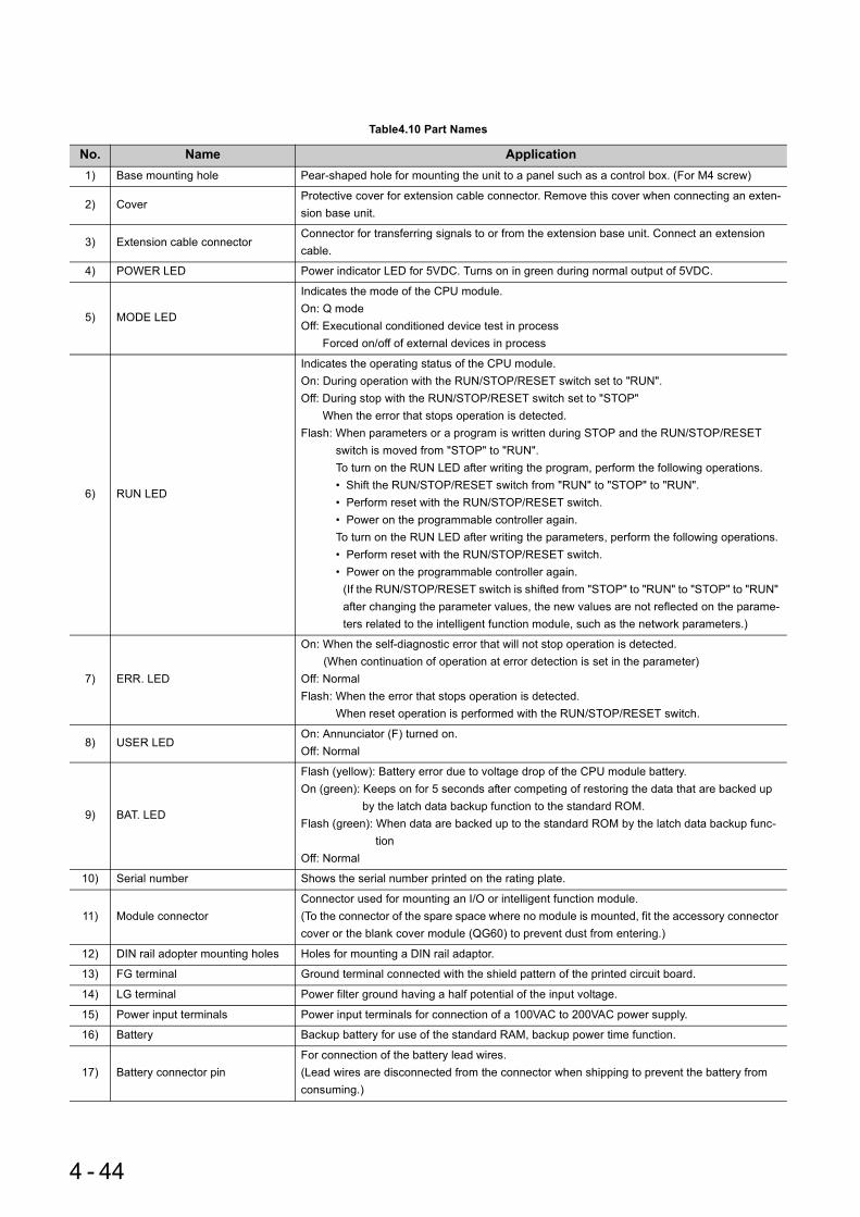
Table4.10 Part Names
No. Name Application1) Base mounting hole Pear-shaped hole for mounting the unit to a panel such as a control box. (For M4 screw)
2) CoverProtective cover for extension cable connector. Remove this cover when connecting an exten-sion base unit.
3) Extension cable connectorConnector for transferring signals to or from the extension base unit. Connect an extension cable.
4) POWER LED Power indicator LED for 5VDC. Turns on in green during normal output of 5VDC.
5) MODE LED
Indicates the mode of the CPU module.On: Q modeOff: Executional conditioned device test in process
Forced on/off of external devices in process
6) RUN LED
Indicates the operating status of the CPU module.On: During operation with the RUN/STOP/RESET switch set to "RUN".Off: During stop with the RUN/STOP/RESET switch set to "STOP"
When the error that stops operation is detected.Flash: When parameters or a program is written during STOP and the RUN/STOP/RESET
switch is moved from "STOP" to "RUN".To turn on the RUN LED after writing the program, perform the following operations.• Shift the RUN/STOP/RESET switch from "RUN" to "STOP" to "RUN".• Perform reset with the RUN/STOP/RESET switch.• Power on the programmable controller again.To turn on the RUN LED after writing the parameters, perform the following operations.• Perform reset with the RUN/STOP/RESET switch.• Power on the programmable controller again.
(If the RUN/STOP/RESET switch is shifted from "STOP" to "RUN" to "STOP" to "RUN" after changing the parameter values, the new values are not reflected on the parame-ters related to the intelligent function module, such as the network parameters.)
7) ERR. LED
On: When the self-diagnostic error that will not stop operation is detected.(When continuation of operation at error detection is set in the parameter)
Off: NormalFlash: When the error that stops operation is detected.
When reset operation is performed with the RUN/STOP/RESET switch.
8) USER LEDOn: Annunciator (F) turned on.Off: Normal
9) BAT. LED
Flash (yellow): Battery error due to voltage drop of the CPU module battery.On (green): Keeps on for 5 seconds after competing of restoring the data that are backed up
by the latch data backup function to the standard ROM. Flash (green): When data are backed up to the standard ROM by the latch data backup func-
tionOff: Normal
10) Serial number Shows the serial number printed on the rating plate.
11) Module connectorConnector used for mounting an I/O or intelligent function module.(To the connector of the spare space where no module is mounted, fit the accessory connector cover or the blank cover module (QG60) to prevent dust from entering.)
12) DIN rail adopter mounting holes Holes for mounting a DIN rail adaptor.
13) FG terminal Ground terminal connected with the shield pattern of the printed circuit board.
14) LG terminal Power filter ground having a half potential of the input voltage.
15) Power input terminals Power input terminals for connection of a 100VAC to 200VAC power supply.
16) Battery Backup battery for use of the standard RAM, backup power time function.
17) Battery connector pinFor connection of the battery lead wires.(Lead wires are disconnected from the connector when shipping to prevent the battery from consuming.)
4 - 44

CHAPTER4 HARDWARE SPECIFICATIONS OF THE CPU MODULE
1
2
3
4
5
6
7
8
4.4 Universal M
odel QC
PU
4.4.1 Part nam
es
*1: When a cable is connected to the RS-232 connector at all times, clamp the cable to prevent a poor connection, moving, and disconnection by unintentional pulling.The Q6HLD-R2 type RS-232 Connector Disconnection Prevention Holder is available as a clamp for RS-232 connector.
*2: Operate the RUN/STOP/RESET switch with your fingertips.To prevent the switch from being damaged, do not use any tool such as screw driver.
Table4.10 Part Names
No. Name Application
18) USB connector *1Connector for connection with USB-compatible peripheral devices. (Connector type miniB)Can be connected by USV-dedicated cable.
19) RS-232 connector *1Connector for connecting a peripheral device by RS-232.Can be connected by RS-232 connection cable. (QC30R2)
20) RUN/STOP/RESET switch *2
RUN: Executes sequence program operation.STOP: Stops sequence program operation.RESET: Performs hardware reset, operation error reset, operation initialization or like.
(Section 4.4.3)
Figure 4.19 RS-232 cable fixing processing
Fixing screw
Q6HLD-R2
CPU module
RS-232 cable
4 - 45
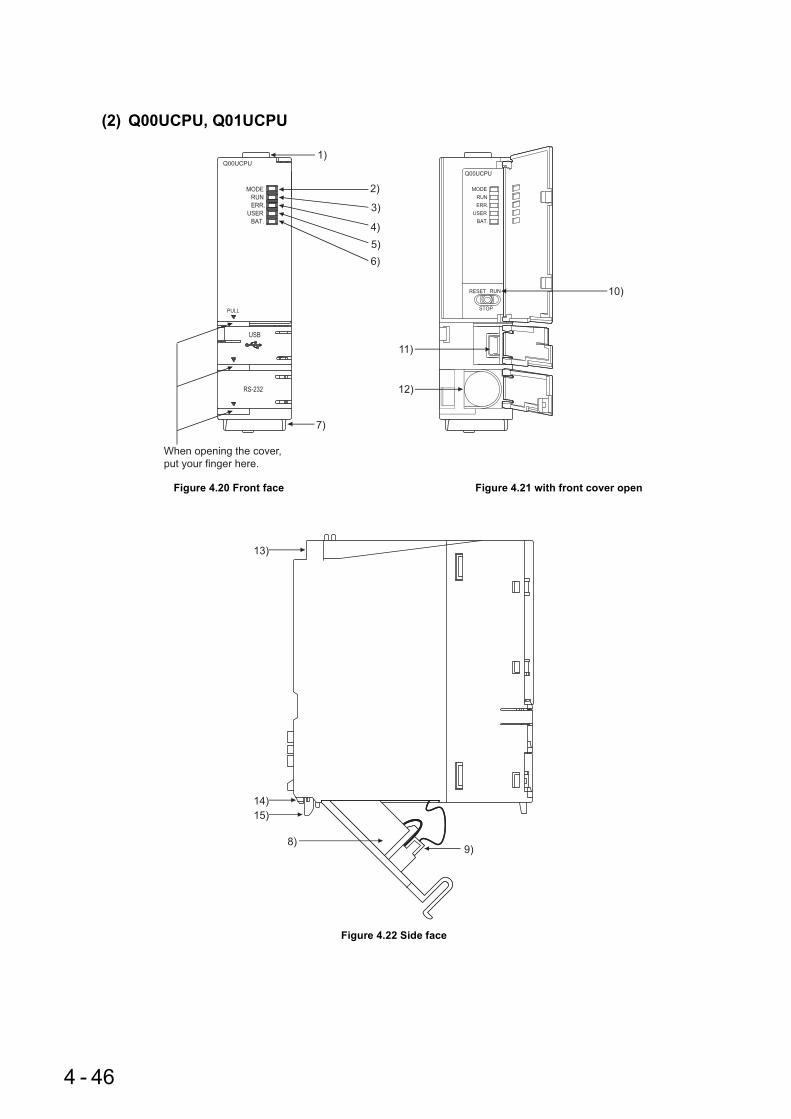
(2) Q00UCPU, Q01UCPU
Figure 4.20 Front face Figure 4.21 with front cover open
Figure 4.22 Side face
Q00UCPU
When opening the cover,
put your finger here.
7)
2)
3)
4)
6)
5)
1)
11)
12)
10)
13)
14)
15)
8)9)
4 - 46

CHAPTER4 HARDWARE SPECIFICATIONS OF THE CPU MODULE
1
2
3
4
5
6
7
8
4.4 Universal M
odel QC
PU
4.4.1 Part nam
es
Table4.11 Part Names
No. Name Application1) Module fixing hook Hook used to fix the module to the base unit. (Single-motion installation)
2) MODE LED
Indicates the mode of the CPU module.On : Q modeFlash : Executional conditioned device test is in process
Forced on and off function for external I/O is in process.
3) RUN LED
Indicates the operating status of the CPU module.On: During operation with the RUN/STOP/RESET switch set to "RUN"Off: During stop with the RUN/STOP/RESET switch set to "STOP".
When an error that stops operation is detected.Flash: Parameters or programs are written with the RUN/STOP/RESET switch set to "STOP",
and then the RUN/STOP/RESET switch is turned from "STOP" to "RUN."To turn on the RUN LED after writing the program, perform the following operations.
• Set the RUN/STOP/RESET switch in the order of "RUN" "STOP" "RUN".• Perform reset with the RUN/STOP/RESET switch• Power on the programmable controller again.To turn on the RUN LED after writing the parameters, perform the following operations.• Perform reset with the RUN/STOP/RESET switch• Power on the programmable controller again.(If the RUN/STOP/RESET switch is set in the order of "RUN" "STOP" "RUN" after changing the parameters, network parameters and intelligent function module parame-ters will not be updated.)
4) ERR. LED
On : Detection of self-diagnosis error which will not stop operation, except battery error. (When operation continued at error detection is set in the parameter setting.)Off : NormalFlash : Detection of the error that stops operation.
When reset operation becomes valid with the RUN/STOP/RESET switch.RUN/STOP/RESET.
5) USER LEDOn : Annunciator (F) turned on.Off : Normal
6) BAT. LED
On (yellow) : Battery error due to battery voltage drop of the memory card.On (green) : Turned on for 5 seconds after restoring of data backed up to the standard ROM by
the latch data backup is completed.Flash (green) : Flashes when backup of data to the standard ROM by latch data backup is
completed.Off: NormalFlash (yellow): Battery error due to voltage drop of the CPU module battery.On (green): Keeps on for 5 seconds after completing of restoring the data that are backed up
by the latch data backup function to the standard ROM. Flash (green): Completion of backup to the standard ROM by the latch data backup function.Off: Normal
7) Serial number Shows serial number printed on the rating plate.
8) BatteryBackup battery for use of the program memory, standard RAM, and backup power time func-tion.
9) Battery connector pinFor connection of battery lead wires.(Lead wires are disconnected from the connector when shipping to prevent the battery from consuming.)
10) RUN/STOP/RESET switch *2
RUN: Executes sequence program operationSTOP: Stops sequence program operationRESET: Performs hardware reset, operation error reset, operation initialization, and like.
( Section 4.4.3)
11) USB connector *1Connector for connection with USB-compatible peripheral device. (Connector type miniB)Can be connected by USB-dedicated cable.USB.
4 - 47

*1: When a cable is connected to the RS-232 connector at all times, clamp the cable to prevent a poor connection, moving, and disconnection by unintentional pulling.The Q6HLD-R2 type RS-232 Connector Disconnection Prevention Holder is available as a clamp for RS-232 connector.
*2: Operate the RUN/STOP/RESET switch with your fingertips.To prevent the switch from being damaged, do not use any tool such as screw driver.
Table4.11 Part Names
No. Name Application
12) RS-232 connector *1Connector for connecting a peripheral device by RS-232.Can be connected by RS-232 connection cable (QC30R2).
13) Module fixing holes Hole for the screw used to fix to the base unit. (M3 12 screw)
14) Module fixing projection Projection used to secure the module to the base unit.
15) Module mounting lever Lever used to mount the module to the base unit.
Figure 4.23 RS-232 cable fixing processing
Fixing screw
Q6HLD-R2
CPU module
RS-232 cable
4 - 48

CHAPTER4 HARDWARE SPECIFICATIONS OF THE CPU MODULE
1
2
3
4
5
6
7
8
4.4 Universal M
odel QC
PU
4.4.1 Part nam
es
(3) Q02UCPU, Q03UDCPU, Q04UDHCPU, Q06UDHCPU, Q10UDHCPU, Q13UDHCPU, Q20UDHCPU, Q26UDHCPU
Figure 4.24 Front face Figure 4.25 With front cover open
Figure 4.26 Side face
1)
When opening the cover, put
your finger here.
2)
3)
4)
6)
7)
5)
8)
9)
10)
11)
12)
13)
14)
15)
18)
17)
16)
4 - 49

(4) Q03UDECPU, Q04UDEHCPU, Q06UDEHCPU, Q10UDEHCPU, Q13UDEHCPU, Q20UDEHCPU, Q26UDEHCPU
Figure 4.27 Front face Figure 4.28 With front cover open
Figure 4.29 Side face
1)
When opening the cover, put
your finger here.
2)
3)
4)
6)
7)
5)
8)
21)
20)
9)
10)
11)
19)
13)
15)
18)
17)
16)
14)
4 - 50

CHAPTER4 HARDWARE SPECIFICATIONS OF THE CPU MODULE
1
2
3
4
5
6
7
8
4.4 Universal M
odel QC
PU
4.4.1 Part nam
es
Table4.12 Part names
No. Name Application1) Module fixing hook Hook used to fix the module to the base unit. (Single-motion installation)
2) MODE LED
Indicates the mode of the CPU module.On: Q modeFlash: Executional conditioned device test is in process Forced on and off function for external I/O is in process CPU module change function with memory card is in process
3) RUN LED
Indicates the operating status of the CPU module.On : During operation with the RUN/STOP/RESET switch set to "RUN"Off : During stop with the RUN/STOP/RESET switch set to "STOP".
When an error that stops operation is detected.Flash : Parameters or programs are written with the RUN/STOP/RESET switch set to
"STOP", and then the RUN/STOP/RESET switch is turned from "STOP" to "RUN."To turn on the RUN LED after writing the program, perform the following operations.
• Set the RUN/STOP/RESET switch in the order of "RUN" "STOP" "RUN".• Perform reset with the RUN/STOP/RESET switch.• Power on the programmable controller again.
To turn on the RUN LED after writing the parameters, perform the following operations.• Perform reset with the RUN/STOP/RESET switch.• Power on the programmable controller again.
(If the RUN/STOP/RESET switch is set in the order of "RUN" "STOP" "RUN" after changing the parameters, network parameters and intelligent function module parameters will not be updated.)
4) ERR. LED
On : Detection of self-diagnosis error which will not stop operation, except battery error.(When operation continued at error detection is set in the parameter setting.)
Off : NormalFlash : Detection of the error that stops operation.
When reset operation becomes valid with the RUN/STOP/RESET switch.
5) USER LEDOn : Annunciator ( F) turned onOff : Normal
6) BAT. LED
On (yellow) :Battery error due to battery voltage drop of the memory card.Flash (yellow) : Battery error due to voltage drop of the CPU module battery.On (green) : Turned on for 5 seconds after restoring of data backuped to the standard
ROM by the latch data backup is completed.Flash (green) : Flashes when backup of data to the standard ROM by latch data backup is
completed.Off : Normal
7) BOOT LEDOn : Start of boot operationOff : Non-execution of boot operation
4 - 51

*1: When a cable is connected to the RS-232 connector at all times, clamp the cable to prevent a poor connection, moving, and disconnection by unintentional pulling.The Q6HLD-R2 type RS-232 Connector Disconnection Prevention Holder is available as a clamp for RS-232 connector.
*2: Operate the RUN/STOP/RESET switch with your fingertips.To prevent the switch from being damaged, do not use any tool such as screw driver.
Table4.12 Part names
No. Name Application8) Serial number Shows the serial number printed on the rating plate.
9) Memory card EJECT button Used to eject the memory card from the CPU module.
10) Memory card installing connector Connector used for installing the memory card to the CPU module.
11) USB connectorConnector for connection with USB-compatible peripheral device. (Connector type miniB)Can be connected by USB-dedicated cable.
12) RS-232 connector *1Connector for connecting a peripheral device by RS-232.Can be connected by RS-232 connection cable (QC30R2).
13) RUN/STOP/RESET switch*2
RUN : Executes sequence program operation.STOP : Stops sequence program operation.RESET : Performs hardware reset, operation error reset, operation initialization or like.
( Section 4.4.3)
14) Module fixing screw hole Hole for the screw used to secure to the base unit. (M3 12 screw)
15) Module fixing projection Projection used to secure the module to the base unit.
16) Battery connector pinFor connection of battery lead wires.(Lead wires are disconnected from the connector when shipping to prevent the battery from consuming.)
17) Battery Backup battery for use of standard RAM, clock function and backup power time function.
18) Module mounting lever Lever used to mount the module to the base unit.
19) Ethernet connector Connector for connecting an Ethernet device (RJ-45 connector)
20) 100M LEDOn: Connected at 100Mbps.Off: Not connected, or connected at 10Mbps
21) SD/RD LEDOn: Data being sent/receivedOff: No data being sent/received
Figure 4.30 RS-232 cable fixing processing
Fixing screw
Q6HLD-R2
CPU module
RS-232 cable
4 - 52

CHAPTER4 HARDWARE SPECIFICATIONS OF THE CPU MODULE
1
2
3
4
5
6
7
8
4.4 Universal M
odel QC
PU
4.4.2 Sw
itch operation after writing a program
4.4.2 Switch operation after writing a program
This section explains the switch operation after a program is written using GX Developer.
(1) When writing program with CPU module set to "STOP" *1
(a) To set to RUN status with device memory data cleared1) Set the RUN/STOP/RESET switch to the RESET position once (Approximately 1 second) and return it to
the STOP position.
2) Set the RUN/STOP/RESET switch to the RUN position.
3) The CPU module is placed in the RUN status (RUN LED: On).
(b) To set to RUN status with device memory data not cleared (held)1) Set the RUN/STOP/RESET switch to the RUN position.
2) The RUN LED flashes.
3) Set the RUN/STOP/RESET switch to the STOP position.
4) Setthe RUN/STOP/RESET switch to the RUN position again.
5) The CPU module is placed in the RUN status (RUN LED: On).
(2) When a program is written while CPU module is running (online change)*2
No operation is needed for the RUN/STOP/RESET switch of the CPU module. At this time, the device memory data are not cleared.
*1: When a program was written to the program memory during boot operation, also write the program to the boot source memory.If the program is not written to the boot source memory, the old program will be executed at the next boot operation.
*2: When a program is written online in the ladder mode, the changed program is written to the program memory.When performing boot operation, also write the program to the boot source memory after online change. If the program is not written to the boot source memory, the old program will be executed at the next boot operation
For details of the boot operation, refer to the following.
QnUCPU User's Manual (Functional Description, Program Fundamentals)
When the CPU module is placed in the STOP status by the remote STOP operation of GX Developer, it can be set in the RUN status by the remote RUN operation of GX Developer after program write.In that case, no operation is needed for the RUN/STOP/RESET switch of the CPU module.For details of GX Developer, refer to the following.
GX Developer Operating Manual
4 - 53

4.4.3 Reset operation
For the Universal model QCPU, the RUN/STOP/RESET switch of the CPU module is used to switch between the RUN status and STOP status and to perform RESET operation.When using the RUN/STOP/RESET switch to reset the CPU module, setting the RUN/STOP/RESET switch to the reset position will not reset it immediately.
Hold the RUN/STOP/RESET switch in the RESET position until reset processing is complete (the flashing ERR. LED turns off).If you release your hand from the RUN/STOP/RESET switch during reset processing (the ERR. LED is flashing), the switch will return to the STOP position and reset processing cannot be completed.
Perform reset operation with the RUN/STOP/RESET switch as shown in Figure 4.31.
Figure 4.31 Reset operation
Start
Termination , completed , end
Hold the RUN/STOP/RESET switch
in the "RESET" position.
Reset operation is started using
the RUN/STOP/RESET switch.
.......................
Reset is accepted and reset
processing is performed.
.......................
Reset is completed........................
Reset is canceled........................
Releasing your hand from the
RUN/STOP/RESET switch returns it
to the STOP position.
RESET RUN
STOP
RUN/STOP/RESET
switch
Flickers.
Goes off.
The ERR. LED flickers several times
(3 to 4 times) rapidly.
The "ERR. LED" goes off .
Return the RUN/STOP/RESET
switch to the "STOP" position.
RUN/STOP/RESET
switch
RESET RUN
STOP
:
MODE
RUN
ERR.
USER
BAT.
BOOT
MODE
RUN
ERR.
USER
BAT.
BOOT
4 - 54

CHAPTER4 HARDWARE SPECIFICATIONS OF THE CPU MODULE
1
2
3
4
5
6
7
8
4.4 Universal M
odel QC
PU
4.4.4 Latch clear operation
Operate the RUN/STOP/RESET switch with your fingertips.To prevent the switch from being damaged, do not use any tool such as screw driver.
4.4.4 Latch clear operation
For the Universal model QCPU, latch clear is performed by the remote latch clear operation of GX Developer.Latch clear cannot be executed by operating the switches of the CPU module.
● The valid/invalid for latch clear in the clear range of latch clear operation can be set for each device. The setting can be made in the device setting of the PLC parameter.
● For the remote latch clear operation by GX Developer, refer to the following. QnUCPU User's Manual (Functional Description, Program Fundamentals)
4 - 55
CHAPTER5 POWER SUPPLY MODULE
This chapter describes the specifications of the power supply modules applicable for the programmable controller system (The Q Series power supply module, slim type power supply module, redundant power supply module and AnS/A Series power supply module) and how to select the most suitable module.
5.1 Base Unit that Can Be Used in Combination with Power Supply Module
This section describes the base unit that can be used in combination with the power supply module respectively.For details of the CPU modules and base units, refer to the following.
CPU modules : CHAPTER 4
Base units : CHAPTER 6
For details of the system configuration, refer to CHAPTER 2.
: Combination available : Combination not available*1: When mounting the Q64RP to the Q65WRB, use the Q64RP whose serial number (first six digits) is "081103" or later.
The vibration condition described in the general specifications may not be met if the serial number (first six digits) of the Q64RP is "081102" or earlier is mounted.
*2: The QA6ADP+A6 B also has the equivalent specifications.
Table5.1 Base unit that can be used in combination with power supply module
Power supply module
Base unitMain base unit Extension base unit
Q33BQ35BQ38B
Q312B
Q32SBQ33SBQ35SB
Q38RBQ38DB
Q312DBQ52BQ55B
Q63BQ65BQ68B
Q612B
Q68RB Q65WRBQA1S65BQA1S68B
QA65BQA68B
*2
Q61P-A1Q61P-A2Q61PQ61P-DQ62PQ63PQ64PQ64PN
Q61SP
Q63RPQ64RP
*1
A1S61PNA1S62PNA1S63P
A61PA61PNA62PA63PA61PEUA62PEU
5 - 1

CHAPTER5 POWER SUPPLY MODULE
1
2
3
4
5
6
7
8
5.2 Specifications
5.2.1 Pow
er supply module specifications
5.2 Specifications
5.2.1 Power supply module specifications
Table5.2 shows the specifications of the power supply modules.
Table5.2 Power supply module specifications
ItemPerformance Specifications
Q61P-A1 Q61P-A2 Q61P Q62PMounting position Power supply module mounting slot
Applicable base unit Q3 B, Q3 DB, Q6 B
Input power supply 100 to 120VAC
(85 to 132VAC)
200 to 240VAC
(170 to 264VAC)
100 to 240VAC
(85 to 264VAC)
Input frequency 50/60Hz 5%
Input voltage distortion factor Within 5% ( Section 5.2.4)
Max. input apparent power
105VA 120VA 105VA
Max. input power ----
Inrush current 20A within 8ms*5
Rated output current
5VDC 6A 3A
24VDC ---- 0.6A
External output voltage ---- 24VDC 10%
Overcurrent
protection*1
5VDC 6.6A or more 3.3A or more
24VDC ---- 0.66A or more
Overvoltage
protection *25VDC 5.5 to 6.5V
24VDC ----
Efficiency 70% or more 65% or more
Allowable momentary
power failure period *3Within 20ms
Dielectric withstand voltage
Between input -LG batched and output-FG batched2830VAC rms/3 cycles (2000m (6562 feet))
Insulation resistanceInput and LG batched, output and FG batched, batch input-LG, batch output-FG10M or higher by 500VDC insulation resistance tester
Noise durability • By noise simulator of 1500Vp-p noise voltage, 1 s noise width and 25 to 60Hz noise frequency• Noise voltage IEC 61000-4-4, 2KV
Operation indication LED indication (Normal: On (green), Error: Off)
Fuse Built-in (User-unchangeable)
+10%
-15%
+10%
-15%
+10%
-15%
5 - 2

Table5.2 Power supply module specifications
ItemPerformance Specifications
Q61P-A1 Q61P-A2 Q61P Q62P
Con
tact
out
put s
ectio
n
Application ERR. contact ( Section 5.3)
Rated switching voltage, current
24VDC, 0.5A
Minimum switching load
5VDC, 1mA
Response time OFF to ON: 10ms max. ON to OFF: 12ms max.
LifeMechanical : More than 20 million times
Electrical : More than 100 thousand times at rated switching voltage, current
Surge suppressor
No
Fuse No
Terminal screw size M3.5 7
Applicable wire size 0.75 to 2mm2
Applicable solderless terminal
RAV1.25 - 3.5, RAV2 - 3.5
Applicable tightening torque
0.66 to 0.89N•m
External dimensions
H 98mm (3.86 inches)
W 55.2mm (2.17 inches)
D 90mm (3.55 inches)
Weight 0.31kg 0.40kg 0.39kg
5 - 3

CHAPTER5 POWER SUPPLY MODULE
1
2
3
4
5
6
7
8
5.2 Specifications
5.2.1 Pow
er supply module specifications
Table5.3 Power supply module specifications
ItemPerformance Specifications
Q63PMounting position Power supply module mounting slot
Applicable base unit Q3 B, Q3 DB, Q6 B
Input power supply 24VDC
(15.6 to 31.2VDC)
Input frequency ----
Input voltage distortion factor
----
Max. input apparent power
----
Max. input power 45W
Inrush current 100A within 1ms (at 24VDC input)
Rated output current
5VDC 6A
24VDC ----
External output voltage ----
Overcurrent
protection*1
5VDC 6.6A or more
24VDC ----
Overvoltage
protection *25VDC 5.5 to 6.5V
24VDC ----
Efficiency 70% or more
Allowable momentary
power failure time *3Within 10ms
(at 24VDC input)
Dielectric withstand voltage
Between primary and 5VDC 500VAC
Insulation resistance 10M or more by insulation resistance tester
Noise durability By noise simulator of 500Vp-p noise voltage, 1 s noise width and 25 to 60Hz noise frequency
Operation indication LED indication (Normal: On (green), Error: Off)
Fuse Built-in (User-unchangeable)
+30%
-35%
5 - 4
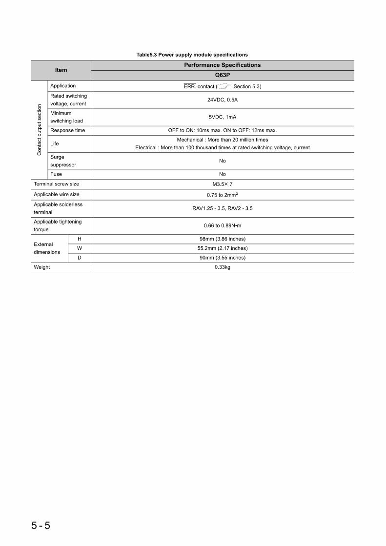
Table5.3 Power supply module specifications
ItemPerformance Specifications
Q63P
Con
tact
out
put s
ectio
n
Application ERR. contact ( Section 5.3)
Rated switching voltage, current
24VDC, 0.5A
Minimum switching load
5VDC, 1mA
Response time OFF to ON: 10ms max. ON to OFF: 12ms max.
LifeMechanical : More than 20 million times
Electrical : More than 100 thousand times at rated switching voltage, current
Surge suppressor
No
Fuse No
Terminal screw size M3.5 7
Applicable wire size 0.75 to 2mm2
Applicable solderless terminal
RAV1.25 - 3.5, RAV2 - 3.5
Applicable tightening torque
0.66 to 0.89N•m
External dimensions
H 98mm (3.86 inches)
W 55.2mm (2.17 inches)
D 90mm (3.55 inches)
Weight 0.33kg
5 - 5
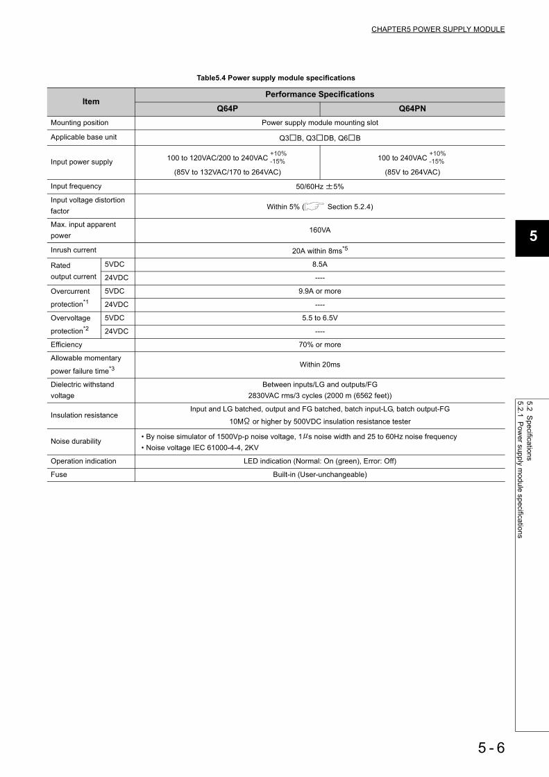
CHAPTER5 POWER SUPPLY MODULE
1
2
3
4
5
6
7
8
5.2 Specifications
5.2.1 Pow
er supply module specifications
Table5.4 Power supply module specifications
ItemPerformance Specifications
Q64P Q64PNMounting position Power supply module mounting slot
Applicable base unit Q3 B, Q3 DB, Q6 B
Input power supply 100 to 120VAC/200 to 240VAC
(85V to 132VAC/170 to 264VAC)
100 to 240VAC
(85V to 264VAC)
Input frequency 50/60Hz 5%
Input voltage distortion factor Within 5% ( Section 5.2.4)
Max. input apparent power
160VA
Inrush current 20A within 8ms*5
Ratedoutput current
5VDC 8.5A
24VDC ----
Overcurrent
protection*1
5VDC 9.9A or more
24VDC ----
Overvoltage
protection*2
5VDC 5.5 to 6.5V
24VDC ----
Efficiency 70% or more
Allowable momentary
power failure time*3 Within 20ms
Dielectric withstand voltage
Between inputs/LG and outputs/FG2830VAC rms/3 cycles (2000 m (6562 feet))
Insulation resistanceInput and LG batched, output and FG batched, batch input-LG, batch output-FG
10M or higher by 500VDC insulation resistance tester
Noise durability • By noise simulator of 1500Vp-p noise voltage, 1 s noise width and 25 to 60Hz noise frequency• Noise voltage IEC 61000-4-4, 2KV
Operation indication LED indication (Normal: On (green), Error: Off)
Fuse Built-in (User-unchangeable)
+10%
-15%
+10%
-15%
5 - 6

Table5.4 Power supply module specifications
ItemPerformance Specifications
Q64P Q64PN
Con
tact
out
put s
ectio
n
Application ERR. contact ( Section 5.3)
Rated switching voltage, current
24VDC, 0.5A
Minimum switching load
5VDC, 1mA
Response time OFF to ON: 10ms max. ON to OFF: 12ms max.
LifeMechanical : More than 20 million times
Electrical : More than 100 thousand times at rated switching voltage, current
Surge suppressor
None
Fuse None
Terminal screw size M3.5 screw
Applicable wire size 0.75 to 2mm2
Applicable solderless terminal
RAV1.25 - 3.5, RAV2 - 3.5
Applicable tightening torque
0.66 to 0.89N•m
External dimensions
H 98mm (3.86 inches)
W 55.2mm (2.17 inches)
D 115mm (4.53 inches)
Weight 0.40kg 0.47kg
5 - 7

CHAPTER5 POWER SUPPLY MODULE
1
2
3
4
5
6
7
8
5.2 Specifications
5.2.1 Pow
er supply module specifications
Table5.5 Power supply module specifications
ItemPerformance Specifications
Q61SPMounting position Power supply module mounting slot
Applicable base unit Q3 SB
Input power supply 100 to 240VAC
(85 to 264VAC)
Input frequency 50/60Hz 5%
Input voltage distortion factor Within 5% ( Section 5.2.4)
Max. input apparent power
40VA
Inrush current 20A within 8ms*5
Rated output current
5VDC 2A
24VDC ----
Overcurrent
protection*1
5VDC 2.2A or more
24VDC ----
Overvoltage
protection*2
5VDC 5.5 to 6.5V
24VDC ----
Efficiency 70% or more
Allowable momentary
power failure time*3 Within 20ms (AC100VAC or more)
Dielectric withstand voltage
Between inputs/LG and outputs/FG2830VAC rms/3 cycles (2000 m (6562 feet))
Insulation resistanceInput and LG batched, output and FG batched, batch input-LG, batch output-FG
10M or higher by 500VDC insulation resistance tester
Noise durability • By noise simulator of 1500Vp-p noise voltage, 1 s noise width and 25 to 60Hz noise frequency• Noise voltage IEC 61000-4-4, 2KV
Operation indication LED indication (Normal: On (green), Error: Off)
Fuse Built-in (User-unchangeable)
Con
tact
out
put s
ectio
n
Application ERR. contact ( Section 5.3)
Rated switching voltage, current
24VDC, 0.5A
Minimum switching load
5VDC, 1mA
Response time OFF to ON: 10ms max. ON to OFF: 12ms max.
LifeMechanical : More than 20 million times
Electrical : More than 100 thousand times at rated switching voltage, current
Surge suppressor
None
Fuse None
+10%
-15%
5 - 8

Table5.5 Power supply module specifications
ItemPerformance Specifications
Q61SPTerminal screw size M3.5 screw
Applicable wire size 0.75 to 2mm2
Applicable solderless terminal
RAV1.25 - 3.5, RAV2 - 3.5
Applicable tightening torque
0.66 to 0.89N•m
External dimensions
H 98mm (3.86 inches)
W 27.4mm (1.08 inches)
D 104mm (4.09 inches)
Weight 0.18kg
5 - 9

CHAPTER5 POWER SUPPLY MODULE
1
2
3
4
5
6
7
8
5.2 Specifications
5.2.1 Pow
er supply module specifications
*6: Although the POWER LED momentarily turns on in red immediately after the power supply is turned on or off, the Q64RP is not faulty.
Table5.6 Power supply module specifications
ItemPerformance Specifications
Q63RPBase unit position Power supply module mounting slot
Applicable base unit Q3 RB, Q3 RB, Q6 WRB
Input power supply 24V DC(-35%/+30%) (15.6 to 31.2V DC)
Max. input power 65W
Inrush current 150A within 1ms
Rated output current
5VDC 8.5A
24VDC ----
Overcurrent
protection*1
5VDC 9.35A or more
24VDC ----
Overvoltage
protection*2
5VDC 5.5 to 6.5V
24VDC ----
Efficiency 65% or more
Allowable momentary
power failure period*3 Within 10ms(at 24V DC input)
Dielectric withstand voltage
Between primary and 5VDC 500VAC
Insulation resistance 10M or more by insulation resistance tester
Noise durabilityBy noise simulator of 500Vp-p
noise voltage, 1 s noise width and 25 to 60Hz noise frequency
Operation indication LED indication*6 (Normal operation: On(green) Error:Off(red)
Fuse Built-in (User-unchangeable)
Con
tact
out
put s
ectio
n
Application ERR. contact ( Section 5.3)
Rated switching voltage, current
24VDC, 0.5A
Minimum switching load
5VDC, 1mA
Response time OFF to ON: 10ms max. ON to OFF: 12ms max.
LifeMechanical : More than 20 million times
Electrical : More than 100 thousand times at rated switching voltage, current
Surge suppressor None
Fuse None
Terminal screw size M3.5 Screw
Applicable wire size 0.75 to 2mm2
Applicable solderless terminal
RAV1.25-3.5, RAV2-3.5, RAV1.25-3.5, RAV2-3.5
Applicable tightening torque
0.66 to 0.89N•m
External dimensions
H 98mm (3.86 inches)
W 83mm (3.27 inches)
D 115mm (4.53 inches)
Weight 0.60kg
5 - 10

*7: Although the POWER LED momentarily turns on in red immediately after the power supply is turned on or off, the Q64RP is not faulty.*8: When mounting the Q64RP to the Q65WRB, use the Q64RP whose first 6 digits of serial No. is "081103" or later.
The vibration condition described in the general specifications may not be met if the serial number (first six digits) of the Q64RP is "081102" or earlier is mounted.
Table5.7 Power supply module specifications
ItemPerformance Specifications
Q64RPMounting position Power supply module mounting slot
Applicable base unit Q3 RB, Q6 RB, Q6 WRB*8
Input power supply 100 to 120VAC/200 to 240VAC
(85 to 132VAC/170 to 264VAC)
Input frequency 50/60Hz 5%
Input voltage distortion factor Within 5% ( Section 5.2.4)
Max. input apparent power
160VA
Inrush current 20A within 8ms*5
Rated output current
5VDC 8.5A
24VDC ----
Overcurrent
protection*1
5VDC 9.35A or more
24VDC ----
Overvoltage
protection*2
5VDC 5.5 to 6.5V
24VDC ----
Efficiency 65% or more
Allowable momentary
power failure time*3 Within 20ms
Dielectric withstand voltage
Between inputs/LG and outputs/FG2830VAC rms/3 cycles (2000 m (6562 feet))
Insulation resistanceInput and LG batched, output and FG batched, batch input-LG, batch output-FG
10M or higher by 500VDC insulation resistance tester
Noise durability • By noise simulator of 1500Vp-p noise voltage, 1 s noise width and 25 to 60Hz noise frequency• Noise voltage IEC 61000-4-4, 2KV
Operation indication LED indication (Normal: ON (green), Error: ON (red)) *7
Fuse Built-in (User-unchangeable)
+10%
-15%
5 - 11

CHAPTER5 POWER SUPPLY MODULE
1
2
3
4
5
6
7
8
5.2 Specifications
5.2.1 Pow
er supply module specifications
Table5.7 Power supply module specifications
ItemPerformance Specifications
Q64RP
Con
tact
out
put s
ectio
n
Application ERR. contact ( Section 5.3)
Rated switching voltage, current
24VDC, 0.5A
Minimum switching load
5VDC, 1mA
Response time OFF to ON: 10ms max. ON to OFF: 12ms max.
LifeMechanical : More than 20 million times
Electrical : More than 100 thousand times at rated switching voltage, current
Surge suppressor
None
Fuse None
Terminal screw size M3.5 screw
Applicable wire size 0.75 to 2mm2
Applicable solderless terminal
R1.25-3.5, R2-3.5, RAV1.25-3.5, RAV2-3.5
Applicable tightening torque
0.66 to 0.89N•m
External dimensions
H 98mm (3.86 inches)
W 83mm (3.27 inches)
D 115mm (4.53 inches)
Weight 0.47kg
5 - 12

*10: When using the Q61P-D in the system configured with a A/AnS series module, the power supply modules mounted on the main base unit and extension base unit must be turned on and off simultaneously.
Table5.8 Power supply module specifications
ItemPerformance Specifications
Q61P-DMounting position Power supply module mounting slot
Applicable base unit Q3 B, Q3 DB, Q6 B
Input power supply*10 100 to 240VAC
(85 to 264VAC)
Input frequency 50/60Hz 5%
Input voltage distortion factor Within 5% ( Section 5.2.4)
Max. input apparent power
130VA
Max. input power ----
Inrush current 20A within 8ms*5
Rated output current
5VDC 6A
24VDC ----
External output voltage ----
Overcurrent
protection*1
5VDC 6.6A or more
24VDC ----
Overvoltage
protection *25VDC 5.5 to 6.5V
24VDC ----
Efficiency 70% or more
Allowable momentary
power failure period *3Within 20ms
Dielectric withstand voltage
Between input -LG batched and output-FG batched2830VAC rms/3 cycles (2000m (6562 feet))
Insulation resistanceInput and LG batched, output and FG batched, batch input - LG, batch output - FG
10M or higher by 500VDC insulation resistance tester
Noise durability • By noise simulator of 1500Vp-p noise voltage, 1 s noise width and 25 to 60Hz noise frequency• Noise voltage IEC 61000-4-4, 2KV
Operation indication LED indication (POWER LED, LIFE LED)
Fuse Built-in (User-unchangeable)
Con
tact
out
put s
ectio
n
Application ERR. contact, LIFE OUT contact ( Section 5.3)
Rated switching voltage, current
24VDC, 0.5A
Minimum switching load
5VDC, 1mA
Response time OFF to ON: 10ms max. ON to OFF: 12ms max.
LifeMechanical : More than 20 million times
Electrical : More than 100 thousand times at rated switching voltage, current
Surge suppres-sor
No
Fuse No
+10%
-15%
5 - 13

CHAPTER5 POWER SUPPLY MODULE
1
2
3
4
5
6
7
8
5.2 Specifications
5.2.1 Pow
er supply module specifications
Table5.8 Power supply module specifications
ItemPerformance Specifications
Q61P-DTerminal screw size M3.5 7
Applicable wire size 0.75 to 2mm2
Applicable solderless terminal
RAV1.25 - 3.5, RAV2 - 3.5
Applicable tightening torque
0.66 to 0.89N•m
External dimensions
H 98mm (3.86 inches)
W 55.2mm (2.17 inches)
D 90mm (3.55 inches)
Weight 0.45kg
5 - 14

Table5.9 Power supply module specifications
ItemPerformance Specifications
Q00JCPU (Power supply part) Q00UJCPU (Power supply part)
Input power supply 100 to 120VAC
(85 to 264VAC)
Input frequency 50/60Hz 5%
Input voltage distortion factor Within 5% ( Section 5.2.4)
Max. input apparent power
105VA
Inrush current 40A within 8ms*5
Rated output current
5VDC 3A
Overcurrent
protection*1 5VDC 3.3A or more
Overvoltage
protection*2 5VDC 5.5 to 6.5V
Efficiency 65% or more
Allowable momentary
power failure time*3 Within 20ms (100VAC or more)
Dielectric withstand voltage
Between inputs/LG and outputs/FG2830VAC rms/3 cycles (2000 m (6562 feet))
Insulation resistanceInput and LG batched, output and FG batched, batch input-LG, batch output-FG
10M or higher by 500VDC insulation resistance tester
Noise durability • By noise simulator of 1500Vp-p noise voltage, 1 s noise width and 25 to 60Hz noise frequency• Noise voltage IEC61000-4-4, 2KV
Operation indication LED indication (The POWER LED of the CPU part: Normal: On (green), Error: Off)
Fuse Built-in (User-unchangeable)
Contact output section None
Terminal screw size M3.5 7
Applicable wire size 0.75 to 2mm2
Applicable solderless terminal
RAV1.25 - 3.5, RAV2 - 3.5
Applicable tightening torque
0.66 to 0.89N•m
External dimensions Section 4.1
Weight
+10%
-15%
5 - 15

CHAPTER5 POWER SUPPLY MODULE
1
2
3
4
5
6
7
8
5.2 Specifications
5.2.1 Pow
er supply module specifications
Table5.10 Power supply module specifications
ItemPerformance Specifications
A1S61PN A1S62PN A1S63PMounting position Power supply module mounting slot
Applicable base unit QA1S6 B
Input power supply 100 to 240VAC
(85 to 264VAC)
24VDC
(15.6 to 31.2VDC)
Input frequency 50/60Hz 5% ----
Input voltage distortion factor Within 5% ( Section 5.2.4) ---
Max. input apparent power
105VA ----
Max. input power ---- 41W
Inrush current 20A within 8ms*5 81A within 1ms
Rated output current
5VDC 5A 3A 5A
24VDC ---- 0.6A ----
Overcurrent
protection*1
5VDC 5.5A or more 3.3A or more 5.5A or more
24VDC ---- 0.66A or more ----
Overvoltage
protection*2
5VDC 5.5 to 6.5V
24VDC ----
Efficiency 65% or more
Allowable momentary
power failure time*3 Within 20msWithin 10ms
(at 24VDC input)
Dielectric withstand voltage
Between inputs/LG and outputs/FG2830VAC rms/3 cycles (2000 m (6562 feet))
Between primary and 5VDC 500VAC
Insulation resistanceBetween inputs and outputs (LG and FG separated), between inputs and
LG/FG, between outputs and FG/LG 10M or more by insulation resistance tester
5M or more by insulation resistance tester
Noise durability• By noise simulator of 1500Vp-p noise voltage, 1 s noise width and 25
to 60Hz noise frequency• Noise voltage IEC 61000-4-4, 2KV
By noise simulator of 500Vp-p noise
voltage, 1 s noise width and 25 to 60Hz noise frequency
Operation indication LED indication (Normal: On (green), Error: Off)
Fuse Built-in (User-unchangeable)
Contact output section None
Terminal screw size M3.5 screw
Applicable wire size 0.75 to 2mm2
Applicable solderless terminal
RAV1.25 to 3.5, RAV2 to 3.5
Applicable tightening torque
0.66 to 0.89N•m
External dimensions
H 130mm (5.12 inches)
W 55mm (2.17 inches)
D 93.6mm (3.69 inches)
Weight 0.60kg 0.50kg
+10%
-15%
+30%
-35%
5 - 16

Table5.11 Power supply module specifications
ItemSpecifications
A61P A61PN A62P A63PSlot position Power supply module mounting slot
Applicable base unit QA6 B
Input power supply
100VAC to 120VAC
(85VAC to 132VAC) 24VDC
(15.6VDC to 31.2VDC)200VAC to 240VAC
(170VAC to 264VAC)
Input frequency 50/60Hz 5% –
Input voltage distortion Within 5% ( Section 5.2.4) –
Max. input apparent power
160VA 155VA 65W
Inrush current 20A, 8ms or less*5 100A, 1ms or less
Rated output current
5VDC 8A 5A 8A
24VDC – 0.8A –
Overcurrent
protection*1
5VDC 8.8A or more 5.5A or more 8.5A or more
24VDC – 1.2A or more –
Overvoltage
protection*2
5VDC 5.5 to 6.5V 5.5 to 6.5V 5.5 to 6.5V
24VDC –
Efficiency 65% or more
Dielectric withstand voltage
Between AC external terminals and ground, 1500V AC, 1 minuteBetween DC external terminals and ground, 500V AC, 1 minute
Noise durability By noise simulator of 1500Vp-p noise voltage, noise width 1 s, and 25 to 60Hz
noise frequency
By noise simulator of 500Vp-p noise voltage, noise width 1 s, and 25 to 60Hz noise frequency
Insulation resistance Between AC external terminals and ground, 5M or higher by 500VDC insulation resistance tester
Power indicator LED indication of power supply
Terminal screw size M4 0.7 6
Applicable wire size 0.75 to 2mm2
Applicable solderless terminal
R1.25-4, R2-4RAV1.25, RAV2-4
Applicable tightening torque
78 to 118 Ncm
External dimensions
H 250mm(9.84 inches)
W 55mm(2.17 inches)
D 121mm(4.76 inches)
Weight 0.98 kg 0.75 kg 0.94 kg 0.8 kg
Allowable momentary
power failure time*3 20ms or less 1ms or less
+10%
-15%
+30%
-35%
+10%
-15%
5 - 17

CHAPTER5 POWER SUPPLY MODULE
1
2
3
4
5
6
7
8
5.2 Specifications
5.2.1 Pow
er supply module specifications
Table5.12 Power supply module specifications
ItemPerformance specifications
A61PEU A62PEUSlot position Power supply module mounting slot
Applicable base unit QA6 B
Input power supply 100 to 120/200 to 240VAC +10%/-15%
Input frequency 50/60Hz 5%
Input voltage distortion Within 5% ( Section 5.2.4)
Max. input apparent power 130VA 155VA
Inrush current 20A, 8ms or less*5
Rated output current
5VDC 8A 5A
24VDC – 0.8A
Overcurrent
protection*1
5VDC 8.8A or more 5.5A or more
24VDC – 1.2A or more
Overvoltage
protection*2
5VDC 5.5 to 6.5V –
24VDC –
Efficiency 65% or more
Dielectric withstand voltage
Between primary side and FG
2830V AC rms/3 cycles (altitude 2000m (6562 feet))
Noise durabilityBy noise simulator of noise voltage IEC 801-4, 2KV, 1500Vp-p,
noise width 1 s, and noise frequency 25 to 60Hz
Power indicator LED indication of power supply
Terminal screw size M4 0.7 6
Applicable wire size 0.75 to 2mm2
Applicable solderless terminal RAV1.25-4, RAV2-4
Applicable tightening torque 98 to 137N cm
External dimensions
H 250mm(9.84 inches)
W 55mm(2.17 inches)
D 121mm(4.76 inches)
Weight 0.8 kg 0.9 kg
Allowable momentary power failure
time*3 20ms or less
5 - 18

*1: Overcurrent protectionThe overcurrent protection device shuts off the 5 V, 24 VDC circuit and stops the system if the current flowing in the circuit exceeds the specified value.The LED of the power supply module turns off or turns on in dim green when voltage is lowered. (As for the redundant power supply module, the LED turns off or turns on in red.) If this device is activated, switch the input power supply off and eliminate the cause such as insufficient current capacity or short. Then, a few minutes later, switch it on to restart the system.The initial start for the system takes place when the current value becomes normal.
*2: Overvoltage protectionThe overvoltage protection device shuts off the 5 VDC circuit and stops the system if a voltage of 5.5 VDC is applied to the circuit. When this device is activated, the power supply module LED turns off. If this happens, switch the input power off, then a few minutes later on. This causes the initial start for the system to take place. The power supply module must be changed if the system is not booted and the LED remains off (As for the redundant power supply module, the LED turns on in red).
*3: Allowable momentary power failure time(a)For AC input power supply
• If the momentary power failure time is within 20ms, the system detects an AC down and suspends the operation processing. However, the system continues operations after the power comes back.
• If the momentary power failure time exceeds 20ms, the system either continues or initially starts operations depending on the power supply load. In case that the operation processing is continued, the system operates the same as when the momentary power failure time is within 20ms.Supplying the same amount of AC to both the power supply module and the input module (such as QX10) can prevent the sensor connected to the input module from being switched to the OFF status when the power supply turns off.Note, however, that if only the input module (such as QX10) is connected on the AC line, which is connected to the power supply, an AC down detection in the power supply module may be delayed due to the internal capacitor of the input module. To avoid this, connect a load of approx. 30mA per input module on the AC line.In the system operating with two redundant power supply modules, the system does not initially start operations when the momentary power failure exceeding 20ms occurs in only one of the input power supplies.The system, however, may initially start operations when the momentary power failure exceeding 20ms occurs simultaneously in both input power supplies.
(b)For DC input power supply • If the momentary power failure time is within 10ms(*4), the system detects an 24VDC down and suspends the
operation processing. However, the system continues operations after the power comes back. • If the momentary power failure time exceeds 10ms(*4), the system either continues or initially starts operations
depending on the power supply load. In case that the operation processing is continued, the system operates the same as when the momentary power failure time is within 10ms.(*4: This is the time when 24VDC is input. If the input is less than 24VDC, the time will be less than 10ms.)
*5: Inrush currentWhen power is switched on again immediately (within 5 seconds) after power-off, an inrush current of more than the specified value (2ms or less) may flow. Reapply power 5 or more seconds after power-off. When selecting a fuse and breaker in the external circuit, take account of the blowout, detection characteristics and above matters.
5 - 19

CHAPTER5 POWER SUPPLY MODULE
1
2
3
4
5
6
7
8
5.2 Specifications
5.2.1 Pow
er supply module specifications
*8: The overcurrent protection shuts off the +15VDC circuit if a current higher than the specified value flows in the circuit and:• Both +15VDC and -15VDC are switched off if overcurrent has occurred at +15V; or• -15VDC is switched off but +15V remains output if overcurrent has occuerred at -15V; and• The power supply module LED is switched off or dimly lit due to 15VDC voltage drop.
If this device is activated, turn off the input power supply and eliminate the cause such as insufficient current capacity or short before restarting the system.
Table5.13 Power supply module specifications
ItemPerformance Specifications
A68PLocation I/O module slot
Number of points occupied 2 slots occupied, 1 slot 16 points
Input voltage
100 to 120V AC
(85 to 132V AC)
200 to 240V AC
(170 to 264V AC)
Input frequency 50/60Hz 5%
Max. input apparent power 95VA
Inrush current 20A, within 8ms
Rated output current
+15VDC 1.2A
-15VDC 0.7A
Overcurrent
protection*8
+15VDC 1.64A or more
-15VDC 0.94A or more
Efficiency 65% or more
Power indicator Power LED display (Normal: On (green), error: Off)
Power ON monitor output
Contact output
Switched on if +15V DC output is +14.25V or higher or -15V DC output is -14.25V or lower.
Min. contact switching load: 5V DC, 10mAMin. contact switching load: 264V AC (R load)
Terminal screw size M3 0.5(0.02) 6(0.24)
Wire size 0.75 to 2mm2 (18 to 14 AWG)
Soldreless terminal V1.25 - 4, V2 - YS4A, V2 - S4, V2 - YS4A
External dimensions
H 250mm(9.84 inches)
W 75.5mm(2.97 inches)
D 121mm(4.76 inches)
Weight 0.9kg
+10%
-15%
+10%
-15%
5 - 20
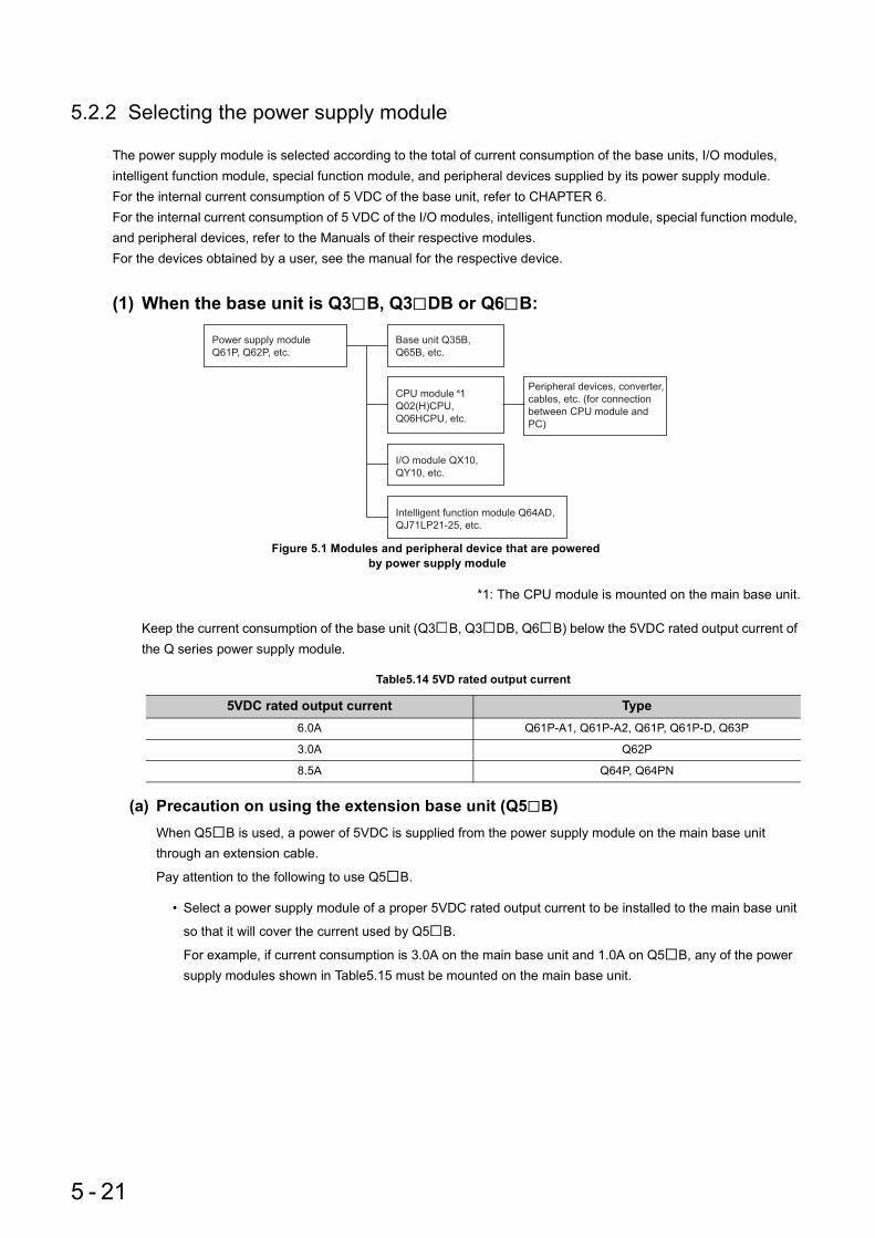
5.2.2 Selecting the power supply module
The power supply module is selected according to the total of current consumption of the base units, I/O modules, intelligent function module, special function module, and peripheral devices supplied by its power supply module.For the internal current consumption of 5 VDC of the base unit, refer to CHAPTER 6.For the internal current consumption of 5 VDC of the I/O modules, intelligent function module, special function module, and peripheral devices, refer to the Manuals of their respective modules. For the devices obtained by a user, see the manual for the respective device.
(1) When the base unit is Q3 B, Q3 DB or Q6 B:
*1: The CPU module is mounted on the main base unit.
Keep the current consumption of the base unit (Q3 B, Q3 DB, Q6 B) below the 5VDC rated output current of the Q series power supply module.
(a) Precaution on using the extension base unit (Q5 B)When Q5 B is used, a power of 5VDC is supplied from the power supply module on the main base unit through an extension cable.
Pay attention to the following to use Q5 B.
• Select a power supply module of a proper 5VDC rated output current to be installed to the main base unit
so that it will cover the current used by Q5 B.
For example, if current consumption is 3.0A on the main base unit and 1.0A on Q5 B, any of the power supply modules shown in Table5.15 must be mounted on the main base unit.
Figure 5.1 Modules and peripheral device that are powered by power supply module
Table5.14 5VD rated output current
5VDC rated output current Type6.0A Q61P-A1, Q61P-A2, Q61P, Q61P-D, Q63P
3.0A Q62P
8.5A Q64P, Q64PN
Power supply module
Q61P, Q62P, etc.
Base unit Q35B,
Q65B, etc.
Peripheral devices, converter,
cables, etc. (for connection
between CPU module and
PC)
I/O module QX10,
QY10, etc.
Intelligent function module Q64AD,
QJ71LP21-25, etc.
CPU module 1
Q02(H)CPU,
Q06HCPU, etc.
5 - 21

CHAPTER5 POWER SUPPLY MODULE
1
2
3
4
5
6
7
8
5.2 Specifications
5.2.2 Selecting the pow
er supply module
• Because 5VDC is supplied to Q5 B through an extension cable, voltage is lowered in the extension cable.The power supply module and extension cable must be selected so that a voltage of 4.75VDC or more is
supplied at the "IN" connector of Q5 B.For details of the voltage drop, refer to Section 6.1.5.
(b) Methods for reducing voltage dropsThe following methods are effective to reduce voltage drops at the extension cables.
1) Changing the module loading positionsLoad large current consumption modules on the main base unit.
Load small current consumption modules on the extension base unit (Q5 B).
2) Using short extension cablesThe shorter the extension cable is, the smaller the resistance and voltage drops will be.Use the shortest possible extension cables.
(2) When the base unit is Q3 SB:
Keep the current consumption of the slim type main base unit (Q3 SB) not exceeding the 5VDC rated output current of the slim type power supply module (Q61SP).
Table5.15 5VD rated output current
5VDC rated output current Type6.0A Q61P-A1, Q61P-A2, Q61P, Q61P-D, Q63P
8.5A Q64P, Q64PN
Figure 5.2 Modules and peripheral device that are powered by power supply module
Table5.16 5VD rated output current
5VDC Rated output current Type2.0A Q61SP
CPU module
Q02(H)CPU,
Q06HCPU, etc.
Peripheral devices, converter,
cables, etc. (for connection
between CPU module and
PC)
Slim type
Power supply module
Q61SP
I/O module QX10,
QY10, etc.
Intelligent function module Q64AD,
QJ71LP21-25, etc.
Slim type main base unit Q32SB,
Q33SB, Q35SB
5 - 22

(3) When the base unit is Q3 RB or Q6 RB
When a redundant power supply system is configured and one redundant power supply module has failed, the system is operated using the other redundant power supply module only during replacement of the failed redundant power supply module.Therefore, keep the current consumption of the redundant power supply base unit (Q3 RB/Q6 RB/Q6 WRB) within the 5VDC rated output current (8.5A) for one redundant power supply module.
Figure 5.3 Modules and peripheral device that are poweredby power supply module
Table5.17 5VD rated output current
5VDC rated output current Type
8.5AQ63RPQ64RP
Peripheral devices, converter,
cables, etc. (for connection
between CPU module and
PC)
Redundant power supply
module × 2 modules
I/O module QX10,
QY10, etc.
Intelligent function module Q64AD,
QJ71LP21-25, etc.
Redundant power supply base unit
Q3 RB, Q6 RB
CPU module 2
Q02(H)CPU,
Q06HCPU, etc.
2: Mounted on the redundant main base unit (Q3 RB)
5 - 23

CHAPTER5 POWER SUPPLY MODULE
1
2
3
4
5
6
7
8
5.2 Specifications
5.2.2 Selecting the pow
er supply module
(a) Cautions for using the extension base unit (Q5 B)When Q5 B is used, a power of 5VDC is supplied from the redundant power supply module on the redundant
power main base unit (Q3 RB) through an extension cable.
Pay attentions to the following to use Q5 B.
• Keep the sum of the current consumption on Q3 RB and Q5 B not exceeding the 5VDC rated output current for one redundant power supply module.
• Because 5VDC is supplied to Q5 B through an extension cable, voltage drop occurs in the extension cable.Select an appropriate extension cable so that a voltage of 4.75VDC or more is supplied at the "IN"
connector of Q5 B.For details of the voltage drop, refer to Section 6.1.5.
(b) Methods for reducing voltage dropsThe following methods are effective to reduce voltage drops at the extension cables.
1) Changing the module mounting positionsMount a module with large current consumption on the redundant power main base unit (Q3 RB).
Mount small current consumption modules on the extension base unit (Q5 B).
2) Using short extension cablesThe shorter the extension cable is, the smaller the resistance and voltage drops are.Use the shortest possible extension cables.
(4) When the base unit is QA1S6 B:
Select the power supply module also in consideration of the current consumption of the peripheral devices connected to the special function module.For example, when the AD75TU is connected to the AD75P1-S3, the current consumption of the AD75TU must also be taken into account.
Figure 5.4 Modules and peripheral device that are powered by power supply module
AnS series power supply
module A1S61PN, A1S62PN,
A1S63P
I/O module A1SX10,
A1SY10, etc.
Special function module
A1SD61,A1SD75P1-S3, etc.
peripheral
devices
AD75TU
Base unit QA1S65B,
QA1S68B
5 - 24

(5) When the base unit is QA6 B:
Select the power supply module also in consideration of the current consumption of the peripheral devices connected to the special function module.For example, when the AD75TU is connected to the AD75P1-S3, the current consumption of the AD75TU must also be taken into account.
Figure 5.5 Modules and peripheral device that are powered by power supply module
A series power supply
module A61P, A61PN, A62P,
A63P
I/O module AX10,
AY10, etc.
Special function module
AD61,AD75P1-S3, etc.
Peripheral
device
AD75TU
Base unit QA65B,
QA68B
5 - 25

CHAPTER5 POWER SUPPLY MODULE
1
2
3
4
5
6
7
8
5.2 Specifications
5.2.3 Life detection power supply m
odule
5.2.3 Life detection power supply module
The Life detection power supply module estimates its remaining life internally and indicates the life. The remaining life of the module can be checked by the LIFE LED located on the front of the module and on/off of the LIFE OUT termi-nals.
(1) LED indication and module status during operationTable5.18 indicates the LED indication and module status during operation.
*1: The remaining life of the module varies depending on the ambient temperature.
(If the ambient temperature rose by 10 , the remaining life of the module will be shortened by half.)
(2) Monitoring module life by using the LIFE OUT terminalThe module life can be monitored in either of the following way by using outputs of the LIFE OUT terminal
• Connecting the terminal to an external display device • Obtaining the output status into an input module and monitoring it by GOT
Table5.18 LED indication and module status
LEDLIFE OUT terminal Module
POWER LIFE
Off Off Off
• Power supply module failure• AC power is not input• Power failure (including momentary power
failure for 20ms or more)
On (green) On (green)
On
• Normal operation
On (green) On (orange)• Normal operation (Remaining life approx.
50%)*1
On (green)Flash (orange)(On for 5 sec. and off for 1 sec.)
Off
• Normal operation (Remaining life approx. 1
year)*1
Replacement of the module is recommended
On (green)Flash (orange)(At intervals of half a sec.)
• Normal operation (Remaining life approx. 6
months)*1
On (green) Off • Life expired
On (green) On (red)
Turns off and on three times at intervals of 1 second and then off
• Ambient temperature is out of range (Ambi-ent temperature is exceeding the specifica-tion)
On (green)Flash (red)(At intervals of 1 sec.)
• Function failure (Normal processing is not available due to a failure of the life diagnos-tics circuit in the module)
On (green) Off
• Ambient temperature is out of range (Ambi-ent temperature is exceeding the specifica-tion and also the life detection function has stopped.)
On (orange) Off Off • Watchdog timer error in the module
5 - 26

(a) Connecting the terminal to an external display deviceConnecting the LIFE OUT terminal allows indication of the remaining life of the module to an external display, device such as external LED, by turning it off when the life is one year or less.When the external display device turned off, the remaining life can be checked by the LIFE LED of the Q61P-D located in the control panel.
(b) Obtaining the output status into an input module and monitoring it by GOTObtaining the LIFE OUT terminal status into an input module allows monitoring of the module remaining life in a sequence program.The following indicates how to monitor the remaining life of the power supply module in the sequence program by using GOT.
1) System configuration
Figure 5.6 When connecting to an external display device
Figure 5.7 When obtaining into an input module
Table5.19 I/O assignment
Model name Start XYQ02CHPU -
QX40 0000H
Control panelExternal LED
LIFE OUT terminal
The LIFE LED turns on in orange
Remaining life is 1 year or less
GOT
Q61P-D
5 - 27

CHAPTER5 POWER SUPPLY MODULE
1
2
3
4
5
6
7
8
5.2 Specifications
5.2.3 Life detection power supply m
odule
2) Conditions of a programTable5.20 and Table5.21 indicate devices used in a program for monitoring the module life.
When the life detection function of the Q61P-D is faulty, the LIFE OUT terminal repeats on and off for three times when the module is started.Depending on the system, this behavior (ons and offs) of the LIFE OUT terminal may not be obtained to the input module due to delay of the sequence program start after the Q61P-D has started.In this program example, M11 turns on even though the life detection function is faulty when powered on since the remaining life is regarded as one year.
Table5.20 Devices used by user
Sinal Device FunctionMonitoring clear command X0F Resets the life monitoring processing
Life warning signal M11Turns on when the remaining life of the Q61P-D is one year or less
Error signal M12Turns on when the life detection function of the Q61P-D is faulty
Table5.21 Devices used by program
Signal Device Function
LIFE OUT signal X00LIFE OUT terminal status of the Q61P-D
Monitoring clear request M0An internal signal for resetting the life monitoring processing
Monitoring start flag M1An internal signal for detecting offs of the LIFE OUT terminal
Time monitoring flag M2An internal signal for counting ons and offs of the LIFE OUT terminal
ON/OFF monitoring timer T0Ons and offs of the LIFE OUT terminal are counted while this timer is enabled (6 seconds)
ON/OFF counter D100Counts ons and offs of the LIFE OUT terminal
5 - 28

3) Program example
Monitoring for 6 seconds
The life is 1 year or less if remains off
Monitoring continues if turned on
Faulty if repeats off and on
5 - 29

CHAPTER5 POWER SUPPLY MODULE
1
2
3
4
5
6
7
8
5.2 Specifications
5.2.4 Precaution w
hen connecting the uninterruptive power supply
5.2.4 Precaution when connecting the uninterruptive power supply
Be sure of the following terms when connecting the Q series CPU module system to the uninterruptive power supply (hereinafter referred to as UPS):
Use the online UPS or line interactive UPS with a voltage distortion rate of 5% or less.For the off-line system UPS, use Mitsubishi Electric's F Series UPS (serial number P or later) (Ex.: FW-F10-0.3K/0.5K).Do not use any off-line system UPS other than the F series mentioned above.
5.2.5 Precautions on power supply capacity
The Q64RP and Q64P automatically recognize the rated input voltage waveform to switch the input voltage between 100VAC and 200VAC.Select the power supply for the Q64RP/Q64P power supply module, considering the power supply capacity. (Reference: At least twice as much as the current consumption)If the power supply of insufficient capacity is applied, the power supply module might fail when 200VAC power is supplied.
5 - 30

5.3 Part Names and Settings
This section describs part names of each power supply module.
Figure 5.8 Power supply module
Q61P-A1 (100 to 120VAC input, 5VDC 6A output)
Q61P-A2 (200 to 240VAC input, 5VDC 6A output)
Q61P (100 to 240VAC input, 5VDC 6A output)
Q62P (100 to 240VAC input, 5VDC 3A/24VDC 0.6A output)
Q63P (24VDC input, 5VDC 6A output)
Q64P (100 to 120VAC/200 to 240VAC input, 5VDC 8.5A output)
Q64PN (100 to 240VAC input, 5VDC 8.5A output)
1), 2)11)
12)
11)
4)
6)
7)
15)
12)
Q61SP
Q61SP
INPUT
MITSUBISHI
100-240VAC
8)
7)
6)
4)
10)
9)
13), 14),
15), 17)
(Q62P
only)
Q61P-A1, Q61P-A2, Q61P, Q62P, Q64P, Q64PN
7)
6)
4)
10)
9)
16)
Q63P
15)
9)12)
10)
4)
6)
7)
1)3)
11)
5)
Q61P-D (100 to 240VAC input, 5VDC 6A output) Q61SP (100 to 240VAC input, 5VDC2A output)
5 - 31

CHAPTER5 POWER SUPPLY MODULE
1
2
3
4
5
6
7
8
5.3 Part N
ames and S
ettings
*1: Flicker-OFF indicates that the output signal of the terminal turns off and on at intervals of one second for three times and then off (opens).
*2: When using the Q61P-D in the system configured with an extension base unit, the POWER LED of the Q61P-D on the extension base unit may turn on in dull red when the module is turned off. Note that this does not indicate an error.
Table5.22 Part Names
No. Name Application
1) POWER LED*2
On (green): Normal (5VDC output, momentary power failure within 20ms)Off: • AC power supply is on but the power supply module is out of order.
(5VDC error, overload, internal circuit failure, or blown fuse)• AC power supply is not on.• Power failure (including an momentary power failure of 20ms or more)
2) POWER LED
On (green): Normal (5VDC output, momentary power failure within 10ms)Off: • DC power supply is on but the power supply module is out of order.
(5VDC error, overload, internal circuit failure, or blown fuse)• DC power supply is not on.• Power failure (including an momentary power failure of 10ms or more)
3) LIFE LED
On (green) : When operation has startedOn (orange) : Remaining life of the module approx. 50%Flash(orange) : • On for 5 seconds and off for 1 second:
Module remaining life is approx. 1 year• At intervals of 0.5 seconds:
Module remaining life is approx. 6 monthsOff: • Module life expired. (Turns on red for 1 second after power-on)
• Ambient temperature is out of range (Ambient temperature of the module is exceeding the specification and also the life detection function is stopped.)
On (red) : Ambient temperature out of range (Ambient temperature of the module is exceeding the specification)
Flash(red) : Function failure
4) ERR. terminal
• Turns on when the entire system operates normally.• Turns off (opens) when the AC power is not supplied, a stop error (including reset)
occurs in the CPU module, or the fuse is blown.• In a multiple CPU system, turns off when a stop error occurs in any of the CPU
modules.Normally off when mounted on a extension base unit.
5) LIFE OUT terminal
• Output signal of the terminal turns off (opens) when the life is detected. (Applica-ble only when the remaining life is 1 year or less.)
• Flicker-OFF (opens) when the life diagnostics error (including detection error)is
detected.*1
• Flicker-OFF (opens) when the ambient temperature is detected out of range.*1
• Output signal of the terminal turns off (opens) when the watchdog timer error is detected in the module.
The above operations are available when the module is mounted on an extension base unit.
6) FG terminal Ground terminal connected to the shield pattern of the printed circuit board.
7) LG terminalGrounding for the power supply filter. For AC input, it has one-half the potential of the input voltage.
8) +24V, 24G terminalsUsed to supply 24VDC power to inside the output module (using external wiring).
9) Terminal screw M3.5 7 screw
10) Terminal cover Protective cover of the terminal block
11) Module fixing screw holeUsed to secure the module to the base unit. M3 12 screw (user-prepared) (Tightening torque range : 0.36 to 0.48N•m)
12) Module mounting lever Used to mount the module onto the base unit.
5 - 32

● The Q61P-A1 is dedicated for inputting a voltage of 100 VAC.Do not input a voltage of 200 VAC into it or trouble may occur on the Q61P-A1.
● Q64P automatically switches the input range 100/200VAC.Therefore, it is not compatible with the intermediate voltage (133 to 169VAC).The CPU module may not work normally if the above intermediate voltage is applied.
● Ground the LG and FG terminals to the protective ground conductor.
● When the Q61P-A1, Q61P-A2, Q61P-D, Q61P, Q62P, Q63P, Q64P or Q64PN is mounted on the extension base unit, a system error cannot be detected by the ERR. terminal. (The ERR. terminal is always off.)
● Cables for the ERR. contact and LIFE OUT contact must be up to 30m (98.43 feet) and installed in the control panel.
Table5.22 Part Names
No. Name Application13) Power input terminals Power input terminals for Q61P-A1 and connected to a 100VAC power supply.
14) Power input terminals Power input terminals for Q61P-A2 and connected to a 200VAC power supply.
15) Power input terminalsPower input terminals for Q61P, Q61P-D, Q61SP, Q62P, Q64PN and connected to a power supply of 100VAC to 200VAC.
16) Power input terminals Power input terminals for Q63P and connected to a 24VDC power supply.
17) Power input terminals Power input terminals for Q64P and connected to a 100VAC/200VAC power supply.
Table5.23 Precaution
Power module typeSupply power voltage
100VAC 200VACQ61P-A1 Operates normally. Power supply module causes trouble.
Q61P-A2Power supply module does not cause trouble.CPU module cannot be operated.
Operates normally.
5 - 33

CHAPTER5 POWER SUPPLY MODULE
1
2
3
4
5
6
7
8
5.3 Part N
ames and S
ettings
Figure 5.9 Power supply module
Table5.24 Part Names
No. Name Application
1) POWER LED*1
On (green) : Normal operation (5V DC output, momentary power failure of 20ms or less)
On (red)*1 : DC power is input but the Q63RP is faulty. (5V DC error, overload, or internal circuit failure)
Off : DC power not input, blown fuse, power failure (including momentary power failure of 10ms or more)
2) POWER LED*1
On (green) : Normal (5V DC output, momentary power failure within 20ms)On (red) : AC power supply is on but Q64RP is out of order.
(5V DC error, overload, or internal circuit failure)Off : AC power supply is not on, blown fuse, power failure (including
momentary power failure of 10ms or more)
3) ERR. terminal
<When power supply is mounted on redundant power main base unit (Q3 RB)>• Turns on when the system on the redundant power main base unit operates
normally.• Turns off (open) when the Q63RP fails, the DC power supply is not input, a CPU
module stop error (including a reset) occurs, or the fuse is blown.• Turns off (open) when a stop error occurs in any of the CPU modules in a multiple
CPU system.
<When power supply is mounted on redundant power extension base unit (Q6 RB) or
redundant type extension base unit (Q6 WRB)>• Turns on when the Q63RP operates normally.• Turns off (open) when the Q63RP fails, the DC power supply is not input, or the
fuse is blown.4) FG terminal Ground terminal connected to the shield pattern of the printed circuit board.
5) LG terminalGrounding for the power supply filter. The potential of Q64RP terminal is 1/2 of the input voltage.
6) Power input terminals Connect direct current of 24 VDC with the power input terminal.
7) Power input terminals Power input terminals and connected to a 100VAC/200VAC power supply.
8) Terminal screw M3.5 7 screw
Q64RPQ63RP
10)
11)
2)
3)
4)
5)
7)
8)
9) 9)
10) 1)
3)
4)
5)
6)
8)11)
Q63RP
INPUT 24VDC
24G
+24V
24VDC 0.5A
L
ERR.
(LG)
(FG)
OUTPUT 5VDC 8.5A
INPUT
MAX 65W
24VDC
5 - 34

*1: Although the POWER LED turns on in red for a moment immediately after the power supply is turned on or off, redundant power supply modules is not faulty.
● Q64RP automatically switches the input range 100/200VAC.Therefore, it is not compatible with the intermediate voltage (133 to 169VAC).The CPU module may not work normally if the above intermediate voltage is applied.
● Supply power to redundant power supply modules from separate power sources (a redundant power supply system).
● Ground the LG and FG terminals to the protective ground conductor.
9) Terminal cover Protective cover of the terminal block
10) Module fixing screw holeScrew hole for securing a module to the base unit.M3 12 screw (user-prepared) (Tightening torque : 0.36 to 0.48N•m)
11) Module mounting lever Used to mount a module on the base unit.
No. Name Application
5 - 35

CHAPTER5 POWER SUPPLY MODULE
1
2
3
4
5
6
7
8
5.3 Part N
ames and S
ettings
● Do not wire to those terminals for which NC is stamped on the terminal block.
● Ground the LG and FG terminals to the protective ground conductor.
Figure 5.10 Power supply module
Table5.25 Part names
No. Name Application
1) POWER LED
On (green): Normal (5VDC output, momentary power failure within 20ms)Off : • AC power supply is on but the power supply module is out of order.
(5VDC error, overload, internal circuit failure, or fuse blown)• AC power supply is not on• Power failure (including an momentary power failure of 20ms or more)
2) +24V, 24G terminals Used to supply 24VDC power to inside the output module (using external wiring).
3) FG terminals Ground terminal connected to the shield pattern of the printed circuit board.
4) LG terminalsGrounding for the power supply filter. The potential of A1S61PN or A1S62PN terminal is 1/2 of the input voltage.
5) Power input terminals Used to connect a 100VAC to 200VAC power supply.
6) Power input terminals Used to connect a 24VDC power supply.
7) Terminal screw M3.5 7 screw
8) Terminal cover Protective cover of the terminal block
9) Module fixing screw holeUsed to secure the module to the base unit.(M4 screw, tightening torque : 0.66 to 0.89N•m)
2) 3) 4) 5) 7)3) 4) 5) 7)
9)
3) 4) 6) 7)
8)
1) 1) 1)
8)
9)
8)
9)
A1S61PN A1S62PN A1S63P
5 - 36
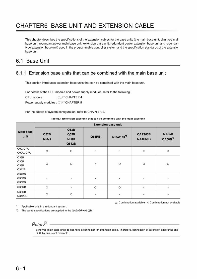
CHAPTER6 BASE UNIT AND EXTENSION CABLE
This chapter describes the specifications of the extension cables for the base units (the main base unit, slim type main base unit, redundant power main base unit, extension base unit, redundant power extension base unit and redundant type extension base unit) used in the programmable controller system and the specification standards of the extension base unit.
6.1 Base Unit
6.1.1 Extension base units that can be combined with the main base unit
This section introduces extension base units that can be combined with the main base unit.
For details of the CPU module and power supply modules, refer to the following.
CPU module : CHAPTER 4
Power supply modules : CHAPTER 5
For the details of system configuration, refer to CHAPTER 2.
: Combination available : Combination not available*1: Applicable only in a redundant system.*2: The same specifications are applied to the QA6ADP+A6 B.
Slim type main base units do not have a connector for extension cable. Therefore, connection of extension base units and GOT by bus is not available.
Table6.1 Extension base unit that can be combined with the main base unit
Main base unit
Extension base unit
Q52BQ55B
Q63BQ65BQ68BQ612B
Q68RB Q65WRB*1 QA1S65BQA1S68B
QA65B
QA68B*2
Q00JCPUQ00UJCPU
Q33BQ35BQ38BQ312B
Q32SBQ33SBQ35SB
Q38RB
Q38DBQ312DB
6 - 1

CHAPTER6 BASE UNIT AND EXTENSION CABLE
1
2
3
4
5
6
7
8
6.1 Base U
nit6.1.2 S
pecification table
6.1.2 Specification table
The base unit is a unit to which the CPU module, power supply module, I/O module and/or intelligent function module are installed.Section 6.1.2 to Section 6.1.5 provide the specifications and other information on the base unit.
(1) Main base unit
*1: The 5 base mounting screws are included with the Q38B and Q312B that have 5 base mounting holes.
(2) Slim type main base unit
Table6.2 Main base unit specifications
ItemType
Q33B Q35B Q38B Q312BNumber of I/O modules installed
3 5 8 12
Possibility of extension Extendable
Applicable module Q series modules
5 VDC internal current consumption
0.11A 0.12A 0.13A
Mounting hole size M4 screw hole or 4.5 hole (for M4 screw)
External dimensions
H 98mm (3.86 inches)
W 189mm (7.44 inches) 245mm (9.65 inches) 328mm (12.92 inches) 439mm (17.28 inches)
D 44.1mm (1.74 inches)
Weight 0.21kg 0.27kg 0.36kg 0.47kg
Attachment Mounting screw M4 14 4 pieces*1 (DIN rail mounting adapter is sold separately)
DIN rail mounting adapter type
Q6DIN3 Q6DIN2 Q6DIN1
Table6.3 Slim type main base unit specifications
ItemType
Q32SB Q33SB Q35SBNumber of I/O modules installed
2 3 5
Possibility of extension Not extendable
Applicable module Q series modules
5 VDC internal current consumption
0.09A 0.10A
Mounting hole size M4 screw hole or 4.5 hole (for M4 screw)
External dimensions
H 98mm (3.86 inches)
W 114mm (4.49 inches) 142mm (5.59 inches) 197.5mm (7.78 inches)
D 18.5mm (0.73 inches)
Weight 0.12kg 0.15kg 0.21kg
Attachment Mounting screw M4 12 4 pieces (DIN rail mounting adapter is sold separately)
DIN rail mounting adapter type
Q6DIN3
6 - 2

(3) Redundant power main base unit
(4) Multiple CPU high speed main base unit
Table6.4 Redundant power main base unit specifications
ItemType
Q38RBNumber of I/O modules installed
8
Possibility of extension Extendable
Applicable module Q series modules
5 VDC internal current consumption
0.12A
Mounting hole size M4 screw hole or 4.5 hole (for M4 screw)
External dimensions
H 98mm (3.86 inches)
W 439mm (17.28 inches)
D 44.1mm (1.74 inches)
Weight 0.47kg
Attachment Mounting screw M4 14 5 pieces (DIN rail mounting adapter is sold separately)
DIN rail mounting adapter type
Q6DIN1
Table6.5 Multiple CPU high speed main base unit specifications
ItemType
Q38DB Q312DBNumber of I/O modules installed
8 12
Possibility of extension Extendable
Applicable module Q series modules
5 VDC internal current consumption
0.23A 0.24A
Mounting hole size M4 screw hole or 4.5 hole (for M4 screw)
External dimensions
H 98mm (3.86 inches)
W 328mm (12.92 inches) 439mm(17.30 inches)
D 44.1mm (1.74 inches)
Weight 0.41kg 0.54kg
Attachment Mounting screw M4 14, 5 pieces (DIN rail mounting adapter is sold separately)
DIN rail mounting adapter type
Q6DIN1
6 - 3

CHAPTER6 BASE UNIT AND EXTENSION CABLE
1
2
3
4
5
6
7
8
6.1 Base U
nit6.1.2 S
pecification table
(5) Extension base unit (Type not requiring power supply module)
(6) Extension base unit (Type requiring power supply module)
*2: The 5 base mounting screws are included with the Q68B and Q612B that have 5 base mounting holes.
Table6.6 Extension base unit (Type not requiring power supply module) specifications
ItemType
Q52B Q55BNumber of I/O modules installed
2 5
Possibility of extension Extendable
Applicable module Q series modules
5 VDC internal current consumption
0.08A 0.10A
Mounting hole size M4 screw hole or 4.5 hole (for M4 screw)
External dimensions
H 98mm (3.86 inches)
W 106mm (4.17 inches) 189mm (7.44 inches)
D 44.1mm (1.74 inches)
Weight 0.14kg 0.23kg
Attachment Mounting screw M4 14, 4 pieces (DIN rail mounting adapter is sold separately)
DIN rail mounting adapter type
Q6DIN3
Table6.7 Extension base unit (Type requiring power supply module) specifications
ItemType
Q63B Q65B Q68B Q612B QA1S65B QA1S68B QA65B QA68BNumber of I/O modules installed
3 5 8 12 5 8 5 8
Possibility of extension
Extendable
Applicable module Q series modules AnS series modules A series module
5 VDC internal current consumption
0.11A 0.12A 0.13A 0.12A
Mounting hole size M4 screw hole or 4.5 hole(for M4 screw)
M5 screw hole or 5.5 hole(for M5 screw)
External dimensions
H 98mm (3.86 inches) 130mm (5.12 inches) 250mm (9.84 inches)
W189mm (7.44
inches)
245mm (9.65
inches)
328mm (12.92 inches)
439mm (17.28 inches)
315mm (12.41 inches)
420mm (16.55 inches)
352mm (13.86 inches)
466mm (18.34 inches)
D 44.1mm (1.74 inches) 51.2mm (2.02 inches) 46.6mm (1.83 inches)
Weight 0.23kg 0.28kg 0.38kg 0.48kg 0.75kg 1.00kg 1.60kg 2.00kg
Attachment Mounting screw M4 14 , 4 pieces *2 (DIN rail mounting adapter sold separately)
Mounting screw M5 25 4 pieces
----
DIN rail mounting adapter type
Q6DIN3 Q6DIN2 Q6DIN1 ---- ---- ---- ----
6 - 4

(7) Redundant power extension base unit
(8) Redundant extension base unit
Table6.8 Redundant power extension base unit specifications
ItemType
Q68RBNumber of I/O modules installed
8
Possibility of extension Extendable
Applicable module Q series modules
5 VDC internal current consumption
0.12A
Mounting hole size M4 screw hole or 4.5 hole (for M4 screw)
External dimensions
H 98mm (3.86 inches)
W 439mm (17.28 inches)
D 44.1mm (1.74 inches)
Weight 0.49kg
Attachment Mounting screw M4 14 , 5 pieces (DIN rail mounting adapter is sold separately)
DIN rail mounting adapter type
Q6DIN1
Table6.9 Redundant extension base unit specifications
ItemType
Q65WRBNumber of I/O modules installed
5
Possibility of extension Extendable
Applicable module Q series modules
5 VDC internal current consumption
0.16A
Mounting hole size M4 screw hole or 4.5 hole (for M4 screw)
External dimensions
H 98mm (3.86 inches)
W 439mm (17.28 inches)
D 44.1mm (1.74 inches)
Weight 0.52kg
Attachment Mounting screw M4 14 , 5 pieces (DIN rail mounting adapter is sold separately)
DIN rail mounting adapter type
Q6DIN1
6 - 5

CHAPTER6 BASE UNIT AND EXTENSION CABLE
1
2
3
4
5
6
7
8
6.1 Base U
nit6.1.3 P
art names
6.1.3 Part names
The part names of the base unit are described below.
(1) Main base unit (Q33B, Q35B, Q38B, Q312B)
Figure 6.1 Main base unit (Q33B, Q35B, Q38B, Q312B)
Table6.10 Part names
No. Name Application
1) Extension cable connectorConnector for connecting an extension cable (for signal communications with the extension base unit)
2) Base coverProtective cover of extension cable connector. Before an extension cable is connected, the area of the base cover surrounded by the groove under the word "OUT" on the base cover must be removed with a tool such as nippers.
3) Module connector
Connector for installing the Q series power supply module, CPU module, I/O modules, and intelligent function module.To the connectors located in the spare space where these modules are not installed, attach the supplied connector cover or the blank cover module (QG60) to prevent entry of dirt.
4) Module fixing screw hole Screw hole for fixing the module to the base unit. Screw size: M3 12
5) Base mounting hole Hole for mounting this base unit onto the panel such as a control panel (for M4 screw)
6) DIN rail adapter mounting hole Hole for mounting DIN rail adapter
1)
2)
5) 4)
3) 6)
I/O9 I/O10 I/O11I/O8I/O7I/O6IO5I/O4I/O3I/O2I/O1I/O0CPUPOWER
5V
SG
FG
OUT
6 - 6

(2) Slim type main base unit (Q32SB, Q33SB, Q35SB)
Figure 6.2 Slim type main base unit (Q32SB, Q33SB, Q35SB)
Table6.11 Part names
No. Name Application
1) Module connector
Connector for installing the Q series power supply module, CPU module, I/O modules, and intelligent function module.To the connectors located in the spare space where these modules are not installed, attach the supplied connector cover or the blank cover module (QG60) to prevent entry of dirt.
2) Module fixing screw hole Screw hole for fixing the module to the base unit. Screw size: M3 12
3) Base mounting hole Hole for mounting this base unit onto the panel such as a control panel (for M4 screw)
4) DIN rail adapter mounting hole Hole for mounting DIN rail adapter
1)
2)3)
4)
SG
6 - 7

CHAPTER6 BASE UNIT AND EXTENSION CABLE
1
2
3
4
5
6
7
8
6.1 Base U
nit6.1.3 P
art names
(3) Redundant power main base unit (Q38RB)
Figure 6.3 Redundant power main base unit (Q38RB)
Table6.12 Part names
No. Name Application
1) Extension cable connectorConnector for connecting an extension cable (for signal communications with the extension base unit)
2) Base coverProtective cover of extension cable connector. Before an extension cable is connected, the area surrounded by the groove under the word "OUT" must be removed with a tool such as a flat head screwdriver.
3) Module connector
Connector for connecting a redundant power supply module, CPU module, I/O module and intelligent function moduleTo the connectors unused, attach the supplied connector cover or the blank cover module (QG60) to prevent entry of dirt.
4) Module fixing screw hole Screw hole for fixing the module to the base unit. Screw size: M3 12
5) Base mounting hole Hole for mounting this base unit onto the panel such as a control panel (for M4 screw)
6) DIN rail adapter mounting hole Hole for mounting DIN rail adapter
OUT
I/O7I/O6I/O5I/O4I/O3
5V
FG
SG
I/O2I/O1I/O0
5V
FG
CPU
SG
1)
2)
5) 4)
3) 6)
6 - 8

(4) Multiple CPU high speed main base unit (Q38DB, Q312DB)
Figure 6.4 Multiple CPU high speed main base unit (Q38DB, Q312DB)
Table6.13 Part names
No. Name Application
1) Extension cable connectorConnector for connecting an extension cable (for signal communications with the extension base unit)
2) Base coverProtective cover of extension cable connector. Before an extension cable is connected, the area of the base cover surrounded by the groove under the word "OUT" on the base cover must be removed with a tool such as nippers.
3) Module connector
Connector for installing the Q series power supply module, CPU module, I/O modules, and intelligent function module.To the connectors located in the spare space where these modules are not installed, attach the supplied connector cover or the blank cover module (QG60) to prevent entry of dirt.
4) Module fixing screw hole Screw hole for fixing the module to the base unit. Screw size: M3 12
5) Base mounting hole Hole for mounting this base unit onto the panel such as a control panel (for M4 screw)
6) DIN rail adapter mounting hole Hole for mounting DIN rail adapter
OUT
FG
SG
5V
I/O11I/O10I/O9I/O8I/O7I/O6I/O5I/O4I/O3I/O2I/O1I/O0CPUPOWER
b1a1
1)
2)
5) 4)
3) 6)
6 - 9

CHAPTER6 BASE UNIT AND EXTENSION CABLE
1
2
3
4
5
6
7
8
6.1 Base U
nit6.1.3 P
art names
(5) Extension base unit (Q5 B, Q6 B, QA1S6 B, QA6 B)
Q52B,Q55B
Q63B,Q65B,Q68B,Q612B
QA1S65B,QA1S68B
QA65B, QA68B
Figure 6.5 Extension base unit (Q5 B, Q6 B, QA1S6 B, QA6 B)
I/O2I/O1I/O0 I/O3 I/O4
OUTIN
6)
3)
2)
1)
7) 4)
5)
6)
3)
5)
2)
4) 7)
I/O11I/O10I/O9I/O8I/O7I/O6I/O5I/O4I/O3I/O2I/O1I/O0POWER
5V
SG
1)
OUTIN
I/O0 I/O7I/O6I/O5I/O4I/O3I/O2I/O1
6)
3)
2)
1)
5)
4)
5V
SG
FG
IN OUT
QA68B
8)
1)
5)
5)3) 4)
2)
6)
8)
6 - 10

Table6.14 Part names
No. Name Application
1) Extension cable connectorConnector for connecting an extension cable (for signal communications with the main base unit or other extension base unit)
2) Base coverProtective cover of extension cable connector.Before connecting an extension cable, the part under OUT on the base cover must be removed with a tool such as a flat blade screwdriver.
3) Base No. setting connectorConnector for setting the number of bases of the extension base unit.
( Section 6.1.4)
4) Module connector
Connectors for installing the power supply module, I/O modules, and intelligent function mod-ule/ special function module.To those connectors located in the spare space where these modules are not installed, apply the supplied connector cover or the blank cover module to prevent entry of dirt.Blank cover module applicable to Q52B, Q55B, Q63B,Q65B, Q68B and Q612B: QG60Blank cover module applicable to QA1S65B and QA1S68B: A1SG60Blank cover module applicable to QA6BB and QA68B:AG60
5) Module fixing screw holeScrew hole for fixing the module to the base unit.Q52B, Q55B, Q63B,Q65B,Q68B and Q612B.................................Screw size: M3 12QA1S6B, QA1S68B, QA65B and QA68B.......................................Screw size: M4 12
6) Base mounting holeHole for mounting this base unit on the panel such as a control panel.Q52B, Q55B, Q65B,Q68B and Q612B...........................................For M4 screwQA1S6B, QA1S68B, QA65B and QA68B.......................................For M5 screw
7) DIN rail adapter mounting hole DIN rail adapter mounting hole.
8) Module fixing hole Cut out to accept projection and hook at rear of modules.
6 - 11

CHAPTER6 BASE UNIT AND EXTENSION CABLE
1
2
3
4
5
6
7
8
6.1 Base U
nit6.1.3 P
art names
(6) Redundant power extension base unit (Q68RB)
Figure 6.6 Redundant power extension base unit (Q68RB)
Table6.15 Part names
No. Name Application
1) Extension cable connectorConnector for connecting an extension cable (for signal communications with the redundant power main base unit or other extension base unit)
2) Base coverProtective cover of extension cable connector.Before connecting an extension cable, the part under OUT on the base cover must be removed with a tool such as a flat blade screwdriver.
3) Base No. setting connectorConnector for setting the number of bases of redundant power extension base units.
( Section 6.1.4)
4) Module connector
Connector for installing a redundant power supply module, I/O module and intelligent function module.To the connectors unused, attach the supplied connector cover or the blank cover module (QG60) to prevent entry of dirt.
5) Module fixing screw hole Screw hole for fixing the module to the base unit. Screw size: M3 12
6) Base mounting hole Hole for mounting this base unit on the control panel. (For M4 screw)
7) DIN rail adapter mounting hole DIN rail adapter mounting hole.
FG
SG
5V5V
SG
FG
I/O0 I/O1 I/O2 I/O3 I/O4 I/O5 I/O6 I/O7
OUTIN
3)
5)
2)
1)
6)
4) 7)
6 - 12

(7) Redundant extension base unit (Q65WRB)
Figure 6.7 Redundant extension base unit (Q65WRB)
Table6.16 Part names
No. Name Application
1) Extension cable connectorConnector for connecting an extension cable (for signal communications with the redundant system of the main base unit)
2) Base coverProtective cover of extension cable connector.Before connecting an extension cable, the part under OUT on the base cover must be removed with a tool such as a flat blade screwdriver.
3) Module connector
Connector for installing a redundant power supply module, I/O module and intelligent function module.To the connectors unused, attach the supplied connector cover or the blank cover module (QG60) to prevent entry of dirt.
4) Module fixing screw hole Screw hole for fixing the module to the base unit. Screw size: M3 12
5) Base mounting hole Hole for mounting this base unit on the control panel. (For M4 screw)
6) DIN rail adapter mounting hole DIN rail adapter mounting hole.
POWER 2
SG
5V5V
SG
POWER 1 I/O0 I/O1 I/O2 I/O3 I/O4
IN2 OUTIN1
5)
1)
4)
6)3)
2)
6 - 13

CHAPTER6 BASE UNIT AND EXTENSION CABLE
1
2
3
4
5
6
7
8
6.1 Base U
nit6.1.4 S
etting extension bases
6.1.4 Setting extension bases
The base number setting method of each extension base unit to be used is described below.
Figure 6.8 Connector
Table6.17 Setting of base number for extension base units
CPU module
Number setting for extension basesExtensi
on 1Extensi
on 2Extensi
on 3Extensi
on 4Extensi
on 5Extensi
on 6Extensi
on 7
Q02(H)CPU, Q06HCPU, Q12HCPU, Q25HCPU, Q02PHCPU, Q06PHCPU, Q12PHCPU, Q25PHCPU, Q03UD(E)CPU, Q04UD(E)HCPU, Q06UD(E)HCPU, Q10UD(E)HCPU, Q13UD(E)HCPU, Q20UD(E)HCPU, Q26UD(E)HCPU
Setting available
Q12PRHCPU*2, Q25PRHCPU*2
Setting not
available*3
Setting available*4
Q00JCPU, Q00UJCPU Setting available Setting prohibited *1
Q00CPU, Q00UCPU, Q01CPU, Q01UCPU, Q02UCPU
Setting available Setting prohibited *1
1234567
Stage No. setting
connector
6 - 14

*1: If these base numbers are set, "BASE LAY ERROR" (error code: 2010) occurs.*2: The extension base unit can be connected only when the serial number (first five digits) of the Redundant CPU is "09012"
or later and the redundant system is configured.The extension base unit cannot be connected when the serial number (first five digits) of the Redundant CPU module is "09011" or earlier.
*3: Connect the Q6 WRB to the first extension base. Since the Q6 WRB is fixed to the first extension base, base number setting is not required.
*4: The Q6 WRB cannot be connected to the second extension base or later bases. Use the Q6 RB for the second extension base or later bases.
● For the base number setting connector, set the number matched with the extension base number.Do not set the same base number at two or more positions or do not fail to set a number. A miss-input or miss-output may occur.
● In case of using the QA6ADP+A5 B/A6 B, set the same base number to both the base number setting connector of the A5 B/A6 B and that of the QA6ADP.
6 - 15

CHAPTER6 BASE UNIT AND EXTENSION CABLE
1
2
3
4
5
6
7
8
6.1 Base U
nit6.1.5 G
uideline for extension base units
6.1.5 Guideline for extension base units
Since the extension base unit (Q5 B) is supplied with 5VDC from the power supply module on the main base unit, a voltage drop occurs at extension cables.Improper I/O may be provided if the specified voltage (4.75VDC or higher) is not supplied to the "IN" connector of the
Q5 B.
When using the Q5 B, make sure that the "IN" connector of the Q5 B is supplied with 4.75VDC or higher.And it is recommend to connect it with the shortest possible extension cable right after connecting the main base unit, so as to minimize the effects of voltage drop.
(1) When only the Q5 B is connected to the extension base unit
(a) Selection condition4.75VDC or higher should be supplied to the "IN" connector of the Q5 B in the final extension base.
(b) How to calculate voltage to "IN" connectorThe 5VDC output voltage of the power supply module on the main base unit is set to at least 4.90VDC.
Therefore, the Q5 B can be used if the voltage drop is 0.15VDC or lower (4.9VDC - 4.75VDC = 0.15VDC).
Table6.18 Extension cable conductor resistance
Extension cable typeExtension cable conductor
resistanceQC05B 0.044
QC06B 0.051
QC12B 0.082
QC30B 0.172
QC50B 0.273
QC100B 0.530
Figure 6.9 System configuration
Extension
stage 1
Extension
stage 2
Extension
stage 7
V1
V2
V7
R1
R2
R7
Main base unit
I1
I2
I7
Power supply module
Extension base unit (Q5 B)
Extension base unit (Q5 B)
Extension base unit (Q5 B)
6 - 16

*1: Sum total of current consumed by Q5 B and currents consumed by the I/O, intelligent function modules loaded on the Q5 B.
The symbols including "I" (I1 to I7) vary with the modules loaded on the Q5 B. For details of the symbol, refer to the User's manuals of the module used.
The voltage supplied to "IN" connector of the Q5 B in the final extension reaches 4.75 VDC or higher on the condition
that the sum total of voltage drop to "IN" connector of Q5 B (V) is 0.15V or lower.
Table6.19 Symbol
Symbol Description
V1 Voltage drop at the extension cable between the main base unit and extension base unit (Q5 B)
VnVoltage drop at the extension cable between the extension base unit (Q5 B) (extension base n-1) and extension base unit
(Q5 B) (extension base n)
R1 Extension cable resistance between the main base unit and extension base unit (Q5 B)
Rn Extension cable resistance between the extension base unit (Q5 B) (extension base n-1) and extension base unit (Q5 B) (extension base n)
l1 to l7 5VDC current consumption among extension base 1 to 7 *1
Table6.20 List for calculating voltage drops occurring at extension cables in system consisting of extensions 1 to 7
Q5 B Installation
position
Voltage drop at extension cable on corresponding extension unit Sum total of voltage drops to "IN" connector
of Q5 B (V)V1 V2 V3 V4 V5 V6 V7
Extension 1 R1•I1 ---- ---- ---- ---- ---- ---- V=V1
Extension 2 R1 (I1+I2) R2•I2 ---- ---- ---- ---- ---- V= V1+V2
Extension 3R1 (I1+I2+I3)
R2 (I2+I3) R3•I3 ---- ---- ---- ---- V=V1+V2+V3
Extension 4R1 (I1+I2+I3+I4)
R2 (I2+I3+I4)
R3 (I3+I4) R4•I4 ---- ---- ---- V=V1+V2+V3+V4
Extension 5R1 (I1+I2+I3+I4+I5)
R2 (I2+I3+I4+I5)
R3 (I3+I4+I5)
R4 (I4+I5) R5•I5 ---- ----V=V1+V2+V3+V4+
V5
Extension 6R1 (I1+I2+I3+I4+I5+I6)
R2 (I2+I3+I4+I5+I6)
R3 (I3+I4+I5+I6)
R4 (I4+I5+I6)
R5 (I5+I6) R6•I6 ----V=V1+V2+V3+V4+
V5+V6
Extension 7
R1 (I1+I2+I3+I4+I5+I6+I7)
R2 (I2+I3+I4+I5+I6+I7)
R3 (I3+I4+I5+I6+I7)
R4 (I4+I5+I6+I7)
R5 (I5+I6+I7)
R6 (I6+I7) R7•I7V=V1+V2+V3+V4+
V5+V6+V7
6 - 17

CHAPTER6 BASE UNIT AND EXTENSION CABLE
1
2
3
4
5
6
7
8
6.1 Base U
nit6.1.5 G
uideline for extension base units
(2) When the Q6 B is connected between the main base unit and the Q5 B
(a) Selection condition4.75VDC or higher should be supplied to the "IN" connector of the Q5 B in the final extension.
(b) How to calculate voltage to "IN" connectorThe 5VDC output voltage of the power supply module on the main base unit is set to at least 4.90VDC.
Therefore, the Q5 B can be used if the voltage drop is 0.15VDC or lower (4.9VDC -4.75VDC = 0.15VDC).
Table6.21 Extension cable conductor resistance
[When the Q5 B is connected to Extension 2.] Extension cable typeExtension cable conductor
resistanceQC05B 0.044
QC06B 0.051
QC12B 0.082
QC30B 0.172
QC50B 0.273
QC100B 0.530
Figure 6.10 System configuration
Table6.22 Symbol
Symbol Description
V Voltage drop at the extension cable between the main base unit and extension base unit (Q5 B)
In
5VDC current consumption when the extension base unit (Q5 B) is used as Extension n+1, n = 1 to 6, n: Extension number of
extension base unit (Q6 B) connected
(Sum total of current consumed by Q5 B and currents consumed by the I/O, intelligent function modules loaded on the
Q5 B.)
RnExtension cable resistance between the main base unit and the extension base unit (Q6 B) or the extension base unit
(Q6 B) and the extension base unit (Q6 B)
Rn+1 Extension cable resistance between the extension base unit (Q6 B) and extension base unit (Q5 B)
Extension
stage 1
Extension
stage 2
V
R1
R2
I1
Power supply module
Power supply module
Main base unit
Extension base unit (Q6 B)
Extension base unit (Q5 B)
6 - 18

The voltage supplied to the "IN" connector of the Q5 B reaches 4.75 VDC or later on the condition that the voltage
drop (V) at the extension cable between the main base unit and Q5 B is 0.15 VDC or lower.
(3) When the GOT is bus-connected
(a) Selection condition4.75VDC or later should be supplied to the "IN" connector of the Q5 B.
(b) How to calculate voltage to "IN" connectorThe 5VDC output voltage of the power supply module on the main base unit is set to at least 4.90VDC.
Therefore, the Q5 B can be used if the voltage drop is 0.15VDC or lower (4.9VDC -4.75VDC = 0.15VDC).
Table6.23 List for calculating voltage drops occurring at extension cables
when connecting Q6 B between main base unit and Q5 B
Position of extension base unit Voltage drop caused by extension cable from the main base unit to the Q5 B IN connector (V)Q6 B Q5 B
Extension1 Extension 2 V=(R1+R2)I1
Extension 1, Extension 2 Extension 3 V=(R1+R2+R3)I2
Extension 1 to 3 Extension 4 V=(R1+R2+R3+R4)I3
Extension 1 to 4 Extension 5 V=(R1+R2+R3+R4+R5)I4
Extension 1 to 5 Extension 6 V=(R1+R2+R3+R4+R5+R6)I5
Extension 1 to 6 Extension 7 V=(R1+R2+R3+R4+R5+R6+R7)I6
Table6.24 Extension cable conductor resistance
Extension cable typeExtension cable conductor
resistanceQC05B 0.044
QC06B 0.051
QC12B 0.082
QC30B 0.172
QC50B 0.273
QC100B 0.530
Figure 6.11 System configuration
R1
V
R2
Im
GOT GOT
Number of GOTs connected : Max. 5units
Power
supply
module
Power
supply
module
Extension
stage 1
I1Extension
stage 2
Extension
stage 3
[When the Q5 B is connected to Extension stage 2.]
Main base unit
Extension base unit (Q6 B)
Extension base unit (Q5 B)
6 - 19

CHAPTER6 BASE UNIT AND EXTENSION CABLE
1
2
3
4
5
6
7
8
6.1 Base U
nit6.1.5 G
uideline for extension base units
The voltage supplied to the "IN" connector of the Q5 B reaches 4.75 VDC or later on the condition that the voltage drop (V) at the extension cable between the main base unit and Q5 B is 0.15 VDC or lower.
When connecting GOT by extension cable that is 13.2 m (43.31ft) or longer, the bus extension connector box A9GT-QCNB is required. Since the A9GT-QCNB is supplied with 5VDC from the power supply module loaded on the main base unit, 30mA must be added to "Im" as the current consumption of the A9GT-QCNB.For details of the method for GOT bus connection, refer to the following.
GOT-A900 Series User's Manual (Connection) GOT1000 Series Connection Manual
Table6.25 Symbol
Symbol Description
V Voltage drop at the extension cable between the main base unit and extension base unit (Q5 B)
In5VDC current consumption when the extension base unit (Q5 B) is used as Extension n+1, n = 1 to 5, n: Extension number of
the extension base unit (Q6 B) connected
(Sum total of current consumed by Q5 B and currents consumed by I/O, intelligent function modules loaded on the Q5 B)
Im5VDC current consumption of the GOT (current consumption per GOT is 255mA)• Im = 255 c (c: Number of GOTs connected (c: 1 to 5))
RnExtension cable resistance between the main base unit and extension base unit (Q6 B) or the extension base unit (Q6 B)
and extension base unit (Q6 B)
Rn+1 Extension cable resistance between the extension base unit (Q6 B) and extension base unit (Q5 B)
Table6.26 List of calculated voltage drop caused by the extension in bus connection of GOT
Position of extension base unit Number of bases for GOT bus connection
Voltage drop caused by extension cable from the
main base unit to the Q5 B IN connector (V)Q6 B Q5 B
Extension 1 Extension 2 Extension 3 V=(R1+R2)(I1+Im)
Extension 1, Extension 2 Extension 3 Extension 4 V=(R1+R2+R3)(I2+Im)
Extension 1 to 3 Extension 4 Extension 5 V=(R1+R2+R3+R4)(I3+Im)
Extension 1 to 4 Extension 5 Extension 6 V=(R1+R2+R3+R4+R5)(I4+Im)
Extension 1 to 5 Extension 6 Extension 7 V=(R1+R2+R3+R4+R5+R6)(I5+Im)
6 - 20

6.2 Extension Cable
The extension cables are connected to transfer signals between a main base unit and an extension base unit or between extension base units.For specifications of the extension cables, refer to Section 6.2.1.
6.2.1 Specification table
When the extension cables are used in combination, overall distance of the combined cable must be 13.2 m (43.28 feet) or less.
Table6.27 Extension cable specifications
ItemType
QC05B QC06B QC12B QC30B QC50B QC100BCable length 0.45m 0.6m 1.2m 3.0m 5.0m 10.0m
Conductor resistance value 0.044 0.051 0.082 0.172 0.273 0.530
Weight 0.15kg 0.16kg 0.22kg 0.40kg 0.60kg 1.11kg
6 - 21

CHAPTER7 MEMORY CARD AND BATTERY
1
2
3
4
5
6
7
8
7.1 Mem
ory Card
7.1.1 List of usable mem
ory cards
CHAPTER7 MEMORY CARD AND BATTERY
This chapter describes the specifications of the memory cards and the batteries for the Q Series CPU Module and how to handle them.
7.1 Memory Card
The memory card Note7.1 is used for storing programs and file registers as well as storing debugged data by the
tracing function.Note1It is also used when handling a file register that exceeds the number of points storable in the standard RAM.
( Section 4.1)
7.1.1 List of usable memory cards
Three types of memory cards(SRAM card, Flash card, and ATA card) are available. The memory cards usable for each CPU module are shown in Table7.1.
: Usable : Not usable*1: Only one memory card can be installed for each CPU module.
Storable data vary depending on the type of memory card.For the data that can be stored on memory cards, refer to the following.
Manuals for the CPU module used (Function Explanation, Program Fundamentals)
Note1
Table7.1 Memory cards and applicable CPU modules
Memory card *1
CPU module
Q00JCPUQ00CPUQ01CPU
Q02CPUQ02HCPUQ06HCPUQ12HCPUQ25HCPU
Q02PHCPUQ06PHCPUQ12PHCPUQ25PHCPU
Q12PRHCPUQ25PRHCPU
Q00UJCPUQ00UCPUQ01UCPU
Q02UCPUQ03UD(E)CPU
Q04UD(E)HCPUQ06UD(E)HCPUQ10UD(E)HCPUQ13UD(E)HCPUQ20UD(E)HCPUQ26UD(E)HCPU
SRAM card
Q2MEM-1MBS
Q2MEM-2MBS
Q3MEM-4MBS
Q3MEM-8MBS
Flash cardQ2MEM-2MBF
Q2MEM-4MBF
ATA card
Q2MEM-8MBA
Q2MEM-16MBA
Q2MEM-32MBA
Note7.1The Basic model QCPU, Q00U(J)CPU, Q01UCPU do not support memory cards.
Basic Universal
7 - 1

7.1.2 Memory card specifications
The specifications of the memory card which can be used on the CPU module are compliant with those of the PCMCIA small PC card.
(1) SRAM card
(2) Flash card
(3) ATA card
*1: The size of ATA cards after formating will be as follows when the manufacuturer control number of the card is E or earlier.Manufacturer control number E: Q2MEM-8MBA: 7948K bytes, Q2MEM-16MBA: 15948K bytesManufacturer control number D or earlier: Q2MEM-8MBA: 7940k bytes, Q2MEM-16MBA: 15932K bytesFor the manufacturer control number, refer to "POINT" in this section.
*2: Up to 511 files can be stored in the Universal model QCPU.
Table7.2 SRAM card specifications
ItemType
Q2MEM-1MBS Q2MEM-2MBS Q3MEM-4MBS Q3MEM-8MBSMemory size after format 1011.5K bytes 2034K bytes 4078K bytes 8172K bytes
Storable number of files 255 287 319
Number of insertions and removals 5000 times
External dimensions
H 45mm (1.77 inches) 74mm (2.91 inches)
W 42.8mm (1.69 inches)
D 3.3mm (0.13 inches) 8.1mm (0.32 inches)
Weight 15g 30g 31g
Table7.3 Flash card specifications
ItemType
Q2MEM-2MBF Q2MEM-4MBFMemory size 2035K bytes 4079K bytes
Storable number of files 288
Number of insertions and removals 5000 times
Number of writings 100000 times
External dimensions
H 45mm (1.77 inches)
W 42.8mm (1.69 inches)
D 3.3mm (0.13 inches)
Weight 15g
Table7.4 ATA card specifications
ItemType
Q2MEM-8MBA Q2MEM-16MBA Q2MEM-32MBAMemory size after format 7982K bytes*1 15982K bytes*1 31854K bytes
Storable number of files 512
Number of insertions and removals 5000 times
Number of writings 1000000 times
External dimensions
H 45mm (1.77 inches)
W 42.8mm (1.69 inches)
D 3.3mm (0.13 inches)
Weight 15g
7 - 2

CHAPTER7 MEMORY CARD AND BATTERY
1
2
3
4
5
6
7
8
7.1 Mem
ory Card
7.1.2 Mem
ory card specifications
When the ATA card is used, the value stored in the special register SD603 differs depending on the manufacturer control number and CPU module type.When the CPU module is the Universal model QCPU, the ATA card size is stored in SD603 in units of K bytes.When the module is not the Universal model QCPU, 8000, 16000, or 32000 is stored in SD603 and the value depends on the manufacturer control number and CPU module type
The manufacturer control number (the third digit from the left) of the ATA card is described in the label on the back of the ATA card. (Refer to Figure 7.1)When character string including the manufacturer control number is 4digits, the third digit from the left is the manufacturer control number, and when it is 3 digits, the manufacturer control number is "B".
Table7.5 When the value stored in SD603 depending on manufacturer control number of the Q2MEM-8MBA
Manufacturer control No. and type of ATA card type
Value stored in special register SD603Other than the Universal model QCPU
Universal model QCPU
Serial No. (first 5 digits) is 09011 or
earlier
Serial No. (first 5 digits) is 09012 or
later
" " and " D " or earlier
Q2MEM-8MBA 8000 8000
ATA card size(K bytes)
Q2MEM-16MBA 16000 16000
Q2MEM-32MBA 32000 32000
" E "
Q2MEM-8MBA 16000 8000
Q2MEM-16MBA 16000 16000
Q2MEM-32MBA 32000 32000
" F " or later
Q2MEM-8MBA 32000 16000
Q2MEM-16MBA 32000 32000
Q2MEM-32MBA 32000 32000
Figure 7.1 Label on the back of ATA card
Manufacturer
control number
7 - 3
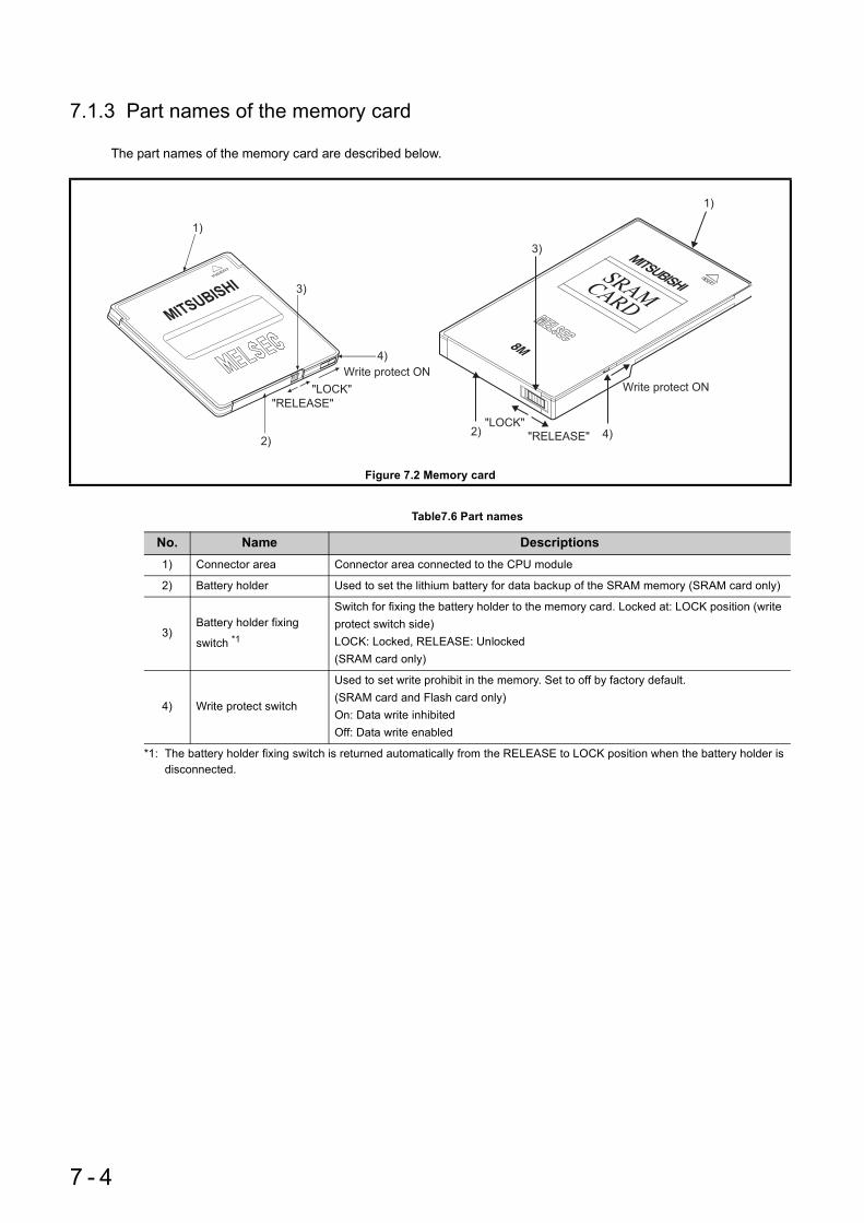
7.1.3 Part names of the memory card
The part names of the memory card are described below.
*1: The battery holder fixing switch is returned automatically from the RELEASE to LOCK position when the battery holder is disconnected.
Figure 7.2 Memory card
Table7.6 Part names
No. Name Descriptions1) Connector area Connector area connected to the CPU module
2) Battery holder Used to set the lithium battery for data backup of the SRAM memory (SRAM card only)
3)Battery holder fixing
switch *1
Switch for fixing the battery holder to the memory card. Locked at: LOCK position (write protect switch side)LOCK: Locked, RELEASE: Unlocked(SRAM card only)
4) Write protect switch
Used to set write prohibit in the memory. Set to off by factory default.(SRAM card and Flash card only)On: Data write inhibitedOff: Data write enabled
Write protect ON
2)
1)
4)
3)
"LOCK"
"RELEASE"
2)
3)
"LOCK"
Write protect ON
"RELEASE"
1)
4)
7 - 4

CHAPTER7 MEMORY CARD AND BATTERY
1
2
3
4
5
6
7
8
7.1 Mem
ory Card
7.1.4 Handling the m
emory card
7.1.4 Handling the memory card
(1) Formatting of memory cardAny SRAM or ATA card must have been formatted to use in the CPU module.Since the SRAM or ATA card purchased is not yet formatted, format it using GX Developer before use. (Formatting is not necessary for Flash cards.)For formatting, refer to the following.
GX Developer Operating Manual
Do not format an ATA card other than by GX Developer.(If formatted using format function of Microsoft® Windows® Operating System, the ATA card may not be usable in a CPU module.)
(2) Installation of SRAM card batteryA battery used to backup for power failure is supplied with the SRAM card.Before using the SRAM card, install the battery.
Note that the SRAM card memory is not backed up by the CPU module battery only. Also, the program memory, standard RAM, and latch devices of the CPU module are not backed up by the battery installed on the SRAM card.
(3) Types of files which can be stored on memory cardFor the types of the files that can be stored on each memory card, refer to the following.
Manuals for the CPU module used (Function Explanation, Program Fundamentals)
7 - 5

7.1.5 Installing and removing a memory card
(1) For Q2MEM type memory card
(a) To install the memory cardInstall the memory card into the CPU module, while paying attention to the orientation of the memory card. Insert the memory card securely into the connector until the height of the memory card reaches that of the memory card EJECT button.
(b) To remove the memory cardWhen removing the memory card from the CPU module, press the memory card EJECT button to pull out the memory card.
Figure 7.3 Install the memory card
Figure 7.4 Remove the memory card
Memory card
Memory cardEJECT button
CPU module main unit
Insertion direction check ( mark)
Memory card
Push
Memory card EJECT button
CPU modulemain unit
7 - 6

CHAPTER7 MEMORY CARD AND BATTERY
1
2
3
4
5
6
7
8
7.1 Mem
ory Card
7.1.5 Installing and removing a m
emory card
(2) For Q3MEM type memory card
(a) To install the memory cardWhen installing a memory card to the CPU module main body, install it according to the procedures in Figure 7.5, while paying attention to the direction of the memory card.
Figure 7.5 Installing a memory card
Install the memory card
Completed
Turn OFF power supply of the
CPU module and remove a lid
of the CPU module main body.
Install a memory card to a
memory card slot of the CPU
module main body.
Set a memory card protective
cover to the CPU module.
CPU modulemain unit
CPU modulemain unit
Slightly bend the center of a lid to make space between a projection and a mounting hole and remove the lid.
Projection
CPU modulemain unit
MEMORY cardEJECT button
Memory card
*Insertion direction check( mark)
7 - 7

(b) To remove the memory cardWhen removing a memory card from the CPU module main body, remove a memory card protective cover and press the EJECT button to pull out the memory card.
(3) To remove the memory card during power onWhen removing the memory card, confirm that special relays "SM604" and "SM605" are off.
• The memory card cannot be removed while "SM604" is on because the CPU module is using the card. • Turn off "SM605" if it is on.
When both "SM604" and "SM605" are off, remove the memory card according to the following procedure.
1) Turn on the special relay "SM609" using the sequence program or by the device test of GX Developer.
2) By monitoring GX Developer, check that the special relay "SM600" is turned off.
3) Remove the memory card.
(4) To install the memory card while the power is on1) Install the memory card.
2) Check that the special relay "SM600" is turned on by monitoring GX Developer etc., .
Figure 7.6 Removing a memory card
SM600 (Memory card can be used) : The system is turned on when memory card is ready to be used.
SM604 (memory card is being used) : The system is turned on when the CPU module is using the memory card.
SM605 (memory card removal prohibited) : Turned on by the user to disable a removal of the memory card.
Remove the memory card
Completed
Turn OFF power supply of the
CPU module and remove a
memory card protective cover
from the CPU module.
Press the EJECT button to eject
a memory card.
CPU modulemain unit
Remove a cover, pressing fixing claws of top/bottom
CPU modulemain unit
Push
Memory cardEJECT button
7 - 8

CHAPTER7 MEMORY CARD AND BATTERY
1
2
3
4
5
6
7
8
7.1 Mem
ory Card
7.1.5 Installing and removing a m
emory card
The following precautions must be observed when inserting or removing the memory card while the power is on.
● Note that the data in the memory card may be damaged if the above mentioned procedures are not performed correctly.Also, if the CPU module operation for an error is set to "Stop" in the Parameters, the CPU module stops its operation upon the occurrence of “ICM.OPE.ERROR”.
● When the memory card is installed, the scanning time is increased by several 10ms max. 1 scan is only added, when the CPU module executes mount processing.
● Poor insertion of the memory card may result in “ICM.OPE.ERROR”.
● Using the tweezers below is effective when the memory card cannot be removed smoothly.
Table7.7 Tweezers for replacing memory card
Product Model namePlastic tweezers NK-2539
Figure 7.7 Memory card replacement using plastic tweezers
7 - 9

7.1.6 Specifications of the memory card battery
This section describes the specifications of the battery used for the memory card (SRAM card).
Remark • For the life of the memory card battery, refer to Section 11.3.4. • For the battery irective in EU member states, refer to Appendix 4.
Table7.8 Specifications of the Battery for Memory Card
ItemType
Q2MEM-BAT Q3MEM-BATClassification Graphite fluoride lithium primary battery Manganese dioxide lithium primary battery
Initial voltage 3.0V 3.0V
Nominal current 48mAh 550mAh
Battery life when stored Actually 5 years (room temperature)
Battery life when used Section 11.3.4.
Lithium content 0.014g 0.150g
ApplicationPower failure backup for SRAM card(for Q2MEM-1MBS/Q2MEM-2MBS)
Power failure backup for SRAM card(for Q3MEM-4MBS/Q3MEM-8MBS)
7 - 10

CHAPTER7 MEMORY CARD AND BATTERY
1
2
3
4
5
6
7
8
7.1 Mem
ory Card
7.1.7 Battery Installation into the m
emory card
7.1.7 Battery Installation into the memory card
Installation method of the battery for the memory card (SRAM card)The battery for the SRAM card is removed from the battery holder when shipping.Before installing the SRAM card into the CPU module, set the battery holder as shown in Figure 7.8.
(1) For Q2MEM-1MBS and Q2MEM-2MBS
Insert or remove the battery in the horizontal direction along the battery holder fixing guide.Failure to do so may damage the latches of the battery holder.
Figure 7.8 Memory card battery setting procedure
Figure 7.9 Battery setting direction
Set the battery holder's locking switch to
the "RELEASE" position.
Set the battery onto the battery holder
with the "plus" face up.
Insert the battery holder with which the
battery is installed firmly, into the SRAM
card.
Confirm that the battery holder's locking
switch is set to the "LOCK" position.
Completed
......
......
......
......
......
Side with “product name”
RELEASE position
Battery holder
"LOCK"
The battery holder's locking switch is set automatically to the
"LOCK" position when the battery holder is removed. In its position,
insert the battery holder firmly.
:
Remove the battery holder from the SRAM card.
Battery holder's locking switch
' ' sign
Battery fixing guide
Battery holder
Battery holder latches
7 - 11

(2) For Q3MEM-4MBS and Q3MEM-8MBS
*1:The following shows the direction of a battery.
Figure 7.10 Memory card battery setting procedure
Figure 7.11 Direction of a battery
Completed
Set a battery holder fixing switch to
the RELEASE position.
Pull out a battery holder of a SRAM
card.
Facing up a positive side of a
battery, set the battery on the
battery holder.
Deeply insert the battery holder
where the battery is set into the
SRAM card.
Set the battery holder fixing switch
to the LOCK position.
RELEASEpositionBattery holder
fixing switch '+' sign*1
Battery holder
LOCKposition
Manufacture number
(varies depending on date of manufacture)
Maker name
'+' side '-' side
Model
Polarity
Voltage
7 - 12

CHAPTER7 MEMORY CARD AND BATTERY
1
2
3
4
5
6
7
8
7.2 Battery (Q
6BA
T, Q7B
AT, Q
8BA
T)7.2.1 B
attery specifications
7.2 Battery (Q6BAT, Q7BAT, Q8BAT)
Batteries (Q6BAT, Q7BAT and Q8BAT) are installed in the CPU module to retain data of the program memory, standard RAM, and latch device in case of power failure.
7.2.1 Battery specifications
This section describes the specifications of the battery used for the CPU module.Note1
*1: Included only when the Q7BAT-SET is purchased.*2: Included only when the Q8BAT-SET is purchased.
Remark • For the battery life, refer to Section 11.3.2. • For the battery directive in EU member states, refer to Appendix 4.
Note1
Table7.9 Battery specifications
ItemType
Q6BAT Q7BAT(-SET) Note7.2 Q8BAT(-SET) Note7.2
Classification Manganese dioxide lithium primary batteryManganese dioxide lithium primary battery
(assembled battery)
Initial voltage 3.0V
Nominal current 1800mAh 5000mAh 1800mAh (1800mAh 10 pieces)
Battery life when stored Actually 5 years (room temperature)
Battery life when used Section 11.3.2.
Lithium content 0.49g 1.52g 4.9g
ApplicationFor data retention of the program memory, standard RAM, and latch device during the power
failure
Accessory ---- Battery holder*1 Q8BAT connection cable*2
Note7.2The Q7BAT and Q8BAT is not applicable to the Basic model QCPU.
Basic
7 - 13

7.2.2 Battery installation
(1) Q6BAT battery installation procedureThe battery connector of Q6BAT is disconnected when shipping. Connect the connector as follows.For the service life of the battery and how to replace the battery, refer to Section 11.3.
(a) Basic model QCPU
(b) High Performance model QCPU, Process CPU, Redundant CPU and Universal model QCPU
Firmly push the connector all the way.
Figure 7.12 Q6BAT battery installation procedure
Figure 7.13 Q6BAT battery installation procedure
CPU module
Connector
Completed
Insert the battery connector into the
connector pin on the case. Be sure that
the insertion direction is correct.
Open the CPU module front cover.
Confirm that the battery is loaded
correctly.
Completed
Insert the battery connector into the
connector pin on the case. Be sure that
the insertion direction is correct.
Open the CPU module bottom cover.
Confirm that the battery is loaded
correctly. Battery
Connector
Connectorstopper
CPU module
7 - 14

CHAPTER7 MEMORY CARD AND BATTERY
1
2
3
4
5
6
7
8
7.2 Battery (Q
6BA
T, Q7B
AT, Q
8BA
T)7.2.2 B
attery installation
(2) Q7BAT-SET battery installation procedureWhen changing the battery for the CPU module from the Q6BAT to the Q7BAT, set the battery and connect its connector in the following procedure.
Firmly push the connector all the way.
Figure 7.14 Q7BAT-SET battery installation procedure
Open the CPU module bottom cover.
Set the Q7BAT- SET in the CPU module.
Completed
Disconnect the connector connecting the
Q6BAT to the CPU module.
Remove the Q6BAT and cover from the
CPU module.
Connect the Q7BAT- SET to the battery
connector of the CPU module and set it
into the connector holder of the battery
holder.
Battery holder
Connector
Connector stopper
CPU module
7 - 15

(3) Q8BAT-SET battery installation procedureWhen changing the battery of the CPU module from the Q6BAT to the Q8BAT, install the battery and connect its connector in the following procedure.
Open the cover of the CPU module's bottom.
(To next page)
Connector of CPU module
Q6BAT
CPU module
Connectorof cable
Q8BAT connection cable
Q8BAT connection cover
Disconnect the connector connecting the Q6BAT to the CPU module.
Insert the connector of Q8BAT connection cable (included in the Q8BAT-SET) into the connector of CPU module while confirming the orientation of each connector.
Remove the Q6BAT and cover from the CPU module.
Attach the Q8BAT connection cover to the CPU module.
Connector of battery
Connector of CPU module
CPU module
Q8BAT connection cover
Q8BAT connection cable
CPU module
7 - 16

CHAPTER7 MEMORY CARD AND BATTERY
1
2
3
4
5
6
7
8
7.2 Battery (Q
6BA
T, Q7B
AT, Q
8BA
T)7.2.2 B
attery installation
• Clamp the Q8BAT connection cable.Failure to do so may damage the Q8BAT connection cover, connector, or the cable due to unintentional swinging and shifting or accidental pulling of the cable.
• Provide 10mm (0.39 inches) or more of the bending radius for the Q8BAT connection cable.If the bending radius is less than 10mm (0.39 inches), malfunction may occur due to characteristic deterioration and wire breakage.
• For details of the module mounting position, refer to the following. Section 10.3.2
• Firmly push the connector all the way. • When installing the Q8BAT for the Universal model QCPU, use the connection cable with “A” printed.
Mount the CPU module onto the main base unit, so that the Q8BAT connection cable connected to the CPU module will not interfere with the other devices.
Fix the Q8BAT onto the control panel. (Screws or DIN rail is applicable.)
(From previous page)
Attach the connector of Q8BAT connection cable to the Q8BAT while confirming the orientation of the connector.
Completed
Q8BAT
Control panel
Q8BAT connection cable
Q8BAT
R (bending radius)10mm (0.39 inch)
or more
A Sticker
7 - 17

CHAPTER8 CPU MODULE START-UP PROCEDURES
This chapter provide the start-up procedure for the Q Series CPU module on the assumption that programs and parameters have been created separately.For the start-up procedures for a redundant system configured with a Redundant CPU, refer to the following.
QnPRHCPU User's Manual (Redundant System)
Module installation • • • CHAPTER 10Install any of the following modules required for the system configuration to the base unit.
•Power supply module•CPU module (Install a memory card if necessary.)•Intelligent function module and/or special function module•Network module•I/O module
Wiring/connection • • • CHAPTER 6, CHAPTER 7, CHAPTER 10
1) Wire the power supply to the power supply module.2) Wire external device(s) to intelligent function module(s), special function mod-
ule(s), and/or I/O module(s).3) Install wiring between network modules.4) Install the battery to the CPU module.5) Connect the main base unit to an extension base unit and also between exten-
sion base units by extension cables and then set the number of bases to exten-sion base units.
Module initial settings • • • CHAPTER 41) Halt the CPU module.2) Set up switches of the intelligent function module(s) and/or special function
module(s).3) Set up switches of the network module.
System power on • • • CHAPTER 4, CHAPTER 5, CHAPTER 10
Confirm the following items of the system, and then power on the system.•Wiring of the power supply•Power supply voltage•Operating status of the CPU module: Stop status (reset canceled)
Connection of the PC in which GX Developer is installed • • • GX Developer Operating Manual
1) Start up GX Developer on the personal computer.2) Connect the personal computer in which GX Developer is installed, to the CPU
module.
Figure 8.1 CPU module start-up procedures
Start
(To next page)
8 - 1
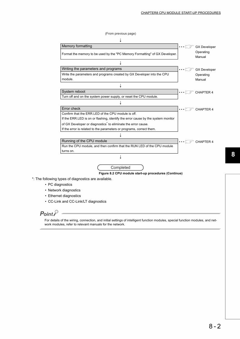
CHAPTER8 CPU MODULE START-UP PROCEDURES
1
2
3
4
5
6
7
8
*: The following types of diagnostics are available. • PC diagnostics • Network diagnostics • Ethernet diagnostics • CC-Link and CC-Link/LT diagnostics
For details of the wiring, connection, and initial settings of intelligent function modules, special function modules, and net-work modules, refer to relevant manuals for the network.
Memory formatting • • • GX Developer Operating Manual
Format the memory to be used by the "PC Memory Formatting" of GX Developer.
Writing the parameters and programs • • • GX Developer Operating Manual
Write the parameters and programs created by GX Developer into the CPU module.
System reboot • • • CHAPTER 4Turn off and on the system power supply, or reset the CPU module.
Error check • • • CHAPTER 4Confirm that the ERR.LED of the CPU module is off.If the ERR.LED is on or flashing, identify the error cause by the system monitor
of GX Developer or diagnostics* to eliminate the error cause.If the error is related to the parameters or programs, correct them.
Running of the CPU module • • • CHAPTER 4Run the CPU module, and then confirm that the RUN LED of the CPU module turns on.
Figure 8.2 CPU module start-up procedures (Continue)
(From previous page)
Completed
8 - 2

Memo
8 - 3

CHAPTER9 EMC AND LOW VOLTAGE DIRECTIVES
9
2
3
4
5
6
7
8
9.1 Requirem
ents for Com
pliance with the E
MC
Directive
CHAPTER9 EMC AND LOW VOLTAGE DIRECTIVES
Compliance to the EMC Directive, which is one of the EU Directives, has been a legal obligation for the products sold in European countries since 1996 as well as the Low Voltage Directive since 1997.Manufacturers who recognize their products are compliant to the EMC and Low Voltage Directives are required to declare that print a "CE mark" on their products.
(1) Authorized representative in EuropeAuthorized representative in Europe is shown below.
9.1 Requirements for Compliance with the EMC Directive
The EMC Directive specifies that products placed on the market must be so constructed that they do not cause excessive electromagnetic interference (emissions) and are not unduly affected by electromagnetic interference (immunity)".Section 9.1.1 through Section 9.1.6 summarize the precautions on compliance with the EMC Directive of the machinery constructed with the MELSEC-Q series programmable controllers.These precautions are based on the requirements and the standards of the regulation, however, it does not guarantee that the entire machinery constructed according to the descriptions will comply with above-mentioned directive. The method and judgement for complying with the EMC Directive must be determined by the person who construct the entire machinery.
Name : Mitsubishi Electric Europe BVAddress: Gothaer strase 8, 40880 Ratingen, Germany
9 - 1

9.1.1 Standards relevant to the EMC Directive
The standards relevant to the EMC Directive are listed in Table9.1.
*1: QP : Quasi-peak value, Mean : Average value*2: Programmable controller is an open type device (a device designed to be housed inside other equipment) and must be installed inside a
conductive control panel. The corresponding test has been conducted with the programmable controller installed inside a control panel.Besides, our programmable controller has been tested with the maximum rated input value of the power supply module to be used.
Table9.1 Standards relevant to the EMC Directive
Specification Test item Test details Standard value
EN61131-2:2003
EN61000-4-2Electrostatic discharge
immunity*2
Immunity test in which electrostatic is appliedto the cabinet of the equipment.
8KV Air discharge4KV Contact discharge
EN61000-4-3Radiated electromagnetic
field immunity*2
Immunity test in which electricfields are irradiated to theproduct.
1.4GHz-2.0GHz, 80-1000MHz, 10V/m, 80%AM modulation@1KHz
EN61000-4-4Electrical fast transient/
burst immunity *2
Immunity test in which burstnoise is applied to the power cable and signal line.
AC power cable: 2KV
DC power cable: 2KV
I/O power(DC): 1KVDC I/O, analog, communication
line(shielded): 1KV
EN61000-4-5
Surge immunity *2
Immunity test in which burstnoise is applied to the power lineand signal line.
AC power line:
Common mode 2KV, differential
mode 1KVDC power line:
Common mode 1KV, differential
mode 0.5KVI/O power(DC):
Common mode 0.5KV, differential
mode 0.5KVDC I/O, analog, communication (shielded):
Common mode 1KV
EN61000-4-6Conducted disturbances
immunity *2
Immunity test in which highfrequency noise is applied to thepower line and signal line.
0.15-80MHz, 80%AM modulation 1KHz,3Vrms
9 - 2

CHAPTER9 EMC AND LOW VOLTAGE DIRECTIVES
9
2
3
4
5
6
7
8
9.1 Requirem
ents for Com
pliance with the E
MC
Directive
9.1.2 Installation instructions for EM
C D
irective
9.1.2 Installation instructions for EMC Directive
Programmable controller is an open type device and must be installed inside a control panel for use.*1
This not only ensures safety but also ensures effective shielding of programmable controller-generated electromagnetic noise.
*1: Also, each network remote station needs to be installed inside the control panel.However, the waterproof type remote station can be installed outside the control panel.
(1) Control panel • Use a conductive control panel. • When attaching the control panel's top plate or base plate, mask painting and weld so that good surface
contact can be made between the panel and plate. • To ensure good electrical contact with the control panel, mask the paint on the installation bolts of the inner
plate in the control panel so that contact between surfaces can be ensured over the widest possible area. • Ground the control panel with a thick wire so that a low impedance connection to ground can be ensured
even at high frequencies. • Holes made in the control panel must be 10 cm (3.94 inches) diameter or less. If the holes are 10 cm (3.94
inches) or larger, radio frequency noise may be emitted.In addition, because radio waves leak through a clearance between the control panel door and the main unit, reduce the clearance as much as practicable.The leakage of radio waves can be suppressed by the direct application of an EMI gasket on the paint surface.
Our tests have been carried out on a panel having the damping characteristics of 37 dB max. and 30 dB mean (measured by 3 m method with 30 to 300 MHz).
(2) Connection of power line and ground wireGround wire and power supply cable for the programmable controller system must be connected as described below.
• Provide an grounding point near the power supply module. Ground the power supply's LG and FG terminals (LG : Line Ground, FG : Frame Ground) with the thickest and shortest wire possible. (The wire length must be 30 cm (11.81 inches) or shorter.) The LG and FG terminals function is to pass the noise generated in the programmable controller system to the ground, so an impedance that is as low as possible must be ensured. As the wires are used to relieve the noise, the wire itself carries a large noise content and thus short wiring means that the wire is prevented from acting as an antenna.
• The ground wire led from the grounding point must be twisted with the power supply wires. By twisting with the ground wire, noise flowing from the power supply wires can be relieved to the ground. However, if a filter is installed on the power supply wires, the wires and the ground wire may not need to be twisted.
9 - 3

9.1.3 Cables
The cables extracted from the control panel contain a high frequency noise component. On the outside of the control panel, therefore, they serve as antennas to emit noise. To prevent noise emission, use shielded cables for the cables which are connected to the I/O modules and intelligent function modules and may be extracted to the outside of the control panel.The use of a shielded cable also increases noise resistance. The signal lines (including common line) of the programmable controller, which are connected to I/O modules, intelligent function modules and/or extension cables, have noise durability in the condition of grounding their shields by using the shielded cables. If a shielded cable is not used or not grounded correctly, the noise resistance will not meet the specified requirements.
(1) Grounding of shield section of shield cable • Ground the exposed shield section of the shielded cable close to the module. Confirm that the grounded
cables are not induced to electromagnetic from the cables, which are not yet grounded. • Ground the exposed shield section to spacious area on the control panel.A clamp can be used as shown in
Figure 9.2.In this case, apply a cover on the painted inner wall surface of the control panel, which comes in contact with the clamp
Note) The method of grounding with a vinyl-coated wire soldered onto the shielded section of the shielded cable as in shown Figure 9.3 is not recommended. Doing so will raise the high-frequency impedance, resulting in loss of the shielding effect.
Figure 9.1 Part to be exposed Figure 9.2 Shield grounding (Correct example)
Figure 9.3 Shield grounding (Incorrect example)
Shield section
Screw
Clamp fitting
Shield cable
Paint mask
Shield cable
Wire
Solderless terminal, crimp contact
9 - 4
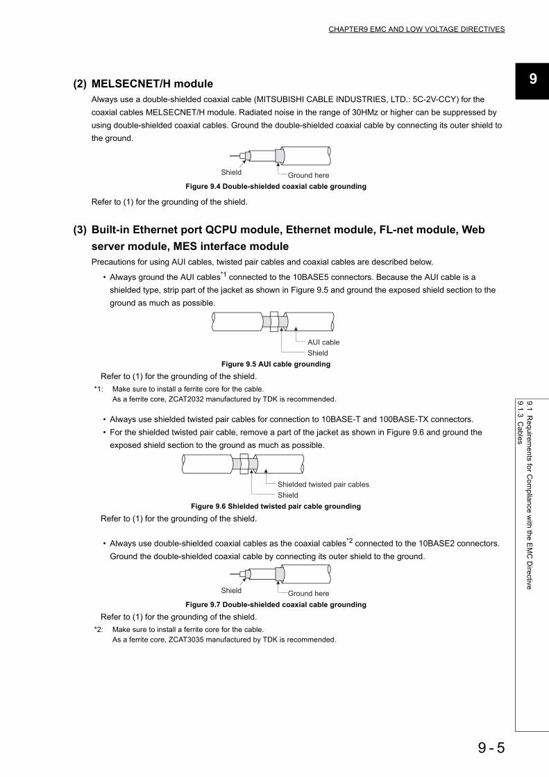
CHAPTER9 EMC AND LOW VOLTAGE DIRECTIVES
9
2
3
4
5
6
7
8
9.1 Requirem
ents for Com
pliance with the E
MC
Directive
9.1.3 Cables
(2) MELSECNET/H moduleAlways use a double-shielded coaxial cable (MITSUBISHI CABLE INDUSTRIES, LTD.: 5C-2V-CCY) for the coaxial cables MELSECNET/H module. Radiated noise in the range of 30HMz or higher can be suppressed by using double-shielded coaxial cables. Ground the double-shielded coaxial cable by connecting its outer shield to the ground.
Refer to (1) for the grounding of the shield.
(3) Built-in Ethernet port QCPU module, Ethernet module, FL-net module, Web server module, MES interface modulePrecautions for using AUI cables, twisted pair cables and coaxial cables are described below.
• Always ground the AUI cables*1 connected to the 10BASE5 connectors. Because the AUI cable is a shielded type, strip part of the jacket as shown in Figure 9.5 and ground the exposed shield section to the ground as much as possible.
Refer to (1) for the grounding of the shield.*1: Make sure to install a ferrite core for the cable.
As a ferrite core, ZCAT2032 manufactured by TDK is recommended.
• Always use shielded twisted pair cables for connection to 10BASE-T and 100BASE-TX connectors. • For the shielded twisted pair cable, remove a part of the jacket as shown in Figure 9.6 and ground the
exposed shield section to the ground as much as possible.
Refer to (1) for the grounding of the shield.
• Always use double-shielded coaxial cables as the coaxial cables*2 connected to the 10BASE2 connectors. Ground the double-shielded coaxial cable by connecting its outer shield to the ground.
Refer to (1) for the grounding of the shield.*2: Make sure to install a ferrite core for the cable.
As a ferrite core, ZCAT3035 manufactured by TDK is recommended.
Figure 9.4 Double-shielded coaxial cable grounding
Figure 9.5 AUI cable grounding
Figure 9.6 Shielded twisted pair cable grounding
Figure 9.7 Double-shielded coaxial cable grounding
Ground hereShield
AUI cable
Shield
Shielded twisted pair cables
Shield
Ground hereShield
9 - 5
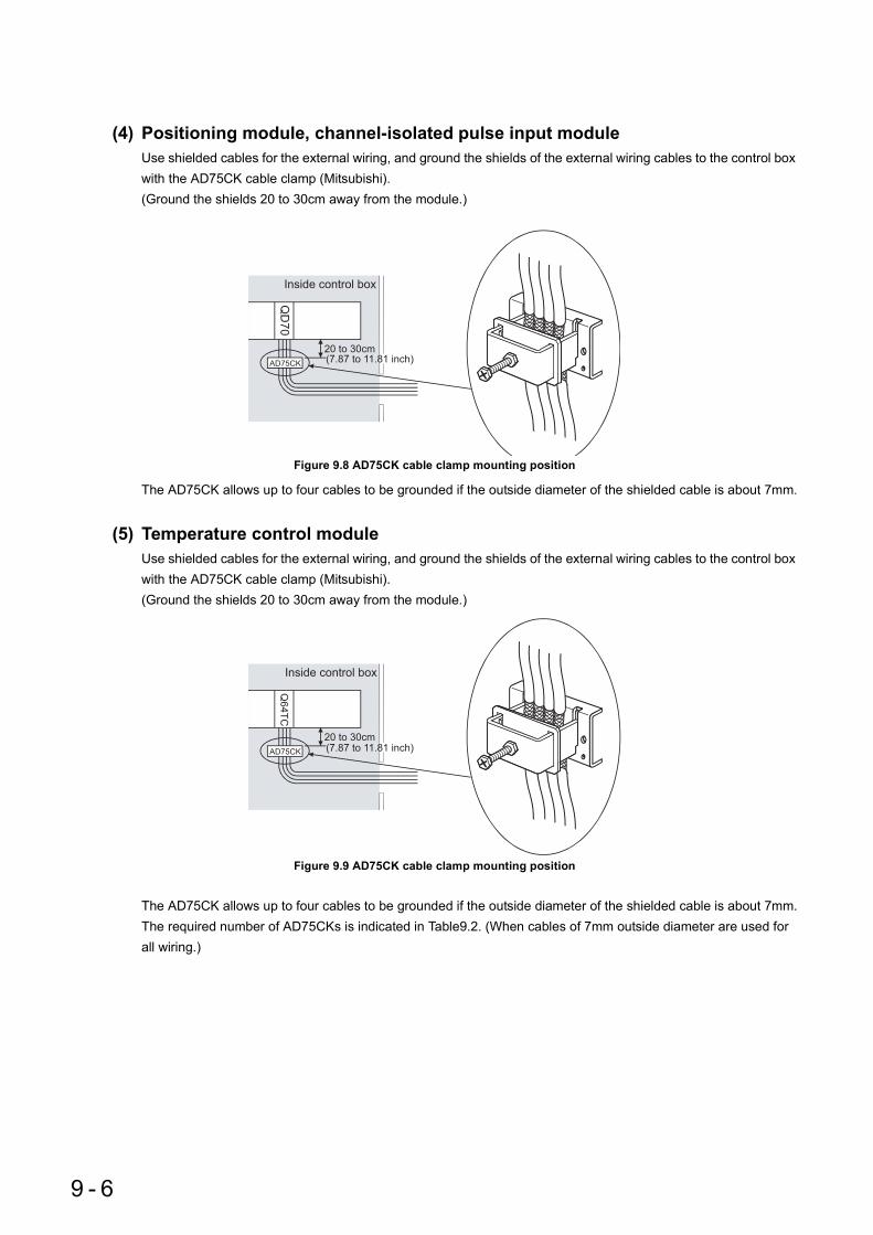
(4) Positioning module, channel-isolated pulse input moduleUse shielded cables for the external wiring, and ground the shields of the external wiring cables to the control box with the AD75CK cable clamp (Mitsubishi).(Ground the shields 20 to 30cm away from the module.)
The AD75CK allows up to four cables to be grounded if the outside diameter of the shielded cable is about 7mm.
(5) Temperature control moduleUse shielded cables for the external wiring, and ground the shields of the external wiring cables to the control box with the AD75CK cable clamp (Mitsubishi).(Ground the shields 20 to 30cm away from the module.)
The AD75CK allows up to four cables to be grounded if the outside diameter of the shielded cable is about 7mm.The required number of AD75CKs is indicated in Table9.2. (When cables of 7mm outside diameter are used for all wiring.)
Figure 9.8 AD75CK cable clamp mounting position
Figure 9.9 AD75CK cable clamp mounting position
Inside control box
QD
70
20 to 30cm
AD75CK (7.87 to 11.81 inch)
Inside control box
Q6
4T
C
20 to 30cm
AD75CK (7.87 to 11.81 inch)
9 - 6

CHAPTER9 EMC AND LOW VOLTAGE DIRECTIVES
9
2
3
4
5
6
7
8
9.1 Requirem
ents for Com
pliance with the E
MC
Directive
9.1.3 Cables
(6) Redundant CPUBe sure to use the QC TR for the tracking cable, and ground the shielded part of the cable to the panel with the AD75CK cable clamp (Mitsubishi).(Ground the shield at a position 20 to 30cm (7.87 to 11.81 inches) away from the module.)
(7) I/O signal lines and other communication cablesFor the I/O signal lines (including common line) and other communication cables (RS-232, RS-422, CC-Link, etc.), always ground the shields of the shield cables as in (1) if they are pulled out of the control panel.
(8) Extension cableFor an extension cable, always ground the shields of the shield cables as in (1) if they are pulled out of the control panel.
(9) Power line for external power supply terminalThe power line connecting to the external power supply terminal of the analog module must be 30m (98.43 feet) or less.
(10)Power line of CC-Link remote modulePower line connecting to the external power supply terminal (compliant with I/O power port of CE standard) must be 30m (98.43 feet) or less. Power line connecting to module power supply terminal (compliant with I/O power port of CE standard) must be 10m or less.
Table9.2 Required number of AD75CK
Required Number of AD75CKsNumber of Used Channels
1 2 3 4
Number of used CT channel
0 1 1 2 2
1 1 2 2 3
2 1 2 2 3
3 2 2 3 3
4 2 2 3 3
5 2 3 3 4
6 2 3 3 4
7 3 3 4 4
8 3 3 4 4
Figure 9.10 AD75CK cable clamp mounting position
Inside control panel
Qn
PR
HC
PU
20 to 30cm
AD75CK (7.87 to 11.81 inch)
9 - 7

9.1.4 Power supply part of the power supply module, Q00JCPU, and Q00UJCPU
Always ground the LG and FG terminals after short-circuiting them.
9.1.5 When using MELSEC-A series modules
The following describes the case where the MELSEC-A series module is used, using the QA1S6 B, QA6 B, and
QA6ADP+A5 B/A6 B as the extension base unit.
(1) Cable
(a) Grounding the shield section of shielded cable • Ground the exposed shield section of the shielded cable close to the module. Confirm that the grounded
cables are not induced to electromagnetic from the cables, which are not yet grounded. • Ground the exposed shield section to spacious area on the control panel. • A clamp can be used as shown in Figure 9.12.
In this case, apply a cover on the painted inner wall surface of the control panel, which comes in contact with the clamp.
Note) The method of grounding with a vinyl-coated wire soldered onto the shielded section of the shielded cable as in shown Figure 9.13 is not recommended. Doing so will raise the high-frequency impedance, resulting in loss of shielding effect.
Figure 9.11 Part to be exposed Figure 9.12 Shield grounding (Correct example)
Figure 9.13 Shield grounding (Incorrect example)
Shield section
Screw
Clamp fitting
Shield cable
Paint mask
Shield cable
Wire
Solderless terminal, crimp contact
9 - 8

CHAPTER9 EMC AND LOW VOLTAGE DIRECTIVES
9
2
3
4
5
6
7
8
9.1 Requirem
ents for Com
pliance with the E
MC
Directive
9.1.5 When using M
ELS
EC
-A series m
odules
(b) Positioning modulesPrecautions for configuring the machinery compliant with the EMC Directives using the A1SD75P -S3
(abbreviated as A1SD75 hereafter), AD75P -S3 (abbreviated as AD75 hereafter) are described below.
1) When wiring cable of a 2 m (6.56 feet) or less • Ground the shield of the external device connection cable with a cable clamp. (Ground the shield at the
closest location to the A1SD75/AD75 external wiring connector.) • Wire external device connection cables to drive modules and external devices by the shortest distance. • Install the drive unit in the same panel.
2) When wiring with cable that exceeds 2 m (6.56 feet), but is 10 m (32.79 feet) or less • Ground the shield of the external device connection cable with a cable clamp. (Ground the shield at the
closest location to the A1SD75/AD75 external wiring connector.) • Wire external device connection cables to drive modules and external devices by the shortest distance. • Install a ferrite core.
Figure 9.14 When wiring with a 2 m (6.56 feet) or less cable
Figure 9.15 When wiring with cable that exceeds 2 m (6.56 feet), but is 10 m (32.79 feet) or less
Connector for external device connection
Cable clamp
Cable for external device connection (within 2 m)
A1
SD
75
Po
we
r su
pp
ly m
od
ule
Drive unit
Connector for external device connection
Ferrite core
Cable for external device connection (over 2 m to less than 10 m)
Cable clamp
A1
SD
75
Po
we
r su
pp
ly m
od
ule
Drive unit
9 - 9

3) Ferrite core and cable clamp types • Cable clamp
Type : AD75CK (Mitsubishi) • Ferrite core
Type : ZCAT3035-1330 (TDK ferrite core)
4) Cable clamp mounting position
Table9.3 Number of required ferrite cores and cable clamps
Cable length Prepared partRequired Qty
1 axis 2 axes 3 axesWithin 2 m (6.56 feet) AD75CK 1 1 1
2 m (6.56 feet) to 10m(32.79feet)
AD75CK 1 1 1
ZCAT3035-1330 1 2 3
Figure 9.16 AD75CK cable clamp mounting position
Inside control box
AD75
20 to 30cm
AD75CK (7.87 to 11.81 inch)
9 - 10

CHAPTER9 EMC AND LOW VOLTAGE DIRECTIVES
9
2
3
4
5
6
7
8
9.1 Requirem
ents for Com
pliance with the E
MC
Directive
9.1.5 When using M
ELS
EC
-A series m
odules
(c) CC-Link module • Be sure to ground the cable shield that is connected to the CC-Link module close to the exit of control
panel or to any of the CC-Link stations within 30 cm (11.81 inches) from the module or stations.The CC-Link dedicated cable is a shielded cable. Remove a part of the jacket as shown in Figure 9.17 and ground the exposed shield section to the ground as much as possible.
• Always use the specified CC-Link dedicated cable. • The CC-Link module, the CC-Link stations and the FG line inside the control panel must be connected at
the FG terminal as shown in Figure 9.18.
• Use the external power supply that is CE compliant. Ground FG terminals.
• Power line connecting to the external power supply terminal (compliant with I/O power port of CE standard) must be 30m (98.43 feet) or less. Power line connecting to module power supply terminal (compliant with I/O power port of CE standard) must be 10m (32.81 feet) or less.
• The signal line connecting to the analog input of the following modules must be 30m or less.
AJ65BT-64RD3AJ65BT-64RD4AJ65BT-68TD
(d) I/O signal linesFor the I/O signal lines (including common line), if extracted to the outside of the control panel, also ensure to ground the shield section of these lines and cables in the same manner as in item (1) above.
(e) Extension cableFor an extension cable, always ground the shield section of the shield cables as in (1) if they are pulled out of the control panel.
Figure 9.17 CC-Link dedicated cable grounding
Figure 9.18 Connection between CC-Link module/CC-Link station and FG line inside the control panel. (Simplified figure)
Table9.4 External power supply
Power supply model name
DLP75-24-1 DLP100-24-1 DLP120-24-1 DLP180-24-1 DLP240-24-1
Rated input voltage 100 to 240VACRated output
Voltage 24VDCCurrent 3.1A 4.1A 5.0A 7.5A 10.0A
CC-Link dedicated cable
Shield
Terminal resistor Terminal resistorDA
DB
DG
SLD
FG
DA
DB
DG
SLD
FG
(Blue)
(White)
(Yellow)
CC-Link
dedicated
cable
CC-Link
dedicated
cable
DA
DB
DG
SLD
FG
Master module Remote module Local module
9 - 11

(2) Power supply moduleThe precautions required for each power supply module are described in Table9.5. Always observe the items noted as precautions.
*1: If sufficient filter circuitry is built into the 24VDC external power supply module, the noise generated by A1S63P will be absorbed by that filter circuit, so a line filter may not be required.Filtering circuitry of version F or later of A1S63P is improved so that a external line filter is not required.
Table9.5 Precautions when using a power supply module
Model PrecautionsA1S61PA1S62PA61PA62P
Not usable
A1S63P *1
A163PUse the CE marked 24VDC panel power equipment.
A1S61PEUA1S62PEUA1S61PNA1S62PNA61PNA61PEUA62PEUA68P
Always ground the LG and FG terminals after short-circuiting them.
9 - 12

CHAPTER9 EMC AND LOW VOLTAGE DIRECTIVES
9
2
3
4
5
6
7
8
9.1 Requirem
ents for Com
pliance with the E
MC
Directive
9.1.6 Others
9.1.6 Others
(1) Ferrite coreA ferrite core has the effect of reducing radiated noise in the 30MHz to 100MHz band. It is not required to fit ferrite cores to cables, but it is recommended to fit ferrite cores if shield cables pulled out of the enclosure do not provide sufficient shielding effects.Note that the ferrite cores must be fitted to the cables in the position immediately before they are pulled out of the enclosure. If the fitting position is improper, the ferrite will not produce any effect.
(2) Noise filter (power supply line filter)A noise filter is a component which has an effect on conducted noise.It is not required to attach the noise filter to the power supply line except the A61PEU, A62PEU power supply modules and some models, however, attaching it can suppress more noise.(The noise filter has the effect of reducing conducted noise of 10 MHz or less.)
The precautions required when installing a noise filter are described below. • Do not bundle the wires on the input side and output side of the noise filter. When bundled, the output side
noise will be induced into the input side wires from which the noise was filtered.
• Ground the noise filter grounding terminal to the control cabinet with the shortest wire possible (approx. 10 cm (3.94 inches)).
Remark
Figure 9.19 Precautions on noise filter
Table9.6 Noise filter specifications
Noise filter model name FN343-3/01 FN660-6/06 ZHC2203-11Manufacturer SCHAFFNER SCHAFFNER TDKRated current 3A 6A 3ARated voltage 250V
Filter
Induction
Input side
(power supply side)
Output side
(device side)
Filter
Input side
(power supply side)
Output side
(device side)
The noise will be included when the
input and output wires are bundled.
Separate and lay the input
and output wires.
9 - 13

(3) Isolation transformerAn isolation transformer has an effect on reducing conducted noise (especially, lightning surge).Lightning surge may cause a malfunction of the programmable controller.As a measure against lightning surge, connect an isolation transformer as shown in Figure 9.20.The use of an isolation transformer reduces an impact of lightning.
Figure 9.20 Power supply wiring figure
100VAC
200VAC
T1
Main power supply
Relay terminal block
I/O power supply
I/O equipment
Inside a control panel
Programmablecontroller powersupply
Isolationtransformer
Programmablecontroller
Motor power supply
Motor equipment
9 - 14

CHAPTER9 EMC AND LOW VOLTAGE DIRECTIVES
9
2
3
4
5
6
7
8
9.2 Requirem
ent to Com
pliance with the Low
Voltage D
irective9.2.1 S
tandard applied for ME
LSE
C-Q
series programm
able controller
9.2 Requirement to Compliance with the Low Voltage Directive
The Low Voltage Directive requires each device that operates with the power supply ranging from 50 to 1000VAC and 75 to 1500VDC to satisfy the safety requirements.In Section 9.2.1 to Section 9.2.6, cautions on installation and wiring of the MELSEC-Q series programmable controller to comply with the Low Voltage Directive are described.These descriptions are based on the requirements and standards of the regulation, however, it does not guarantee that the entire machinery manufactured based on the descriptions complies with the above-mentioned directive. The method and judgment for the low voltage directive must be left to the manufacturer's own discretion.
9.2.1 Standard applied for MELSEC-Q series programmable controller
The standard applied for MELSEC-Q series programmable controller is EN61131-2 safety of devices used in measurement rooms, control rooms, or laboratories.
The MELSEC-Q series programmable controller which operate at the rated voltage of 50VAC/75VDC or above are also developed to conform to the above standard.The modules which operate at the rated voltage of less than 50VAC/75VDC are out of the Low Voltage Directive application range.For products with the CE mark, refer to the "Standard Compliance" menu of the MELFANSweb homepage.
9.2.2 MELSEC-Q series programmable controller selection
(1) Power supply moduleThere are dangerous voltages (voltages higher than 42.4V peak) inside the power supply modules of the 100/200VAC rated I/O voltages. Therefore, the CE marked models are enhanced in insulation internally between the primary and secondary.
(2) I/O moduleThere are dangerous voltages (voltages higher than 42.4V peak) inside the I/O modules of the 100/200VAC rated I/O voltages. Therefore, the CE marked models are enhanced in insulation internally between the primary and secondary.The I/O modules of 24VDC or less rating are out of the Low Voltage Directive application range.
(3) CPU module, memory card, base unitUsing 5VDC circuits inside, the above modules are out of the Low Voltage Directive application range.
(4) Intelligent function modules (special function modules)The intelligent function modules such as analog-digital converter modules, digital-analog converter modules, network modules, and positioning modules (special function modules) are out of the scope of the low voltage directive because the rated voltage is 24VDC or less.
(5) Display deviceUse the CE marked display device.
9 - 15

9.2.3 Power supply
The insulation specification of the power supply module was designed assuming installation category II. Be sure to use the installation category II power supply to the programmable controller. The installation category indicates the durability level against surge voltage generated by a thunderbolt. Category I has the lowest durability; category IV has the highest durability.
Category II indicates a power supply whose voltage has been reduced by two or more levels of isolating transformers from the public power distribution.
9.2.4 Control panel
Programmable controller is an open type device (a device designed to be housed inside other equipment) and must be installed inside a control panel for use.*1
*1: Also, each network remote station needs to be installed inside the control panel.However, the waterproof type remote station can be installed outside the control panel.
(1) Electrical shock preventionThe control panel must be handled as shown below to protect a person who does not have adequate knowledge of electricity from an electric shock.
• Lock the control panel so that only those who are trained and have acquired enough knowledge of electric facilities can open the control panel.
• The control panel must have a structure which automatically stops the power supply when the box is opened.
• For electric shock protection, use IP20 or greater control panel.
Figure 9.21 Installation category for power supply moduleCategory IV Category III Category II Category I
9 - 16

CHAPTER9 EMC AND LOW VOLTAGE DIRECTIVES
9
2
3
4
5
6
7
8
9.2 Requirem
ent to Com
pliance with the Low
Voltage D
irective9.2.4 C
ontrol panel
(2) Dustproof and waterproof featuresThe control panel also has the dustproof and waterproof functions. Insufficient dustproof and waterproof features lower the insulation withstand voltage, resulting in insulation destruction. The insulation in our programmable controller is designed to cope with the pollution level 2, so use in an environment with pollution level 2 or below.
Pollution level 1 : An environment where the air is dry and conductive dust does not exist.Pollution level 2 : An environment where conductive dust
does not usually exist, but occasional temporary conductivity occurs due to the accumulated dust. Generally, this is the level for inside the control box equivalent to IP54 in a control room or on the floor of a typical factory.
Pollution level 3 : An environment where conductive dust exits and conductivity may be generated due to the accumulated dust. An environment for a typical factory floor.
Pollution level 4 : Continuous conductivity may occur due to rain, snow, etc. An outdoor environment.
As shown above, the programmable controller can realize the pollution level 2 when stored in a control panel equivalent to IP54.
9 - 17

9.2.5 Grounding
There are the following two different ground terminals.Use either ground terminal in an grounding status.
Protective grounding : Maintains the safety of the programmable controller and improves the noise resistance.
Functional grounding : Improves the noise resistance.
9.2.6 External wiring
(1) Module power supply and external power supplyFor the remote module which requires 24VDC as module power supply, the 5/12/24/48VDC I/O module, and the intelligent function module (special function module) which requires the external power supply, use the 5/12/24/48VDC circuit which is doubly insulated from the hazardous voltage circuit or use the power supply whose insulation is reinforced.
(2) External devicesWhen a device with a hazardous voltage circuit is externally connected to the programmable controller, use a model whose circuit section of the interface to the programmable controller is intensively insulated from the hazardous voltage circuit.
(3) Intensive insulationThe intensive insulation covers the withstand voltages shown in Table9.7.
Table9.7 Intensive Insulation Withstand Voltage (Installation Category II, source : IEC 664)
Rated voltage of hazardous voltage areaSurge withstand voltage
(1.2/50 s)150VAC or below 2500V
300VAC or below 4000V
9 - 18
CHAPTER10 LOADING AND INSTALLATION
9
10
3
4
5
6
7
8
10.1 General S
afety Requirem
ents
CHAPTER10 LOADING AND INSTALLATION
In order to increase the reliability of the system and exploit the maximum performance of its functions, this chapter describes the methods and precautions for the mounting and installation of the system.
10.1 General Safety Requirements
DANGER
Configure safety circuits external to the programmable controller toensure that the entire system operates safely even when a fault occurs inthe external power supply or the programmable controller. Failure to doso may result in an accident due to an incorrect output or malfunction.(1) Configure external safety circuits, such as an emergency stop
circuit, protection circuit, and protective interlock circuit for forward/reverse operation or upper/lower limit positioning.
(2) When the programmable controller CPU stops its operation upondetection of the following status, and the output status of the systemwill be as shown below.
All outputs may turn on when an error occurs in the part, such as I/Ocontrol part, where the programmable controller CPU cannot detectany error. To ensure the safety operation in such a case, provide asafety mechanism or a fail-safe circuit external to the programmablecontroller.
(3) Outputs may remain on or off due to a failure of an output modulerelay or transistor. Configure an external circuit for monitoring outputsignals that could cause a serious accident.
In an output module, when a load current exceeding the rated current oran overcurrent caused by a load short-circuit flows for a long time, it maycause smoke and fire. To prevent this, configure an external safetycircuit, such as a fuse.
Configure a circuit so that the programmable controller is turned on firstand then the external power supply.If the external power supply is turned on first, an accident may occur dueto an incorrect output or malfunction.
For the operating status of each station after a communication failure,refer to the relevant manuals for the network.Incorrect output or malfunction due to a communication failure amy resultin an accident.
Q series module AnS/A series module
All outputs are
turned off.
All outputs are
turned off.
All outputs are held or turned off according to the parameter setting.
Overcurrent or overvoltage protection of the power supply module is activated.
The CPU module detects an error such as a
watchdog timer error by the self-diagnostic
function.
(a)
(b) All outputs are
turned off.
10 - 1

When the programmable controller is powered on and off, normal control output may not be done momentarily due to a delay or a start-up time difference between the programmable controller power supply and the external power supply (DC in particular) for the control target.For example, if the external power supply for the controlled object is switched on in a DC output module and then the programmable controller power supply is switched on, the DC output module may provide false output instantaneously at power-on of the programmable controller. Therefore, it is necessary to make up a circuit that can switch on the programmable controller power supply first.Also, malfunction may occour if an external power supply or the programmable controller is faulty.To prevent any malfunction which may affect the whole system and in a fail-safe viewpoint, provide a external circuit to the areas which can result in machine breakdown and accidents (e.g. emergency stop, protective and interlock circuits) must be constructed outside the programmable controller.The following page gives examples of system designing in the above viewpoint.
DANGER
When changing data of the running programmable controller from aperipheral connected to the CPU module or from a personal computerconnected to an intelligent function module, configure an interlock circuitin the sequence program to ensure that the entire system will alwaysoperate safely.For program modification and operating status change, read relevantmanuals carefully and ensure the safety before operation.Especially, in the case of a control from an external device to a remoteprogrammable controller, immediate action cannot be taken for aproblem on the programmable controller due to a communication failure.To prevent this, configure an interlock circuit in the sequence program,and determine corrective actions to be taken between the externaldevice and CPU module in case of a communication failure.
CAUTION
Do not install the control lines or communication cables together with themain circuit lines or power cables.Keep a distance of 100mm (3.94 inches) or more between them.Failure to do so may result in malfunction due to noise.
When a device such as a lamp, heater, or solenoid valve is controlledthrough an output module, a large current (approximately ten timesgreater than normal) may flow when the output is turned from off to on.Take measures such as replacing the module with one having asufficient current rating.
10 - 2

CHAPTER10 LOADING AND INSTALLATION
9
10
3
4
5
6
7
8
10.1 General S
afety Requirem
ents
(1) System design circuit example (when not using ERR. terminal of power supply module, or using Q00JCPU)
Figure 10.1 System design circuit example
The power-on procedure is as follows:
For AC For AC/DC
1) Turn the power on. 1) Turn power on.2) Set CPU to RUN. 2) Set CPU to RUN.3) Turn on the start switch. 3) When DC power is established, RA2 goes ON.4) When the magnetic contactor (MC) comes
on, the output equipment is powered and may be driven by the program.
4) Timer (TM) times out after the DC power reaches 100%. (The TM set value must be the period of time from when RA2 goes on to the establishment of 100% DC voltage. Set this value to approximately 0.5 seconds.)
5) Turn on the start switch.6) When the magnetic contactor (MC) comes on, the output equipment is
powered and may be driven by the program. (If a voltage relay is used at RA2, no timer (TM) is required in the program.)
MC
RA1
RA2XM
Ym
Yn
MC2
MC1
M10NO
MC MC
SM52SM52
SM403SM403
XM
TM
MC
MC2
MC1
Ym
Yn
MC
RA1
MC
Input switched when power supply established.
FOR AC
Power supply
Transformer
Fuse
CPU module
START SW
STOP SW
Program
Input module
Output module
Output module
Low battery alarm(Lamp or buzzer)
ON when run by SM403
Power to output equipment switched OFF when the STOP signal is given.
In the case of anemergency stop or a stop caused by a limit switch.
Interlock circuits as necessary.Provide external interlock circuits for conflicting operations, such as forward rotation and reverse rotation, and for parts that could damage the machine or cause accidents if no interlock were used.
interlocked with RA1 (run monitor relay)
RUN/STOP circuit
Power supplyFOR AC/DC
Transformer
Fuse
Transformer
Fuse
CPU module
DC power
Fuse
Program
START SW
STOP SW
Output module
Output module
Set time for DC power supply to be established.
Voltage relay is recommended
Low battery alarm(Lamp or buzzer)
ON when run by SM403
Power to output equipment switched OFF when the STOP signal is given.
In the case of anemergency stop or a stop caused by a limit switch.
MC
RA2
L
MC1
RA1
MC2
Ym
TM
MC1 NO M10
MC1
MC2
L
RA1
MC
Ym
Yn
(-) (+)
Yn
10 - 3

(2) System design circuit example (when using ERR. terminal of power supply module)
Figure 10.2 System design circuit example
The power-ON procedure is as follows:
For AC/DC
1) Turn power ON.2) Set CPU to RUN.3) When DC power is established, RA2 goes on.4) Timer (TM) times out after the DC power reaches 100%. (The TM set value must be the period of time from when RA2
goes ON to the establishment of 100% DC voltage. Set this value to approximately 0.5s.)5) Turn on the start switch.6) When the magnetic contactor (MC) comes on, the output equipment is powered and may be driven by the program. (If a
voltage relay is used at RA2, no timer (TM) is required in the program.)
MC
RA1
RA2XM
Ym
MC2
MC1
M10
NO
MC MC
SM52
XM
TM
ERR
SM403
RA3
Yn
Power supply FOR AC/DC
Input switched when power supply established.
RUN/STOP circuit
interlocked with RA1 (run monitor relay)
Power supply module
Interlock circuits as necessary.Provide external interlock circuits for conflicting operations, such as forward rotation and reverse rotation, and for parts that could damage the machine or cause accidents if no interlock were used.
Transformer
Fuse
Transformer
Fuse
CPU module
START SW
STOP SW
Program
Output module
Output module
DC power
Fuse
Set time for DC power supply to be established.
Voltage relay is recommended
Low battery alarm(Lamp or buzzer)
OFF at ERR contact OFF (stop error occurrence)
In the case of anemergency stop or a stop caused by a limit switch.
MC
RA2
L
MC1
RA3
MC2
Ym
TM
MC1 NO M10
(-) (+)
Yn
RA1
Output by ERR contact OFFPower OFF of equipment
10 - 4

CHAPTER10 LOADING AND INSTALLATION
9
10
3
4
5
6
7
8
10.1 General S
afety Requirem
ents
(3) Fail-safe measures against failure of the programmable controllerFailure of a CPU module or memory can be detected by the self-diagnosis function. However, failure of I/O control area may not be detected by the CPU module.In such cases, all I/O points turn on or off depending on a condition of problem, and normal operating conditions and operating safety cannot sometimes be maintained.Though Mitsubishi programmable controllers are manufactured under strict quality control, they may cause failure or abnormal operations due to unspecific reasons. To prevent the abnormal operation of the whole system, machine breakdown, and accidents, fail-safe circuitry against failure of the programmable controller must be constructed outside the programmable controller.Figure 10.3 and Figure 10.4 are a system example and its fail-safe circuit example.
*1: The output module for fail-safe purpose must be mounted in the last slot of the system. (Y80 to Y8F in the above system.)
Figure 10.3 System example
Exte
nsio
n c
ab
le
Y80 to Y
8F
No. of slots
Output module for fail-safe purpose 1
16 points 16 points 16 points 16 points16 points
No. of slots 16 points 16 points 16 points16 points
Input
Outp
ut
Outp
ut
Em
pty
Outp
ut
Outp
ut
Outp
ut
Input
Input
Input
10 - 5

*2: Y80 repeats turning on and then off at 0.5s intervals.Use a no-contact output module (transistor in the example shown above).
Figure 10.4 <Fail-safe circuit example>
SM412
T11s
T21s
L
L
MC
T2T1
DC24V
Y80
Y81
Y8F
24V
0V
Y80
Y80
0.5s0.5s
MC
Internal program
CPU module Output module
On delay time
Off delay timer
External load
2
10 - 6

CHAPTER10 LOADING AND INSTALLATION
9
10
3
4
5
6
7
8
10.2 Calculating H
eat Generation of P
rogramm
able Controller
10.2 Calculating Heat Generation of Programmable Controller
The ambient temperature inside the panel storing the programmable controller must be suppressed to an ambient
temperature of 55 or less, which is specified for the programmable controller.For the design of a heat releasing panel, it is necessary to know the average power consumption (heating value) of the devices and instruments stored inside.Here the method of obtaining the average power consumption of the programmable controller system is described.From the power consumption, calculate a rise in ambient temperature inside the panel.
The power consuming parts of the programmable controller are roughly classified into six blocks as shown below.
(1) Power consumption of power supply moduleThe power conversion efficiency of the power supply module is approx. 70 %, while 30 % of the output power is consumed as heat. As a result, 3/7 of the output power is the power consumption.Therefore the calculation formula is as follows.
I5V: Current consumption of logic 5 VDC circuit of each moduleI15V: Current consumption of 15VDC external power supply part of intelligent function moduleI24V: Average current consumption of 24VDC power supply for internal consumption of the output module
In a redundant power supply system configuration, the same calculation method is applied.(When 2 redundant power supply modules are placed in parallel, they run sharing the load current half-and-half.)
(2) Total power consumption for 5VDC logic circuits of all modules (including CPU module)The power consumption of the 5 VDC output circuit section of the power supply module is the power consumption
of each module*1 (including the current consumption of the base unit).
W5V = I5V 5 (W)*1: For the power consumption of the motion CPU and PC CPU module, refer to the instruction manuals of the
corresponding modules.
How to calculate average power consumption
PW =37
×{(I5V×5) + (I15V×15) + (I24V×24)} (W)W
10 - 7

(3) A total of 24 VDC average power consumption of the output module(power consumption for simultaneous ON points)The average power of the external 24 VDC power is the total power consumption of each module.
W24V = I24V 24 Simultaneous ON rate (W)
(4) Average power consumption due to voltage drop in the output section of the output module(Power consumption for simultaneous ON points)
WOUT = IOUT Vdrop Number of outputs Simultaneous ON rate (W)
IOUT : Output current (Current in actual use) (A)Vdrop : Voltage drop in each output module (V)
(5) Average power consumption of the input section of the input module(Power consumption for simultaneous ON points)
WIN = IIN E Number of input points Simultaneous ON rate (W)
IIN : Input current (Effective value for AC) (A)E : Input voltage (Voltage in actual use) (V)
(6) Power consumption of the external power supply section of the intelligent function module
WS = I+15V 15+I-15V 15+I24V 24 (W)
The total of the power consumption values calculated for each block becomes the power consumption of the overall sequencer system.
From this overall power consumption (W), calculate the heating value and a rise in ambient temperature inside the panel.The outline of the calculation formula for a rise in ambient temperature inside the panel is shown below.
W : Power consumption of overall sequencer system (value obtained above)A : Surface area inside the panelU : When the ambient temperature inside the panel is uniformed by a fan......6
When air inside the panel is not circulated..................................................4
If the temperature inside the panel has exceeded the specified range, it is recommended to install a heat exchanger to the panel to lower the temperature.If a normal ventilating fan is used, dust will be sucked into the programmable controller together with the external air, and it may affect the performance of the programmable controller.
W = WPW+W5V+W24V+WOUT+WIN+WS (W)
= CTUAW
10 - 8

CHAPTER10 LOADING AND INSTALLATION
9
10
3
4
5
6
7
8
10.2 Calculating H
eat Generation of P
rogramm
able Controller
(7) Example of calculation of average power consumption
(a) System configuration
(b) 5VDC/24VDC current consumption of each module
(c) Power consumption of power supply moduleWPW = 3/7 (0.64 + 0.05 + 0.05 + 0.065 + 0.55 + 0.33 + 0.11) 5 = 3.85(W)
(d) Total power consumption for 5 VDC logic circuits of all moduleW5V = (0.64 + 0.05 + 0.05 + 0.065 + 0.55+ 0.33 + 0.11) 5 = 8.98(W)
(e) Total 24 VDC average power consumption of the output moduleW24V = 0.01 24 1 = 0.24(W)
(f) Average power consumption due to voltage drop in the output section of the output moduleWOUT = 0.1 0.2 16 1 = 0.32(W)
(g) Average power consumption of the input section of the input moduleWIN = 0.004 24 32 1 = 3.07(W)
(h) Power consumption of the external power supply section of the intelligent function moduleWS = 0.12 24=2.88(W)
(i) Power consumption of overall systemW = 3.85 + 8.98 + 0.24 + 0.32 + 3.07 + 2.88 = 19.34(W)
The value of the heat generated in a redundant system configuration (when the Redundant CPU is used) is the sum of the two values for the control and standby systems, each of which is calculated by the same method as that for the single system.
Figure 10.5 System configuration
Table10.1 5VDC/24VDC current consumption
module name 5VDC 24VDCQ02HCPU 0.64A ----QX40 0.05A ----QY40P 0.065A 0.01AQJ71LP-25 0.55A ----Q62DA 0.33A 0.12AQ35B 0.11A ----
QX40 Q62DA
QY40P
Q35B
QJ71LP21-25
Q02HCPU
Q61P-A1
10 - 9

10.3 Module Installation
10.3.1 Precaution on installation
CAUTION
Use the programmable controller in an environment that meets thegeneral specifications in this manual.Failure to do so may result in electric shock, fire, malfunction, or damageto or deterioration of the product.
To mount the module, while pressing the module mounting lever locatedin the lower part of the module, fully insert the module fixing projection(s)into the hole(s) in the base unit and press the module until it snaps intoplace. Incorrect mounting may cause malfunction, failure or drop of the module.When using the programmable controller in an environment of frequentvibrations, fix the module with a screw.Tighten the screw within the specified torque range.Undertightening can cause drop of the screw, short circuit or malfunction.Overtightening can damage the screw and/or module, resulting in drop,short circuit, or malfunction.
When installing more cables, be sure that the base unit and the moduleconnectors are installed correctly. After installation, check them for looseness. Poor connections could cause an input or output failure.
When using a memory card, fully insert it into the memory card slot.Check that it is inserted completely.Poor contact may cause malfunction.
Shut off the external power supply for the system in all phases beforemounting or removing the module. Failure to do so may result in damageto the product. A module can be replaced online (while power is on) on anyMELSECNET/H remote I/O station or in the system where a CPUmodule supporting the online module change function is used.Note that there are restrictions on the modules that can be replacedonline, and each module has its predetermined replacement procedure.( 12.4.1).
After the first use of the product, do not mount or remove the module toor from the base unit, and the terminal block to or from the module morethan 50 times (IEC 61131-2 compliant) respectively.Exceeding the limit of 50 times may cause malfunction.
10 - 10

CHAPTER10 LOADING AND INSTALLATION
9
10
3
4
5
6
7
8
10.3 Module Installation
10.3.1 Precaution on installation
In case of using the QA1S6 B, when installing the base unit to DIN rail in an environment of frequent vibration, use a vibration-proofing bracket (A1S-PLT-D). Mounting the vibration-proofing bracket (A1S-PLT-D) enhances the resistance to vibration.Depending on the environment to install the base unit, it is also recommended to secure the base unit directly to the control panel.
This section gives instructions for handling the CPU, I/O, intelligent function and power supply modules, base units and so on.
• Module enclosure, terminal block connectors and pin connectors are made of resin; do not drop them or subject them to strong impact.
• Do not remove module's printed circuit boards from the enclosure in order to avoid changes in operation. • Tighten the module fixing screws and terminal block screws within the tightening torque range specified
shown in Table10.2.
• Be sure to install a power supply module in the power supply installation slot of Q3 B, Q3 SB, Q3 RB, Q3 DB, Q6 B, Q6 RB, Q6 WRB, QA1S6 B or QA6 B.Even if the power supply module is not installed, when the I/O modules and intelligent function module installed on the base units are of light load type, the modules may be operated. In this case, because a voltage becomes unstable, we cannot guarantee the operation.
• When using an extension cable or a tracking cable, keep it away from the main circuit cable (high voltage and large current).Keep a distance of 100mm (3.94 inches) or more from the main circuit.
• The following are precautions on use in combination with a module whose depth is 130mm or more (Q66DA-G).
1) A module that is less than 130mm in depth cannot be mounted between modules that are 130mm or more in depth.
2) A module that is less than 130mm in depth cannot be mounted on the right side of a module that is 130mm or more in depth.
3) If a module that is 130mm or more in depth is mounted in slot 0 with the Q64P(N) used as power supply, operations such as installing or removing a CPU memory card may be difficult.
Although there is no problem with the operation behavior, if it is inconvenient, mount a module that is less than 130mm in depth in slot 0 or leave the slot empty.
CAUTION
Do not directly touch any conductive part of the module.Doing so can cause malfunction of failure of the module.
When using the Motion CPU module or motion module, check that thecombination of modules is correct before power-on.The product may be damaged if the combination is incorrect.For details, refer to the User's manual for the Motion CPU module.
Table10.2 Tightening torque range
Location of Screw Tightening Torque Range
Module fixing screw (M3 12 screw) 0.36 to 0.48N•m
I/O module terminal block screw (M3 screw) 0.42 to 0.58N•m
I/O module terminal block fixing screw (M3.5 screw) 0.66 to 0.89N•m
Power supply module terminal screw (M3.5 screw) 0.66 to 0.89N•m
10 - 11
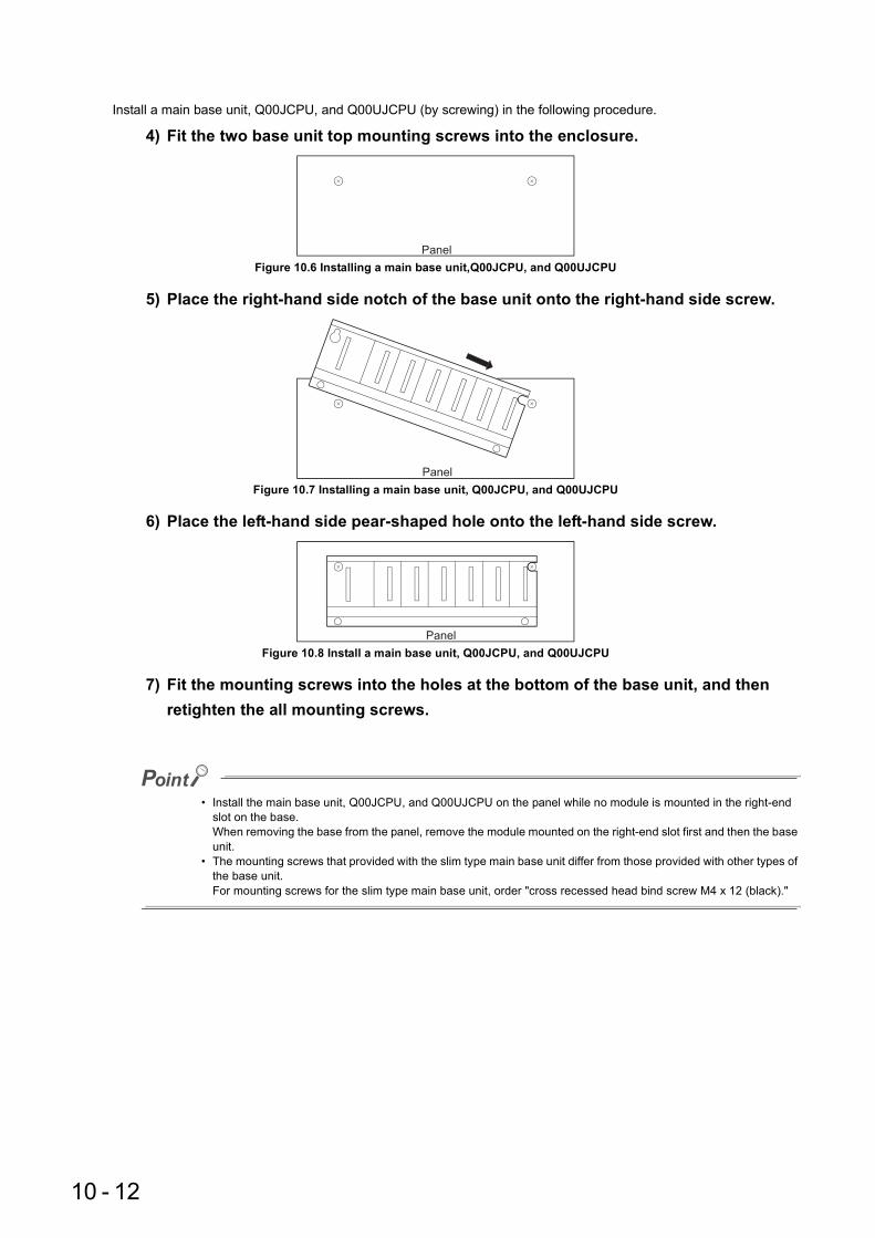
Install a main base unit, Q00JCPU, and Q00UJCPU (by screwing) in the following procedure.
4) Fit the two base unit top mounting screws into the enclosure.
5) Place the right-hand side notch of the base unit onto the right-hand side screw.
6) Place the left-hand side pear-shaped hole onto the left-hand side screw.
7) Fit the mounting screws into the holes at the bottom of the base unit, and then retighten the all mounting screws.
• Install the main base unit, Q00JCPU, and Q00UJCPU on the panel while no module is mounted in the right-end slot on the base.When removing the base from the panel, remove the module mounted on the right-end slot first and then the base unit.
• The mounting screws that provided with the slim type main base unit differ from those provided with other types of the base unit. For mounting screws for the slim type main base unit, order "cross recessed head bind screw M4 x 12 (black)."
Figure 10.6 Installing a main base unit,Q00JCPU, and Q00UJCPU
Figure 10.7 Installing a main base unit, Q00JCPU, and Q00UJCPU
Figure 10.8 Install a main base unit, Q00JCPU, and Q00UJCPU
Panel
Panel
Panel
10 - 12

CHAPTER10 LOADING AND INSTALLATION
9
10
3
4
5
6
7
8
10.3 Module Installation
10.3.1 Precaution on installation
Note the following when mounting a DIN rail.Mounting a DIN rail needs special adaptors (optional), which are user-prepared.
(a) Applicable adaptor typesFor Q38B,Q312B,Q68B,Q612B,Q38RB,Q68RB,Q65WRB,Q38DB,Q312DB : Q6DIN1For Q35B,Q65B,Q00JCPU, Q00UJCPU : Q6DIN2For Q33B,Q52B,Q55B,Q63B,Q32SB,Q33SB,Q35SB : Q6DIN3
(b) Adaptor installation methodThe way to install the adaptors for mounting a DIN rail to the base unit is given in Figure 10.9.
Table10.3 Parts included with DIN rail mounting adaptors
DIN rail mounting adaptors
Quantity of included parts
Adaptor(Large) Adaptor(small)Mounting screw
(M5 10)Square washer Stopper
Q6DIN1 2 4 3 3 2
Q6DIN2 2 3 2 2 2
Q6DIN3 1 2 2 2 2
Figure 10.9 Adaptor installation method
Base unit rear
Place the hook of the adaptor
(small) in the lower hole.
Push the top of the adaptor
(small) far enough until it
"clicks".
Insert the adaptor (large) into the grooves of
the base unit from below.
Push the bottom of the adaptor (large) far enough
until it "clicks".
10 - 13

(c) Applicable DIN rail types (IEC 60715)TH35-7.5FeTH35-7.5AlTH35-15Fe
(d) Distance between DIN rail mounting screwsWhen using DIN rail, DIN rail mounting screws must be inserted in 200 mm (7.88 inches) distances or less in order to ensure that the rail has sufficient strength.
When installing the DIN rail in a frequent vibration and/or shock prone environment, insert the mounting screws in 200mm interrals or less by the following method show below.
<For Q38B, Q312B, Q68B, Q612B, Q38RB, Q68RB, Q65WRB, Q38DB or Q312DB type>Screw the DIN rail in three places using the mounting screws and square washers included with the DIN rail mounting adaptors (hereafter referred to as the adaptors) in ‘Position A’ (bottom of base unit).
Figure 10.10 Distance between DIN rail mounting screws
Figure 10.11 Distance between DIN rail mounting screws
35mm
(1.38 inch)
P=200mm (7.88 inch) or less
DIN rail DIN rail mounting screw
(obtained by user)
P P P
DIN rail
35mm
PP P PStopper
Stopper
A *2B *3 B *3
P=200mm (7.88 inch) or less
Mounting screws (included with adaptors)
Square washers necessary *1Mounting screws (obtained by user)
No square washers
10 - 14

CHAPTER10 LOADING AND INSTALLATION
9
10
3
4
5
6
7
8
10.3 Module Installation
10.3.1 Precaution on installation
<For Q00JCPU, Q00UJCPU, Q33B, Q35B, Q65B, Q52B, Q55B, Q63B, Q32SB, Q33SB or Q35SB type>Screw the DIN rail in two places using the mounting screws and square washers included with the adaptors in ‘Position A’ (bottom of base unit).
*1: The following shows where to position the square washers.
*2: Screw the DIN rail to a control panel using the mounting screws and square washers included with the adaptors in ‘Position A’ (bottom of base unit).
*3: Screw the DIN rail with mounting screws(obtained by user) in ‘Position B’ (Where the base unit is not installed). In this method the supplied mounting screws and square washers are not used.
● Use only one washer for each mounting screw. Use only the square washers supplied with the adaptors.If two or more washers are used together for one mounting screw, the screw may interfere with the base unit.
● Make sure to align the square washer sides with the DIN rail.
● Use the DIN rail that is compatible with M5 size screws.
Figure 10.12 Distance between DIN rail mounting screws
Figure 10.13 Square washer
Figure 10.14 Precautions when mounting a square washer
DIN rail
35mm
P
P=200mm (7.88 inch) or less
P PStopper
Stopper
A *2B *3 B *3
Mounting screws
(included with adaptors)
Square washers necessary *1
Mounting screws (obtained by user)
No square washers
DIN rail
Mounting screws
(M5 10)
Square washer
Side view A
DIN railMounting screws
square washer Mounting side
(e.g. Control panel)
Side view A
DIN railsquare washer DIN railsquare washer
10 - 15

(e) Stopper mountingWhen using the DIN rail in the environment with frequent vibration, use stoppers included with the DIN rail mounting adaptor shown in (a).
Figure 10.15 Fixture mounting procedure
4)
5)
Stopper
(Left side)
4)
5)
Stopper
(Right side)
2)
3)
1)
StopperHook
Hook
Stopper Stopper
Hitch hook to top of
DIN rail
Hitch hook to bottom
of DIN rail
DIN rail
DIN rail
Complete
1)
2)
3)
4)
5)
Loosen the screw at the top of the
stopper. (2 stoppers)
Hitch the lower hook of the stopper
to the bottom of the DIN rail. Install
the stopper with the arrowhead side
facing up.
Hitch the upper hook of the stopper
to the top of the DIN rail.
Slide the stopper to the end of the
base unit so that they are fully in
contact.
Tighten the screw of the stopper
with a screwdriver.
(Tightening torque 1.00 to 1.35N m)
Make sure that the left and right
stoppers are fixed securely to the
DIN rail.
10 - 16
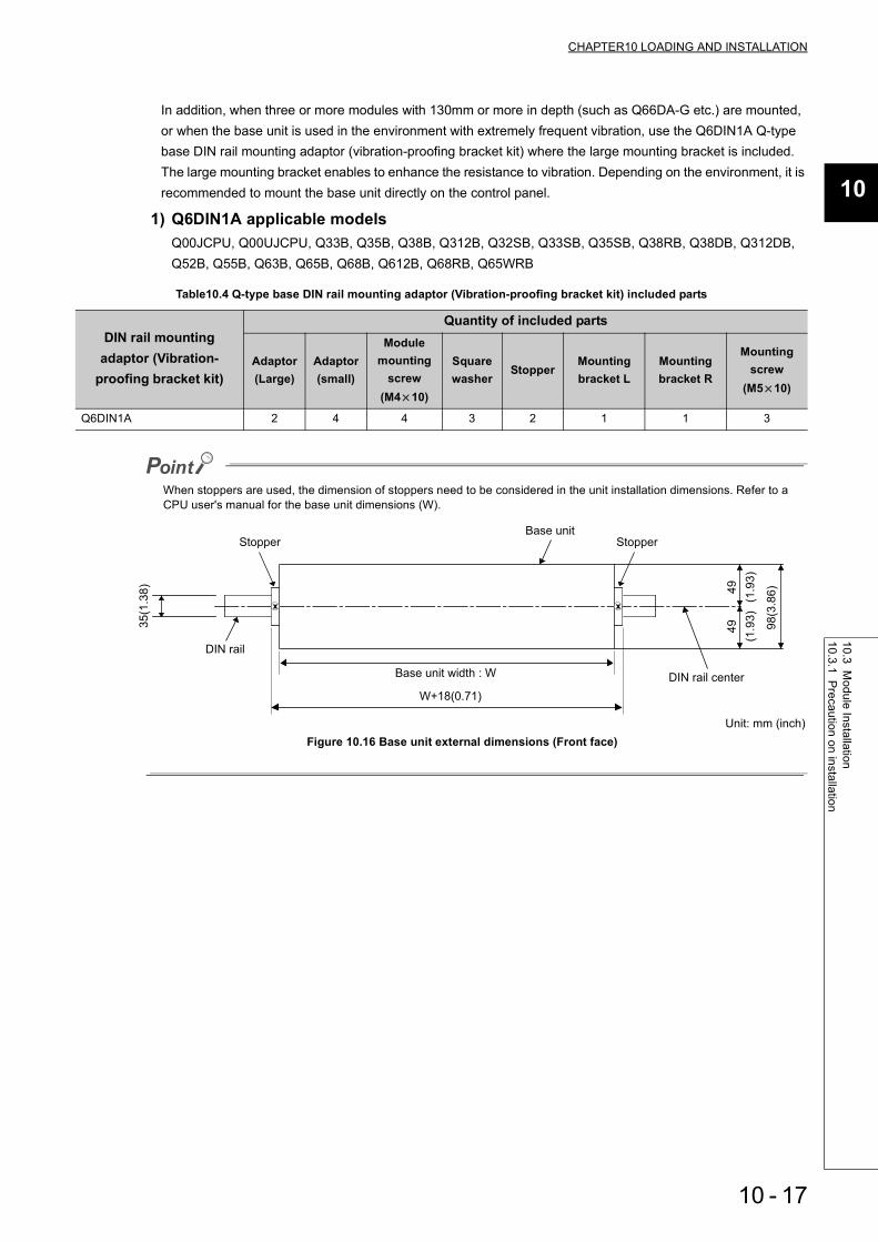
CHAPTER10 LOADING AND INSTALLATION
9
10
3
4
5
6
7
8
10.3 Module Installation
10.3.1 Precaution on installation
In addition, when three or more modules with 130mm or more in depth (such as Q66DA-G etc.) are mounted, or when the base unit is used in the environment with extremely frequent vibration, use the Q6DIN1A Q-type base DIN rail mounting adaptor (vibration-proofing bracket kit) where the large mounting bracket is included. The large mounting bracket enables to enhance the resistance to vibration. Depending on the environment, it is recommended to mount the base unit directly on the control panel.
1) Q6DIN1A applicable modelsQ00JCPU, Q00UJCPU, Q33B, Q35B, Q38B, Q312B, Q32SB, Q33SB, Q35SB, Q38RB, Q38DB, Q312DB, Q52B, Q55B, Q63B, Q65B, Q68B, Q612B, Q68RB, Q65WRB
When stoppers are used, the dimension of stoppers need to be considered in the unit installation dimensions. Refer to a CPU user's manual for the base unit dimensions (W).
Table10.4 Q-type base DIN rail mounting adaptor (Vibration-proofing bracket kit) included parts
DIN rail mounting adaptor (Vibration-
proofing bracket kit)
Quantity of included parts
Adaptor(Large)
Adaptor(small)
Module mounting
screw (M4 10)
Square washer
StopperMounting bracket L
Mounting bracket R
Mounting screw
(M5 10)
Q6DIN1A 2 4 4 3 2 1 1 3
Figure 10.16 Base unit external dimensions (Front face)Unit: mm (inch)
49
49
Base unit
DIN rail
W+18(0.71)
Base unit width : W DIN rail center
35
(1.3
8)
(1.9
3)
98
(3.8
6)
(1.9
3)
Stopper Stopper
10 - 17

(f) Dimensions when DIN rail is attached (Side view).
Figure 10.17 External dimensions (Side face)
7.5D
3
DIN rail depth (D)
Board side
DIN rail adaptor
Base unit
Example) Q64PN Power supply module = 115 (4.53)
Power supply module
DIN rail: TH35-7.5Fe,TH35-7.5Al,TH35-15Fe
TH35-7.5Fe, TH35-7.5Al:7.5 (0.30)
TH35-15Fe:15 (0.59)
(0.1
2)
35
(1
.38
)
(0.30)
98
(3
.86
)
(49
(1
.93
))(4
9 (
1.9
3))
5(0.20)
Unit: mm (inch)
10 - 18

CHAPTER10 LOADING AND INSTALLATION
9
10
3
4
5
6
7
8
10.3 Module Installation
10.3.2 Instructions for mounting the base unit
10.3.2 Instructions for mounting the base unit
When mounting the programmable controller to an enclosure or similar, fully consider its operability, maintainability and environmental resistance.
(1) Module mounting positionKeep the clearances shown in Figure 10.18 or Figure 10.19 between the top/bottom faces of the module and other structures or parts to ensure good ventilation and facilitate module replacement.
(a) In case of main base unit or extension base unit
*1: For wiring duct with 50mm (1.97 inches) or less height. 40mm (1.58 inches) or more for other cases.
*2: 20mm (0.79 inches) or more when the adjacent module is not removed and the extension cable is connected.*3: 80mm (3.15 inches) or more for the connector type. 140mm (5.51 inches) or more for installing a tracking cable when
using a Redundant CPU. 80mm (3.15 inches) or more for installing the Q8BAT cable when using the Q8BAT.*4: 45mm (1.77 inches) or more when the Q7BAT is mounted.*5: 30mm (1.18 inches) or more from the top and bottom of the Q8BAT when the Q8BAT is mounted.*6: 5mm (0.20 inches) or more from the right and left of the Q8BAT when the Q8BAT is mounted.
Figure 10.18 Module mounting position
5mm (0.20 inch) or more 2, 6
Indicates the panel top, wiring duct or any part position.
5mm (0.20 inch) or more 6
Panel
Programmablecontroller
Door
20mm (0.79 inch)or more 3
30mm(1.18 inch)or more 4, 5
30mm(1.18 inch) or more 1, 5
4
5, 6
10 - 19

(b) In case of slim type main base unit
*1: For wiring duct with 50mm (1.97 inches) or less height.40mm (1.58 inches) or more for other cases.
*2: The cable of the power supply module of the slim type main base unit protrudes out of the left end of the module. Install the module while reserving 17mm (0.67 inches) or more wiring space. If the cable sheath is susceptible to damage caused by a structural object or part on the left side of the module, take a protective measure with spiral tube or a similar insulator.
*3: 80mm (3.15 inches) or more for the connector type. 80mm (3.15 inches) or more for installing the Q8BAT cable when using the Q8BAT.
*4: 45mm (1.77 inches) or more when the Q7BAT is mounted.*5: 30mm (1.18 inches) or more from the top and bottom of the Q8BAT when the Q8BAT is mounted.*6: 5mm (0.20 inches) or more from the right and left of the Q8BAT when the Q8BAT is mounted.
(2) Module mounting orientation • Install the programmable controller in the orientation in Figure 10.20 to ensure good ventilation for heat
release.
• Do not mount it in either of the orientations shown in Figure 10.21.
Figure 10.19 Module mounting position
Figure 10.20 Orientation in which modules can be mounted
Figure 10.21 Orientation in which modules cannot be mounted
Indicates the panel top, wiring duct or any part position.
5mm (0.20 inch) or more 6
Panel
Programmable controller
Door
30mm (1.18 inch)or more 4, 5
30mm (1.18 inch)or more 1, 5
20mm (0.79 inch) or more 3
17 mm (0.67 inch) or more 2, 6
5, 6
4
Horizontal installationVertical mounting
10 - 20
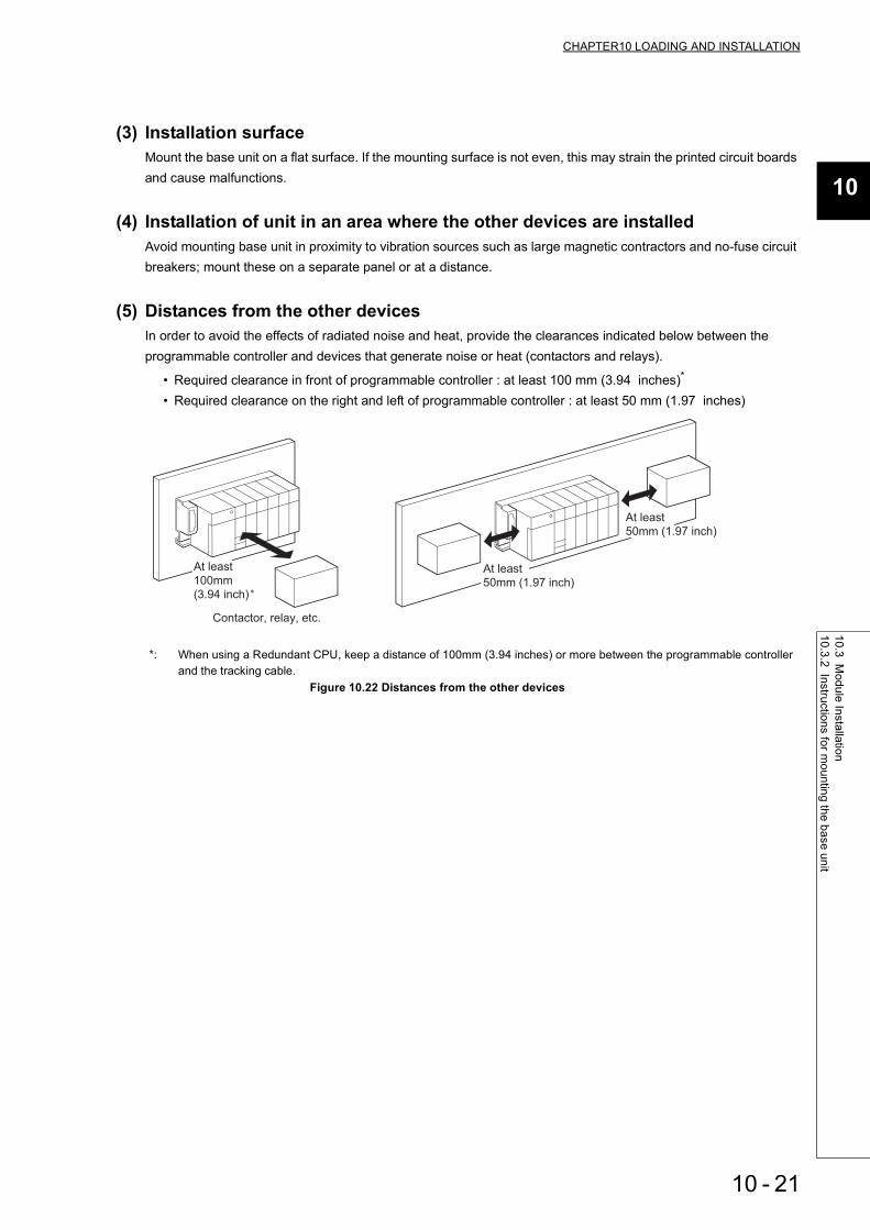
CHAPTER10 LOADING AND INSTALLATION
9
10
3
4
5
6
7
8
10.3 Module Installation
10.3.2 Instructions for mounting the base unit
(3) Installation surfaceMount the base unit on a flat surface. If the mounting surface is not even, this may strain the printed circuit boards and cause malfunctions.
(4) Installation of unit in an area where the other devices are installedAvoid mounting base unit in proximity to vibration sources such as large magnetic contractors and no-fuse circuit breakers; mount these on a separate panel or at a distance.
(5) Distances from the other devicesIn order to avoid the effects of radiated noise and heat, provide the clearances indicated below between the programmable controller and devices that generate noise or heat (contactors and relays).
• Required clearance in front of programmable controller : at least 100 mm (3.94 inches)*
• Required clearance on the right and left of programmable controller : at least 50 mm (1.97 inches)
*: When using a Redundant CPU, keep a distance of 100mm (3.94 inches) or more between the programmable controller and the tracking cable.
Figure 10.22 Distances from the other devices
Contactor, relay, etc.
At least
50mm (1.97 inch)
At least
50mm (1.97 inch)
At least
100mm
(3.94 inch)
10 - 21
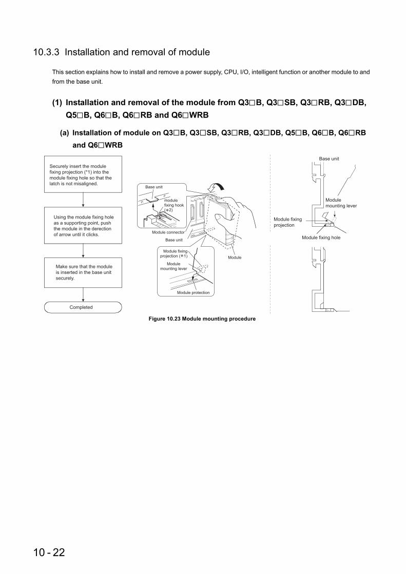
10.3.3 Installation and removal of module
This section explains how to install and remove a power supply, CPU, I/O, intelligent function or another module to and from the base unit.
(1) Installation and removal of the module from Q3 B, Q3 SB, Q3 RB, Q3 DB, Q5 B, Q6 B, Q6 RB and Q6 WRB
(a) Installation of module on Q3 B, Q3 SB, Q3 RB, Q3 DB, Q5 B, Q6 B, Q6 RB and Q6 WRB
Figure 10.23 Module mounting procedure
Module fixing hole
Module fixing
projection
Base unit
Module
mounting lever
Make sure that the module
is inserted in the base unit
securely.
Completed
Module
module fixing hook ( 2)
Base unit
Module protection
Module mounting lever
Module fixing projection ( 1)
Base unit
Module connector
Securely insert the module
fixing projection (*1) into the
module fixing hole so that the
latch is not misaligned.
Using the module fixing hole
as a supporting point, push
the module in the derection
of arrow until it clicks.
10 - 22

CHAPTER10 LOADING AND INSTALLATION
9
10
3
4
5
6
7
8
10.3 Module Installation
10.3.3 Installation and removal of m
odule
*1: If the module has two module fixing projections, insert the two module fixing projections on the right and left into the module fixing holes so that they are not misaligned.
*2: If the module has two module fixing projections on its top, push the center top of the module so that the two module fixing hooks on the right and left are securely engaged with the base unit hooks.
● When mounting the module, always insert the module fixing projection into the module fixing hole of the base unit.At that time, securely insert the module fixing projection so that it does not come off from the module fixing hole.Failure to do so may damage the module connector and module.
● When using the programmable controller in an environment of frequent vibration or impact, secure the CPU module to the base unit using screws.Module fixing screw : M3 X 12 (user-prepared)
● After first use of the product, do not mount or remove the module onto or from the base unit and the terminal block to or from the module more than 50 times (IEC 61131-2 compliant) respectively. Exceeding the limit of 50 times may cause malfunction.
Figure 10.24 Mounting the Q6 RP
Q6 RP
Push
Base unit hook
Module hook
Center top
10 - 23

(b) Removal from Q3 B, Q3 SB, Q3 RB, Q3 DB, Q5 B, Q6 B, Q6 RB, and Q6 WRB
*1: If the module has two module fixing hooks on its top, push the two modules fixing projections on the right and left of the module top simultaneously with your fingers until they stop.
*2: If the module has two fixing projections, remove the two module fixing projections on the right and left of the module bottom from the module fixing holes.
When removing the module which is secured by module fixing screw, remove the module fixing screw first and then module fixing projection off the module fixing hole of the base unit.Failure to do so may damage the module fixing projection.
Figure 10.25 Module removal procedure
Figure 10.26 Q6 RP removal procedure
Completed
Unit/Module
Module connector
Module fixing hole
Base unit
Push
Module fixing hook
Lifting
1
Pull the module based on the
supporting point of module bottom
while pressing the module fixing
hook (*1).
While lifting the module, take off
the module fixing projection (*2)
from the module fixing hole.
Support the module with both
hands and securely press the
module fixing hook(*1) with your
finger.
Push simultaneously
Module fixing projection
10 - 24
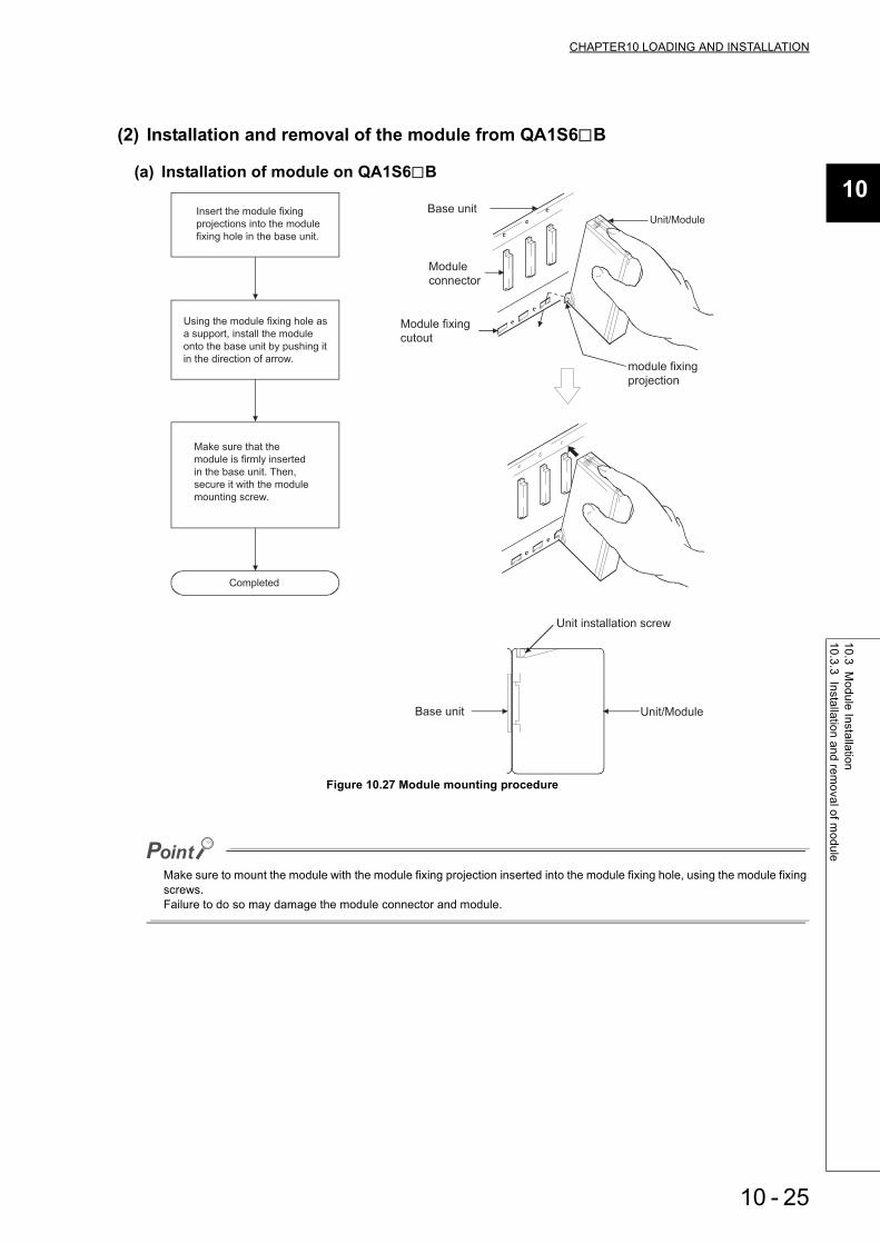
CHAPTER10 LOADING AND INSTALLATION
9
10
3
4
5
6
7
8
10.3 Module Installation
10.3.3 Installation and removal of m
odule
(2) Installation and removal of the module from QA1S6 B
(a) Installation of module on QA1S6 B
Make sure to mount the module with the module fixing projection inserted into the module fixing hole, using the module fixing screws.Failure to do so may damage the module connector and module.
Figure 10.27 Module mounting procedure
Base unit
Module
connector
Module fixing
cutout
Unit/Module
module fixing
projection
Unit installation screw
Unit/ModuleBase unit
Completed
Make sure that the
module is firmly inserted
in the base unit. Then,
secure it with the module
mounting screw.
Insert the module fixing
projections into the module
fixing hole in the base unit.
Using the module fixing hole as
a support, install the module
onto the base unit by pushing it
in the direction of arrow.
10 - 25

(b) Removal from QA1S6 B
When removing the module which is secured by module fixing screw, remove the module fixing screw first and then module fixing projection off the module fixing hole of the base unit.Failure to do so may damage the module fixing projection.
Figure 10.28 Module removal procedure
Base unit
Unit/Module
Completed
Lift the module upwards
and remove the module
fixing projection from the
module fixing hole.
Remove the module
mounting screw, and
using the bottom of the
module as a support,
pull the top of the
module toward you.
Module connector
Module fixing cutout
10 - 26

CHAPTER10 LOADING AND INSTALLATION
9
10
3
4
5
6
7
8
10.3 Module Installation
10.3.3 Installation and removal of m
odule
(3) Installation and removal of modules
(a) Installation of module on QA6 B
10 - 27

For use in an environment with particularly frequent vibrations and/or shock, secure the module to the base with screws. The applicable screw size is M4(0.16) 0.7(0.03) 12mm (0.47 inches). Refer to the figure on the right.
CAUTION
To mount a module, Insert the module fixing projection(s) into the fixinghole(s) in the base unit and press the module until it snaps into place.Incorrect mounting may cause malfunction, failure, or a drop of themodule.When using in an environment of frequent vibrations, secure the modulewith a screw.Tighten the screw within the specified torque range.Undertightning can cause drop of the screw, circuit or malfunction.Overtightning can damage the screw and/or module, resulting in drop,short circuit, or malfunction.
10 - 28

CHAPTER10 LOADING AND INSTALLATION
9
10
3
4
5
6
7
8
10.3 Module Installation
10.3.3 Installation and removal of m
odule
(b) Removal from QA6 B
Disengage the hook from the module fixing hole (A) and then remove the module fixing projection from the module fixing hole (B). Attempting to remove the module forcibly may damage the hook or module fixing projection.
10 - 29

10.4 How to set the Base Number for the Extension Base Unit
When using two or more extension base units, the base number must be set with their base number setting
connectors.*1 (The number of extension bases is set to 1 by factory default.)
*1: Since the Q6 WRB is fixed to the extension 1, extension base No. setting is not required.
(1) Setting the extension base numberSet the extension base number in the following procedure.
1) The base number setting connector of the extension base unit is located under the IN side base cover.
(Setting of the extension number setting connector ( Section 6.1.4))First, loosen the upper and lower screws in the IN side base cover and remove the base cover from the extension base unit.
2) Insert the connector pin in the required base number location of the connector (PIN1) existing between the IN and OUT sides of the extension cable connector.
Figure 10.29 Removing a base cover
Figure 10.30 Setting the number of extension bases
Flat blade screwdriver
Base cover
Extension base unit
Fixing screw
Base cover
Connector pin
10 - 30

CHAPTER10 LOADING AND INSTALLATION
9
10
3
4
5
6
7
8
10.4 How
to set the Base N
umber for the E
xtension Base U
nit
3) Install the base cover to the extension base unit and tighten the base cover screw. (Tightening torque: 0.36 to 0.48N•m)
Set the numbers for extension base units in the order of connecting, starting from the one connected to the main base unit.
Figure 10.31 Base cover removal procedure
Flat blade screwdriverBase cover
Base cover
Extension base unit
Fixing screw
10 - 31

(2) Precautions for setting the extension base numbers
(a) Setting orderSet the extension base number consecutively.In Auto mode, when any extension base number is skipped, no slots will be allocated to an empty extension base so that the slots cannot be reserved.For details of the base mode, refer to the follwoing.
Manuals for the CPU module used (Function Explanation, Program Fundamentals)
Figure 10.32 The number of slots when a extension base number is skipped
Power supply
moduleCPU module
Extension 1
Main base unit
Slot numberCPU 0 1 2 3 4 5 6 7 8 9 10 11
12 13 14 15 16 17 18 19
Extension 20 0 0 0 0 0 0 0
Extension 320 21 22 23 24 25 26 27
Extension base unit
Skipped
stage number
Q312B
Q68B
Q68B
Q68B
10 - 32

CHAPTER10 LOADING AND INSTALLATION
9
10
3
4
5
6
7
8
10.4 How
to set the Base N
umber for the E
xtension Base U
nit
(b) When the same number is setThe same extension number cannot be set.
Figure 10.33 When the same extension number is set
Power supply
moduleCPU module
Extension 1
Main base unit
Slot numberCPU 0 1 2 3 4 5 6 7 8 9 10 11
Extension 1
Extension base unit
Q312B
Q68B
Q68B
The same extension stage
number cannot be set!
Extension stage number
setting connector
10 - 33

(c) When connector pins are connectd in more than 2 positions, or no pin is usedThe extension base unit cannot be used when connector pins for base number setting are inserted in more than two positions and when not using any connector pin.
Figure 10.34 Connector pins are used in 2 positions, and not using any connector pin
Power supply
moduleCPU module
Extension 1
Main base unit
Slot numberCPU 0 1 2 3 4 5 6 7 8 9 10 11
Extension 2
Extension base unit
Q312B
Q68B
Q68B
Connector pin must be inserted!
Connector pins must not be
inserted in 2 or more positions!
10 - 34

CHAPTER10 LOADING AND INSTALLATION
9
10
3
4
5
6
7
8
10.4 How
to set the Base N
umber for the E
xtension Base U
nit
(d) Extension base positioning for AnS/A series-compatible extension base units
(QA1S6 B, QA6 B, and QA6ADP+A5 B/A6 B)When using AnS/A series-compatible extension base units in combination, connect Q5 B/Q6 B closest to
the main base unit, and then QA1S6 B, QA6 B, and then QA6ADP+A5 B/A6 B.
Note that the QA1S6 B and QA6ADP+A5 B/A6 B cannot be used in combination.
*1: When using the QA6ADP+A5 B/A6 B, connect it below the QA6 B.
Figure 10.35 Extension base positioning for the AnS/A series-compatible extension base units
CPU 0 1 2 3 4 5 6 7 8 9 10 11
12 13 14 15 16 17 18 19
20 21 22 23 24 25 26 27
28 29 30 31 32 33 34 35
Q312B
Q68B
QA1S68
QA68B
Main base unit
Slot number
Power supply
module CPU module
Extension base unit
Extension 1 Extension base unit for
mounting module corresponding
to the Q Series
(Q5 B/Q6 B is connected to
the main base unit or Q5 B/
Q6 B.)
Extension base unit for
mounting module corresponding
to the AnS series (QA1S6 B is
connected to the main base unit,
the end of the Q5 B/Q6 B or
QA1S6 B)
Extension base unit for mounting
module corresponding to the A
series 2 (QA6 B is connected to
the main base unit, the end of
the Q5 B/Q6 B/QA1S6 B or
QA6 B)
Extension 2
Extension 3
10 - 35

10.5 Connection and Disconnection of Extension Cable
(1) Instructions for handling an extension cable • Do not step on an extension cable. • Connect the extension cable to the base unit with the base cover installed to the base unit.
(After you have set the extension number to the extension base unit, reinstall and screw the base cover.) • When laying an extension cable, secure 55mm (2.17 inches) or more as the minimum cable bending radius.
If it is less than 55mm (2.17 inches), a malfunction may occur due to characteristic deterioration, cable disconnection or the like.
• The overall length of extension cables must be up to 13.2m (43.31 feet). • Do not install extension cables with the main circuit (high voltage and large current) line. • When connecting or disconnecting an extension cable, do not hold the ferrite cores mounted at both ends of
the cable.Hold the connector part of the cable for connection or disconnection.
Holding the ferrite core may cause the cable disconnection in the connector.Also, if the ferrite core position is shifted, the characteristic will change. When handling the cable, do not to shift the ferrite core position.
Figure 10.36 Connection and Disconnection of Extension Cable
Main base unit
Connector
Extension cable
Ferrite core
10 - 36
CHAPTER10 LOADING AND INSTALLATION
9
10
3
4
5
6
7
8
10.5 Connection and D
isconnection of Extension C
able
(2) Connection of extension cable
When connecting an extension base unit to the main base unit with an extension cable, plug the OUT side connector of the main base unit and the IN side connector of the extension base unit with an extension cable. The system will not operate properly if the extension cable is connected in the form of IN to IN, OUT to OUT or IN to OUT.When connecting two or more extension base units, plug the OUT side connector of the first extension base unit and the IN side connector of the second extension base unit with an extension cable.
• To connect an extension cable to the main base unit, remove the portion under the OUT characters on the
base cover with a tool such as a flat blade screwdriver (5.5 75, 6 100).This also applies to a case where an extension cable is connected to the OUT side connector of the extension base unit.When connecting an extension cable to the Q00JCPU and Q00UJCPU, remove the base cover manually.To remove the base cover, insert the tip of a screwdriver into a clearance below the base cover and pry it up.Be careful not to damage the connector when inserting the screw driver since a connector is located inside the base cover.
Figure 10.37 Connection of extension cable
Main base unit
Base cover
Flat blade screwdriver
Cut at 3 places of thin wall
Extension base unit
Flat blade screwdriver
OUT side of base cover
Cut at 3 places of thin wall
10 - 37
• To connect the extension cable to the next extension base unit, remove the sticker put under the IN characters on the base cover.
• When plugging the extension cable to any base unit, hold the connector part of the extension cable.
• After fitting the extension cable, always tighten the extension cable connector fixing screws.(Tightening torque: 0.20N•m)
(3) Disconnection of extension cableWhen disconnectiong the extension cable, hold and pull the connector part of the extension cable after confirming that the fixing screws have been completely removed.
Figure 10.38 Connection of extension cable
Figure 10.39 Connection of extension cable
Figure 10.40 Connection of extension cable
Extension base unit
Seal
IN side of base cover
Main base unit
Connector
Extension cable
Flat blade screwdriver
Main base unit
Fixing screw
10 - 38

CHAPTER10 LOADING AND INSTALLATION
9
10
3
4
5
6
7
8
10.6 Wiring
10.6.1 Wiring precautions
10.6 Wiring
10.6.1 Wiring precautions
DANGER
Shut off the external power supply for the system in all phases beforewiring. Failure to do so may result in electric shock or damage to the product.
After wiring, attach the included terminal cover to the module beforeturning it on for operation.Failure to do so may result in electric shock.
CAUTION
Ground the FG and LG terminals to the protective ground conductordedicated to the programmable controller.Failure to do so may result in electric shock or malfunction.
Check the rated voltage and terminal layout before wiring to the module,and connect the cables correctly.Connecting a power supply with a different voltage rating or incorrectwiring may cause a fire or failure.
Connectors for external connection must be crimped or pressed with thetool specified by the manufacturer, or must be correctly soldered. Incomplete connections could result in short circuit, fire, or malfunction.
Tighten the terminal screws within the specified torque range. Undertightning can cause short circuit, fire, or malfunction. Overtightening can cause damage the screw and/or module, resulting indrop, short circuit, or malfunction.
Prevent foreign matter such as dust or wire chips from entering themodule. Such foreign matter can cause a fire, failure, or malfunction.
A protective film is attached to the top of the module to prevent foreignmatter, such as wire chips, from entering the module during wiring.Do not remove the film during wiring.Remove it for heat dissipation before system operation.
Mitsubishi programmable controller must be installed in a control panels.Connect the main power supply to the power supply module in thecontrol panel through a relay terminal block.Wiring and replacement of a power supply module must be performed bya maintenance personnel who is familiar with protection againstelectricshock. (For the wiring methods, refer to Section 10.6.2.)
10 - 39

This section describes the precautions for wiring power supply lines.
(1) Wiring power supply lines • Wire the power supply lines for programmable controller, I/O devices, and motor equipment separately as
shown in Figure 10.41. • If there is much noise, such as lightning surge, connect an isolation transformer.
For details on the isolation transformer, refer to the following. Section 9.1.6(3) Isolation transformer
• Taking rated current or inrush current into consideration when wiring the power supply, connect a breaker or an external fuse that have proper blown and detection.When using a single programmable controller, a 10A breaker or an external fuse are recommended for wiring protection.
• Do not connect the 24VDC outputs of two or more power supply modules in parallel to supply power to one I/O module. Parallel connection will damage the power supply modules.
• 100VAC, 200VAC and 24VDC wires must be twisted as dense as possible. Connect the modules with the shortest distance.Also, to reduce the voltage drop to the minimum, use the thickest wires possible (maximum 2mm2).
• Do not bundle the 100VAC and 24VDC wires with, or run them close to, the main circuit (high voltage, large current) and I/O signal lines (including common line). Reserve a distance of at least 100 mm from adjacent wires.
Figure 10.41 Power supply wiring
Figure 10.42 Cautions when connecting a power supply module
100VAC
200VAC
T1
Main power supply
Relay terminal block
I/O power supply
I/O equipment
Inside a control panel
Programmablecontroller powersupply
Isolationtransformer
Programmablecontroller
Motor power supply
Motor equipment
Power supply module I/O module
DC24V
DC24V
Power supply module I/O module
DC24V External power supply
10 - 40

CHAPTER10 LOADING AND INSTALLATION
9
10
3
4
5
6
7
8
10.6 Wiring
10.6.1 Wiring precautions
• Momentary power failure may be detected or the CPU module may be reset due to serge caused by lightening.As measures against serge caused by lightening, connect a surge absorber for lightening as shown in Figure 10.43.Using the surge absorber for lightening can reduce the influence of lightening.
● Separate the ground of the surge absorber for lightening (E1) from that of the programmable controller (E2).
● Select a surge absorber for lightening whose power supply voltage does no exceed the maximum allowable circuit voltage even at the time of maximum power supply voltage elevation.
Figure 10.43 Connecting a lightning surge absorber
E1 E1
AC
E1
E2
Surge absorber for lightening
Programmable
controller
I/O devices
10 - 41

(2) Wiring of I/O equipment • Insulation-sleeved crimping terminals cannot be used with the terminal block.
It is recommended to cover the wire connections of the crimping terminals with mark or insulation tubes.
• The wires used for connection to the terminal block must be 0.3 to 0.75mm2 in core and 2.8mm (0.11 inches) max. in outside diameter.
• Run the input and output lines away from each other. • When the lines cannot be run away from the main circuit and power lines, use a batch-shielded cable and
ground it on the programmable controller side.In some cases, ground it in the opposite side.
• Where wiring runs through piping, ground the piping. • Run the 24VDC input line away from the 100VAC and 200VAC lines. • Wiring of 200m (686.67 feet) or longer will raises current leakage due to the line capacity, resulting in a fault. • To prevent electric shock or malfunction, provide the external power supply for the module to be changed
online with means that can turn the power supply off individually, e.g. a switch. ( Section 12.4)For details, refer to Section 12.5.
• As a countermeasure against the power surge due to lightning, separate the AC wiring and DC wiring and connect a surge absorber for lightning as shown in (1) of item (10.6.1).Failure to do so increases the risk of I/O device failure due to lightning.
Figure 10.44 Wiring of I/O equipmentDC
RA
Programmable
controllerShield cable
Input
Output Shield jacket
10 - 42

CHAPTER10 LOADING AND INSTALLATION
9
10
3
4
5
6
7
8
10.6 Wiring
10.6.1 Wiring precautions
(3) GroundingFor grounding, perform the following:
• Use a dedicated grounding wire as far as possible. (Grounding resistance of 100 or less.) • When a dedicated grounding cannot be provided, use (2) Common grounding shown below.
• For grounding a cable, use the cable of 2 mm2 or more.Position the ground-contact point close to the programmable controller as much as possible so that the length of the grounding cable will be shorten.
Figure 10.45 Grounding procedures(3) Joint grounding Not allowed
Grounding
Programmable controller
Programmable controller
Programmable controller
Another equipment
Another equipment
Another equipment
Grounding
(1) Independent grounding Best (2) Common grounding Good
10 - 43

10.6.2 Connecting to the power supply module
The following figure shows the wiring example of lines such as power lines and grounding lines to the main base unit and extension base units.
(1) Singular power supply system
*1: The operation of the ERR terminal is as fllows.<When the power supply module is mounted on the main base unit>The terminal turns off (opens) when the AC power is not input, a CPU module stop error (including a reset) occurs, or the fuse of the power supply module is blown.<When the power supply module is mounted on the extension base unit>The terminal is always off (opened).
● Use the thickest possible (max. 2 mm2 (14 AWG)) wires for the 100/200VAC and 24VDC power cables. Twist these wires starting at the connection terminals. Use a solderless terminal for wiring a terminal block. To prevent short-circuit due to loosening screws, use the solderless terminals with insulation sleeves of 0.8 mm (0.03 inches) or less. Note that up to two solderless terminals can be connected per terminal block.
● When LG and FG terminals are connected, ground the wires.If not, the programmable controller may become susceptible to noise.Since the LG terminal has a half of the input voltage, touching this terminal may result in electric shock.
● No system error can be detected by the ERR terminal of an extension base unit. (The ERR terminal is always set to off.)
Figure 10.46 Single power supply system wiring example
AC
ACDC
100/110VAC
24VDC
Q61P-A1
Q61P-A1 I/O module
100VAC
FGLGINPUT100-120VAC
FGLGINPUT100-120VAC
Fuse
Connect to 24VDC
terminals of I/O module
that requires 24VDC
internally.
Extension cable
Ground wire
Grounding
Main base unit
(Q38B)
CPU module
Extension base unit
(Q68B)
ERR 1
ERR 1
Terminal blockSolderless terminals
with insulation sleeves
10 - 44

CHAPTER10 LOADING AND INSTALLATION
9
10
3
4
5
6
7
8
10.6 Wiring
10.6.2 Connecting to the pow
er supply module
(2) Redundant power supply system
*2: The operation of the ERR terminal is as fllows.<When the redundant power supply module is mounted on the redundant power main base unit>The terminal turns off (opens) when the AC power is not input, a CPU module stop error (including a reset) occurs, the redundant power supply module fails, or the fuse of the redundant power supply module is blown.<When the redundant power supply module is mounted on the redundant power extension base unit>The terminal turns off (opens) when the redundant power supply module fails.
*3 When input power is supplied to the redundant power supply module mounted on the redundant power main base unit and the redundant power supply module mounted on the redundant power extension base unit simultaneously, the ON (short) timing of the ERR terminal on the redundant power main base unit is later than that of the ERR terminal on the redundant power extension base unit by the initial processing time of the CPU module.
Figure 10.47 Redundant power supply system wiring example
AC
100V/200VAC
AC
100V/200VAC FGLG
Q64RP
Ground wire
Extension cable
Grounding
CPU module
I/O moduleQ64RP
FGLGINPUT
Q64RP
Redundant power main base unit
(Q38RB)
Redundant power extension base unit
(Q68RB)
FGLG
100/200VAC
INPUT100/200VAC
INPUT100/200VAC
INPUT100/200VAC
FGLG
Q64RP
AC
100V/200VAC
AC
100V/200VAC
System BSystem A
ERR 2, 3
ERR 2, 3
ERR 2, 3
ERR 2, 3
10 - 45

● Use the thickest possible (max. 2 mm2 (14 AWG)) wires for the 100/200VAC and 24VDC power cables. Twist these wires starting at the connection terminals. Use a solderless terminal for wiring a terminal block. To prevent short-circuit due to loosening screws, use the solderless terminals with insulation sleeves of 0.8 mm (0.03 inches) or less. Note that up to two solderless terminals can be connected per terminal block.
● Supply power to two redundant power supply modules individually (redundant power supply system).
● When two redundant power supply modules (Q64RP) are placed together and operated as a redundant power supply system, it is recommended to use one of them as an AC power input and connect the other to an uninterruptible power supply to the other.
● When the LG and FG terminals are connected, ground the wires.If not, the programmable controller may become susceptible to noise.Since the LG terminal has a half of the input voltage, touching this termial may result in electric shock.
Terminal blockSolderless terminals
with insulation sleeves
10 - 46

CHAPTER11 MAINTENANCE AND INSPECTION
1
2
11
4
5
6
7
8
CHAPTER11 MAINTENANCE AND INSPECTION
DANGER
Do not touch the terminals while power is on.Doing so will cause electric shock.
Correctly connect the battery connector.Do not charge, disassemble, heat, short-circuit, solder, or throw the battery into the fire.Doing so will cause the battery to produce heat, explode, or ignite, resulting in injury and fire.
Shut off the external power supply for the system in all phases before cleaning the module or retightening the terminal screws or module fixing screws.Failure to do so may result in electric shock.Undertightening the terminal screws can cause short circuit or malfunction.Overtightening can damage the screw and/or module, resulting in drop, short circuit, or malfunction.
11 - 1

In order to use the programmable controller in normal and optimal condition at all times, this section describes items that must be maintained or inspected daily or at regular intervals.
CAUTION
Before performing online operations (especially, program modification, forced output, and operation status change) for the running CPU module from the peripheral connected, read relevant manuals carefully and ensure the safety. Do not disassemble of modify the modules.Doing so may cause failure, malfunction, injury or a fire.
Use any radio communication device such as a cellular phone or PHS (Personal Handy-phone System) more than 25cm (9.85 inches) away in all directions from the programmable controller.Failure to do so may cause malfunction.
Shut off the external power supply for the system in all phases before mounting or removing the module. Failure to do so may cause the module to fail or malfunction.A module can be replaced online (while power is on) on any MELSECNET/H remote I/O station or in the system where a CPU module supporting the online module change function is used.Note that there are restrictions on the modules that can be replaced online, and each module has its predetermined replacement procedure.( Section 12.4.1).
After the first use of the product, do not mount/remove the module to/from the base unit, and the terminal block to/from the module more than 50 times (IEC 61131-2 compliant) respectively.Exceeding the limit of 50 times may cause malfunction.
Do not drop or apply shock to the battery to be installed in the module.Doing so may damage the battery, causing the battery fluid to leak inside the battery.If the battery is dropped or any shock is applied to it, dispose of it without using.
Before handling the module, touch a grounded metal object to discharge the static electricity from the human body.Failure to do so may cause the module to fail or malfunction.
11 - 2

CHAPTER11 MAINTENANCE AND INSPECTION
1
2
11
4
5
6
7
8
11.1 Daily Inspection
11.1 Daily Inspection
The items that must be inspected daily are listed in Table11.1.
*1: For the Q00JCPU and Q00UJCPU, check the POWER LED on the CPU module side.*2: When the Life detection power supply module is used, check the LIFE LED.*3: The Basic model QCPU does not have the MODE LED.*4: The Basic model QCPU does not have the BAT. LED.
Table11.1 Daily inspection
Item Inspection Item Inspection Judgment Criteria Measures
1 Installation of base unitCheck that fixing screws are not loose and the cover is not dislocated.
The screws and cover must be installed securely
Retighten the screws.
2 Installation of I/O moduleCheck that the module is not dislocated and the unit fixing hook is engaged securely.
The module fixing hook must be engaged and installed securely.
Securely engaged the module fixing hook.
3 Connecting conditions
Check for loose terminal screws.
Screws must not be loose. Retighten the terminal screws.
Check for distance between solderless terminals.
The proper clearance must be provided between solderless terminals.
Correct.
Check that the cable connec-tor is not loose.
Connections must no be loose.Retighten the connector fixing screws.
4
Mod
ule
indi
catio
n LE
D
Power supply module
POWER LED*1Check that the LED is on.
The LED must be on (green). (Error if the LED is off or on (red)).
Section 12.2.
Power supply module
LIFE LED*2Check that the LED is on.
The LED must be on (green or orange) or flashing (orange).(Error if the LED is off, on (red), or flashing (red))
CPU module
MODE LED*3 Check that the LED is on.The LED must be on (green).(Error if the LED is off or flash-ing.)
CPU module RUN LED
Check that the LED is on in the RUN status.
The LED must be on. (Error if the LED is off.)
CPU module ERR. LED
Check that the LED is off.The LED must be off. (Error if the LED is on or flashing.)
CPU module
BAT. LED*4 Check that the LED is off.The LED must be off. (Error if the LED is on.)
Input moduleInput LED
Check that the LED turns on and off.
The LED must be on when the input power is turned on.The LED must be off when the input power is turned off.(Error if the LED does not turn on or turn off as indicated above.)
Output moduleOutput LED
Check that the LED turns on and off.
The LED turns on when the output power is turned on.The LED must be off when the output power is turned off.(Error if the LED does not turn on or turn off as indicated above.)
11 - 3

11.2 Periodic Inspection
The items that must be inspected one or two times every 6 months to 1 year are listed below.When the equipment has been relocated or modified, or wiring layout has been changed, perform this inspection.
Periodic Inspection
*1: When AnS/A Series module is included in the system, the judgement criteria will be from 10 to 90 % RH.
Table11.2 Periodic Inspection
Item Inspection Item Inspection Judgment Criteria Measures
1
Am
bien
t env
ironm
ent Ambient temperature
Measure with a thermometer and a hygrometer.Measure corrosive gas.
0 to 55When the sequencer is used in the board, the ambient temperature in the board becomes the ambient temperature.
Ambient humidity 5 to 95 %RH *1
AtmosphereCorrosive gas must not be present.
2 Power voltageMeasure a voltage between the terminals of 100/200VAC and 24VDC.
85 to 132VAC
Change the power supply.170 to 264VAC
15.6 to 31.2VDC
3
Inst
alla
tion Looseness, rattling
Move the module to check for looseness and rattling.
The module must be installed securely.
Retighten the screws.If the CPU, I/O, or power supply module is loose, fix it with screws.
Adhesion of dirt and foreign matter
Check visually.Dirt and foreign matter must not be present.
Remove and clean.
4
Con
nect
ion
Looseness of terminal screws
Try to further tighten screws with a screwdriver.
Screws must not be loose. Retighten the terminal screws.
Proximity of solderless terminals to each other
Check visually.Solderless terminals must be positioned at proper intervals.
Correct.
Looseness of connectors
Check visually. Connectors must not be loose.Retighten the connector fixing screws.
5 Battery
Check the BAT. LED at the front side of the CPU module.
The LED must be off.Replace the battery when the BAT. LED is on.
Check the length of term after purchasing the battery.
Must not be used more than 5 years.
Replace the battery if it has been used more than 5 years.
Check that SM51 or SM52 is turned off using GX Developer in monitor mode.
Must be turned off.Replace the battery when SM51 or SM52 is on.
6 PLC diagnostics Check the Error log.The Error log must not be updated.
Section 12.3.3
7 Maximum scan timeCheck the values of SD526 and SD527 using GX Developer in the monitor mode.
Maximum scan time must be within the allowable range given in the specification of the system.
Specify factors that increase the scan time.(Check the operation status of the trigger signal that passes through a loop if loop positions exist in the sequence program.)
11 - 4

CHAPTER11 MAINTENANCE AND INSPECTION
1
2
11
4
5
6
7
8
11.3 Battery Life and R
eplacement P
rocedure
11.3 Battery Life and Replacement Procedure
The batteries installed in the CPU module and SRAM card are used for data retention of the program memory, standard RAM, and latch device during the power failure. Special relays SM51 and SM52 turn on due to the battery voltage drop. Even if the special relays turn on, the program and retained data are not deleted immediately.After relay SM51 turns on, replace the battery quickly within the backup power time for (3 minutes).
SM51 turns on when the battery voltage drops below the specified value, and remains on even after the voltage is recovered to the normal value.SM52 turns on when the battery voltage drops below the specified value, and turns off when the voltage is recovered to the normal value.After SM51 and/or SM52 turns on, replace the battery quickly.
SM51 and SM52 turn on when the battery voltage of the CPU module or SRAM card is lowered.To identify the specific battery of the memory of which voltage is lowered, check the contents of the special resisters SD51 and SD52.
For details of SD51 and SD52, refer to Section 12.8.
The cases for memory retention by the CPU module battery and the SRAM card battery are described below.The important points are:
● The CPU module battery cannot retain the SRAM card memory.
● The SRAM card battery cannot retain the CPU module memory.
: Retained, : Not retained
Figure 11.1 Bit pattern
Table11.3 Cases for memory retention by the CPU module battery and the SRAM card battery.
Power supply module
Battery of CPU module
SRAM card batteryMemory of CPU
moduleMemory of SRAM
card
On
ConnectedInstalled
Not installed
Not connectedInstalled
Not installed
Off
ConnectedInstalled
Not installed
Not connectedInstalled
Not installed
b3to b4 b2 b1 b0b15
SD51, SD52 Fixed at 0
Battery error for CPU module
Battery alarm for SRAM card
Battery error for SRAM card
When the battery
voltage is low, the
value is "1."
11 - 5

11.3.1 Display of battery consumption and reduction measures of the consumption
(1) Battery consumptionThe battery consumption represents consumption of the CPU module battery energy.*1Note1The larger value of the battery consumption in the table, the more battery per time unit is consumed.The battery consumption depends on the factors of (a) to (c) as follows.The following table shows the relationship of the factors and the battery consumption.
When the standard RAM is set as a storage location for module error log data, battery consumption will be as
shown in Table11.5.
*1: Applicable to the Q02UCPU, Q03UDCPU, Q04UDHCPU, and Q06UDHCPU if the serial numbers (first five digits) are "10012" or later.The current consumption level can be checked by referring to SD118 where the battery consumption value is stored.
*2: For details of the battery life-prolonging function, refer to the following.
( QnUCPU User's Manual (Function Explanation, Program Fundamentals)*3: For details of the module error log function, refer to the following.
( QnUCPU User’s Manual (Function Explanation, Program Fundamentals)
Note1
Table11.4 Battery consumption and causes for determining the consumption
Factors of battery consumption
Battery consumption
(a) Battery life-prolonging
function*2(b) Module error log function*3
(c) Size of file register file in standard RAM (SR)
<Unit: word>
Set ---- ---- 1
Not setNot set
No file registers or 0K < SR 128K 2
128K < SR 384K 3
384K < SR 4
Set Refer to Table11.5.
Table11.5 Battery consumption when module error log data are stored to the standard RAM
(c) Size of file register file in standard RAM
(SR) <Unit: word>
Battery consumption
Q00U/01U/02U/Q03UD(E)/
Q04UD(E)HCPUQ6UD(E)HCPU
Q10UD(E)H/Q13UD(E)H/Q20UD(E)H/Q26UD(E)HC
PU
0K SR 128K 2 3 3
128K < SR 384K ---- 3 4
384K < SR ---- ---- 4
Note11.1The battery consumption value is displayed only for the Universal model QCPU.
Basic Redundant Highperformance Process
11 - 6

CHAPTER11 MAINTENANCE AND INSPECTION
1
2
11
4
5
6
7
8
11.3 Battery Life and R
eplacement P
rocedure11.3.1 D
isplay of battery consumption and reduction m
easures of the consumption
(2) Reduction measures of battery consumptionThe following describes measures for reducing battery consumption.
• Enable the battery life-prolonging function. • When storing a file register in standard the RAM, minimize the file register file. • By performing the latch data backup function (to standard ROM), the battery life-prolonging function will be
enabled independent of the parameter setting.*4
If not powering on the programmable controller for a long period of time for shipment or other reason, back up the data to the standard ROM.
*4: Except when the battery life-prolonging function has already been enabled.
11 - 7

11.3.2 Battery lives of CPU modules
(1) Battery (Q6BAT) lives of Basic model QCPUs
*1: The power-on time ratio indicates the ratio of programmable controller power-on time to one day (24 hours).(When the total power-on time is 12 hours and the total power-off time is 12 hours, the power-on time ratio is 50%.)
*2: The guaranteed value represents a battery life at 70 , which is calculated based on the characteristic values of manufacturere-supplied memories (SRAM) and on the assumption of storage within the ambient temperature range of -25 to 75 (operating ambient temperature of 0 to 55 ).
*3: The actual service value (reference value) represents a battery life that is calculated based on the values measured at storage ambient temperature of 40 . This value is intended for reference only, as it varies with characteristics of the memory.
*4: In the following status, the backup time after power off is 3 minutes.•The battery connector is disconnected.•The lead wire of the battery is broken.
Table11.6 Battery life
CPU module model
Power-on time
ratio*1
Battery life
Guaranteed value *2
Actual service value (Reference
value)*3
After SM52 turned on. (Backup power
time after an
alarm*4)
Q00JCPU
0%26,000 hours
2.96 years43,800 hours
5.00 years710 hours30 days
30%37,142 hours
4.23 years43,800 hours
5.00 years710 hours30 days
50%43,800 hours
5.00 years43,800 hours
5.00 years710 hours30 days
70%43,800 hours
5.00 years43,800 hours
5.00 years710 hours30 days
100%43,800 hours
5.00 years43,800 hours
5.00 years710 hours30 days
Q00CPU
0%26,000 hours
2.96 years43,800 hours
5.00 years710 hours30 days
30%37,142 hours
4.23 years43,800 hours
5.00 years710 hours30 days
50%43,800 hours
5.00 years43,800 hours
5.00 years710 hours30 days
70%43,800 hours
5.00 years43,800 hours
5.00 years710 hours30 days
100%43,800 hours
5.00 years43,800 hours
5.00 years710 hours30 days
Q01CPU
0%5,600 hours0.63 years
25,175 hours2.87 years
420 hours18 days
30%8,000 hours0.91 years
35,964 hours4.10 years
420 hours18 days
50%11,200 hours1.27 years
43,800 hours5.00 years
420 hours18 days
70%18,666 hours
2.13 years43,800 hours
5.00 years420 hours18 days
100%43,800 hours
5.00 years43,800 hours
5.00 years420 hours18 days
11 - 8

CHAPTER11 MAINTENANCE AND INSPECTION
1
2
11
4
5
6
7
8
11.3 Battery Life and R
eplacement P
rocedure11.3.2 B
attery lives of CP
U m
odules
● Do not use the battery exceeding the guaranteed value of the battery life.
● When the battery may be used exceeding the guaranteed value of the battery life, take the following measures. • Perform ROM operation to protect a program even if the battery dies at the programmable controller power-off. • Back up programs and data after SM52 turned on (within the backup power time after an alarm).
● When the battery (Q6BAT) is not connected to the CPU module, its service life is five years.
● When the battery-low special relay SM52 turns on, immediately change the battery.Even if an alarm has not yet occurred, it is recommended to replace the battery periodically according to the operating condition.
● The battery (Q7BAT and Q8BAT) is not available for the Basic model QCPU.
11 - 9

(2) Battery (Q6BAT, Q7BAT and Q8BAT) lives of High Performance model QCPU, Process CPU, and Redundant CPU
Table11.7 Battery life
CPU module model
Power-on time ratio*1
Battery life*5
Q6BAT Q7BAT
Guaranteed value*2
Actual service value
(Reference value)*3
After SM52 turned on.(Backup
power time after an alarm*4)
Guaranteed value*2
Actual service value
(Reference value)*3
After SM52 turned on.(Backup
power time after an alarm*4)
Q02CPU
0%30,000 hours
3.42 years43,800 hours
5.00 years120 hours
5 days43,800 hours
5.00 years43,800 hours
5.00 years240 hours10 days
30%42,857 hours
4.89 years43,800hours5.00 years
120 hours5 days
43,800 hours5.00 years
43,800 hours5.00 years
240 hours10 days
50%43,800 hours
5.00 years43,800 hours
5.00 years120 hours
5 days43,800 hours
5.00 years43,800hours5.00 years
240 hours10 days
70%43,800 hours
5.00 years43,800 hours
5.00 years120 hours
5 days43,800 hours
5.00 years43,800 hours
5.00 years240 hours10 days
100%43,800 hours
5.00 years43,800 hours
5.00 years120 hours
5 days43,800 hours
5.00 years43,800 hours
5.00 years240 hours10 days
Q02HCPUQ06HCPU
0%2,341 hours0.26 years
18,364 hours2.09 years
120 hours5 days
5,000 hours0.57 years
43,800 hours5.00 years
240 hours10 days
30%3,344 hours0.38 years
26,234 hours2.99 years
120 hours5 days
7,142 hours0.81 years
43,800 hours5.00 years
240 hours10 days
50%4,682 hours0.53 years
36,728 hours4.19 years
120 hours5 days
10,000 hours1.14 years
43,800 hours5.00 years
240 hours10 days
70%7,803 hours0.89 years
43,800 hours5.00 years
120 hours5 days
16,666 hours1.90 years
43,800 hours5.00 years
240 hours10 days
100%43,800 hours
5.00 years43,800 hours
5.00 years120 hours
5 days43,800 hours
5.00 years43,800 hours
5.00 years240 hours10 days
Q02PHCPUQ06PHCPU
0%1,897 hours0.21 years
14,229 hours1.62 years
96hours4 days
4,051 hours0.46 years
38,727 hours4.42 years
192 hours8 days
30%2,710 hours0.30 years
20,327 hours2.32 years
96hours4 days
5,787 hours0.66 years
43,800 hours5.00 years
192 hours8 days
50%3,794 hours0.43 years
28,458 hours3.25 years
96 hours4 days
8,102 hours0.92 years
43,800 hours5.00 years
192 hours8 days
70%6,323 hours0.72 years
43,800 hours5.00 years
96 hours4 days
13,503 hours1.54 years
43,800 hours5.00 years
192 hours8 days
100%43,800 hours
5.00 years43,800 hours
5.00 years9 hours4 days
43,800 hours5.00 years
43,800 hours5.00 years
192 hours8 days
Q12HCPUQ25HCPU
Q12PHCPUQ25PHCPU
Q12PRHCPUQ25PRHCPU
0%1,260 hours0.14 years
7,755 hours0.88 years
48 hours 2 days
2,900 hours0.33 years
21,107 hours2.40 years
96 hours4 days
30%1,800 hours0.20 years
11,079 hours1.26 years
48 hours2 days
4,142 hours0.47 years
30,153 hours3.44 years
96 hours4 days
50%2,520 hours0.28 years
15,510 hours1.77 years
48 hours2 days
5,800 hours0.66 years
42,214 hours4.81 years
96 hours4 days
70%4,200 hours0.47 years
25,850 hours2.95 years
48 hours2 days
9,666 hours1.10 years
43,800 hours5.00 years
96 hours4 days
100%43,800 hours
5.00 years43,800 hours
5.00 years48 hours2 days
43,800 hours5.00 years
43,800 hours5.00 years
96 hours4 days
11 - 10

CHAPTER11 MAINTENANCE AND INSPECTION
1
2
11
4
5
6
7
8
11.3 Battery Life and R
eplacement P
rocedure11.3.2 B
attery lives of CP
U m
odules
CPU module model Power-on time ratio*1
Battery life*5
Q8BAT
Guaranteed value*2Actual service value (Reference value)*3
After SM52 turned on.(Backup power time
after an alarm*4)
Q02CPU
0%43,800 hours
5.00 years43,800 hours
5.00 years240 hours10 days
30%43,800 hours
5.00 years43,800 hours
5.00 years240 hours10 days
50%43,800 hours
5.00 years43,800 hours
5.00 years240 hours10 days
70%43,800 hours
5.00 years43,800 hours
5.00 years240 hours10 days
100%43,800 hours
5.00 years43,800 hours
5.00 years240 hours10 days
Q02HCPUQ06HCPU
0%20,498 hours
2.34 years43,800 hours
5.00 years240 hours10 days
30%29,959 hours
3.42 years43,800 hours
5.00 years240 hours10 days
50%41,785 hours
4.77 years43,800 hours
5.00 years240 hours10 days
70%43,800 hours
5.00 years43,800 hours
5.00 years240 hours10 days
100%43,800 hours
5.00 years43,800 hours
5.00 years240 hours10 days
Q02PHCPUQ06PHCPU
0%16,609 hours
1.89 years43,800 hours
5.00 years192 hours
8 days
30%23,727 hours
2.70 years43,800 hours
5.00 years192 hours
8 days
50%33,218 hours
3.79 years43,800 hours
5.00 years192 hours
8 days
70%43,800 hours
5.00 years43,800 hours
5.00 years192 hours
8 days
100%43,800 hours
5.00 years43,800 hours
5.00 years192 hours
8 days
Q12HCPUQ25HCPU
Q12PHCPUQ25PHCPU
Q12PRHCPUQ25PRHCPU
0%11,038 hours
1.26 years29,609 hours
3.38 years96 hours4 days
30%16,200 hours
1.80 years42,311 hours
4.83 years96 hours4 days
50%22,075 hours
2.52 years43,800 hours
5.00 years96 hours4 days
70%37,055 hours
4.23 years43,800 hours
5.00 years96 hours4 days
100%43,800 hours
5.00 years43,800 hours
5.00 years96 hours4 days
11 - 11

*1: The power-on time ratio indicates the ratio of programmable controller power-on time to one day (24 hours).(When the total power-on time is 12 hours and the total power-off time is 12 hours, the power-on time ratio is 50%.)
*2: The guaranteed value represents a battery life at 70 , which is calculated based on the characteristic values of manufacturer-supplied memories (SRAM) and on the assumption of storage ambient temperature range of -25 to 75 (operating ambient temperature of 0 to 55 ).
*3: The actual service value (reference value) represents a battery life that is calculated based on the values measured at storage ambient temperature of 40 . This value is intended for reference only, as it varies with characteristics of the memory.
*4: In the following status, the backup time after power off is 3 minutes.• The battery connector is disconnected.• The lead wire of the battery is broken.
*5: For the High Performance model QCPU, these values are applicable when the serial number (first five digits) of the CPU module is "05011" or later.For the battery life of the CPU module with a serial number (first five digits) is "05010" or earlier, refer to Appendix 2.3.
● Do not use the battery exceeding the guaranteed value of the battery life.
● When the battery may be used exceeding the guaranteed value of the battery life, take the following measures. • Perform ROM operation to protect a program even if the battery dies at the programmable controller power-off. • Back up programs and data after SM52 turned on (within the backup power time after an alarm).
● When the battery (Q6BAT, Q7BAT and Q8BAT) is not connected to the CPU module, its service life is five years.
● When the battery-low special relay SM52 turns on, immediately change the battery.Even if an alarm has not yet occurred, it is recommended to replace the battery periodically according to the operating condition.
11 - 12

CHAPTER11 MAINTENANCE AND INSPECTION
1
2
11
4
5
6
7
8
11.3 Battery Life and R
eplacement P
rocedure11.3.2 B
attery lives of CP
U m
odules
(3) Battery (Q6BAT, Q7BAT and Q8BAT) lives of the Universal model QCPU
Table11.8 Battery life
CPU module model
Battery consumption*1
Power-on time ratio*2
Battery lifeQ6BAT
Guaranteed value*3 Actual service value (Reference Value)*4
After SM52 turned on.
(Backup power time after an alarm*5)
Q00U(J)CPUQ01UCPUQ02UCPU
Q03UD(E)CPU
1
0%30,100 hours
3.44 years43,800 hours
5.00 years600 hours25 days
30%43,000 hours
4.91 years43,800 hours
5.00 years600 hours25 days
50%43,800 hours
5.00 years43,800 hours
5.00 years600 hours25 days
70%43,800 hours
5.00 years43,800 hours
5.00 years600 hours25 days
100%43,800 hours
5.00 years43,800 hours
5.00 years600 hours25 days
2
0%25,300 hours
2.89 years43,800 hours
5.00 years600 hours25 days
30%36,100 hours
4.12 years43,800 hours
5.00 years600 hours25 days
50%43,800 hours
5.00 years43,800 hours
5.00 years600 hours25 days
70%43,800 hours
5.00 years43,800 hours
5.00 years600 hours25 days
100%43,800 hours
5.00 years43,800 hours
5.00 years600 hours25 days
Q04UD(E)HCPU
1
0%30,100 hours
3.44 years43,800 hours
5.00 years600 hours25 days
30%43,000 hours
4.91 years43,800 hours
5.00 years600 hours25 days
50%43,800 hours
5.00 years43,800 hours
5.00 years600 hours25 days
70%43,800 hours
5.00 years43,800 hours
5.00 years600 hours25 days
100%43,800 hours
5.00 years43,800 hours
5.00 years600 hours25 days
2
0%4,300 hours0.49 years
32,100 hours3.66 years
384hours16 days
30%6,100 hours0.70 years
43,800 hours5.00 years
384hours16 days
50%8,600 hours0.98 years
43,800 hours5.00 years
384hours16 days
70%14,300 hours
1.63 years43,800 hours
5.00 years384hours16 days
100%43,800 hours
5.00 years43,800 hours
5.00 years384hours16 days
11 - 13

Table11.8 Battery life
CPU module model
Battery consumption*1
Power-on time ratio*2
Battery lifeQ6BAT
Guaranteed value*3 Actual service value (Reference Value)*4
After SM52 turned on.
(Backup power time after an alarm*5)
Q06UD(E)HCPU
1
0%25,300 hours
2.89 years43,800 hours
5.00 years600 hours25 days
30%36,100 hours
4.12 years43,800 hours
5.00 years600 hours25 days
50%43,800 hours
5.00 years43,800 hours
5.00 years600 hours25 days
70%43,800 hours
5.00 years43,800 hours
5.00 years600 hours25 days
100%43,800 hours
5.00 years43,800 hours
5.00 years600 hours25 days
2
0%4,200 hours0.48 years
32,100 hours3.66 years
384 hours16 days
30%6,000 hours0.68 years
43,800 hours5.00 years
384 hours16 days
50%8,400 hours0.96 years
43,800 hours5.00 years
384 hours16 days
70%14,000 hours
1.60 years43,800 hours
5.00 years384 hours16 days
100%43,800 hours
5.00 years43,800 hours
5.00 years384 hours16 days
3
0%2,300 hours0.26 years
19,200 hours2.19 years
192 hours8 days
30%3,200 hours0.37 years
27,400 hours3.13 years
192 hours8 days
50%4,600 hours0.53 years
38,400 hours4.38 years
192 hours8 days
70%7,600 hours0.87years
43,800 hours5.00 years
192 hours8 days
100%43,800 hours
5.00 years43,800 hours
5.00 years192 hours
8 days
11 - 14

CHAPTER11 MAINTENANCE AND INSPECTION
1
2
11
4
5
6
7
8
11.3 Battery Life and R
eplacement P
rocedure11.3.2 B
attery lives of CP
U m
odules
Table11.8 Battery life
CPU module model
Battery consumption*1
Power-on time ratio*2
Battery lifeQ6BAT
Guaranteed value*3 Actual service value (Reference Value)*4
After SM52 turned on.
(Backup power time after an alarm*5)
Q10UD(E)HCPUQ13UD(E)HCPUQ20UD(E)HCPUQ26UD(E)HCPU
1
0%22,600 hours
2.58 years43,800 hours
5.00 years600 hours25 days
30%32,200 hours
3.68 years43,800 hours
5.00 years600 hours25 days
50%43,800 hours
5.00 years43,800 hours
5.00 years600 hours25 days
70%43,800 hours
5.00 years43,800 hours
5.00 years600 hours25 days
100%43,800 hours
5.00 years43,800 hours
5.00 years600 hours25 days
2
0%4,100 hours0.47 years
26,200 hours2.99 years
384 hours16 days
30%5,800 hours0.66 years
37,400 hours4.27 years
384 hours16 days
50%8,200 hours0.94 years
43,800 hours5.00 years
384 hours16 days
70%13,600 hours
1.55 years43,800 hours
5.00 years384 hours16 days
100%43,800 hours
5.00 years43,800 hours
5.00 years384 hours16 days
3
0%2,300 hours0.26 years
18,600 hours2.12 years
192 hours8 days
30%3,200 hours0.37 years
26,500 hours3.03 years
192 hours8 days
50%4,600 hours0.53 years
37,200 hours4.25 years
192 hours8 days
70%7,600 hours0.87 years
43,800 hours5.00 years
192 hours8 days
100%43,800 hours
5.00 years43,800 hours
5.00 years192 hours
8 days
4
0%1,500 hours0.17 years
13,800 hours1.58 years
144 hours6 days
30%2,100 hours0.24 years
19,700 hours2.25 years
144 hours6 days
50%3,000 hours0.34 years
27,600 hours3.15 years
144 hours6 days
70%5,000 hours0.57 years
43,800 hours5.00 years
144 hours6 days
100%43,800 hours
5.00 years43,800 hours
5.00 years144 hours
6 days
11 - 15

Table11.8 Battery life
CPU module model
Battery consumption*1
Power-on time ratio*2
Battery lifeQ7BAT
Guaranteed value*3 Actual service value (Reference Value)*4
After SM52 turned on.
(Backup power time after an alarm*5)
Q00U(J)CPUQ01UCPUQ02UCPU
Q03UD(E)CPU
1
0%43,800 hours
5.00 years43,800 hours
5.00 years600 hours25 days
30%43,800 hours
5.00 years43,800 hours
5.00 years600 hours25 days
50%43,800 hours
5.00 years43,800 hours
5.00 years600 hours25 days
70%43,800 hours
5.00 years43,800 hours
5.00 years600 hours25 days
100%43,800 hours
5.00 years43,800 hours
5.00 years600 hours25 days
2
0%43,800 hours
5.00 years43,800 hours
5.00 years600 hours25 days
30%43,800 hours
5.00 years43,800 hours
5.00 years600 hours25 days
50%43,800 hours
5.00 years43,800 hours
5.00 years600 hours25 days
70%43,800 hours
5.00 years43,800 hours
5.00 years600 hours25 days
100%43,800 hours
5.00 years43,800 hours
5.00 years600 hours25 days
Q04UD(E)HCPU
1
0%43,800 hours
5.00 years43,800 hours
5.00 years600 hours25 days
30%43,800 hours
5.00 years43,800 hours
5.00 years600 hours25 days
50%43,800 hours
5.00 years43,800 hours
5.00 years600 hours25 days
70%43,800 hours
5.00 years43,800 hours
5.00 years600 hours25 days
100%43,800 hours
5.00 years43,800 hours
5.00 years600 hours25 days
2
0%11,700 hours
1.34 years43,800 hours
5.00 years600 hours25 days
30%16,700 hours
1.91 years43,800 hours
5.00 years600 hours25 days
50%23,400 hours
2.67 years43,800 hours
5.00 years600 hours25 days
70%39,000 hours
4.45 years43,800 hours
5.00 years600 hours25 days
100%43,800 hours
5.00 years43,800 hours
5.00 years600 hours25 days
11 - 16

CHAPTER11 MAINTENANCE AND INSPECTION
1
2
11
4
5
6
7
8
11.3 Battery Life and R
eplacement P
rocedure11.3.2 B
attery lives of CP
U m
odules
Table11.8 Battery life
CPU module model
Battery consumption*1
Power-on time ratio*2
Battery lifeQ7BAT
Guaranteed value*3 Actual service value (Reference Value)*4
After SM52 turned on.
(Backup power time after an alarm*5)
Q06UD(E)HCPU
1
0%43,800 hours
5.00 years43,800 hours
5.00 years600 hours25 days
30%43,800 hours
5.00 years43,800 hours
5.00 years600 hours25 days
50%43,800 hours
5.00 years43,800 hours
5.00 years600 hours25 days
70%43,800 hours
5.00 years43,800 hours
5.00 years600 hours25 days
100%43,800 hours
5.00 years43,800 hours
5.00 years600 hours25 days
2
0%11,400 hours1.30 years
43,800 hours5.00 years
600 hours25 days
30%16,200 hours
1.85 years43,800 hours
5.00 years600 hours25 days
50%22,800 hours
2.60 years43,800 hours
5.00 years600 hours25 days
70%38,000 hours
4.34 years43,800 hours
5.00 years600 hours25 days
100%43,800 hours
5.00 years43,800 hours
5.00 years600 hours25 days
3
0%5,000 hours0.57 years
43,800 hours5.00 years
600 hours25 days
30%7,100 hours0.81 years
43,800 hours5.00 years
600 hours25 days
50%10,000 hours
1.14 years43,800 hours
5.00 years600 hours25 days
70%16,600 hours
1.89 years43,800 hours
5.00 years600 hours25 days
100%43,800 hours
5.00 years43,800 hours
5.00 years600 hours25 days
11 - 17

Table11.8 Battery life
CPU module model
Battery consumption*1
Power-on time ratio*2
Battery lifeQ7BAT
Guaranteed value*3 Actual service value (Reference Value)*4
After SM52 turned on.
(Backup power time after an alarm*5)
Q10UD(E)HCPUQ13UD(E)HCPUQ20UD(E)HCPUQ26UD(E)HCPU
1
0%43,800 hours
5.00 years43,800 hours
5.00 years600 hours25 days
30%43,800 hours
5.00 years43,800 hours
5.00 years600 hours25 days
50%43,800 hours
5.00 years43,800 hours
5.00 years600 hours25 days
70%43,800 hours
5.00 years43,800 hours
5.00 years600 hours25 days
100%43,800 hours
5.00 years43,800 hours
5.00 years600 hours25 days
2
0%11,100 hours
1.27 years43,800 hours
5.00 years600 hours25 days
30%15,800 hours
1.80 years43,800 hours
5.00 years600 hours25 days
50%22,200 hours
2.53 years43,800 hours
5.00 years600 hours25 days
70%37,000 hours
4.22 years43,800 hours
5.00 years600 hours25 days
100%43,800 hours
5.00 years43,800 hours
5.00 years600 hours25 days
3
0%5,000 hours0.57 years
43,800 hours5.00 years
600 hours25 days
30%7,100 hours0.81 years
43,800 hours5.00 years
600 hours25 days
50%10,000 hours
1.14 years43,800 hours
5.00 years600 hours25 days
70%16,600 hours
1.89 years43,800 hours
5.00 years600 hours25 days
100%43,800 hours
5.00 years43,800 hours
5.00 years600 hours25 days
4
0%3,700 hours0.42 years
36,100 hours4.12 years
432 hours18 days
30%5,200 hours0.59 years
43,800 hours5.00 years
432 hours18 days
50%7,400 hours0.84 years
43,800 hours5.00 years
432 hours18 days
70%12,300 hours
1.40 years43,800 hours
5.00 years432 hours18 days
100%43,800 hours
5.00 years43,800 hours
5.00 years432 hours18 days
11 - 18

CHAPTER11 MAINTENANCE AND INSPECTION
1
2
11
4
5
6
7
8
11.3 Battery Life and R
eplacement P
rocedure11.3.2 B
attery lives of CP
U m
odules
Table11.8 Battery life
CPU module model
Battery consumption*1
Power-on time ratio*2
Battery lifeQ8BAT
Guaranteed value*3 Actual service value (Reference Value)*4
After SM52 turned on.
(Backup power time after an alarm*5)
Q00U(J)CPUQ01UCPUQ02UCPU
Q03UD(E)CPU
1
0%43,800 hours
5.00 years43,800 hours
5.00 years600 hours25 days
30%43,800 hours
5.00 years43,800 hours
5.00 years600 hours25 days
50%43,800 hours
5.00 years43,800 hours
5.00 years600 hours25 days
70%43,800 hours
5.00 years43,800 hours
5.00 years600 hours25 days
100%43,800 hours
5.00 years43,800 hours
5.00 years600 hours25 days
2
0%43,800 hours
5.00 years43,800 hours
5.00 years600 hours25 days
30%43,800 hours
5.00 years43,800 hours
5.00 years600 hours25 days
50%43,800 hours
5.00 years43,800 hours
5.00 years600 hours25 days
70%43,800 hours
5.00 years43,800 hours
5.00 years600 hours25 days
100%43,800 hours
5.00 years43,800 hours
5.00 years600 hours25 days
Q04UD(E)HCPU
1
0%43,800 hours
5.00 years43,800 hours
5.00 years600 hours25 days
30%43,800 hours
5.00 years43,800 hours
5.00 years600 hours25 days
50%43,800 hours
5.00 years43,800 hours
5.00 years600 hours25 days
70%43,800 hours
5.00 years43,800 hours
5.00 years600 hours25 days
100%43,800 hours
5.00 years43,800 hours
5.00 years600 hours25 days
2
0%38,800 hours
4.43 years43,800 hours
5.00 years600 hours25 days
30%43,800 hours
5.00 years43,800 hours
5.00 years600 hours25 days
50%43,800 hours
5.00 years43,800 hours
5.00 years600 hours25 days
70%43,800 hours
5.00 years43,800 hours
5.00 years600 hours25 days
100%43,800 hours
5.00 years43,800 hours
5.00 years600 hours25 days
11 - 19

Table11.8 Battery life
CPU module model
Battery consumption*1
Power-on time ratio*2
Battery lifeQ8BAT
Guaranteed value*3 Actual service value (Reference Value)*4
After SM52 turned on.
(Backup power time after an alarm*5)
Q06UD(E)HCPU
1
0%43,800 hours
5.00 years43,800 hours
5.00 years600 hours25 days
30%43,800 hours
5.00 years43,800 hours
5.00 years600 hours25 days
50%43,800 hours
5.00 years43,800 hours
5.00 years600 hours25 days
70%43,800 hours
5.00 years43,800 hours
5.00 years600 hours25 days
100%43,800 hours
5.00 years43,800 hours
5.00 years600 hours25 days
2
0%37,900 hours
4.33 years43,800 hours
5.00 years600 hours25 days
30%43,800 hours
5.00 years43,800 hours
5.00 years600 hours25 days
50%43,800 hours
5.00 years43,800 hours
5.00 years600 hours25 days
70%43,800 hours
5.00 years43,800 hours
5.00 years600 hours25 days
100%43,800 hours
5.00 years43,800 hours
5.00 years600 hours25 days
3
0%20,500 hours
2.34 years43,800 hours
5.00 years600 hours25 days
30%29,200 hours
3.33 years43,800 hours
5.00 years600 hours25 days
50%41,000 hours
4.68 years43,800 hours
5.00 years600 hours25 days
70%43,800 hours
5.00 years43,800 hours
5.00 years600 hours25 days
100%43,800 hours
5.00 years43,800 hours
5.00 years600 hours25 days
11 - 20

CHAPTER11 MAINTENANCE AND INSPECTION
1
2
11
4
5
6
7
8
11.3 Battery Life and R
eplacement P
rocedure11.3.2 B
attery lives of CP
U m
odules
Table11.8 Battery life
CPU module model
Battery consumption*1
Power-on time ratio*2
Battery lifeQ8BAT
Guaranteed value*3 Actual service value (Reference Value)*4
After SM52 turned on.
(Backup power time after an alarm*5)
Q10UD(E)HCPUQ13UD(E)HCPUQ20UD(E)HCPUQ26UD(E)HCPU
1
0%43,800 hours
5.00 years43,800 hours
5.00 years600 hours25 days
30%43,800 hours
5.00 years43,800 hours
5.00 years600 hours25 days
50%43,800 hours
5.00 years43,800 hours
5.00 years600 hours25 days
70%43,800 hours
5.00 years43,800 hours
5.00 years600 hours25 days
100%43,800 hours
5.00 years43,800 hours
5.00 years600 hours
25days
2
0%37,000 hours
4.22 years43,800 hours
5.00 years600 hours25 days
30%43,800 hours
5.00 years43,800 hours
5.00 years600 hours25 days
50%43,800 hours
5.00 years43,800 hours
5.00 years600 hours25 days
70%43,800 hours
5.00 years43,800 hours
5.00 years600 hours25 days
100%43,800 hours
5.00 years43,800 hours
5.00 years600 hours25 days
3
0%20,200 hours
2.31 years43,800 hours
5.00 years600 hours25 days
30%28,800 hours
3.29 years43,800 hours
5.00 years600 hours25 days
50%40,400 hours
4.61 years43,800 hours
5.00 years600 hours25 days
70%43,800 hours
5.00 years43,800 hours
5.00 years600 hours25 days
100%43,800 hours
5.00 years43,800 hours
5.00 years600 hours25 days
4
0%14,000 hours
1.60 years43,800 hours
5.00 years600 hours25 days
30%20,000 hours
2.28 years43,800 hours
5.00 years600 hours25 days
50%28,000 hours
3.20 years43,800 hours
5.00 years600 hours25 days
70%43,800 hours
5.00 years43,800 hours
5.00 years600 hours25 days
100%43,800 hours
5.00 years43,800 hours
5.00 years600 hours25 days
11 - 21

*1: For the battery consumption Section 11.3.1.*2: The power-on time ratio indicates the ratio of programmable controller power-on time to one day (24 hours).
(When the total power-on time is 12 hours and the total power-off time is 12 hours, the power-on time ratio is 50%.)*3: The guaranteed value represents a battery life at 70 , which is calculated based on the characteristic values of manufacturer-supplied
memories (SRAM) and on the assumption of storage ambient temperature range of -25 to 75 (operating ambient temperature of 0 to 55 ).
*4: The actual service value (reference value) represents a battery life that is calculated based on the values measured at storage ambient temperature of 40 . This value is intended for reference only, as it varies with characteristics of the memory.
*5: In the following status, the backup time after power off is 3 minutes.• The battery connector is disconnected.• The lead wire of the battery is broken.
● Do not use the battery exceeding the guaranteed value of the battery life.
● When the battery may be used exceeding the guaranteed value of the battery life, take the following measures. • Perform ROM operation to protect a program even if the battery dies at the programmable controller power-off. • Back up programs and data After SM52 turned on (within the backup power time after an alarm).
● When the battery (Q6BAT, Q7BAT and Q8BAT) is not connected to the CPU module, its service life is five years.
● When the battery-low special relay SM52 turned on, immediately change the battery.Even if an alarm has not yet occurred, it is recommended to replace the battery periodically according to the operating condition.
11 - 22

CHAPTER11 MAINTENANCE AND INSPECTION
1
2
11
4
5
6
7
8
11.3 Battery Life and R
eplacement P
rocedure11.3.3 R
eplacement procedure of the C
PU
module battery
11.3.3 Replacement procedure of the CPU module battery
Replace the battery of the CPU module by the following procedures when it comes to the end of its life.The programmable controller power must be on for 10 minutes or longer before dismounting the battery.Data in the memory are backed up for a while by a capacitor even after the battery is removed. However, since data in the memory may be erased if the time for replacement exceeds the backup time shown in Table11.9 to Table11.12, replace the battery quickly.
(1) Replacement procedure for the Basic model QCPU's Q6BAT battery
Table11.9 Backup time
Backup time3 minutes
Figure 11.2 Replacement procedure for the Q6BAT battery
Open the CPU module front cover.
Remove the old battery from its
holder.
Insert a new battery into the holder
in the correct direction. Connect
the lead to the connector.
Close the CPU module front cover.
ON
OFF
Bit 0 is ON.
Bit 0 is OFF.
Failure of CPU module battery Completed
Monitor
SM51 to check
ON/OFF.
Monitor
SD52 to check if bit 0 is
ON.
Replacing battery
CPU module
Connector CPU module side
Connector battery side
Backup the program and the
data.
Turn OFF the programmable controller
power supply.
Turn ON the programmable controller
power supply.
11 - 23

(2) Replacement procedure of the Q6BAT battery for the High Performance model QCPU, Process CPU, Redundant CPU and Universal model QCPU
Table11.10 Backup time
Backup time3 minutes
Figure 11.3 Replacement procedure for the Q6BAT battery
Open the CPU module bottom cover.
Close the CPU module bottom cover.
Failure of CPU module battery
Bit 0 is on.
Bit 0 is OFF.
OFF
ON
Install the CPU module into the
base unit.
Remove the old battery from its
holder.
Remove the CPU module from the
base unit.
Insert a new battery into the holder
in the correct direction. Connect the
lead to the connector.
Completed
Monitor
SM51 to verify
on/off.
Monitor
SD52 to check if bit 0 is
ON.
Battery Q6BAT
Connector CPU
module side
Connector
battery side
CPU module
Backup the program and the
data.
Replacing battery
Turn off the programmable controller
power supply.
Turn on the programmable controller
power supply.
11 - 24

CHAPTER11 MAINTENANCE AND INSPECTION
1
2
11
4
5
6
7
8
11.3 Battery Life and R
eplacement P
rocedure11.3.3 R
eplacement procedure of the C
PU
module battery
(3) Replacement procedure of the Q7BAT battery
Table11.11 Backup time
Backup time3 minutes
Figure 11.4 Replacement procedure for the Q7BAT battery
Battery Q7BAT
Battery holder
Battery holder
Latch
Battery holder
Connector
Connectorstopper
CPU module
Monitor
SM51 to verify
on/off.
Monitor
SD52 to check if bit 0 is
ON.
Replacing battery
Turn off the programmable controller
power supply.
Remove the CPU module from the
base unit.
Remove the battery holder at the
bottom of the CPU module.
Disconnect the battery connector,
and pull out the Q6BAT/Q7BAT
being used. *1
Q6BAT to be
replaced by Q7BAT.
Q7BAT to be replaced by Q7BAT.
Set the battery holder to the
CPU module.
Confirm
the type of the old
battery.
Connect the Q7BAT to the battery
connector of the CPU module, and
set it into the connector holder of the
battery holder.
Install the CPU module into the
base unit.
Turn on the programmable controller
power supply.
OFF
ON
Bit 0 is on.
Bit 0 is OFF.
Failure of CPU module battery
When disconnecting the battery
connector, hold the connector part being
careful not to damage the battery cable.
Disengage the catch on one side of
the battery holder to disassemble the
holder into two, and remove the
Q7BAT.
Insert the new Q7BAT into the holder
in the correct direction, and
reassemble the battery holder so that
the battery cable comes out of the
hole in the holder connection. (Push
the holder parts in until they click.)
Completed
Backup the program and the data.
*1:
11 - 25

(4) Replacement procedure of the Q8BAT battery
Table11.12 Backup time
Backup time3 minutes
*1: Remove the battery connector with holding the connector part so that the battery cable may not be damaged.
Replacing battery
Q8BAT to be replaced by Q8BAT.
Q6BAT/Q7BAT to
be replaced by
Q8BAT.
Remove the Q8BAT from the control
panel.
Remove the CPU module from the
base unit.
Remove the cover/battery holder at
the bottom of the CPU module.
Disconnect the battery connector, and
pull out the Q6BAT/Q7BAT. *1
Connect the Q8BAT connection cable
to the connector of the CPU module.
(To next page)
1)
2)
Backup the program and the data.
Connector of battery
Connector of CPU module
Q6BAT
CPU moduleConnector
of cable
Connector of CPU module
CPU module
Q8BAT connection
cable
Q8BAT connection
cover
Install the new Q8BAT to the control
panel.*2 (Fixing with a mounting
screw or fixing with the DIN rail is
Connect the Q8BAT connection
cable to the new Q8BAT.
Remove the Q8BAT connection
cable from the Q8BAT.
Confirm
the type of the old
battery.
Turn off the programmable controller
power supply.
11 - 26

CHAPTER11 MAINTENANCE AND INSPECTION
1
2
11
4
5
6
7
8
11.3 Battery Life and R
eplacement P
rocedure11.3.3 R
eplacement procedure of the C
PU
module battery
*2: For the module mounting position, refer to the following .
Section 10.3.2*3: Clamp the Q8BAT connection cable. If not being clamped, the Q8BAT connection cover, connector, and cable, may be
damaged by a loose cable connection, shifting, or pulling due to carelessness, etc.*4: Secure 10mm or more as the minimum cable bend radius.
If it is less than 10mm, malfunction may occur due to characteristic deterioration, open cable or the like.
Figure 11.5 Replacement procedure for the Q8BAT battery
Completed
Bit 0 is on.
ON
Bit 0 is OFF.
OFF
Failure of Q8BAT
Fix the Q8BAT connection cable to the
control panel. *3
Install the CPU module into the
base unit.
Monitor
SM51 to verify
on/off.
Monitor
SD52 to check if bit 0 is
ON.
(From previous page)
2)
1)
Install the Q8BAT connection cover
to the CPU module.
Install the Q8BAT to the control panel.
*2 (Fixing with a mounting screw or
fixing with the DIN rail are available.)
Connect the Q8BAT connection cable
to the Q8BAT.
Turn on the programmable controller
power supply.
Q8BAT connection cable
CPU module
Q8BAT connection cover
Q8BAT
Control panel
Q8BAT connection cable
Q8BAT
R (bending radius) *4
10mm (0.39 inch) or more
11 - 27

● After replacing a battery, write the date for next battery replacement on the sticker on the back side of the front cover.Write the proper date by checking the battery life. ( Section 11.3.2)
● When replacing the battery of a CPU module, pay attention to the following: • Back up the data in the CPU module by GX Developer before starting replacement. • When replacing a battery of a Redundant CPU, back up the memory data such as programs by the memory copy
from the control system to the standby system, and then replace the battery of the CPU module that was changed into the standby status by the system switching function.For the memory copy from control system to standby system and system switching function, refer to the manual below.
QnPRHCPU User's Manual (Redundant System) • When the MELSEC-Q series is used as a UL-certified product, the Q7BAT and Q8BAT battery must be replaced
by service personnel.The service personnel are defined as experienced technicians who have been sufficiently educated and trained, and are capable of perceiving and avoiding operational hazard.
Figure 11.6 Back side of the front cover
11 - 28

CHAPTER11 MAINTENANCE AND INSPECTION
1
2
11
4
5
6
7
8
11.3 Battery Life and R
eplacement P
rocedure11.3.4 S
RA
M card battery life
11.3.4 SRAM card battery life
Table11.13 SRAM card battery life
SRAM cardPower-on
time ratio *1
Battery life *3
Guaranteed value (MIN)
Actual service value
(Reference value)*4
After SM52 turned on.
(Backup power time after an alarm)
Q2MEM-1MBSManufacturing control
number
" A" *2
0%690 hours0.07 years
6,336 hours0.72 years
8 hours
100%11,784 hours
1.34 years13,872 hours
1.58 years8 hours
Q2MEM-1MBSManufacturing control
number
" B" *2
or
" B " *2
0%2,400 hours0.27 years
23,660 hours2.7 years
20 hours
30%2,880 hours0.32 years
31,540 hours3.6 years
20 hours
50%4,320 hours0.49 years
39,420 hours4.5 years
20 hours
70%6,480 hours0.73 years
43,800 hours5.0 years
20 hours
100%43,800 hours
5.0 years43,800 hours
5.0 years50 hours
Q2MEM-2MBS
0%2,400 hours0.27 years
23,660 hours2.7 years
20 hours
30%2,880 hours0.32 years
31,540 hours3.6 years
20 hours
50%4,320 hours0.49 years
39,420 hours4.5 years
20 hours
70%6,480 hours0.73 years
43,800 hours5.0 years
20 hours
100%43,800 hours
5.0 years43,800 hours
5.0 years50 hours
Q3MEM-4MBS
0%43,800 hours
5.0 years43,800 hours
5.0 years50 hours
30%43,800 hours
5.0 years43,800 hours
5.0 years50 hours
50%43,800 hours
5.0 years43,800 hours
5.0y ears50 hours
70%43,800 hours
5.0 years43,800 hours
5.0 years50 hours
100%43,800 hours
5.0 years43,800 hours
5.0 years50 hours
On and after B
11 - 29

*1: The power-on time ratio indicates the ratio of programmable controller power-on time to one day (24 hours).(When the total power-on and power-off times are 12 hours for each, the power-on time ratio is 50%).
*2: The manufacturing control number (the third digit from the leftmost) is written on the label on the back of the SRAM card (as shown in Figure 11.7).
*3: Indicates the battery life when the SRAM card is installed in the High Performance model QCPU with the serial number (first five digits) is "04012" or later.For the battery life for those of "04011" or lower, refer to Appendix 2.
*4: The actual value may vary depending on ambient temperature.
● Do not use the battery exceeding the guaranteed value of the battery life.
● When the battery may be used exceeding the guaranteed value of the battery life, take the following measures. • Perform ROM operation to protect a program even if the battery dies at the programmable controller power-off. • Back up programs and data after SM52 turned on (within the backup time after an alarm).
● Note that the SRAM card battery is consumed even while the programmable controller is powered ON with the CPU module battery connected.
● When the special relay showing battery low, SM52 turned on, immediately change the battery.Even if an alarm has not yet occurred, it is recommended to replace the battery periodically according to the conditions of use.
● The SRAM card is not available for the Basic model QCPU.
Q3MEM-8MBS
0%36,300hours
4.1 years43,800hours
5.0 years50 hours
30%43,800hours
5.0 years43,800hours
5.0 years50 hours
50%43,800hours
5.0 years43,800hours
5.0 years50 hours
70%43,800hours
5.0years43,800hours
5.0 years50 hours
100%43,800hours
5.0 years43,800hours
5.0 years50 hours
Figure 11.7 Label on the back of SRAM card
SRAM cardPower-on
time ratio *1
Battery life *3
Guaranteed value (MIN)
Actual service value
(Reference value)*4
After SM52 turned on.
(Backup power time after an alarm)
Manufacturer
control number
11 - 30

CHAPTER11 MAINTENANCE AND INSPECTION
1
2
11
4
5
6
7
8
11.3 Battery Life and R
eplacement P
rocedure11.3.5 S
RA
M card C
PU
module battery replacem
ent procedure
11.3.5 SRAM card CPU module battery replacement procedure
Replace the SRAM card battery in the following procedure.
(1) Replacing Q2MEM-1MBS and Q2MEM-2MBS
Figure 11.8 Replacing Q2MEM-BAT
Bit 1 and bit 2 are OFF.
Monitor
SM52 to verify on/off.
Monitor
SD52 to check if bit 1 and bit
2 are ON.
Replacing battery
Open the front cover while the
programmable controller power
supply is on.
Remove the battery holder
from the SRAM card.
Remove the old battery from its
holder.
Insert a new battery into the
holder in the correct direction.
Check that the battery holder
fixing switch is set to the LOCK
position.
With a flat-blade screwdriver, etc.,
remove the battery holder locking
switch from the LOCK position.
Completed
OFF
ON
Bit 1 and bit 2 are ON.
Deeply insert the SRAM card
into the battery holder.
Battery holder fixing switch
CPU module main unit
CPU module main unit
Flat blade screwdriver
Release direction
CPU module main unit
Battery holder
Used battery
New battery
CPU module main unit
Put + toward you.
Backup the program and the
data.
Failure of SRAM card battery
* : The battery holder fixing switch is
automatically set to the "LOCK" position
when the battery holder is removed. In its
position, insert the battery holder to the
end.
*
Lock
direction
Battery holder fixing switch
11 - 31

(2) Replacing Q3MEM-4MBS and Q3MEM-8MBS
Figure 11.9 Replacing Q3MEM-8BAT
Bit 1 and bit 2 are OFF.
Failure of SRAM card battery
OFF
ON
Bit 1 and bit 2 are ON.
Replacing battery
Completed
Backup the program and the
data.
Remove the battery holder from
the SRAM card.
Remove the old battery from its
holder.
Insert a new battery into the
holder in the correct direction.
Deeply insert the SRAM card
into the battery holder.
Set a battery holder fixing switch
to the LOCK position
Set the memory card protective
cover on the CPU module.
Remove a memory card
protective cover of the CPU
module at power-on status of
the programmable controller.
With a flat-blade screwdriver, etc.,
remove the battery holder locking
switch from the LOCK position.
Monitor
SD52 to check if bit 1 and bit
2 are ON.
Facing "+ (positive)" up, install the battery
LOCK
CPU modulemain unit
Battery holder fixing switch
Monitor
SM52 to verify on/off.
Remove a caver, pressing fixing claws of top/bottom
CPU modulemain unit
CPU modulemain unit
Battery holder
Battery holder fixing switch
Releasedirection
11 - 32

CHAPTER11 MAINTENANCE AND INSPECTION
1
2
11
4
5
6
7
8
11.3 Battery Life and R
eplacement P
rocedure11.3.5 S
RA
M card C
PU
module battery replacem
ent procedure
Be careful about the following to replace the SRAM card battery.
● To back up the data, replace the SRAM card battery with the programmable controller power supply on and the SRAM card installed.
● Start replacement after backing up the CPU module data using GX Developer.
● Since replacement is made with the programmable controller power supply ON, take extreme care not to get an electric shock.
● When dismounting or mounting the battery holder on the SRAM card, take care so that the battery does not come out of the battery holder.
● When replacing the battery with the programmable controller power supply off, always back up the data before starting replacement.[Battery replacement procedure]1) Back up the SRAM card data using GX Developer.2) Replace the battery.3) Write the backed up data from GX Developer to the memory card.
Insert or remove the battery in the horizontal direction along the battery holder fixing guide.Failure to do so may damage the latches of the battery holder.
● If a battery of the SRAM card is hard to replace, use of the following tweezers is recommended.
Figure 11.10 Battery setting direction
Table11.14 Tweezers for replacing battery
Product Model namePlastic tweezers NK-2539
Figure 11.11 Replacement of battery using plastic tweezers
Battery fixing guide
Battery holder
Battery holder latches
11 - 33

11.4 When Programmable Controller Has Been Stored Without Bat-tery
When resuming operation of the programmable controller after having been stored without battery installed, the data in the CPU module and the memory card may be corrupted.Before restarting operation, format the CPU module memory and SRAM card using GX Developer.After formatting the memories, write backed up data to each memory.To format a program memory during boot operation, select the "Clear program memory" checkbox in the Boot file tab of the PLC parameter dialog box.
RemarkFor the Universal model QCPU, when the latch data backup function (to standard ROM) is used, data will not be disap-peared even if storing data without a battery, since latch data such as device data of the CPU module or error history can be backed up without using a battery.
The relationships between battery and battery-backed memorie are shown in Table11.15.
: Battery backed up, : Not battery backed up*1: Q6BAT, Q7BAT and Q8BAT are available.*2: The Universal model QCPU needs no battery backup.*3: Not applicable the Basic model QCPU.
Before restarting the operation, format the battery-backed memories shown in Table11.15 using GX Developer.
For formatiing memories, refer to the following.
GX Developer Operating Manual
● Before storing the programmable controller, back up all the data stored in the memories.
● When the programmable controller is powered on or the CPU module is reset, the CPU module initializes all of the fol-lowing data if an error is detected.
• Program memory data • Standard RAM data • Error history • Latch data (latch relay (L), devices in latch setting range set in the parameter, special relay SM900 to SM999, spe-
cial register SD900 to SD900) • Sampling trace data
Table11.15 Relationships between the battery and battery-backed memories
MemoryBattery
Battery of QCPU Module*1 Battery Built in Memory Card
CPU module
Program memory *2
Standard RAM
Standard ROM ---- (Battery backup not needed)
Memory card*3
SRAM card
Flash card ---- (Battery backup not needed)
ATA card ---- (Battery backup not needed)
11 - 34

CHAPTER11 MAINTENANCE AND INSPECTION
1
2
11
4
5
6
7
8
11.5 When B
attery Has G
one Flat During S
torage of Program
mable C
ontroller
11.5 When Battery Has Gone Flat During Storage of Programmable Controller
When using the programmable controller after the guaranteed battery life had expired during storing, the data in the CPU module and the memory card may had been corrupted.Before restarting operation, format the CPU module memory and SRAM card using GX Developer.After formatting the memories, write backed up data to each memory.To format a program memory during boot operation, select the "Clear program memory" checkbox in the Boot file tab of the PLC parameter dialog box.
RemarkFor the Universal model QCPU, when the latch data backup function (to standard ROM) is used, data will not be disap-peared even if a battery life ends, since latch data such as device data of the CPU module or error history can be backed up without using a battery.
The relationships between battery and battery-backed memorie are shown in Table11.16.
: Battery backed up, : Not battery backed up*1: Q6BAT, Q7BAT and Q8BAT are available.*2: The Universal model QCPU needs no battery backup.*3: Not applicable to the Basic model QCPU.
Before restarting the operation, format the battery-backed up memories shown in Table11.16 using GX Developer.
For formatting memories, refer to the following.
GX Developer Operating Manual
● Before storing the programmable controller, back up all the data stored in the memories.
● When the programmable controller is powered on or the CPU module is reset, the CPU module initializes all of the fol-lowing data if an error is detected.
• Program memory data • Standard RAM data • Error history • Latch data (latch relay (L), devices in latch setting range set in the parameter, special relay SM900 to SM999, spe-
cial register SD900 to SD900) • Sampling trace data
Table11.16 Relationships between the battery and battery-backed memories
MemoryBattery
Battery of QCPU Module*1 Battery Built in Memory Card
CPU module
Program memory *2
Standard RAM
Standard ROM ---- (Battery backup not needed)
Memory card*3
SRAM card
Flash card ---- (Battery backup not needed)
ATA card ---- (Battery backup not needed)
11 - 35

CHAPTER12 TROUBLESHOOTING
This chapter describes errors that may occur during system operation, how to locate the errors, and measures against the errors.
For a redundant system (when the Redundant CPU is used), refer to the following. QnPRHCPU User's Manual (Redundant System)
12.1 Troubleshooting Basics
In order to increase the reliability of the system, resuming the system operation promptly after correcting a problem is one of the important factors as well as using reliable device. To promptly start up the system, the trouble cause must be located and eliminated correctly.The basic three points to be followed in the troubleshooting are as follows.
(1) Visual inspectionVisually check the following.
1) Behavior of the programmable controller and other connected devices
2) Applicability of the power supply
3) States of input and output devices
4) Installation states of the power supply module, CPU module, I/O module, intelligent function module, and extension cables
5) Wiring (Cables including input and output cables)
6) Display status of all indicators such as "POWER", "RUN", "ERR.", and "I/O" LEDs.
7) Setting status of all switches such as the number of extension base units and data retention time during power failure.
After checking 1) through 7), connect GX Developer and monitor the operating status and programs of the programmable controller.
(2) Error checkingCheck how the error status changes by operating the following to the programmable controller.
1) Set the RUN/STOP switch Note12.1 to STOP. Note1
2) Reset the trouble with the RESET/L.CLR switch. Note12.1 ( CHAPTER 4)*1
3) Power on and off.*1
*1: Resetting and powering off clears the error codes stored in the completion status area for the dedicated instruction and the buffer memory states of intelligent function modules.Before resetting or powering off, backup the error codes and buffer memory states that are relevant to the error.
Note1
Note12.1For the Basic model QCPU or Universal model QCPU use the "RUN/STOP/RESET switch" for the operation.
Basic Universal
12 - 1

CHAPTER12 TROUBLESHOOTING
1
2
3
12
5
6
7
8
12.1 Troubleshooting Basics
(3) Narrowing down the scope for identifying trouble cause.Estimate the troubled part in accordance with items (1) and (2) above.
1) Programmable controller or external devices
2) I/O module or others
3) Sequence program
12 - 2

12.2 Troubleshooting
This section describes how to identify errors, details of errors, and measures to eliminate the errors.
12.2.1 Troubleshooting flowchart
The following shows the contents of the troubles according to the types of events.Note1
Note1
Note12.2The Basic model QCPU does not have the following LEDs.MODE LEDUSER LEDBAT. LEDBOOT LED
Basic
Error description
ERR. terminal has turned off (opened).When the ERR. Terminal (negative logic) has
turned off (opened)
MODE LED does not turn on. When the MODE LED does not turn on
MODE LED is flickering. When the MODE LED is flickering
RUN LED has turned off. When the RUN LED has turned off
RUN LED is flickering. When the RUN LED is flickering
ERR. LED has turned on or is flickering. When the ERR. LED has turned on or is flickering
USER LED has turned on. When the USER LED has turned on
BOOT LED is flickering. When the BOOT LED is flickering
LEDs of the output module do not turn on. When the LEDs of the output module do not turn on
Unable to read a program. When unable to read a program
Unable to write a program. When unable to write a program
Program is rewritten unintentionally.
(To the next page)
When a program is rewritten unintentionally
I/O modules do not operate normally.
POWER LED has turned off. When the POWER LED has turned off
When the LIFE OUT terminal (negative logic) has
turned off
When output load of the output module does not
turn on
LIFE OUT terminal of the Life detection power
supply module has turned off.
When the POWER LED is flickering in orangePOWER LED of the Life detection power
supply module is flickering in orange.
When the POWER LED has turned on in redPOWER LED of the redundant power supply
module has turned on in red.
When the LIFE LED has turned offLIFE LED of the Life detection power supply
module has turned off.
When the LIFE LED has turned on in redLIFE LED of the Life detection power supply
module has turned on in red.
When the LIFE LED is flickering in redLIFE LED of the Life detection power supply
module is flickering in red.
When the BAT.LED has turned on or is flickeringBAT.LED has turned on
or is flickering.
Section 12.2.2
Section 12.2.3
Note12.2
Note12.2
Note12.2
Note12.2
Section 12.2.4
Section 12.2.5
Section 12.2.6
Section 12.2.7
Section 12.2.8
Section 12.2.9
Section 12.2.10
Section 12.2.11
Section 12.2.12
Section 12.2.13
Section 12.2.14
Section 12.2.15
Section 12.2.16
Section 12.2.17
Section 12.2.18
Section 12.2.19
Section 12.2.20
Section 12.2.21
Section 12.2.22
12 - 3

CHAPTER12 TROUBLESHOOTING
1
2
3
12
5
6
7
8
12.2 Troubleshooting12.2.1 Troubleshooting flow
chart
Note1
Figure 12.1 Troubleshooting flowchart
Note1
UNIT VERIFY ERR. has occurred. When "UNIT VERIFY ERR." has occurred
CONTROL BUS ERR. has occurred. When "CONTROL BUS ERR." has occurred
CPU module does not start. When the CPU module does not start
Clock data cannot be set by SNTP. When clock data cannot be set by SNTP
OPERATION ERROR has occurred at
execution of the S(P).SFCSCOMR and
S(P).SFCTCOMR instructions.
(From the previous page)
When unable to perform boot operation from
the memory card
When "OPERATION ERROR" has occurred at
execution of the S(P).SFCSCOMR and
S(P).SFCTCOMR instructions
Comments cannot be read at the execution of
the S(P).SFCSCOMR and S(P).SFCTCOMR
instructions.
Open process of the Socket communication
function does not complete (SD1282 (Open
completion signal) does not turn on).
When comments cannot be read at execution of
the S(P).SFCSCOMR and S(P).SFCTCOMR
instructions
Data cannot be received on the target device
side after sending upon the send instruction
from the Built-in Ethernet port QCPU by using
the Socket communication function.
Unable to perform boot operation from
memory card.
When "PARAMETER ERROR" has occurred at
power on or reset
PARAMETER ERROR has occurred at power
on or reset.
When the CPU module cannot communicate with
GX Developer
CPU module cannot communicate with
GX Developer.
When Ethernet communication is not available other
than by direct connection to GX Developer
Ethernet communication is not available other
than by direct connection to GX Developer.
When Ethernet communication with the target
device is not available
Ethernet communication with the target device
is not available.
When Ethernet communication is not available by
direct connection to GX Developer
Ethernet communication is not available by
direct connection to GX Developer.
When Ethernet communication with a CPU module
is slow or unstable
Ethernet communication with a CPU module is
slow or unstable.
When an error has occurred during MC protocol
communication
When unable to receive data on the target device
side by the Socket communication function
Data cannot be received on the Built-in
Ethernet port QCPU side after sending from
the target device side by using the Socket
communication function.
When unable to receive data by the Socket
communication function
When open process of the Socket communication
function does not complete
Error has occurred during MC protocol
communication.
Section 12.2.23
Section 12.2.24
Section 12.2.25
Section 12.2.26
Section 12.2.27
Section 12.2.28
Section 12.2.29
Section 12.2.30
Section 12.2.31
Section 12.2.32
Section 12.2.33
Section 12.2.34
Section 12.2.35
Section 12.2.36
Section 12.2.37
Section 12.2.38
Section 12.2.39
Note12.3
Note12.3The Basic model QCPU cannot use the memory card.
Basic
12 - 4

12.2.2 When the ERR. terminal (negative logic) has turned off (opened)
Refer to the following flowchart when the ERR. terminal has turned off (opened) at power-on or during operation of the programmable controller.Note1
Note1
Note12.4The Basic model QCPU does not have the "MODE" LED. In the flowchart, proceed to "Off".
Basic
The ERR. terminal has
turned off (opened).
Remove the corresponding power
supply module, and mount it to the
normal base unit.
(Do not mount any modules other
than the power supply module.)
Mount the corresponding power
supply module to the original system
again, and remove all modules other
than the power supply module from
the base unit.
NO
Flickering (CPU
module is in stop
error) Check error details and take action
according to the details.
On (green)
The corresponding power supply module is
faulty
(Replace it with a normal power supply
module).
( Section 12.4.2)
How is the "ERR."
LED of the CPU
module?
Not flickering
YES
How is the "MODE"
LED of the
CPU module?
Off
Supply power of proper voltage.Is power supplied?
Is the power supply
voltage proper?
On (red)
Turned on green
How is the "POWER" LED
of the power supply
module?
(To next page)
Note12.4
Section 12.4.2
12 - 5

CHAPTER12 TROUBLESHOOTING
1
2
3
12
5
6
7
8
12.2 Troubleshooting12.2.2 W
hen the ER
R. term
inal (negative logic) has turned off (opened)
If a CPU module stop error occurs during use of two redundant power supply modules, the error is output from the ERR. terminals of the two redundant power supply modules.Refer to the following for details of the ERR. terminal.
Section 5.2.1 Power supply module specification listSection 10.6.2 Wring of power supply module
Figure 12.2 When the ERR. terminal has turned off
Check the sum of internal current
consumptions of the modules that
comprise the system.
Hardware fault
Execute operation checks in due order,
starting with the minimum system.
For the module that does not operate,
please contact your local nearest
Mitsubishi or representative, explaining
a detailed description of the problem.
Off
Reexamine the system configuration to make the
total current less than the rated current consumption
of one power supply module.
On (green)
The base unit that includes the corresponding
power supply module is faulty.
(Change it for a normal base unit.)
Yes
No
Does the total
current exceed the rated
current consumption of one power
supply module?
How is the "POWER"
LED of the power supply
module?
(From previous page)
12 - 6

Errors that can be detected by the ERR. terminal
The following shows the errors that can be detected by the ERR. terminal of the power supply module in a singular power supply system/redundant power supply system.
<Singular power supply system>.....................................................One Q series power supply module is used.
*: Excluding the Q00JCPU and Q00UJCPU (without ERR. terminal).
<Singular power supply system>.....................................................One slim type power supply module is used.
*: Excluding the Q00JCPU and Q00UJCPU (without ERR. terminal).
<Redundant power supply system>...................................................... Two redundant power supply modules are used.
*: Excluding the Q00JCPU and Q00UJCPU (without ERR. terminal).
Table12.1 Errors that can be detected by the ERR. terminal of a power supply module
Base unit
CPU moduleBasic model QCPU*,
High Performance model QCPU, Process CPU, Universal model QCPU
Redundant CPU
Main base unit (Q3 B)AC power not input, power supply module fuse blown and CPU module stop error (including reset) can be detected.Multiple CPU high speed main base
unit (Q3 DB)
Extension base unit (Q6 B) Errors cannot be detected (always off). (Cannot be added)
Table12.2 Errors that can be detected by the ERR. terminal of a power supply module
Base unit
CPU moduleBasic model QCPU*,
High Performance model QCPU, Universal model QCPU
Process CPU, Redundant CPU
Slim type main base unit
(Q3 SB)
AC power not input, power supply module fuse blown and CPU module stop error (including reset) can be detected.
(Cannot be combined)
Table12.3 Errors that can be detected by the ERR. terminal of a power supply module
Base unit
CPU moduleBasic model QCPU*,
High Performance model QCPU, Process CPU, Universal model QCPU
Redundant CPU
Redundant power main base unit
(Q3 RB)
AC power not input, redundant power supply module fuse blown, CPU module stop error (including reset), and redundant power supply module failure can be detected.
Redundant power extension base unit
(Q6 RB)
AC power not input, redundant power supply module fuse blown, and redundant power supply module failure can be detected.
(Cannot be added)
12 - 7

CHAPTER12 TROUBLESHOOTING
1
2
3
12
5
6
7
8
12.2 Troubleshooting12.2.2 W
hen the ER
R. term
inal (negative logic) has turned off (opened)
Remark
In the redundant power supply system, the failure of the redundant power supply module can also be detected by using
GX Developer (Version 8.18U or later). Note12.5, Note12.6
● Detection by PLC diagnosticsNote1
● Detection by system monitorFor details of PLC diagnostics and system monitor, refer to the following.
GX Developer Operating Manual
Note1
Note12.5Failure of redundant power supply cannot be detected by the Basic model QCPU.
Basic
Note12.6When using the High Performance QCPU or the Process CPU, check the versions of CPU module and GX Developer.
( Appendix 2)
Highperformance Process
12 - 8

12.2.3 When the LIFE OUT terminal (negative logic) has turned off (opened)
Refer to the following flowchart when the LIFE OUT terminal of the Life detection power supply module has turned off (opened) at power-on or during operation of the programmable controller.
Figure 12.3 When the LIFE OUT terminal has turned off
YES
NO
YES
NO
YES
NO
YES
NO
YES
NO
The LIFE OUT terminal turned off (opened).
Is the POWER LED
on in green?
Is the LIFE LED
on or flickering?
Is the LIFE LED
flickering in orange?
The module is normal.
Check the flickering intervals of
the LIFE LED as follows.
Repeatedly turns on for 5 seconds
and off for 1 second?
Remaining life is approx. 1year.
Module replacement is recommended.
Flickers at intervals of 0.5 seconds?
Remaining life is approx. 6 months.
Replace the module.
Is the POWER LED
flickering in orange?
Flowchart for when the POWER LED
turned off
Flowchart for when the LIFE LED turned on
in red
Flowchart for when the LIFE LED turned off
Flowchart for when the POWER LED is
flickering in orange
Flowchart for when the LIFE LED is
flickering in red
Is the LIFE LED on in red?
Section 12.2.6 Section 12.2.7
Section 12.2.9
Section 12.2.10 Section 12.2.11
12 - 9

CHAPTER12 TROUBLESHOOTING
1
2
3
12
5
6
7
8
12.2 Troubleshooting12.2.4 W
hen the MO
DE
LED
does not turn on
12.2.4 When the MODE LED does not turn on
Refer to the following flowchart when the MODE LED of the CPU module does not turn on at programmable controller power-on.
*: This applies to the redundant power supply module.Figure 12.4 When the MODE LED does not turn on
Connect peripheral device and CPU module.
YES
On (green)
YES
NO
NO
NO
NO
RESET position
YESNO
NO
YES
YES
YES
Completed
Hardware fault of power supply module.
NO
Neutral position
Replace the power supply module and
confirm that the "POER" LED is turned on
green.
Can the CPU communicate with the
peripheral device?
Carry out PLC diagnostics, and
perform troubleshooting according to
the diagnostics result.
Check the wiring and power on all the
power supply modules.
(When off)
Section 12.2.5 Flowchart for
when the "POWER" LED
turns off.
(When on (red))
Section 12.2.6 Flowchart for
when the "POWER" LED turns
on (red).
Is the extension cable connected
properly? (Isn't IN connected to IN or OUT connected to
OUT?)
Is the CPU module
RESET/L. CLR switch in
the neutral position?
A hardware fault may have occurred in any of the following modules.
Perform operations in due order, starting with the minimum system where the power supply module and CPU module are mounted on the main base unit.If the module will not work, please consalt your local nearest Mitsubishi or representative, explaining a detailed description of the problem.
CPU moduleMain base unit, extension base unit
Extension cable
I/O Module (If one is installed)
Connect the extension cable properly.
After resetting the CPU with the RESET/L.CLR switch, set the RESET/L.CLR switch to the neutral position.
YES
Are all the power
supply modules powered on?
Is the wiring of the power supply module
correct?
Off or On (red)How is the
"POWER" LED of the power
supply module?
2) 1)
3)
4)
Intelligent function module
(If one is installed)
5)
Network module (If one is installed)6)
The "MODE" LED has not turned on
Can "MODE" LED turn on?
Can "MODE" LED turn on?
Can "MODE" LED turn on?
Can "MODE" LED turn on?
Section 12.2.6
Section 12.2.8
12 - 10

12.2.5 When the MODE LED is flickering
Refer to the following flowchart when the MODE LED of the CPU module flickers at programmable controller power-on, at operation start or during operation.
Figure 12.5 When the MODE LED is flickering
The "MODE" LED is flickering.
Have the
forced ON/OFF
settings made?Cancel forced ON/OFF.
Can "MODE" LED
turn on?
Move the RESET/L.CLR switch to the
neutral position.
Can "MODE" LED
turn on?
Completed
YES
NO
NO
NO
YES
YES
Neutral position
RESET positionIs the CPU
module RESET/L. CLR
switch in the neutral
position?
If the module will not work, please
consult your local Mitsubishi service
center or representative, explaining
a detailed description of the
problem.
Check operations in the order
starting from the minimum system.
Hardware faultHardware fault
Execute operation checks in due
order, starting with the minimum
system.
For the module that does not
operate, please contact your local
nearest Mitsubishi or
representative, explaining a detailed
description of the problem.
Set the RESET/L.CLR switch to the
neturarl position.
12 - 11

CHAPTER12 TROUBLESHOOTING
1
2
3
12
5
6
7
8
12.2 Troubleshooting12.2.6 W
hen the PO
WE
R LE
D has turned off
12.2.6 When the POWER LED has turned off
Refer to the following flowchart when the POWER LED of the power supply module has turned off at programmable controller power-on or during operation.
Flowchart for when the POWER LED turns on (red)
Flowchart for when the POWER LED turns on (red)
Flowchart for when the POWER LED turns on (red)
Supply power
Remove all the modules except for
the power supply module from
the base unit.
The base unit that includes the power
supply module is faulty.
(Replace the base unit.)
The POWER LED turned off.
Completed
Is the MODE LED
of the CPU module on
in green?
How is the POWER LED?
How is the POWER LED?
To (B) on the next page
Is the power being supplied?
Is the power voltage
within the specification?
Is the power supply
module mounted securely?
*: Applicable only to the redundant power supply module.
To (A) on the next page
YES
YES
Off
On (red)*
On (red)*
On (red)*
Off
Off
Off
On (green)
On (green)
On (green)
On (green)
YES
YES
NO
NO
NO
NO
Adjust the voltage within the specification
Mount the power supply module securely.
How is the POWER LED?
How is the POWER LED?
Section 12.2.8
Section 12.2.8
Section 12.2.8
12 - 12

Figure 12.6 When the POWER LED has turned off
If this problem occurs frequently,
replace the power supply module.
If the same problem still remains after
the replacement, please consult your
local Mitsubishi service center or
representative, explaining a detailed
description of the problem.
Completed
Power on the programmable controller again.
From (A) on the previous page
Is the POWER LED off?
Is the POWER LED on in green?
Is the POWER LED
flickering in orange?
Replace the faulty module.YES
YES
Replace the faulty module.NO
NO
NO
YES
Hardware fault
Check the operation starting from the
smallest system.
For the inoperable module, please
consult your local Mitsubishi service
center or representative, explaining
a detailed description of the problem.
Check the total internal current
consumption of the modules that are
configuring the system.
From (B) on the previous page
Is the total current exceeding the rated output current
of the power supply module?Reexamine the system configuration
not to let the total current exceed the
rated output current of the power
supply module.
Exceeding
Not exceeding
12 - 13

CHAPTER12 TROUBLESHOOTING
1
2
3
12
5
6
7
8
12.2 Troubleshooting12.2.7 W
hen the PO
WE
R LE
D is flickering in orange
12.2.7 When the POWER LED is flickering in orange
Refer to the following flowchart when the POWER LED of the Life detection power supply module flickers in orange at
power-on or during operation of the programmable controller.
Figure 12.7 When the POWER LED is flickering in orange
YES
YES
NO
NO
NO
The POWER LED is flickering in orange.
Completed
YES
Flowchart for when the POWER LED
turned off
The corresponding Life detection
power supply module is faulty.
(Replace with a normal Life detection
power supply module.)
Is the POWER LED off?
Power on the programmable controller again.
Is the POWER LED
flickering again?
Is the POWER LED on
in green?
Section 12.2.6
12 - 14

12.2.8 When the POWER LED has turned on in red
Refer to the following flowchart when the POWER LED of the redundant power supply module has turned on in red at power-on or during operation of the programmable controller.
Figure 12.8 When the POWER LED has turned on in red
How is the
"POWER" LED of the
redundant power supply
module?
The corresponding redundant power
supply module is faulty.
(Replace it with a normal one.)
( Section 12.4.2)
Remove the corresponding
redundant power supply module,
and mount it onto the normal
redundant base unit.
(At this time, do not mount any
modules other than the redundant
power supply module.)
Return the corresponding
redundant power supply module to
the original system, and remove all
modules other than the redundant
power supply module from the
redundant base unit.
Check the sum of internal current
consumptions of the modules that
comprise the system.
On (green)
Off or On (red)
On (green)
Off
The redundant base unit that
includes the corresponding
redundant power supply module is
faulty. (Replace it with a normal
redundant base unit.)
Does the total current exceed the rated
output current of the power supply module?
Reexamine the system configuration
to make the total current less than
the rated current consumption of one
redundant power supply module.
Hardware fault
check operations checks in the
order starting with the minimum
system.
If the module will not work, please
consalt your local nearest
Mitsubishi or representative,
explaining a detailed description of
the problem.
No
Yes
How is the
"POWER" LED of the
redundant power supply
module?
The "POWER" LED has
turned on (red).
Section 12.4.2
12 - 15

CHAPTER12 TROUBLESHOOTING
1
2
3
12
5
6
7
8
12.2 Troubleshooting12.2.9 W
hen the LIFE LE
D has turned off
12.2.9 When the LIFE LED has turned off
Refer to the following flowchart when the LIFE LED of the Life detection power supply module turned off at power-on or during operation of the programmable controller.
Figure 12.9 When the LIFE LED of the Life detection module has turned off
NO
Completed
YES
NO
YES
NO
YES
Flowchart for when the LIFE LED turned on
in red
Flowchart for when the LIFE LED is flickering
in red
Turned on in red
Flickering in red
The LIFE LED turned off.
Power on the programmable controller again.
The life diagnostics is not available.
Replacement of the module is
recommended.
The power supply module life expired.
Replace the power supply module.
Did the LIFE LED
turn on for 1 second?
Is the LIFE LED on in green or orange or flickering
in orange?
Is the LIFE LED on
in red or flickering in red?
Section 12.2.10
Section 12.2.11
12 - 16

12.2.10 When the LIFE LED has turned on in red
Refer to the following flowchart when the LIFE LED of the Life detection power supply module has turned on in red at power-on or during operation of the programmable controller.
12.2.11 When the LIFE LED is flickering in red
Refer to the following flowchart when the LIFE LED of the Life detection power supply module flickers in red at power-on or during operation of the programmable controller.
Figure 12.10 When the LIFE LED turn on in red
Figure 12.11 When the LIFE LED is flickering in red
NO
NO
YES
YES
Completed
The LIFE LED turned on in red.
Adjust the operating ambient
temperature within the 0 to 55 .
Power on the programmable controller
again.
Stop the operation of the module for
heat dissipation.
Replace the faulty module.
Is the operating
ambient temperature within
the 0 to 55 ?
Is the LIFE LED on
in green or orange?
The LIFE LED is flickering in red.
NO (Flickering in red)
YES
Completed
Power on the programmable controller again.
Replace the faulty module.
Is the LIFE LED on
in green or orange?
12 - 17
CHAPTER12 TROUBLESHOOTING
1
2
3
12
5
6
7
8
12.2 Troubleshooting12.2.12 W
hen the RU
N LE
D has turned off
12.2.12 When the RUN LED has turned off
Refer to the following flowchart when the RUN LED of the CPU module has turned off during operation of the programmable controller.Note1
*: This applies to the redundant power supply module.
Note1
Figure 12.12 When the RUN LED has turned off
Note12.7For the Basic model QCPU, use the RUN/STOP/RESET switch for operation.
Basic
YES
NO
YES
NO
Completed
Can "RUN" LED turn on?
How is the
"POWER" LED of the power
supply module?
Is "ERR." LED
on/flickering?
"RUN" LED is off.
"RUN" LED is
on.
Off or
On (red)
Turned on green
"RUN" LED does
not turn on.
For the case of (1) For the
case of (2)
"RUN" LED is on.
Set the CPU module's RUN/STOP
switch to STOP and
write END to address 0 with the GX
Developer.
(1)
Excessive noise generation(2)
Set the CPU module's RUN/STOP
switch to RUN and enter
to the monitor mode with the GX
Developer to be operated.
Possible cause is a sequence
program error.
Check the program and modify the
program error location.
Reset the CPU module RESET/L.
CLR switch.
Please consult your local Mitsubishi
service center or representative,
explaining a detailed description of
the problem.
(When off)
Section 12.2.5 "Flowchart for
when the "POWER" LED has
turned off."(When on (red))
Section 12.2.6 Flowchart for
when the "POWER" LED has
turned on (red)
Section 12.2.9 "Flowchart for
when the "ERR." LED is
on/flickering."
Connect a surge suppression
circuit, such as CR, to the noise
source.
The "RUN" LED has turned off.
Programmable controller part
fault/poor connection between
the module and base unit
Section 12.2.6
Note12.7
Section 12.2.8
Section
Note12.7
Note12.7
12 - 18

12.2.13 When the RUN LED is flickering
If the RUN LED flickering, follow the procedure below.Note1When the programs or parameters are written into the CPU module during the STOP status and then the RUN/STOP
switch Note12.8 is set from STOP to RUN, the RUN LED of the CPU module flickers.Although this status does not mean the CPU module error, the CPU module stops the operation. To set the CPU
module to the RUN status, reset the CPU module using the RESET/L.CLR switch Note12.8 or set the RUN/STOP
switch Note12.8 from STOP to RUN position again.With this setting, the RUN LED turns on.
12.2.14 When the ERR. LED has turned on or is flickering
Refer to the following flowchart when the ERR. LED of the CPU module turns on or flickers at programmable controller power-on, at operation start or during operation.
Note1
Figure 12.13 When the ERR. LED is on or flickers
Note12.8For the Basic model QCPU, use the RUN/STOP/RESET switch for operation.
Basic
Please consult your local Mitsubishi
service center or representative,
explaining a detailed description of
the problem.
Hardware fault
"ERR." LED is on/flickering.
Set the RUN/STOP
switch to STOP.
Set the RUN/STOP switch
to RUN.
Reset by the RESET/L. CLR
switch .
Modify error details.
Confirm details of error by GX
Developer.
Can
"ERR." LED
turn off?
YES
NO
( Section 12.3)
( Section 12.3)
Completed
Note12.8
Section 12.3
Section 12.3
Note12.8
Note12.8
12 - 19

CHAPTER12 TROUBLESHOOTING
1
2
3
12
5
6
7
8
12.2 Troubleshooting12.2.15 W
hen the US
ER
LED
has turned on
12.2.15 When the USER LED has turned on
If the USER LED turned on, follow the procedure described below.
The USER LED turns on when an error is detected by the CHK instruction or the annunciator (F) turns on.If the USER LED is on, monitor the special relays SM62 and SM80 in the monitor mode of GX Developer.
• When M62 has turned onThe annunciator (F) is on.Check the error cause using SD62 to SD79.
• When SM80 has turned onThe USER LED turns on by the execution of the CHK instruction. Check the error cause using SD80.
Eliminate the error cause after checking.
The USER LED can be turned off by: • Resetting with the RESET/L.CLR switch or • Executing the LEDR instruction in the sequence program.
When the RESET/L. CLR switch is tilted to L.CLR several times for latch clear operation, the USER LED flickers to indicate that the latch clear processing is in process.When the RESET/L. CLR switch is further tilted to L.CLR while the USER LED flickering, the USER LED turns off and terminates the latch clear processing.
12.2.16 When the BAT. LED has turned on or is flickering
When the BAT. LED has turned on or is flickering, follow the procedure described below.
The BAT. LED turns on or flickers when a low battery capacity is detected.If the BAT. LED is on, monitor the special relays and special registers in the monitor mode of GX Developer to check which of the CPU module and SRAM card batteries was lowered in capacity. (SM51 to SM52, SD51 to SD52)Note1After checking, replace the battery with a new one, and reset the CPU module with the RESET/L.CLR switch
Note12.9 or run the LEDR instruction, and the BAT. LED will turn off.
Note1
Note12.9For the Universal model QCPU, use the RUN/STOP/RESET switch for operation.
Universal
12 - 20

12.2.17 When the BOOT LED is flickering
Refer to the following flowchart when the BOOT LED of the CPU module flickers at programmable controller power-on, at operation start, or during operation.
Figure 12.14 When the BOOT LED is flickering
CPU module hardware fault. Please
consult your local nearest Mitsubishi
or representative, explaining a
detailed description of the problem.
NO
YES
Remove the memory card.
Move the DIP switches SW2 and
SW3 of the CPU module to ON.
Completion of automatic write
from memory card to standard
ROM
Perform boot operation from
standard ROM.
The "BOOT" LED is flickering
Does the "BOOT" LED
turn on?
Power off the programmable
controller.
Power on the programmable
controller.
12 - 21

CHAPTER12 TROUBLESHOOTING
1
2
3
12
5
6
7
8
12.2 Troubleshooting12.2.18 W
hen the LED
s of the output module do not turn on
12.2.18 When the LEDs of the output module do not turn on
Refer to the following flowchart when the LEDs of the output module do not turn on during programmable controller operation.Note1
Note1
Figure 12.15 When the LEDs of the output module do not turn on
Note12.10The Basic model QCPU does not have the MODE LED. In the flowchart, proceed to "YES".
Basic
Reexamine the program.
Change the output number.
Is the "MODE"
LED on?
Does the output
number match?
Check the input/output number on
the GX Developer system monitor.
NO
NO
NO
NO
NO
(Flickering)
YES
YES
YES
YES
YES
Does the LED turn
on when another output
module is forcibly
turned on?
Does the
LED turn on when
the output module is changed for
another output module,
which is then forcibly
turned on?
CPU module, base unit, extension
cable hardware fault.
Please consult your local Mitsubishi
service center or representative,
explaining a detailed description of
the problem.
Output module hardware fault.
Please consult your local nearest
Mitsubishi or representative,
explaining a detailed description of
the problem.
Section 12.2.4 "Flowchart for
when the "MODE" LED is
flickering."
The output module LED
has not turned on
Is the LED on when the
output module is monitored
on GX Developer?
Section 12.2.5Note12.10
12 - 22

12.2.19 When output load of the output module does not turn on
Refer to the following flowchart when the output load of the output module does not turn on during programmable controller operation.
For the trouble in which input signal to the input module does not turn off, troubleshoot referring to Section 12.5, Examples of I/O Modules Troubleshooting.
Figure 12.16 When the output load of the output module does not turn on
Output module failure
Replace the output module.
Set the GX Developer in the
monitor mode and check that the
input signal is OFF.
Check the power supply load
wire and recover the power
supply.
Check the load wire and load, and
recover the power supply.
Check the external wiring and
external input devices.
Check output conditions with the
monitor mode of the GX
Developer.
Voltage measurement among
the modules input and COM
terminals.
(Monitor signal off)
Is voltage for the
power supply load
added?
The rated voltage
is supplied.
Change the output relay number and
let the load maximum simultaneous
on current to within the specification.
0V
NO
NO
0V
Off
On
OK
NG
YES
YES
Is the operation
indicator of output module
turned on?
What is the voltage
among the various
output COM terminals of the
output module?
Is the operation
indicator of input
module turned on?
Please consult your local Mitsubishi
service center or representative,
explaining a detailed description of
the problem.
Supply
voltage
value
The output load has not turned on.
Confirm rush current that flows to the
load when the maximum number of
outputs turns on simultaneously.
12 - 23

CHAPTER12 TROUBLESHOOTING
1
2
3
12
5
6
7
8
12.2 Troubleshooting12.2.20 W
hen unable to read a program
12.2.20 When unable to read a program
Refer to the following flowchart when a program cannot be read out from the CPU module.
Figure 12.17 When a program cannot be read out
Select the correct memory.
Can a program be read?
Can a program be read?
Can a program be read?
Connect the connection cable
properly.
Is the memory to be read
correct?
Is the connection
type RS-232?
Is the connection cable
connected properly?
NO
NO
NO
NO
NO
NO
NO
NO
Completed
A program cannot be read.
YES
YES
YES
RS-232
USB
YES
YES
YES
YES
YES
Can a program
be read by replacing the
connection cable?
Can a program
be read by lowering the baud
rate?
Is the USB driver
installed in the personal
computer?
Please consult your local nearest
Mitsubishi or representative,
explaining a detailed description of
the problem.
Please consult your local nearest
Mitsubishi or representative,
explaining a detailed description of
the problem.
Install the USB driver into
the personal computer.
12 - 24
12.2.21 When unable to write a program
Refer to the following flowchart when a program cannot be written in the CPU module.Note1
Note1
Figure 12.18 When a program cannot be written
Note12.11The Basic model QCPU and Universal model QCPU do not have the DIP switches. In the flowchart, proceed to "OFF".
Basic Universal
Note12.12The Basic model QCPU does not support the memory card.
Basic
OFFNO YES
ON
NO
NO YES
YES
YES
NOYES
NO
Completed
Can a program
be written?
Can a program
be written?
Memory card
Is the memory program
memory?
Format program memory.
Program memory
Is the DIP
switch SW1
set to OFF?
Turn the DIP switch
SW1 (system protect) to OFF.
Cancel the password using the GX
Developer.
Perform the following.
Confirm whether the write-
protect switch is off or not.
Confirm if it is formatted.
Confirm the writing destination
specification.
Perform the following.Organize file.
NO
YES
Please consult your local nearest
Mitsubishi or representative,
explaining a detailed description of
the problem.
Confirm memory space.
Confirm the writing destination
specification.
A program cannot be written
into the CPU module.
Has the password
registered?
Can a program
be written?
Can a program
be written?
Can a program
be written?
Note12.11
Note12.12
Note12.11
12 - 25

CHAPTER12 TROUBLESHOOTING
1
2
3
12
5
6
7
8
12.2 Troubleshooting12.2.22 W
hen program is rew
ritten unintentionally
12.2.22 When program is rewritten unintentionally
Refer to the following flowchart when a program is unintentionally rewritten at power-on or reset of the programmable controller.
Figure 12.19 When program is rewritten unintentionally
Program is rewritten unintentionally.
Is SM660 ON?
Is the program rewritten?
After formatting the program memory
that is performing boot operation
from the standard ROM, write data to
the standard ROM.
Invalidate the "Perform boot from
standard ROM" check box in the
boot file setting of the PLC
parameter dialog box.
Hardware fault
Please consult your local nearest
Mitsubishi or representative,
explaining a detailed description of
the problem.
Write the parameters and
sequence program to the program
memory.
Power on the programmable
controller/perform reset operation.
OFF (Program memory execution)
YES
ON (During boot operation)
NO
Completed
12 - 26

12.2.23 When unable to perform boot operation from the memory card
Refer to the following flowchart when the boot operation of the CPU module cannot be performed using the memory card.Note1
Note1
Note12.13The Basic model QCPU and Universal model QCPU do not have the DIP switches. In the flowchart, proceed to "YES".
Basic Universal
Remove the cause of the error.
Can boot operation
be performed?
Has a CPU error
occurred?
Is the parameter-
valid drive specified by the
DIP switches?
Set the DIP switch 2 and 3 to the
drive in which the parameter file is
stored.
Set a file to boot file setup.
NONO
NO
NO
NO
NO
YES
YES
YES
YES
YES
YES
Is a file set
with parameter boot
file setup?
Boot operation cannot be performed
Can boot operation
be performed?
Can boot operation
be performed?
(To next page) (To next page)
Note12.13
12 - 27

CHAPTER12 TROUBLESHOOTING
1
2
3
12
5
6
7
8
12.2 Troubleshooting12.2.23 W
hen unable to perform boot operation from
the mem
ory card
Figure 12.20 When boot operation cannot be performed from the memory card
Write a file to the memory card.
Set a file to program setup.
Please consult your local nearest
Mitsubishi or representative,
explaining a detailed description of
the problem.
NO
NO
NO
NO
YES
YES
YES
YES
Is a file set with
parameter program setup?
Is boot
operation file stored in the
memory card?
Completed
Can boot operation
be performed?
Can boot operation
be performed?
(From previous page) (From previous page)
12 - 28

12.2.24 When “UNIT VERIFY ERR.” has occurred
Refer to the following flowchart when “UNIT VERIFY ERR.” has occurred at programmable controller power-on or during operation.
Figure 12.21 When “UNIT VERIFY ERR.” has occurred
Replace the
corresponding module.
Has the "ERR."
LED turned off?
Has the "ERR."
LED turned off?
Has the "ERR."
LED turned off?
Connect the extension cable properly.
Replace the corresponding module.
Reset the CPU module.
Replace the CPU
module.
Error detection
Error detection
Error detection
Normal operation
Normal operation
Normal operation
Replace the
applicable base unit.
Check the slot where error occurred
with the GX Developer.
NO
NO
NO
NO
NO
NOYES
YES
YES
YES
YES
YES
Completed
Hardware fault
Please consult your local Mitsubishi
service center or representative,
explaining a detailed description of
the problem.
Is the module
of the applicable slot
mounted properly?
Are all the
extension cables of
the base unit connected
properly?
Has
the module on
the corresponding slot been
removed/mounted during
operation?
The UNIT VERIFY ERR. has occured.
Mounted the module properly.
Please consult your local nearest
Mitsubishi or representative,
explaining a detailed description of
the problem.
12 - 29

CHAPTER12 TROUBLESHOOTING
1
2
3
12
5
6
7
8
12.2 Troubleshooting12.2.25 W
hen “CO
NTR
OL B
US
ER
R.” has occurred
12.2.25 When “CONTROL BUS ERR.” has occurred
Refer to the following flowchart when “CONTROL BUS ERR.” has occurred at programmable controller power-on or during operation.This flow chart is applicable only when a slot/base unit can be specified by the error code.
Figure 12.22 When “CONTROL BUS ERR.” has occurred
Replace the
corresponding module.
Take measures against noise.
Replace the
applicable base unit.
Replace the CPU
module.
Is the "ERR." LED
turned off?
Is the "ERR." LED
turned off?
Connect the extension cable properly.
Check the slot base unit where error
occurred with the GX Developer.
NO
NO
NO
NO
NO
YES
YES
YES YES
YES
Is the module of
the applicable slot mounted
properly? Is the extension cable of the
applicable base unit connected
properly?
Are all the
extension cables of the
base unit connected
properly?
Complete
Hardware fault
Please consult your local Mitsubishi
service center or representative,
explaining a detailed description of
the problem.
Error detection
Error detection
Error detection
Normal operation
Normal operation
Normal operation
Has
noise in excess of
the specified value been
generated?
The CONTROL BUS ERR.
has occured.
Please consult your local nearest
Mitsubishi or representative,
explaining a detailed description of
the problem.
Mount the module and extension
cable properly.
12 - 30

12.2.26 When the CPU module does not start
Refer to the following flowchart when the CPU module does not start upon power-on.Note1
Note1
Figure 12.23 When the CPU module does not start
Note12.14For the Basic model QCPU, it applied to the CPU module (power supply section) is.
Basic
Note12.15For the Basic model QCPU, check if the RUN/STOP/RESET switch of CPU module is in the RESET position.
Basic
Correct the connection of the extension cable.
End
NO
YES NO
YES
NO
YES NO YES
NO
NO YES
RESET position
The CPU module does not start.
Is the "POWER" LED
of the power supply module
lit (green)?
NO
Check the wiring and turn ON all power
supply modules.
YES
Connect peripheral deivce.
Perform PLC diagnostics and troubleshoot
according to the results of the diagnosis.
Is the direction ofthe exension cable correct?(Check if IN-IN or OUT-OUT
connection is made.)
Is communicationwith peripheral device
succeeded?
Is the RESET-L.CLR switch of the CPU module
in the RESET position?
In other than RESET position
Change the power supply module and
check if the LED lights up (green).
Does the CPU module start?
Cancel the RESET position.
Hardware error of power supply
module.
YES
NO
YES
Does the CPU module start?
Does the CPU module start?
(When off)
(When on (red))
Flowchart for when
the "POWER" LED turns off.
Flowchart for when
the "POWER" LED turns on (red).
Are all powersupply modules turned on?Is the power supply module
connected correctly?
The following pleces of hardware may be faulty.1) CPU module2) Main base unit, extension base unit3) Extension cable4) I/O Module (If one is installed)5) Interlligent function module (If one is installed) 6) Network module (If one is installed)Perform operations in due order, starting with the minimum system where the power supply module and CPU module are mounted on the main base unit.If the module will not work, please consalt your local nearest Mitsubishi or representative, explaining a detailed discription of the problem.
Does the CPU module start?
Note12.14
Note12.15
Section 12.2.6
Section 12.2.8
12 - 31

CHAPTER12 TROUBLESHOOTING
1
2
3
12
5
6
7
8
12.2 Troubleshooting12.2.27 W
hen “OP
ER
ATIO
N E
RR
OR
” has occurred at execution of the S(P
).SFC
SC
OM
R and
S(P).S
FCTC
OM
R instructions.
12.2.27 When “OPERATION ERROR” has occurred at execution of the S(P).SFCSCOMR and S(P).SFCTCOMR instructions.
Refer to the following flowchart when “OPERATION ERROR” (error code: 4100) has occurred at execution of the S(P).SFCSCOMR and S(P).SFCTCOMR instructions.
The OPERATION ERROR has
occurred at the execution of
SP.SFCSCOMR and
SP.SFCTCOMR instructions.
Check the program file name and step
No. where error occurred on the PLC
diagnostic screen of GX Developer.
Correct the values specified with n1,
n2 and n3 of the instruction device
within the range.
Set the comment file stored in the
memory other than ATA card *1 as
"Comment file used in a command".
Check that the values of the following
instruction devices are within the
range.
n1 (Block No.)
n2 (No. of reading comment)
n3 (No. of reading comment pe scan)
1 : Program memory, Standard ROM, SRAM
memory card and Flash memory card
NO
YES
Are the values
specified with n1, n2 and n3 within
the setting range?
12 - 32

12.2.28 When comments cannot be read at execution of the S(P).SFCSCOMR and S(P).SFCTCOMR instructions
Refer to the following flowchart when any comment of active step or transfer condition associating with active step cannot be read at execution of the S(P).SFCSCOMR and S(P).SFCTCOMR instructions
Completed
The comment cannot be read.
NO
YES
YES
YES
NO
Run the SFC program.
Set the program execution type of
the SFC program to "SCAN".
NO
Switch the power from OFF to ON
or reset, after writing the PLC
parameter to the CPU module.
Can the comment
of active step or the
comment of transfer condition
associating with active
step be read?
Is the comment file
to be used for instructions
set with "Comment file used in a
command" setting of the PLC
parameter or with the
QCDSET instruction?
Execute the QCDSET instruction to
perform the comment file setting.
YES
Should the
comment file setting be
performed with the "Comment
file used in a command"
setting of the PLC
parameter?
Can the
comment of active step or the
comment of transfer condition
associating with active
step be read?
Set the comment file with the
"Comment file used in a command"
setting of the PLC parameter or with
the QCDSET instruction.
NO
Is the SFC program run?
(Check with SM331)
Completed(To next page)
NO (Setting with the QCDSET instruction)
(Setting with the PLC parameter)YES
12 - 33

CHAPTER12 TROUBLESHOOTING
1
2
3
12
5
6
7
8
12.2 Troubleshooting12.2.28 W
hen comm
ents cannot be read at execution of the S(P
).SFC
SC
OM
R and S
(P).S
FCTC
OM
Rinstructions
(From previous page)
Completed
YES
YES
YES
YES
NO
NO
NO
NO
NO
YES
Does a
comment file which
has the same name as the
SFC program file exist in
the target memory?
Create a comment file which has the same
name as the SFC program file and store it
in the target memory.
Check the activated SFC block with the
"All block batch monitor" of GX
Developer.
Is the "Comment
file used in a command"
setting of the "PLC file setting" of
the PLC parameter the "Use
the same file name as
the program"?
Can the
comment of active step or
the comment of transfer
condition associating
with active step
be read?
Switch the power from OFF to ON or
reset, after writing the PLC parameter.
Is the block
specified with the
SP.SFCSCOMR and
SP.SFCTCOMR instructions
activated?
Does
an activated step
exist in the block specified
with the SP.SFCSCOMR
and SP.SFCTCOMR
instructions?
Check the active step in the block
specified with the SP.SFCSCOMR and
SP.SFCTCOMR instructions on "Active
step monitor" of GX Developer.
Confirm that the comment of the activated
step or the comment of transfer condition
associating with the activated step can be
read.
Correct the block specified with the
instruction or review the executing
condition of instruction. (The comment of
the active step or the comment of transfer
condition associating with the active step
cannot be read, since the block specified
with the instruction is not activated.)
Review the executing condition of
instruction. (The comment of the active
step or the comment of transfer condition
associating with the active step cannot
be read, since no activated step exists in
the block specified with the instruction.)
12 - 34

12.2.29 When “PARAMETER ERROR” has occurred at power on or reset.
Refer to the following flowchart when “PARAMETER ERROR” occurs at power ON/reset.
(1) When “PARAMETER ERROR” (error code: 3013) has occurred
NO
YES
YES
YES
NO
YES
NO
Is a device set
for each CPU transmission
range individually with
the multiple CPU
refresh setting?
Is a device
for each refresh of
the transmission range for the
host CPU set as " "
(Blank)?
Is the product
information of the CPU
module "070320000000000"
or later?
Check the product information of the
CPU module on the GX Developer
system monitor.
Read the PLC parameter from the
parameter-valid drive on GX
Developer.
Check the parameter on GX
Developer.
Switch the power from OFF to ON or
reset, after writing the PLC parameter
to the CPU module again.
Confirm that the same error does not
occur.
Correct the item where the error has
occurred. Perform the parameter
check on GX Developer again and
confirm that no error is detected.
Set the refresh source device of the
transmission range for the host CPU
set as other than " "(Blank).
(The refresh source device of the
transmission range for the host CPU
cannot be set as " "(Blank).)
Uncheck "Set starting device for each
PLC" or change to a CPU module of
which product information is
"070320000000000" or later. (If the
product information is not
"070320000000000" or later, the
function for setting a device of each
transmission range individually cannot
be used.)
NO
Is the error
detected as the result of the
parameter check on GX
Developer?
The PARAMETER ERROR
(error code: 3013) has occurred.
12 - 35

CHAPTER12 TROUBLESHOOTING
1
2
3
12
5
6
7
8
12.2 Troubleshooting12.2.29 W
hen “PA
RA
ME
TER
ER
RO
R” has occurred at pow
er on or reset.
(2) When “PARAMETER ERROR” (error code: 3040) has occurred.
NO
YES
YES
Write the "parameter
(PLC/Network/Remote)" to the
parameter-valid drive on GX
Developer.
Since the CPU module may be
faulty, please contact your local
Mitsubishi representative, explaining
a detailed description of the problem.
The PARAMETER ERROR (error
code: 3040) has occurred.
Switch the power of the system
from OFF to ON or reset the CPU
module.
Is the PARAMETER ERROR (error
code: 3040) detected again?
Has the "Target
memory" selected the
current parameter-valid
drive on the screen of
write to PLC of GX
Developer?
Select a parameter-valid drive with
the "target memory" on the PLC
writing screen of GX Developer.
Completed
NO
12 - 36

(3) When PARAMETER ERROR (error code: 3041) has occurred.
NO
YES
YES
Write the "parameter (Intelligent
function module)" to the parameter-
valid drive on GX Developer.
Since the CPU module may be
faulty, please contact your local
Mitsubishi representative, explaining
a detailed description of the problem.
The PARAMETER ERROR (error
code: 3041) has occurred.
Switch the power of the system
from OFF to ON or reset the CPU
module.
Is the PARAMETER ERROR (error
code: 3041) detected again?
Has the "Target
memory" selected the
current parameter-valid
drive on the screen of
write to PLC of GX
Developer?
Select a parameter-valid drive with
the "target memory" on the PLC
writing screen of GX Developer.
Completed
NO
12 - 37

CHAPTER12 TROUBLESHOOTING
1
2
3
12
5
6
7
8
12.2 Troubleshooting12.2.29 W
hen “PA
RA
ME
TER
ER
RO
R” has occurred at pow
er on or reset.
(4) When PARAMETER ERROR (error code: 3042) has occurred.
NO
YES
NO
Is the parameter-valid
drive set in the program
memory?
The PARAMETER ERROR
(error code: 3042) has occurred.
Is the "PARAM" set for
booting to the program
memory with the "Boot
file setting" of the PLC
parameter?
YES
Set the "PARAM" for booting to the
program memory with the "Boot file
setting" of the PLC parameter.
Write the "parameter
(PLC/Network/Remote)" to the
parameter-valid drive on GX
Developer.
Switch the power of the system from
OFF to ON or reset the CPU
module.
NO
YES
YES
Since the CPU module may be
faulty, please contact your local
Mitsubishi representative, explaining
a detailed description of the problem.
Is the PARAMETER ERROR
(error code: 3042) detected
again?
Has the "Target
memory" selected the
current parameter-valid
drive on the screen of
write to PLC of GX
Developer?
Select a parameter-valid drive with
the "target memory" on the PLC
writing screen of GX Developer.
Completed
NO
12 - 38

12.2.30 When the CPU cannot communicate with GX Developer
Refer to the following flowchart when communication with peripheral device is disabled when connecting the CPU module with GX Developer.
Can the CPU
communicate with the GX
Developer?
Can the CPU
communicate with the GX
Developer?
Connect the connection cable
properly.Is the connection cable
connected properly?
Is the connection
type RS-232?
Can the CPU
communicate with the GX
Developer by replacing the
connection cable?
Replace the CPU module with
another one and check to see if communication can be made
between the replaced CPU module and GX
Developer.
NO
NO
NO
NO
NO
YES
NO
Completed
The CPU cannot communicate
with the GX Developer.
YES
YES
RS-232
USB
YES
YES
YES
NO
YES
Can the CPU
communicate with GX
Developer by lowering the
baud rate?
Is the USB driver
installed in the personal
computer?
Please consult your local nearest
Mitsubishi or representative,
explaining a detailed description of
the problem.
Please consult your local nearest
Mitsubishi or representative,
explaining a detailed description of
the problem.
Install the USB driver into
the personal computer.
Replace the replaced CPU module
with the original CPU module and
check to see if the CPU module
starts up normally.
(To next page)
12 - 39

CHAPTER12 TROUBLESHOOTING
1
2
3
12
5
6
7
8
12.2 Troubleshooting12.2.30 W
hen the CP
U cannot com
municate w
ith GX
Developer
Connect the extension cable properly.
Hardware fault of power supply module.
Completed
NO
YES NO
YES NO YES
NO
NO YES
RESET position
How is the "POWER" LED
of the power supply module?
NO
Check the wiring and power on all
the power supply modules.
YES
Is the extension cable connected properly?
(Isn't IN connected to IN or OUT connected
to OUT?)
Is the CPU module
RESET/L. CLR switch in
the neutral position?
Other than RESET position
Cancel the RESET.
YES
NO
YES
Can the CPU communicate
with the GX Developer?
Can the CPU communicate
with the GX Developer?
Can the CPU communicate
with the GX Developer?
Can the CPU communicate
with the GX Developer?
(When off)
(When on (red))
Flowchart for when
the "POWER" LED turns off.
Flowchart for when
the "POWER" LED turns on (red).
Are all the power
supply modules powered on?
Is the wiring of the power supply
module correct?
A hardware fault may have occurred in any of the following modules.1) CPU module2) Main base unit, extension base unit3) Extension cable4) I/O Module (If one is installed)5) Interlligent function module (If one is installed) 6) Network module (If one is installed)Perform operations in due order, starting with the minimum system where the power supply module and CPU module are mounted on the main base unit.If the module will not work, please consalt your local nearest Mitsubishi or representative, explaining a detailed discription of the problem.
(From previous page)
Replace the power supply module and
confirm that the "POWER" LED is turned
on green.
Section 12.2.6
Section 12.2.8
12 - 40

12.2.31 When Ethernet communication is not available other than by direct connection to GX Developer
Refer to the following flowchart when Ethernet communication is not available other than by connecting GX Developer directly.
YES
YESNO
NO
YESNO
NO
YES
YESNO
In "Transfer Setup" of GX Developer,
select "Ethernet" for "PC side I/F", "PLC
module" for "PLC side I/F", and "Other
station" for "Other station", and then
click "Connection test".
Is the Find CPU function used
for IP address setting? *1
Is duplicate IP address
warning displayed?
Are settings in
"Transfer Setup" of GX Developer
correct? *2
Correct the "Transfer Setup"
settings in GX Developer.
Set unique IP addresses.
Is Ethernet
communication available
with GX Developer?
Is Ethernet
communication available
with GX Developer?
Is Ethernet
communication available
with GX Developer?
YES
YESNO
NO
YESNO
Accessing a QnA/A series
CPU on another station?
Are the conditions in *3 met?
Replace the MELSECNET/H
network module with the one
whose product information is
100420000000000-D or later.
Ethernet communication is not available
by a method other than direct connection
to GX Developer.
When Ethernet communication with the target device is not availableCompleted
Section 12.2.32
12 - 41

CHAPTER12 TROUBLESHOOTING
1
2
3
12
5
6
7
8
12.2 Troubleshooting12.2.31 W
hen Ethernet com
munication is not available other than by direct connection to G
X
Developer
*1: If the target CPU is not found by the Find CPU function, check the following.Route:• Check that access to the target CPU does not pass through any router.• Check the parameters.• Check that the Find CPU function is not rejected by a parameter setting of the target CPU.Computer-side settings:• Check if an IP address is set.• Check if use of the Ethernet port is enabled.• Check if the firewall setting is disabled.
When enabled, check if communication with Built-in Ethernet QCPU is excluded in the setting.• Check if communication with Built-in Ethernet QCPU is disabled by security software.CPU-side settings:• Is the load for service processing too high in the target CPU? (If so, increase the service
process time in Service process setting of PLC parameters.)*2: Check the following:
PC side I/F Ethernet board setting• Correct protocol specification (TCP/UDP)?
PC side I/F Detailed setting of PLC module• Isn't direct CPU connection selected? • Correct IP address specification?
*3: Check if all of the following conditions are met:• The Built-in Ethernet QCPU connected to GX Developer is in a multiple CPU configuration.• The control CPU of the MELSECNET/H network module on the route is any other than Built-in
Ethernet QCPU.• The product information of the MELSECNET/H network module on the route is:
(100320000000000-D or earlier)
12 - 42

12.2.32 When Ethernet communication with the target device is not available
Refer to the following flowchart when Ethernet communication with the target device is not available.
Ethernet communication with the target
device is not available.
NO
YES NOIs Ethernet
communication available
with the target device?
Is Ethernet
communication available
with the target device?
Is Ethernet
communication available
with the target device?
YES
YESYES
YES
YES
NO
NO
NO
NO
Off
Flashing
On (green)
Completed
Check the following:
Is an IP address set?
Is the Ethernet port enabled?
Is the Ethernet port device operating normally?
Is the firewall setting disabled?
If enabled,is communication with the Built-in Ethernet QCPU excluded in the setting?
Isn't communication with the Built-in Ethernet QCPU disabled by security software?
(To the next page)
Ask your network administrator for the
target device's IP address, and set it
correctly.
Check wiring of cables and hub
and connect them correctly. *1
To diagnose the built-in
Ethernet port, power on the
CPU module again or reset it.
*1: Supplemental remarks on switching hubs
Reconnecting a personal computer or CPU to a
switching hub or replacing the switching hub with
another may take time for the hub to read MAC
addresses.
Retry it after a little while, or power on the hub again.
*2:
Off or
on (red)
Any cable disconnection,
poor contact, or power-off or
an error of the hub? *1
Is the target device's
IP address set correctly? *2
How is the "SD/RD"
LED of the CPU module during
communication?
How is the "POWER"
LED of the power supply module?
Are cables and
hub connected correctly? *1
Connect cables properly.
Power on the hub.
Remove the error in the hub.
Perform the following.
(When off)
(When on (red))
When the "POWER" LED turns off
When the "POWER" LED turns on (red)
Section 12.2.6
Section 12.2.8
12 - 43

CHAPTER12 TROUBLESHOOTING
1
2
3
12
5
6
7
8
12.2 Troubleshooting12.2.32 W
hen Ethernet com
munication w
ith the target device is not available
*3: Confirm the following:• Correct IP address?• Normal subnet mask pattern?• Normal default router IP address?• Protocol in the open setting, protocol desired for the function, and whether the settings are
completed for the number of modules used for the function?
(From the previous page)
How is the "ERR."
LED of the CPU module?
Is the Ethernet
port setting in "PLC parameter" for the Built-in
Ethernet port QCPU correct?*3
Is forced deactivation
set in "Status of each connection"
of "Ethernet diagnosis"?
Any error in
"Status of each connection" or
"Error log" of "Ethernet
diagnosis"?
On or flashing
Off"LAN CTRL. DOWN"?
Flowchart for when the "ERR." LED is on/flickering
YES
YES
NO
NO
YES
YES
YES
NO
NO
NO
NO
YES
YES
NO
Enter correct parameters.
Is Ethernet
communication available with
the target device?
Is Ethernet
communication available with
the target device?
Is Ethernet
communication available with
the target device?
Disable the forced
deactivation.
Take actions according to
the error code.
(To the next page)
Completed
Change to USB connection to read
CPU setting parameters.
Hardware fault
Please consult your local nearest
Mitsubishi or representative,
explaining a detailed description
of the problem.
Section 12.2.14
12 - 44

(From the previous page)
YES
YES
YES
YES
YES
YES
YESNO
NO
NO
NO
NO
NO
NO
TCP/IP?
(To the next page)
Completed
Use TCP or UDP in
MELSOFT connection for
the specified number of
modules or less.
Is TCP or UDP in MELSOFT
connection used for more than
the number of modules set
by the parameter?
Has any device been
turned off during TCP/IP connection?
In the detailed
host station setting of
"Transfer Setup", increase the time out
value or the number of retries.
Is communication now
available?
Wait for a little while (approx. 1min.), and
retry after the connection is closed by
the alive check funciton of the Built-in
Ethernet port QCPU.
Increase the number of connections in the
setting to allow some spare connections.
Perform the following.
Perform the following.Set a time out value or number
of retries again.
Consult your network administrator
and check the network status.
Is Ethernet
communication available with
the target device?
Is Ethernet
communication available with
the target device?
Is Ethernet
communication available with
the target device?
12 - 45

CHAPTER12 TROUBLESHOOTING
1
2
3
12
5
6
7
8
12.2 Troubleshooting12.2.32 W
hen Ethernet com
munication w
ith the target device is not available
(From the previous page)
YES
YES
YES
YES
YES
YES
YES
YES
YES
YES
YES
YES
YES
YES
NO
NO
NO
NO
NO
NO
NO
NO
NO
NO
NO
NO
NO
NO
Does transmissionpass through a router?
Does transmissionpass through a router?
(To the next page)
(To the next page)
1)
1)
Set the same network address for the IP addresses.
Remove the error in the router.
Are the router
settings correct? *4 Modify the router settings.
Are the routing settings for the Built-in Ethernet port QCPU and target devices correct?
Isn't communication with the Built-in Ethernet QCPU disabled by any security or
security software?
Completed
(To the next page)
Is a response returned in
PING test?
Is the same network address set
for IP addresses of the target
device, router, and CPU?
Is there default router IP address
and subnet mask pattern settings in
CPU parameters?
Are the router IP address and
subnet mask set on the target
device side?
Set the router IP address and subnet
mask correctly.
*4: Check the following.
Correct the network
address and subnet mask
of the IP address.
Any error in the router?
Is the same network
address set for IP addresses of the target
device and CPU?
Is the same subnet mask used?
Enter a default router IP address and subnet
mask pattern correctly.
Is Ethernet
communication available with
the target device?
Is Ethernet
communication available with
the target device?
Is Ethernet
communication available with
the target device?
Is Ethernet
communication available with
the target device?
Is Ethernet
communication available with
the target device?
12 - 46

(From previous page)
NO
NO
YES
YES
Normal operation
Error detection
Completed
Replace the hub, router, or
cables to check for
communication.
Check the cables and hub in the
network to ensure normal
communication route.
Do PING replies return
between each pair of nodes on the
same network?
Is Ethernet
communication available with
the target device?
Hardware fault
Please consult your local nearest
Mitsubishi or representative,
explaining a detailed description of
the problem.
12 - 47
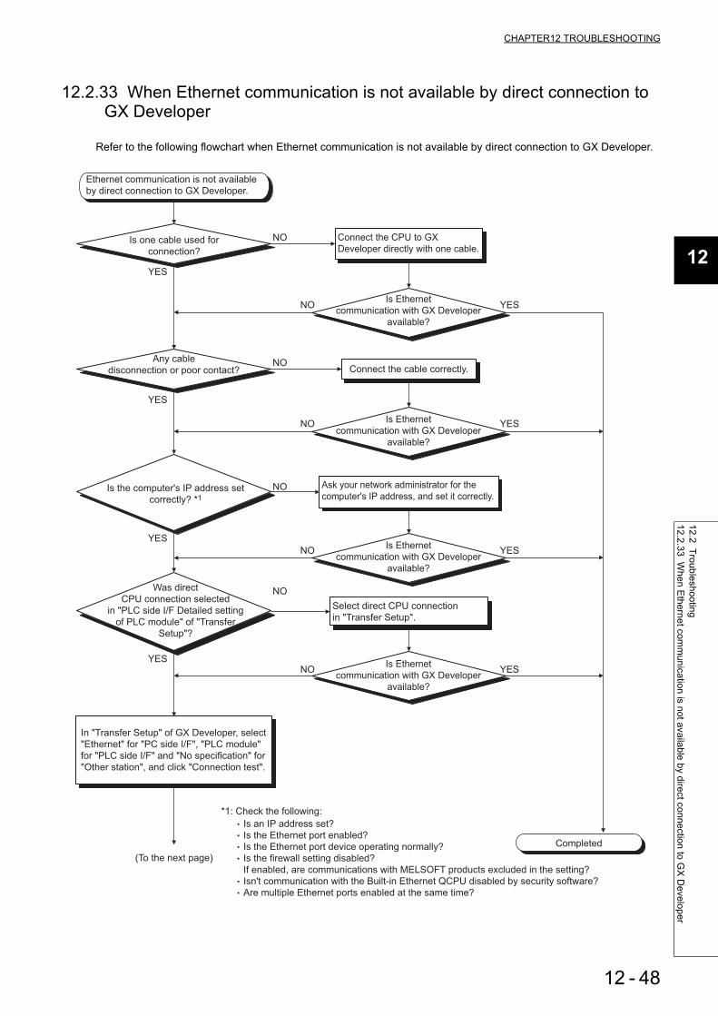
CHAPTER12 TROUBLESHOOTING
1
2
3
12
5
6
7
8
12.2 Troubleshooting12.2.33 W
hen Ethernet com
munication is not available by direct connection to G
X D
eveloper
12.2.33 When Ethernet communication is not available by direct connection to GX Developer
Refer to the following flowchart when Ethernet communication is not available by direct connection to GX Developer.
NO
NO
NO
NO
NO
NO
NO
NO
YES
YES
YES
YESYES
YES
YES
YES
Connect the cable correctly.
Select direct CPU connection
in "Transfer Setup".
(To the next page)
Is an IP address set?
Is the Ethernet port enabled?
Is the Ethernet port device operating normally?
Is the firewall setting disabled?
If enabled, are communications with MELSOFT products excluded in the setting?
Isn't communication with the Built-in Ethernet QCPU disabled by security software?
Are multiple Ethernet ports enabled at the same time?
Completed
Ethernet communication is not available
by direct connection to GX Developer.
Is one cable used for
connection?
Is the computer's IP address set
correctly? *1
In "Transfer Setup" of GX Developer, select
"Ethernet" for "PC side I/F", "PLC module"
for "PLC side I/F" and "No specification" for
"Other station", and click "Connection test".
Connect the CPU to GX
Developer directly with one cable.
Ask your network administrator for the
computer's IP address, and set it correctly.
*1: Check the following:
Is Ethernet
communication with GX Developer
available?
Is Ethernet
communication with GX Developer
available?
Is Ethernet
communication with GX Developer
available?
Is Ethernet
communication with GX Developer
available?
Any cable
disconnection or poor contact?
Was direct
CPU connection selected
in "PLC side I/F Detailed setting
of PLC module" of "Transfer
Setup"?
12 - 48
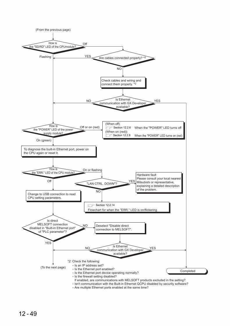
(From the previous page)
How is
the "SD/RD" LED of the CPUmodule?Off
Flashing YES
YES
YES
YES
YES
NO
NO
NO
NO
NO
How is
the "POWER" LED of the power
supply module?
Off or on (red)
On (green)
How is
the "ERR." LED of the CPU module?On or flashing
Off"LAN CTRL. DOWN"?
Flowchart for when the "ERR." LED is on/flickering
(To the next page)Is an IP address set?
Is the Ethernet port enabled?
Is the Ethernet port device operating normally?
Is the firewall setting disabled?
If enabled, are communications with MELSOFT products excluded in the setting?
Isn't communication with the Built-in Ethernet QCPU disabled by security software?
Are multiple Ethernet ports enabled at the same time?
To diagnose the built-in Ethernet port, power on
the CPU again or reset it.
Change to USB connection to read
CPU setting parameters.
Check cables and wiring and
connect them properly. *2
Deselect "Disable direct
connection to MELSOFT".
*2: Check the following:
Are cables connected properly? *2
Is Ethernet
communication with GX Developer
available?
Is direct
MELSOFT connection
disabled in "Built-in Ethernet port"
of "PLC parameter"?
Is Ethernet
communication with GX Developer
available?
(When off)
(When on (red))
When the "POWER" LED turns off
When the "POWER" LED turns on (red)
Hardware fault
Please consult your local nearest
Mitsubishi or representative,
explaining a detailed description
of the problem.
Completed
Section 12.2.6
Section 12.2.8
Section 12.2.14
12 - 49

CHAPTER12 TROUBLESHOOTING
1
2
3
12
5
6
7
8
12.2 Troubleshooting12.2.33 W
hen Ethernet com
munication is not available by direct connection to G
X D
eveloper
In "Status of
each connection" of
"Ethernet diagnosis", is the directly
connected connection set in
forced deactivation
status?
Any error in "Status of
each connection" or "Error log" of
"Ethernet diagnosis"?
In the detailed
host station setting of
"Transfer Setup", increase the value
of Time out or Retry times.
Is communication now
available?
Is direct connection
available for the connected
device? (Check the Ethernet interface
specifications.)
Replace the cable.
YES
YES
YES
Normal operation
YES
YES
YES
YES
NO
NO
NO
NO
NO
Error detection
NO
NO
Disable the forced deactivation.
Take actions according to the error code.
Perform the following.
Connect a hub to the line and
communicate with others through
the hub.
Adjust the communication timeout or the
number of retries again.
Check the status of the cables, connected
devices, and Built-in Ethernet port QCPU
Hardware fault
Please consult your local nearest
Mitsubishi or representative,
explaining a detailed description of
the problem.
Is Ethernet
communication available
with GX Developer?
Is Ethernet
communication available
with GX Developer?
Is Ethernet
communication available
with GX Developer?
(From the previous page)
Completed
12 - 50

12.2.34 When Ethernet communication with CPU module is slow or unstable
Refer to the following flowchart when Ethernet communication with a CPU module is slow or unstable.
Completed
(To the next page)
Ethernet communication with the CPU module
is slow or unstable.
NO
YES Use UDP in MELSOFT connection for the specified
number of modules or less.
NO
Consult your network administrator and correct the hub.
NO YES
YES
Use TCP instead of UDP.
Improved?Use TCP.
NO
YES
Retry or increase the number of
retries. Improved?Use retries. *2
NO
YES
Replace the hub, router or cables.
Stabilized?Replace the faulty one with another.
NO
YES
YES
NO
NO
YES
Set unique IP addresses.
YESNO
Does a duplicate IP
address exist? *1
Is UDP in
MELSOFT connection
or MC protocol used for more the number
of modules set by the
parameter?
Is the hub
capable of flow control
(IEEE802.3x PAUSE)?
Is the flow control enabled?
(Consult your network administrator.)Use a hub that is capable of flow control.
Enable the flow control.
Is Ethernet
communication stabilized?
Is Ethernet
communication stabilized?
Is Ethernet
communication stabilized?
*1: Checking methods:
With the Find CPU function of GX Developer, check the Built-in Ethernet
port QCPU for IP address duplication.
Disconnect a suspected device from the network, and run PING test from
another device to its address. If a reply is returned, there is a device with
a duplicate IP address.
Check respective IP address settings.
Using retries may increase stability of Ethernet communication.
*2: If transmissions pass through a wireless LAN, some packets may be lost resulting
in unstable Ethernet communication.
12 - 51

CHAPTER12 TROUBLESHOOTING
1
2
3
12
5
6
7
8
12.2 Troubleshooting12.2.34 W
hen Ethernet com
munication w
ith CP
U m
odule is slow or unstable
Completed(From the previous page)
NO
YES
NO
YES
NO
YES
NO
YES
YESNO
YESNO
YESNO
YESNO
Is the Ethernet
communication load on the Built-in
Ethernet port QCPU
too high?
Is any interrupt program used?
Check the communications referring to the following.
NO YESNO
YES
Has the hub
or router discarded messages
because of its too-small packet buffer
capacity? (Consult your network
administrator.)
Use a hub or router that has a large packet buffer
capacity.
Consult your network administrator and check the hub
and router.
Consult your network administrator and check thenetwork condition.Take actions against noise to reduce communicationerrors. *3
Check the traffic, and if a high traffic is a cause of theproblem, take actions for it.
Is communication of a
device other than the Built-in Ethernet port
QCPU unstable? (Consult your network
administrator.)
Have manyunnecessary broadcast data
been received? (See Connectionstatus in Ethernet
diagnosis.)
Unnecessary broadcast data have been highly loaded.
Increase service time for the Built-in Ethernet port QCPU.
Reduce the Ethernet communication load on the Built-in Ethernet port QCPU.
Increase service time for the Built-in Ethernet port QCPU.
Reduce the number of connected devices.
Reduce the connection setting value.
Reduce the communication frequency per connection and data volume.
Consult your network administrator, and check the network condition.
Identify a broadcasting device, and restrict the broadcast data volume.
(Devices such as computers or routers may broadcast data.)
Use filtering of broadcast data with a router to prevent the Built-in Ethernet port
QCPU from receiving them.
Separate the network where frequent broadcast occur from the network
containing the Built-in Ethernet port QCPU.
Reduce the frequency and process time of the interrupt
program.
Is Ethernet
communication stabilized?
Is Ethernet
communication stabilized?
Is Ethernet
communication stabilized?
Is Ethernet
communication stabilized?
Is Ethernet
communication stabilized?
When Ethernet communication with the target device is not available
Section 12.2.32
12 - 52

*3 : A communication error may occur due to high-frequency noise emitted from a device other than programmable controllers. The following measures can be taken to protect network systems from high-frequency noise.
Wiring• Do not install twisted pair cables together with the main circuit or power cables.• Put twisted pair cables in a duct.• Replace UTP cables with STP cables.Communication method• Use TCP/IP to exchange data with the target device.• Increase the number of communication retries, if necessary.• 10Mbps communication• In the case of using 100Mbps, replace the hub with a 10Mbps hub and perform data
communication at a transmission speed of 10Mbps.
12 - 53

CHAPTER12 TROUBLESHOOTING
1
2
3
12
5
6
7
8
12.2 Troubleshooting12.2.35 W
hen an error has occurred during MC
protocol comm
unication
12.2.35 When an error has occurred during MC protocol communication
Refer to the following flowchart when an error has occurred during MC protocol communication.
Completed
Was the command sent from
another device?Send the command to the Built-in Ethernet port QCPU.
(To the next page)
Was the error resolved?
YES
NO
YES
NO
YES
NO
YES
NO
NO
YES
YESNO
YESNO
According to the end code or error code, repair the
error part.
YESNO
Correct the IP address and send the command again.
YESNO
Communication error
Was a response
returned to the device that sent
the command?
Is the end code of the response "0"?
Is the IP address
specified in the command correct?
Are command
format specifications such as
command type, device,
or address correct?
Was the error resolved?
Was the error resolved?
Was the error resolved?
Correct the command format referring to the following
manual.
MELSEC Communication Protocol Reference Manual
Hardware fault
Please consult your local nearest Mitsubishi or
representative, explaining a detailed description of the
problem.
12 - 54

Completed
(From the previous page)
Send data of the request data length.
Send a sub-header of a normal value.
Send the data to the specified port No.
Use the same protocol (TCP/IP) for communication with
the target device.
(To the next page)
YES
NO
YES
NO
YES
NO
YES
NO
YES
NO
YES
NO
YESNO
YESNO
YESNO
YESNO
YESNO
YESNO
Is the same
protocol (TCP/IP) used for
communication with the target
device?
Was the error resolved?
Was the error resolved?
Was the error resolved?
Was the error resolved?
Was the error resolved?
Was the error resolved?
Is the IP address
specified in the command correct?
Are the data sent
to the port number specified in the Open
settings on the Built-in Ethernet
port QCPU?
Correct the IP address and send the command again.
Is the Communicationdata code setting (binary/ASCII)
matched with the sentcommand?
Send a command matched with Communication data
code setting.
Is the sub-header
value correct?
Were data of the request
data length sent?
12 - 55

CHAPTER12 TROUBLESHOOTING
1
2
3
12
5
6
7
8
12.2 Troubleshooting12.2.35 W
hen an error has occurred during MC
protocol comm
unication
Was the error resolved?
Completed
(From previous page)
YESYES
YES
YES
NO
NO
NO
NO
Correct the command format referring to the following manual.
MELSEC Communication Protocol Reference Manual
Are the data
specified for command format,
such as command type, device or
address correct?
Were requests
from multiple devices
simultaneously sent to the MC protocol
port specified in Open
settings?
Was the error resolved?
Perform the following.
Disable simultaneous request
transmissions from multiple devices.
Set a different MC protocol port for
each target.
When Ethernet communication with the target device is not available
Section 12.2.32
12 - 56

12.2.36 When clock data cannot be set by SNTP
Refer to the following flowchart when clock data cannot be set by SNTP.
Completed
Time cannot be set by SNTP.
Is the multiple CPU function used?
YES
NO
NO
YES
(To the next page)
Check if time was overwritten from the
sequence program or another device.
Enter correct parameters.
Set time on CPU No.1.
NO
NO YES
YES
YES
NO
NO
YESYESNO
NO YES
Is the time setting
functioning? (See Ethernet
diagnosis screen or SD1270.)Check the time setting function settings. *1
Is the time setting available?
Is the time setting available?
Is the time setting available?
Failed to set time?
(See Ethernet diagnosis screen or
SD1270.)
Has time been set on CPU
No.1 in the multiple CPU system?
Are the prameters of
the Built-in Ethernet port QCPU
correct? *1
12 - 57

CHAPTER12 TROUBLESHOOTING
1
2
3
12
5
6
7
8
12.2 Troubleshooting12.2.36 W
hen clock data cannot be set by SN
TP
Repair the SNTP server.
Is the time setting available?
Completed
(From the previous page)
YES
YES
YES
YES
Enter correct parameters.
NO
NO
NO
NO
Are the prameters of the
Built-in Ethernet port QCPU
correct?
Is the time setting available?
Is the SNTP server
specified for Q series running
properly?
When Ethernet communication with the target device is not available
Section 12.2.32
12 - 58

12.2.37 When unable to receive data on the external device side by the Socket communication function
Data are not received by the target.
YES
NO
NO
YES
YES
NO
NO
NO
YES
NO
NO
YES
YES
YES
YES
The connection opened?*1
The port No. of
the target specified by FFFFH
when using UDP?
Any error shown in the Status of
each connection screen or the Error log screen on the Ethernet
diagnosis screen?
The SOCSND
instruction completed
in error (Error completion
device turned on)?
The parameters
and setting data for
SOCOPEN correct?*2
The SOCSND
instruction being executed
(Start-up contact rose)?
Set the send data length?*3
NOAny faulty part
in the target device?
When open process of the Socket
communication function does not complete
When Ethernet communication with
the target device is not available
Data cannot be sent in a connection for
simultaneous broadcast whose target
port No. is FFFFH.
Send by another connection.
Set the port No. of the target device by
the SOCSET instruction and then send.
Take corrective actions
according to the error code
stored in the completion status
area of the SOCSND instruction.
Take corrective actions
according to the error code.
Correct the parameters and
setting data for SOCOPEN.
Correct the execution
conditions of the SOCSND
instruction.
Set the data length.
Correct the faulty part in
the target device.
*1 Refer to the corresponding bit of SD1282 (Open completion signal).
*2 Check the following:
Is the IP address correct?
Is the subnet mask pattern correct?
Is the default router IP address correct?
Connection No.
Are the connection method and open method correct?
Are the port No. of own station and IP address/port No. of the
target device correct?
Are the protocols and functions to be used all configured in the
Open settings?
*3 Two or more receive instructions may be executed to read the data
sent by one send instruction since TCP does not have architecture for
specifying data boundaries.
For this reason, the received data size must be checked when
receiving, and receive the remaining data if exists.
For more details, refer to the following.
QnUCPU User's Manual (Communication via Built-in
Ethernet Port)
Section 12.2.32
Section 12.2.39
12 - 59

CHAPTER12 TROUBLESHOOTING
1
2
3
12
5
6
7
8
12.2 Troubleshooting12.2.38 W
hen unable to receive data by the Socket com
munication function
12.2.38 When unable to receive data by the Socket communication function
Data cannot be received.
YES
NO
NO
NO
NO
NO
YES
YES
YES
YES
The connection opened?*1
Any error shown in the Status
of each connection screen or the Error log screen on the
Ethernet diagnosis screen?
The receive completion
signal of the connection on?
The SOCRCV(S)
instruction being executed?
(Start-up contact is on or
has rosen?)*5
The length of the data to be received
and the volume of actually received data the same in size
when using TCP?
Complete
When open process of the Socket
communication function does not
complete
When Ethernet communication with
the target device is not available
Take corrective actions
according to the error code.
NO
YESThe SOCRCV
instruction completed in
error (Error completion
device turned on)?
Take corrective actions according
to the error code stored in
the completion status area of
the SOCRCV instruction.
NO
YES
Data are sent from
the target device side?
Send data from the target
device. Check the send
processing on the target
device side.
NO
YES
The parameters
and setting data for SOCOPEN
correct?*2
Correct the parameters
and setting data for
SOCOPEN.
NO
YES
Any faulty part
in the target device?
Correct the faulty part
in the target device.
Correct the execution
conditions of the SOCRCV(S)
instruction.
When the data length is determined, use the fixed-length receive
mode.
If the actual data volume is less than the expected data length,
take actions for receiving the remaining data .
If the actual data volume is exceeding the expected data length,
process the data as the next message or as unnecessary data.
*3, *4
*5 The start-up contact may not be turned on only with the Reception status signal (SD1286) depending
on the scan time since the signal turns on if the next data are received immediately after executing
the SP.SOCRCV instruction.
In this case, provide a normal close contact of the completion device of the SP.SOCRCV instruction
in the start-up condition of the instruction.
*1 Refer to the corresponding bit of SD1282 (Open completion signal)
*2 Check the following:
Is the IP address correct?
Is the subnet mask pattern correct?
Is the default router IP address correct?
Connection No.
Are the connection method and open method correct?
Are the port No. of own station and IP address/port No.
of the target device correct?
Are the protocols and functions to be used all configured in
the Open settings?
*3 Two or more receive instructions may be executed to read the data
sent by one send instruction since TCP does not have architecture for
specifying data boundaries.
For this reason, the received data size must be checked when
receiving, and receive the remaining data if exists.
For more details, refer to the following.
QnUCPU User's Manual (Communication via Built-in
Ethernet Port)
*4 It is recommended to include the checking method, such as the data
length and data type code, in the message data so that the data
information such as the number of bytes and data size can be
checked on the receive side.
When Ethernet communication with
the target device is not available
NO
YES
Provided the processing for
receiving remaining data when the actual data is less than the
response data length of the receive message?
Section 12.2.32
Section 12.2.32
Section 12.2.39
12 - 60

12.2.39 When open process of the Socket communication function does not complete
NO
YES
NO
NO
Execute
the SOCOPEN
instruction with Active
open specified.
Take corrective actions
according to the error
code stored in the
completion status area
of the SOCOPEN
instruction.
Correct the parameters
and setting data for
SOCOPEN.
Change the status of
the specified port of
the target device to
Passive open.
When open process of the Socket communication function does not complete
TCP/IP?
Connect from
the Built-in Ethernet port
QCPU side?
Executed
the SOCOPEN instruction
with Active open
specified?
The SOCOPEN instruction completed
in error (Error completion device turned
on)?
The specified port on the target device
side is in the Passive open status?
Parameters are
correctly set?*2
The parameters
and setting data for
SOCOPEN
correct?*1
The target device
is connected to the
specified port?*3
Any faulty part
in the target device?
TCP/IP
UDP/IP
NO
YES
YES
NO
YES Take corrective
actions according to
the error code.
Any error shown in the Status
of each connection screen or the Error log screen on
the Ethernet diagnosis screen?
NO
YES
YES
NO Correct the execution
conditions of the
SOCOPEN instruction.
The SOCOPEN instruction being executed?
(Start-up contact is on or has rosen?)
YES
YES
YES
Passive open
YES
NO
YES
Active open
NO
NO
NO
Correct the parameters.
Correct the parameters.*1
Connect from the target
device to the specified
port.
Correct the faulty part
in the target device.
Connected again with the same communication
target IP address, the same own station port No., and the same communication
target port No. after closing?
NO
YESRetry 8 seconds later or
change the own station port
No. of the device that is in
active open.
*1 Check the following:
Is the IP address correct?
Is the subnet mask pattern correct?
Is the default router IP address correct?
Connection No.
Are the connection method and open method correct?
Are the port No. of own station and IP address/port No. of the target device
correct?
*2 Check the following:
Is the IP address correct?
Is the subnet mask pattern correct?
Is the default router IP address correct?
Connection No.
Are the connection method and open method correct?
Is the port No. of own station correct?
When in Full passive, are the IP address and port No. of the target device
correct?
Are the protocols and functions to be used all configured in the Open
settings?
*3 When in Fullpassive, check that
the IP address and port No. of
the target device match with
the set data.
When Ethernet communication
with the target device is not
available.
Section 12.2.32
12 - 61

CHAPTER12 TROUBLESHOOTING
12
12.3 Error C
ode List
12.3 Error Code List
The CPU module uses the self diagnostics function to display error information (on the LED) and stores the information into the special relay SM and special register SD, when an error occurs in the following situations:• When the Progammable Controller is powered ON.• When the CPU module is switched from STOP to RUN.• While the CPU module is running.
If an error occurs when a communication request is issued from the peripheral device, intelligent function module or network system to the CPU module, the CPU module returns the error code (4000H to 4FFFH) to the request source.
The following describes the description of errors which occur in the CPU module and the corrective actions for the errors.
(1) How to read the error code listThe following describes how to read Section 12.3.3 Error code list (1000 to 1999) to Section 12.3.9 Error code list (7000 to 10000).
(a) Error code, common information and individual informationAlphanumeric characters in the parentheses of the titles indicate the special register numbers where each information is stored.
(b) Compatible CPUQCPU : Indicates all the Q series CPU modules.Q00J/Q00/Q01 : Indicates the Basic model QCPU.Qn(H) : Indicates the High Performance model QCPU.QnPH : Indicates the Process CPU.QnPRH : Indicates the Redundant CPU.QnU : Indicates the Universal model QCPU.Each CPU module : Indicates the relevant specific CPU module.model name (Example: Q02U)
12 - 62

12.3.1 Error codes
Errors are detected by the self diagnostic function of the CPU module or detected during communication with the CPU module.
The relation between the error detection pattern, error detection location and error code is shown in Table 12.1.
*1: CPU module error codes are classified into minor, moderate, major errors as shown below.• Minor error: Errors that may allow the CPU module to continue the operation, e.g., battery error.
(Error code: 1300 to 10000) • Moderate error: Errors that may cause the CPU module to stop the operation, e.g., WDT error.
(Error code: 1300 to 10000)• Major error: Errors that may cause the CPU module to stop the operation, e.g., RAM error.
(Error code: 1000 to 1299)Determine the error level, i.e. whether the operation can be continued or stopped, by referring to "Operating Statuses of CPU" described in Section 12.3.3 to 12.3.9 "Error Code List"
*2: When detected an error code without being noted in the reference table, please contact your local Mitsubishi representive.
12.3.2 Reading an error code
When an error occurs, reading an error code, error message or the like can be executed with GX Developer.
For the details of the operation method, refer to the operating manual for GX Developer.
Table12.1Reference destination
Error detection patternError detection
locationError code Reference
Detection by the self diagnostics function of CPU module
CPU module 1000 to 10000*1*2 Section 12.3.3 to 12.3.9
Detection at communication with CPU module
CPU module 4000H to 4FFFH• QCPU User's Manual (Hardware design,
Maintenance and Inspection)Serial communication module, etc.
7000H to 7FFFH Serial Communication User's Manual, etc.
CC-Link module B000H to BFFFHCC-Link System Master/Local Module User's Manual
Ethernet module C000H to CFFFH Ethernet Interface Module User's ManualCC-Link IE controller network
E000H to EFFFHCC-Link IE Controller Network Reference Manual
MELSECNET/Hnetwork module
F000H to FFFFH
• MELSECNET/H modeQ Corresponding MELSECNET/H Network System Reference Manual
• MELSECNET/10 modeFor QnA/Q4AR MELSECNET/10 Network System Reference Manual
12 - 63

CHAPTER12 TROUBLESHOOTING
12
12.3 Error C
ode List12.3.3 E
rror code list (1000 to 1999)
12.3.3 Error code list (1000 to 1999)
The following shows the error messages from the error code 1000 to 1999, the contents and causes of the errors, and the corrective actions for the errors.
ErrorCode
Error Contents and Cause Corrective ActionLED StatusCPU Status
CorrespondingCPU
1000
[MAIN CPU DOWN]Runaway or failure of CPU module or failure of main CPU• Malfunctioning due to noise or other reason• Hardware fault
■Collateral information• Common Information:–• Individual Information:–
■Diagnostic Timing• Always
• Take noise reduction measures.• Reset the CPU module and RUN it again.If the
same error is displayed again, this suggests a CPU module hardware fault.(Contact your local Mitsubishi representative.)
RUN:Off
ERR.:Flicker
CPU Status:Stop
QCPU
1001
[MAIN CPU DOWN]Runaway or failure of CPU module or failure of main CPU• Malfunctioning due to noise or other reason• Hardware fault• Accessed to outlying devices with the device
range checks disabled (SM237 is turned on)(This error occurs only when BMOV, FMOV, and DFMOV instructions are executed.)(Universal model QCPU only)
■Collateral information• Common Information:–• Individual Information:–
■Diagnostic Timing• Always
• Take noise reduction measures.• Reset the CPU module and RUN it again.If the
same error is displayed again, this suggests a CPU module hardware fault.(Contact your local Mitsubishi representative.)
• Check the devices specified by BMOV, FMOV, and DFMOV instructions and correct the device settings. (Universal model QCPU only)
1002 [MAIN CPU DOWN]Runaway or failure of CPU module or failure of main CPU• Malfunctioning due to noise or other reason• Hardware fault
■Collateral information• Common Information:–• Individual Information:–
■Diagnostic Timing• Always
• Take noise reduction measures.• Reset the CPU module and RUN it again.If the
same error is displayed again, this suggests a CPU module hardware fault.(Contact your local Mitsubishi representative.)
1003
1004
1005
[MAIN CPU DOWN]Runaway or failure of CPU module or failure of main CPU• Malfunctioning due to noise or other reason• Hardware fault
■Collateral information• Common Information:–• Individual Information:–
■Diagnostic Timing• Always
• Take noise reduction measures.• Reset the CPU module and RUN it again.If the
same error is displayed again, this suggests a CPU module hardware fault.(Contact your local Mitsubishi representative.)
[MAIN CPU DOWN]Boot operation was performed in the transfer desti-nation without formatting.■Collateral information• Common Information:–• Individual Information:–
■Diagnostic Timing• At power ON
• Before performing boot operation by the parame-ter, select "Clear program memory" to clear the program memory.
Qn(H)QnPH
QnPRH
12 - 64

1006 [MAIN CPU DOWN]Runaway or failure of CPU module or failure of main CPU• Malfunctioning due to noise or other reason• Hardware fault
■Collateral information• Common Information:–• Individual Information:–
■Diagnostic Timing• Always
• Take noise reduction measures.• Reset the CPU module and RUN it again.If the
same error is displayed again, this suggests a CPU module hardware fault.(Contact your local Mitsubishi representative.)
RUN:Off
ERR.:Flicker
CPU Status:Stop
QCPU1007
Qn(H)QnPH
QnPRH1008
1009
[MAIN CPU DOWN]• A failure is detected on the power supply module,
CPU module, main base unit, extension base unit or extension cable.
• When using the redundant base unit, the redun-dant power supply module failure in both sys-tems and/or the redundant base unit failure are detected.
■Collateral information• Common Information:–• Individual Information:–
■Diagnostic Timing• Always
Reset the CPU module and RUN it again.If the same error is detected again, it is considered that the power supply module, CPU module, main base unit, extension base unit or extension cable is faulty.(Contact your local Mitsubishi representative.)
Q00J/Q00/Q01*4
Qn(H)*6
QnPHQnPRH
QnU
1010
[END NOT EXECUTE]Entire program was executed without the execution of an END instruction.• When the END instruction is executed it is read
as another instruction code, e.g. due to noise.• The END instruction has been changed to
another instruction code somehow.■Collateral information• Common Information:–• Individual Information:–
■Diagnostic Timing• When an END instruction executed
• Take noise reduction measures.• Reset the CPU module and RUN it again. If the
same error is displayed again, this suggests a CPU module hardware fault. (Contact your local Mitsubishi representative.)
QCPU
1020
[SFCP. END ERROR]The SFC program cannot be normally terminated due to noise or other reason.• The SFC program cannot be normally terminated
due to noise or any similar cause.• The SFC program cannot be normally terminated
for any other reason.■Collateral information• Common Information:–• Individual Information:–
■Diagnostic Timing• When SFC program is executed
• Take noise reduction measures.• Reset the CPU module and RUN it again. If the
same error is displayed again, this suggests a CPU module hardware fault. (Contact your local Mitsubishi representative.)
Q00J/Q00/Q01*4
QnPHQnU
1035
[MAIN CPU DOWN]Runaway or error of the CPU module was detected.• Malfunction due to noise etc.• Hardware failure
■Collateral information• Common Information:–• Individual Information:–
■Diagnostic Timing• Always
• Take measures against noise.• Reset the CPU module and run it again. If the
same error is displayed again, the CPU module has hardware failure.(Contact your local Mitsub-ishi representative, explaining a detailed descrip-tion of the problem.)
QnU
ErrorCode
Error Contents and Cause Corrective ActionLED StatusCPU Status
CorrespondingCPU
*4 Function version is B or later.
12 - 65*6 The module whose first 5 digits of serial No. is "04101" or later.

CHAPTER12 TROUBLESHOOTING
12
12.3 Error C
ode List12.3.3 E
rror code list (1000 to 1999)
1101
[RAM ERROR]The sequence program storing program memory in the CPU module is faulty.■Collateral information• Common Information:–• Individual Information:–
■Diagnostic Timing• At power ON/ At reset/ When an END instruction
executed
• Take noise reduction measures.• Reset the CPU module and RUN it again. If the
same error is displayed again,this suggests a CPU module hardware fault.(Contact your local Mitsubishi representative.) RUN:
OffERR.:
Flicker
CPU Status:Stop
QCPU
1102
[RAM ERROR]• The work area RAM in the CPU module is faulty.• The standard RAM and extended RAM in the
CPU module are faulty.■Collateral information• Common Information:–• Individual Information:–
■Diagnostic Timing• At power ON/ At reset/ When an END instruction
executed
• Take noise reduction measures.• Reset the CPU module and RUN it again. If the
same error is displayed again,this suggests a CPU module hardware fault.(Contact your local Mitsubishi representative.)
ErrorCode
Error Contents and Cause Corrective ActionLED StatusCPU Status
CorrespondingCPU
12 - 66

1103
[RAM ERROR]The device memory in the CPU module is faulty.■Collateral information• Common Information:–• Individual Information:–
■Diagnostic Timing• At power ON/ At reset
• Take noise reduction measures.• When indexing is performed, check the value of
index register to see if it is within the device range.
• Reset the CPU module and RUN it again. If the same error is displayed again,this suggests a CPU module hardware fault.(Contact your local Mitsubishi representative.)
RUN:Off
ERR.:Flicker
CPU Status:Stop
QCPU
[RAM ERROR]• The device memory in the CPU module is faulty.• The device out of range is accessed due to
indexing, and the device for system is overwrit-ten.
■Collateral information• Common Information:–• Individual Information:–
■Diagnostic Timing• At power ON/ At reset/ When an END instruction
executed
Qn(H)*8
QnPH*8
QnPRH*9
1104
[RAM ERROR]The address RAM in the CPU module is faulty.■Collateral information• Common Information:–• Individual Information:–
■Diagnostic Timing• At power ON/ At reset
• Take noise reduction measures.• Reset the CPU module and RUN it again.If the
same error is displayed again, this suggests a CPU module hardware fault. (Contact your local Mitsubishi representative.)
QCPU
1105
[RAM ERROR]The CPU memory in the CPU module is faulty.■Collateral information• Common Information:–• Individual Information:–
■Diagnostic Timing• At power ON/ At reset
• Take noise reduction measures.• Reset the CPU module and RUN it again.If the
same error is displayed again, this suggests a CPU module hardware fault. (Contact your local Mitsubishi representative.)
Q00J/Q00/Q01QnU
[RAM ERROR]The CPU shared memory in the CPU module is faulty.■Collateral information• Common Information:–• Individual Information:–
■Diagnostic Timing• At power ON/ At reset
Qn(H)*4
QnPHQnPRH
QnU
1106
[RAM ERROR]The battery is dead.The program memory in the CPU module is faulty.■Collateral information• Common Information:–• Individual Information:–
■Diagnostic Timing• STOP RUN/When an END instruction exe-
cuted
• Check the battery to see if it is dead or not. If dead, replace the battery.
• Take noise reduction measures.• Format the program memory, write all files to the
PLC, then reset the CPU module, and RUN it again.If the same error is displayed again, the possible cause is a CPU module hardware fault. (Contact your local Mitsubishi representative, explaining a detailed description of the problem.)
Qn(H)
QnPH*7
QnPRH
ErrorCode
Error Contents and Cause Corrective ActionLED StatusCPU Status
CorrespondingCPU
*4 Function version is B or later.*7 The module whose first 5 digits of serial No. is "07032" or later.*8 The module whose first 5 digits of serial No. is "08032" or later.
12 - 67*9 The module whose first 5 digits of serial No. is "09012" or later.
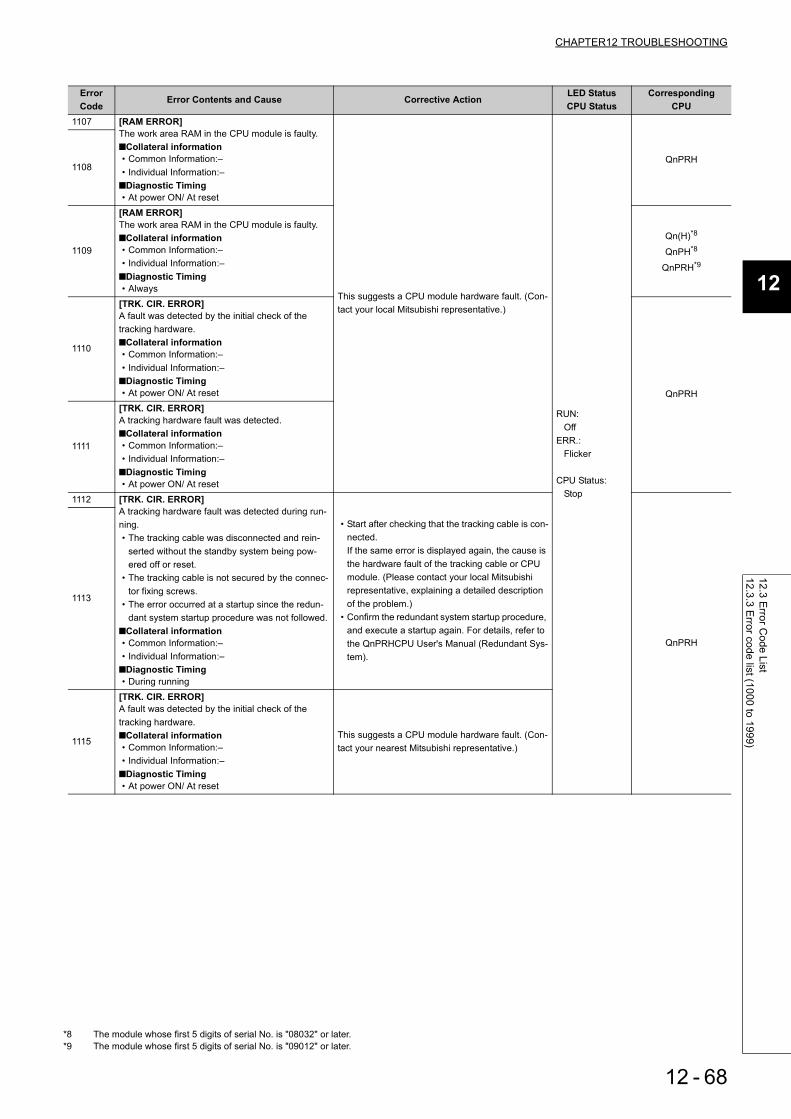
CHAPTER12 TROUBLESHOOTING
12
12.3 Error C
ode List12.3.3 E
rror code list (1000 to 1999)
1107 [RAM ERROR]The work area RAM in the CPU module is faulty.■Collateral information• Common Information:–• Individual Information:–
■Diagnostic Timing• At power ON/ At reset
This suggests a CPU module hardware fault. (Con-tact your local Mitsubishi representative.)
RUN:Off
ERR.:Flicker
CPU Status:Stop
QnPRH1108
1109
[RAM ERROR]The work area RAM in the CPU module is faulty.■Collateral information• Common Information:–• Individual Information:–
■Diagnostic Timing• Always
Qn(H)*8
QnPH*8
QnPRH*9
1110
[TRK. CIR. ERROR]A fault was detected by the initial check of the tracking hardware.■Collateral information• Common Information:–• Individual Information:–
■Diagnostic Timing• At power ON/ At reset QnPRH
1111
[TRK. CIR. ERROR]A tracking hardware fault was detected.■Collateral information• Common Information:–• Individual Information:–
■Diagnostic Timing• At power ON/ At reset
1112 [TRK. CIR. ERROR]A tracking hardware fault was detected during run-ning.• The tracking cable was disconnected and rein-
serted without the standby system being pow-ered off or reset.
• The tracking cable is not secured by the connec-tor fixing screws.
• The error occurred at a startup since the redun-dant system startup procedure was not followed.
■Collateral information• Common Information:–• Individual Information:–
■Diagnostic Timing• During running
• Start after checking that the tracking cable is con-nected.If the same error is displayed again, the cause is the hardware fault of the tracking cable or CPU module. (Please contact your local Mitsubishi representative, explaining a detailed description of the problem.)
• Confirm the redundant system startup procedure, and execute a startup again. For details, refer to the QnPRHCPU User's Manual (Redundant Sys-tem).
QnPRH
1113
1115
[TRK. CIR. ERROR]A fault was detected by the initial check of the tracking hardware.■Collateral information• Common Information:–• Individual Information:–
■Diagnostic Timing• At power ON/ At reset
This suggests a CPU module hardware fault. (Con-tact your nearest Mitsubishi representative.)
ErrorCode
Error Contents and Cause Corrective ActionLED StatusCPU Status
CorrespondingCPU
*8 The module whose first 5 digits of serial No. is "08032" or later.
12 - 68*9 The module whose first 5 digits of serial No. is "09012" or later.

1116
[TRK. CIR. ERROR]A tracking hardware fault was detected during run-ning.• The tracking cable was disconnected and rein-
serted without the standby system being pow-ered off or reset.
• The tracking cable is not secured by the connec-tor fixing screws.
• The error occurred at a startup since the redun-dant system startup procedure was not followed.
■Collateral information• Common Information:–• Individual Information:–
■Diagnostic Timing• During running
• Start after checking that the tracking cable is con-nected.If the same error is displayed again, the cause is the hardware fault of the tracking cable or CPU module. (Please contact your local Mitsubishi representative, explaining a detailed description of the problem.)
• Confirm the redundant system startup procedure, and execute a startup again. For details, refer to the QnPRHCPU User's Manual (Redundant Sys-tem).
RUN:Off
ERR.:Flicker
CPU Status:Stop
QnPRH
1150
[RAM ERROR]The memory of the CPU module in the Multiple CPU high speed transmission area is faulty.■Collateral information• Common Information:–• Individual Information:–
■Diagnostic Timing• At power ON/ At reset
• Take noise reduction measures. • Reset the CPU module and RUN it again.
If the same error is displayed again, the CPU module has hardware failure. Contact your local Mitsubishi representative, explaining a detailed description of the problem.
QnU*10
1160
[RAM ERROR]The program memory in the CPU module is over-written.■Collateral information• Common Information:–• Individual Information:–
■Diagnostic Timing• At program execution
• Take noise reduction measures. • Format the program memory, write all files to the
PLC, then reset the CPU module, and RUN it again.If the same error is displayed again, the CPU module has hardware failure. Contact your local Mitsubishi representative, explaining a detailed description of the problem.
RUN:Off
ERR.:Flicker
CPU Status:Stop
QnU1161
[RAM ERROR]The data of the device memory built in the CPU module is overwritten.■Collateral information• Common Information:–• Individual Information:–
■Diagnostic Timing• At program execution
• Take noise reduction measures.If the same error is displayed again, the CPU module has hardware failure. Contact your local Mitsubishi representative, explaining a detailed description of the problem.
1162
[RAM ERROR]The error of the data held by the battery in the CPU module is detected. (It occurs when the automatic format is not set.)■Collateral information• Common Information:–• Individual Information:–
■Diagnostic Timing• At power ON/ At reset
• Take noise reduction measures. • Change the CPU main body or SRAM card bat-
tery.If the same error is displayed again, the CPU module has hardware failure. Contact your local Mitsubishi representative, explaining a detailed description of the problem.
1164
[RAM ERROR]The destruction of the data stored in the standard RAM is detected.■Collateral information• Common Information:–• Individual Information:–
■Diagnostic Timing• When instruction executed
• Take noise reduction measures.If the same error is displayed again, the CPU module has hardware failure. Contact your local Mitsubishi representative, explaining a detailed description of the problem.
QnU*11
ErrorCode
Error Contents and Cause Corrective ActionLED StatusCPU Status
CorrespondingCPU
*10 The Universal model QCPU except the Q00UJCPU, Q00UCPU, Q01UCPU, and Q02UCPU.
12 - 69*11 The Q10UD(E)HCPU, Q13UD(E)HCPU, Q20UD(E)HCPU, .Q26UD(E)HCPU only.

CHAPTER12 TROUBLESHOOTING
12
12.3 Error C
ode List12.3.3 E
rror code list (1000 to 1999)
1200
[OPE. CIRCUIT ERR.]The operation circuit for index modification in the CPU module does not operate normally.■Collateral information• Common Information:–• Individual Information:–
■Diagnostic Timing• At power ON/ At reset
This suggests a CPU module hardware fault. (Con-tact your local Mitsubishi representative.)
RUN:Off
ERR.:Flicker
CPU Status:Stop
QCPU1201
[OPE. CIRCUIT ERR.]The hardware (logic) in the CPU module does not operate normally.■Collateral information• Common Information:–• Individual Information:–
■Diagnostic Timing• At power ON/ At reset
1202
[OPE. CIRCUIT ERR.]The operation circuit for sequence processing in the CPU module does not operate normally.■Collateral information• Common Information:–• Individual Information:–
■Diagnostic Timing• At power ON/ At reset
1203
[OPE. CIRCUIT ERR.]The operation circuit for index modification in the CPU module does not operate normally.■Collateral information• Common Information:–• Individual Information:–
■Diagnostic Timing• When an END instruction executed
QnPRH1204
[OPE. CIRCUIT ERR.]The hardware (logic) in the CPU module does not operate normally.■Collateral information• Common Information:–• Individual Information:–
■Diagnostic Timing• When an END instruction executed
1205
[OPE. CIRCUIT ERR.]The operation circuit for sequence processing in the CPU module does not operate normally.■Collateral information• Common Information:–• Individual Information:–
■Diagnostic Timing• When an END instruction executed
ErrorCode
Error Contents and Cause Corrective ActionLED StatusCPU Status
CorrespondingCPU
12 - 70

1300
[FUSE BREAK OFF]There is an output module with a blown fuse.■Collateral information• Common Information:Module No.(Slot No.)
[For Remote I/O network]Network No./Station No.
• Individual Information:–■Diagnostic Timing• Always
• Check FUSE. LED of the output modules and replace the module whose LED is lit.(The module with a blown fuse can also be iden-tified using GX Developer.Check the special registers SD1300 to SD1331 to see if the bit corresponding to the module is "1".)
• When a GOT is bus-connected to the main base unit or extension base unit, check the connection status of the extension cable and the earth status of the GOT.
RUN:Off/On
ERR.:Flicker/On
CPU Status:Stop/
Continue*1
Qn(H)QnPH
QnPRHQnU
[FUSE BREAK OFF]There is an output module with a blown fuse.■Collateral information• Common Information:Module No.(Slot No.)
[For Remote I/O network]Network No./Station No.
• Individual Information:–■Diagnostic Timing• Always
Check ERR. LED of the output modules and replace the module whose LED is lit.(The module with a blown fuse can also be identi-fied using GX Developer. Check the special regis-ters SD130 to SD137 to see if the bit corresponding to the module is "1".)
Q00J/Q00/Q01
1310
[I/O INT. ERROR]An interruption has occurred although there is no interrupt module.■Collateral information• Common Information:–• Individual Information:–
■Diagnostic Timing• During interrupt
Any of the mounted modules is experiencing a hardware fault. Therefore, check the mounted mod-ules and change the faulty module. (Contact your local Mitsubishi representative.)
RUN:Off
ERR.:Flicker
CPU Status:Stop
QCPU
1311
[I/O INT. ERROR]An interrupt request from other than the interrupt module was detected.■Collateral information• Common Information:–• Individual Information:–
■Diagnostic Timing• During interrupt
Take action so that an interrupt will not be issued from other than the interrupt module.
Q00J/Q00/Q01*4
QnU
[I/O INT. ERROR]An interrupt request from the module where inter-rupt pointer setting has not been made in the PLC parameter dialog box was detected.■Collateral information• Common Information:–• Individual Information:–
■Diagnostic Timing• During interrupt
• Correct the interrupt pointer setting in the PLC system setting of the PLC parameter dialog box.
• Take measures so that an interrupt is not issued from the module where the interrupt pointer set-ting in the PLC system setting of the PLC param-eter dialog box has not been made. Correct the interrupt setting of the network parameter. Cor-rect the interrupt setting of the intelligent function module buffer memory. Correct the basic pro-gram of the QD51.
Q00J/Q00/Q01 *5
QnPRHQnU
1320 [LAN CTRL.DOWN]The H/W self-diagnostics detected a LAN controller failure.■Collateral information• Common Information:–• Individual Information:–
■Diagnostic Timing• At power ON/ At reset
This suggests a CPU module hardware fault. (Con-tact your local Mitsubishi representative.)
RUN:Off
ERR.:Flicker
CPU Status:Stop
QnU*131321
ErrorCode
Error Contents and Cause Corrective ActionLED StatusCPU Status
CorrespondingCPU
*1 CPU operation can be set in the parameters at error occurrence. (LED indication varies.)*4 Function version is B or later.*5 Function version is A.
12 - 71*13 This applies to the Built-in Ethernet port QCPU.

CHAPTER12 TROUBLESHOOTING
12
12.3 Error C
ode List12.3.3 E
rror code list (1000 to 1999)
1401
[SP. UNIT DOWN]• There was no response from the intelligent func-
tion module/special function module in the initial processing.
• The size of the buffer memory of the intelligent function module/special function module is invalid.
• The unsupported module is mounted.■Collateral information• Common Information:Module No.(Slot No.)• Individual Information:–
■Diagnostic Timing• At power ON/ At reset/When intelligent function
module is accessed
When the unsupported module is mounted, remove it.When the corresponding module is supported, this suggests the intelligent function module/special function module, CPU module and/or base unit is expecting a hardware fault (Contact your local Mit-subishi representative.)
RUN:Off/On
ERR.:Flicker/On
CPU Status:Stop/
Continue*2
QCPU
1402
[SP. UNIT DOWN]The intelligent function module/special function module was accessed in the program, but there was no response.■Collateral information• Common Information:Module No. (Slot No.)• Individual Information:Program error location
■Diagnostic Timing• When an intelligent function module access
instruction is executed
This suggests the intelligient function module/spe-cial function module , CPU module and/or base unit is expecting a hardware fault (Contact your local Mitsubishi representative.)
1403
[SP. UNIT DOWN]• The unsupported module is mounted.
■Collateral information• Common Information:Module No. (Slot No.)• Individual Information:–
■Diagnostic Timing• When an END instruction executed
When the unsupported module is mounted, remove it.When the corresponding module is supported, this suggests the intelligent function module/special function module , CPU module and/or base unit is expecting a hardware fault (Contact your local Mit-subishi representative.)
[SP. UNIT DOWN]• There was no response from the intelligent func-
tion module/special function module when the END instruction is executed.
• An error is detected at the intelligent function module/special function module.
• The I/O module (intelligent function module/spe-cial function module) is nearly removed, com-pletely removed, or mounted during running.
■Collateral information• Common Information:Module No. (Slot No.)• Individual Information:–
■Diagnostic Timing• Always
The CPU module, base module and/or the intelli-gent function module/special function module that was accessed is experiencing a hardware fault. (Contact your local Mitsubishi representative.)
1411
[CONTROL-BUS. ERR.]When performing a parameter I/O allocation the intelligent function module/special function module could not be accessed during initial communica-tions.(On error occurring, the head I/O number of the corresponding intelligent function module/special function module is stored in the common informa-tion.)■Collateral information• Common Information:Module No. (Slot No.)• Individual Information:–
■Diagnostic Timing• At power ON/ At reset
Reset the CPU module and RUN it again. If the same error is displayed again, the intelligent func-tion module/special function module, CPU module or base unit is faulty. (Contact your local Mitsubishi representative.)
RUN:Off
ERR.:Flicker
CPU Status:Stop
QCPU
ErrorCode
Error Contents and Cause Corrective ActionLED StatusCPU Status
CorrespondingCPU
12 - 72*2 In the QCPU, either error stop or continue can be selected for each intelligent function module by the parameters.

1412
[CONTROL-BUS. ERR.]The FROM/TO instruction is not executable, due to a control bus error with the intelligent function mod-ule/special function module.(On error occurring, the program error location is stored in the individual information.)■Collateral information• Common Information:Module No. (Slot No.)• Individual Information:Program error location
■Diagnostic Timing• During execution of FROM/TO instruction set
Reset the CPU module and RUN it again. If the same error is displayed again, the intelligent func-tion module/special function module, CPU module or base unit is faulty. (Contact your local Mitsubishi representative.)
RUN:Off
ERR.:Flicker
CPU Status:Stop
QCPU
1413
[CONTROL-BUS. ERR.]In a multiple CPU system, a CPU module incom-patible with the multiple CPU system is mounted.■Collateral information• Common Information:–• Individual Information:–
■Diagnostic Timing• Always
• Remove the CPU module incompatible with the multiple CPU system from the main base unit, or replace the CPU module incompatible with the multiple CPU system with a CPU module com-patible with the multiple CPU system.
• The intelligent function module, CPU module or base unit is faulty. (Contact your local Mitsubishi representative.)
Q00J/Q00/Q01*4
Qn(H)*4
QnPH
[CONTROL-BUS. ERR.]An error is detected on the system bus.• Self-diagnosis error of the system bus.• Self-diagnosis error of the CPU module
■Collateral information• Common Information:–• Individual Information:–
■Diagnostic Timing• Always
Reset the CPU module and RUN it again. If the same error is displayed again, the intelligent func-tion module, CPU module or base unit is faulty. (Contact your local Mitsubishi representative.)
QCPU
1414
[CONTROL-BUS. ERR.]• Fault of a loaded module was detected.• In a multiple CPU system, a CPU module incom-
patible with the multiple CPU system is mounted.■Collateral information• Common Information:Module No. (Slot No.)• Individual Information:–
■Diagnostic Timing• Always
• Remove the CPU module incompatible with the multiple CPU system from the main base unit, or replace the CPU module with a CPU module compatible with the multiple CPU system.
• Reset the CPU module and RUN it again. If the same error is displayed again, the intelligent function module, CPU module or base unit is faulty. (Contact your local Mitsubishi representa-tive.)
Q00J/Q00/Q01*4
Qn(H)*4
QnPHQnU
[CONTROL-BUS. ERR.]An error is detected on the system bus.■Collateral information• Common Information:Module No. (Slot No.)• Individual Information:–
■Diagnostic Timing• Always
Reset the CPU module and RUN it again. If the same error is displayed again, the intelligent func-tion module, CPU module or base unit is faulty. (Contact your local Mitsubishi representative.)
Q00J/Q00/Q01*4
Qn(H)QnPH
QnPRHQnU
ErrorCode
Error Contents and Cause Corrective ActionLED StatusCPU Status
CorrespondingCPU
12 - 73*4 Function version is B or later.

CHAPTER12 TROUBLESHOOTING
12
12.3 Error C
ode List12.3.3 E
rror code list (1000 to 1999)
1415
[CONTROL-BUS. ERR.]Fault of the main or extension base unit was detected.■Collateral information• Common Information:Module No. (Slot No.)• Individual Information:–
■Diagnostic Timing• When an END instruction executed
Reset the CPU module and RUN it again. If the same error is displayed again, the intelligent func-tion module, CPU module or base unit is faulty. (Contact your local Mitsubishi representative.)
RUN:Off
ERR.:Flicker
CPU Status:Stop
Q00J/Q00/Q01
Qn(H)*4
QnPHQnPRH
QnU
[CONTROL-BUS. ERR.]Fault of the main or extension base unit was detected.■Collateral information• Common Information:Module No. (Slot No.)• Individual Information:–
■Diagnostic Timing• At power-ON/ At reset/ When an END instruction
executed
Qn(H)*8
QnPH*8
1416
[CONTROL-BUS. ERR.]System bus fault was detected at power-on or reset.■Collateral information• Common Information:Module No. (Slot No.)• Individual Information:–
■Diagnostic Timing• At power ON/ At reset
Qn(H)*4
QnPHQnU
[CONTROL-BUS. ERR.]In a multiple CPU system, a bus fault was detected at power-on or reset.■Collateral information• Common Information:Module No. (Slot No.)• Individual Information:–
■Diagnostic Timing• At power ON/ At reset
Reset the CPU module and RUN it again. If the same error is displayed again, the intelligent func-tion module, CPU module or base unit is faulty.(Contact your local Mitsubishi representative.)
Q00/Q01*4
QnU
1417
[CONTROL-BUS. ERR.]A reset signal error was detected on the system bus.■Collateral information• Common Information:–• Individual Information:–
■Diagnostic Timing• Always
QnPRH
1418
[CONTROL-BUS.ERR.]In the redundant system, at power-on/reset or switching system, the control system cannot access the extension base unit since it failed to acquire the access right.■Collateral information• Common Information:–• Individual Information:–
■Diagnostic Timing• At power-ON/ At reset/ At Switching execution
Reset the CPU module and RUN it again. If the same error is displayed again, the CPU module,
the Q6 WRB, or hardware of extension cable is faulty. (Contact your local Mitsubishi representative, explaining a detailed description of the problem.)
QnPRH*9
1430
[MULTI-C.BUS ERR.]The error of host CPU is detected in the Multiple CPU high speed bus.■Collateral information• Common Information:–• Individual Information:–
■Diagnostic Timing• At power ON/ At reset
Reset the CPU module and RUN it again. If the same error is displayed again, the CPU module has hardware failure. (Contact your local Mitsubishi rep-resentative, explaining a detailed description of the problem.)
QnU*10
ErrorCode
Error Contents and Cause Corrective ActionLED StatusCPU Status
CorrespondingCPU
*4 Function version is B or later.*8 The module whose first 5 digits of serial No. is "08032" or later.*9 The module whose first 5 digits of serial No. is "09012" or later.
12 - 74*10 The Universal model QCPU except the Q00UJCPU, Q00UCPU, Q01UCPU, and Q02UCPU.

1431
[MULTI-C.BUS ERR.]The communication error with other CPU is detected in the Multiple CPU high speed bus.■Collateral information• Common Information:Module No. (CPU No.)• Individual Information:–
■Diagnostic Timing• At power ON/ At reset
• Take noise reduction measures. • Check the main base unit mounting status of the
CPU module.• Reset the CPU module and RUN it again. If the
same error is displayed again, the CPU module has hardware failure. (Contact your local Mitsub-ishi representative, explaining a detailed descrip-tion of the problem.)
RUN:Off
ERR.:Flicker
CPU Status:Stop
QnU*10
1432
[MULTI-C.BUS ERR.]The communication time out with other CPU is detected in the Multiple CPU high speed bus.■Collateral information• Common Information:Module No. (CPU No.)• Individual Information:–
■Diagnostic Timing• At power ON/ At reset
Reset the CPU module and RUN it again. If the same error is displayed again, the CPU module has hardware failure. (Contact your local Mitsubishi rep-resentative, explaining a detailed description of the problem.)
1433 [MULTI-C.BUS ERR.]The communication error with other CPU is detected in the Multiple CPU high speed bus.■Collateral information• Common Information:Module No. (CPU No.)• Individual Information:–
■Diagnostic Timing• Always
• Take noise reduction measures. • Check the main base unit mounting status of the
CPU module.• Reset the CPU module and RUN it again. If the
same error is displayed again, the CPU module has hardware failure. (Contact your local Mitsub-ishi representative, explaining a detailed descrip-tion of the problem.)
1434
1435
1436 [MULTI-C.BUS ERR.]The error of the Multiple CPU high speed main base unit is detected. (The error of the Multiple CPU high speed bus is detected.)■Collateral information• Common Information:–• Individual Information:–
■Diagnostic Timing• At power ON/ At reset
Reset the CPU module and RUN it again. If the same error is displayed again, the CPU module has hardware failure. (Contact your local Mitsubishi rep-resentative, explaining a detailed description of the problem.)
1437
• Take noise reduction measures. • Check the main base unit mounting status of the
CPU module.• Reset the CPU module and RUN it again. If the
same error is displayed again, the CPU module has hardware failure. (Contact your local Mitsub-ishi representative, explaining a detailed descrip-tion of the problem.)
1439
[MULTI-C.BUS ERR.]An error of the multiple CPU high speed main base unit was detected. (An error of the multiple CPU high speed bus was detected.)■Collateral information• Common Information:–• Individual Information:–
■Diagnostic Timing• At power ON/ At reset
Reset the CPU module and RUN it again. If the same error is displayed again, the CPU module has hardware failure. (Contact your local Mitsubishi rep-resentative, explaining a detailed description of the problem.)
1500
[AC/DC DOWN]• A momentary power supply interruption has
occurred.• The power supply went off.
■Collateral information• Common Information:–• Individual Information:–
■Diagnostic Timing• Always
Check the power supply.
RUN:On
ERR.:Off
CPU Status:Continue
QCPU
ErrorCode
Error Contents and Cause Corrective ActionLED StatusCPU Status
CorrespondingCPU
12 - 75*10 The Universal model QCPU except the Q00UJCPU, Q00UCPU, Q01UCPU, and Q02UCPU.

CHAPTER12 TROUBLESHOOTING
12
12.3 Error C
ode List12.3.3 E
rror code list (1000 to 1999)
1510
[SINGLE PS. DOWN]The power supply voltage of either of redundant power supply modules on the redundant base unit dropped. ■Collateral information• Common Information:Base No./ Power supply No.• Individual Information:–
■Diagnostic Timing• Always
Check the power supplied to the redundant power supply modules mounted on the redundant base unit. RUN:
OnERR.:
On
CPU Status:Continue
Qn(H)*6
QnPH*6
QnPRH
QnU*12
1520
[SINGLE PS. ERROR]On the redundant base unit, the one damaged redundant power supply module was detected.■Collateral information• Common Information:Base No./ Power supply No.• Individual Information:–
■Diagnostic Timing• Always
Hardware fault of the redundant power supply mod-ule. (Contact your local Mitsubishi representative, explaining a detailed description of the problem.)
1600
[BATTERY ERROR*3]• The battery voltage in the CPU module has
dropped below stipulated level.• The lead connector of the CPU module battery is
not connected.• The lead connector of the CPU module battery is
not securely engaged.■Collateral information• Common Information:Drive Name• Individual Information:–
■Diagnostic Timing• Always
• Change the battery.• If the battery is for program memory, standard
RAM or for the back-up power function, install a lead connector.
• Check the lead connector of the CPU module for looseness. Firmly engage the connector if it is loose.
RUN:On
ERR.:Off
CPU Status:Continue
QCPU
1601
[BATTERY ERROR*3]Voltage of the battery on memory card has dropped below stipulated level.■Collateral information• Common Information:Drive Name• Individual Information:–
■Diagnostic Timing• Always
Change the battery.
Qn(H)QnPH
QnPRH
QnU*14
1610
[FLASH ROM ERROR]The number of writing to flash ROM (standard ROM and system securement area) exceeds 100,000 times. (Number of writings >100,000 times)■Collateral information• Common Information:–• Individual Information:–
■Diagnostic Timing• When writing to ROM
Change the CPU module.
RUN:On
ERR.:On
CPU Status:Continue
QnU
ErrorCode
Error Contents and Cause Corrective ActionLED StatusCPU Status
CorrespondingCPU
*3 BAT. LED is displayed at BATTERY ERROR.*6 The module whose first 5 digits of serial No. is "04101" or later.*12 The module whose first 5 digits of serial No. is "10042" or later.
12 - 76*14 The Universal model QCPU except the Q00UJCPU, Q00UCPU, and Q01UCPU.
12.3.4 Error code list (2000 to 2999)
The following shows the error messages from the error code 2000 to 2999, the contents and causes of the errors, and the corrective actions for the errors.
ErrorCode(SD0)
Error Contents and Cause Corrective ActionLED StatusCPU Status
CorrespondingCPU
2000
[UNIT VERIFY ERR.]In a multiple CPU system, a CPU module incom-patible with the multiple CPU system is mounted.■Collateral information• Common Information:Module No. (Slot No.)
[For Remote I/O network]Network No./Station No.
• Individual Information:–■Diagnostic Timing• When an END instruction executed
Replace the CPU module incompatible with the multiple CPU system with a CPU module compati-ble with the multiple CPU system.
RUN:Off/On
ERR.:Flicker/On
CPU Status:Stop/
Continue*1
Qn(H)*3
QnPH
[UNIT VERIFY ERR.]The I/O module status is different from the I/O mod-ule information at power ON.• I/O module (or intelligent function module) is not
installed properly or installed on the base unit.■Collateral information• Common Information:Module No. (Slot No.)
[For Remote I/O network]Network No./Station No.
• Individual Information:–■Diagnostic Timing• When an END instruction executed
Read the error common information at the GX Developer, and check and/or change the module that corresponds to the numerical value (module number) there.Alternatively, monitor special registers SD150 to SD157 using GX Developer, and check and replace the module where the bit of its data is "1".
Q00J/Q00/Q01
[UNIT VERIFY ERR.]I/O module information power ON is changed.• I/O module (or intelligent function module/special
function module) not installed properly or installed on the base unit.
■Collateral information• Common Information:Module No. (Slot No.)
[For Remote I/O network]Network No./Station No.
• Individual Information:–■Diagnostic Timing• When an END instruction executed
• Read the common information of the error using the peripheral device, and check and/or change the module that corresponds to the numerical value (module number) there.
• Alternatively, monitor the special registers SD1400 to SD1431 at a peripheral device, and change the fuse at the output module whose bit has a value of "1".
• When a GOT is bus-connected to the main base unit or extension base unit, check the connection status of the extension cable and the grounding status of the GOT.
Qn(H)QnPH
QnPRHQnU
2001
[UNIT VERIFY ERR.]During operation, a module was mounted on the slot where the empty setting of the CPU module was made.■Collateral information• Common Information:Module No. (CPU No.)• Individual Information:–
■Diagnostic Timing• When an END instruction executed
During operation, do not mount a module on the slot where the empty setting of the CPU module was made.
RUN:Off/On
ERR.:Flicker/On
CPU Status:Stop/
Continue*2
Q00J/Q00/Q01*3
QnU
2010
[BASE LAY ERROR]• More than applicable number of extension base
units have been used.• When a GOT was bus-connected, the CPU mod-
ule was reset while the power of the GOT was OFF.
■Collateral information• Common Information:Base No.• Individual Information:–
■Diagnostic Timing• At power ON/At reset
• Use the allowable number of extension base units or less.
• Power on the Progammable Controller and GOT again.
RUN:Off
ERR.:Flicker
CPU Status:Stop
Q00J/Q00/Q01*3
QnPRHQ00UJ
Q00U/Q01UQ02U
*1 CPU operation can be set in the parameters at error occurrence. (LED indication varies.)*2 Either error stop or continue can be selected for each module by the parameters.
12 - 77*3 The function version is B or later.

CHAPTER12 TROUBLESHOOTING
12
12.3 Error C
ode List12.3.4 E
rror code list (2000 to 2999)
2011
[BASE LAY ERROR]The QA1S6 B, QA6 B, or
QA6ADP+A5 B/A6 B was used as the base unit.■Collateral information• Common Information:Base No.• Individual Information:–
■Diagnostic Timing• At power ON/At reset
Do not use the QA1S6 B, QA6 B, or
QA6ADP+A5 B/A6 B as the base unit.
RUN:Off
ERR.:Flicker
CPU Status:Stop
Q00J/Q00/Q01*3
QnPHQnPRH
QnU
2012
[BASE LAY ERROR]The GOT is bus-connected to the main base unit of the redundant system.The following errors are detected in the CPU redundant system compatible with the extension base unit.
• The base unit other than the Q6 WRB is con-nected to the extension stage No.1.
• The base unit is connected to any one of the extension stages No.2 to No.7, although the
Q6 WRB does not exist in the extension stage No.1 .
• The other system CPU module is incompatible with the extension base unit.
• The Q5 B, QA1S6 B, QA6 B or
QA6ADP+A5 B/A6 B is connected.• The number of slots of the main base unit for
both systems is different.
Information of the Q6 WRB cannot be read cor-rectly.
■Collateral information• Common Information:Base No.• Individual Information:–
■Diagnostic Timing• At power ON/At reset
• Remove a bus connection cable for GOT con-nection connected to the main base unit.
• Use the Q6 WRB (fixed to the extension stage No.1)
• Use the CPU module compatible with the exten-sion base unit for the other system.
• Do not use the Q5 B, QA1S6 B, QA6 B or
QA6ADP+A5 B/A6 B for the base unit.• Use the main base unit which has the same num-
ber of slots.
• Hardware failure of the Q6 WRB. (Contact your local Mitsubishi representative, explaining a detailed description of the problem.)
QnPRH*6
2013
[BASE LAY ERROR]Stage number of the Q6 WRB is recognized as other than extension stage No.1 in the redundant system.■Collateral information• Common Information:Base No.• Individual Information:–
■Diagnostic Timing• At power ON/At reset
Hardware failure of the Q6 WRB. (Contact your local Mitsubishi representative, explaining a detailed description of the problem.)
2020
[EXT.CABLE ERR.]The following errors are detected in the redundant system.• At power-on/reset, the standby system has
detected the error in the path between the control
system and the Q6 WRB.• The standby system has detected the error in the
path between the host system CPU and the
Q6 WRB at END processing.■Collateral information• Common Information:–• Individual Information:–
■Diagnostic Timing• At power-ON/At reset/ When an END instruction
executed
Check to see if the extension cable between the
main base unit and the Q6 WRB is connected cor-rectly. If not, connect it after turning OFF the main base unit where the extension cable will be con-nected.If the cable is connected correctly, hardware of the
CPU module, Q6 WRB, or extension cable is faulty. (Contact your local Mitsubishi representative, explaining a detailed description of the problem.)
QnPRH*6
ErrorCode(SD0)
Error Contents and Cause Corrective ActionLED StatusCPU Status
CorrespondingCPU
*3 The function version is B or later.
12 - 78*6 The module whose first 5 digits of serial No. is "09012" or later.

2100
[SP. UNIT LAY ERR.]The slot to which the QI60 is mounted is set to other than Inteli (intelligent function module) or Interrupt (interrupt module) in the I/O assignment of PLC parameter.■Collateral information• Common Information:Module No. (Slot No.)• Individual Information:–
■Diagnostic Timing• At power ON/At reset
Make setting again to match the PLC parameter I/O assignment with the actual loading status.
RUN:Off
ERR.:Flicker
CPU Status:Stop
Qn(H)*3
QnPHQnPRH
[SP. UNIT LAY ERR.]• In the I/O assignment setting of PLC parameter,
Inteli (intelligent function module) was allocated to an I/O module or vice versa.
• In the I/O assignment setting of PLC parameter, a module other than CPU (or nothing) was allo-cated to the location of a CPU module or vice versa.
• In the I/O assignment setting of the PLC parame-ter, switch setting was made to the module that has no switch setting.
• In the I/O assignment setting of the PLC parame-ter dialog box, the number of points assigned to the intelligent function module is less than the number of points of the mounted module.
■Collateral information• Common Information:Module No. (Slot No.)• Individual Information:–
■Diagnostic Timing• At power ON/At reset
• Make the PLC parameter’s I/O assignment set-ting again so it is consistent with the actual status of the intelligent function module and the CPU module.
• Delete the switch setting in the I/O assignment setting of the PLC parameter.
Qn(H)QnPH
QnPRHQnU
[SP. UNIT LAY ERR.]• In the parameter I/O allocation settings, an Inteli
(intelligent function module) was allocated to a location reserved for an I/O module or vice versa.
• In the parameter I/O allocation settings, a module other than CPU (or nothing) was allocated to a location reserved for a CPU module or vice versa.
• In the I/O assignment setting of the PLC parame-ter dialog box, the number of points assigned to the intelligent function module is less than the number of points of the mounted module.
■Collateral information• Common Information:Module No. (Slot No.)• Individual Information:–
■Diagnostic Timing• At power ON/At reset
Reset the parameter I/O allocation setting to con-form to the actual status of the intelligent function module and the CPU module.
Q00J/Q00/Q01
2101
[SP. UNIT LAY ERR.]13 or more A-series special function modules (except for the A1SI61) that can initiate an interrupt to the CPU module have been installed.■Collateral information• Common Information:Module No. (Slot No.)• Individual Information:–
■Diagnostic Timing• At power ON/At reset
Reduce the A series special function modules (except the A1SI61) that can make an interrupt start to the CPU module to 12 or less.
Qn(H)
ErrorCode(SD0)
Error Contents and Cause Corrective ActionLED StatusCPU Status
CorrespondingCPU
12 - 79*3 The function version is B or later.

CHAPTER12 TROUBLESHOOTING
12
12.3 Error C
ode List12.3.4 E
rror code list (2000 to 2999)
2102
[SP. UNIT LAY ERR.]Seven or more A1SD51S have been installed.■Collateral information• Common Information:Module No. (Slot No.)• Individual Information:–
■Diagnostic Timing• At power ON/At reset
Keep the number of A1SD51S to six or fewer.
RUN:Off
ERR.:Flicker
CPU Status:Stop
Qn(H)
2103
[SP. UNIT LAY ERR.]• Two or more QI60/A1SI61 modules are mounted
in a single CPU system.• Two or more QI60/A1SI61 modules are set to the
same control CPU in a multiple CPU system.• Two or more A1SI61 modules are loaded in a
multiple CPU system.■Collateral information• Common Information:Module No. (Slot No.)• Individual Information:–
■Diagnostic Timing• At power ON/At reset
• Reduce the number of QI60/A1SI61 modules mounted in the single CPU system to one.
• Change the number of QI60/A1SI61 modules set to the same control CPU to only one in the multi-ple CPU system.
• Reduce the number of A1SI61 modules to only one in the multiple CPU system. When using an interrupt module with each QCPU in a multiple CPU system, replace it with the QI60. (Use one A1SI61 module + max. three QI60 modules or only the QI60 modules.)
Qn(H)*3
QnPH
[SP. UNIT LAY ERR.]Two or more QI60, A1SI61 interrupt modules have been mounted.■Collateral information• Common Information:Module No. (Slot No.)• Individual Information:–
■Diagnostic Timing• At power ON/At reset
Install only 1 QI60, A1SI61 module.Qn(H)
QnPRH
[SP. UNIT LAY ERR.]Two or more QI60 modules are mounted.■Collateral information• Common Information:Module No. (Slot No.)• Individual Information:–
■Diagnostic Timing• At power ON/At reset
Reduce the QI60 modules to one. Q00J/Q00/Q01*5
[SP. UNIT LAY ERR.]Two or more QI60 modules where interrupt pointer setting has not been made are mounted.■Collateral information• Common Information:Module No. (Slot No.)• Individual Information:–
■Diagnostic Timing• At power ON/At reset
• Reduce the QI60 modules to one.• Make interrupt pointer setting to the second QI60
module and later.
Q00J/Q00/Q01*3
QnU
ErrorCode(SD0)
Error Contents and Cause Corrective ActionLED StatusCPU Status
CorrespondingCPU
*3 The function version is B or later.
12 - 80*5 The module whose first 5 digits of serial No. is "04101" or later.

2106
[SP.UNIT LAY ERR.]• Two or more MELSECNET/H modules are
mounted.• Two or more CC-Link IE controller network mod-
ules are mounted.• Two or more Ethernet modules are mounted.
■Collateral information• Common Information:Module No.• Individual Information:–
■Diagnostic Timing• At power ON/At reset
• Reduce the number of MELSECNET/H modules to one.
• Reduce the number of CC-Link IE controller net-work modules to one.
• Reduce the number of Ethernet modules to one.
RUN:Off
ERR.:Flicker
CPU Status:Stop
Q00UJ
[SP.UNIT LAY ERR.]• Five or more MELSECNET/H and CC-Link IE
controller network modules in total are mounted in the entire system.
• Two or more MELSECNET/H modules are mounted in the entire system.
• Two or more CC-Link IE controller network mod-ules are mounted in the entire system.
• Two or more Ethernet modules are mounted in the entire system.
■Collateral information• Common Information:Module No.• Individual Information:–
■Diagnostic Timing• At power ON/At reset
• Reduce the number of MELSECNET/H and CC-Link IE controller network modules to four or less in total in the entire system.
• Reduce the number of MELSECNET/H modules to one in the entire system.
• Reduce the number of CC-Link IE controller net-work modules to one in the entire system.
• Reduce the number of Ethernet modules to one in the entire system.
Q00U/Q01U
[SP.UNIT LAY ERR.]• Three or more MELSECNET/H and CC-Link IE
controller network modules in total are mounted in the entire system.
• Three or more Ethernet interface modules are mounted in the entire system.
■Collateral information• Common Information:Module No.• Individual Information:–
■Diagnostic Timing• At power ON/At reset
• Reduce the MELSECNET/H and CC-Link IE con-troller network modules up to two or less in the entire system.
• Reduce the Ethernet interface modules up to two or less in the entire system.
Q02U
[SP.UNIT LAY ERR.]• Five or more MELSECNET/H and CC-Link IE
controller network modules in total are mounted in the entire system.
• Five or more Ethernet interface modules are mounted in the entire system.
■Collateral information• Common Information:Module No.• Individual Information:–
■Diagnostic Timing• At power ON/At reset
• Reduce the MELSECNET/H and CC-Link IE con-troller network modules up to four or less in the entire system.
• Reduce the Ethernet interface modules up to four or less in the entire system.
QnU*7
[SP.UNIT LAY ERR.]• Three or more CC-Link IE controller network
modules are mounted in the entire system.• Five or more MELSECNET/H and CC-Link IE
controller network modules in total are mounted in the entire system.
■Collateral information• Common Information:Module No.• Individual Information:–
■Diagnostic Timing• At power ON/At reset
• Reduce the CC-Link IE controller network mod-ules up to two or less in the entire system.
• Reduce the total number of the MELSECNET/H and CC-Link IE controller network modules up to four or less in the entire system.
Qn(H)*6
QnPH*9
QnPRH*9
ErrorCode(SD0)
Error Contents and Cause Corrective ActionLED StatusCPU Status
CorrespondingCPU
*6 The module whose first 5 digits of serial No. is "09012" or later.*7 The Universal model QCPU except the Q00UJCPU, Q00UCPU, Q01UCPU, and Q02UCPU.
12 - 81*9 The module whose first 5 digits of serial No. is "10042" or later.

CHAPTER12 TROUBLESHOOTING
12
12.3 Error C
ode List12.3.4 E
rror code list (2000 to 2999)
2106
[SP. UNIT LAY ERR.]• Five or more MELSECNET/H modules have
been installed.• Five or more Ethernet interface modules have
been installed.■Collateral information• Common Information:Module No. (Slot No.)• Individual Information:–
■Diagnostic Timing• At power ON/At reset
• Reduce the number of MELSECNET/H modules to four or less.
• Reduce the number of Ethernet modules to four or less.
RUN:Off
ERR.:Flicker
CPU Status:Stop
Qn(H)QnPH
QnPRH
[SP. UNIT LAY ERR.]• Two or more MELSECNET/H modules were
installed.• Two or more Ethernet modules were installed.• Three or more CC-Link modules were installed.
■Collateral information• Common Information:Module No. (Slot No.)• Individual Information:–
■Diagnostic Timing• At power ON/At reset
• Reduce the MELSECNET/H modules to one or less.
• Reduce the Ethernet modules to one or less.• Reduce the CC-Link modules to two or less.
Q00J/Q00/Q01
[SP. UNIT LAY ERR.]• The same network number or same station num-
ber is duplicated in the MELSECNET/H network system.
■Collateral information• Common Information:Module No. (Slot No.)• Individual Information:–
■Diagnostic Timing• At power ON/At reset
• Check the network number and station number.
Q00J/Q00/Q01Qn(H)QnPH
QnPRH
2107
[SP. UNIT LAY ERR.]The start X/Y set in the PLC parameter’s I/O assignment settings is overlapped with the one for another module.■Collateral information• Common Information:Module No. (Slot No.)• Individual Information:–
■Diagnostic Timing• At power ON/At reset
Make the PLC parameter’s I/O assignment setting again so it is consistent with the actual status of the intelligent function module/special function mod-ules.
QCPU
2108
[SP. UNIT LAY ERR.]• Network module A1SJ71LP21, A1SJ71BR11,
A1SJ71AP21, A1SJ71AR21, or A1SJ71AT21B dedicated for the A2USCPU has been installed.
• Network module A1SJ71QLP21 or A1SJ71QBR11 dedicated for the Q2AS has been installed.
■Collateral information• Common Information:Module No. (Slot No.)• Individual Information:–
■Diagnostic Timing• At power ON/At reset
Replace the network module for the A2USCPU or the network module for the Q2ASCPU with the MELSECNET/H module.
Qn(H)
ErrorCode(SD0)
Error Contents and Cause Corrective ActionLED StatusCPU Status
CorrespondingCPU
12 - 82

2110
[SP. UNIT ERROR]• The location designated by the FROM/TO
instruction set is not the intelligent function mod-ule/special function module.
• The module that does not include buffer memory has been specified by the FROM/TO instruction.
• The intelligent function module/special function module, Network module being accessed is faulty.
• Station not loaded was specified using the instruction whose target was the CPU share memory.
■Collateral information• Common Information:Module No. (Slot No.)• Individual Information:Program error location
■Diagnostic Timing• When instruction executed
• Read the individual information of the error using the GX Developer, check the FROM/TO instruc-tion that corresponds to that numerical value (program error location), and correct when nec-essary.
• The intelligent function module/special function module that was accessed is experiencing a hardware fault. Therefore, change the faulty module. Alternatively, contact your local Mitsub-ishi representative.
RUN:Off/On
ERR.:Flicker/On
CPU Status:Stop/
Continue*1
Q00J/Q00/Q01
Qn(H)*3
QnPHQnPRH
QnU
2111
[SP. UNIT ERROR]• The location designated by a link direct device
(J \ ) is not a network module.• The I/O module (intelligent function module/spe-
cial function module) was nearly removed, com-pletely removed, or mounted during running.
■Collateral information• Common Information:Module No. (Slot No.)• Individual Information:Program error location
■Diagnostic Timing• When instruction executed
QCPU
2112
[SP. UNIT ERROR]• The module other than intelligent function mod-
ule/special function module is specified by the intelligent function module/special function mod-ule dedicated instruction.Or, it is not the corresponding intelligent function module/special function module.
• There is no network No. specified by the network dedicated instruction. Or the relay target network does not exit.
■Collateral information• Common Information:Module No. (Slot No.)• Individual Information:Program error location
■Diagnostic Timing• When instruction executed/STOP RUN
Read the individual information of the error using a peripheral device, and check the special function module /special function module dedicated instruc-tion (network instruction) that corresponds to the value (program error part) to make modification.
2113
[SP. UNIT ERROR]The module other than network module is specified bythe network dedicated instruction.■Collateral information• Common Information:FFFFH (fixed)• Individual Information:Program error location
■Diagnostic Timing• When instruction executed/STOP RUN
Qn(H)QnPH
ErrorCode(SD0)
Error Contents and Cause Corrective ActionLED StatusCPU Status
CorrespondingCPU
*1 CPU operation can be set in the parameters at error occurrence. (LED indication varies.)
12 - 83*3 The function version is B or later.

CHAPTER12 TROUBLESHOOTING
12
12.3 Error C
ode List12.3.4 E
rror code list (2000 to 2999)
2114
[SP. UNIT ERROR]An instruction, which on execution specifies other stations, has been used for specifying the host CPU. (An instruction that does not allow the host CPU to be specified).■Collateral information• Common Information:Module No. (Slot No.)• Individual Information:Program error location
■Diagnostic Timing• When instruction executed/ STOP RUN
Read the individual information of the error using the GX Developer, check the program correspond-ing that value (program error location), and make correction.
RUN:Off/On
ERR.:Flicker/On
CPU Status:Stop/Continue
Q00J/Q00/Q01*3
Qn(H)*3
QnPHQnU
2115
[SP. UNIT ERROR]An instruction, which on execution specifies the host CPU, has been used for specifying other CPUs. (An instruction that does not allow other sta-tions to be specified).■Collateral information• Common Information:Module No. (Slot No.)• Individual Information:Program error location
■Diagnostic Timing• When instruction executed/ STOP RUN
Q00J/Q00/Q01*3
Qn(H)*3
QnPH
2116
[SP. UNIT ERROR]• An instruction that does not allow the under the
control of another CPU to be specified is being used for a similar task.
• Instruction was executed for the A or QnA mod-ule under control of another CPU.
■Collateral information• Common Information:Module No. (Slot No.)• Individual Information:Program error location
■Diagnostic Timing• When instruction executed/ STOP RUN
Q00J/Q00/
Q01*3
Qn(H)*3
QnPHQnU
2117
[SP. UNIT ERROR]A CPU module that cannot be specified in the instruction dedicated to the multiple CPU system was specified.■Collateral information• Common Information:Module No. (Slot No.)• Individual Information:Program error location
■Diagnostic Timing• When instruction executed/ STOP RUN
2118
[SP. UNIT ERROR]When the online module change setting is set to be “enabled” in the PLC parameter in a multiple CPU system, intelligent function module controlled by other CPU using the FROM instruction/intelligent
function module device (U \ G) is specified.■Collateral information• Common Information:Module No. (Slot No.)• Individual Information:Program error location
■Diagnostic Timing• When instruction executed
• When performing the online module change in a multiple CPU system, correct the program so that access will not be made to the intelligent function module controlled by the other CPU.
• When accessing the intelligent function module controlled by the other CPU in a multiple CPU system, set the online module change setting to be “disabled” by parameter.
Qn(H)*3
QnPH
QnU*7
ErrorCode(SD0)
Error Contents and Cause Corrective ActionLED StatusCPU Status
CorrespondingCPU
*3 The function version is B or later.
12 - 84*7 The Universal model QCPU except the Q00UJCPU, Q00UCPU, Q01UCPU, and Q02UCPU.

2120
[SP. UNIT LAY ERR.]The locations of the Q5 B/Q6 B, QA1S6 B/
QA6 B, and QA6ADP+A5 B/A6 B are improper.■Collateral information• Common Information:–• Individual Information:–
■Diagnostic Timing• At power ON/At reset
Check the location of the base unit.
RUN:Off
ERR.:Flicker
CPU Status:Stop
Q00J/Q00/Q01*4
Qn(H)QnPH
2121
[SP. UNIT LAY ERR.]The CPU module is installed to other than the CPU slot and slots 0 to 2.■Collateral information• Common Information:–• Individual Information:–
■Diagnostic Timing• At power ON/At reset
Check the loading position of the CPU module and reinstall it at the correct slot.
Qn(H)QnPH
2122
[SP. UNIT LAY ERR.]The QA1S6 B/QA6 B and QA6ADP+A5 B/
A6 B are used for the main base unit.■Collateral information• Common Information:–• Individual Information:–
■Diagnostic Timing• At power ON/At reset
Replace the main base unit with a usable one.Qn(H)QnPH
QnPRH
2124
[SP. UNIT LAY ERR.]• A module is mounted on the 65th slot or later
slot.• A module is mounted on the slot whose number
is greater than the number of slots specified at [Slots] in [Standard setting] of the base setting.
• A module is mounted on the slot whose number of I/O points exceeds 4096 points.
• A module is mounted on the slot whose number of I/O points strides 4096 points.
■Collateral information• Common Information:–• Individual Information:–
■Diagnostic Timing• At power ON/At reset
• Remove the module mounted on the 65th slot or later slot.
• Remove the module mounted on the slot whose number is greater than the number of slots spec-ified at [Slots] in [Standard setting] of the base setting.
• Remove the module mounted on the slot whose number of I/O points exceeds 4096 points.
• Replace the module with the one whose number of occupied points does not exceed 4096 points.
Qn(H)QnPH
QnPRH
QnU*7
[SP. UNIT LAY ERR.]• A module is mounted on after the 25th slot (on
after the 17th slot for the Q00UJ).• A module is mounted on the slot whose number
is later than the one set in the "Base setting" on the I/O assignment tab of PLC parameter in GX Developer.
• A module is mounted on the slot for which I/O points greater than 1024 (greater than 256 for the Q00UJ) is assigned.
• A module is mounted on the slot for which I/O points is assigned from less than 1024 to greater than 1024 (from less than 256 to greater than 256 for the Q00UJ).
■Collateral information• Common Information:–• Individual Information:–
■Diagnostic Timing• At power ON/At reset
• Remove the module mounted on after the 25th (on after the 17th slot for the Q00UJ).
• Remove the module mounted on the slot whose number is later than the one set in the "Base set-ting" on the I/O assignment tab of PLC parameter in GX Developer.
• Remove the module mounted on the slot for which I/O points greater than 1024 (greater than 256 for the Q00UJ) is assigned.
• Replace the end module with the one whose number of occupied points is within 1024 (within 256 for the Q00UJ).
Q00UJQ00U/Q01U
ErrorCode(SD0)
Error Contents and Cause Corrective ActionLED StatusCPU Status
CorrespondingCPU
*4 The function version is A.
12 - 85*7 The Universal model QCPU except the Q00UJCPU, Q00UCPU, Q01UCPU, and Q02UCPU.

CHAPTER12 TROUBLESHOOTING
12
12.3 Error C
ode List12.3.4 E
rror code list (2000 to 2999)
2124
[SP. UNIT LAY ERR.]• A module is mounted on the 37th slot or later
slot.• A module is mounted on the slot whose number
is greater than the number of slots specified at [Slots] in [Standard setting] of the base setting.
• A module is mounted on the slot whose number of I/O points exceeds 2048 points.
• A module is mounted on the slot whose number of I/O points strides 2048 points.
■Collateral information• Common Information:–• Individual Information:–
■Diagnostic Timing• At power ON/At reset
• Remove the module mounted on the 37th slot or later slot.
• Remove the module mounted on the slot whose number is greater than the number of slots spec-ified at [Slots] in [Standard setting] of the base setting.
• Remove the module mounted on the slot whose number of I/O points exceeds 2048 points.
• Replace the module with the one whose number of occupied points does not exceed 2048 points.
RUN:Off
ERR.:Flicker
CPU Status:Stop
Q02U
[SP. UNIT LAY ERR.]• A module is mounted on the 25th slot or later
slot. (The 17th slot or later slot for the Q00J.)• A module is mounted on the slot whose number
is greater than the number of slots specified at [Slots] in [Standard setting] of the base setting.
• A module is mounted on the slot whose number of I/O points exceeds 1024 points. (256 points for the Q00J.)
• A module is mounted on the slot whose number of I/O points strides 1024 points. (256 points for the Q00J.)
■Collateral information• Common Information:–• Individual Information:–
■Diagnostic Timing• At power ON/At reset
• Remove the module mounted on the 25th slot or later slot. (The 17th slot or later slot for the Q00J.)
• Remove the module mounted on the slot whose number is greater than the number of slots spec-ified at [Slots] in [Standard setting] of the base setting.
• Remove the module mounted on the slot whose number of I/O points exceeds 1024 points. (256 points for the Q00J.)
• Replace the module with the one whose number of occupied points does not exceed 1024 points. (256 points for the Q00J.)
Q00J/Q00/Q01
[SP. UNIT LAY ERR.]5 or more extension base units were added. (3 bases for Q00J)■Collateral information• Common Information:–• Individual Information:–
■Diagnostic Timing• At power ON/At reset
Remove 5 or more extension base units. (3 bases for Q00J) Q00J/Q00/Q01*4
2125
[SP. UNIT LAY. ERR.]• A module which the QCPU cannot recognise has
been installed.• There was no response form the intelligent func-
tion module/special function module.■Collateral information• Common Information:Module No. (Slot No.)• Individual Information:–
■Diagnostic Timing• At power ON/ At reset
• Install a usable module.• The intelligent function module/special function
module is experiencing a hardware fault. (Con-tact your local Mitsubishi representative.)
QCPU
ErrorCode(SD0)
Error Contents and Cause Corrective ActionLED StatusCPU Status
CorrespondingCPU
12 - 86*4 The function version is A.

2126
[SP. UNIT LAY. ERR.]CPU module locations in a multiple CPU system are either of the following.• There are empty slots between the QCPU and
QCPU/motion controller.• A module other than the High Performance
model QCPU/Process CPU (including the motion controller) is mounted on the left-hand side of the High Performance model QCPU/Process CPU.
■Collateral information• Common Information:Module No. (Slot No.)• Individual Information:–
■Diagnostic Timing• At power ON/ At reset
• Mount modules on the available slots so that the empty slots will be located on the right-hand side of the CPU module.
• Remove the module mounted on the left-hand side of the High Performance model QCPU/Pro-cess CPU, and mount the High Performance model QCPU/Process CPU on the empty slot.Mount the motion CPU on the right-hand side of the High Performance model QCPU/Process CPU.
RUN:Off
ERR.:Flicker
CPU Status:Stop
Qn(H)*3
QnPH
2128
[SP.UNIT LAY ERR.]The unusable module is mounted on the extension base unit in the redundant system.■Collateral information• Common Information:Module No.• Individual Information:–
■Diagnostic Timing• At power-ON/ At reset
• Remove the unusable module from the extension base unit. QnPRH*6
2150
[SP. UNIT VER. ERR.]In a multiple CPU system, the control CPU of the intelligent function module incompatible with the multiple CPU system is set to other than CPU No.1.■Collateral information• Common Information:Module No. (Slot No.)• Individual Information:–
■Diagnostic Timing• At power ON/At reset/
At writing to progurammable controller
• Change the intelligent function module for the one compatible with the multiple CPU system (function version B).
• Change the setting of the control CPU of the intelligent function module incompatible with the multiple CPU system to CPU No.1.
Q00J/Q00/Q01QnPH
QuU*10
2151
[SP. UNIT VER. ERR.]Either of the following modules incompatible with the redundant system has been mounted in a redundant system.• CC-Link IE controller network modules • MELSECNET/H modules• Ethernet modules
■Collateral information• Common Information:Module No. (Slot No.)• Individual Information:–
■Diagnostic Timing• At power ON/At reset/
At writing to progurammable controller
Use either of the following modules compatible with the redundant system.• CC-Link IE controller network modules • MELSECNET/H modules• Ethernet modules
QnPRH
ErrorCode(SD0)
Error Contents and Cause Corrective ActionLED StatusCPU Status
CorrespondingCPU
*3 The function version is B or later.*6 The module whose first 5 digits of serial No. is "09012" or later.
12 - 87*10 The Universal model QCPU except the Q00UJCPU.

CHAPTER12 TROUBLESHOOTING
12
12.3 Error C
ode List12.3.4 E
rror code list (2000 to 2999)
2200
[MISSING PARA.]There is no parameter file in the drive specified as valid parameter drive by the DIP switches.■Collateral information• Common Information:Drive Name• Individual Information:–
■Diagnostic Timing• At power ON/At reset/ STOP RUN
• Check and correct the valid parameter drive set-tings made by the DIP switches.
• Set the parameter file to the drive specified as valid parameter drive by the DIP switches.
RUN:Off
ERR.:Flicker
CPU Status:Stop
Qn(H)QnPH
QnPRH
[MISSING PARA.]There is no parameter file at the program memory.■Collateral information• Common Information:Drive Name• Individual Information:–
■Diagnostic Timing• At power ON/At reset/ STOP RUN
Set the parameter file to the program memory. Q00J/Q00/Q01
[MISSING PARA.]Parameter file does not exist in all drives where parameters will be valid.■Collateral information• Common Information:Drive Name• Individual Information:–
■Diagnostic Timing• At power ON/At reset/ STOP RUN
Set a parameter file in a drive to be valid. QuU
2210
[BOOT ERROR]The contents of the boot file are incorrect.■Collateral information• Common Information:Drive name• Individual Information:–
■Diagnostic Timing• At power ON/ At reset
Check the boot setting.
Q00J/Q00/Q01*3
Qn(H)QnPH
QnPRHQnU
2211
[BOOT ERROR]File formatting is failed at a boot.■Collateral information• Common Information:Drive name• Individual Information:–
■Diagnostic Timing• At power ON/ At reset
• Reboot.• CPU module hardware fault. (Contact your local
Mitsubishi representative, explaining a detailed description of the problem.)
Qn(H)QnPRH
QnU
2220
[RESTORE ERROR]• The device information (number of points) back-
uped by the device data backup function is differ-ent from the number of device points of the PLC parameter.
After this error occurred, perform restore per power-on/reset until the number of device points is identical to the number of device points in the PLC parameter, or until the backup data is deleted.■Collateral information• Common Information:File name/ Drive name• Individual Information:–
■Diagnostic Timing• At power ON/ At reset
• Set the number of device points at the time of backup to the device point setting in [PLC parameter]. Then, turn ON from OFF power sup-ply, or reset the CPU and cancel reset.
• Delete the backuped data, and turn ON from OFF power supply, or reset the CPU and cancel reset.
QnU
ErrorCode(SD0)
Error Contents and Cause Corrective ActionLED StatusCPU Status
CorrespondingCPU
12 - 88*3 The function version is B or later.

2221
[RESTORE ERROR]• The device information backuped by the device
data backup function is incomplete. (Turning power supply OFF or reset is suspected.)
Do not return the data when this error occurs. Also, delete the incomplete device information at the time of this error occurrence.■Collateral information• Common Information:File name/ Drive name• Individual Information:–
■Diagnostic Timing• At power ON/ At reset
Reset the CPU module and run it again.
RUN:Off
ERR.:Flicker
CPU Status:Stop
QnU
2225
[RESTORE ERROR]The model name of the restoration destination CPU module is different from the one of the backup source CPU module.■Collateral information• Common Information:–• Individual Information:–
■Diagnostic Timing• At power ON/ At reset
Execute a restore for the CPU module whose name is same as the backup source CPU module.
2226
[RESTORE ERROR]• ·The backup data file is destroyed. (The content
of the file is different from the check code.• Reading the backup data from the memory card
is not successfully completed.• Since the write protect switch of the SRAM card
is set to on (write inhibited), the checked "Restore for the first time only" setting cannot be performed.
■Collateral information• Common Information:–• Individual Information:–
■Diagnostic Timing• At power ON/ At reset
• Execute a restore of other backup data because the backup data may be destructed.
• Set the write protect switch of the SRAM card to off (write enabled).
2227
[RESTORE ERROR]Writing the backup data to the restoration destina-tion drive is not successfully completed.■Collateral information• Common Information:File name/Drive name• Individual Information:–
■Diagnostic Timing• At power ON/ At reset
Execute a restore for the other CPU module too because the CPU module may be damaged.
2300
[ICM. OPE. ERROR]• A memory card was removed without switching
the memory card in/out switch OFF.• The memory card in/out switch is turned ON
although a memory card is not actually installed.■Collateral information• Common Information:Drive name• Individual Information:–
■Diagnostic Timing• When memory card is inserted or removed
• Remove memory card after placing the memory card in/out switch OFF.
• Turn on the card insert switch after inserting a memory card.
RUN:Off/On
ERR.:Flicker/On
CPU Status:Stop/
Continue*1
Qn(H)QnPH
QnPRH
QnU*11
ErrorCode(SD0)
Error Contents and Cause Corrective ActionLED StatusCPU Status
CorrespondingCPU
*1 CPU operation can be set in the parameters at error occurrence. (LED indication varies.)
12 - 89*11 The Universal model QCPU except the Q00UJCPU, Q00UCPU, and Q01UCPU.

CHAPTER12 TROUBLESHOOTING
12
12.3 Error C
ode List12.3.4 E
rror code list (2000 to 2999)
2301
[ICM. OPE. ERROR]• The memory card has not been formatted.• Memory card format status is incorrect.• The QCPU file does not exist in the Flash card.
■Collateral information• Common Information:Drive name• Individual Information:–
■Diagnostic Timing• When memory card is inserted or removed/When
memory card is inserted
• Format memory card.• Reformat memory card.• Write the QCPU file the Flash card
RUN:Off/On
ERR.:Flicker/On
CPU Status:Stop/
Continue*1
Qn(H)QnPH
QnPRH
QnU*11
[ICM. OPE. ERROR]SRAM card failure is detected. (It occurs when automatic format is not set.)Writing parameters was performed duruing setting file registers.■Collateral information• Common Information:Drive name• Individual Information:–
■Diagnostic Timing• When memory card is inserted or removed/When
memory card is inserted
Format SRAM card after changing battery of SRAM card.Write a parameter, which set the file register at "Not available", in CPU, and then perform the ioperation.
QnU*11
2302
[ICM. OPE. ERROR]A memory card that cannot be used with the CPU module has been installed.■Collateral information• Common Information:Drive name• Individual Information:–
■Diagnostic Timing• When memory card is inserted or removed
• Format memory card.• Reformat memory card.• Check memory card.
Qn(H)QnPH
QnPRH
QnU*11
2400
[FILE SET ERROR]Automatic write to standard ROM was performed on the CPU module that is incompatible with auto-matic write to standard ROM.(Memory card where automatic write to standard ROM was selected in the boot file was fitted and the parameter enable drive was set to the memory card.)■Collateral information• Common Information:File name/ Drive name• Individual Information:Parameter number
■Diagnostic Timing• At power ON/At reset/ At writing to proguramma-
ble controller
• Execute automatic write to standard ROM on the CPU module which is compatible with automatic write to standard ROM.
• Using GX Developer, perform write of parame-ters and programs to standard ROM.
• Change the memory card for the one where automatic write to standard ROM has not been set, and perform boot operation from the memory card.
RUN:Off
ERR.:Flicker
CPU Status:Stop
Qn(H)*3
QnPHQnPRH
[FILE SET ERROR]The file designated at the PLC file settings in the parameters cannot be found.■Collateral information• Common Information:File name/ Drive name• Individual Information:Parameter number
■Diagnostic Timing• At power ON/At reset/ At writing to proguramma-
ble controller
• Read the individual information of the error using peripheral device, check to be sure that the parameter drive name and file name correspond to the numerical values there (parameter num-ber), and correct.
• Create a file created using parameters, and load it to the CPU module.
QCPU
ErrorCode(SD0)
Error Contents and Cause Corrective ActionLED StatusCPU Status
CorrespondingCPU
*1 CPU operation can be set in the parameters at error occurrence. (LED indication varies.)*3 The function version is B or later.
12 - 90*11 The Universal model QCPU except the Q00UJCPU, Q00UCPU, and Q01UCPU.

2401
[FILE SET ERROR]Program memory capacity was exceeded by per-forming boot operation or automatic write to stan-dard ROM.■Collateral information• Common Information:File name/ Drive name• Individual Information:Parameter number
■Diagnostic Timing• At power ON/At reset/
At writing to progurammable controller
• Check and correct the parameters (boot setting).• Delete unnecessary files in the program memory.• Choose "Clear program memory" for boot in the
parameter so that boot is started after the pro-gram memory is cleared.
RUN:Off
ERR.:Flicker
CPU Status:Stop
Qn(H)*3
QnPHQnPRH
[FILE SET ERROR]Program memory capacity was exceeded by per-forming boot operation.■Collateral information• Common Information:File name/ Drive name• Individual Information:Parameter number
■Diagnostic Timing• At power ON/At reset/
At writing to progurammable controller
QnU
[FILE SET ERROR]The file specified by parameters cannot be made.■Collateral information• Common Information:File name/ Drive name• Individual Information:Parameter number
■Diagnostic Timing• At power ON/At reset/ At writing to proguramma-
ble controller
• Read the individual information of the error using the peripheral device, check to be sure that the parameter drive name and file name correspond to the numerical values there (parameter num-ber), and correct.
• Check the space remaining in the memory card.
QCPU
[FILE SET ERROR]• Although setting is made to use the device data
storage file, there is no empty capacity required for creating the device data storage file in the standard ROM.
• When the latch data backup function (to standard ROM) is used, there is no empty capacity required for storing backup data in standard ROM. (The parameter number "FFFFH" is dis-played for the error individual information.)
• Standard RAM capacity is insufficient that error history of the module cannot be stored.
■Collateral information• Common Information:File name/ Drive name• Individual Information:Parameter number
■Diagnostic Timing• At power ON/At reset/ At writing to proguramma-
ble controller
Secure the empty capacity of the standard ROM. QnU
2410
[FILE OPE. ERROR]• The specified program does not exist in the pro-
gram memory.This error may occur when the ECALL, EFCALL, PSTOP, PSCAN, POFF or PLOW instruction is executed.
• The specified file does not exist.■Collateral information• Common Information:File name/ Drive name• Individual Information:Program error location
■Diagnostic Timing• When instruction executed
• Read the individual information of the error using the peripheral device, check to be sure that the program corresponds to the numerical values there (program location), and correct.Create a file created using parameters, and load it to the CPU module.
• In case a specified file does not exist, write the file to a target memory and/or check the file spec-ified with the instruction again.
RUN:Off/On
ERR.:Flicker/On
CPU Status:Stop/
Continue*1
Qn(H)QnPH
QnPRHQnU
ErrorCode(SD0)
Error Contents and Cause Corrective ActionLED StatusCPU Status
CorrespondingCPU
*1 CPU operation can be set in the parameters at error occurrence. (LED indication varies.)
12 - 91*3 The function version is B or later.

CHAPTER12 TROUBLESHOOTING
12
12.3 Error C
ode List12.3.4 E
rror code list (2000 to 2999)
2411
[FILE OPE. ERROR]• The file is the one which cannot be specified by
the sequence program (such as comment file).• The specified program exists in the program
memory, but has not been registered in the pro-gram setting of the Parameter dialog box.This error may occur when the ECALL, EFCALL, PSTOP, PSCAN or POFF instruction is executed.
■Collateral information• Common Information:File name/ Drive name• Individual Information:Program error location
■Diagnostic Timing• When instruction executed
Read the individual information of the error using the peripheral device, check to be sure that the pro-gram corresponds to the numerical values there (program location), and correct.
RUN:Off/On
ERR.:Flicker/On
CPU Status:Stop/
Continue*1
Qn(H)QnPH
QnPRHQnU
2412
[FILE OPE. ERROR]The SFC program file is one that cannot be desig-nated by the sequence program.■Collateral information• Common Information:File name/ Drive name• Individual Information:Program error location
■Diagnostic Timing• When instruction executed
Read the individual information of the error using the peripheral device, check to be sure that the pro-gram corresponds to the numerical values there (program location), and correct.
Qn(H)QnPH
QnPRHQnU
2413
[FILE OPE. ERROR]No data has been written to the file designated by the sequence program.■Collateral information• Common Information:File name/ Drive name• Individual Information:Program error location
■Diagnostic Timing• When instruction executed
Read the individual information of the error using the peripheral device, check to be sure that the pro-gram corresponds to the numerical values there (program location), and correct.Check to ensure that the designated file has not been write protected.
Qn(H)QnPH
QnPRH
2500
[CAN'T EXE. PRG.]• There is a program file that uses a device that is
out of the range set in the PLC parameter device setting.
• After the PLC parameter setting is changed, only the parameter is written into the PLC.
■Collateral information• Common Information:File name/ Drive name• Individual Information:–
■Diagnostic Timing• At power ON/At reset/ STOP RUN
• Read the common information of the error using the peripheral device, check to be sure that the parameter device allocation setting and the pro-gram file device allocation correspond to the numerical values there (file name), and correct if necessary.
• If PLC parameter device setting is changed, batch-write the parameter and program file into the PLC.
RUN:Off
ERR.:Flicker
CPU Status:Stop
QCPU
[CAN'T EXE. PRG.]After the index modification of the PLC parameter is changed, only the parameter is written to the PLC.■Collateral information• Common Information:File name/ Drive name• Individual Information:–
■Diagnostic Timing• At power ON/At reset/ STOP RUN
When the index modification of the PLC parameter is changed, batch-write the parameter and program file into the PLC.
QnU
ErrorCode(SD0)
Error Contents and Cause Corrective ActionLED StatusCPU Status
CorrespondingCPU
12 - 92*1 CPU operation can be set in the parameters at error occurrence. (LED indication varies.)

2501
[CAN'T EXE. PRG.]There are multiple program files although "none" has been set at the PLC parameter program set-tings.■Collateral information• Common Information:File name/ Drive name• Individual Information:–
■Diagnostic Timing• At power ON/At reset/ STOP RUN
Edit the PLC parameter program setting to "yes". Alternatively, delete unneeded programs.
RUN:Off
ERR.:Flicker
CPU Status:Stop
Qn(H)QnPH
QnPRHQnU
[CAN'T EXE. PRG.]• There are three or more program files.• The program name differs from the program con-
tents.■Collateral information• Common Information:File name/ Drive name• Individual Information:–
■Diagnostic Timing• At power ON/At reset/ STOP RUN
• Delete unnecessary program files.• Match the program name with the program con-
tents.Q00J/Q00/Q01
2502
[CAN'T EXE. PRG.]The program file is incorrect.Alternatively, the file contents are not those of a sequence program.■Collateral information• Common Information:File name/ Drive name• Individual Information:–
■Diagnostic Timing• At power ON/At reset/ STOP RUN
Check whether the program version
is .QPG, and check the file contents to be sure they are for a sequence program.
QCPU
[CAN'T EXE. PRG.]The program file is not the one for the redundant CPU.■Collateral information• Common Information:File name/ Drive name• Individual Information:–
■Diagnostic Timing• At power ON/At reset/ STOP RUN
Create a program using GX Developer or PX Developer for which the PLC type has been set to the redundant CPU (Q12PRH/Q25PRH), and write it to the CPU module.
QnPRH
2503
[CAN'T EXE. PRG.]There are no program files at all.■Collateral information• Common Information:File name/ Drive name• Individual Information:–
■Diagnostic Timing• At power ON/At reset/ STOP RUN
• Check program configuration.• Check parameters and program configuration.
QCPU
2504
[CAN'T EXE. PRG.]Two or more SFC normal programs or control pro-grams have been designated.■Collateral information• Common Information:File name/ Drive name• Individual Information:–
■Diagnostic Timing• At power ON/At reset/ STOP RUN
Qn(H)QnPH
QnPRHQnU
[CAN'T EXE. PRG.]There are two or more SFC programs.■Collateral information• Common Information:File name/ Drive name• Individual Information:–
■Diagnostic Timing• At power ON/At reset/ STOP RUN
Reduce the SFC programs to one. Q00J/Q00/Q01*3
ErrorCode(SD0)
Error Contents and Cause Corrective ActionLED StatusCPU Status
CorrespondingCPU
12 - 93*3 The function version is B or later.

CHAPTER12 TROUBLESHOOTING
12
12.3 Error C
ode List12.3.4 E
rror code list (2000 to 2999)
2700
[REMOTE PASS.FAIL]The count of remote password mismatches reached the upper limit.■Collateral information• Common Information:–• Individual Information:–
■Diagnostic Timing• Always
Check for illegal accesses. If any illegal access is identified, take actions such as disabling communi-cation of the connection.If no illegal access is identified, clear the error and perform the following. (Clearing the error also clears the count of remote password mismatches.)• Check if the remote password sent is correct.• Check if the remote password has been locked.• Check if concurrent access was made from multi-
ple devices to one connection by UDP.• Check if the upper limit of the remote password
mismatch count is too low.
RUN:ON
ERR.:ON
CPU Status:Continue
QnU*8
2710
[SNTP OPE.ERROR]Time setting failed when the programmable control-ler was powered ON or reset.■Collateral information• Common Information:–• Individual Information:–
■Diagnostic Timing• When time setting function is executed
• Check if the time setting function is set up cor-rectly.
• Check if the specified SNTP server is operating normally, or if any failure has occurred on the network connected to the specified SNTP server computer.
RUN:Off/ON
ERR.:Flicker/ON
CPU Status:Stop/Continue
ErrorCode(SD0)
Error Contents and Cause Corrective ActionLED StatusCPU Status
CorrespondingCPU
12 - 94*8 This applies to the Built-in Ethernet port QCPU.

12.3.5 Error code list (3000 to 3999)
The following shows the error messages from the error code 3000 to 3999, the contents and causes of the errors, and the corrective actions for the errors.
ErrorCode(SD0)
Error Contents and Cause Corrective ActionLED StatusCPU Status
CorrespondingCPU
3000
[PARAMETER ERROR]In a multiple CPU system, the intelligent function module under control of another CPU is specified in the interrupt pointer setting of the PLC parameter.■Collateral information• Common Information:File name/ Drive name• Individual Information:Parameter number
■Diagnostic Timing• At power ON/At reset/STOP RUN/
At writing to progurammable controller
• Specify the head I/O number of the intelligent function module under control of the host CPU.
• Delete the interrupt pointer setting of the parame-ter.
RUN:Off
ERR.:Flicker
CPU Status:Stop
Qn(H)*1
QnPH
QnU*10
[PARAMETER ERROR]The PLC parameter settings for timer time limit set-ting, the RUN-PAUSE contact, the common pointer number, general data processing, number of empty slots, system interrupt settings, baud rate setting, and service processing setting are outside the range that can be used by the CPU module.■Collateral information• Common Information:File name/ Drive name• Individual Information:Parameter number
■Diagnostic Timing• At power ON/At reset/STOP RUN/
At writing to progurammable controller
• Read the individual information of the error using the peripheral device, check the parameter item corresponding to the numerical value (parameter No.), and correct it.
• Rewrite corrected parameters to the CPU mod-ule, reload the CPU power supply and/or reset the module.
• If the same error occurs, it is thought to be a hardware error. (Contact your local Mitsubishi representative.)
QCPU
[PARAMETER ERROR]In a program memory check, the check capacity has not been set within the range applicable for the CPU module.■Collateral information• Common Information:File name/ Drive name• Individual Information:Parameter number
■Diagnostic Timing• At power ON/At reset/STOP RUN/
At writing to progurammable controller
QnPH
QnPRH*5
[PARAMETER ERROR]The parameter settings in the error individual infor-mation (special register SD16) are illegal.■Collateral information• Common Information:File name/ Drive name• Individual Information:Parameter number
■Diagnostic Timing• At power ON/At reset/STOP RUN/
At writing to progurammable controller
QCPU
[PARAMETER ERROR]The ATA card is set to the memory card slot when the specified drive for the file register is set to “memory card (ROM)” and [Use the following file] or [Use the same file name as the program] (either one is allowed) is set in the PLC file setting.■Collateral information• Common Information:File name/ Drive name• Individual Information:Parameter number
■Diagnostic Timing• At power ON/At reset/STOP RUN/
At writing to progurammable controller
QnU*11
*1 The function version is B or later.*5 The module whose first 5 digits of serial No. is "07032" or later.*10 The Universal model QCPU except the Q00UJCPU.
12 - 95*11 The Universal model QCPU except the Q00UJCPU, Q00UCPU, and Q01UCPU.

CHAPTER12 TROUBLESHOOTING
12
12.3 Error C
ode List12.3.5 E
rror code list (3000 to 3999)
3001
[PARAMETER ERROR]The parameter settings are corrupted.■Collateral information• Common Information:File name/ Drive name• Individual Information:Parameter number
■Diagnostic Timing• At power ON/At reset/STOP RUN/
At writing to progurammable controller
• Read the individual information of the error using the peripheral device, check the parameter item corresponding to the numerical value (parameter No.), and correct it.
• Rewrite corrected parameters to the CPU mod-ule, reload the CPU power supply and/or reset the module.
• If the same error occurs, it is thought to be a hardware error. (Contact your local Mitsubishi representative.)
RUN:Off
ERR.:Flicker
CPU Status:Stop
QCPU
3002
[PARAMETER ERROR]When "Use the following file" is selected for the file register in the PLC file setting of the PLC parameter dialog box, the specified file does not exist although the file register capacity has been set.■Collateral information• Common Information:File name/ Drive name• Individual Information:Parameter number
■Diagnostic Timing• At power ON/At reset/STOP RUN/
At writing to progurammable controller
• Read the individual information of the error using the peripheral device, check the parameter item corresponding to the numerical value (parameter No.), and correct it.
• Rewrite corrected parameters to the CPU mod-ule, reload the CPU power supply and/or reset the module.
• If the same error occurs, it is thought to be a hardware error. (Contact your local Mitsubishi representative.)
Qn(H)QnPH
QnPRH
[PARAMETER ERROR]When [Use the following file] is set for the file regis-ter in the PLC file setting of the PLC parameter dia-log box and the capacity of file register is not set, the file register file does not exist in the specified target memory.■Collateral information• Common Information:File name/ Drive name• Individual Information:Parameter number
■Diagnostic Timing• At power ON/At reset/STOP RUN/
At writing to progurammable controller
QnU*10
[PARAMETER ERROR]When [Use the following file.] is set for the device data storage file in [PLC file] of [PLC parameter], and [Capacity] is not set, the device data storage file does not exist in the target memory.■Collateral information• Common Information:File name/ Drive name• Individual Information:Parameter number
■Diagnostic Timing• At power ON/At reset/STOP RUN/
At writing to progurammable controller
QnU
ErrorCode(SD0)
Error Contents and Cause Corrective ActionLED StatusCPU Status
CorrespondingCPU
12 - 96*10 The Universal model QCPU except the Q00UJCPU.

3003
[PARAMETER ERROR]The automatic refresh range of the multiple CPU system exceeded the file register capacity.■Collateral information• Common Information:File name/ Drive name• Individual Information:Parameter number
■Diagnostic Timing• When an END instruction executed
Change the file register file for the one refresh-enabled in the whole range.
RUN:Off
ERR.:Flicker
CPU Status:Stop
Qn(H)*1
QnPH
QnU*10
[PARAMETER ERROR]The number of devices set at the PLC parameter device settings exceeds the possible CPU module range.■Collateral information• Common Information:File name/ Drive name• Individual Information:Parameter number
■Diagnostic Timing• At power-On/ At reset/ STOP RUN/
At writing to progurammable controller
• Read the individual information of the error using the peripheral device, check the parameter item corresponding to the numerical value (parameter No.), and correct it.
• If the error is still generated following the correc-tion of the parameter settings, the possible cause is the memory errorm of the CPU module's pro-gram memory or the memory card. (Contact your local Mitsubishi representative.)
QCPU
3004
[PARAMETER ERROR]The parameter file is incorrect.Alternatively, the contents of the file are not param-eters.■Collateral information• Common Information:File name/ Drive name• Individual Information:Parameter number
■Diagnostic Timing• At power-On/ At reset/ STOP RUN/
At writing to progurammable controller
Check whether the parameter file version
is .QPA, and check the file contents to be sure they are parameters.
3005
[PARAMETER ERROR]The contents of the parameter are broken.■Collateral information• Common Information:File name/ Drive name• Individual Information:Parameter number
■Diagnostic Timing• At power-ON/ At reset/ STOP RUN
• Read the individual information of the error using the peripheral device, check the parameter item corresponding to the numerical value (parameter No.), and correct it.
• Write the modified parameter items to the CPU module again, and power-on the Programmable Controller or reset the CPU module.
• When the same error occurs again, the hardware is faulty. Contact your local Mitsubishi represen-tative, explaining a detailed description of the problem.
Qn(H)*7
QnPH*9
QnPRH*9
3006
[PARAMETER ERROR]• The high speed interrupt is set in a Q02CPU.• The high speed interrupt is set in a multiple CPU
system.
• The high speed interrupt is set when aQA1S6 B
or QA6 B is used.• No module is installed at the I/O address desig-
nated by the high speed interrupt.■Collateral information• Common Information:File name/ Drive name• Individual Information:Parameter number
■Diagnostic Timing• At power-On/ At reset/ STOP RUN/
At writing to progurammable controller
• Delete the setting of the Q02CPU' s high speed interrupt. To use high speed interrupts, change the CPU module to one of the Q02H/Q06H/Q12H/Q25HCPU.
• To use a multiple CPU system, delete the setting of the high-speed interrupt. To use high speed interrupts, change the system to a single CPU system.
• To use either the QA1S6 B or QA6 B, delete the setting of the high speed interrupt. To use
high speed interrupts, do not use the QA1S6 B/
QA6 B.• Re-examine the I/O address designated by the
high speed interrupt setting.
Qn(H)*4
ErrorCode(SD0)
Error Contents and Cause Corrective ActionLED StatusCPU Status
CorrespondingCPU
*1 The function version is B or later.*4 The module whose first 5 digits of serial No. is "04012" or later.*7 The module whose first 5 digits of serial No. is "09012" or later.*9 The module whose first 5 digits of serial No. is "10042" or later.
12 - 97*10 The Universal model QCPU except the Q00UJCPU.
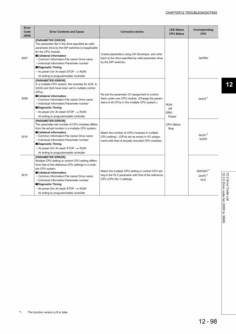
CHAPTER12 TROUBLESHOOTING
12
12.3 Error C
ode List12.3.5 E
rror code list (3000 to 3999)
3007
[PARAMETER ERROR]The parameter file in the drive specified as valid parameter drive by the DIP switches is inapplicable for the CPU module.■Collateral information• Common Information:File name/ Drive name• Individual Information:Parameter number
■Diagnostic Timing• At power-On/ At reset/ STOP RUN/
At writing to progurammable controller
Create parameters using GX Developer, and write them to the drive specified as valid parameter drive by the DIP switches.
RUN:Off
ERR.:Flicker
CPU Status:Stop
QnPRH
3009
[PARAMETER ERROR]In a multiple CPU system, the modules for AnS, A, Q2AS and QnA have been set to multiple control CPUs.■Collateral information• Common Information:File name/ Drive name• Individual Information:Parameter number
■Diagnostic Timing• At power-On/ At reset/ STOP RUN/
At writing to progurammable controller
Re-set the parameter I/O assignment to control them under one CPU module. (Change the param-eters of all CPUs in the multiple CPU system.)
Qn(H)*1
3010
[PARAMETER ERROR]The parameter-set number of CPU modules differs from the actual number in a multiple CPU system.■Collateral information• Common Information:File name/ Drive name• Individual Information:Parameter number
■Diagnostic Timing• At power-On/ At reset/ STOP RUN/
At writing to progurammable controller
Match the number of (CPU modules in multiple CPU setting) - (CPUs set as empty in I/O assign-ment) with that of actually mounted CPU modules.
Qn(H)*1
QnPH
3012
[PARAMETER ERROR]Multiple CPU setting or control CPU setting differs from that of the reference CPU settings in a multi-ple CPU system.■Collateral information• Common Information:File name/ Drive name• Individual Information:Parameter number
■Diagnostic Timing• At power-On/ At reset/ STOP RUN/
At writing to progurammable controller
Match the multiple CPU setting or control CPU set-ting in the PLC parameter with that of the reference CPU (CPU No.1) settings.
Q00/Q01*1
Qn(H)*1
QnU
ErrorCode(SD0)
Error Contents and Cause Corrective ActionLED StatusCPU Status
CorrespondingCPU
12 - 98*1 The function version is B or later.

3013
[PARAMETER ERROR]Multiple CPU auto refresh setting is any of the fol-lowings in a multiple CPU system.• When a bit device is specified as a refresh
device, a number other than a multiple of 16 is specified for the refresh-starting device.
• The device specified is other than the one that may be specified.
• The number of send points is an odd number.■Collateral information• Common Information:File name/ Drive name• Individual Information:Parameter number
■Diagnostic Timing• At power-On/ At reset/ STOP RUN/
At writing to progurammable controller
Check the following in the multiple CPU auto refresh setting and make correction.• When specifying the bit device, specify a multiple
of 16 for the refresh starting device.• Specify the device that may be specified for the
refresh device.• Set the number of send points to an even num-
ber.
RUN:Off
ERR.:Flicker
CPU Status:Stop
Qn(H)*1
QnPH
[PARAMETER ERROR]In a multiple CPU system, the multiple CPU auto refresh setting is any of the following.• The total number of transmission points is
greater than the maximum number of refresh points.
■Collateral information• Common Information:File name/ Drive name• Individual Information:Parameter number
■Diagnostic Timing• At power-On/ At reset/ STOP RUN/
At writing to progurammable controller
Check the following in the multiple CPU auto refresh setting and make correction.• The total number of transmission points is within
the maximum number of refresh points.
Q00/Q01*1
[PARAMETER ERROR]In a multiple CPU system, the multiple CPU auto refresh setting is any of the following.• The device specified is other than the one that
may be specified.• The number of send points is an odd number.• The total number of send points is greater than
the maximum number of refresh points.• The setting of the refresh range crosses over the
boundary between the internal user device and the extended data register (D) or extended link register (W).
■Collateral information• Common Information:File name/ Drive name• Individual Information:Parameter number
■Diagnostic Timing• At power-On/ At reset/ STOP RUN/
At writing to progurammable controller
Check the following in the multiple CPU auto refresh setting and make correction.• Specify the device that may be specified for the
refresh device.• Set the number of send points to an even num-
ber.• Set the total number of send points within the
range of the maximum number of refresh points.• Set the refresh range so that it does not cross
over the boundary between the internal user device and the extended data register (D) or extended link register (W).
QnU*10
3014
[PARAMETER ERROR]• In a multiple CPU system, the online module
change parameter (multiple CPU system param-eter) settings differ from those of the reference CPU.
• In a multiple CPU system, the online module change setting is enabled although the CPU module mounted does not support online module chang parameter.
■Collateral information• Common Information:File name/ Drive name• Individual Information:Parameter number
■Diagnostic Timing• At power-On/ At reset/ STOP RUN/
At writing to progurammable controller
• Match the online module change parameter with that of the reference CPU.
• If the CPU module that does not support online module change is mounted, replace it with the CPU module that supports online module change.
Qn(H)QnPH
QnU*8
ErrorCode(SD0)
Error Contents and Cause Corrective ActionLED StatusCPU Status
CorrespondingCPU
*1 The function version is B or later.*8 The Universal model QCPU except the Q00UJCPU, Q00UCPU, Q01UCPU, and Q02UCPU.
12 - 99*10 The Universal model QCPU except the Q00UJCPU.
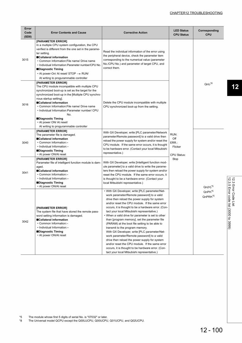
CHAPTER12 TROUBLESHOOTING
12
12.3 Error C
ode List12.3.5 E
rror code list (3000 to 3999)
3015
[PARAMETER ERROR]In a multiple CPU system configuration, the CPU verified is different from the one set in the parame-ter setting.■Collateral information• Common Information:File name/ Drive name• Individual Information:Parameter number/CPU No.
■Diagnostic Timing• At power-On/ At reset/ STOP RUN/
At writing to progurammable controller
Read the individual information of the error using the peripheral device, check the parameter item corresponding to the numerical value (parameter No./CPU No.) and parameter of target CPU, and correct them.
RUN:Off
ERR.:Flicker
CPU Status:Stop
QnU*8
3016
[PARAMETER ERROR]The CPU module incompatible with multiple CPU synchronized boot-up is set as the target for the synchronized boot-up in the [Multiple CPU synchro-nous startup setting].■Collateral information• Common Information:File name/ Drive name• Individual Information:Parameter number/ CPU
No.■Diagnostic Timing• At power ON/ At reset/
At writing to progurammable controller
Delete the CPU module incompatible with multiple CPU synchronized boot-up from the setting.
3040
[PARAMETER ERROR]The parameter file is damaged.■Collateral information• Common Information:–• Individual Information:–
■Diagnostic Timing• At power ON/At reset
With GX Developer, write [PLC parameter/Network parameter/Remote password] to a valid drive then reload the power supply for system and/or reset the CPU module. If the same error occurs, it is thought to be hardware error. (Contact your local Mitsubishi representative.)
Qn(H)*5
QnPH*5
QnPRH*5
3041
[PARAMETER ERROR]Parameter file of intelligent function module is dam-aged.■Collateral information• Common Information:–• Individual Information:–
■Diagnostic Timing• At power ON/At reset
With GX Developer, write [Intelligent function mod-ule parameter] to a valid drive to write the parame-ters then reload the power supply for system and/or reset the CPU module. If the same error occurs, it is thought to be a hardware error. (Contact your local Mitsubishi representative.)
3042
[PARAMETER ERROR]The system file that have stored the remote pass-word setting information is damaged.■Collateral information• Common Information:–• Individual Information:–
■Diagnostic Timing• At power ON/At reset
• With GX Developer, write [PLC parameter/Net-work parameter/Remote password] to a valid drive then reload the power supply for system and/or reset the CPU module. If the same error occurs, it is thought to be a hardware error. (Con-tact your local Mitsubishi representative.)
• When a valid drive for parameter is set to other than [program memory], set the parameter file (PARAM) at the boot file setting to be able to transmit to the program memory.With GX Developer, write [PLC parameter/Net-work parameter/Remote password] to a valid drive then reload the power supply for system and/or reset the CPU module. If the same error occurs, it is thought to be hardware error. (Con-tact your local Mitsubishi representative.)
ErrorCode(SD0)
Error Contents and Cause Corrective ActionLED StatusCPU Status
CorrespondingCPU
*5 The module whose first 5 digits of serial No. is "07032" or later.
12 - 100*8 The Universal model QCPU except the Q00UJCPU, Q00UCPU, Q01UCPU, and Q02UCPU.

3100
[LINK PARA. ERROR]In a multiple CPU system, the CC-Link IE controller network module controlled by another CPU is spec-ified as the head I/O number of the CC-Link IE con-troller network module.■Collateral information• Common Information:File name/ Drive name• Individual Information:Parameter number
■Diagnostic Timing• At power-ON/ At reset/ STOP RUN
• Delete the network parameter of the CC-Link IE controller network module controlled by another CPU.
• Change the setting to the head I/O number of the CC-Link IE controller network module controlled by host CPU.
RUN:Off
ERR.:Flicker
CPU Status:Stop
Qn(H)*7
QnPH*9
QnU
[LINK PARA. ERROR]The network parameter of the CC-Link IE controller network operating as the normal station is overwrit-ten to the control station.Or, the network parameter of the CC-Link IE con-troller network operating as the control station is overwritten to the normal station.(The network parameter is updated on the module by resetting.)■Collateral information• Common Information:File name/ Drive name• Individual Information:Parameter number
■Diagnostic Timing• At power-ON/ At reset/ STOP RUN
Reset the CPU module.
Qn(H)*7
QnPH*9
QnPRH*9
QnU
[LINK PARA. ERROR]• The number of modules actually mounted is dif-
ferent from that is set in Network parameter for MELSECNET/H.
• The head I/O number of the actually mounted module is different from the one set in the net-work parameter of the CC-Link IE controller net-work.
• Data cannot be handled in the parameter exists.• The network type of CC-Link IE controller net-
work is overwritten during power-on. (When changing the network type, switch RESET to RUN.)
■Collateral information• Common Information:File name/ Drive name• Individual Information:Parameter number
■Diagnostic Timing• At power-ON/ At reset/ STOP RUN
• Check the network parameter and actual mount-ing status, and if they differ, make them matched. When network parameters are modified, write them to the CPU module.
• Check the setting of extension base unit stage number.
• Check the connection status of extension base unit and extension cable. When the GOT is bus-connected to the main base unit or extension base unit, also check its connection status.If an error occurs even after performing the above checks, the hardware may be faulty.(Contact your local Mitsubishi representative, explaining a detailed description of the problem.)
[LINK PARA. ERROR]• The CC-Link IE controller network module is
specified for the head I/O number of network parameter in the MELSECNET/H.
• The MELSECNET/H module is specified for the head I/O number of network parameter in the CC-Link IE controller network.
■Collateral information• Common Information:File name/ Drive name• Individual Information:Parameter number
■Diagnostic Timing• At power-ON/ At reset/ STOP RUN
ErrorCode(SD0)
Error Contents and Cause Corrective ActionLED StatusCPU Status
CorrespondingCPU
*7 The module whose first 5 digits of serial No. is "09012" or later.
12 - 101*9 The module whose first 5 digits of serial No. is "10042" or later.

CHAPTER12 TROUBLESHOOTING
12
12.3 Error C
ode List12.3.5 E
rror code list (3000 to 3999)
3100
[LINK PARA. ERROR]• Although the CC-Link IE controller network mod-
ule is mounted, network parameter for the CC-Link IE controller network module is not set.
• Although the CC-Link IE controller network and MELSECNET/H modules are mounted, network parameter for the MELSECNET/H module is not set.
■Collateral information• Common Information:File name/ Drive name• Individual Information:Parameter number
■Diagnostic Timing• At power-ON/ At reset/ STOP RUN
• Check the network parameter and actual mount-ing status, and if they differ, make them matched. When network parameters are modified, write them to the CPU module.
• Check the setting of extension base unit stage number.
• Check the connection status of extension base unit and extension cable. When the GOT is bus-connected to the main base unit or extension base unit, also check its connection status.If an error occurs even after performing the above checks, the hardware may be faulty.(Contact your local Mitsubishi representative, explaining a detailed description of the problem.)
RUN:Off
ERR.:Flicker
CPU Status:Stop
Qn(H)*7
QnPH*9
QnPRH*9
QnU
[LINK PARA. ERROR]In a multiple CPU system, the MELSECNET/H under control of another CPU is specified as the head I/O number in the network setting parameter of the MELSECNET/H.■Collateral information• Common Information:File name/ Drive name• Individual Information:Parameter number
■Diagnostic Timing• At power ON/At reset/STOP RUN
• Delete the MELSECNET/H network parameter of the MELSECNET/H under control of another CPU.
• Change the setting to the head I/O number of the MELSECNET/H under control of the host CPU.
Q00/Q01*1
Qn(H)*1
QnPH
QnU*10
[LINK PARA. ERROR]The network parameter of the MELSECNET/H operating as the normal station is overwritten to the control station. Or, the network parameter of the MELSECNET/H operating as the control station is overwritten to the normal station. (The network parameter is updated on the module by resetting.)■Collateral information• Common Information:File name/ Drive name• Individual Information:Parameter number
■Diagnostic Timing• At power ON/At reset/STOP RUN
Reset the CPU module.
Qn(H)*1
QnPHQnPRH
QnU
[LINK PARA. ERROR]• The number of modules actually mounted is dif-
ferent from that is set in Network parameter for MELSECNET/H.
• The head I/O number of actually installed mod-ules is different from that designated in the net-work parameter of MELSECNET/H.
• Some data in the parameters cannot be handled.• The network type of MELSECNET/H is overwrit-
ten during power-on. (When changing the net-work type, switch RESET to RUN.)
• The mode switch of MELSECNET/H module*5 is outside the range.
■Collateral information• Common Information:File name/ Drive name• Individual Information:Parameter number
■Diagnostic Timing• At power ON/At reset/STOP RUN
• Check the network parameters and actual mounting status, and if they differ, make them matched.If any network parameter has been corrected, write it to the CPU module.
• Check the extension base unit stage No. setting.• Check the connection status of the extension
base units and extension cables.When the GOT is bus-connected to the main base unit and extension base units, also check the connection status.
If the error occurs after the above checks, the pos-sible cause is a hardware fault. (Contact your local Mitsubishi representative, explaining a detailed description of the problem.)
• Set the mode switch of MELSECNET/H module*5 within the range.
QCPU
ErrorCode(SD0)
Error Contents and Cause Corrective ActionLED StatusCPU Status
CorrespondingCPU
*1 The function version is B or later.*5 The module whose first 5 digits of serial No. is "07032" or later.*7 The module whose first 5 digits of serial No. is "09012" or later.*9 The module whose first 5 digits of serial No. is "10042" or later.
12 - 102*10 The Universal model QCPU except the Q00UJCPU.

3101
[LINK PARA. ERROR]The link refresh range exceeded the file register capacity.■Collateral information• Common Information:File name/ Drive name• Individual Information:Parameter number
■Diagnostic Timing• When an END instruction executed
Change the file register file for the one that enables entire range refresh.
RUN:Off
ERR.:Flicker
CPU Status:Stop
Qn(H)*1
QnPHQnPRH
QnU*10
[LINK PARA. ERROR]• When the station number of the MELSECNET/H
module is 0, the PLC-to-PLC network parameter has been set.
• When the station number of the MELSECNET/H module is other than 0, the remote master parameter setting has been made.
■Collateral information• Common Information:File name/ Drive name• Individual Information:Parameter number
■Diagnostic Timing• At power ON/At reset/STOP RUN
Correct the type or station number of the MELSEC-NET/H module in the network parameter to meet the used system.
Qn(H)*1
QnPHQnPRH
[LINK PARA. ERROR]The refresh parameter for the CC-Link IE controller network is outside the range.■Collateral information• Common Information:File name/ Drive name• Individual Information:Parameter number
■Diagnostic Timing• At power ON/At reset/STOP RUN
• Check the network parameters and mounting status, and if they differ, match the network parameters and mounting status.If any network parameter has been corrected, write it to the CPU module.
• Confirm the setting of the number of extension stages of the extension base units.
• Check the connection status of the extension base units and extension cables.When the GOT is bus-connected to the main base unit and extension base units, also check their connection status.
If the error occurs after the above checks, the cause is a hardware fault. (Contact your local Mit-subishi representative, explaining a detailed description of the problem.)
Qn(H)*7
QnPH*9
QnPRH*9
QnU
[LINK PARA. ERROR]• The network No. specified by a network parame-
ter is different from that of the actually mounted network.
• The head I/O No. specified by a network parame-ter is different from that of the actually mounted I/O unit.
• The network class specified by a network param-eter is different from that of the actually mounted network.
• The network refresh parameter of the MELSEC-NET/H, MELSECNET/10 is out of the specified area.
■Collateral information• Common Information:File name/ Drive name• Individual Information:Parameter number
■Diagnostic Timing• At power ON/At reset/STOP RUN
QCPU
[LINK PARA. ERROR]A multi-remote I/O network was configured using a module that does not support the MELSECNET/H multi-remote I/O network.■Collateral information• Common Information:File name/ Drive name• Individual Information:Parameter number
■Diagnostic Timing• At power ON/At reset/STOP RUN
Use a module that supports the MELSECNET/H multi-remote I/O network.
QnPH
ErrorCode(SD0)
Error Contents and Cause Corrective ActionLED StatusCPU Status
CorrespondingCPU
*1 The function version is B or later.*7 The module whose first 5 digits of serial No. is "09012" or later.*9 The module whose first 5 digits of serial No. is "10042" or later.
12 - 103*10 The Universal model QCPU except the Q00UJCPU.

CHAPTER12 TROUBLESHOOTING
12
12.3 Error C
ode List12.3.5 E
rror code list (3000 to 3999)
3101
[LINK PARA. ERROR]• The system A of the MELSECNET/H remote
master station has been set to other than Station No. 0.
• The system B of the MELSECNET/H remote master station has been set to Station No. 0.
■Collateral information• Common Information:File name/ Drive name• Individual Information:Parameter number
■Diagnostic Timing• At power ON/At reset/STOP RUN
• Set the system A of the MELSECNET/H remote master station to Station No. 0.
• Set the system B of the MELSECNET/H remote master station to any of Station No. 1 to 64.
RUN:Off
ERR.:Flicker
CPU Status:Stop
QnPRH
[LINK PARA. ERROR]Since the number of points of the B/W device set in [Device] of the PLC parameter is lower than the number of B/W refresh device points shown in the following table when parameters of the MELSEC-NET/H are not set, the refresh between the CPU module and the MELSECNET/H cannot be per-
formed..
■Collateral information• Common Information:File name/ Drive name• Individual Information:Parameter number
■Diagnostic Timing• At power ON/At reset/STOP RUN
Set the refresh parameter of the MELSECNET/H in accordance with the number of points of B/W devices set in [Device] of the PLC parameter.
Qn(H)*7
QnPH*7
QnPRH*7
QnU
[LINK PARA. ERROR]The setting of the network refresh range crosses over the boundary between the internal user device and the extended data register (D) or extended link register (W).■Collateral information• Common Information:File name/ Drive name• Individual Information:Parameter number
■Diagnostic Timing• At power ON/At reset/STOP RUN
Set the network refresh range so that it does not cross over the boundary between the internal user device and the extended data register (D) or extended link register (W).
QnU
ErrorCode(SD0)
Error Contents and Cause Corrective ActionLED StatusCPU Status
CorrespondingCPU
No. of refresh device
points of B device
No. of refresh device
points of W device
1
8192 points
(8192 points×1
module)
8192 points
(8192 points×1
module)
2
8192 points
(4096 points×2
modules)
8192 points
(4096 points×2
modules)
3
6144 points
(2048 points×3
modules)
6144 points
(2048 points×3
modules)
4
8192 points
(2048 points×4
modules)
8192 points
(2048 points×4
modules)
Refresh
device
No. of
mountable
network
modules
12 - 104*7 The module whose first 5 digits of serial No. is "09012" or later.

3102
[LINK PARA. ERROR]A CC-Link IE controller network parameter error was detected.■Collateral information• Common Information:File name/ Drive name• Individual Information:Parameter number
■Diagnostic Timing• At power ON/At reset/STOP RUN • Correct and write the network parameters.
• If the error occurs after correction, it suggests a hardware fault. (Contact your local Mitsubishi representative.)
RUN:Off
ERR.:Flicker
CPU Status:Stop
Qn(H)*7
QnPH*9
QnPRH*9
QnU
[LINK PARA. ERROR]• The network module detected a network parame-
ter error.• A MELSECNET/H network parameter error was
detected.■Collateral information• Common Information:File name/ Drive name• Individual Information:Parameter number
■Diagnostic Timing• At power ON/At reset/STOP RUN
QCPU
[LINK PARA. ERROR]The station No. specified in pairing setting are not correct.• The stations are not numbered consecutively.• Pairing setting has not been made for the CPU
module at the normal station.■Collateral information• Common Information:File name/ Drive name• Individual Information:Parameter number
■Diagnostic Timing• At power ON/At reset/STOP RUN
Refer to the troubleshooting of the network module, and if the error is due to incorrect pairing setting, reexamine the pairing setting of the network param-eter.
QnPRH
[LINK PARA. ERROR]The CC-Link IE controller network module whose first 5 digits of serial No. is "09041" or earlier is mounted.■Collateral information• Common Information:File name/ Drive name• Individual Information:Parameter number
■Diagnostic Timing• At power ON/At reset/STOP RUN
Mount the CC-Link IE controller network module whose first 5 digits of serial No. is "09042" or later.
QnU
[LINK PARA. ERROR]Group cyclic function in CC-Link IE controller net-work that does not correspond to group cyclic func-tion is set.■Collateral information• Common Information:File name/ Drive name• Individual Information:Parameter number
■Diagnostic Timing• At power ON/At reset/STOP RUN
Set group cyclic function in function version D or later of CC-Link IE controller network. QnU*9
[LINK PARA. ERROR]Paring setting in CC-Link IE controller network modules installed in CPUs except for redundant CPUs was performed.■Collateral information• Common Information:File name/ Drive name• Individual Information:Parameter number
■Diagnostic Timing• At power ON/At reset/STOP RUN
Examine the paring setting for the network parame-ter in the control staion.
Q00J/Q00/Q01
Qn(H)*9
QnPH*9
QnU*9
ErrorCode(SD0)
Error Contents and Cause Corrective ActionLED StatusCPU Status
CorrespondingCPU
*7 The module whose first 5 digits of serial No. is "09012" or later.
12 - 105*9 The module whose first 5 digits of serial No. is "10042" or later.
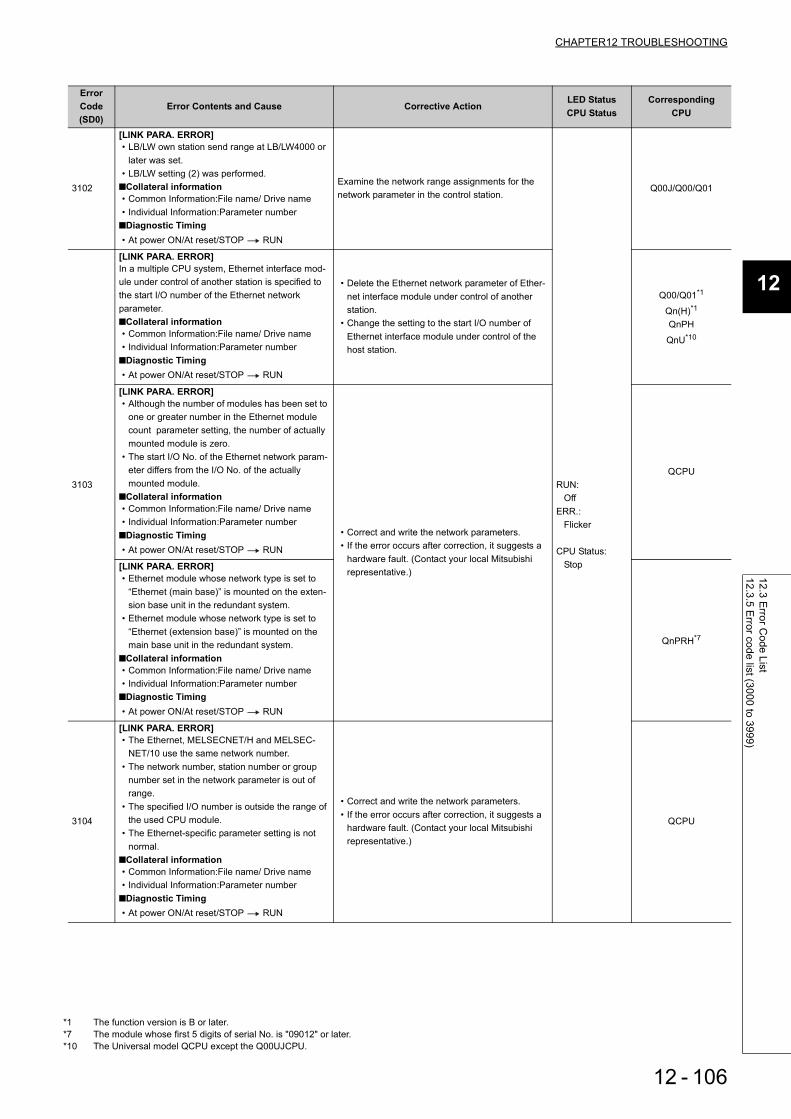
CHAPTER12 TROUBLESHOOTING
12
12.3 Error C
ode List12.3.5 E
rror code list (3000 to 3999)
3102
[LINK PARA. ERROR]• LB/LW own station send range at LB/LW4000 or
later was set.• LB/LW setting (2) was performed.
■Collateral information• Common Information:File name/ Drive name• Individual Information:Parameter number
■Diagnostic Timing• At power ON/At reset/STOP RUN
Examine the network range assignments for the network parameter in the control station.
RUN:Off
ERR.:Flicker
CPU Status:Stop
Q00J/Q00/Q01
3103
[LINK PARA. ERROR]In a multiple CPU system, Ethernet interface mod-ule under control of another station is specified to the start I/O number of the Ethernet network parameter.■Collateral information• Common Information:File name/ Drive name• Individual Information:Parameter number
■Diagnostic Timing• At power ON/At reset/STOP RUN
• Delete the Ethernet network parameter of Ether-net interface module under control of another station.
• Change the setting to the start I/O number of Ethernet interface module under control of the host station.
Q00/Q01*1
Qn(H)*1
QnPH
QnU*10
[LINK PARA. ERROR]• Although the number of modules has been set to
one or greater number in the Ethernet module count parameter setting, the number of actually mounted module is zero.
• The start I/O No. of the Ethernet network param-eter differs from the I/O No. of the actually mounted module.
■Collateral information• Common Information:File name/ Drive name• Individual Information:Parameter number
■Diagnostic Timing• At power ON/At reset/STOP RUN
• Correct and write the network parameters.• If the error occurs after correction, it suggests a
hardware fault. (Contact your local Mitsubishi representative.)
QCPU
[LINK PARA. ERROR]• Ethernet module whose network type is set to
“Ethernet (main base)” is mounted on the exten-sion base unit in the redundant system.
• Ethernet module whose network type is set to “Ethernet (extension base)” is mounted on the main base unit in the redundant system.
■Collateral information• Common Information:File name/ Drive name• Individual Information:Parameter number
■Diagnostic Timing• At power ON/At reset/STOP RUN
QnPRH*7
3104
[LINK PARA. ERROR]• The Ethernet, MELSECNET/H and MELSEC-
NET/10 use the same network number.• The network number, station number or group
number set in the network parameter is out of range.
• The specified I/O number is outside the range of the used CPU module.
• The Ethernet-specific parameter setting is not normal.
■Collateral information• Common Information:File name/ Drive name• Individual Information:Parameter number
■Diagnostic Timing• At power ON/At reset/STOP RUN
• Correct and write the network parameters.• If the error occurs after correction, it suggests a
hardware fault. (Contact your local Mitsubishi representative.)
QCPU
ErrorCode(SD0)
Error Contents and Cause Corrective ActionLED StatusCPU Status
CorrespondingCPU
*1 The function version is B or later.*7 The module whose first 5 digits of serial No. is "09012" or later.
12 - 106*10 The Universal model QCPU except the Q00UJCPU.

3105
[LINK PARA. ERROR]In a multiple CPU system, the CC-Link module under control of another station is specified as the head I/O number of the CC-Link network parame-ter.■Collateral information• Common Information:File name/ Drive name• Individual Information:Parameter number
■Diagnostic Timing• At power ON/At reset/STOP RUN
• Delete the CC-Link network parameter of the CC-Link module under control of another station.
• Change the setting to the start I/O number of the CC-Link module under control of the host station.
RUN:Off
ERR.:Flicker
CPU Status:Stop
Q00/Q01*1
Qn(H)*1
QnPH
QnU*10
[LINK PARA. ERROR]• Though the number of CC-Link modules set in
the network parameters is one or more, the num-ber of actually mounted modules is zero.
• The start I/O number in the common parameters is different from that of the actually mounted module.
• The station type of the CC-Link module count setting parameters is different from that of the actually mounted station.
■Collateral information• Common Information:File name/ Drive name• Individual Information:Parameter number
■Diagnostic Timing• At power ON/At reset/STOP RUN
• Correct and write the network parameters.• If the error occurs after correction, it suggests a
hardware fault. (Contact your local Mitsubishi representative.)
QCPU
[LINK PARA. ERROR]• CC-Link module whose station type is set to
“master station (compatible with redundant func-tion)” is mounted on the extension base unit in the redundant system.
• CC-Link module whose station type is set to “master station (extension base)” is mounted on the main base unit in the redundant system.
■Collateral information• Common Information:File name/ Drive name• Individual Information:Parameter number
■Diagnostic Timing• At power ON/At reset/STOP RUN
QnPRH*7
ErrorCode(SD0)
Error Contents and Cause Corrective ActionLED StatusCPU Status
CorrespondingCPU
*1 The function version is B or later.*7 The module whose first 5 digits of serial No. is "09012" or later.
12 - 107*10 The Universal model QCPU except the Q00UJCPU.

CHAPTER12 TROUBLESHOOTING
12
12.3 Error C
ode List12.3.5 E
rror code list (3000 to 3999)
3106
[LINK PARA. ERROR]The CC-Link link refresh range exceeded the file register capacity.■Collateral information• Common Information:File name/ Drive name• Individual Information:Parameter number
■Diagnostic Timing• When an END instruction executed
Change the file register file for the one refresh-enabled in the whole range.
RUN:Off
ERR.:Flicker
CPU Status:Stop
Qn(H)*1
QnPHQnPRH
QnU
[LINK PARA. ERROR]The network refresh parameter for CC-Link is out of range.■Collateral information• Common Information:File name• Individual Information:Parameter number
■Diagnostic Timing• At power ON/At reset/STOP RUN
Check the parameter setting. QCPU
[LINK PARA. ERROR]The setting of the network refresh range crosses over the boundary between the internal user device and the extended data register (D) or extended link register (W).■Collateral information• Common Information:File name• Individual Information:Parameter number
■Diagnostic Timing• At power ON/At reset/STOP RUN
Set the network refresh range so that it does not cross over the boundary between the internal user device and the extended data register (D) or extended link register (W).
QnU
3107
[LINK PARA. ERROR]• The CC-Link parameter setting is incorrect.• The set mode is not allowed for the version of the
mounted CC-Link module.■Collateral information• Common Information:File name• Individual Information:Parameter number
■Diagnostic Timing• At power ON/At reset/STOP RUN
Check the parameter setting. QCPU
3200
[SFC PARA. ERROR]The parameter setting is illegal.• Though Block 0 was set to "Automatic start" in
the SFC setting of the PLC parameter dialog box, Block 0 does not exist.
■Collateral information• Common Information:File name• Individual Information:Parameter number
■Diagnostic Timing• STOP RUN
Read the common information of the error using the peripheral device, check error step correspond-ing to its numerical value (program error location), and correct the problem.
Q00J/Q00/Q01*1
QnPHQnPRH
QnU
3201
[SFC PARA. ERROR]The block parameter setting is illegal.■Collateral information• Common Information:File name• Individual Information:Parameter number
■Diagnostic Timing• STOP RUN
Qn(H)QnPH
QnPRH
ErrorCode(SD0)
Error Contents and Cause Corrective ActionLED StatusCPU Status
CorrespondingCPU
12 - 108*1 The function version is B or later.

3202
[SFC PARA. ERROR]The number of step relays specified in the device setting of the PLC parameter dialog box is less than that used in the program.■Collateral information• Common Information:File name• Individual Information:Parameter number
■Diagnostic Timing• STOP RUN
Read the common information of the error using the peripheral device, check error step correspond-ing to its numerical value (program error location), and correct the problem.
RUN:Off
ERR.:Flicker
CPU Status:Stop
Qn(H)QnPH
QnPRH
3203
[SFC PARA. ERROR]The execution type of the SFC program specified in the program setting of the PLC parameter dialog box is other than scan execution.■Collateral information• Common Information:File name• Individual Information:Parameter number
■Diagnostic Timing• At power-ON/ At reset/ STOP RUN*3
Qn(H)QnPH
QnPRHQnU
3300
[SP. PARA ERROR]The start I/O number in the intelligent function mod-ule parameter set on GX Configurator differs from the actual I/O number.■Collateral information• Common Information:File name
• Individual Information:Parameter number*2
■Diagnostic Timing• At power-On/ At reset/ STOP RUN/
At writing to progurammable controller
Check the parameter setting. QCPU
3301
[SP. PARA ERROR]• The refresh setting of the intelligent function
module exceeded the file register capacity.• The intelligent function module set in GX Config-
urator differs from the actually mounted module.■Collateral information• Common Information:File name
• Individual Information:Parameter number*2
■Diagnostic Timing• At power-On/ At reset/ STOP RUN/
At writing to progurammable controller
• Change the file register file for the one which allows refresh in the whole range.
• Check the parameter setting.
Q00J/Q00/Q01
Qn(H)*1
QnPHQnPRH
QnU
[SP. PARA ERROR]The intelligent function module's refresh parameter setting is outside the available range.■Collateral information• Common Information:File name
• Individual Information:Parameter number*2
■Diagnostic Timing• At power-On/ At reset/ STOP RUN/
At writing to progurammable controller
Check the parameter setting. QCPU
[SP. PARA ERROR]The setting of the refresh parameter range crosses over the boundary between the internal user device and the extended data register (D) or extended link register (W).■Collateral information• Common Information:File name
• Individual Information:Parameter number*2
■Diagnostic Timing• At power-On/ At reset/ STOP RUN/
At writing to progurammable controller
Set the refresh parameter range so that it does not cross over the boundary between the internal user device and the extended data register (D) or extended link register (W).
QnU
ErrorCode(SD0)
Error Contents and Cause Corrective ActionLED StatusCPU Status
CorrespondingCPU
*1 The function version is B or later.*2 Parameter No. is the value gained by dividing the head I/O number of parameter in the intelligent function module set by GX Configurator by 10H.
12 - 109*3 The diagnostic timing of CPU modules except for Universal QCPU can be performed only when switching the CPU modules to run.

CHAPTER12 TROUBLESHOOTING
12
12.3 Error C
ode List12.3.5 E
rror code list (3000 to 3999)
3302
[SP. PARA ERROR]The intelligent function module's refresh parameter are abnormal.■Collateral information• Common Information:File name
• Individual Information:Parameter number*2
■Diagnostic Timing• At power-On/ At reset/ STOP RUN/
At writing to progurammable controller
Check the parameter setting.
RUN:Off
ERR.:Flicker
CPU Status:Stop
QCPU
3303
[SP. PARA ERROR]In a multiple CPU system, the automatic refresh setting or other parameter setting was made to the intelligent function module under control of another station.■Collateral information• Common Information:File name/ Drive name• Individual Information:Parameter number
■Diagnostic Timing• At power-On/ At reset/ STOP RUN/
At writing to progurammable controller
• Delete the automatic refresh setting or other parameter setting of the intelligent function mod-ule under control of another CPU.
• Change the setting to the automatic refresh set-ting or other parameter setting of the intelligent function module under control of the host CPU.
Q00/Q01*1
Qn(H)*1
QnPH
QnU*10
3400
[REMOTE PASS. ERR.]The head I/O number of the target module of the remote password is set to other than 0H to 0FF0H.■Collateral information• Common Information:–• Individual Information:–
■Diagnostic Timing• At power ON/At reset/STOP RUN
Change the head I/O number of the target module to be within the 0H to 0FF0H range.
Qn(H)*1
QnPHQnPRH
QnU*7
[REMOTE PASS. ERR.]The head I/O number of the target module of the remote password is set to other than 0H to 07E0H.■Collateral information• Common Information:–• Individual Information:–
■Diagnostic Timing• At power ON/At reset/STOP RUN
Change the head I/O number of the target module to be within the 0H to 07E0H range.
Q02U
[REMOTE PASS. ERR.]The head I/O number of the target module of the remote password is outside the following range.• Q00JCPU: 0H to 1E0H
• Q00CPU/Q01CPU: 0H to 3E0H
■Collateral information• Common Information:–• Individual Information:–
■Diagnostic Timing• At power ON/At reset/STOP RUN
Change the head I/O number of the target module of the remote password for the number within the following range.• Q00JCPU: 0H to 1E0H
• Q00CPU/Q01CPU: 0H to 3E0H
Q00J/Q00/Q01*1
ErrorCode(SD0)
Error Contents and Cause Corrective ActionLED StatusCPU Status
CorrespondingCPU
*1 The function version is B or later.*2 Parameter No. is the value gained by dividing the head I/O number of parameter in the intelligent function module set by GX Configurator by 10H.*7 The module whose first 5 digits of serial No. is "09012" or later.
12 - 110*10 The Universal model QCPU except the Q00UJCPU.

3401
[REMOTE PASS. ERR.]Position specified as the head I/O number of the remote password file is incorrect due to one of the following reasons:• Module is not loaded.• Other than a the intelligent function module (I/O
module)• Intelligent function module other than serial com-
munication module, modem interface module or Ethernet module
• Serial communication module or Ethernet mod-ule of function version A
The intelligent function module where remote pass-word is available is not mounted.■Collateral information• Common Information:–• Individual Information:–
■Diagnostic Timing• At power ON/At reset/STOP RUN
Mount serial communication module, modem inter-face module or Ethernet module of function version B or later in the position specified in the head I/O No. of the remote password file.
RUN:Off
ERR.:Flicker
CPU Status:Stop
Qn(H)*1
QnPHQnPRH
QnU
[REMOTE PASS. ERR.]Any of the following modules is not mounted on the slot specified for the head I/O number of the remote password.• Serial communication module of function version
B or later• Ethernet module of function version B or later• Modem interface module of function version B or
later■Collateral information• Common Information:–• Individual Information:–
■Diagnostic Timing• At power ON/At reset/STOP RUN
Mount any of the following modules in the position specified for the head I/O number of the remote password.• Serial communication module of function version
B or later• Ethernet module of function version B or later• Modem interface module of function version B or
later
Q00J/Q00/Q01*1
[REMOTE PASS. ERR.]Serial communication module, modem interface module or Ethernet module of function version B or later controlled by another CPU was specified in a multiple CPU system.■Collateral information• Common Information:–• Individual Information:–
■Diagnostic Timing• At power ON/At reset/STOP RUN
• Change it for the Ethernet module of function version B or later connected by the host CPU.
• Delete the remote password setting.
Qn(H)*1
QnPH
QnU*10
ErrorCode(SD0)
Error Contents and Cause Corrective ActionLED StatusCPU Status
CorrespondingCPU
*1 The function version is B or later.
12 - 111*10 The Universal model QCPU except the Q00UJCPU.

CHAPTER12 TROUBLESHOOTING
12
12.3 Error C
ode List12.3.6 E
rror code list (4000 to 4999)
12.3.6 Error code list (4000 to 4999)
The following shows the error messages from the error code 4000 to 4999, the contents and causes of the errors, and the corrective actions for the errors.
ErrorCode(SD0)
Error Contents and Cause Corrective ActionLED StatusCPU Status
CorrespondingCPU
4000
[INSTRCT. CODE ERR]• The program contains an instruction code that
cannot be decoded.• An unusable instruction is included in the pro-
gram.■Collateral information• Common Information:Program error location• Individual Information:–
■Diagnostic Timing• At power ON/At reset/STOP RUN
When instruction executed
Read the common information of the error using a peripheral device, check error step corresponding to its numerical value (program error location), and correct the problem.
RUN:Off
ERR.:Flicker
CPU Status:Stop
QCPU
4001
[INSTRCT. CODE ERR]The program contains a dedicated instruction for SFC although it is not an SFC program.■Collateral information• Common Information:Program error location• Individual Information:–
■Diagnostic Timing• At power ON/At reset/STOP RUN
When instruction executed
Q00J/Q00/Q01*2
Qn(H)QnPH
QnPRHQnU
4002
[INSTRCT. CODE ERR]• The name of dedicated instruction specified by
the program is incorrect.• The dedicated instruction specified by the pro-
gram cannot be executed by the specified mod-ule.
■Collateral information• Common Information:Program error location• Individual Information:–
■Diagnostic Timing• At power ON/At reset/STOP RUN
When instruction executed
QCPU
4003
[INSTRCT. CODE ERR]The number of devices for the dedicated instruction specified by the program is incorrect.■Collateral information• Common Information:Program error location• Individual Information:–
■Diagnostic Timing• At power ON/At reset/STOP RUN
When instruction executed
4004
[INSTRCT. CODE ERR]The device which cannot be used by the dedicated instruction specified by the program is specified.■Collateral information• Common Information:Program error location• Individual Information:–
■Diagnostic Timing• At power ON/At reset/STOP RUN
When instruction executed
12 - 112*2 The function version is B or later.
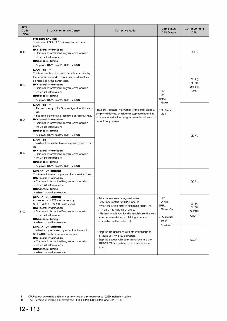
4010
[MISSING END INS.]There is no END (FEND) instruction in the pro-gram.■Collateral information• Common Information:Program error location• Individual Information:–
■Diagnostic Timing• At power ON/At reset/STOP RUN
Read the common information of the error using a peripheral device, check error step corresponding to its numerical value (program error location), and correct the problem.
RUN:Off
ERR.:Flicker
CPU Status:Stop
QCPU
4020
[CAN'T SET(P)]The total number of internal file pointers used by the program exceeds the number of internal file pointers set in the parameters.■Collateral information• Common Information:Program error location• Individual Information:–
■Diagnostic Timing• At power ON/At reset/STOP RUN
Qn(H)QnPH
QnPRHQnU
4021
[CAN'T SET(P)]• The common pointer Nos. assigned to files over-
lap.• The local pointer Nos. assigned to files overlap.
■Collateral information• Common Information:Program error location• Individual Information:–
■Diagnostic Timing• At power ON/At reset/STOP RUN QCPU
4030
[CAN'T SET(I)]The allocation pointer Nos. assigned by files over-lap.■Collateral information• Common Information:Program error location• Individual Information:–
■Diagnostic Timing• At power ON/At reset/STOP RUN
4100
[OPERATION ERROR]The instruction cannot process the contained data.■Collateral information• Common Information:Program error location• Individual Information:–
■Diagnostic Timing• When instruction executed
RUN:Off/On
ERR.:Flicker/On
CPU Status:Stop/
Continue*1
QCPU
[OPERATION ERROR]Access error of ATA card occurs bySP.FREAD/SP.FWRITE instructions.■Collateral information• Common Information:Program error location• Individual Information:–
■Diagnostic Timing• When instruction executed
• Take measurements against noise.• Reset and restart the CPU module.
When the same error is displayed again, the ATA card has hardware failure.(Please consult your local Mitsubishi service cen-ter or representative, explaining a detailed description of the problem.)
Qn(H)QnPH
QnPRH
QnU*11
[OPERATION ERROR]The file being accessed by other functions with SP.FWRITE instruction was accessed.■Collateral information• Common Information:Program error location• Individual Information:–
■Diagnostic Timing• When instruction executed
• Stop the file accessed with other functions to execute SP.FWRITE instruction.
• Stop the access with othrer functions and the SP.FWRITE instructuion to execute at same time.
QnU*11
ErrorCode(SD0)
Error Contents and Cause Corrective ActionLED StatusCPU Status
CorrespondingCPU
*1 CPU operation can be set in the parameters at error occurrence. (LED indication varies.)
12 - 113*11 The Universal model QCPU except the Q00UJCPU, Q00UCPU, and Q01UCPU.

CHAPTER12 TROUBLESHOOTING
12
12.3 Error C
ode List12.3.6 E
rror code list (4000 to 4999)
4101
[OPERATION ERROR]• The number of setting data dealt with the instruc-
tion exceeds the applicable range.• The storage data and constant of the device
specified by the instruction exceeds the applica-ble range.
• When writing to the host CPU shared memory, the write prohibited area is specified for the write destination address.
• The range of storage data of the device specified by the instruction is duplicated.
• The device specified by the instruction exceeds the range of the number of device points.
• The interrupt pointer No. specified by the instruc-tion exceeds the applicable range.
■Collateral information• Common Information:Program error location• Individual Information:–
■Diagnostic Timing• When instruction executed
Read the common information of the error using the peripheral device, check error step correspond-ing to its numerical value (program error location), and correct the problem.
RUN:Off/On
ERR.:Flicker/On
CPU Status:Stop/
Continue*1
QCPU
[OPERATION ERROR]• The storage data of file register specified by the
instruction exceeds the applicable range. Or, file register is not set.
■Collateral information• Common Information:Program error location• Individual Information:–
■Diagnostic Timing• When instruction executed
QnU*10
[OPERATION ERROR]• The block data that crosses over the boundary
between the internal user device and the extended data register (D) or extended link regis-ter is specified (including 32-bit binary, real num-ber (single precision, double precision), indirect address, and control data)
■Collateral information• Common Information:Program error location• Individual Information:–
■Diagnostic Timing• When instruction executed
QnU
ErrorCode(SD0)
Error Contents and Cause Corrective ActionLED StatusCPU Status
CorrespondingCPU
*1 CPU operation can be set in the parameters at error occurrence. (LED indication varies.)
12 - 114*10 The Universal model QCPU except the Q00UJCPU.

4102
[OPERATION ERROR]In a multiple CPU system, the link direct device
(J \ ) was specified for the network module under control of another station.■Collateral information• Common Information:Program error location• Individual Information:–
■Diagnostic Timing• When instruction executed
• Delete from the program the link direct device which specifies the network module under con-trol of another CPU.
• Using the link direct device, specify the network module under control of the host CPU.
RUN:Off/On
ERR.:Flicker/On
CPU Status:Stop/
Continue*1
Q00/Q01*2
Qn(H)*2
QnPH
QnU*10
[OPERATION ERROR]• The network No. or station No. specified for the
dedicated instruction is wrong.
• The link direct device (J \ ) setting is incorrect.• The module No./ network No./number of charac-
ter strings exceeds the range that can be speci-fied.
■Collateral information• Common Information:Program error location• Individual Information:–
■Diagnostic Timing• When instruction executed
Read the common information of the error using the peripheral device, check error step correspond-ing to its numerical value (program error location), and correct the problem.
QCPU
[OPERATION ERROR]• The specification of character string
(" ") specified by dedicated instruction cannot be used for the character string.
■Collateral information• Common Information:Program error location• Individual Information:–
■Diagnostic Timing• When instruction executed
QnU
4103
[OPERATION ERROR]The configuration of the PID dedicated instruction is incorrect.■Collateral information• Common Information:Program error location• Individual Information:–
■Diagnostic Timing• When instruction executed
Q00J/Q00/
Q01*2
Qn(H)QnPRH
QnU
4105
[OPERATION ERROR]PLOADP/PUNLOADP/PSWAPP instructins were executed while setting program memory check.■Collateral information• Common Information:Program error location• Individual Information:–
■Diagnostic Timing• When instruction executed
• Delete the program memory check setting.• When using the program memory check, delete
PLOADP/PUNLOADP/PSWAPP instructions.QnPH*5
4107
[OPERATION ERROR]33 or more multiple CPU dedicated instructions were executed from one CPU module.■Collateral information• Common Information:Program error location• Individual Information:–
■Diagnostic Timing• When instruction executed
Using the multiple CPU dedicated instruction com-pletion bit, provide interlocks to prevent one CPU module from executing 33 or more multiple CPU dedicated instructions.
Q00/Q01*2
Qn(H)*2
QnPHQ00U/Q01U
Q02U
ErrorCode(SD0)
Error Contents and Cause Corrective ActionLED StatusCPU Status
CorrespondingCPU
*1 CPU operation can be set in the parameters at error occurrence. (LED indication varies.)*2 The function version is B or later.*5 The module whose first 5 digits of serial No. is "07032" or later.
12 - 115*10 The Universal model QCPU except the Q00UJCPU.

CHAPTER12 TROUBLESHOOTING
12
12.3 Error C
ode List12.3.6 E
rror code list (4000 to 4999)
4109
[OPERATION ERROR]With high speed interrupt setting PR, PRC, UDCNT1, UDCNT2, PLSY or PWM instruction is executed.■Collateral information• Common Information:Program error location• Individual Information:–
■Diagnostic Timing• When instruction executed
Delete the high-speed interrupt setting.When using high-speed interrupt, delete the PR, PRC, UDCNT1, UDCNT2, PLSY and PWM instruc-tions.
RUN:Off/On
ERR.:Flicker/On
CPU Status:Stop/
Continue*1
Qn(H)*3
4111
[OPERATION ERROR]An attempt was made to perform write/read to/from the CPU shared memory write/read disable area of the host station CPU module with the instruction.■Collateral information• Common Information:Program error location• Individual Information:–
■Diagnostic Timing• When instruction executed
Read the common information of the error using GX Developer, and check and correct the error step corresponding to that value (program error loca-tion).
Q00/Q01*2
QnU
4112
[OPERATION ERROR]The CPU module that cannot be specified with the multiple CPU dedicated instruction was specified.■Collateral information• Common Information:Program error location• Individual Information:–
■Diagnostic Timing• When instruction executed
Q00/Q01*2
QnU*10
4113
[OPERATION ERROR]• When the SP.DEVST instruction is executed, the
number of writing to the standard ROM of the day exceeds the value specified by SD695.
• The value outside the specified range is set to SD695.
■Collateral information• Common Information:Program error location• Individual Information:–
■Diagnostic Timing• When instruction executed
• Check that the number of execution of the SP.DEVST instruction is proper.
• Execute the SP.DEVST instruction again the fol-lowing day or later day. Or, arrange the value of SD695.
• Correct the value of SD695 so that it does not exceed the range.
RUN:Off/On
ERR.:Flicker/On
CPU Status:Stop/Continue
QnU
4120
[OPERATION ERROR]Since the manual system switching enable flag (special register SM1592) is OFF, manual system switching cannot be executed by the control system switching instruction (SP. CONTSW).■Collateral information• Common Information:Program error location• Individual Information:–
■Diagnostic Timing• When instruction executed
To execute control system switching by the SP. CONTSW instruction, turn ON the manual system switching enable flag (special register SM1592).
RUN:Off/On
ERR.:Flicker/On
CPU Status:Stop/
Continue*1
QnPRH
4121
[OPERATION ERROR]• In the separate mode, the control system switch-
ing instruction (SP. CONTSW) was executed in the standby system CPU module.
• In the debug mode, the control system switching instruction (SP. CONTSW) was executed.
■Collateral information• Common Information:Program error location• Individual Information:–
■Diagnostic Timing• When instruction executed
• Reexamine the interlock signal for the SP. CONTSW instruction, and make sure that the SP. CONTSW instruction is executed in the control system only. (Since the SP. CONTSW instruction cannot be executed in the standby system, it is recommended to provide an interlock using the operation mode signal or like.)
• As the SP. CONTSW instruction cannot be exe-cuted in the debug mode, reexamine the inter-lock signal related to the operation mode.
RUN:Off/On
ERR.:Flicker/On
CPU Status:Stop/
Continue*1
QnPRH
ErrorCode(SD0)
Error Contents and Cause Corrective ActionLED StatusCPU Status
CorrespondingCPU
*1 CPU operation can be set in the parameters at error occurrence. (LED indication varies.)*2 The function version is B or later.*3 The module whose first 5 digits of serial No. is "04012" or later.
12 - 116*10 The Universal model QCPU except the Q00UJCPU.

4122
[OPERATION ERROR]• The dedicated instruction was executed to the
module mounted on the extension base unit in the redundant system.
• The instruction for accessing the intelligent func-tion module mounted on the extension base unit from the standby system at separate mode was executed.
■Collateral information• Common Information:Program error location• Individual Information:–
■Diagnostic Timing• When instruction executed
• Delete the dedicated instruction for the module mounted on the extension base unit.
• Delete the instruction for accessing the intelligent function module mounted on the extension base unit from the standby system.
RUN:Off/On
ERR.:Flicker/On
CPU Status:Stop/Continue
QnPRH*6
4130
[OPERATION ERROR]Instructions to read SFC step comment (S(P).SFC-SCOMR) and SFC transition condition comment (S(P).SFCTCOMR) are executed for the comment file in ATA card■Collateral information• Common Information:Program error location• Individual Information:–
■Diagnostic Timing• When END/other instruction executed
Target comment file is to be other than the com-ment file in ATA card.
RUN:Off/On
ERR.:Flicker/On
CPU Status:Stop/
Continue*1
Qn(H)*4
QnPH*5
QnPRH
4131
[OPERATION ERROR]The SFC program is started up by the instruction while the other SFC program has not yet been completed.■Collateral information• Common Information:Program error location• Individual Information:–
■Diagnostic Timing• When instruction executed
Check the SFC program specified by the instruc-tion. Or, check the executing status of the SFC pro-gram.
RUN:Off/On
ERR.:Flicker/On
CPU Status:Stop/Continue
QnU4140
[OPERATION ERROR]Operation where the input data is special value ("-0", unnormalized number, nonnumeric, ) is performed.■Collateral information• Common Information:Program error location• Individual Information:–
■Diagnostic Timing• When instruction executed
Read the common information of the error using the peripheral device, check the error step corre-sponding to the numerical value (program error part), and correct it.
RUN:Off/On
ERR.:Flicker/On
CPU Status:Stop/
Continue*1
4141
[OPERATION ERROR]Overflow occurs at operation.■Collateral information• Common Information:Program error location• Individual Information:–
■Diagnostic Timing• When instruction executed
Read the common information of the error using the peripheral device, check the error step corre-sponding to the numerical value (program error part), and correct it.
4200
[FOR NEXT ERROR]No NEXT instruction was executed following the execution of a FOR instruction.Alternatively, there are fewer NEXT instructions than FOR instructions.■Collateral information• Common Information:Program error location• Individual Information:–
■Diagnostic Timing• When instruction executed
Read the common information of the error using the peripheral device, check error step correspond-ing to its numerical value (program error location), and correct the problem.
RUN:Off
ERR.:Flicker
CPU Status:Stop
QCPU
ErrorCode(SD0)
Error Contents and Cause Corrective ActionLED StatusCPU Status
CorrespondingCPU
*1 CPU operation can be set in the parameters at error occurrence. (LED indication varies.)*4 The module whose first 5 digits of serial No. is "07012" or later.*5 The module whose first 5 digits of serial No. is "07032" or later.
12 - 117*6 The module whose first 5 digits of serial No. is "09012" or later.

CHAPTER12 TROUBLESHOOTING
12
12.3 Error C
ode List12.3.6 E
rror code list (4000 to 4999)
4201
[FOR NEXT ERROR]A NEXT instruction was executed although no FOR instruction has been executed.Alternatively, there are more NEXT instructions than FOR instructions.■Collateral information• Common Information:Program error location• Individual Information:–
■Diagnostic Timing• When instruction executed
Read the common information of the error using the peripheral device, check error step correspond-ing to its numerical value (program error location), and correct the problem.
RUN:Off
ERR.:Flicker
CPU Status:Stop
QCPU
4202
[FOR NEXT ERROR]More than 16 nesting levels are programmed.■Collateral information• Common Information:Program error location• Individual Information:–
■Diagnostic Timing• When instruction executed
Keep nesting levels at 16 or under.
4203
[FOR NEXT ERROR]A BREAK instruction was executed although no FOR instruction has been executed prior to that.■Collateral information• Common Information:Program error location• Individual Information:–
■Diagnostic Timing• When instruction executed
Read the common information of the error using the peripheral device, check error step correspond-ing to its numerical value (program error location), and correct the problem.
4210
[CAN'T EXECUTE(P)]The CALL instruction is executed, but there is no subroutine at the specified pointer.■Collateral information• Common Information:Program error location• Individual Information:–
■Diagnostic Timing• When instruction executed
4211
[CAN'T EXECUTE(P)]There was no RET instruction in the executed sub-routine program.■Collateral information• Common Information:Program error location• Individual Information:–
■Diagnostic Timing• When instruction executed
Read the common information of the error using the peripheral device, check error step correspond-ing to its numerical value (program error location), and correct the problem.
4212
[CAN'T EXECUTE(P)]The RET instruction exists before the FEND instruction of the main routine program.■Collateral information• Common Information:Program error location• Individual Information:–
■Diagnostic Timing• When instruction executed
4213
[CAN'T EXECUTE(P)]More than 16 nesting levels are programmed.■Collateral information• Common Information:Program error location• Individual Information:–
■Diagnostic Timing• When instruction executed
Keep nesting levels at 16 or under.
ErrorCode(SD0)
Error Contents and Cause Corrective ActionLED StatusCPU Status
CorrespondingCPU
12 - 118

4220
[CAN'T EXECUTE(I)]Though an interrupt input occurred, the corre-sponding interrupt pointer does not exist.■Collateral information• Common Information:Program error location• Individual Information:–
■Diagnostic Timing• When instruction executed
Read the common information of the error using the peripheral device, check error step correspond-ing to its numerical value (program error location), and correct the problem.
RUN:Off
ERR.:Flicker
CPU Status:Stop
QCPU4221
[CAN'T EXECUTE(I)]An IRET instruction does not exist in the executed interrupt program.■Collateral information• Common Information:Program error location• Individual Information:–
■Diagnostic Timing• When instruction executed
4223
[CAN'T EXECUTE(I)]The IRET instruction exists before the FEND instruction of the main routine program.■Collateral information• Common Information:Program error location• Individual Information:–
■Diagnostic Timing• When instruction executed
[CAN'T EXECUTE(I)]• The IRET instruction was executed in the fixed
scan execution type program.• The STOP instruction was executed in the fixed
scan execution type program.■Collateral information• Common Information:Program error location• Individual Information:–
■Diagnostic Timing• When instruction executed
QnU
4225
[CAN'T EXECUTE(I)]The interrupt pointer for the module mounted on the extension base unit is set in the redundant sys-tem.■Collateral information• Common Information:–• Individual Information:–
■Diagnostic Timing• At power-ON/At reset
Delete the setting of interrupt pointer for the module mounted on the extension base unit, since it cannot be used.
QnPRH*6
4230
[INST. FORMAT ERR.]The number of CHK and CHKEND instructions is not equal.■Collateral information• Common Information:Program error location• Individual Information:–
■Diagnostic Timing• When instruction executed
Read the common information of the error using the peripheral device, check error step correspond-ing to its numerical value (program error location), and correct the problem.
Qn(H)QnPH
4231
[INST. FORMAT ERR.]The number of IX and IXEND instructions is not equal.■Collateral information• Common Information:Program error location• Individual Information:–
■Diagnostic Timing• When instruction executed
QCPU
ErrorCode(SD0)
Error Contents and Cause Corrective ActionLED StatusCPU Status
CorrespondingCPU
12 - 119*6 The module whose first 5 digits of serial No. is "09012" or later.

CHAPTER12 TROUBLESHOOTING
12
12.3 Error C
ode List12.3.6 E
rror code list (4000 to 4999)
4235
[INST. FORMAT ERR.]The configuration of the check conditions for the CHK instruction is incorrect.Alternatively, a CHK instruction has been used in a low speed execution type program.■Collateral information• Common Information:Program error location• Individual Information:–
■Diagnostic Timing• When instruction executed
Read the common information of the error using the peripheral device, check error step correspond-ing to its numerical value (program error location), and correct the problem.
RUN:Off
ERR.:Flicker
CPU Status:Stop
Qn(H)QnPH
4350
[MULTI-COM.ERROR]• The multiple CPU high-speed transmission dedi-
cated instruction used in the program specifies the wrong CPU module. Or, the setting in the CPU module is incompatible with the multiple CPU high-speed transmission dedicated instruc-tion.
• The reserved CPU is specified.• The uninstalled CPU is specified.• The head I/O number of the target CPU/16 (n1)
is outside the range of 3EH to 3E3H.• The CPU module where the instruction cannot be
executed is specified.• The instruction is executed in a single CPU sys-
tem.• The host CPU is specified.• The instruction is executed without setting the
"Use multiple CPU high speed communication".■Collateral information• Common Information:Program error location• Individual Information:–
■Diagnostic Timing• When instruction executed
QnU*7
4351
[MULTI-COM.ERROR]• The multiple CPU high-speed transmission dedi-
cated instruction specified by the program cannot be executed to the specified target CPU module.
• The instruction name is wrong.• The instruction unsupported by the target CPU
module is specified.■Collateral information• Common Information:Program error location• Individual Information:–
■Diagnostic Timing• When instruction executed
4352
[MULTI-COM.ERROR]The number of devices for the multiple CPU high-speed transmission dedicated instruction specified by the program is wrong.■Collateral information• Common Information:Program error location• Individual Information:–
■Diagnostic Timing• When instruction executed
ErrorCode(SD0)
Error Contents and Cause Corrective ActionLED StatusCPU Status
CorrespondingCPU
12 - 120*7 The Universal model QCPU except the Q00UJCPU, Q00UCPU, Q01UCPU, and Q02UCPU.

4353
[MULTI-COM.ERROR]The device which cannot be used for the multiple CPU high-speed transmission dedicated instruction specified by the program is specified.■Collateral information• Common Information:Program error location• Individual Information:–
■Diagnostic Timing• When instruction executed
Read the common information of the error using the peripheral device, check error step corresponding to its numerical value (program error location), and correct the problem.
RUN:Off
ERR.:Flicker
CPU Status:Stop
QnU*7
4354
[MULTI-COM.ERROR]The character string which cannot be handled by the multiple CPU high-speed transmission dedi-cated instruction is specified.■Collateral information• Common Information:Program error location• Individual Information:–
■Diagnostic Timing• When instruction executed
QnU*7
4355
[MULTI-COM.ERROR]The number of read/write data (number of request/receive data) for the multiple CPU high-speed transmission dedicated instruction specified by the program is not valid.■Collateral information• Common Information:Program error location• Individual Information:–
■Diagnostic Timing• When instruction executed
4400
[SFCP. CODE ERROR]No SFCP or SFCPEND instruction in SFC pro-gram.■Collateral information• Common Information:Program error location• Individual Information:–
■Diagnostic Timing• STOP RUN
Write the program to the CPU module again using GX Developer.
Qn(H)QnPH
QnPRH
4410
[CAN'T SET(BL)]The block number designated by the SFC program exceeds the range.■Collateral information• Common Information:Program error location• Individual Information:–
■Diagnostic Timing• STOP RUN
Q00J/Q00/Q01*2
Qn(H)QnPH
QnPRHQnU
4411
[CAN'T SET(BL)]Block number designations overlap in SFC pro-gram.■Collateral information• Common Information:Program error location• Individual Information:–
■Diagnostic Timing• STOP RUN
4420
[CAN'T SET(S)]A step number designated in an SFC program exceeds the range.■Collateral information• Common Information:Program error location• Individual Information:–
■Diagnostic Timing• STOP RUN
ErrorCode(SD0)
Error Contents and Cause Corrective ActionLED StatusCPU Status
CorrespondingCPU
*2 The function version is B or later.
12 - 121*7 The Universal model QCPU except the Q00UJCPU, Q00UCPU, Q01UCPU, and Q02UCPU.

CHAPTER12 TROUBLESHOOTING
12
12.3 Error C
ode List12.3.6 E
rror code list (4000 to 4999)
4421
[CAN'T SET(S)]Total number of steps in all SFC programs exceed the maximum.■Collateral information• Common Information:Program error location• Individual Information:–
■Diagnostic Timing• STOP RUN Write the program to the CPU module again using
GX Developer.
RUN:Off
ERR.:Flicker
CPU Status:Stop
Q00J/Q00/Q01*2
Qn(H)QnPH
QnPRHQnU
4422
[CAN'T SET(S)]Step number designations overlap in SFC program.■Collateral information• Common Information:Program error location• Individual Information:–
■Diagnostic Timing• STOP RUN
4423
[CAN'T SET(S)]The total number of (maximum step No.+1) of each block exceeds the total number of step relays.■Collateral information• Common Information:Program error location• Individual Information:–
■Diagnostic Timing• STOP RUN
Correct the total number of step relays so that it does not exceed the total number of (maximum step No.+1) of each block.
Q00J/Q00/Q01*2
QnU
4430
[SFC EXE. ERROR]The SFC program cannot be executed.• The data of the block data setting is illegal.• The SFC data device of the block data setting is
beyond the device setting range set in the PLC parameter.
■Collateral information• Common Information:File name/Drive name• Individual Information:–
■Diagnostic Timing• STOP RUN
• Write the program to the CPU module again using GX Developer.
• After correcting the setting of the SFC data device, write it to the CPU module.
• After correcting the device setting range set in the PLC parameter, write it to the CPU module.
4431
[SFC EXE. ERROR]The SFC program cannot be executed.• The block parameter setting is abnormal.
■Collateral information• Common Information:File name/Drive name• Individual Information:–
■Diagnostic Timing• STOP RUN Write the program to the CPU module again using
GX Developer.
4432
[SFC EXE. ERROR]The SFC program cannot be executed.• The structure of the SFC program is illegal.
■Collateral information• Common Information:File name/Drive name• Individual Information:–
■Diagnostic Timing• STOP RUN
ErrorCode(SD0)
Error Contents and Cause Corrective ActionLED StatusCPU Status
CorrespondingCPU
12 - 122*2 The function version is B or later.

4500
[SFCP. FORMAT ERR.]The numbers of BLOCK and BEND instructions in an SFC program are not equal.■Collateral information• Common Information:Program error location• Individual Information:–
■Diagnostic Timing• STOP RUN
Write the program to the CPU module again using the peripheral device.
RUN:Off
ERR.:Flicker
CPU Status:Stop
Qn(H)QnPH
QnPRH
4501
[SFCP. FORMAT ERR.]The configuration of the STEP* to TRAN* to TSET to SEND instructions in the SFC program is incor-rect.■Collateral information• Common Information:Program error location• Individual Information:–
■Diagnostic Timing• STOP RUN
4502
[SFCP. FORMAT ERR.]The structure of the SFC program is illegal.• STEPI* instruction does not exist in the block of
the SFC program.■Collateral information• Common Information:Program error location• Individual Information:–
■Diagnostic Timing• STOP RUN
Q00J/Q00/Q01*2
Qn(H)QnPH
QnPRHQnU
4503
[SFCP. FORMAT ERR.]The structure of the SFC program is illegal.• The step specified in the TSET instruction does
not exist.• In jump transition, the host step number was
specified as the destination step number.■Collateral information• Common Information:Program error location• Individual Information:–
■Diagnostic Timing• STOP RUN
• Write the program to the CPU module again using GX Developer.
• Read the common information of the error using GX Developer, and check and correct the error step corresponding to that value (program error location).
4504
[SFCP. FORMAT ERR.]The structure of the SFC program is illegal.• The step specified in the TAND instruction does
not exist.■Collateral information• Common Information:Program error location• Individual Information:–
■Diagnostic Timing• STOP RUN
Write the program to the CPU module again using GX Developer.
ErrorCode(SD0)
Error Contents and Cause Corrective ActionLED StatusCPU Status
CorrespondingCPU
12 - 123*2 The function version is B or later.

CHAPTER12 TROUBLESHOOTING
12
12.3 Error C
ode List12.3.6 E
rror code list (4000 to 4999)
4505
[SFCP. FORMAT ERR.]The structure of the SFC program is illegal.• In the operation output of a step, the SET Sn/
BLmSn or RST Sn/BLmSn instruction was speci-fied for the host step.
■Collateral information• Common Information:Program error location• Individual Information:–
■Diagnostic Timing• STOP RUN
Read the common information of the error using GX Developer, and check and correct the error step corresponding to that value (program error loca-tion).
RUN:Off
ERR.:Flicker
CPU Status:Stop
Q00J/Q00/Q01*2
QnU
4506
[SFCP. FORMAT ERR.]The structure of the SFC program is illegal.• In a reset step, the host step number was speci-
fied as the destination step.■Collateral information• Common Information:Program error location• Individual Information:–
■Diagnostic Timing• STOP RUN
4600
[SFCP. OPE. ERROR]The SFC program contains data that cannot be pro-cessed.■Collateral information• Common Information:Program error location• Individual Information:–
■Diagnostic Timing• When instruction executed
Read common information of the error using the peripheral device, check error step corresponding to its numerical value (program error location), and correct the problem.
RUN:Off/On
ERR.:Flicker/On
CPU Status:Stop/
Continue*1
Qn(H)QnPH
QnPRH4601
[SFCP. OPE. ERROR]Exceeds device range that can be designated by the SFC program.■Collateral information• Common Information:Program error location• Individual Information:–
■Diagnostic Timing• When instruction executed
4602
[SFCP. OPE. ERROR]The START instruction in an SFC program is pre-ceded by an END instruction.■Collateral information• Common Information:Program error location• Individual Information:–
■Diagnostic Timing• When instruction executed
ErrorCode(SD0)
Error Contents and Cause Corrective ActionLED StatusCPU Status
CorrespondingCPU
*1 CPU operation can be set in the parameters at error occurrence. (LED indication varies.)
12 - 124*2 The function version is B or later.

4610
[SFCP. EXE. ERROR]The active step information at presumptive start of the SFC program is incorrect.■Collateral information• Common Information:Program error location• Individual Information:–
■Diagnostic Timing• STOP RUN
Read common information of the error using the peripheral device, check error step corresponding to its numerical value (program error location), and correct the problem.The program is automatically subjected to an initial start.
RUN:On
ERR.:On
CPU Status:Continue Qn(H)
QnPHQnPRH
4611
[SFCP. EXE. ERROR]Key-switch was reset during RUN when presump-tive start was designated for SFC program.■Collateral information• Common Information:Program error location• Individual Information:–
■Diagnostic Timing• STOP RUN
4620
[BLOCK EXE. ERROR]Startup was executed at a block in the SFC pro-gram that was already started up.■Collateral information• Common Information:Program error location• Individual Information:–
■Diagnostic Timing• When instruction executed
Read common information of the error using the peripheral device, check error step corresponding to its numerical value (program error location), and correct the problem.
RUN:Off
ERR.:Flicker
CPU Status:Stop
4621
[BLOCK EXE. ERROR]Startup was attempted at a block that does not exist in the SFC program.■Collateral information• Common Information:Program error location• Individual Information:–
■Diagnostic Timing• When instruction executed
• Read the common information of the error using GX Developer, and check and correct the error step corresponding to that value (program error location).
• Turn ON if the special relay SM321 is OFF.
Q00J/Q00/Q01*2
Qn(H)QnPH
QnPRHQnU
4630
[STEP EXE. ERROR]Startup was executed at a block in the SFC pro-gram that was already started up.■Collateral information• Common Information:Program error location• Individual Information:–
■Diagnostic Timing• When instruction executed
Read common information of the error using the peripheral device, check error step corresponding to its numerical value (program error location), and correct the problem.
Qn(H)QnPH
QnPRH
ErrorCode(SD0)
Error Contents and Cause Corrective ActionLED StatusCPU Status
CorrespondingCPU
12 - 125*2 The function version is B or later.

CHAPTER12 TROUBLESHOOTING
12
12.3 Error C
ode List12.3.6 E
rror code list (4000 to 4999)
4631
[STEP EXE. ERROR]• Startup was attempted at the step that does not
exist in the SFC program.Or, the step that does not exist in the SFC pro-gram was specified for end.
• Forced transition was executed based on the transition condition that does not exit in the SFC program. Or, the transition condition for forced transition that does not exit in the SFC program was can-celed.
■Collateral information• Common Information:Program error location• Individual Information:–
■Diagnostic Timing• When instruction executed
• Read the common information of the error using the peripheral device, and check and correct the error step corresponding to that value (program error location).
• Turn ON if the special relay SM321 is OFF.
RUN:Off
ERR.:Flicker
CPU Status:Stop
Q00J/Q00/Q01*2
Qn(H)QnPH
QnPRHQnU
4632
[STEP EXE. ERROR]There were too many simultaneous active steps in blocks that can be designated by the SFC program.■Collateral information• Common Information:Program error location• Individual Information:–
■Diagnostic Timing• When instruction executed
Read common information of the error using the peripheral device, check error step corresponding to its numerical value (program error location), and correct the problem.
Qn(H)QnPH
QnPRHQnU
4633
[STEP EXE. ERROR]There were too many simultaneous active steps in all blocks that can be designated.■Collateral information• Common Information:Program error location• Individual Information:–
■Diagnostic Timing• When instruction executed
ErrorCode(SD0)
Error Contents and Cause Corrective ActionLED StatusCPU Status
CorrespondingCPU
12 - 126*2 The function version is B or later.

12.3.7 Error code list (5000 to 5999)
The following shows the error messages from the error code 5000 to 5999, the contents and causes of the errors, and the corrective actions for the errors.
ErrorCode(SD0)
Error Contents and Cause Corrective ActionLED StatusCPU Status
CorrespondingCPU
5000
[WDT ERROR]• The scan time of the initial execution type pro-
gram exceeded the initial execution monitoring time specified in the PLC RAS setting of the PLC parameter.
■Collateral information• Common Information:Time (value set)• Individual Information:Time (value actually mea-
sured)■Diagnostic Timing• Always
• Read the individual information of the error from the peripheral device, check its value (time), and shorten the scan time.
• Change the initial execution monitoring time or the WDT value in the PLC RAS setting of the PLC parameter.
• Resolve the endless loop caused by jump transi-tion.
RUN:Off
ERR.:Flicker
CPU Status:Stop
Qn(H)QnPH
QnPRHQnU
[WDT ERROR]• The power supply of the standby system is
turned OFF.• The tracking cable is disconnected or connected
without turning off or resetting the standby sys-tem.
• The tracking cable is not secured by the connec-tor fixing screws.
■Collateral information• Common Information:Time (value set)• Individual Information:Time (value actually mea-
sured)■Diagnostic Timing• Always
• Since power-off of the standby system increases the control system scan time, reset the WDT value, taking the increase of the control system scan time into consideration.
• When the tracking cable is disconnected during operation, securely connect it and restart the CPU module. If the same error is displayed again, the tracking cable or CPU module has a hardware fault. (Contact your local Mitsubishi representative, explaining a detailed description of the problem.)
QnPRH
5001
[WDT ERROR]• The scan time of the program exceeded the
WDT value specified in the PLC RAS setting of the PLC parameter.
■Collateral information• Common Information:Time (value set)• Individual Information:Time (value actually mea-
sured)■Diagnostic Timing• Always
• Read the individual information of the error using the peripheral device, check its value (time), and shorten the scan time.
• Change the initial execution monitoring time or the WDT value in the PLC RAS setting of the PLC parameter.
• Resolve the endless loop caused by jump transi-tion.
QCPU
[WDT ERROR]• The power supply of the standby system is
turned OFF.• The tracking cable is disconnected or connected
without turning off or resetting the standby sys-tem.
• The tracking cable is not secured by the connec-tor fixing screws.
■Collateral information• Common Information:Time (value set)• Individual Information:Time (value actually mea-
sured)■Diagnostic Timing• Always
• Since power-off of the standby system increases the control system scan time, reset the WDT value, taking the increase of the control system scan time into consideration.
• When the tracking cable is disconnected during operation, securely connect it and restart the CPU module. If the same error is displayed again, the tracking cable or CPU module has a hardware fault. (Contact your local Mitsubishi representative, explaining a detailed description of the problem.)
QnPRH
12 - 127

CHAPTER12 TROUBLESHOOTING
12
12.3 Error C
ode List12.3.7 E
rror code list (5000 to 5999)
5010
[PRG. TIME OVER]The program scan time exceeded the constant scan setting time specified in the PLC RAS setting of the PLC parameter.■Collateral information• Common Information:Time (value set)• Individual Information:Time (value actually mea-
sured)■Diagnostic Timing• Always
• Review the constant scan setting time.• Review the constant scan setting time and low
speed program execution time in the PLC param-eter so that the excess time of constant scan can be fully secured.
RUN:On
ERR.:On
CPU Status:Continue
Qn(H)QnPH
QnPRHQnU
[PRG. TIME OVER]The low speed program execution time specified in the PLC RAS setting of the PLC parameter exceeded the excess time of the constant scan.■Collateral information• Common Information:Time (value set)• Individual Information:Time (value actually mea-
sured)■Diagnostic Timing• Always
Qn(H)QnPH
QnPRH
[PRG. TIME OVER]The program scan time exceeded the constant scan setting time specified in the PLC RAS setting of the PLC parameter.■Collateral information• Common Information:Time (value set)• Individual Information:Time (value actually mea-
sured)■Diagnostic Timing• Always
Review the constant scan setting time in the PLC parameter so that the excess time of constant scan can be fully secured.
Q00J/Q00/Q01
5011
[PRG. TIME OVER]The scan time of the low speed execution type pro-gram exceeded the low speed execution watch time specified in the PLC RAS setting of the PLC parameter dialog box.■Collateral information• Common Information:Time (value set)• Individual Information:Time (value actually mea-
sured)■Diagnostic Timing• Always
Read the individual information of the error using the peripheral device, check the numerical value (time) there, and shorten scan time if necessary. Change the low speed execution watch time in the PLC RAS setting of the PLC parameter dialog box.
Qn(H)QnPH
ErrorCode(SD0)
Error Contents and Cause Corrective ActionLED StatusCPU Status
CorrespondingCPU
12 - 128

12.3.8 Error code list (6000 to 6999)
The following shows the error messages from the error code 6000 to 6999, the contents and causes of the errors, and the corrective actions for the errors.
ErrorCode(SD0)
Error Contents and Cause Corrective ActionLED StatusCPU Status
CorrespondingCPU
6000
[FILE DIFF.]In a redundant system, the control system and standby system do not have the same programs and parameters.
The file type detected as different between the two systems can be checked by the file name of the error common information.
• The program is different.(File name = ********.QPG)
• The PLC parameters/network parameters/redun-dant parameters are different.(File name = PARAM.QPA)
• The remote password is different.(File name = PARAM.QPA)
• The intelligent function module parameters are different.(File name = IPARAM.QPA)
• The device initial values are different.(File name = ********.QDI)
• The capacity of each write destination within the CPU for online pchange of multiple program blocks is different.(File name = MBOC.QMB)(This can be detected from the standby system of the redundant system.)
■Collateral information• Common Information:File name• Individual Information:–
■Diagnostic Timing• At power ON/At reset/
At tracking cable connection/At changing to backup mode/At completion of write during RUN/At system switching/At switching both systems into RUN
• Match the programs and parameters of the con-trol system and standby system.
• Verify the systems by either of the following pro-cedures 1), 2) to clarify the differences between the files of the two systems, then correct a wrong file, and execute “Write to PLC“ again.
1) After reading the programs/parameters of System A using GX Developer or PX Developer, verify them with those of System B.
2) Verify the programs/parameters of GX Devel-oper or PX Developer saved in the offline environment with those written to the CPU modules of both systems.
• When the capacity of each write destination within the CPU for online change of multiple pro-gram blocks is different between the two sys-tems, take corrective action 1) or 2).
1) Using the memory copy from control system to standby system, copy the program memory from the control system to the standby sys-tem.
2) Format the CPU module program memories of both systems. (For the capacity of each write destination within the CPU for online change of multiple program blocks, set the same value to both systems.)
RUN:Off
ERR.:Flicker
CPU Status:Stop
QnPRH
6001
[FILE DIFF.]In a redundant system, the valid parameter drive settings (SW2, SW3) made by the DIP switches are not the same.■Collateral information• Common Information:–• Individual Information:–
■Diagnostic Timing• At power ON/At reset/At tracking cable connec-
tion/At operation mode change
Match the valid parameter drive settings (SW2, SW3) by the DIP switches of the control system and standby system.
12 - 129
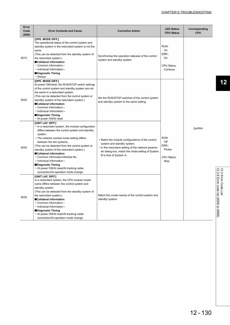
CHAPTER12 TROUBLESHOOTING
12
12.3 Error C
ode List12.3.8 E
rror code list (6000 to 6999)
6010
[OPE. MODE DIFF.]The operational status of the control system and standby system in the redundant system is not the same.(This can be detected from the standby system of the redundant system.)■Collateral information• Common Information:–• Individual Information:–
■Diagnostic Timing• Always
Synchronise the operation statuses of the control system and standby system.
RUN:On
ERR.:On
CPU Status:Continue
QnPRH
6020
[OPE. MODE DIFF.]At power ON/reset, the RUN/STOP switch settings of the control system and standby system are not the same in a redundant system.(This can be detected from the control system or standby system of the redundant system.)■Collateral information• Common Information:–• Individual Information:–
■Diagnostic Timing• At power ON/At reset
Set the RUN/STOP switches of the control system and standby system to the same setting.
RUN:Off
ERR.:Flicker
CPU Status:Stop
6030
[UNIT LAY. DIFF.]• In a redundant system, the module configuration
differs between the control system and standby system.
• The network module mode setting differs between the two systems.
(This can be detected from the control system or standby system of the redundant system.)■Collateral information• Common Information:Module No.• Individual Information:–
■Diagnostic Timing• At power ON/At reset/At tracking cable
connection/At operation mode change
• Match the module configurations of the control system and standby system.
• In the redundant setting of the network parame-ter dialog box, match the mode setting of System B to that of System A.
6035
[UNIT LAY. DIFF.]In a redundant system, the CPU module model name differs between the control system and standby system.(This can be detected from the standby system of the redundant system.)■Collateral information• Common Information:–• Individual Information:–
■Diagnostic Timing• At power ON/At reset/At tracking cable
connection/At operation mode change
Match the model names of the control system and standby system.
ErrorCode(SD0)
Error Contents and Cause Corrective ActionLED StatusCPU Status
CorrespondingCPU
12 - 130

6036
[UNIT LAY. DIFF.]A difference in the remote I/O configuration of the MELSECNET/H multiplexed remote I/O network between the control system and standby system of a redundant system was detected.(This can be detected from the control system or standby system of the redundant system.)■Collateral information• Common Information:Module No.• Individual Information:–
■Diagnostic Timing• Always
Check the network cables of the MELSECNET/H multiplexed remote I/O network for disconnection.
RUN:Off
ERR.:Flicker
CPU Status:Stop
QnPRH
6040
[CARD TYPE DIFF.]In a redundant system, the memory card installa-tion status (installed/not installed) differs between the control system and standby system.■Collateral information• Common Information:–• Individual Information:–
■Diagnostic Timing• At power ON/At reset
Match the memory card installation statuses (set/not set) of the control system and standby system.
6041
[CARD TYPE DIFF.]In a redundant system, the memory card type dif-fers between the control system and standby sys-tem.■Collateral information• Common Information:–• Individual Information:–
■Diagnostic Timing• At power ON/At reset
Match the memory card types of the control system and standby system.
6050
[CAN'T EXE. MODE]The function inexecutable in the debug mode or operation mode (backup/separate mode) was exe-cuted.(This can be detected from the control system or standby system of the redundant system.)■Collateral information• Common Information:–• Individual Information:–
■Diagnostic Timing• Always
Execute the function executable in the debug mode or operation mode (backup/separate mode).
RUN:On
ERR.:On
CPU Status:Continue
6060
[CPU MODE DIFF.]In a redundant system, the operation mode (backup/separate) differs between the control sys-tem and standby system.(This can be detected from the standby system of the redundant system.)■Collateral information• Common Information:–• Individual Information:–
■Diagnostic Timing• At power ON/At reset/At tracking cable connec-
tion
Match the operation modes of the control system and standby system.
RUN:Off
ERR.:Flicker
CPU Status:Stop
ErrorCode(SD0)
Error Contents and Cause Corrective ActionLED StatusCPU Status
CorrespondingCPU
12 - 131

CHAPTER12 TROUBLESHOOTING
12
12.3 Error C
ode List12.3.8 E
rror code list (6000 to 6999)
6061
[CPU MODE DIFF.]In a redundant system, the operation mode (backup/separate) differs between the control sys-tem and standby system.(This can be detected from the standby system of the redundant system.)■Collateral information• Common Information:–• Individual Information:–
■Diagnostic Timing• When an END instruction executed
Match the operation modes of the control system and standby system.
RUN:Off
ERR.:Flicker
CPU Status:Stop
QnPRH
6062
[CPU MODE DIFF.]Both System A and B are in the same system sta-tus (control system).(This can be detected from the system B of the redundant system.)■Collateral information• Common Information:–• Individual Information:–
■Diagnostic Timing• At power ON/At reset/At tracking cable
connection
Power the CPU module (System B) which resulted in a stop error, OFF and then ON.
6100
[TRK. TRANS. ERR.]• An error (e.g. retry limit exceeded) occurred in
tracking data transmission.(This error may be caused by tracking cable removal or other system power-off (including reset).)
• The error occurred at a startup since the redun-dant system startup procedure was not followed.
■Collateral information• Common Information:Tracking transmission data
classification• Individual Information:–
■Diagnostic Timing• Always
• Check the CPU module or tracking cable. If the error still occurs, this indicates the CPU module or tracking cable is faulty. (Contact your local Mit-subishi representative, explaining a detailed description of the problem.)
• Confirm the redundant system startup procedure, and execute a startup again.
RUN:On
ERR.:On
CPU Status:Continue
6101
[TRK. TRANS. ERR.]• A timeout error occurred in tracking (data trans-
mission).(This error may be caused by tracking cable removal or other system power-off (including reset).)
• The error occurred at a startup since the redun-dant system startup procedure was not followed.
(This can be detected from the control system or standby system of the redundant system.)■Collateral information• Common Information:Tracking transmission data
classification• Individual Information:–
■Diagnostic Timing• Always
ErrorCode(SD0)
Error Contents and Cause Corrective ActionLED StatusCPU Status
CorrespondingCPU
12 - 132

6102
[TRK. TRANS. ERR.]A data sum value error occurred in tracking (data reception).(This can be detected from the control system or standby system of the redundant system.)■Collateral information• Common Information:–• Individual Information:–
■Diagnostic Timing• Always
• Check the CPU module or tracking cable. If the error still occurs, this indicates the CPU module or tracking cable is faulty. (Contact your local Mit-subishi representative, explaining a detailed description of the problem.)
• Confirm the redundant system startup procedure, and execute a startup again.
RUN:On
ERR.:On
CPU Status:Continue
QnPRH
6103
[TRK. TRANS. ERR.]• A data error (other than sum value error)
occurred in tracking (data reception).(This error may be caused by tracking cable removal or other system power-off (including reset).)
• The error occurred at a startup since the redun-dant system startup procedure was not followed.(This can be detected from the control system or standby system of the redundant system.)
■Collateral information• Common Information:–• Individual Information:–
■Diagnostic Timing• Always
6105
[TRK. TRANS. ERR.]• An error (e.g. retry limit exceeded) occurred in
tracking (data transmission).(This error may be caused by tracking cable removal or other system power-off (including reset).)
• The error occurred at a startup since the redun-dant system startup procedure was not followed.(This can be detected from the control system or standby system of the redundant system.)
■Collateral information• Common Information:Tracking transmission data
classification• Individual Information:–
■Diagnostic Timing• Always
6106
[TRK. TRANS. ERR.]• A timeout error occurred in tracking (data trans-
mission).(This error may be caused by tracking cable removal or other system power-off (including reset).)
• The error occurred at a startup since the redun-dant system startup procedure was not followed.
(This can be detected from the control system or standby system of the redundant system.)■Collateral information• Common Information:Tracking transmission data
classification• Individual Information:–
■Diagnostic Timing• Always
• Check the CPU module or tracking cable. If the error still occurs, this indicates the CPU module or tracking cable is faulty. (Contact your local Mit-subishi representative, explaining a detailed description of the problem.)
• Confirm the redundant system startup procedure, and execute a startup again.
ErrorCode(SD0)
Error Contents and Cause Corrective ActionLED StatusCPU Status
CorrespondingCPU
12 - 133

CHAPTER12 TROUBLESHOOTING
12
12.3 Error C
ode List12.3.8 E
rror code list (6000 to 6999)
6107
[TRK. TRANS. ERR.]A data sum value error occurred in tracking (data reception).(This can be detected from the control system or standby system of the redundant system.)■Collateral information• Common Information:–• Individual Information:–
■Diagnostic Timing• Always • Check the CPU module or tracking cable. If the
error still occurs, this indicates the CPU module or tracking cable is faulty. (Contact your local Mit-subishi representative, explaining a detailed description of the problem.)
• Confirm the redundant system startup procedure, and execute a startup again.
RUN:On
ERR.:On
CPU Status:Continue
QnPRH
6108
[TRK. TRANS. ERR.]• A data error (other than sum value error)
occurred in tracking (data reception).(This error may be caused by tracking cable removal or other system power-off (including reset).)
• The error occurred at a startup since the redun-dant system startup procedure was not followed.
(This can be detected from the control system or standby system of the redundant system.)■Collateral information• Common Information:–• Individual Information:–
■Diagnostic Timing• Always
6110
[TRK. SIZE ERROR]The tracking capacity exceeded the allowed range.(This can be detected from the control system or standby system of the redundant system.)■Collateral information• Common Information:Tracking capacity excess
error factor• Individual Information:–
■Diagnostic Timing• When an END instruction executed
Reexamine the tracking capacity.
6111
[TRK. SIZE ERROR]The control system does not have enough file reg-ister capacity for the file registers specified in the tracking settings.(This can be detected from the control system or standby system of the redundant system.)■Collateral information• Common Information:–• Individual Information:–
■Diagnostic Timing• When an END instruction executed
Switch to the file registers of which capacity is greater than the file registers specified in the track-ing settings.
6112
[TRK. SIZE ERROR]File registers greater than those of the standby sys-tem were tracked and transmitted from the control system.(This can be detected from the standby system of the redundant system.)■Collateral information• Common Information:–• Individual Information:–
■Diagnostic Timing• When an END instruction executed
Switch to the file registers of which capacity is greater than the file registers specified in the track-ing settings.
ErrorCode(SD0)
Error Contents and Cause Corrective ActionLED StatusCPU Status
CorrespondingCPU
12 - 134

6120
[TRK. CABLE ERR.]• A start was made without the tracking cable
being connected.• A start was made with the tracking cable faulty.• As the tracking hardware on the CPU module
side was faulty, communication with the other system could not be made via the tracking cable.
(This can be detected from the control system or standby system of the redundant system.)■Collateral information• Common Information:–• Individual Information:–
■Diagnostic Timing• At power ON/At reset
Make a start after connecting the tracking cable. If the same error still occurs, this indicates the track-ing cable or CPU module side tracking transmis-sion hardware is faulty.(Contact your local Mitsubishi representative, explaining a detailed description of the problem.)
RUN:Off
ERR.:Flicker
CPU Status:Stop
QnPRH
6130
[TRK. DISCONNECT]• The tracking cable was removed.• The tracking cable became faulty while the CPU
module is running.• The CPU module side tracking hardware
became faulty.(This can be detected from the control system or standby system of the redundant system.)■Collateral information• Common Information:–• Individual Information:–
■Diagnostic Timing• Always
• If the tracking cable was removed, connect the tracking cable to the connectors of the CPU mod-ules of the two systems.
• When the error is not resolved after connecting the tracking cable to the connectors of the CPU modules of the two systems and resetting the error, the tracking cable or CPU module side tracking hardware is faulty.(Contact your local Mitsubishi representative, explaining a detailed description of the problem.)
RUN:On
ERR.:On
CPU Status:Continue
6140
[TRK.INIT. ERROR]• The other system did not respond during initial
communication at power ON/reset.• The error occurred at a startup since the redun-
dant system startup procedure was not followed.(This can be detected from the control system or standby system of the redundant system.)■Collateral information• Common Information:–• Individual Information:–
■Diagnostic Timing• At power ON/At reset
• Power the corresponding CPU module OFF and then ON again, or reset it and then unreset. If the same error still occurs, this indicates the CPU module is faulty. (Contact your local Mitsubishi representative, explaining a detailed description of the problem.)
• Confirm the redundant system startup procedure, and execute a startup again.
RUN:Off
ERR.:Flicker
CPU Status:Stop
6200
[CONTROL EXE.]The standby system has been switched to the con-trol system in a redundant system. (Detected by the CPU that was switched from the standby system to the control system)Since this error code does not indicate the error information of the CPU module but indicates its sta-tus, the error code and error information are not stored into SD0 to 26, but are stored into the error log every system switching.(Check the error information by reading the error log using GX Developer.)■Collateral information• Common Information:Reason(s) for system
switching• Individual Information:–
■Diagnostic Timing• Always
–
RUN:On
ERR.:Off
CPU Status:No error
ErrorCode(SD0)
Error Contents and Cause Corrective ActionLED StatusCPU Status
CorrespondingCPU
12 - 135

CHAPTER12 TROUBLESHOOTING
12
12.3 Error C
ode List12.3.8 E
rror code list (6000 to 6999)
6210
[STANDBY]The control system has been switched to the standby system in a redundant system. (Detected by the CPU that was switched from the control sys-tem to the standby system)Since this error code does not indicate the error information of the CPU module but indicates its sta-tus, the error code and error information are not stored into SD0 to 26, but are stored into the error log every system switching.(Check the error information by reading the error log using GX Developer.)■Collateral information• Common Information:Reason(s) for system
switching• Individual Information:–
■Diagnostic Timing• Always
–
RUN:On
ERR.:Off
CPU Status:No error
QnPRH6220
[CAN'T SWITCH]System switching cannot be executed due to standby system error/ tracking cable error/ online module change in execution at separate mode. Causes for switching system at control system are as follows:• System switching by SP. CONTSW instruction• System switching request from network module
■Collateral information• Common Information:Reason(s) for system switching• Individual Information:Reason(s) for system switching
failure■Diagnostic Timing• At switching execution
• Check the status of the standby system and resolve the error.
• Complete the online module change.
RUN:On
ERR.:On
CPU Status:No error
6300
[STANDBY SYS. DOWN]Any of the following errors was detected in the backup mode.• The standby system has not started up in the
redundant system.• The standby system has developed a stop error
in the redundant system.• The CPU module in the debug mode was con-
nected to the operating control system.(This can be detected from the control system of the redundant system.)■Collateral information• Common Information:–• Individual Information:–
■Diagnostic Timing• Always
• Check whether the standby system is on or not, and if it is not on, power it on.
• Check whether the standby system has been reset or not, and if it has been reset, unreset it.
• Check whether the standby system has devel-oped a stop error or not, and if it has developed the error, remove the error factor and restart it.
• When the CPU module in the debug mode was connected to the control system operating in the backup mode, make connection so that the con-trol system and standby system are combined correctly.
RUN:On
ERR.:On
CPU Status:Continue
ErrorCode(SD0)
Error Contents and Cause Corrective ActionLED StatusCPU Status
CorrespondingCPU
12 - 136

6310
[CONTROL SYS. DOWN]Any of the following errors was detected in the backup mode.• The control system has not started up in the
redundant system.• The control system has developed a stop error in
the redundant system.• The CPU module in the debug mode was con-
nected to the operating standby system.• The error occurred at a startup since the redun-
dant system startup procedure was not followed.(This can be detected from the standby system of the redundant system.)■Collateral information• Common Information:–• Individual Information:–
■Diagnostic Timing• Always
• The standby system exists but the control system does not exist.
• Check whether the system other than the standby system is on or not, and if it is not on, power it on.
• Check whether the system other than the standby system has been reset or not, and if it is has been reset, unreset it.
• Check whether the system other than the standby system has developed a stop error or not, and if has developed the error, remove the error factor, set the control system and standby system to the same operating status, and restart.
• When the CPU module in the debug mode was connected to the control system operating in the backup mode, make connection so that the con-trol system and control system are combined cor-rectly.
• Confirm the redundant system startup procedure, and execute a startup again.
RUN:Off
ERR.:Flicker
CPU Status:Stop
QnPRH
6311 [CONTROL SYS. DOWN]• As consistency check data has not transmitted
from the control system in a redundant system, the other system cannot start as a standby sys-tem.
• The error occurred at a startup since the redun-dant system startup procedure was not followed.
(This can be detected from the standby system of the redundant system.)■Collateral information• Common Information:–• Individual Information:–
■Diagnostic Timing• At power ON/At reset
• Replace the tracking cable. If the same error still occurs, this indicates the CPU module is faulty. (Contact your local Mitsubishi representative, explaining a detailed description of the problem.)
• Confirm the redundant system startup procedure, and execute a startup again.
RUN:Off
ERR.:Flicker
CPU Status:Stop
6312
6313
[CONTROL SYS. DOWN]The control system detected the error of the system configuration and informed it to the standby system (host system) in the redundant system.■Collateral information• Common Information:–• Individual Information:–
■Diagnostic Timing• At power ON/At reset
Restart the system after checking that the connec-tion between base unit and the system configura-tion (type/number/parameter of module) are correct.
RUN:Off
ERR.:Flicker
CPU Status:Stop
QnPRH*1
6400
[PRG. MEM. CLEAR]The memory copy from control system to standby system was executed, and the program memory was cleared.■Collateral information• Common Information:–• Individual Information:–
■Diagnostic Timing• At execution of the memory copy from control
system to standby system
After the memory copy from control system to standby system is completed, switch power OFF and then ON, or make a reset.
RUN:Off
ERR.:Flicker
CPU Status:Stop
QnPRH
ErrorCode(SD0)
Error Contents and Cause Corrective ActionLED StatusCPU Status
CorrespondingCPU
12 - 137

CHAPTER12 TROUBLESHOOTING
12
12.3 Error C
ode List12.3.8 E
rror code list (6000 to 6999)
6410
[MEM.COPY EXE]The memory copy from control system to standby system was executed.(This can be detected from the control system of the redundant system.)■Collateral information• Common Information:–• Individual Information:–
■Diagnostic Timing• At execution of the function of copying memory
from control system to standby system
–
RUN:On
ERR.:On
CPU Status:Continue
QnPRH6500
[TRK. PARA. ERROR]The file register file specified in the tracking setting of the PLC parameter dialog box does not exist.■Collateral information• Common Information:File name/Drive name• Individual Information:Parameter number
■Diagnostic Timing• At power ON/At reset
Read the individual information of the error using GX Developer, and check and correct the drive name and file name. Create the specified file.
RUN:Off
ERR.:Flicker
CPU Status:Stop
6501
[TRK. PARA. ERROR]The file register range specified in the device detail setting of the tracking setting of the PLC parameter dialog box exceeded the specified file register file capacity.■Collateral information• Common Information:File name/Drive name• Individual Information:Parameter number
■Diagnostic Timing• At power ON/At reset
Read the individual information of the error using GX Developer, and increase the file register capac-ity.
ErrorCode(SD0)
Error Contents and Cause Corrective ActionLED StatusCPU Status
CorrespondingCPU
12 - 138

12.3.9 Error code list (7000 to 10000)
The following shows the error messages from the error code 7000 to 10000, the contents and causes of the errors, and the corrective actions for the errors.
ErrorCode(SD0)
Error Contents and Cause Corrective ActionLED StatusCPU Status
CorrespondingCPU
7000
[MULTI CPU DOWN]• In the operating mode of a multiple CPU system,
a CPU error occurred at the CPU where "All sta-tion stop by stop error of CPU " was selected.
• In a multiple CPU system, a CPU module incom-patible with the multiple CPU system was mounted.
• CPU modules other than CPU No.1 were removed from the base unit in operation, or reset.
■Collateral information• Common Information:Module No.(CPU No.)• Individual Information:–
■Diagnostic Timing• Always
• Read the individual information of the error using GX Developer, identify the error of the CPU mod-ule, and remove the error.
• Remove the CPU module incompatible with the multiple CPU system from the main base unit.
• Check the mounting status of CPU modules other than CPU No.1 and whether the CPU mod-ules were reset.
RUN:Off
ERR.:Flicker
CPU Status:Stop
Q00/Q01*1
Qn(H)*1
QnPH
QnU*6
[MULTI CPU DOWN]In a multiple CPU system, CPU other than CPU No.1 cannot be started up due to stop error of the CPU No.1 at power-on, which occurs to CPU No.2 to No.4.■Collateral information• Common Information:Module No.(CPU No.)• Individual Information:–
■Diagnostic Timing• At power ON/At reset
Read the individual information of the error using GX Developer, identify the error of the CPU mod-ule, and remove the error.
Q00/Q01*1
Qn(H)*1
QnPH
QnU*6
7002
[MULTI CPU DOWN]• There is no response from the target CPU mod-
ule in a multiple CPU system during initial com-munication.
• In a multiple CPU system, a CPU module incom-patible with the multiple CPU system was mounted.
■Collateral information• Common Information:Module No.(CPU No.)• Individual Information:–
■Diagnostic Timing• At power ON/At reset
• Reset the CPU module and RUN it again. If the same error is displayed again, this suggests the hardware fault of any of the CPU modules. (Con-tact your local Mitsubishi representative.)
• Remove the CPU module incompatible with the multiple CPU system from the main base unit. Or, replace the CPU module incompatible with the multiple CPU system with the compatible one.
Q00/Q01*1
Qn(H)*1
QnPH
[MULTI CPU DOWN]• There is no response from the target CPU mod-
ule in a multiple CPU system during initial com-munication.
■Collateral information• Common Information:Module No.(CPU No.)• Individual Information:–
■Diagnostic Timing• At power ON/At reset
• Reset the CPU module and RUN it again. If the same error is displayed again, this suggests the hardware fault of any of the CPU modules. (Con-tact your local Mitsubishi representative.)
QnU*6
7003
[MULTI CPU DOWN]There is no response from the target CPU module in a multiple CPU system at initial communication stage.■Collateral information• Common Information:Module No.(CPU No.)• Individual Information:–
■Diagnostic Timing• At power ON/At reset
Reset the CPU module and RUN it again. If the same error is displayed again, this suggests the hardware fault of any of the CPU modules. (Contact your local Mitsubishi representative.)
Q00/Q01*1
Qn(H)*1
QnPH
*1 The function version is B or later.
12 - 139*6 The Universal model QCPU except the Q00UJCPU.

CHAPTER12 TROUBLESHOOTING
12
12.3 Error C
ode List12.3.9 E
rror code list (7000 to 10000)
7004
[MULTI CPU DOWN]In a multiple CPU system, a data error occurred in communication between the CPU modules.■Collateral information• Common Information:Module No.(CPU No.)• Individual Information:–
■Diagnostic Timing• Always
• Check the system configuration to see if modules are mounted in excess of the number of I/O points.
• When there are no problems in the system con-figuration, this indicates the CPU module hard-ware is faulty. (Contact your local Mitsubishi representative, explaining a detailed description of the problem.)
RUN:Off
ERR.:Flicker
CPU Status:Stop
Q00/Q01*1
QnU*6
7010
[MULTI EXE. ERROR]• In a multiple CPU system, a faulty CPU module
was mounted.• In a multiple CPU system, a CPU module incom-
patible with the multiple CPU system was mounted. (The CPU module compatible with the multiple CPU system was used to detect an error.)
• In a multiple CPU system, any of the CPU No. 2 to 4 was reset with power ON. (The CPU whose reset state was cancelled was used to detect an error.)
■Collateral information• Common Information:Module No.(CPU No.)• Individual Information:–
■Diagnostic Timing• At power ON/At reset
• Read the individual information of the error using GX Developer, and replace the faulty CPU mod-ule.
• Replace the CPU module with the one compati-ble with the multiple CPU system.
• Do not reset any of the No. 2 to 4 CPU modules.• Reset CPU No. 1 and restart the multiple CPU
system.
RUN:Off
ERR.:Flicker
CPU Status:Stop
Q00/Q01*1
Qn(H)*1
QnPH
QnU*6
[MULTI EXE. ERROR]The PC CPU module-compatible software package
(PPC-DRV-01)*5 whose version is 1.06 or earlier is used in a multiple CPU system.■Collateral information• Common Information:Module No.(CPU No.)• Individual Information:–
■Diagnostic Timing• At power ON/At reset
Change the version of the PC CPU module-com-patible software package (PPC-DRV-01)*5 to 1.07 or later.
RUN:Off
ERR.:Flicker
CPU Status:Stop
Q00/Q01*1
[MULTI EXE. ERROR]The Q172(H)CPU(N) or Q173(H)CPU(N) is mounted on the multiple CPU high-speed main
base unit (Q3 DB). (This may result in a module failure.)■Collateral information• Common Information:Module No.(CPU No.)• Individual Information:–
■Diagnostic Timing• At power ON/At reset
Replace the Q172(H)CPU(N) and Q173(H)CPU(N) with the Motion CPU compatible with the multiple CPU high-speed main base unit.
RUN:Off
ERR.:Flicker
CPU Status:Stop
Qn(H)*4
QnPH*4[MULTI EXE. ERROR]The Universal model QCPU (except Q02UCPU) and Q172(H)CPU(N) are mounted on the same base unit. (This may result in a module failure.)■Collateral information• Common Information:Module No.(CPU No.)• Individual Information:–
■Diagnostic Timing• At power ON/At reset
Check the QCPU and Motion CPU that can be used in a multiple CPU system, and change the system configuration.
RUN:Off
ERR.:Flicker
CPU Status:Stop
ErrorCode(SD0)
Error Contents and Cause Corrective ActionLED StatusCPU Status
CorrespondingCPU
*1 The function version is B or later.*4 The module whose first 5 digits of serial No. is "09082" or later.
12 - 140*6 The Universal model QCPU except the Q00UJCPU.

7011
[MULTI EXE. ERROR]Either of the following settings was made in a multi-ple CPU system.• Multiple CPU automatic refresh setting was
made for the inapplicable CPU module.• "I/O sharing when using multiple CPUs" setting
was made for the inapplicable CPU module.■Collateral information• Common Information:Module No.(CPU No.)• Individual Information:–
■Diagnostic Timing• At power ON/At reset
• Correct the multiple CPU automatic refresh set-ting.
• Correct the "I/O sharing when using multiple CPUs" setting.
RUN:Off
ERR.:Flicker
CPU Status:Stop
Q00/Q01*1
QnU*6
[MULTI EXE. ERROR]The system configuration for using the Multiple CPU high speed transmission function is not met.• The QnUCPU is not used for the CPU No.1.• The Multiple CPU high speed main base unit
(Q3 DB) is not used.• Points other than 0 is set to the send range for
the CPU module incompatible with the multiple CPU high speed transmission function.
• Points other than 0 is set to the send range for the CPU module incompatible with the multiple CPU.
■Collateral information• Common Information:Module No.(CPU No.)• Individual Information:–
■Diagnostic Timing• At power ON/At reset
• Change the system configuration to meet the conditions for using the Multiple CPU high speed transmission function.
• Set the send range of CPU, that does not corre-spond to multiple CPU compatible area, at 0 point, when performing automatic refreshing in multiple CPU compatible area.
RUN:Off
ERR.:Flicker
CPU Status:Stop
QnU*3
7013
[MULTI EXE. ERROR]The Q172(H)CPU(N) or Q173(H)CPU(N) is mounted to the CPU slot or slots 0 to 2. (The mod-ule may break down.)■Collateral information• Common Information:Module No.(CPU No.)• Individual Information:–
■Diagnostic Timing• At power ON/At reset
• Check the QCPU and Motion CPU that can be used in a multiple CPU system, and change the system configuration.
• Remove the Motion CPU incompatible with the multiple CPU system.
RUN:Off
ERR.:Flicker
CPU Status:Stop
QnU
7020
[MULTI CPU ERROR]In the operating mode of a multiple CPU system, an error occurred in the CPU where "system stop" was not selected.(The CPU module where no error occurred was used to detect an error.)■Collateral information• Common Information:Module No.(CPU No.)• Individual Information:–
■Diagnostic Timing• Always
Read the individual information of the error using the peripheral device, check the error of the CPU module resulting in CPU module fault, and remove the error.
RUN:On
ERR.:On
CPU Status:Continue
Q00/Q01*1
Qn(H)*1
QnPH
QnU*6
7030
[CPU LAY. ERROR]An assignment error occurred in the CPU-mount-able slot (CPU slot, I/O slot 0, 1) in excess of the number of CPU modules specified in the multiple CPU setting of the PLC parameter dialog box.■Collateral information• Common Information:Module No.(CPU No.)• Individual Information:–
■Diagnostic Timing• At power ON/At reset
• Set the same value to the number of CPU mod-ules specified in the multiple CPU setting of the PLC parameter dialog box and the number of mounted CPU modules (including CPU (empty)).
• Make the type specified in the I/O assignment setting of the PLC parameter dialog box consis-tent with the CPU module configuration.
RUN:Off
ERR.:Flicker
CPU Status:Stop
Q00J/Q01/Q01*1
QnU
ErrorCode(SD0)
Error Contents and Cause Corrective ActionLED StatusCPU Status
CorrespondingCPU
*1 The function version is B or later.*3 The Universal model QCPU except the Q00UJCPU, Q00UCPU, Q01UCPU, and Q02UCPU.
12 - 141*6 The Universal model QCPU except the Q00UJCPU.
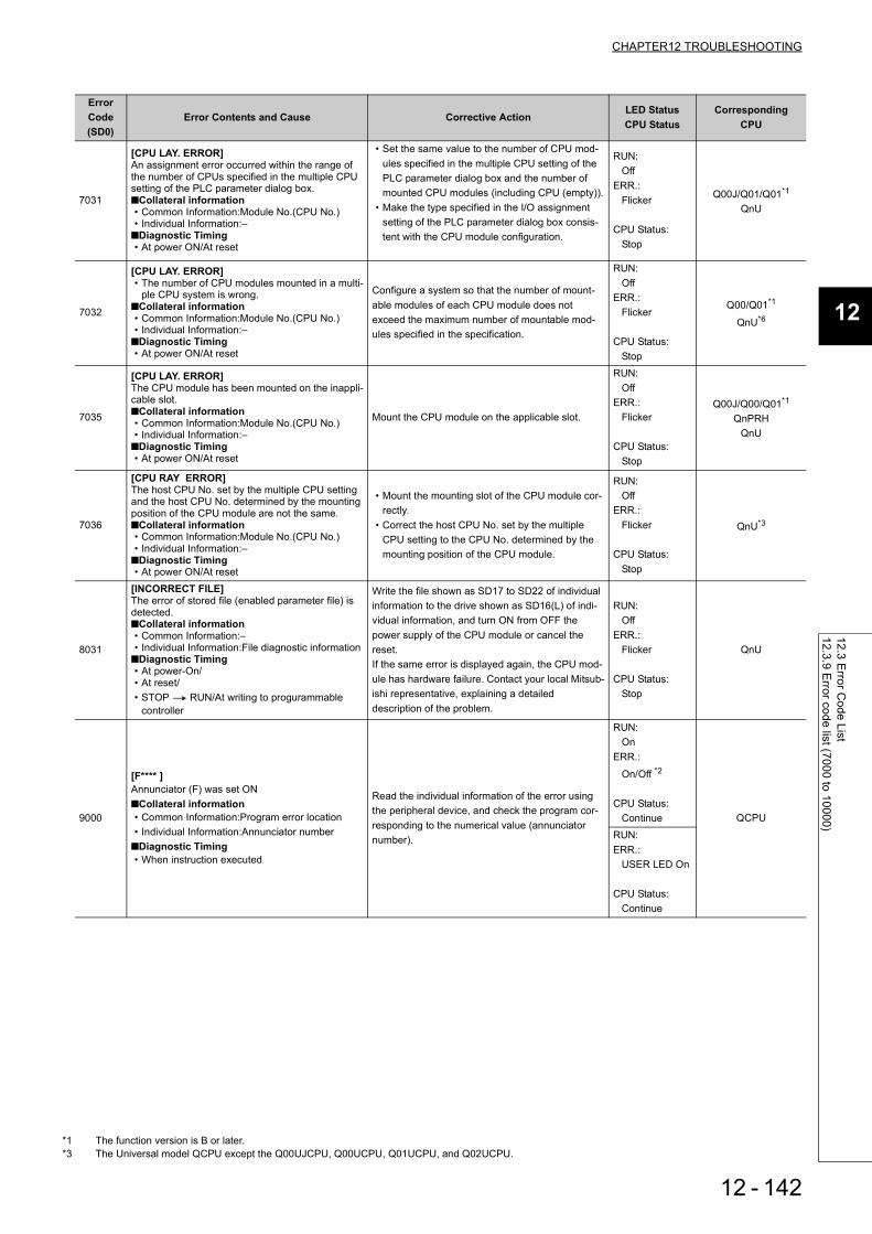
CHAPTER12 TROUBLESHOOTING
12
12.3 Error C
ode List12.3.9 E
rror code list (7000 to 10000)
7031
[CPU LAY. ERROR]An assignment error occurred within the range of the number of CPUs specified in the multiple CPU setting of the PLC parameter dialog box.■Collateral information• Common Information:Module No.(CPU No.)• Individual Information:–
■Diagnostic Timing• At power ON/At reset
• Set the same value to the number of CPU mod-ules specified in the multiple CPU setting of the PLC parameter dialog box and the number of mounted CPU modules (including CPU (empty)).
• Make the type specified in the I/O assignment setting of the PLC parameter dialog box consis-tent with the CPU module configuration.
RUN:Off
ERR.:Flicker
CPU Status:Stop
Q00J/Q01/Q01*1
QnU
7032
[CPU LAY. ERROR]• The number of CPU modules mounted in a multi-
ple CPU system is wrong.■Collateral information• Common Information:Module No.(CPU No.)• Individual Information:–
■Diagnostic Timing• At power ON/At reset
Configure a system so that the number of mount-able modules of each CPU module does not exceed the maximum number of mountable mod-ules specified in the specification.
RUN:Off
ERR.:Flicker
CPU Status:Stop
Q00/Q01*1
QnU*6
7035
[CPU LAY. ERROR]The CPU module has been mounted on the inappli-cable slot.■Collateral information• Common Information:Module No.(CPU No.)• Individual Information:–
■Diagnostic Timing• At power ON/At reset
Mount the CPU module on the applicable slot.
RUN:Off
ERR.:Flicker
CPU Status:Stop
Q00J/Q00/Q01*1
QnPRHQnU
7036
[CPU RAY ERROR]The host CPU No. set by the multiple CPU setting and the host CPU No. determined by the mounting position of the CPU module are not the same.■Collateral information• Common Information:Module No.(CPU No.)• Individual Information:–
■Diagnostic Timing• At power ON/At reset
• Mount the mounting slot of the CPU module cor-rectly.
• Correct the host CPU No. set by the multiple CPU setting to the CPU No. determined by the mounting position of the CPU module.
RUN:Off
ERR.:Flicker
CPU Status:Stop
QnU*3
8031
[INCORRECT FILE]The error of stored file (enabled parameter file) is detected.■Collateral information• Common Information:–• Individual Information:File diagnostic information
■Diagnostic Timing• At power-On/• At reset/• STOP RUN/At writing to progurammable
controller
Write the file shown as SD17 to SD22 of individual information to the drive shown as SD16(L) of indi-vidual information, and turn ON from OFF the power supply of the CPU module or cancel the reset.If the same error is displayed again, the CPU mod-ule has hardware failure. Contact your local Mitsub-ishi representative, explaining a detailed description of the problem.
RUN:Off
ERR.:Flicker
CPU Status:Stop
QnU
9000
[F**** ]Annunciator (F) was set ON■Collateral information• Common Information:Program error location• Individual Information:Annunciator number
■Diagnostic Timing• When instruction executed
Read the individual information of the error using the peripheral device, and check the program cor-responding to the numerical value (annunciator number).
RUN:On
ERR.:
On/Off *2
CPU Status:Continue QCPU
RUN:ERR.:
USER LED On
CPU Status:Continue
ErrorCode(SD0)
Error Contents and Cause Corrective ActionLED StatusCPU Status
CorrespondingCPU
*1 The function version is B or later.
12 - 142*3 The Universal model QCPU except the Q00UJCPU, Q00UCPU, Q01UCPU, and Q02UCPU.

9010
[<CHK>ERR ***-***]Error detected by the CHK instruction.■Collateral information• Common Information:Program error location• Individual Information:Failure No.
■Diagnostic Timing• When instruction executed
Read the individual information of the error using the peripheral device, and check the program cor-responding to the numerical value (error number) there.
RUN:On
ERR.:OffUSER LED On
CPU Status:Continue
Qn(H)QnPH
QnPRH
9020
[BOOT OK]Storage of data onto ROM was completed normally in automatic write to standard ROM.(BOOT LED also flickers.)■Collateral information• Common Information:–• Individual Information:–
■Diagnostic Timing• At power ON/At reset
Use the DIP switches to set the valid parameter drive to the standard ROM. Then, switch power on again, and perform boot operation from the stan-dard ROM.
RUN:Off
ERR.:Flicker
CPU Status:Stop
Qn(H)*1
QnPHQnPRH
10000
[CONT. UNIT ERROR]In the multiple CPU system, an error occurred in the CPU module other than the Process CPU/High Performance model QCPU.■Collateral information• Common Information:–• Individual Information:–
■Diagnostic Timing• Always
Check the details of the generated error by con-necting to the corresponding CPU module using GX Developer.
RUN:Off
ERR.:Flicker
CPU Status:Continue
Qn(H)*1
QnPH
ErrorCode(SD0)
Error Contents and Cause Corrective ActionLED StatusCPU Status
CorrespondingCPU
12 - 143*1 The function version is B or later.
CHAPTER12 TROUBLESHOOTING
12
12.3 Error C
ode List12.3.10 C
anceling of Errors
12.3.10 Canceling of Errors
Q series CPU module can perform the cancel operation for errors only when the errors allow the CPU module to continue its operation.To cancel the errors, follow the steps shown below.
1) Eliminate the cause of the error.2) Store the error code to be canceled in the special register SD50.3) Energize the special relay SM50 (OFF ON).4) The error to be canceled is canceled.
After the CPU module is reset by the canceling of the error, the special relays, special registers, and LEDs associated with the error are returned to the status under which the error occurred.If the same error occurs again after the cancellation of the error, it will be registered again in the error history.
When multiple enunciators(F) detected are canceled, the first one with No. F only is canceled.
Refer to the following manual for details of error canceling.Qn(H)/QnPH/QnPRHCPU User's Manual (Function Explanation, Program Fundamentals)
(1) When the error is canceled with the error code to be canceled stored in the SD50, the lower one digit of the code is neglected.(Example)If error codes 2100 and 2101 occur, and error code 2100 to cancel error code 2101.If error codes 2100 and 2111 occur, error code 2111 is not canceled even if error code 2100 is canceled.
(2) Errors developed due to trouble in other than the CPU module are not canceled even if the special relay (SM50) and special register (SD50) are used to cancel the error.(Example)Since "SP. UNIT DOWN" is the error that occurred in the base unit (including the extension cable), intelligent function module, etc. the error cause cannot be removed even if the error is canceled by the special relay (SM50) and special register (SD50).Refer to the error code list and remove the error cause.
12 - 144

Memo
12 - 145

CHAPTER12 TROUBLESHOOTING
12
12.3 Error C
ode List12.3.11 E
rror codes returned to request source during comm
unication with C
PU
module
12.3.11 Error codes returned to request source during communication with CPU module
The Q series CPU module returns an error code to the request source if an error occurs at a request of communication from GX Developer, intelligent function module or network system.
This error code is not an error that is detected by the CPU module self-diagnosis function, so it is not stored in the special relay (SD0).When the request source is a GX Developer, a message or an error code is displayed.When the request source is an intelligent function module or network system, an error is returned to the process that was requested.
The error contents of the error codes (4000H to 4FFFH) detected by the CPU module and the messages displayed by the GX Developer are shown in .
Table12.2 Error code
Error code(Hexadecimal)
Error item Error details Corrective action
4000H
Common error
Serial communication sum check error• Connect the serial communication cable correctly.• Take noise reduction measures.
4001H Unsupported request was executed.• Check the command data of the MC protocol, etc.• Check the CPU module model name selected in the
peripheral device.
4002H Unsupported request was executed.• Check the command data of the MC protocol, etc.• Check the CPU module model name selected in the
peripheral device.
4003HCommand for which a global request cannot be performed was executed.
Check the command data of the MC protocol, etc.
4004H
Any operation for the CPU module is prohibited by the system protect function provided against the following events.• The system protect switch is ON.• The CPU module is starting.
• Set the system protect switch of the CPU module to OFF.
• Perform operation again after the CPU module has completed starting.
4005HThe volume of data handled according to the specified request is too large.
Check the command data of the MC protocol, etc.
4006H Serial communication could not be initialized.
• Check with the external device maker for the support condition.
• Check the CPU module model name selected in the peripheral device.
4008HThe CPU module is BUSY.(The buffer is not vacant).
After the free time has passed, reexecute the request.
4010HCPU mode error
Since the CPU module is running, the request contents cannot be executed.
Execute after setting the CPU module to STOP status.
4013HSince the CPU module is not in a STOP status, the request contents cannot be executed.
Execute after setting the CPU module to STOP status.
12 - 146

Table12.2 Error code
Error code(Hexadecimal)
Error item Error details Corrective action
4021H
CPU file related error
The specified drive memory does not exist or there is an error.
• Check the specified drive memory status.• After backing up the data in the CPU module, execute
programmable controller memory format.
4022HThe file with the specified file name or file No. does not exist.
Check the specified file name and file No.
4023HThe file name and file No. of the specified file do not match.
Delete the file and then recreate the file.
4024H The specified file cannot be handled by a user. Do not access the specified file.
4025HThe specified file is processing the request from the other peripheral device.
Forcibly execute the request, or make the request again after the processing from the other peripheral device is com-pleted.
4026HThe file password or drive keyword set to the tar-get drive (memory) must be specified.
Make access after specifying the file password or drive key-word set to the target drive (memory).
4027H The specified range exceeds the file range. Check the specified range and access within that range.
4028H The same file already exists.Forcefully execute the request forcibly.Or reexecute after changing the file name.
4029H The specified file capacity cannot be obtained.Revise the specified file contents.Or reexecute after cleaning up and reorganizing the speci-fied drive memory.
402AH The specified file is abnormal.After backing up the data in the CPU module, execute pro-grammable controller memory format.
402BHThe request contents cannot be executed in the specified drive memory.
Execute again after setting the CPU module to the STOP status.Execute programmable controller memory arrangement to increase the continuous free space of the drive (memory).
402CHThe requested operation cannot be executed cur-rently.
Execute again after a while.
4030H
CPU device specified error
The specified device name cannot be handled. Check the specified device name.
4031H The specified device No. is outside the range.• Check the specified device No.• Check the device assignment parameters of the CPU
module.
4032H
There is a mistake in the specified device qualifi-cation.The unusable device name (TS,TC,SS,SC,CS,CC) must be specified in MC protocol random reading, random writing (word), monitor registeration and monitor command.
• Check the specified device qualification method.• Check the specified device name.
4033HWriting cannot be done because the specified device is for system use.
Do not write the data in the specified device, and do not turn on or off.
4034H
Cannot be executed since the completion device for the dedicated instruction cannot be turned ON.
Since the completion device for the target station CPU mod-ule cannot be turned ON by the SREAD instruction/SWRITE instruction, execute again after setting the operating status of the target station CPU module to the RUN status.
12 - 147

CHAPTER12 TROUBLESHOOTING
12
12.3 Error C
ode List12.3.11 E
rror codes returned to request source during comm
unication with C
PU
module
Table12.2 Error code
Error code(Hexadecimal)
Error item Error details Corrective action
4040H
Intelligent func-tion module specification error
The request contents cannot be executed in the specified intelligent function module.
Check whether the specified module is the intelligent func-tion module having the buffer memory.
4041HThe access range exceeds the buffer memory range of the specified intelligent function module.
Check the header address and access number of points and access using a range that exists in the intelligent function module.
4042HThe specified intelligent function module cannot be accessed.
• Check that the specified intelligent function module is operating normally.
• Check the specified module for a hardware fault.
4043HThe intelligent function module does not exist in the specified position.
Check the I/O No. of the specified intelligent function module.
4044HA control bus error occurred during access to the intelligent function module.
Check the specified intelligent function module and other modules and base units for a hardware fault.
4050H
Protect error
The request contents cannot be executed because the memory card write protect switch is on.
Turn off the memory card write protect switch.
4051HThe specified device memory cannot be accessed.
Check the following and make it countermeasures.• Is the memory one that can be used?• Is the specified drive memory correctly installed?
4052HThe specified file attribute is read only so the data cannot be written.
Do not write data in the specified file.Or change the file attribute.
4053HAn error occurred when writing data to the speci-fied drive memory.
Check the specified drive memory.Or reexecute write after changing the corresponding drive memory.
4054HAn error occurred when deleting the data in the specified drive memory.
Check the specified drive memory.Or re-erase after replacing the corresponding drive memory.
4060H
Online registra-tion error
The online debug function is being executed by the other peripheral device.
• Execute the function again after the operation of the other peripheral device has ended.
• When the operation was suspended by the other peripheral device, execute the function again after executing it on the other peripheral device to normally complete the operation.
4061HCommunication of the online debug function was unsuccessful.
• Execute communication after the registering the online debug function (e.g.online program change/trace/con-ditional monitor).
• Execute again after checking the communication route such as the communication cable.
4063HThe registered number of locked files exceeded the maximum value.
Execute again after file access by the other peripheral device has ended.
4064HThe specified data of the online debug function is incorrect.
• Check the set data of the online debug function (e.g. online program change/trace/conditional monitor).
• Execute again after checking the communication route such as the communication cable.
12 - 148

Table12.2 Error code
Error code(Hexadecimal)
Error item Error details Corrective action
4065H
Online registra-tion error
The device allocation information differs from the parameter.
Check the device assignment parameters of the CPU mod-ule or the device assignment of the request data.
4066HThe specified drive keyword/file password is wrong.
• Correct the drive keyword of the specified drive.• Correct the file password of the specified file.
4067H Monitor communication was unsuccessful.
• Check the system area capacity of the user setting specified for programmable controller memory format.
• Execute again after checking the communication route such as the communication cable.
4068HOperation is disabled since the same operation is being executed from the other peripheral device.
Execute the function again after the operation from the other peripheral device has been ended.
406AHThe drive (memory) number that cannot be han-dled (other than 0 to 4) was specified.
Check the specified drive and specify the correct drive.
4070HCircuit inquiry error
The program not yet corrected and the one cor-rected by online program change are different.
Execute Read from PLC to make the program of the periph-eral device the same as that of the CPU module, and then execute online program change again.
4080H
Other errors
Request data error Check the request data specified in the MC protocol, etc.
4081H The sort subject cannot be detected. Check the data to be searched.
4082HThe specified command is executing and there-fore cannot be executed.
Execute the command again after the request from the other peripheral device is completed.
4083HAn attempt was made to perform operation for the program not registered to the parameters.
Register the program to the parameters.
4084H The specified pointer P, I did not exist. Check the pointer P, I in the specified data.
4085HPointer P, I cannot be specified because the pro-gram is not specified in the parameter.
Specify pointer P, I after registering the program to be exe-cuted in the parameter.
4086H Pointer P, I has already been added. Check the pointer No. to be added and make correction.
4087H Trying to specify too many pointer P, I. Check the specified pointer P, I and make a correction.
4088H
• The specified step No. is not the start of the instruction.
• Program stored in the CPU is different from the relevant program.
• Check and correct the specified step No.• Read from PLC to make the program of the peripheral
device the same as that of the CPU module, and write to PLC during RUN again.
4089HAn attempt was made to insert/delete the END instruction by online program change.
• Check the specified program file contents.• Write the program after setting the CPU module to the
STOP status.
12 - 149

CHAPTER12 TROUBLESHOOTING
12
12.3 Error C
ode List12.3.11 E
rror codes returned to request source during comm
unication with C
PU
module
Table12.2 Error code
Error code(Hexadecimal)
Error item Error details Corrective action
408AH
Other errors
The file capacity was exceeded by the write dur-ing Run.
• Check the capacity of the specified program file.• Write the program after setting the CPU module to the
STOP status.
408BH The remote request cannot be executed.
• Reexecute after the CPU module is in a status where the mode request can be executed.
• For remote operation, set the parameter to "Enable remote reset".
408CH
An attempt was made to remote-start the pro-gram, which uses the CHK instruction, as a low speed program.
• The program including the CHK instruction cannot be executed at low speed. Execute again after checking the program.
408DHThe instruction code that cannot be handled exists.
• Check whether the model of the used CPU module is correct or not.
• The sequence program where online program change was attempted includes the instruction that cannot be handled by the CPU module model name set in the project. Reexamine the sequence program and delete that instruction.
408EH The write step is illegal.
• Write the program after setting the CPU module to the STOP status.
• The starting position of online program change is not specified with the correct program step No. Check whether the used peripheral device supports the CPU module model name and CPU module version set in the project.
40A0H
SFC device specification error
A block No. outside the range was specified. Check the setting contents and make a correction.
40A1HA number of blocks that exceeds the range was specified.
Check the number of settings and make a correction.
40A2HA step No. that is outside the range was speci-fied.
Check the setting contents and make a correction.
40A3H Step range limit exceeded Check the number of settings and make a correction.
40A4HThe specified sequence step No. is outside the range.
Check the setting contents and make a correction.
40A5H The specified device is outside the range. Check the number of settings and make a correction.
40A6HThe block specification pattern and step specifi-cation pattern were wrong.
Check the setting contents and make a correction.
40B0H
SFC file related error
The drive (memory) specified in SFC file opera-tion is wrong.
Check the setting contents and make a correction.
40B1HThe SFC program specified in SFC file operation does not exist.
Check the specified file name and make a correction.
40B2HThe program specified in SFC file operation is not an SFC program.
Check the specified file name and make a correction.
40B3H
Using online program change of SFC, an attempt was made to execute rewrite operation of the "SFC dedicated instruction", such as the "STEP start instruction or transition start instruction", that shows an SFC chart.(SFC dedicated instruction cannot be written dur-ing RUN.)
Write the program after setting the CPU module to the STOP status.
12 - 150

Table12.2 Error code
Error code(Hexadecimal)
Error item Error details Corrective action
4100H
Other errors
CPU module hardware fault Change the CPU module.
4101HSerial communication connection was executed for a different CPU module series.
Check the CPU module series.
4102HAn attempt was made to erase the Flash ROM during use of the file register.
Execute again after setting the CPU module to the STOP status.
4103HThe instruction written during RUN is wrong or illegal.
Execute online program change again, or write the program after setting the CPU module to the STOP status.
4105H CPU module internal memory hardware fault Change the CPU module.
4106H
The command cannot be executed since the CPU module is performing system initialization pro-cessing.
Execute the operation again after the CPU module has started.
4107H
An attempt was made to perform the operation of the function unavailable for the target CPU mod-ule model name.
Do not execute the function unsupported by the target CPU module.
4108HOperation cannot be made normally by device monitor/test.
Execute device monitor/test again. Before execution, check that access is not made to the access prohibited area.
4109H
The specified operation cannot be executed since the monitoring, set the condition for other appli-cation in same computer, is in execution.
Execute the request again after deregistering the monitoring condition on the same screen.
410AHThe specified command cannot be executed because of online prgram change.
Execute the request again after the online program change.
410BHThe registration of monitoring condition was can-celed because of online program change.
Execute the registration of monitoring condition again after the online program change.
4110H
CPU mode error
Since the CPU module is in a stop error status, it cannot execute the request.
Execute the request again after resetting the CPU module.
4111H
The requested operation cannot be performed since the other CPU modules have not yet started in the multiple CPU system.
Execute the request again after the other CPU modules have started.
12 - 151

CHAPTER12 TROUBLESHOOTING
12
12.3 Error C
ode List12.3.11 E
rror codes returned to request source during comm
unication with C
PU
module
4121H
File-related errorsFile-related errors
The specified drive (memory) or file does not exist.
Execute again after checking the specified drive (memory) or file.
4122HThe specified drive (memory) or file does not exist.
Execute again after checking the specified drive (memory) or file.
4123H The specified drive (memory) is abnormal.
Execute programmable controller memory format to make the drive (memory) normal.In the case of the Flash ROM, check the data to be written to the Flash ROM, and write them to the Flash ROM.
4124H The specified drive (memory) is abnormal.
Execute programmable controller memory format to make the drive (memory) normal.In the case of the Flash ROM, check the data to be written to the Flash ROM, and write them to the Flash ROM.
4125HThe specified drive (memory) or file is performing processing.
Execute again after a while.
4126HThe specified drive (memory) or file is performing processing.
Execute again after a while.
4127H File password mismatch Execute again after checking the file password.
4128H File password mismatch with copy destination Execute again after checking the file password.
4129HCannot be executed since the specified drive (memory) is ROM.
Execute again after changing the target drive (memory).
412AHCannot be executed since the specified drive (memory) is ROM.
Execute again after changing the target drive (memory).
412BH The specified drive (memory) is write-inhibited.Execute again after changing the write inhibit condition or drive (memory).
412CH The specified drive (memory) is write-inhibited.Execute again after changing the write inhibit condition or drive (memory).
412DHThe specified drive (memory) does not have enough free space.
Execute again after increasing the free space of the drive (memory).
412EHThe specified drive (memory) does not have enough free space.
Execute again after increasing the free space of the drive (memory).
412FH
The drive (memory) capacity differs between the drive (memory) copy destination and copy source.
Execute again after checking the drive (memory) copy desti-nation and copy source.
4130HThe drive (memory) type differs between the drive (memory) copy destination and copy source.
Execute again after checking the drive (memory) copy desti-nation and copy source.
4131HThe file name of the file copy destination is the same as that of the copy source.
Execute again after checking the file names.
4132H The specified number of files does not exist. Execute again after checking the specified data.
4133H The specified drive (memory) has no free space.Execute again after increasing the free space of the drive (memory).
4134HThe attribute specification data of the file is wrong.
Execute again after checking the specified data.
4135HThe date/time data of the peripheral device (per-sonal computer) is beyond the range.
Execute again after checking the clock setting of the periph-eral device (personal computer).
4136H The specified file already exists. Execute again after checking the specified file name.
4137H The specified file is read-only.Execute again after changing the condition of the specified file.
4138HSimultaneously accessible files exceeded the maximum.
Execute again after decreasing file operations.
4139HThe specified file has exceeded the already exist-ing file range.
Execute again after checking the size of the specified file.
Error code(Hexadecimal)
Error item Error details Corrective action
12 - 152

Table12.2 Error code
Error code(Hexadecimal)
Error item Error details Corrective action
413AH
File-related errorsFile-related errors
The specified file has exceeded the already existing file size.
Execute again after checking the size of the specified file.
413BHThe same file was accessed simultaneously from different peripheral devices.
Execute again after a while.
413CH The specified file is write-inhibited. Execute again after changing the file condition.
413DH The specified file capacity cannot be secured.Execute again after increasing the capacity of the specified drive (memory).
413EHOperation is disabled for the specified drive (memory).
Execute again after changing the target drive (memory).
413FHThe file is inhibited from write to the standard RAM.
Execute again after changing the specified drive (memory).
414AHIntelligent func-tion module specification error
Operation was executed for the intelligent func-tion module of the non-control group in the multi-ple CPU system.
Execute the operation again from the control CPU of the tar-get module.
414CHThe I/O address of the specified CPU module is wrong.
Execute again after checking the I/O address of the specified CPU module.
4150HFile-related errors
An attempt was made to format the drive pro-tected by the system.
Do not format the target drive (memory) as it cannot be for-matted.
4151HAn attempt was made to delete the file protected by the system.
Do not delete the target file as it cannot be deleted.
4160H
Online registra-tion error
The registered number of forced inputs/outputs exceeded the maximum value.
Deregister the unused forced inputs/outputs.
4165HThe multiple-block online change system file does not exist.
Execute again after securing the area that enables multiple-block online change at the time of programmable controller memory format.
4166H
Cannot be executed since file batch online change is being made by the same starting source.
Since the file batch online change executed previously remains abnormally terminated for some reason (example: communication disturbance during execution), file batch online change is disabled.Forcibly perform new file batch online change.
4167H
Cannot be executed since file batch online change is being made from the other starting source.
Since the file batch online change executed previously from the other communication route remains abnormally termi-nated for some reason (example: communication distur-bance during execution), file batch online change is disabled.If file batch online change is not being executed by the other peripheral device, forcibly perform new file batch online change.
4168HThe registered number of device test with execut-ing condition exceeds 32.
Deregister the device test with executing condition in CPU module, or decrease the number of registering device test with executing condition at one time.
4169HThe device test with executing condition has never been registered.
Deregister the device test with executing condition after checking the registered number of device test with executing condition in CPU module.
416AHThe specified executing condition does not exist.(Device test with executing condition)
Check whether the specified executing conditions (program, step No. operation timing, device name) in deregistering are registered.
416BHThe specified program is SFC program. (Device test with executing condition)
Check the specifing program name in de/registering the device test with executing condition.
12 - 153

CHAPTER12 TROUBLESHOOTING
12
12.3 Error C
ode List12.3.11 E
rror codes returned to request source during comm
unication with C
PU
module
Table12.2 Error code
Error code(Hexadecimal)
Error item Error details Corrective action
4170H
EthernetI/FError
The passward is wrong.Check the specified remote passward then, execute the lock/unlock processing of the remote password again.
4171HThe port for communication use is at remote passsword locking status.
Execute communication after unlocking the remote password processing.
4174HRequested for a wrong module to unlock remote password.
• Stop transmitting from several modules simultaneously when setting a remote password and using User Data-gram Protocol (UDP) in MELSOFT connection.
• The MELSOFT connection can be used with Transmis-sion Control protocol (TCP) when setting a remote password.
4176HCommunication error occured in direct connec-tion.
• Do not specify the direct connection when using otherconnection setting.
• Do not turn off the CPU power during communication,reset the power, and plug out the cable in directconnection.
4178H
• File operation is disabled since File Transfer Protocol (FTP) function is in operation.
• Online operation that requires file access is performed while File Transfer Protocol (FTP) function is in operation.
Retry after the operation for FTP function is completed.
4180HSystem error.(The setting data in OS is abnor-mal.)
• Check whether the power module and the programma-ble controller CPU are attached properly.
• Check whether the system's use environment is within the range of the programmable controller CPU genaral specifications.
• Check whether the power capacity is sufficient.• Reset the CPU module.
If the error is shown once again, the CPU module hardware must be abnormal. Please contact with system service sta-tions, agencies, or branch offices nearby and consult forl the problems.
4181HTransmission to the receiving modules is unsuc-cessful.
• Check the receiving module operation.• Check the status of the lines, such as cables, hubs
and routes,connected to receiving modules.• Some line packets may be engaged. Retry to commu-
nicate a little while later.
4182HCommunication with receiving modules caused a time-out error.
• Check the receiving module operation.• Check the status of the lines such as a cable, a hub
and a route to receiving modules.• Some line packets may be engaged. Retry to commu-
nicate a little while later.
4183HCommunication with receiving modules was inter-rupted.
• Check the receiving module operation.• Check the status of the lines such as cables, hubs and
routes connected to receiving modules.
12 - 154

Table12.2 Error code
Error code(Hexadecimal)
Error item Error details Corrective action
4184H
EthernetI/FError
• Communication processing buffer has been ran out since requests were consecutively received in MC protocol.
• Communication processing buffer has been ran out since received data read is not per-formed or cannot keep up with the volume.
• Communication processing is not available since the communication processing buffer has been ran out.
• For MC protocol, send a request after receiving a response to the previous request.
• For socket communication, enable received data read.• For socket communication, decrease the number of
data sent from the target device.
4185H
• The connection to the target device is dis-connected before sending a response using MC protocol
• The connection to the target device is dis-connected during communication
• For MC protocol, keep the connection until a response is sent.
• Keep the connection until a sequence of communica-tion is completed.
• Other error such as 4184H may be the cause. If any other error has occurred, take corrective action of that error.
4186HSystem error (The argument data in OS is abnor-mal.)
• Check whether the power module and programmable controller CPU are attached properly.
• Check whether the system use environment is within the range of the programmable controller CPU genaral specifications.
• Check whether the power capacity is sufficient.• Reset the CPU module.
If the error is shown once again, the CPU module hardware is abnormal. Please contact with system service, agency, or branch office nearby and tell the problems.
4187HSystem error (The wait processing in OS is abnormal.)
4188H System error (The data length in OS is abnormal.)
4189HSystem error (The protocol information in OS is abnormal.)
418AHSystem error (The address data of communicat-ing module in OS is abnormal.)
418BHSystem error (The protocol information in OS is abnormal.)
418CHSystem error (The protocol specification process-ing in OS is abnormal.)
418DHSystem error(The typed data in OS is abnormal.)
418EHSystem error (The expedited data processing in OS is abnormal.)
418FH
4190H
System error (The protocol information in OS is abnormal.)
4191HSystem error (The address data of communicat-ing module in OS is abnormal.)
4192HSystem error (The host module address process-ing in OS is abnormal.)
4193H to4196H
System error (The transmission processing in OS is abnormal.)
4197H
4198H
System error (The connection processing in OS is abnormal.)
4199HSystem error (The connection termination pro-cessing is abnormal.)
419AHSystem error (The connection processing in OS is abnormal.)
419BHSystem error (The connection termination pro-cessing is abnormal.)
419CH
419DH
System error (The processing order in OS is abnormal.)
12 - 155

CHAPTER12 TROUBLESHOOTING
12
12.3 Error C
ode List12.3.11 E
rror codes returned to request source during comm
unication with C
PU
module
Table12.2 Error code
Error code(Hexadecimal)
Error item Error details Corrective action
419EH
EthernetI/FError
Connection to the module was unsuccessful or interrupped.
• Check the receiving module operation.• Check the status of the lines such as a cable, a hub
and a route to receiving modules• Retry to connect a little while later, if the error occured
in communication.
419FHSystem error (The I/O control processing is abnormal.)
• Check whether the power module and programmable controller CPU are attached properly.
• Check whether the system use environment is within the range of the programmable controller CPU genaral specifications.
• Check whether the power capacity is sufficient.• Reset the CPU module.
If the error is shown once again, the CPU module hardware is abnormal. Please contact with system
41A0H
Data cannot be sent since the target device has no free space in receive area (TCP window size is zero).
• Retry after a while• Check the behavior of the target device.• Check whether the target device is processing data
receiving.• Check whether the QnUDE(H)CPU is sending any
unnecessary data.
41A1H
Ethernet I/Fsocket com-muinication error
The port number setting for the Built-in Ethernet port QCPU is invalid.
Correct the port number.41A2H
The port number setting for the target device is invalid.
41A3H
• For TCP/IP, the same Host station port No. is specified as MC protocol.
• For TCP/IP, a connection with the same host station No. and the same destination port No. are already specified to one communi-cation target.
• Specify a port number that is not duplicated with that of MC protocol
• Review port numbers of the Built-in Ethernet port QCPU and correct if duplicated.
41A4H
• For UDP/IP, the same Host station port No. is specified as MC protocol.
• For UDP/IP, the specified host station No. is duplicated.
• Specify a port number that is not duplicated with that of MC protocol
• Review port numbers of the Built-in Ethernet port QCPU and target device and correct if duplicated.
41A5HThe IP address setting of the target device for OPEN processing is invalid.
Correct the IP address. Specify A, B, or C for the class.
41A6HConnection was not established in OPEN pro-cessing for TCP connection.
• Check the bihavior of the target device.• Check OPEN processing of the target device.• Correct the port No. of the Built-in Ethernet port QCPU
and the IP address, port No., and open processing method of the target device.
• Check whether the cables are securely connected.
41A8H Data length is out of permissible range.• Correct the data length.• If the data is longer than the range, split the data and
send them.
41ABH Failed to send data due to resend timeout in TCP.
• Review the IP address and Ethernet address of the tar-get device.
• Check whether the target device has the ARP function. If not, communicate with the one that has the ARP function.
• Check the bihavior of the target device.• The line may be congested with packets. Resend data
after a while.• Check whether the cables are securely connected.
12 - 156

Table12.2 Error code
Error code(Hexadecimal)
Error item Error details Corrective action
41ACH
Ethernet I/Fsocket com-muinication error
The target device cannot be found.• Check the bihavior of the target device.• Check whether the cables are securely connected.
41ADHData cannot be send due to no connection or dis-connection of the cable.
• Check whether the cables are securely connected.• Check the line status by PING test from the target
device.• Check the status of Built-in Ethernet port QCPU by self
diagnostic test (Built-in Ethernet port QCPU reset)• Send data again
41B4H The connection number setting is invalid.• Specify the connection No. within 1 to 16.• Check whether "Socket communication" is selected for
"Open system" parameter.
41B6HThe specified connection has already completed OPEN processing.
Perform CLOSE processing and then OPEN processing.
41B7H• The specified connection has not completed
OPEN processing.• Reexecute after OPEN processing is completed.
41B9H
• Contents of control data is not correct.• Open instruction was executed through
open settings parameter even though parameters are not set for "Open settings".
• Correct the contents of the control data.• Configure the open settings parameters or execute the
OPEN instruction through control data.
41C1H
File-related errors
The format information data of the specified drive (memory) is abnormal.
The file information data may be corrupted.After backing up the data in the CPU module, execute pro-grammable controller memory format.
41C2HFile open specification data for file access is wrong.
Execute again after checking the specification data.
41C3HSimultaneously accessible files exceeded the maximum.
Execute again after decreasing file operations.
41C4HSimultaneously accessible files exceeded the maximum.
Execute again after decreasing file operations.
41C5H The specified file does not exist. Execute again after checking the file.
41C7HThe specified file or drive (memory) does not exist.
Execute again after checking the file or drive (memory).
41C8HThe specified file has exceeded the already exist-ing file range.
Execute again after checking the size of the specified file.If the error recurs after re-execution, the file information data may be corrupted.After backing up the data in the CPU module, execute pro-grammable controller memory format.
41C9H
Access to the file sector was unsuccessful.The format information data of the target drive (memory) is abnormal.
After backing up the data in the CPU module, execute pro-grammable controller memory format.
12 - 157

CHAPTER12 TROUBLESHOOTING
12
12.3 Error C
ode List12.3.11 E
rror codes returned to request source during comm
unication with C
PU
module
Table12.2 Error code
Error code(Hexadecimal)
Error item Error details Corrective action
41CAH
File-related errors
Access to the file sector was unsuccessful.The format information data of the target drive (memory) is abnormal.
After backing up the data in the CPU module, execute pro-grammable controller memory format.
41CBH The file name is specified in a wrong method. Execute again after checking the file name.
41CCH The specified file does not exist. Execute again after checking the file.
41CDH Access to the file is inhibited by the system. Do not access the specified file.
41CEHThe specified file is write-disabled since its attribute is read-only.
The specified file is write-inhibited. Execute again after checking the attribute.
41CFHThe specified drive (memory) capacity was exceeded.
Execute again after checking the drive (memory) capacity.
41D0H The specified drive (memory) has no free space.Execute again after increasing the free space of the drive (memory).
41D1H The file name is specified in a wrong method.
Execute again after checking the file name.If the error recurs after re-execution, the file information data may be corrupted.After backing up the data in the CPU module, execute pro-grammable controller memory format.
41D4HThe specified file has exceeded the already exist-ing file range.
Execute again after checking the size of the specified file.If the error recurs after re-execution, the file information data may be corrupted.After backing up the data in the CPU module, execute pro-grammable controller memory format.
41D5H The file of the same name exists.Forcibly execute the request, or execute after changing the file name.
41D6HThe format information data of the specified drive (memory) is abnormal.
The file information data may be corrupted.After backing up the data in the CPU module, execute pro-grammable controller memory format.
41D7HThe format information data of the specified drive (memory) is abnormal.
The file information data may be corrupted.After backing up the data in the CPU module, execute pro-grammable controller memory format.
41D8H The specified file is being accessed. Execute again after a while.
41DFH The specified drive (memory) is write-protected.Execute again after canceling the write protect of the speci-fied drive (memory).
41E0HThe specified drive (memory) is abnormal or does not exist.
• Execute again after checking whether the memory card has been installed.
• After backing up the data, execute programmable con-troller memory format.
41E1H Access to the flash ROM was unsuccessful.
• After backing up the data, execute write to PLC (Flash ROM).
• Execute again after checking whether the specified drive is the Flash ROM card and whether the memory card size is correct.
12 - 158
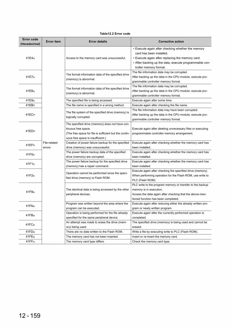
Table12.2 Error code
Error code(Hexadecimal)
Error item Error details Corrective action
41E4H
File-related errors
Access to the memory card was unsuccessful.
• Execute again after checking whether the memory card has been installed.
• Execute again after replacing the memory card.• After backing up the data, execute programmable con-
troller memory format.
41E7HThe format information data of the specified drive (memory) is abnormal.
The file information data may be corrupted.After backing up the data in the CPU module, execute pro-grammable controller memory format.
41E8HThe format information data of the specified drive (memory) is abnormal.
The file information data may be corrupted.After backing up the data in the CPU module, execute pro-grammable controller memory format.
41E9H The specified file is being accessed. Execute again after some time.
41EBH The file name is specified in a wrong method. Execute again after checking the file name.
41ECHThe file system of the specified drive (memory) is logically corrupted.
The file information data may have been corrupted.After backing up the data in the CPU module, execute pro-grammable controller memory format.
41EDH
The specified drive (memory) does not have con-tinuous free space.(The free space for file is sufficient but the contin-uous free space is insufficient.)
Execute again after deleting unnecessary files or executing programmable controller memory arrangement.
41EFHCreation of power failure backup for the specified drive (memory) was unsuccessful.
Execute again after checking whether the memory card has been installed.
41F0HThe power failure backup data of the specified drive (memory) are corrupted.
Execute again after checking whether the memory card has been installed.
41F1HThe power failure backup for the specified drive (memory) has a repair command.
Execute again after checking whether the memory card has been installed.
41F2HOperation cannot be performed since the speci-fied drive (memory) is Flash ROM.
Execute again after checking the specified drive (memory).When performing operation for the Flash ROM, use write to PLC (Flash ROM).
41F8HThe identical data is being accessed by the other peripheral devices.
PLC write to the program memory or transfer to the backup memory is in execution.Access the data again after checking that the above-men-tioned function has been completed.
41FAHProgram was written beyond the area where the program can be executed.
Execute again after reducing either the already written pro-gram or newly written program.
41FBHOperation is being performed for the file already specified for the same peripheral device.
Execute again after the currently performed operation is completed.
41FCHAn attempt was made to erase the drive (mem-ory) being used.
The specified drive (memory) is being used and cannot be erased.
41FDH There are no data written to the Flash ROM. Write a file by executing write to PLC (Flash ROM).
41FEH The memory card has not been inserted. Insert or re-insert the memory card.
41FFH The memory card type differs. Check the memory card type.
12 - 159

CHAPTER12 TROUBLESHOOTING
12
12.3 Error C
ode List12.3.11 E
rror codes returned to request source during comm
unication with C
PU
module
Table12.2 Error code
Error code(Hexadecimal)
Error item Error details Corrective action
41CAH
File-related errors
Access to the file sector was unsuccessful.The format information data of the target drive (memory) is abnormal.
After backing up the data in the CPU module, execute pro-grammable controller memory format.
41CBH The file name is specified in a wrong method. Execute again after checking the file name.
41CCH The specified file does not exist. Execute again after checking the file.
41CDH Access to the file is inhibited by the system. Do not access the specified file.
41CEHThe specified file is write-disabled since its attribute is read-only.
The specified file is write-inhibited. Execute again after checking the attribute.
41CFHThe specified drive (memory) capacity was exceeded.
Execute again after checking the drive (memory) capacity.
41D0H The specified drive (memory) has no free space.Execute again after increasing the free space of the drive (memory).
41D1H The file name is specified in a wrong method.
Execute again after checking the file name.If the error recurs after re-execution, the file information data may be corrupted.After backing up the data in the CPU module, execute pro-grammable controller memory format.
41D4HThe specified file has exceeded the already exist-ing file range.
Execute again after checking the size of the specified file.If the error recurs after re-execution, the file information data may be corrupted.After backing up the data in the CPU module, execute pro-grammable controller memory format.
41D5H The file of the same name exists.Forcibly execute the request, or execute after changing the file name.
41D6HThe format information data of the specified drive (memory) is abnormal.
The file information data may be corrupted.After backing up the data in the CPU module, execute pro-grammable controller memory format.
41D7HThe format information data of the specified drive (memory) is abnormal.
The file information data may be corrupted.After backing up the data in the CPU module, execute pro-grammable controller memory format.
41D8H The specified file is being accessed. Execute again after a while.
41DFH The specified drive (memory) is write-protected.Execute again after canceling the write protect of the speci-fied drive (memory).
41E0HThe specified drive (memory) is abnormal or does not exist.
• Execute again after checking whether the memory card has been installed.
• After backing up the data, execute programmable con-troller memory format.
41E1H Access to the flash ROM was unsuccessful.
• After backing up the data, execute write to PLC (Flash ROM).
• Execute again after checking whether the specified drive is the Flash ROM card and whether the memory card size is correct.
41E4H Access to the memory card was unsuccessful.
• Execute again after checking whether the memory card has been installed.
• Execute again after replacing the memory card.• After backing up the data, execute programmable con-
troller memory format.
12 - 160

Table12.2 Error code
Error code(Hexadecimal)
Error item Error details Corrective action
41E7H
File-related errors
The format information data of the specified drive (memory) is abnormal.
The file information data may be corrupted.After backing up the data in the CPU module, execute pro-grammable controller memory format.
41E8HThe format information data of the specified drive (memory) is abnormal.
The file information data may be corrupted.After backing up the data in the CPU module, execute pro-grammable controller memory format.
41E9H The specified file is being accessed. Execute again after some time.
41EBH The file name is specified in a wrong method. Execute again after checking the file name.
41ECHThe file system of the specified drive (memory) is logically corrupted.
The file information data may have been corrupted.After backing up the data in the CPU module, execute pro-grammable controller memory format.
41EDH
The specified drive (memory) does not have con-tinuous free space.(The free space for file is sufficient but the contin-uous free space is insufficient.)
Execute again after deleting unnecessary files or executing programmable controller memory arrangement.
41EFHCreation of power failure backup for the specified drive (memory) was unsuccessful.
Execute again after checking whether the memory card has been installed.
41F0HThe power failure backup data of the specified drive (memory) are corrupted.
Execute again after checking whether the memory card has been installed.
41F1HThe power failure backup for the specified drive (memory) has a repair command.
Execute again after checking whether the memory card has been installed.
41F2HOperation cannot be performed since the speci-fied drive (memory) is Flash ROM.
Execute again after checking the specified drive (memory).When performing operation for the Flash ROM, use write to PLC (Flash ROM).
41F8HThe identical data is being accessed by the other peripheral devices.
PLC write to the program memory or transfer to the backup memory is in execution.Access the data again after checking that the above-men-tioned function has been completed.
41FAHProgram was written beyond the area where the program can be executed.
Execute again after reducing either the already written pro-gram or newly written program.
41FBHOperation is being performed for the file already specified for the same peripheral device.
Execute again after the currently performed operation is completed.
41FCHAn attempt was made to erase the drive (mem-ory) being used.
The specified drive (memory) is being used and cannot be erased.
41FDH There are no data written to the Flash ROM. Write a file by executing write to PLC (Flash ROM).
41FEH The memory card has not been inserted. Insert or re-insert the memory card.
41FFH The memory card type differs. Check the memory card type.
12 - 161

CHAPTER12 TROUBLESHOOTING
12
12.3 Error C
ode List12.3.11 E
rror codes returned to request source during comm
unication with C
PU
module
Table12.2 Error code
Error code(Hexadecimal)
Error item Error details Corrective action
4200H
Online module change-related error
The requested processing cannot be performed since online module change is not enabled in the setting of the multiple CPU setting parameter.
Do not make a request where an error occurred, or make a request again after enabling online module change in the setting of the multiple CPU setting parameter.
4201H
The requested processing cannot be performed since online module change is enabled in the set-ting of the multiple CPU setting parameter.
Do not make a request where an error occurred, or make a request again after disabling online module change in the setting of the multiple CPU setting parameter.
4202H
The requested processing cannot be performed since an online module change is being per-formed.
Make a request again after completion of the online module change.
4203H
The module mounted on the main base unit can-not be replaced online since the extension base unit is mounted.
Take following procedures to replace the module mounted on the main base unit.• Switch the system where the target module to be
replaced is mounted to the standby system.• Turn OFF power supply of the standby system.• Replace the target module.
4204H
The specified module of the extension base unit cannot be replaced online since it is connected to the standby system.
Change the connection destination to the control system and perform the online module change again. (This corrective action can be made to the module mounted on the extension base unit only.)
4210HThe specified head I/O number is outside the range.
When making a request, specify the head I/O number of the module that will be changed online.
4211H An online module change request is abnormal. Check the command used to make a request.
4212HAn online module change is already being made for other equipment.
Make a request again after completion of the online module change, or continue after changing the connection path.
4213HThe specified head I/O number differs from the one registered for online module change.
When making a request, specify the head I/O number of the module being changed online.
4214HThe specified module differs from the one changed online.
Make a request again after mounting the module that is the same as the one changed online.
4215H The specified module does not exist.When making a request, specify the head I/O number of the module that will be changed online, or make a request again after mounting the module.
4216H The specified module is faulty. Make a request again after changing the module.
4217H There is no response from the specified module. Continue the online module changing operation.
4218HThe specified module is incompatible with online module change.
Do not make a request where an error occurred, or make a request again to the module compatible with online module change.
4219H
The specified module is mounted on the exten-sion base unit of the type that requires no power supply module.
Do not make a request to any modules mounted on the extension base unit of the type that requires no power supply module and the main base unit.
421AH The specified module is not in a control group.Make a request to the CPU module that controls the speci-fied module.
421BHAn error occurred in the setting of the initial set-ting parameter of the intelligent function module.
Resume processing after checking the contents of the intelli-gent function module buffer memory.
421CHCannot be executed as the parameter file has been rewritten.
Operation cannot be performed. Operation is interrupted.
12 - 162
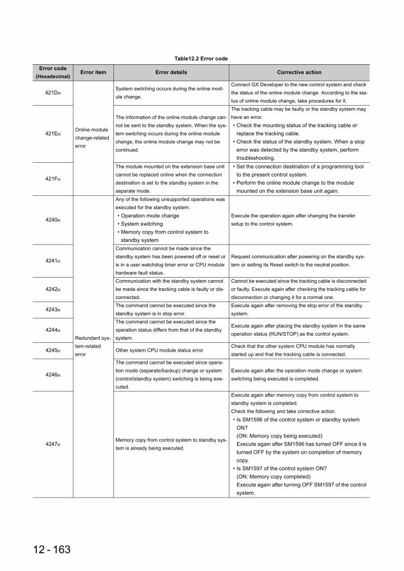
Table12.2 Error code
Error code(Hexadecimal)
Error item Error details Corrective action
421DH
Online module change-related error
System switching occurs during the online mod-ule change.
Connect GX Developer to the new control system and check the status of the online module change. According to the sta-tus of online module change, take procedures for it.
421EH
The information of the online module change can-not be sent to the standby system. When the sys-tem switching occurs during the online module change, the online module change may not be continued.
The tracking cable may be faulty or the standby system may have an error.• Check the mounting status of the tracking cable or
replace the tracking cable.• Check the status of the standby system. When a stop
error was detected by the standby system, perform troubleshooting.
421FH
The module mounted on the extension base unit cannot be replaced online when the connection destination is set to the standby system in the separate mode.
• Set the connection destination of a programming tool to the present control system.
• Perform the online module change to the module mounted on the extension base unit again.
4240H
Redundant sys-tem-related error
Any of the following unsupported operations was executed for the standby system.• Operation mode change• System switching• Memory copy from control system to
standby system
Execute the operation again after changing the transfer setup to the control system.
4241H
Communication cannot be made since the standby system has been powered off or reset or is in a user watchdog timer error or CPU module hardware fault status.
Request communication after powering on the standby sys-tem or setting its Reset switch to the neutral position.
4242H
Communication with the standby system cannot be made since the tracking cable is faulty or dis-connected.
Cannot be executed since the tracking cable is disconnected or faulty. Execute again after checking the tracking cable for disconnection or changing it for a normal one.
4243HThe command cannot be executed since the standby system is in stop error.
Execute again after removing the stop error of the standby system.
4244H
The command cannot be executed since the operation status differs from that of the standby system.
Execute again after placing the standby system in the same operation status (RUN/STOP) as the control system.
4245H Other system CPU module status errorCheck that the other system CPU module has normally started up and that the tracking cable is connected.
4246H
The command cannot be executed since opera-tion mode (separate/backup) change or system (control/standby system) switching is being exe-cuted.
Execute again after the operation mode change or system switching being executed is completed.
4247HMemory copy from control system to standby sys-tem is already being executed.
Execute again after memory copy from control system to standby system is completed.Check the following and take corrective action.• Is SM1596 of the control system or standby system
ON?(ON: Memory copy being executed)Execute again after SM1596 has turned OFF since it is turned OFF by the system on completion of memory copy.
• Is SM1597 of the control system ON?(ON: Memory copy completed)Execute again after turning OFF SM1597 of the control system.
12 - 163

CHAPTER12 TROUBLESHOOTING
12
12.3 Error C
ode List12.3.11 E
rror codes returned to request source during comm
unication with C
PU
module
Table12.2 Error code
Error code(Hexadecimal)
Error item Error details Corrective action
4248H
Redundant sys-tem-related error
• Communication was made during system switching.
• The system specified in the transfer setup (request destination module I/O number) does not exist.
• Execute again after system switching.• After checking whether the specified system exists or
not, restart communication.
4249H
The redundant system is not established.(Control system/standby system or System A/System B not yet definite)
• Normally start the system as the redundant system.(Make communication again after establishing the sys-tem.)
• Execute again after changing the transfer setup (request destination module I/O number) to "No set-tings have been made" (03FFH).
424AH
The command that could not be processed was executed when the transfer setup (request desti-nation module I/O number) is Control system/Standby system/System A/System B.
Execute again after changing the transfer setup (request destination module I/O number) to "No settings have been made" (03FFH).
424BH
The command cannot be executed since system switching is inhibited by the manual system switching enable flag (SM1592).
Manual system switching is inhibited by the manual system switching enable flag (SM1592). Execute again after turning ON SM1592.
424CHThe specified command cannot be executed dur-ing online program change operation.
Execute again after the online program change operation is finished.
424DHThe transfer setup or function unavailable for the debug mode was used.
• Execute again after changing to the backup mode.• Execute again after changing the transfer setup
(request destination module I/O number) to System A or control system.
424EHThe control system/standby system specifying method is not supported.
This function cannot be executed since it is not supported.
424FH
System switching was executed by the other con-dition during execution of system switching by GX Developer.
Although system switching was executed from GX Devel-oper, system switching was executed first by the other condi-tion. Check the system for any problem and execute the operation again as necessary.
4250HSum check error occurred in tracking communica-tion.
Execute communication again after changing the tracking cable.If the same error recurs after the tracking cable is changed, the cause is the hardware fault of the CPU module.(Please contact your local nearest Mitsubishi or representa-tive, explaining a detailed description of the problem.)
4251HThe command cannot be executed in the sepa-rate mode.
Execute again after changing to the backup mode.
4252H
System switching was not executed since an error occurred in the redundant system compati-ble network module of the standby system.
By monitoring SD1690 (other system network module No. that issued system switching request), identify the faulty redundant-compatible intelligent module of the standby sys-tem, then remove the module fault, and execute again.
12 - 164

Table12.2 Error code
Error code(Hexadecimal)
Error item Error details Corrective action
4253H
Redundant sys-tem-related error
Since a communication error or system switching occurred during online program change to the control system CPU module, online program change to the standby CPU module cannot be executed.
Since a communication error or system switching occurred during execution of online program change to the control system CPU module, online program change redundant tracking was suspended.Execute online program change again after confirming that communication with the control system CPU module and standby system CPU module can be normally made.When long time is taken for communication between GX Developer and control system CPU module or standby sys-tem CPU module, the error may be avoided by adjusting SD1710 (standby system online program change start wait-ing time).
4254H
The command cannot be executed since an error was detected in the tracking communication hard-ware.
The tracking cable may not be connected correctly, or the tracking communication hardware of the CPU module may be faulty. Check the connection status of the tracking cable.If the condition is not restored to normal after the cable con-nection status is corrected, the possible cause is the hard-ware fault of the CPU module.
4255HThe command cannot be executed since tracking communication is being prepared.
Tracking communication is being prepared when it is con-nected. Execute the operation again after a while (about 1 second).
4256HThe command cannot be executed since a time-out error occurred in tracking communication.
The tracking cable may not be connected correctly, or the tracking communication hardware of the CPU module may be faulty. Check the connection status of the tracking cable.If the condition is not restored to normal after the cable con-nection status is corrected, the possible cause is the hard-ware fault of the CPU module.
4257H
The command cannot be executed since the host system CPU module is in a watchdog timer error or CPU module hardware fault status.
The command cannot be executed since the host system is in a watchdog timer error or CPU module hardware fault sta-tus. Execute again after checking the host system status.
4258HOperation mode being changed (from backup mode to separate mode)
Execute again after completing the operation mode change by changing the status from STOP to RUN using the RUN/STOP switch of the CPU module whose RUN LED is flicker-ing or remote operation.
4259H
Operation mode change is being executed in the communication route different from the current one from the other peripheral device.
Execute again in the same communication route as the one where the operation mode change was executed.
425BH
Although the communication was made via the intelligent function module mounted on the exten-sion base unit, the combination of the connection destination specification (Redundant CPU specifi-cation) and the command is unsupported.
Change the combination of the connection destination speci-fication and the command to the supported combination.
425CH
System switching cannot be made since the mod-ule mounted on the extension base unit is being replaced online.
Switch systems after the online module change has been completed.
425DH
Operation mode cannot be changed since the module mounted on the extension base unit is being replaced online.
Change the operation mode after the online module change has been completed.
12 - 165

CHAPTER12 TROUBLESHOOTING
12
12.3 Error C
ode List12.3.11 E
rror codes returned to request source during comm
unication with C
PU
module
Table12.2 Error code
Error code(Hexadecimal)
Error item Error details Corrective action
4A00H
Link-related error
• Access to the specified station cannot be made since the routing parameters are not set to the start source CPU module and/or relay CPU module.
• For routing via a multiple CPU system, the control CPU of the network module for data routing has not started.
• When System A/System B is not yet identi-fied in a redundant system configuration, communication was made with the other station via the network module.
• Set to the related stations the routing parameters for access to the specified station.
• Retry after a while, or start communication after con-firming that the system for data routing has started.
• In a redundant system configuration, connect the tracking cable, start System A/System B normally, and then restart communication.
4A01HThe network of the No. set to the routing parame-ters does not exist.
Check and correct the routing parameters set to the related stations.
4A02H Access to the specified station cannot be made.
• Check the network module/link module for an error or offline status.
• Check to see if the network number/PC number setting has no mistake.
4A03H A request for network test was issued. Check the request data of the MC protocol, etc.
4B00H
Target-related error
An error occurred in the access destination or relay station, or the specified transfer setup (request destination module I/O number) is illegal.
• Take corrective action after checking the error that occurred at the specified access destination or the relay station to the accessed station.
• Check the transfer setup (request destination module I/O number or programmable controller number) in the request data of the MC protocol, etc.
4B01HThe target is not the No. 1 CPU of the multiple CPU system.
Execute the request for the No. 1 CPU of the multiple CPU system.
4B02H The request is not addressed to the CPU module.Perform operation for the module that can execute the speci-fied function.
4B03H
• The specified route is not supported by the specified CPU module version.
• The communication target CsPU is not mounted.
Check whether the specified route is supported or not.
4B04HThe specified transfer setup (request destination module I/O number) is not supported.
In the target setup, an illegal value is set as the head I/O number of the target module.
4C00H
Multiple CPU-related error
The specified device is unavailable for the motion CPU or outside the device range.
Check the request data contents.
4C08HThere are a total of 33 or more DDWR and DDRD requests.
Execute again after reducing the number of DDWR and DDRD requests to be executed simultaneously.
4C09HThe specification of the requested CPU module No. is illegal.
Check the request data contents.
12 - 166

12.4 Module Change during System Operation
This section explains how to change the module online (with power on) without stopping the system.
12.4.1 Online module change
An online module change Note12.15 is a function that allows the Q series module mounted on the main base unit or
extension base unit to be changed during system control executed by the Process CPU or Redundant CPU.Note1Using an online module change, the module that failed during control can be replaced with the module of the same model name.
● An online module change cannot add a module or change the current module for another module.
● When executing an online module change for the Process CPU in the multiple CPU system, it is necessary to specify "Online module change enable for other CPU" in the multiple CPU setting of the PLC parameter dialog box.Also, there are restrictions on the versions of the CPU modules that comprise the multiple CPU system. For details, refer to the following.
QCPU User's Manual (Multiple CPU System)
● Perform an online module change after confirming that the system outside the programmable controller will not malfunction.
● To prevent an electric shock, operating module malfunction, etc., provide a switch or similar individually cutting-off means for the external power supply of the module to be changed online.
● It is recommended to verify that the operations of the unchanged modules will not be affected by executing an online module change in an actual system beforehand to confirm the following
• The means and structure that will cut off the connection with the external device are correct. • ON/OFF of switches, etc. has no influence.
● Do not mount/remove the module onto/from base unit or terminal block more than 50 times (IEC 61131-2 compliant), after the first use of the product.Failure to do so may cause the module to malfunction due to poor contact of connector.
Note1
Note12.15The Basic model QCPU, High Performance model QCPU and Universal model QCPU are notcompatible with an online module change.
Basic Highperformance Universal
12 - 167

CHAPTER12 TROUBLESHOOTING
1
2
3
12
5
6
7
8
12.4 Module C
hange during System
Operation
12.4.1 Online m
odule change
(1) System configuration that allows online module changeAn online module change can be peformed under the following conditions.
(a) Modules that can be changed onlineThe modules that can be changed online are shown in Table12.3.
*1: When using Redundant CPU and/or connecting a extension base unit, online module change cannot be performed to a intelligent function module mounted on the main base unit.
The modules other than listed above cannot be changed online.For whether the above intelligent function modules can be changed online or not and their changing procedures, refer to the manual of the used intelligent function module.
(b) Versions of GX Developer that supports online module changeGX Developer is required to perform an online module change.For GX Developer version, refer to the following
When Process CPU is used : Section 2.1.6
When Redundant CPU is used : QnPRHCPU User's Manual (Redundant System)
An online module change can also be performed from GX Developer via a network.
(c) Restrictions on base units
1) When the slim type main base unit (Q3 SB) is used, an online module change cannot be performed.
2) When the extension base unit of the type that requires no power supply module (Q5 SB) is used, an online module change cannot be performed for the modules mounted on all base units connected.
3) When the redundant type extension base unit (Q6 WRB) is used, the online module change cannot be performed to all modules connected to the main base unit.
Table12.3 Modules that can be changed online
Module type RestrictionsInput module
No restrictionsOutput module
I/O combined module
Intelligent function module
Analog-digital converter module
Supported by function version C.
Digital-analog converter module
Temperature input module
Temperature control module
Pulse input module
12 - 168

(d) Control status of CPU module1) An online module change can be executed when a stop error has not occurred.
Whether an online module change can be executed or not depending on the control status of the CPU module is shown in Table12.4.
*1: Including the case where a continue error has occurred in the RUN status.
2) An online module change can be continued if the control status of the CPU module is changed to the STOP/PAUSE status during the online module change.
In either of the following cases, however, the online module change cannot be continued. •When the CPU module is reset •When a stop error occurs
(e) Number of modules that can be changed onlineThe number of modules that can be changed online at one time is one for each CPU module.Multiple modules cannot be changed simultaneously.
Table12.4 Whether online module change can be executed or not
Control status RUN status*1 STOP status PAUSE status At stop errorWhether online module change can be executed or not
Can be executed Can be executed Can be executed Cannot be executed
12 - 169

CHAPTER12 TROUBLESHOOTING
1
2
3
12
5
6
7
8
12.4 Module C
hange during System
Operation
12.4.1 Online m
odule change
(2) Restrictions on online module changeThe following operations cannot be performed during an online module change.
• Issue an online module change request from multiple GX Developers to one CPU module. • Write parameters to the CPU module during online module change.
The following message appears (refer to Figure 12.24) if an online module change request is issued from another GX Developer to the CPU module during online module change. After confirming the message, select "Yes" or "No".
When "Yes" is selectedOnline module change operation is switched to "GX Developer 2)" that issued the request later. (Operation is continued from the pre-switching status.)
When "No" is selectedThe operation of online module change "GX Developer 2)" requested later is suspended. (Online module change "GX Developer 1)" executed first is continued.)
Figure 12.24 Message screen
Figure 12.25 Online module change (When "Yes" is selected)
Figure 12.26 Online module change (When "No" is selected)
GX Developer 2)
Online module
change continued
Online module change
execution canceled
GX Developer 1)
"Yes" selected
GX Developer 2)
Online module
change suspended
Online module change
execution continued
GX Developer 1)
"No" selected
12 - 170

(3) Special relays and special register related to online module changeInformation during online module change is stored into the special relays (SM235, SM236) and special register (SD235).
•Whether the online module change of the corresponding CPU module is executed or not can be checked by monitoring SM235, SM236 and SD235.
•SM235: Online module change flag (turns on during online module change) •SM236: Flag that turns on only one scan after online module change (turns on only one scan
after completion of online module change) •SD235: Module being changed online (stores the starting I/O number of the module being
changed online/10H)
Refer to Section 12.7 for details of SM235 and SM236 and to Section 12.8 for details of SD235.
Figure 12.27 Time chart
OFF
ON
OFF
ON
SM235
SD235
SM236
1 scan
Online module change start
Online module change completed
Starting I/O number of module being changed online/10H
12 - 171

CHAPTER12 TROUBLESHOOTING
1
2
3
12
5
6
7
8
12.4 Module C
hange during System
Operation
12.4.1 Online m
odule change
(4) Online module change procedureThe following explains the online module change procedure of the I/O module.For the online module change procedure of the intelligent function module, refer to the manual of the used intelligent function module.
• It is recommended to turn off the output (Y) from the output module/I/O combined module to be changed online before it is changed.
• When making an online module change for the Redundant CPU, specify "No settings have been made (Default)", "System A" or "System B" as the target system in the "transfer setup" by GX Developer.Do not specify the "Control system" or "Standby system" as the target system.If the "Control system" or "Standby system" is specified in the transfer setup, the following error dialog (refer to Figure 12.28) appears at execution of an online module change.When the following error dialog is displayed, change the target system to "No settings have been made (Default)", "System A" or "System B", and then perform an online module change.
• When executing online module change for the module mounted on the extension base unit in the Redundant CPU, access cannot be made to a module mounted on the extension base unit from the standby system. Set [Transfer setup] in GX Developer, checking that the trasnfer target Redundant CPU module is the control system.
Figure 12.28 Error dialog box
12 - 172

1) Choose [Diagnostics] [Online module change] on GX Developer, and select the "Online module change" mode.
2) Double-click the module to be changed online to display the online module change screen.(Table12.5 shows the communication status with the target module for online module change when the following screen (refer to Figure 12.30) is displayed.)
Figure 12.29 System monitor
Table12.5 Communication status with the module
Target module, itemExecuted/Not
executedInput module refresh ExecutedOutput module refresh Executed
I/O hybrid moduleInput refresh ExecutedOutput refresh Executed
Intelligent function module
Input refresh ExecutedOutput refresh ExecutedFROM/TO instruction ExecutedInstruction using intelligent function module device
Executed
Intelligent dedicated instruction ExecutedIntelligent automatic refresh Executed
Buffer memory batch monitor Executed
Figure 12.30 Online module change screen
12 - 173

CHAPTER12 TROUBLESHOOTING
1
2
3
12
5
6
7
8
12.4 Module C
hange during System
Operation
12.4.1 Online m
odule change
3) Click the Execution button to enable a module change.(Table12.6 shows the communication status with the target module for online module change when the following screen (refer to Figure 12.31) is displayed.)
4) With a switch or other device, cut off the connection with the external device (module I/O signals).
5) Turn off the switch of the external power supply for module to shut off power supply.
6) Disconnect the terminal block or connector from the module.
7) Remove the module. ( Section 10.3.3)
8) Mount a new module on the same slot. ( Section 10.3.3)
9) Connect the terminal block or connector to the module.
10)Turn on the switch of the external power supply for module to resume power supply.
11)With a switch or other device, make a connection with the external device (module I/O signals).
Table12.6 Communication status with the module
Target module, itemExecuted/Not
executed
Input module refreshNot executed(Data held)
Output module refresh Not executed
I/O hybrid moduleInput refresh
Not executed(Data held)
Output refresh Not executed
Intelligent function module
Input refresh Not executedOutput refresh Not executedFROM/TO instruction No processingInstruction using intelligent function module device
No processing
Intelligent dedicated instruction No processingIntelligent automatic refresh No processing
Buffer memory batch monitorCommunication error
Figure 12.31 Online module change screen
12 - 174
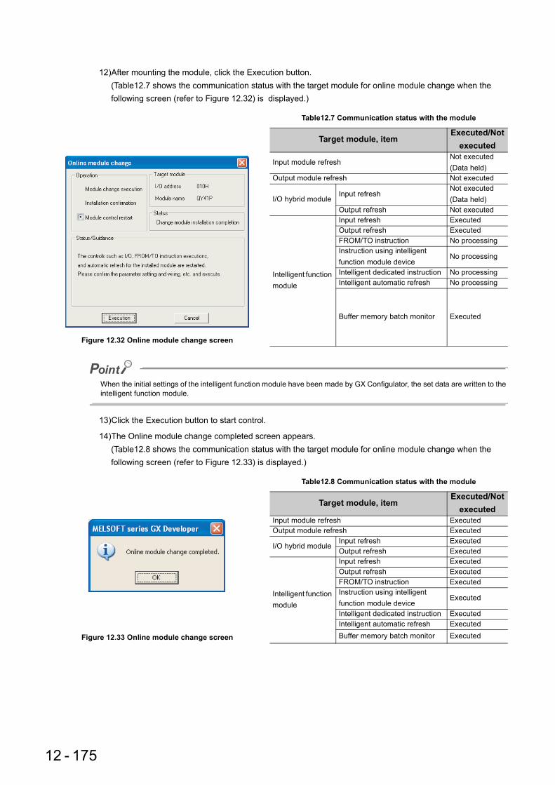
12)After mounting the module, click the Execution button.(Table12.7 shows the communication status with the target module for online module change when the following screen (refer to Figure 12.32) is displayed.)
When the initial settings of the intelligent function module have been made by GX Configulator, the set data are written to the intelligent function module.
13)Click the Execution button to start control.
14)The Online module change completed screen appears.(Table12.8 shows the communication status with the target module for online module change when the following screen (refer to Figure 12.33) is displayed.)
Table12.7 Communication status with the module
Target module, itemExecuted/Not
executed
Input module refreshNot executed(Data held)
Output module refresh Not executed
I/O hybrid moduleInput refresh
Not executed(Data held)
Output refresh Not executed
Intelligent function module
Input refresh ExecutedOutput refresh ExecutedFROM/TO instruction No processingInstruction using intelligent function module device
No processing
Intelligent dedicated instruction No processingIntelligent automatic refresh No processing
Buffer memory batch monitor Executed
Figure 12.32 Online module change screen
Table12.8 Communication status with the module
Target module, itemExecuted/Not
executedInput module refresh ExecutedOutput module refresh Executed
I/O hybrid moduleInput refresh ExecutedOutput refresh Executed
Intelligent function module
Input refresh ExecutedOutput refresh ExecutedFROM/TO instruction ExecutedInstruction using intelligent function module device
Executed
Intelligent dedicated instruction ExecutedIntelligent automatic refresh ExecutedBuffer memory batch monitor ExecutedFigure 12.33 Online module change screen
12 - 175

CHAPTER12 TROUBLESHOOTING
1
2
3
12
5
6
7
8
12.4 Module C
hange during System
Operation
12.4.1 Online m
odule change
(5) Operation in case of system switching occurrence during online module change (When Redundant type extension base unit is used)The following describes the procedures to be taken when the system switching occurs during online module change is performed to the module mounted on the extension base unit in the Redundant CPU.
1) Connect GX Developer to the new control system.
2) Check the status of the module where the online module change was performed at [System Monitor].
3) When selecting [Online module change] in a status of a module being replaced online, screen shown in Figure 12.30 is displayed.
4) Continue the operation that has been executed before system switching occurrence.
Figure 12.34 System monitor
Figure 12.35 Online module change screen
12 - 176

• When connecting the new control system and clicking the Execution button, the message shown in Figure 12.31 may be shown. In this case, select [Yes] and continue operation for the online module change.
• At the time of completion of the online module change, the error dialog box shown in Figure 12.32 may be shown, but the online module change is completed normally.
Figure 12.36 Message dialog box
Figure 12.37 Error dialog box
12 - 177

CHAPTER12 TROUBLESHOOTING
1
2
3
12
5
6
7
8
12.4 Module C
hange during System
Operation
12.4.2 Change of redundant pow
er supply module
12.4.2 Change of redundant power supply module
Following the flowchart shown below, change a faulty redundant power supply module online (with power on).(It is assumed that the other redundant power supply module is normally operating.)
Figure 12.38 Redundant power supply module replacement procedure
Start
Completed
Check the redundant power supply
module to be changed.
Power OFF the redundant power supply
module to be changed.
Change the redundant power supply
module.
Power ON the new redundant power
supply module.
Make sure that the "POWER" LED is
turned on green.
12 - 178

• If either redundant power supply module fails, change it for a normal one earlier than usual (within 14 days as a guideline).If it does not fail, it is recommended to change the redundant power supply module for a new one after five years have elapsed.
• Change the redundant power supply module with extreme care, referring to Section 10.3.3(1).If the module fixing projection of the redundant power supply module comes off from the module fixing hole of the redundant base unit, an error will occur due to connector damage.
• When the redundant power supply system is used, a "continue" error will occur due to a redundant power supply module failure. Cancel the error after changing the faulty redundant power supply module for a normal one.
Note12.16, Note12.17 • When the redundant power supply system is used, the failure status of the redundant power supply module can
be checked by the system monitor of GX Developer (Version 8.18U or later) or the special relay SM1781/special
register SD1781. Note12.16, Note12.17Note1For details of the system monitor, refer to the following.
GX Developer Operating Manual
Note1
Note12.16Failure of redundant power supply cannot be detected by the Basic model QCPU.
Basic
Note12.17When using the High Performance QCPU or the Process CPU, confirm the versions of CPU module and GX
Developer. ( Appendix 2)
Highperformance Process
12 - 179

CHAPTER12 TROUBLESHOOTING
1
2
3
12
5
6
7
8
12.5 I/O M
odule Troubleshooting12.5.1 Input circuit troubleshooting
12.5 I/O Module Troubleshooting
This section explains possible problems with I/O circuits and their corrective actions.
12.5.1 Input circuit troubleshooting
The following describes possible problems with input circuits and their corrective actions.
Table12.9 Input circuit problems and corrective actions
Condition Cause Corrective Action
Exa
mpl
e 1
Input signal is not turned off.
• Leakage current of input switch (e.g. drive by non-contact switch).
• Connect an appropriate CR so that the voltage across the terminals of the input module becomes lower than the off voltage.
It is recommended to use 0.1 to 47 F+47 to 120 (1/2W) for the CR constant.
Exa
mpl
e 2
Input signal is not turned off.
• Drive by a limit switch with neon lamp.• Same as Example 1.• Provide an independent display circuit separately.
Exa
mpl
e 3
Input signal is not turned off.
• Leakage current due to line capacity of wiring cable. (Line capacity C of twisted pair wire is approx. 100 pF/m).
• Same as Example 1.(However, leakage current is not generated when the power supply is located in the input equipment side as shown below.)
Exa
mpl
e 4
Input signal is not turned off.
• Drive by a switch with LED display. • Connect an appropriate resistor so that the current across the input module becomes lower than the off current.
*: A calculation example of the resistance to be connected is shown on the following page.
Table12.9 Input circuit problems and corrective actions (Continued)
AC input
Input
module
Leakage
current
Power supply
Input
module
AC input
R
AC input
Input
module
Leakage
current
Power supply
AC input
Input
module
Leakage
current
Power supply
AC input
Input
module
Power supply
DC input (plus common)
Input
module
Leakage current
DC input (plus common)
Input
moduleResister
12 - 180

<Calculation example of the resistance to be connected in Example 4> • Connecting a switch with LED display, in which a maximum 2.33mA leakage current flows when 24VDC is
supplied to the QX40.
• In this case, the circuit does not satisfy the condition that the off current of the QX40 is 1.7mA or less. Connect a resistance as follows.
(To the next page)
Condition Cause Corrective ActionE
xam
ple
5
Input signal is not turned off.
• Sneak path due to the use of two power supplies.• Use only one power supply.• Connect a sneak path prevention diode. (Figure
below)
Exa
mpl
e 6 Input signal is
not turned on (AC input module)
Stepwise distortion as shown below appears to the zero cross voltage of input signal (AC).
Improve input signal waveform by using the on-line system etc.
Exa
mpl
e 7
False input due to noise
Depending on response time setting, noise is imported as input.
Change the response time setting. Example: 1ms to 5ms(When excessive noise is cyclic, shorter response time setting may produce a higher effect.) When the above action is not effective, take measures against noise to block excessive noise, e.g. avoid tying the power cables and control cables in a bundle, and add surge absorbers to the noise sources such as the relays and contactors used with the same power supply.
DC input
Input
moduleE1 E2
E1 E2
DC input
Input
moduleE1 E2
Zero cross
voltage
Input
moduleLeakage current
24VDC
QX40
2.33mA
24VDC
QX402.33mA
IZ=1.7mAIR=0.63mA Input impedance
5.6kR
12 - 181

CHAPTER12 TROUBLESHOOTING
1
2
3
12
5
6
7
8
12.5 I/O M
odule Troubleshooting12.5.1 Input circuit troubleshooting
(From preceding page) • In order to satisfy the condition that the OFF current of the QX40 is 1.7mA or less, the resistance R, in which
a 0.63mA or more current flows, shall be connected.Calculating with the formula "IR: IZ = Z (Input impedance): R",
the resistance R will be R<15.11k .
Consequently, if the resistance R is set to 12k , the electric power W of the resistance R will be calculated in the following formula,
W= (Input voltage)2/R=28.82/12000=0.069[W].
• Since the resistance requires the electric power which is 3 to 5 times of the power actually consumed, the
resistance to be connected to the corresponding terminal shall be 12.0k and 1/4 to 1[W].
• The OFF voltage of the QX40 when the resistance R calculated above is connected will be 8.90[V]
This also satisfies the condition that the OFF voltage of the QX40 is 11V or less.
R< Z (Input impedance)= 5.6=15.11[k ]IRIZ
0.631.7
2.33[mA]=8.90[V]1
1 1+
12.0[k ] 5.6[k ]
12 - 182

12.5.2 Output circuit troubleshooting
This section explains trouble examples and troubleshooting in the output circuit.
Table12.10 Output circuit troubleshooting
Condition Cause Corrective Action
Exa
mpl
e 1 Excessive
voltage is applied to load when output turns off.
• When load is half-wave rectified inside (This is typical of some solenoids.)
• When the polarity of the power supply is [1], the capacitor C is charged. When the polarity is [2], the voltage charged in C plus the power supply voltage is applied to across D1. The maximum value of the voltage is approx. 2.2E.(This usage does not pose problems to the output components but may deteriorate the diode built in the load, causing burnout, etc.)
• Connect a resistor of several ten K to several
hundred K at both ends of the load.
Exa
mpl
e 2 Load does not
turn off.(Triac output)
• Leakage current due to the built-in surge suppressor
• Connect a resistor at both ends of the load.(If the wiring from the output module to the load is long, be careful since there may be a leakage current due to the line capacity.)
Exa
mpl
e 3
The load is not turned off. (Triac output)
• The load current is lower than the minimum load current.
• When the load current is lower than the minimum load current of the output module, the triac does not operate and the load current flows into a phototriac as shown by the arrow in the following figure. When an inductive load is being connected, the load may not be turned off since surge at the time of off is applied to the phototriac.
• Connect a resistor to both ends of a load so that the load current is higher than the minimum load current.
Output module
QY22D1 [1]
[2]
Load
Resistor
Load
Load
Leakage current
QY22
Output module
Resistor
Load
Phototriac
QY22
Triac
Surge suppressor
Control
circuitLoad
Resistor
Load
12 - 183

CHAPTER12 TROUBLESHOOTING
1
2
3
12
5
6
7
8
12.5 I/O M
odule Troubleshooting12.5.2 O
utput circuit troubleshooting
Table12.10 Output circuit troubleshooting (Continued)
Situation Cause Countermeasure
Exa
mpl
e 4
When the external power supply turns on, the load is turned on for a moment.
Erroneous output due to the stray capacitance (C) between collector and emitter of hotocoupler.
There is no erroneous output at normal load.An erroneous output may occur at high sensitivity load (such as solid state relay).
I
When turning on or off the external power, check that the external power supply rising edge is 10ms or more, and switch the SW1 to the primary side of external power supply.
When switching to the secondary side of the external power supply is required, the external power supply rising edge connected a condenser must be slow, and measured 10ms or more.
Sink output
Source output
*: Measures will not be effective to the following module due to the characterictic of external power supply circuit.• QY81P
L
Output module, Combined module
Photocoupler
C
ICTr1
Y0
12/24VDC
COM
SW
24V
Constant
voltage circuit
Primary
side
SW1external power supply
Programmable
controller
Secondary
side
L
Y0
COM
C1
24V
R1
SW0V
L
Y0
COM
C1
24V
R1
SW0V
12 - 184

Table12.10 Output circuit troubleshooting (Continued)
Situation Cause Countermeasure
Exa
mpl
e 4
When the external power supply turns on, the load is turned on for a moment.
If the external power supply is turned on precipitously, Ic current flows due to the stray capacitance (C) between collector and emitter of hotocoupler.
Ic current flows to the next stage of transister Tr1 gate and Y0 output turns on by 100 s R1: Several tens of ohms
Power capacity (external power supply current*1)2 resistance value (3 to 5)*2
C1: Several hundreds of microfarads 50V*1 Refer to consumption current of the
external power supply for modules used in this manual.
*2 Select the power capacity of resistance to be 3 to 5 times lager than the actual power consumption.
(Example)R1=40 , C1=300 FUse the below expression to calculated a time constant
C1 R1=300 10-6 40=12 10-3s=12ms
SW: External power
supply (24V) at On
Output Y0
10ms or less
Approx. 100 s
12 - 185

CHAPTER12 TROUBLESHOOTING
1
2
3
12
5
6
7
8
12.5 I/O M
odule Troubleshooting12.5.2 O
utput circuit troubleshooting
Table12.10 Output circuit troubleshooting (Continued)Situation Cause Countermeasure
Exa
mpl
e 5
The load which was turned off is turned on for a moment at power-off. (Transistor output)
The load [2] which was turned OFF may be turned ON due to back electromotive force at the time of power-off [1] if an inductive load is used.
Take either of the following measure.• To prevent the generation of the back electromotive force, connect diode in parallel with load where the back electromotive force has been generated.
Source output[3]
Sink output[3]
• Connect diode between (+) and (-) of the external power supply so that a sneak path circuit is porvided.Connect the diode to C1 and R1 in parallel when example 4 is performed simultaneously.
* Measures will not be effective to the following module due to the characterictic of external power supply circuit.
• QY81P
D1: Reverse current VR(VRM)···*1, Forward current IF(IFM)···*2* 1 Approx. 10 times the rated voltage of the spec.
Ex.: 24VDC Approx.200V*2 More than 2 times the Max. load current (common) of the spec. Ex: 2A/1 common More than 4A
Output module,
ombined moduleBack electromotive
force+-
-+
Load
Load
[1]
Shut off
[3]
[2]
[2]
Y0
Y1
COM
0V
Source output
ON
OFF
Output module,
ombined moduleBack electromotive
force
Load
Load
[1]
Shut off
[3]
Y0
Y1
COM
12/24VDC
Sink output
ON
OFF
Back electromotive force
Load
Load
Back electromotive force
Source output
ON
OFF
[1]
Shut off
[2]
[3]
Y0
Y1
COM
0V
D1
C1 R1
Example 4
Back electromotive
force
Load
Load
+-
ON
OFF[1]
Shut off
[2]
[3]
Y0
Y1
COM
12/24VDC
D1
C1 R1
Example 4
Sink output
Load
Load
Back electromotive
force-+
12 - 186

12.6 Built-in Ethernet Port Diagnosis
Using the diagnostic function of GX Developer, the module status, parameter settings, communication status, and error log of the Built-in Ethernet port QCPU can be checked.
The relevant screen can be activated by either of the following two methods.
• In GX Developer, select [Diagnostics] [PLC diagnostics] [Ethernet diagnosis]
• In GX Developer, select [Diagnostics] [Ethernet diagnostics]
On the following pages, details of the built-in Ethernet port diagnosis screens are described.
Figure 12.39 PLC Diagnostics screen
Figure 12.40 Ethernet diagnosis screen
12 - 187

CHAPTER12 TROUBLESHOOTING
1
2
3
12
5
6
7
8
12.6 Built-in E
thernet Port D
iagnosis
(1) Parameter status
Before performing the Built-in Ethernet port, check that the “CPU” is selected in the Target module setting on the Ethernet diagnosis screen.
Figure 12.41 Ethernet diagnosis (Parameter status) screen
Table12.11 Ethernet diagnosis (Parameter status) items
Item DescriptionIP address
The Ethernet address (MAC address) of the Built-in Ethernet port QCPU can be monitored.
Subnet mask
Default router IP address
Ethernet address
12 - 188

(2) Error log
*1 "SNTP OPE. ERROR" (error code: 2710) is stored in the error log only when the time setting at power-ON or reset has failed.For results in the case of executing the time setting regularly or by special relay "SM1270" from the sequence program, check the SNTP status screen or special register "SD1270".
Because the error log is battery backed up, the information is retained even if the power is turned off.Note that the latch data backup function (to the standard ROM) cannot back up the error log to the standard ROM.
Figure 12.42 Ethernet diagnosis (Error log) screen
Table12.12 Ethernet diagnosis (Error log) items
Item Description
Connection No.Displays connection No. of the connection that has an error.UDP connections that function in MELSOFT connection are treated as one connection, and the lowest connection No. is stored in the error log.
Protocol
Displays the settings of PLC parameter.Open system
Host station port No.
Error codeDisplays a generated error code.*1
In the case of MELSOFT connection, only the errors related to Ethernet com-munication are stored in the Error log.
Destination IP addressDisplays the IP address of the other device when an error occurs in communi-cation with it.
Destination port No.Displays the port number of the other device when an error occurs in commu-nication with it.
Command code Displays command No. when an error occurs in MC protocol communication.
Year/Month/Day, Time Displays the date and time of error occurrence.
Clear history Clears the displayed error log.
Error and solution Displays details of the selected error code and corrective actions.
12 - 189

CHAPTER12 TROUBLESHOOTING
1
2
3
12
5
6
7
8
12.6 Built-in E
thernet Port D
iagnosis
(3) Status of each connection
*1: UDP connections that function in MELSOFT connection are treated as one connection. Therefore, for multiple connec-tions, the same information is displayed.
*2: Not displayed when the protocol is UDP and direct connection to GX Developer is used.*3: The same information is displayed when the protocol is TCP and when multiple MELSOFT connections exist.
Figure 12.43 Ethernet diagnosis (Status of each connection) screen
Table12.13 Ethernet diagnosis (Status of each connection) items
Item DescriptionHost station port number Displays the setting of PLC parameter.
Destination IP address Displays the IP address of the target device.*1
Destination port No. Displays the port number of the target device.*1
Latest Error CodeDisplays an error code for an error that occurred on the connection.*1
In the case of MELSOFT connection, only the errors related to Ethernet com-munication are stored in the Status of each connection.
ProtocolDisplays the settings of PLC parameter.
Open system
TCP statusIn TCP connections, displays whether connection with the target device is established or not.*1
Remote password status Displays the remote password status.*2
Unlock error count Displays how many times an unlock error has occurred.*1*3
Force deactivation statusIf this is set for a connection for which illegal accesses are suspected, commu-nication of the connection is disabled. *1*3
12 - 190

(4) Connection status
Figure 12.44 Ethernet diagnosis (Connection status) screen
Table12.14 Ethernet diagnosis (Connection status) items
Item DescriptionFull duplex/Half duplex Displays whether the line uses the full or half duplex system.
Connection status Displays whether a hub or target device is connected or not.
10BASE-T/100BASE-TX Displays whether the network is 10BASE-T or 100BASE-TX.
Maximum size of detection Displays the maximum size of discarded broadcast message data.
Amount of data per unit time (latest) Displays the total size of discarded broadcast message data per unit time.
Amount of data per unit time (maximum)Displays the maximum total size of discarded broadcast message data per unit time.
Clear line status Clears the number of receive buffer overflows and broadcast information.
12 - 191
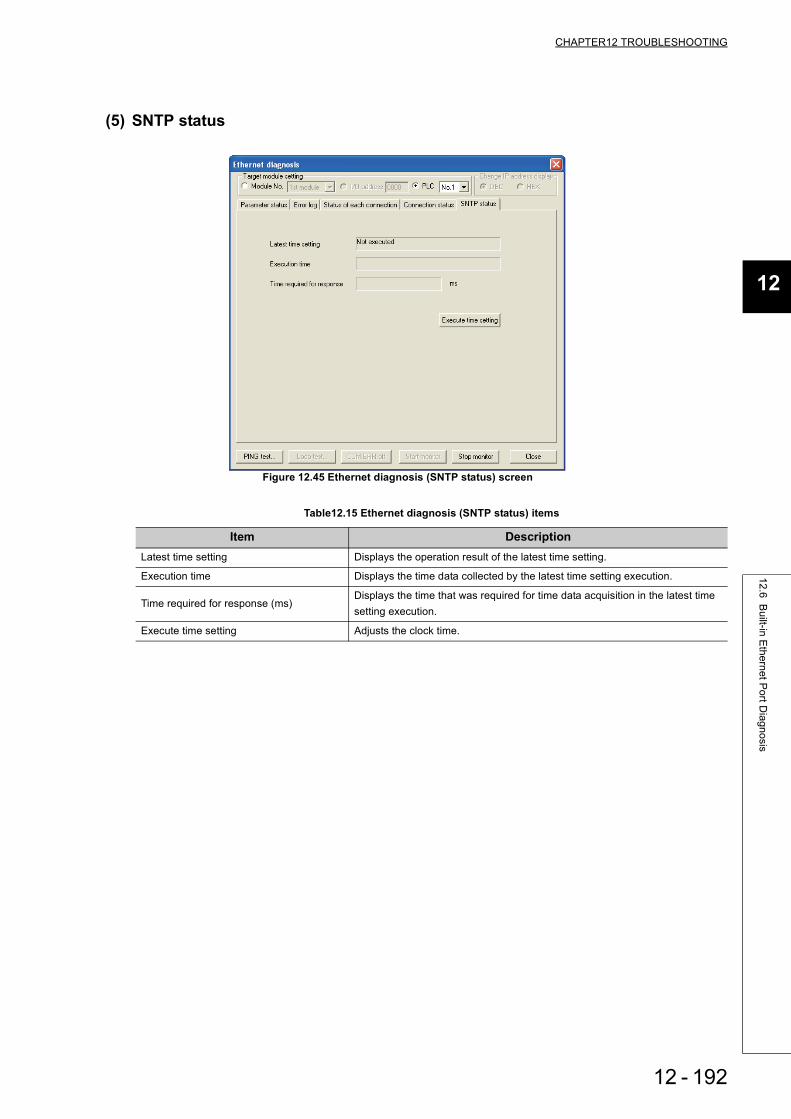
CHAPTER12 TROUBLESHOOTING
1
2
3
12
5
6
7
8
12.6 Built-in E
thernet Port D
iagnosis
(5) SNTP status
Figure 12.45 Ethernet diagnosis (SNTP status) screen
Table12.15 Ethernet diagnosis (SNTP status) items
Item DescriptionLatest time setting Displays the operation result of the latest time setting.
Execution time Displays the time data collected by the latest time setting execution.
Time required for response (ms)Displays the time that was required for time data acquisition in the latest time setting execution.
Execute time setting Adjusts the clock time.
12 - 192

(6) PING testPING test is a test by which existence of the Built-in Ethernet port QCPU can be checked from GX Developer.Performing a PING test for the Built-in Ethernet port QCPU can determine the following:
• Whether the line is connected to the target Built-in Ethernet port QCPU properly • Whether the parameters for the Built-in Ethernet port QCPU are set correctly
(a) Executing a PING test by GX DeveloperIn GX Developer, open the Ethernet diagnosis screen and click [PING test]
Figure 12.46 Ethernet diagnosis screen
12 - 193

CHAPTER12 TROUBLESHOOTING
1
2
3
12
5
6
7
8
12.6 Built-in E
thernet Port D
iagnosis
If failed, check the following and run the PING test again. • The Built-in Ethernet port QCPU installation to the base unit • Connection to Ethernet • Respective parameters written to the Built-in Ethernet port QCPU • Built-in Ethernet port QCPU operating status (whether an error has occurred or not) • Respective IP addresses set in GX Developer and PING test target stations • Subnet addresses set in GX Developer and PING test target stations when transmissions do not pass through any
router
Table12.16 PING test items
Item Description Setting range
Address speci-fication
IP address Specify the IP address of the PING test target station. (Target station's IP address)
IP address input form Select a form for IP address entry. Decimal/Hexadecimal
IP address/Host name Specify a host name of the PING test target station. -
Setting Options
Display the host name.In the Result area, displays the test results for the host name corresponding to the IP address.
-
Specify the data size.Specify any size of the system data that are sent during a PING test.
1 to 8192 bytes(For the Built-in Ethernet port QCPU, 1460 bytes or less)
Specify the time of the communication time check.
Specify the time to wait for PING test completion. 1 to 30 seconds
Specify the number of transmissions.
Specify the number of transmissions.• Specify the number of times.
No. of times: 1 to 50• Execute till interrupting
Result Displays PING test results. -
Success/transmissionsDisplays the total number of packet transmissions and the number of successful transmissions.
-
12 - 194

12.7 SPECIAL RELAY LIST
Special relays, SM, are internal relays whose applications are fixed in the Programmable Controller.
For this reason, they cannot be used by sequence programs in the same way as the normal internal relays.
However, they can be turned ON or OFF as needed in order to control the CPU module.
The heading descriptions in the following special relay lists are shown in 3.1.
For details on the following items, refer to the following manuals: • Networks Manual of the corresponding network module • SFC QCPU(Q mode)/QnACPU Programming Manual (SFC)
Do not change the values of special relays set by the system with user program or device test operations.Doing so may result in system downtime or communication fault.
Table12.17 Explanation of special relay list
Item Function of ItemNumber • Indicates special relay numberName • Indicates name of special relayMeaning • Indicates contents of special relayExplanation • Discusses contents of special relay in more detail
Set by (When set)
• Indicates whether the relay is set by the system or user, and, if it is set by the system, when setting is performed.<Set by> S : Set by system U : Set by user (sequence programs or test operations from GX Developer) S/U : Set by both system and user<When set> Indicated only for registers set by system Each END : Set during each END processing Initial : Set only during initial processing (when power supply is turned ON, or when going from STOP
to RUN) Status change : Set only when there is a change in status Error : Set when error occurs Instruction execution : Set when instruction is executed Request : Set only when there is a user request (through SM, etc.) System switching : Set when system switching is executed.
Corresponding ACPU M9
• Indicates the corresponding special relay (M9 ) of the ACPU. (When the contents are changed, the special relay is represented M9 format change. Incompatible with the Q00J/Q00/Q01 and QnPRH.)
• New indicates the special relay newly added to the Q series CPU module.
Corresponding CPU
Indicates the corresponding CPU module type name.QCPU : Indicates all the Q series CPU modules.Q00J/Q00/Q01 : Indicates the Basic model QCPU.Qn(H) : Indicates the High Performance model QCPU.QnPH : Indicates the Process CPU.QnPRH : Indicates the Redundant CPU.QnU : Indicates the Universal model QCPUEach CPU module model name: Indicates the relevant specific CPU module. (Example: Q02U)
12 - 195

CHAPTER12 TROUBLESHOOTING
1
2
3
12
6
7
8
12.7 SP
EC
IAL R
ELA
Y LIS
T
(2) Diagnostic Information
Table12.18 Special relay
Number Name Meaning ExplanationSet by
(When Set)
Corres-ponding ACPU
M9
Corresponding CPU
SM0 Diagnostic errors OFF : No errorON : Error
• Turns ON if an error occurs as a result of diagnosis.(Includes when an annunciator is ON, and when an error is detected with CHK instruction)
• Remains ON even if the condition is restored to normal thereafter.
S (Error) NewQn(H)QnPH
QnPRH
• Turns ON if an error occurs as a result of diagnosis.(Includes when an annunciator is ON)
• Remains ON even if the condition is restored to normal thereafter.
S (Error) New Q00J/Q00/Q01QnU
SM1 Self-diagnostic errorOFF : No self-diagnosis
errorsON : Self-diagnosis
• Turns ON if an error occurs as a result of diagnosis.(Does not include when an annunciator is ON or when an error is detected by the CHK instruction)
• Remains ON even if the condition is restored to normal thereafter.
S (Error) M9008Qn(H)QnPH
QnPRH
• Turns ON if an error occurs as a result of diagnosis.(Does not include when an annunciator is ON)
• Remains ON even if the condition is restored to normal thereafter.
S (Error) New Q00J/Q00/Q01QnU
SM5Error common information
OFF : No error common information
ON : Error common information
• When SM0 is ON, turns ON if there is error common information S (Error) New
QCPU
SM16 Error individual information
OFF : No error individual information
ON : Error individual information
• When SM0 is ON, turns ON if there is error individual information
S (Error) New
SM50 Error reset OFF ON: Error reset • Conducts error reset operation U New
SM51 Battery low latchOFF : NormalON : Battery low
• Turns ON if battery voltage at CPU module or memory card drops below rated value.
• Remains ON even if the battery voltage returns to normal thereafter.
• Synchronizes with the BAT. LED.
S (Error) M9007
Qn(H)QnPH
QnPRHQnU
• Turns ON if battery voltage at CPU module drops below rated value.
• Remains ON even if the battery voltage returns to normal thereafter.
• Synchronous with ERR. LED
S (Error) New Q00J/Q00/Q01
SM52 Battery low OFF : NormalON : Battery low
• Same as SM51, but turns OFF subsequently when battery voltage returns to normal. S (Error) M9006
QCPUSM53 AC/DC DOWN
detection
OFF : AC/DC DOWN not detected
ON : AC/DC DOWN detected
• Turns ON if an instantaneous power failure of within 20ms occurs during use of the AC power supply module.Reset when the power supply is switched OFF, then ON.
S (Error) M9005• Turns ON if an instantaneous power failure of within
10ms occurs during use of the DC power supply module.Reset when the power supply is switched OFF, then ON.
12 - 196

*6: The relevant modules are as follows:• The Universal model QCPU whose serial number (first five digits) is "10012" or later.• Q13UDHCPU, Q26UDHCPU
*7: The module whose first 5 digits of serial No. is "10102" or later.
Table12.18 Special relay
Number Name Meaning ExplanationSet by
(When Set)
Corres-ponding
ACPUM9
Corresponding CPU
SM56 Operation error OFF : NormalON : Operation error
• ON when operation error is generated• Remains ON if the condition is restored to normal
thereafter.S (Error) M9011
QCPU
SM60 Blown fuse detectionOFF : NormalON : Module with blown
fuse
• Turns ON if there is at least one output module whose fuse has blown.
• Remains ON if the condition is restored to normal thereafter.
• Blown fuse status is checked even for remote I/O station output modules.
S (Error) M9000
SM61 I/O module verify error OFF : NormalON : Error
• Turns ON if the I/O module differs from the status registered at power on.
• Remains ON if the condition is restored to normal thereafter.
• I/O module verification is also conducted for remote I/O station modules.
S (Error) M9002
SM62 Annunciator detection OFF : Not detectedON : Detected • Goes ON if even one annunciator (F) goes ON. S (Instruction
execution) M9009
SM80 CHK detection OFF : Not detectedON : Detected
• Goes ON if error is detected by CHK instruction.• Remains ON if the condition is restored to normal
thereafter.
S (Instruction execution) New
Qn(H)QnPH
QnPRH
SM90
Startup of monitoring timer for step transition(Enabled only when SFC program exists)
OFF : Not started(monitoring timer reset)
ON : Started(monitoring timer started)
Corresponds to SD90
• Goes ON when measurement of step transition monitoring timer is commenced.
• Resets step transition monitoring timer when it goes OFF.
U
M9108
Qn(H)QnPH
QnPRH
SM91 Corresponds to SD91 M9109
SM92 Corresponds to SD92 M9110
SM93 Corresponds to SD93 M9111
SM94 Corresponds to SD94 M9112
SM95 Corresponds to SD95 M9113
SM96 Corresponds to SD96 M9114
SM97 Corresponds to SD97 New
SM98 Corresponds to SD98 New
SM99 Corresponds to SD99 New
SM100 Serial communication function using flag
OFF : Serial communication function is not used.
ON : Serial communication function is used.
• Stores the setting of whether the serial communication function is used or not in the serial communication setting parameter
S (Power-ON or reset)
New
Q00/Q01Q00UJQ00UQ01U
Q02U*7
SM101 Communication protocol status flag
OFF : GX DeveloperON : MC protocol
communication device
• Stores whether the device that is communicating via the RS-232 interface is GX Developer or MC protocol communication device
S (RS232 communication)
SM110 Protocol error OFF : NormalON : Abnormal
• Turns ON when an abnormal protocol was used to make communication in the serial communication function.
• Remains ON if the condition is restored to normal thereafter
S (Error)
SM111 Communication status OFF : NormalON : Abnormal
• Turns ON when the mode used to make communication was different from the setting in the serial communication function.
• Remains ON if the condition is restored to normal thereafter.
S (Error)
SM112 Error information clear ON : Cleared• Turns ON when the error codes stored in SM110,
SM111, SD110 and SD111 are cleared. (Activated when turned from OFF to ON)
U
SM113 Overrun error OFF : NormalON : Abnormal
• Turns ON when an overrun error occurred in the serial communication error. S (Error)
SM114 Parity error OFF : NormalON : Abnormal
• Turns ON when a parity error occurred in the serial communication error. S (Error)
SM115 Framing error OFF : NormalON : Abnormal
• Turns ON when a framing error occurred in the serial communication error. S (Error)
SM165Program memory batch transfer execution status
OFF : CompletedON : Not being executed or
Not completed
• Turns ON when the data is written to the program cache memory.
• Turns OFF when the program memory batch transfer is completed.
• Remains ON if the program memory batch transfer is not executed after the data is written to the program cache memory.
S (When status changed) New QnU*6
12 - 197
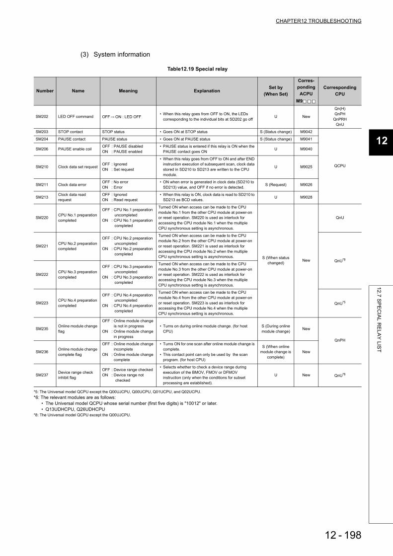
CHAPTER12 TROUBLESHOOTING
1
2
3
12
6
7
8
12.7 SP
EC
IAL R
ELA
Y LIS
T
(3) System information
*5: The Universal model QCPU except the Q00UJCPU, Q00UCPU, Q01UCPU, and Q02UCPU.*6: The relevant modules are as follows:
• The Universal model QCPU whose serial number (first five digits) is "10012" or later.• Q13UDHCPU, Q26UDHCPU
*8: The Universal model QCPU except the Q00UJCPU.
Table12.19 Special relay
Number Name Meaning ExplanationSet by
(When Set)
Corres-ponding ACPU
M9
Corresponding CPU
SM202 LED OFF command OFF ON : LED OFF• When this relay goes from OFF to ON, the LEDs
corresponding to the individual bits at SD202 go offU New
Qn(H)QnPH
QnPRHQnU
SM203 STOP contact STOP status • Goes ON at STOP status S (Status change) M9042
QCPU
SM204 PAUSE contact PAUSE status • Goes ON at PAUSE status S (Status change) M9041
SM206 PAUSE enable coilOFF : PAUSE disabledON : PAUSE enabled
• PAUSE status is entered if this relay is ON when the PAUSE contact goes ON U M9040
SM210 Clock data set requestOFF : IgnoredON : Set request
• When this relay goes from OFF to ON and after END instruction execution of subsequent scan, clock data stored in SD210 to SD213 are written to the CPU module.
U M9025
SM211 Clock data errorOFF : No errorON : Error
• ON when error is generated in clock data (SD210 to SD213) value, and OFF if no error is detected. S (Request) M9026
SM213 Clock data read request
OFF : IgnoredON : Read request
• When this relay is ON, clock data is read to SD210 to SD213 as BCD values. U M9028
SM220 CPU No.1 preparation completed
OFF : CPU No.1 preparation uncompleted
ON : CPU No.1 preparation completed
Turned ON when access can be made to the CPU module No.1 from the other CPU module at power-on or reset operation. SM220 is used as interlock for accessing the CPU module No.1 when the multiple CPU synchronous setting is asynchronous.
S (When status changed) New
QnU
SM221 CPU No.2 preparation completed
OFF : CPU No.2 preparation uncompleted
ON : CPU No.2 preparation completed
Turned ON when access can be made to the CPU module No.2 from the other CPU module at power-on or reset operation. SM221 is used as interlock for accessing the CPU module No.2 when the multiple CPU synchronous setting is asynchronous.
QnU*8
SM222 CPU No.3 preparation completed
OFF : CPU No.3 preparation uncompleted
ON : CPU No.3 preparation completed
Turned ON when access can be made to the CPU module No.3 from the other CPU module at power-on or reset operation. SM222 is used as interlock for accessing the CPU module No.3 when the multiple CPU synchronous setting is asynchronous.
SM223CPU No.4 preparation completed
OFF : CPU No.4 preparation uncompleted
ON : CPU No.4 preparation completed
Turned ON when access can be made to the CPU module No.4 from the other CPU module at power-on or reset operation. SM223 is used as interlock for accessing the CPU module No.4 when the multiple CPU synchronous setting is asynchronous.
QnU*5
SM235Online module change flag
OFF : Online module change is not in progress
ON : Online module change in progress
• Turns on during online module change. (for host CPU)
S (During online module change) New
QnPH
SM236 Online module change complete flag
OFF : Online module change incomplete
ON : Online module change complete
• Turns ON for one scan after online module change is complete.
• This contact point can only be used by the scan program. (for host CPU)
S (When online module change is
complete)New
SM237 Device range checkinhibit flag
OFF : Device range checkedON : Device range not checked
• Selects whether to check a device range during execution of the BMOV, FMOV or DFMOV instruction (only when the conditions for subset processing are established).
U New QnU*6
12 - 198

*1: This applies to the CPU of function version B or later.*2: The module whose first 5 digits of serial No. is "09012" or later.*5: The Universal model QCPU except the Q00UJCPU, Q00UCPU, Q01UCPU, and Q02UCPU.*6: The module whose first 5 digits of serial No. is "10042" or later.*8: The Universal model QCPU except the Q00UJCPU.
Table12.19 Special relay
Number Name Meaning ExplanationSet by
(When Set)
Corres-ponding
ACPUM9
Corresponding CPU
SM240 No. 1 CPU reset flagOFF : No. 1 CPU reset
cancelON : No. 1 CPU resetting
• Goes OFF when reset of the No. 1 CPU is canceled.• Comes ON when the No. 1 CPU is resetting
(including the case where the CPU module is removed from the base).The other CPUs are also put in reset status.
S (Status change) New
Q00/Q01*1
Qn(H)*1
QnPHQnU*8
SM241 No. 2 CPU reset flagOFF : No. 2 CPU reset
cancelON : No. 2 CPU resetting
• Goes OFF when reset of the No. 2 CPU is canceled.• Comes ON when the No. 2 CPU is resetting
(including the case where the CPU module is removed from the base).The other CPUs result in "MULTI CPU DOWN" (error code: 7000).
SM242 No. 3 CPU reset flagOFF : No. 3 CPU reset
cancelON : No. 3 CPU resetting
• Goes OFF when reset of the No. 3 CPU is canceled.• Comes ON when the No. 3 CPU is resetting
(including the case where the CPU module is removed from the base).The other CPUs result in "MULTI CPU DOWN" (error code: 7000).
SM243 No. 4 CPU reset flagOFF : No. 4 CPU reset
cancelON : No. 4 CPU resetting
• Goes OFF when reset of the No. 4 CPU is canceled.• Comes ON when the No. 4 CPU is resetting
(including the case where the CPU module is removed from the base).The other CPUs result in "MULTI CPU DOWN" (error code: 7000).
Qn(H)*1
QnPHQnU*5
SM244 No. 1 CPU error flagOFF : No. 1 CPU normalON : No. 1 CPU during stop
error
• Goes OFF when the No. 1 CPU is normal (including a continuation error).
• Comes ON when the No. 1 CPU is during a stop error.
Q00/Q01*1
Qn(H)*1
QnPHQnU*8
SM245 No. 2 CPU error flagOFF : No. 2 CPU normalON : No. 2 CPU during stop
error
• Goes OFF when the No. 2 CPU is normal (including a continuation error).
• Comes ON when the No. 2 CPU is during a stop error.
SM246 No. 3 CPU error flagOFF : No. 3 CPU normalON : No. 3 CPU during stop
error
• Goes OFF when the No. 3 CPU is normal (including a continuation error).
• Comes ON when the No. 3 CPU is during a stop error.
SM247 No. 4 CPU error flagOFF : No. 4 CPU normalON : No. 4 CPU during stop
error
• Goes OFF when the No. 4 CPU is normal (including a continuation error).
• Comes ON when the No. 4 CPU is during a stop error
S (Status change) NewQn(H)*1
QnPHQnU*5
SM250 Max. loaded I/O readOFF : IgnoredON : Read
• When this relay goes from OFF to ON, maximum loaded I/O number is read to SD250. U New
Qn(H)QnPH
QnPRH
SM254 All stations refresh command
OFF : Refresh arrival stationON : Refresh all stations
• Effective for the batch refresh (also effective for the low speed cyclic)
• Designate whether to receive arrival stations only or to receive all slave stations in the MELSECNET/H.
U New
• Designate whether to receive arrival stations only or to receive all slave stations in the CC-Link IE controller network .
Qn(H)*2
QnPH*6
QnPRH*6
• Effective for the batch refresh (also effective for the low speed cyclic)
• Specify whether to receive only arrival station or all stations in the MELSECNET/H or CC-Link IE controller network.
QnU
12 - 199

CHAPTER12 TROUBLESHOOTING
1
2
3
12
6
7
8
12.7 SP
EC
IAL R
ELA
Y LIS
T
*1: This applies to the CPU of function version B or later.
Table12.19 Special relay
Number Name Meaning ExplanationSet by
(When Set)
Corres-ponding ACPU
M9
Corresponding CPU
SM255
MELSECNET/10, MELSECNET/H module 1 information
OFF : Operative networkON : Standby network
• Goes ON for standby network(If no designation has been made concerning active or standby, active is assumed.)
S (Initial) New
Qn(H)QnPH
QnPRH
SM256OFF : ReadsON : Does not read
• For refresh from link to CPU module (B, W, etc.) indicate whether to read from the link module. U New
SM257OFF : WritesON : Does not write
• For refresh from CPU module to link (B, W, etc.), designate whether to write to the link module. U New
SM260MELSECNET/10, MELSECNET/H module 2 information
OFF : Operative networkON : Standby network
• Goes ON for standby network(If no designation has been made concerning active or standby, active is assumed.)
S (Initial) New
SM261 OFF : ReadsON : Does not read
• For refresh from link to CPU module (B, W, etc.) indicate whether to read from the link module.
U New
SM262 OFF : WritesON : Does not write
• For refresh from CPU module to link (B, W, etc.), designate whether to write to the link module.
U New
SM265MELSECNET/10, MELSECNET/H module 3 information
OFF : Operative networkON : Standby network
• Goes ON for standby network(If no designation has been made concerning active or standby, active is assumed.)
S (Initial) New
SM266 OFF : ReadsON : Does not read
• For refresh from link to CPU module (B, W, etc.) indicate whether to read from the link module. U New
SM267 OFF : WritesON : Does not write
• For refresh from CPU module to link (B, W, etc.), designate whether to write to the link module. U New
SM270
MELSECNET/10, MELSECNET/H module 4 information
OFF : Operative networkON : Standby network
• Goes ON for standby network(If no designation has been made concerning active or standby, active is assumed.)
S (Initial) New
SM271 OFF : ReadsON : Does not read
• For refresh from link to CPU module (B, W, etc.) indicate whether to read from the link module. U New
SM272 OFF : WritesON : Does not write
• For refresh from CPU module to link (B, W, etc.), designate whether to write to the link module. U New
SM280 CC-Link error OFF : NormalON : Error
• Goes ON when a CC-Link error is detected in any of the installed CC-Link module. Goes OFF when normal operation is restored.
S (Status change) New
SM315Communication reserved time delay enable/disable flag
OFF : Without delayON : With delay
• This flag is enabled when the time reserved for communication processing is set in SD315.
• Turns ON to delay the END processing by the time set in SD315 in order to perform communication processing.(The scan time increases by the period set in SD315.)
• Turns OFF to perform the END processing without a delay of the time set in SD315 when there is no communication processing. (Defaults to OFF)
U New Q00J/Q00/Q01
SM320 Presence/absence of SFC program
OFF : SFC program absentON : SFC program present
• Turns ON when an SFC program is registered.• OFF when an SFC program is not registered. S (Initial) M9100
Q00J/Q00/Q01*1
Qn(H)QnPH
QnPRHQnU
SM321 Start/stop SFC program
OFF : SFC program not executed (stop)
ON : SFC program executed (start)
• Initial value is set at the same value as SM320.(Goes ON automatically if SFC program is present.)
• Turn this relay from ON to OFF to stop program execution.
• Turn this relay from OFF to ON to resume program execution.
S (Initial)/U M9101format change
12 - 200

*1: This applies to the CPU of function version B or later.*3: The module whose first 5 digits of serial No. is "04122" or later.*4: The module whose first 5 digits of serial No. is "07032" or later.
Table12.19 Special relay
Number Name Meaning ExplanationSet by
(When Set)
Corres-ponding
ACPUM9
Corresponding CPU
SM322 SFC program start status
OFF : Initial startON : Resume start
• The SFC program starting mode in the SFC setting of the PLC parameter dialog box is set as the initial value.AT initial start: OFFAt continued start: ON
S (Initial)/U M9102format change
Q00J/Q00/Q01*1
Qn(H)QnPH
QnPRHQnU
SM323Presence/absence of continuous transition for entire block
OFF : Continuous transition not effective
ON : Continuous transition effective
Set the presence/absence of continuous transition for the block where "Continuous transition bit" of the SFC data device has not been set.
U M9103
SM324 Continuous transition prevention flag
OFF : When transition is executed
ON : When no transition
• OFF during operation in the continuous transition mode or during continuous transition, and ON when continuous transition is not executed.
• Always ON during operation in the no continuous transition mode.
S (Instruction execution)
M9104
S (Status change) New
SM325 Output mode at block stop
OFF : OFFON : Preserves
Select whether the coil outputs of the active steps are held or not at the time of a block stop.• As the initial value, the output mode at a block stop in
the parameter is OFF when the coil outputs are OFF, and ON when the coil outputs are held.
• All coil outputs go OFF when this relay is OFF.• Coil outputs are preserved when this relay is ON.
S (Initial)/U M9196
SM326 SFC device clear mode
OFF : Clear deviceON : Preserves device
Selects the device status when the stopped CPU is run after the sequence program or SFC program has been modified when the SFC program exists.
U New
SM327Output during end step execution
OFF : Hold step output turned OFF (cleared)
ON : Hold step output held
Select the device status at the time of switching from STOP to program write to RUN.(All devices except the step relay)
S (Initial)/UNew
Qn(H)QnPH
QnPRHQnU
U Q00J/Q00/Q01*1
SM328Clear processing mode when end step is reached
OFF : Clear processing is performed.
ON : Clear processing is not performed.
Select whether clear processing will be performed or not if active steps other than the ones being held exist in the block when the end step is reached.? • When this relay turns OFF, all active steps are
forcibly terminated to terminate the block.• When this relay is ON, the execution of the block is
continued as-is.• If active steps other than the ones being held do not
exist when the end step is reached, the steps being held are terminated to terminate the block.
U New Q00J/Q00/Q01*1
QnU
SM330Operation mode for low speed execution type program
OFF : Asynchronous modeON : Synchronous mode
Select whether the low speed execution type program will be executed in the asynchronous mode or in the synchronous mode.• Asynchronous mode (this relay is turned OFF.)
Mode in which the operation of the low speed execution type program is performed continuously within the excess time.
• Synchronous mode (this relay is turned ON.)Mode in which the operation of the low speed execution type program is not performed continuously and operation is performed from the next scan if there is excess time.
U New Qn(H)QnPH
SM331 Normal SFC program execution status
OFF : Not executedON : Being executed
• Indicates whether the normal SFC program is being executed or not.
• Used as an SFC control instruction execution interlock.
S (Status change) NewQn(H)*3
QnPH*4
QnPRHSM332
Program execution management SFC program execution status
OFF : Not executedON : Being executed
• Indicates whether the program execution management SFC program is being executed or not.
• Used as an SFC control instruction execution interlock.
SM390 Access execution flagON indicates completion of intelligent function module access
• The status of the intelligent function module access instruction executed immediately before is stored.(This data is overwritten when the intelligent function module access instruction is executed again.)
• Used by the user in a program as a completion bit.
S (Status change) NewQn(H)QnPH
QnPRH
SM391GINT instruction execution completion flag
OFF : Not executedON : Execution completed
Indicates execution status of the S(P).GINT instruction.• Turned OFF before the instruction is executed.• Turned ON after the instruction is completed.
S (Instruction execution) New QnU
12 - 201

CHAPTER12 TROUBLESHOOTING
1
2
3
12
6
7
8
12.7 SP
EC
IAL R
ELA
Y LIS
T
(4) System clocks/countersTable12.20 Special relay
Number Name Meaning ExplanationSet by
(When Set)
Corres-ponding ACPU
M9
Corresponding CPU
SM400 Always ON • Normally is ON S (Every END processing) M9036
QCPU
SM401 Always OFF • Normally is OFFS (Every END processing) M9037
SM402 After RUN, ON for 1 scan only
• After RUN, ON for 1 scan only.• This connection can be used for scan execution type
programs only.• When an initial execution type program is used, this
relay turns OFF at the END processing of the scan execution type program in the first scan after RUN.
S (Every END processing) M9038
Qn(H)QnPH
QnPRHQnU
• After RUN, ON for 1 scan only. S (Every END processing) New Q00J/Q00/Q01
SM403 After RUN, OFF for 1 scan only
• After RUN, OFF for 1 scan only.• This connection can be used for scan execution type
programs only.• When an initial execution type program is used, this
relay turns OFF at the END processing of the scan execution type program in the first scan after RUN. S (Every END
processing) M9039
Qn(H)QnPH
QnPRHQnU
• After RUN, OFF for 1 scan only. S (Every END processing) New Q00J/Q00/Q01
SM404Low speed execution type programON for 1 scan only after RUN
• After RUN, ON for 1 scan only.• This connection can be used for low speed execution type
programs only.
S (Every END processing)
New
Qn(H)QnPH
SM405
Low speed execution type programAfter RUN, OFF for 1 scan only
• After RUN, OFF for 1 scan only.• This connection can be used for low speed execution type
programs only.
S (Every END processing)
New
SM409 0.01 second clock
• Repeatedly changes between ON and OFF at 5-ms interval.
• When Programmable Controller power supply is turned ON or a CPU module reset is performed, goes from OFF to start.(Note that the ON-OFF status changes when the designated time has elapsed during the execution of the program.)
S (Status change) New
Qn(H)QnPH
QnPRHQnU
SM410 0.1 second clock• Repeatedly changes between ON and OFF at each
designated time interval.• When Programmable Controller power supply is
turned ON or a CPU module reset is performed, goes from OFF to start.(Note that the ON-OFF status changes when the designated time has elapsed during the execution of the program.)
S (Status change)
M9030
QCPU
SM411 0.2 second clock M9031
SM412 1 second clock M9032
SM413 2 second clock M9033
SM414 2n second clock
• This relay alternates between ON and OFF at intervals of the time (unit: s) specified in SD414.
• When Programmable Controller power supply is turned ON or a CPU module reset is performed, goes from OFF to start.(Note that the ON-OFF status changes when the designated time has elapsed during the execution of the program.)
S (Status change)M9034format change
ON
OFF
ON
OFF
ON
OFF1 scan
ON
OFF1 scan of scan execution type
program
Initial execution
type program
ON
OFF1 scan ON
OFF
1 scan of scan
execution type
program
Initial
execution
type program
ON
OFF1 scan
ON
OFF1 scan
0.005s0.005s
0.05s0.05s
0.1s0.1s
0.5s0.5s
1s1s
nsns
12 - 202

(5) Scan information
(6) I/O refresh
*1: This applies to the CPU of function version B or later.
Table12.20 Special relay
Number Name Meaning ExplanationSet by
(When Set)
Corres-ponding
ACPUM9
Corresponding CPU
SM415 2n (ms) clock
• This relay alternates between ON and OFF at intervals of the time (unit: ms) specified in SD415.
• When Programmable Controller power supply is turned ON or a CPU module reset is performed, goes from OFF to start.(Note that the ON-OFF status changes when the designated time has elapsed during the execution of the program.)
S (Status change) New
Qn(H)QnPH
QnPRHQnU
SM420 User timing clock No.0 • Relay repeats ON/OFF switching at fixed scan intervals.
• When Programmable Controller power supply is turned ON or a CPU module reset is performed, goes from OFF to start.(For the redundant CPU, however, this relay is always OFF after system switching.)
• The ON/OFF intervals are set with the DUTY instruction
n1: ON scan intervaln2: OFF scan interval
S (Every END processing)
M9020
QCPU
SM421 User timing clock No.1 M9021
SM422 User timing clock No.2 M9022
SM423 User timing clock No.3 M9023
SM424 User timing clock No.4 M9024
SM430 User timing clock No.5
• For use with SM420 to SM424 low speed programsS (Every END processing) New
Qn(H)QnPH
SM431 User timing clock No.6
SM432 User timing clock No.7
SM433 User timing clock No.8
SM434 User timing clock No.9
Table12.21 Special relay
Number Name Meaning ExplanationSet by
(When Set)
Corres-ponding
ACPUM9
Corresponding CPU
SM510Low speed program execution flag
OFF : Completed or not executed
ON : Execution under way.
• Goes ON when low speed execution type program is executed.
S (Every END processing) New
Qn(H)QnPH
SM551 Reads module service interval
OFF : IgnoredON : Read
• When this relay goes from OFF to ON, the module service interval designated by SD550 is read to SD551 to SD552.
U NewQn(H)QnPH
QnPRH
Table12.22 Special relay
Number Name Meaning ExplanationSet by
(When Set)
Corres-ponding
ACPUM9
Corresponding CPU
SM580 Program to program I/O refresh
OFF : Not refreshedON : Refreshed
• When this special relay is turned ON, I/O refresh is performed after execution of the first program, and the next program is then executed.When a sequence program and an SFC program are to be executed, the sequence program is executed, I/O refresh is performed, and the SFC program is then executed.
U New Q00J/Q00/Q01*1
n(ms)n(ms)
n1 scan
n2 scan n2 scan
DUTY n1 n2 SM420
12 - 203

CHAPTER12 TROUBLESHOOTING
1
2
3
12
6
7
8
12.7 SP
EC
IAL R
ELA
Y LIS
T
(7) Memory cards
*1: The Universal model QCPU except the Q00UJCPU, Q00UCPU, and Q01UCPU.*2: The Universal model QCPU except the Q00UJCPU.
Table12.23 Special relay
Number Name Meaning ExplanationSet by
(When Set)
Corres-ponding ACPU
M9
Corresponding CPU
SM600 Memory card usable flags
OFF : UnusableON : Use enabled • ON when memory card is ready for use by user S (Status change) New
Qn(H)QnPH
QnPRHQnU*1
SM601 Memory card protect flag
OFF : No protectON : Protect • Goes ON when memory card protect switch is ON S (Status change) New
SM602 Drive 1 flag OFF : No drive 1ON : Drive 1 present • Turns ON when the mounted memory card is RAM S (Status change) New
SM603 Drive 2 flag OFF : No drive 2ON : Drive 2 present • Turns ON when the mounted memory card is ROM S (Status change) New
SM604 Memory card in-use flag
OFF : Not usedON : In use • Goes ON when memory card is in use S (Status change) New
SM605 Memory card remove/insert prohibit flag
OFF : Remove/insert enabledON : Remove/insert
prohibited
• Goes ON when memory card cannot be inserted or removed
U New
SM609 Memory card remove/insert enable flag
OFF : Remove/insert prohibited
ON : Remove/insert enabled
• Turned ON by user to enable the removal/insertion of memory card.
• Turned OFF by the system after the memory card is removed.
• This contact can be used only when SM604 and SM605 are OFF.
S/U New
SM620 Drive 3/4 usable flags OFF : UnusableON : Use enabled • Always ON S (Initial) New QCPU
SM622 Drive 3 flag OFF : No drive 3ON : Drive 3 present • Always ON S (Initial) New
Q00J/Q00/Q01Qn(H)QnPH
QnPRHQnU*2
SM623 Drive 4 flag OFF : No drive 4ON : Drive 4 present • Always ON S (Initial) New QCPU
SM624 Drive 3/4 in-use flag OFF : Not usedON : In use
• Goes ON when the file within Drive 3 (standard RAM) or Drive 4 (standard ROM) is used.
S (Status change) New
Qn(H)QnPH
QnPRHQnU
SM640 File register useOFF : File register not usedON : File register in use • Goes ON when file register is in use S (Status change) New
Q00J/Q00/Q01Qn(H)QnPH
QnPRHQnU*2
12 - 204

*1: The Universal model QCPU except the Q00UJCPU, Q00UCPU, and Q01UCPU.*3: The modules whose serial number (first five digits) is "10102" or later are the relevant models. (Except the Q00UJCPU, Q00UCPU, and Q01UCPU)
Table12.23 Special relay
Number Name Meaning ExplanationSet by
(When Set)
Corres-ponding
ACPUM9
Corresponding CPU
SM650 Comment useOFF : File register not usedON : File register in use • Goes ON when comment file is in use S (Status change) New
Qn(H)QnPH
QnPRHQnU
SM660 Boot operation
OFF : Internal memory execution
ON : Boot operation in progress
• Goes ON while boot operation is in process• Goes OFF if boot designation switch is OFF S (Status change) New
Qn(H)QnPH
QnPRH
OFF : Program memory execution
ON : Boot operation in progress
• Goes ON while boot operation is in process S (Status change) NewQ00J/Q00/Q01
QnU*1
SM671Latch data backup to standard ROM completion flag
OFF : Not completedON : Completed
• Turned ON when latch data backup to the standard ROM is completed.
• Time when the latch data backup to the standard ROM was performed is stored in SD672 or later.
S (Status change) New QnU
SM672Memory card file register access range flag
OFF : Within access rangeON : Outside access range
• Goes ON when access is made to area outside the range of file register of memory card(Set within END processing.)
• Reset at user program
S/U NewQn(H)QnPH
QnPRH
SM675Error completion of latch data backup to standard ROM
OFF : No ErrorON : Error
• Turned ON when data cannot be backuped to the standard ROM by the latch data backup normally.
• Turned OFF when data is backuped to the standard ROM by the latch data backup normally.
S New
QnU
SM676Specification of restration repeated execution
OFF : Not specifiedON : Specified
• If latch data backup is performed when SM676 is ON, restore the data every time turning ON from OFF the power supply from the next power-on.
• Delete the backuped latch data, or restore the data every time turning ON from OFF the power supply until the latch data backup operation will be executed again.
U New
SM680 Program memory write error
OFF : Write errorON : Write not executed/
normal
• Turns ON if a write error is detected at writing to program memory (flash ROM).Turns OFF by the write direction.
S (At write) New
SM681Program memory writing flag
OFF : During writingON : Write not executed
• Turns ON when writing to the program memory (flash ROM) is in progress, and turns OFF when writing is completed.
S (At write) New
SM682Program memory overwrite count error flag
OFF : Overwrite count is 100,000 or more
ON : Overwrite count is less than 100,000
• Turns ON when the overwrite count of program memory (flash ROM) reaches 100,000. S (At write) New
SM685Standard ROM write error
OFF : Write errorON : Write not executed/
normal
• Turns ON when write error is detected at writing to standard ROM (flash ROM).
• Turns OFF by the write direction.S (At write) New
SM686 Standard ROM writing flag
OFF : During overwritingON : Overwrite not executed
• Turns ON when writing to the standard ROM (flash ROM) is in progress, and turns OFF when writing is completed.
S (At write) New
SM687Standard ROM overwrite count error flag
OFF : Overwrite count is 100,000 or more
ON : Overwrite count is less than 100,000
• Turns ON when the overwrite count of standard ROM (flash ROM) reaches 100,000.(It is necessary to change CPU module.)
S (At write) New
SM691 Backup start preparation status flag
OFF : Backup start preparation not completed
ON : Backup start preparation completed
Turns on when the backup start preparation is completed. S (Status change) New
QnU*3
SM692 Restoration complete flag
OFF : Restoration not completed
ON : Restoration completed
Turns on when restoration of the backup data in the memory card is completed.
S (Status change) New
12 - 205

CHAPTER12 TROUBLESHOOTING
1
2
3
12
6
7
8
12.7 SP
EC
IAL R
ELA
Y LIS
T
(8) Instruction-Related Special Relays
*1: The module whose first 5 digits of serial No. is "09042" or later.*2: The relevant modules are as follows:
• The Universal model QCPU whose serial number (first five digits) is "10102" or later.• Q00UJCPU, Q00UCPU, Q01UCPU
*3: The relevant modules are as follows:• The Universal model QCPU whose serial number (first five digits) is "10102" or later.• Q00UCPU, Q01UCPU
Table12.24 Special relay
Number Name Meaning ExplanationSet by
(When Set)
Corres-ponding ACPU
M9
Corresponding CPU
SM700 Carry flag OFF : Carry OFFON : Carry ON • Carry flag used in application instruction S (Instruction
execution) M9012 QCPU
SM701 Number of output characters selection
Switching the number of output characters and the output pattern
• Used for the PR, PRC, BINDA, DBINDA, BINHA, DBINHA, BCDDA, DBCDDA, or COMRD instruction U M9049
Qn(H)QnPH
QnPRHQnU
SM702 Search method OFF : Search nextON : 2-part search
• Designates method to be used by search instruction.• Data must be arranged for 2-part search. U New
QCPUSM703 Sort order OFF : Ascending orderON : Descending order
• The sort instruction is used to designate whether data should be sorted in ascending order or in descending order.
U New
SM704 Block comparison OFF : Non-match foundON : All match
• Goes ON when all data conditions have been met for the BKCMP instruction.
S (Instruction execution) New
• Goes ON when all data conditions have been met for the DBKCMP instruction.
S (Instruction execution) New
QnU*2
SM709DT/TM instruction improper data detection flag
OFF : Improper data not detected
ON : Improper data detected
Turns on when the data to be compared by the DT or TM instruction is not recognized as date data or time data, or the device (3 words) to be compared exceeds the specified device range.
S (Instruction execution) or U New
SM710 CHK instruction priority ranking flag
OFF : Conditions priorityON : Pattern priority
• Remains as originally set when OFF.• CHK priorities updated when ON.
S (Instruction execution) New
Qn(H)QnPH
QnPRH
SM715 EI flag OFF : During DION : During EI • ON when EI instruction is being executed. S (Instruction
execution) New QCPU
SM716Block comparison (Except an interrupt program)
OFF : Mismatch foundON : No mismatch
Turns on when all data conditions are confirmed that they are met by the DBKCMP instruction.(Initial execution type program, scan execution type program, stand-by type program executed from initial execution type program or scan execution type program)
S (Instruction execution) New
QnU*2
SM717 Block comparison (Interrupt program)
OFF : Mismatch foundON : No mismatch
Turns on when all data conditions are confirmed that they are met by the DBKCMP instruction.(Interrupt program, fixed scan execution type program, stand-by type program executed from interrupt program or fixed scan execution type program)
SM718Block comparison (Interrupt program (I45))
OFF : Mismatch foundON : No mismatch
Turns on when all data conditions are confirmed that they are met by the DBKCMP instruction.(Interrupt program (I45) or Stand-by type program executed from interrupt program (I45))
QnU*3
SM720 Comment read completion flag
OFF : Comment read not completed
ON : Comment read completed
• Turns on only during one scan when the processing of the COMRD or PRC instruction is completed.
S (Status change) New
Qn(H)QnPH
• Turns on only during one scan when the processing of the COMRD instruction is completed.
QnPRHQnU
SM721 File being accessed OFF : File not accessedON : File being accessed
• Switches ON while a file is being accessed by the SP. FWRITE, SP. FREAD, COMRD, PRC, or LEDC instruction.
S (Status change) New
Qn(H)QnPH
• Switches ON while a file is being accessed by the SP. FWRITE, SP. FREAD, COMRD or LEDC instruction.
Qn(H)QnPH
QnPRH• Switches ON while a file is being accessed by the
SP. FWRITE, SP. FREAD, COMRD or SP.DEVST instruction.
QnU
• Turns ON while the ATA card or standard ROM is being accessed. QnU*1
SM722 BIN/DBIN instruction error disabling flag
OFF : Error detection performed
ON : Error detection not performed
• Turned ON when "OPERATION ERROR" is suppressed for BIN or DBIN instruction. U New QCPU
12 - 206

*1: The module whose first 5 digits of serial No. is "06082" or later.*2: The module whose first 5 digits of serial No. is "07012" or later.*3: The module whose first 5 digits of serial No. is "07032" or later.*4: This applies to the CPU module of function version B or later.*5: The module whose first 5 digits of serial No. is "04012" or later.*6: The module whose first 5 digits of serial No. is "05032" or later.*8: The relevant modules are as follows:
• The Universal model QCPU whose serial number (first five digits) is "10102" or later.• Q00UJCPU, Q00UCPU, Q01UCPU
*9: The Universal model QCPU except the Q00UJCPU.
Table12.24 Special relay
Number Name Meaning ExplanationSet by
(When Set)
Corres-ponding
ACPUM9
Corresponding CPU
SM734XCALL instruction execution condition designation
OFF : Not executed by execution condition risen
ON : Executed by execution condition risen
• During OFF, XCALL instructions will not be executed even if execution condition is risen.
• During ON, XCALL instructions will be executed when execution condition is risen.
U New Qn(H)*1
SM735SFC comment readout instruction in execution flag
OFF : SFC comment readout instruction is inactivated.
ON : SFC comment readout instruction is activating.
• Turns on the instructions, (S(P).SFCSCOMR) to read the SFC step comments and (S(P). SFCTCOMR) to read the SFC transition condition comments.
S (status change) NewQn(H)*2
QnPH*3
QnPRH*3
SM738 MSG instruction reception flag
OFF : Instruction not executed
ON : Instruction execution• Goes ON when MSG instruction is executed S (Instruction
execution) New Qn(H)QnPRH
SM750 Scaling instruction search method setting
OFF : Search nextON : 2-part search
Determines a search method when the scaling instruction is executed. U New QnU*8
SM774
PID bumpless processing(for complete derivative)
OFF : MatchedON : Not matched
• Specifies whether to match the set value (SV) with the process value (PV) or not in the manual mode. U New
Q00J/Q00/Q01*4
Qn(H)QnPRH
QnU
SM775
Selection of refresh processing during COM/CCOM instruction execution
OFF : Performs link refreshON : Performs no link
refresh
• Select whether link refresh processing will be performed or not when only communication with the CPU module is made at the execution of the COM instruction.
U NewQ00J/Q00/Q01
Qn(H)QnPH
OFF : Performs refresh processes other than an I/O refresh
ON : Performs refresh set by SD778
• Select whether to perform refresh processes other than an I/O refresh set by SD778 when the COM or CCOM instruction is executed.
U New
Q00J/Q00/Q01*4
Qn(H)*5
QnPH*3
QnPRHQnU
SM776 Enable/disable local device at CALL
OFF : Local device disabledON : Local device enabled
• Set whether the local device of the subroutine program called at execution of the CALL instruction is valid or invalid.
U New Qn(H)QnPH
QnPRHQnU*9SM777
Enable/disable local device in interrupt program
OFF : Local device disabledON : Local device enabled
• Set whether the local device at execution of the interrupt program is valid or invalid. U New
SM794PID bumpless processing(for incomplete derivative)
OFF : MatchedON : Not matched
• Specifies whether to match the set value (SV) with the process value (PV) or not in the manual mode. U New
Q00J/Q00/Q01*4
Qn(H)*6QnPRH
QnU
12 - 207

CHAPTER12 TROUBLESHOOTING
1
2
3
12
6
7
8
12.7 SP
EC
IAL R
ELA
Y LIS
T
*7: The Universal model QCPU except the Q00UJCPU, Q00UCPU, Q01UCPU, and Q02UCPU.
(9) Debug
*1: The Universal model QCPU except the Q00UJCPU.
Table12.24 Special relay
Number Name Meaning ExplanationSet by
(When Set)
Corres-ponding ACPU
M9
Corresponding CPU
SM796
Block information using multiple CPU high-speed transmission dedicated instruction (for CPU No.1)
OFF : Block is securedON : Block set by SD796
cannot be secured
• Turns ON when the number of the remaining blocks of the dedicated instruction transmission area used for the multiple CPU high-speed transmission dedicated instruction(target CPU= CPU No.1) is less than the number of blocks specified by SD796.Turns ON at instruction execution. Turns OFF when the empty area exists at END processing.
S (When instruction/END
processing executed)
New
QnU*7
SM797
Block information using multiple CPU high-speed transmission dedicated instruction (for CPU No.2)
OFF : Block is securedON : Block set by SD797
cannot be secured
• Turns ON when the number of the remaining blocks of the dedicated instruction transmission area used for the multiple CPU high-speed transmission dedicated instruction (target CPU= CPU No.2) is less than the number of blocks specified by SD797.Turns ON at instruction execution. Turns OFF when the empty area exists at END processing.
S (When instruction/END
processing executed)
New
SM798
Block information using multiple CPU high-speed transmission dedicated instruction (for CPU No.3)
OFF : Block is securedON : Block set by SD798
cannot be secured
• Turns ON when the number of the remaining blocks of the dedicated instruction transmission area used for the multiple CPU high-speed transmission dedicated instruction (target CPU= CPU No.3) is less than the number of blocks specified by SD798.Turns ON at instruction execution. Turns OFF when the empty area exists at END processing.
S (When instruction/END
processing executed)
New
SM799
Block information using multiple CPU high-speed transmission dedicated instruction (for CPU No.4)
OFF : Block is securedON : Block set by SD799
cannot be secured
• Turns ON when the number of the remaining blocks of the dedicated instruction transmission area used for the multiple CPU high-speed transmission dedicated instruction(target CPU= CPU No.4) is less than the number of blocks specified by SD799.Turns ON at instruction execution. Turns OFF when the empty area exists at END processing.
S (When instruction/END
processing executed)
New
Table12.25 Special relay
Number Name Meaning ExplanationSet by
(When Set)
Corres-ponding ACPU
M9
Corresponding CPU
SM800 Trace preparation OFF : Not readyON : Ready
• Switches ON when the trace preparation is completed S (Status change) New
Qn(H)QnPH
QnPRHQnU*1
SM801 Trace start OFF : SuspendON : Start
• Trace is started when this relay switches ON.• Trace is suspended when this relay switches OFF.
(All related special Ms switches OFF.)U M9047
SM802 Trace execution in progress
OFF : SuspendON : Start • Switches ON during execution of trace. S (Status change) M9046
SM803 Trace trigger OFF ON: Start• Trace is triggered when this relay switches from OFF
to ON. (Identical to TRACE instruction execution status)
U M9044
SM804 After trace trigger OFF : Not after triggerON : After trigger • Switches ON after trace is triggered. S (Status change) New
SM805 Trace completed OFF : Not completedON : End
• Switches ON at completion of trace S (Status change) M9043
SM826 Trace errorOFF : NormalON : Errors • Switches ON if error occurs during execution of trace S (Status change) New
SM829Forced registration specification of trace setting
ON : Forced registration enabled
OFF : Forced registration disabled
• Even when the trace condition or the trigger condition is established, the sampling trace setting can be set to the CPU module by turning SM829 ON and registering the sampling trace setting by GX Developer.
U New QnU*1
12 - 208

(10) A to Q conversion correspondencesSpecial relays SM1000 to SM1255 are the relays which correspond to ACPU special relays M9000 to M9255 after A to Q conversion.(However, the Basic model QCPU and Redundant CPU do not support the A to Q conversion.)These special relays are all set by the system, and cannot be set by the user program.To turn them ON/OFF by the user program, change the special relays in the program into those of QCPU.However, some of SM1084 and SM1200 to SM1255 (corresponding to M9084 and M9200 to M9255 before conversion) can be turned ON/OFF by the user program, if they could be turned ON/OFF by the user program before conversion.For details on the ACPU special relays, see the user's manuals for the individual CPUs, and MELSECNET or MELSECNET/B Data Link System Reference Manuals
Check "Use special relay/special register from SM/SD1000" for "A-PLC" on the PLC system tab of PLC parameter in GX Developer when the converted special relays are used with the High Performance model QCPU, Process CPU, and Universal model QCPU.When not using the converted special relays, uncheck "Use special relay/special register from SM/SD1000" to save the time taken for processing special relays.
RemarkThe following are additional explanations about the Special Relay for Modification column.
When a special relay for modification is provided, the device number should be changed to the provided QCPU special relay.
When is provided, the converted special relay can be used for the device number.
When is provided, the device number does not work with QCPU.
*1: The relevant modules are as follows:• The Universal model QCPU whose serial number (first five digits) is "10102" or later.• Q00UJCPU, Q00UCPU, Q01UCPU
Table12.26 Special relay
ACPU Special Relay
Special Relay after Conversion
Special Relay for
ModificationName Meaning Details
Corresponding CPU
M9000 SM1000 – Fuse blownOFF : NormalON : Module with blown
fuse
• Turned on when there is one or more output modules of which fuse has been blown.
• Remains ON if the condition is restored to normal thereafter.
• Output modules of remote I/O stations are also checked fore fuse condition.
Qn(H)QnPHQnU*1
M9002 SM1002 – I/O module verify error
OFF : NormalON : Error
• Turned on if the status of I/O module is different form entered status when power is turned on.
• Remains ON if the condition is restored to normal thereafter.
• I/O module verification is done also to remote I/O station modules.
• Reset is enabled only when special registers SD1116 to SD1123 are reset.
12 - 209

CHAPTER12 TROUBLESHOOTING
1
2
3
12
6
7
8
12.7 SP
EC
IAL R
ELA
Y LIS
T
*1: The relevant modules are as follows:• The Universal model QCPU whose serial number (first five digits) is "10102" or later.• Q00UJCPU, Q00UCPU, Q01UCPU
Table12.27 Special relay
ACPU Special Relay
Special Relay after Conversion
Special Relay for
ModificationName Meaning Details
Corresponding CPU
M9005 SM1005 – AC DOWN detection
OFF : AC DOWN not detected
ON : AC DOWN detected
• Turns ON if an instantaneous power failure of within 20ms occurs during use of the AC power supply module.
• Reset when the power supply is switched OFF, then ON.
Qn(H)QnPHQnU*1
• Turns ON if an instantaneous power failure of within 10ms occurs during use of the DC power supply module.
• Reset when the power supply is switched OFF, then ON.
M9006 SM1006 – Battery lowOFF : NormalON : Battery low
• Turns ON when the battery voltage drops to or below the specified.
• Turns OFF when the battery voltage returns to normal thereafter.
M9007 SM1007 – Battery low latch OFF : NormalON : Battery low
• Turns ON when the battery voltage drops to or below the specified.
• Remains ON if the battery voltage returns to normal thereafter.
M9008 SM1008 SM1Self-diagnosis error
OFF : No errorON : Error
• Turned on when error is found as a result of self-diagnosis.
M9009 SM1009 SM62 Annunciator detection
OFF : No F number detectedON : F number detected
• Turned on when OUT F of SET F instruction is executed.
• Switched off when SD1124 data is cleared to zero.
M9011 SM1011 SM56 Operation error flag
OFF : No errorON : Error
• Turned on when operation error occurs during execution of application instruction.
• Remains ON if the condition is restored to normal thereafter.
M9012 SM1012 SM700 Carry flagOFF : Carry OFFON : Carry ON • Carry flag used in application instruction.
Qn(H)QnPH
M9016 SM1016 Data memory clear flag
OFF : lgnoredON : Output claered
• Clears the data memory including the latch range (other than special relays and special registers) in remote run mode from computer, etc. when SM1016 is on.
M9017 SM1017Data memory clear flag
OFF : lgnoredON : Output claered
• Clears the unlatched data memory (other than special relays and special registers) in remote run mode from computer, etc. when SM1017 is on.
M9020 SM1020 – User timing clock No.0
• Relay which repeats on/off at intervals of predetermined scan.
• When power is turned on or reset is per-formed, the clock starts with off.Set the intervals of on/off by DUTY instruction.
n1: ON scan intervaln2: OFF scan interval
* : If DUTY instruction, which specified from SM 1020 to SM 1024 of User timing clock in programs other than a program for a Universal model QCPU, changes the programmable controller to the Universal model QCPU, the special relays SM 420 to 424 will be replaced.(Universal model QCPUs cannot specify the special relays from SM 1020 to SM1024.)
Qn(H)QnPHQnU*1
M9021 SM1021 – User timing clock No.1
M9022 SM1022 – User timing clock No.2
M9023 SM1023 – User timing clock No.3
M9024 SM1024 – User timing clock No.4
M9025 SM1025 – Clock data set request
OFF : IgnoredON : Set request present
used
• Writes the clock data stored in SD1025 to SD1028 to the CPU module after the END instruction is executed in the scan in which SM1025 turned from OFF to ON.
M9026 SM1026 – Clock data error OFF : No errorON : Error • Switched on by clock data (SD1025 to SD1028) error
M9028 SM1028 – Clock data read request
OFF : IgnoredON : Read request
• Reads clock data to SD1025 to SD1028 in BCD when SD1028 is on.
M9029 SM1029
Batch processing of data communications requests
OFF : Batch processing not conducted
ON : Batch processing conducted
• The SM1029 relay is turned on using a sequence program to process all data communication requests accepted during one scan in the END processing of that scan.
• The batch processing of the data communication requests can be turned on and off during running.
• The default is OFF (processed one at a time for each END processing in the order in which data communication requests are accepted).
Qn(H)QnPH
M9030 SM1030 – 0.1 second clock
• 0.1 second, 0.2 second, 1 second and 2 second, clocks are generated.
• Not turned on or off per scan but turned on and off even during scan if corresponding time has elapsed.
• Starts with off when Programmable Controller power supply is turned on or CPU module reset is performed.
Qn(H)QnPHQnU*1
M9031 SM1031 – 0.2 second clock
M9032 SM1032 – 1 second clock
M9033 SM1033 – 2 second clock
n1 scan
n2 scan n2 scan
DUTY n1 n2 SM1020
0.05s0.05s
0.1s0.1s
0.5s0.5s
1s1s
12 - 210

*1: The relevant modules are as follows:• The Universal model QCPU whose serial number (first five digits) is "10102" or later.• Q00UJCPU, Q00UCPU, Q01UCPU
*2: minute clock indicates the name of the special relay (M9034) of the ACPU.
Table12.27 Special relay
ACPU Special Relay
Special Relay after Conversion
Special Relay for
ModificationName Meaning Details
Corresponding CPU
M9034 SM1034 –2n minute clock(1
minute clock)*2
• Alternates between ON and OFF according to the seconds specified at SD414. (Default: n = 30)
• Not turned on or off per scan but turned on and off even during scan if corresponding time has elapsed.
• Starts with off when Programmable Controller power supply is turned on or CPU module reset is performed.
Qn(H)QnPHQnU*1
M9036 SM1036 – Always ON• Used as dummy contacts of initialization and application
instruction in sequence program.• SM1038 and SM1037 are turned on and off without regard
to position of key switch on CPU module front. SM1038 and SM1039 are under the same condition as RUN status except when the key switch is at STOP position, and turned off and on. Switched off if the key switch is in STOP position. SM1038 is on for one scan only and SM1039 is off for one scan only if the key switch is not in STOP position.
M9037 SM1037 – Always OFF
M9038 SM1038 – ON for 1 scan only after RUN
M9039 SM1039 –RUN flag(After RUN, OFF for 1 scan only)
M9040 SM1040 SM206 PAUSE enable coil OFF : PAUSE disabledON : PAUSE enabled • When RUN key switch is at PAUSE position or pause
contact has turned on and if SM1040 is on, PAUSE mode is set and SM1041 is turned on.
Qn(H)QnPH
M9041 SM1041 SM204 PAUSE status contact
OFF : PAUSE not in effectON : PAUSE in effect
Qn(H)QnPHQnU*1
M9042 SM1042 SM203STOP status contact
OFF : STOP not in effectON : STOP in effect
• Switched on when the RUN key switch or RUN/STOP switch is in STOP position.
M9043 SM1043 SM805 Sampling trace completed
OFF : Sampling trace in progress
ON : Sampling trace completed
• Turned on upon completion of sampling trace performed the number of times preset by parameter after STRA instruction is executed.Reset when STRAR instruction is executed.
M9044 SM1044 SM803 Sampling trace
OFF ON Same as STRA instruction execution
ON OFF Same as STRAR instruction execution
• Turning on/off SM1044 can execute STRA/STRAR instruction.(SM1044 is forcibly turned on/off by a peripheral device.) When switched from OFF to ON: STRA instructionWhen switched from ON to OFF: STRAR instructionThe value stored in SD1044 is used as the condition for the sampling trace. At scanning, at time Time (10 ms unit)
Qn(H)QnPH
M9045 SM1045 Watchdog timer (WDT) reset
OFF : Does not reset WDTON : Resets WDT
• The SM1045 relay is turned on to reset the WDT when the ZCOM instruction and data communication request batch processing are executed (used when the scan time exceeds 200 ms).
M9046 SM1046 SM802 Sampling trace OFF : Trace not in progressON : Trace in progress • Switched on during sampling trace.
Qn(H)QnPHQnU*1
M9047 SM1047 SM801Sampling trace preparations
OFF : Sampling trace suspended
ON : Sampling trace started
• Sampling trace is not executed unless SM1047 is turned ON.Sampling trace is suspended when SM1047 goes OFF.
Qn(H)QnPH
M9049 SM1049 SM701Switching the number of output characters
OFF : Output until NULL code encountered
ON : 16 characters output
• When SM1049 is OFF, characters up to NULL (00H) code are output.
• When SM1049 is ON, ASCII codes of 16 characters are output.
M9051 SM1051 CHG instruction execution disable
OFF : EnabledON : Disable
• Switched ON to disable the CHG instruction.• Switched ON when program transfer is requested.
Automatically switched OFF when transfer is complete.
M9052 SM1052 SEG instruction switch
OFF : 7SEG segment displayON : I/O partial refresh
• When SM1052 is ON, the SEG instruction is executed as an I/O partial refresh instruction.When SM1052 is OFF, the SEG instruction is executed as a 7-SEG display instruction.
nsns
ON
OFF
ON
OFF
ON
OFF1 scan
ON
OFF1 scan
12 - 211

CHAPTER12 TROUBLESHOOTING
1
2
3
12
6
7
8
12.7 SP
EC
IAL R
ELA
Y LIS
T
*3: The A8UPU/A8PUJ is not available for the QCPU/QnACPU.
Table12.27 Special relay
ACPU Special Relay
Special Relay after Conversion
Special Relay for
ModificationName Meaning Details
Corresponding CPU
M9056 SM1056 Main side P, I set request
OFF : Other than when P, I set being requested
ON : P, I set being requested
• Provides P, I set request after transfer of the other program (for example subprogram when main program is being run) is complete during run. Automatically switched off when P, I setting is complete.
Qn(H)QnPH
M9057 SM1057 Sub side P, I set request
OFF : Other than when P, I set being requested
ON : P, I set being requested
M9058 SM1058Main side P, I set completion
Momentarily ON at P, I set completion • Turned ON once when the P, I set has been completed,
and then turned OFF again.M9059 SM1059 Sub program P, I
set completionMomentarily ON at P, I set
completion
M9060 SM1060Sub program 2 P, I set request
OFF : Other than when P, I set being requested
ON : P, I set being requested
• Provides P, I set request after transfer of the other program (for example subprogram when main program is being run) is complete during run. Automatically switched off when P, I setting is complete.
M9061 SM1061 Sub program 3 P, I set request
OFF : Other than when P, I set being requested
ON : P, I set being requested
M9070 SM1070A8UPU/A8PUJrequired search time*3
OFF : Read time not shortened
ON : Read time shortened
• Turned ON to shorten the search time in the A8UPU/A8PUJ.(In this case, the scan time is extended by 10 %.)
M9084 SM1084 Error checkOFF : Error check executedON : No error check
It is set whether the error checks below are performed or not when the END instruction is processed (to set the END instruction processing time).• Check for fuse blown.• Check of battery• Collation check of I/O module
M9091 SM1091Operation error details flag
OFF : No errorON : Error
• Turns ON when the detail factor of the operation error is stored into SD1091.
• Remains ON if the condition is restored to normal thereafter.
M9100 SM1100 SM320 Presence/absence of SFC program
OFF : SFC programs not used
ON : SFC programs used
• Turned on if the SFC program is registered.• Turned off if the SFC program is not registered.
M9101 SM1101 SM321 Start/stop SFC program
OFF : SFC programs stopON : SFC programs start
• The value in SM1100 is set as the initial value.(The relay automatically turns ON when the SFC program is present.)
• When this relay turns from ON to OFF, execution of the SFC program stops.
• When this relay turns from OFF to ON, execution of the SFC program resumes.
M9102 SM1102 SM322SFC program start status
OFF : Initial startON : Resume start
• The SFC program start mode in the SFC setting of the PLC parameter dialog box is set as the initial value.At initial start: OFFAt continue start: ON
12 - 212

(11) QCPU with built-in Ethernet port
* 1: This applies to the Built-in Ethernet port QCPU.
Table12.27 Special relay
ACPU Special Relay
Special Relay after Conversion
Special Relay for
ModificationName Meaning Details
Corresponding CPU
M9103 SM1103 SM323Presence/absence of continuous transition
OFF : Continuous transition not effective
ON : Continuous transition effective
• Set whether continuous transition will be performed for the block where the "continuous transition bit" of the SFC information device is not set.
Qn(H)QnPH
M9104 SM1104 SM324Continuous transition suspension flag
OFF : When transition is completed
ON : When no transition
• OFF during operation in the continuous transition mode or during continuous transition, and ON when continuous transition is not executed.
• Always ON during operation in the no continuous transition mode.
M9108 SM1108 SM90
Step transition monitoring timer start (equivalent of SD90)
OFF : Monitoring timer resetON : Monitoring timer reset
start
• Turns ON when the measurement of the step transition monitoring timer is started.Turning this relay OFF resets the step transition monitoring timer.
M9109 SM1109 SM91
Step transition monitoring timer start (equivalent of SD91)
M9110 SM1110 SM92
Step transition monitoring timer start (equivalent of SD92)
M9111 SM1111 SM93
Step transition monitoring timer start (equivalent of SD93)
M9112 SM1112 SM94
Step transition monitoring timer start (equivalent of SD94)
M9113 SM1113 SM95
Step transition monitoring timer start (equivalent of SD95)
M9114 SM1114 SM96
Step transition monitoring timer start (equivalent of SD96)
M9196 SM1196 SM325 Operation output at block stop
OFF : Coil output OFFON : Coil output ON
• Selects the operation output when block stop is executed.ON : Retains the ON/OFF status of the coil being used
by using operation output of the step being executed at block stop.
OFF : All coil outputs are turned off. (Operation output by the SET instruction is retained regardless of the ON/OFF status of SM1196.)
M9197 SM1197Switch between blown fuse and I/O verify error display
SM1197
SM1198
I/O numbers to be
displayed
Switches I/O numbers in the fuse blow module storage registers (SD1100 to SD1107) and I/O module verify error storage registers (SD1116 to SD1123) according to the combination of ON/OFF of the SM1197 and SM1198.
OFF OFF X/Y0 to 7F0
ON OFF X/Y800 to FF0
M9198 SM1198OFF ON
X/Y1000 to 17F0
ON ON X/Y1800 to 1FF0
M9199 SM1199Data recovery of online sampling trace/status latch
OFF : Data recovery disabledON : Data recovery enabled
• Recovers the setting data stored in the CPU module at restart when sampling trace/status latch is executed.
• SM1199 should be ON to execute again. (Unnecessary when writing the data again from peripheral devices.)
Table12.28 Special relay
Number Name Meaning ExplanationSet by
(When Set)
Corres-pondingACPU
M9
Corresponding CPU
SM1270Time setting function (SNTP client) execution
OFF : No time setting function(SNTP client) execution
ON : Time setting function (SNTP client) execution
Set this to ON when executing the time setting function (SNTP client).(Only when the time setting function is in "Use" with the time setting parameter.)
U New
QnU*1
SM1273 Remote password mismatch count clear
OFF : NormalON : Clear
To clear the acumulated numeber (SD979 to 999) of mismatched remote passwords, the setting SM1273 is executed.
U New
12 - 213
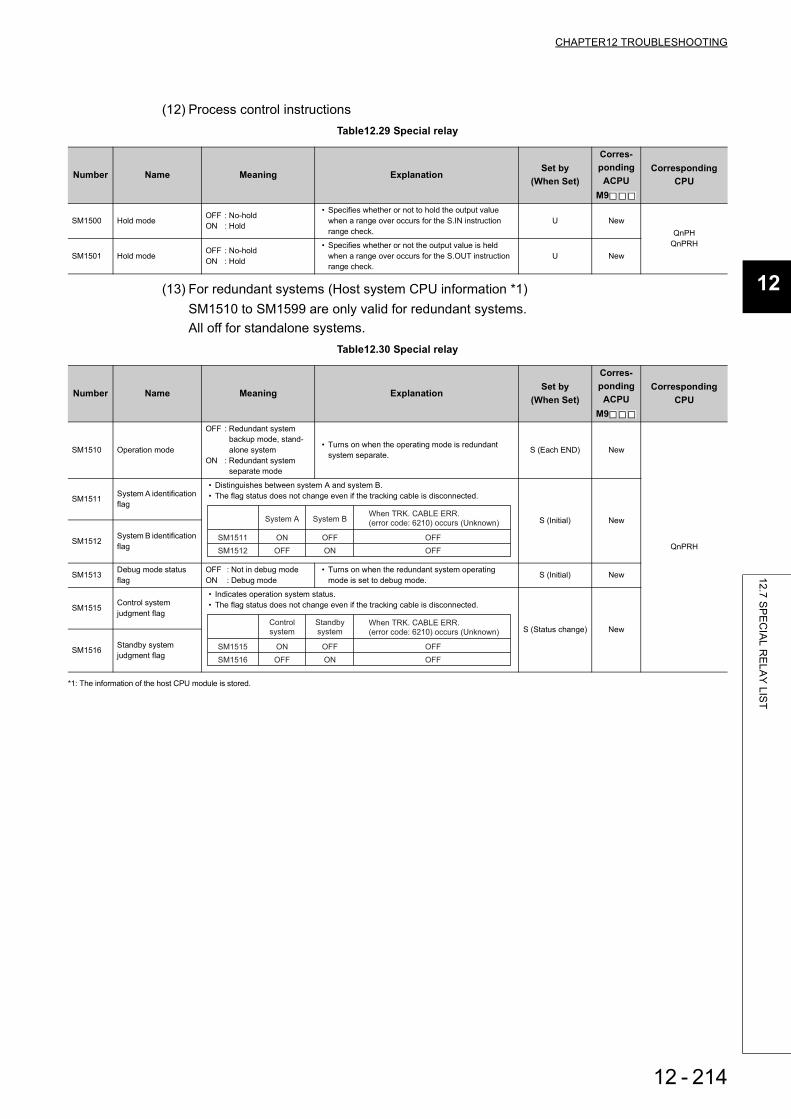
CHAPTER12 TROUBLESHOOTING
1
2
3
12
6
7
8
12.7 SP
EC
IAL R
ELA
Y LIS
T
(12) Process control instructions
(13) For redundant systems (Host system CPU information *1)SM1510 to SM1599 are only valid for redundant systems.All off for standalone systems.
*1: The information of the host CPU module is stored.
Table12.29 Special relay
Number Name Meaning ExplanationSet by
(When Set)
Corres-pondingACPU
M9
Corresponding CPU
SM1500 Hold mode OFF : No-holdON : Hold
• Specifies whether or not to hold the output value when a range over occurs for the S.IN instruction range check.
U NewQnPH
QnPRHSM1501 Hold mode
OFF : No-holdON : Hold
• Specifies whether or not the output value is held when a range over occurs for the S.OUT instruction range check.
U New
Table12.30 Special relay
Number Name Meaning ExplanationSet by
(When Set)
Corres-pondingACPU
M9
Corresponding CPU
SM1510 Operation mode
OFF : Redundant system backup mode, stand-alone system
ON : Redundant system separate mode
• Turns on when the operating mode is redundant system separate. S (Each END) New
QnPRH
SM1511 System A identification flag
• Distinguishes between system A and system B.• The flag status does not change even if the tracking cable is disconnected.
S (Initial) New
SM1512System B identification flag
SM1513 Debug mode status flag
OFF : Not in debug modeON : Debug mode
• Turns on when the redundant system operating mode is set to debug mode.
S (Initial) New
SM1515 Control system judgment flag
• Indicates operation system status.• The flag status does not change even if the tracking cable is disconnected.
S (Status change) New
SM1516 Standby system judgment flag
SM1511
SM1512
ON
OFF
System A
OFF
System B
ON
OFF
OFF
When TRK. CABLE ERR.(error code: 6210) occurs (Unknown)
SM1515
SM1516
ON
OFF
Controlsystem
OFF
Standbysystem
ON
OFF
OFF
When TRK. CABLE ERR.(error code: 6210) occurs (Unknown)
12 - 214

Table12.29 Special relay
Number Name Meaning ExplanationSet by
(When Set)
Corres-ponding
ACPUM9
Corresponding CPU
SM1517 CPU module startup status
OFF : Power supply on startup
ON : Operation system switch start up
• Turns on when the CPU module is started up by the system switching (switching from the standby system to the control system). Remains OFF when the standby system is switched to the control system by a power-ON startup.
S (Status change) New
QnPRH
SM1518Standby system to control system switching status flag
• Turns ON once switch between standby system to control system, (ON for 1 scan only) occurs.
• This status flag can only be used for scan execution type programs.
S (Each END) New
SM1519Previous Control System Identification Flag
• On the last operation Control System was System B,if power supply is supplied, or reset is released on both SYSTEM together,After RUN, ON for 1 scan only by System A side.
S (Each END) New
SM1520
Data tracking transfer trigger specification
OFF : No triggerON : Trigger
SM1520 Block 1
• When data is transferred based on the tracking setting of the redundant parameter dialog box, the target block is specified as trigger.
• When "Auto Tracking block No.1" is enabled in the tracking setting, SM1520 is turned ON by the system at power ON/STOP to RUN. In other cases, SM1520 to SM1583 are turned ON by the user.
S (initial)/U New
SM1521 SM1521 Block 2
SM1522 SM1522 Block 3
SM1523 SM1523 Block 4
SM1524 SM1524 Block 5
SM1525 SM1525 Block 6
SM1526 SM1526 Block 7
SM1527 SM1527 Block 8
SM1528 SM1528 Block 9
SM1529 SM1529 Block 10
SM1530 SM1530 Block 11
SM1531 SM1531 Block 12
SM1532 SM1532 Block 13
SM1533 SM1533 Block 14
SM1534 SM1534 Block 15
SM1535 SM1535 Block 16
SM1536 SM1536 Block 17
SM1537 SM1537 Block 18
SM1538 SM1538 Block 19
SM1539 SM1539 Block 20
SM1540 SM1540 Block 21
SM1541 SM1541 Block 22
SM1542 SM1542 Block 23
SM1543 SM1543 Block 24
SM1544 SM1544 Block 25
SM1545 SM1545 Block 26
SM1546 SM1546 Block 27
SM1547 SM1547 Block 28
SM1548 SM1548 Block 29
ON
OFF1 scan
ON
OFF1 scan
12 - 215
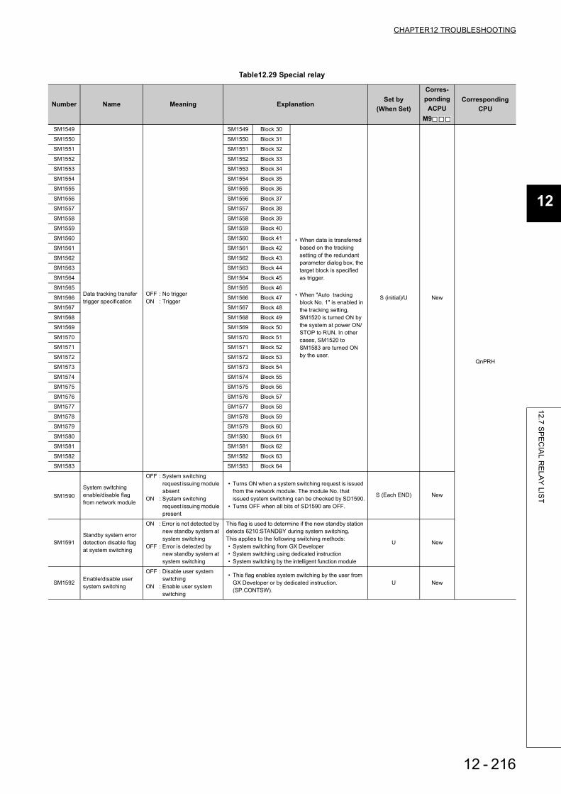
CHAPTER12 TROUBLESHOOTING
1
2
3
12
6
7
8
12.7 SP
EC
IAL R
ELA
Y LIS
T
Table12.29 Special relay
Number Name Meaning ExplanationSet by
(When Set)
Corres-pondingACPU
M9
Corresponding CPU
SM1549
Data tracking transfer trigger specification
OFF : No triggerON : Trigger
SM1549 Block 30
• When data is transferred based on the tracking setting of the redundant parameter dialog box, the target block is specified as trigger.
• When "Auto tracking block No. 1" is enabled in the tracking setting, SM1520 is turned ON by the system at power ON/STOP to RUN. In other cases, SM1520 to SM1583 are turned ON by the user.
S (initial)/U New
QnPRH
SM1550 SM1550 Block 31
SM1551 SM1551 Block 32
SM1552 SM1552 Block 33
SM1553 SM1553 Block 34
SM1554 SM1554 Block 35
SM1555 SM1555 Block 36
SM1556 SM1556 Block 37
SM1557 SM1557 Block 38
SM1558 SM1558 Block 39
SM1559 SM1559 Block 40
SM1560 SM1560 Block 41
SM1561 SM1561 Block 42
SM1562 SM1562 Block 43
SM1563 SM1563 Block 44
SM1564 SM1564 Block 45
SM1565 SM1565 Block 46
SM1566 SM1566 Block 47
SM1567 SM1567 Block 48
SM1568 SM1568 Block 49
SM1569 SM1569 Block 50
SM1570 SM1570 Block 51
SM1571 SM1571 Block 52
SM1572 SM1572 Block 53
SM1573 SM1573 Block 54
SM1574 SM1574 Block 55
SM1575 SM1575 Block 56
SM1576 SM1576 Block 57
SM1577 SM1577 Block 58
SM1578 SM1578 Block 59
SM1579 SM1579 Block 60
SM1580 SM1580 Block 61
SM1581 SM1581 Block 62
SM1582 SM1582 Block 63
SM1583 SM1583 Block 64
SM1590System switching enable/disable flag from network module
OFF : System switching request issuing module absent
ON : System switching request issuing module present
• Turns ON when a system switching request is issued from the network module. The module No. that issued system switching can be checked by SD1590.
• Turns OFF when all bits of SD1590 are OFF.
S (Each END) New
SM1591Standby system error detection disable flag at system switching
ON : Error is not detected by new standby system at system switching
OFF : Error is detected by new standby system at system switching
This flag is used to determine if the new standby station detects 6210:STANDBY during system switching.This applies to the following switching methods:• System switching from GX Developer• System switching using dedicated instruction• System switching by the intelligent function module
U New
SM1592Enable/disable user system switching
OFF : Disable user system switching
ON : Enable user system switching
• This flag enables system switching by the user from GX Developer or by dedicated instruction. (SP.CONTSW).
U New
12 - 216

*2: The module whose first 5 digits of serial No. is “09012” or later.
(14) For redundant system (Other system CPU information *1)SM1600 to SM1650 only valid for the CPU redundant system backup mode, so they cannot be refreshed during the separate mode.Either the backup mode or the separate mode is valid for the SM4651 to SM1699.SM1600 to SM1699 are all turned off for stand-alone system.
*1 Stores other system CPU diagnostic information and system information.
*2 This shows the special relay(SM ) for the host system CPU.
Table12.29 Special relay
Number Name Meaning ExplanationSet by
(When Set)
Corres-ponding
ACPUM9
Corresponding CPU
SM1593Setting to access extension base unit of standby system CPU
OFF : ErrorON : Ignored
Sets the operation for the case accessing buffer memory of the intelligent function module mounted on the extension base unit from the standby system CPU in separate mode.OFF : “OPERATION ERROR” (error code: 4112) will be
returned when accessing buffer memory of the intelligent function module on the extension base unit from the standby system CPU.
ON : No processing is performed when accessing buffer memory of intelligent function module on the extension base unit from the standby system CPU.
U
New
QnPRH*2
SM1595Memory copy to other system start flag
OFF : Start memory copyON : No memory copy
initiated
• When SM1595 is turned from OFF to ON, memory copy from control system to standby system starts. Note that when SM1595 is turned from OFF to ON, memory copy does not start if the I/O No. of the copy destination (standby system CPU module: 3D1H) is not stored in SD1595.
QnPRHSM1596
Memory copy to other system status flag
OFF : Memory copy not executed
ON : Memory copy executed
• Turns on while memory is copied to other system.• Turns off when memory copy execution has
completed.
S (Starting to copy/finish)
SM1597Memory copy to other system completion flag
OFF : Memory copy not completed
ON : Memory copy completed
• Turns on once the memory copying to the other system has completed. S (finish)/U
New
SM1598Copy contents of standard ROM during memory copy
OFF : Copy standard ROM data
ON : Standard ROM data is not copied
• If set to on by user, the standard ROM data is not copied to the other system while memory copy is executing.
U
Table12.30 Special relay
Number Name Meaning ExplanationSet by
(When Set)
Corresponding
HostSM
*2
Corresponding CPU
SM1600 Other system error flag
OFF : No errorON : Error
• Turns on when an error occurs during redundant system. Error check (Turns on single bit of SD1600.)
• Is off when no errors are presentS (Each END) – QnPRH
SM1610 Other system diagnostics error
OFF : No errorON : Error
• Turns on when a diagnostics error occurs. (Includes error detection when annunciator is ON, and by CHK instruction)
• Corresponds to status of SM0 at other system
S (Each END) SM0
QnPRH
SM1611Other systems self diagnostics error.
OFF : No self diagnostics error occurred
ON : Self diagnostics error occurred
• Turns on when a self diagnostics error occurs.(Does not include error detection when annunciator is ON, and by CHK instruction)
• Corresponds to status of SM1 at other system
S (Each END) SM1
SM1615 Other system common error information
OFF : No common error information present
ON : Common error information present
• Turns on when there is common error information at other system
• Corresponds to status of SM5 at other systemS (Each END) SM5
SM1626Error individual information for other systems
OFF : No individual error information present
ON : Individual error information present
• Turns on when there is individual error information at other system
• Corresponds to status of SM16 at other systemS (Each END) SM16
SM1649Standby system cancel error flag
OFF to ON:Cancels error of standby system
By turning this relay from OFF to ON, the continue error that occurred in the standby system CPU module can be canceled.Use SD1649 to specify the error code of the error to be canceled.
U –
12 - 217

CHAPTER12 TROUBLESHOOTING
1
2
3
12
6
7
8
12.7 SP
EC
IAL R
ELA
Y LIS
T
(15) For redundant system (tracking)Either the backup mode or the second mode is valid for SM1700 to SM1799.All is turned off for stand-alone system.
Table12.31 Special relay
Number Name Meaning ExplanationSet by
(When Set)
Corres-pondingACPU
M9
Corresponding CPU
SM1700 Transfer trigger completion flag
OFF : Transfer not completedON : Transfer completed
• Turns on for one scan, once transfer of block 1 to block 64 is completed. S (status change)
New QnPRH
SM1709
Manual system switching disable/enable setting during online program change redundant tracking
ON : Manual system switching enabled(Disable canceled)
OFF : Manual system switching disabled
(1) Turning this relay from OFF to ON enables manual system switching during online program change redundant tracking.After the manual system switching disable status is canceled, the system automatically turns off SM1709.
(2) System switching due to any of the following conditions is executed even during online program change redundant tracking, regardless of the status of this relay.•Power off, reset, hardware failure, CPU stop error
(3) In either of the following statuses, the system switching disable status can also be canceled by this relay.•Multiple-block online program change redundant
tracking execution status•File batch online program change redundant
tracking execution status
S (When executed)/U
SM1710Transfer tracking data during online program change enable flag
OFF : No device trackingON : Transfer device
memory
(1) Set whether the tracking of the following data will be executed or not during online program change redundant tracking.•Device memory
(Including SM/SD that will automatically execute tracking)
•PIDINIT information, S.PIDINIT information, SFC information
(2) SM1710 can be also used to set whether tracking will be executed or not while online change of multiple program blocks or batch of files is being performed to ensure consistency of both systems.
(3) This SM is also transferred form control system CPU module to standby system CPU module by tracking data.
U
12 - 218

Table12.31 Special relay
Number Name Meaning ExplanationSet by
(When Set)
Corres-ponding
ACPUM9
Corresponding CPU
SM1712
Transfer trigger completion flag
OFF : Transfer uncompletedON : Transfer completed
SM1712 Block 1
Turns ON only during one scan when the transmission of the corresponding block is completed.
S (status change) New QnPRH
SM1713 SM1713 Block 2
SM1714 SM1714 Block 3
SM1715 SM1715 Block 4
SM1716 SM1716 Block 5
SM1717 SM1717 Block 6
SM1718 SM1718 Block 7
SM1719 SM1719 Block 8
SM1720 SM1720 Block 9
SM1721 SM1721 Block 10
SM1722 SM1722 Block 11
SM1723 SM1723 Block 12
SM1724 SM1724 Block 13
SM1725 SM1725 Block 14
SM1726 SM1726 Block 15
SM1727 SM1727 Block 16
SM1728 SM1728 Block 17
SM1729 SM1729 Block 18
SM1730 SM1730 Block 19
SM1731 SM1731 Block 20
SM1732 SM1732 Block 21
SM1733 SM1733 Block 22
SM1734 SM1734 Block 23
SM1735 SM1735 Block 24
SM1736 SM1736 Block 25
SM1737 SM1737 Block 26
SM1738 SM1738 Block 27
SM1739 SM1739 Block 28
SM1740 SM1740 Block 29
SM1741 SM1741 Block 30
SM1742 SM1742 Block 31
SM1743 SM1743 Block 32
SM1744 SM1744 Block 33
SM1745 SM1745 Block 34
SM1746 SM1746 Block 35
SM1747 SM1747 Block 36
SM1748 SM1748 Block 37
SM1749 SM1749 Block 38
SM1750 SM1750 Block 39
SM1751 SM1751 Block 40
SM1752 SM1752 Block 41
SM1753 SM1753 Block 42
SM1754 SM1754 Block 43
SM1755 SM1755 Block 44
SM1756 SM1756 Block 45
SM1757 SM1757 Block 46
SM1758 SM1758 Block 47
SM1759 SM1759 Block 48
12 - 219

CHAPTER12 TROUBLESHOOTING
1
2
3
12
6
7
8
12.7 SP
EC
IAL R
ELA
Y LIS
T
(16) Redundant power supply module information
*1: The "power supply 1" indicates the redundant power supply module mounted on the POWER 1 slot of the redundant base unit (Q38RB/Q68RB/Q65WRB).The "power supply 2" indicates the redundant power supply module mounted on the POWER 2 slot of the redundant base unit (Q38RB/Q68RB/Q65WRB).
*2: The module whose first 5 digits of serial No. is "04012" or later.However, for the multiple CPU system configuration, this applies to all CPU modules whose first 5 digits of serial No. are "07032" or later.
*3: The module whose first 5 digits of serial No. is "10042" or later.
Table12.31 Special relay
Number Name Meaning ExplanationSet by
(When Set)
Corres-pondingACPU
M9
Corresponding CPU
SM1760
Transfer trigger completion flag
OFF : Transmission uncompleted
ON : Transmission end
SM1760 Block 49
Turns ON only during one scan when the transmission of the corresponding block is completed.
S (status change) New QnPRH
SM1761 SM1761 Block 50SM1762 SM1762 Block 51SM1763 SM1763 Block 52SM1764 SM1764 Block 53SM1765 SM1765 Block 54SM1766 SM1766 Block 55SM1767 SM1767 Block 56SM1768 SM1768 Block 57SM1769 SM1769 Block 58SM1770 SM1770 Block 59SM1771 SM1771 Block 60SM1772 SM1772 Block 61SM1773 SM1773 Block 62SM1774 SM1774 Block 63SM1775 SM1775 Block 64
Table12.32 Special relay
Number Name Meaning ExplanationSet by
(When Set)
Corres-pondingACPU
M9
Corresponding CPU
SM1780 Power supply off detection flag
OFF : No redundant power supply module with input power OFF detected
ON : Redundant power supply module with input power OFF detected
• Turns ON when one or more redundant power supply modules with input power OFF are detected.
• Turns on if any of SD1780 bits is on.• Turns off if all bits of SD1780 are off.• Turns OFF when the main base unit is not the
redundant main base unit (Q38RB).• When the multiple CPU system is configured, the
flags are stored only to the CPU No.1.
S (Each END)
New
Qn(H)*2
QnPH*2
QnPRHQnU*3
SM1781 Power supply failure detection flag
OFF : No faulty redundant power supply module detected
ON : Faulty redundant power supply module detected
• Turns ON when one or more faulty redundant power supply modules are detected.
• Turns on if any of SD1781 bits is on.• Turns off if all bits of SD1781 are off.• Turns OFF when the main base unit is not the
redundant main base unit (Q38RB).• When the multiple CPU system is configured, the
flags are stored only to the CPU No.1.
S (Each END)
SM1782Momentary power failure detection flag for power supply 1 *1
OFF : No momentary power failure detected
ON : Momentary power failure detected
• Turns ON when a momentary power failure of the input power supply to the power supply 1 or 2 is detected one or more times. After turning ON, remains ON even if the power supply recovers from the momentary power failure.
• Turns OFF the flag (SM1782, SM1783) of the power supply 1/2 when the CPU module starts.
• When the input power to one of the redundant power supply modules turns OFF the corresponding flag turns OFF.
• Turns OFF when the main base unit is not the redundant main base unit (Q38RB).
• When the multiple CPU system is configured, the flags are stored only to the CPU No.1.
S (Each END)
SM1783Momentary power failure detection flag for power supply 2 *1
12 - 220

12.8 SPECIAL REGISTER LIST
The special registers, SD, are internal registers with fixed applications in the Programmable Controller.
For this reason, it is not possible to use these registers in sequence programs in the same way that normal registers are used.
However, data can be written as needed in order to control the CPU modules.
Data stored in the special registers are stored as BIN values if no special designation has been made to the contrary.
The heading descriptions in the following special register lists are shown in 4.1.
For details on the following items, refer to the following manuals: • Networks Manual of the corresponding network module • SFC QCPU(Q mode)/QnACPU Programming Manual (SFC)
Do not change the values of special relays set by the system with user program or device test operations.Doing so may result in system downtime or communication fault.
Table12.33 Descriptions of the special register lists headings
Item Function of ItemNumber • Indicates special register numberName • Indicates name of special registerMeaning • Indicates contents of special registerExplanation • Discusses contents of special register in more detail
Set by (When set)
• Indicates whether the relay is set by the system or user, and, if it is set by the system, when setting is performed.<Set by> S : Set by system U : Set by user (sequence programs or test operations from GX Developer) S/U : Set by both system and user<When set> Indicated only for registers set by system Each END : Set during each END processing Initial : Set only during initial processing (when power supply is turned ON, or when going from STOP to RUN) Status change : Set only when there is a change in status Error : Set when error occurs Instruction execution : Set when instruction is executed Request : Set only when there is a user request (through SM, etc.) System switching : Set when system switching is executed.
Corresponding ACPU M9
• Indicates corresponding special register in ACPU
(When the contents are changed, the special register is represented D9 format change. Incompatible with the Q00J/Q00/Q01 and QnPRH.)
• New indicates the special register newly added to the Q series CPU module.
Corresponding CPU
Indicates the relevant CPU module.QCPU : Indicates all the Q series CPU modules.Q00J/Q00/Q01 : Indicates the Basic model QCPU.Qn(H) : Indicates the High Performance model QCPU.QnPH : Indicates the Process CPU.QnPRH : Indicates the Redundant CPU.QnU : Indicates the Universal model QCPUEach CPU type name : Can be applied only to the specific CPU. (e.g. Q02U)
12 - 221

CHAPTER12 TROUBLESHOOTING
1
2
3
12
6
7
8
12.8 SP
EC
IAL R
EG
ISTE
R LIS
T
(1) Diagnostic InformationTable12.34 Special register
Number Name Meaning ExplanationSet by
(When Set)
Corres-ponding ACPU
D9
CorrespondingCPU
SD0 Diagnostic errors
Diagnosis error code
• Error codes for errors found by diagnosis are stored as BIN data.• Contents identical to latest fault history information. S (Error)
D9008 format change
QCPU
SD1
Clock time for diagnosis error occurrence
Clock time for diagnosis error occurrence
• Year (last two digits) and month that SD0 data was updated is stored as BCD 2-digit code.
S (Error) NewSD2
• The day and hour that SD0 was updated is stored as BCD 2-digit code.
SD3
• The minute and second that SD0 data was updated is stored as BCD 2-digit code.
SD4Error information categories
Error information category code
Category codes which help indicate what type of information is being stored in the common information areas (SD5 through SD15) and the individual information areas (SD16 through SD26) are stored here.The category code for judging the error information type is stored.
• The common information category codes store the following codes:0 : No error1: Unit/module No./ CPU No./Base No.*
2: File name/Drive name3: Time (value set)4: Program error location5: System switching cause (for Redundant CPU only)6: Reason(s) for tracking capacity excess error (specific to Redundant
CPU)7: Base No./Power supply No. (The first 5 digits of serial number 10072
or higer are chosen for Universal model QCPU.)8: Tracking transmission data classification (specific to Redundant CPU)*: For a multiple CPU system that consists of the Basic model QCPU,
High Performance model QCPU, Process CPU, Universal model QCPU the module number or CPU number is stored depending on the error that occurred.(Refer to the corresponding error code for which number has been stored.)CPU No. 1: 1, CPU No. 2: 2, CPU No. 3: 3, CPU No. 4: 4
• The individual information category codes store the following codes:0: No error1: (Empty)2: File name/Drive name3: Time (value actually measured)4: Program error location5: Parameter number6: Annunciator number7: CHK instruction failure No. (except for the Basic model QCPU and the
Universal model QCPU)8: Reason(s) for system switching failure (specific to Redundant CPU)12: File diagnostic information (specific to the Universal model QCPU)13: Parameter No./CPU No. (specific to the Universal model QCPU)
S (Error) New
b15 b7 b0b8to to
Year (0 to 99) Month (1 to 12)
(Example) October, 1995
9510H
b15 b7 b0b8to to
Day (1 to 31) Hour (0 to 23)
(Example) 10 a.m. on 25th
2510H
b15 b7 b0b8to to
Minutes (0 to 59) Seconds (0 to 59)
(Example) 35 min. 48 sec.
3548H
b15 b7 b0b8to to
Individual information
category codes
Common information
category codes
12 - 222
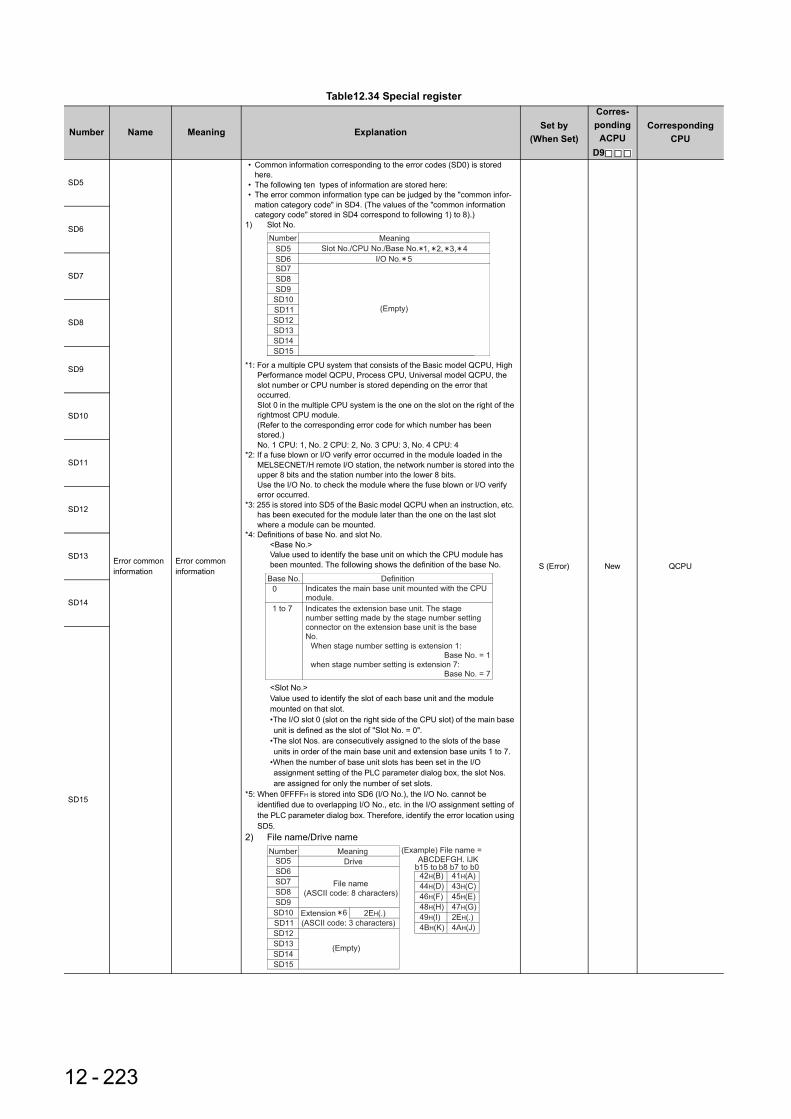
Table12.34 Special register
Number Name Meaning ExplanationSet by
(When Set)
Corres-ponding
ACPUD9
CorrespondingCPU
SD5
Error common information
Error common information
• Common information corresponding to the error codes (SD0) is stored here.
• The following ten types of information are stored here:• The error common information type can be judged by the "common infor-
mation category code" in SD4. (The values of the "common information category code" stored in SD4 correspond to following 1) to 8).)
1) Slot No.
*1: For a multiple CPU system that consists of the Basic model QCPU, High Performance model QCPU, Process CPU, Universal model QCPU, the slot number or CPU number is stored depending on the error that occurred.Slot 0 in the multiple CPU system is the one on the slot on the right of the rightmost CPU module.(Refer to the corresponding error code for which number has been stored.)No. 1 CPU: 1, No. 2 CPU: 2, No. 3 CPU: 3, No. 4 CPU: 4
*2: If a fuse blown or I/O verify error occurred in the module loaded in the MELSECNET/H remote I/O station, the network number is stored into the upper 8 bits and the station number into the lower 8 bits.Use the I/O No. to check the module where the fuse blown or I/O verify error occurred.
*3: 255 is stored into SD5 of the Basic model QCPU when an instruction, etc. has been executed for the module later than the one on the last slot where a module can be mounted.
*4: Definitions of base No. and slot No.<Base No.>Value used to identify the base unit on which the CPU module has been mounted. The following shows the definition of the base No.
<Slot No.>Value used to identify the slot of each base unit and the module mounted on that slot.•The I/O slot 0 (slot on the right side of the CPU slot) of the main base unit is defined as the slot of "Slot No. = 0".
•The slot Nos. are consecutively assigned to the slots of the base units in order of the main base unit and extension base units 1 to 7.
•When the number of base unit slots has been set in the I/O assignment setting of the PLC parameter dialog box, the slot Nos. are assigned for only the number of set slots.
*5: When 0FFFFH is stored into SD6 (I/O No.), the I/O No. cannot be identified due to overlapping I/O No., etc. in the I/O assignment setting of the PLC parameter dialog box. Therefore, identify the error location using SD5.
2) File name/Drive name
S (Error) New QCPU
SD6
SD7
SD8
SD9
SD10
SD11
SD12
SD13
SD14
SD15
1, 2, 3, 4SD5
SD6
SD7
SD8
SD9
SD10
SD11
SD12
SD13
SD14
SD15
Number
Slot No./CPU No./Base No.
I/O No. 5
Meaning
(Empty)
0
1 to 7
Base No.
Indicates the main base unit mounted with the CPU module.
Indicates the extension base unit. The stage number setting made by the stage number setting connector on the extension base unit is the base No.
When stage number setting is extension 1: Base No. = 1
when stage number setting is extension 7: Base No. = 7
Definition
SD5
SD6
SD7
SD8
SD9
SD10
SD11
SD12
SD13
SD14
SD15
2EH(.)6
ABCDEFGH. IJK
42H(B) 41H(A)
44H(D) 43H(C)
46H(F) 45H(E)
48H(H) 47H(G)
49H(I) 2EH(.)
4BH(K) 4AH(J)
b15 to b8 b7 to b0
Number Meaning
Drive
File name
(ASCII code: 8 characters)
Extension
(ASCII code: 3 characters)
(Empty)
(Example) File name =
12 - 223
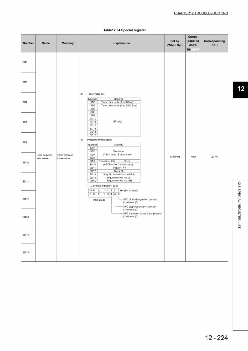
CHAPTER12 TROUBLESHOOTING
1
2
3
12
6
7
8
12.8 SP
EC
IAL R
EG
ISTE
R LIS
T
Table12.34 Special register
Number Name Meaning ExplanationSet by
(When Set)
Corres-ponding ACPU
D9
CorrespondingCPU
SD5
Error common information
Error common information
3) Time (value set)
4) Program error location
*7 : Contents of pattern data
S (Error) New QCPU
SD6
SD7
SD8
SD9
SD10
SD11
SD12
SD13
SD14
SD15
SD5
SD6
SD7
SD8
SD9
SD10
SD11
SD12
SD13
SD14
SD15
Number Meaning
Time : 1 s units (0 to 999 s)
Time : 1ms units (0 to 65535ms)
(Empty)
SD5
SD6
SD7
SD8
SD9
SD10
SD11
SD12
SD13
SD14
SD15
6
7
Number Meaning
File name
(ASCII code: 8 characters)
Extension 2EH(.)
(ASCII code: 3 characters)
Pattern
Block No.
Step No./transition condition
Sequence step No. (L) Sequence step No. (H)
000 0 to
0123415 14 to
(Not used)
(Bit number)
SFC block designation present (1)/absent (0)
SFC transition designation present (1)/absent (0)
SFC step designation present (1)/absent (0)
12 - 224

*1: The module whose first 5 digits of serial No. is "07032" or later.*2: The module whose first 5 digits of serial No. is "10042" or later.
Table12.34 Special register
Number Name Meaning ExplanationSet by
(When Set)
Corres-ponding
ACPUD9
CorrespondingCPU
SD5
Error common information
Error common information
5) Reason(s) for system switching
*13: Details of reason(s) for system switching
6) Reason(s) for tracking capacity excess errorThe block No. when the data amount that can be tracked (100k) is exceeded is indicated by the bit pattern of the corresponding special relay.
S (Error) New QnPRH
SD6
SD7
SD8
SD9
SD10
SD11
SD12
SD13
7) Power supply No.
S (Error) New
Qn(H)*1
QnPH*1
QnPRHQnU*2
SD14
SD15
SD5
SD6
SD7
SD8
SD9
SD10
SD11
SD12
SD13
SD14
SD15
Number Meaning
System switching condition 13
Control system switching instruction argument
(Empty)
1 : Power-OFF, reset, hardware failure, watchdog timer error
2 : Stop error(except watchdog timer error)
3 : System switching request by network module
16 : Control system switching instruction
17 : Control system switching request from GX Developer
0 : No system switching condition (default)
SD15
SD5
SD8
SD9
SD6
SD7
0 0 0 0 0 0 0 0 0 00 0 0 0 0 0
1
(SM1535)
(Block16)0
b15 b14
0
b13
0
b12
0
b11
0
b10
0
b9
1
(SM1528)
(Block9)0
b8
1
(SM1520)
(Block1)
b0b7
0
b6
0
b5
0
b4
0
b3
0
b2
0
0 0 0 0 0 0 0 0 0 00 0 0 0 0 0
0 0 0 0 0 0 0 0 0 00 0 0 0 0 0
b1
1
(SM1583)
(Block64)0 0 0 0 0 0 0 0
1
(SM1568)
(Block49)0 0 0 0 0 0
0 0 0 0 0 0 0 0 0 00 0 0 0 0 0
1: Power supply 1 fault
2: Power supply 2 fault
Redundant power supply module
mounted on POWER 1 slot of redundant
base unit (Q38RB, Q68RB, Q65WRB)
"Power
supply
module 1":
Redundant power supply module
mounted on POWER 2 slot of redundant
base unit (Q38RB, Q68RB, Q65WRB)
"Power
supply
module 2":
SD5
SD6
SD7
SD8
SD9
SD10
SD11
SD12
SD13
SD14
SD15
Number Meaning
Base No.
Power supply No.
(Empty)
12 - 225

CHAPTER12 TROUBLESHOOTING
1
2
3
12
6
7
8
12.8 SP
EC
IAL R
EG
ISTE
R LIS
T
Table12.34 Special register
Number Name Meaning ExplanationSet by
(When Set)
Corres-ponding ACPU
D9
CorrespondingCPU
SD5
Error common information
Error common information
8) Tracking transmission data classificationStores the data classification during tracking.
*15: Details of data classificationS (Error) New QnPRH
SD6
SD7
SD8
SD9
SD10
SD11
SD12
SD13
SD14
SD15
SD5
SD6
SD7
SD8
SD9
SD10
SD11
SD12
SD13
SD14
SD15
Number Meaning
Data type 15
(Empty)
b15 b5 b4 b3 b2 b1 b0tob14
0
b6 Each bit
Device data
Signal flow
PIDINIT/S. PIDINIT instruction data
SFC execution data
System switchingrequest
Operation mode change request
System data
0: Not sent1: Being sent
12 - 226

Table12.34 Special register
Number Name Meaning ExplanationSet by
(When Set)
Corres-ponding
ACPUD9
CorrespondingCPU
SD16
Error individual information
Error individual information
• Individual information corresponding to error codes (SD0) is stored here.• There are the following eight different types of information are stored.• The error individual information type can be judged by the "individual
information category code" in SD4. (The values of the "individual infor-mation category code" stored in SD4 correspond to following 1) to 8), 12), and 13).)
1) (Empty)
2) File name/Drive name
3) Time (value actually measured)
4) Program error location
*7 : Contents of pattern data
*16: For details of the parameter No., refer to the User's Manual (Function Explanation, Program Fundamentals) of the CPU module used.
S (Error) New QCPU
SD17
SD18
SD19
SD20
SD21
SD22
SD23
SD24
SD25
SD26
SD16
SD17
SD18
SD19
SD20
SD21
SD22
SD23
SD24
SD25
SD26
6
ABCDEFGH. IJK
42H(B) 41H(A)
44H(D) 43H(C)
46H(F) 45H(E)
48H(H) 47H(G)
49H(I) 2EH(.)
4BH(K) 4AH(J)
b15 to b8 b7 to b0
Number Meaning
Drive
File name
(ASCII code: 8 characters)
Extension 2EH(.)
(ASCII code: 3 characters)
(Empty)
(Example) File name =
SD16
SD17
SD18
SD19
SD20
SD21
SD22
SD23
SD24
SD25
SD26
Number Meaning
Time : 1 s units (0 to 999 s)
Time : 1ms units (0 to 65535ms)
(Empty)
SD16
SD17
SD18
SD19
SD20
SD21
SD22
SD23
SD24
SD25
SD26
Number Meaning
File name
(ASCII code: 8 characters)
Extension 6 2EH(.)
(ASCII code: 3 characters)
Pattern 7
Block No.
Step No./transition No.
Sequence step No. (L) Sequence step No. (H)
000 0 to
0123415 14 to
(Not used)
(Bit number)
SFC block designationpresent (1)/absent (0)
SFC step designationpresent (1)/absent (0)
SFC transition designationpresent (1)/absent (0)
SD16
SD17
SD18
SD19
SD20
SD21
SD22
SD23
SD24
SD25
SD26
SD16
SD17
SD18
SD19
SD20
SD21
SD22
SD23
SD24
SD25
SD26
Number Meaning Number Meaning
Parameter No. 16 No.
(Empty) (Empty)
Annunciator number /
CHK instruction
malfunction number
6)Parameter No.5)
7)
12 - 227

CHAPTER12 TROUBLESHOOTING
1
2
3
12
6
7
8
12.8 SP
EC
IAL R
EG
ISTE
R LIS
T
*6 : Extensions are shown below.Table12.35 Extension name
SDn SDn+1 Extension Name
File TypeHigher 8 bits Lower 8 bits Higher 8 bits
51H 50H 41H QPA Parameters
51H 50H 47H QPG• Sequence program• SFC program
51H 43H 44H QCD Device comment51H 44H 49H QDI Initial device value51H 44H 52H QDR File register
51H 44H 4CH QDLLocal device(Other than the Basic model QCPU)
51H 54H 44H QTDSampling trace data(Other than the Basic model QCPU)
51H 46H 44H QFDBreakdown history data(Other than the Basic model QCPU and the Universal model QCPU)
51H 53H 54H QSTSP.DEVST/S.DEVLD instruction file(For Universal model QCPU only)
12 - 228

Table12.34 Special register
Number Name Meaning ExplanationSet by
(When Set)
Corres-ponding
ACPUD9
CorrespondingCPU
SD26 Error individual information
Error individual information
8) Reason(s) for system switching failure
*14: Details of reason(s) for system switching failure
S (Error) New
QnPRH
12) File diagnostic information
13) Parameter No./CPU No. QnU
SD16
SD17
SD18
SD19
SD20
SD21
SD22
SD23
SD24
SD25
SD26
Number MeaningSystem switching prohibition
condition 14
(Empty)
10 : Error detected by network module of standby system
7 : Operation differs between two systems (in backup mode only)
3 : Hardware failure, power OFF, reset or watchdog timer error occurring in control system
9 : Online program change
11 : System switching being executed
12 : Online module change in progress
8 : During memory copy from control system to standby system
6 : Standby system is in stop error (except watchdog timer error)
4 : Preparing for tracking5 : Time limit exceeded
2 : Hardware failure, power OFF, reset or watchdog timer error occurring in standby system
0 : Normal switching completion (default)
1 : Tracking cable fault (cable removal, cable fault, internal circuit fault, hardware fault)
SD17
SD18
SD19
SD20
File name
(ASCll: 8 characters)
SD21
SD22
SD23
SD24
SD16 drive No.(L)
SD25
SD26
Failuer information (H)
Failure information 2
(CRC value that is read)
EXtension *6 2EH(.)
(ASCll; 3 characters)
Failure information 3(CRC value that is calculated)
SD17
SD18
SD19
SD20
SD21
SD22
SD23
SD24
SD16
SD25
SD26
Parameter No.*16
(Empty)
Number Meaning
CPU No. (1 to 4)
12 - 229

CHAPTER12 TROUBLESHOOTING
1
2
3
12
6
7
8
12.8 SP
EC
IAL R
EG
ISTE
R LIS
T
Table12.34 Special register
Number Name Meaning ExplanationSet by
(When Set)
Corres-ponding ACPU
D9
CorrespondingCPU
SD50 Error resetError number that performs error reset
• Stores error number that performs error reset U New
QCPU
SD51 Battery low latch
Bit pattern indicating where battery voltage drop occurred
• All corresponding bits go 1(ON) when battery voltage drops.• Subsequently, these remain 1(ON) even after battery voltage has been
returned to normal.
• In the alarm, data can be held within the time specified for battery low.• The error indicates the complete discharge of the battery.
S (Error) New
SD52 Battery low
Bit pattern indicating where battery voltage drop occurred
• Same configuration as SD51 above• After the alarm is detected (ON), the alarm turns OFF by error detection
(ON). (For the Universal model QCPU only)• Turns to 0 (OFF) when the battery voltage returns to normal thereafter.
S (Error) New
SD53AC/DC DOWN detection
Number of times for AC/DC DOWN detection
• Every time the input voltage falls to or below 85% (AC power)/65% (DC power) of the rating during operation of the CPU module, the value is incremented by 1 and stored in BIN code.
• The counter repeats increment and decrement of the value ;0 32767 -32768 0
S (Error) D9005
SD60Number of module with blown fuse
Number of module with blown fuse
• Value stored here is the lowest station I/O number of the module with the blown fuse. S (Error) D9000
SD61I/O module verify error number
I/O module verify error module number
• The lowest I/O number of the module where the I/O module verification number took place. S (Error) D9002
0
b3 b2 b1 b0
CPU error
1: This does not apply to Basic model QCPU.
alarm
error
b15 to
1
12 - 230

Table12.34 Special register
Number Name Meaning ExplanationSet by
(When Set)
Corres-ponding
ACPUD9
CorrespondingCPU
SD62Annunciator number
Annunciator number • The first annunciator number (F number) to be detected is stored here.
S (Instruction execution) D9009
QCPU
SD63Number of annunciators
Number of annunciators • Stores the number of annunciators searched.
S (Instruction execution) D9124
SD64
Table of detected annunciator numbers
Annunciator detection number
When F goes ON due to OUT F or SET F instruction, the F numbers which go progressively ON from SD64 through SD79 are registered.The F numbers turned OFF by RST F instruction are deleted from SD64 - SD79, and the F numbers stored after the deleted F numbers are shifted to the preceding registers.Execution of the LEDR instruction shifts the contents of SD64 to SD79 up by one.After 16 annunciators have been detected, detection of the 17th will not be stored from SD64 through SD79.
S (Instruction execution)
D9125
SD65 D9126
SD66 D9127
SD67 D9128
SD68 D9129
SD69 D9130
SD70 D9131
SD71 D9132
SD72 New
SD73 New
SD74 New
SD75 New
SD76 New
SD77 New
SD78 New
SD79 New
SD80 CHK number CHK number • Error codes detected by the CHK instruction are stored as BCD code.S (Instruction
execution) New
Qn(H)QnPH
QnPRH
SD90
Step transition monitoring timer setting value (Enabled only when SFC program exists)
F number for timer set value and time over error
Corresponds to SM90 • Set the annunciator number (F number) that will
be turned ON when the step transition monitoring timer setting or monitoring timeout occurs.
• Turning ON any of SM90 to SM99 during an active step starts the timer, and if the transition condition next to the corresponding step is not met within the timer time limit, the set annunciator (F) turns ON.
U
D9108
SD91 Corresponds to SM91
D9109
SD92 Corresponds to SM92
D9110
SD93 Corresponds to SM93
D9111
SD94 Corresponds to SM94
D9112
SD95 Corresponds to SM95
D9113
SD96 Corresponds to SM96
D9114
SD97 Corresponds to SM97
New
SD98 Corresponds to SM98
New
SD99 Corresponds to SM99
New
SD62 0 50 50 50 50 50 50 50 50 50 50 50 99 (Number detected)
SD63 0 1 2 3 2 3 4 5 6 7 8 9 8
0 50 50 50 50 50 50 50 50 50 50 50 99SD64
SD65
SD66
SD67
SD68
SD69
SD70
SD71
SD72
SD73
SD74
SD75
SD76
SD77
SD78
SD79
0 0 25 25 99 99 99 99 99 99 99 99 15
0 0 0 99 0 15 15 15 15 15 15 15 70
0 0 0 0 0 0 70 70 70 70 70 70 65
0 0 0 0 0 0 0 65 65 65 65 65 38
0 0 0 0 0 0 0 0 38 38 38 38 110
0 0 0 0 0 0 0 0 0 110 110 110 151
0 0 151
0
0 0 0 0 0 0 0 0 151210
00 0 0 0 0 0 0 0 0 0210
0 00 0 0 0 0 0 0 0 0 00
0 00 0 0 0 0 0 0 0 0 00
0 00 0 0 0 0 0 0 0 0 00
0 00 0 0 0 0 0 0 0 0 00
0 00 0 0 0 0 0 0 0 0 00
0 00 0 0 0 0 0 0 0 0 00
0 00 0 0 0 0 0 0 0 0 00
(Number of annunciators detected)
(Number detected)
SET
F50
SET
F25
SET
F99
RST
F25
SET
F15
SET
F70
SET
F65
SET
F38
SET
F110
SET
F151
SET
F210 LEDR
b15 b7 b0b8
F number setting
(0 to 255)
Timer time limit
setting(1 to 255s:
(1s units))
to to
12 - 231

CHAPTER12 TROUBLESHOOTING
1
2
3
12
6
7
8
12.8 SP
EC
IAL R
EG
ISTE
R LIS
T
*3: This applies to Universal model QCPUs except for the Built-in Ethernet port QCPU.*4: The module whose first 5 digits of serial No. is "10102" or later.
Table12.34 Special register
Number Name Meaning ExplanationSet by
(When Set)
Corres-ponding ACPU
D9
CorrespondingCPU
SD100Transmission speed storage area
Stores the transmission speed specified in the serial communication setting.
96 : 9.6kbps, 192 : 19.2kbps, 384 : 38.4kbps,576 : 57.6kbps, 1152 : 115.2kbps
S (Power-ON or reset) New
Q00/Q01Q00UJQ00UQ01U
Q02U*4
SD101Communication setting storage area
Stores the communication setting specified in the serial communication setting.
* : Since the data is used by the system, it is undefined.
S (Power-ON or reset) New
SD102Transmission wait time storage area
Stores the transmission wait time specifed in the serial communication setting.
0 : No waiting time10 to 150: Waiting time (unit: ms)
Defaults to 0.
S (Power-ON or reset) New
SD105
CH1 transmission speed setting (RS-232)
Stores the preset transmission speed when GX Developer is used.
96 : 9600bps, 192 : 19.2kbps, 384 : 38.4kbps,576 : 57.6kbps, 1152 : 115.2kbps*: Other than RS-232 connection holds the data at RS-232 connection. (When disconnected, the default value is 1152.)
S New
Qn(H)QnPH
QnPRHQnU*3
SD110Data sending result storage area
Stores the data sending result when the serial communication function is used.
Stores the error code at the timeout sending data. S (Error)
New
Q00/Q01Q00UJQ00UQ01U
Q02U*4SD111
Data receiving result storage area
Stores the data receiving result when the serial communication function is used.
Stores the error code at the time of receiving data. S (Error)
SD118Amount of battery consumption
Amount of battery consumption
Displays the current amount of battery consumption.The value range:1 to 2(Q00UJCPU, Q00UCPU, Q01UCPU,
Q02UCPU, Q03UD(E)CPU, Q04UD(E)HCPU)1 to 3(Q06UD(E)HCPU)1 to 4(Q10UD(E)HCPU, Q20UD(E)HCPU, Q13UD(E)HCPU, Q26UD(E)HCPU)
S (Status change) New QnU*4
SD119Battery life-prolonging factor
Battery life-prolonging factor
Stores the factor which makes the battery life-prolonging function valid.When SD119 is other than 0, the battery life-prolonging function is valid.
S (Status change) New QnU
b0tob3b4b5b6b15 to
Sumcheck presence
0: Absent
1: Present0: Disabled
1: Enabled
Write during RUN setting
b0:CPU switch setting
0:No factor1:Foctor
b1:Backup in execution by
latch data backup function
(to standard ROM)
b15 to b2 b1 b0
12 - 232

Table12.34 Special register
Number Name Meaning ExplanationSet by
(When Set)
Corres-ponding
ACPUD9
CorrespondingCPU
SD130
Fuse blown module
Bit pattern in units of 16 points, indicating the modules whose fuses have blown0: No blown fuse1: Blown fuse
present
• The numbers of output modules whose fuses have blown are input as a bit pattern (in units of 16 points).(If the module numbers are set by parameter, the parameter-set numbers are stored.)
• Not cleared even if the blown fuse is replaced with a new one.This flag is cleared by error resetting operation
S (Error) New Q00J/Q00/Q01
SD131
SD132
SD133
SD134
SD135
SD136
SD137
SD150
I/O module verify error
Bit pattern, in units of 16 points, indicating the modules with verify errors.0: No I/O verify
errors1: I/O verify error
present
• When I/O modules, of which data are different from those entered at power-ON, have been detected, the I/O module numbers (in units of 16 points) are entered in bit pattern. (Preset I/O module numbers set in parmeters when parameter setting has been performed.)
• Not cleared even if the blown fuse is replaced with a new one.This flag is cleared by error resetting operation.
SD151
SD152
SD153
SD154
SD155
SD156
SD157
b15 b14 b13 b12 b11b10 b9 b8 b7 b6 b5 b4 b3 b2 b1 b0
0 0 01
(YC0) 0 0 0 0 0 0 0 0 0 0 01
(Y80)SD130
0 01
(Y1F0) 0 0 0 0 0 0 0 0 0 01
(Y1A0)SD131 0 0
0 01
(Y7B0) 0 0 0 0 0 0 0 0SD137 0 001
(Y730)0
Indicates fuse blow.
b15 b14 b13 b12 b11 b10 b9 b8 b7 b6 b5 b4 b3 b2 b1 b0
0 0 0 0 0 0 0 0 0 0 0 0 0SD150
0 0 0 0 0 0 0 0 0 0 0SD151 0 0
0 0 0 0 0 0 0 0 0SD157 0 000
Indicates an I/O module verify error.
0 0
00
001
( )X Y7E0
1( )X Y
0
1( )X Y190
12 - 233

CHAPTER12 TROUBLESHOOTING
1
2
3
12
6
7
8
12.8 SP
EC
IAL R
EG
ISTE
R LIS
T
(2) System informationTable12.36 Special register
Number Name Meaning ExplanationSet by
(When Set)
Corres-ponding ACPU
D9
CorrespondingCPU
SD200 Status of switch Status of CPU switch
• The CPU switch status is stored in the following format:
S (Every END processing) New
Qn(H)QnPH
QnPRH
• The CPU switch status is stored in the following format:
S (Every END processing) New Q00J/Q00/Q01
• The CPU switch status is stored in the following format:
S (when RUN/STOP/RESET
switch changed)New QnU
SD201 LED status Status of CPU-LED
• The following bit patterns store the status of the LEDs on the CPU module:
• 0 is off, 1 is on, and 2 is flicker.
1): RUN 5): BOOT2): ERR. 6): Empty Mode bit pattern3): USER 7): Empty 0: OFF 1: Green4): BAT. 8): MODE 2: Orange(The Basic model QCPU does not include 3) to 8).)
S (Status change) New
Q00J/Q00/Q01Qn(H)QnPH
QnPRH
• The following bit patterns store the status of the LEDs on the CPU module:
• 0 is off, 1 is on, and 2 is flicker.
1): RUN 5): BOOT2): ERROR 6): Empty3): USER 7): Empty4): BAT. 8): MODE(The Q00UJCPU, Q00UCPU, and Q01UCPU do not include 5).)
S (Status change)
New QnU
b15 b12 b11 b8 b7 b4 b3 b0
1)2)Empty3)
to tototo
1): CPU switch status
0: RUN
1: STOP
2: L.CLR
2): Memory card
switchAlways OFF
3): DIP switch
b8 through b12 correspond to
SW1 through SW5 of system
setting switch 1.
0: OFF, 1: ON.
b13 through b15 are empty.
b15 b8 b7 b4 b3 b0
1)2)Empty
to toto
1): 0: RUN
1: STOP
2):
CPU switch status
Memory card switch Always OFF
b15 b8 b7 b4 b3 b0
1)2)Empty
to toto
1): 0: RUN
1: STOP
2):
CPU switch status
Memory card switch Always OFF
b15 b12b11 b8 b7 b4 b3 b0
1)2)4) 3)5)6)8) 7)
to tototo
b15 b12b11 b8 b7 b4 b3 b0
1)2)4) 3)5)6)8) 7)
to tototo
12 - 234

Table12.36 Special register
Number Name Meaning ExplanationSet by
(When Set)
Corres-ponding
ACPUD9
CorrespondingCPU
SD202LED off command
Bit pattern of LED that is turned off
• Specify the LEDs to be turned off using this register, and turn SM202 from OFF to ON to turn off the specified LEDs.USER and BOOT can be specified as the LEDs to be turned off.
• Specify the LEDs to be turned off in the following bit pattern.(Turned off at 1, not be turned off at 0.)
(The Q00UJCPU, Q00UCPU, and Q01UCPU cannot specify the BOOT LED.)
U New
Qn(H)QnPH
QnPRHQnU
SD203 Operating status of CPU
Operating status of CPU
• The CPU operating status is stored as indicated in the following figure:
S (Every END processing)
D9015 format change
QCPU
SD204 LED displaycolor
CPU-LED displaycolor
• The LED display color of the LED status shown in SD201 1) to 8).
(The Q00UJCPU, Q00UCPU, and Q01UCPU do not include 5).)
S (status change)
New QnU
b15 b8 b4 b0
USER
LED
BOOT
LED
Fixed
to 0
Fixed
to 0
Fixed
to 0
b15 b12 b11 b8 b7 b4 b3 b0
1)
to to to to
2)
1): Operating status
of CPU
0:
1:
2:
3:
2): STOP/PAUSE
cause
0:
1:
2:
3:
4: Error
RUN
STEP-RUN (For the QnACPU only)
STOP
PAUSE
Instruction in remote operation program
from RUN/STOP switch ("RUN/STOP/
RESET switch" for Basic model QCPU)
Remote contact
Remote operation from GX Developer/
serial communication, etc.
Internal program instruction
Note: Priority is
earliest first
b15 b12 b11 b8 b7 b4 b3 b0
1)RUN LED
0: OFF
1: Green
2)ERROR LED
0: OFF
1: Red
3)USER LED
0: OFF
1: Red
4)BAT. LED
0: OFF
1: Yellow
2: Green
8)MODE LED
0: OFF
1: Green
5)BOOT LED
0: OFF
1: Green
6)Empty
7)Empty
12 - 235

CHAPTER12 TROUBLESHOOTING
1
2
3
12
6
7
8
12.8 SP
EC
IAL R
EG
ISTE
R LIS
T
*9: Function version is B or later.
Table12.36 Special register
Number Name Meaning ExplanationSet by
(When Set)
Corres-ponding ACPU
D9
CorrespondingCPU
SD207
LED display priority ranking
Priorities 1 to 4
• When error is generated, the LED display (flicker) is made according to the error number setting priorities.(The Basic model QCPU supports only the annunciator (error item No. 7).
• The Universal model QCPU sets execution/non-execution of LED display of the error corresponding to the each priority ranking when the error occurs.
• The setting areas for priorities are as follows:
Default ValueSD207 = 4321H(0000H for Basic model QCPU)SD208 = 8765H(0700H for Basic model QCPU)
(0765H for Redundant CPU)SD209 = 00A9H(0000H for Basic model QCPU)
(0B09H for Redundant CPU)• No display is made if "0" is set.• In case of the Basic model QCPU, the ERR. LED turns ON when the
annunciator turns ON, if "7" has been set to either of priorities 1 to 11.• In case of the Basic model QCPU, the ERR. LED does not turn ON
when the annumciator turns ON, if "7" has not been set to either of priorities 1 to 11.However, even if "0" has been set, information concerning CPU module operation stop (including parameter settings) errors will be indicated by the LEDs without conditions.
U
D9038
Q00J/ Q00/Q01*9
Qn(H)QnPH
QnPRHQnU
SD208 Priorities 5 to 8D9039 format change
SD209 Priorities 9 to 11 New
SD210 Clock data Clock data (year, month)
• The year (last two digits) and month are stored as BCD code as shown below:
S (Request)/U
D9025
QCPUSD211 Clock data Clock data (day, hour)
• The day and hour are stored as BCD code as shown below:
D9026
SD212 Clock data Clock data (minute, second)
• The minutes and seconds (after the hour) are stored as BCD code as shown below:
D9027
SD207
SD208
SD209
b15 b12to
Priority 4
Priority 8
(Priority 11 is valid when Redundant CPU is used.)
b11 b8to
Priority 3
Priority 7
b3 b0to
Priority 1
Priority 5
Priority 9
b7 b4to
Priority 2
Priority 6
Priority 10Priority 11
b15 b12to b11 b8to b7 b4to b3 b0to Example:
July, 1993
9307H
Year Month
b15 b12to b11 b8to b7 b4to b3 b0to
Day Hour
Example:
31st, 10 a.m.
3110H
b15 b12to b11 b8to b7 b4to b3 b0to Example:
35 min, 48 s
3548H
SecondSecondMinute
12 - 236

Table12.36 Special register
Number Name Meaning ExplanationSet by
(When Set)
Corres-ponding
ACPUD9
CorrespondingCPU
SD213 Clock dataClock data (higher digits of year, day of week)
• The year (first two digits) and the day of the week are stored as BCD code as shown below.
S (Request)/U D9028
QCPU
SD220
LED display data LED display data
• LED display ASCII data (16 characters) stored here.(On the Basic model QCPU, the registers store the message (16 characters of ASCII data) at error occurrence (including annunciator ON).
• The LED display device data at the time of CHK is not stored in the Basic model QCPU and the Universal model QCPU.
S (When changed) New
SD221
SD222
SD223
SD224
SD225
SD226
SD227
SD235
Module to which online module change is being performed
The header I/O number of the module to which online module change is being performed /10H
• 10H is added to the value of the header I/O number of which the online module change is being performed.
S (During online module change) New
QnPHQnPRH
SD240 Base mode0: Automatic
mode1: Detail mode
• Stores the base mode. S (Initial) New
QCPU
SD241 Extension stage number
0: Main base only1 to 7: Extension stage number
• Stores the maximum number of the extension bases being installed. S (Initial) New
b15 b12to b11 b8to b7 b4to b3 b0to
0
1
2
3
4
5
6
Example:
1993, Friday1905H
Higher digits of year (19 or 20)Sunday
Saturday
Friday
Thursday
Wednesday
Tuesday
Monday
Day of the week
SD220
SD221
SD222
SD223
SD224
SD225
SD226
SD227
b15 to b8 b7 to b0
15th character from the right
16th character from the right
13th character from the right
14th character from the right
11th character from the right
12th character from the right
9th character from the right
10th character from the right
7th character from the right
8th character from the right
5th character from the right
6th character from the right
3rd character from the right
4th character from the right
1st character from the right
2nd character from the right
12 - 237

CHAPTER12 TROUBLESHOOTING
1
2
3
12
6
7
8
12.8 SP
EC
IAL R
EG
ISTE
R LIS
T
*9: Function version is B or later.
Table12.36 Special register
Number Name Meaning ExplanationSet by
(When Set)
Corres-ponding ACPU
D9
CorrespondingCPU
SD242
A/Q base differentiation
Base type differentiation0: QA**B is
installed (A mode)
1: Q**B is installed (Q mode)
S (Initial) NewQn(H)QnPH
QnPRH
Installed Q base presence/absence
Base type differentiation0: Base not
installed1: Q**B is installed
S (Initial) New Q00J/Q00/Q01
Installed Q base presence/absence
Base type differentiation0: Base not
installed1: Q**B is installed
• The bits from the third extension stage to the seventh extension stage are fixed to "0" in the Q00UJCPU.
• The bits from the fifth extension stage to the seventh extension stage are fixed to "0" in the Q00UCPU, Q01UCPU, and Q02UCPU.
S (Initial) New QnU
SD243
No. of base slots No. of base slots
• As shown above, each area stores the number of slots being installed.• The bits from the third extension stage to the seventh extension stage
are fixed to "0" in the Q00UJCPU.• The bits from the fifth extension stage to the seventh extension stage are
fixed to "0" in the Q00UCPU, Q01UCPU, and Q02UCPU.
S (Initial) New
Qn(H)QnPH
QnPRHQnUSD244
SD243No. of base slots (Operation status)
No. of base slots
• As shown above, each area stores the number of slots being installed.(Number of set slots when parameter setting has been made)
S (Initial)
New
Q00J/Q00/Q01
SD244
SD245No. of base slots (Mounting status)
No. of base slots
• As shown above, each area stores the number of module-mounted slots of the base unit (actual number of slots of the installed base unit).
S (Initial) Q00J/Q00/Q01*9
SD246
SD250Loaded maximum I/O
Loaded maximum I/O No.
• When SM250 goes from OFF to ON, the upper 2 digits of the final I/O number plus 1 of the modules loaded are stored as BIN values.
S (Request END) New
Qn(H)QnPH
QnPRH
• The upper 2 digits of the final I/O number plus 1 of the modules loaded are stored as BIN values.
S (Initial) New Q00J/Q00/Q01QnU
b0b1b2b7
toFixed to 0
Main base unit
1st extension base
2nd extension base
to7th extension base
Fixed to 0 when the base is not installed.
b0b1b2b4
Fixed to 0
Main base unit
1st extension base
2nd extension base
4th extension base
to
to
b0b1b2b7
toFixed to 0
Main base unit
1st extension base
2nd extension base
to7th extension base
Fixed to 0 when the base is not installed.
SD243
SD244
b15 to b12 b11 to b8 b7 to b4 b3 to b0
Extension 3
Extension 2 MainExtension
1Extension
7Extension
6Extension
4Extension
5
SD243
SD244
b15 to b12 b11 to b8 b7 to b4 b3 to b0
Extension 3
Extension 2 Main
Extension 1
Fixed to0
Fixed to0
Extension 4
Fixed to0
SD245
SD246
b15 to b12 b11 to b8 b7 to b4 b3 to b0
Extension 3
Extension 2 Main
Extension 1
Fixed to 0
Fixed to 0
Extension 4
Fixed to 0
12 - 238

*10: The Universal model QCPU except the Q00UJCPU, Q00UCPU, and Q01UCPU.*11: The Universal model QCPU except the Q00UJCPU, Q00UCPU, Q01UCPU, and Q02UCPU.
Table12.36 Special register
Number Name Meaning ExplanationSet by
(When Set)
Corres-ponding ACPU
D9
CorrespondingCPU
SD254
MELSECNET/10.MELSECNET/Hinformation
Number of modules installed
• Indicates the number of mounted MELSECNET/10 modules or MELSECNET/H modules.
S (Initial) New
QCPU
SD255
Info
rmat
ion
from
1st
mod
ule
I/O No.• Indicates I/O number of mounted MELSECNET/10 module or
MELSECNET/H module
SD256 Network No.
• Indicates network No. of mounted MELSECNET/10 module or MELSECNET/H module
SD257 Group number
• Indicates group No. of mounted MELSECNET/10 module or MELSECNET/H module
SD258 Station No.
• Indicates station No. of mounted MELSECNET/10 module or MELSECNET/H module
SD259Standby informa-tion
• In the case of standby stations, the module number of the standby station is stored. (1 to 4) Qn(H)
QnPHQnPRHQnU*10
SD260 to SD264
Information from 2nd module • Configuration is identical to that for the first module.
SD265 to SD269
Information from 3rd module
• Configuration is identical to that for the first module. Qn(H)QnPH
QnPRHQnU*11
SD270 to SD274
Information from 4th module
• Configuration is identical to that for the first module.
SD280 CC-Link error Error detection status
1) When Xn0 of the mounted CC-Link module turns ON, the bit of the corresponding station turns to 1 (ON).
2) When either Xn1 or XnF of the mounted CC-Link module turns OFF, the bit of the corresponding station turns to 1 (ON).
3) Turns to 1 (ON) when communication between the mounted CC-Link module and CPU module cannot be made.
The above module Nos. n are in order of the head I/O numbers.(However, the one where parameter setting has not been made is not counted.)
S (Error) NewQn(H)QnPH
QnPRH
b0
3rd module
4th module
b3b4b7b8b11b12b15
Information of 2)
Information of 1)
to tototo
Information of 3)
Empty
1st module
2nd module
12 - 239

CHAPTER12 TROUBLESHOOTING
1
2
3
12
6
7
8
12.8 SP
EC
IAL R
EG
ISTE
R LIS
T
*14: The module whose first 5 digits of serial No. is "08032" or later.*15: The module whose first 5 digits of serial No. is "09012" or later.*16: The module whose first 5 digits of serial No. is "10042" or later.
Table12.36 Special register
Number Name Meaning ExplanationSet by
(When Set)
Corres-ponding ACPU
D9
CorrespondingCPU
SD281 CC-Link errorError detection status
1) When Xn0 of the mounted CC-Link module turns ON, the bit of the corresponding station turns to 1 (ON).
2) When either Xn1 or XnF of the mounted CC-Link module turns OFF, the bit of the corresponding station turns to 1 (ON).
3) Turns to 1 (ON) when communication between the mounted CC-Link module and CPU module cannot be made.
The above module Nos. n are in order of the head I/O numbers.(However, the one where parameter setting has not been made is not counted.)
S (Error) NewQn(H)*14
QnPH*14
QnPRH*15
SD286
Device assignment
Points assigned to M (for extension)
• The number of points assigned to M is stored with 32 bits.• Even if the points assigned to M are 32k points or less, the points are
stored.S (Initial) New QnU*16
SD287
SD288Points assigned to B (for extension)
• The number of points assigned to B is stored with 32 bits.• Even if the points assigned to B are 32k points or less, the points are
stored.SD289
SD290
Device assignment (Same as parameter contents)
Number of points assigned for X • Stores the number of points currently set for X devices
S (Initial) New
QCPU
SD291Number of points assigned for Y • Stores the number of points currently set for Y devices
SD292 Number of points assigned for M • Stores the number of points currently set for M devices
SD293 Number of points assigned for L • Stores the number of points currently set for L devices
SD294 Number of points assigned for B
• Stores the number of points currently set for B devices
SD295 Number of points assigned for F
• Stores the number of points currently set for F devices
SD296Number of points assigned for SB • Stores the number of points currently set for SB devices
SD297
Device assignment (Same as parameter contents)
Number of points assigned for V • Stores the number of points currently set for V devices
S (Initial) New
SD298 Number of points assigned for S • Stores the number of points currently set for S devices
SD299 Number of points assigned for T • Stores the number of points currently set for T device
SD300 Number of points assigned for ST
• Stores the number of points currently set for ST devices
SD301 Number of points assigned for C
• Stores the number of points currently set for C devices
SD302Number of points assigned for D • Stores the number of points currently set for D devices
SD303Number of points assigned for W • Stores the number of points currently set for W devices
SD304 Number of points assigned for SW • Stores the number of points currently set for SW devices
b0
7rd module
8th module
b3b4b7b8b11b12b15
Information of 2)
Information of 1)
to tototo
Information of 3)
Empty
5st module
6nd module
12 - 240

*10: The Universal model QCPU except the Q00UJCPU, Q00UCPU, and Q01UCPU.*11: The Universal model QCPU except the Q00UJCPU, Q00UCPU, Q01UCPU, and Q02UCPU.*17: The Universal model QCPU except the Q00UJCPU.
Table12.36 Special register
Number Name Meaning ExplanationSet by
(When Set)
Corres-ponding ACPU
D9
CorrespondingCPU
SD305Device assignment (Index register)
16 bit modification Number of points assigned for Z
• Stores the number of points of index register (Z) to be modified in the range of 16 bits.(The assignment is set by the ZR device index modification setting parameter.)
S (Initial) New QnU
SD306Device assignment (Same as parameter contents)
Number of points assigned for ZR (for extension)
• Stores the number of ZR device points (except the number of points of extended data register (D) and extended link register (W)). The number of assignment points of ZR device is stored into this SD only when 1k point or more is set to the extended data register (D) and extended link register (W).
S (Initial) New QnU*17
SD307
SD308Device assignment (assignment including the number of points set to the extended data register (D) and extended link register (W))
Number of points assigned for D (for inside + for extension)
• Stores the total number of points of the extended data register (D) and data register in internal device memory area (stores the value in 32-bit binary).SD309
SD310 Number of points assigned for W (for inside + for extension)
• Stores the total number of points of the extended link register (W) and link register in internal device memory area (stores the value in 32-bit binary).SD311
SD315
Time reserved for communication processing
Time reserved for communication processing
• Reserves the designated time for communication processing with GX Developer or other units.
• The greater the value is designated, the shorter the response time for communication with other devices (GX Developer, serial communication units) becomes.
• If the designated value is out of the range above, it is processed that no setting is made.
• Setting range: 1 to 100 ms• Note that the scan time becomes longer by the designated time.
U New
Q00J/Q00/Q01Qn(H)QnPH
QnPRH
SD340
Ethernet information
No. of modules installed • Indicates the number of mounted Ethernet module.
S (Initial) New
QCPU
SD341
Info
rmat
ion
of 1
st m
odul
e
I/O No. • Indicates I/O No. of mounted Ethernet module
SD342 Network No.
• Indicates network No. of mounted Ethernet module
SD343 Group No. • Indicates group No. of mounted Ethernet module
SD344 Station No. • Indicates station No. of mounted Ethernet module
SD345 to SD346 Empty
• Empty(With QCPU, the Ethernet module IP address of the 1st module is stored in buffer memory.) Qn(H)
QnPHQnPRHQnU*10
SD347 Empty• Empty
(With QCPU, the Ethernet module error code of the 1st module is read with the ERRRD instruction.)
SD348 to SD354
Ethernet information
Information from 2nd module • Configuration is identical to that for the first module.
S (Initial) NewSD355 to SD361
Information from 3rd module • Configuration is identical to that for the first module. Qn(H)
QnPHQnPRHQnU*11
SD362 to SD368
Information from 4th module
• Configuration is identical to that for the first module.
12 - 241

CHAPTER12 TROUBLESHOOTING
1
2
3
12
6
7
8
12.8 SP
EC
IAL R
EG
ISTE
R LIS
T
Table12.36 Special register
Number Name Meaning ExplanationSet by
(When Set)
Corres-ponding ACPU
D9
CorrespondingCPU
SD380Ethernet instruction reception status
Instruction reception status of 1st module
S (Instruction execution) New QnPRH
SD381
Ethernetinstructionreceptionstatus
Instruction reception status of 2nd module
• Configuration is identical to that for the first module.
SD382Instruction reception status of 3rd module
• Configuration is identical to that for the first module.
SD383Instruction reception status of 4th module
• Configuration is identical to that for the first module.
b0b1b2b3b4b5b6b7b8b15
0
to
Instruction reception status of channel 1
Instruction reception status of channel 2
Instruction reception status of channel 3
Instruction reception status of channel 4
Instruction reception status of channel 5
Instruction reception status of channel 6Instruction reception status of channel 7
Instruction reception status of channel 8
ON: Received (Channel is being used.)
OFF: Not received (Channel is not used.)
Not used
12 - 242

*9: Function version is B or later.*11: The Universal model QCPU except the Q00UJCPU, Q00UCPU, Q01UCPU, and Q02UCPU.*17: The Universal model QCPU except the Q00UJCPU.
(3) System clocks/counters
Table12.36 Special register
Number Name Meaning ExplanationSet by
(When Set)
Corres-ponding
ACPUD9
CorrespondingCPU
SD393
Multiple CPU system information
Number of multiple CPUs
• The number of CPU modules that comprise the multiple CPU system is stored. (1 to 3, Empty also included)
S (Initial) New
Q00/Q01*9
QnU
SD394 CPU mounting information
• The CPU module types of No. 1 CPU to 3 and whether the CPU modules are mounted or not are stored.
Q00/Q01*9
SD395 Multiple CPU number
• In a multiple CPU system configuration, the CPU number of the host CPU is stored.CPU No. 1: 1, CPU No. 2: 2, CPU No. 3: 3, CPU No. 4: 4
S (Initial) New
Q00/Q01*9
Qn(H)*9
QnPHQnU
SD396 No. 1 CPU operation status The operation information of each CPU No. is stored.
(The information on the number of multiple CPUs indicated in SD393 is stored.)
S (END processing
error)New
Q00/Q01*9
QnU*17SD397 No. 2 CPU
operation status
SD398No. 3 CPU operation status
SD399 No. 4 CPU operation statu QnU*11
Table12.37 Special register
Number Name Meaning ExplanationSet by
(When Set)
Corres-ponding
ACPUD9
CorrespondingCPU
SD412 1 second counter
Number of counts in 1-second units
• Following programmable controller CPU module RUN, 1 is added each second
• Count repeats from 0 to 32767 to -32768 to 0
S (Status change)
D9022QCPU
SD414 2n second clock setting
2n second clock units
• Stores value n of 2n second clock (Default is 30)• Setting can be made between 1 and 32767
U New
SD415 2nms clock setting 2nms clock units • Stores value n of 2nms clock (Default is 30)
• Setting can be made between 1 and 32767 U NewQn(H)QnPH
QnPRHQnU
SD420 Scan counter Number of counts in each scan
• Incremented by 1 for each scan execution after the CPU module is set to RUN. (Not counted by the scan in an initial execution type program.)
• Count repeats from 0 to 32767 to -32768 to 0
S (Every END processing)
New
• Incremented by 1 for each scan execution after the CPU module is set to RUN.
• Count repeats from 0 to 32767 to -32768 to 0
S (Every END processing) New Q00J/Q00/Q01
SD430Low speed scan counter
Number of counts in each scan
• Incremented by 1 for each scan execution after the CPU module is set to RUN.
• Count repeats from 0 to 32767 to -32768 to 0• Used only for low speed execution type programs
S (Every END processing) New
Qn(H)QnPH
b15 b8 b7b12 b11 b4 b3 b0Empty (0)
toto totoCPU No.2CPU No.3 CPU No.1SD394
CPU module mounted or
not mounted
0: Not mounted
1: Mounted
CPU module type
0: PLC CPU
1: Motion CPU
2: PC CPU
b15 b8 b7 b4 b3 b0to totob14Vacancy Classification Operation status
4: InitialFH: ResetFH: Reset
0: Normal 1: Minor fault2: Medium fault3: Major fault
0: RUN2: STOP3: PAUSE
mounted
0: Not mounted
1: Mounted
12 - 243

CHAPTER12 TROUBLESHOOTING
1
2
3
12
6
7
8
12.8 SP
EC
IAL R
EG
ISTE
R LIS
T
(4) Scan informationTable12.38 Special register
Number Name Meaning ExplanationSet by
(When Set)
Corres-ponding ACPU
D9
Corresponding CPU
SD500 Execution program No.
Program No. in execution
• Program number of program currently being executed is stored as BIN value.
S (Status change)
New
Qn(H)QnPH
QnPRHQnU
SD510Low speed excution type program No.
Low speed execution type program No. in execution
• Program number of low speed excution type program No. currently being executed is stored as BIN value.
• Enabled only when SM510 is ON.
S (Every END processing) New
Qn(H)QnPH
SD520
Current scan time
Current scan time (in 1 ms units)
• The current scan time is stored into SD520 and SD521.(Measurement is made in 100 s units. (For the Universal model QCPU, in 1 s units.))SD520: Stores the ms place. (Storage range: 0 to 65535)SD521: Stores the s place. (Storage range: 0 to 900 (For the Universal model QCPU, storage range is 0 to 999))
(Example) When the current scan time is 23.6ms, the following values are stored.SD520 = 23SD521 = 600
S (Every END processing)
D9018format change
QCPU
SD521 Current scan time (in 100 s units)
S (Every END processing)
New
SD522
Initial scan time
Initial scan time (in 1 ms units)
• Stores the scan time of an initial execution type program into SD522 and SD523. (Measurement is made in 100 s units. (For the Universal model QCPU, in 1 s units.))SD522: Stores the ms place. (Storage range: 0 to 65535)SD523: Stores the s place. (Storage range: 0 to 900 (For the Universal model QCPU, storage range is 0 to 999))
S (First END processing) New
Qn(H)QnPH
QnPRHQnU
SD523 Initial scan time (in 100 s units)
SD524Minimum scan time
Minimum scan time (in 1 ms units)
• Stores the minimum value of the scan time except that of an initial execution type program into SD524 and SD525. (Measurement is made in 100 s units. (For the Universal model QCPU, in 1 s units.))SD524: Stores the ms place. (Storage range: 0 to 65535)SD525: Stores the s place. (Storage range: 0 to 900 (For the Universal model QCPU, storage range is 0 to 999))
S (Every END processing)
D9017format change
SD525Minimum scan time (in 100 s units)
S (Every END processing) New
SD526Maximum scan time
Maximum scan time (in 1 ms units)
• Stores the maximum value of the scan time except that of an initial execution type program into SD526 and SD527. (Measurement is made in 100 s units. (For the Universal model QCPU, in 1 s units.))SD526: Stores the ms place. (Storage range: 0 to 65535)SD527: Stores the s place. (Storage range: 0 to 900 (For the Universal model QCPU, storage range is 0 to 999))
S (Every END processing)
D9019format change
SD527Maximum scan time (in 100 s units)
New
SD528 Current scan time for low speed execution type programs
Current scan time (in 1 ms units)
• Stores the current scan time of a low speed execution type program into SD528 and SD529. (Measurement is made in 100 s units.)SD528: Stores the ms place. (Storage range: 0 to 65535)SD529: Stores the s place. (Storage range: 0 to 900)
S (Every END processing) New
Qn(H)QnPH
SD529 Current scan time (in 100 s units)
SD532 Minimum scan time for low speed execution type programs
Minimum scan time (in 1 ms units)
• Stores the minimum value of the scan time of a low speed execution type program into SD532 and SD533. (Measurement is made in 100 s units.)SD532: Stores the ms place. (Storage range: 0 to 65535)SD533: Stores the s place. (Storage range: 0 to 900)
S (Every END processing) New
SD533Minimum scan time (in 100 s units)
SD534 Maximum scan time for low speed execution type programs
Maximum scan time (in 1 ms units)
• Stores the maximum value of the scan time except that of the first scan of a low speed execution type program into SD534 and SD535. (Measurement is made in 100 s units.)SD534: Stores the ms place. (Storage range: 0 to 65535)SD535: Stores the s place. (Storage range: 0 to 900)
S (Every END processing)
New
SD535Maximum scan time (in 100 s units)
SD540
END processing time
END processing time (in 1 ms units)
• Stores the time from the end of a scan execution type program to the start of the next scan into SD540 and SD541. (Measurement is made in 100 s units.(For the Universal model QCPU, in 1 s units.))SD540: Stores the ms place. (Storage range: 0 to 65535)SD541: Stores the s place. (Storage range: 0 to 900) (Storage range: 0 to 900 (For the Universal model QCPU, storage range is 0 to 999))
S (Every END processing) New
Qn(H)QnPH
QnPRHQnUSD541
END processing time (in 100 s units)
12 - 244

Table12.38 Special register
Number Name Meaning ExplanationSet by
(When Set)
Corres-ponding
ACPU D9
Corresponding CPU
SD524Minimum scan time
Minimum scan time (in 1 ms units)
• Stores the minimum value of the scan time into SD524 and SD525.(Measurement is made in 100 s units.)SD524: Stores the ms place. (Storage range: 0 to 65535)SD525: Stores the s place. (Storage range: 0 to 900)
S (Every END processing)
New
Q00J/Q00/Q01
SD525Minimum scan time (in 100 s units)
SD526Maximum scan time
Maximum scan time (in 1 ms units)
• Stores the maximum value of the scan time into SD526 and SD527.(Measurement is made in 100 s units.)SD526: Stores the ms place. (Storage range: 0 to 65535)SD527: Stores the s place. (Storage range: 0 to 900)
S (Every END processing)
SD527Maximum scan time (in 100 s units)
SD540END processing time
END processing time (in 1 ms units)
• Stores the time from when the scan program ends until the next scan starts into SD540 and SD541.(Measurement is made in 100 s units.)SD540: Stores the ms place. (Storage range: 0 to 65535)SD541: Stores the s place. (Storage range: 0 to 900)
S (Every END processing) New
SD541END processing time (in 100 s units)
SD542Constant scan wait time
Constant scan wait time (in 1 ms units)
• Stores the wait time for constant scan setting into SD542 and SD543. (Measurement is made in 100 s units. (For the Universal model QCPU, in 1 s units.))SD542: Stores the ms place. (Storage range: 0 to 65535)SD543: Stores the s place. (Storage range: 0 to 900 (For the Universal model QCPU, storage range is 0 to 999))
S (Every END processing)
New QCPU
SD543Constant scan wait time (in 100
s units)
SD544Cumulative execution time for low speed execution type programs
Cumulative execution time for low speed execution type programs (in 1 ms units)
• Stores the cumulative execution time of a low speed execution type program into SD544 and SD545. (Measurement is made in 100 s units.)SD544: Stores the ms place. (Storage range: 0 to 65535)SD545: Stores the s place. (Storage range: 0 to 900)
• Cleared to 0 after the end of one low speed scan.
S (Every END processing) New
Qn(H)QnPH
SD545
Cumulative execution time for low speed execution type programs (in 100 s units)
SD546Execution time for low speed execution type programs
Execution time for low speed execution type programs (in 1 ms units)
• Stores the execution time of a low speed execution type program during one scan into SD546 and SD547. (Measurement is made in 100 s units.)SD546: Stores the ms place. (Storage range: 0 to 65535)SD547: Stores the s place. (Storage range: 0 to 900)
• Stored every scan.
S (Every END processing) New
SD547
Execution time for low speed execution type programs (in 100 s units)
SD548Scan execution type program execution time
Scan execution type program execution time (in 1 ms units)
• Stores the execution time of a scan execution type program during one scan into SD548 and SD549. (Measurement is made in 100 s units.)SD548: Stores the ms place. (Storage range: 0 to 65535)SD549: Stores the s place. (Storage range: 0 to 900)
• Stored every scan.
S (Every END processing) New
Qn(H)QnPH
QnPRHSD549
Scan execution type program execution time (in 100 s units)
SD548
Scan program execution time
Scan program execution time (in 1 ms units)
• Stores the execution time of a scan program during one scan into SD548 and SD549.(Measurement is made in 100 s units. (For the Universal model QCPU, in 1 s units.))SD548: Stores the ms place. (Storage range: 0 to 65535)SD549: Stores the s place. (Storage range: 0 to 900 (For the Universal model QCPU, storage range is 0 to 999))
• Stored every scan.
S (Every END processing)
New Q00J/Q00/Q01QnU
SD549Scan program execution time (in 100 s units)
SD550Service interval measurement module
Unit/module No. • Sets I/O number for module that measures service interval. U New
Qn(H)QnPH
QnPRHSD551
Service interval time
Module service interval (in 1 ms units)
• Stores the service interval for the module specified in SD550 into SD551 and SD552 when SM551 is turned ON. (Measurement is made in 100 s units.)SD551: Stores the ms place. (Storage range: 0 to 65535)SD552: Stores the s place. (Storage range: 0 to 900)
S (Request) New
SD552Module service interval (in 100 s units)
12 - 245

CHAPTER12 TROUBLESHOOTING
1
2
3
12
6
7
8
12.8 SP
EC
IAL R
EG
ISTE
R LIS
T
(5) Memory card
*1: When the Q2MEM-8MBA is used, value stored in the special register SD603 differs depending on the combination of the serial number of the High Performance model QCPU and the manufacture control number of the ATA card.For details, refer to Section 7.1.2.
*2: The Universal model QCPU except the Q00UJCPU, Q00UCPU, and Q01UCPU.
Table12.39 Special register
Number Name Meaning ExplanationSet by
(When Set)
Corres-ponding ACPU
D9
Corresponding CPU
SD600Memory card typs Memory card typs
• Indicates the type of the memory card installed.
(The bits for the drive 1 (RAM) type and drive 2 (ROM) type are fixed to "0" in the Q00UJCPU, Q00UCPU, and Q01UCPU.)
S (Initial and card removal) New
Qn(H)QnPH
QnPRHQnU
SD602Drive 1 (Memory card RAM) capacity
Drive 1 capacity • Drive 1 capacity is stored in 1 k byte units.• (Empty capacity after format is stored.)
S (Initial and card removal) New Qn(H)
QnPHQnPRHQnU*2SD603
Drive 2 (Memory card ROM) capacity
Drive 2 capacity • Drive 2 capacity is stored in 1 k byte units.*1S (Initial and
card removal)New
SD604
Memory card use conditions
Memory card use conditions
• The use conditions for memory card are stored as bit patterns .(In use when ON)
• The significance of these bit patterns is indicated below:
S (Status change)
NewQn(H)QnPH
QnPRH
Memory card use conditions
Memory card use conditions
• The use conditions for memory card are stored as bit patterns .(In use when ON)
• The significance of these bit patterns is indicated below:
*1: Turned ON at boot start and OFF at boot completion.*2: Turned ON when reflection of device initial value is started and OFF
when reflection of device initial value is completed.*3: The module whose first 5 digits of serial No. is "10102" or later.
S (Status change) New QnU*2
b4 b3 b0
0
0: Does not exist
(1: SRAM)
b8 b7b15 to to to
Drive 1 (RAM) type
Drive 2 type
0: Does not exist
1: SRAM card
2: ATA card
3: Flash card
b0 : Boot operation (QBT)
b1 : Parameters (QPA)
b2 : Device comments (QCD)
b3 : Device initial value (QDI)
b4 : File register R (QDR)
b5 : Sampling trace (QTD)
b6 : Not used
b7 : Not used
b8 : Not used
b9 : CPU fault history (QFD)
b10 : Not used
b11 : Local device (QDL)
b12 : Not used
b13 : Not used
b14 : Not used
b15 : Not used
b0 : Boot operation (QBT)*1
b1 : Parameters (QPA)
b2 : Device comments (QCD)
b3 : Device initial value (QDI)*2
b4 : File register R (QDR)
b5 : Sampling trace (QTD)
b6 : Not used
b7 : Backup data (QBP)
b8 : Not used
b9 : Not used
b10 : Not used
b11 : Local device (QDL)
b12 : Not used
b13 : Not used
b14 : Not used
b15 : Not used*3
12 - 246

*3: The Universal model QCPU except the Q00UJCPU.*10: On the Basic model QCPU, data is set at STOP to RUN or RSET instruction execution after parameter execution.
Table12.39 Special register
Number Name Meaning Explanation Set by (When Set)
Corres-ponding
ACPU D9
Corresponding CPU
SD620 Drive 3/4 typs Drive 3/4 typs
• Indicates the drive 3/4 type.
(The bits for the drive 3 (standard RAM) type is fixed to "0" in the Q00UJCPU.)
S (Initial) New
Qn(H)QnPH
QnPRHQnU
• Indicates the drive 3/4 type.
S (Initial) New Q00J/Q00/Q01
SD622Drive 3 (Standard RAM) capacity
Drive 3 capacity• Drive 3 capacity is stored in 1 k byte units.
(Empty capacity after format is stored.) S (Initial) New
Qn(H)QnPH
QnPRHQnU
• Drive 3 capacity is stored in 1k byte units. S (Initial) New Q00J/Q00/Q01
SD623Drive 4 (Standard ROM) capacity
Drive 4 capacity• Drive 4 capacity is stored in 1 k byte units.
(Empty capacity after format is stored.) S (Initial) New
Qn(H)QnPH
QnPRHQnU
• Drive 4 capacity is stored in 1k byte units. S (Initial) New Q00J/Q00/Q01
SD624
Drive 3/4 use conditions
Drive 3/4 use conditions
• The conditions for usage for drive 3/4 are stored as bit patterns. (In use when ON)
• The significance of these bit patterns is indicated below:
S (Status change) New
Qn(H)QnPH
QnPRH
Drive 3/4 use conditions
Drive 3/4 use conditions
• The conditions for usage for drive 3/4 are stored as bit patterns. (In use when ON)
• The significance of these bit patterns is indicated below:
*1: Turned ON at boot start and OFF at boot completion.*2: The modules whose first 5 digits of serial No. is "11043" or later.
S (Status change) New QnU
SD624 Drive 3/4 use conditions
Drive 3/4 use conditions
• The conditions for usage for drive 3/4 are stored as bit patterns.
S (Status change) New Q00J/Q00/Q01
SD640 File register drive Drive number: • Stores drive number being used by file register S (Status
change) *10 New
Q00J/Q00/Q01Qn(H)QnPH
QnPRHQnU*3
0
b7 b4 b0b15 b8to to
Drive 3
(Standrd
RAM)
Fixed to 1
Drive 4
(Standrd
ROM)
Fixed to 3
b3 to
b4 b3 b0
0
b8 b7b15 to toto
Drive 3 (Standard RAM)
Drive 4 (Standrd ROM)
0: Absent
1: Present
Fixed to "3 (FLASH ROM)"
b0 : Boot operation (QBT)
b1 : Parameters (QPA)
b2 : Device comments (QCD)
b3 : Device initial value (QDI)
b4 : File register (QDR)
b5 : Sampling trace (QTD)
b6 : Not used
b7 : Not used
b8 : Not used
b9 : CPU fault history (QFD)
b10 : SFC trace (QTS)
b11 : Local device (QDL)
b12 : Not used
b13 : Not used
b14 : Not used
b15 : Not used
b0 : Not used
b1 : Parameters (QPA)
b2 : Device comments (QCD)
b3 : Device initial value (QDI)*1
b4 : File register (QDR)
b5 : Sampling trace (QTD)
b6 : Not used
b7 : Not used
b8 : Module error log*2
b9 : Not used
b10 : Not used
b11 : Local device (QDL)
b12 : Not used
b13 : Not used
b14 : Not used
b15 : Not used
0
b4 b0b15 to to
Boot operation (QBT)0: Not used 1: In use
b5
0 0 0 0 0
File register (QDR)0: Not used 1: In use
12 - 247
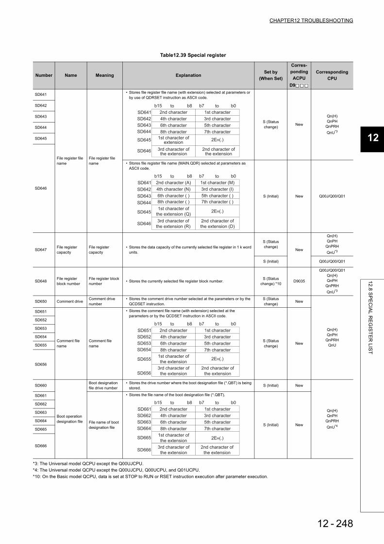
CHAPTER12 TROUBLESHOOTING
1
2
3
12
6
7
8
12.8 SP
EC
IAL R
EG
ISTE
R LIS
T
*3: The Universal model QCPU except the Q00UJCPU.*4: The Universal model QCPU except the Q00UJCPU, Q00UCPU, and Q01UCPU.*10: On the Basic model QCPU, data is set at STOP to RUN or RSET instruction execution after parameter execution.
Table12.39 Special register
Number Name Meaning ExplanationSet by
(When Set)
Corres-ponding ACPU
D9
Corresponding CPU
SD641
File register file name
File register file name
• Stores file register file name (with extension) selected at parameters or by use of QDRSET instruction as ASCII code.
S (Status change) New
Qn(H)QnPH
QnPRHQnU*3
SD642
SD643
SD644
SD645
SD646
• Stores file register file name (MAIN.QDR) selected at parameters as ASCII code.
S (Initial) New Q00J/Q00/Q01
SD647 File register capacity
File register capacity
• Stores the data capacity of the currently selected file register in 1 k word units.
S (Status change)
New
Qn(H)QnPH
QnPRHQnU*3
S (Initial) Q00J/Q00/Q01
SD648 File register block number
File register block number • Stores the currently selected file register block number. S (Status
change) *10 D9035
Q00J/Q00/Q01Qn(H)QnPH
QnPRHQnU*3
SD650 Comment driveComment drive number
• Stores the comment drive number selected at the parameters or by the QCDSET instruction.
S (Status change) New
Qn(H)QnPH
QnPRHQnU
SD651
Comment file name
Comment file name
• Stores the comment file name (with extension) selected at the parameters or by the QCDSET instruction in ASCII code.
S (Status change)
New
SD652
SD653
SD654
SD655
SD656
SD660
Boot operation designation file
Boot designation file drive number
• Stores the drive number where the boot designation file (*.QBT) is being stored. S (Initial) New
Qn(H)QnPH
QnPRHQnU*4
SD661
File name of boot designation file
• Stores the file name of the boot designation file (*.QBT).
S (Initial) New
SD662
SD663
SD664
SD665
SD666
SD641
SD642
SD643
SD644
SD645
SD646
b15 to b8 b7 to b0
2nd character 1st character
4th character 3rd character
6th character 5th character
8th character 7th character
2EH(.)
2nd character of the extension
1st character of extension
3rd character of the extension
SD641
SD642
SD643
SD644
SD645
SD646
b15 to b8 b7 to b0
2nd character (A) 1st character (M)
4th character (N) 3rd character (I)
6th character ( ) 5th character ( )
8th character ( ) 7th character ( )
2EH(.)
2nd character of
the extension (D)
1st character of
the extension (Q)
3rd character of
the extension (R)
SD651
SD652
SD653
SD654
SD655
SD656
b15 to b8 b7 to b0
2nd character 1st character
4th character 3rd character
6th character 5th character
8th character 7th character
2EH(.)
2nd character of
the extension
1st character of
the extension
3rd character of
the extension
SD661
SD662
SD663
SD664
SD665
SD666
b15 to b8 b7 to b0
2nd character 1st character
4th character 3rd character
6th character 5th character
8th character 7th character
2EH(.)
2nd character of
the extension
1st character of
the extension
3rd character of
the extension
12 - 248

Table12.39 Special register
Number Name Meaning ExplanationSet by
(When Set)
Corres-ponding
ACPU D9
Corresponding CPU
SD670Parameter enable drive information
Parameter enable drive No.
• Stores information of parameter storage destination drive which is enabled. 0: Drive 0 (Program memory) 1: Drive 1 (SRAM card) 2: Drive 2 (Flash card/ATA card) 4: Drive 4 (Standard ROM)
(Only drive 0 and drive 4 are valid in the Q00UJCPU, Q00UCPU, and Q01UCPU.)
S (Initial) New
QnU
SD671Status of latch data backup function
Status display
Indicates the status of the latch data backup function.
• "2 Restore ready completion" is a status immediately after restoring data."3 Backup execution wait" is a status after turning power supply ON from OFF at "2 Restore ready completion".
S (Status change)
New
SD672
Backup information
Backup time (Year and month)
• Stores the last 2 digits of year and month when backup is performed in 2-digit BCD code.
S (At write) New
SD673 Backup time (Day and hour)
• Stores the day and hour when backup is performed in 2-digit BCD code.
SD674Backup time (Minute and second)
• Stores the minute and second when backup is performed in 2-digit BCD code.
SD675 Backup time (Year and day of week)
• Stores the first 2 digits of year and day of week when backup is performed in BCD code.
Presence/
absence of
backup data
0 No backup data Absent Restoring not executed
1Restore ready
completion
Present
Restoring executed when
turning power supply
ON from OFF the
following time
2Restore execution
completion Restoring not executed
3 Backup execution wait Restoring not executed
4Restore repeated
execution ready
completion
Restoring executed
when turning power
supply ON from OFF
StatusRestore operation at
turning power supply
ON from OFF
b15 b12to b11 b8to b7 b4to b3 b0to Example:
July, 1993
9307H
Year Month
b15 b12to b11 b8to b7 b4to b3 b0to
Day Hour
Example:
31st, 10 a.m.
3110H
b15 b12to b11 b8to b7 b4to b3 b0to Example:
35 min., 48 sec.
3548H
SecondSecondMinute
b15 b12to b11 b8to b7 b4to b3 b0to
0
1
2
3
4
5
6
Example:
1993, Friday1905H
Higher digits of year (0 to 99)Sunday
Saturday
Friday
Thursday
Wednesday
Tuesday
Monday
Day of the week
12 - 249

CHAPTER12 TROUBLESHOOTING
1
2
3
12
6
7
8
12.8 SP
EC
IAL R
EG
ISTE
R LIS
T
SD676
Backup data restration information
Restore time (Year and month)
• Stores the last 2 digits of year and month when data is restored in 2-digit BCD code.
S (Initial) New
QnU
SD677Restore time (Day and time)
• Stores the day and time when data is restored in 2-digit BCD code.
SD678Restore time (Minute and second)
• Stores the minute and second when data is restored in 2-digit BCD code.
SD679Restore time (Year and day of week)
• Stores the first 2 digits of year and day of week when data is restored in BCD code.
SD681Program memory write (transfer) status
Write (transfer) status display (percentage)
Displays the status of writing (transferring) the program memory (flash ROM) in percentage. (0 to 100%) "0" is set when the write direction is set. S (At write) New
SD682
Programmemory writecount index
Write count indexup to present
• Stores the index value for the number of write operations to the program memory (flash ROM) up to the present in BIN 32-bit value.When the index value exceeds 100 thousand times, "FLASH ROM ERROR" (error code: 1610) occurs. (The index value is calculated even when exceeding 100 thousand times.)
Note) The write count does not equal to the index value.(Since a flash ROM write life is prolonged by the system, 1 is added to the write count index when writing is performed twice or so.).
S (At write) NewSD683
SD686Standard ROM write (transfer) status
Write (transfer) status display (per-centage)
Displays the status of writing (transferring) the standard ROM (flash ROM) in percentage. (0 to 100%) "0" is set when the write direction is set. S (At write) New
SD687
Standard ROM write count index
Write count index up to present
• Stores the index value for the number of write operations to the standard ROM (flash ROM) up to the present in BIN 32-bit value.When the index value exceeds 100 thousand times, "FLASH ROM ERROR" (error code: 1610) occurs. (The index value is calculated even when exceeding 100 thousand times.)
Note) The write count does not equal to the index value. (Since a flash ROM write life is prolonged by the system, 1 is added to the write count index when the total write capacity after the previous count up reaches about 1M byte.)
S (At write) NewSD688
SD689 Backup error factor
Backup error factor
Stores the factor of the error that occurred in the backup.0H : No error100H: Memory card not inserted200H: Size of backup target data exceeded300H: Memory card write inhibit setting400H: Memory card write error500H: Backup target data read error (from program memory)503H: Backup target data read error (from standard RAM)504H: Backup target data read error (from standard ROM)510H: Backup target data read error (from system data)
S (Backup error occurrence)
New
QnU*1
SD690 Backup status Backup status
Stores the current backup status.0 : Before backup start1 : Backup start prepared2 : Backup start preparation completed3 : Backup in execution4 : Backup completedFF: Backup error
S (Status change) New
*1: The module whose first 5 digits of serial No. is "10102" or later. (Except the Q00UJCPU, Q00UCPU, and Q01UCPU)
Number Name Meaning ExplanationSet by
(When Set)
Corres-ponding ACPU
D9
Corresponding CPU
b15 b12to b11 b8to b7 b4to b3 b0to Example:
July, 1993
9307H
Year Month
b15 b12to b11 b8to b7 b4to b3 b0to
Day Hour
Example:
31st, 10 a.m.
3110H
b15 b12to b11 b8to b7 b4to b3 b0to Example:
35 min., 48 sec.
3548H
SecondSecondMinute
b15 b12to b11 b8to b7 b4to b3 b0to
0
1
2
3
4
5
6
Example:
1993, Friday1905H
Higher digits of year (0 to 99)Sunday
Saturday
Friday
Thursday
Wednesday
Tuesday
Monday
Day of the week
12 - 250

SD691 Backup execution status
Backup execution status display (Percentage)
• Displays the execution status of data backup to the memory card in percentage (0 to 100%).
• "0" is set when the backup starts.
S (Status change) New
QnU*1
SD692Restoration error factor
Factor of error occurred in the restoration
Stores the factor of an error that occurred in the restoration.Each error factor is as follows:800H: The CPU module model name is not matched.801H: The file password is set only for the restoration destination data or is
not matched.810H: The verified backup data file is not matched or the backup data read
failed.
S (Error occurrence) New
SD693 Restoration status
Current restoration status
Stores the current restoration execution status.Each error factor is as follows:0 : Before restoration start1 : Restoration in execution2 : Restoration completedFF: Restoration errorSets "0" (Before restoring), however, when the restoration is completed only during the automatic restoration.
S (Status change)
New
SD694 Restoration execution status
Restoration execution status display (Percentage)
• Displays the execution status of restoration to the CPU module in percentage (0 to 100%).
• "0" is set before the restoration.Sets "0" (Before restoring), however, when the restoration is completed only during the automatic restoration.
S (Status change) New
SD695
Specification of writing to stan-dard ROM instruction count
Specification of writing to standard ROM instruction count
• Specifies the maximum number of executions of the writing to standard ROM instruction (SP.DEVST) to write to the standard ROM per day.
• When the number of executions of the writing to standard ROM instruction exceeds the number of times set by SD695, “OPERATION ERROR” (error code: 4113) occurs.
• The setting range for SD695 is 1 to 32767. If 0 or value outside the range is set, “OPERATION ERROR” (error code: 4113) occurs at execution of the writing to standard ROM instruction.
U New QnU
SD696 Available memory in memory card
Available memory in memory card
Stores the available memory in memory card. (Stores the value in 32-bit binary.)
S (Backup in operation) New QnU*1
SD697
SD698 Backup data capacity
Backup data capacity Stores the backup data capacity. (Stores the value in 32-bit binary.)
SD699
*1: The module whose first 5 digits of serial No. is "10102" or later. (Except the Q00UJCPU, Q00UCPU, and Q01UCPU)
Number Name Meaning ExplanationSet by
(When Set)
Corres-ponding
ACPU D9
Corresponding CPU
12 - 251

CHAPTER12 TROUBLESHOOTING
1
2
3
12
6
7
8
12.8 SP
EC
IAL R
EG
ISTE
R LIS
T
(6) Instruction-Related RegistersTable12.40 Special register
Number Name Meaning ExplanationSet by
(When Set)
Corres-ponding ACPU
D9
Corresponding CPU
SD705Mask pattern Mask pattern
• During block operations, turning SM705 ON makes it possible to use the mask pattern being stored at SD705 (or at SD705 and SD706 if double words are being used) to operate on all data in the block with the masked values.
U New
Q00J/Q00/Q01Qn(H)QnPH
QnPRHSD706
SD715
IMASK instruction mask pattern
Mask pattern
• Patterns masked by use of the IMASK instruction are stored in the following manner:
S (During execution) New
QCPU
SD716
SD717
SD718Accumulator Accumulator • For use as replacement for accumulators used in A series programs. S/U New
SD719
SD720
Program No. designation for PLOADP instruction
Program No. designation for PLOADP instruction
Stores the program number of the program to be loaded by the PLOADP instruction when designated.Designation range: 1 to 124
U New Qn(H)QnPH
SD738
Message storage
Message storage
• Stores the message designated by the MSG instruction.
S (During execution)
New QCPU
SD739
SD740
SD741
SD742
SD743
SD744
SD745
SD746
SD747
SD748
SD749
SD750
SD751
SD752
SD753
SD754
SD755
SD756
SD757
SD758
SD759
SD760
SD761
SD762
SD763
SD764
SD765
SD766
SD767
SD768
SD769
SD715
SD716
SD717
l15 l1 l0
l31
l47
l17
l33
l16
l32
b15 b0b1
to
to
to
SD738
SD739
SD740
SD741
SD742
SD743
b15 to b8 b7 to b0
SD744
SD745
SD746
SD747
SD748
SD749
SD750
SD751
SD752
SD753
SD754
SD755
SD756
SD757
SD758
SD759
SD760
SD761
SD762
SD763
SD764
SD765
SD766
SD767
SD768
SD769
2nd character 1st character
4th character 3rd character
6th character 5th character
8th character 7th character
10th character 9th character
12th character 11th character
14th character 13th character
16th character 15th character
18th character 17th character
20th character 19th character
22nd character 21st character
24th character 23rd character
26th character 25th character
28th character 27th character
30th character 29th character
32nd character 31st character
34th character 33rd character
36th character 35th character
38th character 37th character
40th character 39th character
42nd character 41st character
44th character 43rd character
46th character 45th character
48th character 47th character
50th character 49th character
52nd character 51st character
54th character 53rd character
56th character 55th character
58th character 57th character
60th character 59th character
62nd character 61st character
64th character 63rd character
12 - 252

*9: Function version is B or later.*11: The module whose first 5 digits of serial No. is "04012" or later.*12: The module whose first 5 digits of serial No. is "07032" or later.*13: The module whose first 5 digits of serial No. is "09012" or later.
Table12.40 Special register
Number Name Meaning ExplanationSet by
(When Set)
Corres-ponding
ACPU D9
Corresponding CPU
SD774 to SD775
PID limit setting(for complete derivative)
0: With limit1: Without limit
• Specify the limit of each PID loop as shown below.
U NewQn(H)
QnPRHQnU
SD774PID limit setting(for complete derivative)
0: With limit1: Without limit
• Specify the limit of each PID loop as shown below.
U New Q00J/Q00/Q01*9
SD778
Refresh processing selection when the COM/CCOM instruction is executed
b0 to b14:0: Do not refresh1: Refreshb15 bit0: Communication
with CPU module is executed
1: Communication withCPU module is nonexecuted
• Selects whether or not the data is refreshed when the COM instruction is executed.
• Designation of SD778 is made valid when SM775 turns ON.
• Refresh between multiple CPUs by COM instruction is performed under the following occasion.Receiving operation from other device: b4 of SD778(refresh in the CPU shared memory) is turned to 1.Sending operation from host CPU : b15 of SD778(communication with peripheral device is executed/nonexecuted) is turned to 0.
U NewQ00J/Q00/Q01*9
Qn(H)*11
• Selects whether or not the data is refreshed when the COM instruction is executed.
• Designation of SD778 is made valid when SM775 turns ON.
• Refresh between multiple CPUs by COM instruction is performed under the following occasion.Receiving operation from other device: b4 of SD778(refresh in the CPU shared memory) is turned to 1.Sending operation from host CPU : b15 of SD778(communication with peripheral device is executed/nonexecuted) is turned to 0.
• When b2 (refresh of the CC-Link IE controller network and MELSECNET/H) of SD778 is 1, the CC-Link IE controller network and MELSECNET/H perform refresh.Therefore, if there are many refresh points, processing time for the COM instruction will be extended.
U NewQn(H)*13
QnPH*12
QnPRH
SD774
SD775
b15
to
to
Loop2
Loop18
Loop1
Loop17
b1 b0
Loop16
Loop32
SD774
b15
to
toto b1 b0b7b8
Loop8 Loop2 Loop1
b0b1b2b3b4b5b14b15
0
to
I/O refresh
CC-Link refresh
MELSECNET/H
refresh
Automatic refresh of
intelligent function
modules
Execution/non-
execution of
communication with
CPU module
Automatic refresh of
CPU shared memory
(Fixed to "0" for
Redundant CPU)
0/1 0/1 0/1 0/1 0/10/1SD778
b0b1b2b3b4b5b6b14b15
0
to
I/O refresh
CC-Link refresh
CC-Link IE controller
network or
0/1 0/10/1 0/1 0/1 0/10/1SD778
Automatic refresh of
intelligent function
modules
Execution/non-
execution of
communication with
CPU module
Reading input/output
from group outside
multiple CPU system
Auto refresh using the
multiple CPU high speed
transmission area of
multiple CPU system
MELSECNET/H refresh
12 - 253

CHAPTER12 TROUBLESHOOTING
1
2
3
12
6
7
8
12.8 SP
EC
IAL R
EG
ISTE
R LIS
T
*9: Function version is B or later.*13: The module whose first 5 digits of serial No. is "09012" or later.
Table12.40 Special register
Number Name Meaning ExplanationSet by
(When Set)
Corres-ponding ACPU
D9
Corresponding CPU
SD778
Refresh processing selection when the COM/CCOM instruction is executed
b0 to b14:0: Do not refresh1: Refreshb15 bit0: communication
with peripheral device is executed
1: communication with peripheral device is nonexecuted
• Selects whether or not the data is refreshed when the COM, CCOM instruction is executed.
• Designation of SD778 is made valid when SM775 turns ON.
U New QnU
SD781 to SD793
Mask pattern of IMASK instruction
Mask pattern
• Stores the mask patterns masked by the IMASK instruction as follows:
(The Q00UJCPU, Q00UCPU, and Q01UCPU cannot use the special registers SD786 to SD793.)
S (During execution) New
Qn(H)QnPH
QnPRHQnU
SD781 to SD785
Mask pattern of IMASK instruction
Mask pattern
• Stores the mask patterns masked by the IMASK instruction as follows:
S (During execution) New Q00J/Q00/Q01
SD794 to SD795
PID limit setting (for incomplete derivative)
0: With limit1: Without limit
• Specify the limit of each PID loop as shown below.
U NewQn(H)*13
QnPRHQnU
SD794PID limit setting (for incomplete derivative)
0: With limit 1: Without limit
• Specify the limit of each PID loop as shown below.
U New Q00J/Q00/Q01*9
b0b1b2b3b4b5b6b14b15
0
to
I/O refresh
CC-Link refresh
Refresh of
MELSECNET/H and
CC-Link IE controller
network
0/1 0/10/1 0/1 0/1 0/10/1SD778
Automatic refresh of
intelligent function
modules
Execution/non-
execution of
communication with
CPU module
Auto refresh using
QCPU standard area of
multiple CPU system and
reading input/output from
group outside.
Auto refresh using the
multiple CPU high speed
transmission area of
multiple CPU system
SD781
SD782
SD793
l63 l49 l48
l79
l255
l65
l241
l64
l240
b15 b0b1
to
to
to
to
to to
SD781
SD782
SD785
l63 l49 l48
l79
l127
l65
l113
l64
l112
b15 b0b1
to
to
to
SD794
SD795
b15
to
to
b1 b0
Loop16
Loop32
Loop2
Loop18
Loop1
Loop17
SD794
b15
to
to b1 b0b7b8
Loop8 Loop2 Loop1
12 - 254

*14: The Universal model QCPU except the Q00UJCPU, Q00UCPU, Q01UCPU, and Q02UCPU.*15: The range is from 1 to 9 for the Q03UDCPU, Q04UDCPU, and Q06UDHCP whose first 5 digits of serial number is "10012" or earlier.
(Default: 2 Or when setting other than 1 to 9, the register operates as 9).
Table12.40 Special register
Number Name Meaning ExplanationSet by
(When Set)
Corres-ponding
ACPU D9
Corresponding CPU
SD796
Maximum number of blocks used for the multiple CPU high-speed transmission dedicated instruction setting (for CPU No.1)
Maximum number of blocks range for dedicated instructions Range: 1 to 7 (Default: 2 Or when setting other than 1 to 7, the register operates as 7).
• Specifies the maximum number of blocks used for the multiple CPU high-speed transmission dedicated instruction (target CPU=CPU No.1). When the dedicated instruction of Multiple CPU transmission is executed to the CPU No.1, and the number of empty blocks of the dedicated instruction transmission area is less than the setting value of this register, SM796 is turned ON, which is used as the interlock signal for consecutive execution of the dedicated instruction of Multiple CPU transmission.
U (At 1 scan after RUN) New
QnU*14*15
SD797
Maximum number of blocks used for the multiple CPU high-speed transmission dedicated instruction setting (for CPU No.2)
• Specifies the maximum number of blocks used for the multiple CPU high-speed transmission dedicated instruction (target CPU=CPU No.2). When the dedicated instruction of Multiple CPU transmission is executed to the CPU No.2, and the number of empty blocks of the dedicated instruction transmission area is less than the setting value of this register, SM797 is turned ON, which is used as the interlock signal for consecutive execution of the dedicated instruction of Multiple CPU transmission.
U (At 1 scan after RUN) New
SD798
Maximum number of blocks used for the multiple CPU high-speed transmission dedicated instruction setting (for CPU No.3)
• Specifies the maximum number of blocks used for the multiple CPU high-speed transmission dedicated instruction (target CPU=CPU No.3). When the dedicated instruction of Multiple CPU transmission is executed to the CPU No.3, and the number of empty blocks of the dedicated instruction transmission area is less than the setting value of this register, SM798 is turned ON, which is used as the interlock signal for consecutive execution of the dedicated instruction of Multiple CPU transmission.
U (At 1 scan after RUN) New
SD799
Maximum number of blocks used for the multiple CPU high-speed transmission dedicated instruction setting (for CPU No.4)
• Specifies the maximum number of blocks used for the multiple CPU high-speed transmission dedicated instruction (target CPU=CPU No.4). When the dedicated instruction of Multiple CPU transmission is executed to the CPU No.4, and the number of empty blocks of the dedicated instruction transmission area is less than the setting value of this register, SM799 is turned ON, which is used as the interlock signal for consecutive execution of the dedicated instruction of Multiple CPU transmission.
U (At 1 scan after RUN) New
12 - 255
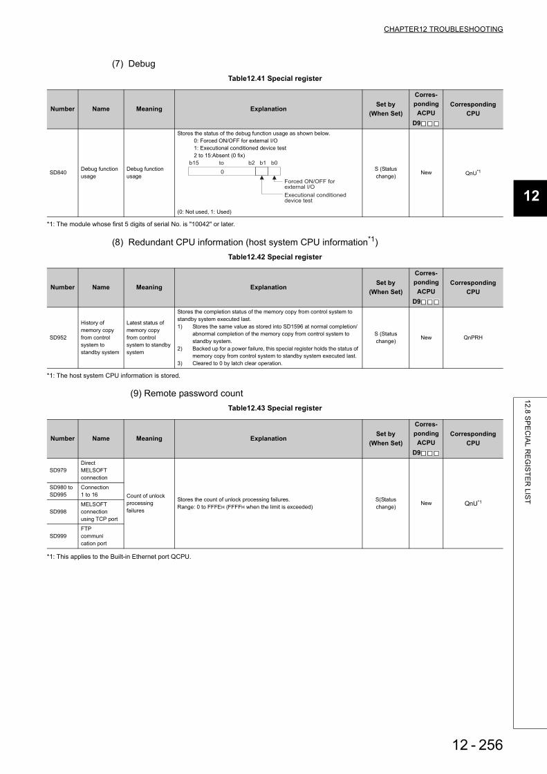
CHAPTER12 TROUBLESHOOTING
1
2
3
12
6
7
8
12.8 SP
EC
IAL R
EG
ISTE
R LIS
T
(7) Debug
*1: The module whose first 5 digits of serial No. is "10042" or later.
(8) Redundant CPU information (host system CPU information*1)
*1: The host system CPU information is stored.
(9) Remote password count
*1: This applies to the Built-in Ethernet port QCPU.
Table12.41 Special register
Number Name Meaning ExplanationSet by
(When Set)
Corres-ponding ACPU
D9
Corresponding CPU
SD840 Debug function usage
Debug function usage
Stores the status of the debug function usage as shown below. 0: Forced ON/OFF for external I/O 1: Executional conditioned device test 2 to 15:Absent (0 fix)
(0: Not used, 1: Used)
S (Status change)
New QnU*1
Table12.42 Special register
Number Name Meaning ExplanationSet by
(When Set)
Corres-ponding ACPU
D9
Corresponding CPU
SD952
History of memory copy from control system to standby system
Latest status of memory copy from control system to standby system
Stores the completion status of the memory copy from control system to standby system executed last.1) Stores the same value as stored into SD1596 at normal completion/
abnormal completion of the memory copy from control system to standby system.
2) Backed up for a power failure, this special register holds the status of memory copy from control system to standby system executed last.
3) Cleared to 0 by latch clear operation.
S (Status change) New QnPRH
Table12.43 Special register
Number Name Meaning ExplanationSet by
(When Set)
Corres-ponding ACPU
D9
Corresponding CPU
SD979Direct MELSOFTconnection
Count of unlock processing failures
Stores the count of unlock processing failures.Range: 0 to FFFEH (FFFFH when the limit is exceeded)
S(Status change)
New QnU*1
SD980 to SD995
Connection 1 to 16
SD998MELSOFTconnection using TCP port
SD999FTPcommunication port
0
b15 b2to b1 b0
Executional conditioned device test
Forced ON/OFF for external I/O
12 - 256

(10) A to Q conversionACPU special registers D9000 to D9255 correspond to Q special registers SD1000 to SD1255 after A to Q/QnA conversion.(However, the Basic model QCPU and Redundant CPU do not support the A to Q conversion.)These special registers are all set by the system, and cannot be set by the user program.To set data by the user program, correct the program for use of the QCPU special registers.However, some of SD1200 to SD1255 (corresponding to D9200 to 9255 before conversion) can be set by the user program if they could be set by the user program before conversion.For details on the ACPU special registers, refer to the user's manual for the corresponding CPU, and MELSECNET or MELSECNET/B Data Link System Reference Manuals.
Check "Use special relay/special register from SM/SD1000" for "A-PLC" on the PLC system tab of PLC parameter in GX Developer when the converted special registers are used with the High Performance model QCPU, Process CPU, and Universal model QCPU. When not using the converted special registers, uncheck "Use special relay/special registers from SM/SD1000" to save the time taken for processing special registers.
RemarkSupplemental explanation on "Special Register for Modification" column
For the device numbers for which a special register for modification is specified, modify it to the special register for QCPU.
For the device numbers for which is specified, special register after conversion can be used.
Device numbers for which is specified do not function for QCPU.
12 - 257

CHAPTER12 TROUBLESHOOTING
1
2
3
12
6
7
8
12.8 SP
EC
IAL R
EG
ISTE
R LIS
T
*1: The relevant modules are as follows:• The Universal model QCPU whose serial number (first five digits) is "10102" or later.• Q00UJCPU, Q00UCPU, Q01UCPU
Table12.44 Special register
ACPU Special Register
Special Register
after Conversion
Special Register for Modification
Name Meaning DetailsCorresponding
CPU
D9000 SD1000 – Fuse blown Number of module with blown fuse
• When fuse blown modules are detected, the first I/O number of the lowest number of the detected modules is stored in hexadecimal.(Example: When fuses of Y50 to 6F output modules have blown, "50" is stored in hexadecimal) To monitor the number by peripheral devices, perform monitor operation given in hexadecimal. (Cleared when all contents of SD1100 to SD1107 are reset to 0.)
• Fuse blow check is executed also to the output modules of remote I/O stations.
Qn(H)QnPHQnU*1
D9001 SD1001 – Fuse blown Number of module with blown fuse
• Stores the module numbers corresponding to setting switch numbers or base slot numbers when fuse blow occurred.
• For the remote I/O station, the value of (module I/O No./10H) + 1 is stored.
Qn(H)QnPH
D9002 SD1002 – I/O module verify error
I/O module verify error module number
• If I/O modules, of which data are different from data entered, are detected when the power is turned on, the first I/O number of the lowest number unit among the detected units is stored in hexadecimal. (Storing method is the same as that of SD1000.) To monitor the number by peripheral devices, perform monitor operation given in hexadecimal. (Cleared when all contents of SD1116 to SD1123 are reset to 0.)
• I/O module verify check is executed also to the modules of remote I/O terminals.
Qn(H)QnPHQnU*1
D9005 SD1005 – AC DOWN counter
Number of times for AC DOWN
• When the AC power supply module is used, 1 is added at occurrence of an instantaneous power failure of within 20ms. (The value is stored in BIN code.) It is reset when the power supply is switched from OFF to ON.
Qn(H)QnPHQnU*1
• When the DC power supply module is used, 1 is added at occurrence of an instantaneous power failure of within 10ms. (The value is stored in BIN code.) It is reset when the power supply is switched from OFF to ON.
Qn(H)QnPHQnU*1
D9008 SD1008 SD0 Self-diagnostic error
Self-diagnostic error number
• When error is found as a result of self-diagnosis, error number is stored in BIN code.
Qn(H)QnPHQnU*1
AJ02 I/O module Extension base unit
Setting switch
Stored data
Base unit slot No.
Stored data
0
1
2
3
4
5
6
7
0
1
2
3
4
5
6
7
0
1
2
3
4
5
6
7
12 - 258

*1: The relevant modules are as follows:• The Universal model QCPU whose serial number (first five digits) is "10102" or later.• Q00UJCPU, Q00UCPU, Q01UCPU
Table12.44 Special register
ACPU Special Register
Special Register
after Conversion
Special Register for Modification
Name Meaning DetailsCorresponding
CPU
D9009 SD1009 SD62 Annunciator detection
F number at which external failure has occurred
• When one of F0 to 2047 is turned on by OUT F or SET F instruction, the F number, which has been detected earliest among the F numbers which have turned on, is stored in BIN code.
• SD1009 can be cleared by RST F or LEDR instruction. If another F number has been detected, the clearing of SD1009 causes the next number to be stored in SD1009.
Qn(H)QnPHQnU*1
D9010 SD1010 Error stepStep number at which operation error has occurred.
• When operation error has occurred during execution of application instruction, the step number, at which the error has occurred, is stored in BIN code. Thereafter, each time operation error occurs, the contents of SD1010 are renewed.
Qn(H)QnPHD9011 SD1011 Error step
Step number at which operation error has occurred.
• When operation error has occurred during execution of application instruction, the step number, at which the error has occurred, is stored in BIN code. Since the step number is stored into SD1011 when SM1011 turns from OFF to ON, the data of SD1011 is not updated unless SM1011 is cleared by a user program.
D9014 SD1014 I/O control mode
I/O control mode number
• The I/O control mode set is returned in any of the following numbers:0: Both input and output in direct mode1: Input in refresh mode, output in direct mode3: Both input and output in refresh mode
D9015 SD1015 SD203 Operating status of CPU
Operating status of CPU
• The operation status of CPU as shown below are stored in SD1015.
*1: When the CPU mdoule is in RUN mode and SM1040 is off, the CPU module remains in RUN mode if changed to PAUSE mode.
Qn(H)QnPHQnU*1
b15 b12to b11 b8to b7 b4to b3 b0to
0
1
2
RUN
PAUSE
STOP
Remote RUN/STOP
by parameter setting
0
1
2
RUN
PAUSE
STOP
Remote RUN/STOP
by computer0
1
2
RUN
PAUSE
3 STEP RUN
STOP
CPU key switch
0
1
Except below
Instruction execution
Status in program
Remains the same in
remote RUN/STOP
mode.
STOP
11
1
12 - 259

CHAPTER12 TROUBLESHOOTING
1
2
3
12
6
7
8
12.8 SP
EC
IAL R
EG
ISTE
R LIS
T
*1: The relevant modules are as follows:• The Universal model QCPU whose serial number (first five digits) is "10102" or later.• Q00UJCPU, Q00UCPU, Q01UCPU
Table12.44 Special register
ACPU Special Register
Special Register
after Conversion
Special Register for Modification
Name Meaning DetailsCorresponding
CPU
D9016 SD1016Program number
0: Main program (ROM)
1: Main program (RAM)
2: Subprogram 1 (RAM)
3: Subprogram 2 (RAM)
4: Subprogram 3 (RAM)
5: Subprogram 1 (ROM)
6: Subprogram 2 (ROM)
7: Subprogram 3 (ROM)
8: Main program (E2PROM)
9: Subprogram 1 (E2PROM)
A: Subprogram 2 (E2PROM)
B: Subprogram 3 (E2PROM)
• Indicates which sequence program is run presently. One value of 0 to B is stored in BIN code.
Qn(H)QnPH
D9017 SD1017 SD524 Scan time Minimum scan time (10 ms units)
• If scan time is smaller than the content of SD1017, the value is newly stored at each END. Namely, the minimum value of scan time is stored into SD1017 in BIN code.
Qn(H)QnPHQnU*1
D9018 SD1018 SD520 Scan timeScan time (10 ms units)
• At every END, the scan time is stored in BIN code and always rewritten.
D9019 SD1019 SD526 Scan time Maximum scan time (10 ms units)
• If scan time is larger than the content of SD1019, the value is newly stored at each END. Namely, the maximum value of scan time is stored into SD1019 in BIN code.
D9020 SD1020 Constant scanConstant scan time (User sets in 10 ms units)
• Sets the interval between consecutive program starts in multiples of 10 ms. 0 : No setting 1 to 200 : Set. Program is executed at intervals of (set
value) 10 ms.
Qn(H)QnPH
D9021 SD1021 – Scan timeScan time(1 ms units)
• At every END, the scan time is stored in BIN code and always rewritten.
Qn(H)QnPHQnU*1
D9022 SD1022 SD4121 second counter Count in units of 1s.
• When the PC CPU starts running, it starts counting 1 every second.
• It starts counting up from 0 to 32767, then down to -32768 and then again up to 0. Counting repeats this routine.
D9025 SD1025 – Clock data Clock data(year, month)
• The year (last two digits) and month are stored as BCD code as shown below.
D9026 SD1026 – Clock data Clock data(day, hour)
• The day and hour are stored as BCD code as shown below.
D9027 SD1027 – Clock data Clock data(minute, second)
• The minute and second are stored as BCD code as shown below.
b15 b12to b11 b8to b7 b4to b3 b0to Example:
1987, July
H8707
Year Month
b15 b12to b11 b8to b7 b4to b3 b0to Example:
31st, 10 a.m.H3110
Day Hour
b15 b12to b11 b8to b7 b4to b3 b0to Example:
35 min, 48 sec.H3548
Minute Second
12 - 260

*1: The relevant modules are as follows:• The Universal model QCPU whose serial number (first five digits) is "10102" or later.• Q00UJCPU, Q00UCPU, Q01UCPU
Table12.44 Special register
ACPU Special Register
Special Register
after Conversion
Special Register for Modification
Name Meaning DetailsCorresponding
CPU
D9028 SD1028 – Clock data Clock data(day of week)
• The day of the week is stored as BCD code as shown below.
Qn(H)QnPHQnU*1
D9035 SD1035 SD648Extension file register Use block No.
• Stores the block No. of the extension file register being used in BCD code.
D9036 SD1036
Extension file registerfor designation of device number
Device number when individual devices from extension file register are directly accessed
• Designate the device number for the extension file register for direct read and write in 2 words at SD1036 and SD1037 in BIN data. Use consecutive numbers beginning with R0 of block No. 1 to designate device numbers.
Qn(H)QnPH
D9037 SD1037
D9038 SD1038 SD207
LED display priority ranking
Priorities 1 to 4
• Sets priority of ERROR LEDs which illuminate (or flicker) to indicate errors with error code numbers.
• Configuration of the priority setting areas is as shown below.
• For details, refer to the applicable CPUs User's Manual and the ACPU Programming manual (Fundamentals).
D9039 SD1039 SD208 Priorities 5 to 7
D9044 SD1044For sampling trace
Step or time during sampling trace
• Turned on/off with a peripheral device.When STRA or STRAR instruction is executed, the value stored in SD1044 is used as the sampling trace condition.At scanning--------0At time--------------Time (10 msec unit)The value is stored into SD1044 in BIN code.
D9049 SD1049 Work area for SFC
Block number of extension file register
• Stores the block number of the expansion file register which is used as the work area for the execution of a SFC program in a binary value.
• Stores "0" if an empty area of 16K bytes or smaller, which cannot be expansion file register No. 1, is used or if SM320 is OFF.
D9050 SD1050 SFC program error number
Error code generated by SFC program
• Stores error code of errors occurred in the SFC program in BIN code.0 : No error80: SFC program parameter error81: SFC code error82: Number of steps of simultaneous execution exceeded83: Block start error84: SFC program operation error
D9051 SD1051 Error block Block number where error occurred
• Stores the block number in which an error occurred in the SFC program in BIN code.In the case of error 83 the starting block number is stored.
D9052 SD1052 Error step Step number where error occurred
• Stores the step number, where error code 84 occurred in an SFC program, in BIN value.
• Stores "0" when error code 80, 81 or 82 occurred.• Stores the block stating step number when error code 83 occurs.
b15 b12to b11 b8to b7 b4to b3 b0to
0
1
2
3
4
5
6
H0005
Sunday
Saturday
Friday
Thursday
Wednesday
Tuesday
Monday
Day of the week
Example:
Friday
Always set "0"
Device No. (BIN data)
SD1037,SD1036
0to
16383
16384
to
to
Extension file register
Block No.1 area
Block No.2 area
SD207
SD208
b15 b12 b11 b8 b7 b4 b3 b0to to to to
Priority 4 Priority 3
Priority 7 Priority 6
Priority 2
Priority 5
Priority 1
12 - 261

CHAPTER12 TROUBLESHOOTING
1
2
3
12
6
7
8
12.8 SP
EC
IAL R
EG
ISTE
R LIS
T
*1: The relevant modules are as follows:• The Universal model QCPU whose serial number (first five digits) is "10102" or later.• Q00UJCPU, Q00UCPU, Q01UCPU
Table12.44 Special register
ACPU Special Register
Special Register
after Conversion
Special Register for Modification
Name Meaning DetailsCorresponding
CPU
D9053 SD1053 Error transitionTransition condition number where error occurred
• Stores the transition condition number, where error code 84 occurred in an SFC program, in BIN value. Stores "0" when error code 80, 81, 82 or 83 occurred.
Qn(H)QnPH
D9054 SD1054 Error sequence step
Sequence step number where error occurred
• Stores the sequence step number of transfer condition and operation output in which error 84 occurred in the SFC program in BIN code.
D9055 SD1055 SD812Status latch execution step number
Status latch step
• Stores the step number when status latch is executed.• Stores the step number in a binary value if status latch is executed
in a main sequence program.• Stores the block number and the step number if status latch is
executed in a SFC program.
D9072 SD1072PLC communication check
Data check of serial communication module
• In the self-loopback test of the serial communication module, the serial communication module writes/reads data automatically to make communication checks.
Qn(H)QnPH
D9085 SD1085Register for setting time check value
1 s to 65535 s
• Sets the time check time of the data link instructions (ZNRD, ZNWR) for the MELSECNET/10.
• Setting range : 1 s to 65535 s (1 to 65535)• Setting unit : 1 s• Default value : 10 s (If 0 has been set, default 10 s is applied) Qn(H)
QnPH
D9090 SD1090
Number of special functions modules over
Number of special functions modules over
• For details, refer to the manual of each microcomputer program package.
D9091 SD1091 Detailed error code
Self-diagnosis detailed error code
• Stores the detail code of cause of an instruction error.Qn(H)QnPHQnU*1
D9094 SD1094 SD251
Head I/O number of I/O module to be replaced
Head I/O number of I/O module to be replaced
• Stores the first two digits of the head I/O number of the I/O module, which will be dismounted/mounted online (with power on), in BIN value.Example) Input module X2F0 H2F
Qn(H)QnPH
D9095 SD1095 SD200 DIP switch information
DIP switch information
• The DIP switch information of the CPU module is stored in the following format.0: OFF1: ON
Qn(H)QnPH
Lower 8 bitsUpper 8 bits
Block No.
(BIN)
Step No.
(BIN)
SW1
SW2
b0b1b2b3b4b5b15
SW3
SW4
SW5
D9095
to
0
12 - 262

*1: The relevant modules are as follows:• The Universal model QCPU whose serial number (first five digits) is "10102" or later.• Q00UJCPU, Q00UCPU, Q01UCPU
Table12.44 Special register
ACPU Special Register
Special Register
after Conversion
Special Register for Modification
Name Meaning DetailsCorresponding
CPU
D9100 SD1100
– Fuse blown module
Bit pattern in units of 16 points, indicating the modules whose fuses have blown
• Output module numbers (in units of 16 points), of which fuses have blown, are entered in bit pattern. (Preset output module numbers when parameter setting has been performed.)
• Fuse blow check is executed also to the output module of remote I/O station. (If normal status is restored, clear is not performed. Therefore, it is required to perform clear by user program.)
Qn(H)QnPHQnU*1
D9101 SD1101
D9102 SD1102
D9103 SD1103
D9104 SD1104
D9105 SD1105
D9106 SD1106
D9107 SD1107
D9108 SD1108
–Step transfer monitoring timer setting
Timer setting valve and the F number at time out
• Set the value of the step transition monitoring timer and the annunciator number (F number) that will be turned ON when the monitoring timer times out.
• By turning ON any of SM1108 to SM1114, the monitoring timer starts. If the transition condition following a step which corresponds to the timer is not established within set time, set annunciator (F) is turned on.)
Qn(H)QnPH
D9109 SD1109
D9110 SD1110
D9111 SD1111
D9112 SD1112
D9113 SD1113
D9114 SD1114
D9116 SD1116
– I/O module verification error
Bit pattern, in units of 16 points, indicating the modules with verification errors.
• When I/O modules, of which data are different from those entered at power-ON, have been detected, the I/O module numbers (in units of 16 points) are entered in bit pattern. (Preset I/O module numbers set in parmeters when parameter setting has been performed.)
• I/O module verify check is executed also to remote I/O station modules.(If normal status is restored, clear is not performed. Therefore, it is required to perform clear by user program.)
Qn(H)QnPHQnU*1
D9117 SD1117
D9118 SD1118
D9119 SD1119
D9120 SD1120
D9121 SD1121
D9122 SD1122
D9123 SD1123
D9124 SD1124 SD63Number of annuciator detections
Number of annuciator detections
• When one of F0 to 255 (F0 to 2047 for AuA and AnU) is turned on by SET F instruction 1 is added to the contents of SD63. When RST F or LEDR instruction is executed, 1 is subtracted from the contents of SD63.
• Quantity, which has been turned on by SET F instruction is stored into SD63 in BIN code. The value of SD63 is maximum 16.
b15 b14b13b12b11b10 b9 b8 b7 b6 b5 b4 b3 b2 b1 b0
000000001(Y80)
0001(YC0)
000
0000000000000000
000000000000001Y7
B0
1Y7
30
SD1100
SD1101
SD1107
Indicates fuse blow.
b15 b7 b0b8to to
(02 to 255)
F number setting Timer time limit setting
(1 to 255 s:(1 s units))
b15 b14b13b12b11b10 b9 b8 b7 b6 b5 b4 b3 b2 b1 b0
0000000000000
000000000000000
000000000000001
XY7B0
SD1116
SD1117
SD1123
1XY0
1XY190
0
0 0
Indicates an I/O module verify error.
12 - 263

CHAPTER12 TROUBLESHOOTING
1
2
3
12
6
7
8
12.8 SP
EC
IAL R
EG
ISTE
R LIS
T
*1: The relevant modules are as follows:• The Universal model QCPU whose serial number (first five digits) is "10102" or later.• Q00UJCPU, Q00UCPU, Q01UCPU
Table12.44 Special register
ACPU Special Register
Special Register
after Conversion
Special Register for Modification
Name Meaning DetailsCorresponding
CPU
D9125 SD1125 SD64
Annunciator detection number
Annunciator detection number
• When any of F0 to 2047 is turned on by SET F instruction, the annunciator numbers (F numbers) that are turned on in order are registered into SD1125 to SD1132.
• The F number turned off by RST F instruction is erased from any of SD1125 to SD1132, and the F numbers stored after the erased F number are shifted to the preceding registerers.By executing LEDR instruction, the contents of SD1125 to SD1132 are shifted upward by one. When there are 8 annunciator detections, the 9th one is not stored into SD1125 to SD1132 even if detected.
Qn(H)QnPHQnU*1
D9126 SD1126 SD65
D9127 SD1127 SD66
D9128 SD1128 SD67
D9129 SD1129 SD68
D9130 SD1130 SD69
D9131 SD1131 SD70
D9132 SD1132 SD71
0 50 50 50 50 50 50 50 50 50 50 50 99
0
0 50 50 50 50 50 50 50 50 50 50 99
0 25 25 99 99 99 99 99 99 99 99 15
1 2 3 2 3 4 5 6 7 8 8 8
50
0
0 99 15 15 15 15 15 15 15 700 0 0
0 70 70 70 70 70 70 650 0 00 0
0 65 65 65 65 65 380 0 00 0 0
0 38 38 38 38 1100 0 00 0 0 0
0 110 110 110 1510 0 00 0 0 0
0 151 151 2100 0 00 0 0 0
0
0 0
SD1009
SD1124
SD1125
SD1126
SD1127
SD1128
SD1129
SD1130
SD1131
SD1132
SETF50
SETF25
SETF99
RSTF25
SETF15
SETF70
SETF65
SETF38
SETF110
SETF151
SETF210 LEDR
12 - 264

(11) QCPU with built-in Ethernet port
*1: This applies to the Built-in Ethernet port QCPU.
Table12.45 Special register
Number Name Meaning ExplanationSet by
(When Set)
Corres-ponding ACPU
D9
Corresponding CPU
SD1270
Tim
e se
tting
func
tion
Operation result
Stores operationresult.
Stores the operation result of the time setting function. 0: Not executed 1: Success FFFFH: Failure
S (status change)
New QnU*1
SD1271
Execution time
Stores time acquired with time setting function.
Stores years (last two digits of the Christian Era) and monthes by two digits of BCD code.
SD1272
Stores dates and hours acquired with time setting function by two digits of BCD code.
SD1273
Stores minutes and seconds acquired with time setting function by two digits of BCD code.
SD1274
Stores years (first two digits of the Christian Era) and days acquierd with time setting function.
SD1275Required response time
Stores time required for clock time aquisition.
Stores time taken from transmission to SNTP server to clook time setup at CPU.Range: 0 to FFFEH (Unit: ms) FFFFH when the above limit is exceeded.
SD1276
Forced connection invalidation
Specifies forced connection invalidation.
Specify this when a connection is to be invalidated forcibly on the user program. If invalidation is specified for a connection, it stops communication and does not respond. (When a remote password is used and frequent unlock processing errors have occurred on a connection, this is useful for temporarily inhibiting access to the connection.)
0: Valid (default)1: InvalidThis register is to be invalidated if a socket communication is used as an open system.
USD1277
b15 b12to b11 b8to b7 b4to b3 b0to Example:
July, 1993
9307H
Year Month
b15 b12to b11 b8to b7 b4to b3 b0to
Day Hour
Example:
31st, 10 a.m.
3110H
b15 b12to b11 b8to b7 b4to b3 b0to Example:
35 min., 48 sec.
3548H
SecondSecondMinute
b15 b12to b11 b8to b7 b4to b3 b0to
0
1
2
3
4
5
6
Example:
1993, Friday1905H
Higher digits of year (0 to 99)Sunday
Saturday
Friday
Thursday
Wednesday
Tuesday
Monday
Day of the week
b15b14 b0b1
SD1276
Connection 1
Directconnection to
SD1277
MELSOFT communication
FTP communication port
to
b15b14 b13 b12 b4 b3 b2 b1 b0
MELSOFT communication
00 0
to
Connection 16
Connection 15
Connection 2
port (UDP/IP)
port (TCP/IP)
MELSOFT
12 - 265

CHAPTER12 TROUBLESHOOTING
1
2
3
12
6
7
8
12.8 SP
EC
IAL R
EG
ISTE
R LIS
T
*2: The built-in Ethernet port QCPU whose serial number (first five digits) is "11012" or later is targeted.
Table12.46 Special register
Number Name Meaning ExplanationSet by
(When Set)
Corres-ponding
ACPU D9
Corresponding CPU
SD1282Open completion signal
Stores open completion status
Open completion status of connections (whose open system is socket communication) using socket communication functions is stored.All bits corresponding to connections using any communications other than the socket communication are fixed to "0".
0 : Open processing is not completed.1 : Open processing is completed.
S (Status change) New QnU*2
SD1284 Open request signal
Stores open request status
Open request status of connections using socket communication functions is stored.All bits corresponding to connections using any communications other than the socket communication are fixed to "0".
0 : No open requests1 : In open request
S (Status change)
New QnU*2
SD1286Reception status signal
Stores reception status
Reception status of connections using socket communication functions is stored.All bits corresponding to connections using any communications other than the socket communication are fixed to "0".
For TCP (Normal reception mode) 0 : Data have not been received. 1 : Data have been received.For TCP (Fixed length reception mode) 0 : Data have not been received ,or received data size has not been reached to valid buffer size. 1 : Received data size has been reached to valid buffer size.For UDP 0 : Data have not been received. 1 : Data have been received.
S (Status change) New QnU*2
SD1288Built-in Ethernet port connection status
Stores connection status of built-in Ethernet port
Connection status of built-in Ethernet port is stored.
It may take several seconds for the QCPU to determine whether to connect or disconnect a built-in Ethernet port.
S (Status change)
New QnU*2
b15b14 b0b1
SD1282
Connection 1
to
to
Connection 16
Connection 15
Connection 2
b15b14 b0b1
SD1284
Connection 1
to
to
Connection 16
Connection 15
Connection 2
b15b14 b0b1
SD1286
Connection 1
to
to
Connection 16
Connection 15
Connection 2
b15 b11 b10
1/0
b9 b0
SD1288
to to
Connection status
0 : Not connected with or disconnected from hubs or devices.
1 : Connected to hubs or devices
12 - 266

(12) Fuse blown module
(13) I/O module verification
(14) Process control instructions
Table12.47 Special register
Number Name Meaning Explanation Set by (When Set)
Corres-ponding
ACPU D9
Corresponding CPU
SD1300
Fuse blown module
Bit pattern in units of 16 points, indicating the modules whose fuses have blown0 : No blown fuse1 : Blown fuse
present
• The numbers of output modules whose fuses have blown are input as a bit pattern (in units of 16 points).(If the module numbers are set by parameter, the parameter-set numbers are stored.)
• Also detects blown fuse condition at remote station output modules
• Not cleared even if the blown fuse is replaced with a new one.This flag is cleared by error resetting operation.
S (Error)
D9100
Qn(H)QnPH
QnPRHQnU
SD1301 D9101SD1302 D9102SD1303 D9103SD1304 D9104SD1305 D9105SD1306 D9106SD1307 D9107SD1308 NewSD1309 to SD1330
New
SD1331 New
Table12.48 Special register
Number Name Meaning Explanation Set by (When Set)
Corres-ponding
ACPU D9
Corresponding CPU
SD1400
I/O module verify error
Bit pattern, in units of 16 points, indicating the modules with verification errors.0 : No I/O
verification errors
1 : I/O verification error present
• When the I/O modules whose I/O module information differs from that registered at power-ON are detected, the numbers of those I/O modules are entered in bit pattern.(If the I/O numbers are set by parameter, the parameter-set numbers are stored.)
• Also detects I/O module information.
• Not cleared even if the blown fuse is replaced with a new one.This flag is cleared by error resetting operation.
S (Error)
D9116
Qn(H)QnPH
QnPRHQnU
SD1401 D9117SD1402 D9118SD1403 D9119SD1404 D9120SD1405 D9121SD1406 D9122SD1407 D9123SD1408 NewSD1409 to SD1430
New
SD1431 New
Table12.49 Special register
Number Name Meaning Explanation Set by (When Set)
Corres-ponding
ACPU D9
Corresponding CPU
SD1500 SD1501 Basic period Basic period tome
• Set the basic period (1 second units) use for the process control instruction using floating point data.
U New
QnPHSD1502Process control instruction detail error code
Process control instruction detail error code
• Shows the detailed error contents for the error that occurred in the process control instruction. S (Error) New
SD1503
Process control instruction generated error location
Process control instruction generated error location
• Shows the error process block that occurred in the process control instruction. S (Error) New
SD1506SD1507 Dummy device Dummy device • Used to specify dummy devices by a process control instruction. U New QnPH
QnPRH
SD1508
Function availability selection for process control instruction
b0 Bumpless function availability setting for the S.PIDP instrunction0: Enabled 1: Disabled (Default: 0)
• Selects the availability (enabled/disabled) of the function for process control instructions.
U New QnPHQnPRH
b15 b14b13b12 b11b10 b9 b8 b7 b6 b5 b4 b3 b2 b1 b0
0 0 01
(YC0) 0 0 0 0 0 0 0 0 0 0 01
(Y80)SD1300
0 01
(Y1F0) 0 0 0 0 0 0 0 0 0 01
(Y1A0)SD1301 0 0
0 01
Y1F
B00 0 0 0 0 0 0 0SD1331 0 00
1Y1F
300
Indicates fuse blow.
b15 b14 b13 b12 b11 b10 b9 b8 b7 b6 b5 b4 b3 b2 b1 b0
0 0 0 0 0 0 0 0 0 0 0 0 0SD1400
0 0 0 0 0 0 0 0 0 0 0SD1401 0 0
0 0 0 0 0 0 0 0 0SD1431 0 000
Indicates an I/O module verify error.
0 0
00
00
1X Y0
1X Y190
1X Y1FE0
SD1501 SD1500Floating points data = SD1501 SD1500Floating point data =
b0b1b2b15 b14 to
00SD1508 0 1/0
Bumpless function availability for the S.PIDP instruction
12 - 267

CHAPTER12 TROUBLESHOOTING
1
2
3
12
6
7
8
12.8 SP
EC
IAL R
EG
ISTE
R LIS
T
(15) For redundant systems (Host system CPU information *1)SD1510 to SD1599 are only valid for redundant systems. They are all set to 0 for stand-alone systems.
*1: The information of the host CPU module is stored.
Table12.50 Special register
Number Name Meaning ExplanationSet by
(When Set)
Corres-ponding ACPU
D9
Corresponding CPU
SD1585Redundant system LED status
4 LED states • BACKUP • CONTROL • SYSTEM A • SYSTEM B
The LED status for BACKUP, CONTROL, SYSTEM A, SYSTEM B is stored in the following format:
S (status change) New
QnPRH
SD1588Reason(s) forsystem switch-ing
Reason(s) forsystem switching that occurred in host station
Stores the reason(s) for system switching on the host system.The following values are stored corresponding to the methods for system switching:Initialized to 0 when the power supply is switched off and then on or the RESET switch is set to the RESET position and then to the neutral position.
0: Initial value (control system has not been switched)1: Power off, Reset, H/W failure, WDT error,2: CPU stop error (except WDT)3: System switching request from network module
16: System switching dedicated instruction17: System switching request from GX Developer
S (when condition occurs)
SD1589
Reason(s) forsystem switching failure conditions
Reason(s) for system switching failure No.
• Stores the reason(s) for system switching failure.0: System switching normal (default)1: Tracking cable is not connected , tracking cable error, FPGA circuit
failure.2: H/W failure, power-OFF, Reset, WDT error on the standby system3: H/W failure, power-OFF, Reset, WDT error on the Control system4: Tracking data transfer initialization5: Communication timeout6: Serious error(except WDT error) on the Standby system7: There is difference between both systems
(detected as Backup mode only)8: During memory copy from control system to standby system9: During online program change
10: During detection of intelligent function module failure on the standby system
11: System switching being executed• Resets to "0" when host system is powered on.• Resets to "0" once system has been switched successfully.
S(when system is switched) QnPRH
SD1590
Network module head address, which requested system switching
Network module head address, which requested system switching
• Stores head address of network module which a system switch request was initiated.
• Turns off automatically by system, after network error is reset by user.
• Please refer to SD1690 which stores the corresponding head address of network module on other system.
S (Error/Status change) New
QnPRH
SD1595Memory copy target I/O number
Memory copy target I/O number
• Stores the memory copy target I/O No.(Standby system CPU module: 3D1H) of before SM1595 is turned from OFF to ON. U New
SD1596 Memory copy status
Memory copy status
• Stores the execution result of Memory copy function.0 : Memory copy successfully completed4241H : Standby system power supply off4242H : Tracking cable is disconnected or is damaged4247H : Memory copy function is being executed4248H : Unsupported memory copy destination I/O Number
S (Status change) New
b0tob2b3b4b5b6b7b8b10b9b15
0 0
to
SYSTEM B
0: Off
1: On
2: Flicker
SYSTEM A
0: Off
1: On
2: Flicker
CONTROL
0: Off
1: On
BACKUP
0: Off1: On (red)
2:
3: On(green)
4: Flicker(green)
Flicker(red)
5: On (orange-yellow)
6: Flicker
(orange-yellow)
b1 b0b15 b11to to
0 0/10/1 0
Module 0:
Module 1:
Module11:
SD1590
Each bit
0:OFF 1:ON
to
CPU module is invalid as it is 2-slot model.
Module on the right side of the CPU module
Module at the rightmost end of the 12-slot base (Q312B)
12 - 268

(16) For redundant systems (Other system CPU information *1)SD1600 to SD1659 is only valid during the back up mode for redundant systems, and refresh cannot be done when in the separate mode.SD1651 to SD1699 are valid in either the backup mode or separate mode.When a stand-alone system SD1600 to SD1699 are all 0.
*2: Shows the special register (SD ) for the host system CPU module.
Table12.51 Special register
Number Name Meaning ExplanationSet by
(When Set)
Corres-ponding
ACPU SD *2
Corresponding CPU
SD1600 System error information
System error information
• If an error is detected by the error check for redundant system, the corresponding bit shown below turns ON. That bit turns OFF when the error is cleared after that.
• If any of b0, b1, b2 and b15 is ON, the other bits are all OFF.• In the debug mode, b0, b1, b2 and b15 are all OFF.
S(Every END)
–
QnPRHSD1601System switching results
System switching results
Stores the reasons for system switching.• Stores the reasons for system switching into SD1601 of both systems
when system switching occarred.• Initialized to 0 at power OFF to ON/reset to unreset.• The following shows values stored into this register.
0: Initial value (System switching has not occurred)1: Power-OFF, Reset, H/W failure, WDT error,(*)2: CPU stop error (except WDT)3: System switching request by network module
16: System switching dedicated instruction17: System switching request from GX Developer*: When the system is switched by the power OFF/reset of the control
system, "1" is not stored into SD1601 of the new standby system.
S(when system is switched)
SD1602
System switching dedicated instruction parameter
System switching dedicated instruction parameter
• Stores the parameters for system switching dedicated instruction SP.CONTSW.(The parameters (SD1602) for SP.CONTSW are stored in both systems A&B)
• SD1602 is only valid when "16" is stored in SD1601.• This SD1602 is updated once system switch instruction SP.CONTSW is
activated.
S(when system is switched)
SD1610 Other system diagnostic error
Diagnostic error code
• The error value sorted in BIN code.• Stores SD0 of the other system CPU module
S(Every END) SD0
SD1611 Other system diagnostic error occurrence time
Diagnostic error occurrence time
• Stores the date and time when diagnostics error occurred corresponding to error code stored in SD1610.
• Data format is the same as SD1 to SD3.• Also, stores the value to SD1 to SD3.
S(Every END)SD1 to
SD3SD1612
SD1613
SD1614
Other system error information category
Error information category code
• Stores the category code corresponding to the error comment information/individual information code.
• Data format is the same as SD4.• Also, stores the value to SD4.
S(Every END) SD4
SD1615 to SD1625
Other system error common information
Error common information
• Stores the common information corresponding to the error code stored in this system CPU.
• Data composition is the same as SD5 to SD15.• Also, stores the value to SD5 to SD15.
S(Every END) SD5 to SD15
SD1626to SD1636
Other system error individual information
Error individual information
• Stores the individual information corresponding to the error code stored in this system CPU.
• Data composition is the same as SD16 to SD26.• Also, stores the value to SD16 to SD26.
S(Every END) SD16 to SD26
b1 b0b15 b2
Fixed to 0
Tracking cable is not connected or damaged
Each bit0: OFF1: ON
Power-OFF, reset, watchdog timer error or hardware failure occurred in other system
Bit turns on when failing to connect with other system. The following causes are shown below:
Tracking H/W failure
Host system WDT errorCannot recognize other system therefore causing error
SD1600
Other system stop error (except watchdog timer error)
12 - 269

CHAPTER12 TROUBLESHOOTING
1
2
3
12
6
7
8
12.8 SP
EC
IAL R
EG
ISTE
R LIS
T
*2 : Shows the special register (SD ) for the host system CPU.
Table12.51 Special register
Number Name Meaning ExplanationSet by
(When Set)
Corres-ponding ACPU
SD *2
Corresponding CPU
SD1649Standby system error cancel command
Error code of error to be cleared
• Stores the error code of the error to be cleared by clearing a standby system error.
• Stores the error code of the error to be cleared into this register and turn SM1649 from OFF to ON to clear the standby system error.
• The value in the lowest digit (1 place) of the error code is ignored when stored into this register.(By storing 4100 in this register and resetting the error, errors 4100 to 4109 can be cleared.)
S(Every END)
– QnPRH
SD1650Other system operating information
Other system operating information
Stores the operation information of the other system CPU module in the following format."00FFH" I stored when a communication error occurs, or when in debug mode.
Note : A communication error is caused by the following:.• When the power supply is switched off, or when the other system is
reset.• H/W error occurs on either of system A or B.• WDT error occurs.• Tracking cable is not connected.• Tracking cable is disconnected or damaged.
S(Every END)
SD1690
Network module head address, which requested system switching on host (control) system
Network module head address, which requested system switching on host (control) system
• Stores head address of network module which a system switch request was initiated, using the following format.
• Turns off automatically by system, after network error is reset by user.
• Please refer to SD1590 which stores the corresponding head address of network module on host system.
S(Every END)
0:No error
1:Continue error
2:Stop error
F:Communication with
other system
disabled
0:RUN
2:STOP
3:PAUSE
F:Communication with
other system
disabled
: Communication
with other system
disabled, debug
mode
b15 to tob8 b4b7 tob3 b0
0SD1650
)(
)(
to
b1 b0b15 b11to to
0 0/10/1 0
Module 0: CPU module is invalid as it is 2-slot model
Module 1: Module on the right side of the CPU module
Module11: Module at the rightmost end of the 12-slot base (Q312B)
SD1690
Each bit
0:OFF 1:ON
12 - 270

(17) For redundant systems (Trucking)SD1700 to SD1779 is valid only for redundant systems. These are all 0 for stand-alone systems.
Table12.52 Special register
Number Name Meaning ExplanationSet by
(When Set)
Corres-ponding
ACPU D9
Corresponding CPU
SD1700 Tracking error detection count
Tracking error detection count
• When the tracking error is detected, count is added by one.• The counter repeats an increment and decrement of the value; 0
32767 - 32768 0S(Error)
New
QnPRH
SD1710
Waiting time for online program change (standby system)
Waiting time for online program change (standby system)
• Set in seconds the waiting time of the standby system CPU module from when online program change to the control system CPU module is completed by the online program change for redundancy function until the online program change to the standby system CPU module starts.
• If no online program change request is issued to the standby system CPU module within the preset time after completion of the online program change to the control system CPU module, both system CPU modules judge it as the failure of the online program change for redundancy. In this case, both system CPU modules resume the consistency check between system A & B suspended during the online program change. Also, the control system CPU module is set to accept a new request of online program change for redundancy.
• When both systems are powered on, 90 seconds are set to SD1710 as the default value.
• Set the value within the range 90 to 3600 seconds. When the setting is 0 to 89 seconds, it is regarded as 90 seconds for operation. If the setting is outside the allowed range, it is regarded other than 0 to 3600 seconds for operation.
• The waiting time for a start of online program change to the standby system CPU module is checked according to the SD1710 setting during online change of multiple blocks and online change of batch of files for redundancy.
U/ S (Initial) QnPRH
12 - 271

CHAPTER12 TROUBLESHOOTING
1
2
3
12
6
7
8
12.8 SP
EC
IAL R
EG
ISTE
R LIS
T
(18) Redundant power supply module informationSD1780 to SD1789 are valid only for a redundant power supply system.The bits are all 0 for a singular power supply system.
*1: The "power supply 1" in dicates the redundant power supply module mounted on the POWER 1 slot of the redundant base unit (Q38RB/68RB/Q65WRB).The "power supply 2" indicates the redundant power supply module mounted on the POWER 2 slot of the redundant base unit (Q38RB/68RB/Q65WRB).
*2: The module whose first 5 digits of serial No. is "07032" or later.However, for the multiple CPU system configuration, this applies to all CPU modules whose first 5 digits of serial No. are "07032" or later.
*3: The module whose first 5 digits of serial No. is "10042" or later.
Table12.53 Special register
Number Name Meaning ExplanationSet by
(When Set)
Corres-ponding ACPU
D9
Corresponding CPU
SD1780Power supply off detection status
Power supply off detection status
• Stores the status of the redundant power supply module with input power OFF in the following bit pattern.
• Stores 0 when the main base unit is not the redundant power main base unit (Q38RB).
• When configuring multiple CPU, the status is stored to 1st CPU module.
S(Every END) New
Qn(H)*2
QnPH*2
QnPRHQnU*3
SD1781Power supply failure detection status
Power supply failure detection status
• Stores the failure detection status of the redundant power supply module in the following bit pattern. (The corresponding bit is cleared to 0 when the input power to the faulty redundant power supply module is switched OFF after detection of the redundant power supply module failure.)
• Stores 0 when the main base unit is not the redundant power main base unit (Q38RB).
• When configuring multiple CPU, the status is stored to 1st CPU module.
S(Every END) New
SD1782
Momentary power failure detection counter for power supply 1*1
Momentary power failure detection count for power supply 1
• Counts the number of times of momentary power failure of the power supply 1/2.
• Monitors the status of the power supply 1/ 2 mounted on the redundant power main base unit (Q38RB) and counts the number of times of momentary power failure.Status of power supply 1/power supply 2 mounted on the redundant extension base unit is not monitored.
• When the CPU module starts, the counter of the power supply 1/ 2 is cleared to 0.
• If the input power to one of the redundant power supply modules is turned OFF, the corresponding counter is cleared to 0.
The counter is incremented by 1 every time the momentary power failure of the power supply 1/ 2 is detected.(The counter repeats increment and decrement of the value; 0 32767 – 32768 0 (The system monitor of GX Developer shows the counter within the range between 0 and 65535.• Stores 0 when the main base unit is not the redundant power main base
unit (Q38RB).• When configuring multiple CPU, the status is stored to 1st CPU module.• The counter repeats increment and decrement of the value, 0 32767
– 32768 0 (The system monitor of GX Developer shows the counter within the range between 0 and 65535.
S(Every END) New
SD1783
Momentary power failure detection counter for power supply 2*1
Momentary power failure detection count for power supply 2
S(Every END) New
b0b7b8b15 toto
toto
Input power OFF
detection status of
power supply 2 Each bit
0: Input power ON status/ No
redundant power supply
module
1: Input power OFF statusSD1780
Input power OFF
detection status of
power supply 11 1
b9 b1
Main base unit
Extension base unit 1st stage
Extension base unit 7th stage
Main base unit
Extension base unit 1st stage
Extension base unit 7th stage
:
:
Failure detection
status of power
supply 1
b0b7b8b15 toto
toto
Failure detection
status of power
supply 2 Each bit
0: Redundant power supply
module failure not
detected/No redundant power
supply module
1: Redundant power supply
module failure detected
(Detectable for redundant
power supply module only)
SD1781
1 1
Main base unit
Extension base unit 1st stage
Extension base unit 7th stage
Main base unit
Extension base unit 1st stage
Extension base unit 7th stage
:
:
b9 b1
12 - 272

APPENDICES
Appendix 1 External Dimensions
Appendix 1.1 CPU Module
(1) Q00JCPU
(2) Q00UJCPU
Unit : mm (inches)Figure App.1 Q00JCPU
Unit : mm (inches)Figure App.2 Q00UJCPU
4-mounting screws (M4 14)
244 (9.61)
98 (
3.8
6)
7
(0.2
8)
98 (3.86)
80
0.3
(3.1
5
0.0
1)
15.5
(0.61)
224.4 0.3 (8.83 0.01)
15.5
(0.61)
4
(0.1
6)
98 (
3.8
6)
7
(0.2
8)
98 (3.86)
4-mounting screws (M4 14)
80
0.3
(3
.15
0.0
1)
244 (9.61)224.4 0.3 (8.83 0.01)
App - 1

1
2
3
App
APPEN-DIX
6
7
8
Appendix 1 E
xternal Dim
ensionsA
ppendix 1.1 CP
U M
oduleAPPENDICES
(3) Q00CPU,Q01CPU,Q02CPU,Q02HCPU,Q06HCPU,Q12HCPU,Q25HCPU, Q02PHCPU, Q06PHCPU, Q12PHCPU,Q25PHCPU, Q00UCPU, Q01UCPU, Q02UCPU, Q03UDCPU, Q04UDHCPU, Q06UDHCPU, Q10UDHCPU, Q13UDHCPU, Q20UDHCPU, Q26UDHCPU
Unit : mm (inches)Figure App.3 Q00CPU,Q01CPU,Q02CPU,Q02HCPU,Q06HCPU,Q12HCPU,Q25HCPU,Q02PHCPU,Q06PHCPU,
Q12PHCPU,Q25PHCPU,Q00UCPU, Q01UCPU,Q02UCPU,Q03UDCPU,Q04UDHCPU,Q06UDHCPU, Q10UDHCPU,Q13UDHCPU,Q20UDHCPU,Q26UDHCPU
89.3 (3.52)
98
(3.8
6)
4
(0.1
6)
Q02HCPU
RS-232
USB
MODE
RUN
ERR.
USER
BAT.
BOOT
27.4
(1.08)
PULL
23 (0.92)
App - 2

(4) Q03UDECPU,Q04UDEHCPU,Q06UDEHCPU,Q10UDEHCPU,Q13UDEHCPU,Q20UDEHCPU,Q26UDEHCPU
(5) Q12PRHCPU,Q25PRHCPU
Unit : mm (inches)Figure App.4 Q03UDECPU,Q04UDEHCPU,Q06UDEHCPU,Q10UDEHCPU,Q13UDEHCPU,Q20UDEHCPU, Q26UDEHCPU
Unit : mm (inches)Figure App.5 Q12PRHCPU,Q25PRHCPU
(3.8
6)
98
4
(0.1
6)
23 (0.92)
27.4
(1.08)
115 (4.53)
2
(0.08)
89.3 (3.52)
98 (
3.8
6)
55.2
(2.17)
Q25PRHCPU
PULL
USB
RS-232
RUN
ERR.
BAT.
BOOT
USER
MODE
CONTROL
SYSTEM A
SYSTEM B
BACKUP
TRACKING
50.8
98 (
3.8
6)
(2.03)(0.1
6)
4
App - 3

1
2
3
App
APPEN-DIX
6
7
8
Appendix 1 E
xternal Dim
ensionsA
ppendix 1.1 CP
U M
oduleAPPENDICES
(6) When Q7BAT-SET is mounted on the CPU module
Unit : mm (inches)
Unit : mm (inches)Figure App.6 When Q7BAT-SET is mounted on the CPU module
98
(3
.86
)3
0 (
1.1
8)
27.4
(1.08)
89.3 (3.52)
PULL
RUN
ERR.
BAT.
BOOT
USER
MODE
Q25HCPU
Q7BAT-SETMODELLITHIUM BATTERY
USB
RS-232
TRACKING
Q25PRHCPU
PULL
USB
RS-232
Q7BAT-SETMODELLITHIUM BATTERY
98
(3
.86
)
30
(1
.18
)
27.4(1.08)
89.3 (3.52)
RUN
ERR.
BAT.
BOOT
USER
MODE
CONTROL
SYSTEM A
SYSTEM B
BACKUP
2(0.08)
App - 4

(7) When Q3MEM-4MBS or Q3MEM-8MBS is mounted on the CPU module
Unit : mm (inches)Figure App.7 When Q3MEM-4MBS, Q3MEM-8MBS is mounted on the CPU module
98 (3
.86)
89.3 (3.52) 24.5(5.95) (0.20)118.8 (4.68) 27.4
(1.09)
5
App - 5

1
2
3
App
APPEN-DIX
6
7
8
Appendix 1 E
xternal Dim
ensionsA
ppendix 1.2 Pow
er Supply M
oduleAPPENDICES
Appendix 1.2 Power Supply Module
(1) Q61P-A1,Q61P-A2,Q61P,Q61P-D,Q62P,Q63P
(2) Q64P
Unit : mm (inches)Figure App.8 Q61P-A1,Q61P-A2,Q61P,Q61P-D,Q62P,Q63P
Unit : mm (incases)Figure App.9 Q64P
Q61P-A1POWER
PULL
90 (3.54) 55.2
(2.17)
98
(3
.86
)
Q64PPOWER
PULL
115 (4.53) 55.2
(2.17)
98
(3
.86
)
App - 6

(3) Q64PN
(4) Q61SP
Unit : mm (inches)Figure App.10 Q64PN
Unit : mm (inches)Figure App.11 Q61SP
115 (4.53) 55.2 (2.17)
98
(3
.86
)
Q61SP
Q61SP
INPUT
MITSUBISHI
27.4
(1.08)
14
(0.55)
90 (3.54)
98
(3
.86
)
100-240VAC
App - 7

1
2
3
App
APPEN-DIX
6
7
8
Appendix 1 E
xternal Dim
ensionsA
ppendix 1.2 Pow
er Supply M
oduleAPPENDICES
(5) Q63RP
(6) Q64RP
Unit : mm (inches)Figure App.12 Q63RP
Unit : mm (inches)Figure App.13 Q64RP
98
(3
.86
)
83 (3.27)
Q63RP
PULL
POWER
115 (4.53)
98
(3
.86
)
83 (3.27)
Q64RP
PULL
POWER
115 (4.53)
App - 8

(7) A1S61PN,A1S62PN,A1S63P
Unit : mm (inches)Figure App.14 A1S61PN,A1S62PN,A1S63P
A1S61PN
POWER
INPUT100-240VAC 105VA 50 / 60Hz
OUTPUTDC 5V 5A
NP
6.5(0.26)
93.6 (3.69) 54.5 (2.15)
13
0 (5
.12)
App - 9

1
2
3
App
APPEN-DIX
6
7
8
Appendix 1 E
xternal Dim
ensionsA
ppendix 1.3 Main B
ase Unit
APPENDICES
Appendix 1.3 Main Base Unit
(1) Q33B
(2) Q35B
Unit : mm (inches)Figure App.15 Q33B
Unit : mm (inches)Figure App.16 Q35B
7.5
(0.30)
I/O0CPUPOWER I/O2I/O1
44.1
(1.74) 15.5(0.61)
98
(3
.86
)
7
(0.2
8)
189 (7.44)
5V
SG
FG
80
0
.3
(3.1
5
0.0
1)
169 0.3 (0.65 0.01)
4-mounting screws (M4×14)
OUT
7.5
(0.30)
I/O0CPUPOWER I/O2I/O1 I/O3 I/O4
44.1
(1.74)
(0.61)
15.5
98
(3
.86
)
7
(0.2
8)
245 (9.65)
5V
SG
FG
4-mounting screws (M4×14)
80
0
.3
(3.1
5
0.0
1)
224.5 0.3 (8.84 0.01)
OUT
App - 10

(3) Q38B
(a) Q38B with 5 base mounting holes
(b) Q38B with 4 base mounting holes
Unit : mm (inches)Figure App.17 Q38B (5 base mounting holes)
Unit : mm (inches)Figure App.18 Q38B (4 base mounting holes)
OUT
98
(3.8
6)
15.57
328(12.91)44.1
7.5(0.30)
FG
SG
5V
I/O7I/O6I/O5I/O4I/O3I/O2I/O1I/O0CPUPOWER
b1a1
5-mounting screws
(M4 14)
170 0.3(6.69 0.01) 138 0.3 (5.43 0.01)
80
0
.3(3
.15
0
.01
)
(1.74)
(0.2
8)
(0.61)
I/O1I/O0CPU I/O5I/O4I/O3I/O2 I/O6 I/O7
7.5
(0.30) 44.1
(1.74)(0.61)15.5
98
(3
.86
)
7
(0.2
8)
328 (12.91)
POWER
5V
SG
FG
4-mounting screws (M4×14)
80
0
.3
(3.1
5
0.0
1)
308 0.3 (12.13 0.01)
OUT
App - 11

1
2
3
App
APPEN-DIX
6
7
8
Appendix 1 E
xternal Dim
ensionsA
ppendix 1.3 Main B
ase Unit
APPENDICES
(4) Q312B
(a) Q312B with 5 base mounting holes
(b) Q312B with 4 base mounting holes
Unit : mm (inches)Figure App.19 Q312B (5 base mounting holes)
Unit : mm (inches)Figure App.20 Q312B (4 base mounting holes)
OUT
44.1
7.5(0.30)
FG
SG
5V
I/O11I/O10I/O9I/O8I/O7I/O6I/O5I/O4I/O3I/O2I/O1I/O0CPUPOWER
b1a1
98
(3.8
6)
439(17.28)
7
15.5
5-mounting screws
(M4 14)
80
0
.3
249 0.3(9.8 0.01)170 0.3(6.69 0.01)
(1.74)
(3.1
5
0.0
1)
(0.61)
(0.2
8)
7.5
(0.30) 44.1
(1.74)(0.61)
15.5
98
(3
.86
)
7
(0.2
8)
439 (17.28)
4-mounting screws (M4×14)
80
0
.3
(3.1
5
0.0
1)
419 0.3 (16.50 0.01)
OUT
App - 12

(5) Q32SB
(6) Q33SB
Unit : mm (inches)Figure App.21 Q32SB
Unit : mm (inches)Figure App.22 Q33SB
7.5
18.5(0.30)
(0.73)
SG
5V
I/O0 I/O1CPUPOWER
114 (4.49)
98
(3
.86
)
7
(0.2
8)
80
0
.3(3
.15
0
.01
)
8.5 (0.33)
101 0.3 (3.98 0.01)
4-mounting screws (M4×12)
7.5
(0.30) 18.5
(0.73) 142 (5.59)
98
(3
.86
)
7
(0.2
8)
80
0
.3
(3.1
5
0.0
1)
8.5 (0.33)
129 0.3 (5.08 0.01)
SG
5V
I/O2I/O0 I/O1CPUPOWER
4-mounting screws (M4×12)
App - 13

1
2
3
App
APPEN-DIX
6
7
8
Appendix 1 E
xternal Dim
ensionsA
ppendix 1.3 Main B
ase Unit
APPENDICES
(7) Q35SB
(8) Q38RB
Unit : mm (inches)Figure App.23 Q35SB
Unit : mm (inches)Figure App.24 Q38RB
7.5
(0.30) 18.5
(0.73)
197.5 (7.78)9
8 (
3.8
6)
7(0
.28
)8
0
0.3
(3.1
5
0.0
1)
8.5
(0.33)
184.5 0.3 (7.26 0.01)
4-mounting screws (M4×12)
SG
5V
OUT
439 (17.28)
I/O7I/O6I/O5I/O4I/O3
5V
FG
SG
I/O2I/O1I/O0
5V
FG
CPU
SG
(M4×14)
7.5(0.30)
44.1 (1.74)
98
(3
.86
)7
(0.2
8)
15.5 (0.61)
80
0
.3
170 0.3 (6.69 0.01) 249 0.3 (9.80 0.01)
5-mounting screws
(3.1
5
0.0
1)
App - 14

(9) Q38DB
(10)Q312DB
Unit : mm (inches)Figure App.25 Q38DB
Unit : mm (inches)Figure App.26 Q312DB
98
(3
.86
)
15.5(0.61)
7
(0.2
8)
328 (12.91)
44.1 (1.74)
(0.30)7.5
5-mounting screws
(M4 14)
170 0.3 (6.69 0.01) 138 0.3 (5.43 0.01)
80
0.3
OUT
38DFG
SG
5V
I/O7I/O6I/O5I/O4I/O3I/O2I/O1I/O0CPUPOWER
b1a1
98
(3
.86
)
15.5 (0.61)
7
439 (17.28)44.1 (1.74)
7.5(0.30) 170 0.3 (6.69 0.01) 249 0.3 (9.80 0.01)
80
0.3
(3.1
5
0
.01
)
5-mounting screws
(M4 14)
(0.2
8)
OUT
312DFG
SG
5V
I/O11I/O10I/O9I/O8I/O7I/O6I/O5I/O4I/O3I/O2I/O1I/O0CPUPOWER
b1a1
App - 15

1
2
3
App
APPEN-DIX
6
7
8
Appendix 1 E
xternal Dim
ensionsA
ppendix 1.4 Extension B
ase Unit
APPENDICES
Appendix 1.4 Extension Base Unit
(1) Q52B
(2) Q55B
(3) Q63B
Unit : mm (inches)Figure App.27 Q52B
Unit : mm (inches)Figure App.28 Q55B
Unit : mm (inches)Figure App.29 Q63B
7.5
(0.30)44.1
(1.74)9
8 (
3.8
6)
80
0.3
7
(0.2
8)
15.5
(0.16)
106 (4.17)
83.5 0.3
(3.29 0.01)
I/O0 I/O1
OUTIN
4-mounting screws (M4×14)
(3.1
5
0.0
1)
I/O2I/O1I/O0 I/O3 I/O4
7.5
(0.30)44.1
(1.74)
98
(3
.86
)
80
0.3
7(0
.28
)
15.5
(0.61) 189 (7.44)
167 0.3 (6.57 0.01)
OUTIN
4-mounting screws (M4×14)
(3.1
5
0.0
1)
I/O0
FG
I/O2I/O1
7.5
(0.30)44.1
(1.74)
98
(3
.86
)
7
(0.2
8)
15.5
(0.61)189 (7.44)
POWER
5V
SG
OUTIN
4-mounting screws (M4×14)
80
0
.3(3
.15
0
.01
)
167 0.3 (6.57 0.01)
App - 16

(4) Q65B
(5) Q68B
(a) Q68 with 5 base mounting holes
(b) Q68 with 4 base mounting holes
Unit : mm (inches)Figure App.30 Q65B
Unit : mm (inches)Figure App.31 Q68B (5 base mounting holes)
Unit : mm (inches)Figure App.32 Q68B (4 base mounting holes)
I/O0
FG
I/O2I/O1 I/O3 I/O4
7.5
44.1
98
(3
.86
)
715.5
245 (9.65)
POWER
5V
SG
OUTIN
4-mounting screws (M4×14)
80
0
.3222.5 0.3 (8.76 0.01)
(0.30)
(1.74)(0
.28
)(0.61)
(3.1
5
0.0
1)
98
(3.8
6)
80
0
.3
15.5
7
b1a1
5V
SG
FG
POWER I/O0 I/O1 I/O2 I/O3 I/O4 I/O5 I/O6 I/O7
328(12.91)44.1(1.74)
7.5(0.30)
IN OUT
5-mounting screws
(M4 14)
190 0.3(7.48 0.01) 116 0.3 ( 4.57 0.01)
(3.1
5
0.0
1)
(0.2
8)
(0.61)
I/O2I/O1I/O0POWER
FG
I/O5I/O4I/O3 I/O6 I/O7
7.5
44.1
98
(3
.86
)
7
15.5
80
0
.3
328 (12.91)
5V
SG
OUTIN
4-mounting screws (M4×14)
306 0.3 (12.05 0.01)
(0.30)
(1.74)
(0.2
8)
(0.61)
(3.1
5
0.0
1)
App - 17

1
2
3
App
APPEN-DIX
6
7
8
Appendix 1 E
xternal Dim
ensionsA
ppendix 1.4 Extension B
ase Unit
APPENDICES
(6) Q612B
(a) Q612B with 5 base mounting holes
(b) Q612B with 4 base mounting holes
Unit : mm (inches)Figure App.33 Q612B (5 base mounting holes)
Unit : mm (inches)Figure App.34 Q612B (4 base mounting holes)
98
(3.8
6)
439 (17.28)
7
15.5
b1a1
5V
SG
FG
POWER I/O0 I/O1 I/O2 I/O3 I/O4 I/O5 I/O6 I/O7 I/O8 I/O9 I/O10 I/O11
5-mounting screws
(M4 14)
IN OUT
44.1
7.5(0.30)
80
0.3
227 0.3 (8.94 0.01)190 0.3 (7.48 0.01)(0.2
8) (3
.15
0
.01
)
(0.61)(1.74)
I/O9I/O8I/O7I/O6I/O5I/O4I/O3I/O2I/O1I/O0
7.5
44.1
98
(3
.86
)
7
15.5
439 (17.28)
POWER
FG
5V
SG
OUTIN
4-mounting screws (M4×14)
80
0
.3
417 0.3 (16.42 0.01)
(0.30)
(1.74)
(0.2
8)
(0.61)
(3.1
5
0.0
1)
App - 18

(7) QA1S65B
(8) QA1S68B
Unit : mm (inches)Figure App.35 QA1S65B
Unit : mm (inches)Figure App.36 QA1S68B
51.2(2.02)
315 (12.40)
13
0 (
5.1
2)
IN OUT
16.4(0.65) 1
0
(0.3
9)
POWER
5V
SG
FG
I/O0 I/O1 I/O2 I/O3 I/O4
QA1S65B
4-mounting screws (M5×25)
11
0
0.3
(4
.33
0
.01
)
295 0.3 (11.61 0.01)10(0.39)
I/O0 I/O7I/O6I/O5I/O4I/O3I/O2I/O1
QA1S68B
16.4
51.210
(0.39) 420 (16.54)
13
0 (
5.1
2)
10
(0.3
9)
IN OUT
POWER
5V
SG
FG
11
0
0.3
(4
.33
0
.01
)
400 0.3 (15.75 0.01)
4-mounting screws (M5×25)
(2.02)
(0.65)
App - 19

1
2
3
App
APPEN-DIX
6
7
8
Appendix 1 E
xternal Dim
ensionsA
ppendix 1.4 Extension B
ase Unit
APPENDICES
(9) QA65B
(10) QA68B
Unit : mm (inches)Figure App.37 QA65B
Unit : mm (inches)Figure App.38 QA68B
Base cover2 6-M4 screw
(for module installation)
4- 6 installation holes
(M5 mounting screw)
Hand hold
20
0
0
.3
25
0 (
9.8
4)
46.6
(1.83)
332 0.3 (13.07 0.01)
352 (13.87)
(7.8
7
0
.01
)
Base cover2 9-M4 screw(for module installation)
4- 6 installation holes(M5 mounting screw)
Hand hold
250
(9.8
4)
200
0.
3(7
.87
0.
01)
46.6(1.83)
446 0.3 (17.56 0.01)
466 (18.35)
App - 20

(11) Q68RB
(12) Q65WRB
Unit : mm (inches)Figure App.39 Q68RB
Unit : mm (inches)Figure App.40 Q65WRB
FG
SG
5V5V
SG
FG
I/O0 I/O1 I/O2 I/O3 I/O4 I/O5 I/O6 I/O7
OUTIN
439 (17.28)
7.5
(0.30)
15.5(0.61)
44.1 (1.74)
98 (
3.8
6)
7
(0.2
8)
80
0
.3
170 0.3 (6.69 0.01) 247 0.3 (9.72 0.01)
5-mounting screws
(3.1
5
0.0
1)
(M4×14)
POWER 2
SG
5V5V
SG
POWER 1 I/O0 I/O1 I/O2 I/O3 I/O4
IN2 OUTIN1
439 (17.28)
7.5
(0.30)
15.5(0.61)
44.1
(1.74)
98 (
3.8
6)
7
(0.2
8)
80
0
.3
170 0.3 (6.69 0.01) 247 0.3 (9.72 0.01)
5-mounting screws
(3.1
5
0.0
1)
(M4×14)
App - 21

1
2
3
App
APPEN-DIX
6
7
8
Appendix 1 E
xternal Dim
ensionsA
ppendix 1.5 Extension C
ableAPPENDICES
Appendix 1.5 Extension Cable
QC05B,QC06B,QC12B,QC30B,QC50B,QC100B
Appendix 1.6 Tracking cable
QC10TR,QC30TR
Unit : mm (inches)Figure App.41 QC05B,QC06B,QC12B,QC30B,QC50B,QC100B
Unit : mm (inches)Figure App.42 QC10TR,QC30TR
42
.0
(1.6
5)
10
(0.39)
34.2 6.0
(1.35) (0.24)
39
.7
(1.5
6)
12.4
(0.49)
33.5
(1.32)
A A
B B
App - 22

Appendix 1.7 Q8BAT-SET
Q8BAT
QC10BAT
Unit : mm (inches)Figure App.43 Q8BAT
Unit : mm (inches)Figure App.44 QC10BAT
5.8
(0.23)
4.5
(0.1
8)
98(3
.86)
49(1
.93)
87(3.43)
47.1(1.85)
55.2(2.17)
89.8
(3.5
4)
Q8BAT
OUTPUT
3VDC
4.5mounting screws(M4 14)
4.5 5.1mounting screws(M4 14)
QC10BAT
55(2.17)
39(1.54) 1000(39.37)
30
(1.18)
App - 23

1
2
3
App
APPEN-DIX
6
7
8
Appendix 2 Functions A
dded or Changed by V
ersion Upgrade
Appendix 2.1 B
asic Model Q
CP
U U
pgradeAPPENDICES
Appendix 2 Functions Added or Changed by Version Upgrade
Q series CPU module is updated to add functions and change the specifications.The functions and specifications that can be used by the CPU module change depending on the function version.
Appendix 2.1 Basic Model QCPU Upgrade
(1) Specification comparison
: Usable/compatible, : Unusable/incompatible
TableApp.1 Specification comparison
SpecificationsFunction Version of CPU Module
Function Version A Function Version B"04121" or earlier "04122" or later
Standard RAM capacity
Q00JCPU
Q00CPU 64K bytes 128K bytes
Q01CPU 64K bytes 128K bytes
CPU shared memory
Q00JCPU
Q00CPU
Q01CPU
App - 24

(2) Function comparisons and supported GX Developer versions
- : Not related to GX Developer * : Incompatible with Q00JCPU*1: When the CPU instruction installed by GX Developer Version 8 is read by GX Developer of Version 7 or earlier, it is processed as an
"instruction code error" by GX Developer.*2: Unsupported by the Q00JCPU.*3: For details of the functions, refer to the following.
Qn(H)/QnPH/QnPRHCPU User's Manual (Function Explanation, Program Fundamentals)
TableApp.2 Function comparisons and supported GX Developer versions
Function Function versionFirst 5 digits of
serial No.Supported GX
DeveloperFunction block
( GX Developer Operating Manual (Function Block))
A “04121” of earlier
Version 8.00A or later-
Structured text (ST) language
( QCPU (Q Mode) Programming Manual (Structured Text))
MELSAP3
( QCPU (Q Mode)/QnACPU Programming Manual (SFC))
B “04122“ or later
PID operation function*1
( QCPU (Q Mode)/QnACPU Programming Manual (PID Control Instructions))
Real number operation*1 *3
Intelligent function module event interruption *3
Device initial value automatic setting function *3
Remote password setting function *3
E-mail parameter
( Manual of the module that includes e-mail function)
Online change using pointer *3
Increased file register capacity (32K points to 64K points)*2 *3
Multiple CPU System compatibility
( QCPU User's Manual (Multiple CPU System)) Version 8.00A or later
Multiple-block online change *3
CC-Link Remote network additional mode
( CC-Link System Master/Local Module User's Manual) B “06112“ or later Version 8.03D or later
App - 25

1
2
3
App
APPEN-DIX
6
7
8
Appendix 2 Functions A
dded or Changed by V
ersion Upgrade
Appendix 2.2 H
igh Perform
ance Model Q
CP
U U
pgradeAPPENDICES
Appendix 2.2 High Performance Model QCPU Upgrade
(1) Specification comparison
: Usable/compatible, : Unusable/incompatible*1: For details of the SRAM card battery life, refer to Section 11.3.4.
(2) Function comparisons and supported GX Developer versions
TableApp.3 Specification comparison
Specifications
First 5 digits of serial number of the CPU Module
Function Version A Function Version B“02091“ or
earlier“02092“ or
later“02112“ or
later“03051“ or
later“04012“ or
later
Standard RAM capacity
Q02CPU 64K bytes
Q02HCPU 64K bytes 128K bytes
Q06HCPU 64K bytes 128K bytes
Q12HCPU 64K bytes 256K bytes
Q25HCPU 64K bytes 256K bytes
CPU shared memory
Extended life battery SRAM card *1
Compatibility with 2Mbyte SRAM card
TableApp.4 Function comparisons and supported GX Developer versions
Function Function versionFirst 5 digits of
serial No.Supported GX
Developer
Automatic write to standard ROM *2
A “02092” or laterVersion 6 or later
Enforced ON/OFF for external I/O *2
Remote password setting *2
Compatibility with MELSECNET/H remote I/O network *2
Interrupt module (QI60) compatibility *2
Programming module compatibility
( Section 2.1.5) -
App - 26

- : Not related to GX Developer*2: For details of the functions, refer to the following.
Qn(H)/QnPH/QnPRHCPU User's Manual (Function Explanation, Program Fundamentals)*3: For details of the functions, refer to the following.
QCPU User's Manual (Multiple CPU System)*4: For details of the functions, refer to the following.
QCPU (Q Mode) / QnACPU Programming Manual (PID Control Instructions)
Compatibility with the multiple CPU system *5
B
“02122“ or later Version 7 or later
Installation of PC CPU module into the multiple CPU system *3 “03051“ or later Version 7.10L or later
High speed interrupt *2
“04012“ or later
Version 8 or later
Compatibility with index modification for module designation of dedicated instruction
-
Selection of refresh item for COM instructionQCPU Programing Manual (Comon Instructions)
-
SFC program online batch change *2“04122“ or later Version 8 or later
File memory capacity change*2
CC-Link remote network additional mode
( CC-Link Manual)“05032“ or later
Version 8.03D or later
Incomplete derivative PID operation function *4
Floating-point comparison instruction speedup -
Read of the SFC activity step comment compatible
( QCPU (Q mode)/ QnACPU programming manual (SFC))
“07012“ or later
Error detection in the redundant power supply system *2
“07032“ or later
Version 8.23Z or later
Clock data in 1/1000 sec. units compatible *2 -
Storage of sampling trace files in standard RAM *2Version 8.23Z or later
Individual setting of refresh device on multiple CPU system *3
Selection of trailing edge instruction execution/non-execution at
online change *2 “07092“ or later Version 8.27D or later
Block assurance function of CC-Link cyclic data per station
( CC-Link System Master/Local Module User's Manual (Details))
“08032“ or later Version 8.32J or laterCC-Link network parameter can be set up to 8 modules.
( CC-Link System Master/Local Module User's Manual (Details))
Compatibility with MELSECNET/G network
( MELSECNET/G Network System ReferenceManual (Controller Network)) B “09012“ or later
Version 8.45X or later
Compatibility with ATA card
( Section 7.1.2)-
Function Function versionFirst 5 digits of
serial No.Supported GX
Developer
App - 27

1
2
3
App
APPEN-DIX
6
7
8
Appendix 2 Functions A
dded or Changed by V
ersion Upgrade
Appendix 2.3 P
recautions for Using the H
igh Perform
ance Model Q
CP
U of O
lder Versions
APPENDICES
Appendix 2.3 Precautions for Using the High Performance Model QCPU of Older Versions
(1) Q6BAT/Q7BAT battery life when the serial number (first five digits) of the QCPU is "05010" or earlier
TableApp.5 Q6BAT/Q7BAT Battery life
CPU module model
Power-on time ratio
Battery lifeQ6BAT Q7BAT
Guaranteed value(70 )
Actual service value
(Reference value) (40 )
After SM52 turned on (Backup
power time after an alarm)
Guaranteed value(70 )
Actual service value
(Reference value) (40 )
After SM52 turned on (Backup
power time after an alarm)
Q02CPU
0%5,433 hours0.62 years
43,800 hours5.00 years
120 hours5 days
13,000 hours1.48 years
43,800 hours5.00 years
240 hours10 days
30%7,761 hours.0.88 years
43,800 hours5.00 years
120 hours5 days
18,571 hours.2.11 years
43,800 hours5.00 years
240 hours10 days
50%10,866 hours
1.24 years43,800 hours
5.00 years120 hours
5 days26,000 hours
2.96 years43,800 hours
5.00 years240 hours10 days
70%18,110 hours2.06 years
43,800 hours5.00 years
120 hours5 days
43,333 hours4.94 years
43,800 hours5.00 years
240 hours10 days
100%43,800 hours
5.00 years43,800 hours
5.00 years120 hours
5 days43,800 hours
5.00 years43,800 hours
5.00 years240 hours10 days
Q02HCPUQ06HCPU
0%2,341 hours0.26 years
14,550 hours1.66 years
120 hours5 days
5,000 hours0.57 years
38,881 hours4.43 years
240 hours10 days
30%3,344 hours0.38 years
20,786 hours2.37 years
120 hours5 days
7,142 hours0.81 years
43,800 hours5.00 years
240 hours10 days
50%4,682 hours0.53 years
29,100 hours3.32 years
120 hours5 days
10,000 hours1.14 years
43,800 hours5.00 years
240 hours10 days
70%7,803 hours0.89 years
43,800 hours5.00 years
120 hours5 days
16,666 hours1.90 years
43,800 hours5.00 years
240 hours10 days
100%43,800 hours
5.00 years43,800 hours
5.00 years120 hours
5 days43,800 hours
5.00 years43,800 hours
5.00 years240 hours10 days
Q12HCPUQ25HCPU
0%1,260 hours0.14 years
6,096 hours0.69 years
48 hours2 days
2,900 hours0.33 years
16,711 hours1.90 years
96 hours4 days
30%1,800 hours0.20 years
8,709 hours0.99 years
48 hours2 days
4,142 hours0.47 years
23,873 hours2.72 years
96 hours4 days
50%2,520 hours0.28 years
12,192 hours1.39 years
48 hours2 days
5,800 hours0.66 years
33,422 hours3.81 years
96 hours4 days
70%4,200 hours0.47 years
20,320 hours2.31 years
48 hours2 days
9,666 hours1.10 years
43,800 hours5.00 years
96 hours4 days
100%43,800 hours
5.00 years43,800 hours
5.00 years48 hours2 days
43,800 hours5.00 years
43,800 hours5.00 years
96 hours4 days
App - 28

TableApp.6 Q6BAT/Q7BAT Battery life
CPU module model
Power-on time ratio
Battery lifeQ6BAT
Guaranteed value(70 )
Actual service value(Reference value) (40 )
After SM52 turned on (Backup power time after
an alarm)
Q02CPU
0%43,800 hours
5.00 years43,800 hours
5.00 years600 hours25 days
30%43,800 hours
5.00 years43,800 hours
5.00 years600 hours25 days
50%43,800 hours
5.00 years43,800 hours
5.00years600 hours25 days
70%43,800 hours
5.00 years43,800 hours
5.00 years600 hours25 days
100%43,800 hours
5.00 years43,800 hours
5.00 years600 hours25 days
Q02HCPUQ06HCPU
0%20,498 hours
2.34 years43,800 hours
5.00 years600 hours25 days
30%29,959 hours
3.42 years43,800 hours
5.00 years600 hours25 days
50%41,785 hours
4.77 years43,800 hours
5.00 years600 hours25 days
70%43,800 hours
5.00 years43,800 hours
5.00 years600 hours25 days
100%43,800 hours
5.00 years43,800 hours
5.00 years600 hours25 days
Q12HCPUQ25HCPU
0%11,038 hours1.26 years
43,800 hours5.00 years
240 hours10 days
30%16,200 hours
1.80 years43,800 hours
5.00 years240 hours10 days
50%22,075 hours
2.52 years43,800 hours
5.00 years240 hours10 days
70%37,055 hours
4.23 years43,800 hours
5.00 years240 hours10 days
100%43,800 hours
5.00 years43,800 hours
5.00 years240 hours10 days
App - 29

1
2
3
App
APPEN-DIX
6
7
8
Appendix 2 Functions A
dded or Changed by V
ersion Upgrade
Appendix 2.3 P
recautions for Using the H
igh Perform
ance Model Q
CP
U of O
lder Versions
APPENDICES
(2) SRAM card battery life when the serial number (first five digits) of the QCPU is "04011" or earlier
(3) Number of file register points according to the serial number (first five digits)
TableApp.7 SRAM card Battery life
SRAM cardPower-on time ratio
Battery life
Guaranteed value (MIN)
Actual service value (Reference Value)
After SM52 turned on (Backup power time
after an alarm)
Q2MEM-1MBSQ2MEM-2MBS
0%690 hours0.07 years
6,336 hours0.72 years
8 hours
100%11,784 hours1.34 years
13,872 hours1.58 years
8 hours
TableApp.8 File register points
CPU module model name Number of file register pointsQ02CPU 32K points
Q02HCPUQ06HCPU
Serial number (first five digits) is "04011" or earlier 32K points
Serial number (first five digits) is "04012" or later 64K points
Q12HCPUQ25HCPU
Serial number (first five digits) is "02091" or earlier 32K points
Serial number (first five digits) is "02092" or later 128K points
App - 30

Appendix 2.4 Process CPU Upgrade
(1) Function comparisons and supported GX Developer versions
- : Not related to GX Developer*1: For details of the functions, refer to the following.
Qn(H)/QnPH/QnPRHCPU User's Manual (Function Explanation, Program Fundamentals)
TableApp.9 Function comparisons and supported GX Developer versions
Function Function versionFirst 5 digits of
serial No.Supported GX
DeveloperCompatibility with index modification for module designation of dedicated instructionManual of the intelligent function module that can use the dedicated instructions
C
“07032“ or later
-
Selection of refresh item for COM instruction
( QCPU Programming manual (Common Instructions))
SFC program online batch change*1
Version 8(Version 8.22Y or
earlier)
File memory capacity change*1
CC-Link remote network additional mode
( CC-Link System Master/Local Module User's Manual)
Program memory check function*1 Version 8.23Z or later
Read of the SFC activity step comment compatible
( QCPU (Q mode)/ QnACPU programming manual (SFC Manual))
-
Error detection in the redundant power supply system *1 Version 8.23Z or later
Clock data in 1/1000 sec. units compatible *1 -
Storage of sampling trace files in standard RAM *1
Version 8.23Z or laterIndividual setting of refresh device on multiple CPU system
( QCPU User's Manual (Multiple CPU System))
Selection of trailing edge instruction execution/non-execution
at online change*1 “07092“ or later Version 8.27D or later
Block assurance function of CC-Link cyclic data per station
( CC-Link System Master/Local Module User's Manual)“08032“ or later Version 8.32J or later
CC-Link network parameter can be set up to 8 modules.
( CC-Link System Master/Local Module User's Manual)
Compatibility with CC-Link IE controller network ( CC-Link IE Controller Network Reference Manual)
“10042“ or later Version 8.68W or later
App - 31

1
2
3
App
APPEN-DIX
6
7
8
Appendix 2 Functions A
dded or Changed by V
ersion Upgrade
Appendix 2.5 R
edundant CP
U U
pgradeAPPENDICES
Appendix 2.5 Redundant CPU Upgrade
(1) Function comparisons and supported GX Developer versions
- : Not related to GX Developer*1: For details of the functions, refer to the following.
Qn(H)/QnPH/QnPRHCPU User's Manual (Function Explanation, Program Fundamentals)
TableApp.10 Function comparisons and supported GX Developer versions
Function Function versionFirst 5 digits of serial
No.Supported GX
DeveloperRead of the SFC activity step comment compatible
( QCPU (Q mode)/ QnACPU programming manual (SFC))
D
“07032“ or later
-
Clock data in 1/1000 sec. units
compatible *1
Storage of sampling trace files in standard
RAM *1Version 8.23Z or later
Selection of trailing edge instruction execution/non-execution at online change *1
“07092“ or later Version 8.27D or later
Extension base unit compatible
( QnPRHCPU User's Manual(Redundant System))
“09012“ or later Version 8.45X or later
Settingí8í for the number of modules in Network parameter for CC-Link
( CC-Link System Master/Local Module User's Manual)
“09012“ or later Version 8.58L or later
Compatibility with CC-Link IE controller
network ( CC-Link IE Controller Network Reference Manual)
“10042“ or later Version 8.68W or later
App - 32

Appendix 2.6 Universal Model QCPU Upgrade
(1) Function comparisons and supported GX Developer versions
- : Not related to GX Developer*1: For details of the functions, refer to the following.
QnUCPU User's Manual (Function Explanation, Program Fundamentals)*2: Some models do not support the function. For details, refer to the corresponding reference.*3: Data of the extended data register (D) and extended link register (W) can be retained in the standard ROM by using the latch data
backup function (Section 6.29) if the serial number (first five digits) of the Universal model QCPU is "10042" or later.*4: Communication using A-compatible 1E frame is available only via the Ethernet module.
If the module is connected to the Ethernet port built in the CPU, this function is not available.
TableApp.11 Function comparisons and supported GX Developer versions
Function Function versionFirst 5 digits of serial
No.Supported
GX Developer
Use of the PC CPU module*2
( QCPU User's manual(Multiple CPU System))
B
“09072“ or later -
Setting whether to use the local devices
per program*1
“10012“ or later
Version 8.62Q or later
Program memory batch transfer status
check function (SM165)-compatible*1
-
The multiple CPU high-speed transmission dedicated instruction-
compatible*2
( QCPU Programming manual (Common Instructions))
Display of the amount of battery
consumption ( Section 11.3.1)
Bit device extension*1
“10042“ or later Version 8.68W or later
Execution conditioned device test*1
Sampling trace auto start function*1 *2
CC-Link IE group cyclic communication function
( CC-Link IE Controller Network Reference Manual)
Scan time measurement*1
Forced ON/OFF of external I/O*1
Monitoring condition setting*1 *2
Redundant power supply system
compatible*1 *2
32-bit indexing with "ZZ" specification
( QCPU Programming manual (Common Instructions))
App - 33

1
2
3
App
APPEN-DIX
6
7
8
Appendix 2 Functions A
dded or Changed by V
ersion Upgrade
Appendix 2.6 U
niversal Model Q
CP
U U
pgradeAPPENDICES
- : Not related to GX Developer*1: For details of the functions, refer to the following.
QnUCPU User's Manual (Function Explanation, Program Fundamentals)*2: Some models do not support the function. For details, refer to the corresponding reference.*3: Data of the extended data register (D) and extended link register (W) can be retained in the standard ROM by using the latch data
backup function (Section 6.29) if the serial number (first five digits) of the Universal model QCPU is "10042" or later.*4: Communication using A-compatible 1E frame is available only via the Ethernet module.
If the module is connected to the Ethernet port built in the CPU, this function is not available.*5: Communication using the A-compatible 1C frame is available only via any serial communication module.
If the module is connected to the built-in RS-232 interface of the CPU module, this function is not available.*6: Use GX Works2 of version 1.10L or later.
TableApp.11 Function comparisons and supported GX Developer versions
Function Function versionFirst 5 digits of serial
No.Supported
GX DeveloperExtended data register (D) and extended
link register (W)*1 *2
B
“09042“ or later*3 Version 8.70Y or later
Serial communication function*1 *2
“10102“ or later
Version 8.78G or later
CPU module change function with
memory card*1 *2
Local device setting of the index register*1
*2
Communication using the A-compatible
1C/1E frame (MC protocol)*4 *5 ( Q Corresponding MELSEC Communication Protocol Reference Manual)
Socket communication function *2
( QnUCPU User's Manual (Communication via Built-in Ethernet Port))
"11012" or later
Module model name read“11043” or later
Version 8.82L or later
Module error log function ----*6
App - 34

App - 35
Appendix 3 Precautions for Battery Transportation
When transporting lithium batteries, follow the transportation regulations.
(1) Regulated modelsThe batteries for the Q Series CPU module (including memory cards) are classified as shown in TableApp.12
(2) Transport guidelinesComply with IATA Dangerous Goods Regulations, IMDG code and the local transport regulations when transporting products after unpacking or repacking, while Mitsubishi ships products with packages to comply with the transport regulations.Also, consult with the shipping carrier.
TableApp.12 Models subject to transportation regulations
Product name Model Product supply statusClassification for
transportation
Battery Q8BAT Lithium battery (assembled battery)
Dangerous goodsBattery Q8BAT-SET
Lithium battery (assembled battery) + Q8BAT connection cable
Battery Q7BAT Lithium battery
Battery Q7BAT-SET Lithium battery with holder
Battery Q6BAT Lithium battery
Non-dangerous goods
SRAM card batteryQ2MEM-BATQ3MEM-BAT
Lithium coin battery
Memory card
Q2MEM-1MBSQ2MEM-2MBS
Packed with lithium coin battery (Q2MEM-BAT)
Q3MEM-4MBSQ3MEM-8MBS
Packed with lithium coin battery (Q3MEM-BAT)
Q3MEM-4MBS-SETQ3MEM- 8MBS-SET
Packed with lithium coin battery (Q3MEM-BAT)+ Memory card protective cover

1
2
3
App
APPEN-DIX
6
7
8
Appendix 4 H
andling of Batteries and D
evices with B
uilt-in Batteries in E
U M
ember S
tatesA
ppendix 4.1 Disposal precautionsAPPENDICES
Appendix 4 Handling of Batteries and Devices with Built-in Batteries in EU Member States
This section describes the precautions for disposing of waste batteries in EU member states and exporting batteries and/or devices with built-in batteries to EU member states.
Appendix 4.1 Disposal precautions
In EU member states, there is a separate collection system for waste batteries. Dispose of batteries properly at the local community waste collection/recycling center.
The symbol shown in Figure App.45 is printed on the batteries and packaging of batteries and devices with built-in batteries used for Mitsubishi programmable controllers.
Note: This symbol is for EU member states only.The symbol is specified in the new EU Battery Directive (2006/66/EC) Article 20 “Information for end-users” and Annex II.
The symbol indicates that batteries need to be disposed of separately from other wastes.
Figure App.45 Symbol
App - 36

Appendix 4.2 Exportation precautions
The new EU Battery Directive (2006/66/EC) requires the follwoing when marketing or exporting batteries and/or devices with built-in batteries to EU member states.
• To print the symbol on batteries, devices, or their packaging • To explain the symbol in the manuals of the products
(1) LabellingTo market or export batteries and/or devices with built-in batteries, which have no symbol, to EU member states on September 26, 2008 or later, print the symbol shown in Figure App.45 on the batteries, devices, or their pack-aging.
(2) Explaining the symbol in the manualsTo export devices incorporating Mitsubishi programmable controller to EU member states on September 26, 2008 or later, provide the latest manuals that include the explanation of the symbol.If no Mitsubishi manuals or any old manuals without the explanation of the symbol are provided, separately attach an explanatory note regarding the symbol to each manual of the devices.
The requirements apply to batteries and/or devices with built-in batteries manufactured before the enforcement date of the new EU Battery Directive(2006/66/EC).
App - 37

1
2
3
4
INDEX
INDEX
7
8
INDEX
[0] to [9]
5VDC internal current consumption. . . . . . . . . . . . 4-3
[A]
A series power supply module. . . . . . . . . . . . . . .A-25A5oooB . . . . . . . . . . . . . . . . . . . . . . . . . . . . . . . .A-25A6oooB . . . . . . . . . . . . . . . . . . . . . . . . . . . . . . . .A-25Allowable momentary power failure time. . . . . . . . 4-3Annunciator [F] . . . . . . . . . . . . . . . . . . . . . . . . . . . 4-2AnS series . . . . . . . . . . . . . . . . . . . . . . . . . . . . . . A-24AnS series power supply module . . . . . . . . . . . .A-25ATA card . . . . . . . . . . . . . . . . . . . . . . . . . . . . . . . . 7-1Automatic writing to standard ROM. . . . . . . . . . . 4-42
[B]
Backup mode. . . . . . . . . . . . . . . . . . . . . . . . . . . . 4-38Base unit
Extension stages . . . . . . . . . . . . . . . . . . . . . . . 6-10External dimensions. . . . . . . . . . . . . . . . . . .App-10Installation and removal of module . . . . . . . . 10-22Mounting dimensions . . . . . . . . . . . . . . . . . . . 10-19Mounting orientation . . . . . . . . . . . . . . . . . . . 10-20Mounting position. . . . . . . . . . . . . . . . . . . . . . 10-19Parts names. . . . . . . . . . . . . . . . . . . . . . . . . . . . 6-6Specification Table. . . . . . . . . . . . . . . . . . . . . . . 6-2
Basic model QCPU . . . . . . . . . . . . . . . . . . . . . . . A-24Battery
Battery for QCPU . . . . . . . . . . . . . . . . . . . . . . . 7-13Battery for SRAM card . . . . . . . . . . . . . . . . . . . 7-10Life . . . . . . . . . . . . . . . . . . . . . . . . . . . . . . . . . . 11-8Replacement procedure (CPU module). . . . . 11-23Replacement procedure (SRAM card). . . . . . 11-31Replacement reference period. . . . . . . . . . . . . 11-8
Boot operation . . . . . . . . . . . . . . . . . . . . . . . . . . . 4-42
[C]
Calculating heat generation. . . . . . . . . . . . . . . . . 10-7Category II . . . . . . . . . . . . . . . . . . . . . . . . . . . . . . 9-16CC-Link . . . . . . . . . . . . . . . . . . . . . . . . . . . . . . . .A-25CE mark. . . . . . . . . . . . . . . . . . . . . . . . . . . . . . . . . 9-1Circuit
Fail-safe circuit . . . . . . . . . . . . . . . . . . . . . . . . . 10-5System design circuit . . . . . . . . . . . . . . . . . . . . 10-3
Constant scan . . . . . . . . . . . . . . . . . . . . . . . . . . . . 4-1Control method . . . . . . . . . . . . . . . . . . . . . . . . . . . 4-1Control system. . . . . . . . . . . . . . . . . . . . . . . . . . . 4-38Counter [C] . . . . . . . . . . . . . . . . . . . . . . . . . . . . . . 4-2CPU module
External dimensions. . . . . . . . . . . . . . . . . . . . App-1Installation and removal . . . . . . . . . . . . . . . . . 10-22Performance specifications . . . . . . . . . . . . . . . . 4-1
CPU shared memory . . . . . . . . . . . . . . . . . . . . . . . 4-1
[D]
Daily inspection . . . . . . . . . . . . . . . . . . . . . . . . . . 11-3Data register [D]. . . . . . . . . . . . . . . . . . . . . . . . . . . 4-2Debug mode . . . . . . . . . . . . . . . . . . . . . . . . . . . . 4-38Device
Annunciator [F]. . . . . . . . . . . . . . . . . . . . . . . . . . 4-2Counter [C]. . . . . . . . . . . . . . . . . . . . . . . . . . . . . 4-2Data register [D] . . . . . . . . . . . . . . . . . . . . . . . . . 4-2Edge relay [V]. . . . . . . . . . . . . . . . . . . . . . . . . . . 4-2File register [R,ZR] . . . . . . . . . . . . . . . . . . . . . . . 4-2Function input [FX] . . . . . . . . . . . . . . . . . . . . . . . 4-3Function output [FY]. . . . . . . . . . . . . . . . . . . . . . 4-3Function register [FD]. . . . . . . . . . . . . . . . . . . . . 4-3Index register [Z] . . . . . . . . . . . . . . . . . . . . . . . . 4-3Intelligent function module device . . . . . . . . . . . 4-3Internal relay [M] . . . . . . . . . . . . . . . . . . . . . . . . 4-2Interrupt pointer [I] . . . . . . . . . . . . . . . . . . . . . . . 4-3Latch relay [L]. . . . . . . . . . . . . . . . . . . . . . . . . . . 4-2Link direct device . . . . . . . . . . . . . . . . . . . . . . . . 4-3Link register [W] . . . . . . . . . . . . . . . . . . . . . . . . . 4-2Link relay [B] . . . . . . . . . . . . . . . . . . . . . . . . . . . 4-2Link special register [SW]. . . . . . . . . . . . . . . . . . 4-2Link special relay [SB] . . . . . . . . . . . . . . . . . . . . 4-2Pointer [P] . . . . . . . . . . . . . . . . . . . . . . . . . . . . . 4-3Retentive timer [ST] . . . . . . . . . . . . . . . . . . . . . . 4-2Special register [SD] . . . . . . . . . . . . . . . . . . . . . 4-3Special relay [SM] . . . . . . . . . . . . . . . . . . . . . . . 4-3Step relay [S] . . . . . . . . . . . . . . . . . . . . . . . . . . . 4-3Timer [T]. . . . . . . . . . . . . . . . . . . . . . . . . . . . . . . 4-2
DIN railApplicable DIN rail . . . . . . . . . . . . . . . . . . . . . 10-14DIN rail mounting Adapter type . . . . . . . . . . . . . 6-2DIN rail mounting screw intervals. . . . . . . . . . 10-14
Drive . . . . . . . . . . . . . . . . . . . . . . . . . . . . . . . . . . . 4-1
[E]
Edge relay [V] . . . . . . . . . . . . . . . . . . . . . . . . . . . . 4-2EMC Directive . . . . . . . . . . . . . . . . . . . . . . . . . . . . 9-2Ethernet . . . . . . . . . . . . . . . . . . . . . . . . . . . . . . . .A-25Extended scan time . . . . . . . . . . . . . . . . . . . . . . . . 4-1Extension
Number of extension stages . . . . . . . . . . . . . . 6-14Setting for number of extension stages . . . . . . 6-14
Extension base unit . . . . . . . . . . . . . . . . . . . . . . .A-24External dimensions
CPU module. . . . . . . . . . . . . . . . . . . . . . . . . .App-1Extension base unit . . . . . . . . . . . . . . . . . . .App-16Extension cable . . . . . . . . . . . . . . . . . . . . . .App-22Main base unit . . . . . . . . . . . . . . . . . . . . . . .App-10Power supply module. . . . . . . . . . . . . . . . . . .App-6Tracking cable . . . . . . . . . . . . . . . . . . . . . . .App-22
Index - 1

[F]
Fail-safeCircuit . . . . . . . . . . . . . . . . . . . . . . . . . . . . . . . 10-5Measures . . . . . . . . . . . . . . . . . . . . . . . . . . . . 10-5
Features . . . . . . . . . . . . . . . . . . . . . . . . . . . . . . . . 1-1Ferrite core . . . . . . . . . . . . . . . . . . . . . . . . . . . . . 9-13File register. . . . . . . . . . . . . . . . . . . . . . . . . . . . . . 4-2Flash card. . . . . . . . . . . . . . . . . . . . . . . . . . . . . . . 7-1Function input [FX] . . . . . . . . . . . . . . . . . . . . . . . . 4-3Function output [FY] . . . . . . . . . . . . . . . . . . . . . . . 4-3Function register [FD] . . . . . . . . . . . . . . . . . . . . . . 4-3Function version . . . . . . . . . . . . . . . . . . . . . . . . . 2-25
[G]
GOT . . . . . . . . . . . . . . . . . . . . . . . . . . . . . . . . . . A-26GX Developer . . . . . . . . . . . . . . . . . . . . . . . . . . . A-26
[H]
High Performance model QCPU . . . . . . . . . . . . A-24
[I]
I/O control mode . . . . . . . . . . . . . . . . . . . . . . . . . . 4-1Index register [Z]. . . . . . . . . . . . . . . . . . . . . . . . . . 4-3Intelligent function module
Intelligent function module device. . . . . . . . . . . 4-3Intelligent function module parameter. . . . . . . . 4-2
Intensive insulation . . . . . . . . . . . . . . . . . . . . . . . 9-18Internal current consumption . . . . . . . . . . . . . . . . 4-3Internal relay [M]. . . . . . . . . . . . . . . . . . . . . . . . . . 4-2Interrupt pointer [I] . . . . . . . . . . . . . . . . . . . . . . . . 4-3Isolation transformer. . . . . . . . . . . . . . . . . . . . . . 9-14
[L]
Latch clear operation . . . . . . . . . . . . . . . . . . . . . 4-33Latch range. . . . . . . . . . . . . . . . . . . . . . . . . . . . . . 4-3Latch relay [L] . . . . . . . . . . . . . . . . . . . . . . . . . . . . 4-2LED
"BAT." LED turns on . . . . . . . . . . . . . . . . . . . 12-20"BOOT" LED of the CPU module flickers . . . 12-21"ERR." LED of the CPU module turns on or flickers. . . . . . . . . . . . . . . . . . . . . . . . . . . . . . 12-19"MODE" LED of the CPU module does not turn on. . . . . . . . . . . . . . . . . . . . . . . . . . . . . . 12-10"MODE" LED of the CPU module flickers . . . 12-11"POWER" LED of the power supply module turns off . . . . . . . . . . . . . . . . . . . . . . . . . . . . . 12-12"POWER" LED of the redundant power supply module turns on red. . . . . . . . . . . . . . 12-15"RUN" LED flickers . . . . . . . . . . . . . . . . . . . . 12-19"RUN" LED of the CPU module turns off . . . 12-18"USER" LED turns on . . . . . . . . . . . . . . . . . . 12-20LEDs . . . . . . . . . . . . . . . . . . . . . . . . . . . . . . . . 4-26
Link direct device . . . . . . . . . . . . . . . . . . . . . . . . . 4-3Link register [W] . . . . . . . . . . . . . . . . . . . . . . . . . . 4-2Link relay [B]. . . . . . . . . . . . . . . . . . . . . . . . . . . . . 4-2
Link special register [SW] . . . . . . . . . . . . . . . . . . . 4-2Link special relay [SB] . . . . . . . . . . . . . . . . . . . . . 4-2Low Voltage directive . . . . . . . . . . . . . . . . . . . . . . 9-1
[M]
Main base unit . . . . . . . . . . . . . . . . . . . . . . . . . . A-24Max. number of files stored . . . . . . . . . . . . . . . . . 4-2MELSECNET/H . . . . . . . . . . . . . . . . . . . . . . . . . A-25Memory capacity. . . . . . . . . . . . . . . . . . . . . . . . . . 4-1Memory Card
Battery Installation into the Memory Card . . . . 7-11Handling . . . . . . . . . . . . . . . . . . . . . . . . . . . . . . 7-5List of usable memory cards . . . . . . . . . . . . . . . 7-1Loading/unloading procedures . . . . . . . . . . . . . 7-6Part names . . . . . . . . . . . . . . . . . . . . . . . . . . . . 7-4Specifications . . . . . . . . . . . . . . . . . . . . . . . . . . 7-2Specifications of the battery . . . . . . . . . . . . . . 7-10
Memory size . . . . . . . . . . . . . . . . . . . . . . . . . . . . . 4-4Module
Removal . . . . . . . . . . . . . . . . . . . . . . . . . . . . 10-24Module change
During System Operation . . . . . . . . . . . . . . 12-167Redundant power supply module . . . . . . . . 12-178
Multiple CPU high speed main base unit . . . . . . A-25
[N]
Network module . . . . . . . . . . . . . . . . . . . . . . . . . . 2-6No. of device points . . . . . . . . . . . . . . . . . . . . . . . 4-2No. of device tracking words. . . . . . . . . . . . . . . . . 4-3No. of I/O device points . . . . . . . . . . . . . . . . . . . . 4-2No. of I/O points . . . . . . . . . . . . . . . . . . . . . . . . . . 4-2Noise filter. . . . . . . . . . . . . . . . . . . . . . . . . . . . . . 9-13
[O]
Online (with power on) . . . . . . . . . . . . . . . . . . 12-167Online module change . . . . . . . . . . . . . . . . . . 12-167Operation mode change . . . . . . . . . . . . . . . . . . . 4-36
[P]
Part nameBase unit . . . . . . . . . . . . . . . . . . . . . . . . . . . . . . 6-6Memory card . . . . . . . . . . . . . . . . . . . . . . . . . . . 7-4
Part namesBasic model QCPU . . . . . . . . . . . . . . . . . . . . . 4-26High Performance model QCPU, Process CPU and Redundant CPU . . . . . . . . . . . . . . . 4-34Power supply module . . . . . . . . . . . . . . . . . . . 5-31
Periodic inspection . . . . . . . . . . . . . . . . . . . . . . . 11-4Pointer [P] . . . . . . . . . . . . . . . . . . . . . . . . . . . . . . . 4-3Power supply module
Connecting to the power supply module . . . . 10-44External dimensions . . . . . . . . . . . . . . . . . . . App-6Names of Parts and Settings . . . . . . . . . . . . . 5-31Specifications . . . . . . . . . . . . . . . . . . . . . . . . . . 5-2
Precaution
Index - 2

1
2
3
4
INDEX
INDEX
7
8
Connection of GOT . . . . . . . . . . . . . . . . . . . . . 2-13Precaution on installation. . . . . . . . . . . . . . . . 10-10Precautions for battery transportation . . . . . App-35Precautions for using coaxial cables . . . . . . . . . 9-5Precautions for using the high performance model QCPU . . . . . . . . . . . . . . . . . . . . . . . .App-28Precautions when connecting the uninterruptive power supply . . . . . . . . . . . . . . . 5-30System configuration . . . . . . . . . . . . . . . . . . . . . 2-6Wiring precautions . . . . . . . . . . . . . . . . . . . . . 10-39
Process control language . . . . . . . . . . . . . . . . . . . 4-1Process CPU . . . . . . . . . . . . . . . . . . . . . . . . . . . .A-24Processing speed . . . . . . . . . . . . . . . . . . . . . . . . . 4-1Program capacity. . . . . . . . . . . . . . . . . . . . . . . . . . 4-1Program language . . . . . . . . . . . . . . . . . . . . . . . . . 4-1Program size . . . . . . . . . . . . . . . . . . . . . . . . . . . . . 4-8Program transfer time . . . . . . . . . . . . . . . . . . . . . . 1-4
[Q]
Q series . . . . . . . . . . . . . . . . . . . . . . . . . . . . . . . .A-24Q series power supply module . . . . . . . . . . . . . .A-25Q3oooB . . . . . . . . . . . . . . . . . . . . . . . . . . . . . . . .A-25Q3oooDB. . . . . . . . . . . . . . . . . . . . . . . . . . . . . . .A-25Q3oooRB. . . . . . . . . . . . . . . . . . . . . . . . . . . . . . .A-25Q3oooSB . . . . . . . . . . . . . . . . . . . . . . . . . . . . . . .A-25Q5oooB . . . . . . . . . . . . . . . . . . . . . . . . . . . . . . . .A-25Q6BAT. . . . . . . . . . . . . . . . . . . . . . . . . . . . . . . . . 7-13Q6oooB . . . . . . . . . . . . . . . . . . . . . . . . . . . . . . . .A-25Q6oooRB. . . . . . . . . . . . . . . . . . . . . . . . . . . . . . .A-25Q6oooWRB . . . . . . . . . . . . . . . . . . . . . . . . . . . . .A-25Q7BAT. . . . . . . . . . . . . . . . . . . . . . . . . . . . . . . . . 7-13Q7BAT-SET. . . . . . . . . . . . . . . . . . . . . . . . . . . . . 7-15Q8BAT. . . . . . . . . . . . . . . . . . . . . . . . . . . . . . . . . 7-13Q8BAT-SET. . . . . . . . . . . . . . . . . . . . . . . . . . . . . 7-16QA1S6oooB. . . . . . . . . . . . . . . . . . . . . . . . . . . . .A-25QA6oooB . . . . . . . . . . . . . . . . . . . . . . . . . . . . . . .A-25QnUD(H)CPU . . . . . . . . . . . . . . . . . . . . . . . . . . .A-24
[R]
Redundant base unit . . . . . . . . . . . . . . . . . . . . . .A-25Redundant CPU . . . . . . . . . . . . . . . . . . . . . . . . .A-24Redundant power extension base unit . . . . . . . .A-24Redundant power main base unit . . . . . . . . . . . .A-24Redundant power supply module . . . . . . . . . . . .A-25Redundant power supply system . . . . . . . . . . . 10-45Redundant system
Backup mode . . . . . . . . . . . . . . . . . . . . . . . . . . 4-38Debug mode . . . . . . . . . . . . . . . . . . . . . . . . . . 4-38Operation mode change . . . . . . . . . . . . . . . . . 4-36Separate mode . . . . . . . . . . . . . . . . . . . . . . . . 4-38
Reset operation . . . . . . . . . . . . . . . . . . . . . . . . . . 4-32Retentive timer [ST]. . . . . . . . . . . . . . . . . . . . . . . . 4-2RUN/PAUSE contact . . . . . . . . . . . . . . . . . . . . . . . 4-3
[S]
Screw tightening torque range. . . . . . . . . . . . . . 10-11
Separate mode . . . . . . . . . . . . . . . . . . . . . . . . . . 4-38Serial number . . . . . . . . . . . . . . . . . . . . . . . . . . . 2-25Singlar power supply system . . . . . . . . . . . . . . . 10-44Slim type main base unit . . . . . . . . . . . . . . . . . . .A-24Slim type power supply module . . . . . . . . . . . . . .A-25Special register [SD] . . . . . . . . . . . . . . . . . . . . . . . 4-3Special relay [SM] . . . . . . . . . . . . . . . . . . . . . . . . . 4-3Specifications
Battery specifications . . . . . . . . . . . . . . . . . . . . 7-13Extension cable specifications . . . . . . . . . . . . . 6-21General specifications . . . . . . . . . . . . . . . . . . . . 3-1Hardware specifications of the CPU module . . . 4-1Main base unit specifications . . . . . . . . . . . . . . . 6-2Memory card specifications . . . . . . . . . . . . . . . . 7-2Performance specifications . . . . . . . . . . . . . . . . 4-1Power supply module specifications . . . . . . . . . 5-2Specifications of the battery for memory card. . . . . . . . . . . . . . . . . . . . . . . . . . . . . . . . . . . . . 7-10
SRAM card . . . . . . . . . . . . . . . . . . . . . . . . . . . . . . 7-1Standard RAM . . . . . . . . . . . . . . . . . . . . . . . . . . . . 4-1Standard ROM. . . . . . . . . . . . . . . . . . . . . . . . . . . . 4-1Standards
EMC Directive . . . . . . . . . . . . . . . . . . . . . . . . . . 9-2Low Voltage Directive . . . . . . . . . . . . . . . . . . . . 9-1
Standby system . . . . . . . . . . . . . . . . . . . . . . . . . . 4-38Step relay [S] . . . . . . . . . . . . . . . . . . . . . . . . . . . . . 4-3System
Control system . . . . . . . . . . . . . . . . . . . . . . . . . 4-38Standby system . . . . . . . . . . . . . . . . . . . . . . . . 4-38System A . . . . . . . . . . . . . . . . . . . . . . . . . . . . . 4-38System B . . . . . . . . . . . . . . . . . . . . . . . . . . . . . 4-38
System A . . . . . . . . . . . . . . . . . . . . . . . . . . . . . . . 4-38System B . . . . . . . . . . . . . . . . . . . . . . . . . . . . . . . 4-38System configuration
Applicable softwares . . . . . . . . . . . . . . . . . . . . 2-22Outline . . . . . . . . . . . . . . . . . . . . . . . . . . . . . . . 2-15Overall configuration . . . . . . . . . . . . . . . . . . . . . 2-2Peripheral device configuration . . . . . . . . . . . . 2-17Precautions . . . . . . . . . . . . . . . . . . . . . . . . . . . . 2-6Sequence control language . . . . . . . . . . . . . . . . 4-1
System switching . . . . . . . . . . . . . . . . . . . . . . . . . 4-38
[T]
Timer [T] . . . . . . . . . . . . . . . . . . . . . . . . . . . . . . . . 4-2Timer function . . . . . . . . . . . . . . . . . . . . . . . . . . . . 4-3Tracking execution time. . . . . . . . . . . . . . . . . . . . . 4-1Troubleshooting
Troubleshooting Basics . . . . . . . . . . . . . . . . . . 12-1Troubleshooting flowchart
Flowchart for when it is unable to perform boot operation from memory card . . . . . . . . . 12-27Flowchart for when output load of output module does not turn on . . . . . . . . . . . . . . . . 12-23Flowchart for when output module LED is not turned on . . . . . . . . . . . . . . . . . . . . . . . . . . . . 12-22Flowchart for when program is rewritten unintentionally . . . . . . . . . . . . . . . . . . . . . . . . 12-26
Index - 3

Flowchart for when the "ERR." LED is on/flickering. . . . . . . . . . . . . . . . . . . . . . . . . . 12-19Flowchart for when the "MODE" LED is flickering . . . . . . . . . . . . . . . . . . . . . . . . . . . . 12-11Flowchart for when the "MODE" LED is not turned on. . . . . . . . . . . . . . . . . . . . . . . . . . . . 12-10Flowchart for when the "POWER" LED is turned off . . . . . . . . . . . . . . . . . . . . . . . . . . . . . . . . . 12-12Flowchart for when the "RUN" LED is turned off . . . . . . . . . . . . . . . . . . . . . . . . . . . . . . . . . 12-18Flowchart for when the ERR terminal is turned off (opened). . . . . . . . . . . . . . . . . . . . . . . . . . . 12-5Flowchart for when unable to read a program . . . . . . . . . . . . . . . . . . . . . . . . . . . . . . . . . . . 12-24Flowchart for when unable to write a program . . . . . . . . . . . . . . . . . . . . . . . . . . . . . . . . . . . 12-25Flowchart for when UNIT VERIFY ERR. occurs . . . . . . . . . . . . . . . . . . . . . . . . . . . . . . . . . . . 12-29When "CONTROL BUS ERR." has occurred . . . . . . . . . . . . . . . . . . . . . . . . . . . . . . . . . . . 12-30When the "BAT." LED is turned on . . . . . . . . 12-20When the "RUN" LED is flickering. . . . . . . . . 12-19When the "USER" LED is turned on . . . . . . . 12-20
[U]
Universal model QCPU . . . . . . . . . . . . . . . . . . . A-24
[W]
WeightBase unit . . . . . . . . . . . . . . . . . . . . . . . . . . . . . . 6-2CPU module . . . . . . . . . . . . . . . . . . . . . . . . . . . 4-3Extension cable. . . . . . . . . . . . . . . . . . . . . . . . 6-21Memory card . . . . . . . . . . . . . . . . . . . . . . . . . . . 7-2Power supply module . . . . . . . . . . . . . . . . 5-3,5-14
WiringWiring of extension cables . . . . . . . . . . . . . . 10-36Wiring of I/O equipment . . . . . . . . . . . . . . . . 10-42Wiring of I/O module . . . . . . . . . . . . . . . . . . . 10-42Wiring to power supply module. . . . . . . . . . . 10-44
Wiring of I/O module. . . . . . . . . . . . . . . . . . . . . 10-42
Index - 4

WarrantyPlease confirm the following product warranty details before using this product.1. Gratis Warranty Term and Gratis Warranty Range
If any faults or defects (hereinafter "Failure") found to be the responsibility of Mitsubishi occurs during use of theproduct within the gratis warranty term, the product shall be repaired at no cost via the sales representative orMitsubishi Service Company.However, if repairs are required onsite at domestic or overseas location, expenses to send an engineer will besolely at the customer's discretion. Mitsubishi shall not be held responsible for any re-commissioning,maintenance, or testing on-site that involves replacement of the failed module.[Gratis Warranty Term]The gratis warranty term of the product shall be for one year after the date of purchase or delivery to a designatedplace.Note that after manufacture and shipment from Mitsubishi, the maximum distribution period shall be six (6) months,and the longest gratis warranty term after manufacturing shall be eighteen (18) months. The gratis warranty term ofrepair parts shall not exceed the gratis warranty term before repairs. [Gratis Warranty Range](1) The range shall be limited to normal use within the usage state, usage methods and usage environment, etc.,
which follow the conditions and precautions, etc., given in the instruction manual, user's manual and cautionlabels on the product.
(2) Even within the gratis warranty term, repairs shall be charged for in the following cases.1. Failure occurring from inappropriate storage or handling, carelessness or negligence by the user. Failure
caused by the user's hardware or software design.2. Failure caused by unapproved modifications, etc., to the product by the user.3. When the Mitsubishi product is assembled into a user's device, Failure that could have been avoided if
functions or structures, judged as necessary in the legal safety measures the user's device is subject to oras necessary by industry standards, had been provided.
4. Failure that could have been avoided if consumable parts (battery, backlight, fuse, etc.) designated in theinstruction manual had been correctly serviced or replaced.
5. Failure caused by external irresistible forces such as fires or abnormal voltages, and Failure caused by forcemajeure such as earthquakes, lightning, wind and water damage.
6. Failure caused by reasons unpredictable by scientific technology standards at time of shipment fromMitsubishi.
7. Any other failure found not to be the responsibility of Mitsubishi or that admitted not to be so by the user.2. Onerous repair term after discontinuation of production
(1) Mitsubishi shall accept onerous product repairs for seven (7) years after production of the product isdiscontinued.Discontinuation of production shall be notified with Mitsubishi Technical Bulletins, etc.
(2) Product supply (including repair parts) is not available after production is discontinued.3. Overseas service
Overseas, repairs shall be accepted by Mitsubishi's local overseas FA Center. Note that the repair conditions ateach FA Center may differ.
4. Exclusion of loss in opportunity and secondary loss from warranty liabilityRegardless of the gratis warranty term, Mitsubishi shall not be liable for compensation of damages caused by anycause found not to be the responsibility of Mitsubishi, loss in opportunity, lost profits incurred to the user by Failuresof Mitsubishi products, special damages and secondary damages whether foreseeable or not , compensation foraccidents, and compensation for damages to products other than Mitsubishi products, replacement by the user,maintenance of on-site equipment, start-up test run and other tasks.
5. Changes in product specificationsThe specifications given in the catalogs, manuals or technical documents are subject to change without prior notice.
6. Product application(1) In using the Mitsubishi MELSEC programmable controller, the usage conditions shall be that the application will
not lead to a major accident even if any problem or fault should occur in the programmable controller device,and that backup and fail-safe functions are systematically provided outside of the device for any problem orfault.
(2) The Mitsubishi programmable controller has been designed and manufactured for applications in generalindustries, etc. Thus, applications in which the public could be affected such as in nuclear power plants andother power plants operated by respective power companies, and applications in which a special qualityassurance system is required, such as for Railway companies or Public service purposes shall be excludedfrom the programmable controller applications.In addition, applications in which human life or property that could be greatly affected, such as in aircraft,medical applications, incineration and fuel devices, manned transportation, equipment for recreation andamusement, and safety devices, shall also be excluded from the programmable controller range ofapplications.However, in certain cases, some applications may be possible, providing the user consults their localMitsubishi representative outlining the special requirements of the project, and providing that all partiesconcerned agree to the special circumstances, solely at the users discretion.

Microsoft, Windows, Windows NT, and Windows Vista are registered trademarks of Microsoft Corporation in the United States and other countries. Pentium is a trademark of Intel Corporation in the United States and other countries.Ethernet is a trademark of Xerox Corporation.All other company names and product names used in this manual are trademarks or registered trademarks of their respective companies.
SH(NA)-080483ENG-P


HEADQUARTERS
EUROPEMITSUBISHI ELECTRIC EUROPE B.V.German BranchGothaer Straße 8D-40880 RatingenPhone: +49 (0)2102 / 486-0Fax: +49 (0)2102 / 486-1120
CZECH REPUBLICMITSUBISHI ELECTRIC EUROPE B.V.Czech BranchAvenir Business Park, Radlická 714/113aCZ-158 00 Praha 5Phone: +420 - 251 551 470Fax: +420 - 251-551-471
FRANCEMITSUBISHI ELECTRIC EUROPE B.V.French Branch25, Boulevard des BouvetsF-92741 Nanterre CedexPhone: +33 (0)1 / 55 68 55 68Fax: +33 (0)1 / 55 68 57 57
IRELANDMITSUBISHI ELECTRIC EUROPE B.V.Irish BranchWestgate Business Park, BallymountIRL-Dublin 24Phone: +353 (0)1 4198800Fax: +353 (0)1 4198890
ITALYMITSUBISHI ELECTRIC EUROPE B.V.Italian BranchViale Colleoni 7I-20041 Agrate Brianza (MB)Phone: +39 039 / 60 53 1Fax: +39 039 / 60 53 312
POLANDMITSUBISHI ELECTRIC EUROPE B.V.Poland BranchKrakowska 50PL-32-083 BalicePhone: +48 (0)12 / 630 47 00Fax: +48 (0)12 / 630 47 01
SPAINMITSUBISHI ELECTRIC EUROPE B.V.Spanish BranchCarretera de Rubí 76-80E-08190 Sant Cugat del Vallés (Barcelona)Phone: 902 131121 // +34 935653131Fax: +34 935891579
UKMITSUBISHI ELECTRIC EUROPE B.V.UK BranchTravellers LaneUK-Hatfield, Herts. AL10 8XBPhone: +44 (0)1707 / 27 61 00Fax: +44 (0)1707 / 27 86 95
JAPANMITSUBISHI ELECTRIC CORPORATIONOffice Tower “Z” 14 F8-12,1 chome, Harumi Chuo-KuTokyo 104-6212Phone: +81 3 622 160 60Fax: +81 3 622 160 75
USAMITSUBISHI ELECTRIC AUTOMATION, Inc.500 Corporate Woods ParkwayVernon Hills, IL 60061Phone: +1 847 478 21 00Fax: +1 847 478 22 53
EUROPEAN REPRESENTATIVES
AUSTRIAGEVAWiener Straße 89AT-2500 BadenPhone: +43 (0)2252 / 85 55 20Fax: +43 (0)2252 / 488 60
BELARUSTEHNIKONOktyabrskaya 16/5, Off. 703-711BY-220030 MinskPhone: +375 (0)17 / 210 46 26Fax: +375 (0)17 / 210 46 26
BELGIUMESCO DRIVES & AUTOMATIONCulliganlaan 3BE-1831 DiegemPhone: +32 (0)2 / 717 64 30Fax: +32 (0)2 / 717 64 31
BELGIUMKoning & Hartman b.v.Woluwelaan 31BE-1800 VilvoordePhone: +32 (0)2 / 257 02 40Fax: +32 (0)2 / 257 02 49
BOSNIA AND HERZEGOVINAINEA BH d.o.o.Aleja Lipa 56BA-71000 SarajevoPhone: +387 (0)33 / 921 164Fax: +387 (0)33/ 524 539
BULGARIAAKHNATON4 Andrej Ljapchev Blvd. Pb 21BG-1756 SofiaPhone: +359 (0)2 / 817 6004Fax: +359 (0)2 / 97 44 06 1
CROATIAINEA CR d.o.o.Losinjska 4 aHR-10000 ZagrebPhone: +385 (0)1 / 36 940 - 01/ -02/ -03Fax: +385 (0)1 / 36 940 - 03
CZECH REPUBLICAutoCont C.S. s.r.o.Technologická 374/6CZ-708 00 Ostrava-PustkovecPhone: +420 595 691 150Fax: +420 595 691 199
CZECH REPUBLICB:ELECTRIC, s.r.o.Mladoboleslavská 812CZ-197 00 Praha 19 - KbelyPhone: +420 286 850 848, +420 724 317 975Fax: +420 286 850 850
DENMARKBeijer Electronics A/SLykkegårdsvej 17, 1.DK-4000 RoskildePhone: +45 (0)46/ 75 76 66Fax: +45 (0)46 / 75 56 26
ESTONIABeijer Electronics Eesti OÜPärnu mnt.160iEE-11317 TallinnPhone: +372 (0)6 / 51 81 40Fax: +372 (0)6 / 51 81 49
FINLANDBeijer Electronics OYJaakonkatu 2FIN-01620 VantaaPhone: +358 (0)207 / 463 500Fax: +358 (0)207 / 463 501
GREECEUTECO A.B.E.E.5, Mavrogenous Str.GR-18542 PiraeusPhone: +30 211 / 1206 900Fax: +30 211 / 1206 999
HUNGARYMELTRADE Ltd.Fertő utca 14.HU-1107 BudapestPhone: +36 (0)1 / 431-9726Fax: +36 (0)1 / 431-9727
LATVIABeijer Electronics SIAVestienas iela 2LV-1035 RigaPhone: +371 (0)784 / 2280Fax: +371 (0)784 / 2281
LITHUANIABeijer Electronics UABSavanoriu Pr. 187LT-02300 VilniusPhone: +370 (0)5 / 232 3101Fax: +370 (0)5 / 232 2980
EUROPEAN REPRESENTATIVES
MALTAALFATRADE Ltd.99, Paola HillMalta- Paola PLA 1702Phone: +356 (0)21 / 697 816Fax: +356 (0)21 / 697 817
MOLDOVAINTEHSIS srlbld. Traian 23/1MD-2060 KishinevPhone: +373 (0)22 / 66 4242Fax: +373 (0)22 / 66 4280
NETHERLANDSHIFLEX AUTOM.TECHNIEK B.V.Wolweverstraat 22NL-2984 CD RidderkerkPhone: +31 (0)180 – 46 60 04Fax: +31 (0)180 – 44 23 55
NETHERLANDSKoning & Hartman b.v.Haarlerbergweg 21-23NL-1101 CH AmsterdamPhone: +31 (0)20 / 587 76 00Fax: +31 (0)20 / 587 76 05
NORWAYBeijer Electronics ASPostboks 487NO-3002 DrammenPhone: +47 (0)32 / 24 30 00Fax: +47 (0)32 / 84 85 77
ROMANIASirius Trading & Services srlAleea Lacul Morii Nr. 3RO-060841 Bucuresti, Sector 6Phone: +40 (0)21 / 430 40 06Fax: +40 (0)21 / 430 40 02
SERBIACraft Con. & Engineering d.o.o.Bulevar Svetog Cara Konstantina 80-86SER-18106 NisPhone: +381 (0)18 / 292-24-4/5Fax: +381 (0)18 / 292-24-4/5
SERBIAINEA SR d.o.o.Izletnicka 10SER-113000 SmederevoPhone: +381 (0)26 / 617 163Fax: +381 (0)26 / 617 163
SLOVAKIAAutoCont Control s.r.o.Radlinského 47SK-02601 Dolny KubinPhone: +421 (0)43 / 5868210Fax: +421 (0)43 / 5868210
SLOVAKIACS MTrade Slovensko, s.r.o.Vajanskeho 58SK-92101 PiestanyPhone: +421 (0)33 / 7742 760Fax: +421 (0)33 / 7735 144
SLOVENIAINEA d.o.o.Stegne 11SI-1000 LjubljanaPhone: +386 (0)1 / 513 8100Fax: +386 (0)1 / 513 8170
SWEDENBeijer Electronics ABBox 426SE-20124 MalmöPhone: +46 (0)40 / 35 86 00Fax: +46 (0)40 / 35 86 02
SWITZERLANDOmni Ray AGIm Schörli 5CH-8600 DübendorfPhone: +41 (0)44 / 802 28 80Fax: +41 (0)44 / 802 28 28
TURKEYGTSBayraktar Bulvari Nutuk Sok. No:5TR-34775 Yukarı Dudullu-Ümraniye-İSTANBULPhone: +90 (0)216 526 39 90Fax: +90 (0)216 526 3995
UKRAINECSC Automation Ltd.4-B, M. Raskovoyi St.UA-02660 KievPhone: +380 (0)44 / 494 33 55Fax: +380 (0)44 / 494-33-66
EURASIAN REPRESENTATIVES
KAZAKHSTANKazpromautomatics Ltd.Mustafina Str. 7/2KAZ-470046 KaragandaPhone: +7 7212 / 50 11 50Fax: +7 7212 / 50 11 50
MIDDLE EAST REPRESENTATIVES
ISRAELILAN & GAVISH Ltd.24 Shenkar St., Kiryat ArieIL-49001 Petah-TiqvaPhone: +972 (0)3 / 922 18 24Fax: +972 (0)3 / 924 0761
ISRAELTEXEL ELECTRONICS Ltd.2 Ha´umanut, P.O.B. 6272IL-42160 NetanyaPhone: +972 (0)9 / 863 39 80Fax: +972 (0)9 / 885 24 30
LEBANONCEG INTERNATIONALCebaco Center/Block A Autostrade DORALebanon - BeirutPhone: +961 (0)1 / 240 430Fax: +961 (0)1 / 240 438
AFRICAN REPRESENTATIVE
SOUTH AFRICACBI Ltd.Private Bag 2016ZA-1600 IsandoPhone: + 27 (0)11 / 977 0770Fax: + 27 (0)11 / 977 0761
MITSUBISHIELECTRIC
FACTORY AUTOMATIONMitsubishi Electric Europe B.V. /// FA - European Business Group /// Gothaer Straße 8 /// D-40880 Ratingen /// GermanyTel.: +49(0)2102-4860 /// Fax: +49(0)2102-4861120 /// [email protected] /// www.mitsubishi-automation.com
MITSUBISHI ELECTRIC