Functional near-infrared spectroscopy for Hb and HbOâ ...
85
Rowan University Rowan University Rowan Digital Works Rowan Digital Works Theses and Dissertations 8-12-2009 Functional near-infrared spectroscopy for Hb and HbO₂ detection Functional near-infrared spectroscopy for Hb and HbO detection using remote sensing using remote sensing Rane M. Pierson Rowan University Follow this and additional works at: https://rdw.rowan.edu/etd Part of the Electrical and Computer Engineering Commons Recommended Citation Recommended Citation Pierson, Rane M., "Functional near-infrared spectroscopy for Hb and HbO₂ detection using remote sensing" (2009). Theses and Dissertations. 657. https://rdw.rowan.edu/etd/657 This Thesis is brought to you for free and open access by Rowan Digital Works. It has been accepted for inclusion in Theses and Dissertations by an authorized administrator of Rowan Digital Works. For more information, please contact [email protected].
-
Upload
khangminh22 -
Category
Documents
-
view
1 -
download
0
Transcript of Functional near-infrared spectroscopy for Hb and HbOâ ...

Rowan University Rowan University
Rowan Digital Works Rowan Digital Works
Theses and Dissertations
8-12-2009
Functional near-infrared spectroscopy for Hb and HbO₂ detection Functional near-infrared spectroscopy for Hb and HbO detection
using remote sensing using remote sensing
Rane M. Pierson Rowan University
Follow this and additional works at: https://rdw.rowan.edu/etd
Part of the Electrical and Computer Engineering Commons
Recommended Citation Recommended Citation Pierson, Rane M., "Functional near-infrared spectroscopy for Hb and HbO₂ detection using remote sensing" (2009). Theses and Dissertations. 657. https://rdw.rowan.edu/etd/657
This Thesis is brought to you for free and open access by Rowan Digital Works. It has been accepted for inclusion in Theses and Dissertations by an authorized administrator of Rowan Digital Works. For more information, please contact [email protected].

FUNCTIONAL NEAR-INFRARED SPECTROSCOPY FOR Hb AND HbO2
DETECTION USING REMOTE SENSING
byRane M. Pierson
A Thesis
Submitted in partial fulfillment of the requirements of theMaster of Science in Engineering Degree
ofThe Graduate School
atRowan UniversityAugust 12, 2009
Thesis Chair: Dr. Linda Head
© Rane M. Pierson 2009

ABSTRACT
Rane M. PiersonFUNCTIONAL NEAR-INFRARED SPECTROSCOPY FOR Hb AND HbO 2
DETECTION USING REMOTE SENSING2008/09
Dr. Linda HeadMaster of Science in Engineering
The goal of the work presented in this thesis is to develop a wireless, near-infrared (NIR)
imaging system to provide flexibility and functionality to clinicians and researchers who
require monitoring of blood profusion to tissue, muscles, or the brain. The prototype
device uses a single stimulus/detection unit composed of an Epitex NIR LED with three
wavelength options: 730, 805, and 850 nm, and an OPT101 photodiode detector. The
device can be used to detect changes in the levels of oxygenated and deoxygenated
hemoglobin in the body by measuring the amounts of absorbed and backscattered light at
the wavelength associated with the correct compound. The backscattered light collected
by the optical sensor is converted to a digital, serial bit stream for wireless transmission
to a base station computer. The usefulness of this design may significantly change the
way in which researchers and clinicians study the human body. Without the need to
attach a subject to bulky equipment and confine them to a laboratory setting, the
investigator can gather data unrestricted by the experimental setting. This advantage
permits a vital metabolic indicator to be studied in many different and extremely difficult
situations.

ACKNOWLEDGEMENTS
I would first like to thank Ryan Elwell and Terry Hopely for their preliminary work on
the fNIRS imaging system and for laying the groundwork for which I have built upon. I
also want to thank Andrew Flanyak, Jessica Donovan, and Michael McDonald for all of
their hard work in the development of the fNIRS imaging system prototype, as well as
Phil Mease and Daniel Brateris for their assistance over the course of this thesis. I would
also like to thank my girlfriend and family for all the love and support that have shown
me in everything that I have accomplished. It is because of them that I have
accomplished such great things and I am forever grateful for their support.
I also want to thank the Rowan University engineering faculty for offering me an
outstanding undergraduate and graduate education that has helped me to become a strong
engineer with a great knowledge of the field. Specifically, I would like to thank Dr.
Linda Head for providing me the opportunity work alongside her and for mentoring me
throughout my graduate career. Without all of her help and support along the way, none
of this would be possible. I would also like to thank the Department Chair Dr.
Shreekanth Mandayam and the thesis committee members, Dr. Robert Krchnavek and Dr.
Jennifer Kadlowec, for taking the time out of their busy schedules to be apart of this
thesis.

TABLE OF CONTENTS
CHAPTER I.................................................1
1.1 Overview of Medical Monitoring Techniques .............................. 1
1.1.1 Electroencephalography (EEG) ...................................... ............ 1
1.1.2 Magnetoencephalography (MEG).....................................................2
1.2 Overview of Medical Imaging Techniques........................... ........... 3
1.2.1 Magnetic Resonance Imaging (MRI)................. ................................. 3
1.2.2 Positron Emission Tomography (PET)...................... ........... 4
1.2.3 X-Ray Tomography............................................... ............... 4
1.3 Overview of Functional Near-Infrared Spectroscopy (fNIRS)...................5
1.4 Scattering ....................................................................................... 8
1.4.1 Rayleigh Scattering............................................... ..............10
1.4.2 Debye Scattering................................................ ............... 11
1.4.3 Mie Scattering ...................................................... 12
1.5 Three Types of fNIRS Imaging............................................... ............ 13
1.6 Modified Beer-Lambert Law (MBLL) ................................... ........... 13
CHAPTER II.....................................................................................16
2.1 Overview of the fNIRS Wireless Imaging System...........................16
CHAPTER III ................................................ 1
3.1 Sensor Design Overview ....................................................... ............ 17
3.2 Sensor Development ....................................................... ..............17
3.2.1 Sensor Mold............................................................................................17
3.2.2 Sensor Fabrication.....................................................................................18
3.2.3 Power Management ................................................................................... 19
4.1 Wireless System Data Processing and Control Circuitry Overview ......................... 23
4.1.1 Variable Gain Amplifier (VGA) ..................................................................... 24
111

4.1.5 Flip-Flop ...................................................................................... 27
4.1.6 On-Board Clock ......................................................... ............. 28
4.2 Circuit Schematic ..................................................... 28
4.3 Circuit Timing....................................................29
4.4 Altium Designer"' and Board Fabrication ............................ ........... 30
CHAPTER V.............................................................................. ..................................... 33
5.1 Wireless Communication Overview...................................... ............ 33
5.2 Wireless Data Links ...................................................... .......... 34
5.3 Configuring the Modules............................................... ........... 35
5.4 MAX232 and Serial Communication ..................................... ............ 35
CHAPTER VI................................................3
6.1 Phantom Development Overview ....................................... ... 37
6.2 Creating the Phantoms ..................................................... ........... 38
6.3 System Characterization ............................................ 396.3.1 Testing for Backscattered Light ..................................... ............ 39
6.3.2 Varying Levels of TiO2 ...................... . .. .. .. .. .. .. .. . . . .. . . . . . . . . . . . . . . . . . . . . . . . 41
6.3.3 Signal Detection Sensitivity to Different Absorber Concentrations ..........43
CHAPTER VII ....................................................................................... 44
7.1 Wireless Communication Software ....................................... ...........44
7.1.1 Connect.m ........................................ 44
7.1.2 Convert.m ........................................ 45
7.1.3 Compare.m ............................................................................................. 47
7.2 Real-Time Data Plotting ................................................................................... 48
CHAPTER VIII ...................................................................................................... 50
REFERENCES ....................................................................................................... 52
APPENDIX A - Epitex LED Spec Sheet ......................................................................... 54
APPENDIX B - OPTi0l Photodiode Spec Sheet ............................................................ 55
IV

APPENDIX G - Inverter Spec Sheet ............................................................................. 63
APPENDIX H - Flip-Flop Spec Sheet............................................................................65
APPENDIX I - On-Board Clock Spec Sheet....................................................................66
APPENDIX J - MATLAB TM Code...................................................................................68
Connect.m ....................................................................................................... 68
Convert.m........................................................................................................69
C ompare.m......................................................................................................71
G UU I m ...m ..... ........................................................................................................ 7 37

LIST OF FIGURES
Figure 1.1 - Absorption Spectrum in NIR Window [ 16] .............................................. 6Figure 1.2 - Graphical Representation of the Three Types of Photon Scattering......... 9Figure 1.3 - Example of Rayleigh Scattering.............................................................. 11Figure 1.4 - Example of Mie Scattering.........................................................................12Figure 1.5 - Example of Large Object Mie Scattering................................................. 13Figure 3.1 - Optical Sensor Mold Developed in SolidWorksTM........................................ 18Figure 3.2 - Optical Sensor Mold .............................................. ........................ 18Figure 3.3 - Switching Circuit for the Different LED Wavelengths........................... 20Figure 3.4 - Internal Photdiode and LED Wiring ....................................................... 21Figure 3.5 - The Optical Sensor ........................................... ....................................... 22Figure 3.6 - Optical Sensing Array ........................................ ..................................... 22Figure 4.1 - Wireless System Block Diagram ............................................................ 24Figure 4.2 - Data Processing and Control Circuitry Schematic.................................. 29Figure 4.3 - Tim ing D iagram ............................................. ......................................... 30Figure 4.4 - Data Processing/Control Circuitry Board Alitum DesignerTM Schematic.....31Figure 4.5 - Altium DesignerTM Printed Circuit Board Layout............................ 31Figure 4.6 - Top and Bottom View of the Manufactured PCB ......................................... 32Figure 5.1 - Radicom WHM900 Antenna [25]................................................................ 33Figure 5.2 - Transmitting Wireless Module..................................................................... 34Figure 6.1 - Plexiglas Phantom M old .............................................................................. 39Figure 6.2 - Control Test Setup Configuration With A Clear Phantom ........................... 40Figure 6.3 - Test Setup Configuration for Varying TiO2 Concentrations........................ 41Figure 7.1 - Connect.m Command Window Output........................................................ 45Figure 7.2 - Convert.m Command Window Output ........................................................ 46Figure 7.3 - Voltages Saved to the Text File ................................................................... 46Figure 7.4 - Voltage Plot with Ambient Light................................................................. 47Figure 7.5 - Compare.m Comparison Plot for 3 Different Test Runs............................... 48Figure 7.6 - Real-Tim e Voltage Plot................................................................................ 49
vi

LIST OF TABLES
Table 3.1 - LED Operating Voltages for Each NIR Wavelength (See APPENDIX A) ... 19
Table 3.2 - Pin Configuration For Each LED Wavelength.....................21Table 4.1 - Flip-Flop Outputs of the Counter ..................... ............. 26
Table 4.2 -NAND Gate Outputs with QO and Q2 Inverted ................................. 27
Table 6.1 -The Four Main Elements of a Phantom .......................................... 38Table 6.2 -Data Collected at 805 rim......................................................... 40
Table 6.3 -Voltage Readings for TiO2 Concentrationons on Black/White Surfaces...42
Table 6.4 -Voltage Response at 805 rim with Increasing Amounts of Carbon Black..43
vii

CHAPTER I
INTRODUCTION
As technology and medical understanding of the human body continue to increase in
complexity, the need for simpler, more efficient means of non-invasive medical imaging
techniques must be established. Over the course of human history, the medical
profession has searched for newer and more efficient medical tools and remedies to
maintain a healthy society. Since early understanding of the atomic world, researchers
have developed countless methods for diagnosing and treating illnesses through
understanding the chemistry involved in creating pharmaceutical drugs and the physical
laws that govern modem technology. This thesis describes the development of a
hardware system that allows for an inexpensive, simple, and non-invasive method for
studying the human body.
1.1 Overview of Medical Monitoring Techniques
Although the focus of this thesis is on medical imaging, it is important to first look at the
medical monitoring techniques that are commonly used by clinicians and researchers.
The two most common are the EEG and MEG which will be discussed in Section 1.1.1
and Section 1.1.2.
1.1.1 Electroencephalography (EEG)
The simplest way to monitor brain activity is by using electroencephalography (EEG).
An EEG test is used to monitor electrical activity in the brain. By monitoring brain
activity, it is possible to detect anomalies in brain function and the EEG offers a simple

way to perform this monitoring. During an EEG, many electrodes are placed in specific
locations on the scalp to detect and observe different electrical patterns within the brain
[1]. This is achieved by recording sets of electrical potential differences between pairs of
electrodes [2]. However, there is currently no mathematical model of EEG activity, so
researchers have been implementing different methods of analyzing the stochastic and
deterministic features found in these signals. EEG is a good method of brain monitoring
for detecting diseases like epilepsy due to the large potentials it generates between
electrodes [3]. However, it is not nearly as helpful as imaging techniques are for detecting
other types of diseases.
1.1.2 Magnetoencephalography (MEG)
An MEG is a technique that is used to measure the magnetic fields generated by the
electrical activity of the brain's neurons. This technique provides information about the
dynamics of induced and impulsive neural activity and the locations of their
corresponding sources in the brain. Performing an MEG requires the clinician to place a
superconducting quantum interference device, also known as a SQUID, on the patient.
The SQUID detects magnetic fields with low noise interference and converts the
magnetic flux into voltages, which allows detection of weak neuro-magnetic signals. A
typical MEG device has approximately 300 SQUID devices within an array contained in
a helmet that the patient wears, called a dewar. This allows for simultaneous
measurements at different locations of the brain [4]. MEG signals result from current
flowing throughout the cortex. These brain currents can be measured accurately with
BEG whereas MEG does not require the sensors to physically contact the head.
Therefore MEG is easier, faster, and less invasive to implement than BEG [2]. In

general, EEG and MEG both provide good temporal resolution, but locating the origins
of the electrical and magnetic signals is difficult. Also, the spatial resolution of EEG and
MEG is inferior to imaging techniques such as fMRI [5].
1.2 Overview of Medical Imaging Techniques
Before describing the details of functional near-infrared spectroscopy (fNIRS), we first
review other types of medical imaging currently in use today. The following sections
1.2.1-1.2.3 will give an overview of three of the most popular types of medical imaging:
MRI, PET, and X-Ray.
1.2.1 Magnetic Resonance Imaging (MRI)
Magnetic resonance imaging (MRI) uses the phenomenon of nuclear magnetic resonance
(NMR) to map the brain. Most of the physical and chemical properties associated with
objects leave a faint mark on the NMR signal that is detectable. This has made the MRI
flexible for imaging the body and the brain. An MRI can detect the locations of neuronal
processing in the brain associated with different tasks. These tasks, whether mental or
physical, are detected by identifying the effect of increased blood flow and blood
oxygenation of the specific region of the brain [6]. An MRI is performed by exposing the
human body to a strong magnetic field. The strength of the magnetic field (-1.5 tesla)
causes the proton in each hydrogen atom nucleus (found mostly in water and fat
molecules) to align with the magnetic field. A radio frequency pulse is then directed at
the body that causes the protons to snap out of their alignment with the magnetic field.
As the protons move back to their original positions, they emit radio frequency signals
that can be detected by the MRJ machine and interpreted to create three-dimensional
images [7]. The most useful aspect of an MRJ is its ability to form 3D images of the

body that can be viewed from any direction, giving clinicians a way to understand what is
happening in the body non-invasively.
1.2.2 Positron Emission Tomography (PET)
Positron emission tomography (PET) is used for measuring the metabolic activity of the
cells in the body. This technique produces images of the body's biochemistry, which is
fundamentally different from other techniques that produce images of the body's
anatomy [8]. To perform a PET scan, the patient is first injected with a
radiopharmaceutical or "radioactive tracer". After injection, the scan is delayed
anywhere from a few seconds to a few minutes to allow the radio-isotope to transport
throughout the area under test. As the radio-isotope decays, it emits a positron which
travels a small distance before annihilating with an electron. The annihilation of a
positron and electron emits two high-energy photons (511 keV) that propagate in almost
opposite directions [9]. The photons emitted are gamma rays which can be detected by
the scanning device that surrounds the patient. A computer then analyzes the collection
of gamma rays to create a map of the area under test. The amount of radiopharmaceutical
collected in the tissue reflects how brightly the tissue will appear on the computer
generated image, indicating the level of tissue function [10].
1.2.3 X-Ray Tomography1
X-rays have been used world-wide since their discovery in 1895 by Rector Wilhelm
Conrad Roentgen [11]. To obtain an X-ray image, X-rays are generated from a source
and directed towards the patient, where they pass through the body to be detected by a
1The information in this section is found in reference [27].
4

film or ionization chamber on the opposite side of the body. The size of the area exposed
to X-rays can be regulated using a collimator to avoid exposing other parts of the body to
unnecessary radiation. When the X-ray is completed, there is a contrast in the image due
to the attenuation of the X-rays through different tissues in the body. Materials, such as
bone, highly attenuate the X-rays and appear white on the X-ray image whereas tissue
attenuates the X-rays less and appears darker. If the area being X-rayed is complex, then
X-ray computed tomography (CT) is employed. In X-ray CT, the source and detector
rotate around the patient. The collection of 1D images from different angles can then be
combined to generate a 2D image with a high spatial resolution ('1mm).
1.3 Overview of Functional Near-Infrared Spectroscopy (fNIRS)
Non-invasive near-infrared spectroscopy (NIRS) was initially used to study cerebral
oxygenation and muscle oxidative metabolism. This followed the groundbreaking work
of Frans Jobsis who was the first to publish findings on in vivo NIRS [12]. Most of his
work was performed from 1977 to 1985, the time between his first publication in Science,
and his first grant from the National Institute of Health (NIH) [13]. The work was
groundbreaking because before fNIRS, conventional imaging techniques explored the
body with particles and waves, which underwent very little scattering within the body.
As a result, scattering had been viewed as an obstacle to imaging for a long time [14].
In modem research, fNIRS medical imaging methods have been established to
create non-invasive methods of studying the human body. fNIRS methods are
implemented by exposing parts of the body to visible or near-infrared light [15], and
monitoring the scattering and absorption of the different frequencies from multiple
detector sources. Unlike other medical imaging methods that rely on large, expensive
5

instruments to form images. the eqipment [or INIRS methods can be quite portable and
inexpensive (note that INIRS imaging monitors the inside of the body, but does not
generate images like MRI and PET, therefore it is not used as a replacement for those
tests). fNIRS methods are designed to simply monitor specific molecules within the body
and no internal changes need to be made to the subject. Infrared light is absorbed by
water, as well as oxygenated and deoxygenated hemoglobin, as shown in the absorption
spectra of Figure 1.1.
0.30
0.25"Wate'
EHL 0.200
Optica Wndowii 0.15
0
0.5 xy-Hb
600 700 800 900 1.000 1.100
Wavele'-th *nrn)
FIGURE 1.1 - ABSORPTION SPECTRUM IN NIR WINDOW [16]
No alteration of these substances is required to enhance or affect detection. The amount
of backscattered light of frequencies in the optical window that is not absorbed can be
detected and used to determine any changes in the concentration of blood chromophores
(oxy and deoxy hemoglobin) [171. This is simpler than other methods such as 'IR or
PET. MRI uses expensive instrumentation to create the necessary magnetic fields for
imaging. and PETI requires the use of a radioactive dye.
U nderstanding of tNIRS requires knowledge of the properties of infrared light
and how it interacts with the human body. When light from the near-infrared (NIR)

spectrum is directed towards the body, the photons from the NIR light scatter based on
the physical properties of the tissue being illuminated within the body. Photons from
different NIR wavelengths are absorbed in different layers of tissue. These absorbing
tissues can be skin, bone, the brain, or other tissues. Some of these photons however, are
not absorbed at all. They are scattered and reflected out of the body following specific
scattering patterns that are dependent on the type of tissue causing the scattering [18].
The backscattered photons can then be detected by photo-detectors, and information
about the absorption properties of the tissue can be collected.
With this data collected, the spectra of light that are absorbed are used to
determine what tissues or substances are absorbing the light. It has been found that blood
chromophores of oxygenated and deoxygenated hemoglobin absorb the most NIR light,
and water is virtually transparent to it. With this information, it is possible to calculate
amplitude changes in blood chromophore concentrations from the backscattered portion
of NIR light [18]. Using fNIRS, recent studies on exposed brain tissue have shown that
brain activity begins with a decrease in hemoglobin oxygenation followed by consistent
hemoglobin oxygenation, making INIRS useful in monitoring the brain [19].
fNIRS is similar to computed tomography (CT) in that they both expose the body
to electromagnetic radiation. However, fNIRS does so with a much lower level of energy
to ensure that there is no adverse tissue damage as a result. The most important aspect of
fNIRS is that it operates at the red edge of the visible light spectrum, allowing
frequencies from the 600-900 nm range to probe deeply into the body before they are
absorbed. This is an ideal frequency range for probing the body because at longer
wavelengths the absorption of water greatly increases, and at shorter wavelengths, blood
7

dominates the absorption. Operating outside of the 600-900 nm spectra is ineffective
because water and blood absorb too much light [20]. This can be clearly shown in Figure
1.1. The range between 700-900 nm is commonly referred to as the "optical window"
into the body. Within this range, light travels a number of centimeters into the body and
retains adequate amplitude to still be detected, whereas other wavelengths are only useful
up to a few millimeters [17].
Using fNIRS as an imaging technique to measure the level of neural activity in
the brain is possible because of the neurovascular coupling theorem. This theorem states
that there is a "relationship between local neural activity and subsequent changes in
cerebral blood flow" [21]. Therefore, when particular parts of the brain are activated, the
local blood volume in the area changes rapidly. Along with the local blood volume
changing, the optical properties and electrochemical properties change as well. In
particular, oxygenated and deoxygenated hemoglobin become visible in the NIR range
and a change in concentration can be measured. Since most tissues absorb very little
energy at these wavelengths, the surrounding tissue becomes transparent when using this
technique. However, the oxygenated and deoxygenated hemoglobin absorb enough
energy to make them visible. The most common approach is to calculate the ratio of
oxygenated hemoglobin to blood volume [22].
1.4 Scattering2
To better understand fNJRS, it is important to know how photons are scattered within the
body. There are essentially three different forms of transmission that can take place:
unscattered, forward-scattered, and back-scattered. Unscattered photons arise when a
2The information in this section is found in references [23] and [28]

photon does not come in contact with any tissue and simply passes directly through the
body. When this occurs, the optical path length remains the same as the physical distance
between the entry and exit points of the photon. A forward-scattered photon arises when
the photon changes directions from its original angle of incidence into the body, but still
exits opposite from its entry point. Here the path length of the photon becomes longer
than that of an unscattered photon. Lastly, when a photon enters the body and is
scattered, but exits the body from the same side it entered, it is considered to have been
back-scattered. As mentioned earlier, the sensor implemented for the wireless system
takes advantage of back-scattered NIR light. For this case. the LE[ and photodiode can
be attached to the same side of the body. allowing for a simpler design. Shown in Figure
1.2 is a graphical example of the three methods of scattering.
sc ttelui
fortairl-s atterledihoton
NIR hllt uis' artel edphoton
bade-statteie(Iphoton
FIGURE 1.2 - GRAPHICAL REPRESENTATION OF THE THREE TYPES OF PHOTON SCATTERING
It is clearly shown how the photons that comprise the NIR beam are individually
scattered according to one of these three methods of scattering.
Aside from the ways in which photons can be scattered, there are two additional
characteristics of scattering: inelastic and elastic. In inelastic scattering, energy at
different wavelengths is emitted as the excited molecules revert to one of several other
states as the incident energy is absorbed by the scatterer. In elastic scattering, there is no

energy loss so the energy simply moves in a different direction than that of the energy
coming in. When using NIR light with tissue, it is possible for both elastic and inelastic
forms of scattering to arise although most research has involved elastic scattering.
1.4.1 Rayleigh Scattering
When scattering occurs due to very small particles of radius r, that are much smaller than
the wavelength X, it is known as Rayleigh scattering. In fNIRS, Rayleigh scattering can
result from the NIR light being scattered by individual atoms found within the body.
Here the particles are exposed to a uniform electric field Eo, and because of this the
particle acts as a dipole moment, p,, defined as:
Pm = XEo Eq. 1
In this definition, x represents the ability of the scatterer to be polarized. When the
scatterer is of a spherical shape, and n is the refractive index, x can be defined as:
Eq. 1 and Eq. 2 can then be combined to redefine the dipole moment to include the
polarizability of the scatterer as seen below:
(n2- 3
pm = Eo ( 2 )r3 Eq. 3
The electric field of the scattered wave can then be used to derive an expression for the
scattered intensity Is, at a distance xs, from the scatterer at a scattering angle of 0, due to
the incident intensity Jo. This gives rise to the Rayleigh equation for describing a single
scatterer, shown below:
- = -84r
6 (n-) (1 + cos 26) Eq.4
10 xs 2 t4 n2+2
10

Eq. 4 shows that this type of single scatterer is not strong because the particle radius is a
sixth power that quickly decreases with wavelength as a function of A 4. Shown below
in Figure 1.3 is an example of Rayleigh scattering.
Rayleigh Scattering
ncident Fight
FIGURE 1.3 - EXAMPLE OF RAYLEIGH SCATTERING
Rayleigh scattering is considered to be a form of elastic scattering because the energy
from the scattered photons does not change. When photons change energies during
scattering, it is known as Raman scattering.
1.4.2 Debye Scattering
Particles can be considered as a collection of point sources when the particles are larger
than they are in Rayleigh scattering, but are still smaller than X. In this case, each particle
acts as a dipole that reradiates electromagnetic energy. In fNIRS, Debye scattering can
be caused by groups of smaller particles clumped together, such as molecules. The
scattered electromagnetic fields will interfere with each other due to the relative phase for
each field. The phase factor can be defined as:
3 (sin(k) - k cos (k)) Eq. 5
The relationship between particle radius, wavelength, and scattering angle are attributed
to kby:
k-- (4rcrsin(O/2))t Eq. 6
With Eq. 5 and Eq. 6 the overall scattered intensity can be defined as follows:
11

Is 87C4r6 (n2-:)IS- 8 4 r 6 n 2- (1 + cos 2O)I 2 Eq. 72o X2 \n42 +21
When these Debye conditions are met, stronger and more forward-directed scattering
takes place and the intensity of the scatter decreases approximately asA - .
1.4.3 Mie Scattering
If scattering particles have radii larger than k, then Rayleigh and Debye scattering are
overtaken by Mie scattering. In fNIRS, Mie scattering can be caused by blood cells or
other objects of considerable size with respect to wavelength. Mie scattering accounts for
scattering events arising from within the particle. For N spherical scatterers, the scattered
intensity is defined as:
IS_ N112 2n+1 2
Is 8-2
X2 e n(n+ (anYn(cos 8) + bn Un(COS 0)) Eq. 8
2n+12+E n(n+i (bnYn(cos 0) + an tn(cos 0))
Where an and bn are scattering coefficients and Yn and rn are angular dependent
functions [23]. Shown below in Figure 1.4 is an example of Mie scattering.
Mie Scattering
lient Light
FIGURE 1.4- EXAMPLE OF MIE SCATTERING
The larger the scattering object, the more dominant the front lobe becomes. That means
the light waves exiting the opposite side of the incident light direction become
condensed, and the front lobe becomes narrower. Figure 1.5 shows this in more detail.
12

Large Object Mie Scattering
Icident Light
FIGURE 1.5 - EXAMPLE OF LARGE OBJECT MIE SCATTERING
It is also important to note that Mie scattering is not exceedingly wavelength dependent.
1.5 Three Types of fNIRS Imaging
There are three main types of NIR imaging currently in use [5]. These are continuous
wave (CW), frequency domain (FD), and time resolved (TR). The type implemented for
the instrumentation described in this thesis is the CW method where NIR light is directed
at a constant intensity level during the measurement sequence, and the detected signal is a
decayed version of the input signal. With the FD method, the input signal is a sinusoidal
signal at a desired frequency and the output signal reveals a change in amplitude and
phase. With the TR method, a picoseconds pulse is applied and the detected signal is a
longer signal that decays over time. Each of these methods has different advantages and
disadvantages in various applications.
1.6 Modified Beer-Lambert Law (MBLL)3
Infrared radiation is produced by an infrared LED, and the scattered output signal is
measured with a photodiode. The change in magnitude of the light will indicate changes
in hemoglobin concentrations due to the absorption of the light. This is calculated using
the Modified Beer-Lambert Law (MBLL), which states that there is a relationship
between the absorption of light and the material which is absorbing the light.
3 The information in this section is found in reference [26]
13

The Modified Beer-Lambert Law is based on how oxygenated and deoxygenated
hemoglobin absorb NIR light and provides a practical description of optical attenuation in
highly scattering mediums. This allows for changes in chromophore concentrations to be
quantified. The Modified Beer-Lambert Law is shown below:
OD = -log(f-)=ECLB +G Eq. 9
The variables in the MBLL represent the following values: optical density (OD), incident
light intensity (Io), detected light intensity (), extinction coefficient of the chromophore
(e), distance between entering light position and detected light position (L), path and
length factor accounting for increased photon path length brought on by tissue scattering
(B), and factor accounting for measurement geometry (G).
It is important to understand that a change in chromophore concentration will
cause the detected intensity to change. When concentration changes, the extinction
coefficient e and distance L do not change, and it is assumed that B and G remain
constant. Therefore we are able to rewrite the initial MBLL with the log base e
convention, as:
AOD = -n ('inal) = EACLB Eq. 10'llnitialJ
Where AOD = ODFinal - ODinitiaI represents the change in optical density, 'Final and
'Initial represent the measured intensities before and after the concentration changed, and
AC is the change in concentration. L is known from the emitter and detector separation
distance, e is specific to the type of chromophore, and B has been previously calculated
for different types of tissues. Therefore the change in chromophore concentration can be
14

calculated from the given extinction coefficient. However, if we want to use the above
condensed MBLL to account for independent concentration changes in oxygenated and
deoxygenated hemoglobin, then we must rewrite the equation to account for both
chromophores as seen below (where ) represents a specific wavelength):
AOD = (EbO[A[HbO] + EHbA[Hb])BIL Eq. 11
By using the known extinction coefficients of oxyhemoglobin (EHbo) and
deoxyhemoglobin (EHb), and measuring AOD at two wavelengths, their concentration
changes can be computed from the following equations:
A2 AOD1 A, AODX2EHbO 8A1 HbO BA2
[Hb] = OO Eq. 12A 1a-2 2 A1 )LEHbEHbO - EHb HbO
A, AOD2 2 AODX1EHb BA2 E Hb BE1
A[Hb0] =-Eq.13
(EHbEHbo - EHbEHbO
15

CHAPTER II
fNIRS SYSTEM OVERVIEW
2.1 Overview of the fNIRS Wireless Imaging System
Medical imaging techniques such as MRI and PET are performed within the confines of a
laboratory or clinical setting. This is because the equipment needed for these medical
procedures often consumes significant amounts of power and requires interfacing several
different components such as computers, monitors, amplifiers, and other necessary
medical hardware. However, the most inconvenient aspect of these medical imaging
techniques is that they require the patient to remain motionless. The goal of the fNIRS
wireless system is to free the subject from direct attachment to the instrumentation and
allow medical research to be performed in a less restrictive manner.
Allowing medical researchers to explore and study the human body with a small,
portable wireless system will give them the ability to understand how the human body
reacts under various situations that could not be explored with existing, non-portable
imaging instrumentation. Without the confines of a laboratory, medical researchers and
scientists can study the human body when it is undergoing types of stress that are not
possible when the patient is confined by the requirements of other imaging methods.
The following chapters will describe in detail each component of the portable
wireless fNIRS system and the integration of these components. The sensor design will
be described, followed by the data processing and control circuitry, phantom testing, and
then the wireless communication system.
16

CHAPTER III
SENSOR DESIGN
3.1 Sensor Design Overview
The optical imaging sensor consists of two elements: an Epitex NIR LED (See
APPENDIX A) that emits three different wavelengths of light: 730, 805, and 850 nm, and
an OPT101 photodiode (See APPENDIX B). The three wavelengths available in the
LED are controlled by the application of current to individual pins associated with each
wavelength. Using this configuration, specific wavelengths can be turned on and off
allowing the user to change which compounds are to be probed in the body by switching
to the appropriate NIR wavelength.
3.2 Sensor Development
The overall sensor development process was developed in such a way that it could easily
be modified in the future to fit custom applications. As will be explained in the following
sections, the use of SolidWorksTM allows for custom shaped sensors to be built that can
accommodate several LEDs and photodiodes with customized separation distances for
specific applications.
3.2.1 Sensor Mold
The design for the sensor mold was developed using SolidWorksTM. This allowed the
mold to be crafted to exact specifications and to be modified in the future if needed.
Shown below in Figure 3.1 is the mold developed in SolidWorksTM.
17

FIGURE 3.1 - OPTICAL SENSOR MOLD DEVELOPED IN SOLIDWORKST
With a finished SolidWorksTM file for the mold. we were then able to print a 3D plastic
mold using a 31) printer. The 3D printer used was a I)imension BST which creates 3[)
objects by stacking many 2D layers of acrylonitrile butadiene styrene (ABS). which is an
amorphous thermoplastic that is very resistant to stress and cracking 124]. Shown below
in Figure 3.2 is the printed 3D optical sensor mold.
FIGURE 3.2 - OPTICAL SENSOR MOLD
3.2.2 Sensor Fabrication
The sensor is fabricated by installing all the components into the plastic mold in the
shape needed for the particular application. The source (LED) and detector (photodiode)
O~

are properly wired and connected to I/O ports along the outside of the sensor mold. The
mold is then injected with a silicone rubber compound and placed in an oven at 60
degrees Celsius for approximately 8-12 hours. Once it cures, the plastic mold is removed
and we are left with a flexible, silicone rubber optical imaging sensor.
3.2.3 Power Management
Sensor power distribution is currently managed by the main control board. It receives +5
V to power the photodiode and receives +10 V to power the three LED wavelengths. The
+10 V is shared in parallel by the three individual devices in the LED because typically,
only one device is powered at a time. Resistors are used to create voltage dividers that
reduce the +10 V to the appropriate operating voltage for each device. The required
operating voltages are shown below in Table 3.1 along with the amount of current drawn
by each LED wavelength device.
TABLE 3.1- LED OPERATING VOLTAGES FOR EACH NIR WAVELENGTH (SEE APPENDIX A)
LED Wavelength 730 nm 805 nm 850 nm
Operating Voltage 7.6V 6.4V 5.6VCurrent 3OmA 14mA 9mA
Resistance 3300 560Q2 750n
The resistance values shown in the above table are the individual resistances that are
combined with 1 Kn resisters to create the voltage dividers used to achieve the LED
operating voltages. Shown below in Figure 3.3 is the schematic for the LED switches.
19
LED PHOTO DIODEr TO VGA
.2 1
f
ON
?30nm
POWER TOPHOTO DIODE
+5v
POWER TO LEDSWITCHES +10v GND
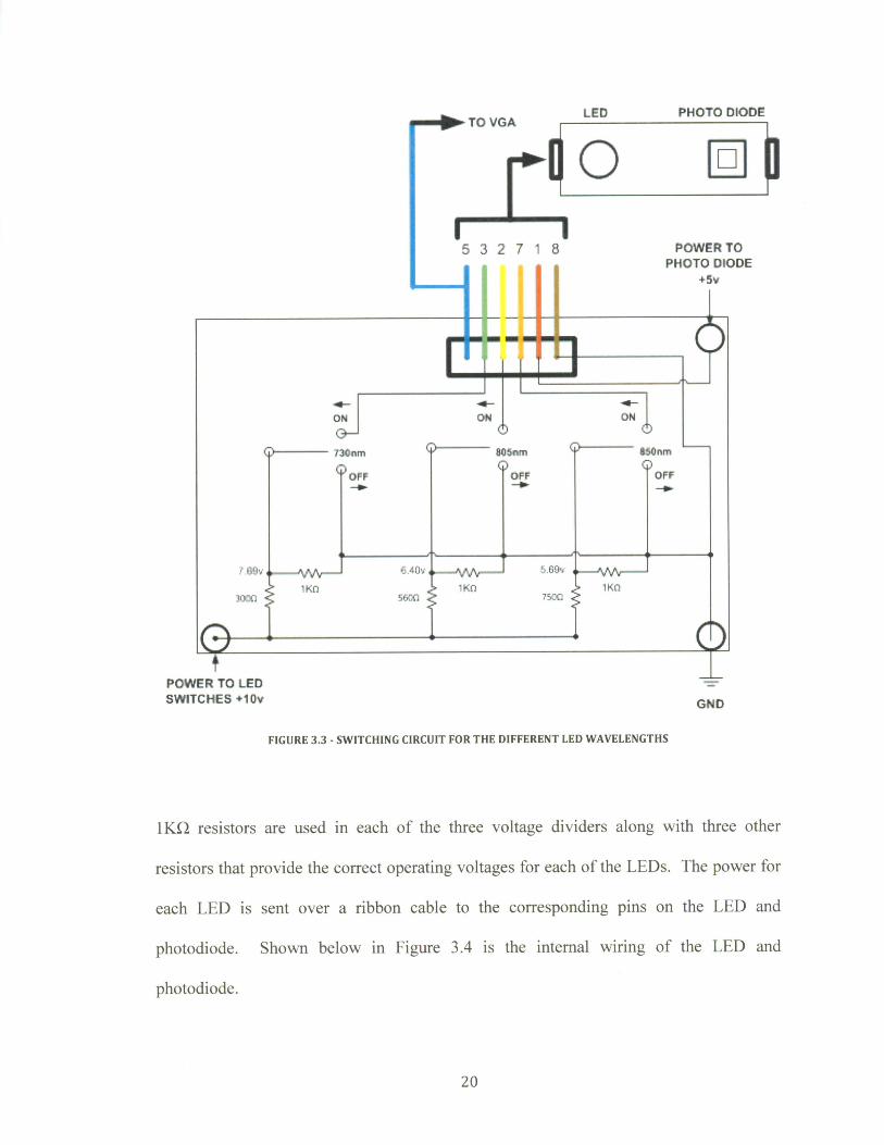
FIGURE 3.3 - SWITCHING CIRCUIT FOR THE DIFFERENT LED WAVELENGTHS
1K) resistors are used in each of the three voltage dividers along with three other
resistors that provide the correct operating voltages for each of the LEDs. The power for
each LED is sent over a ribbon cable to the corresponding pins on the LED and
photodiode. Shown below in Figure 3.4 is the internal wiring of the LEDI) and
photodiode.

OPTICAL SENSOR
FIGURE 3.4 - INTERNAL PHOTDIODE AND LED WIRING
The photodiode only requires +5 V to operate and to be grounded. The other pins apply
to different applications for the photodiode and are therefore unused. The output voltage
of the photodiode (Pin 5) is sent to the variable gain amplifier (VGA) for amplification
before reaching the analog to digital converter. For the LED, each voltage from the
switching circuit is fed to the corresponding pins for each wavelength. Table 3.2 below
shows the pin configuration for each wavelength.
TABLE 3.2 - PIN CONFIGURATION FOR EACH LED WAVELENGTH
Wavelength (nm) Power Pin Ground Pin730 Pin 2 Pin 4805 Pin 1 Pin 5850 Pin 8 Pin 6
The sensor itself is quite small when only housing one photodiode and one LED. In this
single unit configuration it measures 2 x 0.8 x 0.4 inches. Shown below in Figure 3.5 is a
completed optical sensor. The emitter and detector are spaced about 1.25 inches apart,
however increasing the separation distance between them will increase penetration depth
into the area under test.
21
+5V
PHOTODIODE1 Vs GND 7
4 OUTPUT 5 To VGA
I; I I I I
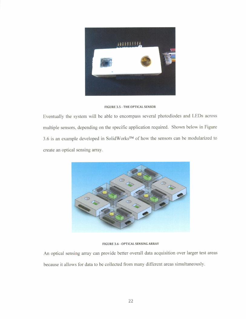
FIGURE 3.5 - THE OPTICAL SENSOR
Eventually the system will be able to encompass several photodiodes and LE[s across
multiple sensors, depending on the specific application required. Shoxxn below in Figure
3.6 is an example developed in SolidWorksT" of ho the sensors can be modularized to
create an optical sensing array.
-; (
K
FIGURE 3.6 - OPTICAL SENSING ARRAY
An optical sensing array can provide better overall data acquisition over larger test areas
because it allows for data to be collected from many different areas simultaneously.
'1 0 0

CHAPTER IV
DATA PROCESSING AND CONTROL CIRCUITRY
4.1 Wireless System Data Processing and Control Circuitry Overview
The data processing and control circuitry are a crucial part of the entire imaging system
and are carefully designed to work seamlessly with the optical sensor and wireless
interface. The data processing and control circuitry are designed to be small and
portable. The goal is to keep the circuitry as simple and compact as possible. The core
data processing and control of the system is accomplished using the following
components:
1. Variable Gain Amplifier (VGA)
2. 8-Bit Analog to Digital Converter (ADC)
3. 4-Bit Synchronous Counter
4. NAND Gate
5. Inverter
6. Flip-Flop
7. 2.4 KHz On-Board Clock
8. MAX232 chip for converting 0-5 V to ±9 V for serial transmission following the
RS232 standard
The next section describes in detail the integration of these components and how each
serves an important function in the overall operation of the data processing and control
23

system. Io get a clearer understanding of how- the next few sections tie together, a block
diagram has been provided below in Figure 4.1.
CLOCK SENSOR
COUNTER VGA WHM900
INVERTER ADC - MAX-232
NO = Control Circuitry
NAND FLIP-FLOP Signal Circuitry
= Data Processing Circuitry
FIGURE 4.1 - WIRELESS SYSTEM BLOCK DIAGRAM
4.1.1 Variable Gain Amplifier (V(;A)
For the variable gain amplifier, a Motorola [M358N dual, low power operational
amplifier is used (See APPENDIX C). The variable gain amplifier is used to amplify the
voltage output from the optical sensor. It has been characterized using a 2KQ resistor
and 802 potentiometer to provide gains from 1 to 40 (output voltages from 0.1 V to 4.0
V with input of 0.1 V). (ain of the system is varied based upon the signal strength
associated with the test location and individual tissue characteristics. To compensate for
these changes. the output signal of the sensor can be amplified by a gain that is
determined from the experimental conditions. This allows for accurate results to be
obtained from a wide range of subjects rather than just from the ones whose body

characteristics most conveniently work with the system. The amplified signal from the
optical sensor is then fed in as the input to the ADC. This is the main input for data
processing.
4.1.2 8-bit Analog to Digital Converter (ADC)
For the analog to digital converter (ADC), a Texas Instruments TLC0831CP successive-
approximation ADC is used (See APPENDIX D). The ADC has an 8-bit resolution to
quantize input voltages from the amplifier between 0-5 V to a serial output of values
ranging between 0-255. The TLC0831CP has two modes of operation. Without control
circuitry, the ADC can be set to continuously read voltages and output serial bit streams
by grounding the chip select pin (CS'). For our application however, sampling the sensor
output at a user defined interval is more appropriate then reading every sensor output
value. To achieve this sampling effect, the data processing circuitry regulates the CS' pin
transitions, thereby allowing us to sample the sensor output each time CS' is forced low.
This will be explained in detail in the descriptions of the rest of the circuitry. Once a
reading is taken, the serial output is sent to the MAX232 chip which converts the 0-5 V
bit stream into a ±9 V signal that can be sent to the wireless development board via the
RS232 standard.
4.1.3 4-Bit Counter
For the counter, a Philips 74HC161N pre-settable, 4-bit synchronous counter with
asynchronous reset is used (See APPENDIX E). The counter is used to control the read
command to CS'. By default, the counter cycles from 0 to 15 as long as the master reset
pin (MR') is set high. When the counter reaches 15, it then signals a one clock cycle
wide high pulse from the terminal count pin (TC). TC is used to control other circuitry
25

by signaling the end of the count cycle to another chip. However, counting from 0-15 is
not suitable for controlling CS' on the ADC for this application. Therefore, an alternative
signal is provided to replace TC.
Once CS' transitions from high to low, the ADC starts its conversion by inserting
a low start bit, then 8 bits of data. This means that to get the ADC to perform its full
conversion correctly, CS' must remain low for a period of 9 clock cycles and then go
high for one clock cycle to substitute as the stop bit (the ADC does not provide its own
stop bit, so a high stop bit was added at the end of the conversion). The start and stop bits
are necessary for the wireless transmission so that the receiving computer is aware of
when data is being sent and when it has completed sending. However, due to delays from
the setup time required by the ADC, CS' needs to remain low for 10 clock cycles (a
timing diagram is provided further in the chapter). To accomplish this, the four flip-flop
outputs of the counter (QO-Q3) are fed into a NAND gate. The QO-Q3 flip-flops are
output from the counter to show what the current value of the counter is. Table 4.1 below
shows their outputs from 0-15.
TABLE 4.1 -FLIP-FLOP OUTPUTS OF THE COUNTER
Count 0 1 2 3 4 5 6 7 8 9 10 11 12 13 14 15
QO 0 1 0 1 0 1 0 1 0 1 0 1 0 1 0 1
Q1 0 0 1 1 0 0 1 1 0 0 1 1 0 0 1 1Q2 0 0 0 0 1 1 1 1 0 0 0 0 1 1 1 1Q3 0 0 0 0 0 0 0 0 1 1 1 1 1 1 1 1
4.1.4 NAND Gate and Inverter
For the NAND gate, a Texas Instruments SN74HC2ON dual, 4-input positive NAND gate
is used (See APPENDIX F). The NAND gate continuously outputs a high signal state on
its output until all four of its inputs are "1". When this occurs, the NAND gate then
26

outputs a low signal state until at least one of its inputs becomes a "0". In order to get the
NAND gate to output a high signal state again after one clock cycle, the counter needs to
be reset. To reset the counter, the MR' pin on the counter must receive a high to low
transition. By sending the output of the NAND gate to the MR' of the counter, the
counter will be reset every time the NAND gate receives all "l's" and the NAND gate
will then output a low signal again. In order to achieve all "l's" in the NAND gate
before the counter reaches 15, an inverter is used to invert the Q0 and Q2 flip-flop signals
before they enter the NAND gate. The inverter used is an ON Semiconductor
MC14049UBCPD hex inverter (See APPENDIX G). The binary representation for ten is
1010, so by inverting QO and Q2, the NAND gate will see 1111 when the counter reaches
ten. With the NAND gate receiving all "1's", the counter will be forced to reset. Shown
below in Table 4.2 are the outputs for the NAND gate with Q0 and Q2 inverted.
TABLE 4.2 - NAND GATE OUTPUTS WITH Q0 AND Q2 INVERTED
Count 0 1 2 3 4 5 6 7 8 9 1011 12131415
Q0' 1 0 1 0 1 0 1 0 1 0 1 0 1 0 1 0
Q1 0 0 1 1 0 0 1 1 0 0 1 1 0 0 1 1
Q2' 1 1 1 1 0 0 0 0 1 1 1 0 0 0 0
Q3 0 0 0 0 0 0 0 0 1 1 1 1 1 1 1 1
NAND 1 1 1 1 1 1 1 1 1 1 0 1 1 1 1 1
4.1.5 Flip-Flop
For the flip-flop, a Motorola MC74HC74A dual, D flip-flop with set and reset is used
(See APPENDIX H). The flip-flop is used to create the actual CS' signal and it changes
state on the rising edge of each clock cycle. But instead of feeding the flip-flop an actual
clock signal, the output of the NAND gate is sent to an inverter so a single low to high
pulse reaches the flip-flop every 10 clock cycles. When the flip-flop receives the first
27

pulse, it goes to a high state. This high state is fed back into the flip-flop as in input, and
when it receives the next pulse from the inverted NAND gate output, it will flip to its
opposite state, which would be low. It is important to note that the current state of the
flip-flop is continuously output from its Qi1 pin (this is different than the Qi pin on the
counter). This signal is high for 10 clock cycles and then low for 10 clock cycles. This
repeats continuously until the entire board is powered down. The low for 10 clock
cycles, high for 10 clock cycles signal is fed straight into CS' on the ADC providing it
the necessary window to convert 8 bits worth of data with a start bit and our added stop
bit, and then wait another 10 clock cycles before the next conversion. This provides a
sampling rate of 120 samples per second at 2400 baud.
4.1.6 On-Board Clock
For the clock, a National Semiconductor LM555CN timer is used (See APPENDIX I). The
on-board clock generates a 2.4 KHz clock that matches the 2400bps baud rate used to
communicate with the wireless system. To accomplish this, the LM555CN was set up as
a 50% duty cycle oscillator, which allowed for the development of an accurate clock
signal. To achieve 2.4 KHz, the required resistor values were determined to be
30062.53S and 12725.65g. With these resistor values at a tolerance of ±0.05-0.10%, it
is possible to get within 0.2% of the 50% duty cycle. Due to the extended wait period
for custom resistors to be manufactured, two sensitive trimmer potentiometers are being
used for the clock circuit.
4.2 Circuit Schematic
The layout for all of the integrated circuitry is rather complex. To gain a better
understanding of how each chip functions with the rest of the board, a schematic has been
28

developed that shows all of the main circuitry (excluding the LED power switching
circuit). The data processing and control circuitry schematic is shown below in Figure
4.2.
FIGURE 4.2 - DATA PROCESSING AND CONTROL CIRCUITRY SCHEMATIC
4.3 Circuit Timing
Although the overall flow of data was described for each individual chip in Section 4.2, it
is much easier to comprehend when it is described graphically and all at once. The
program used to generate the timing diagram is called TimeGenTM 3.0. It allows for
multiple timing signals to be generated in a clear and useful format that makes it easy to
see all the events that occur on the rising and falling edge of each clock cycle. This
program was especially helpful in demonstrating all of the different actions occurring
29

within the control and data processing circuitry. The timing diagram is shown below in
Figure 4.3 (Note that the ADC Data I and ADC Data 2 signals demonstrate two separate
conversions, but serve to show how the stop bits are added when the conversion ends in a
Sor a 0).
1 3 . 4 5 8 3 10 11 12 13 14 15 1E 17 18 14 20 21 22 23 24 20
Clock
ADC Dat 1
ADC Data 2 F2TiF.
r: S.:
Fl pFlop Clk
01 I
NANDM P
FIGURE 4.3 - TIMING DIAGRAM
4.4 Altium DesignerTm and Board Fabrication
Once all of the circuitry was designed and tested, a printed circuit board (PC1) was laid
out for the components. This was important not only to make the system portable and
smaller, but also to remove unwanted noise in the system arising from all the stripped
wires and breadboard connections. To develop the printed circuit board layout, Altium
DesignerTM was used. The software allows all of the component pieces to be wired
together by creating a schematic from a large parts data base. Shown below in Figure 4.4
is the schematic for the data processing and control circuitry board developed in Altium
DesignerTM.
.. 7
211
I-.
- '1 ~'
.4~~---~
TUI I2
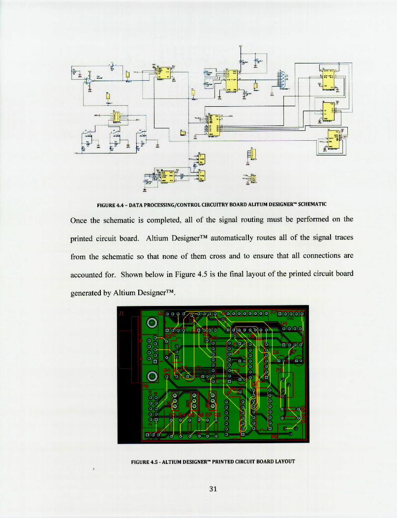
FIGURE 4.4 - DATA PROCESSING/CONTROL CIRCUITRY BOARD ALITUM DESIGNER'" SCHEMATIC
Once the schematic is completed, all of the signal routing must be performed on the
printed circuit board. Altium DesigneriM automatically routes all of the signal traces
from the schematic so that none of them cross and to ensure that all connections are
accounted for. Shown below in Figure 4.5 is the final layout of the printed circuit board
generated by Altium DesignerTM
FIGURE 4.5 - ALTIUM DESIGNER'" PRINTED CIRCUIT BOARD LAYOUT
I111.
L
1~ -°i '
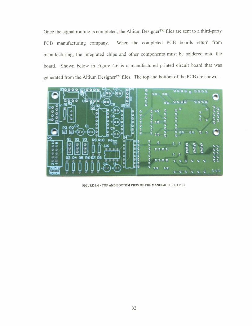
Once the signal routing is completed. the Altium Designers' files are sent to a third-part)
P'CB manufacturing company. When the completed PCB boards return from
manufacturing, the integrated chips and other components must be soldered onto the
board. Shown below in Figure 4.6 is a manufactured printed circuit board that was
generated from the Altium DesigneriM files. The top and bottom of the PCB are shown.
a S
FU i4
FIGU RE 4.6 - TOP AN D BOTTO M VIEW OF TH E MANUFACTU RED PCB
I. 5.i,~~
CHAPTER V
WIRELESS COMMUNICATION
5.1 Wireless Communication Overview
The wireless communication for the transmission of data from the imaging sensor to the
base station computer is achieved using two Radicom WHM900 RF antennas mounted on
development boards 1251. The sending and receiving antennas communicate on a
915.02MHz frequency. which lies in the License-Free ISM Band (900-928MHz). They
communicate with a baud rate of 2400bps and have a communication range of
approximately 300 to 500 feet. This range is more than acceptable for the applications
that the imaging system is designed for. The Radicom WHM900 development board was
used for initial system development because it allowed for easy communication with the
base station computer. The provided RS-232 cable allows for direct communication with
the module via HyperTerminal, and also allows the module to send data to MATLABTM.
Shown below in Figure 5.1 is an image of the WHM900 antenna and communications
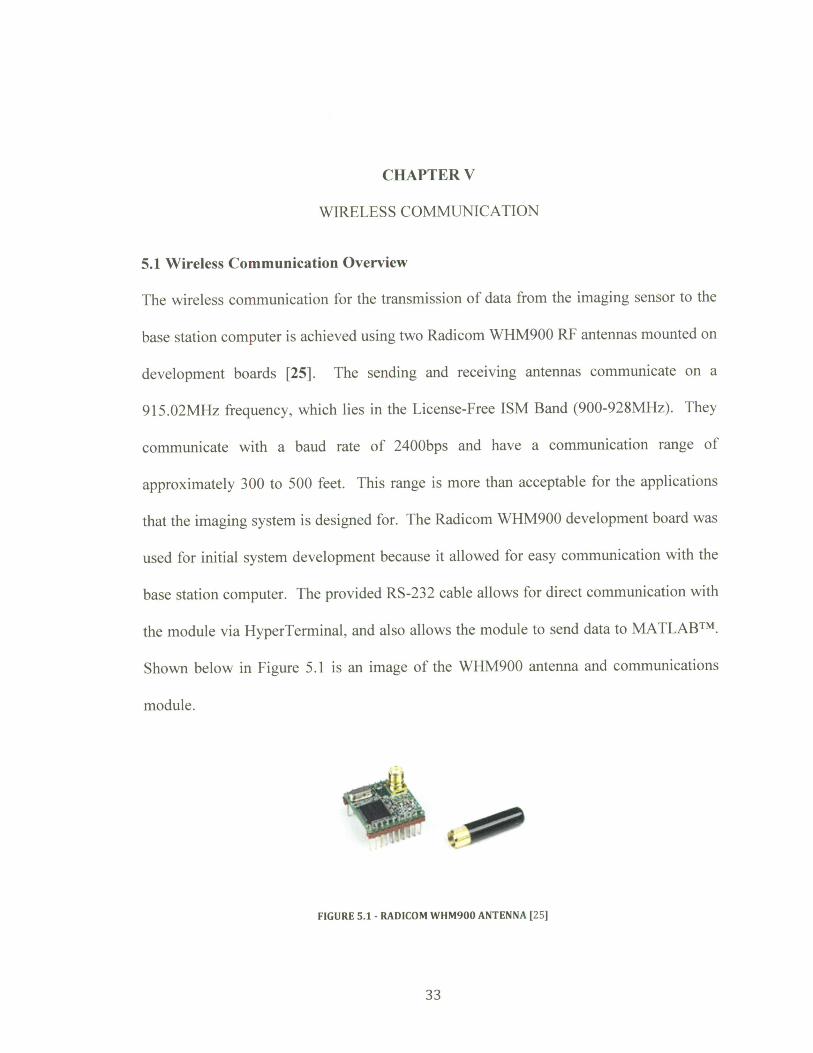
module.
-ii
FIGURE 5.1 - RADICOM WHM900 ANTENNA [25]
5.2 Wireless Data Links
The W1IM900 comes equipped with the ability to establish three different types of
wireless data links. The first is Point-to-Point Operation. which allows the user to
establish single, or multiple point-to-point locations by setting different channel IDs,
frequencies, and speeds. The second is Auto-Link Operation. which forces the sending
and receiving modules to maintain a point-to-point connection automatically. The third
is Point to Multi-Point Broadcasting. which allows for a Master module to broadcast data
to multiple remote Slave modules. For our specific application, the Auto-Link Operation
wireless data link was chosen because we only had two communicating modules and one
communication link. One advantage of using the Auto-Link Operation is that if there is a
power outage or the link is lost due to temporary interference. the modules will
automatically detect the lost data link and automatically re-establish a connection. Also.
once the modules are designated as sender and receiver through commands in
tHyperTerminal. the modules automatically establish a connection at power-on. Shown
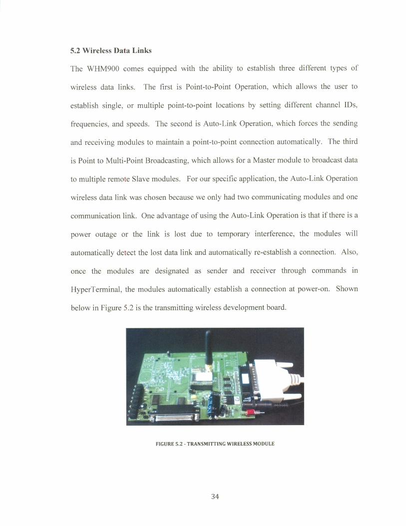
below in Figure 5.2 is the transmitting wireless development board.
FIGURE 5.2 - TRANSMITTING WIRELESS MODULE

5.3 Configuring the Modules
HyperTerminal is used to communicate with the WHM900 modules through a series of
predefined terminal commands. To establish an Auto-Link connection between two
modules, one module is set up for Answer Mode (receiver) and the other for Originate
Mode (sender). To do so, the command "ATSO=l&W" is sent to one module and the
command "ATSO=2&W" is sent to the other module. Once this is completed, the Auto-
Link Operation setup is complete and the modules are ready to communicate. There are
also several default settings that can be changed such as the operating frequency, baud
rate, and transmit level. These adjustments are made by sending the module other
terminal commands. All of the settings are stored in Non-Volatile Memory (NVRAM) so
that if the module is powered down, it still retains all of its current settings. Therefore,
setup is only required one time unless changes are desired. To change a setting, "+++" is
entered in HyperTerminal and the module enters On Line Command Mode and the
change commands can be entered. After settings have been changed, to return to On Line
Data Mode, "ATO" must be entered in HyperTerminal.
5.4 MAX232 and Serial Communication
Currently, the data processing circuit utilizes a MAX232 chip to interface the system
control circuitry with the wireless board. This chip is essential to bridge the
communication gap because the data processing board and the wireless modules
communicate with signals of different voltages. The data processing board's data signal
that is sent to the wireless board is a 0-5 V signal. However, the communication link
between the data processing board and wireless board is an RS-232 cable. The RS-232
standard requires signals that are +9 V, so transmitting a 0-5 V signal over an RS-232
35

cable is insufficient. The MAX232 chip takes the 0-5 V bit stream from the ADC and
converts it to +9 V before sending the data to the wireless board. Eventually the need for
the MAX232 chip will be phased out as the wireless circuit card is mounted directly to
the circuit board, and the entire data processing system is made as a field-programmable
gate array (FPGA).
36

CHAPTER VI
PHANTOM DEVELOPMENT AND SYSTEM CHARACTERIZATION
6.1 Phantom Development Overview
In order to test our system response, a series of phantom test structures was prepared. A
phantom is a synthetic model created to simulate the desired response of the fNIRS
sensor to changes in oxy and deoxy-hemoglobin. Phantoms range in complexity from
simple models of biological tissue, to complex models designed to accurately emulate the
chemical composition of the human body. The more complex the data obtained from an
imaging system, the more accurate the phantoms must be to properly test all the different
components of the biological system.
After the development of any new medical imaging hardware, it is important to
understand it thoroughly and perform controlled tests on the new equipment to ensure
proper functionality and consistency of results. Although it is important to eventually
perform tests on live subjects, it is also necessary to characterize the system using
phantoms to ensure that the system is safe and that accurate results will be achieved when
in vivo testing is conducted. The most useful aspect of phantoms is that they permit
functional characterization of the system because they can be created to very specific
standards with known concentrations of chemicals. Therefore, the response of the
imaging system can be characterized when the exact properties of the phantom are
known. Phantoms play an integral role in all medical imaging systems because they
provide help in the development process, and ensure that medical systems do not cause
adverse effects to people.
37

The Epitex LED and OPT101 photodiode implemented for the sensor are a good
pairing for implementing fNIRS. This is partly due to the fact that these components are
relatively inexpensive and effective in fNIRS applications. The 8-bit ADC provides 256
bits of resolution over 0-5 V so voltages can be detected at approximately 0.02 V
intervals without amplification, which provides accurate quantization resolution. With a
higher resolution ADC, more accurate data could be obtained however 8-bit resolution is
currently sufficient for this specific application.
The goal of the system characterization was to verify that the overall system will
respond to a variation in simulated test conditions. The sensor system was tested on
phantoms and the data presented here is used to characterize system functionality, but is
not representative of any particular biological system.
6.2 Creating the Phantoms
The phantoms used for our initial characterization required four components. These four
components are listed below in Table 6.1. Silicone (base plus curing agent) is used as the
structural base for the phantoms. Agents were also added to provide scattering and
absorption characteristics.
TABLE 6.1 - THE FOUR MAIN ELEMENTS OF A PHANTOM
Phantom Component
Base RTV12A
Curing Agent RTV12CScattering Agent TiO2Absorbing Agent Carbon Black
38
A weight ratio of 10:1 of RTV I2A:RTV 12C is used lr the basic silicone form. Ihe
components are weighed and added into the RTVI2A base compound. This compound is
thoroughly mixed prior to curing.
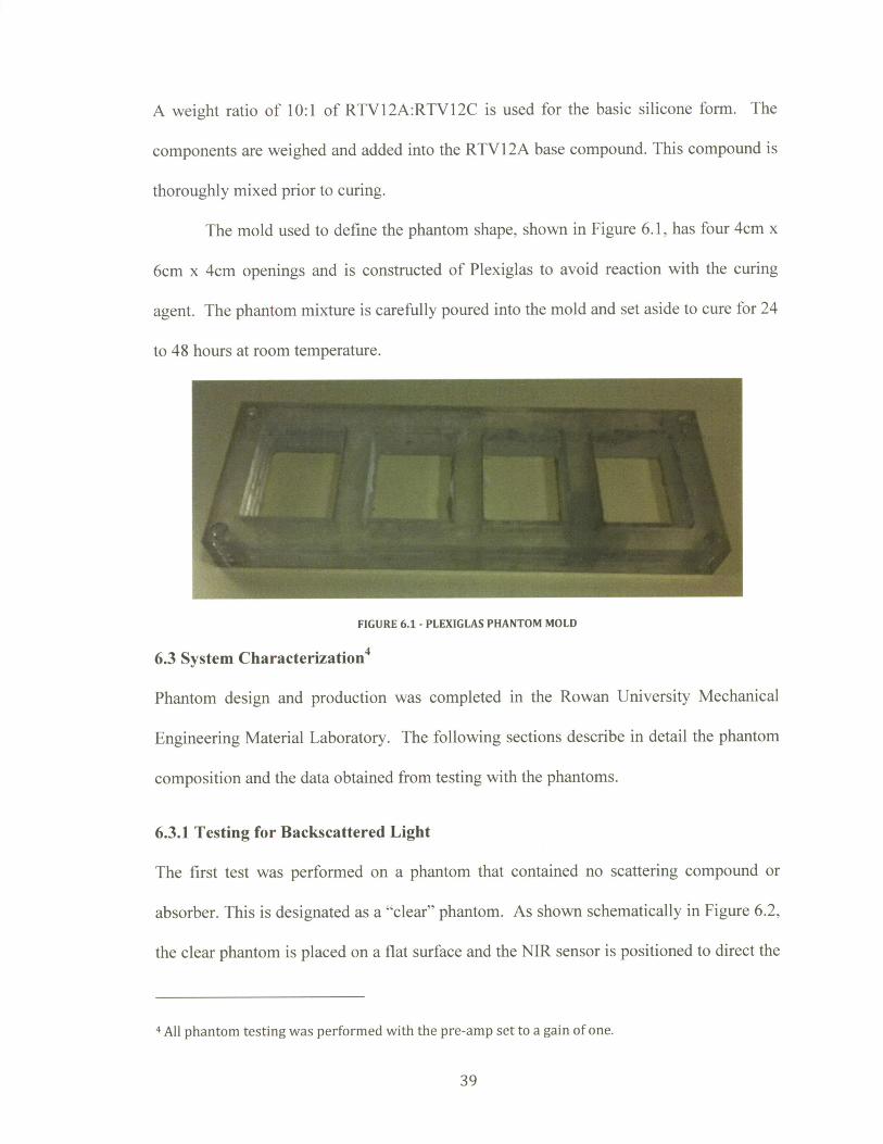
TI he mold used to define the phantom shape. shown in Figure 6.1. has four 4cm x
6cm x 4cm openings and is constructed of Plexiglas to avoid reaction with the curing
agent. The phantom mixture is carefully poured into the mold and set aside to cure for 24
to 48 hours at room temperature.
FIGURE 6.1 - PLEXIGLAS PHANTOM MOLD
6.3 System Characterization
Ihantom design and production was completed in the Rowan University Mechanical
[ngineering Material Laboratory. The following sections describe in detail the phantom
composition and the data obtained from testing with the phantoms.
6.3.1 Testing for Backscattered Light
The first test was performed on a phantom that contained no scattering compound or
absorber. This is designated as a "clear" phantom. As shown schematically in Figure 6.2.
the clear phantom is placed on a flat surface and the NIR sensor is positioned to direct the
4 All phantom testing was performed with the pre-amp set to a gain of one.
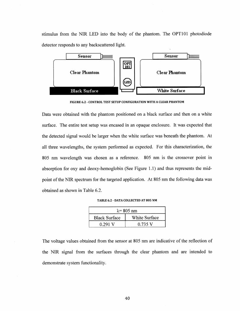
stimulus from the NIR LED into the body of the phantom. The OPT101 photodiode
detector responds to any backscattered light.
S en or ens or
Clear Phantom Clear Phantom
I Bl [ack q AmWhite Suface
FIGURE 6.2 - CONTROL TEST SETUP CONFIGURATION WITH A CLEAR PHANTOM
7
Data were obtained with the phantom positioned on a black surface and then on a white
surface. The entire test setup was encased in an opaque enclosure. It was expected that
the detected signal would be larger when the white surface was beneath the phantom. At
all three wavelengths, the system performed as expected. For this characterization, the
805 nm wavelength was chosen as a reference. 805 nm is the crossover point in
absorption for oxy and deoxy-hemoglobin (See Figure 1.1) and thus represents the mid-
point of the NIR spectrum for the targeted application. At 805 nm the following data was
obtained as shown in Table 6.2.
TABLE 6.2 - DATA COLLECTED AT 805 NM
a= 805 nm
Black Surface White Surface
0.291 V 0.735 V
The voltage values obtained from the sensor at 805 nm are indicative of the reflection of
the NIR signal from the surfaces through the clear phantom and are intended to
demonstrate system functionality.
40

6.3.2 Varying Levels of TiO 2
For testing the system response to varying levels of absorbing compound, an optimal
amount of scatterer (TiO 2) was determined empirically. The goal is to contain the NIR
signal completely within the phantom. Testing was performed with the goal of
developing phantoms that would scatter the NIR signal in a similar manner to biological
tissue and most accurately demonstrate the correct functionality of the sensor and
circuitry. To gain an understanding of how the phantoms would perform under testing,
three additional phantoms were created each with a different quantity of titanium dioxide
(TiO 2) distributed throughout the silicone molds. The four quantities chosen were: Og
(the clear phantom), ig, 2g, and 3g TiO 2. By using a silicone phantom with no TiO 2 as a
control, we were able to see how much backscattered light would be produced by each
different phantom as the quantity of TiO2 was increased with no absorber added. The
phantom testing was again performed on both black and white surfaces to see how much
light was being backscattered by the TiO 2 or by the surface that the phantom was resting
on (this was also done to determine a correct thickness for the phantoms). The sensor
and phantom were also shielded from ambient light by being enclosed in an opaque box.
Shown below in Figure 6.3 is the test setup configuration for testing on black and white
surfaces with varying amounts of TiO 2.
Sensor ]J ensor ]
\White Siuface
:at•e .y .h .i2or
FIGURE 6.3 - TEST SETUP CONFIGURATION FOR VARYING TIO2 CONCENTRATIONS
41
ligh wa be l ack Sma

Using the above configuration, each phantom with a different concentration of TiO 2 was
tested at each of the three NIR wavelengths, and the scatterer was spread as
homogenously as possible throughout the phantoms (data from the clear phantom is
repeated here for comparison). The data collected from these measurements at 805 nm
are shown below in Table 6.3.
TABLE 6.3 - VOLTAGE READINGS FOR TIO2 CONCENTRATIONS ON BLACK/WHITE SURFACES
Wavelengthk= 805 nm
Surface Black White AV
Og TiO2 0.291 V 0.735 V 0.444 V
1g TiO2 0.133 V 0.229 V 0.096 V
2g TiO2 0.044 V 0.060 V 0.016 V
3g TiO2 0.026 V 0.033 V 0.007 V
The data shown in Table 6.3, on both black and white surfaces, reveals the trend that we
anticipated. As the amount of TiO2 is increased, light is scattered throughout the
phantom rather than being directed to and reflected from the underlying surface. As TiO2
levels increased, AV decreased indicating that the underlying surface was decreasingly
significant as an influence in the measurement. Because the measurement, ideally,
should not be influenced by the environment but only a function of the components of the
phantom, AV should approach 0. Because we chose not to adjust the gain of the system
preamplifier, the compromise for this testing phase was to choose a value of TiO2 in the
phantom that yielded reasonable voltage levels with small AV. Consequently, the 2g level of
TiO 2 was chosen. This amount of TiO2 translated into a density of 0.0197 g/cm3, which
was used for the remainder of the system characterization measurements.
42

6.3.3 Signal Detection Sensitivity to Different Absorber Concentrations
Finally, the sensitivity of the system to varying levels of absorbing compound was
demonstrated. A new set of phantoms was fabricated with the concentration of TiO 2 held
constant at 0.0197 g/cm3. Carbon black, a compound sometimes used as a pigment in
rubber products, was used as the absorber. Two levels of absorption were simulated by
adding carbon black to the phantoms in the following quantities: 0.01 g and 0.05g.
With the concentration of scatterer in the phantoms at 0.0197 g/cm 3, it was
assumed that the testing surface was only reflecting a minute amount of NIR light,
however testing was performed once again on both black and white surfaces for
consistency. Measurements of backscattered light were made at each level of added
carbon black. At the reporting wavelength, 805 nm, the data shown in Table 6.4 was
obtained.
TABLE 6.4- VOLTAGE RESPONSE AT 805 NM WITH INCREASING AMOUNTS OF CARBON BLACK
X&= 805 nm
Carbon Black Black White0.01g 0.042 V 0.047 V0.05g 0.007 V 0.014 V
The choice of carbon black quantities was not adequately fine grained in this experiment.
Between 0.01g and 0.05g, AV is 0.035 V on the black surface and AV is 0.033 V on the
white surface, which indicates a strong response to the increased concentration of carbon
black.
43
CHAPTER VII
SYSTEM INTEGRATION AND TESTING
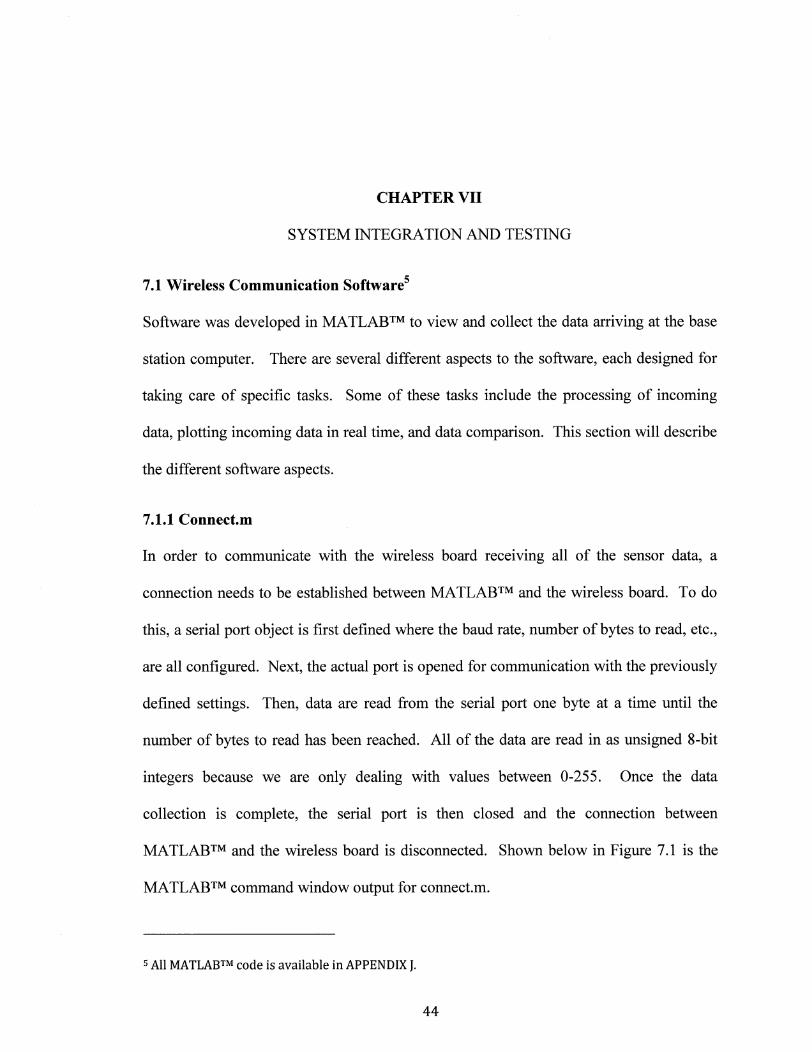
7.1 Wireless Communication Software5
Software was developed in MATLABTM to view and collect the data arriving at the base
station computer. There are several different aspects to the software, each designed for
taking care of specific tasks. Some of these tasks include the processing of incoming
data, plotting incoming data in real time, and data comparison. This section will describe
the different software aspects.
7.1.1 Connect.m
In order to communicate with the wireless board receiving all of the sensor data, a
connection needs to be established between MATLABTM and the wireless board. To do
this, a serial port object is first defined where the baud rate, number of bytes to read, etc.,
are all configured. Next, the actual port is opened for communication with the previously
defined settings. Then, data are read from the serial port one byte at a time until the
number of bytes to read has been reached. All of the data are read in as unsigned 8-bit
integers because we are only dealing with values between 0-255. Once the data
collection is complete, the serial port is then closed and the connection between
MATLABTM and the wireless board is disconnected. Shown below in Figure 7.1 is the
MATLABTM command window output for connect.m.
Al MATLAB TM code is available in APPENDIX J.
44

H-Ip
coI~nnect.
Enter the Nurber of Bytes to Read: 512
Serial Pnrt Connection Estatlihed
Serial Port Open for Reading
Press 1 to Begin Reatding or 2 to Quit: 1
Peading data please mait...
rata Pead Complete
Serial Port 'lonnect iun 'ClLsed
FIGURE 7.1 - CONNECT.M COMMAND WINDOW OUTPIUT
7.1.2 Convert.m
T he next step after reading all of the data from the serial port is to convert the data into
the correct format. This must be done because the AD' outputs its conversions with the
least significant bit (LSB) first and the most significant bit (MSB) last, whereas
MATI ABTM reads the data in the opposite configuration. 1To compensate. the bits that
are read must be reordered. For example. a binary - 1001100" output from the ADC will
be interpreted by MATLAB*M as 51 in decimal. when the actual number is 204. By
reversing the data to '00110011". MATLABTM will then interpret the number correctly
as 204. This is performed on every byte using a simple algorithm so that all of the data is
correct. ['hen, each byte is multiplied by 5/256 to get a decimal voltage between 0-5 V
from the 0-255 quantization used by the ADC. All the voltages are then plotted to gixe a
visual representation for the information gathered by the sensor. All of the data are then
stored in a text tile for future reference or immediate analysis. Shoxn below in Figure
7.2 is the MAI'LABTM command window output for convert.m followed by the voltages
saved to the text tile for a simple test in Figure 7.3.
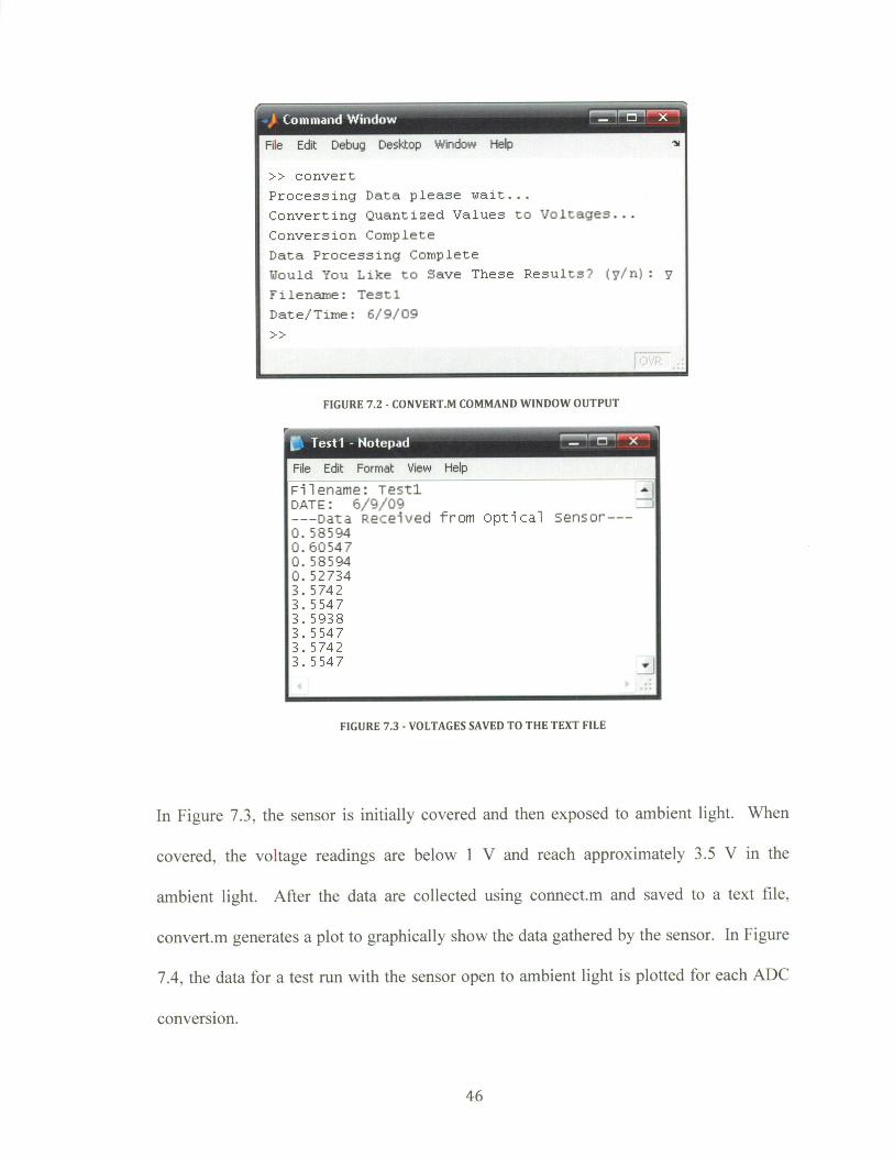
convert
Processing Data please walt...
Coner t ing yuant ed Values to Vu ltages..
Convrsion Iorrplett
Data Processing 1COniOplete
Mi uild You Like to Save These lesu ilr )n: 7
Filename: Testl
Date/Time: 6''9; 09
IGURF 7 72 ( )\\l RI %I COlMMAND W11, DOW O)ITPUTI
Filp E~it Frrr ~t Jir! : HPIp
Fi l enarrne : TestiDATE: E ii'c0
--- [;aa F~cei e1 fror Ii -lptial sem_=or---
0.5s5940. 527343.5742_ 55473.59333. 5547
4 574:5.5547
FIGURE 7.3 - VOLTAGES SAVED TO THE TEXT FILE
In Figure 7.3. the sensor is initially covered and then exposed to ambient light. When
covered, the voltage readings are below 1 V and reach approximately 3.5 V in the
ambient light. After the data are collected Lsing connect.m and saved to a text file.
convert.m generates a plot to graphically show the data gathered by the sensor. In Figure
7.4. the data for a test run with the sensor open to ambient light is plotted for each ADC
conversion.

n ia; 61 cam +y (.- mow }" Q fu'
Voltage Readings from Optical Sensor
T 3 -----
3
cr 25
15
050 1O 230 300 400 500 600
Sample #f
FIGURE 7.4 - VOLTAGE PLOT WITH AMBIENT LIGHT
7.1.3 Compare.m
Once multiple data captures have been converted and saved to a file, they can then be
compared (up to three data sets). Each of the different sets of voltages is plotted on the
same graph to show the differences or similarities between them. This is useful for
gathering a few sets of data for the same type of test to cheek for consistency in the
method of testing or to compare healthy data vs. unhealthy data. In Figure 7.5 shown
below, three different tests have been performed and plotted against each other. Test I
shows the voltages output from the sensor in ambient light. Test 2 shows the voltages
output from the sensor when light is partially restricted but held constant, and 1'est 3
shows a random set of voltages generated by varying the sensor input in an arbitrary
manner.
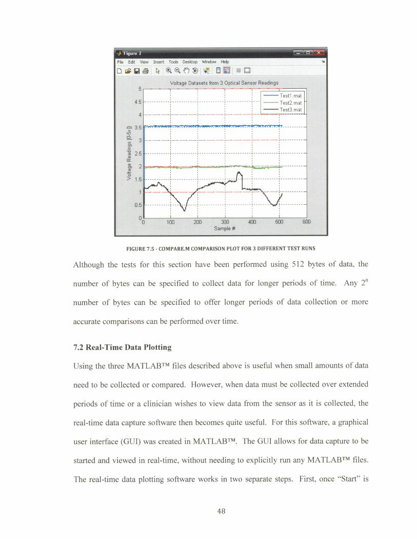
FIGURE 7.5 -COMPARE.M COMPARISON PLOT FOR 3 DIFFERENT TEST RUNS
Although the tests for this section have been performed using 512 bytes of
number of bxtes can be specified to collect data tor longer periods of time.
number of bytes can be specified to offer longer periods of data collection
accurate comparisons can be performed oxver time.
data, the
Anv 2"
or more
7.2 Real-Time Data Plotting
Using the three MATl AI3IM files described above is useful when small amounts of data
need to be collected or compared. lowxever. when data must be collected oxer extended
periods of time or a clinician wxishes to x iew data from the sensor as it is collected, the
real-time data capture softxxare then becomes quite useful. For this softxxare a graphical
user interface (GUI) was created in MATLABIM. Ihe (ill alloxs for data capture to be
started and viexed in real-time. xithout needing to explicitly run any MATLAI3" files.
Ihe real-time data plotting softwxare xorks in txo separate steps. First, once "Start" is
F "
5
4.5
4
-35
3
257Cr
~-2
15
1
03
Voltage Datasets frorr 3 Optical Sensor Readings
Test1 mat
Test" mt
TestaS1 rr at
------- J~i~---------
400 500 600i 100 200 300
Sample #
-- ---- -

clicked on the GUI, the software will initially capture 25 data points in real-time. After
25 data points, the software shifts the x-axis of the plot and adds one new point while
removing the previous point (each 25 samples apart). This allows the plot to move with
the number of samples taken over time and provides a current look at what voltages the
sensor is producing at any given time. A sample is taken from the incoming wireless data
every 0.5 seconds, so the x-axis is labeled in seconds, with two samples being taken each
second. Sampling once per second was too slow when looking at the plot and anymore
than two samples per second became redundant. Therefore, two samples were chosen per
second to represent the gathered data: however, data could be averaged over time and
plotted rather than sampling the incoming data. Displayed below in Figure 7.6 is an
example of the real-time data plot GUI.
FIGURE 7.6 - REAL-TIME VOLTAGE PLOT
O~l ± 5 :,1 + Cg~0] E
Voltage Readings 'rom , l al Sensor
55
35 .............. .. .i.......
N 3
3 - 1 _ LI
> 2
C,~ra -+s
05
105 110 115 120 125 '30 135 14[ 145 150Time

CHAPTER VIII
FUTURE WORK
Although much has been accomplished on the wireless system integration and the NIR
optical sensor, there are still many tasks that need to be completed. As mentioned in
Section 3.2.3, a main future goal is to develop a multichannel sensing array that can
record data over a larger area or in several different areas simultaneously. This will
require updating the control and data processing circuitry to handle multiple data signals.
It will also require more processing power to perform all of the voltage quantization that
right now, only one ADC is handling. The ADC can handle multiple conversions, but to
do so, the circuitry will have to be reconfigured to trigger each of the different
conversions.
A portable power system will also need to be developed in order to allow the
entire system to migrate away from the current power source that has been used over the
course of the systems development. This will require some engineering of a battery pack
that will easily power the system and not inhibit use. Size and weight will be factors in
the development of this powering system as well as the amount of power that will be
required for different types of testing (i.e. number of sensors, accuracy of data
conversion, etc.)
Another future focus will be to research ways to increase system functionality by
implementing on-board digital signal processing methods. Data averaging could be used
to remove some of the load that is currently being taken on by the MATLABTM portion of
50

the system. Also, moving the data conversion to the board could increase the overall
speed of data collection.
The phantom development is also in its early stages, and will need to be
thoroughly researched in order to create more sophisticated testing applications.
Currently, the titanium dioxide and carbon black tests have served as a preliminary
testing base to prove the functionality of the system. However, in the future these
phantoms must be refined to provide more accurate sensor testing.
Finally, once the fNIRS system has been completed, the entire system will be
moved to a FPGA. This will allow for all of the circuitry to be moved to one chip, add
versatility to the fNIRS wireless system, and greatly increase the number of applications
that it could be used for.
51

REFERENCES
[1] M. D.,. K. Gross. (2006, Sep.) U.S. National Library of Medicine and National Institutes of
Health. [Online]. http://www.nln.nih. gov/medlineplus/eicy/artirle/0039 31 .ltm
[2] 0. I. Tanzer, "Numerical Modeling in Electro- And Magnetoencephalography," PhD
Thesis, Helsinki University of Technology, Espoo, Finland, 2006.
[3] C. K. Bergey and P. J. Franaszczuk, "Epileptic Seizures are Characterized by Changing
Signal Complexity," Johns Hopkins University School of Medicine Technical Paper, 2000.
[4] M. Hamalainen. (2004, Dec.) Athinoula A. Martinos Center for Biomedical Imaging.
[Online]. http): //www.nr i gh.halrvard.edu/martinos/rsearch/technoloiesM EG.php
[5] D. A. Boas, et al., "Imaging the Body with Diffuse Optical Tomorgraphy," IEEE Signal
Processing Magazine, vol. 18, no. 6, Pp. 57-75, Nov. 2001.
[6] L. Wald. (2005, Feb.) Athinoula A. Martinos Center for Biomedical Imaging. [Online].
http /www.nmr.mgh.harvard.edu/martinos/research/technologiesMR.php
[7] N. Savage, "A Weaker, Cheaper MRI," IEEE Spectrum Online, Jan. 2008.
[8] B. W. Murphy. (2005, Sep.) Center for Positron Emission Tomography (CPET):
University of Buffalo. [Online]. http://www.nucmed.buffalo.edu/prevweb/petdef.htm
[9] J. M. Ollinger and J. A. Fessler, "Positron Emmision Tomography," IEEE Signal Processing
Magazine, vol. 14, no. 1, pp. 43-55, Jan. 1997.
[10] University of Virginia. (2007, Dec.) University of Virginia Health System. [Online].
htt ://www.lu'althsystem.virginia.edu/uvahealth/adult radiology/pet.cfm
[11] A. Assmus, "Early History of X Rays," Beam Line, vol. 25, no. 2, pp. 10-24, 1995.
[12] M. Wolf and M. F. V. Quaresima, "Progress of near-infrared spectroscopy and topography
for brain and muscle clinical applications," Journal of Biomedical Optics, vol. 12, no. 6,
Dec. 2007.
[13] D. T. Delpy, M. Ferrari, C. A. Piantadosi, and M. Tamura, "Pioneers in Biomedical Optics:
Special Section Honoring Professor Frans F. Jobsis of Duke University," Journal of
Biomedical Optics, vol. 12, no. 6, Dec. 2007.
[14] V. A. Markel and J. C. Schotland, "Single-Scattering Optical Tomography," in Conference
on Lasers and Electro-Optics, Baltimore, MD, 2007, pp. 1-2.

[15] A. P. Gibson, J. C. Hebden, and S. R. Arridge, "Recent advances in diffuse optical imaging,"
Physics in Medicine and Biology, vol. 50, no. 4, pp. R1-R43, Feb. 2005.
[16] M. Izzetoglu, S. C. Bunce, K. Izzetoglu, B. Onaral, and K. Pourrezaei, "Functional Brain
Imaging Using Near-Infrared Technology," IEEE Engineering In Medicine and Biology
Magazine, vol. 26, no. 4, pp. 38-46, Aug. 2007.
[17] G. Strangman, D. A. Boas, and J. P. Sutton, "Non-Invasive Neuroimaging Using Near-
Infrared Light," Society of Biological Psychiatry, vol. 52, no. 7, pp. 679-693, Oct. 2002.
[18] A. Bozkurt, A. Rosen, H. Rosen, and B. Onaral, "A portable near infrared spectroscopy
system for bedside monitoring of newborn brain," BioMedical Engineering OnLine, Apr.
2005.
[19] A. Villringer and B. Chance, "Non-invasive optical spectroscopy and imaging of human
brain function," Trends in Neurosciences, vol. 20, no. 10, pp. 435-442, Oct. 1997.
[20] M. Schweiger, A. Gibson, and S. R. Arridge, "Computational Aspects of Diffuse Optical
Tomography," Computing in Science and Engineering, vol. 5, no. 6, pp. 33-41, Nov. 2003.
[21] B. N. Pasley and R. D. Freeman. (2008, May) Neurovascular Coupling. Article.
[22] S. C. Bunce, M. Izzetoglu, K. Izzetoglu, B. Onaral, and K. Pourrezaei, "Functional Near-
Infrared Spectroscopy: An Emerging Neuroimaging Modality," IEEE Engineering in
Medicine and Biology Magazine, vol. 25, no. 4, pp. 54-62, Jul. 2007.
[23] P. Rolfe, "In Vivo Near-Infrared Spectroscopy," Annu. Rev. Biomed. Eng., vol. 2, pp. 715-
754, 2000.
[24] Duncan Seddon & Associates. (2003, Jan.) Resin Portrait ABS. Document.
[25] Radicom Research, Inc. (2007) Radicom. [Online].
ltt://www.adi.com/modular43.lt
[26] D. A. Boas, M. A. Franceschini, A. K. Dunn, and G. Strangman, "Noninvasive Imaging of
Cerebral Activation with Diffuse Optical Tomography," in In Viva Optical Imaging of
Brain Function, R. D. Frostig, Ed. Boca Raton: CRC Press, 2002, ch. B, pp. 193-221.
[27] A. G. Webb, "X-Ray Imaging and Computed Tomography," in Introduction to Biomedical
Imaging, 2002, ch. 1, pp. 1-55.
[28] R. Nave. (2006) HyperPhysics - Georgia State Univeristy. [Online].
http://hvpeiplivsics py-astrgsu.edu/Hbase/atmos/busky.htmi

APPENDIX A - Epitex LED Spec Sheet
eI~iteAX Oplo-Device & Custom LED 08 STEM TYPE LED L4*73O/4*805I4*850-4OQ96-I
Lead (Pb) Free Product RoHS compliant
L4*73O/4*8O5/4*85O-4OQ96-I multi-wavelength LED*Outer dimension (Unit: mm)
L4*730/4*8O5/4*85O-40Q96-I consists ofl2chips of AIGaAs (730nm, 805nm and 850nm)LED mounted with AIN heat sink pedestalon TO-5 stem and sealed with a flat glass can.
*Specifications1) Product Name multi-wavelength LED2) Type No. L4*730/4*805/4*850-40Q96-l3) Chip(1) Chip material AIGaAs(2) Peak wavelength 730, 805, 850nmn(3) Ch p numbers Each 4pcs4) Package(1) Stem TO-5, 8pmn type(2) Lens Flat glass can
.Absolu~te Maximum Ratinas R =9.5l1
b i~I ---
Top View
3 ss Inns1
2 1 8
130 00~5 i 50Og
4 5 6
Item Symbol ---- 7 -... Maximum -- Rated .Value...-5----- Unit
Power Dissipation __._ .. PD 720_-_- -_-680___ ... "'640 -- ____-mW_Forward Current IF 7510 100 mAPulse Forward Current - -IF -- ---- 200 -------- 300---500-_.-" uiiA_-- -- -
Reverse Voltage. VR S. V- --- .---- -- -- - - -- -- --- - -- -- -- --- -- - -Operating Temperature -TOPR -------. _-20-+80 -.. _.._....-------Storage a Temperature TSTG -30-+100'l rigT m eaue T L -------------- 24 -. ___._.._,._._ p
*Soldering condition: Soldering condition must be completed within 3 seconds at 240°Cand is allowed in the area apart 3mm from the bottom of the lamp.
*Eiectro-OpticalCharacteristics__[[a=25DC] _____
Symbol Wavelength Condition Minimum Tpia Maximum Unit730 _ __._ . .. 7.6 9.0 ---
VF 805 IF=S0mA 6.4 7.2 V8.50 5.6 6.5
-- IR--- .V R-- - -- I 1 - -- --- --_V__-- - 10 -- - - ---uA -- -
-- -- -- -- - -- - 730 -_-- 15-I ., ._ . 30 . - - - - - - - - - -- - - - - - - - -Po0 _805 lF=50mA 1 - 30----- ---- mW
-- -850-- - --- 20---. -- 30- ----------- --- 730- __ " ----- 715 730'- - 745 , -- 8 5 - - I= 0 A8 0_._ n
A1805-IF=5OmA 40- nm---- 850---------------_,_ _ .... 40... _ _________-_________
lTotal Radiated Power is measured by Photodyne#500
EPITEX INC. : 4, Nishiaketa-Cho, Higashi-Kujyou, Minami-Ku, Kyoto, JapanTel.: ++'81-75-682-2338 Fax: ++81 -75-682-2267
e-mail: sales-dev(. eoitex.com htto/Ifwww.epitex.com
54
i
.
h'

APPENDIX B - OPTiOl Photodiode Spec Sheet
BURR - BROWN~
I~-I OPTIDI
MONOLITHIC PHOTODIODE ANDSINGLE-SUPPLY TRANSIMPEDANCE AMPLIFIER
FEATURES* SINGLE SUPPLY: +2~7 to +36V* PHOTODIODE SIZE: 0,090 ~ 0.090 Inch* iNTERNAL 1M~ FEEDBACK RESISTOR
* HIGH RESPONSIVITY: 0.45A/W (650nm)* 8ANDWIDTH: 14kHz at R1. 1M~
* LOW QUIESCENT CURRENT: 120~iA* AVAILABLE IN S~PIN DIP, ~-PlN S1P~ AND
a-LEAD SURFACE MOUNT PACKAGES
APPLICATIONS* MEDICAL INSTRUMENTATION* LASORATORY INSTRUMENTATION* POSITION AND PROXIMITY SENSORS* PHOTOGRAPHIC ANALYZERS* BARCODE SCANNERS* SMOKE DETECTORS* CURRENCY CHANGERS
fliF ri~
DESCRI PTIONTh~ DPi JUl [~ a monolidik photodiod~ willi on-chip~ran~Lmpcdanc~ ampIiliv~x OulpuL ~ohagL~ 1n~T~a~iL~i
iirnariy w~th light inti~n~ity. The amplltier htbr ~inpJe or dual power ~iuppIv operation, mukLn~ 2tidea] for baLti~ry operafl~d cquipim~nt.
ike inie~rai~d combinat300 o~ phnodiodc andIxan~iLmpcdance arnpiitie~r on a ~in~ie dtip eIiminiite~3w probJem~ ecuamonJy t~ncounter~d in di ~cn~e d~-
~ such u:i leiLkiLge curn~at eria~m, noise pick-up andgain p~ak~ng due to stray capactan~e. Thi.~ (~O9 nim~h pha4rdi~de L~ op~raEcd tn the photoconduct2vemode br ewellent iinearilv and low dark irreni.
The (WT JUl operates turn +23V tu +36V iupphe~and quwsc~nt currcn i~i onLy J2~LA. it i~ ilva]]abLe inclear pla~bc X-pin DII', 5-pin SIP and 1-torned DIP I~cir~udace rnount3n~ Th~rnperature range ~ (f C to 7O~C.
U~fI~L ~i(~zOr~v Is
II~
~0
~ riri
55

PIN CONFIGURATIONS
Tap View DIP
Vr 1 8 Common
-In 2 d 1 7 NII :ti I
-V 3 -,,I 6 NC1 MU Feedbac-i 4 5 Ouepu?
JO E: (1) Photodiode Ica'ior.
rop View SIP
Commor LiV [2_ --V 3
B I
Ou1 pt FeedbackE
ABSOLUTE MAXIMUM RATINGSSuppy Votage Vtok'Corrr'non aC'pir 3)............... 0 o+vOutout Short-Circuit (~o ground) ..................................... CortiruouaOoeratir g Temperature ...............- 26 C to -86CStorage Temperature ....... .,............................... -25'C to +8SSCJurcaon Tempeature ................................................... +8Cxead Tempe'atuwe aokderirg, 10,s) ..................... +30
(Vapor-Phase Soldeing Not PRecomrended)
PACKAGE INFORMATIONPACKaAGE DRAWING
PRODUCT COLOR PACKAGE NUM8ERI1OPTi161 P Cleii. 8-Pin Plastic 0 P 006-1OPTi101 P,. Clear 8-Lead Surface Maount' 006-4OPT 161iW Clew 5 -Pier Plastic SIP 321
NOTE: (1) For detailed ,drawing~ and c-ireansion ab e, please see end of daeaheet, or Appeni C of Burr-Srown IC Data Book. ,:2:8-amn DIP ivrt- , -formed-cads'-or surface mounting.
EECTROSTATICDISCHARGE SENSITIVITY
'This integrated circuit can be damaged by ESD. Burr-Brownrecommends that all integrated circuits be handled with ap-propriate precautions, Failure to observe proper handling andinstallation procedures can cause damage.
LSD damage can range from subtle performance degradationto complete device failure. Precision integrated circuits maybe more susceptible to damage because very small parametricchanges could cause [he device not to meet its published.specifications,
©MOISTURE SENSITIVITYAND SOLDERING
Clear plastic does not contain the structural-enhancing fillersused in black plastic molding comrpound. As, a result, clear
plastic is more sensitive to environmental stress than blackplastic. This can cause difficulties if devices have been stored
in high humidity prior to soldering. The rapid heating during
soldering can stress wire bonds and cause failures. Prior tosoldering, it is recommended that plastic devices be baked-outat +85°C for 24 hours.
The lire-retardant fillers used in black plastic are not compat-ible with clear molding compound. The OPT 101 plasticpackages cannot meet flaxnmability test, UL-94.
56

APPENDIX C - Variable Gain Amplifier Spec Sheet
® MOTORLA
Dual Low PowerOperational Amplifies
Ltili #^ the circ, 51 designs e c ofor recently t lroduceQ uad.
Operational An p l i fer s, these cual cperational anplif r s feature 1: loanpower cramr- 2) a o nmc :n moes input voltage range Dextencing to
gr~cund'EE, 1 single s ot or split supply oneGalion and 4l pir'cutscomipatible %v,-1 the p~opular MClsb dual operational amplifier. The LM 1:series is eqi valent to one-hair of an LIM 124 .
These aniottiers nave several distin~ct advanages over standardoperational a nplif er t'-pes in single supply applications- They' Caroperate at:supply ol ages as low as 3.0 V or as high as 32 V, ! 1h q e~ currentsabout tame-fifthh-of tiose assooated with the f C 741 on a pe~r amplifier
basis. The common mocde input range induces the negayie supply, therebyel nirairig the necessity or external basi'r oomp nenthsr n manyapplications. T he -output vcl age range also includes the negative pow-ersupply voltage." Sh~ort Circuit Prctecc Outputs
*True = ferentmal Input Stage
" Single Supply Operation: 3.C V to 32 VLow lnrput ias Currentsln ernally Cor oe sa ed
" Commn Mace Rarrge Exends to, Negative S& o~rty
" Single ano Spit u S~ otyOralion,py Similar Performance 10 the Poo Aa r f C lbIlESO Clamps on the Inputs Increase Ruggedness cas he aevce wdhfcu:Mecling Ooeraiion
MAXIMLM R JlMNGS I. ;,4 ° . &rflss olr r ISO y nt.
1.h128 L M0Rating SyntI tM LM29I V' Unit
______________________ V ::E :16 .1
Jrii~i nrmTrnp raiitro j 1t(
.curags: TavrprrePmi ryt T ,-5 to t 12 v
er r 1 Ambi r Itrjn.r 'AHrzr
LM358, LM258,LM2904, LM2904V
DUAL D3IFFERENTIAL INPUTOPERATIONAL AMPLIFIERS
SEMICONDUCIORTECHNICAL DATA
N SUFFIXF"LAS 1C FACKAGE
CASE: 628
C] SUFFIX.PL~SIC FACCE
CASE: 751
PIN CONNIECTIONIS
ORD ERINI INFORMATIONOpiirwtmg
tDevkeaT~Jmpp~ture lige Packae
7AI-1 0oI4----L LY2 O N Pil:KK CP
LA 258- 40L 5I
PIi2 iC
LV2SI3D v
57

APPENDIX D - Analog to Digital Converter Spec Sheet
TLCC931 C, TLCO631 I1TLCCS2CTLCOB3I
BilT ANALOG-TO " DIGITAL CONVERTERS WITH SERIAL CONTROL
*8-Bit Resolutlion* Easy Microprociessor Inrterf ace or
Standalone Operation* Operates Ratiomnetricalily or With 5-V
Reference*, Single Channel or Multiplexed Twin
Channels With Einglie-E ndedi or DifferentialInput Options
*Input ange 0l toL6 V With Single 6-V Supply: inputs and Outputs Are Compatibe WithTTIL and MOS
" Conversion Time of 32 is atfda= 250 kR-z
* Designed t Be Interchangeable WithNational Semiconductor A0C0631 andADC0832
T C 31 ... 0'l R P PAC~KAGEITop VlLW~
1N#- C 7CLKIN- 4JDC~
GND .i .5JJFE:
rILC05a2 1OH PPACKAGE
CS 8 I4.I1EFCHO 2 CLK.Cl-Il 3 5DGI
GND alD
* Total Una dju ,ed Error I LSB
description
These devices are s-bit coessiva- oprcximation analog -ucctal converters. The TLCO83 has single inputchanr els: The Th00832 has mu lip x ed win input clanneivs. The serial output is corfigured to i nerfac e will
sndarc shift registers ac- microprocessors.The ThC082 mu iplexe" is sofiware configured for single-endec Dr dif'erenlial inpu1s. The differential analog
voltage input albwes for -rnrion-mode rejection or offset o the anaaogsero input voltage value. In addition, thevoltage reference i nput can o adjusled- to a~ ow encoding arny ma er arealog owage span 1o te full 8 bits ofraesa Li
The opeialion cJ the TLCOB3 1 and. TLC-0832 devices is vey sifti ar%~ ihe more complex TLCO834 ard TL-00838devices. Raliorel-ic convrsion can be ataired by setting the REF irput equal to Ihe maximum aralog inputsignal value. which gives ihe hig ear. posibfe cnversin resolution. Typically, REF is set equal to VC- (darein ern ally ca" the 7_cO832 .
The TLC S31 C and TLCOB32O are characterized fcaperation fromi O C ±c 70 C. The =_CO831 and _V.C 0832are char"acerized for opera' ion from -.4O°C to °C.
P AEA ILA B LE" rn wII
58

TLCOO31 C, T DC8311ITLCOOS2C,TLCDB2IB -BT QQANALOG-TO-DIGITAL- CONVERTERS WITH SERIAL CONTRO L
sequence of oporationi
1:2 1 4 ~ 6 7 B ~ 1
e 4
set-ling time -
0 Fleet
M~kB
MI6Sa 4
L
ti
i
F_ r.
is e .
_-...... _ .. .. _......_ _.. _..
y __ _ _ __
1! 2 3 4 a 6is 1Uq 11 12 13 14 iI 19 2?J 2
Start 4 .III9
I M R-Firm 0IOA =
~*III4Tb~ LSD3Fi-rst Data - * li-
7 6 2 1 0 1 2 5 7
TLC8 2 AX-ADORE5 CONTROL LOGIC TABLE
:MUX AU HtLS IHANNEL NUMRER
II L
H I riulI nyIir'S ;~ i 1
59
I
I

APPENDIX E - Counter Spec Sheet
°Id23Su-mco'icuctc, '-'r9Cdt Sp'2CIcC'
Presettable synchronous 4-bit binary 74H0/HCT161counter: asynchronous reset
ORDERING INFORMATION
PIN DESCRIPTION
PIN NO. SYMBOL NAME AND FUNCTION
11 F, asyrcI oro is rraste' reset fact ve -OV.i
2 C clock ciput (LO'.ti tc HIlGH. cge Vt'geecc
3, ~. 5. Dr ,o G-, JatO rpaXlt
? *Z)ccj-it C~eble : *putH GND g~ciitc 10 V~i
5 PL Cara el Cr'abIO ripi. (active LO'.Vi
1-J CLT cci it eciable cars : put
1-, "3. 12. 11 0- tc Qj tfip 410p outp its
15 TC W-11 n Cccrt Cxput
15 V::c2os t veu SU2, y vc cage
rP " JY . 4
D3 FW 3]l10- A'
rlJ L^ _
g.1 D hi corrt guat or. Fig 2 -. ogic symnbol F g.3 ILC logic symfbol.
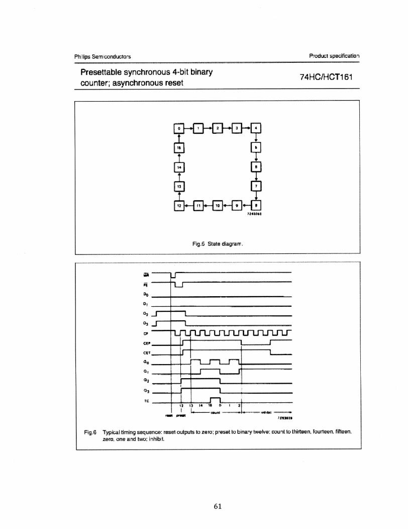
Ph lips Seen condixic~ Podu~i Weciticatiai
Presettable synchronous 4-bit binary
counter-, asynchronous reset74HC/HCT1 51
61
Figsi State diararr.
Fig..6 Typo aI timing aequen' : resel outputs ze ;p eset tbbinwy Iwet : r u rt i thirteen, Fourteen. fiile n.zero, oneand -t~: hhiid.
P, m cl specificatio 1Ph' lips 3e ndu 1 °:s
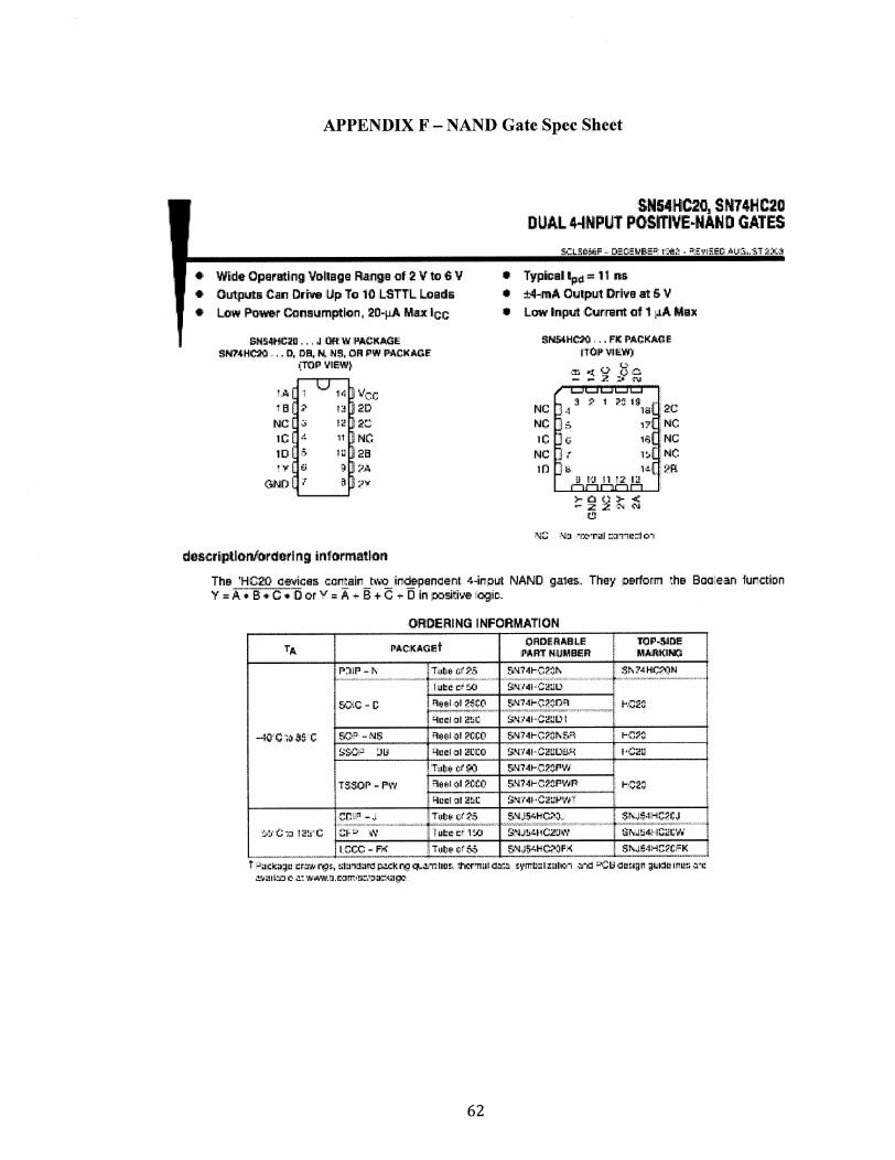
APPENDIX F - NAND Gate Spec Sheet
SN54;c2, NI4H C20DUAL 44 PUT PGflVENANO GATES
i °L 3- a F rE I B E D £ Y ha..: r
*Wide Operating Voltage Ranga at 2 V t 6 V*OutputsCa Drie Up To 10 LSTTL Loads*Low Po'wr cnsumption., 20-piA Max [C
I
II
N5I1 .. J NVPC74H , OR, N fl5 OR PWFACK-A(LF(TOP VIEW~
NC 2Fa:
Typoat ~=11 ms4-mA Output Drive at SV
Low Input Currnt aolAA Max
SN54HC , ,.FlCPACKM FIc 'wVIL W)
NC . w2CNC ~.17 NC
10 i NC
NC 1,NC
>-0 >N. 2:
des rip~l o rderl rig infratitorThe 'HC20-c ices car tair t~o irdepencen t .4-iot NAND gales. They P erform the
Y=A. B C D or ' =:A B+! in isidi'e giE.
ORDER~ING INFORMATIONORDERA LE TOP-$IDF
TT PAC KA it ART N R F? MARKING
IPIPa C ___7_HC ____4
TO5PP O Rel I #C 1 r x1? -4H.,2FWP"E
L~.~ k-3FX r F- ---- --- ---
Bode an furction
62
z r. F
p srt
-4 4
1fa L 44e "bC.ti 1 w!= C - +d 1. .:..,,

APPENDIX G - Inverter Spec Sheet
MCI 4049UB
Hex BuffersThe MC 14491B hex inverternbut1er is constructed with MOS
P char nel and N- chanrnel enhancement. mode devices in a singlemonolithic structure. This complementary M OS device finds piinaryuse where low power dissipation and. or high noise immunityr is
desired. This device provides logic-level conversion using only onesupply voltage, V1)). The input-signal high liee (Vjrn) can exceed the
DD supply voltage f °r logic 4evel conversions. Thvo TTL/IJTL
Loads can h driven when the device is used as CMOS to-'TTLDTLcnverters (VDD = 5.0 V VO)L.:(14OV, 'OL a 3.2 mA). Note that pins
13 and 16 are not co nnected. internally on this device; consequentlycnnections to these terminals will .not affect circuit operation.
* High Source and Sink Currents* High-to- Low Level Convenier
* Supply Voltage Range - 3.0 V to 18 r* Meets J EDEC U B Specietications* YiN can exceed V DI)* Improved ESD Protection on All Inputs
MAXIMUM RATINGS (V/stages Referenced to V S) (No te 2.)Symbol Parameter Value Unit
' r DC S:upply Voltage- Range -0.5 to +' 8.0 VVia Input Vottage Range -0.5 to +1 8.0 V
=DC or Transienit)
VVr Output Voltage Range -0.5 to Vr,: +0-.5 VDC or Tansient)
S r Input Current 1.0mADC or Tanaiernt pe- Pin
IW Output Current -45 mADC or Transient) pe- Pin
P Power Dissipaticrn, mWper Package (Note .3. )Plastic 825SOIC 740
TA Ambient Temperature Range -55 to +_ 25 ~CT~t Storage Tempoerature Rar~e -65 to +! 50 1C
TL Lead Te 'p eratu re 260 ':8-Second Soldering) _______
2. Maxir'um Ratings are those values beyond hitch damage to the devicemray occur.
3. Tetrperature Derating:All Packages: See Figure 4.
This -device contains ci:c:tyto p.'tct' the inpouts again~st dam~age due to highstatic ye tages or electric fields referenced to th V55 pin, only. Exta precautions
hitp:/lorisem .corm
P[IP-1P SUFFIXCASE 648
541C-t6D SUFFIX
CASE 7571B
TSSOP-16DT SUFFXCASE 90.8,
SOEIAJ-16F SUFFIXCASE 966
MARKINGDIAGRAMS
16
LhM144UBCPI
1~~
16
1M104 u1
A = Assembty LocaNionW Lor L = Water Let
YY'or Y = YearVWW e W =Wc-"kWeek
ORDERING INF~ORMATION
Device Package Shipping
FMC1404@U3CP PDIP-16 200W~Ex
MC 1 4 tU3D lC--1 6 24O0~cx
MC 1 4O4QUDR2 SOIC-" 6 2500 ,,ape & Re
MC 1449U3DT TSSOP-16 6GIRail
MC 14O49U DTR2 TSSOP-16 2S00 Tape & Re
MC 14049UBF SOEIAJ-1Q See Note 1.
MC14OU3FEL SOElA.--16 ) See Note 1.
For ordering information on the E .+'j version -ofthe SOICOpackages, please contact your =calON Semiconductor r-eprese'ntative.
63
drlAANIN Smlctr
Aqw

MCi14049UB
PIN ASSIGNMENT
'tat; 1 " 1E5#NC
our14 2 15 Du 1-
IdN 3 14 IN~
uu 1 4 13 11C
INJ 5 12 OUT-
iS, g 9 IN~
NC NO 0,0rNEC.ION
LOGIC aDIAGRAM
DIN 8145
CIRCUIT SCHEMATIC(116 OF CIRCUIT SHOWN)
9 iD:y
MCI 4i49 U6
VS1
64
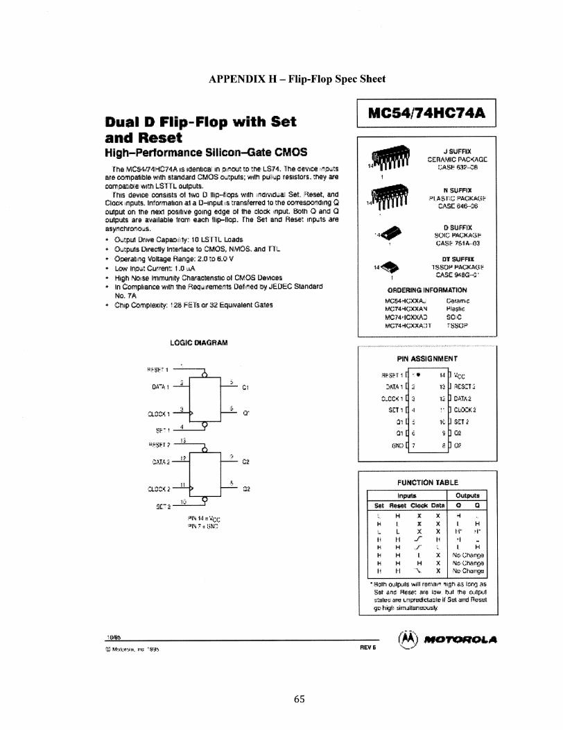
APPENDIX H - Flip-Flop Spec Sheet
Dual D Flip-Flop with Setand Reset
igh-Performance Silicon-Gate CMOSfhe ' AC547 -4C71A is denica in DOWu'tow:hL574. The aece r :s
are cnpalible with standard CrMas ~puts; with pu~ p resistors. ~s rc2nat e oih LS T L outputs .
This deioe' cnssts oI i 1U)Ilp1p s with Gvrdea. Set. R-eet, andClcic inputs. Inf- na1Ion al a U-input is ransterrd 10 the o~rst> 'ng
output on the nexi p msie going edge o1 the clock nput. 1h and 0outputs are available iron' each hlip-hlop,. rhe Set and Hese. inp 1s areasryCnr.4..
a OpuUrrwe Capao t y: 10 LSI'L Leeads
Ox-~puts Iiretly Intle"ace to CMOs: NAC(S. and TV_.
* O'perat V oltage Harge: 2.0 to 6.0 V*Lw I n ; Cu'en: 1.0 iA*High 'cse Immunity Ohara tenslic LotlCEC! O evces*In Compliance With ihe ec rerns ls Deftined 'y JEUEC Slandar-d
No. IAC ~hip G npla it : '28 I=Mscr3 u ent Gates
LOGIC VIAaHAM
C
'a
C2
IL'k 14
LMC54/74HIC4A
14*
JSUFRiXtfAICPACKAGE,
:$U=FFIX
.ASE 34&°6
D 'SUF FIX
DT SUFFIX1 St) PiA KA(-
CAE 9-- '
OGRDERING INFORMATION
MBC?4'CX) A OC C
PIN ASSIGNMENT
ST 4 C LXKc2
Inpwtis 0uLp4JtnSet Reset CkckcOnto 0 0
H X X -1I> . x x I,, H
- L X >X 11'F H I HI- H I_ X ' 1; =I ir'E1- H H X Iv rr~
.t Ih o iIp i wll! rorn rnih i l r] -SIL1 F -1.T: ir Id w ji ' .t CA rL
g ( kg ) MOTOROLA1"e
65
Mi s. t :
t;=°' off"' = 1
14
14

APPENDIX I - On-Board Clock Spec Sheet
E'ina
General Desiton13f%165 rth i liri ig.in-ra u"4
Ir r p Ror os$ I jn A h ,1r I !r is are ' 1
t c f~Ir riL i pi - y uiul bc o ixtar nur -
ir;r dz l', w,11 Iv aixi r !9~ r zr : c tits. Terr if ltlmayiw"v riyurL) d Metjes. rr llir y w Ir ir, ird
1l-II 1 lu~r r: r~ pi t
Features[FIir crer pincrrer 'Okr :9 5 56
* irniin ryr~rr i 1-1D:,i , h i q r,-A* Ajuutub Duty =t: r
u O i. cirw S r ik 2 j n* 01 u :. drd a Iv TTL Ltxipa IbkiA T r t hlrAl l 11 Lhr iuri 0.G2 e
Uf ii ~L' i ikiriflfltly 07UbWt.* viiabk ii -pin 1SOP roc
Applications'm Pr 4Ws 'I 'rnirfjtr ¢rpr
*~ PLI'L ii a ut i:l y ut
1 .1r ur f'dtr:; gvLiLraIt
Connection Diagraml ~ I-In-L:Jn SImil Culrw
and Molded Mini Small Outline Packaese
IKE1 t 43$
dH KR Li
!fit T~
Top Vie
Ordering Information_____Pat_______ Part Nueibr Package !Mrkin~ Media Tr naeor NMS Druwing
N -Pir &OWIC L S555 W L 56 i# 1
! -Pir MOP LM5CM : Z551Lih Tp ir Pu
_________ L 55 V BMX ZS! 5 3.51 UsiL Tu 1L t fl~i M i~~Vu-Pr MAIII .M5 55N
66
h JI'
LM555Timer
Ur1= ti r P Ui
1:z : z- I f; K
Applications Information nugd.)
50%6 DUTY CYCLE OSCILLATORFr r a60% duty eydCk, the resistors R,, and RB na be con-rA, lie as irn Figut + 14. The 1i r pr; od for Me out t s'igh ib 1
ls as as veuvious, t1 0.6133 RA 0. For the oulpul low it
RR -RA]Thus Lie Iruq wrtzy lI 05C1 ation is LTS
FIGURE 14. 50% Diry Cycle Oscillator
Note that th "s cruut w I not oscillate it RB is greater than 1 12
RA because lbsu unction o1 RAand RB r not tbring p n 2down to 113 V c~ and trigger tie I wu1 o'uparator.
AIDDITIONAL INFORMATIONAequale power upply bypassing is r sces sry to protect
associated cruPy. Minimnum mcomrneridsd is 0.lpF in par-allel wvi1lpF eleotrczytc.Lower compa-ratosr storage lts Canl ie aslon~g as 1bqs
w isi pmn 2 is driven lTully to ground for triggur ng. This I_=nitsthe mrootable pulse w dth to l0ps min nu r.
Delay time eset to output is 0.47pi ty pk al. Mi'imnrri resetpulse w -dth must be 0.3 i5, ly pica .
Pin 7 current switche~s within 3011s 01 lie outpul (pin 3: vulIt-age.
67
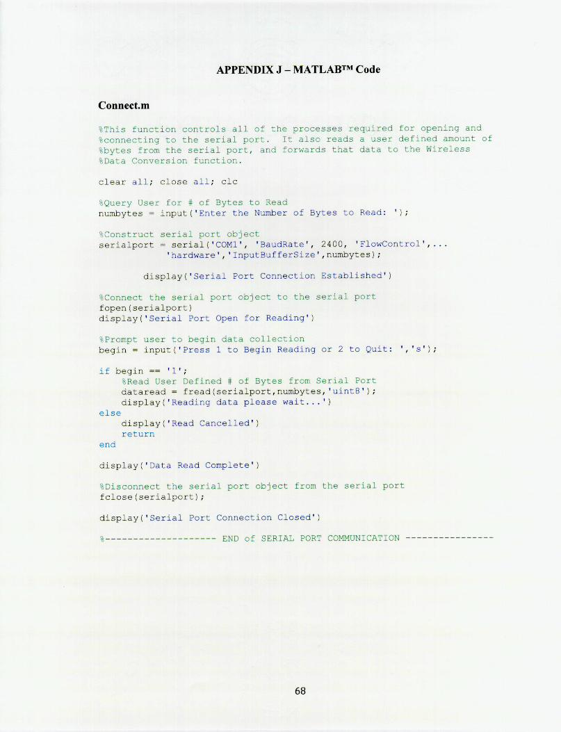
APPENDIX J - MATLAB T MI Code
Connect.m
=o nnecting to the serial port. it als reads a user definod amt o ft
bytes frmt seia ort, and forwards that data to the Wreless
clear all; close al ~
r urby7e e irnput ('Enter the Numrber of By' e Read:'.
ser 'alport'hrdware',' nutBuferrize,ubytes)
display('Serial Prt Conectio Establisnea'
fopen serialport)display('Serial P o Open fo Reaing')
beginr irput('Press tou Begin. Reading or 2 toQuit: ','s)
begin
dataread =fread serialport,rurbytes,'in~t8')
diirplay('Reading data please wat..'
display('Read Cancelled')
display('Data Rea omplete')
fclose seriaip or)
display('Serlai P o Connecton Clse'

C'onvert.m
reverses thle einary strings ana r
x dataread';display(' .'Fa
)51119<5 PaLe as ue2II~Td UTL :r' .
:ength (x
binary -jec2br a.~
reversedi, birzdec~birary
end3
vltages = reversed*(5/256))
grid on, hoed rn
pierplot(piot(plotpiot1
plet(tittie
xi abey] at e
0,iergrh a ],[2,2],'[0 engt (xa , [3, 3] ,'
[ lergth(a ],[4,4 ,'
0,iength a)],[5,5,
- , news th,l
r , Iew id-.
r1 ', ews r',1
:ergrh a ,volages, 'b', 'liiewldrh',lI.tag Read2 rgs frem Opticai Sensrs
'Sampie #')Vtage Readirgs -v]'
display('Data Precessing Cemplete'
rnput('Woul s Yos Like to Save These Ressits? (yrn:'s)
if stere 'yrame = iputdate =!p
eles
save as t[arme,fid =foper sav
(Filerame: '' I
*f (fid < 0)
st r
i ...
. xt' - ,
s,'wt' ,
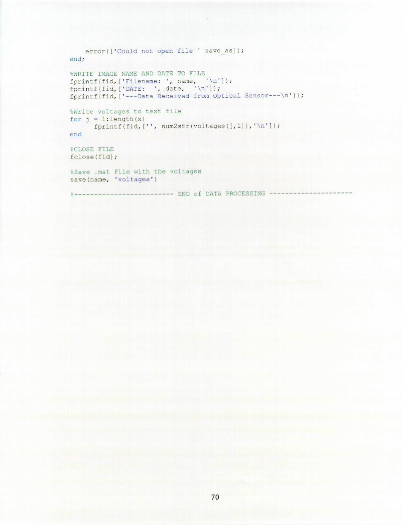
Prr()
ft rIno( fidc,fprintf fid,
LA~TE: ,date, Ar. )
--ata Received from Opticai Sensor-
!:lenghx)fpri ntf (f id, ['', nm2str (voltages (, 1
fclose(I );
save(name, 'voltages'
--- ND of DATA PROCESSING
r- er. _ '. e ' save a:1,rl

Compare.m
voltaqes forcomDnarison.
comsparisor
-are .npu.('Woula
y/r:
ent A J' a , as is
* ke to comparison different datasets.
cmparson y'num - nput('Please enter tre #
display('Propramr'Yun
I f num-rmax 1;
e l rEi um=max 2;
elei n um=
max=3;
ard Otews py the Brnyrr
rf Samples to comparison (1-3)
Has Completed';
='2'
datasetldataset2daaset3
hf figure;set (hf i '
for d = :maxda =
clrchange ='b';
dataset l nput('Type Name
datasetl _ dataset, '.mat
1oad (datasetl, 'a ltages')1 fd==2clorchange = g';
dataser =input('Type Name
dataset2 = dataset, '.mat'
1oad (datase"2'otgs)ci rd==3
colrchange ='k';dataset =irput('-ype Name
dataset3 = dataset, '.mat'
lead (damaset3, 'volages')

urr n __ .
pLot l:length(voimages),vo1tageshold on, grid on
tie(['Volmage Data-Readings';;
xLabel('Sample #')ylabel(' Voltage Redn
ri2ptr rex) '1'ial Sensor
I
t max =legend damasetl)
elsi _ mfrax ==2legerd daraset1,damaset2)
e *r F ax==3legend damaseml,damaset,damase
cod
plot([0,lengmth
F ot(0,lengmrplT([,lengtr
pit[,lerjrm
F ot([C,length
volmages)],[1,1,'vloages)],[2,21,
vo ages)],[3,3,'
volma;: ),H,4 ,'
ye mages)],[55
I 7wldtn',l),'ewldmh',l)
rnewldmh',1
;-N% of 0OLAGK DALiASFIE ARSN
set (hf,'vis.ibi,',' )
IPARTSONS

(AJIm
function varargoatGUII M-
GUI varargir
singl±eton'
H C GI returns the :
the existlna single,
CCI('CALrBACK',hOa ecr,t At, 1e' I
funct1on niamed CALLBACK in GU--.M with the a ten input arguments.
CI('Property', 'Value........creates a new GUI or raises the
existing sinaletor*. Starting from the left, property value
pair: are applied to the CGUI before CU OpeningFunctlon gets
-allea. An unreaognized property name or invalid value makes
prr ty anffliwarion st op. Ai inputs are passed tn
CUI Oper i.g an via varargin. -See CU Options or CGUD's To:
menu. Choose "GIl allows only one lnstanc to run (singleto_"
See alio: GUIDE, CGUIDATA, GUHANDLES
Edit the anov taxt to noltf the responsec to help CII
Last Mo-. tf~d by GUIDE v?.5 29-Tan-2 8 132254
gui Singleto -r 1gui State -struct('gai N ,'
'gui S5 _egui Opernongul ouputb'goi Layoat.'gui Ca1b
it nargir && ischtar varargin{1'}
nargout
[varargoutVi:targout}] gui
mfl erare,gui Singleton,
?GUIIpenng 'n,@GUICutput 'n,
rtn 'arargi 1)
i mairfcn gui State, varargir{:};
gul mainfrt gui State, varargin{:f)
--Exec
functian C IOpenirgtcn aQjeat, evetdata, :Handes, varargin)
Thi
eventdat a reservea - to be definea in a future verso n or MATLAB
set(h~bet,' bar', '~ t iu ;
handles.output =h bjct

guidata(hObect, hardies)
a w._t harno~ -t igurel)
function varargout =GUI OutputP'r (bObject, eventdata, hardles)
kar3
i -~ ,c r '-' or ,301Di>
n bje-' eevertdaja resrvedJ tc be mtae& e a suture 'r r a MIATLAB
handles structur~e with handles and user data (see GUILATA)
varargout 1)
fur .
hnroes.output;
tart Caiiback hObject, evertdata, handles)
h ever:
harndies
. - -II reu ,_ u ,rs or of MAT AB
structure with hardles ano user oata (see CUID/AA
selects axes: as the current axes, so thatM, t 1 vh v~~ws eet p1ot the data
fclose instr f
serialport
rnd 'lose all oper serial per" connections
serial ('AD> _, '-ddate', 2400'ha ', 'Th-->,u-Duff rQi e
fopern(serialportaxes(handles.0 xes3
id:-25)p m__ox
window
dataread -fread serialport,lx =dataread';b'nary =decmhr(x,seversed (4, : h in_ ( .a-.voltages =reversed*(5256);
plot i/,voltages i),'c' ,' :new Cub',2);hoid
oitle ('Volta ,x abei('Tite '
jladel o. 'Vguidara h bjc , hanrles)
pause .)
om Optical Senso r
0-5v)y'rn randle
axis ;grid on

window+1):60000
datzaread =fread serialpor: ,1, 'unn'
x =dataread';brnary =dec2brnx 8),reversed i,: bin2dec~bnary(8-:voitages =revered-(5256))
plotmi12,voirages i,W'')axis([1i2)-window, window+- i2),
title('Voltage Readings from Opmical Lensor';xlabel('Tire')yladel (' Vo a x Rd nqs ')
guiama hb1 d -t, nd es2
paose(.)end
function pause Callback habject, eventdama, handls
even, 1a
handles structure with hardles and user data (see GUTDATA)