Fabrication of 1×2 asymmetric plastic optical fiber coupler for portable optical access-card system
7
Fabrication of 1Â2 Asymmetric Plastic Optical Fiber Coupler for Portable Optical Access-Card System Abang Annuar EHSAN, Sahbudin SHAARI, and Mohd Kamil Abd. RAHMAN 1 Institute of Microengineering and Nanoelectronics, Universiti Kebangsaan Malaysia, 43600 UKM, Bangi, Selangor, Malaysia 1 Faculty of Applied Science, Universiti Teknologi MARA, 40450 Shah Alam, Selangor, Malaysia (Received May 31, 2010; Accepted October 14, 2010) An optical code generating device using plastic optical fiber (POF) coupler for a portable optical access card system is presented. The code generating device has been constructed using asymmetric hollow POF coupler design. The device provides a unique series of output light intensities which are successively used as an optical code. Ray tracing models of various coupler designs showed a linear relationship between the tap-off ratio (TOFR) and the waveguide tap width. The asymmetric POF coupler has been fabricated on metal-based materials using machining technique. The results for the simulated and fabricated metal-based 12 asymmetric couplers show the same linear characteristics between the TOFR and the tap width. The simulated devices show a TOFR variation from 18.6 to 49.9% whereas the TOFR for the fabricated metal-based devices varies from 10.7 to 47.7%, for a tap width of 500 mm to 1 mm. The insertion loss for the 12 asymmetric coupler at the tap line varies from 12.7 to 21.2 dB whereas for the bus line, the average insertion loss is about 12 dB. # 2011 The Japan Society of Applied Physics Keywords: Asymmetric, access-card, coupler, mold insert, plastic optical fiber, POF, tap-off ratio 1. Introduction The field of integrated optics has been in much attention in recent years. Optical communication systems, optical interconnects and optical sensors are some of the vast application of integrated optics. Optical sensing is a broad field encompassing many applications. One of the proposed applications in optical sensor is the optical code generating devices for security access system application. The application of optical components in security access systems has been known and several international patents have been identified. Most of the US patents applied between the year 1978 until 2005 use optical technology but none uses the concept of applying a unique series of light-intensity for code generation in an access-card system. These systems do not utilize planar optical waveguides or the concept of applying a unique series of optical power for code generation in an access-card system. They basically used fiber optics bundle where the codes are represented by the linear pattern of lighted and unlighted fibers, done by obscuring, breaking or omitting selected fiber in the bundle. 1,2) For an example, the UK patent 2022300, 1) had used the linear pattern of lighted and unlighted fibers to represent the code and had not used the individual light intensity coming out from each fiber as a component of a code. In addition, it used 8 fiber optics bundles which can generate 2 8 ¼ 256 codes only. As for the US patent 3728521, 2) it has the same concept as the UK patent, but it had some moving parts on the receiving side. The security access system developed by the NASA Research Center is a system that utilized optical component for optical code generation. This system used fiber Bragg gratings (FBG) as its code generating device. 3) Figure 1 shows the security system that used the FBG to generate optical codes. The codes are basically the reflected spec- trums from the FBG which are then dispersed at particular wavelengths using the diffraction grating. Lawrence Livermore’s Defense, Nuclear Technologies and Engineering Directorate had also developed a similar optical key component named Light Lock Optical Security System. 4) Figure 2 illustrates the Light Lock Optical Security System. This component is mainly designed to secure military vehicle systems from theft and unauthorized operation. However, the major disadvantage of the systems developed by NASA Research Center and Lawrence Livermore’s Lab is the utilization of high cost single mode optical components and both the laser and power supply units have to be built into the portable key respectively. This paper reports on the development of an optical code generating device constructed using asymmetric plastic optical fiber (POF) coupler, embedded in new portable optical access-card system. A unique unbreakable optical code can be produced by simple arrangement of the output power of the asymmetric coupler. The proposed portable optical access-card system employs a simple coding- decoding of light signal transmitted from an LED or laser, where the light signal is ‘‘coded’’ using the POF coupler. The heart of the portable optical access-card system will be the asymmetric coupler device. This device can have N-number of output ports and one input port. An asymmetrical waveguide design is used to design the device which allows the input power to be split into any value from 0 to 100%. Figure 3 is a block diagram showing how the output powers of the code generating device are utilized for generating a unique optical code for the access-card system. In this figure, a generic 14 coupler is shown (N ¼ 4, 4-digit code). The characters A, B, C, and D represent generic terms for the codes. By a simple arrangement of the output power, a series of optical codes can be produced. Two examples of optical codes generated are shown in this figure. Each output port OPTICAL REVIEW Vol. 18, No. 1 (2011) 86–92 86
-
Upload
independent -
Category
Documents
-
view
0 -
download
0
Transcript of Fabrication of 1×2 asymmetric plastic optical fiber coupler for portable optical access-card system
Fabrication of 1�2 Asymmetric Plastic Optical Fiber Couplerfor Portable Optical Access-Card SystemAbang Annuar EHSAN, Sahbudin SHAARI, and Mohd Kamil Abd. RAHMAN1
Institute of Microengineering and Nanoelectronics, Universiti Kebangsaan Malaysia, 43600 UKM, Bangi, Selangor, Malaysia1Faculty of Applied Science, Universiti Teknologi MARA, 40450 Shah Alam, Selangor, Malaysia
(Received May 31, 2010; Accepted October 14, 2010)
An optical code generating device using plastic optical fiber (POF) coupler for a portable optical access card system ispresented. The code generating device has been constructed using asymmetric hollow POF coupler design. The deviceprovides a unique series of output light intensities which are successively used as an optical code. Ray tracing modelsof various coupler designs showed a linear relationship between the tap-off ratio (TOFR) and the waveguide tap width.The asymmetric POF coupler has been fabricated on metal-based materials using machining technique. The results forthe simulated and fabricated metal-based 1�2 asymmetric couplers show the same linear characteristics between theTOFR and the tap width. The simulated devices show a TOFR variation from 18.6 to 49.9% whereas the TOFR for thefabricated metal-based devices varies from 10.7 to 47.7%, for a tap width of 500 mm to 1 mm. The insertion loss for the1�2 asymmetric coupler at the tap line varies from 12.7 to 21.2 dB whereas for the bus line, the average insertion loss isabout 12 dB. # 2011 The Japan Society of Applied Physics
Keywords: Asymmetric, access-card, coupler, mold insert, plastic optical fiber, POF, tap-off ratio
1. Introduction
The field of integrated optics has been in much attentionin recent years. Optical communication systems, opticalinterconnects and optical sensors are some of the vastapplication of integrated optics. Optical sensing is a broadfield encompassing many applications. One of the proposedapplications in optical sensor is the optical code generatingdevices for security access system application.
The application of optical components in security accesssystems has been known and several international patentshave been identified. Most of the US patents appliedbetween the year 1978 until 2005 use optical technologybut none uses the concept of applying a unique series oflight-intensity for code generation in an access-card system.These systems do not utilize planar optical waveguides orthe concept of applying a unique series of optical power forcode generation in an access-card system. They basicallyused fiber optics bundle where the codes are representedby the linear pattern of lighted and unlighted fibers, doneby obscuring, breaking or omitting selected fiber in thebundle.1,2) For an example, the UK patent 2022300,1) hadused the linear pattern of lighted and unlighted fibers torepresent the code and had not used the individual lightintensity coming out from each fiber as a component of acode. In addition, it used 8 fiber optics bundles whichcan generate 28 ¼ 256 codes only. As for the US patent3728521,2) it has the same concept as the UK patent, but ithad some moving parts on the receiving side.
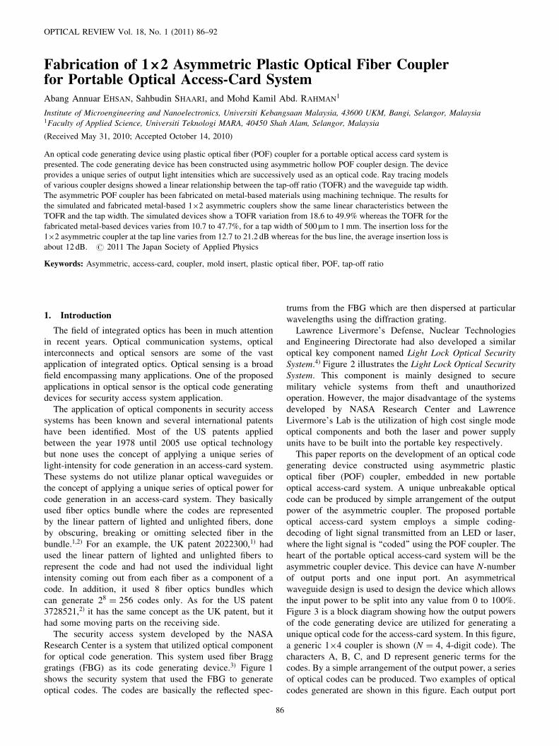
The security access system developed by the NASAResearch Center is a system that utilized optical componentfor optical code generation. This system used fiber Bragggratings (FBG) as its code generating device.3) Figure 1shows the security system that used the FBG to generateoptical codes. The codes are basically the reflected spec-
trums from the FBG which are then dispersed at particularwavelengths using the diffraction grating.
Lawrence Livermore’s Defense, Nuclear Technologiesand Engineering Directorate had also developed a similaroptical key component named Light Lock Optical SecuritySystem.4) Figure 2 illustrates the Light Lock Optical SecuritySystem. This component is mainly designed to securemilitary vehicle systems from theft and unauthorizedoperation. However, the major disadvantage of the systemsdeveloped by NASA Research Center and LawrenceLivermore’s Lab is the utilization of high cost single modeoptical components and both the laser and power supplyunits have to be built into the portable key respectively.
This paper reports on the development of an optical codegenerating device constructed using asymmetric plasticoptical fiber (POF) coupler, embedded in new portableoptical access-card system. A unique unbreakable opticalcode can be produced by simple arrangement of the outputpower of the asymmetric coupler. The proposed portableoptical access-card system employs a simple coding-decoding of light signal transmitted from an LED or laser,where the light signal is ‘‘coded’’ using the POF coupler. Theheart of the portable optical access-card system will be theasymmetric coupler device. This device can have N-numberof output ports and one input port. An asymmetricalwaveguide design is used to design the device which allowsthe input power to be split into any value from 0 to 100%.Figure 3 is a block diagram showing how the output powersof the code generating device are utilized for generating aunique optical code for the access-card system. In this figure,a generic 1�4 coupler is shown (N ¼ 4, 4-digit code). Thecharacters A, B, C, and D represent generic terms for thecodes. By a simple arrangement of the output power, a seriesof optical codes can be produced. Two examples of opticalcodes generated are shown in this figure. Each output port
OPTICAL REVIEW Vol. 18, No. 1 (2011) 86–92
86
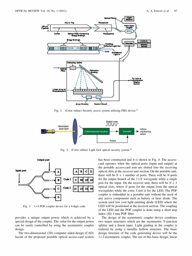
provides a unique output power which is achieved by aspecial design of the coupler. The value for the output powercan be easily controlled by using the asymmetric couplerdesign.
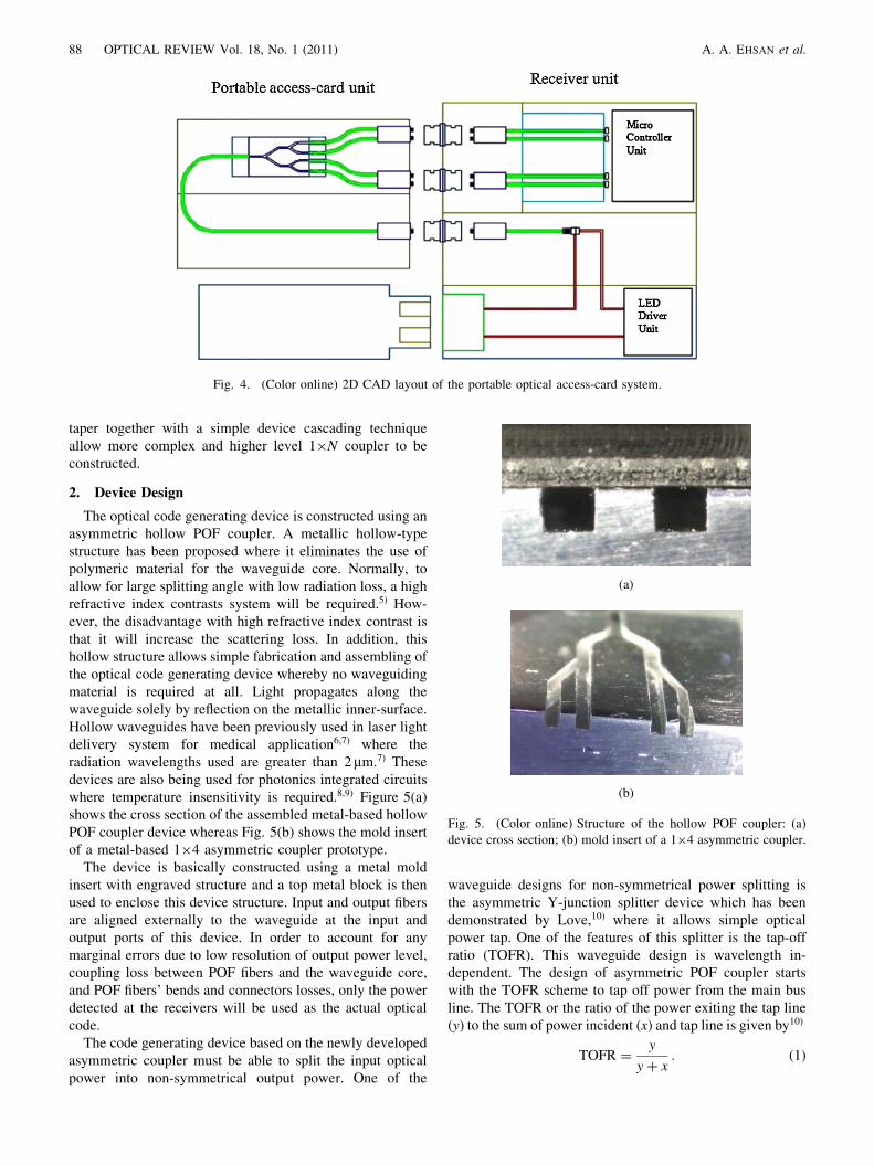
The two-dimensional (2D) computer aided design (CAD)layout of the proposed portable optical access-card system
has been constructed and it is shown in Fig. 4. The access-card operates when the optical ports (input and output) atthe portable access-card unit are slotted into the receivingoptical slots at the receiver unit section. On the portable unit,there will be N þ 1 number of ports. There will be N-portsfor the output branch of the 1�N waveguide while a singleport for the input. On the receiver unit, there will be N þ 1
optical slots, where N ports for the output from the opticalwaveguides while the extra 1 slot is for the LED. The POFcoupler is embedded in a portable unit without the need ofany active components such as battery or laser diode. Thesystem used low cost light emitting diode (LED) where theLED will be positioned at the receiver section. The couplingof the LED and the POF coupler is done using a short stepindex (SI) 1 mm POF fiber.
The design of the asymmetric coupler device combinestwo major structures which are the asymmetric Y-junctionsplitter and a linear taper. Light guiding in the coupler isrealized by using a metallic hollow structure. The basicdesign structure of the code generating device will be the1�2 asymmetric coupler. The use of this basic design, linear
Fig. 1. (Color online) Security access system utilizing FBG device.3)
Fig. 2. (Color online) Light lock optical security system.4)
Fig. 3. 1�4 POF coupler device for a 4-digit code.
OPTICAL REVIEW Vol. 18, No. 1 (2011) A. A. EHSAN et al. 87
taper together with a simple device cascading techniqueallow more complex and higher level 1�N coupler to beconstructed.
2. Device Design
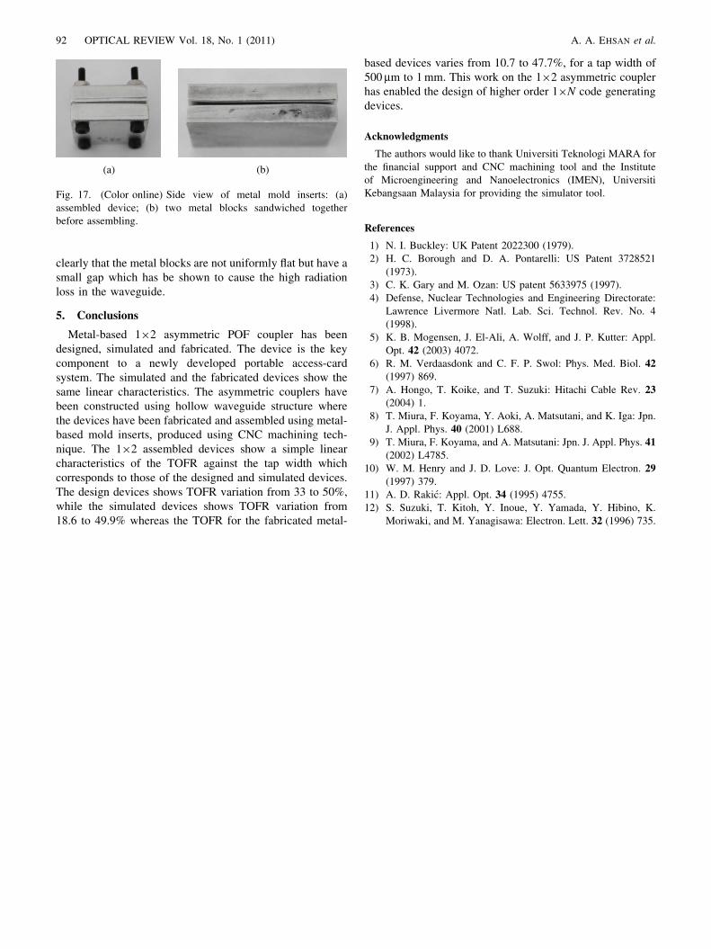
The optical code generating device is constructed using anasymmetric hollow POF coupler. A metallic hollow-typestructure has been proposed where it eliminates the use ofpolymeric material for the waveguide core. Normally, toallow for large splitting angle with low radiation loss, a highrefractive index contrasts system will be required.5) How-ever, the disadvantage with high refractive index contrast isthat it will increase the scattering loss. In addition, thishollow structure allows simple fabrication and assembling ofthe optical code generating device whereby no waveguidingmaterial is required at all. Light propagates along thewaveguide solely by reflection on the metallic inner-surface.Hollow waveguides have been previously used in laser lightdelivery system for medical application6,7) where theradiation wavelengths used are greater than 2 mm.7) Thesedevices are also being used for photonics integrated circuitswhere temperature insensitivity is required.8,9) Figure 5(a)shows the cross section of the assembled metal-based hollowPOF coupler device whereas Fig. 5(b) shows the mold insertof a metal-based 1�4 asymmetric coupler prototype.
The device is basically constructed using a metal moldinsert with engraved structure and a top metal block is thenused to enclose this device structure. Input and output fibersare aligned externally to the waveguide at the input andoutput ports of this device. In order to account for anymarginal errors due to low resolution of output power level,coupling loss between POF fibers and the waveguide core,and POF fibers’ bends and connectors losses, only the powerdetected at the receivers will be used as the actual opticalcode.
The code generating device based on the newly developedasymmetric coupler must be able to split the input opticalpower into non-symmetrical output power. One of the
waveguide designs for non-symmetrical power splitting isthe asymmetric Y-junction splitter device which has beendemonstrated by Love,10) where it allows simple opticalpower tap. One of the features of this splitter is the tap-offratio (TOFR). This waveguide design is wavelength in-dependent. The design of asymmetric POF coupler startswith the TOFR scheme to tap off power from the main busline. The TOFR or the ratio of the power exiting the tap line(y) to the sum of power incident (x) and tap line is given by10)
TOFR ¼y
yþ x: ð1Þ
Fig. 4. (Color online) 2D CAD layout of the portable optical access-card system.
(a)
(b)
Fig. 5. (Color online) Structure of the hollow POF coupler: (a)device cross section; (b) mold insert of a 1�4 asymmetric coupler.
88 OPTICAL REVIEW Vol. 18, No. 1 (2011) A. A. EHSAN et al.

In the device design, this TOFR is achieved by varying thewidth size of the tap line. This design also includes a lineartaper structure which allows the smaller-sized tap line tocouple to a larger core POF fiber at the output ports ofthe coupler. Figure 6 illustrates the simple 1�2 asymmetricY-junction splitter with the bus and tap line.
The 1�2 asymmetric POF coupler design with bus linewidth (x) of 1 mm and a tap width (y) of 0.7 mm (41%TOFR) is shown in Fig. 7. Figure 7(a) shows the 2D layoutof the 1�2 asymmetric coupler. The hollow waveguidestructure is designed by building a rectangular block andinserting the three dimensional (3D) coupler design into it.Figure 7(b) shows the 3D layout of the coupler. Arectangular block is then constructed where the 3D designedstructure is then subtracted from the main rectangular block,which is shown in Fig. 7(c). The 3D layout in Fig. 7(c) willbe utilized for device modeling, illustrated in the nextsection.
In the device design, the split angle, � has been set to 6�.The split angle 6� is chosen to allow a minimum output portsspacing of 150 mm for a design with tap width of 500 mm. At
this stage, this angle will be the smallest angle for this designdue to the very narrow output port spacing, which will bevulnerable to cracks and breakdown during the actual moldinsert fabrication. This angle is fixed throughout the designprocess which enables us to control only the tap line width.
The designed TOFR for the 1�2 asymmetric coupler isgiven in Fig. 8 which shows the plot of the designed TOFRagainst the tap width. These results are obtained by taking onthe ratio of the tap line to the sum of the tap line and bus linewidths, from y ¼ 300 to 1000 mm with a bus line width of1000 mm. The TOFR obtained using this range of tap widthsare from 23 to 50%. In addition to the TOFR against tapwidth, the remaining power ratio at the bus line is alsoincluded as comparison. The result shows that there is alinear relationship between the TOFR and the tap width.
3. Device Simulation
Due to the multimode characteristics of the POF coupler,ray-tracing technique has been used to model these opticaldevices. The ray tracing simulation of the POF coupler usingZemax simulator tool, is performed to predict the opticaltransmission properties of the device.
The light source used is a Rectangular Source modelwhich acts like a diffuse source whereas the detector used isa Detector Rectangle. It is a flat detector in the form ofrectangular (or square) shape. The non-sequential ray tracingis performed using the 3D design of the hollow structure inFig. 7(c). In order to make the hollow waveguide to reflectlight rays all the way from the input port to the output port,the inner coating of the coupler is defined as reflective wherethe coating is written as metal coating.
Some assumptions have been made for the devicemodeling. One of the assumptions is that the device willhave an entirely closed hollow structure region from theinput to the output ports. There will be no air gaps for thelight rays to escape from this region and all rays which hitthe sides inside this block will reflect back into the hollowgap. In addition, another assumption made is that themetal block used will have its metallic surface coated withaluminum. This coating has a coating thickness of 0.04 mm
Fig. 6. 1�2 asymmetric waveguide coupler design.
(a)
(b)
(c)
Fig. 7. 1�2 asymmetric POF coupler (0.7 mm tap width): (a) 2Dlayout; (b) 3D layout; (c) 3D hollow structure.
Fig. 8. TOFR vs tap width for a 1�2 asymmetric POF coupler:designed devices.
OPTICAL REVIEW Vol. 18, No. 1 (2011) A. A. EHSAN et al. 89

and a high reflection coefficient at 650 nm, Rs ¼ 0:90535 (atabout 90% of light gets reflected).11) The wavelength used inthis simulation is 650 nm, with input power of 1.0 mW.Another feature of this waveguide structure is that it isoperated unidirectional only. An example of the ray tracingdiagram of the POF coupler is shown in Fig. 9 for the 41%TOFR asymmetric POF coupler.
Some other TOFR values have also been tested for the1�2 asymmetric coupler design. Tap width of 500 to1000 mm are used in this simulation. The results for theTOFR against the tap line width are given in Fig. 10. Thisplot shows the simulated TOFR based on the designedstructure in Fig. 6.
The TOFR for the simulated devices are obtained bytaking the ratio of the optical power at the tap line over thesum of power at the tap line and bus line12) which is shownas the following relationship:
Branching ratio ¼P2
P1 þ P2
; ð2Þ
where P2 is the output power at the tap line and P1 is theoutput power at the bus line.
Figure 11 shows the plot of the TOFR against the tapwidth for both the designed and simulated devices. Thedesigned devices are based on the results for the TOFR as inequation (1), from y ¼ 500 mm until y ¼ 1000 mm with a busline width, x of 1000 mm. On the other hand, the simulateddevices are based on the results obtained from thesimulations for the tap line width, y of 500 to 1000 mm.
The simulated devices show the same linear characteristic asthat of the designed devices. The TOFR obtained for the1�2 asymmetric coupler based on this simulation is from18.6 to 49.9%.
The designed values for the TOFR and the simulationresults show that for large TOFR, the error between thedesign and simulation values are less significant. The errorsare quite significant especially for the smaller TOFR. Thelarge variation of the TOFR in particular for the small tapline width is due to the increase of attenuation as the coresize decreases. As the tap width reduces, the higher ordermodes will be suppressed and not able to propagate into thesmaller waveguide.
4. Device Fabrication and Characterization
One of the key advantages of this developed POF coupleris the simplification of the fabrication steps. This fabricationtechnique is a maskless process which significantly reducedthe highly cost of producing photomask, and the costlyphotolithographic equipment. We have used Roland EGX-400 desktop CNC engraver to engrave the design structuredrawn in CAD tool onto the metallic block. The endmilltool size used is 0.5 mm and machine spindle speed of30,000 rpm has been utilized. Figure 12(a) is the mold insertfor the 1�2 asymmetric device whereas Fig. 12(b) is anexample of the mold insert for a 1�4 asymmetric device.
After the mold insert has been fabricated, a top metal plateis positioned and the connecting screws are secured. Finally,short POF fibers (20 cm) are inserted into the input andoutput ports until the fibers are positioned just about 1 mminto the engraved slots. Figure 13(a) shows the assembleddevice before the POF fibers are inserted whereas Fig. 13(b)shows the POF fibers after insertion into the device.Figure 13(c) shows the assembled device structure withthe input and output POF fibers.
The insertion loss of this device has been tested usingAdvanced Fiber Solution FF-OS417 optical source at650 nm and optical power meter OM210. The effectiveinput power is 0 dBm. Figure 14 is the plot of the TOFRagainst Tap Width for the metal-based fabricated devices. In
Fig. 9. (Color online) Ray tracing of the 1�2 asymmetric coupler(41% TOFR).
Fig. 10. TOFR vs tap width for a 1�2 asymmetric coupler:simulated devices.
Fig. 11. TOFR vs tap width for 1�2 asymmetric coupler(designed and simulated devices).
90 OPTICAL REVIEW Vol. 18, No. 1 (2011) A. A. EHSAN et al.

addition, branching ratios for the bus line are also includedin this plot. In this plot, the TOFR varies from as small as10.7 to 47.7% by a simple variation of the tap width.Figure 15 shows the plot of the TOFR against Tap Width forthe design, simulated and fabricated devices. Here, thesimilarity of the TOFR linear characteristics for the design,simulated and fabricated devices can be seen.
Finally, the insertion loss for the designed, simulated andfabricated devices is plotted and is shown in Fig. 16. Theinsertion loss for the 1�2 asymmetric coupler at the tapline varies from 12.7 to 21.2 dB whereas for the bus line,the insertion loss is about 12 dB. The insertion loss for thedesign and simulated devices are close to each other except
for the smaller tap width. Again, it has been shown that inthe simulated model, due to mode conversion, the insertionloss at the smaller tap line has increased compare to thatof the design structure. However, there is a large constantinsertion loss deviation between the simulated and fabricateddevices.
It has been shown in the device model that a perfectlyconstructed hollow structure with a high reflective surfaceswill not allow any light ray to escape from the hollow regionbut will be confined in that hollow region. Again, this modelis accurate when the device is a piece of metal block withhollow structure in the middle of the block. Nevertheless, theactual device is actually a two-piece metal blocks sandwichtogether. This is one of the limitations of the fabrication andassembling technique. Due to the non-flatness of the metalsurfaces, when these blocks are sandwiched, there will be airgaps between the top block and the bottom mold. This hascontributed to the high insertion loss of this device due toradiation. Figure 17 shows the side view of the mold insertsused for the metal-based POF couplers. This figure shows
(a) (b) (c)
Fig. 13. (Color online) Assembling of the 1�2 asymmetric cou-pler: (a) mold insert with connecting screws; (b) fibers insertion andtop plate placement; (c) connecting screws are secured.
Fig. 14. TOFR vs tap width for the fabricated metal-based 1�2
asymmetric coupler.
Fig. 15. TOFR vs tap width for 1�2 asymmetric coupler(designed, simulated and fabricated devices).
Fig. 16. Insertion loss vs tap width for the metal-based 1�2
asymmetric coupler (designed, simulated, and fabricated devices).
(a) (b)
Fig. 12. (Color online) Mold insert for (a) 1�2; (b) 1�4 asym-metric coupler devices.
OPTICAL REVIEW Vol. 18, No. 1 (2011) A. A. EHSAN et al. 91
clearly that the metal blocks are not uniformly flat but have asmall gap which has be shown to cause the high radiationloss in the waveguide.
5. Conclusions
Metal-based 1�2 asymmetric POF coupler has beendesigned, simulated and fabricated. The device is the keycomponent to a newly developed portable access-cardsystem. The simulated and the fabricated devices show thesame linear characteristics. The asymmetric couplers havebeen constructed using hollow waveguide structure wherethe devices have been fabricated and assembled using metal-based mold inserts, produced using CNC machining tech-nique. The 1�2 assembled devices show a simple linearcharacteristics of the TOFR against the tap width whichcorresponds to those of the designed and simulated devices.The design devices shows TOFR variation from 33 to 50%,while the simulated devices shows TOFR variation from18.6 to 49.9% whereas the TOFR for the fabricated metal-
based devices varies from 10.7 to 47.7%, for a tap width of500 mm to 1 mm. This work on the 1�2 asymmetric couplerhas enabled the design of higher order 1�N code generatingdevices.
Acknowledgments
The authors would like to thank Universiti Teknologi MARA forthe financial support and CNC machining tool and the Instituteof Microengineering and Nanoelectronics (IMEN), UniversitiKebangsaan Malaysia for providing the simulator tool.
References
1) N. I. Buckley: UK Patent 2022300 (1979).2) H. C. Borough and D. A. Pontarelli: US Patent 3728521
(1973).3) C. K. Gary and M. Ozan: US patent 5633975 (1997).4) Defense, Nuclear Technologies and Engineering Directorate:
Lawrence Livermore Natl. Lab. Sci. Technol. Rev. No. 4(1998).
5) K. B. Mogensen, J. El-Ali, A. Wolff, and J. P. Kutter: Appl.Opt. 42 (2003) 4072.
6) R. M. Verdaasdonk and C. F. P. Swol: Phys. Med. Biol. 42(1997) 869.
7) A. Hongo, T. Koike, and T. Suzuki: Hitachi Cable Rev. 23(2004) 1.
8) T. Miura, F. Koyama, Y. Aoki, A. Matsutani, and K. Iga: Jpn.J. Appl. Phys. 40 (2001) L688.
9) T. Miura, F. Koyama, and A. Matsutani: Jpn. J. Appl. Phys. 41(2002) L4785.
10) W. M. Henry and J. D. Love: J. Opt. Quantum Electron. 29(1997) 379.
11) A. D. Rakic: Appl. Opt. 34 (1995) 4755.12) S. Suzuki, T. Kitoh, Y. Inoue, Y. Yamada, Y. Hibino, K.
Moriwaki, and M. Yanagisawa: Electron. Lett. 32 (1996) 735.
(a) (b)
Fig. 17. (Color online) Side view of metal mold inserts: (a)assembled device; (b) two metal blocks sandwiched togetherbefore assembling.
92 OPTICAL REVIEW Vol. 18, No. 1 (2011) A. A. EHSAN et al.