Magnetic Retraction of Bowel by Intraluminal Injectable Cyanoacrylate-Based Magnetic Media

1. INTRODUCTIONCouplers, also known as "isolators" because they electrically isolate aswell as transmit data, are widely used in industrial and factory networks,instruments, and telecommunications. Every one knows the problems withoptocouplers. They take upa lot of space, are slow, optocouplers age and their temperature range is quite limited. For years, optical couplers were the onlyoption. Over the years, most of the components used to build instrumentationcircuits have become ever smaller. Optocoupler technology, however, hasn’t keptup. Existing coupler technologies look like dinosaurs on modern circuit boards.Magnetic couplers are analogous to optocouplers in a number of ways.Design engineers, especially in instrumentation technology, will welcome agalvanically isolated data coupler with integrated signal conversion in a single IC.My report will give a detailed study about ‘ISOLOOP MAGNETIC COUPLERS’.

2. INDUSTRIAL NETWORKS NEED ISOLATION2.1 Ground LoopsWhen equipment using different power supplies is tied together (with a common ground connection) there is a potential for ground loop currentsto exist. This is an induced current in the common ground line as a result of adifference in ground potentials at each piece of equipment. Normally all groundsare not in the same potential.Widespread electrical and communications networks often havenodes with different ground domains. The potential difference between thesegrounds can be AC or DC, and can contain various noise components. Groundsconnected by cable shielding or logic line ground can create a ground loopunwanted current flow in the cable. Ground-loop currents can degrade datasignals, produce excessive EMI, damage components, and, if the current is largeenough, present a shock hazard.Galvanic isolation between circuits or nodes in different grounddomains eliminates these problems, seamlessly passing signal information whileisolating ground potential differences and common-mode transients. Addingisolation components to a circuit or network is considered good design practiceand is often mandated by industry standards. Isolation is frequently used inmodems, LAN and industrial network interfaces (e.g., network hubs, routers, andswitches), telephones, printers, fax machines, and switched-mode power supplies.

3. GALVANIC COUPLERSOptocouplers transmit signals by means of light through a bulk dielectric that provides galvanic isolation (see Figure 1).Magnetic couplers are n a l o g o u s t o o p t o c o u p l e r s in a n u m b e r o f w a y s .Figure 1:Optical Isolator

Figure 2:Isoloop IsolatorMagnetic couplers transmit signals via a magnetic field, rather than a photon transmission, across a thin film dielectric that provides the galvanicisolation. As is true of optocouplers, magnetic couplers are unidirectional andoperate down to DC. But in contrast to optocouplers, magnetic couplers offer thehigh-frequency performance of
an isolation transformer, covering nearly the entirecombined bandwidth of the two conventional isolation technologies.
4. PHYSICS OF THEGIANT MAGNETORESISTANCE4.1 Giant Magnetoresistive

Large magnetic field dependent changes in resistance are possibleinthin film ferromagnet/nonmagnetic metallic multilayers. The phenomenonwas firstobserved in France in 1988, when changes in resistance with magnetic field of upto 70% were seen. Compared to the small percent change in resistance observed ina n i s o t r o p i c m a g n e t o r e s i s t a n c e , t h i s p h e n om e n o n w a s t r u l y ‘ g i a n t ’ magnetoresistance.The spin of electrons in a magnet is aligned to produce a magneticmoment. Magnetic layers with opposing spins (magnetic moments) impede the progress of the electrons (higher scattering) through a sandwiched conductivelayer. This arrangement causes the conductor to have a higher resistance to currentflow.An external magnetic field can realign all of the layers into a singlemagnetic moment.When this happens, electron flow will be less effected (lower scattering) by the uniform spins of the adjacent ferromagnetic layers. This causesthe conduction layer to have a lower resistance to current flow. Note that these phenomenon takes places only when the conduction layer is thin enough (less than5 nm) for the ferromagnetic layer’s electron spins to affect the conductive layer’selectron’s path.

Figure 3: Nonmagnetic Conductive Layers
The resistance of two thin ferromagnetic layers separated bya thinnonmagnetic conducting layer can be altered by changing the moments of theferromagnetic layers from parallel to antiparallel, or parallel but in the oppositedirection.
Layers with parallel magnetic moments will have less scattering at theinterfaces, longer mean free paths, and lower resistance. Layers with antiparallelmagnetic moments will have more scattering at the interfaces, shorter mean free paths, and higher resistance (see Figure 2 & 3).
Figure 4: Magneto Resistive Sensor
For spin-dependent scattering to be a significant part of the totalresistance, the layers must be thinner than the mean free path of electrons in the bulk material. For many ferromagnets the mean free path is tens of nanometers, sothe layers themselves must each be typically <10 nm (100 Å). It is therefore notsurprising that GMR was only recently observed with the development of thin filmdeposition systems.

The spins of electrons in a magnet are aligned to produce a magneticmoment. Magnetic layers with opposing spins (magnetic moments) impede the progress of the electrons (higher scattering) through a sandwiched conductivelayer. This arrangement causes the conductor to have a higher resistance to currentflow.
4.2 Gmr Materials
There are presently several GMR multilayer materials used in sensorsand sensor arrays. The following chart shows a typical characteristic for a GMR material:

Figure 5: : Characteristics Of Gmr Materials
Notice that the output characteristic is omnipolar, meaning that thematerial provides the same change in resistance for a directionally positivemagnetic field as it does for a directionally negative field. This characteristic hasadvantages incertain applications.
For example, when used on a magnetic encoder wheel, a GMR sensor using this material will provide a complete sine wave output for each poleon the encoder thus doubling the resolution of theoutput signal.
The material shown in the plot is used in most of GMR sensor products. It provides a 98% linear output from 10% to 70% of full scale, a largeGMR effect (13% to 16%), a stable temperature co

efficient (0.15%/°C) and temperature tolerance (+150°C),and a large magnetic field range (0to 300 Gauss ).
For spin-dependent scattering to be a significant partof the total resistance, thelayers must be thinner than the mean free path of electrons in the bulk material. or many ferromagnets the mean free path is tens of nanometers, so the layersthemselves must each be typically <10 nm (100 Å). It is therefore not surprisingthat GMR was only recently observed with the development of thin film depositionsystems.

5. CONSTRUCTION OF ISOLOOP MAGNETICCOUPLER
Figure 6: Isolator Data Travel
Figure 5. In a GMR, isolator data travels via a magnetic field througha dielectric isolation to affect that resistance elements arranged in a bridgeconfiguration.
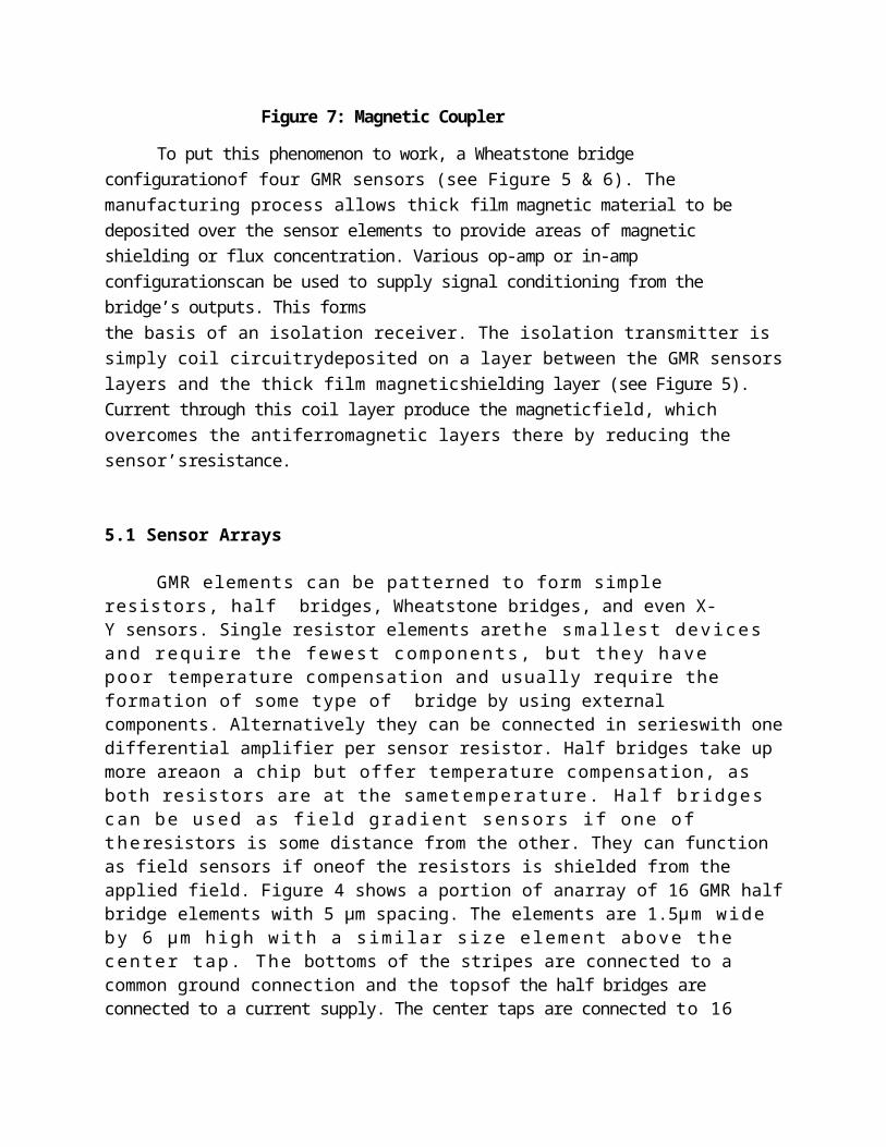
Figure 7: Magnetic Coupler
To put this phenomenon to work, a Wheatstone bridge configurationof four GMR sensors (see Figure 5 & 6). The manufacturing process allows thick film magnetic material to be deposited over the sensor elements to provide areas of magnetic shielding or flux concentration. Various op-amp or in-amp configurationscan be used to supply signal conditioning from the bridge’s outputs. This forms the basis of an isolation receiver. The isolation transmitter is simply coil circuitrydeposited on a layer between the GMR sensorslayers and the thick film magneticshielding layer (see Figure 5). Current through this coil layer produce the magneticfield, which overcomes the antiferromagnetic layers there by reducing the sensor’sresistance.
5.1 Sensor Arrays
GMR elements can be patterned to form simple resistors, half bridges, Wheatstone bridges, and even X-Y sensors. Single resistor elements arethe smallest devices and require the fewest components, but they have poor temperature compensation and usually require the formation of some type of bridge by using external components. Alternatively they can be connected in serieswith onedifferential amplifier per sensor resistor. Half bridges take up more areaon a chip but offer temperature compensation, as both resistors are at the sametemperature. Half bridges can be used as field gradient sensors if one of theresistors is some distance from the other. They can function as field sensors if oneof the resistors is shielded from the applied field. Figure 4 shows a portion of anarray of 16 GMR halfbridge elements with 5 µm spacing. The elements are 1.5µm wide by 6 µm high with a similar size element above the center tap. The bottoms of the stripes are connected to a common ground connection and the topsof the half bridges are connected to a current supply. The center taps are connected to 16

separate pads on the die. A bias strap passes over the lower elements to provide a magnetic field to bias the elements.
5.2 Signal Processing
Adding signal processing electronics to the basic sensor elementincreases the functionality of sensors. The large output signal of the GMR sensor element Introduction means less circuitry, smaller signal errors, less drift, and better temperature stability compared to sensors where more amplification isrequired to create a usable output.
For the GMR products, we add a simple comparator and outputtransistor circuit to create the world’s most precisedigital magnetic sensor. For these products, no amplification of the sensor’s output signal is necessary. A block diagram of this circuitry is shown in the figure 8.

Figure 8: Signal Processing CircuitThe GMR Switch holds its precise magnetic operate
point over extreme variations in temperature and power supply voltage. This is a low costmethod.
6. WORKING OF A ISOLOOP MAGNETIC COUPLER
In the Isoloop magnetic couplers, a signal at the input induces acurrent in a planar coil (see figure no: 5).The current produces a magnetic field,which is proportional to the current in the planar coil. The resulting magnetic field produces a resistance change in the GMR material,which is separated from the planar coil by a high voltage insulating material. Since the GMR is sensitive parallel to the plane of the substrate, this allows a considerably more compactconstruction than would be possible with Hall sensors. The resistance change in GMR material, which was caused by themagnetic field, is amplified by anelectronic circuit and impressed upon the output as a reproduction of the inputsignal. Since changes in the ground potential at the input, output or both doesn’t produce a current in the planar coil, no magnetic field is created. The GMR material doesn’t change. In this way safe galvanic signal isolation is achieved andat the same time a corresponding common mode voltage tolerance.

7. ADVANTAGES OF MAGNETIC COUPLING
The advantages of magnetic coupling include high bandwidth,small footprint, excellent noise immunity, and temperature stability.
7.1 BandwidthIsoLoop couplers are 5–10 times faster than the
fastestoptocouplers, and have correspondingly faster rise,fall, and propagation times(see Figure 9). Shorter rise and fall times also reduce power consumption in thedevice and system by minimizing time in active regions.

Figure 9: Magnetic Couplers Traces
7.2 Small FootprintIsoLoop couplers can be fabricated in <1 mm2 of die area per channel(see Figure 10). Less board real estate means both more room for other functions and lower prices. Furthermore, because of their small die size, IsoLoop couplerscost no more than high-performance optocouplers.

Figure 10: Four-Channel Magnetic Coupler Die
7.3 Noise Immunity
Magnetic couplers provide transient immunity up to 25 kV/µs,compared to 10 kV/µs for optocouplers. Transient immunity is especiallyimportant in harsh industrial and process control environments.
7.4 Temperature Stability
Because the transmission and sensing elements are not subject tosemiconductor temperature variations, magnetic couplers operate to 100°C andabove; for most optocouplers theupper limit is 75°C. Magnetic couplers are alsoimmune to optocouplers’ inherent performance decay with age.

8. DIGITAL ISOLATORS
These devices offer true isolated logic integration ina level not previously available. All transmit and receive channels operate at 110 Mbd over the full temperature and supply voltage range. The symmetric magnetic coupling barrier provides a typical propagation delay of only 10 ns and a pulse widthdistortion of 2 ns achieving the best specifications of any isolator device. Typicaltransient immunity of 30 kV/µs is unsurpassed.
8.1 Dynamic Power Consumption
Isoloop devices achieve their low power consumption from themanner by which they transmit data across the isolation barrier. By detecting theedge transitions of the input logic signal and converting these to narrow current pulses, a magnetic field is created around the GMR Wheatstone bridge.Depending on the direction of the magnetic field, the bridge causes the outputcomparator to switch following the input logic signal. Power consumption isindependent of mark-to-space ratio and solely dependent on frequency. This hasobvious advantages over optocouplers whose power consumption is heavilydependent on its on-state and frequency.The maximum power supply current per channel for IsoLoop is:
8.2 Data Transmission Rates
The reliability of a transmission system is directly related to theaccuracy and quality of the transmitted digital information. For a digital system,those parameters, which determine the limits of the data transmission, are pulsewidth distortion and propagation, delay skew.
Propagation delay is the time taken for the signal to travelthroughthe device. This is usually different when sending a low-to-high than whensending a high-to-low signal. This difference, or error, is called pulse widthdistortion (PWD) and is usually in ns. It may also be expressed as a percentage:
P W D % = ( M a x i m u m P u l s e W i d t h D i s t o r t i o n ( n s ) / S i g n a l P u l s e Width (ns)) x 100%
Propagation delay skew is the difference in time taken for two or more channels to propagate their signals. This becomes significant when clockingis involved since it is undesirable for the clock pulse to arrive before the data hassettled. A short propagation delay skew is therefore critical, especially in high datarate parallel systems, to establish and maintain accuracy and repeatability. TheIsoLoop range of isolators all has a maximum propagation delay skew of 6 ns,which is five times better than any optocoupler. The maximum channel to

channelskew in the IsoLoop coupler is only 3 ns, ten times better then any other optocouplers.
9. COMPARISON BETWEEN OPTOCOUPLER ANDISOLOOP MAGNETIC COUPLERUnlike typical microsecond TON/TOFF times of optoisolators,
TheIsoLoop-isolators also have identical TON/TOFF times, which produce no pulse-w i d t h d i s t o r t i o n a s i s t h e c a s e w i t h m a n y o p t o i s ol a t o r s h a v i n g d i f f e r i n g TON/TOFF times. Propagation delays are less than 10 ns with inter-channelskewing ofless than 2 ns. Isoloop-isolators have up to four channels per packagein a variety of device direction configurations. These standard devices are greatfor bus isolation, serial ADCs and DACs, and communication isolation. Theworking range of optocouplers is only between zeroand ten megahertz. TheIsoLoop couplers have data transmission speeds up to100 mega baud. IsoLoopdevices will operate over a wide temperature range of -40 to +100C, comparedwith the restricted range of 0 to +70C for optoisolators. The power consumptionof IsoLoop devices is solely dependent on frequency. This makes for lower power consumption than optoisolators, whose power consumption is heavily dependenton state and frequency. With data rates up to 100Mbaud, the IsoLoop technologyoffers rates of up to ten times that of optoisolators.
10. CURRENT APPLICATIONSMagnetic isolators are quickly finding their way into process controland industrial applications. Isolation of A/D interfaces is one popular use. Inaddition, magnetic isolators’ combination of speed and packaging density provides a good method of efficient data channel management when multipleA/Ds need to be interfaced on the same circuit card. A four-channel part withthree channels going one way and one going the other is

available for A/Dinterface applications. Magnetic couplers also enable higher speed factorynetworks such as Profibus and other protocols. These devices are great for busisolation, serial ADCs and DACs, and communication isolation. The combinationof the fast and high-density IsoLoop couplers with high packing density allowsefficient data channel management where several A/D channels must be isolatedon a board.
10.1 Digital Isolation Applications
ADCs DACs Multiplexed Data Transmission Data Interfaces Digital Noise Reduction Ground Loop Elimination
11. THE FUTURE
Magnetic field detection has vastly expanded as industry hasused avariety of magnetic sensors to detect the presence, strength, or direction of magnetic fields from the Earth, permanent magnets, magnetized soft magnets, andthe magnetic fields associated with current. These sensors are used as proximitysensors, speed and distance measuring devices, navigation compasses, and currentsensors. They can measure these properties without actual contact to the medium being measured and have become the eyes of many control systems.
12. CONCLUSIONMagnetic couplers will in time be even faster and have
more channels.More types of integrated bus transceivers will be available. Several manufacturersare planning to introduce magnetic couplers. The U.S. military is providingsignificant funding for

advanced magnetic coupler development because of thevalue of their high speed and noise immunity in aircraft and other systems. It hasreported prototype devices with speeds of 300 Mbaud and switching times of <1ns. Also under development are higher-density parts (full byte-wide couplers) andmore functionality (latching bus transceivers). Finally, the inherent linearity of aresistive coil and resistive sensing elements make magnetic couplers well suitedfor linear data protocols such as low-voltage differential signaling.
13. REFERENCES
1. J.Daughton and Y. Chen. "GMR Materials for Low Field Applications, "IEEE Trans Magn, Vol. 29:2705-2710, 2003.pp.18-21
2. Michael J. Caruso, Tamara Bratland, C. H. Smith, and Robert Schneider, “A New Perspective on Magnetic Field Sensing,” Sensors Magazine, vol.15, no. 12, (December 2002), pp. 34-46
3. Carl H. Smith and Robert W. Schneider, “Low-Field Magnetic Sensingwith GMR Sensors, Part 1: The Theory of Solid-State Sensing,” Sensors Magazine, vol. 16, no. 9, (September 2002), pp. 76-83.
4. Carl H. Smith and Robert W. Schneider, “Low-Field Magnetic Sensingw i t h G M R S e n s o r s , P a r t 2 : G M R S e n s o r s a n d th e i r A p p l i c a t i o n s , ” Sensors Magazine, vol. 16, no. 10, (October 2002), pp. 84- 91.
5. http://www.circuitcellar.com/library/print/0502/JEFF/4.asp
6 . h t t p : / / w w w . s e n s o r s m a g . c o m /

7. http://www.nve.com/isoloop/news/hispdnr.php
8. http://www.electronicstalk.com/news/rho/rho000.html
Copyright © 2022 FDOKUMEN