Experimental investigation of photonic band gap influence on enhancement of Raman-scattering in...
8
Experimental investigation of photonic band gap influence on enhancement of Raman-scattering in metal-dielectric colloidal crystals Sriram Guddala, Shadak Alee Kamanoor, Andrea Chiappini, Maurizio Ferrari, and Narayana Rao Desai Citation: J. Appl. Phys. 112, 084303 (2012); doi: 10.1063/1.4758315 View online: http://dx.doi.org/10.1063/1.4758315 View Table of Contents: http://jap.aip.org/resource/1/JAPIAU/v112/i8 Published by the American Institute of Physics. Related Articles Monitoring the in-situ oxide growth on uranium by ultraviolet-visible reflectance spectroscopy J. Appl. Phys. 112, 093104 (2012) Design of lumpy metallic nanoparticles for broadband and wide-angle light scattering Appl. Phys. Lett. 101, 141112 (2012) Experimental surface-enhanced Raman scattering response of two-dimensional finite arrays of gold nanopatches Appl. Phys. Lett. 101, 111606 (2012) Origins of high visible light transparency and solar heat-shielding performance in LaB6 Appl. Phys. Lett. 101, 041913 (2012) Influence of alloy inhomogeneities on the determination by Raman scattering of composition and strain in Si1–xGex/Si(001) layers J. Appl. Phys. 112, 023512 (2012) Additional information on J. Appl. Phys. Journal Homepage: http://jap.aip.org/ Journal Information: http://jap.aip.org/about/about_the_journal Top downloads: http://jap.aip.org/features/most_downloaded Information for Authors: http://jap.aip.org/authors Downloaded 27 Nov 2012 to 14.139.69.1. Redistribution subject to AIP license or copyright; see http://jap.aip.org/about/rights_and_permissions
Transcript of Experimental investigation of photonic band gap influence on enhancement of Raman-scattering in...

Experimental investigation of photonic band gap influence on enhancementof Raman-scattering in metal-dielectric colloidal crystalsSriram Guddala, Shadak Alee Kamanoor, Andrea Chiappini, Maurizio Ferrari, and Narayana Rao Desai Citation: J. Appl. Phys. 112, 084303 (2012); doi: 10.1063/1.4758315 View online: http://dx.doi.org/10.1063/1.4758315 View Table of Contents: http://jap.aip.org/resource/1/JAPIAU/v112/i8 Published by the American Institute of Physics. Related ArticlesMonitoring the in-situ oxide growth on uranium by ultraviolet-visible reflectance spectroscopy J. Appl. Phys. 112, 093104 (2012) Design of lumpy metallic nanoparticles for broadband and wide-angle light scattering Appl. Phys. Lett. 101, 141112 (2012) Experimental surface-enhanced Raman scattering response of two-dimensional finite arrays of gold nanopatches Appl. Phys. Lett. 101, 111606 (2012) Origins of high visible light transparency and solar heat-shielding performance in LaB6 Appl. Phys. Lett. 101, 041913 (2012) Influence of alloy inhomogeneities on the determination by Raman scattering of composition and strain inSi1–xGex/Si(001) layers J. Appl. Phys. 112, 023512 (2012) Additional information on J. Appl. Phys.Journal Homepage: http://jap.aip.org/ Journal Information: http://jap.aip.org/about/about_the_journal Top downloads: http://jap.aip.org/features/most_downloaded Information for Authors: http://jap.aip.org/authors
Downloaded 27 Nov 2012 to 14.139.69.1. Redistribution subject to AIP license or copyright; see http://jap.aip.org/about/rights_and_permissions

Experimental investigation of photonic band gap influence on enhancementof Raman-scattering in metal-dielectric colloidal crystals
Sriram Guddala,1 Shadak Alee Kamanoor,1 Andrea Chiappini,2 Maurizio Ferrari,2
and Narayana Rao Desai1,a)
1School of Physics, University of Hyderabad, Hyderabad 500 046, India2CNR-IFN, CSMFO Lab., Via alla Cascata 56/c, Povo, Trento 38123, Italy
(Received 23 April 2012; accepted 12 September 2012; published online 17 October 2012)
A simple chemical technique is implemented to fabricate a metal-dielectric colloidal crystal
structure (MDCS) in order to enhance the otherwise weak Raman signals by combining the
effects of localized surface plasmon resonance (LSPR) enhancement due to gold nanoparticles,
precise field confinement of dielectric and air bands in the periodic dielectric structure and field
enhancements at the photonic band gap (PBG) edges. The higher density of electromagnetic
modes (DOS) near these band edges is explained as due to the reduced group velocity at the
photonic band gap edges. Intense electric field strength due to the excitation of high DOS at the
edges of PBG of MDCS and the LSPR excitation through field confinement in the dielectric
medium of MDCS are employed to study the Raman-scattering signals of adsorbed benzenethiol
(BT) molecule on the MDCS. Large enhancement for the Raman signal in MDCS in comparison
to the Raman spectra observed for BT molecule dispersed on sputtered gold film shows the
effectiveness of MDCS for the micro-level detection of the analyte. VC 2012 American Institute ofPhysics. [http://dx.doi.org/10.1063/1.4758315]
I. INTRODUCTION
The modification in the spontaneous emission rate
owing to the location of light source in special environment
known as the Purcell effect,1 has been established as due to
the role of density of electromagnetic modes (DOS) on the
spontaneous emission of light in different mesoscopic struc-
tures viz., microcavities,2 metal-dielectric interfaces,3 dielec-
tric slabs,4 and so on. One such mesoscopic structures called
photonic crystals (PhCs), which are also called the periodic
dielectric materials,5–8 have been an interesting topic of
research to attain a complete photonic band gap (PBG),
where the propagation of electromagnetic waves of any
polarization is forbidden in any direction for some frequency
range.5 Theoretically it was predicted by Yablonovitch6 and
John7 in terms of spontaneous emission suppression and
strong Anderson localization of photons, respectively, to
demonstrate the Purcell effect in these PhCs. A theoretical
prediction was recently made by Gaponenko about the effect
of photon DOS on the spontaneous light scattering9,10 in
PhCs and its contribution to the enhancement of Raman-
scattering. As the group velocity, vg, is low for the propagat-
ing electromagnetic modes at the band edge region of the
PBG, it leads to enhanced DOS and larger light matter inter-
action as compared to a homogeneous 3D medium (Figure
1(a) in Ref. 9). There are very few reports in the literature on
the experimental results regarding the band edge DOS
effects on the Raman scattering in a PhC. Avakyants et al.11
have infiltrated NaNO2 into the silica colloidal crystal and
observed an enhancement of the NaNO2 Raman-scattering
signal under selective excitation wavelength near one of its
band edges. Another report by Kuroda et al.12 for polymer
gel infiltrated polystyrene colloidal crystal, shows the poly-
styrene Raman-scattering signal as a function of the excita-
tion frequency and an enhancement at the band edge of the
PBG. A theoretical model was also developed by Sakoda
et al.10 for such bare polystyrene opals and a possible
enhancement of the Raman-scattering due to high DOS
available at the band edge regions. The work by Mamichev
et al.13 looks at similar effects in the case of a porous silicon
multilayer 1D PhC structure. Gaponenko9 had proposed that
enhancement might be more in a metal-dielectric systems in
comparison to bare dielectric structures.
Metal-dielectric colloidal crystal structures (MDCS)
have attracted an intense research activity,14–16 during the
last decade for its unified features, localized surface plasmon
resonance (LSPR) of noble metallic nanoparticles and PBG
of colloidal type PhCs. These new optical materials have
been studied for the past few years as surface enhanced
Raman-scattering (SERS) substrates. SERS has been known
for achieving the amplification of Raman-scattering signals
of molecules in the proximity or adsorbed to noble metallic
nanoparticles or nanostructures through an intense electric
field generated because of the surface plasmon resonance
property. The general understanding of the SERS involves
two mechanisms for the enhancement of Raman-scattering:
one is electromagnetic enhancement17 and other being chem-
ical enhancement.18 The first involves the excitation of sur-
face plasmons and thereby creating high intense electric field
and the latter is due to a possible charge transfer mechanism
caused by mixing of molecular orbitals of an analyte and a
metallic structure, there by changing the environment of the
analyte.
In this communication, we are reporting the experimen-
tal observations on the possible effects of photonic band gap
in a novel MDCS. We also report the enhancement ofa)E-mail addresses: [email protected] and [email protected].
0021-8979/2012/112(8)/084303/7/$30.00 VC 2012 American Institute of Physics112, 084303-1
JOURNAL OF APPLIED PHYSICS 112, 084303 (2012)
Downloaded 27 Nov 2012 to 14.139.69.1. Redistribution subject to AIP license or copyright; see http://jap.aip.org/about/rights_and_permissions

Raman-scattering signal of benzenethiol (BT) molecules at
low molar concentration in MDCS and compared it with
Raman signals from BT molecules on a metallic substrate
without any photonic band gaps.
II. EXPERIMENTAL
MDCS is prepared by immobilizing the gold nanopar-
ticles (Au NPs) through a selective amino group (�NH3þ)
functionalization of the silica network in an inverse silica
opal (ISO). Scheme 1 shows the protocol followed for the
fabrication of our novel MDCS. Briefly, a bare polystyrene
(PS) opal was first grown by the vertical deposition tech-
nique.8,19 In this technique initially a 3 ml aqueous solution
of homemade mono sized 420 nm diameter PS spheres of
0.05 wt. % was taken in a 5 ml beaker. Then the hydrophi-
lized substrate was kept at 45� angle in this solution and left
at a temp of 50 �C and a relative humidity of 70%–80% for
48 h. During the process of evaporation of water the spheres
get pulled towards the meniscus due to the capillary forces
and self-assemble into a fcc crystalline lattice. Then the
structure was heat treated at 80 �C for 10 h to make the struc-
ture mechanically stable and possible necking between the
spheres. In the next step, we have infiltrated the 26% air vol-
ume fraction between the PS spheres with silica solution and
calcinated the structure at 450 �C for 30 min and then
brought it to the room temp at a ramp rate of 0.5 �C/min so
that the PS spheres get evaporated and the silica matrix gets
densified simultaneously. At the end, we will be left with a
silica matrix in the ordered original air voids and the air
voids in place of original PS spheres. This type of structure
is known as the inverse opal.8,20 This inverse structure was
functionalized with –NH3þ group by immersing it in 10%
3-aminopropyltriethoxysilane (APTES) – ethanol solution
under smooth stirring for 20 h. In the following step, the
functionalized ISO was immersed in a pre-prepared Au NPs
solution, by the well-known Turkevich method,21 for differ-
ent intervals of time: 5 h, 10 h, 15 h, and 20 h. From now
onwards the structures will be labeled as MDCS-Xh where X
represents 5, 10, 15, and 20 h of immersion. A uniform gold
thin film of �250 nm thickness was deposited on a glass sub-
strate using EMITECH SC7620 sputter coater.
Optical absorption spectra of all MDCS, gold nanopar-
ticles solution and sputtered gold thin film on glass substrate
were measured using a double beam UV-Vis/NIR spectro-
photometer (JASCO V-670). Spectra were collected with
2 mm diameter spot size for the light beam and a spectral re-
solution of 0.2 nm. The structural features were investigated
using Zeiss Ultra-55 field emission scanning electron micro-
scope (FESEM). For the Raman-scattering enhancement
from the as realized MDCS and gold thin film, BT was used
as an analyte because of its well-known strong Raman activ-
ity, the non-resonant Raman-scattering and formation of
monolayer on the gold surface with possible covalent bond-
ing. The samples were immersed in BT solution for overnight
and rinsed twice in ethanol and once in water to remove the
excess of unattached BT. The samples were finally dried with
dry N2 gas. The Raman-scattering was collected using high
resolution confocal micro-Raman spectrometer (Horiba Jobi-
nYvon, LabRAM-HR 800) equipped with three excitation
wavelengths at 514.5 nm, 632.8 nm, and 785 nm. The laser
power was significantly attenuated by neutral density filters to
0.7 mW before reaching the sample. A 50� objective lens
with a numerical aperture value of 0.75 focused the excitation
beam to �1 lm2 area of the sample. The scattered light was
collected by the same objective lens and passed through
Raman edge filter (blocking bandwidth of �120 cm�1) before
entering the monochromator chamber with 1800 g/mm grating
and a Peltier-cooled charge coupled device (CCD) detector at
�70 �C. Each Raman spectrum was obtained with a 10 s ex-
posure time for the detector. A macro-sampling accessory was
used with a 40 mm focal length lens and a spherical mirror for
double laser pass for recording the normal Raman-scattering
spectrum (NRS) of pure BT solution with all the three differ-
ent excitation wavelengths. All experiments were carried out
at room temperature.
III. RESULTS AND DISCUSSION
A. MDCS characterization
Figure 1(a) shows optical absorption spectra of the as
synthesized Au NPs with LSPR band at 520 nm. An approxi-
mate size of the Au NPs was calculated using the formula23
R ¼Vf � k2
p
2pc � Dk; (1)
where R is radius of metal nanoparticle, Vf is Fermi velocity
of electrons in bulk metal (for gold, Vf¼ 1.39� 108 cm/s), c
SCHEME 1. The schematic diagram
shows the protocol for the fabrication
steps of a metal-dielectric inverse colloi-
dal structure: (a) self-assembled polysty-
rene colloidal crystal; (b) silica solution
infiltrated polystyrene colloidal crystal
structure; (c) an inverse silica opal (ISO)
structure obtained by annealing and sin-
tering processes; (d) amino group func-
tionalization of the ISO structure with
APTES; (e) immobilization of Au Nps on
the silica network.
084303-2 Guddala et al. J. Appl. Phys. 112, 084303 (2012)
Downloaded 27 Nov 2012 to 14.139.69.1. Redistribution subject to AIP license or copyright; see http://jap.aip.org/about/rights_and_permissions

is the light velocity, kp is the peak position of the absorption
band, and Dk is the full-width at half-maximum of the absorp-
tion band. The estimated size of Au NPs is �10 nm in dia-
meter using kp¼ 520 nm and Dk¼ 48 nm in Eq. (1). The
estimated value is in good agreement with the average size
found from FESEM measurement shown in Fig. 2(a). The
absorption spectra (Figure 1(b)) show two bands: one located
at 600 nm due to the PBG and the other at 520 nm due to the
LSPR of Au NPs. The PBG corresponding to the ISO satisfies
the Bragg diffraction given by the modified Bragg formula:8
k ¼ 2� 0:816� D�ffiffiffiffiffiffiffiffiffiffiffiffiffiffiffiffiffiffiffiffiffiffiffiffiffiffiffiffiffiðn2
ef f � Sin2 hÞq
; (2)
where
n2ef f ¼ 0:74� n2
air þ 0:26� n2silica; (3)
and D refers to the diameter of hollow air spheres and h rep-
resents the angle between the direction of incident light and
the normal to the (111) plane of fcc lattice of crystal. neff is
the effective refractive index of the crystal, where nair¼ 1
and nsilica¼ 1.45.
The position of PBG at 600 nm satisfies Eq. (2) for a
sphere diameter of 325 nm which was originally occupied by
the polystyrene bead before being burnt out. This demon-
strates a shrinkage occurring during the sintering process.
This is not surprising as the latex spheres are mesoporous,
and water vapor released from these pores during the calci-
nation leads to a shrinkage of the beads.20 These results are
also in agreement with the FESEM image as shown in Figure
2(a), where the average size of the air gap is around �325
(65) nm. The reflectance spectrum (Figure 1(c)) of ISO was
measured with white light beam of 1 mm diameter at an
angle of incidence of 10� to the normal of crystal growth
(111) plane. The reflection maximum occurring at 591 nm is
in good agreement with the value calculated from Eq. (2).
The oscillations following the reflection maximum are due
to the Fabry-P�erot interference of light reflected from the
end surfaces of the opal. Appearance of the Fabry-P�erot
oscillations is a good indicator of the homogeneity and the
average refractive index of PhCs.24 Fabry-P�erot oscillations
FIG. 1. UV-Vis/NIR absorption spectra of (a) Au NPs solution (b) ISO
doped with Au NPs for different times, (i) ISO, (ii) MDCS-5 h, (iii) MDCS-
10 h, (iv)MDCS-15 h, (v) MDCS-20 h, and (c) normalized white light reflec-
tion spectrum of ISO for 10� angle of incidence.
FIG. 2. (a) MDCS-20 h shows ISO with 325 nm dimension air voids and the
immobilized Au NPs in the silica matrix and (b) MDCS-20 h in cross-
section view shows the immobilization of Au NPs throughout the network
of ISO.
084303-3 Guddala et al. J. Appl. Phys. 112, 084303 (2012)
Downloaded 27 Nov 2012 to 14.139.69.1. Redistribution subject to AIP license or copyright; see http://jap.aip.org/about/rights_and_permissions

also indicate the occurrence of high DOS in the crystal,25
which will be discussed in Sec. III B.
The immobilized Au-NP in the silica matrix can be seen
clearly in the FESEM images shown in Figure 2. Figure 2(a)
gives the top view while Figure 2(b) shows the cross-
sectional image. It is also evident from Figure 2 that the Au
Nps are immobilized uniformly throughout the network of
the ISO without any observable aggregation. From the optical
and structural properties characterization (Figures 1 and 2), it
can be concluded that the resultant novel MDCS obtained
here present the unique features of LSPR of Au NP and PBG
of ISO.
B. Raman scattering measurement
The existence of a PBG in the MDCS could make these
new optical materials fascinating in the field of photonics.
Due to low group velocity vg for the frequencies near the
edges of the PBG,5 the DOS not only reduced in the band
gap but also get enhanced at the band edges due to long opti-
cal path length and by large light matter interaction. Thus,
the strength of the optical field within the crystal may be
enhanced, which constitutes an advantage if one deals with
optically active constituents.9 To study the effect of PBG
here we have employed for the first time the MDCS for
enhancement of Raman-scattering through the well known
SERS mechanism. The Raman spectrum of BT molecules,
which get attached to the Au NPs of the MDCS, was
recorded using three different excitation wavelengths:
514.5 nm, 632.8 nm, and 785 nm. The wavelengths and the
PBG are so chosen that the excitation wavelengths 514.5 nm
falls on the high frequency side of the band edge and
632.8 nm falls on the lower frequency band edge of the PBG.
The 785 nm is chosen such a way that it is far away from the
band gap and on the lower frequency side of the band gap
(Figure 4(a)). Through this choice of wavelengths we plan to
look at PBG effects: precise field confinement in the dielec-
tric and air media, effect on the DOS at the band edges26 and
their contribution towards the enhancement of Raman-
scattering from the analyte. In Figure 3, the intense peaks
centered at 998, 1022, 1070, and 1572 cm�1 appear in
Raman spectrum obtained with the MDCS and gold thin film
as substrates, and they correspond to BT molecule’s in-plane
ring-breathing mode, the in-plane C-H bending mode, the in-
plane ring-breathing mode coupled with the C-S stretching
mode and the C-C stretching mode, respectively.22,29
Raman-scattering spectra recorded with the different
excitations show that Raman signals are strong for the
632.8 nm and 785 nm excitations with the former leading to
more intense spectra than the later (Figure 3(a)). The
Raman-scattering with the 514.5 nm excitation shows very
weak signal (Figure 3(a)) and deviates from the well-known
x4 Raman scattering cross-section, where x is the incident
frequency.27 However, the Raman spectra of the adsorbed
BT molecule on the sputtered gold thin film for the opted ex-
citation wavelengths show the validity of x4 scattering prob-
ability where intense signals were observed for the 514.5 nm
excitation compared to 632.8 nm. Signals were too weak and
did not show up with 785 nm excitation.
Considering the location of the excitation wavelengths
in the optical absorption spectrum of the MDCS (Figure
4(a)), the Stokes Raman bands will be on their respective
longer wavelength side indicated by the bands in Figure 4(a).
For the excitation wavelength of 632.8 nm, which is falling
on the red band edge, the MDCS will have more DOS due to
its fascinating PBG feature compared to a homogenous
system.9
It is evident from Figure 3(a) that Raman signals are
more intense with 632.8 nm excitation than with 514.5 nm
and 785 nm excitations. According to electromagnetic varia-
tional theorem for the PhCs5 the low frequency bands would
be concentrated in the high dielectric (e) or high refractive
index (n) regions, and the high frequency bands have a larger
fraction of their energy in the low refractive index (n)
regions. In 2D and 3D PhC, these media being the high index
dielectric material and the low index air medium, the bands
above the band gap and below the band gap are labeled as
“air band” and “dielectric band,” respectively. In the current
PhC, the excitation wavelengths 632.8 nm, 785 nm and their
respective Raman scattered modes would be below the band
gap (Figure 4(a)) and hence their energy would be concen-
trated in the dielectric medium.28 The dielectric medium in
our MDCS system is a very thin silica matrix with immobi-
lized Au NPs, which is shown with a red circled portion in
Figure 4(b). The 514.5 nm excitation wavelength and their
FIG. 3. Wavelength scanned Raman-scattering of 5 lM BT molecule col-
lected over (a) MDCS-20 h and (b) RF sputtered Gold film for three different
wavelengths 514.5, 632.8, and 785 nm with a power of 0.7 mW next to the
filter. The spectra were offset along the y-axis.
084303-4 Guddala et al. J. Appl. Phys. 112, 084303 (2012)
Downloaded 27 Nov 2012 to 14.139.69.1. Redistribution subject to AIP license or copyright; see http://jap.aip.org/about/rights_and_permissions
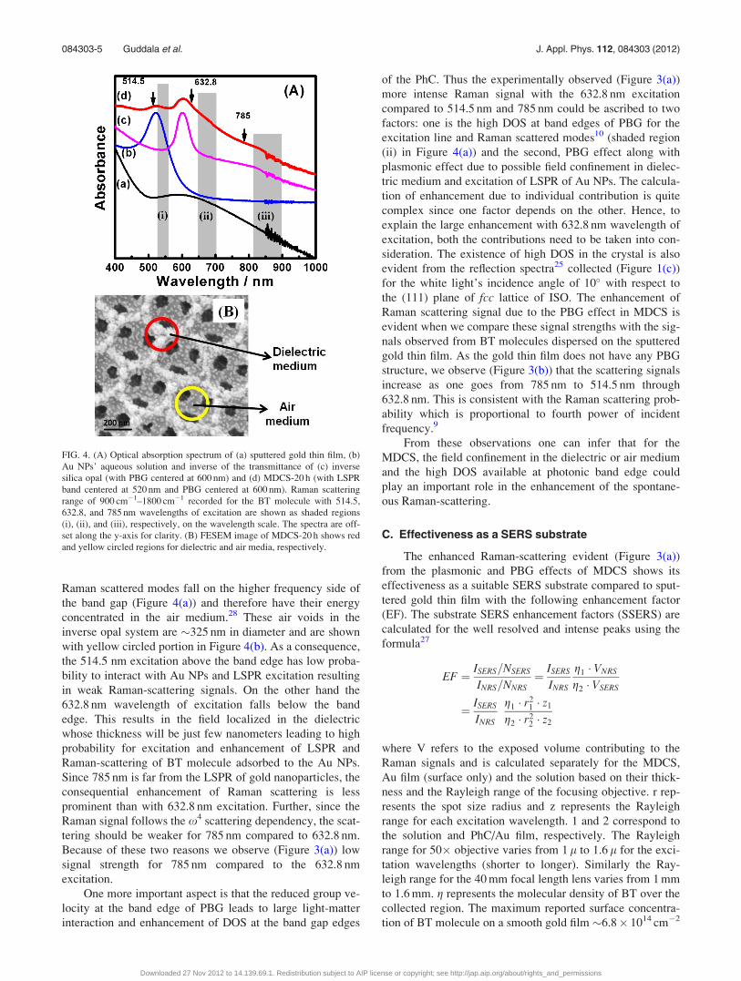
Raman scattered modes fall on the higher frequency side of
the band gap (Figure 4(a)) and therefore have their energy
concentrated in the air medium.28 These air voids in the
inverse opal system are �325 nm in diameter and are shown
with yellow circled portion in Figure 4(b). As a consequence,
the 514.5 nm excitation above the band edge has low proba-
bility to interact with Au NPs and LSPR excitation resulting
in weak Raman-scattering signals. On the other hand the
632.8 nm wavelength of excitation falls below the band
edge. This results in the field localized in the dielectric
whose thickness will be just few nanometers leading to high
probability for excitation and enhancement of LSPR and
Raman-scattering of BT molecule adsorbed to the Au NPs.
Since 785 nm is far from the LSPR of gold nanoparticles, the
consequential enhancement of Raman scattering is less
prominent than with 632.8 nm excitation. Further, since the
Raman signal follows the x4 scattering dependency, the scat-
tering should be weaker for 785 nm compared to 632.8 nm.
Because of these two reasons we observe (Figure 3(a)) low
signal strength for 785 nm compared to the 632.8 nm
excitation.
One more important aspect is that the reduced group ve-
locity at the band edge of PBG leads to large light-matter
interaction and enhancement of DOS at the band gap edges
of the PhC. Thus the experimentally observed (Figure 3(a))
more intense Raman signal with the 632.8 nm excitation
compared to 514.5 nm and 785 nm could be ascribed to two
factors: one is the high DOS at band edges of PBG for the
excitation line and Raman scattered modes10 (shaded region
(ii) in Figure 4(a)) and the second, PBG effect along with
plasmonic effect due to possible field confinement in dielec-
tric medium and excitation of LSPR of Au NPs. The calcula-
tion of enhancement due to individual contribution is quite
complex since one factor depends on the other. Hence, to
explain the large enhancement with 632.8 nm wavelength of
excitation, both the contributions need to be taken into con-
sideration. The existence of high DOS in the crystal is also
evident from the reflection spectra25 collected (Figure 1(c))
for the white light’s incidence angle of 10� with respect to
the (111) plane of fcc lattice of ISO. The enhancement of
Raman scattering signal due to the PBG effect in MDCS is
evident when we compare these signal strengths with the sig-
nals observed from BT molecules dispersed on the sputtered
gold thin film. As the gold thin film does not have any PBG
structure, we observe (Figure 3(b)) that the scattering signals
increase as one goes from 785 nm to 514.5 nm through
632.8 nm. This is consistent with the Raman scattering prob-
ability which is proportional to fourth power of incident
frequency.9
From these observations one can infer that for the
MDCS, the field confinement in the dielectric or air medium
and the high DOS available at photonic band edge could
play an important role in the enhancement of the spontane-
ous Raman-scattering.
C. Effectiveness as a SERS substrate
The enhanced Raman-scattering evident (Figure 3(a))
from the plasmonic and PBG effects of MDCS shows its
effectiveness as a suitable SERS substrate compared to sput-
tered gold thin film with the following enhancement factor
(EF). The substrate SERS enhancement factors (SSERS) are
calculated for the well resolved and intense peaks using the
formula27
EF ¼ ISERS=NSERS
INRS=NNRS¼ ISERS
INRS
g1 � VNRS
g2 � VSERS
¼ ISERS
INRS
g1 � r21 � z1
g2 � r22 � z2
where V refers to the exposed volume contributing to the
Raman signals and is calculated separately for the MDCS,
Au film (surface only) and the solution based on their thick-
ness and the Rayleigh range of the focusing objective. r rep-
resents the spot size radius and z represents the Rayleigh
range for each excitation wavelength. 1 and 2 correspond to
the solution and PhC/Au film, respectively. The Rayleigh
range for 50� objective varies from 1 l to 1.6 l for the exci-
tation wavelengths (shorter to longer). Similarly the Ray-
leigh range for the 40 mm focal length lens varies from 1 mm
to 1.6 mm. g represents the molecular density of BT over the
collected region. The maximum reported surface concentra-
tion of BT molecule on a smooth gold film �6.8� 1014 cm�2
FIG. 4. (A) Optical absorption spectrum of (a) sputtered gold thin film, (b)
Au NPs’ aqueous solution and inverse of the transmittance of (c) inverse
silica opal (with PBG centered at 600 nm) and (d) MDCS-20 h (with LSPR
band centered at 520 nm and PBG centered at 600 nm). Raman scattering
range of 900 cm�1–1800 cm�1 recorded for the BT molecule with 514.5,
632.8, and 785 nm wavelengths of excitation are shown as shaded regions
(i), (ii), and (iii), respectively, on the wavelength scale. The spectra are off-
set along the y-axis for clarity. (B) FESEM image of MDCS-20 h shows red
and yellow circled regions for dielectric and air media, respectively.
084303-5 Guddala et al. J. Appl. Phys. 112, 084303 (2012)
Downloaded 27 Nov 2012 to 14.139.69.1. Redistribution subject to AIP license or copyright; see http://jap.aip.org/about/rights_and_permissions

is considered29 and this value is used for both the Au film as
well as the MDCS. In the case of MDCS, the molecular den-
sity over probed volume is calculated by considering the
26% filling fraction of the dielectric medium. The molecular
density of the pure BT solution is 5.9� 1021 cm�3. The
intensities of SERS and NRS are calculated from the area af-
ter fitting the lines to a Lorentzian line shape. The enhance-
ment factors obtained through these measurements are
shown in Table I.
The calculated EFs for both the MDCS and the gold thin
film relative to the NRS of BT solution for the 514.5 nm and
632.8 nm are tabulated in the Table I. We have also shown
the enhancement observed for MDCS relative to the BT mole-
cules dispersed on the gold film in the last column of Table I.
We observe an enhancement of 82 times for the MDCS with
632.8 nm for the 998 cm�1 mode in comparison to the other
modes, which could be because the 998 cm�1 is closer to the
band edge than the other vibrational modes. One can also see
the large enhancement for 632.8 nm excitation compared to
the 514.5 nm. These large enhancements in the Raman signals
strongly support that this novel MDCS can be an effective
SERS substrate for the micro level detection of adsorbed
analyte.
IV. CONCLUSIONS
A novel MDCS is realized by a simple chemical process
through immobilization of Au NPs on the amino group func-
tionalized matrix of silica. Optical and structural character-
izations show unified features of plasmonic properties of
metal nanoparticles and PBG features of colloidal PhCs. The
observations made in respect to MDCS and gold thin film for
Raman-scattering studies of adsorbed BT molecule illus-
trates the effect of band edge DOS and confinement of
modes in specific media of the periodic dielectric structure.
The precise low and high energy field confinements in the
dielectric and air media could find various applications in op-
tical trapping, laser cooling.28 The increase in the light inten-
sity inside the structure could find interesting nonlinear
effects as well.30,31 The intense field at the PBG edges along
with plasmonic effects from metal nanoparticles can be used
in the single molecule detection and reduction of the thresh-
old value for stimulated Raman-scattering.
ACKNOWLEDGMENTS
This work carried under the frame work of ITPAR
Phase-II and UGC-BRNS. The author S. Guddala would like
to acknowledge the financial support of UGC sponsored Ba-
sic Science Research (BSR) fellowship, India. The authors
are grateful to Dr. P. S. R. Prasad, National Geophysical
Research Institute (NGRI), Hyderabad for useful discussions
on Raman scattering studies.
1E. M. Purcell, Phys. Rev. 69, 681 (1946).2P. R. Berman, Cavity Quantum Electrodynamics: Advances in Atomic,Molecular and Optical Physics, Suppl. 2 (Academic, Boston, 1994).
3P. T. Worthing, R. M. Amos, and W. L. Barnes, Phys. Rev. A 59, 865
(1999).4G. L. J. A. Rikken, Phys. Rev. A 51, 4906 (1995).5J. D. Joannopoulos, S. G. Johnson, J. N. Winn, and R. D. Meade, PhotonicCrystals: Molding the Flow of Light, 2nd ed. (Princeton University Press,
Princeton, 2008).6E. Yablonovitch, Phys. Rev. Lett. 58, 2059 (1987).7S. John, Phys. Rev. Lett. 58, 2486 (1987).8C. Lopez, Adv. Mater. 15, 1679 (2003).9S. V. Gaponenko, Phy. Rev. B 65, 140303 (2002).
10T. Ochiai, K. Sakoda, and T. Sawada, Phy. Rev. B 77, 245101 (2008).11L. P. Avakyants, V. S. Gorelik, L. I. Zlobina, N. N. Mel’nik, P. P. Sverbil’,
A. B. Fadyushin, and A. V. Chervyakov, Inorg. Mater. 42, 635 (2006).12K. Kuroda, T. Sawada, T. Ochiai, T. Kuroda, K. Watanabe, and K.
Sakoda, Thin Solid Films 517, 1727 (2009).13D. A. Mamichev, K. A. Gonchar, V. Yu. Timoshenko, G. K. Mussabek, V.
E. Nikulin, and T. I. Taurbaev, J. Raman Spectrosc. 42, 1392 (2011).14S. V. Gaponenko, A. A. Gaiduk, O. S. Kulakovich, S. A. Maskevich, N. D.
Strekal, O. A. Prokhorov, and V. M. Shelekhina, JETP Lett. 74, 309
(2001).15L. Lu, I. Randjelovic, R. Capek, N. Gaponik, J. Yang, H. Zhang, and A.
Eychmu€ller, Chem. Mater. 17, 5731 (2005).16S. Kubo, Z. Ze Gu, D. A. Tryk, Y. Ohko, O. Sato, and A. Fujishima, Lang-
muir 18, 5043 (2002).17G. C. Schatz and R. P. Van Duyne, “Electromagnetic mechanism of
surface-enhanced spectroscopy,” in Handbook of Vibrational Spectros-copy, edited by J. M. Chalmers and P. R. Griffiths (Wiley, New York,
2002), Vol. 1, p. 759.18J. R. Lombardi and R. L. Birke, J. Phys. Chem. C 112, 5605 (2008).19A. Chiappini, C. Armellini, A. Chiasera, M. Ferrari, L. Fortes, M. Clara
Gonc-alves, R. Guider, Y. Jestin, R. Retoux, G. Nunzi conti, S. Pelli, R.
M. Almeida, and G. C. Righini, J. Non-Cryst. Solids 355, 1167 (2009).
TABLE I. Approximated SERS substrate enhancement factor and relative enhancement for MDCS.
Raman shifta (cm�1)
Enhancement factorb (�106)
MDCSc Au thin filmc Enhancementd MDCS/Au film
514.5 nm 632.8 nm 514.5 nm 632.8 nm 514.5 nm(�10�2) 632.8 nm
998 0.01 0.82 0.70 0.01 1.43 82.0
1022 0.05 2.42 0.11 0.11 45.45 22.0
1070 0.11 10.11 0.66 0.41 16.66 24.65
1572 0.18 10.39 0.54 0.70 33.33 14.84
aOnly the intense vibration modes of BT molecule are considered for EF calculation.bAll the EF values for MDCS and Au thin film are with respect to the NRS of BT.cEFs for MDCS and Au thin film are approximated with respect to pure BT molecule Raman spectra for each, 514.5 nm and 632.8 nm, wavelengths of
excitation.dEnhancement is calculated by taking the ratio of EFs for MDCS and Au thin film for the concerned excitation line.
084303-6 Guddala et al. J. Appl. Phys. 112, 084303 (2012)
Downloaded 27 Nov 2012 to 14.139.69.1. Redistribution subject to AIP license or copyright; see http://jap.aip.org/about/rights_and_permissions

20A. Chiappini, C. Armellini, A. Chiasera, Y. Jestin, M. Felrari, M. Mattar-
elli, M. Montagna, E. Moser, C. Tosello, L., Zampedri, G. Nunzi Conti, S.
Pelli, R. M. Almeida, and G. C. Righini, Optoelectron. Lett. 3, 184 (2007).21J. Turkevich, P. C. Stevenson, and J. Hillier, Discuss. Faraday Soc. 11, 55
(1951).22S. Guddala, A. Chiappini, G. Alombert-Goget, C. Armellini, M. Ferrari,
K. Shadak Alee, D. Narayana Rao, A. Chiasera, E. Moser, S. Berneschi,
G. Nunzi Conti, G. C. Righini, and P. F�eron, Proc. SPIE 8173, 817317
(2011).23J. Shin, K. Jang, K.S. Lim, I. B. Sohn, Y. C. Noh, and J. Lee, Appl. Phys.
A 93, 923 (2008).24T. Maka, D. N. Chigrin, S. G. Romanov, and C. M. Sotomayor Torres,
Prog. Electromagn. Res. 41, 307 (2003).
25J. M. Bendickson, J. P. Dowling, and M. Scalora, Phy. Rev. E 53, 4107
(1996).26I. S. Nikolaev, W. L. Vos, and A. F. Koenderink, J. Opt. Soc. Am. B 26,
987 (2009).27E. Le Ru and P. Etchegoin, Principles of Surface-Enhanced Raman Spec-
troscopy: and Related Plasmonic Effects, 1st ed. (Elsevier, 2009).28O. Toader, S. John, and K. Busch, Opt. Express 8, 217 (2001).29A. D. McFarland, M. A. Young, J. A. Dieringer, and R. P. Van Duyne, J.
Phys. Chem. B 109, 11279 (2005).30X. Zhu, J. Wang, P. Lau, D. Nguyen, and R. A. Norwood, Appl. Phys.
Lett. 97, 093503 (2010).31P. P. Markowicz, H. Tiryaki, H. Pudavar, and P. N. Prasad, N. N. Lepesh-
kin, and R. W. Boyd, Phy. Rev. Lett. 92(8), 083903 (2004).
084303-7 Guddala et al. J. Appl. Phys. 112, 084303 (2012)
Downloaded 27 Nov 2012 to 14.139.69.1. Redistribution subject to AIP license or copyright; see http://jap.aip.org/about/rights_and_permissions