EXPERIMENT NO. 1 - MIET
40
EXPERIMENT NO. 1 OBJECTIVE: Introduction to digital electronics lab- nomenclature of digital ICs, specifications, study of data sheet, Concept of Vcc and ground, verification of the truth table of the logic gates using TTL ICs. Outcome: To understand various digital ICs and their datasheet. Apparatus Required: Bread board IC-7400 (NAND Gate), IC-7402 (NOR Gate), IC-7404 (NOT Gate) , IC-7408 (AND Gate), IC-7432 (OR Gate), IC-7486 (EX-OR Gate), Connecting wires, etc. THEORY: Logic gate is a circuit with one output and two or more input channels. An output signal occurs only for certain combination of input signals. Logic circuits are used to perform various computer functions. NAND GATE (7400): The term NAND is a contraction of expression NOT-AND. A NAND gate therefore is an AND gate followed by an inverter. It is defined as whenever all the input is high then output must be low otherwise output is high. Schematic symbol of 2 -INPUT NAND gate is shown below. Mathematically it is expressed as y =A.B Truth table of 2- INPUT NAND gates is shown in table. NAND GATE (7400): Fig (i) Pin diagram of NAND Gate (IC 7400) and logic symbol The output is high when either of inputs A or B is high, or if neither is high. In other words, it is normally high, going low only if both A and B are high.
-
Upload
khangminh22 -
Category
Documents
-
view
0 -
download
0
Transcript of EXPERIMENT NO. 1 - MIET

EXPERIMENT NO. 1
OBJECTIVE: Introduction to digital electronics lab- nomenclature of digital ICs,
specifications, study of data sheet, Concept of Vcc and ground, verification of the truth table
of the logic gates using TTL ICs.
Outcome: To understand various digital ICs and their datasheet.
Apparatus Required: Bread board IC-7400 (NAND Gate), IC-7402 (NOR Gate), IC-7404
(NOT Gate) , IC-7408 (AND Gate), IC-7432 (OR Gate), IC-7486 (EX-OR Gate), Connecting
wires, etc.
THEORY: Logic gate is a circuit with one output and two or more input channels. An output
signal occurs only for certain combination of input signals. Logic circuits are used to perform
various computer functions.
NAND GATE (7400): The term NAND is a contraction of expression NOT-AND. A NAND
gate therefore is an AND gate followed by an inverter. It is defined as whenever all the input is
high then output must be low otherwise output is high. Schematic symbol of 2 -INPUT NAND
gate is shown below. Mathematically it is expressed as y =A.B
Truth table of 2- INPUT NAND gates is shown in table.
NAND GATE (7400):
Fig (i) Pin diagram of NAND Gate (IC 7400) and logic symbol
The output is high when either of inputs A or B is high, or if neither is high. In other words, it is
normally high, going low only if both A and B are high.
NOR GATE (7402): The NOR gate is an improved logic element used for implementing
decision making logic function. The term NOR is a contraction of expression NOT-OR .The
NOR gate is essentially a circuit containing the logic function of an OR gate and an inverter. It is
defined as whenever all the inputs are low then output must be high otherwise output is low.
Schematic symbol of 2- input NOR gate is shown below.
7402 - QUAD 2-INPUT NOR GATE
Fig (ii) Pin diagram and logic symbol of NOR Gate
SYMBOL & TRUTH TABLE
The output is high only when neither A nor B is high. That is, it is normally high but any
kind of zero input will take it low.
NOT GATE (7404): The Simplest from of logic circuit is the INVERTER or NOT gate. It
can have one input and one output terminal. It is defined as, when ever input is high then output
is low and the vice-versa, or we can say that the inverter is a logic element whose output state is
always opposite of its input state. Schematic Symbol is shown.

7404 - HEX INVERTER
SYMBOL & TRUTH TABLE
Fig (iii) Pin diagram and logic symbol of Not gate
AND GATE (7408): It can have two or more input and a single output. It is defined as when
all the inputs are high then output must be high otherwise output is low. Logic expression for the
AND gate is AB. A mechanical analogy and Schematic Symbol is shown.
Symbol & Truth Table
7408 - Quad 2-Input AND Gate
Fig (iv) Pin diagram and logic symbol of AND gate
The output is high only when both inputs A and B are high.
OR GATE (7432 ): It can have two or more input and a single output . It is defined as
whenever any one or all the inputs are high then output must be high otherwise low. A
mechanical analogy and Schematic Symbol is shown.
\

7432 - QUAD 2-INPUT OR GATE SYMBOL & TRUTH TABLE
Fig (v) Pin diagram and logic symbol of NOR gate
EX-OR GATE (7486) : The EX- OR gate operation is widely used in digital circuit. It is not a
basic operation and can be performed using the basic gates – AND, OR, and NOT or universal
gates NAND or NOR. It is similar to the basic OR gates except that the output is low, when both
the inputs are high (1) or low (0). The output of the gate is high (1) when any one input is high
(1). The standard symbol is below.
7486 -Quad 2-Input Exclusive OR-Gate Symbol & Truth Table
Fig (vi) Pin diagram and logic symbol of EX-OR gate
PROCEDURE:
1. Make the connections as shown in the figure.
2. Connect Pin No-7 to GND.
3. Connect Pin No-14 to Vcc.

RESULT: Truth table of various logic function (OR, NOR, NOT, AND, NAND, EX-OR
GATE) are verified.
PRECAUTIONS:
1) All Connections should be according to circuit diagram.
2) All Connections should be right and tight.
3) Reading should be taken carefully.
4) Switch off Power supply after completing the Experiment.

QUESTIONS
Q.1 Define positives logic and negative logic?
Q.2 What is truth table?
Q.3 What are the Universal Logic Gates?
Q.4 Why NAND-NAND realization is preferred over AND- OR realization?
Q.5 List out the IC‟s for various logic operations like NAND, NOR, XOR, OR, AND etc.
Q.6. Explain Propagation delay of digital IC.
Q.7 Explain Power dissipation of digital IC.
Q.8 What are the applications of logic gates?
Q.9 Draw Ex-OR gate using NANAD Gate?
Q.10 Why logic gates are called basic gates?

EXPERIMENT NO. 2
OBJECTIVE: Implementation of the given Boolean function using logic gates in both Sum
of Product and Product of Sum forms.
OUTCOME: To implement Boolean function using logic gates on bread board.
APPARATUS REQUIRED: Bread board , IC-7400 (NAND Gate ) , IC-7408 (AND Gate ) ,
IC-7432 (OR Gate ),Connecting wires ,etc.
THEORY: To implement a Boolean function with lesser number of gates we have to minimize
literals (variables) and the number of terms. The Boolean variables are either in complemented
or in un-complemented form and the terms are arranged in one of the two standard forms of
Boolean functions.
1. Sum of product form (SOP)
2. Product of sum form (POS)
SUM OF PRODUCT FORM (SOP): The sum of product form expression contains two or
more AND terms which are ORed together. Each AND term (product term) consists of one or
more variables appearing either in complemented or in un-complemented form.
For example:
1. ABC+BC
2. XY+Z+XYZ
Fig (i) Logic diagram of Boolean expression in SOP form
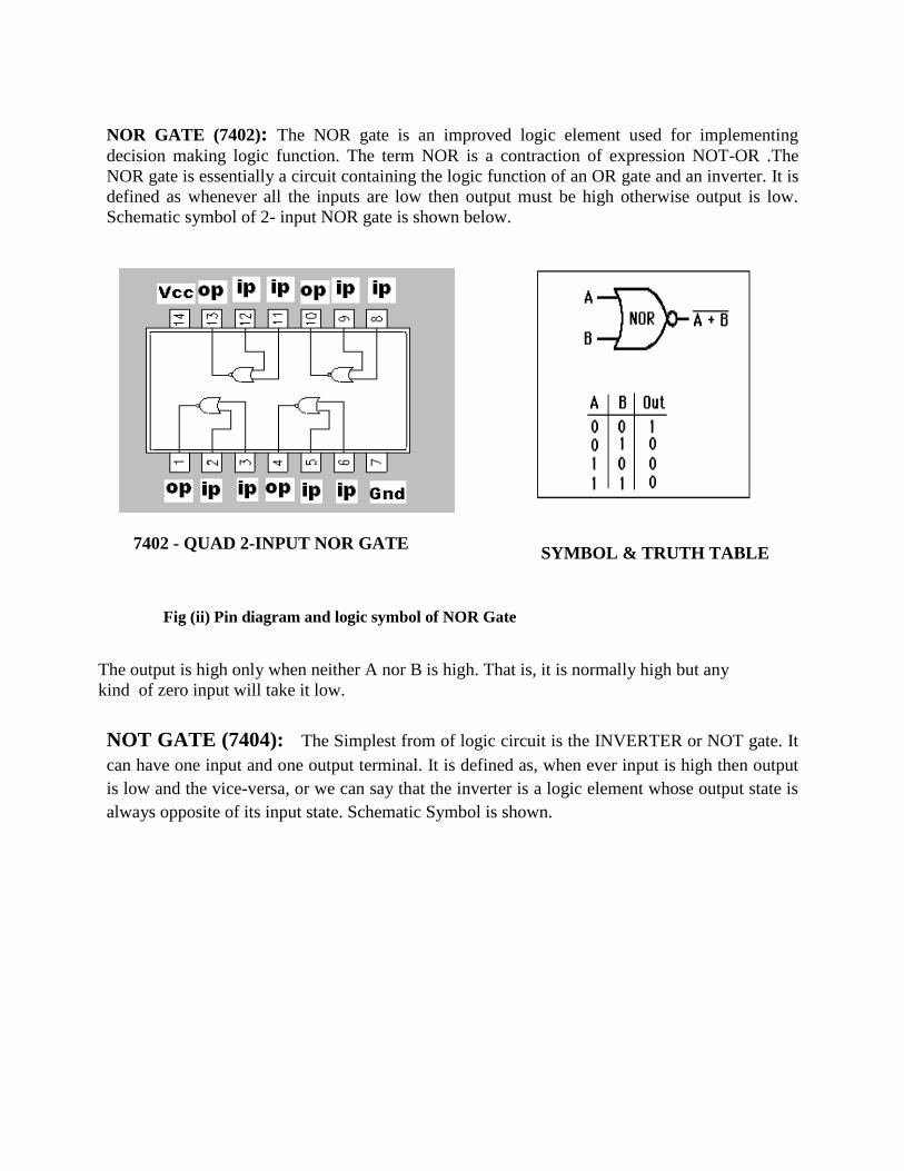
PRODUCT OF SUM FORM (POS): The product of sum form expression contains two
or more OR terms which are ANDed together to form POS expression. Each OR term contains
one or more variables appearing either in complemented or in un-complemented form.
For example:
1. (A+B+C).(B+C)
2. (B+C).(B).(A+B)
Fig (ii) Logic diagram of Boolean expression in POS form
OBSERVATION TABLE OF SOP:
Input outputs
ABC BC ABC ABC+BC
000 0 0 0
001 1 0 1
010 0 0 0
011 0 0 0
100 0 0 0
101 1 0 1
110 0 1 1
111 0 0 0
Table (i) Truth table for SOP representation

OBSERVATION TABLE OF POS:-
Input Outputs
ABC A+B+C B+C (A+B+C)+(B+C)
000 1 1 1
001 0 1 0
010 1 0 0
011 1 0 0
100 1 1 1
101 1 1 1
110 1 1 1
111 1 1 1
Fig (ii) Truth table for POS representation
RESULT: The observation table of SOP and POS is verified.
PRECAUTIONS:
1 All Connections should be according to circuit diagram.
2. All Connections should be right and tight.
3. Reading should be taken carefully.
4. Switch off Power supply after completing the Experiment.
.

QUESTIONS
Q.1 What are the various methods to simplify Boolean Expression?
Q.2 What is Boolean Algebra?
Q.3 Distinguish between sum of product and product of sum?
Q.4 What is minterm?
Q.5 What is maxterm?
Q.6 Distinguish between min terms and max terms.
Q.7 Distinguish between combinational logic circuits and sequential logic circuits?
Q.8 Why logic gates are called as logic gates not boolean gates?
Q.9 What is D‟ morgans theorem?
Q.10 Define K-map?

EXPERIMENT NO. 3
OBJECTIVE: Verification of state tables of RS, JK, T and D flip-flops using NAND & NOR
Gates.
OUTCOME: To verify of state tables of various flip-flops using NAND & NOR gates.
APPARATUS REQUIRED: Digital Trainer Kit, ICs, (7400, 7404, 7410) & Connecting wire.
THEORY: A Flip flop is a bistable electronic circuit that has two stable state .That is , its
output is either +5V(logic 1) or 0V(logic 0) .A Flip Flop can be referred as memory device since
its output will remain unchanged until its input is not changed. It is used to store one binary digit.
R-S FLIP FLOP: A R-S Flip Flop is one that has two inputs R & S and two outputs Q & Q‟. An
R-S Flip Flop can be constructed using NOR gates or NAND gates. Figure shows R-S Flip Flop
constructed using four NAND gates.
CIRCUIT DIAGRAM:
Fig (i) R-S FLIP–FLOP
CHARACTERISTIC TABLE
CLK S R Q (t+1)
0 X X NO CHANGE
1 0 0 NO CHANGE
1 0 1 0
1 1 0 1
1 1 1 FORBIDDEN
Table (i) Characteristic table of R-S Flip-Flop
D- FLIP FLOP: To avoid the forbidden case that occur in R-S Flip Flop, when R=S=1, D Flip
Flop is implemented. In the D Flip Flop, there is only one input D as show in figure .We can
transmit the value of D at the output of the Flip Flop when CLK is high.

CIRCUIT DIAGRAM
Fig (ii) Circuit Diagram of D Flip-Flop
J-K FLIP FLOP: Setting R=S=1 with a R-S Flip Flop Q and Q‟ will set to the same logic level.
This is an illegal conditions .The J-K Flip Flop accounts for this illegal input. It is used to build
counter. The values of J and K determine what a J-K Flip Flop does on the next clock edge.
When both are low, the Flip Flop retains its last state. When J is low and K is high, the Flip Flop
resets. When J is high and K is low, the Flip Flop sets. When both are high the Flip flop toggles.
In this last mode, the J-K Flip Flop can be used as a frequency divider.
PIN CONFIGURATION OF 7410:- CIRCUIT DIAGRAM:-
FIGf
Fig (iii) Pin diagram and circuit diagram of JK Flip Flop
T- FLIP FLOP: The T- Flip Flop is known as Toggle Flip flop. The T Flip flop is a
modification of the JK Flip flop by connecting both inputs J and K together. Figure shows the
logic diagram of T flip flop ,logic symbol and truth table of T Flip flop is also shown.

When T=0, both AND gates are disabled and hence there is no change in the previous output.
When T=1(J=K=1) output toggles. Toggles means that the output is 0 when the previous state is
1 otherwise output is 1 when the previous state is 0. So the output is a complement of the
previous output.
Circuit Diagram
Fig (iv) Circuit diagram of JK Flip Flop
OBSERVATION TABLE: D - FLIP –FLOP
CLK D Q (t+1)
0 X NO CHANGE
1 1 1
1 0 0
Table (ii) Characteristic table of D Flip-Flop
OBSERVATION TABLE: J-K - FLIP -FLOP
CLK J K Q (t+1)
0 x X NO CHANGE
1 0 0 NO CHANGE
1 0 1 0
1 1 0 1
1 1 1 TOGGLE
Table (iii) Characteristic table of J-K Flip-Flop

OBSERVATION TABLE: T - FLIP -FLOP
Preset State Flip flop Input Next State
Qn T Qn+1
0 0 0
0 1 1
1 0 1
1 1 0
Table (iv) Characteristic table of T Flip-Flop
RESULT: The observation tables of various flip-flops are verified.
PRECAUTIONS:
1) All Connections should be according to circuit diagram.
2) All Connections should be right and tight.
3) Reading should be taken carefully.
4) Switch off Power supply after completing the Experiment.

QUESTIONS
Q.1 What are flip flops?
Q.2 What is latch?
Q.3 What is an excitation table?
Q.5 List out the application of flip-flop.
Q.6 What are the application of T flip flop?
Q.7 What is the difference of D Flip-flop and T flip-flop?
Q.8 How do you Convert SR flip- flop from D flip flop?
Q.9 Convert from T flip flop to d flip flop?
Q.10 What is race around condition?.
Q. 11 How race around condition is eliminated in a Master-slave J-K flip-flop?
EXPERIMENT NO.4
OBJECTIVE: Implementation and verification of Decoder using logic gates.
OUTCOME: To implement various combinational circuits on bread board using different Logic
gates ICs.
APPARATUS REQUIRED: Bread Board, 3-input AND gate and NOT gate ICs, Connecting
wire etc.
THEORY:
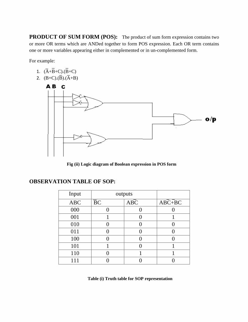
3:8 DECODER: A decoder is a combinational circuit that converts binary information from n
line to a maximum of 2n
unique output lines . The name decoder is also used in conjunction with
some code converters such as a BCD to seven segment decoder. The block diagram of a decoder
is shown in the figure.

Fig (i) Circuit diagram and block diagram representation of 3:8 Decoder
TRUTH TABLE:
Input Output
X1 X2 X3 Y0 Y1 Y2 Y3 Y4 Y6 Y7 Y8
0 0 0 1 0 0 0 0 0 0 0
0 0 1 0 1 0 0 0 0 0 0
0 1 0 0 0 1 0 0 0 0 0
0 1 1 0 0 0 1 0 0 0 0
1 0 0 0 0 0 0 1 0 0 0
1 0 1 0 0 0 0 0 1 0 0
1 1 0 0 0 0 0 0 0 0 0
1 1 1 0 0 0 0 0 0 0 1
Table (i) Turth table of 3:8 Decoder
RESULT: The observation table of decoder is verified.
PRECAUTION:
1. All Connections should be according to circuit diagram.
2. All Connections should be right and tight.
3. Reading should be taken carefully.
4. Switch off Power supply after completing the experiment.

QUESTIONS
Q.1 What is Decoder?
Q.2 What is the main difference between decoder and de-multiplexer?
Q.3 What is combinational circuit?
Q.5 What are the difference between combinational and sequential logic?
Q.6 Why Binary is different from Gray code?
Q.7 Write the full form of ASCII code?
Q.8 Binary code is weighted code or not?
Q.9 Design 4:16 Decoder?
Q.10 What are the difference between combinational and sequential logic?
EXPERIMENT NO.5
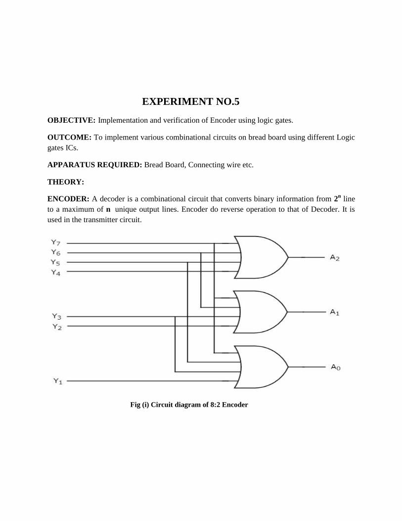
OBJECTIVE: Implementation and verification of Encoder using logic gates.
OUTCOME: To implement various combinational circuits on bread board using different Logic
gates ICs.
APPARATUS REQUIRED: Bread Board, Connecting wire etc.
THEORY:
ENCODER: A decoder is a combinational circuit that converts binary information from 2n line
to a maximum of n unique output lines. Encoder do reverse operation to that of Decoder. It is
used in the transmitter circuit.
Fig (i) Circuit diagram of 8:2 Encoder

TRUTH TABLE:
Input Output
Y0 Y1 Y2 Y3 Y4 Y6 Y7 Y8 A1 A2 A3
1 0 0 0 0 0 0 0 0 0 0
0 1 0 0 0 0 0 0 0 0 1
0 0 1 0 0 0 0 0 0 1 0
0 0 0 1 0 0 0 0 0 1 1
0 0 0 0 1 0 0 0 1 0 0
0 0 0 0 0 1 0 0 1 0 1
0 0 0 0 0 0 0 0 1 1 0
0 0 0 0 0 0 0 1 1 1 1
Table (i) Truth Table of 8:3 Encoder
RESULT: The observation table of encoder is verified.
PRECAUTION:
1. All Connections should be according to circuit diagram.
2. All Connections should be right and tight.
3. Reading should be taken carefully.
4. Switch off Power supply after completing the experiment.

QUESTIONS
Q.1 What is encoder?
Q.2 What are the difference between Decoder and De-multiplexer?
Q.3 Can Decoder work as De-multiplexer?
Q.4 What is the function of enable input to any IC?
Q.5 What is IC?
Q.6 Tell about the advancement of Integrated circuit?
Q.7 What is Delay in combinational circuits?
Q.8 Draw the full adder circuit diagram?
Q.9 What size of decoder is used to implement a Boolean function of 3 variable?
Q.10 Implement half adder using decoder?
EXPERIMENT NO. 6
OBJECTIVE: To Implementation of 4x1 multiplexer using logic gates.
OUTCOME: To implement various combinational circuits on bread board using different Logic
gates ICs.
APPARATUS REQUIRED: Three input AND Gate & Four input OR Gate, Connecting wire
and trainer kit etc.
THEORY:
It quite often happens, in the design of large-scale digital systems, that a single line is required to
carry two or more different digital signals. Of course, only one signal at a time can be placed on
the one line. What is required is a device that will allow us to select, at different instants, the
signal we wish to place on this common line. Such a circuit is referred to as a Multiplexer.
A multiplexer performs the function of selecting the input on any one of 'n' input lines and
feeding this input to one output line. Multiplexers are used as one method of reducing the
number of integrated circuit packages required by a particular circuit design. This in turn reduces
the cost of the system.
Assume that we have four lines, C0, C1, C2 and C3, which are to be multiplexed on a single line,
Output (f). The four input lines are also known as the Data Inputs. Since there are four inputs, we
will need two additional inputs to the multiplexer, known as the Select Inputs, to select which of
the C inputs is to appear at the output. Call these select lines A and B.
The gate implementation of a 4-line to 1-line multiplexer is shown below:

Fig (i) Circuit diagram of 4:1 multiplexer with two selection line.
Fig (ii) Function table Block diagram and of 4:1 Multiplexer
RESULT: The observation table of 4X1 Multiplexer is verified.
PRECAUTION:
1. All Connections should be according to circuit diagram.
2. All Connections should be right and tight.
3. Reading should be taken carefully.
4. Switch off Power supply after completing the Experiment.
Select input output
0 0 C0
0 1 C1
1 0 C2
1 1 C3

QUESTIONS
Q.1 Write the advantage of multiplexer?
Q.2 What are the applications of multiplexer?
Q.3 What is the main difference between decoder and multiplexer?
Q.4. What are the differences between electronic multiplexer and mechanical multiplexer?
Q.5 What types of multiplexing are used?
Q.6 Why MUX is called as Date selector?
Q.7 Differentiate between function of MUX and DEMUX?
Q.8 How many 4:1 MUX is required to implement 8:1 MUX?
Q.9 What do you mean by multiplexing?
Q.10 The number of control lines required to implement 32:1 MUX?

EXPERIMENT NO. 7
OBJECTIVE: Implementation and verification of 1:4 de-multiplexer using logic gates.
OUTCOME: To implement various combinational circuits on bread board using different Logic
gates ICs.
APPARATUS REQUIRED: Bread Board, three input AND gate and NOT gate ICs,
Connecting wire etc.
THEORY:
1:4 DMUX: De-multiplexer means one into many. De-multiplexer is a logic circuit with one
input and many output. By applying control signal we can steer the input signal to one of the
lines. Given figure illustrates that circuit has one input signal, m control signal and n output
signal.

Fig (i) Block Diagram and circuit diagram of De-multiplexer
FUNCTION TABLE:
Enable Select Line Output
E S0 S1 Y0 Y1 Y2 Y3
0 X X 0 0 0 0
1 0 0 I 0 0 0
1 0 1 0 I 0 0
1 1 0 0 0 I 0
1 1 1 0 0 0 I
Table (i) Function Table of 1:4 DEMUX

RESULT: The observation table of de-multiplexer is verified.
PRECAUTION:
1. All Connections should be according to circuit diagram.
2. All Connections should be right and tight.
3. Reading should be taken carefully.
4. Switch off Power supply after completing the experiment.
QUESTIONS
Q.1 Write the advantage of De-multiplexer?
Q.2 What are the applications of multiplexer?
Q.3 What is the main difference between decoder and multiplexer?
Q.4 What are the differences between electronic multiplexer and mechanical multiplexer?
Q.5 What types of multiplexing are used?
Q.6 What is the role of select line in De-multiplexer?
Q.8 The no. of control lines required for 1:8 De-multiplexer?
Q.9 What are the application of De-multiplexer?

Q.10 The no. of 1:2 DEMUX is used to implement the 1: 8 DEMUX?
EXPERIMENT NO. 8
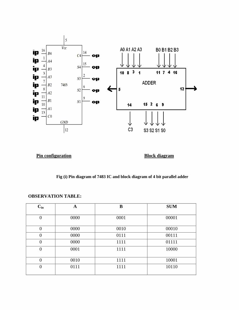
OBJECTIVE: Implementation of 4-bit parallel adder using IC 7483.
OUTCOME: To implement various combinational circuits on bread board using different Logic
gates ICs.
APPRATUS REQUIRED: Trainer Kit, IC- 7483, & Connecting Wire.
THEORY: An adder circuit for addition of two n bit binary numbers consists of n full adder
Circuit. It accepts two n bit binary number as input & produces an (n+ 1) bit binary number as
the sum. Here A & B are the two n bit input to be added & C0 to C3 are carry inputs and S2-S0 is
their sum. In this a half adder may be used to add the least significant bit A0 & B0. By cascading
these full adders we can design parallel adder for n- bit addition.
Pin configuration Block diagram
Fig (i) Pin diagram of 7483 IC and block diagram of 4 bit parallel adder
OBSERVATION TABLE:
Cin A B SUM
0 0000 0001 00001
0 0000 0010 00010
0 0000 0111 00111
0 0000 1111 01111
0 0001 1111 10000
0 0010 1111 10001
0 0111 1111 10110

0 1111 1111 11110
1 1111 1111 11111
Table (i) Functional table of 4-bit parallel Adder
PROCEDURE:
1. Make the connection as shown in the figure.
2. The12th
Pin of IC is to be grounded.
3. Vcc is applied on 5th
Pin of IC.
RESULT: The observation table of binary adder is verified.
PRECAUTION:
1. All Connections should be according to circuit diagram.
2. All Connections should be right and tight.
3. Reading should be taken carefully.
4. Switch off Power supply after completing the Experiment.
.
QUESTIONS
Q.1 What is the major difference between half-adders and full-adders?
Q.2 How four-bit adder can perform subtraction ?
Q.3 What is effect of 4-bit full-adder circuits?
Q.4 What is a half adder?
Q.5 What is a full- adder?

Q.6 What is parallel adder?
Q.7 Draw and explain block diagram for 4 bit parallel adder.
Q.8 Define adder & subtractor?
Q.9 What are the applications of 4 bit adder and subtractor?
Q.10 What are applications of Adder?
EXPERIMENT NO. 9
OBJECTIVE: Design and verify the 4-bit Synchronous counter.
OUTCOME: To design the 4-bit synchronous counter. .
Apparatus Required: Experimental Kit, IC- 74190, & Connecting Wire.
THEORY:
The ripple counter is the simplest to build, but there is a limit to its highest operating
frequency. 4 flip flops are used to construct 4- bit Synchronous counter. Every flip flop is
triggered in synchronism with the clock. The construction of that type of parallel binary counter
is shown in figure 1, along with the truth table and the waveforms for the natural count sequence.

The basic idea here is to keep the J and K inputs of each flip flop high, such that the flip flop will
toggle with any negative clock transition at its clock input. We then use AND gates to gate
every second clock to flip flop B, every fourth clock to flip flop C, and so on. This logic
configuration is after referred to as “steering logic” Since the clock pulses are gated or steered to
each individual flip flop.
The clock is applied directly to flip flop A. Since the JK flip flop used responds to a negative
transition at the clock input and toggles when both the J and K input are high. Flip flop A will
change state with each negative clock transition. Whenever A is high. AND gate X is enable and
a clock pulse is passed through the gate to the clock input of flip flop B. Thus B changes state
with every other negative clock transition at points b, d, f and h on the time line. Since AND gate
y is enabled and will transmit the clock to flip flop C only. When both A and B are high. Flip
flop C changes state with every fourth negative clock transition at points d and h on the time line.
Examination of the waveform and the truth table reveals that this counter progresses upward in a
natural binary sequence from count 000 up to count 111, advancing One count with each
negative clock transition. This is a mode 8 parallel or synchronous, binary counter operating in
the count up mode.

04 BIT SYNCHRONOUS BINARY COUNTERS
Fig (i) 4 Bit Synchronous binary counter circuit diagram and waveform
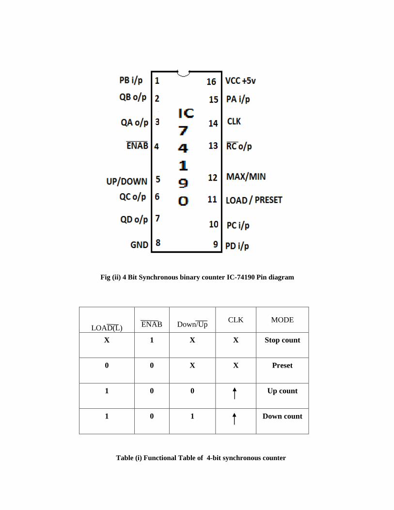
Fig (ii) 4 Bit Synchronous binary counter IC-74190 Pin diagram
LOAD(L)
ENAB
Down/Up CLK MODE
X 1 X X Stop count
0 0 X X Preset
1 0 0 Up count
1 0 1 Down count
Table (i) Functional Table of 4-bit synchronous counter

OBSERVATION TABLE: For Counter-
Count (I /n) Q3 Q2 Q1 Q0
(output ) 0 0 0 0 0
1 0 0 0 1
2 0 0 1 0
3 0 0 1 1
4 0 1 0 0
5 0 1 0 1
6 0 1 1 0
7 0 1 1 1
8 1 0 0 0
9 1 0 0 1
10 1 0 1 0
11 1 0 1 1
12 1 1 0 0
13 1 1 0 1
14 1 1 1 0
15 1 1 1 1
Table (ii) Observation table of 4 bit synchronous counter
PROCEDURE:
1. Make the connections as shown in the pin diagram.
2. Connect Pin No- 8 to GND.
3. Connect Pin No- 16 to Vcc.
RESULT: The Observation table of Synchronous counter is verified.
PRECAUTION:
1. All Connections should be according to Pin diagram.
2. All Connections should be right and tight.
3. Reading should be taken carefully.
4. Switch off Power supply after completing the Experiment.

QUESTIONS
Q.1 What do you understand by counter?
Q.2 How Synchronous counters eliminate the delay problems encountered with asynchronous
counters?
Q.3 What is the difference between combinational logic and sequential logic?
Q.4 Define synchronous counter?
Q.5 What is deference between synchronous counter and asynchronous counters?
Q.6 What are the advantages of synchronous counters over asynchronous counters?
Q.7 What are the Applications of synchronous counter?
Q.8 What changes must be made to a 3-bit counter to make it a 4-bit counter?
Q.9 What do you understand by state diagram?
Q.10 Which flip-flop is used in synchronous counter?

EXPERIMENT NO. 10
OBJECTIVE: Design and verify the 4-bit Asynchronous counter.
OUTCOME: To design the 4-bit asynchronous counter.
APPARATUS REQUIRED: Bread Board, IC 7473 & Connecting Wire.
THEORY: A binary ripple counter can be constructed by use of clocked J K flip- flops. The
system clock, a square wave, drives flip flop A. The output of A drives B , and the output of B
drives flip –flop C. All the J and K input are tied to +Vcc. This means that each flip flop will
change state with a negative transition at its clock input. Lets assume that the flip - flops are
initially reset to produce „0‟outputs. If we consider A to be least -significant bit (LSB) and C the
most significant bit (MSB) , we can say the contents of the counter is CBA =000.
Since A acts as the clock for B, each time the waveform at A goes low, flip flop
B will toggle. Thus at point b on the time line, B goes high ;it then goes low at the point d and
toggles back high again at point f. Notice that the wave from at the output of flip flops one –half
the frequency of A and one –forth the clock frequency . Since B acts a the clock for C, Each
time the waveform at B goes low, flip flop C will toggle. Thus C goes high at point d on the time
line and goes back low again at point h. The frequency of the wave form at C is one half that at
B, But it is only one either the clock frequency.
Wave form
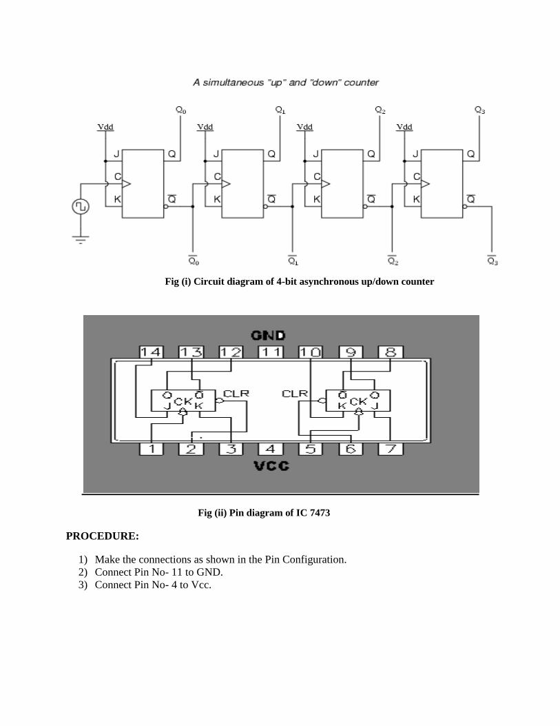
Fig (i) Circuit diagram of 4-bit asynchronous up/down counter
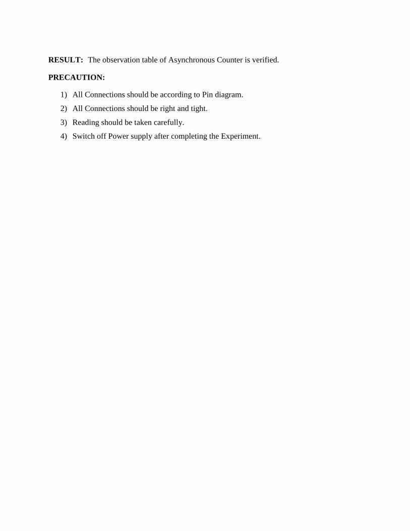
Fig (ii) Pin diagram of IC 7473
PROCEDURE:
1) Make the connections as shown in the Pin Configuration.
2) Connect Pin No- 11 to GND.
3) Connect Pin No- 4 to Vcc.
RESULT: The observation table of Asynchronous Counter is verified.
PRECAUTION:
1) All Connections should be according to Pin diagram.
2) All Connections should be right and tight.
3) Reading should be taken carefully.
4) Switch off Power supply after completing the Experiment.

QUESTIONS
Q.1 Define Asynchronous down counter?
Q.2 Write the problems associated with ripple counters?
Q.3 What is meant by a counter?
Q.4 What is a ripple counter?
Q.5 How is parallel counter is faster then ripple counter?
Q.6 How is it possible to make a modulo 2N counter using N-flip-flops? Name the two types
of such counters.
Q.7 What are the applications of ripple counter?
Q.8 How do you convert a ripple counter to a decade counter?
Q.9 What is meant by BCD ripple counter?
Q.10 What is the count sequence for a BCD up-counter?