Experiment No. 1 Objective Theory - umartalha
21
SSUET/QR/112 220) - igital Logic Design (EE D ______________________________________________________________________________ Department of Telecommunication Engineering Sir Syed University of Engineering & Technology, Karachi Experiment No. 1 Objective To study the logic gates in the TTL ICs and familiarize with Combinational logic Components Required Bread board 5 V - power supply Multimeter Logic probe LEDs with resistors Connecting wires Switches Following ICs and their datasheets 7408: quad 2 input AND 7432: quad 2 input OR gate 7404: hex inverter 7400: quad 2 input NAND 7402: quad 2 input NOR gate 7486: quad 2 input EXOR gate Theory Logic Gates Logic gates are the fundamental building blocks of digital systems. These devices are able to make decisions, in the sense that they produce one output level when some combinations of input levels are present and a different output when other combinations are applied; hence given the name Logic Gates. The two levels produced by digital circuitry are referred as HIGH and LOW, TRUE and FALSE, ON and OFF, or simply 1 and 0. There are only three basic gates: AND, OR and NOT. The other gates are merely combinations of these basic gates. Logic gates can be interconnected to perform a variety of logical operations. This interconnection of gates to achieve prescribed outcomes is called logic design. AND Gate An AND gate's output is 1 if and only if all its inputs are 1. e.g if A and B. are two inputs of an AND gate then output, F of the gate is given as: F = A . B OR Gate An OR gate's output is 1 if at least one of its input is 1 e.g. if A and B are two inputs to an OR gate then output, F of the gate is given as: F = A+B
-
Upload
khangminh22 -
Category
Documents
-
view
2 -
download
0
Transcript of Experiment No. 1 Objective Theory - umartalha

SSUET/QR/112 220)-igital Logic Design (EED
______________________________________________________________________________
Department of Telecommunication Engineering
Sir Syed University of Engineering & Technology, Karachi
Experiment No. 1
Objective
To study the logic gates in the TTL ICs and familiarize with Combinational logic
Components Required
Bread board
5 V - power supply
Multimeter
Logic probe
LEDs with resistors
Connecting wires
Switches
Following ICs and their datasheets
7408: quad 2 input AND
7432: quad 2 input OR gate
7404: hex inverter
7400: quad 2 input NAND
7402: quad 2 input NOR gate
7486: quad 2 input EXOR gate
Theory Logic Gates
Logic gates are the fundamental building blocks of digital systems. These devices are able to
make decisions, in the sense that they produce one output level when some combinations of
input levels are present and a different output when other combinations are applied; hence
given the name Logic Gates. The two levels produced by digital circuitry are referred as HIGH
and LOW, TRUE and FALSE, ON and OFF, or simply 1 and 0. There are only three basic
gates: AND, OR and NOT. The other gates are merely combinations of these basic gates.
Logic gates can be interconnected to perform a variety of logical operations. This
interconnection of gates to achieve prescribed outcomes is called logic design.
AND Gate An AND gate's output is 1 if and only if all its inputs are 1. e.g if A and B. are two inputs of an
AND gate then output, F of the gate is given as: F = A . B
OR Gate An OR gate's output is 1 if at least one of its input is 1 e.g. if A and B are two inputs to an OR
gate then output, F of the gate is given as: F = A+B
SSUET/QR/112 220)-igital Logic Design (EED
_____________________________________________________________________________
Department of Telecommunication Engineering
Sir Syed University of Engineering & Technology, Karachi
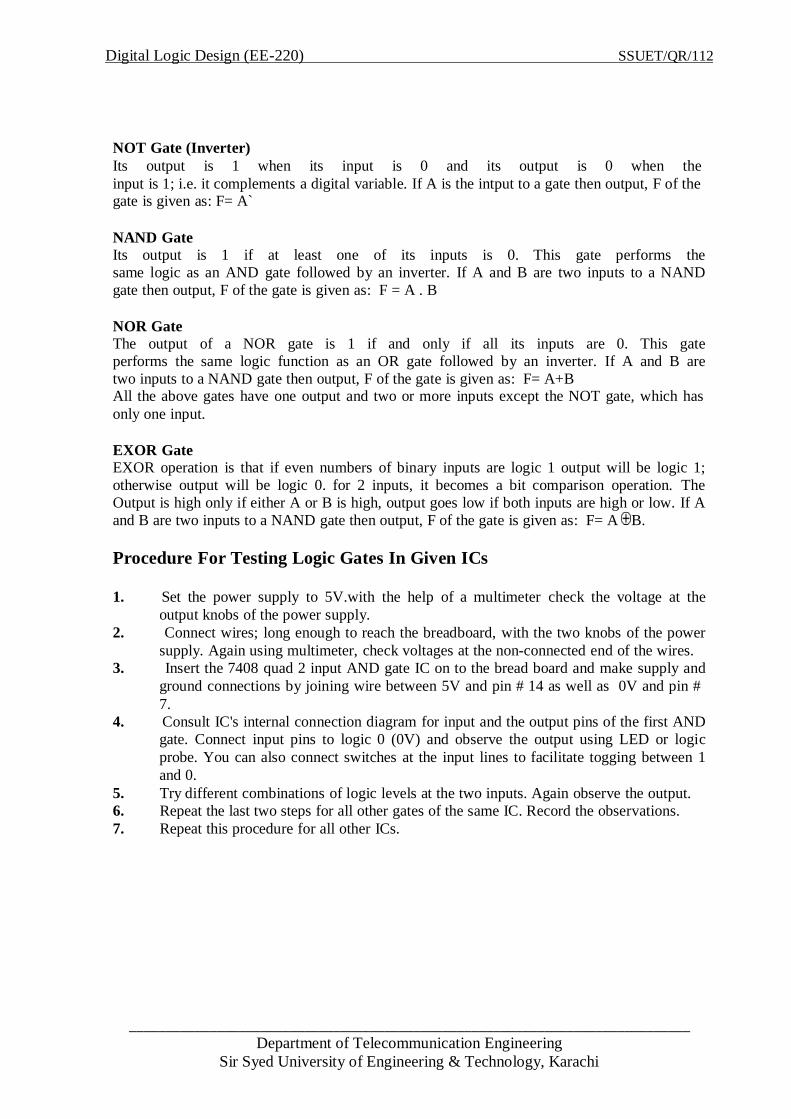
NOT Gate (Inverter)
Its output is 1 when its input is 0 and its output is 0 when the
input is 1; i.e. it complements a digital variable. If A is the intput to a gate then output, F of the gate is given as: F= A`
NAND Gate Its output is 1 if at least one of its inputs is 0. This gate performs the
same logic as an AND gate followed by an inverter. If A and B are two inputs to a NAND
gate then output, F of the gate is given as: F = A . B
NOR Gate The output of a NOR gate is 1 if and only if all its inputs are 0. This gate
performs the same logic function as an OR gate followed by an inverter. If A and B are
two inputs to a NAND gate then output, F of the gate is given as: F= A+B All the above gates have one output and two or more inputs except the NOT gate, which has
only one input.
EXOR Gate EXOR operation is that if even numbers of binary inputs are logic 1 output will be logic 1;
otherwise output will be logic 0. for 2 inputs, it becomes a bit comparison operation. The
Output is high only if either A or B is high, output goes low if both inputs are high or low. If A
and B are two inputs to a NAND gate then output, F of the gate is given as: F= A B.
Procedure For Testing Logic Gates In Given ICs
1. Set the power supply to 5V.with the help of a multimeter check the voltage at the
output knobs of the power supply.
2. Connect wires; long enough to reach the breadboard, with the two knobs of the power
supply. Again using multimeter, check voltages at the non-connected end of the wires.
3. Insert the 7408 quad 2 input AND gate IC on to the bread board and make supply and
ground connections by joining wire between 5V and pin # 14 as well as 0V and pin #
7.
4. Consult IC's internal connection diagram for input and the output pins of the first AND
gate. Connect input pins to logic 0 (0V) and observe the output using LED or logic
probe. You can also connect switches at the input lines to facilitate togging between 1
and 0.
5. Try different combinations of logic levels at the two inputs. Again observe the output.
6. Repeat the last two steps for all other gates of the same IC. Record the observations.
7. Repeat this procedure for all other ICs.
SSUET/QR/112 220)-igital Logic Design (EED
______________________________________________________________________________
Department of Telecommunication Engineering
Sir Syed University of Engineering & Technology, Karachi
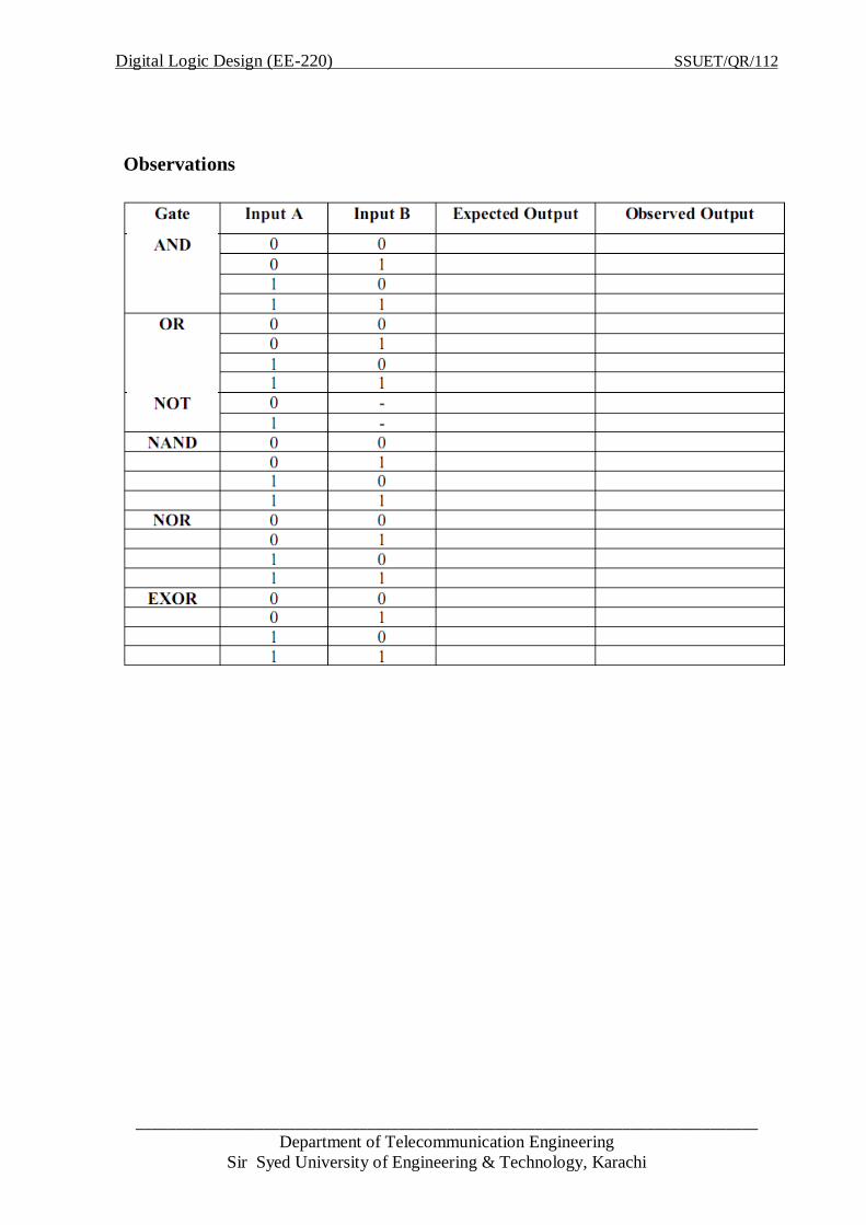
Observations

SSUET/QR/112 220)-igital Logic Design (EED
_____________________________________________________________________________
Department of Telecommunication Engineering
Sir Syed University of Engineering & Technology, Karachi
Task 1.1: Procedure for Implementation of the Given Circuit
1. Set the power supply to 5V.
2. Insert ICs on the bread board and make their supply and ground connections.
3. As given in the logic diagram, make connections using wires and gates in the
ICs.
4. Apply different combinations at the three inputs and observe the output.
Circuit Diagram
Figure 1.2
Observations
Logic expression for the given logic diagram:
SSUET/QR/112 220)-igital Logic Design (EED
______________________________________________________________________________
Department of Telecommunication Engineering
Sir Syed University of Engineering & Technology, Karachi
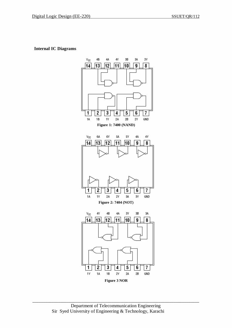
Internal IC Diagrams
Figure 1: 7400 (NAND)
Figure 2: 7404 (NOT)
Figure 3 NOR
SSUET/QR/112 220)-igital Logic Design (EED
_____________________________________________________________________________
Department of Telecommunication Engineering
Sir Syed University of Engineering & Technology, Karachi
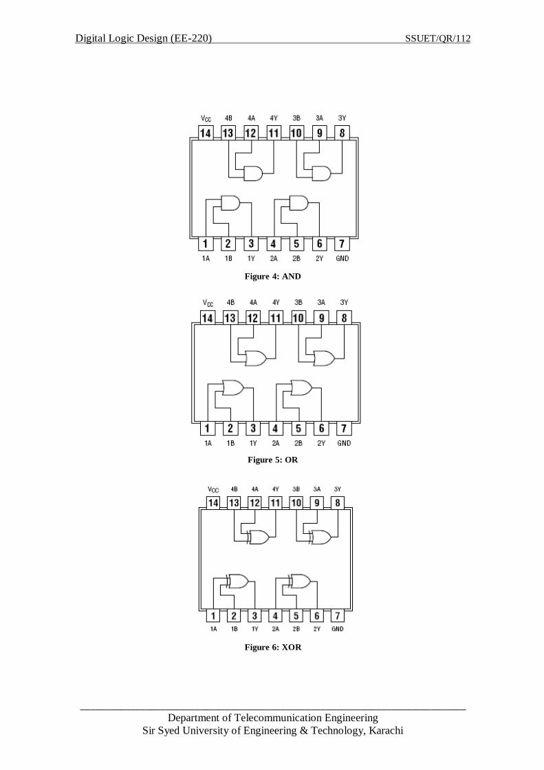
Figure 4: AND
Figure 5: OR
Figure 6: XOR

SSUET/QR/112 220)-igital Logic Design (EED
______________________________________________________________________________
Department of Telecommunication Engineering
Sir Syed University of Engineering & Technology, Karachi
Experiment No. 2
Objective To verify De-Morgan’s laws and verification of Boolean Laws and Rules.
Components & Apparatus Required Bread board/Digital Logic Trainer 5 V -DC Power Supply
Logic probe
ICs 7410, 7427, 7432, 7408 & 7404
Theory In Boolean algebra, the two De Morgan’s laws are very important as these play key role
in manipulating logic functions into SOP/POS forms. For two inputs, these laws are:
In this experiment, you will using 3-input NAND and NOR gates to verify De Morgan’s
laws for three inputs
Procedure & Observations
Using 3-input NAND gate & NOT+OR gates to verify:
1. Take IC 7410 triple 3-inputs NAND gate and insert it in bread board/Digital logic
trainer.
2. Connect the circuit as shown below by connecting the DC supply (5V) and ground
to pin#14 and 7 and logic inputs A, B and C to pin# 1, 2 and 13. Then take output
from pin# 12.
3. In Boolean form this output is .
4. Change inputs according to the table below and record your observations in
observation table 2.1
5. Now implement Boolean function using NOT and OR gates.
SSUET/QR/112 220)-igital Logic Design (EED
_____________________________________________________________________________
Department of Telecommunication Engineering
Sir Syed University of Engineering & Technology, Karachi
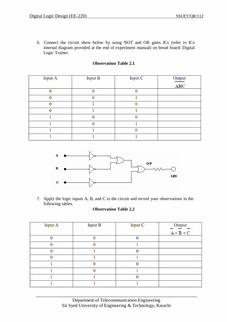
6. Connect the circuit show below by using NOT and OR gates ICs (refer to ICs
internal diagram provided at the end of experiment manual) on bread board/ Digital
Logic Trainer.
Observation Table 2.1
Input A Input B Input C Output
0 0 0
0 0 1
0 1 0
0 1 1
1 0 0
1 0 1
1 1 0
1 1 1
7. Apply the logic inputs A, B, and C to the circuit and record your observations in the
following tables.
Observation Table 2.2
SSUET/QR/112 220)-igital Logic Design (EED
______________________________________________________________________________
Department of Telecommunication Engineering
Sir Syed University of Engineering & Technology, Karachi
You will agree that the outputs of two tables are same. Hence De- Morgan’s law is
verified.
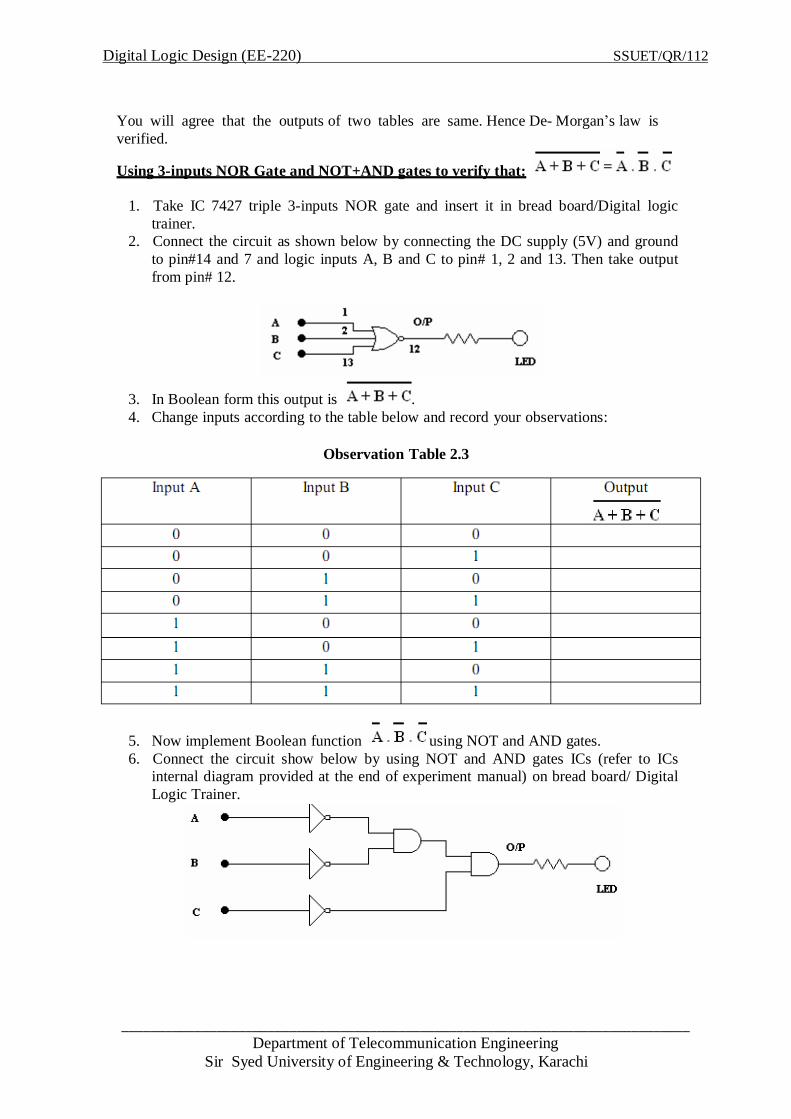
Using 3-inputs NOR Gate and NOT+AND gates to verify that:
1. Take IC 7427 triple 3-inputs NOR gate and insert it in bread board/Digital logic
trainer.
2. Connect the circuit as shown below by connecting the DC supply (5V) and ground
to pin#14 and 7 and logic inputs A, B and C to pin# 1, 2 and 13. Then take output
from pin# 12.
3. In Boolean form this output is .
4. Change inputs according to the table below and record your observations:
Observation Table 2.3
Input A Input B Input C Output
0 0 0
0 0 1
0 1 0
0 1 1
1 0 0
1 0 1
1 1 0
1 1 1
5. Now implement Boolean function using NOT and AND gates.
6. Connect the circuit show below by using NOT and AND gates ICs (refer to ICs
internal diagram provided at the end of experiment manual) on bread board/ Digital
Logic Trainer.
SSUET/QR/112 220)-igital Logic Design (EED
_____________________________________________________________________________
Department of Telecommunication Engineering
Sir Syed University of Engineering & Technology, Karachi
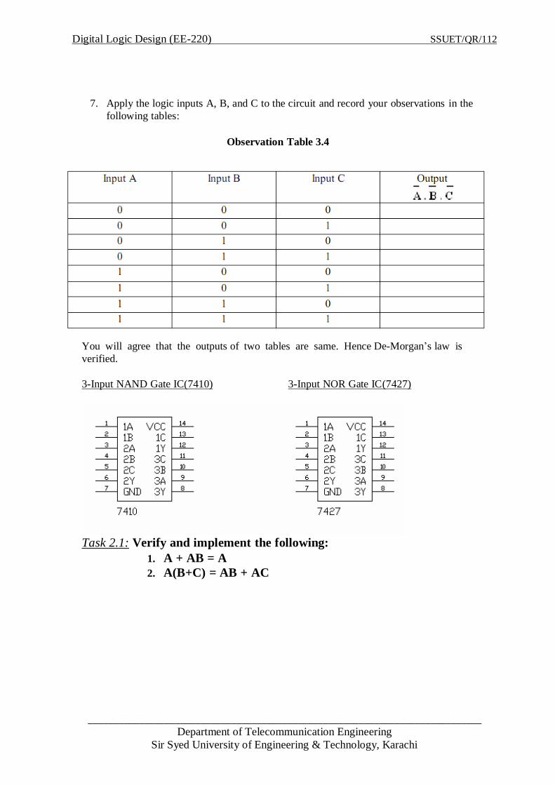
7. Apply the logic inputs A, B, and C to the circuit and record your observations in the
following tables:
Observation Table 3.4
Input A Input B Input C Output
0 0 0
0 0 1
0 1 0
0 1 1
1 0 0
1 0 1
1 1 0
1 1 1
You will agree that the outputs of two tables are same. Hence De-Morgan’s law is
verified.
3-Input NAND Gate IC(7410) 3-Input NOR Gate IC(7427)
Task 2.1: Verify and implement the following:
1. A + AB = A
2. A(B+C) = AB + AC
SSUET/QR/112 220)-igital Logic Design (EED
______________________________________________________________________________
Department of Telecommunication Engineering
Sir Syed University of Engineering & Technology, Karachi
Experiment No. 3
Objective Design and implement Half and Full Adder using combinational logic.
Components and Apparatus Required 1. Following ICs and their Datasheets:
I. 7408 Quad 2-input AND Gate.
II. 7432 Quad 2-input OR Gate.
III. 7486 Quad 2-input XOR Gate
2. Bread board/Digital Trainer.
3. 5 V - Power Supply.
4. Multimeter.
5. Logic Probe.
6. LEDs with Resistors.
7. Connecting wires.
Theory
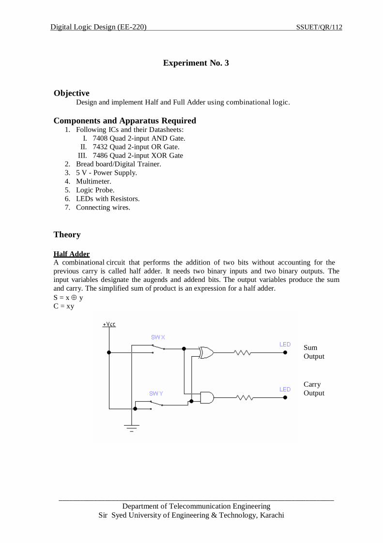
Half Adder A combinational circuit that performs the addition of two bits without accounting for the
previous carry is called half adder. It needs two binary inputs and two binary outputs. The
input variables designate the augends and addend bits. The output variables produce the sum
and carry. The simplified sum of product is an expression for a half adder.
S = x y
C = xy
Sum
Output
Carry
Output
SSUET/QR/112 220)-igital Logic Design (EED
_____________________________________________________________________________
Department of Telecommunication Engineering
Sir Syed University of Engineering & Technology, Karachi
Full Adder
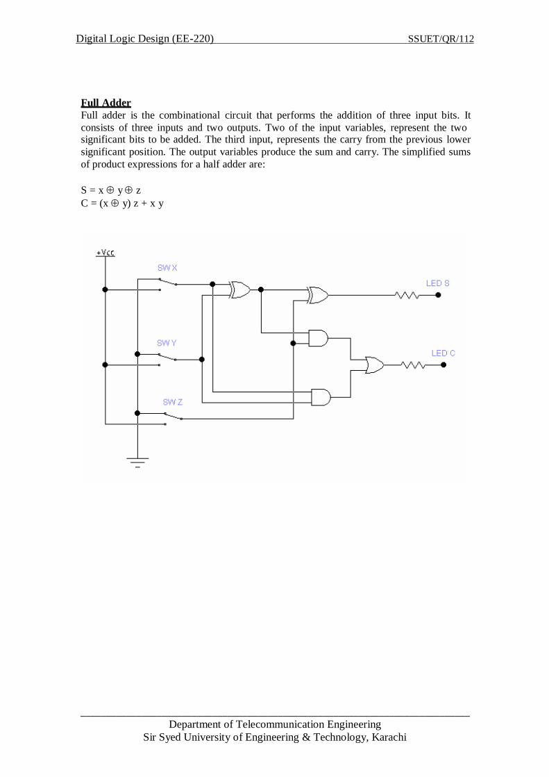
Full adder is the combinational circuit that performs the addition of three input bits. It
consists of three inputs and two outputs. Two of the input variables, represent the two significant bits to be added. The third input, represents the carry from the previous lower
significant position. The output variables produce the sum and carry. The simplified sums
of product expressions for a half adder are:
S = x y z
C = (x y) z + x y
SSUET/QR/112 220)-igital Logic Design (EED
______________________________________________________________________________
Department of Telecommunication Engineering
Sir Syed University of Engineering & Technology, Karachi
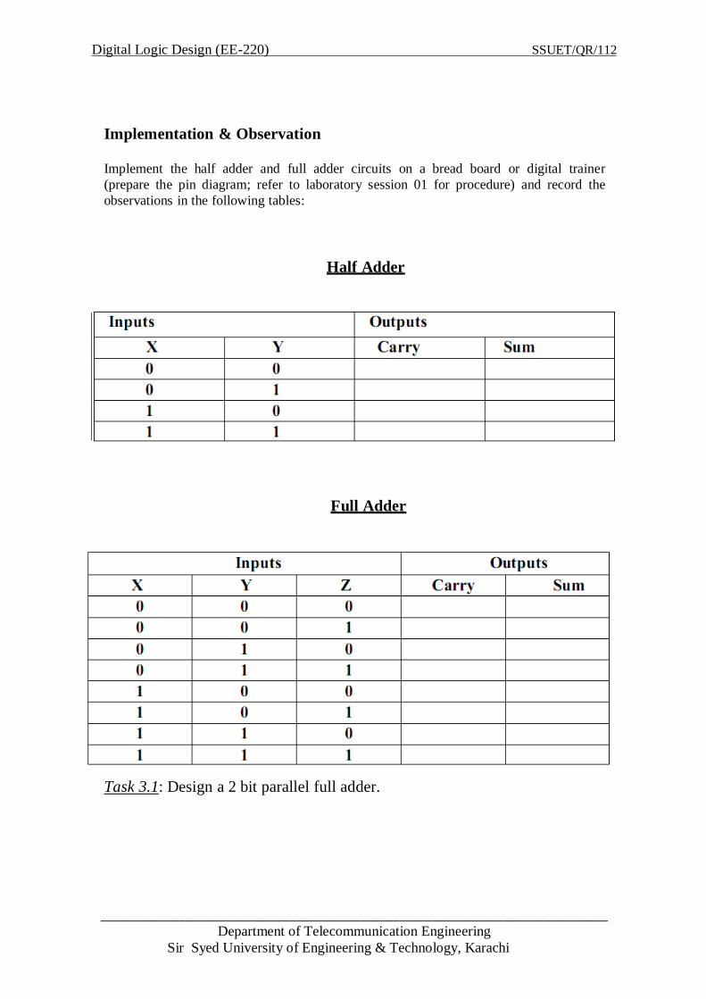
Implementation & Observation
Implement the half adder and full adder circuits on a bread board or digital trainer
(prepare the pin diagram; refer to laboratory session 01 for procedure) and record the
observations in the following tables:
Half Adder
Inputs Outputs
X Y Carry Sum
0 0
0 1
1 0
1 1
Full Adder
Inputs Outputs
X Y Z Carry Sum
0 0 0
0 0 1
0 1 0
0 1 1
1 0 0
1 0 1
1 1 0
1 1 1
Task 3.1: Design a 2 bit parallel full adder.

SSUET/QR/112 220)-igital Logic Design (EED
_____________________________________________________________________________
Department of Telecommunication Engineering
Sir Syed University of Engineering & Technology, Karachi
Experiment No 4
Objective Implementation of 4 variable Karnaugh-Map (SOP).
Given Logic Expression
F (A, B, C, D) = (0, 1, 2, 4, 5, 6, 8, 9, 12, 13, 14)
Components And Apparatus Required
Bread board
5 V – Power supply
Multimeter.
logic probe
LEDs with resistors.
Connecting wires.
Following Digital ICs and their Datasheets
7408 Quad 2-input AND Gate
7432 Quad 2-input OR Gate
7404 Hex Inverter
Procedure 1. Construct the truth table of given logic expression.
2. Use Karnaugh- map to reduce the given function.
3. Draw the circuit diagram for the obtained reduced function.
4. Implement the reduced circuit using digital ICs on a bread board.
5. Observe the output and record it in the observation table and check it with the truth table.
SSUET/QR/112 220)-igital Logic Design (EED
______________________________________________________________________________
Department of Telecommunication Engineering
Sir Syed University of Engineering & Technology, Karachi
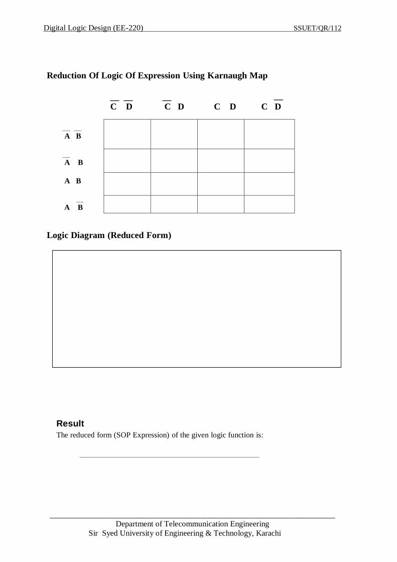
Reduction Of Logic Of Expression Using Karnaugh Map
__
C D C D C D C D
A B
A B
A B
A B
Logic Diagram (Reduced Form)
Result
The reduced form (SOP Expression) of the given logic function is:
220)-EEDigital Logic Design ( Lab Manuab
_____________________________________________________________________________
Department of Telecommunication Engineering
Sir Syed University of Engineering & Technology, Karachi
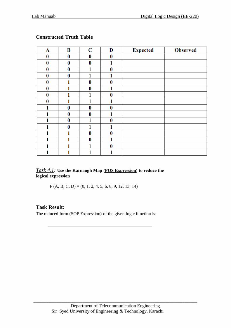
Constructed Truth Table
Task 4.1: Use the Karnaugh Map (POS Expression) to reduce the
logical expression
F (A, B, C, D) = (0, 1, 2, 4, 5, 6, 8, 9, 12, 13, 14)
Task Result:
The reduced form (SOP Expression) of the given logic function is:
220)-Digital Logic Design (EE ManualLab
_____________________________________________________________________________
Department of Telecommunication Engineering
Sir Syed University of Engineering & Technology, Karachi
Experiment No. 5 (a)
Objective To convert given binary numbers to gray codes
Components & Apparatus Required Bread board/Digital Trainer 5V power supply
Multimeter/ Logic probe
LEDs with Resistors
IC 7486
Connecting wires
Theory: Gray code is an unweighted code that has a single bit change between one code word and
the next in a sequence. Gray code is used to avoid problems in systems where an error can
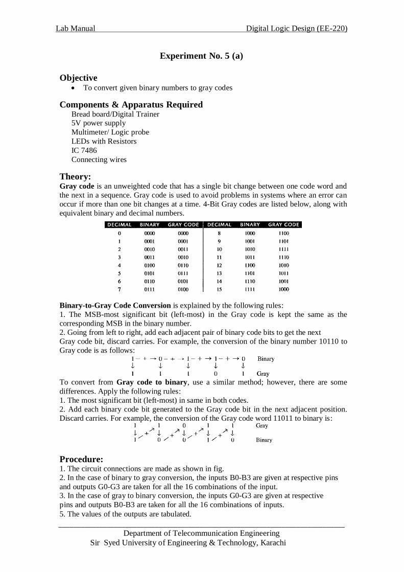
occur if more than one bit changes at a time. 4-Bit Gray codes are listed below, along with
equivalent binary and decimal numbers.
Binary-to-Gray Code Conversion is explained by the following rules:
1. The MSB-most significant bit (left-most) in the Gray code is kept the same as the
corresponding MSB in the binary number.
2. Going from left to right, add each adjacent pair of binary code bits to get the next
Gray code bit, discard carries. For example, the conversion of the binary number 10110 to
Gray code is as follows:
To convert from Gray code to binary, use a similar method; however, there are some
differences. Apply the following rules:
1. The most significant bit (left-most) in same in both codes.
2. Add each binary code bit generated to the Gray code bit in the next adjacent position.
Discard carries. For example, the conversion of the Gray code word 11011 to binary is:
Procedure: 1. The circuit connections are made as shown in fig.
2. In the case of binary to gray conversion, the inputs B0-B3 are given at respective pins
and outputs G0-G3 are taken for all the 16 combinations of the input. 3. In the case of gray to binary conversion, the inputs G0-G3 are given at respective
pins and outputs B0-B3 are taken for all the 16 combinations of inputs.
5. The values of the outputs are tabulated.
220)-EEDigital Logic Design ( Lab Manuab
_____________________________________________________________________________
Department of Telecommunication Engineering
Sir Syed University of Engineering & Technology, Karachi
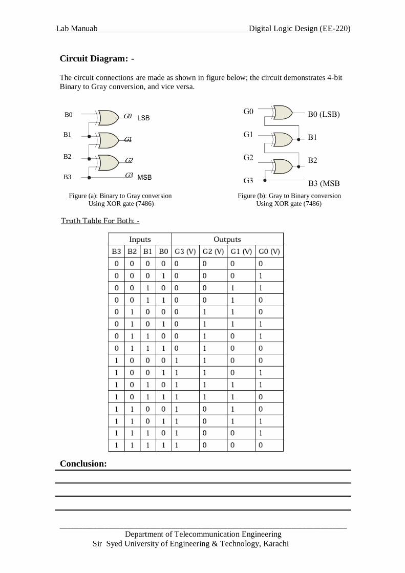
Circuit Diagram: -
The circuit connections are made as shown in figure below; the circuit demonstrates 4-bit
Binary to Gray conversion, and vice versa. B0
B1
B2
B3
Figure (a): Binary to Gray conversion Figure (b): Gray to Binary conversion
Using XOR gate (7486) Using XOR gate (7486)
Conclusion:
0G
1G
2G
3G
GG
GG
GG
GG
(BSL) LG
GL
GL
BSL) GL
220)-Digital Logic Design (EE ManualLab
_____________________________________________________________________________
Department of Telecommunication Engineering
Sir Syed University of Engineering & Technology, Karachi
Experiment No. 5 (b)
Objective Designing an Odd Parity Generator and Checker for a 3-bit Data
Components & Apparatus Required Bread board/Digital Trainer
5 V - Power Supply
Multimeter
Logic Probe
LEDs with Resistors
Connecting wires
Following ICs and their Datasheets: 7486 Quad 2-mput Exclusive-OR Gates
7404 Hex Inverter
Theory
Parity Generator When binary data is transmitted and processed ( like all electrical signals, it is also
susceptible to noise and contents can be altered or distorted), it may be effectively
changed from 1s to 0s and vice versa. To overcome this problem one or more bits are
often added to data as an aid in detecting errors caused by noise. The most common of
these is a parity bit that signifies whether the total number of 1s in a code group is odd
or even. In an odd parity system the parity bit is made 0 or 1 as necessary to make the
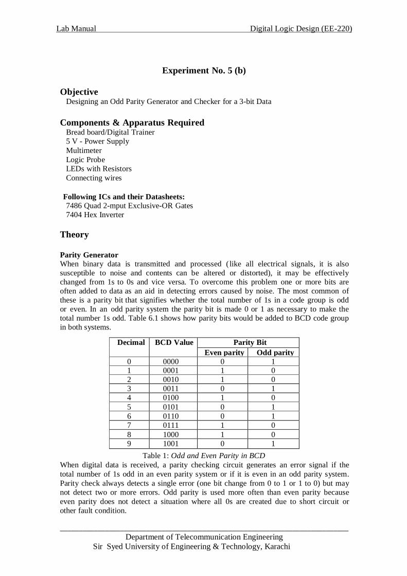
total number 1s odd. Table 6.1 shows how parity bits would be added to BCD code group
in both systems.
Parity Bit BCD Value
Decimal
Odd parity Even parity
1 0 0000 0 0 1 0001 1
0 1 0010 2
1 0 0011 3
0 1 0100 4
1 0 0101 5
1 0 0110 6
0 1 0111 7
0 1 1000 8
1 0 1001 9
Table 1: Odd and Even Parity in BCD
When digital data is received, a parity checking circuit generates an error signal if the
total number of 1s odd in an even parity system or if it is even in an odd parity system.
Parity check always detects a single error (one bit change from 0 to 1 or 1 to 0) but may
not detect two or more errors. Odd parity is used more often than even parity because
even parity does not detect a situation where all 0s are created due to short circuit or
other fault condition.
220)-EEDigital Logic Design ( Lab Manuab
_____________________________________________________________________________
Department of Telecommunication Engineering
Sir Syed University of Engineering & Technology, Karachi
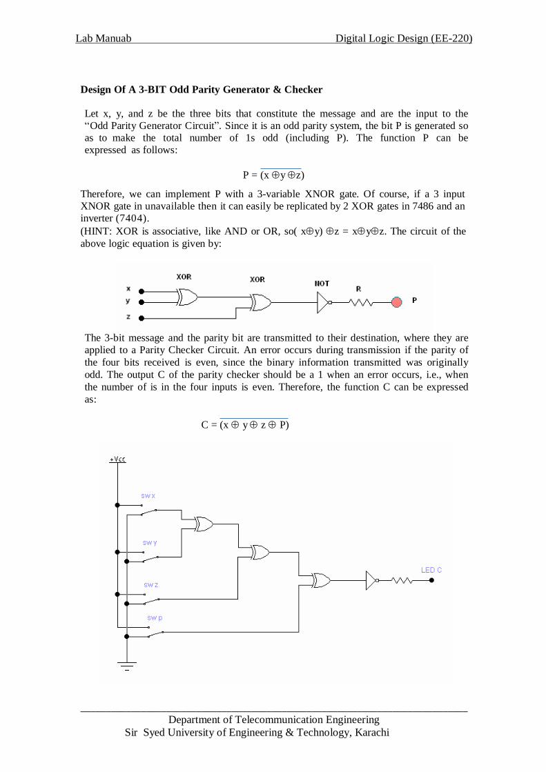
Design Of A 3-BIT Odd Parity Generator & Checker
Let x, y, and z be the three bits that constitute the message and are the input to the
“Odd Parity Generator Circuit”. Since it is an odd parity system, the bit P is generated so
as to make the total number of 1s odd (including P). The function P can be
expressed as follows:
P = (x y z)
Therefore, we can implement P with a 3-variable XNOR gate. Of course, if a 3 input
XNOR gate in unavailable then it can easily be replicated by 2 XOR gates in 7486 and an
inverter (7404).
(HINT: XOR is associative, like AND or OR, so( xy) z = xyz. The circuit of the
above logic equation is given by:
The 3-bit message and the parity bit are transmitted to their destination, where they are
applied to a Parity Checker Circuit. An error occurs during transmission if the parity of
the four bits received is even, since the binary information transmitted was originally
odd. The output C of the parity checker should be a 1 when an error occurs, i.e., when
the number of is in the four inputs is even. Therefore, the function C can be expressed
as:
C = (x y z P)
220)-Digital Logic Design (EE ManualLab
_____________________________________________________________________________
Department of Telecommunication Engineering
Sir Syed University of Engineering & Technology, Karachi
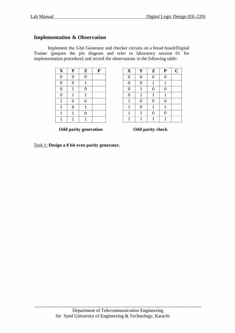
Implementation & Observation
Implement the 3-bit Generator and checker circuits on a bread board/Digital
Trainer (prepare the pin diagram and refer to laboratory session 01 for
implementation procedure) and record the observations in the following table:
Odd parity generation Odd parity check
Task 1: Design a 8 bit even parity generator.
P Z Y X
0 0 0
1 0 0
0 1 0
1 1 0
0 0 1
1 0 1
0 1 1
1 1 1
C P Z Y X
0 0 0 0
1 1 0 0
0 0 1 0
1 1 1 0
0 0 0 1
1 1 0 1
0 0 1 1
1 1 1 1