Electro-Thermal and Semiconductivity Behaviour of Natural Sintered Complex Carbonate Ore for...
11
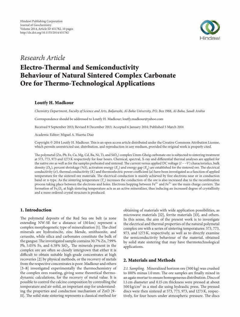
Research Article Electro-Thermal and Semiconductivity Behaviour of Natural Sintered Complex Carbonate Ore for Thermo-Technological Applications Loutfy H. Madkour Chemistry Department, Faculty of Science and Arts, Baljarashi, Al-Baha University, P.O. Box 1988, Al-Baha, Saudi Arabia Correspondence should be addressed to Loutfy H. Madkour; [email protected] Received 9 September 2013; Revised 8 December 2013; Accepted 6 January 2014; Published 5 March 2014 Academic Editor: Miguel A. Huerta-Diaz Copyright © 2014 Loutfy H. Madkour. is is an open access article distributed under the Creative Commons Attribution License, which permits unrestricted use, distribution, and reproduction in any medium, provided the original work is properly cited. e polymetal (Zn, Pb, Fe, Ca, Mg, Cd, Ba, Ni, Ti, and SiO 2 ) complex Umm-Gheig carbonate ore is subjected to sintering treatment at 573, 773, 973 and 1273K respectively for four hours. Chemical, spectral, X-ray and differential thermal analyses are applied for the native ore as well as for the samples preheated and sintered. e current versus applied DC voltage (−−) characteristics, bulk density ( b ), percent shrinkage (%), activation energy ( a ) and energy gap ( g ) are established for the sintered ore. e electrical conductivity (), thermal conductivity () and thermoelectric power coefficient () have been investigated as a function of applied temperature for the sintered ore materials. e electrical conduction is mainly achieved by free electrons near or in conduction band or n-type. As the sintering temperature ( s ) increases the conduction of the ore is also increased due to the recombination process taking place between the electrons and holes. Electrons hopping between Fe 2+ and Fe 3+ are the main charge carriers. e formation of Fe 3 O 4 at high sintering temperature acts as an active mineralizer, thus inducing an increased degree of crystallinity and a more ordered crystal structure is produced. 1. Introduction e polymetal deposits of the Red Sea ore belt (a zone extending NW-SE for a distance of 130km) represent a complex morphogenetic type of mineralization [1]. e chief minerals are hydrozincite, zinc blende, smithsonite, and cerussite, while silica and carbonates constitute the bulk of the gangue. e investigated sample contains 30.7% Zn, 7.99% Pb, 5.05% Fe, and 6.58% SiO 2 . e minerals present in the complex ore are oſten so closely intergrown that either it is difficult to obtain suitable high-grade concentrates at high recoveries [2] by physical methods, or the recovery of metals from the respective concentrates is poor. Madkour and others [3–8] investigated experimentally the thermochemistry of the complex ores roasting, giving some theoretical thermo- dynamic calculations, for the recovery of metal value. It is possible to control the calcine composition by controlling the temperature and air-solid, an important step for understand- ing the properties and conduction mechanism of ZnO [9– 11]. e solid state sintering represents a classical method for obtaining of materials with wide application possibilities, as microwave materials [12], ferrite materials [13], and others. In this sense, the aim of the present work is to investigate the electrical and thermal properties of the natural polymetal complex ore with a series of sintering temperatures: 573, 773, 973, and 1273 K, respectively, as well as to directly examine the semiconductivity behaviour of the material, obtained by solid state sintering that may have thermotechnological applications. 2. Materials and Methods 2.1. Sampling. Mineralized horizon ore (500 kg) was crushed to 100% minus 1.0 mm. e ore samples are finally mixed in an agate mortar to ensure homogeneous distribution. Discs of 1.1 cm diameter and 0.15 cm thickness were pressed at about 500 kg/cm 2 in a steel die using hydraulic press. e pressed discs were then sintered at 573, 773, 973, and 1273 K, respec- tively, for four hours under atmospheric pressure. e discs Hindawi Publishing Corporation Journal of Geochemistry Volume 2014, Article ID 451782, 10 pages http://dx.doi.org/10.1155/2014/451782
Transcript of Electro-Thermal and Semiconductivity Behaviour of Natural Sintered Complex Carbonate Ore for...
Research ArticleElectro-Thermal and SemiconductivityBehaviour of Natural Sintered Complex CarbonateOre for Thermo-Technological Applications
Loutfy H Madkour
Chemistry Department Faculty of Science and Arts Baljarashi Al-Baha University PO Box 1988 Al-Baha Saudi Arabia
Correspondence should be addressed to Loutfy H Madkour loutfymadkouryahoocom
Received 9 September 2013 Revised 8 December 2013 Accepted 6 January 2014 Published 5 March 2014
Academic Editor Miguel A Huerta-Diaz
Copyright copy 2014 Loutfy H MadkourThis is an open access article distributed under the Creative Commons Attribution Licensewhich permits unrestricted use distribution and reproduction in any medium provided the original work is properly cited
The polymetal (Zn Pb Fe CaMg Cd Ba Ni Ti and SiO2) complex Umm-Gheig carbonate ore is subjected to sintering treatment
at 573 773 973 and 1273K respectively for four hours Chemical spectral X-ray and differential thermal analyses are applied forthe native ore as well as for the samples preheated and sinteredThe current versus applied DC voltage (119868minusminus119881) characteristics bulkdensity (119863b) percent shrinkage (119878) activation energy (119864a) and energy gap (119864g) are established for the sintered ore The electricalconductivity (120590) thermal conductivity (119870) and thermoelectric power coefficient (120572) have been investigated as a function of appliedtemperature for the sintered ore materials The electrical conduction is mainly achieved by free electrons near or in conductionband or n-type As the sintering temperature (119879s) increases the conduction of the ore is also increased due to the recombinationprocess taking place between the electrons and holes Electrons hopping between Fe2+ and Fe3+ are the main charge carriers Theformation of Fe
3O4at high sintering temperature acts as an active mineralizer thus inducing an increased degree of crystallinity
and a more ordered crystal structure is produced
1 Introduction
The polymetal deposits of the Red Sea ore belt (a zoneextending NW-SE for a distance of 130 km) represent acomplex morphogenetic type of mineralization [1] The chiefminerals are hydrozincite zinc blende smithsonite andcerussite while silica and carbonates constitute the bulk ofthe gangueThe investigated sample contains 307Zn 799Pb 505 Fe and 658 SiO
2 The minerals present in the
complex ore are often so closely intergrown that either it isdifficult to obtain suitable high-grade concentrates at highrecoveries [2] by physical methods or the recovery of metalsfrom the respective concentrates is poorMadkour and others[3ndash8] investigated experimentally the thermochemistry ofthe complex ores roasting giving some theoretical thermo-dynamic calculations for the recovery of metal value It ispossible to control the calcine composition by controlling thetemperature and air-solid an important step for understand-ing the properties and conduction mechanism of ZnO [9ndash11] The solid state sintering represents a classical method for
obtaining of materials with wide application possibilities asmicrowave materials [12] ferrite materials [13] and othersIn this sense the aim of the present work is to investigatethe electrical and thermal properties of the natural polymetalcomplex ore with a series of sintering temperatures 573 773973 and 1273K respectively as well as to directly examinethe semiconductivity behaviour of the material obtainedby solid state sintering that may have thermotechnologicalapplications
2 Materials and Methods
21 Sampling Mineralized horizon ore (500 kg) was crushedto 100 minus 10mm The ore samples are finally mixed inan agatemortar to ensure homogeneous distributionDiscs of11 cm diameter and 015 cm thickness were pressed at about500 kgcm2 in a steel die using hydraulic press The presseddiscs were then sintered at 573 773 973 and 1273K respec-tively for four hours under atmospheric pressure The discs
Hindawi Publishing CorporationJournal of GeochemistryVolume 2014 Article ID 451782 10 pageshttpdxdoiorg1011552014451782
2 Journal of Geochemistry
Pow
er su
pply
Milliammeter
Sample Volta
met
erFurnace
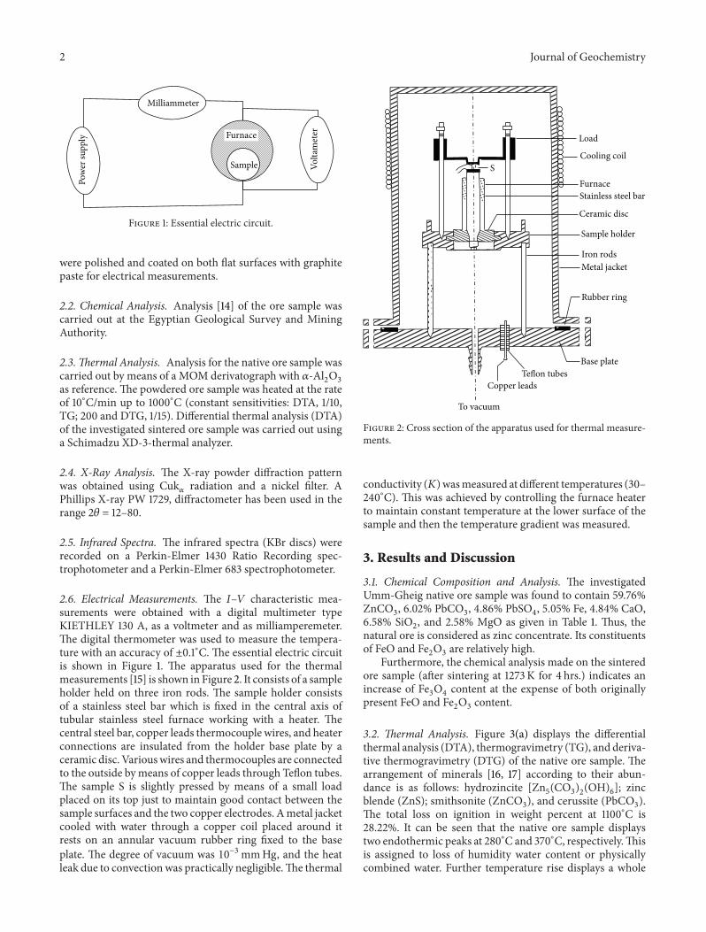
Figure 1 Essential electric circuit
were polished and coated on both flat surfaces with graphitepaste for electrical measurements
22 Chemical Analysis Analysis [14] of the ore sample wascarried out at the Egyptian Geological Survey and MiningAuthority
23 Thermal Analysis Analysis for the native ore sample wascarried out by means of a MOM derivatograph with 120572-Al
2O3
as reference The powdered ore sample was heated at the rateof 10∘Cmin up to 1000∘C (constant sensitivities DTA 110TG 200 and DTG 115) Differential thermal analysis (DTA)of the investigated sintered ore sample was carried out usinga Schimadzu XD-3-thermal analyzer
24 X-Ray Analysis The X-ray powder diffraction patternwas obtained using Cuk
120572radiation and a nickel filter A
Phillips X-ray PW 1729 diffractometer has been used in therange 2120579 = 12ndash80
25 Infrared Spectra The infrared spectra (KBr discs) wererecorded on a Perkin-Elmer 1430 Ratio Recording spec-trophotometer and a Perkin-Elmer 683 spectrophotometer
26 Electrical Measurements The 119868ndash119881 characteristic mea-surements were obtained with a digital multimeter typeKIETHLEY 130 A as a voltmeter and as milliamperemeterThe digital thermometer was used to measure the tempera-ture with an accuracy of plusmn01∘C The essential electric circuitis shown in Figure 1 The apparatus used for the thermalmeasurements [15] is shown in Figure 2 It consists of a sampleholder held on three iron rods The sample holder consistsof a stainless steel bar which is fixed in the central axis oftubular stainless steel furnace working with a heater Thecentral steel bar copper leads thermocouple wires and heaterconnections are insulated from the holder base plate by aceramic disc Variouswires and thermocouples are connectedto the outside bymeans of copper leads through Teflon tubesThe sample S is slightly pressed by means of a small loadplaced on its top just to maintain good contact between thesample surfaces and the two copper electrodes Ametal jacketcooled with water through a copper coil placed around itrests on an annular vacuum rubber ring fixed to the baseplate The degree of vacuum was 10minus3mmHg and the heatleak due to convectionwas practically negligibleThe thermal
Load
SCooling coil
Furnace
Ceramic disc
Stainless steel bar
Sample holder
Iron rodsMetal jacket
Rubber ring
Base plateTeflon tubes
Copper leads
To vacuum
Figure 2 Cross section of the apparatus used for thermal measure-ments
conductivity (119870) wasmeasured at different temperatures (30ndash240∘C) This was achieved by controlling the furnace heaterto maintain constant temperature at the lower surface of thesample and then the temperature gradient was measured
3 Results and Discussion
31 Chemical Composition and Analysis The investigatedUmm-Gheig native ore sample was found to contain 5976ZnCO
3 602 PbCO
3 486 PbSO
4 505 Fe 484 CaO
658 SiO2 and 258 MgO as given in Table 1 Thus the
natural ore is considered as zinc concentrate Its constituentsof FeO and Fe
2O3are relatively high
Furthermore the chemical analysis made on the sinteredore sample (after sintering at 1273K for 4 hrs) indicates anincrease of Fe
3O4content at the expense of both originally
present FeO and Fe2O3content
32 Thermal Analysis Figure 3(a) displays the differentialthermal analysis (DTA) thermogravimetry (TG) and deriva-tive thermogravimetry (DTG) of the native ore sample Thearrangement of minerals [16 17] according to their abun-dance is as follows hydrozincite [Zn
5(CO3)2(OH)6] zinc
blende (ZnS) smithsonite (ZnCO3) and cerussite (PbCO
3)
The total loss on ignition in weight percent at 1100∘C is2822 It can be seen that the native ore sample displaystwo endothermic peaks at 280∘C and 370∘C respectivelyThisis assigned to loss of humidity water content or physicallycombined water Further temperature rise displays a whole
Journal of Geochemistry 3
Table 1 Chemical and spectral analysis of native Umm-Gheig natural complex polymetal ore
Compound Content () Compound Content () Element Content (parts times 10minus6)SiO2 658 Zn 3070 Cd 800Al2O3 083 Pb 799 Ti 006Fe 505 PbSO4 486 Ba 400MgO 258 PbCO3 602 Ni 40CaO 484 ZnCO3 5976 Co mdashSO4
2minus 128 Moisture 097 Ag mdashLOIlowast 2822 Au mdashlowastLoss on ignition in weight percent at 1100∘C
0
20
40
60
80
100
120
140
160
180100200 300400 500 600 700 800 900
Temperature (∘C)
ΔM
ΔT
TG
DTA
DTG dm
dt
(a)
75 150 225 300 375 450 525 600
(E)
(D)
(C)(B)
Temperature (∘C)
(b)
Figure 3 Thermal analysis of (a) the native ore sample and (b) sintered ore samples for 4 hrs at 573 K (B) 773 K (C) 973K (D) and 1273K(E)
intense broad exothermic hump covering the temperaturerange 400ndash550∘C peaking at 500∘C for the strongest oneThisis due to collective phase changes [16] corresponding to thefollowing reactions
Fe2O3
400∘C
997888997888997888997888rarr Fe3O4(magnetite)
FeO 450∘C
997888997888997888997888rarr Fe2O3(hematite)
Fe2O3
500∘C
997888997888997888997888rarr Fe3O4(magnetite)
(1)
respectively It is of importance to note that the native Fe2O3
(hematite) present and the formed Fe3O4(magnetite)may act
as catalyst for the subsequent oxidation and oxygen uptake ofFeO giving Fe
2O3and later on for the formation of Fe
3O4as
a final product Besides it acts as an active mineralizer thusinducing an increased degree of crystallinity [18] which oftenappears after the applied sintering treatment at 573 773 973and 1273K respectively
The broad exothermic peak covering the temperaturerange 630ndash750∘C peaking at 690∘C for the strongest one cor-responds to the decomposition of the original present metalcarbonates and sulphates into the corresponding oxides
Differential thermal analysis for the ore samples pre-heated and sintered at temperatures 573 773 973 and 1273Krespectively for hours is shown in Figure 3(b) DTA for thesintered ore indicates oxidation of various metal carbonates
and sulphates present in the native ore into correspondingmetal oxides
33 X-Ray Analysis X-ray diffraction studies ensured thechemical composition of the native Umm-Gheig natural oreand samples preheated and sintered at 573ndash1273K respec-tively as shown in Figure 4 The X-ray diffraction patternof raw material sample (Figure 4(A)) displays the essentialcharacteristic peaks for ZnCO
3(2120579 = 3370 2510 5125 3780
4640 4160 and 6140) PbCO3(2120579 = 2580 3640 4380
2900 4920 3640 and 4730) PbSO4(2120579 = 2950 2680
4450 2740 and 2210) and [Zn5(CO3)2(OH)6] (2120579 = 3640
3370 2900 2510 3070 and 1680) X-ray powder diffractiondata shows that galena is mainly converted to cerussite
After the sintering treatment at 573 773 973 and 1273Kfor four hours respectively the X-ray diffraction patternof sintered ore samples (Figures 4(B)ndash4(E)) displays thecharacteristic deflection peaks for different metal oxidesformed as follows
ZnO (2120579 = 3610 3170 and 3380) PbO (2120579 = 2910 31603215 4870 and 4560) PbO
2(2120579 = 2815 4955 and 2280)
Pb2O3(2120579=2950 2960 and 2740) Pb
3O4(2120579=2620 3160
and 3215) FeO (2120579 = 4195 3620 and 6100) Fe2O3(2120579 =
3350 3560 and 5420) Fe3O4(2120579 = 3560 6240 and 2960)
The X-ray diffraction studies of sintered ore samples athigher sintering temperatures (Figure 4) ensured a spinelphase formation (xFe
2O4) where x = Zn or Pb The essential
4 Journal of Geochemistry
(A)
(B)(C)
(D)
(E)
80 70 60 50 40 30 20 12
2120579
Figure 4 X-ray diffraction pattern for the native ore sample (A) andsintered ore samples for 4 hrs at 573K (B) 773 K (C) 973K (D) and1273K (E)
characteristic peaks for spinel ZnFe2O4and PbFe
2O4are
2120579 = 3500 2960 6205 and 5660 and 2120579 = 3240 46005680 7440 and 6740 respectively Furthermore there is noindication for the appearance of reflection peaks characteris-tics of the carbonate mineral or sulphate composition whichwas originally present in the native ore before thesinteringprocesses at 573ndash1273KThis is due to the thermal decompo-sition of the main minerals present into the correspondingmetal oxides
34 Infrared Spectra The IR frequencies of the native Umm-Gheig ore sample (A) and the sintered ore samples (BndashE)along with their assignments are given in Figure 5The bandsat 1677ndash1632 cmminus1 are assigned to the ]C=O groupsMetalliccarbonyls absorb in the 1984 cmminus1 region [19] Silicates giveabsorption bands in the 1168ndash915 cmminus1 range Appearance ofnew bands in the frequency region at 332ndash328 cmminus1 (Figures5(B)ndash5(D)) is due to stretching vibration bands ofmetal oxide(MndashO) bonds whereM=Zn Pb or FeThe existence ofwatermolecules within the coordination sphere of the hydrated oresamples is supported by the presence of absorption bandsin the regions 3889ndash3422 cmminus1and 1116ndash1073 cmminus1 in thespectra of the ore due to (OH) stretching HOH deformationand H
2O rocking [20]
35 Effect of Sintering Temperature on the Bulk Density(119863119887) and Shrinkage (S) The measured diameter of the
sintered ore discs is decreased as the sintering temperatureincreases therefore the percent shrinkage (S) of the sinteredore samples is consequently increased with increasing thesintering temperature (Figure 6) The bulk density (119863b) isalso measured for the different sintered ore discs and the data
T (
)
(E)
(D)
(C)
(B)
(A)
4000 3500 3000 2500 2000 1500 1000 500
Max = 10000 T
CMminus1
TMin = 000
Figure 5 Infrared spectra of the native ore sample (A) and sinteredore samples for 4 hrs at 573 K (B) 773 K (C) 973K (D) and 1273K(E)
is plotted as a function of the sintering temperature (119879s) asrepresented in Figure 6The results show that the bulk densityas well as the percentage shrinkage increased graduallywith increasing sintering temperature in the temperaturerange 573ndash1273K This behaviour may be due to the morediffusive [21] process occurring at high sintering temperatureleading to porosity reduction As a result of this contractionthe crystal structure becomes compacted and rigid at highsintering temperatureThe observed small values of (119863b) and(S) at lower sintering temperatures can be attributed to thelimited rearrangement of the crystal lattice structure throughthe movement of grain boundaries [22]
36 Temperature Dependence of Electrical Properties The119868ndash119881 characteristics have been measured on the sinteredore samples at the different sintering temperatures studiedranging from 573 to 1273K as shown in Figure 7 From thisfigure we can see that the 119868 versus 119881 plots are on the wholestraight lines at all different sintering temperaturesTheplot isconverted also to log 119868 versus log119881 as represented in Figure 8It is evident from this figure that at the appliedDC voltages anohmic relationship (120572 = 1) is obtained for all sintered sampleswith the exception of the ore sample sintered at 773K Thisbehaviour is called the current ohmic range But for the caseof the sintered sample at 773K the nonohmic relation 119868 equiv119881120572 holds well The parameter 120572 which essentially defines
the nonohmic nature of the material equals 152 and 195for the lower and upper branches lines respectively Thenonohmic region (120572 gt 1) in the 119868ndash119881 curves arises due tothe space-charge effects and is termed as the space-charge-limited current (SCLC) regionThese observations show thatthe 119868ndash119881 characteristics provide the best understanding ofthe conduction mechanism in the ore samples The testedore material may be considered to be composed of layers
Journal of Geochemistry 5
600 700 800 900 1000 1100 1200 1300Sintering temperature (K)
28
27
26
25
24
23
22
21
2
S
S
Db (
gmc
m3)
Db
Figure 6 Effect of sintering temperature (119879s) on the bulk density(119863b) and shrinkage (S) of the ore samples
0 2 4 6 8 10 120
5
10
15
20
25
30
35
App
lied
DC
volta
ge
773K973K1273K
Current (100nA)
Figure 7 DC current voltage characteristic of sintered ore samples
with different conductivities and thicknesses in series witheach other The well-conducting grains having thickness 119889
1
conductivity 1205901 and permittivity 120576
1 are separated by a thin
layer of poorly conducting grain boundaries (GB) having athickness 119889
2 a conductivity 120590
2 and a permittivity 120576
2 It is
reasonable to assume that 1205901≫ 1205902 If 1198811and 119881
2are the
DC voltage drops across the grain and the GB respectivelythen 119881 = 119881
1+ 1198812is the externally applied DC voltage The
voltage drop will take place mainly across the grain boundary(ie 119881 cong 119881
2) If the current (119894
Ω1
) through the grain is onlyohmic and the current through the GB is ohmic ( 119894
Ω2
) aswell as space-charge-limited (119894scl) the total current (119868) is then
573K773K
973K1273K
04 06 08 1 12 14
10
95
9
85
8
75
minuslo
gI
(A)
log V
Figure 8 Logarithmic current voltage characteristic of sintered oresamples
119868 = 119894Ω1
+ 119894Ω2
+ 119894119904119888119897 The total current in the ore solid can be
approximated as 119894Ω2
≪ 119894scl cong 119868Thus the 119868ndash119881 characteristic inthe nonohmic region is given by 119894scl equiv 1198812120572 The space-charge-limited current is determined mainly by the number of freecharge carriers available in the grain-boundary layers At theapplied DC voltages on the ore samples that is before thenonohmic region (at 773K sintered ore sample) the current ispurely ohmic (120572 = 1) In this region the total current throughthe ore solid is 119894scl ≪ 119894
Ω2
cong 119894 and hence an ohmic relationholds According to this theory [23] the 119868ndash119881 curves consistof three parts
(i) low-current ohmic range for the sintered ore at1273K (120572 = 093)
(ii) SCLC range or the nonohmic range for the sinteredore at 773K (120572
1= 152 120572
119906= 195) where 120572
1and
120572119906represent the values of 120572 at lower and upper line
inflection (Figure 7) respectively
(iii) high-current ohmic range for the sintered ore at 573K(120572 = 1)
The broken line of 119868ndash119881 characteristic for the tested sin-tered ore sample at 773K shows that the critical voltage (119881c)at which the line is broken equals 15 volts The dependenceof the electrical resistivity of the sintered ore samples onthe applied sintering temperature is given in Table 2 Theobtained data indicates that the resistivity of the sinteredore samples decreases as the sintering temperature increasesfor the samples Electrical conductivity versus temperaturecharacteristics (ln120590minus1119879) of all the investigated samples weremeasured and represented in Figure 9 From the typical log120590versus 1119879 characteristics as shown in Figure 9 it is seenthat the sintered ore samples had a good semiconductivity
6 Journal of Geochemistry
Table 2 The electrical resistivity (120588) as a function of sinteringtemperature
Sintering temperature (K) Resistivity (120588 times 107Ωsdotcm)573 7384773 2110 (before 119881c) and 843 (after 119881c)973 11751273 1109
behaviour with increasing applied temperature from 430ndash550K according to a Boltzmann distribution [24]
120590 = 120590oeminus119864a119896119879
(2)
The parameter 120590119900 which is given by the intercept of the
line at 1119879 = 0 is called the preexponential factor or thefrequency factor 119896 is the Boltzmann constant and 119879 is theabsolute temperature However it is worth anticipating theinterpretation of the activation energy (119864a) for the electricconduction in eV which is achieved by rewriting the aboveequation as
log 120590 = log 120590o minus119864a119896sdot 119879 (3)
There we shall see that the activation energy (119864a) repre-sents the minimum energy necessary for a molecule to havein the sample to react 119864a is calculated from the slope ofthe straight line of this plot (Figure 9) The values of acti-vation energy (119864a) are plotted as a function of the sinteringtemperature (119879s) as shown in Figure 10 The experimentalresults in Figures 9 and 10 indicate that the electrical con-ductivity increases and consequently the activation energiesare decreased with increasing sintering temperature Theobtained data of either electrical conductivity (Figure 9) oractivation energy (Figure 10) are in good agreement withthose obtained from previous studies of the resistivity valuesas given in Table 2 Also the results obtained are in goodagreement with other works [25] and can be explained on thebasis that the propagation of lattice imperfection decreaseswhile a more ordered crystal structure is produced
Thus all the investigated sintered ore samples havesemiconductivity properties Generally in a semiconductormaterial the outer electrons or valence electrons are normallystable that is bound to their atoms and are not free to moveBut when heat is applied or an impurity (a doping element)that serves to raise energy is incorporated the application ofa voltage will cause displacement of valence electrons in thematerial that is turn them into charge carriers So an electriccurrent in a sintered ore semiconductor may be inducedand varied over a wide range of sintering temperature onlyunder the action of an external influence such as heat anddoping The higher the temperature the greater the numberof free electrons and the higher the conductive currentin the semiconductor Thus electrical conduction [26] inall semiconductors is mainly by free electrons near or inconduction band (n-type) Since the electrons that participatein conduction are the semiconductorrsquos own electrons its
1000T (K)
minuslo
gco
nduc
tivity
(O
115
11
105
10
95
9
85
8185 19 195 2 205 21 215 22 225 23
573K773K
973K1273K
hmmiddotcm
)
Figure 9 Temperature dependence of electrical conductivity (120590) forsintered ore samples
600 700 800 900 1000 1100 1200 1300
065
07
075
08
085
Sintering temperature (K)
Act
ivat
ion
ener
gy
Ea (eV)
Ea
(eV
)
Figure 10 Effect of sintering temperature on the activation energy(119864a) for electrical conductivity of the ore samples
conduction is called intrinsic The atoms that lost theirelectrons turn into positive-charge ions bound and unableto move The vacancy left by the electron in the outer ringof the atom is called a hole An electron set free from theneighboring atommay fill the vacancy by moving to the holeand leaving instead a hole in its atom thereby turning it intoa positively charged ion
The application of an electric current to a semiconductorwill cause electrons to move from atom to atom in onedirection and leave holes in the opposite direction The holeis generally regarded as a positive particle equal in chargeto the electron The seeming movement of holes in thedirection opposite to that of electrons is called hole currentThe electric conduction in the semiconductor conditioned
Journal of Geochemistry 7
by this current hole or p-type conduction The movementof electrons in one direction and of holes in the oppositedirection determines the intrinsic electrical conduction ina semiconductor because the charge carriers (electrons andholes) belong to the semiconductorrsquos own atoms In this casethe conduction current 119868 consists of the electron 119868e and hole119868h current components that is 119868 = 119868e + 119868h
With intrinsic conduction concentration of electrons(119873e) and of holes (119873h) is equal However 119868e gt 119868h because themobility of electrons is higher than that of holesThemobilityof a charge carrier is represented by the ratio of the velocity ofan electron (Ve) or of a hole (Vh) to the electric field strength(119864) in the semiconductor Hence the electronmobility can berepresented by 120583e = Ve119864 and hole mobility by 120583h = Vh119864
In that way mobility indicates the distance the electron orthe hole covers per second in a field of strength 119864 = 1Vcm
Considering the aforementioned expressions for theelectron and the hole current components may be written as[26]
119868e = 119873eeVe = 119873e e120583e119864
119868h = 119873heVh = 119873he120583e119864(4)
where e is the charge of electron or hole and 119864 is the electricfield strength
The conduction current in a semiconductor is
119868 = 119868e + 119868h = 119873e e119904Ve + 119873heVh = 119873ee120583e119864 + 119873he120583h119864 (5)
With intrinsic conduction concentration of electrons isequal to that of holes in semiconductor that is
119873e = 119873h = 119873
119868 = 119873e (120583e + 120583h) 119864(6)
In a pure (intrinsic) semiconductor impurities constitutenot more than 10minus11 The investigated natural Umm-Gheigsintered ore containing the iron atoms as impurities of avalency higher than the semiconductorrsquos material tends togive electrons thereby increasing the electron density Theyplay the role of donors Thus the atoms of iron impuritiespresent originally in the native ore can modify its electricalproperties For example to obtain a semiconductor that willexhibit n-type conduction This leads to the formation ofsome Fe2+ ions from Fe3+ ionsThe polarization of the ferriteis determined by local displacement [23] of electrons in thedirection of an applied electric field which is due to theelectron exchange interaction
Fe2+ 999445999468 Fe3+ + eminus (7)
The energy gap (119864g) which is defined as the energyrequired for separating the highest-filled or valence band(VB) from the conduction band (CB) is equal to twice [27]the activation energy value that is 119864g = 2119864a
The values of 119864a and 119864g for the investigated semiconduc-tor sintered ore samples are calculated and given in Table 3 asfollows
Table 3The effect of sintering temperature (119879s) on119864a and119864g values
Sinteringtemperature (K)
Activation energy119864a (eV)
Energy gap119864g (eV)
573 0850 170773 0825 165973 0760 1521273 0580 116
37 Temperature Dependence of Thermal Conductivity (K)The coefficient of thermal conductivity of the sintered oresamples was estimated using the formula
119876 =119868119881
119869=119870119860119889119879
119889119883 (8)
where 119876 is the quantity of heat per unit time transferredthrough the sample of thickness 119889119883 and 119869 is the Joulersquoscoefficient The parameters 119868 119880 119889119879119889119883 and 119860 are thecurrent (in amperes) voltage across the heater (in volts)temperature gradient in (degreem) and sample area (inm2)respectively
The heat transport through lattice vibrations (phonons)is mainly important for insulators and semiconductors Thethermal conductivity of the sintered ore sample crystals hascontributions from two components [28] lattice vibration(phonons) and the carriers (electrons)
119870 = 119870ph + 119870e (9)
If we consider the heat conduction by electron carriersdue to the presence of Fe2+ and Fe3+ impurities the tem-perature gradient will cause a carrier concentration gradientwhich results in a diffusion current which transports heatenergy At temperatures lower than the Debye temperaturethe inelastic scattering processes become important thusstrongly affecting the thermal conductivity In this rangethere is a sharp drop in phonon concentration with risingtemperatures leading to a sharp increase in119870 which becomesproportional to 1198793 But at temperatures higher than theDebye temperature the scattering processes must be respon-sible for the thermal resistance and the elastic scatteringis dominant since the phonon contribution to the thermalconductivity is relatively small compared with the electroncontribution
The measured thermal conductivity is approximatelyequal to the contribution from electrons In this range 119870 isinversely proportional to the temperature (119870 equiv 119879minus1)
The temperature dependence of 119870 for the investigatedsintered ore samples is shown in Figure 11 A sharp risingof thermal conductivity with rising temperature can beobserved up to the transition temperatureThe concentrationof phonons decreases with rising temperature leading toa consequent decrease in lattice vibrations This decreaseof lattice vibration diminishes lattice scattering causing anincrease in the mean free path which would result in anincrease in 119870
Thus the thermal conductivity (119870) increases at lowtemperature due to the increase of modes of vibration of the
8 Journal of Geochemistry
40 60 80 100 120 140 160 180 200 220 24050
100
150
200
250
300
350
400
Temperature (∘C)
573K773K973K
Ther
mal
cond
uctiv
ity K
(W
mmiddotd
eg)times10minus3
Figure 11 Temperature dependence on thermal conductivity (119870)for sintered ore samples
crystal lattice and is responsible for conduction of phononsup to the Debye temperature Above the transition temper-ature or Debye temperature the concentration of phononsincreases with rising temperature leading to lattice scatteringcausing a decrease in the mean free path which would resultin a decrease of119870 As shown in Figure 11 the values of thermalconductivity (119870) increase as the sintering temperature of thetested sintered ore samples is also increased As the sinteringtemperature increases the material becomes more dense andthe pores decrease The pores act as scattering centers ofphonons so the decreasing of pores causes the observedincreasing of the thermal conduction (119870) The maximumvalues of thermal conductivity of the tested ore samplessintered at 573 773 and 973K were as follows 180 210and 390K (Wm sdot deg) times 10minus3 respectively as shown inFigure 11The results obtained from thermal conductivity (119870)measurements are in a good agreement with those obtainedfrom the previous electrical conductivity (120590) studies
The thermoelectric power coefficient (120572) was measuredexperimentally for the investigated sintered ore samples as afunction of temperatureThe120572measured had negative valuesdemonstrating that the main charge carriers are electronshopping between Fe2+ and Fe3+ ions which were originallypresent in thematerial as impurities (called dopants) Dopantor doping Fe whose atoms tend to give electrons to thesemiconductor thereby increasing the electron density iscalled donor Iron impurities modify the electrical andthermal properties to obtain a semiconductor that will exhibitn-type conduction It is clear that the electrons constitutingthe iron impurity conduction are the chief charge carriers inthe investigated semiconductor sintered ore material
Finally the conduction current in the investigated semi-conductor sintered ore samples is the sum of electronic and
hole currents but electronic current is ten times that of holecurrent
Efficient solar conversion requires materials with bandgaps [29] of 13 plusmn 03 eV that is absorption of light in thespectral range of 250ndash1000 nm Considerable attention hasbeen given in recent years to the application [30 31] ofsemiconductor colloids powders and films for conversionof solar energy into electricity and chemical energy Theconcentration of current carriers and hence semiconductivityincreases with increasing temperature according to the Boltz-mann distribution [24] Thus the obtained experimentalenergy gap values (119864g) of the sintered ore samples underconsideration as shown in Table 3 are suitable and optimumfor using the tested natural sintered ore material as a highlyabsorbing semiconductor in photoelectrochemical systemsand thermotechnological applications as suggested by thefollowing techniques
(1) nitrogen reduction to ammonia by photosensitized[32] electron transfer from dispersed ore oxides(Fe2O3 PbO
2 ZnO) doped TiO
2semiconductor
particles
(2) semiconductors in water [33] treatment
(3) colloidal semiconductors in photovoltaic [27 34]systems As known from the Schottky barrier theorythe low bias potential region might be controlledby recombination and trapping of electrons in thedepletion region [35] These processes occur mosteffectively in localized states energetically centeredin the midgap position leading to a recombinationcurrent proportional to [exp(qV2kT) minus 1] [36 37]
(4) it is often necessary that semiconductor materialsare exclusively of n- or p-type for many industrialapplications for example for semiconductor-basedrectifiers to rectify alternating current into pulsatingdirect current Thus a system of two semiconductorswith different types of electric conduction resistsreverse current flow This property is highly valuedfor semiconductor rectifiers Fusing together the twotypes forms a p-n junction that has the propertyof rectifying alternating current If we apply an ACvoltage to such a systemof two semiconductors the p-n junction will pass the current of only one half cycleof voltage In crystal diodes the p-n junction is usedchiefly for rectifiers applications
(5) thermoelectric generation is essentially the same asthe energy conversion and heat pumping (when asemiconductor material is used thermoelectrically asa heat pump) with p-type and n-type materials
(6) partial illumination of a semiconductor induces aphoto emf between the illuminated and unillumi-nated areas of the material surfaceThis phenomenonis used for making sources of electric power suchas photovoltaic cells and solar batteries and semi-conductor devices capable of solar-to-electric energyconversion
Journal of Geochemistry 9
4 Conclusions
The obtained results of electron microscopic investigationfor either the native ore or the ore after sintering treatmentconfirmed by metal value data given in the ASTM cardscoincide well with those given by chemical analysis
From the observations of 119868ndash119881 characteristics in 120590 versus1119879 and 119870 versus 119879 behaviours of the investigated naturalsintered ore samples we can summarize the following con-clusions
(1) The sintered ore material had good semiconductivitybehaviour with increasing temperature
(2) The semiconductor sintered ore exhibits n-type con-duction
(3) Both values of 119864a and 119864g in eV decrease with increas-ing the applied sintering temperatures from 573 to1273K Consequently the electrical conductivity (120590)increases in the same range of the studied sinteringtemperatures
(4) The thermal phonon scattering and lattice vibrationscattering are responsible for the thermal conductiv-ity (119870) and the behaviour of the material at changingtemperatures
(5) The above measurements from electrical thermaland semiconductivity behavior of the investigatedmaterial obtained by solid state sintering may havethermotechnological industrial applications
Conflict of Interests
The author declares that there is no conflict of interests re-garding the publication of this paper
References
[1] A H Sabet V B Tsogoev V P Bordonosov V A BeloshitskyD N Kuznetsove and H A El-HakimAnnals of the GeologicalSurvey of Egypt According to Contract VI 1976
[2] A M Eid and M M Abd El-Rehime Metallurgical Researchon Zn-Pb Oxidised Ore of Umm-Gheig Deposit Eastern DesertGeological Survey and Mineral Research Department Egypt1963
[3] P V Viswanathan B V S Yedavalli S R Srinivasan and P PBhatnagar Symposium on Recent Development in Non-FerrousMetals Technology Volume 2 Copper 1968
[4] H H Kellogg ldquoA critical review of sulfation equilibriardquo Trans-actions of the AIME vol 230 pp 1622ndash1634 1964
[5] G R Smithson Jr and J E Hanway Jr ldquoBench scale devel-opment of a sulfation process for complex sulphide oresrdquoTransactions of the Metallurgical Society of AIME vol 224 p827 1962
[6] F Taha S E Afifi and L H Madkour ldquoTreatment of UmmmdashSamiuki ComplexrdquoTabbin Institute forMetallurgical Studies no47 pp 1ndash19 1982
[7] A P Snernikar and V M Yurenko ldquoLaboratory studies onthe hydrometailurigical treatment of Cu-Pb-Zn intermediateproductsrdquo Russian Journal of Non-Ferrous Metals vol 11 p 771965
[8] L H Madkour ldquoThermodynamic studies on sulphate roastingfor zinc electrowinning from carbonate orerdquo Journal of Chem-ical Technology and Biotechnology vol 36 no 5 pp 197ndash2111986
[9] M Tao B Ai O Dorlanne and A Loubiere ldquoDifferent ldquosinglegrain junctionsrdquo within a ZnO varistorrdquo Journal of AppliedPhysics vol 61 no 4 pp 1562ndash1567 1987
[10] E Olsson and G L Dunlop ldquoCharacterization of individualinterfacial barriers in a ZnO varistor materialrdquo Journal ofApplied Physics vol 66 no 8 pp 3666ndash3675 1989
[11] Z Feng and C Zechun ldquoStudy on the electrical properties ofsingle grain boundaries in BaTiO
3ceramicsrdquo Journal of Applied
Physics vol 80 no 2 pp 1033ndash1036 1996[12] V Parvanova I Iliev and L Ilkov ldquoSynthesis and microwave
properties of doped zinc titanaterdquo Journal of the University ofChemical Technology andMetallurgy vol 41 no 4 pp 461ndash4662006
[13] B Boyanov ldquoSynthesis and determination of Curie temperatureof ferrites from the systems BaO-CoO-ZrO
2-Fe2O3and BaO-
NiO-ZrO2-Fe2O3rdquo Journal of the University of Chemical Tech-
nology and Metallurgy vol 41 no 1 pp 61ndash64 2006[14] EMerckComplexometric AssayMethods with Titriplex Merck
Darmstadt Germany 3rd edition 1971[15] AAGAwad andMAAhmed ldquoElectrical conductivity inCu-
ferritesrdquo Proceedings of the Mathematical and Physical Society ofEgypt vol 42 p 93 1976
[16] D N Todor Thermal Analysis of Minerals Abacus PressTunbridge Wells UK 1976
[17] L H Madkour ldquoRecommended flowsheets for the electrolyticextraction of lead and zinc from red sea polymetal orerdquo Journalof Chemical Technology andBiotechnology vol 35 no 3 pp 108ndash114 1985
[18] L H Madkour M M Abou-Sekkina and O M HemedaldquoThermo-physical studies on ilmenite ore for mass productionof ceramic capacitorsrdquo Erzmetall vol 49 no 5 pp 309ndash3131996
[19] L J Bellamy The Infrared Spectra of Complex MoleculesChapman amp Hall London UK 3rd edition 1975
[20] K Nakamoto Infrared Spectra of Inorganic and CoordinationCompounds John Wiley amp Sons New York NY USA 1970
[21] P J Jorgensen Sintering andRelated Phenomena edited byGGKuczynski N A Hooton and C F Gibbon Gordan amp BreachNew York NY USA 1967
[22] H Schmalzried Solid State Reactions Verlag Chemie GmbHWeinheimBergstr and Academic Press New York NY USA1974
[23] B K Kuanr and G P Srivastava ldquoDispersion observed inelectrical properties of titanium-substituted lithium ferritesrdquoJournal of Applied Physics vol 75 no 10 pp 6115ndash6117 1994
[24] J O Williams ldquoElectrical conduction in organic solidsrdquo Ad-vances in Physical Organic Chemistry vol 16 pp 159ndash237 1978
[25] DW Strickler andWGCarlson ldquoElectrical conductivity in theZrO2-rich region of severalM
2O3ndashZrO
2systemsrdquo Journal of the
American Ceramic Society vol 48 no 6 pp 286ndash289 1965[26] N Nikulin Fundamentals of Electrical Materials Mir Publish-
ers Moscow Russia 1988[27] K Buker N Alonso-Vante and H Tributsch ldquoPhotovoltaic
output limitation of n-FeS2
(pyrite) Schottky barriers atemperature-dependent characterizationrdquo Journal of AppliedPhysics vol 72 no 12 pp 5721ndash5728 1992
10 Journal of Geochemistry
[28] J S Blakmore Solid State Physics Mir Publisher MoscowRussia 2nd edition 1988
[29] R Memming ldquoSolar energy conversion by photoelectrochemi-cal processesrdquoElectrochimicaActa vol 25 no 1 pp 77ndash88 1980
[30] M Gratzel Heterogeneous Photochemical Electron Transferchapter 3 CRC Press Boca Raton Fla USA 1989
[31] P V Kamat Kinetics and Catalysis in MicroheterogeneousSystems edited by M Gratzel and K Kalyanasundaram MarcelDekker New York NY USA 1991
[32] P P Radford and C G Francis ldquoPhotoreduction of nitrogen bymetal doped titanium dioxide powders a novel use for metalvapour techniquesrdquo Journal of the Chemical Society ChemicalCommunications no 24 pp 1520ndash1521 1983
[33] M Gratzel Aspects of Electrochemistry edited by R E White JO M Bockris and B E Conway Plenum Press New York NYUSA 1983
[34] P Bogdanoff and N J Alonso-Vante ldquoA kinetic approach ofcompetitive photoelectrooxidation of HCOOH and H
2O on
TiO2anatase thin layers via on-line mass detectionrdquo Journal of
Electroanalytical Chemistry vol 379 no 1-2 pp 415ndash421 1994[35] E H Rhoderick and R H Williams Metal-Semiconductor
Contacts Clarendon Press Oxford UK 2nd edition 1988[36] W Shockley andW T Read ldquoStatistics of the recombinations of
holes and electronsrdquo Physical Review vol 87 no 5 pp 835ndash8421952
[37] A S Grove Physics and Technology of Semiconductors DevicesJohn Wiley amp Sons New York NY USA 1967
Submit your manuscripts athttpwwwhindawicom
Hindawi Publishing Corporationhttpwwwhindawicom Volume 2014
ClimatologyJournal of
EcologyInternational Journal of
Hindawi Publishing Corporationhttpwwwhindawicom Volume 2014
EarthquakesJournal of
Hindawi Publishing Corporationhttpwwwhindawicom Volume 2014
Hindawi Publishing Corporationhttpwwwhindawicom
Applied ampEnvironmentalSoil Science
Volume 2014
Mining
Hindawi Publishing Corporationhttpwwwhindawicom Volume 2014
Journal of
Hindawi Publishing Corporation httpwwwhindawicom Volume 2014
International Journal of
Geophysics
OceanographyInternational Journal of
Hindawi Publishing Corporationhttpwwwhindawicom Volume 2014
Journal of Computational Environmental SciencesHindawi Publishing Corporationhttpwwwhindawicom Volume 2014
Journal ofPetroleum Engineering
Hindawi Publishing Corporationhttpwwwhindawicom Volume 2014
Geochemistry
Hindawi Publishing Corporationhttpwwwhindawicom Volume 2014
Journal of
Atmospheric SciencesInternational Journal of
Hindawi Publishing Corporationhttpwwwhindawicom Volume 2014
OceanographyHindawi Publishing Corporationhttpwwwhindawicom Volume 2014
Advances in
Hindawi Publishing Corporationhttpwwwhindawicom Volume 2014
MineralogyInternational Journal of
Meteorology
Hindawi Publishing Corporationhttpwwwhindawicom Volume 2014
Advances in
The Scientific World JournalHindawi Publishing Corporation httpwwwhindawicom Volume 2014
Paleontology JournalHindawi Publishing Corporationhttpwwwhindawicom Volume 2014
ScientificaHindawi Publishing Corporationhttpwwwhindawicom Volume 2014
Hindawi Publishing Corporationhttpwwwhindawicom
Volume 2014
Geological ResearchJournal of
Hindawi Publishing Corporationhttpwwwhindawicom Volume 2014
Geology Advances in
2 Journal of Geochemistry
Pow
er su
pply
Milliammeter
Sample Volta
met
erFurnace
Figure 1 Essential electric circuit
were polished and coated on both flat surfaces with graphitepaste for electrical measurements
22 Chemical Analysis Analysis [14] of the ore sample wascarried out at the Egyptian Geological Survey and MiningAuthority
23 Thermal Analysis Analysis for the native ore sample wascarried out by means of a MOM derivatograph with 120572-Al
2O3
as reference The powdered ore sample was heated at the rateof 10∘Cmin up to 1000∘C (constant sensitivities DTA 110TG 200 and DTG 115) Differential thermal analysis (DTA)of the investigated sintered ore sample was carried out usinga Schimadzu XD-3-thermal analyzer
24 X-Ray Analysis The X-ray powder diffraction patternwas obtained using Cuk
120572radiation and a nickel filter A
Phillips X-ray PW 1729 diffractometer has been used in therange 2120579 = 12ndash80
25 Infrared Spectra The infrared spectra (KBr discs) wererecorded on a Perkin-Elmer 1430 Ratio Recording spec-trophotometer and a Perkin-Elmer 683 spectrophotometer
26 Electrical Measurements The 119868ndash119881 characteristic mea-surements were obtained with a digital multimeter typeKIETHLEY 130 A as a voltmeter and as milliamperemeterThe digital thermometer was used to measure the tempera-ture with an accuracy of plusmn01∘C The essential electric circuitis shown in Figure 1 The apparatus used for the thermalmeasurements [15] is shown in Figure 2 It consists of a sampleholder held on three iron rods The sample holder consistsof a stainless steel bar which is fixed in the central axis oftubular stainless steel furnace working with a heater Thecentral steel bar copper leads thermocouple wires and heaterconnections are insulated from the holder base plate by aceramic disc Variouswires and thermocouples are connectedto the outside bymeans of copper leads through Teflon tubesThe sample S is slightly pressed by means of a small loadplaced on its top just to maintain good contact between thesample surfaces and the two copper electrodes Ametal jacketcooled with water through a copper coil placed around itrests on an annular vacuum rubber ring fixed to the baseplate The degree of vacuum was 10minus3mmHg and the heatleak due to convectionwas practically negligibleThe thermal
Load
SCooling coil
Furnace
Ceramic disc
Stainless steel bar
Sample holder
Iron rodsMetal jacket
Rubber ring
Base plateTeflon tubes
Copper leads
To vacuum
Figure 2 Cross section of the apparatus used for thermal measure-ments
conductivity (119870) wasmeasured at different temperatures (30ndash240∘C) This was achieved by controlling the furnace heaterto maintain constant temperature at the lower surface of thesample and then the temperature gradient was measured
3 Results and Discussion
31 Chemical Composition and Analysis The investigatedUmm-Gheig native ore sample was found to contain 5976ZnCO
3 602 PbCO
3 486 PbSO
4 505 Fe 484 CaO
658 SiO2 and 258 MgO as given in Table 1 Thus the
natural ore is considered as zinc concentrate Its constituentsof FeO and Fe
2O3are relatively high
Furthermore the chemical analysis made on the sinteredore sample (after sintering at 1273K for 4 hrs) indicates anincrease of Fe
3O4content at the expense of both originally
present FeO and Fe2O3content
32 Thermal Analysis Figure 3(a) displays the differentialthermal analysis (DTA) thermogravimetry (TG) and deriva-tive thermogravimetry (DTG) of the native ore sample Thearrangement of minerals [16 17] according to their abun-dance is as follows hydrozincite [Zn
5(CO3)2(OH)6] zinc
blende (ZnS) smithsonite (ZnCO3) and cerussite (PbCO
3)
The total loss on ignition in weight percent at 1100∘C is2822 It can be seen that the native ore sample displaystwo endothermic peaks at 280∘C and 370∘C respectivelyThisis assigned to loss of humidity water content or physicallycombined water Further temperature rise displays a whole
Journal of Geochemistry 3
Table 1 Chemical and spectral analysis of native Umm-Gheig natural complex polymetal ore
Compound Content () Compound Content () Element Content (parts times 10minus6)SiO2 658 Zn 3070 Cd 800Al2O3 083 Pb 799 Ti 006Fe 505 PbSO4 486 Ba 400MgO 258 PbCO3 602 Ni 40CaO 484 ZnCO3 5976 Co mdashSO4
2minus 128 Moisture 097 Ag mdashLOIlowast 2822 Au mdashlowastLoss on ignition in weight percent at 1100∘C
0
20
40
60
80
100
120
140
160
180100200 300400 500 600 700 800 900
Temperature (∘C)
ΔM
ΔT
TG
DTA
DTG dm
dt
(a)
75 150 225 300 375 450 525 600
(E)
(D)
(C)(B)
Temperature (∘C)
(b)
Figure 3 Thermal analysis of (a) the native ore sample and (b) sintered ore samples for 4 hrs at 573 K (B) 773 K (C) 973K (D) and 1273K(E)
intense broad exothermic hump covering the temperaturerange 400ndash550∘C peaking at 500∘C for the strongest oneThisis due to collective phase changes [16] corresponding to thefollowing reactions
Fe2O3
400∘C
997888997888997888997888rarr Fe3O4(magnetite)
FeO 450∘C
997888997888997888997888rarr Fe2O3(hematite)
Fe2O3
500∘C
997888997888997888997888rarr Fe3O4(magnetite)
(1)
respectively It is of importance to note that the native Fe2O3
(hematite) present and the formed Fe3O4(magnetite)may act
as catalyst for the subsequent oxidation and oxygen uptake ofFeO giving Fe
2O3and later on for the formation of Fe
3O4as
a final product Besides it acts as an active mineralizer thusinducing an increased degree of crystallinity [18] which oftenappears after the applied sintering treatment at 573 773 973and 1273K respectively
The broad exothermic peak covering the temperaturerange 630ndash750∘C peaking at 690∘C for the strongest one cor-responds to the decomposition of the original present metalcarbonates and sulphates into the corresponding oxides
Differential thermal analysis for the ore samples pre-heated and sintered at temperatures 573 773 973 and 1273Krespectively for hours is shown in Figure 3(b) DTA for thesintered ore indicates oxidation of various metal carbonates
and sulphates present in the native ore into correspondingmetal oxides
33 X-Ray Analysis X-ray diffraction studies ensured thechemical composition of the native Umm-Gheig natural oreand samples preheated and sintered at 573ndash1273K respec-tively as shown in Figure 4 The X-ray diffraction patternof raw material sample (Figure 4(A)) displays the essentialcharacteristic peaks for ZnCO
3(2120579 = 3370 2510 5125 3780
4640 4160 and 6140) PbCO3(2120579 = 2580 3640 4380
2900 4920 3640 and 4730) PbSO4(2120579 = 2950 2680
4450 2740 and 2210) and [Zn5(CO3)2(OH)6] (2120579 = 3640
3370 2900 2510 3070 and 1680) X-ray powder diffractiondata shows that galena is mainly converted to cerussite
After the sintering treatment at 573 773 973 and 1273Kfor four hours respectively the X-ray diffraction patternof sintered ore samples (Figures 4(B)ndash4(E)) displays thecharacteristic deflection peaks for different metal oxidesformed as follows
ZnO (2120579 = 3610 3170 and 3380) PbO (2120579 = 2910 31603215 4870 and 4560) PbO
2(2120579 = 2815 4955 and 2280)
Pb2O3(2120579=2950 2960 and 2740) Pb
3O4(2120579=2620 3160
and 3215) FeO (2120579 = 4195 3620 and 6100) Fe2O3(2120579 =
3350 3560 and 5420) Fe3O4(2120579 = 3560 6240 and 2960)
The X-ray diffraction studies of sintered ore samples athigher sintering temperatures (Figure 4) ensured a spinelphase formation (xFe
2O4) where x = Zn or Pb The essential
4 Journal of Geochemistry
(A)
(B)(C)
(D)
(E)
80 70 60 50 40 30 20 12
2120579
Figure 4 X-ray diffraction pattern for the native ore sample (A) andsintered ore samples for 4 hrs at 573K (B) 773 K (C) 973K (D) and1273K (E)
characteristic peaks for spinel ZnFe2O4and PbFe
2O4are
2120579 = 3500 2960 6205 and 5660 and 2120579 = 3240 46005680 7440 and 6740 respectively Furthermore there is noindication for the appearance of reflection peaks characteris-tics of the carbonate mineral or sulphate composition whichwas originally present in the native ore before thesinteringprocesses at 573ndash1273KThis is due to the thermal decompo-sition of the main minerals present into the correspondingmetal oxides
34 Infrared Spectra The IR frequencies of the native Umm-Gheig ore sample (A) and the sintered ore samples (BndashE)along with their assignments are given in Figure 5The bandsat 1677ndash1632 cmminus1 are assigned to the ]C=O groupsMetalliccarbonyls absorb in the 1984 cmminus1 region [19] Silicates giveabsorption bands in the 1168ndash915 cmminus1 range Appearance ofnew bands in the frequency region at 332ndash328 cmminus1 (Figures5(B)ndash5(D)) is due to stretching vibration bands ofmetal oxide(MndashO) bonds whereM=Zn Pb or FeThe existence ofwatermolecules within the coordination sphere of the hydrated oresamples is supported by the presence of absorption bandsin the regions 3889ndash3422 cmminus1and 1116ndash1073 cmminus1 in thespectra of the ore due to (OH) stretching HOH deformationand H
2O rocking [20]
35 Effect of Sintering Temperature on the Bulk Density(119863119887) and Shrinkage (S) The measured diameter of the
sintered ore discs is decreased as the sintering temperatureincreases therefore the percent shrinkage (S) of the sinteredore samples is consequently increased with increasing thesintering temperature (Figure 6) The bulk density (119863b) isalso measured for the different sintered ore discs and the data
T (
)
(E)
(D)
(C)
(B)
(A)
4000 3500 3000 2500 2000 1500 1000 500
Max = 10000 T
CMminus1
TMin = 000
Figure 5 Infrared spectra of the native ore sample (A) and sinteredore samples for 4 hrs at 573 K (B) 773 K (C) 973K (D) and 1273K(E)
is plotted as a function of the sintering temperature (119879s) asrepresented in Figure 6The results show that the bulk densityas well as the percentage shrinkage increased graduallywith increasing sintering temperature in the temperaturerange 573ndash1273K This behaviour may be due to the morediffusive [21] process occurring at high sintering temperatureleading to porosity reduction As a result of this contractionthe crystal structure becomes compacted and rigid at highsintering temperatureThe observed small values of (119863b) and(S) at lower sintering temperatures can be attributed to thelimited rearrangement of the crystal lattice structure throughthe movement of grain boundaries [22]
36 Temperature Dependence of Electrical Properties The119868ndash119881 characteristics have been measured on the sinteredore samples at the different sintering temperatures studiedranging from 573 to 1273K as shown in Figure 7 From thisfigure we can see that the 119868 versus 119881 plots are on the wholestraight lines at all different sintering temperaturesTheplot isconverted also to log 119868 versus log119881 as represented in Figure 8It is evident from this figure that at the appliedDC voltages anohmic relationship (120572 = 1) is obtained for all sintered sampleswith the exception of the ore sample sintered at 773K Thisbehaviour is called the current ohmic range But for the caseof the sintered sample at 773K the nonohmic relation 119868 equiv119881120572 holds well The parameter 120572 which essentially defines
the nonohmic nature of the material equals 152 and 195for the lower and upper branches lines respectively Thenonohmic region (120572 gt 1) in the 119868ndash119881 curves arises due tothe space-charge effects and is termed as the space-charge-limited current (SCLC) regionThese observations show thatthe 119868ndash119881 characteristics provide the best understanding ofthe conduction mechanism in the ore samples The testedore material may be considered to be composed of layers
Journal of Geochemistry 5
600 700 800 900 1000 1100 1200 1300Sintering temperature (K)
28
27
26
25
24
23
22
21
2
S
S
Db (
gmc
m3)
Db
Figure 6 Effect of sintering temperature (119879s) on the bulk density(119863b) and shrinkage (S) of the ore samples
0 2 4 6 8 10 120
5
10
15
20
25
30
35
App
lied
DC
volta
ge
773K973K1273K
Current (100nA)
Figure 7 DC current voltage characteristic of sintered ore samples
with different conductivities and thicknesses in series witheach other The well-conducting grains having thickness 119889
1
conductivity 1205901 and permittivity 120576
1 are separated by a thin
layer of poorly conducting grain boundaries (GB) having athickness 119889
2 a conductivity 120590
2 and a permittivity 120576
2 It is
reasonable to assume that 1205901≫ 1205902 If 1198811and 119881
2are the
DC voltage drops across the grain and the GB respectivelythen 119881 = 119881
1+ 1198812is the externally applied DC voltage The
voltage drop will take place mainly across the grain boundary(ie 119881 cong 119881
2) If the current (119894
Ω1
) through the grain is onlyohmic and the current through the GB is ohmic ( 119894
Ω2
) aswell as space-charge-limited (119894scl) the total current (119868) is then
573K773K
973K1273K
04 06 08 1 12 14
10
95
9
85
8
75
minuslo
gI
(A)
log V
Figure 8 Logarithmic current voltage characteristic of sintered oresamples
119868 = 119894Ω1
+ 119894Ω2
+ 119894119904119888119897 The total current in the ore solid can be
approximated as 119894Ω2
≪ 119894scl cong 119868Thus the 119868ndash119881 characteristic inthe nonohmic region is given by 119894scl equiv 1198812120572 The space-charge-limited current is determined mainly by the number of freecharge carriers available in the grain-boundary layers At theapplied DC voltages on the ore samples that is before thenonohmic region (at 773K sintered ore sample) the current ispurely ohmic (120572 = 1) In this region the total current throughthe ore solid is 119894scl ≪ 119894
Ω2
cong 119894 and hence an ohmic relationholds According to this theory [23] the 119868ndash119881 curves consistof three parts
(i) low-current ohmic range for the sintered ore at1273K (120572 = 093)
(ii) SCLC range or the nonohmic range for the sinteredore at 773K (120572
1= 152 120572
119906= 195) where 120572
1and
120572119906represent the values of 120572 at lower and upper line
inflection (Figure 7) respectively
(iii) high-current ohmic range for the sintered ore at 573K(120572 = 1)
The broken line of 119868ndash119881 characteristic for the tested sin-tered ore sample at 773K shows that the critical voltage (119881c)at which the line is broken equals 15 volts The dependenceof the electrical resistivity of the sintered ore samples onthe applied sintering temperature is given in Table 2 Theobtained data indicates that the resistivity of the sinteredore samples decreases as the sintering temperature increasesfor the samples Electrical conductivity versus temperaturecharacteristics (ln120590minus1119879) of all the investigated samples weremeasured and represented in Figure 9 From the typical log120590versus 1119879 characteristics as shown in Figure 9 it is seenthat the sintered ore samples had a good semiconductivity
6 Journal of Geochemistry
Table 2 The electrical resistivity (120588) as a function of sinteringtemperature
Sintering temperature (K) Resistivity (120588 times 107Ωsdotcm)573 7384773 2110 (before 119881c) and 843 (after 119881c)973 11751273 1109
behaviour with increasing applied temperature from 430ndash550K according to a Boltzmann distribution [24]
120590 = 120590oeminus119864a119896119879
(2)
The parameter 120590119900 which is given by the intercept of the
line at 1119879 = 0 is called the preexponential factor or thefrequency factor 119896 is the Boltzmann constant and 119879 is theabsolute temperature However it is worth anticipating theinterpretation of the activation energy (119864a) for the electricconduction in eV which is achieved by rewriting the aboveequation as
log 120590 = log 120590o minus119864a119896sdot 119879 (3)
There we shall see that the activation energy (119864a) repre-sents the minimum energy necessary for a molecule to havein the sample to react 119864a is calculated from the slope ofthe straight line of this plot (Figure 9) The values of acti-vation energy (119864a) are plotted as a function of the sinteringtemperature (119879s) as shown in Figure 10 The experimentalresults in Figures 9 and 10 indicate that the electrical con-ductivity increases and consequently the activation energiesare decreased with increasing sintering temperature Theobtained data of either electrical conductivity (Figure 9) oractivation energy (Figure 10) are in good agreement withthose obtained from previous studies of the resistivity valuesas given in Table 2 Also the results obtained are in goodagreement with other works [25] and can be explained on thebasis that the propagation of lattice imperfection decreaseswhile a more ordered crystal structure is produced
Thus all the investigated sintered ore samples havesemiconductivity properties Generally in a semiconductormaterial the outer electrons or valence electrons are normallystable that is bound to their atoms and are not free to moveBut when heat is applied or an impurity (a doping element)that serves to raise energy is incorporated the application ofa voltage will cause displacement of valence electrons in thematerial that is turn them into charge carriers So an electriccurrent in a sintered ore semiconductor may be inducedand varied over a wide range of sintering temperature onlyunder the action of an external influence such as heat anddoping The higher the temperature the greater the numberof free electrons and the higher the conductive currentin the semiconductor Thus electrical conduction [26] inall semiconductors is mainly by free electrons near or inconduction band (n-type) Since the electrons that participatein conduction are the semiconductorrsquos own electrons its
1000T (K)
minuslo
gco
nduc
tivity
(O
115
11
105
10
95
9
85
8185 19 195 2 205 21 215 22 225 23
573K773K
973K1273K
hmmiddotcm
)
Figure 9 Temperature dependence of electrical conductivity (120590) forsintered ore samples
600 700 800 900 1000 1100 1200 1300
065
07
075
08
085
Sintering temperature (K)
Act
ivat
ion
ener
gy
Ea (eV)
Ea
(eV
)
Figure 10 Effect of sintering temperature on the activation energy(119864a) for electrical conductivity of the ore samples
conduction is called intrinsic The atoms that lost theirelectrons turn into positive-charge ions bound and unableto move The vacancy left by the electron in the outer ringof the atom is called a hole An electron set free from theneighboring atommay fill the vacancy by moving to the holeand leaving instead a hole in its atom thereby turning it intoa positively charged ion
The application of an electric current to a semiconductorwill cause electrons to move from atom to atom in onedirection and leave holes in the opposite direction The holeis generally regarded as a positive particle equal in chargeto the electron The seeming movement of holes in thedirection opposite to that of electrons is called hole currentThe electric conduction in the semiconductor conditioned
Journal of Geochemistry 7
by this current hole or p-type conduction The movementof electrons in one direction and of holes in the oppositedirection determines the intrinsic electrical conduction ina semiconductor because the charge carriers (electrons andholes) belong to the semiconductorrsquos own atoms In this casethe conduction current 119868 consists of the electron 119868e and hole119868h current components that is 119868 = 119868e + 119868h
With intrinsic conduction concentration of electrons(119873e) and of holes (119873h) is equal However 119868e gt 119868h because themobility of electrons is higher than that of holesThemobilityof a charge carrier is represented by the ratio of the velocity ofan electron (Ve) or of a hole (Vh) to the electric field strength(119864) in the semiconductor Hence the electronmobility can berepresented by 120583e = Ve119864 and hole mobility by 120583h = Vh119864
In that way mobility indicates the distance the electron orthe hole covers per second in a field of strength 119864 = 1Vcm
Considering the aforementioned expressions for theelectron and the hole current components may be written as[26]
119868e = 119873eeVe = 119873e e120583e119864
119868h = 119873heVh = 119873he120583e119864(4)
where e is the charge of electron or hole and 119864 is the electricfield strength
The conduction current in a semiconductor is
119868 = 119868e + 119868h = 119873e e119904Ve + 119873heVh = 119873ee120583e119864 + 119873he120583h119864 (5)
With intrinsic conduction concentration of electrons isequal to that of holes in semiconductor that is
119873e = 119873h = 119873
119868 = 119873e (120583e + 120583h) 119864(6)
In a pure (intrinsic) semiconductor impurities constitutenot more than 10minus11 The investigated natural Umm-Gheigsintered ore containing the iron atoms as impurities of avalency higher than the semiconductorrsquos material tends togive electrons thereby increasing the electron density Theyplay the role of donors Thus the atoms of iron impuritiespresent originally in the native ore can modify its electricalproperties For example to obtain a semiconductor that willexhibit n-type conduction This leads to the formation ofsome Fe2+ ions from Fe3+ ionsThe polarization of the ferriteis determined by local displacement [23] of electrons in thedirection of an applied electric field which is due to theelectron exchange interaction
Fe2+ 999445999468 Fe3+ + eminus (7)
The energy gap (119864g) which is defined as the energyrequired for separating the highest-filled or valence band(VB) from the conduction band (CB) is equal to twice [27]the activation energy value that is 119864g = 2119864a
The values of 119864a and 119864g for the investigated semiconduc-tor sintered ore samples are calculated and given in Table 3 asfollows
Table 3The effect of sintering temperature (119879s) on119864a and119864g values
Sinteringtemperature (K)
Activation energy119864a (eV)
Energy gap119864g (eV)
573 0850 170773 0825 165973 0760 1521273 0580 116
37 Temperature Dependence of Thermal Conductivity (K)The coefficient of thermal conductivity of the sintered oresamples was estimated using the formula
119876 =119868119881
119869=119870119860119889119879
119889119883 (8)
where 119876 is the quantity of heat per unit time transferredthrough the sample of thickness 119889119883 and 119869 is the Joulersquoscoefficient The parameters 119868 119880 119889119879119889119883 and 119860 are thecurrent (in amperes) voltage across the heater (in volts)temperature gradient in (degreem) and sample area (inm2)respectively
The heat transport through lattice vibrations (phonons)is mainly important for insulators and semiconductors Thethermal conductivity of the sintered ore sample crystals hascontributions from two components [28] lattice vibration(phonons) and the carriers (electrons)
119870 = 119870ph + 119870e (9)
If we consider the heat conduction by electron carriersdue to the presence of Fe2+ and Fe3+ impurities the tem-perature gradient will cause a carrier concentration gradientwhich results in a diffusion current which transports heatenergy At temperatures lower than the Debye temperaturethe inelastic scattering processes become important thusstrongly affecting the thermal conductivity In this rangethere is a sharp drop in phonon concentration with risingtemperatures leading to a sharp increase in119870 which becomesproportional to 1198793 But at temperatures higher than theDebye temperature the scattering processes must be respon-sible for the thermal resistance and the elastic scatteringis dominant since the phonon contribution to the thermalconductivity is relatively small compared with the electroncontribution
The measured thermal conductivity is approximatelyequal to the contribution from electrons In this range 119870 isinversely proportional to the temperature (119870 equiv 119879minus1)
The temperature dependence of 119870 for the investigatedsintered ore samples is shown in Figure 11 A sharp risingof thermal conductivity with rising temperature can beobserved up to the transition temperatureThe concentrationof phonons decreases with rising temperature leading toa consequent decrease in lattice vibrations This decreaseof lattice vibration diminishes lattice scattering causing anincrease in the mean free path which would result in anincrease in 119870
Thus the thermal conductivity (119870) increases at lowtemperature due to the increase of modes of vibration of the
8 Journal of Geochemistry
40 60 80 100 120 140 160 180 200 220 24050
100
150
200
250
300
350
400
Temperature (∘C)
573K773K973K
Ther
mal
cond
uctiv
ity K
(W
mmiddotd
eg)times10minus3
Figure 11 Temperature dependence on thermal conductivity (119870)for sintered ore samples
crystal lattice and is responsible for conduction of phononsup to the Debye temperature Above the transition temper-ature or Debye temperature the concentration of phononsincreases with rising temperature leading to lattice scatteringcausing a decrease in the mean free path which would resultin a decrease of119870 As shown in Figure 11 the values of thermalconductivity (119870) increase as the sintering temperature of thetested sintered ore samples is also increased As the sinteringtemperature increases the material becomes more dense andthe pores decrease The pores act as scattering centers ofphonons so the decreasing of pores causes the observedincreasing of the thermal conduction (119870) The maximumvalues of thermal conductivity of the tested ore samplessintered at 573 773 and 973K were as follows 180 210and 390K (Wm sdot deg) times 10minus3 respectively as shown inFigure 11The results obtained from thermal conductivity (119870)measurements are in a good agreement with those obtainedfrom the previous electrical conductivity (120590) studies
The thermoelectric power coefficient (120572) was measuredexperimentally for the investigated sintered ore samples as afunction of temperatureThe120572measured had negative valuesdemonstrating that the main charge carriers are electronshopping between Fe2+ and Fe3+ ions which were originallypresent in thematerial as impurities (called dopants) Dopantor doping Fe whose atoms tend to give electrons to thesemiconductor thereby increasing the electron density iscalled donor Iron impurities modify the electrical andthermal properties to obtain a semiconductor that will exhibitn-type conduction It is clear that the electrons constitutingthe iron impurity conduction are the chief charge carriers inthe investigated semiconductor sintered ore material
Finally the conduction current in the investigated semi-conductor sintered ore samples is the sum of electronic and
hole currents but electronic current is ten times that of holecurrent
Efficient solar conversion requires materials with bandgaps [29] of 13 plusmn 03 eV that is absorption of light in thespectral range of 250ndash1000 nm Considerable attention hasbeen given in recent years to the application [30 31] ofsemiconductor colloids powders and films for conversionof solar energy into electricity and chemical energy Theconcentration of current carriers and hence semiconductivityincreases with increasing temperature according to the Boltz-mann distribution [24] Thus the obtained experimentalenergy gap values (119864g) of the sintered ore samples underconsideration as shown in Table 3 are suitable and optimumfor using the tested natural sintered ore material as a highlyabsorbing semiconductor in photoelectrochemical systemsand thermotechnological applications as suggested by thefollowing techniques
(1) nitrogen reduction to ammonia by photosensitized[32] electron transfer from dispersed ore oxides(Fe2O3 PbO
2 ZnO) doped TiO
2semiconductor
particles
(2) semiconductors in water [33] treatment
(3) colloidal semiconductors in photovoltaic [27 34]systems As known from the Schottky barrier theorythe low bias potential region might be controlledby recombination and trapping of electrons in thedepletion region [35] These processes occur mosteffectively in localized states energetically centeredin the midgap position leading to a recombinationcurrent proportional to [exp(qV2kT) minus 1] [36 37]
(4) it is often necessary that semiconductor materialsare exclusively of n- or p-type for many industrialapplications for example for semiconductor-basedrectifiers to rectify alternating current into pulsatingdirect current Thus a system of two semiconductorswith different types of electric conduction resistsreverse current flow This property is highly valuedfor semiconductor rectifiers Fusing together the twotypes forms a p-n junction that has the propertyof rectifying alternating current If we apply an ACvoltage to such a systemof two semiconductors the p-n junction will pass the current of only one half cycleof voltage In crystal diodes the p-n junction is usedchiefly for rectifiers applications
(5) thermoelectric generation is essentially the same asthe energy conversion and heat pumping (when asemiconductor material is used thermoelectrically asa heat pump) with p-type and n-type materials
(6) partial illumination of a semiconductor induces aphoto emf between the illuminated and unillumi-nated areas of the material surfaceThis phenomenonis used for making sources of electric power suchas photovoltaic cells and solar batteries and semi-conductor devices capable of solar-to-electric energyconversion
Journal of Geochemistry 9
4 Conclusions
The obtained results of electron microscopic investigationfor either the native ore or the ore after sintering treatmentconfirmed by metal value data given in the ASTM cardscoincide well with those given by chemical analysis
From the observations of 119868ndash119881 characteristics in 120590 versus1119879 and 119870 versus 119879 behaviours of the investigated naturalsintered ore samples we can summarize the following con-clusions
(1) The sintered ore material had good semiconductivitybehaviour with increasing temperature
(2) The semiconductor sintered ore exhibits n-type con-duction
(3) Both values of 119864a and 119864g in eV decrease with increas-ing the applied sintering temperatures from 573 to1273K Consequently the electrical conductivity (120590)increases in the same range of the studied sinteringtemperatures
(4) The thermal phonon scattering and lattice vibrationscattering are responsible for the thermal conductiv-ity (119870) and the behaviour of the material at changingtemperatures
(5) The above measurements from electrical thermaland semiconductivity behavior of the investigatedmaterial obtained by solid state sintering may havethermotechnological industrial applications
Conflict of Interests
The author declares that there is no conflict of interests re-garding the publication of this paper
References
[1] A H Sabet V B Tsogoev V P Bordonosov V A BeloshitskyD N Kuznetsove and H A El-HakimAnnals of the GeologicalSurvey of Egypt According to Contract VI 1976
[2] A M Eid and M M Abd El-Rehime Metallurgical Researchon Zn-Pb Oxidised Ore of Umm-Gheig Deposit Eastern DesertGeological Survey and Mineral Research Department Egypt1963
[3] P V Viswanathan B V S Yedavalli S R Srinivasan and P PBhatnagar Symposium on Recent Development in Non-FerrousMetals Technology Volume 2 Copper 1968
[4] H H Kellogg ldquoA critical review of sulfation equilibriardquo Trans-actions of the AIME vol 230 pp 1622ndash1634 1964
[5] G R Smithson Jr and J E Hanway Jr ldquoBench scale devel-opment of a sulfation process for complex sulphide oresrdquoTransactions of the Metallurgical Society of AIME vol 224 p827 1962
[6] F Taha S E Afifi and L H Madkour ldquoTreatment of UmmmdashSamiuki ComplexrdquoTabbin Institute forMetallurgical Studies no47 pp 1ndash19 1982
[7] A P Snernikar and V M Yurenko ldquoLaboratory studies onthe hydrometailurigical treatment of Cu-Pb-Zn intermediateproductsrdquo Russian Journal of Non-Ferrous Metals vol 11 p 771965
[8] L H Madkour ldquoThermodynamic studies on sulphate roastingfor zinc electrowinning from carbonate orerdquo Journal of Chem-ical Technology and Biotechnology vol 36 no 5 pp 197ndash2111986
[9] M Tao B Ai O Dorlanne and A Loubiere ldquoDifferent ldquosinglegrain junctionsrdquo within a ZnO varistorrdquo Journal of AppliedPhysics vol 61 no 4 pp 1562ndash1567 1987
[10] E Olsson and G L Dunlop ldquoCharacterization of individualinterfacial barriers in a ZnO varistor materialrdquo Journal ofApplied Physics vol 66 no 8 pp 3666ndash3675 1989
[11] Z Feng and C Zechun ldquoStudy on the electrical properties ofsingle grain boundaries in BaTiO
3ceramicsrdquo Journal of Applied
Physics vol 80 no 2 pp 1033ndash1036 1996[12] V Parvanova I Iliev and L Ilkov ldquoSynthesis and microwave
properties of doped zinc titanaterdquo Journal of the University ofChemical Technology andMetallurgy vol 41 no 4 pp 461ndash4662006
[13] B Boyanov ldquoSynthesis and determination of Curie temperatureof ferrites from the systems BaO-CoO-ZrO
2-Fe2O3and BaO-
NiO-ZrO2-Fe2O3rdquo Journal of the University of Chemical Tech-
nology and Metallurgy vol 41 no 1 pp 61ndash64 2006[14] EMerckComplexometric AssayMethods with Titriplex Merck
Darmstadt Germany 3rd edition 1971[15] AAGAwad andMAAhmed ldquoElectrical conductivity inCu-
ferritesrdquo Proceedings of the Mathematical and Physical Society ofEgypt vol 42 p 93 1976
[16] D N Todor Thermal Analysis of Minerals Abacus PressTunbridge Wells UK 1976
[17] L H Madkour ldquoRecommended flowsheets for the electrolyticextraction of lead and zinc from red sea polymetal orerdquo Journalof Chemical Technology andBiotechnology vol 35 no 3 pp 108ndash114 1985
[18] L H Madkour M M Abou-Sekkina and O M HemedaldquoThermo-physical studies on ilmenite ore for mass productionof ceramic capacitorsrdquo Erzmetall vol 49 no 5 pp 309ndash3131996
[19] L J Bellamy The Infrared Spectra of Complex MoleculesChapman amp Hall London UK 3rd edition 1975
[20] K Nakamoto Infrared Spectra of Inorganic and CoordinationCompounds John Wiley amp Sons New York NY USA 1970
[21] P J Jorgensen Sintering andRelated Phenomena edited byGGKuczynski N A Hooton and C F Gibbon Gordan amp BreachNew York NY USA 1967
[22] H Schmalzried Solid State Reactions Verlag Chemie GmbHWeinheimBergstr and Academic Press New York NY USA1974
[23] B K Kuanr and G P Srivastava ldquoDispersion observed inelectrical properties of titanium-substituted lithium ferritesrdquoJournal of Applied Physics vol 75 no 10 pp 6115ndash6117 1994
[24] J O Williams ldquoElectrical conduction in organic solidsrdquo Ad-vances in Physical Organic Chemistry vol 16 pp 159ndash237 1978
[25] DW Strickler andWGCarlson ldquoElectrical conductivity in theZrO2-rich region of severalM
2O3ndashZrO
2systemsrdquo Journal of the
American Ceramic Society vol 48 no 6 pp 286ndash289 1965[26] N Nikulin Fundamentals of Electrical Materials Mir Publish-
ers Moscow Russia 1988[27] K Buker N Alonso-Vante and H Tributsch ldquoPhotovoltaic
output limitation of n-FeS2
(pyrite) Schottky barriers atemperature-dependent characterizationrdquo Journal of AppliedPhysics vol 72 no 12 pp 5721ndash5728 1992
10 Journal of Geochemistry
[28] J S Blakmore Solid State Physics Mir Publisher MoscowRussia 2nd edition 1988
[29] R Memming ldquoSolar energy conversion by photoelectrochemi-cal processesrdquoElectrochimicaActa vol 25 no 1 pp 77ndash88 1980
[30] M Gratzel Heterogeneous Photochemical Electron Transferchapter 3 CRC Press Boca Raton Fla USA 1989
[31] P V Kamat Kinetics and Catalysis in MicroheterogeneousSystems edited by M Gratzel and K Kalyanasundaram MarcelDekker New York NY USA 1991
[32] P P Radford and C G Francis ldquoPhotoreduction of nitrogen bymetal doped titanium dioxide powders a novel use for metalvapour techniquesrdquo Journal of the Chemical Society ChemicalCommunications no 24 pp 1520ndash1521 1983
[33] M Gratzel Aspects of Electrochemistry edited by R E White JO M Bockris and B E Conway Plenum Press New York NYUSA 1983
[34] P Bogdanoff and N J Alonso-Vante ldquoA kinetic approach ofcompetitive photoelectrooxidation of HCOOH and H
2O on
TiO2anatase thin layers via on-line mass detectionrdquo Journal of
Electroanalytical Chemistry vol 379 no 1-2 pp 415ndash421 1994[35] E H Rhoderick and R H Williams Metal-Semiconductor
Contacts Clarendon Press Oxford UK 2nd edition 1988[36] W Shockley andW T Read ldquoStatistics of the recombinations of
holes and electronsrdquo Physical Review vol 87 no 5 pp 835ndash8421952
[37] A S Grove Physics and Technology of Semiconductors DevicesJohn Wiley amp Sons New York NY USA 1967
Submit your manuscripts athttpwwwhindawicom
Hindawi Publishing Corporationhttpwwwhindawicom Volume 2014
ClimatologyJournal of
EcologyInternational Journal of
Hindawi Publishing Corporationhttpwwwhindawicom Volume 2014
EarthquakesJournal of
Hindawi Publishing Corporationhttpwwwhindawicom Volume 2014
Hindawi Publishing Corporationhttpwwwhindawicom
Applied ampEnvironmentalSoil Science
Volume 2014
Mining
Hindawi Publishing Corporationhttpwwwhindawicom Volume 2014
Journal of
Hindawi Publishing Corporation httpwwwhindawicom Volume 2014
International Journal of
Geophysics
OceanographyInternational Journal of
Hindawi Publishing Corporationhttpwwwhindawicom Volume 2014
Journal of Computational Environmental SciencesHindawi Publishing Corporationhttpwwwhindawicom Volume 2014
Journal ofPetroleum Engineering
Hindawi Publishing Corporationhttpwwwhindawicom Volume 2014
Geochemistry
Hindawi Publishing Corporationhttpwwwhindawicom Volume 2014
Journal of
Atmospheric SciencesInternational Journal of
Hindawi Publishing Corporationhttpwwwhindawicom Volume 2014
OceanographyHindawi Publishing Corporationhttpwwwhindawicom Volume 2014
Advances in
Hindawi Publishing Corporationhttpwwwhindawicom Volume 2014
MineralogyInternational Journal of
Meteorology
Hindawi Publishing Corporationhttpwwwhindawicom Volume 2014
Advances in
The Scientific World JournalHindawi Publishing Corporation httpwwwhindawicom Volume 2014
Paleontology JournalHindawi Publishing Corporationhttpwwwhindawicom Volume 2014
ScientificaHindawi Publishing Corporationhttpwwwhindawicom Volume 2014
Hindawi Publishing Corporationhttpwwwhindawicom
Volume 2014
Geological ResearchJournal of
Hindawi Publishing Corporationhttpwwwhindawicom Volume 2014
Geology Advances in
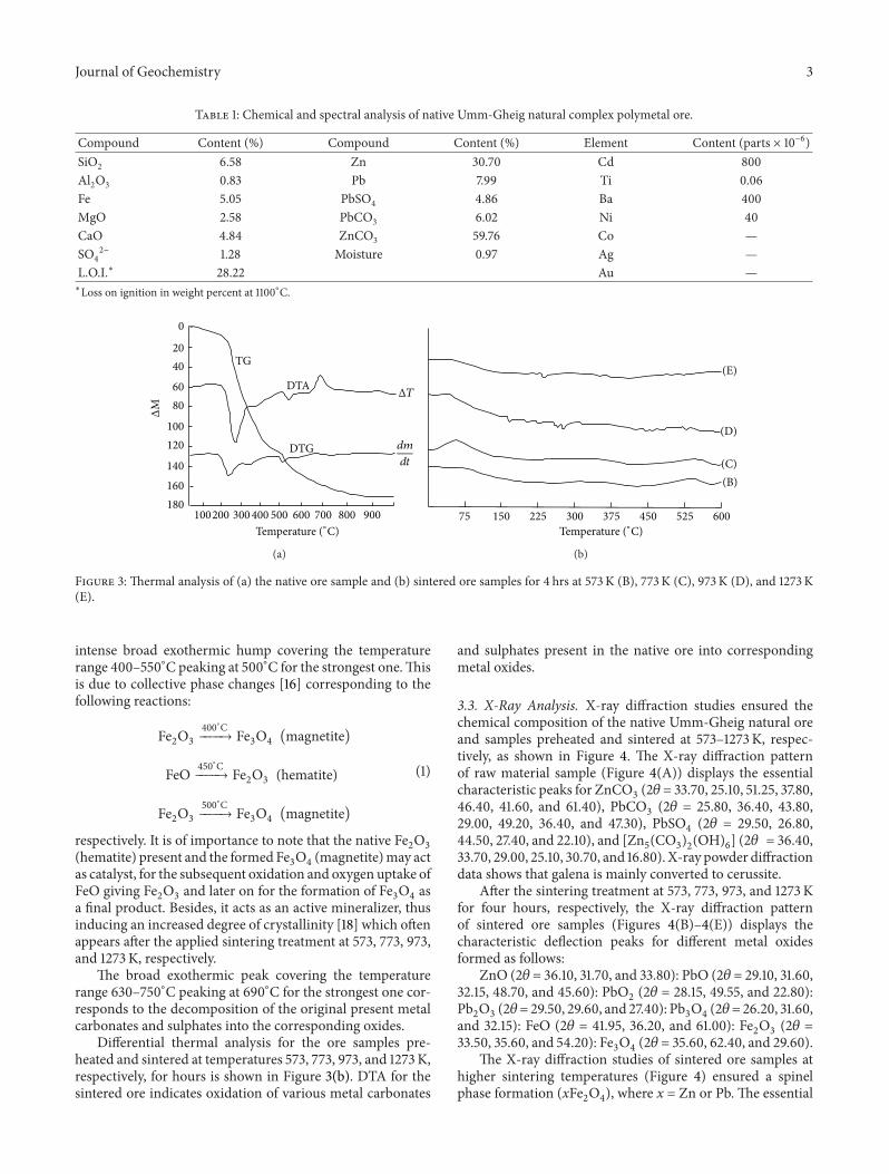
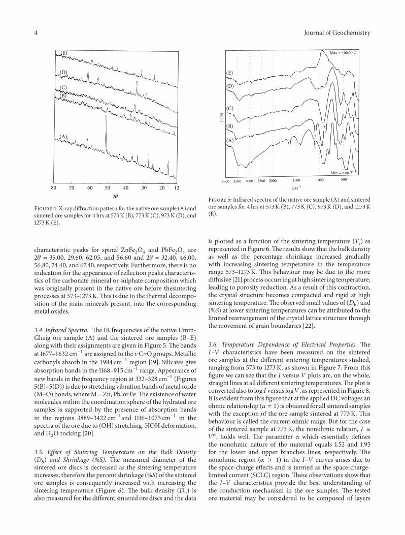
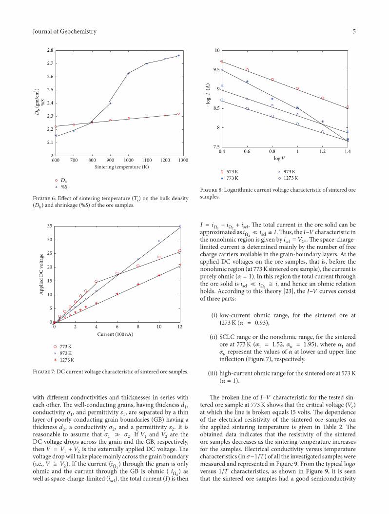
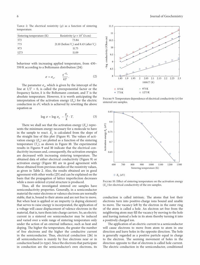
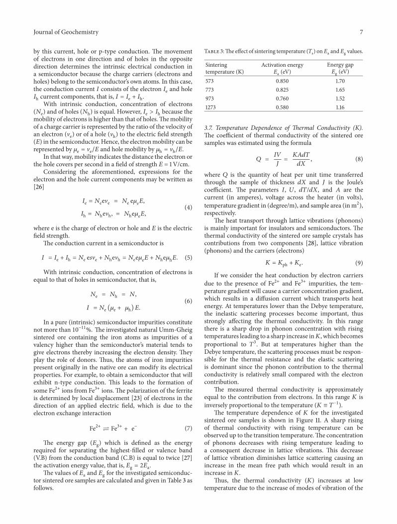
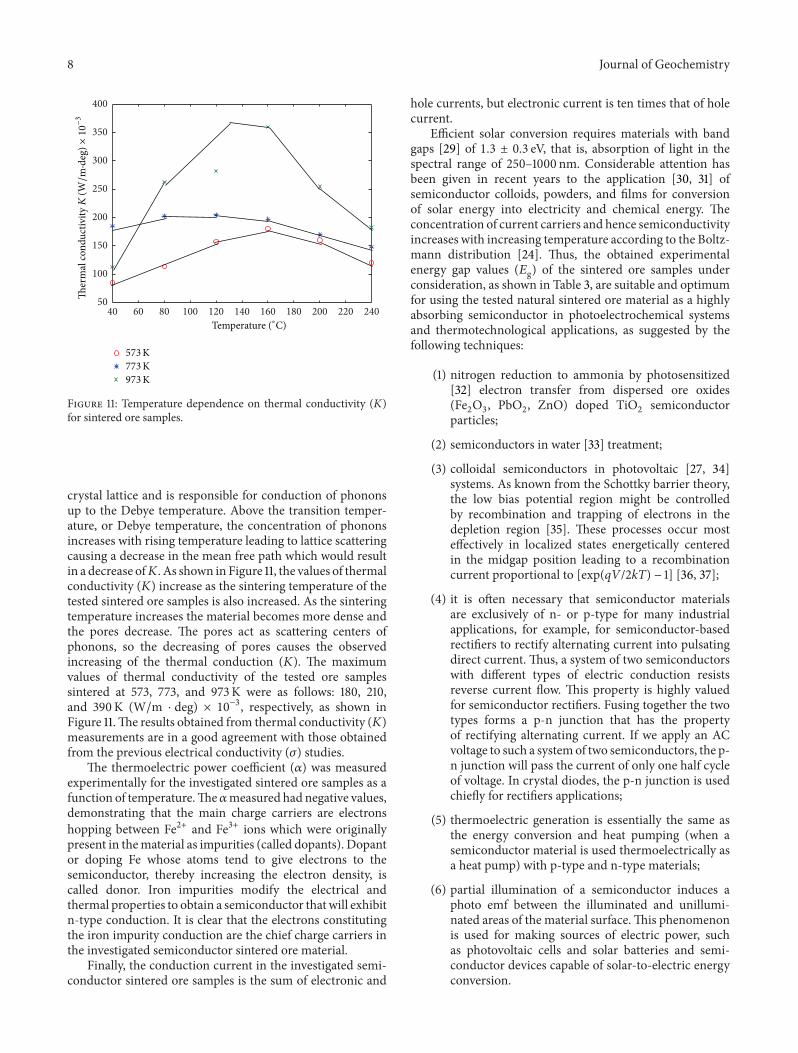