Sputtering Erosion Measurement on Boron Nitride as a Hall Thruster Material
Upload
independentCategory
view
2download
0
Electron. Mater. Lett., Vol. 10, No. 6 (2014), pp. 1093-1101
Effects of Pressure and Deposition Time on the Characteristics of In2Se3 Films Grown by Magnetron Sputtering
Yong Yan,1,* Shasha Li,
1 Yufeng Ou,
1 Yaxin Ji,
1 Zhou Yu,
1,* Lian Liu,1 Chuanpeng
Yan,
1
Yong Zhang,1 and Yong Zhao
1,2
1Superconductivity and New Energy R&D Center (SNERDC), School of Electrical Engineering, Key Laboratory of Advanced Technology of Materials, Ministry of Education of China, Southwest Jiaotong University,
Mail Stop 165#, Chengdu 610031, China2School of Materials Science and Engineering, University of New South Wales, Sydney 2052 NSW, Australia
(received date: 11 March 2014 / accepted date: 20 May 2014 / published date: 10 November 2014)
Crystalline In2Se3 films were fabricated by magnetron sputtering from a sintered In2Se3-compound target and theeffects of the deposition parameters, including the working pressure and deposition time, on the phase composi-tion, structure, morphology, and optical properties were clarified. Single-phase κ-In2Se3 was prepared at 4.0 Pa,but γ-In2Se3 was recognized when the working pressure was lower than 4.0 Pa. The optical transmittance of thefilms decreased to 45% and the optical band gap varied from 2.9 to 2.0 eV with increasing film thickness from 80to 967 nm. Metal-semiconductor-metal (MSM) photodetectors based on γ-In2Se3 thin films with various thick-nesses were also fabricated. The result of photosensitivity research on such MSM photodetectors suggests that itmay be impossible to fabricate wide-absorption-range MSM devices by just using a single material (γ-In2Se3)because of spatial potential fluctuations in the layers.
Keywords: semiconducting In2Se3 films, working pressure, deposition time, optical properties, MSMphotodetector
1. INTRODUCTION
Indium selenide (In2Se3) has emerged as an importantlayered semiconductor material belonging to the class of III-VI binary compounds.[1] Being a direct bandgap semicon-ductor, In2Se3 is widely utilized in photovoltaic cells,[2] photosensors[3] and phase-change random-access memory devices(PRAM).[4] In2Se3 consists of at least five phases includingthe α,[5] β,[6] γ,[7] κ,[8] and δ phase. A number of techniqueshave been used for the fabrication of In2Se3 thin films, suchas co-evaporation,[5] chemical bath deposition,[9] solid statereaction,[10] molecular beam epitaxy (MBE),[11] metal organicchemical vapor deposition (MOCVD),[12] electrodeposition[13]
and sol-gel.[14] Nevertheless, all these foregoing techniqueshave disadvantages, such as toxic growth conditions, difficultiesin controlling the stoichiometry, and the coexistence of morethan one compound and/or phase in the final product.[5,7,8,14,15]
Magnetron sputtering[16,17] is considered as a relative simpleand cheap method to prepare single-phase In2Se3 films.Recently, researchers have studied the morphological andstructural properties of γ-In2Se3 films in dependence ofvarious sets of sputtering parameters including the sputtering
power and substrate temperature.[17]
However, to the best of our knowledge, very few articleshave reported about the influences of the working pressureand deposition time on the In2Se3 films. The variation of theworking pressure p strongly changes the physical conditionsunder which thin films are formed and, therefore, makes itpossible to produce films with new physical or chemicalproperties.[18] In addition, the deposition time t affects thefilm thickness, which is one of the important parameters thatalter the physical characteristics of the grown layerssignificantly, especially in case of In2Se3.
[19] Therefore, acorresponding systematic investigation is necessary.
In this work, In2Se3 thin films were deposited on K9 glasssubstrates using radio-frequency (RF) magnetron sputteringfrom an In2Se3-compound target under argon atmosphereand metal-semiconductor-metal (MSM) photodetectors basedon γ-In2Se3 thin films with various thicknesses were fabricated.The main purpose of this study was to investigate the effectof the working pressure and deposition time on the phasecomposition, structure, morphology, and optical properties ofIn2Se3 films. Based on these results, the correlation betweenthe deposition parameters and the optical transmittance andperformance has been explored. The photosensitivity ofMSM photodetectors based on γ-In2Se3 thin films withvarious thicknesses was investigated. The result suggests
DOI: 10.1007/s13391-014-4081-y
*Corresponding author: [email protected]©KIM and Springer

1094 Y. Yan et al.
Electron. Mater. Lett. Vol. 10, No. 6 (2014)
that it may be impossible to fabricate wide-absorption-rangeMSM devices by just using a single material (γ-In2Se3).
2. EXPERIMENTAL PROCEDURE
In2Se3 thin films were deposited onto K9 glass substratesby RF magnetron sputtering. The In2Se3 target was preparedvia a hot pressing sintering process and was composed of In:39.8 and Se: 60.2 atm% (atomic percent). The K9 glasssubstrates of size of 2 cm × 2 cm were cleaned using thesequence of de-ionized water, acetone, and alcohol and,finally, were dried at 100°C. The substrates were heated to380°C with a heating rate of 10°C/min, followed by 30 minfor thermal stabilization, before starting the individualdeposition processes. A fixed target-to-substrate distance dof 60 mm was applied for all In2Se3 depositions. The basepressure of the vacuum chamber was 1.9 × 10⁻⁴ Pa, then, Ar(99.99%) was introduced into the chamber. The workingpressure was changed from 0.5 Pa to 4.0 Pa in order toinvestigate the effect of the deposition pressure on theproperties of the In2Se3 films while the RF power was fixedat 80 W. The deposition time t for the In2Se3 layers wasadjusted from 1.25 to 15.0 min to obtain the proper thickness.Table 1 lists the details of the deposition parameters used forthe preparation of the In2Se3 layers investigated in this work.
The crystal structures of the as-deposited In2Se3 thin filmswere characterized by x-ray diffraction (XRD) employingCu-Kα (PANalytical X’Pert PRO XRD system, λ = 0.1542 nm)radiation. The morphology was analyzed by field emissionscanning electron microscopy (FESEM, JEOL 7001, Japan)equipped with energy dispersive x-ray spectroscopy (EDS,Inca spectrometer, Oxford Instruments) for the compositionalanalysis. The operating voltage of FESEM was 20 kV. Thethickness was determined by a profiler model AMBIOS XP-2. The transmission of the films was measured by an UV-VIS (APADA UV-6300) double-beam spectrophotometer.
The photosensitive performance of MSM photodetectorsbased on γ-In2Se3 thin films with various thicknesses wasinvestigated. After the deposition of γ-In2Se3 thin films, Ar+
etching was implemented for 1 min to decrease the surfaceroughness and to prepare films for the deposition of metalprobes. A metal with a high work function, namely Au of200 nm in thickness, was deposited on the films using a DCsputtering system. Post-annealing at 250°C was successivelycarried out in N2 atmosphere for 5 min to improve theelectrical contact between the electrodes and the film. Thetwo-probe method was applied to measure the I-V charac-teristics of the detectors. Monochromatic light from a sourcecomposed of a tungsten lamp (150 W) and a monochromator(CROWNTECH, 1/4 m M24-S) was focused and guidedonto the detectors. A mechanical chopper was employed toturn off and on the light irradiation. The variation of thephotocurrent in dependence of time was determined by aKeithley 2635A SMU under chopped illumination (2.917mW/cm2) at the bias voltage of 5 V. All measurements wereperformed in air at ambient temperature.
3. RESULTS AND DISCUSSION
3.1 Effect of working pressure
The effect of the working pressure was examined byvarying the flow rate of argon gas using a mass-flowcontroller (MFC). The argon source with a flow rate of 10,20, 40, and 80 sccm (standard-state cubic centimeter perminute), was induced into the chamber to grow the In2Se3
thin films at 380°C. The previously optimized[17] depositiontime was used to obtain films with identical thickness.Figure 1 shows the effect of the working pressure on theaverage growth rate of the deposited In2Se3 films. At aworking pressure of 0.5 Pa, the as-deposited In2Se3 filmshowed an average growth rate of 1.10 nm/s, whichdecreased to 0.55 nm/s at 4.0 Pa. The average growth rate of
Table 1. Deposition parameters for In2Se3 films (Ts for the substratetemperature, p for the working pressure, Prf for the RF power, d for thetarget-to-substrate distance, t for the deposition time, and th for thethickness including the measuring error).
Samples
ID
Ts
(°C)
p
(Pa)
Prf
(W)
d
(mm)
t
(min)
th
(nm)
A 380 0.5 80 60 5.0 332 ± 5
B 380 1.0 80 60 5.1 327 ± 12
C 380 2.0 80 60 6.5 325 ± 19
D 380 4.0 80 60 10.1 330 ± 3
E 380 0.5 80 60 1.25 080 ± 3
F 380 0.5 80 60 7.5 455 ± 15
G 380 0.5 80 60 10.0 603 ± 22
H 380 0.5 80 60 15.0 967 ± 115Fig. 1. Effect of the working pressure on the average growth rate ofthe In2Se3 films deposited by sputtering.

Y. Yan et al. 1095
Electron. Mater. Lett. Vol. 10, No. 6 (2014)
the films in the sputtering chamber depends on the mean freepath of the reactant species (indium and selenium) during thereaction process. The mean free path of the reactant atoms isinfluenced by the working pressure according to thefollowing equation:[20]
(1)
Here, la is the mean free path, R is the ideal gas constant, Tis the temperature, p is the gas pressure, and NA isAvogadro’s number. The mean free path for the reactantspecies decreased with increasing working pressure at aconstant growth temperature. A larger mean free path of thereactant species results in the higher growth rate at lowerworking pressure.
Figure 2 shows the XRD patterns of the films A-D. Theresults suggest that these In2Se3 films are of acceptablecrystallinity with a highly preferential c-axis orientation. At0.5 Pa, the dominant diffraction peak at 2θ = 27.6° correspondsto the (006) plane of γ-In2Se3 (JCPDS 40-1407). Theexistence of the diffraction peak at 2θ = 26.6° correspondingto the (006) plane of κ-In2Se3 was noted at 1.0 Pa. κ-In2Se3
[8]
and γ-In2Se3 have similar structures. However, the reorderingof vacancies in the κ-In2Se3 structure changes the latticeparameters and destroys the high symmetry of γ-In2Se3.
[21] Afurther increase in growth pressure results in single-phase κ-
In2Se3 thin films at 4.0 Pa. Table 2 shows the peak positionsand widths (full width at half maximum, FWHM) of the(006) reflections of γ- and κ- In2Se3 as a function of theworking pressure. First of all, it can be noted that the valueof the lattice parameter c of the γ-phase, calculated from the(006) peak position, is virtually constant at about 19.2 Å butthe behavior of lattice parameter c of the κ-phase is slightlydifferent, increasing with increasing working pressure to amaximum of 20.1 Å at 4.0 Pa. Furthermore, it is found thatthe FWHM of the γ-phase increases from 0.150 to 0.231° onincreasing working pressure, implying a smaller averagegrain size at higher pressure. According to Debye-Scherrer’sformula,
(2)
la4RT
πa2pNA
------------------=
Dkλ
βcosθ--------------=
Fig. 2. XRD patterns of In2Se3 films deposited at different pressures.
Table 2. XRD results for In2Se3 thin films deposited at different sput-tering pressures.
Sample
ID
(006) Peak Position FWHM Grain Size (nm)
κ γ κ γ κ γ
A -- 27.56 -- 0.141 -- 58.0
B 26.91 27.61 0.630 0.228 13.0 35.9
C 26.83 27.48 0.470 0.231 17.5 35.4
D 26.57 -- 0.527 -- 15.4 --

1096 Y. Yan et al.
Electron. Mater. Lett. Vol. 10, No. 6 (2014)
in which k is the shape factor of 0.9, λ is the wavelengthused, β is the FWHM of a reflection in radians, and θ is thecorresponding Bragg’s angle, the average grain size D forthe γ-phase decreased outstandingly from 58.0 to 35.4 nmwhile the grain size of the κ-phase changed only slightly.This behavior suggested that a reordering of native defects inthe anisotropic structure of the κ-phase happened withincreasing working pressure, which resulted in a loose crys-talline structure with much more defects in k-In2Se3 films.
Figure 3 shows the surface morphology of the In2Se3 filmsdeposited at various working pressures. The film depositedat 0.5 Pa is composed of close packed lamellar grains whichrepresent a distinct hexagonal or trigonal structure. As theworking pressure was increased to 1.0 Pa, the surfacemorphology of the deposited film was not uniform anymore
and uneven granules formed the films. Some bigger, uprightlamellar grains were distributed on the rough surface. Afurther increase in working pressure results in films withsmall irregular grains, deposited at 4.0 Pa. In addition, thegranules became smaller at higher working pressure. Forexample, grains with size of 100 - 200 nm in diameter wereobserved at 0.5 Pa, as shown in Fig. 3(a). At 1.0 and 2.0 Pa,the grain size was approximately 50 - 100 nm in diameter,which decreased further to approximately 20 - 50 nm at4.0 Pa. The K9 glass was cut to observe the cross-sectionalview of the films, which was used to confirm the filmthickness measured by AMBIOS XP-2 that is shown in Fig. 3.The film deposited at 4.0 Pa showed a homogeneous structurewithout any pinholes across the film thickness. Energydispersive x-ray spectroscopy (EDS) was used to determine
Fig. 3. The surface morphology and typical profile (film D), EDS result (film D) for In2Se3 films deposited at different pressures. (a) 0.5 Pa, (b)1.0 Pa, (c) 2.0 Pa, (d) 4.0 Pa.
Y. Yan et al. 1097
Electron. Mater. Lett. Vol. 10, No. 6 (2014)
the composition of the In2Se3 films and a typical spectrum isalso shown in Fig. 3. According to the EDS measurements,the film deposited at 4.0 Pa is solely composed of In and Sewithout any impurities and the average ratio of In to Se wasapproximately 2 : 3, indicating that the film deposited at4.0 Pa was stoichiometric.
Previous reports have shown that Zn doping during thedeposition process promoted the formation of κ-In2Se3, whileair exposure and passivation-layer deposition suppressedit.[15,21] However, in the present work, κ-In2Se3 was stabilizedunder ambient conditions without Zn doping. The stabilizationof κ-In2Se3 may be related to the specific growth mechanismin the sputtering process. At low working pressure, thereactant species can migrate to the most suitable lattice sitesregarding bond direction and length to achieve the optimumbonding between adjacent atoms, thereby resulting in a highcrystallinity of the films and the phase changes to the stableγ-phase. At higher working pressure, the mean free path ofthe sputtered particles becomes shorter because of thecollisions with argon ions and other atoms, resulting in adecrease in kinetic energy. When the reactant species arrive atthe surface of the substrates, a part of the kinetic energy istransformed by thermalization during the collision processof the film-forming particles, resulting in a further decreaseof the surface mobility and, consequently, the reactantspecies cannot migrate to the most suitable lattice sites, thephase changes to the metastable one (κ-phase), thecrystallinity decreases, and the grain size becomes smaller.Similar structural and phase-concerning changes wereobserved in the investigation on the influence of thesubstrate temperature.[17]
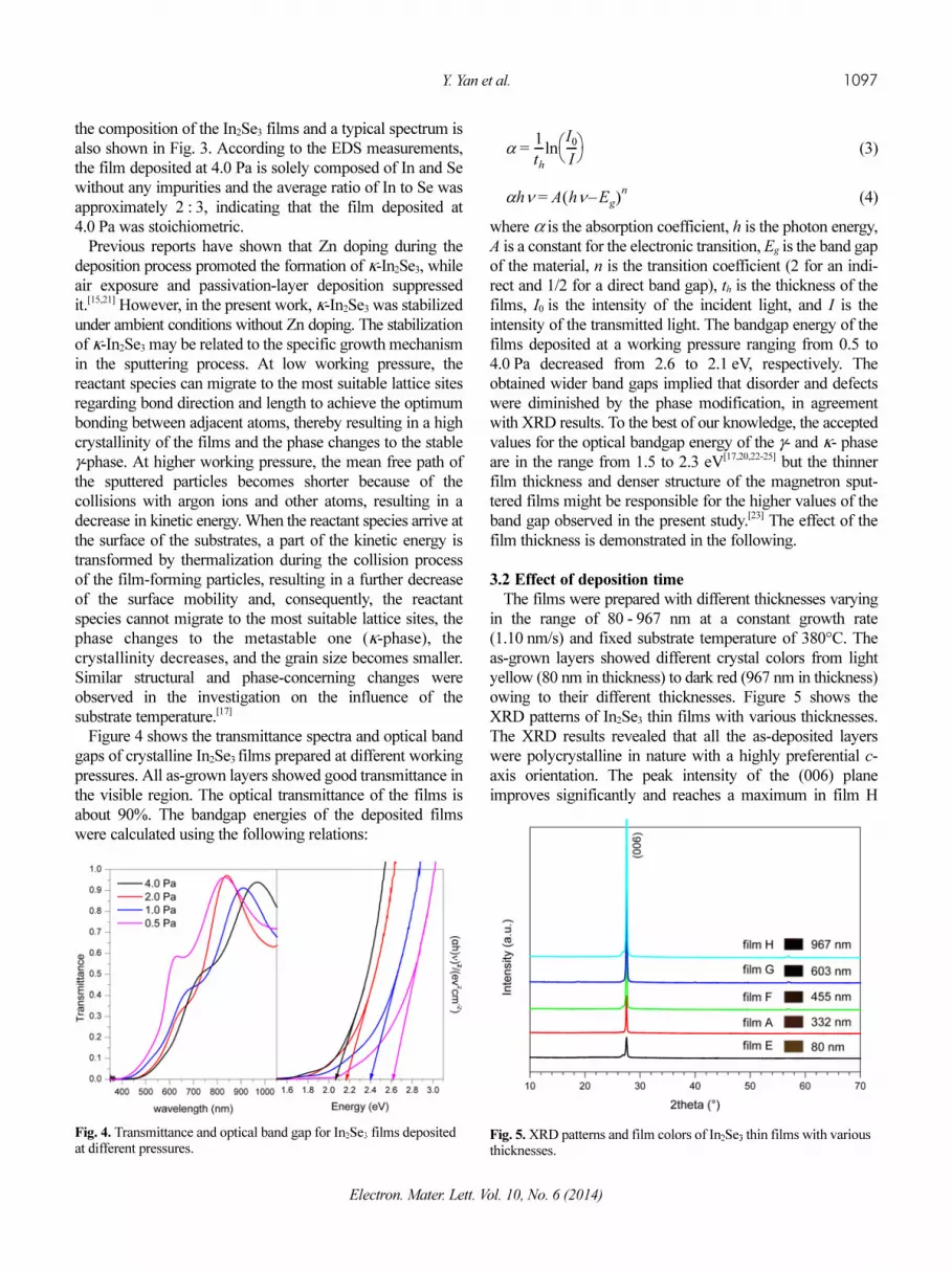
Figure 4 shows the transmittance spectra and optical bandgaps of crystalline In2Se3 films prepared at different workingpressures. All as-grown layers showed good transmittance inthe visible region. The optical transmittance of the films isabout 90%. The bandgap energies of the deposited filmswere calculated using the following relations:
(3)
(4)
where α is the absorption coefficient, h is the photon energy,A is a constant for the electronic transition, Eg is the band gapof the material, n is the transition coefficient (2 for an indi-rect and 1/2 for a direct band gap), th is the thickness of thefilms, I0 is the intensity of the incident light, and I is theintensity of the transmitted light. The bandgap energy of thefilms deposited at a working pressure ranging from 0.5 to4.0 Pa decreased from 2.6 to 2.1 eV, respectively. Theobtained wider band gaps implied that disorder and defectswere diminished by the phase modification, in agreementwith XRD results. To the best of our knowledge, the acceptedvalues for the optical bandgap energy of the γ- and κ- phaseare in the range from 1.5 to 2.3 eV[17,20,22-25] but the thinnerfilm thickness and denser structure of the magnetron sput-tered films might be responsible for the higher values of theband gap observed in the present study.[23] The effect of thefilm thickness is demonstrated in the following.
3.2 Effect of deposition time
The films were prepared with different thicknesses varyingin the range of 80 - 967 nm at a constant growth rate(1.10 nm/s) and fixed substrate temperature of 380°C. Theas-grown layers showed different crystal colors from lightyellow (80 nm in thickness) to dark red (967 nm in thickness)owing to their different thicknesses. Figure 5 shows theXRD patterns of In2Se3 thin films with various thicknesses.The XRD results revealed that all the as-deposited layerswere polycrystalline in nature with a highly preferential c-axis orientation. The peak intensity of the (006) planeimproves significantly and reaches a maximum in film H
α1th---ln
I0
I----⎝ ⎠⎛ ⎞=
αhν A hν Eg–( )n=
Fig. 4. Transmittance and optical band gap for In2Se3 films depositedat different pressures.
Fig. 5. XRD patterns and film colors of In2Se3 thin films with variousthicknesses.

1098 Y. Yan et al.
Electron. Mater. Lett. Vol. 10, No. 6 (2014)
with a thickness of 967 nm, which indicates an improvementin the crystallinity of the grown layers for increasing filmthickness.
The surface morphology of the as-deposited films isshown in Fig. 6. Uniform nanoscale granules of hexagonalor trigonal shape were observed in the films E and A. Thesegranules were well crystallized with size of 100 - 150 nm.As the film thickness increased to ~450 nm, the film showeda rough surface. A further increase of the thickness resultedin a rougher and less compact surface, as shown in Fig. 6(e)and (f). The granules were adhered to or embedded in thesurface. The thickness of one flake-shaped layer was fixed ataround 20 nm with increasing thickness. Furthermore, thegranules kept their hexagonal shape. The growth mechanismof In2Se3 films with preferential c-axis orientation combinesa 2D layer growth and a 3D island growth, following theStranski-Krastanov (SK) type of growth. The growth modesof thin films are determined by the chemical and physicalproperties, such as surface energies and lattice-strain energy
of the film.[26,27] When In and Se atoms are sputtered fromthe target and deposited on the amorphous K9 glass substrate,the film can wet the substrate surface and grows in-plane, soa 2D layer is formed. At a critical layer thickness, the film nolonger wets the substrate and growth in form of 3D islandsbegins. Concerning the 3D grains, the crystallites growalong new growth directions due to the emergence of freshnucleation zones on top of the planes parallel to the c-axis,according to the self-catalytic vapor-solid growth mechanism.[16]
Based on the above results, the preferential growth trans-formation has been suggested as the mechanism to explainthe morphology change.
Figure 7 shows the optical transmittance spectra of In2Se3
thin films with various thicknesses. The optical properties ofIn2Se3 films were measured in the wavelength range of 300 -1050 nm at ambient temperature. All as-deposited In2Se3
films exhibited good transmittance in the visible region. Theoptical transmittance of the films is approximately 95% atlower thickness and decreased to 40% with further increase
Fig. 6. The surface morphology for In2Se3 films with different film thicknesses. (a) film E, (b) film A, (c) film F, (d) film G, (e) and (f) film H.

Y. Yan et al. 1099
Electron. Mater. Lett. Vol. 10, No. 6 (2014)
of the film thickness. The decrease in transmittance for largerfilm thickness is because of thickness-induced absorptionand enhanced surface scattering. Furthermore, the absorptionedge was found to shift toward longer wavelength as the filmthickness increased. Similar changes in the optical propertieswere observed for indium sulfide thin films, prepared byclose space evaporation.[19] The optical band gaps of thedeposited films were calculated using Equations (3) and (4).Fig. 5(b) shows the optical band gap of the films decreasingfrom 2.9 to 2.0 eV for increasing thickness from 80 nm to967 nm. However, the band gap changed only slightly whenthe thickness was above 600 nm in the present work. Thesefilm properties enable the use of γ-In2Se3 for thickness-tunable band gap optical filters. The upper inset in Fig. 5(b)shows the optical bandgap energy of two samples withdifferent thickness (i.e., 80 and 603 nm), amounting to about1.9 eV. This means we can fabricate In2Se3-based opticallogic switches (i.e., ON and OFF switching, see the upperinset in Fig. 5(b)).
The thickness dependence of the direct band gap of γ-In2Se3 layers can be attributed to the amorphous structureand the quantum size effect occurring in nanocrystals.[28]
From the conductivity characteristics of the samples, Bernedesuggested that γ-In2Se3 layers were composed of micro-crystallites embedded in an amorphous matrix.[29] Recently,high-resolution transmission electron microscopy (HRTEM)images directly showed that layered γ-In2Se3 is slightlydisordered and nanocrystalline states exist in the films In thepresent work, the size of granules determined from SEMimages (Figs. 3 and 6) is larger than the grain size calculatedfrom XRD results (Figs. 2 and 5), which suggests that theremay be a coexistence of nanocrystals and amorphousregions in the granules. When light impinges upon the layersurface, high-energy photons penetrate along a path providedby the nanocrystals. The average optical band gap of a thin γ-
In2Se3 sample is hence increased. However, for a thickersample, many single layers are stacked along the c-axis and arandom distribution of nanocrystals in the different layersmay better shield high-energy photons from transmittingbetween the layers. Therefore the average optical band gapof a thick γ-In2Se3 is reduced.[28]
Fig. 7. Optical transmittance spectra (a) and optical band gap (b) of In2Se3 thin films with various thicknesses.
Fig. 8. Photocurrent of In2Se3-based MSM photodetectors with vari-ous thicknesses.

1100 Y. Yan et al.
Electron. Mater. Lett. Vol. 10, No. 6 (2014)
Due to the characteristics of the thickness-tunable opticalband gap of γ-In2Se3, a wide-absorption-range unit made byan MSM device and staircase stacking of γ-In2Se3 layers wasproposed by Ho.[28] In the present work, the photosensitivityof MSM photodetectors based on γ-In2Se3 with variousthicknesses is shown in Fig. 8. For a photoconductive-typedetector, carriers move parallel to the substrate and cansuffer from scattering and trapping due to roughness anddefect surface states.[30] Film H with the roughest surfacewas not suitable for the fabrication of MSM photodetectors.As shown in Fig. 8, the photosensitivity peak is located ataround ~2.0 eV whereas the electrical band gap of γ-In2Se3
for various thicknesses lies in the (visible) range from~2.6 eV to over ~3.0 eV. This result shows that the electricalbandgap energy window of the two samples with differentthickness (i.e. 80 and 603 mm) is about 0.4 eV, which islower than the optical gap energy window (1.9 eV). Anotherdiscrepancy is also found between optical transmittance dataof film G, which reveal only a small Eg of 2.0 eV, andelectrical measurements, which predict a much larger value(2.6 eV). These inconsistencies may be resolved by a modelthat takes into account potential fluctuations in an amorphousmaterial. The absorption of photons takes place via excitationof electrons from the valence to the conduction band ofIn2Se3 thin films. However, local density fluctuations atdifferent positions in the γ-In2Se3 layers may produce spatialpotential fluctuations that, in turn, may result in the fact thatelectrons and holes are trapped in different regions. Near themobility edge, the extended electron wavefunctions aresomewhat excluded from regions in which electrons arelocalized.[18,31] The result of the present photosensitivityresearch predicts that it may be impossible to fabricate wide-absorption-range MSM devices just by using a singlematerial (γ-In2Se3).
4. CONCLUSIONS
Polycrystalline In2Se3 thin films were deposited on heatedglass substrates by RF magnetron sputtering. The characteristicsof the thus prepared In2Se3 films in dependence of thesputtering parameters including the working pressure anddeposition time was clarified. The mean growth rate of thefilms decreased with increasing pressure. XRD analysesdemonstrated that the structure of the In2Se3 films wasgreatly influenced by the working pressure. Single-phase κ-In2Se3 was prepared at 4.0 Pa while, additionally, γ-In2Se3
was recognized when the working pressure was lower than4.0 Pa. The band gap decreased from 2.6 to 2.1 eV withincreasing working pressure from 0.5 to 4 Pa. At higherpressure, the films showed a granule-like surface morphologycombined with small irregular grains. The optical transmittanceof the films decreased from 95% to 40% and the band gapvaried in the range from 2.9 to 2.0 eV with increasing film
thickness from 80 nm to 967 nm, respectively. The morphologyvariation was explained by the Stranski-Krastanov growthmodel. The result of the photosensitivity research predictsthat it may be impossible to fabricate wide-absorption-rangeMSM devices by using only a single material (γ-In2Se3)because of spatial potential fluctuations in the layers.
ACKNOWLEDGEMENTS
The authors are grateful for the financial support of theFoundation of National Magnetic Confinement FusionScience Program 2011GB112001, 2013GB110001; Programof International S&T Cooperation 2013DFA51050; NationalNatural Science Foundation of China (No. 51271155,51377138); Science Foundation of Sichuan Province2011JY0031, 2011JY0130.
REFERENCES
1. C. Julien, M. Eddrief, K. Kambas, and M. Balkanski, Thin
Solid Films 137, 27 (1986).
2. S. H. Kwon, B. T. Ahn, S. K. Kim, K. H. Yoon, and J.
Song, Thin Solid Films 323, 265 (1998).
3. T. Zhai, X. Fang, M. Liao, X. Xu, L. Li, B. Liu, Y. Koide,
Y. Ma, J. Yao, Y. Bando, and D. Golberg, Acs Nano. 4,
1596 (2010).
4. X. Tao and Y. Gu, Nano Lett. 13, 3501 (2013).
5. B. Thomas, Appl. Phys. A-Mater. 54, 293 (1992).
6. D. Eddike, A. Ramdani, G. Brun, J. C. Tedenac, and B.
Liautard, Mater. Res. Bull. 33, 519 (1998).
7. Y. C. Huang, Z. Y. Li, W. Y. Uen, S. M. Lan, K. J. Chang,
Z. J. Xie, J. Y. Chang, S. C. Wang, and J. L. Shen, J. Cryst.
Growth 310, 1679 (2008).
8. C. H. de Groot and J. S. Moodera, J. Appl. Phys. 89, 4336
(2001).
9. H. M. Pathan, S. S Kulkarni, R. S. Mane, and C. D.
Lokhande, Mater. Chem. Phys. 93, 16 (2005).
10. S. Marsillac, J. C. Bernede, R. Leny, and A. Conan, Vacuum
46, 1315 (1995).
11. T. Okamoto, A. Yamada, and M. Konagai, J. Cryst.
Growth 175, 1045 (1997).
12. J. H. Park, M. Afzaal, M. Helliwell, M. A. Malik, P.
O'Brien, and J. Raftery, Chem. Mater. 15, 4205 (2003).
13. M. Valdes, M. Vazquez, and A. Goossens, Electrochim.
Acta 54, 524 (2008).
14. I. H. Mutlu, M. Z. Zarbaliyev, and F. Aslan, J. Sol-Gel. Sci.
Techn. 43, 223 (2007).
15. C. Amory, J. C. Bernede, and S. Marsillac, J. Appl. Phys.
94, 6945 (2003).
16. Y. Yan, S. Li, Y. Ji, L. Liu, C. Yan, Y. Zhang, Z. Yu, and Y.
Zhao, Mater. Lett. 109, 291 (2013).
17. S. Li, Y. Yan, Y. Zhang, Y. Ou, Y. Ji, L. Liu, C. Yan, Y.
Zhao, and Z. Yu, Vacuum. 99, 228 (2014).
18. J. Musil, Vacuum. 50, 363 (1998).

Y. Yan et al. 1101
Electron. Mater. Lett. Vol. 10, No. 6 (2014)
19. N. Revathi, P. Prathap, and K. T. R. Reddy, Solid. State.
Commun. 11, 1288 (2009).
20. S. M. Yu, J. H. Yoo, S. P. Patole, J. H. Lee, and J.-B. Yoo,
Electron. Mater. Lett. 8, 245 (2012).
21. J. Jasinski, W. Swider, J. Washburn, Z. Liliental-Weber, A.
Chaiken, K. Nauka, G. A. Gibson, and C. C. Yang, Appl.
Phys. Lett. 81, 4356 (2002).
22. D. Y. Lyu, T. Y. Lin, T. W. Chang, S. M. Lan, T. N. Yang,
C. C. Chiang, C. L. Chen, and H. P. Chiang, J. Alloy.
Compd. 499, 104 (2010).
23. C. Julien, A. Chevy, and D. Siapkas, Phys. Stat. Sol. A. 118,
553 (1990).
24. M. Emziane, S. Marsillac, J. Ouerfelli, J. C. Bernede, and
R. Le Ny, Vacuum. 48, 871 (1997).
25. C.-H. Ho, Y.-C. Chen, and C.-C. Pan, J. Appl. Phys. 115,
033501 (2014).
26. J. Venables, Introduction to Surface and Thin Film Pro-
cesses, p. 38, Cambridge University Press, London (2000).
27. J. B. Hudson, Surface Science: An Introduction, p. 25, John
Wiley & Sons, NewYork (1998).
28. C.-H. Ho and Y.-C. Chen, RSC Adv. 3, 24896 (2013).
29. J. C. Bernede, S. Marsillac, and A. Conan, Mater. Chem.
Phys. 48, 5 (1997).
30. F. Taghibakhsh, I. Khodami, and K. S. Karim, IEEE T.
Electron. Dev. 55, 337 (2008).
31. H. Fritzsche, J. Non-Cryst. Solids 6, 49 (1971).
Copyright © 2022 FDOKUMEN