
Author's personal copy Effects of duty cycle and pulse frequency on the fabrication of AlCrN thin...
12
This article appeared in a journal published by Elsevier. The attached copy is furnished to the author for internal non-commercial research and education use, including for instruction at the authors institution and sharing with colleagues. Other uses, including reproduction and distribution, or selling or licensing copies, or posting to personal, institutional or third party websites are prohibited. In most cases authors are permitted to post their version of the article (e.g. in Word or Tex form) to their personal website or institutional repository. Authors requiring further information regarding Elsevier’s archiving and manuscript policies are encouraged to visit: http://www.elsevier.com/authorsrights
Transcript of Author's personal copy Effects of duty cycle and pulse frequency on the fabrication of AlCrN thin...

This article appeared in a journal published by Elsevier. The attachedcopy is furnished to the author for internal non-commercial researchand education use, including for instruction at the authors institution
and sharing with colleagues.
Other uses, including reproduction and distribution, or selling orlicensing copies, or posting to personal, institutional or third party
websites are prohibited.
In most cases authors are permitted to post their version of thearticle (e.g. in Word or Tex form) to their personal website orinstitutional repository. Authors requiring further information
regarding Elsevier’s archiving and manuscript policies areencouraged to visit:
http://www.elsevier.com/authorsrights
Author's personal copy
Effects of duty cycle and pulse frequency on the fabrication of AlCrN thin filmsdeposited by high power impulse magnetron sputtering
Yu-Chiao Hsiao a, Jyh-Wei Lee b,c,⁎, Yung-Chin Yang a, Bih-Show Lou d,⁎⁎a Department of Materials Engineering, National Taipei University of Technology, Taipei, Taiwanb Department of Materials Engineering, Ming Chi University of Technology, Taipei, Taiwanc Center for Thin Film Technology and Applications, Ming Chi University of Technology, Taipei, Taiwand Chemistry Division, Center for General Education, Chang Gung University, Taoyuan, Taiwan
a b s t r a c ta r t i c l e i n f o
Available online 22 August 2013
Keywords:High power impulse magnetron sputtering(HIPIMS)Aluminum chromium nitride (AlCrN)Duty cycleFrequencyAdhesion
High power impulse magnetron sputtering (HIPIMS) is a newly developed coating technology, characterized byits ultra-high peak current and peak power density to achieve unique thin film properties, such as high hardness,good adhesion and tribological performance. In this study, an AlCr alloy target was used to deposit AlxCr1 − xNcoatings on various substrates by the HIPIMS technique. The aim of this workwas to systematically study themi-crostructure evaluation and mechanical properties of AlxCr1 − xN coatings as a function of duty cycle and pulsefrequency. The experimental results showed that the peak power density increased linearly as the duty cycle de-creased from 5% to 2% at constant frequency of 1000 Hz. A maximum peak power density of 2.76 kW cm−2 wasachieved at the duty cycle of 2% and repetition frequency of 833 Hz. Amixture of cubic and hexagonal AlxCr1 − xNphaseswas found for each coating. The x value of AlxCr1 − xN thin films changed from0.72 to 0.75 and showed nodirect relationships with duty cycle and repetition frequency. The peak power density had great influence on themicrostructure evolution and altered the microstructure from coarse columnar to fine columnar structure. Re-nucleation grains were also found between columnar grains. The hardness increased with increasing frequencyat constant duty cycle of 2% and reached the optimum hardness of 39.9 GPa at x = 0.75. Good adhesion andwear resistance was observed for each coating. The critical load increased as the repetition frequency increasedfrom 500 to 1250 Hz at the same duty cycle of 2%. Since the wear resistance for each coating was excellent, theduty cycle and pulse frequency showed limited influence on the wear resistance of thin films.
© 2013 Elsevier B.V. All rights reserved.
1. Introduction
The magnetron sputtering technology for thin film deposition hasbeen developed for several decades and has becomes an important fab-rication tool in almost every industrial field today. Among several mag-netron sputtering techniques, the high power pulsed magnetronsputtering (HPPMS), or the so-called high power impulse magnetronsputtering (HIPIMS) attracts considerable attention from researchersand industries since Kouznetsov et al. [1] reported the extremely highpeak power density, 2800 W cm−2 and 70% ionization during Cu filmsynthesis in 1999. The HIPIMS technique usually operates at a low dutycycle (b10%), relatively short pulse on-time from several μs to thousandsof μs and in the repetition frequency range of 10 Hz to 10 kHz [2]. There-fore, the HIPIMS technique can provide very high target peak current,high peak power density of several kW cm−2 and high ionization rate,
which are much higher than those of conventional radio frequencymagnetron sputtering (rf-MS), direct current MS (dc-MS) and mid-frequency pulsed dc-MS. Since a homogeneous thin film thickness canbe achieved on complex-shaped substrate with the HIPIMS, it has be-come a promising technology for hard coatings on cutting and formingtools [2,3]. Meanwhile, the ease of installing a HIPIMS system, by simplyexchanging theHIPIMS supply in the same coater, is also a unique advan-tage for its industry application [2]. The application of the HIPIMS systemon the fabrication of transition metal nitride coatings, such as CrN [4,5],TiN [6], TiMoN [7], AlCrN and AlCrSiN [3], CrN/NbN [8], CrAlYN/CrN [9]andCrN/TiN [10] nanolaminated thinfilmshave been studied successful-ly. The HIPIMS system provides thin films with smooth surfaces, densemicrostructures and better mechanical properties, these advantageshave been discovered through the proper adjustments of pulse on/offtime configuration.
Recently, the AlCrN coatings have been studied by researchers andindustries due to their attractive wear- and heat-resistance at elevatedtemperature [11–20]. Themechanical property of the rock salt structurec-AlxCr1 − xN can be improved by Al doping into cubic, rock salt type B1CrN phase. The maximum Al content to keep the B1 structure is at x =0.7–0.75 [11–14]. Mo et al. [15] reported that the cathodic arc deposited
Thin Solid Films 549 (2013) 281–291
⁎ Correspondence to: J.-W. Lee, Department of Materials Engineering, Ming ChiUniversity of Technology, Taipei, Taiwan. Tel.: +886 2 29089899; fax: +886 2 29084091.⁎⁎ Corresponding author.
E-mail addresses: [email protected] (J.-W. Lee), [email protected](B.-S. Lou).
0040-6090/$ – see front matter © 2013 Elsevier B.V. All rights reserved.http://dx.doi.org/10.1016/j.tsf.2013.08.059
Contents lists available at ScienceDirect
Thin Solid Films
j ourna l homepage: www.e lsev ie r .com/ locate / ts f

Author's personal copy
c-AlCrN coating had better performance of anti-oxidation and anti-spalling as compared with the TiAlN coating. Although the HIPIMS sys-tem has already become a powerful tool to deposit transition metalnitride coatings, research onHIPIMS fabricatedAlCrN thinfilm is limited[3]. In addition, the effect of pulse on/off time configuration on the char-acteristics of AlCrN coatings has still not been revealed. In this work, thepulse on-time, off-time, duty cycle and repetition frequencywere variedto deposit eight AlxCr1 − xN coatings using the Al0.7Cr0.3 compoundtarget in an Ar/N2 atmosphere. The target current–voltage waveformsduring HIPIMS process were recorded and discussed. The relationshipsbetween the pulse on/off time configuration, duty cycle, repetition fre-quency and film properties, including chemical composition, crystallinestructure, microstructure and mechanical properties were furtherevaluated.
2. Experimental details
In this work, a high power impulse magnetron sputtering (HIPIMS)system was used to deposit AlCrN thin films on Si wafer and hardenedAISI420 disk substrates. The 3″ diameter AlCr alloy target (purity of70 at.% Al–30 at.% Cr) power was supplied by a SPIK2000A pulsepower supply (SPIK 2000A, Shen Chang Electric Co., Taiwan) operatingin the unipolar negative mode at constant power of 600 W. The pulseon-time, ton, and pulse off-time, toff, were adjusted to achievevarious duty cycle ((ton / (toff + ton) × 100%) and repetition frequen-cies (1 / (toff + ton)) ranging from 2 to 5% and 500 to 1250 Hz, respec-tively. The substrate-to-target vertical distance was kept at 12 cm. Thechamberwas pumped to a base pressure of 6.7 × 10⁻⁴ Pa. Theworkingpressure was maintained at around 0.67 Pa by the inlet of an Ar and N2
(Ar:N2 = 1:2) gas mixture. These coatings were deposited at a temper-ature of 200 °C. A pulse bias voltage of −60 V was applied to thesubstrate holder during deposition. No attemptsweremade to synchro-nize the frequency between HIPIMS target and bias. A digital oscillo-scope (DS 5205CA, RIGOL, USA) combined with the high voltagedifferential probe (SI-9010, Sapphire Instruments Co. Ltd., Taiwan)and the current probe amplifier (80i-110s, FLUKE, France) were usedto measure the voltage and current of target, respectively, duringsputtering. The calculated ion eroded area of the AlCr compound target,26.51 cm2, was used to calculate the peak power density. Beforedeposition, the samples were ion etched in argon atmosphere using−300 V DC bias discharge. The detailed sputtering parameters anddesignation for each coating are listed in Table 1. A Langmuir probe(ESPION System, Hiden Analytical Inc., UK) was inserted into the centerof the plasma region to determine the electron temperature, electrondensity and ion density within the bulk plasma for each selected thinfilm deposition process. Target-to-tip vertical distance was kept at6 cm. The probe bias changed from −20 V to +30 V and scan for 10
times. The total measurement time was 136 s for each plasmacondition.
The crystalline structures of thin films were explored by a glancingangle X-ray diffractometer (GA-XRD, PANalytical, X'pert, Holland)with an incidence angle of 1°. Cu Kα radiation generated at 40 kV and30 mA from a Cu target was used. The lateral grain size of eachfilm was estimated by the Scherrer formula [21]. The precise latticeparameter, a0, of each film was calculated according to the followingequation [22]:
a ¼ a0 þ K � cos2θsinθ
ð1Þ
where a is lattice contact, K is constant and θ is diffraction angle. Thecross-sectional morphologies of thin films were examined with a fieldemission scanning electron microscope (FE-SEM, JSM-6701, JEOL,Japan). Selected samples were further analyzed by transmission elec-tron microscopy (TEM, JEOL, JSM-2100, Japan). The chemical composi-tion of thin films was analyzed with a field emission electron probemicroanalyzer (FE-EPMA, JXA-8500F, JEOL, Japan). The thin films werecoated on AISI420 disk substrates for the surface roughness, hardness,scratch and wear tests. The surface roughness values of coatings weremeasured by an atomic force microscopy (AFM, DI-3100, Bruker,USA). The nanohardness and elastic modulus of AlCrN filmswere inves-tigated by means of a nanoindenter (TI-900, TriboIndenter, Hysitron,USA) equipped with a Berkovich 142.3° diamond probe tip at a maxi-mum applied load of 5 mN. The loading rate was 1000 μN/s. Eight in-dentation tests were made for each coating. The hardness and elasticmodulus of each indent were determined on the basis of the Oliverand Pharr method [23]. The elastic modulus, E, was expressed as fol-lows:
1Er
¼ 1−ν2
Eþ 1−νi
2
Eið2Þ
where Er and ν are the reduced elastic modulus and Poisson's ratio,respectively, for the thin film under test, and Ei (1140 GPa) and νi(0.07) are the corresponding parameters of the diamond indenter. Thefused quartz standard sample was used to calibrate the area functionof the nanoindenter.
A scratch test (Scratch Tester, J & L Tech. Co., Korea), with up to amaximum load of 100 N was adopted to explore the adhesion proper-ties of thin films. A pin-on-disk wear method was used to investigatethe tribological performance of coatings. AWC–6%Coballwith 6 mmdi-ameter was adopted as the stationary pin. A normal load of 5 Nwas ap-plied. The rotation speed was 200 rpm with a wear track diameter of10 mm. The test temperature was 20 °C, and the relative humiditywas kept at 60%. The wear length was 500 m for each test. A 3-Dprofilometer was adopted to determine the wear volume and thewear rate of coating.
3. Results and discussion
3.1. Characteristics of HIPIMS discharge
Fig. 1a and b shows the typical temporal evolution of the target volt-age and currentwaveforms of AlCr target at 600 Waverage power, witha repetition frequency of 1000 Hz (ton time = 50 μs, toff time =950 μs), duty cycle of 5% (sample A), repetition frequency of 833 Hz(ton time = 24 μs, toff time = 1176 μs), and duty cycle of 2% (sampleF). During the sputtering at lower peak power density, the rectangularand triangular shapes of voltage and current waveforms are observed,respectively, in Fig. 1a. However, the loading voltage is not maintainedconstant during the pulse on-time when the peak current reachesvery high value as shown in Fig. 1b. Its temporal evolution is rather de-termined by the size of the capacitor bank and the time-dependent
Table 1Typical deposition conditions and target current–voltage characteristics for AlxCr1 − xNcoatings.
Sample # A B C D E F G H
Frequency (Hz) 1000 1250 833 714 500ton time (μs) 50 40 30 20 16 24 28 40toff time (μs) 950 960 970 980 784 1176 1372 1960Duty cycle (%) 5 4 3 2 2Avg. target current (A) 1.21 1.17 1.04 0.89 0.85 0.91 0.93 0.96Avg. target voltage (V) 495 513 574 669 707 659 638 624Peak current (A) 70 80 90 105 100 110 110 120Peak power density(kW cm−2)
1.30 1.59 1.97 2.72 2.68 2.76 2.68 2.68
Deposition rate (nm/min) 8.28 5.81 7.93 3.68 5.03 4.17 7.25 6.43Sputter gas (sccm) Ar: 10Reactive gas (sccm) N2: 20Substrate bias (V) 60ton/toff time for substratebias (μs)
15/15
Deposition temperature (°C) 200
282 Y.-C. Hsiao et al. / Thin Solid Films 549 (2013) 281–291

Author's personal copy
plasma impedance [2]. Similar results were also reported for the sameSPIK2000A HIPIMS system [2,5]. In Fig. 1, the time lags ~10 and 4 μswere found for the plasma ignition at different pulse on-times of ton,50 and 24 μs, respectively. There is no current measured in the first 4to 10 μs and the voltage oscillation from a few volts to tens of voltsare also observed in Fig. 1a and b, respectively. Themagnitude of voltageoscillation increased with increasing pulse off-time, toff. This phenome-non is attributed to the high impedance before the plasma ignition,which is caused by the depletion of the discharge between pulses[5,24]. In addition, this phenomenon can also be influenced by the char-acter of internal impedance and the size of the capacitor bank of theSPIK2000A.
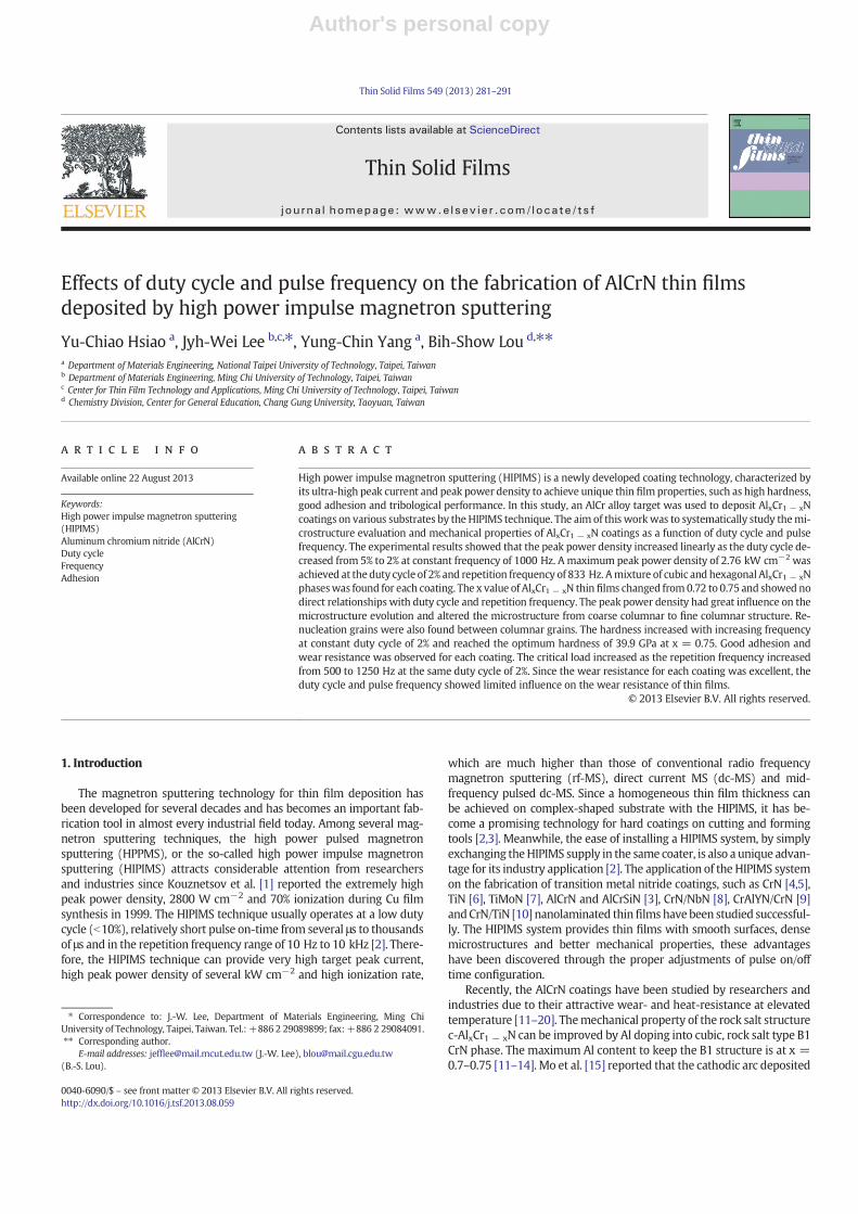
It is obvious that the maximum target peak current increased from70 A to 110 A as the toff time increases from 950 to 1176 μs and theduty cycle decreases from 5 to 2% as shown in Fig. 1. Similar target volt-age and current waveforms were also observed for other pulse on/offtime configurations. The target peak current and peak power densitymeasured from the digital oscilloscope are listed in Table 1 for eachcoating. The average target current and average target voltage obtainedfrom the power supply display panel readings are also listed in Table 1.
It is obvious that the peak current and peak power density ranging from70 to 120 A and 1.30 to 2.76 kW cm−2, respectively, were found foreach coating indicating that the high power impulse magnetronsputtering condition was achieved in this work. The relationships be-tween the peak power density, duty cycle and frequency are illustratedin Fig. 2a and b, respectively. For the coatings deposited with the samefrequency, 1 kHz, the peak power density increased from 1.30 to2.72 kW cm−2, and the peak current increased from 70 to 105 Awhen the duty cycle decreased from 5 to 2%, i.e., the pulse off-time,toff, increased from 950 to 980 μs and the pulse on-time, ton, decreasedfrom50 to 20 μs. It is obvious that the duty cycle showed great influenceon the peak power density. On the other hand, a slight change of 3% isfound around peak power densities of 2.68 to 2.76 kW cm−2 and thepower density is almost not influenced by frequencies ranging from500 to 1250 Hz when the duty cycle is 2%; the pulse off-time, toff, in-creases from 784 to 1960 μs and the pulse on-time, ton, increases from16 to 40 μs. According to the data listed in Table 1, the peak current in-creased slightly from 100 to 120 A as the frequency decreased from1250 to 500 Hz. Apparently, the duty cycle, i.e., the pulse on/off timeconfiguration, showed great influence on the peak current and peak
Fig. 1. Temporal evolution of the target voltage and current waveforms of AlCr target for (a) sample A, repetition frequency 1000 Hz, duty cycle 5% and (b) sample F, repetition frequency833 Hz, duty cycle 2%.
283Y.-C. Hsiao et al. / Thin Solid Films 549 (2013) 281–291
Author's personal copy
power density. For the SPIK2000A pulse power supply, the electrical en-ergy stored in the capacitor during the long toff time and supplied to thetarget to ignite the plasma during the relatively short ton time. There-fore, the total target power density and peak current increased withshorter duty cycle, i.e., increasing toff and decreasing ton time. AlthoughAlami and co-workers reported that the peak target current increasedwith increasing pulse off-time [5], the proper pulse on/off time configu-rations that yield a 2% duty cycle is the key issue to achieve higher peaktarget current and power density in this work. It is known that the ion-ization of HIPIMS plasma and related plasma properties are stronglyinfluenced by the pulse on/off time configuration [2]. In this work, ashort pulse on-time was selected due to the fact that the density inthe HIPIMS plasma increased with short pulsed on-time around 5 to10 μs [25]. The HIPIMS with short pulse on-time ranging from 5 to20 μs can keep the glow discharge in a transient regime, which is illus-trated by the triangular waveform of target current [2]. Therefore, theglow to arc transition is thus prevented.
Fig. 3a illustrates the temporal evolution of the substrate bias voltagewaveform before target power on. Although a pulsed biasing (ton:toff =15:15 μs) was used, a rather smooth voltage waveform can be observeddue to its short pulse off-time. On the other hand, the temporal evolu-tion of the bias voltage waveform of substrate for deposition of sampleA, repetition frequency 1000 Hz, duty cycle 5% is depicted in Fig. 3b.The turbulent variation of biasing voltage ranging from −70 V to
+5 V during the pulse on-time and in the following pulse off-time ofHIPIMS target power for almost 300 μs is clear observed. Similar turbu-lent variation of substrate biasing voltage waveforms for samples C andE are also revealed in Fig. 3c and d, respectively. The advantage of thepulsed substrate bias during the sputtering process has been reportedin literature [26,27]. By pulsing the substrate bias, the electron temper-ature, the ion saturation current, the power flux of ions, the ion to atomratio toward the substrate, and the substrate heating effect are also in-creased. However, the abnormal turbulent variation of substrate biasingvoltagewaveform for theHIPIMS process has not yet been reported. Theinfluence of DC and pulsed substrate bias at different voltages on thecharacteristics of thin film will be discussed in the near future.
Average ion density, average electron density and average electrontemperature for sample A, C and E as measured by the Langmuirprobe are listed in Table 2, respectively. The peak power density ofeach coating is also listed. It is obvious that the time averaged ion den-sity and time averaged electron temperature increased with increasingpeak power density. We observe rather large standard deviation valuesof average electron density and average electron temperature, whichare possibly due to the strong energy delivered into the plasma duringthe pulse on-time period. The time-resolved plasma characteristicswill be necessarily conducted soon.
3.2. Chemical composition and phases of AlxCr1 − xN thin films
The chemical compositions of AlxCr1 − xN thin films were deter-mined by FE-EPMA and are listed in Table 3. The Al/Cr ratio rangedfrom 2.54 to 2.98 for all coatings, which is considerably higher thanthe target composition ratio, Al/Cr = 2.33 due to the lower ionizationenergy of Al. For the Al/(Al + Cr) ratio, x, for each coating is also listedin Table 3. The x value changed from 0.72 to 0.75 and showed no directrelationships with duty cycle and repetition frequency. Furthermore,the nitrogen content of all coatings is almost the same, which is around50–52 at.%. For the N/(Al + Cr) ratio, y, ranging from 1.01 to 1.15 is ob-served in Table 3 indicating the over-stoichiometric (AlxCr1 − x)Ny
structure for each coating.Fig. 4 illustrates the X-ray diffraction patterns of AlxCr1 − xN thinfilms.
In general, the peak intensities decrease and broaden as the peak powerdensity of coating increases. To determine the cubic-type B1 AlN andwurtzite-type B4 AlN, the JCPDS-ICDD card 461200 and JCPDS-ICDDcard651902were used. Solid anddash lines representing the correspond-ing diffraction peaks were inserted in Fig. 4. In addition, the diffractionpeaks of cubic-type B1 CrN (JCPDS-ICDD card 11-0065) were plotted asa reference in Fig. 4. The crystalline cubic-type c-AlN (c-AlxCr1 − xN)and wurtzite-type h-AlN (h-AlxCr1 − xN) dual phase structures were ob-served for each coating as depicted in Fig. 4a and b. As compared withthe standard peaks of c-AlN and h-AlN phases as indicated in Fig. 4, it isobvious that the diffraction peaks shifted to lower diffraction angles dueto the incorporation of Cr atoms into the AlN leading to a lattice expan-sion. The compressive residual stress of thinfilmalsohas certain influenceon the shift of XRDpeaks in Fig. 4. According to the chemical compositionslisted in Table 1 and peaks shifting to lower diffraction angles, the c-AlNand h-AlN can be assigned as the c-AlxCr1 − xN and h-AlxCr1 − xN phases,respectively, due to its high Al contents and high x value for each coating.In Fig. 4a, a stronger intensity of c-AlxCr1 − xNphasewas found for sampleAwith x = 0.72. In general, thepeak intensity of h-AlxCr1 − xN is strongerthan that of c-AlxCr1 − xN when the x value is larger than 0.72. However,the c-AlxCr1 − xN (111) phase exhibits the stronger intensity than theh-AlxCr1 − xN phase for samples E and G. According to Table 3, thelattice constant of the c-AlxCr1 − xN phase for each coating is around0.406 to 0.412 nm. Hasegawa et al. [12] reported that the structureof cathodic arc fabricated Cr1 − xAlxN coating changed from a cubicstructure at x = 0.6 to a hexagonal structure at x = 0.7. On theother hand, the rf-sputtered Cr1 − xAlxN films changed from B1(NaCl) to B4 (wurtzite) structure between x = 0.7 and x = 0.8[16]. The lattice parameters of Cr1 − xAlxN gradually decreased
Fig. 2. The peak power density as a function of (a) duty cycle (fixed frequency 1000 Hz)and (b) repetition frequency (fixed duty cycle 2%).
284 Y.-C. Hsiao et al. / Thin Solid Films 549 (2013) 281–291

Author's personal copy
from 0.416 nm (x = 0) to 0.413 nm (x = 0.6). The B1 to B4 phasetransition occurred between x = 0.67 and 0.75 for the planar-typemagnetron sputtered Cr1 − xAlxN films [17]. It is well known thatthe crystallized AlN has a B4, hexagonal wurtzite (ZnS prototype)structure at standard condition and is immiscible with face-centered cubic (fcc) transition-metal nitride (MeN, NaCl prototype).However, the metastable B1 type fcc c-Alx (Me1 − x)N solid solutionfrom the incorporation of AlN into MeN can be obtained during anon-equilibrium growth condition, such as the sputtering process.When the solubility limit of the metastable phase is exceeded, thesolid solution starts to separate and transits to hexagonal wurtzite(h) h-Alx(Cr1 − x)N. A mixture of cubic and hexagonal Alx Cr1 − xNphases can be found in the transition region [20]. In this work,
both the B1 and B4 structures are observed for the HIPIMS synthe-sized Cr1 − xAlxN coating with x = 0.72–0.75, which is comparableto results in literature [16]. Due to the overlapping of c-AlN (111)and h-AlN (101) reflections at 2θ = 37.5–38.6° ranges, the grainsize calculation of c-AlxCr1 − xN and h-AlxCr1 − xN phases wasbased on other strong reflections at other ranges. The average grainsize values of two phases are listed in Table 3. In general, the grainsize of h-AlxCr1 − xN phase is larger than that of c-AlxCr1 − xNphase. The grain size of c-AlxCr1 − xN phase decreases with increas-ing peak current and peak power density. However, larger grainsize is observed for sample H, which is possibly due to its highestpeak current and high energy to cause the recrystallization andgrain growth.
3.3. Microstructures of AlxCr1 − xN thin films
The thickness of coating was measured according to the FE-SEMcross-sectional morphology of each coating. The deposition rate ofeach coating is calculated and listed in Table 1. The highest and lowestdeposition rates, 8.28 and 3.68 nm/min were achieved for samples Aand D, respectively. The deposition rate of HIPIMS is closely related tomany factors [28]. It is reported that the deposition rate decreaseswith increasing HIPIMS voltages [28]. Longer pulse on-time alsoresulted in the lower deposition rate [1]. Meanwhile, the depositionrate increased with increasing peak current density and higher dutycycle were revealed [4]. On the other hand, a contradictory result wasreported that the deposition rate of HIPIMS decreased with increasing
Fig. 3. Temporal evolution of the bias voltage waveform of substrate (a) before target power on, (b) sample A, repetition frequency 1000 Hz, duty cycle 5%, (c) sample C, repetition fre-quency 1000 Hz, duty cycle 3% and (d) sample E, repetition frequency 1250 Hz, duty cycle 2%.
Table 2The time averages ion density, electron density and electron temperature for sample A, Cand E coatings measured from a Langmuir probe.
Sample# A C E
Frequency (Hz) 1000 1000 1250ton time (μs) 50 30 16toff time (μs) 950 970 784Duty cycle (%) 5 3 2Peak power density (kW cm−2) 1.30 1.97 2.68Average ion density(×1017 ion/m3)
2.36 ± 0.15 2.56 ± 0.83 2.81 ± 0.16
Average electron density(×1016 electron/m3)
2.65 ± 2.51 3.38 ± 2.71 2.63 ± 2.43
Average electron temperature (eV) 8.17 ± 10.57 9.46 ± 12.76 11.78 ± 10.99
285Y.-C. Hsiao et al. / Thin Solid Films 549 (2013) 281–291

Author's personal copy
peak cathode current density [29]. However, our results in Table 1 donot reflect this and there seems to be no consistent relationship be-tween deposition rates with other parameters tested such as peak cur-rent density, length of pulse on-time, HIPIMS voltage and duty cycle.Results depicted in Fig. 3, where the biasing voltage shifts drasticallyfrom the baseline, shown in Fig. 3a, suggest that the alteration in biasingvoltage sputteringmay be a contributing factor on the deposition rate inthis work.
The FE-SEM cross-sectional morphologies of samples A to H areshown in Fig. 5. All AlxCr1 − xN films have dense columnar structure.For the samples A, B and C, coarse columnar structures are revealed asa result of their lower peak power density values (1.30, 1.59,1.97 kW cm−2). On the other hand, the finer columnar structures areobserved in samples D to H because of their higher peak power densityvalues (2.68–2.76 kW cm−2). The dense and fine microstructures forthese coatings can also be recognized by the broadened diffractionpeaks as shown in Fig. 4 and the smaller grain size values listed inTable 3. It is obvious that the peak power density exerts great influenceon the microstructure evolution and alters the microstructure fromcoarse columnar to fine columnar structure. The surface morphologyand corresponding surface roughness, Ra, for each coating are plottedin Fig. 6. In general, the surface roughness values were around1.1–2.4 nm for samples A to E and increased abruptly to 4.12 and6.18 nm for G and H, which were deposited with longer pulse off- andon-times. Some larger particles can be found on the surfaces of G andH coatings. Although studies also reported decreasing surface roughnessof coating with increasing peak target currents [5,30], such a depen-dence of surface roughness on peak current density is not observed inthis work.
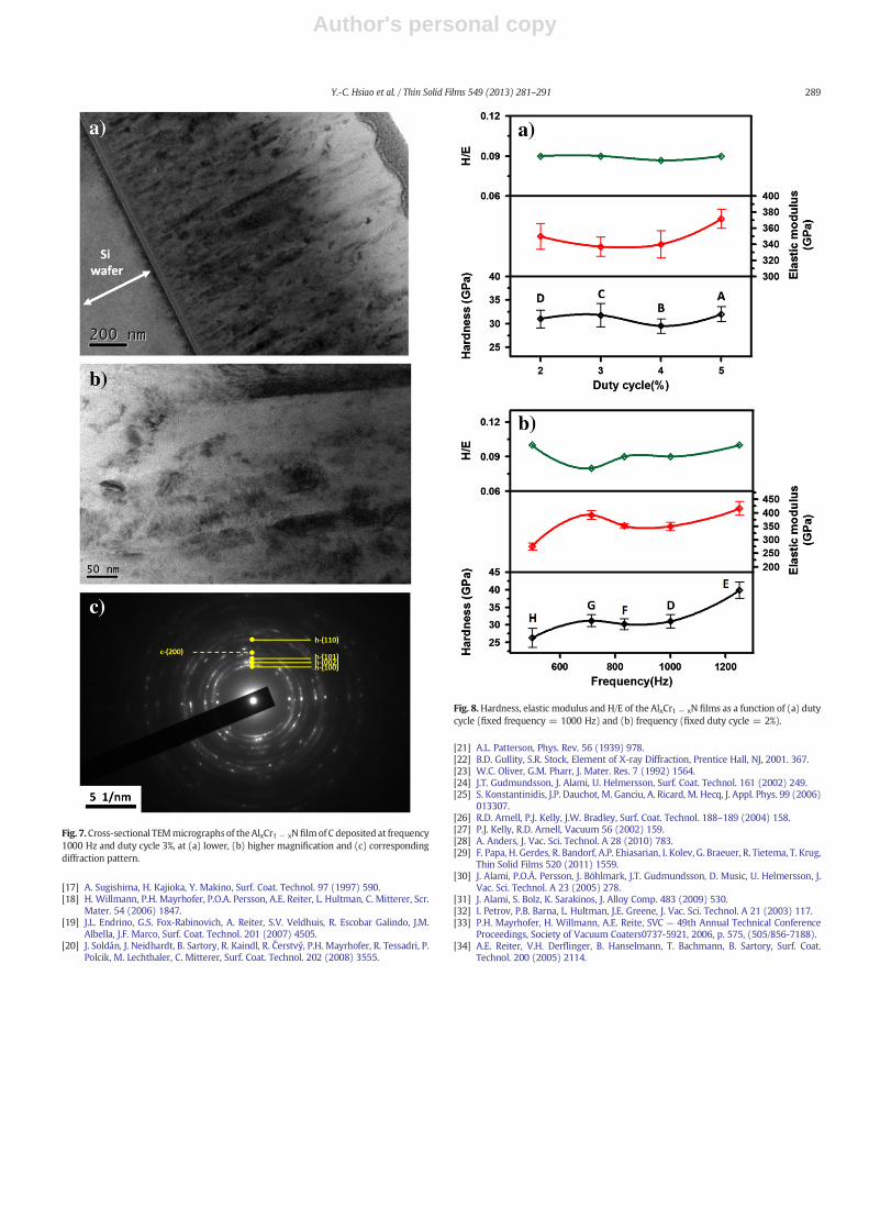
The microstructure of sample C was further studied by TEM. Fig. 7presents the cross-sectional TEM micrographs under low (a) and high(b)magnifications and the corresponding selected area electron diffrac-tion (c). Notably, Fig. 7b shows dense and fine columnar structureswithsome fine grains embedded within the columnar grains. The diffractionpattern in Fig. 7c also indicates that the film consists of both B1 and B4type AlxCr1 − xN phases. Alami et al. [4,5] discovered that the densifica-tion of CrNfilms fromdense columnar to featurelessmicrostructurewasobservedwhen thepeak target current increased. TheHPPMS fabricatedTiAlN coating also showed ananocrystalline structure, with densermor-phology and smoother surface compared to the dc-MS film [31]. A sim-ilar result is also clearly observed in this study. It is noticed that somefine grains embedded within the columnar grains indicating the re-nucleation of AlxCr1 − xN grains. The re-nucleation of HIPIMS fabricatedCrN columnar grains has been found to be caused by the increase of ionbombardment as the target peak current increased [5]. Ion irradiation
during sputtering has been suggested to interrupt the columnar graingrowth and induces surface defects to promote the re-nucleationphenomenon [32].
3.4. Mechanical properties of AlxCr1 − xN thin films
The hardness and elastic modulus of AlxCr1 − xN thin films are sum-marized in Table 3. The H/E ratio, used to describe resistance of mate-rials against elastic strain to failure, is also listed in Table 3. Fig. 8aillustrates the relationship of average hardness, elastic modulus, andH/E ratio to duty cycle for AlxCr1 − xN thin films of A to D, and Fig. 8billustrates the relationship of average hardness, elastic modulus, andE/H ratio to repetition frequency for samples D to H. In Fig. 8a, the hard-ness and the elastic modulus were in the range of 29.5–32.0 GPa and337–372 GPa, respectively, when the duty cycle increased from 2 to5% and the frequency was kept at the same 1000 Hz. The H/E ratio isthe same, 0.09, for all samples. On the other hand, an increasing tenden-cy can be found for the hardness as the repetition frequency increasedfrom 500 to 1250 Hz at the same duty cycle, 2%, as illustrated inFig. 8b. The maximum hardness and elastic modulus of 39.9 and417 GPa were achieved with repetition frequency of 1250 Hz andduty cycle of 2%, respectively. Based on the data listed in Table 3 andplotted in Fig. 8, the pulse repetition frequency has more effect on thehardness and elasticmodulus than pulse duty cycle. For thefilms depos-ited at 1000 Hz, the hardness of the films varied between 29.5 GPa and32.0 GPa randomly as the pulse duty cycle was altered. Nevertheless,the hardness of thin films increased obviously from 26.3 to 39.9 GPawith an increase in repetition frequency from 500 to 1250 Hz. The elas-tic modulus of thin films also increased from 275 GPa to 417 GPa. Thesolution hardening effect due to the incorporation of aluminum atomsin the fcc-AlxCr1 − xN lattice is no longer valid since all films exhibit sub-stantial amounts of hexagonal phases and all exceeds themaximumsol-ubility limit of AlN in c-AlxCr1 − xN phase, x N 0.71 [33]. Mayrhofer et al.[33] reported that the h-AlN has an ~1.26 times larger specific volumethan c-AlN [33]. It is argued that the compressive stress generatingfrom the larger amount of h-AlxCr1 − xN for thin film E with the maxi-mum x value, 0.75might have certain influences on its higher hardnessvalue. However, the exact reason for themaximumhardness of thinfilmE still needs further investigation.
The scratch test was adopted to evaluate the adhesion properties ofAlxCr1 − xN coatings and characterized by the critical load, LC, which isthe load at which the first delamination at the edge of the scratchtrack occurred (adhesion failure). Fig. 9 depicts the full-length scratchtracks of samples A to H. The average critical loads were also insertedfor each coating and listed in Table 3. In summary, all coatings exhibit
Table 3Summary of thin film composition, mechanical and tribological properties of AlxCr1 − xN coatings.
Film properties Sample #
Designation A B C D E F G H
Al (at.%) 35.5 34.4 34.9 34.1 36.0 35.1 34.8 34.7Cr (at.%) 14.0 12.0 12.6 12.0 12.1 12.9 12.9 13.1N (at.%) 49.8 52.6 51.4 52.9 50.3 51.2 52.0 52.0O (at.%) 0.7 1.0 1.0 1.0 1.6 0.9 0.4 0.3Al/Cr ratio 2.54 2.87 2.77 2.84 2.98 2.72 2.70 2.65x, Al/(Al + Cr) ratio 0.72 0.74 0.73 0.74 0.75 0.73 0.73 0.73y, N/(Al + Cr) ratio 1.01 1.14 1.08 1.15 1.05 1.07 1.09 1.09Lattice constant (nm) 0.412 0.406 0.408 0.408 0.406 0.409 0.409 0.409Grain size (nm) c-AlxCr1 − xN 8.6 6.6 6.0 5.0 5.6 5.5 6.7 8.9
h-AlxCr1 − xN 10.8 11.5 10.6 2.6 7.3 5.2 6.2 12.1Hardness (GPa) 32.0 29.5 31.8 31.0 39.9 30.2 31.2 26.3Elastic modulus (GPa) 372 340 337 350 417 352 392 275H/E 0.09 0.09 0.09 0.09 0.10 0.09 0.08 0.10Critical load (N) 44 61 90 62 75 79 47 34Coefficient of friction 0.56 0.54 0.51 0.57 0.54 0.56 0.60 0.53Wear rate(×10−6 mm3 N−1 m−1)
0.64 1.31 0.77 1.78 1.86 0.75 0.59 1.37
286 Y.-C. Hsiao et al. / Thin Solid Films 549 (2013) 281–291

Author's personal copy
good adhesion quality except sample H. For the C thin film, only sometiny chippings were found until the scratch load reaches 90 N and nodelamination of the coating inside the scratch track was observed, indi-cating that excellent adhesion quality was achieved. On the other hand,severe spallation of coating adjacent to the scratch trackwas found for Hcoating after the scratch load increased to 34 N. Of the critical loads forD to H coatings, which were fabricated under the same duty cycle of 2%,the critical load increased from 34 to 75 N as the repetition frequencyincreased from 500 to 1250 Hz. Meanwhile, the critical load increasedfrom 44 to 90 N but dropped to 62 N as the duty cycle decreased from5 to 2%.
Wear resistance of a thin film material plays an important role dur-ing application. Fig. 10 illustrates the coefficient of friction (COF) versuswear length for all thin films. The average COF of each coating is in therange of 0.51–0.6 and is listed in Table 3 along with the average wear
rate for each coating. It can be clearly seen that the wear rate changesin a small range from 0.59 to 1.86 × 10⁻⁶ mm3 N−1 m−1. Mo et al.[15] found that the better performance of AlCrN coating against wearand thermal effects was attributed to the tribo-chemical products con-taining chrome oxide and aluminum oxide during wear test. It is sug-gested that the good wear resistance achieved for each coating in thiswork is also attributed to these products. It is reported that themicrohardness of Cr1 − xAlxN films increased from 15 GPa (x = 0) to27 GPa (x = 0.6), and decreased to 23 GPa (x = 0.7), and then17 GPa (x = 1.0) [12]. The hardness and the tribological properties ofAlxCr1 − xN coatings have been reported to improve with increasingAl-content as long as the cubic structure is retained, and deterioratewhen the hexagonal structure forms at higher (x N 0.75) aluminumcontents [18,19]. Reiter et al. [34] studied the cathodic arc depositedcubic-B1 phase Cr1 − xAlxN and discovered out that the hardness wasoptimum at x = 0.7. The hardness value around 37.0 GPa was foundfor Al46Cr54N and Al71Cr29N coatings. In this work, the hardness in-creased with increasing pulse frequency at a constant duty cycle of 2%and reached an optimum hardness of 39.9 GPa at x = 0.75. The dutycycle and pulse frequency also show limited influence on thewear resis-tance of the B1 and B4 mixed dual phase AlxCr1 − xN thin films.
4. Conclusions
Eight AlxCr1 − xN coatings were fabricated using the high power im-pulse magnetron sputtering (HIPIMS) system with an AlCr alloy targetunder various pulse on/off time configurations. The duty cycle, i.e., thepulse on/off time configuration, showed great influence on the peakcurrent and peak power density. The peak power density increased lin-early as the duty cycle decreased from 5% to 2% at a constant frequencyof 1000 Hz. A maximum peak power density of 2.76 kW cm−2 wasachieved at a duty cycle of 2% and a repetition frequency of 833 Hz.The B1 cubic and B4 hexagonal dual phases were found in theAlxCr1 − xN phases at x = 0.72 to 0.75. The duty cycle and peakpower density had great influence on the microstructure evolutionand altered the microstructure from coarse columnar to fine columnarstructure. Re-nucleation grains were also found between columnargrains. The hardness increased to 39.9 GPa at x = 0.75 as the frequencyincreased to 1250 Hz at constant duty cycle of 2%. Good adhesion andwear resistance was observed for each coating. The critical loadincreased as the repetition frequency increased from 500 to 1250 Hzat the same duty cycle of 2%. Excellent wear resistance was obtainedfor each coating and was independent with the duty cycle and pulsefrequency.
Acknowledgment
The authors gratefully acknowledge the financial support of the Na-tional Science Council, Taiwan through contracts Nos. NSC 101-2622-E-131-001-CC2, NSC 100-2221-E-131-008-MY3, and NSC 100-2221-E-131-008-MY3 and the partial financial support from Solar AppliedMaterials Technology Corporation, Taiwan.
References
[1] V. Kouznetsov, K.Macak, J.M. Schneider, U. Helmersson, I. Petrov, Surf. Coat. Technol.122 (1999) 290.
[2] K. Sarakinos, J. Alami, S. Konstantinidis, Surf. Coat. Technol. 204 (2010) 1661.[3] K. Bobzin, N. Bagcivan, P. Immich, S. Bolz, R. Cremer, T. Leyendecker, Thin Solid Films
517 (2008) 1251.[4] J. Alami, K. Sarakinos, G. Mark, M. Wuttig, Appl. Phys. Lett. 89 (2006) 154104.[5] J. Alami, K. Sarakinos, F. Uslu, M. Wuttig, J. Phys. D: Appl. Phys. 42 (2009) 015304.[6] R. Machunze, A.P. Ehiasarian, F.D. Tichelaar, G.C.A.M. Janssen, Thin Solid Films 518
(2009) 1561.[7] S. Yang, X. Li, K.E. Cooke, D.G. Teer, Appl. Surf. Sci. 258 (2012) 2062.[8] Y.P. Purandare, A. Ehiasarian, P.Eh. Hovsepian, J. Vac. Sci. Technol. A 26 (2) (2008)
288.[9] P.Eh. Hovsepian, C. Reinhard, A.P. Ehiasarian, Surf. Coat. Technol. 201 (2006) 4105.
20 25 30 35 40 45 50 55 60 65 70 75 80 85 902θ (degree)
20 25 30 35 40 45 50 55 60 65 70 75 80 85 902θ (degree)
Inte
nsit
y (a
rb. u
nits
)
5% (A)
4% (B)
3% (C)
2% (D)
a) c -AlN (461200) h-AlN (651902)c -CrN (110065)(1
00)
(002
)
(200
)
(102
)
(110
)
(220
)(2
20)
(103
)
(112
)
(111
)(1
01)
(111
) (200
)
Inte
nsit
y (a
rb. u
nits
)
1000Hz (D)
833Hz (F)
714Hz (G)
500Hz (H)
1250Hz (E)
b) c -AlN (461200) h-AlN (651902)c -CrN (110065)
(100
)(0
02)
(200
)
(102
)
(110
)
(220
)(2
20)
(103
)
(112
)
(111
)(1
01)
(111
)
(200
)
Fig. 4. X-ray diffraction pattern of AlxCr1 − xN thin films at various (a) duty cycle (fixedfrequency 1000 Hz) and (b) repetition frequency (fixed duty cycle 2%).
287Y.-C. Hsiao et al. / Thin Solid Films 549 (2013) 281–291

Author's personal copy
[10] J. Paulitsch, M. Schenkel, A. Schintlmeister, H. Hutter, P.H. Mayrhofer, Thin SolidFilms 518 (2010) 5553.
[11] H. Willmann, M. Beckers, J. Birch, P.H. Mayrhofer, C. Mitterer, L. Hultman, Thin SolidFilms 517 (2008) 598.
[12] H. Hasegawa, M. Kawate, T. Suzuki, Surf. Coat. Technol. 200 (2005) 2409.
[13] M. Kawate, A. Kimura, T. Suzuki, J. Vac. Sci. Technol. A 20 (2002) 569.[14] W. Kalss, A. Reiter, V. Derflinger, C. Gey, J.L. Endrino, Int. J. Refract. Met. Hard Mater.
24 (2006) 399.[15] J.L. Mo, M.H. Zhu, B. Lei, Y.X. Leng, N. Huang, Wear 263 (2007) 1423.[16] Y. Makino, K. Nogi, Surf. Coat. Technol. 98 (1998) 1008.
Fig. 5. Cross-sectional SEM micrographs of the AlxCr1 − xN films deposited by HIPIMS.
Fig. 6. AFM surface morphologies of AlxCr1 − xN films deposited at different parameters.
288 Y.-C. Hsiao et al. / Thin Solid Films 549 (2013) 281–291
Author's personal copy
[17] A. Sugishima, H. Kajioka, Y. Makino, Surf. Coat. Technol. 97 (1997) 590.[18] H. Willmann, P.H. Mayrhofer, P.O.A. Persson, A.E. Reiter, L. Hultman, C. Mitterer, Scr.
Mater. 54 (2006) 1847.[19] J.L. Endrino, G.S. Fox-Rabinovich, A. Reiter, S.V. Veldhuis, R. Escobar Galindo, J.M.
Albella, J.F. Marco, Surf. Coat. Technol. 201 (2007) 4505.[20] J. Soldán, J. Neidhardt, B. Sartory, R. Kaindl, R. Čerstvý, P.H. Mayrhofer, R. Tessadri, P.
Polcik, M. Lechthaler, C. Mitterer, Surf. Coat. Technol. 202 (2008) 3555.
[21] A.L. Patterson, Phys. Rev. 56 (1939) 978.[22] B.D. Gullity, S.R. Stock, Element of X-ray Diffraction, Prentice Hall, NJ, 2001. 367.[23] W.C. Oliver, G.M. Pharr, J. Mater. Res. 7 (1992) 1564.[24] J.T. Gudmundsson, J. Alami, U. Helmersson, Surf. Coat. Technol. 161 (2002) 249.[25] S. Konstantinidis, J.P. Dauchot, M. Ganciu, A. Ricard, M. Hecq, J. Appl. Phys. 99 (2006)
013307.[26] R.D. Arnell, P.J. Kelly, J.W. Bradley, Surf. Coat. Technol. 188–189 (2004) 158.[27] P.J. Kelly, R.D. Arnell, Vacuum 56 (2002) 159.[28] A. Anders, J. Vac. Sci. Technol. A 28 (2010) 783.[29] F. Papa, H. Gerdes, R. Bandorf, A.P. Ehiasarian, I. Kolev, G. Braeuer, R. Tietema, T. Krug,
Thin Solid Films 520 (2011) 1559.[30] J. Alami, P.O.Å. Persson, J. Böhlmark, J.T. Gudmundsson, D. Music, U. Helmersson, J.
Vac. Sci. Technol. A 23 (2005) 278.[31] J. Alami, S. Bolz, K. Sarakinos, J. Alloy Comp. 483 (2009) 530.[32] I. Petrov, P.B. Barna, L. Hultman, J.E. Greene, J. Vac. Sci. Technol. A 21 (2003) 117.[33] P.H. Mayrhofer, H. Willmann, A.E. Reite, SVC — 49th Annual Technical Conference
Proceedings, Society of Vacuum Coaters0737-5921, 2006, p. 575, (505/856-7188).[34] A.E. Reiter, V.H. Derflinger, B. Hanselmann, T. Bachmann, B. Sartory, Surf. Coat.
Technol. 200 (2005) 2114.
Fig. 7.Cross-sectional TEMmicrographs of theAlxCr1 − xN filmof C deposited at frequency1000 Hz and duty cycle 3%, at (a) lower, (b) higher magnification and (c) correspondingdiffraction pattern.
Fig. 8.Hardness, elastic modulus and H/E of the AlxCr1 − xN films as a function of (a) dutycycle (fixed frequency = 1000 Hz) and (b) frequency (fixed duty cycle = 2%).
289Y.-C. Hsiao et al. / Thin Solid Films 549 (2013) 281–291

Author's personal copy
Fig. 9. The surface morphologies of scratch tracks of all AlxCr1 − xN films.
290 Y.-C. Hsiao et al. / Thin Solid Films 549 (2013) 281–291

Author's personal copy
Fig. 10. COF of the AlxCr1 − xN films as a function of (a) duty cycle (fixed frequency =1000 Hz) and (b) frequency (fixed duty cycle = 2%).
291Y.-C. Hsiao et al. / Thin Solid Films 549 (2013) 281–291