design, construction, and optimization of a magnetron sputtering
Upload
independentCategory
view
3download
0
Sp
ASa
b
c
a
ARRAA
KSZXNS
1
(isdacfttfim
aomGcf
0d
Applied Surface Science 257 (2011) 9909– 9914
Contents lists available at ScienceDirect
Applied Surface Science
j our nal ho me p age: www.elsev ier .com/ loc ate /apsusc
tudy of microstructure and nanomechanical properties of Zr films prepared byulsed magnetron sputtering
kash Singha, P. Kuppusamia,∗, R. Thirumurugesana, R. Ramaseshanb, M. Kamruddinb,. Dashb, V. Ganesanc, E. Mohandasa
Materials Synthesis and Structural Characterization Section, Physical Metallurgy Group, Indira Gandhi Centre for Atomic Research, Kalpakkam 603 102, IndiaSurface and Nano Science Division, Indira Gandhi Centre for Atomic Research, Kalpakkam 603 102, IndiaUGC-DAE Consortium for Scientific Research, Indore 452 017, India
r t i c l e i n f o
rticle history:eceived 4 February 2011eceived in revised form 21 June 2011ccepted 21 June 2011vailable online 29 June 2011
a b s t r a c t
The present work studies the effect of substrate temperature on the growth characteristics of zirconiumfilms prepared by pulsed magnetron sputtering. Formation of �-phase of zirconium was observed inthe temperature range 300–873 K. X-ray diffraction of Zr films revealed predominantly [0 0 1] texture.It is noticed that crystallite size increases with increasing substrate temperature. Hexagonal shapedcrystallites seem to grow along the surface normal of the substrate for the films deposited at 773 K.
eywords:putteringirconium-ray diffractionanohardnesscratch test
Nanoindentation measurements showed that the hardness of the films is in the range 6–10 GPa. Thescratch test indicated that the films deposited at higher substrate temperatures had excellent bondingwith the substrate and no significant critical failure was noticed up to an applied load of 20 N.
© 2011 Elsevier B.V. All rights reserved.
. Introduction
Zirconium (Zr) with hexagonal close packed crystal structure�-Zr) at room temperature is widely used in nuclear industry andn reprocessing plants owing to its low neutron absorption crossection and its exceptional resistance to corrosion [1]. In the pastecades, structural and mechanical properties of bulk zirconiumnd its alloys have been extensively studied [2–9]. Zirconiumoating has been suggested as a diffusion barrier between U-Mouel and aluminium cladding in order to maintain the integrity ofhe fuel plates and to prevent fuel plate swelling and possible rup-ure during reactor operation [10]. Also, polycrystalline zirconiumlms are used in thin multilayers for various applications such asetallic superlattice formation [11–13].Zirconium occurs in more than 30 recognized mineral species
nd its chemical compounds, such as oxides and phosphates areften used in refractory applications for their resistance to ther-al shock and for their extremely low thermal conductivity [14].
ood refractory properties of oxides and high hardness and electri-al conductivity of nitrides provide wide scope for these materialsor industrial applications [15–20]. Thin films of zirconium oxides∗ Corresponding author. Tel.: +91 442 748 0121; fax: +91 442 748 0306.E-mail address: [email protected] (P. Kuppusami).
169-4332/$ – see front matter © 2011 Elsevier B.V. All rights reserved.oi:10.1016/j.apsusc.2011.06.106
and nitrides can be prepared by the treatment of Zr coatings underoxidizing or nitriding atmospheres [21]. Basic knowledge of theinitial Zr film microstructure is of prime importance as it can influ-ence the reaction and the final product when it is deposited onsubstrates. The initial structure may be strongly dependent on theconditions used for the deposition process especially when usingnon-equilibrium growth mechanisms occurring with highly ener-getic ion bombardment in some of the glow discharge processes.At normal pressure and room temperature, zirconium exists in the�-phase, which exhibits hexagonal close packed structure. At nor-mal pressure and above 1135 K, a �-phase occurs (bcc structure).At room temperature and high pressure (above 2–8 GPa), a �-phasewith a hexagonal structure is reported [22]. Magnetron sputteringis one of the promising techniques for metal thin film depositionbecause of several advantages. The precise control of the grainsize in the nanocomposite films prepared by magnetron sputter-ing could be achieved by optimizing the process parameters suchas substrate temperature, bias voltage, discharge current, and par-tial pressure of reactive gas. With the recent advancement in powersupplies, pulsed dc magnetron sputtering process has become anattractive production deposition technology [23–25]. The tech-
nique is capable of reducing the arcing event, which results fromcharge accumulation on target surfaces. It consequently preventsthe deterioration of film properties and maintains a stable depo-sition process. The technique also provides higher ratios of the
9910 A. Singh et al. / Applied Surface Science 257 (2011) 9909– 9914
Table 1Chemical composition (wt.%) of titanium modified stainless steel (alloy D-9).
Mn
1.3
flto[hdwspentusfi
2
fiSwwiaosdzabassatowflptpffaso
TE
Element C Ni Cr Mo Ti Si
wt.% 0.05 14.9 14.7 2.2 0.18 0.65
uxes of bombarding ions and depositing atoms. It was reportedhat the formation of �-Zr is sometimes hindered by the growthf �-phase of zirconium films because of the compressive stresses21] or due to the nature of the substrate [26]. Chakraborty et al. [27]ave recently reported high in-plane compressive stress in Zr filmseposited by dc magnetron sputtering which is found to decreaseith increasing film thickness. In the present work, effect of sub-
trate temperature on the growth characteristics of zirconium filmsrepared by pulsed DC magnetron sputtering is investigated. Theffect of substrate temperature on the surface morphology andanomechanical properties is reported for the first time. Results onhe scratch test on these films are also presented since it is a widelysed method for investigating adhesion of the films with the sub-trates [28–30]. These data are necessary for the development of Zrlms from the application point of view.
. Experimental details
Zirconium target of 99.9% purity was used to deposit zirconiumlms in the range 1.2–1.5 �m thickness on to Si (1 1 1) substrates.ome of the films for measurement of nanomechanical propertiesere deposited on titanium modified stainless steel (D-9 alloy),hose composition is given in Table 1. Si was chosen because of
ts wide application in electronic industry, while D-9 alloy is useds a clad material in breeder reactors. The sputtering was carriedut in a custom built magnetron sputtering system which con-isted of a stainless steel chamber of 45 cm diameter and 20 cmeep using Mighty Mak US sputtering gun of 3 in. diameter [31]. Airconium disc of 76 mm diameter and 2 mm thickness was useds a sputtering target. The deposition chamber was evacuated to aase pressure of 8 × 10⁻⁴ Pa using a pumping system consisting of
rotary and turbo molecular pumps (Alcatel, France). Silicon sub-trates (size of 10 mm × 10 mm × 0.5 mm) were first cleaned usingoap solution and then ultrasonically cleaned in acetone for 15 minnd dried by blowing hot air before being placed in the deposi-ion chamber. Substrates of 10 mm diameter and 1 mm thicknessf D-9 alloy were prepared metallographically and fine polishedith a surface roughness of 0.5 �m and cleaned with acetone. Theow rate of Ar (99.99%) was set at 50 standard cubic centimeterer minute (sccm) using MKS make mass flow controller duringhe sputtering. RPG-50 asymmetric bipolar pulsed DC power sup-ly (MKS instruments, USA) was used as the electrical power sourceor the thin film deposition. The substrate temperature was variedrom 300 to 873 K using a halogen lamp (800 W, 6.3 A) heater with
digital programmable temperature controller. Preheating of theubstrate to a desired set temperature for about 0.5 h was carriedut. Pre-sputtering of Zr target was performed for 5 min before each
able 2xperimental parameters for deposition of Zr thin films.
Base pressure 8 × 10⁻⁴ PaOperating pressure 7.5 × 10⁻¹ PaSubstrate to target distance 60 mmTarget voltage 205–230 VSubstrate temperature 300–873 KPulse power 100 WDuty cycle 20%Pulse frequency 100 kHzArgon flow rate 50 sccm
S P Al B N Fe
<0.005 0.008 <0.0034 0.0015 <0.04 Bal
deposition. The deposition conditions and pulse parameters usedin the present investigations are given in Table 2.
The thickness of the films was measured using DEKTAK 6M-stylus profiler (Veeco, USA). The profilometer was used to measurethe step height, which represented the thickness of the depositedfilm. Structural properties of the as deposited Zr films were charac-terized by X-ray diffraction using an INEL XRG-3000 Diffractometerwith glancing angle of incidence (ω) of 5◦ using Cu K�1 radiation.The crystallite size was determined using the Scherrer’s formula:
D = k�
cos �√
B2 − b2
where � is wavelength of the X-rays used, k is the correction fac-tor, � is the diffraction angle, B is the full width at half maximum(FWHM) of film, and b is the FWHM of the instrumental broadening.The instrumental broadening was corrected using standard siliconpowder received from National Physical Laboratory, New Delhi.However, broadening due to strain was not considered. Texturecoefficients (TC) of (0 0 2) and (1 0 1) reflections were determinedfrom the intensities of Zr peaks. In general, the texture coefficient,TC for any reflection can be determined using the following relation[32]:
TC = {Im(h k l)/I0(h k l)}(1/n)˙{Im(h k l)/I0(h k l)}
where n, the number of peaks; Im, the measured peak intensitiesof reflections of Zr films; and I0, the respective peak intensitiescorresponding to the bulk Zr data from JCPDS File No. 05-0665.SUPRA 55 Carl Zeiss field emission scanning electron micro-scope (SEM) was used to analyze the surface morphology of thefilms. Surface morphology of the films was also examined in anatomic force microscope (Digital Instruments Inc., Nanoscope E,US) in contact mode. The microhardness measurements were car-ried out using Leitz micro hardness tester with 10 g load. Thenanohardness measurements were carried out by means of ananoindenter (CSM, Switzerland) equipped with a Berkovich dia-mond indenter tip at a load of 10 mN on the films in the rangeof 1.2–1.5 �m thickness deposited on titanium modified stainlesssteel (D-9) substrates. While measuring the nanomechanical prop-erties, indentation depth was kept less than 1/10th of the filmthickness in order to eliminate the substrate effect. Scratch testwas carried out using a scratch tester (CSM Revetest, Switzerland)on the coatings deposited on D-9 substrate with a load range of1–300 N. A sphero-conical diamond indenter of radius 200 �m withan included angle of 120◦ was used as the scratching body. An in-built acoustic emission (AE) sensor was used to capture the energyreleased during failure events like cracking and chipping. Scratchspeed was maintained at 3 mm/min for a constant length of 3 mmduring all the scratch tests and normal load was increased from 1 Nto 20 N along the fixed scratch length.
3. Results and discussion
3.1. Microstructure
Fig. 1 shows the XRD pattern of the films deposited on alloy D-9and Si substrates in the temperature range 300–873 K. The filmsare generally polycrystalline in nature and are crystalline even atroom temperature. Unit cell program has been used to calculate the

A. Singh et al. / Applied Surface Science 257 (2011) 9909– 9914 9911
20 30 40 50 60 70 80
(200
)
(111
)D
9
D9
(202
)(0
04)
(201
)(112
)(2
00)
(103
)
(110
)
(102
)
(101
)(0
02)
(100
)
INTE
NSI
TY(A
RB
. U)
TWO THETA (DEGREE)
300K
573K
673K773K
873K
80706050403020
(105
)
(202
)(0
04)(2
01)(112
)(2
00)
(103
)
(110
)
(102
)
(101
)(0
02)
(100
)
873K
773K
673K
573K
300K
IN
TEN
SITY
(AR
B. U
)
TWO THETA (DEGREE)
SiO
2
(a)
(b)
Fig. 1. Zr films deposited at various substrate temperatures by pulsed DC magnetronsputtering on (a) D-9 alloy and (b) Si (1 1 1) substrate.
300 400 50 0 600 70 0 80 0 90 00.0
0.5
1.0
1.5
2.0
2.5
3.0
3.5
Text
ure
Coe
ffici
ent
Substrate Temperature (K)
(00 2) (10 1)
300 400 50 0 600 700 800 9000.300
0.305
0.310
0.315
0.320
0.325
0.330
0.335
0.340
0.345
0.350 a c
Temperature (K)
a(nm
)
0.500
0.505
0.510
0.515
0.520
0.525
0.530
0.535
0.540
0.545
0.550
c(nm)
(a)
Fig. 2. (a) Lattice parameter and (b) crystallite size of Zr films as a func
Fig. 3. Texture coefficient for (0 0 2) and (1 0 1) reflections of the Zr films on D-9alloy substrate as a function of substrate temperature.
lattice constant of the films and all the peaks have been consideredfor the determination of lattice parameter. The lattice parame-ters, a and c were found to be in the range 0.3238–0.3253 nm and0.5157–0.521 nm, respectively in the temperature range 300–873 K(Fig. 2(a)). Though the variation in a lattice parameter is sig-nificantly small (<1%), the c lattice parameter increases slightlyresulting in the overall increase in the unit cell volume expansionwith substrate temperatures ≥673 K. The average lattice parame-ters of the films were always higher than the bulk lattice parameters(a = 0.3232 nm, c = 0.5147 nm and c/a = 1.592) reported in JCPDS fileno. 05-0665, indicating the presence of compressive stress in thefilms.
Crystallite size has been calculated using (1 0 1) and (0 0 2)reflections, since these are the dominant peaks in the diffractionpattern and the variation in the crystallite size corresponding toboth the reflections is shown in Fig. 2(b). It is clear that the crys-tallite size of the films determined using Scherrer’s equation showa similar trend for both (1 0 1) and (0 0 2) reflections. For instance,the crystallite size of Zr deposited on D-9 alloy substrate corre-sponding to (1 0 1) reflection increases from ∼14 nm to 44 nm with
the increase of substrate temperature up to 773 K and there is adecrease in the crystallite size at 873 K. The crystallite size calcu-lated for films deposited on Si and D-9 alloy substrates also showed90080070060050040030010
15
20
25
30
35
40
45
50
Cry
stal
lite
Size
(nm
)
Temperature (K)
(002) (101)(b)
tion of substrate temperature deposited on D-9 alloy substrate.
9912 A. Singh et al. / Applied Surface Science 257 (2011) 9909– 9914
subst
amipadstthHlfitc
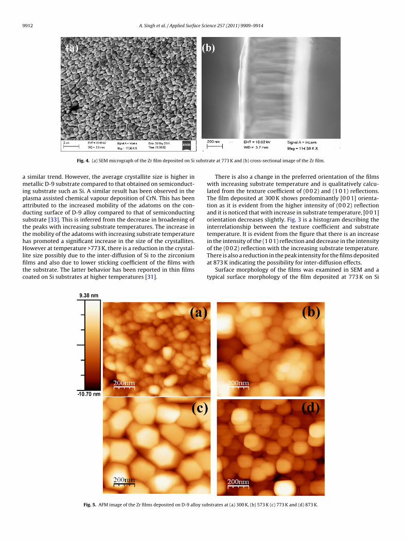
Fig. 4. (a) SEM micrograph of the Zr film deposited on Si
similar trend. However, the average crystallite size is higher inetallic D-9 substrate compared to that obtained on semiconduct-
ng substrate such as Si. A similar result has been observed in thelasma assisted chemical vapour deposition of CrN. This has beenttributed to the increased mobility of the adatoms on the con-ucting surface of D-9 alloy compared to that of semiconductingubstrate [33]. This is inferred from the decrease in broadening ofhe peaks with increasing substrate temperatures. The increase inhe mobility of the adatoms with increasing substrate temperatureas promoted a significant increase in the size of the crystallites.owever at temperature >773 K, there is a reduction in the crystal-
ite size possibly due to the inter-diffusion of Si to the zirconiumlms and also due to lower sticking coefficient of the films withhe substrate. The latter behavior has been reported in thin filmsoated on Si substrates at higher temperatures [31].
Fig. 5. AFM image of the Zr films deposited on D-9 alloy sub
rate at 773 K and (b) cross-sectional image of the Zr film.
There is also a change in the preferred orientation of the filmswith increasing substrate temperature and is qualitatively calcu-lated from the texture coefficient of (0 0 2) and (1 0 1) reflections.The film deposited at 300 K shows predominantly [0 0 1] orienta-tion as it is evident from the higher intensity of (0 0 2) reflectionand it is noticed that with increase in substrate temperature, [0 0 1]orientation decreases slightly. Fig. 3 is a histogram describing theinterrelationship between the texture coefficient and substratetemperature. It is evident from the figure that there is an increasein the intensity of the (1 0 1) reflection and decrease in the intensityof the (0 0 2) reflection with the increasing substrate temperature.
There is also a reduction in the peak intensity for the films depositedat 873 K indicating the possibility for inter-diffusion effects.Surface morphology of the films was examined in SEM and atypical surface morphology of the film deposited at 773 K on Si
strates at (a) 300 K, (b) 573 K (c) 773 K and (d) 873 K.

A. Singh et al. / Applied Surface Sci
Fig. 6. Scratch test of Zr films deposited on D-9 alloy substrate at (a) 300 K and (b)7t
suficpaptiitoctamt
adhesion of the coating with the substrate. Also, the coefficient of
73 K showing acoustic signal and friction coefficient versus load. SEM images ofhe film surface after scratch testing are also shown.
ubstrate (Fig. 4(a)) indicated that the film has a uniform gran-lar structure. Cross-sectional image shown in Fig. 4(b) for thelm deposited at 773 K, revealed a uniform film thickness and aolumnar structure. Such columnar structures are reported to beromoted when Ts/Tm ≤ 0. 3 [34], where Ts is the substrate temper-ture (773 K) and Tm is the melting point of the material (meltingoint of Zr ∼2123 K). Metallic films such as Ti deposited underhe condition of limited atomic mobility also has exhibited a sim-lar columnar morphology [35]. AFM images (Fig. 5) showed anncreased crystallite size with increasing substrate temperature inhe range 300–773 K. There is a clear change in the morphologyf the crystallites as a function of the substrate temperature. Therystallites are small and the film is porous at temperatures lesshan 773 K, while the films contain hexagonal shaped crystallites
t 773 K. These crystallites appear to grow along the surface nor-al of the substrate surface (c-axis oriented) in accordance with theexture analysis. However, dense and spherically shaped smaller Zr
ence 257 (2011) 9909– 9914 9913
crystallites are seen at 873 K. The root mean square (RMS) rough-ness of the films as a function of the substrate temperature was alsomeasured by AFM. The RMS roughness is found to decrease from∼20 nm to ∼4 nm for the increase in the substrate temperature from300 K to 773 K because of the densification of the films with increas-ing temperature. These results clearly indicate that the film growthis dominated by nucleation at low substrate temperature (<773 K)and particle coarsening at 773 K in agreement with the metallicalloy film grown by magnetron sputtering [36]. The study revealedthat the substrate temperature of 773 K could produce well grownhexagonal crystallites of Zr. Both XRD and AFM studies suggest thatunlike refractory oxides, the metallic films could be prepared evenat room temperature because of low crystallization temperature[37].
3.2. Nanomechanical properties
Hardness was determined by microhardness and nanoinden-tation hardness testers on Zr films of thickness >1 �m depositedon D-9 alloy. The D-9 alloy was chosen in the annealed condi-tion (∼220VHN) in order to assess the hardness of the film. Thismaterial is softer than Si (1 1 1) and is used as a clad material forbreeder reactors. The microhardness measurements were carriedout for the films deposited as a function of substrate tempera-ture using a load of 10 g and the composite hardness was in therange 600–800 VHN. Nanoindentation measurements were alsocarried out to estimate the hardness of the film. The applied load fornanoindentor was selected such that the indentation depths werein the range from 100 to 150 nm in order to avoid the contributionfrom the substrate. For measuring hardness and modulus using thenanoindentation method with a Berkovich indenter, indentationload, P, with displacement, h, was continuously recorded during onecomplete cycle of loading and unloading [38]. Both the microhard-ness and nanohardness showed a decrease in the hardness for thefilms with increasing substrate temperature from 300 K to 773 K.For instance, the hardness of the Zr films was found to 6.4 and10.5 GPa for the films deposited at 773 K and 573 K, respectively.The decreased hardness for the films could be correlated with thestress relaxation in larger crystallites formed at higher growth tem-peratures. Also, the hardness is known to depend on the crystallitesize according to Hall–Petch relation and it generally increases withdecrease in crystallite or grain size [39].
Scratch test was carried out to determine the films adhesionwith the substrate and the film failure, if any. This was furtherassessed by optical microscopy and scanning electron microscopyduring and after the scratch test. The tangential force and acousticemission signals were measured and recorded during the scratchtest process and used as a supplementary test to identify differentfilm damage levels. Scratch tests were carried out with increasingload to determine the critical scratch load and friction coefficientfor a given damage level. Scratch test indicates that chipping andflaking of the films has been found to depend on the substrate tem-perature during film deposition. From the acoustic emission signals,the films deposited at room temperature show failures at first andsecond critical loads of about ∼2 N and 7 N, respectively (Fig. 6),while they do not fail up to a load of 20 N for the films deposited inthe temperature range 573–773 K. SEM images of the scratch testedregions of the films deposited at 773 K indicate a few debris fromthe scratched region at loads exceeding 15 N only. The better per-formance of the coatings prepared at higher temperature could berelated to the increased thermal diffusion of the substrate elementswith increasing substrate temperature. This could possibly help for
friction (COF) of the films remains at about 0.2. However, it rises tohigher value (0.3), whenever there is a failure of the films. This isevident from Fig. 6(a) in the load range 9–14 N. In contrast, the COF
9 ce Sci
vtaio
cctfice
4
efTtt
trstd
A
pVMp
R
[[[
[[
[
[[
[
[
[
[
[[[
[
[
[
[[[[
[
[
[[
[
914 A. Singh et al. / Applied Surfa
alues of the film deposited at 773 K remain at a uniform value inhe entire range of the load during scratch indicating an excellentdhesion with the substrate. However, there is a minor differencen the estimated values of COF of the films deposited at RT and 773 Kwing to the difference in the microstructure.
The present study has illustrated that magnetron sputteringould be used for the development of Zr films on metallic and semi-onducting substrate of desired mechanical properties. Besideshese properties, measurements of corrosion properties of suchlms will be necessary in order to put them in use in the repro-essing of the nuclear fuels and latter properties will be reportedlsewhere.
. Conclusions
Formation of �-phase of zirconium with [0 0 1] preferred ori-ntation was noticed in the temperature range 300–873 K. It wasound that crystallite size increases with increasing temperature.he increase in mobility of the adatoms with increasing substrateemperature has caused an increase in the size of the crystallites atemperatures ≤773 K.
Nanoindentation and microhardness measurements showedhat the hardness of the films is in the range 6–10 GPa. Scratch testesults indicated that the films have better adhesion at higher sub-trate temperature. The load for the first critical failure is 20 N forhe films deposited at 773 K compared to that of 7 N for the filmeposited at room temperature.
cknowledgements
The authors are thankful to Smt. M. Jyothi for substratereparation and XRD analysis. They are also grateful to Dr. M.ijayalakshmi, AD, PMG, Dr. T. Jayakumar, Director, Metallurgy andaterials Group and Shri. S.C. Chetal, Director, IGCAR for the sup-
ort and encouragement.
eferences
[1] H.O. Pierson, Handbook of Refractory Carbides and Nitrides, Noyes Publications,New Jersey, USA, 1996, pp. 181–205.
[2] P. Gaunt, J.W. Christian, Acta Metall. 7 (1959) 534.[3] E.J. Rapperport, Acta Metall. 7 (1959) 254.[4] L. Kaufman, Acta Metall. 7 (1959) 575.
[
[[
ence 257 (2011) 9909– 9914
[5] E.S. Fisher, C.J. Renken, Phys. Rev. 135 (2A) (1964) A482.[6] D.O. Northwood, I.M. London, L.E. Bahen, J. Nucl. Mater. 55 (1975) 299.[7] E. Tenckhoff, Deformation Mechanism, Texture and Anisotropy in Zirconium
and Zircalloys, ASTM, Philadelphia, PA, 1988, p 55.[8] R.A. Lebensohn, C.N. Tome, Acta Metall. Mater. 41 (1993) 2611.[9] G.C. Kaschner, G.T. Gray III, Metall. Mater. Trans., A 31 (2000) 1997.10] K.J. Hollis, Adv. Mater. Process. (November–December) (2010) 57–59.11] A. Baudry, P. Boyer, M. Brunel, J. Magn. Mater. 185 (1998) 309.12] D.J. Li, M.X. Wang, J.J. Zhang, Mater. Sci. Eng. A 423 (2006)
116–120.13] L. Smardz, J. Alloys Compd. 395 (2005) 17.14] Y. Zhao, J. Zhang, C. Pantea, J. Qian, L.L. Daemen, Phys. Rev. B 71 (2005)
184119.15] S. Ramanathan, C.-M. Park, P.C. McIntyre, J. Appl. Phys. 91 (2002)
4521.16] S. Niyomsoan, W. Grant, D.L. Olson, B. Mishra, Thin Solid Films 415 (2002) 187.17] S. Miyazaki, M. Narasaki, M. Ogasawara, M. Hirose, Solid State Electron. 46
(2002) 1679.18] N.L. Zhang, Z.T. Song, Q. Wan, Q.W. Shen, C.L. Lin, Appl. Surf. Sci. 202 (2002)
126.19] H.M. Benia, M. Guemmaz, G. Schmerber, A. Mosser, J.-C. Parlebas, Appl. Surf.
Sci. 200 (2002) 231.20] L.Q. Shi, G.Q. Yan, J.Y. Zhou, S.Z. Luo, S.M. Peng, W. Ding, X.G. Long, J. Vac. Sci.
Technol. A 20 (2002) 1840.21] L. Pichon, T. Girardeau, F. Lignou, A. Straboni, Thin Solid Films 342 (1999)
93–99.22] S.K. Sikka, Y.K. Vohra, R. Chidambaram, Prog. Mater. Sci. 27 (1982) 245.23] R.D. Arnell, P.J. Kelly, J.W. Bradley, Surf. Coat. Technol. 188 (2004) 158.24] Johan Bohlmark, Chris Christou, P. Arutiun, Ehiasarian, Ulf Helmersson, Jones
Alami, J. Vac. Sci. Technol. A 23 (2005) 18.25] W. Somkhunthot, T. Burinprakhon, I. Thomas, T. Seetawan, V. Amornkitbam-
rung, Elektrika 9 (2007) 20.26] D. Pilloud, J.F. Pierson, C. Rousselot, F. Palmino, Scripta Mater. 53 (2005)
1031–1036.27] J. Chakraborty, K. Kishor Kumar, S. Mukherjee, S.K. Ray, Thin Solid Films 516
(2008) 8479–8486.28] M.T. Laugier, Thin Solid Films 76 (1981) 289.29] M.T. Laugier, Thin Solid Films 117 (1984) 243.30] J. Smolik, K. Zdunek, B. Larisch, Vacuum 55 (1999) 45.31] T. Elangovan, P. Kuppusami, R. Thirumurugesan, V. Ganesan, E. Mohandas,
D. Mangalaraj, Mater. Sci. Eng. B 167 (2010) 17–25.32] H. Ohsaki, Y. Tachibana, J. Shimizu, T. Oyama, Thin Solid Films 281/282 (1996)
213.33] Arup Dasgupta, P. Kuppusami, V.S. Falix Lawrence, P. Raghunathan, Premkumar
S Antony, K.S. Nagaraja, Mater. Sci. Eng. A 374 (1–2) (2004) 362–368.34] J.A. Thornton, Ann. Rev. Mater. Sci. 7 (1977) 239.35] Arup Dasgupta, Akash Singh, Pradyumna Kumar Parida, P. Kuppusami, S. Saroja,
M. Vijayalakshmi, Bull. Mater. Sci., in press, doi:10.1007/s12034-011-0118-0.36] C. Padmaprabhu, P. Kuppusami, A. Singh, E. Mohandas, V.S. Raghunathan,
Scripta Mater. 44 (2001) 1837–1840.
37] G. Balakrishnan, P. Kuppusami, S. Tripura Sundari, R. Thirumurugesan,V. Ganesan, E. Mohandas, D. Sastikumar, Thin Solid Films 518 (2010)3898–3902.
38] J.L. Loubet, J.M. Georges, O. Marchesini, G. Meille, ASME J. Tribol. 106 (1984) 43.39] S.E. Hsu, G.R. Edwards, J.C. Shyne, O.D. Sherby, J. Mater. Sci. 12 (1977) 131.
Copyright © 2022 FDOKUMEN