Origin of damages in OLED from Al top electrode deposition by DC magnetron sputtering
10
Origin of damages in OLED from Al top electrode deposition by DC magnetron sputtering Tae Hyun Gil a, * , Christian May a , Sebastian Scholz b , Sebastian Franke a , Michael Toerker a , Hubert Lakner a , Karl Leo a , Stefan Keller c a Fraunhofer Institut für Photonische Mikrosysteme, Maria-Reiche Strasse 2, 01109 Dresden, Germany b Institut für Angewandte Photophysik, Technische Universität Dresden, 01062 Dresden, Germany c Applied Materials GmbH, Siemens Strasse 100, 63755 Alzenau, Germany article info Article history: Received 14 September 2009 Received in revised form 4 November 2009 Accepted 5 November 2009 Available online 14 November 2009 Keywords: Organic light emitting diode Sputter damage DC magnetron sputtering Ellipsometry LDI-TOF-MS SEM/EDX abstract In this study, we examine organic light emitting diodes (OLEDs) having Al top electrodes deposited on organic layers by direct-current magnetron sputtering. The OLEDs consisted of electronically doped transport layers and phosphorescent emission layer were charac- terized by typical current–voltage–luminance measurement. They showed higher leakage currents, decreased forward currents, and corresponding increases of driving voltage after the sputter deposition on the organic layers. The OLEDs exhibited randomly distributed bright spots on the active area, and the bright spots were investigated by scanning electron microscopy/energy-dispersive X-ray spectroscopy. In order to prove the origins of sputter damage, simple organic/Al layer samples were made and investigated by ellipsometry and laser-induced desorption/ionization time-of-flight mass spectrometry. The results are compared with previous works addressing the fundamental phenomena of magnetron sputtering. We conclude that the high leakage current originated from a penetration of sputtered metal atoms into the underlying organic layers, and the decrease of forward cur- rent resulted from an interface degradation caused by the radiation of plasma, which reduces charge carrier injection preferentially at the Al/organic layer interface. Ó 2009 Elsevier B.V. All rights reserved. 1. Introduction Organic light emitting diodes (OLED) are excellent opto- electronic devices for various applications like display and general lighting due to their self-emissive characteristics, natural color expression, and comparably simple device structure. Since a multilayered organic electrolumines- cence device was reported [1] , its efficiency has been tremendously improved by introducing highly efficient and functional organic materials and stack optimization [2–5]. Fabrication technologies as well as organic materials also achieved great progress on large area substrates, although high deposition rate and stability of top electrode deposition are still a challenge. The top electrodes, e.g. Al or Ag, are evaporated at two or threefold higher tempera- ture than organic materials. For this purpose, metal boats made of Ta or W are generally used to heat the electrode materials. However, such metal boats are supplied with a high power in order to exceed the vaporizing temperature of the electrode metals, which causes a gradual degrada- tion of the boat materials. In particular, molten Al can eas- ily wet the boat surface, resulting in a serious damage due to an extremely high current. In OLED mass production, this problem is still a critical issue in the metal electrode deposition, because it leads to a shorter equipment uptime. Due to those problems, the development of an alternative deposition method has been strongly urged by the OLED industry, especially for large area OLEDs. Magnetron sput- tering method is still the best candidate for the metal 1566-1199/$ - see front matter Ó 2009 Elsevier B.V. All rights reserved. doi:10.1016/j.orgel.2009.11.011 * Corresponding author. Tel.: +49 351 8823 235; fax: +49 351 8823 266. E-mail address: [email protected] (T.H. Gil). Organic Electronics 11 (2010) 322–331 Contents lists available at ScienceDirect Organic Electronics journal homepage: www.elsevier.com/locate/orgel
-
Upload
tu-dresden -
Category
Documents
-
view
0 -
download
0
Transcript of Origin of damages in OLED from Al top electrode deposition by DC magnetron sputtering

Organic Electronics 11 (2010) 322–331
Contents lists available at ScienceDirect
Organic Electronics
journal homepage: www.elsevier .com/locate /orgel
Origin of damages in OLED from Al top electrode depositionby DC magnetron sputtering
Tae Hyun Gil a,*, Christian May a, Sebastian Scholz b, Sebastian Franke a, Michael Toerker a,Hubert Lakner a, Karl Leo a, Stefan Keller c
a Fraunhofer Institut für Photonische Mikrosysteme, Maria-Reiche Strasse 2, 01109 Dresden, Germanyb Institut für Angewandte Photophysik, Technische Universität Dresden, 01062 Dresden, Germanyc Applied Materials GmbH, Siemens Strasse 100, 63755 Alzenau, Germany
a r t i c l e i n f o
Article history:Received 14 September 2009Received in revised form 4 November 2009Accepted 5 November 2009Available online 14 November 2009
Keywords:Organic light emitting diodeSputter damageDC magnetron sputteringEllipsometryLDI-TOF-MSSEM/EDX
1566-1199/$ - see front matter � 2009 Elsevier B.Vdoi:10.1016/j.orgel.2009.11.011
* Corresponding author. Tel.: +49 351 8823 235; faE-mail address: [email protected]
a b s t r a c t
In this study, we examine organic light emitting diodes (OLEDs) having Al top electrodesdeposited on organic layers by direct-current magnetron sputtering. The OLEDs consistedof electronically doped transport layers and phosphorescent emission layer were charac-terized by typical current–voltage–luminance measurement. They showed higher leakagecurrents, decreased forward currents, and corresponding increases of driving voltage afterthe sputter deposition on the organic layers. The OLEDs exhibited randomly distributedbright spots on the active area, and the bright spots were investigated by scanning electronmicroscopy/energy-dispersive X-ray spectroscopy. In order to prove the origins of sputterdamage, simple organic/Al layer samples were made and investigated by ellipsometry andlaser-induced desorption/ionization time-of-flight mass spectrometry. The results arecompared with previous works addressing the fundamental phenomena of magnetronsputtering. We conclude that the high leakage current originated from a penetration ofsputtered metal atoms into the underlying organic layers, and the decrease of forward cur-rent resulted from an interface degradation caused by the radiation of plasma, whichreduces charge carrier injection preferentially at the Al/organic layer interface.
� 2009 Elsevier B.V. All rights reserved.
1. Introduction deposition are still a challenge. The top electrodes, e.g. Al
Organic light emitting diodes (OLED) are excellent opto-electronic devices for various applications like display andgeneral lighting due to their self-emissive characteristics,natural color expression, and comparably simple devicestructure. Since a multilayered organic electrolumines-cence device was reported [1] , its efficiency has beentremendously improved by introducing highly efficientand functional organic materials and stack optimization[2–5]. Fabrication technologies as well as organic materialsalso achieved great progress on large area substrates,although high deposition rate and stability of top electrode
. All rights reserved.
x: +49 351 8823 266.(T.H. Gil).
or Ag, are evaporated at two or threefold higher tempera-ture than organic materials. For this purpose, metal boatsmade of Ta or W are generally used to heat the electrodematerials. However, such metal boats are supplied with ahigh power in order to exceed the vaporizing temperatureof the electrode metals, which causes a gradual degrada-tion of the boat materials. In particular, molten Al can eas-ily wet the boat surface, resulting in a serious damage dueto an extremely high current. In OLED mass production,this problem is still a critical issue in the metal electrodedeposition, because it leads to a shorter equipment uptime.Due to those problems, the development of an alternativedeposition method has been strongly urged by the OLEDindustry, especially for large area OLEDs. Magnetron sput-tering method is still the best candidate for the metal

T.H. Gil et al. / Organic Electronics 11 (2010) 322–331 323
deposition. Much works were done in order to apply mag-netron sputtering for the top electrode deposition on or-ganic layers [6–8], but serious damages in device werereported unfortunately. However, a positive result was alsoreported by Guenther et al. that only a slight voltage in-crease of less than 1 V was observed in case of sputteredIndium–Tin–Oxide (ITO) top electrode with a device opti-mization, keeping the efficiencies and the lifetime similaras for a device having a evaporated metal top electrode [9].
The first part of this study is therefore devoted to exam-ine the OLEDs fabricated with Al cathodes by direct-cur-rent (DC) magnetron sputtering and to identify theorigins of damage, especially leakage currents. In the Alsputter depositions, only the Ar flow rate was varied to al-ter the process pressure, which affects sputter depositionsignificantly. Since the process pressure plays a decisiverole in changing kinetic energy of atomic particles by colli-sions with background Ar gases, a corresponding variationin damages of OLEDs can be expected. The fabricatedOLEDs were characterized by current–voltage–luminance(I–V–L) measurements. The results are discussed on the ba-sis of the fundamental phenomena of magnetron sputter-ing, and a possible damage source responsible for thehigh leakage current is inferred from it. Simple structureswere made in order to prove a change of the electronic le-vel structure in an organic layer after Al cathode depositionby sputtering. Each sample consisted of a single organicand Al layer deposited with the same process parametersas for the OLED fabrications. The samples were examinedby ellipsometry which allows an easy access to opticalconstants of the materials. We employed laser desorp-tion/ionization time-of-flight mass spectrometry (LDI–TOF–MS), which is a useful tool to detect chemical mix-tures via their mass-to-charge ratio, in order to identifymaterials responsible for the high leakage current [10].
In the second part, radiation effects from plasma on themetal/organic interface are examined. If a substrate is im-mersed into the plasma, the surface of the substrate expe-riences impingement of radiative particles includingelectrons, ions and photons. The former two particles haveenergy corresponding to plasma potential, but the latterphotons range from ultra-violet (UV) to infrared. In partic-ular, the high-energy photons (hv > 10 eV) generated fromthe energy transition of excited or ionized atoms have beenexamined in various plasma-associated processes becausethe photon radiation is quite intensive in glow dischargeplasma and affects a device performance significantly.While radiation-induced material damages have been
Table 1Sample descriptions for experiments.
Sample Stack
Reference Glass/ITO/NHT5:NDP2(190 nm)/a-NPD(10 nm)/a-NPD:Ir(MDQNET5:NDN1(40 nm)/evaporated Al(100 nm)
A/B/C Glass/ITO/NHT5:NDP2(190 nm)/a-NPD(10 nm)/a-NPD:Ir(MDQNET5:NDN1(40 nm)/Al(100 nm)
D Glass/NET5(100 nm)/evaporated Al(100 nm)E/F/G Glass/NET5(100 nm)/Al(100 nm)H/I Stainless plate/BPhen(20 nm)/Al(10 nm)
studied widely in semiconductor devices, e.g. metal–oxide-semiconductor devices and bipolar transistors, or asurface modification engineering of polymers using plasma[11–13] , such effects have been rarely discussed in OLEDfield. During magnetron sputtering, those particles are alsogenerated from the bulk plasma and the surface of sputtercathode considerably. Therefore, we will examine resultinginfluences from the plasma radiation on OLED characteris-tic by considering an radiation energy, which the underly-ing organic layer suffers differently according to thevariation of sputter process parameters.
2. Experimental preparation
The samples listed in Table 1, except for the referenceOLED, were fabricated in VES400 vertical In-line OLEDdeposition system (Applied Materials, GmbH & Co. KG)[14,15] . The VES400 consists of several vacuum chambersas shown in Fig. 1, and all the organic materials are ther-mally evaporated in linear type sources.
The stacks of the samples are listed in Table 1. Sub-strates used for OLED fabrications were cleaned with iso-propanol, acetone and deionised water ultrasonically.Afterwards they were heated at 120 �C for outgassing.The substrate loading to a transport carrier was carriedout in the nitrogen ambient glove box 1, and the carriermoved from glove box 1 into the loadlock chamber. Thedeposition processes were performed at high vacuum of10�7 mbar range by passing all the process chambers. Inthe substrates, indium tin oxide (ITO) was predepositedon glass as a transparent anode material. For all the OLEDsincluding the reference OLED and the OLEDs from A to C,doped transport layers (Novaled AG.) were employed toachieve low driving voltage and high carrier transport.These organic layers, NHT5:NDP2 and NET5:NDN1, haveelectrical conductivity above 10�5 S/cm which are electri-cally approximately equivalent to MeO—TPD : F4�TCNQand BPhen:Li, respectively [4] . The emission layer con-sisted of 4,4-bis [N-(1-naphtyl)-N-phenyl-amino] biphenyl(a-NPD) and Iridium(III)bis(2-methyldibenzo-[f,h] quinox-aline)(acetylacetonate) (Ir(MDQ)2(acac)) as a host and or-ange–red phosphorescent dye dopant, respectively. Thisemitting system allows an effective energy transfer fromthe host to the guest dopant because the HOMO/LUMOpositions of a-NPD and the triplet energy state of Ir(MD-Q)2(acac) are quite well matched. Hence an effective en-ergy transfer of the singlet and triplet excitons from the
Sputter processparameter
)2(acac)(20 nm)/NET5(10 nm)/ �
)2(acac)(20 nm)/NET5(10 nm)/ 1 (A), 2 (B), 3 (C)
�1 (E), 2 (F), 3 (G)1 (H), 3 (I)

Fig. 1. Schematic illustration of In-line machine implemented for the experiments.
324 T.H. Gil et al. / Organic Electronics 11 (2010) 322–331
host to the phosphorescent dye dopant is accomplished[16].
The reference OLED was fabricated in a cluster equip-ment with same organic stack in order to deposit Al cath-ode by thermal evaporation. The Al cathodes of the sampleA/B/C are deposited in the sputter chamber after deposi-tions of organic layers. The sputter chamber equipped withtwo conventional magnetron sputtering cathodes is alsolocated in the middle of the In-line machine so that Alcathodes were subsequently deposited on organic layerswithout vacuum break. The process parameters for Al sput-tering are listed in Table 2. As indicated, three different Arflow rates (100, 300 and 500 sccm) were selected with anequal DC power 500 W. After all the film depositions, thesubstrates were encapsulated in a nitrogen-filled glovebox with glass including getter inside to protect the OLEDsfrom oxygen and water vapors. I–V–L characteristic of thefabricated OLEDs was measured by DMS 101 (AutronicMelchers, GmbH). The samples from D to H were madeon different substrates prepared with the same prepara-tion sequence for ITO substrates. The samples for ellipsom-etry and LDI–TOF–MS measurements were put into anitrogen-filled carrier with O-ring seal directly after filmdeposition in order to prevent them from ambient beforethe measurements.
The basic setup of ellipsometry is depicted in Fig. 2. Themeasurements were performed twice on both sample
Table 2Process parameters for Al sputter depositions and corresponding depositionrates.
Processparameter
DC power(W)
Ar flowrate (sccm)
Pressure(mbar)
Deposition rate(nm/speed.oscillation)
1 500 100 0.001 24.862 500 300 0.003 18.703 500 500 0.005 14.75
Fig. 2. Ellipsometry scheme on the sample for measurement. The opticalconstants of organic layer after sputter deposition are obtained from thissetup.
sides. In the first measurement, linearly polarized lightemitted from light source fell onto the Al film at an incom-ing angle h = 65�, and the optical constant of the Al filmwas obtained first after eliminating the constant of a thinsurface aluminum oxide. Afterwards, the film-coated sideof the sample was set above like Fig. 2, and the measure-ment was performed once more with the setup. In thiscase, the polarized light is reflected at the Al/organic layerinterface and escapes from the sample. The light undergoesphase delays by passing through the glass and the organiclayer because the refractive indices of glass and most or-ganic materials are higher than air. The light escaping thesample is then falls onto the detector. Since the opticalconstants of Al films processed at different parameterswere almost identical, we assumed that the optical proper-ties of the Al film at the interface agreed with those at theair side. Since the refractive index of the glass is alreadyknown (n ffi 1.5), that of the organic layer is able to be ex-tracted. By means of iterative fits, the thickness as well asthe index of the organic layer was successfully obtained.The thickness of the organic layer exhibited approximately5% deviation from the value measured by a profilometer,proving that the sample preparations were very reproduc-ible. As an organic interlayer, NET5 (Novaled AG, Dresden)was deposited on the glass because this material under-goes sputter damage firstly in OLED.
The samples for LDI–TOF–MS were prepared on well-cleaned stainless plates. The instrument was describedwell by Scholz et al. [10]. The samples were placed in theanalysis chamber under a vacuum of 10�7 mbar duringmeasurement. The wavelength of the laser was 337 nmand the total laser intensity was 129.2 lJ/pulse. The spec-tra were taken at positive detection mode at a laser inten-sity of 75%. Three different positions at one sample weremeasured, and 60 spectra were gathered from each posi-tion to obtain one spectrum.
3. Results and discussion
3.1. Origin of leakage current in OLED
In Fig. 3, the I–V–L characteristics of the reference OLEDand the OLED samples A to C are shown. Notable are highcurrent densities at low forward voltage under 2 V andnegative voltage regions in the OLEDs having sputteredAl cathode while the reference OLED shows very low cur-rent. According to the transport theory in a dielectric layer,the current at those regions exhibits I / V characteristic ina well-fabricated device. This current obeys Ohm’s law,and this ohmic current is controlled by thermally gener-ated charges [17] . The current level is usually much lowerthan the trap-filled space charge limited current at higher

Fig. 3. I–V Characteristics of fabricated OLEDs. The OLEDs show highleakage currents after the Al top contact deposition using magnetronsputtering. Remarkable point in the graph is that the leakage currentdecreases as the process pressure increases.
Fig. 4. Lifetime results of the fabricated OLEDs. (a) and (b) are thenormalized brightness of reference OLED measured at 10 and 30 mA/cm2,respectively. (c) From the sample B measured at 10 mA/cm2, and (d) fromthe sample C measured at 30 mA/cm2.
Fig. 5. Comparison of refractive indices and extinction coefficients of thesamples from D to G. The NET5 layers show an identical optical gap of3.26 eV despite of different leakage currents in the sample A–C.
T.H. Gil et al. / Organic Electronics 11 (2010) 322–331 325
voltage region. When the low current density of around10�4 mA/cm2 at between ±2 V in the reference OLED isconsidered, the higher currents in the OLED samples A toC seem to be defects caused by sputtering deposition onthe organic layers. There can be other possible reasons likeshortcuts due to ITO roughness or particle contamination.However, it is certainly sputter-induced damage becausean identical procedure for substrate preparation was car-ried out for all the samples including the reference OLED.Similar phenomena have been examined by Kim et al. forAl top electrode deposition using facing target sputter(FTS) apparatus [8] . In that study, the reason for high leak-age current was explained with a formation of a metallicsurface due to bombardment of energetic particles andwith a current path at the interface between metal and or-ganic layers due to local damage, quoting the study of Liaoet al. and Gu et al., respectively [18,19] . In the Liao’s study,the effect of energetic Ar+ ion bombardment on tris-(8-hydroxyquinoline) aluminum (Alq3) molecules has beenexamined in order to simulate sputtering deposition. Theyexplained that the bombardment of high energetic parti-cles destroyed molecular band structure, resulting in a for-mation of a metal-like conducting surface consequently.However, their experiment was not carried out by a sub-stantial sputtering deposition, and employed an inten-tional 100 eV Ar+ which is scarcely generated in Al targetsputtering with Ar+ ion at a discharge voltage around300 V [20] . Furthermore, only a metallic surface is notthought to induce such high leakage current because thebombarded surface of organic layer makes contact with adeposited Al layer, which is incomparably moreconductive.
Since these high leakage currents often result in anunstable device operation or sudden death, lifetime mea-surement must be performed to evaluate the stability ofOLED. The measurement is also necessary to turn out a cor-relation between the leakage current and the lifetime.Fig. 4 contains four graphs of normalized brightness ob-tained from lifetime measurements. OLEDs, the referenceand sample A/B/C, are supplied with the current densityof 10 and 30 mA/cm2. It should be noted in advance thatthe sample A, which has shown the highest leakage cur-
rent, exhibited extremely short lifetime, only a few min-utes, so the result is not included. As expected, theresults of the reference OLED in Fig. 4a and b shows curvesstably decaying in brightness at the both current densities.In contrast with the reference OLED, the sample B fromFig. 4c measures at 10 mA/cm2 showed a faster decay, fluc-tuating until the sample resulted in sudden death eventu-ally. Whereas, the sample C in Fig. 4d shows relativelymore stable decay than the sample B. This result is attrib-uted to the lower leakage current of the sample C. It istherefore manifested that the leakage current and the life-time have an intimate correlation.
In order to compare the previous explanations of Liao etal. with our results, simple structures (samples D–G) weremade for an investigation on optical properties of the or-ganic material by ellipsometry. In Fig. 5, the curves of theoptical constants obtained for NET5 layers are shown.Interestingly, there were no significant differences in theoptical properties of the organic layers in spite of the highleakage currents in the OLEDs. In particular, the opticalbandgaps of NET5 layers from the extinction coefficients
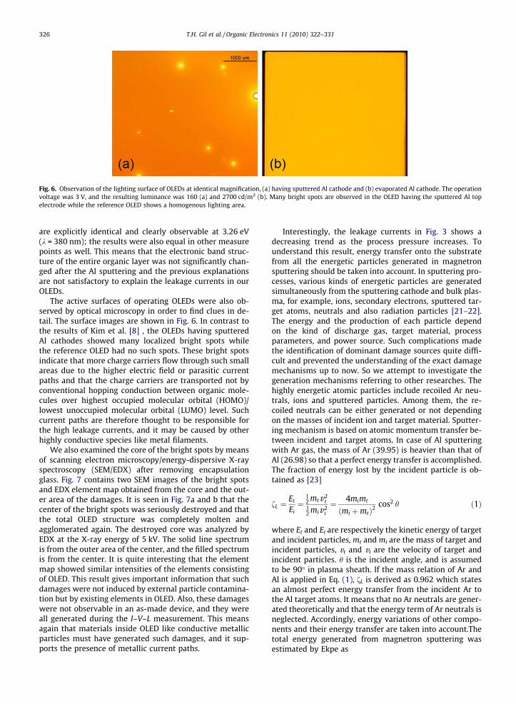
Fig. 6. Observation of the lighting surface of OLEDs at identical magnification, (a) having sputtered Al cathode and (b) evaporated Al cathode. The operationvoltage was 3 V, and the resulting luminance was 160 (a) and 2700 cd/m2 (b). Many bright spots are observed in the OLED having the sputtered Al topelectrode while the reference OLED shows a homogenous lighting area.
326 T.H. Gil et al. / Organic Electronics 11 (2010) 322–331
are explicitly identical and clearly observable at 3.26 eV(k = 380 nm); the results were also equal in other measurepoints as well. This means that the electronic band struc-ture of the entire organic layer was not significantly chan-ged after the Al sputtering and the previous explanationsare not satisfactory to explain the leakage currents in ourOLEDs.
The active surfaces of operating OLEDs were also ob-served by optical microscopy in order to find clues in de-tail. The surface images are shown in Fig. 6. In contrast tothe results of Kim et al. [8] , the OLEDs having sputteredAl cathodes showed many localized bright spots whilethe reference OLED had no such spots. These bright spotsindicate that more charge carriers flow through such smallareas due to the higher electric field or parasitic currentpaths and that the charge carriers are transported not byconventional hopping conduction between organic mole-cules over highest occupied molecular orbital (HOMO)/lowest unoccupied molecular orbital (LUMO) level. Suchcurrent paths are therefore thought to be responsible forthe high leakage currents, and it may be caused by otherhighly conductive species like metal filaments.
We also examined the core of the bright spots by meansof scanning electron microscopy/energy-dispersive X-rayspectroscopy (SEM/EDX) after removing encapsulationglass. Fig. 7 contains two SEM images of the bright spotsand EDX element map obtained from the core and the out-er area of the damages. It is seen in Fig. 7a and b that thecenter of the bright spots was seriously destroyed and thatthe total OLED structure was completely molten andagglomerated again. The destroyed core was analyzed byEDX at the X-ray energy of 5 kV. The solid line spectrumis from the outer area of the center, and the filled spectrumis from the center. It is quite interesting that the elementmap showed similar intensities of the elements consistingof OLED. This result gives important information that suchdamages were not induced by external particle contamina-tion but by existing elements in OLED. Also, these damageswere not observable in an as-made device, and they wereall generated during the I–V–L measurement. This meansagain that materials inside OLED like conductive metallicparticles must have generated such damages, and it sup-ports the presence of metallic current paths.
Interestingly, the leakage currents in Fig. 3 shows adecreasing trend as the process pressure increases. Tounderstand this result, energy transfer onto the substratefrom all the energetic particles generated in magnetronsputtering should be taken into account. In sputtering pro-cesses, various kinds of energetic particles are generatedsimultaneously from the sputtering cathode and bulk plas-ma, for example, ions, secondary electrons, sputtered tar-get atoms, neutrals and also radiation particles [21–22].The energy and the production of each particle dependon the kind of discharge gas, target material, processparameters, and power source. Such complications madethe identification of dominant damage sources quite diffi-cult and prevented the understanding of the exact damagemechanisms up to now. So we attempt to investigate thegeneration mechanisms referring to other researches. Thehighly energetic atomic particles include recoiled Ar neu-trals, ions and sputtered particles. Among them, the re-coiled neutrals can be either generated or not dependingon the masses of incident ion and target material. Sputter-ing mechanism is based on atomic momentum transfer be-tween incident and target atoms. In case of Al sputteringwith Ar gas, the mass of Ar (39.95) is heavier than that ofAl (26.98) so that a perfect energy transfer is accomplished.The fraction of energy lost by the incident particle is ob-tained as [23]
fL ¼Et
Ei¼
12 mtv2
t12 miv2
i
¼ 4mimt
ðmi þmtÞ2cos2 h ð1Þ
where Et and Ei are respectively the kinetic energy of targetand incident particles, mt and mi are the mass of target andincident particles, vt and vi are the velocity of target andincident particles. h is the incident angle, and is assumedto be 90� in plasma sheath. If the mass relation of Ar andAl is applied in Eq. (1), fL is derived as 0.962 which statesan almost perfect energy transfer from the incident Ar tothe Al target atoms. It means that no Ar neutrals are gener-ated theoretically and that the energy term of Ar neutrals isneglected. Accordingly, energy variations of other compo-nents and their energy transfer are taken into account.Thetotal energy generated from magnetron sputtering wasestimated by Ekpe as

Fig. 7. SEM images of bright spots after I–V–L measurement and EDX element map from the core and the vicinity: (a) and (b) destroyed OLED structuresthrough melting and agglomeration. EDX element map in Fig. 6c shows two spectra obtained from the degradation core (filled) and outer the degradation(solid line), non-destroyed region. Two spectra exhibit almost identical signal intensities throughout the elements consisting of OLED.
T.H. Gil et al. / Organic Electronics 11 (2010) 322–331 327
Etotal ¼ U þ Ek þ E0RE
Yþ Ep þ Ee þ Et ð2Þ
where U and Ek represent the heat of condensation and theaverage kinetic energy of the deposited atoms, respectively[24]. The third term represents the contribution of the re-flected gas neutrals determined per sputtered atoms interms of the yield Y. As discussed already, this term is elim-inated. Ep represents the contribution of photonic radiationgenerated from excited atoms within plasma. Ee and Et arethe contributions of electron and thermal radiation,respectively. In this equation, however, the contributionof ions from plasma bulk onto the substrate is absent,and it should be added. Therefore, Eq. (2) is modified into
Etotal ¼ U þ Ek þ Ep þ Ee þ Et þ Ei ð3Þ
It is then essential to know which energy terms or ele-ments in Eq. (3) vary with respect to process pressure.Firstly, the kinetic energy of the sputtered atoms and itschanges on the process pressure is discussed. The energyand direction of the sputtered target atoms arriving atthe substrate is related to the transport process from thetarget to the substrate. Each energy term in Eq. (3) is signif-icantly affected by process parameters like power andoperating pressure. Pressure-dependent deposition rateor film uniformity changes have been described by manyresearchers [25–27], and the average energy of the sput-
tered Al atoms was also reported to reach 19.2 eV at pro-cess conditions similar to our study. In magnetronsputtering, the transport from the sputter target to thesubstrate plays a significant role in film deposition andproperties. Collisions and mutual energy transfer betweensputtered atoms and discharge gases, depending on theirenergies, masses and densities, are the key factors in deter-mining the transport process. A mean free path is intro-duced primarily to explain the effect of collision betweenparticles. Since the energetic particles generated collidewith the background gas atoms, the energy of the back-ground gases should be taken into account. The mean freepath km is then expressed as
km ¼kBTpr
ð4Þ
where kB is the Boltzmann constant, T is the temperature ofthe sputtering gas. p is the pressure of the sputtering gas,and r is the collision cross section for momentum transfer[28]. Referred to Eq. (4), the km is decreased reciprocallywith an increase of pressure. This effect is due to increaseof collision frequency which can lead to a deviation of thedirection by scattering and a loss of kinetic energy of thesputtered atoms, so-called thermalization. Therefore, thedeposition rate decreases at higher process pressure asindicated in Table 2, and a decrease of the kinetic energy

Fig. 8. Temperature variations during Al depositions at different Ar flowrates. The highest temperature is found as 26 �C at the Ar flow rate of500 sccm which showed the longest deposition time.
328 T.H. Gil et al. / Organic Electronics 11 (2010) 322–331
of the sputtered atoms is thus expected.Secondly, the en-ergy transfers by other energy terms (Ep, Ee and Et) are dis-cussed. In contrast to the energy of sputtered atoms, theirenergy transfer is increased at higher process pressure be-cause the process time to deposit film of a same thicknessbecomes longer and accordingly the surface of organiclayer is exposed to the plasma longer. Those plasma com-ponents are particles which change internal energy of or-ganic molecules or deposited Al film by ionization andexcitation. By continuous irradiation on the surface of or-ganic layers or on the initial thin metal layer previous toa high reflection or screening against such irradiation,other degradation at the interface of metal and organiclayer can occur. However, it is believed that they are notthe major source to give rise to a high leakage current be-cause their masses are extremely small to deliver a suffi-cient kinetic energy for a formation of metallic currentpaths.
When comparing these explanations with the OLED I–V–L results in Fig. 3, one can recognize that only the en-ergy variation of the sputtered Al atoms in good agree-ment with the change of leakage current in OLEDs.Considering their masses and energies, the sputtered Alatoms are supposed to penetrate into the underlying or-ganic layers much deeper than the evaporated Al atoms.Moreover, if energy is transferred further by collision cas-cades due to continuous atomic bombardments, highlyconductive current paths can be formed locally throughthe organic layers. As a similar phenomenon, it was re-ported that even evaporated metal atoms deposited atan elevating substrate temperature up to 70 �C were alsoable to diffuse into a single crystalline organic diindenop-erylene (DIP) film [29]. A high electric field can be theninduced through the localized paths caused by metal dif-fusion, and it leads to highly localized currents throughthe OLED even at a low operation voltage, as shown inFig. 3. The substrate temperature during deposition wasmeasured on glass substrate by Super mole™ (ECD, Inc.).Highest temperature during Al depositions in the In-linemachine was however only 26 �C as shown in Fig. 8, sothe thermal energy seems not to play a significant rolein producing such highly conductive paths resulted frompenetration or diffusion.
By LDI–TOF–MS, we were able to identify the presenceof metal particles deep in the organic layer. There areseveral methods to detect atomic elements in thin filmslike depth profiling X-ray photoemission spectroscopy(XPS) and depth profiling secondary ion mass spectrome-try (SIMS). However, these instruments require an addi-tional ion gun in order to sputter the surface ofspecimen. This is a quite destructive method, and thebombarded surface element can also penetrate deeperinto the underlying film. In case of organic films, theintermolecular bonding is in general held by a weakvan der Walls force so that such energetic metal atomscan easier penetrate through organic molecules thaninorganic molecules. Therefore, it is difficult to distin-guish whether such metal atoms originate from sputter-ing damage or depth profiling in those instruments. Onthe other hand, the LDI–TOF–MS can also provide in-depth information by laser-induced desorption. One
important thing is that the laser intensity must be con-trolled at a threshold level to avoid an excess of ioniza-tions and corresponding chemical reactions.
A shallow doping of metal atoms was reported to bebeneficial to improve charge injection into the organic lay-ers by a self-doping effect at the metal/organic layer inter-face [30]. However, if metal atoms exist in a deep area oforganic layer, they will provide current paths interconnect-ing the two electrodes of OLED. The organic material BPhenused for the measurements is reported to produce a com-plex with Al or Ag metal atom by donor–acceptor interac-tion. Hence one can recognize the presence of those metalatoms from the detection of metal–organic complexes.Additionally, the quantity of the metal atoms can be com-pared by the intensity of spectra. Its depth resolution is un-known, but the deposited 10 nm think Al layer of thesample H and I is certainly transparent for the wavelengthof the laser. Hence the given condition for the laser irradi-ation was same, and it enables a relative comparison of theboth samples. Nevertheless, the technique is suitable togive quantitative statement about incorporated com-pounds and reacted molecules, even for metal on organichetero structures [30].
In Fig. 9, two spectra of the sample H and I are shown. Itis clearly seen that the sample H contains much more Aladduct ions, [BPhen + Al]+ at m/z = 359 amu and [2BPhe-

Fig. 9. LDI–TOF–MS results of sample H and I. The sample H shows much higher intensities of BPhen + Al and 2BPhen + Al complexes than the sample I,representing the existence of Al atoms inside of the BPhen layer.
T.H. Gil et al. / Organic Electronics 11 (2010) 322–331 329
n + Al]+ at m/z = 692.1 amu, than the sample I. The ratios ofthe spectrum intensities from the existing molecules aretabulated in Table 3. This result gives a decisive evidenceto clarify that more metal atoms existed inside the BPhenlayer of the sample H than the sample I, supporting thepenetration effect of Al atoms due to continuous bombard-ment effect with high-energy. Therefore, we can concludethat the penetrated Al atoms resulted in high leakage cur-rent flowing through the organic layers.
3.2. Radiation effects in OLED
The forward I–V in the linear scale and L–V characteris-tics of the OLEDs are plotted again and shown in Fig. 10aand b. The reference OLED exhibits a high forward currentdensity of 100 mA/cm2 at 4 V. On the other hand, the for-ward current density of the OLED from the sample A–C de-creases with increasing process pressure. The forward
Table 3Calculated ratios from the spectrum intensities of the sample H and I.
Molecules for comparison Sample H(Ar = 100 sccm)
Sample I(Ar = 500 sccm)
BPhen/BPhen-Dimer 2.51 2.488BPhen + Al/2BPhen + Al 0.57 0.54BPhen/Al + BPhen 1.18 2.85BPhen-Dimer/2Bphen + Al 0.268 0.62
current in OLED is the summation of hole and electron cur-rents. The decrease of the forward current reflects a poorcharge carrier injection, especially electrons from the Alcathode. It is probably due to generation of different elec-tronics states or charge traps at the top metal/organic layerinterface generated by the irradiation from plasma. Severalmechanisms can be introduced to explain the degradationof interface property due to plasma radiation. Electrons fallonto a substrate faster than ions when the substrate is im-mersed in the plasma. The electrons can be accumulatedon the surface making the interface of metal/organic layernegatively charged. Such localization of electrons can pos-sibly modify electronic structure of organic molecules [31].The photons with energies higher than the band gap of or-ganic material can excite bound electrons to LUMO orhigher states, generating electron–hole pairs (EHPs) [32].When the organic molecules are excited, they may dissi-pate the excess energy by emitting photons as it returnsto a lower energy level and eventually to the ground state.The energy can also be emitted irradiatively forming frag-mented and reactive species by the opening of a bondstructure and the detachment of hydrogen or an organic li-gand. It is because the photon energy in plasma rangesmuch exceeding the binding energy of carbon–carboncovalent bonds or carbon–hydrogen bonds of organic mol-ecules, and such unbound sites are then able to act ascharge trapping sites which hinder the injection of chargecarriers from the electrode.

Fig. 10. Rescaled I–V and L–V characteristics of the OLEDs. The forwardcurrent and corresponding luminance decrease as the irradiative energyincreases, resulted from the decrease of the deposition rate.
330 T.H. Gil et al. / Organic Electronics 11 (2010) 322–331
The generation of such degradations can be related witha total radiation energy, which is estimated as a product ofradiation flux from plasma and exposure time of the organ-ic layers. As discussed briefly in former section, the totalradiation energy comprising Ep, Ee, Et and Ei in Eq. (3) be-comes larger at higher process pressure because the pro-cess time to deposit 100 nm thick Al layer in the sampleC was roughly two times longer than A. Corresponding ef-fect is clearly seen in Fig. 10a that the forward current ofthe sample C decreased from 57 mA/cm2 at 4.75 V to30 mA/cm2 of the sample A, which is well matched withthe increase of the process time. Therefore, the decreaseof the forward current can be ascribed surely to the radia-tion out of plasma. It should be mentioned one more thatthis radiation effect should be separated from that of theleakage current, because the tendency of the both effectswith respect to the variation of the process pressure wasobviously opposite. The luminance of the OLED is undoubt-edly decreased, and this yielded also a shift of driving volt-age from 2.7 V of the reference OLED to almost 4 V of theother OLEDs for 1000 cd/m2.
4. Conclusions
We demonstrated OLEDs having Al top electrode depos-ited by a conventional magnetron sputtering system. TheAl sputtering deposition on organic layers resulted in highleakage current and lower forward current in the OLEDsfabricated. The OLEDs possessing high leakage current
showed many bright spots on active area, which arethought as the result from the leakage current. The opticalconstants of the organic layers obtained from ellipsometryshowed no changes in the optical gap of the organic layers.This means that the organic layer was not damaged seri-ously after Al sputter deposition and that other sourcesmight have caused the high leakage currents. Based onthe operating principle of magnetron sputtering, we con-cluded that the high kinetic energy of sputtered Al atomswas the dominant source responsible for the leakage cur-rent, resulting in a metal penetration into the underlyingorganic layers. In order to prove the metal penetration,we employed LDI–TOF–MS. At the same process parameterthat OLED showed highest leakage current, the obviousexistence of Al atoms deeper inside the organic layer wasidentified as a form of metal–organic complex. It assuredthat the high leakage current was caused by conductivemetallic paths provided by penetrated Al metal particlesinto organic layer.
The effect of plasma radiation on the metal/organiclayer interface was also examined. The forward currentdensity showed a decreasing trend, as the process time be-came longer. This result was explained well with the in-crease of the radiation energy that influences thegeneration of the interface degradation.
We note that if the process pressure is increased furtherin order to reduce the leakage current in OLED, the inter-face will be degraded more, which leads to a higher oper-ating voltage. Therefore, the two damages caused bymagnetron sputtering are in a trade-off relation, and athick buffer layer or modified organic layers based on p–i–n OLED would be helpful to obtain comparable leakagecurrent, efficiency and lifetime with OLED having evapo-rated metal electrode.
Acknowledgement
This work was performed with financial support by Ap-plied Materials GmbH & Co. KG within the OPAL project(Support Code 13N8944) funded by the Federal Ministryfor Education and Research of Germany.
References
[1] C.W. Tang, S.A. VanSlyke, Appl. Phys. Lett. 51 (1987) 913.[2] M.A. Baldo, D.F. O’Brien, Y. You, A. Shoustikov, S. Sibley, M.E.
Thompson, S.R. Forrest, Nature 395 (1998) 151.[3] M.A. Baldo, M.E. Thompson, S.R. Forrest, Nature 403 (2000) 750.[4] K. Walzer, B. Maennig, M. Pfeiffer, K. Leo, Chem. Rev. 107 (2007)
1233.[5] S. Reineke, F. Lindner, G. Schwartz, N. Seidler, K. Walzer, B. Lüssem, K.
Leo, Nature 459 (2009) 234.[6] L.S. Hung, C.W. Tang, Appl. Phys. Lett. 74 (1999) 3209.[7] L.S. Hung, L.S. Liao, C.S. Lee, S.T. Lee, J. Appl. Phys. 86 (1999) 4607.[8] H.K. Kim, S.W. Kim, K.S. Lee, K.H. Kim, Appl. Phys. Lett. 88 (2006)
083513.[9] G. Guenther, in: Proceedings of IDMC, Invited Talk, 2009.
[10] S. Scholz, C. Corten, K. Walzer, D. Kuckling, K. Leo, Organ. Electron. 8(2007) 709.
[11] J. Kassabov, E. Atanassova, D. Dimitrov, J. Vasileva, Thin Solid Films169 (1989) 43.
[12] A.M. Wróbel, G. Czeremuszkin, Thin Solid Films 216 (1992) 203.[13] A.C. Fozza, J. Roch, J.E. Klemberg-Sapieha, A. Kruse, A. Holläder,
M.R. Wertheimer, Nucl. Instrum. Methods. Phys. Res. B I31 (1997)205.

T.H. Gil et al. / Organic Electronics 11 (2010) 322–331 331
[14] U. Hoffmann, P. Netuschill, M. Bender, P. Sauer, M. Schreil, J.Amelung, K. Leo, SID Symp. Dig. Tech. Papers 34 (2003)1410.
[15] C. May, Y. Tomita, M. Toerker, M. Eritt, F. Loeffler, J. Amelung, K. Leo,Thin Solid Films 516 (2007) 4609.
[16] R. Meerheim, S. Scholz, G. Schwartz, S. Reineke, S. Olthof, K. Walzer,K. Leo, Proc. SPIE 6999 (2008) 699917.
[17] C.R. Dutta, K. Barua, J. Phys. D: Appl. Phys. 14 (1981) L179.[18] L.S. Liao, L.S. Hung, W.C. Chan, X.M. Ding, T.K. Sham, I. Bello, C.S. Lee,
S.T. Lee, Appl. Phys. Lett. 75 (1999) 1619.[19] G. Gu, V. Bulovic, P.E. Burrows, S.R. Forrest, M.E. Thompson, Appl.
Phys. Lett. 68 (1996) 2606.[20] Tilo P. Drüsedau, Mirko Löhmann, Bernd Garke, J. Vac. Sci. Technol. A
16 (4) (1998) 2728.[21] S.M. Rossnagel, J. Vac, Sci. Technol. A 7 (1989) 1025.[22] S.M. Rossnagel, K.L. Saenger, J. Vac, Sci. Technol. A 7 (1989) 968.
[23] M.A. Lieberman, Principles of Plasma Discharges and MaterialsProcessing, John Wiley & Sons, 1994.
[24] S.D. Ekpe, S.K. Dew, J. Vac. Sci. Technol. A 20 (2002) 1877.[25] J.C. Helmer, C.E. Wickersham, J. Vac. Sci. Technol. A 4 (1986) 408.[26] T.P. Drüsedau, M. Löhmann, B. Garke, J. Vac. Sci. Technol. A 16 (1998)
2728.[27] A. Settaouti, L. Settaouti, Appl. Surf. Sci. 254 (2008) 5750.[28] S.D. Ekpe, L.W. Bezuidenhout, S.K. Dew, Thin Solid Films 474 (2005)
330.[29] A.C. Dürr, F. Schreiber, M. Kelsch, H.D. Carstanjen, H. Dosch, Adv.
Mater. 14 (2002) 961.[30] S. Scholz, Q. Huang, M. Thomschke, S. Olthof, P. Sebastian, K. Walzer,
K. Leo, S. Oswald, C. Corten, D. Kuckling, J. Appl. Phys. 104 (2008)104502.
[31] R.Q. Zhang, C.S. Lee, S.T. Lee, Chem. Phys. Lett. 326 (2000) 413.[32] H. Yasuda, J. Macromol. Sci.-Chem. A10 (3) (1976) 383.