Magnetization reversal studies in structurally tailored cobalt nanowires
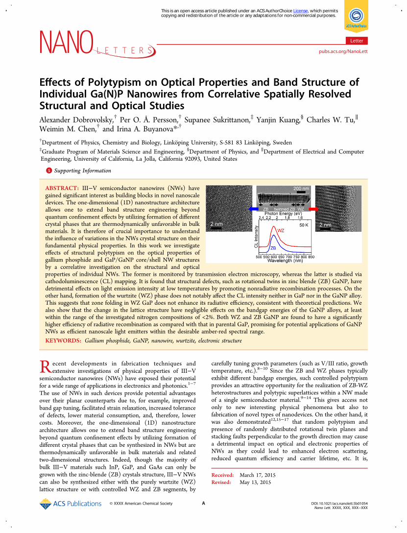
Effects of Polytypism on Optical Properties and Band Structure ofIndividual Ga(N)P Nanowires from Correlative Spatially ResolvedStructural and Optical StudiesAlexander Dobrovolsky,† Per O. Å. Persson,† Supanee Sukrittanon,‡ Yanjin Kuang,§ Charles W. Tu,∥
Weimin M. Chen,† and Irina A. Buyanova*,†
†Department of Physics, Chemistry and Biology, Linkoping University, S-581 83 Linkoping, Sweden‡Graduate Program of Materials Science and Engineering, §Department of Physics, and ∥Department of Electrical and ComputerEngineering, University of California, La Jolla, California 92093, United States
*S Supporting Information
ABSTRACT: III−V semiconductor nanowires (NWs) havegained significant interest as building blocks in novel nanoscaledevices. The one-dimensional (1D) nanostructure architectureallows one to extend band structure engineering beyondquantum confinement effects by utilizing formation of differentcrystal phases that are thermodynamically unfavorable in bulkmaterials. It is therefore of crucial importance to understandthe influence of variations in the NWs crystal structure on theirfundamental physical properties. In this work we investigateeffects of structural polytypism on the optical properties ofgallium phosphide and GaP/GaNP core/shell NW structuresby a correlative investigation on the structural and opticalproperties of individual NWs. The former is monitored by transmission electron microscopy, whereas the latter is studied viacathodoluminescence (CL) mapping. It is found that structural defects, such as rotational twins in zinc blende (ZB) GaNP, havedetrimental effects on light emission intensity at low temperatures by promoting nonradiative recombination processes. On theother hand, formation of the wurtzite (WZ) phase does not notably affect the CL intensity neither in GaP nor in the GaNP alloy.This suggests that zone folding in WZ GaP does not enhance its radiative efficiency, consistent with theoretical predictions. Wealso show that the change in the lattice structure have negligible effects on the bandgap energies of the GaNP alloys, at leastwithin the range of the investigated nitrogen compositions of <2%. Both WZ and ZB GaNP are found to have a significantlyhigher efficiency of radiative recombination as compared with that in parental GaP, promising for potential applications of GaNPNWs as efficient nanoscale light emitters within the desirable amber-red spectral range.
KEYWORDS: Gallium phosphide, GaNP, nanowire, wurtzite, electronic structure
Recent developments in fabrication techniques andextensive investigations of physical properties of III−V
semiconductor nanowires (NWs) have exposed their potentialfor a wide range of applications in electronics and photonics.1−7
The use of NWs in such devices provide potential advantagesover their planar counterparts due to, for example, improvedband gap tuning, facilitated strain relaxation, increased toleranceof defects, lower material consumption, and, therefore, lowercosts. Moreover, the one-dimensional (1D) nanostructurearchitecture allows one to extend band structure engineeringbeyond quantum confinement effects by utilizing formation ofdifferent crystal phases that can be synthesized in NWs but arethermodynamically unfavorable in bulk materials and relatedtwo-dimensional structures. Indeed, though the majority ofbulk III−V materials such InP, GaP, and GaAs can only begrown with the zinc-blende (ZB) crystals structure, III−V NWscan also be synthesized either with the purely wurtzite (WZ)lattice structure or with controlled WZ and ZB segments, by
carefully tuning growth parameters (such as V/III ratio, growthtemperature, etc.).8−10 Since the ZB and WZ phases typicallyexhibit different bandgap energies, such controlled polytypismprovides an attractive opportunity for the realization of ZB-WZheterostructures and polytypic superlattices within a NW madeof a single semiconductor material.9−14 This gives access notonly to new interesting physical phenomena but also tofabrication of novel types of nanodevices. On the other hand, itwas also demonstrated12,15−17 that random polytypism andpresence of randomly distributed rotational twin planes andstacking faults perpendicular to the growth direction may causea detrimental impact on optical and electronic properties ofNWs as they could lead to enhanced electron scattering,reduced quantum efficiency and carrier lifetime, etc. It is,
Received: March 17, 2015Revised: May 13, 2015
Letter
pubs.acs.org/NanoLett
© XXXX American Chemical Society A DOI: 10.1021/acs.nanolett.5b01054Nano Lett. XXXX, XXX, XXX−XXX
This is an open access article published under an ACS AuthorChoice License, which permitscopying and redistribution of the article or any adaptations for non-commercial purposes.
therefore, of crucial importance to understand the influence oflocal variations in the crystal structure of NWs on theirfundamental physical properties.Such information has recently been obtained in a number of
III−V NWs based on direct bandgap semiconductors, suchGaAs, GaN, and InP,11,14,18,19 largely from extensive opticalstudies that utilized high radiative efficiency of these materials.On the other hand, similar studies devoted to WZ or polytypicgallium phosphide nanowires remains scarce,20,21 in spite of thefact that GaP has the smallest lattice mismatch to Si (less than0.4% at room temperature) and is, therefore, one of the bestcandidates for integration of photonics based on III−Vmaterials with planar silicon technology. A major obstaclehere is a low radiative efficiency of this indirect bandgapsemiconductor and, therefore, a lack of radiative transitionsrelated to free exciton or band-to-band recombination, whichare often used to monitor electronic states caused by differentlattice polytypes within NWs.11,14,17,19 In principle, due to zonefolding effects, the bandgap character of WZ GaP has beentheoretically predicted22−24 to change to a pseudodirect onewith the lowest Γ8c conduction band (CB) minimum (CBM)that is derived from the folded L6c states of ZB. However,important issues on whether this should lead to an improvedradiative efficiency of WZ GaP and also what is the bandgapenergy of this material remain controversial.20−24 For example,though the first principle calculations22,24 have concluded thatWZ GaP is a poor light emitter as the direct optical transitionsbetween Γ8c CBM and the valence band (VB) states areelectric-dipole forbidden, the opposite conclusion was reachedfrom transient photoluminescence (PL) measurements.21 Alsonot known are effects of structural defects, such as stackingfaults and twins, on the NWs optical quality.In this paper we address these important issues by correlative
studies of structural and optical properties of individualGa(N)P-based NWs. The structural properties were monitoredby aberration-corrected transmission electron microscopy (AC-TEM), whereas the optical properties were studied bycathodoluminescence (CL) spectroscopy. In order to improvethe radiative efficiency of the wires, a small amount (up to 2%)of nitrogen was incorporated into GaP to form GaP/GaNPcore/shell structures with the optically active shell layer ofGaNP (see Methods for a detailed description of the samplesstructure). According to previous studies of bulk and two-dimensional GaNP, this material has a significantly higheroscillator strength of optical transitions caused by strong N-induced perturbations of the CB states which brings the Γ-character to the CB minimum of the formed alloy.25 Our recentstudies have demonstrated excellent optical quality of suchGaP/GaNP NWs evident, e.g., from the observation of strongPL emissions over a wide temperature range with a significantlyhigher efficiency than that offered by GaP NWs.26,27 We havealso shown that the GaNP-based NWs structures are potentiallyimportant for novel optoelectronic applications, i.e., as ananoscale light source that emits linearly polarized light withthe polarization direction perpendicularly to the wire axis evenin ZB nanowires28 or for light harvesting utilizing energyupconversion.29
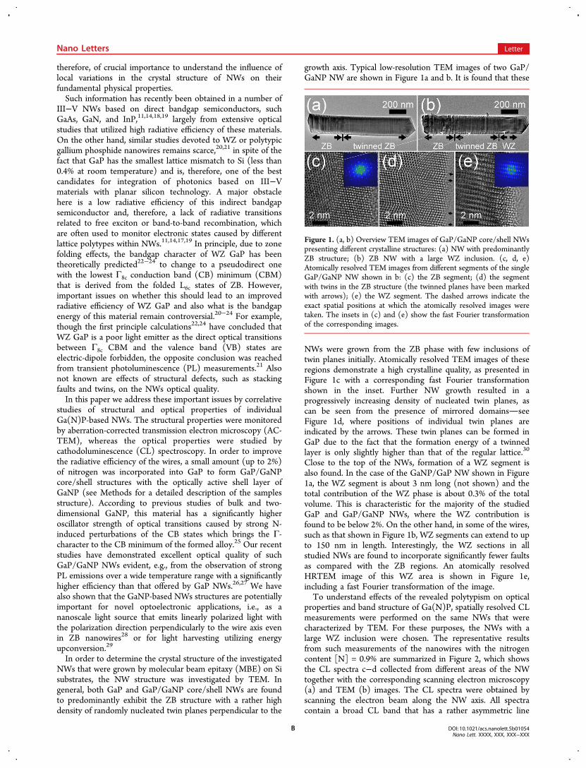
In order to determine the crystal structure of the investigatedNWs that were grown by molecular beam epitaxy (MBE) on Sisubstrates, the NW structure was investigated by TEM. Ingeneral, both GaP and GaP/GaNP core/shell NWs are foundto predominantly exhibit the ZB structure with a rather highdensity of randomly nucleated twin planes perpendicular to the
growth axis. Typical low-resolution TEM images of two GaP/GaNP NW are shown in Figure 1a and b. It is found that these
NWs were grown from the ZB phase with few inclusions oftwin planes initially. Atomically resolved TEM images of theseregions demonstrate a high crystalline quality, as presented inFigure 1c with a corresponding fast Fourier transformationshown in the inset. Further NW growth resulted in aprogressively increasing density of nucleated twin planes, ascan be seen from the presence of mirrored domainsseeFigure 1d, where positions of individual twin planes areindicated by the arrows. These twin planes can be formed inGaP due to the fact that the formation energy of a twinnedlayer is only slightly higher than that of the regular lattice.30
Close to the top of the NWs, formation of a WZ segment isalso found. In the case of the GaNP/GaP NW shown in Figure1a, the WZ segment is about 3 nm long (not shown) and thetotal contribution of the WZ phase is about 0.3% of the totalvolume. This is characteristic for the majority of the studiedGaP and GaP/GaNP NWs, where the WZ contribution isfound to be below 2%. On the other hand, in some of the wires,such as that shown in Figure 1b, WZ segments can extend to upto 150 nm in length. Interestingly, the WZ sections in allstudied NWs are found to incorporate significantly fewer faultsas compared with the ZB regions. An atomically resolvedHRTEM image of this WZ area is shown in Figure 1e,including a fast Fourier transformation of the image.To understand effects of the revealed polytypism on optical
properties and band structure of Ga(N)P, spatially resolved CLmeasurements were performed on the same NWs that werecharacterized by TEM. For these purposes, the NWs with alarge WZ inclusion were chosen. The representative resultsfrom such measurements of the nanowires with the nitrogencontent [N] = 0.9% are summarized in Figure 2, which showsthe CL spectra c−d collected from different areas of the NWtogether with the corresponding scanning electron microscopy(a) and TEM (b) images. The CL spectra were obtained byscanning the electron beam along the NW axis. All spectracontain a broad CL band that has a rather asymmetric line
Figure 1. (a, b) Overview TEM images of GaP/GaNP core/shell NWspresenting different crystalline structures: (a) NW with predominantlyZB structure; (b) ZB NW with a large WZ inclusion. (c, d, e)Atomically resolved TEM images from different segments of the singleGaP/GaNP NW shown in b: (c) the ZB segment; (d) the segmentwith twins in the ZB structure (the twinned planes have been markedwith arrows); (e) the WZ segment. The dashed arrows indicate theexact spatial positions at which the atomically resolved images weretaken. The insets in (c) and (e) show the fast Fourier transformationof the corresponding images.
Nano Letters Letter
DOI: 10.1021/acs.nanolett.5b01054Nano Lett. XXXX, XXX, XXX−XXX
B
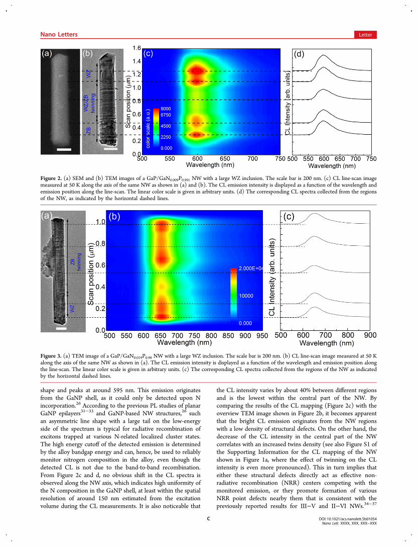
shape and peaks at around 595 nm. This emission originatesfrom the GaNP shell, as it could only be detected upon Nincorporation.26 According to the previous PL studies of planarGaNP epilayers31−33 and GaNP-based NW structures,26 suchan asymmetric line shape with a large tail on the low-energyside of the spectrum is typical for radiative recombination ofexcitons trapped at various N-related localized cluster states.The high energy cutoff of the detected emission is determinedby the alloy bandgap energy and can, hence, be used to reliablymonitor nitrogen composition in the alloy, even though thedetected CL is not due to the band-to-band recombination.From Figure 2c and d, no obvious shift in the CL spectra isobserved along the NW axis, which indicates high uniformity ofthe N composition in the GaNP shell, at least within the spatialresolution of around 150 nm estimated from the excitationvolume during the CL measurements. It is also noticeable that
the CL intensity varies by about 40% between different regionsand is the lowest within the central part of the NW. Bycomparing the results of the CL mapping (Figure 2c) with theoverview TEM image shown in Figure 2b, it becomes apparentthat the bright CL emission originates from the NW regionswith a low density of structural defects. On the other hand, thedecrease of the CL intensity in the central part of the NWcorrelates with an increased twins density (see also Figure S1 ofthe Supporting Information for the CL mapping of the NWshown in Figure 1a, where the effect of twinning on the CLintensity is even more pronounced). This in turn implies thateither these structural defects directly act as effective non-radiative recombination (NRR) centers competing with themonitored emission, or they promote formation of variousNRR point defects nearby them that is consistent with thepreviously reported results for III−V and II−VI NWs.34−37
Figure 2. (a) SEM and (b) TEM images of a GaP/GaN0.009P0.991 NW with a large WZ inclusion. The scale bar is 200 nm. (c) CL line-scan imagemeasured at 50 K along the axis of the same NW as shown in (a) and (b). The CL emission intensity is displayed as a function of the wavelength andemission position along the line-scan. The linear color scale is given in arbitrary units. (d) The corresponding CL spectra collected from the regionsof the NW, as indicated by the horizontal dashed lines.
Figure 3. (a) TEM image of a GaP/GaN0.019P0.98 NW with a large WZ inclusion. The scale bar is 200 nm. (b) CL line-scan image measured at 50 Kalong the axis of the same NW as shown in (a). The CL emission intensity is displayed as a function of the wavelength and emission position alongthe line-scan. The linear color scale is given in arbitrary units. (c) The corresponding CL spectra collected from the regions of the NW as indicatedby the horizontal dashed lines.
Nano Letters Letter
DOI: 10.1021/acs.nanolett.5b01054Nano Lett. XXXX, XXX, XXX−XXX
C
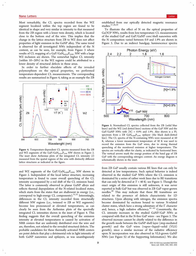
Most remarkably, the CL spectra recorded from the WZsegment localized within the top region are found to beidentical in shape and very similar in intensity to that measuredfrom the ZB region with a lower twin density, which is locatedclose to the bottom end of the wire. This implies that thechange in the lattice structure from ZB to WZ does not affectproperties of light emission in the GaNP alloy. The same trendis observed for all investigated NWs independent of the Ncontent, as can be seen, for example, from Figure 3 whereresults of CL mapping of a GaP/GaN0.019P0.981 NW with a largeWZ inclusion are shown. The somewhat higher CL intensity(within 10−20%) in the WZ regions could be attributed to alower density of structural defects in these areas.In order to further elucidate effects of the revealed
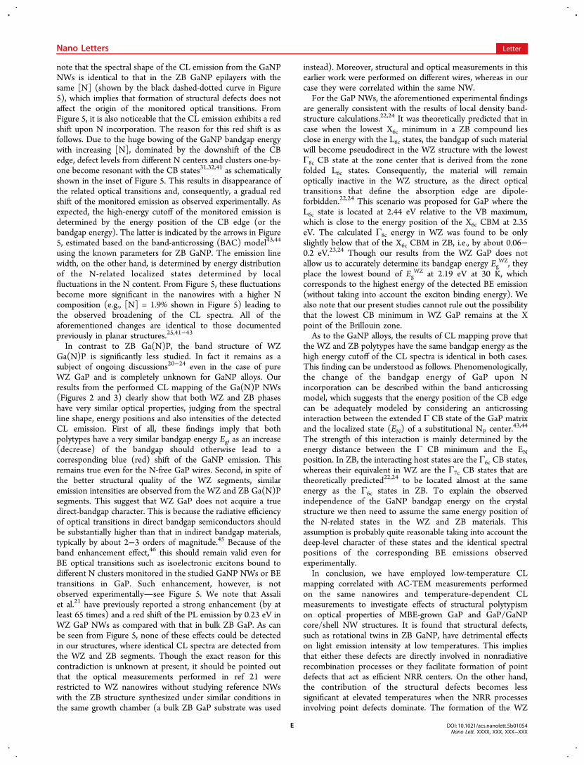
polymorphism on the optical properties, we performedtemperature-dependent CL measurements. The correspondingresults are summarized in Figure 4, taking as an example the ZB
and WZ segments of the GaP/GaN0.009P0.991 NW shown inFigure 2. Independent of the local lattice structure, increasingtemperature is found to cause overall quenching of the CLintensity accompanied by a red shift of the CL emission band.The latter is commonly observed in planar GaNP alloys andreflects thermal depopulation of the N-related localized states,which starts from the states that are shallowest in energy (i.e.,correspond to high-energy CL components).31,32 Interestingly,differences in the CL intensity recorded from structurallydifferent NW regions (i.e., twinned vs ZB or WZ segments)become less pronounced at elevated temperatures, as canclearly be seen from the Arrhenius plots of the spectrallyintegrated CL intensities shown in the inset of Figure 4. Thisfinding suggests that the overall quenching of the emissionintensity at elevated temperatures is caused by activation ofNRR centers that are uniformly distributed over the wire andare, therefore, not related to the revealed structural defects. Theprobable candidates for these thermally activated NRR centersare point defects that play a detrimental role in light intensity ofboth GaNP nanowires and epilayers, as was unambiguously
established from our optically detected magnetic resonancestudies.27,38,39
To illustrate the effect of N on the optical properties ofGa(N)P NWs, results from low-temperature CL measurementsof the studied GaP and GaP/GaNP core/shell nanowires withthe N composition varied between 0.9 and 1.9% are shown inFigure 5. Due to an indirect bandgap, luminescence spectra
from ZB GaP usually contain various BE lines that can only bedetected at low temperatures. Such optical behavior is indeedobserved in the studied GaP NWs where the CL emission isdominated by a series of rather week lines due to BE transitionsthat can only be detected at T < 40 K: see Figure 5. Though theexact origin of this emission is still unknown, it was neverreported in bulk GaP but was observed in ZB GaP vapor-grownneedles.40 This may indicate that these BE transitions arerelated to the presence of defects characteristic for 1Dstructures. Upon alloying with nitrogen, the emission spectrabecome dominated by excitons bound to various N-relatedcluster states, which have a strong admixture of the Γ characterand, hence, a high radiative efficiency.41−43 Consistently, theCL intensity increases in the studied GaNP/GaP NWs ascompared with that in the N-free GaP wires - see Figure 5. Theobserved increase cannot be chiefly related to the difference inthe growth mode between the GaNP shell layer (step-mediatedgrowth) and the GaP wires (vapor−liquid−solid (VLS)growth), since a similar increase of the radiative efficiencyupon N incorporation was also observed in VLS-grown GaNPNWs (see Figure S2 of the Supporting Information). We also
Figure 4. Temperature-dependent CL spectra measured from the ZBand WZ segments of the GaP/GaN0.019P0.98 NW shown in Figure 2.The inset show Arrhenius plots of the integrated CL intensity (I)measured from the spatial regions of the wire with distinctly differentlattice structures as indicated in the figure.
Figure 5. Normalized CL spectra collected from the ZB (solid bluelines) and the WZ (red dotted lines) sections of the GaP NW and theGaP/GaNP NWs with [N] = 0.9% and 1.9%. Also shown is a PLspectrum from a ZB GaN0.009P0.991 epilayer (the black dash-dottedline). The CL spectra of the N-containing NWs were measured at 50K, whereas a lower measurement temperature of 30 K was used torecord the emission from the GaP wires, due to strong thermalquenching of the monitored emission at higher temperatures. Thespectra are vertically offset for clarity, as indicated by horizontal lines.The vertical arrows mark the energy position of the band gap of ZBGaP with the corresponding nitrogen content. An energy diagram isschematically shown in the inset.
Nano Letters Letter
DOI: 10.1021/acs.nanolett.5b01054Nano Lett. XXXX, XXX, XXX−XXX
D
note that the spectral shape of the CL emission from the GaNPNWs is identical to that in the ZB GaNP epilayers with thesame [N] (shown by the black dashed-dotted curve in Figure5), which implies that formation of structural defects does notaffect the origin of the monitored optical transitions. FromFigure 5, it is also noticeable that the CL emission exhibits a redshift upon N incorporation. The reason for this red shift is asfollows. Due to the huge bowing of the GaNP bandgap energywith increasing [N], dominated by the downshift of the CBedge, defect levels from different N centers and clusters one-by-one become resonant with the CB states31,32,41 as schematicallyshown in the inset of Figure 5. This results in disappearance ofthe related optical transitions and, consequently, a gradual redshift of the monitored emission as observed experimentally. Asexpected, the high-energy cutoff of the monitored emission isdetermined by the energy position of the CB edge (or thebandgap energy). The latter is indicated by the arrows in Figure5, estimated based on the band-anticrossing (BAC) model43,44
using the known parameters for ZB GaNP. The emission linewidth, on the other hand, is determined by energy distributionof the N-related localized states determined by localfluctuations in the N content. From Figure 5, these fluctuationsbecome more significant in the nanowires with a higher Ncomposition (e.g., [N] = 1.9% shown in Figure 5) leading tothe observed broadening of the CL spectra. All of theaforementioned changes are identical to those documentedpreviously in planar structures.25,41−43
In contrast to ZB Ga(N)P, the band structure of WZGa(N)P is significantly less studied. In fact it remains as asubject of ongoing discussions20−24 even in the case of pureWZ GaP and is completely unknown for GaNP alloys. Ourresults from the performed CL mapping of the Ga(N)P NWs(Figures 2 and 3) clearly show that both WZ and ZB phaseshave very similar optical properties, judging from the spectralline shape, energy positions and also intensities of the detectedCL emission. First of all, these findings imply that bothpolytypes have a very similar bandgap energy Eg, as an increase(decrease) of the bandgap should otherwise lead to acorresponding blue (red) shift of the GaNP emission. Thisremains true even for the N-free GaP wires. Second, in spite ofthe better structural quality of the WZ segments, similaremission intensities are observed from the WZ and ZB Ga(N)Psegments. This suggest that WZ GaP does not acquire a truedirect-bandgap character. This is because the radiative efficiencyof optical transitions in direct bandgap semiconductors shouldbe substantially higher than that in indirect bandgap materials,typically by about 2−3 orders of magnitude.45 Because of theband enhancement effect,46 this should remain valid even forBE optical transitions such as isoelectronic excitons bound todifferent N clusters monitored in the studied GaNP NWs or BEtransitions in GaP. Such enhancement, however, is notobserved experimentallysee Figure 5. We note that Assaliet al.21 have previously reported a strong enhancement (by atleast 65 times) and a red shift of the PL emission by 0.23 eV inWZ GaP NWs as compared with that in bulk ZB GaP. As canbe seen from Figure 5, none of these effects could be detectedin our structures, where identical CL spectra are detected fromthe WZ and ZB segments. Though the exact reason for thiscontradiction is unknown at present, it should be pointed outthat the optical measurements performed in ref 21 wererestricted to WZ nanowires without studying reference NWswith the ZB structure synthesized under similar conditions inthe same growth chamber (a bulk ZB GaP substrate was used
instead). Moreover, structural and optical measurements in thisearlier work were performed on different wires, whereas in ourcase they were correlated within the same NW.For the GaP NWs, the aforementioned experimental findings
are generally consistent with the results of local density band-structure calculations.22,24 It was theoretically predicted that incase when the lowest X6c minimum in a ZB compound liesclose in energy with the L6c states, the bandgap of such materialwill become pseudodirect in the WZ structure with the lowestΓ8c CB state at the zone center that is derived from the zonefolded L6c states. Consequently, the material will remainoptically inactive in the WZ structure, as the direct opticaltransitions that define the absorption edge are dipole-forbidden.22,24 This scenario was proposed for GaP where theL6c state is located at 2.44 eV relative to the VB maximum,which is close to the energy position of the X6c CBM at 2.35eV. The calculated Γ8c energy in WZ was found to be onlyslightly below that of the X6c CBM in ZB, i.e., by about 0.06−0.2 eV.23,24 Though our results from the WZ GaP does notallow us to accurately determine its bandgap energy Eg
WZ, theyplace the lowest bound of Eg
WZ at 2.19 eV at 30 K, whichcorresponds to the highest energy of the detected BE emission(without taking into account the exciton binding energy). Wealso note that our present studies cannot rule out the possibilitythat the lowest CB minimum in WZ GaP remains at the Xpoint of the Brillouin zone.As to the GaNP alloys, the results of CL mapping prove that
the WZ and ZB polytypes have the same bandgap energy as thehigh energy cutoff of the CL spectra is identical in both cases.This finding can be understood as follows. Phenomenologically,the change of the bandgap energy of GaP upon Nincorporation can be described within the band anticrossingmodel, which suggests that the energy position of the CB edgecan be adequately modeled by considering an anticrossinginteraction between the extended Γ CB state of the GaP matrixand the localized state (EN) of a substitutional NP center.43,44
The strength of this interaction is mainly determined by theenergy distance between the Γ CB minimum and the ENposition. In ZB, the interacting host states are the Γ6c CB states,whereas their equivalent in WZ are the Γ7c CB states that aretheoretically predicted22,24 to be located almost at the sameenergy as the Γ6c states in ZB. To explain the observedindependence of the GaNP bandgap energy on the crystalstructure we then need to assume the same energy position ofthe N-related states in the WZ and ZB materials. Thisassumption is probably quite reasonable taking into account thedeep-level character of these states and the identical spectralpositions of the corresponding BE emissions observedexperimentally.In conclusion, we have employed low-temperature CL
mapping correlated with AC-TEM measurements performedon the same nanowires and temperature-dependent CLmeasurements to investigate effects of structural polytypismon optical properties of MBE-grown GaP and GaP/GaNPcore/shell NW structures. It is found that structural defects,such as rotational twins in ZB GaNP, have detrimental effectson light emission intensity at low temperatures. This impliesthat either these defects are directly involved in nonradiativerecombination processes or they facilitate formation of pointdefects that act as efficient NRR centers. On the other hand,the contribution of the structural defects becomes lesssignificant at elevated temperatures when the NRR processesinvolving point defects dominate. The formation of the WZ
Nano Letters Letter
DOI: 10.1021/acs.nanolett.5b01054Nano Lett. XXXX, XXX, XXX−XXX
E

phase does not change the intensity of the monitored CL eitherin GaP or in the GaNP alloy. Considering a better structuralquality of the WZ segments, this finding is consistent with theresults of the first principle calculations22,24 suggesting that thefundamental band-to-band transitions in WZ GaP remaindipole forbidden in spite of zone folding. Moreover, thebandgap energy of WZ GaP is concluded to be above 2.19 eVat 30 K (without taking into account the exciton bindingenergy). We also show that the change in the lattice structuresdoes not affect the bandgap energies of the GaNP alloys, atleast within the range of nitrogen composition [N] < 2.0%studied in this work. Both WZ and ZB GaNP are found to havea significantly higher efficiency of radiative recombination ascompared with that in the parental GaP, promising for potentialapplications of GaNP NWs as efficient nanoscale light emitterswithin the amber-red spectral range.Methods. The investigated GaP NWs and GaP/GaNP
core/shell NWs were grown by gas-source molecular beamepitaxy (GS MBE) on Si(111) substrates as reportedpreviously.47 The GaP NWs were synthesized in a Ga-catalyzedvapor−liquid−solid (VLS) growth mode at a substratetemperature Tsub of 580 °C with a V/III flux ratio of 1.5.The same growth conditions were used for the growth of coreregions in the coaxial NW heterostructures. The GaNP shellwas fabricated via the step-mediated growth at a lower substratetemperature Tsub of 520 °C and a V/III flux ratio of 2.5. Thenitrogen composition in the shell was varied between 0.6 and2.0% by changing the power of the rf-plasma and the nitrogenflux. The nitrogen content in the resulting core/shell NWs wasestimated by comparing the PL data with the band anticrossingmodel.43 The performed SEM measurements have shown thatthe NWs are oriented perpendicular to the substrate plane andexhibit a hexagonal cross-section, indicating that they wereepitaxially grown following the [111] crystallographic orienta-tion of Si substrates. The lateral facets of these NW are foundto belong to the{11 0} crystallographic family. The NWs areuniform in sizes and have an axial length of about 2−2.5 μm, anaverage diameter of 110 nm for the GaP NWs andapproximately 220 nm for the GaP/GaNP core/shell structure.Samples for TEM and CL characterization were prepared by
direct transfer of the NWs onto a carbon/copper grid. Thecrystal structure of the NWs was analyzed by AC-TEM usingthe Linkoping double corrected Titan3 60−300 microscope.For these purposes the nanowires were mechanically trans-ferred onto TEM grids. The structure of the NWs was manuallycharacterized from top to bottom at high magnification andhigh resolution. Structure images of ZB and WZ regions wereidentified and recorded at high magnification, while overviewimages were obtained by zooming out from the identifiedregions. Spatially resolved measurements of the CL spectraalong the NW axis were performed in a dedicated setup using aLeo 1550 Gemini SEM microscope equipped with a He-coolingstage. The CL system was operated with either a photo-multiplier tube for monochromatic imaging or a charge-coupleddevice (CCD) detector to record CL spectra. Both CL andSEM images were recorded simultaneously. CL mapping wasperformed by scanning an electron beam along the NW withthe acceleration voltage of 5 kV. Based on performed MonteCarlo simulations, the maximum concentration of theelectron−hole pairs (and, therefore, the CL intensity) underthese conditions was generated from a depth of 50 nm, whereasabout 80% of the CL intensity emerged from the depth of 0−140 nm. Taking into account strong localization effects in the
studied nanowires due to fluctuations in N composition andstructural defects, this determines the spatial resolution duringthe CL measurements as being around 140 nm. For each Ncomposition, the CL mapping was done on 3−8 nanowires thatwere first characterized by TEM.
■ ASSOCIATED CONTENT*S Supporting InformationDescription of additional experimental results. The SupportingInformation is available free of charge on the ACS Publicationswebsite at DOI: 10.1021/acs.nanolett.5b01054.
■ AUTHOR INFORMATIONCorresponding Author*E-mail: [email protected] ContributionsThe samples were grown by S.S. and Y.K. under supervision ofC.W.T. TEM images were acquired by P.O.Å. A.D. carried outthe CL measurements and analyzed the data with guidancefrom W.M.C. and I.A.B. I.A.B. wrote the final version of themanuscript, with contributions from the coauthors.NotesThe authors declare no competing financial interest.
■ ACKNOWLEDGMENTSFinancial support by the Swedish Energy Agency (grant no.P40119-1) is greatly appreciated. The nanowire growth issupported by the U.S. National Science Foundation underGrant no. DMR-0907652 and DMR-1106369. S.S. is partiallyfunded by a Royal Government of Thailand Scholarship. TheKnut and Alice Wallenberg Foundation is gratefully acknowl-edged for funding of the Electron Microscopy laboratory inLinkoping.
■ REFERENCES(1) Wang, J.; Gudiksen, M. S.; Duan, X.; Cui, Y.; Lieber, C. M. Science2001, 293, 1455−1457.(2) Gudiksen, M. S.; Lauhon, L. J.; Wang, J.; Smith, D. C.; Lieber, C.M. Nature 2002, 415, 617−620.(3) Yan, R. X.; Gargas, D.; Yang, P. D. Nat. Photonics 2009, 3, 569−576.(4) Wallentin, J.; Anttu, N.; Asoli, D.; Huffman, M.; Aberg, I.;Magnusson, M. H.; Siefer, G.; Fuss-Kailuweit, P.; Dimroth, F.;Witzigmann, B.; Xu, H. Q.; Samuelson, L.; Deppert, K.; Borgstrom, M.T. Science 2013, 339, 1057−1060.(5) Saxena, D.; Mokkapati, S.; Parkinson, P.; Jiang, N.; Gao, Q.; Tan,H. H.; Jagadish, C. Nat. Photonics 2013, 7, 963−968.(6) Tomioka, K.; Yoshimura, M.; Fukui, T. A. Nature 2012, 488,189−192.(7) Thelander, C.; Agarwal, P.; Brongersma, S.; Eymery, J.; Feiner, L.F.; Forchel, A.; Scheffler, M.; Riess, W.; Ohlsson, B. J.; Gosele, U.;Samuelson, L. Mater. Today 2006, 9, 28−35.(8) Caroff, P.; Dick, K. A.; Johansson, J.; Messing, M. E.; Deppert, K.;Samuelson, L. Nat. Nanotechnol. 2009, 4, 50−55.(9) Algra, R. E.; Verheijen, M. A.; Borgstrom, M. T.; Feiner, L.-F.;Immink, G.; van Enckevort, W. J. P.; Vlieg, E.; Bakkers, E. P. A. M.Nature 2008, 456, 369−372.(10) Joyce, H. J.; Wong-Leung, J.; Gao, Q.; Hoe Tan, H.; Jagadish, C.Nano Lett. 2010, 10, 908−915.(11) Spirkoska, D.; Arbiol, J.; Gustafsson, A.; Conesa-Boj, S.; Glas, F.;Zardo, I.; Heigoldt, M.; Gass, M. H.; Bleloch, A. L.; Estrade, S.;Kaniber, M.; Rossler, J.; Peiro, F.; Morante, J. R.; Abstreiter, G.;Samuelson, L.; Fontcuberta i Morral, A. Phys. Rev. B 2009, 80, 245325.(12) Bao, J.; Bell, D. C.; Capasso, F.; Wagner, J. B.; Martensson, T.;Tragardh, J.; Samuelson, L. Nano Lett. 2008, 8, 836−841.
Nano Letters Letter
DOI: 10.1021/acs.nanolett.5b01054Nano Lett. XXXX, XXX, XXX−XXX
F

(13) Bolinsson, J.; Caroff, P.; Mandl, B.; Dick, K. A. Nanotechnology2011, 22, 265606.(14) Akopian, N.; Patriarche, G.; Liu, L.; Harmand, J.-C.; Zwiller, V.Nano Lett. 2010, 10, 1198−1201.(15) Woo, R. L.; Xiao, R.; Kobayashi, Y.; Gao, L.; Goel, N.; Hudait,M. K.; Mallouk, T. E.; Hicks, R. F. Nano Lett. 2008, 8, 4664−4669.(16) Perera, S.; Fickenscher, M. A.; Jackson, H. E.; Smith, L. M.;Yarrison-Rice, J. M.; Joyce, H. J.; Gao, Q.; Tan, H. H.; Jagadish, C.;Zhang, X.; Zou, J. Appl. Phys. Lett. 2008, 93, 053110.(17) Parkinson, P.; Joyce, H. J.; Gao, Q.; Tan, H. H.; Zhang, X.; Zou,J.; Jagadish, C.; Herz, L. M.; Johnston, M. B. Nano Lett. 2009, 9,3349−3353.(18) Jahn, U.; Lahnemann, J.; Pfuller, C.; Brandt, O.; Breuer, S.;Jenichen, B.; Ramsteiner, M.; Geelhaar, L.; Riechert, H. Phys. Rev. B2012, 85, 045323.(19) Jacopin, G.; Rigutti, L.; Largeau, L.; Fortuna, F.; Furtmayr, F.;Julien, F. H.; Eickhoff, M.; Tchernycheva, M. J. Appl. Phys. 2011, 110,064313.(20) Zhang, Z.; Senz, S.; Zhao, F.; Chen, L.; Gao, X.; Liu, J.-M. RSCAdv. 2012, 2, 8631−8636.(21) Assali, S.; Zardo, I.; Plissard, S.; Kriegner, D.; Verheijen, M. A.;Bauer, G.; Meijerink, A.; Belabbes, A.; Bechstedt, F.; Haverkort, J. E.M.; Bakkers, E. P. A. M. Nano Lett. 2013, 13 (4), 1559−1563.(22) Yeh, C.-Y.; Wei, S.-H.; Zunger, A. Phys. Rev. B 1994, 50 (4),2715−2718.(23) De, A.; Pryor, C. E. Phys. Rev. B 2010, 81, 155210.(24) Belabbes, A.; Panse, C.; Furthmuller, J.; Bechstedt, F. Phys. Rev.B 2012, 86, 075208.(25) Physics and applications of dilute nitrides; Buyanova, I. A., Chen,W. M., Eds.; Taylor & Francis: New York, 2004.(26) Dobrovolsky, A.; Stehr, J. E.; Chen, S. L.; Kuang, Y. J.;Sukrittanon, S.; Tu, C. W.; Chen, W. M.; Buyanova, I. A. Appl. Phys.Lett. 2012, 101, 163106.(27) Stehr, J. E.; Dobrovolsky, A.; Sukrittanon, S.; Kuang, Y. J.; Tu,C. W.; Chen, W. M.; Buyanova, I. A. Nano Lett. 2015, 15 (1), 242−247.(28) Filippov, S.; Sukrittanon, S.; Kuang, Y.; Tu, C. W.; Persson, P.O. Å.; Chen, W. M.; Buyanova, I. A. Nano Lett. 2014, 14, 5264−5269.(29) Dobrovolsky, A.; Sukrittanon, S.; Kuang, Y. J.; Tu, C. W.; Chen,W. M.; Buyanova, I. A. Small 2014, 10, 4403−4408.(30) Gottschalk, H.; Patzer, G.; Alexander, H. Phys. Status Solidi1978, 45, 207.(31) Buyanova, I. A.; Rudko, G. Y.; Chen, W. M.; Xin, H. P.; Tu, C.W. Appl. Phys. Lett. 2002, 80, 1740−1742.(32) Buyanova, I. A.; Chen, W. M.; Tu, C. W. Solid-State Electron.2003, 47, 467−475.(33) Liu, X.; Bishop, S. G.; Baillargeon, J. N.; Cheng, K. Y. Appl. Phys.Lett. 1993, 63, 208−210.(34) Joyce, H. J.; Gao, Q.; Tan, H. H.; Jagadish, C.; Kim, Y.; Zou, J.;Smith, L. M.; Jackson, H. E.; Yarrison-Rice, J. M.; Parkinson, P.;Johnston, M. B. Prog. Quantum Electron. 2011, 35, 23−75.(35) Titova, L. V.; Hoang, T. B.; Jackson, H. E.; Smith, L. M.;Yarrison- Rice, J. M.; Kim, Y.; Joyce, H. J.; Tan, H. H.; Jagadish, C.Appl. Phys. Lett. 2006, 89, 173126.(36) Liu, Z.; Zhang, X.; Hark, S. K. Cryst. Growth Des. 2009, 9, 803−806.(37) Svensson, C. P. T.; Martensson, T.; Tradgardh, J.; Larsson, C.;Rask, M.; Hessman, D.; Samuelson, L.; Ohlsson, J. Nanotechnol 2008,19, 305201.(38) Thinh, N.; Vorona, I.; Buyanova, I.; Chen, W.; Limpijumnong,S.; Zhang, S.; Hong, Y.; Xin, H.; Tu, C.; Utsumi, A.; Furukawa, Y.;Moon, S.; Wakahara, A.; Yonezu, H. Phys. Rev. B 2005, 71, 125209.(39) Dagnelund, D.; Vorona, I. P.; Vlasenko, L. S.; Wang, X. J.;Utsumi, A.; Furukawa, Y.; Wakahara, A.; Yonezu, H.; Buyanova, I. A.;Chen, W. M. Phys. Rev. B 2010, 81, 115334.(40) Dean, P. J.; Thomas, D. G.; Frosch, C. J. J. Phys. C: Solid StatePhys. 1984, 17, 747−762.(41) Kent, P. R. C.; Zunger, A. Phys. Rev. Lett. 2001, 86, 2613−2616.
(42) Buyanova, I. A.; Pozina, G.; Bergman, J. P.; Chen, W. M.; Xin,H. P.; Tu, C. W. Appl. Phys. Lett. 2002, 81, 52−54.(43) Shan, W.; Walukiewicz, W.; Yu, K. M.; Wu, J.; Ager, J. W.;Haller, E. E.; Xin, H. P.; Tu, C. W. Appl. Phys. Lett. 2000, 76, 3251−3253.(44) Buyanova, I. A.; Izadifard, M.; Kasic, A.; Arwin, H.; Chen, W.M.; Xin, H. P.; Hong, Y. G.; Tu, C. W. Phys. Rev. B 2004, 70, 085209.(45) Groves, W. O.; Herzog, A. H.; Cradord, M. G. Appl. Phys. Lett.1971, 19, 184−186.(46) Kash, J. A.; Collet, J. H.; Wolford, D. J.; Thompson, J. Phys. Rev.B 1983, 27, 2294−2300.(47) Kuang, Y. J.; Sukrittanon, S.; Li, H.; Tu, C. W. Appl. Phys. Lett.2012, 100, 053108.
Nano Letters Letter
DOI: 10.1021/acs.nanolett.5b01054Nano Lett. XXXX, XXX, XXX−XXX
G
Copyright © 2022 FDOKUMEN