Effect of substrate texture on the growth of hematite nanowires
7
Applied Surface Science 258 (2011) 494–500 Contents lists available at SciVerse ScienceDirect Applied Surface Science jou rn al h om epa g e: www.elsevier.com/locate/apsusc Effect of substrate texture on the growth of hematite nanowires Himanshu Srivastava ∗ , Pragya Tiwari, A.K. Srivastava, Sanjay Rai, Tapas Ganguli, S.K. Deb Indus Synchrotron Utilization Division, Raja Ramanna Centre for Advanced Technology, Indore 452013, India a r t i c l e i n f o Article history: Received 23 June 2011 Received in revised form 19 August 2011 Accepted 20 August 2011 Available online 2 September 2011 Keywords: A1. Nanostructures A1. X-ray diffraction B1. Nanomaterials B2. Semiconducting material a b s t r a c t The effect of texture of iron foil substrate on the growth of hematite nanowires by annealing method has been investigated in detail. Three substrates of different textures were prepared from a [2 0 0] ori- ented iron foil by some simple processes. The hematite nanowires on these substrates were synthesized by annealing iron foil at 700 ◦ C in moist oxygen. The growth pattern of nanowires on these substrates showed that the growth of hematite nanowires depends strongly on the iron substrate texture and [1 1 0] oriented iron grains are necessary for their growth. The samples were characterized by Scanning Electron Microscope (SEM), Transmission Electron Microscope (TEM), X-ray diffraction (XRD), Electron Back Scat- ter Diffraction (EBSD) and Raman Spectroscopy. We have also tried to explain the various observations on the mechanism of growth. Mainly, the presence of water vapor significantly enhanced the formation of hematite nanowires which resulted in a very dense and aligned growth of nanowires on the substrate areas of favorable texture. Finally, the study proved the substrate texture to be a powerful tool to control growth of nanowires and can be used efficiently for patterning and large scale synthesis of the nanowires. © 2011 Elsevier B.V. All rights reserved. 1. Introduction Hematite is the most stable oxide of iron and is of significant technological importance. It is non-toxic, environment friendly and a low cost material; have high resistance to corrosion and can be easily obtained. Hematite is an n-type semiconductor with a bandgap of 2.1 eV and has interesting magnetic properties. It has been widely used in catalysts [1], pigments [2], photocatalysts [3], gas sensing [4], in Li-ion batteries [5] and magnetic coating for data storage devices [6]. More recently it has got significant importance due to its use in the removal of carbon monoxide by catalytic oxida- tion [7], photoelectrolysis of water and solar energy conversion [8]. Different nanostructures of hematite like nanoparticles, nanowires and ultra thin films have been explored to enhance these useful properties. Nanowires get more attention due to their high aspect ratio and large surface to volume ratio. Their use has been demon- strated in various devices [9–14]. In particular Lindgren et al. has shown enhanced photoconversion efficiency in photoelectrolysis of water by the use of hematite nanowires over thin films [11]. Zheng et al. have demonstrated their use in field emission which can be used in Field Emission Displays [12]. Hematite nanowires show magnetic anisotropy [13] which allows a smaller bit size and therefore greater recording density [14]. ∗ Corresponding author. Tel.: +91 731 2488141; fax: +91 731 2442140. E-mail address: [email protected] (H. Srivastava). Synthesis of nanowires has been demonstrated by different techniques e.g. vacuum pyrolysis method [10], sol–gel method using anodic alumina template [14] and annealing method. Among them, the annealing method due to its simple procedure and high quality output of nanowires has attracted more interest. In 1965 Takagi reported the formation of hematite whiskers while anneal- ing iron in air [15]. Later several other works also reported the synthesis of hematite nanowires by annealing method in various synthesis conditions. One of the first reports of hematite nanowires is by Fu et al. who synthesized them by annealing iron under the flow of a mixture of gases like SO 2 , NO 2 , O 2 and H 2 O [16]. Since then, lots of efforts have been made to improve the method by reducing the complexity of oxidizer gas and annealing time and increasing the throughput and alignment of nanowires [17–21]. The formation of the nanowires depends on several process parameters like annealing temperature, annealing time and the type and flow of oxidizer gas. Consequently, the systematic study of the effect of various parameters viz. annealing time, annealing temperature, oxidizing atmosphere and flow rate has been widely studied. But to the best of our knowledge, a similar study on the effect of substrate texture has not been reported yet. In our pre- vious work, for the first time, we have observed that substrate texture plays an important role in the growth of nanowires [21]. In the present work we report a systematic study of the growth of hematite nanowires on the iron substrates of different textures by annealing method. The nanowires were grown by annealing iron substrates in moist oxygen in optimized synthesis conditions. The samples were studied by SEM, TEM, XRD, Raman Spectroscopy and 0169-4332/$ – see front matter © 2011 Elsevier B.V. All rights reserved. doi:10.1016/j.apsusc.2011.08.082
-
Upload
independent -
Category
Documents
-
view
1 -
download
0
Transcript of Effect of substrate texture on the growth of hematite nanowires
E
HI
a
ARRAA
KAABB
1
tabbbgsdtDaprssoZcst
0d
Applied Surface Science 258 (2011) 494– 500
Contents lists available at SciVerse ScienceDirect
Applied Surface Science
jou rn al h om epa g e: www.elsev ier .com/ locate /apsusc
ffect of substrate texture on the growth of hematite nanowires
imanshu Srivastava ∗, Pragya Tiwari, A.K. Srivastava, Sanjay Rai, Tapas Ganguli, S.K. Debndus Synchrotron Utilization Division, Raja Ramanna Centre for Advanced Technology, Indore 452013, India
r t i c l e i n f o
rticle history:eceived 23 June 2011eceived in revised form 19 August 2011ccepted 20 August 2011vailable online 2 September 2011
eywords:1. Nanostructures
a b s t r a c t
The effect of texture of iron foil substrate on the growth of hematite nanowires by annealing methodhas been investigated in detail. Three substrates of different textures were prepared from a [2 0 0] ori-ented iron foil by some simple processes. The hematite nanowires on these substrates were synthesizedby annealing iron foil at 700 ◦C in moist oxygen. The growth pattern of nanowires on these substratesshowed that the growth of hematite nanowires depends strongly on the iron substrate texture and [1 1 0]oriented iron grains are necessary for their growth. The samples were characterized by Scanning ElectronMicroscope (SEM), Transmission Electron Microscope (TEM), X-ray diffraction (XRD), Electron Back Scat-
1. X-ray diffraction1. Nanomaterials2. Semiconducting material
ter Diffraction (EBSD) and Raman Spectroscopy. We have also tried to explain the various observationson the mechanism of growth. Mainly, the presence of water vapor significantly enhanced the formationof hematite nanowires which resulted in a very dense and aligned growth of nanowires on the substrateareas of favorable texture. Finally, the study proved the substrate texture to be a powerful tool to controlgrowth of nanowires and can be used efficiently for patterning and large scale synthesis of the nanowires.
. Introduction
Hematite is the most stable oxide of iron and is of significantechnological importance. It is non-toxic, environment friendly and
low cost material; have high resistance to corrosion and cane easily obtained. Hematite is an n-type semiconductor with aandgap of 2.1 eV and has interesting magnetic properties. It haseen widely used in catalysts [1], pigments [2], photocatalysts [3],as sensing [4], in Li-ion batteries [5] and magnetic coating for datatorage devices [6]. More recently it has got significant importanceue to its use in the removal of carbon monoxide by catalytic oxida-ion [7], photoelectrolysis of water and solar energy conversion [8].ifferent nanostructures of hematite like nanoparticles, nanowiresnd ultra thin films have been explored to enhance these usefulroperties. Nanowires get more attention due to their high aspectatio and large surface to volume ratio. Their use has been demon-trated in various devices [9–14]. In particular Lindgren et al. hashown enhanced photoconversion efficiency in photoelectrolysisf water by the use of hematite nanowires over thin films [11].heng et al. have demonstrated their use in field emission whichan be used in Field Emission Displays [12]. Hematite nanowires
how magnetic anisotropy [13] which allows a smaller bit size andherefore greater recording density [14].∗ Corresponding author. Tel.: +91 731 2488141; fax: +91 731 2442140.E-mail address: [email protected] (H. Srivastava).
169-4332/$ – see front matter © 2011 Elsevier B.V. All rights reserved.oi:10.1016/j.apsusc.2011.08.082
© 2011 Elsevier B.V. All rights reserved.
Synthesis of nanowires has been demonstrated by differenttechniques e.g. vacuum pyrolysis method [10], sol–gel methodusing anodic alumina template [14] and annealing method. Amongthem, the annealing method due to its simple procedure and highquality output of nanowires has attracted more interest. In 1965Takagi reported the formation of hematite whiskers while anneal-ing iron in air [15]. Later several other works also reported thesynthesis of hematite nanowires by annealing method in varioussynthesis conditions. One of the first reports of hematite nanowiresis by Fu et al. who synthesized them by annealing iron under theflow of a mixture of gases like SO2, NO2, O2 and H2O [16]. Since then,lots of efforts have been made to improve the method by reducingthe complexity of oxidizer gas and annealing time and increasingthe throughput and alignment of nanowires [17–21].
The formation of the nanowires depends on several processparameters like annealing temperature, annealing time and thetype and flow of oxidizer gas. Consequently, the systematic studyof the effect of various parameters viz. annealing time, annealingtemperature, oxidizing atmosphere and flow rate has been widelystudied. But to the best of our knowledge, a similar study on theeffect of substrate texture has not been reported yet. In our pre-vious work, for the first time, we have observed that substratetexture plays an important role in the growth of nanowires [21].In the present work we report a systematic study of the growth of
hematite nanowires on the iron substrates of different textures byannealing method. The nanowires were grown by annealing ironsubstrates in moist oxygen in optimized synthesis conditions. Thesamples were studied by SEM, TEM, XRD, Raman Spectroscopy and
H. Srivastava et al. / Applied Surface Science 258 (2011) 494– 500 495
Table 1Comparative chart of different substrates.
Various observations Substrate A Substrate B Substrate C
XRD intensities hkl (standard powderdiffraction intensity)
110 (100%) 0% 54% 0%200 (20%) 100% 100% 100%211 (30%) 25% 47% 20%
Growth pattern of nanowires Growth was observedthe edges
Nanowires formed onwhole substrate
Growth of only largeflakes was observed
m 4–8 �m 10–22 �m nm 80–200 nm 400–850 nm
Eshh
2
mz(Tifromft
Soa(sp
1009080706050400
500
1000
1500
2000
Substrate C
Substrate B(211)
(200)
Inte
nsity
(a.u
.)
2-Theta(deg.)
(110)
Substrate A
only at
Length of nanowires 10–25 �Width of nanowires 40–170
BSD. The growth pattern of the nanowires suggested that the sub-trate texture plays a critical role in the growth of nanowires. Weave tried to understand the exact factor behind this effect andave put forward a detailed growth mechanism.
. Experiment
The hematite nanowires were made by thermal annealingethod. The experimental setup consists of a PID controlled hori-
ontal tube furnace and a gas flow system. Aldrich make iron foils5 mm × 5 mm × 0.3 mm) of 99.9% purity were used as a substrate.he foil was first ultrasonically cleaned in methanol before loadingnto an alumina boat which was put in the middle of the furnaceor annealing. For all the experiments the furnace was heated at theate of 20 ◦C/min up to the desired annealing temperature. Moistxygen was flown at a rate of 240 sccm during the annealing. Theoist oxygen was obtained by bubbling pure oxygen through a one
oot column of low conductivity water. After annealing for desiredime the furnace was allowed to cool naturally.
The as prepared samples were characterized by a Philips XL30CPcanning Electron Microscope (SEM) and X-ray diffraction (XRD)n a Bruker D8 Discover diffracometer. Nanowires were also char-
cterized by a Philips CM200 Transmission Electron MicroscopeTEM). The TEM sample was made by ultrasonicating the as grownample in distill water and then by putting a drop of resultant sus-ension on a TEM carbon/formvar coated Cu grid. The samples wereFig. 2. SEM micrograph of as grown hematite nanowires on substrate A. (a) Edg
Fig. 1. Comparative chart of different substrate.
further characterized by Raman Spectroscopy on a Horiba JY HR800
micro-Raman system equipped with argon 488 nm laser as an exci-tation source and a CCD detector. The Raman setup has a resolutionof 1 cm−1.e region at 2000× magnification, (b) edge region at 5000×, (c) mid region.
496 H. Srivastava et al. / Applied Surface Science 258 (2011) 494– 500
F e, (b) si
tCnvmfatE
3
wciadwiis
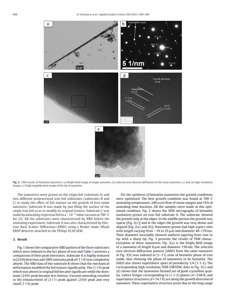
ig. 3. TEM results of hematite nanowires. (a) Bright field image of single nanowirmages, (e) high magnification image of the tip of nanowire.
The nanowires were grown on the virgin foil (substrate A) andwo different preprocessed iron foil substrates (substrates B and) to study the effect of foil texture on the growth of Iron oxideanowire. Substrate B was made by just filing the surface of theirgin iron foil so as to modify its original texture. Substrate C wasade by annealing virgin iron foil in a ∼10−5 mbar vacuum at 700 ◦C
or 2 h. All the substrates were characterized by XRD before thennealing experiment. Substrate A was also characterized by Elec-ron Back Scatter Diffraction (EBSD) using a Bruker make XflashBSD detector attached to the Philips XL30 SEM.
. Result
Fig. 1 shows the comparative XRD pattern of the three substrateshich were indexed to the bcc phase of iron and Table 1 presents a
omparison of their peak intensities. Substrate A is highly texturedn [2 0 0] direction and 100% intensity peak of (1 1 0) was completelybsent. The XRD data of the substrate B shows that the mechanicaleformation modified the foil texture significantly. The (1 1 0) peak
hich was absent in original foil became significant while the dom-nant (2 0 0) peak became less intense. Vacuum annealing resultedn the enhancement of (2 1 1) peak against (2 0 0) peak and verymall (1 1 0) peak.
elected area electron diffraction of the same nanowire, (c) and (d) high resolution
For the synthesis of hematite nanowires the growth conditionswere optimized. The best growth condition was found at 700 ◦Cannealing temperature, 240 sccm flow of moist oxygen and 16 h ofannealing time duration. All the samples were made at this opti-mized condition. Fig. 2 shows the SEM micrographs of hematitenanowires grown on iron foil substrate A. The substrate showedthe growth only at the edges. In the middle portion the growth wassparse [Fig. 2(c)] and at the edges the growth was very dense andaligned [Fig. 2(a) and (b)]. Nanowires grown had high aspect ratiowith length varying from ∼10 to 25 �m and diameter 40–170 nm.Their diameter invariably showed uniform tapering from root totip with a sharp tip. Fig. 3 presents the results of TEM charac-terization of these nanowires. Fig. 3(a) is the bright field imageof a nanowire of length 8 �m and diameter 150 nm. The selectedarea electron diffraction pattern (SAED) from the same nanowirein Fig. 3(b) was indexed to [1–11] zone of hematite phase of ironoxide, thus showing the phase of nanowires to be hematite. TheSAED also shows superlattice spots of periodicity 1/4 (1-1-2). Thecorresponding high resolution TEM (HRTEM) data in Fig. 3(c) and
(d) shows that the nanowires formed are of good crystalline qual-ity. Lattice fringes corresponding to (1-1-2) planes (d = 3.68 A) andsuperlattice structures (d = 14.7 A) are along the growth direction ofnanowire. These superlattice structure arises due to the long range
H. Srivastava et al. / Applied Surface Science 258 (2011) 494– 500 497
Fig. 4. SEM micrograph of as grown hematite nanowires on substrate B. (a) Image at 2000× magnification, (b) image at 5000×.
te C. I
ooatttgwinmd
Fs
Fig. 5. SEM micrograph of as grown hematite nanowires on substra
rdering of oxygen vacancies [22]. The SAED and high resolutionbservations clearly established that the nanowires uniquely grewlong [1 1 0] direction. Fig. 3(d) is a high magnification image of theip of a nanowire. The image shows crystal steps formed duringhe growth of the nanowire. The tapering morphology formed byhese steps suggests that the nanowires grow via tip. The XRD of asrown sample was indexed to hematite rhombohedral structureith lattice parameters a = 5.036 A and c = 13.749 A [Fig. 6]. This
mplies that the upper crust of the substrate which also contains
anowires is hematite. In the graph two peaks (1 1 0) and (3 0 0) hasuch higher relative intensities as compared to standard powderiffraction data. Others peaks are suppressed due to the large inten-
70605040300
2000
4000
6000
8000
10000
12000
14000
16000
18000
20000
202
018 30
021
4
116
024
113
006
110
inte
nsity
(a.u
.)
2-theta
Substrate B Substrate A Substrate C
104
ig. 6. X-ray diffraction of as grown hematite nanowires sample grown on differentubstrates.
mage at 2000× magnification, (b) image of a sparse growth region.
sities of the above two peaks. The large intensity of (1 1 0) peak isdue to the aligned nanowires which uniquely grew in [1 1 0] direc-tion, whereas enhanced (3 0 0) peak only signifies the underlyingoriented hematite film.
Fig. 4 shows the SEM micrographs of the nanowires grownon the substrate B. In this case the dense nanowires grew allover the substrate [Fig. 4(a and b)]. The nanowires were shorterand had lower aspect ratio than those observed on substrate A.The nanowires have length between ∼4 and 8 �m, and diameterfrom ∼80 to 200 nm. Owing to the dense and large growth of thenanowires the XRD of the as grown sample shows a very large peakof (1 1 0) plane and small peaks of other planes [Fig. 6].
Fig. 5 shows the SEM result of the nanowires sample grown onthe pre vacuum annealed substrate C. Annealing resulted in thegrowth of thick nanowires and flakes. The length of the nanowiresvaries from ∼5 to 10 �m and the diameter varies from 120 to180 nm. The flakes have length from ∼10 to 22 �m and width∼400–850 nm. These structures grew in small patches on the sub-strate with coverage of nearly 20% area only. The correspondingXRD pattern matches with the standard diffraction pattern of thehematite phase [Fig. 6].
Fig. 6 presents the comparative XRD result of nanowires samplesgrown on different substrates. All the patterns were well matchedto the hematite phase. The enhanced (1 1 0) peak signifies the pres-ence of large quantity of aligned nanowires. Largest peak of (1 1 0)on substrate B indicates the best growth of the hematite nanowires.
Sample A is different from samples B and C as the last two sub-strates have uniform features with respect to nanowires growthwhereas the sample A has two different regions edge and the midportion. EBSD map of substrate A was taken to find any possible
inhomogeneity in the grain orientation in those two portions. Fig. 7presents the EBSD map results taken on sample A to observe thetexture difference between the edge and the mid region. Fig. 7(a)shows the EBSD map in Z direction at the mid region of substrate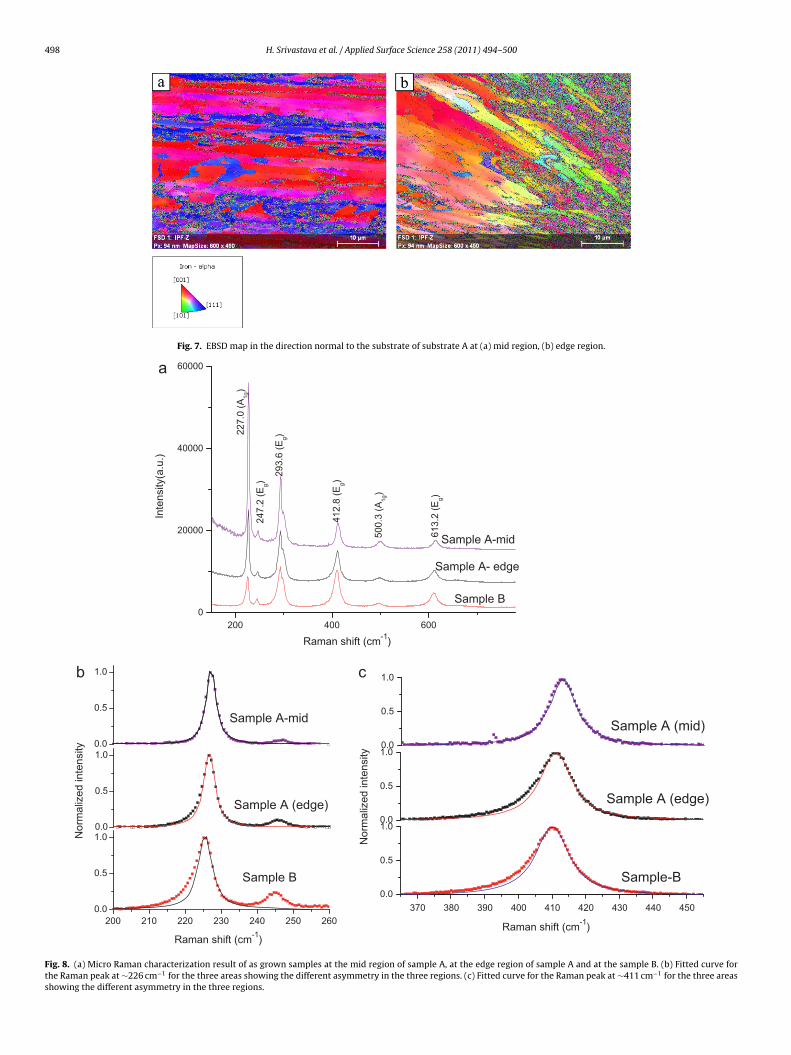
498 H. Srivastava et al. / Applied Surface Science 258 (2011) 494– 500
Fig. 7. EBSD map in the direction normal to the substrate of substrate A at (a) mid region, (b) edge region.
6004002000
20000
40000
60000a
b c
Sample A- edge
Sample A-mid613.
2 (E
g)
247.
2 (E
g)
412.
8 (E
g)
500.
3 (A
1g)
293.
6 (E
g)
Inte
nsity
(a.u
.)
227.
0 (A
1g)
Sample B
0.0
0.5
1.0
4504404304204104003903803700.0
0.5
1.0
0.0
0.5
1.0
Nor
mal
ized
inte
nsity
Sample A (edge)
Raman shift (cm-1)
Raman shift (cm-1)
Raman shift (cm-1)
Sample-B
Sample A (mid)
0.0
0.5
1.0
2602502402302202102000.0
0.5
1.0
0.0
0.5
1.0
Nor
mal
ized
inte
nsity
Sample A (edge)
Sample B
Sample A-mid
Fig. 8. (a) Micro Raman characterization result of as grown samples at the mid region of sample A, at the edge region of sample A and at the sample B. (b) Fitted curve forthe Raman peak at ∼226 cm−1 for the three areas showing the different asymmetry in the three regions. (c) Fitted curve for the Raman peak at ∼411 cm−1 for the three areasshowing the different asymmetry in the three regions.

H. Srivastava et al. / Applied Surface Science 258 (2011) 494– 500 499
Table 2aRaman shift (in cm−1) on different samples.
Peak Raman mode Substrate B (FWHM) Substrate A at the edge (FWHM) Substrate A at mid region (FWHM)
1st A1g 225.1 (4.7) 226.4 (4.3) 227.0 (3.6)2nd Eg 244.7 (5.6) 245.3 (5.7) 247.2 (6.4)3rd Eg 292.4 (10.5) 293.0 (8.0) 293.6 (5.4)
410.9499.7611.4
Aoi[oTrnirhwaEsd
anTtpRsAhl∼sa∼rtnbptbaawttladi
TC
4th Eg 410.3 (13.6)
5th A1g 497.3 (20.4)
6th Eg 610.2 (18.1)
. The map is largely reddish which indicates that the foil is highlyriented in [1 0 0] direction. Also there is no greenish region whichmplies that the foil is completely devoid of the grains oriented in1 1 0] direction. The result is in concurrence with the XRD resultf substrate A. Fig. 7(b) shows the IPF Z map at the edge region.he map shows regions of two types – the plastically deformedegion in the right half is from the edge side of the foil and theormal region at the left half. Plastic deformation at the edges was
nduced by the cutting of the substrate. As expected, the normalegion is oriented in [1 0 0] direction whereas the deformed regionas randomly oriented grains including the [1 1 0] oriented grainshich were completely absent in the normal region. Also, there
re lots of black portions in right half which are the regions whereBSD pattern could not be indexed. It mainly happens for the highlytressed grains, which form in large numbers due to the large plasticeformation.
Fig. 8a shows the Raman Spectrum of the middle area ofnnealed substrate A which is devoid of nanowires and theanowires grown at the edge of substrate A and at substrate B.able 2a presents the comparative list of all the Raman modes,heir peak positions and full width at half maxima (FWHM) of theseeaks in above three cases. All the 6 peaks match with the hematiteaman spectra reported in the literature [23,24]. All these peakshow red shift in peak positions from sample A (mid) to sample
(edge) and further in sample B. The Raman data for the samplesighlight the significant role of nanowire size in determining the
ineshapes of the various peaks. We have chosen the peaks at226 cm−1 and ∼411 cm−1 as a representative of the two type of
ymmetry A1g and Eg respectively, present in hematite, for furthernalysis. Fig. 8b and c shows the Raman peaks at ∼226 cm−1 and411 cm−1 respectively for three samples with their backgrounds
emoved and fitted with a lorentzian peak. It can be clearly seenhat the hematite grown on the substrate A (mid) where noanowires were formed, fits to a perfect lorentzian lineshape foroth the peaks. Similar fits to a lorentzian profile for the Ramaneaks of the nanowires grown on substrates A (edge) and B showhat there is a distinct asymmetry on the lower frequency side ofoth the peaks. Table 2b presents the quantitative estimate of thissymmetry in terms of ratio of � a to � b, where � a is the half widtht half maxima on the lower frequency side and � b is the halfidth on the higher frequency side. The table clearly shows that
he asymmetry increases with decreasing nanowires size (refero Table 1 for comparison of nanowires size). Such asymmetric
ineshapes have been previously reported for nanostructuresnd have been attributed to either phonon confinement [25] orisorder activated zone edge phonons [26]. The increasing red shiftn the Raman frequencies and the FWHM of these peaks observed
able 2bomparison of asymmetry in peaks at ∼226 cm−1 and ∼411 cm−1.
A1g peak at ∼226 cm−1
Substrate B Substrate A edge Substrate A mid
� a 3.2 2.2 1.8
� b 2.3 2.1 1.8
� a/� b 1.39 1.05 1.00
(13.0) 412.8 (9.8) (19.4) 500.3 (17.1) (18.1) 613.2 (14.3)
with decreasing nanowires size is also consistent with the phononconfinement model as explained below [24,25,27]. The explanationand quantification of the observed asymmetry in hematite requiresthe knowledge of the phonon dispersion curves (PDC). To the bestof our knowledge, there has been no published work on thePDC of �-Fe2O3 either by experiments or by calculation. Thus noevaluation of the effects of confinement on the asymmetry of thelineshapes has been made in this work. However, for a qualitativeunderstanding we have looked at the PDC of �-Al2O3 which hasthe same structure as hematite and thus similar Raman activemodes. Ref. [28] gives a detail calculation of PDC for sapphire. PDCof sapphire shows that in all the Raman active modes, the phononfrequency decreases with increase in q and thereby suggestingan asymmetry in the lower frequency side with reducing particlesize. Thus by analogy with �-Al2O3 and the general understandingthat optical modes have a maxima at k = 0 point in the Brillouinzone [27], we conclude that the Raman mode red shift and lowerfrequency side asymmetry is due to the reduced nanowires sizes.
4. Discussion
Table 1 presents the comparative data of nanowires grown onthree substrates A, B and C. The growth of nanowires was observedonly on the substrate B and at the edges of substrate A. The XRD andEBSD results show that these were the only areas which had [1 1 0]oriented grains. The observation clearly suggests that the [1 1 0] ori-ented grains in iron substrate are vital for the growth of hematitenanowires. This also explains our finding in the previous work onhematite nanowires, where we observed that a polycrystalline ironfoil produced much better nanowires growth as compared to a[1 0 0] oriented foil [21]. Iron is a bcc metal. In bcc metals the pre-dominant rolling texture consists of {1 0 0} planes oriented parallelto the plane of the sheet with the [1 1 0] in the rolling direction thusgiving the foil [1 0 0] texture [29]. This texture can be modified bythe various ways of plastic deformations like cutting and filing; togenerate the favorable [1 1 0] oriented grains. The plastic deforma-tion applies a large shear force on the foil. That causes the easy slipplanes of bcc metal (1 1 0), (1 1 2) and (1 2 3) to appear on the sur-face which results in the change of foil texture. This explains thepresence of [1 1 0] oriented grains at the edge of the substrate A onan otherwise [2 0 0] oriented foil. Further, the observation that thepresence of [1 1 0] texture helped in the growth of [1 1 0] orientedhematite nanowires clearly suggests that a topotaxial relationship
exists between [1 1 0]hematite//[1 1 0]iron. To the best of our knowl-edge, the effect of this particular topotaxial relationship has notbeen studied before. This result can be of significant technolog-ical importance as it provides texture as a powerful parameter toEg peak at ∼411 cm−1
Substrate B Substrate A edge Substrate A mid
7.4 6.8 4.96.2 6.2 4.91.19 1.10 1.00
5 urface
ceo
tnabsgamvoTtlrctgcv
rgigmgrevfbirmo
5
iggwAngwrtbm
[[
[
[
[
[[[[
[
[
[
[
[[[[[[[[
00 H. Srivastava et al. / Applied S
ontrol the growth of hematite nanowire. Further, it would be inter-sting to investigate the similar effect in the growth of other metalxide nanowires synthesized by the annealing method.
Comparing the microstructures of nanowires formed in thehree substrates, the edge of substrate A has large aspect ratioanowires whereas substrate B has smaller nanowires of lowspect ratio. Substrate C largely has flakes. The observation cane explained by the surface condition of the substrates. The sub-trate B had a rough surface. The roughness accelerates the oxiderowth and results in the growth of a much thicker oxide layer than
smooth surface in similar annealing conditions [30]. In annealingethod nanowires grow by the diffusion of cations from substrate
ia the root of nanowires to the tip and the tapering in the diameterf nanowires is a strong indication of this mechanism [15,17,21].he thicker oxide layer in substrate B caused the reduction inhe diffusion of iron ion through it, and prevented the growth ofong nanowires. In contrast, the vacuum annealing in substrate Cesulted in the grain growth and recrystallization. Grain growthauses a reduction in the content of grain boundaries which leadso retarded oxidation rate. Thus vacuum annealing resulted in therowth of thinner oxide layer on substrate C in similar annealingonditions as substrates A and B, which helped in the growth ofery large nanowires.
Apart from the texture the water vapor also played an importantole in the growth of nanowires. The use of water vapor with oxy-en enhanced the formation of nanowires significantly and resultedn the growth of dense and highly aligned nanowires. Moist oxy-en as a oxidizer is very simple to produce as compare to complexixture of gases reported earlier, and resulted in the very good
rowth of nanowires which is comparable to the best reportedesults [17,21]. Similar studies in other metals have also shown thenhanced formation of oxide nanowires in the presence of waterapor [31,32]. The water vapour weakens the bonds between sur-ace Fe3+ ions and the oxygen ions immediately below the surfacey the hydroxylation of the hematite surface [33]. As a result, the
ron ions arriving at the surface become more mobile. This allowsapid surface diffusion and results in the preferential growth of theinimum energy surfaces of hematite, resulting in the formation
f hematite whiskers.
. Conclusion
Dense and aligned hematite nanowires were grown by anneal-ng iron foil in moist oxygen at 700 ◦C. Presence of water vaporreatly enhanced the formation of nanowires. Investigating therowth of nanowires on three different substrates A, B and Ce found that only the substrate B and the edge of substrate
which have the [1 1 0] oriented grains showed the growth ofanowires. Thus the [1 1 0] oriented grains are crucial for therowth of nanowires. We also observed that the smooth surfacehere resulted in the long and high aspect ratio nanowires, the
ough surface produced small nanowires. Moreover it was shownhat the growth can also be obtained on the textured substratesy the modification of texture via various ways of plastic defor-ations. The results demonstrate that simple surface texturing
[[
[
Science 258 (2011) 494– 500
techniques can be used efficiently for large scale synthesis of thenanowires and the substrate texture is a very strong tool to con-trol the growth of nanowires and hence can be used effectively forpatterning and the large scale synthesis of nanowires.
Acknowledgements
Authors thank Dr. V.C. Sathe of UGC-DAE-CSR, Indore for Ramanmeasurements and Mr. P. Ganesh of LMP Division, RRCAT for var-ious helpful discussions related to the texture of metals. Authorsalso thank Ms. Priyanka Singh for her work on the optimization ofgrowth of hematite nanowires. At last authors thank Mr. MahendraBabu for throughout support during the course of this work.
References
[1] K.K. Lepers, Vestn. Akad. Nauk SSSR 4 (26) (1990).[2] R.M. Cornell, U. Schwertmann, The Iron Oxides, Structure, Properties, Reactions,
Occurrence and Uses, VCH, Weinhein, 1996.[3] G. Bate, E.D. Wohlforth, Ferromagnetic Material, North-Holland, Amsterdam,
The Netherlands, 1980.[4] L. Huo, W. Li, H. Cui, S. Xi, J. Wang, B. Zhao, Y. Shen, Z. Lu, Chem. Mater. 12 (790)
(2000).[5] W. Huynh, X.G. Peng, A.P. Alivisatos, Adv. Mater. 11 (923) (1999).[6] T. Tepper, F. Ilievski, C.A. Ross, T.R. Zaman, R.J. Ram, S.Y. Yung, B. Stadler, J. Appl.
Phys. 93 (6948) (2003).[7] P. Li, D.E. Miser, S. Rabiei, R.T. Yadav, M.R. Hajaligol, Appl. Catal. B 43 (151)
(2003).[8] T. Ohmori, H. Takahashi, H. Mametsuka, E. Suzuki, Phys. Chem. Chem. Phys. 2
(3519) (2000).[9] C. Wu, P. Yin, X. Zhu, C.O. Yang, Y. Xie, J. Phys. Chem. B 110 (17806) (2006).10] Y. Xiong, Z. Li, X. Li, B. Hu, Y. Xie, Inorg. Chem. 43 (6540) (2004).11] T. Lindgren, H. Wang, N. Beermann, L. Vayssieres, A. Hagfeldt, S.E. Lindquist,
Sol. Energy Mater. Sol. Cells 71 (231) (2002).12] Z. Zheng, Y. Chen, Z. Shen, J. Ma, C.H. Sow, W. Huang, T. Yu, Appl. Phys. A 89
(115) (2007).13] C.H. Kim, H.J. Chun, D.S. Kim, S.Y. Kim, J. Park, J.Y. Moon, G. Lee, J. Yoon, Y. Jo,
M.H. Jung, S.I. Jung, C.J. Lee, Appl. Phys. Lett. 89 (223103) (2006).14] L. Suber, P. Imperatori, G. Ausanio, F. Fabbri, H. Hofmeister, J. Phys. Chem. B 109
(7103) (2005).15] R. Takagi, J. Phys. Soc. Jpn. 12 (11) (1957).16] Y. Fu, J. Chen, H. Zhang, Chem. Phys. Lett. 350 (2001) 491.17] X. Wen, S. Wang, Y. Ding, Z.L. Wang, S. Yang, J. Phys. Chem. B 2005 (2005) 109.18] R. Wang, Y. Chen, Y. Fu, H. Zhang, C. Kisielowski, J. Phys. Chem. B 109 (2005)
12245.19] L.C. Hsu, Y.Y. Li, C.G. Lo, C.W. Huang, G. Chern, J. Phys. D: Appl. Phys. 41 (2008)
185003.20] P. Hiralal, H.E. Unalan, K.G.U. Wijayantha, A. Kursumovic, D. Jefferson, J.L.
MacManus-Driscoll, G.A.J. Amaratunga, Nanotechnology 19 (2008) 455608.21] H. Srivastava, P. Tiwari, A.K. Srivastava, R.V. Nandedkar, J. Appl. Phys. 102 (2007)
054303.22] Z. Chen, U. Cvelbar, M. Mozetic, J. He, M.K. Sunkara, Chem. Mater. 20 (2008)
3224.23] D.L.A. de Faria, S.V. Silva, M.T. de Oliveira, J. Raman Spectrosc. 28 (1997) 873.24] A.M. Jubb, H.C. Allen, Appl. Mat. Interf. 2 (10) (2010) 2804.25] I.H. Campbell, P.M. Fauchet, Solid State Commun. 58 (10) (1986) 739.26] A. Ingale, K.C. Rustagi, Phys. Rev. B 58 (11) (1998) 7197.27] F.J. Owens, J. Orosz, Solid State Commun. 138 (95) (2006).28] R. Heid, D. Strauch, K.P. Bohnen, Phys. Rev. B 61 (13) (2000) 8625.29] G.E. Dieter, Mechanical Metallurgy, vol. 239, Mcgraw-Hill Book Company, 1988.30] C. Juricic, H. Pinto, T. Wroblewski, A.R. Pyzalla, Mater. Sci. Forum 524–525
(2006) 963.
31] G.M. Raynaud, R.A. Rapp, Oxid. Met. 21 (1984) 89.32] H. Srivastava, P. Tiwari, A.K. Srivastava, S. Porwal, S.K. Deb, Semicond. Sci. Tech-nol. 26 (2011) 085030.33] B. Pujilaksono, T. Jonsson, M. Halvarsson, J.E. Svensson, L.G. Johansson, Corros.
Sci. 52 (2010) 1560.