
Effect of nanowire length on the performance of silicon nanowires based solar cell
6
This content has been downloaded from IOPscience. Please scroll down to see the full text. Download details: IP Address: 193.48.172.167 This content was downloaded on 15/11/2014 at 00:11 Please note that terms and conditions apply. Effect of nanowire length on the performance of silicon nanowires based solar cell View the table of contents for this issue, or go to the journal homepage for more 2014 Adv. Nat. Sci: Nanosci. Nanotechnol. 5 045014 (http://iopscience.iop.org/2043-6262/5/4/045014) Home Search Collections Journals About Contact us My IOPscience
-
Upload
independent -
Category
Documents
-
view
1 -
download
0
Transcript of Effect of nanowire length on the performance of silicon nanowires based solar cell

This content has been downloaded from IOPscience. Please scroll down to see the full text.
Download details:
IP Address: 193.48.172.167
This content was downloaded on 15/11/2014 at 00:11
Please note that terms and conditions apply.
Effect of nanowire length on the performance of silicon nanowires based solar cell
View the table of contents for this issue, or go to the journal homepage for more
2014 Adv. Nat. Sci: Nanosci. Nanotechnol. 5 045014
(http://iopscience.iop.org/2043-6262/5/4/045014)
Home Search Collections Journals About Contact us My IOPscience
Effect of nanowire length on theperformance of silicon nanowires basedsolar cell
Van Trinh Pham1,2, Mrinal Dutta2, Hung Thang Bui1 and Naoki Fukata2
1 Institute of Materials Science, Vietnam Academy of Science and Technology, 18 Hoang Quoc Viet Road,Cau Giay District, Hanoi, Vietnam2 International Center for Materials Nanoarchitectonics, National Institute for Materials Science, 1-1Namiki, Tsukuba, Ibaraki 305-0044, Japan
E-mail: [email protected] and [email protected]
Received 6 October 2014Accepted for publication 21 October 2014Published 14 November 2014
AbstractCurrently, silicon nanowires (SiNWs) are attracting attention as promising candidate materialsfor developing the next-generation solar cells to realize both low cost and high efficiency due totheir unique structural, electrical, and optical properties. In this paper, a vertical-aligned SiNWsarray has been prepared by metal-assistant chemical etching technique and implemented onSiNW array textured solar cells for photovoltaic application. The shape and size of SiNWs werecontrolled by etching time of 30 min, 45 min and 60 min with the length of SiNWs of 4 μm, 6 μmand 8 μm, respectively. The etching rate was estimated to be about 133 nm per minute. Theoptical properties of a SiNWs array with different lengths were investigated in terms of opticalreflection property. Less than 6% reflection ratio from 300 nm to 800 nm wavelength wasachieved. In addition, I–V characteristic was used to estimate the dependence of the SiNWslength on the performance of SiNWs based solar cell. Conservation efficiencies were achieved of1.71%, 2.19%, and 2.39% corresponding to 4 μm, 6 μm and 8 μm SiNWs in length, respectively.
Keywords: silicon nanowires, SiNW array, solar cells, SiNWs based solar cellMathematics Subject Classification: 4.08, 6.03
1. Introduction
There is great demand for the development of the next genera-tions of solar cell with higher efficiency, cheaper price andlonger life. Nanomaterials and nanostructures based solar cellshold promising potency to enhance the performance of solarcells by improving both light trapping and photo-carrier collec-tion. Many approaches have been taken to lower the productioncost of Si photovoltaics, among which thin-film Si solar cellsoffer a promising low-cost solution [1, 2], however, thin-film Sisolar cells have lower efficiencies than bulk Si, due to theirlimited absorption thickness. Si nanowires (SiNWs) have beenconsidered as novel class of nanostructured materials for high-performance devices [3, 4] due to their unique structural, elec-trical, optical, and thermoelectric properties. Recently, SiNWshave been widely investigation for developing next-generationsolar cells to realize both low cost and high efficiency [5–9].
SiNWs can be prepared by two main methods includingbottom-up and top-down fabrication. Therein, the bottom-upmethod usually uses chemical vapor deposition (CVD) tech-niques with vapor–liquid–solid (VLS) process for fabricatingthe dense, high aspect ratio, and vertically aligned SiNWs [1].Moreover, the formation of pn junction and preparation ofSiNWs can be easily prepared together by VLS process[10, 11]. However, this method always requires a highlyprotected quality clean room, and expensive CVD systemslead to an increase of the production cost of material. Incontrast, the top-down method with chemical etching tech-nique is promoted as a simple technique to prepare the uni-form, high aspect ratio as well as vertically aligned SiNWssimilar to the VLS process, but it seems to remain highly cost-effective in comparison with VLS process [12–14]. To beused for solar cell application, SiNWs prepared by chemicaletching need doping to form pn junction; doping techniques
| Vietnam Academy of Science and Technology Advances in Natural Sciences: Nanoscience and Nanotechnology
Adv. Nat. Sci.: Nanosci. Nanotechnol. 5 (2014) 045014 (5pp) doi:10.1088/2043-6262/5/4/045014
2043-6262/14/045014+05$33.00 © 2014 Vietnam Academy of Science & Technology1
such as VLS process [15, 16] and wet diffusion process[17, 18] have been used for this goal. Therein, wet diffusionprocess using dopant solution has become a promisingapproach for lowering the cost manufacturing of solar cells.
Therefore, in this paper, we present the results of theinvestigation of using SiNWs for low cost solar cell with thecombination of metal-assisted chemical etching for preparingSiNWs and wet diffusion process for fabricating the radial pnjunction. The optical property and I–V characteristics ofSiNWs based solar cell are also presented in this paper.
2. Experimental procedure
2.1. Materials
Acetone, ethanol, sulfuric acid (H2SO4), hydrogen peroxide(H2O2), hydro fluoric (HF) acid and nitric acid (HNO3) weresupplied by Wako Pure Chemical Industries Co. Silver nitrate(AgNO3) were purchased from Sigma-Aldrich. The p-type Si(100) wafers were produced by Ferrotec Silicon Co. Ohkacoating diffusion-source (OCD) solution containing phos-phorus manufactured by Tokyo Chemical Industry Co. Ltd.Silver and aluminum targets were purchased from KojundoChemical Laboratory Co.
2.2. Preparation of SiNWs
SiNW arrays were prepared with Ag-assisted etching method.p-type (100) silicon wafers were cleaned with acetone (5 min)and ethanol (5 min), rinsed with deionized water (10 min) 3times, then immersed in a 3:1 mixture of H2SO4 (97%) andH2O2 (30%) for 10 min, thoroughly rinsed with deionizedwater for 10 min, and then dipped in HF solution for 1 min.The cleaned silicon wafers were immersed into an aqueousHF solution (4.6 M) containing AgNO3 (0.02 M) and treatedfor 30 min, 45 min and 60 min at room temperature. As-pre-pared SiNW samples were rinsed in deionized water and driedat room temperature. SiNW arrays were treated in HNO3
(35%) for desired durations, and SiNW array of variednanowire densities could be obtained.
2.3. Fabrication of solar cell
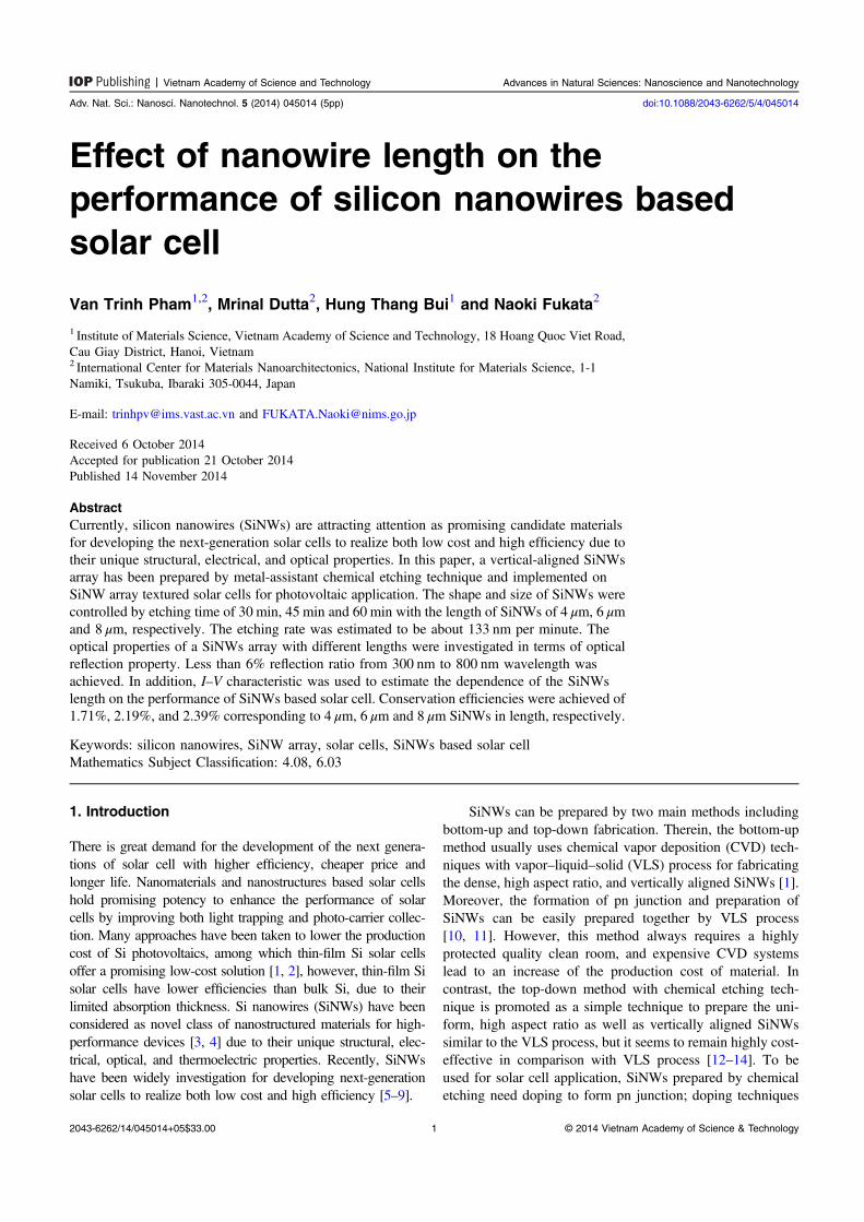
The fabrication process of SiNW radial pn junction arraysshown in figure 1 consists of two main steps: (a) spin-coatingOCD solution onto the surface of synthesized SiNW arrays ata speed of 2000 rpm; (b) annealing of the samples by athermal annealing system in argon atmosphere at 850 °C for45 min followed by removal of remaining OCD solution inpiranha solution for 4 min and SiO2 film in 1% HF solutionfor 2 min. After radial pn junction structure was formed, athin layer of aluminum film with thickness of 200 nm wasdeposited on the rear side of samples. Then a Ag film withthickness of 600 nm was deposited on the surface of SiNWradial pn junction arrays to form the front electrode via ashadow mask evaporation process in thermal evaporationsystem.
2.4. Characterization
The morphologies of the samples were characterized byHitachi S4800 field emission scanning electron microscope(FESEM). Optical reflectance spectra were recorded by Jac-cob V-570 UV/Vis/NIR spectrophotometer. The I–V char-acteristic measurement of based solar cell was performedusing a solar simulator under Air Mass (AM) 1.5 G illumi-nation with intensity of 100 mW cm−2.
3. Results and discussion
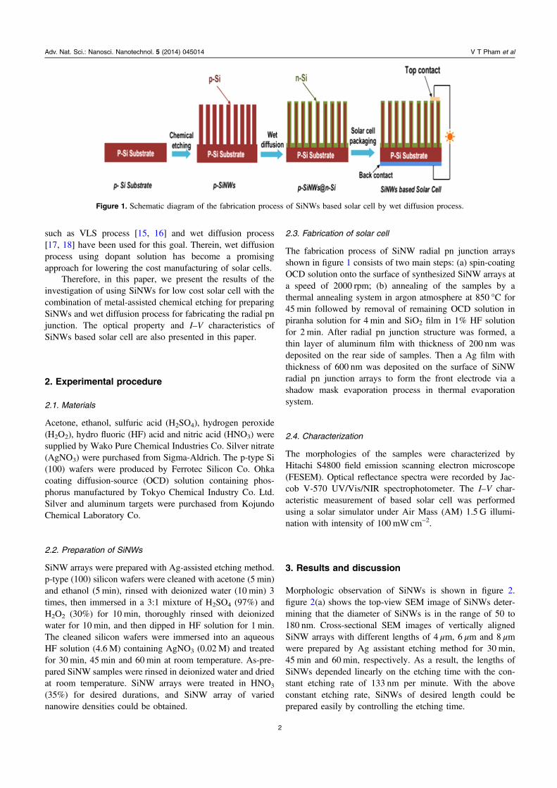
Morphologic observation of SiNWs is shown in figure 2.figure 2(a) shows the top-view SEM image of SiNWs deter-mining that the diameter of SiNWs is in the range of 50 to180 nm. Cross-sectional SEM images of vertically alignedSiNW arrays with different lengths of 4 μm, 6 μm and 8 μmwere prepared by Ag assistant etching method for 30 min,45 min and 60 min, respectively. As a result, the lengths ofSiNWs depended linearly on the etching time with the con-stant etching rate of 133 nm per minute. With the aboveconstant etching rate, SiNWs of desired length could beprepared easily by controlling the etching time.
Figure 1. Schematic diagram of the fabrication process of SiNWs based solar cell by wet diffusion process.
2
Adv. Nat. Sci.: Nanosci. Nanotechnol. 5 (2014) 045014 V T Pham et al
The doping diffusion profile of radial pn junction wasestimated by the following equation [19]
=L Dt ,
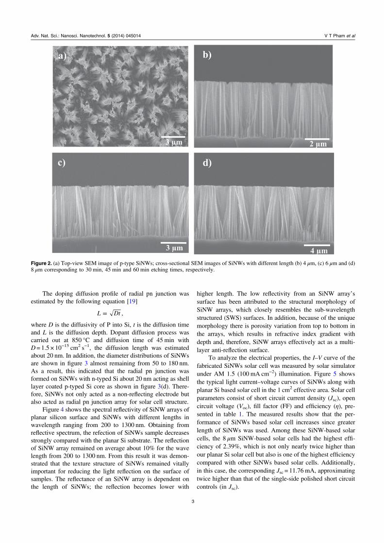
where D is the diffusivity of P into Si, t is the diffusion timeand L is the diffusion depth. Dopant diffusion process wascarried out at 850 °C and diffusion time of 45 min withD= 1.5 × 10⁻¹⁵ cm2 s−1, the diffusion length was estimatedabout 20 nm. In addition, the diameter distributions of SiNWsare shown in figure 3 almost remaining from 50 to 180 nm.As a result, this indicated that the radial pn junction wasformed on SiNWs with n-typed Si about 20 nm acting as shelllayer coated p-typed Si core as shown in figure 3(d). There-fore, SiNWs not only acted as a non-reflecting electrode butalso acted as radial pn junction array for solar cell structure.
Figure 4 shows the spectral reflectivity of SiNW arrays ofplanar silicon surface and SiNWs with different lengths inwavelength ranging from 200 to 1300 nm. Obtaining fromreflective spectrum, the refection of SiNWs sample decreasesstrongly compared with the planar Si substrate. The reflectionof SiNW array remained on average about 10% for the wavelength from 200 to 1300 nm. From this result it was demon-strated that the texture structure of SiNWs remained vitallyimportant for reducing the light reflection on the surface ofsamples. The reflectance of an SiNW array is dependent onthe length of SiNWs; the reflection becomes lower with
higher length. The low reflectivity from an SiNW array’ssurface has been attributed to the structural morphology ofSiNW arrays, which closely resembles the sub-wavelengthstructured (SWS) surfaces. In addition, because of the uniquemorphology there is porosity variation from top to bottom inthe arrays, which results in refractive index gradient withdepth and, therefore, SiNW arrays effectively act as a multi-layer anti-reflection surface.
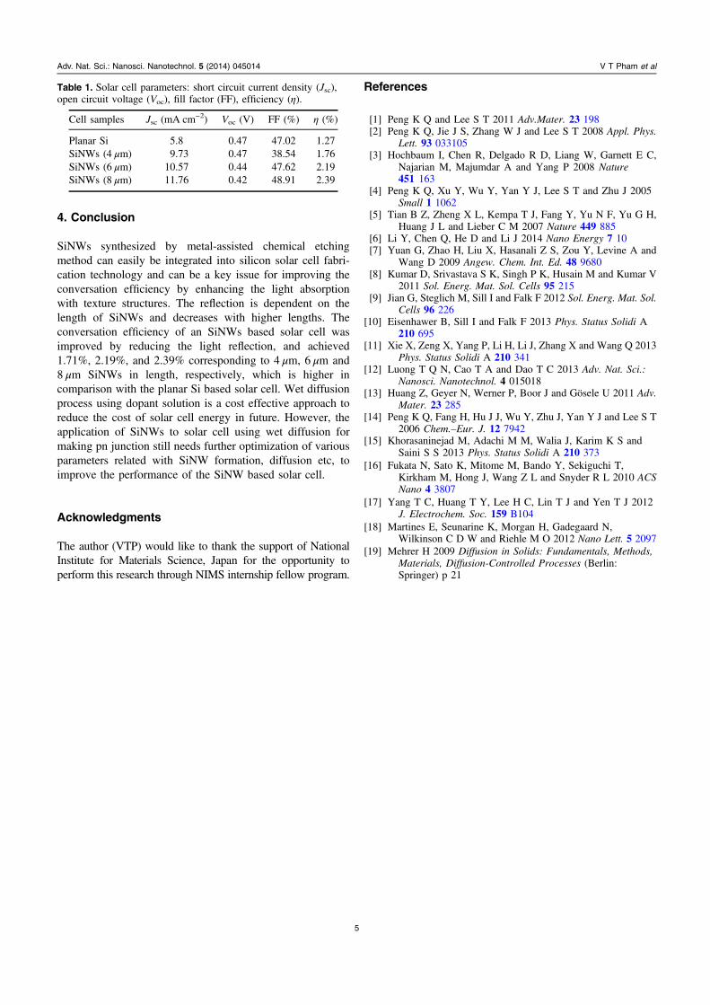
To analyze the electrical properties, the I–V curve of thefabricated SiNWs solar cell was measured by solar simulatorunder AM 1.5 (100 mA cm−2) illumination. Figure 5 showsthe typical light current–voltage curves of SiNWs along withplanar Si based solar cell in the 1 cm2 effective area. Solar cellparameters consist of short circuit current density (Jsc), opencircuit voltage (Voc), fill factor (FF) and efficiency (η), pre-sented in table 1. The measured results show that the per-formance of SiNWs based solar cell increases since greaterlength of SiNWs was used. Among these SiNW-based solarcells, the 8 μm SiNW-based solar cells had the highest effi-ciency of 2.39%, which is not only nearly twice higher thanour planar Si solar cell but also is one of the highest efficiencycompared with other SiNWs based solar cells. Additionally,in this case, the corresponding Jsc = 11.76 mA, approximatingtwice higher than that of the single-side polished short circuitcontrols (in Jsc).
Figure 2. (a) Top-view SEM image of p-type SiNWs; cross-sectional SEM images of SiNWs with different length (b) 4 μm, (c) 6 μm and (d)8 μm corresponding to 30 min, 45 min and 60 min etching times, respectively.
3
Adv. Nat. Sci.: Nanosci. Nanotechnol. 5 (2014) 045014 V T Pham et al
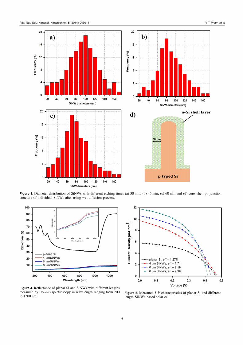
Figure 3. Diameter distribution of SiNWs with different etching times (a) 30 min, (b) 45 min, (c) 60 min and (d) core–shell pn junctionstructure of individual SiNWs after using wet diffusion process.
Figure 4. Reflectance of planar Si and SiNWs with different lengthsmeasured by UV–vis spectroscopy in wavelength ranging from 200to 1300 nm.
Figure 5. Measured I–V characteristics of planar Si and differentlength SiNWs based solar cell.
4
Adv. Nat. Sci.: Nanosci. Nanotechnol. 5 (2014) 045014 V T Pham et al
4. Conclusion
SiNWs synthesized by metal-assisted chemical etchingmethod can easily be integrated into silicon solar cell fabri-cation technology and can be a key issue for improving theconversation efficiency by enhancing the light absorptionwith texture structures. The reflection is dependent on thelength of SiNWs and decreases with higher lengths. Theconversation efficiency of an SiNWs based solar cell wasimproved by reducing the light reflection, and achieved1.71%, 2.19%, and 2.39% corresponding to 4 μm, 6 μm and8 μm SiNWs in length, respectively, which is higher incomparison with the planar Si based solar cell. Wet diffusionprocess using dopant solution is a cost effective approach toreduce the cost of solar cell energy in future. However, theapplication of SiNWs to solar cell using wet diffusion formaking pn junction still needs further optimization of variousparameters related with SiNW formation, diffusion etc, toimprove the performance of the SiNW based solar cell.
Acknowledgments
The author (VTP) would like to thank the support of NationalInstitute for Materials Science, Japan for the opportunity toperform this research through NIMS internship fellow program.
References
[1] Peng K Q and Lee S T 2011 Adv.Mater. 23 198[2] Peng K Q, Jie J S, Zhang W J and Lee S T 2008 Appl. Phys.
Lett. 93 033105[3] Hochbaum I, Chen R, Delgado R D, Liang W, Garnett E C,
Najarian M, Majumdar A and Yang P 2008 Nature451 163
[4] Peng K Q, Xu Y, Wu Y, Yan Y J, Lee S T and Zhu J 2005Small 1 1062
[5] Tian B Z, Zheng X L, Kempa T J, Fang Y, Yu N F, Yu G H,Huang J L and Lieber C M 2007 Nature 449 885
[6] Li Y, Chen Q, He D and Li J 2014 Nano Energy 7 10[7] Yuan G, Zhao H, Liu X, Hasanali Z S, Zou Y, Levine A and
Wang D 2009 Angew. Chem. Int. Ed. 48 9680[8] Kumar D, Srivastava S K, Singh P K, Husain M and Kumar V
2011 Sol. Energ. Mat. Sol. Cells 95 215[9] Jian G, Steglich M, Sill I and Falk F 2012 Sol. Energ. Mat. Sol.
Cells 96 226[10] Eisenhawer B, Sill I and Falk F 2013 Phys. Status Solidi A
210 695[11] Xie X, Zeng X, Yang P, Li H, Li J, Zhang X and Wang Q 2013
Phys. Status Solidi A 210 341[12] Luong T Q N, Cao T A and Dao T C 2013 Adv. Nat. Sci.:
Nanosci. Nanotechnol. 4 015018[13] Huang Z, Geyer N, Werner P, Boor J and Gösele U 2011 Adv.
Mater. 23 285[14] Peng K Q, Fang H, Hu J J, Wu Y, Zhu J, Yan Y J and Lee S T
2006 Chem.–Eur. J. 12 7942[15] Khorasaninejad M, Adachi M M, Walia J, Karim K S and
Saini S S 2013 Phys. Status Solidi A 210 373[16] Fukata N, Sato K, Mitome M, Bando Y, Sekiguchi T,
Kirkham M, Hong J, Wang Z L and Snyder R L 2010 ACSNano 4 3807
[17] Yang T C, Huang T Y, Lee H C, Lin T J and Yen T J 2012J. Electrochem. Soc. 159 B104
[18] Martines E, Seunarine K, Morgan H, Gadegaard N,Wilkinson C D W and Riehle M O 2012 Nano Lett. 5 2097
[19] Mehrer H 2009 Diffusion in Solids: Fundamentals, Methods,Materials, Diffusion-Controlled Processes (Berlin:Springer) p 21
Table 1. Solar cell parameters: short circuit current density (Jsc),open circuit voltage (Voc), fill factor (FF), efficiency (η).
Cell samples Jsc (mA cm−2) Voc (V) FF (%) η (%)
Planar Si 5.8 0.47 47.02 1.27SiNWs (4 μm) 9.73 0.47 38.54 1.76SiNWs (6 μm) 10.57 0.44 47.62 2.19SiNWs (8 μm) 11.76 0.42 48.91 2.39
5
Adv. Nat. Sci.: Nanosci. Nanotechnol. 5 (2014) 045014 V T Pham et al