Effect of milling time and heat treatment on the composition of CuIn0.75Ga0.25Se2 nanoparticle...
10
RESEARCH PAPER Effect of milling time and heat treatment on the composition of CuIn 0.75 Ga 0.25 Se 2 nanoparticle precursors and films B. Vidhya • S. Velumani • R. Asomoza Received: 7 May 2010 / Accepted: 20 December 2010 / Published online: 6 March 2011 Ó Springer Science+Business Media B.V. 2011 Abstract Preparation of pure phase CuIn 0.75- Ga 0.25 Se 2 nanoparticle powder by ball milling tech- nique has been confirmed for the milling time of more than 45 min at 1200 rpm. Formation of shear bands responsible for breakdown of grains and generation of nanostructure during mechanical alloy- ing, dislocation and defects induced due to milling has been studied by High-Resolution Transmission Electron Microscopy (HRTEM) analysis. Deviation in final composition of the products from those of starting materials has been discussed based on low volatilization of Se. Effect of milling time on the phase formation, particle size, and composition has been discussed in detail. Decrease in grain size from 12.44 to 7.96 nm has been observed with the increase in milling time. Mechanically induced self-propagat- ing reaction mechanism which occurred during milling process is also discussed. Nanoparticle pre- cursor was mixed with organic binder material for rheology of mixture to be adjusted for screen printing, and the films are subjected to heat treatment at five different temperatures in nitrogen ambient for 25 min. Average grain size calculated by Scherrer’s formula was almost the same irrespective of temper- ature. Reproducibility of precursor composition in the deposited films has been discussed in detail. Keywords CIGS Ball milling EDX HRTEM Synthesis Introduction The energy conversion efficiency of CuInGaSe 2 (CIGS) has reached 19.5% (692 mV, 35.2 mA/cm 2 , FF 79.9%) at NREL (Contreras et al. 2006). However, laboratory scale efficiency is still lower than that of the expected theoretical calculation efficiency (30%) (Choi and Lee 2007). In last few years, researchers tried to use semiconductor nanocrystals in solar cells technology. They have demonstrated that the perfor- mance of photovoltaic cells may be improved using nano structured materials synthesis and device fabri- cation (Lin et al. 2008). For this reason, CIGS nanoparticles have been studied by several authors. Commonly used methods for synthesis of CIGS nanoparticles include solvothermal technique and low temperature colloidal synthesis (Luo et al. 2010a, b; Ahn et al. 2007; Suryanarayana et al. 2001). Among them, solvothermal technique is time consuming, for example, a reaction temperature of B. Vidhya (&) S. Velumani R. Asomoza Department of Electrical Engineering (SEES), CINVESTAV, 07360 Mexico, D.F., Mexico e-mail: [email protected] S. Velumani e-mail: [email protected] S. Velumani Nanoscience and Nanotechnology Programme, CINVESTAV, 07360 Mexico, D.F., Mexico 123 J Nanopart Res (2011) 13:3033–3042 DOI 10.1007/s11051-010-0200-3
Transcript of Effect of milling time and heat treatment on the composition of CuIn0.75Ga0.25Se2 nanoparticle...

RESEARCH PAPER
Effect of milling time and heat treatment on the compositionof CuIn0.75Ga0.25Se2 nanoparticle precursors and films
B. Vidhya • S. Velumani • R. Asomoza
Received: 7 May 2010 / Accepted: 20 December 2010 / Published online: 6 March 2011
� Springer Science+Business Media B.V. 2011
Abstract Preparation of pure phase CuIn0.75-
Ga0.25Se2 nanoparticle powder by ball milling tech-
nique has been confirmed for the milling time of
more than 45 min at 1200 rpm. Formation of shear
bands responsible for breakdown of grains and
generation of nanostructure during mechanical alloy-
ing, dislocation and defects induced due to milling
has been studied by High-Resolution Transmission
Electron Microscopy (HRTEM) analysis. Deviation
in final composition of the products from those of
starting materials has been discussed based on low
volatilization of Se. Effect of milling time on the
phase formation, particle size, and composition has
been discussed in detail. Decrease in grain size from
12.44 to 7.96 nm has been observed with the increase
in milling time. Mechanically induced self-propagat-
ing reaction mechanism which occurred during
milling process is also discussed. Nanoparticle pre-
cursor was mixed with organic binder material for
rheology of mixture to be adjusted for screen
printing, and the films are subjected to heat treatment
at five different temperatures in nitrogen ambient for
25 min. Average grain size calculated by Scherrer’s
formula was almost the same irrespective of temper-
ature. Reproducibility of precursor composition in the
deposited films has been discussed in detail.
Keywords CIGS � Ball milling � EDX � HRTEM �Synthesis
Introduction
The energy conversion efficiency of CuInGaSe2
(CIGS) has reached 19.5% (692 mV, 35.2 mA/cm2,
FF 79.9%) at NREL (Contreras et al. 2006). However,
laboratory scale efficiency is still lower than that of
the expected theoretical calculation efficiency (30%)
(Choi and Lee 2007). In last few years, researchers
tried to use semiconductor nanocrystals in solar cells
technology. They have demonstrated that the perfor-
mance of photovoltaic cells may be improved using
nano structured materials synthesis and device fabri-
cation (Lin et al. 2008). For this reason, CIGS
nanoparticles have been studied by several authors.
Commonly used methods for synthesis of CIGS
nanoparticles include solvothermal technique and
low temperature colloidal synthesis (Luo et al.
2010a, b; Ahn et al. 2007; Suryanarayana et al.
2001). Among them, solvothermal technique is time
consuming, for example, a reaction temperature of
B. Vidhya (&) � S. Velumani � R. Asomoza
Department of Electrical Engineering (SEES),
CINVESTAV, 07360 Mexico, D.F., Mexico
e-mail: [email protected]
S. Velumani
e-mail: [email protected]
S. Velumani
Nanoscience and Nanotechnology Programme,
CINVESTAV, 07360 Mexico, D.F., Mexico
123
J Nanopart Res (2011) 13:3033–3042
DOI 10.1007/s11051-010-0200-3

280 �C for 36 h and then cooling to room temperature
has been reported (Chun et al. 2005). Low tempera-
ture colloidal synthesis uses Na2Se as one of the
starting materials, which is highly toxic (Ahn et al.
2007). Even though there is a recent report on CIS
films prepared by combustion method and spin-
coating process (Luo et al. 2010a, b), there is no such
reports on CIGS. Addition of Ga precursor could
make this process difficult, due to the low melting
temperature of Ga. Thus, mechanochemical synthesis
is considered as a suitable method which employs the
elemental (Cu, In, Ga, and Se) sources and a
comparatively less time (Suryanarayana et al. 2001).
Recently, a wide variety of nanoparticles have been
synthesized by mechanochemical technique, includ-
ing CdO, GaN, ZnO, TiO2, CIGS, etc.(Yang et al.
2004; Cai et al. 2002; Dodd et al. 2008; Gesenhues
1999; Vidhya et al. 2010).
One of the special qualities of CIGS is its variable
band gap, which increases from 1.02 to 1.66 eV by
increasing the Ga/(Ga ? In) ratio from 0 to 1 (Lund-
berg et al. 2003). Also CIGS films should have Cu/
(In ? Ga) \ 1, i.e., Cu poor and In ? Ga rich, which
would create an abundance of Cu vacancies at the
CIGS/CdS interface. The ionic radii of Cu (0.070 nm)
and Cd (0.097 nm) are very close, and the substitution
of Cd in Cu vacancy sites is most likely, and therefore
the resulting composition mixing will reduce the
effects of interface (CdS/CIGS) carrier recombination,
thus leading to higher efficiency. Apart from this
effect, Sakurai et al. (2003) have reported that Cu/
(In ? Ga) affect the morphology of CIGS absorber
layer. Similarly, Kaufamn et al. (2005) have observed
an increase in roughness of film when Cu/
(In ? Ga) [ 1. Also in our previous report we have
confirmed that the relative Ga composition x = Ga/
(In ? Ga) affects the structural characteristics of ball
milled CIGS precursor powder (Vidhya et al. 2010).
Based on above aspects, the optimum value of Cu/
(In ? Ga) ranges from 0.8 to 0.95, which is less than 1
(Chityuttakan et al. 2006; Nouiri et al. 2007; Contreras
et al. 2005) thus the composition of precursor powder
and film plays a significant role in cell efficiency.
Recently, Benslim et al. (2010) have reported the
mechanochemical synthesis of CuIn0.5Ga0.5Se2 nano-
particles of size 16.4 ± 0.2 nm with Cu-rich compo-
sition, but effect of milling time on composition of
CIGS nanoparticles has not been reported till date. In
this article, we have discussed this aspect in detail,
showing the difference in composition based on low
volatilization of Se. It has been reported that in the
process using CuInxGa1-xSe2 nanoparticle precursors
the composition control of precursor and final product
film is easy because the composition of precursor
nanoparticle is transferred directly to that of as-coated
and selenized film without change in the atomic ratio
of elements (Panthani et al. 2008). This can be coupled
with the ability to coat a large area with excellent
control of composition, laterally in that any part of the
films has same composition as that of precursor
nanoparticles. To the best of our knowledge, there
are no reports justifying the transfer of precursor
nanoparticle composition directly on film deposited by
screen printing followed by heat treatment. Therefore,
in this study, we have discussed in detail the possibility
of reproducing the precursor composition in deposited
nanoparticle films and change in composition due to
thermodynamically unstable nature of nanoparticles.
Experimental
Experimental section consists of three parts which
include the preparation of CuIn0.75G0.25Se2 nanopar-
ticle precursors followed by screen printing and then
characterization of the prepared precursors and films.
Preparation of CuIn0.75G0.25Se2 nanoparticle
precursors
i. In the preparation of CuIn0.75Ga0.25Se2 nanoparticle
powders, copper granules ([99.9% pure), selenium
and indium powders ([99.9% pure), and fine chips/
granules of gallium were weighed to correspond to
the stoichiometry of CuIn0.75Ga0.25Se2.
ii. This blended elemental mixture and stainless
steel balls were loaded in a stainless steel
container inside an argon-filled glove box.
iii. Ball-to-powder weight ratio (BPR) was main-
tained at 5:1. Milling was conducted using a
SPEX-8000 mixer/mill at 1200 rpm.
iv. Reactants (Cu, In, Ga, and Se) are initiated by
mechanical energy such as collision and friction
with the stainless steel balls.
v. The explosive reaction ends in a short time
(1 min or less for CuInSe2) (Wada and Kinoshita
2005) this reaction is a type of chain reaction.
3034 J Nanopart Res (2011) 13:3033–3042
123

vi. After the reaction is completed, synthesized
CuIn0.75Ga0.25Se2 powder is pulverized by mill-
ing, leading to the formation of nanoparticles.
Deposition of films by screen printing
CuIn0.75Ga0.25Se2 nano particle powder prepared by
ball milling is mixed with an organic binder such as
ethyl cellulose in the ratio 5:1 followed by the
addition of ethylene glycol and ethyl alcohol in the
ratio 1:5, which is mixed thoroughly until a semi
paste like ink is obtained. This precursor is used for
screen printing on glass substrates, which is then
subjected to heat treatment for 25 min in nitrogen
ambient for different temperatures of 300, 325, 350,
375, and 400 �C.
Characterization techniques
Structure of the prepared nanoparticles and screen
printed films were analyzed using an X-ray diffrac-
tometer (Siemens D5000, using Cu-Ka radiation with
k = 1.5406 A´
). Measurements were made for 2hvalues over 20�–80�. Morphology of the deposited
films has been analyzed by JEOL 840 SEM. Particle
size of the prepared powders was analyzed by
HRTEM JEOL JEM-2010 FEG instrument with a
point resolution of 1.9 A. Samples were placed on
carbon copper grid of 300 mesh. The measurements of
lattice-fringe spacing and angles recorded in digital
high-resolution electron micrographs were made using
digital image analysis of reciprocal space parameters.
This analysis was carried out with the aid of Digital
Micrograph software, Simula TEM. Composition of
the nanoparticle and film was analyzed by JEOL 840
SEM-energy dispersive X-ray analysis (EDS).
Results and discussions
Characterization of CuIn0.75Ga0.25Se2
nanoparticles
In this study, CuIn0.75Ga0.25Se2 nanoparticles have
been prepared by a simple, low cost mechanochemical
synthesis. This process is a dry milling technique in
which elemental Cu, In, Ga, and Se are repeatedly
welded, fractured, and rewelded under a highly ener-
getic ball charge to prepare CuIn0.75Ga0.25Se2 powders
at various milling times of 45 min, 1.5, 3, 4.5, and 6 h.
Figure 1 shows the evolution of X-ray diffractograms
as a function of milling time, and it is observed that
CuIn0.75Ga0.25Se2 phase formation occurs after 45 min
of milling. For 45 min milled sample, apart from XRD
reflections corresponding to CuIn0.75Ga0.25Se2 chal-
copyrite structure an additional reflection at
2h = 42.54� is also observed which corresponds to
In4Se3 phase (ICSD #:023465). As milling time
progresses, only pure CuIn0.75Ga0.25Se2 phase has
been observed, and no phase change has been detected.
We can say that the phase formation has occurred very
quickly, and increase in milling duration leads to
homogenization (Sherif El-Eskandarany et al. 2003).
XRD reflections are slightly left shifted with the
increase in milling time; this is attributed to the internal
stresses induced by milling. These internal stresses
modify the lattice parameter and consequently produce
an angular shift of XRD peak. This shift is well defined
for 3 h of milling and increases continuously with
milling time. Similar shift due to the increase in milling
time has been observed for Fe50Ni50 nanoparticles
(Djekoun et al. 2006).
Chalcopyrite structure of CuIn0.75Ga0.25Se2 has
been simulated using space group I42d (122) with
Fig. 1 XRD pattern of ball milled CuIn0.75Ga0.25Se2
nanoparticles
J Nanopart Res (2011) 13:3033–3042 3035
123

standard lattice constants a = 5.673 A and c =
11.322 A (JCPDS-40-1488) (Suri et al. 1989), and
the experimental diffraction pattern of 1.5 h milled
sample is matched with the simulated pattern by
Rietveld refinement, as shown in Fig. 2. Here, it
should be noted that recent report on 300 rpm ball
milled CuIn0.5Ga0.5Se2 showed the presence of
In3Se4 reflection for 30, 60, and 120 min milling.
Therefore, they have achieved the best refinement of
XRD patterns by introducing an additional binary
phase (InSe) (Benslim et al. 2010). In this study, best
refinement is obtained with the single phase CuIn0.75-
Ga0.25Se2 without inclusion of any binary phases.
Hence, we confirm the preparation of pure phase
CuIn0.75Ga0.25Se2 nanoparticle powder by low cost
mehano-chemical synthesis.
Grain size and lattice constants are determined
using Eqs. 1 and 2 and given in Table 1.
D ¼ 0:94kð Þ= bcoshð Þ ð1Þ
1=d2 ¼ h2 þ k2� �
=a2 þ l2=c2 ð2ÞIt is observed that the grain size decreased from
12.44 to 7.96 nm with the increase in milling time
from 45 min to 6 h. The prepared nanoparticles did
not show any preferred orientation, which is con-
firmed by nearly equal texture coefficient value
calculated using Eq. 3 and given in Table 2.
Texture coefficient
¼ I hklð Þ=I0 hklð Þ 1=nX
i¼1 to nð ÞI hklð Þ=I0 hklð Þ
2
4
3
5
�1
ð3Þ
where I(hkl) is the experimental value obtained, I0(hkl)
corresponds to standard data, and n is the number of
peaks considered.
Fig. 2 Simulated and
experimental XRD pattern
of CuIn0.75Ga0.25Se2 milled
for 1.5 h
Table 1 Structural parameters of ball milled CuIn0.75-
Ga0.25Se2 nanoparticles
Milling
time
Grain size
D (nm)
a (A) c (A) c/a u = 2 - c/a
45 min 12.44 5.70 11.32 1.985 0.015
1.5 h 12.24 5.70 11.49 2.015 -0.015
3 h 11.23 5.73 11.43 1.994 0.006
4.5 h 9.94 5.75 11.49 1.998 0.002
6 h 7.96 5.69 11.34 1.992 0.008
Table 2 Calculated texture coefficients of ball milled
CuIn0.75Ga0.25Se2 nanoparticles
(hkl): (112) (220)/(204) (312)/(116)
Milling time
45 min 0.783 1.274 0.803
1.5 h 0.961 1.194 0.833
3 h 1.046 1.119 0.837
4.5 h 1.079 1.082 0.844
6 h 1.092 1.104 0.803
3036 J Nanopart Res (2011) 13:3033–3042
123

The HRTEM images allow the determination of
size of nanoparticles and also the possible induced
morphologies, so we used it to recognize these
variables from our samples. In Fig. 3a, a single
particle is clearly identified with the size of
11.73 nm; this confirms the value of 12.24 nm for
1.5 h milled sample obtained from Scherrer’s for-
mula. HRTEM images allow finding defects in the
nanocrystalline material as marked with an arrow in
Fig. 3a; these can be representatives of the processes
that induce the reduction of nanocrystal size during
mechanochemical synthesis and thus producing more
stress leading to change in lattice parameters and
hence the shift in XRD peak as stated above.
Figure 3b gives the lattice spacing of 1.72 A, which
corresponds to (116)/(312) planes, we have simulated
the crystal planes of CuIn0.75Ga0.25Se2 chalcopyrite
structure and matched it with the HRTEM pattern.
The HRTEM also revealed that during the process
of ball milling large deformations are introduced, like
distorted regions within the sub grains, grain bound-
ary and even across entire grains, moire, fringes, and
stacking faults as shown in Fig. 3c. The distorted
regions are generated by an accumulation of dislo-
cations from other regions. This sort of distortion is
not commonly observed in coarse-grained materials
(Reddy et al. 2008). HRTEM photographs also
showed that during milling the grains slide and
overlap (stacking faults are seen) and that fragmen-
tation and adhesion of grains is a steady process.
Newly formed interfaces between grains are brought
into intimate contact by subsequent ball collision
forming a composite grain. The presence of an extra
plane resulted in slip dislocation leading to the
formation of core dislocation as shown in Fig. 3c.
The bands shown in the grains in Fig. 3c, have also
been observed in other studies (Reddy et al. 2008),
and have been identified as shear bands. It has been
reported that the formation of these shear bands is
responsible for breakdown of the grains and gener-
ation of nanostructure during mechanical alloying.
Apart from this tetragonal-layered structure having
deformed and ruptured planes are identified in
Fig. 3d, confirming the crystal structure. A moire
pattern develops when there is a small rotation
between the two crystals or when there is a slight
difference in lattice constant. It gives a kind of
magnified image of the boundary. These patterns are
evident in our sample, which shows the interruption
of long range order in crystallites.
The EDX composition analysis revealed a small
deviation from the initial composition CuIn0.75-
Ga0.25Se2 as given in Table 3. The sample milled
for 45 min showed higher amount of In and Se, this is
in accordance with XRD results where In4Se3 reflec-
tion has been observed for this particular milling time
as discussed above. This gives the evidence of
initiation and formation of CuIn0.75Ga0.25Se2 com-
pound semiconductor (Benslim et al. 2010). With the
increase in milling time, increase in percentage of
copper and decrease in selenium have been observed,
which is in accordance with the results reported by
Fig. 3 a Nanoparticle of size 11.73 nm, b simulated planes
and FFT for the particle in Fig. 3a. c Distortions, dislocation,
and stacking fault. d Tetragonal layered structure having
deformed and ruptured lattice planes
J Nanopart Res (2011) 13:3033–3042 3037
123
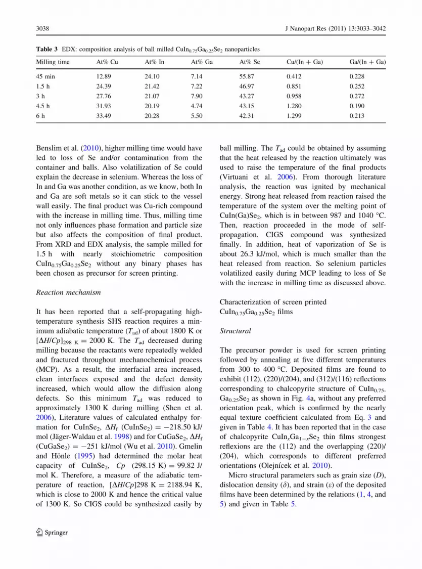
Benslim et al. (2010), higher milling time would have
led to loss of Se and/or contamination from the
container and balls. Also volatilization of Se could
explain the decrease in selenium. Whereas the loss of
In and Ga was another condition, as we know, both In
and Ga are soft metals so it can stick to the vessel
wall easily. The final product was Cu-rich compound
with the increase in milling time. Thus, milling time
not only influences phase formation and particle size
but also affects the composition of final product.
From XRD and EDX analysis, the sample milled for
1.5 h with nearly stoichiometric composition
CuIn0.75Ga0.25Se2 without any binary phases has
been chosen as precursor for screen printing.
Reaction mechanism
It has been reported that a self-propagating high-
temperature synthesis SHS reaction requires a min-
imum adiabatic temperature (Tad) of about 1800 K or
[DH/Cp]298 K = 2000 K. The Tad decreased during
milling because the reactants were repeatedly welded
and fractured throughout mechanochemical process
(MCP). As a result, the interfacial area increased,
clean interfaces exposed and the defect density
increased, which would allow the diffusion along
defects. So this minimum Tad was reduced to
approximately 1300 K during milling (Shen et al.
2006), Literature values of calculated enthalpy for-
mation for CuInSe2, DHf (CuInSe2) = -218.50 kJ/
mol (Jager-Waldau et al. 1998) and for CuGaSe2, DHf
(CuGaSe2) = -251 kJ/mol (Wu et al. 2010). Gmelin
and Honle (1995) had determined the molar heat
capacity of CuInSe2, Cp (298.15 K) = 99.82 J/
mol K. Therefore, a measure of the adiabatic tem-
perature of reaction, [DH/Cp]298 K = 2188.94 K,
which is close to 2000 K and hence the critical value
of 1300 K. So CIGS could be synthesized easily by
ball milling. The Tad could be obtained by assuming
that the heat released by the reaction ultimately was
used to raise the temperature of the final products
(Virtuani et al. 2006). From thorough literature
analysis, the reaction was ignited by mechanical
energy. Strong heat released from reaction raised the
temperature of the system over the melting point of
CuIn(Ga)Se2, which is in between 987 and 1040 �C.
Then, reaction proceeded in the mode of self-
propagation. CIGS compound was synthesized
finally. In addition, heat of vaporization of Se is
about 26.3 kJ/mol, which is much smaller than the
heat released from reaction. So selenium particles
volatilized easily during MCP leading to loss of Se
with the increase in milling time as discussed above.
Characterization of screen printed
CuIn0.75Ga0.25Se2 films
Structural
The precursor powder is used for screen printing
followed by annealing at five different temperatures
from 300 to 400 �C. Deposited films are found to
exhibit (112), (220)/(204), and (312)/(116) reflections
corresponding to chalcopyrite structure of CuIn0.75-
Ga0.25Se2 as shown in Fig. 4a, without any preferred
orientation peak, which is confirmed by the nearly
equal texture coefficient calculated from Eq. 3 and
given in Table 4. It has been reported that in the case
of chalcopyrite CuInxGa1-xSe2 thin films strongest
reflexions are the (112) and the overlapping (220)/
(204), which corresponds to different preferred
orientations (Olejnıcek et al. 2010).
Micro structural parameters such as grain size (D),
dislocation density (d), and strain (e) of the deposited
films have been determined by the relations (1, 4, and
5) and given in Table 5.
Table 3 EDX: composition analysis of ball milled CuIn0.75Ga0.25Se2 nanoparticles
Milling time At% Cu At% In At% Ga At% Se Cu/(In ? Ga) Ga/(In ? Ga)
45 min 12.89 24.10 7.14 55.87 0.412 0.228
1.5 h 24.39 21.42 7.22 46.97 0.851 0.252
3 h 27.76 21.07 7.90 43.27 0.958 0.272
4.5 h 31.93 20.19 4.74 43.15 1.280 0.190
6 h 33.49 20.28 5.50 42.31 1.299 0.213
3038 J Nanopart Res (2011) 13:3033–3042
123

b ¼ k= Dcoshð Þ½ � � etanh ð4Þ
d ¼ 1�
D2 ð5Þ
It is observed that grain size increases slightly for
films compared to the precursor powder due to heat
treatment. Dislocation density and strain values also
remain almost the same irrespective of annealing
temperature. Peak shift to lower angles in XRD
patterns without remarkable growth of particles has
been noticed as given in Fig. 4b. In general, XRD
peak shift of CuInxGa1-xSe2 is considered to be
related to the Ga contents in film, where as Ga
contents increase the lattice constant decreases and
subsequently diffraction angle increases (Ahn et al.
2008). Thus, peak shift appearing in Fig. 4b with heat
treatment temperatures can be attributed to decrease
of Ga content in films. To determine the change in Ga
Fig. 4 a XRD pattern
of screen printed
CuIn0.75Ga0.25Se2 films.
b Zoom in image which
shows left shift in peak
Table 4 Calculated texture coefficients of screen printed
CuIn0.75Ga0.25Se2 films
(hkl): (112) (220)/(204) (312)/(116)
Annealing temp (�C)
300 1.232 1.066 0.702
325 1.128 0.970 0.900
350 1.124 1.038 0.837
375 1.160 1.048 0.792
400 1.121 1.063 0.815
Table 5 Structural parameters of screen printed CuIn0.75-
Ga0.25Se2 films
Annealing
temp (�C)
Grain
size D (nm)
Strain e 9 10-3 Dislocation
density d 9 1015
300 43.9 4.76 5.197
325 43.6 4.81 5.254
350 43.4 4.86 5.310
375 42.1 4.98 5.636
400 42.4 4.93 5.575
Fig. 5 SEM image of screen printed CuIn0.75Ga0.25Se2 films
annealed at 400 �C and the precursor material
J Nanopart Res (2011) 13:3033–3042 3039
123

content, EDX composition analysis has been carried
out, and the results are discussed below.
Morphology and composition
SEM image given in Fig. 5, shows the presence of
smaller particles, which is in agreement with XRD
results. (Ahn et al. 2007) have reported that increase
in temperature to 500 �C leads to the formation of
impure binary phases due to loss of Ga. This is very
well observed from EDX composition analysis of
film where the ratio of Ga/(In ? Ga) and Cu/
(In ? Ga) has been plotted in Fig. 6a and b, respec-
tively. It is observed that higher the heat treatment
temperature was, lower were the Ga contents in films,
which is consistent with XRD data in Fig. 5a as
stated above. Ratio of Ga/(In ? Ga) was found to be
almost independent of temperature, reflecting that the
In contents in films decreased together with Ga
keeping the Ga/(In ? Ga) ratio of particles constant.
Accordingly, simultaneous decrease in Ga and In
contents resulted in the increase in Cu/(In ? Ga) with
increase in temperature as given in Fig. 6b. Possible
reasons for this enhanced In and Ga loss are that the
nanosized particles generally have large surface
energies, meaning that they are thermodynamically
unstable and the vapor pressures of constituents of the
particles are notably higher than those of bulk
materials (Suryanarayana et al. 2001), resulting in
significant reduction of evolution temperature of gas
phases. Other explanations include the poor
crystallinity of nanoparticles used (Ahn et al. 2008)
and no Se supply during the heat treatment at all.
Apart from this there were no traces of other
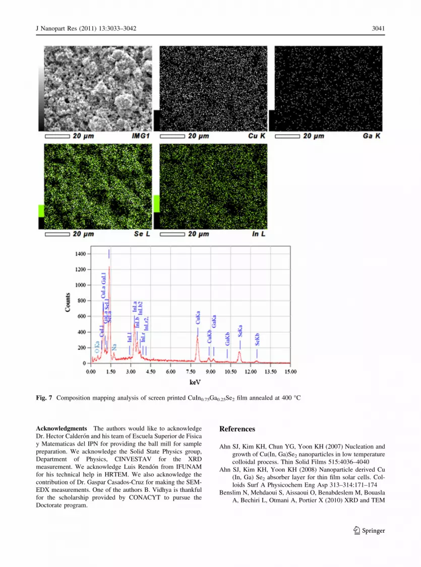
impurities as shown in Fig. 7, composition mapping
of screen printed CIGS films. Hence, confirming the
purity of deposited films.
Conclusions
Single phase CIGS nanoparticles can be prepared by
ball milling for more than 45 min at 1200 rpm. Shift
in XRD peaks toward lower angle is observed due to
stress induced during the process of milling. HRTEM
analysis confirmed the nanoparticle size of 11.73 nm
which was in agreement with the value calculated by
Scherrer’s formula. Numerous dislocations and dis-
tortions were induced during milling leading to the
formation of nanoparticles. Composition analysis
revealed a slight deviation in the milled samples
from the initial composition due to low volatilization
of Se. Heat treatment of screen printed CuIn0.75-
Ga0.25Se2 films in nitrogen atmosphere induced loss
of In and Ga contents due to thermodynamic
instability of nanoparticles. Therefore, we conclude
that either it be milled precursor nanoparticles or
nanoparticle films, the exact reproducibility of com-
position always has some hindrances such as low
volatilization of Se and thermodynamically unstable
nature of nanoparticles.
Fig. 6 a Ga/(In ? Ga) versus annealing temperature, b Cu/(In ? Ga) versus annealing temperature
3040 J Nanopart Res (2011) 13:3033–3042
123
Acknowledgments The authors would like to acknowledge
Dr. Hector Calderon and his team of Escuela Superior de Fisica
y Matematicas del IPN for providing the ball mill for sample
preparation. We acknowledge the Solid State Physics group,
Department of Physics, CINVESTAV for the XRD
measurement. We acknowledge Luis Rendon from IFUNAM
for his technical help in HRTEM. We also acknowledge the
contribution of Dr. Gaspar Casados-Cruz for making the SEM-
EDX measurements. One of the authors B. Vidhya is thankful
for the scholarship provided by CONACYT to pursue the
Doctorate program.
References
Ahn SJ, Kim KH, Chun YG, Yoon KH (2007) Nucleation and
growth of Cu(In, Ga)Se2 nanoparticles in low temperature
colloidal process. Thin Solid Films 515:4036–4040
Ahn SJ, Kim KH, Yoon KH (2008) Nanoparticle derived Cu
(In, Ga) Se2 absorber layer for thin film solar cells. Col-
loids Surf A Physicochem Eng Asp 313–314:171–174
Benslim N, Mehdaoui S, Aissaoui O, Benabdeslem M, Bouasla
A, Bechiri L, Otmani A, Portier X (2010) XRD and TEM
Fig. 7 Composition mapping analysis of screen printed CuIn0.75Ga0.25Se2 film annealed at 400 �C
J Nanopart Res (2011) 13:3033–3042 3041
123
characterizations of the mechanically alloyed CuIn0.5-
Ga0.5Se2 powders. J Alloys Compd 489:437–440
Cai S, Tsuzuki T, Fisher TA, Nener BD, Dell JM, McCormick
PG (2002) Mechanochemical synthesis and characteriza-
tion of GaN nanocrystals. J Nanopart Res 4:37–367
Chityuttakan C, Chinvetkitvanich P, Yoodee K, Chatraphorn S
(2006) In situ monitoring of the growth of Cu(In, Ga)Se2
thin films. Sol Energy Mater Sol Cells 90:3124–3129
Choi IH, Lee DH (2007) Preparation of CuIn1-xGaxSe2 films
by metalorganic chemical vapor deposition using three
precursors. Thin Solid Films 515(11):4778–4782
Chun YG, Kim KH, Yoon KH (2005) Synthesis of CuInGaSe2
nanoparticles by solvothermal route. Thin Solid Films
480–481:46–49
Contreras MA, Ramanathan K, Abushama J, Hasoon F, Young
DL, Egaas B, Noufi R (2005) Diode characteristics in
state-of-the-art ZnO/CdS/Cu(In1-xGax)Se2 solar cells.
Prog Photovolt Res Appl 13:209–216
Contreras MA, Romero MJ, Noufi R (2006) Characterization
of Cu(In, Ga)Se2 materials used in record performance
solar cells. Thin Solid Films 511–512:51–54
Djekoun A, Bouzabata B, Otmani A, Greneche JM (2006)
X-ray diffraction and Mossbauer studies of nanocrystal-
line Fe–Ni alloys prepared by mechanical alloying. Catal
Today 113:235–239
Dodd A, McKinley A, Tsuzuki T, Saunders M (2008) A
comparative evaluation of the photocatalytic and optical
properties of nanoparticulate ZnO synthesised by mech-
anochemical processing. J Nanopart Res 10(Suppl 1):
243–248
Gesenhues U (1999) Substructure of titanium dioxide
agglomerates from dry ball-milling experiments. J Nano-
part Res 1:223–234
Gmelin E, Honle W (1995) Anomalous lattice specific-heat of
LiInSe2 at low-temperatures. Thermochim Acta 269–270:
575–590
Jager-Waldau A, Meyer N, Weiss T, Fiechter S, Lux-Steiner
MCh, Tempelhoff K, Richter W (1998) A new approach
to grow polycrystalline CuGaSe2 thin films: chemical
vapor deposition with I2 as transport agent. Jpn J Appl
Phys 37:1617–1621
Kaufamn CA, Neisser A, Klenk R, Scheer R (2005) Transfer of
Cu(In, Ga)Se2 thin film solar cells to flexible substrates
using an in situ process control. Thin Solid Films
480–481:515–519
Lin Y, Chen Y, Feng M, Yan A, Zhuang X (2008) One-pot
synthesis of soluble nanoscale CIGS photoactive func-
tional materials. Nanoscale Res Lett 3:21–24
Lundberg LuJ, Rockett A, Edoff M, Stolt L (2003) Diffusion of
indium and gallium in Cu(In, Ga)Se2 thin film solar cells.
J Phys Chem Solids 64:1499–1504
Luo P, Yu P, Zuo R, Jin J, Ding Y, Song J, Chen Y (2010a)
The preparation of CuInSe2 films by solvothermal route
and non-vacuum spin-coating process. Physica B 405:
3294–3298
Luo P, Zuo R, Chen L (2010b) The preparation of CuInSe2
films by combustion method and non-vacuum spin-coat-
ing process. Sol Energy Mater Sol Cells 94:1146–1151
Nouiri M, Ben Ayadi Z, Khirouni K, Alaya S, Djessas K, Yapi
S (2007) Effect of substrate temperature and source grain
size on the structural and electrical properties of CSVT
grown Cu(In1-xGax)Se2 thin films. Mater Sci Eng C
27:1002–1006
Olejnıcek J, Kamler CA, Mirasano A, Martinez-Skinner AL,
Ingersoll MA, Exstrom CL, Darveau SA, Huguenin-Love
JA, Diaz M, Ianno NJ, Soukup RJ (2010) A non-vacuum
process for preparing nanocrystalline CuIn1-xGaxSe2
materials involving an open-air solvothermal reaction. Sol
Energy Mater Sol Cells 94:8–11
Panthani MG, Akhavan V, Goodfellow B, Schmidtke JP, Dunn
L, Dodabalapur A, Barbara PF, Korgel BA (2008) Syn-
thesis of CuInS2, CuInSe2, and Cu(InxGa1-x)Se2 (CIGS)
nanocrystal ‘‘inks’’ for printable photovoltaics. J Am
Chem Soc 130(49):16770–16777
Reddy BSB, Rajasekhar K, Venu M, Dilip JJS, Das Siddhartha,
Das Karabi (2008) Mechanical activation-assisted solid-
state combustion synthesis of in situ aluminum matrix
hybrid (Al3Ni/Al2O3) nanocomposites. J Alloys Compd
465:97–105
Sakurai K, Hunger R, Tsuchimochi N, Baba T, Matsubara K,
Fons P, Yamada A, Kojima T, Deguchi T, Nakanishi H,
Niki S (2003) Properties of CuInGaSe2 solar cells based
upon an improved three-stage process. Thin Solid Films
431–432:6–10
Shen J, Kim WK, Shang S, Chu M, Cao S, Anderson TJ (2006)
Thermodynamic description of the ternary compounds in
the Cu–In–Se system. Rare Met 25:481
Sherif El-Eskandarany M, Saida J, Inoue A (2003) Mechani-
cally induced solid-state devitrifications of Zr70Pd20Ni10
glassy alloy powders. Metall Mater Trans A 34A:893
Suri D, Nagpal K, Chadha G (1989) X-ray study of CuGaxIn1-x
Se2 solid solutions. J Appl Crystallogr 22:578
Suryanarayana C, Yoo SH, Groza JR (2001) Consolidation of
mechanically alloyed Cu–In–Ga–Se powders. J Mater Sci
Lett 20:2179–2181
Vidhya B, Velumani S, Arenas-Alatorre JesusA, Morales-
Acevedo Arturo, Asomoza R, Chavez-Carvayar JA (2010)
Structural studies of mechano-chemically synthesized
CuIn1-xGaxSe2 nanoparticles. Mater Sci Eng B 174:216–
221
Virtuani A, Lotter E, Powallia M (2006) Influence of Cu
content on electronic transport and shunting behavior of
Cu(In, Ga)Se2 solar cells. J Appl Phys 99:014906
Wada T, Kinoshita H (2005) Rapid exothermic synthesis of
chalcopyrite-type CuInSe2. J Phys Chem Solids 66:1987–
1989
Wu S, Xue Y, Zhang Z (2010) Microanalysis on CuInSe2
compound synthesized by mechanochemical processing.
J Alloys Compd 491:456–459
Yang H, Qiu GZ, Zhang XC, Tang A, Yang W (2004) Prep-
aration of CdO nanoparticles by mechanochemical reac-
tion. J Nanopart Res 6:539–542
3042 J Nanopart Res (2011) 13:3033–3042
123