DIAGNOSIS AND ERROR CORRECTION FOR A FAULT ...
134
DIAGNOSIS AND ERROR CORRECTION FOR A FAULT-TOLERANT ARITHMETIC AND LOGIC UNIT FOR MEDICAL MICROPROCESSORS BY VARADAN SAVULIMEDU VEERAVALLI A thesis submitted to the Graduate School—New Brunswick Rutgers, The State University of New Jersey in partial fulfillment of the requirements for the degree of Master of Science Graduate Program in Electrical and Computer Engineering Written under the direction of Prof. Michael L. Bushnell and approved by New Brunswick, New Jersey October, 2008
-
Upload
khangminh22 -
Category
Documents
-
view
1 -
download
0
Transcript of DIAGNOSIS AND ERROR CORRECTION FOR A FAULT ...

DIAGNOSIS AND ERROR CORRECTION
FOR A FAULT-TOLERANT ARITHMETIC
AND LOGIC UNIT FOR MEDICAL
MICROPROCESSORS
BY VARADAN SAVULIMEDU VEERAVALLI
A thesis submitted to the
Graduate School—New Brunswick
Rutgers, The State University of New Jersey
in partial fulfillment of the requirements
for the degree of
Master of Science
Graduate Program in Electrical and Computer Engineering
Written under the direction of
Prof. Michael L. Bushnell
and approved by
New Brunswick, New Jersey
October, 2008

ABSTRACT OF THE THESIS
Diagnosis and Error Correction for a
Fault-Tolerant Arithmetic and Logic Unit for
Medical Microprocessors
by Varadan Savulimedu Veeravalli
Thesis Director: Prof. Michael L. Bushnell
We present a fault tolerant Arithmetic and Logic Unit (ALU) for medical
systems. Real-time medical systems possess stringent requirements for fault tol-
erance because faulty hardware could jeopardize human life. For such systems,
checkers are employed so that incorrect data never leaves the faulty module and
recovery time from faults is minimal. We have investigated information, hard-
ware and time redundancy. After analyzing the hardware, the delay and the
power overheads we have decided to use time redundancy as our fault tolerance
method for the ALU.
The original contribution of this thesis is to provide single stuck-fault error
correction in an ALU using recomputing with swapped operands (RESWO). Here,
we divide the 32-bit data path into 3 equally-sized segments of 11 bits each, and
then we swap the bit positions for the data in chunks of 11 bits. This requires
multiplexing hardware to ensure that carries propagate correctly. We operate the
ALU twice for each data path operation – once normally, and once swapped. If
there is a discrepancy, then either a bit position is broken or a carry propagation
ii
circuit is broken, and we diagnose the ALU using diagnosis vectors. First, we test
the bit slices without generating carriers – this requires three or four patterns to
exercise each bit slice for stuck-at 0 and stuck-at 1 faults. We test the carry chain
for stuck-at faults and diagnose their location – this requires two patterns, one to
propagate a rising transition down the carry chain, and another to propagate a
falling transition. Knowledge of the faulty bit slice and the fault in the carry path
makes error correction possible by reconfiguring MUXes. It may be necessary to
swap a third time and recompute to get more data to achieve full error correction.
The hardware overhead with the RESWO approach and the reconfiguration
mechanism of one spare chunk for every sixteen chunks for the 64-bit ALU is
78%. The delay overhead for the 64-bit ALU with our fault-tolerance mechanism
is 110.96%.
iii

Acknowledgements
I would like to express my gratitude to everyone who has helped me complete
this degree. I am thankful to Prof. Michael Bushnell whose cooperation and
encouragement made this work possible. Dr. Bushnell guided me throughout the
project and helped me complete it successfully. I would also like to thank Prof.
Tapan Chakraborty for his encouragement and help with this project.
I would also like to acknowledge my parents for their support throughout my
graduate school years. They stood by me through thick and thin and I would
have never achieved anything in my life without their persisting motivation and
hard work.
I would like to thank all my friends Aditya, Roystein, Sharanya, Hari Vijay,
Rajamani, Omar and Raghuveer. I would especially like to thank the technical
staff William Kish and Skip Carter for their support.
iv

Dedication
To my parents Charumathy and Padmanaban, my grandparents Naryanan and
Chellam, my sister Srikrupa, my brother Vignesh, and all my teachers.
v

Table of Contents
Abstract . . . . . . . . . . . . . . . . . . . . . . . . . . . . . . . . . . . . ii
Acknowledgements . . . . . . . . . . . . . . . . . . . . . . . . . . . . . iv
Dedication . . . . . . . . . . . . . . . . . . . . . . . . . . . . . . . . . . . v
List of Tables . . . . . . . . . . . . . . . . . . . . . . . . . . . . . . . . . xi
List of Figures . . . . . . . . . . . . . . . . . . . . . . . . . . . . . . . . xii
1. Introduction . . . . . . . . . . . . . . . . . . . . . . . . . . . . . . . . 1
1.1. Contribution of this Research . . . . . . . . . . . . . . . . . . . . 2
1.2. Motivation and Justification of this Research . . . . . . . . . . . . 3
1.3. Snapshot of Results of the Thesis . . . . . . . . . . . . . . . . . . 6
1.4. Roadmap of the Thesis . . . . . . . . . . . . . . . . . . . . . . . . 7
2. Prior Work . . . . . . . . . . . . . . . . . . . . . . . . . . . . . . . . 8
2.1. Coding Theory . . . . . . . . . . . . . . . . . . . . . . . . . . . . 9
2.2. Self-Checking Circuits . . . . . . . . . . . . . . . . . . . . . . . . 10
2.3. Error-Detecting and Error-Correcting Codes . . . . . . . . . . . . 11
2.3.1. Two-Rail Checker (TRC) . . . . . . . . . . . . . . . . . . . 11
2.3.2. Berger Codes . . . . . . . . . . . . . . . . . . . . . . . . . 12
2.3.3. Hamming Codes . . . . . . . . . . . . . . . . . . . . . . . 13
2.3.3.1. Hamming Distance . . . . . . . . . . . . . . . . . 14
2.3.3.2. Single Error Correcting Code . . . . . . . . . . . 15
2.3.4. Reed Solomon (RS) Codes . . . . . . . . . . . . . . . . . . 16
vi

2.3.4.1. Architectures for Encoding and Decoding Reed
Solomon Codes . . . . . . . . . . . . . . . . . . . 17
2.3.4.2. Encoder Architecture . . . . . . . . . . . . . . . . 17
2.3.4.3. Decoder Architecture . . . . . . . . . . . . . . . . 18
2.3.5. Residue Codes . . . . . . . . . . . . . . . . . . . . . . . . . 19
2.3.6. IBM’s Research on Error Correcting Codes . . . . . . . . . 21
2.4. Hardware Redundancy . . . . . . . . . . . . . . . . . . . . . . . . 22
2.4.1. Duplication of the Hardware . . . . . . . . . . . . . . . . . 22
2.4.2. Triple Modular Redundancy . . . . . . . . . . . . . . . . . 22
2.5. Time Redundancy . . . . . . . . . . . . . . . . . . . . . . . . . . 25
2.5.1. Recomputing with Shifted Operands (RESO) . . . . . . . . 26
2.5.2. Recomputing with Alternating Logic . . . . . . . . . . . . 27
2.5.3. Recomputing with Swapped Operands (RESWO) . . . . . . 29
2.6. Fault Diagnosis . . . . . . . . . . . . . . . . . . . . . . . . . . . . 30
2.7. Summary – Best of Prior Methods . . . . . . . . . . . . . . . . . . 31
3. Fault-Tolerant Technique for an ALU – Implementation Study
and Justification . . . . . . . . . . . . . . . . . . . . . . . . . . . . . . . 32
3.1. Architecture of the ALU . . . . . . . . . . . . . . . . . . . . . . . 32
3.1.1. Adders . . . . . . . . . . . . . . . . . . . . . . . . . . . . . 34
3.1.1.1. Brent-Kung Adder . . . . . . . . . . . . . . . . . 35
3.1.1.2. Kogge-Stone Adder . . . . . . . . . . . . . . . . . 35
3.1.1.3. Sklansky Adder . . . . . . . . . . . . . . . . . . . 35
3.1.2. Multipliers . . . . . . . . . . . . . . . . . . . . . . . . . . . 36
3.1.2.1. Booth Encoding Multiplier . . . . . . . . . . . . 37
3.1.2.2. Wallace Tree Multiplication . . . . . . . . . . . . 38
3.1.2.3. Dadda Tree Multiplication . . . . . . . . . . . . . 39
3.2. Justification for Recomputing Using Swapped Operands for Fault
Tolerance . . . . . . . . . . . . . . . . . . . . . . . . . . . . . . . 40
vii
3.2.1. Why Information Redundancy Is Not Useful . . . . . . . . 40
3.2.2. Why Hardware Redundancy Is Not Useful . . . . . . . . . 42
3.2.3. Why the other Time-redundancy Mechanisms Are Not Useful 43
3.3. Results . . . . . . . . . . . . . . . . . . . . . . . . . . . . . . . . 43
4. Diagnosis of ALU Using RESWO and Test Vectors and Recon-
figuration for Error Correction . . . . . . . . . . . . . . . . . . . . . . 46
4.1. Diagnosis Method . . . . . . . . . . . . . . . . . . . . . . . . . . . 46
4.1.1. Fault Dictionary . . . . . . . . . . . . . . . . . . . . . . . 47
4.1.2. Diagnosis Tree . . . . . . . . . . . . . . . . . . . . . . . . 47
4.1.3. Why We Use a Diagnosis Tree . . . . . . . . . . . . . . . . 48
4.2. Comparison with Alternative Methods . . . . . . . . . . . . . . . 48
4.2.1. Implementation of Diagnosis for ALU . . . . . . . . . . . 48
4.2.1.1. Design the ALU as One Piece . . . . . . . . . . . 49
4.2.1.2. Design the ALU with Reconfigurable 4-bit ALU
Chunks . . . . . . . . . . . . . . . . . . . . . . . 49
4.2.1.3. Design the ALU with Reconfigurable 2-bit ALU
Chunks . . . . . . . . . . . . . . . . . . . . . . . 49
4.2.1.4. Design the Boolean, Addition, Subtraction and
Shifting Operations Using Reconfigurable 2-bit ALU
Chunks. Design the Multiplier Separately . . . . 50
4.2.1.5. Design the Boolean, Addition, Subtraction and
Shifting Operations Using Reconfigurable 1-bit ALU
Chunks. Design the Multiplier Separately . . . . 52
4.2.2. Minimal Test Set for 100% Fault Detection . . . . . . . . . 52
4.3. Results . . . . . . . . . . . . . . . . . . . . . . . . . . . . . . . . . 55
5. Optimal Reconfiguration Scheme for the ALU . . . . . . . . . . 57
5.1. Reconfiguration Analysis . . . . . . . . . . . . . . . . . . . . . . . 57
5.2. Reconfiguration Schemes . . . . . . . . . . . . . . . . . . . . . . 58
viii

5.2.1. For Every Two Chunks Provide One Spare Chunk . . . . . 59
5.2.2. For Every Four Chunks Provide One Spare Chunk . . . . . 61
5.2.3. For Every Eight Chunks Provide One Spare Chunk . . . . 63
5.2.4. For Every Sixteen Chunks Provide One Spare Chunk . . . 65
5.3. Hardware Overheads of Different Types of Reconfiguration Schemes
66
5.3.1. ALU Without Multiplier . . . . . . . . . . . . . . . . . . 66
5.3.2. Booth Encoder . . . . . . . . . . . . . . . . . . . . . . . . 68
5.3.3. Booth Selector . . . . . . . . . . . . . . . . . . . . . . . . 70
5.3.4. Full Adder and Half Adder . . . . . . . . . . . . . . . . . . 70
5.3.5. Carry Propagation Adder . . . . . . . . . . . . . . . . . . 74
5.4. Results . . . . . . . . . . . . . . . . . . . . . . . . . . . . . . . . . 74
6. Reliability Analysis . . . . . . . . . . . . . . . . . . . . . . . . . . . 78
6.1. TMR with Single Voting Mechanism . . . . . . . . . . . . . . . . 78
6.2. TMR with Triplicated Voting Mechanism . . . . . . . . . . . . . . 79
6.3. Our Fault-Tolerance Mechanism . . . . . . . . . . . . . . . . . . . 80
6.4. Results . . . . . . . . . . . . . . . . . . . . . . . . . . . . . . . . . 83
7. Conclusions and Future Research . . . . . . . . . . . . . . . . . . 84
7.1. Statement of Original Ideas . . . . . . . . . . . . . . . . . . . . . 84
7.2. Comparison of Our Scheme . . . . . . . . . . . . . . . . . . . . . 85
7.2.1. TMR Single Voting Mechanism . . . . . . . . . . . . . . . 85
7.2.2. TMR Triplicated Voting Mechanism . . . . . . . . . . . . 86
7.2.3. Residue Codes and RESWO Checkers as Fault-Tolerance
Mechanisms . . . . . . . . . . . . . . . . . . . . . . . . . . 86
7.3. Statement of Results . . . . . . . . . . . . . . . . . . . . . . . . . 87
7.4. Benefits of Our Scheme . . . . . . . . . . . . . . . . . . . . . . . . 89
7.5. Future Work Directions . . . . . . . . . . . . . . . . . . . . . . . . 90
References . . . . . . . . . . . . . . . . . . . . . . . . . . . . . . . . . . . 91
ix

Appendix A. Validation of ALU Design . . . . . . . . . . . . . . . . 97
Appendix B. Validation of Fault-Tolerance Method . . . . . . . . . 100
Appendix C. Validation of Reconfiguration Method . . . . . . . . . 103
Appendix D. Reliability Analysis Calculations . . . . . . . . . . . . 107
Appendix E. Testing of the ALU with the Reconfiguration Mecha-
nism . . . . . . . . . . . . . . . . . . . . . . . . . . . . . . . . . . . . . . 117
x
List of Tables
1.1. Diagnosis Vectors for Booth Encoded Dadda Tree Multiplier . . . 6
2.1. Hardware Overhead of Berger Code . . . . . . . . . . . . . . . . . 12
2.2. Types of Hamming Code . . . . . . . . . . . . . . . . . . . . . . . 16
3.1. Results for a 16-bit ALU . . . . . . . . . . . . . . . . . . . . . . . 44
3.2. RESWO Implementation for Different Architectures of the ALU . 44
4.1. Test Vectors for the Booth Selector Circuit . . . . . . . . . . . . . 53
4.2. Test Vectors for the Full Adder Circuit . . . . . . . . . . . . . . . 54
4.3. Test Vectors for the Half Adder Circuit . . . . . . . . . . . . . . . 55
4.4. Diagnosis Vectors for Different Diagnosis Implementations . . . . 55
4.5. Diagnosis Vectors for Booth Encoded Dadda Tree Multiplier . . . 56
6.1. Reliability for TMR with Single Voting Mechanisms . . . . . . . . 80
6.2. Reliability for TMR with Triplicated Voting Mechanisms . . . . . 81
6.3. Reliability for our Fault-Tolerance Mechanism . . . . . . . . . . . 82
7.1. Diagnosis Vectors for Booth Encoded Dadda Tree Multiplier . . . 88
C.1. Reconfiguration of the 64-bit ALU . . . . . . . . . . . . . . . . . . 104
D.1. Reliability Analysis . . . . . . . . . . . . . . . . . . . . . . . . . . 115
E.1. Fault Coverage of Different Circuits . . . . . . . . . . . . . . . . . 119
xi

List of Figures
1.1. Variation of SER with Technology . . . . . . . . . . . . . . . . . . 4
2.1. Typical Diagram of a System with an Error Correcting Code . . . 10
2.2. Logic Diagram of a TRC . . . . . . . . . . . . . . . . . . . . . . . 11
2.3. Block Diagram of Berger Code . . . . . . . . . . . . . . . . . . . . 12
2.4. Block Diagram of Check Bit Generator for 7 Information Bits . . 13
2.5. Block Diagram of Hamming Code . . . . . . . . . . . . . . . . . . 14
2.6. Diagram for Hamming Distance . . . . . . . . . . . . . . . . . . . 15
2.7. Block Diagram of System with Reed Solomon Code . . . . . . . . 16
2.8. Typical Block Diagram of Reed Solomon Encoder . . . . . . . . . 18
2.9. Typical Block Diagram of Reed Solomon Decoder . . . . . . . . . 18
2.10. Block Diagram of System with Duplication of Hardware Mechanism 23
2.11. Triple Redundancy as Originally Envisaged by Von Neumann . . 23
2.12. Triple Modular Redundant Configuration . . . . . . . . . . . . . . 24
2.13. Time Redundancy for Permanent Errors . . . . . . . . . . . . . . 26
2.14. Structure of RESO System . . . . . . . . . . . . . . . . . . . . . . 27
2.15. Structure of Recomputing with Alternating Logic System . . . . . 28
2.16. Structure of RESWO System . . . . . . . . . . . . . . . . . . . . 29
3.1. Sklansky Tree Adder . . . . . . . . . . . . . . . . . . . . . . . . . 36
3.2. Radix-4 Booth Encoder and Selector . . . . . . . . . . . . . . . . 37
3.3. Wallace Tree Multiplier . . . . . . . . . . . . . . . . . . . . . . . . 39
3.4. Dadda Tree Multiplier . . . . . . . . . . . . . . . . . . . . . . . . 40
4.1. Booth Selector Circuit . . . . . . . . . . . . . . . . . . . . . . . . 53
4.2. Full Adder Circuit . . . . . . . . . . . . . . . . . . . . . . . . . . 53
xii

4.3. Half Adder Circuit . . . . . . . . . . . . . . . . . . . . . . . . . . 54
5.1. Reconfiguration Scheme – For Every Two Chunks Provide One
Spare Chunk . . . . . . . . . . . . . . . . . . . . . . . . . . . . . 60
5.2. Reconfiguration Scheme – For Every Four Chunks Provide One
Spare Chunk . . . . . . . . . . . . . . . . . . . . . . . . . . . . . 61
5.3. Reconfiguration Scheme – For Every Eight Chunks Provide One
Spare Chunk . . . . . . . . . . . . . . . . . . . . . . . . . . . . . 64
5.4. Hardware Overhead of 2-bit ALU Chunks with Different Reconfig-
uration Schemes . . . . . . . . . . . . . . . . . . . . . . . . . . . . 66
5.5. Hardware Overhead Comparison of 2-bit ALU and 1-bit ALU Chunks
with Different Reconfiguration Schemes . . . . . . . . . . . . . . . 67
5.6. Hardware Overhead of Booth Encoder with Different Reconfigura-
tion Schemes . . . . . . . . . . . . . . . . . . . . . . . . . . . . . 69
5.7. Hardware Overhead of Booth Selector with Different Reconfigura-
tion Schemes . . . . . . . . . . . . . . . . . . . . . . . . . . . . . 71
5.8. Hardware Overhead of Full Adder with Different Reconfiguration
Schemes . . . . . . . . . . . . . . . . . . . . . . . . . . . . . . . . 72
5.9. Hardware Overhead of Half Adder with Different Reconfiguration
Schemes . . . . . . . . . . . . . . . . . . . . . . . . . . . . . . . . 73
5.10. Hardware Overhead of Carry Propagation Adder with Different
Reconfiguration Schemes . . . . . . . . . . . . . . . . . . . . . . . 75
5.11. Hardware Overhead of the 64-bit ALU (Including the Multiplier)
with Different Reconfiguration Schemes . . . . . . . . . . . . . . . 76
6.1. Venn Diagram of Triple Modular Redundant System . . . . . . . 79
6.2. Reliability of Different Fault-Tolerance Mechanisms . . . . . . . . 83
D.1. Full Adder Circuit . . . . . . . . . . . . . . . . . . . . . . . . . . 108
D.2. Half Adder Circuit . . . . . . . . . . . . . . . . . . . . . . . . . . 109
D.3. Booth Encoder Circuit . . . . . . . . . . . . . . . . . . . . . . . . 110
D.4. Booth Selector Circuit . . . . . . . . . . . . . . . . . . . . . . . . 110
xiii

D.5. Carry Propagation Circuit . . . . . . . . . . . . . . . . . . . . . . 111
D.6. 2:1 MUX Circuit . . . . . . . . . . . . . . . . . . . . . . . . . . . 112
D.7. 4:1 MUX Circuit . . . . . . . . . . . . . . . . . . . . . . . . . . . 112
D.8. 8:1 MUX Circuit . . . . . . . . . . . . . . . . . . . . . . . . . . . 113
D.9. 16:1 MUX Circuit . . . . . . . . . . . . . . . . . . . . . . . . . . . 114
E.1. Fault Coverage for the ALU . . . . . . . . . . . . . . . . . . . . . 117
xiv

1
Chapter 1
Introduction
The role of electronics in every branch of science has become pivotal. Integrated
circuits, digital and analog, are used extensively in applications ranging from
medical to home-automation. System reliability has been a major concern since
the dawn of the electronic digital computer age [61]. As the scale of integration
increased from small/medium to large and to today’s very large scale, the relia-
bility per basic function has continued its dramatic improvement [24]. Due to the
demand for enhanced functionality, the complexity of contemporary computers,
measured in terms of basic functions, rose almost as fast as the improvement in
the reliability of the basic component. Secondly, our dependence on computing
systems has grown so great that it becomes impossible to return to less sophis-
ticated mechanisms. Previously, reliable computing has been limited to military,
industrial, aerospace, and communications applications in which the consequence
of computer failure had significant economic impact and/or loss of life [3, 41].
Today even commercial applications require high reliability as we move towards
a cashless/automated life-style. Reliability is of critical importance in situations
where a computer malfunction could have catastrophic results. Reliability is used
to describe systems in which it is not feasible to repair (as in computers on board
satellites) or in which the computer is serving a critical function and cannot be
lost even for the duration of a replacement (as in flight control computers on an
aircraft) or in which the repair is prohibitively expensive. Systems that tolerate
failures have been of interest since the 1940’s [45] when computational engines
were constructed from relays.

2
1.1 Contribution of this Research
The main aim of this research is to come up with a new fault-tolerant scheme for
an Arithmetic and Logic Unit (ALU), with a better hardware and power overhead
compared to the current fault tolerance techniques. In order to achieve this, we
will employ single stuck-fault error correction in an ALU using recomputing with
swapped operands (RESWO). Here, we divide the 32-bit data path into 3 equally-
sized segments of 11 bits each, and then we swap the bit positions for the data
in chunks of 11 bits. This requires multiplexing hardware to ensure that carries
propagate correctly. We operate the ALU twice for each data path operation –
once normally, and once swapped. If there is a discrepancy, then either a bit
position is broken or a carry propagation circuit is broken, we diagnose the ALU
using special diagnosis vectors. Knowledge of the faulty bit slice and the fault in
the carry path makes error correction possible.
A diagnosis test is characterized by its diagnostic resolution, defined as the
ability to get closer to the fault. When a failure is indicated by a pass/fail type
of test in a system that is operating in the field, a diagnostic test is applied. We
have employed different types of diagnosis mechanisms for the ALU. We found
that the best diagnosis mechanism for the 64-bit ALU is designing the Boolean,
addition, subtraction and shifting operations with thirty two reconfigurable 2-
bit ALU chunks and designing the multiplier separately. We had to split the
multiplier into identical bit slices of Booth encoders, Booth selectors, full adders,
half adders and carry propagation adders. It was easy to reconfigure the multiplier
once it was split into identical bit slices.
If a fault is detected and a permanent failure located, the system may be
able to reconfigure its components to replace the failed component or to isolate
it from the rest of the system [24]. The component may be replaced by backup
spares. We employed different reconfiguration schemes for the 64-bit ALU. We
decided that the best reconfiguration mechanism for the 64-bit ALU is to use
one spare chunk for every sixteen chunks. The reconfiguration mechanism of one

3
spare chunk for every sixteen chunks can correct up to four faults, provided that
they are not in the same sixteen-bit chunk.
1.2 Motivation and Justification of this Research
The reason for the use of the fault-tolerant design is to achieve a reliability or
availability that cannot be attained by the fault-intolerant design. The main argu-
ment against the use of fault-tolerance techniques in computer systems has been
the cost of redundancy. High performance general-purpose computing systems
are very susceptible to transient errors and permanent faults. As performance
demand increases, fault tolerance may be the only course to building commercial
systems. The most stringent requirement for fault-tolerance is in real time control
systems, where faulty computation could jeopardize human life or have high eco-
nomic impact. Computations must not only be correct, but recovery time from
faults must be minimized. Specially designed hardware must be employed with
fault-tolerance mechanisms so that incorrect data never leaves the faulty module.
As the dimensions and operating voltages of electronic devices are reduced to
satisfy the ever–increasing demand for higher density and low-power, their sensi-
tivity to radiation increases dramatically. A soft error arises in the system upon
exposure to high energy radiation (cosmic rays, α particles, neutrons, etc.). In
the past, soft errors were primarily a concern only in space applications. Signif-
icant single event upsets (SEUs) arise due to α particle emissions from minute
traces of radioactive elements in packaging materials [7]. Even though SEUs are
the preponderant phenomenon, there are important instances in which multiple
event upsets occur. Multiple event upsets are those where an incident heavy ion
can cause a SEU in a string of memory cells, in a microcircuit, that happen to lie
physically along the penetration ion track. The problem gets severe and recurrent
with shrinking device geometry. Shorter channel lengths mean fewer number of
charge carriers, resulting in a smaller value of critical charge. The critical charge

4
of a memory array storage cell is defined as the largest charge that can be in-
jected without changing the cell’s logic state. SEUs were initially associated with
small and densely packed memories, but are now commonly observed in combi-
national circuits and latches. Exponential growth in the amount of transistors in
microprocessors and digital signal processors has led the soft error rate (SER) to
increase with each generation, with no end in sight. The most effective method
of dealing with soft errors in memory components is to use additional circuits for
error detection and correction.
Figure 1.1: Variation of SER with Technology [8]
Figure 1.1 illustrates the variation of soft-error rate with respect to chip tech-
nology [8]. This trend is of great concern to chip manufacturers since SRAM
constitutes a large part of all advanced integrated circuits today. The soft-error
rate is measured in units of failures in time (FITs). One FIT is equivalent to one
failure in 1 billion (109) operational hours.
As the complexity of microelectronic components continues to increase, design

5
and reliability engineers will need to address several key areas to enable advanced
SoC (System-on-a-chip) products in the commercial sector. The first challenge
will be to develop improved and more accurate system level modeling of soft er-
rors including not just device and component failure rates but architectural and
algorithmic dependencies as well [9]. With these improved models, the next chal-
lenge will be to develop optimized memory and logic mitigation designs that offer
a good balance between performance and robustness against soft errors and single
energy transients (SETs). The last challenge will be the development of viable
commercial fault-tolerant solutions that will render complex systems relatively
insensitive to soft errors at the operation level.
Fault tolerance is no longer an exotic engineering discipline rather than it
is becoming as fundamental to computer design as logic synthesis. Designs will
be compared and contrasted not only by their cost, power consumption, and
performance but also by their reliability and ability to tolerate failures. These
countermeasures never come for free and impact the cost of system being devel-
oped. Also, the resulting system will be slower and may feature an increased block
size. There will always be a trade–off between cost, efficiency and fault-tolerance
and it will be a judgment call by designers, developers and users to choose which
of these requirements best suit their needs.
We need a better fault-tolerance mechanism for the ALU that has the hard-
ware overhead lower than 100% because the current fault-tolerance mechanisms
have the hardware overhead more than 200%. In this research our top prior-
ity is the hardware overhead, then the power and the delay overheads. There
is no fault-tolerance mechanism that can handle both the transient errors and
the permanent errors. Our main goal here is to come up with a fault-tolerance
mechanism than can handle both the hard and the soft errors with a hardware
overhead not more than 100%.

6
1.3 Snapshot of Results of the Thesis
We used time redundancy as the fault-tolerance mechanism for the ALU after a
very brief analysis. We chose REcomputing with SWapped Operands (RESWO) as
it had 5.3% lower hardware, 9.06% lower power and 3.26% lower delay overheads
than Recomputing with Alternating Logic. The RESWO approach has been shown
to be less expensive, particularly when the complexity of individual modules of the
circuit is high. Once a fault is detected in the ALU using the RESWO approach
we diagnose the ALU with diagnosis vectors and locate the fault.
When there is a discrepancy in the circuit (either a bit position is broken or a
carry propagation circuit is broken), we diagnose the ALU using special diagnosis
vectors. We have implemented different diagnosis mechanisms for the ALU. After
a very brief analysis we found that the best diagnosis mechanism for the 64-bit
ALU is designing the Boolean, addition, subtraction and shifting operations with
thirty two reconfigurable 2-bit chunks and designing the multiplier separately.
We had to split the multiplier into identical bit slices of Booth encoders, Booth
Selectors, full adders and carry propagation adders.
Table 1.1: Diagnosis Vectors for Booth Encoded Dadda Tree Multiplier
Architecture Number ofDiagnosis Vectors
2-bit ALU without Multiplier 22Booth Encoder 7Booth Selector 4
Full Adder 5Half Adder 4
Carry Propagation Adder 7
Once the fault is located we have to reconfigure the circuit and remove the
faulty part. We developed different reconfiguration mechanisms for the 64-bit
ALU. After analyzing all the reconfiguration mechanisms we decided to use one
spare chunk for every sixteen chunks as our reconfiguration mechanism because
it has a much lower hardware overhead of 78% (2.49% of this overhead is for the

7
RESWO checkers) compared to the hardware overheads of TMR with single vot-
ing mechanism (201.87%) and TMR with triplicated voting mechanism (207.5%)
and an error correction rate of 6.25%.
Reliability analysis showed that our fault-tolerance mechanism is better than
the current fault-tolerant mechanisms. If the reliability of all the sub-modules of
the 64-bit ALU with fault-tolerance mechanism is 90%, then the entire system
reliability is 99.99%.
1.4 Roadmap of the Thesis
This thesis is organized as follows. In Chapter 2 we survey the related work. In
this chapter we present a detailed introduction to the different fault-tolerant tech-
niques (error detecting and error correcting codes), diagnosis and reconfiguration.
The next chapter describes the architecture and the most optimum fault-tolerant
mechanism for the Arithmetic and Logic Unit ALU. Chapter 4 explains the dif-
ferent implementations of diagnosis mechanisms with an analysis and results.
Chapter 5 describes the different implementations of reconfiguration mechanisms
with a brief analysis and results. Chapter 6 explains the reliability of different
fault-tolerance mechanisms. Chapter 7 concludes this thesis. The first section
gives us the essence of the work and the last section discusses the directions for
this work in the future.
8
Chapter 2
Prior Work
In fault tolerance, we will discuss prior work focusing on information, hardware
and time redundancy. First, we will review the work that has been done in the area
of fault tolerance. Then we will discuss the different fault-tolerant mechanisms.
Later we will discus the work done in diagnosis and reconfiguration of Arithmetic
and Logic Units (ALUs).
Systems that tolerate failures have been of interest since the 1940’s when
computational engines were constructed from relays. Fault detection provides no
tolerance to faults, but gives warning when they occur [45]. If the dominant form
of faults is transient/intermittent, recovery can be initiated by a retry invoked
from a previous checkpoint in the system at whose time the system state was
known to be good. Design errors, whether in hardware or software, are those
caused by improper translation of a concept into an operational realization [2, 4,
6, 38]. The three major axes of the space of fault-tolerant designs are: system
application, system structure, and fault-tolerant technique employed [60]. The
most stringent requirement for fault tolerance is in real-time control systems,
where faulty computation could jeopardize human life or have high economic
impact [56]. Computations must not only be correct, but recovery time from faults
must be minimized. Specially designed hardware is employed with concurrent
error detection so that incorrect data never leaves the faulty module [43].
Major error-detection techniques include duplication (frequently used for ran-
dom logic) and error detecting codes [36]. Recovery techniques can restore enough
of the system state to allow a process execution to restart without loss of acquired
information. There are two basic approaches: forward and backward recovery.

9
Forward recovery attempts to restore the system by finding a new state from
which the system can continue operation. Backward recovery attempts to recover
the system by rolling back the system to a previously saved state, assuming that
the fault manifested itself after the saved state. Forward error recovery, which
produces correct results through continuation of normal processing, is usually
highly application-dependent [53]. Backward recovery techniques require some
redundant process and state information to be recorded as computations progress.
Error detection and correction codes have proven very effective for regular logic
such as memories and memory chips have built-in support for error detection and
correcting codes [36, 40, 51]. With the ever-increasing dominance of transient and
intermittent failures, retry mechanisms will be built into all levels of the system
as the major error-recovery mechanism [3, 41]. Fault tolerance is no longer an
exotic engineering discipline; rather, it is becoming as fundamental to computer
design as logic synthesis. Designs will be compared and contrasted not only by
their cost, power consumption, and performance but also by their reliability and
ability to tolerate failures [61].
2.1 Coding Theory
A stream of source data, in the form of zeros and ones, is being transmitted over
a communications channel, such as telephone line [12]. How can we tell that
the original data has been changed, and when it has, how can we recover the
original data? Here are some easy things to try: Do nothing. If a channel error
occurs with probability p, then the probability of making a decision error is p.
Send each bit 3 times in succession. The bit gets picked by a majority voting
scheme. If errors occur independently, then the probability of making a decision
error is 3p2 − 2p3, which is less than p for p < 1/2. Generalize the above; Send
each bit n times and choose the majority bit. In this way, we can make the
probability of making a decision error arbitrarily small, but communications are
inefficient in terms of transmission rate. From the above suggestion we see the

10
basic elements of encoding of data: Encode the source information, by adding
additional information, sometimes referred to as redundancy, which can be used
to detect, and perhaps correct, errors in transmission. The more redundancy we
add, the more reliably we can detect and correct errors but the less efficient we
become at transmitting the source data.
Sends Source Message
May IntroduceErrors
Source1011
Encoder Channel
1011010
1010010
1011
DecoderReceiver
Receives Source Message
Corrects errorand ReclaimsSource Message
Encodes SourceMessage intoCodeword
Figure 2.1: Typical Diagram of a System with an Error Correcting Code
2.2 Self-Checking Circuits
• Definition I: A combinational circuit is self-testing for a fault set F if and
only if for every fault in F, the circuit produces a non-codeword output dur-
ing normal operation for atleast one input code word [40, 63, 65]. Namely,
if during normal circuit operation any fault occurs, this property guarantees
an error indication.
• Definition II: A combinational circuit is Strongly-Fault-Secure (SFS) for a
fault set F iff, for every fault in F, the circuit never produces an incorrect
output code-word [26, 65].
• Definition III: A combinational circuit is Self-Checking circuit SCC for a
fault set F iff, for every fault n F, the circuit is both self-testing and strongly
fault secure [13, 63, 65].

11
2.3 Error-Detecting and Error-Correcting Codes
2.3.1 Two-Rail Checker (TRC)
A one bit output is insufficient for a Totally Self-Checking (TSC) circuit since a
stuck-at-fault on the output resulting in the “good” output could not be detected
[36, 40, 51, 65]. The output of a TSC circuit is typically encoded using a two
rail (1-out-of-2) code. The checker is said to be TSC circuit iff, under the fault
X0
Y0
X1
Y1
f
g
Figure 2.2: Logic Diagram of a TRC
models:
1. The output of the checker is 01 or 10 whenever the input is a code word
(strongly-fault-secure property).
2. The output is 00 or 11 whenever the input is not a code word (code-disjoint
property).
3. Faults in the checker are detectable by test inputs that are code words and,
under fault-free condition, for at least two inputs X and Y , the checker
outputs are 01 and 10, respectively.

12
2.3.2 Berger Codes
Berger codes are perfect error detection codes in a completely asymmetric channel.
A completely asymmetric channel is one in which only one type of error occurs,
either only zeros converted to ones or only ones converted to zeros. They are
separable codes [10]. The Berger code counts the number of 1’s in the word and
expresses it in binary. It complements the binary word, and appends the count to
the data. Berger codes are optimal systematic AUED (All Unidirectional Error
Check bitGenerator
RailTwobits
I
Kbits
Circuit
gChecker
f
Figure 2.3: Block Diagram of Berger Code
Table 2.1: Hardware Overhead of Berger CodeInformation Check Overhead
Bits (k) Bits (c)4 3 0.75008 4 0.5000
16 5 0.312532 6 0.187564 7 0.1094
128 8 0.0625256 9 0.0352512 10 0.0195
Detecting) codes [36, 40, 51]. A code is optimal if it has the highest possible
information rate (i.e., c/n). A code is systematic if there is a generator matrix for
the code. It is optimal because the check symbol length is minimal for the Berger

13
code compared to all other systematic codes. Less logic is required to implement
the Berger check error detection. It detects all unidirectional bit errors, i.e, if
Fulli1i2i3
i4i5i6
i7
c1
c3
AdderFull
AdderFull
AdderFull
Adder c2
Figure 2.4: Block Diagram of Check Bit Generator for 7 Information Bits
one or more ones turn into zeros it can be identified, but at the same time, zeros
converted into ones cannot be identified. If the same number of bits flips from
one to zero as from zero to one, then the error will not be detected. If the number
of data bits is k, then the check bits (c) are equal to log2(k + 1) bits. Hence, the
overhead is log2((k+1)/k). These codes have been designed to be separable codes
that are also perfect error detection codes in a completely asymmetric channel
[10]. The major purpose has been to demonstrate that this unique feature of the
fixed weight codes can also be achieved with separable codes so that advantage
may be taken of the asymmetry of a channel while still maintaining the flexibility
and compatibility associated with separable codes.
2.3.3 Hamming Codes
The study is given in consideration of large scale computing machines in which
a large number of operations must be performed without a single error in the
end result [33]. In transmission from one place to another, digital machines use
codes that are simply sets of symbols to which meanings or values are attached
[36, 40, 51]. Examples of codes that were designed to detect isolated errors are
numerous; among them are the highly developed 2-out-of-5 codes used extensively

14
in common control switching systems and in the Bell Relay Computers. The codes
STEM
ROC
R
TC
I
N
E
O
CheckInputBit
Checkbits
data
Check
Generator
Uncorrected data
Generator
Generator
Syndromebits
Syndrome
Bit
Correctedbits
data
Input data
SY
Check
Figure 2.5: Block Diagram of Hamming Code
used are called systematic codes. Systematic codes may be defined as codes in
which each code symbol has exactly n binary digits, where m digits are associated
with the information while the other k = n−m digits are used for error detection
and correction [32]. Application of these codes may be expected to occur first
only under extreme conditions. How to construct minimum redundancy codes is
shown in the following cases:
1. Single error detecting codes
2. Single error correcting codes
3. Single error correcting plus double error detecting codes.
2.3.3.1 Hamming Distance
The Hamming distance (Hd) of a code, the distance between 2 binary words, is the
number of bit positions in which they differ. Example: For 1001000 to 1011001,
the Hamming distance is 2. Codes 000 and 001 differ by 1 bit so Hd is 1. Codes
000 and 110 differ by 2 bits so Hd is 2. A Hd of 2 between two code words implies
that a single bit error will not change one code word into the other. Codes 000
and 111 differ by 3 bits so Hd is 3. A Hd of 3 can detect any single or double bit
error. If no double bit errors occur, it can correct a single bit error.

15
000
010
100
001
101
011
111110
Figure 2.6: Diagram for Hamming Distance
2.3.3.2 Single Error Correcting Code
There are k information positions of n positions. The c remaining positions are
check positions: c = n − k. The value of c is determined in the encoding process
by even parity checks. Each time the assigned and observed value of parity checks
agree, we write a 0, else we write a 1. Written from right to left, the c 0’s and 1’s
gives the checking number. The checking number gives the position of any single
error. The checking number describes k + c + 1 different things.
2c ≥ k + c + 1 (2.1)
First parity check: 1’s for the first binary digit from the right of their binary
representation. Second parity check: 1’s for the second binary digit from the right
of their binary representation. Third parity check: 1’s for the third binary digit
from the right of their binary representation. Parity checks decide the position of
the information and check bits.
A subset with minimum Hd = 5 may be used for:
1. Double error correction, with of course, double error detection.
2. Single error correction plus triple error detection.
3. Quadruple error detection.

16
Table 2.2: Types of Hamming CodeMinimum MeaningDistance
Hd
1 Uniqueness2 Single error detection3 Single error correction4 Single error correction and double error detection5 Double error correction
2.3.4 Reed Solomon (RS) Codes
Reed Solomon (RS) codes have introduced ideas that form the core of current
commonly used error correction techniques [55]. Reed Solomon codes are used for
Data Storage, Data Transmission, Wireless or Mobile Communications, Satellite
communications and Digital Video Broadcasting (DVB). A Reed Solomon encoder
Reed SolomonEncoder
Communicationchannel orstorage device
Reed SolomonDecoder
DataIn
Noise/Errors
OutData
Typical System
Figure 2.7: Block Diagram of System with Reed Solomon Code
takes a block of digital data and adds extra redundancy bits. Errors occur during
transmission or storage [54, 73]. A Reed Solomon decoder processes each block
and attempts to correct errors and recover [15]. The number and type of errors
that can be corrected depends on the characteristics of the code. A RS code
is specified as RS(n, k) with s-bit symbols. It takes k data symbols of s bits
each and adds parity symbols to make an n-bit symbol. The Reed Solomon
decoder can correct up to t symbols that contain errors in a code word, where
2t = n − k. The minimum code word length (n) for a RS code is n = 2s − 1. A
large value of t means that a large number of errors can be corrected, but requires

17
more computational power than a small value of t. Sometimes error locations are
known in advance, and those errors are called erasures. When a code word is
decoded there are three possible outcomes:
• If 2s + r < 2t (s errors, r erasures) then the original transmitted code word
will always be recovered.
• The decoder will detect that it cannot recover the original code word and
indicate this fact.
• The decoder will misdecode and recover an incorrect code without any in-
dication.
The probability of each of three possibilities depends on the particular Reed
Solomon code and on the number and distribution of errors.
2.3.4.1 Architectures for Encoding and Decoding Reed Solomon Codes
The codes are based on a specialized area of mathematics known as Galois fields.
The encoder or decoder needs to carry out arithmetic operations and it requires
special hardware to implement. This code word is generated using a special
polynomial of the form:
g(x) = (x − αi) (x − αi+1) . . . . .(x − αi+2t) (2.2)
The code word is constructed using:
c(x) = g(x) i(x) (2.3)
where g(x) is the generator polynomial, i(x) is the information block, c(x) is the
valid code word and α is the primitive element of the field.
2.3.4.2 Encoder Architecture
The 2t parity symbols in a systematic RS [44] code word are given by:
p(x) = i(x) (xn − k) (g(x)) (2.4)

18
P(x)+
g2
+ +
g0
Reg 2 Reg 3
g1
Reg 1
i(x)
Figure 2.8: Typical Block Diagram of Reed Solomon Encoder
2.3.4.3 Decoder Architecture
The received code word r(x) is the original (transmitted) code word c(x) plus
errors e(x), i.e., r(x) = c(x)+e(x). A Reed Solomon code word has 2t syndromes
that depend only on errors [50]. A syndrome can be calculated by substituting
the 2t roots of the generator polynomial g(x) into r(x). Finding the symbol error
locations involves solving simultaneous equations with t unknowns. Several fast
algorithms are available to do this. The error locator polynomial is done using
the Berlekamp Massey algorithm or Euclid’s algorithm [11, 12]. Roots of the
polynomial are done using the Chien search algorithm [21]. Symbol error values
are analyzed using the Forney algorithm [29].
Input
SiL(x)
σ
XiYi C(x)
OutputR(x)
Error
ChienSearch
Error
ForneyErrorSyndrome
Generator
ErrorPolynomial
BerlekampAlgorithm
Location Magnitude
AlgorithmCorrector
Figure 2.9: Typical Block Diagram of Reed Solomon Decoder

19
The properties of Reed-Solomon codes make them especially well-suited to
applications where errors occur in bursts. This is because it does not matter to
the code how many bits in a symbol are in error – if multiple bits in a symbol
are corrupted it only counts as a single error. Conversely, if a data stream is
not characterized by error bursts or drop-outs but by random single bit errors,
a Reed-Solomon code is usually a poor choice. RS codes have huge amounts
of hardware and take many clock cycles to encode or decode a stream of data.
The RS code increases the data path width to three times the hardware of an
ALU, additional hardware is needed for the RS encoder and decoder, and it takes
twelve clock cycles to encode the data. In designing fault-tolerance for ALUs huge
amounts of hardware and delay overhead cannot be afforded. Hence, RS codes
cannot be used as a fault-tolerance technique for a microprocessor.
2.3.5 Residue Codes
Residue codes are separable codes and in general have been used to detect errors in
the results produced by arithmetic operations [70]. A residue is simply defined as
the remainder after a division. An introduction to residue arithmetic computation
will now be given. The residue of X modulo m, denoted ‖X‖m is the least positive
remainder when an integer X (a variable operand) is divided by another integer
m (the modulus operator, normally built into the computer in some way). X and
m are assumed positive here, although this restriction is readily removable. A
symbolic statement of this condition is
X = m[
X
m
]
+ ‖X‖m (2.5)
where the meaning of the square brackets is that the integer quotient [X/m] is the
largest integer less than or equal to the improper fraction X/m. In consequence
of this definition of ‖X‖m, inherently:
0 ≤ ‖X‖m ≤ m − 1 (2.6)
Evidently ‖X‖m must be the smallest positive integer which can be expressed
as X − Am, where A is an integer. Equation 2.5 is the “fundamental identity”
20
of residue arithmetic; despite the use of specialized notation, all it states is the
familiar algebraic fact that one integer divided by another yields a quotient and
a remainder that are also integers.
Residue Number System (RNS) arithmetic and Redundant Residue Number
System (RRNS) based codes as well as their properties are reviewed [30, 70].
RNS-based arithmetic exhibits a modular structure that leads naturally to paral-
lelism in digital hardware implementations. The RNS has two inherent features,
namely, the carry-free arithmetic and the lack of ordered significance amongst
the residue digits. These are attractive in comparison to conventional weighted
number systems, such as, for example, the binary weighted number system repre-
sentation. The first property implies that the operations related to the different
residue digits are mutually independent and hence the errors occurring during
addition, subtraction and multiplication operations, or due to the noise induced
by transmission and processing, remain confined to their original residue digits.
In other words, these errors do not propagate and hence do not contaminate
other residue digits due to the absence of a carry forward [20, 22, 28]. The above-
mentioned second property of the RNS arithmetic implies that redundant residue
digits can be discarded without affecting the result, provided that a sufficiently
high dynamic range is retained by the resultant reduced-range RNS system, in
order to unambiguously describe the non-redundant information symbols. As it
is well known in VLSI design, usually so-called systolic architectures are invoked
to divide a processing task into several simple tasks performed by small, (ideally)
identical, easily designed processors. Each processor communicates only with its
nearest neighbor, simplifying the interconnection design and test, while reduc-
ing signal delays and hence increasing the processing speed. Due to its carry-free
property, the RNS arithmetic further simplifies the computations by decomposing
a problem into a set of parallel, independent residue computations.
The properties of the RNS arithmetic suggest that a RRNS can be used for self-
checking, error-detection and error-correction in digital processors. The RRNS
technique provides a useful approach to the design of general-purpose systems,

21
capable of sensing and rectifying their own processing and transmission errors
[37, 70]. For example, if a digital receiver is implemented using the RRNS having
sufficient redundancy, then errors in the processed signals can be detected and
corrected by the RRNS-based decoding. Furthermore, the RRNS approach is the
only one where it is possible to use the very same arithmetic module in the very
same way for the generation of both the information part and the parity part of
a RRNS code word. Moreover, due to the inherent properties of the RNS, the
residue arithmetic offers a variety of new approaches to the realization of digital
signal processing algorithms, such as digital modulation and demodulation, as
well as the fault-tolerant design of arithmetic units. It also offers new approaches
to the design of error-detection and error-correction codes.
2.3.6 IBM’s Research on Error Correcting Codes
Arrays, data paths and control paths were protected either by parity or Error
Correcting Codes (ECCs). High coverage error checking in microprocessors is
implemented and done by duplicating chips and comparing the outputs. Dupli-
cation with comparison is, however, adequate only for error detection. Detection
alone is inadequate for S/390, which singularly requires dynamic CPU recovery
[64]. G3, G4 and G5 are various IBM file server models. The G5 server delivers
this with a (72, 64) Hamming code (it can correct upto 5 simultaneous errors
in the memory). For G3 and G4 servers, a code with 4-bit correction capability
(S4EC) was implemented. It was not necessary to design a (78, 64) code, which
could both correct one 4-bit error and detect a second 4-bit error [68]. The (76,
64) S4EC/DED ECC implemented on G3 and G4 servers is designed to ensure
that all single bit failures of one chip, occurring in the same double word, as
well as a 1-4 bit error on a second chip are detected. G5 returns to single bit
per chip ECC and is therefore able to again use a less costly (72, 64) SEC/DED
code and still protect the system from catastrophic failures caused by a single

22
array-chip failure. The 9121 processor cache uses an ECC scheme, which cor-
rects all single-bit errors and detects all double bit errors within a single byte.
The Power-4 (a power PC machine) error-checking mechanisms, including parity,
ECC, and control checks, have three distinct but related attributes. Checkers
provide data integrity. Checkers initiate appropriate recovery mechanisms from
bus retry based on parity error detection, to ECC correction based on hardware
detection of a non-zero syndrome in ECC logic, to firmware executing recovery
routines based on parity detection [16]. Recovery from soft errors in the power
L2 and L3 caches is accomplished by standard single-error-correct, double error
detect Hamming ECCs.
2.4 Hardware Redundancy
2.4.1 Duplication of the Hardware
TSC circuits use hardware redundancy. For a given combinational circuit we
synthesize a duplicate circuit and logic for the TSC comparator [47, 67]. The
original part of the circuit has true, while its copy has complemented output
values. Whenever the natural and complementary outputs differ from each other,
or whenever a fault affects one of the self-checking TRC checkers, the error signal
reports the presence of faults. The procedure for generating logic for the TSC
comparator is adapted to the number of signals to be compared. Finally, the
duplicated logic and the TSC equality comparator are technology mapped to
VLSI IC’s.
2.4.2 Triple Modular Redundancy
To explain triple-modular redundancy, it is first necessary to explain the concept
of triple redundancy as originally envisaged by Von Neumann [46]. The concept
is illustrated in Figure 2.11 given below, where the three boxes labeled M are
identical modules or black boxes, which have a single output and contain digital

23
ComplementedPrimary outputs
Primary OutputsChecker circuit
Primaryinputs error
signal
FunctionLogicCopy 1
LogicCopy 2
Function TRC
TRC
TRC
Figure 2.10: Block Diagram of System with Duplication of Hardware Mechanism
equipment. (A black box may be a complete computer, or it may be a much less
complex unit, for example, an adder or a gate.) The circle labeled V is called a
majority organ by Von Neumann. In here it will be called a voting circuit because
it accepts the input from the three sources and delivers the majority opinion as
an output. Since the outputs of the M ’s are binary and the number of inputs is
odd, there is bound to be an unambiguous majority opinion. The reliability of
M
M
M
V
Figure 2.11: Triple Redundancy as Originally Envisaged by Von Neumann
the redundant system illustrated in Figure 2.11 is now determined as a function
of the reliability of one module, R, assuming the voting circuit does not fail. The
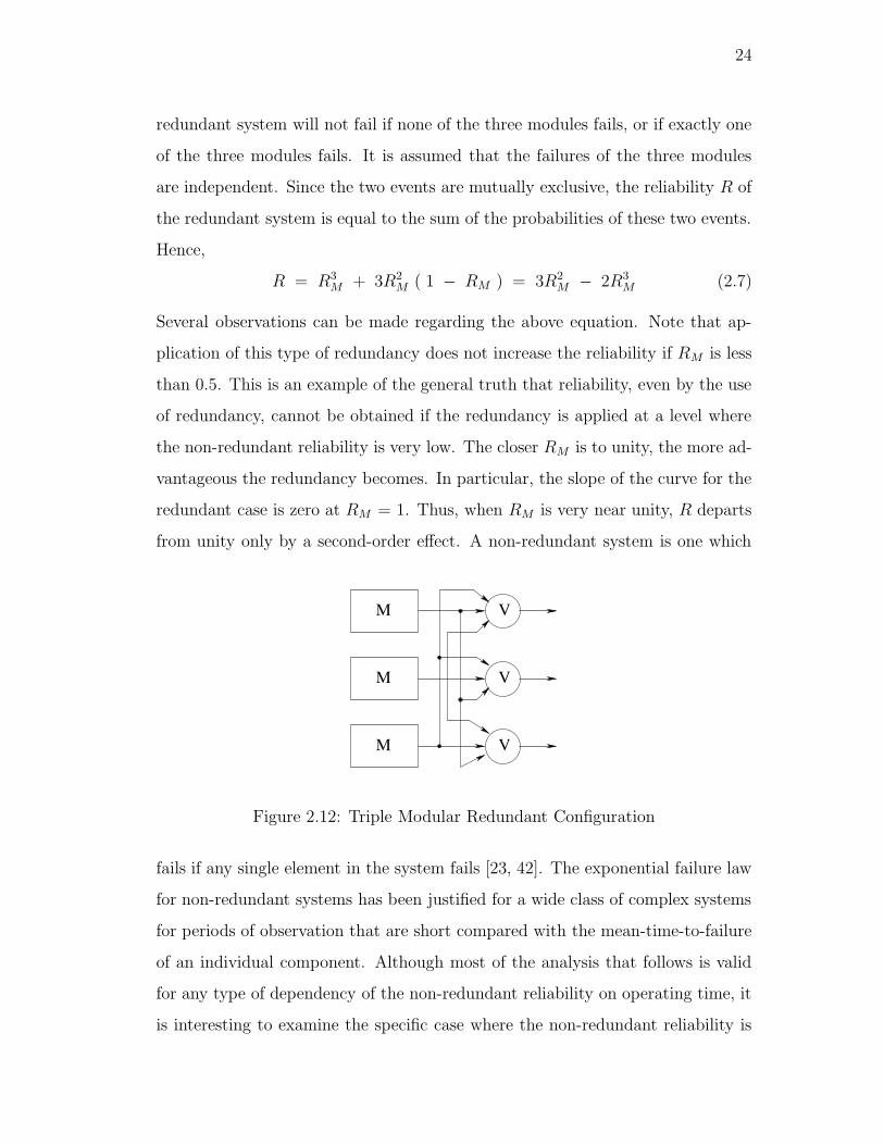
24
redundant system will not fail if none of the three modules fails, or if exactly one
of the three modules fails. It is assumed that the failures of the three modules
are independent. Since the two events are mutually exclusive, the reliability R of
the redundant system is equal to the sum of the probabilities of these two events.
Hence,
R = R3
M + 3R2
M ( 1 − RM ) = 3R2
M − 2R3
M (2.7)
Several observations can be made regarding the above equation. Note that ap-
plication of this type of redundancy does not increase the reliability if RM is less
than 0.5. This is an example of the general truth that reliability, even by the use
of redundancy, cannot be obtained if the redundancy is applied at a level where
the non-redundant reliability is very low. The closer RM is to unity, the more ad-
vantageous the redundancy becomes. In particular, the slope of the curve for the
redundant case is zero at RM = 1. Thus, when RM is very near unity, R departs
from unity only by a second-order effect. A non-redundant system is one which
M
M
M
V
V
V
Figure 2.12: Triple Modular Redundant Configuration
fails if any single element in the system fails [23, 42]. The exponential failure law
for non-redundant systems has been justified for a wide class of complex systems
for periods of observation that are short compared with the mean-time-to-failure
of an individual component. Although most of the analysis that follows is valid
for any type of dependency of the non-redundant reliability on operating time, it
is interesting to examine the specific case where the non-redundant reliability is

25
a decaying exponential of the operating time, i.e., where:
RM(t) = e−ft = e−t/MTF (2.8)
In this formula f is a constant, called the failure rate; and MTF is its reciprocal,
called mean-time-to-failure. The reliability of the triple redundant system is now
given by
R(t) = 3 e−2t/MTF − 2 e−3t/MTF (2.9)
Note that for t > MTF , which is the range of time, R < RM . This means that
triple redundancy at the computer level should not be used to improve reliability
in this case. To obtain improvement in reliability by the use of triple redundancy,
we require t < MTF . This can be achieved in the present situation by breaking
the computer into many modules, each of which is much more reliable than the
entire computer. If these triply redundant modules are now reconnected to assem-
ble an entire triple-modular-redundant (TMR) computer, an over-all improvement
in the reliability of the computer will be achieved.
2.5 Time Redundancy
The basic idea of time redundancy is the repetition of computations in ways that
allow errors to be detected [1, 40, 52]. To allow time redundancy to be used to
detect permanent errors, the repeated computations are performed differently, as
illustrated in Figure 2.13. During the first computation of time t0, the operands
are unmodified and the results are stored for later comparison. During the second
computation at time t0 +∆, the operands are modified in such a way that perma-
nent errors resulting from faults in F (X) have a different impact on the results
and can be detected when the results are compared to those obtained during the
first computation. The basic concept of this form of time redundancy is that the
same hardware is used multiple times in differing ways such that comparison of
the results obtained at the two times will allow error detection.
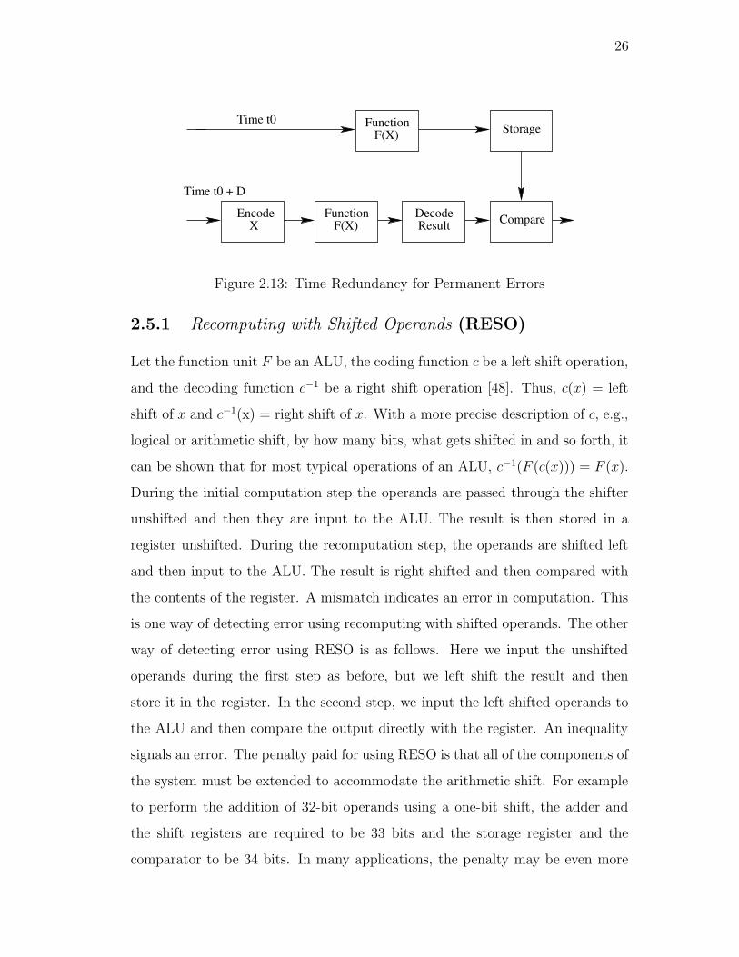
26
Time t0
XEncode
F(X)Function Decode
Result Compare
StorageFunctionF(X)
Time t0 + D
Figure 2.13: Time Redundancy for Permanent Errors
2.5.1 Recomputing with Shifted Operands (RESO)
Let the function unit F be an ALU, the coding function c be a left shift operation,
and the decoding function c−1 be a right shift operation [48]. Thus, c(x) = left
shift of x and c−1(x) = right shift of x. With a more precise description of c, e.g.,
logical or arithmetic shift, by how many bits, what gets shifted in and so forth, it
can be shown that for most typical operations of an ALU, c−1(F (c(x))) = F (x).
During the initial computation step the operands are passed through the shifter
unshifted and then they are input to the ALU. The result is then stored in a
register unshifted. During the recomputation step, the operands are shifted left
and then input to the ALU. The result is right shifted and then compared with
the contents of the register. A mismatch indicates an error in computation. This
is one way of detecting error using recomputing with shifted operands. The other
way of detecting error using RESO is as follows. Here we input the unshifted
operands during the first step as before, but we left shift the result and then
store it in the register. In the second step, we input the left shifted operands to
the ALU and then compare the output directly with the register. An inequality
signals an error. The penalty paid for using RESO is that all of the components of
the system must be extended to accommodate the arithmetic shift. For example
to perform the addition of 32-bit operands using a one-bit shift, the adder and
the shift registers are required to be 33 bits and the storage register and the
comparator to be 34 bits. In many applications, the penalty may be even more

27
shifter
Comparator
Shifter
Extracell
Shifter
Operand BOperand A
SystemCout
Error Signal
Storage/
Cin
Figure 2.14: Structure of RESO System
severe [5, 31]. For example, in a semi-custom design environment, the smallest
available entity may be a four-bit adder, in which case the need for an extra bit
in the adder would require providing the extra bits.
2.5.2 Recomputing with Alternating Logic
Let the function unit F be an ALU, the coding function c be a complement
operation, and the decoding function c−1 be a complement operation [58]. Thus,
c(x) = complement of x and c−1(x) = complement of x. With a more precise
description of c, it can be shown that for most typical operations of an ALU,
c−1(F (c(x))) = F (x). During the initial computation step the operands are
passed through the complementation operator uncomplemented and then they
are input to the ALU. The result is then stored in a register uncomplemented.
During the recomputation step, the operands are complemented and then input
to the ALU. The result is complemented and then compared with the contents of
the register. A mismatch indicates an error in computation. This is one way of

28
Operand A
StorageRegister
Error signal
ComplementOperation
Operand B
System
Comparator
OperationComplement
Figure 2.15: Structure of Recomputing with Alternating Logic System

29
detecting error using recomputing with alternating logic. The primary difficulty
with complementation is that the function, F (x), must be a self-dual to allow
error detection to occur. In many cases, 100% hardware redundancy is required
to create a self-dual function from some arbitrary function [19, 27, 35, 72].
MUX MUX HalfSystem System
Storage/Swapping
Half
Swapping
Storage
Storage/
StorageRegisterRegister
Comparator
Error
Comparator
Cout
C1
Error
C1C2
Cin
A BA
MUX
C2
B
Cin
Figure 2.16: Structure of RESWO System
2.5.3 Recomputing with Swapped Operands (RESWO)
RESWO is a variation of the RESO technique [34, 57]. The encoding and decoding
functions are swapping the upper and lower halves of each operand. At time t the

30
computations are performed using unmodified operands. At time t+∆t, however,
the upper and lower halves of each operand are swapped, and the computations
are repeated. A mismatch indicates an error in computation. The RESWO
approach has been shown to be less expensive, particularly when the complexity
of individual modules of the circuit is high [59]. This has an advantage of being
quick and easy to implement.
2.6 Fault Diagnosis
Diagnosis is the process of locating the fault present within a given fabricated copy
of the circuit [18]. For some digital systems, each fabricated copy is diagnosed
to identify the faults so as to make the decisions about repair. The objective of
diagnosis is to identify the root cause behind the common failures or performance
problems to provide the insights on how to improve the chip yield and/or perfor-
mance. A diagnostic test is designed for fault isolation or diagnosis. Diagnosis
refers to the identification of a faulty part. A diagnosis test is characterized by
its diagnostic resolution, defined as the ability to get closer to the fault. When
a failure is indicated by a pass/fail type of test in a system that is operating
in the field, a diagnostic test is applied. For an effective field repair, this test
must have a diagnostic resolution of the Lowest Replaceable Unit (LRU). For a
computer system that LRU may be a part such as a memory board, hard drive
or keyboard. The diagnostic test must identify the faulty part so that it can be
replaced. The concepts of fault dictionary and diagnostic tree are relevant to any
type of diagnosis. The disadvantage of a fault dictionary approach is that all tests
must be applied before an inference can be drawn. Besides, for large circuits, the
volume of data storage can be large and the task of matching the test syndrome
can also take a long time. It is extremely time consuming to compute a fault
dictionary.
An alternative procedure, known as the diagnostic tree or fault tree, is more
efficient. In this procedure, tests are applied one at a time. After the application

31
of a test, a partial diagnosis is obtained. Also, the test to be applied next is
chosen based on the outcome of the previous test. The depth of the diagnostic
tree is the number of tests on the longest path from the root to any leaf node. It
represents the length of the diagnostic process in the worst case. The presence
of several shorter branches indicates that the process may terminate earlier in
many cases. The maximum depth of the diagnostic tree is bounded by the total
number of tests, but it can be less than that also. Misdiagnosis is also possible
with the diagnostic tree. The notable advantage of the diagnostic tree approach
is that the process can be stopped any time with some meaningful result. If it is
stopped before reaching a leaf node, a diagnosis with reduced resolution results.
In the fault dictionary method, any early termination makes the dictionary look
up practically impossible.
2.7 Summary – Best of Prior Methods
So far, we have seen most of the fault-tolerant design techniques in the literature.
Our motive is to come up with a fault-tolerant design technique that can correct
errors. Berger codes, two-rail checkers and duplication of hardware mechanisms
are not useful because they can only detect errors. Hamming codes can correct
single-bit to multi-bit errors. Reed-Solomon codes can also correct multi-bit errors
at a time but the hardware architecture is very complex. Residue codes can
correct errors but the hardware needed for correcting one bit is huge. We can
correct as many errors as we want by modifying the architecture for these codes.
All these fault-tolerant design techniques have their own merits and de-merits.
Triple modular redundancy also can correct errors, if at any given time only
one hardware module is broken. Time redundancy mechanisms explained above
cannot correct errors, they can only detect errors. So, we cannot really say in
general which is the best-fault tolerance technique. But, the Hamming code, Reed
Solomon codes and Residue codes are the best error correcting fault-tolerance
techniques compared with other fault-tolerant techniques in the literature.

32
Chapter 3
Fault-Tolerant Technique for an ALU –
Implementation Study and Justification
The goal of this work is to implement error correction with 100% hardware over-
head and at most 100% delay overhead. We decided to analyze the different
fault-tolerant techniques in the literature. We analyzed the hardware redundancy,
the information redundancy and the time redundancy methods. After analyzing,
we discovered that we cannot achieve fault-tolerance with 100% hardware over-
head using hardware or information redundancy. Even the Reed-Solomon and the
Residue codes required more than 100% hardware to implement fault-tolerance.
So, we decided to use time redundancy as our fault-tolerance mechanism for the
ALU. In order to choose the best time redundancy mechanism, we had to com-
pare the hardware, the delay and the power overhead of the different mechanisms.
Based on these criteria we decided to use Recomputing Using Swapped Operands
as our fault-tolerance mechanism.
3.1 Architecture of the ALU
An Arithmetic-Logic Unit (ALU) is the part of the Central Processing Unit (CPU)
that carries out arithmetic and logic operations on the operands in computer
instruction words. In some processors, the ALU is divided into two units, an
arithmetic unit (AU) and a logic unit (LU). Typically, the ALU has direct in-
put and output access to the processor controller, main memory (random access
memory or RAM in a personal computer), and input/output devices. Inputs and
outputs flow along an electronic path that is called a bus. The input consists of

33
an instruction word that contains an operation code (sometimes called an “OP
CODE”), one or more operands and sometimes a format code. The operation
code tells the ALU what operation to perform and the operands are used in the
operation. The output consists of a result that is placed in a storage register
and settings that indicate whether the operation was performed successfully. In
general, the ALU includes storage places for input operands (operands that are
being added), the accumulated result and shifted results. The flow of bits and the
operations performed on them in the subunits of the ALU is controlled by gated
circuits. The gates in these circuits are controlled by a sequence logic unit that
uses a particular algorithm or sequence for each operation code. In the arithmetic
unit, multiplication and division are done by a series of adding or subtracting and
shifting operations. There are several ways to represent negative numbers. In the
logic unit, one of 16 possible logic operations can be performed, such as compar-
ing two operands and identifying where bits do not match. The design of the
ALU is obviously a critical part of the processor and new approaches to speeding
up instruction handling are continually being developed. In computing, an ALU
is a digital circuit that performs arithmetic and logic operations. An ALU must
process numbers using the same format as the rest of the digital circuit. For
modern processors, that almost always is the two’s complement binary number
representation. Early computers used a wide variety of number systems, including
one’s complement, sign-magnitude format, and even true decimal systems, with
ten tubes per digit. ALUs for each one of these numeric systems had different
designs, and that influenced the current preference for two’s complement nota-
tion, as this is the representation that makes it easier for the ALUs to add and
subtract. Most of a processor’s operations are performed by one or more ALUs.
An ALU loads data from input registers, executes the operation and stores the
result into output registers. ALUs can perform the following operations:
1. Integer arithmetic operations (addition, subtraction and multiplication)
2. Bitwise logic operations (AND, NOT, OR, XOR), and

34
3. Bit-shifting operations (shifting a word by a specified number of bits to the
left or right).
We implemented a Sklansky tree adder [62] for addition and subtraction instead of
Brent-Kung [17] or Kogge-Stone [39] trees. We chose it because it has the fewest
wires and minimum logic depth. The Sklansky adder topology is the most energy
efficient compared to the other two adders [49] in the 90nm technology. We imple-
mented Booth-encoding [14] to reduce the partial products of the multiplier and
for adding the partial products we used a Wallace Tree [69]. We used the radix-4
Booth encoding scheme for the ALU. For the Carry Propagation Adder (CPA)
at the final stage of the Wallace tree, we reused the Sklansky adder designed for
addition.
3.1.1 Adders
Addition forms the basis of many processing operations, from counting to mul-
tiplication to filtering. As a result, adder circuits that add two binary numbers
are of great interest to digital system designers. An extensive, almost endless,
assortment of adder architectures serve different speed/area requirements. The
simplest design is the ripple-carry adder in which the carry-out of one bit is sim-
ply connected as the carry-in of the next, but, in the carry propagation adders,
the carry-out influences the carry into all subsequent bits. Faster adders look
ahead to predict the carry-out of a multi-bit group. Long adders use multiple
levels of lookahead structures for even more speed. For wide adders, the delay
of carry-lookahead adders becomes dominated by the delay of passing the carry
through the lookahead stages. This delay can be reduced by looking ahead across
the lookahead blocks. In general, one can construct a multi–level tree of looka-
head structures to achieve delay that grows with log N . There are many ways to
build the lookahead tree that offer tradeoffs among the number of stages of logic,
the number of logic gates, the maximum fanout on each gate, and the amount of
wiring between the stages. Three fundamental trees are the Brent-Kung, Sklansky

35
and Kogge-Stone architectures.
3.1.1.1 Brent-Kung Adder
The Brent-Kung tree computes prefixes for 2-bit groups. These are used to find
prefixes for 4-bit groups, which in turn are used to find prefixes for 8-bit groups
and so forth. The prefixes then fan back down to compute the carries-in to each
bit. The tree requires 2(log2 N) − 1 stages. The fanout is limited to 2 at each
stage.
3.1.1.2 Kogge-Stone Adder
The Kogge-Stone tree achieves both (log2 N) stages and fanout of 2 at each stage.
This comes at the cost of many long wires that must be routed between stages.
The tree also contains more Propagate and Generate cells; while this may not
impact the area if the adder layout is on a regular grid, it will increase power
consumption.
3.1.1.3 Sklansky Adder
The Sklansky tree reduces the delay to (log2 N) stages by computing intermedi-
ate prefixes along with the large group prefixes. This comes at the expense of
fanouts that double at each level: The gates fanout to [8,4,2,1] other columns.
These high fanouts cause poor performance on wide adders unless the gates are
appropriately sized or the critical signals are buffered before being used for the
intermediate prefixes. Transistor sizing can cut into the regularity of the layout
because multiple sizes of each cell are required, although the larger gates can
spread into adjacent columns. Note that the recursive doubling in the Sklansky
tree is analogous to the conditional-sum adder. The conditional-sum adder per-
forms carry-select starting with group of 1-bit and recursively doubling to N/2
bits.

36
Figure 3.1: Sklansky Tree Adder [62]
3.1.2 Multipliers
In microprocessors, the multiplication operation is performed in a variety of forms
in hardware and software depending on the cost and transistor budget allocated
for this particular operation. Multiplication is a less common operation than ad-
dition, but is essential for microprocessors, digital signal processors, and graphics
engines. The speed of the multiply operation is of great importance in digital
signal processing as well as in the general purpose processors of today, especially
given the widespread use of media processing. In the past, multiplication was
generally implemented via a sequence of addition, subtraction and shift opera-
tions. Multiplication algorithms will be used to illustrate methods of designing
different cells so that they fit into a larger structure. There are a number of
techniques that can be used to perform multiplication. In general, the choice is
based upon factors such as latency, throughput, area and design complexity. The
different types of multiplier are unsigned array multiplication, 2’s complement ar-
ray multiplication, Booth encoding, Wallace tree multiplication and Dadda tree
multiplication.

37
3.1.2.1 Booth Encoding Multiplier
Booth Encoding was originally proposed to accelerate serial multiplication [14].
The conventional multipliers compute the partial products in a radix-2 manner.
Radix 2r multipliers produce N/r partial products, each of which depend on r
bits of the multiplier. Fewer partial products leads to a smaller and faster Carry-
Save Adder (CSA) array. For example, a radix-4 multiplier produces N/2 partial
products. Each partial product is 0, Y , 2Y , or 3Y , depending on a pair of bits of
X. Computing 2Y is a simple shift, but 3Y is a hard multiple requiring a slow-
carry propagation addition of Y +2Y before product generation begins. Modified
Booth encoding allows higher radix parallel operation without generating the hard
3Y multiple by instead using negative partial products. Negative partial products
are generated by taking the 2’s complement of the multiplicand. Hence, partial
products are chosen by considering a pair of bits along with the most significant
bit from the previous pair.
Figure 3.2: Radix-4 Booth Encoder and Selector [71]
In a radix-4 Booth-encoded multiplier, each group of three bits is decoded into
several select lines (Xi, 2Xi, and Mi) and driven across the partial product row
as shown in the Figure 3.1.2.1. The multiplier Y is distributed to all of the rows.

38
The select lines control Booth selectors that choose the appropriate multiple of Y
for each partial product. The Booth selectors substitute for the AND gates of a
simple array multiplier. Figure 3.1.2.1 shows a conventional Booth selector design
that computes the jth partial product bit of the ith partial product. If the partial
product has a magnitude of Y , yi is selected. If it has a magnitude of 2Y , yi−1 is
selected. If it is negative, the multiple is inverted. Even in an unsigned multiplier,
negative partial products must be sign-extended to be summed correctly. Large
multipliers can use Booth encoding of higher radix. Higher-radix Booth encoding
is possible, but generating the other hard multiples appears not to be worthwhile
for multipliers of fewer than 64 bits. Similar techniques apply to sign-extending
higher-radix multipliers.
3.1.2.2 Wallace Tree Multiplication
In his historic paper, Wallace introduced a way of summing the partial product
bits in parallel using a tree of Carry Save Adders (CSA), which became generally
known as the Wallace Tree [69]. A CSA is effectively a “1 counter” that adds
the number of 1’s on the A, B and C inputs and encodes them on the SUM and
CARRY outputs. A CSA is therefore also known as a (3,2) counter because it
converts three inputs into a count encoded in two outputs. The carry-out is passed
to the next more significant column, while a corresponding carry-in is received
from the previous column. Therefore, for simplicity, a carry is represented as
being passed directly down the column. The output is produced in carry-save
redundant form suitable for the final Carry Propagation Adder. The column
addition is slow because only one CSA is active at a time. Another way to speed
the column addition is to sum partial products in parallel rather than sequentially.
Figure 3.3 shows a Wallace Tree using this approach. The Wallace tree requires
levels of (3,2) counters to reduce N inputs down to 2 carry-save redundant form
outputs. Although this may seem to be a complex process, it yields multipliers
with delay proportional to the logarithm of the operand size N . The Wallace
Tree was widely used in the implementation of the parallel multipliers.

39
Figure 3.3: Wallace Tree Multiplier [69]
3.1.2.3 Dadda Tree Multiplication
A suggestion for improved efficiency of addition of the partial was published by
Dadda. In his historic 1965 paper, Dadda introduces the notion of a counter
structure that will take a number of bits p in the same bit position (of the same
“weight”) and output a number q, which represents the count of ones at the input
[25]. Dadda has introduced a number of ways to compress the partial product
bits using such a counter, which is known as “Dadda’s counter.” This process is
shown for an 8 × 8 Dadda Multiplier in Figure 3.4. Columns having more than
six dots are reduced using half adders and full adders so that no column will have
more than six dots. Partial products are shown by “dots,” half adders are shown
by a “crossed” line and full adders are shown by a line. The height of the tree is
determined by working back from the last two rows of the partial products and
limiting the height of each tree to the largest integer that is no more than 1.5
times the height of its successor. Since the number of stages is logarithmically
related to the number of bits in the words to be multiplied, the delay of the matrix
reduction process is proportional to log(n). Since the adder that reduces the final

40
Figure 3.4: Dadda Tree Multiplier [25]
two row matrix can be implemented as a carry propagation adder, the total delay
of the multiplier is proportional to the logarithm of the word size. An extensive
study of the use of Dadda’s counters was undertaken by Stenzel and Kubitz in
1977 [66]. In their paper they have also demonstrated a parallel multiplier built
using ROM to implement counters used for partial product summation.
3.2 Justification for Recomputing Using Swapped Operands
for Fault Tolerance
3.2.1 Why Information Redundancy Is Not Useful
Information redundancy means using error-detecting codes and error-correcting
codes as fault-tolerance mechanisms. There are many error detecting codes in
the literature such as repetition schemes, parity schemes, checksums, cyclic re-
dundancy checks, etc. But, the error detecting codes are not useful because we

41
want to correct the hard and soft errors in the ALU. So, we decided to use error-
correcting codes. Some of the error correction schemes are Hamming codes, Reed-
Solomon codes, Reed-Muller codes, Golay codes, Turbo codes, Viterbi codes,
Residue codes, Bose-Chaudhuri-Hocquenghem (BCH) codes, etc. But, not all
error-correcting codes are useful for the application of fault-tolerance for an ALU.
So, we decided to examine three of the error correcting codes, namely Hamming,
Residue and Reed-Solomon codes.
We chose the Reed-Solomon (RS) code because the architecture is the same
as for BCH and Reed-Muller codes, and it is more efficient than those two codes.
RS codes are defined over GF (2m) for 3≤ m ≤ 8 (GF means Galois Fields). For
m = 3, the RS encoder will require 21 extra bits for encoding all the inputs in a
three input bit sequence. So, at a time we can process only three input bits, and
if we have to process all of the 32 bits, then we have to do it 11 times. This would
cost us a huge delay. The data path overhead will cost us 66% overhead and when
we include the hardware of the encoder and then the hardware overhead of the
encoder becomes 109.1%. We did not calculate the hardware overhead of the RS
decoder as the hardware overhead of RS encoder is more than 100%. Hence, we
decided not to use the RS codes as the fault-tolerance mechanism for the ALU.
We tried a residue code as the fault-tolerance mechanism for an ALU. The
main concept of residue codes is calculating a remainder. The main problem of
a residue code is designing the most optimal implementation for calculating the
remainder. Residue codes need four moduli in total to correct a single bit error.
Each modulus requires 11 bits and we require 44 bits in total. This increases
the data path overhead by 137.5 %. Not only does it require 44 extra bits but
the mod operators required to calculate the residues require much hardware. We
have the hardware required for the “mod” operation as 58% considering that we
reuse the hardware. The total overhead would be 195.5 %. Above all else, residue
codes do not work with the Boolean operations of the ALU. So, we decided not
to pursue the residue codes as the fault-tolerance mechanism.
We finally decided to try a Hamming code as the fault-tolerance mechanism

42
for an ALU. Hamming codes are really good with the Boolean operations of the
ALU. But, they do not work with arithmetic operations of ALU. For example:
• Let us assume A = 0111 and B = 0111. We will design a (7,4) single bit
error correcting Hamming code.
• Let us assume a0, a1, a2 and a3 are data bits; p0, p1 and p2 are parity bits.
• p0 = a0 ⊕ a1 ⊕ a3 ; p1 = a0 ⊕ a2 ⊕ a3 ; p2 = a1 ⊕ a2 ⊕ a3
• The symbol is a3a2a1p2a0p1p0
• H(A) = 0110100; H(B) = 0110100; H(A) + H(B) = 1101000
• H(A + B) = 1111000
H(A) + H(B) 6= H(A + B) (3.1)
Here “H” represents the Hamming code. Though the hardware overhead was less
than 100%, we were not able to use Hamming codes in arithmetic. So, information
redundancy is not useful as the fault-tolerance mechanism for an ALU.
3.2.2 Why Hardware Redundancy Is Not Useful
Real–time systems are equipped with redundant hardware modules. Whenever a
fault is encountered, the redundant modules takeover the functions of the failed
hardware module. Hardware redundancy methods are mainly charectrized as
duplication with comparison and triple modular redundancy. Duplication with
comparison can only detect errors, but our aim is to correct errors. The hardware
overhead with the duplication with comparison method is 117%. With triple
modular redundancy we can correct errors. Triple modular redundancy uses two
extra copies of the same ALU and that increases the hardware overhead by 200%.
The hardware needed for the triplicated voting mechanism is around 25%. The
total hardware overhead with the triple modular redundancy mechanism is around

43
225%. But, our goal is to have the hardware overhead not more than 100%. So,
hardware redundancy is not useful as a fault tolerance mechanism for ALU.
3.2.3 Why the other Time-redundancy Mechanisms Are
Not Useful
As information and hardware redundancy were not useful, we decided to use time
redundancy as the fault-tolerance mechanism for the ALU. The key to the ef-
fectiveness and efficiency of the time redundancy method is the selection of the
encoding and decoding functions, so we investigated in total three candidate func-
tions, namely, Recomputing using Shifted operands (RESO), Recomputing with
Alternating logic and Recomputing with Swapped operands (RESWO). We had to
choose one of the functions as our fault-tolerance mechanism. The only way we
could make a decision is by implementing all three functions as the fault-tolerance
mechanism for the ALU and comparing the hardware, the delay and the power
overheads of each of the functions. Whichever function gives the best trade-off
would be chosen as the fault-tolerance mechanism for the ALU. We give the first
priority to the hardware overhead, then the power overhead and finally the delay
overhead. So, based on this strategy we chose RESWO as our fault-tolerance
mechanism. We have tabulated the comparison of overheads in Section 3.3.
3.3 Results
We have implemented different types of fault tolerance mechanisms for the 16-bit
ALU. We discovered that error detecting codes such as the Two-Rail checker and
Berger codes are no longer useful, as our aim is error correction. So, we imple-
mented error correcting codes such as the Hamming, Residue and Reed-Solomon
codes as a fault-tolerance mechanism. Hamming codes are not invariant for arith-
metic operations and the hardware overheads of Residue and Reed-Solomon codes
are extremely huge. So, we decided to use Time Redundancy as the fault-tolerance
mechanism for the ALU. The basic idea of time redundancy is the repetition of

44
Table 3.1: Results for a 16-bit ALUArchitecture Hardware Delay Power
Overhead Overhead OverheadRecomputing with 93.1% 89.89% 195.00%Shifted Operands
Recomputing with 82.6% 117.87% 135.37%Alternating logic
Recomputing with 77.3% 114.61% 126.31%Swapped Operands
computations in ways that allow errors to be detected. In order to choose the
best fault-tolerance mechanism we had to calculate the delay, the power and the
hardware overheads. Our main concern was the hardware and the power over-
heads, and then the delay overhead. Results are shown in Table 3.1. So, we
chose REcomputing with SWapped Operands as it had 5.3% lower hardware and
9.06% lower power overheads than Recomputing with Alternating Logic. The best
fault tolerance mechanism for the ALU is REcomputing with SWapped Operands
(RESWO). The RESWO approach has been shown to be less expensive, particu-
larly when the complexity of individual modules of the circuit is high. This has
an advantage of being quick and easy to implement. The hardware overhead of
RESWO with respect to different architectures of the ALU is shown in Table 3.2.
Table 3.2: RESWO Implementation for Different Architectures of the ALUArchitecture Hardware Delay Power
Overhead Overhead Overhead16-bit 77.30% 114.61% 126.31%32-bit 33.62% 112.76% 120.99%64-bit 16.58% 110.96% 113.90%
We operate the ALU twice for each data path operation once normally and
once swapped. When there is a discrepancy in the circuit (either a bit position
is broken or a carry propagation circuit is broken), we diagnose the ALU using
special diagnosis vectors. Knowledge of the faulty bit slice makes error correction
possible, which will be achieved by reconfiguring the ALU. This is covered in the

45
later Chapters 4 and 5.
We use two different swapping mechanisms to detect the soft errors of the
64-bit ALU. The first time we run the operations normally without swapping the
input operands. The second time we run the operations by swapping 32 bits of the
64-bit input operands. We compare these two outputs and check whether there
is a discrepancy in the circuit. If there is no discrepancy in the circuit this will be
the last swap. We swap the operands the third time only if the outputs from the
first time and the second time disagree with each other. If there is a discrepancy
in the circuit we use a different swapping mechanism (we run the operations by
swapping 16 bits of the 64-bit input operands) to check whether it is a soft error
or a hard error. If all the three outputs produced by the ALU with the different
swapping mechanisms differ from each other then there is a hard error in the
ALU. If one of the outputs differs from the other two outputs then there is a soft
error in the ALU. If we use just one swapping mechanism (swapping 32 bits of the
64-bit input operands), then in order to detect the soft errors we have to run the
operations four times. The first time we run the operations normally, the second
time we run it with one swapped mechanism. If a fault is detected then we again
perform the two operations to check whether it is a soft error or hard error. The
advantage of using one swapping mechanism instead of two swapping mechanisms
is we have reduced operand swapping hardware and the disadvantage is increased
delay.

46
Chapter 4
Diagnosis of ALU Using RESWO and Test
Vectors and Reconfiguration for Error
Correction
The goal of this work is to implement the best diagnosis scheme for the ALU
with a minimum number of diagnosis vectors. We implemented the diagnosis
mechanisms for the ALU in five different ways. We found that designing the ALU
with 2-bit ALU chunks requires a minimum number of diagnosis vectors, but we
had some issues with the multiplier. So, after further analyzing the diagnosis
mechanisms we finally decided to design the Boolean, addition, subtraction and
shifting operations, either with 2-bit ALU chunks or with 1-bit ALU chunks and
then design the multiplier separately.
4.1 Diagnosis Method
Diagnosis is the process of locating the fault present within a given fabricated copy
of the circuit [18]. For some digital systems, each fabricated copy is diagnosed
to identify the faults so as to make decisions about repair. The objective of
diagnosis is to identify the root cause behind the common failures or performance
problems to provide insights on how to improve the chip yield and/or performance.
A diagnostic test is designed for fault isolation or diagnosis. Diagnosis refers
to the identification of a faulty part. A diagnosis test is characterized by its
diagnostic resolution, defined as the ability to get closer to the fault. When a
failure is indicated by a pass/fail type of test in a system that is operating in the
field, a diagnostic test is applied. The aim of this test is to identify the faulty

47
part that should be replaced. The environment of the system repair determines
the level or the units to be identified. The cardinality of the suspected set of
Lowest Replaceable Units (LRUs) that the test identifies is defined as its diagnostic
resolution. An ideal test will have the diagnostic resolution of 1. Such a test will
be able to exactly pinpoint the faulty unit and will allow the most efficient repair.
The concepts of fault dictionary and diagnostic tree are relevant to any type of
diagnosis.
4.1.1 Fault Dictionary
Application of a test simply tells us whether or not the system-under-test is
faulty. We must further analyze the test result to determine the nature of the
fault, so that it can be fixed. A fault dictionary contains the set of test symptoms
associated with each modeled fault. One disadvantage of the fault dictionary
approach is that all tests must be applied before an inference can be drawn.
Besides, for large circuits, the volume of data storage can be large and the task
of matching the test syndrome can also take time.
4.1.2 Diagnosis Tree
In this procedure, tests are applied one at a time. After the application of a test
a partial diagnosis is obtained. Also, the test to be applied next is chosen based
on the outcome of the previous test. The maximum depth of the diagnostic tree
is bounded by the total number of tests, but it can be less than that as well. The
depth of the diagnostic tree is the number of tests on the longest path from the
root to any leaf node. It represents the length of the diagnostic process in the
worst case. The diagnostic tree can be arranged in several ways. One approach
is to reduce the depth. We start with the set of all faults as “suspects.” Tests
are ordered such that the passing of each test will reduce the suspect set by the
greatest amount. This may sometimes increase the depth of the tree on the side
of the failing tests.

48
4.1.3 Why We Use a Diagnosis Tree
We chose to use a diagnosis tree instead of a fault dictionary for many reasons.
One notable advantage of the diagnostic tree approach is that the process can be
stopped any time with some meaningful result. If it is stopped before reaching
a leaf node, then a diagnosis with reduced resolution (a larger set of suspected
faults) results. The disadvantage of a fault dictionary approach is that all tests
must be applied before an inference can be drawn. The storage requirements of
a diagnosis tree are typically smaller than for a fault dictionary. If we use a fault
dictionary for large circuits, then the volume of data storage can be large and the
task of matching the test syndrome can also take a long time. It is extremely time
consuming to compute a fault dictionary. In order to avoid these complications
we decided to use a diagnosis tree.
4.2 Comparison with Alternative Methods
4.2.1 Implementation of Diagnosis for ALU
After the Recomputing with Swapped Operands mechanism detects that there is
a permanent fault in the Arithmetic and Logic Unit (ALU), we need to diagnose
the ALU and locate the faulty part in the ALU. In order to diagnose the ALU
we decided to use a diagnosis tree. So, we attempted to implement the diagnosis
tree for the ALU in five different ways. They are:
1. Design the ALU as one piece.
2. Design the ALU with reconfigurable 4-bit ALU chunks.
3. Design the ALU with reconfigurable 2-bit ALU chunks.
4. Design the Boolean, addition, subtraction and shifting operations using
reconfigurable 2-bit ALU chunks. Design the multiplier separately.

49
5. Design the Boolean, addition, subtraction and shifting operations using
reconfigurable 1-bit ALU chinks. Design the multiplier separately
4.2.1.1 Design the ALU as One Piece
We can diagnose the 32-bit ALU as one piece and find the special vectors needed to
locate the faults. The total number of vectors needed to diagnose the entire 32-bit
ALU is approximately 1100. The Booth encoded Wallace tree multiplier designed
initially was not the optimal architecture. We do not know how many vectors it
will take if we optimized the multiplier architecture. As the number of vectors
for diagnosing the ALU is huge, we decided not to pursue this implementation.
4.2.1.2 Design the ALU with Reconfigurable 4-bit ALU Chunks
We designed the 32-bit ALU with eight reconfigurable 4-bit ALU chunks and
diagnosed the 4-bit ALU chunks to locate the faults. The total number of vectors
needed to diagnose the 4-bit ALU is 46. Our goal is to use less than 30 diagnosis
vectors to diagnose the ALU. So, we decided not to pursue this implementation.
4.2.1.3 Design the ALU with Reconfigurable 2-bit ALU Chunks
We designed the 32-bit ALU with sixteen reconfigurable 2-bit ALU chunks and
diagnosed the 2-bit ALU chunks to locate the faults. The total number of di-
agnosis vectors needed to diagnose the 2-bit ALU is 33. We found that some of
the diagnosis vectors were just used to detect either 2 or 3 stuck-at faults in the
circuit. So, we manually calculated the diagnosis vectors needed for detecting all
of the stuck-at faults in the 2-bit ALU. We found that we can eliminate 6 diag-
nosis vectors that were detecting either 2 or 3 stuck-at faults, as these stuck-at
faults can be detected by the other 27 diagnosis vectors. Hence, with 27 diagnosis
vectors we can detect all the stuck-at faults in the 2-bit ALU. With this imple-
mentation we met our goal of diagnosing the ALU with less than 30 diagnosis
vectors. But, the problem with this implementation is the multiplier. In a 32-bit

50
multiplier, we have to multiply two 32-bit inputs. In this implementation we can
multiply only two 2-bit inputs.
The 32-bit multiplier implementation should be
z[63 : 0] = a[31 : 0] × b[31 : 0] (4.1)
The 2-bit ALU implementations will be
z[3 : 0] = a[1 : 0] × b[1 : 0] (4.2)
z[7 : 4] = a[3 : 2] × b[3 : 2] (4.3)
......
...
z[63 : 60] = a[31 : 30] × b[31 : 30] (4.4)
But, in order to get the actual output of the 32-bit multiplier from the 2-bit
multipliers, we have to multiply a[1 : 0] with all other data bits of “b,” i.e.,
b[31 : 2]. Similarly, we have to multiply the other data bits of “a” (i.e., a[31 : 2])
with the data bits of “b.” If we try to implement this hardware separately it is
almost like designing an extra multiplier. To diagnose this extra hardware we
would need many diagnosis vectors. In order to overcome this difficulty we have
to modify the architecture of the multiplier.
4.2.1.4 Design the Boolean, Addition, Subtraction and Shifting Op-
erations Using Reconfigurable 2-bit ALU Chunks. Design the
Multiplier Separately
We can design the Boolean, addition, subtraction and shifting operations using
sixteen reconfigurable 2-bit ALU chunks. We can design the multiplier for the
32-bit ALU separately. The total number of diagnosis vectors needed to diagnose
the ALU without the multiplier is 22. The number of diagnosis vectors needed
to diagnose the 32-bit multiplier is 85. But, our goal is to keep the number of
diagnosis vectors less than 30. In order to achieve this we had to modify the
architecture of the multiplier.

51
We decided to diagnose the Booth encoding separately and the Wallace tree
[69] separately. The number of diagnosis vectors needed to diagnose the Booth
encoding method is 63 and it did not meet our goal. So, we decided to modify
our diagnosis scheme for the Booth encoding method. We decided to diagnose
the Booth encoder and the Booth selector separately. The number of diagnosis
vectors needed to diagnose the Booth encoder (Booth selector) separately is 35
(40).
The number of diagnosis vectors needed to diagnose the Wallace tree is 70. So,
we decided to diagnose the carry save adders (CSA) separately and tried using
similar adders but it increased the hardware of the Wallace tree. This is because
the Wallace tree is not a regular structure. So, we decided to use a Dadda tree
multiplier [25] (which is a regular structure), instead of the Wallace tree for the
ALU. The number of diagnosis vectors used to diagnose the Dadda tree is 50.
Our main aim of this research is to keep the hardware overhead less than 100%.
Once a fault is detected in the Dadda tree we have to replace the entire Dadda
tree. Even if there is a fault in the Booth encoder or the Booth selector, we have
to replace the entire Booth encoder or the Booth Selector. This replacement
hardware will boost the hardware overhead of the multiplier to 100%. In order
to overcome this we have to re-design the diagnosis scheme.
We decided to split the Booth encoder into 16 identical bit slices. To diagnose
one bit slice of the Booth encoder it took 7 vectors. Just like the Booth encoder,
the Booth selector was split into 33 identical bit slices. To diagnose one bit slice
of the Booth selector, it took 4 vectors. The advantage of the Dadda tree is that
it uses full adders and half adders of equal bit slices. The Dadda tree consisted of
433 full adders and 71 half adders. The total number of diagnosis vectors needed
to diagnose the full adders (half adders) was 5 (4). We decided to split the carry
propagation adder of the Dadda tree into identical 2-bit slices. The total number
of diagnosis vectors needed to diagnose the carry propagation adder is 7. Hence,
we were able to diagnose the multiplier with a minimum number of diagnosis
vectors.

52
4.2.1.5 Design the Boolean, Addition, Subtraction and Shifting Op-
erations Using Reconfigurable 1-bit ALU Chunks. Design the
Multiplier Separately
For the 32-bit ALU, we can design the Boolean, addition, subtraction and shifting
operations using thirty two reconfigurable 1-bit ALU chunks. The total number
of diagnosis vectors needed to diagnose the ALU without the multiplier is 17. We
used the same architecture of the multiplier and the same diagnosis scheme as
explained in Section 4.2.1.4.
4.2.2 Minimal Test Set for 100% Fault Detection
In Section 4.2.1 we discussed the number of diagnosis vectors used to detect the
stuck-at faults in a circuit. To diagnose a Booth encoder, a full adder and a half
adder we need 7, 5 and 4 diagnosis vectors, respectively. We proposed that to
diagnose one-bit slice of the Booth selector circuit we need 4 diagnosis vectors and
we are going to prove this using a Theorem. We use the Checkpoint Theorem to
generate diagnosis vectors. The Checkpoint Theorem states that a test set that
detects all single (multiple) stuck-at faults on all checkpoints of a combinational
circuit, also detects all single (multiple) stuck-at faults in that circuit.
We use an automated test pattern generator (EST) and the Checkpoint the-
orem to create the test pattern for all faults in the Booth selector (Figure 4.1),
which are listed in Table 4.1. We collapse thses vectors into the four diagnosis
vectors {T1, T2, T3, T4}, which detects both stuck-at faults s/1 and s/0 for the
Booth selector circuit. {T1, T2, T3, T4} = {11001, 10101, 10110, 01010}
Similarly, we calculate the collapsed test vectors {T1, T2, T3, T4, T5} to detect
both stuck-at faults s/1 and s/0 for the full adder circuit, in Figure 4.2. The
vectors {T1, T2, T3, T4, T5} = {101, 001, 010, 110, 100} are listed in the Table 4.2.
Finally, using the same procedure, we calculate the collapsed test vectors
{T1, T2, T3, T4} to detect both stuck-at faults s/1 and s/0 for the half adder circuit,
in Figure 4.3. The vectors {T1, T2, T3, T4} = {00, 01, 10, 11} are listed in the Table

53
5
3
4
1
c2
6
78
11a
b ef
10
3.1
9
8.1
3.2
8.2d
Figure 4.1: Booth Selector Circuit
Table 4.1: Test Vectors for the Booth Selector Circuit
Circuit Test Vector for Test Vector forLine Stuck-at-0 Faults Stuck-at-1 Faults
1 1XX1X 0XX1X2 X1XX1 X0XX1
3.2 10110 110013.1 10101 01010
4 1XX1X 1XX0X5 X1XX1 X1XX06 10X10 01X107 11X01 01X10
8.2 01010 110018.1 10101 10110
9 01010 1010110 01010 11001
g4 10
119
8
7
65
3.3
3.2
3.1
4.1
4.2
2.2
1.21.12.11
2
3
b
f
ac
d
eh
Figure 4.2: Full Adder Circuit

54
Table 4.2: Test Vectors for the Full Adder Circuit
Circuit Test Vector for Test Vector forLine Stuck-at-0 Faults Stuck-at-1 Faults1.1 11X 01X1.2 11X 01X2.1 11X 10X2.2 11X 10X3.1 001 1103.2 001 1103.3 101 0104.1 100 1104.2 101 001
5 001 1016 110 1017 001 1018 001 1109 001 101
10 110 10111 001 110
3
3.1
3.2
2.1
2.2
2.3
1
2
4
6
5
8
7
d
a b
f
e
c
Figure 4.3: Half Adder Circuit

55
Table 4.3: Test Vectors for the Half Adder Circuit
Circuit Test Vector for Test Vector forLine Stuck-at-0 Faults Stuck-at-1 Faults
1 1X 0X2.1 01 002.2 11 102.3 11 10
3 0X 1X3.1 01 113.2 00 10
4 11 015 11 016 11 107 11 008 01 11
4.3.
4.3 Results
We have implemented different types of diagnosis mechanisms for the 32-bit ALU.
The number of diagnosis vectors needed to detect the faults in the 32-bit ALU,
with different diagnosis mechanisms is shown in Table 4.4. We discovered that
if we split the 32-bit ALU into sixteen 2-bit ALU chunks, then in order to get
the output of the 32-bit multiplier, we need 256 2-bit multipliers in total. So, we
modified the implementation of the multiplier. We decided to design the Boolean,
Table 4.4: Diagnosis Vectors for Different Diagnosis Implementations
Architecture Number ofDiagnosis Vectors
32-bit ALU 11004-bit ALU 462-bit ALU 27
2-bit ALU without Multiplier 221-bit ALU without Multiplier 17
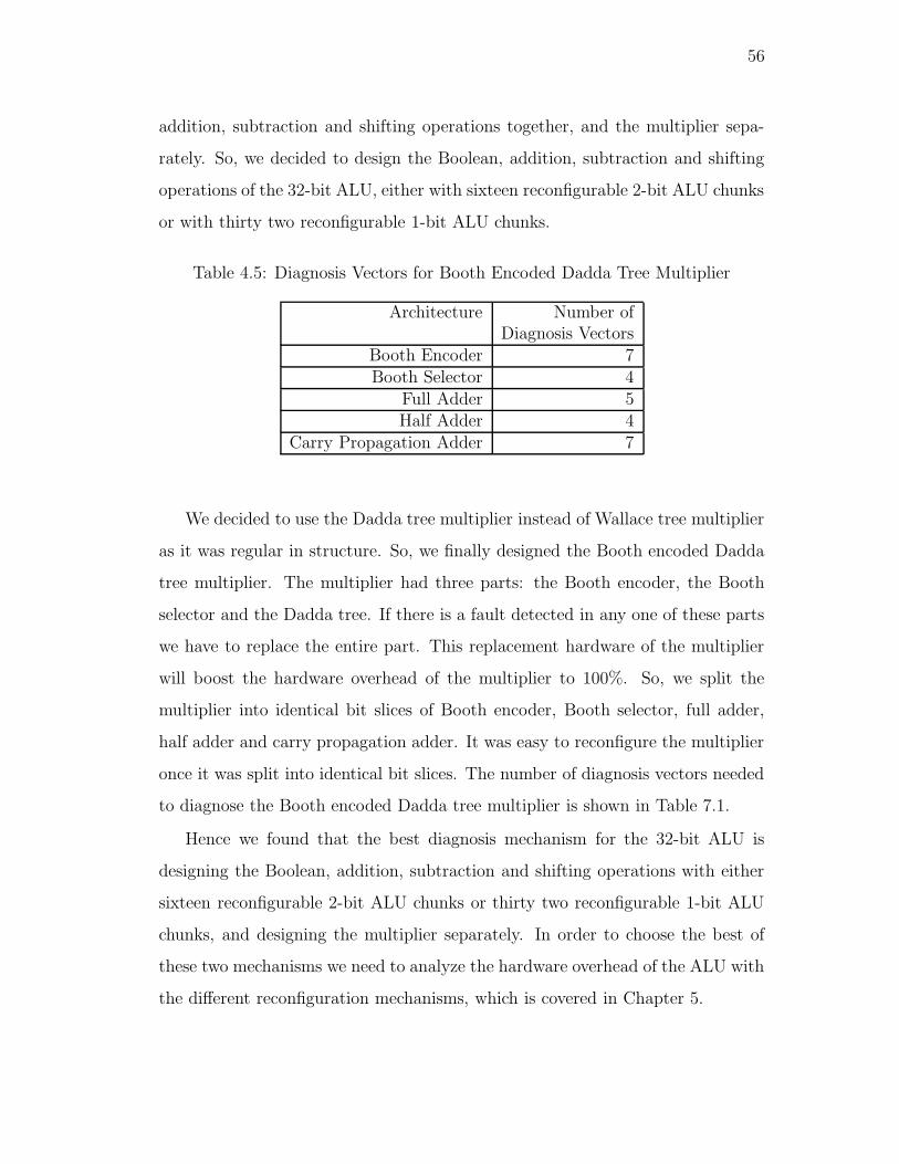
56
addition, subtraction and shifting operations together, and the multiplier sepa-
rately. So, we decided to design the Boolean, addition, subtraction and shifting
operations of the 32-bit ALU, either with sixteen reconfigurable 2-bit ALU chunks
or with thirty two reconfigurable 1-bit ALU chunks.
Table 4.5: Diagnosis Vectors for Booth Encoded Dadda Tree Multiplier
Architecture Number ofDiagnosis Vectors
Booth Encoder 7Booth Selector 4
Full Adder 5Half Adder 4
Carry Propagation Adder 7
We decided to use the Dadda tree multiplier instead of Wallace tree multiplier
as it was regular in structure. So, we finally designed the Booth encoded Dadda
tree multiplier. The multiplier had three parts: the Booth encoder, the Booth
selector and the Dadda tree. If there is a fault detected in any one of these parts
we have to replace the entire part. This replacement hardware of the multiplier
will boost the hardware overhead of the multiplier to 100%. So, we split the
multiplier into identical bit slices of Booth encoder, Booth selector, full adder,
half adder and carry propagation adder. It was easy to reconfigure the multiplier
once it was split into identical bit slices. The number of diagnosis vectors needed
to diagnose the Booth encoded Dadda tree multiplier is shown in Table 7.1.
Hence we found that the best diagnosis mechanism for the 32-bit ALU is
designing the Boolean, addition, subtraction and shifting operations with either
sixteen reconfigurable 2-bit ALU chunks or thirty two reconfigurable 1-bit ALU
chunks, and designing the multiplier separately. In order to choose the best of
these two mechanisms we need to analyze the hardware overhead of the ALU with
the different reconfiguration mechanisms, which is covered in Chapter 5.

57
Chapter 5
Optimal Reconfiguration Scheme for the ALU
After the diagnosis test identifies the location of the fault, we have to reconfigure
or replace the faulty part. We designed the Boolean, addition, subtraction and
shifting operations of the 64-bit ALU with thirty two reconfigurable 2-bit ALU
chunks (the lowest replaceable unit (LRU) for the 64-bit ALU) and designed the
multiplier separately. We implemented the reconfiguration mechanisms for the
ALU in four different ways. We compared the hardware overhead of the 64-bit
ALU with the different reconfiguration mechanisms. We found that the best
reconfiguration mechanism is to use, one spare chunk for every sixteen chunks.
5.1 Reconfiguration Analysis
Reconfiguration is the ability of a system to replace the failed component or to
isolate it from the rest of the system, when a fault is detected or a permanent fail-
ure is located. The component may be replaced by backup spares. Alternatively,
it may simply be switched off and the system capability degraded; this process is
called graceful degradation. The component diagnosed as failed is replaced.
As with reconfiguration, repair can be either on-line or off-line. In off-line
repair, either the failed component is not necessary for system operation, or the
entire system must be brought down to perform the repair. In on-line repair,
the component may be replaced immediately by a back-up spare in a procedure
equivalent to reconfiguration or the operation may continue without the compo-
nent, as is the case with masking redundancy or graceful degradation. In either
case of on-line repair, the failed component may be physically replaced or repaired

58
without interrupting system operation.
Reconfiguration can be implemented with one of two strategies in mind. The
first strategy is to restructure a system in the presence of faults so that the
performance is degraded as little as possible. The second strategy is to restructure
a system in presence of faults using spare modules so that the original performance
is retained. We cannot afford a degraded ALU for the medical system as it has to
do some crucial computations. The system restructuring using spare modules can
be achieved with a hardware overhead of 75.5%, as shown in Figure 5.11. Hence,
the second approach is preferred here as the system under consideration is a part
of medical system and it seems to be a modular approach to fault tolerance.
5.2 Reconfiguration Schemes
Reconfiguration is defined as an operation of replacing faulty components with
spares while maintaining the original interconnection structure. The important
criteria for evaluating a reconfiguration scheme are as follows:
1. Reconfiguration effectiveness – the probability that an array with a given
number of faulty cells is reconfigurable,
2. Hardware overhead for reconfiguration and
3. Overall yield and reliability.
The reconfiguration effectiveness represents the ability of a reconfiguration and
redundancy scheme to tolerate a given number of faults in an array. It also
indicates the utilization of spare cells under a redundancy and reconfiguration
scheme. The reconfiguration effectiveness and hardware overhead are functions
of the redundancy and reconfiguration scheme. The yield and reliability are also
important criteria. They are strongly related to the reconfiguration effectiveness
and the hardware overhead. Our design goals are to reduce the hardware overhead
for reconfiguration, and to increase the yield and reliability.

59
After taking all these factors into consideration, we decided to implement
reconfiguration for the 64-bit ALU (designed the Boolean, addition, subtraction
and shifting operations of the 64-bit ALU with thirty two reconfigurable 2-bit
ALU chunks and with a multiplier designed separately) in four different ways:
1. For every two chunks provide one spare chunk,
2. For every four chunks provide one spare chunk,
3. For every eight chunks provide one spare chunk and
4. For every sixteen chunks provide one spare chunk.
5.2.1 For Every Two Chunks Provide One Spare Chunk
In this reconfiguration scheme, we will use one spare module for every two mod-
ules. In order for this reconfiguration scheme to work both the modules should
be identical. Figure 5.1 shows the block diagram of this reconfiguration scheme.
There are three modules M1, M2 and a spare module. Module M1 has inputs
X, Y , Z and the output connected to the input B4 of a MUX. Module M2 has
inputs A, B, C and the output connected to the input B5 of a MUX. The spare
module has inputs F , G, H and output OUT . There are totally five 2 : 1 MUXes.
The inputs X, Y , Z of module M1 are connected to the inputs B3, B2 and B1 of
the MUXes. The inputs A, B, C of module M2 are connected to the inputs A3,
A2 and A1 of the MUXes. The outputs O1, O2, O3 of the MUXes are connected
to the inputs F , G, H of the spare module. The output OUT of the spare module
is connected to the inputs A4 and A5 of the MUXes. The MUX with inputs A1,
B1 and output O1 has a select signal Sa. The MUX with inputs A2, B2 and
output O2 has a select signal Sa. The MUX with inputs A3, B3 and output O3
has a select signal Sa. The MUX with inputs A4, B4 and output OUT1 has a
select signal Sa. The select signal Sb is generated from the select signal Sa. The
MUX with inputs A5, B5 and output OUT2 has a select signal Sb. If one of the
modules M1 or M2 goes faulty then the select signals Sa or Sb will be activated

60
M
A3
B3
B2
A2
B1
A1
OUT
O3
O2
O1
SPAREMODULE M1 MODULE M2
MUX MUX
Sa
SaSa
Sa
Sa Sb
OUT1 OUT2
A5 B5A4 B4
X Y Z A B C
MODULE
UX
M
UX
M
UX
GF H
Figure 5.1: Reconfiguration Scheme – For Every Two Chunks Provide One SpareChunk

61
accordingly to replace the faulty module with the spare module. Once the faulty
module is replaced the original performance of the system is retained.
5.2.2 For Every Four Chunks Provide One Spare Chunk
In this reconfiguration scheme, we will use one spare module for every four mod-
ules. In order to make this reconfiguration scheme work we should make sure all
ModuleM1
ModuleM2
ModuleM3
ModuleM4
A2
B2C2D2
B1C1D1
YX
Out
Z2
Z1
A1
MUX MUX MUX MUX
Out4Out3Out2Out1
A3 B3 A4 B4 A5 B5 A6 B6
SpareModule
P Q R S T U V W
Sc Sd SfSe
SbSa
MUX
MUX
SbSa
Figure 5.2: Reconfiguration Scheme – For Every Four Chunks Provide One SpareChunk
the modules are identical. Figure 5.2 shows the block diagram of this reconfigu-
ration scheme. There are five modules M1, M2, M3, M4 and a spare module.
Module M1 has inputs P , Q and output is connected to the input B3 of the

62
MUX . Module M2 has inputs R, S and output is connected to the input B4 of
the MUX. Module M3 has inputs T , U and output is connected to the input B5
of the MUX. Module M4 has inputs V , W and output is connected to the input
B6 of the MUX. The spare module has inputs X, Y and output Out. There are
two 4 : 1 MUXes and four 2 : 1 MUXes. The inputs P , Q of the module M1 are
connected to the inputs of MUXes D2 and D1. The inputs R, S of the module
M2 are connected to the inputs of MUXes C2 and C1. The inputs T , U of the
module M3 are connected to the inputs of MUXes B2 and B1. The inputs V ,
W of the module M4 are connected to the inputs of MUXes A2 and A1. The
outputs Z1, Z2 of the MUXes are connected to the inputs X, Y of the spare
module. The output Out of the spare module is connected to the inputs A3, A4,
A5 and A6 of the MUXes. The MUX with inputs A1, B1, C1, D1 and output
Z1 has select signals Sa and Sb. The MUX with inputs A2, B2, C2, D2 and
output Z2 has select signals Sa and Sb. The select signals Sc, Sd, Se and Sf are
generated from the select signals Sa and Sb.
Sc = Sa Sb; (5.1)
Sd = Sa Sb; (5.2)
Se = Sa Sb; (5.3)
Sf = Sa Sb; (5.4)
The MUX with inputs A3, B3 and output Out1 has a select signal Sc. The MUX
with inputs A4, B4 and output Out2 has a select signal Sd. The MUX with
inputs A5, B5 and output Out3 has a select signal Se. The MUX with inputs
A6, B6 and output Out4 has a select signal Sf . If one of the modules M1, M2,
M3 or M4 goes faulty then the select signals Sc, Sd, Se or Sf will be activated
accordingly to replace the faulty module with the spare module. Once the faulty
module is replaced the original performance of the system is retained.

63
5.2.3 For Every Eight Chunks Provide One Spare Chunk
In this reconfiguration scheme, we will use one spare module for every eight
modules. In order to make this reconfiguration scheme work all of the modules
must be identical. Figure 5.3 shows the block diagram of this reconfiguration
scheme. There are nine modules M1, M2, M3, M4, M5, M6, M7, M8 and a
spare module.
Module M1 has inputs P , Q and output is connected to the input B3 of the
MUX. Module M2 has inputs R, S and output is connected to the input B4 of
the MUX. Module M7 has inputs T , U and output is connected to the input B9
of the MUX. Module M8 has inputs V , W and output is connected to the input
B10 of the MUX. The spare module has inputs X, Y and output Out. There are
two 8 : 1 MUXes and eight 2 : 1 MUXes. The inputs P , Q of the module M1
are connected to the inputs H2 and H1 of the MUXes. The inputs R, S of the
module M2 are connected to the inputs G2 and G1 of the MUXes. The inputs
T , U of the module M7 are connected to the inputs B2 and B1 of the MUXes.
The inputs V , W of the module M8 are connected to the inputs A2 and A1 of
the MUXes. The outputs Z1, Z2 of the MUXes are connected to the inputs X,
Y of the spare module. The output Out of the spare module is connected to the
inputs A3, A4, A5, A6, A7, A8, A9 and A10 of the MUXes. The MUX with
inputs A1, B1, C1, D1, E1, F1, G1, H1 and output Z1 has select signals Sa, Sb
and Sc. The MUX with inputs A2, B2, C2, D2, E2, F2, G2, H2 and output Z2
has select signals Sa, Sb and Sc. The select signals Sd, Se, ..., Sj and Sk are
generated from the select signals Sa, Sb and Sc.
Sd = Sa Sb Sc; (5.5)
Se = Sa Sb Sc; (5.6)
Sf = Sa Sb Sc; (5.7)
Sg = Sa Sb Sc; (5.8)
Sh = Sa Sb Sc; (5.9)

64
Module ModuleM2
ModuleM7
ModuleM8M1
YX
B1
A1
G1
H1
B2
A2
G2
H2
Z2
Z1
Out
ModuleSpare
MUX MUX MUX MUX
A3 B3 A4 B4 A9 B9 A10 B10
Out1 Out2 Out7 Out8Se Sj Sk
P Q R S T U V W
Sd
MUX
MUX
SaSbSc
SaSbSc
Figure 5.3: Reconfiguration Scheme – For Every Eight Chunks Provide One SpareChunk

65
Si = Sa Sb Sc; (5.10)
Sj = Sa Sb Sc; (5.11)
Sk = Sa Sb Sc; (5.12)
The MUX with inputs A3, B3 and output Out1 has a select signal Sd. The
MUX with inputs A4, B4 and output Out2 has a select signal Se. The MUX
with inputs A9, B9 and output Out7 has a select signal Sj. The MUX with
inputs A10, B10 and output Out8 has a select signal Sk. If one of the modules
M1, M2, M3, M4, M5, M6, M7 or M8 goes faulty then the select signal Sd,
Se, Sf , Sg, Sh, Si, Sj or Sk will be activated accordingly to replace the faulty
module with the spare module. Once the faulty module is replaced the original
performance of the system is retained.
5.2.4 For Every Sixteen Chunks Provide One Spare Chunk
In this reconfiguration scheme, we will use one spare module for every sixteen
modules. In order to make this reconfiguration scheme work we should make sure
that all of the modules are identical. There will be totally seventeen modules
namely M1, M2, M3, M4, M5, M6, M7, M8, M9, M10, M11, M12, M13,
M14, M15, M16 and spare module. We have seen how the reconfiguration or
replacement of the faulty part works, for the other three reconfiguration schemes.
The procedure is same for this reconfiguration scheme too. Basically, if any one
of the sixteen modules goes faulty, then it will be replaced by the spare module A.
We have explained all the reconfiguration schemes in general. Now, we are going
to implement these schemes for the ALU and analyze the hardware overheads,
which is explained in Section 5.3.

66
5.3 Hardware Overheads of Different Types of Reconfig-
uration Schemes
5.3.1 ALU Without Multiplier
Figure 5.4: Hardware Overhead of 2-bit ALU Chunks with Different Reconfigu-ration Schemes
The ALU designed here can perform addition, subtraction, Boolean and shift-
ing operations. This ALU does not have a multiplier as we have designed the
multiplier separately. If a fault is detected in the 64-bit ALU, we can locate the
faulty part using the diagnosis tree and then we have to reconfigure or replace the
faulty part. We have already discussed our reconfiguration strategies in Section
5.2. Now, we are going to apply all our reconfiguration strategies to the 64-bit

67
ALU and compare the hardware overheads of the different schemes.
The hardware overhead comparison with different reconfiguration mechanisms
is shown in Figure 5.4. Basically this hardware overhead comparison is to find out
which one of the reconfiguration strategies is the best for the 64-bit ALU without
a multiplier. Our main goal is to design the reconfiguration scheme for the 64-bit
ALU with minimum hardware and power overhead. We have already discussed
that we can design the 64-bit ALU using either thirty two reconfigurable 2-bit
ALU chunks or sixty four reconfigurable 1-bit ALU chunks. In order to find the
best design, we are going to compare the hardware overheads of the 2-bit ALU
chunks and the 1-bit ALU chunks with the different reconfiguration mechanisms
for the 64-bit ALU. The hardware overhead comparison between the 2-bit ALU
and 1-bit ALU chunks are shown in Figure 5.5.
Figure 5.5: Hardware Overhead Comparison of 2-bit ALU and 1-bit ALU Chunkswith Different Reconfiguration Schemes
From the bar diagram we can see that the hardware overhead of thirty two

68
2-bit ALU chunks with respect to different reconfiguration schemes is less than
the hardware overhead of the sixty four 1-bit ALU chunks. Based on the results
we have decided that the best way to implement a 64-bit ALU is using thirty
two 2-bit ALU chunks. The reconfiguration scheme of one spare chunk for every
thirty two 2-bit ALU chunks has a better hardware overhead (15.62%) compared
to the reconfiguration scheme one spare chunk for every sixteen 2-bit ALU chunks
(18.8%). The error correction rate for the reconfiguration scheme one spare chunk
for thirty two 2-bit ALU chunks is less compared to the reconfiguration scheme
one spare chunk for sixteen 2-bit ALU chunks, because with the reconfiguration
scheme one spare chunk for sixteen 2-bit ALU chunks we can correct 2 faults,
whereas we can correct only one fault with the reconfiguration scheme one spare
chunk for thirty two 2-bit ALU chunks. We can correct 2 faults in a 64-bit ALU
with the reconfiguration scheme one spare chunk for sixteen 2-bit ALU chunks
provided that there is only one fault in each of the sixteen chunks. So, the
best reconfiguration scheme for the 64-bit ALU is to use one spare chunk for
every sixteen chunks as it has a better error correction rate and a considerable
hardware overhead. We can consider the reconfiguration scheme one spare chunk
for sixty four 1-bit ALU chunks only if we have to correct one error and the error
correction rate is very low.
5.3.2 Booth Encoder
Booth encoding was originally proposed to accelerate serial multiplication. Booth
multiplication is a technique that allows for smaller, faster multiplication circuits,
by recoding the numbers that are multiplied. It is the standard technique used in
chip design, and provides significant improvements over the “long multiplication”
technique. The Booth encoder part of the multiplier has been split into thirty
three identical chunks to handle the sign extension of partial products. We have
already discussed our reconfiguration strategies in Section 5.2. Now, we are going
to apply all of our reconfiguration strategies to the Booth encoder and compare

69
Figure 5.6: Hardware Overhead of Booth Encoder with Different ReconfigurationSchemes

70
the hardware overheads of the different schemes.
The hardware overhead comparison with different reconfiguration mechanisms
is shown in Figure 5.6. Basically, this hardware overhead comparison is to find
which one of the reconfiguration strategies is the best for the Booth encoder.
After analyzing the different reconfiguration schemes we have decided that the
best reconfiguration scheme for the Booth encoder is to use one spare chunk for
every sixteen chunks as it has the lowest hardware overhead.
5.3.3 Booth Selector
The Booth selectors choose the appropriate multiple for each partial product
which are controlled by select lines (outputs of the booth encoder). The Booth
selectors substitute for the AND gates of a simple array multiplier. The Booth
selectors compute the partial products. The Booth selectors of the multiplier has
been split into thirty three identical parts. Each of the Booth selector part has
been divided into sixty five identical 1-bit chunks. We have already discussed
our reconfiguration strategies in Section 5.2. Now, we are going to apply all of
our reconfiguration strategies to the Booth selector and compare the hardware
overheads of the different schemes.
The hardware overhead comparison with different reconfiguration mechanisms
is shown in Figure 5.7. Basically this hardware overhead comparison is to find
which one of the reconfiguration strategies is the best for the Booth selector.
After analyzing the different reconfiguration schemes we have decided that the
best reconfiguration scheme for the Booth selector is to use one spare chunk for
every sixteen chunks as it has the lowest hardware overhead.
5.3.4 Full Adder and Half Adder
Dadda introduces a notion of a counter structure that will take a number of
bits p in the same bit position (of the same “weight”) and output a number q
that represents the count of ones at the input. Dadda has introduced a number

71
Figure 5.7: Hardware Overhead of Booth Selector with Different ReconfigurationSchemes

72
of ways to compress the partial product bits using such a counter, which later
became known as “Dadda’s counter.” We are designing the Dadda tree for the
64 × 64 multiplier. The Dadda tree uses half adders and full adders. A Dadda
tree uses one thousand eight hundred and ninety eight identical full adders (1-bit
chunks) and one hundred and seventy six identical half adders (1-bit chunks) in
total. We are going to analyze the hardware overhead of the full adders and half
adders for the different reconfiguration schemes (which we have already discussed
in Section 5.2).
Figure 5.8: Hardware Overhead of Full Adder with Different ReconfigurationSchemes
The hardware overhead comparison with different reconfiguration mechanisms
for the full adder is shown in Figure 5.8. The hardware overhead comparison for
the half adder with respect to different reconfiguration mechanism is shown in

73
Figure 5.9: Hardware Overhead of Half Adder with Different ReconfigurationSchemes

74
Figure 5.9. Basically, the hardware overhead comparison is to find out which one
of the reconfiguration strategies is the best for the half adders and full adders.
After analyzing the different reconfiguration schemes we have decided that the
best reconfiguration scheme for the full adders and the half adders is to use one
spare chunk for every sixteen chunks as it has the lowest hardware overhead.
5.3.5 Carry Propagation Adder
At the last stage of the Dadda tree we use a fast carry propagation adder to
produce the output. We used the Sklansky tree to design the carry propagation
adder. We implemented the carry propagation adder of the Dadda tree in 2-
bit chunks. The carry propagation adder has been split into sixty two 2-bit
chunks. We are using the previously designed Sklansky tree adder (designed
using thirty two 2-bit ALU chunks for the 64-bit ALU) for the carry propagation
adder of the multiplier. We are going to analyze the hardware overhead of the
carry propagation adder for the different reconfiguration schemes (which has been
discussed in the section 5.2). The hardware overhead comparison with different
reconfiguration mechanisms for the carry propagation adder is shown in Figure
5.10. Basically, the hardware overhead comparison is to find out which one of
the reconfiguration strategies is the best for the carry propagation adder. After
analyzing the different reconfiguration schemes we have decided that the best
reconfiguration scheme for the carry propagation adder is to use one spare chunk
for every sixteen chunks as it has the lowest hardware overhead.
5.4 Results
We have implemented the four different reconfiguration schemes for the 64-bit
ALU. We have also compared the hardware overhead for the different parts of
the ALU including the multiplier (1-bit ALU chunks without the multiplier, 2-
bit ALU chunks without the multiplier, the Booth encoder with 1-bit chunks,
the Booth selector with 1-bit chunks, the half adders with 1-bit chunks, the full

75
Figure 5.10: Hardware Overhead of Carry Propagation Adder with Different Re-configuration Schemes

76
Figure 5.11: Hardware Overhead of the 64-bit ALU (Including the Multiplier)with Different Reconfiguration Schemes

77
adders with 1-bit chunks and the carry propagation adder with 2-bit chunks) with
all of the reconfiguration schemes. After analyzing the hardware overheads of the
thirty two 2-bit ALU chunks without the multiplier and the sixty four 1-bit ALU
chunks without the multiplier with the different reconfiguration schemes, we came
to a conclusion that thirty two 2-bit ALU chunks without the multiplier is the
best design because it has a lower hardware overhead (explained in Section 5.3.1).
The hardware overhead comparison with different reconfiguration mechanisms
for the 64-bit ALU including the multiplier is shown in Figure 5.11. Basically the
hardware overhead comparison is to find out which of the reconfiguration strate-
gies is best for the 64-bit ALU. After a very brief analysis we decided that the best
reconfiguration mechanism for the 64-bit ALU is to use one spare chunk for every
sixteen chunks as it has a better error correction rate and a considerable hardware
overhead (explained in Section 5.3.1). Hence, we have successfully designed the
fault-tolerance mechanism for the 64-bit ALU including the multiplier.

78
Chapter 6
Reliability Analysis
In some applications of electronic systems high levels of reliability, or low proba-
bilities of failure are required. Here we are going to analyze the reliability of the
system without fault-tolerance, TMR with a single voting mechanism, TMR with
a triplicated voting mechanism and with our fault-tolerance method. Here we will
provide the equations for total reliability of a system with different fault-tolerant
schemes. We will also provide a graph that shows the reliability of the system
with different fault-tolerance mechanisms.
6.1 TMR with Single Voting Mechanism
Let the reliability of the voting unit be Rv and the reliability of each triplicated
module be Rm. Let Rtm be the total reliability of the triplicated module sub-
system and R be the total reliability of the system. The three systems used
for triple modular redundancy are indicated as 1, 2 and 3, shown in Figure 6.1.
The gray color space in the Figure 6.1 indicates that one of the two systems is
faulty (systems 1, 2 are good and 3 is faulty; systems 2, 3 are good and 1 is faulty;
systems 1 and 3 are good and 2 is faulty). The gray color space is mathematically
represented as R2m(1 - Rm). The black color space in the Figure 6.1 indicates
that all the three systems are good. The black color space is mathematically
represented as R3m. The total reliability of the triple modular redundancy system
would be the sum of the gray and black color spaces. The total reliability of the
TMR with a single voting mechanism system is the product of reliability of TMR
system and reliability of voter.

79
Figure 6.1: Venn Diagram of Triple Modular Redundant System
R = Rtm × Rv (6.1)
Rtm = 3R2
m − 2R3
m (6.2)
R = (3R2
m − 2R3
m)Rv (6.3)
Based on these equations we have created Table 6.1. In this table we have
assumed the values of the reliability of triplicated modules Rm and the reliability
of the voter Rv. Based on the assumed values of reliability we calculated the total
reliability of the system.
6.2 TMR with Triplicated Voting Mechanism
Let the reliability of the voting unit for the final single output be Rv, the reliability
of the triplicated modules be Rm and the reliability of the triplicated voters be
Rv1. Let Rtm be the total reliability of the triplicated module sub-system, Rtv1
be the total reliability of the triplicated voters and R be the total reliability of
the system. The total reliability of the TMR with a triplicated voting mechanism
system is the product of the reliability of TMR system, the reliability of triplicated
voters and the reliability of the voter for the final single output.
R = Rtm × Rtv1 × Rv (6.4)

80
Table 6.1: Reliability for TMR with Single Voting MechanismsRm Rv Rtm R0.9 0.99 0.972 0.9630.8 0.99 0.896 0.8870.9 0.9 0.972 0.8750.8 0.9 0.896 0.8060.7 0.99 0.784 0.7760.7 0.9 0.784 0.7060.6 0.99 0.648 0.6420.6 0.9 0.648 0.5830.5 0.99 0.5 0.4950.5 0.9 0.5 0.450.4 0.99 0.352 0.3490.4 0.9 0.352 0.3170.3 0.99 0.216 0.2140.3 0.9 0.216 0.1940.2 0.99 0.104 0.1030.2 0.9 0.104 0.09360.1 0.99 0.028 0.02770.1 0.9 0.028 0.0252
0.05 0.99 0.007 0.007
Rtm = 3R2
m − 2R3
m (6.5)
Rtv1 = 3R2
v1 − 2R3
v1 (6.6)
R = (3R2
m − 2R3
m) × (3R2
v1 − 2R3
v1) × Rv (6.7)
Based on these equations we have created Table 6.2. In this table we have
assumed the values of the reliability of triplicated modules Rm, reliability of
triplicated voters Rv1 and the reliability of the voter for single final output Rv.
Based on the assumed values of reliability we calculated the reliability of the
system.
6.3 Our Fault-Tolerance Mechanism
Let the reliability of the ALU without the multiplier be Ralu, the reliability of
the Booth selector unit, the Booth encoder unit, the half adder, the full adder
and the carry propagation adder be Rbsel, Rbenc, Rha, Rfa and Rcpa. Let the

81
Table 6.2: Reliability for TMR with Triplicated Voting MechanismsRm Rv1 Rv Rtm Rtv1 R
0.95 0.99 0.99 0.993 0.999 0.9830.9 0.95 0.99 0.972 0.993 0.955
0.85 0.9 0.99 0.939 0.972 0.9040.8 0.85 0.99 0.896 0.939 0.833
0.75 0.8 0.99 0.844 0.896 0.7480.7 0.75 0.99 0.784 0.844 0.655
0.65 0.7 0.99 0.718 0.784 0.5580.6 0.65 0.99 0.648 0.718 0.461
0.55 0.6 0.99 0.575 0.648 0.3690.5 0.55 0.99 0.5 0.575 0.285
0.45 0.5 0.99 0.425 0.5 0.2110.4 0.45 0.99 0.352 0.425 0.148
0.35 0.4 0.99 0.282 0.352 0.0980.3 0.35 0.99 0.216 0.282 0.0603
0.25 0.3 0.99 0.156 0.216 0.0340.2 0.25 0.99 0.104 0.156 0.016
0.15 0.2 0.99 0.0608 0.104 0.0060.1 0.15 0.99 0.028 0.0608 0.001
0.05 0.1 0.99 0.007 0.028 0.0002
total reliability of the ALU without the multiplier, the Booth selector unit, the
Booth encoder unit, the half adder unit, the full adder unit, the carry propagation
adder be RTalu, RTbsel, RTbenc, RTha, RTfa and RTcpa. Let the total reliability of
multiplier be Rmult and the total reliability of the system be R. Here Ra1 and
Ra2 are the reliabilities of the MUXes used for the reconfiguration of the ALU.
Similarly, Rb is for the Booth selector unit, Rc is used for the Booth encoder unit,
Rd is used for the full adder unit, Re is used for the half adder unit and Rf is
used for the carry propagation unit.
RTalu = (1 − (1 − (RaluRa1)) × (1 − (RaluRa2))) (6.8)
RTbsel = (1 −134∏
i=1
(1 − (RbselRbi))) (6.9)
RTbenc = (1 − (1 − (RbencRc1)) × (1 − (RbencRc22))) (6.10)
RTfa = (1 −119∏
i=1
(1 − (RfaRdi))) (6.11)

82
RTha = (1 −11∏
i=1
(1 − (RhaRei))) (6.12)
RTcpa = (1 −4
∏
i=1
(1 − (RcpaRfi))) (6.13)
Rmult = RTbenc × RTbsel × RTfa × RTha × RTcpa (6.14)
R = (1 − (1 − RTalu) × (1 − Rmult)) (6.15)
Based on these equations we have created Table 6.3. In this table we have
Table 6.3: Reliability for our Fault-Tolerance MechanismRalu Rfa Rha Rcpa Rbenc Rbsel Rmult R0.9 0.9 0.9 0.9 0.9 0.9 0.989 0.9999
0.85 0.85 0.85 0.85 0.85 0.85 0.977 0.99950.8 0.8 0.8 0.8 0.8 0.8 0.959 0.998
0.75 0.75 0.75 0.75 0.75 0.75 0.934 0.99590.7 0.7 0.7 0.7 0.7 0.7 0.903 0.991
0.65 0.65 0.65 0.65 0.65 0.65 0.864 0.98340.6 0.6 0.6 0.6 0.6 0.6 0.8185 0.9710
0.55 0.55 0.55 0.55 0.55 0.55 0.765 0.9520.5 0.5 0.5 0.5 0.5 0.5 0.703 0.926
0.45 0.45 0.45 0.45 0.45 0.45 0.6328 0.88890.4 0.4 0.4 0.4 0.4 0.4 0.555 0.8398
0.35 0.35 0.35 0.35 0.35 0.35 0.4703 0.77620.3 0.3 0.3 0.3 0.3 0.3 0.3799 0.6962
0.25 0.25 0.25 0.25 0.25 0.25 0.2864 0.59860.2 0.2 0.2 0.2 0.2 0.2 0.1943 0.4843
0.15 0.15 0.15 0.15 0.15 0.15 0.1105 0.35730.1 0.1 0.1 0.1 0.1 0.1 0.04484 0.2263
0.05 0.05 0.05 0.05 0.05 0.05 0.0078 0.10450.01 0.01 0.01 0.01 0.01 0.01 0.00004 0.0199
assumed the values of the reliability of the ALU without the multiplier to be
Ralu, the reliability of the Booth selector unit, the Booth encoder unit, the half
adder, the full adder and the carry propagation adder to be Rbsel, Rbenc, Rha, Rfa
and Rcpa, respectively. We have also assumed the values of the MUXes used in for
the reconfiguration of the system. We gave the values 0 or 1 for the reliability of
MUXes. If the reliability of one of the MUXes is zero, it will not bring any critical
change to the whole reliability of the system. Based on the assumed reliability
values we calculated the total reliability of our fault-tolerance mechanism.

83
6.4 Results
We have analyzed and derived the equations for reliability for the fault-tolerance
mechanisms TMR with a single voting mechanism, TMR with a triplicated voting
mechanism and our own fault tolerance mechanism. Based on these equations we
are going to plot the reliability values of the all the fault-tolerance mechanisms,
shown in Figure 6.2. Here the reliability is plotted with respect to time. The
graph shows the reliability curves of all the three fault-tolerance mechanisms and
the reliability curve of the normal system. We assumed that the reliability of
individual modules decrease with respect to time (every year). For every year we
assumed the reliability decreases by 10%.
Figure 6.2: Reliability of Different Fault-Tolerance Mechanisms

84
Chapter 7
Conclusions and Future Research
We have proposed a fault tolerant ALU for medical systems. When compared
with the existing fault-tolerant mechanisms the only one that can correct both
the permanent and the transient errors is our fault-tolerance mechanism. We
compared our design with the triple modular redundancy (TMR) with single vot-
ing and TMR with triplicated voting mechanisms. The hardware overhead of
our fault-tolerance mechanism is less compared to the other two fault-tolerant
mechanisms.
The different steps of our fault-tolerance mechanism is explained as follows.
We detect the stuck-at faults using the Recomputing with Swapped Operands
(RESWO) mechanism. Once the fault is detected we diagnose the ALU to lo-
cate the fault using the special vectors. As soon as we know the fault location
we will replace the faulty part with our online reconfiguration mechanism (for
sixteen chunks one spare chunk). We have designed a 64-bit ALU (2-bit ALU
chunks without the multiplier, the Booth encoder with 1-bit chunks, the Booth
selector with 1-bit chunks, the half adders with 1-bit chunks, the full adders with
1-bit chunks and the carry propagation adder with 2-bit chunks) with the online
reconfiguration mechanism of one spare chunk for every sixteen chunks.
7.1 Statement of Original Ideas
The RESWO mechanism was originally developed by Hana and Johnson [34]. We
used the RESWO mechanism in our research to detect the stuck-at faults and
correct the soft errors. For correcting the stuck-at faults we developed original

85
diagnosis and reconfiguration mechanisms. We designed different diagnosis mech-
anisms for the ALU, which are discussed in detail in Chapter 4. We found that
the best diagnosis mechanism for the 64-bit ALU is designing the Boolean, addi-
tion, subtraction and shifting operations with thirty two reconfigurable 2-bit ALU
chunks and designing the multiplier separately. We implemented four different
reconfiguration schemes for the 64-bit ALU, which are discussed in great detail
in Chapter 5. After a very brief analysis we decided that the best reconfiguration
mechanism for the 64-bit ALU is to use one spare chunk for every sixteen chunks
as it has a error correction rate of 6.25% and much less hardware overhead of 78%
(2.49% of this hardware overhead is for the RESWO checker) compared to the
hardware overheads of TMR with a single voting mechanism (201.87%) and TMR
with a triplicated voting mechanism (207.5%). Hence, we were able to correct
the stuck-at faults using the RESWO mechanism.
7.2 Comparison of Our Scheme
In order to prove that our fault-tolerance mechanism is the best we have to
compare it with the conventional fault-tolerance mechanisms such as TMR with
the single voting mechanism and the TMR with the triplicated voting mechanism.
The hardware overhead with our fault tolerant mechanism is 78%.
7.2.1 TMR Single Voting Mechanism
In computing, triple modular redundancy (TMR) is a fault tolerant form, in which
three identical systems perform a process and that result is processed by a voting
system to produce a single output. Here, we are going to use three copies of the
ALU to perform either arithmetic or Boolean operations and that result would
be voted on by a single voting mechanism to produce a single output. The voter
used in this fault-tolerance mechanism is assumed to be perfect. The hardware
overhead for the TMR with a single voting mechanism is 201.87%, which is com-
paratively higher than the hardware overhead of our fault-tolerance mechanism.

86
The voter used in this system should be fail safe.
7.2.2 TMR Triplicated Voting Mechanism
We are going to use three identical copies of the ALU to perform either arith-
metic or Boolean operations and that result would be produced by a triplicated
voting mechanism to produce three outputs. The three outputs produced by the
triplicated voting mechanisms would be voted on by a single voting mechanism
to produce a single output. In the TMR with a single voting mechanism we have
only one voter whereas in the TMR with triplicated voting mechanisms we have
four voters in total. The hardware overhead of a voter with respect to the entire
ALU is 1.87%. The single voter used to produce a single output is assumed to be
perfect and it should also be fail safe. The hardware overhead for the TMR with
a triplicated voting mechanism is 207.5 %, which is comparatively higher than
the hardware overhead of our fault-tolerance mechanism.
7.2.3 Residue Codes and RESWO Checkers as Fault-
Tolerance Mechanisms
For detecting the permanent errors in the arithmetic operations we use the modulo-
3 residue codes and for the Boolean operations we use the RESWO mechanism.
The hardware overhead with residue codes is 58.4% and with the RESWO check-
ers is 20 %. Once a fault is detected we diagnose and reconfigure the 64-bit ALU.
The hardware overhead with reconfiguration mechanism one spare chunk for ev-
ery sixteen chunks is 75.51%. The total hardware overhead for this fault-tolerance
mechanism is 153.91%, which is comparatively higher than the hardware overhead
of our fault tolerance mechanism. This fault-tolerance mechanism cannot handle
transient errors for arithmetic operations. The advantage of this mechanism is
that it has no extra hardware delay.

87
7.3 Statement of Results
We have implemented different types of fault tolerance mechanisms for the ALU.
We discovered that error detecting codes such as the two-rail checker and Berger
codes are no longer useful, as our aim is error correction. So, we tried implement-
ing error correcting codes such as the Hamming, residue and Reed-Solomon codes
as fault-tolerance mechanisms. Hamming codes are not invariant for arithmetic
operations and the hardware overheads of Residue and Reed-Solomon codes are
extremely huge. So, we decided to use Time Redundancy as the fault-tolerance
mechanism for the ALU. We chose REcomputing with SWapped Operands (RESWO)
as it had 5.3% lower hardware and 9.06% lower power overheads than Recom-
puting with Alternating Logic, discussed in Chapter 3. The best fault tolerance
mechanism for the ALU is REcomputing with SWapped Operands (RESWO). The
RESWO approach has been shown to be less expensive, particularly when the
complexity of individual modules of the circuit is high. The delay overhead for
the 64-bit ALU with the RESWO approach is 110.96%.
We have implemented different types of diagnosis mechanisms for the ALU,
discussed in Chapter 4. We found that the best diagnosis mechanism for the 64-
bit ALU is designing the Boolean, addition, subtraction and shifting operations
with thirty two reconfigurable 2-bit ALU chunks and designing the multiplier sep-
arately. We had to split the multiplier into identical bit slices of Booth encoders,
Booth selectors, full adders, half adders and carry propagation adders. It was
easy to reconfigure the multiplier once it was split into identical bit slices. The
number of diagnosis vectors needed to diagnose the Booth encoded Dadda tree
multiplier is shown in Table 7.1.
We implemented four different reconfiguration schemes for the 64-bit ALU,
discussed in Chapter 5. We decided that the best reconfiguration mechanism for
the 64-bit ALU is to use one spare chunk for every sixteen chunks as it has a error
correction rate of 6.25% and a much lower hardware overhead (explained in Sec-
tion 5.3.1) of 78%(2.49% of this overhead is for the RESWO checkers) compared

88
Table 7.1: Diagnosis Vectors for Booth Encoded Dadda Tree Multiplier
Architecture Number ofDiagnosis Vectors
Booth Encoder 7Booth Selector 4
Full Adder 5Half Adder 4
Carry Propagation Adder 7
to the hardware overheads of TMR with single voting mechanism (201.87%) and
TMR with triplicated voting mechanism (207.5%). We are using this reconfig-
uration mechanism though it has a higher hardware overhead compared to the
reconfiguration mechanism one spare chunk for every thirty two chunks because
it has a better error correction rate. The reconfiguration mechanism one spare
chunk for every sixteen chunks can correct two faults whereas the reconfiguration
mechanism one spare chunk for every thirty two chunks can correct only one fault.
The hardware overhead for the 64-bit ALU with the reconfiguration mechanism
of one spare chunk for every sixteen chunks is 78% (2.49% of this overhead is for
the RESWO checkers).
Duplication with comparison cannot correct the hard or the soft errors. TMR
with a single voting mechanism can give a correct output iff the fault occurs in
one of the three modules. If the fault occurs in two of the three modules or
in the voter circuit then TMR with a single voting mechanism will produce a
incorrect output. TMR with a triplicated voting mechanism can give a correct
output iff the fault occurs in one of the three modules or in one of the three
voters. If the fault occurs in two of the three modules or in two of the three
voters or the voter that produces the single output then TMR with a triplicated
voting mechanism will produce an incorrect output. The error correction rate
of TMR with a single voting mechanism is 33.33%. The error correction rate of
TMR with a triplicated voting mechanism is 33.33%. But, in our fault-tolerance
mechanism we can handle as many as 4 faults, provided that they are not in the

89
same sixteen-bit chunk. The reliability of TMR with a single voting mechanism
and TMR with a triplicated voting mechanism are less than the reliability of our
fault-tolerance mechanism. The probability of faults occuring in more than one
of the sixteen-bit chunks is less than the probability of faults occurring in more
than one of the three 64-bit ALU units. Hence, our fault-tolerance mechanism
for correcting faults is more reliable than the other mechanisms.
The hardware overhead with the RESWO approach and the reconfiguration
mechanism of one spare chunk for every sixteen chunks for the 64-bit ALU is
78%. The delay overhead for the 64-bit ALU with our fault-tolerance mechanism
is 110.96%. Hence, we have successfully designed the fault-tolerance mechanism
for the 64-bit ALU, including the multiplier, that can correct both transient and
permanent errors.
7.4 Benefits of Our Scheme
With this method we have a hardware overhead of 78% (2.49% of this overhead
is for the RESWO checkers)– this is much lower than for TMR, Reed-Solomon
codes, or residue codes. In this method, we can correct one stuck-at fault for
every sixteen bit slices. So, the error correction rate is 6.25%. It can also correct
single-bit transient faults. The diagnosis overhead occurs only when an error hap-
pens, and not during correct machine operation. When an error occurs, we stall
the processor, perform diagnosis and correct the data. In high-performance ma-
chines, where delay overhead is tolerable, we use this fault-tolerance mechanism.
Reliability analysis showed that our fault-tolerance mechanism is better than the
current fault-tolerant mechanisms. If the reliability of all the sub-modules of
the 64-bit ALU with fault-tolerance mechanism is 90%, then the entire system
reliability is 99.99%.

90
7.5 Future Work Directions
Fault-tolerance has been studied greatly since the dawn of the electronic digital
computer age. The probability of both permanent and temporary faults is in-
creasing, making fault-tolerance a key concern in scaling chips. Here we propose
a comprehensive solution to deal with both permanent and transient errors af-
fecting the VLSI chips. We have to improve the fault-tolerance mechanism to
handle multiple transient errors. We have to reduce the delay overhead for our
fault-tolerance mechanism. We have to invent a new error correcting code that
has a hardware overhead less than 100%. We have to improve the error correction
rate of our fault-tolerance mechanism.

91
References
[1] D. A. Anderson. Design of Self-Checking Digital Networks Using CodingTechniques. Research Report # 527, Univ. of Illinois, Urbana Champaign,Coordinated Science Lab., September 1971.
[2] T. Anderson and P. A. Lee. Fault Tolerance Principles and Practices.Prentice-Hall, London, U. K., 1981.
[3] A. Avizienis. Architecture of Fault-Tolerant Computing Systems. In Proc.of the Int’l. Conf. on Fault-Tolerant Computing Systems, IEEE ComputerSociety, pages 3–16, 1975.
[4] A. Avizienis and L. Chen. On the Implementation of N-Version Programmingfor Software Fault Tolerance During Execution. In Proc. of the ComputerSoftware and Applications Conference, pages 149–155, 1977.
[5] A. Avizienis, G. C. Gilley, F. P. Mathur, D. A. Rennels, J. A. Rohr, andD. K. Rubin. The STAR Computer: An Investigation of the Theory andPractice of Fault-Tolerant Computer Design. IEEE Trans. on Computers,C-20(11):1312–1321, November 1971.
[6] A Avizienis and J. P. J. Kelly. Fault-Tolerance by Design Diversity: Conceptsand Experiments. Computer, IEEE Computer Society, 17(8):67–80, August1984.
[7] R.C. Baumann. Soft Errors in Advanced Semiconductor Devices – Part I:The Three Radiation Sources. IEEE Transactions on Device and MaterialsReliability, 1(1):17–22, Mar 2001.
[8] R.C. Baumann. Radiation-Induced Soft Errors in Advanced Semiconduc-tor Technologies. IEEE Transactions on Device and Materials Reliability,5(3):305–316, Sept. 2005.
[9] R.C. Baumann. Soft Errors in Advanced Computer Systems. IEEE Designand Test of Computers, 22(3):258–266, 2005.
[10] J. M. Berger. A Note on Error Detection Codes for Asymmetric Channels.Information and Control, 4(7):68–73, March 1961.
[11] E. R. Berlekamp. Nonbinary BCH Decoding. IEEE Trans. on InformationTheory, 14(2):242–242, March 1968.

92
[12] E. R. Berlekamp. Algebraic Coding Theory. Agean Park Press, Laguna Hills,CA, 1984.
[13] C. Bolchini, R. Montandon, F. Salice, and D. Sciuto. Design of VHDL-Based Totally Self-Checking Finite-State Machine and Data-Path Descrip-tions. IEEE Trans. on VLSI Systems, 8(1):98–103, February 2000.
[14] A. Booth. A Signed Binary Multiplication Technique. Quarterly J. of Me-chanics and Applied Mathematics, 4(2):236–240, June 1951.
[15] R. C. Bose and D. K. Ray-Chaudhuri. On a Class of Error Correcting BinaryGroup Codes. Information and Control, 3(1):68–79, March 1960.
[16] D. C. Bossen, A. Kitamorn, K. F. Reick, and M. S. Floyd. Fault-Tolerant De-sign of the IBM p-series 690 Systems Using POWER4 Processor Technology.IBM J. of Research and Development, 46(1):77–86, January 2002.
[17] R. T. Brent and H. T. Kung. A Regular Layout for Parallel Adders. IEEETrans. on Computers, C-31(3):260–264, March 1982.
[18] M. L. Bushnell and V. D. Agrawal. Essentials of Electronic Testing forDigital, Memory, and Mixed-Signal VLSI Circuits. Springer, Boston, 2000.
[19] W. C. Carter and P. R. Schneider. Design of Dynamically Checked Com-puters. Proc. of the International Federation for Information Processing,2(1):878–883, August 1968.
[20] P. W. Cheney. A Digital Correlator Based on the Residue Number System.Institute of Radio Engineers Trans. on Electronic Computers, EC-10(1):63–70, March 1961.
[21] R. T. Chien. Cyclic Decoding Procedure for the Bose-Chaudhuri-Hocquenghem Codes. IEEE Transactions on Information Theory, 10(4):357–363, October 1964.
[22] Yaohan Chu. Digital Computer Design Fundamentals. McGraw-Hill, NewYork, 1962.
[23] M. Cohn. Redundancy in Complex Computers. In Proceedings of the Na-tional Conference on Aeronautical Electronics, pages 231–235, May 1956.
[24] D. P. Siewiorek. Architecture of Fault Tolerance Computers: A HistoricalPerspective. Proc. of IEEE, 79(12):1710–1734, December 1991.
[25] L. Dadda. Some Schemes for Parallel Multipliers. Alta Frequenza, 34(5):349–356, May 1965.
[26] D. Das and N. A. Touba. Synthesis of Circuits with Low-Cost ConcurrentError Detection Based on Bose-Lin Codes. Journal on Electronic Testing:Theory and Applications (JETTA), 15(1):145–155, August 1999.

93
[27] E. S. Davidson. An Algorithm for NAND Decomposition under NetworkConstraints. IEEE Trans. on Electronic Computers, C-18(12):1098–1109,December 1969.
[28] I. Flores. The Logic of Computer Arithmetic. Prentice-Hall, EnglewoodCliffs, NJ, 1963.
[29] G. D. Forney. On Decoding BCH Codes. IEEE Transactions on InformationTheory, 11(4):549–557, October 1965.
[30] H. L. Garner. The Residue Number System. IRE Trans. on ElectronicComputers, EC-8(6):140–147, June 1959.
[31] H. L. Garner. Error Codes for Arithmetic Operations. IEEE Trans. onElectronic Computers, EC-15(5):763–770, October 1966.
[32] Marcel J. E. Golay. Notes on Digital Coding. Proceedings of the I.R.E.,37(6):657, June 1949.
[33] R. W. Hamming. Error Detecting and Error Correcting Codes. The BellSystem Technical Journal, 29(2):147–160, April 1950.
[34] H. H. Hana and B. W. Johnson. Concurrent Error Detection in VLSI CircuitsUsing Time Redundancy. In Proc. of the IEEE Southeastcon ’86 RegionalConf., pages 208–212, March 1986.
[35] J. P. Hayes. A NAND Model for Fault Diagnosis in Combinational LogicNetworks. IEEE Trans. on Computers, 20(12):1496–1506, December 1971.
[36] B. W. Johnson. Design and Analysis of Fault Tolerant Digital Systems.Addison-Wesley, Reading, MA, 1989.
[37] Y. A. Keir, P. W. Cheney, and M. Tannenbaum. Division and OverflowDetection in Residue Number Systems. IRE Trans. on Electronic Computers,11(5):501–507, August 1962.
[38] J. C. Knight, N. G. Leveson, and L. St. Jean. A Large-Scale Experimentin N-Version Programming. In Proc. of the Int’l. Conf. on Fault-TolerantComputing Systems, IEEE Computer Society, pages 135–139, 1985.
[39] P. M. Kogge and H. S. Stone. A Parallel Algorithm for the Efficient Solutionof a General Class of Recurrence Equations. IEEE Trans. on Computers,C-22(8):786–792, August 1973.
[40] P. K. Lala. Self-Checking and Fault-Tolerant Digital System Design. MorganKaufman Publishers, San Francisco, 2001.
[41] J. C. Laprie. Dependable Computing and Fault-Tolerance: Concepts andTerminology. In Proc. of the Int’l. Conf. on Fault-Tolerant Computing Sys-tems, IEEE Computer Society, pages 2–11, June 1985.

94
[42] R. E. Lyons and W. Vanderkulk. The Use of Triple-Modular Redundancyto Improve Computer Reliability. IBM J. of Research and Development,6(2):200–209, April 1962.
[43] A. Mahmood and E. J. McCluskey. Concurrent Error Detection UsingWatchdog Processors – A Survey. IEEE Trans. on Computers, 37(2):160–174, February 1988.
[44] R. J. McEliece. Finite Fields for Computer Scientists and Engineers. KluwerAcademic Publishers, Boston, 1987.
[45] E. F. Moore and C. E. Shannon. Reliable Circuits Using Less Reliable Relays.J. of the Franklin Institute, 262(3):191–208, September 1956.
[46] J. V. Neumann. Probabilistic Logics. In C. Shannon and J. McCarthy, edi-tors, Automata Studies, Princeton University Press, pages 43–98, Princeton,NJ, 1956.
[47] B. E. Ossfeldt and I. Jonsson. Recovery and Diagnostics in the CentralControl of the AXE Switching System. IEEE Trans. on Computers, C-29(6):482–491, June 1980.
[48] J. Patel and L. Fung. Concurrent Error Detection in ALUs by Recomputingwith Shifted Operands. IEEE Trans. on Computers, 31(7):589–595, July1982.
[49] D. Patil, O. Azizi, M. Horowitz, R. Ho, and R. Ananthraman. RobustEnergy-Efficient Adder Topologies. In ARITH ’07: Proceedings of the 18thIEEE Symposium on Computer Arithmetic, pages 16–28, Washington, DC,USA, June 2007. IEEE Computer Society.
[50] W. W. Peterson. Encoding and Error-Correction Procedures for the Bose-Chaudhuri Codes. IRE Transactions on Information Theory, 6(4):459–470,September 1960.
[51] D. K. Pradhan. Fault-Tolerant Computing: Theory and Techniques, vol-ume I. Prentice Hall, Englewood Cliffs, New Jersey, 2003.
[52] D. K. Pradhan. Fault-Tolerant Computing: Theory and Techniques, vol-ume II. Prentice Hall, Englewood Cliffs, New Jersey, 2003.
[53] B. P. Randell, P. A. Lee, and P. C. Treleavan. Reliability Issues in ComputerSystem Design. Computing Surveys, 10(2):123–165, June 1978.
[54] I. S. Reed. A Class of Multiple-Error-Correcting Codes and the DecodingScheme. Trans. of the I.R.E.; Professional Group on Information Theory,4(4):38–49, 1954.

95
[55] I. S. Reed and G. Solomon. Polynomial Codes Over Certain Finite Fields.Journal of the Society for Industrial and Applied Mathematics, 8(2):300–304,June 1960.
[56] D. A. Rennels. Distributed Fault-Tolerant Computer Systems. Computer,IEEE Computer Society, 13(3):55–65, March 1980.
[57] D. A. Rennels, A. Avizienis, and M. Ercegovac. A Study of Standard Build-ing Blocks for the Design of Fault-Tolerant Distributed Computer System.In Proc. of the 8th Int’l. Conf. on Fault-Tolerant Computing Systems, pages208–212, June 1978.
[58] D. A. Reynolds and G. Metze. Fault Detection Capabilities of AlternatingLogic. IEEE Trans. on Computers, 27(12):1093–1098, December 1978.
[59] J. Shedlesky. Error Correction by Alternate Data Retry. IEEE Trans. onComputers, 27(2):106–112, February 1978.
[60] D. P. Siewiorek, C. G. Bell, and A. Newell. Computer Structures: Principlesand Examples. McGraw-Hill, New York, 1982.
[61] D. P. Siewiorek and R. S. Swarz. Reliable Computer Systems: Design andEvaluation. A. K. Peters, Ltd., Wellesley, MA, 1998.
[62] J. Sklansky. Conditional-Sum Addition Logic. IRE Trans. on ElectronicComputers, EC-9(2):226–231, June 1960.
[63] I. E. Smith and P. Lam. A Theory of Totally Self-checking System Design.IEEE Trans. on Computers, 32(9):831–844, September 1983.
[64] L. Spainhower and T. A. Gregg. IBM S/390 Parallel Enterprise Server G5Fault Tolerance: A Historical Perspective. IBM J. of Research and Develop-ment, 43(5/6):863–873, November 1999.
[65] T. R. Stankovic, M. K. Stojcev, and G. Ordjevic. Design of Self-CheckingCombinational Circuits. In Proc. of the International Conf. on Telecommu-nications in Modern Satellite, Cable and Broadcasting Services, volume 17,pages 763–768, October 2003.
[66] W. J. Stenzel, W. T. Kubitz, and G. H. Garcia. A Compact High SpeedParallel Multiplication Scheme. IEEE Transactions on Computers, C-26(10):948–957, February 1977.
[67] W. Toy. Fault-Tolerant Design of Local ESS Processors. Proc. of the IEEE,66(10):1126–1145, October 1978.
[68] P. K. Turgeon, A. R. Steel, and M. K. Charlebois. Two Approaches to ArrayFault Tolerance in the IBM Enterprise System/9000 Type 9121 Processor.IBM J. of Research and Development, 35(3):382–389, May 1991.

96
[69] C. S. Wallace. A Suggestion for a Fast Multiplier. IEEE Trans. on ElectronicComputers, EC-13(1):14–17, February 1964.
[70] R. W. Watson and C. W. Hastings. Self-Checked Computation UsingResidue Arithmetic. Proceedings of the IEEE, 54(12):1920–1931, December1966.
[71] Neil H. E. Weste and David Harris. CMOS VLSI Design: A Circuits andSystems Perspective. Addison-Wesley, Boston, MA, 2004.
[72] H. Yamamoto, T. Watanabe, and Y. Urano. Alternating Logic and its Ap-plication to Fault Detection. In Proc. of the 1970 IEEE International. Com-puting Group Conference, Washington, DC, pages 220–228, June 1970.
[73] N. Zierler. Linear Recurring Sequences. Journal of the Society for Industrialand Applied Mathematics, 7(1):31–48, June 1959.

97
Appendix A
Validation of ALU Design
We have designed a 64-bit ALU that can perform the Boolean, addition, subtrac-
tion, multiplication and shifting operations. We used a Sklansky tree adder for
addition and subtraction and a Booth–encoded Dadda tree multiplier for the mul-
tiplication operation. We implemented the Boolean, the addition, the subtraction
and the shifting operations using 32 2-bit ALU chunks without the multiplier for
the 64-bit ALU. We designed the multiplier of the 64-bit ALU separately using
the Booth encoder unit, the Booth selector unit and the Dadda tree unit. We
split the multiplier into identical bit slices of Booth encoder, Booth selector, full
adder, half adder and carry propagation adder. It was easy to reconfigure the
multiplier once it was split into identical bit slices. The carry look–ahead stage
of the multiplier uses the 64-bit Sklansky adder designed for the addition and the
subtraction operations of the ALU.
The verilog code for the 64-bit ALU with the test bench is located at /ece/grad/
varadan/Appendixchapter/ALUwithmultmodi5.v
We wrote a test bench for the 64-bit ALU to verify the functionality of all of
the operations. We wrote the verilog code for the 64-bit ALU, synthesized the
verilog code and optimized the code using the Synopsys Design Analyzer. We
verified the design using the Synopsys VCS simulator. The input signals for the
64-bit ALU are “a”, “b”, “CIN”, “lshift”, “rshift”, “logic” and “enable.” The
output signals for the 64-bit ALU are “z” and “COUT.” Signals “a” and “b” are
the 64-bit input operands to the ALU. Signal “CIN” is the carry-in for the ALU.
Signal “COUT” is the carry-out for the ALU. Signal “z” is the 128-bit output of
the ALU. Signal “lshift” is the left shift by 1 command signal for the ALU. Signal

98
“rshift”
isth
erigh
tsh
iftby
1com
man
dsign
alfor
the
ALU
.Sign
al“logic”
isth
e
input
signal
that
diff
erentiates
betw
eenth
eB
oolean
and
arithm
eticop
erations.
Time (1 s)
-10.0 0.0 10.0 20.0 30.0 40.0 50.0 60.0 70.0 80.0 90.0
C1
Virtual Simulator EnvironmentCopyright 1993-2000Synopsys, Inc.All Rights Reserved.
User : [email protected] : Project : Date : Thu Aug 28 01:45:37 2008
Signal Slice : 1 of 1; signals 1-9 of 9 Page : 1 of 1Time Range : [0, 95]Time Slice : 1 of 1; time [0, 95]
Group AutoGroup0
V1
V1
V1
V1
V1
V1
V1
V1
V1
tbench.a[63:0]
tbench.b[63:0]
tbench.CIN
tbench.COUT
tbench.enable[1:0]
tbench.logic
tbench.lshift
tbench.rshift
tbench.z[127:0]
*ffffffff *00000000 *00000000 ffffffffffffffff *000003ff *ffffffff *fffc007f *ffffffff
ffffffffffffffff *e0000000 *0000ffff ffffffffffffffff *01ffffff *ffffffff
22 00 11 33 22 00 11
*00000001 *ffffffff *00000001 *ffffffe0 *ffffffff *ffffffff *00000000 *0003ff80 *ffffffff
If“logic”
is0
(1),th
enth
eA
LU
will
perform
Arith
metic
(Boolean
)op
era-
tions.
The
“enab
le[1:0]”
signal
indicates
the
diff
erent
Boolean
and
arithm
etic
operation
s.T
he
signals
“logic”1
and
“enab
le”0
indicate
the
invert
operation
.
99
The signals “logic” 1 and “enable” 1 indicate the OR operation. The signals
“logic” 1 and “enable” 2 indicate the XOR operation. The signals “logic” 1 and
“enable” 3 indicate the AND operation. The signals “logic” 0 and “enable” 0
indicate the addition operation. The signals “logic” 0 and “enable” 1 indicate the
subtraction operation. The signals “logic” 0 and “enable” 2 indicate the multiply
operation. The signals “logic” 0, “lshift” 1 and “enable” 3 indicate the left shift
operation. The signals “logic” 0, “rshift” 1 and “enable” 3 indicate the right shift
operation. The signals “logic” 0, “rshift” 0, “lshift” 0 and “enable” 3 represents
no shift operation. The left shift and the right shift operations can only shift
1-bit at a time.
The simulation graph of both the arithmetic and the Boolean operations per-
formed by the ALU is presented here. We have verified the design by writing the
test bench and simulating it. We validated both the arithmetic and the Boolean
operations of the ALU and found that all of the operations perform perfectly.

100
Appendix B
Validation of Fault-Tolerance Method
We have designed the fault-tolerance mechanism recomputing with swapped
operands for the 64-bit ALU, which can perform the Boolean, addition, sub-
traction, multiplication and shifting operations. We decided to run the operands
without swapping once, the second time we decided to swap 32 bits of the 64-bit
operands and the third time we decided to swap 16 bits of the 64-bit operands.
This requires multiplexing hardware to ensure that carries propagate correctly.
We operate the ALU twice for each data path operation – once normally, and
once swapped. If there is a discrepancy, then either a bit position is broken or
a carry propagation circuit is broken, and we diagnose the ALU using diagnosis
vectors. Knowledge of the faulty bit slice and the fault in the carry path makes
error correction possible. It may be necessary to swap a third time and recompute
to get more data to achieve full error correction of soft errors.
We use two different swapping mechanisms to detect the soft errors of the
64-bit ALU. The first time we run the operations normally without swapping the
input operands. The second time we run the operations by swapping 32 bits of
the 64-bit input operands. We compare these two outputs and check whether
there is a discrepancy in the circuit. If there is no discrepancy in the circuit this
will be the last swap. We swap the operands the third time only if the outputs
from the first time and the second time disagree with each other. If there is a
discrepancy in the circuit we use a different swapping mechanism (we run the
operations by swapping 16 bits of the 64-bit input operands) to check whether it
is a soft error or a hard error. If all the three outputs produced by the ALU with
the different swapping mechanisms differ from each other then there is a hard

101
errorin
the
ALU
.If
one
ofth
eou
tputs
diff
ersfrom
the
other
two
outp
uts
then
there
isa
softerror
inth
eA
LU
.
Time (1 s)
0.0 5.0 10.0 15.0 20.0 25.0 30.0 35.0 40.0 45.0
Virtual Simulator EnvironmentCopyright 1993-2000Synopsys, Inc.All Rights Reserved.
User : [email protected] : Project : Date : Wed Sep 10 20:14:03 2008
Signal Slice : 1 of 1; signals 1-10 of 10 Page : 1 of 1Time Range : [1, 45]Time Slice : 1 of 1; time [1, 45]
Group AutoGroup0
V1
V1
V1
V1
V1
V1
V1
V1
V1
V1
tbench.a[63:0]
tbench.b[63:0]
tbench.clk
tbench.comp1_res
tbench.comp2_res
tbench.enable[1:0]
tbench.logic
tbench.reset_n
tbench.sel[1:0]
tbench.z[127:0]
00000000000000ff00000000000000ff
*000000000ff *000000000fe 00000000000000ff00000000000000ff
22 11 00 11 22 33 00
00 11 22 00 11 22 00 11 22 00 11 22 00 11 22 00 11 22 00 11 22
*0000000fe01 *00000000001 *000000001fe *000000000ff *00000000000 *000000000ff *fffffffff00
Ifw
euse
just
one
swap
pin
gm
echan
ism(sw
appin
g32
bits
ofth
e64-b
itin
put
operan
ds),
then
inord
erto
detect
the
softerrors
we
have
toru
nth
eop
erations
fourtim
es.T
he
first
time
we
run
the
operation
snorm
ally,th
esecon
dtim
ew
eru
n
102
it with one swapped mechanism. If a fault is detected then we again perform the
two operations to check whether it is a soft error or hard error. The advantage of
using one swapping mechanism instead of two swapping mechanisms is we have
reduced operand swapping hardware and the disadvantage is increased delay.
The verilog code for the fault-tolerance method Recomputing with swapped
operands with the test bench is located at /ece/grad/varadan/Appendixchapter/
ReswappedALU64.v
We wrote a test bench for the recomputing with swapped operands design for
the 64-bit ALU to verify the functionality of all of the fault-tolerance operations.
We wrote the verilog code for the recomputing with swapped operands for the 64-
bit ALU, synthesized the verilog code and optimized the code using the Synopsys
design analyzer. We verified the design using the Synopsys VCS simulator. The
input and the output signals of the 64-bit ALU are listed in Appendix A.
The simulation graph of recomputing using swapped operands for the 64-bit
ALU is presented here. The “sel[1:0]” signal 0 indicates that the operands were
not swapped. The “sel[1:0]” signal 1 indicates that 32 bits of the 64-bit operands
were swapped. The “sel[1:0]” signal 2 indicates that 16 bits of the 64 bit operands
were swapped. The remaining signals were already explained in Appendix A. We
have verified the design by writing the test bench and simulating it. We validated
the recomputing with swapped operands mechanism for the ALU and found that
all the operations perform perfectly.

103
Appendix C
Validation of Reconfiguration Method
We have designed different reconfiguration mechanisms for the 64-bit ALU. We
chose to use the reconfiguration mechanism of one spare chunk for every sixteen
chunks for the 64-bit ALU. The reconfiguration mechanisms have been explained
in great detail in Chapter 5. We have implemented all of the parts of the 64-
bit ALU using identical chunks. In order for this reconfiguration mechanism to
work, all sixteen chunks should be identical. If one of the sixteen chunks has a
fault, we can replace the faulty chunk with the spare chunk using the four select
signals used for reconfiguration. These select signals are for the MUXes used to
reconfigure or replace the faulty part. As the reconfiguration mechanism is one
spare chunk for every sixteen chunks, we need sixteen different signals to replace
the faulty chunk. So, these four select signals will internally generate sixteen
different signals.
Let us assume that the select signals are Sa, Sb, Sc and Sd. The select signals
S1, S2, ..., S15 and S16 are internally generated by the four select signals Sa, Sb,
Sc and Sd.
S1 = Sa Sb Sc Sd; (C.1)
S2 = Sa Sb Sc Sd; (C.2)
S3 = Sa Sb Sc Sd; (C.3)
S4 = Sa Sb Sc Sd; (C.4)
S5 = Sa Sb Sc Sd; (C.5)
S6 = Sa Sb Sc Sd; (C.6)
S7 = Sa Sb Sc Sd; (C.7)

104
S8 = Sa Sb Sc Sd; (C.8)
S9 = Sa Sb Sc Sd; (C.9)
S10 = Sa Sb Sc Sd; (C.10)
S11 = Sa Sb Sc Sd; (C.11)
S12 = Sa Sb Sc Sd; (C.12)
S13 = Sa Sb Sc Sd; (C.13)
S14 = Sa Sb Sc Sd; (C.14)
S15 = Sa Sb Sc Sd; (C.15)
S16 = Sa Sb Sc Sd; (C.16)
The internally generated select signals will have the value of 0 by default.
Whenever a chunk has to be replaced then the corresponding internally generated
select signal will be turned to 1. Let us number the sixteen chunks from 1 to 16.
Let us keep the order of the select signals as Sa, Sb, Sc and Sd. We will list the
values of select signals Sa, Sb, Sc and Sd and the internally generated signals in the
Table C.1. We will also show which chunk will be replaced for the corresponding
select signal.
Table C.1: Reconfiguration of the 64-bit ALU
Sa Sb Sc Sd Chunk to be S1 S2 S3 S4 S5 S6 S7 S8
Replaced0 0 0 0 1 1 0 0 0 0 0 0 00 0 0 1 2 0 1 0 0 0 0 0 00 0 1 0 3 0 0 1 0 0 0 0 00 0 1 1 4 0 0 0 1 0 0 0 00 1 0 0 5 0 0 0 0 1 0 0 00 1 0 1 6 0 0 0 0 0 1 0 00 1 1 0 7 0 0 0 0 0 0 1 00 1 1 1 8 0 0 0 0 0 0 0 1
The verilog code for the 64-bit ALU with the test bench is located at
/ece/grad/ varadan/Appendixchapter/ReconfigALUwithmultfinalmodi1.v

105
Time (1 s)
0.0 10.0 20.0 30.0 40.0 50.0 60.0 70.0 80.0 90.0 100.0
C1
Virtual Simulator EnvironmentCopyright 1993-2000Synopsys, Inc.All Rights Reserved.
User : [email protected] : Project : Date : Thu Aug 28 05:36:00 2008
Signal Slice : 1 of 1; signals 1-25 of 25 Page : 1 of 1Time Range : [10, 104]Time Slice : 1 of 1; time [10, 104]
Group AutoGroup0
V1
V1
V1
V1
V1
V1
V1
V1
V1
V1
V1
V1
V1
V1
V1
V1
V1
V1
V1
V1
V1
V1
V1
V1
V1
tbench.a[63:0]
tbench.b[63:0]
tbench.CIN
tbench.COUT
tbench.enable[1:0]
tbench.logic
tbench.lshift
tbench.recon_sel1
tbench.recon_sel2
tbench.recon_sel3
tbench.recon_sel4
tbench.recon_sel5
tbench.recon_sel6
tbench.recon_sel7
tbench.recon_sel8
tbench.rshift
tbench.sel1
tbench.sel5
tbench.sel4
tbench.sel3
tbench.sel2
tbench.sel6
tbench.sel7
tbench.sel8
tbench.z[127:0]
ffffffffffffffffffffffffffffffff
ffffffffffffffffffffffffffffffff
22 00 11 33 22 00 11
*000000001 *ffffffffe *000000000 *fffffffe0 *fffffffff *fffffffff *0000000000000000000 *fffffffff
We
wrote
atest
ben
chfor
the
reconfigu
rationm
echan
ism(on
esp
arech
unk
for
sixteen
chunks)
used
by
the
64-bit
ALU
toverify
the
function
alityof
the
mech
-
anism
.W
ew
roteth
everilog
code
forth
erecon
figu
rationm
echan
ism(on
esp
are
chunk
forsix
teench
unks),
synth
esizedth
everilog
code
and
optim
izedth
eco
de
usin
gth
eSynop
sys
Design
Analy
zer.W
everifi
edth
edesign
usin
gth
eSynop
sys

106
VCS simulator. The input signals for the reconfiguration mechanism (one spare
chunk for sixteen chunks) are “reconsel1,” “reconsel2,” “reconsel3,” and “recon-
sel4.” The input and output signals of the 64-bit ALU are explained in Appendix
A. Signals “reconsel1,” “reconsel2,” “reconsel3,” and “reconsel4” are the four se-
lect signals used by the reconfiguration mechanism to replace one of the sixteen
faulty chunks with the spare chunk.
The simulation trace of the reconfiguration mechanism of one spare chunk
for sixteen chunks used by the ALU is presented here. The signals “reconsel1,”
“reconsel2,” “reconsel3,” and “reconsel4” internally generate sixteen select signals
to replace one of the sixteen faulty chunks. For every spare chunk of the 64-bit
ALU we need four select signals for reconfiguration. We injected the fault in the
ciruit by connecting the faulty wires to 0 (1) for stuck–at 0 (1) faults. We have
verified the design by writing the test bench and simulating it. We validated
the reconfiguration mechanism of the ALU and found that the reconfiguration
mechanism works perfectly for the 64-bit ALU.

107
Appendix D
Reliability Analysis Calculations
We are going to analyze the reliability of the system with our fault-tolerance
mechanism. Let the reliability of the ALU without the multiplier be Ralu, the
reliability of the Booth selector unit, the Booth encoder unit, the half adder, the
full adder and the carry propagation adder be Rbsel, Rbenc, Rha, Rfa and Rcpa.
Let the total reliability of the ALU without the multiplier, the Booth selector
unit, the Booth encoder unit, the half adder unit, the full adder unit, the carry
propagation adder be RTalu, RTbsel, RTbenc, RTha, RTfa and RTcpa. Let the total
reliability of multiplier be Rmult and the total reliability of the system be R.
We are going to calculate reliability of the full adder used in the 64-bit ALU.
The gate level representation of the full adder circuit is shown in Figure D.1. The
equations to calculate the reliability of the full adder is given below.
R1 = RINV × (1 − (1 − RAND)2)ROR (D.1)
R2 = RNAND × (1 − (1 − RNAND)(1 − ROR)) (D.2)
R3 = (1 − (1 − R1)(1 − R2)) × RXOR (D.3)
Rfa = R16
3 + 15R15
3 (1 − R3) (D.4)
Now, we are going to calculate the reliability of the half adder used in the
64-bit ALU. The gate level representation of the half adder circuit is shown in
Figure D.2. The equations to calculate the reliability of the half adder is given
below.
R4 = RINV × RAND (D.5)
R5 = (1 − (1 − RNAND)(1 − ROR)) × RNAND (D.6)
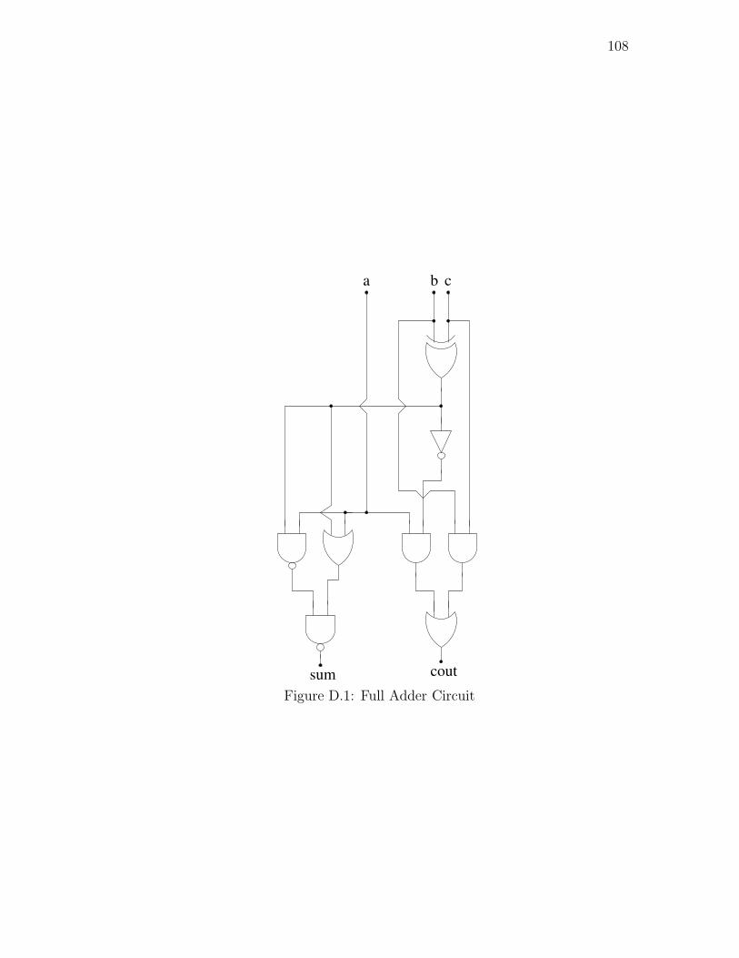
108
sum cout
a b c
Figure D.1: Full Adder Circuit

109
R6 = RINV × (1 − (1 − R4)(1 − R5)) (D.7)
Rha = R16
6 + 15R15
6 (1 − R6) (D.8)
sum cout
ba
Figure D.2: Half Adder Circuit
So far we have given the reliability equations of the half adder and the full
adder circuit. Now, we are going to calculate the reliability of the Booth encoder
circuit used in the 64-bit ALU. The gate level representation of the Booth encoder
circuit is shown in Figure D.3. The equations to calculate the reliability of the
half adder is given below.
R7 = (1 − (1 − RXOR)(1 − RXOR × RAND)) (D.9)
Rbenc = R16
7 + 15R15
7 (1 − R7) (D.10)
Now, we are going to calculate the reliability of the Booth selector circuit used
in the 64-bit ALU. The gate level representation of the Booth selector circuit is
shown in Figure D.4. The equations to calculate the reliability of the Booth
selector circuit is given below.
R8 = (1 − (1 − RAND)(1 − RAND)) (D.11)

110
X2i2i-1 X2i+1
X M2X
X
Figure D.3: Booth Encoder Circuit
R9 = R8 × RNOR × RXNOR (D.12)
Rbsel = R16
9 + 15R15
9 (1 − R9) (D.13)
Yj 2XXM
PP
Yj-1
Figure D.4: Booth Selector Circuit
Now, we are going to calculate the reliability of the carry propagation circuit
used to calculate the final output of the multiplier. The gate level representation
of the carry propagation circuit is shown in Figure D.5. The equations to calculate

111
the reliability of the carry propagation circuit are given below.
R10 = (1 − (1 − RAND)2) × ROR (D.14)
R11 = (1 − (1 − ROR)(1 − RNAND)) × RNAND (D.15)
R12 = (1 − (1 − RAND)2) × RNOR (D.16)
R13 = (1 − RXOR × R12 × RINV × R10) (D.17)
R14 = (1 − RINV × R11)(1 − RXOR × R12) (D.18)
R15 = (1 − R13 × R14) (D.19)
Rcpa = R16
15 + 15R15
15(1 − R15) (D.20)
Cout
z[0]
z[1]a1
a0b0
b1
Cin
Figure D.5: Carry Propagation Circuit
So far we have given the reliability equations of the full adder, the half adder,
the Booth encoder, the Booth selector and the carry propagation circuits. Now,
we are going to give the equation for the MUXes used to reconfigure the 64-bit
ALU. The gate level representation of the 2:1 MUX is shown in Figure D.6. The
equations to calculate the reliability of the 2:1 MUX is given below.
RMUX21 = RINV × (1 − (1 − RNAND)(1 − RNAND) × RNAND (D.21)

112
AS
B
Z
Figure D.6: 2:1 MUX Circuit
Now, we are going to give the equation for the 4:1 MUX circuit used to
reconfigure the 64-bit ALU. The gate level representation of the 4:1 MUX is
shown in Figure D.7. The equation to calculate the reliability of the 4:1 MUX is
given below.
RMUX41 = RNAND4 × (1 − (1 − RNAND3)4) × (1 − (1 − RINV )2) (D.22)
D
C
B
A
Sb
Sa
ZNAND4gate
Figure D.7: 4:1 MUX Circuit
Now, we are going to give the equation for the 8:1 MUX circuit used to
reconfigure the 64-bit ALU. The gate level representation of the 8:1 MUX is
shown in Figure D.8. The equation to calculate the reliability of the 8:1 MUX is

113
given below.
RMUX81 = (1 − (1 − RMUX41)2) × RMUX21 (D.23)
Sa
ScMUX
MUX
MUX
4
2 Z
4
Sb
Sa Sb
ABCD
EFGH
Figure D.8: 8:1 MUX Circuit
Now, we are going to give the equation for the 16:1 MUX circuit used to
reconfigure the 64-bit ALU. The gate level representation of the 16:1 MUX is
shown in Figure D.9. The equation to calculate the reliability of the 16:1 MUX
is given below.
RMUX161 = (1 − (1 − RMUX81)2) × RMUX21 (D.24)
So far we have given the equations of the MUXes being used to reconfigure
the 64-bit ALU. The equation to calculate the total reliability of the MUX used
to reconfigure one spare chunk is given below.
RMUX = (1 − (1 − RMUX161)3) × (1 − (1 − RMUX21)
16) (D.25)
Here Ra1 and Ra2 are the reliabilities of the MUXes used for the reconfigura-
tion of the ALU. Similarly, Rb is for the Booth selector unit, Rc is used for the

114
B
A1B1C1D1E1F1G1H1
Sa Sb Sc
ZMUX
2
SdEFGH
A
CD
MUX
8
SbSa Sc
MUX
8
Figure D.9: 16:1 MUX Circuit

115
Booth encoder unit, Rd is used for the full adder unit, Re is used for the half
adder unit and Rf is used for the carry propagation unit. Now we are going to
put all the equations together and calculate the reliability of the 64-bit ALU.
The equations given below use the parameters which have been derived in the
equations above.
Ra1 = RMUX (D.26)
Ra2 = RMUX (D.27)
Rb = RMUX (D.28)
Rc1 = RMUX (D.29)
Rc2 = RMUX (D.30)
Rd = RMUX (D.31)
Table D.1: Reliability Analysis
RINV ROR RNAND RNOR RAND RXOR R0.999999 0.9999 0.9999 0.9999 0.9999 0.99 0.99999999990.999984 0.9996 0.9996 0.9996 0.9996 0.98 0.99999999900.999919 0.9991 0.9991 0.9991 0.9991 0.97 0.99999902700.999744 0.9984 0.9984 0.9984 0.9984 0.96 0.99999660000.999375 0.9975 0.9975 0.9975 0.9975 0.95 0.99999150000.998704 0.9964 0.9964 0.9964 0.9964 0.94 0.99998630000.997599 0.9951 0.9951 0.9951 0.9951 0.93 0.99997440000.995904 0.9936 0.9936 0.9936 0.9936 0.92 0.99995600000.993439 0.9919 0.9919 0.9919 0.9919 0.91 0.99992900000.991200 0.9900 0.9900 0.9900 0.9900 0.90 0.99989100000.988961 0.9879 0.9879 0.9879 0.9879 0.89 0.99964135600.987856 0.9856 0.9856 0.9856 0.9856 0.88 0.99944208000.986161 0.9831 0.9831 0.9831 0.9831 0.87 0.99915835700.984466 0.9804 0.9804 0.9804 0.9804 0.86 0.99876654200.982771 0.9775 0.9775 0.9775 0.9775 0.85 0.99823857300.981076 0.9744 0.9744 0.9744 0.9744 0.84 0.99754284700.979381 0.9711 0.9711 0.9711 0.9711 0.83 0.99664462700.977686 0.9676 0.9676 0.9676 0.9676 0.82 0.99550663600.975991 0.9639 0.9639 0.9639 0.9639 0.81 0.9940898270

116
Re = RMUX (D.32)
RTalu = (1 − (1 − (RaluRa1)) × (1 − (RaluRa2))) (D.33)
RTbsel = (1 −134∏
i=1
(1 − (RbselRbi))) (D.34)
RTbenc = (1 − (1 − (RbencRc1)) × (1 − (RbencRc2))) (D.35)
RTfa = (1 −119∏
i=1
(1 − (RfaRdi))) (D.36)
RTha = (1 −11∏
i=1
(1 − (RhaRei))) (D.37)
RTcpa = (1 −4
∏
i=1
(1 − (RcpaRfi))) (D.38)
Rmult = RTbenc × RTbsel × RTfa × RTha × RTcpa (D.39)
Table D.1 shows some numerical reliability calculations. The total reliability
for the 64-bit ALU with our fault-tolerance mechanism is:
R = (1 − (1 − RTalu) × (1 − Rmult)) (D.40)

117
Appendix E
Testing of the ALU with the Reconfiguration
Mechanism
The different parts of the ALU including the multiplier are 2-bit ALU chunks
without the multiplier, the Booth encoder with 1-bit chunks, the Booth selector
with 1-bit chunks, the half adders with 1-bit chunks, the full adders with 1-bit
chunks, the carry propagation adder with 2-bit chunks and the MUXes used for
reconfiguration.
****** SFSIM Summary ******Circuit alu_0 PI’s: 12 Gates: 113 PO’s: 3Fault Coverage: 100.0000 % 210 FSIM Detected Faults 210 Total Faults CPU Time (sec.) 0.0000 PARSING 0.1400 SFSIM 0.0000 OVERHEAD 0.1400 TOTAL Memory Usage (KBytes): 9.9 Circuit Memory 27.2 FSIM Memory 0.0 Memory Overhead 37.0 Total Memory
Figure E.1: Fault Coverage for the 2-bit ALU
We decided to check the fault-coverages of all the designs individually. There
are thirty two identical 2-bit ALU chunks without the multiplier in the entire de-
sign. We also have two spare 2-bit ALU chunks without multiplier for reconfigura-
tion purpose. The module being tested is located at /caip/u39/vlsif05/varadan

118
Reconfigtestingappendix/Appendix/alu0.v. At first we ran the circuit with
verilog2rutmod.sun4 simulator to get the rutmod netlist of the verilog circuit.
Then, we ran it through the rfgen.sun4 simulator to get the fault list. We gen-
erated the vectors for the circuit using the spectralatpg.sun4 test generator. In
order to check whether these vectors detect all the faults in the circuit we ran it
through the rsfsim.sun4 simulator. This simulator gives us information about
the number of faults detected, the number of faults undetected, the number of
vectors needed to detect the faults and finally summarizes all of the information.
The fault coverage details are shown in Figure E.1.
We analyzed the Booth encoder circuit, which was split into equal 1-bit
chunks. The Booth encoder circuit is located at /caip/u39/vlsif05/varadan
/Reconfigtestingappendix/Appendix/boothencoder3.v. We analyzed the
Booth selector circuit, which was split into equal 1-bit chunks. The
Booth selector circuit is located at /caip/u39/vlsif05/varadan/Reconfigtes−
tingappendix/Appendix/boothselect18.v. We analyzed the full adder cir-
cuit used by the Dadda tree. The full adder circuit was split into
equal 1-bit chunks. The full adder circuit is located at /caip/u39/vlsi−
f05/varadan/Reconfigtestingappendix/Appendix/FA7.v. We analyzed the
half adder circuit used by the Dadda tree, which was split into equal 1-
bit chunks. The half adder circuit is located at /caip/u39/vlsif05/varadan
/Reconfigtestingappendix/Appendix/HA13.v. We analyzed the carry propa-
gation circuit used at the final stage of the Dadda tree, which was split into
equal 2-bit chunks. The carry propagation circuit is located at /caip/u39/vlsif05
/varadan/Reconfigtestingappendix/Appendix/carrypropogate0.v. We re-
peated the above procedure. The fault coverage details of all circuits are shown
in Table E.1.
So far we have presented the fault coverage results of the individual mod-
ules and the spare modules of the ALU with reconfiguration mechanism. Now,
we are going to discuss the fault coverage of the MUXes used to reconfigure

119
the ALU. We use a 16:1 MUX to reconfigure the inputs of the individual mod-
ules with the spare module and a 2:1 MUX to reconfigure the outputs of the
individual modules and spare module. The 16:1 MUX circuit is located at
/caip/u39/vlsif05/varadan/Reconfigtestingappendix/Appendix/mux16.v and
the 2:1 MUX circuit is located at /caip/u39/vlsif05/varadan/Reconfigtesting
appendix/Appendix/mux16.v. We repeated the above procedure. The fault cov-
erage details for the 16:1 MUX and 2:1 MUX are shown in Table E.1.
Table E.1: Fault Coverage of Different Circuits
Circuit FaultCoverage (in %)
2-bit ALU 100%Booth Encoder 100%Booth Selector 100%
Full Adder 100%Half Adder 100%
Carry Propagation Adder 100%16:1 MUX 100%2:1 MUX 100%
Now, we have discussed the fault coverage of all the individual modules used
in our entire design. The entire design, which uses all these individual modules,
is located at /caip/u39/vlsif05/varadan/Reconfigtestingappendix/Appendix/
topalugtechmodi.v. Once the recomputing with swapped operands detects a fault
in the circuit, we diagnose the entire design to find the location of the fault. In
order to diagnose the design we use the diagnosis vectors. We have to induce
the diagnosis vectors at inputs of the individual modules, namely the 2-bit ALU
without the multiplier, the Booth encoder, the Booth selector, the full adder, the
half adder and the carry propagation adder circuits, to locate the fault. Hence we
can locate the faults in the individual modules. Once the fault is located we will
reconfigure the faulty part with the help of the MUXes explained above. Hence,
we have described how we have performed testing for the entire fault-tolerance
design.

120
We are going to perform the diagnosis for the ALU using the software from
the duplicate microprocessor. In order to perform this we need access to the
PIs and POs of the ALU via a bus. The select signals of the reconfiguration
MUXes are activated by the corresponding results from the diagnosis tree. The
hardware required for the bus and to activate the select signals is not counted in
the hardware overhead calculation of our fault-tolerance mechanism.