Non-Binary SAR ADC with Digital Error Correction for Low Power Applications
39
1 Non-Binary SAR ADC with Digital Error Correction for Low Power Applications T. Ogawa, T. Matsuura, H. Kobayashi N. Takai, M. Hotta, H. San A. Abe, K. Yagi, T. Mori Gunma University STARC, Tokyo City University APCCAS 2010 Session : ADC / DAC I 1569326283 Tuesday, 7th December 2010 14:20-14:40
Transcript of Non-Binary SAR ADC with Digital Error Correction for Low Power Applications

1
Non-Binary SAR ADC
with Digital Error Correction
for Low Power Applications
T. Ogawa, T. Matsuura, H. Kobayashi
N. Takai, M. Hotta, H. San
A. Abe, K. Yagi, T. Mori
Gunma University
STARC, Tokyo City University
APCCAS 2010 Session : ADC / DAC I
1569326283Tuesday, 7th December 2010
14:20-14:40

2
Outline
• Research goal
• SAR ADC characteristics
• Proposed non-binary SAR ADC
- Two-comparator architecture
- Charge-sharing architecture
- Combined two-comparator &
charge-sharing architecture
• Conclusions

3
Outline
• Research goal
• SAR ADC
• Proposed non-binary SAR ADC
- Two-comparator architecture
- Charge-sharing architecture
- Two-comparator &
charge-sharing architecture
• Conclusion
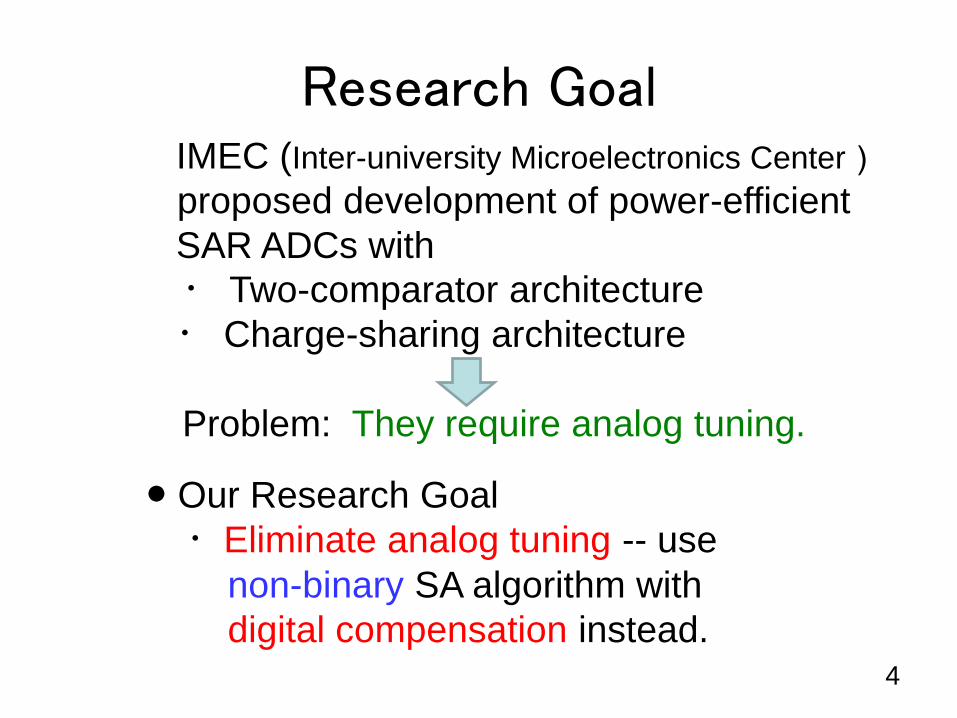
Research Goal
4
IMEC (Inter-university Microelectronics Center)
proposed development of power-efficient
SAR ADCs with
・ Two-comparator architecture
・ Charge-sharing architecture
Problem: They require analog tuning.
● Our Research Goal
・Eliminate analog tuning -- use
non-binary SA algorithm with
digital compensation instead.
5
Outline
• Research goal
• SAR ADC characteristics
• Proposed non-binary SAR ADC
- Two-comparator architecture
- Charge-sharing architecture
- Two-comparator &
charge-sharing architecture
• Conclusion

6
SAR ADC Block Diagram
Sample Hold
DAC
SAR
Logic
Analog
input
Digital
output
ComparatorCLK
SAR ADC is digital centric.
→ Suitable for fine CMOS implementation.

7
SAR ADC Characteristics
• High resolution (10-16bit)
• Medium sampling speed (10-40 MS/s)
• Small die area
• Low power (a few mW)
• Doesn’t require an OP-amp
• Application examples:
automotive, factory automation

8
Binary search algorithm
Vin 8
421
“Principle of a balance”
0
8
16
Vin
Vin = 8
4_
21
= 9
1
Comparison
Comparator output
0 0 1

9
Non-binary search algorithm
0
8
16
Vin
Error
Vin
0
8
16
1 0
Correction
Redundancy
0 1 0 1
Redundancy
1 1 1 14-bit 5-step case

10
Principle of digital error correction
Binary search algorithm
Comparator output : 1 0 0 1
Non-binary search algorithm
Comparator output : 1 0 1 0 1
Comparator output : 0 1 1 1 1
Dout = 8 + 4 – 2 – 1 + 0.5 – 0.5 = 9
Dout = 8 + 3 – 2 + 1 – 1 + 0.5 – 0.5 = 9
Dout = 8 – 3 + 2 + 1 + 1 + 0.5 – 0.5 = 9
Only one
Multiple

Comparator Offset Effects in Conventional SAR ADC
11
:Decision 1
:Decision 0
Digital output [LSB]
Analo
g
Input
0 7
step
1 2 3
Input
4.5
4
100
Decision
boundary

12
:Decision 1
:Decision 0
offset
offset
offset
offset
offset
offset
offset
Digital Output [LSB]
0 7
ADC offset
step
1 2 3
Input
4.5
43
011
Decision
boundary
Analo
g
Input
Comparator Offset Effects in Conventional SAR ADC

13
Outline
• Research goal
• SAR ADC characteristics
• Proposed non-binary SAR ADC
- Two-comparator architecture
- Charge-sharing architecture
- Two-comparator &
charge-sharing architecture
• Conclusion

14
Outline
• Research purpose
• SAR ADC
• Proposed non-binary SAR ADC
- Two-comparator architecture
- Charge-sharing architecture
- Two-comparator &
charge-sharing architecture
• Conclusion

Two-Comparator SAR ADC
15
DAC
+
-
S/H
SAR Logic
2-Dynamic
Comparator
Digital output
Analog input
select
CLK
Comp_CLK
+
-
select
+
-
Comp
Output
Input+
Input-
[1] V. Giannini, P. Nuzzo, V.Chironi, A.Baschirotto, G. V. Plas, J. Craninckx
“ An 820 μ W 9b 40MS/s Noise-Tolerant Dynamic-SAR ADC in 90nm Digital CMOS ”
ISSCC (Feb.2008).
Reference
By IMEC
_CLK

2-Comparator SAR ADC
(Proposed by IMEC)
160
8
16
Comp1
Low power
Comp2
High power
Decision
Error
Vin
1 0 0 1 1
weighting
8 4 2 1 1
redundancy
Noise
compensation
1LSB noise
compensation
1 2 3 4
1 2 3 4 5
Total comparator power
conventional
2-comparator power reduction
power consumption
High power
Comp2(high power)Comp1(low power)
Large noise

Comparator Offset Effects
of Two-Comparator SAR ADC
17
:Decision 1
:Decision 0
Digital Output [LSB]
Analo
g I
nput
0 7step1 2 3
Comp1 Comp2

18
:Decision 1
:Decision 0
offset1
Digital Output [LSB]
Analo
g I
nput
0 7step1 2 3
offset1
offset1
offset2
offset2
offset2
offset2
Comp1 Comp2
Non-linearity
Comparator Offset Effects
of Two-Comparator SAR ADC

19
:Decision 1
:Decision 0
offset1
Digital Output [LSB]
Analo
g I
nput
0 7step1 2 3
offset1
offset1
offset2
offset2
offset2
offset2
Comp1 Comp2
Non-linearity
IMEC: Analog tuning for
comparator offset mismatch within ½ LSB
Comparator Offset Effects
of 2-Comparator SAR ADC
20
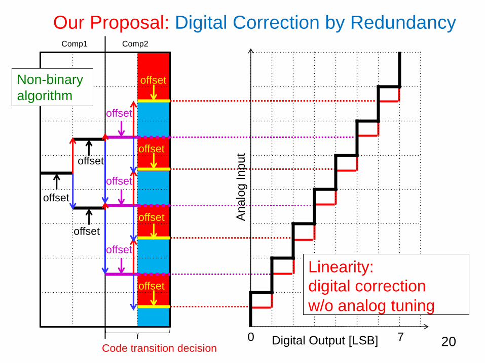
Comp1 Comp2
Code transition decisionDigital Output [LSB]
Analo
g I
nput
0 7
offset
offset
offset
offset
offset
offset
offset
offset
offset
offset
Linearity:
digital correction
w/o analog tuning
Our Proposal: Digital Correction by Redundancy
Non-binary
algorithm

21
0 100 200 300 400 500 600 700 800 900 10000
200
400
600
800
1000
1200
Vin
Outp
ut
[LS
B]
Output
0 100 200 300 400 500 600 700 800 900 1000-2
-1
0
1
2
Code Number
DN
L [
LS
B]
DNL
IMEC method (binary) Proposed method (non-binary)
MATLAB Simulation (Ramp Input)Comp1(low power) offset:+4.0 LSB noise:1.0 LSB
Comp2(high power) offset:-2.0 LSB noise:0.2 LSB
W/O analog tuning of comparator offsets
0 100 200 300 400 500 600 700 800 900 10000
200
400
600
800
1000
1200
Vin
Outp
ut
[LS
B]
Output
0 100 200 300 400 500 600 700 800 900 1000-2
-1
0
1
2
Code Number
DN
L [
LS
B]
DNL

Trade-off of power and
comparator offset mismatch allowance
22
1 2 3 4 5 6 7 8 9 10
1 2 3 4 5 6 7 8 9 10 11
1 2 3 4 5 6 7 8 9 10 11
1-comparator SAR ADC
IMEC method 2-comparator(offset mismatch allowance : small)
Proposed 2-comparator(offset mismatch allowance: large)
Total comparator power
Comp2(high power)Comp1(low power)
Comp2(high power)Comp1(low power)
High power
Smaller mismatch More power reduction

23
Outline
• Research goal
• SAR ADC characteristics
• Proposed non-binary SAR ADC
- Two-comparator architecture
- Charge-sharing architecture
- Two-comparator &
charge-sharing architecture
• Conclusion

Charge-Sharing Binary
SAR ADC
24
Cs
Cu1~CuM-1
SAR_Logic
+
-
Vin
VrefProposed by
IMEC
Low power
SAR ADC
[1] J. Craninckx and G. Van der Plas,
“A 65fJ/Conversion-Step 0-to-50Ms/s 0-to-0.7mW 9b Charge-Sharing SAR ADC in 90nm Digital CMOS ”,
ISSCC Dig. Tech. Papers, pp. 246-247, Feb. 2007.
[2] V.Giannini, P.Nuzzo, V.Chironi,A.Baschirotto, G.V.Plas,J.Craninckx
“ An 820 μ W 9b 40MS/s Noise-Tolerant Dynamic-SARADC in 90nm Digital CMOS ”
ISSCC (Feb.2008).
References

Qin2CxVref CxVref
4C
2C
Logic
+
-
Vin(+Vref ~ -Vref)
Vref Vref
C++ ++
- - - -
25
++
- -
Operation ( sampling)

Operation(step1)
Qin4C
2C
Logic
+
-
Vin(+Vref ~ -Vref)
Vref Vref
C
0XV
sig
nal le
vel 0
+4CxVref
-4CxVref
step 1 2 3
Qin
26Comparator output:1
OFF ++
- -

4C
2C
Logic
+
-
Vref Vref
C
sig
nal le
vel
0
+4CxVref
-4CxVref
step 1 2 3
Qin
27
1
Comparator output:0
Comparator
output
OFF
OFF
ON
ON
+ +
- - - -
+ +
0
subtract
Operation(step2)
0XV

4C
2C
Logic
+
-
Vref Vref
C
sig
nal le
vel
0
+4CxVref
-4CxVref
step 1 2 3
Qin
28
1
OFF
OFF
ON
ON
+ +
- - - -
+ +
0
add
+ +
- -
0
Digital output:4
Operation(step3)
Comparator
output
Comparator output:0
0XV

Charge-Sharing SAR ADC
Comparator Offset Effects
29
:Decision 1
:Decision 0
Digital Output [LSB]
Analo
g I
nput
0 7step1 2 3
Binary
algorithm

Charge-Sharing SAR ADC
Comparator Offset Effects
30
:Decision 1
:Decision 0
0 7step1 2 3
Non-linearity
offset
offset
offset
offset
offset
offset
offset
Digital Output [LSB]
Analo
g I
nput
Binary
algorithm
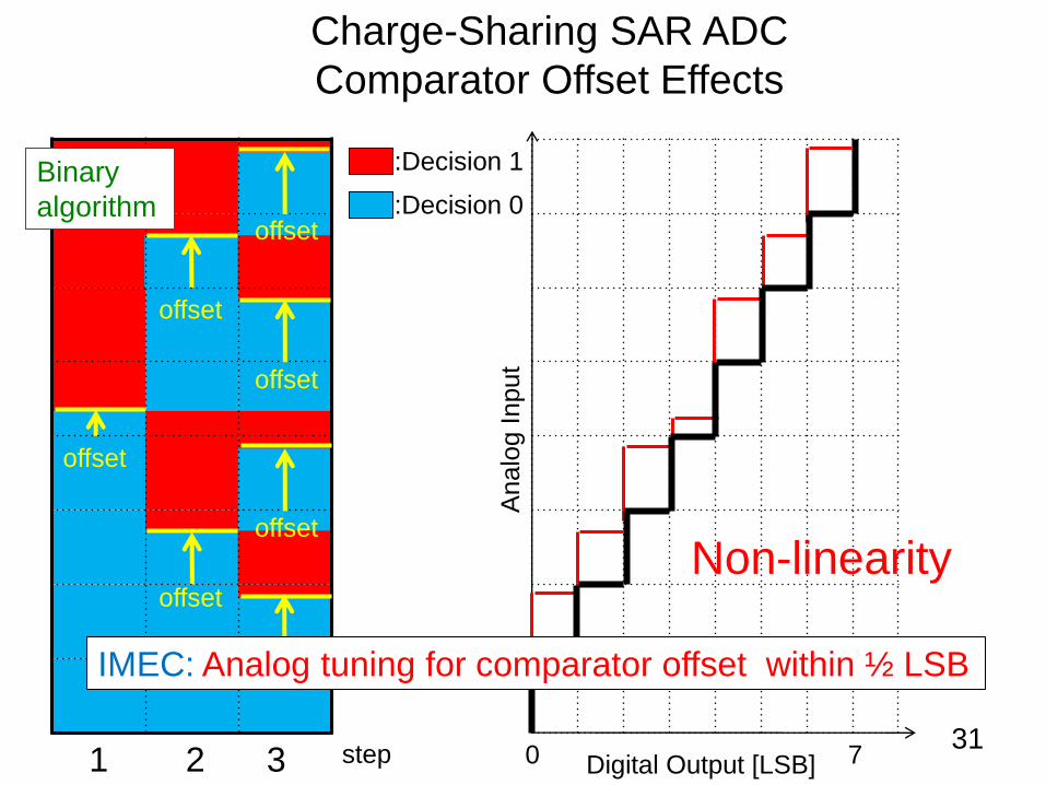
Charge-Sharing SAR ADC
Comparator Offset Effects
31
:Decision 1
:Decision 0
0 7step1 2 3
Non-linearity
offset
offset
offset
offset
offset
offset
offset
Digital Output [LSB]
Analo
g I
nput
IMEC: Analog tuning for comparator offset within ½ LSB
Binary
algorithm

Our Proposal : Digital Correction by Redundancy
32Code transition
0 7
Offset changes are small at latter stages
Digital Output [LSB]
Analo
g I
nput
Non-binary
algorithm

Proposed : Digital Correction by Redundancy
33Code transition decision
Digital Output [LSB]
Ana
log Input
0 7
offset
offset
offset
offset
offset
offset
offset
offset
offset
offset
Linearity:
digital correction
w/o analog tuning
Offset changes are small at latter steps.
Non-binary
algorithm

34
IMEC method (binary) Proposed method (non-binary)
MATLAB Simulation (Ramp Input)Vin:-1~+1 , Vref=1V,Cs=512C
Vos=55mV
W/O analog tuning for comparator offset
-1 -0.8 -0.6 -0.4 -0.2 0 0.2 0.4 0.6 0.8 10
200
400
600
800
1000
1200
Vin
Outp
ut
[LS
B]
0 100 200 300 400 500 600 700 800 900 1000 1100-5
0
5
10
15
20
25
30
Code Number
DN
L [
LS
B]
-1 -0.8 -0.6 -0.4 -0.2 0 0.2 0.4 0.6 0.8 10
200
400
600
800
1000
1200
Vin
Outp
ut
[LS
B]
0 100 200 300 400 500 600 700 800 900 1000 1100-5
0
5
10
15
20
25
30
Code Number
DN
L [
LS
B]

35
Outline
• Research goal
• SAR ADC characteristics
• Proposed non-binary SAR ADC
- Two-comparator architecture
- Charge-sharing architecture
- Two-comparator &
charge-sharing architecture
• Conclusion

Two-Comparator Charge-Sharing SAR ADC
36
Cs
Cu1~CuM-1
SAR_Logic
Vin
Vref
Proposed by IMEC (binary algorithm)
+
-
Com
p_
CLK
se
lect
+
-
select
+
-
Comp
Output
Input+
Input-
_CLK
[1] V. Giannini, P. Nuzzo, V. Chironi, A. Baschirotto, G. V. Plas, J. Craninckx
“ An 820 μW 9b 40MS/s Noise-Tolerant Dynamic-SAR ADC in 90nm Digital CMOS ”
ISSCC (Feb.2008).
Reference

37
IMEC method (binary) Proposed method (non-binary)
MATLAB Simulation(Ramp Input)
Comp1(low power) offset:+8.0 mV noise:1.0 mV
Comp2(high power) offset:-7.0 mV noise:0.2 mV
W/O analog tuning for comparator offsets
Vin:-1~+1, Vref=1V,Cs=512C
-1 -0.8 -0.6 -0.4 -0.2 0 0.2 0.4 0.6 0.8 10
200
400
600
800
1000
1200
Vin
Outp
ut
[LS
B]
0 100 200 300 400 500 600 700 800 900 1000 1100-2
0
2
4
6
8
10
Code Number
DN
L [
LS
B]
-1 -0.8 -0.6 -0.4 -0.2 0 0.2 0.4 0.6 0.8 10
200
400
600
800
1000
1200
Vin
Outp
ut
[LS
B]
0 100 200 300 400 500 600 700 800 900 1000 1100-2
0
2
4
6
8
10
Code Number
DN
L [
LS
B]

38
Outline
• Research goal
• SAR ADC characteristics
• Proposed non-binary SAR ADC
- Two-comparator architecture
- Charge-sharing architecture
- Two-comparator &
charge-sharing architecture
• Conclusion

Conclusion
39
● Proposal of using a non-binary SA algorithm
for low-power techniques:
・Two-comparator
・Charge-sharing
・Their combination
● No analog tuning
● Only digital error correction
● Demonstrate with MATLAB simulation.