Mortgage-Backed Securities - Federal Reserve Bank of New ...
312 IEEE TRANSACTIONS ON ANTENNAS AND PROPAGATION, VOL. 56, NO. 2, FEBRUARY 2008
Development of a Cavity-Backed BroadbandCircularly Polarized Slot/Strip Loop Antenna With a
Simple Feeding StructureRongLin Li, Senior Member, IEEE, Bo Pan, Student Member, IEEE, Anya N. Traille,
John Papapolymerou, Senior Member, IEEE, Joy Laskar, Fellow, IEEE, andManos M. Tentzeris, Senior Member, IEEE
Abstract—A cavity-backed loop antenna is developed forproducing broadband circularly polarized (CP) radiation. Theantenna configuration consists of a slot loop and a strip loop. Theslot loop radiates a CP wave at a lower frequency while the striploop produces CP radiation at a higher frequency. A combinationof the two frequencies leads to a bandwidth enhancement. Theslot/strip loop antenna is fed by a single straight microstrip line.It is demonstrated that the cavity-backed slot/strip loop antennacan achieve an axial ratio ( 3 dB) bandwidth of 19% with goodimpedance matching. The antenna configuration is described andthe operating principles for broadband circular polarization andimpedance matching are analyzed. The antenna performance isconfirmed by experimental results.
Index Terms—Broadband antenna, cavity-backed antenna, cir-cularly polarized (CP) antenna, loop antenna, slot antenna.
I. INTRODUCTION
CAVITY-BACKED slot antennas have two major advan-tages over cavity-backed wire antennas, such as dipole,
helix, and spiral antennas [1]. First, a slot antenna can be flushmounted on a metal surface; therefore, it is suitable for applica-tions in mobile communications (such as IEEE 802.20 for mo-bile broadband wireless access) and radar systems of high-speedvehicles or aircraft [2]. Second, slot antennas can be easily fedby a microstrip line that is fabricated on the same substrate withthe slot and is placed between the cavity and the substrate, thusavoiding the undesirable radiation from the feeding network.This is particularly important for applications in antenna arrays.Many types of slot configurations have been developed for pro-ducing circularly polarized (CP) radiation, such as annual slot[3], dual-spiral slot [4], rectangular slot [5], and cloverleaf slot[6]. However, these slot antennas have a narrow axial ratio (AR)bandwidth (usually for ). Archimedean spi-rals usually offer a much wider bandwidth in free space. Un-fortunately, the presence of a ground plane (or a cavity) limits
Manuscript received February 23, 2006; revised August 28, 2007. This workwas supported in part by the Georgia Electronic Design Center (GEDC), in partby an NSF CAREER Award ECS-9984761, in part by the NSF under GrantECS-0313951, and in part by the NSF Packaging Research Center.
The authors are with the Georgia Electronic Design Center, School of Elec-trical and Computer Engineering, Georgia Institute of Technology, Atlanta, GA30308 USA (e-mail: [email protected]).
Color versions of one or more of the figures in this paper are available onlineat http://ieeexplore.ieee.org.
Digital Object Identifier 10.1109/TAP.2007.915412
the bandwidth enhancement [7]. One way to remedy this lim-itation is to use absorbers inside the cavity or to terminate thespiral slot with tapered resistive loading [8], [9]. But it reducesthe power efficiency. Recently, a bandwidth-enhanced (for ) cavity-backed slot antenna has been presentedin [10], but it requires a complicated feeding network. In thispaper, we develop a broadband cavity-backed loop antenna witha simple feeding structure. The antenna configuration developedis considered to be a combination of a slot loop and a strip loop.The slot loop has a good CP performance at a lower frequencywhile the strip loop produces CP radiation at a higher frequency.A combination of the two frequencies leads to a bandwidth en-hancement. The slot/strip loop is fed by a single straight mi-crostrip line and a good impedance matching is achieved.
The antenna configuration is described in Section II. Theoperating principle for broadband circular polarization andimpedance matching is analyzed in Section III. Finally experi-mental results are presented to verify the antenna performance.
II. DESCRIPTION OF THE ANTENNA
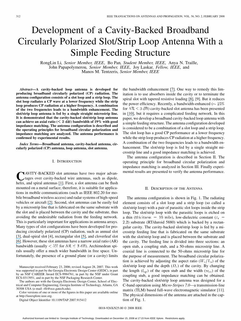
The antenna configuration is shown in Fig. 1. The radiatingelement consists of a slot loop and a strip loop (so called aslot/strip loop) with a pair of parasitic slot loops inside the striploop. The slot/strip loop with the parasitic loops is etched ona thin ( ), low-dielectric constant (
) substrate (RT/duroid 5880) which is backed by a rectan-gular cavity. The cavity-backed slot/strip loop is fed by a mi-crostrip feeding line that is fabricated on the same substratewith the slot/strip loop and is placed between the substrate andthe cavity. The feeding line is divided into three sections: anopen stub, a coupling stub, and a 50-ohms microstrip line. Acoaxial line is connected to the 50-ohms microstrip line forthe purpose of measurement. The broadband circular polariza-tion is achieved by adjusting the aspect ratio ( ) of theslot/strip loop and the depth ( ) of the cavity. By changingthe length ( ) of the open stub and the width ( ) of thecoupling stub, a good impedance matching can be obtained.The cavity-backed slot/strip loop antenna was designed for aC-band operation using Micro-Stripes 7.0—a transmission-linematrix (TLM) based full-wave electromagnetic simulator [11].The physical dimensions of the antenna are attached in the cap-tion of Fig. 1.
0018-926X/$25.00 © 2008 IEEE
Authorized licensed use limited to: Georgia Institute of Technology. Downloaded on December 15, 2008 at 17:15 from IEEE Xplore. Restrictions apply.
LI et al.: DEVELOPMENT OF A CAVITY-BACKED BROADBAND CP SLOT/STRIP LOOP ANTENNA 313
Fig. 1. Configuration of the cavity-backed broadband CP slot/strip loop an-tenna. (W = 36 mm, L = 62 mm, W = 26 mm, L = 52 mm,W = 16 mm, L = 20 mm, w = 2 mm, w = 1 mm, w = 0:78 mm,D = 12 mm, t = 0:254 mm; the width (w ) of the coupling stub isw = w = 2 mm, the length of the coupling stub is 3w = 3 mm, thelength of the open stub is l = 6:5 mm.).
III. OPERATING PRINCIPLES
A. Broadband Circular Polarization
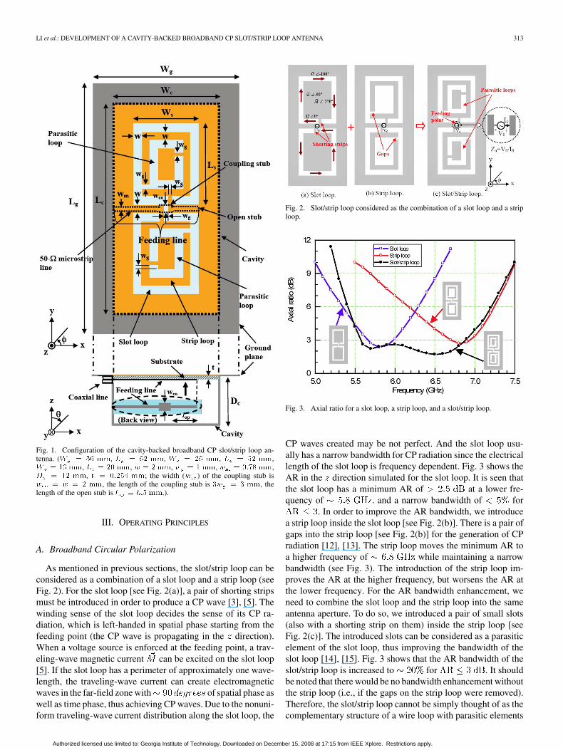
As mentioned in previous sections, the slot/strip loop can beconsidered as a combination of a slot loop and a strip loop (seeFig. 2). For the slot loop [see Fig. 2(a)], a pair of shorting stripsmust be introduced in order to produce a CP wave [3], [5]. Thewinding sense of the slot loop decides the sense of its CP ra-diation, which is left-handed in spatial phase starting from thefeeding point (the CP wave is propagating in the direction).When a voltage source is enforced at the feeding point, a trav-eling-wave magnetic current can be excited on the slot loop[5]. If the slot loop has a perimeter of approximately one wave-length, the traveling-wave current can create electromagneticwaves in the far-field zone with of spatial phase aswell as time phase, thus achieving CP waves. Due to the nonuni-form traveling-wave current distribution along the slot loop, the
Fig. 2. Slot/strip loop considered as the combination of a slot loop and a striploop.
Fig. 3. Axial ratio for a slot loop, a strip loop, and a slot/strip loop.
CP waves created may be not perfect. And the slot loop usu-ally has a narrow bandwidth for CP radiation since the electricallength of the slot loop is frequency dependent. Fig. 3 shows theAR in the direction simulated for the slot loop. It is seen thatthe slot loop has a minimum AR of at a lower fre-quency of . and a narrow bandwidth of for
. In order to improve the AR bandwidth, we introducea strip loop inside the slot loop [see Fig. 2(b)]. There is a pair ofgaps into the strip loop [see Fig. 2(b)] for the generation of CPradiation [12], [13]. The strip loop moves the minimum AR toa higher frequency of while maintaining a narrowbandwidth (see Fig. 3). The introduction of the strip loop im-proves the AR at the higher frequency, but worsens the AR atthe lower frequency. For the AR bandwidth enhancement, weneed to combine the slot loop and the strip loop into the sameantenna aperture. To do so, we introduced a pair of small slots(also with a shorting strip on them) inside the strip loop [seeFig. 2(c)]. The introduced slots can be considered as a parasiticelement of the slot loop, thus improving the bandwidth of theslot loop [14], [15]. Fig. 3 shows that the AR bandwidth of theslot/strip loop is increased to for . It shouldbe noted that there would be no bandwidth enhancement withoutthe strip loop (i.e., if the gaps on the strip loop were removed).Therefore, the slot/strip loop cannot be simply thought of as thecomplementary structure of a wire loop with parasitic elements
Authorized licensed use limited to: Georgia Institute of Technology. Downloaded on December 15, 2008 at 17:15 from IEEE Xplore. Restrictions apply.
314 IEEE TRANSACTIONS ON ANTENNAS AND PROPAGATION, VOL. 56, NO. 2, FEBRUARY 2008
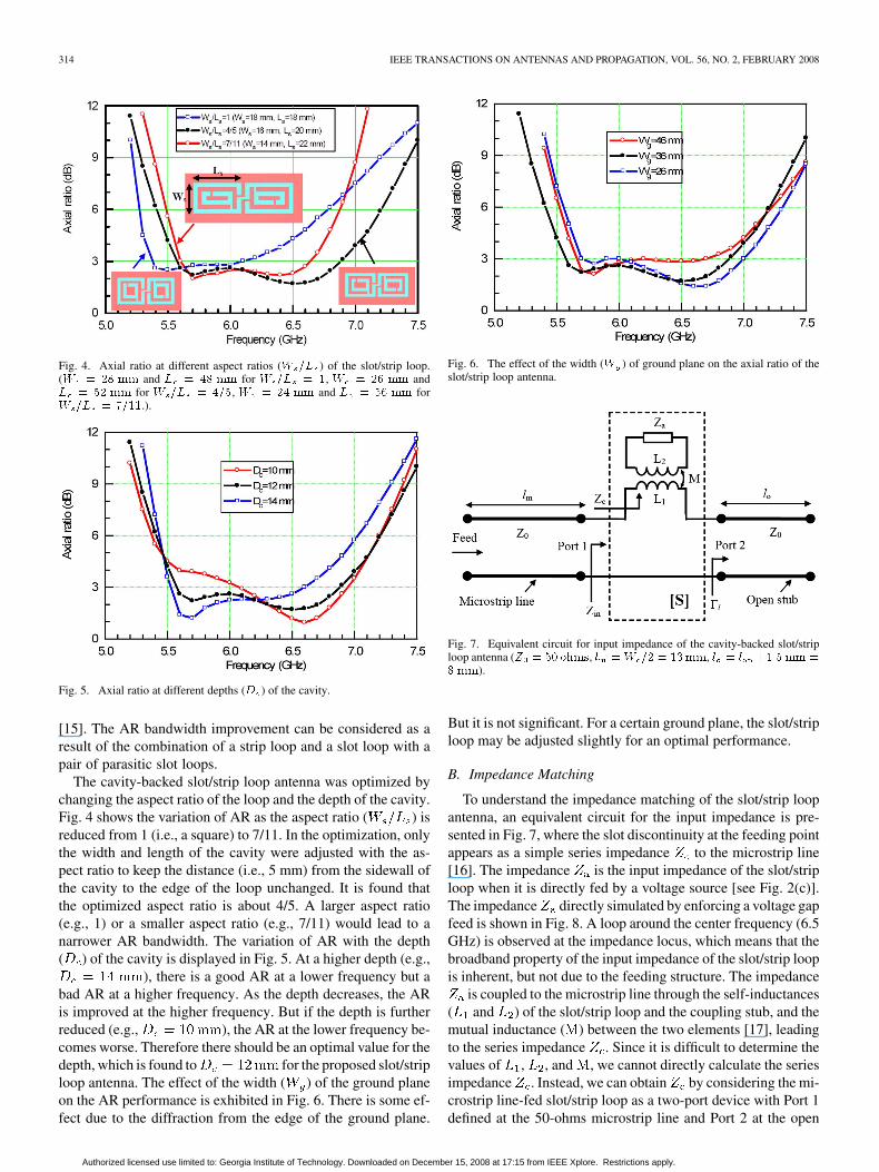
Fig. 4. Axial ratio at different aspect ratios (W =L ) of the slot/strip loop.(W = 28 mm and L = 48 mm for W =L = 1, W = 26 mm andL = 52 mm for W =L = 4=5, W = 24 mm and L = 56 mm forW =L = 7=11.).
Fig. 5. Axial ratio at different depths (D ) of the cavity.
[15]. The AR bandwidth improvement can be considered as aresult of the combination of a strip loop and a slot loop with apair of parasitic slot loops.
The cavity-backed slot/strip loop antenna was optimized bychanging the aspect ratio of the loop and the depth of the cavity.Fig. 4 shows the variation of AR as the aspect ratio ( ) isreduced from 1 (i.e., a square) to 7/11. In the optimization, onlythe width and length of the cavity were adjusted with the as-pect ratio to keep the distance (i.e., 5 mm) from the sidewall ofthe cavity to the edge of the loop unchanged. It is found thatthe optimized aspect ratio is about 4/5. A larger aspect ratio(e.g., 1) or a smaller aspect ratio (e.g., 7/11) would lead to anarrower AR bandwidth. The variation of AR with the depth( ) of the cavity is displayed in Fig. 5. At a higher depth (e.g.,
), there is a good AR at a lower frequency but abad AR at a higher frequency. As the depth decreases, the ARis improved at the higher frequency. But if the depth is furtherreduced (e.g., ), the AR at the lower frequency be-comes worse. Therefore there should be an optimal value for thedepth, which is found to for the proposed slot/striploop antenna. The effect of the width ( ) of the ground planeon the AR performance is exhibited in Fig. 6. There is some ef-fect due to the diffraction from the edge of the ground plane.
Fig. 6. The effect of the width (W ) of ground plane on the axial ratio of theslot/strip loop antenna.
Fig. 7. Equivalent circuit for input impedance of the cavity-backed slot/striploop antenna (Z = 50 ohms, l =W =2 = 13mm, l = l +1:5mm =
8 mm).
But it is not significant. For a certain ground plane, the slot/striploop may be adjusted slightly for an optimal performance.
B. Impedance Matching
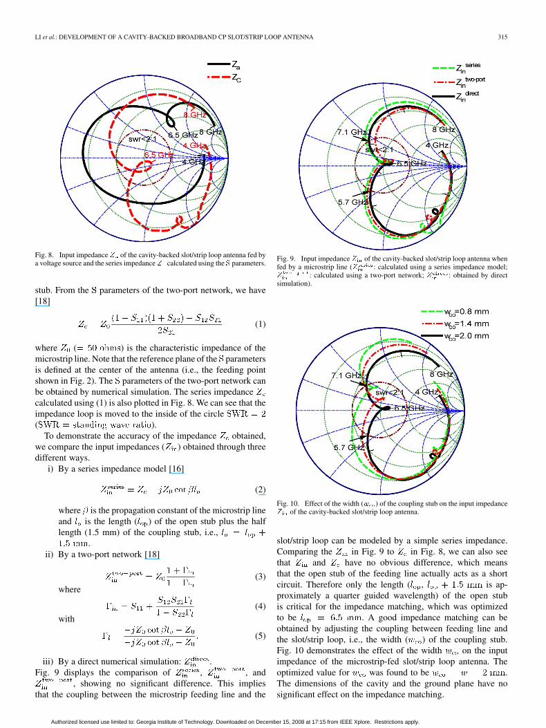
To understand the impedance matching of the slot/strip loopantenna, an equivalent circuit for the input impedance is pre-sented in Fig. 7, where the slot discontinuity at the feeding pointappears as a simple series impedance to the microstrip line[16]. The impedance is the input impedance of the slot/striploop when it is directly fed by a voltage source [see Fig. 2(c)].The impedance directly simulated by enforcing a voltage gapfeed is shown in Fig. 8. A loop around the center frequency (6.5GHz) is observed at the impedance locus, which means that thebroadband property of the input impedance of the slot/strip loopis inherent, but not due to the feeding structure. The impedance
is coupled to the microstrip line through the self-inductances( and ) of the slot/strip loop and the coupling stub, and themutual inductance ( ) between the two elements [17], leadingto the series impedance . Since it is difficult to determine thevalues of , , and , we cannot directly calculate the seriesimpedance . Instead, we can obtain by considering the mi-crostrip line-fed slot/strip loop as a two-port device with Port 1defined at the 50-ohms microstrip line and Port 2 at the open
Authorized licensed use limited to: Georgia Institute of Technology. Downloaded on December 15, 2008 at 17:15 from IEEE Xplore. Restrictions apply.
LI et al.: DEVELOPMENT OF A CAVITY-BACKED BROADBAND CP SLOT/STRIP LOOP ANTENNA 315
Fig. 8. Input impedance Z of the cavity-backed slot/strip loop antenna fed bya voltage source and the series impedanceZ calculated using the S parameters.
stub. From the parameters of the two-port network, we have[18]
(1)
where ( ) is the characteristic impedance of themicrostrip line. Note that the reference plane of the parametersis defined at the center of the antenna (i.e., the feeding pointshown in Fig. 2). The parameters of the two-port network canbe obtained by numerical simulation. The series impedancecalculated using (1) is also plotted in Fig. 8. We can see that theimpedance loop is moved to the inside of the circle( ).
To demonstrate the accuracy of the impedance obtained,we compare the input impedances ( ) obtained through threedifferent ways.
i) By a series impedance model [16]
(2)
where is the propagation constant of the microstrip lineand is the length ( ) of the open stub plus the halflength (1.5 mm) of the coupling stub, i.e.,
.ii) By a two-port network [18]
(3)
where
(4)
with
(5)
iii) By a direct numerical simulation: .Fig. 9 displays the comparison of , , and
, showing no significant difference. This impliesthat the coupling between the microstrip feeding line and the
Fig. 9. Input impedance Z of the cavity-backed slot/strip loop antenna whenfed by a microstrip line (Z : calculated using a series impedance model;Z : calculated using a two-port network; Z : obtained by directsimulation).
Fig. 10. Effect of the width (w ) of the coupling stub on the input impedanceZ of the cavity-backed slot/strip loop antenna.
slot/strip loop can be modeled by a simple series impedance.Comparing the in Fig. 9 to in Fig. 8, we can also seethat and have no obvious difference, which meansthat the open stub of the feeding line actually acts as a shortcircuit. Therefore only the length ( , is ap-proximately a quarter guided wavelength) of the open stubis critical for the impedance matching, which was optimizedto be . A good impedance matching can beobtained by adjusting the coupling between feeding line andthe slot/strip loop, i.e., the width ( ) of the coupling stub.Fig. 10 demonstrates the effect of the width on the inputimpedance of the microstrip-fed slot/strip loop antenna. Theoptimized value for was found to be .The dimensions of the cavity and the ground plane have nosignificant effect on the impedance matching.
Authorized licensed use limited to: Georgia Institute of Technology. Downloaded on December 15, 2008 at 17:15 from IEEE Xplore. Restrictions apply.
316 IEEE TRANSACTIONS ON ANTENNAS AND PROPAGATION, VOL. 56, NO. 2, FEBRUARY 2008
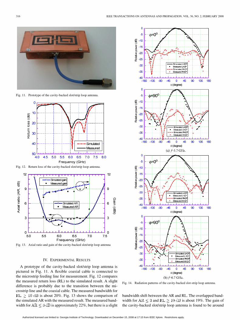
Fig. 11. Prototype of the cavity-backed slot/strip loop antenna.
Fig. 12. Return loss of the cavity-backed slot/strip loop antenna.
Fig. 13. Axial ratio and gain of the cavity-backed slot/strip loop antenna.
IV. EXPERIMENTAL RESULTS
A prototype of the cavity-backed slot/strip loop antenna ispictured in Fig. 11. A flexible coaxial cable is connected tothe microstrip feeding line for measurement. Fig. 12 comparesthe measured return loss (RL) to the simulated result. A slightdifference is probably due to the transition between the mi-crostrip line and the coaxial cable. The measured bandwidth for
is about 20%. Fig. 13 shows the comparison ofthe simulated AR with the measured result. The measured band-width for is approximately 22%, but there is a slight
Fig. 14. Radiation patterns of the cavity-backed slot-strip loop antenna.
bandwidth shift between the AR and RL. The overlapped band-width for and is about 19%. The gain ofthe cavity-backed slot/strip loop antenna is found to be around
Authorized licensed use limited to: Georgia Institute of Technology. Downloaded on December 15, 2008 at 17:15 from IEEE Xplore. Restrictions apply.
LI et al.: DEVELOPMENT OF A CAVITY-BACKED BROADBAND CP SLOT/STRIP LOOP ANTENNA 317
9 dBi. The radiation patterns measured at 5.7 GHz and 6.7 GHare compared with the simulated results in Fig. 14 and goodagreement is observed for the co-polarization (i.e., the left-handcircular polarization, LHCP) over the main beam. As expected,the beamwidth in the is wider than that in the
because the length (i.e., ) of the antennaaperture in the direction is shorter than that (i.e., ) in the
direction. The cross-polarization [i.e., the right-hand circularpolarization (RHCP)] is less than . The discrepanciesbetween the simulated and measured results for the axial ratio,gain, and radiation patterns are mainly due to the measurementerrors. We used the NSI near-field antenna measurement system.Even though the antenna under test was setup at the far-fieldzone, the mechanical supporting structures of the system wouldstill cause diffraction, introducing the measurement errors, par-ticularly on the cross-polarized component. But the measure-ment has indeed demonstrated the broadband CP performancefor the proposed antenna.
V. CONCLUSION
A cavity-backed slot/strip loop antenna has been developedfor broadband CP operation. The slot/strip loop is a combinationof a slot loop and a strip loop. The slot loop radiates a CP wave ata lower frequency while the strip loop produces CP radiation ata higher frequency. A combination of the two frequencies leadsto a significant bandwidth enhancement. A simple microstripline is introduced to feed the slot/strip loop antenna. It has beendemonstrated that the proposed cavity-backed loop antenna canachieve a bandwidth of 19% for with .The operating principles of the slot/strip loop antenna are inves-tigated. Simulation and experimental results show good agree-ment.
REFERENCES
[1] A. Kumar and H. D. Hristov, Microwave Cavity Antennas. Norwood,MA: Artech House, 1989, pp. 101–213.
[2] K. Fujimoto and J. R. James, Eds., Mobile Antenna Systems Hand-book2nd ed. Norwood, MA, Artech House, 2000, pp. 461–631.
[3] H. Morishita, K. Hirasawa, and K. Fujimoto, “Analysis of a cavity-backed annular slot antenna with one point shorted,” IEEE Trans. An-tennas Propag., vol. 39, no. 10, pp. 1472–1478, Oct. 1991.
[4] H. Hirose and H. Nakano, “Dual-spiral slot antennas,” Proc. Inst. Elect.Eng. Microw. Antennas Propag., vol. 134, no. 1, pp. 32–36, Jun. 1991.
[5] S. Shi, K. Hirasawa, and Z. C. Chen, “Circularly polarized rectangu-larly bent slot antennas backed by a rectangular cavity,” IEEE Trans.Antennas Propag., vol. 49, no. 11, pp. 1517–1524, Nov. 2001.
[6] T. Watanabe, K. Hirasawa, and S. Nemoto, “A rectangular-cavity-backed cloverleaf slot antenna for circular polarization,” in Proc. 9thInt. Conf. Communications Systems, Sep. 2004, pp. 595–597.
[7] H. Nakano, K. Nogami, S. Arai, H. Mimaki, and J. Yamauchi, “A spiralantenna backed by a conducting plane reflector,” IEEE Trans. AntennasPropag., vol. 34, no. 6, pp. 791–796, 1986.
[8] T. Ozdemir, J. L. Volakis, and M. W. Nurnberger, “Analysis of thinmultioctave cavity-backed slot spiral antennas,” Proc. Inst. Elect. Eng.Microw. Antennas Propag., vol. 146, no. 6, pp. 447–454, Dec. 1999.
[9] J. L. Volakis, M. W. Nurnberger, and D. S. Filipovic, “A broadbandcavity slot spiral antenna,” IEEE Antennas Propag. Mag., vol. 43, no.6, pp. 15–26, Dec. 2001.
[10] Q. Li and Z. Shen, “An inverted microstrip-fed cavity-backed slot an-tenna for circular polarization,” IEEE Antennas Wireless Propag. Lett.,vol. 1, pp. 190–192, 2002.
[11] Micro-Stripes 7.0 Flomerics Group PLC, 2005.[12] H. Morishita, K. Hirasawa, and T. Nagao, “Circularly polarized wire
antenna with a dual rhombic loop,” Proc. Inst. Elect. Eng. Microw. An-tennas Propag., vol. 145, no. 3, pp. 219–224, Jun. 1998.
[13] R. L. Li and V. Fusco, “Printed figure-of-eight wire antenna for circularpolarization,” IEEE Trans. Antennas Propag., vol. 50, pp. 1487–1490,Oct. 2002.
[14] R. L. Li, G. GeJean, J. Laskar, and M. M. Tentzeris, “Investigation ofcircularly polarized loop antennas with a parasitic element for band-width enhancement,” IEEE Trans. Antennas Propag., vol. 53, no. 12,pp. 3930–3939, Dec. 2005.
[15] R. L. Li, S. Basat, J. Laskar, and M. M. Tentzeris, “Development ofwideband circularly polarised square- and rectangular-loop antennaswith,” Proc. Inst. Elect. Eng. Microw. Antennas Propag., vol. 153, no.3, pp. 293–300, Jun. 2006.
[16] D. M. Pozar, “A reciprocity method of analysis for printed slot andslot-coupled microstrip antennas,” IEEE Trans. Antennas Propag., vol.34, no. 12, pp. 1439–1446, Dec. 1986.
[17] H. G. Akhavan and D. Mirshekar-Syahkal, “Approximate model formicrostrip fed slot antennas,” Electron. Lett., vol. 30, no. 23, pp.1902–1903, Nov. 1994.
[18] D. M. Pozar, Microwave Engineering, 2nd ed. New York: Wiley,1998, pp. 211–216.
RongLin Li (M’02–SM’03) received the B.S. degreein electrical engineering from Xi’an Jiaotong Univer-sity, China, in 1983 and the M.S. and Ph.D. degreesin electrical engineering from Chongqing University,China, in 1990 and 1994, respectively.
From 1983 to 1987, he worked as an Electrical En-gineer at the Yunnan Electric Power Research Insti-tute. From 1994 to 1996, he was a Postdoctoral Re-search Fellow at Zhejiang University, China, where,in 1998, he became a Professor. In 1997, he was withHosei University, Japan, as an HIF (Hosei Interna-
tional Fund) Research Fellow. In 1999, he served as a Research Associate atthe University of Utah, Salt Lake City. In 2000, he was a Research Fellow atQueen’s University of Belfast, Belfast, U.K. Since 2001, he has been a ResearchScientist II with the ATHENA Group at the Georgia Institute of Technology,Atlanta. His latest research interests include computational electromagnetics,modeling of antennas and microwave devices, and RF packaging design.
Bo Pan (S’03) received the B.S. and M.S. degrees(both with honors) from Tsinghua University, Bei-jing, China, in 2000 and 2003, respectively, and iscurrently working toward the Ph.D. degree at theSchool of Electrical and Computer Engineering,Georgia Institute of Technology, Atlanta.
Prior to beginning his Ph.D. studies, he workedas a Visiting Student at Microsoft Research Asia.He is currently a Graduate Research Assistant withthe ATHENA Research Group and MiRCTECH Re-search Group at the Georgia Institute of Technology.
He is also a research member of the Georgia Electronic Design Center (GEDC)and GT-NSF Packaging Research Center (PRC). His research involves thedesign and fabrication of antennas for multiple wireless applications design,as well as development and characterization of various components andcircuits for RF/microwave/millimeter-wave T/R modules, with the focus onmicromachining technologies. He has authored and coauthored over more than20 papers in refereed journals and conference proceedings.
Anya N. Traille was born on January 31, 1982,in Washington, DC. She received the B.S. degreein electrical and computer engineering from theGeorgia Institute of Technology (Georgia Tech),Atlanta, in 2004, where she is currently workingtoward the M.S. degree.
She is currently a member of the research facultyin the Sensors and Electromagnetic ApplicationsLaboratory, Electronics and Antennas Division,Georgia Tech Research Institute (GTRI), workingon radar system aperture design and analysis. She
teaches various undergraduate classes and short courses including the BasicAntennas Concept course offered by GTRI to engineers across the U.S. Hercurrent research includes conformal array synthesis, 3D data visualization,RFID readers, and nanotechnology.
Authorized licensed use limited to: Georgia Institute of Technology. Downloaded on December 15, 2008 at 17:15 from IEEE Xplore. Restrictions apply.
318 IEEE TRANSACTIONS ON ANTENNAS AND PROPAGATION, VOL. 56, NO. 2, FEBRUARY 2008
John Papapolymerou (S’90–M’99–SM’04) re-ceived the B.S.E.E. degree from the NationalTechnical University of Athens, Athens, Greece, in1993, and the M.S.E.E. and Ph.D. degrees from theUniversity of Michigan, Ann Arbor, in 1994 and1999, respectively.
From 1999 to 2001, he was an Assistant Professorin the Department of Electrical and Computer Engi-neering, University of Arizona, Tucson, and duringsummers 2000 and 2003 he was a Visiting Professorat the University of Limoges, France. From 2001 to
2005, he was an Assistant Professor at the School of Electrical and ComputerEngineering, Georgia Institute of Technology (Georgia Tech), Atlanta, where heis currently an Associate Professor. His research interests include the implemen-tation of micromachining techniques and MEMS devices in microwave, mil-limeter-wave and THz circuits and the development of both passive and activeplanar circuits on semiconductor (Si/SiGe, GaAs) and organic substrates (LCP,LTCC) for system-on-a-chip (SOC)/ system-on-a-package (SOP) RF front ends.He has authored or coauthored over 140 publications in peer reviewed journalsand conferences.
Dr. Papapolymerou received the 2004 Army Research Office (ARO) YoungInvestigator Award, the 2002 National Science Foundation (NSF) CAREERaward, the Best Paper Award at the 3rd IEEE Int. Conf. Microwave andMillimeter-Wave Technology (ICMMT2002), Beijing, China, and the 1997Outstanding Graduate Student Instructional Assistant Award presented by theAmerican Society for Engineering Education (ASEE), University of MichiganChapter. His student also received the Best Student Paper Award at the2004 IEEE Topical Meeting on Silicon Monolithic Integrated Circuits in RFSystems, Atlanta, GA. He currently serves as the Vice-Chair for CommissionD of the U.S. National Committee of the URSI and as an Associate Editor forthe IEEE MICROWAVE AND WIRELESS COMPONENT LETTERS and the IEEETRANSACTIONS ON ANTENNAS AND PROPAGATION. During 2004 he was theChair of the IEEE MTT/AP Atlanta Chapter.
Joy Laskar (S’84–M’85–SM’02–F’05) receivedthe B.S. degree in computer engineering (highesthonors) from Clemson University, Clemson, SC, in1985, and the M.S. and the Ph.D. degrees in elec-trical engineering from the University of Illinois atUrbana-Champaign, in 1989 and 1991, respectively.
Prior to joining the Georgia Institute of Tech-nology (Georgia Tech), Atlanta, in 1995, he heldfaculty positions at the University of Illinois andthe University of Hawaii. At Georgia Tech he holdsthe Schlumberger Chair in Microelectronics in the
School of Electrical and Computer Engineering. He is also the Founder andDirector of the Georgia Electronic Design Center and heads a research groupof 250 members (graduate students, research staff, and administration) with afocus on integration of high-frequency mixed-signal electronics for next-gen-eration wireless and wire line systems. Between 1995 through summer 2007,he graduated 31 Ph.D. students. He has authored or coauthored more than 400papers, several book chapters, three books (with two books in development),numerous invited talks and has more than 40 patents issued or pending. Hiswork has resulted in the formation of two companies. In 1998 he co-founded anadvanced WLAN IC Company: RF Solutions, which is now part of Anadgics(Nasdaq: Anad). In 2001, he co-founded a next generation analog CMOSIC company, Quellan, which is developing collaborative signal-processingsolutions for the enterprise, video, storage and wireless markets.
Dr. Laskar’s honors include the Army Research Office’s Young InvestigatorAward in 1995, the National Science Foundation’s CAREER Award in 1996,NSF Packaging Research Center Faculty of the Year in 1997, and co-recipientof the IEEE Rappaport Award (Best IEEE Electron Devices Society Journal
Paper) in 1999. He was faculty advisor for the 2000 IEEE MTT IMS BestStudent Paper award, was Georgia Tech Faculty Graduate Student Mentor ofthe year in 2001, received a 2002 IBM Faculty Award, and the 2003 ClemsonUniversity College of Engineering Outstanding Young Alumni Award. He wasthe 2003 recipient of the Outstanding Young Engineer award of the MicrowaveTheory and Techniques Society and was named an IEEE Fellow in 2005. For the2004–2006 term, he served as an IEEE Distinguished Microwave Lecturer andcurrently is an IEEE EDS Distinguished Lecturer. He received Georgia Tech’s“Outstanding Faculty Research Author” award in 2007, and has been appointedGeneral Chairman of the IEEE International Microwave Symposium 2008.
Manos M. Tentzeris (S’89–M’98–SM’03) receivedthe Diploma Degree in Electrical and ComputerEngineering (magna cum laude) from the NationalTechnical University of Athens, Athens, Greeceand the M.S. and Ph.D. degrees in electrical engi-neering and computer science from the University ofMichigan, Ann Arbor.
He is currently an Associate Professor with Schoolof School of Electrical and Computer Engineering,Georgia Institute of Technology (Georgia Tech),Atlanta. He has published more than 260 papers
in refereed journals and conference proceedings, two books, and ten bookchapters. He has helped develop academic programs in highly integrated/multilayer packaging for RF and wireless applications using ceramic and or-ganic flexible materials, paper-based RFID’s and sensors, microwave MEM’s,SOP-integrated (UWB, mutliband, conformal) antennas and adaptive numericalelectromagnetics (FDTD, multiresolution algorithms) and heads the ATHENAResearch Group, Georgia Tech, (20 researchers). He is the Georgia ElectronicDesign Center Associate Director for RFID/sensors research, and he has beenthe Georgia Tech NSF-Packaging Research Center Associate Director for RFResearch and the RF Alliance Leader from 2003–2006. He was a VisitingProfessor with the Technical University of Munich, Germany for summer 2002,where he introduced a course in the area of high-frequency packaging. He hasgiven more than 50 invited talks in the same area to various universities andcompanies in Europe, Asia, and America.
Dr. Tentzeris was the recipient/co-recipient of the 2007 IEEE APS Sym-posium Best Student Paper Award, the 2007 IEEE IMS Third Best StudentPaper Award, the 2007 ISAP 2007 Poster Presentation Award, the 2006 IEEEMTT Outstanding Young Engineer Award, the 2006 Asian-Pacific MicrowaveConference Award, the 2004 IEEE Transactions on Advanced Packaging Com-mendable Paper Award, the 2003 NASA Godfrey “Art” Anzic CollaborativeDistinguished Publication Award, the 2003 IBC International Educator ofthe Year Award, the 2003 IEEE CPMT Outstanding Young Engineer Award,the 2002 Int. Conf. Microwave and Millimeter-Wave Technology Best PaperAward (Beijing, China), the 2002 Georgia Tech-ECE Outstanding JuniorFaculty Award, the 2001 ACES Conference Best Paper Award and the 2000NSF CAREER Award, and the 1997 Best Paper Award of the InternationalHybrid Microelectronics and Packaging Society. He was also the 1999 Tech-nical Program Co-Chair of the 54th ARFTG Conference, Atlanta, and theChair of the 2005 IEEE CEM-TD Workshop. He is the Vice-Chair of the RFTechnical Committee (TC16) of the IEEE CPMT Society. He has organizedvarious sessions and workshops on RF/Wireless Packaging and Integration,RFID’s, Numerical Techniques/Wavelets, in IEEE ECTC, IMS, VTC and APSSymposia in all of which he is a member of the Technical Program Committeein the area of “Components and RF.” He will be the TPC Chair for IEEE IMS2008 Symposium. He is an Associate Editor of the IEEE TRANSACTIONS ON
ADVANCED PACKAGING. He is a member of URSI Commission D, the MTT-15Committee, an Associate Member of EuMA, a Fellow of the ElectromagneticAcademy, and a member of the Technical Chamber of Greece.
Authorized licensed use limited to: Georgia Institute of Technology. Downloaded on December 15, 2008 at 17:15 from IEEE Xplore. Restrictions apply.
Copyright © 2022 FDOKUMEN