design and implementation of a microwave cavity - METU
178
DESIGN AND IMPLEMENTATION OF A MICROWAVE CAVITY RESONATOR FOR MODULATED BACKSCATTERED WAVE A THESIS SUBMITTED TO THE GRADUATE SCHOOL OF NATURAL AND APPLIED SCIENCES OF MIDDLE EAST TECHNICAL UNIVERSITY BY AHMET AKKOÇ IN PARTIAL FULFILLMENT OF THE REQUIREMENTS FOR THE DEGREE OF MASTER OF SCIENCE IN ELECTRICAL AND ELECTRONICS ENGINEERING AUGUST 2015
-
Upload
khangminh22 -
Category
Documents
-
view
0 -
download
0
Transcript of design and implementation of a microwave cavity - METU
DESIGN AND IMPLEMENTATION OF A MICROWAVE CAVITY
RESONATOR FOR MODULATED BACKSCATTERED WAVE
A THESIS SUBMITTED TO
THE GRADUATE SCHOOL OF NATURAL AND APPLIED SCIENCES
OF
MIDDLE EAST TECHNICAL UNIVERSITY
BY
AHMET AKKOÇ
IN PARTIAL FULFILLMENT OF THE REQUIREMENTS
FOR
THE DEGREE OF MASTER OF SCIENCE
IN
ELECTRICAL AND ELECTRONICS ENGINEERING
AUGUST 2015


Approval of the Thesis:
DESIGN AND IMPLEMENTATION OF A MICROWAVE CAVITY
RESONATOR FOR MODULATED BACKSCATTERED WAVE
submitted by AHMET AKKOÇ in partial fulfillment of the requirements for the
degree of Master of Science in Electrical and Electronics Engineering
Department, Middle East Technical University by,
Prof. Dr. Gülbin Dural Ünver
Dean, Graduate School of Natural and Applied Sciences _______________
Prof. Dr. Gönül Turhan Sayan
Head of Department, Electrical and Electronics Engineering _____________
Prof. Dr. Şimşek Demir
Supervisor, Electrical and Electronics Eng. Dept., METU _____________
Examining Committee Members
Prof. Dr. Özlem Aydın Çivi
Electrical and Electronics Engineering Dept., METU ______________
Prof. Dr. Şimşek Demir
Electrical and Electronics Engineering Dept., METU ______________
Assoc. Prof. Dr. Lale Alatan
Electrical and Electronics Engineering Dept., METU ______________
Assoc. Prof. Dr. Özgür Ergül
Electrical and Electronics Engineering Dept., METU ______________
Assist. Prof. Dr. Mehmet Ünlü
Electrical and Electronics Engineering Dept., YBU ______________
Date: 10.08.2015

iv
I hereby declare that all information in this document has been obtained and
presented in accordance with academic rules and ethical conduct. I also declare
that, as required by these rules and conduct, I have fully cited and referenced
all material and results that are not original to this work.
Name, Last name : Ahmet AKKOÇ
Signature :
v
ABSTRACT
DESIGN AND IMPLEMENTATION OF A MICROWAVE CAVITY
RESONATOR FOR MODULATED BACKSCATTERED WAVE
Akkoç, Ahmet
M.S., Department of Electrical and Electronics Engineering
Supervisor: Prof. Dr. Şimşek Demir
August 2015, 160 pages
In this study, the device called “Theremin’s Bug” which is a passive microwave
cavity resonator is analyzed in detail and a similar device is designed, simulated and
implemented. The device being the predecessor of modulated backscatter wave
communication devices, RFID devices and microwave wireless sensors is invented
by Russian inventor Leon Theremin in 1940s, and used as a covert spy device. The
structure is totally passive and contains no electronic component and no battery. It
uses the modulation of backscattering electromagnetic waves technique and
resembles a passive microphone since it reflects the incoming wave by modulating
with the ambient sound.
Since the device was a secret, there is no exact information about the technical
details and principle of operation of the device. All the information about the device
is consisted of stories and tales. And there are many technical inconsistencies about
the device and working principle. In this work, the device is studied analytically and
a practical prototype is implemented.
Keywords: Cavity Resonator, Coaxial Cavity, Reentrant Cavity, Evanescent Mode
Cavity, Backscatter Wave Modulation, Monopole Antenna, Passive Microphone,
Antenna Loading.

vi
ÖZ
KİPLEMELİ DALGA GERİ SAÇILIMI İÇİN
MİKRODALGA KOVUK ÇINLATICI TASARIM VE ÜRETİMİ
Akkoç, Ahmet
Yüksek Lisans, Elektrik ve Elektronik Mühendisliği Bölümü
Tez Yöneticisi: Prof. Dr. Şimşek Demir
Ağustos 2015, 160 sayfa
Bu çalışmada “Theremin’in Böceği” olarak adlandırılan pasif mikrodalga kovuk
çınlatıcı sistem detaylı bir şekilde analiz edilerek benzer bir sistemin tasarımı,
simulasyonu ve üretimi gerçekleştirilmiştir. Söz konusu aygıt, kiplemeli geri
saçılımlı dalga iletişim sistemlerinin, RFID sistemlerinin ve mikrodalga kablosuz
sensor sistemlerinin ilk örneği olarak görülmektedir ve Rus mucit Leon Theremin
tarafından 1940’lı yıllarda geliştirilerek gizli dinleme amacıyla kullanılmıştır. Sistem
tamamıyla pasif yapıdadır ve batarya veya elektronik eleman içermemektedir. Sistem
geri saçılan dalganın kiplenmesi tekniğini kulanarak çalışmaktadır ve gelen dalgayı
ortam sesi ile kiplediği için pasif bir mikrofon olarak çalışmaktadır.
Söz konusu sistem Sovyet gizli servisine ait olduğundan çalışma mantığı ve teknik
detayları ile ilgili kesin bilgi bulunmamaktadır. Var olan bilgiler anı, hikaye ve
tevatürlerden ibarettir. Ayrıca sistemin çalışma biçimi ile ilgili olarak teknik manada
tutarsız bilgiler bulunmaktadır. Bu tezde, bahsi geçen sistemin yapısı analitik olarak
incelenmiş ve çalışan bir örneği gerçeklenmiştir.
Anahtar Kelimeler: Kovuk Çınlatıcı, Eşeksenel Kovuk, Girintili Kovuk, Sönümlenen
Kipli Kovuk, Geri Saçılım Dalga Kiplemesi, Monopol Anten, Pasif Mikrofon, Anten
Yükleme.

vii
Thanks to the Master of the day of the judgment forever..
To my sweetheart Esma, my cheetah Mustafa Deha and my honey Ece Verda..

viii
ACKNOWLEDGEMENTS
I would like to express my gratitude to my great supervisor Prof. Dr. Şimşek Demir
for his guidance, suggestions and support throughout the study.
I would especially like to thank Dear Mr. Cüneyt for his unique support and
contribution, which I will never forget.
I would also like to thank Mr. Fendil, Mrs. Güzide, Mr. Semih, Mr. Okan, Mr. Raşit,
Mr. Ufuk, Mr. Tahsin, Mrs. Arzu, Mr. Abdullah, Mr. Orhan, Mr. Ferit, Mr. Ahmet
Serbey and Mr. Daniel Ariav for their support and contribution to the thesis.
I would like to thank my friends in METU Antenna and Microwave Laboratory for
such friendly research environments they had provided.
Finally, I would like to thank my great family (Esma, Mustafa Deha and Ece Verda)
for their love, support, devotion and trust to me.

ix
TABLE OF CONTENTS
ABSTRACT ................................................................................................................. v
ÖZ ............................................................................................................................... vi
ACKNOWLEDGEMENTS ...................................................................................... viii
TABLE OF CONTENTS ............................................................................................ ix
LIST OF TABLES ..................................................................................................... xii
LIST OF FIGURES .................................................................................................. xiii
LIST OF ABBREVIATIONS ................................................................................... xvi
CHAPTERS
1. INTRODUCTION .................................................................................................. 1
1.1 History of The Device ...................................................................................... 1
1.2 Motivation to Work And Objective ................................................................. 3
1.3 The Device Properties ...................................................................................... 4
1.4 Organization of the Thesis ............................................................................... 5
2. THEORETICAL BACKGROUND ........................................................................ 7
2.1 Resonance And Resonators .............................................................................. 7
2.1.1 Resonance.................................................................................................. 7
2.1.2 Resonators ................................................................................................. 8
2.1.3 Electrical Resonators ................................................................................ 9
2.2 Microwave Cavities ........................................................................................ 16
2.2.1 Types of Cavity Resonators ..................................................................... 17
2.2.2 Modes of Cavity Resonators .................................................................... 19
2.2.3 Resonant Frequency of Cavity Resonators ............................................. 20
2.2.4 Q Factor of Cavity Resonators ............................................................... 21
2.2.5 Shunt Impedance of Cavity Resonators ................................................... 23
2.2.6 Conducting Material of Cavity Resonators ............................................. 23
2.2.7 Coupling to Cavity Resonators ............................................................... 24
2.2.8 Cylindrical Cavity ................................................................................... 27
2.2.9 Reentrant, Evanescent Mode and Coaxial Cavities ................................ 33
x
2.2.10 Cavity Perturbation Technique ............................................................... 41
2.3 Antennas ......................................................................................................... 42
2.3.1 Monopole Antenna .................................................................................. 42
2.3.2 Reflection from antennas ......................................................................... 43
2.3.3 Antennas as Scatterers ............................................................................ 44
2.4 Backscatter Wave Technique ......................................................................... 47
2.4.1 History of Passive Backscatter Communication ..................................... 48
2.4.2 Modulated Backscatter Technique .......................................................... 48
2.5 Amplitude Modulation ................................................................................... 49
3. THEORETICAL ANALYSIS OF THE STRUCTURE
AND DESIGN OF THE PROTOTYPES .................................................................. 53
3.1 Analysis of The Theremin's Device ............................................................... 53
3.1.1 Physical Structure ................................................................................... 53
3.1.2 Functional Structure ................................................................................ 54
3.2 Analysis of The Structure ............................................................................... 55
3.2.1 The Antenna Analysis .............................................................................. 55
3.2.2 The Cavity Analysis ................................................................................. 56
3.3 Simulation of the Theremin’s Device............................................................. 81
3.3.1 Sensitivity Analysis .................................................................................. 89
3.3.2 Q Factor .................................................................................................. 92
3.4 Design of The Prototypes ............................................................................... 95
3.4.1 Design Considerations ............................................................................ 95
3.5 Simulation of The Prototypes ....................................................................... 100
3.5.1 Sensitivity Analysis ................................................................................ 107
3.5.2 Q Factor ................................................................................................ 109
4. PROTOTYPE MEASUREMENTS AND EXPERIMENTS .............................. 113
4.1 Proof of The Concept ................................................................................... 113
4.2 Resonance Frequency Measurements ........................................................... 115
4.3 Sound Receive Experiments ......................................................................... 121
4.3.1 The Obtained Sound .............................................................................. 123
4.3.2 Link Budget of the Experiment .............................................................. 126
5. SUMMARY AND CONCLUSION .................................................................... 131

xi
5.1 Summary ...................................................................................................... 131
5.2 Conclusion .................................................................................................... 132
5.3 Future Work ................................................................................................. 137
REFERENCES ......................................................................................................... 139
APPENDICES ......................................................................................................... 147
A. ALL AVAILABLE INFORMATION OF THEREMIN’S DEVICE ................ 147
B. ENCLOSED CD-ROM ...................................................................................... 159

xii
LIST OF TABLES
TABLES
Table 1 The most general dimensional parameters of the device ................................ 5
Table 2 Same and values ............................................................................ 28
Table 3 The antenna length of the device from the references .................................. 56
Table 4 The device dimensions that will be used for calculations. ............................ 60
Table 5 The calculation results (lumped parameters & resonance frequencies) ........ 63
Table 6 The SPL levels for some sounds [42] ........................................................... 64
Table 7 The calculation results (parallel plate capacitances & resonance frequency
changes) .......................................................................................................... 68
Table 8 The equivalent circuit parameters ................................................................. 72
Table 9 The estimated link budget of the device operation ....................................... 79
Table 10 Estimated SNR values for several transmitter power values ...................... 81
Table 11 First four mode resonant frequencies of the cavity. .................................... 82
Table 12 Cavity resonator dimensional parameters values used in simulation .......... 83
Table 13 Average sensitivities of the device for several gap lengths. ....................... 91
Table 14 Resonance frequencies (eigenmodes) of the four modes (GHz). .............. 101
Table 15 Sensitivity of Prototype 1 for several gap lengths. ................................... 109
Table 16 Estimated link budget parameters of the sound receive experiment ......... 129
Table 17 Approximately calculated SNR values for several distances .................... 130
Table 18 Theremin’s Device Parameter from several sources ................................. 153
Table 19 The approximate proportional measures of the device from pictures and
drawings ....................................................................................................... 153
xiii
LIST OF FIGURES
FIGURES
Figure 1. The Wooden Great Seal of America and the Theremin’s Device [1-4] ....... 1
Figure 2. The pictures and drawings of the Theremin’s Device [2, 9-12] ................... 4
Figure 3. Ideal LC Resonator ....................................................................................... 9
Figure 4. Parallel and Series LC Resonant Circuit .................................................... 10
Figure 5. Series RLC Resonant Circuit ...................................................................... 12
Figure 6. Parallel RLC Resonant Circuit ................................................................... 14
Figure 7. Resonant Circuit connected to an external Load RL ................................... 16
Figure 8. Cavities having regular shapes [16] ............................................................ 18
Figure 9. Reentrant Type Cavities [16] ...................................................................... 19
Figure 10. Second order mode in a spherical and a cylindrical cavity [16] ............... 20
Figure 11. Q Factor of the resonator .......................................................................... 22
Figure 12. Coupling by means of electron beaming [16]........................................... 24
Figure 13. Coupling loop [16] .................................................................................... 25
Figure 14. Coupling probe [16, 21] ............................................................................ 26
Figure 15. Slot Coupling of the cavity resonator [22] ............................................... 26
Figure 16. Cylindrical cavity resonator ...................................................................... 27
Figure 17. The electric and magnetic fields inside a cylindrical cavity [22] ............. 29
Figure 18. The equivalent circuit of a cylindrical cavity ........................................... 30
Figure 19. Smith Chart representation of coupling to a parallel RLC circuit [22] .... 32
Figure 20. Q calculation from the reflection coefficient curve [22] .......................... 33
Figure 21. Some reentrant type cavities [24] ............................................................. 34
Figure 22. Coaxial Cavity Structure .......................................................................... 35
Figure 23. Variation of input impedance with frequency for a short circuited coaxial
line [26]. ......................................................................................................... 36
Figure 24. Transition from cylindrical cavity to coaxial cavity [30] ......................... 40
Figure 25. Fringing fields inside the coaxial cavity ................................................... 41
Figure 26. Monopole antenna and an equivalent dipole antenna [31] ....................... 42
xiv
Figure 27. Reflection from antenna ............................................................................ 44
Figure 28. Scattering from a loaded antenna [34] ...................................................... 45
Figure 29. Amplitude Modulation [39] ...................................................................... 50
Figure 30. A Drawing of Theremin’s Device [10] ..................................................... 54
Figure 31. Device’s structural drawing ...................................................................... 57
Figure 32. The field distribution of coaxial cavity ..................................................... 59
Figure 33. Capacitance calculation, the cavity is divided into three part ................... 61
Figure 34. Deflection of diaphragm ........................................................................... 66
Figure 35. The equivalent circuit of the cavity resonator .......................................... 71
Figure 36. Equivalent circuit of the device expanded by a fictitious transmission line
........................................................................................................................ 72
Figure 37. Bi-static collocated communication link of the device ............................. 76
Figure 38. HFSS model of the cylindrical body of the device ................................... 82
Figure 39. Cavity resonator mechanical structure and dimensional parameters ........ 84
Figure 40. Electric fields within the cavity related to the first four modes ................ 85
Figure 41. The graphs of the resonance frequency versus other parameters ............. 87
Figure 42. Resonance frequency versus d-Rpl and d-da parameters ........................... 88
Figure 43. Sensitivity graphs around several gap length values ................................ 90
Figure 44. Conversion of diaphragm vibration into an AM modulated signal .......... 91
Figure 45. The graphs of the Q Factor versus other parameters ................................ 93
Figure 46. Q Factor versus d-Rpl and d-da parameters ............................................... 94
Figure 47. Plastic prototypes ...................................................................................... 95
Figure 48. Mechanical drawings of the prototypes .................................................... 96
Figure 49. Part 1, cylindrical body pictures ............................................................... 96
Figure 50. Part 2, backside wall piece ........................................................................ 97
Figure 51. Part 3, central post .................................................................................... 97
Figure 52. Part 4, unified antenna and exciting probe and part 5, SMA connector ... 98
Figure 53. Part 6, diaphragm holding rings and part 7, diaphragm ............................ 98
Figure 54. Pictures of combined prototypes ............................................................... 99
Figure 55. Pictures of finished prototypes ............................................................... 100
Figure 56. HFSS models of the prototypes .............................................................. 101
Figure 57. Field distribution of the Prototype 1 ....................................................... 102

xv
Figure 58. Field distribution of the Prototype 2 ....................................................... 104
Figure 59. Graphs of resonance frequency versus other parameters ....................... 105
Figure 60. Resonance frequency versus d-Rpl and da-Ra parameters ..................... 106
Figure 61. Sensitivity graphs of Prototype 1 for several gap length ........................ 108
Figure 62. Q Factor graphs ...................................................................................... 110
Figure 63. Q Factor versus d – Rpl and da – Ra graphs........................................... 111
Figure 64. Proof of concept experiment setup illustration ....................................... 114
Figure 65. Simple peak detector circuit ................................................................... 114
Figure 66. Experiment setup pictures....................................................................... 115
Figure 67. Resonance frequency measurement of prototypes ................................. 116
Figure 68. Comparison of measurement and simulation results for Prototype-1 .... 118
Figure 69. Comparison of measurement and simulation results for Prototype-2 .... 120
Figure 70. Sound receive experiment setup illustration ........................................... 121
Figure 71. Sound receive experiment setup ............................................................. 122
Figure 72. The sound received by the prototype ...................................................... 124
Figure 73. The sound spectrums .............................................................................. 125
Figure 74. Bi-static dislocated communication link of the experiment ................... 127
Figure 75. Director of Security John Reilly (right) holds the cavity resonator [1] .. 148
Figure 76. Scaled drawing from “Scientific American” science magazine [10] ..... 148
Figure 77. A scene from Channel 4 TV Series “The Spying Game - Walls Have
Ears" [40]...................................................................................................... 149
Figure 78. The Drawings of the device and its operation from the “CIA Special
Weapons & Equipment: Spy Devices of the Cold War” [50] ..................... 149
Figure 79. Pictures and drawings from “Electronics Illustrated” Magazine [2] ...... 150
Figure 80. An old picture of the replica exhibited in National Cryptologic Museum of
NSA [59] ...................................................................................................... 150
Figure 81. A recent picture of the replica exhibited in National Cryptologic Museum
of NSA [13] .................................................................................................. 151
Figure 82. A picture from The Ultimate Spy Book [11] .......................................... 152
xvi
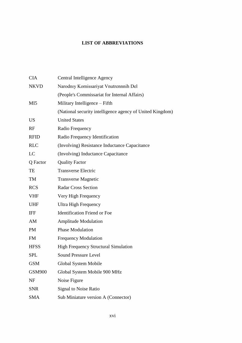
LIST OF ABBREVIATIONS
CIA Central Intelligence Agency
NKVD Narodnıy Komissariyat Vnutrennnih Del
(People's Commissariat for Internal Affairs)
MI5 Military Intelligence – Fifth
(National security intelligence agency of United Kingdom)
US United States
RF Radio Frequency
RFID Radio Frequency Identification
RLC (Involving) Resistance Inductance Capacitance
LC (Involving) Inductance Capacitance
Q Factor Quality Factor
TE Transverse Electric
TM Transverse Magnetic
RCS Radar Cross Section
VHF Very High Frequency
UHF Ultra High Frequency
IFF Identification Friend or Foe
AM Amplitude Modulation
PM Phase Modulation
FM Frequency Modulation
HFSS High Frequency Structural Simulation
SPL Sound Pressure Level
GSM Global System Mobile
GSM900 Global System Mobile 900 MHz
NF Noise Figure
SNR Signal to Noise Ratio
SMA Sub Miniature version A (Connector)
xvii
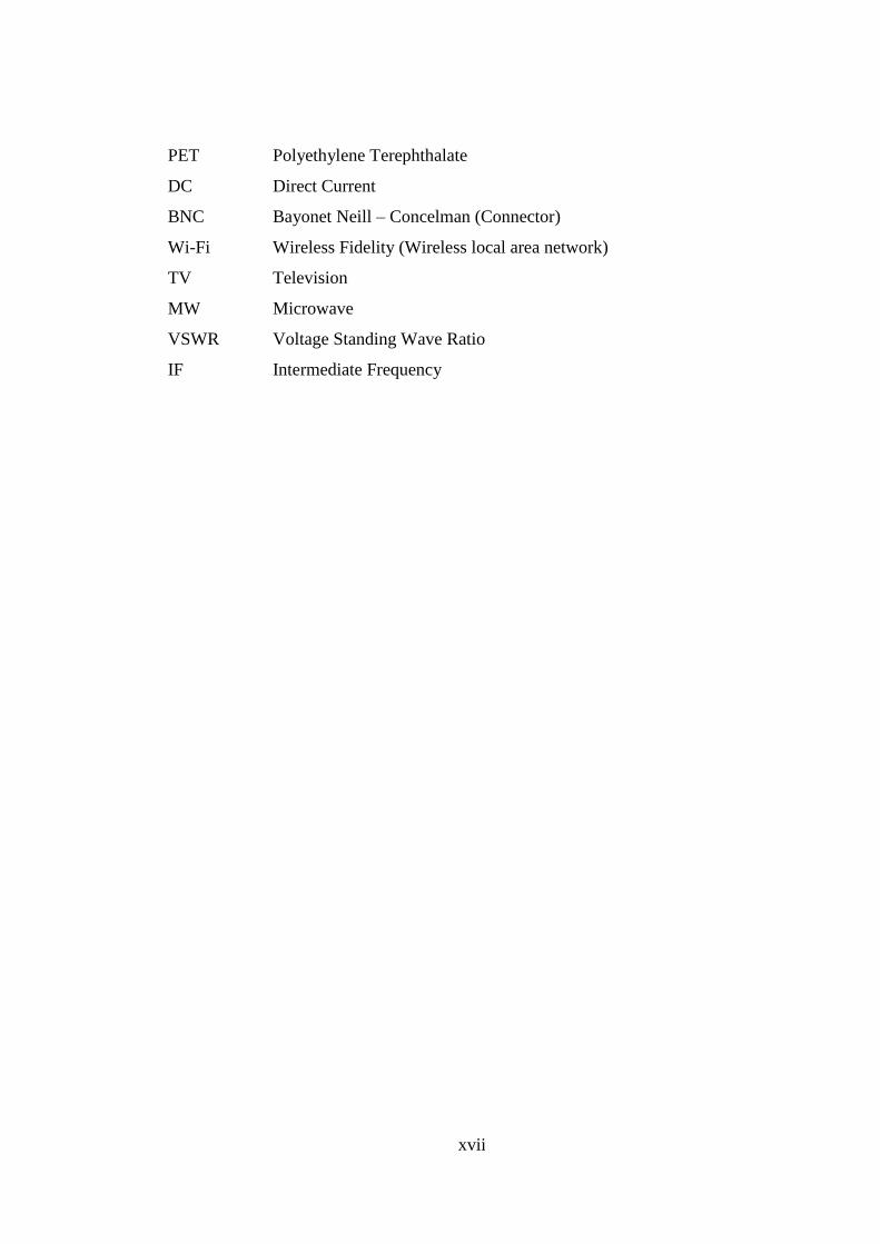
PET Polyethylene Terephthalate
DC Direct Current
BNC Bayonet Neill – Concelman (Connector)
Wi-Fi Wireless Fidelity (Wireless local area network)
TV Television
MW Microwave
VSWR Voltage Standing Wave Ratio
IF Intermediate Frequency

xviii

1
CHAPTER 1
INTRODUCTION
1.1 History of The Device
In 1952 a covert spy device is found in the American Embassy of the Soviet Union.
As it is seen in Figure 1, it had been concealed inside a wooden replica of the Great
Seal of America. Since it was a strange device and it could not be explained how it
works when discovered, it was named as “The Thing” [1-4].
Figure 1. The Wooden Great Seal of America and the Theremin’s Device [1-4]
The seal had been presented to the American Ambassador Averell HARRIMAN as a
peaceful gesture of friendship between the countries by the Soviet school children in
1945. According to some informal sources it was presented to the ambassador by an
anonymous Russian as a personal gift.

2
The bug was not discovered until 1952. The seal had been stayed hung on the wall
just behind the ambassador and Russians listened the American ambassadors for
nearly 7 years until discovered [5]. The listened ambassadors during the period are
- W. Averell Harriman — October 7, 1943
- Walter Bedell Smith — March 22, 1946
- Alan G. Kirk — May 21, 1949
- George F. Kennan — March 14, 1952
Actually Americans had discovered a mysterious signal and realized that Soviets
were bombarding the embassy with a microwave signal for a long time before the
discovery of the device but they could not be able to explain the reason of the signal
bombardment. The CIA counterespionage team had performed technical search
operations at the building (Spaso House, Residence of American Ambassadors in
Moscow) several times but they had found nothing always. Nevertheless, they had
several theories that it might be a mind control attack (at that time, the mind control
was a popular scientific research area) by NKVD (Soviet internal intelligence
service) or NKVD might had been trying to get the people in the embassy depressed
spiritually by microwave signals.
Afterwards they discovered the speech signal by accidentally and then searching in
detail, they found the device and thus solved the signal mystery in 1952. But they
faced with a new mystery, the device itself.
The device was a small tiny metal cylindrical box with a tail and it contained neither
electrical component nor battery. It was a passive device. Soviets were sending a
signal towards the device and device reflects back the signal with a modulation of the
sound.
CIA worked on the device for a long time but could not explain the working
principle of the device. They asked English Service MI5 for help. MI5 dealt with the
device but no solution is found. Eventually English scientist Peter Wright worked on
the device for several months and solved the mystery. The device was a passive
cavity resonator. Later on English service made new devices for themselves and for
Americans [6].
3
The inventor of the device is Leon Theremin who was a Russian scientist and
inventor. He had many practical inventions and innovations. Theremin is the inventor
of first electronic musical instrument called Theremin and the interlace techniques on
video. He had become very famous and had gone to US in 1927. In 1938 he had been
kidnapped by Soviet agents and had been brought to Soviet Union and was
imprisoned in the Butyrka Prison and later sent to work in the Kolyma Gold Mines.
Theremin was supposed to be executed but in fact put to work in Sharashka (a secret
laboratory in the Soviet Gulag Camp System, where the prisoners work for army
research activities) together with some other well-known scientists and engineers.
Where he worked for Soviet Army and Soviet intelligence, and invented “The
Thing” [7].
1.2 Motivation to Work And Objective
The English scientist Peter Wright discovered the working principles of the devices
and he created a similar system called “Satyr” for British intelligence by working for
18 months [7]. The mystery of the device had been solved, but since the issue was
related with the intelligence services and secret spy operations, the details of the
device has been never explained formally. The operation and the device are disclosed
in general aspect but the details of working principle and the properties of the device
were not disclosed so far.
Theremin’s bug had been a great and new technology and it opened a new era at that
time. It was the first practical device using passive communication technique which
had been a theoretical issue up to then. Thus Theremin’s bug became a pioneer for
modulated backscatter wave, passive wireless communication, passive microwave
sensors and RFID applications.
There are many informal references which give information about the device but
almost all of them are consist of memories, rumors and recollection stories. So,
nearly all data about the device are inconsistent. The only consistent information is
the general mechanical structure of the device.

4
In this thesis the device will be analyzed and tried to be clarified technically. After
the analysis of the structure, a similar system will be designed, produced and
implemented.
In addition, in this work the structure is used for perception of the sound but the
structure is a promising design for a variety of different applications to sense or
detect many physical parameters wirelessly, remotely and passively.
1.3 The Device Properties
All the descriptions about the device from all kind of references define physically the
same structure. The device is consisted of a metal cylinder and an aerial protruding
from the cylinder. One circular face of the cylinder is closed by a thin metallic
diaphragm. Inside the cylinder, there is a mushroom shaped post in the middle
which has a disc shaped plate parallel to the diaphragm. The inner part of the antenna
having disc shaped head near to the central post [8]. The available picture and
drawings of the device are given in Figure 2. In Appendix A, all the data and
information collected from all sources about the issue are given in detail.
Figure 2. The pictures and drawings of the Theremin’s Device [2, 9-12]
5
There are many stories about the device. Only few of them are first-hand information
and few of those first-hand stories mention the details. The device is generally
described as a passive cavity resonator. And some references say that the device used
modulated backscattering technique. In any case an electromagnetic signal is sent to
the device; the device modulates the signal with the surrounding sound and reflects
or sends back. The information carrying reflected signal is then detected and
demodulated.
The more explanatory definition can be done in the following way. A high powered
microwave signal is sent from a van parked near to the building by using a highly
directive antenna to the region of the building where the device is placed. The device
resonates at a certain frequency and this frequency changes in accordance with the
sound hitting the thin diaphragm of the device. Because the sound hitting the
diaphragm changes the resonance characteristic of the device, the reflected wave
from the antenna of the device is modulated by the sound.
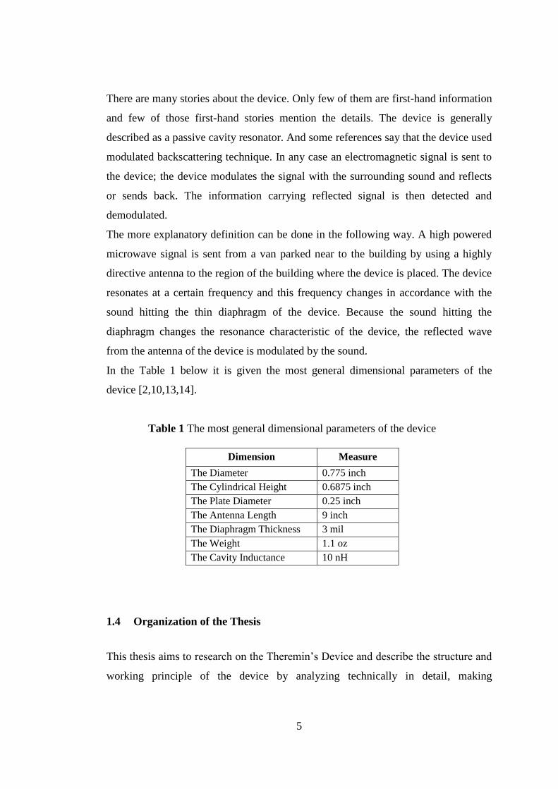
In the Table 1 below it is given the most general dimensional parameters of the
device [2,10,13,14].
Table 1 The most general dimensional parameters of the device
Dimension Measure
The Diameter 0.775 inch
The Cylindrical Height 0.6875 inch
The Plate Diameter 0.25 inch
The Antenna Length 9 inch
The Diaphragm Thickness 3 mil
The Weight 1.1 oz
The Cavity Inductance 10 nH
1.4 Organization of the Thesis
This thesis aims to research on the Theremin’s Device and describe the structure and
working principle of the device by analyzing technically in detail, making

6
simulations, designing and producing a prototype having similar structure and
making experimental work on this prototype. In accordance with this goal;
Chapter 1 (Introduction) gives the history of the device and explains the motivation
and objectives of the thesis and introduces a broad overview of the thesis.
Chapter 2 (Theoretical Background) provides the relevant technical knowledge about
the involving issues such as resonance and resonators, microwave cavities, antennas
and backscatter modulation technique.
Chapter 3 (Theoretical Work) includes the theoretical analysis of the device
structure, calculations, derivations and simulations related with the structure; design,
analysis and simulations of the prototypes.
Chapter 4 (Measurements & Results) describes the experimental set-up, prototype
measurements and experiments. Moreover, Chapter 4 gives experimental results of
the listening experiments.
Chapter 5 (Conclusions) includes a summary of the thesis, conclusions drawn from
the work and several suggestions for future works about the issue.
There are two appendices at the end of the thesis. Appendix A provides more
detailed information relevant to the main text. It contains the pictures, drawings and
existing information about the device in all kind of sources. Appendix B is a CD-
ROM which is attached in an envelope on the back cover of the document. It
contains the audio files related with the sound receive experiments.
The thesis ends with the list of used reference materials following the appendices.

7
CHAPTER 2
THEORETICAL BACKGROUND
This chapter gives the relevant information and provides a theoretical background
about the subjects relating the topics studied in this work. All the information is
presented from the thesis' point of view and necessary to understand the further parts.
2.1 Resonance And Resonators
2.1.1 Resonance
Resonance is a very general phenomenon that happens so often and in so many kinds
of systems. Resonance can be in any media, in any form and in a vast range of spatial
scales. But across this wide range of spatial scales and diverse media, there are
certain general properties of resonance that are common to all of them. They all tend
to oscillate at some characteristic frequency and at its higher harmonic frequencies
that are integer multiples of the fundamental frequency. They all exhibit spatial
standing waves, whose wavelength is inversely proportional to their frequencies. In
the most general sense, resonance represents that the energy in a system exchanges
from one form into another form at a particular rate. However, while exchanging
there happen some losses from cycle to cycle. A resonance system has low quality if
its energy is lost quickly during the energy exchange process. Losses may be caused
by “friction” in mechanical systems and “resistance” in electronic systems. In this
thesis, our main interests are the electrical resonance and the electromagnetic wave
(or microwave) resonance [15].
In electrical circuits, resonance occurs as electrical energy stored in capacitors and
magnetic energy stored in inductors exchange back and forth.

8
Electromagnetic or microwave resonance occurs in a medium as standing waves by
reflections from the boundaries in a frequency related with the medium size. In some
special type microwave resonators, the energy also exchange between the electric
and the magnetic fields.
2.1.2 Resonators
A resonator is a physical system providing the resonance. There is at least one
fundamental frequency at which the resonance takes place for every resonator. This
is called the resonant or resonance frequency. In resonance, the oscillating energy is
converted from one form to another and vice versa. If it is supplied more energy to
the system at the frequency of resonance then the energy is absorbed by the system
and stored in the continuing oscillation. So a resonator is a system which can store
the energy that is oscillating from one kind to another.
There are many structures functioning as a resonator. In acoustic resonators, the air
molecules oscillate back and forth such that the energy changes from pressure to
kinetic energy and vice versa. In mechanical resonators, energy change occurs
between stress force and movement or kinetic energy. The parameters like
dimension, size, shape and stiffness affect the speed of energy oscillation, i.e., the
resonant frequency [15].
In electrical resonators, the alternation of energy occurs between electrical energy
and magnetic energy. In a circuit, the electrical energy is stored in capacitance as
charge separation and the magnetic energy is stored in inductance as charge
movement or current. The energy in the circuit is therefore transformed between
these two forms or between capacitance and the inductance of the circuit. Hence, the
frequency of the oscillation is determined by the inductance and capacitance of the
circuit.
In electromagnetic or microwave resonators, the resonance is created by the
reflection of the wave between the boundaries of the structure and forming a standing
wave oscillation. In some special case of microwave resonators, the energy exchange
takes place between electric and magnetic fields inside the resonator as very like in
electrical resonator.
9
In electromagnetic waves, the electric and magnetic field is already transformed each
other periodically while propagating. The resonant frequency of microwave structure
depends on the dimensional parameters like size and shape and also the electrical and
magnetic properties of the involving structures.
2.1.3 Electrical Resonators
Near the resonant frequencies, a microwave resonator can be modeled by lumped-
element equivalent circuit which may be series RLC or parallel RLC resonator
circuit. So in the following sections it is reviewed some basic properties of the
electrical resonator circuits [15,16].
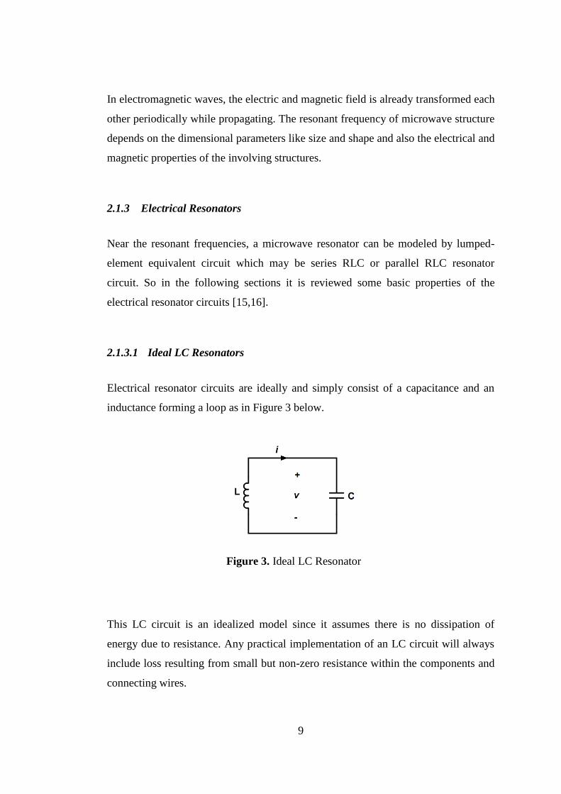
2.1.3.1 Ideal LC Resonators
Electrical resonator circuits are ideally and simply consist of a capacitance and an
inductance forming a loop as in Figure 3 below.
Figure 3. Ideal LC Resonator
This LC circuit is an idealized model since it assumes there is no dissipation of
energy due to resistance. Any practical implementation of an LC circuit will always
include loss resulting from small but non-zero resistance within the components and
connecting wires.
10
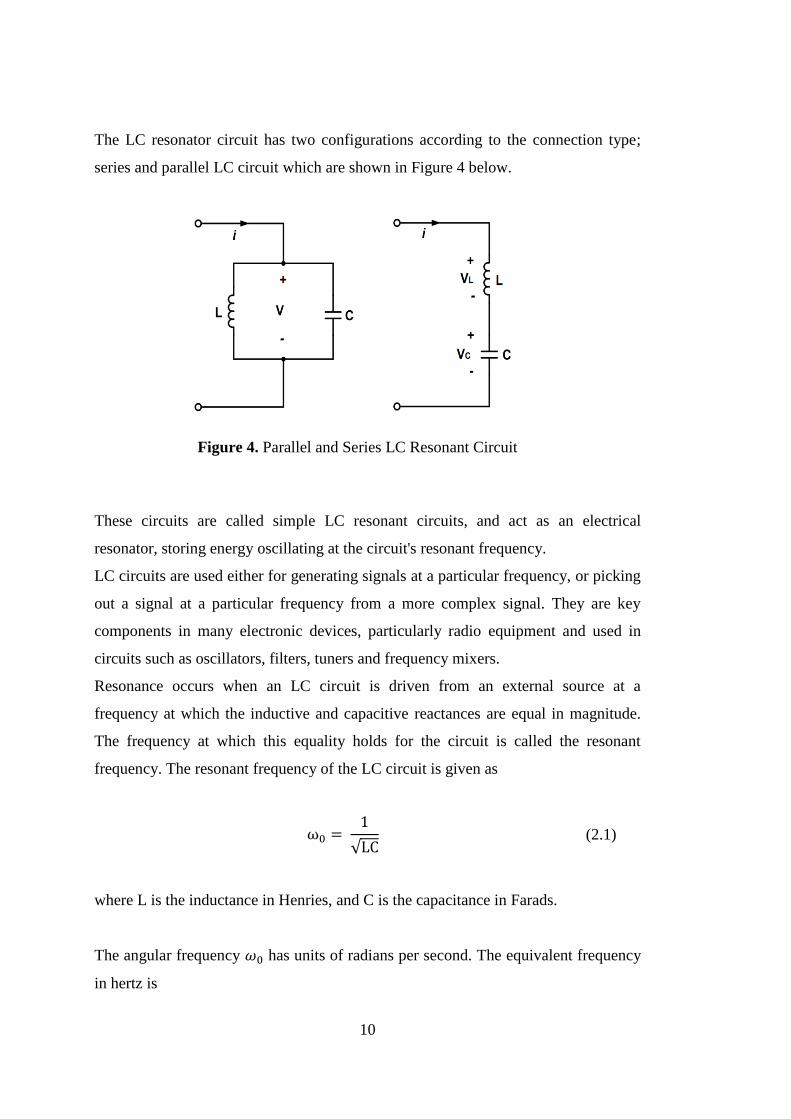
The LC resonator circuit has two configurations according to the connection type;
series and parallel LC circuit which are shown in Figure 4 below.
Figure 4. Parallel and Series LC Resonant Circuit
These circuits are called simple LC resonant circuits, and act as an electrical
resonator, storing energy oscillating at the circuit's resonant frequency.
LC circuits are used either for generating signals at a particular frequency, or picking
out a signal at a particular frequency from a more complex signal. They are key
components in many electronic devices, particularly radio equipment and used in
circuits such as oscillators, filters, tuners and frequency mixers.
Resonance occurs when an LC circuit is driven from an external source at a
frequency at which the inductive and capacitive reactances are equal in magnitude.
The frequency at which this equality holds for the circuit is called the resonant
frequency. The resonant frequency of the LC circuit is given as
√ (2.1)
where L is the inductance in Henries, and C is the capacitance in Farads.
The angular frequency has units of radians per second. The equivalent frequency
in hertz is

11
√ (2.2)
The L/C ratio of the LC circuit is one of the factors that determine its Q Factor
(Quality Factor). The Q Factor is a dimensionless quantity that describes how under-
damped (or lossy) a resonator as well as characterizes a resonator's bandwidth
relative to its center frequency. The two common definitions of Q Factor are as
follows
(2.3)
(2.4)
where is the resonant frequency, is the half power bandwidth.
These two definitions are not necessarily equivalent. They become approximately
equivalent as Q becomes larger, meaning the resonator becomes less damped. Higher
Q indicates a lower rate of energy loss relative to the stored energy of the resonator,
i.e., the oscillations die out more slowly.
The two-element LC circuit described above is the simplest type of inductor-
capacitor network (or LC network). It is also referred to as a second order LC circuit
to distinguish it from more complicated (higher order) LC networks with more
inductors and capacitors. Such LC networks with more than two reactive structures
may have more than one resonant frequency.
2.1.3.2 RLC Resonators
Any practical implementation of an LC circuit will always include loss resulting
from small but non-zero resistance within the components and connecting wires.

12
In LC circuit the charge flows back and forth between the plates of the capacitor,
through the inductor. The energy oscillates back and forth between the capacitor and
the inductor until (if not replenished from a source) internal resistance makes the
oscillations die out. There must be a source to drive continuous oscillations. If the
excitation frequency of the source is at the resonant frequency of the circuit then
resonance will occur.
There are two types of RLC resonators depending on the connection, series and
parallel RLC resonator as given in the Figure 5 below. It will be noted that the only
difference between the series and parallel circuit is in the manner of connection.
At resonance, parallel circuit offers high impedance and the series circuit offer low
impedance to the source.
2.1.3.2.1 Series RLC Resonators
Figure 5. Series RLC Resonant Circuit
A circuit consisting of resistance, inductance and capacitance connected in series
with a voltage applied as shown in Figure 5 is termed as a series resonant circuit. In
many cases, practically R represents the loss resistance of the inductor, which in the
case of air core coils simply means the resistance of the winding. The resistances
associated with the capacitor are often negligible.
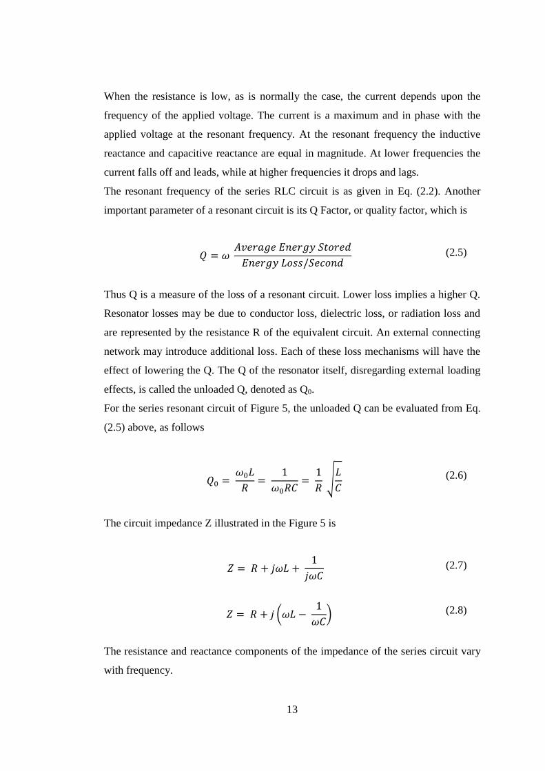
13
When the resistance is low, as is normally the case, the current depends upon the
frequency of the applied voltage. The current is a maximum and in phase with the
applied voltage at the resonant frequency. At the resonant frequency the inductive
reactance and capacitive reactance are equal in magnitude. At lower frequencies the
current falls off and leads, while at higher frequencies it drops and lags.
The resonant frequency of the series RLC circuit is as given in Eq. (2.2). Another
important parameter of a resonant circuit is its Q Factor, or quality factor, which is
(2.5)
Thus Q is a measure of the loss of a resonant circuit. Lower loss implies a higher Q.
Resonator losses may be due to conductor loss, dielectric loss, or radiation loss and
are represented by the resistance R of the equivalent circuit. An external connecting
network may introduce additional loss. Each of these loss mechanisms will have the
effect of lowering the Q. The Q of the resonator itself, disregarding external loading
effects, is called the unloaded Q, denoted as Q0.
For the series resonant circuit of Figure 5, the unloaded Q can be evaluated from Eq.
(2.5) above, as follows
√
(2.6)
The circuit impedance Z illustrated in the Figure 5 is
(2.7)
(
) (2.8)
The resistance and reactance components of the impedance of the series circuit vary
with frequency.
14
In the small frequency region around the resonance, the circuit resistance is
substantially constant. The reactance, on the other hand, varies substantially linearly
from a relatively high capacitive value below resonance to a relatively high inductive
value above resonance, and becomes zero at the resonant frequency. The absolute
value of the impedance is at the minimum in the resonance.
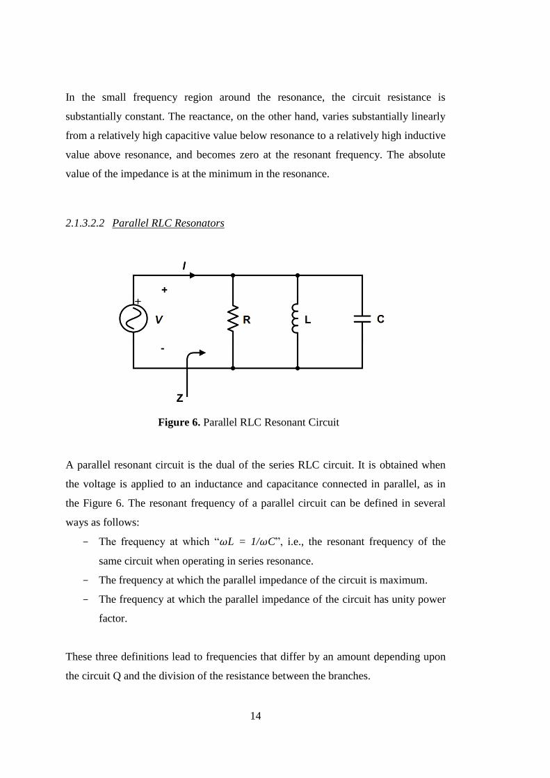
2.1.3.2.2 Parallel RLC Resonators
Figure 6. Parallel RLC Resonant Circuit
A parallel resonant circuit is the dual of the series RLC circuit. It is obtained when
the voltage is applied to an inductance and capacitance connected in parallel, as in
the Figure 6. The resonant frequency of a parallel circuit can be defined in several
ways as follows:
- The frequency at which “ L = 1/ C”, i.e., the resonant frequency of the
same circuit when operating in series resonance.
- The frequency at which the parallel impedance of the circuit is maximum.
- The frequency at which the parallel impedance of the circuit has unity power
factor.
These three definitions lead to frequencies that differ by an amount depending upon
the circuit Q and the division of the resistance between the branches.

15
When the circuit Q is at least moderately high ( ), for all practical purposes
the resonant frequency of a parallel resonant circuit can be taken as the resonant
frequency of the same circuit when connected in series. The only difference between
series and parallel resonance under these conditions is that the phase angles are
reversed, i.e., the phase angle of parallel impedance has the opposite sign from the
phase angle of the current in the series circuit.
The resonant frequency and the Q factor of the parallel RLC circuit are given in Eq.
(2.2) and Eq. (2.6).
The circuit impedance Z is
(2.9)
The unloaded Q factor of the Parallel RLC circuit is
√
(2.10)
As it is seen in Eq. (2.10) above that the Q of the parallel resonant circuit increases as
R increases.
2.1.3.3 Loaded and Unloaded Q Factors
The unloaded quality factor Q0 is a characteristic of the resonator itself in the
absence of any loading effects caused by external circuitry. In practice, however, a
resonator is invariably coupled to other circuitry which will have the effect of
lowering the overall or loaded quality factor QL, of the circuit [16].
16
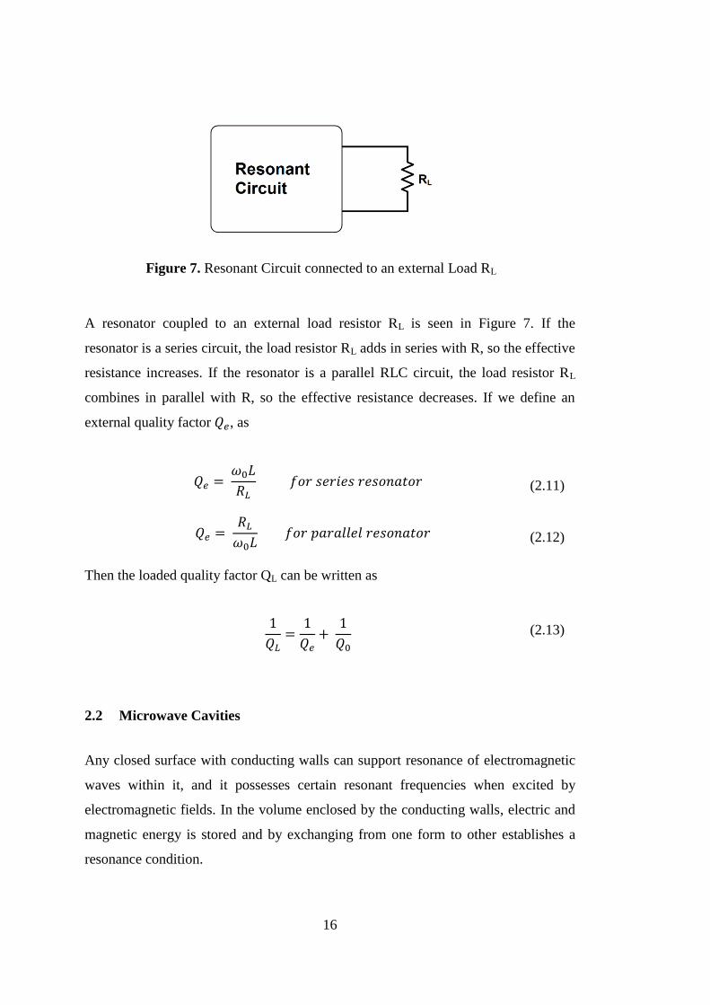
Figure 7. Resonant Circuit connected to an external Load RL
A resonator coupled to an external load resistor RL is seen in Figure 7. If the
resonator is a series circuit, the load resistor RL adds in series with R, so the effective
resistance increases. If the resonator is a parallel RLC circuit, the load resistor RL
combines in parallel with R, so the effective resistance decreases. If we define an
external quality factor , as
(2.11)
(2.12)
Then the loaded quality factor QL can be written as
(2.13)
2.2 Microwave Cavities
Any closed surface with conducting walls can support resonance of electromagnetic
waves within it, and it possesses certain resonant frequencies when excited by
electromagnetic fields. In the volume enclosed by the conducting walls, electric and
magnetic energy is stored and by exchanging from one form to other establishes a
resonance condition.
17
These resonators are commonly termed microwave cavity resonators and are
extensively used as resonant circuits at extremely high frequencies. For such use of
high frequency, cavity resonators have several advantages like simplicity,
manageable physical size, high Q and very high shunt impedances. At wavelengths
well below one meter, microwave cavity resonators become vastly superior to the
corresponding resonators with lumped components.
Cavity resonators have less power dissipation according to the lumped resonators. In
cavities, power is dissipated in the metallic walls of the cavity as well as in the
dielectric material that may fill the cavity.
Cavities are used in many kinds of microwave circuits and systems like microwave
generators (e.g. Klystrons, Magnetrons), frequency meters, material measurements,
heating applications and microwave filters.
The information in this section is compiled from [16-19] in general.
2.2.1 Types of Cavity Resonators
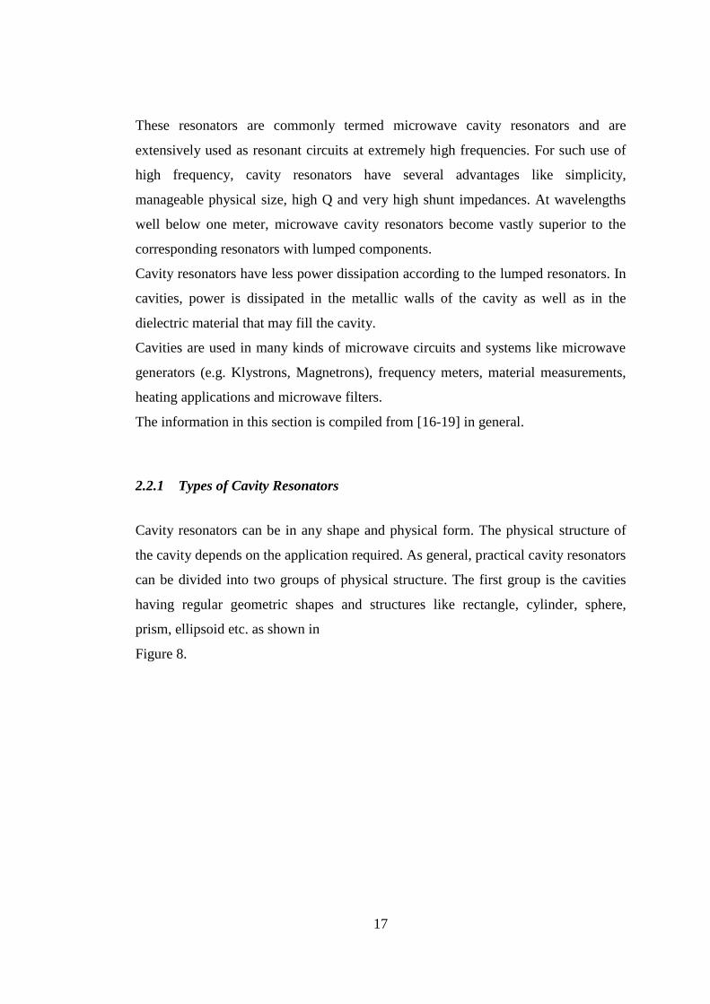
Cavity resonators can be in any shape and physical form. The physical structure of
the cavity depends on the application required. As general, practical cavity resonators
can be divided into two groups of physical structure. The first group is the cavities
having regular geometric shapes and structures like rectangle, cylinder, sphere,
prism, ellipsoid etc. as shown in
Figure 8.

18
Figure 8. Cavities having regular shapes [16]
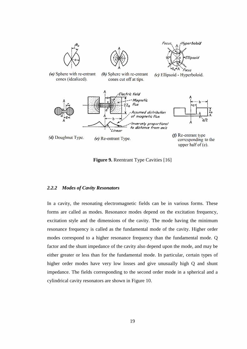
The second group cavities, as illustrated in Figure 9, are in various physical forms
and shapes. They are combination of some idealized and some practical forms. Since
there are some types of protrusions and bulges inwards of the cavities, these cavities
are called as reentrant type.
19
Figure 9. Reentrant Type Cavities [16]
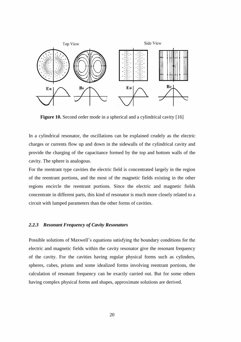
2.2.2 Modes of Cavity Resonators
In a cavity, the resonating electromagnetic fields can be in various forms. These
forms are called as modes. Resonance modes depend on the excitation frequency,
excitation style and the dimensions of the cavity. The mode having the minimum
resonance frequency is called as the fundamental mode of the cavity. Higher order
modes correspond to a higher resonance frequency than the fundamental mode. Q
factor and the shunt impedance of the cavity also depend upon the mode, and may be
either greater or less than for the fundamental mode. In particular, certain types of
higher order modes have very low losses and give unusually high Q and shunt
impedance. The fields corresponding to the second order mode in a spherical and a
cylindrical cavity resonators are shown in Figure 10.
20
Figure 10. Second order mode in a spherical and a cylindrical cavity [16]
In a cylindrical resonator, the oscillations can be explained crudely as the electric
charges or currents flow up and down in the sidewalls of the cylindrical cavity and
provide the charging of the capacitance formed by the top and bottom walls of the
cavity. The sphere is analogous.
For the reentrant type cavities the electric field is concentrated largely in the region
of the reentrant portions, and the most of the magnetic fields existing in the other
regions encircle the reentrant portions. Since the electric and magnetic fields
concentrate in different parts, this kind of resonator is much more closely related to a
circuit with lumped parameters than the other forms of cavities.
2.2.3 Resonant Frequency of Cavity Resonators
Possible solutions of Maxwell’s equations satisfying the boundary conditions for the
electric and magnetic fields within the cavity resonator give the resonant frequency
of the cavity. For the cavities having regular physical forms such as cylinders,
spheres, cubes, prisms and some idealized forms involving reentrant portions, the
calculation of resonant frequency can be exactly carried out. But for some others
having complex physical forms and shapes, approximate solutions are derived.

21
The resonant wavelength is proportional to the resonator size, i.e., if all dimensions
are doubled, then the resonant wavelength will likewise be doubled. Using this fact,
the resonators having complex shapes that cannot be calculated can be constructed
easily. In order to obtain a desired resonant frequency, first it is constructed a
resonator of proper size and shape. Then the resonant frequency is measured. The
ratio of this frequency to the desired resonant frequency gives a scale factor that is
applied to all dimension of the resonator to obtain the resonator operating at the
desired wavelength.
The resonant frequency of resonators such as illustrated in
Figure 9 (d to f) above, which have a large capacitance, can be calculated
approximately by using the capacitance and inductance.
The resonant frequency of a cavity resonator can be changed by changing the
mechanical dimensions or by coupling reactance into the resonator or by means of a
conductive paddle. Small changes in dimensions can be realized by flexible walls,
while large changes require some movable parts. The resonant frequency of the
reentrant type resonators is particularly sensitive to the gap that constituting a
capacitance between the reentrant portions, especially when this gap is small.
Reactance can be coupled into the resonator by coupling loops or probes in the
manner discussed below and affects the resonant frequency. A copper paddle placed
inside the resonator in such a way that intercepts some of the flux lines will increase
the resonant frequency. Changing the position of the paddle will change the effect.
This can be used to adjust the resonant frequency.
2.2.4 Q Factor of Cavity Resonators
The Q Factor of a cavity resonator is the ratio of the energy stored in the fields of the
resonator to the energy lost per cycle, according to the relation below.
(2.14)

22
It has the same significance as for a lumped resonant circuit. So it can be defined as
(2.15)
(2.16)
Figure 11. Q Factor of the resonator
An important implication of Eq. (2.14) is that to achieve a high Q value, the
resonator should have a large ratio of volume to surface area. The physical
explanation for this is that all the energy is stored in the volume of the resonator,
whereas all dissipation occurs at the walls. As a result, resonators such as spheres,
cylinders, and prisms can in general be expected to have higher Q than the resonators
having the same shape with reentrant sections. The drop in Q resulting from reentrant
portion is excessive if the reentrant portions have very sharp spines. With resonators
of the same proportions but different size, Eq. (2.14) shows that the Q will be
proportional to the square root of the wavelength and thus the size.
For practical cavity resonators, typical values of Q are extremely high, compared
with those encountered with common resonator circuits.
23
2.2.5 Shunt Impedance of Cavity Resonators
The shunt impedance of a cavity resonator can be defined as the square of the line
integral of voltage across the resonator, divided by the power loss in the resonator.
This impedance corresponds to the parallel resonant impedance of a tuned circuit,
and at resonance becomes purely resistive and called the shunt resistance of the
resonator.
The shunt impedance of cavity resonators having regular shapes can be calculated by
analytically. The values obtainable are very large. The shunt resistance of the
reentrant type cavity resonators is less than without reentrants. But if the distance
across which the impedance is developed is very short then the reentrant type of
cavity resonator gives much greater shunt impedance in inverse proportion with the
distance [20]
2.2.6 Conducting Material of Cavity Resonators
In terms of cavity performance or quality factor, the conductor material which the
microwave cavity is made of is important. The conductor must be chosen
accordingly with the expected performance. Using materials having better
conductivity provide the lower loss. The materials that can be used for cavity
production and their conductivity values are Copper (5.813 x 10⁷ S/m), Aluminum
(3.816 x 10⁷ S/m) and Brass (2.564 x 10⁷ S/m) [15].
Since copper is very expensive it is not proper for massive structures generally. It is
more common use for applications involving strip conductors, grounds in micro
strips lines, which they have a very small thickness (around 17um ~35um) or even
for wires. Aluminum has the soldering problem with the conventional method using
tin, and the softness of it causes some mechanical difficulties. So finally, brass is
suitable in many aspects for microwave cavity applications. It eliminates the
drawbacks of copper and aluminum for bulky structures. In this work, brass is also
used as cavity material.
24
2.2.7 Coupling to Cavity Resonators
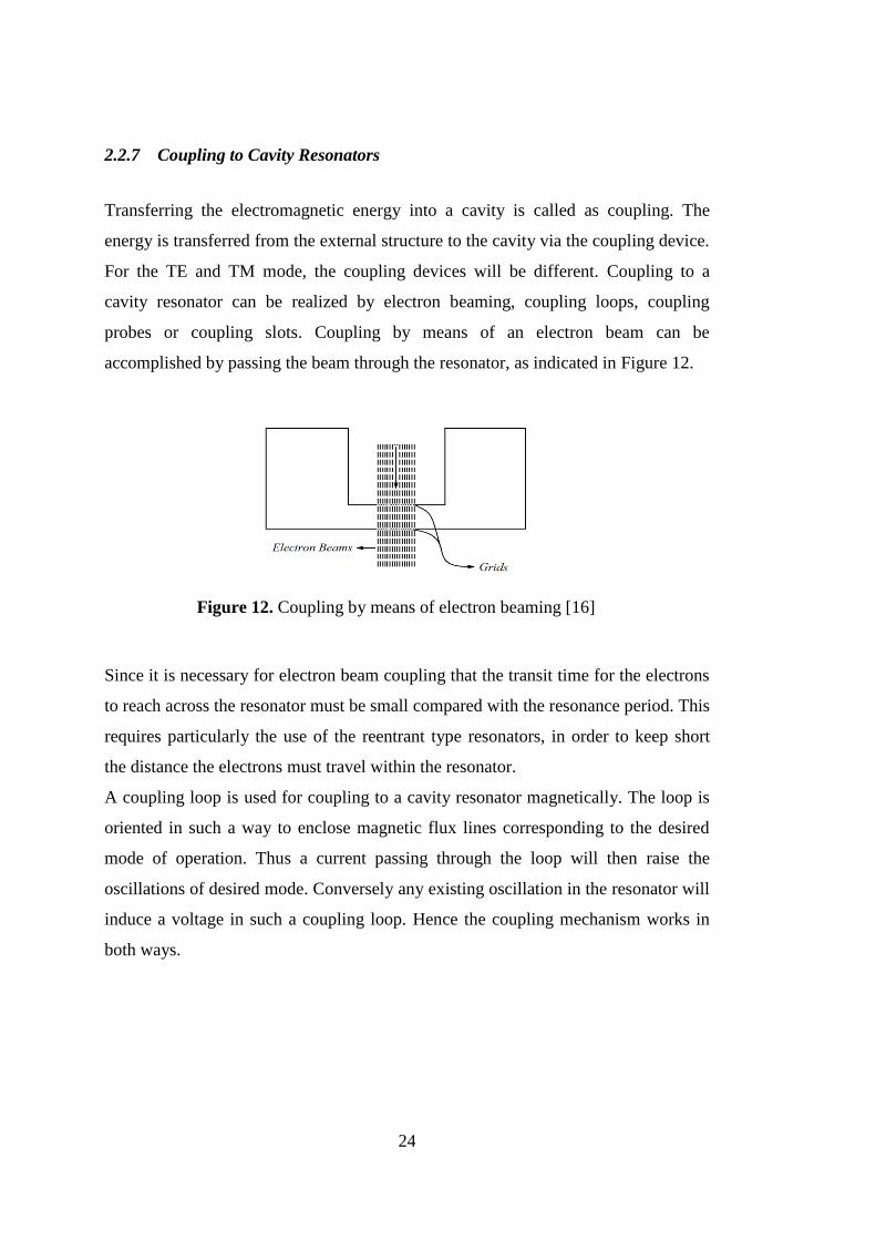
Transferring the electromagnetic energy into a cavity is called as coupling. The
energy is transferred from the external structure to the cavity via the coupling device.
For the TE and TM mode, the coupling devices will be different. Coupling to a
cavity resonator can be realized by electron beaming, coupling loops, coupling
probes or coupling slots. Coupling by means of an electron beam can be
accomplished by passing the beam through the resonator, as indicated in Figure 12.
Figure 12. Coupling by means of electron beaming [16]
Since it is necessary for electron beam coupling that the transit time for the electrons
to reach across the resonator must be small compared with the resonance period. This
requires particularly the use of the reentrant type resonators, in order to keep short
the distance the electrons must travel within the resonator.
A coupling loop is used for coupling to a cavity resonator magnetically. The loop is
oriented in such a way to enclose magnetic flux lines corresponding to the desired
mode of operation. Thus a current passing through the loop will then raise the
oscillations of desired mode. Conversely any existing oscillation in the resonator will
induce a voltage in such a coupling loop. Hence the coupling mechanism works in
both ways.

25
Figure 13. Coupling loop [16]
In order to maximize coupling, the coupling loop must be placed on a location inside
the cavity where the magnetic flux density is maximum or it must be provided that
the loop area is in the most favorable position for enclosing much more magnetic
flux. The magnitude of coupling can be readily changed by simply rotating the loop;
the coupling reduces to zero when the plane of the loop is parallel to the magnetic
flux.
The coupling probe functions as like an antenna inside the cavity. Excitation of a
cavity resonator by means of a coupling probe is shown in Figure 14. It is the
equivalent of a short antenna which provides electric or capacitive coupling to the
field inside the cavity. Probe coupling is useful only in providing coupling to modes
in which the electric field terminates on the surface of the cavity in the vicinity of the
coupling device. The coupling probe must be located on a place inside the cavity
where the electric field of the desired excitation mode is maximal. The coupling
probe produces an electric field component in the same direction as the electric field
of the desired mode of oscillation in the resonator. In this circumstance the voltage
applied to the probe will excite oscillations in the cavity resonator and conversely the
oscillations in the cavity resonator will create a voltage on the probe.

26
Figure 14. Coupling probe [16, 21]
Waveguide coupling or slot coupling is accomplished by arranging so that the waves
entering the cavity from the waveguide or slot produce a field within the cavity that
corresponds to the desired mode of oscillation in the cavity resonator (Figure 15).
Coupling slots or coupling holes are designed is the natural coupling mechanism.
The electromagnetic fields, either the magnetic field or the electric field penetrate the
aperture and couple to cavity resonator. The location, position and the shape of the
slot determines the resonance mode and the magnitude of coupling [15].
Figure 15. Slot Coupling of the cavity resonator [22]

27
2.2.8 Cylindrical Cavity
Cylindrical cavity can be constructed from circular waveguide shorted at both ends.
The basic theory of the cylindrical cavity resonator is similar to circular waveguide.
The geometry of a cylindrical cavity resonator is given in Figure 16 below [22].
Figure 16. Cylindrical cavity resonator
2.2.8.1 Resonant frequency of Cylindrical Cavity
The resonant frequency of the cylindrical cavity resonator has the same properties
with cylindrical waveguide. The dominate modes of the cylindrical cavities are TE111
and TM010. The resonant frequency depends on the dimension of the cavity and the
filling materials. Equations below give the resonant frequency of the cylindrical
cavity [23].
√ √(
)
(
)
(2.17)
m= 0,1,2..
n= 1,2,3..
p= 0,2,3..
28
√ √(
)
(
)
(2.18)
m= 0,1,2..
n= 1,2,3..
p= 1,2,3..
where
is the resonant frequency for the TMmnp mode and
is the
resonant frequency for the TEmnp mode. is the nth zero of the mth order Bessel
function of the first kind and is the nth zero of the derivative of the mth order
Bessel function of the first kind. is the radius and is the height of the cylindrical
cavity.
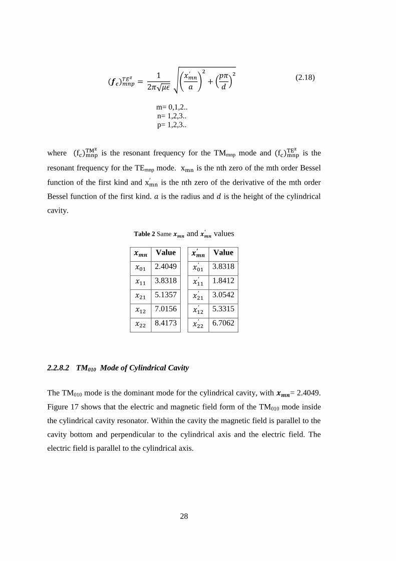
Table 2 Same and values
Value Value
2.4049 3.8318
3.8318 1.8412
5.1357 3.0542
7.0156 5.3315
8.4173 6.7062
2.2.8.2 TM010 Mode of Cylindrical Cavity
The TM010 mode is the dominant mode for the cylindrical cavity, with = 2.4049.
Figure 17 shows that the electric and magnetic field form of the TM010 mode inside
the cylindrical cavity resonator. Within the cavity the magnetic field is parallel to the
cavity bottom and perpendicular to the cylindrical axis and the electric field. The
electric field is parallel to the cylindrical axis.
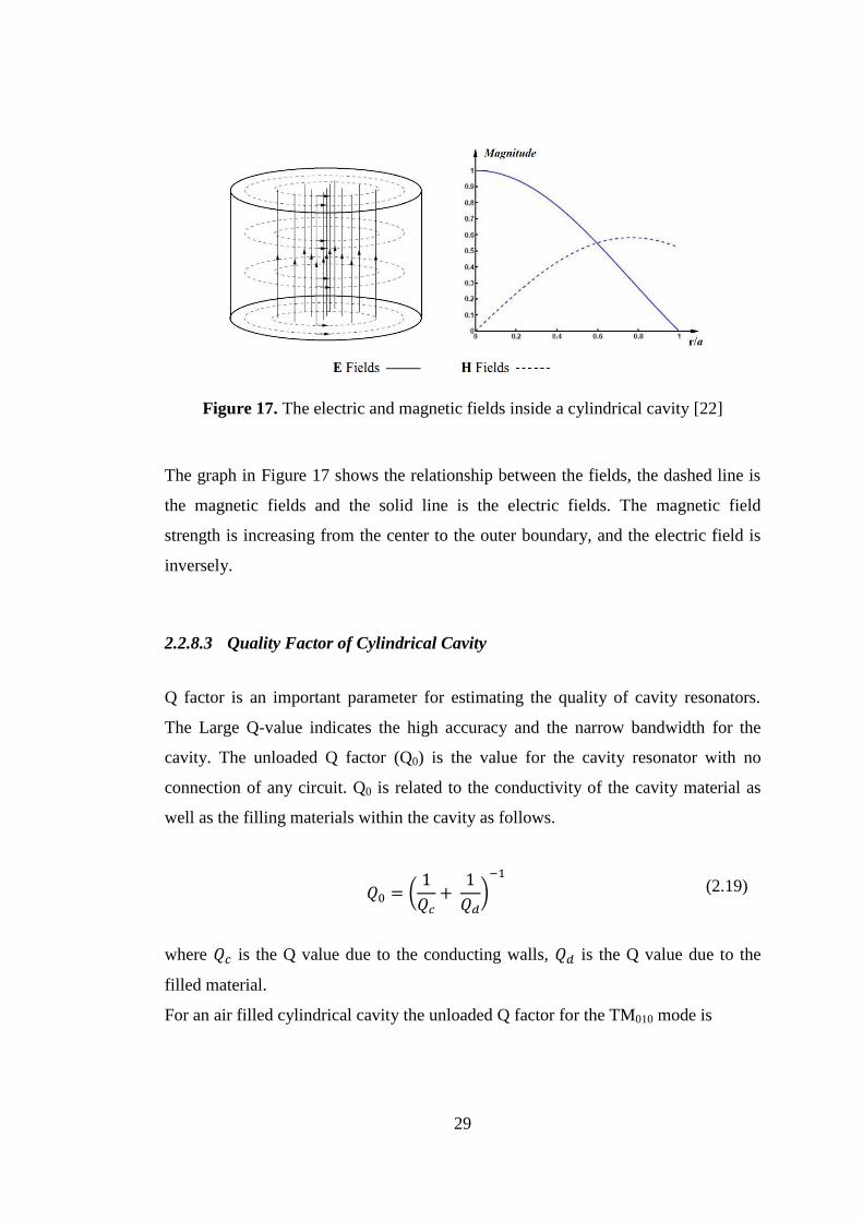
29
Figure 17. The electric and magnetic fields inside a cylindrical cavity [22]
The graph in Figure 17 shows the relationship between the fields, the dashed line is
the magnetic fields and the solid line is the electric fields. The magnetic field
strength is increasing from the center to the outer boundary, and the electric field is
inversely.
2.2.8.3 Quality Factor of Cylindrical Cavity
Q factor is an important parameter for estimating the quality of cavity resonators.
The Large Q-value indicates the high accuracy and the narrow bandwidth for the
cavity. The unloaded Q factor (Q0) is the value for the cavity resonator with no
connection of any circuit. Q0 is related to the conductivity of the cavity material as
well as the filling materials within the cavity as follows.
(
)
(2.19)
where is the Q value due to the conducting walls, is the Q value due to the
filled material.
For an air filled cylindrical cavity the unloaded Q factor for the TM010 mode is

30
√
(2.20)
where V is the cavity volume, S is the internal surface area of the cavity, is the
conductivity of the walls.
When the cavity resonator is connected to an external circuit which has a Q factor
Qe, the external circuit will have the effect of decreasing the overall Q value of the
system. The unloaded Q factor (Q0), the external Q factor (Qe) and the loaded Q
factor (QL) are given below as
(2.21)
(2.22)
(2.23)
2.2.8.4 The Equivalent Circuit of Cylindrical Cavity
The cylindrical cavity resonator can be equivalently regarded as a parallel RLC
resonant circuit illustrated in Figure 18 [20].
Figure 18. The equivalent circuit of a cylindrical cavity

31
The input impedance of the resonator is represented as,
(2.24)
Making some algebra and manipulation the input impedance can be written as
(2.25)
Where
(2.26)
(2.27)
The coupling factor for a Parallel Resonant circuit is given as
(2.28)
: Under coupled resonator
: Critically coupled resonator
: Over coupled resonator
The input impedance of the parallel resonant circuit can be written in terms of is as
follows
(2.29)
The reflection coefficient of the circuit can be written as follows

32
(2.30)
(2.31)
At resonance, , so the imaginery part of the reflection coefficient is zero and
the it is purely real as follows
(2.32)
Figure 19. Smith Chart representation of coupling to a parallel RLC circuit [22]
The unloaded and the loaded Q factors can be written in terms of as follows
(2.33)
(2.34)
The loaded Q factor can be obtained from the graph of reflection coefficient with the
following expression
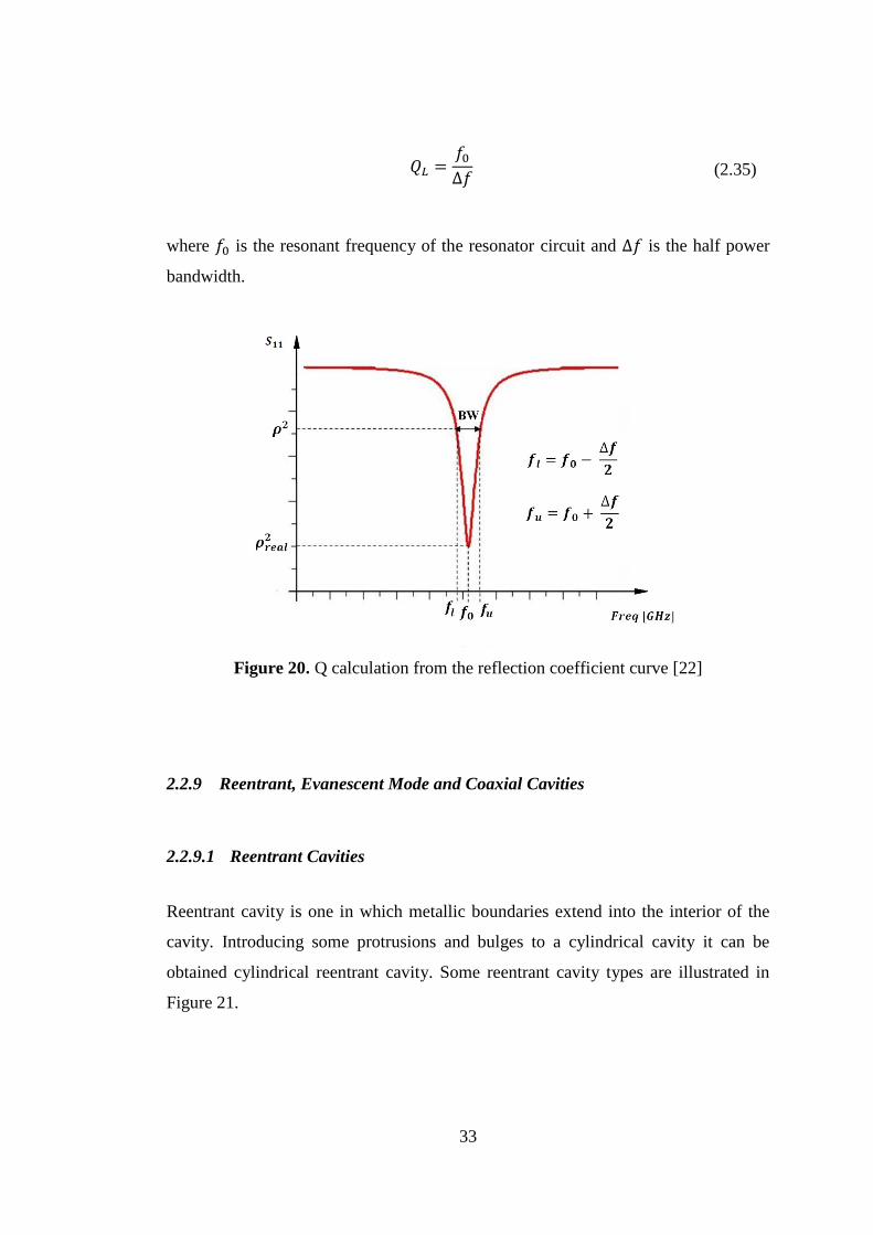
33
(2.35)
where is the resonant frequency of the resonator circuit and is the half power
bandwidth.
Figure 20. Q calculation from the reflection coefficient curve [22]
2.2.9 Reentrant, Evanescent Mode and Coaxial Cavities
2.2.9.1 Reentrant Cavities
Reentrant cavity is one in which metallic boundaries extend into the interior of the
cavity. Introducing some protrusions and bulges to a cylindrical cavity it can be
obtained cylindrical reentrant cavity. Some reentrant cavity types are illustrated in
Figure 21.

34
Figure 21. Some reentrant type cavities [24]
2.2.9.2 Evanescent Mode Cavities
Cavities are often bulky and heavy and it is highly desirable to reduce the size and
weight. Since the resonant frequency of a cavity is inverse proportional to its
dimensions, there will be a limit to the size for a given frequency of interest. By
introducing some structures or reactance inside the cavity, creating a discontinuity or
changing the shape of the cavity the resonant frequency can be reduced. Such
structural transformations can change the resonant frequency to a lower value than
the original one. Cavities that operate using this technique are referred to as
evanescent-mode cavity. In other words an evanescent-mode cavity is one that whose
resonance frequency is somehow lower than its original fundamental mode
frequency. By evanescently loading a cavity, the frequency can be brought down by
an order of magnitude, while still maintaining a high-Q [25].
2.2.9.3 Coaxial Cavity Resonator
A coaxial cavity resonator is a cylindrical cavity structure resembling a finite length
coaxial transmission line which is closed at both end and it is shorted at one end as
illustrated in the Figure 22.

35
Figure 22. Coaxial Cavity Structure
One end of the coaxial transmission line is shorted but there is a small gap at the
other end. This gap creates a capacitance between inner and outer conductor as like a
parallel plate capacitor.
At sufficiently high frequencies, a short section of a transmission line with
completely reflecting terminations acts as an inductor if it is less than quarter
wavelength long. For a short circuited transmission line of fixed length, the
impedance is given as
(2.36)
This formula shows how the reflecting impedance changes with the frequency.
For a short-circuited line, impedance is zero for the zero frequency, but as the
frequency increase it behaves as an increasing inductive reactance. However, as the
frequency is raised higher, the tangent function becomes negative, this means that Zs
is capacitive and its reactance decreases.
At the point where Zs passes from plus infinity to minus infinity the structure
behaves like a parallel resonant circuit, i.e., anti-resonance. When the frequency
reaches the value at which the length of the line is equal to the half wavelength, Zs
becomes zero. At this point the line behaves like a series resonant circuit. Just
beyond this frequency Zs becomes a positive reactance and so on, this is illustrated in
Figure 23.

36
Figure 23. Variation of input impedance with frequency for a short circuited
coaxial line [26].
The above theory can be applied to a coaxial cavity in which case the inductance
created by a line length of less than can resonate with either a lumped
capacitance or a capacitance due to the gap between the inner and the outer
conductor.
In order to have such a coaxial resonant cavity of high performance, many points
must be taken into account. To decrease the losses of the electromagnetic wave
inside the cavity the inner surface must be made as smooth as possible. Also the
inner and outer conductor dimensions have to be chosen to give high quality factor
and low losses. A good short circuit between the inner and outer conductors is very
important.
The loaded quality factor must be high and transmission loss low to provide a sharp
resonance at the frequency of the signal transmitted through the cavity. This may be
achieved by careful tuning of the inner post and further improved by loose coupling
if the unloaded quality factor is high [26].
In coaxial cavity, the central post constitute a capacitive structure together with the
upside wall of the cavity. The E-field inside the cavity is concentrated inside the
capacitive gap between the top of the post and the cavity wall. On changing the gap
width, the frequency changes according to the equation below
37
√ (2.37)
where and are the inductance and the capacitance of the cavity, is the
capacitance between the post and the roof of the cavity, is the capacitance due to
the fringing fields near the post edges.
These parameters can be calculated by using the following expressions.
(2.38)
(2.39)
(2.40)
(2.41)
where is an empirically fitted constant which is sensitive to a/b ratio.
For a/b ≤ 0.3, this constant has been found to be 2.78 [27,28].
2.2.9.3.1 Quality Factor of Coaxial Cavity Resonator
In general, the electromagnetic energy in a cavity at resonance is stored in the
electric and magnetic fields. The stored energy in each field will vary during the
cycle, but their summation is always equal to the total energy stored in the cavity. If
the loaded quality factor of the cavity is high, the rate of the stored energy to
dissipated energy is high, and the average magnetic field density is equal to the
average electric field density over a cycle.

38
At some instants in the cycle the energy will be entirely in the magnetic field, and at
other instants the energy will be entirely in the electric field. With this fact, by
finding the peak magnetic or electric field energy, the total stored energy can be
calculated.
The unloaded quality factor of a cylindrical coaxial cavity can be analytically
approximated using the following equation [27,29]
(
(
)
) (2.42)
where is post radius, is cavity radius, is the height of the post and is the
sheet resistance of the cavity sidewalls.
As it is seen on the expression above the unloaded Q of a coaxial cavity mainly
depends on the cavity dimensions and the sheet resistance. Increasing the radius and
the height of the cavity increases the quality factor because this provides more
volume for energy storage inside the cavity as long as b and h are much smaller than
the resonant wavelength. It can be mathematically validated from the above formula
that when the ratio of the post radius and the cavity radius /b is 0.28 then the quality
factor is maximized.
Sheet resistance is the resistance offered by the cavity walls to the RF currents
and it can be approximated as follows
(2.43)
√ (2.44)
where is the resistivity and is the conductivity of the cavity material [27]. The
cavity thickness can be replaced by the skin depth , provided . So, materials
having higher conductivity provide higher Q for cavity resonators.

39
2.2.9.3.2 Shunt Resistance of Coaxial Cavity Resonator
In a cavity, the losses due to the finite conductance of the wall is represented with an
equivalent shunt resistance or an equivalent series resistance. These resistances are
directly related with the cavity material, physical structure, dimensions and the
operation frequency. The shunt resistance of the coaxial cavity can be analytically
approximated by using the following expression [20].
(
)
(2.45)
where is the skin depth, is the conductivity of the cavity material, is the
angular frequency and is the inductance of the cavity.
The series resistance of the coaxial cavity can be approximated as the following
expression.
(2.46)
2.2.9.3.3 Cylindrical Cavity to Coaxial cavity
The coaxial cavity is defined here as a length of short circuited transmission line
terminated with a capacitive reactance formed by the gap between the inner
conductor and the end plate. As seen in Figure 24 below the coaxial cavity is a
special form of the cylindrical cavity.
Figure 24 shows the transition of a perfect cylindrical cavity to a perfect coaxial
cavity with the illustration of possible electric fields of the lowest mode during
transition. The perfect cylindrical cavity mode TM010 becomes the usual capacitively
loaded coaxial mode TM00p for a small gap between reentrant portions. When the
reentrant portion (i.e., the center conductor) is started to be inserted into the
cylindrical cavity, the resonant frequency decreases slowly at first and then rapidly
until zero frequency is approached asymptotically for full insertion (i.e., center

40
conductor shorted to the end plate). Thus, low frequencies may be obtained by
making the gap sufficiently small.
Figure 24. Transition from cylindrical cavity to coaxial cavity [30]
In a coaxial cavity with a small gap, the electric field is concentrated between the end
of the inner conductor and the end plate and the magnetic field is concentrated near
the opposite end of the resonator, a typical quasi-stationary electromagnetic system
[30].
2.2.9.3.4 Fringing Field Effect
In a coaxial cavity, not only the gap capacitance ( ) is considered, but the
capacitance due to fringing field ( ) should also be taken into account. Since the
fields extending slightly beyond the end of the post (i.e., the fringing fields) create
capacitive reactance which consequently affects the behavior of the cavity.
The effect of additional inductance and capacitance between the tip of the inner
conductor and the adjacent cavity wall should also be considered if a more accurate
electrical circuit equivalent of the cavity is to be established.

41
Figure 25. Fringing fields inside the coaxial cavity
2.2.10 Cavity Perturbation Technique
When a resonant cavity is perturbed, i.e., when an object is introduced into the cavity
or when a general shape of the cavity is changed, the electromagnetic fields inside
the cavity change accordingly. The underlying assumption of cavity perturbation
theory is that the electromagnetic fields inside the cavity after the change differ by a
very small amount from the fields before the change. Then Maxwell's equations for
the original and perturbed cavities can be used to derive expressions for resulting
resonant frequency shifts.
When a general shape of a resonant cavity is changed, a corresponding change in
resonant frequency can be approximated as
∭ | | | |
∭ | | | |
(2.47)
The expression above for change in resonant frequency can additionally be written in
terms of time-average stored energies as follows
(2.48)
where and represent time-average magnetic and electric energies
contained in .

42
This expression can also be written in terms of energy densities as follows
(2.49)
It is clear from the above equation that, an inward perturbation will raise the resonant
frequency if it is made at a point of large H (high ), and will lower the resonant
frequency if it is made at a point of large E (high ). The opposite behavior results
for an outward perturbation. It is also evident that the greatest changes in resonant
frequency will occur when the perturbation is at a position of maximum E and zero
H, or vice versa [18].
2.3 Antennas
2.3.1 Monopole Antenna
The primary interest for this work is monopole antenna. A monopole antenna is half
of a dipole antenna placed on top of a ground plane, as illustrated in Figure 26.
Figure 26. Monopole antenna and an equivalent dipole antenna [31]
Assuming the plane is infinite and perfectly conducting, the monopole antenna will
be equivalent to a dipole whose lower half is the image of the upper half.
43
Thus, the radiation pattern (in the upper hemisphere) will be identical to that of a
dipole [31]. Because the fields are radiated only in the upper hemisphere, the total
radiated power will be half that of a dipole, and hence the corresponding radiation
resistance will also be halved:
(2.50)
(2.51)
In the same manner, the directivity doubles because the isotropic radiation intensity
is a half of its dipole value:
(2.52)
2.3.2 Reflection from antennas
In general, a reflected wave from an antenna is composed of two parts. One is due to
the reflection from the conducting structure of the antenna, i.e., structural mode and
the other is due to the reflection from the mismatch between the antenna and the
circuit behind the antenna, i.e., antenna mode [32].
So the reflected power from a receiving antenna system can be written as the sum of
two terms, one is the scattered power due to the structural mode and the other is due
to the antenna mode. This phenomenon is illustrated in Figure 27. Consequently, it is
not correct to assume that a matched receiving antenna scatters as much as it absorbs.
In general, the reflected power from a receiving antenna may be greater, equal to, or
lower than the absorbed power.

44
Figure 27. Reflection from antenna
The reflected power due to the antenna mode depends on the load impedance of the
antenna, but the power reflected due to structural mode is not affected by load
impedance. Thus the antenna mode reflection can be used for communication or a
modulation by changing properly [33].
2.3.3 Antennas as Scatterers
Antennas have several important properties such as pattern, gain, and impedance
which are both transmitting and receiving antennas. But a receiving antenna has an
additional important property, scattering. In general, the scattering is considered in
absorption efficiency issues. Absorption efficiency is the ratio between the absorbed
power and the received power that is the sum of the absorbed and the scattered
powers. It is generally believed that absorption efficiency is less than or equal to
50%, but it has been shown that this is not true. The scattering from an antenna have
two mode : one that is due to mismatch behind the antenna, called the antenna
scattering or re-radiation since it has the same pattern as the transmitting antenna;
and one that is what is left when the antenna is matched, called the residual or
structural scattering [34].
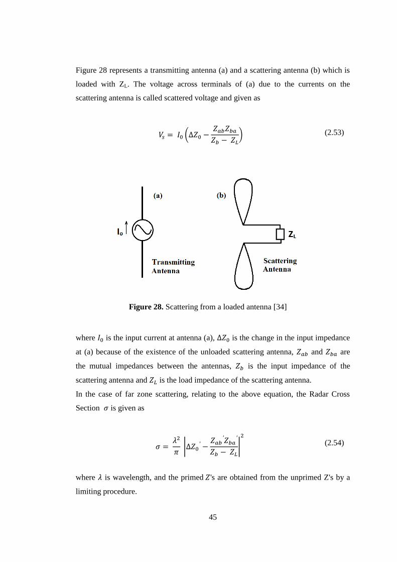
45
Figure 28 represents a transmitting antenna (a) and a scattering antenna (b) which is
loaded with ZL. The voltage across terminals of (a) due to the currents on the
scattering antenna is called scattered voltage and given as
(
) (2.53)
Figure 28. Scattering from a loaded antenna [34]
where is the input current at antenna (a), is the change in the input impedance
at (a) because of the existence of the unloaded scattering antenna, and are
the mutual impedances between the antennas, is the input impedance of the
scattering antenna and is the load impedance of the scattering antenna.
In the case of far zone scattering, relating to the above equation, the Radar Cross
Section is given as
|
|
(2.54)
where is wavelength, and the primed 's are obtained from the unprimed Z's by a
limiting procedure.

46
The gain and the effective area of the scattering antenna are given as
|
|
(2.55)
|
|
(2.56)
where G is the transmitting gain of the scattering antenna, A is the effective area of
the scattering antenna with matched load, and is the radiation resistance ( )
of scattering antenna. So it is seen that, all of the factors except for in the
expression above are related to common antenna parameters. If the first term of the
RCS expression above is small compared to the second term, i.e., if the scattered
field of the unloaded antenna is small compared to that of the loaded antenna, then
the RCS expression can be written as
| | (2.57)
As it is seen in the expression above, the incoming wave is received with an effective
area A and then reradiating some part of the energy with a gain G. Practically, this
approximation usually applies for small antennas, like dipoles and monopoles, which
are less reflecting body.
If all the media involving are reciprocal then the effective area A and the gain G have
a relation as follows
(2.58)
So the RCS expression can be written as
|
|
(2.59)

47
In the case of bi-static scattering, i.e., the transmitter and the receiver are at different
places, formulas similar to Eqns. (2.56) to (2.59) can also be written. The RCS
expression is as follows
|
|
(2.60)
where and
are the mutual impedances between scattering antenna and
transmitting and receiving antennas respectively.
In Eqns. (2.57) to (2.59), G becomes the gain of the scattering antenna in the
direction of the receiver, and A the effective area of the scattering antenna in the
direction of the transmitter. In bi-static case even for the reciprocal media Eqns.
(2.59) and (2.60) are not valid. In the nonreciprocal case, there is in general a G and
an A associated with each direction, for which a special type of reciprocity
relationship applies [34].
2.4 Backscatter Wave Technique
When an electromagnetic wave is reflected or scattered from a target, some
parameters of the scattered or reflected wave is effected from the properties of the
target. The properties of the target affect the way in which the signal is reflected
back. Antenna properties such as cross sectional area, gain, impedance etc. all have
an effect on how the target reflects the incident wave. Thus the scattered wave
properties can be accordingly changed by changing those properties.
Backscattering is a communication technology used at UHF or microwave
frequencies. It is the process of collecting an RF signal (energy), processing the
signal with the data it will carry, and reflecting it back to where it came from. It
works like a reader that sends the electromagnetic wave to a target at a specific
frequency; the target receives the wave, encodes the information into the wave, and
scatters it back to the reader [35].

48
2.4.1 History of Passive Backscatter Communication
Backscatter communication can be realized in several ways. The key point is that a
modulation of reflected or scattered wave must be provided by means of some
parameters. For example, modulation can be provided by a Doppler shift, so that the
receiver detects the motion or vibration of the target or by a deliberately designed
target that modulates the reflections. This is achieved by electronics attached to an
antenna called load modulation. During the Second World War, there was early
interest in modulation sidebands scattered from both radar targets and loaded
antennas. An important issue to be handled was the identification of friend or foe
(IFF), i.e., distinguishing between friendly and enemy aircraft on radar.
Wattson-Watt in Britain tried load modulation with a dipole antenna stretched across
the wings of a fighter aircraft in the late 1930s. By mechanically or electronically
shorting and opening the antenna, pilots would send their codes by reflecting signals
to identify themselves. The received signals were so weak, but it was an active
transponder system developed to transmit IFF codes. Later on, more sensitive and
successful systems including mechanical vibrations and rotating propellers are
developed.
The first public paper about the backscatter communication was published by Harry
Stockman in 1948 [35]. Presumably he did not know about Theremin’s earlier work.
Stockman discussed different approaches to load modulation and mechanical
modulation by translating or rotating reflectors. Load modulation also used for field
measurements, starting with J.H. Richmond’s paper published in 1955 [37].
The first commercial applications of backscatter communication that are similar to
RFID were patented in the mid-1970s. These were targeted at inventory
management, making them true precursors to modern RFID [36].
2.4.2 Modulated Backscatter Technique
A backscatter communication system is a wireless communication that takes place
between a transmitter/receiver and a target.
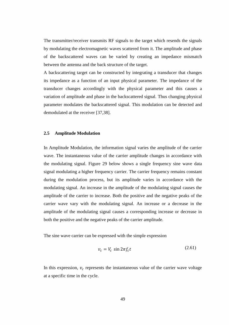
49
The transmitter/receiver transmits RF signals to the target which resends the signals
by modulating the electromagnetic waves scattered from it. The amplitude and phase
of the backscattered waves can be varied by creating an impedance mismatch
between the antenna and the back structure of the target.
A backscattering target can be constructed by integrating a transducer that changes
its impedance as a function of an input physical parameter. The impedance of the
transducer changes accordingly with the physical parameter and this causes a
variation of amplitude and phase in the backscattered signal. Thus changing physical
parameter modulates the backscattered signal. This modulation can be detected and
demodulated at the receiver [37,38].
2.5 Amplitude Modulation
In Amplitude Modulation, the information signal varies the amplitude of the carrier
wave. The instantaneous value of the carrier amplitude changes in accordance with
the modulating signal. Figure 29 below shows a single frequency sine wave data
signal modulating a higher frequency carrier. The carrier frequency remains constant
during the modulation process, but its amplitude varies in accordance with the
modulating signal. An increase in the amplitude of the modulating signal causes the
amplitude of the carrier to increase. Both the positive and the negative peaks of the
carrier wave vary with the modulating signal. An increase or a decrease in the
amplitude of the modulating signal causes a corresponding increase or decrease in
both the positive and the negative peaks of the carrier amplitude.
The sine wave carrier can be expressed with the simple expression
(2.61)
In this expression, represents the instantaneous value of the carrier wave voltage
at a specific time in the cycle.
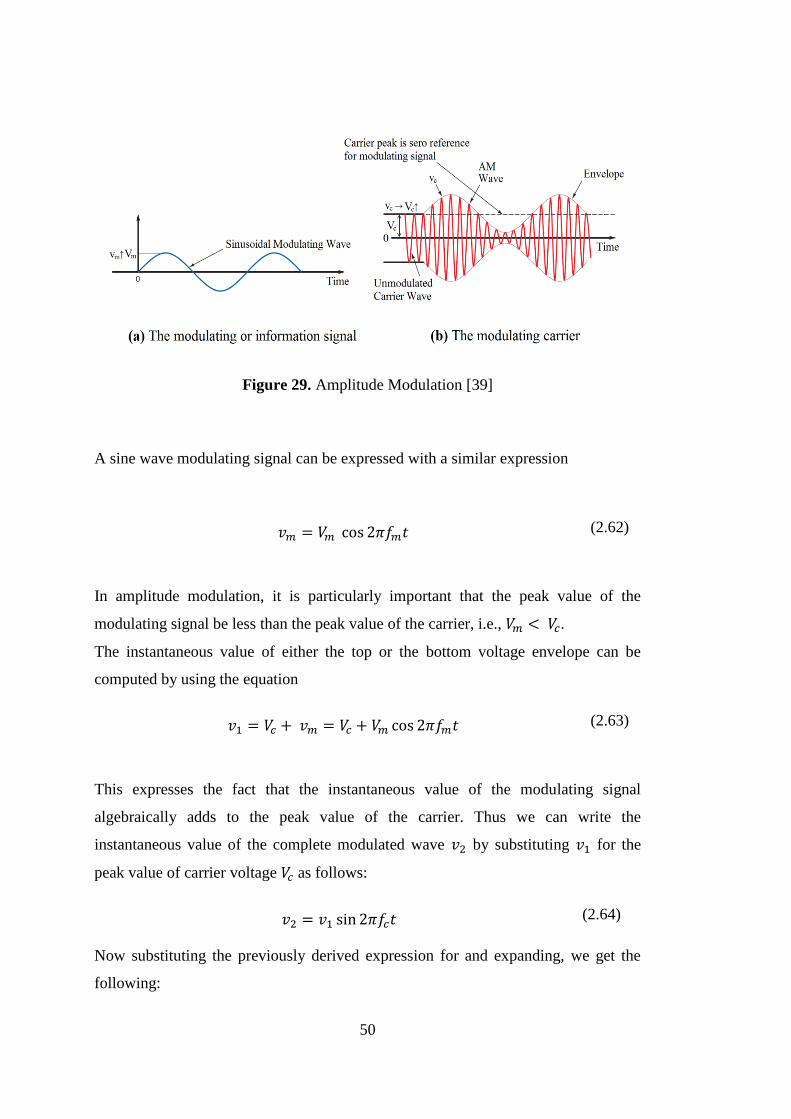
50
Figure 29. Amplitude Modulation [39]
A sine wave modulating signal can be expressed with a similar expression
(2.62)
In amplitude modulation, it is particularly important that the peak value of the
modulating signal be less than the peak value of the carrier, i.e., .
The instantaneous value of either the top or the bottom voltage envelope can be
computed by using the equation
(2.63)
This expresses the fact that the instantaneous value of the modulating signal
algebraically adds to the peak value of the carrier. Thus we can write the
instantaneous value of the complete modulated wave by substituting for the
peak value of carrier voltage as follows:
(2.64)
Now substituting the previously derived expression for and expanding, we get the
following:
51
(2.65)
Thus, as it is seen in the expression above, the modulated signal has three
components: the carrier wave and two pure sine waves (known as sidebands) with
frequencies slightly above and below the carrier frequency [39].

52

53
CHAPTER 3
THEORETICAL ANALYSIS OF THE STRUCTURE
AND DESIGN OF THE PROTOTYPES
In this chapter the theoretical analysis and design works are presented. The physical
and functional details of the device are studied. By creating an HFSS model of the
cavity structure the eigenmode analysis and parametric analysis are realized.
3.1 Analysis of The Theremin's Device
3.1.1 Physical Structure
All the descriptions about the device from all kind of sources define physically the
same structure for the device. That is shown in the Figure 30.
According to the existing descriptions, drawings and pictures of the device; it
composed of a cylindrical box and an aerial protruding from the sidewall. The
cylindrical body of the device is copper and interior is silver-plated. Inside the body a
mushroom shaped central post is attached to the backside. Front side of the cylinder
is covered with a thin metallic diaphragm. The post plate and the diaphragm together
constitute a capacitive gap. The back plate of the cylinder is threaded so that the post
can be positioned relative to the diaphragm to adjust the gap length. The antenna
extending through the side of the cylinder has a disc shaped head terminates near the
central post but does not touch it [10-12,40].
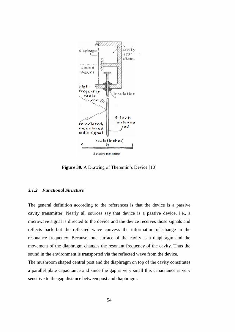
54
Figure 30. A Drawing of Theremin’s Device [10]
3.1.2 Functional Structure
The general definition according to the references is that the device is a passive
cavity transmitter. Nearly all sources say that device is a passive device, i.e., a
microwave signal is directed to the device and the device receives those signals and
reflects back but the reflected wave conveys the information of change in the
resonance frequency. Because, one surface of the cavity is a diaphragm and the
movement of the diaphragm changes the resonant frequency of the cavity. Thus the
sound in the environment is transported via the reflected wave from the device.
The mushroom shaped central post and the diaphragm on top of the cavity constitutes
a parallel plate capacitance and since the gap is very small this capacitance is very
sensitive to the gap distance between post and diaphragm.
55
As it will be detailed in further sections, when the sound wave hits the diaphragm it
moves and this movement changes the gap capacitances and thus the resonant
frequency of the cavity. Hence the coupling and re-radiating property of the structure
change accordingly for a specific frequency and this accordance creates modulation
on the returning wave.
After this general explanation, in the following sections the device and its
components and functions are analyzed in details.
3.2 Analysis of The Structure
3.2.1 The Antenna Analysis
The antenna of the device consists of a metal rod entering to the body of the device.
The section inside the body has a disc shaped head. Considering the overall structure
since it has only one arm, the antenna of the device must be a monopole antenna.
And the structure of the device implies that the body of the cylindrical cavity is a
finite ground plane for the monopole antenna.
There are two possibilities for the connection of the antenna to the cavity.
- First, the antenna section inside the cavity can be a mushroom shaped
exciting probe for the cavity.
- Second, the disc shaped head of the antenna probe section constitutes a
parallel plate capacitance together with the central post of the cavity. Thus the
probe can capacitively couple the antenna to the post or cavity.
The position of the probe section of the antenna with respect to the central post
affects the cavity characteristics. With tight coupling (i.e., the disc head of the
antenna is close to the central post), the loss at the resonance frequency is less and
the Q factor is higher. With loose coupling (i.e., the disc head of the antenna is away
from the central post) the loss at the resonance frequency is more and the Q factor is
lower [41].
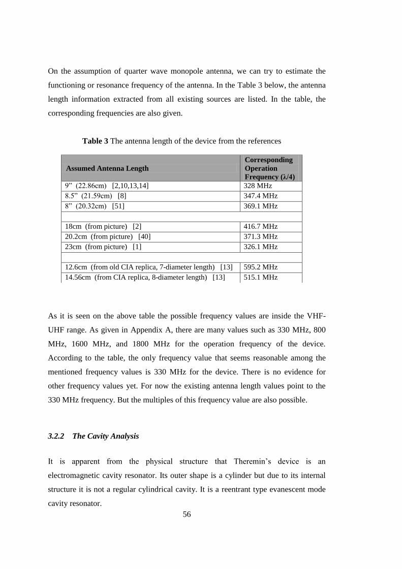
56
On the assumption of quarter wave monopole antenna, we can try to estimate the
functioning or resonance frequency of the antenna. In the Table 3 below, the antenna
length information extracted from all existing sources are listed. In the table, the
corresponding frequencies are also given.
Table 3 The antenna length of the device from the references
Assumed Antenna Length
Corresponding
Operation
Frequency (λ/4)
9” (22.86cm) [2,10,13,14] 328 MHz
8.5” (21.59cm) [8] 347.4 MHz
8” (20.32cm) [51] 369.1 MHz
18cm (from picture) [2] 416.7 MHz
20.2cm (from picture) [40] 371.3 MHz
23cm (from picture) [1] 326.1 MHz
12.6cm (from old CIA replica, 7-diameter length) [13] 595.2 MHz
14.56cm (from CIA replica, 8-diameter length) [13] 515.1 MHz
As it is seen on the above table the possible frequency values are inside the VHF-
UHF range. As given in Appendix A, there are many values such as 330 MHz, 800
MHz, 1600 MHz, and 1800 MHz for the operation frequency of the device.
According to the table, the only frequency value that seems reasonable among the
mentioned frequency values is 330 MHz for the device. There is no evidence for
other frequency values yet. For now the existing antenna length values point to the
330 MHz frequency. But the multiples of this frequency value are also possible.
3.2.2 The Cavity Analysis
It is apparent from the physical structure that Theremin’s device is an
electromagnetic cavity resonator. Its outer shape is a cylinder but due to its internal
structure it is not a regular cylindrical cavity. It is a reentrant type evanescent mode
cavity resonator.

57
It is reentrant because it has a part extended into the interior of the cavity as central
post and nearly reaching to the other side but does not touch it. Because of this
internal structure the resonant frequency is to be lower than a true cylindrical cavity.
So it is an evanescent mode cavity.
In reentrant type evanescent mode cavity class, the structures resembling the device’s
form are called as radial cavity, coaxial cavity or tunable cavity. As the whole
structure depicts, the device looks like a coaxial cavity most.
Figure 31. Device’s structural drawing
The central post of the device has a mushroom shape which increases the quality of
the cavity resonator. The quality factor of the cavity is directly proportional with
volume since the energy stored inside the volume and inversely proportional with the
internal surface since the energy is dissipated in the surface. So by thinning the
central post increases the volume and decreases the surface area and thus increases
the quality factor.
But the end part of the post is enlarged as a thin plate like a disc in order to increase
the parallel plate capacitance. The thin form of the plate reduces the fringing fields
emanating from the post edges and ending in the diaphragm and the side walls of the
cavity. These fringing fields increase the undesired capacitances which diminish the
effect of the gap capacitance over the resonance characteristic.

58
The thin plate increases the sensitivity of the resonance frequency to the gap length
by reducing the unwanted capacitances.
In coaxial cavity, the fundamental resonating mode fields are the same with the
TM010 mode in cylindrical cavities, as illustrated in Figure 17. In this mode, the
electric fields are in the direction of the cylindrical axis from one circular face to
other and the magnetic fields are encircling these electric fields as parallel to the side
walls.
In a cylindrical cavity, from Eq. (2.17) given in the cylindrical cavity section, the
resonant frequency for TM010 is given as
√ (
) (3.1)
From this expression the resonance frequency for the TM010 modes is only affected
from the materials involving the structure and the diameter of the cylindrical cavity.
The height of the cavity does not have an effect on the resonance frequency.
In the case of coaxial cavity the account differs such that the electric and magnetic
fields inside the coaxial cavity are placed in different part of the cavity as illustrated
in Figure 32.
The electric fields are strictly confined to the capacitive gap region between the post
plate and the top wall or the diaphragm of the cavity, whereas the magnetic fields are
in the remaining part of the cavity and encircling the central post. Because of this
field distribution, the resonance frequency of the coaxial cavity depends on mostly
the lumped parameters created by the structure. That is the capacitance and the
inductance of the cavity.

59
Figure 32. The field distribution of coaxial cavity
If the gap is sufficiently small, then the capacitance constituted by the post and the
diaphragm dominate the overall capacitance of the cavity so being the determinant
for the resonant frequency. This dominance stems from the fact that any small
change in the gap has a great effect on the gap capacitance but very little effect on
the other lumped characteristics.
3.2.2.1 The Analytical Calculation of the Resonance Frequency
The dimension information of the device existing in some source is listed in Table 18
in Appendix A. Some references contain many parameters of the device and some
others only few. And some parameters are very different from each other. So it is
reasonable to make calculations by using all alternatives in order to reach a result
that can be commented and evaluated. In Table 19 in Appendix A there exist also
the proportions of the dimensions from some references. So those can be used as a
crosscheck to support calculations.
The parameters which will be used for calculations are given in the Table 4 below.
The resonance frequency will be calculated for three alternatives.
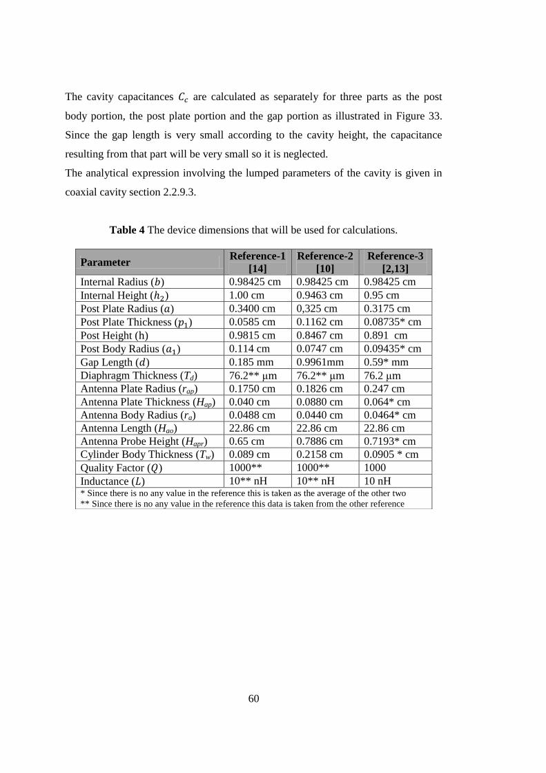
60
The cavity capacitances are calculated as separately for three parts as the post
body portion, the post plate portion and the gap portion as illustrated in Figure 33.
Since the gap length is very small according to the cavity height, the capacitance
resulting from that part will be very small so it is neglected.
The analytical expression involving the lumped parameters of the cavity is given in
coaxial cavity section 2.2.9.3.
Table 4 The device dimensions that will be used for calculations.
Parameter Reference-1
[14]
Reference-2
[10]
Reference-3
[2,13]
Internal Radius ( ) 0.98425 cm 0.98425 cm 0.98425 cm
Internal Height ( ) 1.00 cm 0.9463 cm 0.95 cm
Post Plate Radius ( ) 0.3400 cm 0,325 cm 0.3175 cm
Post Plate Thickness ( ) 0.0585 cm 0.1162 cm 0.08735* cm
Post Height ( ) 0.9815 cm 0.8467 cm 0.891 cm
Post Body Radius ( ) 0.114 cm 0.0747 cm 0.09435* cm
Gap Length ( ) 0.185 mm 0.9961mm 0.59* mm
Diaphragm Thickness (Td) 76.2** 76.2** 76.2
Antenna Plate Radius (rap) 0.1750 cm 0.1826 cm 0.247 cm
Antenna Plate Thickness (Hap) 0.040 cm 0.0880 cm 0.064* cm
Antenna Body Radius (ra) 0.0488 cm 0.0440 cm 0.0464* cm
Antenna Length (Hao) 22.86 cm 22.86 cm 22.86 cm
Antenna Probe Height (Hapr) 0.65 cm 0.7886 cm 0.7193* cm
Cylinder Body Thickness (Tw) 0.089 cm 0.2158 cm 0.0905 * cm
Quality Factor ( ) 1000** 1000** 1000
Inductance ( ) 10** nH 10** nH 10 nH * Since there is no any value in the reference this is taken as the average of the other two
** Since there is no any value in the reference this data is taken from the other reference
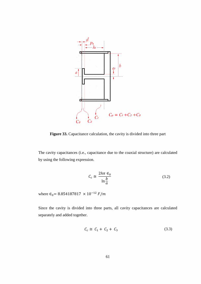
61
Figure 33. Capacitance calculation, the cavity is divided into three part
The cavity capacitances (i.e., capacitance due to the coaxial structure) are calculated
by using the following expression.
(3.2)
where
Since the cavity is divided into three parts, all cavity capacitances are calculated
separately and added together.
(3.3)

62
(3.4)
Since the central post discontinues at the gap region and the gap is very small the
capacitance corresponding to that part is neglected for simplicity.
The parallel plate capacitances created by the post plate and the diaphragm are
calculated by using the following expression.
(3.5)
The fringing field capacitances ( ) are calculated by using the following expression.
(3.6)
where is the empirical constant related with the a/b ratio[27,28]. For a/b ≤ 0.3,
.
Thus the total capacitance for the cavity is
(3.7)
The inductance values of the device are calculated for three parts and added together
to obtain the total inductance. The inductance corresponding to the gap region is also
neglected.
(3.8)
(3.9)
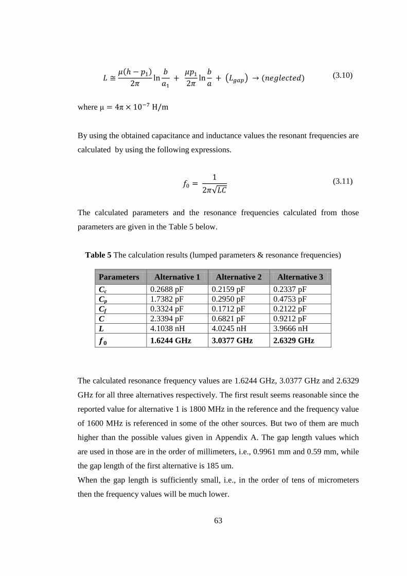
63
( ) (3.10)
where
By using the obtained capacitance and inductance values the resonant frequencies are
calculated by using the following expressions.
√ (3.11)
The calculated parameters and the resonance frequencies calculated from those
parameters are given in the Table 5 below.
Table 5 The calculation results (lumped parameters & resonance frequencies)
Parameters Alternative 1 Alternative 2 Alternative 3
Cc 0.2688 pF 0.2159 pF 0.2337 pF
Cp 1.7382 pF 0.2950 pF 0.4753 pF
Cf 0.3324 pF 0.1712 pF 0.2122 pF
C 2.3394 pF 0.6821 pF 0.9212 pF
L 4.1038 nH 4.0245 nH 3.9666 nH
1.6244 GHz 3.0377 GHz 2.6329 GHz
The calculated resonance frequency values are 1.6244 GHz, 3.0377 GHz and 2.6329
GHz for all three alternatives respectively. The first result seems reasonable since the
reported value for alternative 1 is 1800 MHz in the reference and the frequency value
of 1600 MHz is referenced in some of the other sources. But two of them are much
higher than the possible values given in Appendix A. The gap length values which
are used in those are in the order of millimeters, i.e., 0.9961 mm and 0.59 mm, while
the gap length of the first alternative is 185 um.
When the gap length is sufficiently small, i.e., in the order of tens of micrometers
then the frequency values will be much lower.
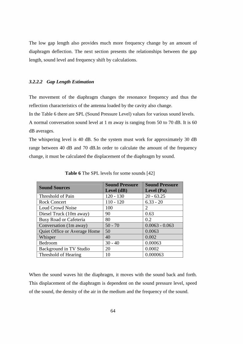
64
The low gap length also provides much more frequency change by an amount of
diaphragm deflection. The next section presents the relationships between the gap
length, sound level and frequency shift by calculations.
3.2.2.2 Gap Length Estimation
The movement of the diaphragm changes the resonance frequency and thus the
reflection characteristics of the antenna loaded by the cavity also change.
In the Table 6 there are SPL (Sound Pressure Level) values for various sound levels.
A normal conversation sound level at 1 m away is ranging from 50 to 70 dB. It is 60
dB averages.
The whispering level is 40 dB. So the system must work for approximately 30 dB
range between 40 dB and 70 dB.In order to calculate the amount of the frequency
change, it must be calculated the displacement of the diaphragm by sound.
Table 6 The SPL levels for some sounds [42]
Sound Sources Sound Pressure
Level (dB)
Sound Pressure
Level (Pa)
Threshold of Pain 120 - 130 20 - 63.25
Rock Concert 110 - 120 6.33 - 20
Loud Crowd Noise 100 2
Diesel Truck (10m away) 90 0.63
Busy Road or Cafeteria 80 0.2
Conversation (1m away) 50 - 70 0.0063 - 0.063
Quiet Office or Average Home 50 0.0063
Whisper 40 0.002
Bedroom 30 - 40 0.00063
Background in TV Studio 20 0.0002
Threshold of Hearing 10 0.000063
When the sound waves hit the diaphragm, it moves with the sound back and forth.
This displacement of the diaphragm is dependent on the sound pressure level, speed
of the sound, the density of the air in the medium and the frequency of the sound.

65
This relation is expressed as follows
(3.12)
where is the displacement of the air molecule in meter, is the pressure
amplitude of the acoustic wave in Pa (the maximum increase or decrease in
pressure), is the velocity of the sound (which is 346.13 m/s at 25oC), is the
density of the air in the medium (which is 1.184 kg/m3 at 25
oC) and is the
frequency of the sound (during normal conversations humans produce sounds from
80 Hz to about 8,000 Hz but the most normal speech occurs between 300 Hz and
3,000 Hz).
The maximum, minimum and average displacements of an air molecule by a speech
sound are calculated by using Eq. (3.12) and the parameters given in Table 6 above.
The maximum deflection is obtained from a 70 dB (0.063 Pa) and 300 Hz sound, the
minimum deflection is from a 50 dB (0.0063 Pa) and 3 kHz sound and average
deflection is from a 60 dB (0.02 Pa) and 1 kHz sound.
As it is seen on the results above, the displacements of the molecules are in the order
of nanometers. So the displacement of the diaphragm will be less than this amount
because of the stiffness of the membrane which is used as diaphragm.
There are two types of membranes, thick membranes and thin membranes [43]. A
membrane is called as thick when its maximum deflection (seen in the Figure 34)
is much smaller than its thickness and thin when the deflection is larger than the
thickness. In our case the thickness of the diaphragm is 76.2 and so the
deflections are much smaller than the thickness.

66
Thus the diaphragm of the device is a thick type membrane. In some source [8,50] it
is said about the diaphragm of the device that it is a metallic diaphragm and silver
plated thin copper sheet. So we can assume the diaphragm of the device is a circular
membrane of thin copper sheet.
Figure 34. Deflection of diaphragm
The deflection of a circular thick membrane with radius is described by the
following equation
(
)
(3.13)
For a thick circular membrane the maximum deflection is given as
(3.14)
where is the thickness of the membrane, is the Poisson's Ratio of the membrane
material (it is 0.33 for copper), is Young's Modulus for membrane material (it is
117 Gpa for copper) and is the pressure difference.
The maximum deflection amounts for maximum, minimum and average sound levels
(70 dB, 60 dB and 50 dB) are calculated by using Eq. (3.14) as follows.

67
The maximum deflection takes place in the middle point of the diaphragm and this
also coincides to the midpoint of the post plate. At the edge of the post plate, the
deflections for three alternatives are calculated by using Eq. (3.13) as follows
(3.15)
(3.16)
(3.17)
Thus the maximum edge deflections are
In order to calculate the capacitance difference due to the diaphragm deflection, we
will take the deflection as the average of the maximum deflection at the center of the
diaphragm and the deflection at the edge of the posts. Thus the deflection amounts
which will be used to calculate the capacitance differences are
The parallel plate capacitances for three alternatives when the deflection is maximum
are calculated by using Eq. (3.5) and the resonant frequency differences with these
capacitance values are calculated by using Eq. (2.37) and given in Table 7 below.

68
Table 7 The calculation results (parallel plate capacitances & resonance frequency
changes)
Parameters Alternative 1 Alternative 2 Alternative 3
(Deflected max.) 1.738151785050 pF 0.294959878516 pF 0.475264091393 pF
(Not deflected) 1.738139817170 pF 0.294959497446 pF 0.475263049598 pF
11.967880 aF 0.381070 aF 1.041795 aF
(Deflected max.) 1.62434872070 GHz 3.03775618727 GHz 2.63294888422 GHz
(Not Deflected) 1.62435287572 GHz 3.03775703587 GHz 2.63295037309 GHz
4.155 kHz 848 Hz 1.489 kHz
As it is seen on the frequency shift results, the deflections are extremely small
according to the gap length which is in the order of millimeters.
Since the first alternative has a very small (185 um) gap length, the frequency shift in
that case are so high than the other alternatives those have larger gap. So this result
shows that the gap length which is in the order of millimeter seems unreasonable for
the device.
In order to obtain higher frequency shift the gap length must be very small. When the
gap length is so small the parallel plate capacitance dominates over the other
capacitances, i.e., fringing field and cavity capacitances. Thus the change in gap
length affects the capacitance much more and thus the resonance frequency as well.
3.2.2.3 Quality factor of the Device
The quality factor of the device can be calculated by using the expression 2.42 for a
rough estimation.
(
(
)
) (3.18)
where is the sheet resistance.
69
(3.19)
where is the skin depth.
√ (3.20)
The device is said to be copper or brass and silver plated according to the references.
The copper and the brass are reasonable for such an application. In both case it is
silver plated so it will be used to silver parameters for conducting surface related
parameters. The conductivity of silver is S/m, resistivity is
Ω.m and the relative permeability is 0.99998.
The calculated resonant frequencies were 1.6244 GHz, 3.0377 GHz and 2.6329 GHz
so by using these frequency values the skin depth is calculated by using Eq. (3.20).
The skin depths for three alternatives are
The sheet resistances, by Eq. (3.19), are
Hence the unloaded quality factors, by Eq. (3.18), are
70
These Q factor values are higher than the value (1000) given in references [2,13].
The reason for obtaining the high Q value is that the formulation used here is valid
for a true coaxial cavity, i.e., the post has a uniform cylindrical shape. But in our case
the post has a mushroom shape and only the body diameter is used in calculation.
And the post plate and antenna probe sections are not taken into account. Since these
unaccounted portions have a negative effect on the quality factor by increasing the
surface area and decreasing the cavity volume, the actual values must be lower than
the calculated values for all alternatives.
The bandwidth of the device can be obtained from the Q value and the resonance
frequency value.
(3.21)
3.2.2.4 The Equivalent Circuit of the Structure
The equivalent circuit of the cavity resonator is given in Figure 35 below as a parallel
resonant circuit.
The cavity capacitance and the inductance values are calculated previously for three
alternatives of the cavity (Table 5). So the equivalent circuit of the device for three
alternatives can be calculated.

71
Figure 35. The equivalent circuit of the cavity resonator
The shunt resistances of the cavities are calculated by using the expression 2.45 as
follows.
(
)
(3.22)
Since the antenna is a quarter wave monopole, the antenna impedance can be
assumed as (36.5 + j21.25) . The antenna load impedance or the cavity input
impedances are
(3.23)

72
Thus the approximate equivalent circuit parameters are determined.
Table 8 The equivalent circuit parameters
Parameters Alternative 1 Alternative 2 Alternative 3
R (kΩ) 95.752 201.820 175.226
L (nH) 2.3394 pF 0.6821 pF 0.9212 pF
C (pF) 4.1038 nH 4.0245 nH 3.9666 nH
ZL (kΩ) 95.7500 - j0.3827 201.1583 - j11.5375 175.2216 - j0.8646
3.2.2.5 Modulation By The Structure
Figure 36. Equivalent circuit of the device expanded by a fictitious transmission
line
In order to express analytically the modulation process the equivalent circuit of the
device is redrawn in Figure 36. In the figure, the equivalent circuit is expanded by a
lossless transmission line to understand what happens within the circuit.

73
This transmission line is fictitious, i.e., it has zero length. The line is not inserted
between the antenna and the load or cavity, but between the real and imaginary part
of the antenna impedance. As the line length is set to zero, it has no influence on the
circuit behavior, but it helps for understanding. The characteristic impedance Z0 of
the line is equal to the real part of the antenna impedance [44].
The real part of the antenna impedance consists of the radiation resistance Rr and Rl
representing the antenna losses.
(3.24)
The available power received by a matched antenna can be written as
| |
(3.25)
Since the characteristic impedance of the line is the same with the antenna, the wave
a shown in Figure 36 has a relationship as
| | (3.26)
The reflected wave b at the right end of the line is then
| | | | (3.27)
where is the reflection coefficient at right end of the line.
(3.28)
The power reflecting from the load and entering into the antenna can be written as

74
| | (3.29)
The radiated power from the antenna
| | (3.30)
where is the antenna efficiency.
(3.31)
The radiated power is the power that reflecting from the antenna load and
reradiating through the antenna. This power does not contain the part which is
reflected by antenna structure.
The formulation so far is in the frequency domain. The signals are represented by
their complex amplitudes, i.e., no time dependence by definition. In order to obtain
the modulation expression, a transition into the time domain must be done.
Let the gap length of the device is a function of time as d(t). Then the capacitance of
the cavity and thus the impedance of the cavity is a function of time as ZL(t).
Eventually the reflection coefficient of the antenna load is a function of time as Γ(t).
| | (3.32)
where is the phase of the reflection coefficient.
The complex wave amplitudes a and b can be written in time domain as
{ } | | (3.33)
{ } | | (3.34)
75
By inserting Eq. (3.27) into Eq. (3.34) it is obtained that
| | (3.35)
where the wave a and its phase are constants.
The magnitude and phase of the reflected wave b change, because the reflection
coefficient changes. So the reflected wave b can be written as
(3.36)
This is a form of time varying signal whose amplitude and phase are function of
some other parameter, i.e., the gap length of the cavity. M(d) and m(d) show the gap
length dependency of the amplitude and the phase respectively.
Eq. (3.36) shows apparently that the reflected wave from the device is amplitude
modulation (AM) of the sound that changes the gap between the diaphragm and the
post and thus the loading of the antenna. Beside that the reflected signal is also phase
modulation (PM) of the sound.
3.2.2.6 Estimated Link Budget of the Device Operation
The operation of Theremin’s device is different from the conventional radio because
it involves two distinct links: power-up or forward link and the reverse or backscatter
link [45,46].
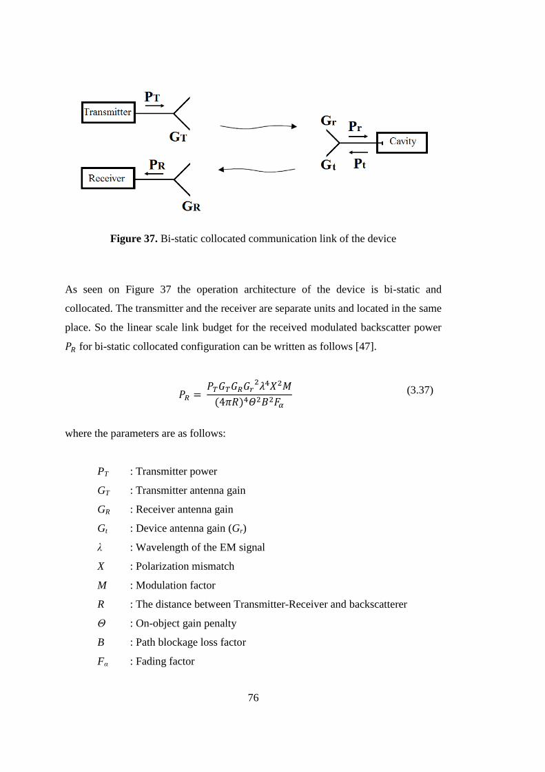
76
Figure 37. Bi-static collocated communication link of the device
As seen on Figure 37 the operation architecture of the device is bi-static and
collocated. The transmitter and the receiver are separate units and located in the same
place. So the linear scale link budget for the received modulated backscatter power
for bi-static collocated configuration can be written as follows [47].
(3.37)
where the parameters are as follows:
PT : Transmitter power
GT : Transmitter antenna gain
GR : Receiver antenna gain
Gt : Device antenna gain (Gr)
λ : Wavelength of the EM signal
X : Polarization mismatch
M : Modulation factor
R : The distance between Transmitter-Receiver and backscatterer
Θ : On-object gain penalty
B : Path blockage loss factor
Fα : Fading factor
77
Eq. (3.37) can be written in dB format as
(in dB)
Where represents the total losses, represents the forward link losses and
represents the backscatter (reverse) link losses.
Since Yagi-Uda antenna was invented in 1926 and it was used in World War II by
Soviets Radar Systems it can be assumed that a Yagi-Uda antenna with a moderate
gain of 13 dBi is used for both transmitter and the receiver for the device operation.
The quarter wave monopole antenna of the device is not an ideal one since it has not
a perfect ground. A perfect quarter wave monopole antenna has a 5 dBi gain ideally.
So the antenna gain of the device can be assumed to have a gain of 2 dBi
approximately as a degraded value.
A reasonable operational distance for the device is assumed to be 50 m and the
assumed frequency of operation is 330 MHz ( as most commonly cited value).
Corresponding wavelength of EM signal is about 90.91cm. So these parameters
correspond to a one-way free space loss of 56.8 dB.
The polarization mismatch X between the antennas may vary from 0 to 1 in a linear
scale. It accounts for the power lost due to polarization mismatch. It is not possible to
determine the exact value, since the antennas have unpredictable orientations with
respect to each other. So an average value of 0.5 can be assumed for the one-way
link. This means a 3 dB one-way loss of polarization mismatch.
The modulation factor M indicates the effects of changing load states to the
reflection. The changing load states change the reflection coefficient and so the
reflected power.

78
The reflection coefficient has a range from -1(Short) to +1 (Open) but in the case of
this study it can be assumed as a reasonable assumption that the reflection coefficient
range is ±0.5 to balance the backscattered and absorbed power by the cavity
resonator. The modulation factor is calculated for two different states of reflection
coefficient A and B as
(3.38)
So the assumption of ± 0.5 range corresponds to a modulation factor of 0.25 and
hence 6 dB loss.
The On-object gain penalty is a factor that accounts for the effects of the objects near
the antennas. These objects change the radiation characteristics of the antenna and so
the gain. It is defined as the ratio of actual gain to the gain changed by surrounding
objects. Practically this factor causes a loss of range 1 dB to 10 dB. So for our case it
can be assumed a moderate on-object gain penalty loss of 5dB.
Path blockages in a microwave link result in serious but surmountable losses in the
link budget. In these cases, the standard modeling techniques for path blockages in
conventional wireless systems is the log-normal distribution. In this model, the
distribution of possible aggregate blockage losses B can be modeled with the
following probability density function [48]:
√ [
] (3.39)
where b is the index of the probability density function, is the average value of
the aggregate blockage loss, and is its standard deviation, all with units of dB.
In the case of our study path blockage is caused mainly by the building and
environmental structures. The exact calculation of the path blockage loss is nearly
impossible. So it is suitable to use an approximate value. In the literature the path
blockage loss can be at a range of 0 to 30 dB depending on the specific conditions.
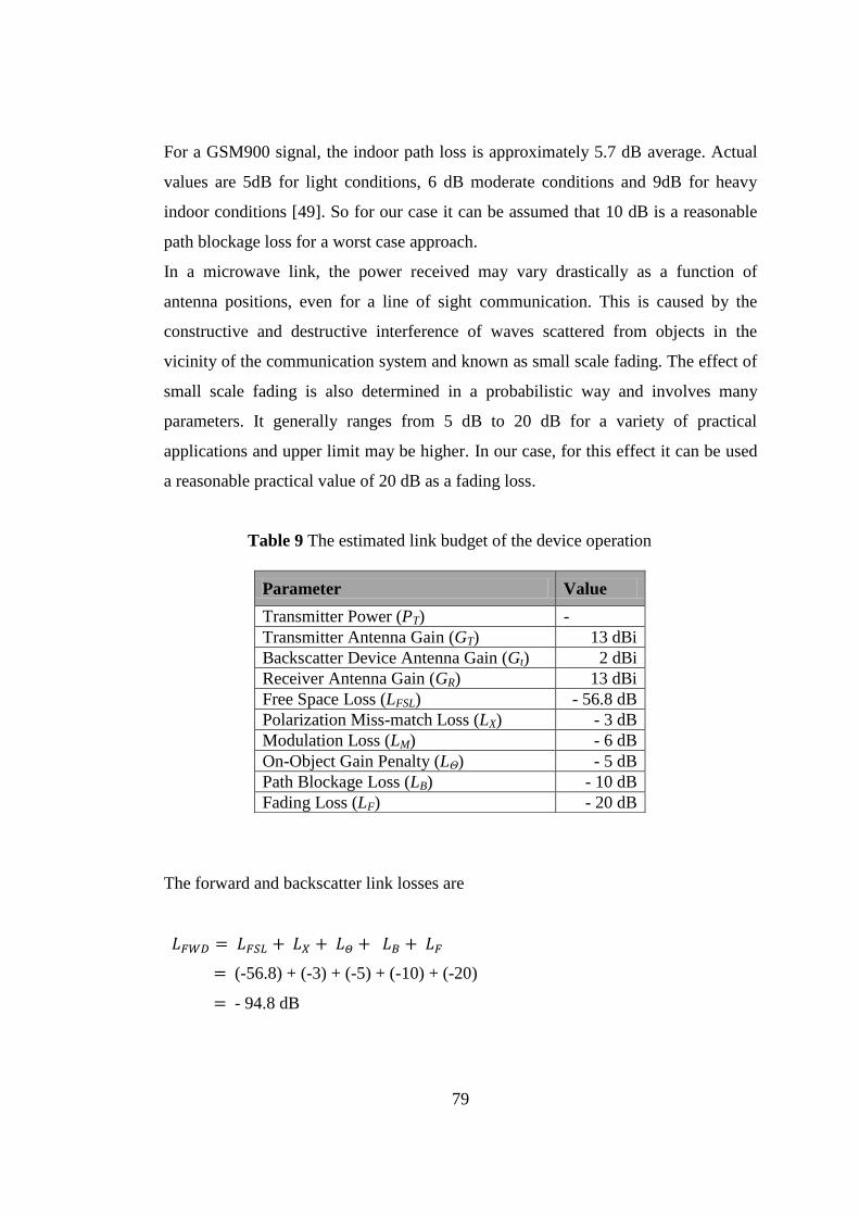
79
For a GSM900 signal, the indoor path loss is approximately 5.7 dB average. Actual
values are 5dB for light conditions, 6 dB moderate conditions and 9dB for heavy
indoor conditions [49]. So for our case it can be assumed that 10 dB is a reasonable
path blockage loss for a worst case approach.
In a microwave link, the power received may vary drastically as a function of
antenna positions, even for a line of sight communication. This is caused by the
constructive and destructive interference of waves scattered from objects in the
vicinity of the communication system and known as small scale fading. The effect of
small scale fading is also determined in a probabilistic way and involves many
parameters. It generally ranges from 5 dB to 20 dB for a variety of practical
applications and upper limit may be higher. In our case, for this effect it can be used
a reasonable practical value of 20 dB as a fading loss.
Table 9 The estimated link budget of the device operation
Parameter Value
Transmitter Power (PT) -
Transmitter Antenna Gain (GT) 13 dBi
Backscatter Device Antenna Gain (Gt) 2 dBi
Receiver Antenna Gain (GR) 13 dBi
Free Space Loss (LFSL) - 56.8 dB
Polarization Miss-match Loss (LX) - 3 dB
Modulation Loss (LM) - 6 dB
On-Object Gain Penalty (LΘ) - 5 dB
Path Blockage Loss (LB) - 10 dB
Fading Loss (LF) - 20 dB
The forward and backscatter link losses are
(-56.8) + (-3) + (-5) + (-10) + (-20)
- 94.8 dB

80
(-56.8) + (-3) + (-6) + (-5) + (-10) + (-20)
- 100.8 dB
The total received power
dB
In order to calculate the signal to noise ratio (SNR), first the noise floor is
determined. So the thermal noise is
(3.40)
where is Boltzman’s constant, T is the temperature of the
receiver system in Kelvin, that is assumed to be 300K and is the bandwidth.
For a sound receiving system must be at least twice the audio bandwidth of 3 kHz.
A typical noise figure (NFRec) of an AM radio receiver that was possible to be used
for the device can be assumed as a moderate value of about -20 dB.
So the SNR level of the receiver
dB
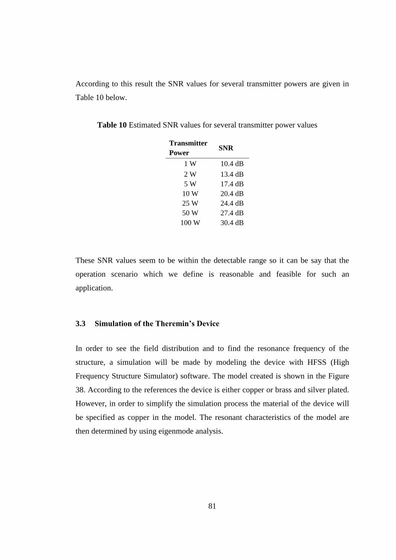
81
According to this result the SNR values for several transmitter powers are given in
Table 10 below.
Table 10 Estimated SNR values for several transmitter power values
Transmitter
Power SNR
1 W 10.4 dB
2 W 13.4 dB
5 W 17.4 dB
10 W 20.4 dB
25 W 24.4 dB
50 W 27.4 dB
100 W 30.4 dB
These SNR values seem to be within the detectable range so it can be say that the
operation scenario which we define is reasonable and feasible for such an
application.
3.3 Simulation of the Theremin’s Device
In order to see the field distribution and to find the resonance frequency of the
structure, a simulation will be made by modeling the device with HFSS (High
Frequency Structure Simulator) software. The model created is shown in the Figure
38. According to the references the device is either copper or brass and silver plated.
However, in order to simplify the simulation process the material of the device will
be specified as copper in the model. The resonant characteristics of the model are
then determined by using eigenmode analysis.
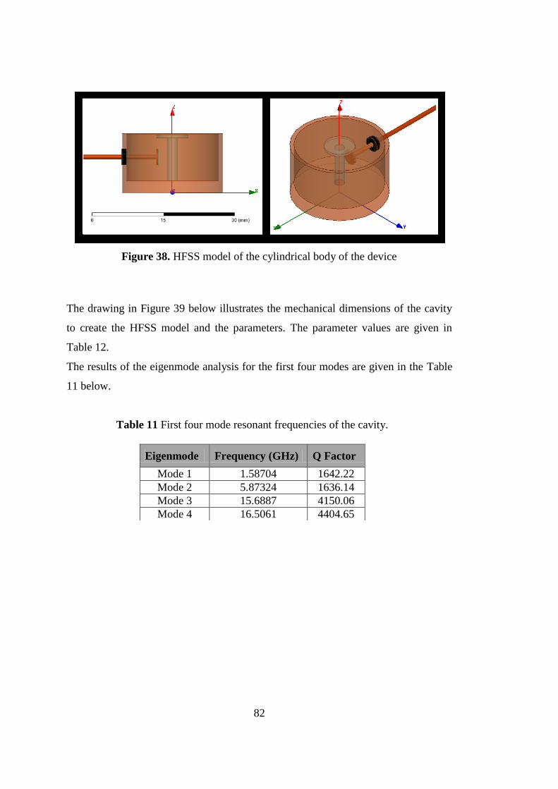
82
Figure 38. HFSS model of the cylindrical body of the device
The drawing in Figure 39 below illustrates the mechanical dimensions of the cavity
to create the HFSS model and the parameters. The parameter values are given in
Table 12.
The results of the eigenmode analysis for the first four modes are given in the Table
11 below.
Table 11 First four mode resonant frequencies of the cavity.
Eigenmode Frequency (GHz) Q Factor
Mode 1 1.58704 1642.22
Mode 2 5.87324 1636.14
Mode 3 15.6887 4150.06
Mode 4 16.5061 4404.65
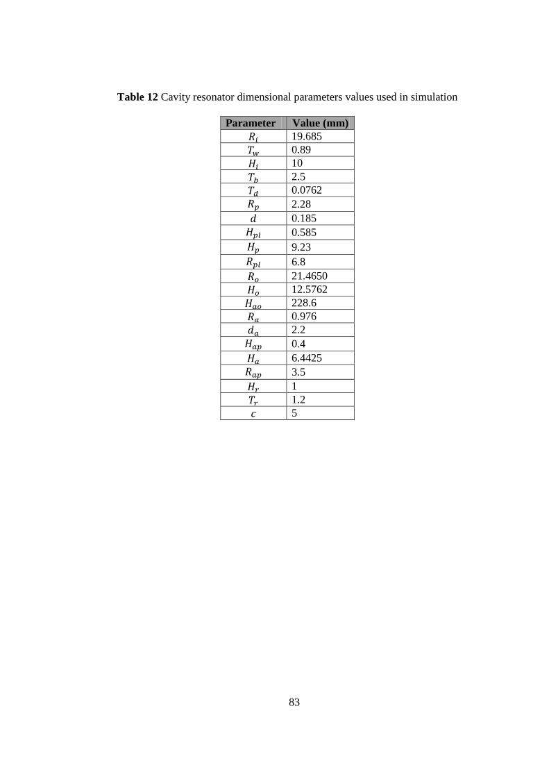
83
Table 12 Cavity resonator dimensional parameters values used in simulation
Parameter Value (mm)
19.685
0.89
10
2.5
0.0762
2.28
0.185
0.585
9.23
6.8
21.4650
12.5762
228.6
0.976
2.2
0.4
6.4425
3.5
1
1.2
5

84
Figure 39. Cavity resonator mechanical structure and dimensional parameters
These results indicate that the higher mode resonant frequencies are too high.
However, the resonant frequency value of the first mode seems reasonable for the
device. In addition, it can be seen on the Figure 40 that since nearly all electric fields
are confined in the gap, the first mode couples strongly to the diaphragm and so
should be very sensitive to the gap width between the post and the diaphragm. A
diaphragm movement or vibration induced acoustically causes the resonance
frequency to change significantly.
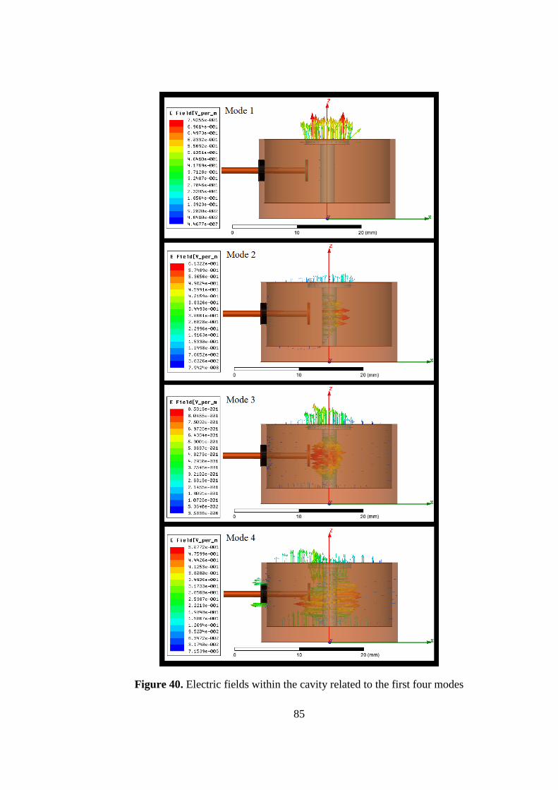
85
Figure 40. Electric fields within the cavity related to the first four modes
86
The resonance frequency of the device is also affected by the physical parameters of
the device. Some parameters affect much and some less. The graphical
representations of these dependencies are illustrated in the Figure 41.
As seen in the graphs in Figure 41 below, the parameter most affecting the resonance
frequency of the cavity is the gap width. The “f vs d” graph shows this relationship.
The parameter having the second major effect on the frequency is the diameter of the
post plate. The “f vs Rpl” graph shows this effect. The post plate width is directly
related with the parallel plate capacitance so as with the resonance frequency. The
internal diameter of the cavity is the parameter having minimal effect on the
frequency among the others in Figure 41. It has nearly no effect on the frequency.
The internal height of the cavity, as seen on the “f vs Hi” graph, slightly affects the
frequency. This effect is due to that any increase of the height provides more space
for magnetic fields and this causes an increase of the inductance and thus a decrease
in resonance frequency.
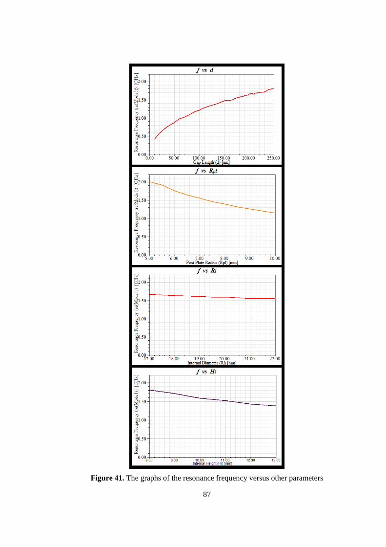
87
Figure 41. The graphs of the resonance frequency versus other parameters
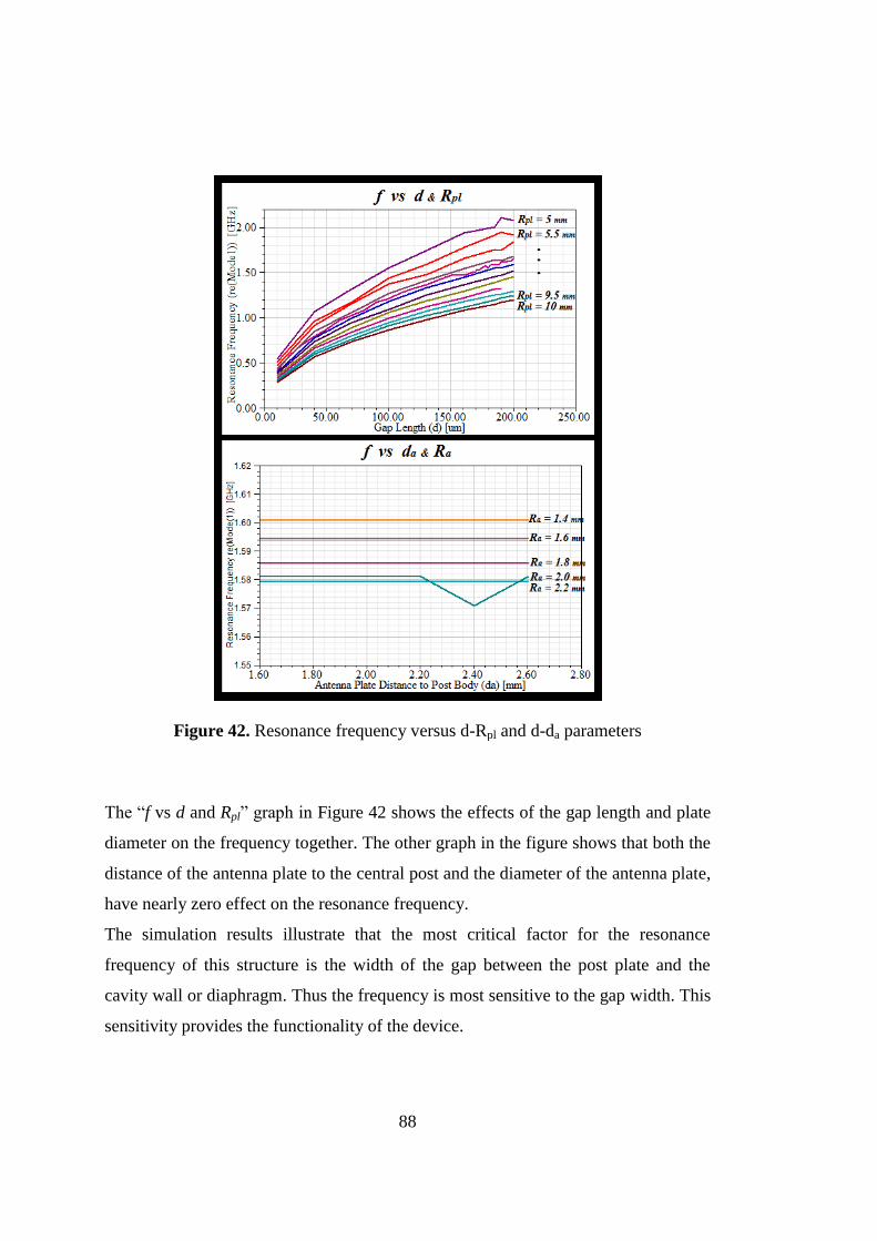
88
Figure 42. Resonance frequency versus d-Rpl and d-da parameters
The “f vs d and Rpl” graph in Figure 42 shows the effects of the gap length and plate
diameter on the frequency together. The other graph in the figure shows that both the
distance of the antenna plate to the central post and the diameter of the antenna plate,
have nearly zero effect on the resonance frequency.
The simulation results illustrate that the most critical factor for the resonance
frequency of this structure is the width of the gap between the post plate and the
cavity wall or diaphragm. Thus the frequency is most sensitive to the gap width. This
sensitivity provides the functionality of the device.

89
3.3.1 Sensitivity Analysis
A sensitivity analysis made for the resonant frequency of Mode 1 as a function of the
gap length and it is shown in Figure 43 for several gap length values.
(a)

90
(b)
Figure 43. Sensitivity graphs around several gap length values
The slopes in the graphs are given in terms of frequency by deflection in Table 13
below.

91
Table 13 Average sensitivities of the device for several gap lengths.
Gap Length Slope
185 m 4.31 MHz/ m
100 m 5.63 MHz/ m
50 m 8.35 MHz/ m
10 m 22.77 MHz/ m
As expected, while the gap length decreases the sensitivity of the cavity increases.
The reason for this effect is the increasing parallel plate capacitance. For a small gap,
the capacitance value will be greater and this greatness causes this capacitance to be
more dominant than the other capacitances (i.e., fringing fields and cavity
capacitances) in determining the resonant frequency. Thus any change in this
capacitance affects the resonance frequency much more. In the same manner when
the gap is small, the same amount of deflection in the diaphragm affects the
capacitance much more for small gap than the larger one. So the sensitivity is higher
for small gaps.
Figure 44. Conversion of diaphragm vibration into an AM modulated signal
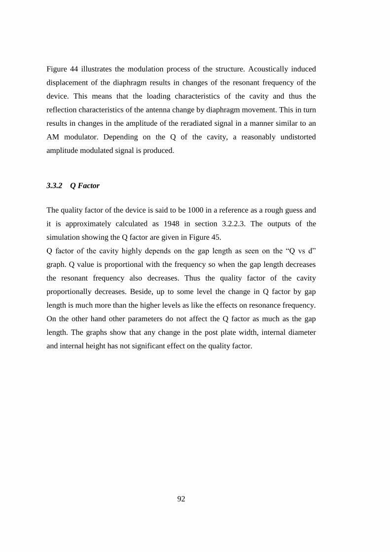
92
Figure 44 illustrates the modulation process of the structure. Acoustically induced
displacement of the diaphragm results in changes of the resonant frequency of the
device. This means that the loading characteristics of the cavity and thus the
reflection characteristics of the antenna change by diaphragm movement. This in turn
results in changes in the amplitude of the reradiated signal in a manner similar to an
AM modulator. Depending on the Q of the cavity, a reasonably undistorted
amplitude modulated signal is produced.
3.3.2 Q Factor
The quality factor of the device is said to be 1000 in a reference as a rough guess and
it is approximately calculated as 1948 in section 3.2.2.3. The outputs of the
simulation showing the Q factor are given in Figure 45.
Q factor of the cavity highly depends on the gap length as seen on the “Q vs d”
graph. Q value is proportional with the frequency so when the gap length decreases
the resonant frequency also decreases. Thus the quality factor of the cavity
proportionally decreases. Beside, up to some level the change in Q factor by gap
length is much more than the higher levels as like the effects on resonance frequency.
On the other hand other parameters do not affect the Q factor as much as the gap
length. The graphs show that any change in the post plate width, internal diameter
and internal height has not significant effect on the quality factor.
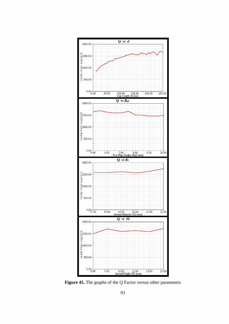
93
Figure 45. The graphs of the Q Factor versus other parameters
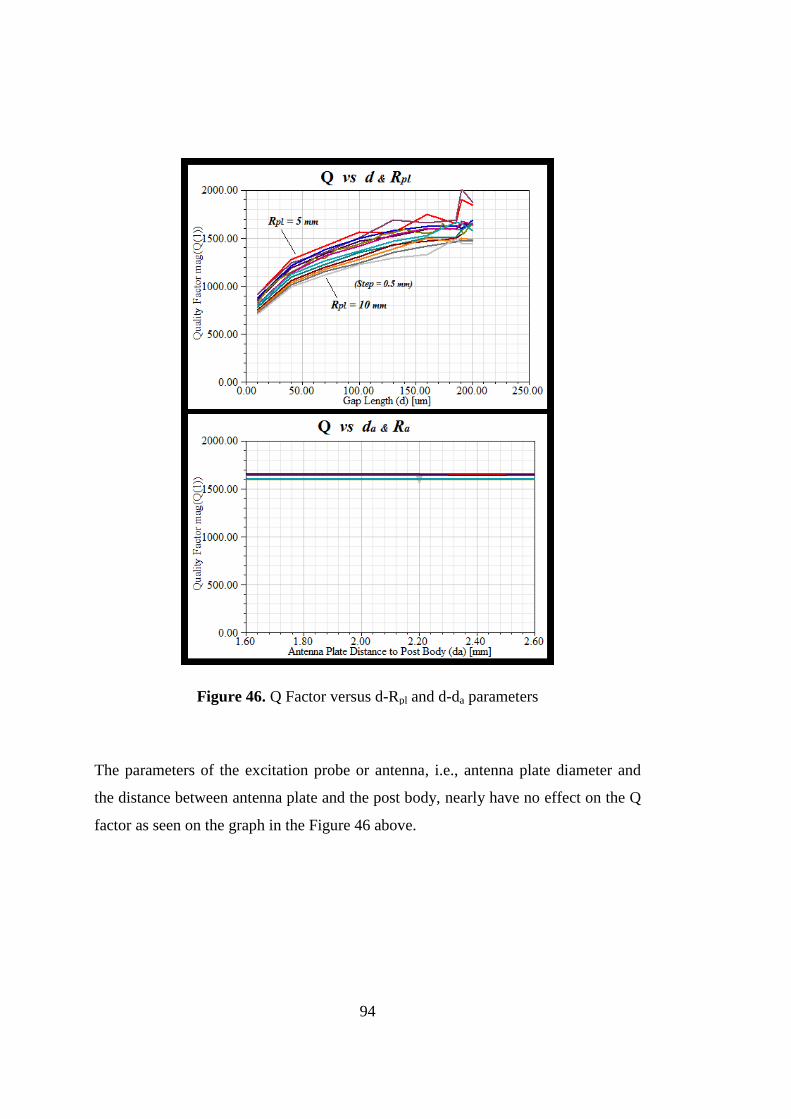
94
Figure 46. Q Factor versus d-Rpl and d-da parameters
The parameters of the excitation probe or antenna, i.e., antenna plate diameter and
the distance between antenna plate and the post body, nearly have no effect on the Q
factor as seen on the graph in the Figure 46 above.
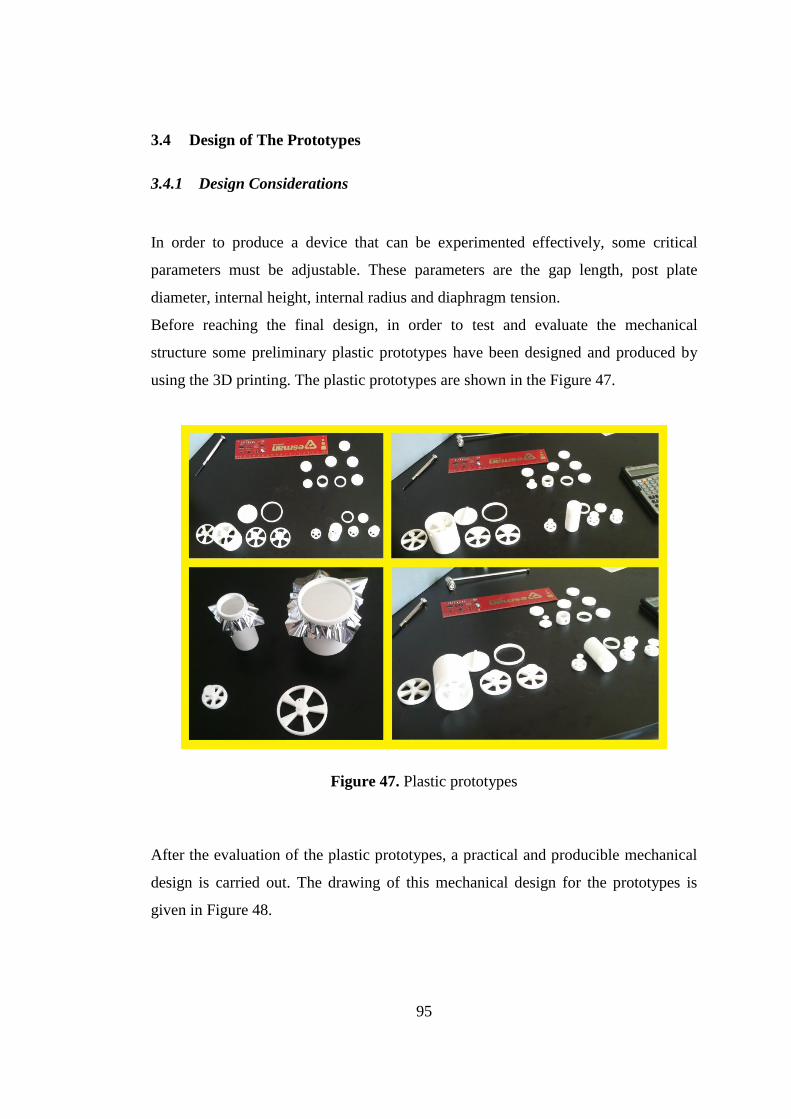
95
3.4 Design of The Prototypes
3.4.1 Design Considerations
In order to produce a device that can be experimented effectively, some critical
parameters must be adjustable. These parameters are the gap length, post plate
diameter, internal height, internal radius and diaphragm tension.
Before reaching the final design, in order to test and evaluate the mechanical
structure some preliminary plastic prototypes have been designed and produced by
using the 3D printing. The plastic prototypes are shown in the Figure 47.
Figure 47. Plastic prototypes
After the evaluation of the plastic prototypes, a practical and producible mechanical
design is carried out. The drawing of this mechanical design for the prototypes is
given in Figure 48.
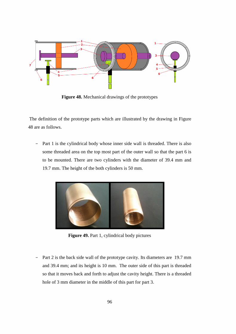
96
Figure 48. Mechanical drawings of the prototypes
The definition of the prototype parts which are illustrated by the drawing in Figure
48 are as follows.
- Part 1 is the cylindrical body whose inner side wall is threaded. There is also
some threaded area on the top most part of the outer wall so that the part 6 is
to be mounted. There are two cylinders with the diameter of 39.4 mm and
19.7 mm. The height of the both cylinders is 50 mm.
Figure 49. Part 1, cylindrical body pictures
- Part 2 is the back side wall of the prototype cavity. Its diameters are 19.7 mm
and 39.4 mm; and its height is 10 mm. The outer side of this part is threaded
so that it moves back and forth to adjust the cavity height. There is a threaded
hole of 3 mm diameter in the middle of this part for part 3.
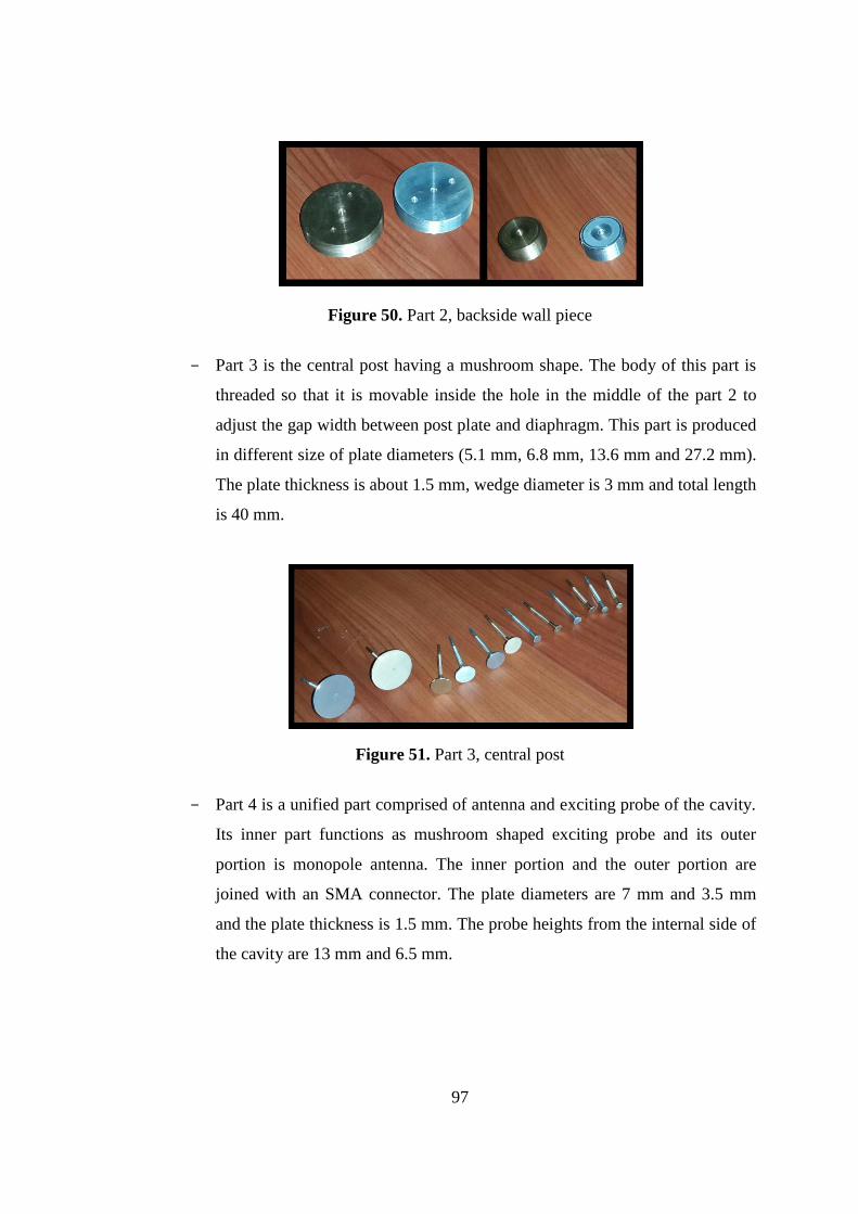
97
Figure 50. Part 2, backside wall piece
- Part 3 is the central post having a mushroom shape. The body of this part is
threaded so that it is movable inside the hole in the middle of the part 2 to
adjust the gap width between post plate and diaphragm. This part is produced
in different size of plate diameters (5.1 mm, 6.8 mm, 13.6 mm and 27.2 mm).
The plate thickness is about 1.5 mm, wedge diameter is 3 mm and total length
is 40 mm.
Figure 51. Part 3, central post
- Part 4 is a unified part comprised of antenna and exciting probe of the cavity.
Its inner part functions as mushroom shaped exciting probe and its outer
portion is monopole antenna. The inner portion and the outer portion are
joined with an SMA connector. The plate diameters are 7 mm and 3.5 mm
and the plate thickness is 1.5 mm. The probe heights from the internal side of
the cavity are 13 mm and 6.5 mm.

98
Figure 52. Part 4, unified antenna and exciting probe and part 5, SMA connector
- Part 5 is the SMA connector which connects the antenna and probe portion of
part 4.
- Part 6 is a two-piece ring structure which holds the diaphragm between its
pieces with screws. The inner side of one piece is threaded so that it is
screwed to the part 1. This part and the diaphragm constitute the front wall of
the prototype cavity. As tightening this part the diaphragm will be stretched
more and vice versa.
Figure 53. Part 6, diaphragm holding rings and part 7, diaphragm
- Part 7 is the diaphragm. It is aluminum metallized PET (Polyethylene
terephthalate) film of 8 m thickness.
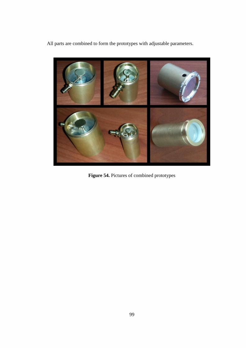
99
All parts are combined to form the prototypes with adjustable parameters.
Figure 54. Pictures of combined prototypes
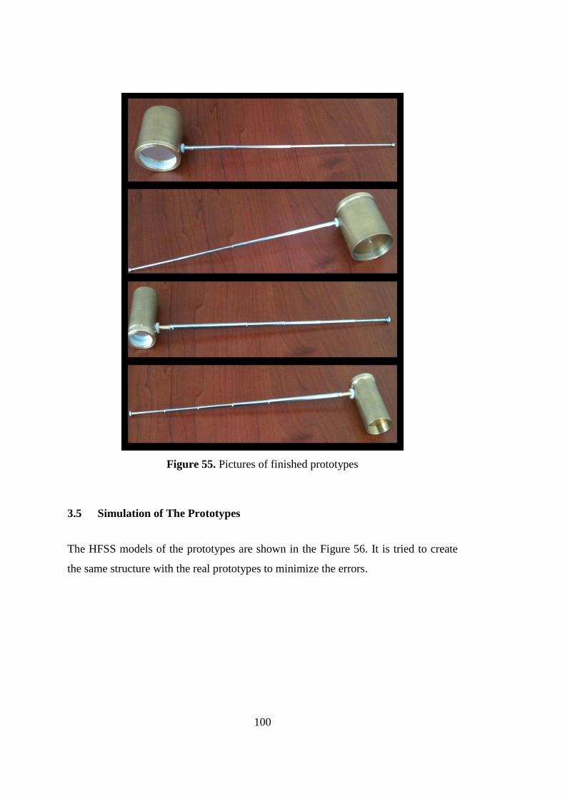
100
Figure 55. Pictures of finished prototypes
3.5 Simulation of The Prototypes
The HFSS models of the prototypes are shown in the Figure 56. It is tried to create
the same structure with the real prototypes to minimize the errors.

101
Figure 56. HFSS models of the prototypes
The Resonant frequencies of the Prototype 1 according to the post plate diameter and
the internal height are shown in the Table 14.
Table 14 Resonance frequencies (eigenmodes) of the four modes (GHz).
Parameters Eigenmode 1 Eigenmode 2 Eigenmode 3 Eigenmode 4
Rpl = 6.8 mm
Hi = 15 mm 1.20523 3.17656 7.78847 9.41907
Rpl = 13.6 mm
Hi = 15 mm 0.665523 3.14251 7.68333 9.39631
Rpl = 27.2 mm
Hi = 15 mm 0.358906 3.12828 6.16415 6.19979
Rpl = 6.8 mm
Hi = 20 mm 0.999673 3.01526 7.72283 7.99985
Rpl = 13.6 mm
Hi = 20 mm 0.577300 3.06320 7.68929 8.01734
Rpl = 27.2 mm
Hi = 20 mm 0.307008 3.01098 6.15254 6.17625
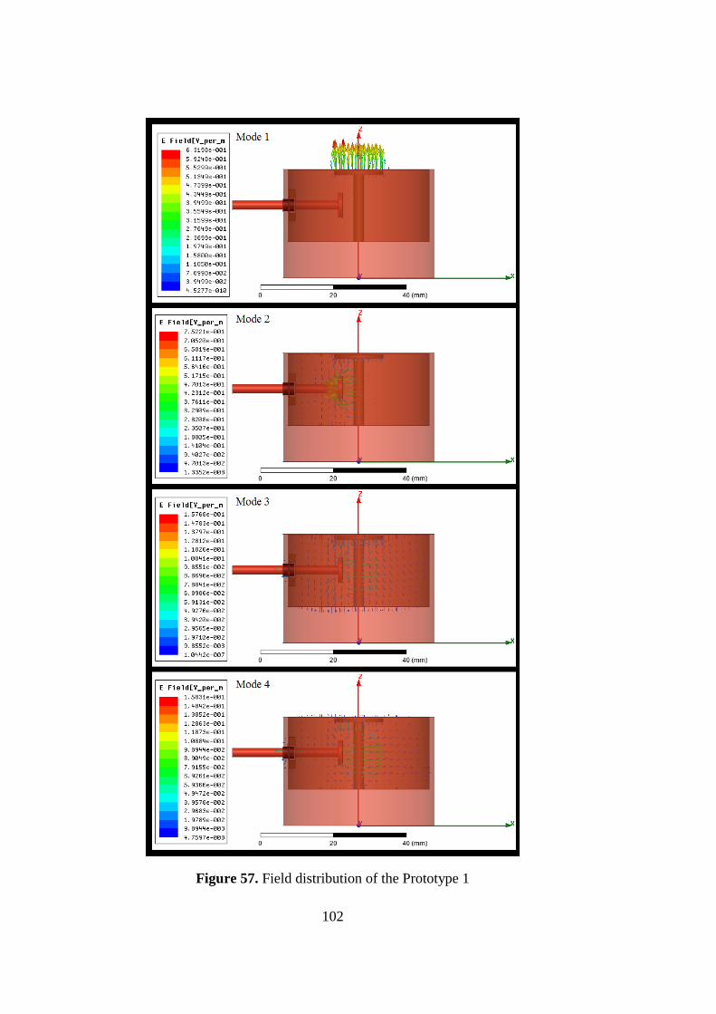
102
Figure 57. Field distribution of the Prototype 1

103
The results in Table 14 shows that higher mode resonant frequencies are too high as
like the results of the device. However, the resonant frequency values of the first
modes are relatively lower.
As in the device model, nearly all electric fields are confined in the gap region as
seen on the Figure 57. So the first mode is very sensitive to a change in the gap
width.
The Figure 58 below shows that the electric fields inside the Prototype 2. For the first
mode the electric fields are accumulated in the gap region. For the third and fourth
mode the electric fields are also greatly accumulated in the gap region. But since
some amounts of the fields are in other region, the effect of the gap on the resonance
frequency is degraded according to first mode for which all fields confined in the gap
region.
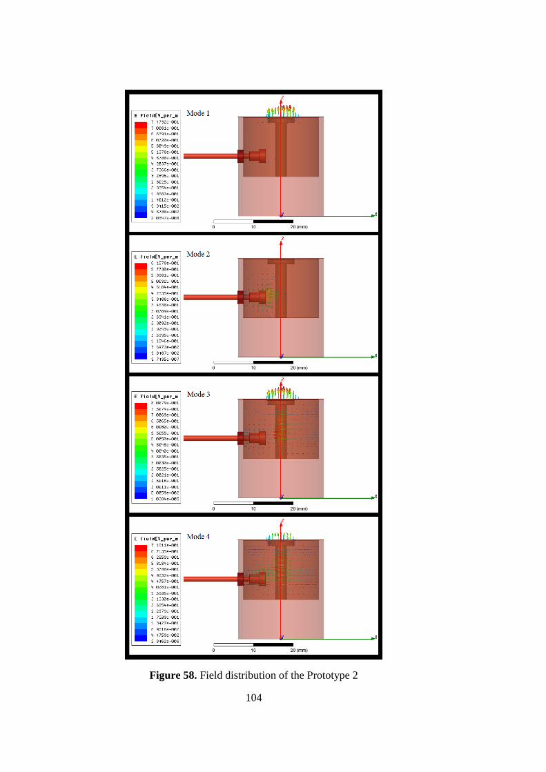
104
Figure 58. Field distribution of the Prototype 2
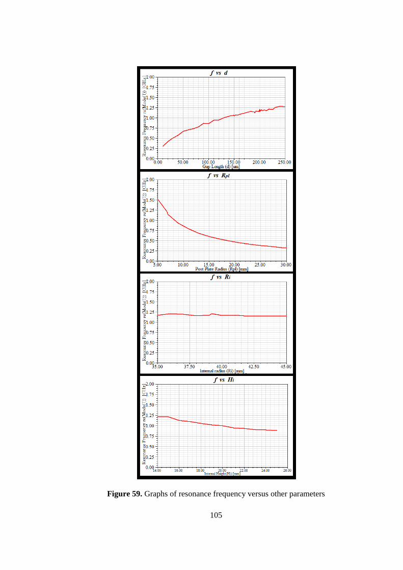
105
Figure 59. Graphs of resonance frequency versus other parameters

106
The Figure 59 shows the relationship between the resonance frequency and the
dimensional parameters of the Prototype 1. As seen in the figure, the parameter most
affecting the resonance frequency of the cavity is the gap width and subsequently the
diameter of the post plate. All the graphs are very similar to the device graphs.
Figure 60. Resonance frequency versus d-Rpl and da-Ra parameters
The first graph in Figure 60 shows the effects of the gap length and plate diameter.
The second graph shows the effects of both the distance of the antenna plate to the
post and the diameter of the antenna plate on the resonance frequency together.
Antenna plate and the space between antenna plate and post have nearly zero effect
on the resonance frequency.
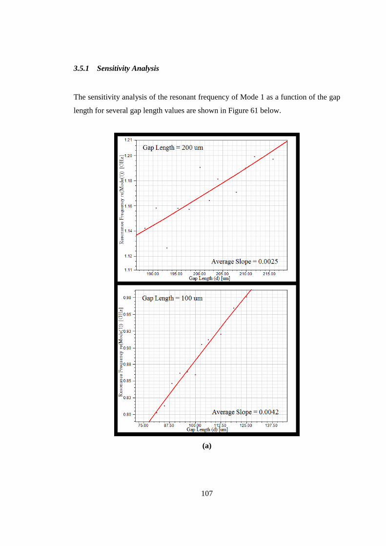
107
3.5.1 Sensitivity Analysis
The sensitivity analysis of the resonant frequency of Mode 1 as a function of the gap
length for several gap length values are shown in Figure 61 below.
(a)

108
(b)
Figure 61. Sensitivity graphs of Prototype 1 for several gap length
The slopes in the graphs are given in terms of frequency by deflection in Table 15
below.

109
Table 15 Sensitivity of Prototype 1 for several gap lengths.
Gap Length Slope
200 m 2.5 MHz/ m
100 m 4.2 MHz/ m
50 m 6.5 MHz/ m
10 m 15.0 MHz/ m
As in the case of the device analysis and as expected, while the gap length decreasing
the sensitivity of the cavity increases.
3.5.2 Q Factor
The quality factor graphs of the Prototype 1 are given in the Figure 62 and Figure 63
below. Graphs show the relationship between the Q factor and the dimensional
parameters of the prototype.
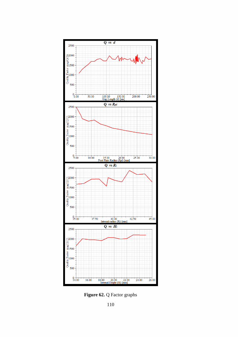
110
Figure 62. Q Factor graphs

111
Figure 63. Q Factor versus d – Rpl and da – Ra graphs
The quality factor graphs of the Prototype 1 are given in the Figure 62 and Figure 63
below. Graphs show the relationship between the Q factor and the dimensional
parameters of the prototype.

112
113
CHAPTER 4
PROTOTYPE MEASUREMENTS AND EXPERIMENTS
In this chapter the experiments performed are described. These are the proof of the
concept experiment, resonance frequency measurements and the sound receive
experiments.
4.1 Proof of The Concept
Before designing a replica of the Theremin’s device, the concept of backscattering
from an antenna by load modulation is proved with a capacitor loaded dipole antenna
as a concept. In order to do such an experiment a backscattering dipole antenna
loaded with a varactor diode and a simple peak detector circuit for detecting the
modulated backscatter wave are designed and implemented.
The experiment setup is illustrated in the Figure 64. An RF carrier signal of 13 dBm
and 450 MHz is produced by the RF signal generator. A sine signal from 0.5 kHz to
4 kHz and 5 Vpp is applied to the varactor diode by a waveform generator connected
to the dipole antenna. Thus the load capacitance of the reflector antenna changes by
the applied waveform signal. And this waveform is detected by the simple detector
circuit, which is shown in Figure 65.
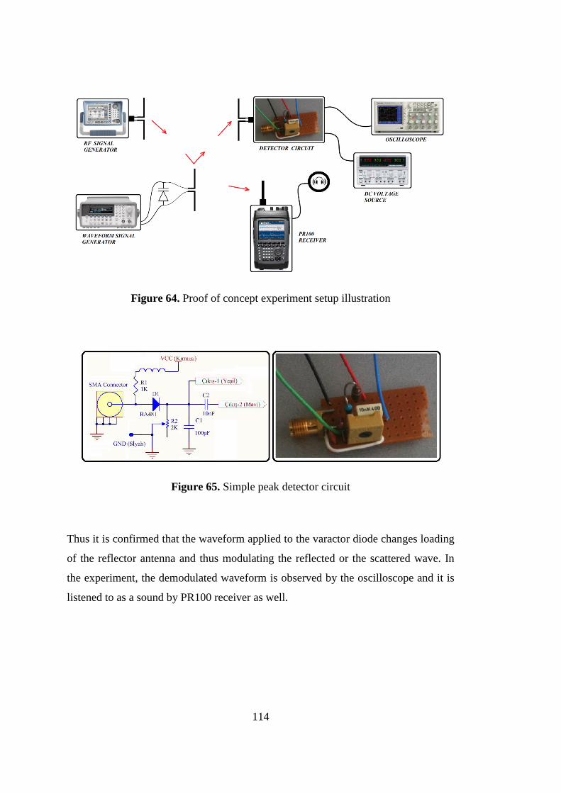
114
Figure 64. Proof of concept experiment setup illustration
Figure 65. Simple peak detector circuit
Thus it is confirmed that the waveform applied to the varactor diode changes loading
of the reflector antenna and thus modulating the reflected or the scattered wave. In
the experiment, the demodulated waveform is observed by the oscilloscope and it is
listened to as a sound by PR100 receiver as well.
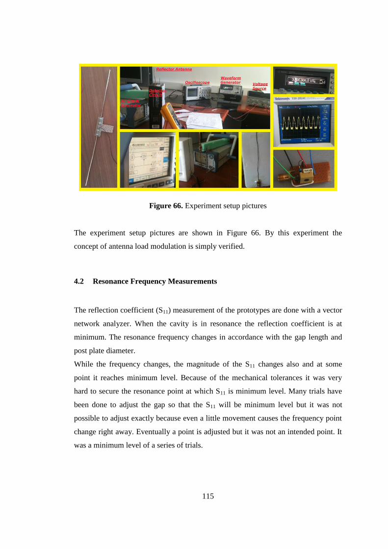
115
Figure 66. Experiment setup pictures
The experiment setup pictures are shown in Figure 66. By this experiment the
concept of antenna load modulation is simply verified.
4.2 Resonance Frequency Measurements
The reflection coefficient (S11) measurement of the prototypes are done with a vector
network analyzer. When the cavity is in resonance the reflection coefficient is at
minimum. The resonance frequency changes in accordance with the gap length and
post plate diameter.
While the frequency changes, the magnitude of the S11 changes also and at some
point it reaches minimum level. Because of the mechanical tolerances it was very
hard to secure the resonance point at which S11 is minimum level. Many trials have
been done to adjust the gap so that the S11 will be minimum level but it was not
possible to adjust exactly because even a little movement causes the frequency point
change right away. Eventually a point is adjusted but it was not an intended point. It
was a minimum level of a series of trials.

116
Figure 67. Resonance frequency measurement of prototypes
At some gap length value and post plate diameter it is measured and recorded the
resonance frequencies for both prototypes. These results are given in Figure 68 as a
graph by comparatively with the simulation results.
As seen in Figure 68 and Figure 69 below the measurement results and the
simulation results are consistent at some degree. Small differences are caused by the
mechanical tolerances, measurement errors and the modeling errors. The machining
errors of the prototypes are at least in the orders of several tens of micrometers which
cause significant changes in resonance frequencies. The length measurements are
done with a caliper so the caliper tolerances and the reading errors also cause some
disparity. And the HFSS models created for the prototypes are tried to be made

117
exactly the same with the prototypes but because of the design limitation and
capability, minor differences would exist which also affects the results.
(a)

118
(b)
Figure 68. Comparison of measurement and simulation results for Prototype-1
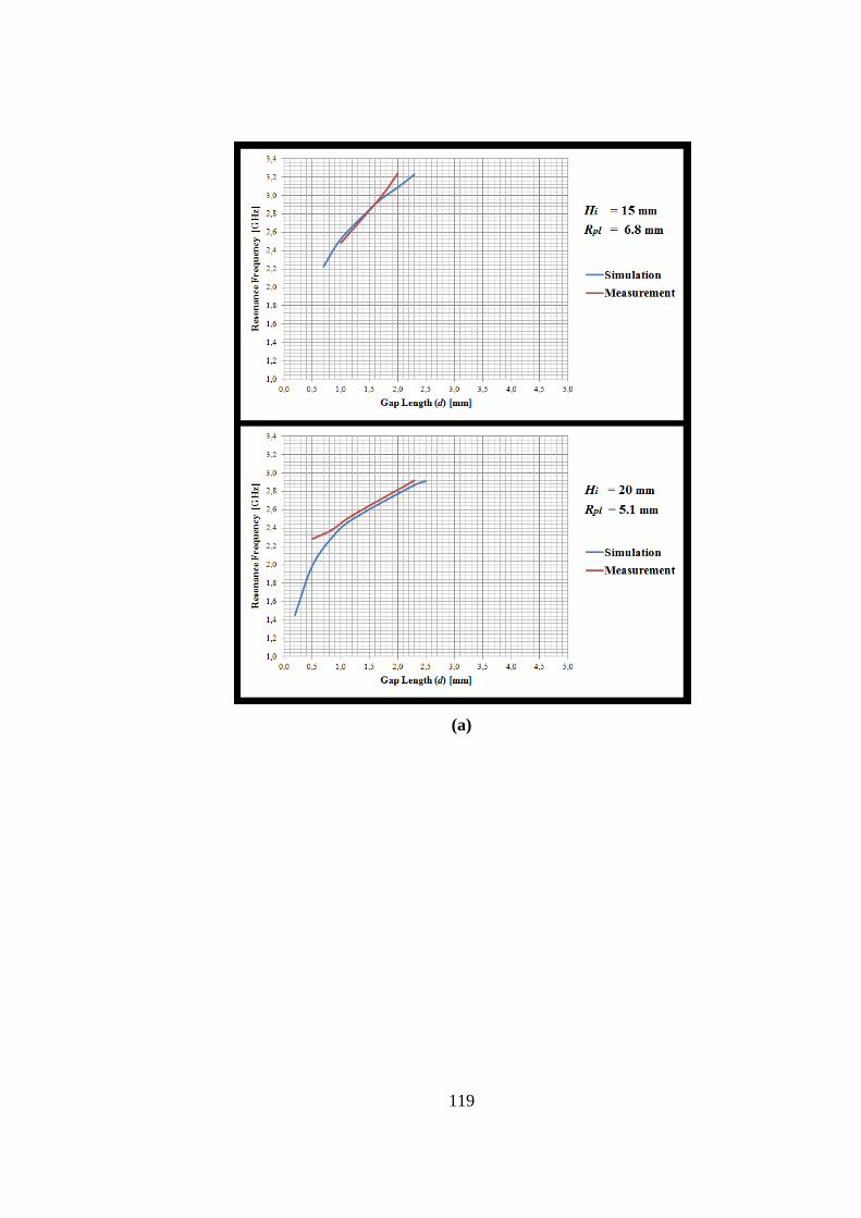
119
(a)
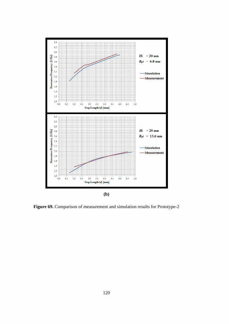
120
(b)
Figure 69. Comparison of measurement and simulation results for Prototype-2

121
4.3 Sound Receive Experiments
Figure 70. Sound receive experiment setup illustration
The sound receive experiment set up is illustrated in the Figure 70. Before the
experiment the determination process of the resonance frequency is performed. In
order to adjust the resonance frequency to a value that gives the minimum reflection
coefficient a serious efforts were exerted. After many trials the resonance frequency
of the prototype was adjusted to the 1.76 GHz eventually and in order to keep this
adjustment unchanged the prototype parts were fixed in proper way carefully.

122
Figure 71. Sound receive experiment setup
A carrier wave is formed as a sine signal with frequency of 1.76 GHz and the
amplitude of 13 dBm (maximum amplitude value of the RF generator) was produced
by SM300 RF signal generator and transmitted. The prototype cavity resonator was
positioned at a distance of about 30 cm from the transmitting antenna of the RF
generator. At a distance of approximately 20 cm a speaker was placed towards to the
diaphragm side of the cavity resonator prototype. PR100 spectrum analyzer which is
capable of AM demodulation and voice recording was used for reception of the
scattered signal from the prototype.
The noise floor in the environment of the experiment is about -120 dBm. And the
signal level measured with the receiver approximately 1m away from the RF signal
generator is about -30 dBm.
123
Hence the SNR value of the received signal is approximately 90 dB. This is for the
total received wave (i.e., the carrier wave and the scattered wave).
When we produce a sine tone with the speaker at the resonance frequency of the
diaphragm (i.e., mechanical resonance of the stretched diaphragm) then it can be
seen and measured the shifted frequency signals on the receiver. The strong vibration
of the diaphragm by a single tone sound causes a clear shift in the frequency of the
backscattered signal. The received level of this signal at shifted frequency is
approximately -55 dBm. So SNR of the backscattered signal by the prototype is
about 65 dB.
The sound produced by the speaker is received by PR100 spectrum analyzer at the
same frequency by AM Modulation. The received sound was a bit noisy and low.
But it was intelligible and understood well. When one of the speaker, the prototype
or the receiver was removed away from the others then the received voice weakened
and at some distance it was totally gone. The voice was received from the distance
up to 1 m away by the analyzer but beyond that it was so much weakened that there
was nearly no voice understood. In the experiment the maximum distance the voice
is received is 10 m but it was with very loud sound and not sustainable and
repeatable.
The experiments are repeated for several sounds like different kinds of music having
different frequency content and sound style, live speaking and recorded speech.
Although AM demodulation is used for the perception of the sound in the
experiment, it is observed that the sound is also obtained by using FM demodulation.
But the sound obtained by FM demodulation is distorted.
4.3.1 The Obtained Sound
The first graph in Figure 72 belongs to the original sound which is a record of a
woman speech played in the test environment, the second graph shows the sound
received by using the cavity resonator prototype and the third graph shows the
filtered version of the received sound.

124
Figure 72. The sound received by the prototype
The sound obtained by the cavity resonator is a bit noisy and this noise reduces the
sound quality and voice clarity. But still the speech in the record is understandable.
The filtering improves the intelligibility of the sound.
All the audio files which are the original sounds used for the experiment, recorded
sounds by the cavity resonator, filtered and amplified version of those are given in
Appendix B.

125
Figure 73. The sound spectrums

126
Figure 73 shows the frequency content of the sounds. First graph belongs to the
original sound, second belongs to the record made by cavity resonator and the third
one is the graph of the filtered version of the record. The sound obtained from the
cavity contains noise spread across all frequencies but it has additional content
especially in low frequency region.
The filtered sound is better than the original received sound in terms of intelligibility
although it has some deterioration because of the filtering process.
The filtering process has been performed by Adobe Audition 3.0 and the applied
filtering process contains the following transactions.
- Repair DC Offset
- Speech Volume Leveler
- Adaptive Noise Reduction
- Vocal Enhancer
These processes filter the excess noise that distort intelligibility of the sound and
enhances the speech clarity thus make the recorded speech more understandable.
4.3.2 Link Budget of the Experiment
The sound receive experiment setup has an architecture of bi-static dislocated
backscatter communication link, because the transmitter and the receiver are separate
units and located in different places. It is illustrated by a drawing in Figure 74.

127
Figure 74. Bi-static dislocated communication link of the experiment
The linear scale link budget for the received modulated backscatter power can be
written as
(4.1)
where f subscripts denote the forward link parameter and b subscripts denote the
backscatter (reverse) link parameters [47].
The parameters in the expression are
PR : Received power
PT : Transmitter power
GT : Transmitter antenna gain
GR : Receiver antenna gain
Gt : Prototype antenna gain (Gr)
λ : Wavelength of the EM signal

128
Xf : Forward link polarization mismatch
Xb : Backscatter link polarization mismatch
M : Modulation factor
Rf : Forward link distance
Rb : Backscatter link distance
Θ : On-object gain penalty
Bf : Forward link path blockage loss factor
Bb : Backscatter link path blockage loss factor
Fα : Fading factor
Transition of Eq. (4.1) to the dB format is as follows
(in dB)
where LFWD represents the forward link losses and LBACK represents the backscatter
(reverse) link losses.
The RF signal transmitter output power is 13 dBm and it has a BNC right angle
monopole antenna with approximate gain of 3 dBi. The prototype has a monopole
antenna with an approximate gain of 2 dBi. The forward link and the backscatter link
distances are about 30 cm. The receiver antenna has gain of 5 dBi. Since all three
antennas are aligned there is no polarization miss-match loss. Also, since all antennas
are in line of sight and there were no object near the antennas which can negatively
affects the antennas there are no on-object gain penalty and path blockage loss. A
moderate 10 dB fading loss and 6dB modulation loss are assumed.

129
Table 16 Estimated link budget parameters of the sound receive experiment
Parameter Value
Transmitter Power (PT) 13 dBm (-17 dB)
Transmitter Antenna Gain (GT) 3 dBi
Backscatter Device Antenna Gain (Gr) 2 dBi
Receiver Antenna Gain (GR) 5 dBi
Free Space Loss (LFSL) -
Polarization Miss-match Loss (LX) 0 dB
Modulation Loss (LM) - 6 dB
On-Object Loss Gain Penalty Loss (LΘ) 0 dB
Path Blockage Loss (LB) 0 dB
Fading Loss (LF) - 20 dB
The forward and backscatter link losses are
+ (0) + (0) + (0) + (-20)
The total received power

130
So the SNR level at the receiver
According to this result, the SNR values for several distances are given in Table 17.
Table 17 Approximately calculated SNR values for several distances
Distance SNR
10 cm 110.3 dB
20 cm 98.3 dB
30 cm 91.2 dB
50 cm 82.3 dB
1 m 70.3 dB
2 m 58.3 dB
5 m 42.3 dB
10 m 30.3 dB
50 m 2.3 dB

131
CHAPTER 5
SUMMARY AND CONCLUSION
In this chapter there are three parts. The summary section provides an overview of
the thesis. The conclusion section contains the results of the work and inferences
obtained from the study. The final section lists suggestions for future work and
further studies.
5.1 Summary
This study investigated the passive cavity resonator structure renowned as
“Theremin’s Device” or “Great Seal Bug” in detail in order to explore the working
principle and technical aspects of the device beyond the rumors and hearsays. The
main goal of the work presented in this thesis focused on understanding the structure,
theoretically explaining the principles of operation and implementation of a similar
structure.
In the first chapter of the thesis, a short story of the device is given and mentioned
the motivation aspects and objectives of the study. Besides, some general properties
of the topic device are presented and given the organizational structure of the thesis.
In the second chapter of the thesis, the theoretical background information necessary
for the study is explained. This includes roughly the topics of resonance and
resonators, microwave cavities and features, antennas and the backscatter wave
techniques.
The third chapter includes main works performed for this study. First, the theoretical
analysis of the device was carried out. Initially the physical structure of the device
was examined.

132
The lumped parameters, quality factor and the resonance frequency of the cavity
structure were calculated by using the values obtained from three different
references. Also the amount of diaphragm movement by a sound was calculated.
The equivalent circuit of the cavity was found. Modulation issue was formulated and
the link budget for the operation of the device was calculated.
After the theoretical analysis, the structure was modeled with the HFSS and
simulated with a wide variety of parameters. The eigenmode and field distribution
analysis of the structure were realized by simulation. Also sensitivity, quality factor
and parameter analysis of the device were performed. After the simulation of the
structure, two prototypes were designed and produced. Prototypes were also
simulated in the same manner.
The fourth chapter includes the work done for prototype measurements and
experiments. Firstly, in order to verify the concept of backscatter modulation a
simple experiment setup was prepared. A dipole antenna that is loaded with a
varactor diode and a simple AM detector circuit were used for proof of the concept
experiment. The resonance frequency measurements of the prototypes were realized
by using network analyzer. Later on the actual experiment setup was prepared with
the prototype. The ambient sound was gathered via the backscattering from the
cavity resonator prototype. The structure was thus successfully replicated and the
working theory and the operation concept of the device was verified. The sound
obtained was filtered, analyzed and compared with the original sound. Lastly the link
budget calculation of the experiment is done.
The fifth chapter, the last one, presents the summary and conclusions of the thesis. It
also mentions the future studies and research areas that can be studied further.
5.2 Conclusion
Theremin’s device being the predecessor of modulated backscatter wave
communication, RFID and microwave wireless sensor technologies was a covert spy
device.

133
It was invented by Leon Theremin who worked for Soviet secret service and it was
used for espionage. The device was found by American intelligence service CIA and
resolved by English service. So the device and its story are secret.
Because of this secrecy there is no exact and certain information about the technical
details and principle of operation. All the information about the device is consisted of
stories, tales and rumors. In the references having information about the device (all
information is given in Appendix A) there are many technical inconsistencies about
the device, working principle and technical details. So it is used the three references
as alternatives and the calculations and analysis are done according to those. And
since none of them has all parameters, the missing parameters of one are taken from
other two. Thus three alternatives are constituted. The calculated frequencies by
using these parameters are approximately 1.62 GHz for the first alternative, 3 GHz
for second and 2.63 GHz for the third one. The first result seems reasonable because
in some references the working frequency is said to be 1600 MHz. But still the other
alternatives may also be close to the original device by use of different measures
because the parameters or mechanical measures are approximate values. For
example, in some references the inductance of the device is said to be 10 nH but in
approximate calculations it is found as approximately 4 nH. And the gap length value
used is 185 um for the first alternative but there may be much less for a higher
sensitivity. So it is not possible to say an exact value for the working frequency. But
330 MHz, 800 MHz and 1600 MHz are all possible acceptable values. The quality
factor cited as an approximate value for the device in some references is 1000. The
calculated Q factor is 1948 so that Q factor seems also reasonable.
In the simulation results of the device, the resonant frequency is also approximately
1.6 GHz. This coincides with the calculation result. According to the graph in Figure
41 showing the relationship between the resonance frequency and the gap length, the
resonance frequency reduces as low as to 400 MHz. And the graph in Figure 42
shows that the resonance frequency can be as low as 300 MHz with the increasing
post plate diameter. In the case of the operating frequency of the device, this suggests
the possibility of 330 MHz which is said to be the working frequency of the device in
some references.

134
These graphs also show the significant effect of the gap length to the resonance
frequency.
The field analysis of the structure supports this effect. Nearly all the electric fields
are concentrated in the gap region. This concentration greatly increases the
sensitivity of the resonance frequency to the gap length because any small change in
the gap has a great effect on these fields. The sensitivity graphs (Figure 43 and
Figure 61) also show the degree of sensitivity for several gap length levels. In these
graphs it is seen that the sensitivity increases when the gap length decreases, i.e., the
sensitivity is inversely proportional to the gap length. This also coincides with the
calculations.
In the graphs (Figure 45, Figure 46, Figure 62, Figure 63) showing the relationship
between the quality factor and the gap length and other parameters it is seen that the
Q factor ranges from approximately from 800 to 1600. This is compatible with the
value of 1000 which is given in some references. Although the roughly calculated Q
factor value is 1948, since the post plate and the antenna portion are not taken into
account, the correct value must be lower than this. So it can be said that the Q factor
graphs are also compatible with theoretical calculations.
The graphs (Figure 41, Figure 42, Figure 59, Figure 60) showing the dependency of
the resonance frequency to the dimensional parameters show that the parameter
affecting the frequency most after the gap length is plate diameter. When the plate
diameter increases then the parallel plate capacitance increases and this increase in
capacitance causes a decrease in resonance frequency. The internal height and the
internal diameter have very little effect on the resonance frequency because the
major factor that determines the resonance frequency is the field distribution inside
the cavity and these dimensions have much less effect on the field distribution in this
structure. The relationships between the Q factor and the dimensional parameters are
nearly in the same manner with the resonance frequency. The gap length has a
greater effect on Q factor but the plate diameter has less effect and the internal
diameter and the internal height have very little effect.
135
The production of such a structure are quite challenging because of the need for tight
tolerances. Especially the gap length is very important in terms of tolerances because
of the greater effect on the resonance characteristic of the cavity.
The measurement and the production tools which used for the production of the
prototypes have tolerances up to several tens of micrometers at best. So the precision
of the prototype measures are not so good. These tolerances cause difficulties in the
adjustment of the gap length such that the slightest move leads to a very large change
such as several hundred MHz. So it is not possible to set a desired value for gap
length and resonance frequency. Instead it is set and the obtained value is used.
Adjusting a proper value is somewhat affordable and it may require so many trials.
Moreover, since even a tiny movement could change the gap length the adjusted
parts (diaphragm ring, post and back side wall) must be fixed somehow. When doing
the sound receive experiment the adjusted parts were fixed with tapes.
The resonance frequency of the prototype cavities were measured with network
analyzer. The resonance frequency measurement results of the prototypes coincide
with the simulation results. These are illustrated as graphs (Figure 68, Figure 69).
The simulation results of the prototypes have also the same characteristic with the
device simulation results.
In order to verify the concept of communication with backscattering modulation, a
proof of the concept experiment was set up. In this experiment it is seen that by
changing the load capacitance of the dipole antenna, the reflected wave from the
antenna can be modulated. This experiment proved the concept of backscatter
communication.
In the sound receive experiment; the speech from a speaker near the prototype was
received. Since the output power of the RF signal generator is low the distance
between the prototype and the receiver affects the performance much. It could be
received the sound by a maximum distance of several meters. The received sound is
very noisy. The noise seems like a white noise and so it cannot be filtered out totally.
But the speech is very well understood despite this noise. But still the intelligibility
of the received sound is improved by some filtering.

136
When compared the frequency spectrum of the received sound with the original
sound it is seen that the received sound contains noise spread across all frequencies
but it has additional content especially in low frequency region.
So the filtering provides better quality in terms of intelligibility despite some
distortion.
As shown by Eq. (3.36) in section 3.2.2.5, the reflected wave from the cavity
resonator is both AM and PM modulation of the sound. So in the experiments AM
demodulation is used for the perception of the sound. But since PM is a special case
of FM, it is observed in the experiments that the sound is also obtained by using FM
demodulation. But the sound obtained by FM demodulation is distorted as expected.
The link budget calculations for the sound receive experiment as being a bi-static
dislocated backscatter communication link show that the approximate SNR value is
70 dB for 1m distance. This theoretical result coincides with the experimental results.
The experimental SNR value for the backscattered signal by the prototype is about
65 dB at a 1m distance.
As a general conclusion, this cavity resonator structure has a great capability and
opportunity for sensing the continuously changing physical quantities like pressure,
vibration, speed, flow, stress, velocity, force etc. passively and remotely. Any
physical parameter that can change the gap length of the cavity resonator
continuously and thus change the resonance characteristics of the resonator can
modulate the scattered wave by the structure and can be sensed or monitored
remotely by demodulation. Since the structure is passive and does need no power for
functioning, it can be used in applications for which power is a critical issue such as
submarine applications, high altitude air applications, rural area applications and
applications carried out in terrestrial depths. For instance; by implanting such a
structure inside the body of an animal, the existence of the respiration or the heart
beat can be monitored remotely and detected that whether it is alive or not. Another
application may be that a design of this structure can be placed in a very high altitude
in the air and the air flow or wind speed can be monitored remotely and wirelessly,
moreover it will not need power so long lasting.

137
5.3 Future Work
There are several issues that can be studied as future work on this topic. Firstly, some
references claim that the operation of the device take place in two different
frequencies such that the incoming and the outgoing or backscattered wave have
different frequencies. It is asserted that the device produces a harmonic of the
incoming frequency and re-radiates it after modulation. This case can be further
investigated and studied.
An issue that can be studied further is the subject of utilizing the signal existing
already in the environment, instead of transmitting a carrier signal. Since there is no
transmitting signal, this method will be totally passive. Today there are many signals
in the environment such as GSM, Wi-Fi, TV broadcast etc. The concept of using
these signals as a carrier for a backscatter communication may be researched.
Another issue that can be studied may be the cable version of the Theremin’s device.
Such a structure would also consist of only the mechanical parts and not contain any
electrical or electronic parts. So it would be a device that cannot be detected by the
device detectors. And it would also be a device that cannot be damaged by electrical
or electromagnetic methods.
The cavity resonators have also many application areas especially in RF MEMS
sensor technologies. Any physical parameter that can change the gap of the coaxial
cavity resonator may be the subject of a sensor application. The sensing of the
position, force, stress, pressure, flow and many more parameters may be a research
area for RF MEMS cavity resonators.

138

139
REFERENCES
[1] U.S. Department of State. (2011). History of the Bureau of Diplomatic
Security of the United States Department of State (No: 176589).
Hillsborough: Global Publishing Solutions
[2] S. David Pursglove. (1962, January). How Russian Radio Works. Electronics
Illustrated, 5, 89-91.
[3] Great Seal Bug. (2012). Retrieved January 07, 2015. From:
http://spymuseum.com/dt_portfolio/great-seal-bug/
[4] Cold War: Great Seal Exhibit. (2015). Retrieved February 12, 2015. From:
National Security Agency Web Page, National Cryptologic Museum - Exhibit
Information:
https://www.nsa.gov/about/cryptologic_heritage/museum/virtual_tour/museum_tour_text.sht
ml#great_seal
[5] Spaso House. (2015). Retrieved April 02, 2015. US Department of State,
Moscow Embassy of The United States of America Web Site
http://moscow.usembassy.gov/spaso.html
[6] A. Glinsky. (2000). Theremin: Ether Music and Espionage. Chicago:
University of Illinois Press.
[7] Wright Peter, Greengrocer Paul. (1987). Spycatcher. Australia: Heinemann
Publishers.

140
[8] Kevin D. Murray. (2012). The Great Seal Bug Story. Retrieved September
25, 2014. Murray Associates Web Site:
http://www.spybusters.com/Great_Seal_Bug.html
[9] Michael E. Mauel.(2012). Understanding the Great Seal Bug. Retrieved
October 9, 2014. Columbia University, Department of Applied Physics and
Applied Mathematics With Materials Science and Engineering Web Site:
http://sites.apam.columbia.edu/courses/apph4903x/Great_Seal_Bug.pdf
[10] S. David Pursglove. (1968, March). Little Radio Transmitters for Short-
Range Telemetry. Scientific American, 218(3), 128-134.
[11] H. Meith Kelton. (1996) The Ultimate Spy Book. Canada: Dorling Kindersley
[12] Pavel Nikitin. (2012). Leon Theremin (Lev Termen). IEEE Antennas and
Propagation Magazine, 54(5), 252-257.
[13] The Thing (listening device). (2014). Retrieved February 11, 2015.
Wikipedia: http://en.wikipedia.org/wiki/The_Thing_(listening_device)
[14] Graham Brooker, Jairo Gomez. (2013, November). Lev Termen's Great Seal
bug analyzed. Aerospace and Electronic Systems Magazine, IEEE, 28(11), 4-
11.
[15] David M. Pozar. (2012). Microwave Engineering. Danvers MA: JohnWiley
& Sons Inc.
[16] Frederick Emmons Terman. (1943). Radio Engineer’s Handbook. New York:
McGraw-Hill Book Company.

141
[17] Robert E. Collin. (1992). Foundations for Microwave Engineering. New
York: McGraw Hill
[18] Roger F. Harrington. (2001). Time-Harmonic Electromagnetic Fields. New
York: John Wiley & Sond Inc.
[19] Herbert P. Neff, Jr. (1991). Introductory Electromagnetics. New York: John
Wiley & Sond Inc.
[20] Kazuo Fujisawa. (October 1958). General Treatment of Klystron Resonant
Cavities. IEEE Transactions on Microwave Theory and Techniques, 6(4),
344-358.
[21] Richard P. Feynman. (2005). The Feynman Lectures on Physics. United
States: Caltech. Available online: http://www.feynmanlectures.caltech.edu/
[22] Li X., Jiang Y. (2010). Design of a Cylindrical Cavity Resonator for
Measurements of Electrical Properties of Dielectric Materials (Master’s
thesis, University of Gävle, Gävle, Sweden). Retrieved from: http://www.diva-
portal.org/smash/get/diva2:354559/fulltext01
[23] Constantine A. Balanis. (2012). Advanced Engineering Electromagnetics.
USA: John Wiley & Sond Inc.
[24] Ali Akdagli. (2011). Electromagnetic Waves in Cavity Design, Hyoung Suk
Kim, Behavior of Electromagnetic Waves in Different Media and Structures,
(77-100). China: In Tech.
[25] Peroulis D., Naglich E., Sinani M., Hickle M. (2014). Tuned to Resonance:
Transfer-Function-Adaptive Filters in Evanescent-Mode Cavity-Resonator
Technology. IEEE Microwave Magazine, 15(5), 55-69.

142
[26] Muhammad-Ahmad, Makki El-Tayyid. (1987). Resonant cavity method for
broadband dielectric measurements (Doctoral thesis, University of Durham,
Durham, UK). Available at Durham E-Theses Online:
http://etheses.dur.ac.uk/6671/
[27] Arif, M.S., Peroulis, D. (2014). All-Silicon Technology for High-Q
Evanescent Mode Cavity Tunable Resonators and Filters. Journal of
Microelectromechanical Systems, 23(3), 727-739.
[28] Barroso, J.J., Castro, P.J., Carneiro, L.A., Aguiar, O.D. (September 2003)
Reentrant Klystron Cavity as an Electromechanical Transducer. Proceedings
of the 2003 SBMO/IEEE MTT-S International, 2(20-23), 1081-1084.
[29] Joshi H., Sigmarsson H.H., and Chappell W.J. (August 2008). Analytical
Modeling of Highly Loaded Evanescent-mode Cavity Resonators for Widely
Tunable High-Q Filter Applications. Proceedings of Union Radio Scientifique
Internationale (URSI), No: D09.6.
[30] Barrow W. L., Mmieher W. W. (April 1940). Natural Oscillations of
Electrical Cavity Resonators. Proceedings of the IRE, 28(4), 184-191.
[31] Sophocles J. Orfanidis. (2003). Electromagnetic Waves and Antennas.
Available Online: http://eceweb1.rutgers.edu/~orfanidi/ewa/orfanidis-ewa-book.pdf.
[32] Andersen, J. B., Frandsen, A. (2005). Absorption Efficiency of Receiving
Antennas. IEEE Transactions on Antennas and Propagation, 53(9), 2843-
2849.
[33] Best, S.R., Kaanta, B.C., (October 2009) A Tutorial on the Receiving and
Scattering Properties of Antennas. IEEE Antennas and Propagation
Magazine, 51(5), 26-37.

143
[34] Roger F. Harrington. (September 1958) Electromagnetic Scattering by
Antennas. IEEE Transactions on Antennas and Propagation, 11(5), 595-596.
[35] Harry Stockman. (1948). Communication by Means of reflected Power.
Proceedings of the Institute of Radio Engineering, 36(10), 1196-1204.
[36] Daniel Gregory Kuester. (2013). Passive Binary-Modulated Backscatter in
Microwave Networks with Applications to RFID (Doctoral thesis, University
of Colorado, Colorado, USA). Available Online:
http://ecee.colorado.edu/microwave/docs/theses/kuester_thesis.pdf
[37] Jack H. Richmond. (1955). A modulated scattering technique for
measurement of field distributions. IRE Transactions on Microwave Theory
and Techniques, 3(4), 13-15.
[38] Pavel V. Nikitin, K.V.S. Rao. (April 2008). Antennas and Propagation in
UHF RFID Systems. In Proceeding of The International Conference on
RFID, 277-278
[39] Louis E. Frenzel. (2008). Principles of Electronic Communication System.
New York: The McGraw Hill
[40] Bates, A. (Narrator), Robbins, A. (Producer/Director). (1999). The Spying
Game - "Walls Have Ears". [TV Series] (Available from British public-
service television broadcaster Channel 4 archive)
[41] Bob Atkins. (1989). A Simple Cavity Filter for 2304 MHz. In The ARRL
UHF/Microwave Project Manual (Page 6-4). Newington, CT: American
Radio Relay League
144
[42] Colin H. Hansen. (2001). Fundamentals of Acoustics. In World Health
Organisation Special Report, Occupational Exposure to Noise: Evaluation,
Prevention and Control Germany: Federal Institute of Occupational Safety
and Health.
[43] Werner Karl Schomburg. (2011). Introduction to Microsystem Design. New
York: Springer.
[44] Bernard Rembold. (2009). Optimum Modulation Efficiency and Sideband
Backscatter Power Response of RFID-Tags. Frequenz, 63(1-2).
[45] Kai Chang. (2000). RF and Microwave Wireless Systems. New York: John
Wiley & Sons.
[46] Daniel M. Dobkin. (2008). The RF in RFID Passive UHF RFID in Practice.
Massachusetts: Elsevier Inc.
[47] Joshua D. Griffin, Gregory D. Durgin. (2009, April). Complete Link Budgets
for Backscatter-Radio and RFID Systems. IEEE Antennas and Propagation
Magazine, 51(2), 11-25.
[48] Kai Chang. (2000). RF and Microwave Wireless Systems. New York: John
Wiley & Sons
[49] Ferreira, L., Kuipers, M., Rodrigues, C., Correia, L.M. (September 2006).
Characterisation of Signal Penetration into Buildings for GSM and UMTS.
3rd International Symposium on Wireless Communication Systems (ISWCS
'06), 63-67.
[50] H. Keith Melton. (1994). CIA Special Weapons & Equipment: Spy Devices of
the Cold War. New York: Sterling Pub Co Inc.

145
[51] Design How To Eavesdropping using microwaves – Addendum. (December
11, 2005). EETimes. Retrieved December 17, 2014.
http://www.eetimes.com/document.asp?doc_id=1274748
[52] Martin L. Kaiser III. (2006). Odyssey of an Eavesdropper: My Life in
Electronic Countermeasures and My Battle against the FBI. New York:
Carroll & Graf Publishers.
[53] John G. Truxal. (1990). The Age of Electronic Messages. Cambridge MA:
The MIT Press.
[54] Wallace, R., Melton H. K., Schlesinger, H. R. (2009). Spycraft: The Secret
History of the CIA's Spytechs, from Communism to Al-Qaeda. New York:
Penguin Group (USA) Inc.
[55] David Wise. (1992). Molehunt: The Secret Search for Traitors That Shattered
the CIA. New York: Random House.
[56] M.L. Shannon. (1992). Don't Bug Me: The Latest High-Tech Spy Methods.
Colorado: Paladin Press.
[57] Winfield R. Koch. (1941). U.S. Patent No: US2238117A. Washington DC:
U.S. Patent and Trademark Office.
[58] Robert M. Brown. (1967) The Electronic Invasion. United States: Hayden
Book Co. Inc.
[59] National Security Agency. (2015). Cold War: Great Seal Exhibit. National
Cryptologic Museum - Exhibit Information. Available online:
https://www.nsa.gov/about/cryptologic_heritage/museum/virtual_tour/museum_tour_text.sht
ml#great_seal

146
147
APPENDIX A
ALL AVAILABLE INFORMATION OF THEREMIN’S DEVICE
There are dozens of formal and informal sources that provide information about the
Theremin's Bug. In this appendix, all gathered information is presented in filtered
and classified manner. The information contained herein has been compiled from [1-
14,40,50-58].
Device Definitions
Here are some definitions which define the type of device.
- Predecessor of RFID technology
- Passive Cavity Transmitter
- Passive Radiator
- High-Q (Sharply Tuned) Cavity
- Passive tuned-cavity listening device
Pictures and Drawings of the Device
There are several picture and drawings of the Theremin’s Device in some references
but there is no clear evident that whether these pictures and the drawings belong to
the original device or not. So the information used here is not so definite.
Nevertheless, we will use all these existing information in this work.
The pictures and drawings of the device are as follows.

148
Figure 75. Director of Security John Reilly (right) holds the cavity resonator [1]
Figure 76. Scaled drawing from “Scientific American” science magazine [10]

149
Figure 77. A scene from Channel 4 TV Series “The Spying Game - Walls
Have Ears" [40]
Figure 78. The Drawings of the device and its operation from the “CIA Special
Weapons & Equipment: Spy Devices of the Cold War” [50]

150
Figure 79. Pictures and drawings from “Electronics Illustrated” Magazine [2]
Figure 80. An old picture of the replica exhibited in National Cryptologic
Museum of NSA [59]
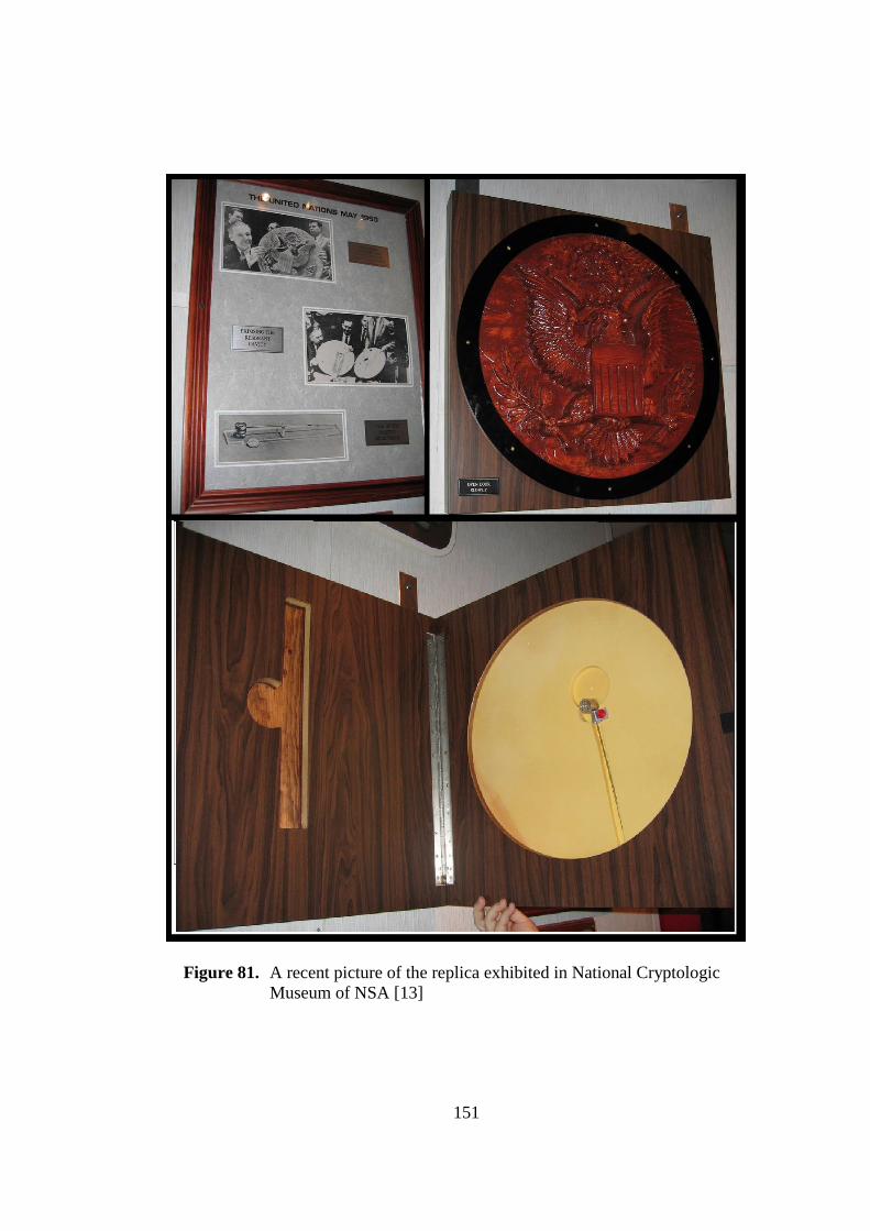
151
Figure 81. A recent picture of the replica exhibited in National Cryptologic
Museum of NSA [13]
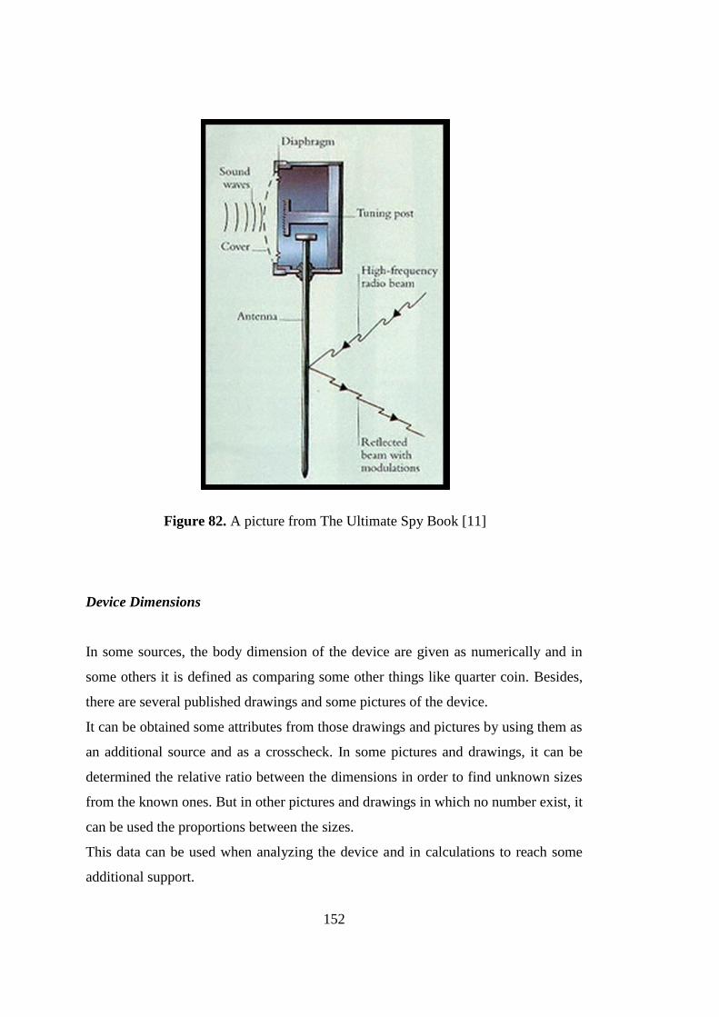
152
Figure 82. A picture from The Ultimate Spy Book [11]
Device Dimensions
In some sources, the body dimension of the device are given as numerically and in
some others it is defined as comparing some other things like quarter coin. Besides,
there are several published drawings and some pictures of the device.
It can be obtained some attributes from those drawings and pictures by using them as
an additional source and as a crosscheck. In some pictures and drawings, it can be
determined the relative ratio between the dimensions in order to find unknown sizes
from the known ones. But in other pictures and drawings in which no number exist, it
can be used the proportions between the sizes.
This data can be used when analyzing the device and in calculations to reach some
additional support.

153
Table 18 Theremin’s Device Parameter from several sources
Parameters Reference-1
[14]
Reference-2
[10]
Reference-3
[2]
Reference-4
[13]
Internal Diameter 1.97 cm 1.9685 cm - 1.9685 cm
Outer Diameter 2.1569 cm 2.374 cm 2.426 cm -
Internal Height 1 cm 0.9463 cm 1.7463 cm 1.7463 cm
Post Plate Diameter 0.68 cm 0.7969 cm 0.635 cm -
Post Plate Thickness 0.0585 cm 0.1162 cm - -
Post Height 0.86 cm 0.8301 cm - -
Post Body Diameter 0.1961 cm 0.1494 cm - -
Gap Length 0.0185 cm 0.9961mm - -
Diaphragm Thickness - - 76.2 76.2
Antenna Plate Diameter 0.35 cm 0.3652 cm - -
Antenna Plate Thickness 0.0464 cm 0.08799 cm - -
Antenna Body Diameter 0.1078 cm 0.08799 cm - -
Antenna Length 22.8 cm 22.86 cm 22.86 cm 22.86 cm
Antenna Height 0.65 cm 0.7886 cm - -
Cylinder Thickness 0.0784 cm 0.2158 cm - -
Quality Factor - - 1000 -
Inductance - - 10 nH 10 nH
Weight - - 1.1 oz 1.1 ounce
Frequency 330 MHz - 1600 MHz 800 MHz
In the Table 18 all the parameter information about the device is given. These
parameters are exactly given as definite. But there are inconsistencies between them.
Table 19 The approximate proportional measures of the device from pictures and
drawings
Parameter Picture-1
[11]
Picture-2
[50]
Picture-3
[2] Internal Diameter * 1 1 1
Internal Height 0.6 0.507 -
Post Plate Diameter 0.379 0.358 0.353
Post Plate Thickness 8.276 0.0405 -
Post Body Diameter 0.152 0.1074 -
Antenna Plate Diameter 0.221 0.189 0.353
Antenna Plate Thickness 0.069 0.0338 0.04082
Antenna Body Diameter 0.0897 0.061 0.07143
Cylinder Thickness 0.069 0.0541 -
* All the parameters are expressed in terms of Internal diameters as a ratio.
154
The Table 19 contains the proportionality of the parameters. In some drawings there
is no value but if they are scaled then the proportionality of the dimensions can be
used as additional information or a crosscheck.
Antenna
There are many different rumors about the antenna length and definition. According
to the sources the antenna is
- A quarter wave antenna
- A monopole
- A half wave antenna (one says no ground)
- A full wave antenna
- A quarter wave antenna for 330MHz
- 9 inch monopole (a silver-plated copper rod)
- 8.5 inch full wave antenna
- 8 inch
- 1800 MHz resonating antenna
It is observed in the pictures from CIA museum, the antenna is almost 7 times the
diameter.
Structure
The information about what the device is made of exists in some sources. Here are
those:
- It did not contain any ferrous materials (and therefore had eluded metal
detectors).
- The device was constructed of precision-tooled steel and comprised a long
pencil-thin antenna with a short cylindrical top.
- The cylinder is made of copper and silver plated.
- Diaphragm was made from the thinnest copper sheet and silver-plated.
- It is made of brass and silver plated.

155
Working Frequency
In the sources there are many different frequency values and definitions for the
Theremin’s device. The list is as follows.
- 330 MHz
- 1800 MHz
- 800 MHz
- 1600 MHz
- Somewhere between 1.1 – 1.5 GHz
- VHF
- UHF
- Usually in MW region, 1 GHz and up
- A wideband signal including many different frequency components
- Radar like signal, not pulsed
Discovery Methods
There are many different stories about how the device is discovered and which kind
of device is used.
The statements defining the device which is used to discover Theremin’s Device are
given below.
- Un-tuned Video Receiver.
- A wideband receiver with a simple diode detector/demodulator.
- Audio amplifier from a thing called a Schmidt Kit. The amplifier had a
crystal diode in series with a short wire rod that acted as an antenna at the
audio input connector.
- Un-tuned crystal video receiver.
- Radio.
- VHF receiver which is used to monitor Russian military aircraft traffic.
- Discovered during a routine physical, not electrical, security check.

156
Working Principle
Although there are many story and explanation about the working principle of the
device, mainly there are only two types of working style.
- It is a device, which reflects the incoming wave and the reflecting wave is
modulated by the diaphragm movement.
- It is a device, which absorbs the incoming wave and sends back a harmonic
of that wave, and the outgoing wave is modulated by the diaphragm
movement.
According to the first definition it is a reflecting device. And the diaphragm affects
the reflected wave. This provides the modulation by the sound. Here are some
explanations about this approach.
- Vibration of membrane changes the capacitance seen by the antenna which in
turn modulated the radio waves that struck and were re-transmitted by the
Thing
- The membrane and the post formed a variable capacitor acting as a condenser
microphone and providing amplitude modulation (AM), with parasitic
frequency modulation (FM) for the re-radiated signal
- A radio beam was aimed at the antenna from a source outside the building. A
sound that struck the diaphragm caused variations in the amount of space
(and the capacitance) between it and the tuning post plate. These variations
altered the charge on the antenna, creating modulations in the reflected radio
beam.
- The pedestal and diaphragm together made up a sort of air-variable capacitor,
which altered the resonant behavior of the cavity.
- To excite passive tuned-cavity listening devices. Microwave energy is
directed toward the cavity using a directional antenna from the monitoring
location. The microwave oscillator is connected to the antenna using a
directional coupler having forward and reverse power detectors. The
instantaneous VSWR is an indication of diaphragm displacement as the
cavity power absorption changes through detuning.

157
- The RF beam struck the bug's tiny antenna and a minuscule signal echoed
back. As long as the antenna kept the same electrical length the echo
remained at a set frequency. The sound waves which struck diaphragm,
causing it to vibrate. This altered the cavity's size ever so slightly and varied
the capacitive values (“post plate – diaphragm” and “post – antenna plate” ).
The changes in capacitances altered the charge on the antenna rod (radiated to
it from the transmitter) and caused its echoed signal to vary accordingly. In
effect, the bug modulated a little piece of the beamed signal before sending it
back as an echo.
According to the second idea, it is a regenerating device. And the diaphragm affects
the regenerated wave which is a harmonic of the incoming wave. This provides the
modulation by the sound. Here are some statements about this harmonic regeneration
approach.
- A harmonic of the inbound radio frequency energy is rebroadcast. It is
important to note that the microwave signal that “powers up” the device is not
the same frequency as the outbound signal.
- The length of the antenna and the dimensions of the cavity were engineered
in order to make the re-broadcast signal a higher harmonic of the illuminating
frequency. (Note that the transmitting frequency is higher than the
illuminating one.)
- The size of the cavity and the length of its antenna are carefully calculated so
that a harmonic (multiple) of the inbound radio frequency energy that bathes
the cavity is rebroadcast.
- The high-Q, silver plated cavity is "tuned" via the adjustable "mushroom" (a
1/4-wavelength shorted stub) to parallel-resonant at an odd-harmonic
frequency (3 times higher) than the transmitted RF carrier. The use of higher
frequencies will allow for a physically smaller cavity. Also, a RF carrier
which is 3 times higher can share an antenna which is for a frequency 3 times
lowers, due to the way the current is distributed in the antenna.
158
Modulation
All stories say that the vibration of the diaphragm by sound modulates the wave. So
what is that modulation? Here are some statements about the modulation.
- Amplitude modulation (AM), with parasitic frequency modulation (FM)
- The modulation was partially both amplitude modulated and frequency
modulated
- Also discussed was how much of the bug's emission was either AM or FM or
did it do both
- Inherently created both AM and FM modulation
- Straightforward zero-IF receiver that delivered the amplitude modulation of
the re-emitted signal as audio output.
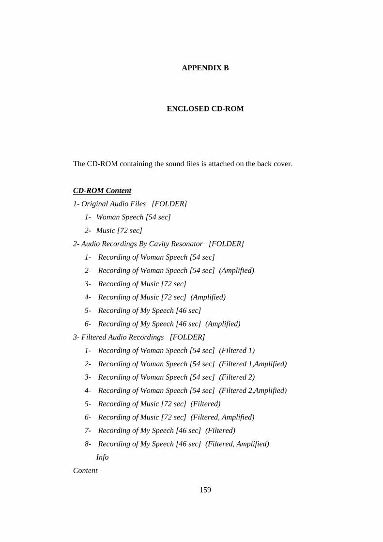
159
APPENDIX B
ENCLOSED CD-ROM
The CD-ROM containing the sound files is attached on the back cover.
CD-ROM Content
1- Original Audio Files [FOLDER]
1- Woman Speech [54 sec]
2- Music [72 sec]
2- Audio Recordings By Cavity Resonator [FOLDER]
1- Recording of Woman Speech [54 sec]
2- Recording of Woman Speech [54 sec] (Amplified)
3- Recording of Music [72 sec]
4- Recording of Music [72 sec] (Amplified)
5- Recording of My Speech [46 sec]
6- Recording of My Speech [46 sec] (Amplified)
3- Filtered Audio Recordings [FOLDER]
1- Recording of Woman Speech [54 sec] (Filtered 1)
2- Recording of Woman Speech [54 sec] (Filtered 1,Amplified)
3- Recording of Woman Speech [54 sec] (Filtered 2)
4- Recording of Woman Speech [54 sec] (Filtered 2,Amplified)
5- Recording of Music [72 sec] (Filtered)
6- Recording of Music [72 sec] (Filtered, Amplified)
7- Recording of My Speech [46 sec] (Filtered)
8- Recording of My Speech [46 sec] (Filtered, Amplified)
Info
Content

160