Design, Construction and Evaluation of a Stacked Polyphase ...
52 IEEE TRANSACTIONS ON COMPONENTS, PACKAGING, AND MANUFACTURING TECHNOLOGY, VOL. 1, NO. 1, JANUARY 2011
Design and Development of Multi-Die LaterallyPlaced and Vertically Stacked Embedded
Micro-Wafer-Level PackagesGaurav Sharma, Vempati Srinivas Rao, Aditya Kumar, Lim Ying Ying, Khong Chee Houe, Sharon Lim,
Vasarla Nagendra Sekhar, Ranjan Rajoo, Vaidyanathan Kripesh, and John H. Lau, Fellow, IEEE
Abstract—Two embedded micro-wafer-level packages(EMWLP) with 1) laterally placed and 2) vertically stackedthin dies are designed and developed. Three-dimensional stackingof thin dies is demonstrated as progressive miniaturization driverfor multi-chip EMWLP. Both the developed packages have di-mensions of 10 mm 10 mm 0.4 mm and solder ball pitch of0.4 mm. As part of the development several key processes like thindie stacking, 8-in wafer encapsulation using compression molding,low-temperature dielectric with processing temperature less than200 C have been developed. The EMWLP components success-fully pass 1000 air to air thermal cycling ( �� C to 125 C),unbiased highly accelerated stress testing (HAST) and moisturesensitivity level (MSL3) tests. Developed EMWLP also show goodboard level TC ( 1000 cycles) and drop test reliability results.Integration of thin film passives like inductors and capacitorsare also demonstrated on EMWLP platform. Developed thin filmpassives show a higher Q–factor when compared to passives onhigh resistivity silicon platform. Thermo-mechanical simulationstudies on developed EMWLP demonstrate that systemic controlover die, RDL, and package thicknesses can lead to designs withimproved mechanical reliability.
Index Terms—Die stacking, embedded wafer package, multi-die,thin film passives.
I. INTRODUCTION
T ODAY consumer electronics comprise 50% of the totalintegrated circuit revenue [1]. Handheld consumer elec-
tronics mandate small form factor and footprint area electronicpackages. In consumer electronic applications, like cell phone,passives constitute 80% of components. In cell phones, pas-sives occupy 80% of circuit board area and contribute 70% ofproduct assembly cost [1]. Thin film passives integrated within
Manuscript received May 15, 2009; revised August 26, 2010; acceptedSeptember 13, 2010. Date of publication December 23, 2010; date of currentversion March 23, 2011. This work was supported by industry consortiummembers under the 9th Electronic Package Research Consortium the membersof which are Asahi Glass Co. Ltd, ASM Technology Singapore Pte Ltd,Hynix Semiconductor Inc., Infineon Technologies Asia Pacific Pte Ltd, IbidenSingapore Pte Ltd, Kinergy Limited, Nitto Denko (Singapore) Pte Ltd, NXPSemiconductors, Samsung Electro-Mechanics Co Ltd, Sumitomo BakeliteSingapore Pte Ltd, Victrex PLC and the Institute of Materials Research andEngineering. This work was recommended for publication by Associate EditorC. Gurumurthy upon evaluation of the reviewers comments.
The authors are with Institute of Microelectronics, A*STAR (Agency forScience, Technology and Research) 11 Science Park Road, Singapore 117685(e-mail: [email protected]).
Color versions of one or more of the figures in this paper are available onlineat http://ieeexplore.ieee.org.
Digital Object Identifier 10.1109/TCPMT.2010.2101470
the package redistribution layer structure can replace discreteintegrated passive devices (IPD) which can lead to progres-sively miniaturized mobile phone packages. System-in-packageis a packaging technology platform that enables integrationof more than one active electronic component of differentfunctionality plus thin film passives and other devices likemicroelectromechanical systems (MEMS) or optical compo-nents [1]. Embedded micro-wafer-level package (EMWLP) isa packaging technology that enables development of low formfactor multi-die packages [2]. EMWLP combined with thinfilm passives integration can provide system-in-package (SiP)solutions.
In addition to providing SiP solutions EMWLP technologyalso possesses several advantages over the conventionalwafer-level packages (WLPs) [3]–[6]. EMWLP providesmulti-die packaging solution where as WLP is restricted to asingle die. EMWLP process flow is known good die (KGD)based which, results in better wafer level yields in packaging.EMWLP also leads to fan out interconnect fabrication which,unlike in WLP, can exceed the die foot print area [7]. In WLPhigh pin count devices can be achieved by increasing the siliconchip size. However, increasing chip size is a large cost adder inthe front end. In EMWLP the mold compound material can beused for fabrication of fan out interconnects which is a muchmore economical way for increasing pin count. In microelec-tronic developments the shrinkage of pitches and pads at thechip/package interface is much faster than the shrinkage at thepackage/board interface which leads to the “interconnect gap”problem in packaging [1]. EMWLP provides a cost economicalway to increase the package/board pin count thus addressingthe “interconnect gap” problem.
In literature, some EMWLP configurations have been re-ported. Keser et al. have reported a chip embedding technologynamed as redistributed chip package (RCP) where completeradio-in-package using RCP was demonstrated [8]. Brunnbaueret al. have demonstrated a single chip embedded device tech-nology solution [7], [9]. Kripesh et al. have shown fabricationand process flow results on a 3-D stacked embedded WLP withthree thin die stacking [10].
In this study two multi-chip EMWLP with 1) laterally placedand 2) vertically stacked thin dies have been designed anddeveloped. The developed multi-die packages have dimensionsof 10 mm 10 mm 0.4 mm and solder ball pitch of 0.4 mm.EMWLP with laterally placed dies and vertically stacked dieshave 206 and 350 input/output (I/O), respectively. As part
2156-3950/$26.00 © 2010 IEEE
SHARMA et al.: DESIGN AND DEVELOPMENT OF MULTI-DIE LATERALLY PLACED AND VERTICALLY STACKED 53
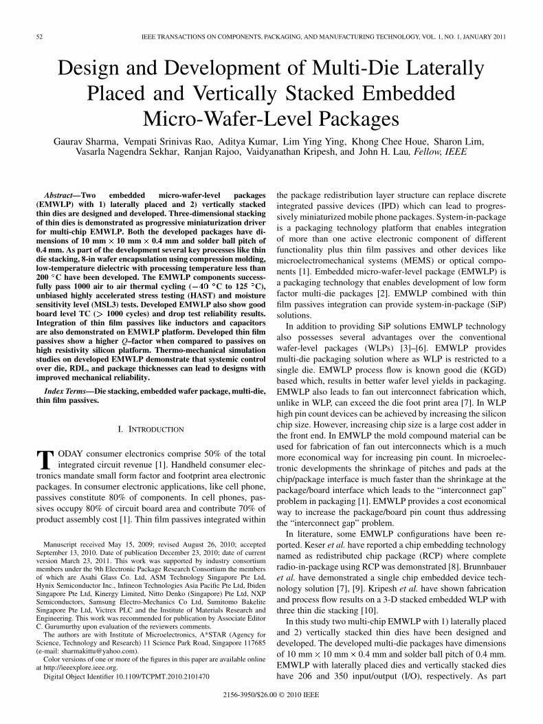
Fig. 1. Schematic showing the EMWLP with (a) laterally placed and (b) verti-cally stacked dies. In (a) chip 1 and chip 2 are 5 mm� 5 mm� 0.3 mm and 1.5mm� 1.2 mm� 0.3 mm respectively. In (b) chip 1 and chip 2 are 5 mm� 5mm� 0.1 mm and 7 mm� 7 mm� 0.3 mm respectively. The dimensions ofboth package components are 10 mm� 10 mm� 0.4 mm.
of this study key processes like wafer thinning with copperpillars, wafer-level compression molding, thin die stacking andlow-temperature dielectric processes have been developed. Sev-eral materials like mold compounds with different coefficientsof thermal expansion (CTE) and filler contents, molding tapes,dicing die attach films, low-temperature dielectric materialshave been evaluated and the associated processes are optimized.The entire package fabrication is carried out using wafer-levelfront end processes. The developed packages demonstrate goodtemperature cycling, MSL3, HAST, and drop test reliabilityresults. Thin film passives fabrication on EMWLP platformis also demonstrated. Simulation of thermo-mechanical reli-ability of EMWLP test vehicles shows that systemic controlover package design parameters like die, redistribution layer(RDL), and package thickness can provide design guidelines toimprove mechanical reliability of EMWLP being developed.
II. PROCESS FLOW
Fig. 1(a) and (b) shows a schematic of the EMWLP that arebeing developed. In Fig. 1(a) package schematic multi-chipintegration is achieved by lateral placement of dies. In Fig. 1(b)package schematic multi-chip integration is achieved by 3-Dstacking. To reduce the overall thickness of the package fab-ricated dies are thinned and then packaged. For the EMWLPwith laterally placed dies the two fabricated die sizes are 5mm 5 mm 0.3 mm and 1.5 mm 1.2 mm 0.3 mm. Forthe EMWLP with stacked dies the die sizes are 5 mm 5mm 0.1 mm and 7 mm 7 mm 0.3 mm. For stacked diepackage copper pillars are electroplated to enable 3-D stackingand I/O formation. Interconnects from both chips of the stackedmodule are brought to the same plane using different heightsof copper pillar interconnects on different chips. Fig. 2 showsan overview of the chip wafer fabrication process. As shown inprocess steps (I) and (II) the basic die layout comprises of alu-minum daisy chain structure passivated with SiO . For EMWLPwith laterally placed dies the die wafers are back grinded to
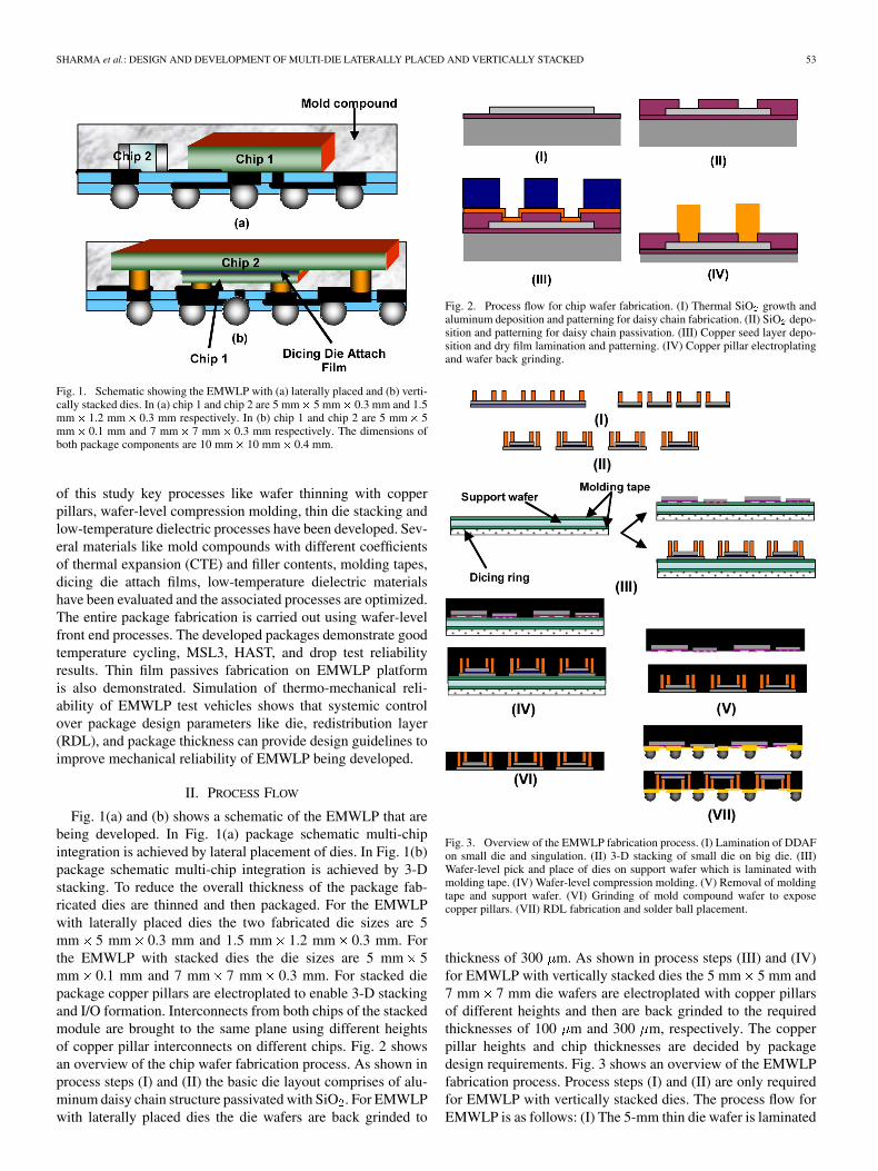
Fig. 2. Process flow for chip wafer fabrication. (I) Thermal SiO growth andaluminum deposition and patterning for daisy chain fabrication. (II) SiO depo-sition and patterning for daisy chain passivation. (III) Copper seed layer depo-sition and dry film lamination and patterning. (IV) Copper pillar electroplatingand wafer back grinding.
Fig. 3. Overview of the EMWLP fabrication process. (I) Lamination of DDAFon small die and singulation. (II) 3-D stacking of small die on big die. (III)Wafer-level pick and place of dies on support wafer which is laminated withmolding tape. (IV) Wafer-level compression molding. (V) Removal of moldingtape and support wafer. (VI) Grinding of mold compound wafer to exposecopper pillars. (VII) RDL fabrication and solder ball placement.
thickness of 300 m. As shown in process steps (III) and (IV)for EMWLP with vertically stacked dies the 5 mm 5 mm and7 mm 7 mm die wafers are electroplated with copper pillarsof different heights and then are back grinded to the requiredthicknesses of 100 m and 300 m, respectively. The copperpillar heights and chip thicknesses are decided by packagedesign requirements. Fig. 3 shows an overview of the EMWLPfabrication process. Process steps (I) and (II) are only requiredfor EMWLP with vertically stacked dies. The process flow forEMWLP is as follows: (I) The 5-mm thin die wafer is laminated
54 IEEE TRANSACTIONS ON COMPONENTS, PACKAGING, AND MANUFACTURING TECHNOLOGY, VOL. 1, NO. 1, JANUARY 2011
with Dicing Die Attach Film (DDAF) and then diced. (II) The7 mm thin die wafer is diced separately and the 5-mm dies arestacked on top of the 7-mm dies. (III) The dies and die stacksare then picked and placed on a two adhesive layer molding tapeusing wafer-level pick and place process. For EMWLP withlaterally placed dies the thin wafer die is singulated and dies arethen picked and placed on a molding tape. To achieve robustpick and place and wafer molding process the back side of themolding tape is laminated on to a silicon support wafer. Themolding tape features thermo-release properties, which allowsremoval of tape after molding. (IV) Pick and place process isfollowed by wafer-level compression molding. Compressionmolding process is optimized for wafer warpage by usingdifferent granular mold compound materials that have differentfiller contents and CTE. (V) After compression molding thesupport wafer and dicing ring support are removed. This isfollowed by post mold cure of the mold compound wafer. (VI)For EMWLP with vertically stacked dies mold wafer grindingis employed to expose the copper pillars. For EMWLP withlaterally placed dies this step is not required since molding taperemoval exposes the chip I/O pads on which RDL is fabricated.(VII) Wafer molding is followed by redistribution layer pro-cessing to fabricate the fan out interconnects. Since the moldedwafer decomposes at temperatures C low-temperaturedielectric process is developed. Two low-temperature dielectricmaterials from separate manufacturers are evaluated that haveprocessing temperature ranging from 160 C to 200 C. TheRDL process is followed by conventional solder ball placementprocess. The EMWLP are then assembled on printed circuitboard (PCB) and reflowed.
The package components are subjected to air to air thermalcycling ( C to 125 C), MSL3 and HAST tests. Thepackage components assembled on PCB also undergo air-to-airthermal cycling ( C to 125 C) and drop tests. Reliabilityassessment is carried out using daisy chain resistance and chaincontinuity measurements. Scanning acoustic microscopy isemployed to assess delamination and voids in EMWLP.
III. EMWLP WITH LATERALLY PLACED THIN DIES
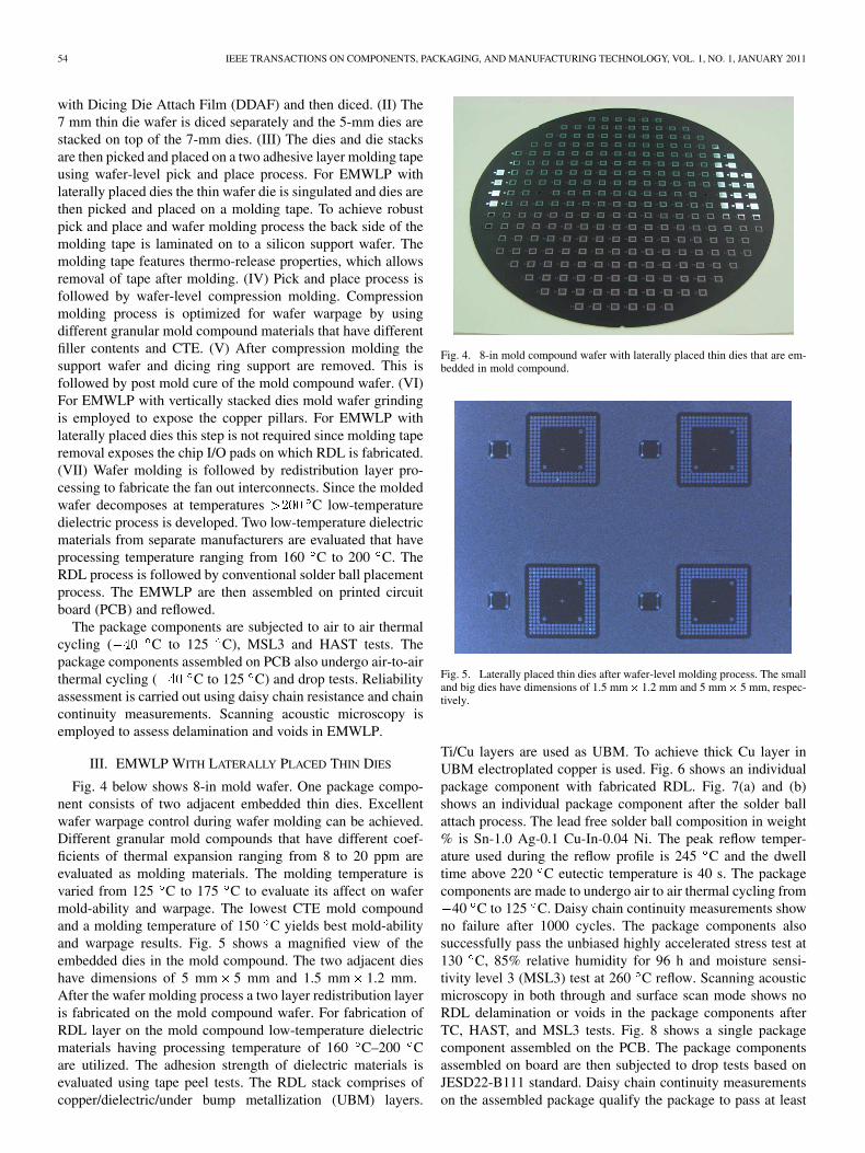
Fig. 4 below shows 8-in mold wafer. One package compo-nent consists of two adjacent embedded thin dies. Excellentwafer warpage control during wafer molding can be achieved.Different granular mold compounds that have different coef-ficients of thermal expansion ranging from 8 to 20 ppm areevaluated as molding materials. The molding temperature isvaried from 125 C to 175 C to evaluate its affect on wafermold-ability and warpage. The lowest CTE mold compoundand a molding temperature of 150 C yields best mold-abilityand warpage results. Fig. 5 shows a magnified view of theembedded dies in the mold compound. The two adjacent dieshave dimensions of 5 mm 5 mm and 1.5 mm 1.2 mm.After the wafer molding process a two layer redistribution layeris fabricated on the mold compound wafer. For fabrication ofRDL layer on the mold compound low-temperature dielectricmaterials having processing temperature of 160 C–200 Care utilized. The adhesion strength of dielectric materials isevaluated using tape peel tests. The RDL stack comprises ofcopper/dielectric/under bump metallization (UBM) layers.
Fig. 4. 8-in mold compound wafer with laterally placed thin dies that are em-bedded in mold compound.
Fig. 5. Laterally placed thin dies after wafer-level molding process. The smalland big dies have dimensions of 1.5 mm� 1.2 mm and 5 mm� 5 mm, respec-tively.
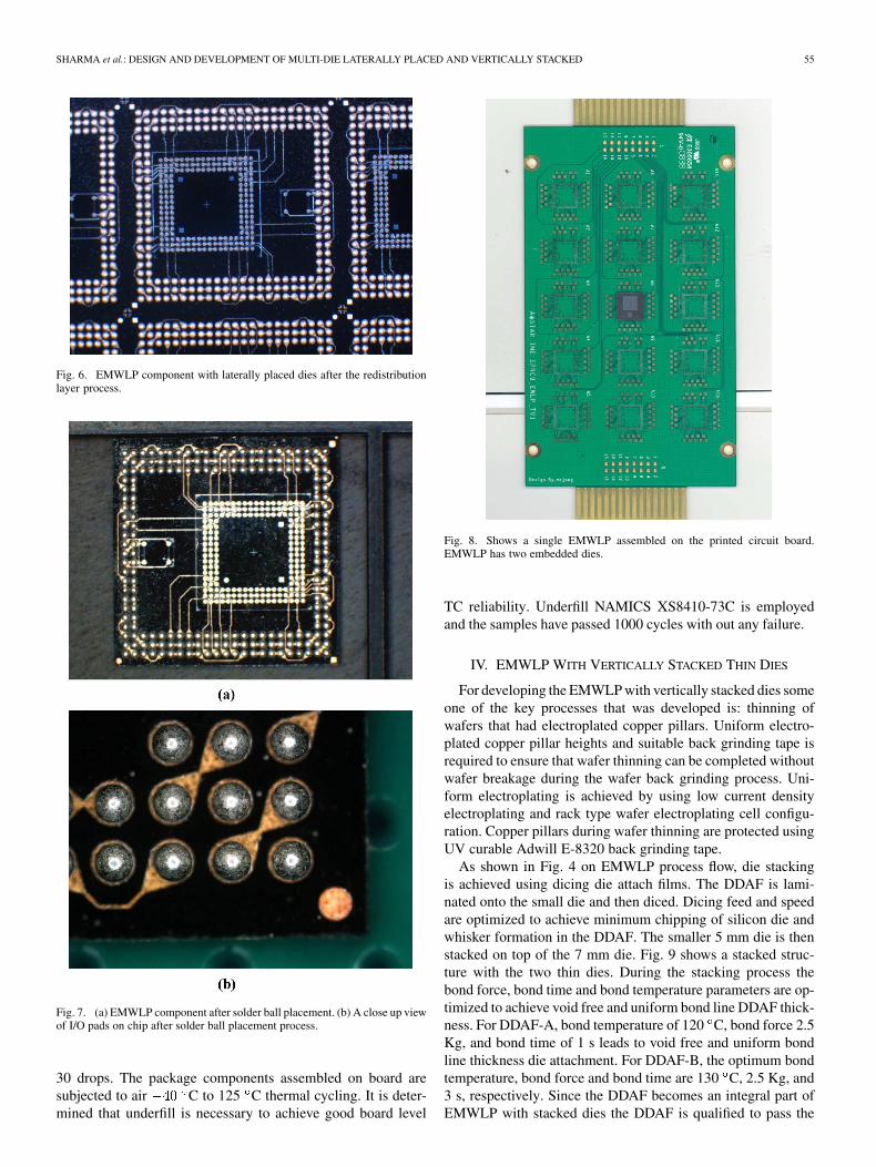
Ti/Cu layers are used as UBM. To achieve thick Cu layer inUBM electroplated copper is used. Fig. 6 shows an individualpackage component with fabricated RDL. Fig. 7(a) and (b)shows an individual package component after the solder ballattach process. The lead free solder ball composition in weight% is Sn-1.0 Ag-0.1 Cu-In-0.04 Ni. The peak reflow temper-ature used during the reflow profile is 245 C and the dwelltime above 220 C eutectic temperature is 40 s. The packagecomponents are made to undergo air to air thermal cycling from
40 C to 125 C. Daisy chain continuity measurements showno failure after 1000 cycles. The package components alsosuccessfully pass the unbiased highly accelerated stress test at130 C, 85% relative humidity for 96 h and moisture sensi-tivity level 3 (MSL3) test at 260 C reflow. Scanning acousticmicroscopy in both through and surface scan mode shows noRDL delamination or voids in the package components afterTC, HAST, and MSL3 tests. Fig. 8 shows a single packagecomponent assembled on the PCB. The package componentsassembled on board are then subjected to drop tests based onJESD22-B111 standard. Daisy chain continuity measurementson the assembled package qualify the package to pass at least
SHARMA et al.: DESIGN AND DEVELOPMENT OF MULTI-DIE LATERALLY PLACED AND VERTICALLY STACKED 55
Fig. 6. EMWLP component with laterally placed dies after the redistributionlayer process.
Fig. 7. (a) EMWLP component after solder ball placement. (b) A close up viewof I/O pads on chip after solder ball placement process.
30 drops. The package components assembled on board aresubjected to air C to 125 C thermal cycling. It is deter-mined that underfill is necessary to achieve good board level
Fig. 8. Shows a single EMWLP assembled on the printed circuit board.EMWLP has two embedded dies.
TC reliability. Underfill NAMICS XS8410-73C is employedand the samples have passed 1000 cycles with out any failure.
IV. EMWLP WITH VERTICALLY STACKED THIN DIES
For developing the EMWLP with vertically stacked dies someone of the key processes that was developed is: thinning ofwafers that had electroplated copper pillars. Uniform electro-plated copper pillar heights and suitable back grinding tape isrequired to ensure that wafer thinning can be completed withoutwafer breakage during the wafer back grinding process. Uni-form electroplating is achieved by using low current densityelectroplating and rack type wafer electroplating cell configu-ration. Copper pillars during wafer thinning are protected usingUV curable Adwill E-8320 back grinding tape.
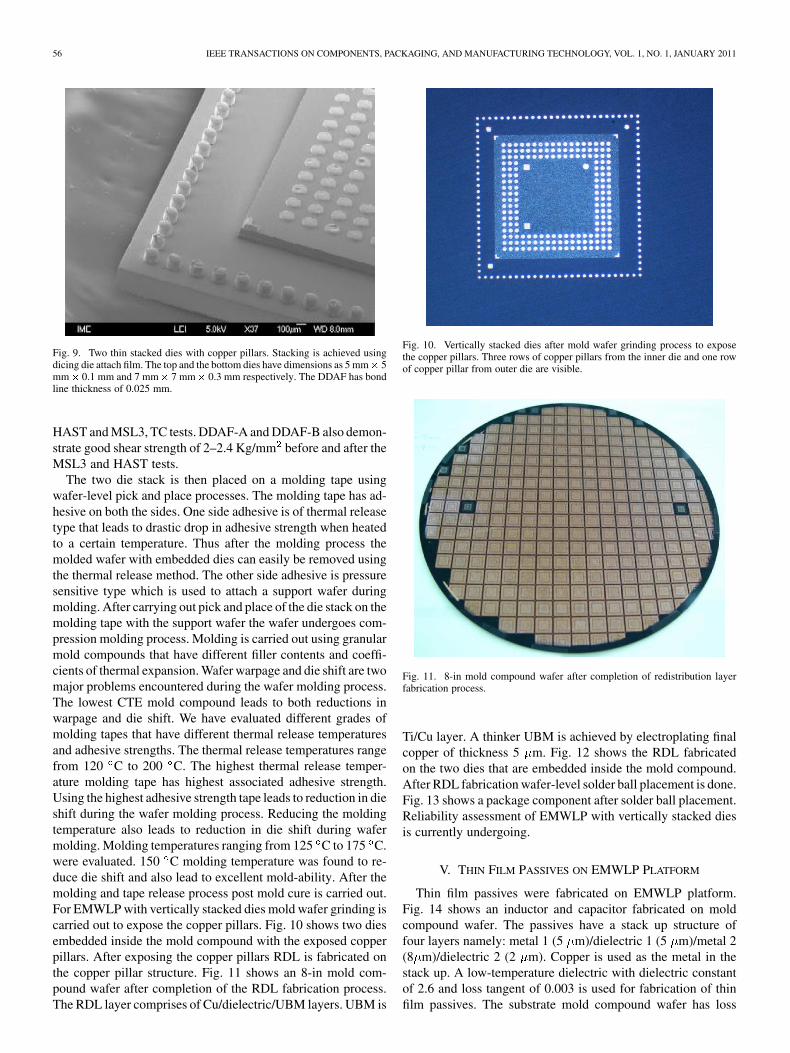
As shown in Fig. 4 on EMWLP process flow, die stackingis achieved using dicing die attach films. The DDAF is lami-nated onto the small die and then diced. Dicing feed and speedare optimized to achieve minimum chipping of silicon die andwhisker formation in the DDAF. The smaller 5 mm die is thenstacked on top of the 7 mm die. Fig. 9 shows a stacked struc-ture with the two thin dies. During the stacking process thebond force, bond time and bond temperature parameters are op-timized to achieve void free and uniform bond line DDAF thick-ness. For DDAF-A, bond temperature of 120 C, bond force 2.5Kg, and bond time of 1 s leads to void free and uniform bondline thickness die attachment. For DDAF-B, the optimum bondtemperature, bond force and bond time are 130 C, 2.5 Kg, and3 s, respectively. Since the DDAF becomes an integral part ofEMWLP with stacked dies the DDAF is qualified to pass the
56 IEEE TRANSACTIONS ON COMPONENTS, PACKAGING, AND MANUFACTURING TECHNOLOGY, VOL. 1, NO. 1, JANUARY 2011
Fig. 9. Two thin stacked dies with copper pillars. Stacking is achieved usingdicing die attach film. The top and the bottom dies have dimensions as 5 mm� 5mm� 0.1 mm and 7 mm� 7 mm� 0.3 mm respectively. The DDAF has bondline thickness of 0.025 mm.
HAST and MSL3, TC tests. DDAF-A and DDAF-B also demon-strate good shear strength of 2–2.4 Kg/mm before and after theMSL3 and HAST tests.
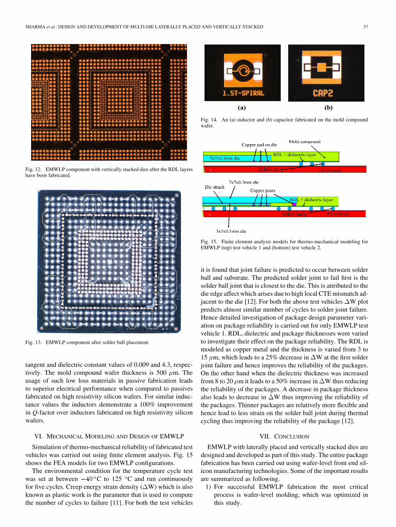
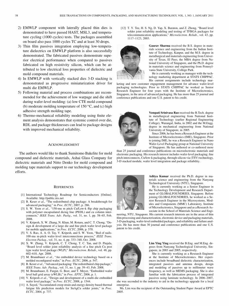
The two die stack is then placed on a molding tape usingwafer-level pick and place processes. The molding tape has ad-hesive on both the sides. One side adhesive is of thermal releasetype that leads to drastic drop in adhesive strength when heatedto a certain temperature. Thus after the molding process themolded wafer with embedded dies can easily be removed usingthe thermal release method. The other side adhesive is pressuresensitive type which is used to attach a support wafer duringmolding. After carrying out pick and place of the die stack on themolding tape with the support wafer the wafer undergoes com-pression molding process. Molding is carried out using granularmold compounds that have different filler contents and coeffi-cients of thermal expansion. Wafer warpage and die shift are twomajor problems encountered during the wafer molding process.The lowest CTE mold compound leads to both reductions inwarpage and die shift. We have evaluated different grades ofmolding tapes that have different thermal release temperaturesand adhesive strengths. The thermal release temperatures rangefrom 120 C to 200 C. The highest thermal release temper-ature molding tape has highest associated adhesive strength.Using the highest adhesive strength tape leads to reduction in dieshift during the wafer molding process. Reducing the moldingtemperature also leads to reduction in die shift during wafermolding. Molding temperatures ranging from 125 C to 175 C.were evaluated. 150 C molding temperature was found to re-duce die shift and also lead to excellent mold-ability. After themolding and tape release process post mold cure is carried out.For EMWLP with vertically stacked dies mold wafer grinding iscarried out to expose the copper pillars. Fig. 10 shows two diesembedded inside the mold compound with the exposed copperpillars. After exposing the copper pillars RDL is fabricated onthe copper pillar structure. Fig. 11 shows an 8-in mold com-pound wafer after completion of the RDL fabrication process.The RDL layer comprises of Cu/dielectric/UBM layers. UBM is
Fig. 10. Vertically stacked dies after mold wafer grinding process to exposethe copper pillars. Three rows of copper pillars from the inner die and one rowof copper pillar from outer die are visible.
Fig. 11. 8-in mold compound wafer after completion of redistribution layerfabrication process.
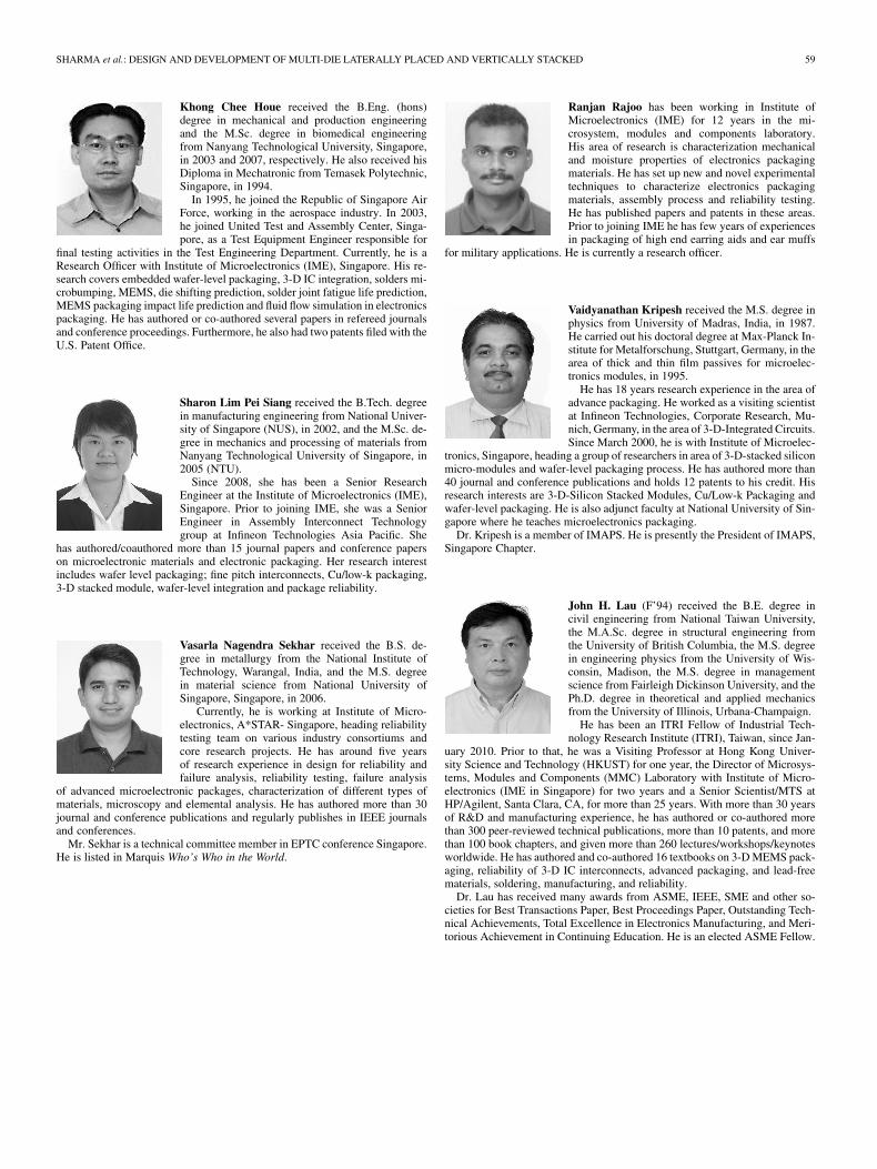
Ti/Cu layer. A thinker UBM is achieved by electroplating finalcopper of thickness 5 m. Fig. 12 shows the RDL fabricatedon the two dies that are embedded inside the mold compound.After RDL fabrication wafer-level solder ball placement is done.Fig. 13 shows a package component after solder ball placement.Reliability assessment of EMWLP with vertically stacked diesis currently undergoing.
V. THIN FILM PASSIVES ON EMWLP PLATFORM
Thin film passives were fabricated on EMWLP platform.Fig. 14 shows an inductor and capacitor fabricated on moldcompound wafer. The passives have a stack up structure offour layers namely: metal 1 (5 m)/dielectric 1 (5 m)/metal 2(8 m)/dielectric 2 (2 m). Copper is used as the metal in thestack up. A low-temperature dielectric with dielectric constantof 2.6 and loss tangent of 0.003 is used for fabrication of thinfilm passives. The substrate mold compound wafer has loss
SHARMA et al.: DESIGN AND DEVELOPMENT OF MULTI-DIE LATERALLY PLACED AND VERTICALLY STACKED 57
Fig. 12. EMWLP component with vertically stacked dies after the RDL layershave been fabricated.
Fig. 13. EMWLP component after solder ball placement.
tangent and dielectric constant values of 0.009 and 4.3, respec-tively. The mold compound wafer thickness is 500 m. Theusage of such low loss materials in passive fabrication leadsto superior electrical performance when compared to passivesfabricated on high resistivity silicon wafers. For similar induc-tance values the inductors demonstrate a 100% improvementin Q-factor over inductors fabricated on high resistivity siliconwafers.
VI. MECHANICAL MODELING AND DESIGN OF EMWLP
Simulation of thermo-mechanical reliability of fabricated testvehicles was carried out using finite element analysis. Fig. 15shows the FEA models for two EMWLP configurations.
The environmental condition for the temperature cycle testwas set at between C to 125 C and run continuouslyfor five cycles. Creep energy strain density ( W) which is alsoknown as plastic work is the parameter that is used to computethe number of cycles to failure [11]. For both the test vehicles
Fig. 14. An (a) inductor and (b) capacitor fabricated on the mold compoundwafer.
Fig. 15. Finite element analysis models for thermo-mechanical modeling forEMWLP (top) test vehicle 1 and (bottom) test vehicle 2.
it is found that joint failure is predicted to occur between solderball and substrate. The predicted solder joint to fail first is thesolder ball joint that is closest to the die. This is attributed to thedie edge affect which arises due to high local CTE mismatch ad-jacent to the die [12]. For both the above test vehicles W plotpredicts almost similar number of cycles to solder joint failure.Hence detailed investigation of package design parameter vari-ation on package reliability is carried out for only EMWLP testvehicle 1. RDL, dielectric and package thicknesses were variedto investigate their effect on the package reliability. The RDL ismodeled as copper metal and the thickness is varied from 3 to15 m, which leads to a 25% decrease in W at the first solderjoint failure and hence improves the reliability of the packages.On the other hand when the dielectric thickness was increasedfrom 8 to 20 m it leads to a 50% increase in W thus reducingthe reliability of the packages. A decrease in package thicknessalso leads to decrease in W thus improving the reliability ofthe packages. Thinner packages are relatively more flexible andhence lead to less strain on the solder ball joint during thermalcycling thus improving the reliability of the package [12].
VII. CONCLUSION
EMWLP with laterally placed and vertically stacked dies aredesigned and developed as part of this study. The entire packagefabrication has been carried out using wafer-level front end sil-icon manufacturing technologies. Some of the important resultsare summarized as following.
1) For successful EMWLP fabrication the most criticalprocess is wafer-level molding, which was optimized inthis study.
58 IEEE TRANSACTIONS ON COMPONENTS, PACKAGING, AND MANUFACTURING TECHNOLOGY, VOL. 1, NO. 1, JANUARY 2011
2) EMWLP component with laterally placed thin dies isdemonstrated to have passed HAST, MSL3, and tempera-ture cycling (1000 cycles) tests. The packages assembledon board also pass 1000 cycles TC and at least 30 drops.
3) Thin film passives integration employing low-tempera-ture dielectrics on EMWLP platform is also successfullydemonstrated. The fabricated passives demonstrate supe-rior electrical performance when compared to passivesfabricated on high resistivity silicon, which can be at-tributed to low electrical loss properties of dielectric andmold compound materials.
4) In EMWLP with vertically stacked dies 3-D stacking isdemonstrated as progressive miniaturization driver formulti die EMWLP.
5) Following material and process combinations are recom-mended for the achievement of low warpage and die shiftduring wafer-level molding: (a) low CTE mold compound(b) moderate molding temperature of 150 C, and (c) highadhesive strength molding tape.
6) Thermo-mechanical reliability modeling using finite ele-ment analysis demonstrates that systemic control over die,RDL and package thicknesses can lead to package designswith improved mechanical reliability.
ACKNOWLEDGMENT
The authors would like to thank Sumitomo Bakelite for moldcompound and dielectric materials, Ashai Glass Company fordielectric materials and Nitto Denko for mold compound andmolding tape materials support to our technology developmentefforts.
REFERENCES
[1] International Technology Roadmap for Semiconductors [Online].Available: http://public.itrs.net
[2] B. Keser et al., “The redistributed chip package: A breakthrough foradvanced packaging,” in Proc. ECTC, 2007, p. 286.
[3] S. W. Yoon et al., “150-mu m pitch Cu/Low-k flip chip packagingwith polymer encapsulated dicing line (PEDL) and cu column inter-connects,” IEEE Trans. Adv. Packg., vol. 31, no. 1, pp. 58–65, Feb.2008.
[4] V. Kripesh, X. W. Zhang, N. Khan, M. Rotaru, and C. T. Chong, “De-sign & development of a large die and fine pitch wafer level packagefor mobile applications,” in Proc. ECTC, 2006, p. 570.
[5] V. S. Rao, A. A. O. Tay, V. Kripesh, and S. W. Yoon, “Bed of nails-100-mu m-pitch wafer-level interconnections process,” IEEE Trans.Electron Packag., vol. 31, no. 4, pp. 333–340, Oct. 2008.
[6] X. W. Zhang, V. Kripesh, C. T. Chong, T. C. Tan, and D. Pinjala,“Board level solder joint reliability analysis of a fine pitch Cu posttype wafer level package (WLP),” Microelectron. Reliab., vol. 48, pp.602–610, Apr. 2008.
[7] M. Brunnbauer et al., “An embedded device technology based on amolded reconfigured wafer,” in Proc. ECTC, 2006, p. 547.
[8] B. Keser et al., “Advanced packaging: The redistributed chip package,”IEEE Trans. Adv. Packag., vol. 31, no. 1, pp. 39–43, Feb. 2008.
[9] M. Brunnbauer, E. Furgut, G. Beer, and T. Meyer, “Embedded waferlevel ball grid array (eWLB),” in Proc. EPTC, 2006, p. 1.
[10] V. Kripesh et al., “Design and development of a multi-die embeddedwafer level package,” in Proc. ECTC, 2008, p. 1544.
[11] A. Sayed, “Accumulated creep strain and energy density based thermalfatigue life prediction models for SnAgCu solder joints,” in Proc.ECTC, 2004, p. 737.
[12] T. Y. Tee, H. S. Ng, D. Yap, X. Baraton, and Z. Zhong, “Board levelsolder joint reliability modeling and testing of TFBGA packages fortelecommunication applications,” Microelectron. Reliab., vol. 43, pp.1117–1123, 2003.
Gaurav Sharma received the B.S. degree in mate-rials science and engineering from the Indian Insti-tute of Technology, Kanpur, and the M.S. degree inmetallurgical and materials engineering from Univer-sity of Texas, El Paso, the MBA degree from Na-tional University of Singapore, and the Ph.D. degreein materials science and engineering from Pennsyl-vania State University, College Park.
He is currently working as manager with the tech-nology marketing department at STATS CHIPPAC.His current assignments include technology mar-
keting and new customer engagement management for advance wafer-levelpackaging technologies. Prior to STATS CHIPPAC he worked as SeniorResearch Engineer for four years with the Institute of Microelectronics,Singapore, in the area of advanced packaging. He has more than 25 journal andconference publications and one U.S. patent to his credit.
Vempati Srinivasa Rao received the B.Tech. degreein metallurgical engineering from National Insti-tute of Technology (earlier Regional EngineeringCollege), Warangal, India, in 2002 and the M.Engg.degree in mechanical engineering from NationalUniversity of Singapore, in 2005.
Since 2006, he has been a Research Engineer at theInstitute of Microelectronics (IME), Singapore. Priorto joining IME, he was a Research Engineer in NanoWafer-Level Packaging group at National Universityof Singapore. He has authored or co-authored more
than 25 journal and conference publications on microelectronic materials andelectronic packaging. His research interest includes wafer-level packaging; finepitch interconnects, Cu/low-k packaging, through silicon via (TSV) technology,3-D stacked module, wafer level integration and package reliability.
Aditya Kumar received the Ph.D. degree in ma-terials science and engineering from the NanyangTechnological University (NTU), Singapore.
He is currently working as a Senior Engineer inthe Technology Development and Research Depart-ment of GLOBALFOUNDRIES, Singapore. Beforejoining GLOBALFOUNDRIES, he worked as a Se-nior Research Engineer in the Microsystems, Mod-ules and Components (MMC) Laboratory, Instituteof Microelectronics, Singapore and as a Research As-sociate in the School of Materials Science and Engi-
neering, NTU, Singapore. His current research interests are in the areas of thinfilm processing and characterization, electronic device and packaging materials,3-D-packaging, wafer-level embedded packages, and reliability and failure anal-ysis. He has more than 30 journal and conference publications and one U.S.patent to his credit.
Lim Ying Ying received the B.Eng. and M.Eng. de-grees from Nanyang Technological University, Sin-gapore, in 2003 and 2005, respectively.
She is currently working as a Research Engineerat the Institute of Microelectronics. Her experi-ences include broadband dielectric characterization,integrated passives and antenna design, designand modeling of passives up to millimeter wavefrequency, as well as MEMS packaging. She is alsofamiliar with the fabrication process of integratedpassives using laminate technology. In 2006–2007,
she was seconded to the industry to aid in the technology upgrade for a localenterprise.
Ms. Lim was the recipient of the Outstanding Student Paper Award at EPTC2005.
SHARMA et al.: DESIGN AND DEVELOPMENT OF MULTI-DIE LATERALLY PLACED AND VERTICALLY STACKED 59
Khong Chee Houe received the B.Eng. (hons)degree in mechanical and production engineeringand the M.Sc. degree in biomedical engineeringfrom Nanyang Technological University, Singapore,in 2003 and 2007, respectively. He also received hisDiploma in Mechatronic from Temasek Polytechnic,Singapore, in 1994.
In 1995, he joined the Republic of Singapore AirForce, working in the aerospace industry. In 2003,he joined United Test and Assembly Center, Singa-pore, as a Test Equipment Engineer responsible for
final testing activities in the Test Engineering Department. Currently, he is aResearch Officer with Institute of Microelectronics (IME), Singapore. His re-search covers embedded wafer-level packaging, 3-D IC integration, solders mi-crobumping, MEMS, die shifting prediction, solder joint fatigue life prediction,MEMS packaging impact life prediction and fluid flow simulation in electronicspackaging. He has authored or co-authored several papers in refereed journalsand conference proceedings. Furthermore, he also had two patents filed with theU.S. Patent Office.
Sharon Lim Pei Siang received the B.Tech. degreein manufacturing engineering from National Univer-sity of Singapore (NUS), in 2002, and the M.Sc. de-gree in mechanics and processing of materials fromNanyang Technological University of Singapore, in2005 (NTU).
Since 2008, she has been a Senior ResearchEngineer at the Institute of Microelectronics (IME),Singapore. Prior to joining IME, she was a SeniorEngineer in Assembly Interconnect Technologygroup at Infineon Technologies Asia Pacific. She
has authored/coauthored more than 15 journal papers and conference paperson microelectronic materials and electronic packaging. Her research interestincludes wafer level packaging; fine pitch interconnects, Cu/low-k packaging,3-D stacked module, wafer-level integration and package reliability.
Vasarla Nagendra Sekhar received the B.S. de-gree in metallurgy from the National Institute ofTechnology, Warangal, India, and the M.S. degreein material science from National University ofSingapore, Singapore, in 2006.
Currently, he is working at Institute of Micro-electronics, A*STAR- Singapore, heading reliabilitytesting team on various industry consortiums andcore research projects. He has around five yearsof research experience in design for reliability andfailure analysis, reliability testing, failure analysis
of advanced microelectronic packages, characterization of different types ofmaterials, microscopy and elemental analysis. He has authored more than 30journal and conference publications and regularly publishes in IEEE journalsand conferences.
Mr. Sekhar is a technical committee member in EPTC conference Singapore.He is listed in Marquis Who’s Who in the World.
Ranjan Rajoo has been working in Institute ofMicroelectronics (IME) for 12 years in the mi-crosystem, modules and components laboratory.His area of research is characterization mechanicaland moisture properties of electronics packagingmaterials. He has set up new and novel experimentaltechniques to characterize electronics packagingmaterials, assembly process and reliability testing.He has published papers and patents in these areas.Prior to joining IME he has few years of experiencesin packaging of high end earring aids and ear muffs
for military applications. He is currently a research officer.
Vaidyanathan Kripesh received the M.S. degree inphysics from University of Madras, India, in 1987.He carried out his doctoral degree at Max-Planck In-stitute for Metalforschung, Stuttgart, Germany, in thearea of thick and thin film passives for microelec-tronics modules, in 1995.
He has 18 years research experience in the area ofadvance packaging. He worked as a visiting scientistat Infineon Technologies, Corporate Research, Mu-nich, Germany, in the area of 3-D-Integrated Circuits.Since March 2000, he is with Institute of Microelec-
tronics, Singapore, heading a group of researchers in area of 3-D-stacked siliconmicro-modules and wafer-level packaging process. He has authored more than40 journal and conference publications and holds 12 patents to his credit. Hisresearch interests are 3-D-Silicon Stacked Modules, Cu/Low-k Packaging andwafer-level packaging. He is also adjunct faculty at National University of Sin-gapore where he teaches microelectronics packaging.
Dr. Kripesh is a member of IMAPS. He is presently the President of IMAPS,Singapore Chapter.
John H. Lau (F’94) received the B.E. degree incivil engineering from National Taiwan University,the M.A.Sc. degree in structural engineering fromthe University of British Columbia, the M.S. degreein engineering physics from the University of Wis-consin, Madison, the M.S. degree in managementscience from Fairleigh Dickinson University, and thePh.D. degree in theoretical and applied mechanicsfrom the University of Illinois, Urbana-Champaign.
He has been an ITRI Fellow of Industrial Tech-nology Research Institute (ITRI), Taiwan, since Jan-
uary 2010. Prior to that, he was a Visiting Professor at Hong Kong Univer-sity Science and Technology (HKUST) for one year, the Director of Microsys-tems, Modules and Components (MMC) Laboratory with Institute of Micro-electronics (IME in Singapore) for two years and a Senior Scientist/MTS atHP/Agilent, Santa Clara, CA, for more than 25 years. With more than 30 yearsof R&D and manufacturing experience, he has authored or co-authored morethan 300 peer-reviewed technical publications, more than 10 patents, and morethan 100 book chapters, and given more than 260 lectures/workshops/keynotesworldwide. He has authored and co-authored 16 textbooks on 3-D MEMS pack-aging, reliability of 3-D IC interconnects, advanced packaging, and lead-freematerials, soldering, manufacturing, and reliability.
Dr. Lau has received many awards from ASME, IEEE, SME and other so-cieties for Best Transactions Paper, Best Proceedings Paper, Outstanding Tech-nical Achievements, Total Excellence in Electronics Manufacturing, and Meri-torious Achievement in Continuing Education. He is an elected ASME Fellow.
Copyright © 2022 FDOKUMEN