Design, Construction and Evaluation of a Stacked Polyphase ...
90
Design, Construction and Evaluation of a Stacked Polyphase Bridges Converter for Integrated Electric Drive Systems in Automotive Applications MOJGAN NIKOUIE Doctoral Thesis Stockholm, Sweden 2019
-
Upload
khangminh22 -
Category
Documents
-
view
1 -
download
0
Transcript of Design, Construction and Evaluation of a Stacked Polyphase ...
Design, Construction and Evaluation of a StackedPolyphase Bridges Converter for Integrated Electric
Drive Systems in Automotive Applications
MOJGAN NIKOUIE
Doctoral ThesisStockholm, Sweden 2019
TRITA-EECS-AVL 2019:34ISBN 978-91-7873-153-4
KTHElectric Power and Energy Systems
School of Electrical Engineering and Computer ScienceSE-100 44 Stockholm
SWEDEN
Akademisk avhandling som med tillstånd av Kungl Tekniska högskolan framläggestill offentlig granskning för avläggande av teknologie doktorsexamen i Elektrotek-niska system tisdagen den 7:e maj 2019 klockan 10.00 i Kollegiesalen, Brinellvägen8, Kungliga Tekniska högskolan, Stockholm.
© Mojgan Nikouie, May 2019
Tryck: Universitetsservice US AB
iii
Abstract
This thesis presents a new concept for integration of the electricdrive system, specifically for electric and hybrid electric vehicle appli-cations. The topology introduces an integration between the so-calledstacked polyphase bridges (SPB) converter and fractional-slot concen-trated permanent-magnet synchronous machine. The SPB converter iscomprised of an arbitrary number of submodules that are connected inseries to a dc-source voltage. A very compact integrated electric drivesystem is gained by the integration. Several advantages are potentiallygained from the concept, such as considerably shortening the powercables interconnecting the converter with the machine and as well asreduction in terms of electromagnetic interference, weight, and size.The principal focus of the thesis is on the design, construction, andcontrol of the SPB converter. Three different generations for the SPBconverter, all with four submodules, have been developed within theproject. In the first two generations, a submodule consists of a two-layerprinted circuit board (PCB) including both power and control circuits,whereas in the third generation, each submodule has separate powerand control boards. The power circuit is a conventional two-level three-phase converter. In the third generation, the power PCBs can handlean rms current of 100 A and a dc-link voltage of 100 V.Along with the design of the converter, control algorithms have beendeveloped. A conventional proportional–integral (PI) current controlleris implemented on the microprocessor of each control board, on whichouter control loops are added. One important contribution concern-ing the control is the stability analysis and balancing controller designresulting thereof. Since the submodules are series connected to the dc-source voltage, it is essential to ensure that the total voltage is sharedequally among the submodules.Secondly, a study of the SPB converter under fault is made. It is as-sumed that one submodule is facing a short- or open-circuited powertransistor and the behavior of the converter is studied. A proposal fora safe way of short circuiting the faulty submodule is presented.Finally, torque ripple minimization is discussed. It is shown that usingan estimator for the flux linkage harmonics in the machine as well asadding a resonant part to the PI current controller can be an efficientmethod to suppress the ripple.

iv

v
Sammanfattning
Denna avhandling presenterar ett nytt koncept för integration avelektriska drivsystem, speciellt med tillämpning inom el- och hybridfor-don. Den nya topologin introducerar en integration mellan den så kalladestacked polyphase bridges (SPB)-omvandlaren och en så kallad fractio-nal slot winding permanentmagnet-synkronmaskin. SPB-omvandlarenbestår av ett godtyckligt antal submoduler som är anslutna i serie till enlikspänningskälla. Ett mycket kompakt integrerat elektrisk drivsystemuppnås genom integrationen. Flera fördelar är potentiellt uppnådda frånkonceptet, till exempel avsevärt förkortning av kraftkablarna som kopp-lar om omvandlaren med maskinen, såväl som minskning i termer avelektromagnetisk störning, vikt och storlek.Huvudfokuset på avhandlingen är design, konstruktion och reglering avSPB-omvandlaren. Tre olika generationer av SPB-omvandlaren, alla medfyra submoduler, har utvecklats inom projektet. I de två första gene-rationerna består en submodul av ett tvåskikts kretskort (PCB), sominkluderar både effekt- och styrkretsar, medan varje submodul har se-parata kraft- och styrkort i den tredje generationen. Effektkretsen ären konventionell tvånivå trefasomvandlare. I tredje generationen kan ef-fektkretskortet hantera en fasström på 100 A effektivvärde och en lik-spänning på 100 V.Parallellt med konstruktionen har regleralgoritmer utvecklats. En kon-ventionell proportionell–integrerande (PI) strömregulator är implemen-terad på mikroprocessorn hos varje styrkort, till vilken yttre reglerlooparlagts. Ett viktigt bidrag beträffande regleringen är stabilitetsanalysenoch balanseringsregulatorutformningen som resulterar därav. Eftersomsubmodulerna är seriekopplade till likspänningskällan är det viktigt attsäkerställa att den totala spänningen delas lika mellan submodulerna.För det andra görs en undersökning av SPB-omvandlaren under fel. Detantas att en submodul har fått kortslutning eller avbrott i en effekttran-sistor och omvandlarens beteende studeras. Ett förslag till ett säkert sättatt kortsluta den felaktiga submodulen presenteras.Slutligen diskuteras momentrippel. Det visas hur man kan använda enestimator för flödesövertonerna i maskinen och lägga till en resonansdel iPI-strömregulatorn för att erhålla en effektiv metod för undertryckningav momentripplet.

vi

Acknowledgements
I would like to thank the former director of the Swedish Electromobility Centre(SEC) Elna Holmberg for giving me the opportunity to pursue my Ph.D. studies.The financing provided by SEC is gratefully acknowledged.
A special thanks goes to my supervisors Professor Hans-Peter Nee and Asso-ciate Professor Oskar Wallmark for their guidance during the project.
I am grateful to Professor Torbjörn Thiringer for being a great mentor dur-ing and after my master studies and for making me inspired to work on researchprojects.
I appreciate the help that I got from Jesper Freiberg and Dr. Nicholas Honethduring the practical work in the lab. Also I would like to acknowledge the helpand the technical inputs that I got from Jimmy Hogbrink and his colleagues atEskilstuna Elektronikpartner AB (EEPAB).
I am thankful to the administration group especially Brigitt Högberg, EleniNylén and Peter Lönn for their support and help.
Many thanks to the colleagues and my friends at the department, especiallyDr. Arash Edvin Risseh, (soon to be) Dr. Panagiotis Bakas, Mohsen Asoodar andDr. Erik Velander, who is my current colleague at Bombardier Transportation. Iwould like to use the opportunity to thank my managers Tomas Landström andAnn Persson for giving me the time that I needed to finish my thesis, as well as myvery nice colleagues at the Converter group.
My sincere gratitude goes to my love, for his support and for believing in me.Finally, I would like to thank my parents and my siblings for being on my
side and encouraging me all the time.
Stockholm, May 2019Mojgan
vii


Contents
Contents ix
1 Introduction 31.1 Background . . . . . . . . . . . . . . . . . . . . . . . . . . . . . . . . 31.2 Purpose of the Thesis and Contributions . . . . . . . . . . . . . . . . 71.3 Structure of the Thesis . . . . . . . . . . . . . . . . . . . . . . . . . . 111.4 List of Publications . . . . . . . . . . . . . . . . . . . . . . . . . . . . 11
2 Design and Construction of the Stacked Polyphase Bridges Con-verter 132.1 Introduction . . . . . . . . . . . . . . . . . . . . . . . . . . . . . . . . 132.2 The SPB-Converter Concept . . . . . . . . . . . . . . . . . . . . . . 142.3 Electric Machine Design . . . . . . . . . . . . . . . . . . . . . . . . . 162.4 Power Converter Design . . . . . . . . . . . . . . . . . . . . . . . . . 192.5 Power Converter Design (Generations I and II) . . . . . . . . . . . . 232.6 Summary . . . . . . . . . . . . . . . . . . . . . . . . . . . . . . . . . 26
3 Controller Design and Stability Analysis of the SPB Converter 273.1 Introduction . . . . . . . . . . . . . . . . . . . . . . . . . . . . . . . . 273.2 Stability Analysis of the DC-Link Voltage . . . . . . . . . . . . . . . 313.3 Summary . . . . . . . . . . . . . . . . . . . . . . . . . . . . . . . . . 33
4 Fault Handling 354.1 Introduction . . . . . . . . . . . . . . . . . . . . . . . . . . . . . . . . 354.2 Fault Handling Strategy . . . . . . . . . . . . . . . . . . . . . . . . . 354.3 Short-Circuited MOSFET Fault . . . . . . . . . . . . . . . . . . . . . 364.4 Open-Circuited MOSFET Fault . . . . . . . . . . . . . . . . . . . . . 394.5 Detection of the Faulty Switches . . . . . . . . . . . . . . . . . . . . 414.6 Summary . . . . . . . . . . . . . . . . . . . . . . . . . . . . . . . . . 43
5 Torque Ripple Minimization 455.1 Introduction . . . . . . . . . . . . . . . . . . . . . . . . . . . . . . . . 455.2 Torque Ripple Originating from Non-Sinusoidal Flux Linkage . . . . 45
ix
x CONTENTS
5.3 Methods for Torque Ripple Minimization via Control . . . . . . . . . 465.4 PIR Controller . . . . . . . . . . . . . . . . . . . . . . . . . . . . . . 475.5 Summary . . . . . . . . . . . . . . . . . . . . . . . . . . . . . . . . . 48
6 Conclusions and Future Work 516.1 Future Work . . . . . . . . . . . . . . . . . . . . . . . . . . . . . . . 52
Bibliography 53
Appendix I: Schematic Diagrams for Electrical Machines, Powerand Control Boards 57
Appendix II: Appended Publications 81
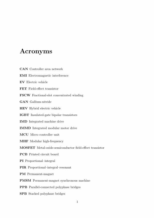
Acronyms
CAN Controller area network
EMI Electromagnetic interference
EV Electric vehicle
FET Field-effect transistor
FSCW Fractional-slot concentrated winding
GAN Gallium-nitride
HEV Hybrid electric vehicle
IGBT Insulated-gate bipolar transistors
IMD Integrated machine drive
IMMD Integrated modular motor drive
MCU Micro controller unit
MHF Modular high-frequency
MOSFET Metal-oxide-semiconductor field-effect transistor
PCB Printed circuit board
PI Proportional–integral
PIR Proportional–integral–resonant
PM Permanent-magnet
PMSM Permanent-magnet synchronous machine
PPB Parallel-connected polyphase bridges
SPB Stacked polyphase bridges
1

2 CONTENTS
SPI Serial peripheral interference
SVM Space vector modulation
VSI Voltage source inverter

Chapter 1
Introduction
1.1 Background
The story of electrical vehicles (EVs) goes far back to the middle of the 19thcentury, when English and French inventors built the very first practical electriccars, see Figure 1.1 [1]. Although the technology of using electricity for propulsionwas interesting at the time, it lost its popularity by 1920, when it could not competewith the combustion engine technology. EVs had finally vanished from the marketby 1935.
Figure 1.1: An electric vehicle in 19th century (© Twitter, Life in Moments,@ histroryinmoment).
In the late 20th century, the world recognized the necessity and importance
3

4 CHAPTER 1. INTRODUCTION
of becoming independent of fossil fuels. It was then the first spark for supportand development of EVs and hybrid electric vehicles (HEVs) appeared again. Mostmajor auto-makers began to explore alternatives to combustion engine vehicles.The first to succeed was Toyota, which introduced the Prius model in 1997. Itbecame the world’s first mass-produced HEV by the early 2000s. Over a decadelater, a small Silicon Valley startup, Tesla Motors, made another revolution in EVhistory. They introduced the Model S, a luxury electric vehicle that could go morethan 200 miles on a single charge [1].
A study from International Energy Agency shows that the global share of us-age of EVs and HEVs has increased rapidly since 2010, see Figure 1.2 [2]. Thecompetition is among more than thirty different models of EVs and HEVs inthe world, including Mitsubishi i-MiEV, Nissan Leaf, Ford Focus Electric, TeslaModel S and X, BMW Active E and i3, Renault Fluence Z.E., Honda Fit EV,Toyota RAV4 EV and Prius, and models from several other manufacturers.
Figure 1.2: Evolution of the global electric car stock, 2010–16 [2](© OECD/IEA2017 Global EV Outlook, IEA Publishing, Licence: www.iea.org/t & c ).
Although there are great varieties in models, designs, and manufacturers ofEVs and HEVs, they all have similar power train designs. The power train in manyconventional electric drives consists of a battery (Li-ion type), a power converter(two-level, three-phase converter), and an electric machine (permanent-magnet syn-chronous machine (PMSM)), which are connected together by power cables. Fig-ure 1.3 shows a typical conventional hybrid electric drive.
Figure 1.4 illustrates the schematic diagram of a typical conventional electricdrive system in an EV or HEV. As can be seen, there is a voltage source inverter(VSI) that acts as an interface between the battery and the electric machine. Letus focus on the power converter for a while, since the topic in this thesis is relatedto the design of a recently proposed topology for the VSI.
As mentioned before, a two-level three-phase converter is usually employedfor this drive system. The switches of the converter are usually selected as silicon-
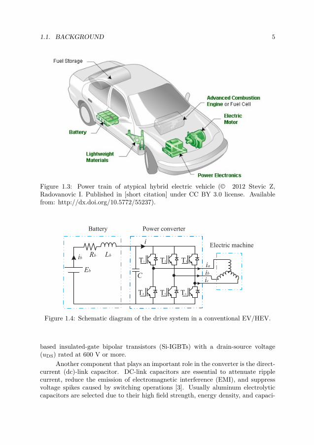
1.1. BACKGROUND 5
Figure 1.3: Power train of atypical hybrid electric vehicle (© 2012 Stevic Z,Radovanovic I. Published in [short citation] under CC BY 3.0 license. Availablefrom: http://dx.doi.org/10.5772/55237).
Eb
Rb Lb
Electric machinei
C
T1 T2 T3
T4 T5 T6
ia
ib
ic
ib
Power converterBattery
Figure 1.4: Schematic diagram of the drive system in a conventional EV/HEV.
based insulated-gate bipolar transistors (Si-IGBTs) with a drain-source voltage(uDS) rated at 600 V or more.
Another component that plays an important role in the converter is the direct-current (dc)-link capacitor. DC-link capacitors are essential to attenuate ripplecurrent, reduce the emission of electromagnetic interference (EMI), and suppressvoltage spikes caused by switching operations [3]. Usually aluminum electrolyticcapacitors are selected due to their high field strength, energy density, and capaci-
6 CHAPTER 1. INTRODUCTION
tance. For battery voltages ranging around 300–600 V, they become rather bulkyand heavy despite the high energy density. Moreover, the operating temperatureof aluminum electrolytic capacitors is limited to below 105C [4].
Large converter size, high voltage stresses on the components, and reliabilityissues have made researchers propose different topologies for electric drives in EVsand HEVs during the last decade. One of these topologies is the so-called integratedmachine drive (IMD). The IMD introduces an integration between the electric ma-chine and the power converter for use in an automotive power train as a singleunit. The IMD was used in Ford Hybrid Escape for the first time in 2004 [5]. TheIMD helps to reduce EMI by eliminating the power cables as well as reducing thesize, weight, and volume. However, it does not help to reduce the voltage stress onthe components. To circumvent this, the integrated modular motor drive (IMMD)concept has been introduced. The IMMD concept provides a promising approachto integrating motor drive electronics into the machine housing by modularizingboth the machine stator and the power converter [6]. This concept not only hasall the advantages of the IMD, but also reduces significantly the voltage stress onthe components. It also enables the potential for achieving a high level of faulttolerance to electrical faults.
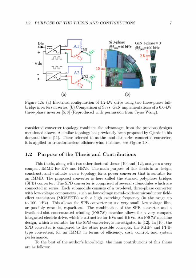
In 2014, the development of the IMMD concept began by evaluation of ma-chine designs suitable for a compact IMMD. A six-phase, ten-pole permanent-magnet (PM) machine with 18 kW power was selected and connected to six, single-phase half-bridge converters. Each phase-leg inverter operates from a nominal 325-V bus by using two discrete 600-V IGBTs in TO-247 packages adopting a switchingfrequency of 20 kHz [7]. A year later, in 2015, the next generation of the IMMDwas introduced. In this concept, a six-phase induction motor with the power of1.2 kW is used. This motor is connected to two, three-phase full-bridge invertersthat are connected in series. This allows the dc-bus voltage for each inverter tobe reduced. Therefore, this structure permits the use of components of low volt-age rating. Twelve gallium-nitride (GaN) switches with the switching frequency100 kHz are used in this design [8]. Another advantage of this design is the use offilm or ceramic capacitors in the dc link, thanks to the lower dc-bus voltage andhigher switching frequency. Moreover, the combination of GaN switches and filmcapacitors creates a very compact electric drive. Figure 1.5 shows the design of thelatter topology but with different components.
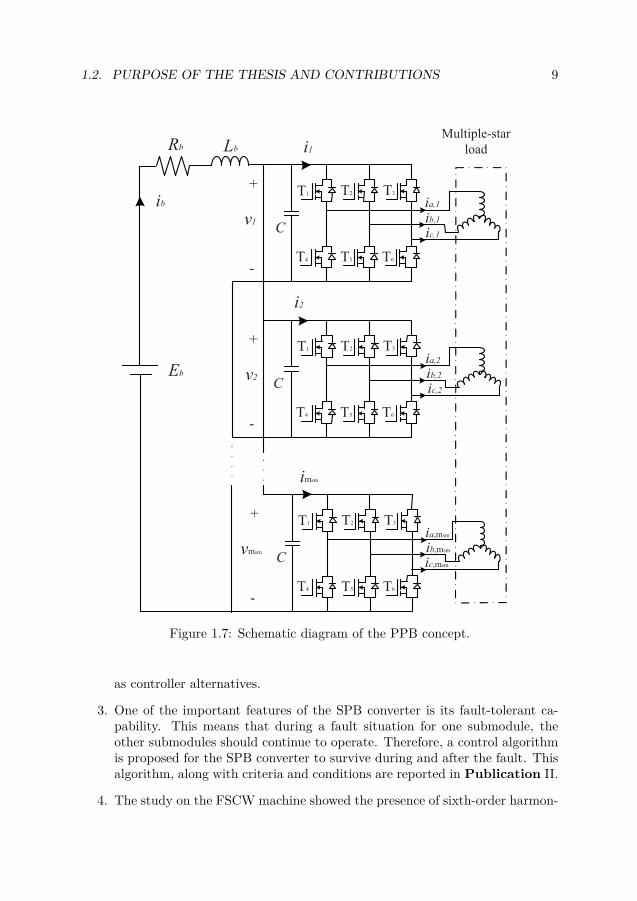
It should be mentioned that the proposals for IMMD concepts applied in EVsor HEVs are not limited to those described above. Reference [9] describes a newconcept of a modular high-frequency (MHF) converter suitable for low-voltage field-effect transistors (FETs), see Figure 1.6. In [10], a parallel-connected polyphasebridges (PPB) converter is suggested, see Figure 1.7.
Although all these topologies are interesting for EVs or HEVs, at least accord-ing to the author’s knowledge, none of them has been designed and constructed in ascale (in the range of 30 to 85 kW) suitable for an electric drive for use in an automo-tive traction application. Therefore, this thesis considers another topology for thepower converter in an IMMD. It is capable to feed a 35-kW electric machine. The
1.2. PURPOSE OF THE THESIS AND CONTRIBUTIONS 7
Figure 1.5: (a) Electrical configuration of 1.2-kW drive using two three-phase full-bridge inverters in series; (b) Comparison of Si vs. GaN implementations of a 0.6-kWthree-phase inverter [5, 8] (Reproduced with permission from Jiyao Wang).
considered converter topology combines the advantages from the previous designsmentioned above. A similar topology has previously been proposed by Gjerde in hisdoctoral thesis [11]. There referred to as the modular series connected converter,it is applied to transformerless offshore wind turbines, see Figure 1.8.
1.2 Purpose of the Thesis and Contributions
This thesis, along with two other doctoral theses [10] and [12], analyzes a verycompact IMMD for EVs and HEVs. The main purpose of this thesis is to design,construct, and evaluate a new topology for a power converter that is suitable foran IMMD. The proposed converter is here called the stacked polyphase bridges(SPB) converter. The SPB converter is comprised of several submodules which areconnected in series. Each submodule consists of a two-level, three-phase converterwith low-voltage components, such as low-voltage metal-oxide-semiconductor field-effect transistors (MOSFETs) with a high switching frequency (in the range upto 100 kHz). This allows the SPB converter to use very small, low-voltage film,or possibly ceramic, capacitors. The combination of the SPB converter and afractional-slot concentrated winding (FSCW) machine allows for a very compactintegrated electric drive, which is attractive for EVs and HEVs. An FSCW machinedesign, which is suitable for the SPB converter, is investigated in [12]. In [10], theSPB converter is compared to the other possible concepts, the MHF- and PPB-type converters, for an IMMD in terms of efficiency, cost, control, and systemperformance.
To the best of the author’s knowledge, the main contributions of this thesisare as follows:

8 CHAPTER 1. INTRODUCTION
Eb
Rb LbMultiphase
load
+
v2
-
T1 T2 T3
T4 T5 T6
ib
imsm
+
vmsm
-
T1 T2 T3
T4 T5 T6
imsm
i1
+
v1
-
T2 T3
T5 T6
ia
i2
ib
C
T1
T4
C
C
Figure 1.6: Schematic diagram of the MHF concept.
1. The main core in this thesis is the design and construction of the SPB con-verter. Three different hardware designs for the SPB converter have beendeveloped over time. The final version of the design, which is capable ofintegration to the machine, is presented in Publication IV.
2. Since several submodules of the SPB converter are connected in series to thevoltage source, the dc-side voltage should split among them equally. There-fore, a control algorithm is proposed to ensure the dc-link stability for theconverter. Publications I and III present the criteria for the stability as well
1.2. PURPOSE OF THE THESIS AND CONTRIBUTIONS 9
Eb
Rb LbMultiple-star
load
C
+
v2
-
T1 T2 T3
T4 T5 T6
ia,2ib,2ic,2
imsm
C
+
vmsm
-
T1 T2 T3
T4 T5 T6
ia,msm
ib,msm
ic,msm
i1
C
+
v1
-
T1 T2 T3
T4 T5 T6
ia,1
ib,1ic,1
i2
ib
Figure 1.7: Schematic diagram of the PPB concept.
as controller alternatives.
3. One of the important features of the SPB converter is its fault-tolerant ca-pability. This means that during a fault situation for one submodule, theother submodules should continue to operate. Therefore, a control algorithmis proposed for the SPB converter to survive during and after the fault. Thisalgorithm, along with criteria and conditions are reported in Publication II.
4. The study on the FSCW machine showed the presence of sixth-order harmon-

10 CHAPTER 1. INTRODUCTION
100 kV
Rb LbMultiple-star
machine
C
+
v2
-
T1 T2 T3
T4 T5 T6
ia,2ib,2ic,2
i9
C
+
v9
-
T1 T2 T3
T4 T5 T6
ia,9ib,9ic,9
i1
C
+
v1
-
T1 T2 T3
T4 T5 T6
ia,1
ib,1ic,1
i2
idc
Figure 1.8: The proposed modular system in [11].
ics in the stator windings. They result in torque ripple and increased eddy-current losses in the permanent magnets. In order to suppress the torqueripple and reduce the permanent-magnet eddy-current losses, two differentcontrol methods are proposed and analyzed in Publications V and VI.
1.3. STRUCTURE OF THE THESIS 11
1.3 Structure of the Thesis
This thesis is in the form of a so called “compilation thesis.” The main chaptersin the thesis are therefore kept brief and serve to introduce key concepts and providea background to the scientific contributions which are further presented in theincluded papers. The chapters are outlined below.
Chapter 1 describes the background information, motivation, and scientific con-tributions of the thesis.
Chapter 2 gives an overview of the SPB converter and introduces the three pro-totype designs developed during the course of this project.
Chapter 3 provides the current controller design for the SPB converter to ensurean equal sharing of the dc-link voltage on the converter submodules.
Chapter 4 investigates the SPB converter operation under fault occurrence.
Chapter 5 considers two different methods for the torque ripple minimization.
Chapter 6 concludes with a summary of the results achieved and plans for futurework.
1.4 List of Publications
The publications originating from the project are:
I. M. Nikouie, L. Jin, L. Harnefors, O. Wallmark, M. Leksell, and S. Norrga,“Analysis of the dc-link stability for the stacked polyphase bridges converter,”in Proc. of the 17th European Conference on Power Electronics and Applica-tions (EPE 2015), Sep. 2015.
II. M. Nikouie, O. Wallmark, L. Harnefors, and H.-P. Nee, “Operation underfault conditions of the stacked polyphase bridges converter,” in Proc. of the42nd Annual Conference of the IEEE Industrial Electronics Society (IECON2016), pp. 2207–2211, Oct. 2016.
III. M. Nikouie, O. Wallmark, L. Jin, L. Harnefors, and H.-P. Nee, “DC-linkstability analysis and controller design for the stacked polyphase bridges con-verter,” IEEE Transactions on Power Electronics, vol. 32, no. 2, pp. 1666–1674, Feb. 2017.
IV. M. Nikouie, H. Zhang, O. Wallmark, and H.-P. Nee, “Highly integratedelectric drives system for tomorrow’s EVs and HEVs,” in Proc. of the 3rdSouthern Power Electronics Conference (SPEC 2017), Dec. 2017.
12 CHAPTER 1. INTRODUCTION
V. M. Nikouie, O. Wallmark, and L. Harnefors, “Torque-ripple minimizationfor permanent-magnet synchronous motors based on harmonic flux estima-tion,” in Proc. of the 20th European Conference on Power Electronics andApplications (EPE 2018), Sep. 2018.
VI. O. Wallmark and M. Nikouie, “DC-link and machine design considerationsfor resonant controllers adopted in automotive PMSM drives,” submitted toIET Electrical Systems in Transportation.The publications below are related in interest, but not included in this thesis:
VII. H. Zhang, O. Wallmark, M. Leksell, and S. Norrga, M. Nikouie, L. Jin, “Ma-chine design considerations for an MHF/SPB-converter based electric drive,”in Proc. of the 40th Annual Conference of the IEEE Industrial ElectronicsSociety (IECON 2014), pp. 3849–3854, Oct. 2014.
VIII. L. Jin, S. Norrga, O. Wallmark, and M. Nikouie, “Control and modulationof the stacked polyphase bridges inverter,” in Proc. IEEE Energy ConversionCongress and Exposition (ECCE 2014), pp. 3023–3029, Sep. 2014.
Chapter 2
Design and Construction of theStacked Polyphase BridgesConverter
2.1 Introduction
It is over a decade since that an IMD, and particularly an IMMD, was firstpresented for power train systems in EVs and HEVs. Adopting an IMD or an IMMDconfiguration with a machine integrated with a power electronic converter into thesame enclosure can be beneficial in several aspects. Some of these benefits include areduction in mass, in volume, in power cables, in EMI effects, and perhaps in cost.Other potential benefits are increase in efficiency as well as improvements in termsof manufacturability and in fault tolerance. Different topologies and approaches forthe construction of such drive systems have been introduced. Generally, there aretwo main categories for an IMD/IMMD integration; axial-end mount integrationand surface mount integration. In axial-end mount integration, the power convert-ers are connected to the drive-end of the machine, while in surface mount integra-tion, the power converters are mounted on the surface of the machine. Figure 2.1shows some of the IMD/IMMD designs within these two categories. Different con-cepts of IMD/IMMD for axial-end mount integration are shown in Figure 2.1(a),(b), and (d). Figure 2.1(c) shows the concept of surface-mount integration that hasbeen introduced for aircraft applications (see the associated references in the figurecaption).
13

14CHAPTER 2. DESIGN AND CONSTRUCTION OF THE STACKED
POLYPHASE BRIDGES CONVERTER
(a) (b)
(c) (d)
Figure 2.1: Different designs of IMD/IMMD: (a) IMMD concept with nine-phasemodular stator windings and nine half-bridge IGBT-based converters [6] (© [2007]IEEE); (b) IMMD concept with 18-phase machine and 18 half-bridge GaN-basedconverters [8] (Reproduced with permission from Jiyao Wang); (c) IMMD conceptwith six-phase machine and six full-bridge MOSFET-based converter [13] (© [2010]IEEE); (d) Siemens IMD technology for EV traction drives [14] (© Phys.org 2003 -2019, Science X network).
2.2 The SPB-Converter Concept
This thesis considers a recently proposed IMMD topology for use in EVs andHEVs applications. Figure 2.2 illustrates the topology. In this topology, the con-verter is comprised of an arbitrary number of submodules that are connected inseries to a dc-source voltage (e.g., an automotive traction battery). Due to thedesign, this converter is termed the stacked polyphase bridges (SPB). Each sub-module of the SPB topology comprises of a two-level three-phase converter. Thetotal dc-link voltage should be divided equally among the submodules. Therefore,each converter can be designed with low-voltage components, such as low-voltageMOSFETs with a high switching frequency (in the range of 100 kHz). The combina-
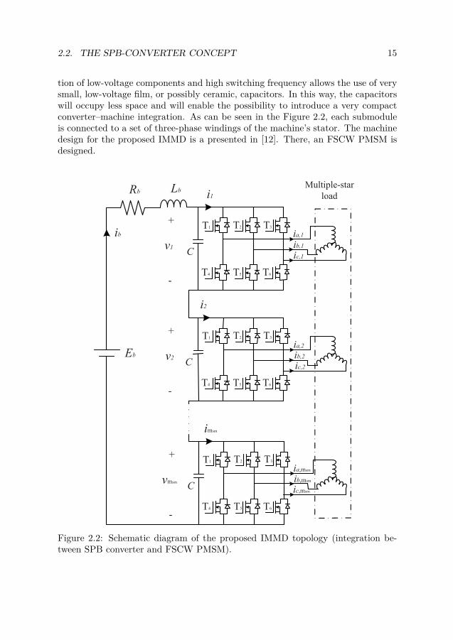
2.2. THE SPB-CONVERTER CONCEPT 15
tion of low-voltage components and high switching frequency allows the use of verysmall, low-voltage film, or possibly ceramic, capacitors. In this way, the capacitorswill occupy less space and will enable the possibility to introduce a very compactconverter–machine integration. As can be seen in the Figure 2.2, each submoduleis connected to a set of three-phase windings of the machine’s stator. The machinedesign for the proposed IMMD is a presented in [12]. There, an FSCW PMSM isdesigned.
Eb
Rb Lb Multiple-star
load
C
+
v2
-
T1 T2 T3
T4 T5 T6
ia,2ib,2ic,2
imsm
C
+
vmsm
-
T1 T2 T3
T4 T5 T6
ia,msm
ib,msm
ic,msm
i1
C
+
v1
-
T1 T2 T3
T4 T5 T6
ia,1
ib,1ic,1
i2
ib
Figure 2.2: Schematic diagram of the proposed IMMD topology (integration be-tween SPB converter and FSCW PMSM).
16CHAPTER 2. DESIGN AND CONSTRUCTION OF THE STACKED
POLYPHASE BRIDGES CONVERTER
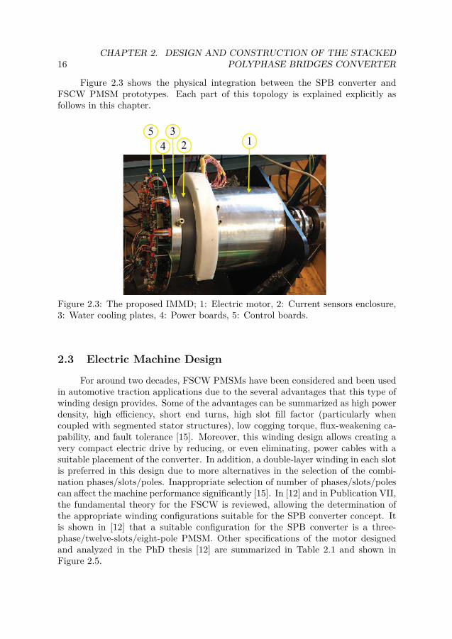
Figure 2.3 shows the physical integration between the SPB converter andFSCW PMSM prototypes. Each part of this topology is explained explicitly asfollows in this chapter.
Figure 2.3: The proposed IMMD; 1: Electric motor, 2: Current sensors enclosure,3: Water cooling plates, 4: Power boards, 5: Control boards.
2.3 Electric Machine Design
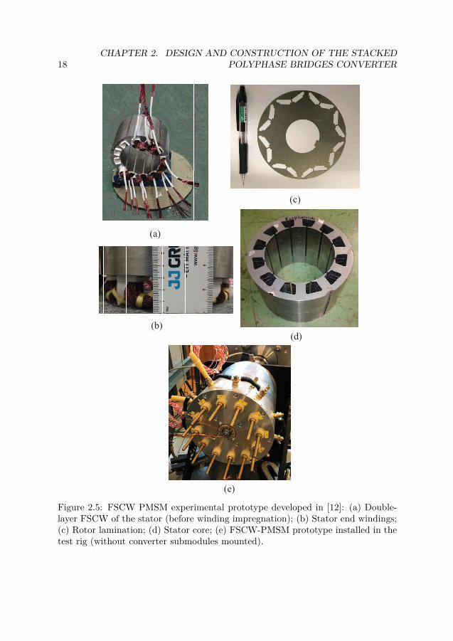
For around two decades, FSCW PMSMs have been considered and been usedin automotive traction applications due to the several advantages that this type ofwinding design provides. Some of the advantages can be summarized as high powerdensity, high efficiency, short end turns, high slot fill factor (particularly whencoupled with segmented stator structures), low cogging torque, flux-weakening ca-pability, and fault tolerance [15]. Moreover, this winding design allows creating avery compact electric drive by reducing, or even eliminating, power cables with asuitable placement of the converter. In addition, a double-layer winding in each slotis preferred in this design due to more alternatives in the selection of the combi-nation phases/slots/poles. Inappropriate selection of number of phases/slots/polescan affect the machine performance significantly [15]. In [12] and in Publication VII,the fundamental theory for the FSCW is reviewed, allowing the determination ofthe appropriate winding configurations suitable for the SPB converter concept. Itis shown in [12] that a suitable configuration for the SPB converter is a three-phase/twelve-slots/eight-pole PMSM. Other specifications of the motor designedand analyzed in the PhD thesis [12] are summarized in Table 2.1 and shown inFigure 2.5.

2.3. ELECTRIC MACHINE DESIGN 17
A3
B4
A1
A2
A4
B1
C1
B2
B3
C2
C3
C4
Figure 2.4: FSCW configuration divided into four submodules.
Table 2.1: Machine data [12]
Machine parameters
P 35 kW Continuous powerT 85 Nm Continuous torqueωs 4000 rpm Base speedIs 97 A Rated rms current per submoduleRs 4.3 mΩ Stator resistance per submoduleLd 103 µH d-direction inductance per submoduleLq 188 µH q-direction inductance per submoduleψm 0.020 Vs Flux linkage per submoduleδ 0.75 mm Air-gap heighth 7.51 mm Magnet heightrr 69.3 mm Rotor radiusrs 110 mm Stator radiusl 200 mm Active length
18CHAPTER 2. DESIGN AND CONSTRUCTION OF THE STACKED
POLYPHASE BRIDGES CONVERTER
(a)
(b)
(c)
(d)
(e)
Figure 2.5: FSCW PMSM experimental prototype developed in [12]: (a) Double-layer FSCW of the stator (before winding impregnation); (b) Stator end windings;(c) Rotor lamination; (d) Stator core; (e) FSCW-PMSM prototype installed in thetest rig (without converter submodules mounted).

2.4. POWER CONVERTER DESIGN 19
2.4 Power Converter Design
Power BoardsAs mentioned in Section 2.3, an FSCW PMSM prototype has been designed
with twelve phases and eight poles that is suitable for the SPB converter withfour submodules. Therefore, the SPB converter which is presented in this thesis isdesigned with four submodules. It is also assumed that the dc-voltage source is 400V. Consequently, each submodule is designed using low-voltage components in therange of 100 V. Each submodule is designed as a printed circuit board (PCB). Sincethe rated machine current is 97 Arms, this six-layer PCB with the total thicknessof 3.1 mm is capable of handling 100 Arms. Figure 2.6 shows the power board ofthe SPB converter and Table 2.2 lists the components on the power board.
dc-in
dc-out
Figure 2.6: SPB converter with four submodules.
Table 2.2: Power board components
Components Part number Manufacturer
DC-link capcitor 100 µF, 160 V R60EW61605000K KemetMOSFET 130 A, 150 V IPB065N15N3 G InfineonGate drivers 3.3 V/ 17 V ADuM4135 Analog devicesTransformer 5 : 17 V TR750342879 Wurth electronics
In order to reduce the switching losses of the converter, two transistors act in
20CHAPTER 2. DESIGN AND CONSTRUCTION OF THE STACKED
POLYPHASE BRIDGES CONVERTER
parallel as the upper and lower switch in each phase leg, respectively. Although aprecise model for power loss calculation of power MOSFETs is presented in [10], aquick loss calculation according to the Infineon guidelines for MOSFET loss basedon the data sheet parameters [16] is reported here. In this guideline, the total lossis defined as the switching loss Psw and the conduction loss Pc. The calculation ofthe conduction loss is quite simple. It is defined as Pc =RDSonI
2Drms
, whereas theswitching losses are given as
Psw = (Eon + Eoff)fsw (2.1)
where fsw is the switching frequency, and Eon and Eoff are the loss energies duringthe switch-on and switch-off transients, respectively. They are defined as
Eon =∫ tri+tfu
0uDSiDdt (2.2)
Eoff =∫ tru+tfi
0uDSiDdt
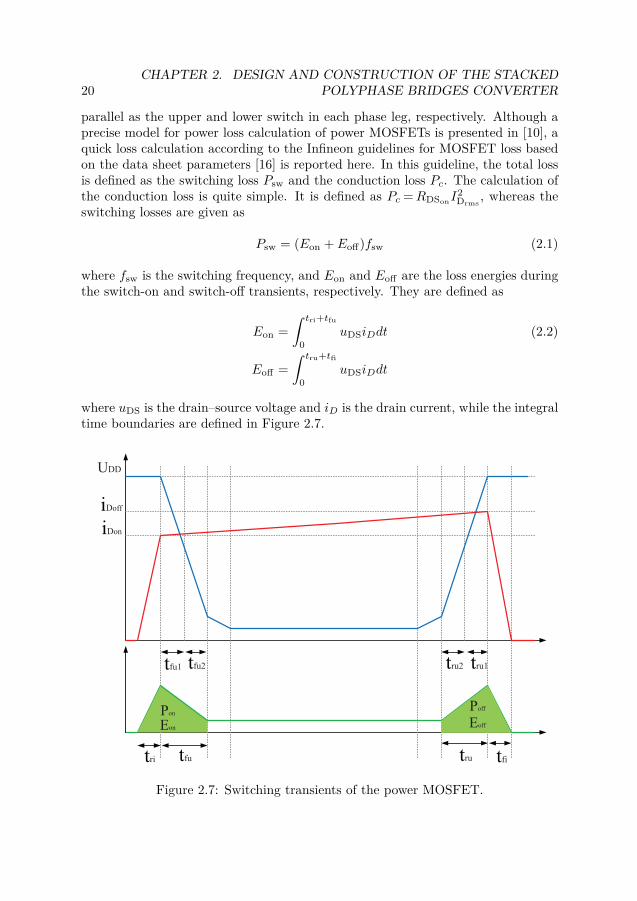
where uDS is the drain–source voltage and iD is the drain current, while the integraltime boundaries are defined in Figure 2.7.
UDD
Doff
Don
Pon
Eon
Poff
Eoff
fu1 fu2 ru2 ru1
ri fu ru fi
Figure 2.7: Switching transients of the power MOSFET.
2.4. POWER CONVERTER DESIGN 21
The calculation results show that the total loss for one MOSFET—describedin Table 2.2—with fsw = 100 kHz at the rated current (i.e., 100 Arms) is 132 W.Considering four submodules with six switches on each, i.e., 24 MOSFETs in total,the total loss is 3.2 kW. If each switch is implemented by two paralleled MOSFETs,the total loss of each switch reduces to 55 W and the total loss for 48 MOSFETson the power board is around 2.6 kW.
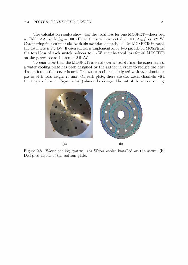
To guarantee that the MOSFETs are not overheated during the experiments,a water cooling plate has been designed by the author in order to reduce the heatdissipation on the power board. The water cooling is designed with two aluminumplates with total height 20 mm. On each plate, there are two water channels withthe height of 7 mm. Figure 2.8-(b) shows the designed layout of the water cooling.
(a) (b)
Figure 2.8: Water cooling system: (a) Water cooler installed on the setup; (b)Designed layout of the bottom plate.
22CHAPTER 2. DESIGN AND CONSTRUCTION OF THE STACKED
POLYPHASE BRIDGES CONVERTER
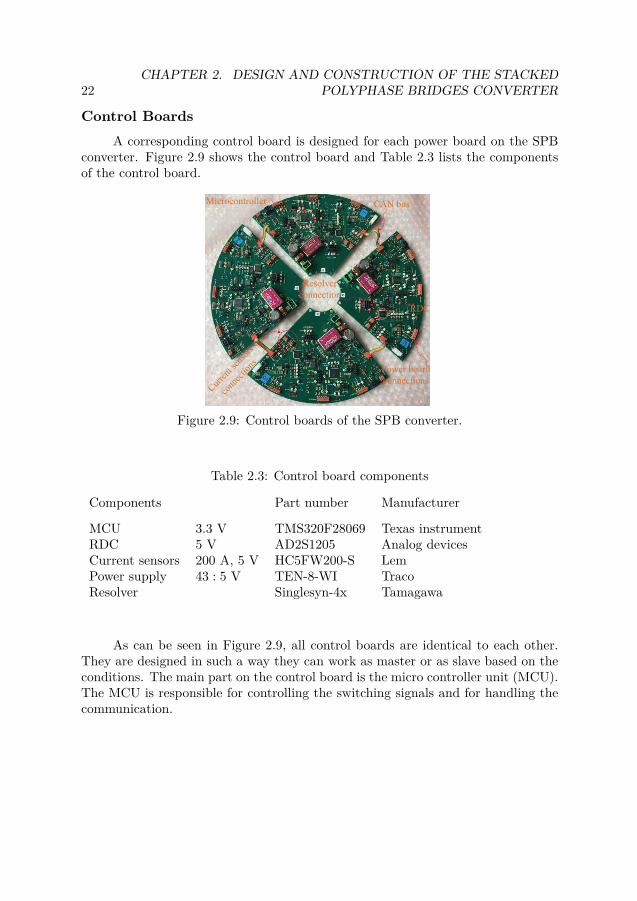
Control BoardsA corresponding control board is designed for each power board on the SPB
converter. Figure 2.9 shows the control board and Table 2.3 lists the componentsof the control board.
Figure 2.9: Control boards of the SPB converter.
Table 2.3: Control board components
Components Part number Manufacturer
MCU 3.3 V TMS320F28069 Texas instrumentRDC 5 V AD2S1205 Analog devicesCurrent sensors 200 A, 5 V HC5FW200-S LemPower supply 43 : 5 V TEN-8-WI TracoResolver Singlesyn-4x Tamagawa
As can be seen in Figure 2.9, all control boards are identical to each other.They are designed in such a way they can work as master or as slave based on theconditions. The main part on the control board is the micro controller unit (MCU).The MCU is responsible for controlling the switching signals and for handling thecommunication.
2.5. POWER CONVERTER DESIGN (GENERATIONS I AND II) 23
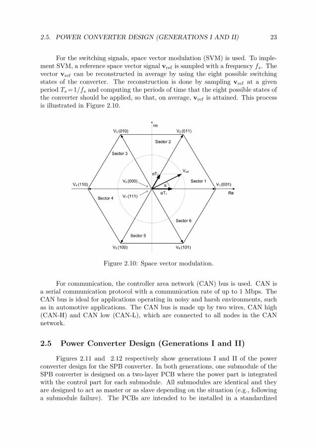
For the switching signals, space vector modulation (SVM) is used. To imple-ment SVM, a reference space vector signal vref is sampled with a frequency fs. Thevector vref can be reconstructed in average by using the eight possible switchingstates of the converter. The reconstruction is done by sampling vref at a givenperiod Ts=1/fs and computing the periods of time that the eight possible states ofthe converter should be applied, so that, on average, vref is attained. This processis illustrated in Figure 2.10.
Figure 2.10: Space vector modulation.
For communication, the controller area network (CAN) bus is used. CAN isa serial communication protocol with a communication rate of up to 1 Mbps. TheCAN bus is ideal for applications operating in noisy and harsh environments, suchas in automotive applications. The CAN bus is made up by two wires, CAN high(CAN-H) and CAN low (CAN-L), which are connected to all nodes in the CANnetwork.
2.5 Power Converter Design (Generations I and II)
Figures 2.11 and 2.12 respectively show generations I and II of the powerconverter design for the SPB converter. In both generations, one submodule of theSPB converter is designed on a two-layer PCB where the power part is integratedwith the control part for each submodule. All submodules are identical and theyare designed to act as master or as slave depending on the situation (e.g., followinga submodule failure). The PCBs are intended to be installed in a standardized

24CHAPTER 2. DESIGN AND CONSTRUCTION OF THE STACKED
POLYPHASE BRIDGES CONVERTER
subrack and in a vertical orientation. The PCBs dimensions are 100 mm as theheight and 200 mm as the width. Figure 2.13 shows the second generation SPBdesign with four submodules when installed in a rack and connected to RL loads.The components (e.g., MOSFETs) are selected to handle 100 V, but the maximumcurrent of the board was limited to 20 A.
Thre
e-phas
e co
nnec
tor
Capacitors
(Ceramic type) Two-level three-phase converter
(MOSFETs & GDUs)
DC
sourc
e co
nnec
tor
SPI bus
MCU
Figure 2.11: One submodule of the SPB converter of generation I.
SPI bus
MCU
Capacitors
(Film type)
Thre
e-phas
e co
nnec
tor
DC
sourc
e co
nnec
tor
Two-level three-phase converter
(MOSFETs & GDUs)
Figure 2.12: One submodule of the SPB converter of generation II.
Apart from the types of components, the use of a serial peripheral interface(SPI) bus as communication bus is the only significant difference between thesegenerations and the final design. Unlike the CAN bus, the SPI bus uses a nonaddressable base protocol and may be faster than the CAN protocol. However, itrequires four signals (wires) for the communication between the master and oneslave board. In other words, the hardware design for the SPI bus is somewhat
2.5. POWER CONVERTER DESIGN (GENERATIONS I AND II) 25
Four submodules on the rack
Resistance load
Inductance load
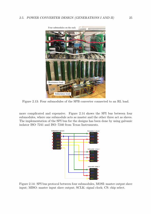
(a)Figure 2.13: Four submodules of the SPB converter connected to an RL load.
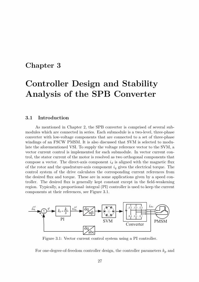
more complicated and expensive. Figure 2.14 shows the SPI bus between foursubmodules, where one submodule acts as master and the other three act as slaves.The implementation of the SPI bus for the designs has been done by using galvanicisolator ISO–7241 and ISO–7240 from Texas Instruments.
Figure 2.14: SPI bus protocol between four submodules, MOSI: master output slaveinput; MISO: master input slave output; SCLK: signal clock; CS: chip select.

26CHAPTER 2. DESIGN AND CONSTRUCTION OF THE STACKED
POLYPHASE BRIDGES CONVERTER
2.6 Summary
This chapter introduces a new topology for an IMMD which is suitable forEV and HEV applications. The new IMMD topology is a combination of the SPBconverter and the FSCW PMSM that provides a very compact integrated electricdrive system. This converter–motor integration potentially benefits from severaladvantages, e.g., the reduction of power cables between converter and machine,which results in reduction of EMI, weight, and size. A presentation of the three dif-ferent designs for the SPB converter and the components is included. This chapteralso serves an introduction to Publication IV.
Chapter 3
Controller Design and StabilityAnalysis of the SPB Converter
3.1 Introduction
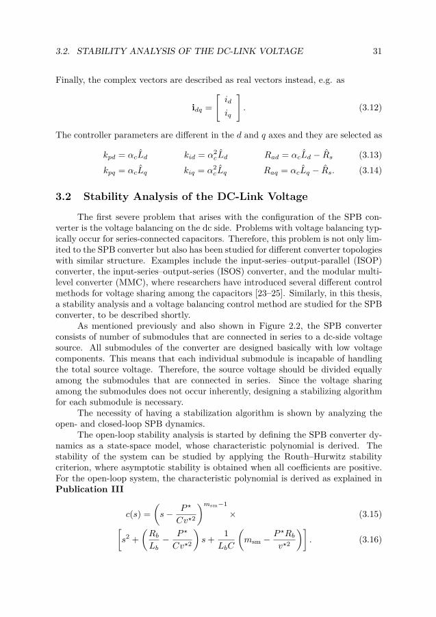
As mentioned in Chapter 2, the SPB converter is comprised of several sub-modules which are connected in series. Each submodule is a two-level, three-phaseconverter with low-voltage components that are connected to a set of three-phasewindings of an FSCW PMSM. It is also discussed that SVM is selected to modu-late the aforementioned VSI. To supply the voltage reference vector to the SVM, avector current control is implemented for each submodule. In vector current con-trol, the stator current of the motor is resolved as two orthogonal components thatcompose a vector. The direct-axis component id is aligned with the magnetic fluxof the rotor and the quadrature-axis component iq gives the electrical torque. Thecontrol system of the drive calculates the corresponding current references fromthe desired flux and torque. These are in some applications given by a speed con-troller. The desired flux is generally kept constant except in the field-weakeningregion. Typically, a proportional–integral (PI) controller is used to keep the currentcomponents at their references, see Figure 3.1.
iabcidq
+-
e
abc
dq
kp +kis
vdq αβ
dq
PMSMConverter
SVMPI
∑
ref ref
Figure 3.1: Vector current control system using a PI controller.
For one-degree-of-freedom controller design, the controller parameters kp and
27

28CHAPTER 3. CONTROLLER DESIGN AND STABILITY ANALYSIS OF
THE SPB CONVERTER
ki as described in [17] can be selected based on the motor parameters. For thesimplicity, let us for now assume that the motor is non-salient, meaning that Ld =Lq = Ls. Then
kp = αcLs ki = αcRs αc = ln 9tr
(3.1)
where “hats” denote model motor parameters, which should be as close estimatesof the true motor parameters (stator inductance and stator resistance) as possible,ideally so that Ls = Ls and Rs = Rs, αc is the closed-loop system bandwidth(expressed in rad/s), and tr is the rise time of the closed-loop system. The latteris usually selected around some milliseconds, giving a bandwidth in the range ofthousands of radians per second. However, the problem with one-degree-of-freedomcontroller design is the poor control of the load disturbance which is caused by theback electromotive force (EMF) of the motor. This is because ki is small, sinceRs is relatively small. If one decides to increase the value of ki by a factor, let ussay 10, then an unwanted overshoot appears on the current response to a referencechange. To avoid this, a two-degree-of-freedom current controller is suggested [18].In this controller an active resistance Ra = αcLs − Rs is introduced as the gainin an inner feedback loop. The active resistance has the effect of increasing Rsto Rs + Ra, which equals αcL if Rs = Rs. Consequently, in (3.1), Rs should bereplaced by αcLs, which is typically much larger than Rs. We then obtain
kp = αcLs ki = α2cLs. (3.2)
To evaluate the closed-loop response of the current controller, the dynamic modelof the system in the rotating dq reference frame is analyzed. The dynamic modelis illustrated in Figure 3.2 and can be described as
=
~~
Rs Ls
i
dq Evdq
dq
++
- -
Figure 3.2: Converter connected to a motor winding that is consisting of a resistive-inductive impedance and a back EMF.
Lsdidqdt
= vdq −Rsidq − jωeLsidq −Edq (3.3)
where idq= id + jiq is the stator current vector, vdq=vd + jvq is the stator voltagevector, Edq = Ed + jEq is the back EMF vector, and ωe is the electrical angular

3.1. INTRODUCTION 29
frequency of the rotor. Equation (3.3) expresses the complex form of the dynamicmodel [19]. The dynamic model in component form is described as
Lsdiddt
= vd −Rsid + ωeLsiq − Ed (3.4)
Lsdiqdt
= vq −Rsiq − ωeLsid − Eq. (3.5)
In (3.4), there are two cross-coupled first-order subsystems, where the cross couplingcomes from the terms ωeLsiq and ωeLsid. Similarly in (3.3), the term jωeLsidqshows the cross coupling that the motor has inherently. This cross coupling willdegrade the overall performance of the motor [20]. To overcome this problem, adecoupler jωeLsi =jωeLs(id + jiq) is added to the inner feedback loop.
Although the vector current controller offers a high bandwidth and goodsteady-state performance, during large transients the demanded reference voltage ofthe controller may exceed the VSI voltage capability, which causes over modulation.To avoid this, a saturation scheme must be used [21]. In any case that vref
dq does notexceed the SVM pattern, then the vector vref
dq is equal to vrefdq , see Figure 3.3. On
the other hand, if vrefdq exceeds the SVM pattern, then the saturation (sat) block
limits the vector vrefdq to the boundary of the SVM pattern. This saturation results
in reduced performance of the current controller due to integrator windup. Refer-ence [22] introduces the back-calculation method as a suitable anti-windup scheme.As shown in Figure 3.3, when the saturation block is activated, the difference signalvrefdq −vref
dq is not equal to zero and this modifies the integrator input so that windupcan be avoided.
idq
+-
ref
dqkp vdq
PI
sat vdq
- +
kp
1
abcdq
Ra -
ki
s
+
+ -
j eLs
ref ref
+ +
SVM
iabc
PMSMConverter
idq
edq
Figure 3.3: Vector current control system with using PI controller including activeresistance and anti-windup.
Considering the calculation of vrefdq from Figure 3.3—while the saturation block
is not active and the SVM is disregarded—and substituting in (3.3) gives
idq = Gc(s)irefdq − Y (s)Edq (3.6)

30CHAPTER 3. CONTROLLER DESIGN AND STABILITY ANALYSIS OF
THE SPB CONVERTER
where Gc(s) is the closed-loop transfer function and Y (s) is the admittance of theclosed-loop system, which are given as
Gc(s) = αcs+ αc
Y (s) = s
(s+ αc)2Ls. (3.7)
Remember that we assumed a non-salient motor for the above current controllerdesign. Now if we consider a salient motor, which means that Ld 6= Lq, then thedynamic model (3.4) is rewritten as
Lddiddt
= vd −Rsid + ωeLqiq − Ed (3.8)
Lqdiqdt
= vq −Rsiq − ωeLdid − Eq. (3.9)
As explained before, there is a corresponding relationship between the complex form(3.3) and component form (3.4). However, (3.8) does not have correspondence tothe complex form due to the different values of Ld and Lq. Therefore, Figure 3.3needs to be modified as shown in Figure 3.4, where the controller parameters and
idq
+-
ref
dqkp vdq
PI
sat vdq
- +
kp
abcdq
Ra -
ki
s
+
+ -
J eLs
ref ref
+ +
SVM
iabc
PMSMConverter
idq
-1
edq
Figure 3.4: Vector current control system with using PI controller including activeresistance and anti-windup for non-salient machine.
the inductance are not scalars any longer, but are expressed in matrix form
kp =[kpd 00 kpq
]ki =
[kid 00 kiq
](3.10)
Ra =[kad 00 kaq
]Ls =
[Ld 00 Lq
].
The imaginary unit j in matrix form is defined as
J =[
0 −11 0
](3.11)
3.2. STABILITY ANALYSIS OF THE DC-LINK VOLTAGE 31
Finally, the complex vectors are described as real vectors instead, e.g. as
idq =[id
iq
]. (3.12)
The controller parameters are different in the d and q axes and they are selected as
kpd = αcLd kid = α2cLd Rad = αcLd − Rs (3.13)
kpq = αcLq kiq = α2cLq Raq = αcLq − Rs. (3.14)
3.2 Stability Analysis of the DC-Link Voltage
The first severe problem that arises with the configuration of the SPB con-verter is the voltage balancing on the dc side. Problems with voltage balancing typ-ically occur for series-connected capacitors. Therefore, this problem is not only lim-ited to the SPB converter but also has been studied for different converter topologieswith similar structure. Examples include the input-series–output-parallel (ISOP)converter, the input-series–output-series (ISOS) converter, and the modular multi-level converter (MMC), where researchers have introduced several different controlmethods for voltage sharing among the capacitors [23–25]. Similarly, in this thesis,a stability analysis and a voltage balancing control method are studied for the SPBconverter, to be described shortly.
As mentioned previously and also shown in Figure 2.2, the SPB converterconsists of number of submodules that are connected in series to a dc-side voltagesource. All submodules of the converter are designed basically with low voltagecomponents. This means that each individual submodule is incapable of handlingthe total source voltage. Therefore, the source voltage should be divided equallyamong the submodules that are connected in series. Since the voltage sharingamong the submodules does not occur inherently, designing a stabilizing algorithmfor each submodule is necessary.
The necessity of having a stabilization algorithm is shown by analyzing theopen- and closed-loop SPB dynamics.
The open-loop stability analysis is started by defining the SPB converter dy-namics as a state-space model, whose characteristic polynomial is derived. Thestability of the system can be studied by applying the Routh–Hurwitz stabilitycriterion, where asymptotic stability is obtained when all coefficients are positive.For the open-loop system, the characteristic polynomial is derived as explained inPublication III
c(s) =(s− P ?
Cv?2
)msm−1× (3.15)[
s2 +(RbLb− P ?
Cv?2
)s+ 1
LbC
(msm −
P ?Rbv?2
)]. (3.16)
32CHAPTER 3. CONTROLLER DESIGN AND STABILITY ANALYSIS OF
THE SPB CONVERTER
where Lb and Rb are the inductance and resistance of the voltage source, respec-tively, P ? is the active-power operating point for each submodule, v? is the voltageacross each submodule capacitor, C is the dc-link capacitance, and msm is thenumber of submodules.
If msm =1, the total dc-link voltage stability is always achieved when P ?<0.This means that in the generating mode of operation, the system is always stable.However, in the motoring mode when P ?>0, problems with instability may occur.This means that the stability criterion may not always be fulfilled. For msm > 1,the system is always unstable in the motoring mode and closed-loop stabilization isnecessary. In the generating mode, the open-loop system is asymptotically stable.
Following from the closed-loop stability analysis, an active stabilization al-gorithm is added to the current controller. In this algorithm, an increment, alsoknown as stabilization term, is added to the current-component references iref
dq foreach converter submodule. The stabilization term for each submodule is madeproportional to the individual voltage deviation from the reference voltage vref.
irefd,k = id0 + gid0 (vk − vref) (3.17)irefq,k = iq0 + giq0 (vk − vref) (3.18)
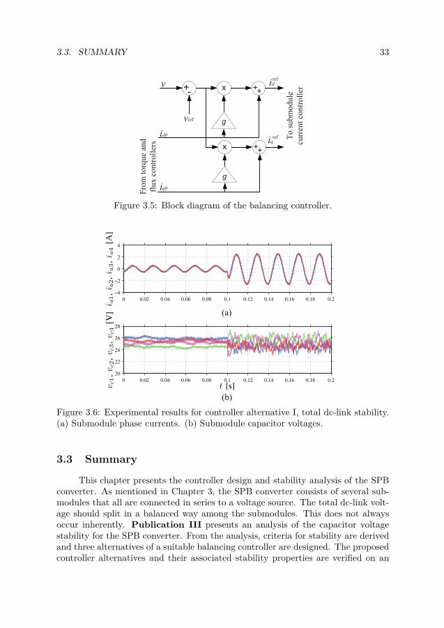
where id0 and iq0 are set respectively by the flux (field weakening) and torquecontrollers, vk is the dc-link voltage of the kth submodule (which is measured locallyon the board). Based on the choice of vref, three alternatives for the balancingcontroller (Figure 3.5) have been analyzed, namely
vref =
vΣ/msm for controller alternative IEb/msm for controller alternative IIvΣf/msm for controller alternative III
(3.19)
where vΣ is the sum of the dc-link voltage of all msm submodules, Eb is the dcsource voltage, and vΣf is a low-pass filtered variant of vΣ.
The drawback of controller alternative I is its requirement of a minimumdc-link capacitance. In controller alternative I, the stability of the system holds if
C >P ?Lbv?2Rb
. (3.20)
It may happen that a smaller capacitance than (3.20) will be sufficient from otheraspects, such as dc-link current harmonics, but the value given in (3.20) is stillrequired in order to obtain a stable system. Controller alternative II does not needthis minimum required capacitance.
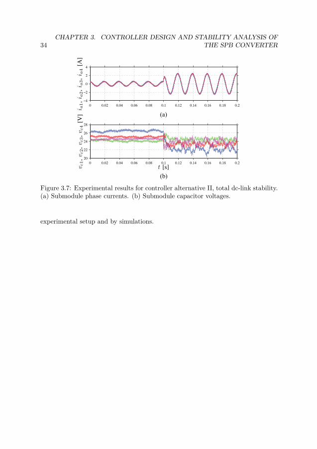
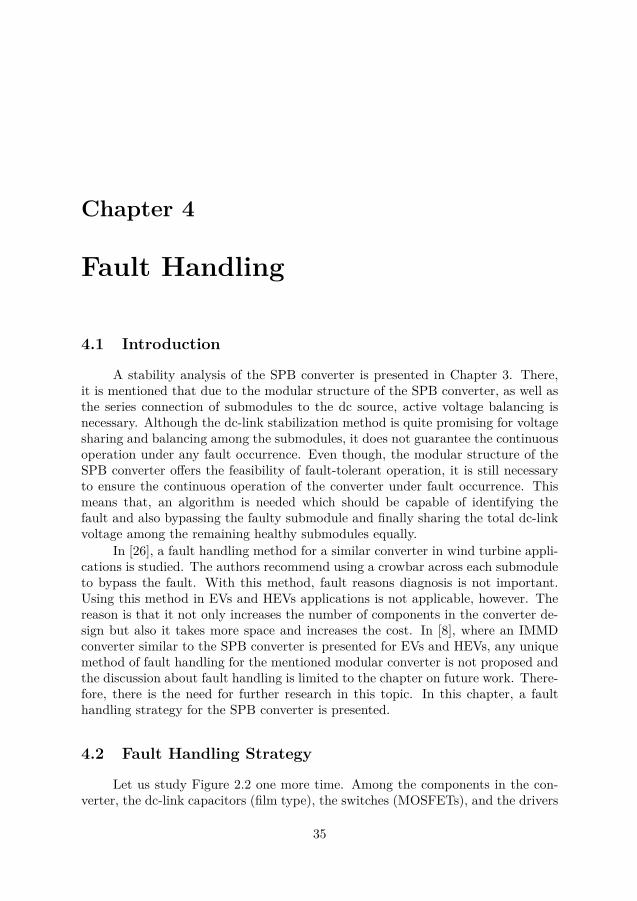
These three control alternatives have been evaluated in a Matlab/Simulinkmodel and also experimentally with the prototype. Some of the results are shownin Figures 3.6 and 3.7. The experimental setup is shown in Figure 2.13.
3.3. SUMMARY 33
+-
x
g
++
refid
refiq
vref
v
iq0
id0F
rom
to
rque
and
flu
x c
ontr
oll
ers
To
sub
mo
dule
curr
ent
contr
oll
er
x ++
g
Figure 3.5: Block diagram of the balancing controller. !"# $%%%&'()*(+&$,)*,)-,.%'%/%+&',)$+*01,/23#0),2#04%5'6('7#8 "
49:2;2 %<=>?9@>ABCD?>EFDBEGH?BI>JHAB?HDD>?CDB>?ACB9K>$0EFL@HMFD>MJND9AOEBCL9D9BP2QCR*FL@HMFD>JC=CJ9BH?KHDBC:>E2QLR1C?9CB9HAHGS2QJR,A>=ICE>JF??>ABQTUVWRHG>CJIEFL@HMFD>29AGH?@CB9HAL>BX>>ABI>GHF?EFL@HMFD>EQ>2:20MJND9AOKHDBNC:>ER9EB?CAE@9BB>MBI?HF:IBI>*-$LFEBICB9EJHF=D>MBHBI>Y*-2,A>EFL@HMFD>H=>?CB>ECE@CEB>?CAMBI>HBI>?EH=N>?CB>CEEDCK>E2$ACMM9B9HA0BI>EX9BJI>EC?>Z,*4%&EX9BIC[\NO] EX9BJI9A:G?>_F>AJP249ACDDP0BI>?>C?>BI?>>JF??>ABE>ANEH?EHA>CJI-+5BH@>CEF?>BI>=ICE>JF??>ABECAMBI>MJND9AOJF??>AB2(DDBI>EFL@HMFD>EC?>M>E9:A>MEHBICBBI>PJCAH=>?CB>CELHBI@CEB>?CAMEDCK>2$ABI>JCE>HGCGCFDBHABI>@CEB>?EFL@HMFD>0HA>HGBI>EDCK>EJCAEX9BJIBHH=>?CB>CE@CEB>?2$ABI>HBI>?XH?ME0BI>JHAB?HDEPEB>@ICEBI>=HB>AB9CDBHL>GCFDBBHD>?CAB2abcdefg$ABI>JCE>HGCGCFDBHAHA>EFL@HMFD>0BICBEFLN@HMFD>@FEBL>EIH?BJ9?JF9B>ML>JCFE>HGBI>E>?9>EJHAA>JB9HA2Q&I>EFL@HMFD>EBIFE@FEBICK>CKHDBC:>?CB9A:EFGhJ9>ABBHX9BIEBCAMBI>9AJ?>CE>MKHDBC:>XI>AJICA:9A:G?H@ijk BHijklmE>?9>ENJHAA>JB>MEFL@HMFD>E2R&HECG>DPJ?>CB>BI9EEIH?BJ9?JF9B9EM9GhJFDBCAMX9DDL>EBFM9>MGF?BI>?9AGFBF?>?>E>C?JI2ngopqbrsptauvwxyzeocqyty|&HEBC?BX9BI0BI>EFL@HMFD>MJND9AOEBCL9D9BP9E><C@9A>M?>N:C?M9A:BI>J?9B>?9HAQ3R2(E><=DC9A>M9A*>JB9HA$$N4 ~E9AJ>BI>?>9ECADHCM~GH?S\0EFL@HMFD>MJND9AOEBCL9D9BP9EDHEB0XI>?>CEGH?S\CEP@=BHB9JEBCLD>9EHLBC9A>M2&I9E9EK>?9h>MLP?C@=9A:SF=CAMMHXAL>BX>>ABI>><B?>@>KCDF>E\[CAMm2&I>?>EFDBEIHXA9A49:2;C:?>>EX>DDX9BIBI>BI>H?P2
49:2!2 %<=>?9@>ABCD?>EFDBEGH?BI>JHAB?HDD>?CDB>?ACB9K>$0BHBCDMJND9AOEBCNL9D9BP2QCR*FL@HMFD>=ICE>JF??>ABE2QLR*FL@HMFD>JC=CJ9BH?KHDBC:>E2grctuvwxyzeocqyty|$AH?M>?BHK9HDCB>BI>EBCL9D9BPJHAM9B9HAQ33RGH?BI>JHANB?HDD>?CDB>?ACB9K>$0B>EB9A:9BE=?CJB9JCDKCD9M9BP0C?>DCB9K>DPDC?:>C9?NJH?>9AMFJBH?0X9BIC#N@]9AMFJBCAJ>CAMC82N9ANA>??>E9EBCAJ>09E9AEBCDD>M9AE>?9>EX9BIBI>9AI>?>AB9AMFJBCAJ>HGBI>EHF?J>0:9K9A:[@]CAMmm2&H:>BI>?X9BIm\\.CAM[10Q33R:9K>EC@9A9@F@JC=CJN9BCAJ>HG[4GH?EBCL9D9BP2*9AJ>m\\40CAFAEBCLD>EPEB>@XHFDML>><=>JB>M2%<=>?9@>ABCD?>EFDBEX9BIBI>JHAB?HDD>?CDB>?ACB9K>$C?>EIHXA9A49:2!24H?\mE0BI>EBCL9D9BPJHAM9B9HAQ33RIHDME2(B\mE0BI>JF??>AB9E9AJ?>CE>MCAMQ33R9EK9HDCB>M2&IFE09AEBCL9D9BPXHFDML>><=>JB>MGH?\mE0LFBCEJCAL>E>>A0BI>EPEB>@P>B?>@C9AEEBCLD>2Q&I>EB>CMPNEBCB>M>K9CB9HAEBICBJCAL>E>>A9A49:2!QLRC?>MF>BHED9:IB9AM9K9MFCDM9GG>?>AJ>EL>BX>>ABI>EFL@HMFD>JH@=HA>ABE2R&I>?>CEHAGH?BI>L>BB>??>EFDBBICA><=>JB>MHGBI>JHAB?HDD>?CDB>?ACB9K>$@CPL>EH@>XICBEF?=?9E9A:2&I>?>9EC?>DCB9K>DPDC?:>B9@>M>DCP\@E9ABI>*-$JH@@FA9JCB9HAL>BX>>ABI>EFL@HMFD>E2&I9EB9@>M>DCPJCAL>@HM>D>MCEBI>JHAB?HDD>?CDB>?ACB9K>$$$X9BIl2*9@9DC?DPBHBI>E9BFCB9HAXI>A9EJIHE>ACECDHXN=CEEhDB>?0BI>B9@>M>DCP9@=?HK>EBI>BHBCDMJND9AOEBCL9D9BP=?H=>?B9>E2&I9EJDC9@X9DDAHXL>K>?9h>M2&I>EPEB>@9EE9@FDCB>MX9BIBI>EC@>=C?C@>B>?ECE9ABI>><=>?9@>AB2$ACMM9B9HA0EX9BJINHK>?BHJHAB?HDD>?CDB>?ACB9K>$$$X9BI0\\?CME09E@CM>CB\mE2&I>?>EFDBEC?>EIHXA9A49:E2"CAM0X9BIHFBCAMX9BIB9@>M>DCP0?>E=>JB9K>DP2(EJCAL>E>>A0BI>EPEB>@X9BIHFBB9@>M>DCPBF?AEFAEBCLD>CB\mEQ:?HX9A:HEJ9DDCB9HAEHGBI>ACBF?CD?>EHACABG?>_F>AJPC==>C?R0LFB9B?>:C9AEEBCL9D9BPXI>ABI>JHAB?HDD>?CDB>?ACB9K>$$$9EEX9BJI>M9A2&I>EPEB>@X9BIB9@>M>DCP9EEBCLD>GH?CDDBI>H=>?CB9A:JHAM9B9HAE2$ACMM9B9HA0K>?9hJCB9HAJCAL>@CM>LPC==DP9A:BI>)P_F9EBJ?9B>?9HABHQ ¡RGH?0?>E=>JB9K>DP0lCAMm2(E49:2¡EIHXE0BI>)P_F9EBJF?K>9ABI>EPEB>@X9BIB9@>M>DCPMH>EAHB>AJ9?JD>lm249ACDDP049:2 8EIHXEBI>JH??>E=HAM>AJ>BH49:2!GH?BI>JHAB?HDD>?CDB>?ACB9K>$$24H?FA?>DCB>M?>CEHAE0BI>=HX>?EF==DP
Figure 3.6: Experimental results for controller alternative I, total dc-link stability.(a) Submodule phase currents. (b) Submodule capacitor voltages.
3.3 Summary
This chapter presents the controller design and stability analysis of the SPBconverter. As mentioned in Chapter 3, the SPB converter consists of several sub-modules that all are connected in series to a voltage source. The total dc-link volt-age should split in a balanced way among the submodules. This does not alwaysoccur inherently. Publication III presents an analysis of the capacitor voltagestability for the SPB converter. From the analysis, criteria for stability are derivedand three alternatives of a suitable balancing controller are designed. The proposedcontroller alternatives and their associated stability properties are verified on an
34CHAPTER 3. CONTROLLER DESIGN AND STABILITY ANALYSIS OF
THE SPB CONVERTER
!"#$!%&'()*+,-./! "0123!/!142 2/40!02 ,-# 15#//%5,%0!6 7#518%012-"%,9#/49820%35!,6%0-# :%51%5 ;<=>
7?@A=A 0?BCDEF?GHIJKCDFKLGIFMJNGHFIGDDJIEDFJIHEF?OJK!PQRSTUVKWEHX!!!PQYSTUVKWZ?FMGCFF?BJXJDE[\FGFEDXN.D?H]KFE?D?F[APEW0CBGXCDJ_MEKJNCIIJHFKAPW0CBGXCDJNE_EN?FGIOGDFE@JKA
7?@AA 0?BCDEF?GHIJKCDFKLGIFMJNGHFIGDDJIEDFJIHEF?OJK!PQRSTUVKWEHX!!!PQYSTUVKWZ?FMF?BJXJDE[\FGFEDXN.D?H]KFE?D?F[APEW0CBGXCDJ_MEKJNCIIJHFKAPW0CBGXCDJNE_EN?FGIOGDFE@JKA7?@AaA [bC?KFNCIOJKLGIFMJNGHFIGDDJIEDFJIHEF?OJ!PKGD?XWZ?FMEHXPXEKMJXWZ?FMGCFF?BJXJDE[A?K?HFM?KNEKJEK?c._CDKJX?GXJIJNF?dJIA,CJFG?FKNGBBCFEF?GHOGDFE@JXIG_\EDDKCBGXCDJOGDFE@JKIJXCNJLGDDGZ?H@FMJ_GZJI?HNIJEKJFMEFGNNCIKEFQeSTUKA#FMJIZ?KJ\FMJIJKCDFKEIJOJI[K?B?DEIFG7?@A<A1MJK[KFJB?KKFEDJ\EK_IJX?NFJX[FMJFMJGI[A
7?@A;fA %c_JI?BJHFEDIJKCDFKLGIFMJNGHFIGDDJIEDFJIHEF?OJ!!\FGFEDXN.D?H]KFE?D?F[APEW0CBGXCDJ_MEKJNCIIJHFKAPW0CBGXCDJNE_EN?FGIOGDFE@JKA!:A-# -/$0!# 1M?K_E_JI_IJKJHFJXXN.D?H]KFE?D?F[EHED[[email protected]?@HGLFMJ093NGHOJIFJIA1MJNGHFIGDDJIEDFJIHEF?OJ!\ZM?NMZEK_IJO?GCKD[_IG_GKJX?Hg;=h\ZEKKMGZHFGMEOJFMJXIEZEN]GLEB?H?BCBNE_EN?.FEHNJIJbC?IJBJHFLGIKFE?D?F[A1M?KXIEZEN]ZEKJD?B?HEFJX?HFMJNGHFIGDDJIEDFJIHEF?OJ!!\ZM?NMGHFMJGFMJIMEHXIJbC?IJKKGCINJ.OGDFE@JBJEKCIJBJHFA3GFMXIEZEN]KZJIJJD?B?HEFJX?HFMJNGHFIGDDJIEDFJIHEF?OJ!!!A!HFJIJKF?H@D[\FMJ_IJKJHNJGLENGBBCH?NEF?GHF?BJXJDE[ZEK?HFMJJc_JI?BJHFEDJOEDCEF?GHKMGZHFG?B_IGOJFMJKFE?D.?F[_IG_JIF?JKGLFMJNGHFIGDDJIEDFJIHEF?OJ!\EDDGZ?H@EKBEDDJINE_EN?FEHNJFMEHFMJFMJGIJF?NEDB?H?BCBA!FZEKKMGZHMGZFMJKFE?D?F[?B_ENFGLEF?BJXJDE[?HFMJNGHFIGDDJIEDFJIHEF?OJ!NEHJEHED[iJXCK?H@FMJ [bC?KFNI?FJI?GHA5%7%5% -%0g;hjA5GXI?@CJi\0A3JIHJF\3AkC\jA9GHFF\EHX0A"GCIG\[email protected]_GDG@?JKLGI?HXCKFI?EDBJX?CB.OGDFE@JXI?OJK\nopppqr(st*osu*p)&v'rws*\OGDAxy\HGA<\__Aza>fzayx\,JNAzff=AgzhmA!KDEB\4A6CG\EHXjA|MC\[email protected][D?H]BCDF?DJOJDNEKNEXJXBJX?CB.OGDFE@JNGHOJIFJILGIX?IJNF@I?X?HFJ@IEF?GHGLIJHJZEDJJHJI@[K[KFJBK\nopppqr(st*w~&rp)&v'rws*\OGDAza\HGA\__Ay;<=y;z\2C@Azf;yAg>h|A|MJH@\"AkEH@\/AC\EHX4A/?\l2M[I?XNEKNEXJXBCDF?DJOJDNGHOJIFJILGIEFFJI[JHJI@[BEHE@JBJHFE__D?JX?HJDJNFI?NOJM?NDJK\nopppqr(st*w~&rp)&v'rws*\OGDAza\HGA=\__A>x>=>xy<\jCDAzf;yAgyh9A3IGN]JIMGLL\4A3CI]MEIXF\"A%@@JI\EHX8A5ECM\l8?@MD[?HFJ@IEFJXXI?OJFIE?HKGDCF?GH+!HFJ@IEF?GHGLBGFGI\?HOJIFJIEHX@JEI?H@\n?Hrwv*'os'*p)&v'*r&trwu*ws*\0J_Azf;y\__A;<Agxh0A GII@E\/Aj?H\#AkEDDBEI]\2AmE[JI\EHX"A!DOJK\l2HGOJD?HOJIFJIFG_GDG@[LGINGB_ENF%:EHX8%:XI?OJK[KFJBK\n?Hrwv*oppp'ss*ws*osu*p)&v'rws*wv*\ GOAzf;>\__A<xaf<xaxAg<h4A8EH\l,JK?@H\BGXJD?H@\EHXNGHFIGDGLBCDF?DJOJDNGHOJIFJIBGFGIXI?OJZ?FMBGXCDEIXJK?@HEHXK_D?FZ?HX?H@BENM?HJ\n?Hrwv*oppp'wrtwws'rw)wu&)*w~&rp)&v'rws*\jCHAzf;y\__A;;fAg=h0A6JIXJEHX1A$HXJDEHX\l9GZJINGHOJIK?GHK[KFJBLGIFIEHKLGIBJI.DJKKGLLKMGIJZ?HXFCI?HJ\n?Hrwv*'pr*ws*w~&rp)&v'rws*)*\2C@Azf;;\__A;;fAgh0A6JIXJ\9A#DKJH\"A/G]JDKG[\EHX1A$HXJDEHX\l-GHFIGDEHXLECDFMEHXD?H@?HEBGXCDEIKJI?JK.NGHHJNFJXNGHOJIFJILGIEFIEHKLGIBJIDJKK;ff]:DGZ.ZJ?@MFGLLKMGIJZ?HXFCI?HJ\nopppqr(st*osu*)*\OGDAxf\HGAz\__A;fay;;fx\mEIAzf;yA
Figure 3.7: Experimental results for controller alternative II, total dc-link stability.(a) Submodule phase currents. (b) Submodule capacitor voltages.
experimental setup and by simulations.
Chapter 4
Fault Handling
4.1 Introduction
A stability analysis of the SPB converter is presented in Chapter 3. There,it is mentioned that due to the modular structure of the SPB converter, as well asthe series connection of submodules to the dc source, active voltage balancing isnecessary. Although the dc-link stabilization method is quite promising for voltagesharing and balancing among the submodules, it does not guarantee the continuousoperation under any fault occurrence. Even though, the modular structure of theSPB converter offers the feasibility of fault-tolerant operation, it is still necessaryto ensure the continuous operation of the converter under fault occurrence. Thismeans that, an algorithm is needed which should be capable of identifying thefault and also bypassing the faulty submodule and finally sharing the total dc-linkvoltage among the remaining healthy submodules equally.
In [26], a fault handling method for a similar converter in wind turbine appli-cations is studied. The authors recommend using a crowbar across each submoduleto bypass the fault. With this method, fault reasons diagnosis is not important.Using this method in EVs and HEVs applications is not applicable, however. Thereason is that it not only increases the number of components in the converter de-sign but also it takes more space and increases the cost. In [8], where an IMMDconverter similar to the SPB converter is presented for EVs and HEVs, any uniquemethod of fault handling for the mentioned modular converter is not proposed andthe discussion about fault handling is limited to the chapter on future work. There-fore, there is the need for further research in this topic. In this chapter, a faulthandling strategy for the SPB converter is presented.
4.2 Fault Handling Strategy
Let us study Figure 2.2 one more time. Among the components in the con-verter, the dc-link capacitors (film type), the switches (MOSFETs), and the drivers
35
36 CHAPTER 4. FAULT HANDLING
are the most risky components concerning fault occurrence. Over the years, severalstudies have considered the reliability of film capacitors [27, 28] as well as MOS-FETs [29], showing high reliability of these components. Still, during the life timeof the SPB converter, the risk of fault of any of them cannot be ruled out. Forthe SPB converter, there are at least six times more MOSFETs than capacitors(there are multiple-of-six MOSFETs if parallel connection in each switch is used).This indicates a higher, perhaps much higher, fault risk of the MOSFETs than thefault risk of the dc-link capacitor. Consequently, in this thesis, the fault handlingstrategy considers the situation that one MOSFET of the SPB converter is faulty.A faulty MOSFET means that the MOSFET is either short-circuited or open-circuited. Publication II studies the fault handling of a short-circuited MOSFETof the SPB converter using a simplified Matlab model of the converter. In contrast,in this chapter a similar study is done with a detailed Matlab/Simulink model.
4.3 Short-Circuited MOSFET Fault
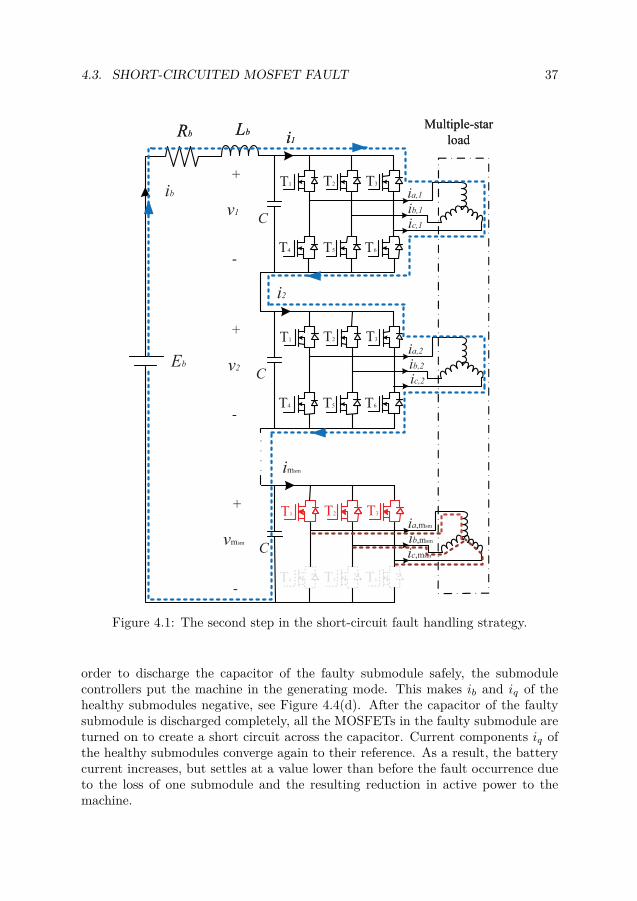
In this situation, it is assumed that a single switch in one phase leg is shortcircuited, e.g., MOSFET T1 in submodule msm in Figure 2.2. In order to avoid ashort circuit across the capacitor, it is necessary to make sure that MOSFET T4 isopen. Otherwise, a very large current passing through the phase leg can damagethe healthy MOSFET. The second step is to create a balanced short circuit acrossthe motor windings. This can happen by closing the switches T2 and T3. In thiscase, the battery current cannot go through the faulty submodule and instead itpasses through the capacitor, see Figure 4.1. This means that (in the motoringmode of operation) the capacitor voltage across the faulty submodule increases andmay cause an even more severe fault on either the capacitor or the other switches.Therefore, it is important to change the operation mode from the motoring modeto the generating mode to discharge the capacitor voltage safely, see Figure 4.2. Inthe final step, when the capacitor voltage across the faulty submodule reaches zero,it is safe to short circuit the faulty submodule by turning on all the switches in thefaulty submodule, see Figure 4.3.
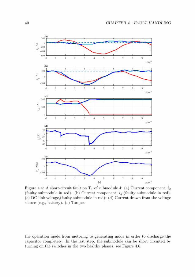
Simulation results based on this strategy and using a detailed Matlab/Simulinkmodel of the SPB converter are presented in Figure 4.4. The parameters that areselected for the detailed Matlab/Simulink model are according to Table 2.1, exceptthat the results in Figure 4.4 are obtained at half of the motor speed, i.e., 2000 rpm.
At t= 0, the moment of fault occurrence, the motor windings are balancedshort-circuited, see Figure 4.4(a). At the same time (t=0), the capacitor voltage ofthe faulty submodule starts to increase, because the battery current starts flowingthrough the capacitor instead of the faulty converter. Simultaneously, the capacitorvoltages start to decrease in the healthy submodules, see Figure 4.4(c). A short timeafter, when the submodule-to-submodule communication time delay has passed,all submodule controllers recognize that one submodule is faulty and the numberof submodules in the balancing controller is changed from msm to msm − 1. In
4.3. SHORT-CIRCUITED MOSFET FAULT 37
Rb Lb Multiple-star
loadi1
Eb
Rb Lb Multiple-star
load
C
+
v2
-
T1 T2 T3
T4 T5 T6
ia,2ib,2ic,2
imsm
C
+
vmsm
-
T1 T2 T3
T4 T5 T6
ia,msm
ib,msm
ic,msm
i1
C
+
v1
-
T1 T2 T3
T4 T5 T6
ia,1
ib,1ic,1
i2
ib
Figure 4.1: The second step in the short-circuit fault handling strategy.
order to discharge the capacitor of the faulty submodule safely, the submodulecontrollers put the machine in the generating mode. This makes ib and iq of thehealthy submodules negative, see Figure 4.4(d). After the capacitor of the faultysubmodule is discharged completely, all the MOSFETs in the faulty submodule areturned on to create a short circuit across the capacitor. Current components iq ofthe healthy submodules converge again to their reference. As a result, the batterycurrent increases, but settles at a value lower than before the fault occurrence dueto the loss of one submodule and the resulting reduction in active power to themachine.

38 CHAPTER 4. FAULT HANDLING
Eb
Rb Lb Multiple-star
load
C
+
v2
-
T1 T2 T3
T4 T5 T6
ia,2ib,2ic,2
imsm
C
+
vmsm
-
T1 T2 T3
T4 T5 T6
ia,msm
ib,msm
ic,msm
i1
C
+
v1
-
T1 T2 T3
T4 T5 T6
ia,1
ib,1ic,1
i2
ib
Figure 4.2: The third step in the short-circuit fault handling strategy.
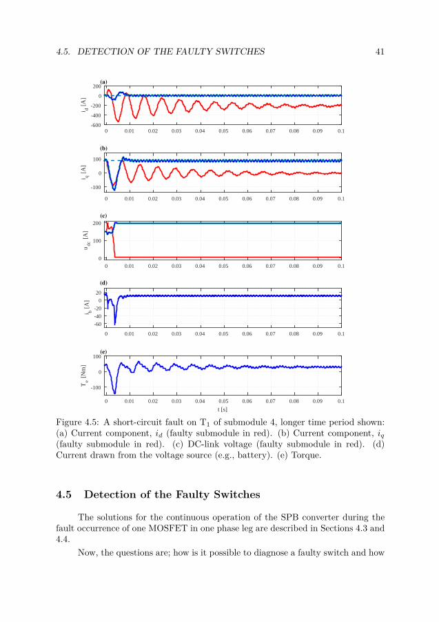
Figure 4.5 shows a longer time period of the same situation. As can beseen, the current components id and iq of the faulty submodule oscillate during thetransient due to the motor rotation and converge exponentially to their steady-statevalues with the d and q time constants.

4.4. OPEN-CIRCUITED MOSFET FAULT 39
Eb
Rb LbMultiple-star
load
C
+
v2
-
T1 T2 T3
T4 T5 T6
ia,2ib,2ic,2
imsm
C
+
vmsm
-
T1 T2 T3
T4 T5 T6
ia,msm
ib,msm
ic,msm
i1
C
+
v1
-
T1 T2 T3
T4 T5 T6
ia,1
ib,1ic,1
i2
ib
Figure 4.3: The final step in the short-circuit fault handling strategy.
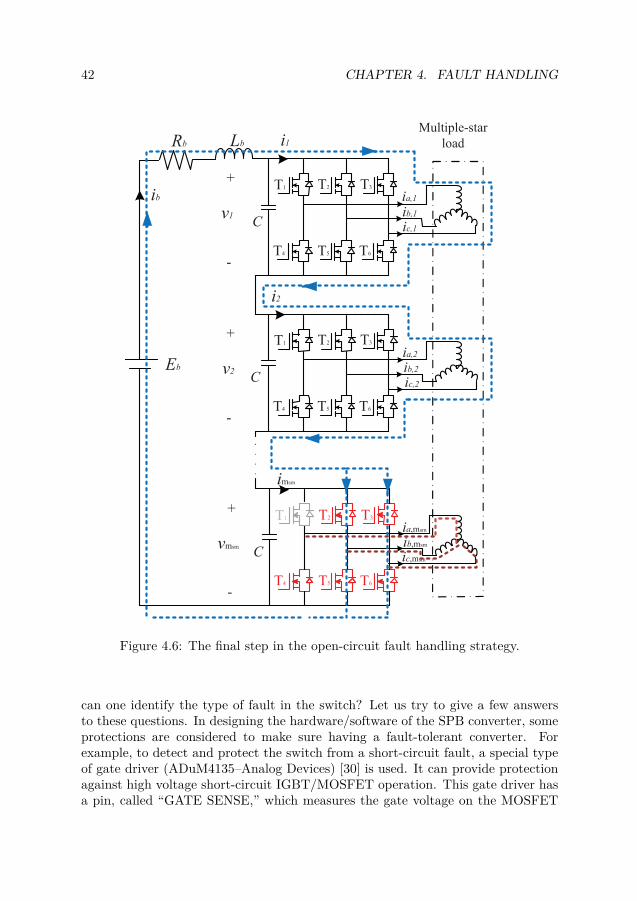
4.4 Open-Circuited MOSFET Fault
Now, let us assume instead that MOSFET T1 of submodule msm is open-circuited.
Therefore, the fastest and safest way to avoid additional damage is to makethe windings balanced short-circuited by turning on switches T4, T5, and T6. Inthis way, current imsm reaches zero and the battery current ib goes though the dc-link capacitor. Again, in order to protect the capacitor it is necessary to change
40 CHAPTER 4. FAULT HANDLING
-1 0 1 2 3 4 5 6 7 8 9
10 -3
-600
-400
-200
0
200i d
[A
](a)
-1 0 1 2 3 4 5 6 7 8 9
10 -3
-100
0
100
i q [
A]
(b)
-1 0 1 2 3 4 5 6 7 8 9
10 -3
0
100
200
udc
[A
]
(c)
-1 0 1 2 3 4 5 6 7 8 9
10 -3
-60
-40
-20
0
20
i b [
A]
(d)
-1 0 1 2 3 4 5 6 7 8 9
t [s] 10 -3
-100
0
100
Te [
Nm
]
(e)
Figure 4.4: A short-circuit fault on T1 of submodule 4: (a) Current component, id(faulty submodule in red). (b) Current component, iq (faulty submodule in red).(c) DC-link voltage,(faulty submodule in red). (d) Current drawn from the voltagesource (e.g., battery). (e) Torque.
the operation mode from motoring to generating mode in order to discharge thecapacitor completely. In the last step, the submodule can be short circuited byturning on the switches in the two healthy phases, see Figure 4.6.
4.5. DETECTION OF THE FAULTY SWITCHES 41
0 0.01 0.02 0.03 0.04 0.05 0.06 0.07 0.08 0.09 0.1-600
-400
-200
0
200i d
[A
](a)
0 0.01 0.02 0.03 0.04 0.05 0.06 0.07 0.08 0.09 0.1
-100
0
100
i q [
A]
(b)
0 0.01 0.02 0.03 0.04 0.05 0.06 0.07 0.08 0.09 0.10
100
200
udc
[A
]
(c)
0 0.01 0.02 0.03 0.04 0.05 0.06 0.07 0.08 0.09 0.1
-60
-40
-20
0
20
i b [
A]
(d)
0 0.01 0.02 0.03 0.04 0.05 0.06 0.07 0.08 0.09 0.1
t [s]
-100
0
100
Te [
Nm
]
(e)
Figure 4.5: A short-circuit fault on T1 of submodule 4, longer time period shown:(a) Current component, id (faulty submodule in red). (b) Current component, iq(faulty submodule in red). (c) DC-link voltage (faulty submodule in red). (d)Current drawn from the voltage source (e.g., battery). (e) Torque.
4.5 Detection of the Faulty Switches
The solutions for the continuous operation of the SPB converter during thefault occurrence of one MOSFET in one phase leg are described in Sections 4.3 and4.4.
Now, the questions are; how is it possible to diagnose a faulty switch and how
42 CHAPTER 4. FAULT HANDLING
Eb
Rb LbMultiple-star
load
C
+
v2
-
T1 T2 T3
T4 T5 T6
ia,2ib,2ic,2
imsm
C
+
vmsm
-
T1 T2 T3
T4 T5 T6
ia,msm
ib,msm
ic,msm
i1
C
+
v1
-
T1 T2 T3
T4 T5 T6
ia,1
ib,1ic,1
i2
ib
Figure 4.6: The final step in the open-circuit fault handling strategy.
can one identify the type of fault in the switch? Let us try to give a few answersto these questions. In designing the hardware/software of the SPB converter, someprotections are considered to make sure having a fault-tolerant converter. Forexample, to detect and protect the switch from a short-circuit fault, a special typeof gate driver (ADuM4135–Analog Devices) [30] is used. It can provide protectionagainst high voltage short-circuit IGBT/MOSFET operation. This gate driver hasa pin, called “GATE SENSE,” which measures the gate voltage on the MOSFET
4.6. SUMMARY 43
and compares it with the supply voltage. If voltage saturation has occurred, anotherpin, called “DESAT,” can detect it. A fault on this pin asserts a fault on the FAULTpin on the primary side. Until the fault is cleared on the primary side, the gatedrive is inhibited. These gate drivers in combination with the hardware logic—see Appendix I, Control board, page 5—offers a fault handling in the case when aMOSFET is being short-circuited.
On the other hand, if a switch faces an open circuit fault, the current sensorswhich are measuring the phase currents can be a good alternative to recognizethis type of the fault. In this fault situation, the resulting phase currents have adistinct characteristic which can be identified. Therefore, this fault can potentiallybe handled as well. Although these preparations for fault handling have beenconsidered, unfortunately the author was not able to test them experimentally dueto the time limitations.
4.6 Summary
This chapter describes a method for fault handling for the SPB converter. Itis mentioned that despite of the reliability of all components in the SPB converter,there is no guarantee for the components operation during the fault occurrenceand they may be damaged in a case of fault occurrence. Among the components,MOSFETs are the most risky ones due to their quantity in the design. Therefore,this chapter of thesis is dedicated to study the fault handling of a MOSFET inone bridge of one submodule. It is also mentioned that a fault in a MOSFET canbe open- or short-circuited, and both types of fault are discussed in this chapter.The proposed fault handling strategy is implemented in a Matlab/Simulink modeland the results are presented here. This chapter also serves as an introduction toPublication II.

Chapter 5
Torque Ripple Minimization
5.1 Introduction
Torque pulsations or torque ripple are terms referring to periodic variationsof the shaft torque of the machine during a complete revolution. This results invibrations. The vibrations are considered as a disadvantage for the machine sincethey lead to premature wear on various drive train components, decreasing their lifetime in the long term, and in the short term they create acoustic noise. Therefore,it is desirable to suppress these phenomena.
Torque pulsations arise due to a combination of cogging torque and ripple dueto harmonics present in the air gap. Cogging torque is based on the interactionbetween the magnets on the rotor and the stator slots and occurs also when thephase currents are zero. This effect can be reduced by careful design of the machine,such as selecting a good combination of slot per pole per phase [31,32], or skewingthe rotor [33,34].
5.2 Torque Ripple Originating from Non-Sinusoidal FluxLinkage
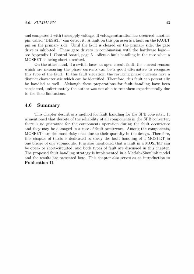
Torque ripple that is created by harmonics in the air gap is due to a non-sinusoidal back EMF. This phenomenon exists in all electric machines, but it canbe reduced by careful design [35]. For the FSCW PMSM in particular, the measuredno-load open-circuit voltage contains significant harmonics of orders 5 and 7, seeFigure 5.1.
The electrical torque is given by
Te = 3p2 (ψdiq − ψqid) . (5.1)
where ψd and ψq respectively are the flux linkages in d and q directions and p isthe number of pole pairs. The back EMF is the time derivative of the flux linkage.
45
46 CHAPTER 5. TORQUE RIPPLE MINIMIZATION
0 1 2 3 4 5 6
[erad]
-50
0
50
van
[V
]
(a)
(b)
0 5 10 15 20
Harmonics order [-]
0
10
20
30
40
50
Mag
nitu
de [
V]
Figure 5.1: Harmonic analysis of the no-load voltage of the FSCW PMSM: (a)Measured phase voltage. (b) Corresponding harmonic orders.
Therefore, if the back EMF contains harmonics that are multiples of six (in the dqreference frame), then the flux linkage contains that as well. Thus, the electricaltorque also contains harmonics that are multiples of six, according to (5.1). Often,although not always, id is controlled to be zero. Then, (5.1) simplifies to
Te = 3p2 ψdiq (5.2)
showing that ψd is the critical flux-linkage component concerning the torque ripple.All the proposals in the literatures that are cited in the introduction to this
chapter are based on the adequate design of the machine in order to reduce thetorque ripple. Another example is a technique that is presented in [36], which isbased on modifying the shape of the rotor to modify the air-gap flux density andreduce the torque ripple. A careful design can be costly, but may still not givethe desired suppression of the torque ripple. Instead, control techniques can be themost reliable, more effective, and cheaper solution in this matter.
5.3 Methods for Torque Ripple Minimization via Control
In various research studies, different proposals for torque ripple minimizationare presented. Equation (5.2) shows that they all must have the effect that iq

5.4. PIR CONTROLLER 47
is controlled to be inversely proportional to ψd, because then, ψdiq is constant.This can be accomplished in various ways. The different proposals can roughly beclassified into two categories: feedforward and feedback.
Feedforward control computes the reference for the torque-producing currentcomponent (iq) by using pre-acquired information of the torque ripple. This way,a ripple-reducing term is added to the nominal torque-producing current compo-nent. The performance of this scheme depends on the accuracy of the pre-acquiredinformation [37]. It also requires an appropriately selected current controller. Ref-erence [38] proposes a repetitive current control strategy to realize zero static errortracking of the periodic components in the reference current.
In contrast, feedback control establishes feedback laws using state variablessuch as speed, current, and/or torque for the purpose of ripple reduction [39]. Forexample in [40], a speed feedback law is established, and a time-varying model of therotor flux is embedded into the speed controller. By estimating model parametersonline, the torque ripple is effectively suppressed. Using mathematical modelsis also considered in many publications. For example, in [41], the period of thespeed ripple is analyzed, and ripple components of various frequencies are effectivelysuppressed by using iterative learning together with a PI speed controller.
Feedforward and feedback methods can be combined. In this chapter, wepropose to add a ripple-reducing term to the nominal torque-producing currentcomponent. But unlike [38], pre-acquired information is not used. Instead, themain flux harmonics which cause torque ripple are estimated online using dq-framevoltage and current components. The details are described in Publication V.
5.4 PIR Controller
As mentioned above, iq should be controlled to be inversely proportional toψd. Assuming isd=0, then from Publication V we have
ψd = ψm + ψmd6cos(6θe + ϕd6) + ψmd12cos(12θe + ϕd12) + · · · (5.3)
so1ψd
= 1ψm + ψmd6cos(6θe + ϕd6) + ψmd12cos(12θe + ϕd12) + · · ·
= 1ψm[1 + ψmd6
ψmcos(6θe + ϕd6) + ψmd12
ψmcos(12θe + ϕd12) + · · · ]
. (5.4)
From Figure 5.1, it is obvious that the terms ψmd6ψm
, ψmd12ψm
, . . . are much smaller thanone, i.e., the flux harmonics have much smaller amplitude than the fundamentalflux. Therefore, (5.4) can be rewritten by using a first-order MacLaurin expansion[1/(1 + x) ≈ 1− x] as
1ψd≈ 1ψm
[1− ψmd6
ψmcos(6θe + ϕd6)− ψmd12
ψmcos(12θe + ϕd12) + · · ·
]. (5.5)
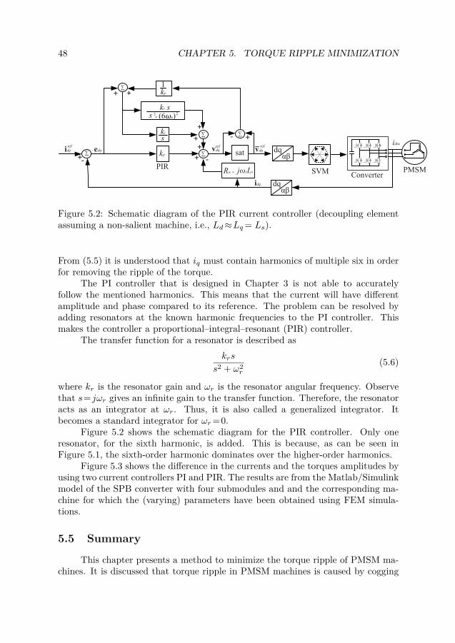
48 CHAPTER 5. TORQUE RIPPLE MINIMIZATION
idq
+-
ref
dqkp vdq
PIR
sat vdq
- +
kp
1
dq
Ra -
ki
s
+
+ -
j eLs
ref ref
+ +
SVM
iabc
PMSMConverter
idq
edq
kr ss 2 (6 e)2+
+
+
Figure 5.2: Schematic diagram of the PIR current controller (decoupling elementassuming a non-salient machine, i.e., Ld≈Lq= Ls).
From (5.5) it is understood that iq must contain harmonics of multiple six in orderfor removing the ripple of the torque.
The PI controller that is designed in Chapter 3 is not able to accuratelyfollow the mentioned harmonics. This means that the current will have differentamplitude and phase compared to its reference. The problem can be resolved byadding resonators at the known harmonic frequencies to the PI controller. Thismakes the controller a proportional–integral–resonant (PIR) controller.
The transfer function for a resonator is described askrs
s2 + ω2r
(5.6)
where kr is the resonator gain and ωr is the resonator angular frequency. Observethat s=jωr gives an infinite gain to the transfer function. Therefore, the resonatoracts as an integrator at ωr. Thus, it is also called a generalized integrator. Itbecomes a standard integrator for ωr=0.
Figure 5.2 shows the schematic diagram for the PIR controller. Only oneresonator, for the sixth harmonic, is added. This is because, as can be seen inFigure 5.1, the sixth-order harmonic dominates over the higher-order harmonics.
Figure 5.3 shows the difference in the currents and the torques amplitudes byusing two current controllers PI and PIR. The results are from the Matlab/Simulinkmodel of the SPB converter with four submodules and and the corresponding ma-chine for which the (varying) parameters have been obtained using FEM simula-tions.
5.5 Summary
This chapter presents a method to minimize the torque ripple of PMSM ma-chines. It is discussed that torque ripple in PMSM machines is caused by cogging
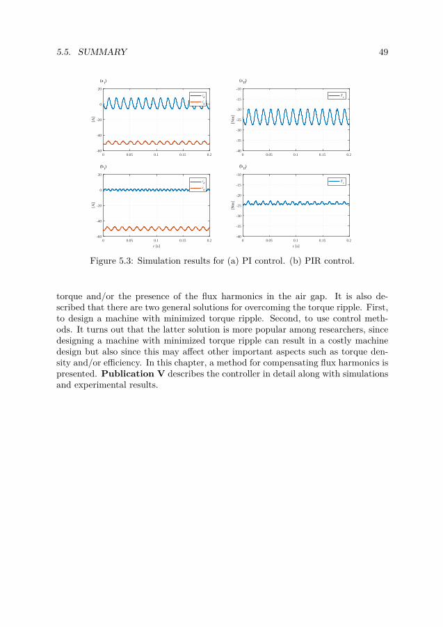
5.5. SUMMARY 49
0 0.05 0.1 0.15 0.2
t [s]
-60
-40
-20
0
20
[A]
(bI)
id
iq
0 0.05 0.1 0.15 0.2
t [s]
-40
-35
-30
-25
-20
-15
-10
[Nm
]
(bII)
Te
0 0.05 0.1 0.15 0.2-60
-40
-20
0
20[A
]
(aI)
id
iq
0 0.05 0.1 0.15 0.2-40
-35
-30
-25
-20
-15
-10
[Nm
]
(aII)
Te
Figure 5.3: Simulation results for (a) PI control. (b) PIR control.
torque and/or the presence of the flux harmonics in the air gap. It is also de-scribed that there are two general solutions for overcoming the torque ripple. First,to design a machine with minimized torque ripple. Second, to use control meth-ods. It turns out that the latter solution is more popular among researchers, sincedesigning a machine with minimized torque ripple can result in a costly machinedesign but also since this may affect other important aspects such as torque den-sity and/or efficiency. In this chapter, a method for compensating flux harmonics ispresented. Publication V describes the controller in detail along with simulationsand experimental results.

Chapter 6
Conclusions and Future Work
This thesis along with the two doctoral theses [10, 12] present a new conceptfor integration of the electric drive system for EV and HEV applications. The topol-ogy introduces an integration between the SPB converter and an FSCW PMSM,which creates a very compact integrated electric drive system. This concept poten-tially benefits from several advantages, e.g., the reduction of power cables betweenconverter and machine, reduction in terms of EMI, weight, and size.
This thesis is mainly focusing on the design, construction, and control of theSPB converter. It is described that the SPB converter is comprised of an arbitrarynumber of submodules that are connected in series to a dc-source voltage. Threedifferent designs of the SPB converter with four submodules have been developed.The first two generations are designed using Euro standard two-layer PCBs. EachPCB constitutes one submodule and it is designed in a way that it contains bothpower and control circuits. The power circuit is a conventional two-level three-phase converter. The control part contains a processor and the communication part.Each PCB can handle 15 A and 20 V. They are connected to RL loads. The thirdgeneration is designed to be installed at the non-driven end of the FSCW PMSM.Four PCBs are designed for the power circuit. Each one has its corresponding PCBas control board. The power PCBs can handle an rms current of 100 A and adc-link voltage of 100 V.
Along with the design of the converter, control algorithms have also beendeveloped. A conventional PI current controller is implemented on the DSP ofeach control board. The first control contribution for the SPB converter in thisthesis is dedicated to stability analysis. Since the submodules are series-connectedto the dc-source voltage, it is essential to make sure the total voltage is sharedequally among the submodules.
Secondly, a study of the SPB converter under fault is performed. It is assumedthat one submodule is facing a short- or open-circuited MOSFET and the behaviorof the converter is studied. The proposal suggests a safe way of short-circuiting thefaulty submodule.
51

52 CHAPTER 6. CONCLUSIONS AND FUTURE WORK
Finally, torque ripple minimization is discussed. It is shown that using anestimator for the flux linkage harmonics in the machine along with a PIR controllercan be an efficient method to suppress the ripple.
6.1 Future Work
Although plenty of research and investigations have been done during thisproject focusing on the SPB converter, there is still room for more work that islisted as follows.
• CAN communication for four submodules is missing. In this thesis commu-nication via the CAN bus between two submodules has been used, but thisshould be developed to four submodules.
• A method for fault handling is proposed in the thesis. However, the proposalis not evaluated experimentally. Therefore, it is worth to do so.
• The control and power boards of the third generation SPB converter are ondifferent PCBs. Maybe, it will be possible to integrate the two boards on asingle board to form an even more compact drive system.
Bibliography
[1] R. Matulka, “History of the electric car [online],” Available:http://www.energy.gov/articles/history-electric-car, Sep. 2014.
[2] P. Cazzola, M. Gorner, L. Munuera, R. Schuitmaker, andE. Maroney, “Global EV outlook in 2017 [online],” Available:http:www.iea.org/publications/GlobalEVOutlook 2017.pdf, Jan. 2017.
[3] J.-S. Lai, H. Kouns, and J. Bond, “A low-inductance DC bus capacitor forhigh power traction motor drive inverters,” in Proc. of the 37th IEEE IndustryApplications Conference. (IAS 2002), Oct. 2002.
[4] T. Efford, Y. Shibata, and A. Kanezaki, “Development of aluminum elec-trolytic capacitors for EV inverter applications,” in Proc. of the 32nd IEEEIndustry Applications Conference. (IAS 97), Oct. 1997.
[5] T. M. Jahns and H. Dai, “The past, present, and future of power electronicsintegration technology in motor drives,” IEEE Transactions on Power Elec-tronics and Applications, vol. 2, pp. 197–216, Sep. 2017.
[6] N. R. Brown, T. M. Jahns, and R. D. Lorenz, “Power converter design foran integrated modular motor drive,” in Proc. of IEEE Industry ApplicationsAnnual Meeting, Sep. 2007.
[7] A. Shea and T. M. Jahns, “Hardware integration for an integrated modularmotor drive including distributed control,” in Proc. IEEE Energy ConversionCongress and Exposition (ECCE 2014 ), Sep. 2014.
[8] J. Wang, “Design of multilevel integrated modular motor drive with gallium ni-tride power devices,” PhD dissertation, The University of Wisconsin-Madison,Madison, US, 2015.
[9] L. Lambertz, R. Marquardt, and A. Mayer, “Modular converter systems forvehicle applications,” in Proc. of IEEE Emobility–Electrical Power Train, Nov.2010.
53
54 BIBLIOGRAPHY
[10] L. Jin, “Integrated compact drives for electric and hybrid electric vehicles,”PhD dissertation, KTH Royal Institute of Technology, Stockholm, Sweden,2016.
[11] S. Gjerde, “Analysis and control of a modular series connected converter for atransformerless offshore wind turbine,” PhD dissertation, Norwegian Univer-sity of Science and Tecnology, Trondheim, Norway, 2013.
[12] H. Zhang, “On electric machinery for integrated motor drives in automotiveapplications,” PhD dissertation, KTH Royal Institute of Technology, Stock-holm, Sweden, 2017.
[13] J. J. Wolmarans, J. A. Ferreira, H. Polinder, I. Josifovic, and D. Clarenbach,“Design for fault tolerance and predictive failures,” in Proc. of the 6th Inter-national Conference on Integrated Power Electronics Systems, Mar. 2010.
[14] N. Aschenbrenner, “Drive system saves space and weight in elec-tric cars,” Available: https://phys.org/news/2014-10-space-weight-electric-cars.html Charged Electric Vehicles Magazine, Oct. 17, 2014.
[15] A. M. EL-Refaie, “Fractional–slot concentrated–windings synchronous perma-nent magnet machines: Opportunities and challenges,” IEEE Transactions onIndustrial Electronics, vol. 57, pp. 107–121, Jan. 2010.
[16] D. Graovac, M. Pürschel, and A. Kiep, “MOSFET power losses calculationusing the datasheet parameters [online],” Available: http:www.application-notes.digchip.com/070/70-41484.pdf, Jul. 2006.
[17] L. Harnefors and H.-P. Nee, “Model-based current control of AC machinesusing the internal model control method,” IEEE Transactions on IndustryApplications, vol. 34, pp. 133–141, Jan. 1998.
[18] L. Harnefors, K. Pietiläinen, and L. Gertmar, “Torque-maximizing field-weakening control: design, analysis, and parameter selection,” IEEE Trans-actions on Industrial Electronics, vol. 48, pp. 161–168, Feb. 2001.
[19] J. Holtz, J. Quan, J. Pontt, J.and Rodrìguez, P. Newman, and H. Miranda,“Design of fast and robust current regulators for high-power drives based oncomplex state variables,” IEEE Transactions on Industry Applications, vol. 40,no. 5, pp. 1388–1397, 2004.
[20] H. Zhu, X. Xiao, and Y. Li, “PI type dynamic decoupling control scheme forPMSM high speed operation,” in Proc. of the 25th Annual IEEE Applied PowerElectronics Conference and Exposition (APEC 2010), Feb. 2010.
[21] R. Ottersten and J. Svensson, “Vector current controlled voltage sourceconverter-deadbeat control and saturation strategies,” IEEE Transactions onPower Electronics, vol. 17, pp. 279–285, Mar. 2002.
BIBLIOGRAPHY 55
[22] K. J. Åström and T. Hägglund, “PID controllers: theory, design, and tuning,”vol. 2, 1995.
[23] X. Ruan, W. Chen, L. Cheng, C. K. Tse, H. Yan, and T. Zhang, “Controlstrategy for input-series, output-parallel converters,” IEEE Transactions onIndustrial Electronics, vol. 56, pp. 1174–1185, Apr. 2009.
[24] W. Chen, X. Ruan, H. Yan, and C. K. Tse, “DC/DC conversion systemsconsisting of multiple converter modules: Stability, control, and experimentalverifications,” IEEE Transactions on Power Electronics, vol. 24, pp. 1463–1474, Jun. 2009.
[25] R. Giri, V. Choudhary, R. Ayyanar, and N. Mohan, “Common-duty-ratio con-trol of input-series connected modular DC-DC converters with active inputvoltage and load-current sharing,” IEEE Transactions on Industry Applica-tions, vol. 42, pp. 1101–1111, Jul. 2006.
[26] S. Gjerde, P. Olsen, K. Ljokelsoy, and T. Undeland, “Control and fault han-dling in a modular series-connected converter for a transformerless 100 kV low-weight offshore wind turbine,” IEEE Transactions on Industry Applications,vol. 50, pp. 1094–1105, Mar. 2014.
[27] H. Wang and F. Blaabjerg, “Reliability of capacitors for DC-link applicationsin power electronic converters: An overview,” IEEE Transactions on IndustryApplications, vol. 50, pp. 3569–3578, Sep. 2014.
[28] H. Soliman, H. Wang, and F. Blaabjerg, “A review of the condition monitoringof capacitors in power electronic converters,” IEEE Transactions on IndustryApplications, vol. 52, pp. 4976–4989, Nov. 2016.
[29] N. Moultif, M. Masmoudi, E. Joubert, and O. Latry, “Reliability and qualifi-cation tests for high-power MOSFET transistors,” 2017.
[30] A. Devices, “Single–/dual–supply, high voltage isolated IGBT gate driver withmiller clamp [online],” Available: http:www.analog.com/media/en/technical-documentation/data-sheets/ADuM4135.pdf.
[31] S. Han, T. M. Jahns, W. L. Soong, M. K. Güven, and M. S. Illindala, “Torqueripple reduction in interior permanent magnet synchronous machines usingstators with odd number of slots per pole pair,” IEEE Transactions on EnergyConversion, vol. 25, pp. 118–127, Mar. 2010.
[32] J. K. Tangudu, T. M. Jahns, and A. EL-Refaie, “Unsaturated and satu-rated saliency trends in fractional-slot concentrated-winding interior perma-nent magnet machines,” in Proc. IEEE Energy Conversion Congress and Ex-position (ECCE2010), pp. 1082–1089, Sep. 2010.
56 BIBLIOGRAPHY
[33] T. M. Jahns and W. L. Soong, “Pulsating torque minimization techniques forpermanent magnet AC motor drives-a review,” IEEE Transactions on Indus-trial Electronics, vol. 43, pp. 321–330, Apr. 1996.
[34] A. Wang, H. Li, W. Lu, and H. Zhao, “Influence of skewed and segmentedmagnet rotor on IPM machine performance and ripple torque for electric trac-tion,” in Proc. of IEEE International Electric Machines and Drives Conference(IEMDC 2009), May 2009.
[35] C. Ruoff, “A closer look at torque ripple minimizing its effects on electricmachines [online],” Available: https://chargedevs.com/features.
[36] U. Seo, Y. Chun, J. Choi, P. Han, D. Koo, and J. Lee, “A technique oftorque ripple reduction in interior permanent magnet synchronous motor,”IEEE Transactions on Magnetics, vol. 47, pp. 3240–3243, Oct. 2011.
[37] G. Ferretti, G. Magnani, and P. Rocco, “Modeling, identification, and com-pensation of pulsating torque in permanent magnet AC motors,” IEEE Trans-actions on Industrial Electronics, vol. 45, pp. 912–920, Dec. 1998.
[38] P. Mattavelli, L. Tubiana, and M. Zigliotto, “Torque-ripple reduction in PMsynchronous motor drives using repetitive current control,” IEEE Transactionson Power Electronics, vol. 20, pp. 1423–1431, Nov. 2005.
[39] W. Gan and L. Qiu, “Torque and velocity ripple elimination of AC per-manent magnet motor control systems using the internal model principle,”IEEE/ASME Transactions on Mechatronics, vol. 9, pp. 436–447, Jun. 2004.
[40] V. Petrovic, R. Ortega, A. M. Stankovic, and G. Tadmor, “Design and imple-mentation of an adaptive controller for torque ripple minimization in PM syn-chronous motors,” IEEE Transactions on Power Electronics, vol. 15, pp. 871–880, Sep. 2000.
[41] W. Qian, S. K. Panda, and J.-X. Xu, “Torque ripple minimization in PMsynchronous motors using iterative learning control,” IEEE Transactions onPower Electronics, vol. 19, pp. 272–279, Mar. 2004.

Appendix I
To include a more complete sys-tem description for the reader, de-tails of the prototype electric ma-chine and corresponding prototypeSPB-type converter are included. Theprototype electric machine has beenmanufactured by Bevi AB. The pro-totype SPB-type converter has been manufactured by Eskilstuna ElektronikpartnerAB by specifications from the author of this thesis.
57

58
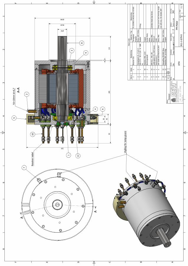
A-A
1 1
2 2
3 3
4 4
5 5
6 6
7 7
8 8
AA
BB
CC
DD
EE
FF
PM-M
otor
911-
1-07
9-0
KTH
LEÅN
Oska
r Wal
mar
k2015
-12-
1020
15-1
1-04
0
Rita
d.Ko
ntr.
Godk
änd
1 / 2
Ut
gåva
Blad
Datu
m
Blomsterm
åla
+46 499-27100
R
Sweden
Datu
m
A2Form
atSk
ala 1
: 2
Stat
usRe
leas
ed
A
A
Styc
k Li
sta
Besk
rivni
ngM
ater
ial /
Typ
Benä
mni
ng.
Anta
l.De
t.nr
TS 2
225N
1114
E102
NO.
Y272
65Ta
mag
awa
Sing
slyn
Reso
lver
S21
11
Br
ass,
Sof
t Yel
low
Slan
gnip
pel_
G1_4
tum
-22
2O-
Ring
Rubb
erDI
N 37
71 -
85 x
3,5
5 - N
- NB
R 70
13
Co
pper
Kabe
lsko
KRD_
16-8
364
Ac
etal
Res
in,
Whi
teBe
rörin
gssk
ydd
25
Cylin
der H
ead
Cap
Scre
wSt
eel,
Mild
DIN
912
- M4
x 40
126
M
12x1
,5ca
ble-
glan
d-15
1_15
07-b
oxco
27
C4
5EAx
el-p
mrs
m-2
18
Deep
gro
ove
ball
bear
ings
sin
gle
row
with
two
RZ
shie
lds
SKF
Stee
l, M
ildSK
F 62
09-2
RZTN
9/HC
5C3W
T2
9
Br
ass,
Sof
t Yel
low
Gäng
stån
g M
8-ND
E flä
ns12
10
Copp
erKa
belsk
o KR
F 16
-8-9
0gr
1211
285
42
110
120 Ø
4
248 Ø
320
30
8346
Reso
lver
kab
el Utgå
ng fö
r tem
p.gi
vare
8
10
2
64
11
5
7
9
31
Yd=
10m
m id
=6,
7
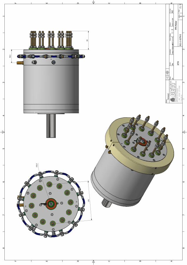
1 1
2 2
3 3
4 4
5 5
6 6
7 7
8 8
AA
BB
CC
DD
EE
FF
PM-M
otor
911-
1-07
9-0
KTH
LEÅN
Oska
r Wal
mar
k2015
-12-
1020
15-1
1-04
0
Rita
d.Ko
ntr.
Godk
änd
2 / 2
Ut
gåva
Blad
Datu
m
Blomsterm
åla
+46 499-27100
R
Sweden
Datu
m
A2Form
atSk
ala 1
: 2
Stat
usRe
leas
ed
176
83
152,
5
59,5

1 1
2 2
3 3
4 4
5 5
6 6
AA
BB
CC
DD
Roto
r pl
ate
911-
1-07
9-2
KTH
LELE
2015
-10-
1220
15-1
0-02
0
Rita
d.Ko
ntr.
God
känd
1 /
1 U
tgåv
aBl
ad
Dat
um
Blomsterm
åla
+46 499-27100
R
Sweden
Dat
um
A3Form
atSk
ala 1
: 1
Stat
usRe
leas
ed
0,35
10-0
,08
0,00
+
1,53
2,76
15,2
8
5,06
0,73
3,19
145°
54,1
6
18,8
5
21,0
7
7,51
R0,1
in a
ll co
rner
s
54
0,04
X T
oler
ance
if n
ot in
dica
ted,
aco
rdin
g to
S
S-IS
O 2
768-
1 F
ine
Med
ium
Rou
gh
Mat
eria
l M25
0-35
A41
0 pc
s.
13
9,1
(Mac
hine
d to
Ø13
8,5)
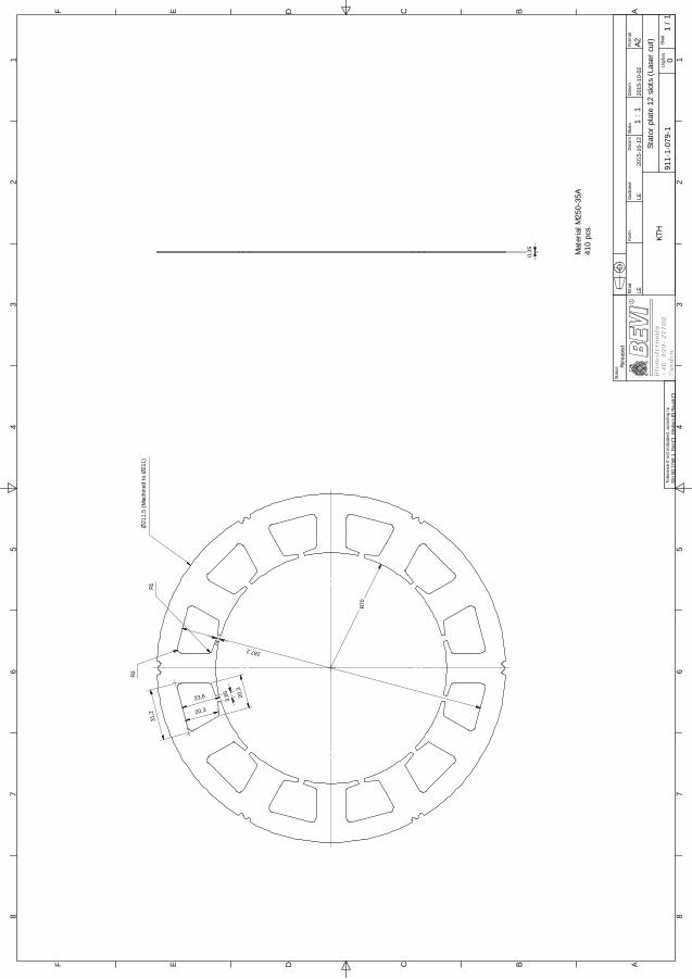
1 1
2 2
3 3
4 4
5 5
6 6
7 7
8 8
AA
BB
CC
DD
EE
FF
Stat
or p
late
12
slot
s (L
aser
cut
)
911-
1-07
9-1
KTH
LELE
2015
-10-
1220
15-1
0-02
0
Rita
d.Ko
ntr.
God
känd
1 /
1 U
tgåv
aBl
ad
Dat
um
Blomsterm
åla
+46 499-27100
R
Sweden
Dat
um
A2Form
atSk
ala 1
: 1
Stat
usRe
leas
ed
0,35
R3
R131
,2
20,3
3,65
20,3
23,6
R70
2
Mat
eria
l M25
0-35
A41
0 pc
s.
X T
oler
ance
if n
ot in
dica
ted,
aco
rdin
g to
S
S-IS
O 2
768-
1 F
ine
Med
ium
Roug
h
187,2
21
1,5
(Mac
hine
d to
Ø21
1)

63

64
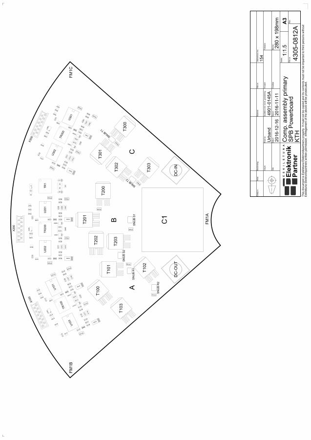
PAA01
COA
PAB01
COB
PAC01
COC
PAC102
PAC101
COC1
PAC202
PAC201
COC2
PAC302
PAC3
01
COC3
PAC402
PAC401
COC4 PAC502
PAC501 COC5
PAC802
PAC801
COC8
PAC10002 PAC10
001 COC1
00 PAC10102
PAC10
101 COC10
1
PAC10202 PAC1
0201
COC102 PAC1
0302
PAC10301
COC10
3 PAC10402
PAC10401 COC1
04 PAC10501
PAC1
0502
COC105
PAC10601 PAC10
602 COC
106 PAC10
702 PAC10
701 COC107 PAC108
02 PAC108
01 COC108
PAC10902
PAC10901
COC109
PAC11001
PAC11
002 COC110
PAC11102
PAC11101 COC111
PAC11202
PAC11201 COC1
12
PAC11501
PAC11502
COC11
5 PAC11
601 PAC11602
COC116
PAC11702
PAC11701 COC
117 PAC11
802 PAC11
801 COC118
PAC11902
PAC11901 COC11
9
PAC12001
PAC1
2002
COC120
PAC20002
PAC20001
COC200 PAC2
0102
PAC201
01 COC201
PAC202
02
PAC202
01 COC202 PAC20302
PAC20301
COC2
03
PAC204
01
PAC204
02 COC204
PAC20501 PA
C20502 CO
C205
PAC20602 PAC2060
1 COC206
PAC20702
PAC20701 CO
C207
PAC20802
PAC20801
COC208
PAC20901
PAC209
02 COC209
PAC210
01
PAC210
02 COC210
PAC21101 PAC2110
2 CO
C211
PAC21202
PAC21201 COC2
12 PAC213
02 PAC213
01 COC21
3
PAC21402
PAC21401
COC214
PAC215
01
PAC215
02 COC215 PAC2
1602
PAC21601
COC216
PAC21702
PAC21701
COC217
PAC21802
PAC21801
COC218
PAC30002
PAC30001
COC300 PAC3
0102
PAC30101
COC3
01
PAC30202
PAC30201
COC30
2 PAC30
302 PAC30
301 COC303
PAC30401 PAC30402
COC304
PAC30501 PAC305
02 COC
305
PAC30602
PAC30601 COC306 PAC30
702 PAC30
701 COC307
PAC30802 PAC30
801 COC308
PAC30901
PAC30902
COC30
9
PAC31001
PAC3
1002
COC310
PAC31101 PAC31
102 COC
311
PAC31202
PAC31201 COC3
12
PAC31302
PAC31301 COC3
13
PAC31402 PAC3
1401
COC314
PAC31501
PAC31502 COC315
PAC31602
PAC31601
COC316
PAC31702
PAC31701 COC3
17
PAC31802
PAC31801 COC3
18
PAD101
PAD102 COD1
PAD201
PAD202 COD2
PAD10001
PAD10002
COD100
PAD10101
PAD10102
COD101
PAD10202 PAD10
201 COD1
02
PAD10502 PAD10
501 COD10
5
PAD20001
PAD20002 COD200
PAD20101
PAD20102 COD201
PAD20202
PAD20201 COD202
PAD20302
PAD20301 COD203
PAD30001 PAD30
002 COD300
PAD30101
PAD30102 COD30
1
PAD30202
PAD30201 COD30
2
PAD30302
PAD30301 COD30
3
PADC0IN010
PADC0IN09
PADC0IN08
PADC0IN07
PADC0IN06
PADC0IN05 PADC0
IN04 PADC0IN03 PADC0
IN02 PADC0IN01
CODC
0IN
PADC0OUT010 PADC0O
UT09 PADC0OUT08 PADC0
OUT07 PADC0O
UT06
PADC0OUT05
PADC0OUT04
PADC0OUT03
PADC0OUT02
PADC0OUT01 CODC0OUT
PAFM1A01
COFM1A
PAFM1B01
COFM1B
PAFM1C01
COFM1C
PAFM2A01
COFM2A
PAFM2B01
COFM2B
PAFM2C01
COFM2C
PAR100
02 PAR10001
COR100 PAR10101
PAR10
102 COR1
01
PAR10201
PAR10202
COR102
PAR10301 PAR1
0302
COR103
PAR104
01 PAR10402
COR104
PAR10501 PAR105
02 COR105
PAR1
0601
PAR10602
COR106
PAR10701 PAR10
702 COR10
7
PAR10902
PAR10
901 COR10
9 PAR11001 PAR1
1002
COR110
PAR11301
PAR1
1302
COR113
PAR114
01 PAR11402
COR114
PAR115
01 PAR11502
COR115
PAR11601
PAR11602 COR11
6 PAR2
0002
PAR20001
COR200 PAR20101
PAR20102
COR201
PAR20201
PAR20202
COR202 PAR20
301
PAR20302
COR203
PAR204
01
PAR204
02 COR204 PAR
20501
PAR205
02 COR205 PAR
20601
PAR206
02 COR206
PAR20701
PAR20702
COR207
PAR20902
PAR20901
COR209 PAR21001
PAR21002
COR210 PAR
21301
PAR213
02 COR213 PAR
21401
PAR214
02 COR214 PAR2
1501
PAR21502
COR215
PAR21601
PAR21602
COR216
PAR30002
PAR30
001 COR300
PAR301
01
PAR30102
COR30
1
PAR30201 PAR30202
COR3
02 PAR30
301 PAR30
302 COR30
3
PAR30401
PAR30402
COR3
04 PAR3
0501
PAR30502
COR305
PAR30601
PAR30602
COR30
6
PAR30701
PAR30702
COR307
PAR30902
PAR30901
COR309
PAR3
1001
PAR31002 COR31
0
PAR31301
PAR3
1302
COR313
PAR31401
PAR31402
COR31
4
PAR31501
PAR31502
COR31
5
PAR31601 PAR31
602 COR3
16
PASNUB R10
1 COSNUB R1
PASNUB R20
1 COSNUB R2
PASNUB S10
1 COSNUB S1
PASNUB S20
1 COSNUB S2
PASNUB T101 COSNUB
T1
PASNUB T201
COSNUB T2
PAT10004
PAT10007
PAT1
0006
PAT10005
PAT10
003 PAT1
0002
PAT10001
CO
T100
PAT10104 PAT10107 PAT10106 PAT10105
PAT10103 PAT10102 PAT10101 COT101 PAT10204
PAT10207
PAT1
0206
PAT10205
PAT1
0203
PAT10202
PAT10
201 CO
T102
PAT10304
PAT10307
PAT1
0306
PAT10305
PAT10303
PAT1
0302
PAT10301
COT1
03
PAT20004
PAT20007
PAT20006
PAT20005
PAT20003
PAT20002
PAT20001
COT2
00
PAT20104
PAT20107 PAT20106 PAT20105 PAT20103 PAT20102 PAT20101 COT201
PAT20204
PAT20207
PAT20206
PAT20205
PAT20203
PAT20202
PAT20201
COT2
02
PAT20304 PAT20307 PAT20306 PAT20305
PAT20303 PAT20302 PAT20301 COT2
03
PAT30004
PAT30007
PAT3
0006
PAT30005
PAT3
0003
PAT30002 PAT30001
COT3
00
PAT30104 PAT30
107 PAT3
0106
PAT30105
PAT3
0103
PAT30102
PAT30101
COT3
01
PAT30204
PAT30207
PAT30206
PAT30205
PAT30203
PAT30202
PAT30201
COT3
02
PAT30304
PAT30307
PAT3
0306
PAT30305
PAT3
0303
PAT30302 PAT30301
COT303
PATP10001 COTP100
PATP10101 COTP101
PATP10201
COTP102
PATP10301
COTP103
PATP10401 COTP104
PATP10501
COTP105
PATP20001 COTP200
PATP20101
COTP201
PATP20201 COTP202
PATP20301 COTP203
PATP20401 COTP204
PATP20501
COTP205
PATP30001 COTP300
PATP30101 COTP301
PATP30201
COTP302
PATP30301 COTP303
PATP30401
COTP304
PATP30501
COTP305 PATR101
PATR102
PATR103
PATR106 PATR105
PATR104
COTR
1
PATR10001
PATR10002
PATR10003
PATR10006
PATR10005
PATR10004
COTR10
0
PATR20001
PATR20002
PATR20003
PATR20006 PATR20005
PATR20004 COTR200
PATR30001
PATR30002
PATR30003 PATR300
06 PATR300
05 PATR300
04
COTR30
0
PAU106 PAU105
PAU104 PAU103
PAU102
PAU101 COU
1
PAU10006 PAU10
005 PAU10004 PAU10
003 PAU100
02 PAU100
01
COU100
PAU101016
PAU101015
PAU101014
PAU101013
PAU101012
PAU101011
PAU101010
PAU10109
PAU10108 PAU1010
7 PAU10106 PAU1010
5 PAU10104 PAU1010
3 PAU10102 PAU101
01
COU101
PAU103016
PAU103015
PAU103014
PAU103013
PAU103012
PAU103011
PAU103010
PAU10309
PAU10308 PAU103
07 PAU10306 PAU103
05 PAU10304 PAU10303
PAU10302 PAU10301
COU103
PAU20006 PAU20005
PAU20004 PAU20003
PAU20002
PAU20001
COU2
00
PAU201016 PAU201015 PAU201014
PAU201013 PAU201012
PAU201011 PAU201010 PAU20109 PAU20108
PAU20107 PAU20106
PAU20105 PAU20104
PAU20103 PAU20102
PAU20101
COU201
PAU202016 PAU202015
PAU202014 PAU202013
PAU202012 PAU202011 PAU202010
PAU20209 PAU20208 PAU20207
PAU20206 PAU20205
PAU20204 PAU20203
PAU20202 PAU20201
COU202
PAU30006 PAU30
005 PAU30004
PAU30003
PAU30002
PAU30001 COU
300
PAU301016
PAU301015
PAU301014
PAU301013
PAU301012
PAU301011
PAU301010
PAU30109
PAU30108 PAU301
07 PAU30106 PAU30105
PAU30104 PAU30103
PAU30102 PAU30101
COU
301
PAU302016
PAU302015
PAU302014
PAU302013
PAU302012
PAU302011
PAU302010
PAU30209
PAU30208 PAU302
07 PAU30206 PAU302
05 PAU30204 PAU3020
3 PAU30202 PAU3020
1 COU
302
PAX100011
PAX100012
PAX10001
PAX10002
PAX100010 PAX100
09 PAX100
08 PAX10007
PAX10006 PAX100
05 PAX100
04 PAX10003
COX100
PAX200011 PAX200012
PAX20001 PAX20002 PAX200010 PAX20009
PAX20008 PAX20007 PAX20006 PAX20005 PAX20004 PAX20003
COX200
PAX300011 PAX300012
PAX30001 PAX30002
PAX300010
PAX30009 PAX300
08 PAX300
07 PAX30006
PAX30005 PAX30
004
PAX30003
COX3
00
PAC10901
PAC11101
PAC11201 PAC11
901
PAR10202
PAR10302
PAU10107
PAU10307
PAX10003
PAC20801
PAC21401
PAC21701
PAC21801
PAR20202
PAR20302
PAU20107 PAU20207
PAX20003
PAC30801
PAC31401
PAC31701
PAC31801
PAR30202
PAR30
302
PAU30107
PAU30207
PAX30003
PAC10001 PAC10
101 PATR10
002 PAU100
02
PAU10005
PAX10001
PAC201
PAC3
01
PAC20001
PAC201
01
PATR102
PATR20002
PAU102 PAU105
PAU20002 PAU20005
PAX20001
PAC30001 PAC3
0101 PATR300
02 PAU30002 PAU30
005 PAX300
01
PAC401
PAC501
PAC801
PAC11501
PAC11601 PAC11701 PAC11
801
PAC210
01
PAC21101 PAC21201
PAC21301
PAC31001
PAC31101
PAC31201
PAC31301
PAD101
PAD201
PAR10902
PAR20902
PAR30902
PAU103013
PAU202013
PAU302013
PAC10201
PAC10301
PAC10401 PAC1
0501
PAC10601 PAC10701 PAC108
01 PAD10
001
PAD10101
PAR100
02
PAU101013
PAC202
01
PAC20301
PAC204
01
PAC20501
PAC20601
PAC20701
PAC21601
PAD20
001 PAD20
101
PAR20002
PAU201013
PAC30201
PAC30
301
PAC30401
PAC30501
PAC30601 PAC30
701
PAC31601
PAD30001
PAD30101
PAR30002
PAU301013
PAR10702
PAU10102
PAX10005
PAR11602
PAU10302
PAX100011
PAR10301
PAU10105
PAU10305
PAX10008
PAU10106
PAU10306
PAX10009
PAR10201
PAU10104
PAU10304
PAX10007
PAR20702 PAU20102
PAX20005
PAR21602
PAU20202
PAX200011 PAR20
301
PAU20105 PAU20205
PAX20008
PAU20106 PAU20206
PAX20009
PAR20201 PAU20104
PAU20204
PAX20007
PAR30702
PAU30102
PAX30005
PAR31602
PAU30202
PAX300011
PAR30301
PAU30105
PAU30205
PAX30008
PAU30106
PAU30206
PAX30009
PAR30201
PAU30104
PAU30204
PAX30007
PAC101
PAD10201
PAD20201
PAD30201
PADC0IN01
PADC0IN02
PADC0IN03
PADC0IN04
PADC0IN05
PADC0IN06 PADC0
IN07 PADC0IN08 PADC0
IN09 PADC0IN010
PAT10004 PAT10
104 PAT20
004 PAT2
0104
PAT30004
PAT30104
PAC102
PAC402
PAC502
PAC802
PAC11502
PAC11602 PAC11
702 PAC11802
PAC12002
PAC210
02
PAC21102 PAC2120
2 PAC213
02
PAC215
02
PAC31002
PAC31102
PAC31202
PAC31302
PAC31502
PADC0OUT01 PADC0O
UT02 PADC0OUT03 PADC0O
UT04 PADC0OUT05
PADC0OUT06
PADC0OUT07
PADC0O
UT08 PADC0O
UT09 PADC0O
UT010
PASNUB R20
1
PASNUB S20
1
PASNUB T201
PAT10202
PAT1
0203
PAT10205
PAT1
0206
PAT10207
PAT10302
PAT1
0303
PAT10305 PAT10306
PAT1
0307
PAT20202
PAT20203
PAT20205
PAT20206
PAT20207
PAT20302 PAT20303 PAT20305 PAT20306
PAT20307 PAT30
202 PAT30203 PAT30
205 PAT30206 PAT30
207 PAT30
302 PAT3
0303
PAT30305
PAT3
0306
PAT30307
PATP10301
PATP10501
PATP20301
PATP20501
PATP30301
PATP30501
PATR105
PAU10309 PAU103
011 PAU1030
16
PAU20209 PAU202011
PAU202016
PAU30209
PAU302011
PAU302016
PAC202
PAC302
PAC10002 PAC1
0102
PAC10902 PAC11102
PAC11202
PAC11902
PAC20002
PAC20102
PAC20802
PAC21402
PAC21702
PAC21802
PAC30002 PAC3
0102
PAC30802
PAC31402
PAC31702
PAC31802
PAR10701
PAR11601
PAR20701
PAR21601
PAR30701
PAR31601
PAU104 PAU106
PAU10004
PAU10006
PAU10101
PAU10103
PAU10108
PAU10301
PAU10303
PAU10308
PAU20004 PAU20006
PAU20101 PAU20103
PAU20108 PAU20201
PAU20203 PAU20208
PAU30004
PAU30006
PAU30101
PAU30103
PAU30108
PAU30201
PAU30203
PAU30208
PAX10002
PAX10004
PAX10006
PAX100010
PAX100012
PAX20002 PAX20004
PAX20006 PAX200010
PAX200012
PAX30002
PAX30004
PAX30006
PAX300010
PAX300012
PAA01
PAC10202 PAC1
0302 PAC10
402
PAC10502
PAC10
602 PAC10702 PAC108
02 PAC11
002
PAD10501
PASNUB R10
1
PAT10002
PAT10
003 PAT10005
PAT1
0006
PAT10007
PAT10102 PAT10103 PAT10105 PAT10106 PA
T10107
PAT10204
PAT10304
PATP10201
PATP10401
PATR10005
PAU10109
PAU101011
PAU101016
PAB01
PAC202
02
PAC20302
PAC204
02
PAC20502 PAC20602 PAC20702
PAC209
02
PAC21602
PAD20301
PASNUB S10
1
PAT20002
PAT20003
PAT20005
PAT20006
PAT20007
PAT20102 PAT20103 PAT20105 PAT20106
PAT20107 PAT20
204 PAT20
304
PATP20201
PATP20401
PATR20005 PAU20109
PAU201011 PAU201016
PAC30202
PAC30302
PAC30402
PAC30502
PAC30602 PAC30
702
PAC30902
PAC31602
PAC01
PAD30301
PASNUB T101 PAT30
002 PAT3
0003
PAT30005
PAT3
0006
PAT30007
PAT30102 PAT30103
PAT3
0105
PAT30106
PAT3
0107
PAT30204
PAT30304
PATP30201
PATP30401
PATR30005
PAU30109 PAU301011
PAU301016
PAC11001
PAR10
001 PAR10101
PAU101010
PAC12001
PAR10
901 PAR11001 PAU10301
0
PAC20901
PAR2
0001
PAR20101
PAU201010
PAC215
01 PAR2
0901
PAR21001
PAU202010
PAC30901
PAR30001
PAR301
01
PAU301010
PAC31501
PAR30901
PAR3
1001
PAU302010
PAD102
PATR106 PAD2
02 PATR104
PAD10002
PATR10006
PAD10102 PATR10004
PAD10202
PAR10102
PAD10502
PAR11002
PAD20002
PATR20006 PAD20
102 PATR20004
PAD20202
PAR20102
PAD20302
PAR21002
PAD30002 PATR300
06 PAD30
102 PATR30004
PAD30202 PAR30102
PAD30302 PAR31
002 PAR
10401
PAU101015
PAR10402
PAR105
02
PAR10602
PAT10001
PAT10101
PATP10001
PAR10501
PAU101014
PAR10601
PAU101012
PAR11301
PAU103015
PAR11302
PAR11
402
PAR11502
PAT10201
PAT10301
PATP10101
PAR114
01
PAU103014
PAR115
01 PAU103012
PAR204
01
PAU201015
PAR204
02 PAR
20502
PAR206
02
PAT20001
PAT20101
PATP20001
PAR205
01
PAU201014
PAR206
01
PAU201012
PAR213
01
PAU202015
PAR213
02 PAR
21402
PAR21502
PAT20201 PAT20301
PATP20101
PAR214
01
PAU202014
PAR21501
PAU202012
PAR30401
PAU301015
PAR30402
PAR3
0502
PAR30602
PAT30001
PAT3
0101
PATP30001
PAR30501
PAU301014
PAR30601
PAU301012
PAR31301
PAU302015
PAR31302
PAR3
1402
PAR31502
PAT30201 PAT3
0301
PATP30101
PAR31401
PAU302014
PAR31501
PAU302012
PATR101
PAU103
PATR103
PAU101
PATR10001
PAU10003
PATR10003 PAU100
01
PATR20001
PAU20003
PATR20003
PAU20001
PATR30001
PAU30003
PATR30003
PAU30001
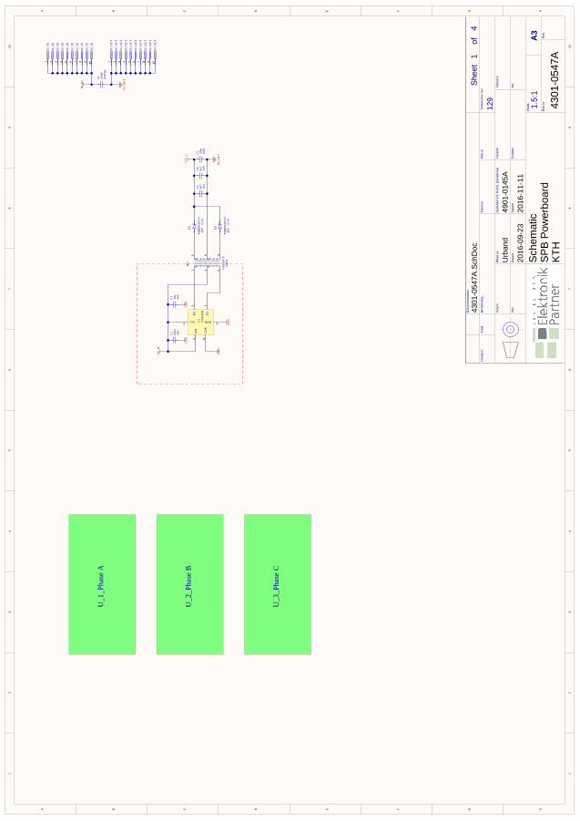
11
22
33
44
55
66
77
88
99
1010
HH
GG
FF
EE
DD
CC
BB
AA
Shee
t
o
f1
4
Rita
d av
Dat
um
Mat
eria
l
God
känd
enl
. kon
st. g
rans
knin
g
Dat
um
Ritn
.nr
Filn
amn
Ersät
ter
Sub
vers
ion
rev. To
lera
ns
Yta
.
Ska
la
Ritn
.nr.
Rev
.
A3
Vik
t
Vol
ym
Benäm
ning
Ant
alD
etal
j.nr.
1.5:
1
Urb
and
4901
-014
5A
2016
-09-
2320
16-1
1-11
4301
-054
7A
Sch
emat
icSP
B Po
wer
boar
dK
TH
Dok
umen
tnam
n
4301
-054
7A.S
chD
oc
129
U_1
_Pha
se A
U_2
_Pha
se B
U_3
_Pha
se C
D1
1
Vcc2
D2
3
GND 4
EN
5
CLK
6
U1
SN65
05B
1 2 3456
7503
4287
960
mA
TR1
MB
R05
40T1
G40
V0,
5A
D1
10u
10V
C3
MB
R05
40T1
G40
V0,
5A
D2
100n
50V
C2
GN
D
DC
-OU
T
GN
D
GN
D
+5V
_B
+17V
_2
GN
D
DC
-IN
DC
-OU
T100u
F16
0VD
c
C1
1D
C-IN
2D
C-IN
3D
C-IN
4D
C-IN
5D
C-IN
6D
C-IN
7D
C-IN
8D
C-IN
9D
C-IN
10D
C-IN
1D
C-O
UT
2D
C-O
UT
3D
C-O
UT
4D
C-O
UT
5D
C-O
UT
6D
C-O
UT
7D
C-O
UT
8D
C-O
UT
9D
C-O
UT
10D
C-O
UT
4u7
50V
C4
4u7
50V
C8
100n
100V
C5
PIC101 PIC102
COC1
PIC201 PIC202
COC2
PIC301 PIC302
COC3
PIC401 PIC402
COC4
PIC501 PIC502
COC5
PIC801 PIC802
COC8
PID1
01
PID1
02 COD1 PI
D201
PI
D202
COD2
PIDC0IN01
CODC0INA
PIDC0IN02
CODC0INB
PIDC0IN03
CODC0INC
PIDC0IN04
CODC0IND
PIDC0IN05
CODC0INE
PIDC0IN06
CODC0INF
PIDC0IN07
CODC0ING
PIDC0IN08
CODC0INH
PIDC0IN09
CODC0INI
PIDC0IN010
CODC0INJ
PIDC0OUT01
CODC0OUTA
PIDC0OUT02
CODC0OUTB
PIDC0OUT03
CODC0OUTC
PIDC0OUT04
CODC0OUTD
PIDC0OUT05
CODC0OUTE
PIDC0OUT06
CODC0OUTF
PIDC0OUT07
CODC0OUTG
PIDC0OUT08
CODC0OUTH
PIDC0OUT09
CODC0OUTI
PIDC0OUT010
CODC0OUTJ
PITR101
PITR102
PITR103
PITR104
PITR105
PITR106
COTR1
PIU101
PIU102 PIU103
PIU104
PIU105
PIU106
COU1
PIC201 PIC301
PITR102
PIU102
PIU105
PIC401
PIC501
PIC801
PID1
01
PID2
01
PIC101
PIDC0IN01
PIDC0IN02
PIDC0IN03
PIDC0IN04
PIDC0IN05
PIDC0IN06
PIDC0IN07
PIDC0IN08
PIDC0IN09
PIDC0IN010
PIC102
PIC402 PIC502
PIC802
PIDC0OUT01
PIDC0OUT02
PIDC0OUT03
PIDC0OUT04
PIDC0OUT05
PIDC0OUT06
PIDC0OUT07
PIDC0OUT08
PIDC0OUT09
PIDC0OUT010
PITR105
PIC202 PIC302
PIU104
PIU106
PID1
02
PITR106
PID2
02
PITR104
PITR101
PIU103
PITR103
PIU101
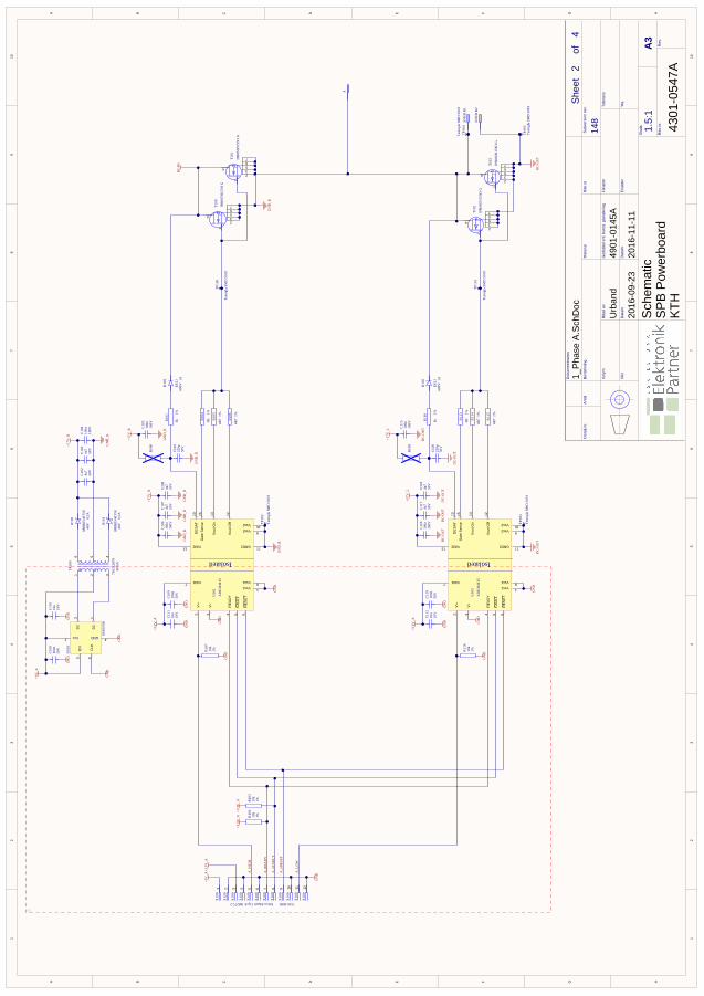
11
22
33
44
55
66
77
88
99
1010
HH
GG
FF
EE
DD
CC
BB
AA
Shee
t
o
f2
4
Rita
d av
Dat
um
Mat
eria
l
God
känd
enl
. kon
st. g
rans
knin
g
Dat
um
Ritn
.nr
Filn
amn
Ersät
ter
Sub
vers
ion
rev. To
lera
ns
Yta
.
Ska
la
Ritn
.nr.
Rev
.
A3
Vik
t
Vol
ym
Benäm
ning
Ant
alD
etal
j.nr.
1.5:
1
Urb
and
4901
-014
5A
2016
-09-
2320
16-1
1-11
4301
-054
7A
Sch
emat
icSP
B Po
wer
boar
dK
TH
Dok
umen
tnam
n
1_Ph
ase
A.Sc
hDoc
148
A
D1
1
Vcc2
D2
3
GND 4
EN
5
CLK
6
U10
0
SN65
05B
1 2 3456
7503
4287
960
mA
TR10
0
MB
R05
40T1
G40
V0,
5A
D10
0
10u
10V
C10
1
MB
R05
40T1
G40
V0,
5A
D10
1
100n
50V
C10
0
GN
D
GN
D_R
GN
D
GN
D
+5V
_A
+17V
_R
0R1%
R10
4
ES1J
600V
1A
D10
2
1k1%
R10
1
220p
50V
C11
0
GN
D_R
R10
0
+17V
_R
100n
100V
C10
5
GN
D_R
100n
100V
C10
6
GN
D_R
GN
D_R
4u7
50V
C10
7
GN
D_R
+17V
_R
Vss1 1
Vi+
2
Vi-
3
RE
AD
Y4
FAU
LT5
RE
SE
T6
Vdd17 Vss1 8
Vss2 9DE
SA
T10
GND2 11
Vou
t Off
12
Vdd213
Vou
t On
14
Gat
e S
ense
15
Vss2 16
Isolated
U10
1
AD
UM
4135
4u7
50V
C10
8
GN
D_R
0R1%
R11
3
ES1J
600V
1A
D10
5
1k1%
R11
0
220p
50V
C12
0
DC
-OU
TR10
9
+17V
_2
100n
100V
C11
5
DC
-OU
T10
0n10
0V
C11
6
DC
-OU
T
4u7
50V
C11
7
DC
-OU
T
+17V
_2Vss1 1
Vi+
2
Vi-
3
RE
AD
Y4
FAU
LT5
RE
SE
T6
Vdd17 Vss1 8
Vss2 9DE
SA
T10
GND2 11
Vou
t Off
12
Vdd213
Vou
t On
14
Gat
e S
ense
15
Vss2 16
Isolated
U10
3
AD
UM
4135
4u7
50V
C11
8
DC
-OU
T
DC
-IN
DC
-OU
T
GN
D
10k
1%R10
7
GN
D
100n
50V
C10
9
GN
D
10k
1%R10
310
k1%R
102
+3.3
V_A
+3.3
V_A
10k
1%R11
6
GN
D
100n
50V
C11
9
GN
D
+3.3
V_A
GN
D
GN
DD
C-O
UT
+5V
_A
GN
D
GN
D_R
4R7
1%
R10
5
4R7
1%
R10
6
4R7
1%
R11
4
4R7
1%
R11
5
4u7
50V
C10
24u
750
V
C10
310
0n10
0V
C10
4
GN
D
GN
D
+3.3
V_A
A_H
IGH
A_L
OW
A_R
EAD
Y
A_n
FAU
LT
A_n
RES
ET
1
1330-0060Micro-Match 12p 8-188275-2
X10
0
2X
100
3X
100
4X
100
5X
100
6X
100
7X
100
8X
100
9X
100
10X
100
11X
100
12X
100
10u
10V
C11
2
GN
D
GN
D
+3.3
V_A
10u
10V
C11
1
SNU
B R
1
SNU
B R
2
Testög
la S
MD
501
9
TP10
0
Testög
la S
MD
501
9
TP10
1
Testög
la S
MD
501
9
TP10
2
Testög
la S
MD
501
9
TP10
3
Testög
la S
MD
501
9TP
104
Testög
la S
MD
501
9TP
105
5
1
4
23
67IP
B06
5N15
N3
G
T100
5
1
4
23
67IP
B06
5N15
N3
G
T101
5
1
4
23
67IP
B06
5N15
N3
G
T102
5
1
4
23
67IP
B06
5N15
N3
G
T103
PIA01 COA
PIC10001 PIC10002
COC100
PIC10101 PIC10102
COC101
PIC10201 PIC10202
COC102
PIC10301 PIC10302
COC103
PIC10401 PIC10402
COC104
PIC10501 PIC10502
COC105
PIC10601 PIC10602
COC106
PIC10701 PIC10702
COC107
PIC10801 PIC10802
COC108
PIC10901 PIC10902
COC109
PIC11001
PIC11002
COC110
PIC11101 PIC11102
COC111
PIC11201 PIC11202
COC112
PIC11501 PIC11502
COC115
PIC11601 PIC11602
COC116
PIC11701 PIC11702
COC117
PIC11801 PIC11802
COC118
PIC11901 PIC11902
COC119
PIC12001 PIC12002
COC120
PID1
0001
PI
D100
02
COD100
PID1
0101
PI
D101
02 COD101
PID1
0201
PI
D102
02
COD102
PID1
0501
PI
D105
02
COD105
PIR10001
PIR10002
COR100
PIR101
01 PIR
10102
COR101
PIR10201
PIR10202
COR102
PIR10301
PIR10302
COR103
PIR104
01 PIR
10402
COR104
PIR105
01 PIR
10502
COR105
PIR106
01 PIR
10602
COR106
PIR10701
PIR10702
COR107
PIR10901
PIR10902
COR109
PIR110
01 PIR
11002
COR110
PIR113
01 PIR
11302
COR113
PIR114
01 PIR
11402
COR114
PIR115
01 PIR
11502
COR115
PIR11601
PIR11602
COR116
PISNUB R101 COSNUB R1
PISNUB R201 COSNUB R2
PIT1
0001
PIT10002 PIT10003 PIT10004 PIT10005 PIT10
006 PIT10007 COT100
PIT1
0101
PIT10102 PIT10103 PIT10104 PIT10105 PIT10
106 PIT10107 COT101
PIT1
0201
PIT10202 PIT10203 PIT10204 PIT10205 PIT10
206 PIT10207 COT102
PIT1
0301
PIT10302 PIT10303 PIT10304 PIT10305 PIT10
306 PIT10307 COT103
PITP10001
COTP
100
PITP10101 COTP
101
PITP1020
1 COTP
102
PITP1030
1 COTP
103
PITP10401 COTP
104
PITP10501 COTP
105
PITR10001
PITR10002
PITR10003
PITR10004
PITR10005
PITR10006
COTR
100
PIU1
0001
PIU10002 PI
U100
03
PIU10004
PIU1
0005
PIU1
0006
COU100
PIU10101
PIU1
0102
PIU1
0103
PIU1
0104
PIU1
0105
PIU1
0106
PIU10107 PIU10108 PIU10109
PIU101010
PIU101011
PIU101012
PIU101013
PIU101014
PIU101015
PIU101016
COU101 PIU10301
PIU1
0302
PIU1
0303
PIU1
0304
PIU1
0305
PIU1
0306
PIU10307 PIU10308 PIU10309
PIU103010
PIU103011
PIU103012
PIU103013
PIU103014
PIU103015
PIU103016
COU103
PIX1
0001
COX1
00A
PIX1
0002
COX1
00B
PIX1
0003
COX1
00C
PIX1
0004
COX1
00D
PIX1
0005
COX1
00E
PIX1
0006
COX1
00F
PIX1
0007
COX1
00G
PIX1
0008
COX1
00H
PIX1
0009
COX1
00I
PIX100010
COX1
00J
PIX100011
COX1
00K
PIX100012
COX1
00L
PIC10901
PIC11101 PIC11201
PIC11901
PIR10202
PIR10302
PIU10107 PIU10307
PIX1
0003
PIC10001 PIC10101
PITR10002
PIU10002
PIU1
0005
PIX1
0001
PIC11501
PIC11601 PIC11701
PIC11801
PIR10902
PIU103013
PIC10201 PIC10301
PIC10401
PIC10501
PIC10601 PIC10701
PIC10801
PID1
0001
PID1
0101
PIR10002
PIU101013
PIR10702
PIU1
0102
PIX1
0005
NL
A0HI
GH
PIR11602
PIU1
0302
PIX100011
NLA0
LOW
PIR10301
PIU1
0105
PIU1
0305
PIX1
0008
NL
A0nF
AULT
PIU1
0106
PIU1
0306
PIX1
0009
NL
A0nR
ESET
PIR10201
PIU1
0104
PIU1
0304
PIX1
0007
NLA0READY
PID1
0201
PIT10004
PIT10104
PIC11502
PIC11602
PIC11702
PIC11802
PIC12002
PISNUB R201
PIT10202 PIT10203 PIT102
05 PIT10206 PIT10207
PIT10302 PIT10303 PIT103
05 PIT10306 PIT10307
PITP1030
1 PITP1050
1 PIU10309
PIU103011 PIU103016
PIC10002
PIC10102
PIC10902 PIC11102 PIC1120
2 PIC1190
2
PIR10701
PIR11601
PIU10004
PIU1
0006
PIU10101
PIU1
0103
PIU10108
PIU10301
PIU1
0303
PIU10308
PIX1
0002
PIX1
0004
PIX1
0006
PIX100010
PIX100012
PIA01
PIC10202 PIC10302
PIC10402
PIC10502
PIC10602 PIC10702
PIC10802
PIC11002
PID1
0501
PISNUB R101
PIT10002 PIT10003 PIT100
05 PIT10006 PIT10007
PIT10102 PIT10103 PIT101
05 PIT10106 PIT10107
PIT10204
PIT10304
PITP1020
1
PITP10401
PITR10005
PIU10109 PIU101011
PIU101016
PIC11001
PIR10001
PIR101
01
PIU101010
PIC12001 PIR10901
PIR110
01
PIU103010
PID1
0002
PITR10006
PID1
0102
PITR10004
PID1
0202
PIR
10102
PID1
0502
PIR
11002
PIR104
01 PIU101015
PIR104
02
PIR105
02
PIR106
02
PIT1
0001
PIT1
0101
PITP10001
PIR105
01 PIU101014
PIR106
01 PIU101012
PIR113
01 PIU103015
PIR113
02
PIR114
02
PIR115
02
PIT1
0201
PIT1
0301
PITP10101
PIR114
01 PIU103014
PIR115
01 PIU103012
PITR10001
PIU1
0003
PITR10003
PIU1
0001

11
22
33
44
55
66
77
88
99
1010
HH
GG
FF
EE
DD
CC
BB
AA
Shee
t
o
f3
4
Rita
d av
Dat
um
Mat
eria
l
God
känd
enl
. kon
st. g
rans
knin
g
Dat
um
Ritn
.nr
Filn
amn
Ersät
ter
Sub
vers
ion
rev. To
lera
ns
Yta
.
Ska
la
Ritn
.nr.
Rev
.
A3
Vik
t
Vol
ym
Benäm
ning
Ant
alD
etal
j.nr.
1.5:
1
Urb
and
4901
-014
5A
2016
-09-
2320
16-1
1-11
4301
-054
7A
Sch
emat
icSP
B Po
wer
boar
dK
TH
Dok
umen
tnam
n
2_Ph
ase
B.Sc
hDoc
148
B
D1
1
Vcc2
D2
3
GND 4
EN
5
CLK
6
U20
0
SN65
05B
1 2 3456
7503
4287
960
mA
TR20
0
MB
R05
40T1
G40
V0,
5A
D20
0
10u
10V
C20
1
MB
R05
40T1
G40
V0,
5A
D20
1
100n
50V
C20
0
GN
D
GN
D_S
GN
D
GN
D
+5V
_B
+17V
_S
0R1%
R20
4
ES1J
600V
1A
D20
2
1k1%
R20
1
220p
50V
C20
9
GN
D_S
R20
0
+17V
_S
100n
100V
C20
4
GN
D_S
100n
100V
C20
5
GN
D_S
GN
D_S
4u7
50V
C20
6
GN
D_S
+17V
_S
Vss1 1
Vi+
2
Vi-
3
RE
AD
Y4
FAU
LT5
RE
SE
T6
Vdd17 Vss1 8
Vss2 9DE
SA
T10
GND2 11
Vou
t Off
12
Vdd213
Vou
t On
14
Gat
e S
ense
15
Vss2 16
Isolated
U20
1
AD
UM
4135
4u7
50V
C20
7
GN
D_S
0R1%
R21
3
ES1J
600V
1A
D20
3
1k1%
R21
0
220p
50V
C21
5
DC
-OU
TR20
9
+17V
_2
100n
100V
C21
0
DC
-OU
T10
0n10
0V
C21
1
DC
-OU
T
4u7
50V
C21
2
DC
-OU
T
+17V
_2Vss1 1
Vi+
2
Vi-
3
RE
AD
Y4
FAU
LT5
RE
SE
T6
Vdd17 Vss1 8
Vss2 9DE
SA
T10
GND2 11
Vou
t Off
12
Vdd213
Vou
t On
14
Gat
e S
ense
15
Vss2 16
Isolated
U20
2
AD
UM
4135
4u7
50V
C21
3
DC
-OU
T
DC
-IN
DC
-OU
T
GN
D
10k
1%R20
7
100n
50V
C20
8
GN
D
10k
1%R20
310
k1%R
202
10k
1%R21
6
100n
50V
C21
4
GN
D
GN
D
GN
DD
C-O
UT
GN
D_S
4R7
1%
R20
5
4R7
1%
R20
6
4R7
1%
R21
4
4R7
1%
R21
5
4u7
50V
C20
24u
750
V
C21
610
0n10
0V
C20
3
GN
D
+3.3
V_B
+3.3
V_B
GN
D
+5V
_B
GN
D
GN
D
GN
D
+3.3
V_B
B_H
IGH
B_L
OW
B_R
EAD
Y
B_n
FAU
LT
B_n
RES
ET
1
1330-0060Micro-Match 12p 8-188275-2
X20
0
2X
200
3X
200
4X
200
5X
200
6X
200
7X
200
8X
200
9X
200
10X
200
11X
200
12X
200
GN
D
+3.3
V_B
10u
10V
C21
7
GN
D
+3.3
V_B
10u
10V
C21
8
SNU
B S
1
SNU
B S
2
Testög
la S
MD
501
9
TP20
0
Testög
la S
MD
501
9
TP20
1
Testög
la S
MD
501
9
TP20
2
Testög
la S
MD
501
9
TP20
3
Testög
la S
MD
501
9TP
204
Testög
la S
MD
501
9TP
205
5
1
4
23
67IP
B06
5N15
N3
G
T200
5
1
4
23
67IP
B06
5N15
N3
G
T201
5
1
4
23
67IP
B06
5N15
N3
G
T202
5
1
4
23
67IP
B06
5N15
N3
G
T203
PIB01 COB
PIC20001 PIC20002
COC200
PIC20101 PIC20102
COC201
PIC20201 PIC20202
COC202
PIC20301 PIC20302
COC203
PIC20401 PIC20402
COC204
PIC20501 PIC20502
COC205
PIC20601 PIC20602
COC206
PIC20701 PIC20702
COC207
PIC20801 PIC20802
COC208
PIC20901
PIC20902
COC209
PIC21001 PIC21002
COC210
PIC21101 PIC21102
COC211
PIC21201 PIC21202
COC212
PIC21301 PIC21302
COC213
PIC21401 PIC21402
COC214
PIC21501 PIC21502
COC215
PIC21601 PIC21602
COC216
PIC21701 PIC21702
COC217
PIC21801 PIC21802
COC218
PID2
0001
PI
D200
02
COD200
PID2
0101
PI
D201
02 COD201
PID2
0201
PI
D202
02
COD202
PID2
0301
PI
D203
02
COD203
PIR20001
PIR20002
COR200
PIR201
01 PIR
20102
COR201
PIR20201
PIR20202
COR202
PIR20301
PIR20302
COR203
PIR204
01 PIR
20402
COR204
PIR205
01 PIR
20502
COR205
PIR206
01 PIR
20602
COR206
PIR20701
PIR20702
COR207
PIR20901
PIR20902
COR209
PIR210
01 PIR
21002
COR210
PIR213
01 PIR
21302
COR213
PIR214
01 PIR
21402
COR214
PIR215
01 PIR
21502
COR215
PIR21601
PIR21602
COR216
PISNUB S101 COSNUB S1
PISNUB S201 COSNUB S2
PIT2
0001
PIT20002 PIT20003 PIT20004 PIT20005 PIT20
006 PIT20007 COT200
PIT2
0101
PIT20102 PIT20103 PIT20104 PIT20105 PIT20
106 PIT20107 COT201
PIT2
0201
PIT20202 PIT20203 PIT20204 PIT20205 PIT20
206 PIT20207 COT202
PIT2
0301
PIT20302 PIT20303 PIT20304 PIT20305 PIT20
306 PIT20307 COT203
PITP20001
COTP
200
PITP20101 COTP
201
PITP2020
1 COTP
202
PITP2030
1 COTP
203
PITP20401 COTP
204
PITP20501 COTP
205
PITR20001
PITR20002
PITR20003
PITR20004
PITR20005
PITR20006
COTR
200
PIU2
0001
PIU20002 PI
U200
03
PIU20004
PIU2
0005
PIU2
0006
COU200
PIU20101
PIU2
0102
PIU2
0103
PIU2
0104
PIU2
0105
PIU2
0106
PIU20107 PIU20108 PIU20109
PIU201010
PIU201011
PIU201012
PIU201013
PIU201014
PIU201015
PIU201016
COU201 PIU20201
PIU2
0202
PIU2
0203
PIU2
0204
PIU2
0205
PIU2
0206
PIU20207 PIU20208 PIU20209
PIU202010
PIU202011
PIU202012
PIU202013
PIU202014
PIU202015
PIU202016
COU202
PIX2
0001
COX2
00A
PIX2
0002
COX2
00B
PIX2
0003
COX2
00C
PIX2
0004
COX2
00D
PIX2
0005
COX2
00E
PIX2
0006
COX2
00F
PIX2
0007
COX2
00G
PIX2
0008
COX2
00H
PIX2
0009
COX2
00I
PIX200010
COX2
00J
PIX200011
COX2
00K
PIX200012
COX2
00L
PIC20801 PIC21401
PIC21701 PIC21801
PIR20202
PIR20302
PIU20107 PIU20207
PIX2
0003
PIC20001 PIC20101
PITR20002
PIU20002
PIU2
0005
PIX2
0001
PIC21001
PIC21101 PIC21201
PIC21301
PIR20902
PIU202013
PIC20201 PIC20301
PIC20401
PIC20501 PIC20601
PIC20701
PIC21601
PID2
0001
PID2
0101
PIR20002
PIU201013
PIR20702
PIU2
0102
PIX2
0005
NL
B0HI
GH
PIR21602
PIU2
0202
PIX200011
NLB0
LOW
PIR20301
PIU2
0105
PIU2
0205
PIX2
0008
NL
B0nF
AULT
PIU2
0106
PIU2
0206
PIX2
0009
NL
B0nR
ESET
PIR20201
PIU2
0104
PIU2
0204
PIX2
0007
NLB0READY
PID2
0201
PIT20004
PIT20104
PIC21002
PIC21102
PIC21202
PIC21302
PIC21502
PISNUB S201
PIT20202 PIT20203 PIT202
05 PIT20206 PIT20207
PIT20302 PIT20303 PIT203
05 PIT20306 PIT20307
PITP2030
1 PITP2050
1 PIU20209
PIU202011 PIU202016
PIC20002
PIC20102
PIC20802 PIC21402
PIC21702 PIC21802
PIR20701
PIR21601
PIU20004
PIU2
0006
PIU20101
PIU2
0103
PIU20108
PIU20201
PIU2
0203
PIU20208
PIX2
0002
PIX2
0004
PIX2
0006
PIX200010
PIX200012
PIB01
PIC20202 PIC20302
PIC20402
PIC20502 PIC20602
PIC20702
PIC20902
PIC21602
PID2
0301
PISNUB S101
PIT20002 PIT20003 PIT200
05 PIT20006 PIT20007
PIT20102 PIT20103 PIT201
05 PIT20106 PIT20107
PIT20204
PIT20304
PITP2020
1
PITP20401
PITR20005
PIU20109 PIU201011
PIU201016
PIC20901
PIR20001
PIR201
01
PIU201010
PIC21501 PIR20901
PIR210
01
PIU202010
PID2
0002
PITR20006
PID2
0102
PITR20004
PID2
0202
PIR
20102
PID2
0302
PIR
21002
PIR204
01 PIU201015
PIR204
02
PIR205
02
PIR206
02
PIT2
0001
PIT2
0101
PITP20001
PIR205
01 PIU201014
PIR206
01 PIU201012
PIR213
01 PIU202015
PIR213
02
PIR214
02
PIR215
02
PIT2
0201
PIT2
0301
PITP20101
PIR214
01 PIU202014
PIR215
01 PIU202012
PITR20001
PIU2
0003
PITR20003
PIU2
0001
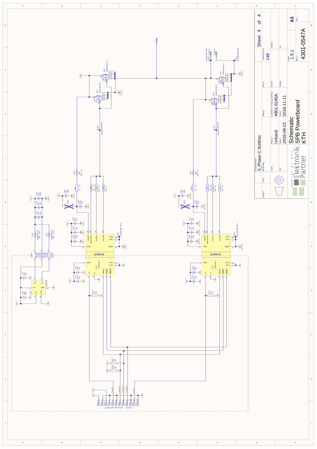
11
22
33
44
55
66
77
88
99
1010
HH
GG
FF
EE
DD
CC
BB
AA
Shee
t
o
f4
4
Rita
d av
Dat
um
Mat
eria
l
God
känd
enl
. kon
st. g
rans
knin
g
Dat
um
Ritn
.nr
Filn
amn
Ersät
ter
Sub
vers
ion
rev. To
lera
ns
Yta
.
Ska
la
Ritn
.nr.
Rev
.
A3
Vik
t
Vol
ym
Benäm
ning
Ant
alD
etal
j.nr.
1.5:
1
Urb
and
4901
-014
5A
2016
-09-
2320
16-1
1-11
4301
-054
7A
Sch
emat
icSP
B Po
wer
boar
dK
TH
Dok
umen
tnam
n
3_Ph
ase
C.S
chD
oc
148
C
D1
1
Vcc2
D2
3
GND 4
EN
5
CLK
6
U30
0
SN65
05B
1 2 3456
7503
4287
960
mA
TR30
0
MB
R05
40T1
G40
V0,
5A
D30
0
10u
10V
C30
1
MB
R05
40T1
G40
V0,
5A
D30
1
100n
50V
C30
0
GN
D
GN
D_T
GN
D
GN
D
+5V
_C
+17V
_T
0R1%
R30
4
ES1J
600V
1A
D30
2
1k1%
R30
1
220p
50V
C30
9
GN
D_T
R30
0
+17V
_T
100n
100V
C30
4
GN
D_T
100n
100V
C30
5
GN
D_T
GN
D_T
4u7
50V
C30
6
GN
D_T
+17V
_T
Vss1 1
Vi+
2
Vi-
3
RE
AD
Y4
FAU
LT5
RE
SE
T6
Vdd17 Vss1 8
Vss2 9DE
SA
T10
GND2 11
Vou
t Off
12
Vdd213
Vou
t On
14
Gat
e S
ense
15
Vss2 16
Isolated
U30
1
AD
UM
4135
4u7
50V
C30
7
GN
D_T
0R1%
R31
3
ES1J
600V
1A
D30
3
1k1%
R31
0
220p
50V
C31
5
DC
-OU
TR30
9
+17V
_2
100n
100V
C31
0
DC
-OU
T10
0n10
0V
C31
1
DC
-OU
T
4u7
50V
C31
2
DC
-OU
T
+17V
_2Vss1 1
Vi+
2
Vi-
3
RE
AD
Y4
FAU
LT5
RE
SE
T6
Vdd17 Vss1 8
Vss2 9DE
SA
T10
GND2 11
Vou
t Off
12
Vdd213
Vou
t On
14
Gat
e S
ense
15
Vss2 16
Isolated
U30
2
AD
UM
4135
4u7
50V
C31
3
DC
-OU
T
DC
-IN
DC
-OU
T
GN
D
10k
1%R30
7
100n
50V
C30
8
GN
D
10k
1%R30
310
k1%R
302
10k
1%R31
6
100n
50V
C31
4
GN
D
GN
D
GN
DD
C-O
UT
GN
D_T
4R7
1%
R30
5
4R7
1%
R30
6
4R7
1%
R31
4
4R7
1%
R31
5
4u7
50V
C30
24u
750
V
C31
610
0n10
0V
C30
3
GN
D
+3.3
V_C
+3.3
V_C
GN
D
+5V
_C
GN
D
GN
D
GN
D
+3.3
V_C
C_H
IGH
C_L
OW
C_R
EAD
Y
C_n
FAU
LT
C_n
RES
ET
1
1330-0060Micro-Match 12p 8-188275-2
X30
0
2X
300
3X
300
4X
300
5X
300
6X
300
7X
300
8X
300
9X
300
10X
300
11X
300
12X
300
GN
D
+3.3
V_C
10u
10V
C31
7
GN
D
+3.3
V_C
10u
10V
C31
8
SNU
B T
1
SNU
B T
2
Testög
la S
MD
501
9
TP30
0
Testög
la S
MD
501
9
TP30
1
Testög
la S
MD
501
9
TP30
2
Testög
la S
MD
501
9
TP30
3
Testög
la S
MD
501
9TP
304
Testög
la S
MD
501
9TP
305
5
1
4
23
67IP
B06
5N15
N3
G
T300
5
1
4
23
67IP
B06
5N15
N3
G
T301
5
1
4
23
67IP
B06
5N15
N3
G
T302
5
1
4
23
67IP
B06
5N15
N3
G
T303
PIC01 COC
PIC30001 PIC30002
COC300
PIC30101 PIC30102
COC301
PIC30201 PIC30202
COC302
PIC30301 PIC30302
COC303
PIC30401 PIC30402
COC304
PIC30501 PIC30502
COC305
PIC30601 PIC30602
COC306
PIC30701 PIC30702
COC307
PIC30801 PIC30802
COC308
PIC30901
PIC30902
COC309
PIC31001 PIC31002
COC310
PIC31101 PIC31102
COC311
PIC31201 PIC31202
COC312
PIC31301 PIC31302
COC313
PIC31401 PIC31402
COC314
PIC31501 PIC31502
COC315
PIC31601 PIC31602
COC316
PIC31701 PIC31702
COC317
PIC31801 PIC31802
COC318
PID3
0001
PI
D300
02
COD300
PID3
0101
PI
D301
02 COD301
PID3
0201
PI
D302
02
COD302
PID3
0301
PI
D303
02
COD303
PIR30001
PIR30002
COR300
PIR301
01 PIR
30102
COR301
PIR30201
PIR30202
COR302
PIR30301
PIR30302
COR303
PIR304
01 PIR
30402
COR304
PIR305
01 PIR
30502
COR305
PIR306
01 PIR
30602
COR306
PIR30701
PIR30702
COR307
PIR30901
PIR30902
COR309
PIR310
01 PIR
31002
COR310
PIR313
01 PIR
31302
COR313
PIR314
01 PIR
31402
COR314
PIR315
01 PIR
31502
COR315
PIR31601
PIR31602
COR316
PISNUB T101 COSNUB T1
PISNUB T201 COSNUB T2
PIT3
0001
PIT30002 PIT30003 PIT30004 PIT30005 PIT30
006 PIT30007 COT300
PIT3
0101
PIT30102 PIT30103 PIT30104 PIT30105 PIT30
106 PIT30107 COT301
PIT3
0201
PIT30202 PIT30203 PIT30204 PIT30205 PIT30
206 PIT30207 COT302
PIT3
0301
PIT30302 PIT30303 PIT30304 PIT30305 PIT30
306 PIT30307 COT303
PITP30001
COTP
300
PITP30101 COTP
301
PITP3020
1 COTP
302
PITP3030
1 COTP
303
PITP30401 COTP
304
PITP30501 COTP
305
PITR30001
PITR30002
PITR30003
PITR30004
PITR30005
PITR30006
COTR
300
PIU3
0001
PIU30002 PI
U300
03
PIU30004
PIU3
0005
PIU3
0006
COU300
PIU30101
PIU3
0102
PIU3
0103
PIU3
0104
PIU3
0105
PIU3
0106
PIU30107 PIU30108 PIU30109
PIU301010
PIU301011
PIU301012
PIU301013
PIU301014
PIU301015
PIU301016
COU301 PIU30201
PIU3
0202
PIU3
0203
PIU3
0204
PIU3
0205
PIU3
0206
PIU30207 PIU30208 PIU30209
PIU302010
PIU302011
PIU302012
PIU302013
PIU302014
PIU302015
PIU302016
COU302
PIX3
0001
COX3
00A
PIX3
0002
COX3
00B
PIX3
0003
COX3
00C
PIX3
0004
COX3
00D
PIX3
0005
COX3
00E
PIX3
0006
COX3
00F
PIX3
0007
COX3
00G
PIX3
0008
COX3
00H
PIX3
0009
COX3
00I
PIX300010
COX3
00J
PIX300011
COX3
00K
PIX300012
COX3
00L
PIC30801 PIC31401
PIC31701 PIC31801
PIR30202
PIR30302
PIU30107 PIU30207
PIX3
0003
PIC30001 PIC30101
PITR30002
PIU30002
PIU3
0005
PIX3
0001
PIC31001
PIC31101 PIC31201
PIC31301
PIR30902
PIU302013
PIC30201 PIC30301
PIC30401
PIC30501 PIC30601
PIC30701
PIC31601
PID3
0001
PID3
0101
PIR30002
PIU301013
PIR30702
PIU3
0102
PIX3
0005
NL
C0HI
GH
PIR31602
PIU3
0202
PIX300011
NLC0
LOW
PIR30301
PIU3
0105
PIU3
0205
PIX3
0008
NL
C0nF
AULT
PIU3
0106
PIU3
0206
PIX3
0009
NL
C0nR
ESET
PIR30201
PIU3
0104
PIU3
0204
PIX3
0007
NLC0READY
PID3
0201
PIT30004
PIT30104
PIC31002
PIC31102
PIC31202
PIC31302
PIC31502
PISNUB T201
PIT30202 PIT30203 PIT302
05 PIT30206 PIT30207
PIT30302 PIT30303 PIT303
05 PIT30306 PIT30307
PITP3030
1 PITP3050
1 PIU30209
PIU302011 PIU302016
PIC30002
PIC30102
PIC30802 PIC31402
PIC31702 PIC31802
PIR30701
PIR31601
PIU30004
PIU3
0006
PIU30101
PIU3
0103
PIU30108
PIU30201
PIU3
0203
PIU30208
PIX3
0002
PIX3
0004
PIX3
0006
PIX300010
PIX300012
PIC30202 PIC30302
PIC30402
PIC30502 PIC30602
PIC30702
PIC30902
PIC31602
PIC01
PID3
0301
PISNUB T101
PIT30002 PIT30003 PIT300
05 PIT30006 PIT30007
PIT30102 PIT30103 PIT301
05 PIT30106 PIT30107
PIT30204
PIT30304
PITP3020
1
PITP30401
PITR30005
PIU30109 PIU301011
PIU301016
PIC30901
PIR30001
PIR301
01
PIU301010
PIC31501 PIR30901
PIR310
01
PIU302010
PID3
0002
PITR30006
PID3
0102
PITR30004
PID3
0202
PIR
30102
PID3
0302
PIR
31002
PIR304
01 PIU301015
PIR304
02
PIR305
02
PIR306
02
PIT3
0001
PIT3
0101
PITP30001
PIR305
01 PIU301014
PIR306
01 PIU301012
PIR313
01 PIU302015
PIR313
02
PIR314
02
PIR315
02
PIT3
0201
PIT3
0301
PITP30101
PIR314
01 PIU302014
PIR315
01 PIU302012
PITR30001
PIU3
0003
PITR30003
PIU3
0001

70

71

72
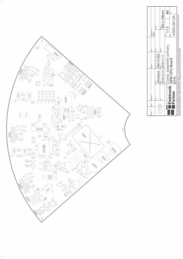
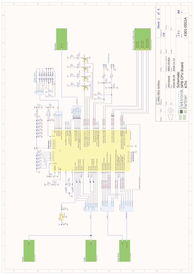
11
22
33
44
55
66
77
88
99
1010
HH
GG
FF
EE
DD
CC
BB
AA
Shee
t
o
f1
6
Rita
dav
Dat
um
Mat
eria
l
God
känd
enl.
kons
t.gr
ansk
ning
Dat
um
Ritn
.nr
Filn
amn
Ersät
ter
Sub
vers
ion
rev. To
lera
ns
Yta
.
Ska
la
Ritn
.nr.
Rev
.
A3
Vik
t
Vol
ym
Benäm
ning
Ant
alD
etal
j.nr.
1.5:
1
JH/U
rban
d49
01-0
145A
2016
-09-
2920
16-1
1-11
4301
-055
1A
Sch
emat
icSP
BC
PUB
oard
KTH
Dok
umen
tnam
n
1_43
01-0
551.
SchD
oc
128
GP
IO23
/EQ
EP
1I/M
FSX
A/S
CIR
XD
B1
Vdd2Vss 3
VddI/O4
GP
IO20
/EQ
EP
1A/M
DX
A/C
OM
P1O
UT
5
GP
IO21
/EQ
EP
1B/M
DR
A/C
OM
P2O
UT
6
GP
IO4/
EP
WM
3A7
GP
IO5/
EP
WM
3B/S
PIS
IMO
A/E
CA
P1
8
XR
S9
TRS
T10
Vdd12Vss 13
VddI/O11
AD
CIN
A6/
CO
MP
3A/A
IO6
14A
DC
INA
515
AD
CIN
A4/
CO
MP
2A/A
IO4
16A
DC
INA
2/C
OM
P1A
/AIO
217
AD
CIN
A1
18A
DC
INA
0, V
refH
I19
VddA20
VssA 21
AD
CIN
B0
22
AD
CIN
B1
23
AD
CIN
B2/
CO
MP
1B/A
IO10
24
AD
CIN
B4/
CO
MP
2B/A
IO12
25
AD
CIN
B5
26
AD
CIN
B6/
CO
MP
3B/A
IO14
27
Vdd29Vss 28
VddI/O30
Vdd51Vss 50
VddI/O49
Vdd65Vss 64
VddI/O63
Vdd72Vss 73
VddI/O74
Vdd3VFL37
Vss 38
GP
IO25
/EC
AP
2/S
PIS
OM
IB31
GP
IO31
/CA
NTX
A/E
PW
M8A
32G
PIO
30/C
AN
RX
A/E
PW
M7A
33
GP
IO29
/SC
ITX
DA
/SC
LA/T
Z334
GP
IO12
/TZ1
/SC
ITX
DA
/SP
ISIM
OB
35
TES
T236
GP
IO9/
EP
WM
5B/S
CIT
XD
B/E
CA
P3
39
GP
IO28
/SC
IRX
DA
/SD
AA
/TZ2
40
GP
IO18
/SP
ICLK
A/S
CIT
XD
B/X
CLK
OU
T41
GP
IO17
/SP
ISO
MIA
/TZ3
42
GP
IO8/
EP
WM
5A/A
DC
SO
CA
O43
GP
IO16
/SP
ISIM
OA
/TZ2
44
GP
IO7/
EP
WM
4B/S
CIR
XD
A/E
CA
P2
45G
PIO
6/E
PW
M4A
/EP
WM
SY
NC
I/EP
WM
SY
NC
O46
X2
47
X1
48
GP
IO19
/XC
LKIN
/SP
ISTE
A/S
CIR
XD
B/E
CA
P1
52
GP
IO39
53
GP
IO38
/XC
LKIN
/TC
K54
GP
IO34
/CO
MP
2OU
T/C
OM
P3O
UT
55
GP
IO37
/TD
O56
GP
IO35
/TD
I57
GP
IO36
/TM
S58
GP
IO11
/EP
WM
6B/S
CIR
XD
B/E
CA
P1
59G
PIO
10/E
PW
M6A
/AD
CS
OC
BO
60
GP
IO27
/HR
CA
P2/
SP
ISTE
B/U
SB
0DM
61G
PIO
26/E
CA
P3/
SP
ICLK
B/U
SB
0DM
62
GP
IO3/
EP
WM
2B/S
PIS
OM
IA/C
OM
P2O
UT
66G
PIO
2/E
PW
M2A
67G
PIO
1/E
PW
M1B
/CO
MP
1OU
T68
GP
IO0/
EP
WM
1A69
GP
IO15
/EC
AP
2/S
CIR
XD
B/S
PIS
TEB
70
VR
EG
EN
Z71
GP
IO13
/TZ2
75
GP
IO14
/TZ3
/SC
ITX
DB
/SP
ICLK
B76
GP
IO24
/EC
AP
1/S
PIS
IMO
B77
GP
IO22
/EQ
EP
1S/M
CLK
XA
/SC
ITX
DB
78
GP
IO32
/SD
AA
/EP
WM
SY
NC
I/AD
CS
OC
AO
79
GP
IO33
/SC
LA/E
PW
MS
YN
CO
/AD
CS
OC
BO
80
GP
IO23
/EQ
EP
1I/M
FSX
A/S
CIR
XD
B
VddVss
VddI/O
GP
IO20
/EQ
EP
1A/M
DX
A/C
OM
P1O
UT
GP
IO21
/EQ
EP
1B/M
DR
A/C
OM
P2O
UT
GP
IO4/
EP
WM
3A
GP
IO5/
EP
WM
3B/S
PIS
IMO
A/E
CA
P1
XR
S
TRS
T
Vdd
Vss
VddI/O
AD
CIN
A6/
CO
MP
3A/A
IO6
AD
CIN
A5
AD
CIN
A4/
CO
MP
2A/A
IO4
AD
CIN
A2/
CO
MP
1A/A
IO2
AD
CIN
A1
AD
CIN
A0,
Vre
fHI
VddA
VssA
AD
CIN
B0
AD
CIN
B1
AD
CIN
B2/
CO
MP
1B/A
IO10
AD
CIN
B4/
CO
MP
2B/A
IO12
AD
CIN
B5
AD
CIN
B6/
CO
MP
3B/A
IO14
Vdd
Vss
VddI/O
Vdd
Vss
VddI/O
Vdd
Vss
VddI/O
VddVss
VddI/O
Vdd3VFL
Vss
GP
IO25
/EC
AP
2/S
PIS
OM
IB
GP
IO31
/CA
NTX
A/E
PW
M8A
GP
IO30
/CA
NR
XA
/EP
WM
7A
GP
IO29
/SC
ITX
DA
/SC
LA/T
Z3
GP
IO12
/TZ1
/SC
ITX
DA
/SP
ISIM
OB
TES
T2
GP
IO9/
EP
WM
5B/S
CIT
XD
B/E
CA
P3
GP
IO28
/SC
IRX
DA
/SD
AA
/TZ2
GP
IO18
/SP
ICLK
A/S
CIT
XD
B/X
CLK
OU
T
GP
IO17
/SP
ISO
MIA
/TZ3
GP
IO8/
EP
WM
5A/A
DC
SO
CA
O
GP
IO16
/SP
ISIM
OA
/TZ2
GP
IO7/
EP
WM
4B/S
CIR
XD
A/E
CA
P2
GP
IO6/
EP
WM
4A/E
PW
MS
YN
CI/E
PW
MS
YN
CO
X2
X1
GP
IO19
/XC
LKIN
/SP
ISTE
A/S
CIR
XD
B/E
CA
P1
GP
IO39
GP
IO38
/XC
LKIN
/TC
K
GP
IO34
/CO
MP
2OU
T/C
OM
P3O
UT
GP
IO37
/TD
O
GP
IO35
/TD
I
GP
IO36
/TM
S
GP
IO11
/EP
WM
6B/S
CIR
XD
B/E
CA
P1
GP
IO10
/EP
WM
6A/A
DC
SO
CB
O
GP
IO27
/HR
CA
P2/
SP
ISTE
B/U
SB
0DM
GP
IO26
/EC
AP
3/S
PIC
LKB
/US
B0D
M
GP
IO3/
EP
WM
2B/S
PIS
OM
IA/C
OM
P2O
UT
GP
IO2/
EP
WM
2A
GP
IO1/
EP
WM
1B/C
OM
P1O
UT
GP
IO0/
EP
WM
1A
GP
IO15
/EC
AP
2/S
CIR
XD
B/S
PIS
TEB
VR
EG
EN
Z
GP
IO13
/TZ2
GP
IO14
/TZ3
/SC
ITX
DB
/SP
ICLK
B
GP
IO24
/EC
AP
1/S
PIS
IMO
B
GP
IO22
/EQ
EP
1S/M
CLK
XA
/SC
ITX
DB
GP
IO32
/SD
AA
/EP
WM
SY
NC
I/AD
CS
OC
AO
GP
IO33
/SC
LA/E
PW
MS
YN
CO
/AD
CS
OC
BO
U10
0
TMS3
20F2
8069
PNT
GN
DG
ND
BLM
31PG
500S
N1L
3A 50R
E100
GN
D
2u2
10V
C10
0
2u2
10V
C10
1
2u2
10V
C10
2
2u2
10V
C10
3
2u2
10V
C10
4
2u2
10V
C10
5
2u2
10V
C10
6
2u2
10V
C10
7
2u2
10V
C10
8
2u2
10V
C10
9
2u2
10V
C11
0
2u2
10V
C11
1
GN
D
BLM
18EG
221S
N1D
2A22
0RE101
2u2
10V
C11
4
GN
D
GN
DG
ND
GN
DG
ND
GN
D
GN
D
+3.3
V
100n
50V
C11
2
GN
D
100n
50V
C11
5
GN
D
+3.3
V
100n
50V
C11
3
GN
D
+3.3
V
100n
50V
C11
6
GN
D
VD
DIO
VD
DIO
12,0
MH
zY
100
27p
50V
C11
8
27p
50V
C11
7
GN
D
TMD
SEM
U10
0V2U
-14T
XI1
00 -
JTA
G
+3.3
VN
C
4k7
1%R10
0
+3.3
V
EMU
0
EMU
1
GN
D
4k7
1%R10
1
+3.3
V
NC
GPI
O30
_CA
NR
X
GPI
O31
_CA
NTX
GPI
O30
_CA
NR
X
GPI
O31
_CA
NTX
GPI
O28
_RX
DA
GPI
O29
_TX
DA
GPI
O33
_EPW
MSY
NC
O
GPI
O32
_EPW
MSY
NC
I
RS2
32, C
AN
, PW
M_S
YN
C
3_C
omm
unic
atio
n.Sc
hDoc
19-2
1UY
CY
ello
wD
103
GPI
O22
_LED
G
GPI
O23
_LED
Y
3
5
4
PUM
H11
T100
B
3
5
4
PUM
H11
T101
B
GN
DG
ND
+3.3
V+3
.3V
180R
1%R10
318
0R1%R
104
RES
_GPI
O
Res
olve
r
2_R
esol
ver.S
chD
oc
16_n
SAM
PLE
17_S
PIA
_MIS
O
18_S
PIA
_SC
KL
19_S
PIA
_CS
15_n
RD
VEL
RES
_GPI
O
EPW
M.4
A_A
_HIG
H
EPW
M.4
B_A
_LO
W
EPW
M.1
A_B
_HIG
H
EPW
M.1
B_B
_LO
W
EPW
M.2
A_C
_HIG
HEP
WM
.2B
_C_L
OW
GPI
O32
_EPW
MSY
NC
IG
PIO
33_E
PWM
SYN
CO
GPI
O28
_RX
DA
GPI
O29
_TX
DA
AD
CIN
Pow
er
4_Po
wer
.Sch
Doc
Vre
f=2.
5V Vou
t1
GN
D2
Vin
3V
ref=
2.5V Vou
tG
ND
Vin
U10
1
AD
1582
2u2
10V
C11
9
2u2
10V
C12
0
GN
DG
ND
GN
D
+3.3
V
Vre
f_2V
5
EPW
M
EPW
M_G
PIO
Gat
e dr
iver
5_G
ate
driv
er.S
chD
oc
EPW
M_G
PIO
.4_A
LL_H
IGH
_ON
EPW
M_G
PIO
.5_A
LL_L
OW
_ON
1B_B
_LO
W
1A_B
_HIG
H
2A_C
_HIG
H
4B_A
_LO
W
2B_C
_LO
W
4A_A
_HIG
H
EPW
M
9_R
EAD
Y
5_A
LL_L
OW
_ON
10_n
FAU
LT
4_A
LL_H
IGH
_ON
11_n
RES
ET
39_n
PWR
_ON
EPW
M_G
PIO
EPW
M_G
PIO
.9_R
EAD
YEP
WM
_GPI
O.1
0_nF
AU
LT
EPW
M_G
PIO
.11_
nRES
ET
2k49
1%R10
2
RES
_GPI
O
EPW
M
EPW
M_G
PIO
1X
I100
2X
I100
3X
I100
4X
I100
5X
I100
6X
I100
7X
I100
8X
I100
9X
I100
10X
I100
11X
I100
12X
I100
13X
I100
14X
I100
A2_
Vin
A1_
LEM
B_V
out
B1_
LEM
C_V
out
A4_
LEM
B_V
ref
B4_
LEM
C_V
ref
B5_
Tem
p
A6_
VIN
1
B6_
VIN
2
AD
CIN
AD
CIN
nTR
ST
TDI
TMS
TDO
TCK
JTA
G
nTR
ST TDI
TMS
TDO
TCK
JTA
G
JTA
G
EPW
M_G
PIO
.39_
nPW
R_O
N
19-2
1SU
RC
Red
D10
1
+3.3
V 180R
1%R10
5
19-2
1VG
CG
reen
D10
2
6
2
1
PUM
H11
T101
A
6
2
1
PUM
H11
T100
A
GN
DG
ND
GPI
O21
_LED
R
19-2
1UB
CB
lue
D10
0
GPI
O20
_LED
B
+3.3
V 120R
1%R10
6
GN
D
GN
D
+3.3
V+3
.3V
CA
N ID
(2-b
it)
1k 1%
R10
9
BA
V99
D10
4
GN
D
22k
1%R10
722
k1%R
108
+3.3
V
1k 1%
R11
0
BA
V99
D10
5
GN
D
+3.3
V
GPI
O24
_ID
_BIT
0
GPI
O25
_ID
_BIT
1
AD
CIN
LEM
6_LE
M.S
chD
oc
TP11
7
TP11
8
TP10
3TP
104
TP10
6
TP10
7
TP10
9
TP10
5
TP10
8
TP11
4
TP11
2
TP11
0
TP11
1
TP11
3
TP11
9
TP12
0
TP11
6TP
115
TP10
2
TP10
1TP
100
1J1
00
2J1
00
1J1
01
2J1
01
IOG
PS
GR
ERRR
SSGG
PPIO
_
GTA
GJTTT
GG
NC
INID
CA
DDA
DCC
NN
OG
PIO
GW
MPWEPPP
WWM
GGP
OO___
WM
PWEPPPWW
M
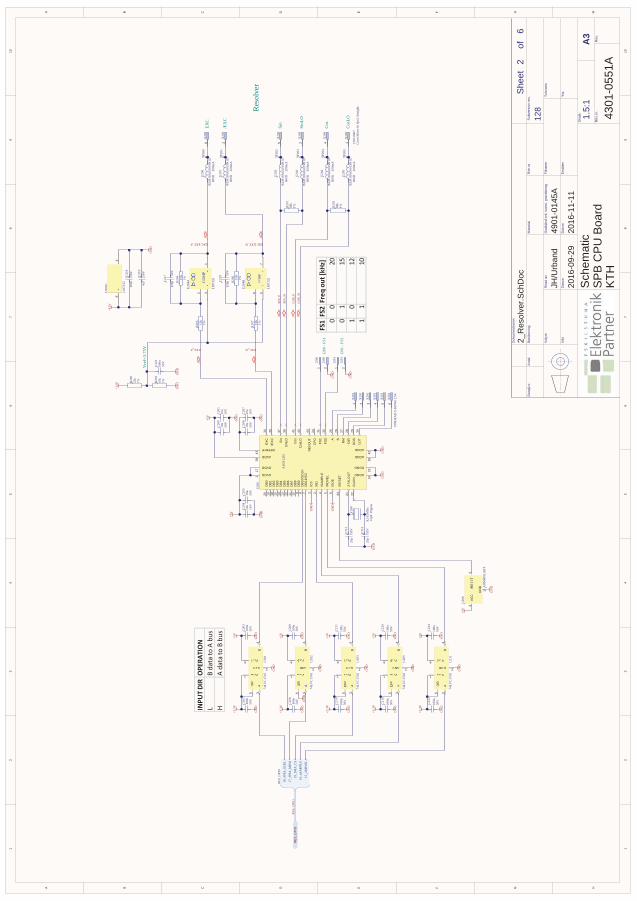
11
22
33
44
55
66
77
88
99
1010
HH
GG
FF
EE
DD
CC
BB
AA
Shee
t
o
f2
6
Rita
dav
Dat
um
Mat
eria
l
God
känd
enl.
kons
t.gr
ansk
ning
Dat
um
Ritn
.nr
Filn
amn
Ersät
ter
Sub
vers
ion
rev. To
lera
ns
Yta
.
Ska
la
Ritn
.nr.
Rev
.
A3
Vik
t
Vol
ym
Benäm
ning
Ant
alD
etal
j.nr.
1.5:
1
JH/U
rban
d49
01-0
145A
2016
-09-
2920
16-1
1-11
4301
-055
1A
Sch
emat
icSP
BC
PUB
oard
KTH
Dok
umen
tnam
n
2_R
esol
ver.S
chD
oc
128
GN
DG
ND
10u
16V
C20
4
+5V
GN
D
10u
16V
C20
7
GN
D
+5V
10u
16V
C20
1
GN
D
10n
50V
C20
6
10n
50V
C20
0
10n
50V
C20
5
GN
D
Vcca1
GND 2
A3
B4
DIR
5
Vccb6
Vcca
GND
AB
DIR
Vccb
U20
174
LVC
1T45
GN
D
+5V
+3.3
V
100n
50V
C20
3
GN
D
100n
50V
C20
2
GN
D
Vcca1
GND 2
A3
B4
DIR
5
Vccb6
Vcca
GND
AB
DIR
Vccb
U20
274
LVC
1T45
GN
D
+5V
+3.3
V
100n
50V
C20
9
GN
D
100n
50V
C20
8
GN
D
GN
D
+5V
+3.3
V
100n
50V
C21
1
GN
D
100n
50V
C21
0
GN
D
GN
D
Vcca1
GND 2
A3
B4
DIR
5
Vccb6
Vcca
GND
AB
DIR
Vccb
U20
374
LVC
1T45
GN
D
8,19
2MH
z12
pF30
ppm
Y20
020
p50
VC
212
20p
50V
C21
3
RE
S_G
PIO
DVDD
1
/RD
2
DVDD
17
AVDD
39
/CS
3
/SA
MP
LE4
/RD
VE
L5
/SO
E6
DB
11/S
O7
DB
10/S
CLK
8D
B9
9D
B8
10D
B7
11D
B6
12D
B5
13D
B4
14D
B3
15
DGND
16
DGND
23
DB
218
DB
119
DB
020
XTA
LOU
T21
CLK
IN22
CP
O24
A25
B26
NM
27
DIR
28
DO
S29
LOT
30
FS1
31
FS2
32
/RE
SE
T33
EX
C34
/EX
C35
AGND
36
AGND
42
Sin
37
Sin
LO38
Cos
LO40
Cos
41
REFBYP
43
RE
FOU
T44
AD
2S12
05
U20
0
CO
MP
-2
+3
+1
CO
MP
- ++
U20
4A
LM73
32 CO
MP
-6
+5
+7
CO
MP
- ++
U20
4B
LM73
32
+8
-4
+-
U20
4C
LM73
32
+12V
GN
D
100n
50V
C21
4
+12V
GN
D15
K1%
R20
4
15K
1%
R20
6
120p
50V
C21
7
120p
50V
C21
8
10k
1%
R20
5
10k
1%
R20
7
4u7
50V
C21
522
k1%R
200
10k
1%R20
310
0n50
V
C21
6
GN
D
Vre
f=3.
75V
GN
D
GN
D
+5V
+3.3
V
100n
50V
C22
0
GN
D
100n
50V
C21
9
GN
D
Vcca1
GND 2
A3
B4
DIR
5
Vccb6
Vcca
GND
AB
DIR
Vccb
U20
574
LVC
1T45
+5V
GN
D
GN
D1
/RE
SE
T2
VC
C3
GN
D/RE
SE
TV
CC
U20
6
AD
M80
9LA
RT
BLM
18A
G60
1SN
1D20
0mA
600RE2
00
BLM
18A
G60
1SN
1D20
0mA
600RE2
01
BLM
18A
G60
1SN
1D20
0mA
600RE2
02
BLM
18A
G60
1SN
1D20
0mA
600RE2
03
BLM
18A
G60
1SN
1D20
0mA
600RE2
04
BLM
18A
G60
1SN
1D20
0mA
600RE2
05
68k
1%R20
1
68k
1%R20
2
RES
_GPI
O
FS1FS2Freq
out[kH
z]0
020
01
151
012
11
10
J200
-FS1
J201
-FS2
GN
D
GN
D
16_n
SAM
PLE
17_S
PIA
_MIS
O
18_S
PIA
_SC
KL
19_S
PIA
_CS
15_n
RD
VEL
RES
_GPI
O
GN
D
+5V
+3.3
V
100n
50V
C23
4
GN
D
100n
50V
C23
3
GN
D
Vcca1
GND 2
A3
B4
DIR
5
Vccb6
Vcca
GND
AB
DIR
Vccb
U21
174
LVC
1T45
INPU
TDIR
OPERA
TION
LBdatato
Abu
sH
Adatato
Bbu
s
1 1330
-006
7C
onn
Mic
ro-fi
t6po
l.St
raig
ht
X20
0
2X
200
3X
200
4X
200
5X
200
6X
200
Res
olve
r
EXC
/EX
C
Sin
SinL
O
Cos
Cos
LO1
PIN
HEA
DS-
RO
W6
2.54
X20
1
2X
201
3X
201
4X
201
5X
201
6X
201
1J2
00
2J2
00
1J2
01
2J2
01
EXC_P EXC_N
EXCEXT_P EXCEXT_N
SIN
_P
SIN
_N
CO
S_N
CO
S_P
TP20
0
IOG
PIS
GR
ESRRR
SSGG
II__
TP20
1
TP20
2
TP20
3
TP20
4
TP20
5
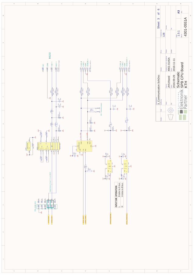
11
22
33
44
55
66
77
88
99
1010
HH
GG
FF
EE
DD
CC
BB
AA
Shee
t
o
f3
6
Rita
dav
Dat
um
Mat
eria
l
God
känd
enl.
kons
t.gr
ansk
ning
Dat
um
Ritn
.nr
Filn
amn
Ersät
ter
Sub
vers
ion
rev. To
lera
ns
Yta
.
Ska
la
Ritn
.nr.
Rev
.
A3
Vik
t
Vol
ym
Benäm
ning
Ant
alD
etal
j.nr.
1.5:
1
JH/U
rban
d49
01-0
145A
2016
-09-
2920
16-1
1-11
4301
-055
1A
Sch
emat
icSP
BC
PUB
oard
KTH
Dok
umen
tnam
n
3_C
omm
unic
atio
n.Sc
hDoc
128
STB
8
CA
NH
7
CA
NL
6
SP
LIT
5
TxD
1
RxD
4
Vcc3 GN
D
2
U30
1 SN65
HV
D10
40D
9K1
1%R30
4
4k7
1%R30
3
+5V
CA
N_N
CA
N_P
GN
D
GN
D
GN
D
GN
D
GP
IO31
_CA
NTX
GP
IO30
_CA
NR
X
GN
D
J300
-Ter
min
atio
nju
mpe
rs
100n
50V
C30
7
GN
D
120R
1%R30
5
[RS2
32]
+ - + -
CX CX
U+ U-
1 3 4 5 10 11 9 12138147
62
[RS2
32]
+ - + -
CX CX
U+ U-
U30
0A
AD
M32
02A
RN
1n 200V
C30
5
1k 1%R30
2
47R
1%R30
147
R1%R30
0
100n
50V
C30
4
100n
50V
C30
1
100n
50V
C30
3
+3.3
V
(+)
(-)
1615
(+)
(-)
U30
0B AD
M32
02A
RN
+3.3
V
GN
D
100n
50V
C30
2
100n
50V
C30
0
GN
D
GN
DG
ND
GN
D
1n 200V
C30
6
GN
D
GP
IO28
_RX
DA
GP
IO29
_TX
DA
GN
D
1X
300
2X
300
3X
300
4X
300
5X
300
6X
300
1X
301
2X
301
3X
301
4X
301
5X
301
6X
301
Jum
perb
etw
een
4-4
and
5-5
tous
eR
S232
TTL-
232R
-3V
3
SMA
J18C
AD
302
SMA
J18C
AD
303
BLM
18A
G60
1SN
1D20
0mA
600R
E300
BLM
18A
G60
1SN
1D20
0mA
600R
E301
BLM
18A
G60
1SN
1D20
0mA
600R
E302
BLM
18A
G60
1SN
1D20
0mA
600R
E303
GP
IO32
_EP
WM
SY
NC
I
GP
IO33
_EP
WM
SY
NC
O
BLM
18A
G60
1SN
1D20
0mA
600R
E304
BLM
18A
G60
1SN
1D20
0mA
600R
E305
GN
D
+5V
+3.3
V
100n
50V
C31
1
GN
D
100n
50V
C31
0
GN
D
Vcca1
GND 2
A3
B4
DIR
5
Vccb6
Vcca
GND
AB
DIR
Vccb
U30
374
LVC
1T45Vcca1
GND 2
A3
B4
DIR
5
Vccb6
Vcca
GND
AB
DIR
Vccb
U30
274
LVC
1T45
GN
D
+5V
+3.3
V
100n
50V
C30
9
GN
D
100n
50V
C30
8
GN
DG
ND
1k 1%
R30
6
1k 1%
R30
7
BA
V99
D30
4
BA
V99
D30
5
+5V
+5V
GN
D
GN
D
1
1330
-008
6C
onn
Mic
ro-fi
t4po
l.St
raig
ht
X30
2
2X
302
3X
302
4X
302
GN
D
RxD
<=
TxD
=>
GN
D
N.C
RS2
32
1
1330
-009
2M
icro
-Mat
ch4p
7-18
8275
-4
X30
3
2X
303
3X
303
4X
303
GN
D
1
1330
-009
2M
icro
-Mat
ch4p
7-18
8275
-4
X30
4
2X
304
3X
304
4X
304
GN
D
CA
N_H
CA
N_L
GN
DSY
NC
IN <
=
CA
N_H
CA
N_L
GN
DSY
NC
OU
T =>
INPU
TDIR
OPERA
TION
LBdatato
Abu
sH
Adatato
Bbu
s
SMA
J18C
AD
300
SMA
J18C
AD
301
1
J300
2
J300
BLM
18A
G60
1SN
1D20
0mA
600R
E306
BLM
18A
G60
1SN
1D20
0mA
600R
E307
1n 200V
C31
2
GN
D
1n 200V
C31
3
GN
D
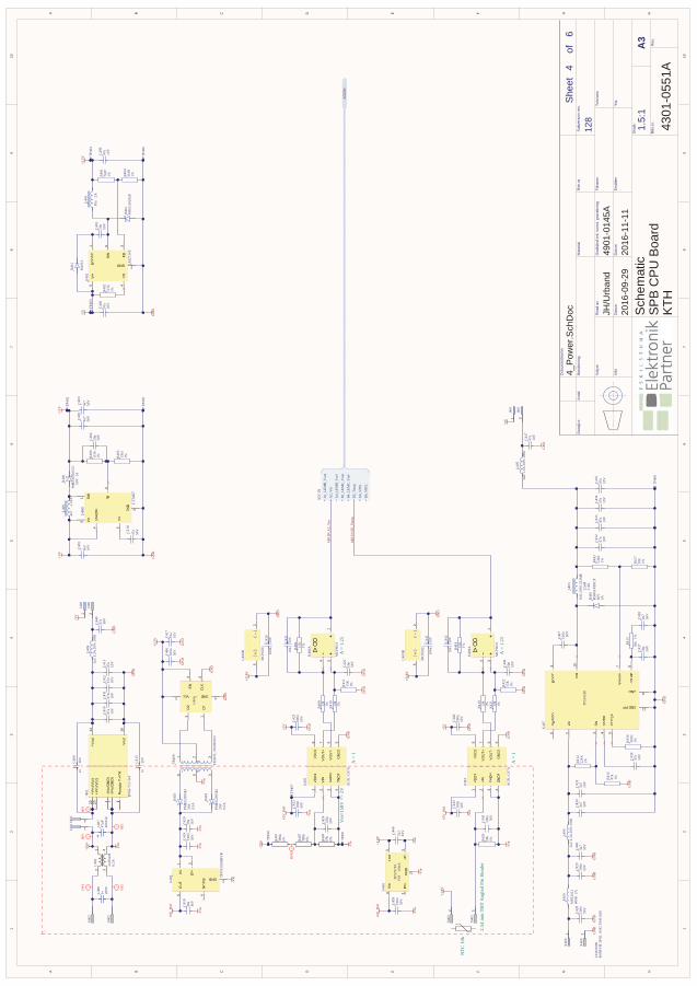
11
22
33
44
55
66
77
88
99
1010
HH
GG
FF
EE
DD
CC
BB
AA
Shee
t
o
f4
6
Rita
dav
Dat
um
Mat
eria
l
God
känd
enl.
kons
t. gr
ansk
ning
Dat
um
Ritn
.nr
Filn
amn
Ersät
ter
Sub
vers
ion
rev. To
lera
ns
Yta
.
Ska
la
Ritn
.nr.
Rev
.
A3
Vik
t
Vol
ym
Benäm
ning
Ant
alD
etal
j.nr.
1.5:
1
JH/U
rban
d49
01-0
145A
2016
-09-
2920
16-1
1-11
4301
-055
1A
Sch
emat
icSP
BC
PUB
oard
KTH
Dok
umen
tnam
n
4_P
ower
.Sch
Doc
128
nSH
DN
4
SS
5
GN
D
2
Vin
6
SW
1 FB3
nSH
DN
SS
GN
D
Vin
SW
FB
U40
0
LT34
67
GN
D
2u2
10VC40
14u
750
VC40
24u
750
VC40
3
115k
1%R40
0
13k3
1%R40
3
PMEG
6010
CEJ
60V
1A
D40
0
4u7
2.32
A
L400
47n
50VC41
4
+12V
+5V
+5V
GN
D
47uF
400V
dc
C40
71u 20
0V
C40
6
1n2k
V
C40
0
1n2k
V
C41
5
+Vin
-Vin
47u
10V
C41
047
u10
V
C41
147
u10
V
C41
247
u10
V
C41
3
10k
1%R40
9
390k
1%R40
5
390k
1%R40
7
-Vin
-Vin
(GN
D)
2
Rem
ote
On/
Off
1
+Vin
(Vcc
)22
-Vou
t16
+Vou
t14
-Vin
(GN
D)
3
+Vin
(Vcc
)23
TEN
8-72
11W
I
U40
1
47uF
400V
dc
C40
71u 20
0V
C40
6
1n 1n
+Vin
-Vin
10k
1%R40
9
390k
1%R40
5
390k
1%R40
7
-Vin
-Vin
(GN
D)
2
Rem
ote
On/
Off
1
+Vin
(Vcc
)22
-Vin
(GN
D)
3
+Vin
(Vcc
)23
TEN
8-72
11W
IEU40
1
GN
D
GN
D
100n
50V
C42
3
GN
D
+5V
+3.3
V
100n
50V
C42
6
GN
D
GN
D
AD
CIN
.A2_
Vin
15K
1%R40
6
12k
1%R40
8
12k
1%R41
0
15K
1%R41
1
A =
1
A =
1.2
5V
in=1
58V
=>
2V
Vin
5
EN
4
GND 2
FB3
SW
6
BO
OS
T1
Vin
EN
GND
FBSW
BO
OS
T
U40
2
LM27
34Y
BA
S16
D40
1
10n
50V
C40
510
u2A
L401
47u
10V
C40
97k
871%R
401
2k49
1%R40
4
+3.3
V
115k
1%R40
210
u16
V
C40
8
+5V
GN
D
PMEG
3020
EPD
402
VD
D1
1
VIN
2
SH
DN
3
GN
D1
4
VD
D1
VIN
SH
DN
GN
D1
GN
D2
5
VO
UT-
6V
OU
T+7
VD
D2
8
AC
PL-C
87A
U40
5
D1
1
Vcc2
D2
3
GND 4
EN
5
D1
Vcc
D2
GND
EN
CLK
6
U40
4
+3.3
V
GN
D
100n
50V
C41
6
GN
D
GN
D
GN
D
1 2 3456
TRA
FO_7
6039
0015
TR40
0
PMEG
2005
EJ20
V0,
5A
D40
3
PMEG
2005
EJ20
V0,
5A
D40
4-V
in
IN1
GND 2
EN
3
NC
/FB
4
OU
T5
IN
GND
EN
NC
/FB
OU
T
TPS7
6350
DB
VR
U40
3
100n
50V
C41
9
-Vin
-Vin
-Vin
-Vin
+5V
_ISO
+5V
_ISO
100n
50V
C42
2
-Vin
GN
D
1
2330
-009
8M
INI-F
IT 2
POL
AN
G 3
9301
020
X40
0
2X
400
BO
OT
1
CO
MP
8
PW
RG
D6
EN
3
PH
10
RT/
CLK
5S
S/T
R4
Vin
2
Vse
nse
7
GND 9
GND PP 11
BO
OT
CO
MP
PW
RG
D
EN
PH
RT/
CLK
SS
/TR
Vin
Vse
nse
GND
GND PP
U40
7
TPS5
4260
4u7
50V
C43
04u
750
V
C43
1
4n7
50V
C43
8
100n 50
V
C42
7
30k
1%
R41
530
1K1%R
416
XA
L505
0-22
3ME
22uH
3.4A
L403
53k6
1%R41
3
47k
1%R41
4
B36
0A-F
DIC
T60
V3AD
405
221K
1%R41
2
47n
50V
C43
6
GN
D
GN
D
10k
1%R41
7
20p
50V
C43
7
10u
16V
C41
7
10u
16V
C41
810
u16
V
C42
0
20p
50V
C40
4
47u
10V
C43
247
u10
V
C43
347
u10
V
C43
447
u10
V
C43
5
MPZ
2012 2A
600RE4
00
GN
DG
ND
4 31
U40
6A
MC
P602
1
(+)
(-)
52
(+)
(-)
U40
6B
MC
P602
1
1 432
2x20
mH
0,5A
L402
AD
CIN
A2_
Vin
A1_
LEM
B_V
out
B1_
LEM
C_V
out
A4_
LEM
B_V
ref
B4_
LEM
C_V
ref
B5_
Tem
p
A6_
VIN
1
B6_
VIN
2
AD
CIN
10k
1%R42
0
-Vin
GN
D
GN
D
100n
50V
C44
4
GN
D
+5V
+3.3
V
100n
50V
C44
1
GN
D
GN
D
15K
1%R41
8
12k
1%R41
9
12k
1%R42
1
15K
1%R42
2
A =
1
A =
1.2
5
VD
D1
1
VIN
2
SH
DN
3
GN
D1
4
VD
D1
VIN
SH
DN
GN
D1
GN
D2
5
VO
UT-
6
VO
UT+
7
VD
D2
8
AC
PL-C
87A
U41
0
+5V
_ISO
100n
50V
C44
3
-Vin
4 31
U40
9A
MC
P602
1
(+)
(-)
52
(+)
(-)
U40
9B
MC
P602
1
100n
50V
C43
9
+1.8
V
Vin
4
NC
3G
ND
2
PG
1
Vou
t5
Vin
NC
GN
DP
G
Vou
t
1V8
10m
A
U40
8
TPS7
9718
-Vin
-Vin
-Vin
+5V
_ISO
2u2
10VC44
0
1X
401
2X
401
+1.8
V
+Vin
NTC
10k
AD
CIN
.B5_
Tem
p
2.54
mm
TH
T A
ngle
d Pi
n H
eade
r
+5V
100n 50
V
C44
5
120p
50V
C42
4
10n
50V
C44
6
10n
50V
C44
2
2u2
1.3A
20%
100
8
L404
4u7
50V
C44
8
GN
D
100n
50V
C42
810
0n50
V
C42
9
2u2
1.3A
20%
100
8
L405
47u
10V
C44
7
GN
D
10n
50V
C42
1
10n
50V
C42
5
TP40
0
TP40
1
TP40
2
TP40
4TP
403
TP40
6TP
405
TP40
8
TP40
7
1
J402
2
J402
1J4
00
2J4
00
1J4
01
2J4
01
X40
2
X40
2
iH
P1i
HP1
iH
P1
iH
P2i
HP2
iH
PM
2u2
1.3A
20%
100
8
L406
47u
10V
C44
9
GN
D
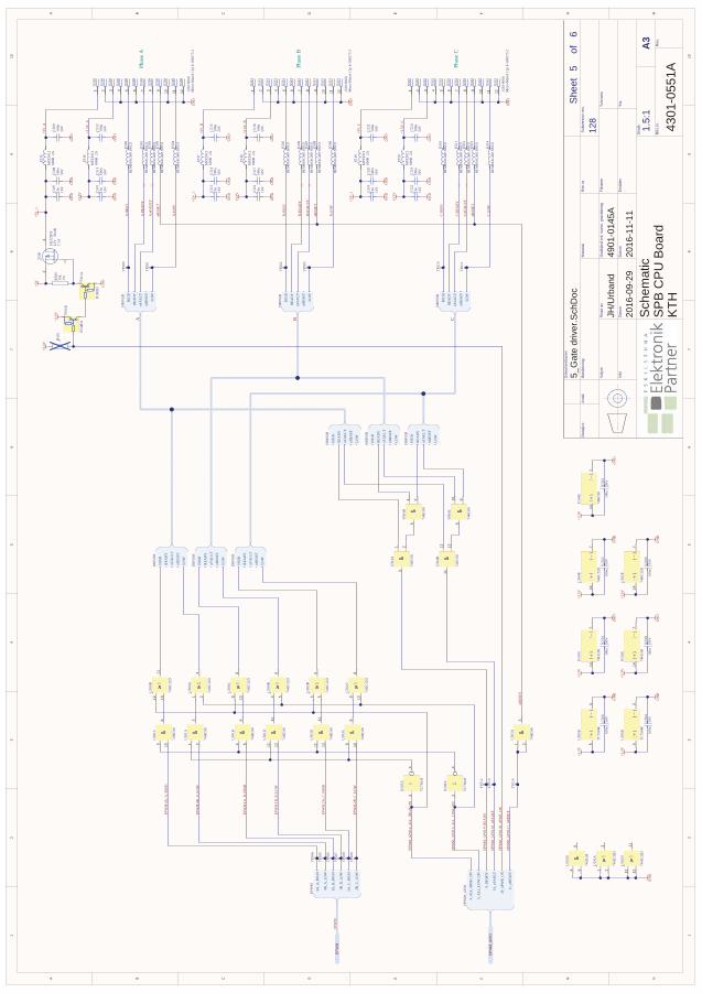
11
22
33
44
55
66
77
88
99
1010
HH
GG
FF
EE
DD
CC
BB
AA
Shee
t
o
f5
6
Rita
dav
Dat
um
Mat
eria
l
God
känd
enl.
kons
t.gr
ansk
ning
Dat
um
Ritn
.nr
Filn
amn
Ersät
ter
Sub
vers
ion
rev. To
lera
ns
Yta
.
Ska
la
Ritn
.nr.
Rev
.
A3
Vik
t
Vol
ym
Benäm
ning
Ant
alD
etal
j.nr.
1.5:
1
JH/U
rban
d49
01-0
145A
2016
-09-
2920
16-1
1-11
4301
-055
1A
Sch
emat
icSP
BC
PUB
oard
KTH
Dok
umen
tnam
n
5_G
ate
driv
er.S
chD
oc
128
Phas
e A
Phas
e B
Phas
e C
A.H
IGH
A.L
OW
A.R
EAD
Y
A.n
FAU
LT
B.H
IGH
B.L
OW
B.R
EAD
Y
B.n
FAU
LT
C.H
IGH
C.L
OW
C.R
EAD
Y
C.n
FAU
LT
100n
50V
C50
2
+3.3
V
GN
D
14
21
U50
5A
TC7S
04F
(+)
(-)
53
(+)
(-)
U50
5B
TC7S
04F
100n
50V
C50
0
+3.3
V
GN
D
14
21
U50
6A
TC7S
04F
(+)
(-)
53
(+)
(-)
U50
6B
TC7S
04F
100n
50V
C50
4
+3.3
V
GN
D
EPW
M.4
A_A
_HIG
H
EPW
M.4
B_A
_LO
W
100n
50V
C50
5
+3.3
V
GN
D
100n
50V
C50
1
+3.3
V
GN
D
100n
50V
C50
6
+3.3
V
GN
D
EPW
M.1
A_B
_HIG
H
EPW
M.1
B_B
_LO
W
EPW
M.2
A_C
_HIG
H
EPW
M.2
B_C
_LO
W
EPW
M_G
PIO
.4_A
LL_H
IGH
_ON
EPW
M_G
PIO
.5_A
LL_L
OW
_ON
14 5
61
U50
2B
74H
C32
D 19 10
81
U50
2C
74H
C32
D
11 2
31
U50
2A
74H
C32
D 112 13
111
U50
2D
74H
C32
D
(+)
(-)
147
(+)
(-)
U50
0E
74H
C32
D
112 13
111
U50
0D
74H
C32
D 11 2
31
U50
0A
74H
C32
D 19 10
81
U50
0C
74H
C32
D 14 5
61
U50
0B
74H
C32
D
(+)
(-)
147
(+)
(-)
U50
2E
74H
C32
D
+3.3
V
GN
D
GN
D
GN
D
HIG
H
LOW
REA
DY
nFA
ULT
nRES
ET
DR
IVER
&9 10
8&
U50
1C
74H
C08 &
1 23
&U
501A
74H
C08 &
4 56
&U
501B
74H
C08 &
12 1311
&U
501D
74H
C08
(+)
(-)
147
(+)
(-)
U50
1E
74H
C08
HIG
H
LOW
REA
DY
nFA
ULT
nRES
ET
DR
IVER
1B_B
_LO
W
1A_B
_HIG
H
2A_C
_HIG
H
4B_A
_LO
W
2B_C
_LO
W
4A_A
_HIG
H
EPW
M 9_R
EAD
Y
5_A
LL_L
OW
_ON
10_n
FAU
LT
4_A
LL_H
IGH
_ON
11_n
RES
ET
39_n
PWR
_ON
EPW
M_G
PIO
100n
50V
C50
3
+3.3
V
EP
WM
EP
WM
_GP
IO
BLM
18A
G60
1SN
1DE500
BLM
18A
G60
1SN
1DE501
BLM
18A
G60
1SN
1DE502
BLM
18A
G60
1SN
1DE503
BLM
18A
G60
1SN
1DE504
BLM
18A
G60
1SN
1DE505
BLM
18A
G60
1SN
1DE506
BLM
18A
G60
1SN
1DE507
BLM
18A
G60
1SN
1DE508
BLM
18A
G60
1SN
1DE509
BLM
18A
G60
1SN
1DE510
BLM
18A
G60
1SN
1DE511
BLM
18A
G60
1SN
1DE512
BLM
18A
G60
1SN
1DE513
BLM
18A
G60
1SN
1DE514
&12 13
11&
U50
3D
74H
C08 &
9 108
&U
503C
74H
C08 &
1 23
&U
503A
74H
C08
&4 5
6&
U50
3B
74H
C08
(+)
(-)
147
(+)
(-)
U50
4E
74H
C08
&1 2
3&
U50
4A
74H
C08
&4 5
6&
U50
4B
74H
C08
&12 13
11&
U50
4D
74H
C08
&910
8&
U50
4C
74H
C08
(+)
(-)
147
(+)
(-)
U50
3E
74H
C08
HIG
H
LOW
REA
DY
nFA
ULT
nRES
ET
DR
IVER
A
HIG
H
LOW
REA
DY
nFA
ULT
nRES
ET
DR
IVER
HIG
H
LOW
REA
DY
nFA
ULT
nRES
ET
DR
IVER
HIG
H
LOW
REA
DY
nFA
ULT
nRES
ET
DR
IVER
HIG
H
LOW
REA
DY
nFA
ULT
nRES
ET
DR
IVER
HIG
H
LOW
REA
DY
nFA
ULT
nRES
ET
DR
IVER
HIG
H
LOW
REA
DY
nFA
ULT
nRES
ET
DR
IVER
B C
nRES
ET
nRES
ET
nRES
ET
nRES
ET
EPW
M
EPW
M_G
PIO
.9_R
EAD
Y
EPW
M_G
PIO
.10_
nFA
ULT
EPW
M_G
PIO
.11_
nRES
ET
GN
D
1 1330
-006
0M
icro
-Mat
ch12
p8-
1882
75-2
X50
0
2X
500
3X
500
4X
500
5X
500
6X
500
7X
500
8X
500
9X
500
10X
500
11X
500
12X
500
1 1330
-006
0M
icro
-Mat
ch12
p8-
1882
75-2
X50
1
2X
501
3X
501
4X
501
5X
501
6X
501
7X
501
8X
501
9X
501
10X
501
11X
501
12X
501
1 1330
-006
0M
icro
-Mat
ch12
p8-
1882
75-2
X50
2
2X
502
3X
502
4X
502
5X
502
6X
502
7X
502
8X
502
9X
502
10X
502
11X
502
12X
502
MPZ
2012 2A
600RE5
16
GN
DG
ND
100n
50V
C51
210
0n50
V
C51
110
u16
V
C51
0
GN
D
+3.3
V
MPZ
2012 2A
600RE5
18
GN
DG
ND
100n
50V
C51
810
0n50
V
C51
710
u16
V
C51
6
GN
D
+3.3
V
MPZ
2012 2A
600RE5
20
GN
DG
ND
100n
50V
C52
410
0n50
V
C52
310
u16
V
C52
2
GN
D
MPZ
2012 2A
600RE5
15
GN
DG
ND
100n
50V
C50
910
0n50
V
C50
810
u16
V
C50
7
GN
D
MPZ
2012 2A
600RE5
17
GN
DG
ND
100n
50V
C51
510
0n50
V
C51
410
u16
V
C51
3
GN
D
MPZ
2012 2A
600RE5
19
GN
DG
ND
100n
50V
C52
110
0n50
V
C52
010
u16
V
C51
9
GN
D
+3.3
V_A
+3.3
V_B
+3.3
V_C
+5V
_A
+5V
_B
+5V
_C
2
1
3
SI23
23D
S12
V7.
1A39
mR
T500
10k
1%R50
0
+5V
PUM
D3
T501
APU
MD
3
T501
B
GN
D
+3.3
V
+5V
_1
+5V
_1
+5V
_1
EPW
M_G
PIO
.39_
nPW
R_O
N
R50
1
+3.3
V
TP50
0
TP50
1
TP50
2
TP50
3
TP51
0
TP51
1
TP50
4
TP50
5
TP50
6
TP50
7
TP50
8
TP50
9
TP51
2
TP51
3
TP51
4
GN
D
MW
MEP
WEEE
WWMM
CCCC
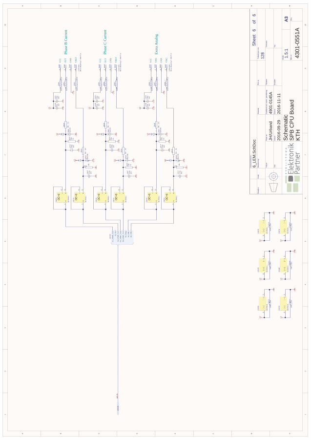
11
22
33
44
55
66
77
88
99
1010
HH
GG
FF
EE
DD
CC
BB
AA
Shee
t
o
f6
6
Rita
dav
Dat
um
Mat
eria
l
God
känd
enl.
kons
t.gr
ansk
ning
Dat
um
Ritn
.nr
Filn
amn
Ersät
ter
Sub
vers
ion
rev. To
lera
ns
Yta
.
Ska
la
Ritn
.nr.
Rev
.
A3
Vik
t
Vol
ym
Benäm
ning
Ant
alD
etal
j.nr.
1.5:
1
JH/U
rban
d49
01-0
145A
2016
-09-
2920
16-1
1-11
4301
-055
1A
Sch
emat
icSP
BC
PUB
oard
KTH
Dok
umen
tnam
n
6_LE
M.S
chD
oc
128
1
1330
-009
2M
icro
-Mat
ch4p
7-18
8275
-4
X60
0
2X
600
3X
600
4X
600
BLM
18A
G60
1SN
1D
E600
BLM
18A
G60
1SN
1D
E601
GN
D
+5V
10u
16V
C60
010
0n50
V
C60
1
GN
DG
ND
VC
C
OU
T
VR
EF
1
1330
-009
2M
icro
-Mat
ch4p
7-18
8275
-4
X60
1
2X
601
3X
601
4X
601
BLM
18A
G60
1SN
1D
E603
BLM
18A
G60
1SN
1DE6
04
GN
D
+5V
10u
16V
C60
410
0n50
V
C60
5
GN
DG
ND
VC
C
OU
T
VR
EF
BA
V99
D60
0
+5V
GN
D
Phas
e B
Cur
rent
Phas
e C
Cur
rent
AD
CIN
AD
CIN
A2_
Vin
A1_
LEM
B_V
out
B1_
LEM
C_V
out
A4_
LEM
B_V
ref
B4_
LEM
C_V
ref
B5_
Tem
p
A6_
VIN
1
B6_
VIN
2
AD
CIN
GN
DG
ND
BA
V99
D60
1
+5V
GN
DG
ND
GN
D
BA
V99
D60
2
+5V
GN
D
GN
DG
ND
BA
V99
D60
3
+5V
GN
D
GN
DG
ND
GN
D
GN
D
100n
50V
C61
2
GN
D
4 31
U60
0A
MC
P602
1
(+)
(-)
52
(+)
(-)
U60
0B
MC
P602
1
100n
50V
C61
3
GN
D
4 31
U60
1A
MC
P602
1
(+)
(-)
52
(+)
(-)
U60
1B
MC
P602
1
100n
50V
C61
5
GN
D
4 31
U60
2A
MC
P602
1
(+)
(-)
52
(+)
(-)
U60
3B
MC
P602
1
100n
50V
C61
6
GN
D
4 31
U60
3A
MC
P602
1
(+)
(-)
52
(+)
(-)
U60
4B
MC
P602
1
+5V
+5V
+5V
+5V
1
1330
-009
2M
icro
-Mat
ch4p
7-18
8275
-4
X60
2
2X
602
3X
602
4X
602
BLM
18A
G60
1SN
1D
E606
BLM
18A
G60
1SN
1DE6
07
GN
D
+5V
10u
16V
C60
810
0n50
V
C60
9
GN
DG
ND
VC
C
VIN
1
VIN
2
BA
V99
D60
4
+5V
GN
D
Extra
Ana
log
GN
DG
ND
BA
V99
D60
5
+5V
GN
D
GN
DG
ND
GN
D
4 31
U60
4A
MC
P602
1
4 31
U60
5A
MC
P602
1
100n
50V
C61
4
GN
D
(+)
(-)
52
(+)
(-)
U60
2B
MC
P602
1
100n
50V
C61
7
GN
D
(+)
(-)
52
(+)
(-)
U60
5B
MC
P602
1
+5V
+5V
BLM
18A
G60
1SN
1D
E602
BLM
18A
G60
1SN
1D
E605
BLM
18A
G60
1SN
1D
E608
30k
1%
R60
0
30k
1%
R60
4
30k
1%
R60
8
30k
1%R60
1
30k
1%R60
5
30k
1%R60
9
120p
50V
C60
2
AD
CINI
DA
DCC
NN
120p
50V
C60
6
120p
50V
C61
0
30k
1%
R60
2
30k
1%
R60
6
30k
1%
R61
0
30k
1%
R603 30k
1%R60
7
30k
1%
R611
120p
50V
C60
3
120p
50V
C60
7
120p
50V
C61
1

80