Optimizing communication and capacity in a 3D stacked reconfigurable cache hierarchy
13
Optimizing Communication and Capacity in a 3D Stacked Reconfigurable Cache Hierarchy * Niti Madan † , Li Zhao ‡ , Naveen Muralimanohar † , Aniruddha Udipi † , Rajeev Balasubramonian † , Ravishankar Iyer ‡ , Srihari Makineni ‡ , Donald Newell ‡ † School of Computing, University of Utah ‡ System Technology Lab, Intel Corporation Abstract Cache hierarchies in future many-core processors are expected to grow in size and contribute a large fraction of overall processor power and performance. In this pa- per, we postulate a 3D chip design that stacks SRAM and DRAM upon processing cores and employs OS-based page coloring to minimize horizontal communication of cache data. We then propose a heterogeneous reconfigurable cache design that takes advantage of the high density of DRAM and the superior power/delay characteristics of SRAM to efficiently meet the working set demands of each individual core. Finally, we analyze the communication patterns for such a processor and show that a tree topology is an ideal fit that significantly reduces the power and la- tency requirements of the on-chip network. The above pro- posals are synergistic: each proposal is made more com- pelling because of its combination with the other innova- tions described in this paper. The proposed reconfigurable cache model improves performance by up to 19% along with 48% savings in network power. Keywords: multi-core processors, cache and memory hierarchy, non-uniform cache architecture (NUCA), page coloring, on-chip networks, SRAM/DRAM cache reconfig- uration. 1. Introduction The design of cache hierarchies for multi-core chips has received much attention in recent years (for example, [5, 8, 10, 18, 38, 48]). As process technologies continue to shrink, a single chip will accommodate many mega-bytes of cache storage and numerous processing cores. It is well known that the interconnects that exchange data between caches and cores represent a major bottleneck with regard to both power and performance. Modern Intel chips al- ready accommodate up to 27 MB of cache space [29]; in- terconnects have been attributed as much as 50% of total chip dynamic power [28]; on-chip networks for large tiled chips have been shown to consume as much as 36% of total chip power [23, 44]; long on-chip wires and router pipeline * This work was supported in parts by NSF grants CCF-0430063, CCF- 0811249, NSF CAREER award CCF-0545959, Intel, and the University of Utah. delays can lead to cache access times of many tens of cy- cles [12, 36]. Not only will we require intelligent mech- anisms to allocate cache space among cores, we will also have to optimize the interconnect that exchanges data be- tween caches and cores. This paper makes an attempt at addressing both of these issues. 3D stacking of dies has been demonstrated as a feasi- ble technology [46] and is already being commercially em- ployed in some embedded domains [35, 39]. In most com- mercial examples, 3D is employed to stack DRAM mem- ory upon CPU cores [35, 39]. This is especially compelling because future multi-cores will make higher memory band- width demands and the inter-die interconnect in a 3D chip can support large data bandwidths. Early projections for Intel’s Polaris 80-core prototype allude to the use of such 3D stacking of DRAM to feed data to the 80 cores [42]. Given the commercial viability of this technology, a few research groups have already begun to explore the archi- tectural ramifications of being able to stack storage upon CPUs [21, 24–27]. In this paper, we first postulate a physical processor design that is consistent with the above trends. We then take advantage of the following three key innovations to architect a cache hierarchy that greatly reduces latency and power: (i) we employ page coloring to localize data and computation, (ii) we propose the use of cache reconfigu- ration to accommodate large working sets for some cores, (iii) we identify a network topology that best matches the needs of data traffic and incurs low delay and power over- heads. The proposed processor employs three dies stacked upon each other (see Figure 1). The lowest die contains the processing cores (along with the corresponding L1 caches). The second die is composed entirely of SRAM cache banks (forming a large shared L2 cache) and employs an on-chip network so that requests from the CPU can be routed to the correct bank. The third die is composed of DRAM banks that serve to augment the L2 cache space provided by the second SRAM die. It is also possible to stack many more DRAM dies upon these three dies to implement main mem- ory [26], but we regard this as an orthogonal design choice and do not consider it further in this paper. The L2 cache banks are organized as a non-uniform 262 978-1-4244-2932-5/08/$25.00 ©2008 IEEE
-
Upload
independent -
Category
Documents
-
view
1 -
download
0
Transcript of Optimizing communication and capacity in a 3D stacked reconfigurable cache hierarchy
Optimizing Communication and Capacity in a 3D Stacked ReconfigurableCache Hierarchy ∗
Niti Madan†, Li Zhao‡, Naveen Muralimanohar†, Aniruddha Udipi†,Rajeev Balasubramonian†, Ravishankar Iyer‡, Srihari Makineni‡, Donald Newell‡
† School of Computing, University of Utah‡ System Technology Lab, Intel Corporation
AbstractCache hierarchies in future many-core processors are
expected to grow in size and contribute a large fractionof overall processor power and performance. In this pa-per, we postulate a 3D chip design that stacks SRAM andDRAM upon processing cores and employs OS-based pagecoloring to minimize horizontal communication of cachedata. We then propose a heterogeneous reconfigurablecache design that takes advantage of the high density ofDRAM and the superior power/delay characteristics ofSRAM to efficiently meet the working set demands of eachindividual core. Finally, we analyze the communicationpatterns for such a processor and show that a tree topologyis an ideal fit that significantly reduces the power and la-tency requirements of the on-chip network. The above pro-posals are synergistic: each proposal is made more com-pelling because of its combination with the other innova-tions described in this paper. The proposed reconfigurablecache model improves performance by up to 19% alongwith 48% savings in network power.
Keywords: multi-core processors, cache and memoryhierarchy, non-uniform cache architecture (NUCA), pagecoloring, on-chip networks, SRAM/DRAM cache reconfig-uration.
1. IntroductionThe design of cache hierarchies for multi-core chips
has received much attention in recent years (for example,[5, 8, 10, 18, 38, 48]). As process technologies continue toshrink, a single chip will accommodate many mega-bytesof cache storage and numerous processing cores. It is wellknown that the interconnects that exchange data betweencaches and cores represent a major bottleneck with regardto both power and performance. Modern Intel chips al-ready accommodate up to 27 MB of cache space [29]; in-terconnects have been attributed as much as 50% of totalchip dynamic power [28]; on-chip networks for large tiledchips have been shown to consume as much as 36% of totalchip power [23, 44]; long on-chip wires and router pipeline
∗This work was supported in parts by NSF grants CCF-0430063, CCF-0811249, NSF CAREER award CCF-0545959, Intel, and the Universityof Utah.
delays can lead to cache access times of many tens of cy-cles [12, 36]. Not only will we require intelligent mech-anisms to allocate cache space among cores, we will alsohave to optimize the interconnect that exchanges data be-tween caches and cores. This paper makes an attempt ataddressing both of these issues.
3D stacking of dies has been demonstrated as a feasi-ble technology [46] and is already being commercially em-ployed in some embedded domains [35, 39]. In most com-mercial examples, 3D is employed to stack DRAM mem-ory upon CPU cores [35, 39]. This is especially compellingbecause future multi-cores will make higher memory band-width demands and the inter-die interconnect in a 3D chipcan support large data bandwidths. Early projections forIntel’s Polaris 80-core prototype allude to the use of such3D stacking of DRAM to feed data to the 80 cores [42].Given the commercial viability of this technology, a fewresearch groups have already begun to explore the archi-tectural ramifications of being able to stack storage uponCPUs [21, 24–27].
In this paper, we first postulate a physical processordesign that is consistent with the above trends. We thentake advantage of the following three key innovations toarchitect a cache hierarchy that greatly reduces latency andpower: (i) we employ page coloring to localize data andcomputation, (ii) we propose the use of cache reconfigu-ration to accommodate large working sets for some cores,(iii) we identify a network topology that best matches theneeds of data traffic and incurs low delay and power over-heads.
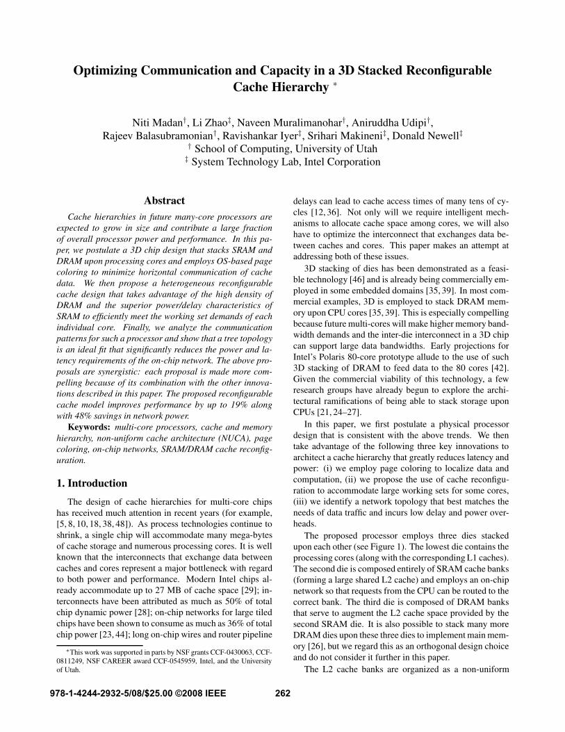
The proposed processor employs three dies stackedupon each other (see Figure 1). The lowest die contains theprocessing cores (along with the corresponding L1 caches).The second die is composed entirely of SRAM cache banks(forming a large shared L2 cache) and employs an on-chipnetwork so that requests from the CPU can be routed to thecorrect bank. The third die is composed of DRAM banksthat serve to augment the L2 cache space provided by thesecond SRAM die. It is also possible to stack many moreDRAM dies upon these three dies to implement main mem-ory [26], but we regard this as an orthogonal design choiceand do not consider it further in this paper.
The L2 cache banks are organized as a non-uniform
262978-1-4244-2932-5/08/$25.00 ©2008 IEEE
cache architecture (NUCA) [22]. The request from theprocessing core is transmitted to the SRAM die throughinter-die vias. From here, the request is propagated to theappropriate bank through the on-chip network and the la-tency for the access is a function of the proximity of thisbank to the processing core. Many recent papers have ex-plored various mechanisms to reduce average access timesin a NUCA cache [5, 7, 9, 10, 18, 48]. Most dynamic (D-NUCA) mechanisms can cause data to be placed anywhereon the chip, requiring search mechanisms to locate the data.We dis-regard these algorithms because of the complex-ity/cost of search mechanisms and resort to a static-NUCA(S-NUCA) organization, where a given physical addressmaps to a unique bank in the cache (the physical addressmaps to a unique bank and set within that bank; the waysof the set may be distributed over multiple subarrays withinthat bank). To improve the proximity of storage and com-putation, we employ page coloring to ensure that data isplaced in “optimal” banks. The idea of employing pagecoloring to dictate data placement in a NUCA cache wasproposed in a recent paper by Cho and Jin [11]. Ideally,a low-overhead run-time mechanism would be required toestimate the usage of a page so that pages can be dynam-ically migrated to their optimal locations [1]. The designof such mechanisms is a non-trivial problem in itself andbeyond the scope of this paper. For this work, we carryout an off-line analysis to identify pages that are private toeach core and that are shared by multiple cores. Privatepages are placed in the bank directly above the core andshared pages are placed in one of four central banks.
With the above page coloring mechanism in place, weexpect high data locality and most cores will end up find-ing their data in the L2 cache bank directly above. In amulti-programmed workload, each core may place differ-ent demands on the L2 cache bank directly above. In amulti-threaded workload, the centrally located cache bankswill experience higher pressure because they must accom-modate shared data in addition to the data that is privateto the corresponding cores. These varied demands on eachcache bank can perhaps be handled by allowing a core tospill some of its pages into the adjacent banks. However,this not only increases the average latency to access thatpage, it also places a higher bandwidth demand on theinter-bank network, a trait we are striving to avoid (moreon this in the next paragraph). Hence, we instead spilladditional pages into the third dimension – to the DRAMbank directly above the SRAM cache bank. Note that theDRAM bank and SRAM bank form a single large verti-cal slice in the same L2 cache level. When the DRAMspace is not employed, each SRAM cache bank accom-modates 1 MB of cache space. If this space is exceeded,the DRAM bank directly above is activated. Since DRAMdensity is eight times SRAM density, this allows the cachespace to increase to roughly 9 MB. While DRAM haspoorer latency and power characteristics than SRAM, its
higher density allows a dramatic increase in cache spacewithout the need for many more stacked dies (that in turncan worsen temperature characteristics). Further, we archi-tect the combined SRAM-DRAM cache space in a mannerthat allows non-uniform latencies and attempts to servicemore requests from the faster SRAM die. DRAM bankaccess itself has much lower cost than traditional DRAMmain memory access because the DRAM die is partitionedinto many small banks and a single small DRAM bank islooked up at a time without traversing long wires on theDRAM die. This results in a heterogeneous reconfigurablecache space, an artifact made possible by 3D die stacking.A reasonable alternative would be the implementation of a3-level cache hierarchy with the top DRAM die serving asan independent L3 cache. A static design choice like thatwould possibly complicate cache coherence implementa-tions, incur the latency to go through three levels for manyaccesses, and reduce the effective capacity of the L2 be-cause of the need for L3 tags. We believe that the overalldesign is made simpler and faster by growing the size ofthe L2 cache bank on a need basis.
Finally, we examine the traffic patterns generated by thecache hierarchy described above. Most requests are ser-viced by the local SRAM and DRAM cache banks and donot require long traversals on horizontal wires. Requeststo shared pages are directed towards the centrally locatedbanks. Requests are rarely sent to non-local non-centralbanks. Such a traffic pattern is an excellent fit for a treenetwork (illustrated in Figure 1). A tree network employsmuch fewer routers and links than the grid network typ-ically employed in such settings. Routers and links arecumbersome structures and are known to consume largeamounts of power and area [23, 44] – hence, a reductionin routers and links has many favorable implications. Treenetworks perform very poorly with random traffic patterns,but the use of intelligent page coloring ensures that the traf-fic pattern is not random and best fits the network topology.A tree network will likely work very poorly for previouslyproposed D-NUCA mechanisms that can place data in oneof many possible banks and that require search mecha-nisms. A tree network will also work poorly if highly pres-sured cache banks spill data into neighboring banks, mak-ing such a topology especially apt for the proposed designthat spills data into the third dimension.
The contributions of the paper are:• A synergistic combination of page coloring, cache re-
configuration, and on-chip network design that im-proves performance by up to 62%.
• The design of a heterogeneous reconfigurable cacheand policies to switch between configurations.
The paper is organized as follows. Section 2 providesbasic background on recent innovations in multi-core cachedesign and related work. Section 3 describes our proposedcache architecture. Results are discussed in Section 4 andwe draw conclusions in Section 5.
263
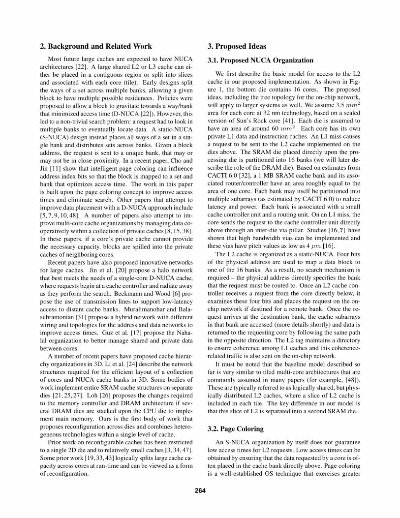
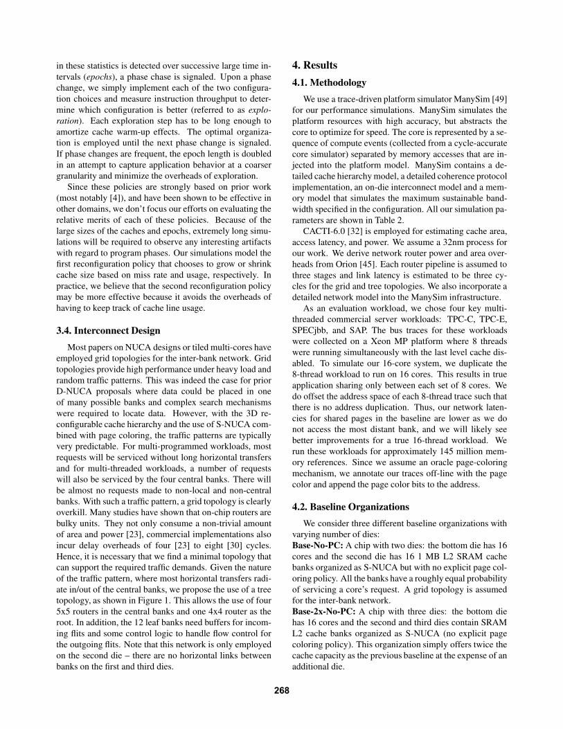
2. Background and Related WorkMost future large caches are expected to have NUCA
architectures [22]. A large shared L2 or L3 cache can ei-ther be placed in a contiguous region or split into slicesand associated with each core (tile). Early designs splitthe ways of a set across multiple banks, allowing a givenblock to have multiple possible residences. Policies wereproposed to allow a block to gravitate towards a way/bankthat minimized access time (D-NUCA [22]). However, thisled to a non-trivial search problem: a request had to look inmultiple banks to eventually locate data. A static-NUCA(S-NUCA) design instead places all ways of a set in a sin-gle bank and distributes sets across banks. Given a blockaddress, the request is sent to a unique bank, that may ormay not be in close proximity. In a recent paper, Cho andJin [11] show that intelligent page coloring can influenceaddress index bits so that the block is mapped to a set andbank that optimizes access time. The work in this paperis built upon the page coloring concept to improve accesstimes and eliminate search. Other papers that attempt toimprove data placement with a D-NUCA approach include[5, 7, 9, 10, 48]. A number of papers also attempt to im-prove multi-core cache organizations by managing data co-operatively within a collection of private caches [8, 15, 38].In these papers, if a core’s private cache cannot providethe necessary capacity, blocks are spilled into the privatecaches of neighboring cores.
Recent papers have also proposed innovative networksfor large caches. Jin et al. [20] propose a halo networkthat best meets the needs of a single-core D-NUCA cache,where requests begin at a cache controller and radiate awayas they perform the search. Beckmann and Wood [6] pro-pose the use of transmission lines to support low-latencyaccess to distant cache banks. Muralimanohar and Bala-subramonian [31] propose a hybrid network with differentwiring and topologies for the address and data networks toimprove access times. Guz et al. [17] propose the Naha-lal organization to better manage shared and private databetween cores.
A number of recent papers have proposed cache hierar-chy organizations in 3D. Li et al. [24] describe the networkstructures required for the efficient layout of a collectionof cores and NUCA cache banks in 3D. Some bodies ofwork implement entire SRAM cache structures on separatedies [21, 25, 27]. Loh [26] proposes the changes requiredto the memory controller and DRAM architecture if sev-eral DRAM dies are stacked upon the CPU die to imple-ment main memory. Ours is the first body of work thatproposes reconfiguration across dies and combines hetero-geneous technologies within a single level of cache.
Prior work on reconfigurable caches has been restrictedto a single 2D die and to relatively small caches [3, 34, 47].Some prior work [19, 33, 43] logically splits large cache ca-pacity across cores at run-time and can be viewed as a formof reconfiguration.
3. Proposed Ideas
3.1. Proposed NUCA Organization
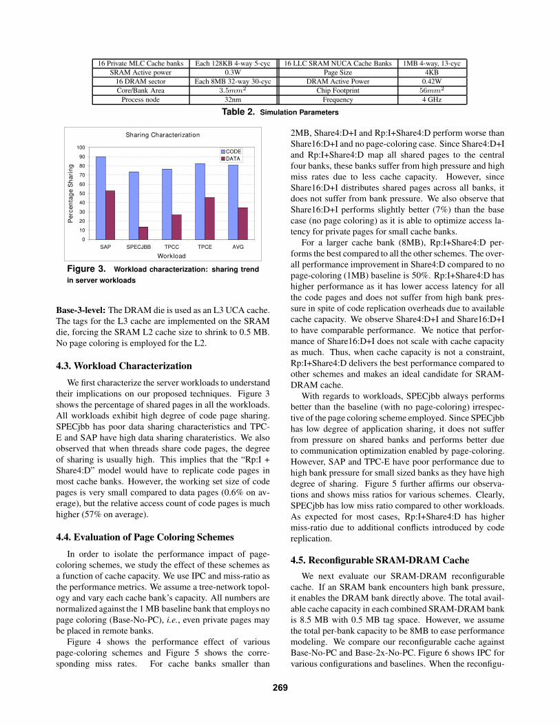
We first describe the basic model for access to the L2cache in our proposed implementation. As shown in Fig-ure 1, the bottom die contains 16 cores. The proposedideas, including the tree topology for the on-chip network,will apply to larger systems as well. We assume 3.5 mm
2
area for each core at 32 nm technology, based on a scaledversion of Sun’s Rock core [41]. Each die is assumed tohave an area of around 60 mm
2. Each core has its ownprivate L1 data and instruction caches. An L1 miss causesa request to be sent to the L2 cache implemented on thedies above. The SRAM die placed directly upon the pro-cessing die is partitioned into 16 banks (we will later de-scribe the role of the DRAM die). Based on estimates fromCACTI 6.0 [32], a 1 MB SRAM cache bank and its asso-ciated router/controller have an area roughly equal to thearea of one core. Each bank may itself be partitioned intomultiple subarrays (as estimated by CACTI 6.0) to reducelatency and power. Each bank is associated with a smallcache controller unit and a routing unit. On an L1 miss, thecore sends the request to the cache controller unit directlyabove through an inter-die via pillar. Studies [16, ?] haveshown that high bandwidth vias can be implemented andthese vias have pitch values as low as 4 µm [16].
The L2 cache is organized as a static-NUCA. Four bitsof the physical address are used to map a data block toone of the 16 banks. As a result, no search mechanism isrequired – the physical address directly specifies the bankthat the request must be routed to. Once an L2 cache con-troller receives a request from the core directly below, itexamines these four bits and places the request on the on-chip network if destined for a remote bank. Once the re-quest arrives at the destination bank, the cache subarraysin that bank are accessed (more details shortly) and data isreturned to the requesting core by following the same pathin the opposite direction. The L2 tag maintains a directoryto ensure coherence among L1 caches and this coherence-related traffic is also sent on the on-chip network.
It must be noted that the baseline model described sofar is very similar to tiled multi-core architectures that arecommonly assumed in many papers (for example, [48]).These are typically referred to as logically shared, but phys-ically distributed L2 caches, where a slice of L2 cache isincluded in each tile. The key difference in our model isthat this slice of L2 is separated into a second SRAM die.
3.2. Page Coloring
An S-NUCA organization by itself does not guaranteelow access times for L2 requests. Low access times can beobtained by ensuring that the data requested by a core is of-ten placed in the cache bank directly above. Page coloringis a well-established OS technique that exercises greater
264

Die containing 16 cores
Die containing 16SRAM sectors
Die containing 16DRAM sectors
Inter-die via pillarto send request from
core to L2 SRAM(not shown: one
pillar for each core)
Inter-die via pillarto access portionof L2 in DRAM
(not shown: onepillar per sector)
On-chip tree networkimplemented on the
SRAM die to connectthe 16 sectors
5x5 routerlinks
Figure 1. Stacked 3D processor layout. The bottom die contains the 16 cores, the second die contains 16 SRAM banks,and the top die contains 16 DRAM banks. Inter-die via pillars (one for each bank) are used to implement vertical connectionsbetween cores and DRAM/SRAM banks. Horizontal communication happens on the on-chip tree network (shown on theright) implemented on the second die. There are no horizontal connections between cores (banks) on the bottom (top) die.
control on the values assigned to bits of the physical ad-dress. Traditionally, page coloring has been employed toeliminate the aliasing problem in large virtually indexedcaches. In the context of an S-NUCA cache, page coloringcan be employed to influence the four bits of the physicaladdress that determine the bank within the NUCA cache.If the entire L2 cache size is 16 MB (each bank is 1 MB)and is 4-way set-associative with 64 byte line size, a 64-bitphysical address has the following components: 6 bits ofoffset, 16 bits of set index, and 42 bits of tag. If the pagesize is 4 KB, the 12 least significant bits are the page off-set and the 52 most significant bits are the physical pagenumber. The four most significant bits of the set index arealso part of the physical page number. These four bits canbe used to determine the bank number. Since the OS hascontrol over the physical page number, it also has controlover the bank number.
For pages that are accessed by only a single core, it isstraightforward to color that page such that it maps to thebank directly above the core. For pages that are accessedby multiple cores, the page must ideally be placed in a bankthat represents the center-of-gravity of all requests for thatpage. Creating such a mapping may require page migrationmechanisms and hardware counters to monitor a page’s ac-cess pattern and cache bank pressure. These are non-trivialpolicies that are beyond the scope of this work. For now,we assume that mechanisms can be developed to closelymatch the page allocation as computed by an off-line ora-cle analysis. In other words, the optimal cache bank for apage is pre-computed based on the center-of-gravity of re-quests for that page from various cores. As a result, shared
data in multi-threaded workloads tend to be placed in thefour banks in the center of the chip. We also devise policiesto map a shared instruction (code) page either in the cen-tral shared bank or as replicated read-only pages in eachbank. We evaluate the following three (oracle) page col-oring schemes (also shown in Figure 2). Note that in allthese schemes, private pages are always placed in the bankdirectly above; the differences are in how shared data andinstruction pages are handled.
• Share4:D+I : In this scheme, we employ a policy thatassigns both shared data and instruction pages to thecentral four banks. The shared bank is selected basedon the proximity to the core that has maximum ac-cesses to that page. If the program has a high degreeof sharing, then we expect the central four banks tohave increased pressure. This may cause the centralbanks to enable their additional DRAM cache space.
• Rp:I + Share4:D : In this scheme, we color all shareddata pages so they are mapped to central banks. Wereplicate shared instruction pages and assign them toeach accessing core. This causes the bank pressure toincrease slightly for all private banks as the workingset size of instruction pages is typically very small.This improves performance greatly as code pages arefrequently accessed in the last-level cache (LLC) incommercial workloads.
• Share16:D+I : In order to uniformly utilize the avail-able cache capacity, we color all shared pages (dataand code) and distribute them evenly across all 16banks. This page coloring scheme does not optimize
265

Figure 2. Page Coloring Schemes
for latency for shared pages, but attempts to maximizeSRAM bank hit rates.
Note that the above schemes may require minimal OSand hardware support. These schemes rely upon detectionof shared versus private pages and code versus data pages.
3.3. Reconfigurable SRAM/DRAM CacheAs described, the L2 cache is composed of 16 banks
and organized as an S-NUCA. Each bank in the SRAM diehas a capacity of 1 MB. If the threads in a core have largeworking sets, a capacity of 1 MB may result in a large missrate. Further, centrally located banks must not only servicethe local needs of their corresponding cores, they must alsoaccommodate shared pages. Therefore, the pressures oneach individual bank may be very different. One possibil-ity is to monitor bank miss rates and re-color some pages sothey spill into neighboring banks and release the pressurein “popular” banks. Instead, we propose a reconfigurablecache that takes advantage of 3D stacking to seamlesslygrow the size of a bank in the vertical dimension. Thisallows the size of each bank to grow independently with-out impacting the capacity or access time of neighboringbanks. Many proposals of 2D reconfigurable caches al-ready exist in the literature: they allow low access timesfor small cache sizes but provide the flexibility to incor-porate larger capacities at longer access times. The use of3D and NUCA makes the design of a reconfigurable cacheespecially attractive: (i) the spare capacity on the third diedoes not intrude with the layout of the second die, nor doesit steal capacity from other neighboring caches (as is com-monly done in 2D reconfigurable caches [3, 47]), (ii) sincethe cache is already partitioned into NUCA banks, the in-troduction of additional banks and delays does not greatlycomplicate the control logic, (iii) the use of a third dimen-sion allows access time to grow less than linearly with ca-pacity (another disadvantage of a 2D reconfigurable cache).
While growing the size of a bank, the third die can im-plement SRAM subarrays identical to the second die, thusallowing the bank size to grow by a factor of two. Butreconfiguration over homogeneous banks does not make
much sense: the added capacity comes at a trivial latencycost, so there is little motivation to employ the smallercache configuration. Reconfiguration does make sensewhen employing heterogeneous technologies. In this case,we advocate the use of a third die that implements DRAMbanks, thus allowing the bank size to grow by up to a factorof nine1. By stacking a single DRAM die (instead of eightSRAM dies), we provide high capacity while limiting thegrowth in temperature and cost, and improving yield. SinceDRAM accesses are less efficient than SRAM accesses, dy-namic reconfiguration allows us to avoid DRAM accesseswhen dealing with small working sets.Organizing Tags and Data.
The SRAM bank is organized into three memory arrays:a tag array, a data array, and an adaptive array that can actas both tag and data arrays. As with most large L2s, thetags are first looked up and after the appropriate way isidentified, the data subarray is accessed. Assuming thateach block is 64 bytes and has a 32 bit tag (including direc-tory state and assuming a 36-bit physical address space),the corresponding tag storage is 64 KB. The use of DRAMenables the total bank data storage to grow to 9 MB, re-quiring a total 576 KB of tag storage. Since tags are ac-cessed before data and since SRAM accesses are cheaperthan DRAM accesses, it is beneficial to implement the tagsin SRAM. As a result, 512 KB of SRAM storage that previ-ously served as data subarray must now serve as tag subar-ray. Compared to a typical data array, a tag array has addi-tional logic to perform tag comparison. The data sub-arrayhas more H-tree bandwidth for data transfer compared toits tag counterpart. To keep the reconfiguration simple, theproposed adaptive array encompasses the functionalities ofboth tag and data array.Growing Associativity, Sets, Block-Size.
The increased capacity provided by DRAM can man-ifest in three forms (and combinations thereof): (i) in-creased associativity, (ii) increased number of sets, and (iii)increased block size.
1Published reports claim a factor of eight difference in the densities ofSRAM and DRAM [40].
266

Configuration Access time (ns) Total Energy per access(nJ) Area (mm2)
Baseline SRAM 1 MB bank 3.13 0.699 2.07Reconfigurable cache (ways) DRAM 6.71 1.4 3.23Reconfigurable cache (sets) DRAM 6.52 1.36 2.76
Reconfigurable cache (block size) DRAM 5.43 51.19 1.44
Table 1. Access time, energy, and area for various cache configurations at a 4 GHz clock derived from [32].
The first form of reconfiguration allows the bank to gofrom 4-way to 34-way set associative. 32 data ways are im-plemented on the DRAM die and two of the original fourdata ways remain on the SRAM die after half the data sub-arrays are converted to tag subarrays. Such an approachhas the following advantages: (i) dirty lines in the twoways in the SRAM die need not be flushed upon every re-configuration, (ii) every set in the bank can have two ofits ways in relatively close proximity in SRAM. The pri-mary disadvantage is the power and complexity overheadof implementing 34-way set-associativity. We can optimizethe cache lookup further by moving the MRU block intothe two SRAM ways on every access in the hope that thiswill reduce average access times. With this policy, a hit inDRAM space will require an SRAM and DRAM read andwrite. In our evaluations, we employ reconfiguration of thenumber of ways, but do not attempt the optimization whereMRU blocks are moved into SRAM.
The second form of reconfiguration causes an increasein the number of sets from 2K to 16K (we will restrictourselves to power-of-two number of sets, possibly lead-ing to extra white space on the top die). When cache sizeis increased, nearly every dirty cache line will have to beflushed. When cache size is decreased, lines residing inthe SRAM data subarrays need not be flushed. The largecache organization has a more favorable access time/powerfor a fraction of the sets that map to SRAM data subarrays.The page coloring mechanism could attempt to color criti-cal pages so they reside in the sets that map to SRAM.
The third form of reconfiguration increases the blocksize from 64 bytes to 512 bytes (again, possibly resultingin white space). Note that this approach does not increasethe tag space requirement, so 1 MB of data can be placedin SRAM, while 7 MB is placed in DRAM. This has theobvious disadvantage of placing higher pressure on the busto main memory and also higher energy consumption foraccesses. While re-configuring the number of sets or blocksize, care must be taken to not change the address bits usedto determine the bank number for an address.
Thus, there are multiple mechanisms to reconfigure thecache. The differences are expected to be minor unlessthe application is highly sensitive to capacity (8 MB ver-sus 8.5 MB) and memory bandwidth. While some mech-anisms can escape flushing the entire cache, these savingsare relatively minor if cache reconfiguration is performedinfrequently. In our evaluations, we only focus on the firstreconfiguration approach that changes the number of ways.
It is worth noting that banks in the DRAM die are laid
out very similar to banks in the SRAM die. Our estimatesfor DRAM delay, power, and area are based on CACTI-6.0 and discussions with industrial teams. Table 1 summa-rizes the delay, power, and area of the considered organiza-tions. The DRAM banks can also be statically employed asa level-3 cache. However, this would significantly reducethe size of the SRAM L2 cache as 0.5 MB space on thesecond die would have to be designated as L3 tags. Thismay have a negative impact for several applications withmoderate working-set sizes (not evaluated in this paper).It will also increase latencies for L3 and memory accessesbecause tags in multiple levels have to be sequentially nav-igated.
Having described the specific implementation, the fol-lowing additional advantages over prior 2D designs [3, 47]are made clear: (i) a dramatic 8x increase in capacity ispossible at a minor delay overhead, (ii) only two configura-tions are possible, enabling a simpler reconfiguration pol-icy, (iii) each cache bank can reconfigure independently,thus avoiding a flush of the entire L2 all at one time.Reconfiguration Policies.
We next examine the design of a reconfiguration pol-icy. The frequency of reconfiguration is a function of theoverheads of a cache flush and cache warm-up. Up to 16Kcache lines will have to be flushed or brought in upon everyreconfiguration. While the fetch of new lines can be over-lapped with execution, cache flush will likely have to stallall requests to that bank. A state-of-the-art memory systemcan handle a peak throughput of 10 GB/s [36]. A com-plete flush will require a stall of roughly 100 K cycles. Forthis overhead to be minor, a reconfiguration is consideredonce every 10 M cycles. Reconfiguration policies are well-studied (for example, [2, 4, 13, 14]). We design two simplepolicies that are heavily influenced by this prior work.
Every 10 M cycles, we examine the following two met-rics for each cache bank: bank miss rate and usage. Ahigh bank miss rate indicates the need to grow cache size,while low usage indicates the need to shrink cache size.It is important to pick a low enough threshold for usage,else the configurations can oscillate. Usage can be deter-mined by maintaining a bit per cache block that is set uponaccess and re-set at the start of every 10 M cycle interval(this is assumed in our simulations). There also exist othercomplexity-effective mechanisms to estimate usage [33].
In an alternative policy, various statistics can be main-tained per bank to determine if the application has movedto a new phase (a part of application execution with differ-ent behavior and characteristics). If a substantial change
267
in these statistics is detected over successive large time in-tervals (epochs), a phase chase is signaled. Upon a phasechange, we simply implement each of the two configura-tion choices and measure instruction throughput to deter-mine which configuration is better (referred to as explo-ration). Each exploration step has to be long enough toamortize cache warm-up effects. The optimal organiza-tion is employed until the next phase change is signaled.If phase changes are frequent, the epoch length is doubledin an attempt to capture application behavior at a coarsergranularity and minimize the overheads of exploration.
Since these policies are strongly based on prior work(most notably [4]), and have been shown to be effective inother domains, we don’t focus our efforts on evaluating therelative merits of each of these policies. Because of thelarge sizes of the caches and epochs, extremely long simu-lations will be required to observe any interesting artifactswith regard to program phases. Our simulations model thefirst reconfiguration policy that chooses to grow or shrinkcache size based on miss rate and usage, respectively. Inpractice, we believe that the second reconfiguration policymay be more effective because it avoids the overheads ofhaving to keep track of cache line usage.
3.4. Interconnect DesignMost papers on NUCA designs or tiled multi-cores have
employed grid topologies for the inter-bank network. Gridtopologies provide high performance under heavy load andrandom traffic patterns. This was indeed the case for priorD-NUCA proposals where data could be placed in oneof many possible banks and complex search mechanismswere required to locate data. However, with the 3D re-configurable cache hierarchy and the use of S-NUCA com-bined with page coloring, the traffic patterns are typicallyvery predictable. For multi-programmed workloads, mostrequests will be serviced without long horizontal transfersand for multi-threaded workloads, a number of requestswill also be serviced by the four central banks. There willbe almost no requests made to non-local and non-centralbanks. With such a traffic pattern, a grid topology is clearlyoverkill. Many studies have shown that on-chip routers arebulky units. They not only consume a non-trivial amountof area and power [23], commercial implementations alsoincur delay overheads of four [23] to eight [30] cycles.Hence, it is necessary that we find a minimal topology thatcan support the required traffic demands. Given the natureof the traffic pattern, where most horizontal transfers radi-ate in/out of the central banks, we propose the use of a treetopology, as shown in Figure 1. This allows the use of four5x5 routers in the central banks and one 4x4 router as theroot. In addition, the 12 leaf banks need buffers for incom-ing flits and some control logic to handle flow control forthe outgoing flits. Note that this network is only employedon the second die – there are no horizontal links betweenbanks on the first and third dies.
4. Results4.1. Methodology
We use a trace-driven platform simulator ManySim [49]for our performance simulations. ManySim simulates theplatform resources with high accuracy, but abstracts thecore to optimize for speed. The core is represented by a se-quence of compute events (collected from a cycle-accuratecore simulator) separated by memory accesses that are in-jected into the platform model. ManySim contains a de-tailed cache hierarchy model, a detailed coherence protocolimplementation, an on-die interconnect model and a mem-ory model that simulates the maximum sustainable band-width specified in the configuration. All our simulation pa-rameters are shown in Table 2.
CACTI-6.0 [32] is employed for estimating cache area,access latency, and power. We assume a 32nm process forour work. We derive network router power and area over-heads from Orion [45]. Each router pipeline is assumed tothree stages and link latency is estimated to be three cy-cles for the grid and tree topologies. We also incorporate adetailed network model into the ManySim infrastructure.
As an evaluation workload, we chose four key multi-threaded commercial server workloads: TPC-C, TPC-E,SPECjbb, and SAP. The bus traces for these workloadswere collected on a Xeon MP platform where 8 threadswere running simultaneously with the last level cache dis-abled. To simulate our 16-core system, we duplicate the8-thread workload to run on 16 cores. This results in trueapplication sharing only between each set of 8 cores. Wedo offset the address space of each 8-thread trace such thatthere is no address duplication. Thus, our network laten-cies for shared pages in the baseline are lower as we donot access the most distant bank, and we will likely seebetter improvements for a true 16-thread workload. Werun these workloads for approximately 145 million mem-ory references. Since we assume an oracle page-coloringmechanism, we annotate our traces off-line with the pagecolor and append the page color bits to the address.
4.2. Baseline OrganizationsWe consider three different baseline organizations with
varying number of dies:Base-No-PC: A chip with two dies: the bottom die has 16cores and the second die has 16 1 MB L2 SRAM cachebanks organized as S-NUCA but with no explicit page col-oring policy. All the banks have a roughly equal probabilityof servicing a core’s request. A grid topology is assumedfor the inter-bank network.Base-2x-No-PC: A chip with three dies: the bottom diehas 16 cores and the second and third dies contain SRAML2 cache banks organized as S-NUCA (no explicit pagecoloring policy). This organization simply offers twice thecache capacity as the previous baseline at the expense of anadditional die.
268
16 Private MLC Cache banks Each 128KB 4-way 5-cyc 16 LLC SRAM NUCA Cache Banks 1MB 4-way, 13-cycSRAM Active power 0.3W Page Size 4KB
16 DRAM sector Each 8MB 32-way 30-cyc DRAM Active Power 0.42WCore/Bank Area 3.5mm
2 Chip Footprint 56mm2
Process node 32nm Frequency 4 GHz
Table 2. Simulation Parameters
Figure 3. Workload characterization: sharing trendin server workloads
Base-3-level: The DRAM die is used as an L3 UCA cache.The tags for the L3 cache are implemented on the SRAMdie, forcing the SRAM L2 cache size to shrink to 0.5 MB.No page coloring is employed for the L2.
4.3. Workload Characterization
We first characterize the server workloads to understandtheir implications on our proposed techniques. Figure 3shows the percentage of shared pages in all the workloads.All workloads exhibit high degree of code page sharing.SPECjbb has poor data sharing characteristics and TPC-E and SAP have high data sharing charateristics. We alsoobserved that when threads share code pages, the degreeof sharing is usually high. This implies that the “Rp:I +Share4:D” model would have to replicate code pages inmost cache banks. However, the working set size of codepages is very small compared to data pages (0.6% on av-erage), but the relative access count of code pages is muchhigher (57% on average).
4.4. Evaluation of Page Coloring Schemes
In order to isolate the performance impact of page-coloring schemes, we study the effect of these schemes asa function of cache capacity. We use IPC and miss-ratio asthe performance metrics. We assume a tree-network topol-ogy and vary each cache bank’s capacity. All numbers arenormalized against the 1 MB baseline bank that employs nopage coloring (Base-No-PC), i.e., even private pages maybe placed in remote banks.
Figure 4 shows the performance effect of variouspage-coloring schemes and Figure 5 shows the corre-sponding miss rates. For cache banks smaller than
2MB, Share4:D+I and Rp:I+Share4:D perform worse thanShare16:D+I and no page-coloring case. Since Share4:D+Iand Rp:I+Share4:D map all shared pages to the centralfour banks, these banks suffer from high pressure and highmiss rates due to less cache capacity. However, sinceShare16:D+I distributes shared pages across all banks, itdoes not suffer from bank pressure. We also observe thatShare16:D+I performs slightly better (7%) than the basecase (no page coloring) as it is able to optimize access la-tency for private pages for small cache banks.
For a larger cache bank (8MB), Rp:I+Share4:D per-forms the best compared to all the other schemes. The over-all performance improvement in Share4:D compared to nopage-coloring (1MB) baseline is 50%. Rp:I+Share4:D hashigher performance as it has lower access latency for allthe code pages and does not suffer from high bank pres-sure in spite of code replication overheads due to availablecache capacity. We observe Share4:D+I and Share16:D+Ito have comparable performance. We notice that perfor-mance of Share16:D+I does not scale with cache capacityas much. Thus, when cache capacity is not a constraint,Rp:I+Share4:D delivers the best performance compared toother schemes and makes an ideal candidate for SRAM-DRAM cache.
With regards to workloads, SPECjbb always performsbetter than the baseline (with no page-coloring) irrespec-tive of the page coloring scheme employed. Since SPECjbbhas low degree of application sharing, it does not sufferfrom pressure on shared banks and performs better dueto communication optimization enabled by page-coloring.However, SAP and TPC-E have poor performance due tohigh bank pressure for small sized banks as they have highdegree of sharing. Figure 5 further affirms our observa-tions and shows miss ratios for various schemes. Clearly,SPECjbb has low miss ratio compared to other workloads.As expected for most cases, Rp:I+Share4:D has highermiss-ratio due to additional conflicts introduced by codereplication.
4.5. Reconfigurable SRAM-DRAM CacheWe next evaluate our SRAM-DRAM reconfigurable
cache. If an SRAM bank encounters high bank pressure,it enables the DRAM bank directly above. The total avail-able cache capacity in each combined SRAM-DRAM bankis 8.5 MB with 0.5 MB tag space. However, we assumethe total per-bank capacity to be 8MB to ease performancemodeling. We compare our reconfigurable cache againstBase-No-PC and Base-2x-No-PC. Figure 6 shows IPC forvarious configurations and baselines. When the reconfigu-
269

Figure 4. Performance Evaluation of Page Coloring schemes as a function of Cache Capacity
Figure 5. Miss Ratio of Page Coloring schemes as afunction of Cache Capacity
ration heuristics are enabled, the model is pre-pended withR, and with no dynamic reconfiguration (the DRAM banksare always enabled), the model is pre-pended with NR. Weassume 100,000 cycles penalty for flushing the caches dur-ing reconfiguration.
We observe that all workloads on average perform 45-62% better than Base-No-PC when DRAM banks areswitched on all the time and 20-35% better comparedto Base-2x-No-PC depending upon the page-coloringscheme. When compared to Base-3-level, our NR casesperform 11-26% better depending upon the page coloringscheme. Our best case performance improvement with re-configuration heuristic enabled when compared to Base-3-level is 19%.
With our reconfiguration heuristic, we observe that
Figure 6. Performance Evaluation of SRAM-DRAMcache
DRAM banks are switched on all the time for centralshared banks in the Rp:I+Share4:D case. The non-centralbanks in this model and occasionally in Share4:D+I haveDRAM switched off due to low bank pressure. Amongstall the page-coloring schemes, Rp:I+Share4:D yields thebest performance with and without reconfiguration heuris-tic. Since we stall all cores during reconfiguration, theoverheads of our heuristic lower the overall performancegain compared to the best case performance with DRAMsenabled all the time. However, we expect this overhead toreduce if the workloads run long enough to amortize thecost of reconfiguration.
Figure 7(a) illustrates the average percentage of timeDRAM banks are switched off for each of the cache banks
270
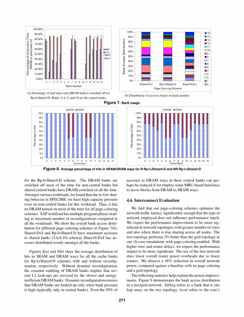
(a) Percentage of total time each DRAM bank is switched off forRp:I+Share4:D. Banks 5, 6, 9, and 10 are the central banks.
(b) Distribution of accesses based on bank number.
Figure 7. Bank usage.
Figure 8. Average percentage of hits in SRAM/DRAM ways for R-Rp:I+Share4:D and NR-Rp:I+Share4:D
for the Rp:I+Share4:D scheme. The DRAM banks areswitched off most of the time for non-central banks butshared central banks have DRAM switched on all the time.Amongst various workloads, we found that due to low shar-ing behavior in SPECJBB, we have high capacity pressureeven on non-central banks for this workload. Thus, it hasits DRAM turned on most of the time for all page-coloringschemes. SAP workload has multiple program phases lead-ing to maximum number of reconfigurations compared toall the workloads. We show the overall bank access distri-bution for different page coloring schemes in Figure 7(b).Share4:D+I and Rp:I+Share4:D have maximum accessesto shared banks (5,6,9,10) whereas Share16:D+I has ac-cesses distributed evenly amongst all the banks.
Figures 8(a) and 8(b) show the average distribution ofhits in SRAM and DRAM ways for all the cache banksfor Rp:I+Share4:D schemes with and without reconfig-uration, respectively. Without dynamic reconfiguration,the constant enabling of DRAM banks implies that sev-eral L2 look-ups are serviced by the slower and energy-inefficient DRAM banks. Dynamic reconfiguration ensuresthat DRAM banks are looked up only when bank pressureis high (typically only in central banks). Even the 50% of
accesses to DRAM ways in these central banks can per-haps be reduced if we employ some MRU-based heuristicsto move blocks from DRAM to SRAM ways.
4.6. Interconnect Evaluation
We find that our page-coloring schemes optimize thenetwork traffic latency significantly enough that the type ofnetwork employed does not influence performance much.We expect the performance improvement to be more sig-nificant in network topologies with greater number of coresand also where there is true sharing across all nodes. Thetree topology performs 2% better than the grid topology inour 16-core simulations with page-coloring enabled. Withhigher wire and router delays, we expect the performanceimpact to be more significant. The use of the tree networkdoes lower overall router power overheads due to fewerrouters. We observe a 48% reduction in overall networkpower, compared against a baseline with no page coloringand a grid topology.
The following statistics help explain the power improve-ments. Figure 9 demonstrates the bank access distributionin a tree/grid network. Sibling refers to a bank that is onehop away on the tree topology, local refers to the core’s
271
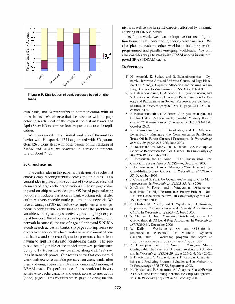
Figure 9. Distribution of bank accesses based on dis-tance
own bank, and Distant refers to communication with allother banks. We observe that the baseline with no pagecoloring sends most of the requests to distant banks andRp:I+Share4:D maximizes local requests due to code repli-cation.
We also carried out an initial analysis of thermal be-havior with Hotspot 4.1 [37] augmented with 3D param-eters [26]. Consistent with other papers on 3D stacking ofSRAM and DRAM, we observed an increase in tempera-ture of about 7 °C.
5. Conclusions
The central idea in this paper is the design of a cache thatenables easy reconfigurability across multiple dies. Thiscentral idea is placed in the context of two related essentialelements of large cache organization (OS-based page color-ing and on-chip network design). OS-based page coloringnot only introduces variation in bank working sets, it alsoenforces a very specific traffic pattern on the network. Wetake advantage of 3D technology to implement a heteroge-neous reconfigurable cache that addresses the problem ofvariable working sets by selectively providing high capac-ity at low cost. We advocate a tree topology for the on-chipnetwork because (i) the use of page coloring and S-NUCAavoids search across all banks, (ii) page coloring forces re-quests to be serviced by local nodes or radiate in/out of cen-tral banks, and (iii) reconfiguration prevents a bank fromhaving to spill its data into neighboring banks. The pro-posed reconfigurable cache model improves performanceby up to 19% over the best baseline, along with 48% sav-ings in network power. Our results show that commercialworkloads exercise variable pressures on cache banks afterpage coloring, requiring a dynamic enabling/disabling ofDRAM space. The performance of these workloads is verysensitive to cache capacity and quick access to instruction(code) pages. This requires smart page coloring mecha-
nisms as well as the large L2 capacity afforded by dynamicenabling of DRAM banks.
As future work, we plan to improve our reconfigura-tion heuristics by considering energy/power metrics. Wealso plan to evaluate other workloads including multi-programmed and parallel emerging workloads. We willalso consider ways to maximize SRAM access in our pro-posed SRAM-DRAM cache.
References
[1] M. Awasthi, K. Sudan, and R. Balasubramonian. Dy-namic Hardware-Assisted Software-Controlled Page Place-ment to Manage Capacity Allocation and Sharing withinLarge Caches. In Proceedings of HPCA-15, Feb 2009.
[2] R. Balasubramonian, D. Albonesi, A. Buyuktosunoglu, andS. Dwarkadas. Memory Hierarchy Reconfiguration for En-ergy and Performance in General-Purpose Processor Archi-tectures. In Proceedings of MICRO-33, pages 245–257, De-cember 2000.
[3] R. Balasubramonian, D. Albonesi, A. Buyuktosunoglu, andS. Dwarkadas. A Dynamically Tunable Memory Hierar-chy. IEEE Transactions on Computers, 52(10):1243–1258,October 2003.
[4] R. Balasubramonian, S. Dwarkadas, and D. Albonesi.Dynamically Managing the Communication-ParallelismTrade-Off in Future Clustered Processors. In Proceedingsof ISCA-30, pages 275–286, June 2003.
[5] B. Beckmann, M. Marty, and D. Wood. ASR: AdaptiveSelective Replication for CMP Caches. In Proceedings ofMICRO-39, December 2006.
[6] B. Beckmann and D. Wood. TLC: Transmission LineCaches. In Proceedings of MICRO-36, December 2003.
[7] B. Beckmann and D. Wood. Managing Wire Delay in LargeChip-Multiprocessor Caches. In Proceedings of MICRO-37, December 2004.
[8] J. Chang and G. Sohi. Co-Operative Caching for Chip Mul-tiprocessors. In Proceedings of ISCA-33, June 2006.
[9] Z. Chishti, M. Powell, and T. Vijaykumar. Distance As-sociativity for High-Performance Energy-Efficient Non-Uniform Cache Architectures. In Proceedings of MICRO-36, December 2003.
[10] Z. Chishti, M. Powell, and T. Vijaykumar. OptimizingReplication, Communication, and Capacity Allocation inCMPs. In Proceedings of ISCA-32, June 2005.
[11] S. Cho and L. Jin. Managing Distributed, Shared L2Caches through OS-Level Page Allocation. In Proceedingsof MICRO-39, December 2006.
[12] W. Dally. Workshop on On- and Off-Chip In-terconnection Networks for Multicore Systems(OCIN), 2006. Workshop program and report athttp://www.ece.ucdavis.edu/˜ocin06/.
[13] A. Dhodapkar and J. E. Smith. Managing Multi-Configurable Hardware via Dynamic Working Set Analy-sis. In Proceedings of ISCA-29, pages 233–244, May 2002.
[14] E. Duesterwald, C. Cascaval, and S. Dwarkadas. Character-izing and Predicting Program Behavior and its Variability.In Proceedings of PACT-12, September 2003.
[15] H. Dybdahl and P. Stenstrom. An Adaptive Shared/PrivateNUCA Cache Partitioning Scheme for Chip Multiproces-sors. In Proceedings of HPCA-13, February 2007.
272
[16] S. Gupta, M. Hilbert, S. Hong, and R. Patti. Techniques forProducing 3D ICs with High-Density Interconnect. In Pro-ceedings of International VLSI Multilevel Interconnection,2004.
[17] Z. Guz, I. Keidar, A. Kolodny, and U. Weiser. Naha-lal: Memory Organization for Chip Multiprocessors. IEEEComputer Architecture Letters, vol.6(1), May 2007.
[18] J. Huh, C. Kim, H. Shafi, L. Zhang, D. Burger, and S. Keck-ler. A NUCA Substrate for Flexible CMP Cache Sharing.In Proceedings of ICS-19, June 2005.
[19] R. Iyer, L. Zhao, F. Guo, R. Illikkal, D. Newell, Y. Solihin,L. Hsu, and S. Reinhardt. QoS Policies and Architecturefor Cache/Memory in CMP Platforms. In Proceedings ofSIGMETRICS, June 2007.
[20] Y. Jin, E. J. Kim, and K. H. Yum. A Domain-Specific On-Chip Network Design for Large Scale Cache Systems. InProceedings of HPCA-13, February 2007.
[21] T. Kgil, S. D’Souza, A. Saidi, N. Binkert, R. Dreslinski,S. Reinhardt, K. Flautner, and T. Mudge. PicoServer: Us-ing 3D Stacking Technology to Enable a Compact EnergyEfficient Chip Multiprocessor. In Proceedings of ASPLOS-XII, October 2006.
[22] C. Kim, D. Burger, and S. Keckler. An Adaptive, Non-Uniform Cache Structure for Wire-Dominated On-ChipCaches. In Proceedings of ASPLOS-X, October 2002.
[23] P. Kundu. On-Die Interconnects for Next GenerationCMPs. In Workshop on On- and Off-Chip InterconnectionNetworks for Multicore Systems (OCIN), December 2006.
[24] F. Li, C. Nicopoulos, T. Richardson, Y. Xie, N. Vijaykr-ishnan, and M. Kandemir. Design and Management of 3DChip Multiprocessors Using Network-in-Memory. In Pro-ceedings of ISCA-33, June 2006.
[25] C. C. Liu, I. Ganusov, M. Burtscher, and S. Tiwari. Bridg-ing the Processor-Memory Performance Gap with 3D ICTechnology. IEEE Design and Test of Computers, 22:556–564, November 2005.
[26] G. Loh. 3D-Stacked Memory Architectures for Multi-CoreProcessors. In Proceedings of ISCA-35, June 2008.
[27] G. Loi, B. Agrawal, N. Srivastava, S. Lin, T. Sherwood,and K. Banerjee. A Thermally-Aware Performance Analy-sis of Vertically Integrated (3-D) Processor-Memory Hier-archy. In Proceedings of DAC-43, June 2006.
[28] N. Magen, A. Kolodny, U. Weiser, and N. Shamir. Intercon-nect Power Dissipation in a Microprocessor. In Proceedingsof System Level Interconnect Prediction, February 2004.
[29] C. McNairy and R. Bhatia. Montecito: A Dual-Core, Dual-Thread Itanium Processor. IEEE Micro, 25(2), March/April2005.
[30] S. Mukherjee, P. Bannon, S. Lang, A. Spink, and D. Webb.The Alpha 21364 Network Architecture. In IEEE Micro,volume 22, 2002.
[31] N. Muralimanohar and R. Balasubramonian. InterconnectDesign Considerations for Large NUCA Caches. In Pro-ceedings of the 34th International Symposium on ComputerArchitecture (ISCA-34), June 2007.
[32] N. Muralimanohar, R. Balasubramonian, and N. Jouppi.Optimizing NUCA Organizations and Wiring Alternativesfor Large Caches with CACTI 6.0. In Proceedings ofthe 40th International Symposium on Microarchitecture(MICRO-40), December 2007.
[33] M. Qureshi and Y. Patt. Utility-Based Cache Partitioning:A Low-Overhead, High-Performance, Runtime Mechanismto Partition Shared Caches. In Proceedings of MICRO-39,December 2006.
[34] P. Ranganathan, S. Adve, and N. Jouppi. Reconfigurablecaches and their application to media processing. Proceed-ings of ISCA-27, pages 214–224, June 2000.
[35] Samsung Electronics Corporation. Samsung Electron-ics Develops World’s First Eight-Die Multi-Chip Packagefor Multimedia Cell Phones, 2005. (Press release fromhttp://www.samsung.com).
[36] Semiconductor Industry Association. InternationalTechnology Roadmap for Semiconductors 2005.http://www.itrs.net/Links/2005ITRS/Home2005.htm.
[37] K. Skadron, M. R. Stan, W. Huang, S. Velusamy, andK. Sankaranarayanan. Temperature-Aware Microarchitec-ture. In Proceedings of ISCA-30, pages 2–13, 2003.
[38] E. Speight, H. Shafi, L. Zhang, and R. Rajamony. AdaptiveMechanisms and Policies for Managing Cache Hierarchiesin Chip Multiprocessors. In Proceedings of ISCA-32, June2005.
[39] Tezzaron Semiconductor. www.tezzaron.com.[40] S. Thoziyoor, J. H. Ahn, M. Monchiero, J. B. Brockman,
and N. P. Jouppi. A Comprehensive Memory ModelingTool and its Application to the Design and Analysis of Fu-ture Memory Hierarchies. In Proceedings of ISCA-35, June2008.
[41] M. Tremblay and S. Chaudhry. A Third-Generation 65nm16-Core 32-Thread Plus 32-Scout-Thread CMT. In Pro-ceedings of ISSCC, Febuary 2008.
[42] S. Vangal, J. Howard, G. Ruhl, S. Dighe, H. Wilson,J. Tschanz, D. Finan, P. Iyer, A. Singh, T. Jacob, S. Jain,S. Venkataraman, Y. Hoskote, and N. Borkar. An 80-Tile1.28TFLOPS Network-on-Chip in 65nm CMOS. In Pro-ceedings of ISSCC, February 2007.
[43] K. Varadarajan, S. Nandy, V. Sharda, A. Bharadwaj, R. Iyer,S. Makineni, and D. Newell. Molecular Caches: A CachingStructure for Dynamic Creation of Application-SpecificHeterogeneous Cache Regions. In Proceedings of MICRO-39, December 2006.
[44] H. S. Wang, L. S. Peh, and S. Malik. A Power Model forRouters: Modeling Alpha 21364 and InfiniBand Routers.In IEEE Micro, Vol 24, No 1, January 2003.
[45] H.-S. Wang, X. Zhu, L.-S. Peh, and S. Malik. Orion:A Power-Performance Simulator for Interconnection Net-works. In Proceedings of MICRO-35, November 2002.
[46] Y. Xie, G. Loh, B. Black, and K. Bernstein. Design SpaceExploration for 3D Architectures. ACM Journal of Emerg-ing Technologies in Computing Systems, 2(2):65–103, April2006.
[47] C. Zhang, F. Vahid, and W. Najjar. A Highly ConfigurableCache Architecture for Embedded Systems. In Proceedingsof ISCA-30, June 2003.
[48] M. Zhang and K. Asanovic. Victim Replication: Maximiz-ing Capacity while Hiding Wire Delay in Tiled Chip Multi-processors. In Proceedings of ISCA-32, June 2005.
[49] L. Zhao, R. Iyer, J. Moses, R. Illikkal, S. Makineni, andD. Newell. Exploring Large-Scale CMP Architectures Us-ing ManySim. IEEE Micro, 27(4):21–33, 2007.
273