Deposition of hard thin films from HMDSO in atmospheric pressure dielectric barrier discharge
18
Deposition of hard thin films from HMDSO in atmospheric pressure dielectric barrier discharge D Trunec 1 , L Zaj´ ıˇ ckov´ a 1 , V Burˇ s´ ıkov´ a 1 , F Studniˇ cka 1 ,P S ˇ tahel 1 , V Prysiazhnyi 1 , V Peˇ rina 2 , J Houdkov´ a 3 , Z Navr´ atil 1 and D Franta 1 1 Department of Physical Electronics, Faculty of Science, Masaryk University, Kotl´aˇ rsk´a2, 611 37 Brno, Czech Republic 2 Institute of Nuclear Physics, Academy of Sciences of the Czech Republic, 250 68 ˇ Reˇ z, Czech Republic 3 Institute of Physics, Academy of Sciences of the Czech Republic, Cukrovarnick´a10, 162 53 Prague, Czech Republic E-mail: [email protected] Abstract. The atmospheric pressure dielectric barrier discharge burning in nitrogen with small admixture of hexamethyldisiloxane (HMDSO) was used for the deposition of thin organosilicon films. The thin films were deposited on glass, silicon and polycarbonate substrates, the substrate temperature during the deposition process was elevated up to values within the range 25 ◦ C – 150 ◦ C in order to obtain hard SiO x -like thin films. The properties of the discharge were studied by means of optical emission spectroscopy and electrical measurements. The deposited films were characterised by Rutherford backscattering and elastic recoil detection methods, x-ray photoelectron spectroscopy, infrared spectroscopy measurements, ellipsometry and depth sensing indentation technique. It was found that the films properties depend significantly on substrate temperature at deposition. An increase of substrate temperature from 25 ◦ C to 150 ◦ C leads to an increase of film hardness from 0.4 GPa to 7 GPa and the film chemical composition changes from CH x Si y O z to SiO x H y . The films were transparent in visible range. Submitted to: J. Phys. D: Appl. Phys. PACS numbers: 52.80 Tn, 52.77 Dq Confidential: not for distribution. Submitted to IOP Publishing for peer review 29 April 2010 peer-00569620, version 1 - 25 Feb 2011 Author manuscript, published in "Journal of Physics D: Applied Physics 43, 22 (2010) 225403" DOI : 10.1088/0022-3727/43/22/225403
-
Upload
independent -
Category
Documents
-
view
0 -
download
0
Transcript of Deposition of hard thin films from HMDSO in atmospheric pressure dielectric barrier discharge

Deposition of hard thin films from HMDSO in
atmospheric pressure dielectric barrier discharge
D Trunec1, L Zajıckova1, V Bursıkova1, F Studnicka1, P
Stahel1, V Prysiazhnyi1, V Perina2, J Houdkova3, Z Navratil1
and D Franta1
1 Department of Physical Electronics, Faculty of Science, Masaryk University,Kotlarska 2, 611 37 Brno, Czech Republic2 Institute of Nuclear Physics, Academy of Sciences of the Czech Republic, 250 68Rez, Czech Republic3 Institute of Physics, Academy of Sciences of the Czech Republic, Cukrovarnicka 10,162 53 Prague, Czech Republic
E-mail: [email protected]
Abstract. The atmospheric pressure dielectric barrier discharge burning in nitrogenwith small admixture of hexamethyldisiloxane (HMDSO) was used for the depositionof thin organosilicon films. The thin films were deposited on glass, silicon andpolycarbonate substrates, the substrate temperature during the deposition process waselevated up to values within the range 25◦C – 150◦C in order to obtain hard SiOx-likethin films. The properties of the discharge were studied by means of optical emissionspectroscopy and electrical measurements. The deposited films were characterised byRutherford backscattering and elastic recoil detection methods, x-ray photoelectronspectroscopy, infrared spectroscopy measurements, ellipsometry and depth sensingindentation technique. It was found that the films properties depend significantlyon substrate temperature at deposition. An increase of substrate temperature from25◦C to 150◦C leads to an increase of film hardness from 0.4 GPa to 7 GPa and the filmchemical composition changes from CHxSiyOz to SiOxHy. The films were transparentin visible range.
Submitted to: J. Phys. D: Appl. Phys.
PACS numbers: 52.80 Tn, 52.77 Dq
Confidential: not for distribution. Submitted to IOP Publishing for peer review 29 April 2010pe
er-0
0569
620,
ver
sion
1 -
25 F
eb 2
011
Author manuscript, published in "Journal of Physics D: Applied Physics 43, 22 (2010) 225403" DOI : 10.1088/0022-3727/43/22/225403

Deposition of hard films in APTD 2
1. Introduction
Dielectric barrier discharges (DBDs) are widely used for industrial purposes such as the
modification of polymer surface properties, e. g. wettability or adhesion, owing to the
possibility of the atmospheric pressure processing and the on-line treatment. Although
this method is very useful, the main disadvantage of DBDs is lack of uniformity. This is
due to the fact that at atmospheric pressure DBD is normally a filamentary discharge.
Due to of this drawback an effort to homogenise DBDs has been made and it was found
that under certain conditions homogeneous DBD can be obtained. A homogeneous
DBD can be obtained in helium or neon and it is called atmospheric pressure glow
discharge (APG discharge, APGD) [1, 2]. Another type of homogeneous DBD can be
obtained in nitrogen and this discharge type is called atmospheric pressure Townsend-
like discharge (APTD) [3]. The uniformity of plasma favours these discharge types for
thin film deposition techniques such as plasma enhanced chemical vapour deposition
(PECVD). PECVD methods enable the preparation of coatings with a wide range
of properties, e. g. wetting and sticking behaviour, mechanical, optical or electrical
properties. The disadvantage of the low pressure PECVD techniques is the necessity
to use expensive vacuum pumping systems. Moreover, the difficulties to arrange the
deposition system for large area depositions have to be overcome. Recently plasma
deposition at atmospheric pressure has become a promising technology due to its
economical and ecological advantages. Sawada et al [4] reported the organosilicon thin
films deposition in APGD in helium with the admixture of tetraethoxysilane (TEOS)
or HMDSO and oxygen, Prat et al [5] reported fluoro-polymer film deposition in helium
APGD with admixture of hexafluoropropylene or tetrafluoroethylene, Gherardi et al
[6] used N2 - SiH4 - N2O APTD for SiO2 deposition, Foest et al [7] used APGD in
helium with an admixture of HMDSO for organosilicon thin film deposition. Starostine
et al [8] reported the silica-like coating deposition in APGD in argon, nitrogen, oxygen
and HMDSO gas mixture. Recent reviews of theoretical understanding of homogeneous
DBD can be found in [9, 10].
In the present paper APTD in nitrogen was used with a small admixture of
hexamethyldisiloxane (C6H18Si2O - HMDSO) for the deposition of thin films with
desired mechanical and optical properties and surface energy. HMDSO is already widely
used for SiOx thin film deposition in different discharge types [11, 12, 13, 14]. In a
previous study it was possible to deposit thin films from HMDSO in nitrogen APTD
[15]. However, the deposited films were polymer-like, their maximum hardness was
0.6 GPa and contained about 40% of carbon. Because such films cannot be used as
hard protective layers, procedures for obtaining harder films were needed. The first
possibility is an annealing of deposited films. The annealing of deposited films increases
their hardness up to 5 GPa and the content of Si–O–Si groups increases also [16]. The
second possibility is to add an oxidizer gas (O2 or N2O) to HMDSO. Massines et al [17]
reported the deposition of SiOx thin film in N2 - HMDSO - N2O APTD. In this case,
N2O acts as oxidizer gas and it was possible to obtain SiO2-like material. However, this
peer
-005
6962
0, v
ersi
on 1
- 25
Feb
201
1

Deposition of hard films in APTD 3
research found that the addition of N2O achieves an insufficient increase of film hardness.
In the present paper we studied another possibility to increase the film hardness, namely
the deposition at higher substrate temperatures.
2. Experimental
The experiments were carried out in a metallic discharge reactor with the dimensions
500 mm × 500 mm × 500 mm. The discharge burned between two planar metal
electrodes, the upper covered with Simax glass, 1.5 mm in thickness. The bottom
electrode was rectangular with dimensions 150 mm × 60 mm, the upper electrode was
circular with a diameter of 36 mm. The bottom electrode could be heated using a
heating spiral and the electrode temperature was measured with a thermocouple. The
films were deposited on thin glass substrates with dimensions 160 mm × 65 mm × 1 mm,
polycarbonate 160 mm × 65 mm × 0.8 mm substrates and 500 µm silicon wafers, 76 or
102 mm in diameter. The glass and polycarbonate substrates were placed directly on
the bottom electrode. In the case of silicon (Si) substrate, a 1 mm thick glass plate was
placed between the bottom electrode and Si. The discharge gap between the substrate
and the upper electrode was set to 0.5 mm.
The films were deposited in homogeneous mode of DBD (APTD) from HMDSO
vapours mixed with synthetic air and pure nitrogen. The 6 or 16 sccm of synthetic air
bubbled through liquid HMDSO in a glass bottle container. It was then mixed with the
main nitrogen flow of 6 slm. The HMDSO flow rate was determined by weighting the
liquid before and after the deposition. The concentration of HMDSO in nitrogen was
70 ppm and 173 ppm whereas the concentration of oxygen was 200 ppm and 532 ppm for
the air flow rates of 6 sccm and 16 sccm, respectively. The film homogeneity depended
on the type of gas flow [18]. Configuration of gas supply was optimized in preliminary
deposition experiments. The final set-up, used for the depositions discussed in this
paper, was as follows. The working gas mixture was supplied through an inlet in the
upper corner of the discharge reactor. The reactor was pumped out from the opposite
bottom corner. The deposition uniformity was further improved by gas exhaustion of
50 sccm through an opening in the centre of the upper electrode.
Before starting the experiments the discharge chamber was pumped down to a
pressure of 20 Pa and then filled with nitrogen to a pressure of 101 kPa. Atmospheric
pressure during the deposition was maintained by slight pumping. High voltage with
a frequency of 6 kHz was used for discharge generation. The type of discharge, as
concerns filamentary or homogeneous mode, was determined from the current-voltage
measurements recorded by the digital oscilloscope HP 54820A Infinium (500 MHz,
2 GS/s). The input power to the 6 kHz high voltage generator was 26 W for the
homogeneous mode deposition on glass substrates. Maintenance of the homogeneous
discharge mode restricted the input power as well as applied voltage in a small range,
especially for Si and polycarbonate substrates. In this case, the input power ensuring the
homogeneous mode was only 15 W and the flow of air bubbled through liquid HMDSO
peer
-005
6962
0, v
ersi
on 1
- 25
Feb
201
1
Deposition of hard films in APTD 4
was only 6 sccm. The power consumed in the discharge was several watts depending
on input power and used substrate [19]. Besides electrical measurements, the discharge
was studied by means of the optical emission spectroscopy. The emission spectra were
recorded with the Jobin-Yvon TRIAX 550 spectrometer equipped with a CCD detector.
The chemical structure of the films was studied by Fourier Transform Infrared
Spectroscopy (FTIR) using a Bruker Vertex 80v spectrometer. The films deposited on
Si were measured in transmittance mode taking bare Si substrate as a reference. The
films on glass substrates were measured in attenuation total reflection (ATR) mode using
diamond crystal (one ATR reflection, angle of incidence 45◦). The sample compartment
was evacuated down to 2.51 hPa in both measurement modes. The resolution of the
spectrometer was set to 4 cm−1.
The surface composition of the deposited films was studied by X-ray
induced photoelectron spectroscopy (XPS) by means of an ADES-400 photoelectron
spectrometer (VG Scientific, UK) using Mg Kα excitation (1253.6 eV) at an incidence
angle of 70◦ and emission angle 0◦ measured from the surface normal. Since the sampling
depth of XPS is about 5 nm, a surface contamination layer was removed by a short argon
ion cleaning (5 keV, 5 min). Surface composition was determined from C 1s, O 1s, Si
2p, and N 1s spectra for both, as-deposited and sputter-cleaned films.
The complete atomic composition was determined by ion beam methods combining
Rutherford backscattering (RBS) and elastic recoil detection analysis (ERDA). The
atomic fractions of C, O and Si were measured by RBS using 2.4 MeV protons
perpendicularly bombarding the surface. The sensitivity to carbon content was
enhanced using proton resonance effect at the energy of 1.74 MeV. ERDA and RBS
with an incident beam of 2.75 MeV α-particles at 75◦ to the surface normal were
simultaneously used to determine the percentage of H. The measured spectra were
evaluated by GISA [20] and SIMNRA [21] procedures.
The optical properties of the films on Si were investigated by ellipsometry
combined with reflectometry. The associated ellipsometric parameters Is, IcII and
IcIII, representing three coordinates on Poincare sphere defined as Is = sin 2Ψ sin ∆,
IcII = sin 2Ψ cos∆ and IcIII = cos 2Ψ, were measured with a UVISEL Jobin Yvon
ellipsometer at five angles of incidence (55◦–75◦) in the spectral range 190–2000 nm. The
reflectance R was measured with a Perkin Elmer Lambda 45 spectrometer within the
spectral range 190–1000 nm at an angle of incidence of 6◦. The fitting procedure utilized
the least-squares method, i.e. minimizing squares of differences between measured
optical quantities R, Is, IcII and IcIII and their theoretical values calculated by 2 × 2
matrix formalism [22]. The models used for the calculation of theoretical values are
briefly described in the next section.
The hardness and elastic modulus values were assessed from depth sensing
indentation tests using a Fischerscope H100 tester with Vickers indenter. The load
and the corresponding indentation depth were recorded as a function of time for both
loading and unloading processes. The desired material parameters were obtained from
analysis of loading and unloading curves. The indentation tests were carried out for
peer
-005
6962
0, v
ersi
on 1
- 25
Feb
201
1

Deposition of hard films in APTD 5
several different indentation depths (i. e. several different applied loads) in order to map
the mechanical properties of the film/substrate system from near surface up to the
film–substrate interface. The applied load L ranged from 1 to 100 mN with the force
resolution of 0.04 mN. The accuracy of the indentation depth measurement was ±1 nm.
Each indentation test was repeated at least 16 times.
3. Results and discussion
3.1. Discharge diagnostics
The discharge diagnostics was done by electrical measurement and optical emission
spectroscopy. The spectra were recorded in the range of 300–800 nm, but above 450 nm
only the second spectral order was registered. The influence of electrode temperature
on the discharge conditions, manifesting e.g. in the deposition rate and film hardness,
was investigated with optical emission spectroscopy. The radiation coming from the
discharge was recorded with a spectrometer during controlled continual decrease of
electrode temperature. Other parameters were kept similar as during depositions
(nitrogen flow 6 slm, synthetic air flow 6 sccm, applied voltage 17 kVpp, frequency of
applied voltage 6.7 kHz). The spectra consisted of the nitrogen second positive system
(N2, C 3Πu → B 3Πg), the first negative system (N+2 , B2Σ+
u → X2Σ+g ) and of CN
violet system (2Π → 2Σ). The integrated intensities of 0-2 band of the nitrogen second
positive system at 380 nm, 0-0 band of the nitrogen first negative system at 391 nm and
1-1 band of CN are plotted against electrode temperature in figure 1. The CN 1-1 band
was chosen in order to avoid the inclusion of overlapping nitrogen bands.
The intensities of the bands strongly depended on electrode temperature, especially
in the low temperature region. While the intensity of N2 band increases linearly with the
electrode temperature, CN band intensity increases at first quickly and then it becomes
saturated at high electrode temperatures. Thus maximum at approx. 60 ◦C is observed
in their intensity ratio CN/N2.
The bands of the second positive system of nitrogen N2 0-2, N2 1-3 and N2 2-4 were
used to calculate vibrational temperature. Determined vibrational temperature was at
about 1720 ± 20K and it this not depend substantially on electrode temperature.
3.2. Chemical structure and composition of films
The chemical structure and composition of the deposited films were assessed by
comparison with FTIR spectroscopy, XPS or RBS combined with ERDA. The films
deposited on Si substrates using 6 sccm of air bubbling through liquid HMDSO were
studied by FTIR transmittance measurements and RBS/ERDA methods. Since the
glass substrates are not transparent in IR range, the films on glass deposited with the
air flow rate of 16 sccm were investigated by FTIR-ATR spectroscopy. Additionally,
these films were studied by XPS. The chemical structure of the films and its evolution
peer
-005
6962
0, v
ersi
on 1
- 25
Feb
201
1

Deposition of hard films in APTD 6
with increased deposition temperature was similar for both substrates and air flow rates.
The details are discussed below.
3.2.1. Films on silicon substrates - air flow rate of 6 sccm The IR absorbances
for the films on Si deposited at 25, 50, 75 and 150◦C are compared in figure 2.
The spectra show three characteristic peaks of silica at 440–450, 802–810 and 1043–
1072 cm−1 corresponding to the rocking, bending and antisymetric stretching vibrations
of the Si-O-Si groups, respectively [23]. The position of the stretching peak shifts
significantly to higher wavenumbers with increased deposition temperature. This can
be caused by several effects such as geometrical reasons, i. e., different film thickness,
oxygen deficiency, material densification or carbon admixture. The first reason can be
disregarded because the film thicknesses were similar (about 450 nm). Oxygen deficiency
causes the shift of this peak to lower wavenumbers [24, 25]. Studies of plastically
densified SiO2 showed the shift of Si-O-Si stretching peak to higher wavenumbers with
increased film density [26]. Some authors relate the absorption in the range 1000–
1100 cm−1 to Si-O-C groups [27, 28, 29] and Aumaille et al observed downshift of this
peak with increased organic content in the HMDSO/O2 deposited films [30]. The results
of RBS/ERDA analyses showed that the carbon content decreased with temperature
from 23 to 2.5 % (figure 3) and the density increased from 1.0 to 2.0 g cm−3 (figure 4).
Additionally, there is an oxygen deficiency at 25◦C because the O/Si ratio is only 1.4.
Figure 1. The dependence of different band intensities (derived from OES) and theirratios on electrode temperature.
peer
-005
6962
0, v
ersi
on 1
- 25
Feb
201
1

Deposition of hard films in APTD 7
All these results are, therefore, consistent with observed shift of the peak from 1043 to
1072 cm−1. It should be noted that its position for the 400 nm thick thermally grown
film was observed by Martinet et al [23] at 1089 cm−1.
Hydrocarbon groups can be responsible for part of the absorption in the region
around 800 cm−1 in the case of low deposition temperature at which the carbon and
hydrogen percentages were quite high (figure 3). A single peak at 810 cm−1 detected
for 150◦C film was obviously composed of minimally three peaks at about 782, 802 and
840 cm−1 for the temperatures 25–75◦C. Their positions corresponded to CH3 rocking
or Si-C stretching in Si-(CH3)x groups (x = 1 . . . 3) [27, 31, 32]. Further evidence
of methylsilyl groups was revealed by a narrow peak at 1273–1281 cm−1 and weak
peak at 1410 cm−1 associated with symmetric and asymmetric bending of Si-(CH3)x,
respectively [31, 33]. The former peak was quite strong for all the low temperature films
but almost diminished at 150◦C. The latter weak peak and weak peak at 2970 cm−1
associated with assymetric stretching of CH3 [31, 34] were observable only for 25–75◦C.
A weak broad peak at about 1360 cm−1 detected for 25◦C was assigned to bending of
CH2 in Si-CH2-Si [31, 33].
Figure 2. Infrared absorbances of thin films deposited on Si substrates (air flow rateof 6 sccm through liquid HMDSO) for different substrate temperatures (given in figurelegend).
peer
-005
6962
0, v
ersi
on 1
- 25
Feb
201
1
Deposition of hard films in APTD 8
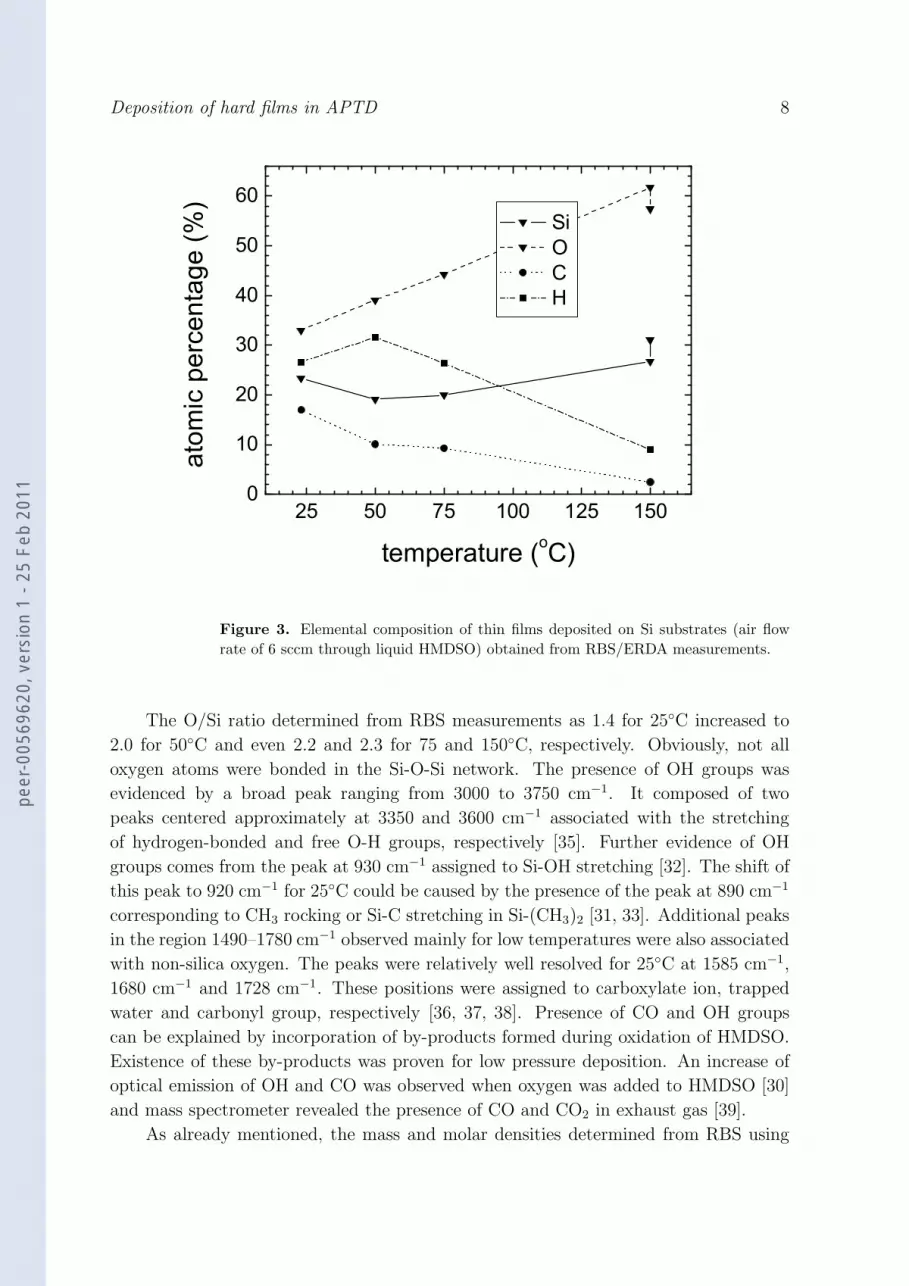
Figure 3. Elemental composition of thin films deposited on Si substrates (air flowrate of 6 sccm through liquid HMDSO) obtained from RBS/ERDA measurements.
The O/Si ratio determined from RBS measurements as 1.4 for 25◦C increased to
2.0 for 50◦C and even 2.2 and 2.3 for 75 and 150◦C, respectively. Obviously, not all
oxygen atoms were bonded in the Si-O-Si network. The presence of OH groups was
evidenced by a broad peak ranging from 3000 to 3750 cm−1. It composed of two
peaks centered approximately at 3350 and 3600 cm−1 associated with the stretching
of hydrogen-bonded and free O-H groups, respectively [35]. Further evidence of OH
groups comes from the peak at 930 cm−1 assigned to Si-OH stretching [32]. The shift of
this peak to 920 cm−1 for 25◦C could be caused by the presence of the peak at 890 cm−1
corresponding to CH3 rocking or Si-C stretching in Si-(CH3)2 [31, 33]. Additional peaks
in the region 1490–1780 cm−1 observed mainly for low temperatures were also associated
with non-silica oxygen. The peaks were relatively well resolved for 25◦C at 1585 cm−1,
1680 cm−1 and 1728 cm−1. These positions were assigned to carboxylate ion, trapped
water and carbonyl group, respectively [36, 37, 38]. Presence of CO and OH groups
can be explained by incorporation of by-products formed during oxidation of HMDSO.
Existence of these by-products was proven for low pressure deposition. An increase of
optical emission of OH and CO was observed when oxygen was added to HMDSO [30]
and mass spectrometer revealed the presence of CO and CO2 in exhaust gas [39].
As already mentioned, the mass and molar densities determined from RBS using
peer
-005
6962
0, v
ersi
on 1
- 25
Feb
201
1

Deposition of hard films in APTD 9
Figure 4. Mass and molar densities of thin films deposited on Si substrates (air flowrate of 6 sccm through liquid HMDSO) obtained from RBS measurements and knownfilm thickness determined by optical methods in UV/VIS/NIR.
known film thicknesses exhibited an increase when the deposition temperature was raised
from 25 to 50◦C and a further temperature increase led to a continuous increase of the
mass density (figure 4). The latter effect was rather related to the reduction of hydrogen
than to the closer packing of atoms as seen from the constant value of the molar density
and rapid decrease of hydrogen content illustrated in figure 3.
3.2.2. Films on glass substrates - air flow rate of 16 sccm The apparent differences
between the films on glass and Si substrates were caused by different instrumentation
used for the investigation of their chemical composition. The striking differences between
RBS/ERDA (figure 3) and XPS results (figure 5), i. e. differing amount of Si, O and C
as well as progressive changes of the composition with the deposition temperature, were
caused by the fact that the amount of hydrogen could not be determined by XPS. If
the RBS/ERDA results were recalculated without taking into account the hydrogen, the
atomic composition of the films deposited on Si at temperatures 50, 75 and 150◦C would
be very similar to the XPS results obtained after the film sputtering. The sputtering
was necessary because it removed carbon contamination of the film surface. This fact
is supported by RBS analyses of the films on Si in which the carbon content also
rapidly decreased to 2.5 at.% for the temperature of 150◦C. In agreement with RBS
the incorporation of nitrogen in the films was below 2 at.%.
peer
-005
6962
0, v
ersi
on 1
- 25
Feb
201
1

Deposition of hard films in APTD 10
Figure 5. Elemental composition of thin films deposited on glass substrates (air flowrate of 16 sccm through liquid HMDSO) obtained from XPS measurement.
The position of Si 2p XPS atomic signal, corrected for a sample charging,
corresponded to the binding energy (BE) of silicon oxides, 103.0–103.5 eV [40, 41, 42].
The corrections were performed by shifting the whole spectra to 285.0 eV of C 1s
signal. More detailed analyses of chemical bonding were obtained by peak fitting of
high resolution measurements of the C1s signals for the as-deposited samples. The
peaks were clearly asymmetric towards higher BE because of oxygen bonded to carbon.
A small peak related to these bonds was fitted at about 286.3 eV.
The FTIR-ATR spectra of the films deposited on glass at the same temperatures are
shown in figure 6. Since ATR measurements were restricted to the range above 530 cm−1,
only two of three characteristic absorption bands of silicon oxides could be observed.
Moreover, the ATR spectra are strongly influenced by the changes of refractive index
around the position of strong absorption peaks and, therefore, these peaks are shifted
to lower wavenumbers and any close peaks at lower wavenumbers increase in intensity.
These effects caused distortion of the FTIR-ATR spectra, when compared to FTIR
transmittances, in the region of strong absorption bands of silicon oxides. The peak of
Si-O-Si rocking vibrations was observed at 790 cm−1, i. e. shifted to lower wavenumbers
peer
-005
6962
0, v
ersi
on 1
- 25
Feb
201
1

Deposition of hard films in APTD 11
by 10–20 cm−1 with respect to the position observed in transmittances of the films
on Si. Similarly, the antisymmetric stretching peak moved to lower wavenumbers by
approximately 20 cm−1. Its shift from 1020 to 1050 cm−1 was again related to the
increased deposition temperature and the possible reasons have already been discussed
in details for the films on Si.
Figure 6. ATR spectra of thin films deposited on glass substrates (air flow rate of16 sccm through liquid HMDSO) for different substrate temperatures.
The stretching peak of the glass substrate was observed at very low wavenumber,
910 cm−1, and could be seen also in the spectra of the films as a weak shoulder at about
900 cm−1. The relatively strong peak observed at 920–940 cm−1 was associated to Si-OH
groups. Its high intensity, compared to transmittances of the films on Si, was caused
by the adjacent strong Si-O-Si stretching peak. Other absorption features and their
behaviour were similar as in the case of the films on Si. The absorption related to OH
groups was also detected in the region 3000–3700 cm−1. At temperatures above 25◦C,
some OH groups were not hydrogen-bonded as evidenced by the appearance of second
peak at higher frequencies, about 3600 cm−1. Absorption in the range 3300–3500 cm−1
could be influenced also by a presence of N-H stretching [35], but since the concentration
of nitrogen determined by XPS was below 2 %, its contribution was disregarded.
The presence of CH3 groups, reminiscent of original HMDSO reactant, was
peer
-005
6962
0, v
ersi
on 1
- 25
Feb
201
1

Deposition of hard films in APTD 12
significant especially at lower temperatures. As discussed for the films on Si, their
fingerprints were the peaks at 1265–1277 cm−1 and 1412 cm−1. The C-H stretching
absorption was also detected in the region 2830–3000 cm−1 as three sharp peaks.
Presence of additional groups, that do not have their origin in HMDSO, was revealed by
a multipeak absorption in the range 1520–1750◦C. It corresponded to several chemical
groups such as carboxylate ion, trapped water and carbonyl groups (see above).
3.3. Film optical properties in UV/VIS/NIR range and deposition rate
The UV/VIS/NIR optical properties and thickness of the films deposited on Si
using 6 sccm of air bubbling through liquid HMDSO were obtained from combined
ellipsometry and reflectometry. Measured data were fitted using a similar dispersion
model of the optical constants as in [13]. The model took into account an absorption in
the UV range resulting from interband transitions, existence of localized states inside the
band gap and a phonon absorption in IR. The interband transitions were described using
three parameters (i) band gap Eg, (ii) maximum energy limit of interband transitions
Eh and (iii) parameter proportional to the total density of states A. The transitions
corresponding to the localized states as well as the phonon absorption were both
parameterized by Gaussian broadened peaks. For details see [43]. Sample imperfections
such as non-uniformity and roughness were also taken into account.
The average film thickness obtained from the fitting was used for the calculation of
deposition rate plotted in figure 7. The deposition rate on Si decreased quadratically
with the deposition temperature. It was quite low as compared to the values reported
e. g. by Massines et al [17] because 4 ppm of HMDSO in their gas mixture resulted
in three times higher deposition rate. However, deposition rate is a function of several
parameters including a local supply of depleted precursor molecules that needs to be
optimized in our experimental set-up.
The optical properties, refractive index and extinction coefficient, are given in
figure 8 and figure 9. The refractive index did not exhibit any monotonic dependence
on the temperature. Its value at 632 nm ranged from 1.45 to 1.47. The film absorption
in UV range evidently decreased with the temperature. The extinction coefficient at
200 nm was in the range 0.014–0.030 for the films deposited at 23–75◦C. It decreased
down to 0.007 for 100◦C and even more to 0.001 for 120 and 150◦C. Therefore, the
material deposited at higher temperatures approaches the structure of SiO2 as already
suggested by the results of the previous section.
3.4. Film mechanical properties
In case of the indentation tests on thin films, the measured properties depend on the
indentation depth due to the combined response of the coating and the substrate (here
glass, silicon or polycarbonate). Therefore, the measured elastic modulus and hardness
values should be corrected for the substrate influence [44]. In the case of glass and
silicon substrates, the elastic modulus and the plastic hardness of the films were lower
peer
-005
6962
0, v
ersi
on 1
- 25
Feb
201
1

Deposition of hard films in APTD 13
Figure 7. Deposition rates for different substrate temperatures.
than those of the substrate and their values could be calculated using the approach of
Oliver and Pharr [45], if the indentation depth does not exceed approx. 10% of the
film thickness. The resulting film elastic modulus and plastic hardness increased with
increasing deposition temperature approaching the mechanical properties of SiO2 in the
temperature range 120–150◦C. The film microhardness in dependence on temperature
is depicted in figure 10.
In the case of films on polycarbonates, the hardness and elastic modulus of film
were always substantially higher than those of the substrate. Therefore, it represented
the system of a thin hard coating deposited on a soft viscoelastic-plastic substrate
(polycarbonate) and the conditions of the Oliver and Pharr method were not fulfilled.
The Martens hardness (HM) that measures both elastic and plastic resistances against
indentation was more suitable for the characterisation of the film/substrate systems.
The dependencies of HM on indentation depth for the films deposited at several different
deposition temperatures are shown in figure 11. According to this figure, the surface
hardness of the polycarbonate after nitrogen plasma treatment slightly decreased. The
films deposited at elevated temperatures, on the other hand, substantially increased its
surface hardness. The trend in the mechanical properties with increasing deposition
temperature was similar as for the glass and Si substrates. The films deposited at
the maximum temperature suitable for polycarbonate substrates, i. e. 120◦C, exhibited
peer
-005
6962
0, v
ersi
on 1
- 25
Feb
201
1

Deposition of hard films in APTD 14
Figure 8. Refractive index of the films deposited on silicon substrates.
mechanical properties very close to SiO2. However, crack creations were observed at
higher indentation depths as shown in figure 11. The crack creation may be suppressed
by deposition of film with graded structure increasing the temperature during the
deposition (i.e. with gradual change of film properties from polymer-like to SiO2)
[46, 47].
4. Conclusion
The plasma enhanced CVD of silicon oxide thin films was investigated in atmospheric
pressure Townsend-like discharge burning in nitrogen. The films were deposited from
the mixture of hexamethyldisiloxane (HMDSO) with oxygen in nitrogen working gas
on glass, silicon and polycarbonate substrates. The substrate temperature, varied from
25◦C to 150◦C, had significant influence on the film’s chemical structure and functional
properties. The increasing deposition temperature resulted in a decreasing content of
carbon and hydrogen and an increasing oxygen-to-silicon ratio in the films. This ratio
reached 2.3 for 150◦C but not all the oxygen atoms were bonded in the Si-O-Si network
as revealed by the presence of OH groups in the FTIR spectra. The hardness of the
films on the glass and silicon substrates increased with increasing substrate temperature
from 0.4 GPa to 7 GPa. Increasing temperature caused increased hardness also for the
peer
-005
6962
0, v
ersi
on 1
- 25
Feb
201
1

Deposition of hard films in APTD 15
Figure 9. Extinction coefficient of the films deposited on silicon substrates.
films on polycarbonate substrates. The Martens hardness of the film/polycarbonate
system for the deposition temperature of 120◦C was several times higher than this of
bare polycarbonate at small indentation depths. The deposition rate decreased with
increasing temperature from 5 nm min−1 at 25◦C to 2.8 nm min−1 at 150◦C. However,
the chemical structure, optical and mechanical properties of the films deposited at 150◦C
approached those of SiO2 films deposited in low pressure discharges [12, 48].
Acknowledgments
The present work was supported by the Ministry of Education of the Czech Republic
under contract MSM0021622411 and by Institutional Research Plan No. AV0Z10100521
and by the Czech Science Foundation under contract 104/09/H080. The authors are
grateful to M Kunovsky for his technical help.
References
[1] Kanazawa S, Kogoma M, Moriwaki T and Okazaki S 1988 J. Phys. D: Appl Phys. 21 838[2] Trunec D, Brablec A and Buchta J 2001 J. Phys. D: Appl. Phys. 34 1697[3] Gherardi N, Gouda G, Gat E, Ricard A and Massines F 2000 Plasma Sources Sci. Technol. 9 340[4] Sawada Y, Ogawa S and Kogoma M 1995 J. Phys. D: Appl Phys. 28 1661
peer
-005
6962
0, v
ersi
on 1
- 25
Feb
201
1

Deposition of hard films in APTD 16
Figure 10. The film microhardness for different deposition conditions. The numbersat curves indicate air flow in sccm / nitrogen flow in slm during the deposition.
[5] Prat R, Koh Y J, Babukutty Y, Kogoma M, Okazaki S and Kodama M 2000 Polymer 41 7355[6] Gherardi N, Martin S and Massines F 2000 J. Phys. D: Appl Phys. 33 L104[7] Foest R, Adler F, Sigeneger F and Schmidt M 2003 Surf. Coating Technol. 163-164 323[8] Starostine S, Aldea E, de Vries H, Creatore M and van de Sanden M. C. M. 2007 Plasma Process.
Polym. 4 S440[9] Massines F, Gherardi N, Naude N and Segur P 2009 Eur. J. Phys. - Appl. Phys. 47 22805
[10] Aldea E, Peeters P, de Vries H and van de Sanden M C M 2005 Surf. Coat. Technol. 200 46[11] Wrobel A M and Wertheimer M R 1990 Plasma Deposition, Treatment and Etching of Polymers
ed. R d’Agostino (New York: Academic Press)[12] Zajıckova L, Bursıkova V, Kucerova Z, Franta D, Dvorak P, Smıd R, Perina V and Mackova A
2007 Plasma Sources Sci. Technol. 16 S123[13] Zajıckova L, Bursıkova V, Franta D, Bousquet A, Granier A, Goullet A and Bursık J 2007 Plasma
Process. Polym. 4 S287[14] Sonnenfeld A, Tun T M, Zajıckova L, Kozlov K V, Wagner H-E, Behnke J F and Hippler R 2001
Plasmas and Polymers 6 266[15] Trunec D, Navratil Z, Stahel P, Zajıckova L, Bursıkova V and Cech J 2004 J. Phys. D: Appl. Phys.
37 2112[16] Cech J, Stahel P, Sıra M, Bursıkova V, Navratil Z, Trunec D and Brablec A 2005 Chemicke listy
99 444[17] Massines F, Gherardi N, Fornelli and Martin S 2005 Surf. Coat. Technol. 200 1855[18] Caquineau H, Enache I, Gherardi N, Naude N and Massines F 2009 J. Phys. D: Appl. Phys. 42
peer
-005
6962
0, v
ersi
on 1
- 25
Feb
201
1

Deposition of hard films in APTD 17
Figure 11. The Martens hardness of films on polycarbonate at different depositiontemperatures using air flow rate of 16 sccm compared with the Martens hardness ofpolycarbonate treated in nitrogen plasma.
125201[19] Sıra M 2009 PhD thesis (Brno: Masaryk University) http://is.muni.cz/th/13705/prif d/dis-
is.muni.cz.pdf p. 78[20] Saarilahti J and Rauhala E 1992 Nucl. Instr. and Meth. B B64 734[21] Mayer M 1997 SIMNRA User’s Guide, Report IPP 9/113 (Garching: Max-Planck-Institut fuer
Plasmaphysik)[22] Ohlıdal I and Franta D 2000 Progress in Optics vol 41 (Amsterdam: Elsevier)[23] Martinet C and Devine R A B 1995 J. Appl. Phys. 77 4343[24] He L, Inokuma T, Kurata Y and Hasegawa S 1995 J. Non-Crystall. Solids 185 249[25] Kucırkova A, Navratil K, Pajasova L and Vorlıcek V 1996 Appl. Phys. A 63 495[26] Devine R A B 1992 Trans. Mater. Res. Soc. Jpn. 8 165[27] Kashiwagi K, Yoshida Y and Murayama Y 1991 Jap. J. Appl. Phys. 30 1803[28] Durrant S F, Mota R P and de Moraes M A B 1996 Vacuum 47 187[29] Kim M T 1997 Thin Solid Films 311 157[30] Aumaille K, Vallee C, Granier A, Goullet A, Gaboriau F and Turban G 2000 Thin Solid Films
359 188[31] Rau C and Kulisch W 1994 Thin Solid Films 249 28[32] Lamendola R, D’Agostino R and Fracassi F 1997 Plasmas and Polymers 2 147[33] Anderson D R 1974 Analysis of Silicones (New York: Wiley-Interscience)
peer
-005
6962
0, v
ersi
on 1
- 25
Feb
201
1

Deposition of hard films in APTD 18
[34] Dischler B, Bubenzer A and Koidl P 1983 Solid State Commun. 48 105[35] Mayo D, Miller F A and Hannah R W 2004 Course Notes on the Interpretation of Infrared and
Raman Spectra (New York: Wiley-Interscience) chap 6[36] Mayo D, Miller F A and Hannah R W 2004 Course Notes on the Interpretation of Infrared and
Raman Spectra (New York: Wiley-Interscience) p 210[37] http://webbook.nist.gov/cgi/cbook.cgi?ID=C7732185&Units=SI&Mask=80 (December 2009).[38] Mayo D, Miller F A and Hannah R W 2004 Course Notes on the Interpretation of Infrared and
Raman Spectra (New York: Wiley-Interscience) chap 7[39] Alexander M R, Jones F R and Short R D 1997 Plasmas and Polymers 2 277[40] Alexander M R, Short R D, Jones F R, Stollenwerk J Z M and Michaeli W 1996 J. Mater. Sci.
31 1879[41] Gengenbach T R and Griesser H J 1999 Polymer 40 5079[42] Moulder J F, Sticle W F, Sobol P E and Bomben K D 1992 Handbook of X-ray Photoelectron
Spectroscopy (Eden Prairie: Perkin-Elmer Co.)[43] Franta D, Necas D and Zajıckova L 2007 Optics Express 15 16230[44] Battacharya A K and Nix W D 2001 Int. J. Solids Struct 38 335[45] Pharr G M, Oliver W C and Brotzen F R 1992 J. Mater. Res. 7 613[46] Schulz U and Kaiser N 2006 Prog. Surf. Sci. 81 387[47] Poitras D and Martinu L 2000 Appl. Opt. 39 1168[48] Zajıckova L, Bursıkova V, Kucerova Z, Franclova J, Stahel P, Perina V and Mackova A 2007 J.
Phys. Chem. Solids 68 1255
peer
-005
6962
0, v
ersi
on 1
- 25
Feb
201
1