DDR4 SDRAM - Micron Technology
391
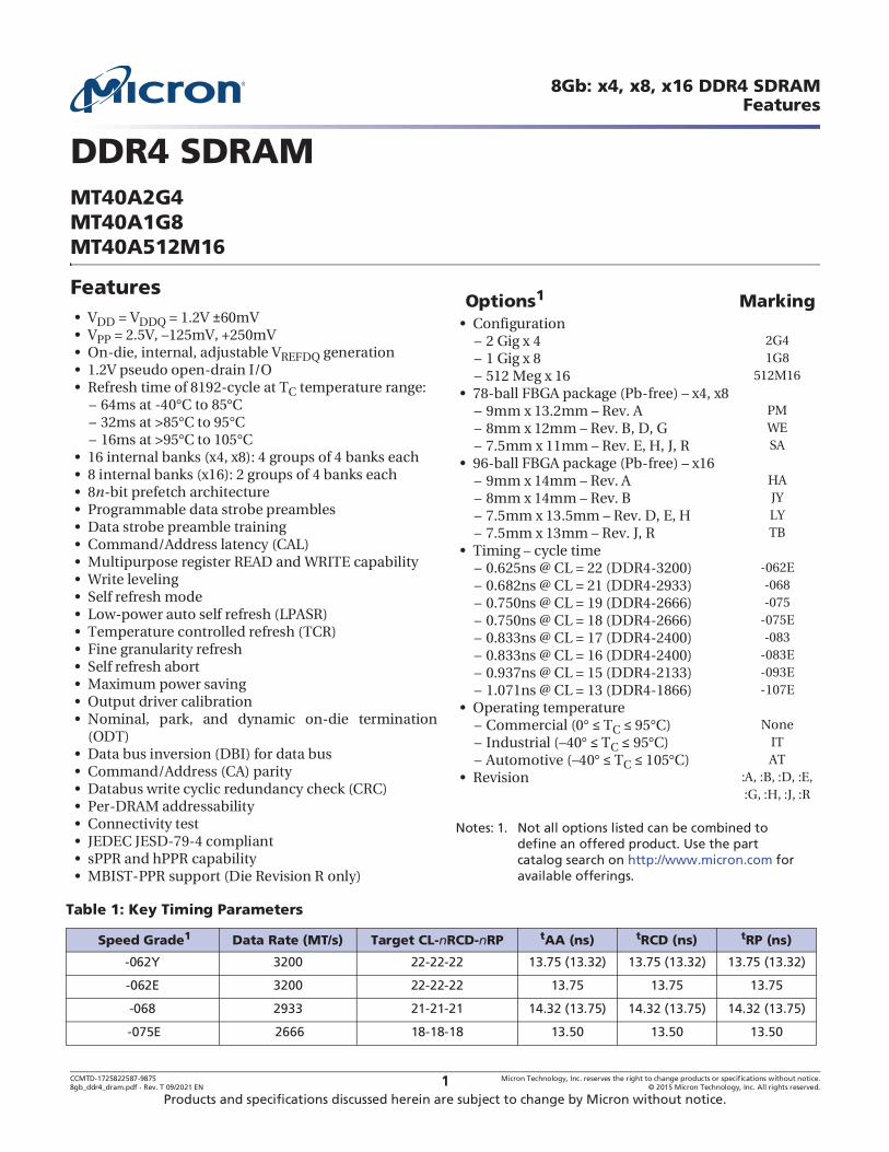
8Gb: x4, x8, x16 DDR4 SDRAM Features CCMTD-1725822587-9875 Micron Technology, Inc. reserves the right to change products or specifications without notice. 8gb_ddr4_dram.pdf - Rev. T 09/2021 EN 2015 Micron Technology, Inc. All rights reserved. Products and specifications discussed herein are subject to change by Micron without notice. 1 DDR4 SDRAM MT40A2G4 MT40A1G8 MT40A512M16 Features Notes: 1. Not all options listed can be combined to define an offered product. Use the part catalog search on http://www.micron.com for available offerings. V DD = V DDQ = 1.2V ά60mV V PP On-die, internal, adjustable V REFDQ generation 1.2V pseudo open-drain I/O Refresh time of 8192-cycle at T C temperature range: 64ms at -40ιC to 85ιC 32ms at >85ιC to 95ιC 16ms at >95ιC to 105ιC 16 internal banks (x4, x8): 4 groups of 4 banks each 8 internal banks (x16): 2 groups of 4 banks each 8n-bit prefetch architecture Programmable data strobe preambles Data strobe preamble training Command/Address latency (CAL) Multipurpose register READ and WRITE capability Write leveling Self refresh mode Low-power auto self refresh (LPASR) Temperature controlled refresh (TCR) Fine granularity refresh Self refresh abort Maximum power saving Output driver calibration Nominal, park, and dynamic on-die termination (ODT) Data bus inversion (DBI) for data bus Command/Address (CA) parity Databus write cyclic redundancy check (CRC) Per-DRAM addressability Connectivity test JEDEC JESD-79-4 compliant sPPR and hPPR capability MBIST-PPR support (Die Revision R only) Options 1 Marking Configuration 2 Gig x 4 2G4 1 Gig x 8 1G8 512 Meg x 16 512M16 PM WE SA HA JY LY TB 0.625ns @ CL = 22 (DDR4-3200) -062E 0.682ns @ CL = 21 (DDR4-2933) -068 0.750ns @ CL = 19 (DDR4-2666) -075 0.750ns @ CL = 18 (DDR4-2666) -075E 0.833ns @ CL = 17 (DDR4-2400) -083 0.833ns @ CL = 16 (DDR4-2400) -083E 0.937ns @ CL = 15 (DDR4-2133) -093E 1.071ns @ CL = 13 (DDR4-1866) -107E Operating temperature Commercial (0ι ζ T C ζ 95ιC) None ι ζ T C ζ 95ιC) IT ι ζ T C ζ 105ιC) AT Revision :A, :B, :D, :E, :G, :H, :J, :R Table 1: Key Timing Parameters Speed Grade 1 Data Rate (MT/s) Target CL-nRCD-nRP t AA (ns) t RCD (ns) t RP (ns) -062Y 3200 22-22-22 13.75 (13.32) 13.75 (13.32) 13.75 (13.32) -062E 3200 22-22-22 13.75 13.75 13.75 -068 2933 21-21-21 14.32 (13.75) 14.32 (13.75) 14.32 (13.75) -075E 2666 18-18-18 13.50 13.50 13.50
-
Upload
khangminh22 -
Category
Documents
-
view
1 -
download
0
Transcript of DDR4 SDRAM - Micron Technology
8Gb: x4, x8, x16 DDR4 SDRAMFeatures
CCMTD-1725822587-9875 Micron Technology, Inc. reserves the right to change products or specifications without notice.8gb_ddr4_dram.pdf - Rev. T 09/2021 EN 2015 Micron Technology, Inc. All rights reserved.
Products and specifications discussed herein are subject to change by Micron without notice.1
DDR4 SDRAMMT40A2G4MT40A1G8MT40A512M16
Features
Notes: 1. Not all options listed can be combined to define an offered product. Use the part catalog search on http://www.micron.com for available offerings.
VDD = VDDQ = 1.2V 60mVVPPOn-die, internal, adjustable VREFDQ generation1.2V pseudo open-drain I/ORefresh time of 8192-cycle at TC temperature range:
64ms at -40 C to 85 C32ms at >85 C to 95 C16ms at >95 C to 105 C
16 internal banks (x4, x8): 4 groups of 4 banks each8 internal banks (x16): 2 groups of 4 banks each8n-bit prefetch architectureProgrammable data strobe preamblesData strobe preamble trainingCommand/Address latency (CAL)Multipurpose register READ and WRITE capabilityWrite levelingSelf refresh modeLow-power auto self refresh (LPASR)Temperature controlled refresh (TCR)Fine granularity refreshSelf refresh abortMaximum power savingOutput driver calibrationNominal, park, and dynamic on-die termination(ODT)Data bus inversion (DBI) for data busCommand/Address (CA) parityDatabus write cyclic redundancy check (CRC)Per-DRAM addressabilityConnectivity testJEDEC JESD-79-4 compliantsPPR and hPPR capabilityMBIST-PPR support (Die Revision R only)
Options1 MarkingConfiguration
2 Gig x 4 2G41 Gig x 8 1G8512 Meg x 16 512M16
PMWESA
HAJYLYTB
0.625ns @ CL = 22 (DDR4-3200) -062E0.682ns @ CL = 21 (DDR4-2933) -0680.750ns @ CL = 19 (DDR4-2666) -0750.750ns @ CL = 18 (DDR4-2666) -075E0.833ns @ CL = 17 (DDR4-2400) -0830.833ns @ CL = 16 (DDR4-2400) -083E0.937ns @ CL = 15 (DDR4-2133) -093E1.071ns @ CL = 13 (DDR4-1866) -107E
Operating temperatureCommercial (0 TC 95 C) None
TC 95 C) IT TC 105 C) AT
Revision :A, :B, :D, :E,:G, :H, :J, :R
Table 1: Key Timing Parameters
Speed Grade1 Data Rate (MT/s) Target CL-nRCD-nRP tAA (ns) tRCD (ns) tRP (ns)
-062Y 3200 22-22-22 13.75 (13.32) 13.75 (13.32) 13.75 (13.32)
-062E 3200 22-22-22 13.75 13.75 13.75
-068 2933 21-21-21 14.32 (13.75) 14.32 (13.75) 14.32 (13.75)
-075E 2666 18-18-18 13.50 13.50 13.50
CCMTD-1725822587-9875 Micron Technology, Inc. reserves the right to change products or specifications without notice.8gb_ddr4_dram.pdf - Rev. T 09/2021 EN 2015 Micron Technology, Inc. All rights reserved.2
8Gb: x4, x8, x16 DDR4 SDRAMFeatures
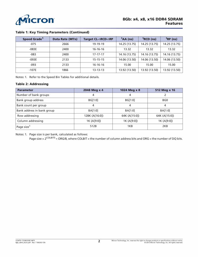
Notes: 1. Refer to the Speed Bin Tables for additional details.
Notes: 1. Page size is per bank, calculated as follows:
Page size = 2COLBITS ORG/8, where COLBIT = the number of column address bits and ORG = the number of DQ bits.
-075 2666 19-19-19 14.25 (13.75) 14.25 (13.75) 14.25 (13.75)
-083E 2400 16-16-16 13.32 13.32 13.32
-083 2400 17-17-17 14.16 (13.75) 14.16 (13.75) 14.16 (13.75)
-093E 2133 15-15-15 14.06 (13.50) 14.06 (13.50) 14.06 (13.50)
-093 2133 16-16-16 15.00 15.00 15.00
-107E 1866 13-13-13 13.92 (13.50) 13.92 (13.50) 13.92 (13.50)
Table 2: Addressing
Parameter 2048 Meg x 4 1024 Meg x 8 512 Meg x 16
Number of bank groups 4 4 2
Bank group address BG[1:0] BG[1:0] BG0
Bank count per group 4 4 4
Bank address in bank group BA[1:0] BA[1:0] BA[1:0]
Row addressing 128K (A[16:0]) 64K (A[15:0]) 64K (A[15:0])
Column addressing 1K (A[9:0]) 1K (A[9:0]) 1K (A[9:0])
Page size1 512B 1KB 2KB
Table 1: Key Timing Parameters (Continued)
Speed Grade1 Data Rate (MT/s) Target CL-nRCD-nRP tAA (ns) tRCD (ns) tRP (ns)

CCMTD-1725822587-9875 Micron Technology, Inc. reserves the right to change products or specifications without notice.8gb_ddr4_dram.pdf - Rev. T 09/2021 EN © 2015 Micron Technology, Inc. All rights reserved.3
8Gb: x4, x8, x16 DDR4 SDRAMFeatures
Figure 1: Order Part Number Example
Example Part Number: MT40A1G8SA-062E:R
Configuration
2 Gig x 4 2G4
1 Gig x 8
512 Meg x 16
1G8
512M16
-
ConfigurationMT40A Package Speed Revision
:
{
Package Mark
78-ball 9.0mm x 13.2mm FBGA PM
78-ball 8.0mm x 12.0mm FBGA WE
78-ball 7.5mm x 11.0mm FBGA SA
96-ball 9.0mm x 14.0mm FBGA HA
96-ball 8.0mm x 14.0mm FBGA JY
96-ball 7.5mm x 13.5mm FBGA LY
96-ball 7.5mm x 13.0mm FBGA TB
:A, :B, :D, :G, :E, :H, :J, :R
Die Revision
SpeedGrade
-107E
-093E
tCK = 1.071ns, CL = 13tCK = 0.937ns, CL = 15
-083E tCK = 0.833ns, CL = 16
-083 tCK = 0.833ns, CL = 17
-075E tCK = 0.750ns, CL = 18
-075 tCK = 0.750ns, CL = 19
-068 t
tCK = 0.682ns, CL = 21
-062E CK = 0.625ns, CL = 22
Cycle Time, CAS Latency
Commercial
Industrial
Extended
None
IT
AT
Case Temperature Mark
c_8Gb_features_current.dita Page 3
CCMTD-1725822587-9875 Micron Technology, Inc. reserves the right to change products or specifications without notice.8gb_ddr4_dram.pdf - Rev. T 09/2021 EN 2015 Micron Technology, Inc. All rights reserved.4
8Gb: x4, x8, x16 DDR4 SDRAM
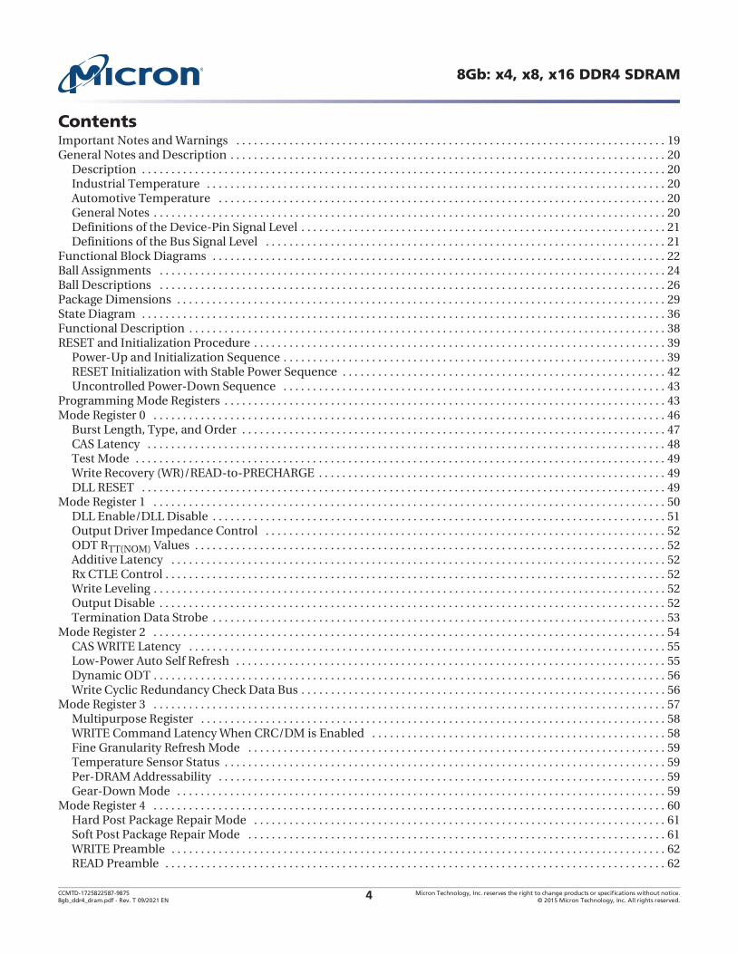
ContentsImportant Notes and Warnings . . . . . . . . . . . . . . . . . . . . . . . . . . . . . . . . . . . . . . . . . . . . . . . . . . . . . . . . . . . . . . . . . . . . . . . . . 19General Notes and Description . . . . . . . . . . . . . . . . . . . . . . . . . . . . . . . . . . . . . . . . . . . . . . . . . . . . . . . . . . . . . . . . . . . . . . . . . . 20
Description . . . . . . . . . . . . . . . . . . . . . . . . . . . . . . . . . . . . . . . . . . . . . . . . . . . . . . . . . . . . . . . . . . . . . . . . . . . . . . . . . . . . . . . . . 20Industrial Temperature . . . . . . . . . . . . . . . . . . . . . . . . . . . . . . . . . . . . . . . . . . . . . . . . . . . . . . . . . . . . . . . . . . . . . . . . . . . . . . 20Automotive Temperature . . . . . . . . . . . . . . . . . . . . . . . . . . . . . . . . . . . . . . . . . . . . . . . . . . . . . . . . . . . . . . . . . . . . . . . . . . . . 20General Notes . . . . . . . . . . . . . . . . . . . . . . . . . . . . . . . . . . . . . . . . . . . . . . . . . . . . . . . . . . . . . . . . . . . . . . . . . . . . . . . . . . . . . . . 20Definitions of the Device-Pin Signal Level . . . . . . . . . . . . . . . . . . . . . . . . . . . . . . . . . . . . . . . . . . . . . . . . . . . . . . . . . . . . . . 21Definitions of the Bus Signal Level . . . . . . . . . . . . . . . . . . . . . . . . . . . . . . . . . . . . . . . . . . . . . . . . . . . . . . . . . . . . . . . . . . . . 21
Functional Block Diagrams . . . . . . . . . . . . . . . . . . . . . . . . . . . . . . . . . . . . . . . . . . . . . . . . . . . . . . . . . . . . . . . . . . . . . . . . . . . . . 22Ball Assignments . . . . . . . . . . . . . . . . . . . . . . . . . . . . . . . . . . . . . . . . . . . . . . . . . . . . . . . . . . . . . . . . . . . . . . . . . . . . . . . . . . . . . . 24Ball Descriptions . . . . . . . . . . . . . . . . . . . . . . . . . . . . . . . . . . . . . . . . . . . . . . . . . . . . . . . . . . . . . . . . . . . . . . . . . . . . . . . . . . . . . . 26Package Dimensions . . . . . . . . . . . . . . . . . . . . . . . . . . . . . . . . . . . . . . . . . . . . . . . . . . . . . . . . . . . . . . . . . . . . . . . . . . . . . . . . . . . 29State Diagram . . . . . . . . . . . . . . . . . . . . . . . . . . . . . . . . . . . . . . . . . . . . . . . . . . . . . . . . . . . . . . . . . . . . . . . . . . . . . . . . . . . . . . . . . 36Functional Description . . . . . . . . . . . . . . . . . . . . . . . . . . . . . . . . . . . . . . . . . . . . . . . . . . . . . . . . . . . . . . . . . . . . . . . . . . . . . . . . . 38RESET and Initialization Procedure . . . . . . . . . . . . . . . . . . . . . . . . . . . . . . . . . . . . . . . . . . . . . . . . . . . . . . . . . . . . . . . . . . . . . . 39
Power-Up and Initialization Sequence . . . . . . . . . . . . . . . . . . . . . . . . . . . . . . . . . . . . . . . . . . . . . . . . . . . . . . . . . . . . . . . . . 39RESET Initialization with Stable Power Sequence . . . . . . . . . . . . . . . . . . . . . . . . . . . . . . . . . . . . . . . . . . . . . . . . . . . . . . . 42Uncontrolled Power-Down Sequence . . . . . . . . . . . . . . . . . . . . . . . . . . . . . . . . . . . . . . . . . . . . . . . . . . . . . . . . . . . . . . . . . 43
Programming Mode Registers . . . . . . . . . . . . . . . . . . . . . . . . . . . . . . . . . . . . . . . . . . . . . . . . . . . . . . . . . . . . . . . . . . . . . . . . . . . 43Mode Register 0 . . . . . . . . . . . . . . . . . . . . . . . . . . . . . . . . . . . . . . . . . . . . . . . . . . . . . . . . . . . . . . . . . . . . . . . . . . . . . . . . . . . . . . . 46
Burst Length, Type, and Order . . . . . . . . . . . . . . . . . . . . . . . . . . . . . . . . . . . . . . . . . . . . . . . . . . . . . . . . . . . . . . . . . . . . . . . . 47CAS Latency . . . . . . . . . . . . . . . . . . . . . . . . . . . . . . . . . . . . . . . . . . . . . . . . . . . . . . . . . . . . . . . . . . . . . . . . . . . . . . . . . . . . . . . . 48Test Mode . . . . . . . . . . . . . . . . . . . . . . . . . . . . . . . . . . . . . . . . . . . . . . . . . . . . . . . . . . . . . . . . . . . . . . . . . . . . . . . . . . . . . . . . . . 49Write Recovery (WR)/READ-to-PRECHARGE . . . . . . . . . . . . . . . . . . . . . . . . . . . . . . . . . . . . . . . . . . . . . . . . . . . . . . . . . . . 49DLL RESET . . . . . . . . . . . . . . . . . . . . . . . . . . . . . . . . . . . . . . . . . . . . . . . . . . . . . . . . . . . . . . . . . . . . . . . . . . . . . . . . . . . . . . . . . 49
Mode Register 1 . . . . . . . . . . . . . . . . . . . . . . . . . . . . . . . . . . . . . . . . . . . . . . . . . . . . . . . . . . . . . . . . . . . . . . . . . . . . . . . . . . . . . . . 50DLL Enable/DLL Disable . . . . . . . . . . . . . . . . . . . . . . . . . . . . . . . . . . . . . . . . . . . . . . . . . . . . . . . . . . . . . . . . . . . . . . . . . . . . . 51Output Driver Impedance Control . . . . . . . . . . . . . . . . . . . . . . . . . . . . . . . . . . . . . . . . . . . . . . . . . . . . . . . . . . . . . . . . . . . . 52ODT RTT(NOM) Values . . . . . . . . . . . . . . . . . . . . . . . . . . . . . . . . . . . . . . . . . . . . . . . . . . . . . . . . . . . . . . . . . . . . . . . . . . . . . . . . 52Additive Latency . . . . . . . . . . . . . . . . . . . . . . . . . . . . . . . . . . . . . . . . . . . . . . . . . . . . . . . . . . . . . . . . . . . . . . . . . . . . . . . . . . . . 52Rx CTLE Control . . . . . . . . . . . . . . . . . . . . . . . . . . . . . . . . . . . . . . . . . . . . . . . . . . . . . . . . . . . . . . . . . . . . . . . . . . . . . . . . . . . . . 52Write Leveling . . . . . . . . . . . . . . . . . . . . . . . . . . . . . . . . . . . . . . . . . . . . . . . . . . . . . . . . . . . . . . . . . . . . . . . . . . . . . . . . . . . . . . . 52Output Disable . . . . . . . . . . . . . . . . . . . . . . . . . . . . . . . . . . . . . . . . . . . . . . . . . . . . . . . . . . . . . . . . . . . . . . . . . . . . . . . . . . . . . . 52Termination Data Strobe . . . . . . . . . . . . . . . . . . . . . . . . . . . . . . . . . . . . . . . . . . . . . . . . . . . . . . . . . . . . . . . . . . . . . . . . . . . . . 53
Mode Register 2 . . . . . . . . . . . . . . . . . . . . . . . . . . . . . . . . . . . . . . . . . . . . . . . . . . . . . . . . . . . . . . . . . . . . . . . . . . . . . . . . . . . . . . . 54CAS WRITE Latency . . . . . . . . . . . . . . . . . . . . . . . . . . . . . . . . . . . . . . . . . . . . . . . . . . . . . . . . . . . . . . . . . . . . . . . . . . . . . . . . . 55Low-Power Auto Self Refresh . . . . . . . . . . . . . . . . . . . . . . . . . . . . . . . . . . . . . . . . . . . . . . . . . . . . . . . . . . . . . . . . . . . . . . . . . 55Dynamic ODT . . . . . . . . . . . . . . . . . . . . . . . . . . . . . . . . . . . . . . . . . . . . . . . . . . . . . . . . . . . . . . . . . . . . . . . . . . . . . . . . . . . . . . . 56Write Cyclic Redundancy Check Data Bus . . . . . . . . . . . . . . . . . . . . . . . . . . . . . . . . . . . . . . . . . . . . . . . . . . . . . . . . . . . . . . 56
Mode Register 3 . . . . . . . . . . . . . . . . . . . . . . . . . . . . . . . . . . . . . . . . . . . . . . . . . . . . . . . . . . . . . . . . . . . . . . . . . . . . . . . . . . . . . . . 57Multipurpose Register . . . . . . . . . . . . . . . . . . . . . . . . . . . . . . . . . . . . . . . . . . . . . . . . . . . . . . . . . . . . . . . . . . . . . . . . . . . . . . . 58WRITE Command Latency When CRC/DM is Enabled . . . . . . . . . . . . . . . . . . . . . . . . . . . . . . . . . . . . . . . . . . . . . . . . . . 58Fine Granularity Refresh Mode . . . . . . . . . . . . . . . . . . . . . . . . . . . . . . . . . . . . . . . . . . . . . . . . . . . . . . . . . . . . . . . . . . . . . . . 59Temperature Sensor Status . . . . . . . . . . . . . . . . . . . . . . . . . . . . . . . . . . . . . . . . . . . . . . . . . . . . . . . . . . . . . . . . . . . . . . . . . . . 59Per-DRAM Addressability . . . . . . . . . . . . . . . . . . . . . . . . . . . . . . . . . . . . . . . . . . . . . . . . . . . . . . . . . . . . . . . . . . . . . . . . . . . . 59Gear-Down Mode . . . . . . . . . . . . . . . . . . . . . . . . . . . . . . . . . . . . . . . . . . . . . . . . . . . . . . . . . . . . . . . . . . . . . . . . . . . . . . . . . . . 59
Mode Register 4 . . . . . . . . . . . . . . . . . . . . . . . . . . . . . . . . . . . . . . . . . . . . . . . . . . . . . . . . . . . . . . . . . . . . . . . . . . . . . . . . . . . . . . . 60Hard Post Package Repair Mode . . . . . . . . . . . . . . . . . . . . . . . . . . . . . . . . . . . . . . . . . . . . . . . . . . . . . . . . . . . . . . . . . . . . . . 61Soft Post Package Repair Mode . . . . . . . . . . . . . . . . . . . . . . . . . . . . . . . . . . . . . . . . . . . . . . . . . . . . . . . . . . . . . . . . . . . . . . . 61WRITE Preamble . . . . . . . . . . . . . . . . . . . . . . . . . . . . . . . . . . . . . . . . . . . . . . . . . . . . . . . . . . . . . . . . . . . . . . . . . . . . . . . . . . . . 62READ Preamble . . . . . . . . . . . . . . . . . . . . . . . . . . . . . . . . . . . . . . . . . . . . . . . . . . . . . . . . . . . . . . . . . . . . . . . . . . . . . . . . . . . . . 62

CCMTD-1725822587-9875 Micron Technology, Inc. reserves the right to change products or specifications without notice.8gb_ddr4_dram.pdf - Rev. T 09/2021 EN 2015 Micron Technology, Inc. All rights reserved.5
8Gb: x4, x8, x16 DDR4 SDRAM
READ Preamble Training . . . . . . . . . . . . . . . . . . . . . . . . . . . . . . . . . . . . . . . . . . . . . . . . . . . . . . . . . . . . . . . . . . . . . . . . . . . . . 62Temperature-Controlled Refresh . . . . . . . . . . . . . . . . . . . . . . . . . . . . . . . . . . . . . . . . . . . . . . . . . . . . . . . . . . . . . . . . . . . . . . 62Command Address Latency . . . . . . . . . . . . . . . . . . . . . . . . . . . . . . . . . . . . . . . . . . . . . . . . . . . . . . . . . . . . . . . . . . . . . . . . . . 62Internal VREF Monitor . . . . . . . . . . . . . . . . . . . . . . . . . . . . . . . . . . . . . . . . . . . . . . . . . . . . . . . . . . . . . . . . . . . . . . . . . . . . . . . . 62Maximum Power Savings Mode . . . . . . . . . . . . . . . . . . . . . . . . . . . . . . . . . . . . . . . . . . . . . . . . . . . . . . . . . . . . . . . . . . . . . . . 62MBIST-PPR . . . . . . . . . . . . . . . . . . . . . . . . . . . . . . . . . . . . . . . . . . . . . . . . . . . . . . . . . . . . . . . . . . . . . . . . . . . . . . . . . . . . . . . . . 63
Mode Register 5 . . . . . . . . . . . . . . . . . . . . . . . . . . . . . . . . . . . . . . . . . . . . . . . . . . . . . . . . . . . . . . . . . . . . . . . . . . . . . . . . . . . . . . . 64Data Bus Inversion . . . . . . . . . . . . . . . . . . . . . . . . . . . . . . . . . . . . . . . . . . . . . . . . . . . . . . . . . . . . . . . . . . . . . . . . . . . . . . . . . . 65Data Mask . . . . . . . . . . . . . . . . . . . . . . . . . . . . . . . . . . . . . . . . . . . . . . . . . . . . . . . . . . . . . . . . . . . . . . . . . . . . . . . . . . . . . . . . . . 65CA Parity Persistent Error Mode . . . . . . . . . . . . . . . . . . . . . . . . . . . . . . . . . . . . . . . . . . . . . . . . . . . . . . . . . . . . . . . . . . . . . . . 66ODT Input Buffer for Power-Down . . . . . . . . . . . . . . . . . . . . . . . . . . . . . . . . . . . . . . . . . . . . . . . . . . . . . . . . . . . . . . . . . . . . 66CA Parity Error Status . . . . . . . . . . . . . . . . . . . . . . . . . . . . . . . . . . . . . . . . . . . . . . . . . . . . . . . . . . . . . . . . . . . . . . . . . . . . . . . . 66CRC Error Status . . . . . . . . . . . . . . . . . . . . . . . . . . . . . . . . . . . . . . . . . . . . . . . . . . . . . . . . . . . . . . . . . . . . . . . . . . . . . . . . . . . . 66CA Parity Latency Mode . . . . . . . . . . . . . . . . . . . . . . . . . . . . . . . . . . . . . . . . . . . . . . . . . . . . . . . . . . . . . . . . . . . . . . . . . . . . . . 66
Mode Register 6 . . . . . . . . . . . . . . . . . . . . . . . . . . . . . . . . . . . . . . . . . . . . . . . . . . . . . . . . . . . . . . . . . . . . . . . . . . . . . . . . . . . . . . . 67Data Rate Programming . . . . . . . . . . . . . . . . . . . . . . . . . . . . . . . . . . . . . . . . . . . . . . . . . . . . . . . . . . . . . . . . . . . . . . . . . . . . . . 68VREFDQ Calibration Enable . . . . . . . . . . . . . . . . . . . . . . . . . . . . . . . . . . . . . . . . . . . . . . . . . . . . . . . . . . . . . . . . . . . . . . . . . . . 68VREFDQ Calibration Range . . . . . . . . . . . . . . . . . . . . . . . . . . . . . . . . . . . . . . . . . . . . . . . . . . . . . . . . . . . . . . . . . . . . . . . . . . . . 68VREFDQ Calibration Value . . . . . . . . . . . . . . . . . . . . . . . . . . . . . . . . . . . . . . . . . . . . . . . . . . . . . . . . . . . . . . . . . . . . . . . . . . . . . 68Truth Tables . . . . . . . . . . . . . . . . . . . . . . . . . . . . . . . . . . . . . . . . . . . . . . . . . . . . . . . . . . . . . . . . . . . . . . . . . . . . . . . . . . . . . . . . 69
NOP Command . . . . . . . . . . . . . . . . . . . . . . . . . . . . . . . . . . . . . . . . . . . . . . . . . . . . . . . . . . . . . . . . . . . . . . . . . . . . . . . . . . . . . . . 74DESELECT Command . . . . . . . . . . . . . . . . . . . . . . . . . . . . . . . . . . . . . . . . . . . . . . . . . . . . . . . . . . . . . . . . . . . . . . . . . . . . . . . . . . 74DLL-Off Mode . . . . . . . . . . . . . . . . . . . . . . . . . . . . . . . . . . . . . . . . . . . . . . . . . . . . . . . . . . . . . . . . . . . . . . . . . . . . . . . . . . . . . . . . . 74DLL-On/Off Switching Procedures . . . . . . . . . . . . . . . . . . . . . . . . . . . . . . . . . . . . . . . . . . . . . . . . . . . . . . . . . . . . . . . . . . . . . . 76
DLL Switch Sequence from DLL-On to DLL-Off . . . . . . . . . . . . . . . . . . . . . . . . . . . . . . . . . . . . . . . . . . . . . . . . . . . . . . . . . 76DLL-Off to DLL-On Procedure . . . . . . . . . . . . . . . . . . . . . . . . . . . . . . . . . . . . . . . . . . . . . . . . . . . . . . . . . . . . . . . . . . . . . . . . 78
Input Clock Frequency Change . . . . . . . . . . . . . . . . . . . . . . . . . . . . . . . . . . . . . . . . . . . . . . . . . . . . . . . . . . . . . . . . . . . . . . . . . . 79Write Leveling . . . . . . . . . . . . . . . . . . . . . . . . . . . . . . . . . . . . . . . . . . . . . . . . . . . . . . . . . . . . . . . . . . . . . . . . . . . . . . . . . . . . . . . . . 79
DRAM Setting for Write Leveling and DRAM TERMINATION Function in that Mode . . . . . . . . . . . . . . . . . . . . . . . 81Procedure Description . . . . . . . . . . . . . . . . . . . . . . . . . . . . . . . . . . . . . . . . . . . . . . . . . . . . . . . . . . . . . . . . . . . . . . . . . . . . . . . 81Write Leveling Mode Exit . . . . . . . . . . . . . . . . . . . . . . . . . . . . . . . . . . . . . . . . . . . . . . . . . . . . . . . . . . . . . . . . . . . . . . . . . . . . . 83
Command Address Latency . . . . . . . . . . . . . . . . . . . . . . . . . . . . . . . . . . . . . . . . . . . . . . . . . . . . . . . . . . . . . . . . . . . . . . . . . . . . . 84Low-Power Auto Self Refresh Mode . . . . . . . . . . . . . . . . . . . . . . . . . . . . . . . . . . . . . . . . . . . . . . . . . . . . . . . . . . . . . . . . . . . . . . 88
Manual Self Refresh Mode . . . . . . . . . . . . . . . . . . . . . . . . . . . . . . . . . . . . . . . . . . . . . . . . . . . . . . . . . . . . . . . . . . . . . . . . . . . . 88Multipurpose Register . . . . . . . . . . . . . . . . . . . . . . . . . . . . . . . . . . . . . . . . . . . . . . . . . . . . . . . . . . . . . . . . . . . . . . . . . . . . . . . . . . 90
MPR Reads . . . . . . . . . . . . . . . . . . . . . . . . . . . . . . . . . . . . . . . . . . . . . . . . . . . . . . . . . . . . . . . . . . . . . . . . . . . . . . . . . . . . . . . . . 91MPR Readout Format . . . . . . . . . . . . . . . . . . . . . . . . . . . . . . . . . . . . . . . . . . . . . . . . . . . . . . . . . . . . . . . . . . . . . . . . . . . . . . . . 93MPR Readout Serial Format . . . . . . . . . . . . . . . . . . . . . . . . . . . . . . . . . . . . . . . . . . . . . . . . . . . . . . . . . . . . . . . . . . . . . . . . . . 93MPR Readout Parallel Format . . . . . . . . . . . . . . . . . . . . . . . . . . . . . . . . . . . . . . . . . . . . . . . . . . . . . . . . . . . . . . . . . . . . . . . . . 94MPR Readout Staggered Format . . . . . . . . . . . . . . . . . . . . . . . . . . . . . . . . . . . . . . . . . . . . . . . . . . . . . . . . . . . . . . . . . . . . . . 95MPR READ Waveforms . . . . . . . . . . . . . . . . . . . . . . . . . . . . . . . . . . . . . . . . . . . . . . . . . . . . . . . . . . . . . . . . . . . . . . . . . . . . . . . 96MPR Writes . . . . . . . . . . . . . . . . . . . . . . . . . . . . . . . . . . . . . . . . . . . . . . . . . . . . . . . . . . . . . . . . . . . . . . . . . . . . . . . . . . . . . . . . . 98MPR WRITE Waveforms . . . . . . . . . . . . . . . . . . . . . . . . . . . . . . . . . . . . . . . . . . . . . . . . . . . . . . . . . . . . . . . . . . . . . . . . . . . . . . 98MPR REFRESH Waveforms . . . . . . . . . . . . . . . . . . . . . . . . . . . . . . . . . . . . . . . . . . . . . . . . . . . . . . . . . . . . . . . . . . . . . . . . . . 100
Gear-Down Mode . . . . . . . . . . . . . . . . . . . . . . . . . . . . . . . . . . . . . . . . . . . . . . . . . . . . . . . . . . . . . . . . . . . . . . . . . . . . . . . . . . . . . 102Maximum Power-Saving Mode . . . . . . . . . . . . . . . . . . . . . . . . . . . . . . . . . . . . . . . . . . . . . . . . . . . . . . . . . . . . . . . . . . . . . . . . . 105
Maximum Power-Saving Mode Entry . . . . . . . . . . . . . . . . . . . . . . . . . . . . . . . . . . . . . . . . . . . . . . . . . . . . . . . . . . . . . . . . . 105Maximum Power-Saving Mode Entry in PDA . . . . . . . . . . . . . . . . . . . . . . . . . . . . . . . . . . . . . . . . . . . . . . . . . . . . . . . . . . 106CKE Transition During Maximum Power-Saving Mode . . . . . . . . . . . . . . . . . . . . . . . . . . . . . . . . . . . . . . . . . . . . . . . . . 106Maximum Power-Saving Mode Exit . . . . . . . . . . . . . . . . . . . . . . . . . . . . . . . . . . . . . . . . . . . . . . . . . . . . . . . . . . . . . . . . . . 106
Command/Address Parity . . . . . . . . . . . . . . . . . . . . . . . . . . . . . . . . . . . . . . . . . . . . . . . . . . . . . . . . . . . . . . . . . . . . . . . . . . . . . 108Per-DRAM Addressability . . . . . . . . . . . . . . . . . . . . . . . . . . . . . . . . . . . . . . . . . . . . . . . . . . . . . . . . . . . . . . . . . . . . . . . . . . . . . . 115VREFDQ Calibration . . . . . . . . . . . . . . . . . . . . . . . . . . . . . . . . . . . . . . . . . . . . . . . . . . . . . . . . . . . . . . . . . . . . . . . . . . . . . . . . . . . 118

CCMTD-1725822587-9875 Micron Technology, Inc. reserves the right to change products or specifications without notice.8gb_ddr4_dram.pdf - Rev. T 09/2021 EN 2015 Micron Technology, Inc. All rights reserved.6
8Gb: x4, x8, x16 DDR4 SDRAM
VREFDQ Range and Levels . . . . . . . . . . . . . . . . . . . . . . . . . . . . . . . . . . . . . . . . . . . . . . . . . . . . . . . . . . . . . . . . . . . . . . . . . . . . 119VREFDQ Step Size . . . . . . . . . . . . . . . . . . . . . . . . . . . . . . . . . . . . . . . . . . . . . . . . . . . . . . . . . . . . . . . . . . . . . . . . . . . . . . . . . . . 119VREFDQ Increment and Decrement Timing . . . . . . . . . . . . . . . . . . . . . . . . . . . . . . . . . . . . . . . . . . . . . . . . . . . . . . . . . . . . 120VREFDQ Target Settings . . . . . . . . . . . . . . . . . . . . . . . . . . . . . . . . . . . . . . . . . . . . . . . . . . . . . . . . . . . . . . . . . . . . . . . . . . . . . . 124
Connectivity Test Mode . . . . . . . . . . . . . . . . . . . . . . . . . . . . . . . . . . . . . . . . . . . . . . . . . . . . . . . . . . . . . . . . . . . . . . . . . . . . . . . 126Pin Mapping . . . . . . . . . . . . . . . . . . . . . . . . . . . . . . . . . . . . . . . . . . . . . . . . . . . . . . . . . . . . . . . . . . . . . . . . . . . . . . . . . . . . . . . 126Minimum Terms Definition for Logic Equations . . . . . . . . . . . . . . . . . . . . . . . . . . . . . . . . . . . . . . . . . . . . . . . . . . . . . . . 127Logic Equations for a x4 Device . . . . . . . . . . . . . . . . . . . . . . . . . . . . . . . . . . . . . . . . . . . . . . . . . . . . . . . . . . . . . . . . . . . . . . 127Logic Equations for a x8 Device . . . . . . . . . . . . . . . . . . . . . . . . . . . . . . . . . . . . . . . . . . . . . . . . . . . . . . . . . . . . . . . . . . . . . . 128Logic Equations for a x16 Device . . . . . . . . . . . . . . . . . . . . . . . . . . . . . . . . . . . . . . . . . . . . . . . . . . . . . . . . . . . . . . . . . . . . . 128CT Input Timing Requirements . . . . . . . . . . . . . . . . . . . . . . . . . . . . . . . . . . . . . . . . . . . . . . . . . . . . . . . . . . . . . . . . . . . . . . 128
Excessive Row Activation . . . . . . . . . . . . . . . . . . . . . . . . . . . . . . . . . . . . . . . . . . . . . . . . . . . . . . . . . . . . . . . . . . . . . . . . . . . . . . 130Post Package Repair . . . . . . . . . . . . . . . . . . . . . . . . . . . . . . . . . . . . . . . . . . . . . . . . . . . . . . . . . . . . . . . . . . . . . . . . . . . . . . . . . . . 131
Post Package Repair . . . . . . . . . . . . . . . . . . . . . . . . . . . . . . . . . . . . . . . . . . . . . . . . . . . . . . . . . . . . . . . . . . . . . . . . . . . . . . . . 131Hard Post Package Repair . . . . . . . . . . . . . . . . . . . . . . . . . . . . . . . . . . . . . . . . . . . . . . . . . . . . . . . . . . . . . . . . . . . . . . . . . . . . . . 131
hPPR Row Repair - Entry . . . . . . . . . . . . . . . . . . . . . . . . . . . . . . . . . . . . . . . . . . . . . . . . . . . . . . . . . . . . . . . . . . . . . . . . . . . . 132 . . . . . . . . . . . . . . . . . . . . . . . . . . . . . . . . . . . . . . . . . . . 132
. . . . . . . . . . . . . . . . . . . . . . . . . . . . . . . . . . . . . . . . 134sPPR Row Repair . . . . . . . . . . . . . . . . . . . . . . . . . . . . . . . . . . . . . . . . . . . . . . . . . . . . . . . . . . . . . . . . . . . . . . . . . . . . . . . . . . . . . . 135MBIST-PPR . . . . . . . . . . . . . . . . . . . . . . . . . . . . . . . . . . . . . . . . . . . . . . . . . . . . . . . . . . . . . . . . . . . . . . . . . . . . . . . . . . . . . . . . . . 138
MBIST-PPR Procedure . . . . . . . . . . . . . . . . . . . . . . . . . . . . . . . . . . . . . . . . . . . . . . . . . . . . . . . . . . . . . . . . . . . . . . . . . . . . . . 139hPPR/sPPR/MBIST-PPR Support Identifier . . . . . . . . . . . . . . . . . . . . . . . . . . . . . . . . . . . . . . . . . . . . . . . . . . . . . . . . . . . . . . 141ACTIVATE Command . . . . . . . . . . . . . . . . . . . . . . . . . . . . . . . . . . . . . . . . . . . . . . . . . . . . . . . . . . . . . . . . . . . . . . . . . . . . . . . . . 141PRECHARGE Command . . . . . . . . . . . . . . . . . . . . . . . . . . . . . . . . . . . . . . . . . . . . . . . . . . . . . . . . . . . . . . . . . . . . . . . . . . . . . . . 142REFRESH Command . . . . . . . . . . . . . . . . . . . . . . . . . . . . . . . . . . . . . . . . . . . . . . . . . . . . . . . . . . . . . . . . . . . . . . . . . . . . . . . . . . 142Temperature-Controlled Refresh Mode . . . . . . . . . . . . . . . . . . . . . . . . . . . . . . . . . . . . . . . . . . . . . . . . . . . . . . . . . . . . . . . . . 145
Normal Temperature Mode . . . . . . . . . . . . . . . . . . . . . . . . . . . . . . . . . . . . . . . . . . . . . . . . . . . . . . . . . . . . . . . . . . . . . . . . . 145Extended Temperature Mode . . . . . . . . . . . . . . . . . . . . . . . . . . . . . . . . . . . . . . . . . . . . . . . . . . . . . . . . . . . . . . . . . . . . . . . . 145
Fine Granularity Refresh Mode . . . . . . . . . . . . . . . . . . . . . . . . . . . . . . . . . . . . . . . . . . . . . . . . . . . . . . . . . . . . . . . . . . . . . . . . . 147Mode Register and Command Truth Table . . . . . . . . . . . . . . . . . . . . . . . . . . . . . . . . . . . . . . . . . . . . . . . . . . . . . . . . . . . . 147tREFI and tRFC Parameters . . . . . . . . . . . . . . . . . . . . . . . . . . . . . . . . . . . . . . . . . . . . . . . . . . . . . . . . . . . . . . . . . . . . . . . . . . 147Changing Refresh Rate . . . . . . . . . . . . . . . . . . . . . . . . . . . . . . . . . . . . . . . . . . . . . . . . . . . . . . . . . . . . . . . . . . . . . . . . . . . . . . 150Usage with TCR Mode . . . . . . . . . . . . . . . . . . . . . . . . . . . . . . . . . . . . . . . . . . . . . . . . . . . . . . . . . . . . . . . . . . . . . . . . . . . . . . 150Self Refresh Entry and Exit . . . . . . . . . . . . . . . . . . . . . . . . . . . . . . . . . . . . . . . . . . . . . . . . . . . . . . . . . . . . . . . . . . . . . . . . . . . 150
SELF REFRESH Operation . . . . . . . . . . . . . . . . . . . . . . . . . . . . . . . . . . . . . . . . . . . . . . . . . . . . . . . . . . . . . . . . . . . . . . . . . . . . . 152Self Refresh Abort . . . . . . . . . . . . . . . . . . . . . . . . . . . . . . . . . . . . . . . . . . . . . . . . . . . . . . . . . . . . . . . . . . . . . . . . . . . . . . . . . . 154Self Refresh Exit with NOP Command . . . . . . . . . . . . . . . . . . . . . . . . . . . . . . . . . . . . . . . . . . . . . . . . . . . . . . . . . . . . . . . . 155
Power-Down Mode . . . . . . . . . . . . . . . . . . . . . . . . . . . . . . . . . . . . . . . . . . . . . . . . . . . . . . . . . . . . . . . . . . . . . . . . . . . . . . . . . . . 157 . . . . . . . . . . . . . . . . . . . . . . . . . . . . . . . . . . . . . . . . . . . . . . . . . . . . . . . . . . . . . . . . . . 162
Power-Down Entry, Exit Timing with CAL . . . . . . . . . . . . . . . . . . . . . . . . . . . . . . . . . . . . . . . . . . . . . . . . . . . . . . . . . . . . . 163ODT Input Buffer Disable Mode for Power-Down . . . . . . . . . . . . . . . . . . . . . . . . . . . . . . . . . . . . . . . . . . . . . . . . . . . . . . . . 165CRC Write Data Feature . . . . . . . . . . . . . . . . . . . . . . . . . . . . . . . . . . . . . . . . . . . . . . . . . . . . . . . . . . . . . . . . . . . . . . . . . . . . . . . 167
CRC Write Data . . . . . . . . . . . . . . . . . . . . . . . . . . . . . . . . . . . . . . . . . . . . . . . . . . . . . . . . . . . . . . . . . . . . . . . . . . . . . . . . . . . . 167WRITE CRC DATA Operation . . . . . . . . . . . . . . . . . . . . . . . . . . . . . . . . . . . . . . . . . . . . . . . . . . . . . . . . . . . . . . . . . . . . . . . . 167DBI_n and CRC Both Enabled . . . . . . . . . . . . . . . . . . . . . . . . . . . . . . . . . . . . . . . . . . . . . . . . . . . . . . . . . . . . . . . . . . . . . . . 168DM_n and CRC Both Enabled . . . . . . . . . . . . . . . . . . . . . . . . . . . . . . . . . . . . . . . . . . . . . . . . . . . . . . . . . . . . . . . . . . . . . . . . 168DM_n and DBI_n Conflict During Writes with CRC Enabled . . . . . . . . . . . . . . . . . . . . . . . . . . . . . . . . . . . . . . . . . . . . 168CRC and Write Preamble Restrictions . . . . . . . . . . . . . . . . . . . . . . . . . . . . . . . . . . . . . . . . . . . . . . . . . . . . . . . . . . . . . . . . 168CRC Simultaneous Operation Restrictions . . . . . . . . . . . . . . . . . . . . . . . . . . . . . . . . . . . . . . . . . . . . . . . . . . . . . . . . . . . . 168CRC Polynomial . . . . . . . . . . . . . . . . . . . . . . . . . . . . . . . . . . . . . . . . . . . . . . . . . . . . . . . . . . . . . . . . . . . . . . . . . . . . . . . . . . . . 168CRC Combinatorial Logic Equations . . . . . . . . . . . . . . . . . . . . . . . . . . . . . . . . . . . . . . . . . . . . . . . . . . . . . . . . . . . . . . . . . . 169Burst Ordering for BL8 . . . . . . . . . . . . . . . . . . . . . . . . . . . . . . . . . . . . . . . . . . . . . . . . . . . . . . . . . . . . . . . . . . . . . . . . . . . . . . 170CRC Data Bit Mapping . . . . . . . . . . . . . . . . . . . . . . . . . . . . . . . . . . . . . . . . . . . . . . . . . . . . . . . . . . . . . . . . . . . . . . . . . . . . . . 170
CCMTD-1725822587-9875 Micron Technology, Inc. reserves the right to change products or specifications without notice.8gb_ddr4_dram.pdf - Rev. T 09/2021 EN 2015 Micron Technology, Inc. All rights reserved.7
8Gb: x4, x8, x16 DDR4 SDRAM
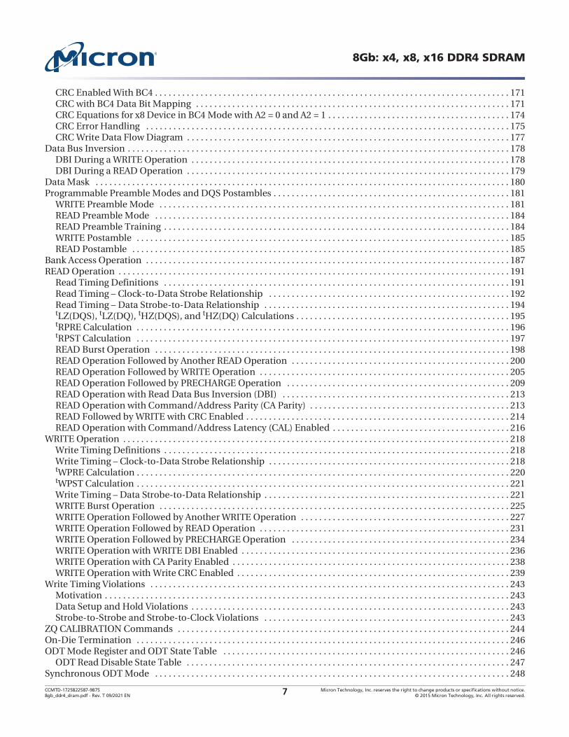
CRC Enabled With BC4 . . . . . . . . . . . . . . . . . . . . . . . . . . . . . . . . . . . . . . . . . . . . . . . . . . . . . . . . . . . . . . . . . . . . . . . . . . . . . . 171CRC with BC4 Data Bit Mapping . . . . . . . . . . . . . . . . . . . . . . . . . . . . . . . . . . . . . . . . . . . . . . . . . . . . . . . . . . . . . . . . . . . . . 171CRC Equations for x8 Device in BC4 Mode with A2 = 0 and A2 = 1 . . . . . . . . . . . . . . . . . . . . . . . . . . . . . . . . . . . . . . . . 174CRC Error Handling . . . . . . . . . . . . . . . . . . . . . . . . . . . . . . . . . . . . . . . . . . . . . . . . . . . . . . . . . . . . . . . . . . . . . . . . . . . . . . . . 175CRC Write Data Flow Diagram . . . . . . . . . . . . . . . . . . . . . . . . . . . . . . . . . . . . . . . . . . . . . . . . . . . . . . . . . . . . . . . . . . . . . . . 177
Data Bus Inversion . . . . . . . . . . . . . . . . . . . . . . . . . . . . . . . . . . . . . . . . . . . . . . . . . . . . . . . . . . . . . . . . . . . . . . . . . . . . . . . . . . . . 178DBI During a WRITE Operation . . . . . . . . . . . . . . . . . . . . . . . . . . . . . . . . . . . . . . . . . . . . . . . . . . . . . . . . . . . . . . . . . . . . . . 178DBI During a READ Operation . . . . . . . . . . . . . . . . . . . . . . . . . . . . . . . . . . . . . . . . . . . . . . . . . . . . . . . . . . . . . . . . . . . . . . . 179
Data Mask . . . . . . . . . . . . . . . . . . . . . . . . . . . . . . . . . . . . . . . . . . . . . . . . . . . . . . . . . . . . . . . . . . . . . . . . . . . . . . . . . . . . . . . . . . . 180Programmable Preamble Modes and DQS Postambles . . . . . . . . . . . . . . . . . . . . . . . . . . . . . . . . . . . . . . . . . . . . . . . . . . . . 181
WRITE Preamble Mode . . . . . . . . . . . . . . . . . . . . . . . . . . . . . . . . . . . . . . . . . . . . . . . . . . . . . . . . . . . . . . . . . . . . . . . . . . . . . 181READ Preamble Mode . . . . . . . . . . . . . . . . . . . . . . . . . . . . . . . . . . . . . . . . . . . . . . . . . . . . . . . . . . . . . . . . . . . . . . . . . . . . . . 184READ Preamble Training . . . . . . . . . . . . . . . . . . . . . . . . . . . . . . . . . . . . . . . . . . . . . . . . . . . . . . . . . . . . . . . . . . . . . . . . . . . . 184WRITE Postamble . . . . . . . . . . . . . . . . . . . . . . . . . . . . . . . . . . . . . . . . . . . . . . . . . . . . . . . . . . . . . . . . . . . . . . . . . . . . . . . . . . 185READ Postamble . . . . . . . . . . . . . . . . . . . . . . . . . . . . . . . . . . . . . . . . . . . . . . . . . . . . . . . . . . . . . . . . . . . . . . . . . . . . . . . . . . . 185
Bank Access Operation . . . . . . . . . . . . . . . . . . . . . . . . . . . . . . . . . . . . . . . . . . . . . . . . . . . . . . . . . . . . . . . . . . . . . . . . . . . . . . . . 187READ Operation . . . . . . . . . . . . . . . . . . . . . . . . . . . . . . . . . . . . . . . . . . . . . . . . . . . . . . . . . . . . . . . . . . . . . . . . . . . . . . . . . . . . . . 191
Read Timing Definitions . . . . . . . . . . . . . . . . . . . . . . . . . . . . . . . . . . . . . . . . . . . . . . . . . . . . . . . . . . . . . . . . . . . . . . . . . . . . 191 . . . . . . . . . . . . . . . . . . . . . . . . . . . . . . . . . . . . . . . . . . . . . . . . . . . . . 192
. . . . . . . . . . . . . . . . . . . . . . . . . . . . . . . . . . . . . . . . . . . . . . . . . . . . . . 194tLZ(DQS), tLZ(DQ), tHZ(DQS), and tHZ(DQ) Calculations . . . . . . . . . . . . . . . . . . . . . . . . . . . . . . . . . . . . . . . . . . . . . . . 195tRPRE Calculation . . . . . . . . . . . . . . . . . . . . . . . . . . . . . . . . . . . . . . . . . . . . . . . . . . . . . . . . . . . . . . . . . . . . . . . . . . . . . . . . . . 196tRPST Calculation . . . . . . . . . . . . . . . . . . . . . . . . . . . . . . . . . . . . . . . . . . . . . . . . . . . . . . . . . . . . . . . . . . . . . . . . . . . . . . . . . . 197READ Burst Operation . . . . . . . . . . . . . . . . . . . . . . . . . . . . . . . . . . . . . . . . . . . . . . . . . . . . . . . . . . . . . . . . . . . . . . . . . . . . . . 198READ Operation Followed by Another READ Operation . . . . . . . . . . . . . . . . . . . . . . . . . . . . . . . . . . . . . . . . . . . . . . . . 200READ Operation Followed by WRITE Operation . . . . . . . . . . . . . . . . . . . . . . . . . . . . . . . . . . . . . . . . . . . . . . . . . . . . . . . 205READ Operation Followed by PRECHARGE Operation . . . . . . . . . . . . . . . . . . . . . . . . . . . . . . . . . . . . . . . . . . . . . . . . . 209READ Operation with Read Data Bus Inversion (DBI) . . . . . . . . . . . . . . . . . . . . . . . . . . . . . . . . . . . . . . . . . . . . . . . . . . 213READ Operation with Command/Address Parity (CA Parity) . . . . . . . . . . . . . . . . . . . . . . . . . . . . . . . . . . . . . . . . . . . . 213READ Followed by WRITE with CRC Enabled . . . . . . . . . . . . . . . . . . . . . . . . . . . . . . . . . . . . . . . . . . . . . . . . . . . . . . . . . . 214READ Operation with Command/Address Latency (CAL) Enabled . . . . . . . . . . . . . . . . . . . . . . . . . . . . . . . . . . . . . . . 216
WRITE Operation . . . . . . . . . . . . . . . . . . . . . . . . . . . . . . . . . . . . . . . . . . . . . . . . . . . . . . . . . . . . . . . . . . . . . . . . . . . . . . . . . . . . . 218Write Timing Definitions . . . . . . . . . . . . . . . . . . . . . . . . . . . . . . . . . . . . . . . . . . . . . . . . . . . . . . . . . . . . . . . . . . . . . . . . . . . . 218
. . . . . . . . . . . . . . . . . . . . . . . . . . . . . . . . . . . . . . . . . . . . . . . . . . . . . 218tWPRE Calculation . . . . . . . . . . . . . . . . . . . . . . . . . . . . . . . . . . . . . . . . . . . . . . . . . . . . . . . . . . . . . . . . . . . . . . . . . . . . . . . . . . 220tWPST Calculation . . . . . . . . . . . . . . . . . . . . . . . . . . . . . . . . . . . . . . . . . . . . . . . . . . . . . . . . . . . . . . . . . . . . . . . . . . . . . . . . . . 221
. . . . . . . . . . . . . . . . . . . . . . . . . . . . . . . . . . . . . . . . . . . . . . . . . . . . . . 221WRITE Burst Operation . . . . . . . . . . . . . . . . . . . . . . . . . . . . . . . . . . . . . . . . . . . . . . . . . . . . . . . . . . . . . . . . . . . . . . . . . . . . . 225WRITE Operation Followed by Another WRITE Operation . . . . . . . . . . . . . . . . . . . . . . . . . . . . . . . . . . . . . . . . . . . . . . 227WRITE Operation Followed by READ Operation . . . . . . . . . . . . . . . . . . . . . . . . . . . . . . . . . . . . . . . . . . . . . . . . . . . . . . . 231WRITE Operation Followed by PRECHARGE Operation . . . . . . . . . . . . . . . . . . . . . . . . . . . . . . . . . . . . . . . . . . . . . . . . 234WRITE Operation with WRITE DBI Enabled . . . . . . . . . . . . . . . . . . . . . . . . . . . . . . . . . . . . . . . . . . . . . . . . . . . . . . . . . . . 236WRITE Operation with CA Parity Enabled . . . . . . . . . . . . . . . . . . . . . . . . . . . . . . . . . . . . . . . . . . . . . . . . . . . . . . . . . . . . . 238WRITE Operation with Write CRC Enabled . . . . . . . . . . . . . . . . . . . . . . . . . . . . . . . . . . . . . . . . . . . . . . . . . . . . . . . . . . . . 239
Write Timing Violations . . . . . . . . . . . . . . . . . . . . . . . . . . . . . . . . . . . . . . . . . . . . . . . . . . . . . . . . . . . . . . . . . . . . . . . . . . . . . . . 243Motivation . . . . . . . . . . . . . . . . . . . . . . . . . . . . . . . . . . . . . . . . . . . . . . . . . . . . . . . . . . . . . . . . . . . . . . . . . . . . . . . . . . . . . . . . . 243Data Setup and Hold Violations . . . . . . . . . . . . . . . . . . . . . . . . . . . . . . . . . . . . . . . . . . . . . . . . . . . . . . . . . . . . . . . . . . . . . . 243Strobe-to-Strobe and Strobe-to-Clock Violations . . . . . . . . . . . . . . . . . . . . . . . . . . . . . . . . . . . . . . . . . . . . . . . . . . . . . . 243
ZQ CALIBRATION Commands . . . . . . . . . . . . . . . . . . . . . . . . . . . . . . . . . . . . . . . . . . . . . . . . . . . . . . . . . . . . . . . . . . . . . . . . . 244On-Die Termination . . . . . . . . . . . . . . . . . . . . . . . . . . . . . . . . . . . . . . . . . . . . . . . . . . . . . . . . . . . . . . . . . . . . . . . . . . . . . . . . . . 246ODT Mode Register and ODT State Table . . . . . . . . . . . . . . . . . . . . . . . . . . . . . . . . . . . . . . . . . . . . . . . . . . . . . . . . . . . . . . . 246
ODT Read Disable State Table . . . . . . . . . . . . . . . . . . . . . . . . . . . . . . . . . . . . . . . . . . . . . . . . . . . . . . . . . . . . . . . . . . . . . . . 247Synchronous ODT Mode . . . . . . . . . . . . . . . . . . . . . . . . . . . . . . . . . . . . . . . . . . . . . . . . . . . . . . . . . . . . . . . . . . . . . . . . . . . . . . 248

CCMTD-1725822587-9875 Micron Technology, Inc. reserves the right to change products or specifications without notice.8gb_ddr4_dram.pdf - Rev. T 09/2021 EN 2015 Micron Technology, Inc. All rights reserved.8
8Gb: x4, x8, x16 DDR4 SDRAM
ODT Latency and Posted ODT . . . . . . . . . . . . . . . . . . . . . . . . . . . . . . . . . . . . . . . . . . . . . . . . . . . . . . . . . . . . . . . . . . . . . . . 248Timing Parameters . . . . . . . . . . . . . . . . . . . . . . . . . . . . . . . . . . . . . . . . . . . . . . . . . . . . . . . . . . . . . . . . . . . . . . . . . . . . . . . . . 248ODT During Reads . . . . . . . . . . . . . . . . . . . . . . . . . . . . . . . . . . . . . . . . . . . . . . . . . . . . . . . . . . . . . . . . . . . . . . . . . . . . . . . . . 250
Dynamic ODT . . . . . . . . . . . . . . . . . . . . . . . . . . . . . . . . . . . . . . . . . . . . . . . . . . . . . . . . . . . . . . . . . . . . . . . . . . . . . . . . . . . . . . . . 251Functional Description . . . . . . . . . . . . . . . . . . . . . . . . . . . . . . . . . . . . . . . . . . . . . . . . . . . . . . . . . . . . . . . . . . . . . . . . . . . . . 251
Asynchronous ODT Mode . . . . . . . . . . . . . . . . . . . . . . . . . . . . . . . . . . . . . . . . . . . . . . . . . . . . . . . . . . . . . . . . . . . . . . . . . . . . . 254Electrical Specifications . . . . . . . . . . . . . . . . . . . . . . . . . . . . . . . . . . . . . . . . . . . . . . . . . . . . . . . . . . . . . . . . . . . . . . . . . . . . . . . 255
Absolute Ratings . . . . . . . . . . . . . . . . . . . . . . . . . . . . . . . . . . . . . . . . . . . . . . . . . . . . . . . . . . . . . . . . . . . . . . . . . . . . . . . . . . . 255DRAM Component Operating Temperature Range . . . . . . . . . . . . . . . . . . . . . . . . . . . . . . . . . . . . . . . . . . . . . . . . . . . . . 255
. . . . . . . . . . . . . . . . . . . . . . . . . . . . . . . . . . . . . . . . . . . . . . 256Supply Operating Conditions . . . . . . . . . . . . . . . . . . . . . . . . . . . . . . . . . . . . . . . . . . . . . . . . . . . . . . . . . . . . . . . . . . . . . . . . 256Leakages . . . . . . . . . . . . . . . . . . . . . . . . . . . . . . . . . . . . . . . . . . . . . . . . . . . . . . . . . . . . . . . . . . . . . . . . . . . . . . . . . . . . . . . . . . 257VREFCA Supply . . . . . . . . . . . . . . . . . . . . . . . . . . . . . . . . . . . . . . . . . . . . . . . . . . . . . . . . . . . . . . . . . . . . . . . . . . . . . . . . . . . . . . 257VREFDQ Supply and Calibration Ranges . . . . . . . . . . . . . . . . . . . . . . . . . . . . . . . . . . . . . . . . . . . . . . . . . . . . . . . . . . . . . . . 258VREFDQ Ranges . . . . . . . . . . . . . . . . . . . . . . . . . . . . . . . . . . . . . . . . . . . . . . . . . . . . . . . . . . . . . . . . . . . . . . . . . . . . . . . . . . . . . 259
. . . . . . . . . . . . . . . . . . . . . . . . . . . . 260RESET_n Input Levels . . . . . . . . . . . . . . . . . . . . . . . . . . . . . . . . . . . . . . . . . . . . . . . . . . . . . . . . . . . . . . . . . . . . . . . . . . . . . . . 260Command/Address Input Levels . . . . . . . . . . . . . . . . . . . . . . . . . . . . . . . . . . . . . . . . . . . . . . . . . . . . . . . . . . . . . . . . . . . . . 260Command, Control, and Address Setup, Hold, and Derating . . . . . . . . . . . . . . . . . . . . . . . . . . . . . . . . . . . . . . . . . . . . 262Data Receiver Input Requirements . . . . . . . . . . . . . . . . . . . . . . . . . . . . . . . . . . . . . . . . . . . . . . . . . . . . . . . . . . . . . . . . . . . 264Connectivity Test (CT) Mode Input Levels . . . . . . . . . . . . . . . . . . . . . . . . . . . . . . . . . . . . . . . . . . . . . . . . . . . . . . . . . . . . . 268
. . . . . . . . . . . . . . . . . . . . . . . . . . . . . . 272Differential Inputs . . . . . . . . . . . . . . . . . . . . . . . . . . . . . . . . . . . . . . . . . . . . . . . . . . . . . . . . . . . . . . . . . . . . . . . . . . . . . . . . . . 272Single-Ended Requirements for CK Differential Signals . . . . . . . . . . . . . . . . . . . . . . . . . . . . . . . . . . . . . . . . . . . . . . . . . 273Slew Rate Definitions for CK Differential Input Signals . . . . . . . . . . . . . . . . . . . . . . . . . . . . . . . . . . . . . . . . . . . . . . . . . 274CK Differential Input Cross Point Voltage . . . . . . . . . . . . . . . . . . . . . . . . . . . . . . . . . . . . . . . . . . . . . . . . . . . . . . . . . . . . . 275DQS Differential Input Signal Definition and Swing Requirements . . . . . . . . . . . . . . . . . . . . . . . . . . . . . . . . . . . . . . 277DQS Differential Input Cross Point Voltage . . . . . . . . . . . . . . . . . . . . . . . . . . . . . . . . . . . . . . . . . . . . . . . . . . . . . . . . . . . . 279Slew Rate Definitions for DQS Differential Input Signals . . . . . . . . . . . . . . . . . . . . . . . . . . . . . . . . . . . . . . . . . . . . . . . . 280
. . . . . . . . . . . . . . . . . . . . . . . . . . . . . . . . . . . . . . 282Address, Command, and Control Overshoot and Undershoot Specifications . . . . . . . . . . . . . . . . . . . . . . . . . . . . . 282Clock Overshoot and Undershoot Specifications . . . . . . . . . . . . . . . . . . . . . . . . . . . . . . . . . . . . . . . . . . . . . . . . . . . . . . . 283Data, Strobe, and Mask Overshoot and Undershoot Specifications . . . . . . . . . . . . . . . . . . . . . . . . . . . . . . . . . . . . . . 284
. . . . . . . . . . . . . . . . . . . . . . . . . . . . . . . . . . . . . . . . 285Single-Ended Outputs . . . . . . . . . . . . . . . . . . . . . . . . . . . . . . . . . . . . . . . . . . . . . . . . . . . . . . . . . . . . . . . . . . . . . . . . . . . . . . 285Differential Outputs . . . . . . . . . . . . . . . . . . . . . . . . . . . . . . . . . . . . . . . . . . . . . . . . . . . . . . . . . . . . . . . . . . . . . . . . . . . . . . . . 286Reference Load for AC Timing and Output Slew Rate . . . . . . . . . . . . . . . . . . . . . . . . . . . . . . . . . . . . . . . . . . . . . . . . . . . 288Connectivity Test Mode Output Levels . . . . . . . . . . . . . . . . . . . . . . . . . . . . . . . . . . . . . . . . . . . . . . . . . . . . . . . . . . . . . . . . 288
. . . . . . . . . . . . . . . . . . . . . . . . . . . . . . . . . . . . . . . 290Connectivity Test Mode Output Driver Electrical Characteristics . . . . . . . . . . . . . . . . . . . . . . . . . . . . . . . . . . . . . . . . 290Output Driver Electrical Characteristics . . . . . . . . . . . . . . . . . . . . . . . . . . . . . . . . . . . . . . . . . . . . . . . . . . . . . . . . . . . . . . . 291Output Driver Temperature and Voltage Sensitivity . . . . . . . . . . . . . . . . . . . . . . . . . . . . . . . . . . . . . . . . . . . . . . . . . . . . 293Alert Driver . . . . . . . . . . . . . . . . . . . . . . . . . . . . . . . . . . . . . . . . . . . . . . . . . . . . . . . . . . . . . . . . . . . . . . . . . . . . . . . . . . . . . . . . 294
. . . . . . . . . . . . . . . . . . . . . . . . . . . . . . . . . . . . . . . . . . . 296ODT Levels and I-V Characteristics . . . . . . . . . . . . . . . . . . . . . . . . . . . . . . . . . . . . . . . . . . . . . . . . . . . . . . . . . . . . . . . . . . . 296ODT Temperature and Voltage Sensitivity . . . . . . . . . . . . . . . . . . . . . . . . . . . . . . . . . . . . . . . . . . . . . . . . . . . . . . . . . . . . 297ODT Timing Definitions . . . . . . . . . . . . . . . . . . . . . . . . . . . . . . . . . . . . . . . . . . . . . . . . . . . . . . . . . . . . . . . . . . . . . . . . . . . . . 298ODT Timing Definitions and Waveforms . . . . . . . . . . . . . . . . . . . . . . . . . . . . . . . . . . . . . . . . . . . . . . . . . . . . . . . . . . . . . . 298
DRAM Package Electrical Specifications . . . . . . . . . . . . . . . . . . . . . . . . . . . . . . . . . . . . . . . . . . . . . . . . . . . . . . . . . . . . . . . . . 301Thermal Characteristics . . . . . . . . . . . . . . . . . . . . . . . . . . . . . . . . . . . . . . . . . . . . . . . . . . . . . . . . . . . . . . . . . . . . . . . . . . . . . . . 305
. . . . . . . . . . . . . . . . . . . . . . . . . . . . . . . . . . . . . . . . . . . . . . . . . . . . . . . 306IDD, IPP, and IDDQ Measurement Conditions . . . . . . . . . . . . . . . . . . . . . . . . . . . . . . . . . . . . . . . . . . . . . . . . . . . . . . . . . . 306IDD Definitions . . . . . . . . . . . . . . . . . . . . . . . . . . . . . . . . . . . . . . . . . . . . . . . . . . . . . . . . . . . . . . . . . . . . . . . . . . . . . . . . . . . . . 308

CCMTD-1725822587-9875 Micron Technology, Inc. reserves the right to change products or specifications without notice.8gb_ddr4_dram.pdf - Rev. T 09/2021 EN 2015 Micron Technology, Inc. All rights reserved.9
8Gb: x4, x8, x16 DDR4 SDRAM
. . . . . . . . . . . . . . . . . . . . . . . . . . . . . . . . . . . . . . . . . . . . . . . . . . . . 312Current Test Definitions and Patterns . . . . . . . . . . . . . . . . . . . . . . . . . . . . . . . . . . . . . . . . . . . . . . . . . . . . . . . . . . . . . . . . 312IDD Specifications . . . . . . . . . . . . . . . . . . . . . . . . . . . . . . . . . . . . . . . . . . . . . . . . . . . . . . . . . . . . . . . . . . . . . . . . . . . . . . . . . . 322
. . . . . . . . . . . . . . . . . . . . . . . . . . . . . . . . . . . . . . . . . . . . . . . . . . . . . . . . . . . . . . . . . . . . . . . . . 323Speed Bin Tables . . . . . . . . . . . . . . . . . . . . . . . . . . . . . . . . . . . . . . . . . . . . . . . . . . . . . . . . . . . . . . . . . . . . . . . . . . . . . . . . . . . . . 344
Backward Compatibility . . . . . . . . . . . . . . . . . . . . . . . . . . . . . . . . . . . . . . . . . . . . . . . . . . . . . . . . . . . . . . . . . . . . . . . . . . . . . 344Refresh Parameters By Device Density . . . . . . . . . . . . . . . . . . . . . . . . . . . . . . . . . . . . . . . . . . . . . . . . . . . . . . . . . . . . . . . . . . 360
AC Electrical Characteristics and AC Timing Parameters . . . . . . . . . . . . . . . . . . . . . . . . . . . . . . . . . . . . . . . . . . . . . . . . 361Electrical Characteristics and AC Timing Parameters: 2666 Through 3200 . . . . . . . . . . . . . . . . . . . . . . . . . . . . . . . . 374
Clock Specification . . . . . . . . . . . . . . . . . . . . . . . . . . . . . . . . . . . . . . . . . . . . . . . . . . . . . . . . . . . . . . . . . . . . . . . . . . . . . . . . . . . 387Definition for tCK(AVG) . . . . . . . . . . . . . . . . . . . . . . . . . . . . . . . . . . . . . . . . . . . . . . . . . . . . . . . . . . . . . . . . . . . . . . . . . . . . . 387Definition for tCK(ABS) . . . . . . . . . . . . . . . . . . . . . . . . . . . . . . . . . . . . . . . . . . . . . . . . . . . . . . . . . . . . . . . . . . . . . . . . . . . . . 387Definition for tCH(AVG) and tCL(AVG) . . . . . . . . . . . . . . . . . . . . . . . . . . . . . . . . . . . . . . . . . . . . . . . . . . . . . . . . . . . . . . . . 387Definition for tJIT(per) and tJIT(per,lck) . . . . . . . . . . . . . . . . . . . . . . . . . . . . . . . . . . . . . . . . . . . . . . . . . . . . . . . . . . . . . . . 387Definition for tJIT(cc) and tJIT(cc,lck) . . . . . . . . . . . . . . . . . . . . . . . . . . . . . . . . . . . . . . . . . . . . . . . . . . . . . . . . . . . . . . . . . 387Definition for tERR(nper) . . . . . . . . . . . . . . . . . . . . . . . . . . . . . . . . . . . . . . . . . . . . . . . . . . . . . . . . . . . . . . . . . . . . . . . . . . . . 388
Jitter Notes . . . . . . . . . . . . . . . . . . . . . . . . . . . . . . . . . . . . . . . . . . . . . . . . . . . . . . . . . . . . . . . . . . . . . . . . . . . . . . . . . . . . . . . . . . . 388Converting Time-Based Specifications to Clock-Based Requirements . . . . . . . . . . . . . . . . . . . . . . . . . . . . . . . . . . . . . . 389Options Tables . . . . . . . . . . . . . . . . . . . . . . . . . . . . . . . . . . . . . . . . . . . . . . . . . . . . . . . . . . . . . . . . . . . . . . . . . . . . . . . . . . . . . . . 390
CCMTD-1725822587-9875 Micron Technology, Inc. reserves the right to change products or specifications without notice.8gb_ddr4_dram.pdf - Rev. T 09/2021 EN 2015 Micron Technology, Inc. All rights reserved.10
8Gb: x4, x8, x16 DDR4 SDRAM
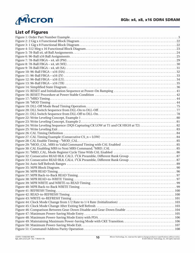
List of FiguresFigure 1: Order Part Number Example . . . . . . . . . . . . . . . . . . . . . . . . . . . . . . . . . . . . . . . . . . . . . . . . . . . . . . . . . . . . . . . . . . . . . 3Figure 2: 2 Gig x 4 Functional Block Diagram . . . . . . . . . . . . . . . . . . . . . . . . . . . . . . . . . . . . . . . . . . . . . . . . . . . . . . . . . . . . . . 22Figure 3: 1 Gig x 8 Functional Block Diagram . . . . . . . . . . . . . . . . . . . . . . . . . . . . . . . . . . . . . . . . . . . . . . . . . . . . . . . . . . . . . . 22Figure 4: 512 Meg x 16 Functional Block Diagram. . . . . . . . . . . . . . . . . . . . . . . . . . . . . . . . . . . . . . . . . . . . . . . . . . . . . . . . . . 23Figure 5: 78-Ball x4, x8 Ball Assignments . . . . . . . . . . . . . . . . . . . . . . . . . . . . . . . . . . . . . . . . . . . . . . . . . . . . . . . . . . . . . . . . . . 24Figure 6: 96-Ball x16 Ball Assignments . . . . . . . . . . . . . . . . . . . . . . . . . . . . . . . . . . . . . . . . . . . . . . . . . . . . . . . . . . . . . . . . . . . . 25Figure 7: . . . . . . . . . . . . . . . . . . . . . . . . . . . . . . . . . . . . . . . . . . . . . . . . . . . . . . . . . . . . . . . . . . . . . . 29Figure 8: . . . . . . . . . . . . . . . . . . . . . . . . . . . . . . . . . . . . . . . . . . . . . . . . . . . . . . . . . . . . . . . . . . . . . . 30Figure 9: . . . . . . . . . . . . . . . . . . . . . . . . . . . . . . . . . . . . . . . . . . . . . . . . . . . . . . . . . . . . . . . . . . . . . . . 31Figure 10: . . . . . . . . . . . . . . . . . . . . . . . . . . . . . . . . . . . . . . . . . . . . . . . . . . . . . . . . . . . . . . . . . . . . . . . 32Figure 11: . . . . . . . . . . . . . . . . . . . . . . . . . . . . . . . . . . . . . . . . . . . . . . . . . . . . . . . . . . . . . . . . . . . . . . . . 33Figure 12: . . . . . . . . . . . . . . . . . . . . . . . . . . . . . . . . . . . . . . . . . . . . . . . . . . . . . . . . . . . . . . . . . . . . . . . . 34Figure 13: . . . . . . . . . . . . . . . . . . . . . . . . . . . . . . . . . . . . . . . . . . . . . . . . . . . . . . . . . . . . . . . . . . . . . . . 35Figure 14: Simplified State Diagram . . . . . . . . . . . . . . . . . . . . . . . . . . . . . . . . . . . . . . . . . . . . . . . . . . . . . . . . . . . . . . . . . . . . . . 36Figure 15: RESET and Initialization Sequence at Power-On Ramping . . . . . . . . . . . . . . . . . . . . . . . . . . . . . . . . . . . . . . . . 41Figure 16: RESET Procedure at Power Stable Condition . . . . . . . . . . . . . . . . . . . . . . . . . . . . . . . . . . . . . . . . . . . . . . . . . . . . 42Figure 17: tMRD Timing. . . . . . . . . . . . . . . . . . . . . . . . . . . . . . . . . . . . . . . . . . . . . . . . . . . . . . . . . . . . . . . . . . . . . . . . . . . . . . . . . 44Figure 18: tMOD Timing . . . . . . . . . . . . . . . . . . . . . . . . . . . . . . . . . . . . . . . . . . . . . . . . . . . . . . . . . . . . . . . . . . . . . . . . . . . . . . . . 44Figure 19: DLL-Off Mode Read Timing Operation. . . . . . . . . . . . . . . . . . . . . . . . . . . . . . . . . . . . . . . . . . . . . . . . . . . . . . . . . . 75Figure 20: DLL Switch Sequence from DLL-On to DLL-Off . . . . . . . . . . . . . . . . . . . . . . . . . . . . . . . . . . . . . . . . . . . . . . . . . . 77Figure 21: DLL Switch Sequence from DLL-Off to DLL-On . . . . . . . . . . . . . . . . . . . . . . . . . . . . . . . . . . . . . . . . . . . . . . . . . . 78Figure 22: Write Leveling Concept, Example 1 . . . . . . . . . . . . . . . . . . . . . . . . . . . . . . . . . . . . . . . . . . . . . . . . . . . . . . . . . . . . . 80Figure 23: Write Leveling Concept, Example 2 . . . . . . . . . . . . . . . . . . . . . . . . . . . . . . . . . . . . . . . . . . . . . . . . . . . . . . . . . . . . . 81Figure 24: Write Leveling Sequence (DQS Capturing CK LOW at T1 and CK HIGH at T2) . . . . . . . . . . . . . . . . . . . . . . . 82Figure 25: Write Leveling Exit . . . . . . . . . . . . . . . . . . . . . . . . . . . . . . . . . . . . . . . . . . . . . . . . . . . . . . . . . . . . . . . . . . . . . . . . . . . . 83Figure 26: CAL Timing Definition . . . . . . . . . . . . . . . . . . . . . . . . . . . . . . . . . . . . . . . . . . . . . . . . . . . . . . . . . . . . . . . . . . . . . . . . 84Figure 27: CAL Timing Example (Consecutive CS_n = LOW) . . . . . . . . . . . . . . . . . . . . . . . . . . . . . . . . . . . . . . . . . . . . . . . . 84Figure 28: tMOD_CAL . . . . . . . . . . . . . . . . . . . . . . . . . . . . . . . . . . . . . . . . . . . . . . . . . . . . . . . . . . . . . . . 85Figure 29: tMOD_CAL, MRS to Valid Command Timing with CAL Enabled . . . . . . . . . . . . . . . . . . . . . . . . . . . . . . . . . . . 85Figure 30: CAL Enabling MRS to Next MRS Command, tMRD_CAL . . . . . . . . . . . . . . . . . . . . . . . . . . . . . . . . . . . . . . . . . . 85Figure 31: tMRD_CAL, Mode Register Cycle Time With CAL Enabled . . . . . . . . . . . . . . . . . . . . . . . . . . . . . . . . . . . . . . . . 86Figure 32: Consecutive READ BL8, CAL3, 1tCK Preamble, Different Bank Group . . . . . . . . . . . . . . . . . . . . . . . . . . . . . . 87Figure 33: Consecutive READ BL8, CAL4, 1tCK Preamble, Different Bank Group . . . . . . . . . . . . . . . . . . . . . . . . . . . . . . 87Figure 34: Auto Self Refresh Ranges . . . . . . . . . . . . . . . . . . . . . . . . . . . . . . . . . . . . . . . . . . . . . . . . . . . . . . . . . . . . . . . . . . . . . . 89Figure 35: MPR Block Diagram. . . . . . . . . . . . . . . . . . . . . . . . . . . . . . . . . . . . . . . . . . . . . . . . . . . . . . . . . . . . . . . . . . . . . . . . . . . 90Figure 36: MPR READ Timing. . . . . . . . . . . . . . . . . . . . . . . . . . . . . . . . . . . . . . . . . . . . . . . . . . . . . . . . . . . . . . . . . . . . . . . . . . . . 96Figure 37: MPR Back-to-Back READ Timing . . . . . . . . . . . . . . . . . . . . . . . . . . . . . . . . . . . . . . . . . . . . . . . . . . . . . . . . . . . . . . . 97Figure 38: MPR READ-to-WRITE Timing. . . . . . . . . . . . . . . . . . . . . . . . . . . . . . . . . . . . . . . . . . . . . . . . . . . . . . . . . . . . . . . . . . 97Figure 39: MPR WRITE and WRITE-to-READ Timing . . . . . . . . . . . . . . . . . . . . . . . . . . . . . . . . . . . . . . . . . . . . . . . . . . . . . . . 99Figure 40: MPR Back-to-Back WRITE Timing. . . . . . . . . . . . . . . . . . . . . . . . . . . . . . . . . . . . . . . . . . . . . . . . . . . . . . . . . . . . . . 99Figure 41: REFRESH Timing . . . . . . . . . . . . . . . . . . . . . . . . . . . . . . . . . . . . . . . . . . . . . . . . . . . . . . . . . . . . . . . . . . . . . . . . . . . . 100Figure 42: READ-to-REFRESH Timing . . . . . . . . . . . . . . . . . . . . . . . . . . . . . . . . . . . . . . . . . . . . . . . . . . . . . . . . . . . . . . . . . . . 100Figure 43: WRITE-to-REFRESH Timing . . . . . . . . . . . . . . . . . . . . . . . . . . . . . . . . . . . . . . . . . . . . . . . . . . . . . . . . . . . . . . . . . . 101Figure 44: Clock Mode Change from 1/2 Rate to 1/4 Rate (Initialization) . . . . . . . . . . . . . . . . . . . . . . . . . . . . . . . . . . . . 103Figure 45: Clock Mode Change After Exiting Self Refresh . . . . . . . . . . . . . . . . . . . . . . . . . . . . . . . . . . . . . . . . . . . . . . . . . . 103Figure 46: Comparison Between Gear-Down Disable and Gear-Down Enable . . . . . . . . . . . . . . . . . . . . . . . . . . . . . . . 104Figure 47: Maximum Power-Saving Mode Entry . . . . . . . . . . . . . . . . . . . . . . . . . . . . . . . . . . . . . . . . . . . . . . . . . . . . . . . . . . 105Figure 48: Maximum Power-Saving Mode Entry with PDA . . . . . . . . . . . . . . . . . . . . . . . . . . . . . . . . . . . . . . . . . . . . . . . . . 106Figure 49: Maintaining Maximum Power-Saving Mode with CKE Transition. . . . . . . . . . . . . . . . . . . . . . . . . . . . . . . . . 106Figure 50: Maximum Power-Saving Mode Exit. . . . . . . . . . . . . . . . . . . . . . . . . . . . . . . . . . . . . . . . . . . . . . . . . . . . . . . . . . . . 107Figure 51: Command/Address Parity Operation . . . . . . . . . . . . . . . . . . . . . . . . . . . . . . . . . . . . . . . . . . . . . . . . . . . . . . . . . . 108
CCMTD-1725822587-9875 Micron Technology, Inc. reserves the right to change products or specifications without notice.8gb_ddr4_dram.pdf - Rev. T 09/2021 EN 2015 Micron Technology, Inc. All rights reserved.11
8Gb: x4, x8, x16 DDR4 SDRAM
Figure 52: Command/Address Parity During Normal Operation. . . . . . . . . . . . . . . . . . . . . . . . . . . . . . . . . . . . . . . . . . . . 110Figure 53: Persistent CA Parity Error Checking Operation. . . . . . . . . . . . . . . . . . . . . . . . . . . . . . . . . . . . . . . . . . . . . . . . . . 110Figure 54: . . . . . . . . . . . . . . . . . . . . . . . . . . . . . . . . . . . . . . . . . . . . . . . . . . . . . . . . 111Figure 55: . . . . . . . . . . . . . . . . . . . . . . . . . . . . . . . . . . . . . . . . . . . . . . . . . . . . . . . 111Figure 56: . . . . . . . . . . . . . . . . . . . . . . . . . . . . . . . . . . . . . . . . . . . . . . . . . . . . . . . . . . 112Figure 57: tMRD_PAR . . . . . . . . . . . . . . . . . . . . . . . . . . . . . . . . . . . . . . . . . . . . . . . . . . . . . 112Figure 58: tMOD_PAR . . . . . . . . . . . . . . . . . . . . . . . . . . . . . . . . . . . . . . . . . . . . . . . . . . . . . 112Figure 59: tMRD_PAR . . . . . . . . . . . . . . . . . . . . . . . . . . . . . . . . . . . . . . . . . . . . . . . . . . . . . . . 113Figure 60: tMOD_PAR. . . . . . . . . . . . . . . . . . . . . . . . . . . . . . . . . . . . . . . . . . . . . . . . . . . . . . . 113Figure 61: CA Parity Flow Diagram . . . . . . . . . . . . . . . . . . . . . . . . . . . . . . . . . . . . . . . . . . . . . . . . . . . . . . . . . . . . . . . . . . . . . . 114Figure 62: PDA Operation Enabled, BL8 . . . . . . . . . . . . . . . . . . . . . . . . . . . . . . . . . . . . . . . . . . . . . . . . . . . . . . . . . . . . . . . . . 116Figure 63: PDA Operation Enabled, BC4 . . . . . . . . . . . . . . . . . . . . . . . . . . . . . . . . . . . . . . . . . . . . . . . . . . . . . . . . . . . . . . . . . 116Figure 64: MRS PDA Exit . . . . . . . . . . . . . . . . . . . . . . . . . . . . . . . . . . . . . . . . . . . . . . . . . . . . . . . . . . . . . . . . . . . . . . . . . . . . . . . 117Figure 65: VREFDQ Voltage Range. . . . . . . . . . . . . . . . . . . . . . . . . . . . . . . . . . . . . . . . . . . . . . . . . . . . . . . . . . . . . . . . . . . . . . . . 118Figure 66: Example of VREF Set Tolerance and Step Size . . . . . . . . . . . . . . . . . . . . . . . . . . . . . . . . . . . . . . . . . . . . . . . . . . . 120Figure 67: VREFDQ Timing Diagram for VREF,time Parameter . . . . . . . . . . . . . . . . . . . . . . . . . . . . . . . . . . . . . . . . . . . . . . . . 121Figure 68: VREFDQ Training Mode Entry and Exit Timing Diagram . . . . . . . . . . . . . . . . . . . . . . . . . . . . . . . . . . . . . . . . . . 122Figure 69: VREF Step: Single Step Size Increment Case . . . . . . . . . . . . . . . . . . . . . . . . . . . . . . . . . . . . . . . . . . . . . . . . . . . . . 123Figure 70: VREF Step: Single Step Size Decrement Case . . . . . . . . . . . . . . . . . . . . . . . . . . . . . . . . . . . . . . . . . . . . . . . . . . . . 123Figure 71: VREF Full Step: From VREF,min to VREF,maxCase . . . . . . . . . . . . . . . . . . . . . . . . . . . . . . . . . . . . . . . . . . . . . . . . . . 124Figure 72: VREF Full Step: From VREF,max to VREF,minCase . . . . . . . . . . . . . . . . . . . . . . . . . . . . . . . . . . . . . . . . . . . . . . . . . . 124Figure 73: VREFDQ Equivalent Circuit . . . . . . . . . . . . . . . . . . . . . . . . . . . . . . . . . . . . . . . . . . . . . . . . . . . . . . . . . . . . . . . . . . . . 125Figure 74: Connectivity Test Mode Entry. . . . . . . . . . . . . . . . . . . . . . . . . . . . . . . . . . . . . . . . . . . . . . . . . . . . . . . . . . . . . . . . . 129Figure 75: . . . . . . . . . . . . . . . . . . . . . . . . . . . . . . . . . . . . . . . . . . . . . . . . . . . . . . . . . . . . . . . . . . . . . . . . . . . 133Figure 76: . . . . . . . . . . . . . . . . . . . . . . . . . . . . . . . . . . . . . . . . . . . . . . . . . . . . . . . . . . . . . . . . . . 134Figure 77: . . . . . . . . . . . . . . . . . . . . . . . . . . . . . . . . . . . . . . . . . . . . . . . . . . . . . . . . . . . . . . . . . . . . . . . . . . . . 135Figure 78: . . . . . . . . . . . . . . . . . . . . . . . . . . . . . . . . . . . . . . . . . . . . . . . . . . . . . . . . . . . . . . . . . . . 135Figure 79: . . . . . . . . . . . . . . . . . . . . . . . . . . . . . . . . . . . . . . . . . . . . . . . . . . . . . . . . . . . . . . . . . . . . . . . . . . . . . . . . 137Figure 80: . . . . . . . . . . . . . . . . . . . . . . . . . . . . . . . . . . . . . . . . . . . . . . . . . . . . . . . . . . . . . . . . . . . . . . . 138Figure 81: MBIST-PPR Sequence . . . . . . . . . . . . . . . . . . . . . . . . . . . . . . . . . . . . . . . . . . . . . . . . . . . . . . . . . . . . . . . . . . . . . . . . 140Figure 82: tRRD Timing . . . . . . . . . . . . . . . . . . . . . . . . . . . . . . . . . . . . . . . . . . . . . . . . . . . . . . . . . . . . . . . . . . . . . . . . . . . . . . . . 141Figure 83: tFAW Timing . . . . . . . . . . . . . . . . . . . . . . . . . . . . . . . . . . . . . . . . . . . . . . . . . . . . . . . . . . . . . . . . . . . . . . . . . . . . . . . . 142Figure 84: REFRESH Command Timing. . . . . . . . . . . . . . . . . . . . . . . . . . . . . . . . . . . . . . . . . . . . . . . . . . . . . . . . . . . . . . . . . . 143Figure 85: Postponing REFRESH Commands (Example) . . . . . . . . . . . . . . . . . . . . . . . . . . . . . . . . . . . . . . . . . . . . . . . . . . . 143Figure 86: Pulling In REFRESH Commands (Example). . . . . . . . . . . . . . . . . . . . . . . . . . . . . . . . . . . . . . . . . . . . . . . . . . . . . 144Figure 87: TCR Mode Example1 . . . . . . . . . . . . . . . . . . . . . . . . . . . . . . . . . . . . . . . . . . . . . . . . . . . . . . . . . . . . . . . . . . . . . . . . . 146Figure 88: 4Gb with Fine Granularity Refresh Mode Example . . . . . . . . . . . . . . . . . . . . . . . . . . . . . . . . . . . . . . . . . . . . . . 149Figure 89: OTF REFRESH Command Timing . . . . . . . . . . . . . . . . . . . . . . . . . . . . . . . . . . . . . . . . . . . . . . . . . . . . . . . . . . . . . 150Figure 90: Self Refresh Entry/Exit Timing . . . . . . . . . . . . . . . . . . . . . . . . . . . . . . . . . . . . . . . . . . . . . . . . . . . . . . . . . . . . . . . . 153Figure 91: Self Refresh Entry/Exit Timing with CAL Mode. . . . . . . . . . . . . . . . . . . . . . . . . . . . . . . . . . . . . . . . . . . . . . . . . . 154Figure 92: Self Refresh Abort. . . . . . . . . . . . . . . . . . . . . . . . . . . . . . . . . . . . . . . . . . . . . . . . . . . . . . . . . . . . . . . . . . . . . . . . . . . . 155Figure 93: Self Refresh Exit with NOP Command. . . . . . . . . . . . . . . . . . . . . . . . . . . . . . . . . . . . . . . . . . . . . . . . . . . . . . . . . . 156Figure 94: Active Power-Down Entry and Exit . . . . . . . . . . . . . . . . . . . . . . . . . . . . . . . . . . . . . . . . . . . . . . . . . . . . . . . . . . . . 158Figure 95: Power-Down Entry After Read and Read with Auto Precharge . . . . . . . . . . . . . . . . . . . . . . . . . . . . . . . . . . . . 159Figure 96: Power-Down Entry After Write and Write with Auto Precharge . . . . . . . . . . . . . . . . . . . . . . . . . . . . . . . . . . . 159Figure 97: Power-Down Entry After Write . . . . . . . . . . . . . . . . . . . . . . . . . . . . . . . . . . . . . . . . . . . . . . . . . . . . . . . . . . . . . . . . 160Figure 98: Precharge Power-Down Entry and Exit. . . . . . . . . . . . . . . . . . . . . . . . . . . . . . . . . . . . . . . . . . . . . . . . . . . . . . . . . 160Figure 99: REFRESH Command to Power-Down Entry . . . . . . . . . . . . . . . . . . . . . . . . . . . . . . . . . . . . . . . . . . . . . . . . . . . . 161Figure 100: Active Command to Power-Down Entry. . . . . . . . . . . . . . . . . . . . . . . . . . . . . . . . . . . . . . . . . . . . . . . . . . . . . . . 161Figure 101: PRECHARGE/PRECHARGE ALL Command to Power-Down Entry . . . . . . . . . . . . . . . . . . . . . . . . . . . . . . . 162Figure 102: MRS Command to Power-Down Entry . . . . . . . . . . . . . . . . . . . . . . . . . . . . . . . . . . . . . . . . . . . . . . . . . . . . . . . . 162Figure 103: . . . . . . . . . . . . . . . . . . . . . . . . . . . . . . . . . . . . . . . . . . . . . . . . 163Figure 104: Active Power-Down Entry and Exit Timing with CAL . . . . . . . . . . . . . . . . . . . . . . . . . . . . . . . . . . . . . . . . . . . 163
CCMTD-1725822587-9875 Micron Technology, Inc. reserves the right to change products or specifications without notice.8gb_ddr4_dram.pdf - Rev. T 09/2021 EN 2015 Micron Technology, Inc. All rights reserved.12
8Gb: x4, x8, x16 DDR4 SDRAM
Figure 105: REFRESH Command to Power-Down Entry with CAL . . . . . . . . . . . . . . . . . . . . . . . . . . . . . . . . . . . . . . . . . . 164Figure 106: ODT Power-Down Entry with ODT Buffer Disable Mode. . . . . . . . . . . . . . . . . . . . . . . . . . . . . . . . . . . . . . . . 165Figure 107: ODT Power-Down Exit with ODT Buffer Disable Mode . . . . . . . . . . . . . . . . . . . . . . . . . . . . . . . . . . . . . . . . . 166Figure 108: CRC Write Data Operation. . . . . . . . . . . . . . . . . . . . . . . . . . . . . . . . . . . . . . . . . . . . . . . . . . . . . . . . . . . . . . . . . . . 167Figure 109: CRC Error Reporting . . . . . . . . . . . . . . . . . . . . . . . . . . . . . . . . . . . . . . . . . . . . . . . . . . . . . . . . . . . . . . . . . . . . . . . . 176Figure 110: CA Parity Flow Diagram . . . . . . . . . . . . . . . . . . . . . . . . . . . . . . . . . . . . . . . . . . . . . . . . . . . . . . . . . . . . . . . . . . . . . 177Figure 111: 1tCK vs. 2tCK WRITE Preamble Mode . . . . . . . . . . . . . . . . . . . . . . . . . . . . . . . . . . . . . . . . . . . . . . . . . . . . . . . . . 181Figure 112: 1tCK vs. 2tCK WRITE Preamble Mode, tCCD = 4 . . . . . . . . . . . . . . . . . . . . . . . . . . . . . . . . . . . . . . . . . . . . . . . . 182Figure 113: 1tCK vs. 2tCK WRITE Preamble Mode, tCCD = 5 . . . . . . . . . . . . . . . . . . . . . . . . . . . . . . . . . . . . . . . . . . . . . . . . 183Figure 114: 1tCK vs. 2tCK WRITE Preamble Mode, tCCD = 6 . . . . . . . . . . . . . . . . . . . . . . . . . . . . . . . . . . . . . . . . . . . . . . . . 183Figure 115: 1tCK vs. 2tCK READ Preamble Mode . . . . . . . . . . . . . . . . . . . . . . . . . . . . . . . . . . . . . . . . . . . . . . . . . . . . . . . . . . 184Figure 116: READ Preamble Training . . . . . . . . . . . . . . . . . . . . . . . . . . . . . . . . . . . . . . . . . . . . . . . . . . . . . . . . . . . . . . . . . . . . 185Figure 117: WRITE Postamble . . . . . . . . . . . . . . . . . . . . . . . . . . . . . . . . . . . . . . . . . . . . . . . . . . . . . . . . . . . . . . . . . . . . . . . . . . 185Figure 118: READ Postamble . . . . . . . . . . . . . . . . . . . . . . . . . . . . . . . . . . . . . . . . . . . . . . . . . . . . . . . . . . . . . . . . . . . . . . . . . . . 186Figure 119: Bank Group x4/x8 Block Diagram . . . . . . . . . . . . . . . . . . . . . . . . . . . . . . . . . . . . . . . . . . . . . . . . . . . . . . . . . . . . 187Figure 120: READ Burst tCCD_S and tCCD_L Examples. . . . . . . . . . . . . . . . . . . . . . . . . . . . . . . . . . . . . . . . . . . . . . . . . . . . 188Figure 121: Write Burst tCCD_S and tCCD_L Examples . . . . . . . . . . . . . . . . . . . . . . . . . . . . . . . . . . . . . . . . . . . . . . . . . . . . 188Figure 122: tRRD Timing . . . . . . . . . . . . . . . . . . . . . . . . . . . . . . . . . . . . . . . . . . . . . . . . . . . . . . . . . . . . . . . . . . . . . . . . . . . . . . . 189Figure 123: tWTR_S Timing (WRITE-to-READ, Different Bank Group, CRC and DM Disabled) . . . . . . . . . . . . . . . . . 190Figure 124: tWTR_L Timing (WRITE-to-READ, Same Bank Group, CRC and DM Disabled) . . . . . . . . . . . . . . . . . . . . 190Figure 125: Read Timing Definition . . . . . . . . . . . . . . . . . . . . . . . . . . . . . . . . . . . . . . . . . . . . . . . . . . . . . . . . . . . . . . . . . . . . . 192Figure 126: Clock-to-Data Strobe Relationship . . . . . . . . . . . . . . . . . . . . . . . . . . . . . . . . . . . . . . . . . . . . . . . . . . . . . . . . . . . 193Figure 127: Data Strobe-to-Data Relationship . . . . . . . . . . . . . . . . . . . . . . . . . . . . . . . . . . . . . . . . . . . . . . . . . . . . . . . . . . . . 194Figure 128: tLZ and tHZ Method for Calculating Transitions and Endpoints . . . . . . . . . . . . . . . . . . . . . . . . . . . . . . . . . 195Figure 129: tRPRE Method for Calculating Transitions and Endpoints. . . . . . . . . . . . . . . . . . . . . . . . . . . . . . . . . . . . . . . 196Figure 130: tRPST Method for Calculating Transitions and Endpoints . . . . . . . . . . . . . . . . . . . . . . . . . . . . . . . . . . . . . . . 197Figure 131: READ Burst Operation, RL = 11 (AL = 0, CL = 11, BL8). . . . . . . . . . . . . . . . . . . . . . . . . . . . . . . . . . . . . . . . . . . 198Figure 132: READ Burst Operation, RL = 21 (AL = 10, CL = 11, BL8). . . . . . . . . . . . . . . . . . . . . . . . . . . . . . . . . . . . . . . . . . 199Figure 133: Consecutive READ (BL8) with 1tCK Preamble in Different Bank Group . . . . . . . . . . . . . . . . . . . . . . . . . . . 200Figure 134: Consecutive READ (BL8) with 2tCK Preamble in Different Bank Group . . . . . . . . . . . . . . . . . . . . . . . . . . . 200Figure 135: Nonconsecutive READ (BL8) with 1tCK Preamble in Same or Different Bank Group . . . . . . . . . . . . . . . 201Figure 136: Nonconsecutive READ (BL8) with 2tCK Preamble in Same or Different Bank Group . . . . . . . . . . . . . . . 201Figure 137: READ (BC4) to READ (BC4) with 1tCK Preamble in Different Bank Group. . . . . . . . . . . . . . . . . . . . . . . . . 202Figure 138: READ (BC4) to READ (BC4) with 2tCK Preamble in Different Bank Group. . . . . . . . . . . . . . . . . . . . . . . . . 202Figure 139: READ (BL8) to READ (BC4) OTF with 1tCK Preamble in Different Bank Group . . . . . . . . . . . . . . . . . . . . 203Figure 140: READ (BL8) to READ (BC4) OTF with 2tCK Preamble in Different Bank Group . . . . . . . . . . . . . . . . . . . . 203Figure 141: READ (BC4) to READ (BL8) OTF with 1tCK Preamble in Different Bank Group . . . . . . . . . . . . . . . . . . . . 204Figure 142: READ (BC4) to READ (BL8) OTF with 2tCK Preamble in Different Bank Group . . . . . . . . . . . . . . . . . . . . 204Figure 143: READ (BL8) to WRITE (BL8) with 1tCK Preamble in Same or Different Bank Group . . . . . . . . . . . . . . . . 205Figure 144: READ (BL8) to WRITE (BL8) with 2tCK Preamble in Same or Different Bank Group . . . . . . . . . . . . . . . . 205Figure 145: READ (BC4) OTF to WRITE (BC4) OTF with 1tCK Preamble in Same or Different Bank Group. . . . . . . 206Figure 146: READ (BC4) OTF to WRITE (BC4) OTF with 2tCK Preamble in Same or Different Bank Group. . . . . . . 206Figure 147: READ (BC4) Fixed to WRITE (BC4) Fixed with 1tCK Preamble in Same or Different Bank Group. . . . . 207Figure 148: READ (BC4) Fixed to WRITE (BC4) Fixed with 2tCK Preamble in Same or Different Bank Group. . . . . 207Figure 149: READ (BC4) to WRITE (BL8) OTF with 1tCK Preamble in Same or Different Bank Group . . . . . . . . . . . 208Figure 150: READ (BC4) to WRITE (BL8) OTF with 2tCK Preamble in Same or Different Bank Group . . . . . . . . . . . 208Figure 151: READ (BL8) to WRITE (BC4) OTF with 1tCK Preamble in Same or Different Bank Group . . . . . . . . . . . 209Figure 152: READ (BL8) to WRITE (BC4) OTF with 2tCK Preamble in Same or Different Bank Group . . . . . . . . . . . 209Figure 153: READ to PRECHARGE with 1tCK Preamble . . . . . . . . . . . . . . . . . . . . . . . . . . . . . . . . . . . . . . . . . . . . . . . . . . . . 210Figure 154: READ to PRECHARGE with 2tCK Preamble . . . . . . . . . . . . . . . . . . . . . . . . . . . . . . . . . . . . . . . . . . . . . . . . . . . . 211Figure 155: READ to PRECHARGE with Additive Latency and 1tCK Preamble . . . . . . . . . . . . . . . . . . . . . . . . . . . . . . . . 211Figure 156: READ with Auto Precharge and 1tCK Preamble . . . . . . . . . . . . . . . . . . . . . . . . . . . . . . . . . . . . . . . . . . . . . . . . 212Figure 157: READ with Auto Precharge, Additive Latency, and 1tCK Preamble . . . . . . . . . . . . . . . . . . . . . . . . . . . . . . . 212
CCMTD-1725822587-9875 Micron Technology, Inc. reserves the right to change products or specifications without notice.8gb_ddr4_dram.pdf - Rev. T 09/2021 EN 2015 Micron Technology, Inc. All rights reserved.13
8Gb: x4, x8, x16 DDR4 SDRAM
Figure 158: Consecutive READ (BL8) with 1tCK Preamble and DBI in Different Bank Group . . . . . . . . . . . . . . . . . . . 213Figure 159: Consecutive READ (BL8) with 1tCK Preamble and CA Parity in Different Bank Group . . . . . . . . . . . . . . 213Figure 160: READ (BL8) to WRITE (BL8) with 1tCK Preamble and CA Parity in Same or Different Bank Group . . . 214Figure 161: READ (BL8) to WRITE (BL8 or BC4: OTF) with 1tCK Preamble and Write CRC in Same or Different Bank Group. . . . . . . . . . . . . . . . . . . . . . . . . . . . . . . . . . . . . . . . . . . . . . . . . . . . . . . . . . . . . . . . . . . . . . . . . . . . . . . . . . . . . . . . . . . . . . . . 214Figure 162: READ (BC4: Fixed) to WRITE (BC4: Fixed) with 1tCK Preamble and Write CRC in Same or Different Bank Group. . . . . . . . . . . . . . . . . . . . . . . . . . . . . . . . . . . . . . . . . . . . . . . . . . . . . . . . . . . . . . . . . . . . . . . . . . . . . . . . . . . . . . . . . . . . . . . . 216Figure 163: Consecutive READ (BL8) with CAL (3tCK) and 1tCK Preamble in Different Bank Group . . . . . . . . . . . . 216Figure 164: Consecutive READ (BL8) with CAL (4tCK) and 1tCK Preamble in Different Bank Group . . . . . . . . . . . . 217Figure 165: Write Timing Definition . . . . . . . . . . . . . . . . . . . . . . . . . . . . . . . . . . . . . . . . . . . . . . . . . . . . . . . . . . . . . . . . . . . . . 219Figure 166: tWPRE Method for Calculating Transitions and Endpoints . . . . . . . . . . . . . . . . . . . . . . . . . . . . . . . . . . . . . . 220Figure 167: tWPST Method for Calculating Transitions and Endpoints . . . . . . . . . . . . . . . . . . . . . . . . . . . . . . . . . . . . . . 221Figure 168: Rx Compliance Mask. . . . . . . . . . . . . . . . . . . . . . . . . . . . . . . . . . . . . . . . . . . . . . . . . . . . . . . . . . . . . . . . . . . . . . . . 222Figure 169: VCENT_DQ VREFDQ Voltage Variation . . . . . . . . . . . . . . . . . . . . . . . . . . . . . . . . . . . . . . . . . . . . . . . . . . . . . . . . . . 222Figure 170: Rx Mask DQ-to-DQS Timings . . . . . . . . . . . . . . . . . . . . . . . . . . . . . . . . . . . . . . . . . . . . . . . . . . . . . . . . . . . . . . . . 223Figure 171: Rx Mask DQ-to-DQS DRAM-Based Timings . . . . . . . . . . . . . . . . . . . . . . . . . . . . . . . . . . . . . . . . . . . . . . . . . . . 224Figure 172: Example of Data Input Requirements Without Training . . . . . . . . . . . . . . . . . . . . . . . . . . . . . . . . . . . . . . . . 225Figure 173: WRITE Burst Operation, WL = 9 (AL = 0, CWL = 9, BL8) . . . . . . . . . . . . . . . . . . . . . . . . . . . . . . . . . . . . . . . . . 226Figure 174: WRITE Burst Operation, WL = 19 (AL = 10, CWL = 9, BL8) . . . . . . . . . . . . . . . . . . . . . . . . . . . . . . . . . . . . . . . 226Figure 175: Consecutive WRITE (BL8) with 1tCK Preamble in Different Bank Group . . . . . . . . . . . . . . . . . . . . . . . . . . 227Figure 176: Consecutive WRITE (BL8) with 2tCK Preamble in Different Bank Group . . . . . . . . . . . . . . . . . . . . . . . . . . 227Figure 177: Nonconsecutive WRITE (BL8) with 1tCK Preamble in Same or Different Bank Group . . . . . . . . . . . . . . 228Figure 178: Nonconsecutive WRITE (BL8) with 2tCK Preamble in Same or Different Bank Group . . . . . . . . . . . . . . 228Figure 179: WRITE (BC4) OTF to WRITE (BC4) OTF with 1tCK Preamble in Different Bank Group. . . . . . . . . . . . . . 229Figure 180: WRITE (BC4) OTF to WRITE (BC4) OTF with 2tCK Preamble in Different Bank Group. . . . . . . . . . . . . . 229Figure 181: WRITE (BC4) Fixed to WRITE (BC4) Fixed with 1tCK Preamble in Different Bank Group. . . . . . . . . . . . 230Figure 182: WRITE (BL8) to WRITE (BC4) OTF with 1tCK Preamble in Different Bank Group . . . . . . . . . . . . . . . . . . 230Figure 183: WRITE (BC4) OTF to WRITE (BL8) with 1tCK Preamble in Different Bank Group . . . . . . . . . . . . . . . . . . 231Figure 184: WRITE (BL8) to READ (BL8) with 1tCK Preamble in Different Bank Group . . . . . . . . . . . . . . . . . . . . . . . . 231Figure 185: WRITE (BL8) to READ (BL8) with 1tCK Preamble in Same Bank Group . . . . . . . . . . . . . . . . . . . . . . . . . . . 232Figure 186: WRITE (BC4) OTF to READ (BC4) OTF with 1tCK Preamble in Different Bank Group. . . . . . . . . . . . . . . 232Figure 187: WRITE (BC4) OTF to READ (BC4) OTF with 1tCK Preamble in Same Bank Group . . . . . . . . . . . . . . . . . . 233Figure 188: WRITE (BC4) Fixed to READ (BC4) Fixed with 1 tCK Preamble in Different Bank Group . . . . . . . . . . . . 233Figure 189: WRITE (BC4) Fixed to READ (BC4) Fixed with 1tCK Preamble in Same Bank Group . . . . . . . . . . . . . . . . 234Figure 190: WRITE (BL8/BC4-OTF) to PRECHARGE with 1tCK Preamble . . . . . . . . . . . . . . . . . . . . . . . . . . . . . . . . . . . . 234Figure 191: WRITE (BC4-Fixed) to PRECHARGE with 1tCK Preamble . . . . . . . . . . . . . . . . . . . . . . . . . . . . . . . . . . . . . . . 235Figure 192: WRITE (BL8/BC4-OTF) to Auto PRECHARGE with 1tCK Preamble . . . . . . . . . . . . . . . . . . . . . . . . . . . . . . . 235Figure 193: WRITE (BC4-Fixed) to Auto PRECHARGE with 1tCK Preamble. . . . . . . . . . . . . . . . . . . . . . . . . . . . . . . . . . . 236Figure 194: WRITE (BL8/BC4-OTF) with 1tCK Preamble and DBI . . . . . . . . . . . . . . . . . . . . . . . . . . . . . . . . . . . . . . . . . . . 236Figure 195: WRITE (BC4-Fixed) with 1tCK Preamble and DBI . . . . . . . . . . . . . . . . . . . . . . . . . . . . . . . . . . . . . . . . . . . . . . 237Figure 196: Consecutive Write (BL8) with 1tCK Preamble and CA Parity in Different Bank Group . . . . . . . . . . . . . . 238Figure 197: Consecutive WRITE (BL8/BC4-OTF) with 1tCK Preamble and Write CRC in Same or Different Bank Group. . . . . . . . . . . . . . . . . . . . . . . . . . . . . . . . . . . . . . . . . . . . . . . . . . . . . . . . . . . . . . . . . . . . . . . . . . . . . . . . . . . . . . . . . . . . . . . . 239Figure 198: Consecutive WRITE (BC4-Fixed) with 1tCK Preamble and Write CRC in Same or Different Bank Group. 239Figure 199: Nonconsecutive WRITE (BL8/BC4-OTF) with 1tCK Preamble and Write CRC in Same or Different Bank Group. . . . . . . . . . . . . . . . . . . . . . . . . . . . . . . . . . . . . . . . . . . . . . . . . . . . . . . . . . . . . . . . . . . . . . . . . . . . . . . . . . . . . . . . . . . . . . . . 240Figure 200: Nonconsecutive WRITE (BL8/BC4-OTF) with 2tCK Preamble and Write CRC in Same or Different Bank Group. . . . . . . . . . . . . . . . . . . . . . . . . . . . . . . . . . . . . . . . . . . . . . . . . . . . . . . . . . . . . . . . . . . . . . . . . . . . . . . . . . . . . . . . . . . . . . . . 241Figure 201: WRITE (BL8/BC4-OTF/Fixed) with 1tCK Preamble and Write CRC in Same or Different Bank Group 242Figure 202: ZQ Calibration Timing . . . . . . . . . . . . . . . . . . . . . . . . . . . . . . . . . . . . . . . . . . . . . . . . . . . . . . . . . . . . . . . . . . . . . . 245Figure 203: Functional Representation of ODT . . . . . . . . . . . . . . . . . . . . . . . . . . . . . . . . . . . . . . . . . . . . . . . . . . . . . . . . . . . 246Figure 204: Synchronous ODT Timing with BL8 . . . . . . . . . . . . . . . . . . . . . . . . . . . . . . . . . . . . . . . . . . . . . . . . . . . . . . . . . . 249
CCMTD-1725822587-9875 Micron Technology, Inc. reserves the right to change products or specifications without notice.8gb_ddr4_dram.pdf - Rev. T 09/2021 EN 2015 Micron Technology, Inc. All rights reserved.14
8Gb: x4, x8, x16 DDR4 SDRAM
Figure 205: Synchronous ODT with BC4 . . . . . . . . . . . . . . . . . . . . . . . . . . . . . . . . . . . . . . . . . . . . . . . . . . . . . . . . . . . . . . . . . 249Figure 206: ODT During Reads. . . . . . . . . . . . . . . . . . . . . . . . . . . . . . . . . . . . . . . . . . . . . . . . . . . . . . . . . . . . . . . . . . . . . . . . . . 250Figure 207: Dynamic ODT (1t CK Preamble; CL = 14, CWL = 11, BL = 8, AL = 0, CRC Disabled) . . . . . . . . . . . . . . . . . 252Figure 208: Dynamic ODT Overlapped with RTT(NOM) (CL = 14, CWL = 11, BL = 8, AL = 0, CRC Disabled) . . . . . . . 252Figure 209: Asynchronous ODT Timings with DLL Off. . . . . . . . . . . . . . . . . . . . . . . . . . . . . . . . . . . . . . . . . . . . . . . . . . . . . 254Figure 210: VREFDQ Voltage Range. . . . . . . . . . . . . . . . . . . . . . . . . . . . . . . . . . . . . . . . . . . . . . . . . . . . . . . . . . . . . . . . . . . . . . . 257Figure 211: RESET_n Input Slew Rate Definition. . . . . . . . . . . . . . . . . . . . . . . . . . . . . . . . . . . . . . . . . . . . . . . . . . . . . . . . . . 260Figure 212: Single-Ended Input Slew Rate Definition. . . . . . . . . . . . . . . . . . . . . . . . . . . . . . . . . . . . . . . . . . . . . . . . . . . . . . 262Figure 213: DQ Slew Rate Definitions. . . . . . . . . . . . . . . . . . . . . . . . . . . . . . . . . . . . . . . . . . . . . . . . . . . . . . . . . . . . . . . . . . . . 265Figure 214: Rx Mask Relative to tDS/tDH . . . . . . . . . . . . . . . . . . . . . . . . . . . . . . . . . . . . . . . . . . . . . . . . . . . . . . . . . . . . . . . . . 267Figure 215: Rx Mask Without Write Training . . . . . . . . . . . . . . . . . . . . . . . . . . . . . . . . . . . . . . . . . . . . . . . . . . . . . . . . . . . . . 268Figure 216: TEN Input Slew Rate Definition . . . . . . . . . . . . . . . . . . . . . . . . . . . . . . . . . . . . . . . . . . . . . . . . . . . . . . . . . . . . . . 269Figure 217: CT Type-A Input Slew Rate Definition . . . . . . . . . . . . . . . . . . . . . . . . . . . . . . . . . . . . . . . . . . . . . . . . . . . . . . . . 270Figure 218: CT Type-B Input Slew Rate Definition . . . . . . . . . . . . . . . . . . . . . . . . . . . . . . . . . . . . . . . . . . . . . . . . . . . . . . . . 270Figure 219: CT Type-C Input Slew Rate Definition . . . . . . . . . . . . . . . . . . . . . . . . . . . . . . . . . . . . . . . . . . . . . . . . . . . . . . . . 271Figure 220: CT Type-D Input Slew Rate Definition . . . . . . . . . . . . . . . . . . . . . . . . . . . . . . . . . . . . . . . . . . . . . . . . . . . . . . . . 272Figure 221: tDVAC . . . . . . . . . . . . . . . . . . . . . . . . . . . . . . . . . . . 272Figure 222: Single-Ended Requirements for CK . . . . . . . . . . . . . . . . . . . . . . . . . . . . . . . . . . . . . . . . . . . . . . . . . . . . . . . . . . . 274Figure 223: Differential Input Slew Rate Definition for CK_t, CK_c . . . . . . . . . . . . . . . . . . . . . . . . . . . . . . . . . . . . . . . . . . 275Figure 224: VIX(CK) Definition . . . . . . . . . . . . . . . . . . . . . . . . . . . . . . . . . . . . . . . . . . . . . . . . . . . . . . . . . . . . . . . . . . . . . . . . . . . 276Figure 225: Differential Input Signal Definition for DQS_t, DQS_c . . . . . . . . . . . . . . . . . . . . . . . . . . . . . . . . . . . . . . . . . . 277Figure 226: DQS_t, DQS_c Input Peak Voltage Calculation and Range of Exempt non-Monotonic Signaling . . . . 278Figure 227: VIXDQS Definition . . . . . . . . . . . . . . . . . . . . . . . . . . . . . . . . . . . . . . . . . . . . . . . . . . . . . . . . . . . . . . . . . . . . . . . . . . . 279Figure 228: Differential Input Slew Rate and Input Level Definition for DQS_t, DQS_c . . . . . . . . . . . . . . . . . . . . . . . . 280Figure 229: ADDR, CMD, CNTL Overshoot and Undershoot Definition . . . . . . . . . . . . . . . . . . . . . . . . . . . . . . . . . . . . . 282Figure 230: CK Overshoot and Undershoot Definition. . . . . . . . . . . . . . . . . . . . . . . . . . . . . . . . . . . . . . . . . . . . . . . . . . . . . 283Figure 231: Data, Strobe, and Mask Overshoot and Undershoot Definition . . . . . . . . . . . . . . . . . . . . . . . . . . . . . . . . . . 284Figure 232: Single-ended Output Slew Rate Definition . . . . . . . . . . . . . . . . . . . . . . . . . . . . . . . . . . . . . . . . . . . . . . . . . . . . 286Figure 233: Differential Output Slew Rate Definition . . . . . . . . . . . . . . . . . . . . . . . . . . . . . . . . . . . . . . . . . . . . . . . . . . . . . . 287Figure 234: Reference Load For AC Timing and Output Slew Rate . . . . . . . . . . . . . . . . . . . . . . . . . . . . . . . . . . . . . . . . . . 288Figure 235: Connectivity Test Mode Reference Test Load . . . . . . . . . . . . . . . . . . . . . . . . . . . . . . . . . . . . . . . . . . . . . . . . . . 289Figure 236: Connectivity Test Mode Output Slew Rate Definition. . . . . . . . . . . . . . . . . . . . . . . . . . . . . . . . . . . . . . . . . . . 289Figure 237: Output Driver During Connectivity Test Mode. . . . . . . . . . . . . . . . . . . . . . . . . . . . . . . . . . . . . . . . . . . . . . . . . 290Figure 238: Output Driver: Definition of Voltages and Currents . . . . . . . . . . . . . . . . . . . . . . . . . . . . . . . . . . . . . . . . . . . . 291Figure 239: Alert Driver . . . . . . . . . . . . . . . . . . . . . . . . . . . . . . . . . . . . . . . . . . . . . . . . . . . . . . . . . . . . . . . . . . . . . . . . . . . . . . . . 294Figure 240: ODT Definition of Voltages and Currents. . . . . . . . . . . . . . . . . . . . . . . . . . . . . . . . . . . . . . . . . . . . . . . . . . . . . . 296Figure 241: ODT Timing Reference Load. . . . . . . . . . . . . . . . . . . . . . . . . . . . . . . . . . . . . . . . . . . . . . . . . . . . . . . . . . . . . . . . . 298Figure 242: tADC Definition with Direct ODT Control . . . . . . . . . . . . . . . . . . . . . . . . . . . . . . . . . . . . . . . . . . . . . . . . . . . . . 299Figure 243: tADC Definition with Dynamic ODT Control . . . . . . . . . . . . . . . . . . . . . . . . . . . . . . . . . . . . . . . . . . . . . . . . . . 300Figure 244: tAOFAS and tAONAS Definitions . . . . . . . . . . . . . . . . . . . . . . . . . . . . . . . . . . . . . . . . . . . . . . . . . . . . . . . . . . . . . 300Figure 245: Thermal Measurement Point . . . . . . . . . . . . . . . . . . . . . . . . . . . . . . . . . . . . . . . . . . . . . . . . . . . . . . . . . . . . . . . . 306Figure 246: Measurement Setup and Test Load for IDDx, IPPx, and IDDQx. . . . . . . . . . . . . . . . . . . . . . . . . . . . . . . . . . . . . 308Figure 247: Correlation: Simulated Channel I/O Power to Actual Channel I/O Power . . . . . . . . . . . . . . . . . . . . . . . . . 308
CCMTD-1725822587-9875 Micron Technology, Inc. reserves the right to change products or specifications without notice.8gb_ddr4_dram.pdf - Rev. T 09/2021 EN 2015 Micron Technology, Inc. All rights reserved.15
8Gb: x4, x8, x16 DDR4 SDRAM
List of TablesTable 1: Key Timing Parameters . . . . . . . . . . . . . . . . . . . . . . . . . . . . . . . . . . . . . . . . . . . . . . . . . . . . . . . . . . . . . . . . . . . . . . . . . . 1Table 2: Addressing. . . . . . . . . . . . . . . . . . . . . . . . . . . . . . . . . . . . . . . . . . . . . . . . . . . . . . . . . . . . . . . . . . . . . . . . . . . . . . . . . . . . . . 2Table 3: Ball Descriptions . . . . . . . . . . . . . . . . . . . . . . . . . . . . . . . . . . . . . . . . . . . . . . . . . . . . . . . . . . . . . . . . . . . . . . . . . . . . . . . 26Table 4: State Diagram Command Definitions. . . . . . . . . . . . . . . . . . . . . . . . . . . . . . . . . . . . . . . . . . . . . . . . . . . . . . . . . . . . . 37Table 5: Supply Power-up Slew Rate. . . . . . . . . . . . . . . . . . . . . . . . . . . . . . . . . . . . . . . . . . . . . . . . . . . . . . . . . . . . . . . . . . . . . . 39Table 6: Address Pin Mapping . . . . . . . . . . . . . . . . . . . . . . . . . . . . . . . . . . . . . . . . . . . . . . . . . . . . . . . . . . . . . . . . . . . . . . . . . . . 46Table 7: MR0 Register Definition . . . . . . . . . . . . . . . . . . . . . . . . . . . . . . . . . . . . . . . . . . . . . . . . . . . . . . . . . . . . . . . . . . . . . . . . . 46Table 8: Burst Type and Burst Order. . . . . . . . . . . . . . . . . . . . . . . . . . . . . . . . . . . . . . . . . . . . . . . . . . . . . . . . . . . . . . . . . . . . . . 48Table 9: Address Pin Mapping . . . . . . . . . . . . . . . . . . . . . . . . . . . . . . . . . . . . . . . . . . . . . . . . . . . . . . . . . . . . . . . . . . . . . . . . . . . 50Table 10: MR1 Register Definition. . . . . . . . . . . . . . . . . . . . . . . . . . . . . . . . . . . . . . . . . . . . . . . . . . . . . . . . . . . . . . . . . . . . . . . . 50Table 11: Additive Latency (AL) Settings . . . . . . . . . . . . . . . . . . . . . . . . . . . . . . . . . . . . . . . . . . . . . . . . . . . . . . . . . . . . . . . . . . 52Table 12: TDQS Function Matrix . . . . . . . . . . . . . . . . . . . . . . . . . . . . . . . . . . . . . . . . . . . . . . . . . . . . . . . . . . . . . . . . . . . . . . . . . 53Table 13: Address Pin Mapping . . . . . . . . . . . . . . . . . . . . . . . . . . . . . . . . . . . . . . . . . . . . . . . . . . . . . . . . . . . . . . . . . . . . . . . . . . 54Table 14: MR2 Register Definition. . . . . . . . . . . . . . . . . . . . . . . . . . . . . . . . . . . . . . . . . . . . . . . . . . . . . . . . . . . . . . . . . . . . . . . . 54Table 15: Address Pin Mapping . . . . . . . . . . . . . . . . . . . . . . . . . . . . . . . . . . . . . . . . . . . . . . . . . . . . . . . . . . . . . . . . . . . . . . . . . . 57Table 16: MR3 Register Definition. . . . . . . . . . . . . . . . . . . . . . . . . . . . . . . . . . . . . . . . . . . . . . . . . . . . . . . . . . . . . . . . . . . . . . . . 57Table 17: Address Pin Mapping . . . . . . . . . . . . . . . . . . . . . . . . . . . . . . . . . . . . . . . . . . . . . . . . . . . . . . . . . . . . . . . . . . . . . . . . . . 60Table 18: MR4 Register Definition. . . . . . . . . . . . . . . . . . . . . . . . . . . . . . . . . . . . . . . . . . . . . . . . . . . . . . . . . . . . . . . . . . . . . . . . 60Table 19: Address Pin Mapping . . . . . . . . . . . . . . . . . . . . . . . . . . . . . . . . . . . . . . . . . . . . . . . . . . . . . . . . . . . . . . . . . . . . . . . . . . 64Table 20: MR5 Register Definition. . . . . . . . . . . . . . . . . . . . . . . . . . . . . . . . . . . . . . . . . . . . . . . . . . . . . . . . . . . . . . . . . . . . . . . . 64Table 21: Address Pin Mapping . . . . . . . . . . . . . . . . . . . . . . . . . . . . . . . . . . . . . . . . . . . . . . . . . . . . . . . . . . . . . . . . . . . . . . . . . . 67Table 22: MR6 Register Definition. . . . . . . . . . . . . . . . . . . . . . . . . . . . . . . . . . . . . . . . . . . . . . . . . . . . . . . . . . . . . . . . . . . . . . . . 67Table 23: . . . . . . . . . . . . . . . . . . . . . . . . . . . . . . . . . . . . . . . . . . . . . . . . . . . . . . . . . . . . . . . . . . . . . . . 69Table 24: . . . . . . . . . . . . . . . . . . . . . . . . . . . . . . . . . . . . . . . . . . . . . . . . . . . . . . . . . . . . . . . . . . . . . . . . . . . . . 72Table 25: MR Settings for Leveling Procedures. . . . . . . . . . . . . . . . . . . . . . . . . . . . . . . . . . . . . . . . . . . . . . . . . . . . . . . . . . . . . 81Table 26: DRAM TERMINATION Function in Leveling Mode. . . . . . . . . . . . . . . . . . . . . . . . . . . . . . . . . . . . . . . . . . . . . . . . 81Table 27: Auto Self Refresh Mode . . . . . . . . . . . . . . . . . . . . . . . . . . . . . . . . . . . . . . . . . . . . . . . . . . . . . . . . . . . . . . . . . . . . . . . . 88Table 28: MR3 Setting for the MPR Access Mode. . . . . . . . . . . . . . . . . . . . . . . . . . . . . . . . . . . . . . . . . . . . . . . . . . . . . . . . . . . 90Table 29: DRAM Address to MPR UI Translation . . . . . . . . . . . . . . . . . . . . . . . . . . . . . . . . . . . . . . . . . . . . . . . . . . . . . . . . . . . 90Table 30: MPR Page and MPRx Definitions. . . . . . . . . . . . . . . . . . . . . . . . . . . . . . . . . . . . . . . . . . . . . . . . . . . . . . . . . . . . . . . . 91Table 31: MPR Readout Serial Format . . . . . . . . . . . . . . . . . . . . . . . . . . . . . . . . . . . . . . . . . . . . . . . . . . . . . . . . . . . . . . . . . . . . 93Table 32: . . . . . . . . . . . . . . . . . . . . . . . . . . . . . . . . . . . . . . . . . . . . . . . . . . . . . . . . . . . . . . . . . 94Table 33: MPR Readout Staggered Format, x4 . . . . . . . . . . . . . . . . . . . . . . . . . . . . . . . . . . . . . . . . . . . . . . . . . . . . . . . . . . . . . 95Table 34: . . . . . . . . . . . . . . . . . . . . . . . . . . . . . . . . . . . . . . . . . 95Table 35: MPR Readout Staggered Format, x8 and x16. . . . . . . . . . . . . . . . . . . . . . . . . . . . . . . . . . . . . . . . . . . . . . . . . . . . . . 96Table 36: Mode Register Setting for CA Parity. . . . . . . . . . . . . . . . . . . . . . . . . . . . . . . . . . . . . . . . . . . . . . . . . . . . . . . . . . . . . 109Table 37: VREFDQ Range and Levels. . . . . . . . . . . . . . . . . . . . . . . . . . . . . . . . . . . . . . . . . . . . . . . . . . . . . . . . . . . . . . . . . . . . . . 119Table 38: VREFDQ Settings (VDDQ = 1.2V) . . . . . . . . . . . . . . . . . . . . . . . . . . . . . . . . . . . . . . . . . . . . . . . . . . . . . . . . . . . . . . . . . 124Table 39: Connectivity Mode Pin Description and Switching Levels. . . . . . . . . . . . . . . . . . . . . . . . . . . . . . . . . . . . . . . . . 127Table 40: MAC Encoding of MPR Page 3 MPR3 . . . . . . . . . . . . . . . . . . . . . . . . . . . . . . . . . . . . . . . . . . . . . . . . . . . . . . . . . . . 130Table 41: PPR MR0 Guard Key Settings . . . . . . . . . . . . . . . . . . . . . . . . . . . . . . . . . . . . . . . . . . . . . . . . . . . . . . . . . . . . . . . . . . 132Table 42: DDR4 hPPR Timing Parameters DDR4-1600 through DDR4-3200 . . . . . . . . . . . . . . . . . . . . . . . . . . . . . . . . . 135Table 43: sPPR Associated Rows . . . . . . . . . . . . . . . . . . . . . . . . . . . . . . . . . . . . . . . . . . . . . . . . . . . . . . . . . . . . . . . . . . . . . . . . 136Table 44: PPR MR0 Guard Key Settings . . . . . . . . . . . . . . . . . . . . . . . . . . . . . . . . . . . . . . . . . . . . . . . . . . . . . . . . . . . . . . . . . . 136Table 45: DDR4 sPPR Timing Parameters DDR4-1600 Through DDR4-3200 . . . . . . . . . . . . . . . . . . . . . . . . . . . . . . . . . 138Table 46: MBIST-PPR Timing Parameter . . . . . . . . . . . . . . . . . . . . . . . . . . . . . . . . . . . . . . . . . . . . . . . . . . . . . . . . . . . . . . . . . 139Table 47: MPR Page3 Configuration for MBIST-PPR. . . . . . . . . . . . . . . . . . . . . . . . . . . . . . . . . . . . . . . . . . . . . . . . . . . . . . . 140Table 48: DDR4 Repair Mode Support Identifier . . . . . . . . . . . . . . . . . . . . . . . . . . . . . . . . . . . . . . . . . . . . . . . . . . . . . . . . . . 141Table 49: Normal tREFI Refresh (TCR Enabled) . . . . . . . . . . . . . . . . . . . . . . . . . . . . . . . . . . . . . . . . . . . . . . . . . . . . . . . . . . . 145Table 50: MRS Definition. . . . . . . . . . . . . . . . . . . . . . . . . . . . . . . . . . . . . . . . . . . . . . . . . . . . . . . . . . . . . . . . . . . . . . . . . . . . . . . 147Table 51: REFRESH Command Truth Table . . . . . . . . . . . . . . . . . . . . . . . . . . . . . . . . . . . . . . . . . . . . . . . . . . . . . . . . . . . . . . 147
CCMTD-1725822587-9875 Micron Technology, Inc. reserves the right to change products or specifications without notice.8gb_ddr4_dram.pdf - Rev. T 09/2021 EN 2015 Micron Technology, Inc. All rights reserved.16
8Gb: x4, x8, x16 DDR4 SDRAM
Table 52: tREFI and tRFC Parameters . . . . . . . . . . . . . . . . . . . . . . . . . . . . . . . . . . . . . . . . . . . . . . . . . . . . . . . . . . . . . . . . . . . . 148Table 53: Power-Down Entry Definitions . . . . . . . . . . . . . . . . . . . . . . . . . . . . . . . . . . . . . . . . . . . . . . . . . . . . . . . . . . . . . . . . 157Table 54: CRC Error Detection Coverage . . . . . . . . . . . . . . . . . . . . . . . . . . . . . . . . . . . . . . . . . . . . . . . . . . . . . . . . . . . . . . . . . 168Table 55: CRC Data Mapping for x4 Devices, BL8 . . . . . . . . . . . . . . . . . . . . . . . . . . . . . . . . . . . . . . . . . . . . . . . . . . . . . . . . . 170Table 56: CRC Data Mapping for x8 Devices, BL8 . . . . . . . . . . . . . . . . . . . . . . . . . . . . . . . . . . . . . . . . . . . . . . . . . . . . . . . . . 170Table 57: CRC Data Mapping for x16 Devices, BL8 . . . . . . . . . . . . . . . . . . . . . . . . . . . . . . . . . . . . . . . . . . . . . . . . . . . . . . . . 171Table 58: CRC Data Mapping for x4 Devices, BC4 . . . . . . . . . . . . . . . . . . . . . . . . . . . . . . . . . . . . . . . . . . . . . . . . . . . . . . . . . 172Table 59: CRC Data Mapping for x8 Devices, BC4 . . . . . . . . . . . . . . . . . . . . . . . . . . . . . . . . . . . . . . . . . . . . . . . . . . . . . . . . . 172Table 60: CRC Data Mapping for x16 Devices, BC4 . . . . . . . . . . . . . . . . . . . . . . . . . . . . . . . . . . . . . . . . . . . . . . . . . . . . . . . . 173Table 61: DBI vs. DM vs. TDQS Function Matrix . . . . . . . . . . . . . . . . . . . . . . . . . . . . . . . . . . . . . . . . . . . . . . . . . . . . . . . . . . 178Table 62: DBI Write, DQ Frame Format (x8) . . . . . . . . . . . . . . . . . . . . . . . . . . . . . . . . . . . . . . . . . . . . . . . . . . . . . . . . . . . . . . 178Table 63: DBI Write, DQ Frame Format (x16) . . . . . . . . . . . . . . . . . . . . . . . . . . . . . . . . . . . . . . . . . . . . . . . . . . . . . . . . . . . . . 178Table 64: DBI Read, DQ Frame Format (x8) . . . . . . . . . . . . . . . . . . . . . . . . . . . . . . . . . . . . . . . . . . . . . . . . . . . . . . . . . . . . . . 179Table 65: DBI Read, DQ Frame Format (x16) . . . . . . . . . . . . . . . . . . . . . . . . . . . . . . . . . . . . . . . . . . . . . . . . . . . . . . . . . . . . . 179Table 66: DM vs. TDQS vs. DBI Function Matrix . . . . . . . . . . . . . . . . . . . . . . . . . . . . . . . . . . . . . . . . . . . . . . . . . . . . . . . . . . 180Table 67: Data Mask, DQ Frame Format (x8) . . . . . . . . . . . . . . . . . . . . . . . . . . . . . . . . . . . . . . . . . . . . . . . . . . . . . . . . . . . . . 180Table 68: Data Mask, DQ Frame Format (x16) . . . . . . . . . . . . . . . . . . . . . . . . . . . . . . . . . . . . . . . . . . . . . . . . . . . . . . . . . . . . 180Table 69: CWL Selection . . . . . . . . . . . . . . . . . . . . . . . . . . . . . . . . . . . . . . . . . . . . . . . . . . . . . . . . . . . . . . . . . . . . . . . . . . . . . . . 182Table 70: DDR4 Bank Group Timing Examples . . . . . . . . . . . . . . . . . . . . . . . . . . . . . . . . . . . . . . . . . . . . . . . . . . . . . . . . . . . 187Table 71: Read-to-Write and Write-to-Read Command Intervals . . . . . . . . . . . . . . . . . . . . . . . . . . . . . . . . . . . . . . . . . . . 192Table 72: Termination State Table . . . . . . . . . . . . . . . . . . . . . . . . . . . . . . . . . . . . . . . . . . . . . . . . . . . . . . . . . . . . . . . . . . . . . . 247Table 73: Read Termination Disable Window . . . . . . . . . . . . . . . . . . . . . . . . . . . . . . . . . . . . . . . . . . . . . . . . . . . . . . . . . . . . 247Table 74: ODT Latency at DDR4-1600/-1866/-2133/-2400/-2666/-3200 . . . . . . . . . . . . . . . . . . . . . . . . . . . . . . . . . . . . . 248Table 75: Dynamic ODT Latencies and Timing (1tCK Preamble Mode and CRC Disabled). . . . . . . . . . . . . . . . . . . . . 251Table 76: Dynamic ODT Latencies and Timing with Preamble Mode and CRC Mode Matrix. . . . . . . . . . . . . . . . . . . 252Table 77: Absolute Maximum Ratings . . . . . . . . . . . . . . . . . . . . . . . . . . . . . . . . . . . . . . . . . . . . . . . . . . . . . . . . . . . . . . . . . . . 255Table 78: Temperature Range. . . . . . . . . . . . . . . . . . . . . . . . . . . . . . . . . . . . . . . . . . . . . . . . . . . . . . . . . . . . . . . . . . . . . . . . . . . 255Table 79: Recommended Supply Operating Conditions . . . . . . . . . . . . . . . . . . . . . . . . . . . . . . . . . . . . . . . . . . . . . . . . . . . 256Table 80: VDD Slew Rate. . . . . . . . . . . . . . . . . . . . . . . . . . . . . . . . . . . . . . . . . . . . . . . . . . . . . . . . . . . . . . . . . . . . . . . . . . . . . . . . 256Table 81: Leakages . . . . . . . . . . . . . . . . . . . . . . . . . . . . . . . . . . . . . . . . . . . . . . . . . . . . . . . . . . . . . . . . . . . . . . . . . . . . . . . . . . . . 257Table 82: VREFDQ Specification. . . . . . . . . . . . . . . . . . . . . . . . . . . . . . . . . . . . . . . . . . . . . . . . . . . . . . . . . . . . . . . . . . . . . . . . . . 258Table 83: VREFDQ Range and Levels. . . . . . . . . . . . . . . . . . . . . . . . . . . . . . . . . . . . . . . . . . . . . . . . . . . . . . . . . . . . . . . . . . . . . . 259Table 84: RESET_n Input Levels (CMOS). . . . . . . . . . . . . . . . . . . . . . . . . . . . . . . . . . . . . . . . . . . . . . . . . . . . . . . . . . . . . . . . . 260Table 85: Command and Address Input Levels: DDR4-1600 Through DDR4-2400 . . . . . . . . . . . . . . . . . . . . . . . . . . . . 260Table 86: Command and Address Input Levels: DDR4-2666. . . . . . . . . . . . . . . . . . . . . . . . . . . . . . . . . . . . . . . . . . . . . . . . 261Table 87: Command and Address Input Levels: DDR4-2933 and DDR4-3200 . . . . . . . . . . . . . . . . . . . . . . . . . . . . . . . . 261Table 88: Single-Ended Input Slew Rates. . . . . . . . . . . . . . . . . . . . . . . . . . . . . . . . . . . . . . . . . . . . . . . . . . . . . . . . . . . . . . . . . 261Table 89: . . . . . . . . . . . . . . . . . . . . . . . . 263Table 90: Derating Values for tIS/t . . . . . . . . . . . . . . . . . . . . . . . . . . . . . . . . . . . . . . . . . . . . . . . . . 263Table 91: Derating Values for tIS/t . . . . . . . . . . . . . . . . . . . . . . . . . . . . . . . . . . . . . . . . . . . . . . . . . 264Table 92: DQ Input Receiver Specifications . . . . . . . . . . . . . . . . . . . . . . . . . . . . . . . . . . . . . . . . . . . . . . . . . . . . . . . . . . . . . . 265Table 93: Rx Mask and tDS/tDH without Write Training . . . . . . . . . . . . . . . . . . . . . . . . . . . . . . . . . . . . . . . . . . . . . . . . . . . 268Table 94: TEN Input Levels (CMOS) . . . . . . . . . . . . . . . . . . . . . . . . . . . . . . . . . . . . . . . . . . . . . . . . . . . . . . . . . . . . . . . . . . . . . 268Table 95: CT Type-A Input Levels . . . . . . . . . . . . . . . . . . . . . . . . . . . . . . . . . . . . . . . . . . . . . . . . . . . . . . . . . . . . . . . . . . . . . . . 269Table 96: CT Type-B Input Levels . . . . . . . . . . . . . . . . . . . . . . . . . . . . . . . . . . . . . . . . . . . . . . . . . . . . . . . . . . . . . . . . . . . . . . . 270Table 97: CT Type-C Input Levels (CMOS) . . . . . . . . . . . . . . . . . . . . . . . . . . . . . . . . . . . . . . . . . . . . . . . . . . . . . . . . . . . . . . . 270Table 98: CT Type-D Input Levels . . . . . . . . . . . . . . . . . . . . . . . . . . . . . . . . . . . . . . . . . . . . . . . . . . . . . . . . . . . . . . . . . . . . . . . 271Table 99: Differential Input Swing Requirements for CK_t, CK_c . . . . . . . . . . . . . . . . . . . . . . . . . . . . . . . . . . . . . . . . . . . 273Table 100: Minimum Time AC Time tDVAC for CK . . . . . . . . . . . . . . . . . . . . . . . . . . . . . . . . . . . . . . . . . . . . . . . . . . . . . . . . 273Table 101: Single-Ended Requirements for CK. . . . . . . . . . . . . . . . . . . . . . . . . . . . . . . . . . . . . . . . . . . . . . . . . . . . . . . . . . . . 274Table 102: CK Differential Input Slew Rate Definition . . . . . . . . . . . . . . . . . . . . . . . . . . . . . . . . . . . . . . . . . . . . . . . . . . . . . 274Table 103: Cross Point Voltage For CK Differential Input Signals at DDR4-1600 through DDR4-2400 . . . . . . . . . . . 276Table 104: Cross Point Voltage For CK Differential Input Signals at DDR4-2666 through DDR4-3200 . . . . . . . . . . . 276

CCMTD-1725822587-9875 Micron Technology, Inc. reserves the right to change products or specifications without notice.8gb_ddr4_dram.pdf - Rev. T 09/2021 EN 2015 Micron Technology, Inc. All rights reserved.17
8Gb: x4, x8, x16 DDR4 SDRAM
Table 105: DDR4-1600 through DDR4-2400 Differential Input Swing Requirements for DQS_t, DQS_c . . . . . . . . . 277Table 106: DDR4-2633 through DDR4-3200 Differential Input Swing Requirements for DQS_t, DQS_c . . . . . . . . . 277Table 107: Cross Point Voltage For Differential Input Signals DQS . . . . . . . . . . . . . . . . . . . . . . . . . . . . . . . . . . . . . . . . . . 279Table 108: DQS Differential Input Slew Rate Definition. . . . . . . . . . . . . . . . . . . . . . . . . . . . . . . . . . . . . . . . . . . . . . . . . . . . 280Table 109: DDR4-1600 through DDR4-2400 Differential Input Slew Rate and Input Levels for DQS_t, DQS_c . . . 280Table 110: DDR4-2666 through DDR4-3200 Differential Input Slew Rate and Input Levels for DQS_t, DQS_c . . . 281Table 111: ADDR, CMD, CNTL Overshoot and Undershoot/Specifications . . . . . . . . . . . . . . . . . . . . . . . . . . . . . . . . . . 282Table 112: CK Overshoot and Undershoot/ Specifications . . . . . . . . . . . . . . . . . . . . . . . . . . . . . . . . . . . . . . . . . . . . . . . . . 283Table 113: Data, Strobe, and Mask Overshoot and Undershoot/ Specifications . . . . . . . . . . . . . . . . . . . . . . . . . . . . . . 284Table 114: Single-Ended Output Levels . . . . . . . . . . . . . . . . . . . . . . . . . . . . . . . . . . . . . . . . . . . . . . . . . . . . . . . . . . . . . . . . . . 285Table 115: Single-Ended Output Slew Rate Definition . . . . . . . . . . . . . . . . . . . . . . . . . . . . . . . . . . . . . . . . . . . . . . . . . . . . . 285Table 116: Single-Ended Output Slew Rate . . . . . . . . . . . . . . . . . . . . . . . . . . . . . . . . . . . . . . . . . . . . . . . . . . . . . . . . . . . . . . . 286Table 117: Differential Output Levels . . . . . . . . . . . . . . . . . . . . . . . . . . . . . . . . . . . . . . . . . . . . . . . . . . . . . . . . . . . . . . . . . . . . 286Table 118: Differential Output Slew Rate Definition . . . . . . . . . . . . . . . . . . . . . . . . . . . . . . . . . . . . . . . . . . . . . . . . . . . . . . . 287Table 119: Differential Output Slew Rate. . . . . . . . . . . . . . . . . . . . . . . . . . . . . . . . . . . . . . . . . . . . . . . . . . . . . . . . . . . . . . . . . 288Table 120: Connectivity Test Mode Output Levels . . . . . . . . . . . . . . . . . . . . . . . . . . . . . . . . . . . . . . . . . . . . . . . . . . . . . . . . 288Table 121: Connectivity Test Mode Output Slew Rate . . . . . . . . . . . . . . . . . . . . . . . . . . . . . . . . . . . . . . . . . . . . . . . . . . . . . 289Table 122: Output Driver Electrical Characteristics During Connectivity Test Mode . . . . . . . . . . . . . . . . . . . . . . . . . . 291Table 123: Strong Mode (34?) Output Driver Electrical Characteristics . . . . . . . . . . . . . . . . . . . . . . . . . . . . . . . . . . . . . . 292Table 124: Weak Mode (48?) Output Driver Electrical Characteristics . . . . . . . . . . . . . . . . . . . . . . . . . . . . . . . . . . . . . . . 293Table 125: Output Driver Sensitivity Definitions . . . . . . . . . . . . . . . . . . . . . . . . . . . . . . . . . . . . . . . . . . . . . . . . . . . . . . . . . . 294Table 126: Output Driver Voltage and Temperature Sensitivity . . . . . . . . . . . . . . . . . . . . . . . . . . . . . . . . . . . . . . . . . . . . . 294Table 127: Alert Driver Voltage. . . . . . . . . . . . . . . . . . . . . . . . . . . . . . . . . . . . . . . . . . . . . . . . . . . . . . . . . . . . . . . . . . . . . . . . . . 295Table 128: ODT DC Characteristics. . . . . . . . . . . . . . . . . . . . . . . . . . . . . . . . . . . . . . . . . . . . . . . . . . . . . . . . . . . . . . . . . . . . . . 296Table 129: ODT Sensitivity Definitions. . . . . . . . . . . . . . . . . . . . . . . . . . . . . . . . . . . . . . . . . . . . . . . . . . . . . . . . . . . . . . . . . . . 297Table 130: ODT Voltage and Temperature Sensitivity . . . . . . . . . . . . . . . . . . . . . . . . . . . . . . . . . . . . . . . . . . . . . . . . . . . . . 298Table 131: ODT Timing Definitions . . . . . . . . . . . . . . . . . . . . . . . . . . . . . . . . . . . . . . . . . . . . . . . . . . . . . . . . . . . . . . . . . . . . . 298Table 132: Reference Settings for ODT Timing Measurements . . . . . . . . . . . . . . . . . . . . . . . . . . . . . . . . . . . . . . . . . . . . . 299Table 133: DRAM Package Electrical Specifications for x4 and x8 Devices . . . . . . . . . . . . . . . . . . . . . . . . . . . . . . . . . . . 301Table 134: DRAM Package Electrical Specifications for x16 Devices . . . . . . . . . . . . . . . . . . . . . . . . . . . . . . . . . . . . . . . . . 302Table 135: Pad Input/Output Capacitance . . . . . . . . . . . . . . . . . . . . . . . . . . . . . . . . . . . . . . . . . . . . . . . . . . . . . . . . . . . . . . . 304Table 136: Thermal Characteristics. . . . . . . . . . . . . . . . . . . . . . . . . . . . . . . . . . . . . . . . . . . . . . . . . . . . . . . . . . . . . . . . . . . . . . 305Table 137: Basic IDD, IPP, and IDDQ Measurement Conditions . . . . . . . . . . . . . . . . . . . . . . . . . . . . . . . . . . . . . . . . . . . . . . 308Table 138: IDD0 and IPP0 Measurement-Loop Pattern1. . . . . . . . . . . . . . . . . . . . . . . . . . . . . . . . . . . . . . . . . . . . . . . . . . . . . 312Table 139: IDD1
1 . . . . . . . . . . . . . . . . . . . . . . . . . . . . . . . . . . . . . . . . . . . . . . . . . . . . . . . . . . . 313Table 140: IDD2N, IDD3N, and IPP3P
1 . . . . . . . . . . . . . . . . . . . . . . . . . . . . . . . . . . . . . . . . . . 314Table 141: IDD2NT
1 . . . . . . . . . . . . . . . . . . . . . . . . . . . . . . . . . . . . . . . . . . . . . . . . . . . . . . . . . 316Table 142: IDD4R
1 . . . . . . . . . . . . . . . . . . . . . . . . . . . . . . . . . . . . . . . . . . . . . . . . . . . . . . . . . . 317Table 143: IDD4W
1 . . . . . . . . . . . . . . . . . . . . . . . . . . . . . . . . . . . . . . . . . . . . . . . . . . . . . . . . . . 318Table 144: IDD4Wc
1 . . . . . . . . . . . . . . . . . . . . . . . . . . . . . . . . . . . . . . . . . . . . . . . . . . . . . . . . . 319Table 145: IDD5R
1 . . . . . . . . . . . . . . . . . . . . . . . . . . . . . . . . . . . . . . . . . . . . . . . . . . . . . . . . . . 320Table 146: IDD7
1 . . . . . . . . . . . . . . . . . . . . . . . . . . . . . . . . . . . . . . . . . . . . . . . . . . . . . . . . . . . 321Table 147: Timings used for IDD, IPP, and IDDQ . . . . . . . . . . . . . . . . . . . . . . . . . . . . . . . 322Table 148: IDD, IPP, and IDDQ Current Limits; Die Rev. A (0 ? TC ? 85 C) . . . . . . . . . . . . . . . . . . . . . . . . . . . . . . . . . . . . . 323Table 149: IDD, IPP, and IDDQ Current Limits; Die Rev. B (0 ? TC ? 85 C) . . . . . . . . . . . . . . . . . . . . . . . . . . . . . . . . . . . . . 325Table 150: IDD, IPP, and IDDQ Current Limits; Die Rev. D (0 ? TC ? 85 C) . . . . . . . . . . . . . . . . . . . . . . . . . . . . . . . . . . . . . 327Table 151: IDD, IPP, and IDDQ Current Limits; Die Rev. E (-40 ? TC ? 85 C) . . . . . . . . . . . . . . . . . . . . . . . . . . . . . . . . . . . 329Table 152: IDD, IPP, and IDDQ Current Limits; Die Rev. E (-40 ? TC ? 105 C) . . . . . . . . . . . . . . . . . . . . . . . . . . . . . . . . . . 331Table 153: IDD, IPP, and IDDQ Current Limits; Die Rev. G (0 ? TC ? 85 C) . . . . . . . . . . . . . . . . . . . . . . . . . . . . . . . . . . . . . 334Table 154: IDD, IPP, and IDDQ Current Limits; Die Rev. H (0 ? TC ? 85 C) . . . . . . . . . . . . . . . . . . . . . . . . . . . . . . . . . . . . . 336Table 155: IDD, IPP, and IDDQ Current Limits; Die Rev. J (-40 ? TC ? 85 C) . . . . . . . . . . . . . . . . . . . . . . . . . . . . . . . . . . . . 338Table 156: IDD, IPP, and IDDQ Current Limits; Die Rev. R (-40 ? TC ? 85 C) . . . . . . . . . . . . . . . . . . . . . . . . . . . . . . . . . . . 340Table 157: Backward Compatibility . . . . . . . . . . . . . . . . . . . . . . . . . . . . . . . . . . . . . . . . . . . . . . . . . . . . . . . . . . . . . . . . . . . . . 345
CCMTD-1725822587-9875 Micron Technology, Inc. reserves the right to change products or specifications without notice.8gb_ddr4_dram.pdf - Rev. T 09/2021 EN 2015 Micron Technology, Inc. All rights reserved.18
8Gb: x4, x8, x16 DDR4 SDRAM
Table 158: DDR4-1600 Speed Bins and Operating Conditions . . . . . . . . . . . . . . . . . . . . . . . . . . . . . . . . . . . . . . . . . . . . . . 346Table 159: DDR4-1866 Speed Bins and Operating Conditions . . . . . . . . . . . . . . . . . . . . . . . . . . . . . . . . . . . . . . . . . . . . . . 348Table 160: DDR4-2133 Speed Bins and Operating Conditions . . . . . . . . . . . . . . . . . . . . . . . . . . . . . . . . . . . . . . . . . . . . . . 350Table 161: DDR4-2400 Speed Bins and Operating Conditions . . . . . . . . . . . . . . . . . . . . . . . . . . . . . . . . . . . . . . . . . . . . . . 352Table 162: DDR4-2666 Speed Bins and Operating Conditions . . . . . . . . . . . . . . . . . . . . . . . . . . . . . . . . . . . . . . . . . . . . . . 354Table 163: DDR4-2933 Speed Bins and Operating Conditions . . . . . . . . . . . . . . . . . . . . . . . . . . . . . . . . . . . . . . . . . . . . . . 356Table 164: DDR4-3200 Speed Bins and Operating Conditions . . . . . . . . . . . . . . . . . . . . . . . . . . . . . . . . . . . . . . . . . . . . . . 358Table 165: Refresh Parameters by Device Density . . . . . . . . . . . . . . . . . . . . . . . . . . . . . . . . . . . . . . . . . . . . . . . . . . . . . . . . . 360Table 166: Electrical Characteristics and AC Timing Parameters: DDR4-1600 through DDR4-2400 . . . . . . . . . . . . . 361Table 167: Electrical Characteristics and AC Timing Parameters. . . . . . . . . . . . . . . . . . . . . . . . . . . . . . . . . . . . . . . . . . . . 374Table 168: . . . . . . . . . . . . . . . . . . . . . . . . . . . . . . . . . . . . . . . . . . . . . . . . . . . . . . . . . . . . . . . . . . . . . . . 390Table 169: . . . . . . . . . . . . . . . . . . . . . . . . . . . . . . . . . . . . . . . . . . . . . . . . . . . . . . . . . . . . . . . . . . . . . . . 391
CCMTD-1725822587-9875 Micron Technology, Inc. reserves the right to change products or specifications without notice.8gb_ddr4_dram.pdf - Rev. T 09/2021 EN 2015 Micron Technology, Inc. All rights reserved.19
8Gb: x4, x8, x16 DDR4 SDRAMImportant Notes and Warnings
Important Notes and Warnings
Micron Technology, Inc. ("Micron") reserves the right to make changes to information published in this document, including without limitation specifications and product descriptions. This document supersedes and replaces all information supplied prior to the publication hereof. You may not rely on any information set forth in this document if you obtain the product described herein from any unauthorized distributor or other source not authorized by Micron.
Automotive Applications. Products are not designed or intended for use in automotive applications unless specifi-cally designated by Micron as automotive-grade by their respective data sheets. Distributor and customer/distrib-utor shall assume the sole risk and liability for and shall indemnify and hold Micron harmless against all claims, costs, damages, and expenses and reasonable attorneys' fees arising out of, directly or indirectly, any claim of product liability, personal injury, death, or property damage resulting directly or indirectly from any use of non-automotive-grade products in automotive applications. Customer/distributor shall ensure that the terms and conditions of sale between customer/distributor and any customer of distributor/customer (1) state that Micron products are not designed or intended for use in automotive applications unless specifically designated by Micron as automotive-grade by their respective data sheets and (2) require such customer of distributor/customer to indemnify and hold Micron harmless against all claims, costs, damages, and expenses and reasonable attorneys' fees arising out of, directly or indirectly, any claim of product liability, personal injury, death, or property damage resulting from any use of non-automotive-grade products in automotive applications.
Critical Applications. Products are not authorized for use in applications in which failure of the Micron component could result, directly or indirectly in death, personal injury, or severe property or environmental damage ("Critical Applications"). Customer must protect against death, personal injury, and severe property and environmental damage by incorporating safety design measures into customer's applications to ensure that failure of the Micron component will not result in such harms. Should customer or distributor purchase, use, or sell any Micron compo-nent for any critical application, customer and distributor shall indemnify and hold harmless Micron and its subsid-iaries, subcontractors, and affiliates and the directors, officers, and employees of each against all claims, costs, damages, and expenses and reasonable attorneys' fees arising out of, directly or indirectly, any claim of product liability, personal injury, or death arising in any way out of such critical application, whether or not Micron or its subsidiaries, subcontractors, or affiliates were negligent in the design, manufacture, or warning of the Micron product.
Customer Responsibility. Customers are responsible for the design, manufacture, and operation of their systems, applications, and products using Micron products. ALL SEMICONDUCTOR PRODUCTS HAVE INHERENT FAILURE RATES AND LIMITED USEFUL LIVES. IT IS THE CUSTOMER'S SOLE RESPONSIBILITY TO DETERMINE WHETHER THE MICRON PRODUCT IS SUITABLE AND FIT FOR THE CUSTOMER'S SYSTEM, APPLICATION, OR PRODUCT. Customers must ensure that adequate design, manufacturing, and operating safeguards are included in customer's applications and products to eliminate the risk that personal injury, death, or severe property or envi-ronmental damages will result from failure of any semiconductor component.
Limited Warranty. In no event shall Micron be liable for any indirect, incidental, punitive, special or consequential damages (including without limitation lost profits, lost savings, business interruption, costs related to the removal or replacement of any products or rework charges) whether or not such damages are based on tort, warranty, breach of contract or other legal theory, unless explicitly stated in a written agreement executed by Micron's duly autho-rized representative.

CCMTD-1725822587-9875 Micron Technology, Inc. reserves the right to change products or specifications without notice.8gb_ddr4_dram.pdf - Rev. T 09/2021 EN 2015 Micron Technology, Inc. All rights reserved.20
8Gb: x4, x8, x16 DDR4 SDRAMGeneral Notes and Description
General Notes and Description
Description
The DDR4 SDRAM is a high-speed dynamic random-access memory internally configured as an eight-bank DRAM for the x16 configuration and as a 16-bank DRAM for the x4 and x8 configurations. The DDR4 SDRAM uses an 8n-prefetch architecture to achieve high-speed operation. The 8n-prefetch architecture is combined with an interface designed to transfer two data words per clock cycle at the I/O pins.
A single READ or WRITE operation for the DDR4 SDRAM consists of a single 8n-bit wide, four-clock data transfer at the internal DRAM core and two corresponding n-bit wide, one-half-clock-cycle data transfers at the I/O pins.
Industrial Temperature
An industrial temperature (IT) device option requires that the case temperature not exceed below C or above 95 C. JEDEC specifications require the refresh rate to double when TC exceeds 85 C;
this also requires use of the high-temperature self refresh option. Additionally, ODT resistance and the input/output impedance must be derated when operating outside of the commercial temperature range, when TC C and 0 C.
Automotive Temperature
The automotive temperature (AT) device option requires that the case temperature not exceed below C or above 105 C. The specifications require the refresh rate to 2X when TC exceeds 85 C; 4X when
TC exceeds 95 C. Additionally, ODT resistance and the input/output impedance must be derated when operating temperature Tc <0 C.
General Notes
The functionality and the timing specifications discussed in this data sheet are for the DLL enable mode of operation (normal operation), unless specifically stated otherwise.Throughout the data sheet, the various figures and text refer to DQs as "DQ." The DQ term is to be interpreted as any and all DQ collectively, unless specifically stated otherwise.The terms "_t" and "_c" are used to represent the true and complement of a differential signal pair. These terms replace the previously used notation of "#" and/or overbar characters. For example, differential data strobe pair DQS, DQS# is now referred to as DQS_t, DQS_c.The term "_n" is used to represent a signal that is active LOW and replaces the previously used "#" and/or overbar characters. For example: CS# is now referred to as CS_n.The terms "DQS" and "CK" found throughout the data sheet are to be interpreted as DQS_t, DQS_c and CK_t, CK_c respectively, unless specifically stated otherwise.Complete functionality may be described throughout the entire document; any page or diagram may have been simplified to convey a topic and may not be inclusive of all requirements.Any specific requirement takes precedence over a general statement.Any functionality not specifically stated here within is considered undefined, illegal, and not supported, and can result in unknown operation.Addressing is denoted as BG[n] for bank group, BA[n] for bank address, and A[n] for row/col address.The NOP command is not allowed, except when exiting maximum power savings mode or when entering gear-down mode, and only a DES command should be used.Not all features described within this document may be available on the Rev. A (first) version.
CCMTD-1725822587-9875 Micron Technology, Inc. reserves the right to change products or specifications without notice.8gb_ddr4_dram.pdf - Rev. T 09/2021 EN 2015 Micron Technology, Inc. All rights reserved.21
8Gb: x4, x8, x16 DDR4 SDRAMGeneral Notes and Description
Not all specifications listed are finalized industry standards; best conservative estimates have been provided when an industry standard has not been finalized.Although it is implied throughout the specification, the DRAM must be used after VDD has reached
the stable power-on level, which is achieved by toggling CKE at least once every 8192 tREFI.
However, in the event CKE is fixed HIGH, toggling CS_n at least once every 8192 tREFI is an accept-able alternative. Placing the DRAM into self refresh mode also alleviates the need to toggle CKE.Not all features designated in the data sheet may be supported by earlier die revisions due to late definition by JEDEC.A x16 device's DQ bus is comprised of two bytes. If only one of the bytes needs to be used, use the lower byte for data transfers and terminate the upper byte as noted:
Connect UDQS_t to VDDQ or VSS/ VSSQ via a resistor in the 200 range.Connect UDQS_c to the opposite rail via a resistor in the same 200 range.Connect UDM to VDDQ via a large (10,000 ) pull-up resistor.Connect UDBI to VDDQ via a large (10,000 ) pull-up resistor.Connect DQ [15:8] individually to VDDQ via a large (10,000 ) resistors, or float DQ [15:8] .
Definitions of the Device-Pin Signal Level
HIGH: A device pin is driving the logic 1 state.LOW: A device pin is driving the logic 0 state.High-Z: A device pin is tri-state.ODT: A device pin terminates with the ODT setting, which could be terminating or tri-state depending on the mode register setting.
Definitions of the Bus Signal Level
HIGH: One device on the bus is HIGH, and all other devices on the bus are either ODT or High-Z. The voltage level on the bus is nominally VDDQ.
LOW: One device on the bus is LOW, and all other devices on the bus are either ODT or High-Z. The voltage level on the bus is nominally VOL(DC) if ODT was enabled, or VSSQ if High-Z.
High-Z: All devices on the bus are High-Z. The voltage level on the bus is undefined as the bus is floating.ODT: At least one device on the bus is ODT, and all others are High-Z. The voltage level on the bus is nominally VDDQ.
The specification requires 8,192 refresh commands within 64ms between 0oC and 85oC. This allows
for a tREFI of 7.8125 s (the use of "7.8 s" is truncated from 7.8125 s). The specification also requires
8,192 refresh commands within 32ms between 85oC and 95oC. This allows for a tREFI of 3.90625 s (the use of "3.9 s" is truncated from 3.90625 s).

CCMTD-1725822587-9875 Micron Technology, Inc. reserves the right to change products or specifications without notice.8gb_ddr4_dram.pdf - Rev. T 09/2021 EN 2015 Micron Technology, Inc. All rights reserved.22
8Gb: x4, x8, x16 DDR4 SDRAMFunctional Block Diagrams
Functional Block Diagrams
DDR4 SDRAM is a high-speed, CMOS dynamic random access memory. It is internally configured as an 16-bank (4-banks per Bank Group) DRAM.
Figure 2: 2 Gig x 4 Functional Block Diagram
Figure 3: 1 Gig x 8 Functional Block Diagram
Sense amplifiers
4
32
32
32
DQS_t / DQS_c
Columns 0, 1, and 2 Read
driversDQ[3:0]
READFIFOanddataMUX
4
Columns 0, 1, and 2
3
DBI_n / DM_n
ZQ
DQS_t / DQS_c
CK_t,CK_c
DLL
CK_t,CK_c
CRC
DQ[3:0]
(0 . . . 3)
BC4
BC4 DBI
Writedrivers
andinputlogic
Datainterface Column 2
(BC4 nibble)
7
16
Row-address
MUX
BG and BA
controllogic
17
ODTcontrol
VrefDQ
ZQcontrol
CRC andparity control
OTF
17
Controllogic
Mode registers
10
A[16:0]BA[1:0]BG[1:0]
17
3 (A16,A15,A14)
2 (A12,A10)
21
21
44
44
2
2
2
2
Refresh counter
To ODT/output drivers
To ZQ ControlZQ CAL
CKE
CK_t, CK_c
PAR
TEN
Command decodeRAS_n, CAS_n, WE_n
CS_n
ACT_n
RESET_nBC4 VrefDQ
Addressregister
OTFCRC Parity
VDDQ
RTTwRTTnRTTp
Bank 0 BG2
Bank 1Bank 2
Bank 3
Bank 0 BG3
Bank 1Bank 2
Bank 3
Bank 0 BG0
Bank 1Bank 2
Bank 3
Bank 0 BG1
Bank 1Bank 2
Bank 3
131,072 (256x64)
1638416384
Sense amplifiers
ers
Bank 1Bank 2
Bank 1Bank 2
Bank 3
Bank 3
(256x64)
1638416384
4096
I/O gatingDM mask logic
Columndecoder
Bank 0Bank Group 1
Bank 0Bank Group 3
Bank 0Bank Group 2
Bank 1Bank 2
Bank 3
Bank 1Bank 2
Bank 3
128x32
GlobalI/O gating
Row-address
latchand
decoder
Columnaddress counter/
latch
VDDQ
VDDQ
RTTwRTTnRTTp
VDDQ
RTTwRTTnRTTp
ALERTODT
Sense amplifiers
Bank 0Bank Group 0
Memoryarray
(131,072 x 128 x 32)
Sense amplifiers
Bank 1Bank 2
Bank 3
Sense amplifiers
8
64
64
64
DQS_t / DQS_c
Columns 0, 1, and 2 Read
driversDQ[7:0]
READFIFOanddataMUX
8
Columns 0, 1, and 2
3
DBI_n / DM_n / TDQS_t
ZQ
TDQS_c
DQS_t / DQS_c
CK_t,CK_c
DLL
CK_t,CK_c
CRC
DQ[7:0]
(0 . . . 7)
BC4
BC4 DBI
Writedrivers
andinputlogic
Datainterface Column 2
(BC4 nibble)
7
16
Row-address
MUX
BG and BA
controllogic
16
ODTcontrol
VrefDQ
ZQcontrol
CRC andparity control
OTF
16
Controllogic
Mode registers
10
A[15:0]BA[1:0]BG[1:0]
16
3 (A16,A15,A14)
2 (A12,A10)
20
20
44
44
2
2
2
2
Refresh counter
To ODT/output drivers
To ZQ ControlZQ CAL
CKE
CK_t, CK_c
PAR
TEN
Command decodeRAS_n, CAS_n, WE_n
CS_n
ACT_n
RESET_nBC4 VrefDQ
Addressregister
OTFCRC Parity
VDDQ
RTTwRTTnRTTp
Bank 0 BG2
Bank 1Bank 2
Bank 3
Bank 0 BG3
Bank 1Bank 2
Bank 3
Bank 0 BG0
Bank 1Bank 2
Bank 3
Bank 0 BG1
Bank 1Bank 2
Bank 3
65,536 (256x64)
1638416384
Sense amplifiers
ers
Bank 1Bank 2
Bank 1Bank 2
Bank 3
Bank 3
(256x64)
1638416384
8192
I/O gatingDM mask logic
Columndecoder
Bank 0Bank Group 1
Bank 0Bank Group 3
Bank 0Bank Group 2
Bank 1Bank 2
Bank 3
Bank 1Bank 2
Bank 3
128x64
GlobalI/O gating
Row-address
latchand
decoder
Columnaddress counter/
latch
VDDQ
VDDQ
RTTwRTTnRTTp
VDDQ
RTTwRTTnRTTp
ALERTODT
Sense amplifiers
Bank 0Bank Group 0
Memoryarray
(65,536 x 128 x 64)
Sense amplifiers
Bank 1Bank 2
Bank 3
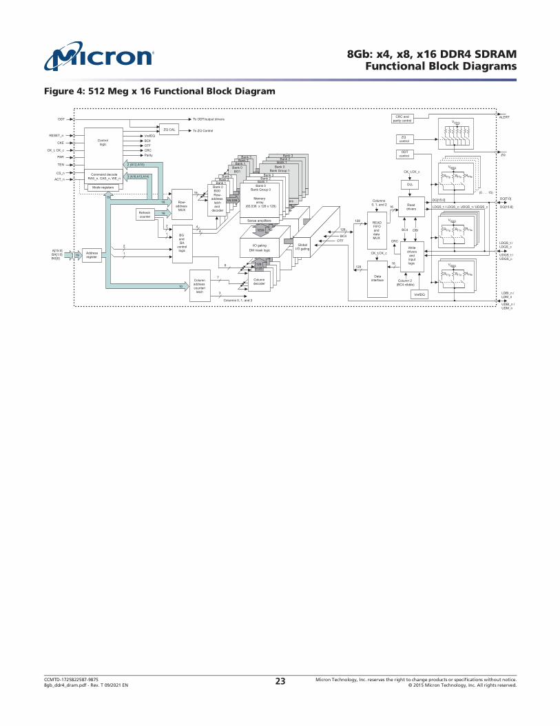
CCMTD-1725822587-9875 Micron Technology, Inc. reserves the right to change products or specifications without notice.8gb_ddr4_dram.pdf - Rev. T 09/2021 EN 2015 Micron Technology, Inc. All rights reserved.23
8Gb: x4, x8, x16 DDR4 SDRAMFunctional Block Diagrams
Figure 4: 512 Meg x 16 Functional Block Diagram
16
128
128
128
LDQS_t / LDQS_c; UDQS_t / UDQS_c
Columns 0, 1, and 2 Read
drivers
DQ[7:0]
DQ[15:8]
READFIFOanddataMUX
16
Columns 0, 1, and 2
3
UDBI_n / UDM_n
LDBI_n / LDM_n
ZQ
UDQS_t / UDQS_c
LDQS_t / LDQS_c
CK_t,CK_c
DLL
CK_t,CK_c
CRC
DQ[15:0]
(0 . . . 15)
BC4
BC4 DBI
Writedrivers
andinputlogic
Datainterface Column 2
(BC4 nibble)
7
8
Row-address
MUX
BG and BA
controllogic
16
ODTcontrol
VrefDQ
ZQcontrol
CRC andparity control
OTF
16
Controllogic
Mode registers
10
A[15:0]BA[1:0]BG[0]
16
3 (A16,A15,A14)
2 (A12,A10)
19
19
44
1
2
2
1
Refresh counter
To ODT/output drivers
To ZQ ControlZQ CAL
CKE
CK_t, CK_c
PAR
TEN
Command decodeRAS_n, CAS_n, WE_n
CS_n
ACT_n
RESET_nBC4 VrefDQ
Addressregister
OTFCRC Parity
VDDQ
RTTwRTTnRTTp
Bank 0 BG0
Bank 1Bank 2
Bank 3
Bank 0 BG1
Bank 1Bank 2
Bank 3
65,536
(256x64)
1638416384
16384
I/O gatingDM mask logic
Columndecoder
Bank 0Bank Group 1
Bank 1Bank 2
Bank 3
Bank 1Bank 2
Bank 3
128x128
GlobalI/O gating
Row-address
latchand
decoder
Columnaddress counter/
latch
VDDQ
VDDQ
RTTwRTTnRTTp
VDDQ
RTTwRTTnRTTp
ALERTODT
Sense amplifiers
Bank 0Bank Group 0
Memoryarray
(65,536 x 128 x 128)
Sense amplifiers
Bank 1Bank 2
Bank 3
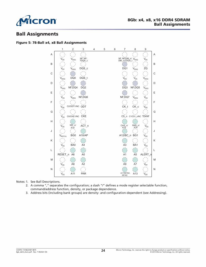
CCMTD-1725822587-9875 Micron Technology, Inc. reserves the right to change products or specifications without notice.8gb_ddr4_dram.pdf - Rev. T 09/2021 EN 2015 Micron Technology, Inc. All rights reserved.24
8Gb: x4, x8, x16 DDR4 SDRAMBall Assignments
Ball Assignments
Figure 5: 78-Ball x4, x8 Ball Assignments
Notes: 1. See Ball Descriptions.2.
command/address function, density, or package dependence.3. Address bits (including bank groups) are density- and configuration-dependent (see Addressing).
2
VSSQ
VDDQ
DQ0
NF,DQ4
VDDQ
C2/ODT1/NC
C0/CKE1/NC
BG0
BA0
A6
A8
A11
3
NF, NF/TDQS_c
DQS_c
DQS_t
DQ2
NF,DQ6
ODT
CKE
ACT_n
A10/AP
A4
A0
A2
PAR
4 6 7
NF, NF/DM_n/DBI_n/TDQS_t
DQ1
VDD
DQ3
NF,DQ7
CK_t
CS_n
CAS_n/A15
A12/BC_n
A3
A1
A9
A17/NF/NC,
8
VSSQ
VDDQ
VSS
NF,DQ5
VDDQ
CK_c
C1/CS1_n/NC
WE_n/ A14
BG1
BA1
A5
A7
A13
9
VSS
ZQ
VDDQ
VSSQ
VSS
VDD
TEN/NF
VSS
VDD
VSS
ALERT_n
VPP
VDD
5
A
B
C
D
E
F
G
H
J
K
L
M
N
A
B
C
D
E
F
G
H
J
K
L
M
N
1
VDD
VPP
VDDQ
VSSQ
VSS
VDD
VSS
VDD
VREFCA
VSS
RESET_n
VDD
VSS
RAS_n/A16
NF/NC
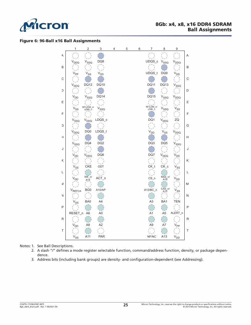
CCMTD-1725822587-9875 Micron Technology, Inc. reserves the right to change products or specifications without notice.8gb_ddr4_dram.pdf - Rev. T 09/2021 EN 2015 Micron Technology, Inc. All rights reserved.25
8Gb: x4, x8, x16 DDR4 SDRAMBall Assignments
Figure 6: 96-Ball x16 Ball Assignments
Notes: 1. See Ball Descriptions.2. -
dence.3. Address bits (including bank groups) are density- and configuration-dependent (see Addressing).
1 2 3 4 6 7 8 95
VDDQ
VPP
VDDQ
VDD
VSS
VSSQ
VDDQ
VSSQ
VDD
VSS
VDD
VREFCA
VSS
RESET_n
VDD
VSS
VSSQ
VSS
DQ12
VSSQ
VDDQ
DQ0
DQ4
VDDQ
CKE
BG0
BA0
A6
A8
A11
DQ8
VDD
DQ10
DQ14
VSSQ
LDQS_c
LDQS_t
DQ2
DQ6
ODT
ACT_n
A10/AP
A4
A0
A2
PAR
UDQS_c
UDQS_t
DQ11
DQ15
DQ1
VDD
DQ3
DQ7
CK_t
CS_n
A12/BC_n
A3
A1
A9
NF/NC
VSSQ
DQ9
DQ13
VSSQ
VSSQ
VDDQ
VSS
DQ5
VDDQ
CK_c
BA1
A5
A7
A13
VDDQ
VDD
VSSQ
VDDQ
VSS
ZQ
VDDQ
VSSQ
VDD
VSS
VDD
VSS
TEN
VPP
VDD
A
B
C
D
E
F
G
H
J
K
L
M
N
P
R
T
A
B
C
D
E
F
G
H
J
K
L
M
N
P
R
T
NF/LDM_n/LDBI_n
ALERT_n
NF/UDM_n/UDBI_n
CAS_n/A15
WE_n/ A14
RAS_n/A16

CCMTD-1725822587-9875 Micron Technology, Inc. reserves the right to change products or specifications without notice.8gb_ddr4_dram.pdf - Rev. T 09/2021 EN 2015 Micron Technology, Inc. All rights reserved.26
8Gb: x4, x8, x16 DDR4 SDRAMBall Descriptions
Ball Descriptions
The pin description table below is a comprehensive list of all possible pins for DDR4 devices. All pins listed may not be supported on the device defined in this data sheet. See the Ball Assignments section to review all pins used on this device.
Table 3: Ball Descriptions
Symbol Type Description
A[17:0] Input Address inputs: Provide the row address for ACTIVATE commands and the column address for READ/WRITE commands to select one location out of the memory array in the respective bank. (A10/AP, A12/BC_n, WE_n/A14, CAS_n/A15, RAS_n/A16 have addi-tional functions, see individual entries in this table.) The address inputs also provide the op-code during the MODE REGISTER SET command. A16 is used on some 8Gb and 16Gb parts. A17 connection is part-number specific; Contact vendor for more informa-tion.
A10/AP Input Auto precharge: A10 is sampled during READ and WRITE commands to determine whether auto precharge should be performed to the accessed bank after a READ or WRITE operation. (HIGH = auto precharge; LOW = no auto precharge.) A10 is sampled during a PRECHARGE command to determine whether the PRECHARGE applies to one bank (A10 LOW) or all banks (A10 HIGH). If only one bank is to be precharged, the bank is selected by the bank group and bank addresses.
A12/BC_n Input Burst chop: A12/BC_n is sampled during READ and WRITE commands to determine if burst chop (on-the-fly) will be performed. (HIGH = no burst chop; LOW = burst chopped). See the Command Truth Table.
ACT_n Input Command input: ACT_n indicates an ACTIVATE command. When ACT_n (along with CS_n) is LOW, the input pins RAS_n/A16, CAS_n/A15, and WE_n/A14 are treated as row address inputs for the ACTIVATE command. When ACT_n is HIGH (along with CS_n LOW), the input pins RAS_n/ A16, CAS_n/A15, and WE_n/A14 are treated as normal commands that use the RAS_n, CAS_n, and WE_n signals. See the Command Truth Table.
BA[1:0] Input Bank address inputs: Define the bank (within a bank group) to which an ACTIVATE, READ, WRITE, or PRECHARGE command is being applied. Also determines which mode register is to be accessed during a MODE REGISTER SET command.
BG[1:0] Input Bank group address inputs: Define the bank group to which an ACTIVATE, READ, WRITE, or PRECHARGE command is being applied. Also determines which mode regis-ter is to be accessed during a MODE REGISTER SET command. BG[1:0] are used in the x4 and x8 configurations. BG1 is not used in the x16 configuration.
C0/CKE1, C1/CS1_n,C2/ODT1
Input Stack address inputs: These inputs are used only when devices are stacked; that is, they are used in 2H, 4H, and 8H stacks for x4 and x8 configurations (these pins are not used in the x16 configuration, and are NC on the x4/x8 SDP). DDR4 will support a tra-ditional DDP package, which uses these three signals for control of the second die (CS1_n, CKE1, ODT1). DDR4 is not expected to support a traditional QDP package. For all other stack configurations, such as a 4H or 8H, it is assumed to be a single-load (master/slave) type of configuration where C0, C1, and C2 are used as chip ID selects in conjunction with a single CS_n, CKE, and ODT signal.
CK_t,CK_c
Input Clock: Differential clock inputs. All address, command, and control input signals are sampled on the crossing of the positive edge of CK_t and the negative edge of CK_c.

CCMTD-1725822587-9875 Micron Technology, Inc. reserves the right to change products or specifications without notice.8gb_ddr4_dram.pdf - Rev. T 09/2021 EN 2015 Micron Technology, Inc. All rights reserved.27
8Gb: x4, x8, x16 DDR4 SDRAMBall Descriptions
CKE Input Clock enable: CKE HIGH activates and CKE LOW deactivates the internal clock sig-nals, device input buffers, and output drivers. Taking CKE LOW provides PRECHARGE POWER-DOWN and SELF REFRESH operations (all banks idle), or active power-down (row active in any bank). CKE is asynchronous for self refresh exit, however, timing
parameters such as tXS are still calculated from the first rising clock edge where CKE
HIGH satisfies tIS. After VREFCA has become stable during the power-on and initializa-tion sequence, it must be maintained during all operations (including SELF REFRESH). CKE must be maintained HIGH throughout read and write accesses. Input buffers (excluding CK_t, CK_c, ODT, RESET_n, and CKE) are disabled during power-down. Input buffers (excluding CKE and RESET_n) are disabled during self refresh.
CS_n Input Chip select: All commands are masked when CS_n is registered HIGH. CS_n provides for external rank selection on systems with multiple ranks. CS_n is considered part of the command code.
DM_n,UDM_nLDM_n
Input Input data mask: DM_n is an input mask signal for write data. Input data is masked when DM is sampled LOW coincident with that input data during a write access. DM is sampled on both edges of DQS. DM is not supported on x4 configurations. The UDM_n and LDM_n pins are used in the x16 configuration: UDM_n is associated with DQ[15:8]; LDM_n is associated with DQ[7:0]. The DM, DBI, and TDQS functions are enabled by mode register settings. See the Data Mask section.
ODT Input On-die termination: ODT (registered HIGH) enables termination resistance internal to the DDR4 SDRAM. When enabled, ODT (RTT) is applied only to each DQ, DQS_t, DQS_c, DM_n/DBI_n/TDQS_t, and TDQS_c signal for the x4 and x8 configurations (when the TDQS function is enabled via mode register). For the x16 configuration, RTT is applied to each DQ, UDQS_t, UDQS_c, LDQS_t, LDQS_c, UDM_n, and LDM_n signal. The ODT pin will be ignored if the mode registers are programmed to disable RTT.
PAR Input Parity for command and address: This function can be enabled or disabled via the mode register. When enabled, the parity signal covers all command and address inputs, including ACT_n, RAS_n/A16, CAS_n/A15, WE_n/A14, A[17:0], A10/AP, A12/BC_n, BA[1:0], and BG[1:0] with C0, C1, and C2 on 3DS only devices. Control pins NOT covered by the parity signal are CS_n, CKE, and ODT. Unused address pins that are density- and configuration-specific should be treated internally as 0s by the DRAM parity logic. Command and address inputs will have parity check performed when commands are latched via the rising edge of CK_t and when CS_n is LOW.
RAS_n/A16,CAS_n/A15,WE_n/A14
Input Command inputs: RAS_n/A16, CAS_n/A15, and WE_n/A14 (along with CS_n and ACT_n) define the command and/or address being entered. See the ACT_n description in this table.
RESET_n Input Active LOW asynchronous reset: Reset is active when RESET_n is LOW, and inac-tive when RESET_n is HIGH. RESET_n must be HIGH during normal operation. RESET_n is a CMOS rail-to-rail signal with DC HIGH and LOW at 80% and 20% of VDD (960 mV for DC HIGH and 240 mV for DC LOW).
TEN Input Connectivity test mode: TEN is active when HIGH and inactive when LOW. TEN must be LOW during normal operation. TEN is a CMOS rail-to-rail signal with DC HIGH and LOW at 80% and 20% of VDD (960mV for DC HIGH and 240mV for DC LOW). On Micron 3DS devices, connectivity test mode is not supported and the TEN pin should be considered NF maintained LOW at all times.
Table 3: Ball Descriptions (Continued)
Symbol Type Description
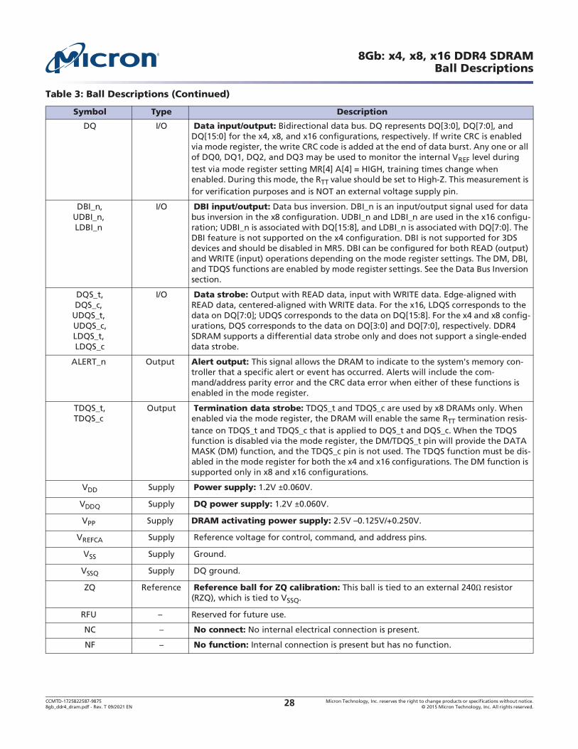
CCMTD-1725822587-9875 Micron Technology, Inc. reserves the right to change products or specifications without notice.8gb_ddr4_dram.pdf - Rev. T 09/2021 EN 2015 Micron Technology, Inc. All rights reserved.28
8Gb: x4, x8, x16 DDR4 SDRAMBall Descriptions
DQ I/O Data input/output: Bidirectional data bus. DQ represents DQ[3:0], DQ[7:0], and DQ[15:0] for the x4, x8, and x16 configurations, respectively. If write CRC is enabled via mode register, the write CRC code is added at the end of data burst. Any one or all of DQ0, DQ1, DQ2, and DQ3 may be used to monitor the internal VREF level during test via mode register setting MR[4] A[4] = HIGH, training times change when enabled. During this mode, the RTT value should be set to High-Z. This measurement is for verification purposes and is NOT an external voltage supply pin.
DBI_n,UDBI_n,LDBI_n
I/O DBI input/output: Data bus inversion. DBI_n is an input/output signal used for data bus inversion in the x8 configuration. UDBI_n and LDBI_n are used in the x16 configu-ration; UDBI_n is associated with DQ[15:8], and LDBI_n is associated with DQ[7:0]. The DBI feature is not supported on the x4 configuration. DBI is not supported for 3DS devices and should be disabled in MR5. DBI can be configured for both READ (output) and WRITE (input) operations depending on the mode register settings. The DM, DBI, and TDQS functions are enabled by mode register settings. See the Data Bus Inversion section.
DQS_t,DQS_c,
UDQS_t, UDQS_c,LDQS_t, LDQS_c
I/O Data strobe: Output with READ data, input with WRITE data. Edge-aligned with READ data, centered-aligned with WRITE data. For the x16, LDQS corresponds to the data on DQ[7:0]; UDQS corresponds to the data on DQ[15:8]. For the x4 and x8 config-urations, DQS corresponds to the data on DQ[3:0] and DQ[7:0], respectively. DDR4 SDRAM supports a differential data strobe only and does not support a single-ended data strobe.
ALERT_n Output Alert output: This signal allows the DRAM to indicate to the system's memory con-troller that a specific alert or event has occurred. Alerts will include the com-mand/address parity error and the CRC data error when either of these functions is enabled in the mode register.
TDQS_t,TDQS_c
Output Termination data strobe: TDQS_t and TDQS_c are used by x8 DRAMs only. When enabled via the mode register, the DRAM will enable the same RTT termination resis-tance on TDQS_t and TDQS_c that is applied to DQS_t and DQS_c. When the TDQS function is disabled via the mode register, the DM/TDQS_t pin will provide the DATA MASK (DM) function, and the TDQS_c pin is not used. The TDQS function must be dis-abled in the mode register for both the x4 and x16 configurations. The DM function is supported only in x8 and x16 configurations.
VDD Supply Power supply: 1.2V 0.060V.
VDDQ Supply DQ power supply: 1.2V 0.060V.
VPP Supply DRAM activating power supply:
VREFCA Supply Reference voltage for control, command, and address pins.
VSS Supply Ground.
VSSQ Supply DQ ground.
ZQ Reference Reference ball for ZQ calibration: This ball is tied to an external 240 resistor (RZQ), which is tied to VSSQ.
RFU Reserved for future use.
NC No connect: No internal electrical connection is present.
NF No function: Internal connection is present but has no function.
Table 3: Ball Descriptions (Continued)
Symbol Type Description
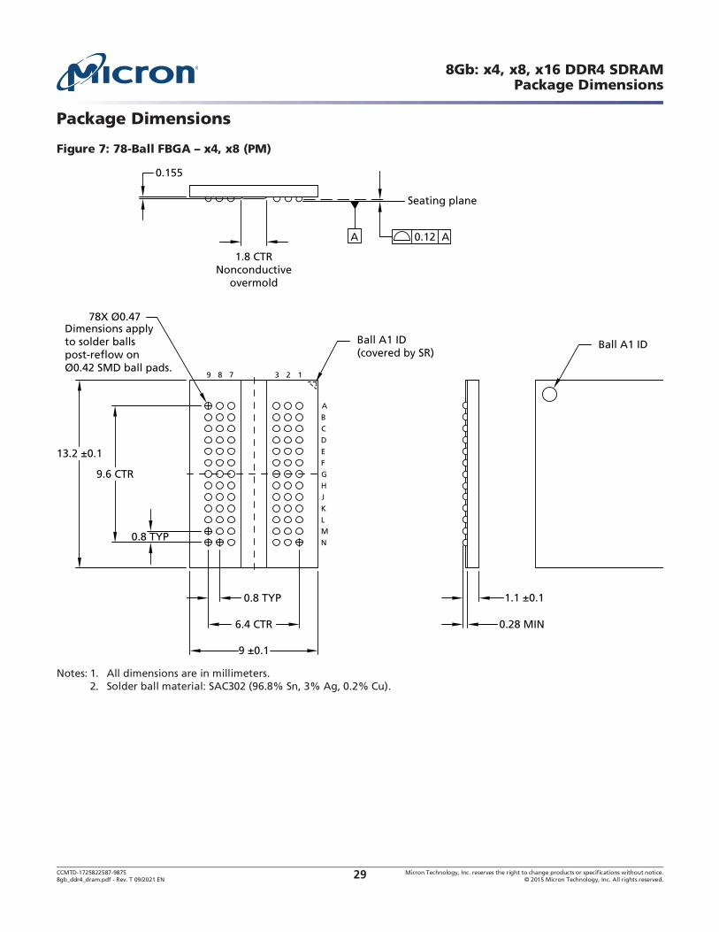
CCMTD-1725822587-9875 Micron Technology, Inc. reserves the right to change products or specifications without notice.8gb_ddr4_dram.pdf - Rev. T 09/2021 EN 2015 Micron Technology, Inc. All rights reserved.29
8Gb: x4, x8, x16 DDR4 SDRAMPackage Dimensions
Package Dimensions
Figure 7:
Notes: 1. All dimensions are in millimeters.2. Solder ball material: SAC302 (96.8% Sn, 3% Ag, 0.2% Cu).
1.8 CTRNonconductive
overmold
0.155
Seating plane
0.12 A
Ball A1 ID(covered by SR)
Ball A1 ID
A
0.28 MIN
1.1 ±0.1
6.4 CTR
9 ±0.1
0.8 TYP
9.6 CTR
13.2 ±0.1
78X Ø0.47Dimensions applyto solder ballspost-reflow onØ0.42 SMD ball pads.
0.8 TYP
123789
ABCDEFGHJKLMN

CCMTD-1725822587-9875 Micron Technology, Inc. reserves the right to change products or specifications without notice.8gb_ddr4_dram.pdf - Rev. T 09/2021 EN 2015 Micron Technology, Inc. All rights reserved.30
8Gb: x4, x8, x16 DDR4 SDRAMPackage Dimensions
Figure 8:
Notes: 1. All dimensions are in millimeters.2. Solder ball material: SAC302 (96.8% Sn, 3% Ag, 0.2% Cu).
1.8 CTRnonconductive
overmold
0.155
Seating plane
0.12 A
Ball A1 ID(covered by SR)
Ball A1 ID
A
0.34 ±0.05
1.1 ±0.1
6.4 CTR
8 ±0.1
0.8 TYP
9.6 CTR
12 ±0.1
78X Ø0.47Dimensions applyto solder balls post-reflow on Ø0.42 SMDball pads.
0.8 TYP
123789
ABCDEFGHJKLMN
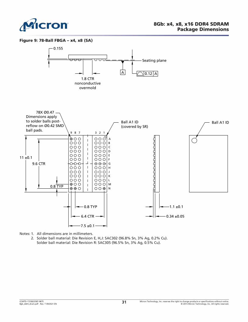
CCMTD-1725822587-9875 Micron Technology, Inc. reserves the right to change products or specifications without notice.8gb_ddr4_dram.pdf - Rev. T 09/2021 EN 2015 Micron Technology, Inc. All rights reserved.31
8Gb: x4, x8, x16 DDR4 SDRAMPackage Dimensions
Figure 9:
Notes: 1. All dimensions are in millimeters.2. Solder ball material: Die Revision E, H,J: SAC302 (96.8% Sn, 3% Ag, 0.2% Cu).
Solder ball material: Die Revision R: SAC305 (96.5% Sn, 3% Ag, 0.5% Cu).
1.8 CTRnonconductive
overmold
0.155
Seating plane
0.12 AA
Ball A1 ID(covered by SR)
Ball A1 ID
0.34 ±0.05
1.1 ±0.1
6.4 CTR
7.5 ±0.1
0.8 TYP
9.6 CTR
11 ±0.1
78X Ø0.47Dimensions applyto solder balls post-reflow on Ø0.42 SMDball pads.
0.8 TYP
123789
ABCDEFGHJKLMN

CCMTD-1725822587-9875 Micron Technology, Inc. reserves the right to change products or specifications without notice.8gb_ddr4_dram.pdf - Rev. T 09/2021 EN 2015 Micron Technology, Inc. All rights reserved.32
8Gb: x4, x8, x16 DDR4 SDRAMPackage Dimensions
Figure 10:
Notes: 1. All dimensions are in millimeters.2. Solder ball material: SAC302 (96.8% Sn, 3% Ag, 0.2% Cu).
1.8 CTRNonconductive
overmold
0.155
Seating plane
0.12 A
Ball A1 ID(covered by SR)
Ball A1 ID
A
0.29 MIN
1.1 ±0.1
6.4 CTR
9 ±0.1
0.8 TYP
12 CTR
14 ±0.1
96X Ø0.47Dimensions applyto solder balls post-reflow on Ø0.42 SMDball pads.
0.8 TYP
123789
ABCDEFGHJKLMNPRT

CCMTD-1725822587-9875 Micron Technology, Inc. reserves the right to change products or specifications without notice.8gb_ddr4_dram.pdf - Rev. T 09/2021 EN 2015 Micron Technology, Inc. All rights reserved.33
8Gb: x4, x8, x16 DDR4 SDRAMPackage Dimensions
Figure 11:
Notes: 1. All dimensions are in millimeters.2. Solder ball material: SAC302 (96.8% Sn, 3% Ag, 0.2% Cu).
1.8 CTRNonconductive
overmold
0.155
Seating plane
0.12 A
Ball A1 ID(covered by SR)
Ball A1 ID
0.34 ±0.05
1.1 ±0.1
6.4 CTR
8 ±0.1
0.8 TYP
12 CTR
14 ±0.1
96X Ø0.47Dimensions applyto solder balls post-reflow on Ø0.42 SMDball pads.
0.8 TYP
123789
ABCDEFGHJKLMNPRT
A
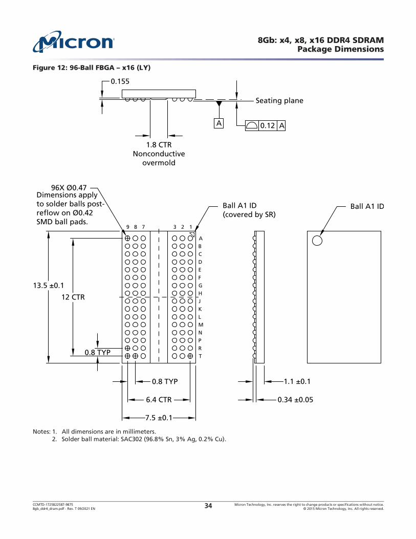
CCMTD-1725822587-9875 Micron Technology, Inc. reserves the right to change products or specifications without notice.8gb_ddr4_dram.pdf - Rev. T 09/2021 EN 2015 Micron Technology, Inc. All rights reserved.34
8Gb: x4, x8, x16 DDR4 SDRAMPackage Dimensions
Figure 12:
Notes: 1. All dimensions are in millimeters.2. Solder ball material: SAC302 (96.8% Sn, 3% Ag, 0.2% Cu).
Seating plane
0.12 A
Ball A1 ID(covered by SR)
Ball A1 ID
A
0.34 ±0.05
1.1 ±0.1
6.4 CTR
7.5 ±0.1
0.8 TYP
12 CTR
13.5 ±0.1
96X Ø0.47Dimensions applyto solder balls post-reflow on Ø0.42SMD ball pads.
0.8 TYP
1.8 CTRNonconductive
overmold
0.155
123789
ABCDEFGHJKLMNPRT

CCMTD-1725822587-9875 Micron Technology, Inc. reserves the right to change products or specifications without notice.8gb_ddr4_dram.pdf - Rev. T 09/2021 EN 2015 Micron Technology, Inc. All rights reserved.35
8Gb: x4, x8, x16 DDR4 SDRAMPackage Dimensions
Figure 13:
Notes: 1. All dimensions are in millimeters.2. Solder ball material: Die Revision J: SAC302 (96.8% Sn, 3% Ag, 0.2% Cu).
Solder ball material: Die Revision R: SAC305 (96.5% Sn, 3% Ag, 0.5% Cu).
Seating plane
0.1 A
Ball A1 ID(covered by SR)
Ball A1 ID
A
0.34 ±0.05
1.1 ±0.1
6.4 CTR
7.5 ±0.1
0.8 TYP
12 CTR
13 ±0.1
96X Ø0.47Dimensionsapply to solderballs post-reflowon Ø0.42 SMDball pads.
0.8 TYP
1.8 CTRNonconductive
overmold
0.155
123789
ABCDEFGHJKLMNPRT

CCMTD-1725822587-9875 Micron Technology, Inc. reserves the right to change products or specifications without notice.8gb_ddr4_dram.pdf - Rev. T 09/2021 EN 2015 Micron Technology, Inc. All rights reserved.36
8Gb: x4, x8, x16 DDR4 SDRAMState Diagram
State Diagram
This simplified state diagram provides an overview of the possible state transitions and the commands to control them. Situations involving more than one bank, the enabling or disabling of on-die termina-tion, and some other events are not captured in full detail.
Figure 14: Simplified State Diagram
Bankactive
ReadingWriting
Activating
Refreshing
Selfrefresh
Idle
Activepower-down
ZQcalibration
Power
From any state
applied Reset procedurePower-On Initialization
MRS, MPR,write leveling,VREFDQ training
Prechargepower-down
Writing Reading
Automaticsequence
Commandsequence
Precharging
READ
READ READ
READ A
READ A
READ A
PRE, PREA
PRE, PREA PRE, PREA
WRITE
WRITEWRITE
WRITE A
WRITE A
WRITE A
PDE
PDE
PDX
PDX
SRX
SRE
REF
ACT
ZQCL
ZQCL,ZQCS
CKE_L
CKE_L
CKE_L
MPSM
PDAmode
IVREFDQ,RTT, andso on
Connectivitytest
RESET
RESET
RESET
TEN = 0
MRS
MRSSRX*
SRX*SRX* = SRX with NOP
MRS
MRS
MRSMRS
TEN = 1TEN = 1

CCMTD-1725822587-9875 Micron Technology, Inc. reserves the right to change products or specifications without notice.8gb_ddr4_dram.pdf - Rev. T 09/2021 EN 2015 Micron Technology, Inc. All rights reserved.37
8Gb: x4, x8, x16 DDR4 SDRAMState Diagram
Notes: 1. See the Command Truth Table for more details.
Table 4: State Diagram Command Definitions
Command Description
ACT Active
MPR Multipurpose register
MRS Mode register set
PDE Enter power-down
PDX Exit power-down
PRE Precharge
PREA Precharge all
READ RD, RDS4, RDS8
READ A RDA, RDAS4, RDAS8
REF Refresh, fine granularity refresh
RESET Start reset procedure
SRE Self refresh entry
SRX Self refresh exit
TEN Boundary scan mode enable
WRITE WR, WRS4, WRS8 with/without CRC
WRITE A WRA, WRAS4, WRAS8 with/without CRC
ZQCL ZQ calibration long
ZQCS ZQ calibration short

CCMTD-1725822587-9875 Micron Technology, Inc. reserves the right to change products or specifications without notice.8gb_ddr4_dram.pdf - Rev. T 09/2021 EN 2015 Micron Technology, Inc. All rights reserved.38
8Gb: x4, x8, x16 DDR4 SDRAMFunctional Description
Functional Description
The DDR4 SDRAM is a high-speed dynamic random-access memory internally configured as sixteen banks (4 bank groups with 4 banks for each bank group) for x4/x8 devices, and as eight banks for each bank group (2 bank groups with 4 banks each) for x16 devices. The device uses double data rate (DDR) architecture to achieve high-speed operation. DDR4 architecture is essentially an 8n-prefetch archi-tecture with an interface designed to transfer two data words per clock cycle at the I/O pins. A single read or write access for a device module effectively consists of a single 8n-bit-wide, four-clock-cycle-data transfer at the internal DRAM core and eight corresponding n-bit-wide, one-half-clock-cycle data transfers at the I/O pins.
Read and write accesses to the device are burst-oriented. Accesses start at a selected location and continue for a burst length of eight or a chopped burst of four in a programmed sequence. Operation begins with the registration of an ACTIVE command, which is then followed by a READ or WRITE command. The address bits registered coincident with the ACTIVE command are used to select the bank and row to be accessed (BG[1:0] select the bank group for x4/x8, and BG0 selects the bank group for x16; BA[1:0] select the bank, and A[17:0] select the row. See the Addressing section for more details). The address bits registered coincident with the READ or WRITE command are used to select the starting column location for the burst operation, determine if the auto PRECHARGE command is to be issued (via A10), and select BC4 or BL8 mode on-the-fly (OTF) (via A12) if enabled in the mode register.
Prior to normal operation, the device must be powered up and initialized in a predefined manner. The following sections provide detailed information covering device reset and initialization, register defi-nition, command descriptions, and device operation.
NOTE: The use of the NOP command is allowed only when exiting maximum power saving mode or when entering gear-down mode.

CCMTD-1725822587-9875 Micron Technology, Inc. reserves the right to change products or specifications without notice.8gb_ddr4_dram.pdf - Rev. T 09/2021 EN 2015 Micron Technology, Inc. All rights reserved.39
8Gb: x4, x8, x16 DDR4 SDRAMRESET and Initialization Procedure
RESET and Initialization Procedure
To ensure proper device function, the power-up and reset initialization default values for the following mode register (MR) settings are defined as:
Gear-down mode (MR3 A[3]): 0 = 1/2 ratePer-DRAM addressability (MR3 A[4]): 0 = disableMaximum power-saving mode (MR4 A[1]): 0 = disableCS to command/address latency (MR4 A[8:6]): 000 = disableCA parity latency mode (MR5 A[2:0]): 000 = disableHard post package repair mode (MR4 A[13]): 0 = disableSoft post package repair mode (MR4 A[5]): 0 = disable
Power-Up and Initialization Sequence
The following sequence is required for power-up and initialization:1. Apply power (RESET_n and TEN should be maintained below 0.2 VDD while supplies ramp up; all
other inputs may be undefined). When supplies have ramped to a valid stable level, RESET_n must
be maintained below 0.2 VDD for a minimum of tPW_RESET_L and TEN must be maintained below 0.2 VDD for a minimum of 700 s. CKE is pulled LOW anytime before RESET_n is de-asserted (minimum time of 10ns). The power voltage ramp time between 300mV to VDD,min must be no greater than 200ms, and during the ramp, VDD must be greater than or equal to VDDQ and (VDD - VDDQ) < 0.3V. VPP must ramp at the same time or up to 10 minutes prior to VDD, and VPP must be equal to or higher than VDD at all times. The total time for which VPP is powered and VDD is unpow-ered should not exceed 360 cumulative hours. After VDD has ramped and reached a stable level, RESET_n must go high within 10 minutes. After RESET_n goes high, the initialization sequence must be started within 3 seconds. For debug purposes, the 10 minute and 3 second delay limits may be extended to 60 minutes each provided the DRAM is operated in this debug mode for no more than 360 cumulative hours.During power-up, the supply slew rate is governed by the limits stated in the table below and either condition A or condition B listed below must be met.
Notes: 1. 20 MHz band-limited measurement.Condition A:
Apply VPP without any slope reversal before or at the same time as VDD and VDDQ.
VDD and VDDQ are driven from a single-power converter output and apply VDD/VDDQ without any slope reversal before or at the same time as VTT and VREFCA.
The voltage levels on all balls other than VDD, VDDQ, VSS, and VSSQ must be less than or equal to VDDQ and VDD on one side and must be greater than or equal to VSSQ and VSS on the other side.
VTT is limited to 0.76V MAX when the power ramp is complete.
VREFCA tracks VDD/2.
Table 5: Supply Power-up Slew Rate
Symbol Min Max Unit Comment
VDD_SL, VDDQ_SL, VPP_SL 0.004 600 V/ms Measured between 300mV and 80% of supply minimum
VDD_ona N/A 200 ms VDD maximum ramp time from 300mV to VDD minimum
VDDQ_ona N/A 200 ms VDDQ maximum ramp time from 300mV to VDDQ minimum

CCMTD-1725822587-9875 Micron Technology, Inc. reserves the right to change products or specifications without notice.8gb_ddr4_dram.pdf - Rev. T 09/2021 EN 2015 Micron Technology, Inc. All rights reserved.40
8Gb: x4, x8, x16 DDR4 SDRAMRESET and Initialization Procedure
Condition B: Apply VPP without any slope reversal before or at the same time as VDD.
Apply VDD without any slope reversal before or at the same time as VDDQ.
Apply VDDQ without any slope reversal before or at the same time as VTT and VREFCA.
The voltage levels on all pins other than VPP, VDD, VDDQ, VSS, and VSSQ must be less than or equal to VDDQ and VDD on one side and must be larger than or equal to VSSQ and VSS on the other side.
2. After RESET_n is de-asserted, wait for a minimum of 500 s, but no longer than 3 seconds, before allowing CKE to be registered HIGH at clock edge Td. During this time, the device will start internal state initialization; this will be done independently of external clocks. A reasonable attempt was made in the design to power up with the following default MR settings: gear-down mode (MR3 A[3]): 0 = 1/2 rate; per-DRAM addressability (MR3 A[4]): 0 = disable; maximum power-down (MR4 A[1]): 0 = disable; CS to command/address latency (MR4 A[8:6]): 000 = disable; CA parity latency mode (MR5 A[2:0]): 000 = disable. However, it should be assumed that at power up the MR settings are unde-fined and should be programmed as shown below.
3. Clocks (CK_t, CK_c) need to be started and stabilized for at least 10ns or 5 tCK (whichever is larger) before CKE is registered HIGH at clock edge Td. Because CKE is a synchronous signal, the corre-
sponding setup time to clock (tIS) must be met. Also, a DESELECT command must be registered
(with tIS setup time to clock) at clock edge Td. After the CKE is registered HIGH after RESET, CKE needs to be continuously registered HIGH until the initialization sequence is finished, including
expiration of tDLLK and tZQinit.4. The device keeps its ODT in High-Z state as long as RESET_n is asserted. Further, the SDRAM keeps
its ODT in High-Z state after RESET_n de-assertion until CKE is registered HIGH. The ODT input
signal may be in an undefined state until tIS before CKE is registered HIGH. When CKE is registered HIGH, the ODT input signal may be statically held either LOW or HIGH. If RTT(NOM) is to be enabled in MR1, the ODT input signal must be statically held LOW. In all cases, the ODT input signal remains
static until the power-up initialization sequence is finished, including the expiration of tDLLK and tZQinit.
5. After CKE is registered HIGH, wait a minimum of RESET CKE EXIT time, tXPR, before issuing the first
MRS command to load mode register (tXPR = MAX (tXS, 5 tCK).
6. Issue MRS command to load MR3 with all application settings, wait tMRD.
7. Issue MRS command to load MR6 with all application settings, wait tMRD.
8. Issue MRS command to load MR5 with all application settings, wait tMRD.
9. Issue MRS command to load MR4 with all application settings, wait tMRD.
10.Issue MRS command to load MR2 with all application settings, wait tMRD.
11.Issue MRS command to load MR1 with all application settings, wait tMRD.
12.Issue MRS command to load MR0 with all application settings, wait tMOD.13.Issue a ZQCL command to start ZQ calibration.
14.Wait for tDLLK and tZQinit to complete.15.The device will be ready for normal operation. Once the DRAM has been initialized, if the DRAM is
in an idle state longer than 960ms, then either (a) REF commands must be issued within tREFI constraints (specification for posting allowed) or (b) CKE or CS_n must toggle once within every 960ms interval of idle time. For debug purposes, the 960ms delay limit maybe extended to 60 minutes provided the DRAM is operated in this debug mode for no more than 360 cumulative hours.
16.Optional MBIST-PPR mode can be entered by setting MR4:A0 to 1, followed by subsequent MR0 guard key sequences, then DRAM will drive ALERT_n to LOW. DRAM will drive ALERT_n to HIGH
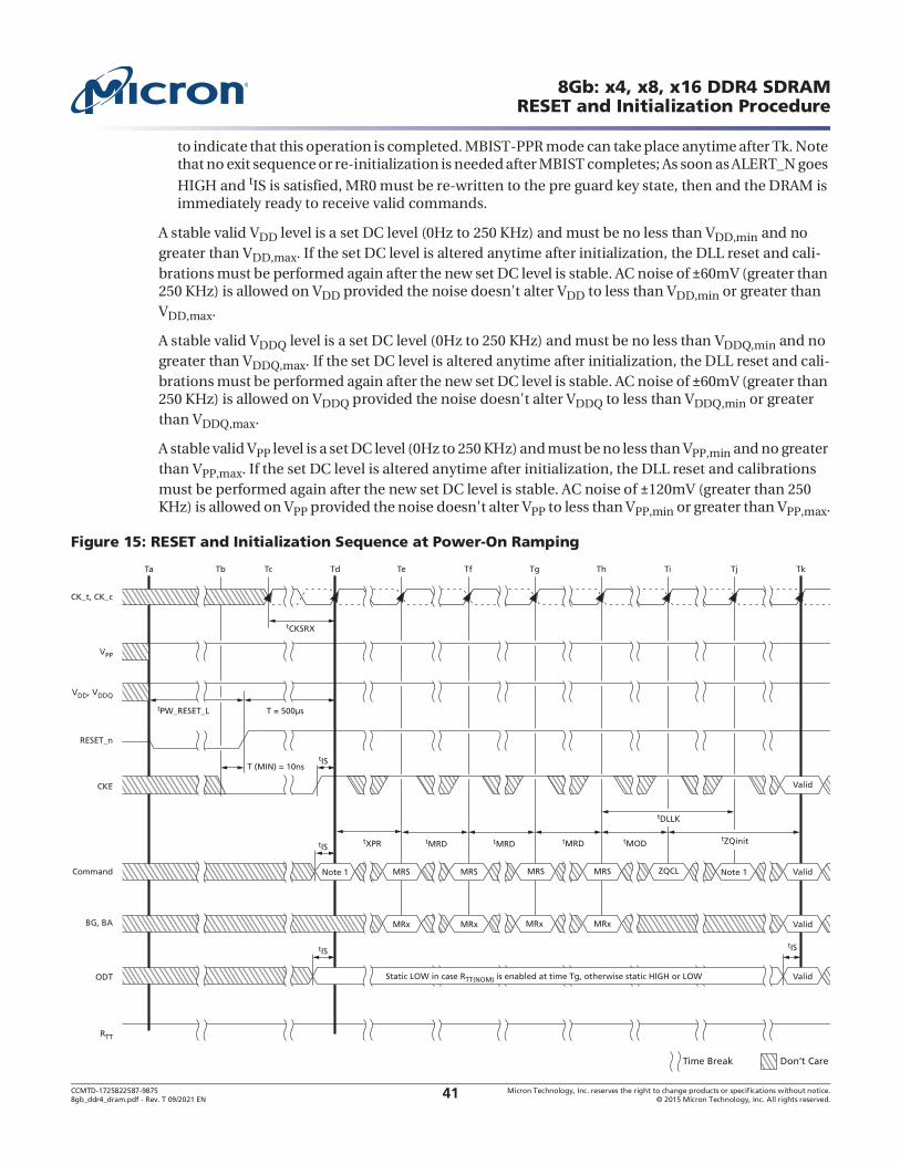
CCMTD-1725822587-9875 Micron Technology, Inc. reserves the right to change products or specifications without notice.8gb_ddr4_dram.pdf - Rev. T 09/2021 EN 2015 Micron Technology, Inc. All rights reserved.41
8Gb: x4, x8, x16 DDR4 SDRAMRESET and Initialization Procedure
to indicate that this operation is completed. MBIST-PPR mode can take place anytime after Tk. Note that no exit sequence or re-initialization is needed after MBIST completes; As soon as ALERT_N goes
HIGH and tIS is satisfied, MR0 must be re-written to the pre guard key state, then and the DRAM is immediately ready to receive valid commands.
A stable valid VDD level is a set DC level (0Hz to 250 KHz) and must be no less than VDD,min and no greater than VDD,max. If the set DC level is altered anytime after initialization, the DLL reset and cali-brations must be performed again after the new set DC level is stable. AC noise of 60mV (greater than 250 KHz) is allowed on VDD provided the noise doesn't alter VDD to less than VDD,min or greater than VDD,max.
A stable valid VDDQ level is a set DC level (0Hz to 250 KHz) and must be no less than VDDQ,min and no greater than VDDQ,max. If the set DC level is altered anytime after initialization, the DLL reset and cali-brations must be performed again after the new set DC level is stable. AC noise of 60mV (greater than 250 KHz) is allowed on VDDQ provided the noise doesn't alter VDDQ to less than VDDQ,min or greater than VDDQ,max.
A stable valid VPP level is a set DC level (0Hz to 250 KHz) and must be no less than VPP,min and no greater than VPP,max. If the set DC level is altered anytime after initialization, the DLL reset and calibrations must be performed again after the new set DC level is stable. AC noise of 120mV (greater than 250 KHz) is allowed on VPP provided the noise doesn't alter VPP to less than VPP,min or greater than VPP,max.
Figure 15: RESET and Initialization Sequence at Power-On Ramping
CKE
RTT
BG, BA
tPW_RESET_L
CK_t, CK_c
Command Note 1 Note 1
TdTc
Don’t CareTime Break
tIS
ODT
Th
tMRD tMOD
MRSMRS Valid
Valid
tMRD tMRD
MRS
MRxMRxMRx
MRS
MRx
Ti Tj Tk
RESET_n
T = 500μs
Valid
TeTa Tb Tf
ZQCL
tIS
Static LOW in case RTT(NOM) is enabled at time Tg, otherwise static HIGH or LOW
tIStIS
tXPR
Valid
T (MIN) = 10ns
VDD, VDDQ
VPP
tDLLK
tZQinit
tCKSRX
Tg

CCMTD-1725822587-9875 Micron Technology, Inc. reserves the right to change products or specifications without notice.8gb_ddr4_dram.pdf - Rev. T 09/2021 EN 2015 Micron Technology, Inc. All rights reserved.42
8Gb: x4, x8, x16 DDR4 SDRAMRESET and Initialization Procedure
Notes: 1. From time point Td until Tk, a DES command must be applied between MRS and ZQCL commands.2. MRS commands must be issued to all mode registers that have defined settings.3. In general, there is no specific sequence for setting the MRS locations (except for dependent or co-related features,
such as ENABLE DLL in MR1 prior to RESET DLL in MR0, for example).4. TEN is not shown; however, it is assumed to be held LOW.5. Optional MBIST-PPR may be entered any time after Tk.
RESET Initialization with Stable Power Sequence
The following sequence is required for RESET at no power interruption initialization:1. Assert RESET_n below 0.2 VDD any time when reset is needed (all other inputs may be undefined).
RESET_n needs to be maintained for minimum tPW_RESET. CKE is pulled LOW before RESET_n being de-asserted (minimum time 10ns).
2. Follow Steps 2 through 10 in the Reset and Initialization Sequence at Power-On Ramping proce-dure.
When the reset sequence is complete, all counters except the refresh counters have been reset and the device is ready for normal operation.
Figure 16: RESET Procedure at Power Stable Condition
Notes: 1. From time point Td until Tk, a DES command must be applied between MRS and ZQCL commands.2. MRS commands must be issued to all mode registers that have defined settings.
CKE
RTT
BG, BA
tPW_RESET_S
CK_t, CK_c
Command Note 1 Note 1
TdTc
Don’t CareTime Break
tIS
ODT
Th
tMRD tMOD
MRSMRS Valid
Valid
tMRD tMRD
MRS
MRxMRxMRx
MRS
MRx
Ti Tj Tk
RESET_n
T = 500μs
Valid
TeTa Tb Tf
ZQCL
tIS
Static LOW in case RTT(NOM) is enabled at time Tg, otherwise static HIGH or LOW
tIStIS
tXPR
Valid
T (MIN) = 10ns
VDD, VDDQ
VPP
tDLLK
tZQinit
tCKSRX
Tg
CCMTD-1725822587-9875 Micron Technology, Inc. reserves the right to change products or specifications without notice.8gb_ddr4_dram.pdf - Rev. T 09/2021 EN 2015 Micron Technology, Inc. All rights reserved.43
8Gb: x4, x8, x16 DDR4 SDRAMProgramming Mode Registers
3. In general, there is no specific sequence for setting the MRS locations (except for dependent or co-related features, such as ENABLE DLL in MR1 prior to RESET DLL in MR0, for example).
4. TEN is not shown; however, it is assumed to be held LOW.
Uncontrolled Power-Down Sequence
In the event of an uncontrolled ramping down of VPP supply, VPP is allowed to be less than VDD provided the following conditions are met:
Condition A: VPP and VDD/VDDQ are ramping down (as part of turning off) from normal operating levels.Condition B: The amount that VPP may be less than VDD/VDDQ is less than or equal to 500mV.
Condition C: The time VPP may be less than VDD is 10ms per occurrence with a total accumulated time in this state 100ms.Condition D: The time VPP may be less than 2.0V and above VSS while turning off is 15ms per occur-rence with a total accumulated time in this state 150ms.
Programming Mode Registers
For application flexibility, various functions, features, and modes are programmable in seven mode registers (MRn) provided by the device as user defined variables that must be programmed via a MODE REGISTER SET (MRS) command. Because the default values of the mode registers are not defined, contents of mode registers must be fully initialized and/or re-initialized; that is, they must be written after power-up and/or reset for proper operation. The contents of the mode registers can be altered by re-executing the MRS command during normal operation. When programming the mode registers, even if the user chooses to modify only a sub-set of the MRS fields, all address fields within the accessed mode register must be redefined when the MRS command is issued. MRS and DLL RESET commands do not affect array contents, which means these commands can be executed any time after power-up without affecting the array contents.
The MRS command cycle time, tMRD, is required to complete the WRITE operation to the mode
register and is the minimum time required between the two MRS commands shown in the tMRD Timing figure.
Some of the mode register settings affect address/command/control input functionality. In these cases, the next MRS command can be allowed when the function being updated by the current MRS
tMRD timing to the next MRS command; however, the input cases have unique MR setting procedures, so refer to individual function descrip-tions:
Gear-down modePer-DRAM addressabilityCMD address latencyCA parity latency modeVREFDQ training value
VREFDQ training mode
VREFDQ training range
Some mode register settings may not be supported because they are not required by certain speed bins.

CCMTD-1725822587-9875 Micron Technology, Inc. reserves the right to change products or specifications without notice.8gb_ddr4_dram.pdf - Rev. T 09/2021 EN 2015 Micron Technology, Inc. All rights reserved.44
8Gb: x4, x8, x16 DDR4 SDRAMProgramming Mode Registers
Figure 17: tMRD Timing
Notes: 1.
2. tMRD applies to all MRS commands with the following exceptions:Gear-down modeCA parity latency modeCMD address latencyPer-DRAM addressability modeVREFDQ training value, VREFDQ training mode, and VREFDQ training range
The MRS command to nonMRS command delay, tMOD, is required for the DRAM to update features, except for those noted in note 2 in figure below where the individual function descriptions may specify
a different requirement. tMOD is the minimum time required from an MRS command to a nonMRS
command, excluding DES, as shown in the tMOD Timing figure.
Figure 18: tMOD Timing
Notes: 1.
2. tMOD applies to all MRS commands with the following exceptions:DLL enable, DLL RESET, Gear-down modeVREFDQ training value, internal VREF training monitor, VREFDQ training mode, and VREFDQ training rangeMaximum power savings mode, Per-DRAM addressability mode, and CA parity latency mode
The mode register contents can be changed using the same command and timing requirements during normal operation as long as the device is in idle state; that is, all banks are in the precharged state with tRP satisfied, all data bursts are completed, and CKE is HIGH prior to writing into the mode register. If
T0 T1 T2 Ta0 Ta1 Tb0 Tb1 Tb2 Tc0 Tc1 Tc2
Don’t Care
ValidValid Valid MRS2 MRS2DES DES DESDES DES Valid
CK_t
CK_c
Command
Settings
CKE
Updating settings
Address Valid Valid Valid Valid Valid Valid Valid Valid Valid Valid Valid
tMRD
Time Break
Old settings
T0 T1 T2 Ta0 Ta1 Ta2 Ta3 Ta4 Tb0 Tb1 Tb2
Don’t Care
ValidValid Valid MRS2 DES DES DESDES DES ValidValid
CK_t
CK_c
Command
Settings
CKE
Updating settings New settings
Address Valid Valid Valid Valid Valid Valid Valid Valid Valid Valid Valid
tMOD
Time Break
Old settings

CCMTD-1725822587-9875 Micron Technology, Inc. reserves the right to change products or specifications without notice.8gb_ddr4_dram.pdf - Rev. T 09/2021 EN 2015 Micron Technology, Inc. All rights reserved.45
8Gb: x4, x8, x16 DDR4 SDRAMProgramming Mode Registers
the RTT(NOM) feature is enabled in the mode register prior to and/or after an MRS command, the ODT signal must continuously be registered LOW, ensuring RTT is in an off state prior to the MRS command.
The ODT signal may be registered HIGH after tMOD has expired. If the RTT(NOM) feature is disabled in the mode register prior to and after an MRS command, the ODT signal can be registered either LOW or HIGH before, during, and after the MRS command. The mode registers are divided into various fields depending on functionality and modes.
In some mode register setting cases, function updating takes longer than tMOD. This type of MRS does
not apply tMOD timing to the next valid command, excluding DES. These MRS command input cases have unique MR setting procedures, so refer to individual function descriptions.

CCMTD-1725822587-9875 Micron Technology, Inc. reserves the right to change products or specifications without notice.8gb_ddr4_dram.pdf - Rev. T 09/2021 EN 2015 Micron Technology, Inc. All rights reserved.46
8Gb: x4, x8, x16 DDR4 SDRAMMode Register 0
Mode Register 0
Mode register 0 (MR0) controls various device operating modes as shown in the following register defi-nition table. Not all settings listed may be available on a die; only settings required for speed bin support are available. MR0 is written by issuing the MRS command while controlling the states of the BGx, BAx, and Ax address pins. The mapping of address pins during the MRS command is shown in the following MR0 Register Definition table.
Notes: 1. RAS_n, CAS_n, and WE_n must be LOW during MODE REGISTER SET command.
Table 6: Address Pin Mapping
Address bus
BG1 BG0 BA1 BA0 A17 RAS_n
CAS_n
WE_n
A13
A12 A11 A10 A9 A8 A7 A6 A5 A4 A3 A2 A1 A0
Mode register
21 20 19 18 17 13 12 11 10 9 8 7 6 5 4 3 2 1 0
Table 7: MR0 Register Definition
Mode Register Description
21 RFU0 = Must be programmed to 01 = Reserved
20:18 MR select000 = MR0001 = MR1010 = MR2011 = MR3100 = MR4101 = MR5110 = MR6111 = DNU
17 N/A on 4Gb and 8Gb, RFU0 = Must be programmed to 01 = Reserved
13,11:9 WR (WRITE recovery)/RTP (READ-to-PRECHARGE)0000 = 10 / 5 clocks1
0001 = 12 / 6 clocks
0010 = 14 / 7 clocks1
0011 = 16 / 8 / clocks
0100 = 18 / 9 clocks1
0101 = 20 /10 clocks0110 = 24 / 12 clocks
0111 = 22 / 11 clocks1
1000 = 26 / 13 clocks1
1001 = 28 / 14 clocks2
1010 through 1111 = Reserved
8 DLL reset0 = No1 = Yes
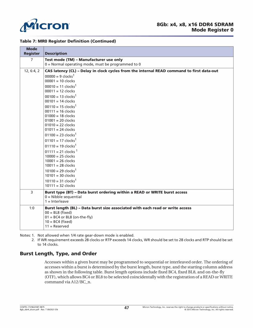
CCMTD-1725822587-9875 Micron Technology, Inc. reserves the right to change products or specifications without notice.8gb_ddr4_dram.pdf - Rev. T 09/2021 EN 2015 Micron Technology, Inc. All rights reserved.47
8Gb: x4, x8, x16 DDR4 SDRAMMode Register 0
Notes: 1. Not allowed when 1/4 rate gear-down mode is enabled.2. If WR requirement exceeds 28 clocks or RTP exceeds 14 clocks, WR should be set to 28 clocks and RTP should be set
to 14 clocks.
Burst Length, Type, and Order
Accesses within a given burst may be programmed to sequential or interleaved order. The ordering of accesses within a burst is determined by the burst length, burst type, and the starting column address as shown in the following table. Burst length options include fixed BC4, fixed BL8, and on-the-fly (OTF), which allows BC4 or BL8 to be selected coincidentally with the registration of a READ or WRITE command via A12/BC_n.
70 = Normal operating mode, must be programmed to 0
12, 6:4, 2
00000 = 9 clocks1
00001 = 10 clocks
00010 = 11 clocks1
00011 = 12 clocks
00100 = 13 clocks1
00101 = 14 clocks
00110 = 15 clocks1
00111 = 16 clocks01000 = 18 clocks01001 = 20 clocks01010 = 22 clocks01011 = 24 clocks
01100 = 23 clocks1
01101 = 17 clocks1
01110 = 19 clocks1
01111 = 21 clocks 1 10000 = 25 clocks10001 = 26 clocks 10011 = 28 clocks
10100 = 29 clocks1 10101 = 30 clocks
10110 = 31 clocks1 10111 = 32 clocks
30 = Nibble sequential1 = Interleave
1:000 = BL8 (fixed)01 = BC4 or BL8 (on-the-fly)10 = BC4 (fixed)11 = Reserved
Table 7: MR0 Register Definition (Continued)
Mode Register Description

CCMTD-1725822587-9875 Micron Technology, Inc. reserves the right to change products or specifications without notice.8gb_ddr4_dram.pdf - Rev. T 09/2021 EN 2015 Micron Technology, Inc. All rights reserved.48
8Gb: x4, x8, x16 DDR4 SDRAMMode Register 0
Table 8: Burst Type and Burst Order
Note 1 applies to the entire table
Notes: 1. 0...7 bit number is the value of CA[2:0] that causes this bit to be the first read during a burst.2. When setting burst length to BC4 (fixed) in MR0, the internal WRITE operation starts two clock cycles earlier than
for the BL8 mode, meaning the starting point for tWR and tWTR will be pulled in by two clocks. When setting burst length to OTF in MR0, the internal WRITE operation starts at the same time as a BL8 (even if BC4 was selected
during column time using A12/BC4_n) meaning that if the OTF MR0 setting is used, the starting point for tWR and tWTR will not be pulled in by two clocks as described in the BC4 (fixed) case.
3. T = Output driver for data and strobes are in High-Z. V = Valid logic level (0 or 1), but respective buffer input ignores level on input pins.
CAS Latency
The CAS latency (CL) setting is defined in the MR0 Register Definition table. CAS latency is the delay, in clock cycles, between the internal READ command and the availability of the first bit of output data. The device does not support half-clock latencies. The overall read latency (RL) is defined as additive latency (AL) + CAS latency (CL): RL = AL + CL.
Burst Length
READ/WRITE
Starting Column Address
(A[2, 1, 0]) Burst Type = Sequential
(Decimal) Burst Type = Interleaved
(Decimal) Notes
BC4 READ 0 0 0 0, 1, 2, 3, T, T, T, T 0, 1, 2, 3, T, T, T, T 2, 3
0 0 1 1, 2, 3, 0, T, T, T, T 1, 0, 3, 2, T, T, T, T 2, 3
0 1 0 2, 3, 0, 1, T, T, T, T 2, 3, 0, 1, T, T, T, T 2, 3
0 1 1 3, 0, 1, 2, T, T, T, T 3, 2, 1, 0, T, T, T, T 2, 3
1 0 0 4, 5, 6, 7, T, T, T, T 4, 5, 6, 7, T, T, T, T 2, 3
1 0 1 5, 6, 7, 4, T, T, T, T 5, 4, 7, 6, T, T, T, T 2, 3
1 1 0 6, 7, 4, 5, T, T, T, T 6, 7, 4, 5, T, T, T, T 2, 3
1 1 1 7, 4, 5, 6, T, T, T, T 7, 6, 5, 4, T, T, T, T 2, 3
WRITE 0, V, V 0, 1, 2, 3, X, X, X, X 0, 1, 2, 3, X, X, X, X 2, 3
1, V, V 4, 5, 6, 7, X, X, X, X 4, 5, 6, 7, X, X, X, X 2, 3
BL8 READ 0 0 0 0, 1, 2, 3, 4, 5, 6, 7 0, 1, 2, 3, 4, 5, 6, 7
0 0 1 1, 2, 3, 0, 5, 6, 7, 4 1, 0, 3, 2, 5, 4, 7, 6
0 1 0 2, 3, 0, 1, 6, 7, 4, 5 2, 3, 0, 1, 6, 7, 4, 5
0 1 1 3, 0, 1, 2, 7, 4, 5, 6 3, 2, 1, 0, 7, 6, 5, 4
1 0 0 4, 5, 6, 7, 0, 1, 2, 3 4, 5, 6, 7, 0, 1, 2, 3
1 0 1 5, 6, 7, 4, 1, 2, 3, 0 5, 4, 7, 6, 1, 0, 3, 2
1 1 0 6, 7, 4, 5, 2, 3, 0, 1 6, 7, 4, 5, 2, 3, 0, 1
1 1 1 7, 4, 5, 6, 3, 0, 1, 2 7, 6, 5, 4, 3, 2, 1, 0
WRITE V, V, V 0, 1, 2, 3, 4, 5, 6, 7 0, 1, 2, 3, 4, 5, 6, 7 3

CCMTD-1725822587-9875 Micron Technology, Inc. reserves the right to change products or specifications without notice.8gb_ddr4_dram.pdf - Rev. T 09/2021 EN 2015 Micron Technology, Inc. All rights reserved.49
8Gb: x4, x8, x16 DDR4 SDRAMMode Register 0
Test Mode
The normal operating mode is selected by MR0[7] and all other bits set to the desired values shown in the MR0 Register Definition table. Programming MR0[7] to a value of 1 places the device into a DRAM manufacturer-defined test mode to be used only by the manufacturer, not by the end user. No opera-tions or functionality is specified if MR0[7] = 1.
Write Recovery (WR)/READ-to-PRECHARGE
The programmed write recovery (WR) value is used for the auto precharge feature along with tRP to
determine tDAL. WR for auto precharge (MIN) in clock cycles is calculated by dividing tWR (in ns) by tCK (in ns) and rounding to the next integer using the rounding algorithms found in the Converting Time-Based Specifications to Clock-Based Requirements section. The WR value must be programmed
to be equal to or larger than tWR (MIN). When both DM and write CRC are enabled in the mode
register, the device calculates CRC before sending the write data into the array; tWR values will change when enabled. If there is a CRC error, the device blocks the WRITE operation and discards the data.
Internal READ-to-PRECHARGE (RTP) command delay for auto precharge (MIN) in clock cycles is
calculated by dividing tRTP (in ns) by tCK (in ns) and rounding to the next integer using the rounding algorithms found in the Converting Time-Based Specifications to Clock-Based Requirements section. The RTP value in the mode register must be programmed to be equal to or larger than RTP (MIN). The
programmed RTP value is used with tRP to determine the ACT timing to the same bank.
DLL RESET
The DLL reset bit is self-clearing, meaning that it returns to the value of 0 after the DLL RESET function has been issued. After the DLL is enabled, a subsequent DLL RESET should be applied. Any time the
DLL RESET function is used, tDLLK must be met before functions requiring the DLL can be used. Such as READ commands or synchronous ODT operations, for example.
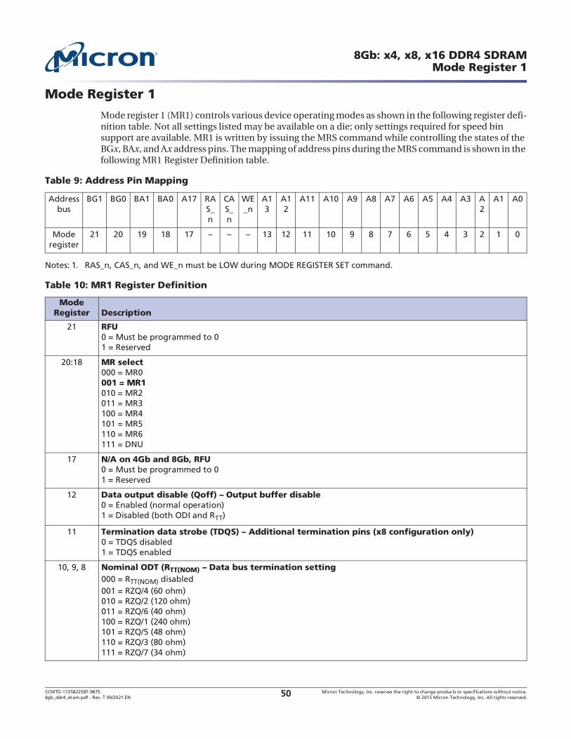
CCMTD-1725822587-9875 Micron Technology, Inc. reserves the right to change products or specifications without notice.8gb_ddr4_dram.pdf - Rev. T 09/2021 EN 2015 Micron Technology, Inc. All rights reserved.50
8Gb: x4, x8, x16 DDR4 SDRAMMode Register 1
Mode Register 1
Mode register 1 (MR1) controls various device operating modes as shown in the following register defi-nition table. Not all settings listed may be available on a die; only settings required for speed bin support are available. MR1 is written by issuing the MRS command while controlling the states of the BGx, BAx, and Ax address pins. The mapping of address pins during the MRS command is shown in the following MR1 Register Definition table.
Notes: 1. RAS_n, CAS_n, and WE_n must be LOW during MODE REGISTER SET command.
Table 9: Address Pin Mapping
Address bus
BG1 BG0 BA1 BA0 A17 RAS_n
CAS_n
WE_n
A13
A12
A11 A10 A9 A8 A7 A6 A5 A4 A3 A2
A1 A0
Mode register
21 20 19 18 17 13 12 11 10 9 8 7 6 5 4 3 2 1 0
Table 10: MR1 Register Definition
Mode Register Description
21 RFU0 = Must be programmed to 01 = Reserved
20:18 MR select000 = MR0001 = MR1010 = MR2011 = MR3100 = MR4101 = MR5110 = MR6111 = DNU
17 N/A on 4Gb and 8Gb, RFU0 = Must be programmed to 01 = Reserved
120 = Enabled (normal operation)1 = Disabled (both ODI and RTT)
110 = TDQS disabled1 = TDQS enabled
10, 9, 8 Nominal ODT (RTT(NOM)000 = RTT(NOM) disabled001 = RZQ/4 (60 ohm)010 = RZQ/2 (120 ohm)011 = RZQ/6 (40 ohm)100 = RZQ/1 (240 ohm)101 = RZQ/5 (48 ohm)110 = RZQ/3 (80 ohm)111 = RZQ/7 (34 ohm)

CCMTD-1725822587-9875 Micron Technology, Inc. reserves the right to change products or specifications without notice.8gb_ddr4_dram.pdf - Rev. T 09/2021 EN 2015 Micron Technology, Inc. All rights reserved.51
8Gb: x4, x8, x16 DDR4 SDRAMMode Register 1
Notes: 1. Not allowed when 1/4 rate gear-down mode is enabled.
DLL Enable/DLL Disable
The DLL must be enabled for normal operation and is required during power-up initialization and upon returning to normal operation after having the DLL disabled. During normal operation (DLL enabled with MR1[0]) the DLL is automatically disabled when entering the SELF REFRESH operation and is automatically re-enabled upon exit of the SELF REFRESH operation. Any time the DLL is
enabled and subsequently reset, tDLLK clock cycles must occur before a READ or SYNCHRONOUS ODT command can be issued to allow time for the internal clock to be synchronized with the external
clock. Failing to wait for synchronization to occur may result in a violation of the tDQSCK, tAON, or tAOF parameters.
During tDLLK, CKE must continuously be registered HIGH. The device does not require DLL for any WRITE operation, except when RTT(WR) is enabled and the DLL is required for proper ODT operation.
The direct ODT feature is not supported during DLL off mode. The ODT resistors must be disabled by continuously registering the ODT pin LOW and/or by programming the RTT(NOM) bits MR1[9,6,2] = 000 via an MRS command during DLL off mode.
The dynamic ODT feature is not supported in DLL off mode; to disable dynamic ODT externally, use the MRS command to set RTT(WR), MR2[10:9] = 00.
70 = Disabled (normal operation)1 = Enabled (enter WL mode)
13, 6, 5 Rx CTLE Control000 = Vendor Default 001 = Vendor Defined 010 = Vendor Defined 011 = Vendor Defined 100 = Vendor Defined101 = Vendor Defined 110 = Vendor Defined 111 = Vendor Defined
4, 300 = 0 (AL disabled)
01 = CL - 11
10 = CL - 211 = Reserved
2, 100 = RZQ/7 (34 ohm)01 = RZQ/5 (48 ohm)10 = Reserved (Although not JEDEC-defined and not tested, this setting will provide RZQ/6 or 40 ohm)11 = Reserved
00 = DLL disabled1 = DLL enabled (normal operation)
Table 10: MR1 Register Definition (Continued)
Mode Register Description
CCMTD-1725822587-9875 Micron Technology, Inc. reserves the right to change products or specifications without notice.8gb_ddr4_dram.pdf - Rev. T 09/2021 EN 2015 Micron Technology, Inc. All rights reserved.52
8Gb: x4, x8, x16 DDR4 SDRAMMode Register 1
Output Driver Impedance Control
The output driver impedance of the device is selected by MR1[2,1], as shown in the MR1 Register Defi-nition table.
ODT RTT(NOM) Values
The device is capable of providing three different termination values: RTT(Park), RTT(NOM), and RTT(WR). The nominal termination value, RTT(NOM), is programmed in MR1. A separate value, RTT(WR), may be programmed in MR2 to enable a unique RTT value when ODT is enabled during WRITE operations. The RTT(WR) value can be applied during WRITE commands even when RTT(NOM) is disabled. A third RTT value, RTT(Park), is programed in MR5. RTT(Park) provides a termination value when the ODT signal is LOW.
Additive Latency
The ADDITIVE LATENCY (AL) operation is supported to make command and data buses efficient for sustainable bandwidths in the device. In this operation, the device allows a READ or WRITE command (either with or without auto precharge) to be issued immediately after the ACTIVATE command. The command is held for the time of AL before it is issued inside the device. READ latency (RL) is controlled by the sum of the AL and CAS latency (CL) register settings. WRITE latency (WL) is controlled by the sum of the AL and CAS WRITE latency (CWL) register settings.
Notes: 1. AL has a value of CL - 1 or CL - 2 based on the CL values programmed in the MR0 register.
Rx CTLE Control
The Mode Register for Rx CTLE Control MR1[A13,A6,A5] is vendor specific. Since CTLE circuits can not be typically bypassed a disable option is not provided. Instead, a vendor optimized setting is given. It should be noted that the settings are not specifically linear in relationship to the vendor optimized setting, so the host may opt to instead walk through all the provided options and use the setting that works best in their environment.
Write Leveling
For better signal integrity, the device uses fly-by topology for the commands, addresses, control signals, and clocks. Fly-by topology benefits from a reduced number of stubs and their lengths, but it causes flight-time skew between clock and strobe at every DRAM on the DIMM. This makes it difficult
for the controller to maintain tDQSS, tDSS, and tDSH specifications. Therefore, the device supports a write leveling feature that allows the controller to compensate for skew.
Output Disable
The device outputs may be enabled/disabled by MR1[12] as shown in the MR1 Register Definition table. When MR1[12] is enabled (MR1[12] = 1) all output pins (such as DQ and DQS) are disconnected
Table 11: Additive Latency (AL) Settings
A4 A3 AL
0 0 0 (AL disabled)
0 1 CL - 1
1 0 CL - 2
1 1 Reserved
CCMTD-1725822587-9875 Micron Technology, Inc. reserves the right to change products or specifications without notice.8gb_ddr4_dram.pdf - Rev. T 09/2021 EN 2015 Micron Technology, Inc. All rights reserved.53
8Gb: x4, x8, x16 DDR4 SDRAMMode Register 1
from the device, which removes any loading of the output drivers. For example, this feature may be useful when measuring module power. For normal operation, set MR1[12] to 0.
Termination Data Strobe
Termination data strobe (TDQS) is a feature of the x8 device and provides additional termination resis-tance outputs that may be useful in some system configurations. Because this function is available only in a x8 configuration, it must be disabled for x4 and x16 configurations.
While TDQS is not supported in x4 or x16 configurations, the same termination resistance function that is applied to the TDQS pins is applied to the DQS pins when enabled via the mode register.
The TDQS, DBI, and DATA MASK (DM) functions share the same pin. When the TDQS function is enabled via the mode register, the DM and DBI functions are not supported. When the TDQS function is disabled, the DM and DBI functions can be enabled separately.
Table 12: TDQS Function Matrix
TDQS Data Mask (DM) WRITE DBI READ DBI
Disabled Enabled Disabled Enabled or disabled
Disabled Enabled Enabled or disabled
Disabled Disabled Enabled or disabled
Enabled Disabled Disabled Disabled
CCMTD-1725822587-9875 Micron Technology, Inc. reserves the right to change products or specifications without notice.8gb_ddr4_dram.pdf - Rev. T 09/2021 EN 2015 Micron Technology, Inc. All rights reserved.54
8Gb: x4, x8, x16 DDR4 SDRAMMode Register 2
Mode Register 2
Mode register 2 (MR2) controls various device operating modes as shown in the following register defi-nition table. Not all settings listed may be available on a die; only settings required for speed bin support are available. MR2 is written by issuing the MRS command while controlling the states of the BGx, BAx, and Ax address pins. The mapping of address pins during the MRS command is shown in the following MR2 Register Definition table.
Notes: 1. RAS_n, CAS_n, and WE_n must be LOW during MODE REGISTER SET command.
Table 13: Address Pin Mapping
Address bus
BG1 BG0 BA1 BA0 A17 RAS_n
CAS_n
WE_n
A13 A12
A11
A10
A9 A8 A7 A6 A5 A4 A3 A2 A1 A0
Mode register
21 20 19 18 17 13 12 11 10 9 8 7 6 5 4 3 2 1 0
Table 14: MR2 Register Definition
Mode Register Description
21 RFU0 = Must be programmed to 01 = Reserved
20:18 MR select000 = MR0001 = MR1010 = MR2011 = MR3100 = MR4101 = MR5110 = MR6111 = DNU
17 N/A on 4Gb and 8Gb, RFU0 = Must be programmed to 01 = Reserved
13 RFU0 = Must be programmed to 01 = Reserved
12 WRITE data bus CRC0 = Disabled1 = Enabled
11:9 Dynamic ODT (RTT(WR)000 = RTT(WR) disabled (WRITE does not affect RTT value)001 = RZQ/2 (120 ohm)010 = RZQ/1 (240 ohm)011 = High-Z 100 = RZQ/3 (80 ohm) 101 = Reserved110 = Reserved111 = Reserved

CCMTD-1725822587-9875 Micron Technology, Inc. reserves the right to change products or specifications without notice.8gb_ddr4_dram.pdf - Rev. T 09/2021 EN 2015 Micron Technology, Inc. All rights reserved.55
8Gb: x4, x8, x16 DDR4 SDRAMMode Register 2
Notes: 1. Not allowed when 1/4 rate gear-down mode is enabled.
CAS WRITE Latency
CAS WRITE latency (CWL) is defined by MR2[5:3] as shown in the MR2 Register Definition table. CWL is the delay, in clock cycles, between the internal WRITE command and the availability of the first bit of input data. The device does not support any half-clock latencies. The overall WRITE latency (WL) is defined as additive latency (AL) + parity latency (PL) + CAS WRITE latency (CWL): WL = AL +PL + CWL.
Low-Power Auto Self Refresh
Low-power auto self refresh (LPASR) is supported in the device. Applications requiring SELF REFRESH operation over different temperature ranges can use this feature to optimize the IDD6 current for a given temperature range as specified in the MR2 Register Definition table.
7:600 = Manual mode - Normal operating temperature range (TC: -40 C)01 = Manual mode - Reduced operating temperature range (TC: -40 C)10 = Manual mode - Extended operating temperature range (TC: -40 C)11 = ASR mode - Automatically switching among all modes
5:3
1tCK WRITE preamble
000 = 9 (DDR4-1600)1
001 = 10 (DDR4-1866)
010 = 11 (DDR4-2133/1600)1
011 = 12 (DDR4-2400/1866)100 = 14 (DDR4-2666/2133)101 = 16 (DDR4-2933,3200/2400)110 = 18 (DDR4-2666)111 = 20 (DDR4-2933, 3200)
2tCK WRITE preamble000 = N/A001 = N/A010 = N/A011 = N/A100 = 14 (DDR4-2400)101 = 16 (DDR4-2666/2400)110 = 18 (DDR4-2933, 3200/2666)111 = 20 (DDR4-2933, 3200)
8, 2 RFU0 = Must be programmed to 01 = Reserved
1:0 RFU0 = Must be programmed to 01 = Reserved
Table 14: MR2 Register Definition (Continued)
Mode Register Description
CCMTD-1725822587-9875 Micron Technology, Inc. reserves the right to change products or specifications without notice.8gb_ddr4_dram.pdf - Rev. T 09/2021 EN 2015 Micron Technology, Inc. All rights reserved.56
8Gb: x4, x8, x16 DDR4 SDRAMMode Register 2
Dynamic ODT
In certain applications and to further enhance signal integrity on the data bus, it is desirable to change the termination strength of the device without issuing an MRS command. This may be done by config-uring the dynamic ODT (RTT(WR)) settings in MR2[11:9]. In write leveling mode, only RTT(NOM) is avail-able.
Write Cyclic Redundancy Check Data Bus
The write cyclic redundancy check (CRC) data bus feature during writes has been added to the device. When enabled via the mode register, the data transfer size goes from the normal 8-bit (BL8) frame to a larger 10-bit UI frame, and the extra two UIs are used for the CRC information.

CCMTD-1725822587-9875 Micron Technology, Inc. reserves the right to change products or specifications without notice.8gb_ddr4_dram.pdf - Rev. T 09/2021 EN 2015 Micron Technology, Inc. All rights reserved.57
8Gb: x4, x8, x16 DDR4 SDRAMMode Register 3
Mode Register 3
Mode register 3 (MR3) controls various device operating modes as shown in the following register defi-nition table. Not all settings listed may be available on a die; only settings required for speed bin support are available. MR3 is written by issuing the MRS command while controlling the states of the BGx, BAx, and Ax address pins. The mapping of address pins during the MRS command is shown in the following MR3 Register Definition table.
Notes: 1. RAS_n, CAS_n, and WE_n must be LOW during MODE REGISTER SET command.
Table 15: Address Pin Mapping
Address bus
BG1 BG0 BA1 BA0 A17 RAS_n
CAS_n
WE_n
A13 A12
A11 A10 A9 A8 A7 A6 A5 A4 A3 A2 A1 A0
Mode register
21 20 19 18 17 13 12 11 10 9 8 7 6 5 4 3 2 1 0
Table 16: MR3 Register Definition
Mode Register Description
21 RFU0 = Must be programmed to 01 = Reserved
20:18 MR select000 = MR0001 = MR1010 = MR2011 = MR3100 = MR4101 = MR5110 = MR6111 = DNU
17 N/A on 4Gb and 8Gb, RFU0 = Must be programmed to 01 = Reserved
13 RFU0 = Must be programmed to 01 = Reserved
12:1100 = Serial01 = Parallel10 = Staggered11 = Reserved
10:9 WRITE CMD latency when CRC/DM enabled00 = 4CK (DDR4-1600)01 = 5CK (DDR4-1866/2133/2400/2666)10 = 6CK (DDR4-2933/3200)11 = Reserved

CCMTD-1725822587-9875 Micron Technology, Inc. reserves the right to change products or specifications without notice.8gb_ddr4_dram.pdf - Rev. T 09/2021 EN 2015 Micron Technology, Inc. All rights reserved.58
8Gb: x4, x8, x16 DDR4 SDRAMMode Register 3
Multipurpose Register
The multipurpose register (MPR) is used for several features:Readout of the contents of the MRn registersWRITE and READ system patterns used for data bus calibrationReadout of the error frame when the command address parity feature is enabled
To enable MPR, issue an MRS command to MR3[2] = 1. MR3[12:11] define the format of read data from the MPR. Prior to issuing the MRS command, all banks must be in the idle state (all banks precharged
and tRP met). After MPR is enabled, any subsequent RD or RDA commands will be redirected to a specific mode register.
The mode register location is specified with the READ command using address bits. The MR is split into upper and lower halves to align with a burst length limitation of 8. Power-down mode, SELF REFRESH, and any other nonRD/RDA or nonWR/WRA commands are not allowed during MPR mode. The RESET function is supported during MPR mode, which requires device re-initialization.
WRITE Command Latency When CRC/DM is Enabled
The WRITE command latency (WCL) must be set when both write CRC and DM are enabled for write CRC persistent mode. This provides the extra time required when completing a WRITE burst when write CRC and DM are enabled. This means at data rates less than or equal to 1600 MT/s then 4nCK is used, 5nCK or 6nCK are not allowed; at data rates greater than 1600 MT/s and less than or equal to 2666
8:6 Fine granularity refresh mode000 = Normal mode (fixed 1x)001 = Fixed 2x010 = Fixed 4x011 = Reserved100 = Reserved101 = On-the-fly 1x/2x110 = On-the-fly 1x/4x111 = Reserved
5 Temperature sensor status 0 = Disabled1 = Enabled
4 Per-DRAM addressability0 = Normal operation (disabled)1 = Enable
30 = [1:1]; (1/2 rate data)1 = [2:1]; (1/4 rate data)
2 Multipurpose register (MPR) access0 = Normal operation1 = Data flow from MPR
1:0 MPR page select00 = Page 001 = Page 110 = Page 211 = Page 3 (restricted for DRAM manufacturer use only)
Table 16: MR3 Register Definition (Continued)
Mode Register Description

CCMTD-1725822587-9875 Micron Technology, Inc. reserves the right to change products or specifications without notice.8gb_ddr4_dram.pdf - Rev. T 09/2021 EN 2015 Micron Technology, Inc. All rights reserved.59
8Gb: x4, x8, x16 DDR4 SDRAMMode Register 3
MT/s then 5nCK is used, 4nCK or 6nCK are not allowed; and at data rates greater than 2666 MT/s and less than or equal to 3200 MT/s then 6nCK is used; 4nCK or 5nCK are not allowed.
Fine Granularity Refresh Mode
This mode had been added to DDR4 to help combat the performance penalty due to refresh lockout at
high densities. Shortening tRFC and decreasing cycle time allows more accesses to the chip and allows for increased scheduling flexibility.
Temperature Sensor Status
This mode directs the DRAM to update the temperature sensor status at MPR Page 2, MPR0 [4,3]. The temperature sensor setting should be updated within 32ms; when an MPR read of the temperature sensor status bits occurs, the temperature sensor status should be no older than 32ms.
Per-DRAM Addressability
This mode allows commands to be masked on a per device basis providing any device in a rank (devices sharing the same command and address signals) to be programmed individually. As an example, this feature can be used to program different ODT or VREF values on DRAM devices within a given rank.
Gear-Down Mode
The device defaults in 1/2 rate (1N) clock mode and uses a low frequency MRS command followed by a sync pulse to align the proper clock edge for operating the control lines CS_n, CKE, and ODT when in 1/4 rate (2N) mode. For operation in 1/2 rate mode, no MRS command or sync pulse is required.
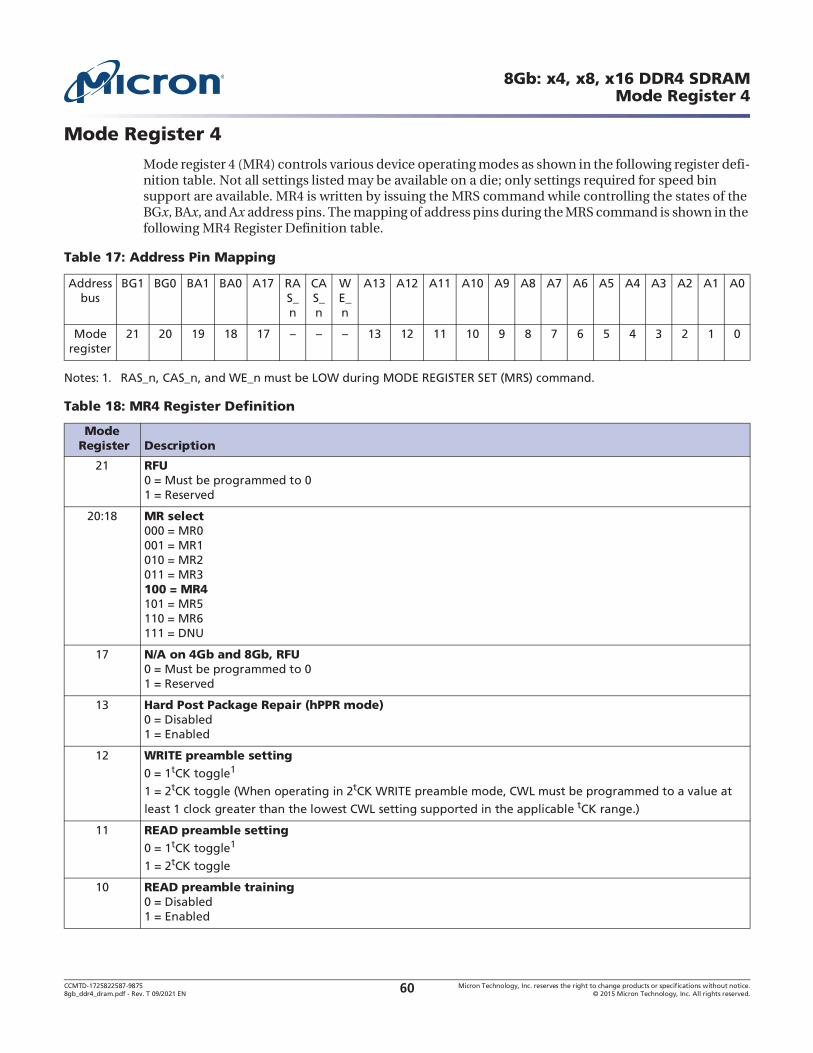
CCMTD-1725822587-9875 Micron Technology, Inc. reserves the right to change products or specifications without notice.8gb_ddr4_dram.pdf - Rev. T 09/2021 EN 2015 Micron Technology, Inc. All rights reserved.60
8Gb: x4, x8, x16 DDR4 SDRAMMode Register 4
Mode Register 4
Mode register 4 (MR4) controls various device operating modes as shown in the following register defi-nition table. Not all settings listed may be available on a die; only settings required for speed bin support are available. MR4 is written by issuing the MRS command while controlling the states of the BGx, BAx, and Ax address pins. The mapping of address pins during the MRS command is shown in the following MR4 Register Definition table.
Notes: 1. RAS_n, CAS_n, and WE_n must be LOW during MODE REGISTER SET (MRS) command.
Table 17: Address Pin Mapping
Address bus
BG1 BG0 BA1 BA0 A17 RAS_n
CAS_n
WE_n
A13 A12 A11 A10 A9 A8 A7 A6 A5 A4 A3 A2 A1 A0
Mode register
21 20 19 18 17 13 12 11 10 9 8 7 6 5 4 3 2 1 0
Table 18: MR4 Register Definition
Mode Register Description
21 RFU0 = Must be programmed to 01 = Reserved
20:18 MR select000 = MR0001 = MR1010 = MR2011 = MR3100 = MR4101 = MR5110 = MR6111 = DNU
17 N/A on 4Gb and 8Gb, RFU0 = Must be programmed to 01 = Reserved
13 Hard Post Package Repair (hPPR mode)0 = Disabled1 = Enabled
12 WRITE preamble setting0 = 1tCK toggle1
1 = 2tCK toggle (When operating in 2tCK WRITE preamble mode, CWL must be programmed to a value at
least 1 clock greater than the lowest CWL setting supported in the applicable tCK range.)
11 READ preamble setting0 = 1tCK toggle1
1 = 2tCK toggle
10 READ preamble training0 = Disabled1 = Enabled
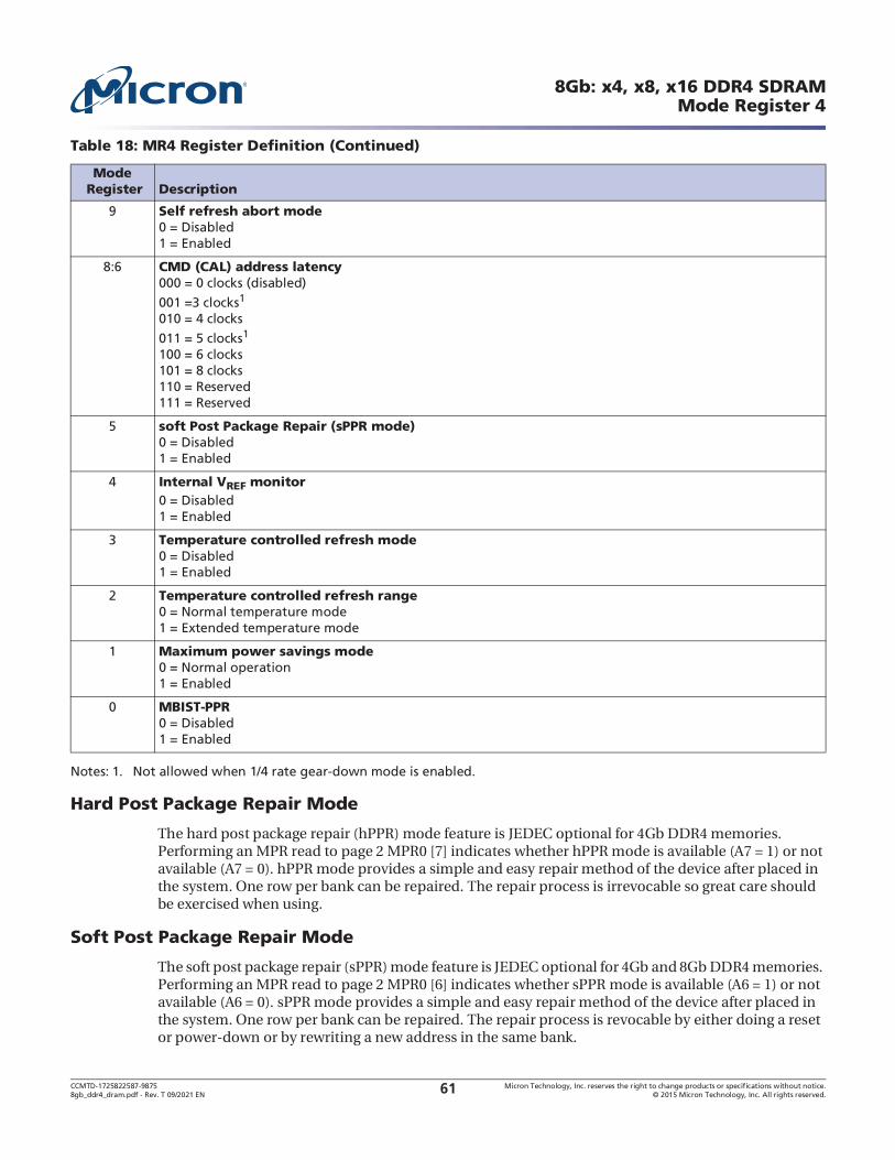
CCMTD-1725822587-9875 Micron Technology, Inc. reserves the right to change products or specifications without notice.8gb_ddr4_dram.pdf - Rev. T 09/2021 EN 2015 Micron Technology, Inc. All rights reserved.61
8Gb: x4, x8, x16 DDR4 SDRAMMode Register 4
Notes: 1. Not allowed when 1/4 rate gear-down mode is enabled.
Hard Post Package Repair Mode
The hard post package repair (hPPR) mode feature is JEDEC optional for 4Gb DDR4 memories. Performing an MPR read to page 2 MPR0 [7] indicates whether hPPR mode is available (A7 = 1) or not available (A7 = 0). hPPR mode provides a simple and easy repair method of the device after placed in the system. One row per bank can be repaired. The repair process is irrevocable so great care should be exercised when using.
Soft Post Package Repair Mode
The soft post package repair (sPPR) mode feature is JEDEC optional for 4Gb and 8Gb DDR4 memories. Performing an MPR read to page 2 MPR0 [6] indicates whether sPPR mode is available (A6 = 1) or not available (A6 = 0). sPPR mode provides a simple and easy repair method of the device after placed in the system. One row per bank can be repaired. The repair process is revocable by either doing a reset or power-down or by rewriting a new address in the same bank.
9 Self refresh abort mode0 = Disabled1 = Enabled
8:6 CMD (CAL) address latency000 = 0 clocks (disabled)
001 =3 clocks1
010 = 4 clocks
011 = 5 clocks1
100 = 6 clocks101 = 8 clocks110 = Reserved111 = Reserved
5 soft Post Package Repair (sPPR mode)0 = Disabled1 = Enabled
4 Internal VREF monitor0 = Disabled1 = Enabled
3 Temperature controlled refresh mode0 = Disabled1 = Enabled
2 Temperature controlled refresh range0 = Normal temperature mode1 = Extended temperature mode
1 Maximum power savings mode0 = Normal operation1 = Enabled
0 MBIST-PPR0 = Disabled 1 = Enabled
Table 18: MR4 Register Definition (Continued)
Mode Register Description
CCMTD-1725822587-9875 Micron Technology, Inc. reserves the right to change products or specifications without notice.8gb_ddr4_dram.pdf - Rev. T 09/2021 EN 2015 Micron Technology, Inc. All rights reserved.62
8Gb: x4, x8, x16 DDR4 SDRAMMode Register 4
WRITE Preamble
Programmable WRITE preamble, tWPRE, can be set to 1tCK or 2tCK via the MR4 register. The 1tCK
setting is similar to DDR3. However, when operating in 2tCK WRITE preamble mode, CWL must be programmed to a value at least 1 clock greater than the lowest CWL setting supported in the applicable tCK range.
Some even settings will require addition of 2 clocks. If the alternate longer CWL was used, the addi-tional clocks will not be required.
READ Preamble
Programmable READ preamble tRPRE can be set to 1tCK or 2tCK via the MR4 register. Both the 1tCK
and 2tCK DDR4 preamble settings are different from that defined for the DDR3 SDRAM. Both DDR4 READ preamble settings may require the memory controller to train (or read level) its data strobe receivers using the READ preamble training.
READ Preamble Training
Programmable READ preamble training can be set to 1tCK or 2tCK. This mode can be used by the memory controller to train or READ level its data strobe receivers.
Temperature-Controlled Refresh
When temperature-controlled refresh mode is enabled, the device may adjust the internal refresh
period to be longer than tREFI of the normal temperature range by skipping external REFRESH commands with the proper gear ratio. For example, the DRAM temperature sensor detected less than 45 C. Normal temperature mode covers the range of -40 C to 85 C, while the extended temperature range covers -40 C to 105 C.
Command Address Latency
COMMAND ADDRESS LATENCY (CAL) is a power savings feature and can be enabled or disabled via
the MRS setting. CAL is defined as the delay in clock cycles (tCAL) between a CS_n registered LOW and its corresponding registered command and address. The value of CAL (in clocks) must be programmed
into the mode register according to the tCAL(ns)/tCK(ns) rounding algorithms found in the Converting Time-Based Specifications to Clock-Based Requirements section.
Internal VREF Monitor
This mode enables output of internally generated VREFDQ for monitoring on DQ0, DQ1, DQ2, and DQ3. May be used during VREFDQ training and test. While in this mode, RTT should be set to High-Z. VREF_-
time must be increased by 10ns if DQ load is 0pF, plus an additional 15ns per pF of loading. This measurement is for verification purposes and is NOT an external voltage supply pin.
Maximum Power Savings Mode
This mode provides the lowest power mode where data retention is not required. When the device is in the maximum power saving mode, it does not need to guarantee data retention or respond to any external command (except the MAXIMUM POWER SAVING MODE EXIT command and during the assertion of RESET_n signal LOW).

CCMTD-1725822587-9875 Micron Technology, Inc. reserves the right to change products or specifications without notice.8gb_ddr4_dram.pdf - Rev. T 09/2021 EN 2015 Micron Technology, Inc. All rights reserved.63
8Gb: x4, x8, x16 DDR4 SDRAMMode Register 4
MBIST-PPR
This mode is JEDEC optional and allows for a self-contained DRAM test and repair. Please refer to the Features list on page 1 for a list of die revisions that support MBIST-PPR.

CCMTD-1725822587-9875 Micron Technology, Inc. reserves the right to change products or specifications without notice.8gb_ddr4_dram.pdf - Rev. T 09/2021 EN 2015 Micron Technology, Inc. All rights reserved.64
8Gb: x4, x8, x16 DDR4 SDRAMMode Register 5
Mode Register 5
Mode register 5 (MR5) controls various device operating modes as shown in the following register defi-nition table. Not all settings listed may be available on a die; only settings required for speed bin support are available. MR5 is written by issuing the MRS command while controlling the states of the BGx, BAx, and Ax address pins. The mapping of address pins during the MRS command is shown in the following MR5 Register Definition table.
Notes: 1. RAS_n, CAS_n, and WE_n must be LOW during MODE REGISTER SET command.
Table 19: Address Pin Mapping
Address bus
BG1 BG0 BA1 BA0 A17 RAS_n
CAS_n
WE_n
A13 A12
A11
A10
A9 A8 A7 A6 A5 A4 A3 A2 A1 A0
Mode register
21 20 19 18 17 13 12 11 10 9 8 7 6 5 4 3 2 1 0
Table 20: MR5 Register Definition
Mode Register Description
21 RFU0 = Must be programmed to 01 = Reserved
20:18 MR select000 = MR0001 = MR1010 = MR2011 = MR3100 = MR4101 = MR5110 = MR6111 = DNU
17 N/A on 4Gb and 8Gb, RFU0 = Must be programmed to 01 = Reserved
13 RFU0 = Must be programmed to 01 = Reserved
120 = Disabled1 = Enabled
110 = Disabled1 = Enabled
10 Data mask (DM)0 = Disabled1 = Enabled
9 CA parity persistent error mode0 = Disabled1 = Enabled
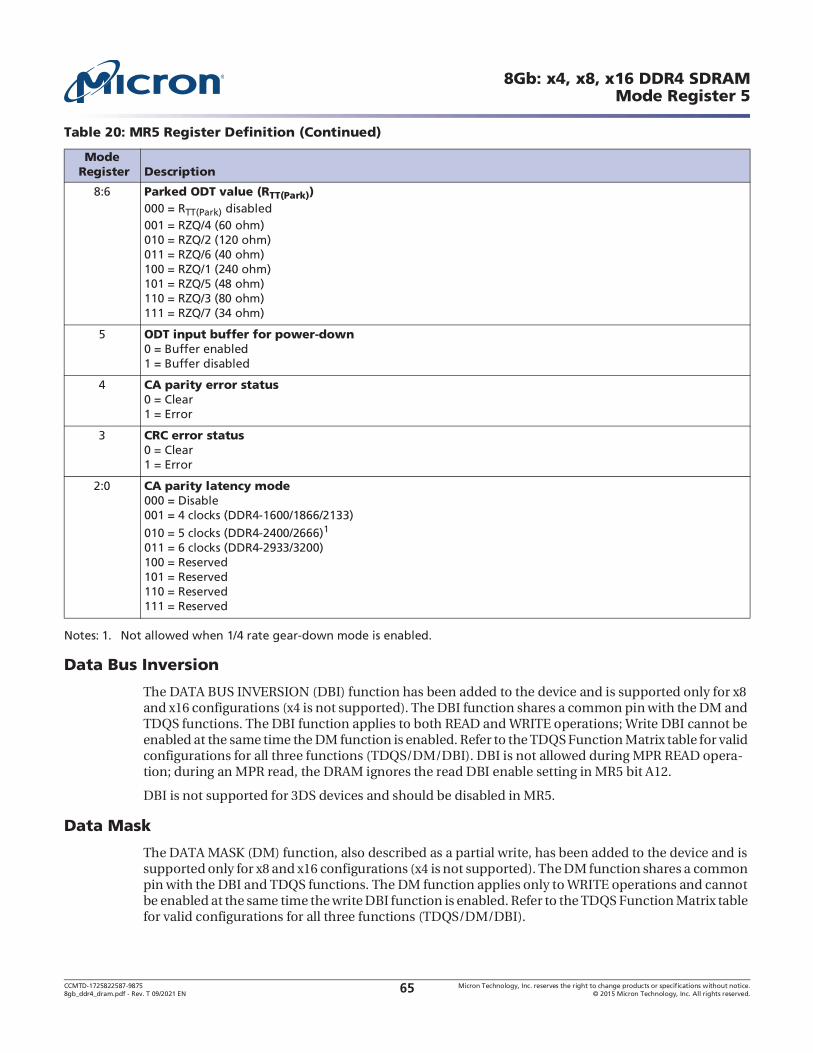
CCMTD-1725822587-9875 Micron Technology, Inc. reserves the right to change products or specifications without notice.8gb_ddr4_dram.pdf - Rev. T 09/2021 EN 2015 Micron Technology, Inc. All rights reserved.65
8Gb: x4, x8, x16 DDR4 SDRAMMode Register 5
Notes: 1. Not allowed when 1/4 rate gear-down mode is enabled.
Data Bus Inversion
The DATA BUS INVERSION (DBI) function has been added to the device and is supported only for x8 and x16 configurations (x4 is not supported). The DBI function shares a common pin with the DM and TDQS functions. The DBI function applies to both READ and WRITE operations; Write DBI cannot be enabled at the same time the DM function is enabled. Refer to the TDQS Function Matrix table for valid configurations for all three functions (TDQS/DM/DBI). DBI is not allowed during MPR READ opera-tion; during an MPR read, the DRAM ignores the read DBI enable setting in MR5 bit A12.
DBI is not supported for 3DS devices and should be disabled in MR5.
Data Mask
The DATA MASK (DM) function, also described as a partial write, has been added to the device and is supported only for x8 and x16 configurations (x4 is not supported). The DM function shares a common pin with the DBI and TDQS functions. The DM function applies only to WRITE operations and cannot be enabled at the same time the write DBI function is enabled. Refer to the TDQS Function Matrix table for valid configurations for all three functions (TDQS/DM/DBI).
8:6 Parked ODT value (RTT(Park))000 = RTT(Park) disabled 001 = RZQ/4 (60 ohm) 010 = RZQ/2 (120 ohm) 011 = RZQ/6 (40 ohm) 100 = RZQ/1 (240 ohm) 101 = RZQ/5 (48 ohm) 110 = RZQ/3 (80 ohm)111 = RZQ/7 (34 ohm)
5 ODT input buffer for power-down0 = Buffer enabled1 = Buffer disabled
4 CA parity error status0 = Clear1 = Error
3 CRC error status0 = Clear1 = Error
2:0 CA parity latency mode000 = Disable001 = 4 clocks (DDR4-1600/1866/2133)
010 = 5 clocks (DDR4-2400/2666)1
011 = 6 clocks (DDR4-2933/3200)100 = Reserved 101 = Reserved110 = Reserved111 = Reserved
Table 20: MR5 Register Definition (Continued)
Mode Register Description

CCMTD-1725822587-9875 Micron Technology, Inc. reserves the right to change products or specifications without notice.8gb_ddr4_dram.pdf - Rev. T 09/2021 EN 2015 Micron Technology, Inc. All rights reserved.66
8Gb: x4, x8, x16 DDR4 SDRAMMode Register 5
CA Parity Persistent Error Mode
Normal CA parity mode (CA parity persistent mode disabled) no longer performs CA parity checking while the parity error status bit remains set at 1. However, with CA parity persistent mode enabled, CA parity checking continues to be performed when the parity error status bit is set to a 1.
ODT Input Buffer for Power-Down
This feature determines whether the ODT input buffer is on or off during power-down. If the input buffer is configured to be on (enabled during power-down), the ODT input signal must be at a valid logic level. If the input buffer is configured to be off (disabled during power-down), the ODT input signal may be floating and the device does not provide RTT(NOM) termination. However, the device may provide RTT(Park) termination depending on the MR settings. This is primarily for additional power savings.
CA Parity Error Status
The device will set the error status bit to 1 upon detecting a parity error. The parity error status bit remains set at 1 until the device controller clears it explicitly using an MRS command.
CRC Error Status
The device will set the error status bit to 1 upon detecting a CRC error. The CRC error status bit remains set at 1 until the device controller clears it explicitly using an MRS command.
CA Parity Latency Mode
CA parity is enabled when a latency value, dependent on tCK, is programmed; this accounts for parity calculation delay internal to the device. The normal state of CA parity is to be disabled. If CA parity is enabled, the device must ensure there are no parity errors before executing the command. CA parity signal (PAR) covers ACT_n, RAS_n/A16, CAS_n/A15, WE_n/A14, and the address bus including bank address and bank group bits. The control signals CKE, ODT, and CS_n are not included in the parity calculation.

CCMTD-1725822587-9875 Micron Technology, Inc. reserves the right to change products or specifications without notice.8gb_ddr4_dram.pdf - Rev. T 09/2021 EN 2015 Micron Technology, Inc. All rights reserved.67
8Gb: x4, x8, x16 DDR4 SDRAMMode Register 6
Mode Register 6
Mode register 6 (MR6) controls various device operating modes as shown in the following register defi-nition table. Not all settings listed may be available on a die; only settings required for speed bin support are available. MR6 is written by issuing the MRS command while controlling the states of the BGx, BAx, and Ax address pins. The mapping of address pins during the MRS command is shown in the following MR6 Register Definition table.
Notes: 1. RAS_n, CAS_n, and WE_n must be LOW during MODE REGISTER SET command.
Table 21: Address Pin Mapping
Address bus
BG1 BG0 BA1 BA0 A17 RAS_n
CAS_n
WE_n
A13
A12 A11 A10
A9 A8 A7 A6 A5 A4 A3 A2 A1 A0
Mode register
21 20 19 18 17 13 12 11 10 9 8 7 6 5 4 3 2 1 0
Table 22: MR6 Register Definition
Mode Register Description
21 RFU0 = Must be programmed to 01 = Reserved
20:18 MR select000 = MR0001 = MR1010 = MR2011 = MR3100 = MR4101 = MR5110 = MR6111 = DNU
17 NA on 4Gb and 8Gb, RFU0 = Must be programmed to 01 = Reserved
12:10 Data rate000 = Data rate 1333 Mb/s (1333 Mb/s)001 = 1333 Mb/s < Data rate 1866 Mb/s (1600, 1866 Mb/s)010 = 1866 Mb/s < Data rate 2400 Mb/s (2133, 2400 Mb/s)011 = 2400 Mb/s < Data rate 2666 Mb/s (2666 Mb/s)100 = 2666 Mb/s < Data rate 3200 Mb/s (2933, 3200 Mb/s) 101 = Reserved110 = Reserved111 = Reserved

CCMTD-1725822587-9875 Micron Technology, Inc. reserves the right to change products or specifications without notice.8gb_ddr4_dram.pdf - Rev. T 09/2021 EN 2015 Micron Technology, Inc. All rights reserved.68
8Gb: x4, x8, x16 DDR4 SDRAMMode Register 6
Data Rate Programming
The device controller must program the correct data rate according to the operating frequency.
VREFDQ Calibration Enable
VREFDQ calibration is where the device internally generates its own VREFDQ to be used by the DQ input receivers. The VREFDQ value will be output on any DQ of DQ[3:0] for evaluation only. The device controller is responsible for setting and calibrating the internal VREFDQ level using an MRS protocol (adjust up, adjust down, and so on). It is assumed that the controller will use a series of writes and reads in conjunction with VREFDQ adjustments to optimize and verify the data eye. Enabling VREFDQ calibra-tion must be used whenever values are being written to the MR6[6:0] register.
VREFDQ Calibration Range
The device defines two VREFDQ calibration ranges: Range 1 and Range 2. Range 1 supports VREFDQ between 60% and 92% of VDDQ while Range 2 supports VREFDQ between 45% and 77% of VDDQ, as seen in VREFDQ Specification table. Although not a restriction, Range 1 was targeted for module-based designs and Range 2 was added to target point-to-point designs.
VREFDQ Calibration Value
Fifty settings provide approximately 0.65% of granularity steps sizes for both Range 1 and Range 2 of VREFDQ, as seen in VREFDQ Range and Levels table in the VREFDQ Calibration section.
13, 9, 8 RFUDefault = 000; Must be programmed to 000 001 = Reserved 010 = Reserved 011 = Reserved 100 = Reserved101 = Reserved 110 = Reserved 111 = Reserved
7 VREF Calibration Enable0 = Disable1 = Enable
6 VREF Calibration Range0 = Range 11 = Range 2
5:0 VREF Calibration ValueSee the VREFDQ Range and Levels table in the VREFDQ Calibration section
Table 22: MR6 Register Definition (Continued)
Mode Register Description
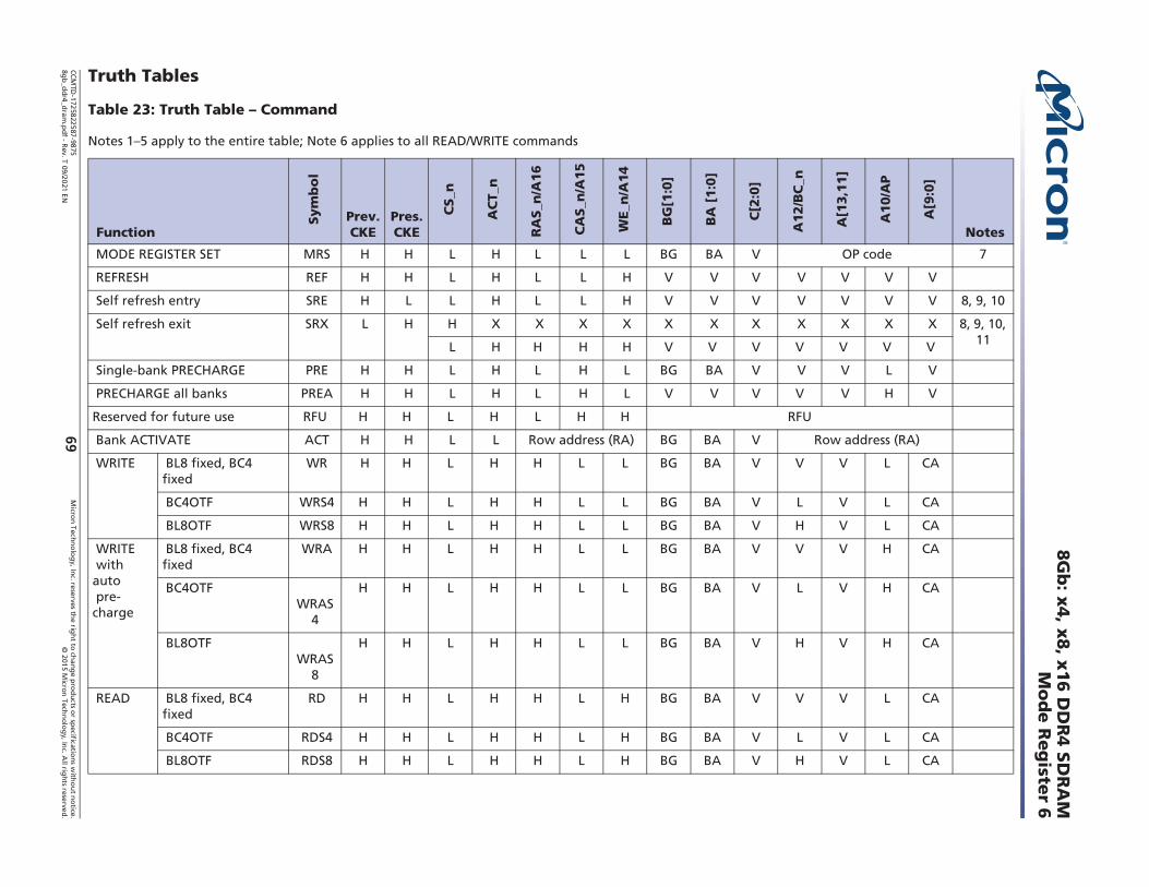
CCM
TD-1725822587-9875
Micro
n Techno
log
y, Inc. reserves the rig
ht to ch
ange p
rod
ucts or sp
ecifications w
itho
ut n
otice.
8gb
_ddr4_d
ram.p
df - Rev. T 09/2021 EN
2015 Micron
Techn
olog
y, Inc. A
ll rights reserved.
69
8Gb
: x4
, x8
, x16
DD
R4
SD
RA
MM
od
e R
egiste
r 6
Truth Tables
Table 23: Truth Table Command
Notes 1 5 apply to the entire table; Note 6 applies to all READ/WRITE commands
Function
Sym
bo
l
Prev. CKE
Pres. CKE
CS_n
AC
T_n
RA
S_n
/A16
CA
S_n
/A15
WE_n
/A14
BG
[1:0
]
BA
[1:0
]
C[2
:0]
A12/B
C_n
A[1
3,1
1]
A10/A
P
A[9
:0]
Notes
MODE REGISTER SET MRS H H L H L L L BG BA V OP code 7
REFRESH REF H H L H L L H V V V V V V V
Self refresh entry SRE H L L H L L H V V V V V V V 8, 9, 10
Self refresh exit SRX L H H X X X X X X X X X X X 8, 9, 10, 11 L H H H H V V V V V V V
Single-bank PRECHARGE PRE H H L H L H L BG BA V V V L V
PRECHARGE all banks PREA H H L H L H L V V V V V H V
Reserved for future use RFU H H L H L H H RFU
Bank ACTIVATE ACT H H L L Row address (RA) BG BA V Row address (RA)
WRITE BL8 fixed, BC4 fixed
WR H H L H H L L BG BA V V V L CA
BC4OTF WRS4 H H L H H L L BG BA V L V L CA
BL8OTF WRS8 H H L H H L L BG BA V H V L CA
WRITE with auto pre-charge
BL8 fixed, BC4 fixed
WRA H H L H H L L BG BA V V V H CA
BC4OTF WRAS
4
H H L H H L L BG BA V L V H CA
BL8OTF WRAS
8
H H L H H L L BG BA V H V H CA
READ BL8 fixed, BC4 fixed
RD H H L H H L H BG BA V V V L CA
BC4OTF RDS4 H H L H H L H BG BA V L V L CA
BL8OTF RDS8 H H L H H L H BG BA V H V L CA
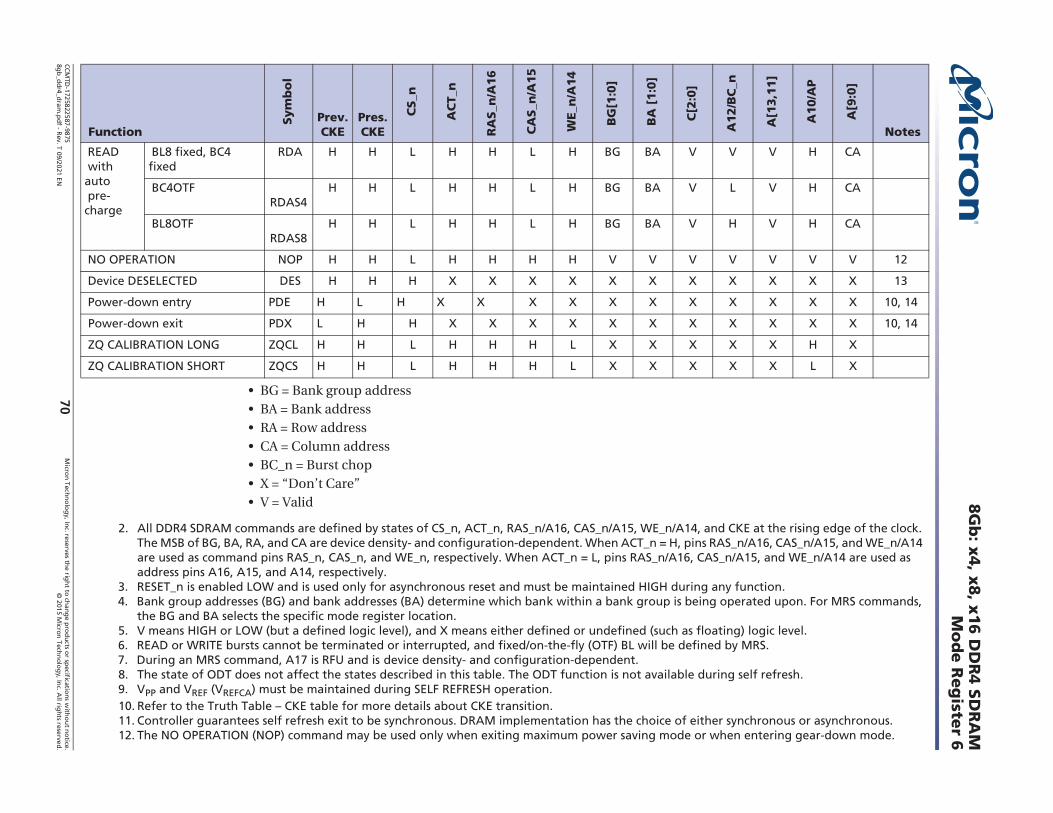
CCM
TD-1725822587-9875
Micro
n Techno
log
y, Inc. reserves the rig
ht to ch
ange p
rod
ucts or sp
ecifications w
itho
ut n
otice.
8gb
_ddr4_d
ram.p
df - Rev. T 09/2021 EN
2015 Micron
Techn
olog
y, Inc. A
ll rights reserved.
70
8Gb
: x4
, x8
, x16
DD
R4
SD
RA
MM
od
e R
egiste
r 6
BG = Bank group addressBA = Bank addressRA = Row addressCA = Column addressBC_n = Burst chopX = Don t CareV = Valid
2. All DDR4 SDRAM commands are defined by states of CS_n, ACT_n, RAS_n/A16, CAS_n/A15, WE_n/A14, and CKE at the rising edge of the clock. The MSB of BG, BA, RA, and CA are device density- and configuration-dependent. When ACT_n = H, pins RAS_n/A16, CAS_n/A15, and WE_n/A14 are used as command pins RAS_n, CAS_n, and WE_n, respectively. When ACT_n = L, pins RAS_n/A16, CAS_n/A15, and WE_n/A14 are used as address pins A16, A15, and A14, respectively.
3. RESET_n is enabled LOW and is used only for asynchronous reset and must be maintained HIGH during any function.4. Bank group addresses (BG) and bank addresses (BA) determine which bank within a bank group is being operated upon. For MRS commands,
the BG and BA selects the specific mode register location.5. V means HIGH or LOW (but a defined logic level), and X means either defined or undefined (such as floating) logic level.6. READ or WRITE bursts cannot be terminated or interrupted, and fixed/on-the-fly (OTF) BL will be defined by MRS.7. During an MRS command, A17 is RFU and is device density- and configuration-dependent.8. The state of ODT does not affect the states described in this table. The ODT function is not available during self refresh.9. VPP and VREF (VREFCA) must be maintained during SELF REFRESH operation.10. Refer to the Truth Table CKE table for more details about CKE transition.11. Controller guarantees self refresh exit to be synchronous. DRAM implementation has the choice of either synchronous or asynchronous.12. The NO OPERATION (NOP) command may be used only when exiting maximum power saving mode or when entering gear-down mode.
READ with auto pre-charge
BL8 fixed, BC4 fixed
RDA H H L H H L H BG BA V V V H CA
BC4OTF RDAS4
H H L H H L H BG BA V L V H CA
BL8OTF RDAS8
H H L H H L H BG BA V H V H CA
NO OPERATION NOP H H L H H H H V V V V V V V 12
Device DESELECTED DES H H H X X X X X X X X X X X 13
Power-down entry PDE H L H X X X X X X X X X X X 10, 14
Power-down exit PDX L H H X X X X X X X X X X X 10, 14
ZQ CALIBRATION LONG ZQCL H H L H H H L X X X X X H X
ZQ CALIBRATION SHORT ZQCS H H L H H H L X X X X X L X
Function
Sym
bo
l
Prev. CKE
Pres. CKE
CS_n
AC
T_n
RA
S_n
/A16
CA
S_n
/A15
WE_n
/A14
BG
[1:0
]
BA
[1:0
]
C[2
:0]
A12/B
C_n
A[1
3,1
1]
A10/A
P
A[9
:0]
Notes
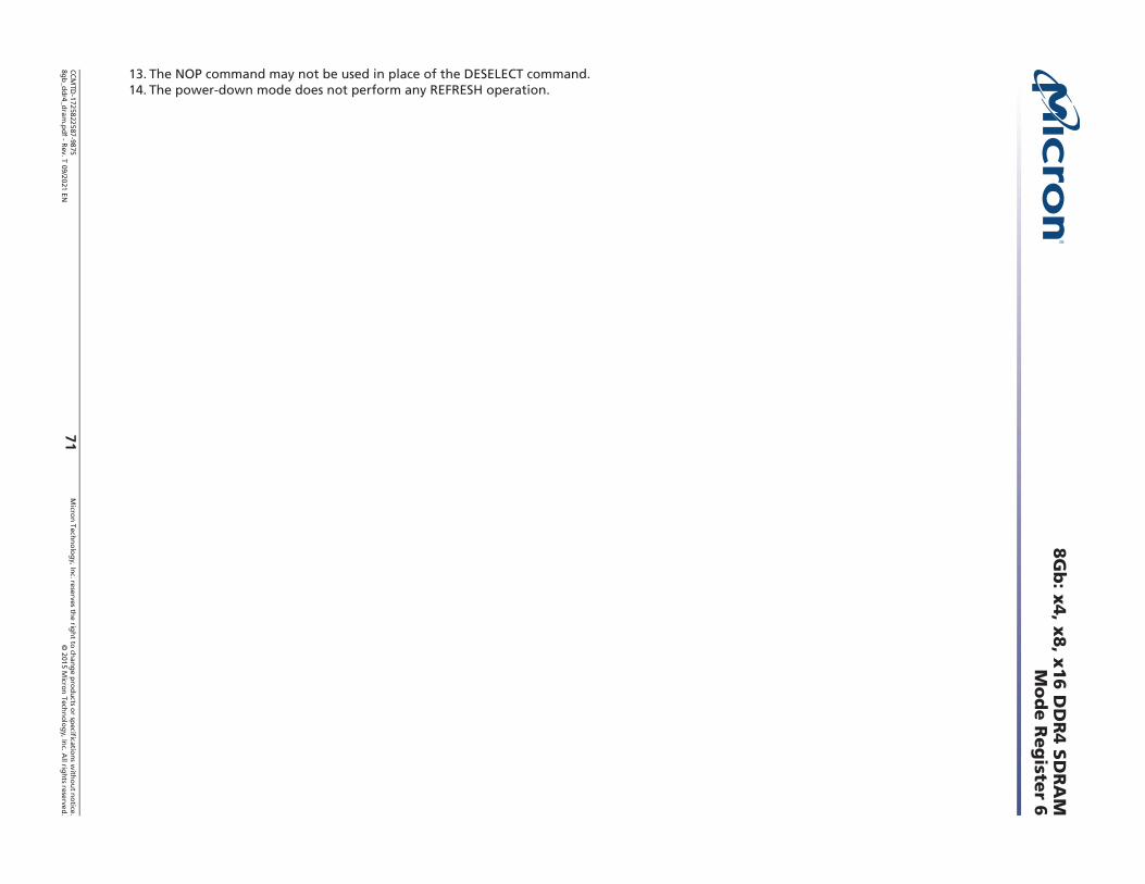
CCM
TD-1725822587-9875
Micro
n Techno
log
y, Inc. reserves the rig
ht to ch
ange p
rod
ucts or sp
ecifications w
itho
ut n
otice.
8gb
_ddr4_d
ram.p
df - Rev. T 09/2021 EN
2015 Micron
Techn
olog
y, Inc. A
ll rights reserved.
71
8Gb
: x4
, x8
, x16
DD
R4
SD
RA
MM
od
e R
egiste
r 6
13. The NOP command may not be used in place of the DESELECT command.14. The power-down mode does not perform any REFRESH operation.
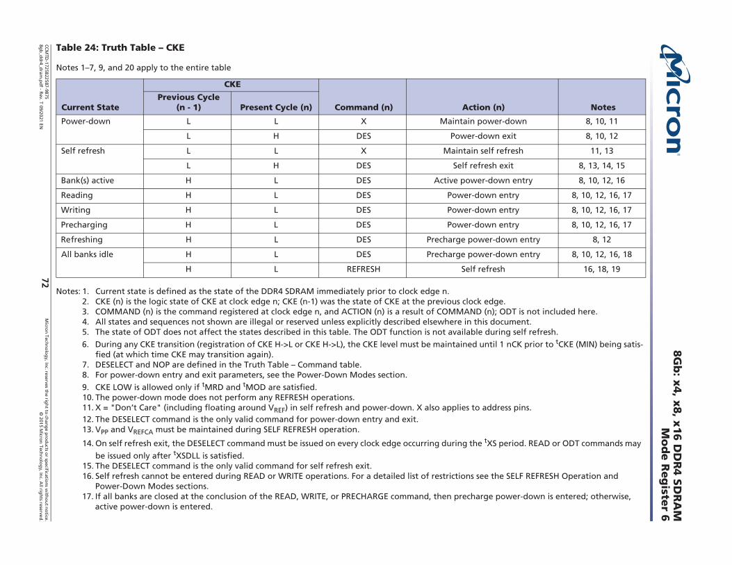
CCM
TD-1725822587-9875
Micro
n Techno
log
y, Inc. reserves the rig
ht to ch
ange p
rod
ucts or sp
ecifications w
itho
ut n
otice.
8gb
_ddr4_d
ram.p
df - Rev. T 09/2021 EN
2015 Micron
Techn
olog
y, Inc. A
ll rights reserved.
72
8Gb
: x4
, x8
, x16
DD
R4
SD
RA
MM
od
e R
egiste
r 6
Table 24: Truth Table CKE
Notes 1 7, 9, and 20 apply to the entire table
Notes: 1. Current state is defined as the state of the DDR4 SDRAM immediately prior to clock edge n.2. CKE (n) is the logic state of CKE at clock edge n; CKE (n-1) was the state of CKE at the previous clock edge.3. COMMAND (n) is the command registered at clock edge n, and ACTION (n) is a result of COMMAND (n); ODT is not included here.4. All states and sequences not shown are illegal or reserved unless explicitly described elsewhere in this document.5. The state of ODT does not affect the states described in this table. The ODT function is not available during self refresh.
6. During any CKE transition (registration of CKE H->L or CKE H->L), the CKE level must be maintained until 1 nCK prior to tCKE (MIN) being satis-fied (at which time CKE may transition again).
7. DESELECT and NOP are defined in the Truth Table Command table.8. For power-down entry and exit parameters, see the Power-Down Modes section.
9. CKE LOW is allowed only if tMRD and tMOD are satisfied.10. The power-down mode does not perform any REFRESH operations.11. X = "Don t Care" (including floating around VREF) in self refresh and power-down. X also applies to address pins.12. The DESELECT command is the only valid command for power-down entry and exit.13. VPP and VREFCA must be maintained during SELF REFRESH operation.
14. On self refresh exit, the DESELECT command must be issued on every clock edge occurring during the tXS period. READ or ODT commands may
be issued only after tXSDLL is satisfied.15. The DESELECT command is the only valid command for self refresh exit.16. Self refresh cannot be entered during READ or WRITE operations. For a detailed list of restrictions see the SELF REFRESH Operation and
Power-Down Modes sections.17. If all banks are closed at the conclusion of the READ, WRITE, or PRECHARGE command, then precharge power-down is entered; otherwise,
active power-down is entered.
Current State
CKE
Command (n) Action (n) Notes Previous Cycle
(n - 1) Present Cycle (n)
Power-down L L X Maintain power-down 8, 10, 11
L H DES Power-down exit 8, 10, 12
Self refresh L L X Maintain self refresh 11, 13
L H DES Self refresh exit 8, 13, 14, 15
Bank(s) active H L DES Active power-down entry 8, 10, 12, 16
Reading H L DES Power-down entry 8, 10, 12, 16, 17
Writing H L DES Power-down entry 8, 10, 12, 16, 17
Precharging H L DES Power-down entry 8, 10, 12, 16, 17
Refreshing H L DES Precharge power-down entry 8, 12
All banks idle H L DES Precharge power-down entry 8, 10, 12, 16, 18
H L REFRESH Self refresh 16, 18, 19

CCM
TD-1725822587-9875
Micro
n Techno
log
y, Inc. reserves the rig
ht to ch
ange p
rod
ucts or sp
ecifications w
itho
ut n
otice.
8gb
_ddr4_d
ram.p
df - Rev. T 09/2021 EN
2015 Micron
Techn
olog
y, Inc. A
ll rights reserved.
73
8Gb
: x4
, x8
, x16
DD
R4
SD
RA
MM
od
e R
egiste
r 6
18. Idle state is defined as all banks are closed (tRP, tDAL, and so on, satisfied), no data bursts are in progress, CKE is HIGH, and all timings from
previous operations are satisfied (tMRD, tMOD, tRFC, tZQinit, tZQoper, tZQCS, and so on), as well as all self refresh exit and power-down exit
parameters are satisfied (tXS, tXP, tXSDLL, and so on).19. Self refresh mode can be entered only from the all banks idle state.20. For more details about all signals, see the Truth Table Command table; must be a legal command as defined in the table.

CCMTD-1725822587-9875 Micron Technology, Inc. reserves the right to change products or specifications without notice.8gb_ddr4_dram.pdf - Rev. T 09/2021 EN 2015 Micron Technology, Inc. All rights reserved.74
8Gb: x4, x8, x16 DDR4 SDRAMNOP Command
NOP Command
The NO OPERATION (NOP) command was originally used to instruct the selected DDR4 SDRAM to perform a NOP (CS_n = LOW and ACT_n, RAS_n/A16, CAS_n/A15, and WE_n/A14 = HIGH). This prevented unwanted commands from being registered during idle or wait states. NOP command general support has been removed and the command should not be used unless specifically allowed, which is when exiting maximum power-saving mode or when entering gear-down mode.
DESELECT Command
The deselect function (CS_n HIGH) prevents new commands from being executed; therefore, with this command, the device is effectively deselected. Operations already in progress are not affected.
DLL-Off Mode
DLL-off mode is entered by setting MR1 bit A0 to 0, which will disable the DLL for subsequent opera-tions until the A0 bit is set back to 1. The MR1 A0 bit for DLL control can be switched either during initialization or during self refresh mode. Refer to the Input Clock Frequency Change section for more details.
The maximum clock frequency for DLL-off mode is specified by the parameter tCKDLL_OFF.
Due to latency counter and timing restrictions, only one CL value and CWL value (in MR0 and MR2 respectively) are supported. The DLL-off mode is only required to support setting both CL = 10 and CWL = 9.
DLL-off mode will affect the read data clock-to-data strobe relationship (tDQSCK), but not the data
strobe-to-data relationship (tDQSQ,tQH). Special attention is needed to line up read data to the controller time domain.
Compared with DLL-on mode, where tDQSCK starts from the rising clock edge (AL + CL) cycles after
the READ command, the DLL-off mode tDQSCK starts (AL + CL - 1) cycles after the READ command.
Another difference is that tDQSCK may not be small compared totCK (it might even be larger than tCK),
and the difference between tDQSCK (MIN) and tDQSCK (MAX) is significantly larger than in DLL-on
mode. The tDQSCK (DLL-off) values are undefined and the user is responsible for training to the data-eye.
The timing relations on DLL-off mode READ operation are shown in the following diagram, where CL = 10, AL = 0, and BL = 8.
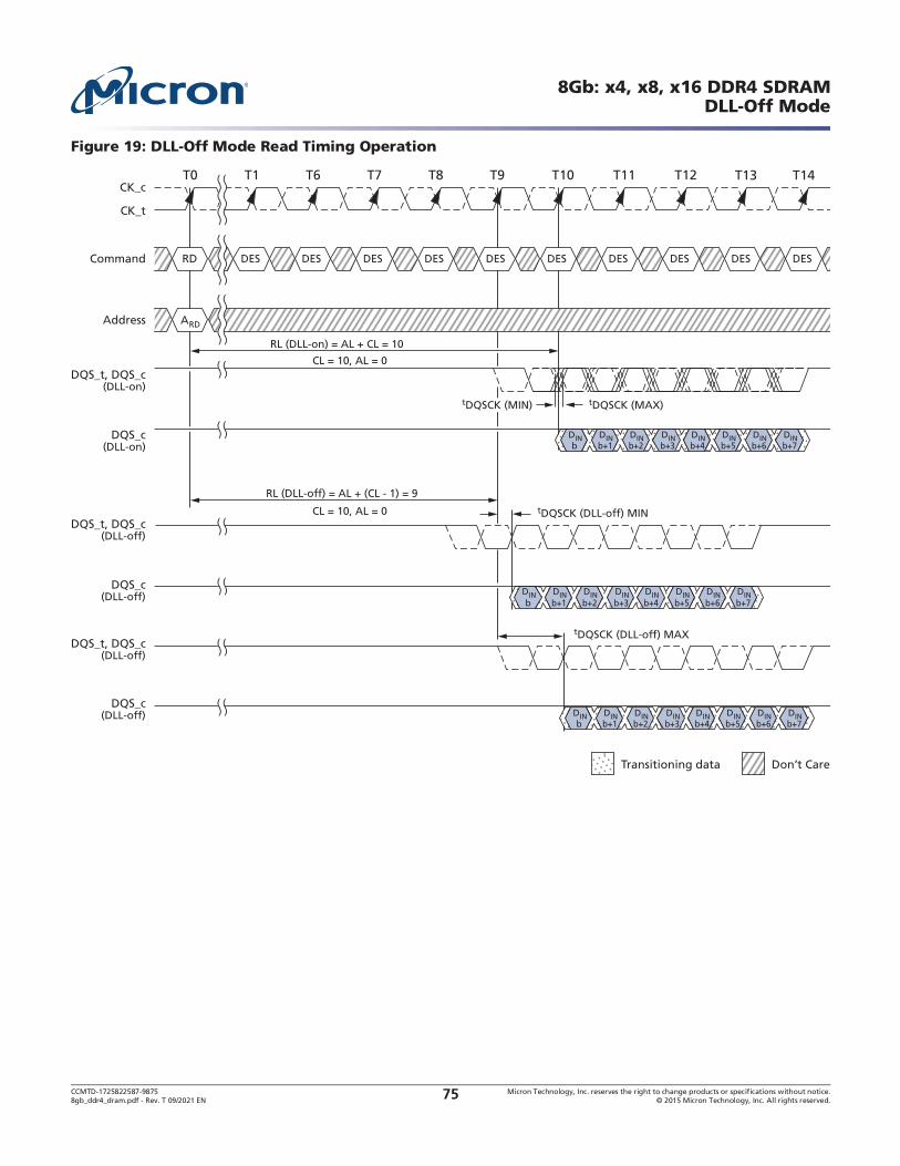
CCMTD-1725822587-9875 Micron Technology, Inc. reserves the right to change products or specifications without notice.8gb_ddr4_dram.pdf - Rev. T 09/2021 EN 2015 Micron Technology, Inc. All rights reserved.75
8Gb: x4, x8, x16 DDR4 SDRAMDLL-Off Mode
Figure 19: DLL-Off Mode Read Timing Operation
CK_c
CK_t
Command
T0 T1 T6 T7 T8 T9 T10 T11 T12 T13 T14
Address
DQS_t, DQS_c(DLL-on)
DQS_c(DLL-on)
CL = 10, AL = 0
CL = 10, AL = 0
RL (DLL-on) = AL + CL = 10
RL (DLL-off) = AL + (CL - 1) = 9
tDQSCK (DLL-off) MAX
tDQSCK (DLL-off) MIN
tDQSCK (MAX)
DQS_t, DQS_c(DLL-off)
DQS_c(DLL-off)
DQS_c(DLL-off)
DQS_t, DQS_c(DLL-off)
RD DES DES DES DES DES DES DES DES DES DES
Don’t CareTransitioning data
DINb
()()
()()
()()
()()
()()
()()
()()
()()
()()
()()
()()
()()
()()
()()
DINb+1
DINb+2
DINb+3
DINb+4
DINb+5
DINb+6
DINb+7
DINb
DINb+1
DINb+2
DINb+3
DINb+4
DINb+5
DINb+6
DINb+7
DINb
DINb+1
DINb+2
DINb+3
DINb+4
DINb+5
DINb+6
DINb+7
()()
tDQSCK (MIN)
ARD

CCMTD-1725822587-9875 Micron Technology, Inc. reserves the right to change products or specifications without notice.8gb_ddr4_dram.pdf - Rev. T 09/2021 EN 2015 Micron Technology, Inc. All rights reserved.76
8Gb: x4, x8, x16 DDR4 SDRAMDLL-On/Off Switching Procedures
DLL-On/Off Switching Procedures
The DLL-off mode is entered by setting MR1 bit A0 to 0; this will disable the DLL for subsequent oper-ations until the A0 bit is set back to 1.
DLL Switch Sequence from DLL-On to DLL-Off
To switch from DLL-on to DLL-off requires the frequency to be changed during self refresh, as outlined in the following procedure:1. Starting from the idle state (all banks pre-charged, all timings fulfilled, and, to disable the DLL, the
DRAM on-die termination resistors, RTT(NOM), must be in High-Z before MRS to MR1.)
2. Set MR1 bit A0 to 1 to disable the DLL.
3. Wait tMOD.
4. Enter self refresh mode; wait until tCKSRE/tCKSRE_PAR is satisfied.5. Change frequency, following the guidelines in the Input Clock Frequency Change section.
6. Wait until a stable clock is available for at least tCKSRX at device inputs.7. Starting with the SELF REFRESH EXIT command, CKE must continuously be registered HIGH until
all tMOD timings from any MRS command are satisfied. In addition, if any ODT features were enabled in the mode registers when self refresh mode was entered, the ODT signal must continu-
ously be registered LOW until all tMOD timings from any MRS command are satisfied. If RTT(NOM) was disabled in the mode registers when self refresh mode was entered, the ODT signal is "Don't Care."
8. Wait tXS_FAST, tXS_ABORT, or tXS, and then set mode registers with appropriate values (an update
of CL, CWL, and WR may be necessary; a ZQCL command can also be issued after tXS_FAST). tXS_FAST: ZQCL, ZQCS, and MRS commands. For MRS commands, only CL and WR/RTP registers in MR0, the CWL register in MR2, and gear-down mode in MR3 may be accessed provided the device is not in per-DRAM addressability mode. Access to other device mode registers must satisfy tXS timing.tXS_ABORT: If MR4 [9] is enabled, then the device aborts any ongoing refresh and does not incre-
ment the refresh counter. The controller can issue a valid command after a delay of tXS_ABORT. Upon exiting from self refresh, the device requires a minimum of one extra REFRESH command before it is put back into self refresh mode. This requirement remains the same regardless of the MRS bit setting for self refresh abort.tXS: ACT, PRE, PREA, REF, SRE, PDE, WR, WRS4, WRS8, WRA, WRAS4, WRAS8, RD, RDS4, RDS8, RDA, RDAS4, and RDAS8.
9. Wait tMOD to complete.
The device is ready for the next command.

CCMTD-1725822587-9875 Micron Technology, Inc. reserves the right to change products or specifications without notice.8gb_ddr4_dram.pdf - Rev. T 09/2021 EN 2015 Micron Technology, Inc. All rights reserved.77
8Gb: x4, x8, x16 DDR4 SDRAMDLL-On/Off Switching Procedures
Figure 20: DLL Switch Sequence from DLL-On to DLL-Off
Notes: 1. Starting in the idle state. RTT in stable state.2. Disable DLL by setting MR1 bit A0 to 0.3. Enter SR.4. Change frequency.
5. Clock must be stable tCKSRX.6. Exit SR.7. Update mode registers allowed with DLL-off settings met.
CK_c
CK_t
Ta Tb0 Tb1 Tc Td Te0 Te1 Tf Tg Th
Don’t CareTime Break
CKE
Command
Enter self refresh Exit self refresh
ODT
Valid
SRE3 DES SRX6
Valid Valid
Valid Valid
MRS2
tXS_FAST
tXS_ABORTtRP
tXS
Note 4
tCPDEDtIS
tCKSRE/tCKSRE_PAR tCKSRX5
Valid
Address Valid
Valid7 Valid8 Valid9
tIS tCKESR/tCKESR_PAR

CCMTD-1725822587-9875 Micron Technology, Inc. reserves the right to change products or specifications without notice.8gb_ddr4_dram.pdf - Rev. T 09/2021 EN 2015 Micron Technology, Inc. All rights reserved.78
8Gb: x4, x8, x16 DDR4 SDRAMDLL-On/Off Switching Procedures
DLL-Off to DLL-On Procedure
To switch from DLL-off to DLL-on (with required frequency change) during self refresh:1. Starting from the idle state (all banks pre-charged, all timings fulfilled, and DRAM ODT resistors
(RTT(NOM)) must be in High-Z before self refresh mode is entered.)
2. Enter self refresh mode; wait until tCKSRE/tCKSRE_PAR are satisfied.3. Change frequency (following the guidelines in the Input Clock Frequency Change section).
4. Wait until a stable clock is available for at least tCKSRX at device inputs.5. Starting with the SELF REFRESH EXIT command, CKE must continuously be registered HIGH until
tDLLK timing from the subsequent DLL RESET command is satisfied. In addition, if any ODT features were enabled in the mode registers when self refresh mode was entered, the ODT signal
must continuously be registered LOW or HIGH until tDLLK timing from the subsequent DLL RESET command is satisfied. If RTT(NOM) disabled in the mode registers when self refresh mode was entered, the ODT signal is "Don't Care."
6. Wait tXS or tXS_ABORT, depending on bit 9 in MR4, then set MR1 bit A0 to 0 to enable the DLL.
7. Wait tMRD, then set MR0 bit A8 to 1 to start DLL reset.
8. Wait tMRD, then set mode registers with appropriate values; an update of CL, CWL, and WR may be
necessary. After tMOD is satisfied from any proceeding MRS command, a ZQCL command can also
be issued during or after tDLLK.
9. Wait for tMOD to complete. Remember to wait tDLLK after DLL RESET before applying any
command requiring a locked DLL. In addition, wait for tZQoper in case a ZQCL command was issued.
The device is ready for the next command.
Figure 21: DLL Switch Sequence from DLL-Off to DLL-On
Notes: 1. Starting in the idle state.2. Enter SR.3. Change frequency.
CK_c
CK_t
Ta Tb0 Tb1 Tc Td Te0 Te1 Tf Tg Th
Don’t CareTime Break
CKE
Command
Enter self refresh Exit self refresh
ODT
Valid
SRE3 DES SRX6
Valid Valid
Valid Valid
MRS2
tXS_ABORT
tRP tXS tMRD
Note 4Note 1
tCPDEDtIS
tCKSRE/tCKSRE_PAR tCKSRX5
Valid
Address Valid
Valid7
tIS
Valid7 Valid7
tCKESR/tCKESR_PAR
CCMTD-1725822587-9875 Micron Technology, Inc. reserves the right to change products or specifications without notice.8gb_ddr4_dram.pdf - Rev. T 09/2021 EN 2015 Micron Technology, Inc. All rights reserved.79
8Gb: x4, x8, x16 DDR4 SDRAMInput Clock Frequency Change
4. Clock must be stable tCKSRX.5. Exit SR.6. Set DLL to on by setting MR1 to A0 = 0.7. Update mode registers.8. Issue any valid command.
Input Clock Frequency Change
After the device is initialized, it requires the clock to be stable during almost all states of normal oper-ation. This means that after the clock frequency has been set and is in the stable state, the clock period is not allowed to deviate except for what is allowed by the clock jitter and spread spectrum clocking (SSC) specifications. The input clock frequency can be changed from one stable clock rate to another stable clock rate only when in self refresh mode. Outside of self refresh mode, it is illegal to change the clock frequency.
After the device has been successfully placed in self refresh mode and tCKSRE/tCKSRE_PAR have been
frequency is permissible, provided the new clock frequency is stable prior to tCKSRX. When entering and exiting self refresh mode for the sole purpose of changing the clock frequency, the self refresh entry and exit specifications must still be met as outlined in SELF REFRESH Operation.
For the new clock frequency, additional MRS commands to MR0, MR2, MR3, MR4, MR5, and MR6 may need to be issued to program appropriate CL, CWL, gear-down mode, READ and WRITE preamble, Command Address Latency, and data rate values.
When the clock rate is being increased (faster), the MR settings that require additional clocks should be updated prior to the clock rate being increased. In particular, the PL latency must be disabled when the clock rate changes, ie. while in self refresh mode. For example, if changing the clock rate from DDR4-2133 to DDR4-2933 with CA parity mode enabled, MR5[2:0] must first change from PL = 4 to PL = disable prior to PL = 6. The correct procedure would be to (1) change PL = 4 to disable via MR5 [2:0], (2) enter self refresh mode, (3) change clock rate from DDR4-2133 to DDR4-2933, (4) exit self refresh mode, (5) Enable CA parity mode setting PL = 6 vis MR5 [2:0].
If the MR settings that require additional clocks are updated after the clock rate has been increased, for example. after exiting self refresh mode, the required MR settings must be updated prior to removing the DRAM from the IDLE state, unless the DRAM is RESET. If the DRAM leaves the IDLE state to enter self refresh mode or ZQ Calibration, the updating of the required MR settings may be deferred to the next time the DRAM enters the IDLE state.
If MR6 is issued prior to self refresh entry for the new data rate value, DLL will relock automatically at self refresh exit. However, if MR6 is issued after self refresh entry, MR0 must be issued to reset the DLL.
The device input clock frequency can change only within the minimum and maximum operating frequency specified for the particular speed grade. Any frequency change below the minimum oper-ating frequency would require the use of DLL-on mode to DLL-off mode transition sequence (see DLL-On/Off Switching Procedures).
Write Leveling
For better signal integrity, DDR4 memory modules use fly-by topology for the commands, addresses, control signals, and clocks. Fly-by topology has benefits from the reduced number of stubs and their length, but it also causes flight-time skew between clock and strobe at every DRAM on the DIMM. This
makes it difficult for the controller to maintain tDQSS,tDSS, and tDSH specifications. Therefore, the device supports a write leveling feature to allow the controller to compensate for skew. This feature

CCMTD-1725822587-9875 Micron Technology, Inc. reserves the right to change products or specifications without notice.8gb_ddr4_dram.pdf - Rev. T 09/2021 EN 2015 Micron Technology, Inc. All rights reserved.80
8Gb: x4, x8, x16 DDR4 SDRAMWrite Leveling
may not be required under some system conditions, provided the host can maintain the tDQSS, tDSS,
and tDSH specifications.
The memory controller can use the write leveling feature and feedback from the device to adjust the DQS (DQS_t, DQS_c) to CK (CK_t, CK_c) relationship. The memory controller involved in the leveling must have an adjustable delay setting on DQS to align the rising edge of DQS with that of the clock at the DRAM pin. The DRAM asynchronously feeds back CK, sampled with the rising edge of DQS, through the DQ bus. The controller repeatedly delays DQS until a transition from 0 to 1 is detected. The
DQS delay established though this exercise would ensure the tDQSS specification. Besides tDQSS, tDSS
and tDSH specifications also need to be fulfilled. One way to achieve this is to combine the actual tDQSS in the application with an appropriate duty cycle and jitter on the DQS signals. Depending on
the actual tDQSS in the application, the actual values for tDQSL and tDQSH may have to be better than
the absolute limits provided in the AC Timing Parameters section in order to satisfy tDSS and tDSH specifications. A conceptual timing of this scheme is shown below.
Figure 22: Write Leveling Concept, Example 1
DQS driven by the controller during leveling mode must be terminated by the DRAM based on the ranks populated. Similarly, the DQ bus driven by the DRAM must also be terminated at the controller.
All data bits carry the leveling feedback to the controller across the DRAM configurations: x4, x8, and x16. On a x16 device, both byte lanes should be leveled independently. Therefore, a separate feedback mechanism should be available for each byte lane. The upper data bits should provide the feedback of the upper diff_DQS(diff_UDQS)-to-clock relationship; the lower data bits would indicate the lower diff_DQS(diff_LDQS)-to-clock relationship.
The figure below is another representative way to view the write leveling procedure. Although it shows the clock varying to a static strobe, this is for illustrative purpose only; the clock does not actually change phase, the strobe is what actually varies. By issuing multiple WL bursts, the DQS strobe can be varied to capture with fair accuracy the time at which the clock edge arrives at the DRAM clock input buffer.
diff_DQS
diff_DQS
DQ
diff_DQS
DQ
T0 T1 T2 T3 T4 T5CK_c
CK_t
T6 T7
Tn T0 T1 T2 T3 T4CK_c
CK_t
T5 T6
0 or 1 0 0 0
0 or 1
Push DQS to capturethe 0-1 transition
1 1 1
Source
Destination
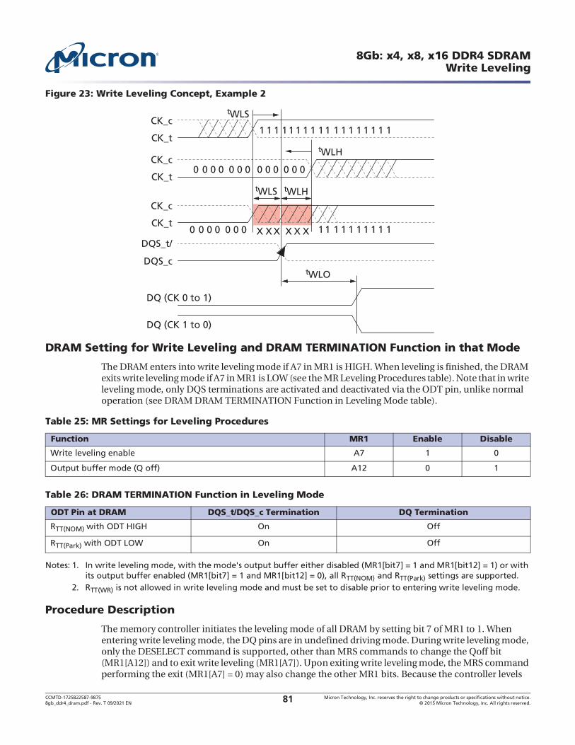
CCMTD-1725822587-9875 Micron Technology, Inc. reserves the right to change products or specifications without notice.8gb_ddr4_dram.pdf - Rev. T 09/2021 EN 2015 Micron Technology, Inc. All rights reserved.81
8Gb: x4, x8, x16 DDR4 SDRAMWrite Leveling
Figure 23: Write Leveling Concept, Example 2
DRAM Setting for Write Leveling and DRAM TERMINATION Function in that Mode
The DRAM enters into write leveling mode if A7 in MR1 is HIGH. When leveling is finished, the DRAM exits write leveling mode if A7 in MR1 is LOW (see the MR Leveling Procedures table). Note that in write leveling mode, only DQS terminations are activated and deactivated via the ODT pin, unlike normal operation (see DRAM DRAM TERMINATION Function in Leveling Mode table).
Notes: 1. In write leveling mode, with the mode's output buffer either disabled (MR1[bit7] = 1 and MR1[bit12] = 1) or with its output buffer enabled (MR1[bit7] = 1 and MR1[bit12] = 0), all RTT(NOM) and RTT(Park) settings are supported.
2. RTT(WR) is not allowed in write leveling mode and must be set to disable prior to entering write leveling mode.
Procedure Description
The memory controller initiates the leveling mode of all DRAM by setting bit 7 of MR1 to 1. When entering write leveling mode, the DQ pins are in undefined driving mode. During write leveling mode, only the DESELECT command is supported, other than MRS commands to change the Qoff bit (MR1[A12]) and to exit write leveling (MR1[A7]). Upon exiting write leveling mode, the MRS command performing the exit (MR1[A7] = 0) may also change the other MR1 bits. Because the controller levels
Table 25: MR Settings for Leveling Procedures
Function MR1 Enable Disable
Write leveling enable A7 1 0
Output buffer mode (Q off) A12 0 1
Table 26: DRAM TERMINATION Function in Leveling Mode
ODT Pin at DRAM DQS_t/DQS_c Termination DQ Termination
RTT(NOM) with ODT HIGH On Off
RTT(Park) with ODT LOW On Off
XX X
CK_t
CK_c
CK_t
CK_c
CK_t
CK_c
DQS_t/
DQS_c
DQ (CK 0 to 1)
tWLH
tWLH
tWLO
tWLS
tWLS
0 0 00 0 00 0 000 0 0
0 0 000 0 0 XX X
11111 11111 1111 1111
11 1111 1111
DQ (CK 1 to 0)

CCMTD-1725822587-9875 Micron Technology, Inc. reserves the right to change products or specifications without notice.8gb_ddr4_dram.pdf - Rev. T 09/2021 EN 2015 Micron Technology, Inc. All rights reserved.82
8Gb: x4, x8, x16 DDR4 SDRAMWrite Leveling
one rank at a time, the output of other ranks must be disabled by setting MR1 bit A12 to 1. The
controller may assert ODT after tMOD, at which time the DRAM is ready to accept the ODT signal, unless DODTLon or DODTLoff have been altered (the ODT internal pipe delay is increased when increasing WRITE latency [WL] or READ latency [RL] by the previous MR command), then ODT asser-
tion should be delayed by DODTLon after tMOD is satisfied, which means the delay is now tMOD + DODTLon.
The controller may drive DQS_t LOW and DQS_c HIGH after a delay of tWLDQSEN, at which time the
DRAM has applied ODT to these signals. After tDQSL and tWLMRD, the controller provides a single
DQS_t, DQS_c edge, which is used by the DRAM to sample CK driven from the controller. tWLMRD (MAX) timing is controller dependent.
The DRAM samples CK status with the rising edge of DQS and provides feedback on all the DQ bits
asynchronously after tWLO timing. There is a DQ output uncertainty of tWLOE defined to allow
mismatch on DQ bits. The tWLOE period is defined from the transition of the earliest DQ bit to the corresponding transition of the latest DQ bit. There are no read strobes (DQS_t, DQS_c) needed for these DQs. The controller samples incoming DQ and either increments or decrements DQS delay setting and launches the next DQS pulse after some time, which is controller dependent. After a 0-to-1 transition is detected, the controller locks the DQS delay setting, and write leveling is achieved for the device. The following figure shows the timing diagram and parameters for the overall write leveling procedure.
Figure 24: Write Leveling Sequence (DQS Capturing CK LOW at T1 and CK HIGH at T2)
Notes: 1. The device drives leveling feedback on all DQs.2. MRS: Load MR1 to enter write leveling mode.3. diff_DQS is the differential data strobe. Timing reference points are the zero crossings. DQS_t is shown with a solid
line; DQS_c is shown with a dotted line.4. CK_t is shown with a solid dark line; CK_c is shown with a dotted line.
5. DQS needs to fulfill minimum pulse width requirements, tDQSH (MIN) and tDQSL (MIN), as defined for regular WRITEs; the maximum pulse width is system dependent.
6. tWLDQSEN must be satisfied following equation when using ODT:
DLL = Enable, then tWLDQSEN > tMOD (MIN) + DODTLon + tADC
DLL = Disable, then tWLDQSEN > tMOD (MIN) + tAONAS
tMOD
tWLDQSEN
tWLMRD
tWLH
tDQSH6tDQSL6 tDQSH6tDQSL6
tWLStWLH
tWLS
NOP
CK_tCK_c5
Command
T1 T2
Early Prime DQ1
ODT
Late Prime DQ1
diff_DQS4
DESMRS2 DES DES DES DES DES DES DES DES DES
Don’t CareUndefined Driving Mode Time Break
tWLO
tWLO tWLO
tWLO
tWLOE
tWLOE
DES3

CCMTD-1725822587-9875 Micron Technology, Inc. reserves the right to change products or specifications without notice.8gb_ddr4_dram.pdf - Rev. T 09/2021 EN 2015 Micron Technology, Inc. All rights reserved.83
8Gb: x4, x8, x16 DDR4 SDRAMWrite Leveling
Write Leveling Mode Exit
Write leveling mode should be exited as follows:1. After the last rising strobe edge (see ~T0), stop driving the strobe signals (see ~Tc0). Note that from
this point on, DQ pins are in undefined driving mode and will remain undefined, until tMOD after the respective MR command (Te1).
2. Drive ODT pin LOW (tIS must be satisfied) and continue registering LOW (see Tb0).3. After RTT is switched off, disable write leveling mode via the MRS command (see Tc2).
4. After tMOD is satisfied (Te1), any valid command can be registered. (MR commands can be issued
after tMRD [Td1]).
Figure 25: Write Leveling Exit
Notes: 1. The DQ result = 1 between Ta0 and Tc0 is a result of the DQS signals capturing CK_t HIGH just after the T0 state.
2. See previous figure for specific tWLO timing.
tMOD
tWLO
ODTL (OFF)
tIS
tMRD
CK_t
T0 T1 T2 Ta0 Tb0 Tc0 Tc1 Tc2 Td0 Td1 Te0 Te1CK_c
Command
ODT
RTT(DQS_t)RTT(DQS_c)
RTT(DQ)
DQ1
DQS_t,DQS_c
DESDES DES DES DES DES DES DES DES
Address MR1 Valid
Valid Valid
Valid
Don’t CareTransitioning Time Break
RTT(NON)
Undefined Driving Mode
tADC (MAX)
tADC (MIN)
DES
RTT(Park)
result = 1
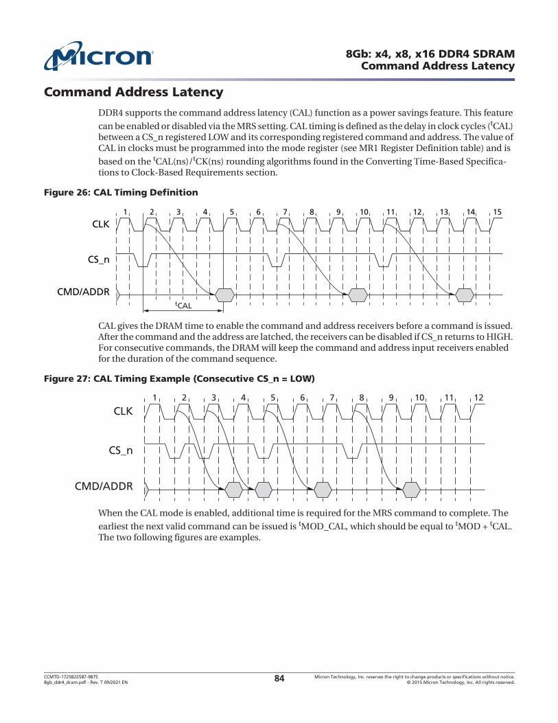
CCMTD-1725822587-9875 Micron Technology, Inc. reserves the right to change products or specifications without notice.8gb_ddr4_dram.pdf - Rev. T 09/2021 EN 2015 Micron Technology, Inc. All rights reserved.84
8Gb: x4, x8, x16 DDR4 SDRAMCommand Address Latency
Command Address Latency
DDR4 supports the command address latency (CAL) function as a power savings feature. This feature
can be enabled or disabled via the MRS setting. CAL timing is defined as the delay in clock cycles (tCAL) between a CS_n registered LOW and its corresponding registered command and address. The value of CAL in clocks must be programmed into the mode register (see MR1 Register Definition table) and is
based on the tCAL(ns)/tCK(ns) rounding algorithms found in the Converting Time-Based Specifica-tions to Clock-Based Requirements section.
Figure 26: CAL Timing Definition
CAL gives the DRAM time to enable the command and address receivers before a command is issued. After the command and the address are latched, the receivers can be disabled if CS_n returns to HIGH. For consecutive commands, the DRAM will keep the command and address input receivers enabled for the duration of the command sequence.
Figure 27: CAL Timing Example (Consecutive CS_n = LOW)
When the CAL mode is enabled, additional time is required for the MRS command to complete. The
earliest the next valid command can be issued is tMOD_CAL, which should be equal to tMOD + tCAL. The two following figures are examples.
CLK
CMD/ADDR
1 2 3 4 5 6 7 8 9 10 11 12 13 14 15
CS_n
tCAL
CLK
CMD/ADDR
1 2 3 4 5 6 7 8 9 10 11 12
CS_n

CCMTD-1725822587-9875 Micron Technology, Inc. reserves the right to change products or specifications without notice.8gb_ddr4_dram.pdf - Rev. T 09/2021 EN 2015 Micron Technology, Inc. All rights reserved.85
8Gb: x4, x8, x16 DDR4 SDRAMCommand Address Latency
Figure 28: tMOD_CAL
Note: 1. CAL mode is enabled at T1.
Figure 29: tMOD_CAL, MRS to Valid Command Timing with CAL Enabled
Note: 1. MRS at Ta1 may or may not modify CAL, tMOD_CAL is computed based on new tCAL setting if modified.
When the CAL mode is enabled or being enabled, the earliest the next MRS command can be issued is tMRD_CAL is equal to tMOD + tCAL. The two following figures are examples.
Figure 30: CAL Enabling MRS to Next MRS Command, tMRD_CAL
T0 T1 Ta0 Ta1 Ta2CK_c
CK_t
Address
CS_n
Settings
Command
Ta3 Ta4
Old settings
MRSValid DESDESDES DES
Valid ValidValid Valid Valid Valid ValidValid
Don’t CareTime Break
Tb0 Tb1 Tb2 Tb3
New settings
Valid Valid
Valid Valid Valid
tMOD_CAL
tCAL
Updating settings
DES DES DES
T0 T1 Ta0 Ta1 Ta2CK_c
CK_t
Address
CS_n
Settings
Command
Tb0 Tb1
Old settings
Valid DESDESDES DES
Valid ValidValid Valid Valid Valid ValidValid
Don’t CareTime Break
Tb2 Tc0 Tc1 Tc2
New settings
Valid Valid Valid
tMOD_CAL
tCAL tCAL
Updating settings
DES DES DESMRS Valid Valid
T0 T1 Ta0 Ta1 Ta2CK_c
CK_t
Address
CS_n
Settings
Command
Ta3 Ta4
Old settings
MRS MRSValid DESDESDES DES DES
Valid ValidValid Valid Valid Valid ValidValid
Don’t CareTime Break
Tb0 Tb1 Tb2 Tb3
Valid Valid Valid
tMRD_CAL
tCAL
Updating settings Updating settings
DES DES DES
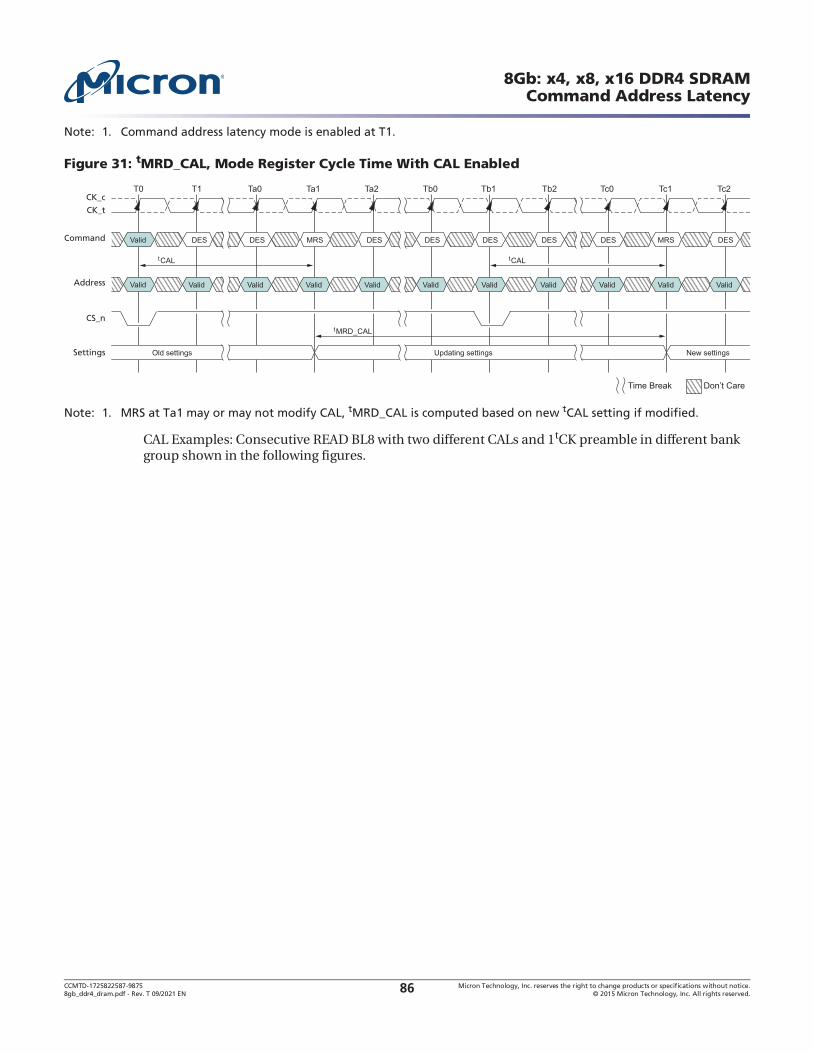
CCMTD-1725822587-9875 Micron Technology, Inc. reserves the right to change products or specifications without notice.8gb_ddr4_dram.pdf - Rev. T 09/2021 EN 2015 Micron Technology, Inc. All rights reserved.86
8Gb: x4, x8, x16 DDR4 SDRAMCommand Address Latency
Note: 1. Command address latency mode is enabled at T1.
Figure 31: tMRD_CAL, Mode Register Cycle Time With CAL Enabled
Note: 1. MRS at Ta1 may or may not modify CAL, tMRD_CAL is computed based on new tCAL setting if modified.
CAL Examples: Consecutive READ BL8 with two different CALs and 1tCK preamble in different bank group shown in the following figures.
T0 T1 Ta0 Ta1 Ta2CK_c
CK_t
Address
CS_n
Settings
Command
Tb0 Tb1
Old settings
Valid DESDESDES DES
Valid ValidValid Valid Valid Valid ValidValid
Don’t CareTime Break
Tb2 Tc0 Tc1 Tc2
New settings
Valid Valid Valid
tMRD_CAL
tCAL tCAL
Updating settings
DES DES DESMRS DESMRS

CCM
TD-1725822587-9875
Micro
n Techno
log
y, Inc. reserves the rig
ht to ch
ange p
rod
ucts or sp
ecifications w
itho
ut n
otice.
8gb
_ddr4_d
ram.p
df - Rev. T 09/2021 EN
2015 Micron
Techn
olog
y, Inc. A
ll rights reserved.
87
8Gb
: x4
, x8
, x16
DD
R4
SD
RA
MC
om
man
d A
dd
ress Laten
cy
Figure 32: Consecutive READ BL8, CAL3, 1tCK Preamble, Different Bank Group
Notes: 1. BL = 8, AL = 0, CL = 11, CAL = 3, Preamble = 1tCK.2. DOUT n = data-out from column n; DOUT b = data-out from column b.3. DES commands are shown for ease of illustration, other commands may be valid at these times.4. BL8 setting activated by either MR0[A1:0 = 00] or MR0[A1:0 = 01] and A12 = 1 during READ command at T3 and T7.5. CA parity = Disable, CS to CA latency = Enable, Read DBI = Disable.6. Enabling CAL mode does not impact ODT control timings. ODT control timings should be maintained with the same timing relationship relative
to the command/address bus as when CAL is disabled.
Figure 33: Consecutive READ BL8, CAL4, 1tCK Preamble, Different Bank Group
Notes: 1. BL = 8, AL = 0, CL = 11, CAL = 4, Preamble = 1tCK.2. DOUT n = data-out from column n; DOUT b = data-out from column b.3. DES commands are shown for ease of illustration, other commands may be valid at these times.4. BL8 setting activated by either MR0[A1:0 = 00] or MR0[A1:0 = 01] and A12 = 1 during READ command at T4 and T8.5. CA parity = Disable, CS to CA latency = Enable, Read DBI = Disable.6. Enabling CAL mode does not impact ODT control timings. ODT control timings should be maintained with the same timing relationship relative
to the command/address bus as when CAL is disabled.
DOUT n
DOUT n + 1
DOUT n + 2
DOUT n + 3RL = 11
RL = 11
T0 T1 T2 T3 T4 T5 T6 T7 T14T13
tCAL = 3
T15 T16
Don’t CareTransitioning Data
T17 T18 T19 T20 T21 T22
Bank,Col n
tRPST
DES DES DES DES DES DES DES DES DES DES DES DES DES DESREADREAD
CK_tCK_c
Command
CS_n
DQ
DQS_t, DQS_c
Address
Bank GroupAddress
tCAL = 3
tCCD_S = 4
BG a
Bank,Col b
BG b
tRPRE (1nCK)
DOUT n + 4
DOUT n + 5
DOUT n + 6
DOUTn + 7
DOUT b
DOUT b + 7
DOUT b + 2
DOUT b + 3
DOUT b + 4
DOUT b + 5
DOUT b + 6
DOUT b + 7
DOUT n
DOUT n + 1
DOUT n + 2
DOUT n + 3RL = 11
RL = 11
T0 T1 T2 T3 T4 T5 T6 T7 T8 T14
tCAL = 4
T15 T16
Don’t CareTransitioning Data
T17 T18 T19 T20 T21 T22 T23
Bank,Col n
tRPST
DES DES DES DES DES DES DES DES DES DES DES DES DES DES DES DESREADREAD
CK_tCK_c
Command
CS_n
DQ
DQS_t, DQS_c
Address
Bank GroupAddress
tCAL = 4
tCCD_S = 4
BG a
Bank,Col b
BG b
tRPRE (1nCK)
DOUT n + 4
DOUT n + 5
DOUT n + 6
DOUTn + 7
DOUT b
DOUT b + 7
DOUT b + 2
DOUT b + 3
DOUT b + 4
DOUT b + 5
DOUT b + 6
DOUT b + 7
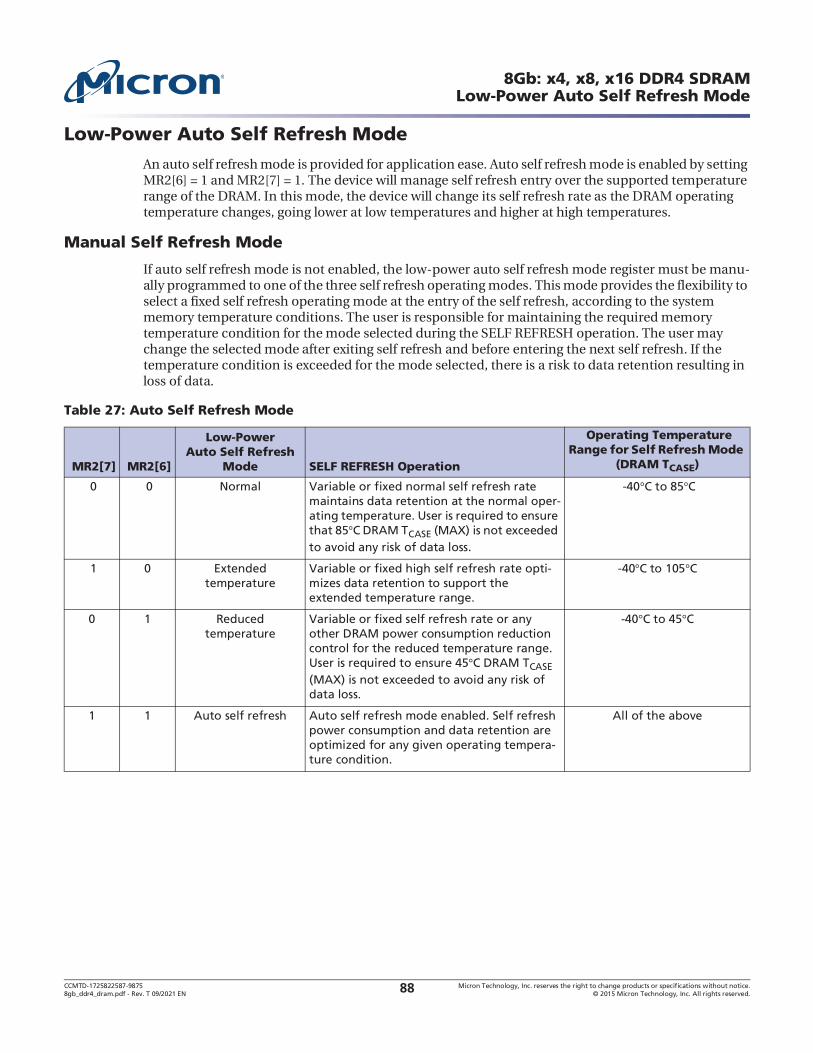
CCMTD-1725822587-9875 Micron Technology, Inc. reserves the right to change products or specifications without notice.8gb_ddr4_dram.pdf - Rev. T 09/2021 EN 2015 Micron Technology, Inc. All rights reserved.88
8Gb: x4, x8, x16 DDR4 SDRAMLow-Power Auto Self Refresh Mode
Low-Power Auto Self Refresh Mode
An auto self refresh mode is provided for application ease. Auto self refresh mode is enabled by setting MR2[6] = 1 and MR2[7] = 1. The device will manage self refresh entry over the supported temperature range of the DRAM. In this mode, the device will change its self refresh rate as the DRAM operating temperature changes, going lower at low temperatures and higher at high temperatures.
Manual Self Refresh Mode
If auto self refresh mode is not enabled, the low-power auto self refresh mode register must be manu-ally programmed to one of the three self refresh operating modes. This mode provides the flexibility to select a fixed self refresh operating mode at the entry of the self refresh, according to the system memory temperature conditions. The user is responsible for maintaining the required memory temperature condition for the mode selected during the SELF REFRESH operation. The user may change the selected mode after exiting self refresh and before entering the next self refresh. If the temperature condition is exceeded for the mode selected, there is a risk to data retention resulting in loss of data.
Table 27: Auto Self Refresh Mode
MR2[7] MR2[6]
Low-Power Auto Self Refresh
Mode SELF REFRESH Operation
Operating Temperature Range for Self Refresh Mode
(DRAM TCASE)
0 0 Normal Variable or fixed normal self refresh rate maintains data retention at the normal oper-ating temperature. User is required to ensure that 85 C DRAM TCASE (MAX) is not exceeded to avoid any risk of data loss.
-40 C to 85 C
1 0 Extendedtemperature
Variable or fixed high self refresh rate opti-mizes data retention to support the extended temperature range.
-40 C to 105 C
0 1 Reducedtemperature
Variable or fixed self refresh rate or any other DRAM power consumption reduction control for the reduced temperature range. User is required to ensure 45 C DRAM TCASE (MAX) is not exceeded to avoid any risk of data loss.
-40 C to 45 C
1 1 Auto self refresh Auto self refresh mode enabled. Self refresh power consumption and data retention are optimized for any given operating tempera-ture condition.
All of the above
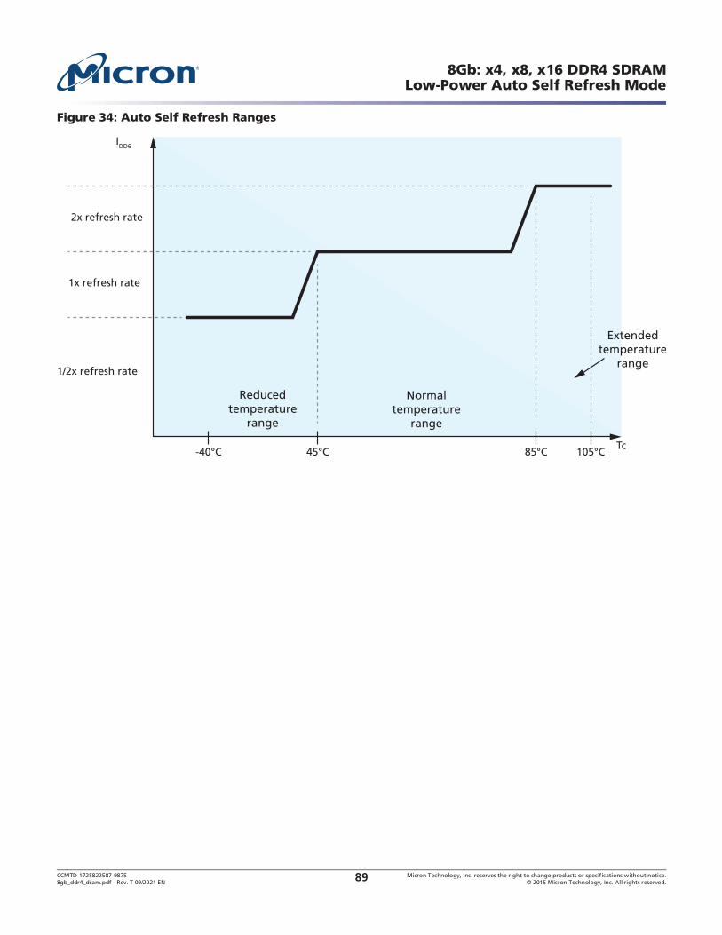
CCMTD-1725822587-9875 Micron Technology, Inc. reserves the right to change products or specifications without notice.8gb_ddr4_dram.pdf - Rev. T 09/2021 EN 2015 Micron Technology, Inc. All rights reserved.89
8Gb: x4, x8, x16 DDR4 SDRAMLow-Power Auto Self Refresh Mode
Figure 34: Auto Self Refresh Ranges
45°C-40°C
IDD6
Tc85°C 105°C
Reducedtemperature
range
Normaltemperature
range
2x refresh rate
1x refresh rate
1/2x refresh rate
Extendedtemperature
range

CCMTD-1725822587-9875 Micron Technology, Inc. reserves the right to change products or specifications without notice.8gb_ddr4_dram.pdf - Rev. T 09/2021 EN 2015 Micron Technology, Inc. All rights reserved.90
8Gb: x4, x8, x16 DDR4 SDRAMMultipurpose Register
Multipurpose Register
The MULTIPURPOSE REGISTER (MPR) function, MPR access mode, is used to write/read specialized data to/from the DRAM. The MPR consists of four logical pages, MPR Page 0 through MPR Page 3, with each page having four 8-bit registers, MPR0 through MPR3. Page 0 can be read by any of three readout modes (serial, parallel, or staggered) while Pages 1, 2, and 3 can be read by only the serial readout mode. Page 3 is for DRAM vendor use only. MPR mode enable and page selection is done with MRS commands. Data bus inversion (DBI) is not allowed during MPR READ operation.
Once the MPR access mode is enabled (MR3[2] = 1), only the following commands are allowed: MRS, RD, RDA WR, WRA, DES, REF, and RESET; RDA/WRA have the same functionality as RD/WR which means the auto precharge part of RDA/WRA is ignored. Power-down mode and SELF REFRESH
command are not allowed during MPR enable mode. No other command can be issued within tRFC after a REF command has been issued; 1x refresh (only) is to be used during MPR access mode. While in MPR access mode, MPR read or write sequences must be completed prior to a REFRESH command.
Figure 35: MPR Block Diagram
Table 28: MR3 Setting for the MPR Access Mode
Address Operation Mode Description
A[12:11] MPR data read format 00 = Serial ........... 01 = Parallel 10 = Staggered .... 11 = Reserved
A2 MPR access 0 = Standard operation (MPR not enabled) 1 = MPR data flow enabled
A[1:0] MPR page selection 00 = Page 0 .... 01 = Page 1 10 = Page 2 .... 11 = Page 3
Table 29: DRAM Address to MPR UI Translation
MPR Location [7] [6] [5] [4] [3] [2] [1] [0]
x A7 A6 A5 A4 A3 A2 A1 A0
x UI0 UI1 UI2 UI3 UI4 UI5 UI6 UI7
Memory core(all banks precharged)
MR3 [2] = 1
DQ,s DM_n/DBI_n, DQS_t, DQS_c
Four multipurpose registers (pages),each with four 8-bit registers:
Data patterns (RD/WR)
Error log (RD)
Mode registers (RD)
DRAM manufacture only (RD)MPR data flow

CCMTD-1725822587-9875 Micron Technology, Inc. reserves the right to change products or specifications without notice.8gb_ddr4_dram.pdf - Rev. T 09/2021 EN 2015 Micron Technology, Inc. All rights reserved.91
8Gb: x4, x8, x16 DDR4 SDRAMMultipurpose Register
Notes: 1. DC = "Don't Care"2. MPR[4:3] 00 = Sub 1X refresh; MPR[4:3] 01 = 1X refresh; MPR[4:3] 10 = 2X refresh; MPR[4:3] 11 = Reserved
MPR Reads
MPR reads are supported using BL8 and BC4 modes. Burst length on-the-fly is not supported for MPR reads. Data bus inversion (DBI) is not allowed during MPR READ operation; the device will ignore the Read DBI enable setting in MR5 [12] when in MPR mode. READ commands for BC4 are supported with a starting column address of A[2:0] = 000 or 100. After power-up, the content of MPR Page 0 has the default values, which are defined in . MPR page 0 can be rewritten via an MPR WRITE command. The
Table 30: MPR Page and MPRx Definitions
Address MPR Location [7] [6] [5] [4] [3] [2] [1] [0] Note
BA[1:0] 00 = MPR0 0 1 0 1 0 1 0 1 Read/Write
(default value listed)
01 = MPR1 0 0 1 1 0 0 1 1
10 = MPR2 0 0 0 0 1 1 1 1
11 = MPR3 0 0 0 0 0 0 0 0
BA[1:0] 00 = MPR0 A7 A6 A5 A4 A3 A2 A1 A0 Read-only01 = MPR1 CAS_n/A
15WE_n/A
14A13 A12 A11 A10 A9 A8
10 = MPR2 PAR ACT_n BG1 BG0 BA1 BA0 A17 RAS_n/A16
11 = MPR3 CRC error status
CA parity error status CA parity latency: [5] = MR5[2], [4] = MR5[1], [3] = MR5[0]
C2 C1 C0
BA[1:0] 00 = MPR0 hPPR support
sPPR support
RTT(WR) MR2[11]
Temperature sen-
sor status2CRC write
enable MR2[12]
RTT(WR) MR2[10:9] Read-only
01 = MPR1 VREFDQ trainging range MR6[6]VREFDQ training value: [6:1] = MR6[5:0]
Gear- down enable MR3[3]
10 = MPR2CAS latency: [7:3] = MR0[6:4,2,12] CAS write latency [2:0] = MR2[5:3]
11 = MPR3RTT(NOM): [7:5] = MR1[10:8] RTT(Park): [4:2] = MR5[8:6] RON: [1:0] = MR1[2:1]
BA[1:0] 00 = MPR0 DC DC DC DC DC DC DC DC Read-only01 = MPR1 DC DC DC DC DC DC DC DC
10 = MPR2 DC DC DC DC DC DC DC DC
11 = MPR3 MBIST-PPR Sup-
port
DCMBIST-PPR Transparency
MAC MAC MAC MAC

CCMTD-1725822587-9875 Micron Technology, Inc. reserves the right to change products or specifications without notice.8gb_ddr4_dram.pdf - Rev. T 09/2021 EN 2015 Micron Technology, Inc. All rights reserved.92
8Gb: x4, x8, x16 DDR4 SDRAMMultipurpose Register
device maintains the default values unless it is rewritten by the DRAM controller. If the DRAM controller does overwrite the default values (Page 0 only), the device will maintain the new values unless re-initialized or there is power loss.
Timing in MPR mode:
Reads (back-to-back) from Page 0 may use tCCD_S or tCCD_L timing between READ commands
Reads (back-to-back) from Pages 1, 2, or 3 may not use tCCD_S timing between READ commands; tCCD_L must be used for timing between READ commands
The following steps are required to use the MPR to read out the contents of a mode register (MPR Page x, MPRy).1. The DLL must be locked if enabled.
2. Precharge all; wait until tRP is satisfied.3. MRS command to MR3[2] = 1 (Enable MPR data flow), MR3[12:11] = MPR read format, and MR3[1:0]
MPR page. a) MR3[12:11] MPR read format:
i) 00 = Serial read formatii) 01 = Parallel read formatiii) 10 = staggered read formativ) 11 = RFU
b) MR3[1:0] MPR page: i) 00 = MPR Page 0ii) 01 = MPR Page 1iii) 10 = MPR Page 2iv) 11 = MPR Page 3
4. tMRD and tMOD must be satisfied.5. Redirect all subsequent READ commands to specific MPRx location.6. Issue RD or RDA command.
a) BA1 and BA0 indicate MPRx location: i) 00 = MPR0ii) 01 = MPR1iii) 10 = MPR2iv) 11 = MPR3
b) A12/BC = 0 or 1; BL8 or BC4 fixed-only, BC4 OTF not supported. i) If BL = 8 and MR0 A[1:0] = 01, A12/BC must be set to 1 during MPR READ commands.
c) A2 = burst-type dependant: i) BL8: A2 = 0 with burst order fixed at 0, 1, 2, 3, 4, 5, 6, 7ii) BL8: A2 = 1 not allowediii) BC4: A2 = 0 with burst order fixed at 0, 1, 2, 3, T, T, T, Tiv) BC4: A2 = 1 with burst order fixed at 4, 5, 6, 7, T, T, T, T
d) A[1:0] = 00, data burst is fixed nibble start at 00.e)
7. After RL = AL + CL, DRAM bursts data from MPRx location; MPR readout format determined by MR3[A12,11,1,0].
8. Steps 5 through 7 may be repeated to read additional MPRx locations.
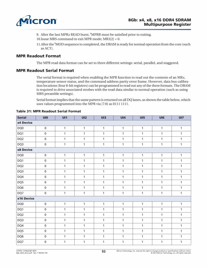
CCMTD-1725822587-9875 Micron Technology, Inc. reserves the right to change products or specifications without notice.8gb_ddr4_dram.pdf - Rev. T 09/2021 EN 2015 Micron Technology, Inc. All rights reserved.93
8Gb: x4, x8, x16 DDR4 SDRAMMultipurpose Register
9. After the last MPRx READ burst, tMPRR must be satisfied prior to exiting.10.Issue MRS command to exit MPR mode; MR3[2] = 0.
11.After the tMOD sequence is completed, the DRAM is ready for normal operation from the core (such as ACT).
MPR Readout Format
The MPR read data format can be set to three different settings: serial, parallel, and staggered.
MPR Readout Serial Format
The serial format is required when enabling the MPR function to read out the contents of an MRx, temperature sensor status, and the command address parity error frame. However, data bus calibra-tion locations (four 8-bit registers) can be programmed to read out any of the three formats. The DRAM is required to drive associated strobes with the read data similar to normal operation (such as using MRS preamble settings).
Serial format implies that the same pattern is returned on all DQ lanes, as shown the table below, which uses values programmed into the MPR via [7:0] as 0111 1111.
Table 31: MPR Readout Serial Format
Serial UI0 UI1 UI2 UI3 UI4 UI5 UI6 UI7
x4 Device
DQ0 0 1 1 1 1 1 1 1
DQ1 0 1 1 1 1 1 1 1
DQ2 0 1 1 1 1 1 1 1
DQ3 0 1 1 1 1 1 1 1
x8 Device
DQ0 0 1 1 1 1 1 1 1
DQ1 0 1 1 1 1 1 1 1
DQ2 0 1 1 1 1 1 1 1
DQ3 0 1 1 1 1 1 1 1
DQ4 0 1 1 1 1 1 1 1
DQ5 0 1 1 1 1 1 1 1
DQ6 0 1 1 1 1 1 1 1
DQ7 0 1 1 1 1 1 1 1
x16 Device
DQ0 0 1 1 1 1 1 1 1
DQ1 0 1 1 1 1 1 1 1
DQ2 0 1 1 1 1 1 1 1
DQ3 0 1 1 1 1 1 1 1
DQ4 0 1 1 1 1 1 1 1
DQ5 0 1 1 1 1 1 1 1
DQ6 0 1 1 1 1 1 1 1
DQ7 0 1 1 1 1 1 1 1

CCMTD-1725822587-9875 Micron Technology, Inc. reserves the right to change products or specifications without notice.8gb_ddr4_dram.pdf - Rev. T 09/2021 EN 2015 Micron Technology, Inc. All rights reserved.94
8Gb: x4, x8, x16 DDR4 SDRAMMultipurpose Register
MPR Readout Parallel Format
Parallel format implies that the MPR data is returned in the first data UI and then repeated in the remaining UIs of the burst, as shown in the table below. Data pattern location 0 is the only location used for the parallel format. RD/RDA from data pattern locations 1, 2, and 3 are not allowed with parallel data return mode. In this example, the pattern programmed in the data pattern location 0 is 0111 1111. The x4 configuration only outputs the first four bits (0111 in this example). For the x16 configuration, the same pattern is repeated on both the upper and lower bytes.
DQ8 0 1 1 1 1 1 1 1
DQ9 0 1 1 1 1 1 1 1
DQ10 0 1 1 1 1 1 1 1
DQ11 0 1 1 1 1 1 1 1
DQ12 0 1 1 1 1 1 1 1
DQ13 0 1 1 1 1 1 1 1
DQ14 0 1 1 1 1 1 1 1
DQ15 0 1 1 1 1 1 1 1
Table 31: MPR Readout Serial Format (Continued)
Serial UI0 UI1 UI2 UI3 UI4 UI5 UI6 UI7
Table 32:
Parallel UI0 UI1 UI2 UI3 UI4 UI5 UI6 UI7
x4 Device
DQ0 0 0 0 0 0 0 0 0
DQ1 1 1 1 1 1 1 1 1
DQ2 1 1 1 1 1 1 1 1
DQ3 1 1 1 1 1 1 1 1
x8 Device
DQ0 0 0 0 0 0 0 0 0
DQ1 1 1 1 1 1 1 1 1
DQ2 1 1 1 1 1 1 1 1
DQ3 1 1 1 1 1 1 1 1
DQ4 1 1 1 1 1 1 1 1
DQ5 1 1 1 1 1 1 1 1
DQ6 1 1 1 1 1 1 1 1
DQ7 1 1 1 1 1 1 1 1
x16 Device
DQ0 0 0 0 0 0 0 0 0
DQ1 1 1 1 1 1 1 1 1
DQ2 1 1 1 1 1 1 1 1
DQ3 1 1 1 1 1 1 1 1
DQ4 1 1 1 1 1 1 1 1
CCMTD-1725822587-9875 Micron Technology, Inc. reserves the right to change products or specifications without notice.8gb_ddr4_dram.pdf - Rev. T 09/2021 EN 2015 Micron Technology, Inc. All rights reserved.95
8Gb: x4, x8, x16 DDR4 SDRAMMultipurpose Register
MPR Readout Staggered Format
Staggered format of data return is defined as the staggering of the MPR data across the lanes. In this mode, an RD/RDA command is issued to a specific data pattern location and then the data is returned on the DQ from each of the different data pattern locations. For the x4 configuration, an RD/RDA to data pattern location 0 will result in data from location 0 being driven on DQ0, data from location 1 being driven on DQ1, data from location 2 being driven on DQ2, and so on, as shown below. Similarly, an RD/RDA command to data pattern location 1 will result in data from location 1 being driven on DQ0, data from location 2 being driven on DQ1, data from location 3 being driven on DQ2, and so on. Examples of different starting locations are also shown.
It is expected that the DRAM can respond to back-to-back RD/RDA commands to the MPR for all DDR4 frequencies so that a sequence (such as the one that follows) can be created on the data bus with no bubbles or clocks between read data. In this case, the system memory controller issues a sequence of RD(MPR0), RD(MPR1), RD(MPR2), RD(MPR3), RD(MPR0), RD(MPR1), RD(MPR2), and RD(MPR3).
DQ5 1 1 1 1 1 1 1 1
DQ6 1 1 1 1 1 1 1 1
DQ7 1 1 1 1 1 1 1 1
DQ8 0 0 0 0 0 0 0 0
DQ9 1 1 1 1 1 1 1 1
DQ10 1 1 1 1 1 1 1 1
DQ11 1 1 1 1 1 1 1 1
DQ12 1 1 1 1 1 1 1 1
DQ13 1 1 1 1 1 1 1 1
DQ14 1 1 1 1 1 1 1 1
DQ15 1 1 1 1 1 1 1 1
Table 32:
Parallel UI0 UI1 UI2 UI3 UI4 UI5 UI6 UI7
Table 33: MPR Readout Staggered Format, x4
x4 READ MPR0 Command x4 READ MPR1 Command x4 READ MPR2 Command x4 READ MPR3 Command
Stagger UI[7:0] Stagger UI[7:0] Stagger UI[7:0] Stagger UI[7:0]
DQ0 MPR0 DQ0 MPR1 DQ0 MPR2 DQ0 MPR3
DQ1 MPR1 DQ1 MPR2 DQ1 MPR3 DQ1 MPR0
DQ2 MPR2 DQ2 MPR3 DQ2 MPR0 DQ2 MPR1
DQ3 MPR3 DQ3 MPR0 DQ3 MPR1 DQ3 MPR2
Table 34:
Stagger UI[7:0] UI[15:8] UI[23:16] UI[31:24] UI[39:32] UI[47:40] UI[55:48] UI[63:56]
DQ0 MPR0 MPR1 MPR2 MPR3 MPR0 MPR1 MPR2 MPR3
DQ1 MPR1 MPR2 MPR3 MPR0 MPR1 MPR2 MPR3 MPR0
DQ2 MPR2 MPR3 MPR0 MPR1 MPR2 MPR3 MPR0 MPR1
DQ3 MPR3 MPR0 MPR1 MPR2 MPR3 MPR0 MPR1 MPR2

CCMTD-1725822587-9875 Micron Technology, Inc. reserves the right to change products or specifications without notice.8gb_ddr4_dram.pdf - Rev. T 09/2021 EN 2015 Micron Technology, Inc. All rights reserved.96
8Gb: x4, x8, x16 DDR4 SDRAMMultipurpose Register
For the x8 configuration, the same pattern is repeated on the lower nibble as on the upper nibble. READs to other MPR data pattern locations follow the same format as the x4 case. A read example to MPR0 for x8 and x16 configurations is shown below.
MPR READ Waveforms
The following waveforms show MPR read accesses.
Figure 36: MPR READ Timing
Notes: 1. tCCD_S = 4tCK, Read Preamble = 1tCK.2. Address setting:
A[1:0] = 00b (data burst order is fixed starting at nibble, always 00b here)A2 = 0b (for BL = 8, burst order is fixed at 0, 1, 2, 3, 4, 5, 6, 7)BA1 and BA0 indicate the MPR location
or 10 and must be 1b when MR0 A[1:0] = 013. Multipurpose registers read/write disable (MR3 A2 = 0).4. Continue with regular DRAM command.5. Parity latency (PL) is added to data output delay when CA parity latency mode is enabled.
Table 35: MPR Readout Staggered Format, x8 and x16
x8 READ MPR0 Command x16 READ MPR0 Command x16 READ MPR0 Command
Stagger UI[7:0] Stagger UI[7:0] Stagger UI[7:0]
DQ0 MPR0 DQ0 MPR0 DQ8 MPR0
DQ1 MPR1 DQ1 MPR1 DQ9 MPR1
DQ2 MPR2 DQ2 MPR2 DQ10 MPR2
DQ3 MPR3 DQ3 MPR3 DQ11 MPR3
DQ4 MPR0 DQ4 MPR0 DQ12 MPR0
DQ5 MPR1 DQ5 MPR1 DQ13 MPR1
DQ6 MPR2 DQ6 MPR2 DQ14 MPR2
DQ7 MPR3 DQ7 MPR3 DQ15 MPR3
T0 Ta0 Ta1
CK_tCK_c
DQ
DQS_t,DQS_c
tMODtMPRR
Tb0 Tc0 Tc1 Tc2 Tc3 Td0 Td1 Te0 Tf0 Tf1
DES DES DES DES MRS3 Valid4 DESCommand MRS1PREA DES READ DES DES
Valid Valid Valid Valid Valid Valid ValidValidValid Valid Add2 Valid ValidAddress
CKE
PL5 + AL + CL
tRP tMOD
UI0 UI1 UI2 UI5 UI6 UI7
MPE Enable MPE Disable
Don’t CareTime Break
CCMTD-1725822587-9875 Micron Technology, Inc. reserves the right to change products or specifications without notice.8gb_ddr4_dram.pdf - Rev. T 09/2021 EN 2015 Micron Technology, Inc. All rights reserved.97
8Gb: x4, x8, x16 DDR4 SDRAMMultipurpose Register
Figure 37: MPR Back-to-Back READ Timing
Notes: 1. tCCD_S = 4tCK, Read Preamble = 1tCK.2. Address setting:
A[1:0] = 00b (data burst order is fixed starting at nibble, always 00b here) A2 = 0b (for BL = 8, burst order is fixed at 0, 1, 2, 3, 4, 5, 6, 7; for BC = 4, burst order is fixed at 0, 1, 2, 3, T, T, T, T)BA1 and BA0 indicate the MPR location
or 10 and must be 1b when MR0 A[1:0] = 013. Parity latency (PL) is added to data output delay when CA parity latency mode is enabled.
Figure 38: MPR READ-to-WRITE Timing
Notes: 1. Address setting:A[1:0] = 00b (data burst order is fixed starting at nibble, always 00b here)A2 = 0b (for BL = 8, burst order is fixed at 0, 1, 2, 3, 4, 5, 6, 7)BA1 and BA0 indicate the MPR location
and must be 1b when MR0 A[1:0] = 012. Address setting:
BA1 and BA0 indicate the MPR locationA[7:0] = data for MPRBA1 and BA0 indicate the MPR location
T0 T1 T2
DQ
DQS_t,DQS_c
T3 T4 T5 T6 Ta0 Ta1 Ta2 Ta3 Ta4 Ta5 Ta6 Ta7 Ta8 Ta9 Ta10
DES DES DES DES DES DES DES DES DES DES DES DESCommand READDES DES DES DES READ
Valid Valid Valid Valid Valid Valid Valid Valid Valid Valid Valid ValidAdd2Valid Valid Add2 Valid ValidAddress
CKE
PL3 + AL + CL
tCCD_S1
DQ
DQS_t,DQS_c
UI0 UI1 UI2 UI3
UI0 UI1 UI2 UI3 UI0 UI1 UI2 UI3
UI4 UI5 UI6 UI7 UI0 UI1 UI2 UI3 UI4 UI5 UI6 UI7
CK_tCK_c
Don’t CareTime Break
T0 T1 T2
DQ
DQS_t,DQS_c
tMPRR
Ta0 Ta1 Ta2 Ta3 Ta4 Ta5 Ta6 Tb0 Tb1 Tb2
DES DES DES DES WRITE DES DESCommand DESREAD DES DES DES DES
Valid Valid Valid Valid Add2 Valid ValidValidAdd1 Valid Valid Valid ValidAddress
CKE
PL3 + AL + CL
UI2 UI3UI0 UI1 UI4 UI5 UI6 UI7
CK_tCK_c
Don’t CareTime Break
CCMTD-1725822587-9875 Micron Technology, Inc. reserves the right to change products or specifications without notice.8gb_ddr4_dram.pdf - Rev. T 09/2021 EN 2015 Micron Technology, Inc. All rights reserved.98
8Gb: x4, x8, x16 DDR4 SDRAMMultipurpose Register
3. Parity latency (PL) is added to data output delay when CA parity latency mode is enabled.
MPR Writes
MPR access mode allows 8-bit writes to the MPR Page 0 using the address bus A[7:0]. Data bus inver-sion (DBI) is not allowed during MPR WRITE operation. The DRAM will maintain the new written values unless re-initialized or there is power loss.
The following steps are required to use the MPR to write to mode register MPR Page 0.1. The DLL must be locked if enabled.
2. Precharge all; wait until tRP is satisfied.3. MRS command to MR3[2] = 1 (enable MPR data flow) and MR3[1:0] = 00 (MPR Page 0); writes to 01,
10, and 11 are not allowed.
4. tMRD and tMOD must be satisfied.5. Redirect all subsequent WRITE commands to specific MPRx location.6. Issue WR or WRA command:
a) BA1 and BA0 indicate MPRx location i) 00 = MPR0ii) 01 = MPR1iii) 10 = MPR2iv) 11 = MPR3
b) A[7:0] = data for MPR Page 0, mapped A[7:0] to UI[7:0].c)
7. tWR_MPR must be satisfied to complete MPR WRITE.8. Steps 5 through 7 may be repeated to write additional MPRx locations.
9. After the last MPRx WRITE, tMPRR must be satisfied prior to exiting.10.Issue MRS command to exit MPR mode; MR3[2] = 0.
11.When the tMOD sequence is completed, the DRAM is ready for normal operation from the core (such as ACT).
MPR WRITE Waveforms
The following waveforms show MPR write accesses.
CCMTD-1725822587-9875 Micron Technology, Inc. reserves the right to change products or specifications without notice.8gb_ddr4_dram.pdf - Rev. T 09/2021 EN 2015 Micron Technology, Inc. All rights reserved.99
8Gb: x4, x8, x16 DDR4 SDRAMMultipurpose Register
Figure 39: MPR WRITE and WRITE-to-READ Timing
Notes: 1. Multipurpose registers read/write enable (MR3 A2 = 1).2. Address setting:
BA1 and BA0 indicate the MPR location
3. Parity latency (PL) is added to data output delay when CA parity latency mode is enabled.
Figure 40: MPR Back-to-Back WRITE Timing
Note: 1. Address setting:BA1 and BA0 indicate the MPR locationA[7:0] = data for MPR
T0 Ta0 Ta1
DQ
DQS_t,DQS_c
tRP tMOD tWR_MPR
Tb0 Tc0 Tc1 Tc2 Td0 Td1 Td2 Td3 Td4 Td5
READ DES DES DES DES DES DESCommand MRS1PREA DES WRITE DES DES
Add Valid Valid Valid Add2 Valid ValidValidValid Valid Add2 Valid ValidAddress
CKE
PL3 + AL + CL
UI2 UI3UI0 UI1 UI4 UI5 UI6 UI7
CK_tCK_c
MPR Enable
Don’t CareTime Break
T0 T1 Ta0
DQ
DQS_t,DQS_c
tWR_MPR
Ta1 Ta2 Ta3 Ta4 Ta5 Ta6 Ta7 Ta8 Ta9 Ta10
DES DES DES DES DES DES DESCommand DESWRITE DES WRITEDES DES
Add Valid Valid Valid Valid Valid ValidValidAdd1 Valid Add1 Valid ValidAddress
CKE
CK_tCK_c
Don’t CareTime Break
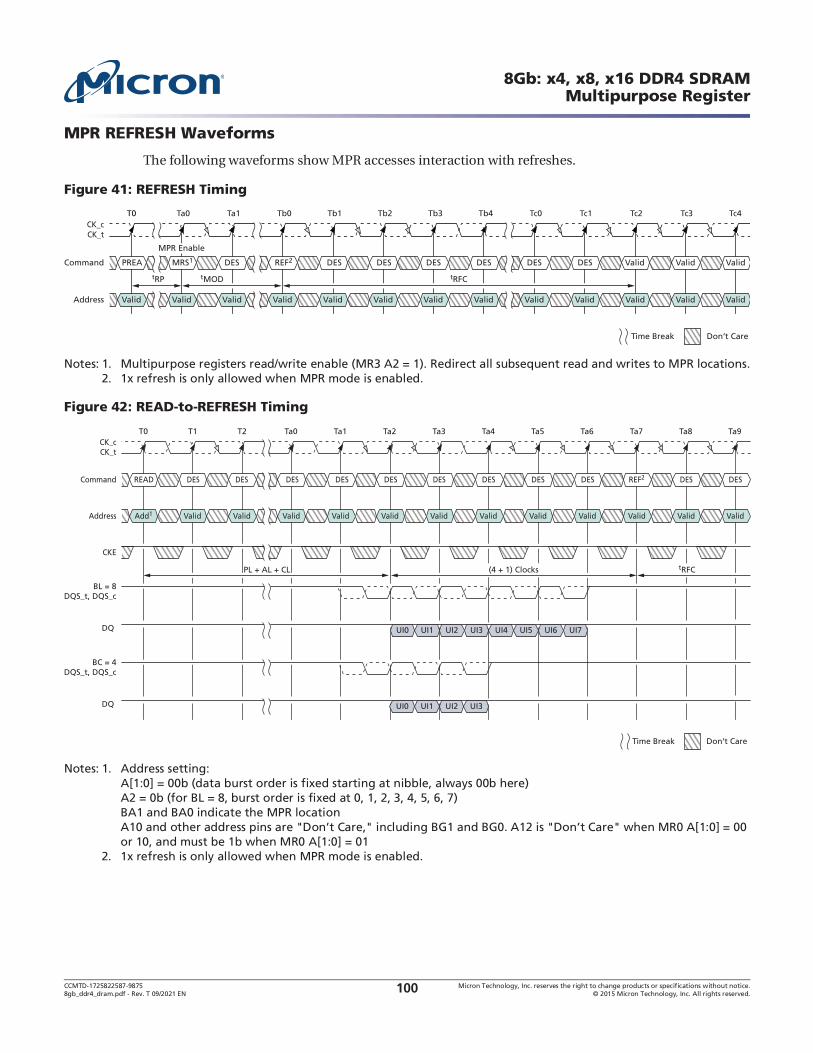
CCMTD-1725822587-9875 Micron Technology, Inc. reserves the right to change products or specifications without notice.8gb_ddr4_dram.pdf - Rev. T 09/2021 EN 2015 Micron Technology, Inc. All rights reserved.100
8Gb: x4, x8, x16 DDR4 SDRAMMultipurpose Register
MPR REFRESH Waveforms
The following waveforms show MPR accesses interaction with refreshes.
Figure 41: REFRESH Timing
Notes: 1. Multipurpose registers read/write enable (MR3 A2 = 1). Redirect all subsequent read and writes to MPR locations.2. 1x refresh is only allowed when MPR mode is enabled.
Figure 42: READ-to-REFRESH Timing
Notes: 1. Address setting:A[1:0] = 00b (data burst order is fixed starting at nibble, always 00b here)A2 = 0b (for BL = 8, burst order is fixed at 0, 1, 2, 3, 4, 5, 6, 7)BA1 and BA0 indicate the MPR location
or 10, and must be 1b when MR0 A[1:0] = 012. 1x refresh is only allowed when MPR mode is enabled.
T0
tMODtRP
Tc4Ta0 Ta1 Tb0 Tb1 Tb2 Tb3 Tb4 Tc0 Tc1 Tc2 Tc3
DES DES DES DES Valid Valid ValidCommand MRS1PREA DES REF2 DES DES
Valid Valid Valid Valid Valid Valid ValidValidValid Valid Valid Valid ValidAddress
CK_tCK_c
tRFC
MPR Enable
Don’t CareTime Break
T0 T1 T2
DQ
BL = 8DQS_t, DQS_c
Ta0 Ta1 Ta2 Ta3 Ta4 Ta5 Ta6 Ta7 Ta8 Ta9
DES DES DES DES REF2 DES DESCommand DESREAD DES DES DES DES
Valid Valid Valid Valid Valid Valid ValidValidAdd1 Valid Valid Valid ValidAddress
CKE
tRFC
UI2 UI3UI0 UI1 UI4 UI5 UI6 UI7
DQ
BC = 4DQS_t, DQS_c
UI2 UI3UI0 UI1
(4 + 1) ClocksPL + AL + CL
CK_tCK_c
Don’t CareTime Break

CCMTD-1725822587-9875 Micron Technology, Inc. reserves the right to change products or specifications without notice.8gb_ddr4_dram.pdf - Rev. T 09/2021 EN 2015 Micron Technology, Inc. All rights reserved.101
8Gb: x4, x8, x16 DDR4 SDRAMMultipurpose Register
Figure 43: WRITE-to-REFRESH Timing
Notes: 1. Address setting:BA1 and BA0 indicate the MPR locationA[7:0] = data for MPR
2. 1x refresh is only allowed when MPR mode is enabled.
T0 T1 Ta0
DQ
DQS_t,DQS_c
tRFC
Don’t Care
Ta1 Ta2 Ta3 Ta4 Ta5 Ta6 Ta7 Ta8 Ta9 Ta10
DES DES DES DES DES DES DESCommand DESWRITE DES DES REF2 DES
Valid Valid Valid Valid Valid Valid ValidValidAdd1 Valid Valid Valid Valid
Time Break
Address
CKE
CK_tCK_c
tWR_MPR
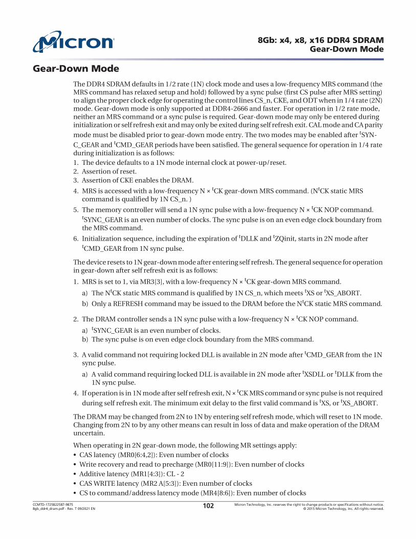
CCMTD-1725822587-9875 Micron Technology, Inc. reserves the right to change products or specifications without notice.8gb_ddr4_dram.pdf - Rev. T 09/2021 EN 2015 Micron Technology, Inc. All rights reserved.102
8Gb: x4, x8, x16 DDR4 SDRAMGear-Down Mode
Gear-Down Mode
The DDR4 SDRAM defaults in 1/2 rate (1N) clock mode and uses a low-frequency MRS command (the MRS command has relaxed setup and hold) followed by a sync pulse (first CS pulse after MRS setting) to align the proper clock edge for operating the control lines CS_n, CKE, and ODT when in 1/4 rate (2N) mode. Gear-down mode is only supported at DDR4-2666 and faster. For operation in 1/2 rate mode, neither an MRS command or a sync pulse is required. Gear-down mode may only be entered during initialization or self refresh exit and may only be exited during self refresh exit. CAL mode and CA parity
mode must be disabled prior to gear-down mode entry. The two modes may be enabled after tSYN-
C_GEAR and tCMD_GEAR periods have been satisfied. The general sequence for operation in 1/4 rate during initialization is as follows:1. The device defaults to a 1N mode internal clock at power-up/reset.2. Assertion of reset.3. Assertion of CKE enables the DRAM.
4. MRS is accessed with a low-frequency N tCK gear-down MRS command. (NtCK static MRS command is qualified by 1N CS_n. )
5. The memory controller will send a 1N sync pulse with a low-frequency N tCK NOP command. tSYNC_GEAR is an even number of clocks. The sync pulse is on an even edge clock boundary from the MRS command.
6. Initialization sequence, including the expiration of tDLLK and tZQinit, starts in 2N mode after tCMD_GEAR from 1N sync pulse.
The device resets to 1N gear-down mode after entering self refresh. The general sequence for operation in gear-down after self refresh exit is as follows:
1. MRS is set to 1, via MR3[3], with a low-frequency N tCK gear-down MRS command.
a) The NtCK static MRS command is qualified by 1N CS_n, which meets tXS or tXS_ABORT.
b) Only a REFRESH command may be issued to the DRAM before the NtCK static MRS command.
2. The DRAM controller sends a 1N sync pulse with a low-frequency N tCK NOP command.
a) tSYNC_GEAR is an even number of clocks.b) The sync pulse is on even edge clock boundary from the MRS command.
3. A valid command not requiring locked DLL is available in 2N mode after tCMD_GEAR from the 1N sync pulse.
a) A valid command requiring locked DLL is available in 2N mode after tXSDLL or tDLLK from the 1N sync pulse.
4. If operation is in 1N mode after self refresh exit, N tCK MRS command or sync pulse is not required
during self refresh exit. The minimum exit delay to the first valid command is tXS, or tXS_ABORT.
The DRAM may be changed from 2N to 1N by entering self refresh mode, which will reset to 1N mode. Changing from 2N to by any other means can result in loss of data and make operation of the DRAM uncertain.
When operating in 2N gear-down mode, the following MR settings apply:CAS latency (MR0[6:4,2]): Even number of clocksWrite recovery and read to precharge (MR0[11:9]): Even number of clocksAdditive latency (MR1[4:3]): CL - 2CAS WRITE latency (MR2 A[5:3]): Even number of clocksCS to command/address latency mode (MR4[8:6]): Even number of clocks

CCMTD-1725822587-9875 Micron Technology, Inc. reserves the right to change products or specifications without notice.8gb_ddr4_dram.pdf - Rev. T 09/2021 EN 2015 Micron Technology, Inc. All rights reserved.103
8Gb: x4, x8, x16 DDR4 SDRAMGear-Down Mode
CA parity latency mode (MR5[2:0]): Even number of clocks
Figure 44: Clock Mode Change from 1/2 Rate to 1/4 Rate (Initialization)
Notes: 1. After tSYNC_GEAR from GEAR-DOWN command, internal clock rate is changed at TdkN.
2. After tSYNC_GEAR + tCMD_GEAR from GEAR-DOWN command, both internal clock rate and command cycle are changed at TdkN + Neven.
Figure 45: Clock Mode Change After Exiting Self Refresh
Notes: 1. After tSYNC_GEAR from GEAR-DOWN command, internal clock rate is changed at TdkN.
2. After tSYNC_GEAR + tCMD_GEAR from GEAR-DOWN command, both internal clock rate and command cycle are changed at TdkN + Neven.
tXPR_GEAR tCMD_GEARtSYNC_GEAR
CK_c
CK_t
Configure DRAMto 1/4 rate
tCKSRX
1N sync pulse 2N mode
DRAM
internal CLK
RESET_n
CKE
CS_n
Command MRS NOP Valid
tGEAR_setup tGEAR_hold tGEAR_setup tGEAR_hold
Don’t CareTime Break
TdkN1 2TdkN + Neven
2
CK_c
CK_t
Don’t CareTime Break
TdkN + Neven
Configure DRAMto 1/4 rate
1N sync pulse 2N mode
DRAM
internal CLK
CKE
CS_n
Command
L
MRS NOP Valid
tXPR_GEAR tCMD_GEARtSYNC_GEAR
tGEAR_setup tGEAR_hold tGEAR_setup tGEAR_hold
TdkN1

CCM
TD-1725822587-9875
Micro
n Techno
log
y, Inc. reserves the rig
ht to ch
ange p
rod
ucts or sp
ecifications w
itho
ut n
otice.
8gb
_ddr4_d
ram.p
df - Rev. T 09/2021 EN
2015 Micron
Techn
olog
y, Inc. A
ll rights reserved.
104
8Gb
: x4
, x8
, x16
DD
R4
SD
RA
MG
ear-D
ow
n M
od
e
Figure 46: Comparison Between Gear-Down Disable and Gear-Down Enable
T0
tRCD = 16
T33T1 T2 T3 T15 T16 T17 T18 T19 T30 T31 T32
DES DES DES DES DES DES DESCommand DESACT DES DES DES READ
DQ
CK_tCK_c
RL =CL= 16 (AL = 0)
T38T34 T35 T36 T37
AL = 0 (geardown = disable)
Don’t CareTransitioning DataTime Break
DOn + 3
DOn + 4
DOn + 5
DOn + 6
DOn + 7
DOn + 2
DOn + 1
DOn
DES DES DES DES DES
DES DES DES DES DES DES DESCommand READACT DES DES DES DES
READ
DQ
RL = AL + CL = 31 (AL = CL - 1 = 15)
AL = CL - 1 (geardown = disable)
DOn + 3
DOn + 4
DOn + 5
DOn + 6
DOn + 7
DOn + 2
DOn + 1
DOn
DES DES DES DES DES
DES DES DESCommand ACT READ DES
READ
DQ
AL + CL = RL = 30 (AL = CL - 2 = 14)
DOn + 3
DOn + 4
DOn + 5
DOn + 6
DOn + 7
DOn + 2
DOn + 1
DOn
DES DES DES

CCMTD-1725822587-9875 Micron Technology, Inc. reserves the right to change products or specifications without notice.8gb_ddr4_dram.pdf - Rev. T 09/2021 EN 2015 Micron Technology, Inc. All rights reserved.105
8Gb: x4, x8, x16 DDR4 SDRAMMaximum Power-Saving Mode
Maximum Power-Saving Mode
Maximum power-saving mode provides the lowest power mode where data retention is not required. When the device is in the maximum power-saving mode, it does not maintain data retention or respond to any external command, except the MAXIMUM POWER SAVING MODE EXIT command
typical power-saving mode. The intent is to be able to park the DRAM at a very low-power state; the device can be switched to an active state via the per-DRAM addressability (PDA) mode.
Maximum Power-Saving Mode Entry
Maximum power-saving mode is entered through an MRS command. For devices with shared control/address signals, a single DRAM device can be entered into the maximum power-saving mode using the per-DRAM addressability MRS command. Large CS_n hold time to CKE upon the mode exit could cause DRAM malfunction; as a result, CA parity, CAL, and gear-down modes must be disabled prior to the maximum power-saving mode entry MRS command.
The MRS command may use both address and DQ information, as defined in the Per-DRAM Address-
ability section. As illustrated in the figure below, after tMPED from the mode entry MRS command, the DRAM is not responsive to any input signals except CKE, CS_n, and RESET_n. All other inputs are disabled (external input signals may become High-Z). The system will provide a valid clock until tCKMPE expires, at which time clock inputs (CK) should be disabled (external clock signals may become High-Z).
Figure 47: Maximum Power-Saving Mode Entry
Ta0 Ta1 Ta2 Tb0 Tb1
Command MRSDES DES DESDES
CK_tCK_c
RESET_n
Tc11Tb3 Tc0 Tc1 Tc2 Tc3 Tc4 Tc7Tc5 Tc6 Tc8 Tc9 Tc10
Don’t CareTime Break
CS_n
CKE
tMPED
CKE LOW makes CS_n a care; CKE LOW followed by CS_n LOW followed by CKE HIGH exits mode
MR4[A1=1]MPSM Enable)
Address Valid
tCKMPE
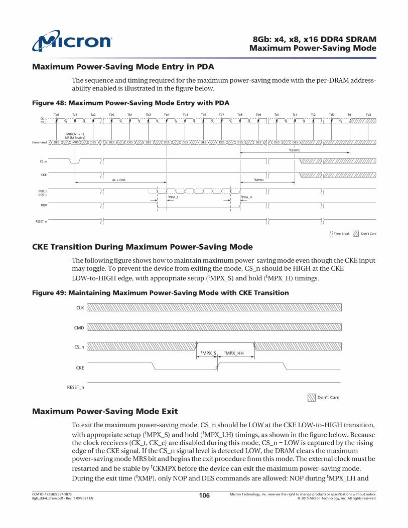
CCMTD-1725822587-9875 Micron Technology, Inc. reserves the right to change products or specifications without notice.8gb_ddr4_dram.pdf - Rev. T 09/2021 EN 2015 Micron Technology, Inc. All rights reserved.106
8Gb: x4, x8, x16 DDR4 SDRAMMaximum Power-Saving Mode
Maximum Power-Saving Mode Entry in PDA
The sequence and timing required for the maximum power-saving mode with the per-DRAM address-ability enabled is illustrated in the figure below.
Figure 48: Maximum Power-Saving Mode Entry with PDA
CKE Transition During Maximum Power-Saving Mode
The following figure shows how to maintain maximum power-saving mode even though the CKE input may toggle. To prevent the device from exiting the mode, CS_n should be HIGH at the CKE
LOW-to-HIGH edge, with appropriate setup (tMPX_S) and hold (tMPX_H) timings.
Figure 49: Maintaining Maximum Power-Saving Mode with CKE Transition
Maximum Power-Saving Mode Exit
To exit the maximum power-saving mode, CS_n should be LOW at the CKE LOW-to-HIGH transition,
with appropriate setup (tMPX_S) and hold (tMPX_LH) timings, as shown in the figure below. Because the clock receivers (CK_t, CK_c) are disabled during this mode, CS_n = LOW is captured by the rising edge of the CKE signal. If the CS_n signal level is detected LOW, the DRAM clears the maximum power-saving mode MRS bit and begins the exit procedure from this mode. The external clock must be
restarted and be stable by tCKMPX before the device can exit the maximum power-saving mode.
During the exit time (tXMP), only NOP and DES commands are allowed: NOP during tMPX_LH and
Ta0 Ta1 Ta2 Tb0 Tb1
Command MRSDES DES DESDES DES DES DES DES DES DES DES DESDES
CK_tCK_c
DQS_tDQS_c
DQ0
Tb3 Tb4 Tb5 Tb6 Tb7 Tb8 Tc1Tb9 Tc0 Tc2 Td0 Td1 Td2
Don’t CareTime Break
CS_n
CKE
RESET_n
MR4[A1 = 1]MPSM Enable)
AL + CWL tMPED
tPDA_HtPDA_S
tCKMPE
CMD
CS_n
CKE
RESET_n
Don’t Care
CLK
tMPX_HHtMPX_S

CCMTD-1725822587-9875 Micron Technology, Inc. reserves the right to change products or specifications without notice.8gb_ddr4_dram.pdf - Rev. T 09/2021 EN 2015 Micron Technology, Inc. All rights reserved.107
8Gb: x4, x8, x16 DDR4 SDRAMMaximum Power-Saving Mode
DES the remainder of tXMP. After tXMP expires, valid commands not requiring a locked DLL are
allowed; after tXMP_DLL expires, valid commands requiring a locked DLL are allowed.
Figure 50: Maximum Power-Saving Mode Exit
Ta0
tCKMPX
tMPX_S
tXMP
tXMP_DLL
Ta1 Ta2 Ta3 Tb0
NOP NOP NOP NOP NOP DES DESCommand
CK_tCK_c
RESET_n
Te1Tb1 Tb2 Tb3 Tc0 Tc1 Tc2 Td1Tc4 Td0 Td2 Td3 Te0
Don’t CareTime Break
DES DES Valid DES DES
CS_n
CKE
tMPX_LH

CCMTD-1725822587-9875 Micron Technology, Inc. reserves the right to change products or specifications without notice.8gb_ddr4_dram.pdf - Rev. T 09/2021 EN 2015 Micron Technology, Inc. All rights reserved.108
8Gb: x4, x8, x16 DDR4 SDRAMCommand/Address Parity
Command/Address Parity
Command/address (CA) parity takes the CA parity signal (PAR) input carrying the parity bit for the generated address and commands signals and matches it to the internally generated parity from the captured address and commands signals. CA parity is supported in the DLL enabled state only; if the DLL is disabled, CA parity is not supported.
Figure 51: Command/Address Parity Operation
CA parity is disabled or enabled via an MRS command. If CA parity is enabled by programming a non-zero value to CA parity latency in the MR, the DRAM will ensure that there is no parity error before executing commands. There is an additional delay required for executing the commands versus when parity is disabled. The delay is programmed in the MR when CA parity is enabled (parity latency) and applied to all commands which are registered by CS_n (rising edge of CK_t and falling CS_n). The command is held for the time of the parity latency (PL) before it is executed inside the device. The command captured by the input clock has an internal delay before executing and is determined with PL. ALERT_n will go active when the DRAM detects a CA parity error.
CA parity covers ACT_n, RAS_n/A16, CAS_n/A15, WE_n/A14, the address bus including bank address and bank group bits, and C[2:0] on 3DS devices; the control signals CKE, ODT, and CS_n are not covered. For example, for a 4Gb x4 monolithic device, parity is computed across BG[1:0], BA[1:0], A16/RAS_n, A15/CAS_n, A14/ WE_n, A[13:0], and ACT_n. The DRAM treats any unused address pins internally as zeros; for example, if a common die has stacked pins but the device is used in a monolithic application, then the address pins used for stacking and not connected are treated internally as zeros.
The convention for parity is even parity; for example, valid parity is defined as an even number of ones across the inputs used for parity computation combined with the parity signal. In other words, the parity bit is chosen so that the total number of ones in the transmitted signal, including the parity bit, is even.
If a DRAM device detects a CA parity error in any command qualified by CS_n, it will perform the following steps:
1. Ignore the erroneous command. Commands in the MAX NnCK window (tPAR_UNKNOWN) prior to the erroneous command are not guaranteed to be executed. When a READ command in this NnCK window is not executed, the device does not activate DQS outputs. If WRITE CRC is enabled and a
WRITE CRC occurs during the tPAR_UNKNOWN window, the WRITE CRC Error Status Bit located at MR5[3] may or may not get set. When CA Parity and WRITE CRC are both enabled and a CA Parity occurs, the WRITE CRC Error Status Bit should be reset.
2. Log the error by storing the erroneous command and address bits in the MPR error log.
CMD/ADDR
DRAM Controller DRAM
CMD/ADDR
Even parity bit
Even parity bit
Even parityGEN
Even parityGEN
CMD/ADDR
Compareparity
bit

CCMTD-1725822587-9875 Micron Technology, Inc. reserves the right to change products or specifications without notice.8gb_ddr4_dram.pdf - Rev. T 09/2021 EN 2015 Micron Technology, Inc. All rights reserved.109
8Gb: x4, x8, x16 DDR4 SDRAMCommand/Address Parity
3. Set the parity error status bit in the mode register to 1. The parity error status bit must be set before
the ALERT_n signal is released by the DRAM (that is, tPAR_ALERT_ON + tPAR_ALERT_PW (MIN)).
4. Assert the ALERT_n signal to the host (ALERT_n is active LOW) within tPAR_ALERT_ON time.
5. Wait for all in-progress commands to complete. These commands were received tPAR_UNKOWN before the erroneous command.
6. Wait for tRAS (MIN) before closing all the open pages. The DRAM is not executing any commands
during the window defined by (tPAR_ALERT_ON + tPAR_ALERT_PW).
7. After tPAR_ALERT_PW (MIN) has been satisfied, the device may de-assert ALERT_n. a) When the device is returned to a known precharged state, ALERT_n is allowed to be de-asserted.
8. After (tPAR_ALERT_PW (MAX)) the DRAM is ready to accept commands for normal operation. Parity latency will be in effect; however, parity checking will not resume until the memory controller has cleared the parity error status bit by writing a zero. The DRAM will execute any erroneous commands until the bit is cleared; unless persistent mode is enabled.
It is possible that the device might have ignored a REFRESH command during tPAR_ALERT_PW or the REFRESH command is the first erroneous frame, so it is recommended that extra REFRESH cycles be issued, as needed.
The parity error status bit may be read anytime after tPAR_ALERT_ON + tPAR_ALERT_PW to deter-mine which DRAM had the error. The device maintains the error log for the first erroneous command until the parity error status bit is reset to a zero or a second CA parity occurs prior to resetting.
The mode register for the CA parity error is defined as follows: CA parity latency bits are write only, the parity error status bit is read/write, and error logs are read-only bits. The DRAM controller can only program the parity error status bit to zero. If the DRAM controller illegally attempts to write a 1 to the parity error status bit, the DRAM can not be certain that parity will be checked; the DRAM may opt to block the DRAM controller from writing a 1 to the parity error status bit.
The device supports persistent parity error mode. This mode is enabled by setting MR5[9] = 1; when enabled, CA parity resumes checking after the ALERT_n is de-asserted, even if the parity error status bit remains a 1. If multiple errors occur before the error status bit is cleared the error log in MPR Page
and de-asserted by the DRAM as defined with the MIN and MAX value tPAR_ALERT_PW. The DRAM controller must issue DESELECT commands once it detects the ALERT_n signal, this response time is
defined as tPAR_ALERT_RSP. The following figures capture the flow of events on the CA bus and the ALERT_n signal.
Table 36: Mode Register Setting for CA Parity
CA Parity Latency MR5[2:0]1 Applicable Speed Bin Parity Error Status Parity Persistent Mode
Erroneous CA Frame
000 = Disabled N/A
MR5 [4] 0 = Clear MR5 [4] 1 = Error
MR5 [9] 0 = Disabled-MR5 [9] 1 = Enabled
C[2:0], ACT_n, BG1, BG0, BA[1:0], PAR, A17, A16/RAS_n,
A15/CAS_n, A14/WE_n, A[13:0]
001 = 4 clocks 1600, 1866, 2133
010 = 5 clocks 2400, 2666
011 = 6 clocks 2933, 3200
100 = 8 clocks RFU
101 = Reserved RFU
110 = Reserved RFU
111 = Reserved RFU

CCMTD-1725822587-9875 Micron Technology, Inc. reserves the right to change products or specifications without notice.8gb_ddr4_dram.pdf - Rev. T 09/2021 EN 2015 Micron Technology, Inc. All rights reserved.110
8Gb: x4, x8, x16 DDR4 SDRAMCommand/Address Parity
Notes: 1. Parity latency is applied to all commands.2. Parity latency can be changed only from a CA parity disabled state; for example, a direct change from PL = 3 to PL
= 4 is not allowed. The correct sequence is PL = 3 to disabled to PL = 4.3. Parity latency is applied to WRITE and READ latency. WRITE latency = AL + CWL + PL. READ latency = AL + CL + PL.
Figure 52: Command/Address Parity During Normal Operation
Notes: 1. DRAM is emptying queues. Precharge all and parity checking are off until parity error status bit is cleared.2. Command execution is unknown; the corresponding DRAM internal state change may or may not occur. The
DRAM controller should consider both cases and make sure that the command sequence meets the specifications.
If WRITE CRC is enabled and a WRITE CRC occurs during the tPAR_UNKNOWN window, the WRITE CRC Error Status Bit located at MR5[3] may or may not get set.
3. Normal operation with parity latency (CA parity persistent error mode disabled). Parity checking is off until parity error status bit is cleared.
Figure 53: Persistent CA Parity Error Checking Operation
Notes: 1. DRAM is emptying queues. Precharge all and parity check re-enable finished by tPAR_ALERT_PW.2. Command execution is unknown; the corresponding DRAM internal state change may or may not occur. The
DRAM controller should consider both cases and make sure that the command sequence meets the specifications.
If WRITE CRC is enabled and a WRITE CRC occurs during the tPAR_UNKNOWN window, the WRITE CRC Error Status Bit located at MR5[3] may or may not get set
3. Normal operation with parity latency and parity checking (CA parity persistent error mode enabled).
Don’t Care Time Break
Command execution unknown
Command not executed
Command executed
DES2
Valid3
ValidError
CK_t
CK_c
Command/Address
Valid2 Valid2 Valid2 Valid3 Valid3
T0 T1 Ta0 Ta1 Tb0 Tc0
ALERT_n
Tc1
tPAR_ALERT_ON
Td0
Valid Valid ValidError
tPAR_UNKNOWN2
Ta2 Te1
tPAR_ALERT_PW1
Te0
DES2 DES2
Valid2
tRPt > 2nCK
Don’t Care Time Break
Command execution unknown
Command not executed
Command executed
DES
Valid3
ValidError
CK_t
CK_c
Command/Address
Valid2 Valid2 Valid2 Valid3
T0 T1 Ta0 Ta1 Tb0 Tc0
ALERT_n
Tc1
tPAR_ALERT_ON
Td0
Valid Valid ValidError
tPAR_UNKNOWN2
Ta2 Te1
tPAR_ALERT_PW1
tPAR_ALERT_RSP
Te0
DES DES DES
Valid2
tRPt > 2nCK

CCMTD-1725822587-9875 Micron Technology, Inc. reserves the right to change products or specifications without notice.8gb_ddr4_dram.pdf - Rev. T 09/2021 EN 2015 Micron Technology, Inc. All rights reserved.111
8Gb: x4, x8, x16 DDR4 SDRAMCommand/Address Parity
Figure 54:
Notes: 1. Only DESELECT command is allowed.2. SELF REFRESH command error. The DRAM masks the intended SRE command and enters precharge power-down.3. Normal operation with parity latency (CA parity persistent error mode disabled). Parity checking is off until the
parity error status bit cleared.4. The controller cannot disable the clock until it has been capable of detecting a possible CA parity error.5. Command execution is unknown; the corresponding DRAM internal state change may or may not occur. The
DRAM controller should consider both cases and make sure that the command sequence meets the specifications.6. Only a DESELECT command is allowed; CKE may go HIGH prior to Tc2 as long as DES commands are issued.
Figure 55:
Notes: 1. Self refresh abort = disable: MR4 [9] = 0.
2. Input commands are bounded by tXSDLL, tXS, tXS_ABORT, and tXS_FAST timing.3. Command execution is unknown; the corresponding DRAM internal state change may or may not occur. The
DRAM controller should consider both cases and make sure that the command sequence meets the specifications.4. Normal operation with parity latency (CA parity persistent error mode disabled). Parity checking off until parity
error status bit cleared.5. Only an MRS (limited to those described in the SELF REFRESH Operation section), ZQCS, or ZQCL command is
allowed.6. Valid commands not requiring a locked DLL.7. Valid commands requiring a locked DLL.
8. This figure shows the case from which the error occurred after tXS_FAST. An error may also occur after tXS_ABORT
and tXS.
Don’t Care Time Break
Command not executed
Command executed
DES6 Command execution unknownDES5
Valid3
DES1Error2
CK_t
CK_c
Command/Address
DES1, 5 Valid3
T0 T1 Ta0 Ta1 Tb1 Tc0
ALERT_n
Tc1
tPAR_ALERT_ON
Td0
DES1
Note 4
Error2
Tb0 Td2
tPAR_ALERT_PW1
Td1
DES6 DES6 DES5
DES1, 5
t > 2nCKtIH
tIS
tXP + PLtCPDED + PL
Td3 Te0 Te1
CKE
tIS
tRP
Don’t CareTime Break
Command execution unknown
Command not executed
Command executed
DES Valid3, 5
Valid4,5,6,7
ValidError
CK_t
CK_c
Command/Address
SRX1 DES DES Valid2, 4, 5 Valid2, 4, 7Valid2, 4, 6
T0 Ta0 Tb0Ta1 Tc0 Tc1
ALERT_n
Tc2
tPAR_ALERT_ON
Td0
Valid2 Valid2 Valid2Error2
tPAR_UNKNOWN
tXS_FAST8
tXStXSDLL
Tb1 Te0
tPAR_ALERT_PW
Td1
DES2, 3 DES2, 3
SRX1
t > 2nCK
Tf0
CKE
tIStRP

CCMTD-1725822587-9875 Micron Technology, Inc. reserves the right to change products or specifications without notice.8gb_ddr4_dram.pdf - Rev. T 09/2021 EN 2015 Micron Technology, Inc. All rights reserved.112
8Gb: x4, x8, x16 DDR4 SDRAMCommand/Address Parity
Figure 56:
Notes: 1. Only DESELECT command is allowed.2. Error could be precharge or activate.3. Normal operation with parity latency (CA parity persistent error mode disabled). Parity checking is off until parity
error status bit cleared.4. Command execution is unknown; the corresponding DRAM internal state change may or may not occur. The
DRAM controller should consider both cases and make sure that the command sequence meets the specifications.5. Only a DESELECT command is allowed; CKE may go HIGH prior to Td2 as long as DES commands are issued.
Figure 57: tMRD_PAR
Note: 1. tMRD_PAR = tMOD + N; where N is the programmed parity latency.
Figure 58: tMOD_PAR
Note: 1. tMOD_PAR = tMOD + N; where N is the programmed parity latency.
Don’t Care Time Break
Command not executed
Command executed
DES5 Command execution unknown
Valid3
DES1Error2
CK_t
CK_c
Command/Address
Valid3
T0 T1 Ta0 Ta1 Tb1 Tc0
ALERT_n
Tc1
tPAR_ALERT_ON
Td0
DES1DES1Error2
Tb0 Td2
tPAR_ALERT_PW1
Td1
DES5 DES5 DES4
DES4
t > 2nCKtIH
tIS
tXP + PLtCPDED + PL
Td3 Te0 Te1
CKE
tIS
tRP
Ta0
tMRD_PAR
Ta1 Ta2 Tb0 Tb1 Tb2
Command MRSDES DES DES MRS DES
PL = 0 Updating setting PL = NParity latency
CK_tCK_c
Enableparity
Don’t CareTime Break
Ta0
tMOD_PAR
Ta1 Ta2 Tb0 Tb1 Tb2
Command MRSDES DES DES Valid DES
Parity latency
CK_tCK_c
Enableparity
Don’t CareTime Break
PL = 0 Updating setting PL = N

CCMTD-1725822587-9875 Micron Technology, Inc. reserves the right to change products or specifications without notice.8gb_ddr4_dram.pdf - Rev. T 09/2021 EN 2015 Micron Technology, Inc. All rights reserved.113
8Gb: x4, x8, x16 DDR4 SDRAMCommand/Address Parity
Figure 59: tMRD_PAR
Note: 1. tMRD_PAR = tMOD + N; where N is the programmed parity latency.
Figure 60: tMOD_PAR
Note: 1. tMOD_PAR = tMOD + N; where N is the programmed parity latency.
Ta0
tMRD_PAR
Ta1 Ta2 Tb0 Tb1 Tb2
Command MRSDES DES DES MRS DES
Parity latency
CK_tCK_c
Disableparity
Don’t CareTime Break
PL = N Updating setting
Ta0
tMOD_PAR
Ta1 Ta2 Tb0 Tb1 Tb2
Command MRSDES DES DES Valid DES
Parity latency
CK_tCK_c
Disableparity
Don’t CareTime Break
PL = N Updating setting
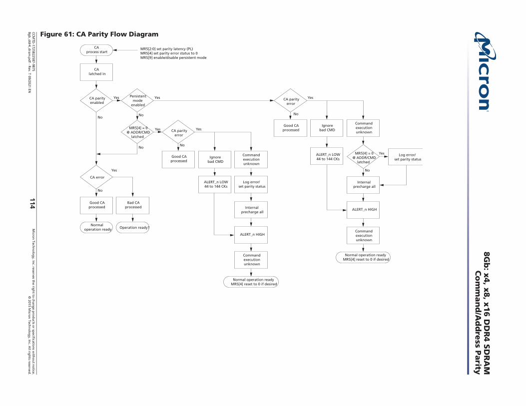
CCM
TD-1725822587-9875
Micro
n Techno
log
y, Inc. reserves the rig
ht to ch
ange p
rod
ucts or sp
ecifications w
itho
ut n
otice.
8gb
_ddr4_d
ram.p
df - Rev. T 09/2021 EN
2015 Micron
Techn
olog
y, Inc. A
ll rights reserved.
114
8Gb
: x4
, x8
, x16
DD
R4
SD
RA
MC
om
ma
nd
/Ad
dre
ss Parity
Figure 61: CA Parity Flow Diagram
CAlatched in
Yes
CAprocess start
MR5[2:0] set parity latency (PL)MR5[4] set parity error status to 0MR5[9] enable/disable persistent mode
No
Yes
No
Yes
No
Yes
No
Yes
No
CA parityenabled
CA error
Persistentmode
enabled
Good CAprocessed
Good CAprocessed
Good CAprocessed
Ignorebad CMD
Ignorebad CMD
Log error/set parity status
Internalprecharge all
ALERT_n HIGH
Commandexecutionunknown
Commandexecutionunknown
Normal operation readyMR5[4] reset to 0 if desired
Normal operation readyMR5[4] reset to 0 if desired
Yes
No
CA parityerror
ALERT_n LOW44 to 144 CKs
ALERT_n LOW44 to 144 CKs
Internalprecharge all
ALERT_n HIGH
Commandexecutionunknown
Commandexecutionunknown
No
Yes Log error/set parity status
MR5[4] = 0@ ADDR/CMD
latched
MR5[4] = 0@ ADDR/CMD
latched
CA parityerror
Normaloperation ready
Bad CAprocessed
Operation ready?

CCMTD-1725822587-9875 Micron Technology, Inc. reserves the right to change products or specifications without notice.8gb_ddr4_dram.pdf - Rev. T 09/2021 EN 2015 Micron Technology, Inc. All rights reserved.115
8Gb: x4, x8, x16 DDR4 SDRAMPer-DRAM Addressability
Per-DRAM Addressability
DDR4 allows programmability of a single, specific DRAM on a rank. As an example, this feature can be used to program different ODT or VREF values on each DRAM on a given rank. Because per-DRAM addressability (PDA) mode may be used to program optimal VREF for the DRAM, the data set up for first DQ0 transfer or the hold time for the last DQ0 transfer cannot be guaranteed. The DRAM may sample DQ0 on either the first falling or second rising DQS transfer edge. This supports a common implemen-tation between BC4 and BL8 modes on the DRAM. The DRAM controller is required to drive DQ0 to a stable LOW or HIGH state during the length of the data transfer for BC4 and BL8 cases. Note, both fixed and on-the-fly (OTF) modes are supported for BC4 and BL8 during PDA mode.1. Before entering PDA mode, write leveling is required.
BL8 or BC4 may be used.2. Before entering PDA mode, the following MR settings are possible:
RTT(Park) MR5 A[8:6] = Enable
RTT(NOM) MR1 A[10:8] = Enable
3. Enable PDA mode using MR3 [4] = 1. (The default programed value of MR3[4] = 0.)4. In PDA mode, all MRS commands are qualified with DQ0. The device captures DQ0 by using DQS
signals. If the value on DQ0 is LOW, the DRAM executes the MRS command. If the value on DQ0 is HIGH, the DRAM ignores the MRS command. The controller can choose to drive all the DQ bits.
5. Program the desired DRAM and mode registers using the MRS command and DQ0.6. In PDA mode, only MRS commands are allowed.
7. The MODE REGISTER SET command cycle time in PDA mode, AL + CWL + BL/2 - 0.5tCK + tMRD_PDA + PL, is required to complete the WRITE operation to the mode register and is the minimum time required between two MRS commands.
8. Remove the device from PDA mode by setting MR3[4] = 0. (This command requires DQ0 = 0.)
Note: Removing the device from PDA mode will require programming the entire MR3 when the MRS command is issued. This may impact some PDA values programmed within a rank as the EXIT command is sent to the rank. To avoid such a case, the PDA enable/disable control bit is located in a mode register that does not have any PDA mode controls.
In PDA mode, the device captures DQ0 using DQS signals the same as in a normal WRITE operation; however, dynamic ODT is not supported. Extra care is required for the ODT setting. If RTT(NOM) MR1 [10:8] = enable, device data termination needs to be controlled by the ODT pin, and applies the same timing parameters (defined below).
Symbol Parameter
DODTLon Direct ODT turnon latency
DODTLoff Direct ODT turn off latency
tADC RTT change timing skew
tAONAS Asynchronous RTT(NOM) turn-on delay
tAOFAS Asynchronous RTT(NOM) turn-off delay
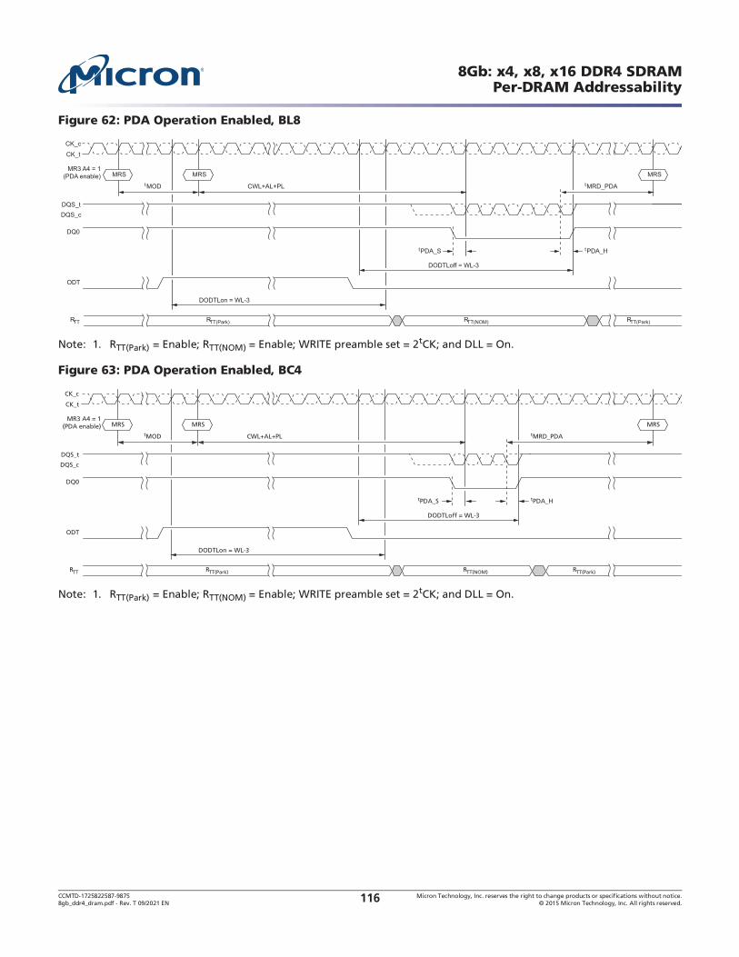
CCMTD-1725822587-9875 Micron Technology, Inc. reserves the right to change products or specifications without notice.8gb_ddr4_dram.pdf - Rev. T 09/2021 EN 2015 Micron Technology, Inc. All rights reserved.116
8Gb: x4, x8, x16 DDR4 SDRAMPer-DRAM Addressability
Figure 62: PDA Operation Enabled, BL8
Note: 1. RTT(Park) = Enable; RTT(NOM) = Enable; WRITE preamble set = 2tCK; and DLL = On.
Figure 63: PDA Operation Enabled, BC4
Note: 1. RTT(Park) = Enable; RTT(NOM) = Enable; WRITE preamble set = 2tCK; and DLL = On.
CK_tCK_c
DQ0
ODT
tPDA_S
tMOD CWL+AL+PL tMRD_PDA
DQS_tDQS_c
MR3 A4 = 1(PDA enable) MRS MRS MRS
DODTLoff = WL-3
DODTLon = WL-3
tPDA_H
RTT(Park)RTT(Park)RTT RTT(NOM)
CK_t
CK_c
DQ0
ODT
tPDA_S
tMOD CWL+AL+PL tMRD_PDA
DQS_t
DQS_c
MR3 A4 = 1(PDA enable) MRS MRS MRS
DODTLoff = WL-3
DODTLon = WL-3
tPDA_H
RTT(Park)RTT(Park)RTT RTT(NOM)
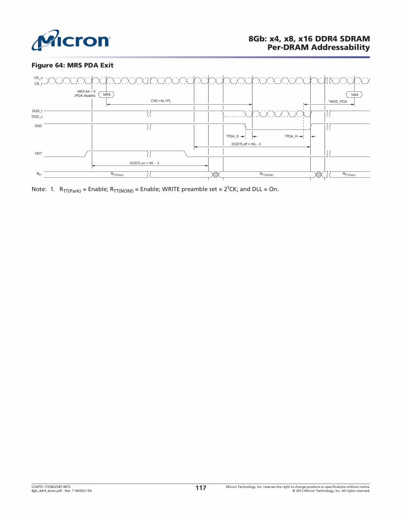
CCMTD-1725822587-9875 Micron Technology, Inc. reserves the right to change products or specifications without notice.8gb_ddr4_dram.pdf - Rev. T 09/2021 EN 2015 Micron Technology, Inc. All rights reserved.117
8Gb: x4, x8, x16 DDR4 SDRAMPer-DRAM Addressability
Figure 64: MRS PDA Exit
Note: 1. RTT(Park) = Enable; RTT(NOM) = Enable; WRITE preamble set = 2tCK; and DLL = On.
CK_tCK_c
DQ0
ODT
RTT
tPDA_S
CWL+AL+PL tMOD_PDA
DQS_tDQS_c
MR3 A4 = 0(PDA disable) MRS Valid
DODTLoff = WL - 3
DODTLon = WL - 3
tPDA_H
RTT(Park) RTT(NOM) RTT(Park)

CCMTD-1725822587-9875 Micron Technology, Inc. reserves the right to change products or specifications without notice.8gb_ddr4_dram.pdf - Rev. T 09/2021 EN 2015 Micron Technology, Inc. All rights reserved.118
8Gb: x4, x8, x16 DDR4 SDRAMVREFDQ Calibration
VREFDQ Calibration
The VREFDQ level, which is used by the DRAM DQ input receivers, is internally generated. The DRAM VREFDQ does not have a default value upon power-up and must be set to the desired value, usually via VREFDQ calibration mode. If PDA or PPR modes (hPPR or sPPR) are used prior to VREFDQ calibration, VREFDQ should initially be set at the midpoint between the VDD,max, and the LOW as determined by the driver and ODT termination selected with wide voltage swing on the input levels and setup and hold times of approximately 0.75UI. The memory controller is responsible for VREFDQ calibration to deter-mine the best internal VREFDQ level. The VREFDQ calibration is enabled/disabled via MR6[7], MR6[6] selects Range 1 (60% to 92.5% of VDDQ) or Range 2 (45% to 77.5% of VDDQ), and an MRS protocol using MR6[5:0] to adjust the VREFDQ level up and down. MR6[6:0] bits can be altered using the MRS command if MR6[7] is enabled. The DRAM controller will likely use a series of writes and reads in conjunction with VREFDQ adjustments to obtain the best VREFDQ, which in turn optimizes the data eye.
The internal VREFDQ specification parameters are voltage range, step size, VREF step time, VREF full step time, and VREF valid level. The voltage operating range specifies the minimum required VREF setting range for DDR4 SDRAM devices. The minimum range is defined by VREFDQ,min and VREFDQ,max. As noted, a calibration sequence, determined by the DRAM controller, should be performed to adjust VREFDQand optimize the timing and voltage margin of the DRAM data input receivers. The internal VREFDQ voltage value may not be exactly within the voltage range setting coupled with the VREF set tolerance; the device must be calibrated to the correct internal VREFDQ voltage.
Figure 65: VREFDQ Voltage Range
VDDQ
VREFrange
VSWING small
VSWING large
System variance
Total range
VREF,max
VREF,min

CCMTD-1725822587-9875 Micron Technology, Inc. reserves the right to change products or specifications without notice.8gb_ddr4_dram.pdf - Rev. T 09/2021 EN 2015 Micron Technology, Inc. All rights reserved.119
8Gb: x4, x8, x16 DDR4 SDRAMVREFDQ Calibration
VREFDQ Range and Levels
VREFDQ Step Size
The VREF step size is defined as the step size between adjacent steps. VREF step size ranges from 0.5% VDDQ to 0.8% VDDQ. However, for a given design, the device has one value for VREF step size that falls within the range.
The VREF set tolerance is the variation in the VREF voltage from the ideal setting. This accounts for accu-mulated error over multiple steps. There are two ranges for VREF set tolerance uncertainty. The range of VREF set tolerance uncertainty is a function of number of steps n.
The VREF set tolerance is measured with respect to the ideal line, which is based on the MIN and MAX VREF value endpoints for a specified range. The internal VREFDQ voltage value may not be exactly within
Table 37: VREFDQ Range and Levels
MR6[5:0] Range 1 MR6[6] 0 Range 2 MR6[6] 1 MR6[5:0] Range 1 MR6[6] 0 Range 2 MR6[6] 1
00 0000 60.00% 45.00% 01 1010 76.90% 61.90%
00 0001 60.65% 45.65% 01 1011 77.55% 62.55%
00 0010 61.30% 46.30% 01 1100 78.20% 63.20%
00 0011 61.95% 46.95% 01 1101 78.85% 63.85%
00 0100 62.60% 47.60% 01 1110 79.50% 64.50%
00 0101 63.25% 48.25% 01 1111 80.15% 65.15%
00 0110 63.90% 48.90% 10 0000 80.80% 65.80%
00 0111 64.55% 49.55% 10 0001 81.45% 66.45%
00 1000 65.20% 50.20% 10 0010 82.10% 67.10%
00 1001 65.85% 50.85% 10 0011 82.75% 67.75%
00 1010 66.50% 51.50% 10 0100 83.40% 68.40%
00 1011 67.15% 52.15% 10 0101 84.05% 69.05%
00 1100 67.80% 52.80% 10 0110 84.70% 69.70%
00 1101 68.45% 53.45% 10 0111 85.35% 70.35%
00 1110 69.10% 54.10% 10 1000 86.00% 71.00%
00 1111 69.75% 54.75% 10 1001 86.65% 71.65%
01 0000 70.40% 55.40% 10 1010 87.30% 72.30%
01 0001 71.05% 56.05% 10 1011 87.95% 72.95%
01 0010 71.70% 56.70% 10 1100 88.60% 73.60%
01 0011 72.35% 57.35% 10 1101 89.25% 74.25%
01 0100 73.00% 58.00% 10 1110 89.90% 74.90%
01 0101 73.65% 58.65% 10 1111 90.55% 75.55%
01 0110 74.30% 59.30% 11 0000 91.20% 76.20%
01 0111 74.95% 59.95% 11 0001 91.85% 76.85%
01 1000 75.60% 60.60% 11 0010 92.50% 77.50%
01 1001 76.25% 61.25% 11 0011 to 11 1111 = Reserved

CCMTD-1725822587-9875 Micron Technology, Inc. reserves the right to change products or specifications without notice.8gb_ddr4_dram.pdf - Rev. T 09/2021 EN 2015 Micron Technology, Inc. All rights reserved.120
8Gb: x4, x8, x16 DDR4 SDRAMVREFDQ Calibration
the voltage range setting coupled with the VREF set tolerance; the device must be calibrated to the correct internal VREFDQ voltage.
Figure 66: Example of VREF Set Tolerance and Step Size
Note: 1. Maximum case shown.
VREFDQ Increment and Decrement Timing
The VREF increment/decrement step times are defined by VREF,time. VREF,time is defined from t0 to t1, where t1 is referenced to the VREF voltage at the final DC level within the VREF valid tolerance (VREF,val_tol). The VREF valid level is defined by VREF,val tolerance to qualify the step time t1. This param-eter is used to insure an adequate RC time constant behavior of the voltage level change after any VREF increment/decrement adjustment.
VREF
VREFstep size
VREF settolerance
VREF settolerance
Straight line(endpoint fit)
Actual VREFoutput
Digital Code

CCMTD-1725822587-9875 Micron Technology, Inc. reserves the right to change products or specifications without notice.8gb_ddr4_dram.pdf - Rev. T 09/2021 EN 2015 Micron Technology, Inc. All rights reserved.121
8Gb: x4, x8, x16 DDR4 SDRAMVREFDQ Calibration
Figure 67: VREFDQ Timing Diagram for VREF,time Parameter
Note: 1. t0 is referenced to the MRS command clock t1 is referenced to VREF,tol
VREFDQ calibration mode is entered via an MRS command, setting MR6[7] to 1 (0 disables VREFDQ cali-bration mode) and setting MR6[6] to either 0 or 1 to select the desired range (MR6[5:0] are "Don't Care"). After VREFDQ calibration mode has been entered, VREFDQ calibration mode legal commands
may be issued once tVREFDQE has been satisfied. Legal commands for VREFDQ calibration mode are ACT, WR, WRA, RD, RDA, PRE, DES, and MRS to set VREFDQ values, and MRS to exit VREFDQ calibration mode. Also, after VREFDQprior to adjusting the VREFDQ value the first time VREFDQ calibration is performed after initialization.
Setting VREFDQ values requires MR6[7] be set to 1 and MR6[6] be unchanged from the initial range selection; MR6[5:0] may be set to the desired VREFDQ values. If MR6[7] is set to 0, MR6[6:0] are not written. VREF,time-short or VREF,time-long must be satisfied after each MR6 command to set VREFDQ value before the internal VREFDQ value is valid.
If PDA mode is used in conjunction with VREFDQ calibration, the PDA mode requirement that only MRS commands are allowed while PDA mode is enabled is not waived. That is, the only VREFDQ calibration mode legal commands noted above that may be used are the MRS commands: MRS to set VREFDQ values and MRS to exit VREFDQ calibration mode.
The last MR6[6:0] setting written to MR6 prior to exiting VREFDQ calibration mode is the range and value used for the internal VREFDQ setting. VREFDQ calibration mode may be exited when the DRAM is in idle state. After the MRS command to exit VREFDQ calibration mode has been issued, DES must be
issued until tVREFDQX has been satisfied where any legal command may then be issued. VREFDQ setting should be updated if the die temperature changes too much from the calibration temperature.
The following are typical script when applying the above rules for VREFDQ calibration routine when performing VREFDQ calibration in Range 1:
MR6[7:6]10 [5:0]XXXXXXX.Subsequent legal commands while in VREFDQ calibration mode: ACT, WR, WRA, RD, RDA, PRE, DES, and MRS (to set VREFDQ values and exit VREFDQ calibration mode).
All subsequent VREFDQ calibration MR setting commands are MR6[7:6]10 [5:0]VVVVVV.
"VVVVVV" are desired settings for VREFDQ.
MRS
VREF settingadjustment
Command
DQ VREF
VREF_time
t0 t1
Old VREF setting New VREF settingUpdating VREF setting
Don’t Care
CK_t
CK_c

CCMTD-1725822587-9875 Micron Technology, Inc. reserves the right to change products or specifications without notice.8gb_ddr4_dram.pdf - Rev. T 09/2021 EN 2015 Micron Technology, Inc. All rights reserved.122
8Gb: x4, x8, x16 DDR4 SDRAMVREFDQ Calibration
Issue ACT/WR/RD looking for pass/fail to determine VCENT (midpoint) as needed.
To exit VREFDQ calibration, the last two VREFDQ calibration MR commands are:
MR6[7:6]10 [5:0]VVVVVV* where VVVVVV* = desired value for VREFDQ.
MR6[7]0 [6:0]XXXXXXX to exit VREFDQ calibration mode.
The following are typical script when applying the above rules for VREFDQ calibration routine when performing VREFDQ calibration in Range 2:
MR6[7:6]11 [5:0]XXXXXXX.Subsequent legal commands while in VREFDQ calibration mode: ACT, WR, WRA, RD, RDA, PRE, DES, and MRS (to set VREFDQ values and exit VREFDQ calibration mode).
All subsequent VREFDQ calibration MR setting commands are MR6[7:6]11 [5:0]VVVVVV.
"VVVVVV" are desired settings for VREFDQ.
Issue ACT/WR/RD looking for pass/fail to determine VCENT (midpoint) as needed.
To exit VREFDQ calibration, the last two VREFDQ calibration MR commands are:
MR6[7:6]11 [5:0]VVVVVV* where VVVVVV* = desired value for VREFDQ.
MR6[7]0 [6:0]XXXXXXX to exit VREFDQ calibration mode.
Note: Range may only be set or changed when entering VREFDQ calibration mode; changing range while in or exiting VREFDQ calibration mode is illegal.
Figure 68: VREFDQ Training Mode Entry and Exit Timing Diagram
Notes: 1. New VREFDQ values are not allowed with an MRS command during calibration mode entry.2. Depending on the step size of the latest programmed VREF value, VREF must be satisfied before disabling VREFDQ
training mode.
T0 T1 Ta0 Ta1 Tb0CK_c
CK_t
Command
Tb1 Tc0
MRS WRDESCMDDESDES CMD DES
Tc1 Td0 Td1 Td2
tVREFDQE
VREFDQ training on
tVREFDQX
DES MRS1,2 DES
New VREFDQvalue or write
New VREFDQvalue or write
VREFDQ training off
Don’t Care

CCMTD-1725822587-9875 Micron Technology, Inc. reserves the right to change products or specifications without notice.8gb_ddr4_dram.pdf - Rev. T 09/2021 EN 2015 Micron Technology, Inc. All rights reserved.123
8Gb: x4, x8, x16 DDR4 SDRAMVREFDQ Calibration
Figure 69: VREF Step: Single Step Size Increment Case
Figure 70: VREF Step: Single Step Size Decrement Case
VREF
Voltage
Time
VREF,val_tol
t1
VREF
(VDDQ(DC))
Step size
VREF
Voltage
Time
VREF,val_tol
t1
VREF
(VDDQ(DC))
Step size

CCMTD-1725822587-9875 Micron Technology, Inc. reserves the right to change products or specifications without notice.8gb_ddr4_dram.pdf - Rev. T 09/2021 EN 2015 Micron Technology, Inc. All rights reserved.124
8Gb: x4, x8, x16 DDR4 SDRAMVREFDQ Calibration
Figure 71: VREF Full Step: From VREF,min to VREF,maxCase
Figure 72: VREF Full Step: From VREF,max to VREF,minCase
VREFDQ Target Settings
The VREFDQ initial settings are largely dependant on the ODT termination settings. The table below shows all of the possible initial settings available for VREFDQ training; it is unlikely the lower ODT settings would be used in most cases.
Table 38: VREFDQ Settings (VDDQ = 1.2V)
RON ODT IN LOW (mV) VREFDQ (mv) VREFDQ (%VDDQ)
34 ohm
34 ohm 600 900 75%
40 ohm 550 875 73%
48 ohm 500 850 71%
60 ohm 435 815 68%
80 ohm 360 780 65%
120 ohm 265 732 61%
240 ohm 150 675 56%
VREF
Voltage
Time
VREF,val_tol
VREF,max
VREF,min
t1
VREF
(VDDQ(DC))
Full rangestep
VREF
Voltage
Time
VREF,val_tol
VREF,max
VREF,min
t1
VREF
(VDDQ(DC))
Full rangestep

CCMTD-1725822587-9875 Micron Technology, Inc. reserves the right to change products or specifications without notice.8gb_ddr4_dram.pdf - Rev. T 09/2021 EN 2015 Micron Technology, Inc. All rights reserved.125
8Gb: x4, x8, x16 DDR4 SDRAMVREFDQ Calibration
Figure 73: VREFDQ Equivalent Circuit
48 ohm
34 ohm 700 950 79%
40 ohm 655 925 77%
48 ohm 600 900 75%
60 ohm 535 865 72%
80 ohm 450 825 69%
120 ohm 345 770 64%
240 ohm 200 700 58%
Table 38: VREFDQ Settings (VDDQ = 1.2V)
RON ODT IN LOW (mV) VREFDQ (mv) VREFDQ (%VDDQ)
RXer
VREFDQ(internal)
RON
ODT
Vx
VDDQ VDDQ
CCMTD-1725822587-9875 Micron Technology, Inc. reserves the right to change products or specifications without notice.8gb_ddr4_dram.pdf - Rev. T 09/2021 EN 2015 Micron Technology, Inc. All rights reserved.126
8Gb: x4, x8, x16 DDR4 SDRAMConnectivity Test Mode
Connectivity Test Mode
Connectivity test (CT) mode is similar to boundary scan testing but is designed to significantly speed up the testing of electrical continuity of pin interconnections between the device and the memory controller on the PC boards. Designed to work seamlessly with any boundary scan device, CT mode is supported in all 4, 8, and 16 non-3DS devices (JEDEC states CT mode for 4 and 8 is not required on 4Gb and is an optional feature on 8Gb and above). 3DS devices do not support CT mode and the TEN pin should be considered RFU maintained LOW at all times.
Contrary to other conventional shift-register-based test modes, where test patterns are shifted in and out of the memory devices serially during each clock, the CT mode allows test patterns to be entered on the test input pins in parallel and the test results to be extracted from the test output pins of the device in parallel. These two functions are also performed at the same time, significantly increasing the speed of the connectivity check. When placed in CT mode, the device appears as an asynchronous device to the external controlling agent. After the input test pattern is applied, the connectivity test results are available for extraction in parallel at the test output pins after a fixed propagation delay time.
Note: A reset of the device is required after exiting CT mode (see RESET and Initialization Procedure).
Pin Mapping
Only digital pins can be tested using the CT mode. For the purposes of a connectivity check, all the pins used for digital logic in the device are classified as one of the following types:
Test enable (TEN): When asserted HIGH, this pin causes the device to enter CT mode. In CT mode, the normal memory function inside the device is bypassed and the I/O pins appear as a set of test input and output pins to the external controlling agent. Additionally, the device will set the internal VREFDQ to VDDQ 0.5 during CT mode (this is the only time the DRAM takes direct control over setting the internal VREFDQ). The TEN pin is dedicated to the connectivity check function and will not be used during normal device operation.Chip select (CS_n): When asserted LOW, this pin enables the test output pins in the device. When de-asserted, these output pins will be High-Z. The CS_n pin in the device serves as the CS_n pin in CT mode.Test input: A group of pins used during normal device operation designated as test input pins. These pins are used to enter the test pattern in CT mode.Test output: A group of pins used during normal device operation designated as test output pins. These pins are used for extraction of the connectivity test results in CT mode.RESET_n: This pin must be fixed high level during CT mode, as in normal function.

CCMTD-1725822587-9875 Micron Technology, Inc. reserves the right to change products or specifications without notice.8gb_ddr4_dram.pdf - Rev. T 09/2021 EN 2015 Micron Technology, Inc. All rights reserved.127
8Gb: x4, x8, x16 DDR4 SDRAMConnectivity Test Mode
Notes: 1. TEN: Connectivity test mode is active when TEN is HIGH and inactive when TEN is LOW. TEN must be LOW during normal operation.
2. CMOS is a rail-to-rail signal with DC HIGH at 80% and DC LOW at 20% of VDD (960mV for DC HIGH and 240mV for DC LOW.)
3. VREFCA should be VDD/2.4. VREFDQ should be VDDQ/2.5. ALERT_n switching level is not a final setting.6. VTT should be set to VDD/2.
Minimum Terms Definition for Logic Equations
The test input and output pins are related by the following equations, where INV denotes a logical inversion operation and XOR a logical exclusive OR operation:
Logic Equations for a x4 Device
Table 39: Connectivity Mode Pin Description and Switching Levels
CT Mode Pins Pin Name During Normal Memory Operation Switching Level Notes
Test enable TEN CMOS (20%/80% VDD) 1, 2
Chip select CS_n VREFCA 200mV 3
Testinput
ABA[1:0], BG[1:0], A[9:0], A10/AP, A11, A12/BC_n, A13, WE_n/A14, CAS_n/A15, RAS_n/A16, A17, CKE, ACT_n, ODT, CLK_t, CLK_c, PAR
VREFCA 200mV 3
B LDM_n/LDBI_n, UDM_n/UDBI_n; DM_n/DBI_n VREFDQ 200mV 4
C ALERT_n CMOS (20%/80% VDD) 2, 5
D RESET_n CMOS (20%/80% VDD) 2
Testoutput
DQ[15:0], UDQS_t, UDQS_c, LDQS_t, LDQS_c; DQS_t, DQS_c VTT 100mV 6
MT0 = XOR (A1, A6, PAR)MT1 = XOR (A8, ALERT_n, A9)MT2 = XOR (A2, A5, A13) or XOR (A2, A5, A13, A17)MT3 = XOR (A0, A7, A11)MT4 = XOR (CK_c, ODT, CAS_n/A15)MT5 = XOR (CKE, RAS_n/A16, A10/AP)MT6 = XOR (ACT_n, A4, BA1)MT7 = 16: XOR (DMU_n/DBIU_n, DML_n/DBIL_n, CK_t)
= x8: XOR (BG1, DML_n/DBIL_n, CK_t)= x4: XOR (BG1, CK_t)
MT8 = XOR (WE_n/A14, A12 / BC, BA0)MT9 = XOR (BG0, A3, RESET_n and TEN)
DQ0 = XOR (MT0, MT1)DQ1 = XOR (MT2, MT3)DQ2 = XOR (MT4, MT5)DQ3 = XOR (MT6, MT7)DQS_t = MT8DQS_c = MT9

CCMTD-1725822587-9875 Micron Technology, Inc. reserves the right to change products or specifications without notice.8gb_ddr4_dram.pdf - Rev. T 09/2021 EN 2015 Micron Technology, Inc. All rights reserved.128
8Gb: x4, x8, x16 DDR4 SDRAMConnectivity Test Mode
Logic Equations for a x8 Device
Logic Equations for a x16 Device
CT Input Timing Requirements
Prior to the assertion of the TEN pin, all voltage supplies, including VREFCA, must be valid and stable and RESET_n registered high prior to entering CT mode. Upon the assertion of the TEN pin HIGH with RESET_n, CKE, and CS_n held HIGH; CLK_t, CLK_c, and CKE signals become test inputs within tCTECT_Valid. The remaining CT inputs become valid tCT_Enable after TEN goes HIGH when CS_n
allows input to begin sampling, provided inputs were valid for at least tCT_Valid. While in CT mode, refresh activities in the memory arrays are not allowed; they are initiated either externally (auto refresh) or internally (self refresh).
The TEN pin may be asserted after the DRAM has completed power-on. After the DRAM is initialized and VREFDQ is calibrated, CT mode may no longer be used. The TEN pin may be de-asserted at any time in CT mode. Upon exiting CT mode, the states and the integrity of the original content of the memory array are unknown. A full reset of the memory device is required.
After CT mode has been entered, the output signals will be stable within tCT_Valid after the test inputs have been applied as long as TEN is maintained HIGH and CS_n is maintained LOW.
DQ0 = MT0 DQ5 = MT5 DQ1 = MT1 DQ6 = MT6 DQ2 = MT2 DQ7 = MT7 DQ3 = MT3 DQS_t = MT8 DQ4 = MT4 DQS_c = MT9
DQ0 = MT0 DQ10 = INV DQ2 DQ1 = MT1 DQ11 = INV DQ3 DQ2 = MT2 DQ12 = INV DQ4 DQ3 = MT3 DQ13 = INV DQ5 DQ4 = MT4 DQ14 = INV DQ6 DQ5 = MT5 DQ15 = INV DQ7 DQ6 = MT6 LDQS_t = MT8 DQ7 = MT7 LDQS_c = MT9 DQ8 = INV DQ0 UDQS_t = INV LDQS_t DQ9 = INV DQ1 UDQS_c = INV LDQS_c
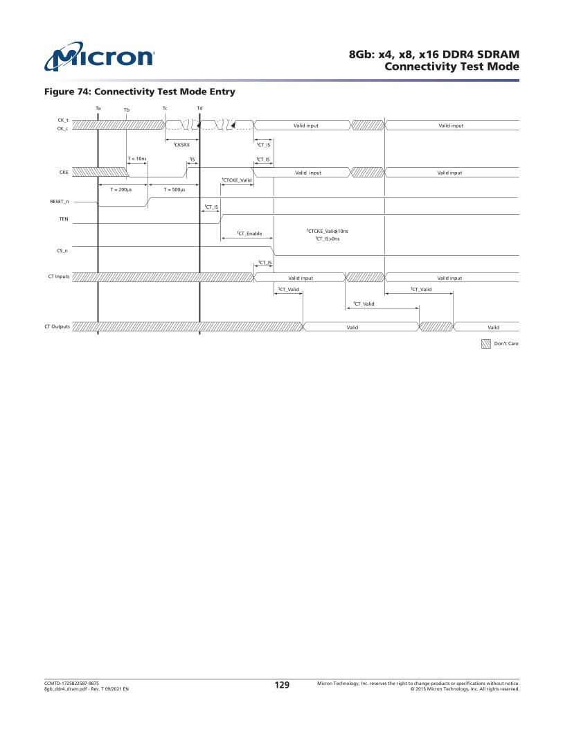
CCMTD-1725822587-9875 Micron Technology, Inc. reserves the right to change products or specifications without notice.8gb_ddr4_dram.pdf - Rev. T 09/2021 EN 2015 Micron Technology, Inc. All rights reserved.129
8Gb: x4, x8, x16 DDR4 SDRAMConnectivity Test Mode
Figure 74: Connectivity Test Mode Entry
tCTCKE_Valid
T = 10ns
CS_n
CT Inputs
CT Outputs
tCT_Enable
tCKSRX
tCTCKE_Valid >10ns tCT_IS >0ns
T = 500μsT = 200μs
tIS
tCT_Valid tCT_Valid
tCT_Valid
TEN
Valid input Valid input
Valid input Valid input
Valid input Valid input
Valid Valid
RESET_n
CKE
CK_c
CK_t
Ta Tb Tc Td
tCT_IS
tCT_IS
tCT_IS
tCT_IS
Don’t Care
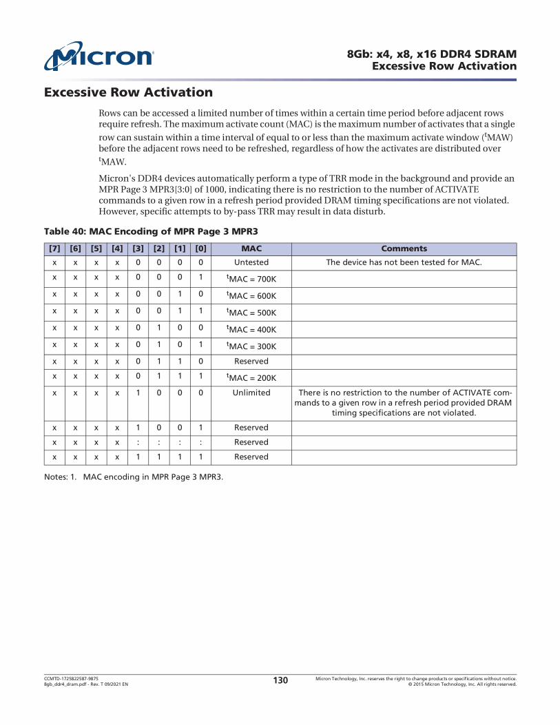
CCMTD-1725822587-9875 Micron Technology, Inc. reserves the right to change products or specifications without notice.8gb_ddr4_dram.pdf - Rev. T 09/2021 EN 2015 Micron Technology, Inc. All rights reserved.130
8Gb: x4, x8, x16 DDR4 SDRAMExcessive Row Activation
Excessive Row Activation
Rows can be accessed a limited number of times within a certain time period before adjacent rows require refresh. The maximum activate count (MAC) is the maximum number of activates that a single
row can sustain within a time interval of equal to or less than the maximum activate window (tMAW) before the adjacent rows need to be refreshed, regardless of how the activates are distributed over tMAW.
Micron's DDR4 devices automatically perform a type of TRR mode in the background and provide an MPR Page 3 MPR3[3:0] of 1000, indicating there is no restriction to the number of ACTIVATE commands to a given row in a refresh period provided DRAM timing specifications are not violated. However, specific attempts to by-pass TRR may result in data disturb.
Notes: 1. MAC encoding in MPR Page 3 MPR3.
Table 40: MAC Encoding of MPR Page 3 MPR3
[7] [6] [5] [4] [3] [2] [1] [0] MAC Comments
x x x x 0 0 0 0 Untested The device has not been tested for MAC.
x x x x 0 0 0 1 tMAC = 700K
x x x x 0 0 1 0 tMAC = 600K
x x x x 0 0 1 1 tMAC = 500K
x x x x 0 1 0 0 tMAC = 400K
x x x x 0 1 0 1 tMAC = 300K
x x x x 0 1 1 0 Reserved
x x x x 0 1 1 1 tMAC = 200K
x x x x 1 0 0 0 Unlimited There is no restriction to the number of ACTIVATE com-mands to a given row in a refresh period provided DRAM
timing specifications are not violated.
x x x x 1 0 0 1 Reserved
x x x x : : : : Reserved
x x x x 1 1 1 1 Reserved
CCMTD-1725822587-9875 Micron Technology, Inc. reserves the right to change products or specifications without notice.8gb_ddr4_dram.pdf - Rev. T 09/2021 EN 2015 Micron Technology, Inc. All rights reserved.131
8Gb: x4, x8, x16 DDR4 SDRAMPost Package Repair
Post Package Repair
Post Package Repair
JEDEC defines two modes of Post Package Repair (PPR): soft Post Package Repair (sPPR) and hard Post Package Repair (hPPR). sPPR is non-persistent so the repair row maybe altered; that is, sPPR is NOT a permanent repair and even though it will repair a row, the repair can be reversed, reassigned via another sPPR, or made permanent via hPPR. Hard Post Package Repair is persistent so once the repair row is assigned for a hPPR address, further PPR commands to a previous hPPR section should not be performed, that is, hPPR is a permanent repair; once repaired, it cannot be reversed. The controller provides the failing row address in the hPPR/sPPR sequence to the device to perform the row repair. hPPR Mode and sPPR Mode may not be enabled at the same time.
JEDEC states hPPR is optional for 4Gb and sPPR is optional for 4Gb and 8Gb parts however Micron 4Gb and 8Gb DDR4 DRAMs should have both sPPR and hPPR support. The hPPR support is identified via an MPR read from MPR Page 2, MPR0[7] and sPPR support is identified via an MPR read from MPR Page 2, MPR0[6].
The JEDEC minimum support requirement for DDR4 PPR (hPPR or sPPR) is to provide one row of repair per bank group (BG), x4/x8 have 4 BG and x16 has 2 BG; this is a total of 4 repair rows available on x4/x8 and 2 repair rows available on x16. Micron PPR support exceeds the JEDEC minimum require-ments; Micron DDR4 DRAMs have at least one row of repair for each bank which is essentially 4 row repairs per BG for a total of 16 repair rows for x4 and x8 and 8 repair rows for x16; a 4x increase in repair rows.
JEDEC requires the user to have all sPPR row repair addresses reset and cleared prior to enabling hPPR Mode. Micron DDR4 PPR does not have this restriction, the existing sPPR row repair addresses are not required to be cleared prior to entering hPPR mode. Each bank in a BG is PPR independent: sPPR or hPPR issued to a bank will not alter a sPPR row repair existing in a different bank.
sPPR followed by sPPR to same bank
When PPR is issued to a bank for the first time and is a sPPR command, the repair row will be a sPPR. When a subsequent sPPR is issued to the same bank, the previous sPPR repair row will be cleared and used for the subsequent sPPR address as the sPPR operation is non-persistent.
sPPR followed by hPPR to same bank
When a PPR is issued to a bank for the first time and is a sPPR command, the repair row will be a sPPR. When a subsequent hPPR is issued to the same bank, the initial sPPR repair row will be cleared and
used for the hPPR address1. If a further subsequent PPR (hPPR or sPPR) is issued to the same bank, the further subsequent PPR ( hPPR or sPPR) repair row will not clear or overwrite the previous hPPR address as the hPPR operation is persistent.
hPPR followed by hPPR or sPPR to same bank
When a PPR is issued to a bank for the first time and is a hPPR command, the repair row will be a hPPR. When a subsequent PPR (hPPR or sPPR) is issued to the same bank, the subsequent PPR ( hPPR or sPPR) repair row will not clear or overwrite the initial hPPR address as the initial hPPR is persistent.
Note: Newer Micron DDR4 designs may not guarantee that an sPPR followed by an hPPR to the same bank will result the same repair row being used. Contact factory for more information.
Hard Post Package Repair
All banks must be precharged and idle. DBI and CRC modes must be disabled. Both sPPR and hPPR must be disabled. sPPR is disabled with MR4[5] = 0. hPPR is disabled with MR4[13] = 0, which is the
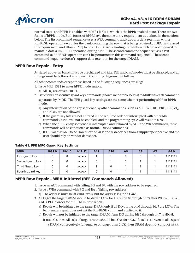
CCMTD-1725822587-9875 Micron Technology, Inc. reserves the right to change products or specifications without notice.8gb_ddr4_dram.pdf - Rev. T 09/2021 EN 2015 Micron Technology, Inc. All rights reserved.132
8Gb: x4, x8, x16 DDR4 SDRAMHard Post Package Repair
normal state, and hPPR is enabled with MR4 [13]= 1, which is the hPPR enabled state. There are two forms of hPPR mode. Both forms of hPPR have the same entry requirement as defined in the sections below. The first command sequence uses a WRA command and supports data retention with a REFRESH operation except for the bank containing the row that is being repaired; JEDEC has relaxed this requirement and allows BA[0] to be a Don't Care regarding the banks which are not required to maintain data a REFRESH operation during hPPR. The second command sequence uses a WR command (a REFRESH operation can't be performed in this command sequence). The second command sequence doesn't support data retention for the target DRAM.
hPPR Row Repair - Entry
As stated above, all banks must be precharged and idle. DBI and CRC modes must be disabled, and all timings must be followed as shown in the timing diagram that follows.
All other commands except those listed in the following sequences are illegal.1. Issue MR4[13] 1 to enter hPPR mode enable.
a) All DQ are driven HIGH.2. Issue four consecutive guard key commands (shown in the table below) to MR0 with each command
separated by tMOD. The PPR guard key settings are the same whether performing sPPR or hPPR mode. a) Any interruption of the key sequence by other commands, such as ACT, WR, RD, PRE, REF, ZQ,
and NOP, are not allowed.b) If the guard key bits are not entered in the required order or interrupted with other MR
commands, hPPR will not be enabled, and the programming cycle will result in a NOP.c) When the hPPR entry sequence is interrupted and followed by ACT and WR commands, these
commands will be conducted as normal DRAM commands.d) JEDEC allows A6:0 to be Don't Care on 4Gb and 8Gb devices from a supplier perspective and the
user should rely on vendor datasheet.
1. Issue an ACT command with failing BG and BA with the row address to be repaired.2. Issue a WRA command with BG and BA of failing row address.
a) The address must be at valid levels, but the address is Don't Care.3. All DQ of the target DRAM should be driven LOW for 4nCK (bit 0 through bit 7) after WL (WL = CWL
+ AL + PL) in order for hPPR to initiate repair. a) Repair will be initiated to the target DRAM only if all DQ during bit 0 through bit 7 are LOW. The
bank under repair does not get the REFRESH command applied to it.b) Repair will not be initiated to the target DRAM if any DQ during bit 0 through bit 7 is HIGH.
i) JEDEC states: All DQs of target DRAM should be LOW for 4tCK. If HIGH is driven to all DQs of
a DRAM consecutively for equal to or longer than 2tCK, then DRAM does not conduct hPPR
Table 41: PPR MR0 Guard Key Settings
MR0 BG1:0 BA1:0 A17:12 A11 A10 A9 A8 A7 A6:0
First guard key 0 0 xxxxxx 1 1 0 0 1 1111111
Second guard key 0 0 xxxxxx 0 1 1 1 1 1111111
Third Guard key 0 0 xxxxxx 1 0 1 1 1 1111111
Fourth guard key 0 0 xxxxxx 0 0 1 1 1 1111111

CCMTD-1725822587-9875 Micron Technology, Inc. reserves the right to change products or specifications without notice.8gb_ddr4_dram.pdf - Rev. T 09/2021 EN 2015 Micron Technology, Inc. All rights reserved.133
8Gb: x4, x8, x16 DDR4 SDRAMHard Post Package Repair
and retains data if REF command is properly issued; if all DQs are neither LOW for 4tCK nor
HIGH for equal to or longer than 2tCK, then hPPR mode execution is unknown.c) DQS should function normally.
4. REF command may be issued anytime after the WRA command followed by WL + 4nCK + tWR + tRP.
a) Multiple REF commands are issued at a rate of tREFI or tREFI/2, however back-to-back REF
commands must be separated by at least tREFI/4 when the DRAM is in hPPR mode.b) All banks except the bank under repair will perform refresh.
5. Issue PRE after tPGM time so that the device can repair the target row during tPGM time.
a) Wait tPGM_Exit after PRE to allow the device to recognize the repaired target row address.6. Issue MR4[13] 0 command to hPPR mode disable.
a) Wait tPGMPST for hPPR mode exit to complete.
b) After tPGMPST has expired, any valid command may be issued.
The entire sequence from hPPR mode enable through hPPR mode disable may be repeated if more than one repair is to be done.
After completing hPPR mode, MR0 must be re-programmed to a prehPPR mode state if the device is to be accessed.
After hPPR mode has been exited, the DRAM controller can confirm if the target row was repaired correctly by writing data into the target row and reading it back.
Figure 75:
ADDR
CMD MRS4
CKE
DQS_tDQS_c
DQs1
Valid
BA Valid BAf
BG Valid
Valid
BGf
tMOD tRCD
CK_t
CK_c
N/A
N/A
N/A
DES
N/A
N/A
N/A
MRS0
00
00
DES
N/A
N/A
N/A
MRS0 DES
N/A
N/A
N/A
MRS0 DES
N/A
N/A
N/A
MRS0 DES
N/A
N/A
N/A
NormalMode
All Banks Precharged
and idle state
hPPR Repair
ACT WRA
hPPR Entry 1st Guard Key Validate 2nd Guard Key Validate 3rd Guard Key Validate 4th Guard Key Validate
tMOD tMOD tMOD tMOD
DES
BAf
BGf
T0 T1 Ta0 Ta1 Tb0 Tb1 Tc0 Tc1 Td0 Td1 Te0 Tf0 Tg0
1st Key 2nd Key 3rd Key 4th Key
00
00
00
00
00
00
Valid (A13=1)
Don’t Care
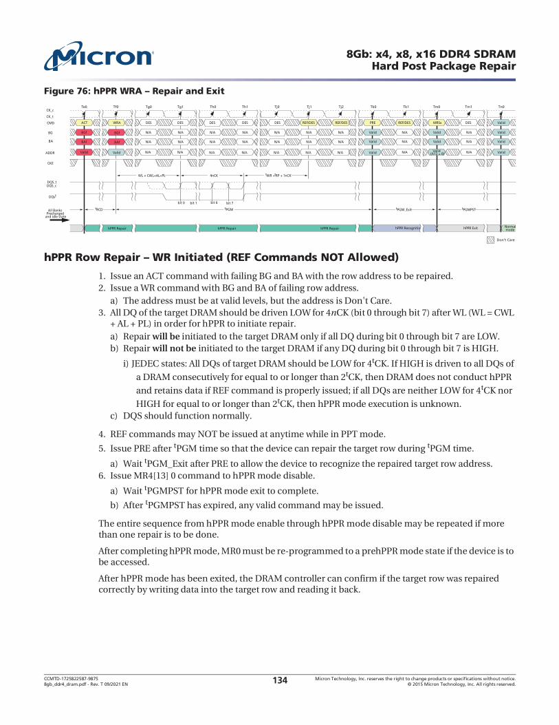
CCMTD-1725822587-9875 Micron Technology, Inc. reserves the right to change products or specifications without notice.8gb_ddr4_dram.pdf - Rev. T 09/2021 EN 2015 Micron Technology, Inc. All rights reserved.134
8Gb: x4, x8, x16 DDR4 SDRAMHard Post Package Repair
Figure 76:
1. Issue an ACT command with failing BG and BA with the row address to be repaired.2. Issue a WR command with BG and BA of failing row address.
a) The address must be at valid levels, but the address is Don't Care.3. All DQ of the target DRAM should be driven LOW for 4nCK (bit 0 through bit 7) after WL (WL = CWL
+ AL + PL) in order for hPPR to initiate repair. a) Repair will be initiated to the target DRAM only if all DQ during bit 0 through bit 7 are LOW.b) Repair will not be initiated to the target DRAM if any DQ during bit 0 through bit 7 is HIGH.
i) JEDEC states: All DQs of target DRAM should be LOW for 4tCK. If HIGH is driven to all DQs of
a DRAM consecutively for equal to or longer than 2tCK, then DRAM does not conduct hPPR
and retains data if REF command is properly issued; if all DQs are neither LOW for 4tCK nor
HIGH for equal to or longer than 2tCK, then hPPR mode execution is unknown.c) DQS should function normally.
4. REF commands may NOT be issued at anytime while in PPT mode.
5. Issue PRE after tPGM time so that the device can repair the target row during tPGM time.
a) Wait tPGM_Exit after PRE to allow the device to recognize the repaired target row address.6. Issue MR4[13] 0 command to hPPR mode disable.
a) Wait tPGMPST for hPPR mode exit to complete.
b) After tPGMPST has expired, any valid command may be issued.
The entire sequence from hPPR mode enable through hPPR mode disable may be repeated if more than one repair is to be done.
After completing hPPR mode, MR0 must be re-programmed to a prehPPR mode state if the device is to be accessed.
After hPPR mode has been exited, the DRAM controller can confirm if the target row was repaired correctly by writing data into the target row and reading it back.
ADDR
CMD
CKE
DQS_tDQS_c
DQs1
Valid
BA BAf
BG
Valid
BGf
tRCD
WL = CWL+AL+PL tWR + tRP + 1nCK
CK_t
CK_c
N/A
N/A
N/A
N/A
N/A
N/A
N/A
N/A
N/A
N/A
N/A
N/A
N/A
N/A
N/A
N/A
N/A
N/A
N/A
N/A
N/A
All Banks Precharged
and idle state
NormalmodehPPR Recognition hPPR ExithPPR Repair hPPR RepairhPPR Repair
MRSx
tPGM
ACT WRA
Valid (A13 = 0)
Valid
Valid
Valid
Valid
Valid
Valid
Valid
ValidN/A
N/A
N/A
tPGM_Exit tPGMPST
REF/DES REF/DES REF/DESDES DES DES DES DES
N/A
N/A
N/A
DESPRE
Valid
BAf
BGf
Te0 Tf0 Tg0 Tg1 Th0 Th1 Tj0 Tj1 Tj2 Tk0 Tk1 Tm0 Tm1 Tn0
4nCK
bit 0 bit 7bit 6bit 1
Don’t Care

CCMTD-1725822587-9875 Micron Technology, Inc. reserves the right to change products or specifications without notice.8gb_ddr4_dram.pdf - Rev. T 09/2021 EN 2015 Micron Technology, Inc. All rights reserved.135
8Gb: x4, x8, x16 DDR4 SDRAMsPPR Row Repair
Figure 77:
Figure 78:
sPPR Row Repair
Soft post package repair (sPPR) is a way to quickly, but temporarily, repair a row element in a bank on a DRAM device, where hPPR takes longer but permanently repairs a row element. sPPR mode is entered in a similar fashion as hPPR, sPPR uses MR4[5] while hPPR uses MR4[13]. sPPR is disabled with MR4[5] = 0, which is the normal state, and sPPR is enabled with MR4[5] = 1, which is the sPPR enabled state.
sPPR requires the same guard key sequence as hPPR to qualify the MR4 PPR entry. After sPPR entry, an ACT command will capture the target bank and target row, herein seed row, where the row repair will
be made. After tRCD time, a WR command is used to select the individual DRAM, through the DQ bits,
Table 42: DDR4 hPPR Timing Parameters DDR4-1600 through DDR4-3200
Parameter Symbol Min Max Unit
hPPR programming time tPGM 4, 8 1000 ms
16 2000 ms
hPPR precharge exit time tPGM_Exit 15 ns
hPPR exit time tPGMPST 50 s
ADDR
CMD MRS4
CKE
DQS_tDQS_c
DQs1
Valid
BA Valid BAf
BG Valid
Valid
BGf
tMOD tRCD
WL = CWL +
CK_t
CK_c
N/A
N/A
N/A
DES
N/A
N/A
N/A
MRS0
00
00
DES
N/A
N/A
N/A
MRS0 DES
N/A
N/A
N/A
MRS0 DES
N/A
N/A
N/A
MRS0 DES
N/A
N/A
N/A
NormalMode
All Banks Precharged
and idle state
hPPR Repair
ACT WR
hPPR Entry 1st Guard Key Validate 2nd Guard Key Validate 3rd Guard Key Validate 4th Guard Key Validate
tMOD tMOD tMOD tMOD
DES
BAf
BGf
T0 T1 Ta0 Ta1 Tb0 Tb1 Tc0 Tc1 Td0 Td1 Te0 Tf0 Tg0
1st Key 2nd Key 3rd Key 4th Key
00
00
00
00
00
00
Valid (A13 = 1)
Don’t Care
ADDR
CMD
CKE
DQS_tDQS_c
DQs1
Valid
BA BAf
BG
Valid
BGf
tRCD
WL = CWL + AL + PL
CK_t
CK_c
N/A
N/A
N/A
N/A
N/A
N/A
N/A
N/A
N/A
N/A
N/A
N/A
N/A
N/A
N/A
N/A
N/A
N/A
N/A
N/A
N/A
All Banks Precharged
and idle state
NormalmodehPPR Recognition hPPR ExithPPR Repair hPPR RepairhPPR Repair
MRSx
tPGM
ACT WR
Valid (A13 = 0)
Valid
Valid
Valid
Valid
Valid
Valid
Valid
ValidN/A
N/A
N/A
tPGM_Exit tPGMPST
DES DES DES DES DES DES DESDES
N/A
N/A
N/A
DESPRE
Valid
BAf
BGf
Te0 Tf0 Tg0 Tg1 Th0 Th1 Tj0 Tj1 Tj2 Tk0 Tk1 Tm0 Tm1 Tn0
4nCK
bit 0 bit 7bit 6bit 1
Don’t Care

CCMTD-1725822587-9875 Micron Technology, Inc. reserves the right to change products or specifications without notice.8gb_ddr4_dram.pdf - Rev. T 09/2021 EN 2015 Micron Technology, Inc. All rights reserved.136
8Gb: x4, x8, x16 DDR4 SDRAMsPPR Row Repair
to transfer the repair address into an internal register in the DRAM. After a write recovery time and PRE command, the sPPR mode can be exited and normal operation can resume.
The DRAM will retain the soft repair information as long as VDD remains within the operating region unless rewritten by a subsequent sPPR entry to the same bank. If DRAM power is removed or the DRAM is reset, the soft repair will revert to the unrepaired state. hPPR and sPPR should not be enabled at the same time; Micron sPPR does not have to be disabled and cleared prior to entering hPPR mode, but sPPR must be disabled and cleared prior to entering MBIST-PPR mode.
With sPPR, Micron DDR4 can repair one row per bank. When a subsequent sPPR request is made to the same bank, the subsequently issued sPPR address will replace the previous sPPR address. When the hPPR resource for a bank is used up, the bank should be assumed to not have available resources for sPPR. If a repair sequence is issued to a bank with no repair resource available, the DRAM will ignore the programming sequence.
The bank receiving sPPR change is expected to retain memory array data in all rows except for the seed row and its associated row addresses. If the data in the memory array in the bank under sPPR repair is
interest and can be ignored. If the data in the memory array is required to be retained in the bank under sPPR mode, then prior to executing the sPPR mode, the seed row and its associated row addresses should be backed up and subsequently restored after sPPR has been completed. sPPR associated seed row addresses are specified in the Table below; BA0 is not required by Micron DRAMs however it is JEDEC reserved.
All banks must be precharged and idle. DBI and CRC modes must be disabled, and all sPPR timings must be followed as shown in the timing diagram that follows.
All other commands except those listed in the following sequences are illegal.1. Issue MR4[5] 1 to enter sPPR mode enable.
a) All DQ are driven HIGH.2. Issue four consecutive guard key commands (shown in the table below) to MR0 with each command
separated by tMOD. Please note that JEDEC recently added the four guard key entry used for hPPR to sPPR entry; early DRAMs may not require four guard key entry code. A prudent controller design should accommodate either option in case an earlier DRAM is used. a) Any interruption of the key sequence by other commands, such as ACT, WR, RD, PRE, REF, ZQ,
and NOP, are not allowed.b) If the guard key bits are not entered in the required order or interrupted with other MR
commands, sPPR will not be enabled, and the programming cycle will result in a NOP.c) When the sPPR entry sequence is interrupted and followed by ACT and WR commands, these
commands will be conducted as normal DRAM commands.d) JEDEC allows A6:0 to be "Don't Care" on 4Gb and 8Gb devices from a supplier perspective and
the user should rely on vendor datasheet.
Table 43: sPPR Associated Rows
sPPR Associated Row Address
BA0* A17 A16 A15 A14 A13 A1 A0
Table 44: PPR MR0 Guard Key Settings
MR0 BG1:0 BA1:0 A17:12 A11 A10 A9 A8 A7 A6:0
First guard key 0 0 xxxxxx 1 1 0 0 1 1111111
Second guard key 0 0 xxxxxx 0 1 1 1 1 1111111

CCMTD-1725822587-9875 Micron Technology, Inc. reserves the right to change products or specifications without notice.8gb_ddr4_dram.pdf - Rev. T 09/2021 EN 2015 Micron Technology, Inc. All rights reserved.137
8Gb: x4, x8, x16 DDR4 SDRAMsPPR Row Repair
3. After tMOD, issue an ACT command with failing BG and BA with the row address to be repaired.
4. After tRCD, issue a WR command with BG and BA of failing row address. a) The address must be at valid levels, but the address is a "Don't Care."
5. All DQ of the target DRAM should be driven LOW for 4nCK (bit 0 through bit 7) after WL (WL = CWL + AL + PL) in order for sPPR to initiate repair. a) Repair will be initiated to the target DRAM only if all DQ during bit 0 through bit 7 are LOW.b) Repair will not be initiated to the target DRAM if any DQ during bit 0 through bit 7 is HIGH.
i) JEDEC states: All DQs of target DRAM should be LOW for 4tCK. If HIGH is driven to all DQs of
a DRAM consecutively for equal to or longer than the first 2tCK, then DRAM does not conduct
hPPR and retains data if REF command is properly issued; if all DQs are neither LOW for 4tCK
nor HIGH for equal to or longer than the first 2tCK, then hPPR mode execution is unknown.c) DQS should function normally.
6. REF command may NOT be issued at anytime while in sPPR mode.
7. Issue PRE after tWR time so that the device can repair the target row during tWR time.
a) Wait tPGM_Exit_s after PRE to allow the device to recognize the repaired target row address.8. Issue MR4[5] 0 command to sPPR mode disable.
a) Wait tPGMPST_s for sPPR mode exit to complete.
b) After tPGMPST_s has expired, any valid command may be issued.
The entire sequence from sPPR mode enable through sPPR mode disable may be repeated if more than one repair is to be done.
After sPPR mode has been exited, the DRAM controller can confirm if the target row was repaired correctly by writing data into the target row and reading it back.
Figure 79:
Third guard key 0 0 xxxxxx 1 0 1 1 1 1111111
Fourth guard key 0 0 xxxxxx 0 0 1 1 1 1111111
Table 44: PPR MR0 Guard Key Settings (Continued)
MR0 BG1:0 BA1:0 A17:12 A11 A10 A9 A8 A7 A6:0
ADDR
CMD MRS4
CKE
DQS_tDQS_c
DQs1
Valid
BA Valid BAf
BG Valid
Valid
BGf
tMOD tRCD
CK_t
CK_c
N/A
N/A
N/A
DES
N/A
N/A
N/A
MRS0
00
00
DES
N/A
N/A
N/A
MRS0 DES
N/A
N/A
N/A
MRS0 DES
N/A
N/A
N/A
MRS0 DES
N/A
N/A
N/A
NormalMode
All Banks Precharged
and idle state
sPPR Repair
ACT WR
sPPR Entry 1st Guard Key Validate 2nd Guard Key Validate 3rd Guard Key Validate 4th Guard Key Validate
tMOD tMOD tMOD tMOD
DES
BAf
BGf
T0 T1 Ta0 Ta1 Tb0 Tb1 Tc0 Tc1 Td0 Td1 Te0 Tf0 Tg0
1st Key 2nd Key 3rd Key 4th Key
00
00
00
00
00
00
Valid (A5=1)
Don’t Care
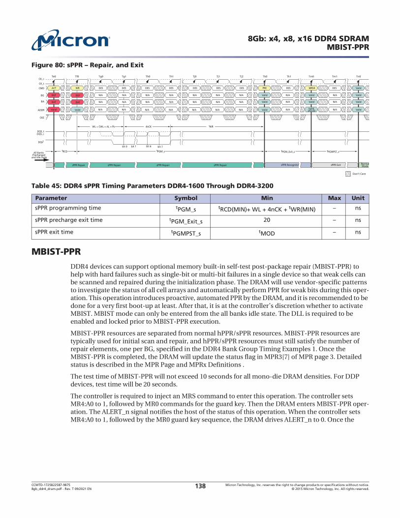
CCMTD-1725822587-9875 Micron Technology, Inc. reserves the right to change products or specifications without notice.8gb_ddr4_dram.pdf - Rev. T 09/2021 EN 2015 Micron Technology, Inc. All rights reserved.138
8Gb: x4, x8, x16 DDR4 SDRAMMBIST-PPR
Figure 80:
MBIST-PPR
DDR4 devices can support optional memory built-in self-test post-package repair (MBIST-PPR) to help with hard failures such as single-bit or multi-bit failures in a single device so that weak cells can be scanned and repaired during the initialization phase. The DRAM will use vendor-specific patterns to investigate the status of all cell arrays and automatically perform PPR for weak bits during this oper-ation. This operation introduces proactive, automated PPR by the DRAM, and it is recommended to be
MBIST. MBIST mode can only be entered from the all banks idle state. The DLL is required to be enabled and locked prior to MBIST-PPR execution.
MBIST-PPR resources are separated from normal hPPR/sPPR resources. MBIST-PPR resources are typically used for initial scan and repair, and hPPR/sPPR resources must still satisfy the number of repair elements, one per BG, specified in the DDR4 Bank Group Timing Examples 1. Once the MBIST-PPR is completed, the DRAM will update the status flag in MPR3[7] of MPR page 3. Detailed status is described in the MPR Page and MPRx Definitions .
The test time of MBIST-PPR will not exceed 10 seconds for all mono-die DRAM densities. For DDP devices, test time will be 20 seconds.
The controller is required to inject an MRS command to enter this operation. The controller sets MR4:A0 to 1, followed by MR0 commands for the guard key. Then the DRAM enters MBIST-PPR oper-ation. The ALERT_n signal notifies the host of the status of this operation. When the controller sets MR4:A0 to 1, followed by the MR0 guard key sequence, the DRAM drives ALERT_n to 0. Once the
Table 45: DDR4 sPPR Timing Parameters DDR4-1600 Through DDR4-3200
Parameter Symbol Min Max Unit
sPPR programming time tPGM_s tRCD(MIN)+ WL + 4nCK + tWR(MIN) ns
sPPR precharge exit time tPGM_Exit_s 20 ns
sPPR exit time tPGMPST_s tMOD ns
bit 1
ADDR
CMD
CKE
DQS_tDQS_c
DQs1
Valid
BA BAf
BG
Valid
BGf
tRCD
WL = CWL + AL + PL
CK_t
CK_c
N/A
N/A
N/A
N/A
N/A
N/A
N/A
N/A
N/A
N/A
N/A
N/A
N/A
N/A
N/A
N/A
N/A
N/A
N/A
N/A
N/A
All Banks Precharged
and idle state
NormalModesPPR Recognition sPPR ExitsPPR Repair sPPR RepairsPPR RepairsPPR Repair
MRS4
tPGM_s
ACT WR
Valid (A5=0)
Valid
Valid
Valid
Valid
Valid
Valid
Valid
ValidN/A
N/A
N/A
DES DES DES DES DES DES DES DES
N/A
N/A
N/A
DESPRE
Valid
BAf
BGf
Te0 Tf0 Tg0 Tg1 Th0 Th1 Tj0 Tj1 Tj2 Tk0 Tk1 Tm0 Tm1 Tn0
4nCK
bit 0 bit 7bit 6
tWR
tPGM_Exit_s tPGMPST_s
Don’t Care

CCMTD-1725822587-9875 Micron Technology, Inc. reserves the right to change products or specifications without notice.8gb_ddr4_dram.pdf - Rev. T 09/2021 EN 2015 Micron Technology, Inc. All rights reserved.139
8Gb: x4, x8, x16 DDR4 SDRAMMBIST-PPR
MBIST-PPR is completed, the DRAM drives ALERT_n to 1 to notify the controller that this operation is completed. DRAM data will not be guaranteed after the MBIST-PPR operation.
MBIST-PPR Procedure
The following sequences are required for MBIST-PPR and are shown in the figure below.1. The DRAM needs to finalize initialization, MR training, and ZQ calibration prior to entering
MBIST-PPR.2. Four consecutive guard key commands must be issued to MR0, with each command separated by
tMOD. The PPR guard key settings are the same whether performing sPPR, hPPR, or MBIST-PPR mode.
3. Anytime after Tk in the Read Termination Disable Window 15, the host must set MR4:A0 to 1, followed by subsequent MR0 guard key sequences (which is identical to typical hPPR/sPPR guard key sequences and specified in Table 73) to start MBIST-PPR operation, and the DRAM drives the ALERT_n signal to 0.
4. During MBIST-PPR mode, only DESELECT commands are allowed.5. The ODT pin must be driven LOW during MBIST-PPR to satisfy DODTLoff from time Tb0 until Tc2.
The DRAM may or may not provide RTT_PARK termination during MBIST-PPR regardless of whether RTT_PARK is enabled in MR5.
Table 46: MBIST-PPR Timing Parameter
Parameter
Value
UnitMin Max
tSELFHEAL Monolithic 10 s
DDP 20
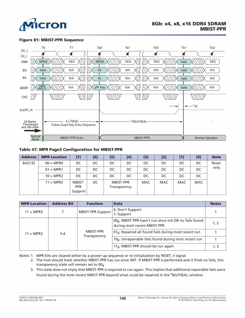
CCMTD-1725822587-9875 Micron Technology, Inc. reserves the right to change products or specifications without notice.8gb_ddr4_dram.pdf - Rev. T 09/2021 EN 2015 Micron Technology, Inc. All rights reserved.140
8Gb: x4, x8, x16 DDR4 SDRAMMBIST-PPR
Figure 81: MBIST-PPR Sequence
Notes: 1. MPR bits are cleared either by a power-up sequence or re-initialization by RESET_n signal2. The host should track whether MBIST-PPR has run since INIT. If MBIST-PPR is performed and it finds no fails, this
transparency state will remain set to 00B3. This state does not imply that MBIST-PPR is required to run again. This implies that additional repairable fails were
found during the most recent MBIST-PPR beyond what could be repaired in the tSELFHEAL window.
Table 47: MPR Page3 Configuration for MBIST-PPR
Address MPR Location [7] [6] [5] [4] [3] [2] [1] [0] Note
BA[1:0] 00 = MPR0 DC DC DC DC DC DC DC DC Read-only01 = MPR1 DC DC DC DC DC DC DC DC
10 = MPR2 DC DC DC DC DC DC DC DC
11 = MPR3 MBIST-PPR
Support
DC MBIST-PPR Transparency
MAC MAC MAC MAC
MPR Location Address Bit Function Data Notes
11 = MPR3 7 MBIST-PPR Support0: Don't Support 1: Support
1
11 = MPR3 5:4MBIST-PPR
Transparency
00B: MBIST-PPR hasn't run since init OR no fails found during most recent MBIST-PPR
1, 2
01B: Repaired all found fails during most recent run 1
10B: Unrepairable fails found during most recent run 1
11B: MBIST-PPR should be run again 1, 3
ADDR
CMD MRS4
CKE
BA Valid
BG Valid
CK_t
CK_c
DES
N/A
N/A
N/A
MRS0
00
00
DES
N/A
N/A
N/A
NormalMode
All Banks Precharged
and idle state
MBIST-PPR Entry MBIST-PPR
T0 T1 Ta0 Ta1 Tb0 Tb1 Tb2
Valid (A0=1)
tMOD5 x
4th Key
Follow Guard Key Entry Sequence
ALERT_N
DES
N/A
N/A
N/A
t IS
tSELFHEAL
Valid
Valid
Valid
Valid
Normal OperationNormal Operation
DES
N/A
N/A
N/A
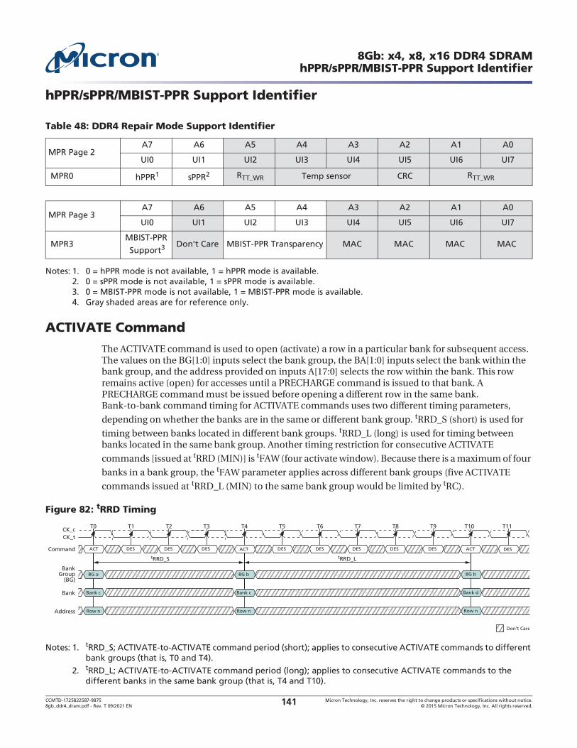
CCMTD-1725822587-9875 Micron Technology, Inc. reserves the right to change products or specifications without notice.8gb_ddr4_dram.pdf - Rev. T 09/2021 EN 2015 Micron Technology, Inc. All rights reserved.141
8Gb: x4, x8, x16 DDR4 SDRAMhPPR/sPPR/MBIST-PPR Support Identifier
hPPR/sPPR/MBIST-PPR Support Identifier
Notes: 1. 0 = hPPR mode is not available, 1 = hPPR mode is available.2. 0 = sPPR mode is not available, 1 = sPPR mode is available.3. 0 = MBIST-PPR mode is not available, 1 = MBIST-PPR mode is available.4. Gray shaded areas are for reference only.
ACTIVATE Command
The ACTIVATE command is used to open (activate) a row in a particular bank for subsequent access. The values on the BG[1:0] inputs select the bank group, the BA[1:0] inputs select the bank within the bank group, and the address provided on inputs A[17:0] selects the row within the bank. This row remains active (open) for accesses until a PRECHARGE command is issued to that bank. A PRECHARGE command must be issued before opening a different row in the same bank. Bank-to-bank command timing for ACTIVATE commands uses two different timing parameters,
depending on whether the banks are in the same or different bank group. tRRD_S (short) is used for
timing between banks located in different bank groups. tRRD_L (long) is used for timing between banks located in the same bank group. Another timing restriction for consecutive ACTIVATE
commands [issued at tRRD (MIN)] is tFAW (four activate window). Because there is a maximum of four
banks in a bank group, the tFAW parameter applies across different bank groups (five ACTIVATE
commands issued at tRRD_L (MIN) to the same bank group would be limited by tRC).
Figure 82: tRRD Timing
Notes: 1. tRRD_S; ACTIVATE-to-ACTIVATE command period (short); applies to consecutive ACTIVATE commands to different bank groups (that is, T0 and T4).
2. tRRD_L; ACTIVATE-to-ACTIVATE command period (long); applies to consecutive ACTIVATE commands to the different banks in the same bank group (that is, T4 and T10).
Table 48: DDR4 Repair Mode Support Identifier
MPR Page 2 A7 A6 A5 A4 A3 A2 A1 A0
UI0 UI1 UI2 UI3 UI4 UI5 UI6 UI7
MPR0 hPPR1 sPPR2 RTT_WR Temp sensor CRC RTT_WR
MPR Page 3 A7 A6 A5 A4 A3 A2 A1 A0
UI0 UI1 UI2 UI3 UI4 UI5 UI6 UI7
MPR3MBIST-PPR
Support3 Don't Care MBIST-PPR Transparency MAC MAC MAC MAC
T0 T1 T2 T3 T4 T5 T6 T7 T8 T9
tRRD_S
T10 T11
Don’t Care
BG a
DESACT ACTDES DES DES DES DES DES DES DES
CK_tCK_c
Command
BankGroup
(BG)
Bank cBank
Row n
BG b
Bank c
Row n
BG b
Bank d
Row nAddress
tRRD_L
ACT

CCMTD-1725822587-9875 Micron Technology, Inc. reserves the right to change products or specifications without notice.8gb_ddr4_dram.pdf - Rev. T 09/2021 EN 2015 Micron Technology, Inc. All rights reserved.142
8Gb: x4, x8, x16 DDR4 SDRAMPRECHARGE Command
Figure 83: tFAW Timing
Note: 1. tFAW; four activate windows.
PRECHARGE Command
The PRECHARGE command is used to deactivate the open row in a particular bank or the open row in
all banks. The bank(s) will be available for a subsequent row activation for a specified time (tRP) after the PRECHARGE command is issued. An exception to this is the case of concurrent auto precharge, where a READ or WRITE command to a different bank is allowed as long as it does not interrupt the data transfer in the current bank and does not violate any other timing parameters.
After a bank is precharged, it is in the idle state and must be activated prior to any READ or WRITE commands being issued to that bank. A PRECHARGE command is allowed if there is no open row in that bank (idle state) or if the previously open row is already in the process of precharging. However, the precharge period will be determined by the last PRECHARGE command issued to the bank.
The auto precharge feature is engaged when a READ or WRITE command is issued with A10 HIGH. The auto precharge feature uses the RAS lockout circuit to internally delay the PRECHARGE operation until the ARRAY RESTORE operation has completed. The RAS lockout circuit feature allows the PRECHARGE operation to be partially or completely hidden during burst READ cycles when the auto precharge feature is engaged. The PRECHARGE operation will not begin until after the last data of the burst write sequence is properly stored in the memory array.
REFRESH Command
The REFRESH command (REF) is used during normal operation of the device. This command is nonpersistent, so it must be issued each time a refresh is required. The device requires REFRESH cycles
at an average periodic interval of tREFI. When CS_n, RAS_n/A16, and CAS_n/A15 are held LOW and WE_n/A14 HIGH at the rising edge of the clock, the device enters a REFRESH cycle. All banks of the
SDRAM must be precharged and idle for a minimum of the precharge time, tRP (MIN), before the REFRESH command can be applied. The refresh addressing is generated by the internal DRAM refresh
counter supplies the addresses during the REFRESH cycle. No control of the external address bus is required once this cycle has started. When the REFRESH cycle has completed, all banks of the SDRAM will be in the precharged (idle) state. A delay between the REFRESH command and the next valid
command, except DES, must be greater than or equal to the minimum REFRESH cycle time tRFC (MIN), as shown in .
NOTE: The tRFC timing parameter depends on memory density.
T0 Ta0 Tb0 Tc0 Tc1 Tc2
tRRD tRRD
Td0 Td1
Don’t Care Time Break
Valid
ValidACT ACTValid Valid Valid Valid Valid NOP
CK_tCK_c
Command
BankGroup
(BG)
ValidBank
Valid
ACT ACT
Address
tFAW
ACT
Valid
Valid
Valid
Valid
Valid
Valid
Valid
Valid
Valid
Valid
Valid
Valid
tRRD

CCMTD-1725822587-9875 Micron Technology, Inc. reserves the right to change products or specifications without notice.8gb_ddr4_dram.pdf - Rev. T 09/2021 EN 2015 Micron Technology, Inc. All rights reserved.143
8Gb: x4, x8, x16 DDR4 SDRAMREFRESH Command
In general, a REFRESH command needs to be issued to the device regularly every tREFI interval. To allow for improved efficiency in scheduling and switching between tasks, some flexibility in the abso-lute refresh interval is provided for postponing and pulling-in the REFRESH command. A limited number REFRESH commands can be postponed depending on refresh mode: a maximum of 8 REFRESH commands can be postponed when the device is in 1X refresh mode; a maximum of 16 REFRESH commands can be postponed when the device is in 2X refresh mode; and a maximum of 32 REFRESH commands can be postponed when the device is in 4X refresh mode.
When 8 consecutive REFRESH commands are postponed, the resulting maximum interval between the
surrounding REFRESH commands is limited to 9 tREFI (see ). For both the 2X and 4X refresh modes,
the maximum interval between surrounding REFRESH commands allowed is limited to 17 tREFI2
and 33 tREFI4, respectively.
A limited number REFRESH commands can be pulled-in as well. A maximum of 8 additional REFRESH
REFRESH commands can be issued when in advance in 2X refresh mode, and a maximum of 32 addi-tional REFRESH commands can be issued in advance when in 4X refresh mode. Each of these REFRESH commands reduces the number of regular REFRESH commands required later by one. The
resulting maximum interval between two surrounding REFRESH commands is limited to 9 tREFI ( ),
17 tRFEI2, or 33 tREFI4. At any given time, a maximum of 16 REF commands can be issued within 2
tREFI, 32 REF2 commands can be issued within 4 tREFI2, and 64 REF4 commands can be issued
within 8 tREFI4 (larger densities are limited by tRFC1, tRFC2, and tRFC4, respectively, which must still be met).
Figure 84: REFRESH Command Timing
Notes: 1. Only DES commands are allowed after a REFRESH command is registered until tRFC (MIN) expires.
2. Time interval between two REFRESH commands may be extended to a maximum of 9 tREFI.
Figure 85: Postponing REFRESH Commands (Example)
DESREF DESREF Valid Valid Valid Valid REF ValidValidValid
CK_t
CK_c
Command
tRFC tRFC (MIN)
tREFI (MAX 9 × tREFI)
Don’t CareTime Break
T0 T1 Ta0 Ta1 Tb0 Tb1 Tb2 Tb3 Tc0 Tc1 Tc2 Tc3
ValidDESDES
DRAM must be idle DRAM must be idle
t
8 REF-Commands postponed
tRFC
tREFI9 × tREFI

CCMTD-1725822587-9875 Micron Technology, Inc. reserves the right to change products or specifications without notice.8gb_ddr4_dram.pdf - Rev. T 09/2021 EN 2015 Micron Technology, Inc. All rights reserved.144
8Gb: x4, x8, x16 DDR4 SDRAMREFRESH Command
Figure 86: Pulling In REFRESH Commands (Example)
t
8 REF-Commands pulled-in
tRFC
tREFI 9 × tREFI

CCMTD-1725822587-9875 Micron Technology, Inc. reserves the right to change products or specifications without notice.8gb_ddr4_dram.pdf - Rev. T 09/2021 EN 2015 Micron Technology, Inc. All rights reserved.145
8Gb: x4, x8, x16 DDR4 SDRAMTemperature-Controlled Refresh Mode
Temperature-Controlled Refresh Mode
During normal operation, temperature-controlled refresh (TCR) mode disabled, the device must have
a REFRESH command issued once every tREFI, except for what is allowed by posting (see REFRESH Command section). This means a REFRESH command must be issued once every 7.8 s if TC is less than or equal to 85 C, once every 3.9 s if TC is greater than 85 C, once every 1.95 s if TC is greater than 95 C, regardless of which Temperature Mode is selected (MR4[2]). TCR mode is disabled by setting MR4[3] = 0 while TCR mode is enabled by setting MR4[3] = 1. When TCR mode is enabled (MR4[3] = 1), the Temperature Mode must be selected where MR4[2] = 0 enables the Normal Temperature Mode while MR4[2] = 1 enables the Extended Temperature Mode.
When TCR mode is enabled, the device will register the externally supplied REFRESH command and
adjust the internal refresh period to be longer than tREFI of the normal temperature range, when allowed, by skipping REFRESH commands with the proper gear ratio. TCR mode has two Temperature Modes to select between the normal temperature range and the extended temperature range; the correct Temperature Mode must be selected so the internal control operates correctly. The DRAM must have the correct refresh rate applied externally; the internal refresh rate is determined by the DRAM based upon the temperature.
Normal Temperature Mode
REFRESH commands should be issued to the device with the refresh period equal to tREFI of normal temperature range (-40 C to 85 C). The system must guarantee that the TC does not exceed 85 C when tREFI of the normal temperature range is used. The device may adjust the internal refresh period to be
longer than tREFI of the normal temperature range by skipping external REFRESH commands with the proper gear ratio when TC is below 85 C. The internal refresh period is automatically adjusted inside the DRAM, and the DRAM controller does not need to provide any additional control.
Extended Temperature Mode
REFRESH commands should be issued to the device with the refresh period equal to tREFI of extended temperature range (85 C to 95 C, or 95 C to 105 C) . The system must guarantee that the TC does not exceed 95 C, or 105 C. Even though the external refresh supports the extended temperature range, the
device may adjust its internal refresh period to be equal to or longer than tREFI of the normal tempera-ture range (-40 C to 85 C) by skipping external REFRESH commands with the proper gear ratio when TC is equal to or below 85 C. The internal refresh period is automatically adjusted inside the DRAM, and the DRAM controller does not need to provide any additional control.
Notes: 1. If the external refresh period is slower than 3.9 s, the device will refresh internally at too slow of a refresh rate and will violate refresh specifications.
Table 49: Normal tREFI Refresh (TCR Enabled)
Normal Temperature Mode Extended Temperature Mode
TemperatureExternal Refresh
PeriodInternal Refresh
PeriodExternal Refresh
PeriodInternal Refresh
Period
TC 85 C 7.8 s 7.8 s 3.9 s1 7.8 s
85 C < TC 95 C 3.9 s
95 C < TC 105 C 1.95 s

CCMTD-1725822587-9875 Micron Technology, Inc. reserves the right to change products or specifications without notice.8gb_ddr4_dram.pdf - Rev. T 09/2021 EN 2015 Micron Technology, Inc. All rights reserved.146
8Gb: x4, x8, x16 DDR4 SDRAMTemperature-Controlled Refresh Mode
Figure 87: TCR Mode Example1
Note: 1. TCR enabled with Extended Temperature Mode selected.
External REFRESHcommands are not
ignored
At least every otherexternal REFRESH
ignored
Controller 85°C < TC 95°C TC 85°C
Controller issues REFRESHcommands at extended
temperature rate
REFRESHExternaltREFI3.9μs
InternaltREFI3.9μs Internal
tREFI7.8μs
REFRESH
REFRESH
REFRESH
REFRESH
REFRESH
REFRESH
REFRESH
REFRESH
REFRESH
REFRESH
REFRESH
REFRESH
REFRESH
REFRESH
REFRESH
REFRESH
REFRESH

CCMTD-1725822587-9875 Micron Technology, Inc. reserves the right to change products or specifications without notice.8gb_ddr4_dram.pdf - Rev. T 09/2021 EN 2015 Micron Technology, Inc. All rights reserved.147
8Gb: x4, x8, x16 DDR4 SDRAMFine Granularity Refresh Mode
Fine Granularity Refresh Mode
Mode Register and Command Truth Table
The REFRESH cycle time (tRFC) and the average refresh interval (tREFI) can be programmed by the MRS command. The appropriate setting in the mode register will set a single set of REFRESH cycle times and average refresh interval for the device (fixed mode), or allow the dynamic selection of one of two sets of REFRESH cycle times and average refresh interval for the device (on-the-fly mode [OTF]). OTF mode must be enabled by MRS before any OTF REFRESH command can be issued.
There are two types of OTF modes (1x/2x and 1x/4x modes) that are selectable by programming the appropriate values into the mode register MR3 [8:6]. When either of the two OTF modes is selected, the device evaluates the BG0 bit when a REFRESH command is issued, and depending on the status of BG0, it dynamically switches its internal refresh configuration between 1x and 2x (or 1x and 4x) modes, and then executes the corresponding REFRESH operation.
tREFI and tRFC Parameters
The default refresh rate mode is fixed 1x mode where REFRESH commands should be issued with the
normal rate; that is, tREFI1 = tREFI(base) (for TC 85 C), and the duration of each REFRESH command
is the normal REFRESH cycle time (tRFC1). In 2x mode (either fixed 2x or OTF 2x mode), REFRESH
commands should be issued to the device at the double frequency (tREFI2 = tREFI(base)/2) of the
normal refresh rate. In 4x mode, the REFRESH command rate should be quadrupled (tREFI4 = tREFI(base)/4). Per each mode and command type, the tRFC parameter has different values as defined in the following table.
Table 50: MRS Definition
MR3[8] MR3[7] MR3[6] Refresh Rate Mode
0 0 0 Normal mode (fixed 1x)
0 0 1 Fixed 2x
0 1 0 Fixed 4x
0 1 1 Reserved
1 0 0 Reserved
1 0 1 On-the-fly 1x/2x
1 1 0 On-the-fly 1x/4x
1 1 1 Reserved
Table 51: REFRESH Command Truth Table
Refresh CS_n ACT_nRAS_n/A
15CAS_n/A
14WE_n/A13 BG1 BG0
A10/AP
A[9:0], A[12:11], A[20:16]
MR3[8:6]
Fixed rate L H L L H V V V V 0vv
OTF: 1x L H L L H V L V V 1vv
OTF: 2x L H L L H V H V V 101
OTF: 4x L H L L H V H V V 110
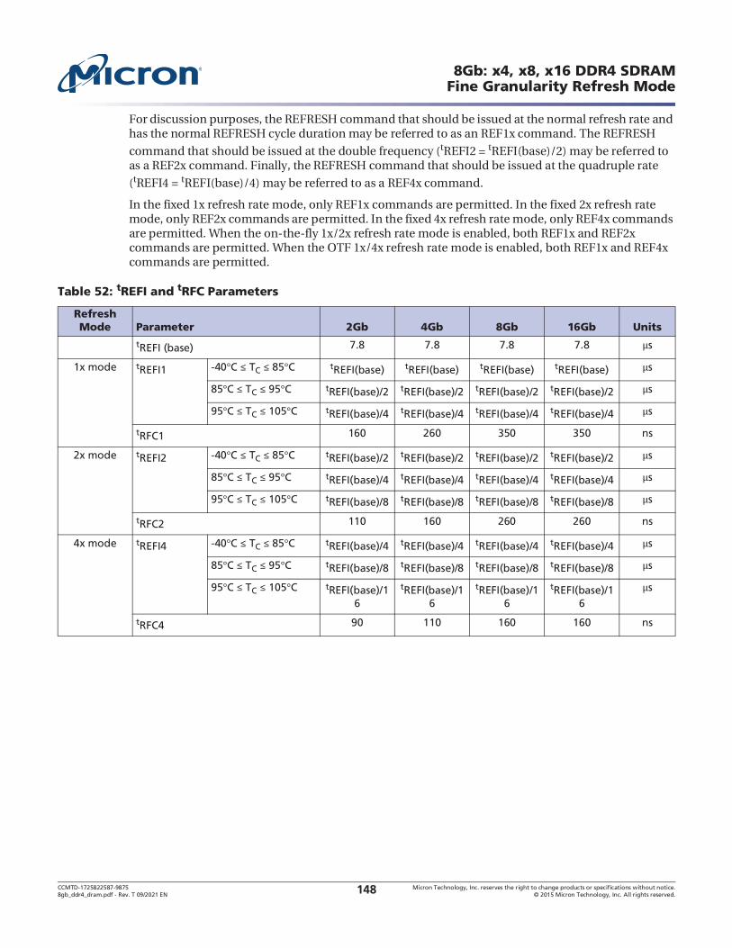
CCMTD-1725822587-9875 Micron Technology, Inc. reserves the right to change products or specifications without notice.8gb_ddr4_dram.pdf - Rev. T 09/2021 EN 2015 Micron Technology, Inc. All rights reserved.148
8Gb: x4, x8, x16 DDR4 SDRAMFine Granularity Refresh Mode
For discussion purposes, the REFRESH command that should be issued at the normal refresh rate and has the normal REFRESH cycle duration may be referred to as an REF1x command. The REFRESH
command that should be issued at the double frequency (tREFI2 = tREFI(base)/2) may be referred to as a REF2x command. Finally, the REFRESH command that should be issued at the quadruple rate
(tREFI4 = tREFI(base)/4) may be referred to as a REF4x command.
In the fixed 1x refresh rate mode, only REF1x commands are permitted. In the fixed 2x refresh rate mode, only REF2x commands are permitted. In the fixed 4x refresh rate mode, only REF4x commands are permitted. When the on-the-fly 1x/2x refresh rate mode is enabled, both REF1x and REF2x commands are permitted. When the OTF 1x/4x refresh rate mode is enabled, both REF1x and REF4x commands are permitted.
Table 52: tREFI and tRFC Parameters
Refresh Mode Parameter 2Gb 4Gb 8Gb 16Gb Units
tREFI (base) 7.8 7.8 7.8 7.8 s
1x mode tREFI1 -40 C TC 85 C tREFI(base) tREFI(base) tREFI(base) tREFI(base) s
85 C TC 95 C tREFI(base)/2 tREFI(base)/2 tREFI(base)/2 tREFI(base)/2 s
95 C TC 105 C tREFI(base)/4 tREFI(base)/4 tREFI(base)/4 tREFI(base)/4 s
tRFC1 160 260 350 350 ns
2x mode tREFI2 -40 C TC 85 C tREFI(base)/2 tREFI(base)/2 tREFI(base)/2 tREFI(base)/2 s
85 C TC 95 C tREFI(base)/4 tREFI(base)/4 tREFI(base)/4 tREFI(base)/4 s
95 C TC 105 C tREFI(base)/8 tREFI(base)/8 tREFI(base)/8 tREFI(base)/8 s
tRFC2 110 160 260 260 ns
4x mode tREFI4 -40 C TC 85 C tREFI(base)/4 tREFI(base)/4 tREFI(base)/4 tREFI(base)/4 s
85 C TC 95 C tREFI(base)/8 tREFI(base)/8 tREFI(base)/8 tREFI(base)/8 s
95 C TC 105 C tREFI(base)/16
tREFI(base)/16
tREFI(base)/16
tREFI(base)/16
s
tRFC4 90 110 160 160 ns

CCM
TD-1725822587-9875
Micro
n Techno
log
y, Inc. reserves the rig
ht to ch
ange p
rod
ucts or sp
ecifications w
itho
ut n
otice.
8gb
_ddr4_d
ram.p
df - Rev. T 09/2021 EN
2015 Micron
Techn
olog
y, Inc. A
ll rights reserved.
149
8Gb
: x4
, x8
, x16
DD
R4
SD
RA
MFin
e G
ranu
larity R
efresh M
od
e
Figure 88: 4Gb with Fine Granularity Refresh Mode Example
t REFI =
0.97
5μs
t REFI =
0.97
5μs
t REFI =
0.97
5μs
t REFI =
0.97
5μs
t REFI =
0.97
5μs
t REFI =
0.97
5μs
t REFI =
0.97
5μs
t REFI =
0.97
5μs
t REFI =
0.97
5μs
t REFI =
0.97
5μs
t REFI =
0.97
5μs
t REFI =
0.97
5μs
t REFI =
0.97
5μs
t REFI =
0.97
5μst REF
I = 0.
975μ
s
t REFI =
0.97
5μs
1x Mode(-40°C to 85°C)
2x Mode(-40°C to 85°C)
4x Mode(-40°C to 85°C)
Normal Temperature Operation – -40°C to 85°C
REF@260ns REF@160ns REF@110ns
REF@110ns
REF@160ns REF@110ns
REF@110ns
REF@260ns REF@160ns REF@110ns
REF@110ns
REF@160ns REF@110ns
REF@110nsREF@260ns REF@160ns
REF@110ns
t REFI =
7.8μ
s
t REFI =
7.8μ
s
t REFI =
3.9μ
s
t REFI =
3.9μ
s
t REFI =
3.9μ
s
t REFI =
3.9μ
s t REFI =
1.95
μs
t REFI =
1.95
μs
t REFI =
1.95
μs
t REFI =
1.95
μs
t REFI =
1.95
μs
t REFI =
1.95
μs
t REFI =
1.95
μs
t REFI =
1.95
μs
1x Mode(-40°C to 105°C)
2x Mode(-40°C to 105°C)
4x Mode(-40°C to 105°C)
REF@260ns REF@160ns REF@110ns
REF@110ns
REF@160ns REF@110ns
REF@110ns
REF@260ns REF@160ns REF@110ns
REF@110ns
REF@160ns REF@110ns
REF@110nsREF@260ns
REF@260ns
REF@260ns
REF@160ns
REF@160ns
REF@160ns
REF@160ns
REF@160ns REF@110ns
REF@110ns
REF@110ns
REF@110ns
REF@110ns
REF@110ns
REF@110ns
REF@110ns
REF@110ns
t REFI =
3.9μ
s
t REFI =
3.9μ
s
t REFI =
3.9μ
s
t REFI =
3.9μ
s t REFI =
1.95
μs
t REFI =
1.95
μs
t REFI =
1.95
μs
t REFI =
1.95
μs
t REFI =
1.95
μs
t REFI =
1.95
μs
t REFI =
1.95
μs
t REFI =
1.95
μs
Extended Temperature Operation – -40°C to 105°C

CCMTD-1725822587-9875 Micron Technology, Inc. reserves the right to change products or specifications without notice.8gb_ddr4_dram.pdf - Rev. T 09/2021 EN 2015 Micron Technology, Inc. All rights reserved.150
8Gb: x4, x8, x16 DDR4 SDRAMFine Granularity Refresh Mode
Changing Refresh Rate
If the refresh rate is changed by either MRS or OTF. New tREFI and tRFC parameters will be applied
from the moment of the rate change. When the REF1x command is issued to the DRAM, tREF1 and tRFC1 are applied from the time that the command was issued; when the REF2x command is issued, tREF2 and tRFC2 should be satisfied.
Figure 89: OTF REFRESH Command Timing
The following conditions must be satisfied before the refresh rate can be changed. Otherwise, data retention cannot be guaranteed.
In the fixed 2x refresh rate mode or the OTF 1x/2x refresh mode, an even number of REF2x commands must be issued because the last change of the refresh rate mode with an MRS command before the refresh rate can be changed by another MRS command.In the OTF1x/2x refresh rate mode, an even number of REF2x commands must be issued between any two REF1x commands.In the fixed 4x refresh rate mode or the OTF 1x/4x refresh mode, a multiple-of-four number of REF4x commands must be issued because the last change of the refresh rate with an MRS command before the refresh rate can be changed by another MRS command.In the OTF1x/4x refresh rate mode, a multiple-of-four number of REF4x commands must be issued between any two REF1x commands.
There are no special restrictions for the fixed 1x refresh rate mode. Switching between fixed and OTF modes keeping the same rate is not regarded as a refresh rate change.
Usage with TCR Mode
If the temperature controlled refresh mode is enabled, only the normal mode (fixed 1x mode, MR3[8:6] = 000) is allowed. If any other refresh mode than the normal mode is selected, the temperature controlled refresh mode must be disabled.
Self Refresh Entry and Exit
The device can enter self refresh mode anytime in 1x, 2x, and 4x mode without any restriction on the number of REFRESH commands that have been issued during the mode before the self refresh entry. However, upon self refresh exit, extra REFRESH command(s) may be required, depending on the condition of the self refresh entry.
The conditions and requirements for the extra REFRESH command(s) are defined as follows:In the fixed 2x refresh rate mode or the enable-OTF 1x/2x refresh rate mode, it is recommended there be an even number of REF2x commands before entry into self refresh after the last self refresh exit, REF1x command, or MRS command that set the refresh mode. If this condition is met, no additional REFRESH commands are required upon self refresh exit. In the case that this condition is not met, either one extra REF1x command or two extra REF2x commands must be issued upon self refresh exit. These extra REFRESH commands are not counted toward the computation of the average
refresh interval (tREFI).
REF1 DESDES DES ValidDES REF2 DESValid Valid DESDES DESREF2
tRFC1 (MIN) tRFC2 (MIN)
tREFI1 tREFI2
Don’t Care
Command
CK_t
CK_c

CCMTD-1725822587-9875 Micron Technology, Inc. reserves the right to change products or specifications without notice.8gb_ddr4_dram.pdf - Rev. T 09/2021 EN 2015 Micron Technology, Inc. All rights reserved.151
8Gb: x4, x8, x16 DDR4 SDRAMFine Granularity Refresh Mode
In the fixed 4x refresh rate mode or the enable-OTF 1x/4x refresh rate mode, it is recommended there be a multiple-of-four number of REF4x commands before entry into self refresh after the last self refresh exit, REF1x command, or MRS command that set the refresh mode. If this condition is met, no additional refresh commands are required upon self refresh exit. When this condition is not met, either one extra REF1x command or four extra REF4x commands must be issued upon self refresh exit. These extra REFRESH commands are not counted toward the computation of the average
refresh interval (tREFI).
There are no special restrictions on the fixed 1x refresh rate mode.
This section does not change the requirement regarding postponed REFRESH commands. The requirement for the additional REFRESH command(s) described above is independent of the require-ment for the postponed REFRESH commands.

CCMTD-1725822587-9875 Micron Technology, Inc. reserves the right to change products or specifications without notice.8gb_ddr4_dram.pdf - Rev. T 09/2021 EN 2015 Micron Technology, Inc. All rights reserved.152
8Gb: x4, x8, x16 DDR4 SDRAMSELF REFRESH Operation
SELF REFRESH Operation
The SELF REFRESH command can be used to retain data in the device, even if the rest of the system is powered down. When in self refresh mode, the device retains data without external clocking. The device has a built-in timer to accommodate SELF REFRESH operation. The SELF REFRESH command is defined by having CS_n, RAS_n, CAS_n, and CKE held LOW with WE_n and ACT_n HIGH at the rising edge of the clock.
Before issuing the SELF REFRESH ENTRY command, the device must be idle with all banks in the
precharge state and tRP satisfied. Idle state is defined as: All banks are closed (tRP, tDAL, and so on, satisfied), no data bursts are in progress, CKE is HIGH, and all timings from previous operations are
satisfied (tMRD, tMOD, tRFC, tZQinit, tZQoper, tZQCS, and so on). After the SELF REFRESH ENTRY command is registered, CKE must be held LOW to keep the device in self refresh mode. The DRAM automatically disables ODT termination, regardless of the ODT pin, when it enters self refresh mode and automatically enables ODT upon exiting self refresh. During normal operation (DLL_on), the DLL is automatically disabled upon entering self refresh and is automatically enabled (including a DLL reset) upon exiting self refresh.
When the device has entered self refresh mode, all of the external control signals, except CKE and
(VDD, VDDQ, VSS, VSSQ, VPP, and VREFCA) must be at valid levels. The DRAM internal VREFDQ generator circuitry may remain on or be turned off depending on the MR6 bit 7 setting. If the internal VREFDQ
circuit is on in self refresh, the first WRITE operation or first write-leveling activity may occur after tXS time after self refresh exit. If the DRAM internal VREFDQ circuitry is turned off in self refresh, it ensures
that the VREFDQ generator circuitry is powered up and stable within the tXSDLL period when the DRAM exits the self refresh state. The first WRITE operation or first write-leveling activity may not occur
earlier than tXSDLL after exiting self refresh. The device initiates a minimum of one REFRESH
command internally within the tCKE period once it enters self refresh mode.
The clock is internally disabled during a SELF REFRESH operation to save power. The minimum time
that the device must remain in self refresh mode is tCKESR/tCKESR_PAR. The user may change the
external clock frequency or halt the external clock tCKSRE/tCKSRE_PAR after self refresh entry is regis-
tered; however, the clock must be restarted and tCKSRX must be stable before the device can exit SELF REFRESH operation.
The procedure for exiting self refresh requires a sequence of events. First, the clock must be stable prior to CKE going back HIGH. Once a SELF REFRESH EXIT command (SRX, combination of CKE going HIGH and DESELECT on the command bus) is registered, the following timing delay must be satisfied:
Commands that do not require locked DLL:tXS = ACT, PRE, PREA, REF, SRE, and PDE.tXS_FAST = ZQCL, ZQCS, and MRS commands. For an MRS command, only DRAM CL, WR/RTP register, and DLL reset in MR0; RTT(NOM) register in MR1; the CWL and RTT(WR) registers in MR2; and gear-down mode register in MR3; WRITE and READ preamble registers in MR4; RTT(PARK) register in MR5; Data rate and VREFDQ calibration value registers in MR6 may be accessed provided the DRAM
is not in per-DRAM mode. Access to other DRAM mode registers must satisfy tXS timing. WRITE commands (WR, WRS4, WRS8, WRA, WRAS4, and WRAS8) that require synchronous ODT and dynamic ODT controlled by the WRITE command require a locked DLL.
Commands that require locked DLL in the normal operating range:
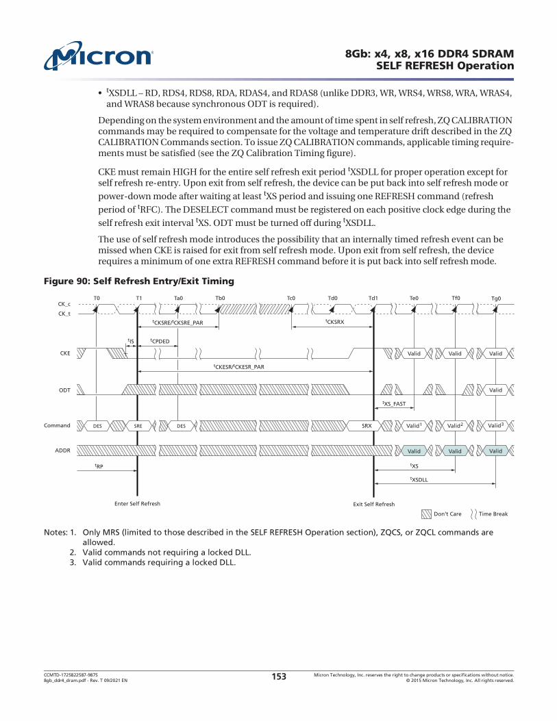
CCMTD-1725822587-9875 Micron Technology, Inc. reserves the right to change products or specifications without notice.8gb_ddr4_dram.pdf - Rev. T 09/2021 EN 2015 Micron Technology, Inc. All rights reserved.153
8Gb: x4, x8, x16 DDR4 SDRAMSELF REFRESH Operation
t
and WRAS8 because synchronous ODT is required).
Depending on the system environment and the amount of time spent in self refresh, ZQ CALIBRATION commands may be required to compensate for the voltage and temperature drift described in the ZQ CALIBRATION Commands section. To issue ZQ CALIBRATION commands, applicable timing require-ments must be satisfied (see the ZQ Calibration Timing figure).
CKE must remain HIGH for the entire self refresh exit period tXSDLL for proper operation except for self refresh re-entry. Upon exit from self refresh, the device can be put back into self refresh mode or
power-down mode after waiting at least tXS period and issuing one REFRESH command (refresh
period of tRFC). The DESELECT command must be registered on each positive clock edge during the
self refresh exit interval tXS. ODT must be turned off during tXSDLL.
The use of self refresh mode introduces the possibility that an internally timed refresh event can be missed when CKE is raised for exit from self refresh mode. Upon exit from self refresh, the device requires a minimum of one extra REFRESH command before it is put back into self refresh mode.
Figure 90: Self Refresh Entry/Exit Timing
Notes: 1. Only MRS (limited to those described in the SELF REFRESH Operation section), ZQCS, or ZQCL commands are allowed.
2. Valid commands not requiring a locked DLL.3. Valid commands requiring a locked DLL.
CK_t
CK_c
Command DES DESSRE
ADDR
CKE
ODT
SRX Valid1 Valid2
Valid Valid
tRP tXS
tXSDLL
tCKESR/tCKESR_PAR
tCPDEDtIS
tCKSRE/tCKSRE_PAR tCKSRX
Enter Self Refresh Exit Self Refresh
T0 T1 Ta0 Td0 Td1 Te0Tc0
Don’t Care
Tf0
Time Break
Tb0 Tg0
tXS_FAST
Valid3
Valid
Valid Valid Valid
Valid

CCMTD-1725822587-9875 Micron Technology, Inc. reserves the right to change products or specifications without notice.8gb_ddr4_dram.pdf - Rev. T 09/2021 EN 2015 Micron Technology, Inc. All rights reserved.154
8Gb: x4, x8, x16 DDR4 SDRAMSELF REFRESH Operation
Figure 91: Self Refresh Entry/Exit Timing with CAL Mode
Notes: 1. tCAL = 3nCK, tCPDED = 4nCK, tCKSRE/tCKSRE_PAR = 8nCK, tCKSRX = 8nCK, tXS_FAST = tREFC4 (MIN) + 10ns.2. CS_n = HIGH, ACT_n = "Don't Care," RAS_n/A16 = "Don't Care," CAS_n/A15 = "Don't Care," WE_n/A14 = "Don't
Care."3. Only MRS (limited to those described in the SELF REFRESH Operations section), ZQCS, or ZQCL commands are
allowed.
4. The figure only displays tXS_FAST timing, but tCAL must also be added to any tXS and tXSDLL associated commands during CAL mode.
Self Refresh Abort
The exit timing from self refresh exit to the first valid command not requiring a locked DLL is tXS. The
value of tXS is (tRFC1 + 10ns). This delay allows any refreshes started by the device time to complete. tRFC continues to grow with higher density devices, so tXS will grow as well. An MRS bit enables the self
refresh abort mode. If the bit is disabled, the controller uses tXS timings (location MR4, bit 9). If the bit is enabled, the device aborts any ongoing refresh and does not increment the refresh counter. The
controller can issue a valid command not requiring a locked DLL after a delay of tXS_ABORT. Upon exit from self refresh, the device requires a minimum of one extra REFRESH command before it is put back into self refresh mode. This requirement remains the same irrespective of the setting of the MRS bit for self refresh abort.
T0
CK_t
CK_cT1 T3 T4
Command
ADDR
w/o CS_n
CS_n
CKE
Don’t Care
Ta9T8 T11 Ta8Ta0T7 Tb1 Tb3Ta7 Ta10 Tb0
DES DES DES SRX DES DES DES DES
Valid
ValidDESSRE
Valid
tCKSRE
tXS_FAST
tCKSRX
tCAL tCPDED tCAL
Note 3Note 2

CCMTD-1725822587-9875 Micron Technology, Inc. reserves the right to change products or specifications without notice.8gb_ddr4_dram.pdf - Rev. T 09/2021 EN 2015 Micron Technology, Inc. All rights reserved.155
8Gb: x4, x8, x16 DDR4 SDRAMSELF REFRESH Operation
Figure 92: Self Refresh Abort
Notes: 1. Only MRS (limited to those described in the SELF REFRESH Operation section), ZQCS, or ZQCL commands are allowed.
2. Valid commands not requiring a locked DLL with self refresh abort mode enabled in the mode register.3. Valid commands requiring a locked DLL.
Self Refresh Exit with NOP Command
Exiting self refresh mode using the NO OPERATION command (NOP) is allowed under a specific system application. This special use of NOP allows for a common command/address bus between active DRAM devices and DRAM(s) in maximum power saving mode. Self refresh mode may exit with NOP commands provided:
The device entered self refresh mode with CA parity, CAL, and gear-down disabled.tMPX_S and tMPX_LH are satisfied.
NOP commands are only issued during tMPX_LH window.
No other command is allowed during the tMPX_LH window after an SELF REFRESH EXIT (SRX) command is issued.
CK_t
CK_c
Command DES DESSRE
ADDR
CKE
ODT
SRX Valid1 Valid2
Valid Valid
tRP tXS_ABORT
tXSDLL
tCKESR/tCKESR_PAR
tCPDEDtIS
tCKSRE/tCKSRE_PAR tCKSRX
Enter Self Refresh Exit Self Refresh
T0 T1 Ta0 Td0 Td1 Te0Tc0
Don’t Care
Tf0
Time Break
Tb0 Tg0
tXS_FAST
Valid3
Valid
Valid Valid Valid
Valid

CCMTD-1725822587-9875 Micron Technology, Inc. reserves the right to change products or specifications without notice.8gb_ddr4_dram.pdf - Rev. T 09/2021 EN 2015 Micron Technology, Inc. All rights reserved.156
8Gb: x4, x8, x16 DDR4 SDRAMSELF REFRESH Operation
Figure 93: Self Refresh Exit with NOP Command
Ta0
CK_t
CK_cTa1 Ta2 Ta3 Td1Tb1 Tb2 Tb3 Td0Tc3Tb0 Tc1 Tc2Tc0 Te0 Te1Tc4 Td2 Td3
CKE
ODT
tCKSRX
tMPX_LHtMPX_S
Command
ADDR
CS_n
Don’t Care
DES DES DES Valid DESDES
Valid
Valid
Valid
Valid
SRX NOP NOP NOP NOP
tXS
tXSDLLtXS +
Valid
Note 3Note 1, 2
DES
Valid Valid Valid Valid
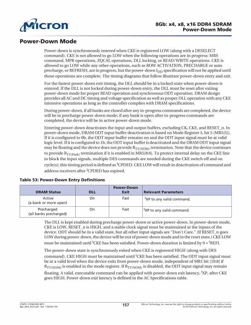
CCMTD-1725822587-9875 Micron Technology, Inc. reserves the right to change products or specifications without notice.8gb_ddr4_dram.pdf - Rev. T 09/2021 EN 2015 Micron Technology, Inc. All rights reserved.157
8Gb: x4, x8, x16 DDR4 SDRAMPower-Down Mode
Power-Down Mode
Power-down is synchronously entered when CKE is registered LOW (along with a DESELECT command). CKE is not allowed to go LOW when the following operations are in progress: MRS command, MPR operations, ZQCAL operations, DLL locking, or READ/WRITE operations. CKE is allowed to go LOW while any other operations, such as ROW ACTIVATION, PRECHARGE or auto precharge, or REFRESH, are in progress, but the power-down IDD specification will not be applied until those operations are complete. The timing diagrams that follow illustrate power-down entry and exit.
For the fastest power-down exit timing, the DLL should be in a locked state when power-down is entered. If the DLL is not locked during power-down entry, the DLL must be reset after exiting power-down mode for proper READ operation and synchronous ODT operation. DRAM design provides all AC and DC timing and voltage specification as well as proper DLL operation with any CKE intensive operations as long as the controller complies with DRAM specifications.
During power-down, if all banks are closed after any in-progress commands are completed, the device will be in precharge power-down mode; if any bank is open after in-progress commands are completed, the device will be in active power-down mode.
Entering power-down deactivates the input and output buffers, excluding CK, CKE, and RESET_n. In power-down mode, DRAM ODT input buffer deactivation is based on Mode Register 5, bit 5 (MR5[5]). If it is configured to 0b, the ODT input buffer remains on and the ODT input signal must be at valid logic level. If it is configured to 1b, the ODT input buffer is deactivated and the DRAM ODT input signal may be floating and the device does not provide RTT(NOM) termination. Note that the device continues to provide RTT(Park) termination if it is enabled in MR5[8:6]. To protect internal delay on the CKE line to block the input signals, multiple DES commands are needed during the CKE switch off and on
cycle(s); this timing period is defined as tCPDED. CKE LOW will result in deactivation of command and
address receivers after tCPDED has expired.
The DLL is kept enabled during precharge power-down or active power-down. In power-down mode, CKE is LOW, RESET_n is HIGH, and a stable clock signal must be maintained at the inputs of the device. ODT should be in a valid state, but all other input signals are "Don't Care." (If RESET_n goes LOW during power-down, the device will be out of power-down mode and in the reset state.) CKE LOW
must be maintained until tCKE has been satisfied. Power-down duration is limited by 9 tREFI.
The power-down state is synchronously exited when CKE is registered HIGH (along with DES
command). CKE HIGH must be maintained until tCKE has been satisfied. The ODT input signal must be at a valid level when the device exits from power-down mode, independent of MR1 bit [10:8] if RTT(NOM) is enabled in the mode register. If RTT(NOM) is disabled, the ODT input signal may remain
floating. A valid, executable command can be applied with power-down exit latency, tXP, after CKE goes HIGH. Power-down exit latency is defined in the AC Specifications table.
Table 53: Power-Down Entry Definitions
DRAM Status DLLPower-Down
Exit Relevant Parameters
Active (a bank or more open)
On Fast tXP to any valid command.
Precharged (all banks precharged)
On Fast tXP to any valid command.

CCMTD-1725822587-9875 Micron Technology, Inc. reserves the right to change products or specifications without notice.8gb_ddr4_dram.pdf - Rev. T 09/2021 EN 2015 Micron Technology, Inc. All rights reserved.158
8Gb: x4, x8, x16 DDR4 SDRAMPower-Down Mode
Figure 94: Active Power-Down Entry and Exit
Notes: 1. Valid commands at T0 are ACT, DES, or PRE with one bank remaining open after completion of the PRECHARGE command.
2. ODT pin driven to a valid state; MR5[5] = 0 (normal setting).3. ODT pin drive/float timing requirements for the ODT input buffer disable option (for additional power savings
during active power-down) is described in the section for ODT Input Buffer Disable Mode for Power-Down; MR5[5] = 1.
CK_t
CK_c
Command DES DES DES DES DES
Address
CKE
Enterpower-down
mode
Exitpower-down
mode
tPD
Valid
Valid
Valid
Valid
tCPDED
Valid
Valid
ODT (ODT buffer enabled - MR5[5] = 0)2
tIH
tIHtIS
tIS
T0 T1 T2 Ta0 Ta1 Tb0 Tb1 Tc0
DES
tXP
tCKE
Don’t CareTime Break
ODT (ODT buffer disabled - MR5[5] = 1)3 Refer to ODT Power-Down Entry/Exit with ODT Buffer Disable Mode figures

CCMTD-1725822587-9875 Micron Technology, Inc. reserves the right to change products or specifications without notice.8gb_ddr4_dram.pdf - Rev. T 09/2021 EN 2015 Micron Technology, Inc. All rights reserved.159
8Gb: x4, x8, x16 DDR4 SDRAMPower-Down Mode
Figure 95: Power-Down Entry After Read and Read with Auto Precharge
Note: 1. DI n (or b) = data-in from column n (or b).
Figure 96: Power-Down Entry After Write and Write with Auto Precharge
Notes: 1. DI n (or b) = data-in from column n (or b).2. Valid commands at T0 are ACT, DES, or PRE with one bank remaining open after completion of the PRECHARGE
command.
T0 T1 Ta0 Ta1 Ta2 Ta3 Ta4 Ta5 Ta6 Ta7
RL = AL + CL
Ta8 Tb0 Tb1
DES
Valid Valid
RD orRDA DES DES DES DES DES DES DES DES DES DES Valid
Valid
CK_t
CK_c
Command
DQ BL8
DQ BC4
DQS_t, DQS_c
Address
CKE
tCPDEDtIS
tPD
tRDPDEN
Power-Downentry
Transitioning Data Don’t CareTime Break
DIb+3
DIb+2
DIb+1
DIb
DIn+3
DIn+2
DIn+1
DIn
DIb+7
DIb+6
DIb+5
DIb+4
T0 T1 Ta0 Ta1 Ta2 Ta3 Ta4 Ta5 Ta6 Ta7
WL = AL + CWL
Tb0 Tb1 Tb2 Tc0 Tc1
Bank,Col n
DIb + 3
DIb + 2
DIb + 1
DIb
DIb + 7
DIb + 6
DIb + 5
DIb + 4
DESWRITE DES DES DES DES DES DES DES DES DES DES DES DES
CK_t
CK_c
Command
DQ BL8
DQ BC4
DQS_t, DQS_c
Address
A10
CKE
WR
tCPDEDtIS
tPD
tWRAPDEN
Power-Down entry
Start internalprecharge
DIn + 3
DIn + 2
DIn + 1
DIn
Transitioning Data Don’t CareTime Break
Valid
Valid
Valid

CCMTD-1725822587-9875 Micron Technology, Inc. reserves the right to change products or specifications without notice.8gb_ddr4_dram.pdf - Rev. T 09/2021 EN 2015 Micron Technology, Inc. All rights reserved.160
8Gb: x4, x8, x16 DDR4 SDRAMPower-Down Mode
Figure 97: Power-Down Entry After Write
Note: 1. DI n (or b) = data-in from column n (or b).
Figure 98: Precharge Power-Down Entry and Exit
T0 T1 Ta0 Ta1 Ta2 Ta3 Ta4 Ta5 Ta6 Ta7
WL = AL + CWL
Tb0 Tb1 Tb2 Tc0 Tc1
Bank,Col n
DESWRITE DES DES DES DES DES DES DES DES DES DES DES DES
CK_t
CK_c
Command
DQ BL8
DQ BC4
DQS_t, DQS_c
Address
A10
CKE
tWR
tCPDEDtIS
tPD
tWRPDEN
Power-Downentry
Valid
Valid
Valid
Transitioning Data Don’t CareTime Break
DIb + 3
DIb + 2
DIb + 1
DIb
DIb + 7
DIb + 6
DIb + 5
DIb + 4
DI n + 3
DIn + 2
DIn + 1
DIn
CK_t
CK_c
Command DES DES DESDES DES DES
CKE
Enterpower-down
mode
Exitpower-down
mode
tPD tXP
tCPDED
tIS
tIHtIS
T0 T1 T2 Ta0 Ta1 Tb0 Tb1 Tc0
tCKE
Don’t CareTime Break
Valid Valid
Valid
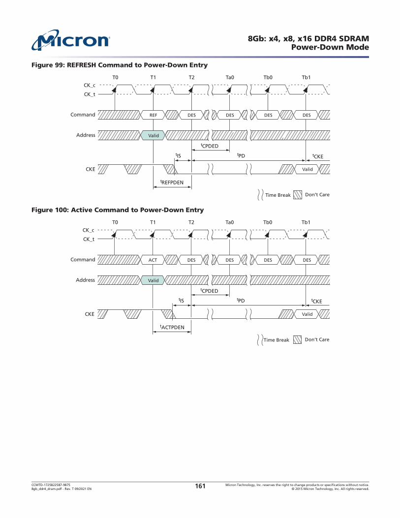
CCMTD-1725822587-9875 Micron Technology, Inc. reserves the right to change products or specifications without notice.8gb_ddr4_dram.pdf - Rev. T 09/2021 EN 2015 Micron Technology, Inc. All rights reserved.161
8Gb: x4, x8, x16 DDR4 SDRAMPower-Down Mode
Figure 99: REFRESH Command to Power-Down Entry
Figure 100: Active Command to Power-Down Entry
CK_t
CK_c
Command REF DES DESDES
Address Valid
CKE
tREFPDEN
tCPDED
tCKE
T0 T1 T2 Ta0 Tb0 Tb1
tPD
Don’t CareTime Break
Valid
tIS
DES
CK_t
CK_c
Command ACT DES DESDES
Address Valid
CKE
tACTPDEN
tCPDED
tCKEtIS
T0 T1 T2 Ta0 Tb0 Tb1
tPD
Don’t CareTime Break
Valid
DES
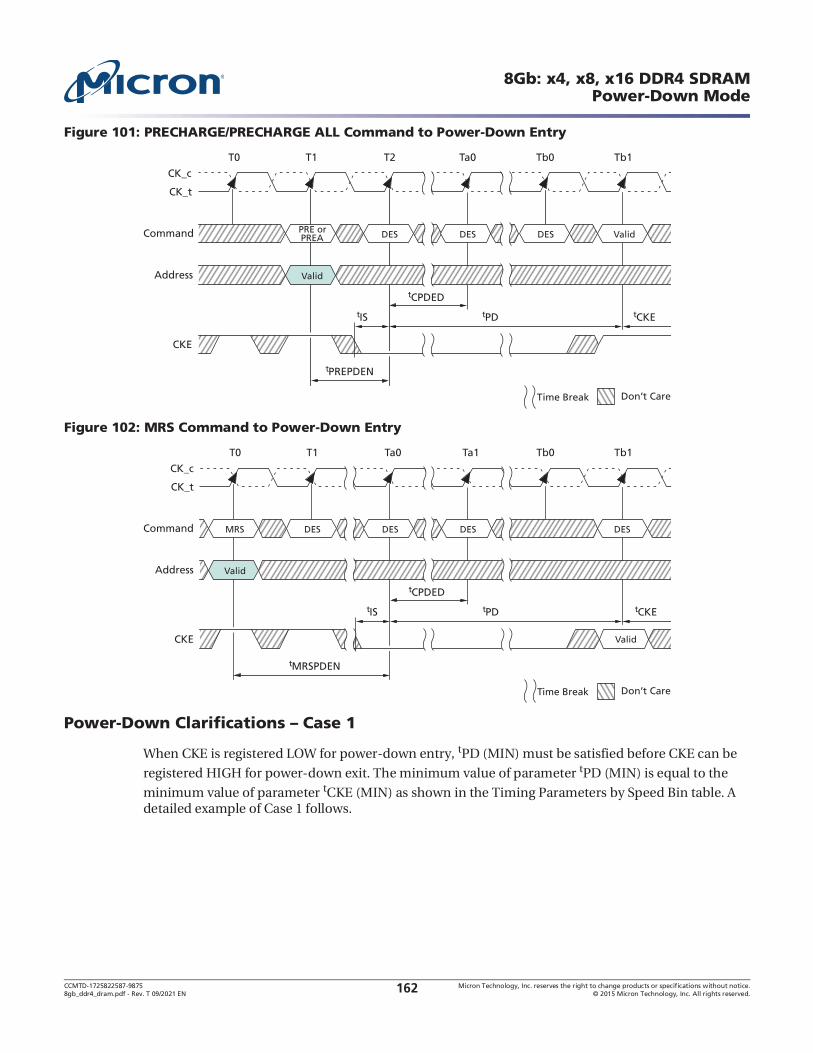
CCMTD-1725822587-9875 Micron Technology, Inc. reserves the right to change products or specifications without notice.8gb_ddr4_dram.pdf - Rev. T 09/2021 EN 2015 Micron Technology, Inc. All rights reserved.162
8Gb: x4, x8, x16 DDR4 SDRAMPower-Down Mode
Figure 101: PRECHARGE/PRECHARGE ALL Command to Power-Down Entry
Figure 102: MRS Command to Power-Down Entry
When CKE is registered LOW for power-down entry, tPD (MIN) must be satisfied before CKE can be
registered HIGH for power-down exit. The minimum value of parameter tPD (MIN) is equal to the
minimum value of parameter tCKE (MIN) as shown in the Timing Parameters by Speed Bin table. A detailed example of Case 1 follows.
CK_t
CK_c
Command PRE orPREA DES DESDES Valid
Address Valid
CKE
tPREPDEN
tCPDED
T0 T1 T2 Ta0 Tb0 Tb1
tPD tCKE
Don’t CareTime Break
tIS
CK_t
CK_c
Command MRS DES DESDES
Address Valid
CKE
tMRSPDEN
tCPDED
T0 T1 Tb0 Tb1Ta0 Ta1
tPD tCKE
Don’t CareTime Break
Valid
tIS
DES

CCMTD-1725822587-9875 Micron Technology, Inc. reserves the right to change products or specifications without notice.8gb_ddr4_dram.pdf - Rev. T 09/2021 EN 2015 Micron Technology, Inc. All rights reserved.163
8Gb: x4, x8, x16 DDR4 SDRAMPower-Down Mode
Figure 103:
Power-Down Entry, Exit Timing with CAL
Command/Address latency is used and additional timing restrictions are required when entering power-down, as noted in the following figures.
Figure 104: Active Power-Down Entry and Exit Timing with CAL
CK_t
CK_c
Command Valid DES DESDES DES
Address Valid
CKE
tCPDED
Enterpower-down
mode
Exitpower-down
mode
Enterpower-down
mode
tCPDED
T0 T1 T2 Ta0 Ta1
tPD tPD
Don’t CareTime Break
Tb0 Tb1 Tb2
tIS tIS
tIH tIS tCKE
tIH
DES DES
CK_t
CK_c
Command DES Valid DESDES DES
Address
CKE
tPD
DES
Valid
tCPDEDtCAL tXP tCAL
Valid
tIH
tIHtIStIS
T0 T1 Ta0 Ta1 Ta2 Tb0 Tb1 Tc0 Tc1 Td0 Td1 Te0
Don’t CareTime Break
CS_n
DES DES ValidDES DES

CCMTD-1725822587-9875 Micron Technology, Inc. reserves the right to change products or specifications without notice.8gb_ddr4_dram.pdf - Rev. T 09/2021 EN 2015 Micron Technology, Inc. All rights reserved.164
8Gb: x4, x8, x16 DDR4 SDRAMPower-Down Mode
Figure 105: REFRESH Command to Power-Down Entry with CAL
CK_t
CK_c
Command DES REF DESDES DES
Address
CKE
tPD
DES
Valid
t CPDEDtCAL tREFPDEN tXP tCAL
Valid
tIH
tIHtIStIS
T0 T1 Ta0 Tb0 Tb1 Tc0 Tc1 Td0 Td1 Te0 Te1 Tf0
Don’t CareTime Break
CS_n
DES DES ValidDES DES

CCMTD-1725822587-9875 Micron Technology, Inc. reserves the right to change products or specifications without notice.8gb_ddr4_dram.pdf - Rev. T 09/2021 EN 2015 Micron Technology, Inc. All rights reserved.165
8Gb: x4, x8, x16 DDR4 SDRAMODT Input Buffer Disable Mode for Power-Down
ODT Input Buffer Disable Mode for Power-Down
DRAM does not provide RTT_NOM termination during power-down when ODT input buffer deactiva-tion mode is enabled in MR5 bit A5.
To account for DRAM internal delay on CKE line to disable the ODT buffer and block the sampled output, the host controller must continuously drive ODT to either low or high when entering power
down (from tDODTLoff+1 prior to CKE low till tCPDED after CKE low).
The ODT signal is allowed to float after tCPDEDmin has expired. In this mode, RTT_NOM termination
corresponding to sampled ODT at the input when CKE is registered low (and tANPD before that) may
be either RTT_NOM or RTT_PARK. tANPD is equal to (WL-1) and is counted backwards from PDE.
Figure 106: ODT Power-Down Entry with ODT Buffer Disable Mode
diff_CK
tDODTLoff +1 tCPDED (MIN)
CKE
ODT Floating
DRAM_RTT_sync(DLL enabled)
CA parity disabled
DRAM_RTT_async(DLL disabled)
RTT(Park)RTT(NOM)
tCPDED (MIN) + tADC (MAX)
tADC (MIN)
DODTLoff
RTT(Park)RTT(NOM)
tAONAS (MIN)
tCPDED (MIN) + tAOFAS (MAX)

CCMTD-1725822587-9875 Micron Technology, Inc. reserves the right to change products or specifications without notice.8gb_ddr4_dram.pdf - Rev. T 09/2021 EN 2015 Micron Technology, Inc. All rights reserved.166
8Gb: x4, x8, x16 DDR4 SDRAMODT Input Buffer Disable Mode for Power-Down
Figure 107: ODT Power-Down Exit with ODT Buffer Disable Mode
diff_CK
CKE
ODT_A(DLL enabled)
tADC (MAX)tXP
tXP
Floating
DRAM_RTT_A RTT(Park) RTT(NOM)
tADC (MIN)DODTLon
ODT_B(DLL disabled)
Floating
DRAM_RTT_B RTT(Park)
tAONAS (MIN)tAOFAS (MAX)
RTT(NOM)

CCMTD-1725822587-9875 Micron Technology, Inc. reserves the right to change products or specifications without notice.8gb_ddr4_dram.pdf - Rev. T 09/2021 EN 2015 Micron Technology, Inc. All rights reserved.167
8Gb: x4, x8, x16 DDR4 SDRAMCRC Write Data Feature
CRC Write Data Feature
CRC Write Data
The CRC write data feature takes the CRC generated data from the DRAM controller and compares it to the internally CRC generated data and determines whether the two match (no CRC error) or do not match (CRC error).
Figure 108: CRC Write Data Operation
WRITE CRC DATA Operation
A DRAM controller generates a CRC checksum using a 72-bit CRC tree and forms the write data frames, as shown in the following CRC data mapping tables for the x4, x8, and x16 configurations. A x4 device has a CRC tree with 32 input data bits used, and the remaining upper 40 bits D[71:32] being 1s. A x8 device has a CRC tree with 64 input data bits used, and the remaining upper 8 bits dependant upon whether DM_n/DBI_n is used (1s are sent when not used). A x16 device has two identical CRC trees each, one for the lower byte and one for the upper byte, with 64 input data bits used by each, and the remaining upper 8 bits on each byte dependant upon whether DM_n/DBI_n is used (1s are sent when not used). For a x8 and x16 DRAMs, the DRAM memory controller must send 1s in transfer 9 location whether or not DM_n/DBI_n is used.
The DRAM checks for an error in a received code word D[71:0] by comparing the received checksum against the computed checksum and reports errors using the ALERT_n signal if there is a mismatch. The DRAM can write data to the DRAM core without waiting for the CRC check for full writes when DM is disabled. If bad data is written to the DRAM core, the DRAM memory controller will try to overwrite the bad data with good data; this means the DRAM controller is responsible for data coherency when DM is disabled. However, in the case where both CRC and DM are enabled via MRS (that is, persistent mode), the DRAM will not write bad data to the core when a CRC error is detected.
Data
DRAM Controller DRAM
Data
CRC Code
CRCCode
CRCengine
Data
CRC Code
CRCengine
CompareCRC
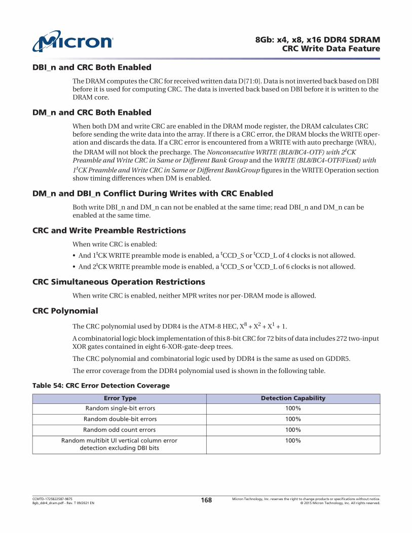
CCMTD-1725822587-9875 Micron Technology, Inc. reserves the right to change products or specifications without notice.8gb_ddr4_dram.pdf - Rev. T 09/2021 EN 2015 Micron Technology, Inc. All rights reserved.168
8Gb: x4, x8, x16 DDR4 SDRAMCRC Write Data Feature
DBI_n and CRC Both Enabled
The DRAM computes the CRC for received written data D[71:0]. Data is not inverted back based on DBI before it is used for computing CRC. The data is inverted back based on DBI before it is written to the DRAM core.
DM_n and CRC Both Enabled
When both DM and write CRC are enabled in the DRAM mode register, the DRAM calculates CRC before sending the write data into the array. If there is a CRC error, the DRAM blocks the WRITE oper-ation and discards the data. If a CRC error is encountered from a WRITE with auto precharge (WRA),
the DRAM will not block the precharge. The Nonconsecutive WRITE (BL8/BC4-OTF) with 2tCK Preamble and Write CRC in Same or Different Bank Group and the WRITE (BL8/BC4-OTF/Fixed) with
1tCK Preamble and Write CRC in Same or Different BankGroup figures in the WRITE Operation section show timing differences when DM is enabled.
DM_n and DBI_n Conflict During Writes with CRC Enabled
Both write DBI_n and DM_n can not be enabled at the same time; read DBI_n and DM_n can be enabled at the same time.
CRC and Write Preamble Restrictions
When write CRC is enabled:
And 1tCK WRITE preamble mode is enabled, a tCCD_S or tCCD_L of 4 clocks is not allowed.
And 2tCK WRITE preamble mode is enabled, a tCCD_S or tCCD_L of 6 clocks is not allowed.
CRC Simultaneous Operation Restrictions
When write CRC is enabled, neither MPR writes nor per-DRAM mode is allowed.
CRC Polynomial
The CRC polynomial used by DDR4 is the ATM-8 HEC, X8 + X2 + X1 + 1.
A combinatorial logic block implementation of this 8-bit CRC for 72 bits of data includes 272 two-input XOR gates contained in eight 6-XOR-gate-deep trees.
The CRC polynomial and combinatorial logic used by DDR4 is the same as used on GDDR5.
The error coverage from the DDR4 polynomial used is shown in the following table.
Table 54: CRC Error Detection Coverage
Error Type Detection Capability
Random single-bit errors 100%
Random double-bit errors 100%
Random odd count errors 100%
Random multibit UI vertical column errordetection excluding DBI bits
100%
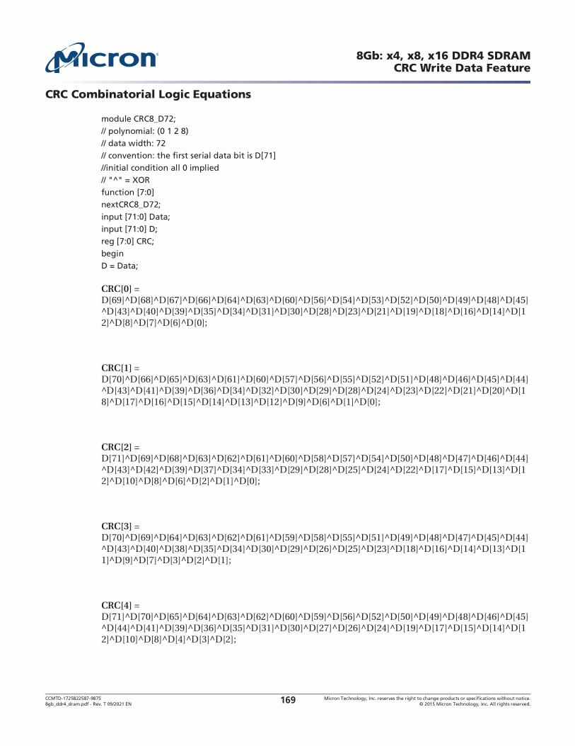
CCMTD-1725822587-9875 Micron Technology, Inc. reserves the right to change products or specifications without notice.8gb_ddr4_dram.pdf - Rev. T 09/2021 EN 2015 Micron Technology, Inc. All rights reserved.169
8Gb: x4, x8, x16 DDR4 SDRAMCRC Write Data Feature
CRC Combinatorial Logic Equations
CRC[0] = D[69]^D[68]^D[67]^D[66]^D[64]^D[63]^D[60]^D[56]^D[54]^D[53]^D[52]^D[50]^D[49]^D[48]^D[45]^D[43]^D[40]^D[39]^D[35]^D[34]^D[31]^D[30]^D[28]^D[23]^D[21]^D[19]^D[18]^D[16]^D[14]^D[12]^D[8]^D[7]^D[6]^D[0];
CRC[1] = D[70]^D[66]^D[65]^D[63]^D[61]^D[60]^D[57]^D[56]^D[55]^D[52]^D[51]^D[48]^D[46]^D[45]^D[44]^D[43]^D[41]^D[39]^D[36]^D[34]^D[32]^D[30]^D[29]^D[28]^D[24]^D[23]^D[22]^D[21]^D[20]^D[18]^D[17]^D[16]^D[15]^D[14]^D[13]^D[12]^D[9]^D[6]^D[1]^D[0];
CRC[2] = D[71]^D[69]^D[68]^D[63]^D[62]^D[61]^D[60]^D[58]^D[57]^D[54]^D[50]^D[48]^D[47]^D[46]^D[44]^D[43]^D[42]^D[39]^D[37]^D[34]^D[33]^D[29]^D[28]^D[25]^D[24]^D[22]^D[17]^D[15]^D[13]^D[12]^D[10]^D[8]^D[6]^D[2]^D[1]^D[0];
CRC[3] = D[70]^D[69]^D[64]^D[63]^D[62]^D[61]^D[59]^D[58]^D[55]^D[51]^D[49]^D[48]^D[47]^D[45]^D[44]^D[43]^D[40]^D[38]^D[35]^D[34]^D[30]^D[29]^D[26]^D[25]^D[23]^D[18]^D[16]^D[14]^D[13]^D[11]^D[9]^D[7]^D[3]^D[2]^D[1];
CRC[4] = D[71]^D[70]^D[65]^D[64]^D[63]^D[62]^D[60]^D[59]^D[56]^D[52]^D[50]^D[49]^D[48]^D[46]^D[45]^D[44]^D[41]^D[39]^D[36]^D[35]^D[31]^D[30]^D[27]^D[26]^D[24]^D[19]^D[17]^D[15]^D[14]^D[12]^D[10]^D[8]^D[4]^D[3]^D[2];
module CRC8_D72;// polynomial: (0 1 2 8)// data width: 72// convention: the first serial data bit is D[71]//initial condition all 0 implied// "^" = XORfunction [7:0]nextCRC8_D72;input [71:0] Data;input [71:0] D;reg [7:0] CRC;beginD = Data;

CCMTD-1725822587-9875 Micron Technology, Inc. reserves the right to change products or specifications without notice.8gb_ddr4_dram.pdf - Rev. T 09/2021 EN 2015 Micron Technology, Inc. All rights reserved.170
8Gb: x4, x8, x16 DDR4 SDRAMCRC Write Data Feature
CRC[5] = D[71]^D[66]^D[65]^D[64]^D[63]^D[61]^D[60]^D[57]^D[53]^D[51]^D[50]^D[49]^D[47]^D[46]^D[45]^D[42]^D[40]^D[37]^D[36]^D[32]^D[31]^D[28]^D[27]^D[25]^D[20]^D[18]^D[16]^D[15]^D[13]^D[11]^D[9]^D[5]^D[4]^D[3];
CRC[6] = D[67]^D[66]^D[65]^D[64]^D[62]^D[61]^D[58]^D[54]^D[52]^D[51]^D[50]^D[48]^D[47]^D[46]^D[43]^D[41]^D[38]^D[37]^D[33]^D[32]^D[29]^D[28]^D[26]^D[21]^D[19]^D[17]^D[16]^D[14]^D[12]^D[10]^D[6]^D[5]^D[4];
CRC[7] = D[68]^D[67]^D[66]^D[65]^D[63]^D[62]^D[59]^D[55]^D[53]^D[52]^D[51]^D[49]^D[48]^D[47]^D[44]^D[42]^D[39]^D[38]^D[34]^D[33]^D[30]^D[29]^D[27]^D[22]^D[20]^D[18]^D[17]^D[15]^D[13]^D[11]^D[7]^D[6]^D[5];
nextCRC8_D72 = CRC;
Burst Ordering for BL8
DDR4 supports fixed WRITE burst ordering [A2:A1:A0 = 0:0:0] when write CRC is enabled in BL8 (fixed).
CRC Data Bit Mapping
Table 55: CRC Data Mapping for x4 Devices, BL8
Function
Transfer
0 1 2 3 4 5 6 7 8 9
DQ0 D0 D1 D2 D3 D4 D5 D6 D7 CRC0 CRC4
DQ1 D8 D9 D10 D11 D12 D13 D14 D15 CRC1 CRC5
DQ2 D16 D17 D18 D19 D20 D21 D22 D23 CRC2 CRC6
DQ3 D24 D25 D26 D27 D28 D29 D30 D31 CRC3 CRC7
Table 56: CRC Data Mapping for x8 Devices, BL8
Function
Transfer
0 1 2 3 4 5 6 7 8 9
DQ0 D0 D1 D2 D3 D4 D5 D6 D7 CRC0 1
DQ1 D8 D9 D10 D11 D12 D13 D14 D15 CRC1 1
DQ2 D16 D17 D18 D19 D20 D21 D22 D23 CRC2 1
DQ3 D24 D25 D26 D27 D28 D29 D30 D31 CRC3 1
DQ4 D32 D33 D34 D35 D36 D37 D38 D39 CRC4 1
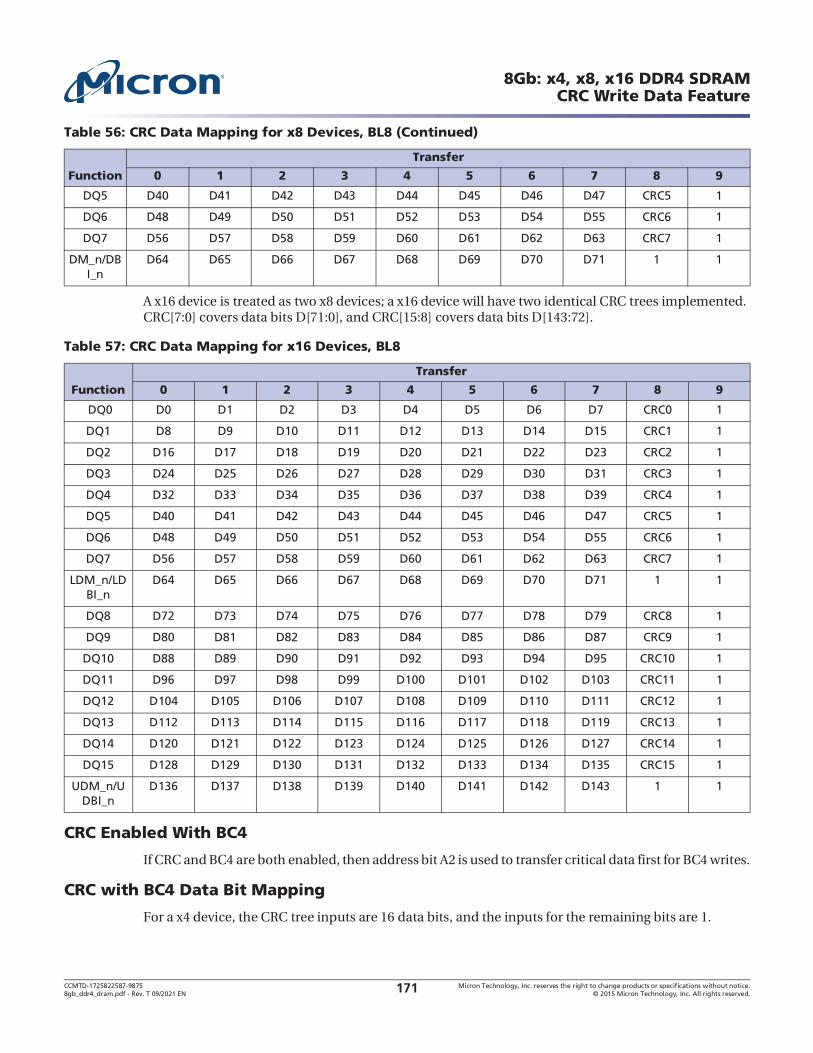
CCMTD-1725822587-9875 Micron Technology, Inc. reserves the right to change products or specifications without notice.8gb_ddr4_dram.pdf - Rev. T 09/2021 EN 2015 Micron Technology, Inc. All rights reserved.171
8Gb: x4, x8, x16 DDR4 SDRAMCRC Write Data Feature
A x16 device is treated as two x8 devices; a x16 device will have two identical CRC trees implemented. CRC[7:0] covers data bits D[71:0], and CRC[15:8] covers data bits D[143:72].
CRC Enabled With BC4
If CRC and BC4 are both enabled, then address bit A2 is used to transfer critical data first for BC4 writes.
CRC with BC4 Data Bit Mapping
For a x4 device, the CRC tree inputs are 16 data bits, and the inputs for the remaining bits are 1.
DQ5 D40 D41 D42 D43 D44 D45 D46 D47 CRC5 1
DQ6 D48 D49 D50 D51 D52 D53 D54 D55 CRC6 1
DQ7 D56 D57 D58 D59 D60 D61 D62 D63 CRC7 1
DM_n/DBI_n
D64 D65 D66 D67 D68 D69 D70 D71 1 1
Table 56: CRC Data Mapping for x8 Devices, BL8 (Continued)
Function
Transfer
0 1 2 3 4 5 6 7 8 9
Table 57: CRC Data Mapping for x16 Devices, BL8
Function
Transfer
0 1 2 3 4 5 6 7 8 9
DQ0 D0 D1 D2 D3 D4 D5 D6 D7 CRC0 1
DQ1 D8 D9 D10 D11 D12 D13 D14 D15 CRC1 1
DQ2 D16 D17 D18 D19 D20 D21 D22 D23 CRC2 1
DQ3 D24 D25 D26 D27 D28 D29 D30 D31 CRC3 1
DQ4 D32 D33 D34 D35 D36 D37 D38 D39 CRC4 1
DQ5 D40 D41 D42 D43 D44 D45 D46 D47 CRC5 1
DQ6 D48 D49 D50 D51 D52 D53 D54 D55 CRC6 1
DQ7 D56 D57 D58 D59 D60 D61 D62 D63 CRC7 1
LDM_n/LDBI_n
D64 D65 D66 D67 D68 D69 D70 D71 1 1
DQ8 D72 D73 D74 D75 D76 D77 D78 D79 CRC8 1
DQ9 D80 D81 D82 D83 D84 D85 D86 D87 CRC9 1
DQ10 D88 D89 D90 D91 D92 D93 D94 D95 CRC10 1
DQ11 D96 D97 D98 D99 D100 D101 D102 D103 CRC11 1
DQ12 D104 D105 D106 D107 D108 D109 D110 D111 CRC12 1
DQ13 D112 D113 D114 D115 D116 D117 D118 D119 CRC13 1
DQ14 D120 D121 D122 D123 D124 D125 D126 D127 CRC14 1
DQ15 D128 D129 D130 D131 D132 D133 D134 D135 CRC15 1
UDM_n/UDBI_n
D136 D137 D138 D139 D140 D141 D142 D143 1 1

CCMTD-1725822587-9875 Micron Technology, Inc. reserves the right to change products or specifications without notice.8gb_ddr4_dram.pdf - Rev. T 09/2021 EN 2015 Micron Technology, Inc. All rights reserved.172
8Gb: x4, x8, x16 DDR4 SDRAMCRC Write Data Feature
When A2 = 1, data bits D[7:4] are used as inputs for D[3:0], D[15:12] are used as inputs to D[11:8], and so forth, for the CRC tree.
For a x8 device, the CRC tree inputs are 36 data bits.
When A2 = 0, the input bits D[67:64]) are used if DBI_n or DM_n functions are enabled; if DBI_n and DM_n are disabled, then D[67:64]) are 1.
When A2 = 1, data bits D[7:4] are used as inputs for D[3:0], D[15:12] are used as inputs to D[11:8], and so forth, for the CRC tree. The input bits D[71:68]) are used if DBI_n or DM_n functions are enabled; if DBI_n and DM_n are disabled, then D[71:68]) are 1.
Table 58: CRC Data Mapping for x4 Devices, BC4
Function
Transfer
0 1 2 3 4 5 6 7 8 9
A2 = 0
DQ0 D0 D1 D2 D3 1 1 1 1 CRC0 CRC4
DQ1 D8 D9 D10 D11 1 1 1 1 CRC1 CRC5
DQ2 D16 D17 D18 D19 1 1 1 1 CRC2 CRC6
DQ3 D24 D25 D26 D27 1 1 1 1 CRC3 CRC7
A2 = 1
DQ0 D4 D5 D6 D7 1 1 1 1 CRC0 CRC4
DQ1 D12 D13 D14 D15 1 1 1 1 CRC1 CRC5
DQ2 D20 D21 D22 D23 1 1 1 1 CRC2 CRC6
DQ3 D28 D29 D30 D31 1 1 1 1 CRC3 CRC7
Table 59: CRC Data Mapping for x8 Devices, BC4
Function
Transfer
0 1 2 3 4 5 6 7 8 9
A2 = 0
DQ0 D0 D1 D2 D3 1 1 1 1 CRC0 1
DQ1 D8 D9 D10 D11 1 1 1 1 CRC1 1
DQ2 D16 D17 D18 D19 1 1 1 1 CRC2 1
DQ3 D24 D25 D26 D27 1 1 1 1 CRC3 1
DQ4 D32 D33 D34 D35 1 1 1 1 CRC4 1
DQ5 D40 D41 D42 D43 1 1 1 1 CRC5 1
DQ6 D48 D49 D50 D51 1 1 1 1 CRC6 1
DQ7 D56 D57 D58 D59 1 1 1 1 CRC7 1
DM_n/DBI_n D64 D65 D66 D67 1 1 1 1 1 1
A2 = 1
DQ0 D4 D5 D6 D7 1 1 1 1 CRC0 1
DQ1 D12 D13 D14 D15 1 1 1 1 CRC1 1
DQ2 D20 D21 D22 D23 1 1 1 1 CRC2 1
DQ3 D28 D29 D30 D31 1 1 1 1 CRC3 1

CCMTD-1725822587-9875 Micron Technology, Inc. reserves the right to change products or specifications without notice.8gb_ddr4_dram.pdf - Rev. T 09/2021 EN 2015 Micron Technology, Inc. All rights reserved.173
8Gb: x4, x8, x16 DDR4 SDRAMCRC Write Data Feature
There are two identical CRC trees for x16 devices, each have CRC tree inputs of 36 bits.
When A2 = 0, input bits D[67:64] are used if DBI_n or DM_n functions are enabled; if DBI_n and DM_n are disabled, then D[67:64] are 1s. The input bits D[139:136] are used if DBI_n or DM_n functions are enabled; if DBI_n and DM_n are disabled, then D[139:136] are 1s.
When A2 = 1, data bits D[7:4] are used as inputs for D[3:0], D[15:12] are used as inputs for D[11:8], and so forth, for the CRC tree. Input bits D[71:68] are used if DBI_n or DM_n functions are enabled; if DBI_n and DM_n are disabled, then D[71:68] are 1s. The input bits D[143:140] are used if DBI_n or DM_n functions are enabled; if DBI_n and DM_n are disabled, then D[143:140] are 1s.
DQ4 D36 D37 D38 D39 1 1 1 1 CRC4 1
DQ5 D44 D45 D46 D47 1 1 1 1 CRC5 1
DQ6 D52 D53 D54 D55 1 1 1 1 CRC6 1
DQ7 D60 D61 D62 D63 1 1 1 1 CRC7 1
DM_n/DBI_n D68 D69 D70 D71 1 1 1 1 1 1
Table 59: CRC Data Mapping for x8 Devices, BC4 (Continued)
Function
Transfer
0 1 2 3 4 5 6 7 8 9
Table 60: CRC Data Mapping for x16 Devices, BC4
Function
Transfer
0 1 2 3 4 5 6 7 8 9
A2 = 0
DQ0 D0 D1 D2 D3 1 1 1 1 CRC0 1
DQ1 D8 D9 D10 D11 1 1 1 1 CRC1 1
DQ2 D16 D17 D18 D19 1 1 1 1 CRC2 1
DQ3 D24 D25 D26 D27 1 1 1 1 CRC3 1
DQ4 D32 D33 D34 D35 1 1 1 1 CRC4 1
DQ5 D40 D41 D42 D43 1 1 1 1 CRC5 1
DQ6 D48 D49 D50 D51 1 1 1 1 CRC6 1
DQ7 D56 D57 D58 D59 1 1 1 1 CRC7 1
LDM_n/LDBI_n
D64 D65 D66 D67 1 1 1 1 1 1
DQ8 D72 D73 D74 D75 1 1 1 1 CRC8 1
DQ9 D80 D81 D82 D83 1 1 1 1 CRC9 1
DQ10 D88 D89 D90 D91 1 1 1 1 CRC10 1
DQ11 D96 D97 D98 D99 1 1 1 1 CRC11 1
DQ12 D104 D105 D106 D107 1 1 1 1 CRC12 1
DQ13 D112 D113 D114 D115 1 1 1 1 CRC13 1
DQ14 D120 D121 D122 D123 1 1 1 1 CRC14 1
DQ15 D128 D129 D130 D131 1 1 1 1 CRC15 1
UDM_n/UDBI_n
D136 D137 D138 D139 1 1 1 1 1 1
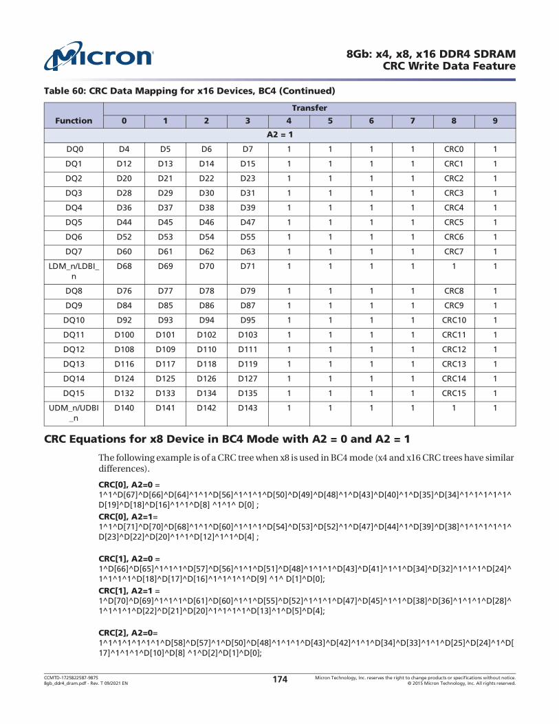
CCMTD-1725822587-9875 Micron Technology, Inc. reserves the right to change products or specifications without notice.8gb_ddr4_dram.pdf - Rev. T 09/2021 EN 2015 Micron Technology, Inc. All rights reserved.174
8Gb: x4, x8, x16 DDR4 SDRAMCRC Write Data Feature
CRC Equations for x8 Device in BC4 Mode with A2 = 0 and A2 = 1
The following example is of a CRC tree when x8 is used in BC4 mode (x4 and x16 CRC trees have similar differences).
A2 = 1
DQ0 D4 D5 D6 D7 1 1 1 1 CRC0 1
DQ1 D12 D13 D14 D15 1 1 1 1 CRC1 1
DQ2 D20 D21 D22 D23 1 1 1 1 CRC2 1
DQ3 D28 D29 D30 D31 1 1 1 1 CRC3 1
DQ4 D36 D37 D38 D39 1 1 1 1 CRC4 1
DQ5 D44 D45 D46 D47 1 1 1 1 CRC5 1
DQ6 D52 D53 D54 D55 1 1 1 1 CRC6 1
DQ7 D60 D61 D62 D63 1 1 1 1 CRC7 1
LDM_n/LDBI_n
D68 D69 D70 D71 1 1 1 1 1 1
DQ8 D76 D77 D78 D79 1 1 1 1 CRC8 1
DQ9 D84 D85 D86 D87 1 1 1 1 CRC9 1
DQ10 D92 D93 D94 D95 1 1 1 1 CRC10 1
DQ11 D100 D101 D102 D103 1 1 1 1 CRC11 1
DQ12 D108 D109 D110 D111 1 1 1 1 CRC12 1
DQ13 D116 D117 D118 D119 1 1 1 1 CRC13 1
DQ14 D124 D125 D126 D127 1 1 1 1 CRC14 1
DQ15 D132 D133 D134 D135 1 1 1 1 CRC15 1
UDM_n/UDBI_n
D140 D141 D142 D143 1 1 1 1 1 1
Table 60: CRC Data Mapping for x16 Devices, BC4 (Continued)
Function
Transfer
0 1 2 3 4 5 6 7 8 9
CRC[0], A2=0 = 1^1^D[67]^D[66]^D[64]^1^1^D[56]^1^1^1^D[50]^D[49]^D[48]^1^D[43]^D[40]^1^D[35]^D[34]^1^1^1^1^1^D[19]^D[18]^D[16]^1^1^D[8] ^1^1^ D[0] ;CRC[0], A2=1= 1^1^D[71]^D[70]^D[68]^1^1^D[60]^1^1^1^D[54]^D[53]^D[52]^1^D[47]^D[44]^1^D[39]^D[38]^1^1^1^1^1^D[23]^D[22]^D[20]^1^1^D[12]^1^1^D[4] ;
CRC[1], A2=0 = 1^D[66]^D[65]^1^1^1^D[57]^D[56]^1^1^D[51]^D[48]^1^1^1^D[43]^D[41]^1^1^D[34]^D[32]^1^1^1^D[24]^1^1^1^1^D[18]^D[17]^D[16]^1^1^1^1^D[9] ^1^ D[1]^D[0];CRC[1], A2=1 = 1^D[70]^D[69]^1^1^1^D[61]^D[60]^1^1^D[55]^D[52]^1^1^1^D[47]^D[45]^1^1^D[38]^D[36]^1^1^1^D[28]^1^1^1^1^D[22]^D[21]^D[20]^1^1^1^1^D[13]^1^D[5]^D[4];
CRC[2], A2=0= 1^1^1^1^1^1^1^D[58]^D[57]^1^D[50]^D[48]^1^1^1^D[43]^D[42]^1^1^D[34]^D[33]^1^1^D[25]^D[24]^1^D[17]^1^1^1^D[10]^D[8] ^1^D[2]^D[1]^D[0];

CCMTD-1725822587-9875 Micron Technology, Inc. reserves the right to change products or specifications without notice.8gb_ddr4_dram.pdf - Rev. T 09/2021 EN 2015 Micron Technology, Inc. All rights reserved.175
8Gb: x4, x8, x16 DDR4 SDRAMCRC Write Data Feature
CRC Error Handling
The CRC error mechanism shares the same ALERT_n signal as CA parity for reporting write errors to the DRAM. The controller has two ways to distinguish between CRC errors and CA parity errors: 1) Read DRAM mode/MPR registers, and 2) Measure time ALERT_n is LOW. To speed up recovery for CRC errors, CRC errors are only sent back as a "short" pulse; the maximum pulse width is roughly ten clocks (unlike CA parity where ALERT_n is LOW longer than 45 clocks). The ALERT_n LOW could be longer than the maximum limit at the controller if there are multiple CRC errors as the ALERT_n signals
are connected by a daisy chain bus. The latency to ALERT_n signal is defined as tCRC_ALERT in the following figure.
The DRAM will set the error status bit located at MR5[3] to a 1 upon detecting a CRC error, which will subsequently set the CRC error status flag in the MPR error log HIGH (MPR Page1, MPR3[7]). The CRC error status bit (and CRC error status flag) remains set at 1 until the DRAM controller clears the CRC error status bit using an MRS command to set MR5[3] to a 0. The DRAM controller, upon seeing an error as a pulse width, will retry the write transactions. The controller should consider the worst-case
CRC[2], A2=1= 1^1^1^1^1^1^1^D[62]^D[61]^1^D[54]^D[52]^1^1^1^D[47]^D[46]^1^1^D[38]^D[37]^1^1^D[29]^D[28]^1^D[21]^1^1^1^D[14]^D12]^1^D[6]^D[5]^D[4];
CRC[3], A2=0 = 1^1^D[64]^1^1^1^D[59]^D[58]^1^D[51]^D[49]^D[48]^1^1^1^D[43]^D[40]^1^D[35]^D[34]^1^1^D[26]^D[25]^1^D[18]^D[16]^1^1^D[11]^D[9] ^1^D[3]^D[2]^D[1];CRC[3], A2=1 = 1^1^D[68]^1^1^1^D[63]^D[62]^1^D[55]^D[53]^D[52]^1^1^1^D[47]^D[44]^1^D[39]^D[38]^1^1^D[30]^D[29]^1^D[22]^D[20]^1^1^D[15]^D[13]^1^D[7]^D[6]^D[5];
CRC[4], A2=0 = 1^1^D[65]^D[64]^1^1^1^D[59]^D[56]^1^D[50]^D[49]^D[48]^1^1^1^D[41]^1^1^D[35]^1^1^D[27]^D[26]^D[24]^D[19]^D[17]^1^1^1^D[10]^D[8] ^1^D[3]^D[2];CRC[4], A2=1 = 1^1^D[69]^D[68]^1^1^1^D[63]^D[60]^1^D[54]^D[53]^D[52]^1^1^1^D[45]^1^1^D[39]^1^1^D[31]^D[30]^D[28]^D[23]^D[21]^1^1^1^D[14]^D[12]^1^D[7]^D[6];
CRC[5], A2=0 = 1^D[66]^D[65]^D[64]^1^1^1^D[57]^1^D[51]^D[50]^D[49]^1^1^1^D[42]^D[40]^1^1^D[32]^1^1^D[27]^D[25]^1^D[18]^D[16]^1^1^D[11]^D[9] ^1^1^D[3];CRC[5], A2=1 = 1^D[70]^D[69]^D[68]^1^1^1^D[61]^1^D[55]^D[54]^D[53]^1^1^1^D[46]^D[44]^1^1^D[36]^1^1^D[31]^D[29]^1^D[22]^D[20]^1^1^D[15]^D[13]^1^1^D[7];
CRC[6], A2=0 = D[67]^D[66]^D[65]^D[64]^1^1^D[58]^1^1^D[51]^D[50]^D[48]^1^1^D[43]^D[41]^1^1^D[33]^D[32]^1^1^D[26]^1^D[19]^D[17]^D[16]^1^1^D[10]^1^1^1;CRC[6], A2=1 = D[71]^D[70]^D[69]^D[68]^1^1^D[62]^1^1^D[55]^D[54]^D[52]^1^1^D[47]^D[45]^1^1^D[37]^D[36]^1^1^D[30]^1^D[23]^D[21]^D[20]^1^1^D[14]^1^1^1;
CRC[7], A2=0= 1^D[67]^D[66]^D[65]^1^1^D[59]^1^1^1^D[51]^D[49]^D[48]^1^1^D[42]^1^1^D[34]^D[33]^1^1^D[27]^1^1^D[18]^D[17]^1^1^D[11]^1^1^1;CRC[7], A2=1 = 1^D[71]^D[70]^D[69]^1^1^D[63]^1^1^1^D[55]^D[53]^D[52]^1^1^D[46]^1^1^D[38]^D[37]^1^1^D[31]^1^1^D[22]^D[21]^1^1^D[15]^1^1^1;

CCMTD-1725822587-9875 Micron Technology, Inc. reserves the right to change products or specifications without notice.8gb_ddr4_dram.pdf - Rev. T 09/2021 EN 2015 Micron Technology, Inc. All rights reserved.176
8Gb: x4, x8, x16 DDR4 SDRAMCRC Write Data Feature
delay for ALERT_n (during initialization) and backup the transactions accordingly. The DRAM controller may also be made more intelligent and correlate the write CRC error to a specific rank or a transaction.
Figure 109: CRC Error Reporting
Notes: 1. D[71:1] CRC computed by DRAM did not match CRC[7:0] at T5 and started error generating process at T6.2. CRC ALERT_PW is specified from the point where the DRAM starts to drive the signal LOW to the point where the
DRAM driver releases and the controller starts to pull the signal up.3. Timing diagram applies to x4, x8, and x16 devices.
Dx
T0 T1 T2 T3 T4 T5 T6 Ta0 Ta1 Ta2 Ta3 Tb0
CK_tCK_c
DQIN Dx+1 Dx+2 Dx+3 Dx+4 Dx+5 Dx+6 Dx+7 CRCy 1
ALERT_n CRC ALERT_PW (MIN)
Tb1
tCRC_ALERTCRC ALERT_PW (MAX)
Don’t CareTransition Data

CCM
TD-1725822587-9875
Micro
n Techno
log
y, Inc. reserves the rig
ht to ch
ange p
rod
ucts or sp
ecifications w
itho
ut n
otice.
8gb
_ddr4_d
ram.p
df - Rev. T 09/2021 EN
2015 Micron
Techn
olog
y, Inc. A
ll rights reserved.
177
8Gb
: x4
, x8
, x16
DD
R4
SD
RA
MC
RC
Write
Da
ta Fea
ture
CRC Write Data Flow Diagram
Figure 110: CA Parity Flow Diagram
Capture data
Transfer DataInternally
Transfer datainternally
Yes
DRAM writeprocess start
MR2 12 enable CRCMR5 3 set CRC error clear to 0MR5 10 enable/disable DMMR3[10:9] WCL if DM enabled
No
No
Yes
Yes
No
ALERT_n LOW6 to 10 CKs
ALERT_n HIGH Set error statusPAGE1 MPR3[7] = 1
Set error flagMR5[A3] = 1
Transfer datainternally
Yes
No
Yes
No
CRCenabled
CA error
Persistentmode
enabled
MR5[A3] andPAGE1 MPR3[7]remain set to 1
No
Yes
DRAMCRC same as
controllerCRC
DRAMCRC same as
controllerCRC
MR5[3] = 0at WRITE
WRITE burstcompleted
WRITE burstcompleted
WRITE burstcompleted
WRITE burstcompleted
WRITE burstcompleted
Bad data writtenMR5 3 reset to 0 if desired
ALERT_n LOW6 to 10 CKs
ALERT_n HIGH Set error statusPAGE1 MPR3[7] = 1
Set error flagMR5[A3] = 1
Yes
No
MR5[A3] andPAGE1 MPR3[7]remain set to 1
MR5[3] = 0at WRITE
WRITE burstrejected
Bad data not writtenMR5 3 reset to 0 if desired

CCMTD-1725822587-9875 Micron Technology, Inc. reserves the right to change products or specifications without notice.8gb_ddr4_dram.pdf - Rev. T 09/2021 EN 2015 Micron Technology, Inc. All rights reserved.178
8Gb: x4, x8, x16 DDR4 SDRAMData Bus Inversion
Data Bus Inversion
The DATA BUS INVERSION (DBI) function is supported only for x8 and x16 configurations (it is not supported on x4 devices). DBI opportunistically inverts data bits, and in conjunction with the DBI_n I/O, less than half of the DQs will switch LOW for a given DQS strobe edge. The DBI function shares a common pin with the DATA MASK (DM) and TDQS functions. The DBI function applies to either or both READ and WRITE operations: Write DBI cannot be enabled at the same time the DM function is enabled, and DBI is not allowed during MPR READ operation. Valid configurations for TDQS, DM, and DBI functions are shown below.
DBI During a WRITE Operation
If DBI_n is sampled LOW on a given byte lane during a WRITE operation, the DRAM inverts write data received on the DQ inputs prior to writing the internal memory array. If DBI_n is sampled HIGH on a given byte lane, the DRAM leaves the data received on the DQ inputs noninverted. The write DQ frame format is shown below for x8 and x16 configurations (the x4 configuration does not support the DBI function).
Table 61: DBI vs. DM vs. TDQS Function Matrix
Read DBI Write DBI Data Mask (DM) TDQS (x8 only)
Enabled (or Disabled) MR5[12]=1 (or MR5[12] = 0)
Disabled MR5[11] = 0
Disabled MR5[10] = 0
Disabled MR1[11] = 0
Enabled MR5[11] = 1
Disabled MR5[10] = 0
Disabled MR1[11] = 0
Disabled MR5[11] = 0
Enabled MR5[10] = 1
Disabled MR1[11] = 0
Disabled MR5[12] = 0
Disabled MR5[11] = 0
Disabled MR5[10] = 0
Enabled MR1[11] = 1
Table 62: DBI Write, DQ Frame Format (x8)
Function
Transfer
0 1 2 3 4 5 6 7
DQ[7:0] Byte 0 Byte 1 Byte 2 Byte 3 Byte 4 Byte 5 Byte 6 Byte 7
DM_n or DBI_n
DM0 or DBI0
DM1 or DBI1
DM2 or DBI2
DM3 or DBI3
DM4 or DBI4
DM5 or DBI5
DM6 or DBI6
DM7 or DBI7
Table 63: DBI Write, DQ Frame Format (x16)
Function
Transfer, Lower (L) and Upper(U)
0 1 2 3 4 5 6 7
DQ[7:0] LByte 0 LByte 1 LByte 2 LByte 3 LByte 4 LByte 5 LByte 6 LByte 7
LDM_n or LDBI_n
LDM0 or LDBI0
LDM1 or LDBI1
LDM2 or LDBI2
LDM3 or LDBI3
LDM4 or LDBI4
LDM5 or LDBI5
LDM6 or LDBI6
LDM7 or LDBI7
DQ[15:8] UByte 0 UByte 1 UByte 2 UByte 3 UByte 4 UByte 5 UByte 6 UByte 7
UDM_n or UDBI_n
UDM0 or UDBI0
UDM1 or UDBI1
UDM2 or UDBI2
UDM3 or UDBI3
UDM4 or UDBI4
UDM5 or UDBI5
UDM6 or UDBI6
UDM7 or UDBI7

CCMTD-1725822587-9875 Micron Technology, Inc. reserves the right to change products or specifications without notice.8gb_ddr4_dram.pdf - Rev. T 09/2021 EN 2015 Micron Technology, Inc. All rights reserved.179
8Gb: x4, x8, x16 DDR4 SDRAMData Bus Inversion
DBI During a READ Operation
If the number of 0 data bits within a given byte lane is greater than four during a READ operation, the DRAM inverts read data on its DQ outputs and drives the DBI_n pin LOW; otherwise, the DRAM does not invert the read data and drives the DBI_n pin HIGH. The read DQ frame format is shown below for x8 and x16 configurations (the x4 configuration does not support the DBI function).
Table 64: DBI Read, DQ Frame Format (x8)
Function
Transfer Byte
0 1 2 3 4 5 6 7
DQ[7:0] Byte 0 Byte 1 Byte 2 Byte 3 Byte 4 Byte 5 Byte 6 Byte 7
DBI_n DBI0 DBI1 DBI2 DBI3 DBI4 DBI5 DBI6 DBI7
Table 65: DBI Read, DQ Frame Format (x16)
Function
Transfer Byte, Lower (L) and Upper(U)
0 1 2 3 4 5 6 7
DQ[7:0] LByte 0 LByte 1 LByte 2 LByte 3 LByte 4 LByte 5 LByte 6 LByte 7
LDBI_n LDBI0 LDBI1 LDBI2 LDBI3 LDBI4 LDBI5 LDBI6 LDBI7
DQ[15:8] UByte 0 UByte 1 UByte 2 UByte 3 UByte 4 UByte 5 UByte 6 UByte 7
UDBI_n UDBI0 UDBI1 UDBI2 UDBI3 UDBI4 UDBI5 UDBI6 UDBI7

CCMTD-1725822587-9875 Micron Technology, Inc. reserves the right to change products or specifications without notice.8gb_ddr4_dram.pdf - Rev. T 09/2021 EN 2015 Micron Technology, Inc. All rights reserved.180
8Gb: x4, x8, x16 DDR4 SDRAMData Mask
Data Mask
The DATA MASK (DM) function, also described as PARTIAL WRITE, is supported only for x8 and x16 configurations (it is not supported on x4 devices). The DM function shares a common pin with the DBI_n and TDQS functions. The DM function applies only to WRITE operations and cannot be enabled at the same time the WRITE DBI function is enabled. The valid configurations for the TDQS, DM, and DBI functions are shown here.
When enabled, the DM function applies during a WRITE operation. If DM_n is sampled LOW on a given byte lane, the DRAM masks the write data received on the DQ inputs. If DM_n is sampled HIGH on a given byte lane, the DRAM does not mask the data and writes this data into the DRAM core. The DQ frame format for x8 and x16 configurations is shown below. If both CRC write and DM are enabled (via MRS), the CRC will be checked and valid prior to the DRAM writing data into the DRAM core. If a CRC error occurs while the DM feature is enabled, CRC write persistent mode will be enabled and data will not be written into the DRAM core. In the case of CRC write enabled and DM disabled (via MRS), that is, CRC write nonpersistent mode, data is written to the DRAM core even if a CRC error occurs.
Table 66: DM vs. TDQS vs. DBI Function Matrix
Data Mask (DM) TDQS (x8 only) Write DBI Read DBI
Enabled MR5[10] = 1
Disabled MR1[11] = 0
Disabled MR5[11] = 0
Enabled or Disabled MR5[12] = 1 or MR5[12] = 0
Disabled MR5[10] = 0
Enabled MR1[11] = 1
Disabled MR5[11] = 0
Disabled MR5[12] = 0
Disabled MR1[11] = 0
Enabled MR5[11] = 1
Enabled or Disabled MR5[12] = 1 or MR5[12] = 0
Disabled MR1[11] = 0
Disabled MR5[11] = 0
Enabled (or Disabled) MR5[12] = 1 (or MR5[12] = 0)
Table 67: Data Mask, DQ Frame Format (x8)
Function
Transfer
0 1 2 3 4 5 6 7
DQ[7:0] Byte 0 Byte 1 Byte 2 Byte 3 Byte 4 Byte 5 Byte 6 Byte 7
DM_n or DBI_n
DM0 or DBI0
DM1 or DBI1
DM2 or DBI2
DM3 or DBI3
DM4 or DBI4
DM5 or DBI5
DM6 or DBI6
DM7 or DBI7
Table 68: Data Mask, DQ Frame Format (x16)
Function
Transfer, Lower (L) and Upper (U)
0 1 2 3 4 5 6 7
DQ[7:0] LByte 0 LByte 1 LByte 2 LByte 3 LByte 4 LByte 5 LByte 6 LByte 7
LDM_n or LDBI_n
LDM0 or LDBI0
LDM1 or LDBI1
LDM2 or LDBI2
LDM3 or LDBI3
LDM4 or LDBI4
LDM5 or LDBI5
LDM6 or LDBI6
LDM7 or LDBI7
DQ[15:8] UByte 0 UByte 1 UByte 2 UByte 3 UByte 4 UByte 5 UByte 6 UByte 7
UDM_n or UDBI_n
UDM0 or UDBI0
UDM1 or UDBI1
UDM2 or UDBI2
UDM3 or UDBI3
UDM4 or UDBI4
UDM5 or UDBI5
UDM6 or UDBI6
UDM7 or UDBI7

CCMTD-1725822587-9875 Micron Technology, Inc. reserves the right to change products or specifications without notice.8gb_ddr4_dram.pdf - Rev. T 09/2021 EN 2015 Micron Technology, Inc. All rights reserved.181
8Gb: x4, x8, x16 DDR4 SDRAMProgrammable Preamble Modes and DQS Postambles
Programmable Preamble Modes and DQS Postambles
The device supports programmable WRITE and READ preamble modes, either the normal 1tCK
preamble mode or special 2tCK preamble mode. The 2tCK preamble mode places special timing constraints on many operational features as well as being supported for data rates of DDR4-2400 and
faster. The WRITE preamble 1tCK or 2tCK mode can be selected independently from READ preamble
1tCK or 2tCK mode.
READ preamble training is also supported; this mode can be used by the DRAM controller to train or "read level" the DQS receivers.
There are tCCD restrictions under some circumstances:
When 2tCK READ preamble mode is enabled, a tCCD_S or tCCD_L of 5 clocks is not allowed.
When 2tCK WRITE preamble mode is enabled and write CRC is not enabled, a tCCD_S or tCCD_L of 5 clocks is not allowed.
When 2tCK WRITE preamble mode is enabled and write CRC is enabled, a tCCD_S or tCCD_L of 6 clocks is not allowed.
WRITE Preamble Mode
MR4[12] = 0 selects 1tCK WRITE preamble mode while MR4[12] = 1 selects 2tCK WRITE preamble mode. Examples are shown in the figures below.
Figure 111: 1tCK vs. 2tCK WRITE Preamble Mode
DQ
CK_c
CK_t
Preamble
2tCK Mode
D0 D1 D2 D3 D4 D5 D6 D7
WL
WR
DQ
DQS_t,DQS_c
DQS_t,DQS_c
CK_c
CK_t
Preamble
1tCK Mode
D0 D1 D2 D3 D4 D5 D6 D7
WRWL
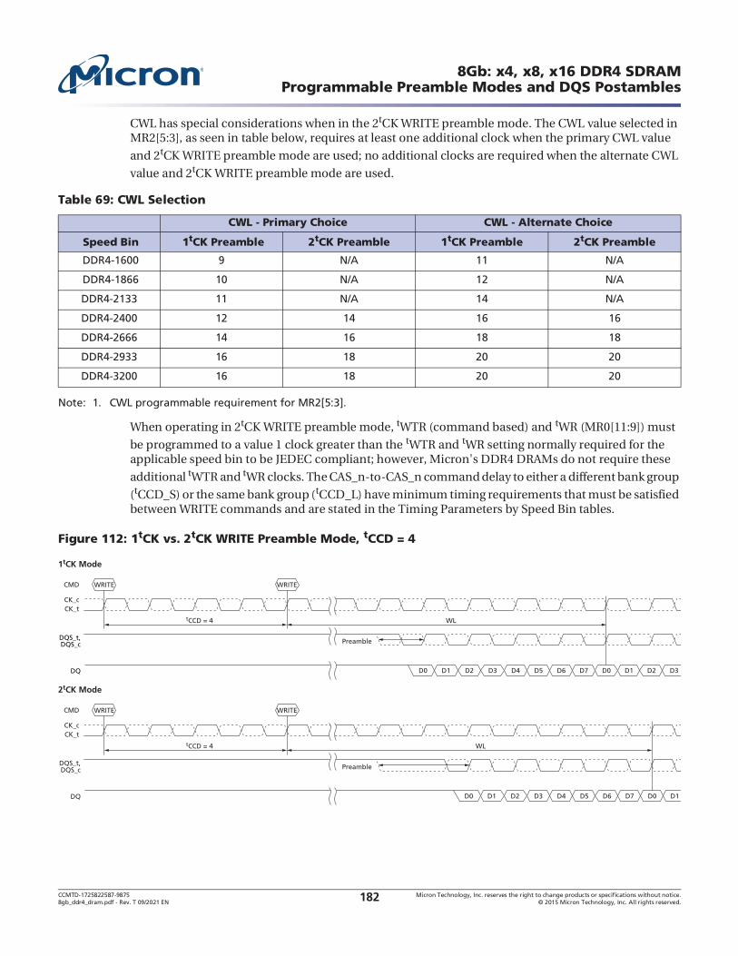
CCMTD-1725822587-9875 Micron Technology, Inc. reserves the right to change products or specifications without notice.8gb_ddr4_dram.pdf - Rev. T 09/2021 EN 2015 Micron Technology, Inc. All rights reserved.182
8Gb: x4, x8, x16 DDR4 SDRAMProgrammable Preamble Modes and DQS Postambles
CWL has special considerations when in the 2tCK WRITE preamble mode. The CWL value selected in MR2[5:3], as seen in table below, requires at least one additional clock when the primary CWL value
and 2tCK WRITE preamble mode are used; no additional clocks are required when the alternate CWL
value and 2tCK WRITE preamble mode are used.
Note: 1. CWL programmable requirement for MR2[5:3].
When operating in 2tCK WRITE preamble mode, tWTR (command based) and tWR (MR0[11:9]) must
be programmed to a value 1 clock greater than the tWTR and tWR setting normally required for the applicable speed bin to be JEDEC compliant; however, Micron's DDR4 DRAMs do not require these
additional tWTR and tWR clocks. The CAS_n-to-CAS_n command delay to either a different bank group
(tCCD_S) or the same bank group (tCCD_L) have minimum timing requirements that must be satisfied between WRITE commands and are stated in the Timing Parameters by Speed Bin tables.
Figure 112: 1tCK vs. 2tCK WRITE Preamble Mode, tCCD = 4
Table 69: CWL Selection
CWL - Primary Choice CWL - Alternate Choice
Speed Bin 1tCK Preamble 2tCK Preamble 1tCK Preamble 2tCK Preamble
DDR4-1600 9 N/A 11 N/A
DDR4-1866 10 N/A 12 N/A
DDR4-2133 11 N/A 14 N/A
DDR4-2400 12 14 16 16
DDR4-2666 14 16 18 18
DDR4-2933 16 18 20 20
DDR4-3200 16 18 20 20
DQ
DQS_t,DQS_c
tCCD = 4 WL
Preamble
1tCK Mode
D0 D1
WRITE WRITE
D2 D3 D4 D5 D6 D7 D0 D1 D2 D3
CK_tCK_c
CMD
DQ
DQS_t,DQS_c
tCCD = 4 WL
Preamble
2tCK Mode
D0 D1
WRITE WRITE
D2 D3 D4 D5 D6 D7 D0 D1
CK_tCK_c
CMD

CCMTD-1725822587-9875 Micron Technology, Inc. reserves the right to change products or specifications without notice.8gb_ddr4_dram.pdf - Rev. T 09/2021 EN 2015 Micron Technology, Inc. All rights reserved.183
8Gb: x4, x8, x16 DDR4 SDRAMProgrammable Preamble Modes and DQS Postambles
Figure 113: 1tCK vs. 2tCK WRITE Preamble Mode, tCCD = 5
Note: 1. tCCD_S and tCCD_L = 5 tCKs is not allowed when in 2tCK WRITE preamble mode.
Figure 114: 1tCK vs. 2tCK WRITE Preamble Mode, tCCD = 6
DQ
DQS_t,DQS_c
tCCD = 5 WL
PreamblePreamble
1tCK Mode
D0 D1
WRITEWRITE
D2 D3 D4 D5 D6 D7 D0 D1 D2 D3
CK_tCK_c
CMD
2tCK Mode: tCCD = 5 is not allowed in 2tCK mode.
DQ
tCCD = 6
DQS_t,DQS_c
WL
PreamblePreamble
1tCK Mode
D0 D1
WRITEWRITE
D2 D3 D4 D5 D6 D7 D0 D1 D2 D3
CK_tCK_c
CMD
2tCK Mode
DQ
tCCD = 6
DQS_t,DQS_c
WL
PreamblePreamble
D0 D1
WRITEWRITE
D2 D3 D4 D5 D6 D7 D0 D1 D2 D3
CK_tCK_c
CMD

CCMTD-1725822587-9875 Micron Technology, Inc. reserves the right to change products or specifications without notice.8gb_ddr4_dram.pdf - Rev. T 09/2021 EN 2015 Micron Technology, Inc. All rights reserved.184
8Gb: x4, x8, x16 DDR4 SDRAMProgrammable Preamble Modes and DQS Postambles
READ Preamble Mode
MR4[11] = 0 selects 1tCK READ preamble mode and MR4[11] = 1 selects 2tCK READ preamble mode. Examples are shown in the following figure.
Figure 115: 1tCK vs. 2tCK READ Preamble Mode
READ Preamble Training
DDR4 supports READ preamble training via MPR reads; that is, READ preamble training is allowed only when the DRAM is in the MPR access mode. The READ preamble training mode can be used by the DRAM controller to train or "read level" its DQS receivers. READ preamble training is entered via an MRS command (MR4[10] = 1 is enabled and MR4[10] = 0 is disabled). After the MRS command is issued to enable READ preamble training, the DRAM DQS signals are driven to a valid level by the time tSDO is satisfied. During this time, the data bus DQ signals are held quiet, that is, driven HIGH. The DQS_t signal remains driven LOW and the DQS_c signal remains driven HIGH until an MPR Page0 READ command is issued (MPR0 through MPR3 determine which pattern is used), and when CAS latency (CL) has expired, the DQS signals will toggle normally depending on the burst length setting. To exit READ preamble training mode, an MRS command must be issued, MR4[10] = 0.
DQ
DQS_t,DQS_c
DQS_t,DQS_c
CK_c
CK_t
Preamble
2tCK Mode
D0 D1 D2 D3 D4 D5 D6 D7
CL
RD
DQ
CK_c
CK_t
Preamble
1tCK Mode
D0 D1 D2 D3 D4 D5 D6 D7
RDCL
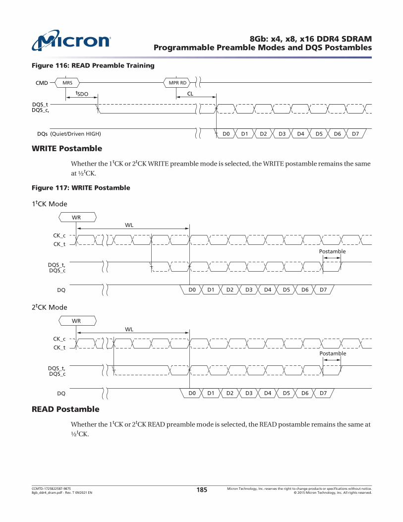
CCMTD-1725822587-9875 Micron Technology, Inc. reserves the right to change products or specifications without notice.8gb_ddr4_dram.pdf - Rev. T 09/2021 EN 2015 Micron Technology, Inc. All rights reserved.185
8Gb: x4, x8, x16 DDR4 SDRAMProgrammable Preamble Modes and DQS Postambles
Figure 116: READ Preamble Training
WRITE Postamble
Whether the 1tCK or 2tCK WRITE preamble mode is selected, the WRITE postamble remains the same tCK.
Figure 117: WRITE Postamble
READ Postamble
Whether the 1tCK or 2tCK READ preamble mode is selected, the READ postamble remains the same at tCK.
CMD
DQs
CL
DQS_tDQS_c,
tSDO
MPR RD
(Quiet/Driven HIGH)
MRS
D0 D1 D2 D3 D4 D5 D6 D7
DQ
DQS_t,DQS_c
DQS_t,DQS_c
CK_c
CK_t
2tCK Mode
D0 D1 D2 D3 D4 D5 D6 D7
WL
WR
DQ
CK_c
CK_tPostamble
1tCK Mode
D0 D1 D2 D3 D4 D5 D6 D7
WRWL
Postamble

CCMTD-1725822587-9875 Micron Technology, Inc. reserves the right to change products or specifications without notice.8gb_ddr4_dram.pdf - Rev. T 09/2021 EN 2015 Micron Technology, Inc. All rights reserved.186
8Gb: x4, x8, x16 DDR4 SDRAMProgrammable Preamble Modes and DQS Postambles
Figure 118: READ Postamble
DQ
CK_c
CK_t
2tCK Mode
D0 D1 D2 D3 D4 D5 D6 D7
CL
RD
DQ
DQS_t,DQS_c
DQS_t,DQS_c
CK_c
CK_t
1tCK Mode
D0 D1 D2 D3 D4 D5 D6 D7
RDCL
Postamble
Postamble

CCMTD-1725822587-9875 Micron Technology, Inc. reserves the right to change products or specifications without notice.8gb_ddr4_dram.pdf - Rev. T 09/2021 EN 2015 Micron Technology, Inc. All rights reserved.187
8Gb: x4, x8, x16 DDR4 SDRAMBank Access Operation
Bank Access Operation
DDR4 supports bank grouping: x4/x8 DRAMs have four bank groups (BG[1:0]), and each bank group is comprised of four subbanks (BA[1:0]); x16 DRAMs have two bank groups (BG[0]), and each bank group is comprised of four subbanks. Bank accesses to different banks' groups require less time delay between accesses than bank accesses to within the same bank's group. Bank accesses to different bank
groups require tCCD_S (or short) delay between commands while bank accesses within the same bank
group require tCCD_L (or long) delay between commands.
Figure 119: Bank Group x4/x8 Block Diagram
Notes: 1. Bank accesses to different bank groups require tCCD_S.
2. Bank accesses within the same bank group require tCCD_L.
Splitting the banks into bank groups with subbanks improved some bank access timings and increased others. However, considering DDR4 did not increase the prefetch from 8n to 16n, the penalty for staying 8n prefetch was significantly mitigated by using bank groups. The table below summarizes the timings affected (values listed as xnCK or yns means the larger of the two values).
Table 70: DDR4 Bank Group Timing Examples
Parameter DDR4-1600 DDR4-2133 DDR4-2400
tCCD_S 4nCK 4nCK 4nCK
tCCD_L 4nCK or 6.25ns 4nCK or 5.355ns 4nCK or 5ns
t 4nCK or 5ns 4nCK or 3.7ns 4nCK or 3.3ns
t 4nCK or 6ns 4nCK or 5.3ns 4nCK or 4.9ns
tRRD_S (1K) 4nCK or 5ns 4nCK or 3.7ns 4nCK or 3.3ns
tRRD_L (1K) 4nCK or 6ns 4nCK or 5.3ns 4nCK or 4.9ns
Local I/O gating
Global I/O gating
Bank 0Memory Array
Sense amplifiers
Bank 1Bank 2
Bank 3
Local I/O gating
Bank 0Memory Array
Sense amplifiers
Bank 1Bank 2
Bank 3
Local I/O gating
Bank 0Memory Array
Sense amplifiers
Bank 1Bank 2
Bank 3
Local I/O gating
Bank 0Memory Array
Sense amplifiers
Bank 1Bank 2
Bank 3
CMD/ADDRregister
CMD/ADDR
Data I/O
Bank Group 0 Bank Group 1 Bank Group 2 Bank Group 3

CCMTD-1725822587-9875 Micron Technology, Inc. reserves the right to change products or specifications without notice.8gb_ddr4_dram.pdf - Rev. T 09/2021 EN 2015 Micron Technology, Inc. All rights reserved.188
8Gb: x4, x8, x16 DDR4 SDRAMBank Access Operation
Notes: 1. Refer to Timing Tables for actual specification values, these values are shown for reference only and are not veri-fied for accuracy.
2. Timings with both nCK and ns require both to be satisfied; that is, the larger time of the two cases must be satis-fied.
Figure 120: READ Burst tCCD_S and tCCD_L Examples
Notes: 1. tCCD_S; CAS_n-to-CAS_n delay (short). Applies to consecutive CAS_n to different bank groups (T0 to T4).
2. tCCD_L; CAS_n-to-CAS_n delay (long). Applies to consecutive CAS_n to the same bank group (T4 to T10).
Figure 121: Write Burst tCCD_S and tCCD_L Examples
Notes: 1. tCCD_S; CAS_n-to-CAS_n delay (short). Applies to consecutive CAS_n to different bank groups (T0 to T4).
2. tCCD_L; CAS_n-to-CAS_n delay (long). Applies to consecutive CAS_n to the same bank group (T4 to T10).
tRRD_S (2K) 4nCK or 6ns 4nCK or 5.3ns 4nCK or 5.3ns
tRRD_L (2K) 4nCK or 7.5ns 4nCK or 6.4ns 4nCK or 6.4ns
tWTR_S 2nCK or 2.5ns 2nCK or 2.5ns 2nCK or 2.5ns
tWTR_L 4nCK or 7.5ns 4nCK or 7.5ns 4nCK or 7.5ns
Table 70: DDR4 Bank Group Timing Examples (Continued)
Parameter DDR4-1600 DDR4-2133 DDR4-2400
T0 T1 T2 T3 T4 T5 T6 T7 T8 T9
tCCD_S
T10 T11
Don’t Care
BG a
DESREAD READDES DES DES DES DES DES DES DES
CK_tCK_c
Command
Bank Group(BG)
Bank cBank
Col n
BG b
Bank c
Col n
BG b
Bank c
Col nAddress
tCCD_L
READ
T0 T1 T2 T3 T4 T5 T6 T7 T8 T9
tCCD_S
T10 T11
Don’t Care
BG a
DESWRITE WRITEDES DES DES DES DES DES DES DES
CK_tCK_c
Command
Bank Group(BG)
Bank cBank
Col n
BG b
Bank c
Col n
BG b
Bank c
Col nAddress
tCCD_L
WRITE

CCMTD-1725822587-9875 Micron Technology, Inc. reserves the right to change products or specifications without notice.8gb_ddr4_dram.pdf - Rev. T 09/2021 EN 2015 Micron Technology, Inc. All rights reserved.189
8Gb: x4, x8, x16 DDR4 SDRAMBank Access Operation
Figure 122: tRRD Timing
Notes: 1. tRRD_S; ACTIVATE-to-ACTIVATE command period (short); applies to consecutive ACTIVATE commands to different bank groups (T0 and T4).
2. tRRD_L; ACTIVATE-to-ACTIVATE command period (long); applies to consecutive ACTIVATE commands to the different banks in the same bank group (T4 and T10).
T0 T1 T2 T3 T4 T5 T6 T7 T8 T9
tRRD_S
T10 T11
Don’t Care
BG a
DESACT ACTDES DES DES DES DES DES DES DES
CK_tCK_c
Command
BankGroup
(BG)
Bank cBank
Row n
BG b
Bank c
Row n
BG b
Bank d
Row nAddress
tRRD_L
ACT
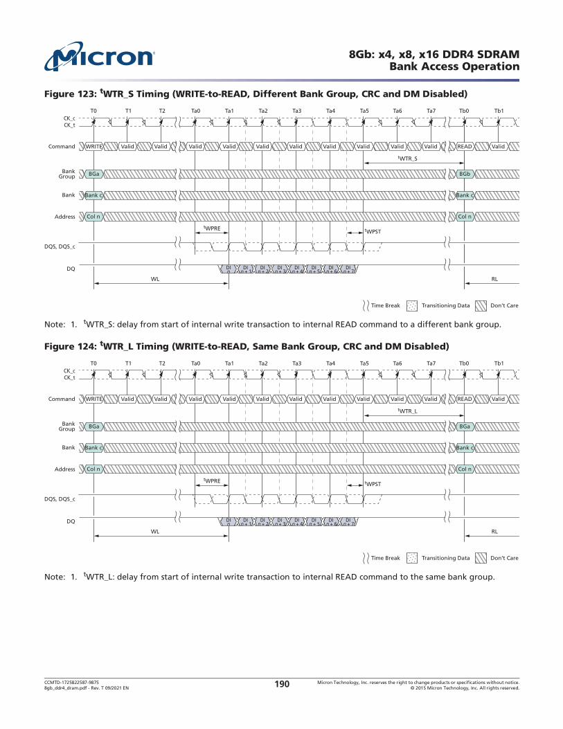
CCMTD-1725822587-9875 Micron Technology, Inc. reserves the right to change products or specifications without notice.8gb_ddr4_dram.pdf - Rev. T 09/2021 EN 2015 Micron Technology, Inc. All rights reserved.190
8Gb: x4, x8, x16 DDR4 SDRAMBank Access Operation
Figure 123: tWTR_S Timing (WRITE-to-READ, Different Bank Group, CRC and DM Disabled)
Note: 1. tWTR_S: delay from start of internal write transaction to internal READ command to a different bank group.
Figure 124: tWTR_L Timing (WRITE-to-READ, Same Bank Group, CRC and DM Disabled)
Note: 1. tWTR_L: delay from start of internal write transaction to internal READ command to the same bank group.
T0 Tb0T1 T2 Ta0 Ta1 Ta2 Ta3 Ta4 Ta5 Ta6 Ta7
Valid Valid Valid Valid Valid READ ValidCommand ValidWRITE Valid Valid Valid Valid
BGbBankGroup BGa
Bank cBank
Col n
Bank c
Col nAddress
CK_tCK_c
Tb1
Don’t CareTransitioning DataTime Break
DQ
WL
tWPRE tWPST
RL
tWTR_S
DIn + 3
DIn + 4
DIn + 5
DIn + 6
DIn + 7
DIn + 2
DIn + 1
DIn
DQS, DQS_c
T0 Tb0T1 T2 Ta0 Ta1 Ta2 Ta3 Ta4 Ta5 Ta6 Ta7
Valid Valid Valid Valid Valid READ ValidCommand ValidWRITE Valid Valid Valid Valid
BGaBankGroup BGa
Bank cBank
Col n
Bank c
Col nAddress
CK_tCK_c
Tb1
Don’t CareTransitioning DataTime Break
DQ
WL
tWPRE tWPST
RL
tWTR_L
DIn + 3
DIn + 4
DIn + 5
DIn + 6
DIn + 7
DIn + 2
DIn + 1
DIn
DQS, DQS_c

CCMTD-1725822587-9875 Micron Technology, Inc. reserves the right to change products or specifications without notice.8gb_ddr4_dram.pdf - Rev. T 09/2021 EN 2015 Micron Technology, Inc. All rights reserved.191
8Gb: x4, x8, x16 DDR4 SDRAMREAD Operation
READ Operation
Read Timing Definitions
The read timings shown below are applicable in normal operation mode, that is, when the DLL is enabled and locked.
Note:tDQSQ = both rising/falling edges of DQS; no tAC defined.
Rising data strobe edge parameters:tDQSCK (MIN)/(MAX) describes the allowed range for a rising data strobe edge relative to CK.tDQSCK is the actual position of a rising strobe edge relative to CK.tQSH describes the DQS differential output HIGH time.tDQSQ describes the latest valid transition of the associated DQ pins.tQH describes the earliest invalid transition of the associated DQ pins.
Falling data strobe edge parameters:tQSL describes the DQS differential output LOW time.tDQSQ describes the latest valid transition of the associated DQ pins.tQH describes the earliest invalid transition of the associated DQ pins.

CCMTD-1725822587-9875 Micron Technology, Inc. reserves the right to change products or specifications without notice.8gb_ddr4_dram.pdf - Rev. T 09/2021 EN 2015 Micron Technology, Inc. All rights reserved.192
8Gb: x4, x8, x16 DDR4 SDRAMREAD Operation
Figure 125: Read Timing Definition
Notes: 1. These timings require extended calibrations times tZQinit and tZQCS.2. RBL: READ burst length associated with READ command, RBL = 8 for fixed 8 and on-the-fly mode 8 and RBL = 4 for
fixed BC4 and on-the-fly mode BC4.3. WBL: WRITE burst length associated with WRITE command, WBL = 8 for fixed 8 and on-the-fly mode 8 or BC4 and
WBL = 4 for fixed BC4 only.
The clock-to-data strobe relationship shown below is applicable in normal operation mode, that is, when the DLL is enabled and locked.
Rising data strobe edge parameters:
Table 71: Read-to-Write and Write-to-Read Command Intervals
Access Type Bank Group Timing Parameters Note
Read-to-Write, mini-mum
Same CL - CWL + RBL/2 + 1tCK + tWPRE 1, 2
Different CL - CWL + RBL/2 + 1tCK + tWPRE 1, 2
Write-to-Read, mini-mum
Same CWL + WBL/2 + tWTR_L 1, 3
Different CWL + WBL/2 + tWTR_S 1, 3
CK_t
CK_c
DQS_c
DQS_t
tDQSCK tDQSCK
tDQSQtDQSQ
Rising stroberegion
window
Rising stroberegion
window
tQSH/DQS_c tQSH/DQS_t
tQH tQH
tDQSCK (MAX)tDQSCK (MIN) tDQSCK (MAX)tDQSCK (MIN)
AssociatedDQ Pins
tDQSCKi
tDQSCK MIN
tDQSCKi
Rising stroberegion
window
Rising stroberegion
window
tDQSCKi
tDQSCK center
tDQSCKi
Rising stroberegion
window
Rising stroberegion
window
tDQSCKi
tDQSCK MAX
tDQSCKi
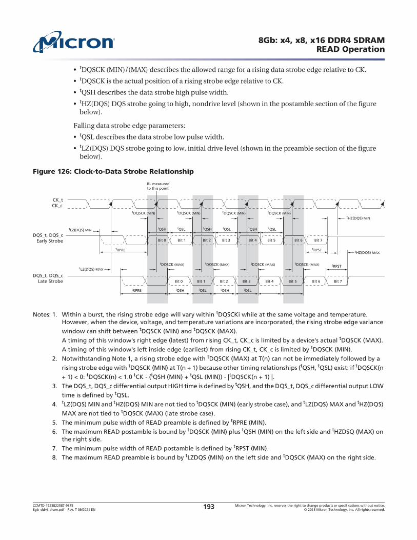
CCMTD-1725822587-9875 Micron Technology, Inc. reserves the right to change products or specifications without notice.8gb_ddr4_dram.pdf - Rev. T 09/2021 EN 2015 Micron Technology, Inc. All rights reserved.193
8Gb: x4, x8, x16 DDR4 SDRAMREAD Operation
tDQSCK (MIN)/(MAX) describes the allowed range for a rising data strobe edge relative to CK.tDQSCK is the actual position of a rising strobe edge relative to CK.tQSH describes the data strobe high pulse width.tHZ(DQS) DQS strobe going to high, nondrive level (shown in the postamble section of the figure below).
Falling data strobe edge parameters:tQSL describes the data strobe low pulse width.tLZ(DQS) DQS strobe going to low, initial drive level (shown in the preamble section of the figure below).
Figure 126: Clock-to-Data Strobe Relationship
Notes: 1. Within a burst, the rising strobe edge will vary within tDQSCKi while at the same voltage and temperature. However, when the device, voltage, and temperature variations are incorporated, the rising strobe edge variance
window can shift between tDQSCK (MIN) and tDQSCK (MAX).
A timing of this window's right edge (latest) from rising CK_t, CK_c is limited by a device's actual tDQSCK (MAX).
A timing of this window's left inside edge (earliest) from rising CK_t, CK_c is limited by tDQSCK (MIN).
2. Notwithstanding Note 1, a rising strobe edge with tDQSCK (MAX) at T(n) can not be immediately followed by a
rising strobe edge with tDQSCK (MIN) at T(n + 1) because other timing relationships (tQSH, tQSL) exist: if tDQSCK(n
+ 1) < 0: tDQSCK(n) < 1.0 tCK - (tQSH (MIN) + tQSL (MIN)) - |tDQSCK(n + 1) |.
3. The DQS_t, DQS_c differential output HIGH time is defined by tQSH, and the DQS_t, DQS_c differential output LOW
time is defined by tQSL.
4. tLZ(DQS) MIN and tHZ(DQS) MIN are not tied to tDQSCK (MIN) (early strobe case), and tLZ(DQS) MAX and tHZ(DQS)
MAX are not tied to tDQSCK (MAX) (late strobe case).
5. The minimum pulse width of READ preamble is defined by tRPRE (MIN).
6. The maximum READ postamble is bound by tDQSCK (MIN) plus tQSH (MIN) on the left side and tHZDSQ (MAX) on the right side.
7. The minimum pulse width of READ postamble is defined by tRPST (MIN).
8. The maximum READ preamble is bound by tLZDQS (MIN) on the left side and tDQSCK (MAX) on the right side.
RL measuredto this point
DQS_t, DQS_cEarly Strobe
CK_tCK_c
tLZ(DQS) MIN
tLZ(DQS) MAX
DQS_t, DQS_cLate Strobe
tDQSCK (MIN)
tDQSCK (MAX) tDQSCK (MAX) tDQSCK (MAX) tDQSCK (MAX)
tDQSCK (MIN) tDQSCK (MIN) tDQSCK (MIN)tHZ(DQS) MIN
tHZ(DQS) MAXtRPRE
tRPRE
tQSH tQSL
tQSH tQSL tQSH tQSL
tQSH tQSL tQSH tQSL
Bit 0 Bit 1 Bit 2 Bit 7Bit 6Bit 4Bit 3 Bit 5
Bit 0 Bit 1 Bit 2 Bit 7Bit 6Bit 4Bit 3 Bit 5
tRPST
tRPST
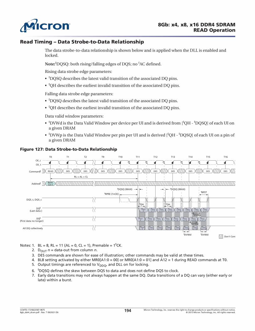
CCMTD-1725822587-9875 Micron Technology, Inc. reserves the right to change products or specifications without notice.8gb_ddr4_dram.pdf - Rev. T 09/2021 EN 2015 Micron Technology, Inc. All rights reserved.194
8Gb: x4, x8, x16 DDR4 SDRAMREAD Operation
The data strobe-to-data relationship is shown below and is applied when the DLL is enabled and locked.
Note:tDQSQ: both rising/falling edges of DQS; no tAC defined.
Rising data strobe edge parameters:tDQSQ describes the latest valid transition of the associated DQ pins.tQH describes the earliest invalid transition of the associated DQ pins.
Falling data strobe edge parameters:tDQSQ describes the latest valid transition of the associated DQ pins.tQH describes the earliest invalid transition of the associated DQ pins.
Data valid window parameters:tDVWd is the Data Valid Window per device per UI and is derived from [tQH - tDQSQ] of each UI on a given DRAMtDVWp is the Data Valid Window per pin per UI and is derived [tQH - tDQSQ] of each UI on a pin of a given DRAM
Figure 127: Data Strobe-to-Data Relationship
Notes: 1. BL = 8, RL = 11 (AL = 0, CL = 1), Premable = 1tCK.2. DOUT n = data-out from column n.3. DES commands are shown for ease of illustration; other commands may be valid at these times.4. BL8 setting activated by either MR0[A1:0 = 00] or MR0[A1:0 = 01] and A12 = 1 during READ commands at T0.5. Output timings are referenced to VDDQ, and DLL on for locking.
6. tDQSQ defines the skew between DQS to data and does not define DQS to clock.7. Early data transitions may not always happen at the same DQ. Data transitions of a DQ can vary (either early or
late) within a burst.
CK_t
CK_c
Command3 READ
Bank,Col n
DES DES DES DES DES DES DES DES DES DES
Address4
DQS_t, DQS_c
DQ2
(Last data )
DQ2
(First data no longer)
All DQ collectively
RL = AL + CL
tDQSQ (MAX)
tRPRE (1nCK)tRPST
tQH tQH
tDVWp
tDVWp
tDVWd tDVWd
T0 T1 T2 T9 T10 T11 T12 T13
Don’t Care
T14 T15 T16
DOUTn + 2
DOUTn + 1
DOUTn + 4
DOUTn + 5
DOUTn + 6
DOUTn + 7
DOUTn + 2
DOUTn + 1
DOUTn + 3
DOUTn + 4
DOUTn + 5
DOUTn + 6
DOUTn + 7
tDQSQ (MAX)
DOUTn
DOUTn + 2
DOUTn + 1
DOUTn + 3
DOUTn + 4
DOUTn + 5
DOUTn + 6
DOUTn + 7
DOUTn
DOUTn + 3
DOUTn

CCMTD-1725822587-9875 Micron Technology, Inc. reserves the right to change products or specifications without notice.8gb_ddr4_dram.pdf - Rev. T 09/2021 EN 2015 Micron Technology, Inc. All rights reserved.195
8Gb: x4, x8, x16 DDR4 SDRAMREAD Operation
tLZ(DQS), tLZ(DQ), tHZ(DQS), and tHZ(DQ) Calculations
tHZ and tLZ transitions occur in the same time window as valid data transitions. These parameters are referenced to a specific voltage level that specifies when the device output is no longer driving tHZ(DQS) and tHZ(DQ), or begins driving tLZ(DQS) and tLZ(DQ). The figure below shows a method to
calculate the point when the device is no longer driving tHZ(DQS) and tHZ(DQ), or begins driving tLZ(DQS) and tLZ(DQ), by measuring the signal at two different voltages. The actual voltage measure-
ment points are not critical as long as the calculation is consistent. tLZ(DQS), tLZ(DQ), tHZ(DQS), and tHZ(DQ) are defined as singled-ended parameters.
Figure 128: tLZ and tHZ Method for Calculating Transitions and Endpoints
Notes: 1. Vsw1 = (0.70 - 0.04) VDDQ for both tLZ and tHZ.
2. Vsw2 = (0.70 + 0.04) VDDQ for both tLZ and tHZ.3. Extrapolated point (low level) = VDDQ/(50 + 34) 34 = 0.4 VDDQ
Driver impedance = RZQ/7 = 34VTT test load = 50 to VDDQ.
CK_t
CK_ctLZ tHZ
DQ
0.7 × VDDQ
0.4 × VDDQ
DQ
Begin point: Extrapolated point at VDDQ
VDDQ
VSW2
Begin point: Extrapolated point (low level)
VDDQ
tLZ(DQ): CK_t, CK_c rising crossing at RL tHZ(DQ) with BL8: CK_t, CK_c rising crossing at RL + 4CKtHZ(DQ) with BC4: CK_t, CK_c rising crossing at RL + 2CK
VSW1
VSW2
VSW1
0.7 × VDDQ
0.4 × VDDQ
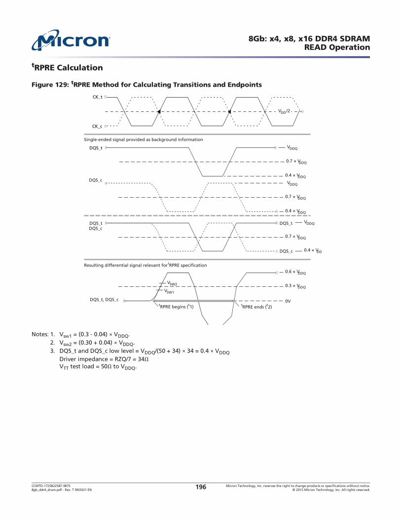
CCMTD-1725822587-9875 Micron Technology, Inc. reserves the right to change products or specifications without notice.8gb_ddr4_dram.pdf - Rev. T 09/2021 EN 2015 Micron Technology, Inc. All rights reserved.196
8Gb: x4, x8, x16 DDR4 SDRAMREAD Operation
tRPRE Calculation
Figure 129: tRPRE Method for Calculating Transitions and Endpoints
Notes: 1. Vsw1 = (0.3 - 0.04) VDDQ.2. Vsw2 = (0.30 + 0.04) VDDQ.3. DQS_t and DQS_c low level = VDDQ/(50 + 34) 34 = 0.4 VDDQ
Driver impedance = RZQ/7 = 34VTT test load = 50 to VDDQ.
DQS_t
CK_t
CK_c
Resulting differential signal relevant for tRPRE specification
Single-ended signal provided as background information
0V
DQS_c
DQS_t, DQS_c
DQS_tDQS_c
DQS_t
DQS_c
VSW1
VSW2
0.7 × VDDQ
0.7 × VDDQ
0.4 × VDDQ
0.4 × VDDQ
VDDQ
VDDQ
VDDQ
0.7 × VDDQ
0.3 × VDDQ
0.6 × VDDQ
0.4 × VDD
VDD /2
tRPRE begins (t1) tRPRE ends (t2)

CCMTD-1725822587-9875 Micron Technology, Inc. reserves the right to change products or specifications without notice.8gb_ddr4_dram.pdf - Rev. T 09/2021 EN 2015 Micron Technology, Inc. All rights reserved.197
8Gb: x4, x8, x16 DDR4 SDRAMREAD Operation
tRPST Calculation
Figure 130: tRPST Method for Calculating Transitions and Endpoints
Notes: 1. Vsw1 VDDQ.2. Vsw2 VDDQ.3. DQS_t and DQS_c low level = VDDQ/(50 + 34) 34 = 0.4 VDDQ
Driver impedance = RZQ/7 = 34VTT test load = 50 to VDDQ.
DQS_t, DQS_c
VSW1
VSW2
DQS_t
tRPST ends (t2)
CK_t
CK_c
Resulting differential signal relevant for tRPST specification
Single-ended signal provided as background information
0V
DQS_c
DQS_t
DQS_c
tRPST begins (t1)
0.7 × VDDQ
0.7 × VDDQ
0.4 × VDDQ
0.4 × VDDQ
VDDQ
VDDQ
VDDQ
0.7 × VDDQ
–0.3 × VDDQ
–0.6 × VDDQ
VDD /2
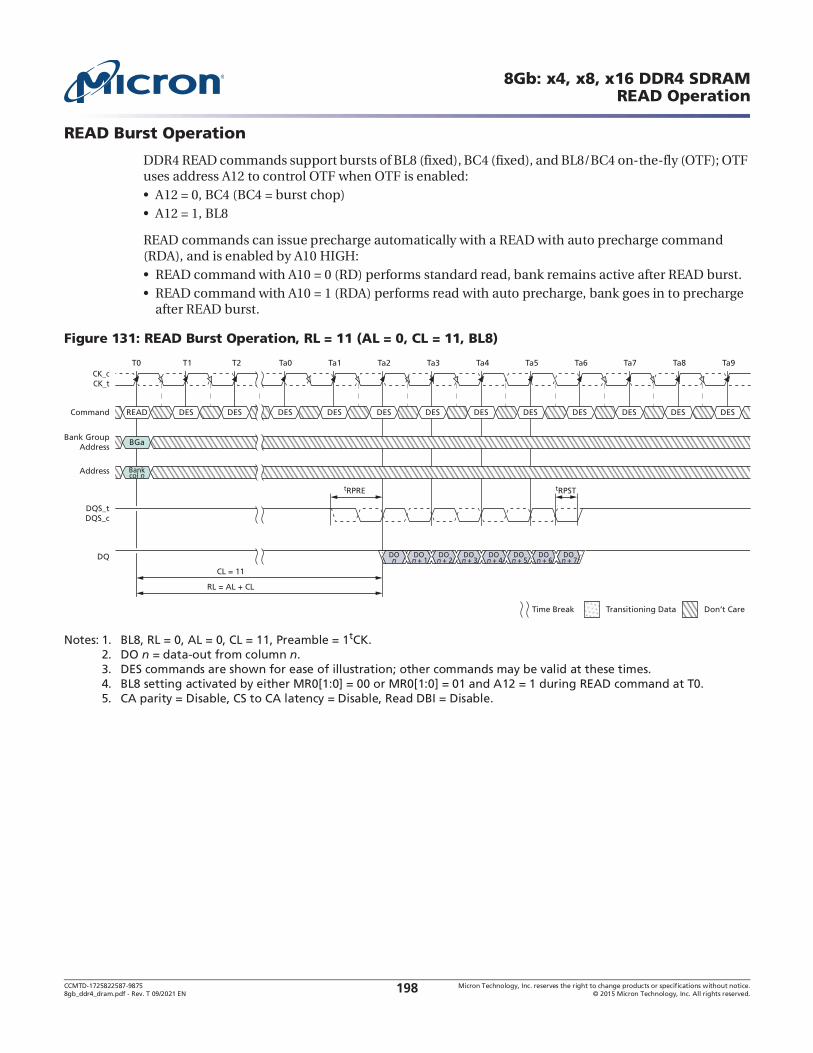
CCMTD-1725822587-9875 Micron Technology, Inc. reserves the right to change products or specifications without notice.8gb_ddr4_dram.pdf - Rev. T 09/2021 EN 2015 Micron Technology, Inc. All rights reserved.198
8Gb: x4, x8, x16 DDR4 SDRAMREAD Operation
READ Burst Operation
DDR4 READ commands support bursts of BL8 (fixed), BC4 (fixed), and BL8/BC4 on-the-fly (OTF); OTF uses address A12 to control OTF when OTF is enabled:
A12 = 0, BC4 (BC4 = burst chop)A12 = 1, BL8
READ commands can issue precharge automatically with a READ with auto precharge command (RDA), and is enabled by A10 HIGH:
READ command with A10 = 0 (RD) performs standard read, bank remains active after READ burst.READ command with A10 = 1 (RDA) performs read with auto precharge, bank goes in to precharge after READ burst.
Figure 131: READ Burst Operation, RL = 11 (AL = 0, CL = 11, BL8)
Notes: 1. BL8, RL = 0, AL = 0, CL = 11, Preamble = 1tCK.2. DO n = data-out from column n.3. DES commands are shown for ease of illustration; other commands may be valid at these times.4. BL8 setting activated by either MR0[1:0] = 00 or MR0[1:0] = 01 and A12 = 1 during READ command at T0.5. CA parity = Disable, CS to CA latency = Disable, Read DBI = Disable.
T0
CL = 11
RL = AL + CL
tRPRE
T1 T2 Ta1Ta0 Ta2 Ta3 Ta4 Ta5 Ta6 Ta7 Ta8 Ta9
DES DES DES DES DES DESCommand DESREAD DES DESDES DES DES
DQ
CK_tCK_c
Don’t CareTransitioning DataTime Break
DOn + 3
DOn + 4
DOn + 5
DOn + 6
DOn + 7
DOn + 2
DOn + 1
DOn
Bank GroupAddress
DQS_tDQS_c
BGa
Address Bankcol n
tRPST

CCMTD-1725822587-9875 Micron Technology, Inc. reserves the right to change products or specifications without notice.8gb_ddr4_dram.pdf - Rev. T 09/2021 EN 2015 Micron Technology, Inc. All rights reserved.199
8Gb: x4, x8, x16 DDR4 SDRAMREAD Operation
Figure 132: READ Burst Operation, RL = 21 (AL = 10, CL = 11, BL8)
Notes: 1. BL8, RL = 21, AL = (CL - 1), CL = 11, Preamble = 1tCK.2. DO n = data-out from column n.3. DES commands are shown for ease of illustration; other commands may be valid at these times.4. BL8 setting activated by either MR0[1:0] = 00 or MR0[1:0] = 01 and A12 = 1 during READ command at T0.5. CA parity = Disable, CS to CA latency = Disable, Read DBI = Disable.
T0
CL = 11AL = 10
RL = AL + CL
tRPRE
T1 Ta0 Ta1 Ta2 Ta3 Tb0 Tb1 Tb2 Tb3 Tb4 Tb5 Tb6
DES DES DES DES DESCommand DESREAD DES DES DES DES
DQ
CK_tCK_c
Don’t CareTransitioning DataTime Break
DOn + 3
DOn + 4
DOn + 5
DOn + 6
DOn + 7
DOn + 2
DOn + 1
DOn
Bank GroupAddress
DQS_tDQS_c
BGa
Address Bankcol n
tRPST
DESDES
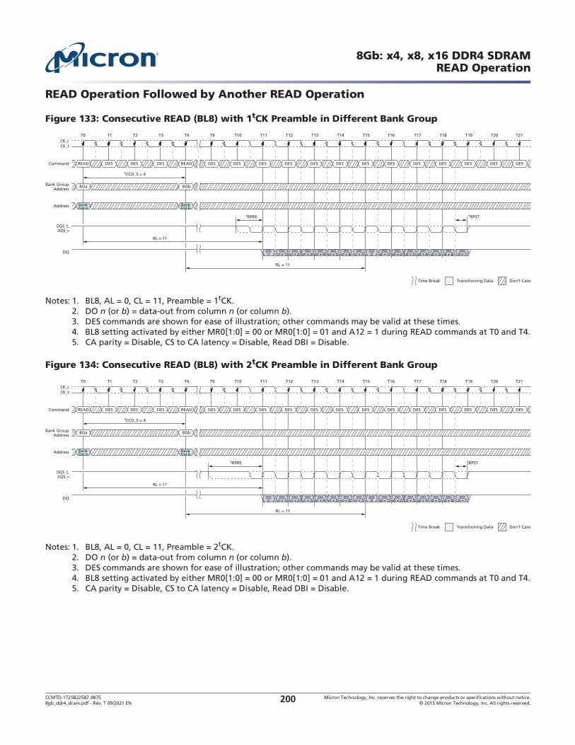
CCMTD-1725822587-9875 Micron Technology, Inc. reserves the right to change products or specifications without notice.8gb_ddr4_dram.pdf - Rev. T 09/2021 EN 2015 Micron Technology, Inc. All rights reserved.200
8Gb: x4, x8, x16 DDR4 SDRAMREAD Operation
READ Operation Followed by Another READ Operation
Figure 133: Consecutive READ (BL8) with 1tCK Preamble in Different Bank Group
Notes: 1. BL8, AL = 0, CL = 11, Preamble = 1tCK.2. DO n (or b) = data-out from column n (or column b).3. DES commands are shown for ease of illustration; other commands may be valid at these times.4. BL8 setting activated by either MR0[1:0] = 00 or MR0[1:0] = 01 and A12 = 1 during READ commands at T0 and T4.5. CA parity = Disable, CS to CA latency = Disable, Read DBI = Disable.
Figure 134: Consecutive READ (BL8) with 2tCK Preamble in Different Bank Group
Notes: 1. BL8, AL = 0, CL = 11, Preamble = 2tCK.2. DO n (or b) = data-out from column n (or column b).3. DES commands are shown for ease of illustration; other commands may be valid at these times.4. BL8 setting activated by either MR0[1:0] = 00 or MR0[1:0] = 01 and A12 = 1 during READ commands at T0 and T4.5. CA parity = Disable, CS to CA latency = Disable, Read DBI = Disable.
T0
tCCD_S = 4
tRPRE
RL = 11
tRPST
T16T1 T2 T3 T4 T9 T10 T11 T12 T13 T14 T15
DES DES DES DES DES DES DESCommand DESREAD DES DES READ DES
DQ
CK_tCK_c
DQS_t,DQS_c
RL = 11
T21T17 T18 T19 T20
Don’t CareTransitioning DataTime Break
DOn + 1
DOn + 2
DOn + 3
DOn + 4
DOn + 5
DOn + 6
DOn + 7
DOb
DOb + 1
DOb + 2
DOb + 3
DOb + 4
DOb + 5
DOb + 6
DOb + 7
DOn
DES DES DES DES DES
Bank GroupAddress
BGa BGb
Address BankCol n
BankCol b
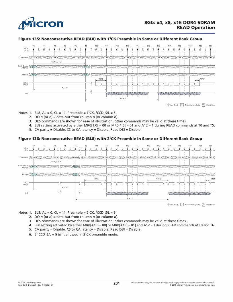
CCMTD-1725822587-9875 Micron Technology, Inc. reserves the right to change products or specifications without notice.8gb_ddr4_dram.pdf - Rev. T 09/2021 EN 2015 Micron Technology, Inc. All rights reserved.201
8Gb: x4, x8, x16 DDR4 SDRAMREAD Operation
Figure 135: Nonconsecutive READ (BL8) with 1tCK Preamble in Same or Different Bank Group
Notes: 1. BL8, AL = 0, CL = 11, Preamble = 1tCK, tCCD_S/L = 5.2. DO n (or b) = data-out from column n (or column b).3. DES commands are shown for ease of illustration; other commands may be valid at these times.4. BL8 setting activated by either MR0[1:0] = 00 or MR0[1:0] = 01 and A12 = 1 during READ commands at T0 and T5.5. CA parity = Disable, CS to CA latency = Disable, Read DBI = Disable.
Figure 136: Nonconsecutive READ (BL8) with 2tCK Preamble in Same or Different Bank Group
Notes: 1. BL8, AL = 0, CL = 11, Preamble = 2tCK, tCCD_S/L = 6.2. DO n (or b) = data-out from column n (or column b).3. DES commands are shown for ease of illustration; other commands may be valid at these times.4. BL8 setting activated by either MR0[A1:0 = 00] or MR0[A1:0 = 01] and A12 = 1 during READ commands at T0 and T6.5. CA parity = Disable, CS to CA latency = Disable, Read DBI = Disable.
6. 6 t tCK preamble mode.
T0
tCCD_S/L = 5
tRPRE
RL = 11
tRPST
T16T1 T2 T3 T4 T5 T10 T11 T12 T13 T14 T15
DES DES DES DES DES DES DESCommand DESREAD DES DES DES READ
DQ
CK_tCK_c
DQS_t,DQS_c
RL = 11
T21T17 T18 T19 T20
Don’t CareTransitioning DataTime Break
DOn + 1
DOn + 2
DOn + 3
DOn + 4
DOn + 5
DOn + 6
DOn + 7
DOb
DOb + 1
DOb + 2
DOb + 3
DOb + 4
DOb + 5
DOb + 6
DOb + 7
DOn
DES DES DES DES DES
Bank GroupAddress BGa BGb
Address BankCol n
BankCol b
T0
tCCD_S/L = 6
tRPRE
RL = 11
tRPST
T16T1 T2 T5 T6 T9 T10 T11 T12 T13 T14 T15
DES DES DES DES DES DES DESCommand DESREAD DES DES READ DES
DQ
CK_tCK_c
DQS_t,DQS_c
RL = 11
T21T17 T18 T19 T20
Don’t CareTransitioning DataTime Break
DOn + 1
DOn + 2
DOn + 3
DOn + 4
DOn + 5
DOn + 6
DOn + 7
DOb
DOb + 1
DOb + 2
DOb + 3
DOb + 4
DOb + 5
DOb + 6
DOb + 7
DOn
DES DES DES DES DES
Bank GroupAddress
BGa BGa orBGb
Address BankCol n
BankCol b
tRPRE

CCMTD-1725822587-9875 Micron Technology, Inc. reserves the right to change products or specifications without notice.8gb_ddr4_dram.pdf - Rev. T 09/2021 EN 2015 Micron Technology, Inc. All rights reserved.202
8Gb: x4, x8, x16 DDR4 SDRAMREAD Operation
Figure 137: READ (BC4) to READ (BC4) with 1tCK Preamble in Different Bank Group
Notes: 1. BL8, AL = 0, CL = 11, Preamble = 1tCK.2. DO n (or b) = data-out from column n (or column b).3. DES commands are shown for ease of illustration; other commands may be valid at these times.4. BC4 setting activated by either MR0[1:0] = 10 or MR0[1:0] = 01 and A12 = 0 during READ commands at T0 and T4.5. CA parity = Disable, CS to CA latency = Disable, Read DBI = Disable.
Figure 138: READ (BC4) to READ (BC4) with 2tCK Preamble in Different Bank Group
Notes: 1. BL8, AL = 0, CL = 11, Preamble = 2tCK.2. DO n (or b) = data-out from column n (or column b).3. DES commands are shown for ease of illustration; other commands may be valid at these times.4. BC4 setting activated by either MR0[1:0] = 10 or MR0[1:0] = 01 and A12 = 0 during READ commands at T0 and T4.5. CA parity = Disable, CS to CA latency = Disable, Read DBI = Disable.
T0
tCCD_S = 4
tRPRE
RL = 11
tRPST
T16T1 T2 T3 T4 T9 T10 T11 T12 T13 T14 T15
DES DES DES DES DES DES DESCommand DESREAD DES DES READ DES
DQ
CK_tCK_c
DQS_t,DQS_c
RL = 11
T21T17 T18 T19 T20
Don’t CareTransitioning DataTime Break
DOn + 1
DOn + 2
DOn + 3
DOb
DOb + 1
DOb + 2
DOb + 3
DOn
DES DES DES DES DES
Bank GroupAddress
BGa BGb
Address BankCol n
BankCol b
tRPREtRPST
T0
tCCD_S = 4
tRPRE
RL = 11
tRPST
T16T1 T2 T3 T4 T9 T10 T11 T12 T13 T14 T15
DES DES DES DES DES DES DESCommand DESREAD DES DES READ DES
DQ
CK_tCK_c
DQS_t,DQS_c
RL = 11
T21T17 T18 T19 T20
Don’t CareTransitioning DataTime Break
DOn + 1
DOn + 2
DOn + 3
DOb
DOb + 1
DOb + 2
DOb + 3
DOn
DES DES DES DES DES
Bank GroupAddress
BGa BGb
Address BankCol n
BankCol b
tRPRE
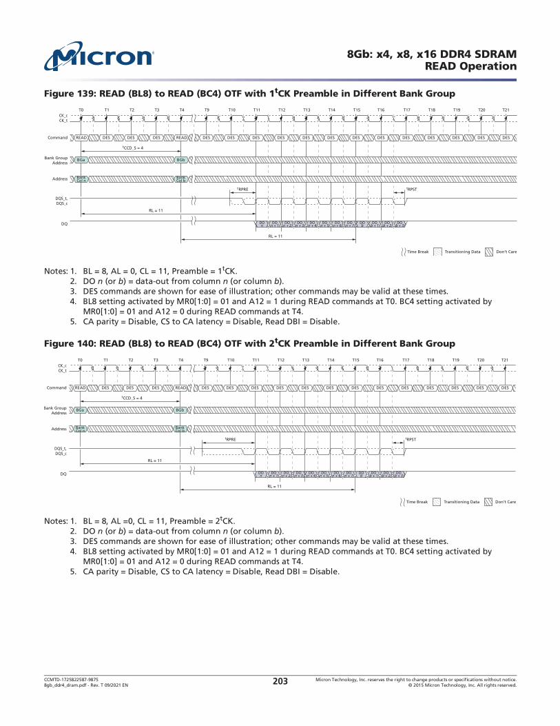
CCMTD-1725822587-9875 Micron Technology, Inc. reserves the right to change products or specifications without notice.8gb_ddr4_dram.pdf - Rev. T 09/2021 EN 2015 Micron Technology, Inc. All rights reserved.203
8Gb: x4, x8, x16 DDR4 SDRAMREAD Operation
Figure 139: READ (BL8) to READ (BC4) OTF with 1tCK Preamble in Different Bank Group
Notes: 1. BL = 8, AL = 0, CL = 11, Preamble = 1tCK.2. DO n (or b) = data-out from column n (or column b).3. DES commands are shown for ease of illustration; other commands may be valid at these times.4. BL8 setting activated by MR0[1:0] = 01 and A12 = 1 during READ commands at T0. BC4 setting activated by
MR0[1:0] = 01 and A12 = 0 during READ commands at T4.5. CA parity = Disable, CS to CA latency = Disable, Read DBI = Disable.
Figure 140: READ (BL8) to READ (BC4) OTF with 2tCK Preamble in Different Bank Group
Notes: 1. BL = 8, AL =0, CL = 11, Preamble = 2tCK.2. DO n (or b) = data-out from column n (or column b).3. DES commands are shown for ease of illustration; other commands may be valid at these times.4. BL8 setting activated by MR0[1:0] = 01 and A12 = 1 during READ commands at T0. BC4 setting activated by
MR0[1:0] = 01 and A12 = 0 during READ commands at T4.5. CA parity = Disable, CS to CA latency = Disable, Read DBI = Disable.
T0
tCCD_S = 4
tRPRE
RL = 11
tRPST
T16T1 T2 T3 T4 T9 T10 T11 T12 T13 T14 T15
DES DES DES DES DES DES DESCommand DESREAD DES DES READ DES
DQ
CK_tCK_c
DQS_t,DQS_c
RL = 11
T21T17 T18 T19 T20
Don’t CareTransitioning DataTime Break
DOn + 1
DOn + 2
DOn + 3
DOn + 4
DOn + 5
DOn + 6
DOn + 7
DOb
DOb + 1
DOb + 2
DOb + 3
DOn
DES DES DES DES DES
Bank GroupAddress
BGa BGb
Address BankCol n
BankCol b
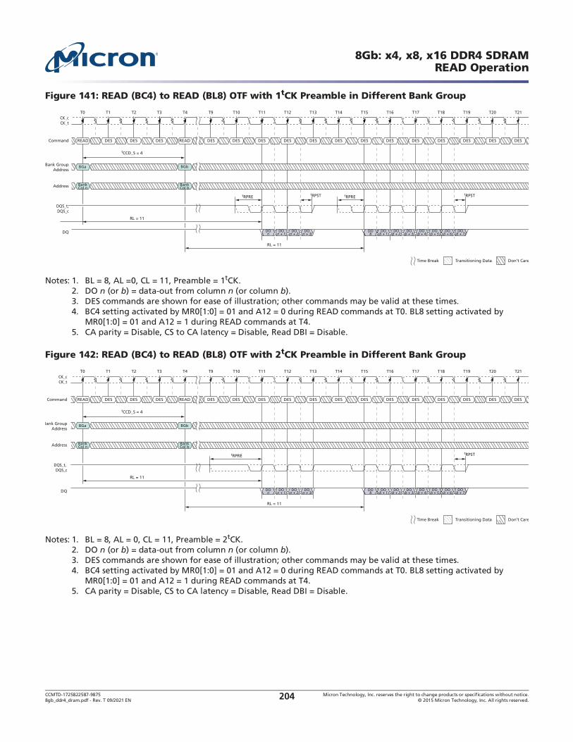
CCMTD-1725822587-9875 Micron Technology, Inc. reserves the right to change products or specifications without notice.8gb_ddr4_dram.pdf - Rev. T 09/2021 EN 2015 Micron Technology, Inc. All rights reserved.204
8Gb: x4, x8, x16 DDR4 SDRAMREAD Operation
Figure 141: READ (BC4) to READ (BL8) OTF with 1tCK Preamble in Different Bank Group
Notes: 1. BL = 8, AL =0, CL = 11, Preamble = 1tCK.2. DO n (or b) = data-out from column n (or column b).3. DES commands are shown for ease of illustration; other commands may be valid at these times.4. BC4 setting activated by MR0[1:0] = 01 and A12 = 0 during READ commands at T0. BL8 setting activated by
MR0[1:0] = 01 and A12 = 1 during READ commands at T4.5. CA parity = Disable, CS to CA latency = Disable, Read DBI = Disable.
Figure 142: READ (BC4) to READ (BL8) OTF with 2tCK Preamble in Different Bank Group
Notes: 1. BL = 8, AL = 0, CL = 11, Preamble = 2tCK.2. DO n (or b) = data-out from column n (or column b).3. DES commands are shown for ease of illustration; other commands may be valid at these times.4. BC4 setting activated by MR0[1:0] = 01 and A12 = 0 during READ commands at T0. BL8 setting activated by
MR0[1:0] = 01 and A12 = 1 during READ commands at T4.5. CA parity = Disable, CS to CA latency = Disable, Read DBI = Disable.
T0
tCCD_S = 4
tRPRE
RL = 11
T1 T2 T3 T4
DES DES DES DES DES DES DESCommand DESREAD DES DES READ DES
DQ
CK_tCK_c
DQS_t,DQS_c
RL = 11
T20 T21T14T9 T10 T11 T12 T13 T19T15 T16 T17 T18
Don’t CareTransitioning DataTime Break
DOn + 1
DOn + 2
DOn + 3
DOb
DOb + 1
DOb + 2
DOb + 3
DOb + 4
DOb + 5
DOb + 6
DOb + 7
DOn
DES DES DES DES DES
Bank GroupAddress
Address BankCol n
BankCol b
BGb
tRPREtRPSTtRPST
BGa
T0
tCCD_S = 4
tRPRE
RL = 11
T1 T2 T3 T4
DES DES DES DES DES DES DESCommand DESREAD DES DES READ DES
DQ
CK_tCK_c
DQS_t,DQS_c
RL = 11
T20 T21T14T9 T10 T11 T12 T13 T19T15 T16 T17 T18
Don’t CareTransitioning DataTime Break
DOn + 1
DOn + 2
DOn + 3
DOb
DOb + 1
DOb + 2
DOb + 3
DOb + 4
DOb + 5
DOb + 6
DOb + 7
DOn
DES DES DES DES DES
Bank GroupAddress
Address BankCol n
BankCol b
BGb
tRPST
BGa

CCMTD-1725822587-9875 Micron Technology, Inc. reserves the right to change products or specifications without notice.8gb_ddr4_dram.pdf - Rev. T 09/2021 EN 2015 Micron Technology, Inc. All rights reserved.205
8Gb: x4, x8, x16 DDR4 SDRAMREAD Operation
READ Operation Followed by WRITE Operation
Figure 143: READ (BL8) to WRITE (BL8) with 1tCK Preamble in Same or Different Bank Group
Notes: 1. BL = 8, RL = 11 (CL = 11, AL = 0), READ preamble = 1tCK, WL = 9 (CWL = 9, AL = 0), WRITE preamble = 1tCK.2. DO n = data-out from column n; DI b = data-in from column b.3. DES commands are shown for ease of illustration; other commands may be valid at these times.4. BL8 setting activated by either MR0[1:0] = 00 or MR0[1:0] = 01 and A12 = 1 during READ commands at T0 and
WRITE commands at T8.5. CA parity = Disable, CS to CA latency = Disable, Read DBI = Disable, Write DBI = Disable, Write CRC = Disable.
Figure 144: READ (BL8) to WRITE (BL8) with 2tCK Preamble in Same or Different Bank Group
Notes: 1. BL = 8, RL = 11 (CL = 11, AL = 0), READ preamble = 2tCK, WL = 10 (CWL = 9+1 [see Note 5], AL = 0), WRITE preamble
= 2tCK.2. DO n = data-out from column n; DI b = data-in from column b.3. DES commands are shown for ease of illustration; other commands may be valid at these times.4. BL8 setting activated by either MR0[1:0] = 00 or MR0[1:0] = 01 and A12 = 1 during READ commands at T0 and
WRITE commands at T8.
5. When operating in 2tCK WRITE preamble mode, CWL may need to be programmed to a value at least 1 clock greater than the lowest CWL setting.
6. CA parity = Disable, CS to CA latency = Disable, Read DBI = Disable, Write DBI = Disable, Write CRC = Disable.
T0
READ to WRITE command delay= RL +BL/2 - WL + 2 tCK 4 Clocks
tRPRE
RL = 11
tRPST
T1 T7 T8 T9
DES DES DES DES DES DES DESCommand DESREAD DES WRITE DES DES
DQ
CK_tCK_c
DQS_t,DQS_c
WL = 9
T22T16T10 T11 T12 T13 T14 T15 T21T17 T18 T19 T20
Don’t CareTransitioning DataTime Break
DOn + 1
DOn + 2
DOn + 3
DOn + 4
DOn + 5
DOn + 6
DOn + 7
DIb
DIb + 1
DIb + 2
DIb + 3
DIb + 4
DIb + 5
DIb + 6
DIb + 7
DOn
DES DES DES DES DES
Bank GroupAddress
Address BankCol n
BankCol b
BGa BGa orBGb
tWPRE tWPST
tWTR
tWR
T0
READ to WRITE command delay= RL +BL/2 - WL + 3 tCK 4 Clocks
tRPRE
RL = 11
tRPST
T1 T7 T8 T9
DES DES DES DES DES DES DESCommand DESREAD DES WRITE DES DES
DQ
CK_tCK_c
DQS_t,DQS_c
WL = 10
T22T16T10 T11 T12 T13 T14 T15 T21T17 T18 T19 T20
Don’t CareTransitioning DataTime Break
DOn + 1
DOn + 2
DOn + 3
DOn + 4
DOn + 5
DOn + 6
DOn + 7
DIb
DIb + 1
DIb + 2
DIb + 3
DIb + 4
DIb + 5
DIb + 6
DIb + 7
DOn
DES DES DES DES DES
Bank GroupAddress
Address BankCol n
BankCol b
BGa BGa orBGb
tWPRE tWPST
tWTR
tWR

CCMTD-1725822587-9875 Micron Technology, Inc. reserves the right to change products or specifications without notice.8gb_ddr4_dram.pdf - Rev. T 09/2021 EN 2015 Micron Technology, Inc. All rights reserved.206
8Gb: x4, x8, x16 DDR4 SDRAMREAD Operation
Figure 145: READ (BC4) OTF to WRITE (BC4) OTF with 1tCK Preamble in Same or Different Bank Group
Notes: 1. BC = 4, RL = 11 (CL = 11, AL = 0), READ preamble = 1tCK, WL = 9 (CWL = 9, AL = 0), WRITE preamble = 1tCK.2. DO n = data-out from column n; DI b = data-in from column b.3. DES commands are shown for ease of illustration; other commands may be valid at these times.4. BC4 (OTF) setting activated by MR0[1:0] = 01 and A12 = 0 during READ commands at T0 and WRITE commands at
T6.5. CA parity = Disable, CS to CA latency = Disable, Read DBI = Disable, Write DBI = Disable, Write CRC = Disable.
Figure 146: READ (BC4) OTF to WRITE (BC4) OTF with 2tCK Preamble in Same or Different Bank Group
Notes: 1. BC = 4, RL = 11 (CL = 11, AL = 0), READ preamble = 2tCK, WL = 10 (CWL = 9 + 1 [see Note 5], AL = 0), WRITE preamble
= 2tCK.2. DO n = data-out from column n; DI b = data-in from column b.3. DES commands are shown for ease of illustration; other commands may be valid at these times.4. BC4 (OTF) setting activated by MR0[1:0] = 01 and A12 = 0 during READ commands at T0 and WRITE commands at
T6.
5. When operating in 2tCK WRITE preamble mode, CWL may need to be programmed to a value at least 1 clock greater than the lowest CWL setting.
6. CA parity = Disable, CS to CA latency = Disable, Read DBI = Disable, Write DBI = Disable, Write CRC = Disable.
T0
READ to WRITE command delay= RL +BL/2 - WL + 2 tCK 4 Clocks
tRPRE
RL = 11
tRPST
T1 T5 T6 T7
DES DES DES DES DES DES DESCommand DESREAD DES WRITE DES DES
DQ
CK_tCK_c
DQS_t,DQS_c
WL = 9
T20T14T8 T9 T10 T11 T12 T13 T19T15 T16 T17 T18
Don’t CareTransitioning DataTime Break
DOn + 1
DOn + 2
DOn + 3
DIb
DIb + 1
DIb + 2
DIb + 3
DOn
DES DES DES DES DES
Bank GroupAddress
Address BankCol n
BankCol b
BGa BGa orBGb
tWPRE tWPST
tWTR
tWR
T0
READ to WRITE command delay= RL +BL/2 - WL + 3 tCK 4 Clocks
tRPRE
RL = 11
tRPST
T1 T5 T6 T7
DES DES DES DES DES DES DESCommand DESREAD DES WRITE DES DES
DQ
CK_tCK_c
DQS_t,DQS_c
WL = 10
T20T14T8 T9 T10 T11 T12 T13 T19T15 T16 T17 T18
Don’t CareTransitioning DataTime Break
DOn + 1
DOn + 2
DOn + 3
DIb
DIb + 1
DIb + 2
DIb + 3
DOn
DES DES DES DES DES
Bank GroupAddress
Address BankCol n
BankCol b
BGa BGa orBGb
tWPRE tWPST
tWTR
tWR

CCMTD-1725822587-9875 Micron Technology, Inc. reserves the right to change products or specifications without notice.8gb_ddr4_dram.pdf - Rev. T 09/2021 EN 2015 Micron Technology, Inc. All rights reserved.207
8Gb: x4, x8, x16 DDR4 SDRAMREAD Operation
Figure 147: READ (BC4) Fixed to WRITE (BC4) Fixed with 1tCK Preamble in Same or Different Bank Group
Notes: 1. BC = 4, RL = 11 (CL = 11, AL = 0), READ preamble = 1tCK, WL = 9 (CWL = 9, AL = 0), WRITE preamble = 1tCK.2. DO n = data-out from column n; DI b = data-in from column b.3. DES commands are shown for ease of illustration; other commands may be valid at these times.4. BC4 (fixed) setting activated by MR0[1:0] = 01.5. CA parity = Disable, CS to CA latency = Disable, Read DBI = Disable, Write DBI = Disable, Write CRC = Disable.
Figure 148: READ (BC4) Fixed to WRITE (BC4) Fixed with 2tCK Preamble in Same or Different Bank Group
Notes: 1. BC = 4, RL = 11 (CL = 11, AL = 0), READ preamble = 2tCK, WL = 9 (CWL = 9 + 1 [see Note 5], AL = 0), WRITE preamble
= 2tCK.2. DO n = data-out from column n; DI b = data-in from column b.3. DES commands are shown for ease of illustration; other commands may be valid at these times.4. BC4 (fixed) setting activated by MR0[1:0] = 10.
5. When operating in 2tCK WRITE preamble mode, CWL may need to be programmed to a value at least 1 clock greater than the lowest CWL setting.
6. CA parity = Disable, CS to CA latency = Disable, Read DBI = Disable, Write DBI = Disable, Write CRC = Disable.
T0
READ to WRITE command delay= RL +BL/2 - WL + 2 tCK
tRPRE
RL = 11
tRPST
T1 T5 T6 T7
DES DES DES DES DES DES DESCommand DESREAD DES WRITE DES DES
DQ
CK_tCK_c
DQS_t,DQS_c
WL = 9
T20T14T8 T9 T10 T11 T12 T13 T19T15 T16 T17 T18
Don’t CareTransitioning DataTime Break
DOn + 1
DOn + 2
DOn + 3
DIb
DIb + 1
DIb + 2
DIb + 3
DOn
DES DES DES DES DES
Bank GroupAddress
Address BankCol n
BankCol b
BGa orBGb
tWPRE tWPST
tWTR
tWR
BGa
2 Clocks
T0
READ to WRITE command delay= RL +BL/2 - WL + 3 tCK 2 Clocks
tRPRE
RL = 11
tRPST
T1 T5 T6 T7
DES DES DES DES DES DES DESCommand DESREAD DES WRITE DES DES
DQ
CK_tCK_c
DQS_t,DQS_c
WL = 10
T20T14T8 T9 T10 T11 T12 T13 T19T15 T16 T17 T18
Don’t CareTransitioning DataTime Break
DOn + 1
DOn + 2
DOn + 3
DIb
DIb + 1
DIb + 2
DIb + 3
DOn
DES DES DES DES DES
Bank GroupAddress
Address BankCol n
BankCol b
BGa BGa orBGb
tWPRE tWPST
tWTR
tWR

CCMTD-1725822587-9875 Micron Technology, Inc. reserves the right to change products or specifications without notice.8gb_ddr4_dram.pdf - Rev. T 09/2021 EN 2015 Micron Technology, Inc. All rights reserved.208
8Gb: x4, x8, x16 DDR4 SDRAMREAD Operation
Figure 149: READ (BC4) to WRITE (BL8) OTF with 1tCK Preamble in Same or Different Bank Group
Notes: 1. BL = 8, RL = 11 (CL = 11, AL = 0), READ preamble = 1tCK, WL = 9 (CWL = 9, AL = 0), WRITE preamble = 1tCK.2. DO n = data-out from column n; DI b = data-in from column b.3. DES commands are shown for ease of illustration; other commands may be valid at these times.4. BC4 setting activated by MR0[1:0] = 01 and A12 = 0 during WRITE commands at T0.
BL8 setting activated by MR0[1:0] = 01 and A12 = 1 during READ commands at T6.5. CA parity = Disable, CS to CA latency = Disable, Read DBI = Disable, Write DBI = Disable, Write CRC = Disable.
Figure 150: READ (BC4) to WRITE (BL8) OTF with 2tCK Preamble in Same or Different Bank Group
Notes: 1. BL = 8, RL = 11 (CL = 11, AL = 0), READ preamble = 2tCK, WL = 10 (CWL = 9 + 1 [see Note 5], AL = 0), WRITE preamble
= 2tCK.2. DO n = data-out from column n; DI b = data-in from column b.3. DES commands are shown for ease of illustration; other commands may be valid at these times.4. BC4 setting activated by MR0[1:0] = 01 and A12 = 0 during WRITE commands at T0.
BL8 setting activated by MR0[1:0] = 01 and A12 = 1 during READ commands at T6.5. CA parity = Disable, CS to CA latency = Disable, Read DBI = Disable, Write DBI = Disable, Write CRC = Disable.
T0
READ to WRITE command delay= RL +BL/2 - WL + 2 tCK
tWPRE
RL = 11
tWPST
T1
DES DES DES DES DES DES DESCommand DESREAD DES WRITE DES DES
DQ
CK_tCK_c
DQS_t,DQS_c
WL = 9
T5 T6 T7 T20T14T8 T9 T10 T11 T12 T13 T19T15 T16 T17 T18
Don’t CareTransitioning DataTime Break
DOn + 1
DOn + 2
DOn + 3
DIn + 4
DIn + 5
DIn + 6
DIn + 7
DIb
DIb + 1
DIb + 2
DIb + 3
DOn
DES DES DES DES DES
Bank GroupAddress
Address BankCol n
BankCol b
BGa BGa orBGb
tRPREtRPST
tWTR
tWR
4 Clocks
T0
READ to WRITE command delay= RL +BL/2 - WL + 3 tCK
tWPRE
RL = 11
tWPST
T1
DES DES DES DES DES DES DESCommand DESREAD DES WRITE DES DES
DQ
CK_tCK_c
DQS_t,DQS_c
WL = 10
T5 T6 T7 T20T14T8 T9 T10 T11 T12 T13 T19T15 T16 T17 T18
Don’t CareTransitioning DataTime Break
DOn + 1
DOn + 2
DOn + 3
DIn + 4
DIn + 5
DIn + 6
DIn + 7
DIb
DIb + 1
DIb + 2
DIb + 3
DOn
DES DES DES DES DES
Bank GroupAddress
Address BankCol n
BankCol b
BGa BGa orBGb
tRPREtRPST
tWTR
tWR
4 Clocks

CCMTD-1725822587-9875 Micron Technology, Inc. reserves the right to change products or specifications without notice.8gb_ddr4_dram.pdf - Rev. T 09/2021 EN 2015 Micron Technology, Inc. All rights reserved.209
8Gb: x4, x8, x16 DDR4 SDRAMREAD Operation
Figure 151: READ (BL8) to WRITE (BC4) OTF with 1tCK Preamble in Same or Different Bank Group
Notes: 1. BL = 8, RL = 11 (CL = 11, AL = 0), READ preamble = 1tCK, WL = 9 (CWL = 9, AL = 0), WRITE preamble = 1tCK.2. DO n = data-out from column n; DI b = data-in from column b.3. DES commands are shown for ease of illustration; other commands may be valid at these times.4. BL8 setting activated by MR0[1:0] = 01 and A12 = 1 during READ commands at T0.
BC4 setting activated by MR0[1:0] = 01 and A12 = 0 during WRITE commands at T8.5. CA parity = Disable, CS to CA latency = Disable, Read DBI = Disable, Write DBI = Disable, Write CRC = Disable.
Figure 152: READ (BL8) to WRITE (BC4) OTF with 2tCK Preamble in Same or Different Bank Group
Notes: 1. BL = 8, RL = 11 (CL = 11, AL = 0), READ preamble = 2tCK, WL = 10 (CWL = 9 + 1 [see Note 5], AL = 0), WRITE preamble
= 2tCK.2. DO n = data-out from column n; DI b = data-in from column b.3. DES commands are shown for ease of illustration; other commands may be valid at these times.4. BL8 setting activated by MR0[1:0] = 01 and A12 = 1 during READ commands at T0.
BC4 setting activated by MR0[1:0] = 01 and A12 = 0 during WRITE commands at T8.5. CA parity = Disable, CS to CA latency = Disable, Read DBI = Disable, Write DBI = Disable, Write CRC = Disable.
READ Operation Followed by PRECHARGE Operation
The minimum external READ command to PRECHARGE command spacing to the same bank is equal
to AL + tRTP with tRTP being the internal READ command to PRECHARGE command delay. Note that
the minimum ACT to PRE timing, tRAS, must be satisfied as well. The minimum value for the internal
T0
READ to WRITE command delay= RL +BL/2 - WL + 2 tCK 4 Clocks
tRPRE
RL = 11
tRPST
T1
DES DES DES DES DES DES DESCommand DESREAD DES WRITE DES DES
DQ
CK_tCK_c
DQS_t,DQS_c
WL = 9
T22T21T7 T20T14T8 T9 T10 T11 T12 T13 T19T15 T16 T17 T18
Don’t CareTransitioning DataTime Break
DOn + 1
DOn + 2
DOn + 3
DOn + 4
DOn + 5
DOn + 6
DOn + 7
DIb
DIb + 1
DIb + 2
DIb + 3
DOn
DES DES DES DES DES
Bank GroupAddress
Address BankCol n
BankCol b
BGa BGa orBGb
tWPRE tWPST
tWTR
tWR
T0
READ to WRITE command delay= RL +BL/2 - WL + 3 tCK 4 Clocks
tRPRE
RL = 11
tRPST
T1
DES DES DES DES DES DES DESCommand DESREAD DES WRITE DES DES
DQ
CK_tCK_c
DQS_t,DQS_c
WL = 10
T22T21T7 T20T14T8 T9 T10 T11 T12 T13 T19T15 T16 T17 T18
Don’t CareTransitioning DataTime Break
DOn + 1
DOn + 2
DOn + 3
DOn + 4
DOn + 5
DOn + 6
DOn + 7
DIb
DIb + 1
DIb + 2
DIb + 3
DOn
DES DES DES DES DES
Bank GroupAddress
Address BankCol n
BankCol b
BGa BGa orBGb
tWPRE tWPST
tWTR
tWR
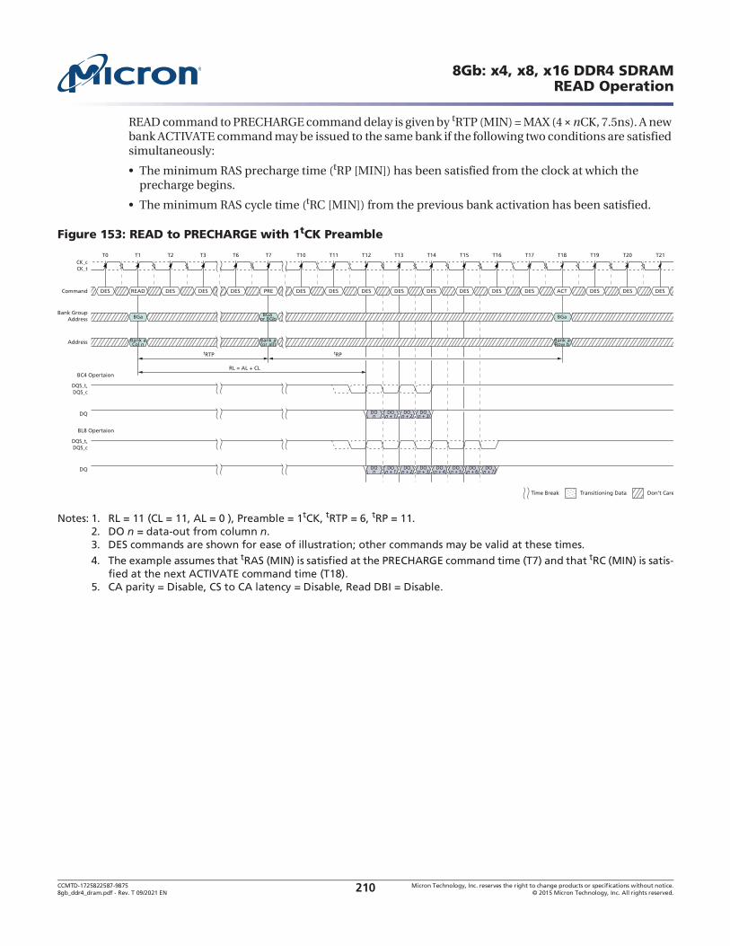
CCMTD-1725822587-9875 Micron Technology, Inc. reserves the right to change products or specifications without notice.8gb_ddr4_dram.pdf - Rev. T 09/2021 EN 2015 Micron Technology, Inc. All rights reserved.210
8Gb: x4, x8, x16 DDR4 SDRAMREAD Operation
READ command to PRECHARGE command delay is given by tRTP (MIN) = MAX (4 nCK, 7.5ns). A new bank ACTIVATE command may be issued to the same bank if the following two conditions are satisfied simultaneously:
The minimum RAS precharge time (tRP [MIN]) has been satisfied from the clock at which the precharge begins.
The minimum RAS cycle time (tRC [MIN]) from the previous bank activation has been satisfied.
Figure 153: READ to PRECHARGE with 1tCK Preamble
Notes: 1. RL = 11 (CL = 11, AL = 0 ), Preamble = 1tCK, tRTP = 6, tRP = 11.2. DO n = data-out from column n.3. DES commands are shown for ease of illustration; other commands may be valid at these times.
4. The example assumes that tRAS (MIN) is satisfied at the PRECHARGE command time (T7) and that tRC (MIN) is satis-fied at the next ACTIVATE command time (T18).
5. CA parity = Disable, CS to CA latency = Disable, Read DBI = Disable.
T0
RL = AL + CL
tRTP tRP
T1 T2 T3 T6
DES DES DES DES DES DES DESCommand READDES DES DES DES PRE
DQ
BC4 Opertaion
CK_tCK_c
DQS_t,DQS_c
T20 T21T14T7 T10 T11 T12 T13 T19T15 T16 T17 T18
Don’t CareTransitioning DataTime Break
DOn + 1
DOn + 2
DOn + 3
DOn
DES ACT DES DES DES
Bank GroupAddress BGa BGa
or BGb BGa
Address Bank aCol n
Bank a(or all)
Bank aRow b
DQ
BL8 Opertaion
DQS_t,DQS_c
DOn + 1
DOn + 2
DOn + 3
DOn + 4
DOn + 5
DOn + 6
DOn + 7
DOn
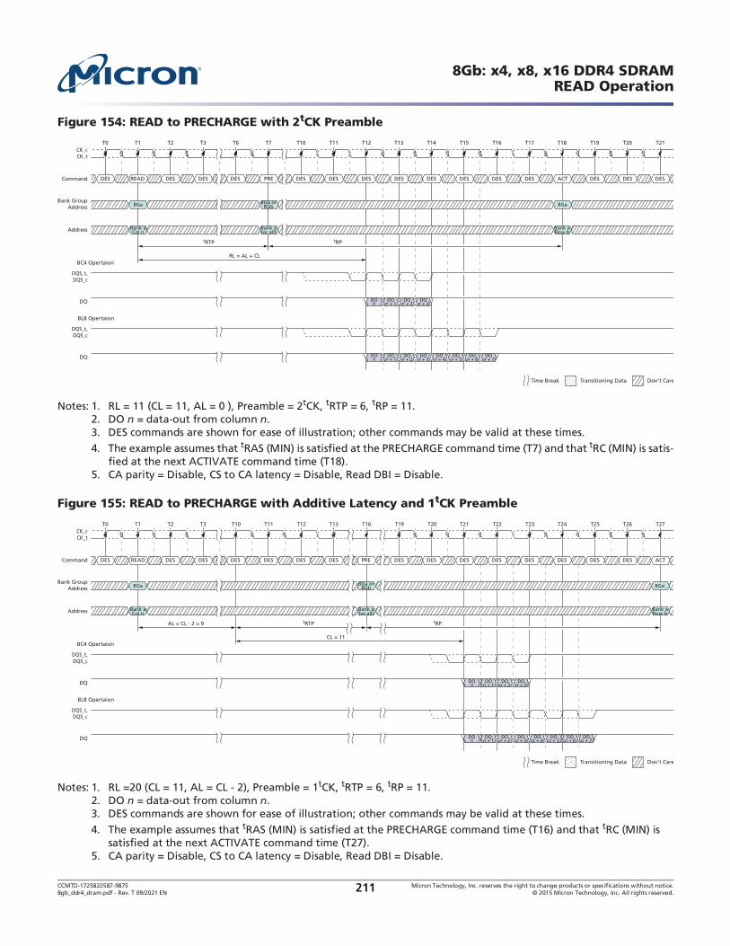
CCMTD-1725822587-9875 Micron Technology, Inc. reserves the right to change products or specifications without notice.8gb_ddr4_dram.pdf - Rev. T 09/2021 EN 2015 Micron Technology, Inc. All rights reserved.211
8Gb: x4, x8, x16 DDR4 SDRAMREAD Operation
Figure 154: READ to PRECHARGE with 2tCK Preamble
Notes: 1. RL = 11 (CL = 11, AL = 0 ), Preamble = 2tCK, tRTP = 6, tRP = 11.2. DO n = data-out from column n.3. DES commands are shown for ease of illustration; other commands may be valid at these times.
4. The example assumes that tRAS (MIN) is satisfied at the PRECHARGE command time (T7) and that tRC (MIN) is satis-fied at the next ACTIVATE command time (T18).
5. CA parity = Disable, CS to CA latency = Disable, Read DBI = Disable.
Figure 155: READ to PRECHARGE with Additive Latency and 1tCK Preamble
Notes: 1. RL =20 (CL = 11, AL = CL - 2), Preamble = 1tCK, tRTP = 6, tRP = 11.2. DO n = data-out from column n.3. DES commands are shown for ease of illustration; other commands may be valid at these times.
4. The example assumes that tRAS (MIN) is satisfied at the PRECHARGE command time (T16) and that tRC (MIN) is satisfied at the next ACTIVATE command time (T27).
5. CA parity = Disable, CS to CA latency = Disable, Read DBI = Disable.
RL = AL + CL
tRTP tRP
DQ
BC4 Opertaion
DQS_t,DQS_c
Don’t CareTransitioning DataTime Break
DOn + 1
DOn + 2
DOn + 3
DOn
DQ
BL8 Opertaion
DQS_t,DQS_c
DOn + 1
DOn + 2
DOn + 3
DOn + 4
DOn + 5
DOn + 6
DOn + 7
DOn
T0 T1 T2 T3 T6
DES DES DES DES DES DES DESCommand READDES DES DES DES PRE
CK_tCK_c
T20 T21T14T7 T10 T11 T12 T13 T19T15 T16 T17 T18
DES ACT DES DES DES
Bank GroupAddress BGa BGaBGa or
BGb
Address Bank aCol n
Bank a(or all)
Bank aRow b
T0
CL = 11
AL = CL - 2 = 9 tRTP
T1 T2 T3
DES DES PRE DES DES DES DESCommand READDES DES DES DES DES
DQ
BC4 Opertaion
CK_tCK_c
DQS_t,DQS_c
T26 T27T10 T11 T12 T13 T24 T25T22 T23T21T20T19T16
Don’t CareTransitioning DataTime Break
DOn + 1
DOn + 2
DOn + 3
DOn
DES DES DES DES ACT
Bank GroupAddress BGa BGa or
BGb
tRP
DQ
BL8 Opertaion
DQS_t,DQS_c
DOn + 1
DOn + 2
DOn + 3
DOn + 4
DOn + 5
DOn + 6
DOn + 7
DOn
Address Bank aCol n
Bank a(or all)
Bank aRow b
BGa

CCMTD-1725822587-9875 Micron Technology, Inc. reserves the right to change products or specifications without notice.8gb_ddr4_dram.pdf - Rev. T 09/2021 EN 2015 Micron Technology, Inc. All rights reserved.212
8Gb: x4, x8, x16 DDR4 SDRAMREAD Operation
Figure 156: READ with Auto Precharge and 1tCK Preamble
Notes: 1. RL = 11 (CL = 11, AL = 0 ), Preamble = 1tCK, tRTP = 6, tRP = 11.2. DO n = data-out from column n.3. DES commands are shown for ease of illustration; other commands may be valid at these times.
4. tRTP = 6 setting activated by MR0[A11:9 = 001].
5. The example assumes that tRC (MIN) is satisfied at the next ACTIVATE command time (T18).6. CA parity = Disable, CS to CA latency = Disable, Read DBI = Disable.
Figure 157: READ with Auto Precharge, Additive Latency, and 1tCK Preamble
Notes: 1. RL = 20 (CL = 11, AL = CL - 2), Preamble = 1tCK, tRTP = 6, tRP = 11.2. DO n = data-out from column n.3. DES commands are shown for ease of illustration; other commands may be valid at these times.
4. tRTP = 6 setting activated by MR0[11:9] = 001.
5. The example assumes that tRC (MIN) is satisfied at the next ACTIVATE command time (T27).6. CA parity = Disable, CS to CA latency = Disable, Read DBI = Disable.
T0
RL = AL + CL
tRTP tRP
T1 T2 T3 T6
DES DES DES DES DES DES DESCommand RDADES DES DES DES PRE
DQ
BC4 Opertaion
CK_tCK_c
DQS_t,DQS_c
T20 T21T14T7 T10 T11 T12 T13 T19T15 T16 T17 T18
Don’t CareTransitioning DataTime Break
DOn + 1
DOn + 2
DOn + 3
DOn
DES ACT DES DES DES
Bank GroupAddress BGa BGa
Address Bank aCol n
Bank aCol n
BGa orBGb
Bank aRow b
DQ
BL8 Opertaion
DQS_t,DQS_c
DOn + 1
DOn + 2
DOn + 3
DOn + 4
DOn + 5
DOn + 6
DOn + 7
DOn
T0
CL = 11
AL = CL - 2 = 9 tRTP
T1 T2 T3
DES DES DES DES DES DES DESCommand RDADES DES DES DES DES
DQ
BC4 Opertaion
CK_tCK_c
DQS_t,DQS_c
T26 T27T10 T11 T12 T13 T24 T25T22 T23T21T20T19T16
Don’t CareTransitioning DataTime Break
DOn + 1
DOn + 2
DOn + 3
DOn
DES DES DES DES ACT
Bank GroupAddress BGa BGa
tRP
DQ
BL8 Opertaion
DQS_t,DQS_c
DOn + 1
DOn + 2
DOn + 3
DOn + 4
DOn + 5
DOn + 6
DOn + 7
DOn
Address Bank aCol n
Bank aRow b
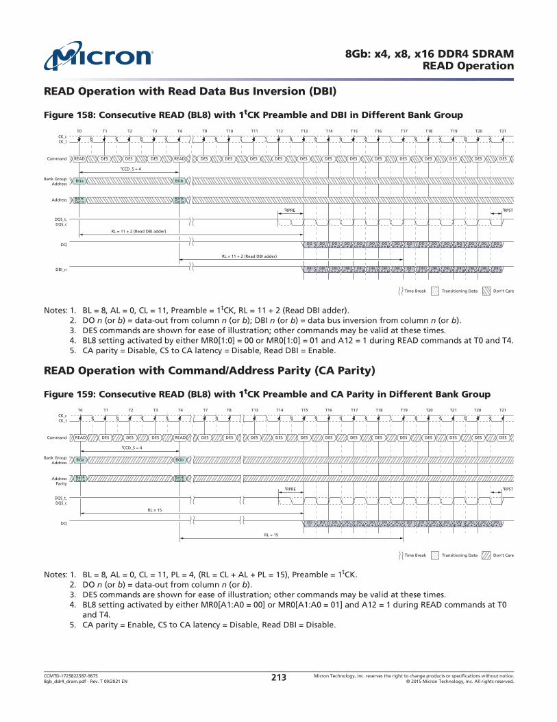
CCMTD-1725822587-9875 Micron Technology, Inc. reserves the right to change products or specifications without notice.8gb_ddr4_dram.pdf - Rev. T 09/2021 EN 2015 Micron Technology, Inc. All rights reserved.213
8Gb: x4, x8, x16 DDR4 SDRAMREAD Operation
READ Operation with Read Data Bus Inversion (DBI)
Figure 158: Consecutive READ (BL8) with 1tCK Preamble and DBI in Different Bank Group
Notes: 1. BL = 8, AL = 0, CL = 11, Preamble = 1tCK, RL = 11 + 2 (Read DBI adder).2. DO n (or b) = data-out from column n (or b); DBI n (or b) = data bus inversion from column n (or b).3. DES commands are shown for ease of illustration; other commands may be valid at these times.4. BL8 setting activated by either MR0[1:0] = 00 or MR0[1:0] = 01 and A12 = 1 during READ commands at T0 and T4.5. CA parity = Disable, CS to CA latency = Disable, Read DBI = Enable.
READ Operation with Command/Address Parity (CA Parity)
Figure 159: Consecutive READ (BL8) with 1tCK Preamble and CA Parity in Different Bank Group
Notes: 1. BL = 8, AL = 0, CL = 11, PL = 4, (RL = CL + AL + PL = 15), Preamble = 1tCK.2. DO n (or b) = data-out from column n (or b).3. DES commands are shown for ease of illustration; other commands may be valid at these times.4. BL8 setting activated by either MR0[A1:A0 = 00] or MR0[A1:A0 = 01] and A12 = 1 during READ commands at T0
and T4.5. CA parity = Enable, CS to CA latency = Disable, Read DBI = Disable.
T0
tCCD_S = 4
tRPRE
RL = 11 + 2 (Read DBI adder)
T16T1 T2 T3 T4 T9 T10 T11 T12 T13 T14 T15
DES DES DES DES DES DES DESCommand DESREAD DES DES READ DES
DQ
CK_tCK_c
DQS_t,DQS_c
RL = 11 + 2 (Read DBI adder)
T21T17 T18 T19 T20
Don’t CareTransitioning DataTime Break
DOn + 1
DOn + 2
DOn + 3
DOb + 1
DOb + 2
DOb + 7
DOn
DES DES DES DES DES
Bank GroupAddress
BGa BGb
Address BankCol n
BankCol b
tRPST
DOn + 4
DOn + 5
DOn + 6
DOn + 7
DOb
DOb + 5
DOb + 6
DOb + 3
DOb +4 _
DBI_n DBIn + 1
DBIn + 2
DBIn + 3
DBIb + 1
DBIb + 2
DBIb + 7
DBIn
DBIn + 4
DBIn + 5
DBIn + 6
DBIn + 7
DBIb
DBIb + 5
DBIb + 6
DBIb + 3
DBIb + 4
T0
tCCD_S = 4
tRPRE
RL = 15
T1 T2 T3 T4 T7 T8
DES DES DES DES DES DES DESCommand DESREAD DES DES READ DES
DQ
CK_tCK_c
DQS_t,DQS_c
RL = 15
T16T13 T14 T15 T21T17 T18 T19 T20 T21T20
Don’t CareTransitioning DataTime Break
DOn + 1
DOn + 2
DOn + 3
DOb + 1
DOb + 2
DOb + 7
DOn
DES DES DES DES DES
Bank GroupAddress
BGa BGb
AddressParity
BankCol n
BankCol b
tRPST
DOn + 4
DOn + 5
DOn + 6
DOn + 7
DOb
DOb + 5
DOb + 6
DOb + 3
DOb +4 _

CCMTD-1725822587-9875 Micron Technology, Inc. reserves the right to change products or specifications without notice.8gb_ddr4_dram.pdf - Rev. T 09/2021 EN 2015 Micron Technology, Inc. All rights reserved.214
8Gb: x4, x8, x16 DDR4 SDRAMREAD Operation
Figure 160: READ (BL8) to WRITE (BL8) with 1tCK Preamble and CA Parity in Same or Different Bank Group
Notes: 1. BL = 8, AL = 0, CL = 11, PL = 4, (RL = CL + AL + PL = 15), READ preamble = 1tCK, CWL = 9, AL = 0, PL = 4, (WL = CL +
AL + PL = 13), WRITE preamble = 1tCK.2. DO n = data-out from column n, DI b = data-in from column b.3. DES commands are shown for ease of illustration; other commands may be valid at these times.4. BL8 setting activated by either MR0[1:0] = 00 or MR0[1:0] = 01 and A12 = 1 during READ commands at T0 and
WRITE command at T8.5. CA parity = Enable, CS to CA latency = Disable, Read DBI = Disable, Write DBI = Disable, Write CRC = Disable.
READ Followed by WRITE with CRC Enabled
Figure 161: READ (BL8) to WRITE (BL8 or BC4: OTF) with 1tCK Preamble and Write CRC in Same or Different Bank Group
Notes: 1. BL = 8 (or BC = 4: OTF for Write), RL = 11 (CL = 11, AL = 0), READ preamble = 1tCK, WL = 9 (CWL = 9, AL = 0), WRITE
preamble = 1tCK.2. DO n = data-out from column n, DI b = data-in from column b.
T0
READ to WRITE command delay= RL +BL/2 - WL + 2 tCK 4 Clocks
tRPRE
RL = 15
tRPST
T1 T7 T8 T9
DES DES DES DES DES DES DESCommand DESREAD DES WRITE DES DES
DQ
CK_tCK_c
DQS_t,DQS_c
WL = 13
T22T16T14 T15 T21T17 T18 T19 T20 T25 T26T24T23
Don’t CareTransitioning DataTime Break
DOn + 1
DOn + 2
DOn + 3
DOn + 4
DOn + 5
DOn + 6
DOn + 7
DIb
DIb + 1
DIb + 2
DIb + 3
DIb + 4
DIb + 5
DIb + 6
DIb + 7
DOn
DES DES DES DES DES
Bank GroupAddress
AddressParity
BankCol n
BankCol b
BGa BGa orBGb
tWPRE tWPST
tWTR
tWR
T0
READ to WRITE command delay= RL +BL/2 - WL + 2 tCK 4 Clocks
tRPRE
RL = 11
tRPST
T1 T7 T8 T9 T10 T11 T12 T13
DES DES DES DES DES DES DESCommand DESREAD DES WRITE DES DES
DQ x4,BL = 8
CK_tCK_c
DQS_t,DQS_c
WL = 9
T22T16T14 T15 T21T17 T18 T19 T20
Don’t CareTransitioning DataTime Break
DOn + 1
DOn + 2
DOn + 3
DOn + 4
DOn + 5
DOn + 6
DOn + 7
DIb
DIb + 1
DIb + 2
DIb + 3
DIb + 4
DIb + 5
DIb + 6
DIb + 7 CRC CRCDO
n
DES DES DES DES DES
Bank GroupAddress
Address BankCol n
BankCol b
BGa BGa orBGb
DQ x8/X16,BL = 8
DOn + 1
DOn + 2
DOn + 3
DOn + 4
DOn + 5
DOn + 6
DOn + 7
DIb
DIb + 1
DIb + 2
DIb + 3
DIb + 4
DIb + 5
DIb + 6
DIb + 7 CRCDO
n
DQ x4,READ: BL = 8,
WRITE: BC = 4 (OTF)
DQ x8/X16,READ: BL = 8,
WRITE: BC = 4 (OTF)
DOn + 1
DOn + 2
DOn + 3
DOn + 4
DOn + 5
DOn + 6
DOn + 7
DIb
DIb + 1
DIb + 2 CRC CRCDO
n
tWPRE tWPST
tWTR
tWR
DOn + 1
DOn + 2
DOn + 3
DOn + 4
DOn + 5
DOn + 6
DOn + 7
DIb
DIb + 1
DIb + 2
DIb + 3 CRCDO
n
DIb + 3
CCMTD-1725822587-9875 Micron Technology, Inc. reserves the right to change products or specifications without notice.8gb_ddr4_dram.pdf - Rev. T 09/2021 EN 2015 Micron Technology, Inc. All rights reserved.215
8Gb: x4, x8, x16 DDR4 SDRAMREAD Operation
3. DES commands are shown for ease of illustration; other commands may be valid at these times.4. BL8 setting activated by either MR0[1:0] = 00 or MR0[1:0] = 01 and A12 = 1 during READ commands at T0 and
WRITE commands at T8.5. BC4 setting activated by MR0[1:0] = 01 and A12 = 0 during WRITE commands at T8.6. CA parity = Disable, CS to CA latency = Disable, Read DBI = Disable, Write DBI = Disable, Write CRC = Enable.

CCMTD-1725822587-9875 Micron Technology, Inc. reserves the right to change products or specifications without notice.8gb_ddr4_dram.pdf - Rev. T 09/2021 EN 2015 Micron Technology, Inc. All rights reserved.216
8Gb: x4, x8, x16 DDR4 SDRAMREAD Operation
Figure 162: READ (BC4: Fixed) to WRITE (BC4: Fixed) with 1tCK Preamble and Write CRC in Same or Different Bank Group
Notes: 1. BC = 4 (Fixed), RL = 11 (CL = 11, AL = 0), READ preamble = 1tCK, WL = 9 (CWL = 9, AL = 0), WRITE preamble = 1tCK.2. DO n = data-out from column n, DI b = data-in from column b.3. DES commands are shown for ease of illustration; other commands may be valid at these times.4. BC4 setting activated by MR0[1:0] = 10.5. CA parity = Disable, CS to CA latency = Disable, Read DBI = Disable, Write DBI = Disable, Write CRC = Enable.
READ Operation with Command/Address Latency (CAL) Enabled
Figure 163: Consecutive READ (BL8) with CAL (3tCK) and 1tCK Preamble in Different Bank Group
Notes: 1. BL = 8, RL = 11 (CL = 11, AL = 0), READ preamble = 1tCK.2. DI n (or b) = data-in from column n (or b).3. DES commands are shown for ease of illustration; other commands may be valid at these times.4. BL8 setting activated by either MR0[1:0] = 00 or MR0[1:0] = 01 and A12 = 1 during READ commands at T3 and T7.5. CA parity = Disable, CS to CA latency = Enable, Read DBI = Disable, Write DBI = Disable, Write CRC = Disable.6. Enabling CAL mode does not impact ODT control timings. The same timing relationship relative to the
command/address bus as when CAL is disabled should be maintained.
T0
READ to WRITE command delay= RL +BL/2 - WL + 2 tCK 2 Clocks
tRPRE
RL = 11
tRPST
T1 T7T6T5 T8 T9 T10 T11 T12 T13
DES DES DES DES DES DES DESCommand DESREAD DES WRITE DES DES
DQ x4,BC = 4 (Fixed)
CK_tCK_c
DQS_t,DQS_c
WL = 9
T16T14 T15 T17 T18 T19 T20
Don’t CareTransitioning DataTime Break
DOn + 1
DOn + 2
DOn + 3
DIb
DIb + 1
DIb + 2
DIb + 3 CRC CRCDO
n
DES DES DES DES DES
Bank GroupAddress
Address BankCol n
BankCol b
BGa BGa orBGb
DQ x8/X16,BC = 4 (Fixed)
DOn + 1
DOn + 2
DOn + 3
DIb
DIb + 1
DIb + 2
DIb + 3 CRCDO
n
tWPRE tWPST
tWTR
tWR
T0
tCAL = 3 tCAL = 3
tCCD_S = 4
tRPRE
RL = 11
T1 T2 T3 T4
DES DES DES DES DES DESCommandw/o CS_n
DES DES READ READDES DES
DQ
CK_tCK_c
DQS_t,DQS_c
RL = 11
T5 T6 T7 T8 T22 T23T13 T17T14 T15 T18 T19 T21
Don’t CareTransitioning DataTime Break
DIn + 1
DIn + 2
DIn + 5
DIn + 6
DIn + 7
DIb
DIb + 1
DIb + 2
DIb + 5
DIb + 6
DIb + 7
DIn
DES DES DES DES DES
Bank GroupAddress
Address BankCol n
BankCol b
BGa BGb
tRPST
CS_n
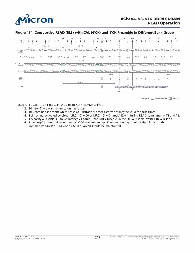
CCMTD-1725822587-9875 Micron Technology, Inc. reserves the right to change products or specifications without notice.8gb_ddr4_dram.pdf - Rev. T 09/2021 EN 2015 Micron Technology, Inc. All rights reserved.217
8Gb: x4, x8, x16 DDR4 SDRAMREAD Operation
Figure 164: Consecutive READ (BL8) with CAL (4tCK) and 1tCK Preamble in Different Bank Group
Notes: 1. BL = 8, RL = 11 (CL = 11, AL = 0), READ preamble = 1tCK.2. DI n (or b) = data-in from column n (or b).3. DES commands are shown for ease of illustration; other commands may be valid at these times.4. BL8 setting activated by either MR0[1:0] = 00 or MR0[1:0] = 01 and A12 = 1 during READ commands at T3 and T8.5. CA parity = Disable, CS to CA latency = Enable, Read DBI = Disable, Write DBI = Disable, Write CRC = Disable.6. Enabling CAL mode does not impact ODT control timings. The same timing relationship relative to the
command/address bus as when CAL is disabled should be maintained.
T0
tCAL = 4 tCAL = 4
tCCD_S = 4
tRPRE
RL = 11
T1 T2 T3 T4
DES DES DES DES DES DESCommandw/o CS_n
DES DES READ READDES DES
DQ
CK_tCK_c
DQS_t,DQS_c
RL = 11
T5 T6 T7 T8 T24T22 T23T16T14 T15 T18 T19 T21
Don’t CareTransitioning DataTime Break
DIn + 1
DIn + 2
DIn + 5
DIn + 6
DIn + 7
DIb
DIb + 1
DIb + 2
DIb + 5
DIb + 6
DIb + 7
DIn
DES DES DES DES DES
Bank GroupAddress
Address BankCol n
BankCol b
BGa BGb
tRPST
CS_n
CCMTD-1725822587-9875 Micron Technology, Inc. reserves the right to change products or specifications without notice.8gb_ddr4_dram.pdf - Rev. T 09/2021 EN 2015 Micron Technology, Inc. All rights reserved.218
8Gb: x4, x8, x16 DDR4 SDRAMWRITE Operation
WRITE Operation
Write Timing Definitions
The write timings shown in the following figures are applicable in normal operation mode, that is, when the DLL is enabled and locked.
The clock-to-data strobe relationship is shown below and is applicable in normal operation mode, that is, when the DLL is enabled and locked.
Rising data strobe edge parameters:tDQSS (MIN) to tDQSS (MAX) describes the allowed range for a rising data strobe edge relative to CK.tDQSS is the actual position of a rising strobe edge relative to CK.tDQSH describes the data strobe high pulse width.tWPST strobe going to HIGH, nondrive level (shown in the postamble section of the graphic below).
Falling data strobe edge parameters:tDQSL describes the data strobe low pulse width.tWPRE strobe going to LOW, initial drive level (shown in the preamble section of the graphic below).
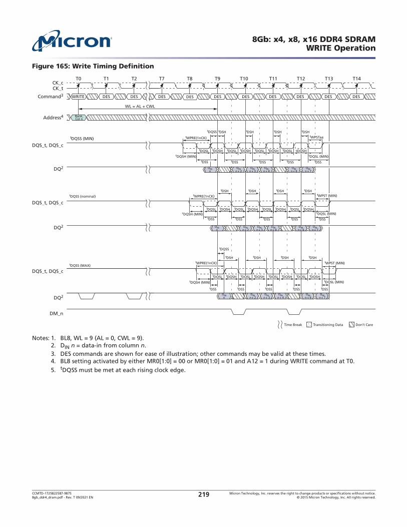
CCMTD-1725822587-9875 Micron Technology, Inc. reserves the right to change products or specifications without notice.8gb_ddr4_dram.pdf - Rev. T 09/2021 EN 2015 Micron Technology, Inc. All rights reserved.219
8Gb: x4, x8, x16 DDR4 SDRAMWRITE Operation
Figure 165: Write Timing Definition
Notes: 1. BL8, WL = 9 (AL = 0, CWL = 9).2. DIN n = data-in from column n.3. DES commands are shown for ease of illustration; other commands may be valid at these times.4. BL8 setting activated by either MR0[1:0] = 00 or MR0[1:0] = 01 and A12 = 1 during WRITE command at T0.
5. tDQSS must be met at each rising clock edge.
WL = AL + CWL
T0 T1 T2 T7 T8 T9 T10 T11 T12 T13 T14
Don’t CareTime Break Transitioning Data
Bank,Col n
DESWRITE DESDES DES DES DES DES DES DES DES
CK_tCK_c
Command3
DQ2
DQS_t, DQS_c
DQS_t, DQS_c
DQS_t, DQS_c
Address4
tWPSTaa
DM_n
tWPST (MIN)
tDQSL
tDQSS (MIN)
DINn
DINn + 2
DINn + 3DQ2
DQ2
tDQSS (MAX)
tDQSS (nominal)
tDQSL
tWPRE(1nCK)
tDQSL
tDQSS
tDQSS
tDSS tDSS tDSS tDSS tDSS
tDSH tDSH tDSH tDSH
tDSS tDSS tDSS tDSS tDSS
tDSS tDSS tDSS tDSS tDSS
tDSH tDSH tDSH tDSH
tDSH tDSH tDSH tDSH
tDQSLtDQSH tDQSLtDQSH tDQSLtDQSH tDQSH
tDQSLtDQSH tDQSLtDQSH tDQSLtDQSH tDQSH
tDQSLtDQSH tDQSLtDQSH tDQSLtDQSH tDQSH
tWPRE(1nCK)
tWPRE(1nCK)
tDQSH (MIN)
tDQSH (MIN)
tDQSH (MIN)
tWPST (MIN)
tDQSL (MIN)
tDQSL (MIN)
tDQSL (MIN)
DINn + 4
DINn + 6
DINn + 7
DINn
DINn + 2
DINn + 3
DINn + 4
DINn + 6
DINn + 7
DINn
DINn + 2
DINn + 3
DINn + 4
DINn + 6
DINn + 7

CCMTD-1725822587-9875 Micron Technology, Inc. reserves the right to change products or specifications without notice.8gb_ddr4_dram.pdf - Rev. T 09/2021 EN 2015 Micron Technology, Inc. All rights reserved.220
8Gb: x4, x8, x16 DDR4 SDRAMWRITE Operation
tWPRE Calculation
Figure 166: tWPRE Method for Calculating Transitions and Endpoints
Notes: 1. Vsw1 = (0.1) VIH,diff,DQS.2. Vsw2 = (0.9) VIH,diff,DQS.
DQS_t
tWPRE ends (t2)
CK_t
CK_c
VDD /2
Resulting differential signal relevant for tWPRE specification
Single-ended signal provided as background information
0V
DQS_c
DQS_t, DQS_c
DQS_tDQS_c
DQS_t
DQS_c
tWPRE begins ( t1)
VSW1
VSW2
VREFDQ
VREFDQ
VREFDQ
VIH,DIFF,DQS VIH,DIFF,Peak
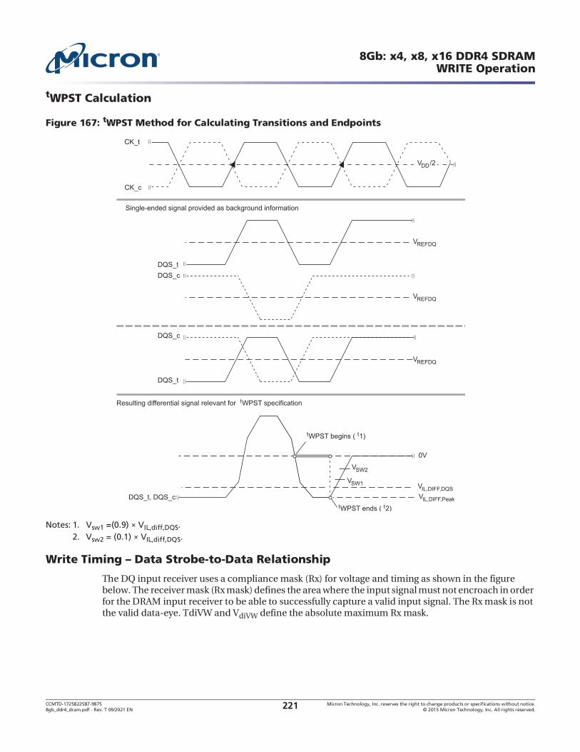
CCMTD-1725822587-9875 Micron Technology, Inc. reserves the right to change products or specifications without notice.8gb_ddr4_dram.pdf - Rev. T 09/2021 EN 2015 Micron Technology, Inc. All rights reserved.221
8Gb: x4, x8, x16 DDR4 SDRAMWRITE Operation
tWPST Calculation
Figure 167: tWPST Method for Calculating Transitions and Endpoints
Notes: 1. Vsw1 =(0.9) VIL,diff,DQS.2. Vsw2 = (0.1) VIL,diff,DQS.
The DQ input receiver uses a compliance mask (Rx) for voltage and timing as shown in the figure below. The receiver mask (Rx mask) defines the area where the input signal must not encroach in order for the DRAM input receiver to be able to successfully capture a valid input signal. The Rx mask is not the valid data-eye. TdiVW and VdiVW define the absolute maximum Rx mask.
DQS_t, DQS_c
VSW1
VSW2
DQS_t
tWPST ends ( t2)
CK_t
CK_c
Resulting differential signal relevant for tWPST specification
Single-ended signal provided as background information
0V
DQS_c
DQS_t
DQS_c
tWPST begins ( t1)
VDD /2
VREFDQ
VREFDQ
VREFDQ
VIL,DIFF,DQS VIL,DIFF,Peak
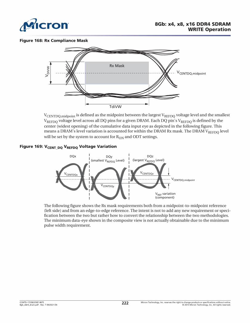
CCMTD-1725822587-9875 Micron Technology, Inc. reserves the right to change products or specifications without notice.8gb_ddr4_dram.pdf - Rev. T 09/2021 EN 2015 Micron Technology, Inc. All rights reserved.222
8Gb: x4, x8, x16 DDR4 SDRAMWRITE Operation
Figure 168: Rx Compliance Mask
VCENTDQ,midpoint is defined as the midpoint between the largest VREFDQ voltage level and the smallest VREFDQ voltage level across all DQ pins for a given DRAM. Each DQ pin's VREFDQ is defined by the center (widest opening) of the cumulative data input eye as depicted in the following figure. This means a DRAM's level variation is accounted for within the DRAM Rx mask. The DRAM VREFDQ level will be set by the system to account for RON and ODT settings.
Figure 169: VCENT_DQ VREFDQ Voltage Variation
The following figure shows the Rx mask requirements both from a midpoint-to-midpoint reference (left side) and from an edge-to-edge reference. The intent is not to add any new requirement or speci-fication between the two but rather how to convert the relationship between the two methodologies. The minimum data-eye shown in the composite view is not actually obtainable due to the minimum pulse width requirement.
TdiVW
VD
IVW
Rx Mask
VCENTDQ,midpoint
VCENTDQx
VCENTDQy
VCENTDQz
VCENTDQ,midpoint
DQx DQy (smallest VREFDQ Level)
DQz (largest VREFDQ Level)
VREF variation(component)

CCMTD-1725822587-9875 Micron Technology, Inc. reserves the right to change products or specifications without notice.8gb_ddr4_dram.pdf - Rev. T 09/2021 EN 2015 Micron Technology, Inc. All rights reserved.223
8Gb: x4, x8, x16 DDR4 SDRAMWRITE Operation
Figure 170: Rx Mask DQ-to-DQS Timings
Notes: 1. DQx represents an optimally centered mask.DQy represents earliest valid mask.DQz represents latest valid mask.
2. DRAMa represents a DRAM without any DQS/DQ skews.
DRAMb represents a DRAM with early skews (negative tDQS2DQ).
DRAMc represents a DRAM with delayed skews (positive tDQS2DQ).3. This figure shows the skew allowed between DRAM-to-DRAM and between DQ-to-DQ for a DRAM. Signals assume
data is center-aligned at DRAM latch.TdiPW is not shown; composite data-eyes shown would violate TdiPW.VCENTDQ,midpoint is not shown but is assumed to be midpoint of VdiVW.
The previous figure shows the basic Rx mask requirements. Converting the Rx mask requirements to a classical DQ-to-DQS relationship is shown in the following figure. It should become apparent that DRAM write training is required to take full advantage of the Rx mask.
DQS, DQs Data-In at DRAM BallDQS, DQs Data-In at DRAM BallRx Mask Rx Mask – Alternative View
Rx Mask
Rx Mask
Rx Mask
Rx Mask
DQS_t
Rx Mask
0.5 × TdiVW0.5 × TdiVW
tDQS2DQ +0.5 × TdiVW
tDQS2DQ +0.5 × TdiVW
DQyDRAMc Rx Mask
DQzDRAMc Rx Mask
DQzDRAMb Rx Mask
DQyDRAMb Rx Mask
DQS_cDQS_c
DQS_t
DQx–zDRAMa
DQyDRAMc
DQzDRAMc
DQzDRAMb
DQyDRAMb
DQx–zDRAMaRx Mask
TdiVW TdiVW
0.5 × TdiVW0.5 × TdiVW
tDQS2DQ
tDQ2DQ
tDQ2DQ
tDQ2DQ
tDQ2DQ
tDQ2DQ
tDQS2DQ
tDQ2DQ
Vd
iVW
Vd
iVW
Vd
iVW
Vd
iVW
Vd
iVW
Vd
iVW
Vd
iVW
Vd
iVW
Vd
iVW
Vd
iVW
TdiVW
TdiVW
TdiVW
TdiVW

CCMTD-1725822587-9875 Micron Technology, Inc. reserves the right to change products or specifications without notice.8gb_ddr4_dram.pdf - Rev. T 09/2021 EN 2015 Micron Technology, Inc. All rights reserved.224
8Gb: x4, x8, x16 DDR4 SDRAMWRITE Operation
Figure 171: Rx Mask DQ-to-DQS DRAM-Based Timings
Notes: 1. DQx represents an optimally centered mask.DQy represents earliest valid mask.DQz represents latest valid mask.
2. *Skew = tDQS2DQ + 0.5 TdiVWDRAMa represents a DRAM without any DQS/DQ skews.
DRAMb represents a DRAM with the earliest skews (negative tDQS2DQ, tDQSy > *Skew).
DRAMc represents a DRAM with the latest skews (positive tDQS2DQ, tDQHz > *Skew).
3. tDS/tDH are traditional data-eye setup/hold edges at DC levels.tDS and tDH are not specified; tDH and tDS may be any value provided the pulse width and Rx mask limits are not violated.tDH (MIN) > TdiVW + tDS (MIN) + tDQ2DQ.
The DDR4 SDRAM's input receivers are expected to capture the input data with an Rx mask of TdiVW provided the minimum pulse width is satisfied. The DRAM controller will have to train the data input buffer to utilize the Rx mask specifications to this maximum benefit. If the DRAM controller does not
DQS_c
DQS_t
Rx Mask
DQS, DQs Data-In at DRAM Ball
Vd
iVW
Vd
iVW
Vd
iVW
Vd
iVW
Vd
iVW
Vd
iVW
DQx , y, z
DQS_c
DQS_t
Rx Mask
DQS, DQs Data-In at DRAM Ball
tDSx tDHx
DQx–zDRAMaDRAMa
DRAMb
DRAMb
DRAMc
DRAMc
TdiPW
TdiPW
Rx Mask vs. Composite Data-Eye Rx Mask vs. UI Data-Eye
TdiPW
*Skew
*Skew
tDSy tDHy
DQyRx Mask
TdiVWtDQ2DQ
DQz
TdiPW
TdiVW TdiVW
tDSz tDHz
DQy tDQ2DQ
DQz
TdiPW
Rx MaskTdiVW
tDQ2DQ
Rx MaskTdiVW
Rx MaskTdiVW
tDQ2DQ
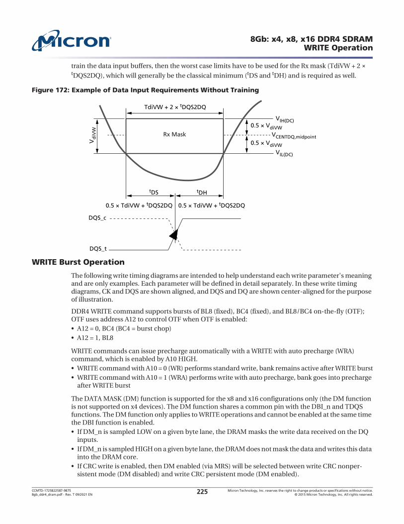
CCMTD-1725822587-9875 Micron Technology, Inc. reserves the right to change products or specifications without notice.8gb_ddr4_dram.pdf - Rev. T 09/2021 EN 2015 Micron Technology, Inc. All rights reserved.225
8Gb: x4, x8, x16 DDR4 SDRAMWRITE Operation
train the data input buffers, then the worst case limits have to be used for the Rx mask (TdiVW + 2 tDQS2DQ), which will generally be the classical minimum (tDS and tDH) and is required as well.
Figure 172: Example of Data Input Requirements Without Training
WRITE Burst Operation
The following write timing diagrams are intended to help understand each write parameter's meaning and are only examples. Each parameter will be defined in detail separately. In these write timing diagrams, CK and DQS are shown aligned, and DQS and DQ are shown center-aligned for the purpose of illustration.
DDR4 WRITE command supports bursts of BL8 (fixed), BC4 (fixed), and BL8/BC4 on-the-fly (OTF); OTF uses address A12 to control OTF when OTF is enabled:
A12 = 0, BC4 (BC4 = burst chop)A12 = 1, BL8
WRITE commands can issue precharge automatically with a WRITE with auto precharge (WRA) command, which is enabled by A10 HIGH.
WRITE command with A10 = 0 (WR) performs standard write, bank remains active after WRITE burstWRITE command with A10 = 1 (WRA) performs write with auto precharge, bank goes into precharge after WRITE burst
The DATA MASK (DM) function is supported for the x8 and x16 configurations only (the DM function is not supported on x4 devices). The DM function shares a common pin with the DBI_n and TDQS functions. The DM function only applies to WRITE operations and cannot be enabled at the same time the DBI function is enabled.
If DM_n is sampled LOW on a given byte lane, the DRAM masks the write data received on the DQ inputs.If DM_n is sampled HIGH on a given byte lane, the DRAM does not mask the data and writes this data into the DRAM core.If CRC write is enabled, then DM enabled (via MRS) will be selected between write CRC nonper-sistent mode (DM disabled) and write CRC persistent mode (DM enabled).
tDS
Vd
iVW
0.5 × VdiVW
0.5 × VdiVW
tDH
0.5 × TdiVW + tDQS2DQ
TdiVW + 2 × tDQS2DQ
0.5 × TdiVW + tDQS2DQ
VCENTDQ,midpoint
VIL(DC)
VIH(DC)
DQS_c
DQS_t
Rx Mask
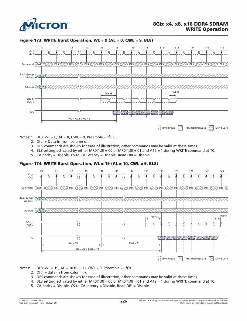
CCMTD-1725822587-9875 Micron Technology, Inc. reserves the right to change products or specifications without notice.8gb_ddr4_dram.pdf - Rev. T 09/2021 EN 2015 Micron Technology, Inc. All rights reserved.226
8Gb: x4, x8, x16 DDR4 SDRAMWRITE Operation
Figure 173: WRITE Burst Operation, WL = 9 (AL = 0, CWL = 9, BL8)
Notes: 1. BL8, WL = 0, AL = 0, CWL = 9, Preamble = 1tCK.2. DI n = Data-in from column n.3. DES commands are shown for ease of illustration; other commands may be valid at these times.4. BL8 setting activated by either MR0[1:0] = 00 or MR0[1:0] = 01 and A12 = 1 during WRITE command at T0.5. CA parity = Disable, CS to CA Latency = Disable, Read DBI = Disable.
Figure 174: WRITE Burst Operation, WL = 19 (AL = 10, CWL = 9, BL8)
Notes: 1. BL8, WL = 19, AL = 10 (CL - 1), CWL = 9, Preamble = 1tCK.2. DI n = data-in from column n.3. DES commands are shown for ease of illustration; other commands may be valid at these times.4. BL8 setting activated by either MR0[1:0] = 00 or MR0[1:0] = 01 and A12 = 1 during WRITE command at T0.5. CA parity = Disable, CS to CA latency = Disable, Read DBI = Disable.
T0
tWPRE
T1 T7T2 T8 T9 T10 T11 T12 T13
DES DES DES DES DES DES DESCommand DESWRITE DES DES DES DES
DQ
CK_tCK_c
DQS_t,DQS_c
WL = AL + CWL = 9
T16T14 T15
Don’t CareTransitioning DataTime Break
DIn + 1
DIn + 2
DIn + 3
DIn + 4
DIn + 5
DIn + 6
DIn + 7
DIn
Bank GroupAddress
Address BankCol n
BGa
tWPST
T0
tWPRE
AL = 10 CWL = 9
T1 T2 T9 T10 T11
DES DES DES DES DES DES DESCommand DESWRITE DES DES DES DES
DQ
CK_tCK_c
DQS_t,DQS_c
WL = AL + CWL = 19
T21T17 T18 T19 T20 T23T22
Don’t CareTransitioning DataTime Break
DIn
DIn + 1
DIn + 2
DIn + 3
DIn + 4
DIn + 5
DIn + 6
DIn + 7
Bank GroupAddress
Address BankCol n
BGa
tWPST
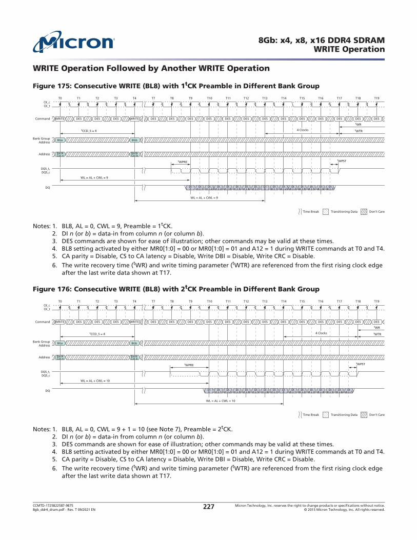
CCMTD-1725822587-9875 Micron Technology, Inc. reserves the right to change products or specifications without notice.8gb_ddr4_dram.pdf - Rev. T 09/2021 EN 2015 Micron Technology, Inc. All rights reserved.227
8Gb: x4, x8, x16 DDR4 SDRAMWRITE Operation
WRITE Operation Followed by Another WRITE Operation
Figure 175: Consecutive WRITE (BL8) with 1tCK Preamble in Different Bank Group
Notes: 1. BL8, AL = 0, CWL = 9, Preamble = 1tCK.2. DI n (or b) = data-in from column n (or column b).3. DES commands are shown for ease of illustration; other commands may be valid at these times.4. BL8 setting activated by either MR0[1:0] = 00 or MR0[1:0] = 01 and A12 = 1 during WRITE commands at T0 and T4.5. CA parity = Disable, CS to CA latency = Disable, Write DBI = Disable, Write CRC = Disable.
6. The write recovery time (tWR) and write timing parameter (tWTR) are referenced from the first rising clock edge after the last write data shown at T17.
Figure 176: Consecutive WRITE (BL8) with 2tCK Preamble in Different Bank Group
Notes: 1. BL8, AL = 0, CWL = 9 + 1 = 10 (see Note 7), Preamble = 2tCK.2. DI n (or b) = data-in from column n (or column b).3. DES commands are shown for ease of illustration; other commands may be valid at these times.4. BL8 setting activated by either MR0[1:0] = 00 or MR0[1:0] = 01 and A12 = 1 during WRITE commands at T0 and T4.5. CA parity = Disable, CS to CA latency = Disable, Write DBI = Disable, Write CRC = Disable.
6. The write recovery time (tWR) and write timing parameter (tWTR) are referenced from the first rising clock edge after the last write data shown at T17.
T0
tCCD_S = 4 4 Clocks
tWPRE
WL = AL + CWL = 9
T1 T2 T3 T4
DES DES DES DES DES DES DESCommand DESWRITE DES DES WRITE DES
DQ
CK_tCK_c
DQS_t,DQS_c
WL = AL + CWL = 9
T7 T8 T9 T10 T11 T12 T13 T16T14 T15 T17 T18 T19
Don’t CareTransitioning DataTime Break
DIn + 1
DIn + 2
DIn + 3
DIn + 4
DIn + 5
DIn + 6
DIn + 7
DIb
DIb + 1
DIb + 2
DIb + 3
DIb + 4
DIb + 5
DIb + 6
DIb + 7
DIn
DES DES DES DES DES
Bank GroupAddress
Address BankCol n
BankCol b
BGa BGb
tWPST
tWTR
tWR
T0
tCCD_S = 4 4 Clocks
tWPRE
WL = AL + CWL = 10
T1 T2 T3 T4
DES DES DES DES DES DES DESCommand DESWRITE DES DES WRITE DES
DQ
CK_tCK_c
DQS_t,DQS_c
WL = AL + CWL = 10
T7 T8 T9 T10 T11 T12 T13 T16T14 T15 T17 T18 T19
Don’t CareTransitioning DataTime Break
DIn + 1
DIn + 2
DIn + 3
DIn + 4
DIn + 5
DIn + 6
DIn + 7
DIb
DIb + 1
DIb + 2
DIb + 3
DIb + 4
DIb + 5
DIb + 6
DIb + 7
DIn
DES DES DES DES DES
Bank GroupAddress
Address BankCol n
BankCol b
BGa BGb
tWPST
tWTR
tWR
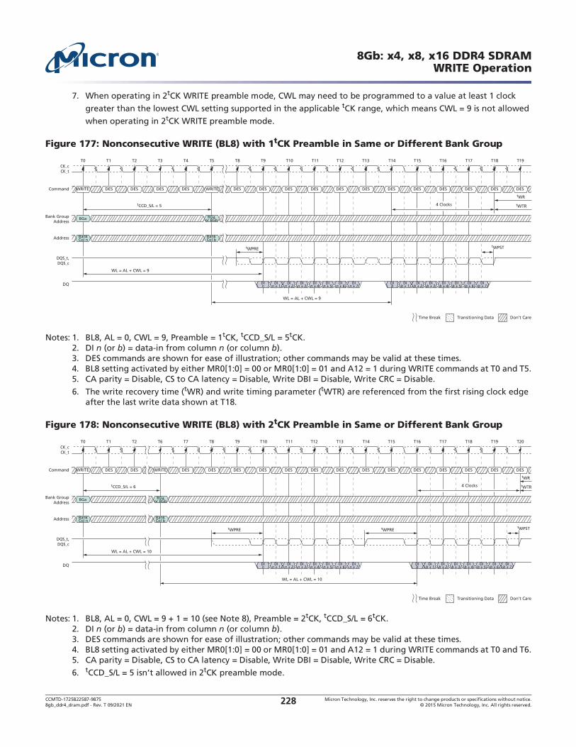
CCMTD-1725822587-9875 Micron Technology, Inc. reserves the right to change products or specifications without notice.8gb_ddr4_dram.pdf - Rev. T 09/2021 EN 2015 Micron Technology, Inc. All rights reserved.228
8Gb: x4, x8, x16 DDR4 SDRAMWRITE Operation
7. When operating in 2tCK WRITE preamble mode, CWL may need to be programmed to a value at least 1 clock
greater than the lowest CWL setting supported in the applicable tCK range, which means CWL = 9 is not allowed
when operating in 2tCK WRITE preamble mode.
Figure 177: Nonconsecutive WRITE (BL8) with 1tCK Preamble in Same or Different Bank Group
Notes: 1. BL8, AL = 0, CWL = 9, Preamble = 1tCK, tCCD_S/L = 5tCK.2. DI n (or b) = data-in from column n (or column b).3. DES commands are shown for ease of illustration; other commands may be valid at these times.4. BL8 setting activated by either MR0[1:0] = 00 or MR0[1:0] = 01 and A12 = 1 during WRITE commands at T0 and T5.5. CA parity = Disable, CS to CA latency = Disable, Write DBI = Disable, Write CRC = Disable.
6. The write recovery time (tWR) and write timing parameter (tWTR) are referenced from the first rising clock edge after the last write data shown at T18.
Figure 178: Nonconsecutive WRITE (BL8) with 2tCK Preamble in Same or Different Bank Group
Notes: 1. BL8, AL = 0, CWL = 9 + 1 = 10 (see Note 8), Preamble = 2tCK, tCCD_S/L = 6tCK.2. DI n (or b) = data-in from column n (or column b).3. DES commands are shown for ease of illustration; other commands may be valid at these times.4. BL8 setting activated by either MR0[1:0] = 00 or MR0[1:0] = 01 and A12 = 1 during WRITE commands at T0 and T6.5. CA parity = Disable, CS to CA latency = Disable, Write DBI = Disable, Write CRC = Disable.
6. t tCK preamble mode.
T0
tCCD_S/L = 5 4 Clocks
tWPRE
WL = AL + CWL = 9
T1 T2 T3 T4
DES DES DES DES DES DES DESCommand DESWRITE DES DES DES WRITE
DQ
CK_tCK_c
DQS_t,DQS_c
WL = AL + CWL = 9
T5 T8 T9 T10 T11 T12 T13 T16T14 T15 T17 T18 T19
Don’t CareTransitioning DataTime Break
DIn + 1
DIn + 2
DIn + 3
DIn + 4
DIn + 5
DIn + 6
DIn + 7
DIb
DIb + 1
DIb + 2
DIb + 3
DIb + 4
DIb + 5
DIb + 6
DIb + 7
DIn
DES DES DES DES DES
Bank GroupAddress
Address BankCol n
BankCol b
BGa BGaor BGb
tWPST
tWTR
tWR
T0
tCCD_S/L = 6 4 Clocks
tWPRE
WL = AL + CWL = 10
T1 T2 T6 T7
DES DES DES DES DES DES DESCommand DESWRITE DES WRITE DES DES
DQ
CK_tCK_c
DQS_t,DQS_c
WL = AL + CWL = 10
T8 T9 T10 T11 T12 T13 T16T14 T15 T17 T18 T20T19
Don’t CareTransitioning DataTime Break
DIn + 1
DIn + 2
DIn + 3
DIn + 4
DIn + 5
DIn + 6
DIn + 7
DIb
DIb + 1
DIb + 2
DIb + 3
DIb + 4
DIb + 5
DIb + 6
DIb + 7
DIn
DES DES DES DES DES
Bank GroupAddress
Address BankCol n
BankCol b
BGa BGaor BGb
tWPREtWPST
tWTR
tWR

CCMTD-1725822587-9875 Micron Technology, Inc. reserves the right to change products or specifications without notice.8gb_ddr4_dram.pdf - Rev. T 09/2021 EN 2015 Micron Technology, Inc. All rights reserved.229
8Gb: x4, x8, x16 DDR4 SDRAMWRITE Operation
7. The write recovery time (tWR) and write timing parameter (tWTR) are referenced from the first rising clock edge after the last write data shown at T20.
8. When operating in 2tCK WRITE preamble mode, CWL may need to be programmed to a value at least 1 clock
greater than the lowest CWL setting supported in the applicable tCK range, which means CWL = 9 is not allowed
when operating in 2tCK WRITE preamble mode.
Figure 179: WRITE (BC4) OTF to WRITE (BC4) OTF with 1tCK Preamble in Different Bank Group
Notes: 1. BC4, AL = 0, CWL = 9, Preamble = 1tCK.2. DI n (or b) = data-in from column n (or column b).3. DES commands are shown for ease of illustration; other commands may be valid at these times.4. BC4 setting activated by MR0[1:0] = 01 and A12 = 0 during WRITE commands at T0 and T4.5. CA parity = Disable, CS to CA latency = Disable, Write DBI = Disable, Write CRC = Disable.
6. The write recovery time (tWR) and write timing parameter (tWTR) are referenced from the first rising clock edge after the last write data shown at T17.
Figure 180: WRITE (BC4) OTF to WRITE (BC4) OTF with 2tCK Preamble in Different Bank Group
Notes: 1. BC4, AL = 0, CWL = 9 + 1 = 10 (see Note 7), Preamble = 2tCK.2. DI n (or b) = data-in from column n (or column b).3. DES commands are shown for ease of illustration; other commands may be valid at these times.4. BC4 setting activated by MR0[1:0] = 01 and A12 = 1 during WRITE commands at T0 and T4.5. CA parity = Disable, CS to CA latency = Disable, Write DBI = Disable, Write CRC = Disable.
T0
tCCD_S = 4 4 Clocks
tWPRE
WL = AL + CWL = 9
T1 T2 T3 T4
DES DES DES DES DES DES DESCommand DESWRITE DES DES WRITE DES
DQ
CK_tCK_c
DQS_t,DQS_c
WL = AL + CWL = 9
T7 T8 T9 T10 T11 T12 T13 T16T14 T15 T17 T18 T19
Don’t CareTransitioning DataTime Break
DIn + 1
DIn + 2
DIn + 3
DIb
DIb + 1
DIb + 2
DIb + 3
DIn
DES DES DES DES DES
Bank GroupAddress
Address BankCol n
BankCol b
BGa BGb
tWPRE
tWTR
tWR
tWPSTtWPST
T0
tCCD_S = 4 4 Clocks
tWPRE
WL = AL + CWL = 10
T1 T2 T3 T4
DES DES DES DES DES DES DESCommand DESWRITE DES DES WRITE DES
DQ
CK_tCK_c
DQS_t,DQS_c
WL = AL + CWL = 10
T7 T8 T9 T10 T11 T12 T13 T16T14 T15 T17 T18 T19
Don’t CareTransitioning DataTime Break
DIn + 1
DIn + 2
DIn + 3
DIb
DIb + 1
DIb + 2
DIb + 3
DIn
DES DES DES DES DES
Bank GroupAddress
Address BankCol n
BankCol b
BGa BGb
tWPRE
tWTR
tWR
tWPST

CCMTD-1725822587-9875 Micron Technology, Inc. reserves the right to change products or specifications without notice.8gb_ddr4_dram.pdf - Rev. T 09/2021 EN 2015 Micron Technology, Inc. All rights reserved.230
8Gb: x4, x8, x16 DDR4 SDRAMWRITE Operation
6. The write recovery time (tWR) and write timing parameter (tWTR) are referenced from the first rising clock edge after the last write data shown at T18.
7. When operating in 2tCK WRITE preamble mode, CWL may need to be programmed to a value at least 1 clock
greater than the lowest CWL setting supported in the applicable tCK range, which means CWL = 9 is not allowed
when operating in 2tCK WRITE preamble mode.
Figure 181: WRITE (BC4) Fixed to WRITE (BC4) Fixed with 1tCK Preamble in Different Bank Group
Notes: 1. BC4, AL = 0, CWL = 9, Preamble = 1tCK.2. DI n (or b) = data-in from column n (or column b).3. DES commands are shown for ease of illustration; other commands may be valid at these times.4. BC4 (fixed) setting activated by MR0[1:0] = 10.5. CA parity = Disable, CS to CA latency = Disable, Write DBI = Disable, Write CRC = Disable.
6. The write recovery time (tWR) and write timing parameter (tWTR) are referenced from the first rising clock edge after the last write data shown at T15.
Figure 182: WRITE (BL8) to WRITE (BC4) OTF with 1tCK Preamble in Different Bank Group
Notes: 1. BL = 8/BC = 4, AL = 0, CL = 9, Preamble = 1tCK.2. DI n (or b) = data-in from column n (or column b).3. DES commands are shown for ease of illustration; other commands may be valid at these times.4. BL8 setting activated by MR0[1:0] = 01 and A12 = 1 during WRITE command at T0.
BC4 setting activated by MR0[1:0] = 01 and A12 = 0 during WRITE command at T4.
T0
tCCD_S = 4 2 Clocks
tWPRE
WL = AL + CWL = 9
T1 T2 T3 T4
DES DES DES DES DES DES DESCommand DESWRITE DES DES WRITE DES
DQ
CK_tCK_c
DQS_t,DQS_c
WL = AL + CWL = 9
T7 T8 T9 T10 T11 T12 T13 T16T14 T15 T17 T18 T19
Don’t CareTransitioning DataTime Break
DIn + 1
DIn + 2
DIn + 3
DIb
DIb + 1
DIb + 2
DIb + 3
DIn
DES DES DES DES DES
Bank GroupAddress
Address BankCol n
BankCol b
BGa BGb
tWPRE
tWTR
tWR
tWPSTtWPST
T0
tCCD_S = 4 4 Clocks
tWPRE
WL = AL + CWL = 9
T1 T2 T3 T4
DES DES DES DES DES DES DESCommand DESWRITE DES DES WRITE DES
DQ
CK_tCK_c
DQS_t,DQS_c
WL = AL + CWL = 9
T7 T8 T9 T10 T11 T12 T13 T16T14 T15 T17 T18 T19
Don’t CareTransitioning DataTime Break
DIn + 1
DIn + 2
DIn + 3
DIn + 4
DIn + 5
DIn + 6
DIn + 7
DIb
DIb + 1
DIb + 2
DIb + 3
DIn
DES DES DES DES DES
Bank GroupAddress
Address BankCol n
BankCol b
BGa BGb
tWTR
tWR
tWPST

CCMTD-1725822587-9875 Micron Technology, Inc. reserves the right to change products or specifications without notice.8gb_ddr4_dram.pdf - Rev. T 09/2021 EN 2015 Micron Technology, Inc. All rights reserved.231
8Gb: x4, x8, x16 DDR4 SDRAMWRITE Operation
5. CA parity = Disable, CS to CA latency = Disable, Read DBI = Disable, Write CRC = Disable.
6. The write recovery time (tWR) and write timing parameter (tWTR) are referenced from the first rising clock edge after the last write data shown at T17.
Figure 183: WRITE (BC4) OTF to WRITE (BL8) with 1tCK Preamble in Different Bank Group
Notes: 1. BL = 8/BC = 4, AL = 0, CL = 9, Preamble = 1tCK.2. DI n (or b) = data-in from column n (or column b).3. DES commands are shown for ease of illustration; other commands may be valid at these times.4. BC4 setting activated by MR0[1:0] = 01 and A12 = 0 during WRITE command at T0.
BL8 setting activated by MR0[1:0] = 01 and A12 = 1 during WRITE command at T4.5. CA parity = Disable, CS to CA latency = Disable, Read DBI = Disable, Write CRC = Disable.
6. The write recovery time (tWR) and write timing parameter (tWTR) are referenced from the first rising clock edge after the last write data shown at T17.
WRITE Operation Followed by READ Operation
Figure 184: WRITE (BL8) to READ (BL8) with 1tCK Preamble in Different Bank Group
Notes: 1. BL = 8, WL = 9 (CWL = 9, AL = 0), CL = 11, READ preamble = 1tCK, WRITE preamble = 1tCK.2. DI b = data-in from column b.3. DES commands are shown for ease of illustration; other commands may be valid at these times.4. BL8 setting activated by either MR0[1:0] = 00 or MR0[1:0] = 01 and A12 = 1 during WRITE command at T0 and READ
command at T15.
T0
tCCD_S = 4
tWPRE tWPRE
WL = AL + CWL = 9
T1 T2 T3 T4
DES DES DES DES DES DES DESCommand DESWRITE DES DES WRITE DES
DQ
CK_tCK_c
DQS_t,DQS_c
WL = AL + CWL = 9
T7 T8 T9 T10 T11 T12 T13 T16T14 T15 T17 T18 T19
Don’t CareTransitioning DataTime Break
DIn + 1
DIn + 2
DIn + 3
DIb
DIb + 1
DIb + 2
DIb + 3
DIb + 4
DIb + 5
DIb + 6
DIb + 7
DIn
DES DES DES DES DES
Bank GroupAddress
Address BankCol n
BankCol b
BGa BGb
tWTR
tWR
tWPSTtWPST
4 Clocks
DIb
DIb + 1
DIb + 2
DIb + 3
DIb + 4
DIb + 5
DIb + 6
T0
tWTR_S = 2
tWPRE
WL = AL + CWL = 9 RL = AL + CL = 11
T1 T7
DES DES DES DES READ DES DESCommand DESWRITE DES DES DES DES
DQ
CK_tCK_c
DQS_t,DQS_c
T8 T9 T10 T11 T12 T13 T16T14 T15 T24 T25 T26 T27 T28 T29
Don’t CareTransitioning DataTime Break
DIn + 1
DIn + 2
DIn + 3
DIn + 4
DIn + 5
DIn + 6
DIn + 7
DIn
DES DES DES DES DES
Bank GroupAddress
Address BankCol n
BankCol b
BGa BGb
tRPREtWPST
4 Clocks
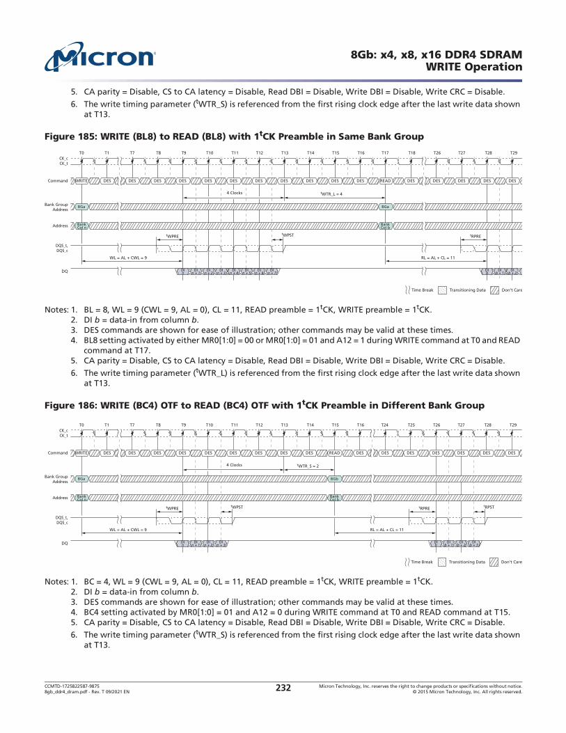
CCMTD-1725822587-9875 Micron Technology, Inc. reserves the right to change products or specifications without notice.8gb_ddr4_dram.pdf - Rev. T 09/2021 EN 2015 Micron Technology, Inc. All rights reserved.232
8Gb: x4, x8, x16 DDR4 SDRAMWRITE Operation
5. CA parity = Disable, CS to CA latency = Disable, Read DBI = Disable, Write DBI = Disable, Write CRC = Disable.
6. The write timing parameter (tWTR_S) is referenced from the first rising clock edge after the last write data shown at T13.
Figure 185: WRITE (BL8) to READ (BL8) with 1tCK Preamble in Same Bank Group
Notes: 1. BL = 8, WL = 9 (CWL = 9, AL = 0), CL = 11, READ preamble = 1tCK, WRITE preamble = 1tCK.2. DI b = data-in from column b.3. DES commands are shown for ease of illustration; other commands may be valid at these times.4. BL8 setting activated by either MR0[1:0] = 00 or MR0[1:0] = 01 and A12 = 1 during WRITE command at T0 and READ
command at T17.5. CA parity = Disable, CS to CA latency = Disable, Read DBI = Disable, Write DBI = Disable, Write CRC = Disable.
6. The write timing parameter (tWTR_L) is referenced from the first rising clock edge after the last write data shown at T13.
Figure 186: WRITE (BC4) OTF to READ (BC4) OTF with 1tCK Preamble in Different Bank Group
Notes: 1. BC = 4, WL = 9 (CWL = 9, AL = 0), CL = 11, READ preamble = 1tCK, WRITE preamble = 1tCK.2. DI b = data-in from column b.3. DES commands are shown for ease of illustration; other commands may be valid at these times.4. BC4 setting activated by MR0[1:0] = 01 and A12 = 0 during WRITE command at T0 and READ command at T15.5. CA parity = Disable, CS to CA latency = Disable, Read DBI = Disable, Write DBI = Disable, Write CRC = Disable.
6. The write timing parameter (tWTR_S) is referenced from the first rising clock edge after the last write data shown at T13.
T0
tWTR_L = 4
tWPRE
WL = AL + CWL = 9 RL = AL + CL = 11
T1 T7
DES DES DES DES DES DESDESCommand DESWRITE DES DES DES READ
DQ
CK_tCK_c
DQS_t,DQS_c
T8 T9 T10 T11 T12 T13 T16T14 T15 T17 T18 T26 T27 T28 T29
Don’t CareTransitioning DataTime Break
DIn + 1
DIn + 2
DIn + 3
DIn + 4
DIn + 5
DIn + 6
DIn + 7
DIn
DES DES DES DES DES
Bank GroupAddress
Address BankCol n
BankCol b
BGa BGa
tRPREtWPST
DIb
DIb + 1
DIb + 2
4 Clocks
T0
tWTR_S = 2
tWPRE
WL = AL + CWL = 9 RL = AL + CL = 11
T1 T7
DES DES DES DES READ DES DESCommand DESWRITE DES DES DES DES
DQ
CK_tCK_c
DQS_t,DQS_c
T8 T9 T10 T11 T12 T13 T16T14 T15 T24 T25 T26 T27 T28 T29
Don’t CareTransitioning DataTime Break
DIn + 1
DIn + 2
DIn + 3
DIn
DES DES DES DES DES
Bank GroupAddress
Address BankCol n
BankCol b
BGa BGb
tRPREtWPST tRPST
DIb
DIb + 1
DIb + 2
DIb + 3
4 Clocks
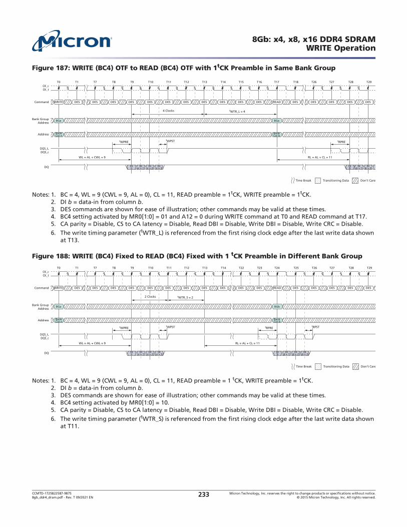
CCMTD-1725822587-9875 Micron Technology, Inc. reserves the right to change products or specifications without notice.8gb_ddr4_dram.pdf - Rev. T 09/2021 EN 2015 Micron Technology, Inc. All rights reserved.233
8Gb: x4, x8, x16 DDR4 SDRAMWRITE Operation
Figure 187: WRITE (BC4) OTF to READ (BC4) OTF with 1tCK Preamble in Same Bank Group
Notes: 1. BC = 4, WL = 9 (CWL = 9, AL = 0), CL = 11, READ preamble = 1tCK, WRITE preamble = 1tCK.2. DI b = data-in from column b.3. DES commands are shown for ease of illustration; other commands may be valid at these times.4. BC4 setting activated by MR0[1:0] = 01 and A12 = 0 during WRITE command at T0 and READ command at T17.5. CA parity = Disable, CS to CA latency = Disable, Read DBI = Disable, Write DBI = Disable, Write CRC = Disable.
6. The write timing parameter (tWTR_L) is referenced from the first rising clock edge after the last write data shown at T13.
Figure 188: WRITE (BC4) Fixed to READ (BC4) Fixed with 1 tCK Preamble in Different Bank Group
Notes: 1. BC = 4, WL = 9 (CWL = 9, AL = 0), CL = 11, READ preamble = 1 tCK, WRITE preamble = 1tCK.2. DI b = data-in from column b.3. DES commands are shown for ease of illustration; other commands may be valid at these times.4. BC4 setting activated by MR0[1:0] = 10.5. CA parity = Disable, CS to CA latency = Disable, Read DBI = Disable, Write DBI = Disable, Write CRC = Disable.
6. The write timing parameter (tWTR_S) is referenced from the first rising clock edge after the last write data shown at T11.
T0
tWTR_L = 4
tWPRE
WL = AL + CWL = 9 RL = AL + CL = 11
T1 T7
DES DES DES DES DES DES READCommand DESWRITE DES DES DES DES
DQ
CK_tCK_c
DQS_t,DQS_c
T8 T9 T10 T11 T12 T13 T16T14 T15 T17 T18 T26 T27 T28 T29
Don’t CareTransitioning DataTime Break
DIn + 1
DIn + 2
DIn + 3
DIn
DES DES DES DES DES
Bank GroupAddress
Address BankCol n
BankCol b
BGa BGa
tRPREtWPST
DIb
DIb + 1
DIb + 2
4 Clocks
T0
tWTR_S = 2
tWPRE
WL = AL + CWL = 9 RL = AL + CL = 11
T1 T7
DES DES DES DES DES DES READCommand DESWRITE DES DES DES DES
DQ
CK_tCK_c
DQS_t,DQS_c
T8 T9 T10 T11 T12 T13 T23T14 T22 T24 T25 T26 T27 T28 T29
Don’t CareTransitioning DataTime Break
DIn + 1
DIn + 2
DIn + 3
DIn
DES DES DES DES DES
Bank GroupAddress
Address BankCol n
BankCol b
BGa BGb
tRPREtWPST tRPST
DIb
DIb + 1
DIb + 2
DIb + 3
2 Clocks
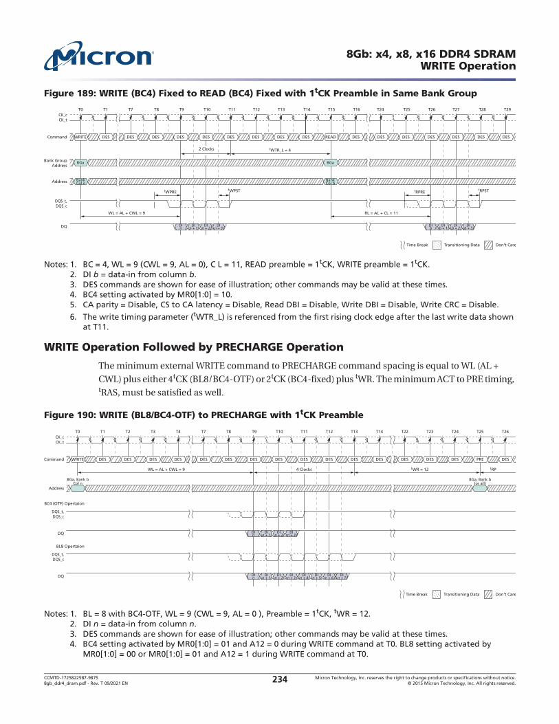
CCMTD-1725822587-9875 Micron Technology, Inc. reserves the right to change products or specifications without notice.8gb_ddr4_dram.pdf - Rev. T 09/2021 EN 2015 Micron Technology, Inc. All rights reserved.234
8Gb: x4, x8, x16 DDR4 SDRAMWRITE Operation
Figure 189: WRITE (BC4) Fixed to READ (BC4) Fixed with 1tCK Preamble in Same Bank Group
Notes: 1. BC = 4, WL = 9 (CWL = 9, AL = 0), C L = 11, READ preamble = 1tCK, WRITE preamble = 1tCK.2. DI b = data-in from column b.3. DES commands are shown for ease of illustration; other commands may be valid at these times.4. BC4 setting activated by MR0[1:0] = 10.5. CA parity = Disable, CS to CA latency = Disable, Read DBI = Disable, Write DBI = Disable, Write CRC = Disable.
6. The write timing parameter (tWTR_L) is referenced from the first rising clock edge after the last write data shown at T11.
WRITE Operation Followed by PRECHARGE Operation
The minimum external WRITE command to PRECHARGE command spacing is equal to WL (AL +
CWL) plus either 4tCK (BL8/BC4-OTF) or 2tCK (BC4-fixed) plus tWR. The minimum ACT to PRE timing, tRAS, must be satisfied as well.
Figure 190: WRITE (BL8/BC4-OTF) to PRECHARGE with 1tCK Preamble
Notes: 1. BL = 8 with BC4-OTF, WL = 9 (CWL = 9, AL = 0 ), Preamble = 1tCK, tWR = 12.2. DI n = data-in from column n.3. DES commands are shown for ease of illustration; other commands may be valid at these times.4. BC4 setting activated by MR0[1:0] = 01 and A12 = 0 during WRITE command at T0. BL8 setting activated by
MR0[1:0] = 00 or MR0[1:0] = 01 and A12 = 1 during WRITE command at T0.
T0
tWTR_L = 4
tWPRE
WL = AL + CWL = 9 RL = AL + CL = 11
T1 T7
DES DES DES DES DESDESREADCommand DESWRITE DES DES DES DES
DQ
CK_tCK_c
DQS_t,DQS_c
T8 T9 T10 T11 T12 T13 T16T14 T15 T24 T25 T26 T27 T28 T29
Don’t CareTransitioning DataTime Break
DIn + 1
DIn + 2
DIn + 3
DIn
DES DES DES DES DES
Bank GroupAddress
Address BankCol n
BankCol b
BGa BGa
tRPREtWPST tRPST
DIb
DIb + 1
DIb + 2
DIb + 3
2 Clocks
T0
WL = AL + CWL = 9 tWR = 12 tRP
T1 T2 T3 T4
DES DES DES DES DES DES DESCommand DESWRITE DES DES DES DES
DQ
BC4 (OTF) Opertaion
CK_tCK_c
DQS_t,DQS_c
T14T7 T8 T9 T10 T11 T12 T13 T26T22 T23 T24 T25
Don’t CareTransitioning DataTime Break
DIn + 1
DIn + 2
DIn + 3
DIn
DES DES DES PRE DES
Address
BGa, Bank bCol n
BGa, Bank b(or all)
DQ
BL8 Opertaion
DQS_t,DQS_c
DIn + 1
DIn + 2
DIn + 3
DIn + 4
DIn + 5
DIn + 6
DIn + 7
DIn
4 Clocks

CCMTD-1725822587-9875 Micron Technology, Inc. reserves the right to change products or specifications without notice.8gb_ddr4_dram.pdf - Rev. T 09/2021 EN 2015 Micron Technology, Inc. All rights reserved.235
8Gb: x4, x8, x16 DDR4 SDRAMWRITE Operation
5. CA parity = Disable, CS to CA latency = Disable, Read DBI = Disable, CRC = Disable.
6. The write recovery time (tWR) is referenced from the first rising clock edge after the last write data shown at T13. tWR specifies the last burst WRITE cycle until the PRECHARGE command can be issued to the same bank.
Figure 191: WRITE (BC4-Fixed) to PRECHARGE with 1tCK Preamble
Notes: 1. BC4 = fixed, WL = 9 (CWL = 9, AL = 0 ), Preamble = 1tCK, tWR = 12.2. DI n = data-in from column n.3. DES commands are shown for ease of illustration; other commands may be valid at these times.4. BC4 setting activated by MR0[1:0] = 10.5. CA parity = Disable, CS to CA latency = Disable, Read DBI = Disable, CRC = Disable.
6. The write recovery time (tWR) is referenced from the first rising clock edge after the last write data shown at T11. tWR specifies the last burst WRITE cycle until the PRECHARGE command can be issued to the same bank.
Figure 192: WRITE (BL8/BC4-OTF) to Auto PRECHARGE with 1tCK Preamble
Notes: 1. BL = 8 with BC4-OTF, WL = 9 (CWL = 9, AL = 0 ), Preamble = 1tCK, tWR = 12.2. DI n = data-in from column n.3. DES commands are shown for ease of illustration; other commands may be valid at these times.4. BC4 setting activated by MR0[1:0] = 01 and A12 = 0 during WRITE command at T0.
BL8 setting activated by MR0[1:0] = 00 or MR0[1:0] = 01 and A12 = 1 during WRITE command at T0.5. CA parity = Disable, CS to CA latency = Disable, Read DBI = Disable, CRC = Disable.
6. The write recovery time (tWR) is referenced from the first rising clock edge after the last write data shown at T13. tWR specifies the last burst WRITE cycle until the PRECHARGE command can be issued to the same bank.
T0
WL = AL + CWL = 9 tWR = 12 tRP
T1 T2 T3 T4
DES DES DES DES DES DES DESCommand DESWRITE DES DES DES DES
DQ
BC4 (Fixed) Opertaion
CK_tCK_c
DQS_t,DQS_c
T14T7 T8 T9 T10 T11 T12 T13 T26T22 T23 T24 T25
Don’t CareTransitioning DataTime Break
DIn + 1
DIn + 2
DIn + 3
DIn
DES PRE DES DES DES
Address
BGa, Bank bCol n
BGa, Bank b(or all)
2 Clocks
T0
WL = AL + CWL = 9 tWR = 12 tRP
T1 T2 T3 T4
DES DES DES DES DES DES DESCommand DESWRITE DES DES DES DES
DQ
BC4 (OTF) Opertaion
CK_tCK_c
DQS_t,DQS_c
T14T7 T8 T9 T10 T11 T12 T13 T26T22 T23 T24 T25
Don’t CareTransitioning DataTime Break
DIn + 1
DIn + 2
DIn + 3
DIn
DES DES DES DES DES
Address
BGa, Bank bCol n
DQ
BL8 Opertaion
DQS_t,DQS_c
DIn + 1
DIn + 2
DIn + 3
DIn + 4
DIn + 5
DIn + 6
DIn + 7
DIn
4 Clocks
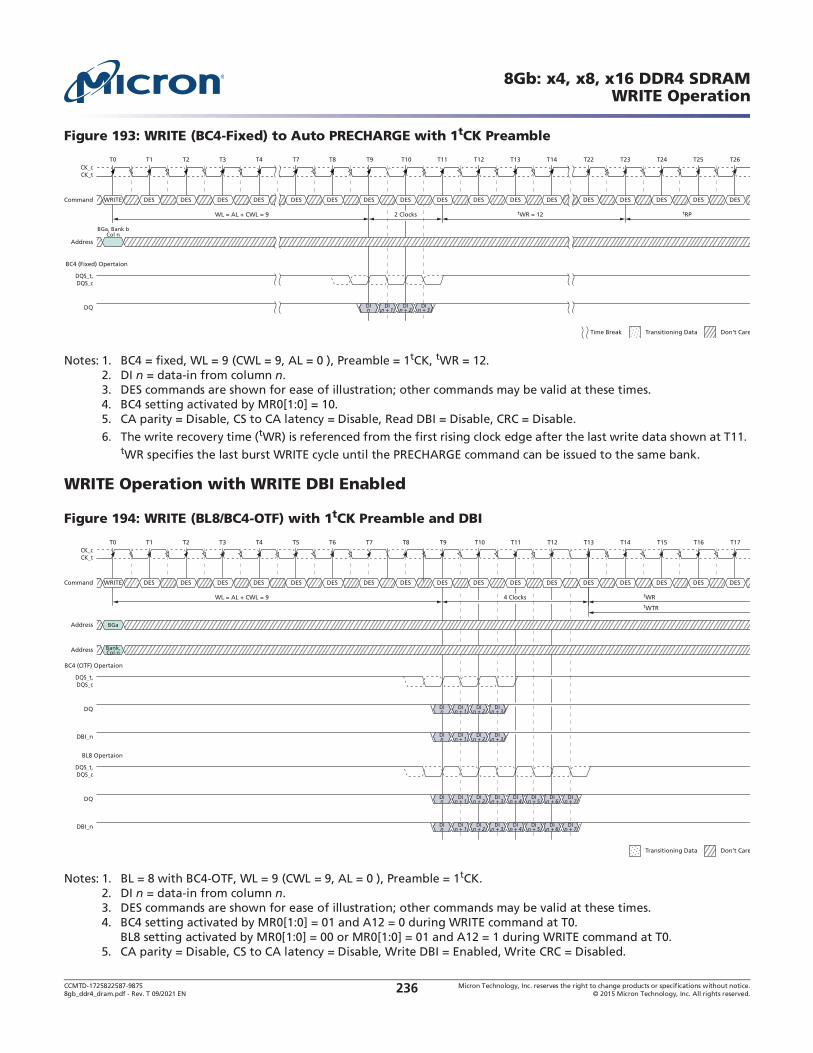
CCMTD-1725822587-9875 Micron Technology, Inc. reserves the right to change products or specifications without notice.8gb_ddr4_dram.pdf - Rev. T 09/2021 EN 2015 Micron Technology, Inc. All rights reserved.236
8Gb: x4, x8, x16 DDR4 SDRAMWRITE Operation
Figure 193: WRITE (BC4-Fixed) to Auto PRECHARGE with 1tCK Preamble
Notes: 1. BC4 = fixed, WL = 9 (CWL = 9, AL = 0 ), Preamble = 1tCK, tWR = 12.2. DI n = data-in from column n.3. DES commands are shown for ease of illustration; other commands may be valid at these times.4. BC4 setting activated by MR0[1:0] = 10.5. CA parity = Disable, CS to CA latency = Disable, Read DBI = Disable, CRC = Disable.
6. The write recovery time (tWR) is referenced from the first rising clock edge after the last write data shown at T11. tWR specifies the last burst WRITE cycle until the PRECHARGE command can be issued to the same bank.
WRITE Operation with WRITE DBI Enabled
Figure 194: WRITE (BL8/BC4-OTF) with 1tCK Preamble and DBI
Notes: 1. BL = 8 with BC4-OTF, WL = 9 (CWL = 9, AL = 0 ), Preamble = 1tCK.2. DI n = data-in from column n.3. DES commands are shown for ease of illustration; other commands may be valid at these times.4. BC4 setting activated by MR0[1:0] = 01 and A12 = 0 during WRITE command at T0.
BL8 setting activated by MR0[1:0] = 00 or MR0[1:0] = 01 and A12 = 1 during WRITE command at T0.5. CA parity = Disable, CS to CA latency = Disable, Write DBI = Enabled, Write CRC = Disabled.
T0
WL = AL + CWL = 9 tWR = 12 tRP
T1 T2 T3 T4
DES DES DES DES DES DES DESCommand DESWRITE DES DES DES DES
DQ
BC4 (Fixed) Opertaion
CK_tCK_c
DQS_t,DQS_c
T14T7 T8 T9 T10 T11 T12 T13 T26T22 T23 T24 T25
Don’t CareTransitioning DataTime Break
DIn + 1
DIn + 2
DIn + 3
DIn
DES DES DES DES DES
Address
BGa, Bank bCol n
2 Clocks
T0
WL = AL + CWL = 9 tWRtWTR
T1 T2 T3 T4
DES DES DES DES DES DES DESCommand DESWRITE DES DES DES DES
DQ
BC4 (OTF) Opertaion
CK_tCK_c
DQS_t,DQS_c
T5 T6 T14T7 T8 T9 T10 T11 T12 T13 T15 T16 T17
Don’t CareTransitioning Data
DIn + 1
DIn + 2
DIn + 3
DIn
DES DES DES DES DES
Address BGa
Address Bank,Col n
DQ
DBI_n
BL8 Opertaion
DQS_t,DQS_c
DIn + 1
DIn + 2
DIn + 3
DIn + 4
DIn + 5
DIn + 6
DIn + 7
DIn
DIn + 1
DIn + 2
DIn + 3
DIn + 4
DIn + 5
DIn + 6
DIn + 7
DIn
DBI_n DIn + 1
DIn + 2
DIn + 3
DIn
4 Clocks

CCMTD-1725822587-9875 Micron Technology, Inc. reserves the right to change products or specifications without notice.8gb_ddr4_dram.pdf - Rev. T 09/2021 EN 2015 Micron Technology, Inc. All rights reserved.237
8Gb: x4, x8, x16 DDR4 SDRAMWRITE Operation
6. The write recovery time (tWR_DBI) is referenced from the first rising clock edge after the last write data shown at T13.
Figure 195: WRITE (BC4-Fixed) with 1tCK Preamble and DBI
Notes: 1. BC4 = fixed, WL = 9 (CWL = 9, AL = 0 ), Preamble = 1tCK.2. DI n = data-in from column n.3. DES commands are shown for ease of illustration; other commands may be valid at these times.4. BC4 setting activated by MR0[1:0] = 10.5. CA parity = Disable, CS to CA latency = Disable, Write DBI = Enabled, Write CRC = Disabled.
T0
WL = AL + CWL = 9 tWRtWTR
T1 T2 T3 T4
DES DES DES DES DES DES DESCommand DESWRITE DES DES DES DES
DQ
BC4 (Fixed) Opertaion
CK_tCK_c
DQS_t,DQS_c
T5 T6 T14T7 T8 T9 T10 T11 T12 T13 T15 T16 T17
Don’t CareTransitioning Data
DIn + 1
DIn + 2
DIn + 3
DIn
DES DES DES DES DES
Address BGa
Address Bank,Col n
DBI_n DIn + 1
DIn + 2
DIn + 3
DIn
2 Clocks
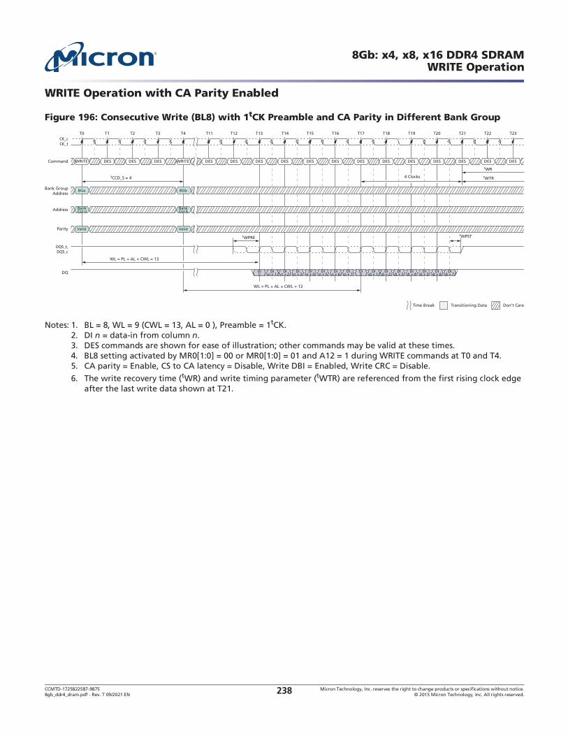
CCMTD-1725822587-9875 Micron Technology, Inc. reserves the right to change products or specifications without notice.8gb_ddr4_dram.pdf - Rev. T 09/2021 EN 2015 Micron Technology, Inc. All rights reserved.238
8Gb: x4, x8, x16 DDR4 SDRAMWRITE Operation
WRITE Operation with CA Parity Enabled
Figure 196: Consecutive Write (BL8) with 1tCK Preamble and CA Parity in Different Bank Group
Notes: 1. BL = 8, WL = 9 (CWL = 13, AL = 0 ), Preamble = 1tCK.2. DI n = data-in from column n.3. DES commands are shown for ease of illustration; other commands may be valid at these times.4. BL8 setting activated by MR0[1:0] = 00 or MR0[1:0] = 01 and A12 = 1 during WRITE commands at T0 and T4.5. CA parity = Enable, CS to CA latency = Disable, Write DBI = Enabled, Write CRC = Disable.
6. The write recovery time (tWR) and write timing parameter (tWTR) are referenced from the first rising clock edge after the last write data shown at T21.
T0
tCCD_S = 4 4 Clocks
tWPRE
WL = PL + AL + CWL = 13
T1 T2 T3 T4
DES DES DES DES DES DES DESCommand DESWRITE DES DES WRITE DES
DQ
CK_tCK_c
DQS_t,DQS_c
WL = PL + AL + CWL = 13
T20 T21 T22 T23T11 T12 T13 T16T14 T15 T17 T18 T19
Don’t CareTransitioning DataTime Break
DIn + 1
DIn + 2
DIn + 3
DIn + 4
DIn + 5
DIn + 6
DIn + 7
DIb
DIb + 1
DIb + 2
DIb + 3
DIb + 4
DIb + 5
DIb + 6
DIb + 7
DIn
DES DES DES DES DES
Bank GroupAddress
Address BankCol n
BankCol b
BGa BGb
tWPST
tWTR
tWR
Parity Valid Valid

CCMTD-1725822587-9875 Micron Technology, Inc. reserves the right to change products or specifications without notice.8gb_ddr4_dram.pdf - Rev. T 09/2021 EN 2015 Micron Technology, Inc. All rights reserved.239
8Gb: x4, x8, x16 DDR4 SDRAMWRITE Operation
WRITE Operation with Write CRC Enabled
Figure 197: Consecutive WRITE (BL8/BC4-OTF) with 1tCK Preamble and Write CRC in Same or Different Bank Group
Notes: 1. BL8/BC4-OTF, AL = 0, CWL = 9, Preamble = 1tCK, tCCD_S/L = 5tCK.2. DI n (or b) = data-in from column n (or column b).3. DES commands are shown for ease of illustration; other commands may be valid at these times.4. BL8 setting activated by either MR0[1:0] = 00 or MR0[1:0] = 01 and A12 = 1 during WRITE commands at T0 and T5.5. BC4 setting activated by MR0[1:0] = 01 and A12 = 0 during WRITE commands at T0 and T5.6. CA parity = Disable, CS to CA latency = Disable, Read DBI = Disable, Write CRC = Enable.
7. The write recovery time (tWR) and write timing parameter (tWTR) are referenced from the first rising clock edge after the last write data shown at T18.
Figure 198: Consecutive WRITE (BC4-Fixed) with 1tCK Preamble and Write CRC in Same or Different Bank Group
T0
tCCD_S/L = 5
tWPRE
WL = AL + CWL = 9
T1 T2 T3 T4
DES DES DES DES DES DES DESCommand DESWRITE DES DES DES WRITE
DQ x4,BL = 8
CK_tCK_c
DQS_t,DQS_c
WL = AL + CWL = 9
T5 T8 T9 T10 T11 T12 T13 T16T14 T15 T17 T18 T19
Don’t CareTransitioning DataTime Break
DIn + 1
DIn + 2
DIn + 3
DIn + 4
DIn + 5
DIn + 6
DIn + 7 CRC
DIn + 7
CRC
CRC
CRC
DIb
DIb + 1
DIb + 2
DIb + 3
DIb + 4
DIb + 5
DIb + 6
DIb + 7 CRC CRCDI
n
DES DES DES DES DES
Bank GroupAddress
Address BankCol n
BankCol b
BGa BGa orBGb
DQ x8/X16,BL = 8
DIn + 1
DIn + 2
DIn + 3
DIn + 4
DIn + 5
DIn + 6
DIb
DIb + 1
DIb + 2
DIb + 3
DIb + 4
DIb + 5
DIb + 6
DIb + 7 CRCDI
n
CRC
DQ x4,BC = 4 (OTF)
DQ x8/X16,BC = 4 (OTF)
DIn + 1
DIn + 2
DIn + 3
DIb
DIb + 1
DIb + 2 CRC CRCDI
n
tWPST
tWTR
tWR
DIn + 1
DIn + 2
DIn + 3
DIb
DIb + 1
DIb + 2
DIb + 3 CRCDI
n
DIb + 3
CRC
4 Clocks
T0
tCCD_S/L = 5
tWPRE
WL = AL + CWL = 9
T1 T2 T3 T4
DES DES DES DES DES DES DESCommand DESWRITE DES DES DES WRITE
CK_tCK_c
DQS_t,DQS_c
WL = AL + CWL = 9
T5 T8 T9 T10 T11 T12 T13 T16T14 T15 T17 T18 T19
Don’t CareTransitioning DataTime Break
CRC
DES DES DES DES DES
Bank GroupAddress
Address BankCol n
BankCol b
BGa BGa orBGb
CRC
CRCDQ x4,
BC = 4 (Fixed)
DQ x8/X16,BC = 4 (Fixed)
DIn + 1
DIn + 2
DIn + 3
DIb
DIb + 1
DIb + 2 CRC CRCDI
n
tWPST
tWTR
tWR
DIn + 1
DIn + 2
DIn + 3
DIb
DIb + 1
DIb + 2
DIb + 3 CRCDI
n
DIb + 3
2 Clocks

CCMTD-1725822587-9875 Micron Technology, Inc. reserves the right to change products or specifications without notice.8gb_ddr4_dram.pdf - Rev. T 09/2021 EN 2015 Micron Technology, Inc. All rights reserved.240
8Gb: x4, x8, x16 DDR4 SDRAMWRITE Operation
Notes: 1. BC4-fixed, AL = 0, CWL = 9, Preamble = 1tCK, tCCD_S/L = 5tCK.2. DI n (or b) = data-in from column n (or column b).3. DES commands are shown for ease of illustration; other commands may be valid at these times.4. BC4 setting activated by MR0[1:0] = 10 during WRITE commands at T0 and T5.5. CA parity = Disable, CS to CA latency = Disable, Read DBI = Disable, Write CRC = Enable, DM = Disable.
6. The write recovery time (tWR) and write timing parameter (tWTR) are referenced from the first rising clock edge after the last write data shown at T16.
Figure 199: Nonconsecutive WRITE (BL8/BC4-OTF) with 1tCK Preamble and Write CRC in Same or Different Bank Group
Notes: 1. BL8/BC4-OTF, AL = 0, CWL = 9, Preamble = 1tCK, tCCD_S/L = 6tCK.2. DI n (or b) = data-in from column n (or column b).3. DES commands are shown for ease of illustration; other commands may be valid at these times.4. BL8 setting activated by either MR0[1:0] = 00 or MR0[1:0] = 01 and A12 = 1 during WRITE commands at T0 and T6.5. BC4 setting activated by MR0[1:0] = 01 and A12 = 0 during WRITE commands at T0 and T6.6. CA parity = Disable, CS to CA latency = Disable, Read DBI = Disable, Write CRC = Enable, DM = Disable.
7. The write recovery time (tWR) and write timing parameter (tWTR) are referenced from the first rising clock edge after the last write data shown at T19.
T0
tCCD_S/L = 6
tWPRE
WL = AL + CWL = 9
T1 T5 T6 T7
DES DES DES DES DES DES DESCommand DESWRITE DES DESDESDESWRITE
DQ x4,BL = 8
CK_tCK_c
DQS_t,DQS_c
WL = AL + CWL = 9
T20T8 T9 T10 T11 T12 T13 T16T14 T15 T17 T18 T19
Don’t CareTransitioning DataTime Break
DIn + 1
DIn + 2
DIn + 3
DIn + 4
DIn + 5
DIn + 6
DIn + 7 CRC
DIn + 7
CRC
CRC
CRC
DIb
DIb + 1
DIb + 2
DIb + 3
DIb + 4
DIb + 5
DIb + 6
DIb + 7 CRC CRCDI
n
DES DES DES DES DES
Bank GroupAddress
Address BankCol n
BankCol b
BGa BGa orBGb
DQ x8/X16,BL = 8
DIn + 1
DIn + 2
DIn + 3
DIn + 4
DIn + 5
DIn + 6
DIb
DIb + 1
DIb + 2
DIb + 3
DIb + 4
DIb + 5
DIb + 6
DIb + 7 CRCDI
n
CRC
DQ x4,BC = 4 (OTF)
DQ x8/X16,BC = 4 (OTF)
DIn + 1
DIn + 2
DIn + 3
DIb
DIb + 1
DIb + 2 CRC CRCDI
n
tWPST
tWTR
tWR
DIn + 1
DIn + 2
DIn + 3
DIb
DIb + 1
DIb + 2
DIb + 3 CRCDI
n
DIb + 3
CRC
4 Clocks
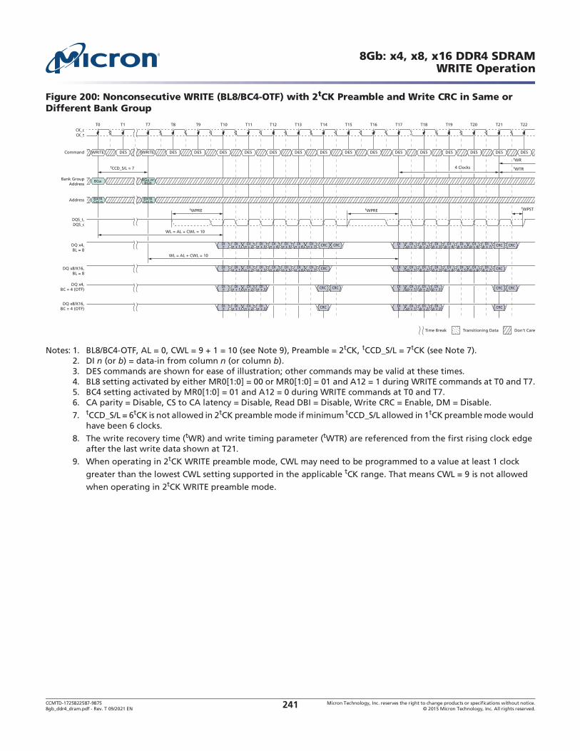
CCMTD-1725822587-9875 Micron Technology, Inc. reserves the right to change products or specifications without notice.8gb_ddr4_dram.pdf - Rev. T 09/2021 EN 2015 Micron Technology, Inc. All rights reserved.241
8Gb: x4, x8, x16 DDR4 SDRAMWRITE Operation
Figure 200: Nonconsecutive WRITE (BL8/BC4-OTF) with 2tCK Preamble and Write CRC in Same or Different Bank Group
Notes: 1. BL8/BC4-OTF, AL = 0, CWL = 9 + 1 = 10 (see Note 9), Preamble = 2tCK, tCCD_S/L = 7tCK (see Note 7).2. DI n (or b) = data-in from column n (or column b).3. DES commands are shown for ease of illustration; other commands may be valid at these times.4. BL8 setting activated by either MR0[1:0] = 00 or MR0[1:0] = 01 and A12 = 1 during WRITE commands at T0 and T7.5. BC4 setting activated by MR0[1:0] = 01 and A12 = 0 during WRITE commands at T0 and T7.6. CA parity = Disable, CS to CA latency = Disable, Read DBI = Disable, Write CRC = Enable, DM = Disable.
7. tCCD_S/L = 6tCK is not allowed in 2tCK preamble mode if minimum tCCD_S/L allowed in 1tCK preamble mode would have been 6 clocks.
8. The write recovery time (tWR) and write timing parameter (tWTR) are referenced from the first rising clock edge after the last write data shown at T21.
9. When operating in 2tCK WRITE preamble mode, CWL may need to be programmed to a value at least 1 clock
greater than the lowest CWL setting supported in the applicable tCK range. That means CWL = 9 is not allowed
when operating in 2tCK WRITE preamble mode.
T0
tCCD_S/L = 7
tWPRE
WL = AL + CWL = 10
T1
DES DES DES DES DES DES DESCommand DESWRITE DES DESDESWRITE
DQ x4,BL = 8
CK_tCK_c
DQS_t,DQS_c
WL = AL + CWL = 10
T22T21T7 T20T8 T9 T10 T11 T12 T13 T16T14 T15 T17 T18 T19
Don’t CareTransitioning DataTime Break
DIn + 1
DIn + 2
DIn + 3
DIn + 4
DIn + 5
DIn + 6
DIn + 7 CRC
DIn + 7
CRC
CRC
CRC
DIb
DIb + 1
DIb + 2
DIb + 3
DIb + 4
DIb + 5
DIb + 6
DIb + 7 CRC CRCDI
n
DES DES DES DES DES
Bank GroupAddress
Address BankCol n
BankCol b
BGa BGa orBGb
DQ x8/X16,BL = 8
DIn + 1
DIn + 2
DIn + 3
DIn + 4
DIn + 5
DIn + 6
DIb
DIb + 1
DIb + 2
DIb + 3
DIb + 4
DIb + 5
DIb + 6
DIb + 7 CRCDI
n
CRC
DQ x4,BC = 4 (OTF)
DQ x8/X16,BC = 4 (OTF)
DIn + 1
DIn + 2
DIn + 3
DIb
DIb + 1
DIb + 2 CRC CRCDI
n
tWPREtWPST
tWTR
tWR
DIn + 1
DIn + 2
DIn + 3
DIb
DIb + 1
DIb + 2
DIb + 3 CRCDI
n
DIb + 3
CRC
4 Clocks

CCMTD-1725822587-9875 Micron Technology, Inc. reserves the right to change products or specifications without notice.8gb_ddr4_dram.pdf - Rev. T 09/2021 EN 2015 Micron Technology, Inc. All rights reserved.242
8Gb: x4, x8, x16 DDR4 SDRAMWRITE Operation
Figure 201: WRITE (BL8/BC4-OTF/Fixed) with 1tCK Preamble and Write CRC in Same or Different Bank Group
Notes: 1. BL8/BC4, AL = 0, CWL = 9, Preamble = 1tCK.2. DI n (or b) = data-in from column n (or column b).3. DES commands are shown for ease of illustration; other commands may be valid at these times.4. BL8 setting activated by either MR0[1:0] = 00 or MR0[1:0] = 01 and A12 = 1 during WRITE command at T0.5. BC4 setting activated by either MR0[1:0] = 10 or MR0[1:0] = 01 and A12 = 0 during WRITE command at T0.6. CA parity = Disable, CS to CA latency = Disable, Read DBI = Disable, Write CRC = Enable, DM = Enable.
7. The write recovery time (tWR_CRC_DM) and write timing parameter (tWTR_S_CRC_DM/tWTR_L_CRC_DM) are referenced from the first rising clock edge after the last write data shown at T13.
T0
tWPRE
WL = AL + CWL = 9
T1 T2 T6 T7
DES DES DES DES DES DES DESCommand DESWRITE DES DESDESDESDES
DQ x4,BL = 8
CK_tCK_c
DQS_t,DQS_c
T20T8 T9 T10 T11 T12 T13 T16T14 T15 T17 T18 T19
Don’t CareTransitioning DataTime Break
DIn + 1
DIn + 2
DIn + 3
DIn + 4
DIn + 5
DIn + 6
DIn + 7 CRC
DIn + 7
CRC
CRC
CRC
DIn
DES DES DES DES DES
Bank GroupAddress
Address BankCol n
BGa
DQ x8/X16,BL = 8
DIn + 1
DIn + 2
DIn + 3
DIn + 4
DIn + 5
DIn + 6
DIn
CRC
DQ x4,BC = 4 (OTF/Fixed)
DQ x8/X16,BC = 4 (OTF/Fixed)
DIn + 1
DIn + 2
DIn + 3
DIn
tWTR_S_CRC_DM/tWTR_L_CRC_DM
tWR_CRC_DM
tWPST
DIn + 1
DIn + 2
DIn + 3
DIn
DMn + 7DMx4/x8/x16
BL = 8
DMn + 1
DMn + 2
DMn + 3
DMn + 4
DMn + 5
DMn + 6
DMn
CRC
DM x4/x8/x16BC = 4 (OTF / Fixed)
DMn + 1
DMn + 2
DMn + 3
DMn
4 Clocks
CCMTD-1725822587-9875 Micron Technology, Inc. reserves the right to change products or specifications without notice.8gb_ddr4_dram.pdf - Rev. T 09/2021 EN 2015 Micron Technology, Inc. All rights reserved.243
8Gb: x4, x8, x16 DDR4 SDRAMWrite Timing Violations
Write Timing Violations
Motivation
Generally, if timing parameters are violated, a complete reset/initialization procedure has to be initi-ated to make sure that the device works properly. However, for certain minor violations, it is desirable that the device is guaranteed not to "hang up" and that errors are limited to that specific operation. A minor violation does not include a major timing violation (for example, when a DQS strobe misses in
the tDQSCK window).
For the following, it will be assumed that there are no timing violations with regard to the WRITE command itself (including ODT, and so on) and that it does satisfy all timing requirements not mentioned below.
Data Setup and Hold Violations
If the data-to-strobe timing requirements (tDS, tDH) are violated, for any of the strobe edges associated with a WRITE burst, then wrong data might be written to the memory location addressed with this WRITE command.
In the example, the relevant strobe edges for WRITE Burst A are associated with the clock edges: T5, T5.5, T6, T6.5, T7, T7.5, T8, and T8.5.
Subsequent reads from that location might result in unpredictable read data; however, the device will work properly otherwise.
Strobe-to-Strobe and Strobe-to-Clock Violations
If the strobe timing requirements (tDQSH, tDQSL, tWPRE, tWPST) or the strobe to clock timing require-
ments (tDSS, tDSH, tDQSS) are violated, for any of the strobe edges associated with a WRITE burst, then wrong data might be written to the memory location addressed with the offending WRITE command. Subsequent reads from that location might result in unpredictable read data; however, the device will work properly otherwise with the following constraints:
Both write CRC and data burst OTF are disabled; timing specifications other than tDQSH, tDQSL, tWPRE, tWPST, tDSS, tDSH, tDQSS are not violated.The offending write strobe (and preamble) arrive no earlier or later than six DQS transition edges from the WRITE latency position.A READ command following an offending WRITE command from any open bank is allowed.One or more subsequent WR or a subsequent WRA (to same bank as offending WR) may be issued tCCD_L later, but incorrect data could be written. Subsequent WR and WRA can be either offending or non-offending writes. Reads from these writes may provide incorrect data.
One or more subsequent WR or a subsequent WRA (to a different bank group) may be issued tCCD_S later, but incorrect data could be written. Subsequent WR and WRA can be either offending or non-offending writes. Reads from these writes may provide incorrect data.After one or more precharge commands (PRE or PREA) are issued to the device after an offending WRITE command and all banks are in precharged state (idle state), a subsequent, non-offending WR or WRA to any open bank will be able to write correct data.
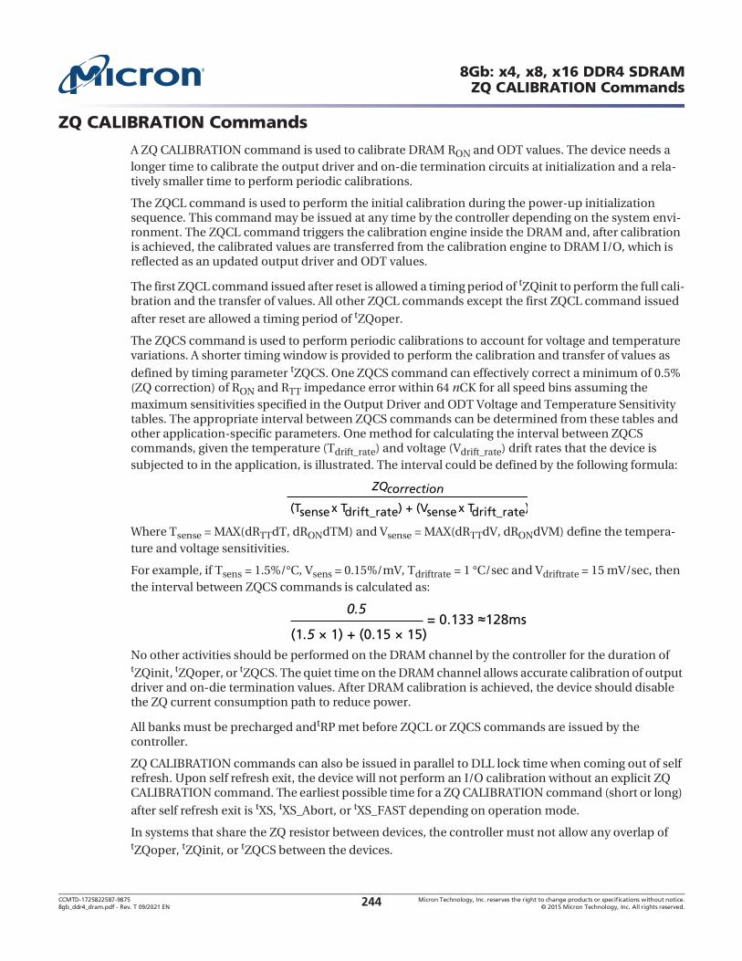
CCMTD-1725822587-9875 Micron Technology, Inc. reserves the right to change products or specifications without notice.8gb_ddr4_dram.pdf - Rev. T 09/2021 EN 2015 Micron Technology, Inc. All rights reserved.244
8Gb: x4, x8, x16 DDR4 SDRAMZQ CALIBRATION Commands
ZQ CALIBRATION Commands
A ZQ CALIBRATION command is used to calibrate DRAM RON and ODT values. The device needs a longer time to calibrate the output driver and on-die termination circuits at initialization and a rela-tively smaller time to perform periodic calibrations.
The ZQCL command is used to perform the initial calibration during the power-up initialization sequence. This command may be issued at any time by the controller depending on the system envi-ronment. The ZQCL command triggers the calibration engine inside the DRAM and, after calibration is achieved, the calibrated values are transferred from the calibration engine to DRAM I/O, which is reflected as an updated output driver and ODT values.
The first ZQCL command issued after reset is allowed a timing period of tZQinit to perform the full cali-bration and the transfer of values. All other ZQCL commands except the first ZQCL command issued
after reset are allowed a timing period of tZQoper.
The ZQCS command is used to perform periodic calibrations to account for voltage and temperature variations. A shorter timing window is provided to perform the calibration and transfer of values as
defined by timing parameter tZQCS. One ZQCS command can effectively correct a minimum of 0.5% (ZQ correction) of RON and RTT impedance error within 64 nCK for all speed bins assuming the maximum sensitivities specified in the Output Driver and ODT Voltage and Temperature Sensitivity tables. The appropriate interval between ZQCS commands can be determined from these tables and other application-specific parameters. One method for calculating the interval between ZQCS commands, given the temperature (Tdrift_rate) and voltage (Vdrift_rate) drift rates that the device is subjected to in the application, is illustrated. The interval could be defined by the following formula:
Where Tsense = MAX(dRTTdT, dRONdTM) and Vsense = MAX(dRTTdV, dRONdVM) define the tempera-ture and voltage sensitivities.
For example, if Tsens = 1.5%/ C, Vsens = 0.15%/mV, Tdriftrate = 1 C/sec and Vdriftrate = 15 mV/sec, then the interval between ZQCS commands is calculated as:
No other activities should be performed on the DRAM channel by the controller for the duration of tZQinit, tZQoper, or tZQCS. The quiet time on the DRAM channel allows accurate calibration of output driver and on-die termination values. After DRAM calibration is achieved, the device should disable the ZQ current consumption path to reduce power.
All banks must be precharged andtRP met before ZQCL or ZQCS commands are issued by the controller.
ZQ CALIBRATION commands can also be issued in parallel to DLL lock time when coming out of self refresh. Upon self refresh exit, the device will not perform an I/O calibration without an explicit ZQ CALIBRATION command. The earliest possible time for a ZQ CALIBRATION command (short or long)
after self refresh exit is tXS, tXS_Abort, or tXS_FAST depending on operation mode.
In systems that share the ZQ resistor between devices, the controller must not allow any overlap of tZQoper, tZQinit, or tZQCS between the devices.
ZQcorrection
(Tsense x Tdrift_rate) + (Vsense x Tdrift_rate)
0.5= 0.133 128ms
(1.5 × 1) + (0.15 × 15)
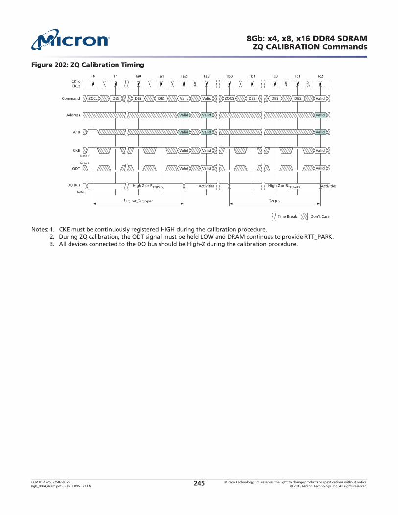
CCMTD-1725822587-9875 Micron Technology, Inc. reserves the right to change products or specifications without notice.8gb_ddr4_dram.pdf - Rev. T 09/2021 EN 2015 Micron Technology, Inc. All rights reserved.245
8Gb: x4, x8, x16 DDR4 SDRAMZQ CALIBRATION Commands
Figure 202: ZQ Calibration Timing
Notes: 1. CKE must be continuously registered HIGH during the calibration procedure.2. During ZQ calibration, the ODT signal must be held LOW and DRAM continues to provide RTT_PARK.3. All devices connected to the DQ bus should be High-Z during the calibration procedure.
T0 T1 Ta0
DQ Bus
tZQinit_tZQoper
Don’t Care
Ta1 Ta2 Ta3 Tb0 Tb1 Tc0 Tc1 Tc2
ZQCS DES DES DES Valid
Valid
Valid
Valid
Valid
Command DESZQCL DES DES Valid Valid
Valid Valid
High-Z or RTT(Park) ActivitiesNote 3
Note 2
Note 1
ActivitiesHigh-Z or RTT(Park)
Time Break
Address
Valid Valid
Valid Valid
A10
CKE
Valid ValidODT
CK_tCK_c
tZQCS

CCMTD-1725822587-9875 Micron Technology, Inc. reserves the right to change products or specifications without notice.8gb_ddr4_dram.pdf - Rev. T 09/2021 EN 2015 Micron Technology, Inc. All rights reserved.246
8Gb: x4, x8, x16 DDR4 SDRAMOn-Die Termination
On-Die Termination
The on-die termination (ODT) feature enables the device to change termination resistance for each DQ, DQS, and DM_n/DBI_n signal for x4 and x8 configurations (and TDQS for the x8 configuration when enabled via A11 = 1 in MR1) via the ODT control pin, WRITE command, or default parking value with MR setting. For the x16 configuration, ODT is applied to each UDQ, LDQ, UDQS, LDQS, UDM_n/UDBI_n, and LDM_n/LDBI_n signal. The ODT feature is designed to improve the signal integrity of the memory channel by allowing the DRAM controller to independently change termina-tion resistance for any or all DRAM devices. If DBI read mode is enabled while the DRAM is in standby, either DM mode or DBI write mode must also be enabled if RTT(NOM) or RTT(Park) is desired. More details about ODT control modes and ODT timing modes can be found further along in this document.
The ODT feature is turned off and not supported in self refresh mode.
Figure 203: Functional Representation of ODT
The switch is enabled by the internal ODT control logic, which uses the external ODT pin and other control information. The value of RTT is determined by the settings of mode register bits (see Mode Register). The ODT pin will be ignored if the mode register MR1 is programmed to disable RTT(NOM) [MR1[10,9,8] = 0,0,0] and in self refresh mode.
ODT Mode Register and ODT State Table
The ODT mode of the DDR4 device has four states: data termination disable, RTT(NOM), RTT(WR), and RTT(Park). The ODT mode is enabled if any of MR1[10:8] (RTT(NOM)), MR2[11:9] (RTT(WR)), or MR5[8:6] (RTT(Park)) are non-zero. When enabled, the value of RTT is determined by the settings of these bits.
RTT control of each RTT condition is possible with a WR or RD command and ODT pin.
RTT(WR): The DRAM (rank) that is being written to provide termination regardless of ODT pin status (either HIGH or LOW).RTT(NOM): DRAM turns ON RTT(NOM) if it sees ODT asserted HIGH (except when ODT is disabled by MR1).RTT(Park): Default parked value set via MR5 to be enabled and RTT(NOM) is not turned on.
The Termination State Table that follows shows various interactions.
The RTT values have the following priority:
Data termination disableRTT(WR)
RTT(NOM)
RTT(Park)
ODT VDDQ
RTT
SwitchDQ, DQS, DM, TDQS
To othercircuitrysuch asRCV, . . .
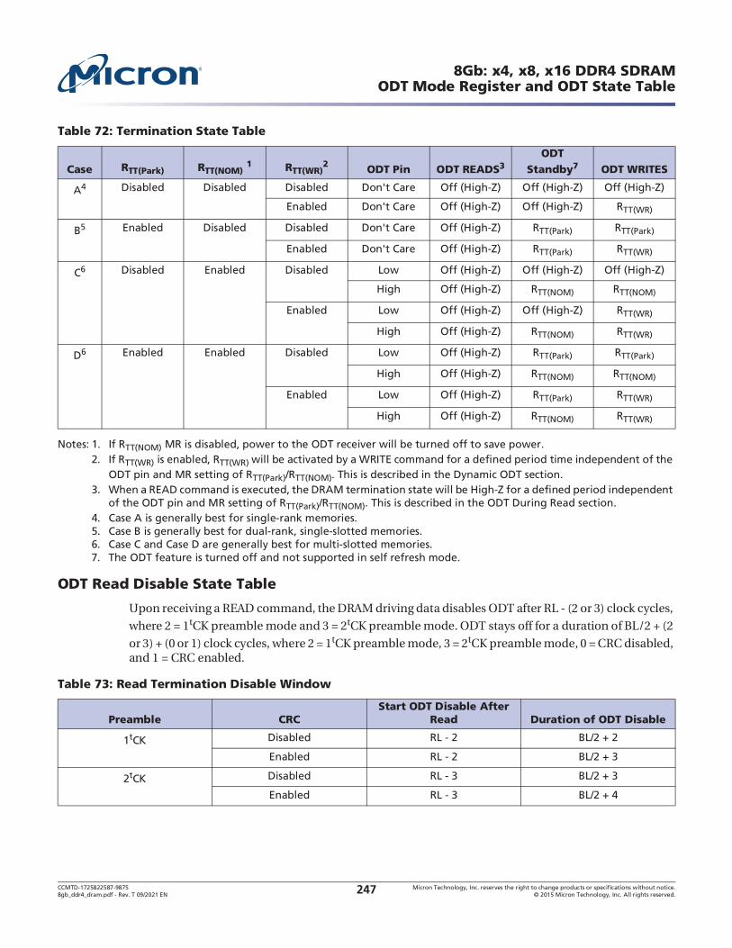
CCMTD-1725822587-9875 Micron Technology, Inc. reserves the right to change products or specifications without notice.8gb_ddr4_dram.pdf - Rev. T 09/2021 EN 2015 Micron Technology, Inc. All rights reserved.247
8Gb: x4, x8, x16 DDR4 SDRAMODT Mode Register and ODT State Table
Notes: 1. If RTT(NOM) MR is disabled, power to the ODT receiver will be turned off to save power.2. If RTT(WR) is enabled, RTT(WR) will be activated by a WRITE command for a defined period time independent of the
ODT pin and MR setting of RTT(Park)/RTT(NOM). This is described in the Dynamic ODT section.3. When a READ command is executed, the DRAM termination state will be High-Z for a defined period independent
of the ODT pin and MR setting of RTT(Park)/RTT(NOM). This is described in the ODT During Read section.4. Case A is generally best for single-rank memories.5. Case B is generally best for dual-rank, single-slotted memories.6. Case C and Case D are generally best for multi-slotted memories.7. The ODT feature is turned off and not supported in self refresh mode.
ODT Read Disable State Table
Upon receiving a READ command, the DRAM driving data disables ODT after RL - (2 or 3) clock cycles,
where 2 = 1tCK preamble mode and 3 = 2tCK preamble mode. ODT stays off for a duration of BL/2 + (2
or 3) + (0 or 1) clock cycles, where 2 = 1tCK preamble mode, 3 = 2tCK preamble mode, 0 = CRC disabled, and 1 = CRC enabled.
Table 72: Termination State Table
Case RTT(Park) RTT(NOM) 1 RTT(WR)
2 ODT Pin ODT READS3ODT
Standby7 ODT WRITES
A4 Disabled Disabled Disabled Don't Care Off (High-Z) Off (High-Z) Off (High-Z)
Enabled Don't Care Off (High-Z) Off (High-Z) RTT(WR)
B5 Enabled Disabled Disabled Don't Care Off (High-Z) RTT(Park) RTT(Park)
Enabled Don't Care Off (High-Z) RTT(Park) RTT(WR)
C6 Disabled Enabled Disabled Low Off (High-Z) Off (High-Z) Off (High-Z)
High Off (High-Z) RTT(NOM) RTT(NOM)
Enabled Low Off (High-Z) Off (High-Z) RTT(WR)
High Off (High-Z) RTT(NOM) RTT(WR)
D6 Enabled Enabled Disabled Low Off (High-Z) RTT(Park) RTT(Park)
High Off (High-Z) RTT(NOM) RTT(NOM)
Enabled Low Off (High-Z) RTT(Park) RTT(WR)
High Off (High-Z) RTT(NOM) RTT(WR)
Table 73: Read Termination Disable Window
Preamble CRCStart ODT Disable After
Read Duration of ODT Disable
1tCK Disabled RL - 2 BL/2 + 2
Enabled RL - 2 BL/2 + 3
2tCK Disabled RL - 3 BL/2 + 3
Enabled RL - 3 BL/2 + 4
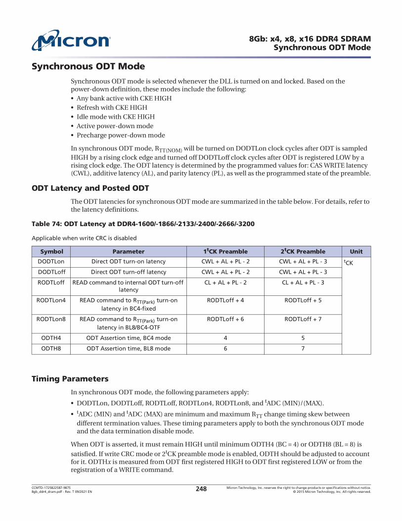
CCMTD-1725822587-9875 Micron Technology, Inc. reserves the right to change products or specifications without notice.8gb_ddr4_dram.pdf - Rev. T 09/2021 EN 2015 Micron Technology, Inc. All rights reserved.248
8Gb: x4, x8, x16 DDR4 SDRAMSynchronous ODT Mode
Synchronous ODT Mode
Synchronous ODT mode is selected whenever the DLL is turned on and locked. Based on the power-down definition, these modes include the following:
Any bank active with CKE HIGHRefresh with CKE HIGHIdle mode with CKE HIGHActive power-down modePrecharge power-down mode
In synchronous ODT mode, RTT(NOM) will be turned on DODTLon clock cycles after ODT is sampled HIGH by a rising clock edge and turned off DODTLoff clock cycles after ODT is registered LOW by a rising clock edge. The ODT latency is determined by the programmed values for: CAS WRITE latency (CWL), additive latency (AL), and parity latency (PL), as well as the programmed state of the preamble.
ODT Latency and Posted ODT
The ODT latencies for synchronous ODT mode are summarized in the table below. For details, refer to the latency definitions.
Table 74: ODT Latency at DDR4-1600/-1866/-2133/-2400/-2666/-3200
Applicable when write CRC is disabled
Timing Parameters
In synchronous ODT mode, the following parameters apply:
DODTLon, DODTLoff, RODTLoff, RODTLon4, RODTLon8, and tADC (MIN)/(MAX).tADC (MIN) and tADC (MAX) are minimum and maximum RTT change timing skew between different termination values. These timing parameters apply to both the synchronous ODT mode and the data termination disable mode.
When ODT is asserted, it must remain HIGH until minimum ODTH4 (BC = 4) or ODTH8 (BL = 8) is
satisfied. If write CRC mode or 2tCK preamble mode is enabled, ODTH should be adjusted to account for it. ODTHx is measured from ODT first registered HIGH to ODT first registered LOW or from the registration of a WRITE command.
Symbol Parameter 1tCK Preamble 2tCK Preamble Unit
DODTLon Direct ODT turn-on latency CWL + AL + PL - 2 CWL + AL + PL - 3 tCK
DODTLoff Direct ODT turn-off latency CWL + AL + PL - 2 CWL + AL + PL - 3
RODTLoff READ command to internal ODT turn-off latency
CL + AL + PL - 2 CL + AL + PL - 3
RODTLon4 READ command to RTT(Park) turn-on latency in BC4-fixed
RODTLoff + 4 RODTLoff + 5
RODTLon8 READ command to RTT(Park) turn-on latency in BL8/BC4-OTF
RODTLoff + 6 RODTLoff + 7
ODTH4 ODT Assertion time, BC4 mode 4 5
ODTH8 ODT Assertion time, BL8 mode 6 7
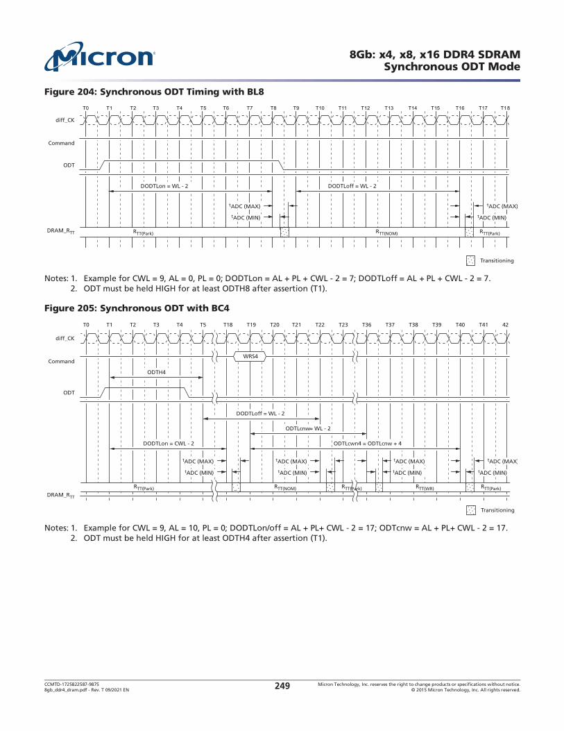
CCMTD-1725822587-9875 Micron Technology, Inc. reserves the right to change products or specifications without notice.8gb_ddr4_dram.pdf - Rev. T 09/2021 EN 2015 Micron Technology, Inc. All rights reserved.249
8Gb: x4, x8, x16 DDR4 SDRAMSynchronous ODT Mode
Figure 204: Synchronous ODT Timing with BL8
Notes: 1. Example for CWL = 9, AL = 0, PL = 0; DODTLon = AL + PL + CWL - 2 = 7; DODTLoff = AL + PL + CWL - 2 = 7.2. ODT must be held HIGH for at least ODTH8 after assertion (T1).
Figure 205: Synchronous ODT with BC4
Notes: 1. Example for CWL = 9, AL = 10, PL = 0; DODTLon/off = AL + PL+ CWL - 2 = 17; ODTcnw = AL + PL+ CWL - 2 = 17.2. ODT must be held HIGH for at least ODTH4 after assertion (T1).
T0 T1 T2 T3 T4 T5 T6 T7 T8 T9 T10 T11 T12 T13 T14 T15 T16 T17 T18
diff_CK
DODTLon = WL - 2 DODTLoff = WL - 2
Command
ODT
DRAM_RTT RTT(Park) RTT(NOM) RTT(Park)
tADC (MIN)
tADC (MAX)
tADC (MIN)
tADC (MAX)
Transitioning
diff_CK
DODTLon = CWL - 2
ODTH4
ODTLcwn4 = ODTLcnw + 4
DODTLoff = WL - 2
Command
ODT
DRAM_RTT
RTT(Park) RTT(Park)RTT(WR)
tADC (MIN)
tADC (MAX)
tADC (MIN)
tADC (MAX)
T1T0 T2 T3 T4 T5 T18 T19 T20 T21 T22 T23 T36 T37 T38 T39 T40 T41 42
tADC (MIN)
tADC (MAX)
tADC (MIN)
tADC (MAX)
WRS4
Transitioning
ODTLcnw = WL - 2
RTT(Park)RTT(NOM)
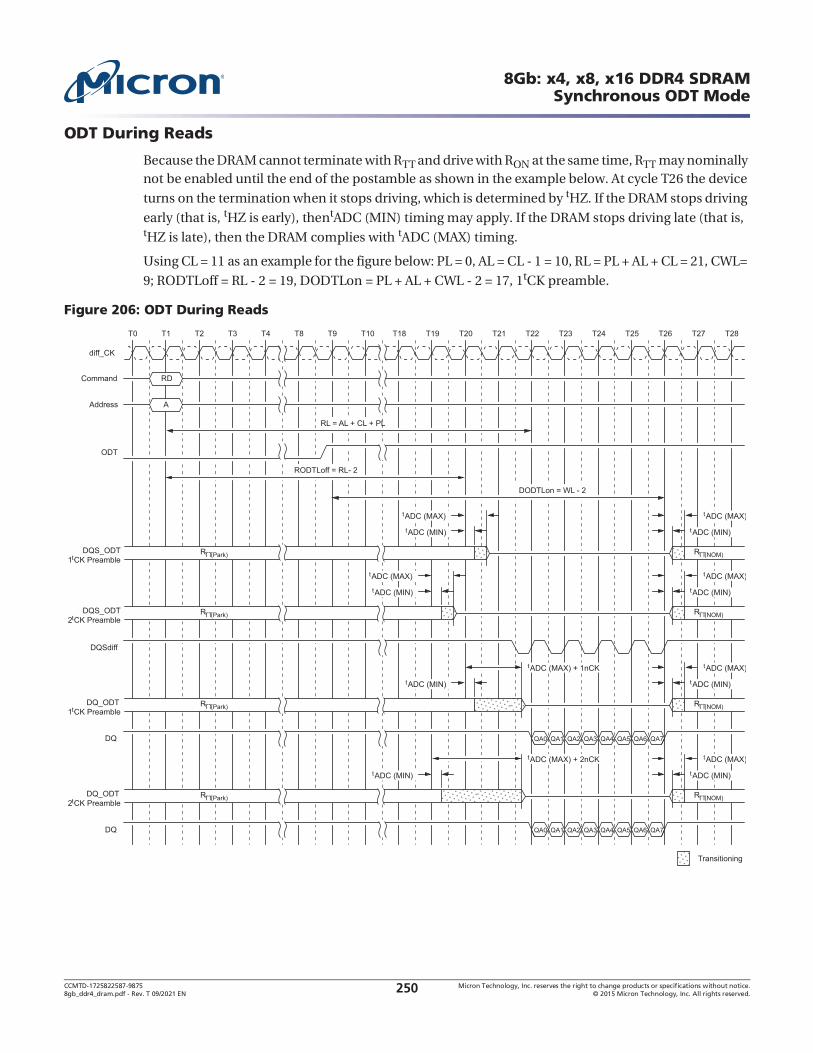
CCMTD-1725822587-9875 Micron Technology, Inc. reserves the right to change products or specifications without notice.8gb_ddr4_dram.pdf - Rev. T 09/2021 EN 2015 Micron Technology, Inc. All rights reserved.250
8Gb: x4, x8, x16 DDR4 SDRAMSynchronous ODT Mode
ODT During Reads
Because the DRAM cannot terminate with RTT and drive with RON at the same time, RTT may nominally not be enabled until the end of the postamble as shown in the example below. At cycle T26 the device
turns on the termination when it stops driving, which is determined by tHZ. If the DRAM stops driving
early (that is, tHZ is early), thentADC (MIN) timing may apply. If the DRAM stops driving late (that is, tHZ is late), then the DRAM complies with tADC (MAX) timing.
Using CL = 11 as an example for the figure below: PL = 0, AL = CL - 1 = 10, RL = PL + AL + CL = 21, CWL=
9; RODTLoff = RL - 2 = 19, DODTLon = PL + AL + CWL - 2 = 17, 1tCK preamble.
Figure 206: ODT During Reads
diff_CK
DODTLon = WL - 2
RL = AL + CL + PL
RODTLoff = RL- 2
Command
ODT
DQS_ODT1tCK Preamble
RTT(Park)
tADC (MIN)
tADC (MAX)
T1T0 T2 T3 T4 T8 T9 T10 T20T19T18 T21 T22 T23 T24 T25 T26 T27 T28
tADC (MIN)
tADC (MAX)
RD
Address A
DQ
DQSdiff
Transitioning
RTT(NOM)
DQS_ODT2tCK Preamble
RTT(Park)
tADC (MIN)
tADC (MAX)
tADC (MIN)
tADC (MAX)
RTT(NOM)
DQ_ODT1tCK Preamble
RTT(Park)
tADC (MIN)
tADC (MAX) + 1nCK
tADC (MAX) + 2nCK
tADC (MIN)
tADC (MAX)
RTT(NOM)
QA7QA6QA5QA4QA3QA2QA1QA0
DQ_ODT2tCK Preamble
RTT(Park)
tADC (MIN) tADC (MIN)
tADC (MAX)
RTT(NOM)
DQ QA7QA6QA5QA4QA3QA2QA1QA0

CCMTD-1725822587-9875 Micron Technology, Inc. reserves the right to change products or specifications without notice.8gb_ddr4_dram.pdf - Rev. T 09/2021 EN 2015 Micron Technology, Inc. All rights reserved.251
8Gb: x4, x8, x16 DDR4 SDRAMDynamic ODT
Dynamic ODT
In certain application cases and to further enhance signal integrity on the data bus, it is desirable that the termination strength of the device can be changed without issuing an MRS command. This requirement is supported by the dynamic ODT feature.
Functional Description
Dynamic ODT mode is enabled if bit A9 or A10 of MR2 is set to 1.
One or two clocks will be added into or subtracted from ODTLcwn8 and ODTLcwn4, depending on
write CRC mode and/or 2tCK preamble enablement.
The following table shows latencies and timing parameters relevant to the on-die termination control in dynamic ODT mode. The dynamic ODT feature is not supported in DLL-off mode. An MRS command must be used to set RTT(WR) to disable dynamic ODT externally (MR2[11:9] = 000).
Three RTTvalues are available: RTT(NOM), RTT(WR), and RTT(Park).The value for RTT(NOM) is preselected via bits MR1[10:8].The value for RTT(WR) is preselected via bits MR2[11:9].The value for RTT(Park) is preselected via bits MR5[8:6].
During operation without WRITE commands, the termination is controlled as follows:Nominal termination strength RTT(NOM) or RTT(Park) is selected.RTT(NOM) on/off timing is controlled via ODT pin and latencies DODTLon and DODTLoff, andRTT(Park) is on when ODT is LOW.
When a WRITE command (WR, WRA, WRS4, WRS8, WRAS4, and WRAS8) is registered, and if dynam-ic ODT is enabled, the termination is controlled as follows:
Latency ODTLcnw after the WRITE command, termination strength RTT(WR) is selected.Latency ODTLcwn8 (for BL8, fixed by MRS or selected OTF) or ODTLcwn4 (for BC4, fixed by MRSor selected OTF) after the WRITE command, termination strength RTT(WR) is de-selected.
Table 75: Dynamic ODT Latencies and Timing (1tCK Preamble Mode and CRC Disabled)
Name and Description
Abbr. Defined from Defined to 1600/1866/2133/2400
2666 2933/3200 Unit
ODT latency for change from RTT(Park)/RTT(NOM) to RTT(WR)
ODTLcnw
Registering external
WRITE com-mand
Change RTT strength from RTT(Park)/RTT(NO
M) to RTT(WR)
ODTLcnw = WL - 2 tCK
ODT latency for change from RTT(WR) to RTT(Park)/RTT(NOM) (BC = 4)
ODTL-cwn4
Registering external
WRITE com-mand
Change RTT strength from
RTT(WR) to RTT(Park)/RTT(NO
M)
ODTLcwn4 = 4 + ODTLcnw tCK
ODT latency for change from RTT(WR) to RTT(Park)/RTT(NOM) (BL = 8)
ODTL-cwn8
Registering external
WRITE com-mand
Change RTT strength from
RTT(NOM) to RTT(WR)
ODTLcwn8 = 6 + ODTLcnw tCK (AVG)
RTT change skew tADC ODTLcnw ODTLcwn
RTT valid tADC (MIN) = 0.30
tADC (MAX) = 0.70
tADC (MIN) = 0.28
tADC (MAX) = 0.72
tADC (MIN) = 0.26
tADC (MAX) = 0.74
tCK (AVG)

CCMTD-1725822587-9875 Micron Technology, Inc. reserves the right to change products or specifications without notice.8gb_ddr4_dram.pdf - Rev. T 09/2021 EN 2015 Micron Technology, Inc. All rights reserved.252
8Gb: x4, x8, x16 DDR4 SDRAMDynamic ODT
Notes: 1. ODTLcnw = WL - 2 (1tCK preamble) or WL - 3 (2tCK preamble).
Figure 207: Dynamic ODT (1t CK Preamble; CL = 14, CWL = 11, BL = 8, AL = 0, CRC Disabled)
Notes: 1. ODTLcnw = WL - 2 (1tCK preamble) or WL - 3 (2tCK preamble).2. If BC4, then ODTLcwn = WL + 4 if CRC disabled or WL + 5 if CRC enabled; If BL8, then ODTLcwn = WL + 6 if CRC
disabled or WL + 7 if CRC enabled.
Figure 208: Dynamic ODT Overlapped with RTT(NOM) (CL = 14, CWL = 11, BL = 8, AL = 0, CRC Disabled)
Table 76: Dynamic ODT Latencies and Timing with Preamble Mode and CRC Mode Matrix
Symbol
1tCK Parameter 2tCK Parameter
UnitCRC Off CRC On CRC Off CRC On
ODTLcnw1 WL - 2 WL - 2 WL - 3 WL - 3 tCK
ODTLcwn4 ODTLcnw + 4 ODTLcnw + 7 ODTLcnw + 5 ODTLcnw + 8
ODTLcwn8 ODTLcnw + 6 ODTLcnw + 7 ODTLcnw + 7 ODTLcnw + 8
diff_CK
ODTLcwn
ODTLcnw
DODTLon = WL - 2
DODTLoff = WL - 2
Command
ODT
RTT RTT(Park) RTT(NOM) RTT(Park)RTT(WR)
tADC (MAX) tADC (MAX)
T1T0 T2 T5 T6 T7 T14T8 T9 T10 T11 T15 T16 T17 T18 T19 T20 T21 T22 T23 T24
tADC (MIN)tADC (MIN)tADC (MIN)tADC (MIN)
tADC (MAX)
RTT(Park)
tADC (MAX)
WR
Transitioning
diff_CK
Command
ODT
T1T0 T2 T5 T6 T7 T25T12T9 T10 T11 T15 T16 T17 T18 T19 T20 T21 T22 T23 T24
WR
ODTLcnw
DODTLoff = CWL -2
ODTLcwn8
RTT RTT_NOM RTT_NOM RTT_PARKRTT_WR
tADC (MAX) tADC (MAX)
tADC (MIN)tADC (MIN)tADC (MIN)
tADC (MAX)
CCMTD-1725822587-9875 Micron Technology, Inc. reserves the right to change products or specifications without notice.8gb_ddr4_dram.pdf - Rev. T 09/2021 EN 2015 Micron Technology, Inc. All rights reserved.253
8Gb: x4, x8, x16 DDR4 SDRAMDynamic ODT
Note: 1. Behavior with WR command issued while ODT is registered HIGH.
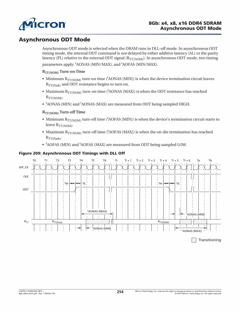
CCMTD-1725822587-9875 Micron Technology, Inc. reserves the right to change products or specifications without notice.8gb_ddr4_dram.pdf - Rev. T 09/2021 EN 2015 Micron Technology, Inc. All rights reserved.254
8Gb: x4, x8, x16 DDR4 SDRAMAsynchronous ODT Mode
Asynchronous ODT Mode
Asynchronous ODT mode is selected when the DRAM runs in DLL-off mode. In asynchronous ODT timing mode, the internal ODT command is not delayed by either additive latency (AL) or the parity latency (PL) relative to the external ODT signal (RTT(NOM)). In asynchronous ODT mode, two timing
parameters apply: tAONAS (MIN/MAX), and tAOFAS (MIN/MAX).
RTT(NOM) Turn-on Time
Minimum RTT(NOM) turn-on time (tAONAS [MIN]) is when the device termination circuit leaves RTT(Park) and ODT resistance begins to turn on.
Maximum RTT(NOM) turn-on time (tAONAS [MAX]) is when the ODT resistance has reached RTT(NOM).
tAONAS (MIN) and tAONAS (MAX) are measured from ODT being sampled HIGH.
RTT(NOM) Turn-off Time
Minimum RTT(NOM) turn-off time (tAOFAS [MIN]) is when the device's termination circuit starts to leave RTT(NOM).
Maximum RTT(NOM) turn-off time (tAOFAS [MAX]) is when the on-die termination has reached RTT(Park).
tAOFAS (MIN) and tAOFAS (MAX) are measured from ODT being sampled LOW.
Figure 209: Asynchronous ODT Timings with DLL Off
diff_CK
tAONAS (MAX)
CKE
ODT
RTT RTT(Park) RTT(NOM)
tAONAS (MIN)tAONAS (MAX)
tAONAS (MIN)
tIH tIS tIH tIS
T1T0 T2 T3 T4 T5 T6 Ti Ti + 1 Ti + 2 Ti + 3 Ti + 4 Ti + 5 Ti + 6 Ta Tb
Transitioning

CCMTD-1725822587-9875 Micron Technology, Inc. reserves the right to change products or specifications without notice.8gb_ddr4_dram.pdf - Rev. T 09/2021 EN 2015 Micron Technology, Inc. All rights reserved.255
8Gb: x4, x8, x16 DDR4 SDRAMElectrical Specifications
Electrical Specifications
Absolute Ratings
Stresses greater than those listed may cause permanent damage to the device. This is a stress rating only, and functional operation of the device at these or any other conditions outside those indicated in the operational sections of this specification is not implied. Exposure to absolute maximum rating conditions for extended periods may adversely affect reliability. Although "unlimited" row accesses to the same row is allowed within the refresh period; excessive row accesses to the same row over a long term can result in degraded operation.
Notes: 1. VDD and VDDQ must be within 300mV of each other at all times, and VREF must not be greater than 0.6 VDDQ. When VDD and VDDQ are <500mV, VREF can be 300mV.
2. Storage temperature is the case surface temperature on the center/top side of the DRAM. For the measurement conditions, please refer to the JESD51-2 standard.
3. VPP must be equal to or greater than VDD/VDDQ at all times when powered.
DRAM Component Operating Temperature Range
Operating temperature, TOPER, is the case surface temperature on the center/top side of the DRAM. For measurement conditions, refer to the JEDEC document JESD51-2.
Notes: 1. The normal temperature range specifies the temperatures at which all DRAM specifications will be supported. During operation, the DRAM case temperature must be maintained between 0 C to 85 C under all operating conditions for the commercial offering; The industrial and automotive temperature offerings allow the case temperature to go below 0 C to -40 C.
2. Some applications require operation of the commercial, industrial, and automotive temperature DRAMs in the extended temperature range (between 85 C and 105 C case temperature). Full specifications are supported in this range, but the following additional conditions apply:
Refer to tREFI and tRFC parameters table for tREFI requirements when operating above 85 CIf SELF REFRESH operation is required in the extended temperature range, it is mandatory to use either the manual self refresh mode with extended temperature range capability (MR2[6] = 0 and MR2 [7] = 1) or enable the optional auto self refresh mode (MR2 [6] = 1 and MR2 [7] = 1).
Table 77: Absolute Maximum Ratings
Symbol Parameter Min Max Unit Notes
VDD Voltage on VDD pin relative to VSS 1.5 V 1
VDDQ Voltage on VDDQ pin relative to VSS 1.5 V 1
VPP Voltage on VPP pin relative to VSS 3.0 V 3
VIN, VOUT Voltage on any pin relative to VSS 1.5 V
TSTG Storage temperature 150 C 2
Table 78: Temperature Range
Symbol Parameter Min Max Unit Notes
TOPER Normal operating temperature range -40 85 C 1
Extended temperature range (optional) >85 105 C 2

CCMTD-1725822587-9875 Micron Technology, Inc. reserves the right to change products or specifications without notice.8gb_ddr4_dram.pdf - Rev. T 09/2021 EN 2015 Micron Technology, Inc. All rights reserved.256
8Gb: x4, x8, x16 DDR4 SDRAM
Supply Operating Conditions
Notes: 1. Under all conditions VDDQ must be less than or equal to VDD.2. VDDQ tracks with VDD. AC parameters are measured with VDD and VDDQ tied together.3. VDD slew rate between 300mV and 80% of VDD,min shall be between 0.004 V/ms and 600 V/ms, 20 MHz
band-limited measurement.4. VDD ramp time from 300mV to VDD,min shall be no longer than 200ms.5. A stable valid VDD level is a set DC level (0 Hz to 250 KHz) and must be no less than VDD,min and no greater than
VDD,max. If the set DC level is altered anytime after initialization, the DLL reset and calibrations must be performed again after the new set DC level is final. AC noise of 60mV (greater than 250 KHz) is allowed on VDD provided the noise doesn't alter VDD to less than VDD,min or greater than VDD,max.
6. A stable valid VDDQ level is a set DC level (0 Hz to 250 KHz) and must be no less than VDDQ,min and no greater than VDDQ,max. If the set DC level is altered anytime after initialization, the DLL reset and calibrations must be performed again after the new set DC level is final. AC noise of 60mV (greater than 250 KHz) is allowed on VDDQ provided the noise doesn't alter VDDQ to less than VDDQ,min or greater than VDDQ,max.
7. A stable valid VPP level is a set DC level (0 Hz to 250 KHz) and must be no less than VPP,min and no greater than VPP,max. If the set DC level is altered anytime after initialization, the DLL reset and calibrations must be performed again after the new set DC level is final. AC noise of 120mV (greater than 250 KHz) is allowed on VPP provided the noise doesn't alter VPP to less than VPP,min or greater than VPP,max.
Notes: 1. Measurement made between 300mV and 80% VDD (minimum level).2. The DC bandwidth is limited to 20 MHz.3. Maximum time to ramp VDD from 300 mV to VDD minimum.
Table 79: Recommended Supply Operating Conditions
Symbol Parameter
Rating
Unit NotesMin Typ Max
VDD Supply voltage 1.14 1.2 1.26V 1, 2, 3, 4, 5
VDDQ Supply voltage for output
1.14 1.2 1.26V 1, 2, 6
VPP Wordline sup-ply voltage
2.375 2.5 2.750V 7
Table 80: VDD Slew Rate
Symbol Min Max Unit Notes
VDD_sl 0.004 600 V/ms 1, 2
VDD_on 200 ms 3

CCMTD-1725822587-9875 Micron Technology, Inc. reserves the right to change products or specifications without notice.8gb_ddr4_dram.pdf - Rev. T 09/2021 EN 2015 Micron Technology, Inc. All rights reserved.257
8Gb: x4, x8, x16 DDR4 SDRAM
Leakages
Notes: 1. Input under test 0V < VIN < 1.1V.2. Additional leakage due to weak pull-down.3. VREFCA = VDD/2, VDD at valid level after initialization.4. DQs are disabled.5. ODT is disabled with the ODT input HIGH.
VREFCA Supply
VREFCA is to be supplied to the DRAM and equal to VDD/2. The VREFCA is a reference supply input and therefore does not draw biasing current.
The DC-tolerance limits and AC-noise limits for the reference voltages VREFCA are illustrated in the figure below. The figure shows a valid reference voltage VREF(t) as a function of time (VREF stands for VREFCA). VREF(DC) is the linear average of VREF(t) over a very long period of time (1 second). This average has to meet the MIN/MAX requirements. Furthermore, VREF(t) may temporarily deviate from VREF(DC) by no more than 1% VDD for the AC-noise limit.
Figure 210: VREFDQ Voltage Range
The voltage levels for setup and hold time measurements are dependent on VREF. VREF is understood as VREF(DC), as defined in the above figure. This clarifies that DC-variations of VREF affect the absolute
Table 81: Leakages
Condition Symbol Min Max Unit Notes
Input leakage (excluding ZQ and TEN) IIN 2 A 1
ZQ leakage IZQ 10 A 1
TEN leakage ITEN 10 A 1, 2
VREFCA leakage IVREFCA 2 A 3
Output leakage: VOUT = VDDQ IOZpd 10 A 4
Output leakage: VOUT = VSSQ IOZpu A 4, 5
VREF AC-noise
VREF(DC)VREF(DC) MAX
VREF(t)
VREF(DC) MIN
VDD/2
VSS
Time
Voltage
VDD
CCMTD-1725822587-9875 Micron Technology, Inc. reserves the right to change products or specifications without notice.8gb_ddr4_dram.pdf - Rev. T 09/2021 EN 2015 Micron Technology, Inc. All rights reserved.258
8Gb: x4, x8, x16 DDR4 SDRAM
voltage a signal has to reach to achieve a valid HIGH or LOW level, and therefore, the time to which setup and hold is measured. System timing and voltage budgets need to account for VREF(DC) devia-tions from the optimum position within the data-eye of the input signals. This also clarifies that the DRAM setup/hold specification and derating values need to include time and voltage associated with VREF AC-noise. Timing and voltage effects due to AC-noise on VREF up to the specified limit ( 1% of VDD) are included in DRAM timings and their associated deratings.
VREFDQ Supply and Calibration Ranges
The device internally generates its own VREFDQ. DRAM internal VREFDQ specification parameters: voltage range, step size, VREF step time, VREF full step time, and VREF valid level are used to help provide estimated values for the internal VREFDQ and are not pass/fail limits. The voltage operating range spec-ifies the minimum required range for DDR4 SDRAM devices. The minimum range is defined by VREFDQ,min and VREFDQ,max. A calibration sequence should be performed by the DRAM controller to adjust VREFDQ and optimize the timing and voltage margin of the DRAM data input receivers.
Notes: 1. VREF(DC) voltage is referenced to VDDQ(DC). VDDQ(DC) is 1.2V.2. DRAM range 1 or range 2 is set by the MRS6[6]6.3. VREF step size increment/decrement range. VREF at DC level.4. VREF,new = VREF,old n VREF,step5. For n >4, the minimum value of VREF setting tolerance = VREF,new - 1.625% VDDQ. The maximum value of VREF
setting tolerance = VREF,new + 1.625% VDDQ.6. Measured by recording the MIN and MAX values of the VREF output over the range, drawing a straight line
between those points, and comparing all other VREF output settings to that line.7. For n 4, the minimum value of VREF setting tolerance = VREF,new - 0.15% VDDQ. The maximum value of VREF
setting tolerance = VREF,new + 0.15% VDDQ.8. Measured by recording the MIN and MAX values of the VREF output across four consecutive steps (n = 4), drawing
a straight line between those points, and comparing all VREF output settings to that line.9. Time from MRS command to increment or decrement one step size for VREF.10. Time from MRS command to increment or decrement more than one step size up to the full range of VREF.11. If the VREF monitor is enabled, VREF must be derated by +10ns if DQ bus load is 0pF and an additional +15 ns/pF of
DQ bus loading.12. Only applicable for DRAM component-level test/characterization purposes. Not applicable for normal mode of
operation. VREF valid qualifies the step times, which will be characterized at the component level.
Table 82: VREFDQ Specification
Parameter Symbol Min Typ Max Unit Notes
Range 1 VREFDQ operating points VREFDQ R1 60% 92% VDDQ 1, 2
Range 2 VREFDQ operating points VREFDQ R2 45% 77% VDDQ 1, 2
VREF step size VREF,step 0.5% 0.65% 0.8% VDDQ 3
VREF set tolerance VREF,set_tol 0% 1.625% VDDQ 4, 5, 6
0% 0.15% VDDQ 4, 7, 8
VREF step time VREF,time 150 ns 9, 10, 11
VREF valid tolerance VREF_val_tol 0% 0.15% VDDQ 12

CCMTD-1725822587-9875 Micron Technology, Inc. reserves the right to change products or specifications without notice.8gb_ddr4_dram.pdf - Rev. T 09/2021 EN 2015 Micron Technology, Inc. All rights reserved.259
8Gb: x4, x8, x16 DDR4 SDRAM
VREFDQ Ranges
MR6[6] selects range 1 (60% to 92.5% of VDDQ) or range 2 (45% to 77.5% of VDDQ), and MR6[5:0] sets the VREFDQ level, as listed in the following table. The values in MR6[6:0] will update the VDDQ range and level independent of MR6[7] setting. It is recommended MR6[7] be enabled when changing the settings in MR6[6:0], and it is highly recommended MR6[7] be enabled when changing the settings in MR6[6:0] multiple times during a calibration routine.
Table 83: VREFDQ Range and Levels
MR6[5:0]MR6[6] 0 =
Range 1MR6[6] 1 =
Range 2 MR6[5:0]MR6[6] 0 =
Range 1MR6[6] 1 =
Range 2
00 0000 60.00% 45.00% 01 1010 76.90% 61.90%
00 0001 60.65% 45.65% 01 1011 77.55% 62.55%
00 0010 61.30% 46.30% 01 1100 78.20% 63.20%
00 0011 61.95% 46.95% 01 1101 78.85% 63.85%
00 0100 62.60% 47.60% 01 1110 79.50% 64.50%
00 0101 63.25% 48.25% 01 1111 80.15% 65.15%
00 0110 63.90% 48.90% 10 0000 80.80% 65.80%
00 0111 64.55% 49.55% 10 0001 81.45% 66.45%
00 1000 65.20% 50.20% 10 0010 82.10% 67.10%
00 1001 65.85% 50.85% 10 0011 82.75% 67.75%
00 1010 66.50% 51.50% 10 0100 83.40% 68.40%
00 1011 67.15% 52.15% 10 0101 84.05% 69.05%
00 1100 67.80% 52.80% 10 0110 84.70% 69.70%
00 1101 68.45% 53.45% 10 0111 85.35% 70.35%
00 1110 69.10% 54.10% 10 1000 86.00% 71.00%
00 1111 69.75% 54.75% 10 1001 86.65% 71.65%
01 0000 70.40% 55.40% 10 1010 87.30% 72.30%
01 0001 71.05% 56.05% 10 1011 87.95% 72.95%
01 0010 71.70% 56.70% 10 1100 88.60% 73.60%
01 0011 72.35% 57.35% 10 1101 89.25% 74.25%
01 0100 73.00% 58.00% 10 1110 89.90% 74.90%
01 0101 73.65% 58.65% 10 1111 90.55% 75.55%
01 0110 74.30% 59.30% 11 0000 91.20% 76.20%
01 0111 74.95% 59.95% 11 0001 91.85% 76.85%
01 1000 75.60% 60.60% 11 0010 92.50% 77.50%
01 1001 76.25% 61.25% 11 0011 to 11 1111 are reserved
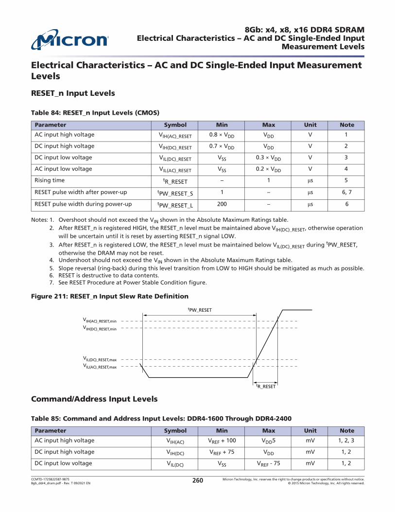
CCMTD-1725822587-9875 Micron Technology, Inc. reserves the right to change products or specifications without notice.8gb_ddr4_dram.pdf - Rev. T 09/2021 EN 2015 Micron Technology, Inc. All rights reserved.260
8Gb: x4, x8, x16 DDR4 SDRAM
Measurement Levels
Levels
RESET_n Input Levels
Notes: 1. Overshoot should not exceed the VIN shown in the Absolute Maximum Ratings table.2. After RESET_n is registered HIGH, the RESET_n level must be maintained above VIH(DC)_RESET, otherwise operation
will be uncertain until it is reset by asserting RESET_n signal LOW.
3. After RESET_n is registered LOW, the RESET_n level must be maintained below VIL(DC)_RESET during tPW_RESET, otherwise the DRAM may not be reset.
4. Undershoot should not exceed the VIN shown in the Absolute Maximum Ratings table.5. Slope reversal (ring-back) during this level transition from LOW to HIGH should be mitigated as much as possible.6. RESET is destructive to data contents.7. See RESET Procedure at Power Stable Condition figure.
Figure 211: RESET_n Input Slew Rate Definition
Command/Address Input Levels
Table 84: RESET_n Input Levels (CMOS)
Parameter Symbol Min Max Unit Note
AC input high voltage VIH(AC)_RESET 0.8 VDD VDD V 1
DC input high voltage VIH(DC)_RESET 0.7 VDD VDD V 2
DC input low voltage VIL(DC)_RESET VSS 0.3 VDD V 3
AC input low voltage VIL(AC)_RESET VSS 0.2 VDD V 4
Rising time tR_RESET 1 s 5
RESET pulse width after power-up tPW_RESET_S 1 s 6, 7
RESET pulse width during power-up tPW_RESET_L 200 s 6
Table 85: Command and Address Input Levels: DDR4-1600 Through DDR4-2400
Parameter Symbol Min Max Unit Note
AC input high voltage VIH(AC) VREF + 100 VDD5 mV 1, 2, 3
DC input high voltage VIH(DC) VREF + 75 VDD mV 1, 2
DC input low voltage VIL(DC) VSS VREF - 75 mV 1, 2
tR_RESET
tPW_RESET
VIH(AC)_RESET,min
VIL(AC)_RESET,max
VIH(DC)_RESET,min
VIL(DC)_RESET,max

CCMTD-1725822587-9875 Micron Technology, Inc. reserves the right to change products or specifications without notice.8gb_ddr4_dram.pdf - Rev. T 09/2021 EN 2015 Micron Technology, Inc. All rights reserved.261
8Gb: x4, x8, x16 DDR4 SDRAM
Measurement Levels
Notes: 1. For input except RESET_n. VREF = VREFCA(DC).2. VREF = VREFCA(DC).
3. Input signal must meet VIL/VIH(AC) to meet tIS timings and VIL/VIH(DC) to meet tIH timings.4. The AC peak noise on VREF may not allow VREF to deviate from VREFCA(DC) by more than 1% VDD (for reference:
approximately 12mV).5.
AC input low voltage VIL(AC) VSS5 VREF - 100 mV 1, 2, 3
Reference voltage for CMD/ADDR inputs VREFFCA(DC) 0.49 VDD 0.51 VDD V 4
Table 85: Command and Address Input Levels: DDR4-1600 Through DDR4-2400 (Continued)
Parameter Symbol Min Max Unit Note
Table 86: Command and Address Input Levels: DDR4-2666
Parameter Symbol Min Max Unit Note
AC input high voltage VIH(AC) VREF + 90 VDD5 mV 1, 2, 3
DC input high voltage VIH(DC) VREF + 65 VDD mV 1, 2
DC input low voltage VIL(DC) VSS VREF - 65 mV 1, 2
AC input low voltage VIL(AC) VSS5 VREF - 90 mV 1, 2, 3
Reference voltage for CMD/ADDR inputs VREFFCA(DC) 0.49 VDD 0.51 VDD V 4
Table 87: Command and Address Input Levels: DDR4-2933 and DDR4-3200
Parameter Symbol Min Max Unit Note
AC input high voltage VIH(AC) VREF + 90 VDD5 mV 1, 2, 3
DC input high voltage VIH(DC) VREF + 65 VDD mV 1, 2
DC input low voltage VIL(DC) VSS VREF - 65 mV 1, 2
AC input low voltage VIL(AC) VSS5 VREF - 90 mV 1, 2, 3
Reference voltage for CMD/ADDR inputs VREFFCA(DC) 0.49 VDD 0.51 VDD V 4
Table 88: Single-Ended Input Slew Rates
Parameter Symbol Min Max Unit Note
SRCA 1.0 7.0 V/ns 1, 2, 3, 4

CCMTD-1725822587-9875 Micron Technology, Inc. reserves the right to change products or specifications without notice.8gb_ddr4_dram.pdf - Rev. T 09/2021 EN 2015 Micron Technology, Inc. All rights reserved.262
8Gb: x4, x8, x16 DDR4 SDRAM
Measurement Levels
Notes: 1. For input except RESET_n.2. VREF = VREFCA(DC).
3. tIS/tIH timings assume SRCA = 1V/ns.4. Measured between VIH(AC) and VIL(AC) for falling edges and between VIL(AC) and VIH(AC) for rising edges
Figure 212: Single-Ended Input Slew Rate Definition
Command, Control, and Address Setup, Hold, and Derating
The total tIS (setup time) and tIH (hold time) required is calculated to account for slew rate variation
by adding the data sheet tIS (base) values, the VIL(AC)/VIH(AC) points, and tIH (base) values, the
VIL(DC)/VIH(DC) points; to the tIS and tIH derating values, respectively. The base values are derived
with single-end signals at 1V/ns and differential clock at 2 V/ns. Example: tIS (total setup time) = tIS
(base) + tIS. For a valid transition, the input signal has to remain above/below VIH(AC)/VIL(AC) for the
time defined by tVAC.
Although the total setup time for slow slew rates might be negative (for example, a valid input signal will not have reached VIH(AC)/VIL(AC) at the time of the rising clock transition), a valid input signal is still required to complete the transition and to reach VIH(AC)/VIL(AC). For slew rates that fall between the values listed in derating tables, the derating values may be obtained by linear interpolation.
Setup (tIS) nominal slew rate for a rising signal is defined as the slew rate between the last crossing of
VIL(DC)max and the first crossing of VIH(AC)min that does not ring back below VIH(DC)min . Setup (tIS) nominal slew rate for a falling signal is defined as the slew rate between the last crossing of VIH(DC)min and the first crossing of VIL(AC)max that does not ring back above VIL(DC)max.
Hold (tIH) nominal slew rate for a rising signal is defined as the slew rate between the last crossing of
VIL(DC)max and the first crossing of VIH(AC)min that does not ring back below VIH(DC)min. Hold (tIH)

CCMTD-1725822587-9875 Micron Technology, Inc. reserves the right to change products or specifications without notice.8gb_ddr4_dram.pdf - Rev. T 09/2021 EN 2015 Micron Technology, Inc. All rights reserved.263
8Gb: x4, x8, x16 DDR4 SDRAM
Measurement Levels
nominal slew rate for a falling signal is defined as the slew rate between the last crossing of VIH(DC)min and the first crossing of VIL(AC)minthat does not ring back above VIL(DC)max.
Table 89:
Symbol 1600 1866 2133 2400 2666 2933 3200 Unit Reference
tIS(base, AC100) 115 100 80 62 ps VIH(AC)/VIL(AC)
tIH(base, DC75) 140 125 105 87 ps VIH(DC)/VIL(DC)
tIS(base, AC90) 55 48 40 ps VIH(AC)/VIL(AC)
tIH(base, DC65) 80 73 65 ps VIH(DC)/VIL(DC)
tIS/tIH(Vref) 215 200 180 162 145 138 130 ps VIH(DC)/VIL(DC)
Table 90: Derating Values for tIS/t
tIS with AC100 Threshold, t
CMD/ADD
R Slew Rate V/ns
CK, CK# Differential Slew Rate
10.0 V/ns 8.0 V/ns 6.0 V/ns 4.0 V/ns 3.0 V/ns 2.0 V/ns 1.5 V/ns 1.0 V/ns
tIS tIH tIS tIH tIS tIH tIS tIH tIS tIH tIH tIH
tIS
tIH
tIS
tIH
7.0 76 54 76 55 77 56 79 58 82 60 86 64 94 73 111 89
6.0 73 53 74 53 75 54 77 56 79 58 83 63 92 71 108 88
5.0 70 50 71 51 72 52 74 54 76 56 80 60 88 68 105 85
4.0 65 46 66 47 67 48 69 50 71 52 75 56 83 65 100 81
3.0 57 40 57 41 58 42 60 44 63 46 67 50 75 58 92 75
2.0 40 28 41 28 42 29 44 31 46 33 50 38 58 46 75 63
1.5 23 15 24 16 25 17 27 19 29 21 33 25 42 33 58 50
1.0 0 0 8 8 25 25
0.9 1 4 18 21
0.8 9 16
0.7 9
0.6 0
0.5
0.4
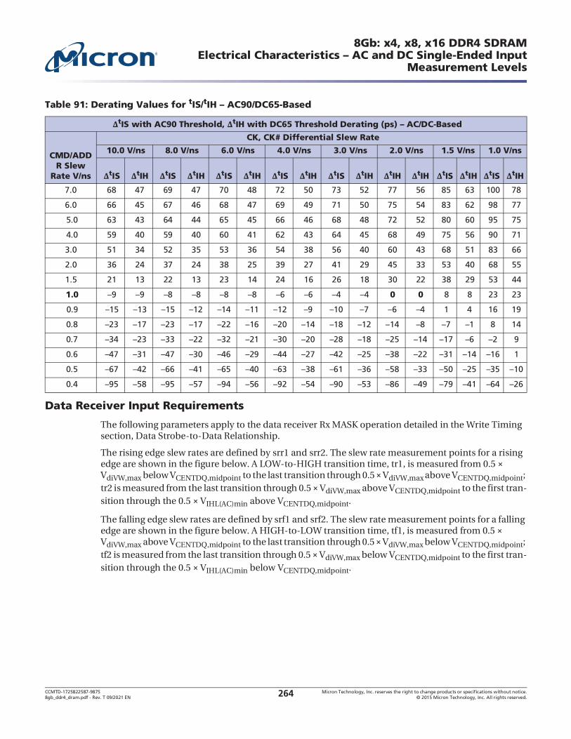
CCMTD-1725822587-9875 Micron Technology, Inc. reserves the right to change products or specifications without notice.8gb_ddr4_dram.pdf - Rev. T 09/2021 EN 2015 Micron Technology, Inc. All rights reserved.264
8Gb: x4, x8, x16 DDR4 SDRAM
Measurement Levels
Data Receiver Input Requirements
The following parameters apply to the data receiver Rx MASK operation detailed in the Write Timing section, Data Strobe-to-Data Relationship.
The rising edge slew rates are defined by srr1 and srr2. The slew rate measurement points for a rising edge are shown in the figure below. A LOW-to-HIGH transition time, tr1, is measured from 0.5 VdiVW,max below VCENTDQ,midpoint to the last transition through 0.5 VdiVW,max above VCENTDQ,midpoint; tr2 is measured from the last transition through 0.5 VdiVW,max above VCENTDQ,midpoint to the first tran-sition through the 0.5 VIHL(AC)min above VCENTDQ,midpoint.
The falling edge slew rates are defined by srf1 and srf2. The slew rate measurement points for a falling edge are shown in the figure below. A HIGH-to-LOW transition time, tf1, is measured from 0.5 VdiVW,max above VCENTDQ,midpoint to the last transition through 0.5 VdiVW,max below VCENTDQ,midpoint; tf2 is measured from the last transition through 0.5 VdiVW,max below VCENTDQ,midpoint to the first tran-sition through the 0.5 VIHL(AC)min below VCENTDQ,midpoint.
Table 91: Derating Values for tIS/t
tIS with AC90 Threshold, t
CMD/ADD
R Slew Rate V/ns
CK, CK# Differential Slew Rate
10.0 V/ns 8.0 V/ns 6.0 V/ns 4.0 V/ns 3.0 V/ns 2.0 V/ns 1.5 V/ns 1.0 V/ns
tIS tIH tIS tIH tIS tIH tIS tIH tIS tIH tIH tIH
tIS
tIH
tIS
tIH
7.0 68 47 69 47 70 48 72 50 73 52 77 56 85 63 100 78
6.0 66 45 67 46 68 47 69 49 71 50 75 54 83 62 98 77
5.0 63 43 64 44 65 45 66 46 68 48 72 52 80 60 95 75
4.0 59 40 59 40 60 41 62 43 64 45 68 49 75 56 90 71
3.0 51 34 52 35 53 36 54 38 56 40 60 43 68 51 83 66
2.0 36 24 37 24 38 25 39 27 41 29 45 33 53 40 68 55
1.5 21 13 22 13 23 14 24 16 26 18 30 22 38 29 53 44
1.0 0 0 8 8 23 23
0.9 1 4 16 19
0.8 8 14
0.7 9
0.6 1
0.5
0.4
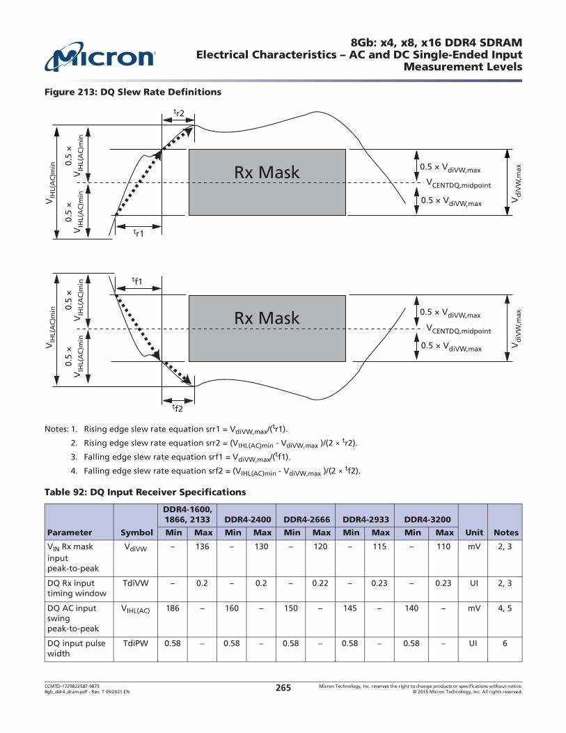
CCMTD-1725822587-9875 Micron Technology, Inc. reserves the right to change products or specifications without notice.8gb_ddr4_dram.pdf - Rev. T 09/2021 EN 2015 Micron Technology, Inc. All rights reserved.265
8Gb: x4, x8, x16 DDR4 SDRAM
Measurement Levels
Figure 213: DQ Slew Rate Definitions
Notes: 1. Rising edge slew rate equation srr1 = VdiVW,max/(tr1).
2. Rising edge slew rate equation srr2 = (VIHL(AC)min - VdiVW,max )/(2 tr2).
3. Falling edge slew rate equation srf1 = VdiVW,max/(tf1).
4. Falling edge slew rate equation srf2 = (VIHL(AC)min - VdiVW,max )/(2 tf2).
Table 92: DQ Input Receiver Specifications
Parameter Symbol
DDR4-1600, 1866, 2133 DDR4-2400 DDR4-2666 DDR4-2933 DDR4-3200
Unit Notes Min Max Min Max Min Max Min Max Min Max
VIN Rx mask input peak-to-peak
VdiVW 136 130 120 115 110 mV 2, 3
DQ Rx input timing window
TdiVW 0.2 0.2 0.22 0.23 0.23 UI 2, 3
DQ AC input swing peak-to-peak
VIHL(AC) 186 160 150 145 140 mV 4, 5
DQ input pulse width
TdiPW 0.58 0.58 0.58 0.58 0.58 UI 6
VIH
L(A
C)m
in
0.5
×V
IHL(
AC
)min
0.5
×V
IHL(
AC
)min
VIH
L(A
C)m
in
0.5
×V
IHL(
AC
)min
0.5
×V
IHL(
AC
)min
0.5 × VdiVW,max
0.5 × VdiVW,max
VCENTDQ,midpoint
Vd
iVW
,max
0.5 × VdiVW,max
0.5 × VdiVW,max Vd
iVW
,max
tr1
tr2
VCENTDQ,midpoint
tf1
tf2
Rx Mask
Rx Mask

CCMTD-1725822587-9875 Micron Technology, Inc. reserves the right to change products or specifications without notice.8gb_ddr4_dram.pdf - Rev. T 09/2021 EN 2015 Micron Technology, Inc. All rights reserved.266
8Gb: x4, x8, x16 DDR4 SDRAM
Measurement Levels
Notes: 1. All Rx mask specifications must be satisfied for each UI. For example, if the minimum input pulse width is violated when satisfying TdiVW (MIN), VdiVW,max, and minimum slew rate limits, then either TdiVW (MIN) or minimum slew rates would have to be increased to the point where the minimum input pulse width would no longer be violated.
2. Data Rx mask voltage and timing total input valid window where VdiVW is centered around VCENTDQ,midpoint after VREFDQ training is completed. The data Rx mask is applied per bit and should include voltage and temperature drift
terms. The input buffer design specification is to achieve at least a BER =1e- 16 when the Rx mask is not violated.3. Defined over the DQ internal VREF range 1.4. Overshoot and undershoot specifications apply.5. DQ input pulse signal swing into the receiver must meet or exceed VIHL(AC)min. VIHL(AC)min is to be achieved on an
UI basis when a rising and falling edge occur in the same UI (a valid TdiPW).6. DQ minimum input pulse width defined at the VCENTDQ,midpoint.7. DQS-to-DQ Rx mask offset is skew between DQS and DQ within a nibble (x4) or word (x8, x16 [for x16, the upper
and lower bytes are treated as separate x8s]) at the SDRAM balls over process, voltage, and temperature.8. DQ-to-DQ Rx mask offset is skew between DQs within a nibble (x4) or word (x8, x16) at the SDRAM balls for a given
component over process, voltage, and temperature.9. Input slew rate over VdiVW mask centered at VCENTDQ,midpoint. Slowest DQ slew rate to fastest DQ slew rate per
transition edge must be within 1.7V/ns of each other.10. Input slew rate between VdiVW mask edge and VIHL(AC)min points.11. Note 1 applies to the entire table.
The following figure shows the Rx mask relationship to the input timing specifications relative to
system tDS and tDH. The classical definition for tDS/tDH required a DQ rising and falling edges to not
violate tDS and tDH relative to the DQS strobe at any time; however, with the Rx mask tDS and tDH can shift relative to the DQS strobe provided the input pulse width specification is satisfied and the Rx mask is not violated.
DQS-to-DQ Rx mask offset
tDQS2DQ 0.17 0.17 0.19 0.22 0.22 UI 7
DQ-to-DQ Rx mask offset
tDQ2DQ 0.1 0.1 0.105 0.115 0.125 UI 8
Input slew rate over VdiVW if tCK 0.937ns
srr1, srf1 1 9 1 9 1 9 1 9 1 9 V/ns 9
Input slew rate over VdiVW if
0.937ns > tCK 0.625ns
srr1, srf1 1.25 9 1.25 9 1.25 9 1.25 9 V/ns 9
Rising input slew rate over 1/2 VIHL(AC)
srr2 0.2 srr1
9 0.2 srr1
9 0.2 srr1
9 0.2 srr1
9 0.2 srr1
9 V/ns 10
Falling input slew rate over 1/2 VIHL(AC)
srf2 0.2 srf1
9 0.2 srf1
9 0.2 srf1
9 0.2 srf1
9 0.2 srf1
9 V/ns 10
Table 92: DQ Input Receiver Specifications (Continued)
Parameter Symbol
DDR4-1600, 1866, 2133 DDR4-2400 DDR4-2666 DDR4-2933 DDR4-3200
Unit Notes Min Max Min Max Min Max Min Max Min Max

CCMTD-1725822587-9875 Micron Technology, Inc. reserves the right to change products or specifications without notice.8gb_ddr4_dram.pdf - Rev. T 09/2021 EN 2015 Micron Technology, Inc. All rights reserved.267
8Gb: x4, x8, x16 DDR4 SDRAM
Measurement Levels
Figure 214: Rx Mask Relative to tDS/tDH
The following figure and table show an example of the worst case Rx mask required if the DQS and DQ pins do not have DRAM controller to DRAM write DQ training. The figure and table show that without DRAM write DQ training, the Rx mask would increase from 0.2UI to essentially 0.54UI. This would also
be the minimum tDS and tDH required as well.
tDH = Greater of 0.5 × TdiVWor
0.5 × (TdiPW + VdiVW/tr1)
tDS = Greater of 0.5 × TdiVWor
0.5 × (TdiPW + VdiVW/tf1)
Vd
iVW
0.5 × VdiVW
tf1 tr1
0.5 × VdiVW
TdiPW
TdiVW
VCENTDQ,pin mean
VIL(DC)
VIH(DC)
DQS_c
DQS_t
RxMask

CCMTD-1725822587-9875 Micron Technology, Inc. reserves the right to change products or specifications without notice.8gb_ddr4_dram.pdf - Rev. T 09/2021 EN 2015 Micron Technology, Inc. All rights reserved.268
8Gb: x4, x8, x16 DDR4 SDRAM
Measurement Levels
Figure 215: Rx Mask Without Write Training
Notes: 1. VIHL(AC), VdiVW, and VILH(DC) referenced to VCENTDQ,midpoint.
Connectivity Test (CT) Mode Input Levels
Table 93: Rx Mask and tDS/tDH without Write Training
DDR4 VIHL(AC)
(mV) TdiPW
(UI) VdiVW (mV)
TdiVW(UI)
tDQS2DQ(UI)
tDQ2DQ(UI)
Rx Mask with Write
Train(ps)
tDS + tDH (ps)
1600 186 0.58 136 0.2 0.17 0.1 125 338
1866 186 0.58 136 0.2 0.17 0.1 107.1 289
2133 186 0.58 136 0.2 0.17 0.1 94 253
2400 160 0.58 130 0.2 0.17 0.1 83.3 225
2666 150 0.58 120 0.22 0.19 0.105 82.5 225
2933 145 0.58 115 0.23 0.22 0.115 78.4 228
3200 140 0.58 110 0.23 0.22 0.125 71.8 209
Table 94: TEN Input Levels (CMOS)
Parameter Symbol Min Max Unit Note
TEN AC input high voltage VIH(AC)_TEN 0.8 VDD VDD V 1
TEN DC input high voltage VIH(DC)_TEN 0.7 VDD VDD V
TEN DC input low voltage VIL(DC)_TEN VSS 0.3 VDD V
TEN AC input low voltage VIL(AC)_TEN VSS 0.2 VDD V 2
TEN falling time tF_TEN 1 0 ns
tDS
Vd
iVW
0.5 × VdiVW
0.5 × VdiVW
tDH
0.5 × TdiVW + tDQS2DQ
TdiVW + 2 × tDQS2DQ
0.5 × TdiVW + tDQS2DQ
VCENTDQ,midpoint
VIL(DC)
VIH(DC)
DQS_c
DQS_t
Rx Mask

CCMTD-1725822587-9875 Micron Technology, Inc. reserves the right to change products or specifications without notice.8gb_ddr4_dram.pdf - Rev. T 09/2021 EN 2015 Micron Technology, Inc. All rights reserved.269
8Gb: x4, x8, x16 DDR4 SDRAM
Measurement Levels
Notes: 1. Overshoot should not exceed the VIN values in the Absolute Maximum Ratings table.2. Undershoot should not exceed the VIN values in the Absolute Maximum Ratings table.
Figure 216: TEN Input Slew Rate Definition
Notes: 1. Refer to Overshoot and Undershoot Specifications.2. CT Type-A inputs: CS_n, BG[1:0], BA[1:0], A[9:0], A10/AP, A11, A12/BC_n, A13, WE_n/A14, CAS_n/A15, RAS_n/A16,
A17, CKE, ACT_n, ODT, CLK_t, CLK_C, PAR.3. VREFCA = 0.5 VDD.
TEN rising time tR_TEN 1 0 ns
Table 94: TEN Input Levels (CMOS) (Continued)
Parameter Symbol Min Max Unit Note
Table 95: CT Type-A Input Levels
Parameter Symbol Min Max Unit Note
CTipA AC input high voltage VIH(AC) VREF + 200 VDD11 V 2, 3
CTipA DC input high voltage VIH(DC) VREF + 150 VDD V 2, 3
CTipA DC input low voltage VIL(DC) VSS VREF - 150 V 2, 3
CTipA AC input low voltage VIL(AC) VSS1 1 VREF - 200 V 2, 3
CTipA falling time tF_CTipA 5 ns 2
CTipA rising time tR_CTipA 5 ns 2
tR_TENtF_TEN
VIH(AC)_TENmin
VIL(AC)_TENmin
VIH(DC)_TENmin
VIL(DC)_TENmin
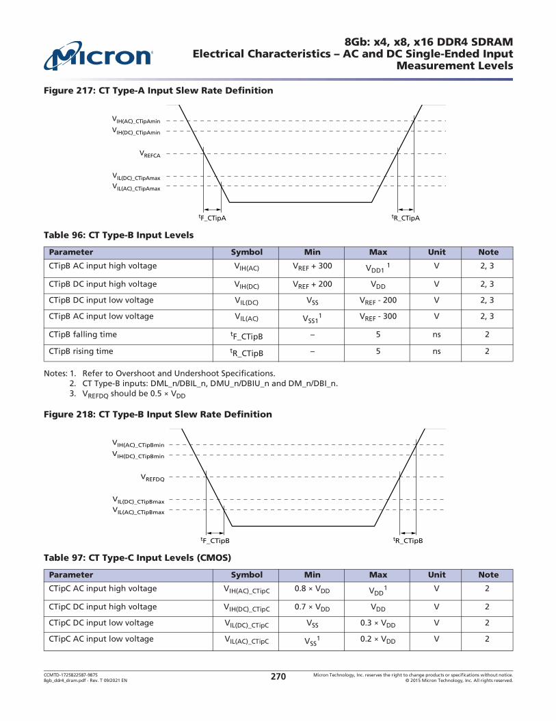
CCMTD-1725822587-9875 Micron Technology, Inc. reserves the right to change products or specifications without notice.8gb_ddr4_dram.pdf - Rev. T 09/2021 EN 2015 Micron Technology, Inc. All rights reserved.270
8Gb: x4, x8, x16 DDR4 SDRAM
Measurement Levels
Figure 217: CT Type-A Input Slew Rate Definition
Notes: 1. Refer to Overshoot and Undershoot Specifications.2. CT Type-B inputs: DML_n/DBIL_n, DMU_n/DBIU_n and DM_n/DBI_n.3. VREFDQ should be 0.5 VDD
Figure 218: CT Type-B Input Slew Rate Definition
Table 96: CT Type-B Input Levels
Parameter Symbol Min Max Unit Note
CTipB AC input high voltage VIH(AC) VREF + 300 VDD1 1 V 2, 3
CTipB DC input high voltage VIH(DC) VREF + 200 VDD V 2, 3
CTipB DC input low voltage VIL(DC) VSS VREF - 200 V 2, 3
CTipB AC input low voltage VIL(AC) VSS11 VREF - 300 V 2, 3
CTipB falling time tF_CTipB 5 ns 2
CTipB rising time tR_CTipB 5 ns 2
Table 97: CT Type-C Input Levels (CMOS)
Parameter Symbol Min Max Unit Note
CTipC AC input high voltage VIH(AC)_CTipC 0.8 VDD VDD1 V 2
CTipC DC input high voltage VIH(DC)_CTipC 0.7 VDD VDD V 2
CTipC DC input low voltage VIL(DC)_CTipC VSS 0.3 VDD V 2
CTipC AC input low voltage VIL(AC)_CTipC VSS1 0.2 VDD V 2
VIH(AC)_CTipAmin
VIL(AC)_CTipAmax
VIH(DC)_CTipAmin
VIL(DC)_CTipAmax
tR_CTipAtF_CTipA
VREFCA
VIH(AC)_CTipBmin
VIL(AC)_CTipBmax
VIH(DC)_CTipBmin
VIL(DC)_CTipBmax
tR_CTipBtF_CTipB
VREFDQ

CCMTD-1725822587-9875 Micron Technology, Inc. reserves the right to change products or specifications without notice.8gb_ddr4_dram.pdf - Rev. T 09/2021 EN 2015 Micron Technology, Inc. All rights reserved.271
8Gb: x4, x8, x16 DDR4 SDRAM
Measurement Levels
Notes: 1. Refer to Overshoot and Undershoot Specifications.2. CT Type-C inputs: Alert_n.
Figure 219: CT Type-C Input Slew Rate Definition
Notes: 1. After RESET_n is registered LOW, the RESET_n level must be maintained below VIL(DC)_RESET during tPW_RESET, otherwise, the DRAM may not be reset.
2. After RESET_n is registered HIGH, the RESET_n level must be maintained above VIH(DC)_RESET, otherwise, operation will be uncertain until it is reset by asserting RESET_n signal LOW.
3. Slope reversal (ring-back) during this level transition from LOW to HIGH should be mitigated as much as possible.4. Overshoot should not exceed the VIN values in the Absolute Maximum Ratings table.5. Undershoot should not exceed the VIN values in the Absolute Maximum Ratings table.6. CT Type-D inputs: RESET_n; same requirements as in normal mode.
CTipC falling time tF_CTipC 1 0 ns 2
CTipC rising time tR_CTipC 1 0 ns 2
Table 97: CT Type-C Input Levels (CMOS) (Continued)
Parameter Symbol Min Max Unit Note
Table 98: CT Type-D Input Levels
Parameter Symbol Min Max Unit Note
CTipD AC input high voltage VIH(AC)_CTipD 0.8 VDD VDD V 4
CTipD DC input high voltage VIH(DC)_CTipD 0.7 VDD VDD V 2
CTipD DC input low voltage VIL(DC)_CTipD VSS 0.3 VDD V 1
CTipD AC input low voltage VIL(AC)_CTipD VSS 0.2 VDD V 5
Rising time tR_RESET 1 s 3
RESET pulse width - after power-up tPW_RESET_S 1 s
RESET pulse width - during power-up tPW_RESET_L 200 s
tR_TENtF_TEN
VIH(AC)_TENmin
VIL(AC)_TENmin
VIH(DC)_TENmin
VIL(DC)_TENmin

CCMTD-1725822587-9875 Micron Technology, Inc. reserves the right to change products or specifications without notice.8gb_ddr4_dram.pdf - Rev. T 09/2021 EN 2015 Micron Technology, Inc. All rights reserved.272
8Gb: x4, x8, x16 DDR4 SDRAM
Measurement Levels
Figure 220: CT Type-D Input Slew Rate Definition
Levels
Differential Inputs
Figure 221: tDVAC
Notes: 1. Differential signal rising edge from VIL,diff,max to VIH,diff(AC)min must be monotonic slope.
tR_RESET
tPW_RESET
VIH(AC)_RESETmin
VIL(AC)_RESETmax
VIH(DC)_RESETmin
VIL(DC)_RESETmax
VIH,diff(AC)min
0.0
VIL,diff,max
tDVAC
VIH,diff,min
VIL,diff(AC)max
Half cycle tDVAC
CK_t, CK_c
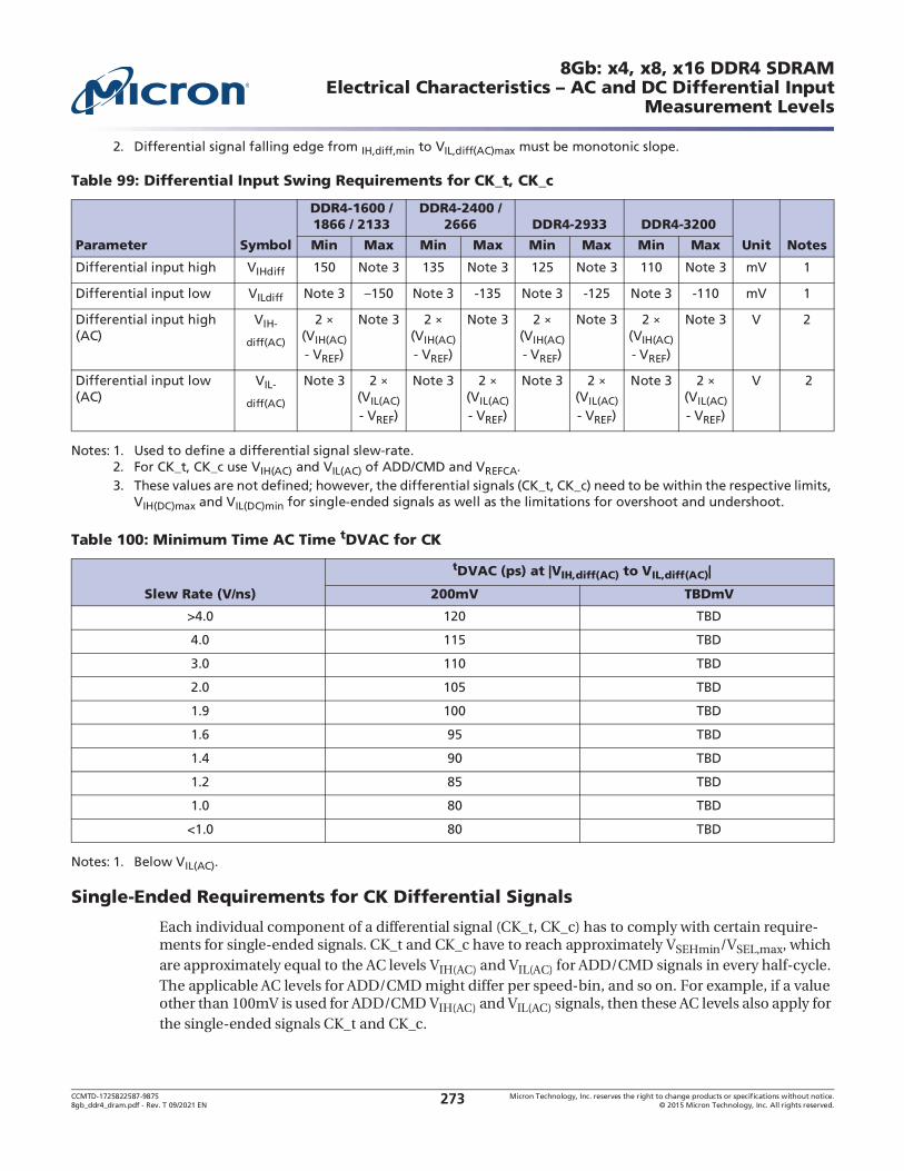
CCMTD-1725822587-9875 Micron Technology, Inc. reserves the right to change products or specifications without notice.8gb_ddr4_dram.pdf - Rev. T 09/2021 EN 2015 Micron Technology, Inc. All rights reserved.273
8Gb: x4, x8, x16 DDR4 SDRAM
Measurement Levels
2. Differential signal falling edge from IH,diff,min to VIL,diff(AC)max must be monotonic slope.
Notes: 1. Used to define a differential signal slew-rate.2. For CK_t, CK_c use VIH(AC) and VIL(AC) of ADD/CMD and VREFCA.3. These values are not defined; however, the differential signals (CK_t, CK_c) need to be within the respective limits,
VIH(DC)max and VIL(DC)min for single-ended signals as well as the limitations for overshoot and undershoot.
Notes: 1. Below VIL(AC).
Single-Ended Requirements for CK Differential Signals
Each individual component of a differential signal (CK_t, CK_c) has to comply with certain require-ments for single-ended signals. CK_t and CK_c have to reach approximately VSEHmin/VSEL,max, which are approximately equal to the AC levels VIH(AC) and VIL(AC) for ADD/CMD signals in every half-cycle. The applicable AC levels for ADD/CMD might differ per speed-bin, and so on. For example, if a value other than 100mV is used for ADD/CMD VIH(AC) and VIL(AC) signals, then these AC levels also apply for the single-ended signals CK_t and CK_c.
Table 99: Differential Input Swing Requirements for CK_t, CK_c
Parameter Symbol
DDR4-1600 / 1866 / 2133
DDR4-2400 / 2666 DDR4-2933 DDR4-3200
Unit NotesMin Max Min Max Min Max Min Max
Differential input high VIHdiff 150 Note 3 135 Note 3 125 Note 3 110 Note 3 mV 1
Differential input low VILdiff Note 3 Note 3 -135 Note 3 -125 Note 3 -110 mV 1
Differential input high (AC)
VIH-
diff(AC)
2 (VIH(AC) - VREF)
Note 3 2 (VIH(AC) - VREF)
Note 3 2 (VIH(AC) - VREF)
Note 3 2 (VIH(AC) - VREF)
Note 3 V 2
Differential input low (AC)
VIL-
diff(AC)
Note 3 2 (VIL(AC) - VREF)
Note 3 2 (VIL(AC) - VREF)
Note 3 2 (VIL(AC) - VREF)
Note 3 2 (VIL(AC) - VREF)
V 2
Table 100: Minimum Time AC Time tDVAC for CK
Slew Rate (V/ns)
tDVAC (ps) at |VIH,diff(AC) to VIL,diff(AC)|
200mV TBDmV
>4.0 120 TBD
4.0 115 TBD
3.0 110 TBD
2.0 105 TBD
1.9 100 TBD
1.6 95 TBD
1.4 90 TBD
1.2 85 TBD
1.0 80 TBD
<1.0 80 TBD

CCMTD-1725822587-9875 Micron Technology, Inc. reserves the right to change products or specifications without notice.8gb_ddr4_dram.pdf - Rev. T 09/2021 EN 2015 Micron Technology, Inc. All rights reserved.274
8Gb: x4, x8, x16 DDR4 SDRAM
Measurement Levels
While ADD/CMD signal requirements are with respect to VREFCA, the single-ended components of differential signals have a requirement with respect to VDD/2; this is nominally the same. The transi-tion of single-ended signals through the AC levels is used to measure setup time. For single-ended components of differential signals the requirement to reach VSEL,max/VSEH,min has no bearing on timing, but adds a restriction on the common mode characteristics of these signals.
Figure 222: Single-Ended Requirements for CK
Notes: 1. For CK_t, CK_c use VIH(AC) and VIL(AC) of ADD/CMD and VREFCA.2. ADDR/CMD VIH(AC) and VIL(AC) based on VREFCA.3. These values are not defined; however, the differential signal (CK_t, CK_c) need to be within the respective limits,
VIH(DC)max and VIL(DC)min for single-ended signals as well as the limitations for overshoot and undershoot.
Slew Rate Definitions for CK Differential Input Signals
Notes: 1. The differential signal CK_t, CK_c must be monotonic between these thresholds.
Table 101: Single-Ended Requirements for CK
Parameter Symbol
DDR4-1600 / 1866 / 2133 DDR4-2400 / 2666 DDR4-2933 / 3200
Unit NotesMin Max Min Max Min Max
Single-ended high level for CK_t, CK_c
VSEH VDD/2 + 0.100
Note 3 VDD/2 + 0.095
Note 3 VDD/2 + 0.085
Note 3 V 1, 2
Single-ended low level for CK_t, CK_c
VSEL Note 3 VDD/2 - 0.100
Note 3 VDD/2 - 0.095
Note 3 VDD/2 - 0.085
V 1, 2
Table 102: CK Differential Input Slew Rate Definition
Description
Measured
Defined byFrom To
Differential input slew rate for rising edge VIL,diff,max VIH,diff,min |VIH,diff,min - VIL,diff,max|/ TRdiff
Differential input slew rate for falling edge VIH,diff,min VIL,diff,max |VIH,diff,min - VIL,diff,max|/ TFdiff
VSS or VSSQ
VDD or VDDQ
VSEL,max
VSEH,min
VSEH
VSEL
CK
VDD/2 or VDDQ/2

CCMTD-1725822587-9875 Micron Technology, Inc. reserves the right to change products or specifications without notice.8gb_ddr4_dram.pdf - Rev. T 09/2021 EN 2015 Micron Technology, Inc. All rights reserved.275
8Gb: x4, x8, x16 DDR4 SDRAM
Measurement Levels
Figure 223: Differential Input Slew Rate Definition for CK_t, CK_c
CK Differential Input Cross Point Voltage
To guarantee tight setup and hold times as well as output skew parameters with respect to clock and strobe, each cross point voltage of differential input signal CK_t, CK_c must meet the requirements shown below. The differential input cross point voltage VIX(CK) is measured from the actual cross point of true and complement signals to the midlevel between VDD and VSS.
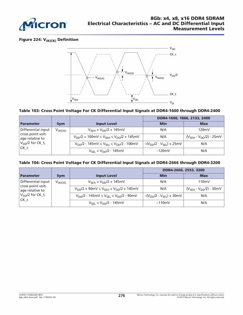
CCMTD-1725822587-9875 Micron Technology, Inc. reserves the right to change products or specifications without notice.8gb_ddr4_dram.pdf - Rev. T 09/2021 EN 2015 Micron Technology, Inc. All rights reserved.276
8Gb: x4, x8, x16 DDR4 SDRAM
Measurement Levels
Figure 224: VIX(CK) Definition
Table 103: Cross Point Voltage For CK Differential Input Signals at DDR4-1600 through DDR4-2400
Parameter Sym Input Level
DDR4-1600, 1866, 2133, 2400
Min Max
Differential input cross point volt-age relative to VDD/2 for CK_t, CK_c
VIX(CK) VSEH > VDD/2 + 145mV N/A 120mV
VDD/2 + 100mV VSEH VDD/2 + 145mV N/A (VSEH - VDD/2) - 25mV
VDD/2 - 145mV VSEL VDD/2 - 100mV DD/2 - VSEL) + 25mV N/A
VSEL < VDD/2 - 145mV N/A
Table 104: Cross Point Voltage For CK Differential Input Signals at DDR4-2666 through DDR4-3200
Parameter Sym Input Level
DDR4-2666, 2933, 3200
Min Max
Differential input cross point volt-age relative to VDD/2 for CK_t, CK_c
VIX(CK) VSEH > VDD/2 + 145mV N/A 110mV
VDD/2 + 90mV VSEH VDD/2 + 145mV N/A (VSEH - VDD/2) - 30mV
VDD/2 - 145mV VSEL VDD/2 - 90mV DD/2 - VSEL) + 30mV N/A
VSEL < VDD/2 - 145mV N/A
VIX(CK)
VSEH VSEL
VIX(CK)
VIX(CK)
CK_t
VSS
VDD/2
CK_c
VDD
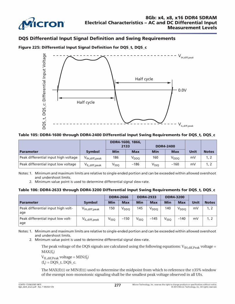
CCMTD-1725822587-9875 Micron Technology, Inc. reserves the right to change products or specifications without notice.8gb_ddr4_dram.pdf - Rev. T 09/2021 EN 2015 Micron Technology, Inc. All rights reserved.277
8Gb: x4, x8, x16 DDR4 SDRAM
Measurement Levels
DQS Differential Input Signal Definition and Swing Requirements
Figure 225: Differential Input Signal Definition for DQS_t, DQS_c
Notes: 1. Minimum and maximum limits are relative to single-ended portion and can be exceeded within allowed overshoot and undershoot limits.
2. Minimum value point is used to determine differential signal slew-rate.
Notes: 1. Minimum and maximum limits are relative to single-ended portion and can be exceeded within allowed overshoot and undershoot limits.
2. Minimum value point is used to determine differential signal slew-rate.
The peak voltage of the DQS signals are calculated using the following equations: VIH,dif,Peak voltage = MAX(ft) VIL,dif,Peak voltage = MIN(ft) (ft) = DQS_t, DQS_c.
The MAX(f(t)) or MIN(f(t)) used to determine the midpoint from which to reference the 35% window of the exempt non-monotonic signaling shall be the smallest peak voltage observed in all UIs.
Table 105: DDR4-1600 through DDR4-2400 Differential Input Swing Requirements for DQS_t, DQS_c
Parameter Symbol
DDR4-1600, 1866, 2133 DDR4-2400
Unit NotesMin Max Min Max
Peak differential input high voltage VIH,diff,peak 186 VDDQ 160 VDDQ mV 1, 2
Peak differential input low voltage VIL,diff,peak VSSQ VSSQ mV 1, 2
Table 106: DDR4-2633 through DDR4-3200 Differential Input Swing Requirements for DQS_t, DQS_c
Parameter Symbol
DDR4-2666 DDR4-2933 DDR4-3200
Unit NotesMin Max Min Max Min Max
Peak differential input high volt-age
VIH,diff,peak 150 VDDQ 145 VDDQ 140 VDDQ mV 1, 2
Peak differential input low volt-age
VIL,diff,peak VSSQ VSSQ VSSQ mV 1, 2
Half cycle
VIL,diff,peak
0.0V
DQ
S_t,
DQ
S_c:
Dif
fere
nti
al In
pu
t V
olt
age VIH,diff,peak
Half cycle

CCMTD-1725822587-9875 Micron Technology, Inc. reserves the right to change products or specifications without notice.8gb_ddr4_dram.pdf - Rev. T 09/2021 EN 2015 Micron Technology, Inc. All rights reserved.278
8Gb: x4, x8, x16 DDR4 SDRAM
Measurement Levels
Figure 226: DQS_t, DQS_c Input Peak Voltage Calculation and Range of Exempt non-Monotonic Signaling
DQS_t
MIN(ft) MAX(ft)
DQS_c
DQ
S_t,
DQ
S_c:
Sin
gle
-En
ded
Inp
ut
Vo
ltag
es
+50%
–50%
+35%
–35%
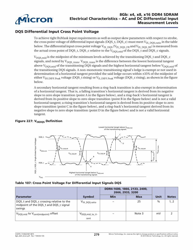
CCMTD-1725822587-9875 Micron Technology, Inc. reserves the right to change products or specifications without notice.8gb_ddr4_dram.pdf - Rev. T 09/2021 EN 2015 Micron Technology, Inc. All rights reserved.279
8Gb: x4, x8, x16 DDR4 SDRAM
Measurement Levels
DQS Differential Input Cross Point Voltage
To achieve tight RxMask input requirements as well as output skew parameters with respect to strobe, the cross point voltage of differential input signals (DQS_t, DQS_c) must meet VIX_DQS,ratio in the table below. The differential input cross point voltage VIX_DQS (VIX_DQS_FR and VIX_DQS_RF) is measured from the actual cross point of DQS_t, DQS_c relative to the VDQS,mid of the DQS_t and DQS_c signals.
VDQS,mid is the midpoint of the minimum levels achieved by the transitioning DQS_t and DQS_c signals, and noted by VDQS_trans. VDQS_trans is the difference between the lowest horizontal tangent above VDQS,mid of the transitioning DQS signals and the highest horizontal tangent below VDQS,mid of
determination of a horizontal tangent provided the said ledge occurs within 35% of the midpoint of either VIH.DIFF.Peak voltage (DQS_t rising) or VIL.DIFF.Peak voltage (DQS_c rising), as shown in the figure below.
A secondary horizontal tangent resulting from a ring-back transition is also exempt in determination
derived from its positive slope to zero slope transition (point B in the figure below) and is not a valid
negative slope to zero slope transition (point D in the figure below) and is not a valid horizontal tangent.
Figure 227: VIXDQS Definition
Table 107: Cross Point Voltage For Differential Input Signals DQS
Parameter Symbol
DDR4-1600, 1866, 2133, 2400, 2666, 2933, 3200
Unit NotesMin Max
DQS_t and DQS_c crossing relative to the midpoint of the DQS_t and DQS_c signal swings
VIX_DQS,ratio 25 % 1, 2
VDQS,mid to Vcent(midpoint) offset VDQS,mid_to_V-
cent
Note 3 mV 2
DQ
S_t,
DQ
S_c:
Sin
gle
-En
ded
Inp
ut
Vo
ltag
es
DQS_t
VIX_DQS,FR
VIX_DQS,FRVIX_DQS,RF
VIX_DQS,RF
VD
QS_
tran
s
VD
QS_
tran
s/2
Lowest horizontal tanget above VDQS,midof the transitioning signals
Highest horizontal tanget below VDQS,midof the transitioning signals
VSSQ
VDQS,mid
DQS_c
A
B
C
D

CCMTD-1725822587-9875 Micron Technology, Inc. reserves the right to change products or specifications without notice.8gb_ddr4_dram.pdf - Rev. T 09/2021 EN 2015 Micron Technology, Inc. All rights reserved.280
8Gb: x4, x8, x16 DDR4 SDRAM
Measurement Levels
Notes: 1. VIX_DQS,ratio is DQS VIX crossing (VIX_DQS,FR or VIX_DQS,RF) divided by VDQS_trans. VDQS_trans is the difference between the lowest horizontal tangent above VDQS,midd of the transitioning DQS signals and the highest horizontal tangent below VDQS,mid of the transitioning DQS signals.
2. VDQS,mid will be similar to the VREFDQ internal setting value (Vcent(midpoint) offset) obtained during VREF Training if the DQS and DQs drivers and paths are matched.
3. The maximum limit shall not exceed the smaller of VIH,diff,DQS minimum limit or 50mV.
Slew Rate Definitions for DQS Differential Input Signals
Notes: 1. The differential signal DQS_t, DQS_c must be monotonic between these thresholds.
Figure 228: Differential Input Slew Rate and Input Level Definition for DQS_t, DQS_c
Notes: 1. Minimum and maximum limits are relative to single-ended portion and can be exceeded within allowed overshoot and undershoot limits.
2. Differential signal rising edge from VIL,diff,DQS to VIH,diff,DQS must be monotonic slope.3. Differential signal falling edge from VIH,diff,DQS to VIL,diff,DQS must be monotonic slope.4. Differential input slew rate for rising edge from VIL,diff,DQS to VIH,diff,DQS is defined by |VIL,diff,min -
VIH,diff,max|/ TRdiff.
Table 108: DQS Differential Input Slew Rate Definition
Description
Measured
Defined byFrom To
Differential input slew rate for rising edge VIL,diff,DQS VIH,diff,DQS |VIH,diff,DQS - VIL,diff,DQS|/ TRdiff
Differential input slew rate for falling edge VIH,diff,DQS VIL,diff,DQS |VIHdiffDQS - VIL,diff,DQS|/ TFdiff
Table 109: DDR4-1600 through DDR4-2400 Differential Input Slew Rate and Input Levels for DQS_t, DQS_c
Parameter Symbol
DDR4-1600, 1866, 2133 DDR4-2400
Unit NotesMin Max Min Max
Peak differential input high voltage VIH,diff,peak 186 VDDQ 160 VDDQ mV 1
Differential input high voltage VIH,diff,DQS 136 130 mV 2, 3
Differential input low voltage VIL,diff,DQS mV 2, 3
Peak differential input low voltage VIL,diff,peak -VDDQ -VDDQ mV 1
DQS differential input slew rate SRIdiff 3.0 18 3.0 18 V/ns 4, 5

CCMTD-1725822587-9875 Micron Technology, Inc. reserves the right to change products or specifications without notice.8gb_ddr4_dram.pdf - Rev. T 09/2021 EN 2015 Micron Technology, Inc. All rights reserved.281
8Gb: x4, x8, x16 DDR4 SDRAM
Measurement Levels
5. Differential input slew rate for falling edge from VIH,diff,DQS to VIL,diff,DQS is defined by |VIL,diff,min - VIH,diff,max|/ TFdiff.
Notes: 1. Minimum and maximum limits are relative to single-ended portion and can be exceeded within allowed overshoot and undershoot limits.
2. Differential signal rising edge from VIL,diff,DQS to VIH,diff,DQS must be monotonic slope.3. Differential signal falling edge from VIH,diff,DQS to VIL,diff,DQS must be monotonic slope.4. Differential input slew rate for rising edge from VIL,diff,DQS to VIH,diff,DQS is defined by |VIL,diff,min -
VIH,diff,max|/ TRdiff.5. Differential input slew rate for falling edge from VIH,diff,DQS to VIL,diff,DQS is defined by |VIL,diff,min -
VIH,diff,max|/ TFdiff.
Table 110: DDR4-2666 through DDR4-3200 Differential Input Slew Rate and Input Levels for DQS_t, DQS_c
Parameter Symbol
DDR4-2666 DDR4-2933 DDR4-3200
Unit NotesMin Max Min Max Min Max
Peak differential input high voltage
VIH,diff,peak 150 VDDQ 145 VDDQ 140 VDDQ mV 1
Differential input high voltage
VIH,diff,DQS 130 115 110 mV 2, 3
Differential input low voltage
VIL,diff,DQS mV 2, 3
Peak differential input low voltage
VIL,diff,peak VSSQ VSSQ VSSQ mV 1
DQS differential input slew rate
SRIdiff 2.5 18 2.5 18 2.5 18 V/ns 4, 5

CCMTD-1725822587-9875 Micron Technology, Inc. reserves the right to change products or specifications without notice.8gb_ddr4_dram.pdf - Rev. T 09/2021 EN 2015 Micron Technology, Inc. All rights reserved.282
8Gb: x4, x8, x16 DDR4 SDRAM
Specifications
Address, Command, and Control Overshoot and Undershoot Specifications
Figure 229: ADDR, CMD, CNTL Overshoot and Undershoot Definition
Table 111: ADDR, CMD, CNTL Overshoot and Undershoot/Specifications
DescriptionDDR4-1600
DDR4-1866
DDR4-2133
DDR4-2400
DDR4-2666
DDR4-2933
DDR4-3200 Unit
Address and control pins (A[17:0], BG[1:0], BA[1:0], CS_n, RAS_n, CAS_n, WE_n, CKE, ODT, C2-0)
Area A: Maximum peak amplitude above VDD absolute MAX
0.06 0.06 0.06 0.06 0.06 0.06 0.06 V
Area B: Amplitude allowed between VDD and VDD absolute MAX
0.24 0.24 0.24 0.24 0.24 0.24 0.24 V
Area C: Maximum peak amplitude allowed for undershoot below VSS
0.30 0.30 0.30 0.30 0.30 0.30 0.30 V
Area A maximum overshoot area per 1tCK 0.0083 0.0071 0.0062 0.0055 0.0055 0.0055 0.0055 V/ns
Area B maximum overshoot area per 1tCK 0.2550 0.2185 0.1914 0.1699 0.1699 0.1699 0.1699 V/ns
Area C maximum undershoot area per 1tCK 0.2644 0.2265 0.1984 0.1762 0.1762 0.1762 0.1762 V/ns
VDD absolute MAX
Absolute MAX overshootOvershoot area above VDD absolute MAX
Overshoot area below VDD absolute MAXand above VDD MAX
Undershoot area below VSS
1tCK
Vo
lts
(V)
VDD
VSS
A
B
C
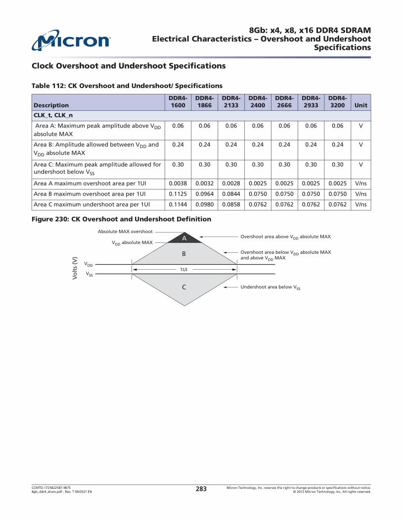
CCMTD-1725822587-9875 Micron Technology, Inc. reserves the right to change products or specifications without notice.8gb_ddr4_dram.pdf - Rev. T 09/2021 EN 2015 Micron Technology, Inc. All rights reserved.283
8Gb: x4, x8, x16 DDR4 SDRAM
Specifications
Clock Overshoot and Undershoot Specifications
Figure 230: CK Overshoot and Undershoot Definition
Table 112: CK Overshoot and Undershoot/ Specifications
DescriptionDDR4-1600
DDR4-1866
DDR4-2133
DDR4-2400
DDR4-2666
DDR4-2933
DDR4-3200 Unit
CLK_t, CLK_n
Area A: Maximum peak amplitude above VDD absolute MAX
0.06 0.06 0.06 0.06 0.06 0.06 0.06 V
Area B: Amplitude allowed between VDD and VDD absolute MAX
0.24 0.24 0.24 0.24 0.24 0.24 0.24 V
Area C: Maximum peak amplitude allowed for undershoot below VSS
0.30 0.30 0.30 0.30 0.30 0.30 0.30 V
Area A maximum overshoot area per 1UI 0.0038 0.0032 0.0028 0.0025 0.0025 0.0025 0.0025 V/ns
Area B maximum overshoot area per 1UI 0.1125 0.0964 0.0844 0.0750 0.0750 0.0750 0.0750 V/ns
Area C maximum undershoot area per 1UI 0.1144 0.0980 0.0858 0.0762 0.0762 0.0762 0.0762 V/ns
VDD absolute MAX
Absolute MAX overshootOvershoot area above VDD absolute MAX
Overshoot area below VDD absolute MAXand above VDD MAX
Undershoot area below VSS
1UI
Vo
lts
(V)
VDD
VSS
A
B
C
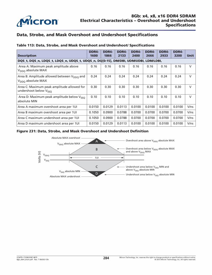
CCMTD-1725822587-9875 Micron Technology, Inc. reserves the right to change products or specifications without notice.8gb_ddr4_dram.pdf - Rev. T 09/2021 EN 2015 Micron Technology, Inc. All rights reserved.284
8Gb: x4, x8, x16 DDR4 SDRAM
Specifications
Data, Strobe, and Mask Overshoot and Undershoot Specifications
Figure 231: Data, Strobe, and Mask Overshoot and Undershoot Definition
Table 113: Data, Strobe, and Mask Overshoot and Undershoot/ Specifications
DescriptionDDR4-1600
DDR4-1866
DDR4-2133
DDR4-2400
DDR4-2666
DDR4-2933
DDR4-3200 Unit
DQS_t, DQS_n, LDQS_t, LDQS_n, UDQS_t, UDQS_n, DQ[0:15], DM/DBI, UDM/UDBI, LDM/LDBI,
Area A: Maximum peak amplitude above VDDQ absolute MAX
0.16 0.16 0.16 0.16 0.16 0.16 0.16 V
Area B: Amplitude allowed between VDDQ and VDDQ absolute MAX
0.24 0.24 0.24 0.24 0.24 0.24 0.24 V
Area C: Maximum peak amplitude allowed for undershoot below VSSQ
0.30 0.30 0.30 0.30 0.30 0.30 0.30 V
Area D: Maximum peak amplitude below VSSQ absolute MIN
0.10 0.10 0.10 0.10 0.10 0.10 0.10 V
Area A maximum overshoot area per 1UI 0.0150 0.0129 0.0113 0.0100 0.0100 0.0100 0.0100 V/ns
Area B maximum overshoot area per 1UI 0.1050 0.0900 0.0788 0.0700 0.0700 0.0700 0.0700 V/ns
Area C maximum undershoot area per 1UI 0.1050 0.0900 0.0788 0.0700 0.0700 0.0700 0.0700 V/ns
Area D maximum undershoot area per 1UI 0.0150 0.0129 0.0113 0.0100 0.0100 0.0100 0.0100 V/ns
VDDQ absolute MAX
VSSQ absolute MIN
A
B
C
Absolute MAX overshoot
Absolute MAX undershoot
Overshoot area above VDDQ absolute MAX
Undershoot area below VSSQ absolute MIN
Overshoot area below VDDQ absolute MAXand above VDDQ MAX
Undershoot area below VSSQ MIN andabove VSSQ absolute MIN
1UI
Vo
lts
(V)
VDDQ
VSSQ
D

CCMTD-1725822587-9875 Micron Technology, Inc. reserves the right to change products or specifications without notice.8gb_ddr4_dram.pdf - Rev. T 09/2021 EN 2015 Micron Technology, Inc. All rights reserved.285
8Gb: x4, x8, x16 DDR4 SDRAM
Levels
Single-Ended Outputs
Notes: 1. The swing of 0.15 VDDQ is based on approximately 50% of the static single-ended output peak-to-peak swing with a driver impedance of RZQ/7 and an effective test load of 50 to VTT = VDDQ.
Using the same reference load used for timing measurements, output slew rate for falling and rising edges is defined and measured between VOL(AC) and VOH(AC) for single-ended signals.
Table 114: Single-Ended Output Levels
Parameter Symbol DDR4-1600 to DDR4-3200 Unit
DC output high measurement level (for IV curve linearity) VOH(DC) 1.1 VDDQ V
DC output mid measurement level (for IV curve linearity) VOM(DC) 0.8 VDDQ V
DC output low measurement level (for IV curve linearity) VOL(DC) 0.5 VDDQ V
AC output high measurement level (for output slew rate) VOH(AC) (0.7 + 0.15) VDDQ V
AC output low measurement level (for output slew rate) VOL(AC) (0.7 - 0.15) VDDQ V
Table 115: Single-Ended Output Slew Rate Definition
Description
Measured
Defined byFrom To
Single-ended output slew rate for rising edge VOL(AC) VOH(AC) [VOH(AC) - VOL(AC)]/ TRse
Single-ended output slew rate for falling edge VOH(AC) VOL(AC) [VOH(AC) - VOL(AC)]/ TFse

CCMTD-1725822587-9875 Micron Technology, Inc. reserves the right to change products or specifications without notice.8gb_ddr4_dram.pdf - Rev. T 09/2021 EN 2015 Micron Technology, Inc. All rights reserved.286
8Gb: x4, x8, x16 DDR4 SDRAM
Levels
Figure 232: Single-ended Output Slew Rate Definition
Notes: 1. SR = slew rate; Q = query output; se = single-ended signals.2. In two cases a maximum slew rate of 12V/ns applies for a single DQ signal within a byte lane:
Case 1 is defined for a single DQ signal within a byte lane that is switching into a certain direction (either from HIGH-to-LOW or LOW-to-HIGH) while all remaining DQ signals in the same byte lane are static (they stay at either HIGH or LOW).Case 2 is defined for a single DQ signal within a byte lane that is switching into a certain direction (either from HIGH-to-LOW or LOW-to-HIGH) while all remaining DQ signals in the same byte lane are switching into the opposite direction (from LOW-to-HIGH or HIGH-to-LOW, respectively). For the remaining DQ signal switching into the opposite direction, the standard maximum limit of 9 V/ns applies.
3. For RON = RZQ/7.
Differential Outputs
Table 116: Single-Ended Output Slew Rate
Parameter Symbol
DDR4-1600/ 1866 / 2133 / 2400 DDR4-2666 DDR4-2933 / 3200
UnitMin Max Min Max Min Max
Single-ended output slew rate
SRQse 4 9 4 9 4 9 V/ns
Table 117: Differential Output Levels
Parameter Symbol DDR4-1600 to DDR4-3200 Unit
AC differential output high measurement level (for output slew rate)
VOH,diff(AC) 0.3 VDDQ V
AC differential output low measurement level (for output slew rate)
VOL,diff(AC) VDDQ V
TRse
TFse
VOH(AC)
VOL(AC)
Sin
gle
-En
ded
Ou
tpu
t V
olt
age
(DQ
)

CCMTD-1725822587-9875 Micron Technology, Inc. reserves the right to change products or specifications without notice.8gb_ddr4_dram.pdf - Rev. T 09/2021 EN 2015 Micron Technology, Inc. All rights reserved.287
8Gb: x4, x8, x16 DDR4 SDRAM
Levels
Notes: 1. The swing of 0.3 VDDQ is based on approximately 50% of the static single-ended output peak-to-peak swing with a driver impedance of RZQ/7 and an effective test load of 50 to VTT = VDDQ at each differential output.
Using the same reference load used for timing measurements, output slew rate for falling and rising edges is defined and measured between VOL,diff(AC) and VOH,diff(AC) for differential signals.
Figure 233: Differential Output Slew Rate Definition
Table 118: Differential Output Slew Rate Definition
Description
Measured
Defined byFrom To
Differential output slew rate for rising edge VOL,diff(AC) VOH,diff(AC) [VOH,diff(AC) - VOL,diff(AC)]/ TRdiff
Differential output slew rate for falling edge VOH,diff(AC) VOL,diff(AC) [VOH,diff(AC) - VOL,diff(AC)]/ TFdiff
TRdiff
TFdiff
VOH,diff(AC)
VOL,diff(AC)
Dif
fere
nti
al In
pu
t V
olt
age
(DQ
S_t,
DQ
S_c)

CCMTD-1725822587-9875 Micron Technology, Inc. reserves the right to change products or specifications without notice.8gb_ddr4_dram.pdf - Rev. T 09/2021 EN 2015 Micron Technology, Inc. All rights reserved.288
8Gb: x4, x8, x16 DDR4 SDRAM
Levels
Notes: 1. SR = slew rate; Q = query output; diff = differential signals.2. For RON = RZQ/7.
Reference Load for AC Timing and Output Slew Rate
The effective reference load of 50 to VTT = VDDQ and driver impedance of RZQ/7 for each output was used in defining the relevant AC timing parameters of the device as well as output slew rate measure-ments.
RON nominal of DQ, DQS_t and DQS_c drivers uses 34 ohms to specify the relevant AC timing param-eter values of the device. The maximum DC high level of output signal = 1.0 VDDQ, the minimum DC low level of output signal = { 34 /( 34 + 50 ) } VDDQ = 0.4 VDDQ.
The nominal reference level of an output signal can be approximated by the following: The center of maximum DC high and minimum DC low = { ( 1 + 0.4 ) / 2 } VDDQ = 0.7 VDDQ. The actual reference level of output signal might vary with driver RON and reference load tolerances. Thus, the actual refer-
Figure 234: Reference Load For AC Timing and Output Slew Rate
Connectivity Test Mode Output Levels
Table 119: Differential Output Slew Rate
Parameter Symbol
DDR4-1600 / 1866 / 2133 / 2400 DDR4-2666 DDR4-2933 / 3200
UnitMin Max Min Max Min Max
Differential output slew rate
SRQdiff 8 18 8 18 8 18 V/ns
Table 120: Connectivity Test Mode Output Levels
Parameter Symbol DDR4-1600 to DDR4-3200 Unit
DC output high measurement level (for IV curve linearity) VOH(DC) 1.1 VDDQ V
DC output mid measurement level (for IV curve linearity) VOM(DC) 0.8 VDDQ V
DC output low measurement level (for IV curve linearity) VOL(DC) 0.5 VDDQ V
DC output below measurement level (for IV curve linearity) VOB(DC) 0.2 VDDQ V
AC output high measurement level (for output slew rate) VOH(AC) VTT + (0.1 VDDQ) V
Timing reference point
DQ, DQS_t, DQS_c, DM, TDQS_t, TDQS_c
CK_t, CK_cDUT
VTT = VDDQVDDQ
VSSQ
RTT = 50

CCMTD-1725822587-9875 Micron Technology, Inc. reserves the right to change products or specifications without notice.8gb_ddr4_dram.pdf - Rev. T 09/2021 EN 2015 Micron Technology, Inc. All rights reserved.289
8Gb: x4, x8, x16 DDR4 SDRAM
Levels
Notes: 1. Driver impedance of RZQ/7 and an effective test load of 50 to VTT = VDDQ.
Figure 235: Connectivity Test Mode Reference Test Load
Figure 236: Connectivity Test Mode Output Slew Rate Definition
AC output low measurement level (for output slew rate) VOL(AC) VTT - (0.1 VDDQ) V
Table 120: Connectivity Test Mode Output Levels (Continued)
Parameter Symbol DDR4-1600 to DDR4-3200 Unit
Table 121: Connectivity Test Mode Output Slew Rate
Parameter Symbol
DDR4-1600 / 1866 / 2133 / 2400 DDR4-2666
DDR4-2933 / 3200
UnitMin Max Min Max Min Max
Output signal falling time
TF_output_CT 10 10 10 ns/V
Output signal rising time TR_output_CT 10 10 10 ns/V
Timing reference point
LDQS_t, LDQS_c, UDQS_t, UDQS_c, DQ, DQS_t, DQS_c,
DM, LDM, HDM, TDQS_t, TDQS_cCT_Inputs
DUT 0.5 × VDDQ
VDDQ
VSSQ
RTT = 50
TFoutput_CT
VOH(AC)
VOL(AC)
VTT0.5 x VDD
TRoutput_CT
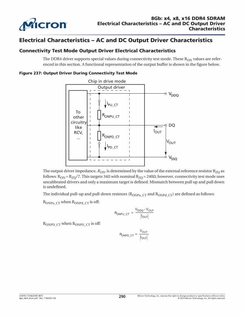
CCMTD-1725822587-9875 Micron Technology, Inc. reserves the right to change products or specifications without notice.8gb_ddr4_dram.pdf - Rev. T 09/2021 EN 2015 Micron Technology, Inc. All rights reserved.290
8Gb: x4, x8, x16 DDR4 SDRAM
Characteristics
Connectivity Test Mode Output Driver Electrical Characteristics
The DDR4 driver supports special values during connectivity test mode. These RON values are refer-enced in this section. A functional representation of the output buffer is shown in the figure below.
Figure 237: Output Driver During Connectivity Test Mode
The output driver impedance, RON, is determined by the value of the external reference resistor RZQ as follows: RON = RZQ/7. This targets 34 with nominal RZQ = 240 ; however, connectivity test mode uses uncalibrated drivers and only a maximum target is defined. Mismatch between pull up and pull down is undefined.
The individual pull-up and pull-down resistors (RONPu_CT and RONPd_CT) are defined as follows:
RONPu_CT when RONPd_CT is off:
RONPD_CT when RONPU_CT is off:
VDDQ
VSSQ
Chip in drive mode
DQ
VOUT
IOUT
RONPU_CT
RONPD_CT
Output driver
Toother
circuitrylikeRCV,
...
IPU_CT
IPD_CT
RONPU_CT =VDDQ - VOUT
IOUT
RONPD_CT =VOUT
IOUT
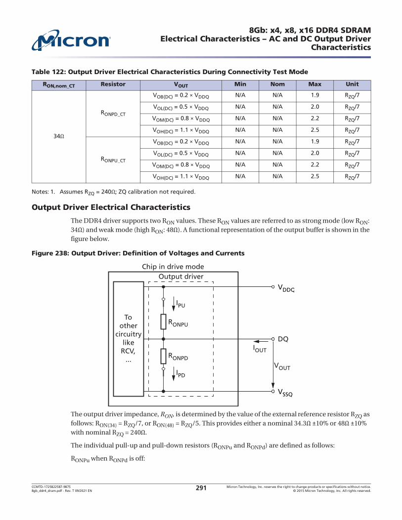
CCMTD-1725822587-9875 Micron Technology, Inc. reserves the right to change products or specifications without notice.8gb_ddr4_dram.pdf - Rev. T 09/2021 EN 2015 Micron Technology, Inc. All rights reserved.291
8Gb: x4, x8, x16 DDR4 SDRAM
Characteristics
Notes: 1. Assumes RZQ = 240 ; ZQ calibration not required.
Output Driver Electrical Characteristics
The DDR4 driver supports two RON values. These RON values are referred to as strong mode (low RON: 34 ) and weak mode (high RON: 48 ). A functional representation of the output buffer is shown in the figure below.
Figure 238: Output Driver: Definition of Voltages and Currents
The output driver impedance, RON, is determined by the value of the external reference resistor RZQ as follows: RON(34) = RZQ/7, or RON(48) = RZQ/5. This provides either a nominal 34.3 10% or 48 10% with nominal RZQ = 240 .
The individual pull-up and pull-down resistors (RONPu and RONPd) are defined as follows:
RONPu when RONPd is off:
Table 122: Output Driver Electrical Characteristics During Connectivity Test Mode
RON,nom_CT Resistor VOUT Min Nom Max Unit
34
RONPD_CT
VOB(DC) = 0.2 VDDQ N/A N/A 1.9 RZQ/7
VOL(DC) = 0.5 VDDQ N/A N/A 2.0 RZQ/7
VOM(DC) = 0.8 VDDQ N/A N/A 2.2 RZQ/7
VOH(DC) = 1.1 VDDQ N/A N/A 2.5 RZQ/7
RONPU_CT
VOB(DC) = 0.2 VDDQ N/A N/A 1.9 RZQ/7
VOL(DC) = 0.5 VDDQ N/A N/A 2.0 RZQ/7
VOM(DC) = 0.8 VDDQ N/A N/A 2.2 RZQ/7
VOH(DC) = 1.1 VDDQ N/A N/A 2.5 RZQ/7
VDDQ
VSSQ
Chip in drive mode
DQ
VOUT
IOUT
RONPU
RONPD
Output driver
Toother
circuitrylikeRCV,
...
IPU
IPD
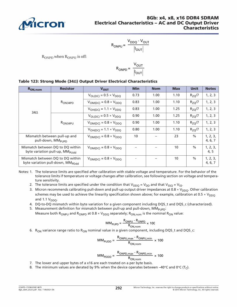
CCMTD-1725822587-9875 Micron Technology, Inc. reserves the right to change products or specifications without notice.8gb_ddr4_dram.pdf - Rev. T 09/2021 EN 2015 Micron Technology, Inc. All rights reserved.292
8Gb: x4, x8, x16 DDR4 SDRAM
Characteristics
RONPD when RONPU is off:
Notes: 1. The tolerance limits are specified after calibration with stable voltage and temperature. For the behavior of the tolerance limits if temperature or voltage changes after calibration, see following section on voltage and tempera-ture sensitivity.
2. The tolerance limits are specified under the condition that VDDQ = VDD and that VSSQ = VSS.3. Micron recommends calibrating pull-down and pull-up output driver impedances at 0.8 VDDQ. Other calibration
schemes may be used to achieve the linearity specification shown above; for example, calibration at 0.5 VDDQ and 1.1 VDDQ.
4. DQ-to-DQ mismatch within byte variation for a given component including DQS_t and DQS_c (characterized).5. Measurement definition for mismatch between pull-up and pull-down, MMPUPD:
Measure both RONPU and RONPD at 0.8 VDDQ separately; RON,nom is the nominal RON value:
6. RON variance range ratio to RON nominal value in a given component, including DQS_t and DQS_c:
7. The lower and upper bytes of a x16 are each treated on a per byte basis.8. C and 0 C (TC).
Table 123: Strong Mode (34 ) Output Driver Electrical Characteristics
RON,nom Resistor VOUT Min Nom Max Unit Notes
34
RON34PD
VOL(DC) = 0.5 VDDQ 0.73 1.00 1.10 RZQ/7 1, 2, 3
VOM(DC) = 0.8 VDDQ 0.83 1.00 1.10 RZQ/7 1, 2, 3
VOH(DC) = 1.1 VDDQ 0.83 1.00 1.25 RZQ/7 1, 2, 3
RON34PU
VOL(DC) = 0.5 VDDQ 0.90 1.00 1.25 RZQ/7 1, 2, 3
VOM(DC) = 0.8 VDDQ 0.90 1.00 1.10 RZQ/7 1, 2, 3
VOH(DC) = 1.1 VDDQ 0.80 1.00 1.10 RZQ/7 1, 2, 3
Mismatch between pull-up and pull-down, MMPUPD
VOM(DC) = 0.8 VDDQ 10 23 % 1, 2, 3, 4, 6, 7
Mismatch between DQ to DQ within byte variation pull-up, MMPUdd
VOM(DC) = 0.8 VDDQ 10 % 1, 2, 3, 4, 5
Mismatch between DQ to DQ within byte variation pull-down, MMPDdd
VOM(DC) = 0.8 VDDQ - 10 % 1, 2, 3, 4, 6, 7
RONPU =VDDQ - VOUT
IOUT
RONPD =VOUT
IOUT
MMPUPD = × 100RONPU - RONPD
RON,nom
MMPUDD = × 100RONPU,max - RONPU,min
RON,nom
MMPDDD = × 100RONPD,max - RONPD,min
RON,nom
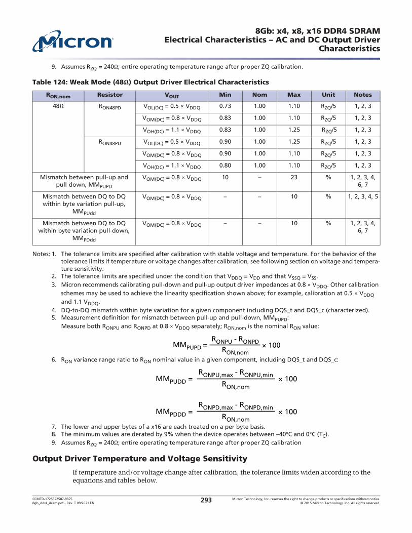
CCMTD-1725822587-9875 Micron Technology, Inc. reserves the right to change products or specifications without notice.8gb_ddr4_dram.pdf - Rev. T 09/2021 EN 2015 Micron Technology, Inc. All rights reserved.293
8Gb: x4, x8, x16 DDR4 SDRAM
Characteristics
9. Assumes RZQ = 240 ; entire operating temperature range after proper ZQ calibration.
Notes: 1. The tolerance limits are specified after calibration with stable voltage and temperature. For the behavior of the tolerance limits if temperature or voltage changes after calibration, see following section on voltage and tempera-ture sensitivity.
2. The tolerance limits are specified under the condition that VDDQ = VDD and that VSSQ = VSS.3. Micron recommends calibrating pull-down and pull-up output driver impedances at 0.8 VDDQ. Other calibration
schemes may be used to achieve the linearity specification shown above; for example, calibration at 0.5 VDDQ and 1.1 VDDQ.
4. DQ-to-DQ mismatch within byte variation for a given component including DQS_t and DQS_c (characterized).5. Measurement definition for mismatch between pull-up and pull-down, MMPUPD:
Measure both RONPU and RONPD at 0.8 VDDQ separately; RON,nom is the nominal RON value:
6. RON variance range ratio to RON nominal value in a given component, including DQS_t and DQS_c:
7. The lower and upper bytes of a x16 are each treated on a per byte basis.8. C and 0 C (TC).9. Assumes RZQ = 240 ; entire operating temperature range after proper ZQ calibration
Output Driver Temperature and Voltage Sensitivity
If temperature and/or voltage change after calibration, the tolerance limits widen according to the equations and tables below.
Table 124: Weak Mode (48 ) Output Driver Electrical Characteristics
RON,nom Resistor VOUT Min Nom Max Unit Notes
48 RON48PD VOL(DC) = 0.5 VDDQ 0.73 1.00 1.10 RZQ/5 1, 2, 3
VOM(DC) = 0.8 VDDQ 0.83 1.00 1.10 RZQ/5 1, 2, 3
VOH(DC) = 1.1 VDDQ 0.83 1.00 1.25 RZQ/5 1, 2, 3
RON48PU VOL(DC) = 0.5 VDDQ 0.90 1.00 1.25 RZQ/5 1, 2, 3
VOM(DC) = 0.8 VDDQ 0.90 1.00 1.10 RZQ/5 1, 2, 3
VOH(DC) = 1.1 VDDQ 0.80 1.00 1.10 RZQ/5 1, 2, 3
Mismatch between pull-up and pull-down, MMPUPD
VOM(DC) = 0.8 VDDQ 10 23 % 1, 2, 3, 4, 6, 7
Mismatch between DQ to DQ within byte variation pull-up,
MMPUdd
VOM(DC) = 0.8 VDDQ 10 % 1, 2, 3, 4, 5
Mismatch between DQ to DQ within byte variation pull-down,
MMPDdd
VOM(DC) = 0.8 VDDQ 10 % 1, 2, 3, 4, 6, 7
MMPUPD = × 100RONPU - RONPD
RON,nom
MMPUDD = × 100RONPU,max - RONPU,min
RON,nom
MMPDDD = × 100RONPD,max - RONPD,min
RON,nom

CCMTD-1725822587-9875 Micron Technology, Inc. reserves the right to change products or specifications without notice.8gb_ddr4_dram.pdf - Rev. T 09/2021 EN 2015 Micron Technology, Inc. All rights reserved.294
8Gb: x4, x8, x16 DDR4 SDRAM
Characteristics
T = T - T(@calibration); V = VDDQ - VDDQ(@ calibration); VDD = VDDQ
Alert Driver
A functional representation of the alert output buffer is shown in the figure below. Output driver impedance, RON, is defined as follows.
Figure 239: Alert Driver
RONPD when RONPU is off:
Table 125: Output Driver Sensitivity Definitions
Symbol Min Max Unit
RONPU@ VOH(DC) 0.6 - dRONdTH | T| - dRONdVH | V| 1.1 _ dRONdTH | T| + dRONdVH | V| RZQ/6
RON@ VOM(DC) 0.9 - dRONdTM | T| - dRONdVM | V| 1.1 + dRONdTM | T| + dRONdVM | V| RZQ/6
RONPD@ VOL(DC) 0.6 - dRONdTL | T| - dRONdVL | V| 1.1 + dRONdTL | T| + dRONdVL | V| RZQ/6
Table 126: Output Driver Voltage and Temperature Sensitivity
Symbol
Voltage and Temperature Range
UnitMin Max
dRONdTM 0 1.5 %/ C
dRONdVM 0 0.15 %/mV
dRONdTL 0 1.5 %/ C
dRONdVL 0 0.15 %/mV
dRONdTH 0 1.5 %/ C
dRONdVM 0 0.15 %/mV
Alert
VOUTRONPD
DRAM
Alert driver
IPD
IOUT
VSSQ
RONPD =VOUT
IOUT

CCMTD-1725822587-9875 Micron Technology, Inc. reserves the right to change products or specifications without notice.8gb_ddr4_dram.pdf - Rev. T 09/2021 EN 2015 Micron Technology, Inc. All rights reserved.295
8Gb: x4, x8, x16 DDR4 SDRAM
Characteristics
Notes: 1. VDDQ voltage is at VDDQ(DC).
Table 127: Alert Driver Voltage
RON,nom Register VOUT Min Nom Max Unit
N/A RONPD VOL(DC) = 0.1 VDDQ 0.3 N/A 1.2 RZQ/7
VOM(DC) = 0.8 VDDQ 0.4 N/A 1.2 RZQ/7
VOH(DC) = 1.1 VDDQ 0.4 N/A 1.4 RZQ/7
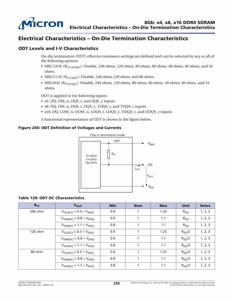
CCMTD-1725822587-9875 Micron Technology, Inc. reserves the right to change products or specifications without notice.8gb_ddr4_dram.pdf - Rev. T 09/2021 EN 2015 Micron Technology, Inc. All rights reserved.296
8Gb: x4, x8, x16 DDR4 SDRAM
ODT Levels and I-V Characteristics
On-die termination (ODT) effective resistance settings are defined and can be selected by any or all of the following options:
MR1[10:8] (RTT(NOM)): Disable, 240 ohms, 120 ohms, 80 ohms, 60 ohms, 48 ohms, 40 ohms, and 34 ohms.MR2[11:9] (RTT(WR)): Disable, 240 ohms,120 ohms, and 80 ohms.
MR5[8:6] (RTT(Park)): Disable, 240 ohms, 120 ohms, 80 ohms, 60 ohms, 48 ohms, 40 ohms, and 34 ohms.
ODT is applied to the following inputs:x4: DQ, DM_n, DQS_t, and DQS_c inputs.x8: DQ, DM_n, DQS_t, DQS_c, TDQS_t, and TDQS_c inputs.x16: DQ, LDM_n, UDM_n, LDQS_t, LDQS_c, UDQS_t, and UDQS_c inputs.
A functional representation of ODT is shown in the figure below.
Figure 240: ODT Definition of Voltages and Currents
Table 128: ODT DC Characteristics
RTT VOUT Min Nom Max Unit Notes
240 ohm VOL(DC) = 0.5 VDDQ 0.9 1 1.25 RZQ 1, 2, 3
VOM(DC) = 0.8 VDDQ 0.9 1 1.1 RZQ 1, 2, 3
VOH(DC) = 1.1 VDDQ 0.8 1 1.1 RZQ 1, 2, 3
120 ohm VOL(DC) = 0.5 VDDQ 0.9 1 1.25 RZQ/2 1, 2, 3
VOM(DC) = 0.8 VDDQ 0.9 1 1.1 RZQ/2 1, 2, 3
VOH(DC) = 1.1 VDDQ 0.8 1 1.1 RZQ/2 1, 2, 3
80 ohm VOL(DC) = 0.5 VDDQ 0.9 1 1.25 RZQ/3 1, 2, 3
VOM(DC) = 0.8 VDDQ 0.9 1 1.1 RZQ/3 1, 2, 3
VOH(DC) = 1.1 VDDQ 0.8 1 1.1 RZQ/3 1, 2, 3
VDDQ
VSSQ
Chip in termination mode
DQ
VOUT
IOUT
RTTTo othercircuitrylike RCV,
...
ODT

CCMTD-1725822587-9875 Micron Technology, Inc. reserves the right to change products or specifications without notice.8gb_ddr4_dram.pdf - Rev. T 09/2021 EN 2015 Micron Technology, Inc. All rights reserved.297
8Gb: x4, x8, x16 DDR4 SDRAM
Notes: 1. The tolerance limits are specified after calibration to 240 ohm 1% resistor with stable voltage and temperature. For the behavior of the tolerance limits if temperature or voltage changes after calibration, see ODT Temperature and Voltage Sensitivity.
2. Micron recommends calibrating pull-up ODT resistors at 0.8 VDDQ. Other calibration schemes may be used to achieve the linearity specification shown here.
3. The tolerance limits are specified under the condition that VDDQ = VDD and VSSQ = VSS.4. The DQ-to-DQ mismatch within byte variation for a given component including DQS_t and DQS_c.5. RTT variance range ratio to RTT nominal value in a given component, including DQS_t and DQS_c.
6. DQ-to-DQ mismatch for a x16 device is treated as two separate bytes.7. C and
0 C (TC).
ODT Temperature and Voltage Sensitivity
If temperature and/or voltage change after calibration, the tolerance limits widen according to the following equations and tables.
T = T - T(@ calibration); V = VDDQ - VDDQ(@ calibration); VDD = VDDQ
60 ohm VOL(DC) = 0.5 VDDQ 0.9 1 1.25 RZQ/4 1, 2, 3
VOM(DC) = 0.8 VDDQ 0.9 1 1.1 RZQ/4 1, 2, 3
VOH(DC) = 1.1 VDDQ 0.8 1 1.1 RZQ/4 1, 2, 3
48 ohm VOL(DC) = 0.5 VDDQ 0.9 1 1.25 RZQ/5 1, 2, 3
VOM(DC) = 0.8 VDDQ 0.9 1 1.1 RZQ/5 1, 2, 3
VOH(DC) = 1.1 VDDQ 0.8 1 1.1 RZQ/5 1, 2, 3
40 ohm VOL(DC) = 0.5 VDDQ 0.9 1 1.25 RZQ/6 1, 2, 3
VOM(DC) = 0.8 VDDQ 0.9 1 1.1 RZQ/6 1, 2, 3
VOH(DC) = 1.1 VDDQ 0.8 1 1.1 RZQ/6 1, 2, 3
34 ohm VOL(DC) = 0.5 VDDQ 0.9 1 1.25 RZQ/7 1, 2, 3
VOM(DC) = 0.8 VDDQ 0.9 1 1.1 RZQ/7 1, 2, 3
VOH(DC) = 1.1 VDDQ 0.8 1 1.1 RZQ/7 1, 2, 3
DQ-to-DQ mismatch within byte
VOM(DC) = 0.8 VDDQ 0 10 % 1, 2, 4, 5, 6
Table 128: ODT DC Characteristics (Continued)
RTT VOUT Min Nom Max Unit Notes
Table 129: ODT Sensitivity Definitions
Parameter Min Max Unit
RTT@ 0.9 - dRTTdT | T| - dRTTdV | V| 1.6 + dRTTdTH | T| + dRTTdVH | V| RZQ/n
DQ-to-DQ mismatch =RTT(MAX) - RTT(MIN)
RTT(NOM)× 100

CCMTD-1725822587-9875 Micron Technology, Inc. reserves the right to change products or specifications without notice.8gb_ddr4_dram.pdf - Rev. T 09/2021 EN 2015 Micron Technology, Inc. All rights reserved.298
8Gb: x4, x8, x16 DDR4 SDRAM
ODT Timing Definitions
The reference load for ODT timings is different than the reference load used for timing measurements.
Figure 241: ODT Timing Reference Load
ODT Timing Definitions and Waveforms
Definitions fortADC, tAONAS, and tAOFAS are provided in the 4 and shown in 3 and 5. Measurement reference settings are provided in the subsequent 5.
The tADC for the dynamic ODT case and read disable ODT cases are represented by tADC of Direct ODT Control case.
Table 130: ODT Voltage and Temperature Sensitivity
Parameter Min Max Unit
dRTTdT 0 1.5 %/ C
dRTTdV 0 0.15 %/mV
Table 131: ODT Timing Definitions
Parameter Begin Point Definition End Point Definition Figure
tADC Rising edge of CK_t, CK_c defined by the end point of DOD-TLoff
Extrapolated point at VRTT,nom 3
Rising edge of CK_t, CK_c defined by the end point of DOD-TLon
Extrapolated point at VSSQ 3
Rising edge of CK_t, CK_c defined by the end point of ODTLcnw
Extrapolated point at VRTT,nom 4
Rising edge of CK_t, CK_c defined by the end point of ODTLcwn4 or ODTLcwn8
Extrapolated point at VSSQ 4
tAONAS Rising edge of CK_t, CK_c with ODT being first registered HIGH
Extrapolated point at VSSQ 5
tAOFAS Rising edge of CK_t, CK_c with ODT being first registered LOW
Extrapolated point at VRTT,nom 5
Timing reference point
DQ, DQS_t, DQS_c, DM, TDQS_t, TDQS_c
CK_t, CK_cDUT
VTT
VDDQ
VSSQ VSSQ=
RTT = 50

CCMTD-1725822587-9875 Micron Technology, Inc. reserves the right to change products or specifications without notice.8gb_ddr4_dram.pdf - Rev. T 09/2021 EN 2015 Micron Technology, Inc. All rights reserved.299
8Gb: x4, x8, x16 DDR4 SDRAM
Notes: 1. MR settings are as follows: MR1 has A10 = 1, A9 = 1, A8 = 1 for RTT(NOM) setting; MR5 has A8 = 0, A7 = 0, A6 = 0 for RTT(Park) setting; and MR2 has A11 = 0, A10 = 1, A9 = 1 for RTT(WR) setting.
2. ODT state change is controlled by ODT pin.3. ODT state change is controlled by a WRITE command.4. Refer to Figure 3.5. Refer to Figure 4.6. Refer to Figure 5.
Figure 242: tADC Definition with Direct ODT Control
Table 132: Reference Settings for ODT Timing Measurements
MeasureParameter
RTT(Park) RTT(NOM) RTT(WR) VSW1 VSW2 Note
tADC Disable RZQ/7 (34 ) 0.20V 0.40V 1, 2, 4
RZQ/7 (34 ) High-Z 0.20V 0.40V 1, 3, 5
tAONAS Disable RZQ/7 (34 ) 0.20V 0.40V 1, 2, 6
tAOFAS Disable RZQ/7 (34 ) 0.20V 0.40V 1, 2, 6
tADC tADC
Begin point: Rising edgeof CK_t, CK_c definedby the end point ofDODTLoff
DODTLoff Begin point: Rising edgeof CK_t, CK_c definedby the end point ofDODTLon
DODTLon
End point: Extrapolatedpoint at VRTT,nom
End point: Extrapolatedpoint at VSSQ
VRTT,nomVRTT,nom
VSSQ VSSQ
DQ, DMDQS_t, DQS_cTDQS_t, TDQS_c
CK_c
CK_t
Vsw2
Vsw1
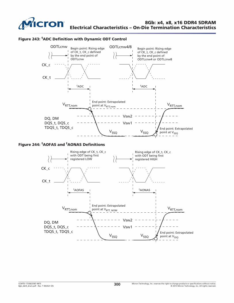
CCMTD-1725822587-9875 Micron Technology, Inc. reserves the right to change products or specifications without notice.8gb_ddr4_dram.pdf - Rev. T 09/2021 EN 2015 Micron Technology, Inc. All rights reserved.300
8Gb: x4, x8, x16 DDR4 SDRAM
Figure 243: tADC Definition with Dynamic ODT Control
Figure 244: tAOFAS and tAONAS Definitions
tADC tADC
Begin point: Rising edgeof CK_t, CK_c definedby the end point ofODTLcnw
ODTLcnw Begin point: Rising edgeof CK_t, CK_c definedby the end point ofODTLcnw4 or ODTLcnw8
ODTLcnw4/8
End point: Extrapolatedpoint at VRTT,nom
End point: Extrapolatedpoint at VSSQ
VRTT,nomVRTT,nom
VSSQ VSSQ
DQ, DMDQS_t, DQS_cTDQS_t, TDQS_c
CK_c
CK_t
Vsw2
Vsw1
tAOFAS tAONAS
Rising edge of CK_t, CK_cwith ODT being firstregistered LOW
Rising edge of CK_t, CK_cwith ODT being firstregistered HIGH
End point: Extrapolatedpoint at VRTT_NOM
End point: Extrapolatedpoint at VSSQ
VRTT,nomVRTT,nom
VSSQ VSSQ
DQ, DMDQS_t, DQS_cTDQS_t, TDQS_c
CK_c
CK_t
Vsw2
Vsw1

CCMTD-1725822587-9875 Micron Technology, Inc. reserves the right to change products or specifications without notice.8gb_ddr4_dram.pdf - Rev. T 09/2021 EN 2015 Micron Technology, Inc. All rights reserved.301
8Gb: x4, x8, x16 DDR4 SDRAMDRAM Package Electrical Specifications
DRAM Package Electrical Specifications
Notes: 1. This parameter is not subject to a production test; it is verified by design and characterization and are provided for reference; system signal simulations should not use these values but use the Micron package model. The package parasitic (L and C) are validated using package only samples. The capacitance is measured with VDD, VDDQ,
Table 133: DRAM Package Electrical Specifications for x4 and x8 Devices
Parameter Symbol
1600/1866/2133/2400/2666
2933 3200
Unit NotesMin Max Min Max Min Max
Input/out-put
Zpkg ZIO 45 85 48 85 48 85 ohm 1, 2, 4
Package delay TdIO 14 42 14 40 14 40 ps 1, 3, 4
Lpkg LIO 3.3 3.3 3.3 nH 10
Cpkg CIO 0.78 0.78 0.78 pF 11
DQS_t, DQS_c
Zpkg ZIO DQS 45 85 48 85 48 85 ohm 1, 2
Package delay TdIO DQS 14 42 14 40 14 40 ps 1, 3
Delta Zpkg DZIO DQS 10 10 10 ohm 1, 2, 6
Delta delay DTdIO DQS 5 5 5 ps 1, 3, 6
Lpkg LIO DQS 3.3 3.3 3.3 nH 10
Cpkg CIO DQS 0.78 0.78 0.78 pF 11
Input CTRL pins
Zpkg ZI CTRL 50 90 50 90 50 90 ohm 1, 2, 8
Package delay TdI CTRL 14 42 14 40 14 40 ps 1, 3, 8
Lpkg LI CTRL 3.4 3.4 3.4 nH 10
Cpkg CI CTRL 0.7 0.7 0.7 pF 11
Input CMD ADD pins
Zpkg ZI ADD CMD 50 90 50 90 50 90 ohm 1, 2, 7
Package delay TdI ADD CMD 14 45 14 40 14 40 ps 1, 3, 7
Lpkg LI ADD CMD 3.6 3.6 3.6 nH 10
Cpkg CI ADD CMD 0.74 0.74 0.74 pF 11
CK_t, CK_c Zpkg ZCK 50 90 50 90 50 90 ohm 1, 2
Package delay TdCK 14 42 14 42 14 42 ps 1, 3
Delta Zpkg DZDCK 10 10 10 ohm 1, 2, 5
Delta delay DTdDCK 5 5 5 ps 1, 3, 5
Lpkg LI CLK 3.4 3.4 3.4 nH 10
Cpkg CI CLK 0.7 0.7 0.7 pF 11
ZQ Zpkg ZO ZQ 100 100 100 ohm 1, 2
ZQ delay TdO ZQ 20 90 20 90 20 90 ps 1, 3
ALERT Zpkg ZO ALERT 40 100 40 100 40 100 ohm 1, 2
ALERT delay TdO ALERT 20 55 20 55 20 55 ps 1, 3
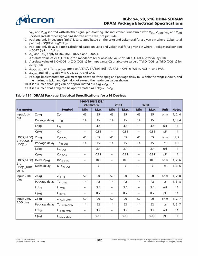
CCMTD-1725822587-9875 Micron Technology, Inc. reserves the right to change products or specifications without notice.8gb_ddr4_dram.pdf - Rev. T 09/2021 EN 2015 Micron Technology, Inc. All rights reserved.302
8Gb: x4, x8, x16 DDR4 SDRAMDRAM Package Electrical Specifications
VSS, and VSSQ shorted with all other signal pins floating. The inductance is measured with VDD, VDDQ, VSS, and VSSQ shorted and all other signal pins shorted at the die, not pin, side.
2. Package-only impedance (Zpkg) is calculated based on the Lpkg and Cpkg total for a given pin where: Zpkg (total per pin) = SQRT (Lpkg/Cpkg).
3. Package-only delay (Tpkg) is calculated based on Lpkg and Cpkg total for a given pin where: Tdpkg (total per pin) = SQRT (Lpkg Cpkg).
4. ZIO and TdIO apply to DQ, DM, TDQS_t and TDQS_c.5. Absolute value of ZCK_t, ZCK_c for impedance (Z) or absolute value of TdCK_t, TdCK_c for delay (Td).6. Absolute value of ZIO (DQS_t), ZIO (DQS_c) for impedance (Z) or absolute value of TdIO (DQS_t), TdIO (DQS_c) for
delay (Td).7. ZI ADD CMD and TdI ADD CMD apply to A[17:0], BA[1:0], BG[1:0], RAS_n CAS_n, WE_n, ACT_n, and PAR.8. ZI CTRL and TdI CTRL apply to ODT, CS_n, and CKE.9. Package implementations will meet specification if the Zpkg and package delay fall within the ranges shown, and
the maximum Lpkg and Cpkg do not exceed the maximum values shown.10. It is assumed that Lpkg can be approximated as Lpkg = ZO Td.11. It is assumed that Cpkg can be approximated as Cpkg = Td/ZO.
Table 134: DRAM Package Electrical Specifications for x16 Devices
Parameter Symbol
1600/1866/2133/2400/2666 2933 3200
Unit NotesMin Max Min Max Min Max
Input/out-put
Zpkg ZIO 45 85 45 85 45 85 ohm 1, 2, 4
Package delay TdIO 14 45 14 45 14 45 ps 1, 3, 4
Lpkg LIO 3.4 3.4 3.4 nH 11
Cpkg CIO 0.82 0.82 0.82 pF 11
LDQS_t/LDQS_c/UDQS_t/UDQS_c
Zpkg ZIO DQS 45 85 45 85 45 85 ohm 1, 2
Package delay TdIO DQS 14 45 14 45 14 45 ps 1, 3
Lpkg LIO DQS 3.4 3.4 3.4 nH 11
Cpkg CIO DQS 0.82 0.82 0.82 pF 11
LDQS_t/LDQS_c, UDQS_t/UDQS_c,
Delta Zpkg DZIO DQS 10.5 10.5 10.5 ohm 1, 2, 6
Delta delay DTdIO DQS 5 5 5 ps 1, 3, 6
Input CTRL pins
Zpkg ZI CTRL 50 90 50 90 50 90 ohm 1, 2, 8
Package delay TdI CTRL 14 42 14 42 14 42 ps 1, 3, 8
Lpkg LI CTRL 3.4 3.4 3.4 nH 11
Cpkg CI CTRL 0.7 0.7 0.7 pF 11
Input CMD ADD pins
Zpkg ZI ADD CMD 50 90 50 90 50 90 ohm 1, 2, 7
Package delay TdI ADD CMD 14 52 14 52 14 52 ps 1, 3, 7
Lpkg LI ADD CMD 3.9 3.9 3.9 nH 11
Cpkg CI ADD CMD 0.86 0.86 0.86 pF 11

CCMTD-1725822587-9875 Micron Technology, Inc. reserves the right to change products or specifications without notice.8gb_ddr4_dram.pdf - Rev. T 09/2021 EN 2015 Micron Technology, Inc. All rights reserved.303
8Gb: x4, x8, x16 DDR4 SDRAMDRAM Package Electrical Specifications
Notes: 1. This parameter is not subject to a production test; it is verified by design and characterization and are provided for reference; system signal simulations should not use these values but use the Micron package model. The package parasitic (L and C) are validated using package only samples. The capacitance is measured with VDD, VDDQ, VSS, and VSSQ shorted with all other signal pins floating. The inductance is measured with VDD, VDDQ, VSS, and VSSQ shorted and all other signal pins shorted at the die, not pin, side.
2. Package-only impedance (Zpkg) is calculated based on the Lpkg and Cpkg total for a given pin where: Zpkg (total per pin) = SQRT (Lpkg/Cpkg).
3. Package-only delay (Tpkg) is calculated based on Lpkg and Cpkg total for a given pin where: Tdpkg (total per pin) = SQRT (Lpkg Cpkg).
4. ZIO and TdIO apply to DQ, DM, TDQS_t and TDQS_c.5. Absolute value of ZCK_t, ZCK_c for impedance (Z) or absolute value of TdCK_t, TdCK_c for delay (Td).6. Absolute value of ZIO (DQS_t), ZIO (DQS_c) for impedance (Z) or absolute value of TdIO (DQS_t), TdIO (DQS_c) for
delay (Td).7. ZI ADD CMD and TdI ADD CMD apply to A[17:0], BA[1:0], BG[1:0], RAS_n CAS_n, WE_n, ACT_n, and PAR.8. ZI CTRL and TdI CTRL apply to ODT, CS_n, and CKE.9. Package implementations will meet specification if the Zpkg and package delay fall within the ranges shown, and
the maximum Lpkg and Cpkg do not exceed the maximum values shown.10. It is assumed that Lpkg can be approximated as Lpkg = ZO Td.11. It is assumed that Cpkg can be approximated as Cpkg = Td/ZO.
CK_t, CK_c Zpkg ZCK 50 90 50 90 50 90 ohm 1, 2
Package delay TdCK 14 42 14 42 14 42 ps 1, 3
Delta Zpkg DZDCK 10.5 10.5 10.5 ohm 1, 2, 5
Delta delay DTdDCK 5 5 5 ps 1, 3, 5
Input CLK Lpkg LI CLK 3.4 3.4 3.4 nH 11
Cpkg CI CLK 0.7 0.7 0.7 pF 11
ZQ Zpkg ZO ZQ 100 100 100 ohm 1, 2
ZQ delay TdO ZQ 20 90 20 90 20 90 ps 1, 3
ALERT Zpkg ZO ALERT 40 100 40 100 40 100 ohm 1, 2
ALERT delay TdO ALERT 20 55 20 55 20 55 ps 1, 3
Table 134: DRAM Package Electrical Specifications for x16 Devices (Continued)
Parameter Symbol
1600/1866/2133/2400/2666 2933 3200
Unit NotesMin Max Min Max Min Max

CCMTD-1725822587-9875 Micron Technology, Inc. reserves the right to change products or specifications without notice.8gb_ddr4_dram.pdf - Rev. T 09/2021 EN 2015 Micron Technology, Inc. All rights reserved.304
8Gb: x4, x8, x16 DDR4 SDRAMDRAM Package Electrical Specifications
Notes: 1. Although the DM, TDQS_t, and TDQS_c pins have different functions, the loading matches DQ and DQS.2. This parameter is not subject to a production test; it is verified by design and characterization and are provided
for reference; system signal simulations should not use these values but use the Micron package model. The capac--
DD, VDDQ, VSS, and VSSQ applied and all other pins floating (except the pin under test, CKE, RESET_n and ODT, as necessary). VDD = VDDQ = 1.2V, VBIAS = VDD/2 and on-die termination off. Measured data is rounded using industry standard half-rounded up methodology to the nearest hundredth of the MSB.
3. This parameter applies to monolithic die, obtained by de-embedding the package L and C parasitics.4. CDIO = CIO(DQ, DM) - 0.5 (CIO(DQS_t) + CIO(DQS_c)).5. Absolute value of CIO (DQS_t), CIO (DQS_c)6. Absolute value of CCK_t, CCK_c7. CI applies to ODT, CS_n, CKE, A[17:0], BA[1:0], BG[1:0], RAS_n, CAS_n, ACT_n, PAR and WE_n.8. CDI_CTRL applies to ODT, CS_n, and CKE.9. CDI_CTRL = CI(CTRL) - 0.5 (CI(CLK_t) + CI(CLK_c)).10. CDI_ADD_CMD applies to A[17:0], BA1:0], BG[1:0], RAS_n, CAS_n, ACT_n, PAR and WE_n.11. CDI_ADD_CMD = CI(ADD_CMD) - 0.5 (CI(CLK_t) + CI(CLK_c)).12. Maximum external load capacitance on ZQ pin: 5pF.13. Only applicable if TEN pin does not have an internal pull-up.
Table 135: Pad Input/Output Capacitance
Parameter Symbol
DDR4-1600, 1866, 2133
DDR4-2400, 2666 DDR4-2933 DDR4-3200
Unit
NotesMin Max Min Max Min Max Min Max
Input/output capacitance: DQ, DM, DQS_t, DQS_c, TDQS_t, TDQS_c
CIO 0.55 1.4 0.55 1.15 0.55 1.00 0.55 1.00 pF 1, 2, 3
Input capacitance: CK_t and CK_c
CCK 0.2 0.8 0.2 0.7 0.2 0.7 0.15 0.7 pF 2, 3
Input capacitance delta: CK_t and CK_c
CDCK - 0.05 - 0.05 - 0.05 - 0.05 pF 2, 3, 6
Input/output capacitance delta: DQS_t and DQS_c
CDDQS - 0.05 - 0.05 - 0.05 - 0.05 pF 2, 3, 5
Input capacitance: CTRL, ADD, CMD input-only pins
CI 0.2 0.8 0.2 0.7 0.2 0.6 0.15 0.55 pF 2, 3, 4
Input capacitance delta: All CTRL input-only pins
CDI_CTRL 0.1 0.1 0.1 0.1 pF 2, 3, 8, 9
Input capacitance delta: All ADD/CMD input-only pins
CDI_AD-
D_CMD
0.1 0.1 0.1 0.1 pF 1, 2, 10, 11
Input/output capacitance delta: DQ, DM, DQS_t, DQS_c, TDQS_t, TDQS_c
CDIO 0.1 0.1 0.1 0.1 pF 1, 2, 3, 4
Input/output capacitance: ALERT pin
CALERT 0.5 1.5 0.5 1.5 0.5 1.5 0.5 1.5 pF 2, 3
Input/output capacitance: ZQ pin
CZQ 2.3 2.3 2.3 2.3 pF 2, 3, 12
Input/output capacitance: TEN pin
CTEN 0.2 2.3 0.2 2.3 0.2 2.3 0.15 2.3 pF 2, 3, 13
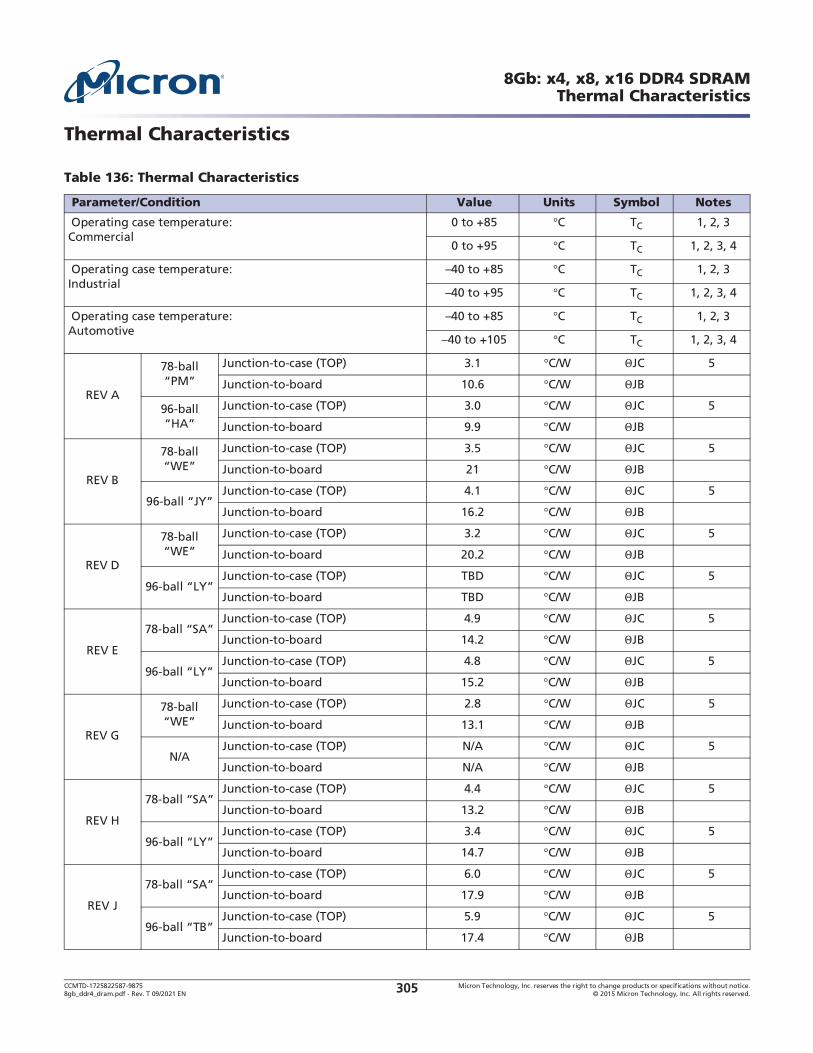
CCMTD-1725822587-9875 Micron Technology, Inc. reserves the right to change products or specifications without notice.8gb_ddr4_dram.pdf - Rev. T 09/2021 EN 2015 Micron Technology, Inc. All rights reserved.305
8Gb: x4, x8, x16 DDR4 SDRAMThermal Characteristics
Thermal Characteristics
Table 136: Thermal Characteristics
Parameter/Condition Value Units Symbol Notes
Operating case temperature: Commercial
0 to +85 C TC 1, 2, 3
0 to +95 C TC 1, 2, 3, 4
Operating case temperature: Industrial
C TC 1, 2, 3
C TC 1, 2, 3, 4
Operating case temperature: Automotive
C TC 1, 2, 3
C TC 1, 2, 3, 4
REV A
78-ball Junction-to-case (TOP) 3.1 C/W JC 5
Junction-to-board 10.6 C/W JB
96-ball Junction-to-case (TOP) 3.0 C/W JC 5
Junction-to-board 9.9 C/W JB
REV B
78-ball Junction-to-case (TOP) 3.5 C/W JC 5
Junction-to-board 21 C/W JB
Junction-to-case (TOP) 4.1 C/W JC 5
Junction-to-board 16.2 C/W JB
REV D
78-ball Junction-to-case (TOP) 3.2 C/W JC 5
Junction-to-board 20.2 C/W JB
Junction-to-case (TOP) TBD C/W JC 5
Junction-to-board TBD C/W JB
REV E
Junction-to-case (TOP) 4.9 C/W JC 5
Junction-to-board 14.2 C/W JB
Junction-to-case (TOP) 4.8 C/W JC 5
Junction-to-board 15.2 C/W JB
REV G
78-ball Junction-to-case (TOP) 2.8 C/W JC 5
Junction-to-board 13.1 C/W JB
N/AJunction-to-case (TOP) N/A C/W JC 5
Junction-to-board N/A C/W JB
REV H
Junction-to-case (TOP) 4.4 C/W JC 5
Junction-to-board 13.2 C/W JB
Junction-to-case (TOP) 3.4 C/W JC 5
Junction-to-board 14.7 C/W JB
REV J
Junction-to-case (TOP) 6.0 C/W JC 5
Junction-to-board 17.9 C/W JB
Junction-to-case (TOP) 5.9 C/W JC 5
Junction-to-board 17.4 C/W JB
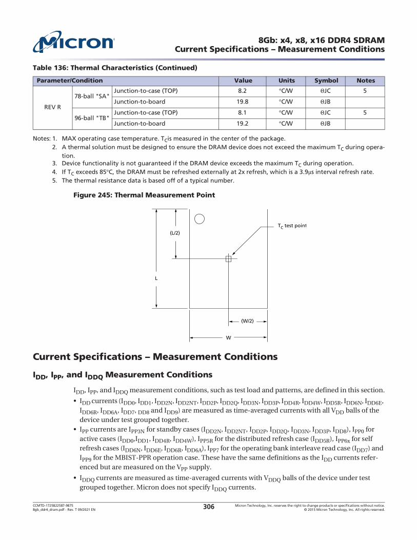
CCMTD-1725822587-9875 Micron Technology, Inc. reserves the right to change products or specifications without notice.8gb_ddr4_dram.pdf - Rev. T 09/2021 EN 2015 Micron Technology, Inc. All rights reserved.306
8Gb: x4, x8, x16 DDR4 SDRAM
Notes: 1. MAX operating case temperature. TCis measured in the center of the package.2. A thermal solution must be designed to ensure the DRAM device does not exceed the maximum TC during opera-
tion.3. Device functionality is not guaranteed if the DRAM device exceeds the maximum TC during operation.4. If TC exceeds 85 C, the DRAM must be refreshed externally at 2x refresh, which is a 3.9 s interval refresh rate.5. The thermal resistance data is based off of a typical number.
Figure 245: Thermal Measurement Point
IDD, IPP, and IDDQ Measurement Conditions
IDD, IPP, and IDDQ measurement conditions, such as test load and patterns, are defined in this section.
IDD currents (IDD0, IDD1, IDD2N, IDD2NT, IDD2P, IDD2Q, IDD3N, IDD3P, IDD4R, IDD4W, IDD5R, IDD6N, IDD6E, IDD6R, IDD6A, IDD7, DD8 and IDD9) are measured as time-averaged currents with all VDD balls of the device under test grouped together.IPP currents are IPP3N for standby cases (IDD2N, IDD2NT, IDD2P, IDD2Q, IDD3N, IDD3P, IDD8), IPP0 for active cases (IDD0,IDD1, IDD4R, IDD4W), IPP5R for the distributed refresh case (IDD5R), IPP6x for self refresh cases (IDD6N, IDD6E, IDD6R, IDD6A), IPP7 for the operating bank interleave read case (IDD7) and IPP9 for the MBIST-PPR operation case. These have the same definitions as the IDD currents refer-enced but are measured on the VPP supply.
IDDQ currents are measured as time-averaged currents with VDDQ balls of the device under test grouped together. Micron does not specify IDDQ currents.
REV R
78-ball "SA"Junction-to-case (TOP) 8.2 C/W JC 5
Junction-to-board 19.8 C/W JB
96-ball "TB"Junction-to-case (TOP) 8.1 C/W JC 5
Junction-to-board 19.2 C/W JB
Table 136: Thermal Characteristics (Continued)
Parameter/Condition Value Units Symbol Notes
(L/2)
L
W
(W/2)
TC test point

CCMTD-1725822587-9875 Micron Technology, Inc. reserves the right to change products or specifications without notice.8gb_ddr4_dram.pdf - Rev. T 09/2021 EN 2015 Micron Technology, Inc. All rights reserved.307
8Gb: x4, x8, x16 DDR4 SDRAM
IPP and IDDQ currents are not included in IDD currents, IDD and IDDQ currents are not included in IPP currents, and IDD and IPP currents are not included in IDDQ currents.
NOTE: IDDQ values cannot be directly used to calculate the I/O power of the device. They can be used to support correlation of simulated I/O power to actual I/O power. In DRAM module application, IDDQ cannot be measured separately because VDD and VDDQ are using a merged-power layer in the module PCB.
The following definitions apply for IDD, IPP and IDDQ measurements.
IN VIL(AC)max
IN VIH(AC)min
REF = VDD/2
Timings used for IDD, IPP and IDDQ measurement-loop patterns are provided in the Current Test Definition and Patterns section.Basic IDD, IPP, and IDDQ measurement conditions are described in the Current Test Definition and Patterns section.Detailed IDD, IPP, and IDDQ measurement-loop patterns are described in the Current Test Definition and Patterns section.Current measurements are done after properly initializing the device. This includes, but is not limited to, setting:RON = RZQ/7 (34 ohm in MR1); Qoff = 0B (output buffer enabled in MR1); RTT(NOM) = RZQ/6 (40 ohm in MR1); RTT(WR) = RZQ/2 (120 ohm in MR2); RTT(Park) = disabled; TDQS feature disabled in MR1; CRC disabled in MR2; CA parity feature disabled in MR3; Gear-down mode disabled in MR3; Read/Write DBI disabled in MR5; DM disabled in MR5Define D = {CS_n, RAS_n, CAS_n, WE_n}: = {HIGH, LOW, LOW, LOW}; apply BG/BA changes when directed.Define D_n = {CS_n, RAS_n, CAS_n, WE_n}: = {HIGH, HIGH, HIGH, HIGH}; apply invert of BG/BA changes when directed above.
NOTE: The measurement-loop patterns must be executed at least once before actual current measure-ments can be taken, with the exception of IDD9 which may be measured any time after MBIST-PPR entry.

CCMTD-1725822587-9875 Micron Technology, Inc. reserves the right to change products or specifications without notice.8gb_ddr4_dram.pdf - Rev. T 09/2021 EN 2015 Micron Technology, Inc. All rights reserved.308
8Gb: x4, x8, x16 DDR4 SDRAM
Figure 246: Measurement Setup and Test Load for IDDx, IPPx, and IDDQx
Figure 247: Correlation: Simulated Channel I/O Power to Actual Channel I/O Power
Note: 1. Supported by IDDQ measurement.
IDD Definitions
Table 137: Basic IDD, IPP, and IDDQ Measurement Conditions
Symbol Description
IDD0 Operating One Bank Active-Precharge Current (AL = 0) CKE: HIGH; External clock: On; tCK, nRC, nRAS, CL: see the previous table; BL: 8;1 AL: 0; CS_n: HIGH between ACT and PRE; Command, address, bank group address, bank address inputs: partially toggling according to the next table; Data I/O: VDDQ; DM_n: stable at 0; Bank activity: cycling with one bank active at a time: 0, 0, 1, 1, 2,
2, ... (see the IDD0 Measurement-Loop Pattern table); Output buffer and RTT: enabled in mode registers;2 ODT signal: stable at 0; Pattern details: see the IDD0 Measurement-Loop Pattern table
IDD
CK_t/CK_c
CS_nCKE
ODT
VDD VDDQ
VSS VSSQ
RESET_n
ACT_n, RAS_n, CAS_n, WE_n
DQS_t, DQS_c
DQ
DM_n
ZQ
A, BG, BA
IDDQ
C
IPP
VPP
DDR4SDRAM
Application-spec ificmemory channel
env ironment
Channe l I/Opower s imulation
IDD Qtest load
IDD Qs imulation
IDD Qmeasure ment
Correlation
Correction
Channe l I/Opower number

CCMTD-1725822587-9875 Micron Technology, Inc. reserves the right to change products or specifications without notice.8gb_ddr4_dram.pdf - Rev. T 09/2021 EN 2015 Micron Technology, Inc. All rights reserved.309
8Gb: x4, x8, x16 DDR4 SDRAM
IPP0 Operating One Bank Active-Precharge IPP Current (AL = 0) Same conditions as IDD0 above
IDD1 Operating One Bank Active-Read-Precharge Current (AL = 0) CKE: HIGH; External clock: on; tCK, nRC, nRAS, nRCD, CL: see the previous table; BL: 8;,, 5 AL: 0; CS_n: HIGH between ACT, RD, and PRE; Command, address, bank group address, bank address inputs, Data I/O: partially toggling according to the IDD1 Measurement-Loop Pattern table; DM_n: stable at 0; Bank activity: cycling with one bank active at a time: 0, 0, 1, 1, 2, 2, ... (see the following table); Output buffer and RTT: enabled in mode
registers;2 ODT Signal: stable at 0; Pattern details: see the IDD1 Measurement-Loop Pattern table
IDD2N Precharge Standby Current (AL = 0) CKE: HIGH; External clock: On; tCK, CL: see the previous table; BL: 8;1 AL: 0; CS_n: stable at 1; Command, address, bank group address, bank address Inputs: partially toggling according to the IDD2N and IDD3N Measure-ment-Loop Pattern table; Data I/O: VDDQ; DM_n: stable at 1; Bank activity: all banks closed; Output buffer and
RTT: enabled in mode registers;2 ODT signal: stable at 0; Pattern details: see the IDD2N and IDD3N Measure-ment-Loop Pattern table
IDD2NT Precharge Standby ODT Current
CKE: HIGH; External clock: on; tCK, CL: see the previous table; BL: 8;1 AL: 0; CS_n: stable at 1; Command, address, bank gropup address, bank address inputs: partially toggling according to the IDD2NT Measure-ment-Loop Pattern table; Data I/O: VSSQ; DM_n: stable at 1; Bank activity: all banks closed; Output buffer and
RTT: enabled in mode registers;2 ODT signal: toggling according to the IDD2NT Measurement-Loop Pattern table; Pattern details: see the IDD2NT Measurement-Loop Pattern table
IDD2P Precharge Power-Down Current
CKE: LOW; External clock: on; tCK, CL: see the previous table; BL: 8;1 AL: 0; CS_n: stable at 1; Command, address, bank group address, bank address inputs: stable at 0; Data I/O: VDDQ; DM_n: stable at 1; Bank activity:
all banks closed; Output buffer and RTT: Enabled in mode registers;2 ODT signal: stable at 0
IDD2Q Precharge Quiet Standby Current CKE: HIGH; External clock: on; tCK, CL: see the previous table; BL: 8;1 AL: 0; CS_n: stable at 1; Command, address, bank group address, bank address inputs: stable at 0; Data I/O: VDDQ; DM_n: stable at 1; Bank activity:
all banks closed; Output buffer and RTT: Enabled in mode registers;2 ODT signal: stable at 0
IDD3N Active Standby Current (AL = 0) CKE: HIGH; External clock: on; tCK, CL: see the previous table; BL: 8;1 AL: 0; CS_n: stable at 1; Command, address, bank group address, bank address inputs: partially toggling according to the IDD2N and IDD3N Measure-ment-Loop Pattern table; Data I/O: VDDQ; DM_n: stable at 1; Bank activity: all banks open; Output buffer and
RTT: Enabled in mode registers;2 ODT signal: stable at 0; Pattern details: see the IDD2N and IDD3N Measure-ment-Loop Pattern table
IPP3N Active Standby IPP3N Current (AL = 0) Same conditions as IDD3N above
IDD3P Active Power-Down Current (AL = 0) CKE: LOW; External clock: on; tCK, CL: see the previous table; BL: 8;1 AL: 0; CS_n: stable at 1; Command, address, bank group address, bank address inputs: stable at 1; Data I/O: VDDQ; DM_n: stable at 1; Bank activity:
all banks open; Output buffer and RTT: Enabled in mode registers;2 ODT signal: stable at 0
Table 137: Basic IDD, IPP, and IDDQ Measurement Conditions
Symbol Description

CCMTD-1725822587-9875 Micron Technology, Inc. reserves the right to change products or specifications without notice.8gb_ddr4_dram.pdf - Rev. T 09/2021 EN 2015 Micron Technology, Inc. All rights reserved.310
8Gb: x4, x8, x16 DDR4 SDRAM
IDD4R Operating Burst Read Current (AL = 0) CKE: HIGH; External clock: on; tCK, CL: see the previous table; BL: 8;, 5 AL: 0; CS_n: HIGH between RD; Com-mand, address, bank group address, bank address inputs: partially toggling according to the IDD4R Measure-ment-Loop Pattern table; Data I/O: seamless read data burst with different data between one burst and the next one according to the IDD4R Measurement-Loop Pattern table; DM_n: stable at 1; Bank activity: all banks open, RD commands cycling through banks: 0, 0, 1, 1, 2, 2, ... (see the IDD4R Measurement-Loop Pattern table);
Output buffer and RTT: Enabled in mode registers;2 ODT signal: stable at 0; Pattern details: see the IDD4R Mea-surement-Loop Pattern table
IDD4W Operating Burst Write Current (AL = 0) CKE: HIGH; External clock: on; tCK, CL: see the previous table; BL: 8;1 AL: 0; CS_n: HIGH between WR; Com-mand, address, bank group address, bank address inputs: partially toggling according to the IDD4W Measure-ment-Loop Pattern table; Data I/O: seamless write data burst with different data between one burst and the next one according to the IDD4W Measurement-Loop Pattern table; DM: stable at 0; Bank activity: all banks open, WR commands cycling through banks: 0, 0, 1, 1, 2, 2, ... (see IDD4W Measurement-Loop Pattern table); Output buffer and RTT: enabled in mode registers (see note2); ODT signal: stable at HIGH; Pattern details: see the IDD4W Measurement-Loop Pattern table
IDD5R Distributed Refresh Current (1X REF) CKE: HIGH; External clock: on; tCK, CL, nREFI: see the previous table; BL: 8;1 AL: 0; CS_n: HIGH between REF; Command, address, bank group address, bank address inputs: partially toggling according to the IDD5R Mea-surement-Loop Pattern table; Data I/O: VDDQ; DM_n: stable at 1; Bank activity: REF command every nREFI (see
the IDD5R Measurement-Loop Pattern table); Output buffer and RTT: enabled in mode registers2; ODT signal: stable at 0; Pattern details: see the IDD5R Measurement-Loop Pattern table
IPP5R Distributed Refresh Current (1X REF) Same conditions as IDD5R above
IDD6N Self Refresh Current: Normal Temperature Range TC C; Auto self refresh (ASR): disabled;3 Self refresh temperature range (SRT): normal;4 CKE: LOW; Exter-
nal clock: off; CK_t and CK_c: LOW; CL: see the table above; BL: 8;1 AL: 0; CS_n, command, address, bank group address, bank address, data I/O: VDDQ; DM_n: stable at 1; Bank activity: SELF REFRESH operation; Output buffer
and RTT: enabled in mode registers;2 ODT signal: midlevel
IDD6E Self Refresh Current: Extended Temperature Range 4
TC C; Auto self refresh (ASR): disabled4; Self refresh temperature range (SRT): extended;4 CKE: LOW;
External clock: off; CK_t and CK_c: LOW; CL: see the previous table; BL: 8;1 AL: 0; CS_n, command, address, group bank address, bank address, data I/O: VDDQ; DM_n: stable at 1; Bank activity: EXTENDED TEMPERATURE
SELF REFRESH operation; Output buffer and RTT: enabled in mode registers;2 ODT signal: midlevel
IPP6x Self Refresh IPP Current Same conditions as IDD6E above
IDD6R Self Refresh Current: Reduced Temperature Range
TC C; Auto self refresh (ASR): disabled; Self refresh temperature range (SRT): reduced;4 CKE: LOW; Exter-
nal clock: off; CK_t and CK_c: LOW; CL: see the previous table; BL: 8;1 AL: 0; CS_n, command, address, bank group address, bank address, data I/O: VDDQ; DM_n: stable at 1; Bank activity: EXTENDED TEMPERATURE SELF
REFRESH operation; Output buffer and RTT: enabled in mode registers;2 ODT signal: midlevel
Table 137: Basic IDD, IPP, and IDDQ Measurement Conditions
Symbol Description
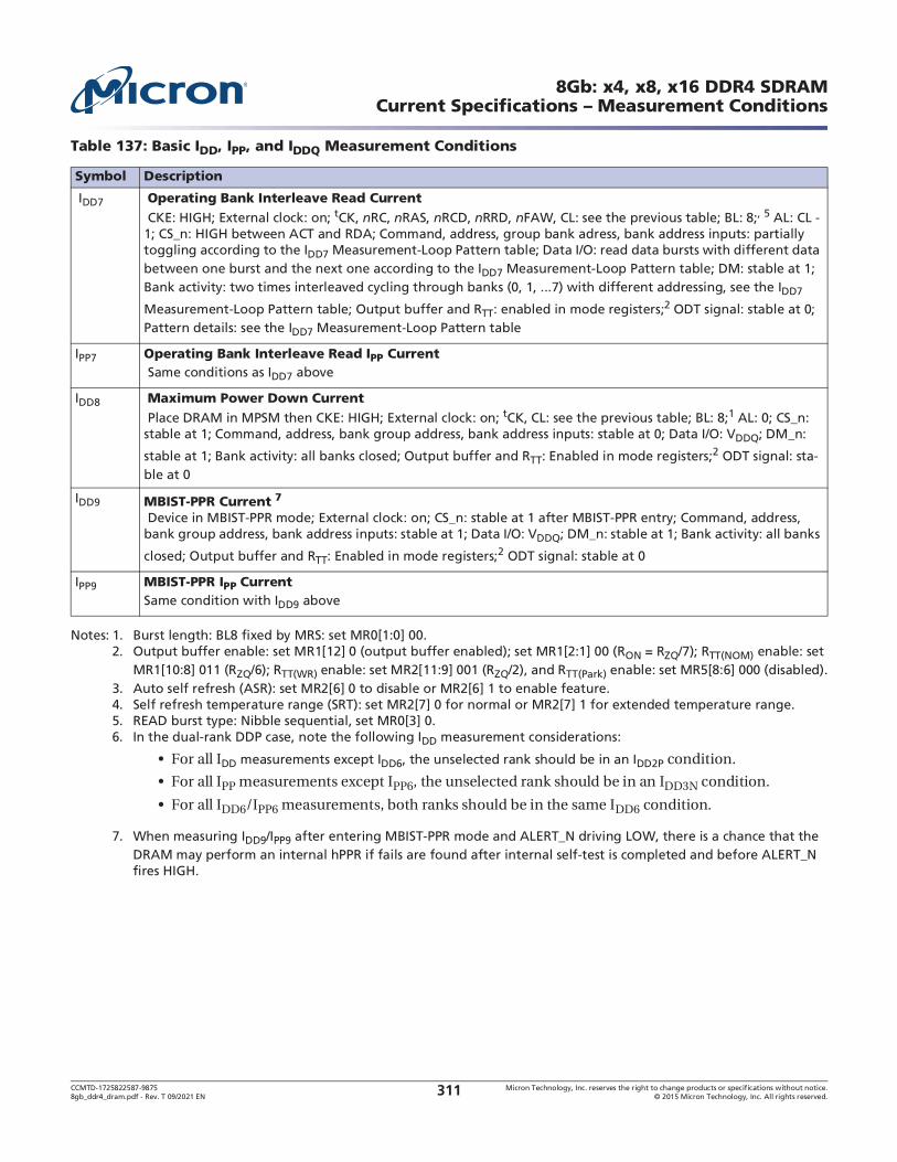
CCMTD-1725822587-9875 Micron Technology, Inc. reserves the right to change products or specifications without notice.8gb_ddr4_dram.pdf - Rev. T 09/2021 EN 2015 Micron Technology, Inc. All rights reserved.311
8Gb: x4, x8, x16 DDR4 SDRAM
Notes: 1. Burst length: BL8 fixed by MRS: set MR0[1:0] 00.2. Output buffer enable: set MR1[12] 0 (output buffer enabled); set MR1[2:1] 00 (RON = RZQ/7); RTT(NOM) enable: set
MR1[10:8] 011 (RZQ/6); RTT(WR) enable: set MR2[11:9] 001 (RZQ/2), and RTT(Park) enable: set MR5[8:6] 000 (disabled).3. Auto self refresh (ASR): set MR2[6] 0 to disable or MR2[6] 1 to enable feature.4. Self refresh temperature range (SRT): set MR2[7] 0 for normal or MR2[7] 1 for extended temperature range.5. READ burst type: Nibble sequential, set MR0[3] 0.6. In the dual-rank DDP case, note the following IDD measurement considerations:
For all IDD measurements except IDD6, the unselected rank should be in an IDD2P condition.
For all IPP measurements except IPP6, the unselected rank should be in an IDD3N condition.
For all IDD6/IPP6 measurements, both ranks should be in the same IDD6 condition.
7. When measuring IDD9/IPP9 after entering MBIST-PPR mode and ALERT_N driving LOW, there is a chance that the DRAM may perform an internal hPPR if fails are found after internal self-test is completed and before ALERT_N fires HIGH.
IDD7 Operating Bank Interleave Read Current
CKE: HIGH; External clock: on; tCK, nRC, nRAS, nRCD, nRRD, nFAW, CL: see the previous table; BL: 8;, 5 AL: CL - 1; CS_n: HIGH between ACT and RDA; Command, address, group bank adress, bank address inputs: partially toggling according to the IDD7 Measurement-Loop Pattern table; Data I/O: read data bursts with different data between one burst and the next one according to the IDD7 Measurement-Loop Pattern table; DM: stable at 1; Bank activity: two times interleaved cycling through banks (0, 1, ...7) with different addressing, see the IDD7
Measurement-Loop Pattern table; Output buffer and RTT: enabled in mode registers;2 ODT signal: stable at 0; Pattern details: see the IDD7 Measurement-Loop Pattern table
IPP7 Operating Bank Interleave Read IPP Current Same conditions as IDD7 above
IDD8 Maximum Power Down Current Place DRAM in MPSM then CKE: HIGH; External clock: on; tCK, CL: see the previous table; BL: 8;1 AL: 0; CS_n: stable at 1; Command, address, bank group address, bank address inputs: stable at 0; Data I/O: VDDQ; DM_n:
stable at 1; Bank activity: all banks closed; Output buffer and RTT: Enabled in mode registers;2 ODT signal: sta-ble at 0
IDD9 MBIST-PPR Current 7 Device in MBIST-PPR mode; External clock: on; CS_n: stable at 1 after MBIST-PPR entry; Command, address, bank group address, bank address inputs: stable at 1; Data I/O: VDDQ; DM_n: stable at 1; Bank activity: all banks
closed; Output buffer and RTT: Enabled in mode registers;2 ODT signal: stable at 0
IPP9 MBIST-PPR IPP Current Same condition with IDD9 above
Table 137: Basic IDD, IPP, and IDDQ Measurement Conditions
Symbol Description

CCMTD-1725822587-9875 Micron Technology, Inc. reserves the right to change products or specifications without notice.8gb_ddr4_dram.pdf - Rev. T 09/2021 EN 2015 Micron Technology, Inc. All rights reserved.312
8Gb: x4, x8, x16 DDR4 SDRAM
Current Test Definitions and Patterns
Notes: 1. DQS_t, DQS_c are VDDQ.2. BG1 is a "Don't Care" for x16 devices.3. DQ signals are VDDQ.4. For x4 and x8 only.
Table 138: IDD0 and IPP0 Measurement-Loop Pattern1
CK
_t, C
K_c
CK
E
Su
b-L
oo
p
Cycl
e N
um
ber
Co
mm
an
d
CS_n
AC
T_n
RA
S_n
/A16
CA
S_n
/A15
WE_n
/A14
OD
T
BG
[1:0
]2
BA
[1:0
]
A12/B
C_n
A[1
7,1
3,1
1]]
A[1
0]/
AP
A[9
:7]
A[6
:3]
A[2
:0] Data3
Tog
glin
g
Stat
ic H
igh
0 0 ACT 0 0 0 0 0 0 0 0 0 0 0 0 0 0
1, 2 D, D 1 0 0 0 0 0 0 0 0 0 0 0 0 0
3, 4 D_n, D_n
1 1 1 1 1 0 3 3 0 0 0 7 F 0
... Repeat pattern 1...4 until nRAS - 1; truncate if necessary
nRAS PRE 0 1 0 1 0 0 0 0 0 0 0 0 0 0
... Repeat pattern 1...4 until nRC - 1; truncate if necessary
1 1 nRC Repeat sub-loop 0, use BG[1:0] = 1, use BA[1:0] = 1 instead
2 2 nRC Repeat sub-loop 0, use BG[1:0] = 0, use BA[1:0] = 2 instead
3 3 nRC Repeat sub-loop 0, use BG[1:0] = 1, use BA[1:0] = 3 instead
4 4 nRC Repeat sub-loop 0, use BG[1:0] = 0, use BA[1:0] = 1 instead
5 5 nRC Repeat sub-loop 0, use BG[1:0] = 1, use BA[1:0] = 2 instead
6 6 nRC Repeat sub-loop 0, use BG[1:0] = 0, use BA[1:0] = 3 instead
7 7 nRC Repeat sub-loop 0, use BG[1:0] = 1, use BA[1:0] = 0 instead
8 8 nRC Repeat sub-loop 0, use BG[1:0] = 2, use BA[1:0] = 0 instead4
9 9 nRC Repeat sub-loop 0, use BG[1:0] = 3, use BA[1:0] = 1 instead4
10 10 nRC Repeat sub-loop 0, use BG[1:0] = 2, use BA[1:0] = 2 instead4
11 11 nRC Repeat sub-loop 0, use BG[1:0] = 3, use BA[1:0] = 3 instead4
12 12 nRC Repeat sub-loop 0, use BG[1:0] = 2, use BA[1:0] = 1 instead4
13 13 nRC Repeat sub-loop 0, use BG[1:0] = 3, use BA[1:0] = 2 instead4
14 14 nRC Repeat sub-loop 0, use BG[1:0] = 2, use BA[1:0] = 3 instead4
15 15 nRC Repeat sub-loop 0, use BG[1:0] = 3, use BA[1:0] = 0 instead4

CCMTD-1725822587-9875 Micron Technology, Inc. reserves the right to change products or specifications without notice.8gb_ddr4_dram.pdf - Rev. T 09/2021 EN 2015 Micron Technology, Inc. All rights reserved.313
8Gb: x4, x8, x16 DDR4 SDRAM
Table 139: IDD11
CK
_c, C
K_t
,
CK
E
Su
b-L
oo
p
Cycl
e
Nu
mb
er
Co
mm
an
d
CS_n
AC
T_n
RA
S_n
/A16
CA
S_n
/A15
WE_n
/A14
OD
T
BG
[1:0
]2
BA
[1:0
]
A12/B
C_n
A[1
7,1
3,1
1]]
A[1
0]/
AP
A[9
:7]
A[6
:3]
A[2
:0] Data3
Tog
glin
g
Stat
ic H
igh
0 0 ACT 0 0 0 0 0 0 0 0 0 0 0 0 0 0
1, 2 D, D 1 0 0 0 0 0 0 0 0 0 0 0 0 0
3, 4 D_n, D_n
1 1 1 1 1 0 3 3 0 0 0 7 F 0
... Repeat pattern 1...4 until nRCD - AL - 1; truncate if necessary
nRCD - AL RD 0 1 1 0 1 0 0 0 0 0 0 0 0 0 D0 = 00, D1 = FF,
D2 = FF, D3 = 00,
D4 = FF, D5 = 00,
D5 = 00, D7 = FF
... Repeat pattern 1...4 until nRAS - 1; truncate if necessary
nRAS PRE 0 1 0 1 0 0 0 0 0 0 0 0 0 0
... Repeat pattern 1...4 until nRC - 1; truncate if necessary
1 1 nRC + 0 ACT 0 0 0 1 1 0 1 1 0 0 0 0 0 0
1 nRC + 1, 2 D, D 1 0 0 0 0 0 0 0 0 0 0 0 0 0
1 nRC + 3, 4 D_n, D_n
1 1 1 1 1 0 3 3 0 0 0 7 F 0
... Repeat pattern nRC + 1...4 until 1 nRC + nRAS - 1; truncate if necessary
1 nRC+nRCD -
AL
RD 0 1 1 0 1 0 1 1 0 0 0 0 0 0 D0 = FF, D1 = 00,
D2 = 00, D3 = FF,
D4 = 00, D5 = FF,
D5 = FF, D7 = 00
... Repeat pattern 1...4 until nRAS - 1; truncate if necessary
1 nRC + nRAS
PRE 0 1 0 1 0 0 1 1 0 0 0 0 0 0
... Repeat pattern nRC + 1...4 until 2 nRC - 1; truncate if necessary
2 2 nRC Repeat sub-loop 0, use BG[1:0] = 0, use BA[1:0] = 2 instead
3 3 nRC Repeat sub-loop 0, use BG[1:0] = 1, use BA[1:0] = 3 instead
4 4 nRC Repeat sub-loop 0, use BG[1:0] = 0, use BA[1:0] = 1 instead
5 5 nRC Repeat sub-loop 0, use BG[1:0] = 1, use BA[1:0] = 2 instead
6 6 nRC Repeat sub-loop 0, use BG[1:0] = 0, use BA[1:0] = 3 instead
7 7 nRC Repeat sub-loop 0, use BG[1:0] = 1, use BA[1:0] = 0 instead
8 9 nRC Repeat sub-loop 0, use BG[1:0] = 2, use BA[1:0] = 0 instead4
9 10 nRC Repeat sub-loop 0, use BG[1:0] = 3, use BA[1:0] = 1 instead4
10 11 nRC Repeat sub-loop 0, use BG[1:0] = 2, use BA[1:0] = 2 instead4
11 12 nRC Repeat sub-loop 0, use BG[1:0] = 3, use BA[1:0] = 3 instead4
12 13 nRC Repeat sub-loop 0, use BG[1:0] = 2, use BA[1:0] = 1 instead4
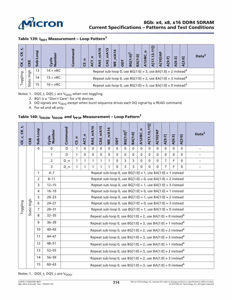
CCMTD-1725822587-9875 Micron Technology, Inc. reserves the right to change products or specifications without notice.8gb_ddr4_dram.pdf - Rev. T 09/2021 EN 2015 Micron Technology, Inc. All rights reserved.314
8Gb: x4, x8, x16 DDR4 SDRAM
Notes: 1. DQS_t, DQS_c are VDDQ when not toggling.2. BG1 is a "Don't Care" for x16 devices.3. DQ signals are VDDQ except when burst sequence drives each DQ signal by a READ command.4. For x4 and x8 only.
Notes: 1. DQS_t, DQS_c are VDDQ.
Tog
glin
g
Stat
ic H
igh 13 14 nRC Repeat sub-loop 0, use BG[1:0] = 3, use BA[1:0] = 2 instead4
14 15 nRC Repeat sub-loop 0, use BG[1:0] = 2, use BA[1:0] = 3 instead4
15 16 nRC Repeat sub-loop 0, use BG[1:0] = 3, use BA[1:0] = 0 instead4
Table 139: IDD11
CK
_c, C
K_t
,
CK
E
Su
b-L
oo
p
Cycl
e
Nu
mb
er
Co
mm
an
d
CS_n
AC
T_n
RA
S_n
/A16
CA
S_n
/A15
WE_n
/A14
OD
T
BG
[1:0
]2
BA
[1:0
]
A12/B
C_n
A[1
7,1
3,1
1]]
A[1
0]/
AP
A[9
:7]
A[6
:3]
A[2
:0] Data3
Table 140: IDD2N, IDD3N, and IPP3P1
CK
_c, C
K_t
,
CK
E
Su
b-L
oo
p
Cycl
e N
um
ber
Co
mm
an
d
CS_n
AC
T_n
RA
S_n
/A16
CA
S_n
/A15
WE_n
/A14
OD
T
BG
[1:0
]2
BA
[1:0
]
A12/B
C_n
A[1
7,1
3,1
1]]
A[1
0]/
AP
A[9
:7]
A[6
:3]
A[2
:0] Data3
Tog
glin
g
Stat
ic H
igh
0 0 D 1 0 0 0 0 0 0 0 0 0 0 0 0 0
1 D 1 0 0 0 0 0 0 0 0 0 0 0 0 0
2 D_n 1 1 1 1 1 0 3 3 0 0 0 7 F 0
3 D_n 1 1 1 1 1 0 3 3 0 0 0 7 F 0
1 Repeat sub-loop 0, use BG[1:0] = 1, use BA[1:0] = 1 instead
2 Repeat sub-loop 0, use BG[1:0] = 0, use BA[1:0] = 2 instead
3 Repeat sub-loop 0, use BG[1:0] = 1, use BA[1:0] = 3 instead
4 Repeat sub-loop 0, use BG[1:0] = 0, use BA[1:0] = 1 instead
5 Repeat sub-loop 0, use BG[1:0] = 1, use BA[1:0] = 2 instead
6 Repeat sub-loop 0, use BG[1:0] = 0, use BA[1:0] = 3 instead
7 Repeat sub-loop 0, use BG[1:0] = 1, use BA[1:0] = 0 instead
8 Repeat sub-loop 0, use BG[1:0] = 2, use BA[1:0] = 0 instead4
9 Repeat sub-loop 0, use BG[1:0] = 3, use BA[1:0] = 1 instead4
10 Repeat sub-loop 0, use BG[1:0] = 2, use BA[1:0] = 2 instead4
11 Repeat sub-loop 0, use BG[1:0] = 3, use BA[1:0] = 3 instead4
12 Repeat sub-loop 0, use BG[1:0] = 2, use BA[1:0] = 1 instead4
13 Repeat sub-loop 0, use BG[1:0] = 3, use BA[1:0] = 2 instead4
14 Repeat sub-loop 0, use BG[1:0] = 2, use BA[1:0] = 3 instead4
15 Repeat sub-loop 0, use BG[1:0] = 3, use BA[1:0] = 0 instead4
CCMTD-1725822587-9875 Micron Technology, Inc. reserves the right to change products or specifications without notice.8gb_ddr4_dram.pdf - Rev. T 09/2021 EN 2015 Micron Technology, Inc. All rights reserved.315
8Gb: x4, x8, x16 DDR4 SDRAM
2. BG1 is a "Don't Care" for x16 devices.3. DQ signals are VDDQ.4. For x4 and x8 only.

CCMTD-1725822587-9875 Micron Technology, Inc. reserves the right to change products or specifications without notice.8gb_ddr4_dram.pdf - Rev. T 09/2021 EN 2015 Micron Technology, Inc. All rights reserved.316
8Gb: x4, x8, x16 DDR4 SDRAM
Notes: 1. DQS_t, DQS_c are VSSQ.2. BG1 is a "Don't Care" for x16 devices.3. DQ signals are VSSQ.4. For x4 and x8 only.
Table 141: IDD2NT1
CK
_c, C
K_t
,
CK
E
Su
b-L
oo
p
Cycl
e N
um
ber
Co
mm
an
d
CS_n
AC
T_n
RA
S_n
/A16
CA
S_n
/A15
WE_n
/A14
OD
T
BG
[1:0
]2
BA
[1:0
]
A12/B
C_n
A[1
7,1
3,1
1]]
A[1
0]/
AP
A[9
:7]
A[6
:3]
A[2
:0] Data3
Tog
glin
g
Stat
ic H
igh
0 0 D 1 0 0 0 0 0 0 0 0 0 0 0 0 0
1 D 1 0 0 0 0 0 0 0 0 0 0 0 0 0
2 D_n 1 1 1 1 1 0 3 3 0 0 0 7 F 0
3 D_n 1 1 1 1 1 0 3 3 0 0 0 7 F 0
1 Repeat sub-loop 0 with ODT = 1, use BG[1:0] = 1, use BA[1:0] = 1 instead
2 Repeat sub-loop 0 with ODT = 0, use BG[1:0] = 0, use BA[1:0] = 2 instead
3 Repeat sub-loop 0 with ODT = 1, use BG[1:0] = 1, use BA[1:0] = 3 instead
4 Repeat sub-loop 0 with ODT = 0, use BG[1:0] = 0, use BA[1:0] = 1 instead
5 Repeat sub-loop 0 with ODT = 1, use BG[1:0] = 1, use BA[1:0] = 2 instead
6 Repeat sub-loop 0 with ODT = 0, use BG[1:0] = 0, use BA[1:0] = 3 instead
7 Repeat sub-loop 0 with ODT = 1, use BG[1:0] = 1, use BA[1:0] = 0 instead
8 Repeat sub-loop 0 with ODT = 0, use BG[1:0] = 2, use BA[1:0] = 0 instead4
9 Repeat sub-loop 0 with ODT = 1, use BG[1:0] = 3, use BA[1:0] = 1 instead4
10 Repeat sub-loop 0 with ODT = 0, use BG[1:0] = 2, use BA[1:0] = 2 instead4
11 Repeat sub-loop 0 with ODT = 1, use BG[1:0] = 3, use BA[1:0] = 3 instead4
12 Repeat sub-loop 0 with ODT = 0, use BG[1:0] = 2, use BA[1:0] = 1 instead4
13 Repeat sub-loop 0 with ODT = 1, use BG[1:0] = 3, use BA[1:0] = 2 instead4
14 Repeat sub-loop 0 with ODT = 0, use BG[1:0] = 2, use BA[1:0] = 3 instead4
15 Repeat sub-loop 0 with ODT = 1, use BG[1:0] = 3, use BA[1:0] = 0 instead4

CCMTD-1725822587-9875 Micron Technology, Inc. reserves the right to change products or specifications without notice.8gb_ddr4_dram.pdf - Rev. T 09/2021 EN 2015 Micron Technology, Inc. All rights reserved.317
8Gb: x4, x8, x16 DDR4 SDRAM
Notes: 1. DQS_t, DQS_c are VDDQ when not toggling.2. BG1 is a "Don't Care" for x16 devices.3. Burst sequence driven on each DQ signal by a READ command. Outside burst operation, DQ signals are VDDQ.4. For x4 and x8 only.
Table 142: IDD4R1
CK
_c, C
K_t
,
CK
E
Su
b-L
oo
p
Cycl
e
Nu
mb
er
Co
mm
an
d
CS_n
AC
T_n
RA
S_n
/A16
CA
S_n
/A15
WE_n
/A14
OD
T
BG
[1:0
]2
BA
[1:0
]
A12/B
C_n
A[1
7,1
3,1
1]]
A[1
0]/
AP
A[9
:7]
A[6
:3]
A[2
:0] Data3
Tog
glin
g
Stat
ic H
igh
0 0 RD 0 1 1 0 1 0 0 0 0 0 0 0 0 0 D0 = 00, D1 = FF, D2 = FF, D3 = 00, D4 = FF, D5 = 00, D5 = 00, D7 = FF
1 D 1 0 0 0 0 0 0 0 0 0 0 0 0 0
2, 3 D_n, D_n
1 1 1 1 1 0 3 3 0 0 0 7 F 0
1 4 RD 0 1 1 0 1 0 1 1 0 0 0 7 F 0 D0 = FF, D1 = 00 D2 = 00, D3 = FF D4 = 00, D5 = FF D5 = FF, D7 = 00
5 D 1 0 0 0 0 0 0 0 0 0 0 0 0 0
6, 7 D_n, D_n
1 1 1 1 1 0 3 3 0 0 0 7 F 0
2 Repeat sub-loop 0, use BG[1:0] = 0, use BA[1:0] = 2 instead
3 Repeat sub-loop 1, use BG[1:0] = 1, use BA[1:0] = 3 instead
4 Repeat sub-loop 0, use BG[1:0] = 0, use BA[1:0] = 1 instead
5 Repeat sub-loop 1, use BG[1:0] = 1, use BA[1:0] = 2 instead
6 Repeat sub-loop 0, use BG[1:0] = 0, use BA[1:0] = 3 instead
7 Repeat sub-loop 1, use BG[1:0] = 1, use BA[1:0] = 0 instead
8 Repeat sub-loop 0, use BG[1:0] = 2, use BA[1:0] = 0 instead4
9 Repeat sub-loop 1, use BG[1:0] = 3, use BA[1:0] = 1 instead4
10 Repeat sub-loop 0, use BG[1:0] = 2, use BA[1:0] = 2 instead4
11 Repeat sub-loop 1, use BG[1:0] = 3, use BA[1:0] = 3 instead4
12 Repeat sub-loop 0, use BG[1:0] = 2, use BA[1:0] = 1 instead4
13 Repeat sub-loop 1, use BG[1:0] = 3, use BA[1:0] = 2 instead4
14 Repeat sub-loop 0, use BG[1:0] = 2, use BA[1:0] = 3 instead4
15 Repeat sub-loop 1, use BG[1:0] = 3, use BA[1:0] = 0 instead4
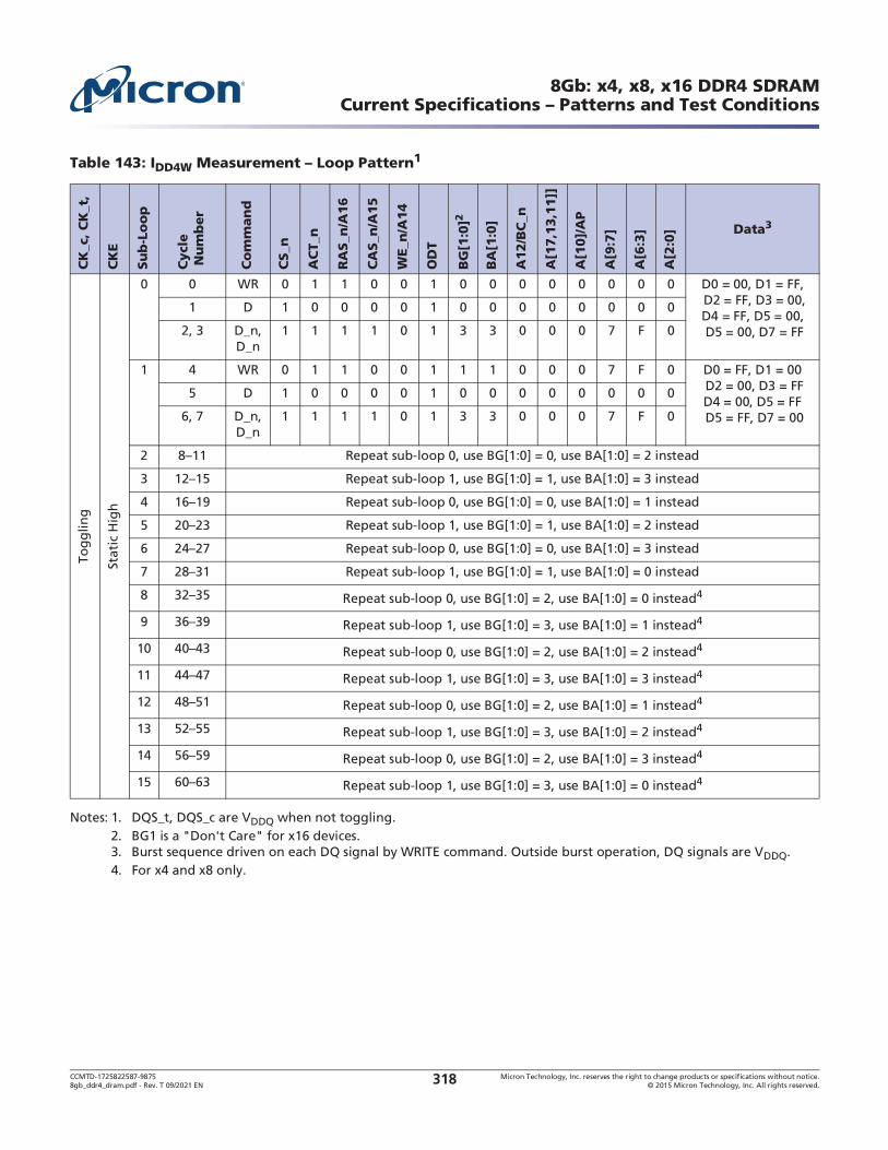
CCMTD-1725822587-9875 Micron Technology, Inc. reserves the right to change products or specifications without notice.8gb_ddr4_dram.pdf - Rev. T 09/2021 EN 2015 Micron Technology, Inc. All rights reserved.318
8Gb: x4, x8, x16 DDR4 SDRAM
Notes: 1. DQS_t, DQS_c are VDDQ when not toggling.2. BG1 is a "Don't Care" for x16 devices.3. Burst sequence driven on each DQ signal by WRITE command. Outside burst operation, DQ signals are VDDQ.4. For x4 and x8 only.
Table 143: IDD4W1
CK
_c, C
K_t
,
CK
E
Su
b-L
oo
p
Cycl
e N
um
ber
Co
mm
an
d
CS_n
AC
T_n
RA
S_n
/A16
CA
S_n
/A15
WE_n
/A14
OD
T
BG
[1:0
]2
BA
[1:0
]
A12/B
C_n
A[1
7,1
3,1
1]]
A[1
0]/
AP
A[9
:7]
A[6
:3]
A[2
:0] Data3
Tog
glin
g
Stat
ic H
igh
0 0 WR 0 1 1 0 0 1 0 0 0 0 0 0 0 0 D0 = 00, D1 = FF, D2 = FF, D3 = 00, D4 = FF, D5 = 00, D5 = 00, D7 = FF
1 D 1 0 0 0 0 1 0 0 0 0 0 0 0 0
2, 3 D_n, D_n
1 1 1 1 0 1 3 3 0 0 0 7 F 0
1 4 WR 0 1 1 0 0 1 1 1 0 0 0 7 F 0 D0 = FF, D1 = 00 D2 = 00, D3 = FF D4 = 00, D5 = FF D5 = FF, D7 = 00
5 D 1 0 0 0 0 1 0 0 0 0 0 0 0 0
6, 7 D_n, D_n
1 1 1 1 0 1 3 3 0 0 0 7 F 0
2 Repeat sub-loop 0, use BG[1:0] = 0, use BA[1:0] = 2 instead
3 Repeat sub-loop 1, use BG[1:0] = 1, use BA[1:0] = 3 instead
4 Repeat sub-loop 0, use BG[1:0] = 0, use BA[1:0] = 1 instead
5 Repeat sub-loop 1, use BG[1:0] = 1, use BA[1:0] = 2 instead
6 Repeat sub-loop 0, use BG[1:0] = 0, use BA[1:0] = 3 instead
7 Repeat sub-loop 1, use BG[1:0] = 1, use BA[1:0] = 0 instead
8 Repeat sub-loop 0, use BG[1:0] = 2, use BA[1:0] = 0 instead4
9 Repeat sub-loop 1, use BG[1:0] = 3, use BA[1:0] = 1 instead4
10 Repeat sub-loop 0, use BG[1:0] = 2, use BA[1:0] = 2 instead4
11 Repeat sub-loop 1, use BG[1:0] = 3, use BA[1:0] = 3 instead4
12 Repeat sub-loop 0, use BG[1:0] = 2, use BA[1:0] = 1 instead4
13 Repeat sub-loop 1, use BG[1:0] = 3, use BA[1:0] = 2 instead4
14 Repeat sub-loop 0, use BG[1:0] = 2, use BA[1:0] = 3 instead4
15 Repeat sub-loop 1, use BG[1:0] = 3, use BA[1:0] = 0 instead4

CCMTD-1725822587-9875 Micron Technology, Inc. reserves the right to change products or specifications without notice.8gb_ddr4_dram.pdf - Rev. T 09/2021 EN 2015 Micron Technology, Inc. All rights reserved.319
8Gb: x4, x8, x16 DDR4 SDRAM
Notes: 1. Pattern provided for reference only.2. DQS_t, DQS_c are VDDQ when not toggling.3. BG1 is a "Don't Care" for x16 devices.4. Burst sequence driven on each DQ signal by WRITE command. Outside burst operation, DQ signals are VDDQ.5. For x4 and x8 only.
Table 144: IDD4Wc1
CK
_c, C
K_t
,
CK
E
Su
b-L
oo
p
Cycl
e
Nu
mb
er
Co
mm
an
d
CS_n
AC
T_n
RA
S_n
/A16
CA
S_n
/A15
WE_n
/A14
OD
T
BG
[1:0
]3
BA
[1:0
]
A12/B
C_n
A[1
7,1
3,1
1]]
A[1
0]/
AP
A[9
:7]
A[6
:3]
A[2
:0] Data4
Tog
glin
g
Stat
ic H
igh
0 0 WR 0 1 1 0 0 1 0 0 0 0 0 0 0 0 D0 = 00, D1 = FF, D2 = FF, D3 = 00, D4 = FF, D5 = 00,
D8 = CRC
1, 2 D, D 1 0 0 0 0 1 0 0 0 0 0 0 0 0
3, 4 D_n, D_n
1 1 1 1 0 1 3 3 0 0 0 7 F 0
1 5 WR 0 1 1 0 0 1 1 1 0 0 0 7 F 0 D0 = FF, D1 = 00, D2 = 00, D3 = FF, D4 = 00, D5 = FF, D5 = FF, D7 = 00
D8 = CRC
6, 7 D, D 1 0 0 0 0 1 0 0 0 0 0 0 0 0
8, 9 D_n, D_n
1 1 1 1 0 1 3 3 0 0 0 7 F 0
2 Repeat sub-loop 0, use BG[1:0] = 0, use BA[1:0] = 2 instead
3 Repeat sub-loop 1, use BG[1:0] = 1, use BA[1:0] = 3 instead
4 Repeat sub-loop 0, use BG[1:0] = 0, use BA[1:0] = 1 instead
5 Repeat sub-loop 1, use BG[1:0] = 1, use BA[1:0] = 2 instead
6 Repeat sub-loop 0, use BG[1:0] = 0, use BA[1:0] = 3 instead
7 Repeat sub-loop 1, use BG[1:0] = 1, use BA[1:0] = 0 instead
8 Repeat sub-loop 0, use BG[1:0] = 2, use BA[1:0] = 0 instead4
9 Repeat sub-loop 1, use BG[1:0] = 3, use BA[1:0] = 1 instead4
10 Repeat sub-loop 0, use BG[1:0] = 2, use BA[1:0] = 2 instead4
11 Repeat sub-loop 1, use BG[1:0] = 3, use BA[1:0] = 3 instead4
12 Repeat sub-loop 0, use BG[1:0] = 2, use BA[1:0] = 1 instead4
13 Repeat sub-loop 1, use BG[1:0] = 3, use BA[1:0] = 2 instead4
14 Repeat sub-loop 0, use BG[1:0] = 2, use BA[1:0] = 3 instead4
15 Repeat sub-loop 1, use BG[1:0] = 3, use BA[1:0] = 0 instead4

CCMTD-1725822587-9875 Micron Technology, Inc. reserves the right to change products or specifications without notice.8gb_ddr4_dram.pdf - Rev. T 09/2021 EN 2015 Micron Technology, Inc. All rights reserved.320
8Gb: x4, x8, x16 DDR4 SDRAM
Notes: 1. DQS_t, DQS_c are VDDQ.2. BG1 is a "Don't Care" for x16 devices.3. DQ signals are VDDQ.4. For x4 and x8 only.
Table 145: IDD5R1
CK
_c, C
K_t
,
CK
E
Su
b-L
oo
p
Cycl
e
Nu
mb
er
Co
mm
an
d
CS_n
AC
T_n
RA
S_n
/A16
CA
S_n
/A15
WE_n
/A14
OD
T
BG
[1:0
]2
BA
[1:0
]
A12/B
C_n
A[1
7,1
3,1
1]]
A[1
0]/
AP
A[9
:7]
A[6
:3]
A[2
:0] Data3
Tog
glin
g
Stat
ic H
igh
0 0 REF 0 1 0 0 1 0 0 0 0 0 0 0 0 0
1 1 D 1 0 0 0 0 0 0 0 0 0 0 0 0 0
2 D 1 0 0 0 0 0 0 0 0 0 0 0 0 0
3 D_n 1 1 1 1 1 0 3 3 0 0 0 7 F 0
4 D_n 1 1 1 1 1 0 3 3 0 0 0 7 F 0
Repeat pattern 1...4, use BG[1:0] = 1, use BA[1:0] = 1 instead
Repeat pattern 1...4, use BG[1:0] = 0, use BA[1:0] = 2 instead
Repeat pattern 1...4, use BG[1:0] = 1, use BA[1:0] = 3 instead
Repeat pattern 1...4, use BG[1:0] = 0, use BA[1:0] = 1 instead
Repeat pattern 1...4, use BG[1:0] = 1, use BA[1:0] = 2 instead
Repeat pattern 1...4, use BG[1:0] = 0, use BA[1:0] = 3 instead
Repeat pattern 1...4, use BG[1:0] = 1, use BA[1:0] = 0 instead
Repeat pattern 1...4, use BG[1:0] = 2, use BA[1:0] = 0 instead4
Repeat pattern 1...4, use BG[1:0] = 3, use BA[1:0] = 1 instead4
Repeat pattern 1...4, use BG[1:0] = 2, use BA[1:0] = 2 instead4
Repeat pattern 1...4, use BG[1:0] = 3, use BA[1:0] = 3 instead4
Repeat pattern 1...4, use BG[1:0] = 2, use BA[1:0] = 1 instead4
Repeat pattern 1...4, use BG[1:0] = 3, use BA[1:0] = 2 instead4
Repeat pattern 1...4, use BG[1:0] = 2, use BA[1:0] = 3 instead4
Repeat pattern 1...4, use BG[1:0] = 3, use BA[1:0] = 0 instead4
2 65...nREFI - 1 Repeat sub-loop 1; truncate if necessary
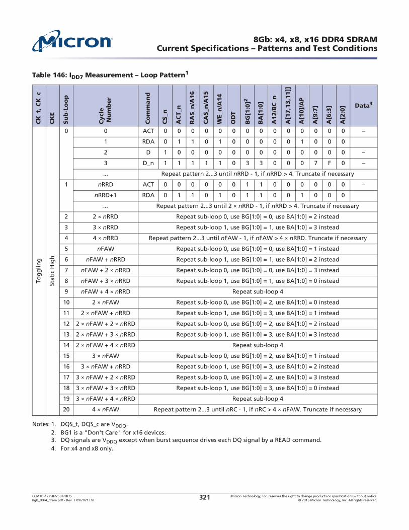
CCMTD-1725822587-9875 Micron Technology, Inc. reserves the right to change products or specifications without notice.8gb_ddr4_dram.pdf - Rev. T 09/2021 EN 2015 Micron Technology, Inc. All rights reserved.321
8Gb: x4, x8, x16 DDR4 SDRAM
Notes: 1. DQS_t, DQS_c are VDDQ.2. BG1 is a "Don't Care" for x16 devices.3. DQ signals are VDDQ except when burst sequence drives each DQ signal by a READ command.4. For x4 and x8 only.
Table 146: IDD71
CK
_t, C
K_c
CK
E
Su
b-L
oo
p
Cycl
e N
um
ber
Co
mm
an
d
CS_n
AC
T_n
RA
S_n
/A16
CA
S_n
/A15
WE_n
/A14
OD
T
BG
[1:0
]2
BA
[1:0
]
A12/B
C_n
A[1
7,1
3,1
1]]
A[1
0]/
AP
A[9
:7]
A[6
:3]
A[2
:0] Data3
Tog
glin
g
Stat
ic H
igh
0 0 ACT 0 0 0 0 0 0 0 0 0 0 0 0 0 0
1 RDA 0 1 1 0 1 0 0 0 0 0 1 0 0 0
2 D 1 0 0 0 0 0 0 0 0 0 0 0 0 0
3 D_n 1 1 1 1 1 0 3 3 0 0 0 7 F 0
... Repeat pattern 2...3 until nRRD - 1, if nRRD > 4. Truncate if necessary
1 nRRD ACT 0 0 0 0 0 0 1 1 0 0 0 0 0 0
nRRD+1 RDA 0 1 1 0 1 0 1 1 0 0 1 0 0 0
... Repeat pattern 2...3 until 2 nRRD - 1, if nRRD > 4. Truncate if necessary
2 2 nRRD Repeat sub-loop 0, use BG[1:0] = 0, use BA[1:0] = 2 instead
3 3 nRRD Repeat sub-loop 1, use BG[1:0] = 1, use BA[1:0] = 3 instead
4 4 nRRD Repeat pattern 2...3 until nFAW - 1, if nFAW > 4 nRRD. Truncate if necessary
5 nFAW Repeat sub-loop 0, use BG[1:0] = 0, use BA[1:0] = 1 instead
6 nFAW + nRRD Repeat sub-loop 1, use BG[1:0] = 1, use BA[1:0] = 2 instead
7 nFAW + 2 nRRD Repeat sub-loop 0, use BG[1:0] = 0, use BA[1:0] = 3 instead
8 nFAW + 3 nRRD Repeat sub-loop 1, use BG[1:0] = 1, use BA[1:0] = 0 instead
9 nFAW + 4 nRRD Repeat sub-loop 4
10 2 nFAW Repeat sub-loop 0, use BG[1:0] = 2, use BA[1:0] = 0 instead
11 2 nFAW + nRRD Repeat sub-loop 1, use BG[1:0] = 3, use BA[1:0] = 1 instead
12 2 nFAW + 2 nRRD Repeat sub-loop 0, use BG[1:0] = 2, use BA[1:0] = 2 instead
13 2 nFAW + 3 nRRD Repeat sub-loop 1, use BG[1:0] = 3, use BA[1:0] = 3 instead
14 2 nFAW + 4 nRRD Repeat sub-loop 4
15 3 nFAW Repeat sub-loop 0, use BG[1:0] = 2, use BA[1:0] = 1 instead
16 3 nFAW + nRRD Repeat sub-loop 1, use BG[1:0] = 3, use BA[1:0] = 2 instead
17 3 nFAW + 2 nRRD Repeat sub-loop 0, use BG[1:0] = 2, use BA[1:0] = 3 instead
18 3 nFAW + 3 nRRD Repeat sub-loop 1, use BG[1:0] = 3, use BA[1:0] = 0 instead
19 3 nFAW + 4 nRRD Repeat sub-loop 4
20 4 nFAW Repeat pattern 2...3 until nRC - 1, if nRC > 4 nFAW. Truncate if necessary
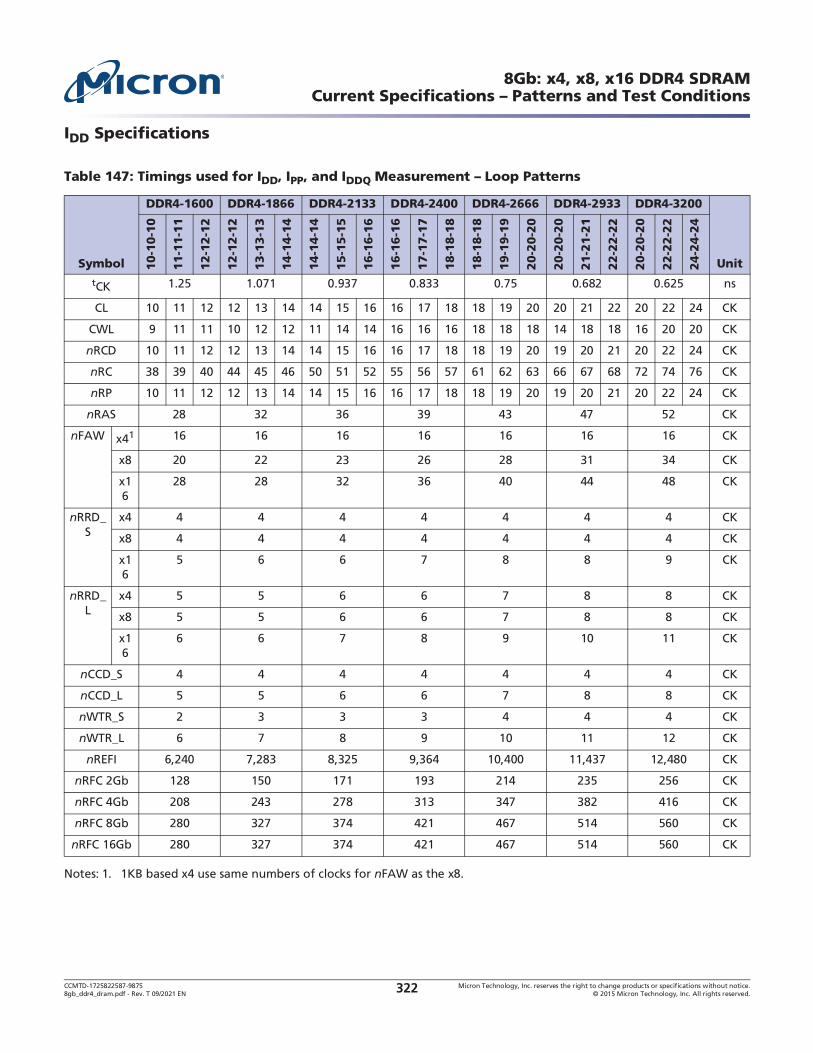
CCMTD-1725822587-9875 Micron Technology, Inc. reserves the right to change products or specifications without notice.8gb_ddr4_dram.pdf - Rev. T 09/2021 EN 2015 Micron Technology, Inc. All rights reserved.322
8Gb: x4, x8, x16 DDR4 SDRAM
IDD Specifications
Notes: 1. 1KB based x4 use same numbers of clocks for nFAW as the x8.
Table 147: Timings used for IDD, IPP, and IDDQ
Symbol
DDR4-1600 DDR4-1866 DDR4-2133 DDR4-2400 DDR4-2666 DDR4-2933 DDR4-3200
Unit10-1
0-1
0
11-1
1-1
1
12-1
2-1
2
12-1
2-1
2
13-1
3-1
3
14-1
4-1
4
14-1
4-1
4
15-1
5-1
5
16-1
6-1
6
16-1
6-1
6
17-1
7-1
7
18-1
8-1
8
18-1
8-1
8
19-1
9-1
9
20-2
0-2
0
20-2
0-2
0
21-2
1-2
1
22-2
2-2
2
20-2
0-2
0
22-2
2-2
2
24-2
4-2
4
tCK 1.25 1.071 0.937 0.833 0.75 0.682 0.625 ns
CL 10 11 12 12 13 14 14 15 16 16 17 18 18 19 20 20 21 22 20 22 24 CK
CWL 9 11 11 10 12 12 11 14 14 16 16 16 18 18 18 14 18 18 16 20 20 CK
nRCD 10 11 12 12 13 14 14 15 16 16 17 18 18 19 20 19 20 21 20 22 24 CK
nRC 38 39 40 44 45 46 50 51 52 55 56 57 61 62 63 66 67 68 72 74 76 CK
nRP 10 11 12 12 13 14 14 15 16 16 17 18 18 19 20 19 20 21 20 22 24 CK
nRAS 28 32 36 39 43 47 52 CK
nFAW x41 16 16 16 16 16 16 16 CK
x8 20 22 23 26 28 31 34 CK
x16
28 28 32 36 40 44 48 CK
nRRD_S
x4 4 4 4 4 4 4 4 CK
x8 4 4 4 4 4 4 4 CK
x16
5 6 6 7 8 8 9 CK
nRRD_L
x4 5 5 6 6 7 8 8 CK
x8 5 5 6 6 7 8 8 CK
x16
6 6 7 8 9 10 11 CK
nCCD_S 4 4 4 4 4 4 4 CK
nCCD_L 5 5 6 6 7 8 8 CK
nWTR_S 2 3 3 3 4 4 4 CK
nWTR_L 6 7 8 9 10 11 12 CK
nREFI 6,240 7,283 8,325 9,364 10,400 11,437 12,480 CK
nRFC 2Gb 128 150 171 193 214 235 256 CK
nRFC 4Gb 208 243 278 313 347 382 416 CK
nRFC 8Gb 280 327 374 421 467 514 560 CK
nRFC 16Gb 280 327 374 421 467 514 560 CK
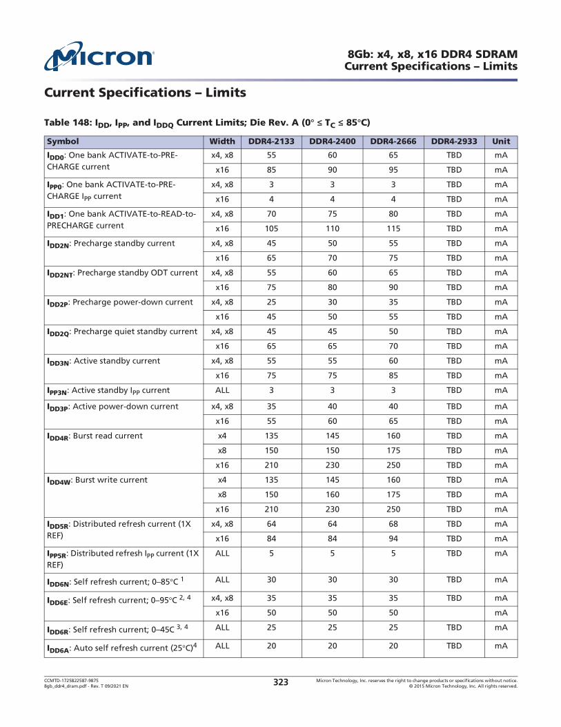
CCMTD-1725822587-9875 Micron Technology, Inc. reserves the right to change products or specifications without notice.8gb_ddr4_dram.pdf - Rev. T 09/2021 EN 2015 Micron Technology, Inc. All rights reserved.323
8Gb: x4, x8, x16 DDR4 SDRAM
Table 148: IDD, IPP, and IDDQ Current Limits; Die Rev. A (0 TC 85 C)
Symbol Width DDR4-2133 DDR4-2400 DDR4-2666 DDR4-2933 Unit
IDD0: One bank ACTIVATE-to-PRE-CHARGE current
x4, x8 55 60 65 TBD mA
x16 85 90 95 TBD mA
IPP0: One bank ACTIVATE-to-PRE-CHARGE IPP current
x4, x8 3 3 3 TBD mA
x16 4 4 4 TBD mA
IDD1: One bank ACTIVATE-to-READ-to- PRECHARGE current
x4, x8 70 75 80 TBD mA
x16 105 110 115 TBD mA
IDD2N: Precharge standby current x4, x8 45 50 55 TBD mA
x16 65 70 75 TBD mA
IDD2NT: Precharge standby ODT current x4, x8 55 60 65 TBD mA
x16 75 80 90 TBD mA
IDD2P: Precharge power-down current x4, x8 25 30 35 TBD mA
x16 45 50 55 TBD mA
IDD2Q: Precharge quiet standby current x4, x8 45 45 50 TBD mA
x16 65 65 70 TBD mA
IDD3N: Active standby current x4, x8 55 55 60 TBD mA
x16 75 75 85 TBD mA
IPP3N: Active standby IPP current ALL 3 3 3 TBD mA
IDD3P: Active power-down current x4, x8 35 40 40 TBD mA
x16 55 60 65 TBD mA
IDD4R: Burst read current x4 135 145 160 TBD mA
x8 150 150 175 TBD mA
x16 210 230 250 TBD mA
IDD4W: Burst write current x4 135 145 160 TBD mA
x8 150 160 175 TBD mA
x16 210 230 250 TBD mA
IDD5R: Distributed refresh current (1X REF)
x4, x8 64 64 68 TBD mA
x16 84 84 94 TBD mA
IPP5R: Distributed refresh IPP current (1X REF)
ALL 5 5 5 TBD mA
IDD6N C 1 ALL 30 30 30 TBD mA
IDD6E C 2, 4 x4, x8 35 35 35 TBD mA
x16 50 50 50 mA
IDD6R3, 4 ALL 25 25 25 TBD mA
IDD6A: Auto self refresh current (25 C)4 ALL 20 20 20 TBD mA
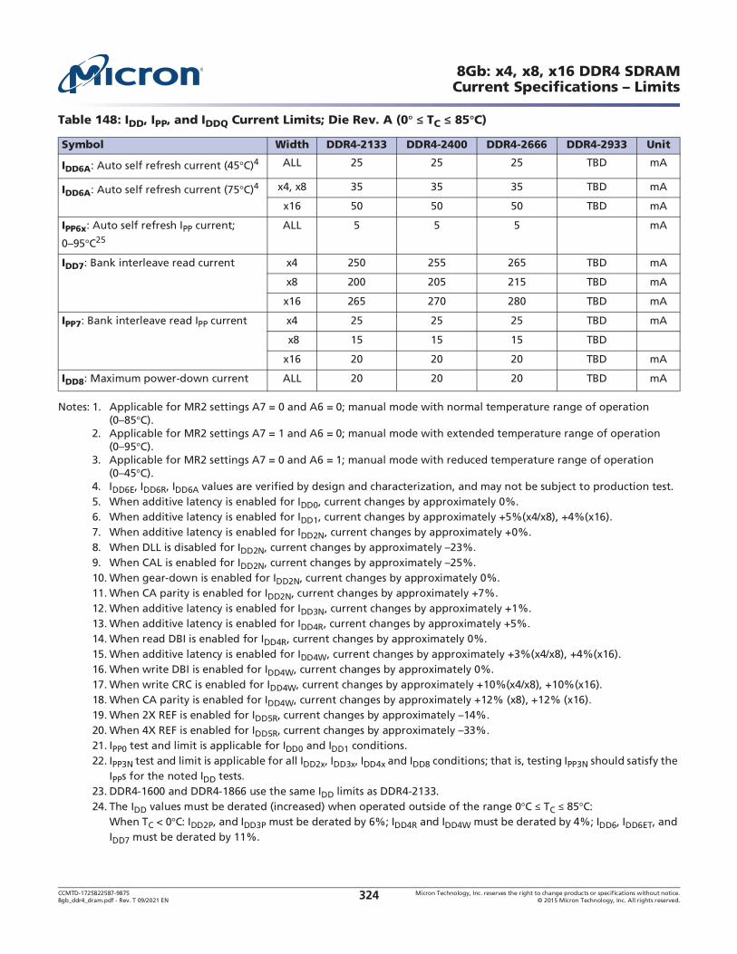
CCMTD-1725822587-9875 Micron Technology, Inc. reserves the right to change products or specifications without notice.8gb_ddr4_dram.pdf - Rev. T 09/2021 EN 2015 Micron Technology, Inc. All rights reserved.324
8Gb: x4, x8, x16 DDR4 SDRAM
Notes: 1. Applicable for MR2 settings A7 = 0 and A6 = 0; manual mode with normal temperature range of operation C).
2. Applicable for MR2 settings A7 = 1 and A6 = 0; manual mode with extended temperature range of operation C).
3. Applicable for MR2 settings A7 = 0 and A6 = 1; manual mode with reduced temperature range of operation C).
4. IDD6E, IDD6R, IDD6A values are verified by design and characterization, and may not be subject to production test.5. When additive latency is enabled for IDD0, current changes by approximately 0%.6. When additive latency is enabled for IDD1, current changes by approximately +5%(x4/x8), +4%(x16).7. When additive latency is enabled for IDD2N, current changes by approximately +0%.8. When DLL is disabled for IDD2N9. When CAL is enabled for IDD2N10. When gear-down is enabled for IDD2N, current changes by approximately 0%.11. When CA parity is enabled for IDD2N, current changes by approximately +7%.12. When additive latency is enabled for IDD3N, current changes by approximately +1%.13. When additive latency is enabled for IDD4R, current changes by approximately +5%.14. When read DBI is enabled for IDD4R, current changes by approximately 0%.15. When additive latency is enabled for IDD4W, current changes by approximately +3%(x4/x8), +4%(x16).16. When write DBI is enabled for IDD4W, current changes by approximately 0%.17. When write CRC is enabled for IDD4W, current changes by approximately +10%(x4/x8), +10%(x16).18. When CA parity is enabled for IDD4W, current changes by approximately +12% (x8), +12% (x16).19. When 2X REF is enabled for IDD5R20. When 4X REF is enabled for IDD5R21. IPP0 test and limit is applicable for IDD0 and IDD1 conditions.22. IPP3N test and limit is applicable for all IDD2x, IDD3x, IDD4x and IDD8 conditions; that is, testing IPP3N should satisfy the
IPPs for the noted IDD tests.23. DDR4-1600 and DDR4-1866 use the same IDD limits as DDR4-2133.24. The IDD values must be derated (increased) when operated outside of the range 0 C TC 85 C:
When TC < 0 C: IDD2P, and IDD3P must be derated by 6%; IDD4R and IDD4W must be derated by 4%; IDD6, IDD6ET, and IDD7 must be derated by 11%.
IDD6A: Auto self refresh current (45 C)4 ALL 25 25 25 TBD mA
IDD6A: Auto self refresh current (75 C)4 x4, x8 35 35 35 TBD mA
x16 50 50 50 TBD mA
IPP6x: Auto self refresh IPP current;
C25
ALL 5 5 5 mA
IDD7: Bank interleave read current x4 250 255 265 TBD mA
x8 200 205 215 TBD mA
x16 265 270 280 TBD mA
IPP7: Bank interleave read IPP current x4 25 25 25 TBD mA
x8 15 15 15 TBD
x16 20 20 20 TBD mA
IDD8: Maximum power-down current ALL 20 20 20 TBD mA
Table 148: IDD, IPP, and IDDQ Current Limits; Die Rev. A (0 TC 85 C)
Symbol Width DDR4-2133 DDR4-2400 DDR4-2666 DDR4-2933 Unit
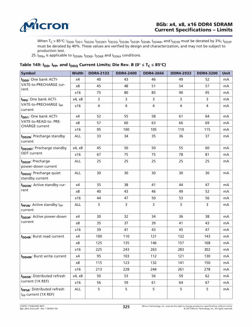
CCMTD-1725822587-9875 Micron Technology, Inc. reserves the right to change products or specifications without notice.8gb_ddr4_dram.pdf - Rev. T 09/2021 EN 2015 Micron Technology, Inc. All rights reserved.325
8Gb: x4, x8, x16 DDR4 SDRAM
When TC > 85 C: IDD0, IDD1, IDD2N, IDD2NT, IDD2Q, IDD3N, IDD3P, IDD4R, IDD4W, and IDD5R must be derated by 3%; IDD2P must be derated by 40%. These values are verified by design and characterization, and may not be subject to production test.
25. IPP6x is applicable to IDD6N, IDD6E, IDD6R and IDD6A conditions.
Table 149: IDD, IPP, and IDDQ Current Limits; Die Rev. B (0 TC 85 C)
Symbol Width DDR4-2133 DDR4-2400 DDR4-2666 DDR4-2933 DDR4-3200 Unit
IDD0: One bank ACTI-VATE-to-PRECHARGE cur-rent
x4 40 43 46 49 52 mA
x8 45 48 51 54 57 mA
x16 75 80 85 90 95 mA
IPP0: One bank ACTI-VATE-to-PRECHARGE IPP current
x4, x8 3 3 3 3 3 mA
x16 4 4 4 4 4 mA
IDD1: One bank ACTI-VATE-to-READ-to- PRE-CHARGE current
x4 52 55 58 61 64 mA
x8 57 60 63 66 69 mA
x16 95 100 105 110 115 mA
IDD2N: Precharge standby current
ALL 33 34 35 36 37 mA
IDD2NT: Precharge standby ODT current
x4, x8 45 50 50 55 60 mA
x16 67 75 75 78 81 mA
IDD2P: Precharge power-down current
ALL 25 25 25 25 25 mA
IDD2Q: Precharge quiet standby current
ALL 30 30 30 30 30 mA
IDD3N: Active standby cur-rent
x4 35 38 41 44 47 mA
x8 40 43 46 49 52 mA
x16 44 47 50 53 56 mA
IPP3N: Active standby IPP current
ALL 3 3 3 3 3 mA
IDD3P: Active power-down current
x4 30 32 34 36 38 mA
x8 35 37 39 41 43 mA
x16 39 41 43 45 47 mA
IDD4R: Burst read current x4 100 110 121 132 143 mA
x8 125 135 146 157 168 mA
x16 225 243 263 283 302 mA
IDD4W: Burst write current x4 95 103 112 121 130 mA
x8 115 123 132 141 150 mA
x16 213 228 244 261 278 mA
IDD5R: Distributed refresh current (1X REF)
x4, x8 50 53 56 59 62 mA
x16 56 59 61 64 67 mA
IPP5R: Distributed refresh IPP current (1X REF)
ALL 5 5 5 5 5 mA

CCMTD-1725822587-9875 Micron Technology, Inc. reserves the right to change products or specifications without notice.8gb_ddr4_dram.pdf - Rev. T 09/2021 EN 2015 Micron Technology, Inc. All rights reserved.326
8Gb: x4, x8, x16 DDR4 SDRAM
Notes: 1. Applicable for MR2 settings A7 = 0 and A6 = 0; manual mode with normal temperature range of operation C).
2. Applicable for MR2 settings A7 = 1 and A6 = 0; manual mode with extended temperature range of operation C).
3. Applicable for MR2 settings A7 = 0 and A6 = 1; manual mode with reduced temperature range of operation C).
4. IDD6E, IDD6R, IDD6A values are verified by design and characterization, and may not be subject to production test.5. When additive latency is enabled for IDD0, current changes by approximately 0%.6. When additive latency is enabled for IDD1, current changes by approximately +5%(x4/x8), +4%(x16).7. When additive latency is enabled for IDD2N, current changes by approximately 0%.8. When DLL is disabled for IDD2N9. When CAL is enabled for IDD2N10. When gear-down is enabled for IDD2N, current changes by approximately 0%.11. When CA parity is enabled for IDD2N, current changes by approximately +7%.12. When additive latency is enabled for IDD3N, current changes by approximately +1%.13. When additive latency is enabled for IDD4R, current changes by approximately +5%.14. When read DBI is enabled for IDD4R, current changes by approximately 0%.15. When additive latency is enabled for IDD4W, current changes by approximately +3%(x4/x8), +4%(x16).16. When write DBI is enabled for IDD4W, current changes by approximately 0%.17. When write CRC is enabled for IDD4W, current changes by approximately +10%(x4/x8), +10%(x16).
IDD6N: Self refresh current;
C 1ALL 30 30 30 30 30 mA
IDD6E: Self refresh current;
C 2, 4ALL 35 35 35 35 35 mA
IDD6R: Self refresh current; 3, 4
ALL 20 20 20 20 20 mA
IDD6A: Auto self refresh cur-
rent (25 C)4ALL 8.6 8.6 8.6 8.6 8.6 mA
IDD6A: Auto self refresh cur-
rent (45 C)4ALL 20 20 20 20 20 mA
IDD6A: Auto self refresh cur-
rent (75 C)4ALL 30 30 30 30 30 mA
IPP6x: Auto self refresh IPP
C25
ALL 5 5 5 5 5 mA
IDD7: Bank interleave read current
x4 175 185 200 215 230 mA
x8 170 175 180 185 190 mA
x16 239 249 259 269 279 mA
IPP7: Bank interleave read IPP current
x4 16 17 18 19 20 mA
x8 15 15 15 15 15 mA
x16 20 20 20 20 20 mA
IDD8: Maximum power-down current
ALL 25 25 25 25 25 mA
Table 149: IDD, IPP, and IDDQ Current Limits; Die Rev. B (0 TC 85 C)
Symbol Width DDR4-2133 DDR4-2400 DDR4-2666 DDR4-2933 DDR4-3200 Unit

CCMTD-1725822587-9875 Micron Technology, Inc. reserves the right to change products or specifications without notice.8gb_ddr4_dram.pdf - Rev. T 09/2021 EN 2015 Micron Technology, Inc. All rights reserved.327
8Gb: x4, x8, x16 DDR4 SDRAM
18. When CA parity is enabled for IDD4W, current changes by approximately +12% (x8), +12% (x16).19. When 2X REF is enabled for IDD5R20. When 4X REF is enabled for IDD5R21. IPP0 test and limit is applicable for IDD0 and IDD1 conditions.22. IPP3N test and limit is applicable for all IDD2x, IDD3x, IDD4x and IDD8 conditions; that is, testing IPP3N should satisfy the
IPPs for the noted IDD tests.23. DDR4-1600 and DDR4-1866 use the same IDD limits as DDR4-2133.24. The IDD values must be derated (increased) when operated outside of the range 0 C TC 85 C:
When TC < 0 C: IDD2P, and IDD3P must be derated by 6%; IDD4R and IDD4W must be derated by 4%; IDD6, IDD6ET, and IDD7 must be derated by 11%.When TC > 85 C: IDD0, IDD1, IDD2N, IDD2NT, IDD2Q, IDD3N, IDD3P, IDD4R, IDD4W, and IDD5R must be derated by 3%; IDD2P must be derated by 40%. These values are verified by design and characterization, and may not be subject to production test.
25. IPP6x is applicable to IDD6N, IDD6E, IDD6R and IDD6A conditions.
Table 150: IDD, IPP, and IDDQ Current Limits; Die Rev. D (0 TC 85 C)
Symbol Width DDR4-2133 DDR4-2400 DDR4-2666 DDR4-2933 DDR4-3200 Unit
IDD0: One bank ACTI-VATE-to-PRECHARGE cur-rent
x4 40 43 46 49 52 mA
x8 45 48 51 54 57 mA
x16 75 80 85 90 95 mA
IPP0: One bank ACTI-VATE-to-PRECHARGE IPP current
x4, x8 3 3 3 3 3 mA
x16 4 4 4 4 4 mA
IDD1: One bank ACTI-VATE-to-READ-to- PRE-CHARGE current
x4 52 55 58 61 64 mA
x8 57 60 63 66 69 mA
x16 95 100 105 110 115 mA
IDD2N: Precharge standby current
ALL 33 34 35 36 37 mA
IDD2NT: Precharge standby ODT current
x4, x8 45 50 50 55 60 mA
x16 67 75 75 78 81 mA
IDD2P: Precharge power-down current
ALL 25 25 25 25 25 mA
IDD2Q: Precharge quiet standby current
ALL 30 30 30 30 30 mA
IDD3N: Active standby cur-rent
x4 40 43 46 49 52 mA
x8 45 48 51 54 56 mA
x16 49 52 55 58 61 mA
IPP3N: Active standby IPP current
ALL 3 3 3 3 3 mA
IDD3P: Active power-down current
x4 30 32 34 36 38 mA
x8 35 37 39 41 43 mA
x16 39 41 43 45 47 mA

CCMTD-1725822587-9875 Micron Technology, Inc. reserves the right to change products or specifications without notice.8gb_ddr4_dram.pdf - Rev. T 09/2021 EN 2015 Micron Technology, Inc. All rights reserved.328
8Gb: x4, x8, x16 DDR4 SDRAM
Notes: 1. Applicable for MR2 settings A7 = 0 and A6 = 0; manual mode with normal temperature range of operation C).
2. Applicable for MR2 settings A7 = 1 and A6 = 0; manual mode with extended temperature range of operation C).
3. Applicable for MR2 settings A7 = 0 and A6 = 1; manual mode with reduced temperature range of operation C).
4. IDD6E, IDD6R, IDD6A values are verified by design and characterization, and may not be subject to production test.5. When additive latency is enabled for IDD0, current changes by approximately 0%.
IDD4R: Burst read current x4 100 110 121 132 143 mA
x8 125 135 146 157 168 mA
x16 225 243 263 283 302 mA
IDD4W: Burst write current x4 105 113 122 130 140 mA
x8 125 132 142 150 160 mA
x16 225 240 255 270 290 mA
IDD5R: Distributed refresh current (1X REF)
x4, x8 56 58 61 64 66 mA
x16 61 64 67 69 72 mA
IPP5R: Distributed refresh IPP current (1X REF)
ALL 5 5 5 5 5 mA
IDD6N: Self refresh current;
C 1ALL 31 31 31 31 31 mA
IDD6E: Self refresh current;
C 2, 4ALL 36 36 36 36 36 mA
IDD6R: Self refresh current; 3, 4
ALL 21 21 21 21 21 mA
IDD6A: Auto self refresh cur-
rent (25 C)4ALL 8.6 8.6 8.6 8.6 8.6 mA
IDD6A: Auto self refresh cur-
rent (45 C)4ALL 21 21 21 21 21 mA
IDD6A: Auto self refresh cur-
rent (75 C)4ALL 31 31 31 31 31 mA
IPP6x: Auto self refresh IPP
C25
ALL 5 5 5 5 5 mA
IDD7: Bank interleave read current
x4 175 185 200 215 230 mA
x8 170 175 180 185 190 mA
x16 239 249 259 269 279 mA
IPP7: Bank interleave read IPP current
x4 16 17 18 19 20 mA
x8 15 15 15 15 15 mA
x16 20 20 20 20 20 mA
IDD8: Maximum power-down current
ALL 25 25 25 25 25 mA
Table 150: IDD, IPP, and IDDQ Current Limits; Die Rev. D (0 TC 85 C)
Symbol Width DDR4-2133 DDR4-2400 DDR4-2666 DDR4-2933 DDR4-3200 Unit

CCMTD-1725822587-9875 Micron Technology, Inc. reserves the right to change products or specifications without notice.8gb_ddr4_dram.pdf - Rev. T 09/2021 EN 2015 Micron Technology, Inc. All rights reserved.329
8Gb: x4, x8, x16 DDR4 SDRAM
6. When additive latency is enabled for IDD1, current changes by approximately +5%(x4/x8), +4%(x16).7. When additive latency is enabled for IDD2N, current changes by approximately 0%.8. When DLL is disabled for IDD2N9. When CAL is enabled for IDD2N10. When gear-down is enabled for IDD2N, current changes by approximately 0%.11. When CA parity is enabled for IDD2N, current changes by approximately +7%.12. When additive latency is enabled for IDD3N, current changes by approximately +1%.13. When additive latency is enabled for IDD4R, current changes by approximately +5%.14. When read DBI is enabled for IDD4R, current changes by approximately 0%.15. When additive latency is enabled for IDD4W, current changes by approximately +3%(x4/x8), +4%(x16).16. When write DBI is enabled for IDD4W, current changes by approximately 0%.17. When write CRC is enabled for IDD4W, current changes by approximately +10%(x4/x8), +10%(x16).18. When CA parity is enabled for IDD4W, current changes by approximately +12% (x8), +12% (x16).19. When 2X REF is enabled for IDD5R20. When 4X REF is enabled for IDD5R21. IPP0 test and limit is applicable for IDD0 and IDD1 conditions.22. IPP3N test and limit is applicable for all IDD2x, IDD3x, IDD4x and IDD8 conditions; that is, testing IPP3N should satisfy the
IPPs for the noted IDD tests.23. DDR4-1600 and DDR4-1866 use the same IDD limits as DDR4-2133.24. The IDD values must be derated (increased) when operated outside of the range 0 C TC 85 C:
When TC < 0 C: IDD2P, and IDD3P must be derated by +6%; IDD4R and IDD4W must be derated by +4%; IDD6, IDD6ET, and IDD7 must be derated by +11%.When TC > 85 C: IDD0, IDD1, IDD2N, IDD2NT, IDD2Q, IDD3N, IDD3P, IDD4R, and IDD4W must be derated by +3%; IDD2P must be derated by +40%; and IDD5R and IPP5R must be derated by +40%. These values are verified by design and char-acterization, and may not be subject to production test.
25. IPP6x is applicable to IDD6N, IDD6E, IDD6R and IDD6A conditions.
Table 151: IDD, IPP, and IDDQ Current Limits; Die Rev. E (-40 TC 85 C)
Symbol Width DDR4-2133 DDR4-2400 DDR4-2666 DDR4-2933 DDR4-3200 Unit
IDD0: One bank ACTI-VATE-to-PRECHARGE cur-rent
x4 37 39 41 43 45 mA
x8 39 41 43 45 47 mA
x16 46 48 50 52 54 mA
IPP0: One bank ACTI-VATE-to-PRECHARGE IPP current
x4, x8 3 3 3 3 3 mA
x16 4 4 4 4 4 mA
IDD1: One bank ACTI-VATE-to-READ-to- PRE-CHARGE current
x4 50 52 54 56 58 mA
x8 55 57 59 61 63 mA
x16 72 74 76 78 80 mA
IDD2N: Precharge standby current
ALL 29 30 31 32 33 mA
IDD2NT: Precharge standby ODT current
x4, x8 36 38 40 42 44 mA
x16 43 46 49 52 55 mA
IDD2P: Precharge power-down current
ALL 22 22 22 22 22 mA
IDD2Q: Precharge quiet standby current
ALL 26 26 26 26 26 mA

CCMTD-1725822587-9875 Micron Technology, Inc. reserves the right to change products or specifications without notice.8gb_ddr4_dram.pdf - Rev. T 09/2021 EN 2015 Micron Technology, Inc. All rights reserved.330
8Gb: x4, x8, x16 DDR4 SDRAM
IDD3N: Active standby cur-rent
x4 34 36 38 40 42 mA
x8 35 37 39 41 43 mA
x16 36 38 40 42 44 mA
IPP3N: Active standby IPP current
ALL 3 3 3 3 3 mA
IDD3P: Active power-down current
x4 28 29 30 31 32 mA
x8 29 30 31 32 33 mA
x16 30 31 32 33 34 mA
IDD4R: Burst read current x4 110 120 131 142 153 mA
x8 135 145 156 167 178 mA
x16 235 253 273 293 312 mA
IDD4W: Burst write current x4 96 105 114 123 132 mA
x8 114 123 132 141 150 mA
x16 182 199 216 233 250 mA
IDD5R: Distributed refresh current (1X REF)
ALL 46 47 48 49 50 mA
IPP5R: Distributed refresh IPP current (1X REF)
ALL 5 5 5 5 5 mA
IDD6N: Self refresh current;
C 1ALL 34 34 34 34 34 mA
IDD6E: Self refresh current;
C 2, 4ALL 58 58 58 58 58 mA
IDD6R: Self refresh current;
C 3, 4ALL 21 21 21 21 21 mA
IDD6A: Auto self refresh cur-
rent (25 C)4ALL 8.6 8.6 8.6 8.6 8.6 mA
IDD6A: Auto self refresh cur-
rent (45 C)4ALL 21 21 21 21 21 mA
IDD6A: Auto self refresh cur-
rent (75 C)4ALL 31 31 31 31 31 mA
IDD6A: Auto self refresh cur-
rent (95 C)4ALL 58 58 58 58 58 mA
IPP6x: Auto self refresh IPP
C26
ALL 5 5 5 5 5 mA
IDD7: Bank interleave read current
x4 175 185 200 215 230 mA
x8 170 175 180 185 190 mA
x16 234 243 252 261 270 mA
Table 151: IDD, IPP, and IDDQ Current Limits; Die Rev. E (-40 TC 85 C)
Symbol Width DDR4-2133 DDR4-2400 DDR4-2666 DDR4-2933 DDR4-3200 Unit
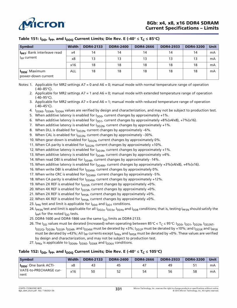
CCMTD-1725822587-9875 Micron Technology, Inc. reserves the right to change products or specifications without notice.8gb_ddr4_dram.pdf - Rev. T 09/2021 EN 2015 Micron Technology, Inc. All rights reserved.331
8Gb: x4, x8, x16 DDR4 SDRAM
Notes: 1. Applicable for MR2 settings A7 = 0 and A6 = 0; manual mode with normal temperature range of operation C).
2. Applicable for MR2 settings A7 = 1 and A6 = 0; manual mode with extended temperature range of operation C).
3. Applicable for MR2 settings A7 = 0 and A6 = 1; manual mode with reduced temperature range of operation C).
4. IDD6E, IDD6R, IDD6A values are verified by design and characterization, and may not be subject to production test.5. When additive latency is enabled for IDD0, current changes by approximately +1%.6. When additive latency is enabled for IDD1, current changes by approximately +8%(x4/x8), +7%(x16).7. When additive latency is enabled for IDD2N, current changes by approximately +1%.8. When DLL is disabled for IDD2N9. When CAL is enabled for IDD2N10. When gear-down is enabled for IDD2N, current changes by approximately 0%.11. When CA parity is enabled for IDD2N, current changes by approximately +10%.12. When additive latency is enabled for IDD3N, current changes by approximately +1%.13. When additive latency is enabled for IDD4R, current changes by approximately +4%.14. When read DBI is enabled for IDD4R, current changes by approximately -14%.15. When additive latency is enabled for IDD4W, current changes by approximately +3%(x4/x8), +4%(x16).16. When write DBI is enabled for IDD4W, current changes by approximately 0%.17. When write CRC is enabled for IDD4W, current changes by approximately -5%.18. When CA parity is enabled for IDD4W, current changes by approximately +12%.19. When 2X REF is enabled for IDD5R, current changes by approximately +0%.20. When 4X REF is enabled for IDD5R, current changes by approximately +0%.21. When 2X REF is enabled for IPP5R, current changes by approximately +0%.22. When 4X REF is enabled for IPP5R, current changes by approximately +0%.23. IPP0 test and limit is applicable for IDD0 and IDD1 conditions.24. IPP3N test and limit is applicable for all IDD2x, IDD3x, IDD4x and IDD8 conditions; that is, testing IPP3N should satisfy the
IPPs for the noted IDD tests.25. DDR4-1600 and DDR4-1866 use the same IDD limits as DDR4-2133.26. The IDD values must be derated (increased) when operating between 85 C < TC 95 C: IDD0, IDD1, IDD2N, IDD2NT,
IDD2Q, IDD3N, IDD3P, IDD4R, and IDD4W must be derated by +3%; IDD2P must be derated by +10%; and IDD5R and IPP5R must be derated by +43%; All IPP currents except IPP6x and IPP5R must be derated by +0%. These values are verified by design and characterization, and may not be subject to production test.
27. IPP6x is applicable to IDD6N, IDD6E, IDD6R and IDD6A conditions.
IPP7: Bank interleave read IPP current
x4 14 14 14 14 14 mA
x8 13 13 13 13 13 mA
x16 18 18 18 18 18 mA
IDD8: Maximum power-down current
ALL 18 18 18 18 18 mA
Table 151: IDD, IPP, and IDDQ Current Limits; Die Rev. E (-40 TC 85 C)
Symbol Width DDR4-2133 DDR4-2400 DDR4-2666 DDR4-2933 DDR4-3200 Unit
Table 152: IDD, IPP, and IDDQ Current Limits; Die Rev. E (-40 TC 105 C)
Symbol Width DDR4-2133 DDR4-2400 DDR4-2666 DDR4-2933 DDR4-3200 Unit
IDD0: One bank ACTI-VATE-to-PRECHARGE cur-rent
x8 43 45 47 49 51 mA
x16 50 52 54 56 58 mA

CCMTD-1725822587-9875 Micron Technology, Inc. reserves the right to change products or specifications without notice.8gb_ddr4_dram.pdf - Rev. T 09/2021 EN 2015 Micron Technology, Inc. All rights reserved.332
8Gb: x4, x8, x16 DDR4 SDRAM
IPP0: One bank ACTI-VATE-to-PRECHARGE IPP current
x8 3 3 3 3 3 mA
x16 4 4 4 4 4 mA
IDD1: One bank ACTI-VATE-to-READ-to- PRE-CHARGE current
x8 59 61 63 65 67 mA
x16 77 79 81 83 85 mA
IDD2N: Precharge standby current
ALL 32 33 34 35 36 mA
IDD2NT: Precharge standby ODT current
x8 40 42 44 46 48 mA
x16 47 49 53 56 59 mA
IDD2P: Precharge power-down current
ALL 26 26 26 26 26 mA
IDD2Q: Precharge quiet standby current
ALL 29 29 29 29 29 mA
IDD3N: Active standby cur-rent
x8 39 41 43 45 47 mA
x16 40 42 44 46 48 mA
IPP3N: Active standby IPP current
ALL 3 3 3 3 3 mA
IDD3P: Active power-down current
x8 33 34 35 36 37 mA
x16 34 35 36 37 38 mA
IDD4R: Burst read current x8 145 155 166 178 189 mA
x16 247 265 292 306 326 mA
IDD4W: Burst write current x8 123 132 141 151 160 mA
x16 193 210 228 245 263 mA
IDD5R: Distributed refresh current (1X REF)
ALL 96 97 98 99 100 mA
IPP5R: Distributed refresh IPP current (1X REF)
ALL 5 5 5 5 5 mA
IDD6N: Self refresh current;
C 1ALL 34 34 34 34 34 mA
IDD6E: Self refresh current;
C 2, 4ALL 95 95 95 95 95 mA
IDD6R: Self refresh current;
C 3, 4ALL 21 21 21 21 21 mA
IDD6A: Auto self refresh cur-
rent (25 C)4ALL 8.6 8.6 8.6 8.6 8.6 mA
IDD6A: Auto self refresh cur-
rent (45 C)4ALL 21 21 21 21 21 mA
IDD6A: Auto self refresh cur-
rent (75 C)4ALL 31 31 31 31 31 mA
Table 152: IDD, IPP, and IDDQ Current Limits; Die Rev. E (-40 TC 105 C)
Symbol Width DDR4-2133 DDR4-2400 DDR4-2666 DDR4-2933 DDR4-3200 Unit
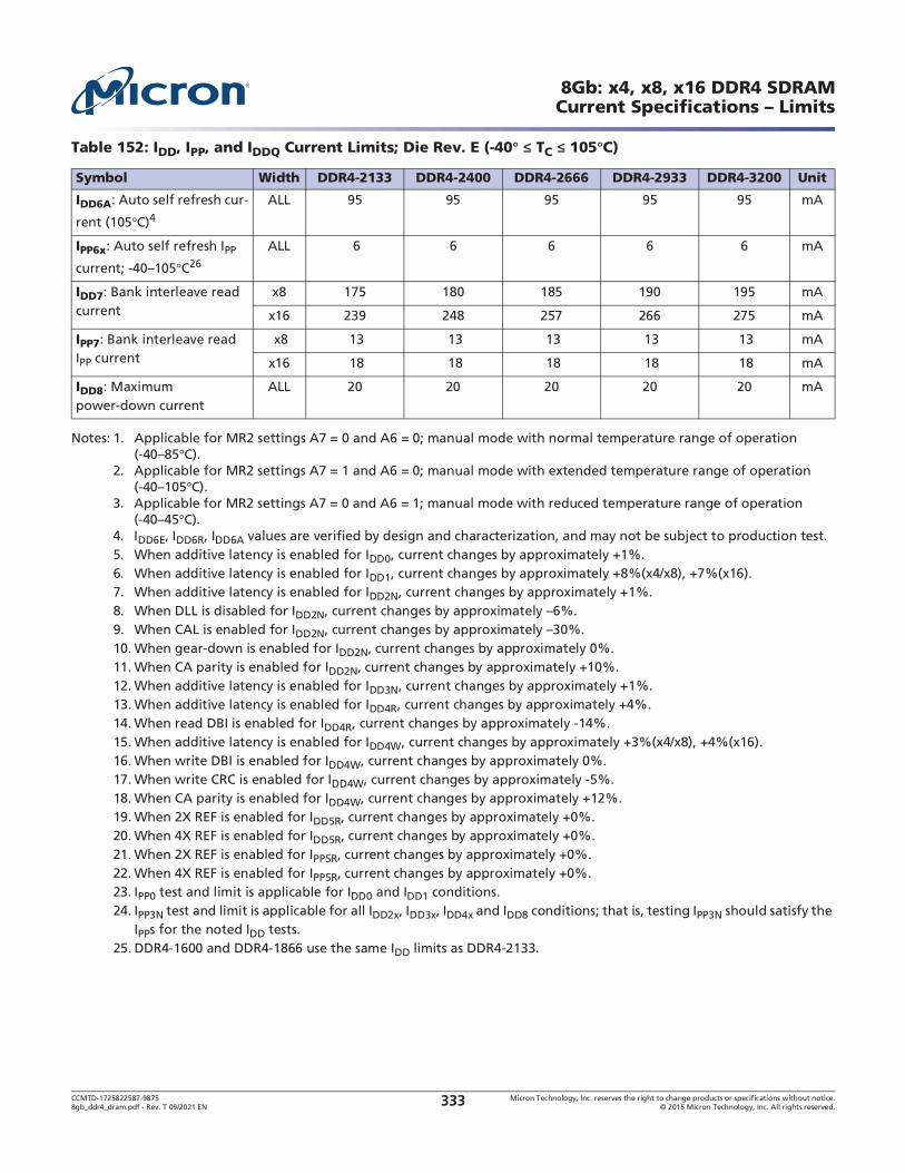
CCMTD-1725822587-9875 Micron Technology, Inc. reserves the right to change products or specifications without notice.8gb_ddr4_dram.pdf - Rev. T 09/2021 EN 2015 Micron Technology, Inc. All rights reserved.333
8Gb: x4, x8, x16 DDR4 SDRAM
Notes: 1. Applicable for MR2 settings A7 = 0 and A6 = 0; manual mode with normal temperature range of operation C).
2. Applicable for MR2 settings A7 = 1 and A6 = 0; manual mode with extended temperature range of operation C).
3. Applicable for MR2 settings A7 = 0 and A6 = 1; manual mode with reduced temperature range of operation C).
4. IDD6E, IDD6R, IDD6A values are verified by design and characterization, and may not be subject to production test.5. When additive latency is enabled for IDD0, current changes by approximately +1%.6. When additive latency is enabled for IDD1, current changes by approximately +8%(x4/x8), +7%(x16).7. When additive latency is enabled for IDD2N, current changes by approximately +1%.8. When DLL is disabled for IDD2N9. When CAL is enabled for IDD2N10. When gear-down is enabled for IDD2N, current changes by approximately 0%.11. When CA parity is enabled for IDD2N, current changes by approximately +10%.12. When additive latency is enabled for IDD3N, current changes by approximately +1%.13. When additive latency is enabled for IDD4R, current changes by approximately +4%.14. When read DBI is enabled for IDD4R, current changes by approximately -14%.15. When additive latency is enabled for IDD4W, current changes by approximately +3%(x4/x8), +4%(x16).16. When write DBI is enabled for IDD4W, current changes by approximately 0%.17. When write CRC is enabled for IDD4W, current changes by approximately -5%.18. When CA parity is enabled for IDD4W, current changes by approximately +12%.19. When 2X REF is enabled for IDD5R, current changes by approximately +0%.20. When 4X REF is enabled for IDD5R, current changes by approximately +0%.21. When 2X REF is enabled for IPP5R, current changes by approximately +0%.22. When 4X REF is enabled for IPP5R, current changes by approximately +0%.23. IPP0 test and limit is applicable for IDD0 and IDD1 conditions.24. IPP3N test and limit is applicable for all IDD2x, IDD3x, IDD4x and IDD8 conditions; that is, testing IPP3N should satisfy the
IPPs for the noted IDD tests.25. DDR4-1600 and DDR4-1866 use the same IDD limits as DDR4-2133.
IDD6A: Auto self refresh cur-
rent (105 C)4ALL 95 95 95 95 95 mA
IPP6x: Auto self refresh IPP
C26
ALL 6 6 6 6 6 mA
IDD7: Bank interleave read current
x8 175 180 185 190 195 mA
x16 239 248 257 266 275 mA
IPP7: Bank interleave read IPP current
x8 13 13 13 13 13 mA
x16 18 18 18 18 18 mA
IDD8: Maximum power-down current
ALL 20 20 20 20 20 mA
Table 152: IDD, IPP, and IDDQ Current Limits; Die Rev. E (-40 TC 105 C)
Symbol Width DDR4-2133 DDR4-2400 DDR4-2666 DDR4-2933 DDR4-3200 Unit

CCMTD-1725822587-9875 Micron Technology, Inc. reserves the right to change products or specifications without notice.8gb_ddr4_dram.pdf - Rev. T 09/2021 EN 2015 Micron Technology, Inc. All rights reserved.334
8Gb: x4, x8, x16 DDR4 SDRAM
26. IPP6x is applicable to IDD6N, IDD6E, IDD6R and IDD6A conditions.
Table 153: IDD, IPP, and IDDQ Current Limits; Die Rev. G (0 TC 85 C)
Symbol Width DDR4-2133 DDR4-2400 DDR4-2666 DDR4-2933 DDR4-3200 Unit
IDD0: One bank ACTI-VATE-to-PRECHARGE cur-rent
x4 40 43 46 49 52 mA
x8 45 48 51 54 57 mA
x16 75 80 85 90 95 mA
IPP0: One bank ACTI-VATE-to-PRECHARGE IPP current
x4, x8 3 3 3 3 3 mA
x16 4 4 4 4 4 mA
IDD1: One bank ACTI-VATE-to-READ-to- PRE-CHARGE current
x4 52 55 58 61 64 mA
x8 57 60 63 66 69 mA
x16 95 100 105 110 115 mA
IDD2N: Precharge standby current
ALL 33 34 35 36 37 mA
IDD2NT: Precharge standby ODT current
x4, x8 45 50 50 55 60 mA
x16 67 75 75 78 81 mA
IDD2P: Precharge power-down current
ALL 25 25 25 25 25 mA
IDD2Q: Precharge quiet standby current
ALL 30 30 30 30 30 mA
IDD3N: Active standby cur-rent
x4 40 43 46 49 52 mA
x8 45 48 51 54 56 mA
x16 49 52 55 58 61 mA
IPP3N: Active standby IPP current
ALL 3 3 3 3 3 mA
IDD3P: Active power-down current
x4 30 32 34 36 38 mA
x8 35 37 39 41 43 mA
x16 39 41 43 45 47 mA
IDD4R: Burst read current x4 100 110 121 132 143 mA
x8 125 135 146 157 168 mA
x16 225 243 263 283 302 mA
IDD4W: Burst write current x4 100 108 117 126 135 mA
x8 120 128 137 146 155 mA
x16 218 233 249 266 283 mA
IDD5R: Distributed refresh current (1X REF)
x4, x8 56 58 61 64 66 mA
x16 61 64 67 69 72 mA
IPP5R: Distributed refresh IPP current (1X REF)
ALL 5 5 5 5 5 mA
IDD6N: Self refresh current;
C 1ALL 31 31 31 31 31 mA

CCMTD-1725822587-9875 Micron Technology, Inc. reserves the right to change products or specifications without notice.8gb_ddr4_dram.pdf - Rev. T 09/2021 EN 2015 Micron Technology, Inc. All rights reserved.335
8Gb: x4, x8, x16 DDR4 SDRAM
Notes: 1. Applicable for MR2 settings A7 = 0 and A6 = 0; manual mode with normal temperature range of operation C).
2. Applicable for MR2 settings A7 = 1 and A6 = 0; manual mode with extended temperature range of operation C).
3. Applicable for MR2 settings A7 = 0 and A6 = 1; manual mode with reduced temperature range of operation C).
4. IDD6E, IDD6R, IDD6A values are verified by design and characterization, and may not be subject to production test.5. When additive latency is enabled for IDD0, current changes by approximately 0%.6. When additive latency is enabled for IDD1, current changes by approximately +5%(x4/x8), +4%(x16).7. When additive latency is enabled for IDD2N, current changes by approximately 0%.8. When DLL is disabled for IDD2N9. When CAL is enabled for IDD2N10. When gear-down is enabled for IDD2N, current changes by approximately 0%.11. When CA parity is enabled for IDD2N, current changes by approximately +7%.12. When additive latency is enabled for IDD3N, current changes by approximately +1%.13. When additive latency is enabled for IDD4R, current changes by approximately +5%.14. When read DBI is enabled for IDD4R, current changes by approximately 0%.15. When additive latency is enabled for IDD4W, current changes by approximately +3%(x4/x8), +4%(x16).16. When write DBI is enabled for IDD4W, current changes by approximately 0%.17. When write CRC is enabled for IDD4W, current changes by approximately +10%(x4/x8), +10%(x16).18. When CA parity is enabled for IDD4W, current changes by approximately +12% (x8), +12% (x16).19. When 2X REF is enabled for IDD5R20. When 4X REF is enabled for IDD5R
IDD6E: Self refresh current;
C 2, 4ALL 36 36 36 36 36 mA
IDD6R: Self refresh current; 3, 4
ALL 21 21 21 21 21 mA
IDD6A: Auto self refresh cur-
rent (25 C)4ALL 8.6 8.6 8.6 8.6 8.6 mA
IDD6A: Auto self refresh cur-
rent (45 C)4ALL 21 21 21 21 21 mA
IDD6A: Auto self refresh cur-
rent (75 C)4ALL 31 31 31 31 31 mA
IPP6x: Auto self refresh IPP
C25
ALL 5 5 5 5 5 mA
IDD7: Bank interleave read current
x4 175 185 200 215 230 mA
x8 170 175 180 185 190 mA
x16 239 249 259 269 279 mA
IPP7: Bank interleave read IPP current
x4 16 17 18 19 20 mA
x8 15 15 15 15 15 mA
x16 20 20 20 20 20 mA
IDD8: Maximum power-down current
ALL 25 25 25 25 25 mA
Table 153: IDD, IPP, and IDDQ Current Limits; Die Rev. G (0 TC 85 C)
Symbol Width DDR4-2133 DDR4-2400 DDR4-2666 DDR4-2933 DDR4-3200 Unit

CCMTD-1725822587-9875 Micron Technology, Inc. reserves the right to change products or specifications without notice.8gb_ddr4_dram.pdf - Rev. T 09/2021 EN 2015 Micron Technology, Inc. All rights reserved.336
8Gb: x4, x8, x16 DDR4 SDRAM
21. IPP0 test and limit is applicable for IDD0 and IDD1 conditions.22. IPP3N test and limit is applicable for all IDD2x, IDD3x, IDD4x and IDD8 conditions; that is, testing IPP3N should satisfy the
IPPs for the noted IDD tests.23. DDR4-1600 and DDR4-1866 use the same IDD limits as DDR4-2133.24. The IDD values must be derated (increased) when operated outside of the range 0 C TC 85 C:
When TC < 0 C: IDD2P, and IDD3P must be derated by 6%; IDD4R and IDD4W must be derated by 4%; IDD6, IDD6ET, and IDD7 must be derated by 11%.When TC > 85 C: IDD0, IDD1, IDD2N, IDD2NT, IDD2Q, IDD3N, IDD3P, IDD4R, IDD4W, and IDD5R must be derated by 3%; IDD2P must be derated by 40%. These values are verified by design and characterization, and may not be subject to production test.
25. IPP6x is applicable to IDD6N, IDD6E, IDD6R and IDD6A conditions.
Table 154: IDD, IPP, and IDDQ Current Limits; Die Rev. H (0 TC 85 C)
Symbol Width DDR4-2133 DDR4-2400 DDR4-2666 DDR4-2933 DDR4-3200 Unit
IDD0: One bank ACTI-VATE-to-PRECHARGE cur-rent
x4 55 55 57 60 na mA
x8 55 55 60 61 na mA
x16 75 75 80 83 na mA
IPP0: One bank ACTI-VATE-to-PRECHARGE IPP current
x4, x8 3 3 3 3 na mA
x16 5 5 5 5 na mA
IDD1: One bank ACTI-VATE-to-READ-to- PRE-CHARGE current
x4 68 68 71 75 na mA
x8 68 68 73 75 na mA
x16 100 100 107 111 na mA
IDD2N: Precharge standby current
ALL 39 39 42 43 na mA
IDD2NT: Precharge standby ODT current
x4, x8 43 43 48 50 na mA
x16 47 47 50 54 na mA
IDD2P: Precharge power-down current
ALL 27 27 27 27 na mA
IDD2Q: Precharge quiet standby current
ALL 34 34 36 36 na mA
IDD3N: Active standby cur-rent
x4 46 47 49 52 na mA
x8 46 47 49 52 na mA
x16 46 47 50 53 na mA
IPP3N: Active standby IPP current
ALL 4.5 4.5 4.5 4.5 na mA
IDD3P: Active power-down current
x4 34 34 34 37 na mA
x8 36 36 39 40 na mA
x16 37 37 40 42 na mA
IDD4R: Burst read current x4 135 135 157 173 na mA
x8 147 147 174 188 na mA
x16 259 259 312 341 na mA

CCMTD-1725822587-9875 Micron Technology, Inc. reserves the right to change products or specifications without notice.8gb_ddr4_dram.pdf - Rev. T 09/2021 EN 2015 Micron Technology, Inc. All rights reserved.337
8Gb: x4, x8, x16 DDR4 SDRAM
Notes: 1. Applicable for MR2 settings A7 = 0 and A6 = 0; manual mode with normal temperature range of operation C).
2. Applicable for MR2 settings A7 = 1 and A6 = 0; manual mode with extended temperature range of operation C).
3. Applicable for MR2 settings A7 = 0 and A6 = 1; manual mode with reduced temperature range of operation C).
4. IDD6E, IDD6R, IDD6A values are verified by design and characterization, and may not be subject to production test.5. When additive latency is enabled for IDD0, current changes by approximately 0%.6. When additive latency is enabled for IDD1, current changes by approximately +5%(x4/x8), +4%(x16).7. When additive latency is enabled for IDD2N, current changes by approximately 0%.
IDD4W: Burst write current x4 163 163 192 210 na mA
x8 181 181 217 234 na mA
x16 298 298 359 392 na mA
IDD5R: Distributed refresh current (1X REF)
x4 49 49 51 53 na mA
x8 49 49 51 53 na mA
x16 49 49 52 54 na mA
IPP5R: Distributed refresh IPP current (1X REF)
ALL 5.5 5.5 5.5 5.5 na mA
IDD6N: Self refresh current;
C 1ALL 36 36 36 36 na mA
IDD6E: Self refresh current;
C 2, 4x4, x8 48 48 49 49 na mA
x16 50 50 50 51 na mA
IDD6R: Self refresh current; 3, 4
ALL 26 26 26 26 na mA
IDD6A: Auto self refresh cur-
rent (25 C)4ALL 15 15 15 15 na mA
IDD6A: Auto self refresh cur-
rent (45 C)4ALL 26 26 26 26 na mA
IDD6A: Auto self refresh cur-
rent (75 C)4ALL 36 36 36 36 na mA
IPP6x: Auto self refresh IPP
C25
ALL 5 5 5 5 na mA
IDD7: Bank interleave read current
x4 278 278 388 369 na mA
x8 228 228 240 244 na mA
x16 311 311 321 331 na mA
IPP7: Bank interleave read IPP current
x4 21 21 26 28 na mA
x8 16 16 16 16 na mA
x16 22 22 22 22 na mA
IDD8: Maximum power-down current
ALL 21 21 21 21 na mA
Table 154: IDD, IPP, and IDDQ Current Limits; Die Rev. H (0 TC 85 C)
Symbol Width DDR4-2133 DDR4-2400 DDR4-2666 DDR4-2933 DDR4-3200 Unit

CCMTD-1725822587-9875 Micron Technology, Inc. reserves the right to change products or specifications without notice.8gb_ddr4_dram.pdf - Rev. T 09/2021 EN 2015 Micron Technology, Inc. All rights reserved.338
8Gb: x4, x8, x16 DDR4 SDRAM
8. When DLL is disabled for IDD2N9. When CAL is enabled for IDD2N10. When gear-down is enabled for IDD2N, current changes by approximately 0%.11. When CA parity is enabled for IDD2N, current changes by approximately +7%.12. When additive latency is enabled for IDD3N, current changes by approximately +1%.13. When additive latency is enabled for IDD4R, current changes by approximately +5%.14. When read DBI is enabled for IDD4R, current changes by approximately 0%.15. When additive latency is enabled for IDD4W, current changes by approximately +3%(x4/x8), +4%(x16).16. When write DBI is enabled for IDD4W, current changes by approximately 0%.17. When write CRC is enabled for IDD4W, current changes by approximately +10%(x4/x8), +10%(x16).18. When CA parity is enabled for IDD4W, current changes by approximately +12% (x8), +12% (x16).19. When 2X REF is enabled for IDD5R20. When 4X REF is enabled for IDD5R21. IPP0 test and limit is applicable for IDD0 and IDD1 conditions.22. IPP3N test and limit is applicable for all IDD2x, IDD3x, IDD4x and IDD8 conditions; that is, testing IPP3N should satisfy the
IPPs for the noted IDD tests.23. DDR4-1600 and DDR4-1866 use the same IDD limits as DDR4-2133.24. The IDD values must be derated (increased) when operated outside of the range 0 C TC 85 C:
When TC < 0 C: IDD2P, and IDD3P must be derated by 6%; IDD4R and IDD4W must be derated by 4%; IDD6, IDD6ET, and IDD7 must be derated by 11%.When TC > 85 C: IDD0, IDD1, IDD2N, IDD2NT, IDD2Q, IDD3N, IDD3P, IDD4R, IDD4W, and IDD5R must be derated by 3%; IDD2P must be derated by 40%. These values are verified by design and characterization, and may not be subject to production test.
25. IPP6x is applicable to IDD6N, IDD6E, IDD6R and IDD6A conditions.
Table 155: IDD, IPP, and IDDQ Current Limits; Die Rev. J (-40 TC 85 C)
Symbol Width DDR4-2133 DDR4-2400 DDR4-2666 DDR4-2933 DDR4-3200 Unit
IDD0: One bank ACTI-VATE-to-PRECHARGE cur-rent
x4 35 37 39 41 43 mA
x8 37 39 41 43 44 mA
x16 44 46 48 50 52 mA
IPP0: One bank ACTI-VATE-to-PRECHARGE IPP current
x4, x8 3 3 3 3 3 mA
x16 4 4 4 4 4 mA
IDD1: One bank ACTI-VATE-to-READ-to- PRE-CHARGE current
x4 48 50 51 53 55 mA
x8 52 54 56 58 60 mA
x16 68 70 72 74 76 mA
IDD2N: Precharge standby current
ALL 28 29 30 30 31 mA
IDD2NT: Precharge standby ODT current
x4, x8 34 36 38 40 42 mA
x16 41 44 47 50 53 mA
IDD2P: Precharge power-down current
ALL 22 22 22 22 22 mA
IDD2Q: Precharge quiet standby current
ALL 26 26 26 26 26 mA
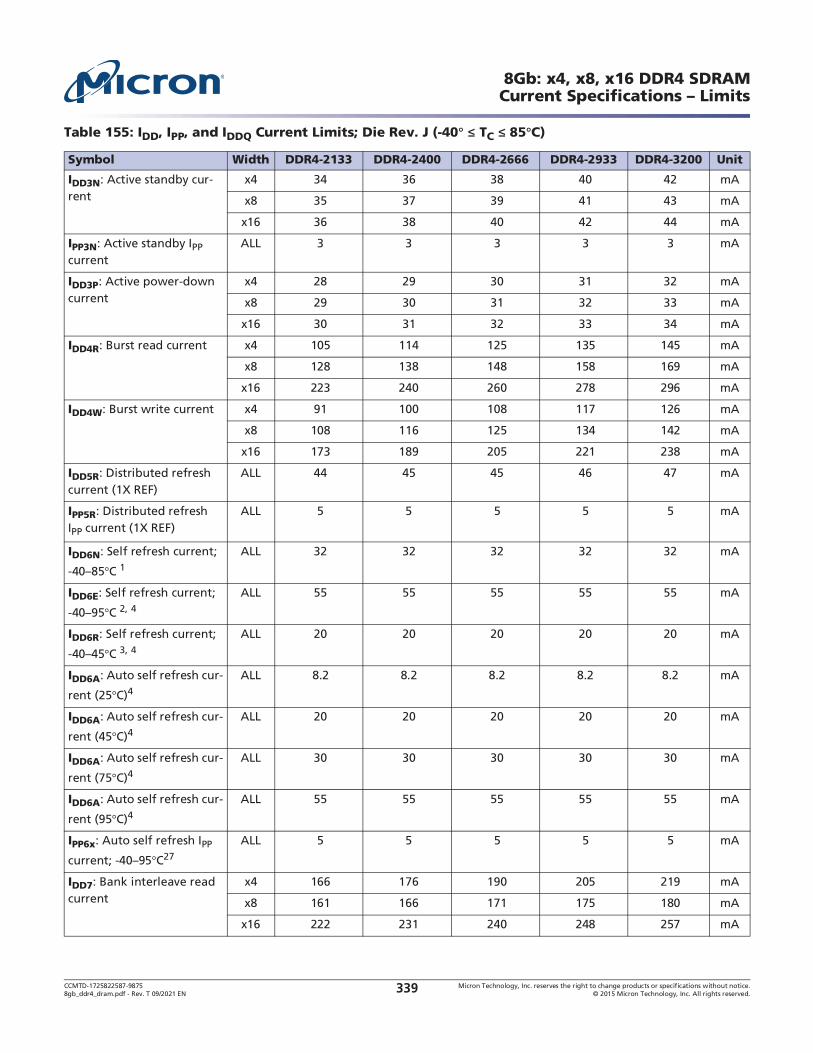
CCMTD-1725822587-9875 Micron Technology, Inc. reserves the right to change products or specifications without notice.8gb_ddr4_dram.pdf - Rev. T 09/2021 EN 2015 Micron Technology, Inc. All rights reserved.339
8Gb: x4, x8, x16 DDR4 SDRAM
IDD3N: Active standby cur-rent
x4 34 36 38 40 42 mA
x8 35 37 39 41 43 mA
x16 36 38 40 42 44 mA
IPP3N: Active standby IPP current
ALL 3 3 3 3 3 mA
IDD3P: Active power-down current
x4 28 29 30 31 32 mA
x8 29 30 31 32 33 mA
x16 30 31 32 33 34 mA
IDD4R: Burst read current x4 105 114 125 135 145 mA
x8 128 138 148 158 169 mA
x16 223 240 260 278 296 mA
IDD4W: Burst write current x4 91 100 108 117 126 mA
x8 108 116 125 134 142 mA
x16 173 189 205 221 238 mA
IDD5R: Distributed refresh current (1X REF)
ALL 44 45 45 46 47 mA
IPP5R: Distributed refresh IPP current (1X REF)
ALL 5 5 5 5 5 mA
IDD6N: Self refresh current;
C 1ALL 32 32 32 32 32 mA
IDD6E: Self refresh current;
C 2, 4ALL 55 55 55 55 55 mA
IDD6R: Self refresh current;
C 3, 4ALL 20 20 20 20 20 mA
IDD6A: Auto self refresh cur-
rent (25 C)4ALL 8.2 8.2 8.2 8.2 8.2 mA
IDD6A: Auto self refresh cur-
rent (45 C)4ALL 20 20 20 20 20 mA
IDD6A: Auto self refresh cur-
rent (75 C)4ALL 30 30 30 30 30 mA
IDD6A: Auto self refresh cur-
rent (95 C)4ALL 55 55 55 55 55 mA
IPP6x: Auto self refresh IPP
C27
ALL 5 5 5 5 5 mA
IDD7: Bank interleave read current
x4 166 176 190 205 219 mA
x8 161 166 171 175 180 mA
x16 222 231 240 248 257 mA
Table 155: IDD, IPP, and IDDQ Current Limits; Die Rev. J (-40 TC 85 C)
Symbol Width DDR4-2133 DDR4-2400 DDR4-2666 DDR4-2933 DDR4-3200 Unit

CCMTD-1725822587-9875 Micron Technology, Inc. reserves the right to change products or specifications without notice.8gb_ddr4_dram.pdf - Rev. T 09/2021 EN 2015 Micron Technology, Inc. All rights reserved.340
8Gb: x4, x8, x16 DDR4 SDRAM
Notes: 1. Applicable for MR2 settings A7 = 0 and A6 = 0; manual mode with normal temperature range of operation C).
2. Applicable for MR2 settings A7 = 1 and A6 = 0; manual mode with extended temperature range of operation C).
3. Applicable for MR2 settings A7 = 0 and A6 = 1; manual mode with reduced temperature range of operation C).
4. IDD6E, IDD6R, IDD6A values are verified by design and characterization, and may not be subject to production test.5. When additive latency is enabled for IDD0, current changes by approximately +1%.6. When additive latency is enabled for IDD1, current changes by approximately +8%(x4/x8), +7%(x16).7. When additive latency is enabled for IDD2N, current changes by approximately +1%.8. When DLL is disabled for IDD2N9. When CAL is enabled for IDD2N10. When gear-down is enabled for IDD2N, current changes by approximately 0%.11. When CA parity is enabled for IDD2N, current changes by approximately +13%.12. When additive latency is enabled for IDD3N, current changes by approximately +2%.13. When additive latency is enabled for IDD4R, current changes by approximately +4(x4/x8), +3%(x16).14. When read DBI is enabled for IDD4R, current changes by approximately -14%(x4/x8), -20%(x16).15. When additive latency is enabled for IDD4W, current changes by approximately +4%(x4/x8), +3%(x16).16. When write DBI is enabled for IDD4W, current changes by approximately 0%.17. When write CRC is enabled for IDD4W, current changes by approximately -5%.18. When CA parity is enabled for IDD4W, current changes by approximately +12%.19. When 2X REF is enabled for IDD5R, current changes by approximately +0%.20. When 4X REF is enabled for IDD5R, current changes by approximately +0%.21. When 2X REF is enabled for IPP5R, current changes by approximately +0%.22. When 4X REF is enabled for IPP5R, current changes by approximately +0%.23. IPP0 test and limit is applicable for IDD0 and IDD1 conditions.24. IPP3N test and limit is applicable for all IDD2x, IDD3x, IDD4x and IDD8 conditions; that is, testing IPP3N should satisfy the
IPPs for the noted IDD tests.25. DDR4-1600 and DDR4-1866 use the same IDD limits as DDR4-2133.26. The IDD values must be derated (increased) when operating between 85 C < TC 95 C: IDD0, IDD1, IDD2N, IDD2NT,
IDD2Q, IDD3N, IDD3P, IDD4R, and IDD4W, must be derated by +3%; IDD2P must be derated by +13%; IDD5R and IPP5R must be derated by +43%; All IPP currents except IPP6x and IPP5R must be derated by +0%. These values are verified by design and characterization, and may not be subject to production test.
27. IPP6x is applicable to IDD6N, IDD6E, IDD6R and IDD6A conditions.
IPP7: Bank interleave read IPP current
x4 11 11 11 11 11 mA
x8 10 10 10 10 13 mA
x16 15 15 15 15 15 mA
IDD8: Maximum power-down current
ALL 18 18 18 18 18 mA
Table 155: IDD, IPP, and IDDQ Current Limits; Die Rev. J (-40 TC 85 C)
Symbol Width DDR4-2133 DDR4-2400 DDR4-2666 DDR4-2933 DDR4-3200 Unit
Table 156: IDD, IPP, and IDDQ Current Limits; Die Rev. R (-40 TC 85 C)
Symbol Width DDR4-2133 DDR4-2400 DDR4-2666 DDR4-2933 DDR4-3200 Unit
IDD0: One bank ACTI-VATE-to-PRECHARGE cur-rent
x4 38 40 42 44 46 mA
x8 40 42 44 46 48 mA
x16 51 53 55 57 59 mA

CCMTD-1725822587-9875 Micron Technology, Inc. reserves the right to change products or specifications without notice.8gb_ddr4_dram.pdf - Rev. T 09/2021 EN 2015 Micron Technology, Inc. All rights reserved.341
8Gb: x4, x8, x16 DDR4 SDRAM
IPP0: One bank ACTI-VATE-to-PRECHARGE IPP current
x4, x8 4 4 4 4 4 mA
x16 5 5 5 5 5 mA
IDD1: One bank ACTI-VATE-to-READ-to- PRE-CHARGE current
x4 43 45 47 49 51 mA
x8 47 49 51 53 55 mA
x16 61 63 65 67 69 mA
IDD2N: Precharge standby current
ALL 34 35 36 37 38 mA
IDD2NT: Precharge standby ODT current
x4, x8 33 35 37 39 41 mA
x16 38 40 42 44 46 mA
IDD2P: Precharge power-down current
ALL 30 30 30 30 30 mA
IDD2Q: Precharge quiet standby current
ALL 34 34 34 34 34 mA
IDD3N: Active standby cur-rent
x4 34 36 38 40 42 mA
x8 35 37 39 41 43 mA
x16 36 38 40 42 44 mA
IPP3N: Active standby IPP current
ALL 3 3 3 3 3 mA
IDD3P: Active power-down current
x4 28 29 30 31 32 mA
x8 29 30 31 32 33 mA
x16 30 31 32 33 34 mA
IDD4R: Burst read current x4 74 80 88 95 103 mA
x8 92 98 105 113 123 mA
x16 130 139 151 164 176 mA
IDD4W: Burst write current x4 62 66 70 76 82 mA
x8 79 85 91 98 106 mA
x16 102 109 119 127 138 mA
IDD5R: Distributed refresh current (1X REF)
ALL 44 45 45 46 47 mA
IPP5R: Distributed refresh IPP current (1X REF)
ALL 5 5 5 5 5 mA
IDD6N: Self refresh current;
C 1ALL 32 32 32 32 32 mA
IDD6E: Self refresh current;
C 2, 4ALL 52 52 52 52 52 mA
IDD6R: Self refresh current;
C 3, 4ALL 19 19 19 19 19 mA
Table 156: IDD, IPP, and IDDQ Current Limits; Die Rev. R (-40 TC 85 C)
Symbol Width DDR4-2133 DDR4-2400 DDR4-2666 DDR4-2933 DDR4-3200 Unit
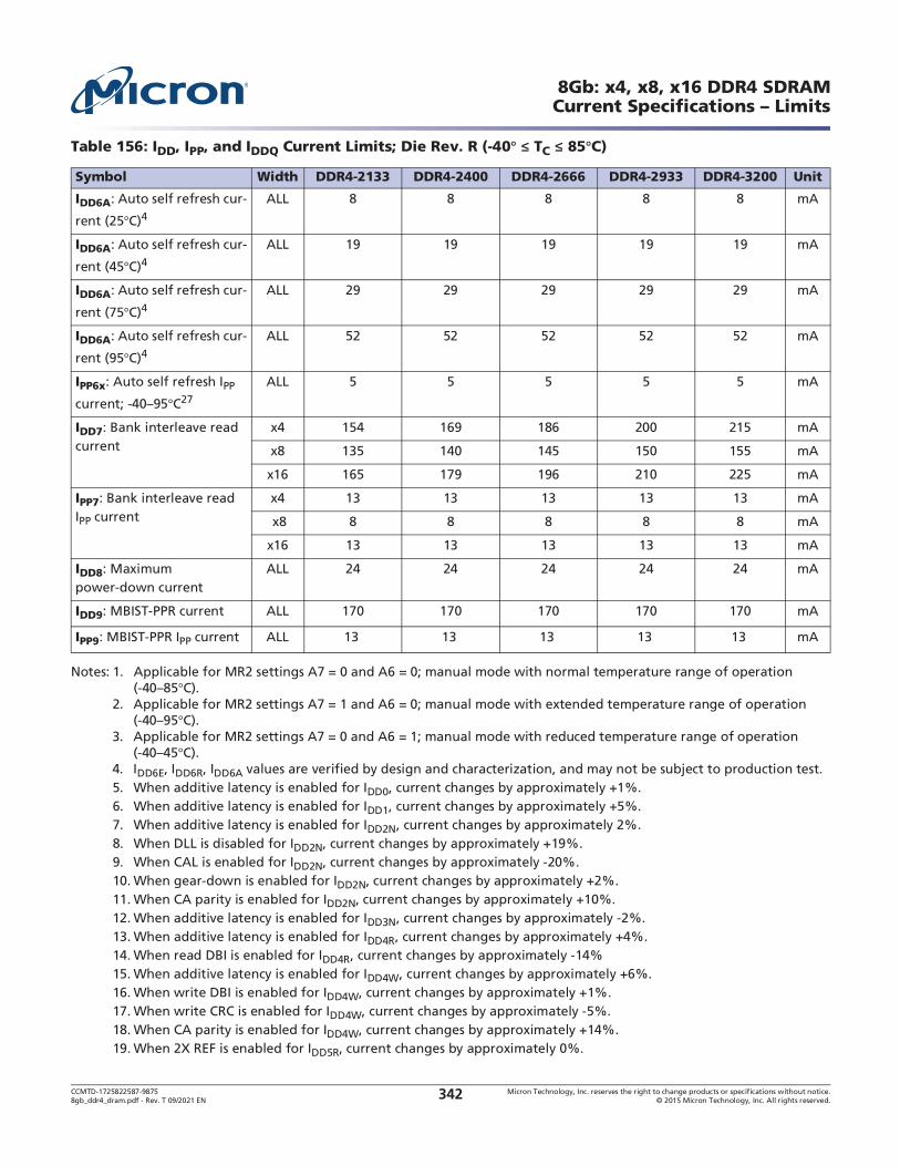
CCMTD-1725822587-9875 Micron Technology, Inc. reserves the right to change products or specifications without notice.8gb_ddr4_dram.pdf - Rev. T 09/2021 EN 2015 Micron Technology, Inc. All rights reserved.342
8Gb: x4, x8, x16 DDR4 SDRAM
Notes: 1. Applicable for MR2 settings A7 = 0 and A6 = 0; manual mode with normal temperature range of operation C).
2. Applicable for MR2 settings A7 = 1 and A6 = 0; manual mode with extended temperature range of operationC).
3. Applicable for MR2 settings A7 = 0 and A6 = 1; manual mode with reduced temperature range of operationC).
4. IDD6E, IDD6R, IDD6A values are verified by design and characterization, and may not be subject to production test.5. When additive latency is enabled for IDD0, current changes by approximately +1%.6. When additive latency is enabled for IDD1, current changes by approximately +5%.7. When additive latency is enabled for IDD2N, current changes by approximately 2%.8. When DLL is disabled for IDD2N, current changes by approximately +19%.9. When CAL is enabled for IDD2N, current changes by approximately -20%.10. When gear-down is enabled for IDD2N, current changes by approximately +2%.11. When CA parity is enabled for IDD2N, current changes by approximately +10%.12. When additive latency is enabled for IDD3N, current changes by approximately -2%.13. When additive latency is enabled for IDD4R, current changes by approximately +4%.14. When read DBI is enabled for IDD4R, current changes by approximately -14%15. When additive latency is enabled for IDD4W, current changes by approximately +6%.16. When write DBI is enabled for IDD4W, current changes by approximately +1%.17. When write CRC is enabled for IDD4W, current changes by approximately -5%.18. When CA parity is enabled for IDD4W, current changes by approximately +14%.19. When 2X REF is enabled for IDD5R, current changes by approximately 0%.
IDD6A: Auto self refresh cur-
rent (25 C)4ALL 8 8 8 8 8 mA
IDD6A: Auto self refresh cur-
rent (45 C)4ALL 19 19 19 19 19 mA
IDD6A: Auto self refresh cur-
rent (75 C)4ALL 29 29 29 29 29 mA
IDD6A: Auto self refresh cur-
rent (95 C)4ALL 52 52 52 52 52 mA
IPP6x: Auto self refresh IPP
C27
ALL 5 5 5 5 5 mA
IDD7: Bank interleave read current
x4 154 169 186 200 215 mA
x8 135 140 145 150 155 mA
x16 165 179 196 210 225 mA
IPP7: Bank interleave read IPP current
x4 13 13 13 13 13 mA
x8 8 8 8 8 8 mA
x16 13 13 13 13 13 mA
IDD8: Maximum power-down current
ALL 24 24 24 24 24 mA
IDD9: MBIST-PPR current ALL 170 170 170 170 170 mA
IPP9: MBIST-PPR IPP current ALL 13 13 13 13 13 mA
Table 156: IDD, IPP, and IDDQ Current Limits; Die Rev. R (-40 TC 85 C)
Symbol Width DDR4-2133 DDR4-2400 DDR4-2666 DDR4-2933 DDR4-3200 Unit
CCMTD-1725822587-9875 Micron Technology, Inc. reserves the right to change products or specifications without notice.8gb_ddr4_dram.pdf - Rev. T 09/2021 EN 2015 Micron Technology, Inc. All rights reserved.343
8Gb: x4, x8, x16 DDR4 SDRAM
20. When 4X REF is enabled for IDD5R, current changes by approximately 0%.21. When 2X REF is enabled for IPP5R, current changes by approximately 0%.22. When 4X REF is enabled for IPP5R, current changes by approximately 0%.23. IPP0 test and limit is applicable for IDD0 and IDD1 conditions.24. IPP3N test and limit is applicable for all IDD2x, IDD3x, IDD4x and IDD8 conditions; that is, testing IPP3N should satisfy the
IPPs for the noted IDD tests.25. DDR4-1600 and DDR4-1866 use the same IDD limits as DDR4-2133.26. The IDD values must be derated (increased) when operating between 85 C < TC 95 C: IDD0, IDD1, IDD2N ,IDD2P
,IDD2NT ,IDD2Q, IDD3N, IDD3P, IDD4R, and IDD4W, must be derated by +10%. IDD5R and IPP5R must be derated by +43%; IPP0 must be derated by +13%. IPP3N must be derated by +22%. IPP7 must be derated by +3%. These values are veri-fied by design and characterization, and may not be subject to production test.
27. IPP6x is applicable to IDD6N, IDD6E, IDD6R and IDD6A conditions.
CCMTD-1725822587-9875 Micron Technology, Inc. reserves the right to change products or specifications without notice.8gb_ddr4_dram.pdf - Rev. T 09/2021 EN 2015 Micron Technology, Inc. All rights reserved.344
8Gb: x4, x8, x16 DDR4 SDRAMSpeed Bin Tables
Speed Bin Tables
DDR4 DRAM timing is primarily covered by two types of tables: the Speed Bin tables in this section and the tables found in the Electrical Characteristics and AC Timing Parameters section. The timing parameter tables define the applicable timing specifications based on the speed rating. The Speed Bin
tables on the following pages list the tAA, tRCD, tRP, tRAS, and tRC limits of a given speed mark and are applicable to the CL settings in the lower half of the table provided they are applied in the correct clock range, which is noted.
Backward Compatibility
Although the speed bin tables list the slower data rates, tAA, CL, and CWL, it is difficult to determine
whether a faster speed bin supports all of the tAA, CL, and CWL combinations across all the data rates of a slower speed bin. To assist in this process, please refer to the Backward Compatibility table.

CCM
TD-1725822587-9875
Micro
n Techno
log
y, Inc. reserves the rig
ht to ch
ange p
rod
ucts or sp
ecifications w
itho
ut n
otice.
8gb
_ddr4_d
ram.p
df - Rev. T 09/2021 EN
2015 Micron
Techn
olog
y, Inc. A
ll rights reserved.
345
8Gb
: x4
, x8
, x16
DD
R4
SD
RA
MSp
eed
Bin
Table
s
Table 157: Backward Compatibility
Note 1 applies to the entire table.
Notes: 1. The backward compatibility table is not meant to guarantee that any new device will be a drop in replacement for an existing part number. Customers should review the operating conditions for any device to determine its suitability for use in their design.
2. This condition exceeds the JEDEC requirement in order to allow additional flexibility for components. However, JEDEC SPD compliance may force modules to only support the JEDEC-defined value. Refer to the SPD documentation for further clarification.
Co
mp
on
en
t Sp
eed
Bin
Speed Bin Supported
-125 -125E -107 -107E -093 -093E -083D -083 -083E -075D -075 -075E -068D -068 -068E -062 -062E -062Y
-125 yes
-125E yes2 yes
-107 yes yes
-107E yes2 yes yes2 yes
-093 yes yes yes
-093E yes2 yes yes2 yes yes2 yes
-083D yes yes yes yes
-083 yes yes yes yes yes
-083E yes2 yes yes2 yes yes2 yes yes2 yes2 yes
-075D yes yes yes yes yes
-075 yes yes yes yes yes yes yes
-075E yes yes yes yes yes yes yes yes yes yes yes
-068D yes yes yes yes yes yes
-068 yes yes yes yes yes yes yes yes yes
-068E yes yes yes yes yes yes yes yes yes yes
-062 yes yes yes yes yes yes yes
-062E yes yes yes yes yes yes yes yes yes yes yes
-062Y yes yes yes yes yes yes yes yes yes yes yes yes yes yes yes yes yes

CCM
TD-1725822587-9875
Micro
n Techno
log
y, Inc. reserves the rig
ht to ch
ange p
rod
ucts or sp
ecifications w
itho
ut n
otice.
8gb
_ddr4_d
ram.p
df - Rev. T 09/2021 EN
2015 Micron
Techn
olog
y, Inc. A
ll rights reserved.
346
8Gb
: x4
, x8
, x16
DD
R4
SD
RA
MSp
eed
Bin
Table
s
Table 158: DDR4-1600 Speed Bins and Operating Conditions
Notes 1 3 apply to the entire table
Notes: 1. Speed Bin table is only valid with DLL enabled.
2. When operating in 2tCK WRITE preamble mode, CWL must be programmed to a value at least 1 clock greater than the lowest CWL setting
supported in the applicable tCK range.
DDR4-1600 Speed Bin -125E -125
Unit
CL-nRCD-nRP 11-11-11 12-12-12
Parameter Symbol Min Max Min Max
Internal READ command to first data tAA 13.75
(13.50)419.006 15.00 19.006 ns
Internal READ command to first data with read DBI enabled tAA_DBI tAA (MIN) + 2nCK
tAA (MAX) +
2nCK
tAA (MIN) + 2nCK
tAA (MAX) +
2nCK
ns
ACTIVATE-to-internal READ or WRITE delay time tRCD 13.75
(13.50)415.00 ns
PRECHARGE command period tRP 13.75
(13.50)415.00 ns
ACTIVATE-to-PRECHARGE command period tRAS 35 9 tREFI 35 9 tREFI ns
ACTIVATE-to-ACTIVATE or REFRESH command period tRC5 tRAS + tRP
tRAS + tRP
ns
Data Rate Max (MT/s)
Equivalent Speed Bin
tAAmin(ns): non-DB
READ CL:nonDBI
READ CL: DBI
WRITE CWL Symbol Min Max Min Max Unit
1333 - 13.50 9 11 9 tCK (AVG)
1.500 1.9006 Reserved ns
- 15.00 10 12 tCK (AVG)
1.5006 1.9006 1.500 1.9006 ns
1600 -125E 13.75 11 13 9, 11 tCK (AVG)
1.250 <1.500 Reserved ns
-125 15.00 12 14 tCK (AVG)
1.250 <1.500 ns
Supported CL settings 9, 106, 11-12 10, 12 nCK
Supported CL settings with read DBI 11, 126, 13-14 12, 14 nCK
Supported CWL settings 9, 11 9, 11 nCK

CCM
TD-1725822587-9875
Micro
n Techno
log
y, Inc. reserves the rig
ht to ch
ange p
rod
ucts or sp
ecifications w
itho
ut n
otice.
8gb
_ddr4_d
ram.p
df - Rev. T 09/2021 EN
2015 Micron
Techn
olog
y, Inc. A
ll rights reserved.
347
8Gb
: x4
, x8
, x16
DD
R4
SD
RA
MSp
eed
Bin
Table
s
3. The programmed value of CWL must be less than or equal to the programmed value of CL.
4. This value applies to non-native tCK-CL-nRCD-nRP combinations.
5. When calculating tRC in clocks, values may not be used in a combination that violate tRAS or tRP.6. This value exceeds the JEDEC requirement in order to allow additional flexibility, especially for components. However, JEDEC SPD compliance
may force modules to only support the JEDEC defined value, please refer to the SPD documentation.

CCM
TD-1725822587-9875
Micro
n Techno
log
y, Inc. reserves the rig
ht to ch
ange p
rod
ucts or sp
ecifications w
itho
ut n
otice.
8gb
_ddr4_d
ram.p
df - Rev. T 09/2021 EN
2015 Micron
Techn
olog
y, Inc. A
ll rights reserved.
348
8Gb
: x4
, x8
, x16
DD
R4
SD
RA
MSp
eed
Bin
Table
s
Table 159: DDR4-1866 Speed Bins and Operating Conditions
Notes 1 3 apply to the entire table
Notes: 1. Speed Bin table is only valid with DLL enabled.
2. When operating in 2tCK WRITE preamble mode, CWL must be programmed to a value at least 1 clock greater than the lowest CWL setting
supported in the applicable tCK range.
DDR4-1866 Speed Bin -107E -107
Unit
CL-nRCD-nRP 13-13-13 14-14-14
Parameter Symbol Min Max Min Max
Internal READ command to first data tAA 13.92
(13.50)419.006 15.00 19.006 ns
Internal READ command to first data with read DBI enabled tAA_DBI tAA (MIN) + 2nCK
tAA (MAX) +
2nCK
tAA (MIN) + 2nCK
tAA (MAX) +
2nCK
ns
ACTIVATE to internal READ or WRITE delay time tRCD 13.92
(13.50)415.00 ns
PRECHARGE command period tRP 13.92
(13.50)415.00 ns
ACTIVATE-to-PRECHARGE command period tRAS 34 9 tREFI 34 9 tREFI ns
ACTIVATE-to-ACTIVATE or REFRESH command period tRC5 tRAS + tRP
tRAS + tRP
ns
Data Rate Max (MT/s)
EquivalentSpeed Bin
tAAmin: nonDBI
READ CL:nonDBI
READ CL: DBI
WRITECWL Symbol Min Max Min Max Unit
1333 13.50 9 11 9 tCK (AVG)
1.500 1.9006 Reserved ns
15.00 10 12 tCK (AVG) 1.5006 1.9006 1.500 1.9006 ns
1600 -125E 13.75 11 13 9, 11 tCK (AVG) 1.250 <1.500 Reserved ns
-125 15.00 12 14 tCK (AVG) 1.250 <1.500 ns
1866 -107E 13.92 13 15 10, 12 tCK (AVG) 1.071 <1.250 Reserved ns
-107 15.00 14 16 tCK (AVG) 1.071 <1.250 ns
Supported CL settings 9, 106, 11 14 10, 12, 14 nCK
Supported CL settings with read DBI 11, 126, 13 16 12, 14, 16 nCK
Supported CWL settings 9 12 9 12 nCK

CCM
TD-1725822587-9875
Micro
n Techno
log
y, Inc. reserves the rig
ht to ch
ange p
rod
ucts or sp
ecifications w
itho
ut n
otice.
8gb
_ddr4_d
ram.p
df - Rev. T 09/2021 EN
2015 Micron
Techn
olog
y, Inc. A
ll rights reserved.
349
8Gb
: x4
, x8
, x16
DD
R4
SD
RA
MSp
eed
Bin
Table
s
3. The programmed value of CWL must be less than or equal to the programmed value of CL.
4. This value applies to non-native tCK-CL-nRCD-nRP combinations.
5. When calculating tRC in clocks, values may not be used in a combination that violate tRAS or tRP.6. This value exceeds the JEDEC requirement in order to allow additional flexibility, especially for components. However, JEDEC SPD compliance
may force modules to only support the JEDEC defined value, please refer to the SPD documentation.

CCM
TD-1725822587-9875
Micro
n Techno
log
y, Inc. reserves the rig
ht to ch
ange p
rod
ucts or sp
ecifications w
itho
ut n
otice.
8gb
_ddr4_d
ram.p
df - Rev. T 09/2021 EN
2015 Micron
Techn
olog
y, Inc. A
ll rights reserved.
350
8Gb
: x4
, x8
, x16
DD
R4
SD
RA
MSp
eed
Bin
Table
s
Table 160: DDR4-2133 Speed Bins and Operating Conditions
Notes 1 3 apply to the entire table
Notes: 1. Speed Bin table is only valid with DLL enabled.
DDR4-2133 Speed Bin -093E -093
Unit
CL-nRCD-nRP 15-15-15 16-16-16
Parameter Symbol Min Max Min Max
Internal READ command to first data tAA 14.06
(13.50)419.006 15.00 19.006 ns
Internal READ command to first data with read DBI enabled tAA_DBI tAA (MIN) + 3nCK
tAA (MAX) +
3nCK
tAA (MIN) + 3nCK
tAA (MAX) +
3nCK
ns
ACTIVATE to internal READ or WRITE delay time tRCD 14.06
(13.50)415.00 ns
PRECHARGE command period tRP 14.06
(13.50)415.00 ns
ACTIVATE-to-PRECHARGE command period tRAS 33 9 tREFI 33 9 tREFI ns
ACTIVATE-to-ACTIVATE or REFRESH command period tRC5 tRAS + tRP
tRAS + tRP
ns
Data Rate Max (MT/s)
EquivalentSpeed Bin
tAAmin (ns): non-DBI
READ CL:non-DBI
READ CL:DBI
WRITECWL Symbol Min Max Min Max Unit
1333 13.50 9 11 9 tCK (AVG) 1.500 1.9006 Reserved ns
15.00 10 12 tCK (AVG) 1.5006 1.9006 1.500 1.9006 ns
1600 -125E 13.75 11 13 9, 11 tCK (AVG) 1.250 <1.500 Reserved ns
-125 15.00 12 14 tCK (AVG) 1.250 <1.500 ns
1866 -107E 13.92 13 15 10, 12 tCK (AVG) 1.071 <1.250 Reserved ns
-107 15.00 14 16 tCK (AVG) 1.071 <1.250 ns
2133 -093E 14.06 15 18 11, 14 tCK (AVG) 0.937 <1.071 Reserved ns
-093 15.00 16 19 tCK (AVG) 0.937 <1.071 ns
Supported CL settings 9, 106, 11 16 10, 12, 14, 16 nCK
Supported CL settings with read DBI 11, 126, 13 16, 18-19 12, 14, 16, 19 nCK
Supported CWL settings 9, 10, 11, 12, 14 9, 10, 11, 12, 14 nCK
CCM
TD-1725822587-9875
Micro
n Techno
log
y, Inc. reserves the rig
ht to ch
ange p
rod
ucts or sp
ecifications w
itho
ut n
otice.
8gb
_ddr4_d
ram.p
df - Rev. T 09/2021 EN
2015 Micron
Techn
olog
y, Inc. A
ll rights reserved.
351
8Gb
: x4
, x8
, x16
DD
R4
SD
RA
MSp
eed
Bin
Table
s
2. When operating in 2tCK WRITE preamble mode, CWL must be programmed to a value at least 1 clock greater than the lowest CWL setting
supported in the applicable tCK range.3. The programmed value of CWL must be less than or equal to the programmed value of CL.
4. This value applies to non-native tCK-CL-nRCD-nRP combinations.
5. When calculating tRC in clocks, values may not be used in a combination that violate tRAS or tRP.6. This value exceeds the JEDEC requirement in order to allow additional flexibility, especially for components. However, JEDEC SPD compliance
may force modules to only support the JEDEC defined value, please refer to the SPD documentation.

CCM
TD-1725822587-9875
Micro
n Techno
log
y, Inc. reserves the rig
ht to ch
ange p
rod
ucts or sp
ecifications w
itho
ut n
otice.
8gb
_ddr4_d
ram.p
df - Rev. T 09/2021 EN
2015 Micron
Techn
olog
y, Inc. A
ll rights reserved.
352
8Gb
: x4
, x8
, x16
DD
R4
SD
RA
MSp
eed
Bin
Table
s
Table 161: DDR4-2400 Speed Bins and Operating Conditions
Notes 1 3 apply to the entire table
DDR4-2400 Speed Bin -083E -083 -083D
Unit
CL-nRCD-nRP 16-16-16 17-17-17 18-18-18
Parameter Symbol Min Max Min Max Min Max
Internal READ command to first data tAA 13.32 19.006 14.16
(13.75)419.006 15.00 19.006 ns
Internal READ command to first data with read DBI enabled tAA_DBI tAA (MIN) + 3nCK
tAA (MAX) +
3nCK
tAA (MIN) + 3nCK
tAA (MAX) +
3nCK
tAA (MIN) + 3nCK
tAA (MAX) +
3nCK
ns
ACTIVATE to internal READ or WRITE delay time tRCD 13.32 14.16
(13.75)415.00 19.00 ns
PRECHARGE command period tRP 13.32 14.16
(13.75)415.00 19.00 ns
ACTIVATE-to-PRECHARGE command period tRAS 32 9 tREFI 32 9 tREFI 32 9 tREFI ns
ACTIVATE-to-ACTIVATE or REFRESH command period tRC5 tRAS + tRP
tRAS + tRP
tRAS + tRP
ns
Data Rate Max (MT/s)
EquivalentSpeed Bin
tAAmin (ns):
non-DBI
READ CL:non-DBI
READ CL: DBI
WRITECWL Symbol Min Max Min Max Min Max Unit
1333 13.50 9 11 9 tCK (AVG) 1.500 1.9006 Reserved Reserved ns
15.00 10 12 tCK (AVG) 1.5006 1.9006 1.500 1.9006 1.500 1.9006 ns
1600 -125E 13.75 11 13 9, 11 tCK (AVG) 1.250 <1.500 1.250 <1.500 Reserved ns
-125 15.00 12 14 tCK (AVG) 1.250 <1.500 ns
1866 -107E 13.92 13 15 10, 12 tCK (AVG) 1.071 <1.250 1.071 <1.250 Reserved ns
-107 15.00 14 16 tCK (AVG) 1.071 <1.250 ns
2133 -093E 14.06 15 18 11, 14 tCK (AVG) 0.937 <1.071 0.937 <1.071 Reserved ns
-093 15.00 16 19 tCK (AVG) 0.937 <1.071 ns
2400 -083E 13.32 16 19 12, 16 tCK (AVG) 0.833 <0.937 Reserved Reserved ns
-083 14.16 17 20 tCK (AVG) 0.833 <0.937 ns
-083D 15.00 18 21 tCK (AVG) 0.833 <0.937 ns
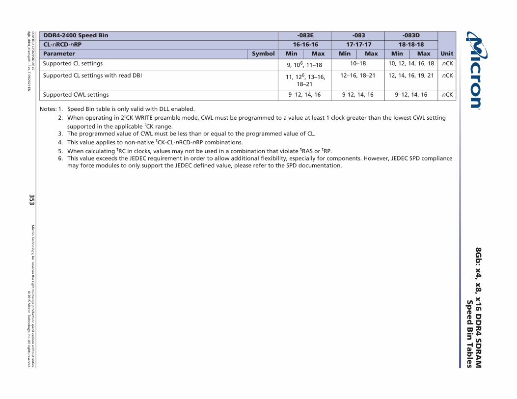
CCM
TD-1725822587-9875
Micro
n Techno
log
y, Inc. reserves the rig
ht to ch
ange p
rod
ucts or sp
ecifications w
itho
ut n
otice.
8gb
_ddr4_d
ram.p
df - Rev. T 09/2021 EN
2015 Micron
Techn
olog
y, Inc. A
ll rights reserved.
353
8Gb
: x4
, x8
, x16
DD
R4
SD
RA
MSp
eed
Bin
Table
s
Notes: 1. Speed Bin table is only valid with DLL enabled.
2. When operating in 2tCK WRITE preamble mode, CWL must be programmed to a value at least 1 clock greater than the lowest CWL setting
supported in the applicable tCK range.3. The programmed value of CWL must be less than or equal to the programmed value of CL.
4. This value applies to non-native tCK-CL-nRCD-nRP combinations.
5. When calculating tRC in clocks, values may not be used in a combination that violate tRAS or tRP.6. This value exceeds the JEDEC requirement in order to allow additional flexibility, especially for components. However, JEDEC SPD compliance
may force modules to only support the JEDEC defined value, please refer to the SPD documentation.
Supported CL settings 9, 106, 11 18 10 18 10, 12, 14, 16, 18 nCK
Supported CL settings with read DBI 11, 126, 13 16, 18 21
12 16, 18 21 12, 14, 16, 19, 21 nCK
Supported CWL settings 9 12, 14, 16 9-12, 14, 16 9 12, 14, 16 nCK
DDR4-2400 Speed Bin -083E -083 -083D
Unit
CL-nRCD-nRP 16-16-16 17-17-17 18-18-18
Parameter Symbol Min Max Min Max Min Max

CCM
TD-1725822587-9875
Micro
n Techno
log
y, Inc. reserves the rig
ht to ch
ange p
rod
ucts or sp
ecifications w
itho
ut n
otice.
8gb
_ddr4_d
ram.p
df - Rev. T 09/2021 EN
2015 Micron
Techn
olog
y, Inc. A
ll rights reserved.
354
8Gb
: x4
, x8
, x16
DD
R4
SD
RA
MSp
eed
Bin
Table
s
Table 162: DDR4-2666 Speed Bins and Operating Conditions
Notes 1 3 apply to the entire table
DDR4-2666 Speed Bin -075E -075 -075D
Unit
CL-nRCD-nRP 18-18-18 19-19-19 20-20-20
Parameter Symbol Min Max Min Max Min Max
Internal READ command to first data tAA 13.50 19.006
14.25
(13.75)419.006 15.00 19.006 ns
Internal READ command to first data with read DBI enabled tAA_DBI
tAA (MIN) + 3nCK
tAA (MAX) +
3nCK
tAA (MIN) + 3nCK
tAA (MAX) +
3nCK
tAA (MIN) + 3nCK
tAA (MAX) +
3nCK ns
ACTIVATE to internal READ or WRITE delay time tRCD 13.50
14.25
(13.75)415.00 ns
PRECHARGE command period tRP 13.50
14.25
(13.75)415.00 ns
ACTIVATE-to-PRECHARGE command period tRAS 32 9 tREFI 32 9 tREFI 32 9 tREFI ns
ACTIVATE-to-ACTIVATE or REFRESH command period tRC5
tRAS + tRP
tRAS + tRP
tRAS + tRP
ns
Data Rate Max (MT/s)
EquivalentSpeed Bin
tAAmin (ns):
non-DBI
READ CL:non-DBI
READ CL: DBI
WRITECWL Symbol Min Max Min Max Min Max Unit
1333 - 13.50 9 11 9
tCK (AVG)1.500 1.9006
Reserved Reserved ns
- 15.00 10 12 tCK (AVG) 1.500 1.9006 1.500 1.9006 ns
1600 -125E 13.75 11 13 9, 11
tCK (AVG)1.250 <1.500 1.250 <1.500
Reserved ns
-125 15.00 12 14 tCK (AVG) 1.250 <1.500 ns
1866 -107E 13.92 13 1510, 12
tCK (AVG)1.071 <1.250 1.071 <1.250
Reserved ns
-107 15.00 14 16 tCK (AVG) 1.071 <1.250 ns
2133 -093E 14.06 15 1811, 14
tCK (AVG)0.937 <1.071 0.937 <1.071
Reserved ns
-093 15.00 16 19 tCK (AVG) 0.937 <1.071 ns
2400 -083E 13.32 16 19
12, 16
tCK (AVG) Reserved ReservedReserved
ns
-083 14.16 17 20 tCK (AVG)0.833 <0.937 0.833 <0.937
ns
-083D 15.00 18 21 tCK (AVG) 0.833 <0.937 ns
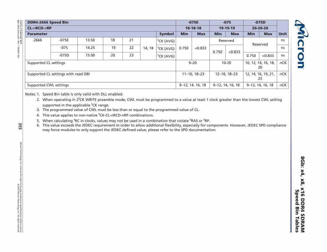
CCM
TD-1725822587-9875
Micro
n Techno
log
y, Inc. reserves the rig
ht to ch
ange p
rod
ucts or sp
ecifications w
itho
ut n
otice.
8gb
_ddr4_d
ram.p
df - Rev. T 09/2021 EN
2015 Micron
Techn
olog
y, Inc. A
ll rights reserved.
355
8Gb
: x4
, x8
, x16
DD
R4
SD
RA
MSp
eed
Bin
Table
s
Notes: 1. Speed Bin table is only valid with DLL enabled.
2. When operating in 2tCK WRITE preamble mode, CWL must be programmed to a value at least 1 clock greater than the lowest CWL setting
supported in the applicable tCK range.3. The programmed value of CWL must be less than or equal to the programmed value of CL.
4. This value applies to non-native tCK-CL-nRCD-nRP combinations.
5. When calculating tRC in clocks, values may not be used in a combination that violate tRAS or tRP.6. This value exceeds the JEDEC requirement in order to allow additional flexibility, especially for components. However, JEDEC SPD compliance
may force modules to only support the JEDEC defined value, please refer to the SPD documentation.
2666 -075E 13.50 18 21
14, 18
tCK (AVG)
0.750 <0.833
ReservedReserved
ns
-075 14.25 19 22 tCK (AVG)0.750 <0.833
ns
-075D 15.00 20 23 tCK (AVG) 0.750 <0.833 ns
Supported CL settings 9 20 10-20 10, 12, 14, 16, 18, 20
nCK
Supported CL settings with read DBI 11 16, 18 23 12 16, 18 23 12, 14, 16, 19, 21, 23
nCK
Supported CWL settings 9 12, 14, 16, 18 9 12, 14, 16, 18 9 12, 14, 16, 18 nCK
DDR4-2666 Speed Bin -075E -075 -075D
Unit
CL-nRCD-nRP 18-18-18 19-19-19 20-20-20
Parameter Symbol Min Max Min Max Min Max

CCM
TD-1725822587-9875
Micro
n Techno
log
y, Inc. reserves the rig
ht to ch
ange p
rod
ucts or sp
ecifications w
itho
ut n
otice.
8gb
_ddr4_d
ram.p
df - Rev. T 09/2021 EN
2015 Micron
Techn
olog
y, Inc. A
ll rights reserved.
356
8Gb
: x4
, x8
, x16
DD
R4
SD
RA
MSp
eed
Bin
Table
s
Table 163: DDR4-2933 Speed Bins and Operating Conditions
Notes 1 3 apply to the entire table
DDR4-2933 Speed Bin -068E -068 -068D
Unit
CL-nRCD-nRP 20-20-20 21-21-21 22-22-22
Parameter Symbol Min Max Min Max Min Max
Internal READ command to first data tAA 13.64 19.006 14.32
(13.75)419.006 15.00 19.006 ns
Internal READ command to first data with read DBI enabled tAA_DBI tAA (MIN) + 4nCK
tAA (MAX) +
4nCK
tAA (MIN) + 4nCK
tAA (MAX) +
4nCK
tAA (MIN) + 4nCK
tAA (MAX) +
4nCK
ns
ACTIVATE-to-internal READ or WRITE delay time tRCD 13.64 14.32
(13.75)415.00 ns
PRECHARGE command period tRP 13.64 14.32
(13.75)415.00 ns
ACTIVATE-to-PRECHARGE command period tRAS 32 9 tREFI 32 9 tREFI 32 9 tREFI ns
ACTIVATE-to-ACTIVATE or REFRESH command period tRC5 tRAS + tRP
tRAS + tRP
tRAS + tRP
ns
Data Rate Max (MT/s)
Equivalent Speed Bin
tAAmin(ns):non-DBI
READ CL: non-DBI
READ CL: DBI
WRITE CWL Symbol Min Max Min Max Min Max Unit
1333 13.50 9 11 9 tCK (AVG) Reserved Reserved Reserved ns
15.00 10 12 tCK (AVG) 1.500 1.9006 1.500 1.9006 1.500 1.9006 ns
1600 -125E 13.75 11 13 9, 11 tCK (AVG) 1.250 <1.500 1.250 <1.500 Reserved ns
-125 15.00 12 14 tCK (AVG) 1.250 <1.500 ns
1866 -107E 13.92 13 15 10, 12 tCK (AVG) 1.071 <1.250 1.071 <1.250 Reserved ns
-107 15.00 14 16 tCK (AVG) 1.071 <1.250 ns
2133 -093E 14.06 15 18 11, 14 tCK (AVG) 0.937 <1.071 0.937 <1.071 Reserved ns
-093 15.00 16 19 tCK (AVG) 0.937 <1.071 ns
2400 -083E 13.32 16 19 12, 16 tCK (AVG) Reserved Reserved Reserved ns
-083 14.16 17 20 tCK (AVG) 0.833 <0.937 0.833 <0.937 ns
083D 15.00 18 21 tCK (AVG) 0.833 <0.937 ns
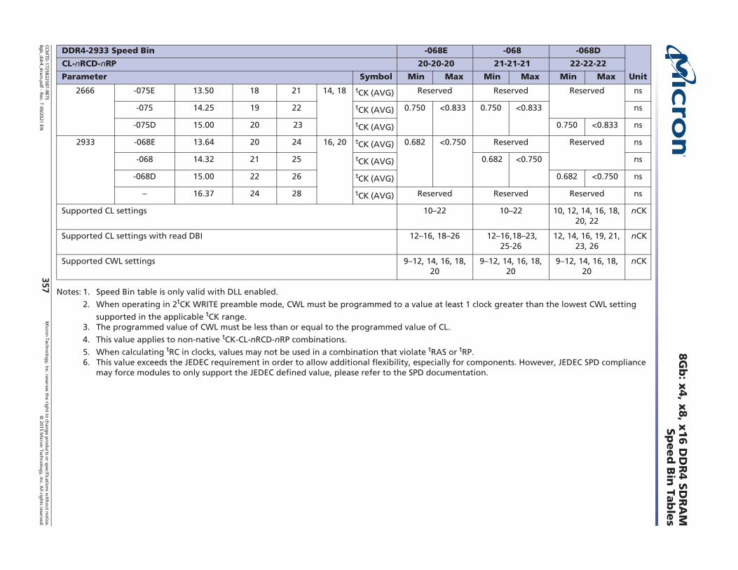
CCM
TD-1725822587-9875
Micro
n Techno
log
y, Inc. reserves the rig
ht to ch
ange p
rod
ucts or sp
ecifications w
itho
ut n
otice.
8gb
_ddr4_d
ram.p
df - Rev. T 09/2021 EN
2015 Micron
Techn
olog
y, Inc. A
ll rights reserved.
357
8Gb
: x4
, x8
, x16
DD
R4
SD
RA
MSp
eed
Bin
Table
s
Notes: 1. Speed Bin table is only valid with DLL enabled.
2. When operating in 2tCK WRITE preamble mode, CWL must be programmed to a value at least 1 clock greater than the lowest CWL setting
supported in the applicable tCK range.3. The programmed value of CWL must be less than or equal to the programmed value of CL.
4. This value applies to non-native tCK-CL-nRCD-nRP combinations.
5. When calculating tRC in clocks, values may not be used in a combination that violate tRAS or tRP.6. This value exceeds the JEDEC requirement in order to allow additional flexibility, especially for components. However, JEDEC SPD compliance
may force modules to only support the JEDEC defined value, please refer to the SPD documentation.
2666 -075E 13.50 18 21 14, 18 tCK (AVG) Reserved Reserved Reserved ns
-075 14.25 19 22 tCK (AVG) 0.750 <0.833 0.750 <0.833 ns
-075D 15.00 20 23 tCK (AVG) 0.750 <0.833 ns
2933 -068E 13.64 20 24 16, 20 tCK (AVG) 0.682 <0.750 Reserved Reserved ns
-068 14.32 21 25 tCK (AVG) 0.682 <0.750 ns
-068D 15.00 22 26 tCK (AVG) 0.682 <0.750 ns
16.37 24 28 tCK (AVG) Reserved Reserved Reserved ns
Supported CL settings 10 22 10 22 10, 12, 14, 16, 18, 20, 22
nCK
Supported CL settings with read DBI 12 16, 18 26 12 16,18 23, 25-26
12, 14, 16, 19, 21, 23, 26
nCK
Supported CWL settings 9 12, 14, 16, 18, 20
9 12, 14, 16, 18, 20
9 12, 14, 16, 18, 20
nCK
DDR4-2933 Speed Bin -068E -068 -068D
Unit
CL-nRCD-nRP 20-20-20 21-21-21 22-22-22
Parameter Symbol Min Max Min Max Min Max
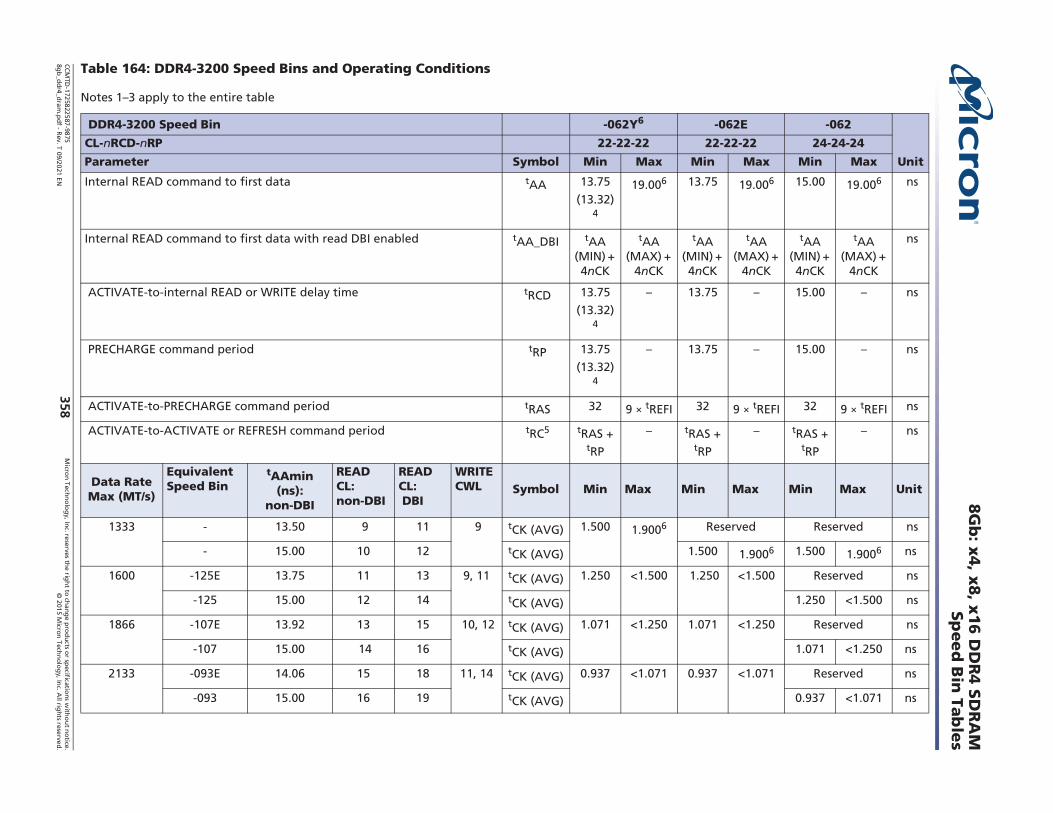
CCM
TD-1725822587-9875
Micro
n Techno
log
y, Inc. reserves the rig
ht to ch
ange p
rod
ucts or sp
ecifications w
itho
ut n
otice.
8gb
_ddr4_d
ram.p
df - Rev. T 09/2021 EN
2015 Micron
Techn
olog
y, Inc. A
ll rights reserved.
358
8Gb
: x4
, x8
, x16
DD
R4
SD
RA
MSp
eed
Bin
Table
s
Table 164: DDR4-3200 Speed Bins and Operating Conditions
Notes 1 3 apply to the entire table
DDR4-3200 Speed Bin -062Y6 -062E -062
Unit
CL-nRCD-nRP 22-22-22 22-22-22 24-24-24
Parameter Symbol Min Max Min Max Min Max
Internal READ command to first data tAA 13.75
(13.32)4
19.006 13.75 19.006 15.00 19.006 ns
Internal READ command to first data with read DBI enabled tAA_DBI tAA (MIN) + 4nCK
tAA (MAX) +
4nCK
tAA (MIN) + 4nCK
tAA (MAX) +
4nCK
tAA (MIN) + 4nCK
tAA (MAX) +
4nCK
ns
ACTIVATE-to-internal READ or WRITE delay time tRCD 13.75
(13.32)4
13.75 15.00 ns
PRECHARGE command period tRP 13.75
(13.32)4
13.75 15.00 ns
ACTIVATE-to-PRECHARGE command period tRAS 32 9 tREFI 32 9 tREFI 32 9 tREFI ns
ACTIVATE-to-ACTIVATE or REFRESH command period tRC5 tRAS + tRP
tRAS + tRP
tRAS + tRP
ns
Data Rate Max (MT/s)
EquivalentSpeed Bin
tAAmin (ns):
non-DBI
READ CL: non-DBI
READ CL: DBI
WRITE CWL Symbol Min Max Min Max Min Max Unit
1333 - 13.50 9 11 9 tCK (AVG) 1.500 1.9006 Reserved Reserved ns
- 15.00 10 12 tCK (AVG) 1.500 1.9006 1.500 1.9006 ns
1600 -125E 13.75 11 13 9, 11 tCK (AVG) 1.250 <1.500 1.250 <1.500 Reserved ns
-125 15.00 12 14 tCK (AVG) 1.250 <1.500 ns
1866 -107E 13.92 13 15 10, 12 tCK (AVG) 1.071 <1.250 1.071 <1.250 Reserved ns
-107 15.00 14 16 tCK (AVG) 1.071 <1.250 ns
2133 -093E 14.06 15 18 11, 14 tCK (AVG) 0.937 <1.071 0.937 <1.071 Reserved ns
-093 15.00 16 19 tCK (AVG) 0.937 <1.071 ns

CCM
TD-1725822587-9875
Micro
n Techno
log
y, Inc. reserves the rig
ht to ch
ange p
rod
ucts or sp
ecifications w
itho
ut n
otice.
8gb
_ddr4_d
ram.p
df - Rev. T 09/2021 EN
2015 Micron
Techn
olog
y, Inc. A
ll rights reserved.
359
8Gb
: x4
, x8
, x16
DD
R4
SD
RA
MSp
eed
Bin
Table
s
Notes: 1. Speed Bin table is only valid with DLL enabled.
2. When operating in 2tCK WRITE preamble mode, CWL must be programmed to a value at least 1 clock greater than the lowest CWL setting
supported in the applicable tCK range.3. The programmed value of CWL must be less than or equal to the programmed value of CL.
4. This value applies to non-native tCK-CL-nRCD-nRP combinations.
5. When calculating tRC in clocks, values may not be used in a combination that violate tRAS or tRP.6. This value exceeds the JEDEC requirement in order to allow additional flexibility, especially for components. However, JEDEC SPD compliance
may force modules to only support the JEDEC defined value, please refer to the SPD documentation.
2400 -083E 13.32 16 19 12, 16 tCK (AVG) 0.833 <0.937 Reserved Reserved ns
-083 14.16 17 20 tCK (AVG) 0.833 <0.937 ns
-083D 15.00 18 21 tCK (AVG) 0.833 <0.937 ns
2666 -075E 13.50 18 21 14, 18 tCK (AVG) 0.750 <0.833 Reserved Reserved ns
-075 14.25 19 22 tCK (AVG) 0.750 <0.833 ns
-075D 15.00 20 23 tCK (AVG) 0.750 <0.833 ns
2933 -068E 13.64 20 24 16, 20 tCK (AVG) Reserved Reserved Reserved ns
-068 14.32 21 25 tCK (AVG) 0.682 <0.750 0.682 <0.750 ns
-068D 15.00 22 26 tCK (AVG) 0.682 <0.750 0.682 <0.750 ns
16.37 24 28 tCK (AVG) 0.682 <0.750 ns
3200 -062E 13.75 22 26 16, 20 tCK (AVG) 0.625 <0.682 0.625 <0.682 Reserved ns
-062 15.00 24 28 tCK (AVG) 0.625 <0.682 ns
Supported CL settings 9 22, 24 10 22, 24 10, 12, 14, 16, 18, 20, 22, 24
nCK
Supported CL settings with read DBI 11 16, 18 23, 25-26, 28
12 16, 18 23, 25-26, 28
12, 14, 16, 19, 21, 23, 26, 28
nCK
Supported CWL settings 9 12, 14, 16, 18, 20
9 12, 14, 16, 18, 20
9 12, 14, 16, 18, 20
nCK
DDR4-3200 Speed Bin -062Y6 -062E -062
Unit
CL-nRCD-nRP 22-22-22 22-22-22 24-24-24
Parameter Symbol Min Max Min Max Min Max

CCMTD-1725822587-9875 Micron Technology, Inc. reserves the right to change products or specifications without notice.8gb_ddr4_dram.pdf - Rev. T 09/2021 EN 2015 Micron Technology, Inc. All rights reserved.360
8Gb: x4, x8, x16 DDR4 SDRAMRefresh Parameters By Device Density
Refresh Parameters By Device Density
Notes: 1. Users should refer to the DRAM supplier data sheet and/or the DIMM SPD to determine if the devices support these options or requirements.
Table 165: Refresh Parameters by Device Density
Parameter Symbol 2Gb 4Gb 8Gb 16Gb Unit Notes
REF command to ACT or REF com-mand time
tRFC (All bank groups) 160 260 350 350 ns
Average periodic refresh interval tREFI -40 C TC 85 C 7.8 7.8 7.8 7.8 s
85 C < TC 95 C 3.9 3.9 3.9 3.9 s 1
95 C < TC 105 C 1.95 1.95 1.95 1.95 s 1
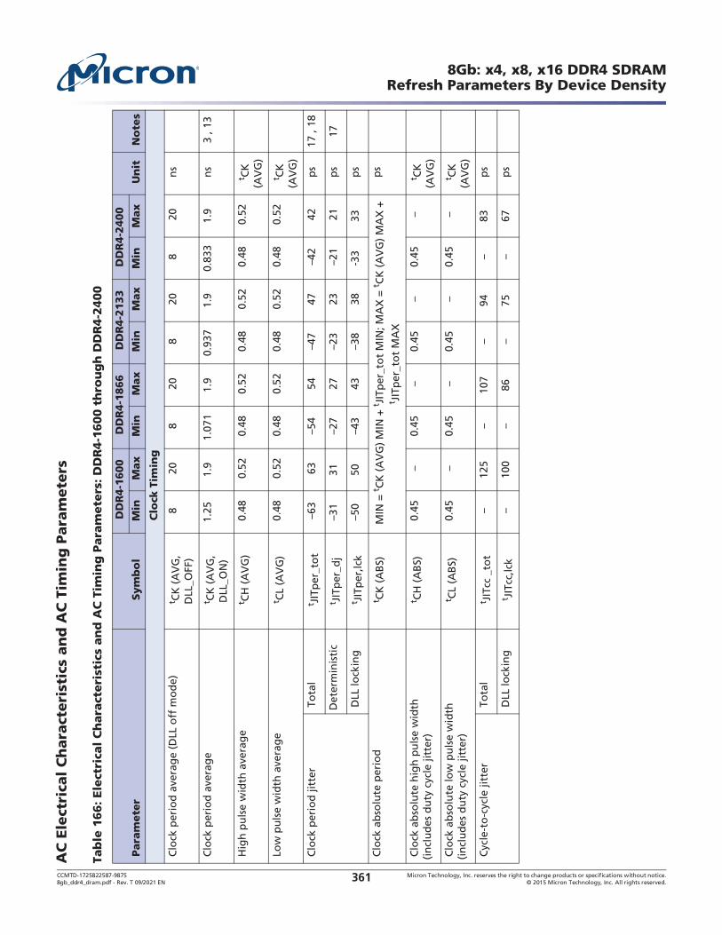
CCMTD-1725822587-9875 Micron Technology, Inc. reserves the right to change products or specifications without notice.8gb_ddr4_dram.pdf - Rev. T 09/2021 EN 2015 Micron Technology, Inc. All rights reserved.361
8Gb: x4, x8, x16 DDR4 SDRAMRefresh Parameters By Device Density
AC
Ele
ctri
cal
Ch
ara
cteri
stic
s an
d A
C T
imin
g P
ara
mete
rs
Tab
le 1
66
: Ele
ctri
cal
Ch
ara
cteri
stic
s an
d A
C T
imin
g P
ara
mete
rs: D
DR
4-1
600 t
hro
ug
h D
DR
4-2
400
Para
mete
r S
ym
bo
l
DD
R4-1
600
DD
R4-1
866
DD
R4-2
133
DD
R4-2
400
Un
it N
ote
s M
in M
ax
Min
Max
Min
Max
Min
Max
Clo
ck T
imin
g
Clo
ck p
erio
d a
vera
ge
(DLL
off
mo
de)
t CK
(A
VG
, D
LL_O
FF)
8 2
0 8
20
8 2
0 8
20
ns
Clo
ck p
erio
d a
vera
ge
t CK
(A
VG
, D
LL_O
N)
1.25
1.9
1.07
11.
90.
937
1.9
0.83
31.
9 n
s 3
, 13
Hig
h p
uls
e w
idth
ave
rag
e t C
H (
AV
G)
0.4
8 0
.52
0.4
8 0
.52
0.4
8 0
.52
0.4
8 0
.52
t CK
(A
VG
)
Lo
w p
uls
e w
idth
ave
rag
e t C
L (A
VG
) 0
.48
0.5
2 0
.48
0.5
2 0
.48
0.5
2 0
.48
0.5
2 t C
K
(AV
G)
Clo
ck p
erio
d ji
tter
To
tal
t JIT
per
_to
t
63 6
3
54 5
4
47 4
7
42 4
2 p
s17
, 18
Det
erm
inis
tic
t JIT
per
_dj
3131
27
27
23
23
21
21
ps
17
DLL
lock
ing
t JIT
per
,lck
5050
43
43
38
38
-33
33 p
s
Clo
ck a
bso
lute
per
iod
t CK
(A
BS)
MIN
= t C
K (
AV
G)
MIN
+ t J
ITp
er_t
ot
MIN
; MA
X =
t CK
(A
VG
) M
AX
+
t JIT
per
_to
t M
AX
ps
Clo
ck a
bso
lute
hig
h p
uls
e w
idth
(in
clu
des
du
ty c
ycle
jitt
er)
t CH
(A
BS)
0.4
5
0.4
5
0.4
5
0.4
5
t CK
(A
VG
)
Clo
ck a
bso
lute
low
pu
lse
wid
th
(in
clu
des
du
ty c
ycle
jitt
er)
t CL
(AB
S) 0
.45
0
.45
0
.45
0
.45
t C
K
(AV
G)
Cyc
le-t
o-c
ycle
jitt
er T
ota
l t J
ITcc
_to
t
125
10
7
94
83 p
s
DLL
lock
ing
t JIT
cc,lc
k
100
86
75
67
ps

CCM
TD-1725822587-9875
Micro
n Techno
log
y, Inc. reserves the rig
ht to ch
ange p
rod
ucts or sp
ecifications w
itho
ut n
otice.
8gb
_ddr4_d
ram.p
df - Rev. T 09/2021 EN
2015 Micron
Techn
olog
y, Inc. A
ll rights reserved.
362
8Gb
: x4
, x8
, x16
DD
R4
SD
RA
MR
efresh Pa
rame
ters B
y D
evice D
ensity
Cumulative error across 2 cycles tERR2per 92 92 79 79 69 69 61 61 ps
3 cycles tERR3per 109 109 94 94 82 82 73 73 ps
4 cycles tERR4per 121 121 104 104 91 91 81 81 ps
5 cycles tERR5per 131 131 112 112 98 98 87 87 ps
6 cycles tERR6per 139 139 119 119 104 104 92 92 ps
7 cycles tERR7per 145 145 124 124 109 109 97 97 ps
8 cycles tERR8per 151 151 129 129 113 113 101 101 ps
9 cycles tERR9per 156 156 134 134 117 117 104 104 ps
10 cycles tERR10per 160 160 137 137 120 120 107 107 ps
11 cycles tERR11per 164 164 141 141 123 123 110 110 ps
12 cycles tERR12per 168 168 144 144 126 126 112 112 ps
n = 13, 14 . . . 49, 50 cycles
tERRnper tERRnper MIN = (1 + 0.68ln[n]) tJITper_tot MIN tERRnper MAX = (1 + 0.68ln[n]) tJITper_tot MAX
ps
DQ Input Timing
Data setup time to DQS_t, DQS_c
Base (cali-brated VREF)
tDS Refer to DQ Input Receiver Specification section
(approximately 0.15tCK to 0.28tCK )
Noncalibrated VREF
tPDA_S minimum of 0.5UI UI 22
Data hold time from DQS_t, DQS_c
Base (cali-brated VREF)
tDH Refer to DQ Input Receiver Specification section
(approximately 0.15tCK to 0.28tCK )
Noncalibrated VREF
tPDA_H minimum of 0.5UI UI 22
DQ and DM minimum data pulse width for each input
tDIPW 0.58 0.58 0.58 0.58 UI
DQ Output Timing (DLL enabled)
DQS_t, DQS_c to DQ skew, per group, per access
tDQSQ 0.16 0.16 0.16 0.17 UI
DQ output hold time from DQS_t, DQS_c tQH 0.76 0.76 0.76 0.74 UI
Table 166: Electrical Characteristics and AC Timing Parameters: DDR4-1600 through DDR4-2400 (Continued)
Parameter Symbol
DDR4-1600 DDR4-1866 DDR4-2133 DDR4-2400
Unit Notes Min Max Min Max Min Max Min Max
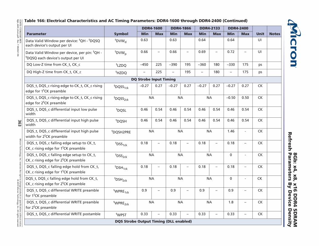
CCM
TD-1725822587-9875
Micro
n Techno
log
y, Inc. reserves the rig
ht to ch
ange p
rod
ucts or sp
ecifications w
itho
ut n
otice.
8gb
_ddr4_d
ram.p
df - Rev. T 09/2021 EN
2015 Micron
Techn
olog
y, Inc. A
ll rights reserved.
363
8Gb
: x4
, x8
, x16
DD
R4
SD
RA
MR
efresh Pa
rame
ters B
y D
evice D
ensity
Data Valid Window per device: tQH - tDQSQ each device s output per UI
tDVWd0.63 0.63 0.64 0.64 UI
Data Valid Window per device, per pin: tQH - tDQSQ each device s output per UI
tDVWp0.66 0.66 0.69 0.72 UI
DQ Low-Z time from CK_t, CK_c tLZDQ 450 225 390 195 360 180 330 175 ps
DQ High-Z time from CK_t, CK_c tHZDQ 225 195 180 175 ps
DQ Strobe Input Timing
DQS_t, DQS_c rising edge to CK_t, CK_c rising
edge for 1tCK preamble tDQSS1ck
0.27 0.27 0.27 0.27 0.27 0.27 0.27 0.27 CK
DQS_t, DQS_c rising edge to CK_t, CK_c rising
edge for 2tCK preamble tDQSS2ck
NA NA NA 0.50 0.50 CK
DQS_t, DQS_c differential input low pulse width
tDQSL 0.46 0.54 0.46 0.54 0.46 0.54 0.46 0.54 CK
DQS_t, DQS_c differential input high pulse width
tDQSH 0.46 0.54 0.46 0.54 0.46 0.54 0.46 0.54 CK
DQS_t, DQS_c differential input high pulse
width for 2tCK preamble tDQSH2PRE NA NA NA 1.46 - CK
DQS_t, DQS_c falling edge setup to CK_t,
CK_c rising edge for 1tCK preamble tDSS1ck
0.18 0.18 0.18 0.18 CK
DQS_t, DQS_c falling edge setup to CK_t,
CK_c rising edge for 2tCK preamble tDSS2ck
NA NA NA 0 - CK
DQS_t, DQS_c falling edge hold from CK_t,
CK_c rising edge for 1tCK preamble tDSH1ck
0.18 0.18 0.18 0.18 CK
DQS_t, DQS_c falling edge hold from CK_t,
CK_c rising edge for 2tCK preamble
tDSH2ckNA NA NA 0 - CK
DQS_t, DQS_c differential WRITE preamble
for 1tCK preamble tWPRE1ck
0.9 0.9 0.9 0.9 CK
DQS_t, DQS_c differential WRITE preamble
for 2tCK preamble tWPRE2ck
NA NA NA 1.8 CK
DQS_t, DQS_c differential WRITE postamble tWPST 0.33 0.33 0.33 0.33 CK
DQS Strobe Output Timing (DLL enabled)
Table 166: Electrical Characteristics and AC Timing Parameters: DDR4-1600 through DDR4-2400 (Continued)
Parameter Symbol
DDR4-1600 DDR4-1866 DDR4-2133 DDR4-2400
Unit Notes Min Max Min Max Min Max Min Max
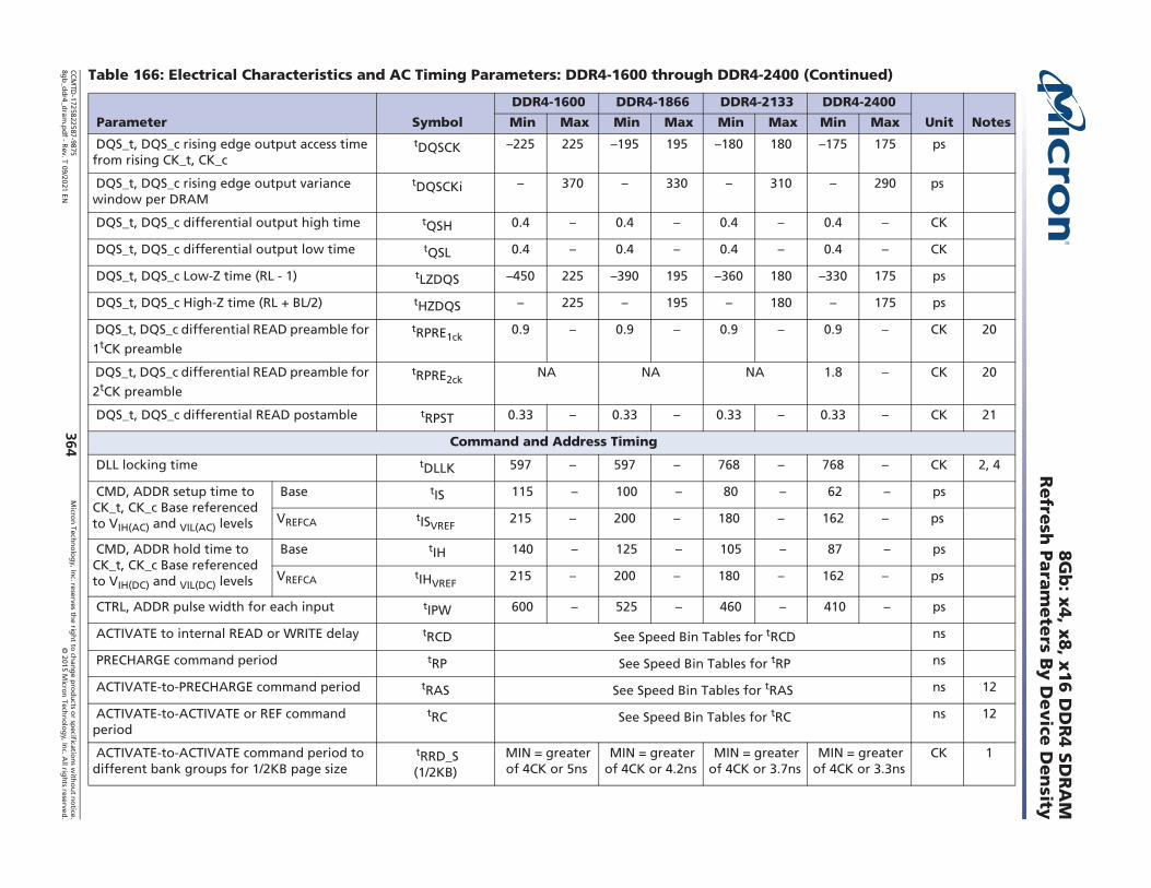
CCM
TD-1725822587-9875
Micro
n Techno
log
y, Inc. reserves the rig
ht to ch
ange p
rod
ucts or sp
ecifications w
itho
ut n
otice.
8gb
_ddr4_d
ram.p
df - Rev. T 09/2021 EN
2015 Micron
Techn
olog
y, Inc. A
ll rights reserved.
364
8Gb
: x4
, x8
, x16
DD
R4
SD
RA
MR
efresh Pa
rame
ters B
y D
evice D
ensity
DQS_t, DQS_c rising edge output access time from rising CK_t, CK_c
tDQSCK 225 225 195 195 180 180 175 175 ps
DQS_t, DQS_c rising edge output variance window per DRAM
tDQSCKi 370 330 310 290 ps
DQS_t, DQS_c differential output high time tQSH 0.4 0.4 0.4 0.4 CK
DQS_t, DQS_c differential output low time tQSL 0.4 0.4 0.4 0.4 CK
DQS_t, DQS_c Low-Z time (RL - 1) tLZDQS 450 225 390 195 360 180 330 175 ps
DQS_t, DQS_c High-Z time (RL + BL/2) tHZDQS 225 195 180 175 ps
DQS_t, DQS_c differential READ preamble for
1tCK preamble tRPRE1ck
0.9 0.9 0.9 0.9 CK 20
DQS_t, DQS_c differential READ preamble for
2tCK preamble tRPRE2ck
NA NA NA 1.8 CK 20
DQS_t, DQS_c differential READ postamble tRPST 0.33 0.33 0.33 0.33 CK 21
Command and Address Timing
DLL locking time tDLLK 597 597 768 768 CK 2, 4
CMD, ADDR setup time to CK_t, CK_c Base referenced to VIH(AC) and VIL(AC) levels
Base tIS 115 100 80 62 ps
VREFCA tISVREF215 200 180 162 ps
CMD, ADDR hold time to CK_t, CK_c Base referenced to VIH(DC) and VIL(DC) levels
Base tIH 140 125 105 87 ps
VREFCA tIHVREF215 200 180 162 ps
CTRL, ADDR pulse width for each input tIPW 600 525 460 410 ps
ACTIVATE to internal READ or WRITE delay tRCD See Speed Bin Tables for tRCD ns
PRECHARGE command period tRP See Speed Bin Tables for tRP ns
ACTIVATE-to-PRECHARGE command period tRAS See Speed Bin Tables for tRAS ns 12
ACTIVATE-to-ACTIVATE or REF command period
tRC See Speed Bin Tables for tRC ns 12
ACTIVATE-to-ACTIVATE command period to different bank groups for 1/2KB page size
tRRD_S (1/2KB)
MIN = greater of 4CK or 5ns
MIN = greater of 4CK or 4.2ns
MIN = greater of 4CK or 3.7ns
MIN = greater of 4CK or 3.3ns
CK 1
Table 166: Electrical Characteristics and AC Timing Parameters: DDR4-1600 through DDR4-2400 (Continued)
Parameter Symbol
DDR4-1600 DDR4-1866 DDR4-2133 DDR4-2400
Unit Notes Min Max Min Max Min Max Min Max

CCM
TD-1725822587-9875
Micro
n Techno
log
y, Inc. reserves the rig
ht to ch
ange p
rod
ucts or sp
ecifications w
itho
ut n
otice.
8gb
_ddr4_d
ram.p
df - Rev. T 09/2021 EN
2015 Micron
Techn
olog
y, Inc. A
ll rights reserved.
365
8Gb
: x4
, x8
, x16
DD
R4
SD
RA
MR
efresh Pa
rame
ters B
y D
evice D
ensity
ACTIVATE-to-ACTIVATE command period to different bank groups for 1KB page size
tRRD_S (1KB)
MIN = greater of 4CK or 5ns
MIN = greater of 4CK or 4.2ns
MIN = greater of 4CK or 3.7ns
MIN = greater of 4CK or 3.3ns
CK 1
ACTIVATE-to-ACTIVATE command period to different bank groups for 2KB page size
tRRD_S (2KB)
MIN = greater of 4CK or 6ns
MIN = greater of 4CK or 5.3ns
MIN = greater of 4CK or 5.3ns
MIN = greater of 4CK or 5.3ns
CK 1
ACTIVATE-to-ACTIVATE command period to same bank groups for 1/2KB page size
tRRD_L (1/2KB)
MIN = greater of 4CK or 6ns
MIN = greater of 4CK or 5.3ns
MIN = greater of 4CK or 5.3ns
MIN = greater of 4CK or 4.9ns
CK 1
ACTIVATE-to-ACTIVATE command period to same bank groups for 1KB page size
tRRD_L (1KB)
MIN = greater of 4CK or 6ns
MIN = greater of 4CK or 5.3ns
MIN = greater of 4CK or 5.3ns
MIN = greater of 4CK or 4.9ns
CK 1
ACTIVATE-to-ACTIVATE command period to same bank groups for 2KB page size
tRRD_L (2KB)
MIN = greater of 4CK or 7.5ns
MIN = greater of 4CK or 6.4ns
MIN = greater of 4CK or 6.4ns
MIN = greater of 4CK or 6.4ns
CK 1
Four ACTIVATE windows for 1/2KB page size tFAW (1/2KB)
MIN = greater of 16CK or 20ns
MIN = greater of 16CK or 17ns
MIN = greater of 16CK or 15ns
MIN = greater of 16CK or 13ns
ns
Four ACTIVATE windows for 1KB page size tFAW (1KB)
MIN = greater of 20CK or 25ns
MIN = greater of 20CK or 23ns
MIN = greater of 20CK or 21ns
MIN = greater of 20CK or 21ns
ns
Four ACTIVATE windows for 2KB page size tFAW (2KB)
MIN = greater of 28CK or 35ns
MIN = greater of 28CK or 30ns
MIN = greater of 28CK or 30ns
MIN = greater of 28CK or 30ns
ns
WRITE recovery time tWR1ck MIN = 15ns ns 1, 5, 9
tWR2ck MIN = 1CK + tWR1ckCK 1, 5, 10
WRITE recovery time when CRC and DM are both enabled
tWR_CRC_DM1ck MIN = tWR1ck + greater of (4CK
or 3.75ns)
MIN = tWR1ck + greater of (5CK or 3.75ns) CK 1, 6, 9
tWR_CRC_DM2ck MIN = 1CK + tWR_CRC_DM1ckCK 1, 6, 10
Delay from start of internal WRITE transac-tion to internal READ command Same bank group
tWTR_L1ck MIN = greater of 4CK or 7.5ns CK 1, 5, 9
tWTR_L2ck MIN = 1CK + tWTR_L1ckCK 1, 5, 10
Delay from start of internal WRITE transac-tion to internal READ command Same bank group when CRC and DM are both enabled
tWTR_L_CRC_DM1ck
MIN = tWTR_L1ck +
greater of (4CK or 3.75ns)
MIN = tWTR_L1ck + greater of (5CK or 3.75ns) CK 1, 6, 9
tWTR_L_CRC_DM2ck
MIN = 1CK + tWTR_L_CRC_DM1ckCK 1, 6, 10
Table 166: Electrical Characteristics and AC Timing Parameters: DDR4-1600 through DDR4-2400 (Continued)
Parameter Symbol
DDR4-1600 DDR4-1866 DDR4-2133 DDR4-2400
Unit Notes Min Max Min Max Min Max Min Max

CCM
TD-1725822587-9875
Micro
n Techno
log
y, Inc. reserves the rig
ht to ch
ange p
rod
ucts or sp
ecifications w
itho
ut n
otice.
8gb
_ddr4_d
ram.p
df - Rev. T 09/2021 EN
2015 Micron
Techn
olog
y, Inc. A
ll rights reserved.
366
8Gb
: x4
, x8
, x16
DD
R4
SD
RA
MR
efresh Pa
rame
ters B
y D
evice D
ensity
Delay from start of internal WRITE transac-tion to internal READ command Different bank group
tWTR_S1ckMIN = greater of (2CK or 2.5ns) CK 1, 5, 7,
8, 9
tWTR_S2ck MIN = 1CK + tWTR_S1ckCK 1, 5, 7,
8, 10
Delay from start of internal WRITE transac-tion to internal READ command Different bank group when CRC and DM are both enabled
tWTR_S_CRC_DM
1ck
MIN = tWTR_S1ck +
greater of (4CK or 3.75ns)
MIN = tWTR_S1ck + greater of (5CK or 3.75ns) CK 1, 6, 7, 8, 9
tWTR_S_CRC_DM2ck
MIN = 1CK + tWTR_S_CRC_DM1ckCK 1, 6, 7,
8, 10
READ-to-PRECHARGE time tRTP MIN = greater of 4CK or 7.5ns CK 1
CAS_n-to-CAS_n command delay to different bank group
tCCD_S 4 4 4 4 CK
CAS_n-to-CAS_n command delay to same bank group
tCCD_L MIN = greate
r of 4CK or 6.25ns
MIN = greate
r of 4CK or 5.355n
s
MIN = greate
r of 4CK or 5.355n
s
MIN = greate
r of 4CK or
5ns
CK 14
Auto precharge write recovery + precharge time
tDAL (MIN) MIN = WR + ROUNDtRP/tCK (AVG); MAX = N/A CK 8
MRS Command Timing
MRS command cycle time tMRD 8 8 8 8 CK
MRS command cycle time in PDA mode tMRD_PDA MIN = greater of (16nCK, 10ns) CK 1
MRS command cycle time in CAL mode tMRD_CAL MIN = tMOD + tCAL CK
MRS command update delay tMOD MIN = greater of (24nCK, 15ns) CK 1
MRS command update delay in PDA mode tMOD_PDA MIN = tMOD CK
MRS command update delay in CAL mode tMOD_CAL MIN = tMOD + tCAL CK
MRS command to DQS drive in preamble training
tSDO MIN = tMOD + 9ns
MPR Command Timing
Multipurpose register recovery time tMPRR MIN = 1CK CK
Table 166: Electrical Characteristics and AC Timing Parameters: DDR4-1600 through DDR4-2400 (Continued)
Parameter Symbol
DDR4-1600 DDR4-1866 DDR4-2133 DDR4-2400
Unit Notes Min Max Min Max Min Max Min Max
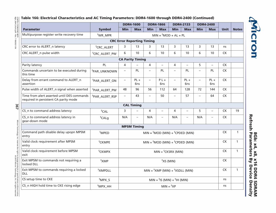
CCM
TD-1725822587-9875
Micro
n Techno
log
y, Inc. reserves the rig
ht to ch
ange p
rod
ucts or sp
ecifications w
itho
ut n
otice.
8gb
_ddr4_d
ram.p
df - Rev. T 09/2021 EN
2015 Micron
Techn
olog
y, Inc. A
ll rights reserved.
367
8Gb
: x4
, x8
, x16
DD
R4
SD
RA
MR
efresh Pa
rame
ters B
y D
evice D
ensity
Multipurpose register write recovery time tWR_MPR MIN = tMOD + AL + PL
CRC Error Reporting Timing
CRC error to ALERT_n latency tCRC_ALERT 3 13 3 13 3 13 3 13 ns
CRC ALERT_n pulse width tCRC_ALERT_PW 6 10 6 10 6 10 6 10 CK
CA Parity Timing
Parity latency PL 4 4 4 5 CK
Commands uncertain to be executed during this time
tPAR_UNKNOWN PL PL PL PL CK
Delay from errant command to ALERT_n assertion
tPAR_ALERT_ON PL + 6ns
P L + 6ns
PL + 6ns
PL + 6ns
CK
Pulse width of ALERT_n signal when asserted tPAR_ALERT_PW 48 96 56 112 64 128 72 144 CK
Time from alert asserted until DES commands required in persistent CA parity mode
tPAR_ALERT_RSP 43 50 57 64 CK
CAL Timing
CS_n to command address latency tCAL 3 4 4 5 CK 19
CS_n to command address latency in gear-down mode
tCALg N/A N/A N/A N/A CK
MPSM Timing
Command path disable delay upopn MPSM entry
tMPED MIN = tMOD (MIN) + tCPDED (MIN) CK 1
Valid clock requirement after MPSMentry
tCKMPE MIN = tMOD (MIN) + tCPDED (MIN) CK 1
Valid clock requirement before MPSMexit
tCKMPX MIN = tCKSRX (MIN) CK 1
Exit MPSM to commands not requiring a locked DLL
tXMP tXS (MIN) CK
Exit MPSM to commands requiring a locked DLL
tXMPDLL MIN = tXMP (MIN) + tXSDLL (MIN) CK 1
CS setup time to CKE tMPX_S MIN = tIS (MIN) + tIH (MIN) ns
CS_n HIGH hold time to CKE rising edge tMPX_HH MIN = tXP ns
Table 166: Electrical Characteristics and AC Timing Parameters: DDR4-1600 through DDR4-2400 (Continued)
Parameter Symbol
DDR4-1600 DDR4-1866 DDR4-2133 DDR4-2400
Unit Notes Min Max Min Max Min Max Min Max
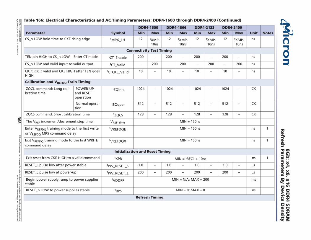
CCM
TD-1725822587-9875
Micro
n Techno
log
y, Inc. reserves the rig
ht to ch
ange p
rod
ucts or sp
ecifications w
itho
ut n
otice.
8gb
_ddr4_d
ram.p
df - Rev. T 09/2021 EN
2015 Micron
Techn
olog
y, Inc. A
ll rights reserved.
368
8Gb
: x4
, x8
, x16
DD
R4
SD
RA
MR
efresh Pa
rame
ters B
y D
evice D
ensity
CS_n LOW hold time to CKE rising edge tMPX_LH 12 tXMP-10ns
12 tXMP-10ns
12 tXMP-10ns
12 tXMP-10ns
ns
Connectivity Test Timing
TEN pin HIGH to CS_n LOW Enter CT mode tCT_Enable 200 200 200 200 ns
CS_n LOW and valid input to valid output tCT_Valid 200 200 200 200 ns
CK_t, CK_c valid and CKE HIGH after TEN goes HIGH
tCTCKE_Valid 10 10 10 10 ns
Calibration and VREFDQ Train Timing
ZQCL command: Long cali-bration time
POWER-UP and RESET operation
tZQinit 1024 1024 1024 1024 CK
Normal opera-tion
tZQoper 512 512 512 512 CK
ZQCS command: Short calibration time tZQCS 128 128 128 128 CK
The VREF increment/decrement step time VREF_time MIN = 150ns
Enter VREFDQ training mode to the first write or VREFDQ MRS command delay
tVREFDQE MIN = 150ns ns 1
Exit VREFDQ training mode to the first WRITE command delay
tVREFDQX MIN = 150ns ns 1
Initialization and Reset Timing
Exit reset from CKE HIGH to a valid command tXPR MIN = tRFC1 + 10ns ns 1
RESET_L pulse low after power stable tPW_RESET_S 1.0 1.0 1.0 1.0 s
RESET_L pulse low at power-up tPW_RESET_L 200 200 200 200 s
Begin power supply ramp to power supplies stable
tVDDPR MIN = N/A; MAX = 200 ms
RESET_n LOW to power supplies stable tRPS MIN = 0; MAX = 0 ns
Refresh Timing
Table 166: Electrical Characteristics and AC Timing Parameters: DDR4-1600 through DDR4-2400 (Continued)
Parameter Symbol
DDR4-1600 DDR4-1866 DDR4-2133 DDR4-2400
Unit Notes Min Max Min Max Min Max Min Max
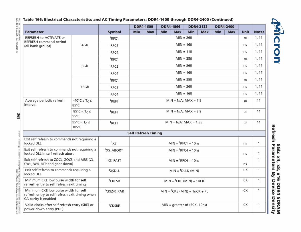
CCM
TD-1725822587-9875
Micro
n Techno
log
y, Inc. reserves the rig
ht to ch
ange p
rod
ucts or sp
ecifications w
itho
ut n
otice.
8gb
_ddr4_d
ram.p
df - Rev. T 09/2021 EN
2015 Micron
Techn
olog
y, Inc. A
ll rights reserved.
369
8Gb
: x4
, x8
, x16
DD
R4
SD
RA
MR
efresh Pa
rame
ters B
y D
evice D
ensity
REFRESH-to-ACTIVATE or REFRESH command period (all bank groups) 4Gb
tRFC1 MIN = 260 ns 1, 11
tRFC2 MIN = 160 ns 1, 11
tRFC4 MIN = 110 ns 1, 11
8Gb
tRFC1 MIN = 350 ns 1, 11
tRFC2 MIN = 260 ns 1, 11
tRFC4 MIN = 160 ns 1, 11
16Gb
tRFC1 MIN = 350 ns 1, 11
tRFC2 MIN = 260 ns 1, 11
tRFC4 MIN = 160 ns 1, 11
Average periodic refresh interval
-40 C TC 85 C
tREFI MIN = N/A; MAX = 7.8 s 11
85 C < TC 95 C
tREFI MIN = N/A; MAX = 3.9 s 11
95 C < TC 105 C
tREFI MIN = N/A; MAX = 1.95 s 11
Self Refresh Timing
Exit self refresh to commands not requiring a locked DLL tXS MIN = tRFC1 + 10ns ns 1
Exit self refresh to commands not requiring a locked DLL in self refresh abort
tXS_ABORT MIN = tRFC4 + 10nsns 1
Exit self refresh to ZQCL, ZQCS and MRS (CL, CWL, WR, RTP and gear-down)
tXS_FAST MIN = tRFC4 + 10nsns
1
Exit self refresh to commands requiring a locked DLL
tXSDLL MIN = tDLLK (MIN) CK 1
Minimum CKE low pulse width for self refresh entry to self refresh exit timing
tCKESR MIN = tCKE (MIN) + 1nCK CK 1
Minimum CKE low pulse width for self refresh entry to self refresh exit timing when CA parity is enabled
tCKESR_PAR MIN = tCKE (MIN) + 1nCK + PL CK 1
Valid clocks after self refresh entry (SRE) or power-down entry (PDE)
tCKSRE MIN = greater of (5CK, 10ns) CK 1
Table 166: Electrical Characteristics and AC Timing Parameters: DDR4-1600 through DDR4-2400 (Continued)
Parameter Symbol
DDR4-1600 DDR4-1866 DDR4-2133 DDR4-2400
Unit Notes Min Max Min Max Min Max Min Max

CCM
TD-1725822587-9875
Micro
n Techno
log
y, Inc. reserves the rig
ht to ch
ange p
rod
ucts or sp
ecifications w
itho
ut n
otice.
8gb
_ddr4_d
ram.p
df - Rev. T 09/2021 EN
2015 Micron
Techn
olog
y, Inc. A
ll rights reserved.
370
8Gb
: x4
, x8
, x16
DD
R4
SD
RA
MR
efresh Pa
rame
ters B
y D
evice D
ensity
Valid clock requirement after self refresh entry or power-down when CA parity is enabled
tCKSRE_PAR MIN = greater of (5CK, 10ns) + PL CK 1
Valid clocks before self refresh exit (SRX) or power-down exit (PDX), or reset exit
tCKSRX MIN = greater of (5CK, 10ns) CK 1
Power-Down Timing
Exit power-down with DLL on to any valid command
tXP MIN = greater of 4CK or 6ns CK 1
Exit power-down with DLL on to any valid command when CA Parity is enabled.
tXP _PAR MIN = (greater of 4CK or 6ns) + PL CK 1
CKE MIN pulse width tCKE (MIN) MIN = greater of 3CK or 5ns CK 1
Command pass disable delay tCPDED 4 4 4 4 CK
Power-down entry to power-down exit tim-ing
tPD MIN = tCKE (MIN); MAX = 9 tREFI CK
Begin power-down period prior to CKE regis-tered HIGH
tANPD WL - 1CK CK
Power-down entry period: ODT either syn-chronous or asynchronous
PDE Greater of tANPD or tRFC - REFRESH command to CKE LOW time CK
Power-down exit period: ODT either synchro-nous or asynchronous
PDX tANPD + tXSDLL CK
Power-Down Entry Minimum Timing
ACTIVATE command to power-down entry tACTPDEN 1 1 2 2 CK
PRECHARGE/PRECHARGE ALL command to power-down entry
tPRPDEN 1 1 2 2 CK
REFRESH command to power-down entry tREFPDEN 1 1 2 2 CK
MRS command to power-down entry tMRSPDEN MIN = tMOD (MIN) CK 1
READ/READ with auto precharge command to power-down entry
tRDPDEN MIN = RL + 4 + 1 CK 1
WRITE command to power-down entry (BL8OTF, BL8MRS, BC4OTF)
tWRPDEN MIN = WL + 4 + tWR/tCK (AVG) CK 1
WRITE command to power-down entry (BC4MRS)
tWRPBC4DEN MIN = WL + 2 + tWR/tCK (AVG) CK 1
Table 166: Electrical Characteristics and AC Timing Parameters: DDR4-1600 through DDR4-2400 (Continued)
Parameter Symbol
DDR4-1600 DDR4-1866 DDR4-2133 DDR4-2400
Unit Notes Min Max Min Max Min Max Min Max

CCM
TD-1725822587-9875
Micro
n Techno
log
y, Inc. reserves the rig
ht to ch
ange p
rod
ucts or sp
ecifications w
itho
ut n
otice.
8gb
_ddr4_d
ram.p
df - Rev. T 09/2021 EN
2015 Micron
Techn
olog
y, Inc. A
ll rights reserved.
371
8Gb
: x4
, x8
, x16
DD
R4
SD
RA
MR
efresh Pa
rame
ters B
y D
evice D
ensity
WRITE with auto precharge command to power-down entry (BL8OTF, BL8MRS,BC4OTF)
tWRAPDEN MIN = WL + 4 + WR + 1 CK 1
WRITE with auto precharge command to power-down entry (BC4MRS)
tWRAPBC4DEN MIN = WL + 2 + WR + 1 CK 1
ODT Timing
Direct ODT turn-on latency DODTLon WL - 2 = CWL + AL + PL - 2 CK
Direct ODT turn-off latency DODTLoff WL - 2 = CWL + AL + PL - 2 CK
RTT dynamic change skew tADC 0.3 0.7 0.3 0.7 0.3 0.7 0.3 0.7 CK
Asynchronous RTT(NOM) turn-on delay (DLL off)
tAONAS 1 9 1 9 1 9 1 9 ns
Asynchronous RTT(NOM) turn-off delay (DLL off)
tAOFAS 1 9 1 9 1 9 1 9 ns
ODT HIGH time with WRITE command and BL8
ODTH8 1tCK 6 6 6 6 CK
ODTH8 2tCK NA NA NA 7
ODT HIGH time without WRITE command or with WRITE command and BC4
ODTH4 1tCK 4 4 4 4 CK
ODTH4 2tCK NA NA NA 5
Write Leveling Timing
First DQS_t, DQS_c rising edge after write lev-eling mode is programmed
tWLMRD 40 40 40 40 CK
DQS_t, DQS_c delay after write leveling mode is programmed
tWLDQSEN 25 25 25 25 CK
Write leveling setup from rising CK_t, CK_c crossing to rising DQS_t, DQS_c crossing
tWLS 0.13 0.13 0.13 0.13 tCK (AVG)
Write leveling hold from rising DQS_t, DQS_c crossing to rising CK_t, CK_c crossing
tWLH 0.13 0.13 0.13 0.13 tCK (AVG)
Write leveling output delay tWLO 0 9.5 0 9.5 0 9.5 0 9.5 ns
Write leveling output error tWLOE 0 2 0 2 0 2 0 2 ns
Gear-Down Timing (Not Supported Below DDR4-2666)
Exit reset from CKE HIGH to a valid MRS gear-down
tXPR_GEAR N/A N/A N/A N/A CK
Table 166: Electrical Characteristics and AC Timing Parameters: DDR4-1600 through DDR4-2400 (Continued)
Parameter Symbol
DDR4-1600 DDR4-1866 DDR4-2133 DDR4-2400
Unit Notes Min Max Min Max Min Max Min Max

CCM
TD-1725822587-9875
Micro
n Techno
log
y, Inc. reserves the rig
ht to ch
ange p
rod
ucts or sp
ecifications w
itho
ut n
otice.
8gb
_ddr4_d
ram.p
df - Rev. T 09/2021 EN
2015 Micron
Techn
olog
y, Inc. A
ll rights reserved.
372
8Gb
: x4
, x8
, x16
DD
R4
SD
RA
MR
efresh Pa
rame
ters B
y D
evice D
ensity
Notes: 1. Maximum limit not applicable.2. Micron tDLLK values support the legacy JEDEC tDLLK specifications.3. DDR4-1600 AC timing parameters apply if DRAM operates at lower than 1600 MT/s data rate.4. Data rate is greater than or equal to 1066 Mb/s.5. WRITE-to-READ when CRC and DM are both not enabled.6. WRITE-to-READ delay when CRC and DM are both enabled.7. The start of internal write transactions is defined as follows:
For BL8 (fixed by MRS and on-the-fly): rising clock edge four clock cycles after WLFor BC4 (on-the-fly): rising clock edge four clock cycles after WLFor BC4 (fixed by MRS): rising clock edge two clock cycles after WL
8. For these parameters, the device supports tnPARAM [nCK] = ROUND{tPARAM [ns]/tCK (AVG) [ns]} according to the rounding algorithms found in the Converting Time-Based Specifications to Clock-Based Requirements section, in clock cycles, assuming all input clock jitter specifications are satisfied.
9. When operating in 1tCK WRITE preamble mode.
10. When operating in 2tCK WRITE preamble mode.
11. When CA parity mode is selected and the DLLoff mode is used, each REF command requires an additional "PL" added to tRFC refresh time.12. DRAM devices should be evenly addressed when being accessed. Disproportionate accesses to a particular row address may result in reduction
of the product lifetime and/or reduction in data retention ability.
13. Applicable from tCK (AVG) MIN to tCK (AVG) MAX as stated in the Speed Bin tables.14. JEDEC specifies a minimum of five clocks.
15. The maximum read postamble is bound by tDQSCK (MIN) plus tQSH (MIN) on the left side and tHZ(DQS) MAX on the right side.16. The reference level of DQ output signal is specified with a midpoint as a widest part of output signal eye, which should be approximately 0.7
VDDQ as a center level of the static single-ended output peak-to-peak swing with a driver impedance of 34 ohms and an effective test load of 50 ohms to VTT = VDDQ.
17. JEDEC hasn't agreed upon the definition of the deterministic jitter; the user should focus on meeting the total limit.18. Spread spectrum is not included in the jitter specification values. However, the input clock can accommodate spread-spectrum at a sweep rate
in the range of 20 60 kHz with an additional 1% of tCK (AVG) as a long-term jitter component; however, the spread spectrum may not use a
clock rate below tCK (AVG) MIN.
19. The actual tCAL minimum is the larger of 3 clocks or 3.748ns/tCK; the table lists the applicable clocks required at targeted speed bin.
CKE HIGH assert to gear-down enable time) tXS_GEAR N/A N/A N/A N/A CK
MRS command to sync pulse time tSYNC_GEAR N/A N/A N/A N/A CK
Sync pulse to first valid command tCMD_GEAR N/A N/A N/A N/A CK
Gear-down setup time tGEAR_setup N/A N/A N/A N/A CK
Gear-down hold time tGEAR_hold N/A N/A N/A N/A CK
Table 166: Electrical Characteristics and AC Timing Parameters: DDR4-1600 through DDR4-2400 (Continued)
Parameter Symbol
DDR4-1600 DDR4-1866 DDR4-2133 DDR4-2400
Unit Notes Min Max Min Max Min Max Min Max
CCM
TD-1725822587-9875
Micro
n Techno
log
y, Inc. reserves the rig
ht to ch
ange p
rod
ucts or sp
ecifications w
itho
ut n
otice.
8gb
_ddr4_d
ram.p
df - Rev. T 09/2021 EN
2015 Micron
Techn
olog
y, Inc. A
ll rights reserved.
373
8Gb
: x4
, x8
, x16
DD
R4
SD
RA
MR
efresh Pa
rame
ters B
y D
evice D
ensity
20. The maximum READ preamble is bounded by tLZ(DQS) MIN on the left side and tDQSCK (MAX) on the right side. See figure in the Clock to Data
Strobe Relationship section. Boundary of DQS Low-Z occurs one cycle earlier in 2tCK toggle mode, as illustrated in the READ Preamble section.21. DQ falling signal middle-point of transferring from HIGH to LOW to first rising edge of DQS differential signal cross-point.
22. The tPDA_S/tPDA_H parameters may use the tDS/tDH limits, respectively, if the signal is LOW the entire BL8.
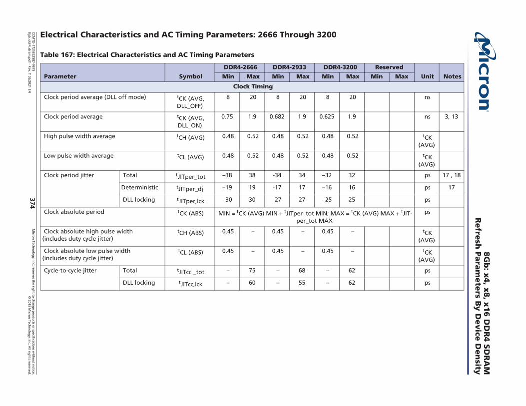
CCM
TD-1725822587-9875
Micro
n Techno
log
y, Inc. reserves the rig
ht to ch
ange p
rod
ucts or sp
ecifications w
itho
ut n
otice.
8gb
_ddr4_d
ram.p
df - Rev. T 09/2021 EN
2015 Micron
Techn
olog
y, Inc. A
ll rights reserved.
374
8Gb
: x4
, x8
, x16
DD
R4
SD
RA
MR
efresh Pa
rame
ters B
y D
evice D
ensity
Electrical Characteristics and AC Timing Parameters: 2666 Through 3200
Table 167: Electrical Characteristics and AC Timing Parameters
Parameter Symbol
DDR4-2666 DDR4-2933 DDR4-3200 Reserved
Unit Notes Min Max Min Max Min Max Min Max
Clock Timing
Clock period average (DLL off mode) tCK (AVG, DLL_OFF)
8 20 8 20 8 20 ns
Clock period average tCK (AVG, DLL_ON)
0.75 1.9 0.682 1.9 0.625 1.9 ns 3, 13
High pulse width average tCH (AVG) 0.48 0.52 0.48 0.52 0.48 0.52 tCK (AVG)
Low pulse width average tCL (AVG) 0.48 0.52 0.48 0.52 0.48 0.52 tCK (AVG)
Clock period jitter Total tJITper_tot 38 38 -34 34 32 32 ps 17 , 18
Deterministic tJITper_dj 19 19 -17 17 16 16 ps 17
DLL locking tJITper,lck 30 30 -27 27 25 25 ps
Clock absolute period tCK (ABS) MIN = tCK (AVG) MIN + tJITper_tot MIN; MAX = tCK (AVG) MAX + tJIT-per_tot MAX
ps
Clock absolute high pulse width(includes duty cycle jitter)
tCH (ABS) 0.45 0.45 0.45 tCK (AVG)
Clock absolute low pulse width (includes duty cycle jitter)
tCL (ABS) 0.45 0.45 0.45 tCK (AVG)
Cycle-to-cycle jitter Total tJITcc _tot 75 68 62 ps
DLL locking tJITcc,lck 60 55 62 ps
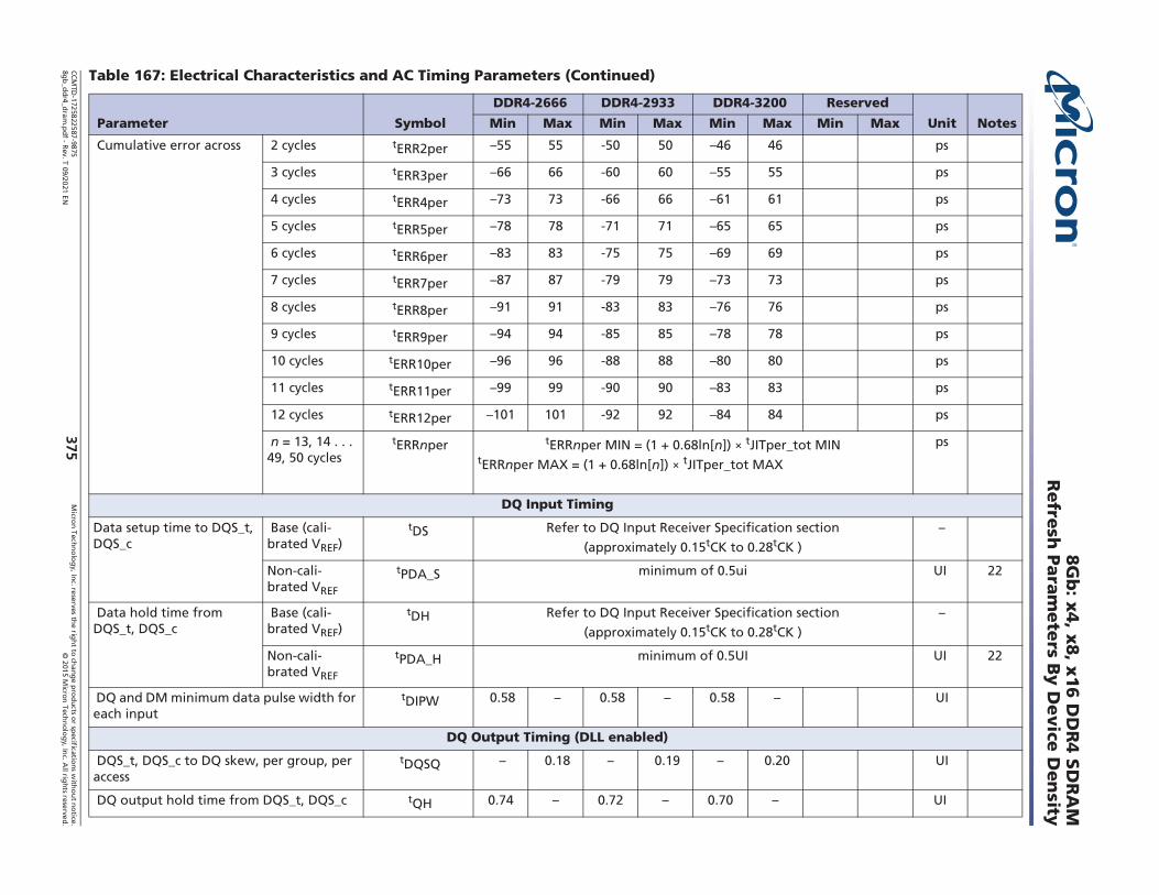
CCM
TD-1725822587-9875
Micro
n Techno
log
y, Inc. reserves the rig
ht to ch
ange p
rod
ucts or sp
ecifications w
itho
ut n
otice.
8gb
_ddr4_d
ram.p
df - Rev. T 09/2021 EN
2015 Micron
Techn
olog
y, Inc. A
ll rights reserved.
375
8Gb
: x4
, x8
, x16
DD
R4
SD
RA
MR
efresh Pa
rame
ters B
y D
evice D
ensity
Cumulative error across 2 cycles tERR2per 55 55 -50 50 46 46 ps
3 cycles tERR3per 66 66 -60 60 55 55 ps
4 cycles tERR4per 73 73 -66 66 61 61 ps
5 cycles tERR5per 78 78 -71 71 65 65 ps
6 cycles tERR6per 83 83 -75 75 69 69 ps
7 cycles tERR7per 87 87 -79 79 73 73 ps
8 cycles tERR8per 91 91 -83 83 76 76 ps
9 cycles tERR9per 94 94 -85 85 78 78 ps
10 cycles tERR10per 96 96 -88 88 80 80 ps
11 cycles tERR11per 99 99 -90 90 83 83 ps
12 cycles tERR12per 101 101 -92 92 84 84 ps
n = 13, 14 . . . 49, 50 cycles
tERRnper tERRnper MIN = (1 + 0.68ln[n]) tJITper_tot MIN tERRnper MAX = (1 + 0.68ln[n]) tJITper_tot MAX
ps
DQ Input Timing
Data setup time to DQS_t, DQS_c
Base (cali-brated VREF)
tDS Refer to DQ Input Receiver Specification section
(approximately 0.15tCK to 0.28tCK )
Non-cali-brated VREF
tPDA_S minimum of 0.5ui UI 22
Data hold time from DQS_t, DQS_c
Base (cali-brated VREF)
tDH Refer to DQ Input Receiver Specification section
(approximately 0.15tCK to 0.28tCK )
Non-cali-brated VREF
tPDA_H minimum of 0.5UI UI 22
DQ and DM minimum data pulse width for each input
tDIPW 0.58 0.58 0.58 UI
DQ Output Timing (DLL enabled)
DQS_t, DQS_c to DQ skew, per group, per access
tDQSQ 0.18 0.19 0.20 UI
DQ output hold time from DQS_t, DQS_c tQH 0.74 0.72 0.70 UI
Table 167: Electrical Characteristics and AC Timing Parameters (Continued)
Parameter Symbol
DDR4-2666 DDR4-2933 DDR4-3200 Reserved
Unit Notes Min Max Min Max Min Max Min Max

CCM
TD-1725822587-9875
Micro
n Techno
log
y, Inc. reserves the rig
ht to ch
ange p
rod
ucts or sp
ecifications w
itho
ut n
otice.
8gb
_ddr4_d
ram.p
df - Rev. T 09/2021 EN
2015 Micron
Techn
olog
y, Inc. A
ll rights reserved.
376
8Gb
: x4
, x8
, x16
DD
R4
SD
RA
MR
efresh Pa
rame
ters B
y D
evice D
ensity
Data Valid Window per device: tQH - tDQSQ each device s output per UI
tDVWd0.64 0.64 0.64 UI
Data Valid Window per device, per pin: tQH
- tDQSQ each device s output per UI
tDVWp0.72 0.72 0.72 UI
DQ Low-Z time from CK_t, CK_c tLZDQ 310 170 280 165 250 160 ps
DQ High-Z time from CK_t, CK_c tHZDQ 170 165 160 ps
DQ Strobe Input Timing
DQS_t, DQS_c rising edge to CK_t, CK_c ris-
ing edge for 1tCK preamble tDQSS1ck
0.27 0.27 0.27 0.27 0.27 0.27 CK
DQS_t, DQS_c rising edge to CK_t, CK_c ris-
ing edge for 2tCK preamble tDQSS2ck
0.50 0.50 0.50 0.50 0.50 0.50 CK
DQS_t, DQS_c differential input low pulse width
tDQSL 0.46 0.54 0.46 0.54 0.46 0.54 CK
DQS_t, DQS_c differential input high pulse width
tDQSH 0.46 0.54 0.46 0.54 0.46 0.54 CK
DQS_t, DQS_c differential input high pulse
width for 2tCK preamble tDQSH2PRE 1.46 - 1.46 - 1.46 - CK
DQS_t, DQS_c falling edge setup to CK_t,
CK_c rising edge for 1tCK preamble tDSS1ck
0.18 0.18 0.18 CK
DQS_t, DQS_c falling edge setup to CK_t,
CK_c rising edge for 2tCK preamble tDSS2ck
0 0 0 CK
DQS_t, DQS_c falling edge hold from CK_t,
CK_c rising edge for 1tCK preamble tDSH1ck
0.18 0.18 0.18 CK
DQS_t, DQS_c falling edge hold from CK_t,
CK_c rising edge for 2tCK preamble tDSH2ck
0 0 0 CK
DQS_t, DQS_c differential WRITE preamble
for 1tCK preamble tWPRE1ck
0.9 0.9 0.9 CK
DQS_t, DQS_c differential WRITE preamble
for 2tCK preamble tWPRE2ck
1.8 1.8 1.8 CK
DQS_t, DQS_c differential WRITE postam-ble
tWPST 0.33 0.33 0.33 CK
Table 167: Electrical Characteristics and AC Timing Parameters (Continued)
Parameter Symbol
DDR4-2666 DDR4-2933 DDR4-3200 Reserved
Unit Notes Min Max Min Max Min Max Min Max

CCM
TD-1725822587-9875
Micro
n Techno
log
y, Inc. reserves the rig
ht to ch
ange p
rod
ucts or sp
ecifications w
itho
ut n
otice.
8gb
_ddr4_d
ram.p
df - Rev. T 09/2021 EN
2015 Micron
Techn
olog
y, Inc. A
ll rights reserved.
377
8Gb
: x4
, x8
, x16
DD
R4
SD
RA
MR
efresh Pa
rame
ters B
y D
evice D
ensity
DQS Strobe Output Timing (DLL enabled)
DQS_t, DQS_c rising edge output access time from rising CK_t, CK_c
tDQSCK 170 170 165 165 160 160 ps
DQS_t, DQS_c rising edge output variance window per DRAM
tDQSCKi 270 265 260 ps
DQS_t, DQS_c differential output high time
tQSH 0.40 0.40 0.40 CK
DQS_t, DQS_c differential output low time tQSL 0.40 0.40 0.40 CK
DQS_t, DQS_c Low-Z time (RL - 1) tLZDQS 310 170 280 165 250 160 ps
DQS_t, DQS_c High-Z time (RL + BL/2) tHZDQS 170 165 160 ps
DQS_t, DQS_c differential READ preamble
for 1tCK preamble tRPRE1ck
0.9 0.9 0.9 CK 20
DQS_t, DQS_c differential READ preamble
for 2tCK preamble tRPRE2ck
1.8 1.8 1.8 CK 20
DQS_t, DQS_c differential READ postamble tRPST 0.33 0.33 0.33 CK 21
Command and Address Timing
DLL locking time tDLLK 854 940 1024 CK 2, 4
CMD, ADDR setup time to CK_t, CK_c referenced to VIH(AC) and VIL(AC) levels
Base tIS 55 48 40 ps
VREFCA tISVREF145 138 130 ps
CMD, ADDR hold time to CK_t, CK_c referenced to VIH(DC) and VIL(DC) levels
Base tIH 80 73 65 ps
VREFCA tIHVREF 145 138 130 ps
CTRL, ADDR pulse width for each input tIPW 385 365 340 ps
ACTIVATE to internal READ or WRITE delay tRCD See Speed Bin Tables for tRCD ns
PRECHARGE command period tRP See Speed Bin Tables for tRP ns
ACTIVATE-to-PRECHARGE command period
tRAS See Speed Bin Tables for tRAS ns 12
ACTIVATE-to-ACTIVATE or REF command period
tRC See Speed Bin Tables for tRC ns 12
Table 167: Electrical Characteristics and AC Timing Parameters (Continued)
Parameter Symbol
DDR4-2666 DDR4-2933 DDR4-3200 Reserved
Unit Notes Min Max Min Max Min Max Min Max
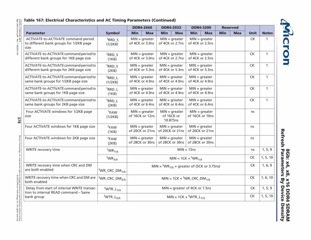
CCM
TD-1725822587-9875
Micro
n Techno
log
y, Inc. reserves the rig
ht to ch
ange p
rod
ucts or sp
ecifications w
itho
ut n
otice.
8gb
_ddr4_d
ram.p
df - Rev. T 09/2021 EN
2015 Micron
Techn
olog
y, Inc. A
ll rights reserved.
378
8Gb
: x4
, x8
, x16
DD
R4
SD
RA
MR
efresh Pa
rame
ters B
y D
evice D
ensity
ACTIVATE-to-ACTIVATE command period to different bank groups for 1/2KB page size
tRRD_S (1/2KB)
MIN = greater of 4CK or 3.0ns
MIN = greater of 4CK or 2.7ns
MIN = greater of 4CK or 2.5ns
CK 1
ACTIVATE-to-ACTIVATE command period to different bank groups for 1KB page size
tRRD_S (1KB)
MIN = greater of 4CK or 3.0ns
MIN = greater of 4CK or 2.7ns
MIN = greater of 4CK or 2.5ns
CK 1
ACTIVATE-to-ACTIVATE command period to different bank groups for 2KB page size
tRRD_S (2KB)
MIN = greater of 4CK or 5.3ns
MIN = greater of 4CK or 5.3ns
MIN = greater of 4CK or 5.3ns
CK 1
ACTIVATE-to-ACTIVATE command period to same bank groups for 1/2KB page size
tRRD_L (1/2KB)
MIN = greater of 4CK or 4.9ns
MIN = greater of 4CK or 4.9ns
MIN = greater of 4CK or 4.9ns
CK 1
ACTIVATE-to-ACTIVATE command period to same bank groups for 1KB page size
tRRD_L (1KB)
MIN = greater of 4CK or 4.9ns
MIN = greater of 4CK or 4.9ns
MIN = greater of 4CK or 4.9ns
CK 1
ACTIVATE-to-ACTIVATE command period to same bank groups for 2KB page size
tRRD_L (2KB)
MIN = greater of 4CK or 6.4ns
MIN = greater of 4CK or 6.4ns
MIN = greater of 4CK or 6.4ns
CK 1
Four ACTIVATE windows for 1/2KB page size
tFAW (1/2KB)
MIN = greater of 16CK or 12ns
MIN = greater of 16CK or 10.875ns
MIN = greater of 16CK or 10ns
ns
Four ACTIVATE windows for 1KB page size tFAW (1KB)
MIN = greater of 20CK or 21ns
MIN = greater of 20CK or 21ns
MIN = greater of 20CK or 21ns
ns
Four ACTIVATE windows for 2KB page size tFAW (2KB)
MIN = greater of 28CK or 30ns
MIN = greater of 28CK or 30ns
MIN = greater of 28CK or 30ns
ns
WRITE recovery time tWR1ck MIN = 15ns ns 1, 5, 9
tWR2ck MIN = 1CK + tWR1ckCK 1, 5, 10
WRITE recovery time when CRC and DM are both enabled
tWR_CRC_DM1ck
MIN = tWR1ck + greater of (5CK or 3.75ns) CK 1, 6, 9
WRITE recovery time when CRC and DM are both enabled
tWR_CRC_DM2ck MIN = 1CK + tWR_CRC_DM1ckCK 1, 6, 10
Delay from start of internal WRITE transac-tion to internal READ command Same bank group
tWTR_L1ck MIN = greater of 4CK or 7.5ns CK 1, 5, 9
tWTR_L2ck MIN = 1CK + tWTR_L1ckCK 1, 5, 10
Table 167: Electrical Characteristics and AC Timing Parameters (Continued)
Parameter Symbol
DDR4-2666 DDR4-2933 DDR4-3200 Reserved
Unit Notes Min Max Min Max Min Max Min Max
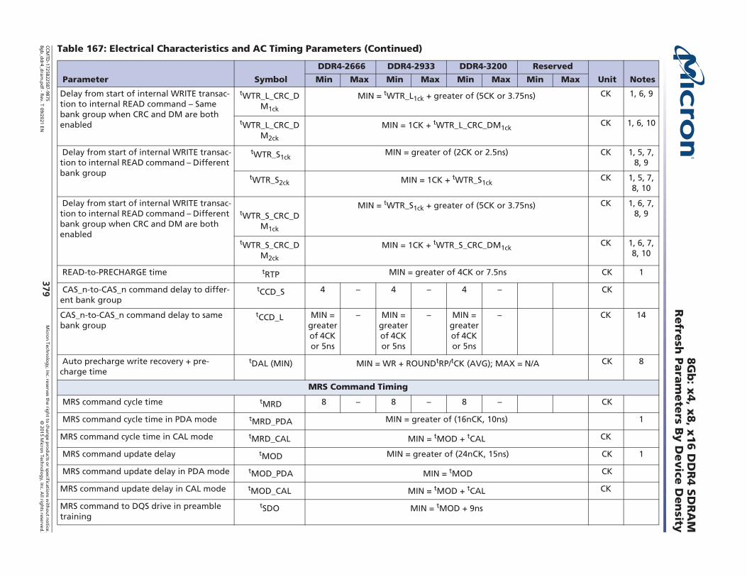
CCM
TD-1725822587-9875
Micro
n Techno
log
y, Inc. reserves the rig
ht to ch
ange p
rod
ucts or sp
ecifications w
itho
ut n
otice.
8gb
_ddr4_d
ram.p
df - Rev. T 09/2021 EN
2015 Micron
Techn
olog
y, Inc. A
ll rights reserved.
379
8Gb
: x4
, x8
, x16
DD
R4
SD
RA
MR
efresh Pa
rame
ters B
y D
evice D
ensity
Delay from start of internal WRITE transac-tion to internal READ command Same bank group when CRC and DM are both enabled
tWTR_L_CRC_DM1ck
MIN = tWTR_L1ck + greater of (5CK or 3.75ns) CK 1, 6, 9
tWTR_L_CRC_DM2ck
MIN = 1CK + tWTR_L_CRC_DM1ckCK 1, 6, 10
Delay from start of internal WRITE transac-tion to internal READ command Different bank group
tWTR_S1ckMIN = greater of (2CK or 2.5ns) CK 1, 5, 7,
8, 9
tWTR_S2ck MIN = 1CK + tWTR_S1ckCK 1, 5, 7,
8, 10
Delay from start of internal WRITE transac-tion to internal READ command Different bank group when CRC and DM are both enabled
tWTR_S_CRC_D
M1ck
MIN = tWTR_S1ck + greater of (5CK or 3.75ns) CK 1, 6, 7, 8, 9
tWTR_S_CRC_DM2ck
MIN = 1CK + tWTR_S_CRC_DM1ckCK 1, 6, 7,
8, 10
READ-to-PRECHARGE time tRTP MIN = greater of 4CK or 7.5ns CK 1
CAS_n-to-CAS_n command delay to differ-ent bank group
tCCD_S 4 4 4 CK
CAS_n-to-CAS_n command delay to same bank group
tCCD_L MIN = greater of 4CK or 5ns
MIN = greater of 4CK or 5ns
MIN = greater of 4CK or 5ns
CK 14
Auto precharge write recovery + pre-charge time
tDAL (MIN) MIN = WR + ROUNDtRP/tCK (AVG); MAX = N/A CK 8
MRS Command Timing
MRS command cycle time tMRD 8 8 8 CK
MRS command cycle time in PDA mode tMRD_PDA MIN = greater of (16nCK, 10ns) 1
MRS command cycle time in CAL mode tMRD_CAL MIN = tMOD + tCAL CK
MRS command update delay tMOD MIN = greater of (24nCK, 15ns) CK 1
MRS command update delay in PDA mode tMOD_PDA MIN = tMOD CK
MRS command update delay in CAL mode tMOD_CAL MIN = tMOD + tCAL CK
MRS command to DQS drive in preamble training
tSDO MIN = tMOD + 9ns
Table 167: Electrical Characteristics and AC Timing Parameters (Continued)
Parameter Symbol
DDR4-2666 DDR4-2933 DDR4-3200 Reserved
Unit Notes Min Max Min Max Min Max Min Max
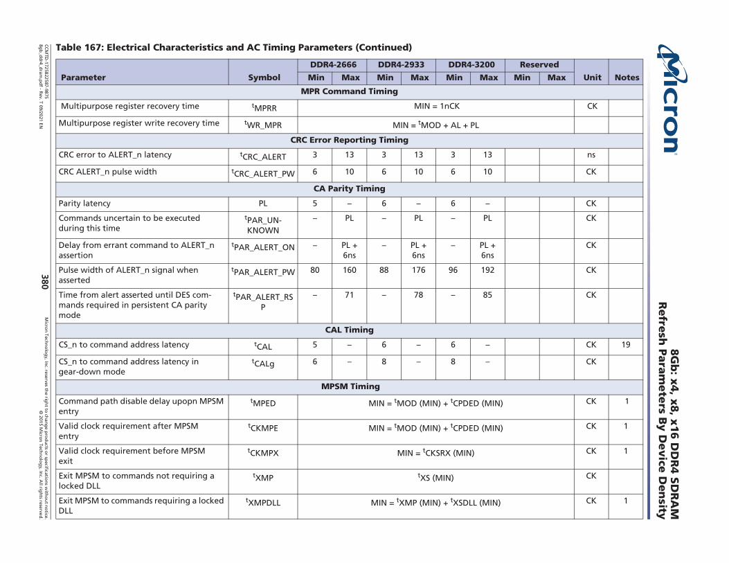
CCM
TD-1725822587-9875
Micro
n Techno
log
y, Inc. reserves the rig
ht to ch
ange p
rod
ucts or sp
ecifications w
itho
ut n
otice.
8gb
_ddr4_d
ram.p
df - Rev. T 09/2021 EN
2015 Micron
Techn
olog
y, Inc. A
ll rights reserved.
380
8Gb
: x4
, x8
, x16
DD
R4
SD
RA
MR
efresh Pa
rame
ters B
y D
evice D
ensity
MPR Command Timing
Multipurpose register recovery time tMPRR MIN = 1nCK CK
Multipurpose register write recovery time tWR_MPR MIN = tMOD + AL + PL
CRC Error Reporting Timing
CRC error to ALERT_n latency tCRC_ALERT 3 13 3 13 3 13 ns
CRC ALERT_n pulse width tCRC_ALERT_PW 6 10 6 10 6 10 CK
CA Parity Timing
Parity latency PL 5 6 6 CK
Commands uncertain to be executed during this time
tPAR_UN-KNOWN
PL PL PL CK
Delay from errant command to ALERT_n assertion
tPAR_ALERT_ON PL + 6ns
PL + 6ns
PL + 6ns
CK
Pulse width of ALERT_n signal when asserted
tPAR_ALERT_PW 80 160 88 176 96 192 CK
Time from alert asserted until DES com-mands required in persistent CA parity mode
tPAR_ALERT_RSP
71 78 85 CK
CAL Timing
CS_n to command address latency tCAL 5 6 6 CK 19
CS_n to command address latency in gear-down mode
tCALg 6 8 8 CK
MPSM Timing
Command path disable delay upopn MPSM entry
tMPED MIN = tMOD (MIN) + tCPDED (MIN) CK 1
Valid clock requirement after MPSMentry
tCKMPE MIN = tMOD (MIN) + tCPDED (MIN) CK 1
Valid clock requirement before MPSMexit
tCKMPX MIN = tCKSRX (MIN) CK 1
Exit MPSM to commands not requiring a locked DLL
tXMP tXS (MIN) CK
Exit MPSM to commands requiring a locked DLL
tXMPDLL MIN = tXMP (MIN) + tXSDLL (MIN) CK 1
Table 167: Electrical Characteristics and AC Timing Parameters (Continued)
Parameter Symbol
DDR4-2666 DDR4-2933 DDR4-3200 Reserved
Unit Notes Min Max Min Max Min Max Min Max

CCM
TD-1725822587-9875
Micro
n Techno
log
y, Inc. reserves the rig
ht to ch
ange p
rod
ucts or sp
ecifications w
itho
ut n
otice.
8gb
_ddr4_d
ram.p
df - Rev. T 09/2021 EN
2015 Micron
Techn
olog
y, Inc. A
ll rights reserved.
381
8Gb
: x4
, x8
, x16
DD
R4
SD
RA
MR
efresh Pa
rame
ters B
y D
evice D
ensity
CS setup time to CKE tMPX_S MIN = tIS (MIN) + tIH (MIN) ns
CS_n HIGH hold time to CKE rising edge tMPX_HH MIN = tXP ns
CS_n LOW hold time to CKE rising edge tMPX_LH 12 tXMP-10ns
12 tXMP-10ns
12 tXMP-10ns
ns
Connectivity Test Timing
TEN pin HIGH to CS_n LOW Enter CT mode
tCT_Enable 200 200 200 ns
CS_n LOW and valid input to valid output tCT_Valid 200 200 200 ns
CK_t, CK_c valid and CKE HIGH after TEN goes HIGH
tCTCKE_Valid 10 10 10 ns
Calibration and VREFDQ Train Timing
ZQCL command: Long cal-ibration time
POWER-UP and RESET operation
tZQinit 1024 1024 1024 CK
Normal oper-ation
tZQoper 512 512 512 CK
ZQCS command: Short calibration time tZQCS 128 128 128 CK
The VREF increment/decrement step time VREF_time MIN = 150ns
Enter VREFDQ training mode to the first write or VREFDQ MRS command delay
tVREFDQE MIN = 150ns ns 1
Exit VREFDQ training mode to the first WRITE command delay
tVREFDQX MIN = 150ns ns 1
Initialization and Reset Timing
Exit reset from CKE HIGH to a valid com-mand
tXPR MIN = tRFC1 + 10ns ns 1
RESET_L pulse low after power stable tPW_RESET_S 1.0 1.0 1.0 s
RESET_L pulse low at power-up tPW_RESET_L 200 200 200 s
Begin power supply ramp to power sup-plies stable
tVDDPR MIN = N/A; MAX = 200 ms
RESET_n LOW to power supplies stable tRPS MIN = 0; MAX = 0 ns
Table 167: Electrical Characteristics and AC Timing Parameters (Continued)
Parameter Symbol
DDR4-2666 DDR4-2933 DDR4-3200 Reserved
Unit Notes Min Max Min Max Min Max Min Max
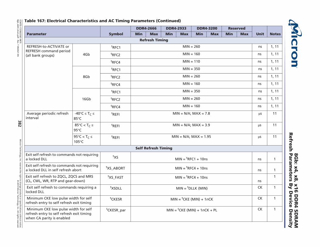
CCM
TD-1725822587-9875
Micro
n Techno
log
y, Inc. reserves the rig
ht to ch
ange p
rod
ucts or sp
ecifications w
itho
ut n
otice.
8gb
_ddr4_d
ram.p
df - Rev. T 09/2021 EN
2015 Micron
Techn
olog
y, Inc. A
ll rights reserved.
382
8Gb
: x4
, x8
, x16
DD
R4
SD
RA
MR
efresh Pa
rame
ters B
y D
evice D
ensity
Refresh Timing
REFRESH-to-ACTIVATE or REFRESH command period (all bank groups) 4Gb
tRFC1 MIN = 260 ns 1, 11
tRFC2 MIN = 160 ns 1, 11
tRFC4 MIN = 110 ns 1, 11
8Gb
tRFC1 MIN = 350 ns 1, 11
tRFC2 MIN = 260 ns 1, 11
tRFC4 MIN = 160 ns 1, 11
16Gb
tRFC1 MIN = 350 ns 1, 11
tRFC2 MIN = 260 ns 1, 11
tRFC4 MIN = 160 ns 1, 11
Average periodic refresh interval
-40 C TC 85 C
tREFI MIN = N/A; MAX = 7.8 s 11
85 C < TC 95 C
tREFI MIN = N/A; MAX = 3.9 s 11
95 C < TC 105 C
tREFI MIN = N/A; MAX = 1.95 s 11
Self Refresh Timing
Exit self refresh to commands not requiring a locked DLL
tXS MIN = tRFC1 + 10ns ns 1
Exit self refresh to commands not requiring a locked DLL in self refresh abort
tXS_ABORT MIN = tRFC4 + 10ns ns 1
Exit self refresh to ZQCL, ZQCS and MRS (CL, CWL, WR, RTP and gear-down)
tXS_FAST MIN = tRFC4 + 10nsns
1
Exit self refresh to commands requiring a locked DLL
tXSDLL MIN = tDLLK (MIN) CK 1
Minimum CKE low pulse width for self refresh entry to self refresh exit timing
tCKESR MIN = tCKE (MIN) + 1nCK CK 1
Minimum CKE low pulse width for self refresh entry to self refresh exit timing when CA parity is enabled
tCKESR_par MIN = tCKE (MIN) + 1nCK + PL CK 1
Table 167: Electrical Characteristics and AC Timing Parameters (Continued)
Parameter Symbol
DDR4-2666 DDR4-2933 DDR4-3200 Reserved
Unit Notes Min Max Min Max Min Max Min Max

CCM
TD-1725822587-9875
Micro
n Techno
log
y, Inc. reserves the rig
ht to ch
ange p
rod
ucts or sp
ecifications w
itho
ut n
otice.
8gb
_ddr4_d
ram.p
df - Rev. T 09/2021 EN
2015 Micron
Techn
olog
y, Inc. A
ll rights reserved.
383
8Gb
: x4
, x8
, x16
DD
R4
SD
RA
MR
efresh Pa
rame
ters B
y D
evice D
ensity
Valid clocks after self refresh entry (SRE) or power-down entry (PDE)
tCKSRE MIN = greater of (5CK, 10ns) CK 1
Valid clock requirement after self refresh entry or power-down when CA parity is enabled
tCKSRE_par MIN = greater of (5CK, 10ns) + PL CK 1
Valid clocks before self refresh exit (SRX) or power-down exit (PDX), or reset exit
tCKSRX MIN = greater of (5CK, 10ns) CK 1
Power-Down Timing
Exit power-down with DLL on to any valid command
tXP MIN = greater of 4CK or 6ns CK 1
Exit precharge power-down with DLL fro-zen to commands not requiring a locked DLL when CA Parity is enabled.
tXP _PAR MIN = (greater of 4CK or 6ns) + PL CK 1
CKE MIN pulse width tCKE (MIN) MIN = greater of 3CK or 5ns CK 1
Command pass disable delay tCPDED 4 4 4 CK
Power-down entry to power-down exit timing
tPD MIN = tCKE (MIN); MAX = 9 tREFI CK
Begin power-down period prior to CKE registered HIGH
tANPD WL - 1CK CK
Power-down entry period: ODT either syn-chronous or asynchronous
PDE Greater of tANPD or tRFC - REFRESH command to CKE LOW time CK
Power-down exit period: ODT either syn-chronous or asynchronous
PDX tANPD + tXSDLL CK
Power-Down Entry Minimum Timing
ACTIVATE command to power-down entry tACTPDEN 2 2 2 CK
PRECHARGE/PRECHARGE ALL command to power-down entry
tPRPDEN 2 2 2 CK
REFRESH command to power-down entry tREFPDEN 2 2 2 CK
MRS command to power-down entry tMRSPDEN MIN = tMOD (MIN) CK 1
READ/READ with auto precharge com-mand to power-down entry
tRDPDEN MIN = RL + 4 + 1 CK 1
WRITE command to power-down entry (BL8OTF, BL8MRS, BC4OTF)
tWRPDEN MIN = WL + 4 + tWR/tCK (AVG) CK 1
Table 167: Electrical Characteristics and AC Timing Parameters (Continued)
Parameter Symbol
DDR4-2666 DDR4-2933 DDR4-3200 Reserved
Unit Notes Min Max Min Max Min Max Min Max

CCM
TD-1725822587-9875
Micro
n Techno
log
y, Inc. reserves the rig
ht to ch
ange p
rod
ucts or sp
ecifications w
itho
ut n
otice.
8gb
_ddr4_d
ram.p
df - Rev. T 09/2021 EN
2015 Micron
Techn
olog
y, Inc. A
ll rights reserved.
384
8Gb
: x4
, x8
, x16
DD
R4
SD
RA
MR
efresh Pa
rame
ters B
y D
evice D
ensity
WRITE command to power-down entry (BC4MRS)
tWRPBC4DEN MIN = WL + 2 + tWR/tCK (AVG) CK 1
WRITE with auto precharge command to power-down entry (BL8OTF, BL8MRS,BC4OTF)
tWRAPDEN MIN = WL + 4 + WR + 1 CK 1
WRITE with auto precharge command to power-down entry (BC4MRS)
tWRAPBC4DEN MIN = WL + 2 + WR + 1 CK 1
ODT Timing
Direct ODT turn-on latency DODTLon WL - 2 = CWL + AL + PL - 2 CK
Direct ODT turn-off latency DODTLoff WL - 2 = CWL + AL + PL - 2 CK
RTT dynamic change skew tADC 0.28 0.72 0.26 0.74 0.26 0.74 CK
Asynchronous RTT(NOM) turn-on delay (DLL off)
tAONAS 1 9 1 9 1 9 ns
Asynchronous RTT(NOM) turn-off delay (DLL off)
tAOFAS 1 9 1 9 1 9 ns
ODT HIGH time with WRITE command and BL8
ODTH8 1tCK 6 6 6 CK
ODTH8 2tCK 7 7 7
ODT HIGH time without WRITE command or with WRITE command and BC4
ODTH4 1tCK 4 4 4 CK
ODTH4 2tCK 5 5 5
Write Leveling Timing
First DQS_t, DQS_c rising edge after write leveling mode is programmed
tWLMRD 40 40 40 CK
DQS_t, DQS_c delay after write leveling mode is programmed
tWLDQSEN 25 25 25 CK
Write leveling setup from rising CK_t, CK_c crossing to rising DQS_t, DQS_c crossing
tWLS 0.13 0.13 0.13 CK
Write leveling hold from rising DQS_t, DQS_c crossing to rising CK_t, CK_c crossing
tWLH 0.13 0.13 0.13 CK
Write leveling output delay tWLO 0 9.5 0 9.5 0 9.5 ns
Write leveling output error tWLOE 0 2 0 2 0 2 ns
Gear-Down Timing
Table 167: Electrical Characteristics and AC Timing Parameters (Continued)
Parameter Symbol
DDR4-2666 DDR4-2933 DDR4-3200 Reserved
Unit Notes Min Max Min Max Min Max Min Max

CCM
TD-1725822587-9875
Micro
n Techno
log
y, Inc. reserves the rig
ht to ch
ange p
rod
ucts or sp
ecifications w
itho
ut n
otice.
8gb
_ddr4_d
ram.p
df - Rev. T 09/2021 EN
2015 Micron
Techn
olog
y, Inc. A
ll rights reserved.
385
8Gb
: x4
, x8
, x16
DD
R4
SD
RA
MR
efresh Pa
rame
ters B
y D
evice D
ensity
Notes: 1. Maximum limit not applicable.2. Micron tDLLK values support the legacy JEDEC tDLLK specifications.3. DDR4-1600 AC timing parameters apply if DRAM operates at lower than 1600 MT/s data rate.4. Data rate is greater than or equal to 1066 Mb/s.5. WRITE-to-READ when CRC and DM are both not enabled.6. WRITE-to-READ delay when CRC and DM are both enabled.7. The start of internal write transactions is defined as follows:
For BL8 (fixed by MRS and on-the-fly): rising clock edge four clock cycles after WLFor BC4 (on-the-fly): rising clock edge four clock cycles after WLFor BC4 (fixed by MRS): rising clock edge two clock cycles after WL
8. For these parameters, the device supports tnPARAM [nCK] = ROUND{tPARAM [ns]/tCK (AVG) [ns]} according to the rounding algorithms found in the Converting Time-Based Specifications to Clock-Based Requirements section, in clock cycles, assuming all input clock jitter specifications are satisfied.
9. When operating in 1tCK WRITE preamble mode.
10. When operating in 2tCK WRITE preamble mode.
11. When CA parity mode is selected and the DLLoff mode is used, each REF command requires an additional "PL" added to tRFC refresh time.12. DRAM devices should be evenly addressed when being accessed. Disproportionate accesses to a particular row address may result in reduction
of the product lifetime and/or reduction in data retention ability.
13. Applicable from tCK (AVG) MIN to tCK (AVG) MAX as stated in the Speed Bin tables.14. JEDEC specifies a minimum of five clocks.
15. The maximum read postamble is bound by tDQSCK (MIN) plus tQSH (MIN) on the left side and tHZ(DQS) MAX on the right side.16. The reference level of DQ output signal is specified with a midpoint as a widest part of output signal eye, which should be approximately 0.7
VDDQ as a center level of the static single-ended output peak-to-peak swing with a driver impedance of 34 ohms and an effective test load of 50 ohms to VTT = VDDQ.
17. JEDEC hasn't agreed upon the definition of the deterministic jitter; the user should focus on meeting the total limit.
Exit reset from CKE HIGH to a valid MRS gear-down
tXPR_GEAR tXPR tXPR tXPR CK
CKE HIGH assert to gear-down enable time) tXS_GEAR tXS tXS tXS CK
MRS command to sync pulse time tSYNC_GEAR tMOD + 4CK tMOD + 4CK tMOD + 4CK CK
Sync pulse to first valid command tCMD_GEAR tMOD tMOD tMOD CK
Gear-down setup time tGEAR_setup 2CK 2CK 2CK CK
Gear-down hold time tGEAR_hold 2CK 2CK 2CK CK
Table 167: Electrical Characteristics and AC Timing Parameters (Continued)
Parameter Symbol
DDR4-2666 DDR4-2933 DDR4-3200 Reserved
Unit Notes Min Max Min Max Min Max Min Max

CCM
TD-1725822587-9875
Micro
n Techno
log
y, Inc. reserves the rig
ht to ch
ange p
rod
ucts or sp
ecifications w
itho
ut n
otice.
8gb
_ddr4_d
ram.p
df - Rev. T 09/2021 EN
2015 Micron
Techn
olog
y, Inc. A
ll rights reserved.
386
8Gb
: x4
, x8
, x16
DD
R4
SD
RA
MR
efresh Pa
rame
ters B
y D
evice D
ensity
18. Spread spectrum is not included in the jitter specification values. However, the input clock can accommodate spread-spectrum at a sweep rate
in the range of 20 60 kHz with an additional 1% of tCK (AVG) as a long-term jitter component; however, the spread spectrum may not use a
clock rate below tCK (AVG) MIN.
19. The actual tCAL minimum is the larger of 3 clocks or 3.748ns/tCK; the table lists the applicable clocks required at targeted speed bin.
20. The maximum READ preamble is bounded by tLZ(DQS) MIN on the left side and tDQSCK (MAX) on the right side. See figure in the Clock to Data
Strobe Relationship section. Boundary of DQS Low-Z occurs one cycle earlier in 2tCK toggle mode, as illustrated in the READ Preamble section.21. DQ falling signal middle-point of transferring from HIGH to LOW to first rising edge of DQS differential signal cross-point.
22. The tPDA_S/tPDA_H parameters may use the tDS/tDH limits, respectively, if the signal is LOW the entire BL8.
CCMTD-1725822587-9875 Micron Technology, Inc. reserves the right to change products or specifications without notice.8gb_ddr4_dram.pdf - Rev. T 09/2021 EN 2015 Micron Technology, Inc. All rights reserved.387
8Gb: x4, x8, x16 DDR4 SDRAMClock Specification
Clock Specification
The jitter specified is a random jitter meeting a Gaussian distribution. Input clocks violating the MIN/MAX values may result in malfunction of the DDR4 SDRAM device.
Definition for tCK(AVG)
tCK(AVG) is calculated as the average clock period across any consecutive 200-cycle window, where each clock period is calculated from rising edge to rising edge.
Definition for tCK(ABS)
tCK(ABS) is defined as the absolute clock period as measured from one rising edge to the next consec-
utive rising edge. tCK(ABS) is not subject to a production test.
Definition for tCH(AVG) and tCL(AVG)
tCH(AVG) is defined as the average high pulse width as calculated across any consecutive 200 high pulses.
tCL(AVG) is defined as the average low pulse width as calculated across any consecutive 200 low pulses.
Definition for tJIT(per) and tJIT(per,lck)
tJIT(per) is defined as the largest deviation of any signal tCK from tCK(AVG).
tJIT(per) = MIN/MAX of {tCKi - tCK(AVG) where i = 1 to 200}.
tJIT(per) defines the single period jitter when the DLL is already locked.
tJIT(per,lck) uses the same definition for single period jitter, but only during the DLL locking period.
tJIT(per) and tJIT(per,lck) are not subject to production test.
Definition for tJIT(cc) and tJIT(cc,lck)
tJIT(cc) is defined as the absolute difference in clock period between two consecutive clock cycles.
tJIT(cc) = MAX of |{tCKi +1 - tCKi}|.
tJIT(cc) defines the cycle to cycle jitter when the DLL is already locked.
tJIT(cc,lck) uses the same definition for cycle to cycle jitter, during the DLL locking period only.
tCK(avg) = tCKj /N
Where N = 200
N
j = 1
tCH(AVG) = tCHj /(N × tCK(AVG))
Where N = 200
N
j = 1
tCL(AVG) = tCLj /(N × tCK(AVG))
Where N = 200
N
j = 1

CCMTD-1725822587-9875 Micron Technology, Inc. reserves the right to change products or specifications without notice.8gb_ddr4_dram.pdf - Rev. T 09/2021 EN 2015 Micron Technology, Inc. All rights reserved.388
8Gb: x4, x8, x16 DDR4 SDRAMJitter Notes
tJIT(cc) and tJIT(cc,lck) are not subject to production test.
Definition for tERR(nper)
tERR is defined as the cumulative error across n multiple consecutive cycles from tCK(AVG). tERR is not subject to a production test.
Jitter Notes
Note a: Unit tCK(AVG) represents the actual tCK(AVG) of the input clock under operation. Unit nCK
represents one clock cycle of the input clock, including the actual clock edges. Example: tMRD = 4 [nCK] means that if one MODE REGISTER SET command is registered at Tm, another MODE
REGISTER SET command may be registered at Tm + 4, even if (Tm + 4 - Tm) is (4 tCK(AVG) + tERR (4 per) MIN).
Note b: These parameters are measured from a command/address signal (such as CKE, CS_n, RAS_n, CAS_n, WE_n, ODT, BA0, A0, or A1) transition edge to its respective clock signal (CK_t/CK_c) crossing.
The specification values are not affected by the amount of clock jitter applied (for example, tJITper, tJITcc) because the setup and hold are relative to the clock signal crossing that latches the command/address. That is, these parameters should be met whether clock jitter is present or not.
Note c: These parameters are measured from a data strobe signal (DQS_t[L/U], DQS_c[L/U]) crossing to its respective clock signal (CK_t, CK_c) crossing. The specification values are not affected by the
amount of clock jitter applied (for example, tJITper, tJITcc) because these are relative to the clock signal crossing. That is, these parameters should be met whether clock jitter is present or not.
Note d: These parameters are measured from a data signal (such as DM[L/U], DQ[L/U]0, or DQ[L/U]1) transition edge to its respective data strobe signal (DQS_t[L/U], DQS_c[L/U]) crossing.
Note e: For these parameters, the DDR4 SDRAM device supports tnPARAM [nCK] = RU[tPARAM
[ns]/tCK(AVG) [ns]], which is in clock cycles, assuming all input clock jitter specifications are satisfied.
For example, the device will support tnRP = RU [tRP/tCK(AVG)], which is in clock cycles, if all input
clock jitter specifications are met. This means that for DDR4-800 6-6-6, tRP = 15ns, the device will
support tnRP = RU[tRP/tCK(AVG)] = 6, as long as the input clock jitter specifications are met. For example, the PRECHARGE command at Tm and ACTIVE command at Tm + 6 is valid even if (Tm + 6 - Tm) is less than 15ns due to input clock jitter.
Note f: When the device is operated with input clock jitter, this parameter needs to be derated by the
actual tERR(mper), act of the input clock, where 2 m 12 (output deratings are relative to the SDRAM
input clock). For example, if the measured jitter into a DDR4-800 SDRAM has tERR(mper), act, MIN = tERR(mper), act, MAX = +193ps, then tDQSCK, MIN(derated) = tDQSCK, MIN - tERR(mper),
tDQSCK, MAX(derated) = tDQSCK, MAX - tERR(mper), act, MIN
= 400ps + 172ps = 572ps. Similarly, tLZ(DQ) for DDR4-800 derates to t
tLZ(DQ), MAX(derated) = 400ps + 172ps = 572ps. Note that tERR(mper), act, MIN
is the minimum measured value of tERR(nper) where 2 n 12, and tERR(mper), act, MAX is the
maximum measured value of tERR(nper) where 2 n 12.
Note g: When the device is operated with input clock jitter, this parameter needs to be derated by the
actual tJIT(per), act of the input clock (output deratings are relative to the SDRAM input clock). For
example, if the measured jitter into a DDR4-800 SDRAM has tCK(AVG), act = 2500ps, tJIT(per), act, MIN
CCMTD-1725822587-9875 Micron Technology, Inc. reserves the right to change products or specifications without notice.8gb_ddr4_dram.pdf - Rev. T 09/2021 EN 2015 Micron Technology, Inc. All rights reserved.389
8Gb: x4, x8, x16 DDR4 SDRAMConverting Time-Based Specifications to Clock-Based
Requirements
tJIT(per), act, MAX = +93ps, then tRPRE, MIN(derated) = tRPRE, MIN + tJIT(per), act, MIN
= 0.9 tCK(AVG), act + tJIT(per), act, MIN = 0.9 2500ps - 72ps = 2178ps. Similarly, tQH, MIN(derated)
= tQH, MIN + tJIT(per), act, MIN = 0.38 tCK(AVG), act + tJIT(per), act, MIN = 0.38 2500ps - 72ps = 878ps.
Converting Time-Based Specifications to Clock-Based Requirements
Software algorithms for calculation of timing parameters are subject to potential rounding errors when converting DRAM timing requirements to system clocks; for example, a memory clock with a nominal frequency of 933.33...3 MHz which yields a clock period of 1.071428571429...ns. It is unrealistic to represent all digits after the decimal point exactly and some sort of rounding needs to be done.
DDR4 SDRAM SPD-based specifications use a minimum granularity for SPD-associated timing
parameters of 1ps. Clock periods such as tCK (AVG) MIN are defined to the nearest picosecond. For
example, 1.071428571429...ns is stated as 1071ps. Parameters such as tAA MIN are specified in units of time (nanoseconds) and require mathematical computation to convert to system clocks (nCK). Rules for rounding allow optimization of device performance without violating device parameters. These SPD algorithms rely on results that are within nCK adjustment factors on device testing and specifica-tion to avoid losing performance due to rounding errors when using SPD-based parameters. Note that JEDEC also defines an nCK adjustment factor, but mandates the inverse nCK adjustment factor be used in case of conflicting results, so only the inverse nCK adjustment factor is discussed here.
Guidance converting SPD associated timing parameters to system clock requirements: Round the application clock period up to the nearest picosecond.Express the timing specification and application clock period in picoseconds; scaling a nano-second-based parameter value by 1000 allows programmers to use integer math instead of real math by expressing timing in ps.Divide the picosecond-based parameter by the picoseconds based application clock period.Add an inverse nCK adjustment factor of 97.4%.Truncate down to the next lower integer value.
nCK = Truncate[(parameter in ps)/(application tCK in ps) + (974/1000)].
Guidance converting nonSPD associated timing parameters to system clock requirements: Divide the time base specification (in ns) and divided by the clock period (in ns).The resultant is set to the next higher integer number of clocks.
nCK = Ceiling[(parameter in ns/application tCK in ns)].
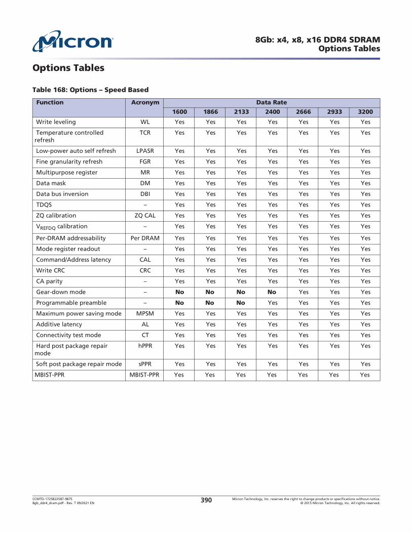
CCMTD-1725822587-9875 Micron Technology, Inc. reserves the right to change products or specifications without notice.8gb_ddr4_dram.pdf - Rev. T 09/2021 EN 2015 Micron Technology, Inc. All rights reserved.390
8Gb: x4, x8, x16 DDR4 SDRAMOptions Tables
Options Tables
Table 168:
Function Acronym Data Rate
1600 1866 2133 2400 2666 2933 3200
Write leveling WL Yes Yes Yes Yes Yes Yes Yes
Temperature controlled refresh
TCR Yes Yes Yes Yes Yes Yes Yes
Low-power auto self refresh LPASR Yes Yes Yes Yes Yes Yes Yes
Fine granularity refresh FGR Yes Yes Yes Yes Yes Yes Yes
Multipurpose register MR Yes Yes Yes Yes Yes Yes Yes
Data mask DM Yes Yes Yes Yes Yes Yes Yes
Data bus inversion DBI Yes Yes Yes Yes Yes Yes Yes
TDQS Yes Yes Yes Yes Yes Yes Yes
ZQ calibration ZQ CAL Yes Yes Yes Yes Yes Yes Yes
VREFDQ calibration Yes Yes Yes Yes Yes Yes Yes
Per-DRAM addressability Per DRAM Yes Yes Yes Yes Yes Yes Yes
Mode register readout Yes Yes Yes Yes Yes Yes Yes
Command/Address latency CAL Yes Yes Yes Yes Yes Yes Yes
Write CRC CRC Yes Yes Yes Yes Yes Yes Yes
CA parity Yes Yes Yes Yes Yes Yes Yes
Gear-down mode No No No No Yes Yes Yes
Programmable preamble No No No Yes Yes Yes Yes
Maximum power saving mode MPSM Yes Yes Yes Yes Yes Yes Yes
Additive latency AL Yes Yes Yes Yes Yes Yes Yes
Connectivity test mode CT Yes Yes Yes Yes Yes Yes Yes
Hard post package repair mode
hPPR Yes Yes Yes Yes Yes Yes Yes
Soft post package repair mode sPPR Yes Yes Yes Yes Yes Yes Yes
MBIST-PPR MBIST-PPR Yes Yes Yes Yes Yes Yes Yes

CCMTD-1725822587-9875 Micron Technology, Inc. reserves the right to change products or specifications without notice.8gb_ddr4_dram.pdf - Rev. T 09/2021 EN 2015 Micron Technology, Inc. All rights reserved.391
8Gb: x4, x8, x16 DDR4 SDRAMOptions Tables
8000 S. Federal Way, P.O. Box 6, Boise, ID 83707-0006208-368-4000, micron.com/support
Micron and the Micron logo are trademarks of Micron Technology, Inc.All other trademarks are the property of their respective owners.
This data sheet contains minimum and maximum limits specified over the power supply and temperature range set forth herein.Although considered final, these specifications are subject to change, as further product development and data characterization sometimes
occur.
Table 169:
Function Acronym Width
x4 x8 x16
Write leveling WL Yes Yes Yes
Temperature controlled refresh TCR Yes Yes Yes
Low-power auto self refresh LPASR Yes Yes Yes
Fine granularity refresh FGR Yes Yes Yes
Multipurpose register MR Yes Yes Yes
Data mask DM No Yes Yes
Data bus inversion DBI No Yes Yes
TDQS No Yes No
ZQ calibration ZQ CAL Yes Yes Yes
VREFDQ calibration Yes Yes Yes
Per-DRAM addressability Per DRAM Yes Yes Yes
Mode regsiter readout Yes Yes Yes
Command/Address latency CAL Yes Yes Yes
Write CRC CRC Yes Yes Yes
CA parity Yes Yes Yes
Gear-down mode Yes Yes Yes
Programmable preamble Yes Yes Yes
Maximum power-down mode MPSM Yes Yes Yes
Additive latency AL Yes Yes Yes
Connectivity test mode CT JEDEC optional on 8Gb and larger densities Micron supports on all densities
Yes
Hard post package repair mode hPPR JEDEC optional on 4Gb Micron supports on all densities
Soft post package repair mode sPPR JEDEC optional on 4Gb and 8Gb Micron supports on all densities
MBIST-PPR MBIST-PPR JEDEC optional Micron supports only on 8Gb Die Rev R and 16Gb Die Rev F