Technical Data Sheet 256Mb: x4, x8, x16 DDR SDRAM - Octopart
93
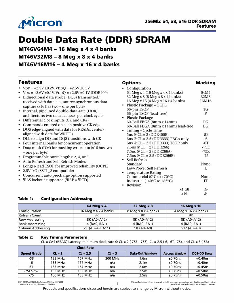
Products and specifications discussed herein are subject to change by Micron without notice. 256Mb: x4, x8, x16 DDR SDRAM Features PDF: 09005aef80768abb/Source: 09005aef8076894f Micron Technology, Inc., reserves the right to change products or specifications without notice. 256MBDDRx4x8x16_1.fm - Rev. L 6/06 EN 1 ©2003 Micron Technology, Inc. All rights reserved. Double Data Rate (DDR) SDRAM MT46V64M4 – 16 Meg x 4 x 4 banks MT46V32M8 – 8 Meg x 8 x 4 banks MT46V16M16 – 4 Meg x 16 x 4 banks Features • VDD = +2.5V ±0.2V, VDDQ = +2.5V ±0.2V • VDD = +2.6V ±0.1V, VDDQ = +2.6V ±0.1V (DDR400) • Bidirectional data strobe (DQS) transmitted/ received with data, i.e., source-synchronous data capture (x16 has two – one per byte) • Internal, pipelined double-data-rate (DDR) architecture; two data accesses per clock cycle • Differential clock inputs (CK and CK#) • Commands entered on each positive CK edge • DQS edge-aligned with data for READs; center- aligned with data for WRITEs • DLL to align DQ and DQS transitions with CK • Four internal banks for concurrent operation • Data mask (DM) for masking write data (x16 has two – one per byte) • Programmable burst lengths: 2, 4, or 8 • Auto Refresh and Self Refresh Modes • Longer-lead TSOP for improved reliability (OCPL) • 2.5V I/O (SSTL_2 compatible) • Concurrent auto precharge option supported • t RAS lockout supported ( t RAP = t RCD) Options Marking • Configuration 64 Meg x 4 (16 Meg x 4 x 4 banks) 64M4 32 Meg x 8 (8 Meg x 8 x 4 banks) 32M8 16 Meg x 16 (4 Meg x 16 x 4 banks) 16M16 • Plastic Package – OCPL 66-pin TSOP TG 66-pin TSOP (lead-free) P • Plastic Package 60-Ball FBGA (8mm x 14mm) FG 60-Ball FBGA (8mm x 14mm) lead-free BG • Timing – Cycle Time 5ns @ CL = 3 (DDR400B) -5B 6ns @ CL = 2.5 (DDR333) FBGA only -6 6ns @ CL = 2.5 (DDR333) TSOP only -6T 7.5ns @ CL = 2 (DDR266) -75E 7.5ns @ CL = 2 (DDR266A) -75Z 7.5ns @ CL = 2.5 (DDR266B) -75 • Self Refresh Standard None Low-Power Self Refresh L • Temperature Rating Commercial (0°C to +70°C) None Industrial (–40°C to +85°C) IT • Revision x4, x8 :G x16 :F Table 1: Configuration Addressing 64 Meg x 4 32 Meg x 8 16 Meg x 16 Configuration 16 Meg x 4 x 4 banks 8 Meg x 8 x 4 banks 4 Meg x 16 x 4 banks Refresh Count 8K 8K 8K Row Addressing 8K (A0–A12) 8K (A0–A12) 8K (A0–A12) Bank Addressing 4 (BA0, BA1) 4 (BA0, BA1) 4 (BA0, BA1) Column Addressing 2K (A0–A9, A11) 1K (A0–A9) 512 (A0–A8) Table 2: Key Timing Parameters CL = CAS (READ) Latency; minimum clock rate @ CL = 2 (-75E, -75Z), CL = 2.5 (-6, -6T, -75), and CL = 3 (-5B) Speed Grade Clock Rate Data-Out Window Access Window DQS–DQ Skew CL = 2 CL = 2.5 CL = 3 -5B 133 MHz 167 MHz 200 MHz 1.6ns ±0.70ns +0.40ns -6 133 MHz 167 MHz n/a 2.1ns ±0.70ns +0.40ns 6T 133 MHz 167 MHz n/a 2.0ns ±0.70ns +0.45ns -75E/-75Z 133 MHz 133 MHz n/a 2.5ns ±0.75ns +0.50ns -75 100 MHz 133 MHz n/a 2.5ns ±0.75ns +0.50ns
-
Upload
khangminh22 -
Category
Documents
-
view
3 -
download
0
Transcript of Technical Data Sheet 256Mb: x4, x8, x16 DDR SDRAM - Octopart
256Mb: x4, x8, x16 DDR SDRAMFeatures
Double Data Rate (DDR) SDRAMMT46V64M4 – 16 Meg x 4 x 4 banksMT46V32M8 – 8 Meg x 8 x 4 banksMT46V16M16 – 4 Meg x 16 x 4 banks
Features• VDD = +2.5V ±0.2V, VDDQ = +2.5V ±0.2V• VDD = +2.6V ±0.1V, VDDQ = +2.6V ±0.1V (DDR400)• Bidirectional data strobe (DQS) transmitted/
received with data, i.e., source-synchronous data capture (x16 has two – one per byte)
• Internal, pipelined double-data-rate (DDR) architecture; two data accesses per clock cycle
• Differential clock inputs (CK and CK#)• Commands entered on each positive CK edge• DQS edge-aligned with data for READs; center-
aligned with data for WRITEs• DLL to align DQ and DQS transitions with CK• Four internal banks for concurrent operation• Data mask (DM) for masking write data (x16 has two
– one per byte)• Programmable burst lengths: 2, 4, or 8• Auto Refresh and Self Refresh Modes• Longer-lead TSOP for improved reliability (OCPL)• 2.5V I/O (SSTL_2 compatible)• Concurrent auto precharge option supported• tRAS lockout supported (tRAP = tRCD)
Table 1: Configuration Addressing
Products and specifications discussed herein are
PDF: 09005aef80768abb/Source: 09005aef8076894f256MBDDRx4x8x16_1.fm - Rev. L 6/06 EN 1
Options Marking• Configuration
64 Meg x 4 (16 Meg x 4 x 4 banks) 64M432 Meg x 8 (8 Meg x 8 x 4 banks) 32M816 Meg x 16 (4 Meg x 16 x 4 banks) 16M16
• Plastic Package – OCPL66-pin TSOP TG66-pin TSOP (lead-free) P
• Plastic Package60-Ball FBGA (8mm x 14mm) FG60-Ball FBGA (8mm x 14mm) lead-free BG
• Timing – Cycle Time5ns @ CL = 3 (DDR400B) -5B6ns @ CL = 2.5 (DDR333) FBGA only -66ns @ CL = 2.5 (DDR333) TSOP only -6T7.5ns @ CL = 2 (DDR266) -75E7.5ns @ CL = 2 (DDR266A) -75Z7.5ns @ CL = 2.5 (DDR266B) -75
• Self RefreshStandard NoneLow-Power Self Refresh L
• Temperature RatingCommercial (0°C to +70°C) NoneIndustrial (–40°C to +85°C) IT
• Revisionx4, x8 :G
x16 :F
64 Meg x 4 32 Meg x 8 16 Meg x 16Configuration 16 Meg x 4 x 4 banks 8 Meg x 8 x 4 banks 4 Meg x 16 x 4 banksRefresh Count 8K 8K 8KRow Addressing 8K (A0–A12) 8K (A0–A12) 8K (A0–A12)Bank Addressing 4 (BA0, BA1) 4 (BA0, BA1) 4 (BA0, BA1)Column Addressing 2K (A0–A9, A11) 1K (A0–A9) 512 (A0–A8)
Table 2: Key Timing ParametersCL = CAS (READ) Latency; minimum clock rate @ CL = 2 (-75E, -75Z), CL = 2.5 (-6, -6T, -75), and CL = 3 (-5B)
Speed Grade
Clock Rate
Data-Out Window Access Window DQS–DQ SkewCL = 2 CL = 2.5 CL = 3-5B 133 MHz 167 MHz 200 MHz 1.6ns ±0.70ns +0.40ns-6 133 MHz 167 MHz n/a 2.1ns ±0.70ns +0.40ns6T 133 MHz 167 MHz n/a 2.0ns ±0.70ns +0.45ns
-75E/-75Z 133 MHz 133 MHz n/a 2.5ns ±0.75ns +0.50ns-75 100 MHz 133 MHz n/a 2.5ns ±0.75ns +0.50ns
subject to change by Micron without notice.
Micron Technology, Inc., reserves the right to change products or specifications without notice.©2003 Micron Technology, Inc. All rights reserved.

256Mb: x4, x8, x16 DDR SDRAMFBGA Part Marking System
Figure 1: 256Mb DDR SDRAM Part Numbers
FBGA Part Marking SystemDue to space limitations, FBGA-packaged components have an abbreviated part mark-ing that is different from the part number. For a quick conversion of an FBGA code, see the FBGA Part Marking Decoder on the Micron Web site: www.micron.com/decoder.
Table 3: Speed Grade Compatibility
Marking PC3200 (3-3-3) PC2700 (2.5-3-3) PC2100 (2-2-2) PC2100 (2-3-3) PC2100 (2.5-3-3) PC1600 (2-2-2)
-5B Yes Yes Yes Yes Yes Yes
-6 – Yes Yes Yes Yes Yes
-6T – Yes Yes Yes Yes Yes
-75E – – Yes Yes Yes Yes
-75Z – – – Yes Yes Yes
-75 – – – – Yes Yes
-5B -6/-6T -75E -75Z -75 -75
L
Special Options
Standard
Low Power
Configuration
64 Meg x 4
32 Meg x 8
16 Meg x 16
64M4
32M8
16M16
Package
400-mil TSOP
400-mil TSOP (lead-free)
8x14 FBGA
8x14 FBGA (lead-free)
TG
P
FG
BG Speed Grade
tCK = 5ns, CL = 3
tCK = 6ns, CL = 2.5
tCK = 6ns, CL = 2.5
tCK = 7.5ns, CL = 2
tCK = 7.5ns, CL = 2
tCK = 7.5ns, CL = 2.5
-5B
-6
-6T
-75E
-75Z
-75
I T
Operating Temp
Standard
Industrial Temp
Example Part Number: MT46V16M16TG-75E
-
ConfigurationMT46V Package Speed
:
RevisionSp.Op. Temp.
Revision
x16
x4, x8
:F
:G
PDF: 09005aef80768abb/Source: 09005aef8076894f Micron Technology, Inc., reserves the right to change products or specifications without notice.256MBDDRx4x8x16_1.fm - Rev. L 6/06 EN 2 ©2003 Micron Technology, Inc. All rights reserved.

256Mb: x4, x8, x16 DDR SDRAMGeneral Description
General DescriptionThe 256Mb DDR SDRAM is a high-speed CMOS, dynamic random-access memory con-taining 268,435,456 bits. It is internally configured as a quad-bank DRAM.
The 256Mb DDR SDRAM uses a double-data-rate architecture to achieve high-speed operation. The double-data-rate architecture is essentially a 2n-prefetch architecture with an interface designed to transfer two data words per clock cycle at the I/O pins. A single read or write access for the 256Mb DDR SDRAM effectively consists of a single 2n-bit wide, one-clock-cycle data transfer at the internal DRAM core and two correspond-ing n-bit wide, one-half-clock-cycle data transfers at the I/O pins.
A bidirectional data strobe (DQS) is transmitted externally, along with data, for use in data capture at the receiver. DQS is a strobe transmitted by the DDR SDRAM during READs and by the memory controller during WRITEs. DQS is edge-aligned with data for READs and center-aligned with data for WRITEs. The x16 offering has two data strobes, one for the lower byte and one for the upper byte.
The 256Mb DDR SDRAM operates from a differential clock (CK and CK#); the crossing of CK going HIGH and CK# going LOW will be referred to as the positive edge of CK. Com-mands (address and control signals) are registered at every positive edge of CK. Input data is registered on both edges of DQS, and output data is referenced to both edges of DQS, as well as to both edges of CK.
Read and write accesses to the DDR SDRAM are burst oriented; accesses start at a selected location and continue for a programmed number of locations in a programmed sequence. Accesses begin with the registration of an ACTIVE command, which is then followed by a READ or WRITE command. The address bits registered coincident with the ACTIVE command are used to select the bank and row to be accessed. The address bits registered coincident with the READ or WRITE command are used to select the bank and the starting column location for the burst access.
The DDR SDRAM provides for programmable READ or WRITE burst lengths of 2, 4, or 8 locations. An auto precharge function may be enabled to provide a self-timed row pre-charge that is initiated at the end of the burst access.
As with standard SDR SDRAMs, the pipelined, multibank architecture of DDR SDRAMs allows for concurrent operation, thereby effectively providing high bandwidth by hiding row precharge and activation time.
An auto refresh mode is provided, along with a power-saving power-down mode. All inputs are compatible with the JEDEC standard for SSTL_2. All full drive option outputs are SSTL_2, Class II compatible.
Notes: 1. The functionality and the timing specifications discussed in this data sheet are for theDLL-enabled mode of operation.
2. Throughout the data sheet, the various figures and text refer to DQs as “DQ.” The DQterm is to be interpreted as any and all DQ collectively, unless specifically stated oth-erwise. Additionally, the x16 is divided into two bytes, the lower byte and upper byte.For the lower byte (DQ0 through DQ7) DM refers to LDM and DQS refers to LDQS. Forthe upper byte (DQ8 through DQ15) DM refers to UDM and DQS refers to UDQS.
3. Complete functionality is described throughout the document and any page or dia-gram may have been simplified to convey a topic and may not be inclusive of allrequirements.
4. Any specific requirement takes precedence over a general statement.
PDF: 09005aef80768abb/Source: 09005aef8076894f Micron Technology, Inc., reserves the right to change products or specifications without notice.256MBDDRx4x8x16_1.fm - Rev. L 6/06 EN 3 ©2003 Micron Technology, Inc. All rights reserved.

PDF: 09005aef80768abb/Source: 09005aef8076894f Micron Technology, Inc., reserves the right to change products or specifications without notice.256MBDDRx4x8x16TOC.fm - Rev. L 6/06 EN 4 ©2003 Micron Technology, Inc. All rights reserved.
256Mb: x4, x8, x16 DDR SDRAMTable of Contents
Table of ContentsFeatures . . . . . . . . . . . . . . . . . . . . . . . . . . . . . . . . . . . . . . . . . . . . . . . . . . . . . . . . . . . . . . . . . . . . . . . . . . . . . . . . . . . . . . . . . . . . . .1FBGA Part Marking System . . . . . . . . . . . . . . . . . . . . . . . . . . . . . . . . . . . . . . . . . . . . . . . . . . . . . . . . . . . . . . . . . . . . . . . . . . . . .2General Description . . . . . . . . . . . . . . . . . . . . . . . . . . . . . . . . . . . . . . . . . . . . . . . . . . . . . . . . . . . . . . . . . . . . . . . . . . . . . . . . . . .3Pin/Ball Assignments and Descriptions. . . . . . . . . . . . . . . . . . . . . . . . . . . . . . . . . . . . . . . . . . . . . . . . . . . . . . . . . . . . . . . . .10Functional Description . . . . . . . . . . . . . . . . . . . . . . . . . . . . . . . . . . . . . . . . . . . . . . . . . . . . . . . . . . . . . . . . . . . . . . . . . . . . . . .14Initialization . . . . . . . . . . . . . . . . . . . . . . . . . . . . . . . . . . . . . . . . . . . . . . . . . . . . . . . . . . . . . . . . . . . . . . . . . . . . . . . . . . . . . . . . .14Register Definition . . . . . . . . . . . . . . . . . . . . . . . . . . . . . . . . . . . . . . . . . . . . . . . . . . . . . . . . . . . . . . . . . . . . . . . . . . . . . . . . . . .15
Mode Register . . . . . . . . . . . . . . . . . . . . . . . . . . . . . . . . . . . . . . . . . . . . . . . . . . . . . . . . . . . . . . . . . . . . . . . . . . . . . . . . . . . . .15Burst Length . . . . . . . . . . . . . . . . . . . . . . . . . . . . . . . . . . . . . . . . . . . . . . . . . . . . . . . . . . . . . . . . . . . . . . . . . . . . . . . . . . . . . .15Burst Type . . . . . . . . . . . . . . . . . . . . . . . . . . . . . . . . . . . . . . . . . . . . . . . . . . . . . . . . . . . . . . . . . . . . . . . . . . . . . . . . . . . . . . . .15Read Latency . . . . . . . . . . . . . . . . . . . . . . . . . . . . . . . . . . . . . . . . . . . . . . . . . . . . . . . . . . . . . . . . . . . . . . . . . . . . . . . . . . . . . .17Operating Mode . . . . . . . . . . . . . . . . . . . . . . . . . . . . . . . . . . . . . . . . . . . . . . . . . . . . . . . . . . . . . . . . . . . . . . . . . . . . . . . . . . .19
Extended Mode Register . . . . . . . . . . . . . . . . . . . . . . . . . . . . . . . . . . . . . . . . . . . . . . . . . . . . . . . . . . . . . . . . . . . . . . . . . . . . . .19Output Drive Strength. . . . . . . . . . . . . . . . . . . . . . . . . . . . . . . . . . . . . . . . . . . . . . . . . . . . . . . . . . . . . . . . . . . . . . . . . . . . . .19DLL Enable/Disable. . . . . . . . . . . . . . . . . . . . . . . . . . . . . . . . . . . . . . . . . . . . . . . . . . . . . . . . . . . . . . . . . . . . . . . . . . . . . . . .19
Commands . . . . . . . . . . . . . . . . . . . . . . . . . . . . . . . . . . . . . . . . . . . . . . . . . . . . . . . . . . . . . . . . . . . . . . . . . . . . . . . . . . . . . . . . . .21DESELECT . . . . . . . . . . . . . . . . . . . . . . . . . . . . . . . . . . . . . . . . . . . . . . . . . . . . . . . . . . . . . . . . . . . . . . . . . . . . . . . . . . . . . . . .22NO OPERATION (NOP). . . . . . . . . . . . . . . . . . . . . . . . . . . . . . . . . . . . . . . . . . . . . . . . . . . . . . . . . . . . . . . . . . . . . . . . . . . . .22LOAD MODE REGISTER . . . . . . . . . . . . . . . . . . . . . . . . . . . . . . . . . . . . . . . . . . . . . . . . . . . . . . . . . . . . . . . . . . . . . . . . . . . .22ACTIVE . . . . . . . . . . . . . . . . . . . . . . . . . . . . . . . . . . . . . . . . . . . . . . . . . . . . . . . . . . . . . . . . . . . . . . . . . . . . . . . . . . . . . . . . . . .22READ . . . . . . . . . . . . . . . . . . . . . . . . . . . . . . . . . . . . . . . . . . . . . . . . . . . . . . . . . . . . . . . . . . . . . . . . . . . . . . . . . . . . . . . . . . . . .22WRITE . . . . . . . . . . . . . . . . . . . . . . . . . . . . . . . . . . . . . . . . . . . . . . . . . . . . . . . . . . . . . . . . . . . . . . . . . . . . . . . . . . . . . . . . . . . .22PRECHARGE . . . . . . . . . . . . . . . . . . . . . . . . . . . . . . . . . . . . . . . . . . . . . . . . . . . . . . . . . . . . . . . . . . . . . . . . . . . . . . . . . . . . . .22Auto Precharge . . . . . . . . . . . . . . . . . . . . . . . . . . . . . . . . . . . . . . . . . . . . . . . . . . . . . . . . . . . . . . . . . . . . . . . . . . . . . . . . . . . .23BURST TERMINATE . . . . . . . . . . . . . . . . . . . . . . . . . . . . . . . . . . . . . . . . . . . . . . . . . . . . . . . . . . . . . . . . . . . . . . . . . . . . . . .23AUTO REFRESH . . . . . . . . . . . . . . . . . . . . . . . . . . . . . . . . . . . . . . . . . . . . . . . . . . . . . . . . . . . . . . . . . . . . . . . . . . . . . . . . . . .23SELF REFRESH . . . . . . . . . . . . . . . . . . . . . . . . . . . . . . . . . . . . . . . . . . . . . . . . . . . . . . . . . . . . . . . . . . . . . . . . . . . . . . . . . . . .24
Operations . . . . . . . . . . . . . . . . . . . . . . . . . . . . . . . . . . . . . . . . . . . . . . . . . . . . . . . . . . . . . . . . . . . . . . . . . . . . . . . . . . . . . . . . . .25Bank/Row Activation. . . . . . . . . . . . . . . . . . . . . . . . . . . . . . . . . . . . . . . . . . . . . . . . . . . . . . . . . . . . . . . . . . . . . . . . . . . . . . .25READs . . . . . . . . . . . . . . . . . . . . . . . . . . . . . . . . . . . . . . . . . . . . . . . . . . . . . . . . . . . . . . . . . . . . . . . . . . . . . . . . . . . . . . . . . . . .27WRITEs . . . . . . . . . . . . . . . . . . . . . . . . . . . . . . . . . . . . . . . . . . . . . . . . . . . . . . . . . . . . . . . . . . . . . . . . . . . . . . . . . . . . . . . . . . .36PRECHARGE . . . . . . . . . . . . . . . . . . . . . . . . . . . . . . . . . . . . . . . . . . . . . . . . . . . . . . . . . . . . . . . . . . . . . . . . . . . . . . . . . . . . . .47Power-Down (CKE Not Active) . . . . . . . . . . . . . . . . . . . . . . . . . . . . . . . . . . . . . . . . . . . . . . . . . . . . . . . . . . . . . . . . . . . . . .47
Absolute Maximum Ratings . . . . . . . . . . . . . . . . . . . . . . . . . . . . . . . . . . . . . . . . . . . . . . . . . . . . . . . . . . . . . . . . . . . . . . . . . . .53Notes . . . . . . . . . . . . . . . . . . . . . . . . . . . . . . . . . . . . . . . . . . . . . . . . . . . . . . . . . . . . . . . . . . . . . . . . . . . . . . . . . . . . . . . . . . . . . . .69Output Drive Characteristics . . . . . . . . . . . . . . . . . . . . . . . . . . . . . . . . . . . . . . . . . . . . . . . . . . . . . . . . . . . . . . . . . . . . . . . . . .75Data Output Timing Diagrams. . . . . . . . . . . . . . . . . . . . . . . . . . . . . . . . . . . . . . . . . . . . . . . . . . . . . . . . . . . . . . . . . . . . . . . . .77Initialization . . . . . . . . . . . . . . . . . . . . . . . . . . . . . . . . . . . . . . . . . . . . . . . . . . . . . . . . . . . . . . . . . . . . . . . . . . . . . . . . . . . . . . . . .81Timing Diagrams. . . . . . . . . . . . . . . . . . . . . . . . . . . . . . . . . . . . . . . . . . . . . . . . . . . . . . . . . . . . . . . . . . . . . . . . . . . . . . . . . . . . .83Package Drawings . . . . . . . . . . . . . . . . . . . . . . . . . . . . . . . . . . . . . . . . . . . . . . . . . . . . . . . . . . . . . . . . . . . . . . . . . . . . . . . . . . . .92

PDF: 09005aef80768abb/Source: 09005aef8076894f Micron Technology, Inc., reserves the right to change products or specifications without notice.256MBDDRx4x8x16LOF.fm - Rev. L 6/06 EN 5 ©2003 Micron Technology, Inc. All rights reserved.
256Mb: x4, x8, x16 DDR SDRAMList of Figures
List of FiguresFigure 1: 256Mb DDR SDRAM Part Numbers . . . . . . . . . . . . . . . . . . . . . . . . . . . . . . . . . . . . . . . . . . . . . . . . . . . . . . . . .2Figure 2: Functional Block Diagram: 64 Meg x 4. . . . . . . . . . . . . . . . . . . . . . . . . . . . . . . . . . . . . . . . . . . . . . . . . . . . . . .7Figure 3: Functional Block Diagram: 32 Meg x 8. . . . . . . . . . . . . . . . . . . . . . . . . . . . . . . . . . . . . . . . . . . . . . . . . . . . . . .8Figure 4: Functional Block Diagram: 16 Meg x 16. . . . . . . . . . . . . . . . . . . . . . . . . . . . . . . . . . . . . . . . . . . . . . . . . . . . . .9Figure 5: Pin Assignment (Top View) 66-Pin TSOP . . . . . . . . . . . . . . . . . . . . . . . . . . . . . . . . . . . . . . . . . . . . . . . . . . .12Figure 6: 60-Ball FBGA Ball Assignment (Top View) . . . . . . . . . . . . . . . . . . . . . . . . . . . . . . . . . . . . . . . . . . . . . . . . . .13Figure 7: Mode Register Definition . . . . . . . . . . . . . . . . . . . . . . . . . . . . . . . . . . . . . . . . . . . . . . . . . . . . . . . . . . . . . . . . .16Figure 8: CAS Latency . . . . . . . . . . . . . . . . . . . . . . . . . . . . . . . . . . . . . . . . . . . . . . . . . . . . . . . . . . . . . . . . . . . . . . . . . . . .18Figure 9: Extended Mode Register Definition . . . . . . . . . . . . . . . . . . . . . . . . . . . . . . . . . . . . . . . . . . . . . . . . . . . . . . . .20Figure 10: Activating a Specific Row in a Specific Bank . . . . . . . . . . . . . . . . . . . . . . . . . . . . . . . . . . . . . . . . . . . . . . . .25Figure 11: Example: Meeting tRCD (tRRD) MIN When 2 < tRCD (tRRD) MIN/tCK ≤ 3 . . . . . . . . . . . . . . . . . . . . . .26Figure 12: READ Command. . . . . . . . . . . . . . . . . . . . . . . . . . . . . . . . . . . . . . . . . . . . . . . . . . . . . . . . . . . . . . . . . . . . . . . . .28Figure 13: READ Burst. . . . . . . . . . . . . . . . . . . . . . . . . . . . . . . . . . . . . . . . . . . . . . . . . . . . . . . . . . . . . . . . . . . . . . . . . . . . . .29Figure 14: Consecutive READ Bursts . . . . . . . . . . . . . . . . . . . . . . . . . . . . . . . . . . . . . . . . . . . . . . . . . . . . . . . . . . . . . . . . .30Figure 15: Nonconsecutive READ Bursts . . . . . . . . . . . . . . . . . . . . . . . . . . . . . . . . . . . . . . . . . . . . . . . . . . . . . . . . . . . . .31Figure 16: Random READ Accesses . . . . . . . . . . . . . . . . . . . . . . . . . . . . . . . . . . . . . . . . . . . . . . . . . . . . . . . . . . . . . . . . . .32Figure 17: Terminating a READ Burst . . . . . . . . . . . . . . . . . . . . . . . . . . . . . . . . . . . . . . . . . . . . . . . . . . . . . . . . . . . . . . . .33Figure 18: READ-to-WRITE . . . . . . . . . . . . . . . . . . . . . . . . . . . . . . . . . . . . . . . . . . . . . . . . . . . . . . . . . . . . . . . . . . . . . . . . .34Figure 19: READ-to-PRECHARGE . . . . . . . . . . . . . . . . . . . . . . . . . . . . . . . . . . . . . . . . . . . . . . . . . . . . . . . . . . . . . . . . . . .35Figure 20: WRITE Command . . . . . . . . . . . . . . . . . . . . . . . . . . . . . . . . . . . . . . . . . . . . . . . . . . . . . . . . . . . . . . . . . . . . . . .37Figure 21: WRITE Burst. . . . . . . . . . . . . . . . . . . . . . . . . . . . . . . . . . . . . . . . . . . . . . . . . . . . . . . . . . . . . . . . . . . . . . . . . . . . .38Figure 22: Consecutive WRITE-to-WRITE . . . . . . . . . . . . . . . . . . . . . . . . . . . . . . . . . . . . . . . . . . . . . . . . . . . . . . . . . . . .39Figure 23: Nonconsecutive WRITE-to-WRITE . . . . . . . . . . . . . . . . . . . . . . . . . . . . . . . . . . . . . . . . . . . . . . . . . . . . . . . .40Figure 24: Random WRITE Cycles . . . . . . . . . . . . . . . . . . . . . . . . . . . . . . . . . . . . . . . . . . . . . . . . . . . . . . . . . . . . . . . . . . .40Figure 25: WRITE-to-READ – Uninterrupting . . . . . . . . . . . . . . . . . . . . . . . . . . . . . . . . . . . . . . . . . . . . . . . . . . . . . . . . .41Figure 26: WRITE-to-READ – Interrupting . . . . . . . . . . . . . . . . . . . . . . . . . . . . . . . . . . . . . . . . . . . . . . . . . . . . . . . . . . . .42Figure 27: WRITE to READ – Odd Number of Data, Interrupting . . . . . . . . . . . . . . . . . . . . . . . . . . . . . . . . . . . . . . . .43Figure 28: WRITE-to-PRECHARGE – Uninterrupting . . . . . . . . . . . . . . . . . . . . . . . . . . . . . . . . . . . . . . . . . . . . . . . . . .44Figure 29: WRITE-to-PRECHARGE – Interrupting . . . . . . . . . . . . . . . . . . . . . . . . . . . . . . . . . . . . . . . . . . . . . . . . . . . . .45Figure 30: WRITE-to-PRECHARGE – Odd Number of Data – Interrupting. . . . . . . . . . . . . . . . . . . . . . . . . . . . . . . .46Figure 31: PRECHARGE Command . . . . . . . . . . . . . . . . . . . . . . . . . . . . . . . . . . . . . . . . . . . . . . . . . . . . . . . . . . . . . . . . .47Figure 32: Power-Down . . . . . . . . . . . . . . . . . . . . . . . . . . . . . . . . . . . . . . . . . . . . . . . . . . . . . . . . . . . . . . . . . . . . . . . . . . . .48Figure 33: Input Voltage Waveform . . . . . . . . . . . . . . . . . . . . . . . . . . . . . . . . . . . . . . . . . . . . . . . . . . . . . . . . . . . . . . . . . .55Figure 34: SSTL_2 Clock Input . . . . . . . . . . . . . . . . . . . . . . . . . . . . . . . . . . . . . . . . . . . . . . . . . . . . . . . . . . . . . . . . . . . . . .56Figure 35: Derating Data Valid Window (tQH – tDQSQ) . . . . . . . . . . . . . . . . . . . . . . . . . . . . . . . . . . . . . . . . . . . . . . . .71Figure 36: Full Drive Pull-Down Characteristics . . . . . . . . . . . . . . . . . . . . . . . . . . . . . . . . . . . . . . . . . . . . . . . . . . . . . .72Figure 37: Full Drive Pull-Up Characteristics . . . . . . . . . . . . . . . . . . . . . . . . . . . . . . . . . . . . . . . . . . . . . . . . . . . . . . . . .72Figure 38: Reduced Drive Pull-Down Characteristics . . . . . . . . . . . . . . . . . . . . . . . . . . . . . . . . . . . . . . . . . . . . . . . . . .73Figure 39: Reduced Drive Pull-Up Characteristics . . . . . . . . . . . . . . . . . . . . . . . . . . . . . . . . . . . . . . . . . . . . . . . . . . . .73Figure 40: x4, x8 Data Output Timing – tDQSQ, tQH, and Data Valid Window . . . . . . . . . . . . . . . . . . . . . . . . . . . .77Figure 41: x16 Data Output Timing – tDQSQ, tQH, and Data Valid Window . . . . . . . . . . . . . . . . . . . . . . . . . . . . . .78Figure 42: Data Output Timing – tAC and tDQSCK. . . . . . . . . . . . . . . . . . . . . . . . . . . . . . . . . . . . . . . . . . . . . . . . . . . . .79Figure 43: Data Input Timing . . . . . . . . . . . . . . . . . . . . . . . . . . . . . . . . . . . . . . . . . . . . . . . . . . . . . . . . . . . . . . . . . . . . . . .80Figure 44: Initialization Flow Diagram . . . . . . . . . . . . . . . . . . . . . . . . . . . . . . . . . . . . . . . . . . . . . . . . . . . . . . . . . . . . . . .82Figure 45: Initialize and Load Mode Registers. . . . . . . . . . . . . . . . . . . . . . . . . . . . . . . . . . . . . . . . . . . . . . . . . . . . . . . . .83Figure 46: Power-Down Mode . . . . . . . . . . . . . . . . . . . . . . . . . . . . . . . . . . . . . . . . . . . . . . . . . . . . . . . . . . . . . . . . . . . . . .84Figure 47: Auto Refresh Mode . . . . . . . . . . . . . . . . . . . . . . . . . . . . . . . . . . . . . . . . . . . . . . . . . . . . . . . . . . . . . . . . . . . . . . .85Figure 48: Self Refresh Mode . . . . . . . . . . . . . . . . . . . . . . . . . . . . . . . . . . . . . . . . . . . . . . . . . . . . . . . . . . . . . . . . . . . . . . . .86Figure 49: Bank Read – Without Auto Precharge . . . . . . . . . . . . . . . . . . . . . . . . . . . . . . . . . . . . . . . . . . . . . . . . . . . . . .87Figure 50: Bank Read – With Auto Precharge. . . . . . . . . . . . . . . . . . . . . . . . . . . . . . . . . . . . . . . . . . . . . . . . . . . . . . . . . .88Figure 51: Bank Write – Without Auto Precharge . . . . . . . . . . . . . . . . . . . . . . . . . . . . . . . . . . . . . . . . . . . . . . . . . . . . . .89Figure 52: Bank Write – With Auto Precharge . . . . . . . . . . . . . . . . . . . . . . . . . . . . . . . . . . . . . . . . . . . . . . . . . . . . . . . . .90Figure 53: Write – DM Operation . . . . . . . . . . . . . . . . . . . . . . . . . . . . . . . . . . . . . . . . . . . . . . . . . . . . . . . . . . . . . . . . . . . .91Figure 54: 66-Pin Plastic TSOP (400 mil). . . . . . . . . . . . . . . . . . . . . . . . . . . . . . . . . . . . . . . . . . . . . . . . . . . . . . . . . . . . . .92Figure 55: 60-Ball FBGA (8 x 14mm) . . . . . . . . . . . . . . . . . . . . . . . . . . . . . . . . . . . . . . . . . . . . . . . . . . . . . . . . . . . . . . . . .93
PDF: 09005aef80768abb/Source: 09005aef8076894f Micron Technology, Inc., reserves the right to change products or specifications without notice.256MBDDRx4x8x16LOT.fm - Rev. L 6/06 EN 6 ©2003 Micron Technology, Inc. All rights reserved.
256Mb: x4, x8, x16 DDR SDRAMList of Tables
List of TablesTable 1: Configuration Addressing . . . . . . . . . . . . . . . . . . . . . . . . . . . . . . . . . . . . . . . . . . . . . . . . . . . . . . . . . . . . . . . . . .1Table 2: Key Timing Parameters . . . . . . . . . . . . . . . . . . . . . . . . . . . . . . . . . . . . . . . . . . . . . . . . . . . . . . . . . . . . . . . . . . . .1Table 3: Speed Grade Compatibility . . . . . . . . . . . . . . . . . . . . . . . . . . . . . . . . . . . . . . . . . . . . . . . . . . . . . . . . . . . . . . . .2Table 4: Ball/Pin Descriptions. . . . . . . . . . . . . . . . . . . . . . . . . . . . . . . . . . . . . . . . . . . . . . . . . . . . . . . . . . . . . . . . . . . . .10Table 5: Reserved NC Balls and Pins . . . . . . . . . . . . . . . . . . . . . . . . . . . . . . . . . . . . . . . . . . . . . . . . . . . . . . . . . . . . . . .11Table 6: Burst Definition. . . . . . . . . . . . . . . . . . . . . . . . . . . . . . . . . . . . . . . . . . . . . . . . . . . . . . . . . . . . . . . . . . . . . . . . . .17Table 7: CAS Latency (CL) . . . . . . . . . . . . . . . . . . . . . . . . . . . . . . . . . . . . . . . . . . . . . . . . . . . . . . . . . . . . . . . . . . . . . . . .18Table 8: Truth Table – Commands . . . . . . . . . . . . . . . . . . . . . . . . . . . . . . . . . . . . . . . . . . . . . . . . . . . . . . . . . . . . . . . . .21Table 9: Truth Table – DM Operation . . . . . . . . . . . . . . . . . . . . . . . . . . . . . . . . . . . . . . . . . . . . . . . . . . . . . . . . . . . . . .21Table 10: Truth Table – CKE. . . . . . . . . . . . . . . . . . . . . . . . . . . . . . . . . . . . . . . . . . . . . . . . . . . . . . . . . . . . . . . . . . . . . . . .48Table 11: Truth Table – Current State Bank n – Command-to-Bank n . . . . . . . . . . . . . . . . . . . . . . . . . . . . . . . . . . .49Table 12: Truth Table – Current State Bank n – Command-to-Bank m . . . . . . . . . . . . . . . . . . . . . . . . . . . . . . . . . .51Table 13: Minimum Delay Summary . . . . . . . . . . . . . . . . . . . . . . . . . . . . . . . . . . . . . . . . . . . . . . . . . . . . . . . . . . . . . . . .52Table 14: DC Electrical Characteristics and Operating Conditions (-6, -6T, -75E, -75Z, -75) . . . . . . . . . . . . . . .53Table 15: DC Electrical Characteristics and Operating Conditions (-5B DDR400) . . . . . . . . . . . . . . . . . . . . . . . .54Table 16: AC Input Operating Conditions. . . . . . . . . . . . . . . . . . . . . . . . . . . . . . . . . . . . . . . . . . . . . . . . . . . . . . . . . . . .55Table 17: Clock Input Operating Conditions . . . . . . . . . . . . . . . . . . . . . . . . . . . . . . . . . . . . . . . . . . . . . . . . . . . . . . . . .56Table 18: Capacitance (x4, x8 TSOP) . . . . . . . . . . . . . . . . . . . . . . . . . . . . . . . . . . . . . . . . . . . . . . . . . . . . . . . . . . . . . . . .57Table 19: Capacitance (x16 TSOP) . . . . . . . . . . . . . . . . . . . . . . . . . . . . . . . . . . . . . . . . . . . . . . . . . . . . . . . . . . . . . . . . . .57Table 20: IDD Specifications and Conditions (x4, x8; -5B) . . . . . . . . . . . . . . . . . . . . . . . . . . . . . . . . . . . . . . . . . . . . . .58Table 21: IDD Specifications and Conditions (x4, x8; -6/-6T/-75E) . . . . . . . . . . . . . . . . . . . . . . . . . . . . . . . . . . . . . .59Table 22: IDD Specifications and Conditions (x4, x8; -75Z/-75) . . . . . . . . . . . . . . . . . . . . . . . . . . . . . . . . . . . . . . . . .60Table 23: IDD Specifications and Conditions (x16; -5B) . . . . . . . . . . . . . . . . . . . . . . . . . . . . . . . . . . . . . . . . . . . . . . . .61Table 24: IDD Specifications and Conditions (x16; -6/-6T/-75E) . . . . . . . . . . . . . . . . . . . . . . . . . . . . . . . . . . . . . . . .62Table 25: IDD Specifications and Conditions (x16; -75Z/-75) . . . . . . . . . . . . . . . . . . . . . . . . . . . . . . . . . . . . . . . . . . .63Table 26: IDD Test Cycle Times . . . . . . . . . . . . . . . . . . . . . . . . . . . . . . . . . . . . . . . . . . . . . . . . . . . . . . . . . . . . . . . . . . . . .64Table 27: Electrical Characteristics and Recommended AC Operating Conditions (-5B) . . . . . . . . . . . . . . . . . .65Table 28: Electrical Characteristics and Recommended AC Operating Conditions (-6/-6T/-75E) . . . . . . . . . .66Table 29: Electrical Characteristics and Recommended AC Operating Conditions (-75Z/-75) . . . . . . . . . . . . .67Table 30: Input Slew Rate Derating Values for Addresses and Commands. . . . . . . . . . . . . . . . . . . . . . . . . . . . . . .68Table 31: Input Slew Rate Derating Values for DQ, DQS, and DM . . . . . . . . . . . . . . . . . . . . . . . . . . . . . . . . . . . . . .68Table 32: Normal Output Drive Characteristics . . . . . . . . . . . . . . . . . . . . . . . . . . . . . . . . . . . . . . . . . . . . . . . . . . . . . .75Table 33: Reduced Output Drive Characteristics . . . . . . . . . . . . . . . . . . . . . . . . . . . . . . . . . . . . . . . . . . . . . . . . . . . . .76

256Mb: x4, x8, x16 DDR SDRAM
Figure 2: Functional Block Diagram: 64 Meg x 4
13
RAS#
CAS#
ROW-ADDRESS
MUX
CK
CS#
WE#
CK#
CONTROLLOGIC
COLUMN-ADDRESSCOUNTER/
LATCH
MODE REGISTERS
11
CO
MM
AN
D
DEC
OD
E
A0-A12,BA0, BA1
CKE
13
ADDRESSREGISTER
15
1024(x8)
8192
I/O GATINGDM MASK LOGIC
COLUMNDECODER
BANK0MEMORY
ARRAY(8,192 x 1,024 x 8)
BANK0ROW-
ADDRESSLATCH
&DECODER
8192
SENSE AMPLIFIERS
BANKCONTROL
LOGIC
15
BANK1BANK2
BANK3
13
10
1
2
2
REFRESHCOUNTER
4
4
4
1
INPUTREGISTERS
1
1
1
1
RCVRS
1
8
8
28
clkout
DATA
DQS
MASK
DATA
CK
CK
COL0
clkin
DRVRS
DLL
MUX
DQSGENERATOR
4
4
4
448
DQ0–DQ3
DQS
DM
1
READLATCH
WRITEFIFO
&DRIVERS
COL0
PDF: 09005aef80768abb/Source: 09005aef8076894f Micron Technology, Inc., reserves the right to change products or specifications without notice.256MBDDRx4x8x16_2.fm - Rev. L 6/06 EN 7 ©2003 Micron Technology, Inc. All rights reserved.

256Mb: x4, x8, x16 DDR SDRAM
Figure 3: Functional Block Diagram: 32 Meg x 8
13
RAS#
CAS#
ROW-ADDRESS
MUX
CK
CS#
WE#
CK#
CONTROLLOGIC
COLUMN-ADDRESSCOUNTER/
LATCH
MODE REGISTERS
10
CO
MM
AN
D
DEC
OD
E
A0-A12,BA0, BA1
CKE
13
ADDRESSREGISTER
15
512(x16)
8192
I/O GATINGDM MASK LOGIC
COLUMNDECODER
BANK0MEMORY
ARRAY(8192 x 512 x 16)
BANK0ROW-
ADDRESSLATCH
&DECODER
8192
SENSE AMPLIFIERS
BANKCONTROL
LOGIC
15
BANK1BANK2
BANK3
13
9
2
2
REFRESHCOUNTER
8
8
8
1
INPUTREGISTERS
1
1
1
1
RCVRS
1
16
16
216
clkout
DATA
DQS
MASK
DATA
CK
CK
clkin
DRVRS
DLL
MUX
DQSGENERATOR
8
8
8
8816
DQ0–DQ7
DQS
1
READLATCH
WRITEFIFO
&DRIVERS
1
COL0
COL0
DM
PDF: 09005aef80768abb/Source: 09005aef8076894f Micron Technology, Inc., reserves the right to change products or specifications without notice.256MBDDRx4x8x16_2.fm - Rev. L 6/06 EN 8 ©2003 Micron Technology, Inc. All rights reserved.

256Mb: x4, x8, x16 DDR SDRAM
Figure 4: Functional Block Diagram: 16 Meg x 16
13
RAS#
CAS#
ROW-ADDRESS
MUX
CK
CS#
WE#
CK#
CONTROLLOGIC
COLUMN-ADDRESSCOUNTER/
LATCH
MODE REGISTERS
9
CO
MM
AN
D
DEC
OD
E
A0-A12,BA0, BA1
CKE
13
ADDRESSREGISTER
15
256(x32)
8192
I/O GATINGDM MASK LOGIC
COLUMNDECODER
BANK0MEMORY
ARRAY(8,192 x 256 x 32)
BANK0ROW-
ADDRESSLATCH
&DECODER
8192
SENSE AMPLIFIERS
BANKCONTROL
LOGIC
15
BANK1BANK2
BANK3
13
8
2
2
REFRESHCOUNTER
16
16
16
2
INPUTREGISTERS
2
2
2
2
RCVRS
2
32
32
432
clkout
DATA
DQS
MASK
DATA
CK
C K
clkin
DRVRS
DLL
MUX
DQSGENERATOR
16
16
16
161632
DQ0 - DQ15
LDQSUDQS
2
READLATCH
WRITEFIFO
&DRIVERS
1
COL0
COL0
LDM,UDM
PDF: 09005aef80768abb/Source: 09005aef8076894f Micron Technology, Inc., reserves the right to change products or specifications without notice.256MBDDRx4x8x16_2.fm - Rev. L 6/06 EN 9 ©2003 Micron Technology, Inc. All rights reserved.
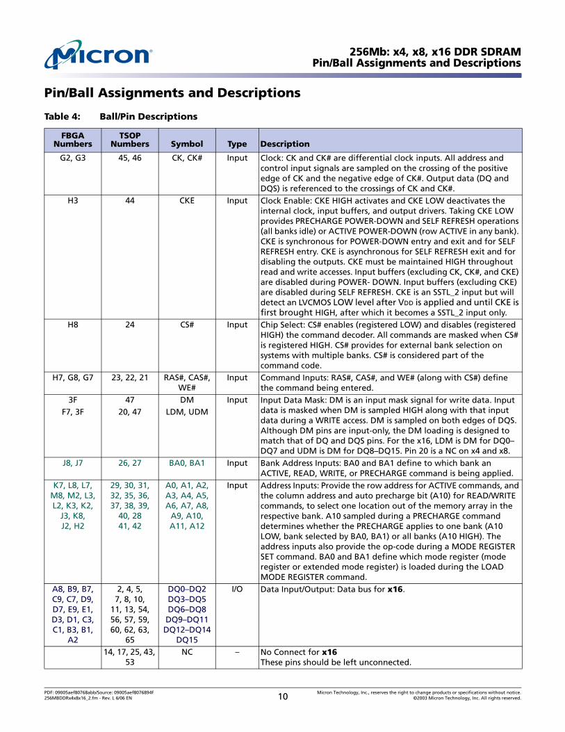
256Mb: x4, x8, x16 DDR SDRAMPin/Ball Assignments and Descriptions
Pin/Ball Assignments and Descriptions
Table 4: Ball/Pin Descriptions
FBGA Numbers
TSOP Numbers Symbol Type Description
G2, G3 45, 46 CK, CK# Input Clock: CK and CK# are differential clock inputs. All address and control input signals are sampled on the crossing of the positive edge of CK and the negative edge of CK#. Output data (DQ and DQS) is referenced to the crossings of CK and CK#.
H3 44 CKE Input Clock Enable: CKE HIGH activates and CKE LOW deactivates the internal clock, input buffers, and output drivers. Taking CKE LOW provides PRECHARGE POWER-DOWN and SELF REFRESH operations (all banks idle) or ACTIVE POWER-DOWN (row ACTIVE in any bank). CKE is synchronous for POWER-DOWN entry and exit and for SELF REFRESH entry. CKE is asynchronous for SELF REFRESH exit and for disabling the outputs. CKE must be maintained HIGH throughout read and write accesses. Input buffers (excluding CK, CK#, and CKE) are disabled during POWER- DOWN. Input buffers (excluding CKE) are disabled during SELF REFRESH. CKE is an SSTL_2 input but will detect an LVCMOS LOW level after VDD is applied and until CKE is first brought HIGH, after which it becomes a SSTL_2 input only.
H8 24 CS# Input Chip Select: CS# enables (registered LOW) and disables (registered HIGH) the command decoder. All commands are masked when CS# is registered HIGH. CS# provides for external bank selection on systems with multiple banks. CS# is considered part of the command code.
H7, G8, G7 23, 22, 21 RAS#, CAS#, WE#
Input Command Inputs: RAS#, CAS#, and WE# (along with CS#) define the command being entered.
3F 47 DM Input Input Data Mask: DM is an input mask signal for write data. Input data is masked when DM is sampled HIGH along with that input data during a WRITE access. DM is sampled on both edges of DQS. Although DM pins are input-only, the DM loading is designed to match that of DQ and DQS pins. For the x16, LDM is DM for DQ0–DQ7 and UDM is DM for DQ8–DQ15. Pin 20 is a NC on x4 and x8.
F7, 3F 20, 47 LDM, UDM
J8, J7 26, 27 BA0, BA1 Input Bank Address Inputs: BA0 and BA1 define to which bank an ACTIVE, READ, WRITE, or PRECHARGE command is being applied.
K7, L8, L7, M8, M2, L3, L2, K3, K2,
J3, K8,J2, H2
29, 30, 31, 32, 35, 36, 37, 38, 39,
40, 2841, 42
A0, A1, A2, A3, A4, A5, A6, A7, A8,
A9, A10,A11, A12
Input Address Inputs: Provide the row address for ACTIVE commands, and the column address and auto precharge bit (A10) for READ/WRITE commands, to select one location out of the memory array in the respective bank. A10 sampled during a PRECHARGE command determines whether the PRECHARGE applies to one bank (A10 LOW, bank selected by BA0, BA1) or all banks (A10 HIGH). The address inputs also provide the op-code during a MODE REGISTER SET command. BA0 and BA1 define which mode register (mode register or extended mode register) is loaded during the LOAD MODE REGISTER command.
A8, B9, B7, C9, C7, D9, D7, E9, E1, D3, D1, C3, C1, B3, B1,
A2
2, 4, 5, 7, 8, 10,
11, 13, 54,56, 57, 59,60, 62, 63,
65
DQ0–DQ2 DQ3–DQ5 DQ6–DQ8
DQ9–DQ11 DQ12–DQ14
DQ15
I/O Data Input/Output: Data bus for x16.
14, 17, 25, 43, 53
NC – No Connect for x16These pins should be left unconnected.
PDF: 09005aef80768abb/Source: 09005aef8076894f Micron Technology, Inc., reserves the right to change products or specifications without notice.256MBDDRx4x8x16_2.fm - Rev. L 6/06 EN 10 ©2003 Micron Technology, Inc. All rights reserved.

256Mb: x4, x8, x16 DDR SDRAMPin/Ball Assignments and Descriptions
A8, B7, C7, D7, D3, C3,
B3, A2
2, 5, 8,11, 56, 59,
62, 65
DQ0–DQ2 DQ3–DQ5 DQ6, DQ7
I/O Data Input/Output: Data bus for x8.
B1, B9, C1, C9, D1, D9, E1, E7, E9, F7
4, 7, 10, 13, 14, 16, 17, 20, 25, 43, 53, 54,
57, 60, 63,
NC – No Connect for x8These pins should be left unconnected.
B7, D7, D3,B3
5, 11, 56,62
DQ0–DQ2DQ3
I/O Data Input/Output: Data bus for x4.
B1, B9, C1, C9, D1, D9, E1, E7, E9, F7,
4, 7, 10, 13, 14, 16, 17, 20, 25, 43, 53, 54,
57, 60, 63,
NC – No Connect for x4These pins should be left unconnected.
A2, A8, C3, C7 2, 8, 59, 65 NF – No Function for x4These pins should be left unconnected.
E3E7E3
511651
DQSLDQSUDQS
I/O Data Strobe: Output with read data, input with write data. DQS is edge-aligned with read data, centered in write data. It is used to capture data. For the x16, LDQS is DQS for DQ0–DQ7 and UDQS is DQS for DQ8–DQ15. Pin 16 (E7) is NC on x4 and x8.
F9 17, 19, 50 DNU – Do Not Use: Must float to minimize noise on VREF.B2, D2, C8,
E8, A93, 9, 15, 55, 61
VDDQ Supply DQ Power Supply: +2.5V ±0.2V (+2.6V ±0.1V for DDR400). Isolated on the die for improved noise immunity.
A1, C2, E2, B8, D8
6, 12, 52,58, 64
VSSQ Supply DQ Ground: Isolated on the die for improved noise immunity.
F8, M7, A7 1, 18, 33 VDD Supply Power Supply: +2.5V ±0.2V (+2.6V ±0.1V for DDR400).A3, F2, M3 34, 48, 66 VSS Supply Ground.
F1 49 VREF Supply SSTL_2 reference voltage.
Table 5: Reserved NC Balls and PinsNC pins not listed may also be reserved for other uses; this table defines NC pins of importance.
FBGA Numbers
TSOP Numbers Symbol Type Description
F9 17 A13 I Address input A13 for 1Gb devices. DNU for FBGA.
Table 4: Ball/Pin Descriptions (Continued)
FBGA Numbers
TSOP Numbers Symbol Type Description
PDF: 09005aef80768abb/Source: 09005aef8076894f Micron Technology, Inc., reserves the right to change products or specifications without notice.256MBDDRx4x8x16_2.fm - Rev. L 6/06 EN 11 ©2003 Micron Technology, Inc. All rights reserved.

256Mb: x4, x8, x16 DDR SDRAMPin/Ball Assignments and Descriptions
Figure 5: Pin Assignment (Top View) 66-Pin TSOP
123456789101112131415161718192021222324252627282930313233
666564636261605958575655545352515049484746454443424140393837363534
VSS
DQ15VSSQDQ14DQ13VDDQDQ12DQ11VSSQDQ10DQ9VDDQDQ8NCVSSQUDQSDNUVREF
VSS
UDMCK#CKCKENCA12A11A9A8A7A6A5A4VSS
x16VDD
DQ0VDDQDQ1DQ2VssQDQ3DQ4
VDDQDQ5DQ6VssQDQ7
NCVDDQLDQS
NCVDD
DNULDMWE#CAS#RAS#
CS#NC
BA0BA1
A10/APA0A1A2A3
VDD
x16VSS
DQ7VSSQNCDQ6VDDQNCDQ5VSSQNCDQ4VDDQNCNCVSSQDQSDNUVREF
VSS
DMCK#CKCKENCA12A11A9A8A7A6A5A4VSS
x8 x4VSS
NFVSSQNCDQ3VDDQNCNFVSSQNCDQ2VDDQNCNCVSSQDQSDNUVREF
VSS
DMCK#CKCKENCA12A11A9A8A7A6A5A4VSS
VDD
DQ0VDDQ
NCDQ1VSSQ
NCDQ2
VDDQNC
DQ3VSSQ
NCNC
VDDQNCNC
VDD
DNUNC
WE#CAS#RAS#
CS#NC
BA0BA1
A10/APA0A1A2A3
VDD
x8x4VDD
NFVDDQ
NCDQ0VSSQ
NCNF
VDDQNC
DQ1VSSQ
NCNC
VDDQNCNC
VDD
DNUNC
WE#CAS#RAS#
CS#NC
BA0BA1
A10/APA0A1A2A3
VDD
PDF: 09005aef80768abb/Source: 09005aef8076894f Micron Technology, Inc., reserves the right to change products or specifications without notice.256MBDDRx4x8x16_2.fm - Rev. L 6/06 EN 12 ©2003 Micron Technology, Inc. All rights reserved.

256Mb: x4, x8, x16 DDR SDRAMPin/Ball Assignments and Descriptions
Figure 6: 60-Ball FBGA Ball Assignment (Top View)
VSSQDQ14DQ12DQ10DQ8VREF
DQ15VDDQVSSQVDDQVSSQVSS
CKA12A11A8A6A4
VSS
DQ13DQ11DQ9
UDQSUDMCK#CKEA9A7A5VSS
VDD
DQ2DQ4DQ6LDQSLDMWE#RAS#BA1A0A2VDD
DQ0VSSQVDDQVSSQVDDQVDD
CAS#CS#BA0A10A1A3
VDDQDQ1DQ3DQ5DQ7DNU
x16 (Top View)
VSSQNCNCNCNC
VREF
NFVDDQVSSQVDDQVSSQVSS
CKA12A11A8A6A4
VSS
DQ3NF
DQ2DQSDMCK#CKEA9A7A5VSS
VDD
DQ0NF
DQ1NCNC
WE#RAS#BA1A0A2VDD
NFVSSQVDDQVSSQVDDQVDD
CAS#CS#BA0A10A1A3
VDDQNCNCNCNC
DNU
x4 (Top View)
VSSQNCNCNCNC
VREF
DQ7VDDQVSSQVDDQVSSQVSS
CKA12A11A8A6A4
VSS
DQ6DQ5DQ4DQSDMCK#CKEA9A7A5VSS
VDD
DQ1DQ2DQ3NCNC
WE#RAS#BA1A0A2VDD
DQ0VSSQVDDQVSSQVDDQVDD
CAS#CS#BA0A10A1A3
VDDQNCNCNCNC
DNU
x8 (Top View)
A
1 2 3 4 5 6 7 8 9
B
C
D
E
F
G
H
J
K
L
M
A
1 2 3 4 5 6 7 8 9
B
C
D
E
F
G
H
J
K
L
M
A
1 2 3 4 5 6 7 8 9
B
C
D
E
F
G
H
J
K
L
M
PDF: 09005aef80768abb/Source: 09005aef8076894f Micron Technology, Inc., reserves the right to change products or specifications without notice.256MBDDRx4x8x16_2.fm - Rev. L 6/06 EN 13 ©2003 Micron Technology, Inc. All rights reserved.

256Mb: x4, x8, x16 DDR SDRAMFunctional Description
Functional DescriptionThe 256Mb DDR SDRAM is a high-speed CMOS, dynamic random-access memory con-taining 268,435,456 bits. The 256Mb DDR SDRAM is internally configured as a quad-bank DRAM.
The 256Mb DDR SDRAM uses a double-data-rate architecture to achieve high-speed operation. The double-data-rate architecture is essentially a 2n-prefetch architecture, with an interface designed to transfer two data words per clock cycle at the I/O pins. A single read or write access for the 256Mb DDR SDRAM consists of a single 2n-bit wide, one-clock-cycle data transfer at the internal DRAM core and two corresponding n-bit wide, one-half-clock-cycle data transfers at the I/O pins.
Read and write accesses to the DDR SDRAM are burst oriented; accesses start at a selected location and continue for a programmed number of locations in a programmed sequence. Accesses begin with the registration of an ACTIVE command, which is then followed by a READ or WRITE command. The address bits registered coincident with the ACTIVE command are used to select the bank and row to be accessed (BA0, BA1 select the bank; A0–A12 select the row). The address bits registered coincident with the READ or WRITE command are used to select the starting column location for the burst access.
Prior to normal operation, the DDR SDRAM must be initialized. The following sections provide detailed information covering device initialization, register definition, com-mand descriptions, and device operation.
InitializationDDR SDRAMs must be powered up and initialized in a predefined manner. Operational procedures other than those specified may result in undefined operation. Power must first be applied to VDD and VDDQ simultaneously, and then to VREF (and to the system VTT). VTT must be applied after VDDQ to avoid device latch-up, which may cause perma-nent damage to the device. VREF can be applied any time after VDDQ but is expected to be nominally coincident with VTT. Except for CKE, inputs are not recognized as valid until after VREF is applied. CKE is an SSTL_2 input but will detect an LVCMOS LOW level after VDD is applied. After CKE passes through VIH, it will transition to a SSTL_2 signal and remain as such until power is cycled. Maintaining an LVCMOS LOW level on CKE during power-up is required to ensure that the DQ and DQS outputs will be in the High-Z state, where they will remain until driven in normal operation (by a read access). After all power supply and reference voltages are stable, and the clock is stable, the DDR SDRAM requires a 200µs delay prior to applying an executable command.
Once the 200µs delay has been satisfied, a DESELECT or NOP command should be applied and CKE should be brought HIGH. Following the NOP command, a PRE-CHARGE ALL command should be applied. Next a LOAD MODE REGISTER command should be issued for the extended mode register (BA1 LOW and BA0 HIGH) to enable the DLL, followed by another LOAD MODE REGISTER command to the mode register (BA0/BA1 both LOW) to reset the DLL and to program the operating parameters. Two hundred clock cycles are required between the DLL reset and any READ command. A PRE-CHARGE ALL command should then be applied, placing the device in the all banks idle state.
Once in the idle state, two AUTO REFRESH cycles must be performed (tRFC must be sat-isfied). Additionally, a LOAD MODE REGISTER command for the mode register with the reset DLL bit deactivated (i.e., to program operating parameters without resetting the DLL) is required. Following these requirements, the DDR SDRAM is ready for normal operation.
PDF: 09005aef80768abb/Source: 09005aef8076894f Micron Technology, Inc., reserves the right to change products or specifications without notice.256MBDDRx4x8x16_2.fm - Rev. L 6/06 EN 14 ©2003 Micron Technology, Inc. All rights reserved.
256Mb: x4, x8, x16 DDR SDRAMRegister Definition
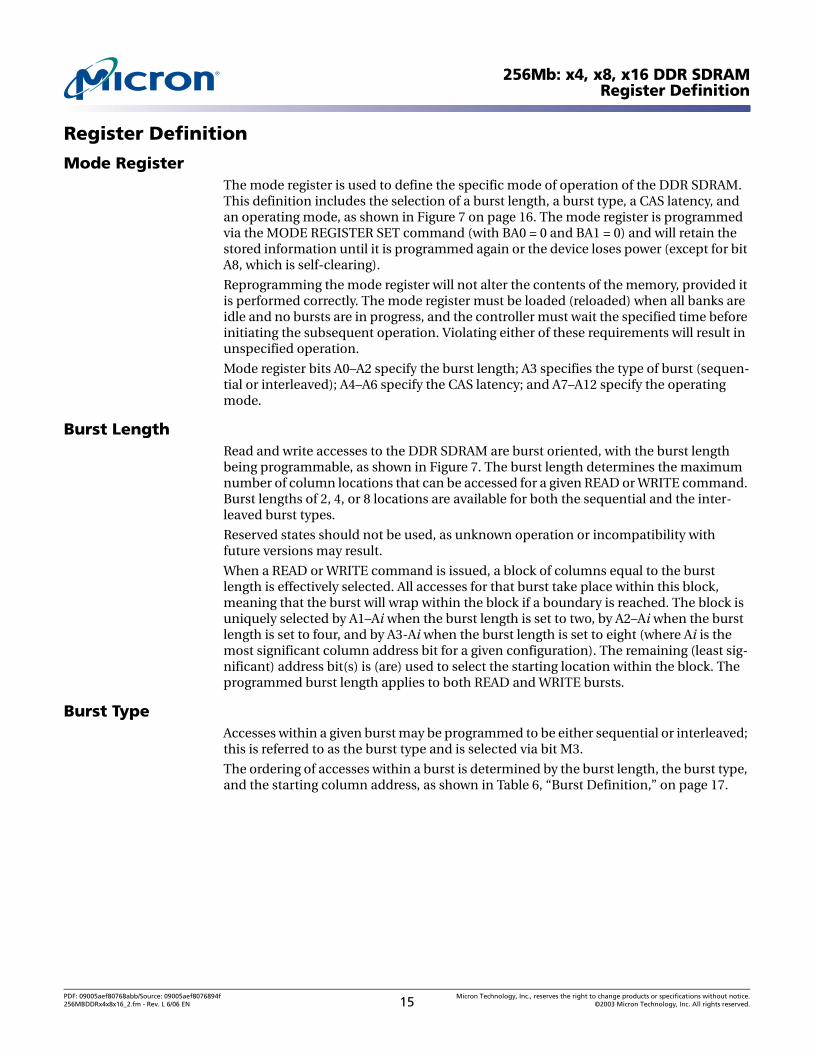
Register Definition
Mode RegisterThe mode register is used to define the specific mode of operation of the DDR SDRAM. This definition includes the selection of a burst length, a burst type, a CAS latency, and an operating mode, as shown in Figure 7 on page 16. The mode register is programmed via the MODE REGISTER SET command (with BA0 = 0 and BA1 = 0) and will retain the stored information until it is programmed again or the device loses power (except for bit A8, which is self-clearing).
Reprogramming the mode register will not alter the contents of the memory, provided it is performed correctly. The mode register must be loaded (reloaded) when all banks are idle and no bursts are in progress, and the controller must wait the specified time before initiating the subsequent operation. Violating either of these requirements will result in unspecified operation.
Mode register bits A0–A2 specify the burst length; A3 specifies the type of burst (sequen-tial or interleaved); A4–A6 specify the CAS latency; and A7–A12 specify the operating mode.
Burst LengthRead and write accesses to the DDR SDRAM are burst oriented, with the burst length being programmable, as shown in Figure 7. The burst length determines the maximum number of column locations that can be accessed for a given READ or WRITE command. Burst lengths of 2, 4, or 8 locations are available for both the sequential and the inter-leaved burst types.
Reserved states should not be used, as unknown operation or incompatibility with future versions may result.
When a READ or WRITE command is issued, a block of columns equal to the burst length is effectively selected. All accesses for that burst take place within this block, meaning that the burst will wrap within the block if a boundary is reached. The block is uniquely selected by A1–Ai when the burst length is set to two, by A2–Ai when the burst length is set to four, and by A3-Ai when the burst length is set to eight (where Ai is the most significant column address bit for a given configuration). The remaining (least sig-nificant) address bit(s) is (are) used to select the starting location within the block. The programmed burst length applies to both READ and WRITE bursts.
Burst TypeAccesses within a given burst may be programmed to be either sequential or interleaved; this is referred to as the burst type and is selected via bit M3.
The ordering of accesses within a burst is determined by the burst length, the burst type, and the starting column address, as shown in Table 6, “Burst Definition,” on page 17.
PDF: 09005aef80768abb/Source: 09005aef8076894f Micron Technology, Inc., reserves the right to change products or specifications without notice.256MBDDRx4x8x16_2.fm - Rev. L 6/06 EN 15 ©2003 Micron Technology, Inc. All rights reserved.

256Mb: x4, x8, x16 DDR SDRAMRegister Definition
Figure 7: Mode Register Definition
Operating Mode
Normal Operation
Normal Operation/Reset DLL
All other states reserved
0
1
-
0
0
-
0
0
-
0
0
-
0
0
-
0
0
-
Valid
Valid
-
0
1
Burst Type
Sequential
Interleaved
CAS Latency
Reserved
Reserved
2
Reserved
Reserved
Reserved
2.5
Reserved
Burst LengthCAS Latency BT0*
A9 A7 A6 A5 A4 A3A8 A2 A1 A0
Mode Register (Mx)
Address Bus
9 7 6 5 4 38 2 1 0
M3
M4
0
1
0
1
0
1
0
1
M5
0
0
1
1
0
0
1
1
M6
0
0
0
0
1
1
1
1
M6-M0M8 M7
Operating Mode
A10A12 A11BA0BA1
101112130*14
* M14 and M13 (BA1 and BA0)must be “0, 0” to select thebase mode register (vs. theextended mode register).
M9M10M12 M11
Burst Length
Reserved
2
4
8
Reserved
Reserved
Reserved
Reserved
M0
0
1
0
1
0
1
0
1
M1
0
0
1
1
0
0
1
1
M2
0
0
0
0
1
1
1
1
CAS Latency
Reserved
Reserved
2
3
Reserved
Reserved
2.5
Reserved
(DDR400)
PDF: 09005aef80768abb/Source: 09005aef8076894f Micron Technology, Inc., reserves the right to change products or specifications without notice.256MBDDRx4x8x16_2.fm - Rev. L 6/06 EN 16 ©2003 Micron Technology, Inc. All rights reserved.

256Mb: x4, x8, x16 DDR SDRAMRegister Definition
Notes: 1. Whenever a boundary of the block is reached within a given sequence above, the follow-ing access wraps within the block.
2. For a burst length of two, A1–Ai select the two-data-element block; A0 selects the first access within the block.
3. For a burst length of four, A2–Ai select the four-data-element block; A0–A1 select the first access within the block.
4. For a burst length of eight, A3–Ai select the eight-data-element block; A0–A2 select the first access within the block.
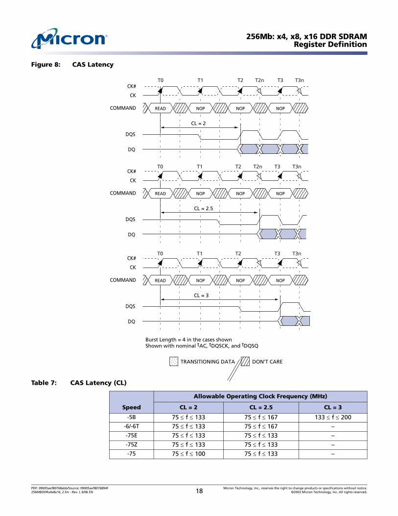
Read LatencyThe READ latency is the delay, in clock cycles, between the registration of a READ com-mand and the availability of the first bit of output data. The latency can be set to 2, 2.5, or 3 (DDR400 only) clocks, as shown in Figure 8 on page 18.
If a READ command is registered at clock edge n, and the latency is m clocks, the data will be available nominally coincident with clock edge n + m. Table 7, “CAS Latency (CL),” on page 18 indicates the operating frequencies at which each CAS latency setting can be used.
Reserved states should not be used, as unknown operation or incompatibility with future versions may result.
Table 6: Burst Definition
Burst LengthStarting Column
Address
Order of Accesses Within a Burst
Type = Sequential Type = Interleaved
2 – – A0 – –– – 0 0-1 0-1– – 1 1-0 1-0
4 – A1 A0 – –– 0 0 0-1-2-3 0-1-2-3– 0 1 1-2-3-0 1-0-3-2– 1 0 2-3-0-1 2-3-0-1– 1 1 3-0-1-2 3-2-1-0
8 A2 A1 A0 – –0 0 0 0-1-2-3-4-5-6-7 0-1-2-3-4-5-6-70 0 1 1-2-3-4-5-6-7-0 1-0-3-2-5-4-7-60 1 0 2-3-4-5-6-7-0-1 2-3-0-1-6-7-4-50 1 1 3-4-5-6-7-0-1-2 3-2-1-0-7-6-5-41 0 0 4-5-6-7-0-1-2-3 4-5-6-7-0-1-2-31 0 1 5-6-7-0-1-2-3-4 5-4-7-6-1-0-3-21 1 0 6-7-0-1-2-3-4-5 6-7-4-5-2-3-0-11 1 1 7-0-1-2-3-4-5-6 7-6-5-4-3-2-1-0
PDF: 09005aef80768abb/Source: 09005aef8076894f Micron Technology, Inc., reserves the right to change products or specifications without notice.256MBDDRx4x8x16_2.fm - Rev. L 6/06 EN 17 ©2003 Micron Technology, Inc. All rights reserved.
256Mb: x4, x8, x16 DDR SDRAMRegister Definition
Figure 8: CAS Latency
Table 7: CAS Latency (CL)
Speed
Allowable Operating Clock Frequency (MHz)
CL = 2 CL = 2.5 CL = 3
-5B 75 ≤ f ≤ 133 75 ≤ f ≤ 167 133 ≤ f ≤ 200-6/-6T 75 ≤ f ≤ 133 75 ≤ f ≤ 167 –-75E 75 ≤ f ≤ 133 75 ≤ f ≤ 133 –-75Z 75 ≤ f ≤ 133 75 ≤ f ≤ 133 –-75 75 ≤ f ≤ 100 75 ≤ f ≤ 133 –
CK
CK#
COMMAND
DQ
DQS
CL = 2
READ NOP NOP NOP
READ NOP NOP NOP
Burst Length = 4 in the cases shownShown with nominal tAC, tDQSCK, and tDQSQ
CK
CK#
COMMAND
DQ
DQS
CL = 2.5
T0 T1 T2 T2n T3 T3n
T0 T1 T2 T2n T3 T3n
DON’T CARETRANSITIONING DATA
READ NOP NOP NOP
CK
CK#
COMMAND
DQ
DQS
CL = 3
T0 T1 T2 T3 T3n
PDF: 09005aef80768abb/Source: 09005aef8076894f Micron Technology, Inc., reserves the right to change products or specifications without notice.256MBDDRx4x8x16_2.fm - Rev. L 6/06 EN 18 ©2003 Micron Technology, Inc. All rights reserved.

256Mb: x4, x8, x16 DDR SDRAMExtended Mode Register
Operating ModeThe normal operating mode is selected by issuing a MODE REGISTER SET command with bits A7–A12 each set to zero and bits A0–A6 set to the desired values. A DLL reset is initiated by issuing a MODE REGISTER SET command with bits A7 and A9–A12 each set to zero, bit A8 set to one, and bits A0–A6 set to the desired values. Although not required by the Micron device, JEDEC specifications recommend when a LOAD MODE REGISTER command is issued to reset the DLL, it should always be followed by a LOAD MODE REGISTER command to select normal operating mode.
All other combinations of values for A7–A12 are reserved for future use and/or test modes. Test modes and reserved states should not be used, as unknown operation or incompatibility with future versions may result.
Extended Mode RegisterThe extended mode register controls functions beyond those controlled by the mode register; these additional functions are DLL enable/disable and output drive strength. These functions are controlled via the bits shown in Figure 9 on page 20. The extended mode register is programmed via the LOAD MODE REGISTER command to the mode register (with BA0 = 1 and BA1 = 0) and will retain the stored information until it is pro-grammed again or the device loses power. The enabling of the DLL should always be fol-lowed by a LOAD MODE REGISTER command to the mode register (BA0/BA1 both LOW) to reset the DLL. Anytime a DLL reset occurs, 200 clock cycles with CKE high is required before a READ command can be issued.
The extended mode register must be loaded when all banks are idle and no bursts are in progress, and the controller must wait the specified time before initiating any subse-quent operation. Violating either of these requirements could result in unspecified oper-ation.
Output Drive StrengthThe normal drive strength for all outputs are specified to be SSTL_2, Class II. The x16 supports a programmable option for reduced drive. This option is intended for the sup-port of the lighter load and/or point-to-point environments. The selection of the reduced drive strength will alter the DQ pins and DQS pins from SSTL_2, Class II drive strength to a reduced drive strength, which is approximately 54 percent of the SSTL_2, Class II drive strength.
DLL Enable/DisableWhen the part is running without the DLL enabled, device functionality may be altered. The DLL must be enabled for normal operation. DLL enable is required during power-up initialization and upon returning to normal operation after having disabled the DLL for the purpose of debug or evaluation. (When the device exits self refresh mode, the DLL is enabled automatically.) Any time the DLL is enabled, a DLL Reset and 200 clock cycles with CKE high must occur before a READ command can be issued.
PDF: 09005aef80768abb/Source: 09005aef8076894f Micron Technology, Inc., reserves the right to change products or specifications without notice.256MBDDRx4x8x16_2.fm - Rev. L 6/06 EN 19 ©2003 Micron Technology, Inc. All rights reserved.

256Mb: x4, x8, x16 DDR SDRAMExtended Mode Register
Figure 9: Extended Mode Register Definition
Notes: 1. E14 and E13 (BA1 and BA0) must be “0, 1” to select the extended mode register vs. the base mode register.
2. The reduced drive strength option is not supported on the x4 and x8 versions; it is only available on the x16 version.
3. The QFC# option is not supported.
Operating Mode
Reserved
Reserved
0
–
0
–
Valid
–
0
1
DLL
Enable
Disable
DLL1101
A9 A7 A6 A5 A4 A3A8 A2 A1 A0
Extended ModeRegister (Ex)
Address Bus
9 7 6 5 4 38 2 1 0
E0
0
1
Drive Strength
Normal
Reduced
E12
E23 E0E1,
Operating Mode
A10A11A12BA1 BA0
1011121314
E3E4
0
–
0
–
0
–
0
–
0
–
E6 E5E7E8E9
0
–
0
–
E10E11
0
–
E12
DS
0
–
PDF: 09005aef80768abb/Source: 09005aef8076894f Micron Technology, Inc., reserves the right to change products or specifications without notice.256MBDDRx4x8x16_2.fm - Rev. L 6/06 EN 20 ©2003 Micron Technology, Inc. All rights reserved.

256Mb: x4, x8, x16 DDR SDRAMCommands
CommandsTable 8 and Table 9 provide a quick reference of available commands, followed by a description of each command. Two additional truth tables, Table 11 on page 49, and Table 12 on page 51, appear following the Operation section, provide current state/next state information.
Notes: 1. CKE is HIGH for all commands shown except SELF REFRESH.2. BA0–BA1 select either the mode register or the extended mode register (BA0 = 0, BA1 = 0
select the mode register; BA0 = 1, BA1 = 0 select extended mode register; other combinations of BA0–BA1 are reserved). A0–A12 provide the op-code to be written to the selected mode register.
3. BA0–BA1 provide bank address and A0–A12 provide row address.4. BA0–BA1 provide bank address; A0–Ai provide column address, (where i = 8 for x16, i = 9
for x8, and i = 9,11 for x4) A10 HIGH enables the auto precharge feature (non persistent); and A10 LOW disables the auto precharge feature.
5. A10 LOW: BA0–BA1 determine which bank is precharged.A10 HIGH: all banks are precharged and BA0–BA1 are “Don’t Care.”
6. This command is AUTO REFRESH if CKE is HIGH, SELF REFRESH if CKE is LOW.7. Internal refresh counter controls row addressing; within the self refresh mode, all inputs
and I/Os are “Don’t Care” except for CKE.8. Applies only to READ bursts with auto precharge disabled; this command is undefined
(and should not be used) for READ bursts with auto precharge enabled and for WRITE bursts.
9. DESELECT and NOP are functionally interchangeable.
Notes: 1. Used to mask write data; provided coincident with the corresponding data.
Table 8: Truth Table – CommandsNote 1 applies to all commands.
Name (Function) CS# RAS# CAS# WE# Addr Notes
DESELECT (NOP) H X X X X 9
NO OPERATION (NOP) L H H H X 9
ACTIVE (Select bank and activate row) L L H H Bank/Row 3
READ (Select bank and column, and start READ burst) L H L H Bank/Col 4
WRITE (Select bank and column, and start WRITE burst) L H L L Bank/Col 4
BURST TERMINATE L H H L X 8
PRECHARGE (Deactivate row in bank or banks) L L H L Code 5
AUTO REFRESH or SELF REFRESH(Enter self refresh mode)
L L L H X 6, 7
LOAD MODE REGISTER L L L L Op-Code 2
Table 9: Truth Table – DM OperationNote 1 applies to all commands.
Name (Function) DM DQ
Write Enable L Valid
Write Inhibit H X
PDF: 09005aef80768abb/Source: 09005aef8076894f Micron Technology, Inc., reserves the right to change products or specifications without notice.256MBDDRx4x8x16_2.fm - Rev. L 6/06 EN 21 ©2003 Micron Technology, Inc. All rights reserved.

256Mb: x4, x8, x16 DDR SDRAMCommands
DESELECTThe DESELECT function (CS# HIGH) prevents new commands from being executed by the DDR SDRAM. The DDR SDRAM is effectively deselected. Operations already in progress are not affected.
NO OPERATION (NOP)The NO OPERATION (NOP) command is used to instruct the selected DDR SDRAM to perform a NOP (CS# is LOW with RAS#, CAS#, and WE# are HIGH). This prevents unwanted commands from being registered during idle or wait states. Operations already in progress are not affected.
LOAD MODE REGISTERThe mode registers are loaded via inputs A0–A12. See mode register descriptions in the Register Definition section on page 15. The LOAD MODE REGISTER command can only be issued when all banks are idle, and a subsequent executable command cannot be issued until tMRD is met.
ACTIVEThe ACTIVE command is used to open (or activate) a row in a particular bank for a sub-sequent access. The value on the BA0, BA1 inputs selects the bank, and the address pro-vided on inputs A0–A12 selects the row. This row remains active (or open) for accesses until a PRECHARGE command is issued to that bank. A PRECHARGE command must be issued before opening a different row in the same bank.
READ
The READ command is used to initiate a burst read access to an active row. The value on the BA0, BA1 inputs selects the bank, and the address provided on inputs A0–Ai (where i = 8 for x16, 9 for x8, or 9, 11 for x4) selects the starting column location. The value on input A10 determines whether or not auto precharge is used. If auto precharge is selected, the row being accessed will be precharged at the end of the READ burst; if auto precharge is not selected, the row will remain open for subsequent accesses.
WRITE
The WRITE command is used to initiate a burst write access to an active row. The value on the BA0, BA1 inputs selects the bank, and the address provided on inputs A0–Ai (where i = 8 for x16, 9 for x8, or 9, 11 for x4) selects the starting column location. The value on input A10 determines whether or not auto precharge is used. If auto precharge is selected, the row being accessed will be precharged at the end of the WRITE burst; if auto precharge is not selected, the row will remain open for subsequent accesses. Input data appearing on the DQ is written to the memory array subject to the DM input logic level appearing coincident with the data. If a given DM signal is registered LOW, the cor-responding data will be written to memory; if the DM signal is registered HIGH, the cor-responding data inputs will be ignored and a WRITE will not be executed to that byte/column location.
PRECHARGEThe PRECHARGE command is used to deactivate the open row in a particular bank or the open row in all banks. The bank(s) will be available for a subsequent row access a specified time (tRP) after the PRECHARGE command is issued, except in the case of con-current auto precharge, where a READ or WRITE command to a different bank is allowed as long as it does not interrupt the data transfer in the current bank and does not violate
PDF: 09005aef80768abb/Source: 09005aef8076894f Micron Technology, Inc., reserves the right to change products or specifications without notice.256MBDDRx4x8x16_2.fm - Rev. L 6/06 EN 22 ©2003 Micron Technology, Inc. All rights reserved.

256Mb: x4, x8, x16 DDR SDRAMCommands
any other timing parameters. Input A10 determines whether one or all banks are to be precharged, and in the case where only one bank is to be precharged, inputs BA0, BA1 select the bank. Otherwise, BA0, BA1 are treated as “Don’t Care.” Once a bank has been precharged, it is in the idle state and must be activated prior to any READ or WRITE commands being issued to that bank. A PRECHARGE command will be treated as a NOP if there is no open row in that bank (idle state) or if the previously open row is already in the process of precharging.
Auto PrechargeAuto precharge is a feature that performs the same individual-bank precharge function described above, but without requiring an explicit command. This is accomplished by using A10 to enable auto precharge in conjunction with a specific READ or WRITE com-mand. A precharge of the bank/row that is addressed with the READ or WRITE com-mand is automatically performed upon completion of the READ or WRITE burst. Auto precharge is nonpersistent in that it is either enabled or disabled for each individual READ or WRITE command. This device supports concurrent auto precharge if the com-mand to the other bank does not interrupt the data transfer to the current bank.
Auto precharge ensures that the precharge is initiated at the earliest valid stage within a burst. This earliest valid stage is determined as if an explicit PRECHARGE command was issued at the earliest possible time, without violating tRAS (MIN), as described for each burst type in the Operation section of this data sheet. The user must not issue another command to the same bank until the precharge time (tRP) is completed.
BURST TERMINATEThe BURST TERMINATE command is used to truncate READ bursts (with auto pre-charge disabled). The most recently registered READ command prior to the BURST TER-MINATE command will be truncated, as shown in the Operation section of this data sheet. The open page, which the READ burst was terminated from, remains open.
AUTO REFRESHAUTO REFRESH is used during normal operation of the DDR SDRAM and is analogous to CAS#-BEFORE-RAS# (CBR) refresh in FPM/EDO DRAMs. This command is nonper-sistent, so it must be issued each time a refresh is required. All banks must be idle before an AUTO REFRESH command is issued.
The addressing is generated by the internal refresh controller. This makes the address bits a “Don’t Care” during an AUTO REFRESH command. The 256Mb DDR SDRAM requires AUTO REFRESH cycles at an average interval of 7.8125µs (maximum).
To allow for improved efficiency in scheduling and switching between tasks, some flexi-bility in the absolute refresh interval is provided. A maximum of eight AUTO REFRESH commands can be posted to any given DDR SDRAM, meaning that the maximum abso-lute interval between any AUTO REFRESH command and the next AUTO REFRESH command is 9 x 7.8125µs (70.3µs). Note that the JEDEC specification only allows 8 x 7.8125µs; thus, the Micron specification exceeds the JEDEC requirement by one clock. This maximum absolute interval is to allow future support for DLL updates internal to the DDR SDRAM to be restricted to AUTO REFRESH cycles, without allowing excessive drift in tAC between updates.
Although not a JEDEC requirement, to provide for future functionality, CKE must be active (HIGH) during the auto refresh period. The auto refresh period begins when the AUTO REFRESH command is registered and ends tRFC later.
PDF: 09005aef80768abb/Source: 09005aef8076894f Micron Technology, Inc., reserves the right to change products or specifications without notice.256MBDDRx4x8x16_2.fm - Rev. L 6/06 EN 23 ©2003 Micron Technology, Inc. All rights reserved.

256Mb: x4, x8, x16 DDR SDRAMCommands
SELF REFRESHThe SELF REFRESH command can be used to retain data in the DDR SDRAM, even if the rest of the system is powered down. When in the self refresh mode, the DDR SDRAM retains data without external clocking. The SELF REFRESH command is initiated like an AUTO REFRESH command except CKE is disabled (LOW). The DLL is automatically dis-abled upon entering SELF REFRESH and is automatically enabled upon exiting SELF REFRESH. (A DLL reset and 200 clock cycles must then occur before a READ command can be issued.) Input signals except CKE are “Don’t Care” during SELF REFRESH. VREF voltage is also required for the full duration of the SELF REFRESH.
The procedure for exiting self refresh requires a sequence of commands. First, CK and CK# must be stable prior to CKE going back HIGH. Once CKE is HIGH, the DDR SDRAM must have NOP commands issued for tXSNR because time is required for the comple-tion of any internal refresh in progress. A simple algorithm for meeting both refresh and DLL requirements is to apply NOPs for tXSRD time, then a DLL reset and NOPs for 200 additional clock cycles before applying a READ. Any command besides a READ can be performed tXSNR MIN after the DLL reset. NOP or DESELECT commands must be issued during the tXSNR MIN time.
PDF: 09005aef80768abb/Source: 09005aef8076894f Micron Technology, Inc., reserves the right to change products or specifications without notice.256MBDDRx4x8x16_2.fm - Rev. L 6/06 EN 24 ©2003 Micron Technology, Inc. All rights reserved.

256Mb: x4, x8, x16 DDR SDRAMOperations
Operations
Bank/Row ActivationBefore any READ or WRITE commands can be issued to a bank within the DDR SDRAM, a row in that bank must be “opened.” This is accomplished via the ACTIVE command, which selects both the bank and the row to be activated, as shown in Figure 10.
After a row is opened with an ACTIVE command, a READ or WRITE command may be issued to that row, subject to the tRCD specification. tRCD (MIN) should be divided by the clock period and rounded up to the next whole number to determine the earliest clock edge after the ACTIVE command on which a READ or WRITE command can be entered. For example, a tRCD specification of 20ns with a 133 MHz clock (7.5ns period) results in 2.7 clocks rounded to 3. This is reflected in Figure 11, which covers any case where 2 < tRCD (MIN)/tCK ≤ 3. (Figure 11 also shows the same case for tRRD; the same procedure is used to convert other specification limits from time units to clock cycles.)
A subsequent ACTIVE command to a different row in the same bank can only be issued after the previous active row has been “closed” (precharged). The minimum time inter-val between successive ACTIVE commands to the same bank is defined by tRC.
A subsequent ACTIVE command to another bank can be issued while the first bank is being accessed, which results in a reduction of total row-access overhead. The minimum time interval between successive ACTIVE commands to different banks is defined by tRRD.
Figure 10: Activating a Specific Row in a Specific Bank
CS#
WE#
CAS#
RAS#
CKE
A0–A12 RA
RA = Row AddressBA = Bank Address
HIGH
BA0, BA1 BA
CK
CK#
PDF: 09005aef80768abb/Source: 09005aef8076894f Micron Technology, Inc., reserves the right to change products or specifications without notice.256MBDDRx4x8x16_2.fm - Rev. L 6/06 EN 25 ©2003 Micron Technology, Inc. All rights reserved.
256Mb: x4, x8, x16 DDR SDRAMOperations
Figure 11: Example: Meeting tRCD (tRRD) MIN When 2 < tRCD (tRRD) MIN/tCK ≤ 3
t
COMMAND
BA0, BA1
ACT ACTNOP
RRD tRCD
CK
CK#
Bank x Bank y
A0–A12 Row Row
NOP RD/WRNOP
Bank y
Col
NOP
T0 T1 T2 T3 T4 T5 T6 T7
DON’T CARE
NOP
PDF: 09005aef80768abb/Source: 09005aef8076894f Micron Technology, Inc., reserves the right to change products or specifications without notice.256MBDDRx4x8x16_2.fm - Rev. L 6/06 EN 26 ©2003 Micron Technology, Inc. All rights reserved.

256Mb: x4, x8, x16 DDR SDRAMOperations
READsREAD bursts are initiated with a READ command, as shown in Figure 12 on page 28.
The starting column and bank addresses are provided with the READ command and auto precharge is either enabled or disabled for that burst access. If auto precharge is enabled, the row being accessed is precharged at the completion of the burst.
Note: For the READ commands used in the following illustrations, auto precharge is dis-abled.
During READ bursts, the valid data-out element from the starting column address will be available following the CAS latency after the READ command. Each subsequent data-out element will be valid nominally at the next positive or negative clock edge (i.e., at the next crossing of CK and CK#). Figure 13 on page 29 shows general timing for each possi-ble CAS latency setting. DQS is driven by the DDR SDRAM along with output data. The initial LOW state on DQS is known as the read preamble; the LOW state coincident with the last data-out element is known as the read postamble.
Upon completion of a burst, assuming no other commands have been initiated, the DQs will go High-Z. A detailed explanation of tDQSQ (valid data-out skew), tQH (data-out window hold), and the valid data window are depicted in Figure 40 on page 77 and Figure 41 on page 78. A detailed explanation of tDQSCK (DQS transition skew to CK) and tAC (data-out transition skew to CK) is depicted in Figure 42 on page 79.
Data from any READ burst may be concatenated with or truncated with data from a sub-sequent READ command. In either case, a continuous flow of data can be maintained. The first data element from the new burst follows either the last element of a completed burst or the last desired data element of a longer burst which is being truncated. The new READ command should be issued x cycles after the first READ command, where x equals the number of desired data element pairs (pairs are required by the 2n-prefetch architecture). This is shown in Figure 14 on page 30. A READ command can be initiated on any clock cycle following a previous READ command. Nonconsecutive read data is illustrated in Figure 15, “Nonconsecutive READ Bursts,” on page 31. Full-speed random read accesses within a page (or pages) can be performed as shown in Figure 16, “Ran-dom READ Accesses,” on page 32.
Data from any READ burst may be truncated with a BURST TERMINATE command, as shown in Figure 17 on page 33. The BURST TERMINATE latency is equal to the read (CAS) latency; i.e., the BURST TERMINATE command should be issued x cycles after the READ command, where x equals the number of desired data element pairs (pairs are required by the 2n-prefetch architecture).
Data from any READ burst must be completed or truncated before a subsequent WRITE command can be issued. If truncation is necessary, the BURST TERMINATE command must be used, as shown in Figure 18 on page 34. The tDQSS (NOM) case is shown; the tDQSS (MAX) case has a longer bus idle time. (tDQSS [MIN] and tDQSS [MAX] are defined in the section on WRITEs.)
A READ burst may be followed by, or truncated with, a PRECHARGE command to the same bank provided that auto precharge was not activated.
The PRECHARGE command should be issued x cycles after the READ command, where x equals the number of desired data element pairs (pairs are required by the 2n-prefetch architecture). This is shown in Figure 19 on page 35. Following the PRECHARGE com-mand, a subsequent command to the same bank cannot be issued until both tRAS and tRP have been met. Note that part of the row precharge time is hidden during the access of the last data elements.
PDF: 09005aef80768abb/Source: 09005aef8076894f Micron Technology, Inc., reserves the right to change products or specifications without notice.256MBDDRx4x8x16_2.fm - Rev. L 6/06 EN 27 ©2003 Micron Technology, Inc. All rights reserved.

256Mb: x4, x8, x16 DDR SDRAMOperations
Figure 12: READ Command
CS#
WE#
CAS#
RAS#
CKE
CAx4: A0–A9, A11
x8: A0–A9x16: A0–A8
A10
BA0,1
HIGH
EN AP
DIS AP
BA
x4: A12x8: A11, A12
x16: A9, A11, A12
CK
CK#
CA = Column AddressBA = Bank AddressEN AP = Enable Auto PrechargeDIS AP = Disable Auto Precharge
DON’T CARE
PDF: 09005aef80768abb/Source: 09005aef8076894f Micron Technology, Inc., reserves the right to change products or specifications without notice.256MBDDRx4x8x16_2.fm - Rev. L 6/06 EN 28 ©2003 Micron Technology, Inc. All rights reserved.

256Mb: x4, x8, x16 DDR SDRAMOperations
Figure 13: READ Burst
Notes: 1. DO n = data-out from column n.2. BL = 4.3. Three subsequent elements of data-out appear in the programmed order following DO n. 4. Shown with nominal tAC, tDQSCK, and tDQSQ.
CK
CK#
COMMAND READ NOP NOP NOP NOP NOP
ADDRESS Bank a,Col n
READ NOP NOP NOP NOP NOP
Bank a,Col n
CL = 2
CK
CK#
COMMAND
ADDRESS
DQ
DQS
CL = 2.5
DQ
DQS
DOn
DOn
T0 T1 T2 T3T2n T3n T4 T5
T0 T1 T2 T3T2n T3n T4 T5
READ NOP NOP NOP NOP NOP
Bank a,Col n
CK
CK#
COMMAND
ADDRESS
DQ
DQS
CL = 3
DOn
T0 T1 T2 T3 T3n T4 T5
DON’T CARE TRANSITIONING DATA
T4n
PDF: 09005aef80768abb/Source: 09005aef8076894f Micron Technology, Inc., reserves the right to change products or specifications without notice.256MBDDRx4x8x16_2.fm - Rev. L 6/06 EN 29 ©2003 Micron Technology, Inc. All rights reserved.

256Mb: x4, x8, x16 DDR SDRAMOperations
Figure 14: Consecutive READ Bursts
Notes: 1. DO n (or b) = data-out from column n (or column b).2. BL = 4 or 8 (if 4, the bursts are concatenated; if 8, the second burst interrupts the first). 3. Three subsequent elements of data-out appear in the programmed order following DO n. 4. Three (or seven) subsequent elements of data-out appear in the programmed order fol-
lowing DO b.5. Shown with nominal tAC, tDQSCK, and tDQSQ.6. Example applies only when READ commands are issued to the same device.
CK
CK#
COMMAND READ NOP READ NOP NOP NOP
ADDRESS Bank,Col n
Bank,Col b
COMMAND READ NOP READ NOP NOP NOP
ADDRESS Bank,Col n
Bank,Col b
CL = 2
CK
CK#
COMMAND
ADDRESS
DQ
DQS
CL = 2.5
DQ
DQS
DOn
DOb
DOn
DOb
T0 T1 T2 T3T2n T3n T4 T5T4n T5n
T0 T1 T2 T3T2n T3n T4 T5T4n T5n
DON’T CARE TRANSITIONING DATA
COMMAND READ NOP READ NOP NOP NOP
ADDRESS Bank,Col n
Bank,Col b
CK
CK#
COMMAND
ADDRESS
DQ
DQS
CL = 3
DOn
DOb
T0 T1 T2 T3 T3n T4 T5T4n T5n
PDF: 09005aef80768abb/Source: 09005aef8076894f Micron Technology, Inc., reserves the right to change products or specifications without notice.256MBDDRx4x8x16_2.fm - Rev. L 6/06 EN 30 ©2003 Micron Technology, Inc. All rights reserved.

256Mb: x4, x8, x16 DDR SDRAMOperations
Figure 15: Nonconsecutive READ Bursts
Notes: 1. DO n (or b) = data-out from column n (or column b).2. BL = 4 or 8 (if 4, the bursts are concatenated; if 8, the second burst interrupts the first).3. Three subsequent elements of data-out appear in the programmed order following DO n.4. Three (or seven) subsequent elements of data-out appear in the programmed order fol-
lowing DO b.5. Shown with nominal tAC, tDQSCK, and tDQSQ.
CK
CK#
COMMAND READ NOP NOP NOP NOP NOP
ADDRESS Bank,Col n
READ
Bank,Col b
COMMAND
ADDRESS
CL = 2
CK
CK#
COMMAND
ADDRESS
DQ
DQS
CL = 2.5
DQ
DQS
DOn
T0 T1 T2 T3T2n T3n T4 T5 T5n T6
READ NOP NOP NOP NOP NOP
Bank,Col n
READ
Bank,Col b
T0 T1 T2 T3T2n T3n T4 T5 T5n T6
DOb
DOn
DOb
DON’T CARE TRANSITIONING DATA
COMMAND
ADDRESS
CK
CK#
COMMAND
ADDRESS
DQ
DQS
CL = 3
READ NOP NOP NOP NOP NOP
Bank,Col n
READ
Bank,Col b
T0 T1 T2 T3 T3n T4 T5T4n T6
DOn
DOb
PDF: 09005aef80768abb/Source: 09005aef8076894f Micron Technology, Inc., reserves the right to change products or specifications without notice.256MBDDRx4x8x16_2.fm - Rev. L 6/06 EN 31 ©2003 Micron Technology, Inc. All rights reserved.

256Mb: x4, x8, x16 DDR SDRAMOperations
Figure 16: Random READ Accesses
Notes: 1. DO n (or x or b or g) = data-out from column n (or column x or column b or column g).2. BL = 2, 4, or 8 (if 4 or 8, the following burst interrupts the previous).3. n' or x' or b' or g' indicates the next data-out following DO n or DO x or DO b or DO g,
respectively.4. READs are to an active row in any bank.5. Shown with nominal tAC, tDQSCK, and tDQSQ.
CK
CK#
COMMAND READ READ READ NOP NOP
ADDRESS Bank,Col n
Bank,Col x
Bank,Col b
Bank,Col x
Bank,Col b
READ
Bank,Col g
COMMAND
ADDRESS
CL = 2
CK
CK#
COMMAND
ADDRESS
DQ
DQS
CL = 2.5
DQ
DQS
DOn
DOx'
DOg
DOn'
DOb
DOx
DOb'
DOn
DOx'
DOn'
DOb
DOx
DOb'
T0 T1 T2 T3T2n T3n T4 T5T4n T5n
READ READ READ NOP NOP
Bank,Col n
READ
Bank,Col g
T0 T1 T2 T3T2n T3n T4 T5T4n T5n
DON’T CARE TRANSITIONING DATA
Bank,Col x
Bank,Col b
COMMAND
ADDRESS
CK
CK#
COMMAND
ADDRESS
DQ
DQS
CL = 3
DOn
DOx'
DOn'
DOb
DOx
DOb'
READ READ READ NOP NOP
Bank,Col n
READ
Bank,Col g
T0 T1 T2 T3 T3n T4 T5T4n T5n
PDF: 09005aef80768abb/Source: 09005aef8076894f Micron Technology, Inc., reserves the right to change products or specifications without notice.256MBDDRx4x8x16_2.fm - Rev. L 6/06 EN 32 ©2003 Micron Technology, Inc. All rights reserved.

256Mb: x4, x8, x16 DDR SDRAMOperations
Figure 17: Terminating a READ Burst
Notes: 1. DO n = data-out from column n. 2. BL = 4 or 8.3. Subsequent element of data-out appears in the programmed order following DO n.4. Shown with nominal tAC, tDQSCK, and tDQSQ.5. BST = BURST TERMINATE command; page remains open.
CK
CK#
COMMAND READ BST5 NOP NOP NOP NOP
ADDRESS Bank a,Col n
READ BST5 NOP NOP NOP NOP
Bank a,Col n
CL = 2
CK
CK#
COMMAND
ADDRESS
DQ
DQS
CL = 2.5
DQ
DQS
DOn
DOn
T0 T1 T2 T3T2n T4 T5
T0 T1 T2 T3T2n T4 T5
DON’T CARE TRANSITIONING DATA
READ BST5 NOP NOP NOP NOP
Bank a,Col n
CK
CK#
COMMAND
ADDRESS
DQ
DQS
CL = 3
T0 T1 T2 T3 T3n T4 T5
DOn
PDF: 09005aef80768abb/Source: 09005aef8076894f Micron Technology, Inc., reserves the right to change products or specifications without notice.256MBDDRx4x8x16_2.fm - Rev. L 6/06 EN 33 ©2003 Micron Technology, Inc. All rights reserved.
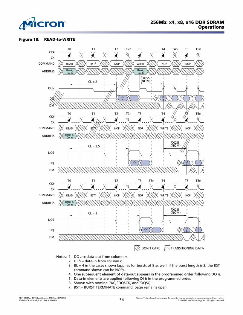
256Mb: x4, x8, x16 DDR SDRAMOperations
Figure 18: READ-to-WRITE
Notes: 1. DO n = data-out from column n.2. DI b = data-in from column b.3. BL = 4 in the cases shown (applies for bursts of 8 as well; if the burst length is 2, the BST
command shown can be NOP).4. One subsequent element of data-out appears in the programmed order following DO n.5. Data-in elements are applied following DI b in the programmed order.6. Shown with nominal tAC, tDQSCK, and tDQSQ.7. BST = BURST TERMINATE command; page remains open.
CK
CK#
COMMAND READ BST7 NOP NOP NOP
ADDRESS Bank,Col n
WRITE
Bank,Col b
T0 T1 T2 T3T2n T4 T5T4n T5n
CL = 2
DQ
DQS
DM
t(NOM)DQSS
DIb
CK
CK#
COMMAND READ BST7 NOP WRITE NOP
ADDRESS Bank a,Col n
NOP
T0 T1 T2 T3T2n T4 T5 T5n
CL = 2.5
DQ
DQS
DOn
DM
DIb
DON’T CARE TRANSITIONING DATA
DOn
t(NOM)DQSS
CK
CK#
COMMAND READ BST7 NOP WRITE NOP
ADDRESS Bank a,Col n
NOP
T0 T1 T2 T3 T4 T5 T5n
CL = 3
DQ
DQS
DOn
DM
T3n
DIb
t(NOM)DQSS
PDF: 09005aef80768abb/Source: 09005aef8076894f Micron Technology, Inc., reserves the right to change products or specifications without notice.256MBDDRx4x8x16_2.fm - Rev. L 6/06 EN 34 ©2003 Micron Technology, Inc. All rights reserved.

256Mb: x4, x8, x16 DDR SDRAMOperations
Figure 19: READ-to-PRECHARGE
Notes: 1. DO n = data-out from column n. 2. BL = 4, or an interrupted burst of 8.3. Three subsequent elements of data-out appear in the programmed order following DO n.4. Shown with nominal tAC, tDQSCK, and tDQSQ.5. READ to PRECHARGE equals two clocks, which allows two data pairs of data-out.6. A READ command with AUTO-PRECHARGE enabled, provided tRAS (MIN) is met, would
cause a precharge to be performed at x number of clock cycles after the READ command, where x = BL/2.
7. An active command to the same bank is only allowed if tRC (MIN) has been satisfied.8. PRE = PRECHARGE command; ACT = ACTIVE command.
CK
CK#
COMMAND6 READ NOP PRE NOP NOP ACT
ADDRESS Bank a,Col n
Bank a,(a or all)
Bank a,Row
READ NOP PRE NOP NOP ACT
Bank a,Col n
CL = 2 tRP
tRP
CK
CK#
COMMAND6
ADDRESS
DQ
DQS
CL = 2.5
DQ
DQS
DOn
DOn
T0 T1 T2 T3T2n T3n T4 T5
T0 T1 T2 T3T2n T3n T4 T5
Bank a,(a or all)
Bank a,Row
DON’T CARE TRANSITIONING DATA
READ NOP
Bank a,Col n
tRP
CK
CK#
COMMAND6
ADDRESS
DQ
DQS
CL = 3
DOn
T0 T1 T2 T3 T4nT3n T4 T5
PRE NOP ACT
Bank a,(a or all)
NOP
Bank a,Row
7
7
7
PDF: 09005aef80768abb/Source: 09005aef8076894f Micron Technology, Inc., reserves the right to change products or specifications without notice.256MBDDRx4x8x16_2.fm - Rev. L 6/06 EN 35 ©2003 Micron Technology, Inc. All rights reserved.

256Mb: x4, x8, x16 DDR SDRAMOperations
WRITEsWRITE bursts are initiated with a WRITE command, as shown in Figure 20.
The starting column and bank addresses are provided with the WRITE command, and auto precharge is either enabled or disabled for that access. If auto precharge is enabled, the row being accessed is precharged at the completion of the burst and after the tWR time.
Note: For the WRITE commands used in the following illustrations, auto precharge is dis-abled.
During WRITE bursts, the first valid data-in element will be registered on the first rising edge of DQS following the WRITE command, and subsequent data elements will be reg-istered on successive edges of DQS. The LOW state on DQS between the WRITE com-mand and the first rising edge is known as the write preamble; the LOW state on DQS following the last data-in element is known as the write postamble.
The time between the WRITE command and the first corresponding rising edge of DQS (tDQSS) is specified with a relatively wide range (from 75 percent to 125 per-cent of one clock cycle and 72 percent to 128 percent for DDR400). All of the WRITE diagrams show the nominal case, and where the two extreme cases (i.e., tDQSS [MIN] and tDQSS [MAX]) might not be intuitive, they have also been included. Figure 21 on page 38 shows the nominal case and the extremes of tDQSS for a burst of 4. Upon completion of a burst, assuming no other commands have been initiated, the DQ will remain High-Z and any additional input data will be ignored.
Data for any WRITE burst may be concatenated with or truncated with a subsequent WRITE command. In either case, a continuous flow of input data can be maintained. The new WRITE command can be issued on any positive edge of clock following the pre-vious WRITE command. The first data element from the new burst is applied after either the last element of a completed burst or the last desired data element of a longer burst which is being truncated. The new WRITE command should be issued x cycles after the first WRITE command, where x equals the number of desired data element pairs (pairs are required by the 2n-prefetch architecture).
Figure 22 on page 39 shows concatenated bursts of 4. An example of nonconsecutive WRITEs is shown in Figure 23 on page 40. Full-speed random write accesses within a page or pages can be performed as shown in Figure 24 on page 40.
PDF: 09005aef80768abb/Source: 09005aef8076894f Micron Technology, Inc., reserves the right to change products or specifications without notice.256MBDDRx4x8x16_2.fm - Rev. L 6/06 EN 36 ©2003 Micron Technology, Inc. All rights reserved.
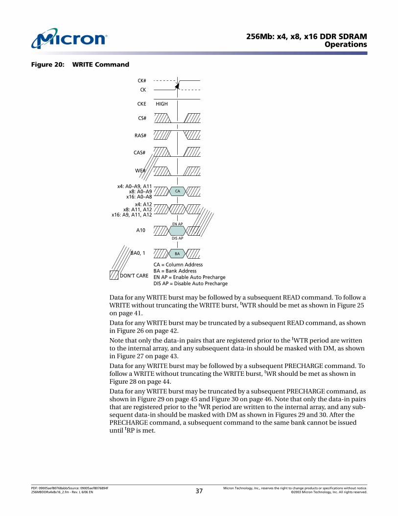
256Mb: x4, x8, x16 DDR SDRAMOperations
Figure 20: WRITE Command
Data for any WRITE burst may be followed by a subsequent READ command. To follow a WRITE without truncating the WRITE burst, tWTR should be met as shown in Figure 25 on page 41.
Data for any WRITE burst may be truncated by a subsequent READ command, as shown in Figure 26 on page 42.
Note that only the data-in pairs that are registered prior to the tWTR period are written to the internal array, and any subsequent data-in should be masked with DM, as shown in Figure 27 on page 43.
Data for any WRITE burst may be followed by a subsequent PRECHARGE command. To follow a WRITE without truncating the WRITE burst, tWR should be met as shown in Figure 28 on page 44.
Data for any WRITE burst may be truncated by a subsequent PRECHARGE command, as shown in Figure 29 on page 45 and Figure 30 on page 46. Note that only the data-in pairs that are registered prior to the tWR period are written to the internal array, and any sub-sequent data-in should be masked with DM as shown in Figures 29 and 30. After the PRECHARGE command, a subsequent command to the same bank cannot be issued until tRP is met.
CS#
WE#
CAS#
RAS#
CKE
CA
A10
BA0, 1
HIGH
EN AP
DIS AP
BA
CK
CK#
CA = Column AddressBA = Bank AddressEN AP = Enable Auto PrechargeDIS AP = Disable Auto Precharge
DON’T CARE
x4: A0–A9, A11x8: A0–A9
x16: A0–A8x4: A12
x8: A11, A12x16: A9, A11, A12
PDF: 09005aef80768abb/Source: 09005aef8076894f Micron Technology, Inc., reserves the right to change products or specifications without notice.256MBDDRx4x8x16_2.fm - Rev. L 6/06 EN 37 ©2003 Micron Technology, Inc. All rights reserved.

256Mb: x4, x8, x16 DDR SDRAMOperations
Figure 21: WRITE Burst
Notes: 1. DI b = data-in for column b.2. Three subsequent elements of data-in are applied in the programmed order following DI
b.3. An uninterrupted burst of 4 is shown.4. A10 is LOW with the WRITE command (auto precharge is disabled).
DQS
tDQSS (MAX)
tDQSS (NOM)
tDQSS (MIN)
tDQSS
DM
DQ
CK
CK#
COMMAND WRITE NOP NOP
ADDRESS Bank a,Col b
NOP
T0 T1 T2 T3T2n
DQStDQSS
DM
DQ
DQStDQSS
DM
DQ DIb
DIb
DIb
DON’T CARE TRANSITIONING DATA
PDF: 09005aef80768abb/Source: 09005aef8076894f Micron Technology, Inc., reserves the right to change products or specifications without notice.256MBDDRx4x8x16_2.fm - Rev. L 6/06 EN 38 ©2003 Micron Technology, Inc. All rights reserved.

256Mb: x4, x8, x16 DDR SDRAMOperations
Figure 22: Consecutive WRITE-to-WRITE
Notes: 1. DI b, etc., = data-in for column b, etc.2. Three subsequent elements of data-in are applied in the programmed order following DI
b. 3. Three subsequent elements of data-in are applied in the programmed order following DI
n. 4. An uninterrupted burst of 4 is shown.5. Each WRITE command may be to any bank.
CK
CK#
COMMAND WRITE NOP WRITE NOP NOP
ADDRESS Bank,Col b
NOP
Bank,Col n
T0 T1 T2 T3T2n T4 T5T4nT3nT1n
DQ
DQS
DM
DIn
DIb
DON’T CARE TRANSITIONING DATA
tDQSStDQSS (NOM)
PDF: 09005aef80768abb/Source: 09005aef8076894f Micron Technology, Inc., reserves the right to change products or specifications without notice.256MBDDRx4x8x16_2.fm - Rev. L 6/06 EN 39 ©2003 Micron Technology, Inc. All rights reserved.
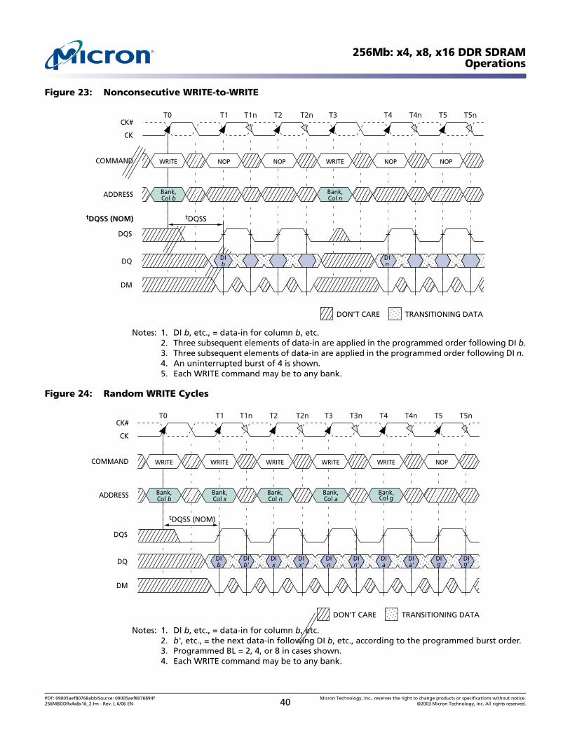
256Mb: x4, x8, x16 DDR SDRAMOperations
Figure 23: Nonconsecutive WRITE-to-WRITE
Notes: 1. DI b, etc., = data-in for column b, etc.2. Three subsequent elements of data-in are applied in the programmed order following DI b.3. Three subsequent elements of data-in are applied in the programmed order following DI n. 4. An uninterrupted burst of 4 is shown.5. Each WRITE command may be to any bank.
Figure 24: Random WRITE Cycles
Notes: 1. DI b, etc., = data-in for column b, etc. 2. b', etc., = the next data-in following DI b, etc., according to the programmed burst order. 3. Programmed BL = 2, 4, or 8 in cases shown.4. Each WRITE command may be to any bank.
CK
CK#
COMMAND WRITE NOP NOP NOP NOP
ADDRESS Bank,Col b
WRITE
Bank,Col n
T0 T1 T2 T3T2n T4 T5T4nT1n T5n
DQ
DQS
DM
DIn
DIb
tDQSS (NOM) tDQSS
DON’T CARE TRANSITIONING DATA
tDQSS (NOM)
CK
CK#
COMMAND WRITE WRITE WRITE WRITE NOP
ADDRESS Bank,Col b
Bank,Col x
Bank,Col n
Bank,Col g
WRITE
Bank,Col a
T0 T1 T2 T3T2n T4 T5T4nT1n T3n T5n
DQ
DQS
DM
DIb
DIb'
DIx
DIx'
DIn
DIn'
DIa
DIa'
DIg
DIg'
DON’T CARE TRANSITIONING DATA
PDF: 09005aef80768abb/Source: 09005aef8076894f Micron Technology, Inc., reserves the right to change products or specifications without notice.256MBDDRx4x8x16_2.fm - Rev. L 6/06 EN 40 ©2003 Micron Technology, Inc. All rights reserved.

256Mb: x4, x8, x16 DDR SDRAMOperations
Figure 25: WRITE-to-READ – Uninterrupting
Notes: 1. DI b = data-in for column b; DO n = data-out for column n.2. Three subsequent elements of data-in are applied in the programmed order following DI
b.3. An uninterrupted burst of 4 is shown.4. tWTR is referenced from the first positive CK edge after the last data-in pair.5. The READ and WRITE commands are to the same device. However, the READ and WRITE
commands may be directed to different devices, in which case, tWTR is not required and the READ command could be applied earlier.
6. A10 is LOW with the WRITE command (auto precharge is disabled).
tDQSS (NOM)
CK
CK#
COMMAND WRITE NOP NOP READ NOP NOP
ADDRESS Bank a,Col b
Bank a,Col n
NOP
T0 T1 T2 T3T2n T4 T5T1n T6 T6n
tWTR
CL = 2
DQ
DQS
DM
DIb
DOn
tDQSStDQSS (MIN) CL = 2
DQ
DQS
DM
DIb
DOn
tDQSStDQSS (MAX) CL = 2
DQ
DQS
DM
DIb
DOn
tDQSS
DON’T CARE TRANSITIONING DATA
PDF: 09005aef80768abb/Source: 09005aef8076894f Micron Technology, Inc., reserves the right to change products or specifications without notice.256MBDDRx4x8x16_2.fm - Rev. L 6/06 EN 41 ©2003 Micron Technology, Inc. All rights reserved.

256Mb: x4, x8, x16 DDR SDRAMOperations
Figure 26: WRITE-to-READ – Interrupting
Notes: 1. DI b = data-in for column;, DO n = data-out for column n.2. An interrupted burst of 4 is shown; two data elements are written.3. One subsequent element of data-in is applied in the programmed order following DI b.4. tWTR is referenced from the first positive CK edge after the last data-in pair.5. A10 is LOW with the WRITE command (auto precharge is disabled).6. DQS is required at T2 and T2n (nominal case) to register DM.7. If the burst of 8 was used, DM and DQS would be required at T3 and T3n because the
READ command would not mask these two data elements.
tDQSS (NOM)
CK
CK#
COMMAND WRITE NOP NOP NOP NOP NOP
ADDRESS Bank a,Col b
Bank a,Col n
READ
T0 T1 T2 T3T2n T4 T5 T5nT1n T6 T6n
tWTR
CL = 2
DQ
DQS
DM
DIb
DOn
tDQSS (MIN) CL = 2
DQ
DQS
DM
DIb
tDQSS (MAX) CL = 2
DQ
DQS
DM
DIb
DOn
DOn
DON’T CARE TRANSITIONING DATA
tDQSS
tDQSS
tDQSS
T3n
PDF: 09005aef80768abb/Source: 09005aef8076894f Micron Technology, Inc., reserves the right to change products or specifications without notice.256MBDDRx4x8x16_2.fm - Rev. L 6/06 EN 42 ©2003 Micron Technology, Inc. All rights reserved.

256Mb: x4, x8, x16 DDR SDRAMOperations
Figure 27: WRITE to READ – Odd Number of Data, Interrupting
Notes: 1. DI b = data-in for column b; DO n = data-out for column n.2. An interrupted burst of 4 is shown; one data element is written.3. tWTR is referenced from the first positive CK edge after the last desired data-in pair (not
the last two data elements).4. A10 is LOW with the WRITE command (auto precharge is disabled).5. DQS is required at T1n, T2, and T2n (nominal case) to register DM.6. If the burst of 8 was used, DM and DQS would be required at T3–T3n because the READ
command would not mask these data elements.
tDQSS (NOM)
CK
CK#
COMMAND WRITE NOP NOP NOP NOP NOP
ADDRESS Bank a,Col b
Bank a,Col n
READ
T0 T1 T2 T3T2n T4 T5T1n T6 T6nT5n
tWTR
CL = 2
DQ
DQS
DM
DIb
DOn
tDQSS (MIN) CL = 2
DQ
DQS
DM
DIb
DOn
tDQSS (MAX) CL = 2
DQ
DQS
DM
DIb
DOn
DON’T CARE TRANSITIONING DATA
tDQSS
tDQSS
tDQSS
T3n
PDF: 09005aef80768abb/Source: 09005aef8076894f Micron Technology, Inc., reserves the right to change products or specifications without notice.256MBDDRx4x8x16_2.fm - Rev. L 6/06 EN 43 ©2003 Micron Technology, Inc. All rights reserved.
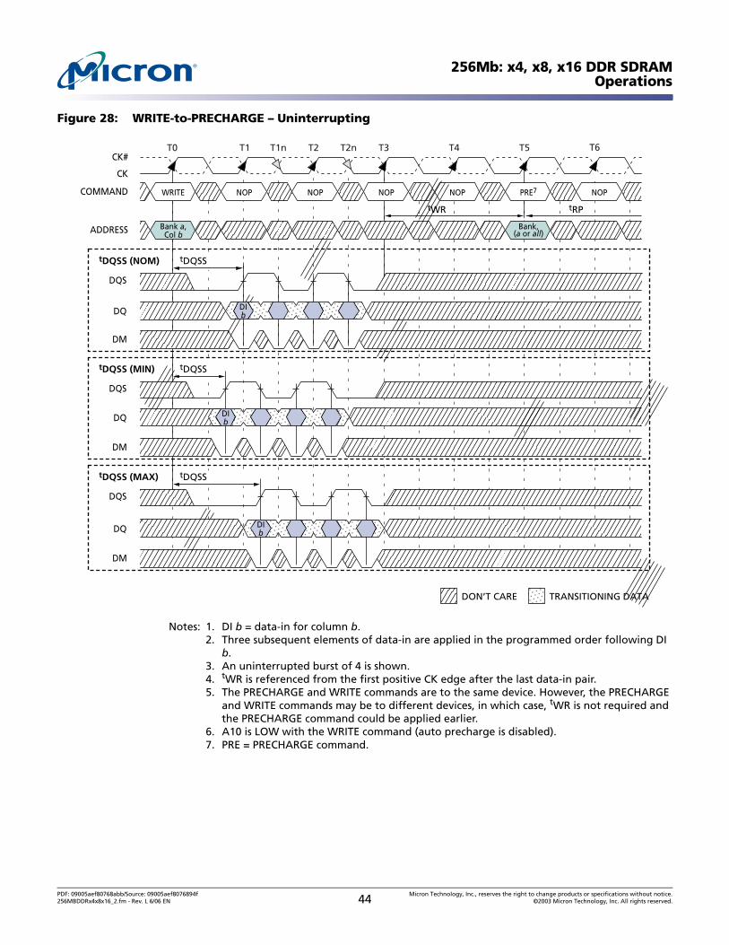
256Mb: x4, x8, x16 DDR SDRAMOperations
Figure 28: WRITE-to-PRECHARGE – Uninterrupting
Notes: 1. DI b = data-in for column b.2. Three subsequent elements of data-in are applied in the programmed order following DI
b.3. An uninterrupted burst of 4 is shown.4. tWR is referenced from the first positive CK edge after the last data-in pair.5. The PRECHARGE and WRITE commands are to the same device. However, the PRECHARGE
and WRITE commands may be to different devices, in which case, tWR is not required and the PRECHARGE command could be applied earlier.
6. A10 is LOW with the WRITE command (auto precharge is disabled).7. PRE = PRECHARGE command.
tDQSS (NOM)
CK
CK#
COMMAND WRITE NOP NOP NOP PRE7 NOP
ADDRESS Bank a,Col b
Bank,(a or all)
NOP
T0 T1 T2 T3T2n T4 T5T1n T6
tWR tRP
DQ
DQS
DM
DIb
tDQSS (MIN)
DQ
DQS
DM
DIb
tDQSS (MAX)
DQ
DQS
DM
DIb
DON’T CARE TRANSITIONING DATA
tDQSS
tDQSS
tDQSS
PDF: 09005aef80768abb/Source: 09005aef8076894f Micron Technology, Inc., reserves the right to change products or specifications without notice.256MBDDRx4x8x16_2.fm - Rev. L 6/06 EN 44 ©2003 Micron Technology, Inc. All rights reserved.

256Mb: x4, x8, x16 DDR SDRAMOperations
Figure 29: WRITE-to-PRECHARGE – Interrupting
Notes: 1. DI b = data-in for column b.2. Subsequent element of data-in is applied in the programmed order following DI b.3. An interrupted burst of 8 is shown; two data elements are written.4. tWR is referenced from the first positive CK edge after the last data-in pair.5. A10 is LOW with the WRITE command (auto precharge is disabled).6. DQS is required at T4 and T4n (nominal case) to register DM.7. If the burst of 4 was used, DQS and DM would not be required at T3, T3n, T4, and T4n.8. PRE = PRECHARGE command.
tDQSStDQSS (NOM)
CK
CK#
COMMAND WRITE NOP NOP PRE8 NOP NOP
ADDRESS Bank a,Col b
Bank,(a or all)
NOP
T0 T1 T2 T3T2n T4 T5T1n T6
tWR tRP
DQ
DQS
DM
DIb
tDQSStDQSS (MIN)
DQ
DQS
DM
DIb
tDQSStDQSS (MAX)
DQ
DQS
DM
DIb
DON’T CARE TRANSITIONING DATA
T3n T4n
PDF: 09005aef80768abb/Source: 09005aef8076894f Micron Technology, Inc., reserves the right to change products or specifications without notice.256MBDDRx4x8x16_2.fm - Rev. L 6/06 EN 45 ©2003 Micron Technology, Inc. All rights reserved.

256Mb: x4, x8, x16 DDR SDRAMOperations
Figure 30: WRITE-to-PRECHARGE – Odd Number of Data – Interrupting
Notes: 1. DI b = data-in for column b.2. An interrupted burst of 8 is shown; one data element is written.3. tWR is referenced from the first positive CK edge after the last data-in pair.4. A10 is LOW with the WRITE command (auto precharge is disabled).5. DQS is required at T4 and T4n (nominal case) to register DM.6. If the burst of 4 was used, DQS and DM would not be required at T3, T3n, T4, and T4n.7. PRE = PRECHARGE command.
tDQSStDQSS (NOM)
CK
CK#
COMMAND WRITE NOP NOP PRE7 NOP NOP
ADDRESS Bank a,Col b
Bank,(a or all)
NOP
T0 T1 T2 T3T2n T4 T5T1n T6
tWR tRP
DQ
DQS
DM
DIb
tDQSStDQSS (MIN)
DQ
DQS
DM
tDQSStDQSS (MAX)
DQ
DQS
DM
DIb
DIb
DON’T CARE TRANSITIONING DATA
T3n T4n
PDF: 09005aef80768abb/Source: 09005aef8076894f Micron Technology, Inc., reserves the right to change products or specifications without notice.256MBDDRx4x8x16_2.fm - Rev. L 6/06 EN 46 ©2003 Micron Technology, Inc. All rights reserved.

256Mb: x4, x8, x16 DDR SDRAMOperations
PRECHARGEThe PRECHARGE command, as shown in Figure 31, is used to deactivate the open row in a particular bank or the open row in all banks. The bank(s) will be available for a subse-quent row access some specified time (tRP) after the PRECHARGE command is issued. Input A10 determines whether one or all banks are to be precharged, and in the case where only one bank is to be precharged, inputs BA0, BA1 select the bank. When all banks are to be precharged, inputs BA0, BA1 are treated as “Don’t Care.” Once a bank has been precharged, it is in the idle state and must be activated prior to any READ or WRITE commands being issued to that bank.
Figure 31: PRECHARGE Command
Power-Down (CKE Not Active)Unlike SDR SDRAMs, DDR SDRAMs require CKE to be active at all times that an access is in progress, from the issuing of a READ or WRITE command until completion of the access. Thus, a clock suspend is not supported. For READs, an access completion is defined when the read postamble is satisfied; for WRITEs, an access completion is defined when the write recovery time (tWR) is satisfied.
Power-down, shown in Figure 32, “Power-Down,” on page 48, is entered when CKE is registered LOW and all of the criteria listed in Table 10, on page 48, are met. If power-down occurs when all banks are idle, this mode is referred to as precharge power-down; if power-down occurs when there is a row active in any bank, this mode is referred to as active power-down. Entering power-down deactivates the input and output buffers, excluding CK, CK#, and CKE. For maximum power savings, the DLL is frozen during pre-
CS#
WE#
CAS#
RAS#
CKE
A10
BA0,1
HIGH
ALL BANKS
ONE BANK
BA
A0–A9, A11, A12
CK
CK#
BA = Bank Address (if A10 is LOW;otherwise “Don’t Care”)
DON’T CARE
PDF: 09005aef80768abb/Source: 09005aef8076894f Micron Technology, Inc., reserves the right to change products or specifications without notice.256MBDDRx4x8x16_2.fm - Rev. L 6/06 EN 47 ©2003 Micron Technology, Inc. All rights reserved.
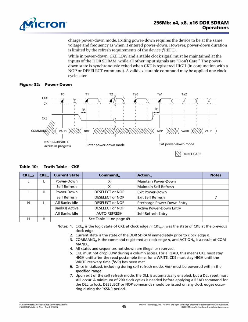
256Mb: x4, x8, x16 DDR SDRAMOperations
charge power-down mode. Exiting power-down requires the device to be at the same voltage and frequency as when it entered power-down. However, power-down duration is limited by the refresh requirements of the device (tREFC).
While in power-down, CKE LOW and a stable clock signal must be maintained at the inputs of the DDR SDRAM, while all other input signals are “Don’t Care.” The power-down state is synchronously exited when CKE is registered HIGH (in conjunction with a NOP or DESELECT command). A valid executable command may be applied one clock cycle later.
Figure 32: Power-Down
Notes: 1. CKEn is the logic state of CKE at clock edge n; CKEn-1 was the state of CKE at the previous clock edge.
2. Current state is the state of the DDR SDRAM immediately prior to clock edge n.3. COMMANDn is the command registered at clock edge n, and ACTIONn is a result of COM-
MANDn.4. All states and sequences not shown are illegal or reserved.5. CKE must not drop LOW during a column access. For a READ, this means CKE must stay
HIGH until after the read postamble time; for a WRITE, CKE must stay HIGH until the WRITE recovery time (tWR) has been met.
6. Once initialized, including during self refresh mode, VREF must be powered within the specified range.
7. Upon exit of the self refresh mode, the DLL is automatically enabled, but a DLL reset must still occur. A minimum of 200 clock cycles is needed before applying a READ command for the DLL to lock. DESELECT or NOP commands should be issued on any clock edges occur-ring during the tXSNR period.
Table 10: Truth Table – CKE
CKEn-1 CKEn Current State Commandn Actionn Notes
L L Power-Down X Maintain Power-DownSelf Refresh X Maintain Self Refresh
L H Power-Down DESELECT or NOP Exit Power-DownSelf Refresh DESELECT or NOP Exit Self Refresh 7
H L All Banks Idle DESELECT or NOP Precharge Power-Down EntryBank(s) Active DESELECT or NOP Active Power-Down EntryAll Banks Idle AUTO REFRESH Self Refresh Entry
H H See Table 11 on page 49
tIS tIS
No READ/WRITEaccess in progress Exit power-down modeEnter power-down mode
CKE
CK
CK#
COMMAND NOP
()()
()()
()()
()()
()()
NOP VALID
T0 T1 T2 Ta0 Ta1 Ta2
VALID
DON’T CARE
VALID
PDF: 09005aef80768abb/Source: 09005aef8076894f Micron Technology, Inc., reserves the right to change products or specifications without notice.256MBDDRx4x8x16_2.fm - Rev. L 6/06 EN 48 ©2003 Micron Technology, Inc. All rights reserved.

256Mb: x4, x8, x16 DDR SDRAMOperations
Notes: 1. This table applies when CKEn-1 was HIGH and CKEn is HIGH (see Table 10 on page 48) and after tXSNR has been met (if the previous state was self refresh).
2. This table is bank-specific, except where noted (i.e., the current state is for a specific bank and the commands shown are those allowed to be issued to that bank when in that state). Exceptions are covered in the notes below.
3. Current state definitions:• Idle: The bank has been precharged, and tRP has been met.• Row Active: A row in the bank has been activated, and tRCD has been met. No data
bursts/accesses and no register accesses are in progress.• Read: A READ burst has been initiated, with auto precharge disabled, and has not yet
terminated or been terminated.• Write: A WRITE burst has been initiated, with auto precharge disabled, and has not yet
terminated or been terminated.4. The following states must not be interrupted by a command issued to the same bank.
COMMAND INHIBIT or NOP commands, or allowable commands to the other bank should be issued on any clock edge occurring during these states. Allowable commands to the other bank are determined by its current state and Table 11, “Truth Table – Current State Bank n – Command-to-Bank n,” on page 49 and according to Table 12, “Truth Table – Cur-rent State Bank n – Command-to-Bank m,” on page 51.• Precharging: Starts with registration of a PRECHARGE command and ends when tRP is
met. Once tRP is met, the bank will be in the idle state.• Row Activating: Starts with registration of an ACTIVE command and ends when tRCD is
met. Once tRCD is met, the bank will be in the “row active” state.• Read w/Auto-Precharge Enabled: Starts with registration of a READ command with auto
precharge enabled and ends when tRP has been met. Once tRP is met, the bank will be in the idle state.
• Write w/Auto- Precharge Enabled: Starts with registration of a WRITE command with auto precharge enabled and ends when tRP has been met. Once tRP is met, the bank will be in the idle state.
5. The following states must not be interrupted by any executable command; COMMAND INHIBIT or NOP commands must be applied on each positive clock edge during these states.• Refreshing: Starts with registration of an AUTO REFRESH command and ends when tRFC
is met. Once tRFC is met, the DDR SDRAM will be in the all banks idle state.
Table 11: Truth Table – Current State Bank n – Command-to-Bank nNotes: 1–6; notes appear below and on next page.
Current State CS# RAS# CAS# WE# Command/Action Notes
Any H X X X DESELECT (NOP/continue previous operation)
L H H H NO OPERATION (NOP/continue previous operation)
Idle L L H H ACTIVE (select and activate row)L L L H AUTO REFRESH 7L L L L LOAD MODE REGISTER 7
Row Active L H L H READ (select column and start READ burst) 10L H L L WRITE (select column and start WRITE burst) 10L L H L PRECHARGE (deactivate row in bank or banks) 8
Read(Auto-
PrechargeDisabled)
L H L H READ (select column and start new READ burst) 10L H L L WRITE (select column and start WRITE burst) 10, 12L L H L PRECHARGE (truncate READ burst, start PRECHARGE) 8L H H L BURST TERMINATE 9
Write(Auto-
PrechargeDisabled)
L H L H READ (select column and start READ burst) 10, 11L H L L WRITE (select column and start new WRITE burst) 10L L H L PRECHARGE (truncate WRITE burst, start PRECHARGE) 8, 11
PDF: 09005aef80768abb/Source: 09005aef8076894f Micron Technology, Inc., reserves the right to change products or specifications without notice.256MBDDRx4x8x16_2.fm - Rev. L 6/06 EN 49 ©2003 Micron Technology, Inc. All rights reserved.
256Mb: x4, x8, x16 DDR SDRAMOperations
• Accessing Mode Register: Starts with registration of a LOAD MODE REGISTER command and ends when tMRD has been met. Once tMRD is met, the DDR SDRAM will be in the all banks idle state.
• Precharging All: Starts with registration of a PRECHARGE ALL command and ends when tRP is met. Once tRP is met, all banks will be in the idle state.
6. All states and sequences not shown are illegal or reserved.7. Not bank-specific; requires that all banks are idle and bursts are not in progress.8. May or may not be bank-specific; if multiple banks are to be precharged, each must be in a
valid state for precharging.9. Not bank-specific; BURST TERMINATE affects the most recent READ burst, regardless of
bank.10. READs or WRITEs listed in the Command/Action column include READs or WRITEs with
auto precharge enabled and READs or WRITEs with auto precharge disabled.11. Requires appropriate DM masking.12. A WRITE command may be applied after the completion of the READ burst; otherwise, a
BURST TERMINATE must be used to end the READ burst prior to asserting a WRITE com-mand.
PDF: 09005aef80768abb/Source: 09005aef8076894f Micron Technology, Inc., reserves the right to change products or specifications without notice.256MBDDRx4x8x16_2.fm - Rev. L 6/06 EN 50 ©2003 Micron Technology, Inc. All rights reserved.

256Mb: x4, x8, x16 DDR SDRAMOperations
Notes: 1. This table applies when CKEn-1 was HIGH and CKEn is HIGH (see Truth Table 2) and after tXSNR has been met (if the previous state was self refresh).
2. This table describes alternate bank operation except where noted (i.e., the current state is for bank n and the commands shown are those allowed to be issued to bank m, assuming that bank m is in such a state that the given command is allowable). Exceptions are cov-ered in the notes below.
3. Current state definitions:• Idle: The bank has been precharged, and tRP has been met.• Row Active: A row in the bank has been activated, and tRCD has been met. No data
bursts/accesses and no register accesses are in progress. • Read: A READ burst has been initiated, with auto precharge disabled, and has not yet
terminated or been terminated.• Write: A WRITE burst has been initiated, with auto precharge disabled, and has not yet
terminated or been terminated• Read with Auto Precharge Enabled: See following text – 3a• Write with Auto Precharge Enabled: See following text – 3a
a.The read with auto precharge enabled or write with auto precharge enabled states can each be broken into two parts: the access period and the precharge period. For read with auto precharge, the precharge period is defined as if the same burst was executed with auto precharge disabled and then followed with the earliest possible PRECHARGE command that still accesses all of the data in the burst. For write with auto precharge, the precharge period begins when tWR ends, with tWR measured as if auto precharge was disabled. The access period starts with registration of the com-mand and ends where the precharge period (or tRP) begins.
Table 12: Truth Table – Current State Bank n – Command-to-Bank mNotes: 1–6; notes appear below and on next page.
Current State CS# RAS# CAS# WE# Command/action Notes
Any H X X X DESELECT (NOP/continue previous operation)L H H H NO OPERATION (NOP/continue previous operation)
Idle X X X X Any Command Otherwise Allowed to Bank mRowActivating,Active, orPrecharging
L L H H ACTIVE (select and activate row)L H L H READ (select column and start READ burst) 7L H L L WRITE (select column and start WRITE burst) 7L L H L PRECHARGE
Read(Auto-PrechargeDisabled)
L L H H ACTIVE (select and activate row)L H L H READ (select column and start new READ burst) 7L H L L WRITE (select column and start WRITE burst) 7, 9L L H L PRECHARGE
Write(Auto-PrechargeDisabled)
L L H H ACTIVE (select and activate row)L H L H READ (select column and start READ burst) 7, 8L H L L WRITE (select column and start new WRITE burst) 7L L H L PRECHARGE
Read(With Auto-Precharge)
L L H H ACTIVE (select and activate row)L H L H READ (select column and start new READ burst) 7, 3aL H L L WRITE (select column and start WRITE burst) 7, 9, 3aL L H L PRECHARGE
Write(With Auto-Precharge)
L L H H ACTIVE (select and activate row)L H L H READ (select column and start READ burst) 7, 3aL H L L WRITE (select column and start new WRITE burst) 7, 3aL L H L PRECHARGE
PDF: 09005aef80768abb/Source: 09005aef8076894f Micron Technology, Inc., reserves the right to change products or specifications without notice.256MBDDRx4x8x16_2.fm - Rev. L 6/06 EN 51 ©2003 Micron Technology, Inc. All rights reserved.

256Mb: x4, x8, x16 DDR SDRAMOperations
This device supports concurrent auto precharge such that when a READ with auto precharge is enabled or a WRITE with auto precharge is enabled any command to other banks is allowed, as long as that command does not inter-rupt the read or write data transfer already in process. In either case, all other related limitations apply (e.g., contention between read data and write data must be avoided).
b.The minimum delay from a READ or WRITE command with auto precharge enabled, to a command to a different bank, is summarized below.
4. AUTO REFRESH and LOAD MODE REGISTER commands may only be issued when all banks are idle.
5. A BURST TERMINATE command cannot be issued to another bank; it applies to the bank represented by the current state only.
6. All states and sequences not shown are illegal or reserved.7. READs or WRITEs listed in the Command/Action column include READs or WRITEs with
auto precharge enabled and READs or WRITEs with auto precharge disabled.8. Requires appropriate DM masking.9. A WRITE command may be applied after the completion of the READ burst; otherwise, a
BURST TERMINATE must be used to end the READ burst prior to asserting a WRITE com-mand.
Table 13: Minimum Delay SummaryCLRU = CAS Latency (CL) rounded up to the next integer. BL = Bust length.
From Command To Command Minimum Delay (with Concurrent Auto Precharge)
WRITE w/AP READ or READ w/AP [1 + (BL/2)] * tCK + tWTRWRITE or WRITE w/AP (BL/2) * tCK
PRECHARGE 1 tCKACTIVE 1 tCK
READ w/AP READ or READ w/AP (BL/2) * tCKWRITE or WRITE w/AP [CLRU
+ (BL/2)] *tCKPRECHARGE 1 tCK
ACTIVE 1 tCK
PDF: 09005aef80768abb/Source: 09005aef8076894f Micron Technology, Inc., reserves the right to change products or specifications without notice.256MBDDRx4x8x16_2.fm - Rev. L 6/06 EN 52 ©2003 Micron Technology, Inc. All rights reserved.
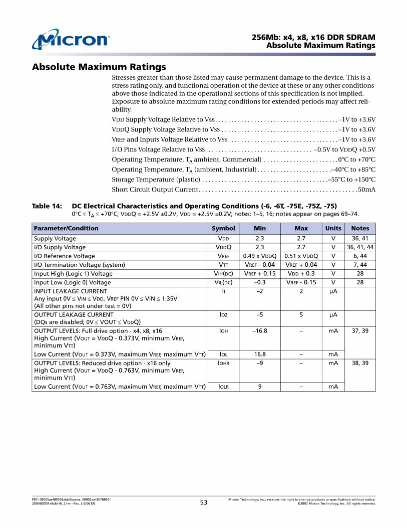
256Mb: x4, x8, x16 DDR SDRAMAbsolute Maximum Ratings
Absolute Maximum RatingsStresses greater than those listed may cause permanent damage to the device. This is a stress rating only, and functional operation of the device at these or any other conditions above those indicated in the operational sections of this specification is not implied. Exposure to absolute maximum rating conditions for extended periods may affect reli-ability.
VDD Supply Voltage Relative to Vss. . . . . . . . . . . . . . . . . . . . . . . . . . . . . . . . . . . . . . –1V to +3.6V
VDDQ Supply Voltage Relative to VSS . . . . . . . . . . . . . . . . . . . . . . . . . . . . . . . . . . . . –1V to +3.6V
VREF and Inputs Voltage Relative to VSS . . . . . . . . . . . . . . . . . . . . . . . . . . . . . . . . . –1V to +3.6V
I/O Pins Voltage Relative to VSS . . . . . . . . . . . . . . . . . . . . . . . . . . . . . . . . –0.5V to VDDQ +0.5V
Operating Temperature, TA ambient, Commercial) . . . . . . . . . . . . . . . . . . . . . . .0°C to +70°C
Operating Temperature, TA (ambient, Industrial) . . . . . . . . . . . . . . . . . . . . . . .–40°C to +85°C
Storage Temperature (plastic) . . . . . . . . . . . . . . . . . . . . . . . . . . . . . . . . . . . . . . .–55°C to +150°C
Short Circuit Output Current. . . . . . . . . . . . . . . . . . . . . . . . . . . . . . . . . . . . . . . . . . . . . . . . . 50mA
Table 14: DC Electrical Characteristics and Operating Conditions (-6, -6T, -75E, -75Z, -75)0°C ≤ TA ≤ +70°C; VDDQ = +2.5V ±0.2V, VDD = +2.5V ±0.2V; notes: 1–5, 16; notes appear on pages 69–74.
Parameter/Condition Symbol Min Max Units Notes
Supply Voltage VDD 2.3 2.7 V 36, 41
I/O Supply Voltage VDDQ 2.3 2.7 V 36, 41, 44
I/O Reference Voltage VREF 0.49 x VDDQ 0.51 x VDDQ V 6, 44
I/O Termination Voltage (system) VTT VREF - 0.04 VREF + 0.04 V 7, 44
Input High (Logic 1) Voltage VIH(DC) VREF + 0.15 VDD + 0.3 V 28
Input Low (Logic 0) Voltage VIL(DC) –0.3 VREF - 0.15 V 28
INPUT LEAKAGE CURRENTAny input 0V ≤ VIN ≤ VDD, VREF PIN 0V ≤ VIN ≤ 1.35V(All other pins not under test = 0V)
II –2 2 µA
OUTPUT LEAKAGE CURRENT(DQs are disabled; 0V ≤ VOUT ≤ VDDQ)
IOZ –5 5 µA
OUTPUT LEVELS: Full drive option - x4, x8, x16High Current (VOUT = VDDQ - 0.373V, minimum VREF, minimum VTT)
IOH –16.8 – mA 37, 39
Low Current (VOUT = 0.373V, maximum VREF, maximum VTT) IOL 16.8 – mA
OUTPUT LEVELS: Reduced drive option - x16 onlyHigh Current (VOUT = VDDQ - 0.763V, minimum VREF, minimum VTT)
IOHR –9 – mA 38, 39
Low Current (VOUT = 0.763V, maximum VREF, maximum VTT) IOLR 9 – mA
PDF: 09005aef80768abb/Source: 09005aef8076894f Micron Technology, Inc., reserves the right to change products or specifications without notice.256MBDDRx4x8x16_2.fm - Rev. L 6/06 EN 53 ©2003 Micron Technology, Inc. All rights reserved.

256Mb: x4, x8, x16 DDR SDRAMAbsolute Maximum Ratings
Table 15: DC Electrical Characteristics and Operating Conditions (-5B DDR400)0°C ≤ TA ≤ +70°C; VDDQ = +2.6V ±0.1V, VDD = +2.6V ±0.1V; notes: 1–5, 16, and 53; notes appear on page 69–74.
Parameter/Condition Symbol Min Max Units Notes
Supply Voltage VDD 2.5 2.7 V 36, 41, 52
I/O Supply Voltage VDDQ 2.5 2.7 V 36, 41, 44, 52
I/O Reference Voltage VREF 0.49 x VDDQ 0.51 x VDDQ V 6, 44
I/O Termination Voltage (system) VTT VREF - 0.04 VREF + 0.04 V 7, 44
Input High (Logic 1) Voltage VIH(DC) VREF + 0.15 VDD + 0.3 V 28
Input Low (Logic 0) Voltage VIL(DC) –0.3 VREF - 0.15 V 28
INPUT LEAKAGE CURRENTAny input 0V ≤ VIN ≤ VDD, VREF PIN 0V ≤ VIN ≤ 1.35V(All other pins not under test = 0V)
II –2 2 µA
OUTPUT LEAKAGE CURRENT(DQs are disabled; 0V ≤ VOUT ≤ VDDQ)
IOZ –5 5 µA
OUTPUT LEVELS: Full drive option – x4, x8, x16High Current (VOUT = VDDQ - 0.373V, minimum VREF, minimum VTT)
IOH –16.8 – mA 37, 39
Low Current (VOUT = 0.373V, maximum VREF, maximum VTT)
IOL 16.8 – mA
OUTPUT LEVELS: Reduced drive option – x16 onlyHigh Current (VOUT = VDDQ - 0.763V, minimum VREF, minimum VTT)
IOHR –9 – mA 38, 39
Low Current (VOUT = 0.763V, maximum VREF, maximum VTT)
IOLR 9 – mA
PDF: 09005aef80768abb/Source: 09005aef8076894f Micron Technology, Inc., reserves the right to change products or specifications without notice.256MBDDRx4x8x16_2.fm - Rev. L 6/06 EN 54 ©2003 Micron Technology, Inc. All rights reserved.

256Mb: x4, x8, x16 DDR SDRAMAbsolute Maximum Ratings
Figure 33: Input Voltage Waveform
Table 16: AC Input Operating Conditions0°C ≤ TA ≤ +70°C; VDDQ = +2.5V ±0.2V, VDD = +2.5V ±0.2V (VDDQ = +2.6V ±0.1V, VDD = +2.6V ±0.1V for DDR400); notes: 1–5, 14, 16; notes appear on pages 69–74.
Parameter/Condition Symbol Min Max Units Notes
Input High (Logic 1) Voltage VIH(AC) VREF + 0.310 – V 14, 28, 40
Input Low (Logic 0) Voltage VIL(AC) – VREF - 0.310 V 14, 28, 40
I/O Reference Voltage VREF(AC) 0.49 x VDDQ 0.51 x VDDQ V 6
0.940V
1.100V
1.200V1.225V1.250V1.275V1.300V
1.400V
1.560V
VILAC
VILDC
VREF -AC NoiseVREF -DC ErrorVREF +DC ErrorVREF +AC Noise
Receiver
Transmitter
VIHDC
VIHAC
VOH (MIN) (1.670V1 for SSTL_2 termination)
VINAC - Provides marginbetween VOL (MAX) and VILAC
VSSQ
VDDQ (2.3V minimum)
VOL (MAX) (0.83V2 for SSTL_2 termination)
System Noise Margin (Power/Ground, Crosstalk, Signal Integrity Attenuation)
NOTE: 1. VOH (MIN) with test load is 1.927V 2. VOL (MAX) with test load is 0.373V 3. For Non-DDR400 devices, numbers
in diagram reflect nomimal values utilizing circuit below.
Reference Point
25Ω
25Ω
VTT
PDF: 09005aef80768abb/Source: 09005aef8076894f Micron Technology, Inc., reserves the right to change products or specifications without notice.256MBDDRx4x8x16_2.fm - Rev. L 6/06 EN 55 ©2003 Micron Technology, Inc. All rights reserved.

256Mb: x4, x8, x16 DDR SDRAMAbsolute Maximum Ratings
Figure 34: SSTL_2 Clock Input
Notes: 1. This provides a minimum of 1.15V to a maximum of 1.35V and is always half of VDDQ.2. CK and CK# must cross in this region.3. CK and CK# must meet at least VID(DC) MIN when static and is centered around VMP(DC).4. CK and CK# must have a minimum 700mv peak-to-peak swing.5. CK or CK# may not be more positive than VDDQ + 0.3V or more negative than VSS - 0.3V.6. For AC operation, all DC clock requirements must also be satisfied.7. Numbers in diagram reflect nominal values for non-DDR400 devices.
Table 17: Clock Input Operating Conditions0°C ≤ TA ≤ +70°C; VDDQ = +2.5V ±0.2V, VDD = +2.5V ±0.2V (VDDQ = +2.6V ±0.1V, VDD = +2.6V ±0.1V for DDR400); notes: 1–5, 15, 16, 30; notes appear on pages 69–74.
Parameter/Condition Symbol Min Max Units Notes
Clock Input Midpoint Voltage; CK and CK# VMP(DC) 1.15 1.35 V 6, 9
Clock Input Voltage Level; CK and CK# VIN(DC) –0.3 VDDQ + 0.3 V 6
Clock Input Differential Voltage; CK and CK# VID(DC) 0.36 VDDQ + 0.6 V 6, 8
Clock Input Differential Voltage; CK and CK# VID(AC) 0.7 VDDQ + 0.6 V 8
Clock Input Crossing Point Voltage; CK and CK# VIX(AC) 0.5 x VDDQ - 0.2 0.5 x VDDQ + 0.2 V 9
CK
CK#
2.80V
23
5
5Maximum Clock Level
Minimum Clock Level
4
- 0.30V
1.25V
1.45V
1.05VVID (AC)
VID (DC)
X
1VMP (DC)
VIX (AC)
X
PDF: 09005aef80768abb/Source: 09005aef8076894f Micron Technology, Inc., reserves the right to change products or specifications without notice.256MBDDRx4x8x16_2.fm - Rev. L 6/06 EN 56 ©2003 Micron Technology, Inc. All rights reserved.

256Mb: x4, x8, x16 DDR SDRAMAbsolute Maximum Ratings
Table 18: Capacitance (x4, x8 TSOP)Note: 13; notes appear on pages 69–74.
Parameter Symbol Min Max Units Notes
Delta Input/Output Capacitance: DQ0–DQ3 (x4), DQ0–DQ7 (x8) DCIO – 0.50 pF 24
Delta Input Capacitance: Command and Address DCI1 – 0.50 pF 29
Delta Input Capacitance: CK, CK# DCI2 – 0.25 pF 29
Input/Output Capacitance: DQs, DQS, DM CIO 4.0 5.0 pF
Input Capacitance: Command and Address CI1 2.0 3.0 pF
Input Capacitance: CK, CK# CI2 2.0 3.0 pF
Input Capacitance: CKE CI3 2.0 3.0 pF
Table 19: Capacitance (x16 TSOP)Note: 13; notes appear on pages 69–74.
Parameter Symbol Min Max Units Notes
Delta Input/Output Capacitance: DQ0–DQ7, LDQS, LDM DCIOL – 0.50 pF 24
Delta Input/Output Capacitance: DQ8–DQ15, UDQS, UDM DCIOU – 0.50 pF 24
Delta Input Capacitance: Command and Address DCI1 – 0.50 pF 29
Delta Input Capacitance: CK, CK# DCI2 – 0.25 pF 29
Input/Output Capacitance: DQ, LDQS, UDQS, LDM, UDM CIO 4.0 5.0 pF
Input Capacitance: Command and Address CI1 2.0 3.0 pF
Input Capacitance: CK, CK# CI2 2.0 3.0 pF
Input Capacitance: CKE CI3 2.0 3.0 pF
PDF: 09005aef80768abb/Source: 09005aef8076894f Micron Technology, Inc., reserves the right to change products or specifications without notice.256MBDDRx4x8x16_2.fm - Rev. L 6/06 EN 57 ©2003 Micron Technology, Inc. All rights reserved.

256Mb: x4, x8, x16 DDR SDRAMAbsolute Maximum Ratings
Table 20: IDD Specifications and Conditions (x4, x8; -5B)0°C ≤ TA ≤ +70°C; (VDDQ = +2.6V ±0.1V, VDD = +2.6V ±0.1V); notes: 1–5, 10, 12, 14, 46; notes appear on pages 69–74; see also Table 26, “Idd Test Cycle Times,” on page 64.
Max
Parameter/condition Symbol -5B Units Notes
OPERATING CURRENT: One bank; active precharge; tRC = tRC (MIN); tCK = tCK (MIN); DQ, DM, and DQS inputs changing once per clock cycle; address and control inputs changing once every two clock cycles
IDD0 135 mA 22, 47
OPERATING CURRENT: One bank; active-read precharge;burst = 4; tRC = tRC (MIN); tCK = tCK (MIN); IOUT = 0mA; address and control inputs changing once per clock cycle
IDD1 170 mA 22, 47
PRECHARGE POWER-DOWN STANDBY CURRENT: All banks idle; power-down mode; tCK = tCK (MIN); CKE = (LOW)
IDD2P 4 mA 23, 32, 49
IDLE STANDBY CURRENT: CS# = HIGH; all banks are idle; tCK = tCK (MIN); CKE = HIGH; address and other control inputs changing once per clock cycle; VIN = VREF for DQ, DQS, and DM
IDD2F 60 mA 50
ACTIVE POWER-DOWN STANDBY CURRENT: One bank active;power-down mode; tCK = tCK (MIN); CKE = LOW
IDD3P 40 mA 23, 32, 49
ACTIVE STANDBY CURRENT: CS# = HIGH; CKE = HIGH; one bank active; tRC = tRAS (MAX); tCK = tCK (MIN); DQ, DM, and DQS inputs changing twice per clock cycle; address and other control inputs changing once per clock cycle
IDD3N 70 mA 22
OPERATING CURRENT: Burst = 2; READs; continuous burst; one bank active; address and control inputs changing once per clock cycle; tCK = tCK (MIN); IOUT = 0mA
IDD4R 200 mA 22, 47
OPERATING CURRENT: Burst = 2; WRITEs; continuous burst; one bank active; address and control inputs changing once per clock cycle; tCK = tCK (MIN); DQ, DM, and DQS inputs changing twice per clock cycle
IDD4W 195 mA 22
AUTO REFRESH BURST CURRENT: tREFC = tRC (MIN) IDD5 260 mA 49tREFC = 7.8µs IDD5A 6 mA 27, 49
SELF REFRESH CURRENT: CKE ≤ 0.2V Standard IDD6 4 mA 11
Low power (L) IDD6A 2 mA 11
OPERATING CURRENT: Four-bank interleaving READs (Burst = 4) with auto precharge, tRC = minimum tRC allowed; tCK = tCK (MIN); address and control inputs change only during active READ or WRITE commands
IDD7 470 mA 22, 48
PDF: 09005aef80768abb/Source: 09005aef8076894f Micron Technology, Inc., reserves the right to change products or specifications without notice.256MBDDRx4x8x16_2.fm - Rev. L 6/06 EN 58 ©2003 Micron Technology, Inc. All rights reserved.
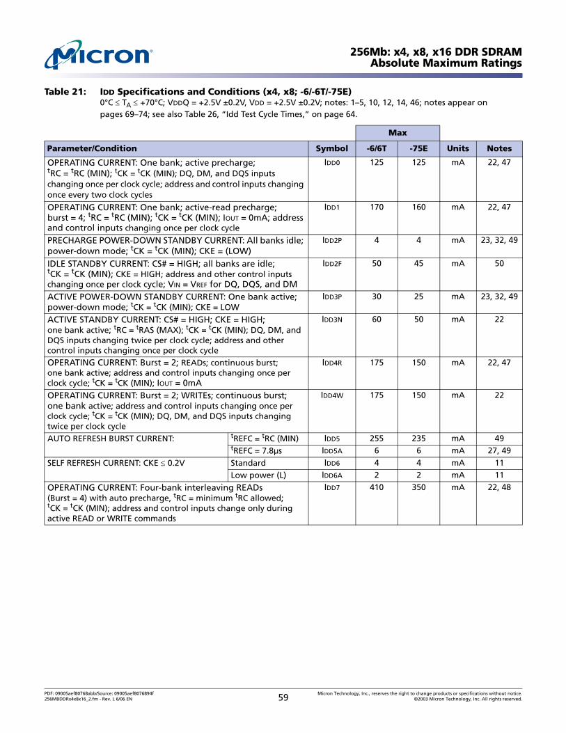
256Mb: x4, x8, x16 DDR SDRAMAbsolute Maximum Ratings
Table 21: IDD Specifications and Conditions (x4, x8; -6/-6T/-75E)0°C ≤ TA ≤ +70°C; VDDQ = +2.5V ±0.2V, VDD = +2.5V ±0.2V; notes: 1–5, 10, 12, 14, 46; notes appear on pages 69–74; see also Table 26, “Idd Test Cycle Times,” on page 64.
Max
Parameter/Condition Symbol -6/6T -75E Units Notes
OPERATING CURRENT: One bank; active precharge; tRC = tRC (MIN); tCK = tCK (MIN); DQ, DM, and DQS inputs changing once per clock cycle; address and control inputs changing once every two clock cycles
IDD0 125 125 mA 22, 47
OPERATING CURRENT: One bank; active-read precharge;burst = 4; tRC = tRC (MIN); tCK = tCK (MIN); IOUT = 0mA; address and control inputs changing once per clock cycle
IDD1 170 160 mA 22, 47
PRECHARGE POWER-DOWN STANDBY CURRENT: All banks idle; power-down mode; tCK = tCK (MIN); CKE = (LOW)
IDD2P 4 4 mA 23, 32, 49
IDLE STANDBY CURRENT: CS# = HIGH; all banks are idle; tCK = tCK (MIN); CKE = HIGH; address and other control inputs changing once per clock cycle; VIN = VREF for DQ, DQS, and DM
IDD2F 50 45 mA 50
ACTIVE POWER-DOWN STANDBY CURRENT: One bank active;power-down mode; tCK = tCK (MIN); CKE = LOW
IDD3P 30 25 mA 23, 32, 49
ACTIVE STANDBY CURRENT: CS# = HIGH; CKE = HIGH; one bank active; tRC = tRAS (MAX); tCK = tCK (MIN); DQ, DM, and DQS inputs changing twice per clock cycle; address and other control inputs changing once per clock cycle
IDD3N 60 50 mA 22
OPERATING CURRENT: Burst = 2; READs; continuous burst; one bank active; address and control inputs changing once per clock cycle; tCK = tCK (MIN); IOUT = 0mA
IDD4R 175 150 mA 22, 47
OPERATING CURRENT: Burst = 2; WRITEs; continuous burst; one bank active; address and control inputs changing once per clock cycle; tCK = tCK (MIN); DQ, DM, and DQS inputs changing twice per clock cycle
IDD4W 175 150 mA 22
AUTO REFRESH BURST CURRENT: tREFC = tRC (MIN) IDD5 255 235 mA 49tREFC = 7.8µs IDD5A 6 6 mA 27, 49
SELF REFRESH CURRENT: CKE ≤ 0.2V Standard IDD6 4 4 mA 11
Low power (L) IDD6A 2 2 mA 11
OPERATING CURRENT: Four-bank interleaving READs (Burst = 4) with auto precharge, tRC = minimum tRC allowed; tCK = tCK (MIN); address and control inputs change only during active READ or WRITE commands
IDD7 410 350 mA 22, 48
PDF: 09005aef80768abb/Source: 09005aef8076894f Micron Technology, Inc., reserves the right to change products or specifications without notice.256MBDDRx4x8x16_2.fm - Rev. L 6/06 EN 59 ©2003 Micron Technology, Inc. All rights reserved.

256Mb: x4, x8, x16 DDR SDRAMAbsolute Maximum Ratings
Table 22: IDD Specifications and Conditions (x4, x8; -75Z/-75)0°C ≤ TA ≤ +70°C; VDDQ = +2.5V ±0.2V, VDD = +2.5V ±0.2V; Notes: 1–5, 10, 12, 14, 46; notes appear on pages 69–74; see also Table 26, “Idd Test Cycle Times,” on page 64.
Max
Parameter/Condition Symbol -75Z -75 Units Notes
OPERATING CURRENT: One bank; active precharge; tRC = tRC (MIN); tCK = tCK (MIN); DQ, DM, and DQS inputs changing once per clock cycle; address and control inputs changing once every two clock cycles
IDD0 120 120 mA 22, 47
OPERATING CURRENT: One bank; active-read precharge;burst = 4; tRC = tRC (MIN); tCK = tCK (MIN); IOUT = 0mA; address and control inputs changing once per clock cycle
IDD1 145 145 mA 22, 47
PRECHARGE POWER-DOWN STANDBY CURRENT: All banks idle; power-down mode; tCK = tCK (MIN); CKE = (LOW)
IDD2P 4 4 mA 23, 32, 49
IDLE STANDBY CURRENT: CS# = HIGH; all banks are idle; tCK = tCK (MIN); CKE = HIGH; address and other control inputs changing once per clock cycle; VIN = VREF for DQ, DQS, and DM
IDD2F 45 45 mA 50
ACTIVE POWER-DOWN STANDBY CURRENT: One bank active;power-down mode; tCK = tCK (MIN); CKE = LOW
IDD3P 25 30 mA 23, 32, 49
ACTIVE STANDBY CURRENT: CS# = HIGH; CKE = HIGH; one bank active; tRC = tRAS (MAX); tCK = tCK (MIN); DQ, DM, and DQS inputs changing twice per clock cycle; address and other control inputs changing once per clock cycle
IDD3N 50 50 mA 22
OPERATING CURRENT: Burst = 2; READs; continuous burst; one bank active; address and control inputs changing once per clock cycle; tCK = tCK (MIN); IOUT = 0mA
IDD4R 150 150 mA 22, 47
OPERATING CURRENT: Burst = 2; WRITEs; continuous burst; one bank active; address and control inputs changing once per clock cycle; tCK = tCK (MIN); DQ, DM, and DQS inputs changing twice per clock cycle
IDD4W 150 150 mA 22
AUTO REFRESH BURST CURRENT: tREFC = tRC (MIN) IDD5 235 245 mA 49tREFC = 7.8µs IDD5A 6 6 mA 27, 49
SELF REFRESH CURRENT: CKE ≤ 0.2V Standard IDD6 4 4 mA 11
Low power (L) IDD6A 2 2 mA 11
OPERATING CURRENT: Four-bank interleaving READs (Burst = 4) with auto precharge, tRC = minimum tRC allowed; tCK = tCK (MIN); address and control inputs change only during active READ or WRITE commands
IDD7 350 365 mA 22, 48
PDF: 09005aef80768abb/Source: 09005aef8076894f Micron Technology, Inc., reserves the right to change products or specifications without notice.256MBDDRx4x8x16_2.fm - Rev. L 6/06 EN 60 ©2003 Micron Technology, Inc. All rights reserved.

256Mb: x4, x8, x16 DDR SDRAMAbsolute Maximum Ratings
Table 23: IDD Specifications and Conditions (x16; -5B)0°C ≤ TA ≤ +70°C; (VDDQ = +2.6V ±0.1V, VDD = +2.6V ±0.1V); notes: 1–5, 10, 12, 14, 46; notes appear on pages 69–74; see also Table 26, “Idd Test Cycle Times,” on page 64.
Max
Parameter/Condition Symbol -5B Units Notes
OPERATING CURRENT: One bank; active precharge; tRC = tRC (MIN); tCK = tCK (MIN); DQ, DM, and DQS inputs changing once per clock cycle; address and control inputs changing once every two clock cycles
IDD0 135 mA 22, 47
OPERATING CURRENT: One bank; active-read precharge;burst = 4; tRC = tRC (MIN); tCK = tCK (MIN); IOUT = 0mA; address and control inputs changing once per clock cycle
IDD1 185 mA 22, 47
PRECHARGE POWER-DOWN STANDBY CURRENT: All banks idle; power-down mode; tCK = tCK (MIN); CKE = (LOW)
IDD2P 4 mA 23, 32, 49
IDLE STANDBY CURRENT: CS# = HIGH; all banks are idle; tCK = tCK (MIN); CKE = HIGH; address and other control inputs changing once per clock cycle; VIN = VREF for DQ, DQS, and DM
IDD2F 60 mA 50
ACTIVE POWER-DOWN STANDBY CURRENT: One bank active;power-down mode; tCK = tCK (MIN); CKE = LOW
IDD3P 40 mA 23, 32, 49
ACTIVE STANDBY CURRENT: CS# = HIGH; CKE = HIGH; one bank active; tRC = tRAS (MAX); tCK = tCK (MIN); DQ, DM, and DQS inputs changing twice per clock cycle; address and other control inputs changing once per clock cycle
IDD3N 70 mA 22
OPERATING CURRENT: Burst = 2; READs; continuous burst; one bank active; address and control inputs changing once per clock cycle; tCK = tCK (MIN); IOUT = 0mA
IDD4R 260 mA 22, 47
OPERATING CURRENT: Burst = 2; WRITEs; continuous burst; one bank active; address and control inputs changing once per clock cycle; tCK = tCK (MIN); DQ, DM, and DQS inputs changing twice per clock cycle
IDD4W 215 mA 22
AUTO REFRESH BURST CURRENT: tREFC = tRC (MIN) IDD5 260 mA 49tREFC = 7.8µs IDD5A 6 mA 27, 49
SELF REFRESH CURRENT: CKE ≤ 0.2V Standard IDD6 4 mA 11
Low power (L) IDD6A 2 mA 11
OPERATING CURRENT: Four-bank interleaving READs (Burst = 4) with auto precharge, tRC = minimum tRC allowed; tCK = tCK (MIN); address and control inputs change only during active READ or WRITE commands
IDD7 510 mA 22, 48
PDF: 09005aef80768abb/Source: 09005aef8076894f Micron Technology, Inc., reserves the right to change products or specifications without notice.256MBDDRx4x8x16_2.fm - Rev. L 6/06 EN 61 ©2003 Micron Technology, Inc. All rights reserved.

256Mb: x4, x8, x16 DDR SDRAMAbsolute Maximum Ratings
Table 24: IDD Specifications and Conditions (x16; -6/-6T/-75E)0°C ≤ TA ≤ +70°C; VDDQ = +2.5V ±0.2V, VDD = +2.5V ±0.2V; notes: 1–5, 10, 12, 14, 46; notes appear on pages 69–74; see also Table 26, “Idd Test Cycle Times,” on page 64.
Max
Parameter/Condition Symbol -6/6T -75E Units Notes
OPERATING CURRENT: One bank; active precharge; tRC = tRC (MIN); tCK = tCK (MIN); DQ, DM, and DQS inputs changing once per clock cycle; address and control inputs changing once every two clock cycles
IDD0 125 125 mA 22, 47
OPERATING CURRENT: One bank; active-read precharge;burst = 4; tRC = tRC (MIN); tCK = tCK (MIN); IOUT = 0mA; address and control inputs changing once per clock cycle
IDD1 180 170 mA 22, 47
PRECHARGE POWER-DOWN STANDBY CURRENT: All banks idle; power-down mode; tCK = tCK (MIN); CKE = (LOW)
IDD2P 4 4 mA 23, 32, 49
IDLE STANDBY CURRENT: CS# = HIGH; all banks are idle; tCK = tCK (MIN); CKE = HIGH; address and other control inputs changing once per clock cycle; VIN = VREF for DQ, DQS, and DM
IDD2F 50 45 mA 50
ACTIVE POWER-DOWN STANDBY CURRENT: One bank active;power-down mode; tCK = tCK (MIN); CKE = LOW
IDD3P 30 25 mA 23, 32, 49
ACTIVE STANDBY CURRENT: CS# = HIGH; CKE = HIGH; one bank active; tRC = tRAS (MAX); tCK = tCK (MIN); DQ, DM, and DQS inputs changing twice per clock cycle; address and other control inputs changing once per clock cycle
IDD3N 60 50 mA 22
OPERATING CURRENT: Burst = 2; READs; continuous burst; one bank active; address and control inputs changing once per clock cycle; tCK = tCK (MIN); IOUT = 0mA
IDD4R 220 185 mA 22, 47
OPERATING CURRENT: Burst = 2; WRITEs; continuous burst; one bank active; address and control inputs changing once per clock cycle; tCK = tCK (MIN); DQ, DM, and DQS inputs changing twice per clock cycle
IDD4W 195 160 mA 22
AUTO REFRESH BURST CURRENT: tREFC = tRC (MIN) IDD5 255 235 mA 49tREFC = 7.8µs IDD5A 6 6 mA 27, 49
SELF REFRESH CURRENT: CKE ≤ 0.2V Standard IDD6 4 4 mA 11
Low power (L) IDD6A 2 2 mA 11
OPERATING CURRENT: Four-bank interleaving READs (Burst = 4) with auto precharge, tRC = minimum tRC allowed; tCK = tCK (MIN); address and control inputs change only during active READ or WRITE commands
IDD7 440 380 mA 22, 48
PDF: 09005aef80768abb/Source: 09005aef8076894f Micron Technology, Inc., reserves the right to change products or specifications without notice.256MBDDRx4x8x16_2.fm - Rev. L 6/06 EN 62 ©2003 Micron Technology, Inc. All rights reserved.

256Mb: x4, x8, x16 DDR SDRAMAbsolute Maximum Ratings
Table 25: IDD Specifications and Conditions (x16; -75Z/-75)0°C ≤ TA ≤ +70°C; VDDQ = +2.5V ±0.2V, VDD = +2.5V ±0.2VNotes: 1–5, 10, 12, 14, 46; notes appear on pages 69–74; see also Table 26, “Idd Test Cycle Times,” on page 64.
Max
Parameter/Condition Symbol -75Z -75 Units Notes
OPERATING CURRENT: One bank; active precharge; tRC = tRC (MIN); tCK = tCK (MIN); DQ, DM, and DQS inputs changing once per clock cycle; address and control inputs changing once every two clock cycles
IDD0 120 120 mA 22, 47
OPERATING CURRENT: One bank; active-read precharge;burst = 4; tRC = tRC (MIN); tCK = tCK (MIN); IOUT = 0mA; address and control inputs changing once per clock cycle
IDD1 155 155 mA 22, 47
PRECHARGE POWER-DOWN STANDBY CURRENT: All banks idle; power-down mode; tCK = tCK (MIN); CKE = (LOW)
IDD2P 4 4 mA 23, 32, 49
IDLE STANDBY CURRENT: CS# = HIGH; all banks are idle; tCK = tCK (MIN); CKE = HIGH; address and other control inputs changing once per clock cycle; VIN = VREF for DQ, DQS, and DM
IDD2F 45 45 mA 50
ACTIVE POWER-DOWN STANDBY CURRENT: One bank active;power-down mode; tCK = tCK (MIN); CKE = LOW
IDD3P 25 30 mA 23, 32, 49
ACTIVE STANDBY CURRENT: CS# = HIGH; CKE = HIGH; one bank active; tRC = tRAS (MAX); tCK = tCK (MIN); DQ, DM, and DQS inputs changing twice per clock cycle; address and other control inputs changing once per clock cycle
IDD3N 50 50 mA 22
OPERATING CURRENT: Burst = 2; READs; continuous burst; one bank active; address and control inputs changing once per clock cycle; tCK = tCK (MIN); IOUT = 0mA
IDD4R 185 185 mA 22, 47
OPERATING CURRENT: Burst = 2; WRITEs; continuous burst; one bank active; address and control inputs changing once per clock cycle; tCK = tCK (MIN); DQ, DM, and DQS inputs changing twice per clock cycle
IDD4W 160 160 mA 22
AUTO REFRESH BURST CURRENT: tREFC = tRC(MIN) IDD5 235 245 mA 49tREFC = 7.8µs IDD5A 6 6 mA 27, 49
SELF REFRESH CURRENT: CKE ≤ 0.2V Standard IDD6 4 4 mA 11
Low power (L) IDD6A 2 2 mA 11
OPERATING CURRENT: Four-bank interleaving READs (Burst = 4) with auto precharge, tRC = minimum tRC allowed; tCK = tCK (MIN); address and control inputs change only during active READ or WRITE commands
IDD7 380 400 mA 22, 48
PDF: 09005aef80768abb/Source: 09005aef8076894f Micron Technology, Inc., reserves the right to change products or specifications without notice.256MBDDRx4x8x16_2.fm - Rev. L 6/06 EN 63 ©2003 Micron Technology, Inc. All rights reserved.

256Mb: x4, x8, x16 DDR SDRAMAbsolute Maximum Ratings
Table 26: IDD Test Cycle TimesValues reflect number of clock cycles for each test.
IDD TestSpeed Grade
Clock Cycle Time tRRD tRCD tRAS tRP tRC tRFC tREFI CL
IDD0 -75/75Z 7.5ns n/a n/a 6 3 9 n/a n/a n/a
-75E 7.5ns n/a n/a 6 2 8 n/a n/a n/a
-6/-6T 6ns n/a n/a 7 3 10 n/a n/a n/a
-5B 5ns n/a n/a 8 3 11 n/a n/a n/a
IDD1 -75 7.5ns n/a n/a 6 3 9 n/a n/a 2.5
-75Z 7.5ns n/a n/a 6 3 9 n/a n/a 2
-75E 7.5ns n/a n/a 6 2 8 n/a n/a 2
-6/-6T 6ns n/a n/a 7 3 10 n/a n/a 2.5
-5B 5ns n/a n/a n/a n/a n/a n/a n/a 3
IDD4R -75 7.5ns n/a n/a n/a n/a n/a n/a n/a 2.5
-75Z 7.5ns n/a n/a n/a n/a n/a n/a n/a 2
-75E 7.5ns n/a n/a n/a n/a n/a n/a n/a 2
-6/-6T 6ns n/a n/a n/a n/a n/a n/a n/a 2.5
-5B 5ns n/a n/a n/a n/a n/a n/a n/a 3
IDD4W -75 7.5ns n/a n/a n/a n/a n/a n/a n/a n/a
-75Z 7.5ns n/a n/a n/a n/a n/a n/a n/a n/a
-75E 7.5ns n/a n/a n/a n/a n/a n/a n/a n/a
-6/-6T 6ns n/a n/a n/a n/a n/a n/a n/a n/a
-5B 5ns n/a n/a n/a n/a n/a n/a n/a n/a
IDD5 -75/75Z 7.5ns n/a n/a n/a n/a n/a 10 10 n/a
-75E 7.5ns n/a n/a n/a n/a n/a 9 9 n/a
-6/-6T 6ns n/a n/a n/a n/a n/a 12 12 n/a
-5B 5ns n/a n/a n/a n/a n/a 14 14 n/a
IDD5A -75/75Z 7.5ns n/a n/a n/a n/a n/a 10 1,030 n/a
-75E 7.5ns n/a n/a n/a n/a n/a 9 1,030 n/a
-6/-6T 6ns n/a n/a n/a n/a n/a 12 1,288 n/a
-5B 5ns n/a n/a n/a n/a n/a 14 1,546 n/a
IDD7 -75 7.5ns 2/4 3 n/a 3 10 n/a n/a 2.5
-75Z 7.5ns 2/4 3 n/a 3 10 n/a n/a 2
-75E 7.5ns 2 3 n/a 2 8 n/a n/a 2
-6/-6T 6ns 2/4 3 n/a 3 10 n/a n/a 2.5
-5B 5ns 2/4 3 n/a 3 11 n/a n/a 3
PDF: 09005aef80768abb/Source: 09005aef8076894f Micron Technology, Inc., reserves the right to change products or specifications without notice.256MBDDRx4x8x16_2.fm - Rev. L 6/06 EN 64 ©2003 Micron Technology, Inc. All rights reserved.

256Mb: x4, x8, x16 DDR SDRAMAbsolute Maximum Ratings
Table 27: Electrical Characteristics and Recommended AC Operating Conditions (-5B)Notes: 1–5, 14–17, 33; notes on pages 69–74; 0°C ≤ TA ≤ +70°C; (VDDQ = +2.6V ±0.1V, VDD = +2.6V ±0.1V)
AC Characteristics -5BParameter Symbol Min Max Units NotesAccess window of DQs from CK/CK# tAC –0.70 +0.70 nsCK high-level width tCH 0.45 0.55 tCK 30CK low-level width tCL 0.45 0.55 tCK 30Clock cycle time CL = 3 tCK (3) 5 7.5 ns 51
CL = 2.5 tCK (2.5) 6 13 ns 45, 51CL = 2 tCK (2) 7.5 13 ns 45, 51
DQ and DM input hold time relative to DQS tDH 0.40 – ns 26, 31DQ and DM input setup time relative to DQS tDS 0.40 – ns 26, 31DQ and DM input pulse width (for each input) tDIPW 1.75 – ns 31Access window of DQS from CK/CK# tDQSCK –0.6 +0.6 nsDQS input high pulse width tDQSH 0.35 – tCKDQS input low pulse width tDQSL 0.35 – tCKDQS–DQ skew, DQS to last DQ valid, per group, per access tDQSQ – 0.4 ns 25, 26WRITE command to first DQS latching transition tDQSS 0.72 1.28 tCKDQS falling edge to CK rising – setup time tDSS 0.2 – tCKDQS falling edge from CK rising – hold time tDSH 0.2 – tCKHalf clock period tHP tCH,tCL – ns 34Data-out high-impedance window from CK/CK# tHZ – +0.7 ns 18, 42Data-out low-impedance window from CK/CK# tLZ –0.7 – ns 18, 42Address and control input hold time (fast slew rate) tIHF 0.60 – nsAddress and control input setup time (fast slew rate) tISF 0.60 – nsAddress and control input hold time (slow slew rate) tIHS 0.60 – ns 14Address and control input setup time (slow slew rate) tISS 0.60 – ns 14Address and Control input pulse width (for each input) tIPW 2.2 – nsLOAD MODE REGISTER command cycle time tMRD 10 – nsDQ–DQS hold, DQS to first DQ to go non-valid, per access tQH tHP
-tQHS– ns 25, 26
Data hold skew factor tQHS – 0.5 nsACTIVE to PRECHARGE command tRAS 40 70,000 ns 35ACTIVE to READ with auto precharge command tRAP 15 – nsACTIVE to ACTIVE/AUTO REFRESH command period tRC 55 – nsAUTO REFRESH command period tRFC 70 – ns 49ACTIVE to READ or WRITE delay tRCD 15 – nsPRECHARGE command period tRP 15 – nsDQS read preamble tRPRE 0.9 1.1 tCK 43DQS read postamble tRPST 0.4 0.6 tCK 43ACTIVE bank a to ACTIVE bank b command tRRD 10 – nsDQS write preamble tWPRE 0.25 – tCKDQS write preamble setup time tWPRES 0 – ns 20, 21DQS write postamble tWPST 0.4 0.6 tCK 19Write recovery time tWR 15 – nsInternal WRITE to READ command delay tWTR 2 – tCKData valid output window (DVW) N/A tQH - tDQSQ ns 25REFRESH to REFRESH command interval tREFC – 70.3 µs 23Average periodic refresh interval tREFI – 7.8 µs 23Terminating voltage delay to VDD tVTD 0 – nsExit SELF REFRESH to non-READ command tXSNR 70 – nsExit SELF REFRESH to READ command tXSRD 200 – tCK
PDF: 09005aef80768abb/Source: 09005aef8076894f Micron Technology, Inc., reserves the right to change products or specifications without notice.256MBDDRx4x8x16_2.fm - Rev. L 6/06 EN 65 ©2003 Micron Technology, Inc. All rights reserved.

256Mb: x4, x8, x16 DDR SDRAMAbsolute Maximum Ratings
Table 28: Electrical Characteristics and Recommended AC Operating Conditions (-6/-6T/-75E)Notes: 1–5, 14–17, 33; notes appear on pages 69–74; 0°C ≤ TA ≤ +70°C; VDDQ = +2.5V ±0.2V, VDD = +2.5V ±0.2V
AC Characteristics -6 (FBGA) -6T (TSOP) -75EParameter Symbol Min Max Min Max Min Max Units NotesAccess window of DQs from CK/CK# tAC –0.70 +0.70 –0.70 +0.70 –0.75 +0.75 nsCK high-level width tCH 0.45 0.55 0.45 0.55 0.45 0.55 tCK 30CK low-level width tCL 0.45 0.55 0.45 0.55 0.45 0.55 tCK 30Clock cycle time CL = 2.5 tCK (2.5) 6 13 6 13 7.5 13 ns 45, 51
CL = 2 tCK (2) 7.5 13 7.5 13 7.5 13 ns 45, 51DQ and DM input hold time relative to DQS tDH 0.45 – 0.45 – 0.5 – ns 26, 31DQ and DM input setup time relative to DQS tDS 0.45 – 0.45 – 0.5 – ns 26, 31DQ and DM input pulse width (for each input) tDIPW 1.75 – 1.75 – 1.75 – ns 31Access window of DQS from CK/CK# tDQSCK –0.6 +0.6 –0.6 +0.6 –0.75 +0.75 nsDQS input high pulse width tDQSH 0.35 – 0.35 – 0.35 – tCKDQS input low pulse width tDQSL 0.35 – 0.35 – 0.35 – tCKDQS–DQ skew, DQS to last DQ valid, per group, per access tDQSQ – 0.4 – 0.45 – 0.5 ns 25, 26WRITE command to first DQS latching transition tDQSS 0.75 1.25 0.75 1.25 0.75 1.25 tCKDQS falling edge to CK rising – setup time tDSS 0.2 – 0.2 – 0.2 – tCKDQS falling edge from CK rising – hold time tDSH 0.2 – 0.2 – 0.2 – tCKHalf clock period tHP tCH,tCL – tCH,tCL – tCH,tCL – ns 34Data-out high-impedance window from CK/CK# tHZ – +0.7 – +0.7 – +0.75 ns 18, 42Data-out low-impedance window from CK/CK# tLZ –0.7 – –0.7 – –0.75 – ns 18, 42Address and control input hold time (fast slew rate) tIHF 0.75 – 0.75 – 0.90 – nsAddress and control input setup time (fast slew rate) tISF 0.75 – 0.75 – 0.90 – nsAddress and control input hold time (slow slew rate) tIHS 0.8 – 0.8 – 1 – ns 14Address and control input setup time (slow slew rate) tISS 0.8 – 0.8 – 1 – ns 14Address and Control input pulse width (for each input) tIPW 2.2 – 2.2 – 2.2 – nsLOAD MODE REGISTER command cycle time tMRD 12 – 12 – 15 – nsDQ–DQS hold, DQS to first DQ to go non-valid, per access tQH tHP
-tQHS– tHP
-tQHS– tHP
-tQHS– ns 25, 26
Data hold skew factor tQHS – 0.5 – 0.55 – 0.75 nsACTIVE to PRECHARGE command tRAS 42 70,000 42 70,000 40 120,000 ns 35, 53ACTIVE to READ with auto precharge command tRAP 15 – 15 – 15 – nsACTIVE to ACTIVE/AUTO REFRESH command period tRC 60 – 60 – 60 – nsAUTO REFRESH command period tRFC 72 – 72 – 75 – ns 49ACTIVE to READ or WRITE delay tRCD 15 – 15 – 15 – nsPRECHARGE command period tRP 15 – 15 – 15 – nsDQS read preamble tRPRE 0.9 1.1 0.9 1.1 0.9 1.1 tCK 43DQS read postamble tRPST 0.4 0.6 0.4 0.6 0.4 0.6 tCK 43ACTIVE bank a to ACTIVE bank b command tRRD 12 – 12 – 15 – nsDQS write preamble tWPRE 0.25 – 0.25 – 0.25 – tCKDQS write preamble setup time tWPRES 0 – 0 – 0 – ns 20, 21DQS write postamble tWPST 0.4 0.6 0.4 0.6 0.4 0.6 tCK 19Write recovery time tWR 15 – 15 – 15 – nsInternal WRITE to READ command delay tWTR 1 – 1 – 1 – tCKData valid output window (DVW) n/a tQH - tDQSQ tQH - tDQSQ tQH - tDQSQ ns 25REFRESH to REFRESH command interval tREFC – 70.3 – 70.3 – 70.3 µs 23Average periodic refresh interval tREFI – 7.8 – 7.8 – 7.8 µs 23Terminating voltage delay to VDD tVTD 0 – 0 – 0 – nsExit SELF REFRESH to non-READ command tXSNR 75 – 75 – 75 – nsExit SELF REFRESH to READ command tXSRD 200 – 200 – 200 – tCK
PDF: 09005aef80768abb/Source: 09005aef8076894f Micron Technology, Inc., reserves the right to change products or specifications without notice.256MBDDRx4x8x16_2.fm - Rev. L 6/06 EN 66 ©2003 Micron Technology, Inc. All rights reserved.

256Mb: x4, x8, x16 DDR SDRAMAbsolute Maximum Ratings
Table 29: Electrical Characteristics and Recommended AC Operating Conditions (-75Z/-75)Notes: 1–5, 14–17, 33; notes appear on pages 69–74; 0°C ≤ TA ≤ +70°C; VDDQ = +2.5V ±0.2V, VDD = +2.5V ±0.2V
AC Characteristics -75Z -75Parameter Symbol Min Max Min Max Units NotesAccess window of DQs from CK/CK# tAC –0.75 +0.75 –0.75 +0.75 nsCK high-level width tCH 0.45 0.55 0.45 0.55 tCK 30CK low-level width tCL 0.45 0.55 0.45 0.55 tCK 30Clock cycle time CL = 2.5 tCK (2.5) 7.5 13 7.5 13 ns 45, 51
CL = 2 tCK (2) 7.5 13 10 13 ns 45, 51DQ and DM input hold time relative to DQS tDH 0.50 – 0.50 – ns 26, 31DQ and DM input setup time relative to DQS tDS 0.50 – 0.50 – ns 26, 31DQ and DM input pulse width (for each input) tDIPW 1.75 – 1.75 – ns 31Access window of DQS from CK/CK# tDQSCK –0.75 +0.75 –0.75 +0.75 nsDQS input high pulse width tDQSH 0.35 – 0.35 – tCKDQS input low pulse width tDQSL 0.35 – 0.35 – tCKDQS–DQ skew, DQS to last DQ valid, per group, per access tDQSQ – 0.5 – 0.5 ns 25, 26WRITE command to first DQS latching transition tDQSS 0.75 1.25 0.75 1.25 tCKDQS falling edge to CK rising – setup time tDSS 0.20 – 0.20 – tCKDQS falling edge from CK rising – hold time tDSH 0.20 – 0.20 – tCKHalf clock period tHP tCH,tCL – tCH,tCL – ns 34Data-out high-impedance window from CK/CK# tHZ – +0.75 – +0.75 ns 18, 42Data-out low-impedance window from CK/CK# tLZ -0.75 – -0.75 – ns 18, 42Address and control input hold time (fast slew rate) tIHF 0.90 – 0.90 – nsAddress and control input setup time (fast slew rate) tISF 0.90 – 0.90 – nsAddress and control input hold time (slow slew rate) tIHS 1 – 1 – ns 14Address and control input setup time (slow slew rate) tISS 1 – 1 – ns 14Address and Control input pulse width (for each input) tIPW 2.2 – 2.2 – nsLOAD MODE REGISTER command cycle time tMRD 15 – 15 – nsDQ–DQS hold, DQS to first DQ to go non-valid, per access tQH tHP
-tQHS– tHP
-tQHS– ns 25, 26
Data hold skew factor tQHS – 0.75 – 0.75 nsACTIVE to PRECHARGE command tRAS 40 120,000 40 120,000 ns 35ACTIVE to READ with auto precharge command tRAP 20 – 20 – nsACTIVE to ACTIVE/AUTO REFRESH command period tRC 65 – 65 – nsAUTO REFRESH command period tRFC 75 – 75 – ns 49ACTIVE to READ or WRITE delay tRCD 20 – 20 – nsPRECHARGE command period tRP 20 – 20 – nsDQS read preamble tRPRE 0.9 1.1 0.9 1.1 tCK 43DQS read postamble tRPST 0.4 0.6 0.4 0.6 tCK 43ACTIVE bank a to ACTIVE bank b command tRRD 15 – 15 – nsDQS write preamble tWPRE 0.25 – 0.25 – tCKDQS write preamble setup time tWPRES 0 – 0 – ns 20, 21DQS write postamble tWPST 0.4 0.6 0.4 0.6 tCK 19Write recovery time tWR 15 – 15 – nsInternal WRITE to READ command delay tWTR 1 – 1 – tCKData valid output window (DVW) n/a tQH - tDQSQ tQH - tDQSQ ns 25REFRESH to REFRESH command interval tREFC – 70.3 – 70.3 µs 23Average periodic refresh interval tREFI – 7.8 – 7.8 µs 23Terminating voltage delay to VDD tVTD 0 – 0 – nsExit SELF REFRESH to non-READ command tXSNR 75 – 75 – nsExit SELF REFRESH to READ command tXSRD 200 – 200 – tCK
PDF: 09005aef80768abb/Source: 09005aef8076894f Micron Technology, Inc., reserves the right to change products or specifications without notice.256MBDDRx4x8x16_2.fm - Rev. L 6/06 EN 67 ©2003 Micron Technology, Inc. All rights reserved.

256Mb: x4, x8, x16 DDR SDRAMAbsolute Maximum Ratings
Table 30: Input Slew Rate Derating Values for Addresses and Commands0°C ≤ TA ≤ +70°C; VDDQ = +2.5V ±0.2V, VDD = +2.5V ±0.2V; notes: 14; notes appear on pages 69–74.
Speed Slew Rate tIS tIH Units
-75/-75Z/-75E 0.50 V/ns ≤ Slew Rate < 1.0 V/ns 1.00 1 ns-75/-75Z/-75E 0.40 V/ns ≤ Slew Rate < 0.5 V/ns 1.05 1 ns-75/-75Z/-75E 0.30 V/ns ≤ Slew Rate < 0.4 V/ns 1.15 1 ns
Table 31: Input Slew Rate Derating Values for DQ, DQS, and DM0°C ≤ TA ≤ +70°C; VDDQ = +2.5V ±0.2V, VDD = +2.5V ±0.2V; notes: 31; notes appear on pages 69-74.
Speed Slew Rate tDS tDH Units
-75/-75Z/-75E 0.50 V/ns ≤ Slew Rate < 1.0 V/ns 0.50 0.50 ns-75/-75Z/-75E 0.40 V/ns ≤ Slew Rate < 0.5 V/ns 0.55 0.55 ns-75/-75Z/-75E 0.30 V/ns ≤ Slew Rate < 0.4 V/ns 0.60 0.60 ns
PDF: 09005aef80768abb/Source: 09005aef8076894f Micron Technology, Inc., reserves the right to change products or specifications without notice.256MBDDRx4x8x16_2.fm - Rev. L 6/06 EN 68 ©2003 Micron Technology, Inc. All rights reserved.

256Mb: x4, x8, x16 DDR SDRAMNotes
Notes1. All voltages referenced to VSS.2. Tests for AC timing, IDD, and electrical AC and DC characteristics may be conducted
at nominal reference/supply voltage levels, but the related specifications and deviceoperation are guaranteed for the full voltage range specified.
3. Outputs (except for IDD measurements) measured with equivalent load:
4. AC timing and IDD tests may use a VIL-to-VIH swing of up to 1.5V in the test environ-ment, but input timing is still referenced to VREF (or to the crossing point for CK/CK#),and parameter specifications are guaranteed for the specified AC input levels undernormal use conditions. The minimum slew rate for the input signals used to test thedevice is 1 V/ns in the range between VIL(AC) and VIH(AC).
5. The AC and DC input level specifications are as defined in the SSTL_2 standard (i.e.,the receiver will effectively switch as a result of the signal crossing the AC input leveland will remain in that state as long as the signal does not ring back above [below] theDC input LOW [HIGH] level).
6. VREF is expected to equal VDDQ/2 of the transmitting device and to track variations inthe DC level of the same. Peak-to-peak noise (noncommon mode) on VREF may notexceed ±2 percent of the DC value. Thus, from VDDQ/2, VREF is allowed ±25mV for DCerror and an additional ±25mV for AC noise. This measurement is to be taken at thenearest VREF bypass capacitor.
7. VTT is not applied directly to the device. VTT, a system supply for signal terminationresistors, is expected to be set equal to VREF and must track variations in the DC levelof VREF.
8. VID is the magnitude of the difference between the input level on CK and the inputlevel on CK#.
9. The value of VIX and VMP are expected to equal VDDQ/2 of the transmitting device andmust track variations in the DC level of the same.
10. IDD is dependent on output loading and cycle rates. Specified values are obtainedwith minimum cycle times at CL = 3 for -5B, CL = 2.5 for -6/-6T and -75, and CL = 2 for-75E/-75Z speeds with the outputs open.
11. Enables on-chip refresh and address counters. 12. IDD specifications are tested after the device is properly initialized and is averaged at
the defined cycle rate.13. This parameter is sampled. VDD = +2.5V ±0.2V, VDDQ = +2.5V ±0.2V, VREF = VSS,
f = 100 MHz, TA = 25°C, VOUT (DC) = VDDQ/2, VOUT (peak to peak) = 0.2V. DM input isgrouped with I/O pins, reflecting that they are matched in loading.
14. For slew rates < 1 V/ns and ≥ 0.5 V/ns. If slew rate is less than 0.5 V/ns, timing must bederated; tIS has an additional 50ps per each 100 mV/ns reduction in slew rate fromthe 500 mV/ns, while tIH is unaffected. If the slew rate exceeds 4.5 V/ns, functionalityis uncertain. For -5B, -6, and -6T, slew rates must be greater than or equal to 0.5 V/ns.
15. The CK/CK# input reference level (for timing referenced to CK/CK#) is the point atwhich CK and CK# cross; the input reference level for signals other than CK/CK# isVREF.
Output(VOUT)
Reference Point
50Ω
VTT
30pF
PDF: 09005aef80768abb/Source: 09005aef8076894f Micron Technology, Inc., reserves the right to change products or specifications without notice.256MBDDRx4x8x16_2.fm - Rev. L 6/06 EN 69 ©2003 Micron Technology, Inc. All rights reserved.

256Mb: x4, x8, x16 DDR SDRAMNotes
16. Inputs are not recognized as valid until VREF stabilizes. Once initialized, includingself-refresh mode, VREF must be powered within the specified range. Exception: dur-ing the period before VREF stabilizes, CKE = 0.3 x VDDQ is recognized as LOW.
17. The output timing reference level, as measured at the timing reference point indi-cated in Note 3, is VTT.
18. tHZ and tLZ transitions occur in the same access time windows as data valid transi-tions. These parameters are not referenced to a specific voltage level, but specifywhen the device output is no longer driving (HZ) or begins driving (LZ).
19. The intent of the “Don’t Care” state after completion of the postamble is that the DQS-driven signal should either be HIGH, LOW, or High-Z and that any signal transitionwithin the input switching region must follow valid input requirements. If DQS transi-tions HIGH, above DC VIH (MIN) then it must not transition LOW, below DC VIH, priorto tDQSH (MIN).
20. This is not a device limit. The device will operate with a negative value, but systemperformance could be degraded due to bus turnaround.
21. It is recommended that DQS be valid (HIGH or LOW) on or before the WRITE com-mand. The case shown (DQS going from High-Z to logic LOW) applies when noWRITEs were previously in progress on the bus. If a previous WRITE was in progress,DQS could be HIGH during this time, depending on tDQSS.
22. tRC (MIN) or tRFC (MIN) for IDD measurements is the smallest multiple of tCKthat meets the minimum absolute value for the respective parameter. tRAS (MAX)for IDD measurements is the largest multiple of tCK that meets the maximumabsolute value for tRAS.
23. The refresh period is 64ms. This equates to an average refresh rate of 7.8125µs. How-ever, an AUTO REFRESH command must be asserted at least once every 70.3µs;burst-refreshing or posting by the DRAM controller greater than eight refresh cycles isnot allowed.
24. The I/O capacitance per DQS and DQ byte/group will not differ by more than thismaximum amount for any given device.
25. The data valid window is derived by achieving other specifications: tHP (tCK/2),tDQSQ, and tQH (tQH = tHP - tQHS). The data valid window derates in direct pro-portion to the clock duty cycle and a practical data valid window can be derived.The clock is allowed a maximum duty-cycle variation of 45/55, because function-ality is uncertain when operating beyond a 45/55 ratio. Figure 35 on page 71shows data valid window derating curves for duty cycles ranging between 50/50and 45/55.
26. Referenced to each output group: x4 = DQS with DQ0–DQ3; x8 = DQS with DQ0–DQ7;x16 = LDQS with DQ0–DQ7; and UDQS with DQ8–DQ15.
27. This limit is actually a nominal value and does not result in a fail value. CKE is HIGHduring REFRESH command period (tRFC [MIN]) else CKE is LOW (i.e., duringstandby).
28. To maintain a valid level, the transitioning edge of the input must:
a. Sustain a constant slew rate from the current AC level through to the target AClevel, VIL (AC) or VIH (AC).
b. Reach at least the target AC level. c. After the AC target level is reached, continue to maintain at least the target DC
level, VIL (DC) or VIH (DC).29. The Input capacitance per pin group will not differ by more than this maximum
amount for any given device.
PDF: 09005aef80768abb/Source: 09005aef8076894f Micron Technology, Inc., reserves the right to change products or specifications without notice.256MBDDRx4x8x16_2.fm - Rev. L 6/06 EN 70 ©2003 Micron Technology, Inc. All rights reserved.

256Mb: x4, x8, x16 DDR SDRAMNotes
Figure 35: Derating Data Valid Window (tQH – tDQSQ)Examples are for speed grades through -75.
30. CK and CK# input slew rate must be ≥ 1 V/ns (≥ 2 V/ns if measured differentially).31. DQ and DM input slew rates must not deviate from DQS by more than 10 percent. If
the DQ/DM/DQS slew rate is less than 0.5 V/ns, timing must be derated: 50ps must beadded to tDS and tDH for each 0.1 V/ns reduction in slew rate. For -5B, -6, and -6Tspeed grades, slew rate must be ≥ 0.5 V/ns. If slew rate exceeds 4 V/ns, functionality isuncertain.
32. VDD must not vary more than four percent if CKE is not active while any bank isactive.
33. The clock is allowed up to ±150ps of jitter. Each timing parameter is allowed to vary bythe same amount.
34. tHP (MIN) is the lesser of tCL minimum and tCH minimum actually applied to thedevice CK and CK# inputs, collectively during bank active.
35. READs and WRITEs with auto precharge are not allowed to be issued until tRAS (MIN)can be satisfied prior to the internal PRECHARGE command being issued.
36. Any positive glitch must be less than 1/3 of the clock cycle and not more than +400mVor 2.9V (+300mV or 2.9V maximum for -5B), whichever is less. Any negative glitchmust be less than 1/3 of the clock cycle and not exceed either -300mV or 2.2V, (2.4V for-5B) whichever is more positive. The average cannot be below the +2.5V (2.6V for -5B)minimum.
37. Normal output drive curves: a. The full variation in driver pull-down current from minimum to maximum pro-
cess, temperature, and voltage will lie within the outer bounding lines of the V-Icurve of Figure 36.
3.7503.700
3.6503.600
3.5503.500
3.4503.400
3.3503.300
3.250
3.4003.350
3.3003.250
3.2003.150
3.1003.050
3.0002.950
2.900
2.5002.463
2.4252.388 2.350
2.313 2.2752.238
2.2002.163
2.125
1.8
2.0
2.2
2.4
2.6
2.8
3.0
3.2
3.4
3.6
3.8
50/50 49.5/50.5 49/51 48.5/52.5 48/52 47.5/53.5 47/53 46.5/54.5 46/54 45.5/55.5 45/55
Clock Du ty Cyc le
ns
—— -75 @ tCK = 10ns
—— -8 @ tCK = 10ns
—— -75 @ tCK = 7.5ns
—— -8 @ tCK = 8ns
PDF: 09005aef80768abb/Source: 09005aef8076894f Micron Technology, Inc., reserves the right to change products or specifications without notice.256MBDDRx4x8x16_2.fm - Rev. L 6/06 EN 71 ©2003 Micron Technology, Inc. All rights reserved.
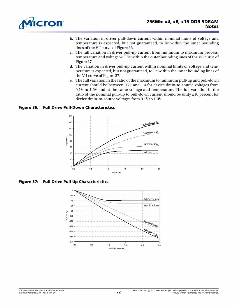
256Mb: x4, x8, x16 DDR SDRAMNotes
b. The variation in driver pull-down current within nominal limits of voltage andtemperature is expected, but not guaranteed, to lie within the inner boundinglines of the V-I curve of Figure 36.
c. The full variation in driver pull-up current from minimum to maximum process,temperature and voltage will lie within the outer bounding lines of the V-I curve ofFigure 37.
d. The variation in driver pull-up current within nominal limits of voltage and tem-perature is expected, but not guaranteed, to lie within the inner bounding lines ofthe V-I curve of Figure 37.
e. The full variation in the ratio of the maximum to minimum pull-up and pull-downcurrent should be between 0.71 and 1.4 for device drain-to-source voltages from0.1V to 1.0V and at the same voltage and temperature. The full variation in theratio of the nominal pull-up to pull-down current should be unity ±10 percent fordevice drain-to-source voltages from 0.1V to 1.0V.
Figure 36: Full Drive Pull-Down Characteristics
Figure 37: Full Drive Pull-Up Characteristics
0
20
40
60
80
100
120
140
160
0.0 0.5 1.0 1.5 2.0 2.5
VOUT (V)
I OU
T (m
A)
-200
-180
-160
-140
-120
-100
-80
-60
-40
-20
0
0.0 0.5 1.0 1.5 2.0 2.5
VDDQ - VOUT (V )
IOU
T (m
A)
PDF: 09005aef80768abb/Source: 09005aef8076894f Micron Technology, Inc., reserves the right to change products or specifications without notice.256MBDDRx4x8x16_2.fm - Rev. L 6/06 EN 72 ©2003 Micron Technology, Inc. All rights reserved.
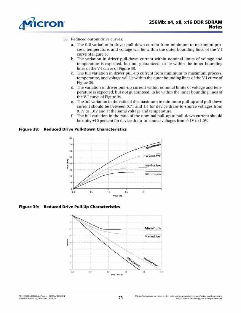
256Mb: x4, x8, x16 DDR SDRAMNotes
38. Reduced output drive curves: a. The full variation in driver pull-down current from minimum to maximum pro-
cess, temperature, and voltage will lie within the outer bounding lines of the V-Icurve of Figure 38.
b. The variation in driver pull-down current within nominal limits of voltage andtemperature is expected, but not guaranteed, to lie within the inner boundinglines of the V-I curve of Figure 38.
c. The full variation in driver pull-up current from minimum to maximum process,temperature, and voltage will lie within the outer bounding lines of the V-I curve ofFigure 39.
d. The variation in driver pull-up current within nominal limits of voltage and tem-perature is expected, but not guaranteed, to lie within the inner bounding lines ofthe V-I curve of Figure 39.
e. The full variation in the ratio of the maximum to minimum pull-up and pull-downcurrent should be between 0.71 and 1.4 for device drain-to-source voltages from0.1V to 1.0V and at the same voltage and temperature.
f. The full variation in the ratio of the nominal pull-up to pull-down current shouldbe unity ±10 percent for device drain-to-source voltages from 0.1V to 1.0V.
Figure 38: Reduced Drive Pull-Down Characteristics
Figure 39: Reduced Drive Pull-Up Characteristics
0
10
20
30
40
50
60
70
80
0.0 0.5 1.0 1.5 2.
VOUT (V)
IOU
T (m
A)
-80
-70
-60
-50
-40
-30
-20
-10
0
0.0 0.5 1.0 1.5 2.0 2.5
VDDQ - VOUT (V)
IOU
T (
mA
)
PDF: 09005aef80768abb/Source: 09005aef8076894f Micron Technology, Inc., reserves the right to change products or specifications without notice.256MBDDRx4x8x16_2.fm - Rev. L 6/06 EN 73 ©2003 Micron Technology, Inc. All rights reserved.

256Mb: x4, x8, x16 DDR SDRAMNotes
39. The voltage levels used are derived from a minimum VDD level and the referencedtest load. In practice, the voltage levels obtained from a properly terminated buswill provide significantly different voltage values.
40. VIH overshoot: VIH (MAX) = VDDQ + 1.5V for a pulse width ≤ 3ns and the pulsewidth can not be greater than 1/3 of the cycle rate. VIL undershoot: VIL (MIN) = –1.5V for a pulse width ≤ 3ns and the pulse width can not be greater than 1/3 ofthe cycle rate.
41. VDD and VDDQ must track each other. 42. tHZ (MAX) will prevail over tDQSCK (MAX) + tRPST (MAX) condition. tLZ (MIN) will
prevail over tDQSCK (MIN) + tRPRE (MAX) condition. 43. tRPST end point and tRPRE begin point are not referenced to a specific voltage level
but specify when the device output is no longer driving (tRPST), or begins driving(tRPRE).
44. During initialization, VDDQ, VTT, and VREF must be equal to or less than VDD + 0.3V.Alternatively, VTT may be 1.35V maximum during power-up, even if VDD/VDDQ are 0V,provided a minimum of 42Ω of series resistance is used between the VTT supply andthe input pin.
45. The current Micron part operates below the slowest JEDEC operating frequency of 83 MHz. As such, future die may not reflect this option.
46. When an input signal is indicated to be HIGH or LOW, it is defined as a steady statelogic HIGH or LOW.
47. Random addressing changing; 50 percent of data changing at every transfer.48. Random addressing changing; 100 percent of data changing at every transfer.49. CKE must be active (HIGH) during the entire time a refresh command is executed.
That is, from the time the AUTO REFRESH command is registered, CKE must beactive at each rising clock edge, until tRFC has been satisfied.
50. IDD2N specifies the DQ, DQS, and DM to be driven to a valid HIGH or LOW logic level.IDD2Q is similar to IDD2F except IDD2Q specifies the address and control inputs toremain stable. Although IDD2F, IDD2N, and IDD2Q are similar, IDD2F is “worst case.”
51. Whenever the operating frequency is altered, not including jitter, the DLL is requiredto be reset followed by 200 clock cycles before any READ command.
52. This is the DC voltage supplied at the DRAM and is inclusive of all noise up to 20 MHz.Any noise above 20 MHz at the DRAM generated from any source other than that ofthe DRAM itself may not exceed the DC voltage range of 2.6V ±100mV.
53. The -6/-6T speed grades will operate with tRAS (MIN) = 40ns and tRAS (MAX) = 120,000ns at any slower frequency.
PDF: 09005aef80768abb/Source: 09005aef8076894f Micron Technology, Inc., reserves the right to change products or specifications without notice.256MBDDRx4x8x16_2.fm - Rev. L 6/06 EN 74 ©2003 Micron Technology, Inc. All rights reserved.

256Mb: x4, x8, x16 DDR SDRAMOutput Drive Characteristics
Output Drive Characteristics
Note: The above characteristics are specified under best, worst, and nominal process variations/conditions.
Table 32: Normal Output Drive Characteristics
Voltage(V)
Pull-Down CurrenT (mA) Pull-Up Current (mA)
Nominal Low
Nominal High Min Max
Nominal Low
Nominal High Min Max
0.1 6.0 6.8 4.6 9.6 –6.1 –7.6 –4.6 –10.00.2 12.2 13.5 9.2 18.2 –12.2 –14.5 –9.2 –20.00.3 18.1 20.1 13.8 26.0 –18.1 –21.2 –13.8 –29.80.4 24.1 26.6 18.4 33.9 –24.0 –27.7 –18.4 –38.80.5 29.8 33.0 23.0 41.8 –29.8 –34.1 –23.0 –46.80.6 34.6 39.1 27.7 49.4 –34.3 –40.5 –27.7 –54.40.7 39.4 44.2 32.2 56.8 –38.1 –46.9 –32.2 –61.80.8 43.7 49.8 36.8 63.2 –41.1 –53.1 –36.0 –69.50.9 47.5 55.2 39.6 69.9 –43.8 –59.4 –38.2 –77.31.0 51.3 60.3 42.6 76.3 –46.0 –65.5 –38.7 –85.21.1 54.1 65.2 44.8 82.5 –47.8 –71.6 –39.0 –93.01.2 56.2 69.9 46.2 88.3 –49.2 –77.6 –39.2 –100.61.3 57.9 74.2 47.1 93.8 –50.0 –83.6 –39.4 –108.11.4 59.3 78.4 47.4 99.1 –50.5 –89.7 –39.6 –115.51.5 60.1 82.3 47.7 103.8 –50.7 –95.5 –39.9 –123.01.6 60.5 85.9 48.0 108.4 –51.0 –101.3 –40.1 –130.41.7 61.0 89.1 48.4 112.1 –51.1 –107.1 –40.2 –136.71.8 61.5 92.2 48.9 115.9 –51.3 –112.4 –40.3 –144.21.9 62.0 95.3 49.1 119.6 –51.5 –118.7 –40.4 –150.52.0 62.5 97.2 49.4 123.3 –51.6 –124.0 –40.5 –156.92.1 62.8 99.1 49.6 126.5 –51.8 –129.3 –40.6 –163.22.2 63.3 100.9 49.8 129.5 –52.0 –134.6 –40.7 –169.62.3 63.8 101.9 49.9 132.4 –52.2 –139.9 –40.8 –176.02.4 64.1 102.8 50.0 135.0 –52.3 –145.2 –40.9 –181.32.5 64.6 103.8 50.2 137.3 –52.5 –150.5 –41.0 –187.62.6 64.8 104.6 50.4 139.2 –52.7 –155.3 –41.1 –192.92.7 65.0 105.4 50.5 140.8 –52.8 –160.1 –41.2 –198.2
PDF: 09005aef80768abb/Source: 09005aef8076894f Micron Technology, Inc., reserves the right to change products or specifications without notice.256MBDDRx4x8x16_2.fm - Rev. L 6/06 EN 75 ©2003 Micron Technology, Inc. All rights reserved.

256Mb: x4, x8, x16 DDR SDRAMOutput Drive Characteristics
Note: The above characteristics are specified under best, worst, and nominal process variations/conditions.
Table 33: Reduced Output Drive Characteristics
Voltage(V)
Pull-Down CurrenT (mA) Pull-Up Current (mA)
Nominal Low
Nominal High Min Max
Nominal Low
Nominal High Min Max
0.1 3.4 3.8 2.6 5.0 –3.5 –4.3 –2.6 –5.00.2 6.9 7.6 5.2 9.9 –6.9 –7.8 –5.2 –9.90.3 10.3 11.4 7.8 14.6 –10.3 –12.0 –7.8 –14.60.4 13.6 15.1 10.4 19.2 –13.6 –15.7 –10.4 –19.20.5 16.9 18.7 13.0 23.6 –16.9 –19.3 –13.0 –23.60.6 19.9 22.1 15.7 28.0 –19.4 –22.9 –15.7 –28.00.7 22.3 25.0 18.2 32.2 –21.5 –26.5 –18.2 –32.20.8 24.7 28.2 20.8 35.8 –23.3 –30.1 –20.4 –35.80.9 26.9 31.3 22.4 39.5 –24.8 –33.6 –21.6 –39.51.0 29.0 34.1 24.1 43.2 –26.0 –37.1 –21.9 –43.21.1 30.6 36.9 25.4 46.7 –27.1 –40.3 –22.1 –46.71.2 31.8 39.5 26.2 50.0 –27.8 –43.1 –22.2 –50.01.3 32.8 42.0 26.6 53.1 –28.3 –45.8 –22.3 –53.11.4 33.5 44.4 26.8 56.1 –28.6 –48.4 –22.4 –56.11.5 34.0 46.6 27.0 58.7 –28.7 –50.7 –22.6 –58.71.6 34.3 48.6 27.2 61.4 –28.9 –52.9 –22.7 –61.41.7 34.5 50.5 27.4 63.5 –28.9 –55.0 –22.7 –63.51.8 34.8 52.2 27.7 65.6 –29.0 –56.8 –22.8 –65.61.9 35.1 53.9 27.8 67.7 –29.2 –58.7 –22.9 –67.72.0 35.4 55.0 28.0 69.8 –29.2 –60.0 –22.9 –69.82.1 35.6 56.1 28.1 71.6 –29.3 –61.2 –23.0 –71.62.2 35.8 57.1 28.2 73.3 –29.5 –62.4 –23.0 –73.32.3 36.1 57.7 28.3 74.9 –29.5 –63.1 –23.1 –74.92.4 36.3 58.2 28.3 76.4 –29.6 –63.8 –23.2 –76.42.5 36.5 58.7 28.4 77.7 –29.7 –64.4 –23.2 –77.72.6 36.7 59.2 28.5 78.8 –29.8 –65.1 –23.3 –78.82.7 36.8 59.6 28.6 79.7 –29.9 –65.8 –23.3 –79.7
PDF: 09005aef80768abb/Source: 09005aef8076894f Micron Technology, Inc., reserves the right to change products or specifications without notice.256MBDDRx4x8x16_2.fm - Rev. L 6/06 EN 76 ©2003 Micron Technology, Inc. All rights reserved.

256Mb: x4, x8, x16 DDR SDRAMData Output Timing Diagrams
Data Output Timing Diagrams
Figure 40: x4, x8 Data Output Timing – tDQSQ, tQH, and Data Valid Window
Notes: 1. DQ transitioning after DQS transition define tDQSQ window. DQS transitions at T2 and at T2n are “early DQS,” at T3, “nominal DQS,” and at T3n, “late DQS.”
2. For a x4, only two DQ apply.3. tDQSQ is derived at each DQS clock edge and is not cumulative over time and begins with
DQS transition and ends with the last valid DQ transition.4. tQH is derived from tHP: tQH = tHP - tQHS.5. tHP is the lesser of tCL or tCH clock transition collectively when a bank is active.6. The data valid window is derived for each DQS transitions and is defined as tQH minus
tDQSQ.
DQ (Last data valid)DQ2
DQ2
DQ2
DQ2
DQ2
DQ2
DQS1
DQ (Last data valid)
DQ (First data no longer valid)
DQ (First data no longer valid)
All DQ and DQS, collectively6
Earliest signal transition
Latest signal transition
T2
T2
T2
T2n
T2n
T2n
T3
T3
T3
T3n
T3n
T3n
CKCK#
T1 T2 T3 T4T2n T3n
tQH4
tHP5 tHP5 tHP5
tQH4 tQH4
tHP5tHP5 tHP5
tQH4
tDQSQ3 tDQSQ3 tDQSQ3 tDQSQ3
DataValid
window
DataValid
window
DataValid
window
DataValid
window
PDF: 09005aef80768abb/Source: 09005aef8076894f Micron Technology, Inc., reserves the right to change products or specifications without notice.256MBDDRx4x8x16_2.fm - Rev. L 6/06 EN 77 ©2003 Micron Technology, Inc. All rights reserved.

256Mb: x4, x8, x16 DDR SDRAMData Output Timing Diagrams
Figure 41: x16 Data Output Timing – tDQSQ, tQH, and Data Valid Window
Notes: 1. DQ transitioning after DQS transition define tDQSQ window. LDQS defines the lower byte and UDQS defines the upper byte.
2. DQ0, DQ1, DQ2, DQ3, DQ4, DQ5, DQ6, or DQ7.3. tDQSQ is derived at each DQS clock edge and is not cumulative over time and begins with
DQS transition and ends with the last valid DQ transition.4. tQH is derived from tHP: tQH = tHP - tQHS.5. tHP is the lesser of tCL or tCH clock transition collectively when a bank is active.6. The data valid window is derived for each DQS transition and is tQH minus tDQSQ. 7. DQ8, DQ9, DQ10, D11, DQ12, DQ13, DQ14, or DQ15.
DQ (Last data valid)2
DQ2
DQ2
DQ2
DQ2
DQ2
DQ2
LDQS1
DQ (Last data valid)2
DQ (First data no longer valid)2
DQ (First data no longer valid)2
DQ0 - DQ7 and LDQS, collectively6 T2
T2
T2
T2n
T2n
T2n
T3
T3
T3
T3n
T3n
T3n
CKCK#
T1 T2 T3 T4T2n T3n
tQH4 tQH4
tDQSQ3 tDQSQ3 tDQSQ3 tDQSQ3
Data Valid window
Data Valid window
DQ (Last data valid)7
DQ7
DQ7
DQ7
DQ7
DQ7
DQ7
UDQS1
DQ (Last data valid)7
DQ (First data no longer valid)7
DQ (First data no longer valid)7
DQ8 - DQ15 and UDQS, collectively6 T2
T2
T2
T2n
T2n
T2n
T3
T3
T3
T3n
T3n
T3n
tQH4tQH4 tQH4 tQH4
tDQSQ3 tDQSQ3 tDQSQ3tDQSQ3
tHP5 tHP5 tHP5 tHP5tHP5tHP5
tQH4tQH4
Data Valid window
Data Valid window
Data Valid window
Data Valid window
Data Valid window
Up
per B
yteLo
wer B
yte
Data Valid window
PDF: 09005aef80768abb/Source: 09005aef8076894f Micron Technology, Inc., reserves the right to change products or specifications without notice.256MBDDRx4x8x16_2.fm - Rev. L 6/06 EN 78 ©2003 Micron Technology, Inc. All rights reserved.

256Mb: x4, x8, x16 DDR SDRAMData Output Timing Diagrams
Figure 42: Data Output Timing – tAC and tDQSCK
Notes: 1. tDQSCK is the DQS output window relative to CK and is the “long-term” component of DQS skew.
2. DQ transitioning after DQS transition define tDQSQ window. 3. All DQ must transition by tDQSQ after DQS transitions, regardless of tAC.4. tAC is the DQ output window relative to CK, and is the “long-term” component of DQ
skew.5. tLZ (MIN) and tAC (MIN) are the first valid signal transition.6. tHZ (MAX),and tAC (MAX) are the latest valid signal transition. 7. READ command with CL = 2 issued at T0.
CK
CK#
DQS, or LDQS/UDQS2
T07 T1 T2 T3 T4 T5T2n T3n T4n T5n T6
tRPST
tLZ (MIN)
tDQSCK1 (MAX)tDQSCK1 (MIN)
tDQSCK1 (MAX)tDQSCK1 (MIN)
tHZ(MAX)
tRPRE
DQ (Last data valid)
DQ (First data valid)
All DQ values, collectively3
tAC4 (MIN) tAC4 (MAX)tLZ (MIN)tHZ (MAX)
T2
T2
T2n T3n T4n T5n
T2n
T2n
T3n
T3n
T4n
T4n
T5n
T5n
T3
T4
T4
T5
T5
T2 T3 T4 T5
T3
PDF: 09005aef80768abb/Source: 09005aef8076894f Micron Technology, Inc., reserves the right to change products or specifications without notice.256MBDDRx4x8x16_2.fm - Rev. L 6/06 EN 79 ©2003 Micron Technology, Inc. All rights reserved.

256Mb: x4, x8, x16 DDR SDRAMData Output Timing Diagrams
Figure 43: Data Input Timing
Notes: 1. tDSH (MIN) generally occurs during tDQSS (MIN).2. tDSS (MIN) generally occurs during tDQSS (MAX).3. WRITE command issued at T0.4. For x16, LDQS controls the lower byte and UDQS controls the upper byte.
DQS
tDQSS
tDQSH tWPST
tDHtDS
tDQSL
tDSS2 tDSH1tDSH1 tDSS2
DM
DQ
CK
CK#T03 T1 T1n T2 T2n T3
DIb
DON’T CARE
TRANSITIONING DATA
tWPREtWPRES
PDF: 09005aef80768abb/Source: 09005aef8076894f Micron Technology, Inc., reserves the right to change products or specifications without notice.256MBDDRx4x8x16_2.fm - Rev. L 6/06 EN 80 ©2003 Micron Technology, Inc. All rights reserved.
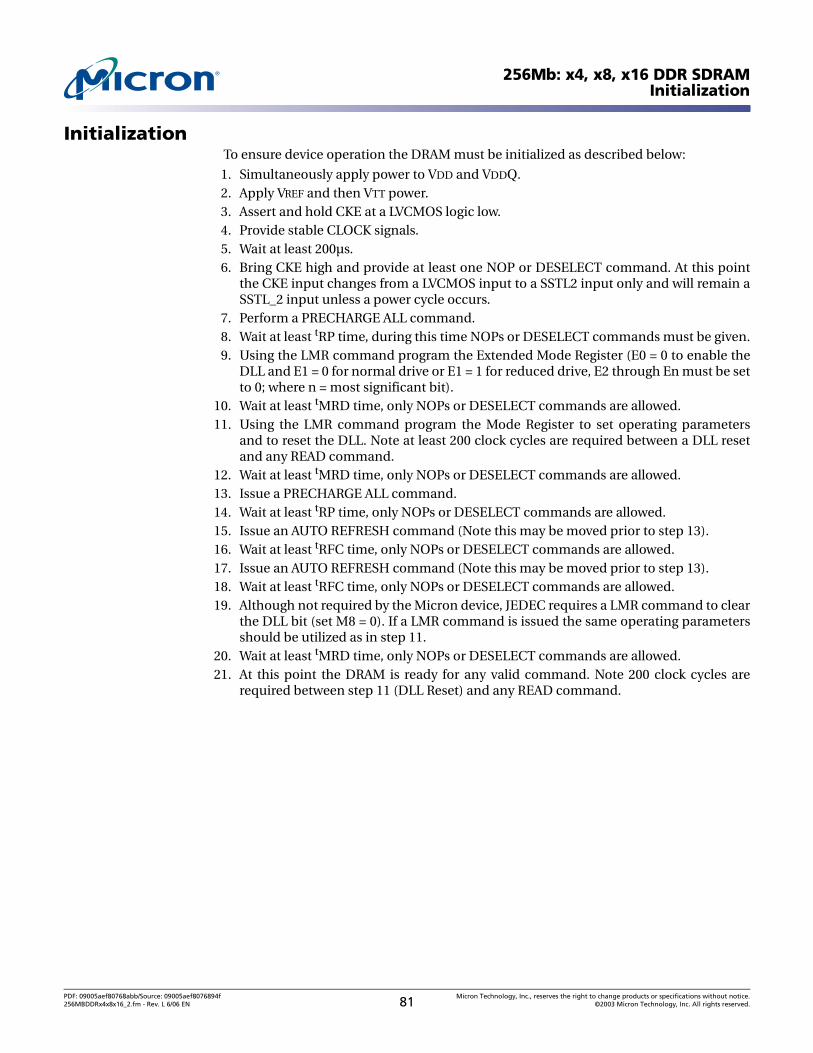
256Mb: x4, x8, x16 DDR SDRAMInitialization
Initialization To ensure device operation the DRAM must be initialized as described below:
1. Simultaneously apply power to VDD and VDDQ.2. Apply VREF and then VTT power.3. Assert and hold CKE at a LVCMOS logic low.4. Provide stable CLOCK signals.5. Wait at least 200µs.6. Bring CKE high and provide at least one NOP or DESELECT command. At this point
the CKE input changes from a LVCMOS input to a SSTL2 input only and will remain aSSTL_2 input unless a power cycle occurs.
7. Perform a PRECHARGE ALL command.8. Wait at least tRP time, during this time NOPs or DESELECT commands must be given.9. Using the LMR command program the Extended Mode Register (E0 = 0 to enable the
DLL and E1 = 0 for normal drive or E1 = 1 for reduced drive, E2 through En must be setto 0; where n = most significant bit).
10. Wait at least tMRD time, only NOPs or DESELECT commands are allowed.11. Using the LMR command program the Mode Register to set operating parameters
and to reset the DLL. Note at least 200 clock cycles are required between a DLL resetand any READ command.
12. Wait at least tMRD time, only NOPs or DESELECT commands are allowed.13. Issue a PRECHARGE ALL command.14. Wait at least tRP time, only NOPs or DESELECT commands are allowed.15. Issue an AUTO REFRESH command (Note this may be moved prior to step 13).16. Wait at least tRFC time, only NOPs or DESELECT commands are allowed.17. Issue an AUTO REFRESH command (Note this may be moved prior to step 13).18. Wait at least tRFC time, only NOPs or DESELECT commands are allowed.19. Although not required by the Micron device, JEDEC requires a LMR command to clear
the DLL bit (set M8 = 0). If a LMR command is issued the same operating parametersshould be utilized as in step 11.
20. Wait at least tMRD time, only NOPs or DESELECT commands are allowed.21. At this point the DRAM is ready for any valid command. Note 200 clock cycles are
required between step 11 (DLL Reset) and any READ command.
PDF: 09005aef80768abb/Source: 09005aef8076894f Micron Technology, Inc., reserves the right to change products or specifications without notice.256MBDDRx4x8x16_2.fm - Rev. L 6/06 EN 81 ©2003 Micron Technology, Inc. All rights reserved.

256Mb: x4, x8, x16 DDR SDRAMInitialization
Figure 44: Initialization Flow Diagram
VDD and VDDQ Ramp
Apply VREF and VTT
CKE must be LVCMOS Low
Apply stable CLOCKs
Bring CKE High with a NOP command
Wait at least 200us
PRECHARGE ALL
Assert NOP or DESELECT for tRP time
Configure Extended Mode Register
Configure Load Mode Register and reset DLL
Assert NOP or DESELECT for tMRD time
Assert NOP or DESELECT for tMRD time
PRECHARGE ALL
Issue AUTO REFRESH command
Assert NOP or DESELECT for tRFC time
Optional LMR command to clear DLL bit
Assert NOP or DESELECT for tMRD time
DRAM is ready for any valid command
Step
1
2
3
4
5
6
7
8
9
10
11
12
13
14
15
16
17
18
19
20
21
Assert NOP or DESELECT commands for tRFC
Issue AUTO REFRESH command
Assert NOP or DESELECT for tRP time
PDF: 09005aef80768abb/Source: 09005aef8076894f Micron Technology, Inc., reserves the right to change products or specifications without notice.256MBDDRx4x8x16_2.fm - Rev. L 6/06 EN 82 ©2003 Micron Technology, Inc. All rights reserved.

256Mb: x4, x8, x16 DDR SDRAMTiming Diagrams
Timing Diagrams
Figure 45: Initialize and Load Mode Registers
Notes: 1. VTT is not applied directly to the device; however, tVTD should be greater than or equal to zero to avoid device latch-up. VDDQ, VTT, and VREF must be equal to or less than VDD + 0.3V. Alternatively, VTT may be 1.35V maximum during power-up, even if VDD/VDDQ are 0V, provided a minimum of 42Ω of series resis-tance is used between the VTT supply and the input pin. Once initialized, VREF must always be powered within the specified range.
2. Reset the DLL with A8 = H while programming the operating parameters.3. tMRD is required before any command can be applied, and 200 cycles of CK are required before a READ
command can be issued.4. The two AUTO REFRESH commands at Td0 and Te0 may be applied following the LOAD MODE
REGISTER (LMR) command at Ta0.5. Although not required by the Micron device, JEDEC specifies issuing another LMR command (A8
= L) prior to activating any bank. If another LMR command is issued, the same operating param-eters must be used as previously issued.
6. PRE = PRECHARGE command; LMR = LOAD MODE REGISTER command; AR = AUTO REFRESH command; ACT = ACTIVE command; RA = Row Address; and BA = Bank Address.
tVTD1
CKELVCMOSLOW LEVEL
DQ
BA0, BA1
200 cycles of CK3Load ExtendedMode Register
Load ModeRegister2
tMRD tMRD tRP tRFC tRFC5
tIS
Power-up: VDD and CK stable
T = 200µs
High-Z
tIH
DM
DQS High-Z
A0-A9,A11, A12
RA
A10 RA
ALL BANKS
CK
CK#
tCH tCL
tCK
VTT1
VREF
VDD
VDDQ
COMMAND6 LMRNOP PRELMR AR AR ACT5
tIS tIH
BA0 = H,BA1 = L
tIS tIHtIS tIH
BA0 = L,BA1 = L
tIS tIH
()()
()()
()()
()()
CODE CODE
tIS tIH
CODE CODE
PRE
ALL BANKS
tIS tIH
T0 T1 Ta0 Tb0 Tc0 Td0 Te0 Tf0
()()
DON’T CARE
BA
()()
()()
()()
()()
()()
()()
()()
()()
()()
()()
()()
()()
()()
()()
tRP
()()
()()
()()
()()
()()
()()
()()
()()
()()
()()
()()
()()
()()
()()
()()
()()
()()
()()
()()
()()
()()
()()
()()
()()
()()
()()
()()
()()
()()
()()
()()
()()
()()
()()
()()
()()
()()
()()
()()
()()
()()
()()
()()
()()
()()
()()
()()
()()
()()
()()
()()
()()
()()
()()
()()
()()
()()
()()
()()
()()
()()
()()
()()
()()
()()
()()
()()
()()
()()
()()
()()
()()
()()
()()
()()
()()
()()
()()
()()
()()
()()
()()
()()
()()
()()
()()
()()
()()
()()
()()
()()
()()
()()
()()
()()
()()
PDF: 09005aef80768abb/Source: 09005aef8076894f Micron Technology, Inc., reserves the right to change products or specifications without notice.256MBDDRx4x8x16_2.fm - Rev. L 6/06 EN 83 ©2003 Micron Technology, Inc. All rights reserved.

256Mb: x4, x8, x16 DDR SDRAMTiming Diagrams
Figure 46: Power-Down Mode
Notes: 1. Once initialized, VREF must always be powered within the specified range.2. If this command is a PRECHARGE (or if the device is already in the idle state), then the
power-down mode shown is precharge power-down. If this command is an ACTIVE (or if at least one row is already active), then the power-down mode shown is active power-down.
3. No column accesses are allowed to be in progress at the time power-down is entered.
CK
CK#
COMMAND VALID2 NOP
ADDR
CKE1
DQ
DM
DQS
VALID
tCK tCH tCL
tIS
tIS
tIH
tIS
tIS tIH
tIH tIS
Enter3
Power-DownMode
ExitPower-Down
Mode
tREFC
()()
()()
()()
()()
()()
()()
()()
()()
()()
()()
()()
T0 T1 Ta0 Ta1 Ta2T2
NOP
DON’T CARE
()()
()()
VALIDVALID
PDF: 09005aef80768abb/Source: 09005aef8076894f Micron Technology, Inc., reserves the right to change products or specifications without notice.256MBDDRx4x8x16_2.fm - Rev. L 6/06 EN 84 ©2003 Micron Technology, Inc. All rights reserved.
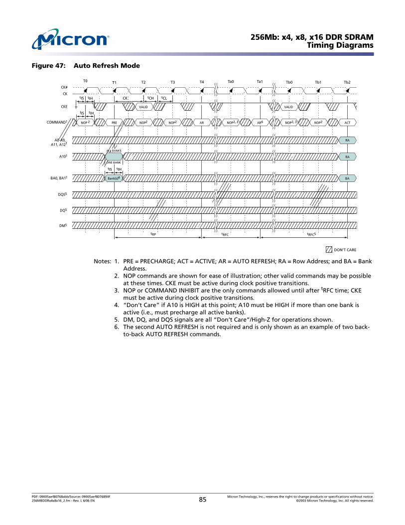
256Mb: x4, x8, x16 DDR SDRAMTiming Diagrams
Figure 47: Auto Refresh Mode
Notes: 1. PRE = PRECHARGE; ACT = ACTIVE; AR = AUTO REFRESH; RA = Row Address; and BA = Bank Address.
2. NOP commands are shown for ease of illustration; other valid commands may be possible at these times. CKE must be active during clock positive transitions.
3. NOP or COMMAND INHIBIT are the only commands allowed until after tRFC time; CKE must be active during clock positive transitions.
4. “Don’t Care” if A10 is HIGH at this point; A10 must be HIGH if more than one bank is active (i.e., must precharge all active banks).
5. DM, DQ, and DQS signals are all “Don’t Care”/High-Z for operations shown.6. The second AUTO REFRESH is not required and is only shown as an example of two back-
to-back AUTO REFRESH commands.
CK
CK#
COMMAND1 NOP2
VALID VALID
NOP 2 NOP2PRE
CKE
RAA0-A9,A11, A121
A101
BA0, BA11 Bank(s)4 BA
AR NOP2, 3 AR6 NOP2, 3 ACTNOP2
ONE BANK
ALL BANKS
CK tCH tCL
tIS
tIS
tIH
tIH
tIS tIH
RA
DQ5
DM5
DQS5
tRFC5tRP tRFC
T0 T1 T2 T3 T4 Ta0 Tb0Ta1 Tb1 Tb2
DON’T CARE
()()
()()
()()
()()
()()
()()
()()
()()
()()
()()
()()
()()
()()
()()
()()
()()
()()
()()
()()
()()
()()
()()
()()
()()
()()
()()
()()
()()
()()
()()
()()
()()
()()
()()
()()
()()
PDF: 09005aef80768abb/Source: 09005aef8076894f Micron Technology, Inc., reserves the right to change products or specifications without notice.256MBDDRx4x8x16_2.fm - Rev. L 6/06 EN 85 ©2003 Micron Technology, Inc. All rights reserved.
256Mb: x4, x8, x16 DDR SDRAMTiming Diagrams
Figure 48: Self Refresh Mode
Notes: 1. Clock must be stable until after the SELF REFRESH command has been registered. A change in clock frequency is allowed before Ta0, provided it is within the specified tCK limits. Regardless, the clock must be stable before exiting self refresh mode. That is, the clock must be cycling within specifications by Ta0.
2. NOPs are interchangeable with DESELECT commands; AR = AUTO REFRESH command.3. Auto refresh is not required at this point, but is highly recommended. 4. Device must be in the all banks idle state prior to entering self refresh mode.5. tXSNR is required before any non-READ command can be applied; only NOP or DESELECT
commands are allowed until Tb1. 6. tXSRD (200 cycles of a valid CK and CKE = high) is required before any READ command can
be applied.7. As a general rule, any time self refresh mode is exited, the DRAM may not re-enter the self
refresh mode until all rows have been refreshed via the AUTO REFRESH command at the distributed refresh rate, tREFI, or faster. However, self refresh mode may be re-entered anytime after exiting, if the following conditions are all met:
a.The DRAM had been in the self refresh mode for a minimum of 200ms prior to exiting. b.tXSNR and tXSRD are not violated. c.At least two AUTO REFRESH commands are performed during each tREFI interval while
the DRAM remains out of self refresh mode.8. If the clock frequency is changed during self refresh mode, a DLL reset is required upon
exit.9. Once initialized, including during self-refresh mode, VREF must always be powered within
the specified range.
CK1
CK#
COMMAND2 NOP AR
ADDR
CKE
DQ
DM
DQS
NOP
tRP4
tCH tCL tCK
tIS
tIS
tIH
tIS tIH tIS
Enter Self Refresh Mode7 Exit Self Refresh Mode7
T0 T11 Ta1
()()
DON’T CARE
Ta01
tXSRD6
()()
()()
()()
()()
NOP
VALID3 VALID
()()
()()
()()
()()
()()
()()
()()
()()
()()
()()
tXSNR5
()()
()()
()()
()()
()()
()()
()()
()()
()()
()()
()()
()()
()()
()()
()()
()()
()()
()()
()()
()()
()()
()()
Ta2 Tb1 Tb2 Tc1
VALID VALID
VALID
tIS tIH()()
()()
VALID
()()
()()
PDF: 09005aef80768abb/Source: 09005aef8076894f Micron Technology, Inc., reserves the right to change products or specifications without notice.256MBDDRx4x8x16_2.fm - Rev. L 6/06 EN 86 ©2003 Micron Technology, Inc. All rights reserved.

256Mb: x4, x8, x16 DDR SDRAMTiming Diagrams
Figure 49: Bank Read – Without Auto Precharge
Notes: 1. DOn = data-out from column n; subsequent elements are provided in the programmed order.
2. BL = 4 in the case shown.3. Disable auto precharge.4. “Don’t Care” if A10 is HIGH at T5.5. PRE = PRECHARGE; ACT = ACTIVE; RA = Row Address; and BA = Bank Address.6. NOP commands are shown for ease of illustration; other commands may be valid at these
times. 7. The PRECHARGE command can only be applied at T5 if tRAS minimum is met.8. Refer to Figure 40 on page 77, Figure 41 on page 78, and Figure 42 on page 79 for
detailed DQS and DQ timing.
CK
CK#
CKE
A10
BA0, BA1
tCK tCH tCL
tIS
tIS
tIH
tIS
tIS
tIH
tIH
tIH
tIS tIH
RA
tRCD
tRAS7
tRC
tRP
CL = 2
DM
T0 T1 T2 T3 T4 T5 T5n T6nT6 T7 T8
DQ1
DQS
Case 1: tAC (MIN) and tDQSCK (MIN)
Case 2: tAC (MAX) and tDQSCK (MAX)
DQ1
DQS
tRPRE
tRPRE
tRPST
tRPST
tDQSCK (MIN)
tDQSCK(MAX)
tLZ (MIN)
tAC (MIN)tLZ (MIN)
DOn
tHZ (MAX)tAC (MAX)
DOn
NOP6NOP6COMMAND5
3
ACT
RA
RA
Col n
READ2 PRE7
Bank x
RA
RA
RA
Bank xBank x4
ACT
Bank x
NOP6 NOP6 NOP6
ONE BANK
ALL BANKS
DON’T CARE TRANSITIONING DATA
x4: A0-A9, A11x8: A0-A9
x16: A0-A8
x4: A12x8: A11, A12
x16: A9, A11, A12
PDF: 09005aef80768abb/Source: 09005aef8076894f Micron Technology, Inc., reserves the right to change products or specifications without notice.256MBDDRx4x8x16_2.fm - Rev. L 6/06 EN 87 ©2003 Micron Technology, Inc. All rights reserved.
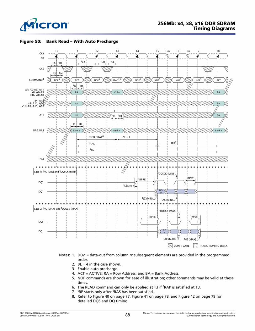
256Mb: x4, x8, x16 DDR SDRAMTiming Diagrams
Figure 50: Bank Read – With Auto Precharge
Notes: 1. DOn = data-out from column n; subsequent elements are provided in the programmed order.
2. BL = 4 in the case shown.3. Enable auto precharge.4. ACT = ACTIVE; RA = Row Address; and BA = Bank Address.5. NOP commands are shown for ease of illustration; other commands may be valid at these
times.6. The READ command can only be applied at T3 if tRAP is satisfied at T3.7. tRP starts only after tRAS has been satisfied.8. Refer to Figure 40 on page 77, Figure 41 on page 78, and Figure 42 on page 79 for
detailed DQS and DQ timing.
CK
CK#
CKE
A10
BA0, BA1
tCK tCH tCL
tIS
tIS
tIH
tIS
tIS
tIH
tIH
tIH
IS IH
RA
tRC
tRP7
CL = 2
DM
T0 T1 T2 T3 T4 T5 T5n T6nT6 T7 T8
DQ1
DQS
Case 1: tAC (MIN) and tDQSCK (MIN)
Case 2: tAC (MAX) and tDQSCK (MAX)
DQ1
DQS
tRPRE
tRPRE
tRPST
tRPST
tDQSCK (MIN)
tDQSCK (MAX)
tAC (MIN)tLZ (MIN)
DOn
tHZ (MAX)tAC (MAX)
DOn
NOP5NOP5COMMAND4
3
ACT
RA
RA
Col n
READ2,6 NOP5
Bank x
RA
RA
RA
Bank x
ACT
Bank x
NOP5 NOP5 NOP5
DON’T CARE TRANSITIONING DATA
x4: A0-A9, A11x8: A0-A9
x16: A0-A8
x4: A12x8: A11, A12
x16: A9, A11, A12
tRAS
tLZ(MIN)
tRCD, tRAP6
PDF: 09005aef80768abb/Source: 09005aef8076894f Micron Technology, Inc., reserves the right to change products or specifications without notice.256MBDDRx4x8x16_2.fm - Rev. L 6/06 EN 88 ©2003 Micron Technology, Inc. All rights reserved.

256Mb: x4, x8, x16 DDR SDRAMTiming Diagrams
Figure 51: Bank Write – Without Auto Precharge
Notes: 1. DI n = data-in from column n; subsequent elements are provided in the programmed order.
2. BL = 4 in the case shown.3. Disable auto precharge.4. “Don’t Care” if A10 is HIGH at T8.5. PRE = PRECHARGE; ACT = ACTIVE; RA = Row Address; and BA = Bank Address.6. NOP commands are shown for ease of illustration; other commands may be valid at these
times. 7. See Figure 43, “Data Input Timing,” on page 80, for detailed DQ timing.8. Although not required by the Micron device, JEDEC specifies that DQS be a valid HIGH,
LOW or some point on a valid transition on or before this clock edge (T3n).
CK
CK#
CKE
A10
BA0, BA1
tCK tCH tCL
tIS
tIS
tIH
tIS
tIS
tIH
tIH
tIH
tIS tIH
RA
tRCD
tRAS tRP
tWR
T0 T1 T2 T3 T4 T5 T5n T6 T7 T8T4n
NOP6NOP6COMMAND5
3
ACT
RA
RA
Col n
WRITE2 NOP6
ONE BANK
ALL BANKS
Bank x
PRE
Bank x
NOP6 NOP6 NOP6
tDQSL tDQSH tWPST
Bank x4
DQ1
DQS
DM
DIb
tDS tDHDON’T CARE TRANSITIONING DATA
tDQSS (NOM)
tWPREtWPRES
x4: A0-A9, A11x8: A0-A9
x16: A0-A8
x4: A12x8: A11, A12
x16: A9, A11, A12
T3n
8
PDF: 09005aef80768abb/Source: 09005aef8076894f Micron Technology, Inc., reserves the right to change products or specifications without notice.256MBDDRx4x8x16_2.fm - Rev. L 6/06 EN 89 ©2003 Micron Technology, Inc. All rights reserved.

256Mb: x4, x8, x16 DDR SDRAMTiming Diagrams
Figure 52: Bank Write – With Auto Precharge
Notes: 1. DIn = data-out from column n; subsequent elements are provided in the programmed order.
2. BL = 4 in the case shown.3. Enable auto precharge.4. ACT = ACTIVE; RA = Row Address; and BA = Bank Address.5. NOP commands are shown for ease of illustration; other commands may be valid at these
times.6. See Figure 43, “Data Input Timing,” on page 80, for detailed DQ timing.7. Although not required by the Micron device, JEDEC specifies that DQS be a valid HIGH,
LOW or some point on a valid transition on or before this clock edge (T3n).
CK
CK#
CKE
A10
BA0, BA1
tCK tCH tCL
tIS
tIS
tIH
tIS
tIS
tIH
tIH
tIH
tIS tIH
RA
tRCD
tRAS tRP
tWR
T0 T1 T2 T3 T4 T5 T5n T6 T7 T8T4n
NOP5NOP5COMMAND4
3
ACT
RA
RA
Col n
WRITE2 NOP5
Bank x
NOP5
Bank x
NOP5 NOP5 NOP5
tDQSL tDQSH tWPST
DQ1
DQS
DM
DIb
tDS tDH
tDQSS (NOM)
DON’T CARE TRANSITIONING DATA
tWPRES tWPRE
x4: A0-A9, A11x8: A0-A9
x16: A0-A8
x4: A12x8: A11, A12
x16: A9, A11, A12
T3n
7
PDF: 09005aef80768abb/Source: 09005aef8076894f Micron Technology, Inc., reserves the right to change products or specifications without notice.256MBDDRx4x8x16_2.fm - Rev. L 6/06 EN 90 ©2003 Micron Technology, Inc. All rights reserved.

256Mb: x4, x8, x16 DDR SDRAMTiming Diagrams
Figure 53: Write – DM Operation
Notes: 1. DIn = data-in from column n; subsequent elements are provided in the programmed order. 2. BL = 4 in the case shown.3. Disable auto precharge.4. “Don’t Care” if A10 is HIGH at T8.5. PRE = PRECHARGE; ACT = ACTIVE; RA = Row Address; and BA = Bank Address.6. NOP commands are shown for ease of illustration; other commands may be valid at these
times. 7. See Figure 43, “Data Input Timing,” on page 80, for detailed DQ timing.8. Although not required by the Micron device, JEDEC specifies that DQS be a valid HIGH,
LOW or some point on a valid transition on or before this clock edge (T3n).
CK
CK#
CKE
A10
BA0, BA1
tCK tCH tCL
tIS
tIS
tIH
tIS
tIS
tIH
tIH
tIH
tIS tIH
RA
tRCD
tRAS tRP
tWR
T0 T1 T2 T3 T4 T5 T5n T6 T7 T8T4n
NOP6NOP6COMMAND5
3
ACT
RA
RA
Col n
WRITE2 NOP6
ONE BANK
ALL BANKS
Bank x
PRE
Bank x
NOP6 NOP6 NOP6
tDQSL tDQSH tWPST
Bank x4
DQ1
DQS
DM
DIb
tDS tDH
DON’T CARE TRANSITIONING DATA
tDQSS (NOM)
tWPRES tWPRE
x4: A0-A9, A11x8: A0-A9
x16: A0-A8
x4: A12x8: A11, A12
x16: A9, A11, A12
8
T3n
PDF: 09005aef80768abb/Source: 09005aef8076894f Micron Technology, Inc., reserves the right to change products or specifications without notice.256MBDDRx4x8x16_2.fm - Rev. L 6/06 EN 91 ©2003 Micron Technology, Inc. All rights reserved.
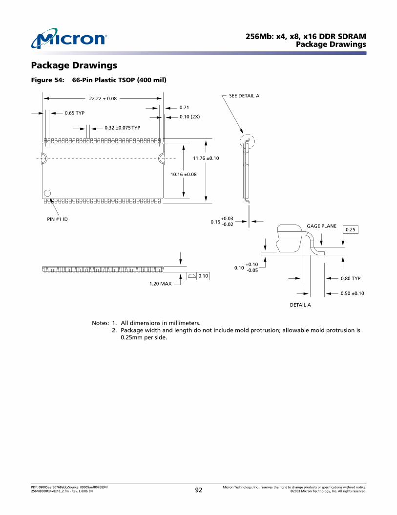
256Mb: x4, x8, x16 DDR SDRAMPackage Drawings
Package Drawings
Figure 54: 66-Pin Plastic TSOP (400 mil)
Notes: 1. All dimensions in millimeters.2. Package width and length do not include mold protrusion; allowable mold protrusion is
0.25mm per side.
SEE DETAIL A
0.10
0.65 TYP0.71
10.16 ±0.08
0.15
0.50 ±0.10
PIN #1 ID
DETAIL A
22.22 ± 0.08
0.32 ±0.075 TYP
+0.03-0.02
+0.10-0.05
1.20 MAX
0.10
0.25
11.76 ±0.10
0.80 TYP
0.10 (2X)
GAGE PLANE
PDF: 09005aef80768abb/Source: 09005aef8076894f Micron Technology, Inc., reserves the right to change products or specifications without notice.256MBDDRx4x8x16_2.fm - Rev. L 6/06 EN 92 ©2003 Micron Technology, Inc. All rights reserved.

256Mb: x4, x8, x16 DDR SDRAMPackage Drawings
Figure 55: 60-Ball FBGA (8 x 14mm)
Notes: 1. All dimensions are in millimeters.2. Topside part marking decoder can be found at www.micron.com/decoder.
PIN A1 ID1.20 MAX
MOLD COMPOUND: EPOXY NOVOLACSUBSTRATE: PLASTIC LAMINATESOLDER BALL MATERIAL: EUTECTIC 62% Sn, 36% Pb, 2%AgSOLDER BALL PAD: Ø .33mm
14.00 ±0.10
BALL A1
BALL A9
PIN A1 ID
1.00 TYP
0.80 TYP
7.00 ±0.05
8.00 ±0.10
4.00 ±0.053.20 ±0.05
5.50 ±0.05
0.850 ±0.075
SEATING PLANE
C
11.00
6.40
0.10 C
60X ∅0.45SOLDER BALL DIAMETER REFERS TO POST REFLOW CONDITION. THE PRE-REFLOW DIAMETER IS Ø 0.40
C L
C L
®
8000 S. Federal Way, P.O. Box 6, Boise, ID 83707-0006, Tel: [email protected] www.micron.com Customer Comment Line: 800-932-4992
Micron, the M logo, and the Micron logo are trademarks of Micron Technology, Inc. All other trademarks are the property of their respective owners.
This data sheet contains minimum and maximum limits specified over the complete power supply and temperature range for production devices. Although considered final, these specifications are subject to change, as further product
development and data characterization sometimes occur.
PDF: 09005aef80768abb/Source: 09005aef8076894f Micron Technology, Inc., reserves the right to change products or specifications without notice.256MBDDRx4x8x16_2.fm - Rev. L 6/06 EN 93 ©2003 Micron Technology, Inc. All rights reserved.