2GB DDR2 SDRAM DIMM - Advantech
14
RoHS Compliant 2GB DDR2 SDRAM DIMM Product Specifications October 6, 2020 Version 1.1 Apacer Technology Inc. 1F., No.32, Zhongcheng Rd., Tucheng Dist., New Taipei City 236, Taiwan Tel: +886-2-2267-8000 Fax: +886-2-2267-2261 www.apacer.com
-
Upload
khangminh22 -
Category
Documents
-
view
3 -
download
0
Transcript of 2GB DDR2 SDRAM DIMM - Advantech

RoHS Compliant
2GB DDR2 SDRAM DIMM
Product Specifications
October 6, 2020
Version 1.1
Apacer Technology Inc.1F., No.32, Zhongcheng Rd., Tucheng Dist., New Taipei City 236, Taiwan
Tel: +886-2-2267-8000 Fax: +886-2-2267-2261
www.apacer.com

©Apacer Technology Inc. 1
Table of Contents
General Description ....................................................................................................... 2
Ordering Information ..................................................................................................... 2
Key Parameters .............................................................................................................. 2
Specifications: ................................................................................................................ 3
Pin Assignments ............................................................................................................. 4
Pin Descriptions ............................................................................................................. 6
Functional Block Diagram ............................................................................................. 7
Absolute Maximum Ratings .......................................................................................... 8
DRAM Component Operating Temperature Range ....................................................... 9
Operating Conditions ................................................................................................... 10
Mechanical Drawing .................................................................................................... 11
©Apacer Technology Inc. 2
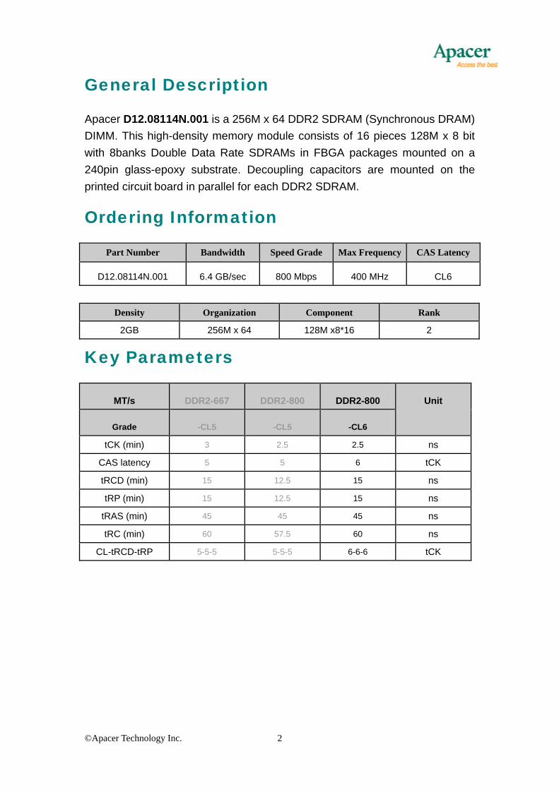
General Description
Apacer D12.08114N.001 is a 256M x 64 DDR2 SDRAM (Synchronous DRAM)
DIMM. This high-density memory module consists of 16 pieces 128M x 8 bit
with 8banks Double Data Rate SDRAMs in FBGA packages mounted on a
240pin glass-epoxy substrate. Decoupling capacitors are mounted on the
printed circuit board in parallel for each DDR2 SDRAM.
Ordering Information
Part Number Bandwidth Speed Grade Max Frequency CAS Latency
D12.08114N.001 6.4 GB/sec 800 Mbps 400 MHz CL6
Density Organization Component Rank
2GB 256M x 64 128M x8*16 2
Key Parameters
MT/s DDR2-667 DDR2-800 DDR2-800 Unit
Grade -CL5 -CL5 -CL6
tCK (min) 3 2.5 2.5 ns
CAS latency 5 5 6 tCK
tRCD (min) 15 12.5 15 ns
tRP (min) 15 12.5 15 ns
tRAS (min) 45 45 45 ns
tRC (min) 60 57.5 60 ns
CL-tRCD-tRP 5-5-5 5-5-5 6-6-6 tCK

©Apacer Technology Inc. 3
Specifications:
JEDEC standard 1.8V ± 0.1V
Power Supply VDDQ = 1.8V± 0.1V
Interface: SSTL_18
Posted CAS
Programmable CAS Latency: 4, 5, 6
OCD (Off-Chip Driver Impedance Adjustment) and ODT (On-Die Termination)
Fully differential clock operations (CK & /CK)
Programmable Burst Length 4 / 8 with both sequential and interleave mode
Auto refresh and self refresh supported
On Die Termination
8192 refresh cycles / 64ms
Serial presence detect with EEPROM
Compliance with RoHS
Compliance with CE
Supports auto-refresh/self-refresh
Operating Temperature Range:
Commercial 0°C≦TC≦85°C
Average refresh period
7.8us at 0 ≦ ≦°C TC 85°C
≦ ≦3.9us at 85°C TC 95°C

©Apacer Technology Inc. 4
Pin Assignments
Pin No. Pin name Pin No. Pin name Pin No. Pin name Pin No. Pin name
1 VREF 61 A4 121 VSS 181 VDDQ
2 VSS 62 VDDQ 122 DQ4 182 A3
3 DQ0 63 A2 123 DQ5 183 A1
4 DQ1 64 VDD 124 VSS 184 VDD
5 VSS 65 VSS 125 DM0 185 CK0
6 /DQS0 66 VSS 126 NC 186 /CK0
7 DQS0 67 VDD 127 VSS 187 VDD
8 VSS 68 NC 128 DQ6 188 A0
9 DQ2 69 VDD 129 DQ7 189 VDD
10 DQ3 70 A10(AP) 130 VSS 190 BA1
11 VSS 71 BA0 131 DQ12 191 VDDQ
12 DQ8 72 VDDQ 132 DQ13 192 /RAS
13 DQ9 73 /WE 133 VSS 193 /S0
14 VSS 74 /CAS 134 DM1 194 VDDQ
15 /DQS1 75 VDDQ 135 NC 195 ODT0
16 DQS1 76 /S1 136 VSS 196 A13
17 VSS 77 ODT1 137 CK1 197 VDD
18 NC 78 VDDQ 138 /CK1 198 VSS
19 NC 79 VSS 139 VSS 199 DQ36
20 VSS 80 DQ32 140 DQ14 200 DQ37
21 DQ10 81 DQ33 141 DQ15 201 VSS
22 DQ11 82 VSS 142 VSS 202 DM4
23 VSS 83 /DQS4 143 DQ20 203 NC
24 DQ16 84 DQS4 144 DQ21 204 VSS
25 DQ17 85 VSS 145 VSS 205 DQ38
26 VSS 86 DQ34 146 DM2 206 DQ39
27 /DQS2 87 DQ35 147 NC 207 VSS
28 DQS2 88 VSS 148 VSS 208 DQ44
29 VSS 89 DQ40 149 DQ22 209 DQ45
30 DQ18 90 DQ41 150 DQ23 210 VSS
©Apacer Technology Inc. 5
Pin No. Pin name Pin No. Pin name Pin No. Pin name Pin No. Pin name
31 DQ19 91 VSS 151 VSS 211 DM5
32 VSS 92 /DQS5 152 DQ28 212 NC
33 DQ24 93 DQS5 153 DQ29 213 VSS
34 DQ25 94 VSS 154 VSS 214 DQ46
35 VSS 95 DQ42 155 DM3 215 DQ47
36 /DQS3 96 DQ43 156 NC 216 VSS
37 DQS3 97 VSS 157 VSS 217 DQ52
38 VSS 98 DQ48 158 DQ30 218 DQ53
39 DQ26 99 DQ49 159 DQ31 219 VSS
40 DQ27 100 VSS 160 VSS 220 CK2
41 VSS 101 SA2 161 NC(CB4)* 221 /CK2
42 NC(CB0)* 102 NC(TEST) 162 NC(CB5)* 222 VSS
43 NC(CB1)* 103 VSS 163 VSS 223 DM6
44 VSS 104 /DQS6 164 NC(DM8)* 224 NC
45 NC(DQS8)* 105 DQS6 165 NC 225 VSS
46 NC(DQS8)* 106 VSS 166 VSS 226 DQ54
47 VSS 107 DQ50 167 NC(CB6)* 227 DQ55
48 NC(CB2)* 108 DQ51 168 NC(CB7)* 228 VSS
49 NC(CB3)* 109 VSS 169 VSS 229 DQ60
50 VSS 110 DQ56 170 VDDQ 230 DQ61
51 VDDQ 111 DQ57 171 CKE1 231 VSS
52 CKE0 112 VSS 172 VDD 232 DM7
53 VDD 113 /DQS7 173 NC(A15)* 233 NC
54 NC(BA2)* 114 DQS7 174 NC(A14)* 234 VSS
55 NC 115 VSS 175 VDDQ 235 DQ62
56 VDDQ 116 DQ58 176 A12 236 DQ63
57 A11 117 DQ59 177 A9 237 VSS
58 A7 118 VSS 178 VDD 238 VDDSPD
59 VDD 119 SDA 179 A8 239 SA0
60 A5 120 SCL 180 A6 240 SA1
1. Pin173 Pin174 are reserved for 2Gb / 4Gb comp. base Unbuffered DIMM.
2. The * pin is not connected on this un-buffer memory module products

©Apacer Technology Inc. 6
Pin Descriptions
Pin Name Description
Ax SDRAM address bus
BAx SDRAM bank select
/RAS SDRAM row address strobe
/CAS SDRAM column address strobe
/WE SDRAM write enable
/Sx DIMM Rank Select Lines
CKEx SDRAM clock enable lines
ODTx On-die termination control lines
DQx DIMM memory data bus
CBx DIMM ECC check bits
DQSx SDRAM data strobes(positive line of differential pair)
/DQSx SDRAM data strobes(negative line of differential pair)
DMx SDRAM data masks high data strobes(x8-based X72 DIMMs)
CKx SDRAM clocks(positive line of differential pair)
/CKx SDRAM clocks(negative line of differential pair)
SCL I2C serial bus clock for EEPROM
SDA I2C serial bus data line for EEPROM
SAx I2C slave address select for EEPROM
VDD SDRAM core power supply
VDDQ SDRAM I/0 Driver power supply
VREF SDRAM I/O reference supply
VSS Power supply return(ground)
VDDSPD Serial EEPROM positive power supply
NC Spare pins(no connect)
TEST Used by memory bus analysis tools(unused on memory DIMMS)
RESET Set DRAMs to Known State
©Apacer Technology Inc. 7
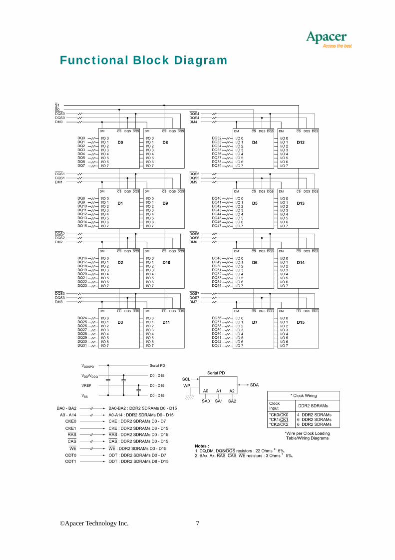
Functional Block Diagram
S0DQS0DQS0DM0
DM CS DQS DQS
DQ0DQ1DQ2DQ3DQ4DQ5DQ6DQ7
I/O 0I/O 1I/O 2I/O 3I/O 4I/O 5I/O 6I/O 7
D0
DQS1DQS1DM1
DM CS DQS DQS
DQ8DQ9DQ10DQ11DQ12DQ13DQ14DQ15
I/O 0I/O 1I/O 2I/O 3I/O 4I/O 5I/O 6I/O 7
D1
DQS2DQS2DM2
DM CS DQS DQS
DQ16DQ17DQ18DQ19DQ20DQ21DQ22DQ23
I/O 0I/O 1I/O 2I/O 3I/O 4I/O 5I/O 6I/O 7
D2
DQS3DQS3DM3
DM CS DQS DQS
DQ24DQ25DQ26DQ27DQ28DQ29DQ30DQ31
I/O 0I/O 1I/O 2I/O 3I/O 4I/O 5I/O 6I/O 7
D3
DQS4DQS4DM4
DM CS DQS DQS
DQ32DQ33DQ34DQ35DQ36DQ37DQ38DQ39
I/O 0I/O 1I/O 2I/O 3I/O 4I/O 5I/O 6I/O 7
D4
DQS5DQS5DM5
DM CS DQS DQS
DQ40DQ41DQ42DQ43DQ44DQ45DQ46DQ47
I/O 0I/O 1I/O 2I/O 3I/O 4I/O 5I/O 6I/O 7
D5
DQS6DQS6DM6
DM CS DQS DQS
DQ48DQ49DQ50DQ51DQ52DQ53DQ54DQ55
I/O 0I/O 1I/O 2I/O 3I/O 4I/O 5I/O 6I/O 7
D6
DQS7DQS7DM7
DM CS DQS DQS
DQ56DQ57DQ58DQ59DQ60DQ61DQ62DQ63
I/O 0I/O 1I/O 2I/O 3I/O 4I/O 5I/O 6I/O 7
D7
Notes : 1. DQ,DM, DQS/DQS resistors : 22 Ohms " 5%.2. BAx, Ax, RAS, CAS, WE resistors : 3 Ohms " 5%.
A0
Serial PD
A1 A2
SA0 SA1 SA2
SCLSDAWP
*Wire per Clock Loading Table/Wiring Diagrams
* Clock Wiring
Clock Input DDR2 SDRAMs
*CK0/CK0*CK1/CK1*CK2/CK2
4 DDR2 SDRAMs6 DDR2 SDRAMs6 DDR2 SDRAMs
VSS D0 - D15
VDD/VDDQ D0 - D15
D0 - D15VREF
VDDSPD Serial PD
A0 - A14
WE
CKE1
BA0 - BA2
ODT0
DM CS DQS DQS
I/O 0I/O 1I/O 2I/O 3I/O 4I/O 5I/O 6I/O 7
D8
DM CS DQS DQS
I/O 0I/O 1I/O 2I/O 3I/O 4I/O 5I/O 6I/O 7
D9
DM CS DQS DQS
I/O 0I/O 1I/O 2I/O 3I/O 4I/O 5I/O 6I/O 7
D10
DM CS DQS DQS
I/O 0I/O 1I/O 2I/O 3I/O 4I/O 5I/O 6I/O 7
D11
DM CS DQS DQS
I/O 0I/O 1I/O 2I/O 3I/O 4I/O 5I/O 6I/O 7
D12
DM CS DQS DQS
I/O 0I/O 1I/O 2I/O 3I/O 4I/O 5I/O 6I/O 7
D13
DM CS DQS DQS
I/O 0I/O 1I/O 2I/O 3I/O 4I/O 5I/O 6I/O 7
D14
DM CS DQS DQS
I/O 0I/O 1I/O 2I/O 3I/O 4I/O 5I/O 6I/O 7
D15
S1
CKE0
BA0-BA2 : DDR2 SDRAMs D0 - D15A0-A14 : DDR2 SDRAMs D0 - D15CKE : DDR2 SDRAMs D0 - D7
RASCAS
CKE : DDR2 SDRAMs D8 - D15RAS : DDR2 SDRAMs D0 - D15CAS : DDR2 SDRAMs D0 - D15
ODT1
WE : DDR2 SDRAMs D0 - D15ODT : DDR2 SDRAMs D0 - D7ODT : DDR2 SDRAMs D8 - D15

©Apacer Technology Inc. 8
Absolute Maximum Ratings
Parameter Symbol Description Units
Voltage on VDD pin relative to Vss VDD - 1.0 V ~ 2.3 V V
Voltage on VDDQ pin relative to Vss VDDQ - 0.5 V ~ 2.3 V V
Voltage on any pin relative to Vss VIN, VOUT - 0.5 V ~ 2.3 V V
Storage Temperature TSTG -55 to +100 ℃
Notes:
1. Stress greater than those listed may cause permanent damage to the device. This is a stress rating only and
device functional operation at or above the conditions indicated is not implied. Exposure to absolute maximum
rating conditions for extended periods may affect reliability. .
.

©Apacer Technology Inc. 9
DRAM Component Operating Temperature Range
Symbol Parameter Rating Units Notes
TOPER Normal Operating Temperature Range 0 to 85 ℃ 1,2
Extended Temperature Range 85 to 95 ℃ 1,3
Notes:
1. Operating Temperature TOPER is the case surface temperature on the center / top side of the DRAM. For
measurement conditions please refer to the JEDEC document JESD51-2.
2. The Normal Temperature Range specifies the temperatures where all DRAM specifications will be supported
during operation, the DRAM case temperature must be maintained between 0℃ - 85℃ under all operating
Conditions.
3. Some applications require operation of the DRAM in the Extended Temperature Range between 85℃ and 95℃
case temperature. Full specifications are guaranteed in this range, but the following additional conditions apply:
a. Refresh commands must be doubled in frequency, therefore reducing the Refresh interval tREFI to 3.9 µs.
b. If Self-Refresh operation is required in the Extended Temperature Range, then it is mandatory to either
use the Manual Self-Refresh mode with Extended Temperature Range capability (MR2 A6 = 0b and
MR2 A7 = 1b), in this case IDD6 current can be increased around 10~20% than normal Temperature
range.

©Apacer Technology Inc. 10
Operating Conditions
Recommended DC Operating Conditions – DDR2 (1.8V) operation
Symbol Parameter Rating
Units Min. Typ. Max.
VDD Supply Voltage 1.7 1.8 1.9 V
VDDQ Supply Voltage for Output 1.7 1.8 1.9 V
Notes:
1. Under all conditions VDDQ must be less than or equal to VDD..
2. VDDQ tracks with VDD. AC parameters are measured with VDD and VDDQ tied together.

©Apacer Technology Inc. 11
Mechanical Drawing
131.35
133.35
10.0
0
128.95
(2)2.50
(2X
)4.0
0
30.00
2.30
17.8
0
A B
63.00 55.00
2.501.00
0.20
2.50
±0.2
0
Detail B
5.00
Detail A
4.00
1.50±0.10
0.80±0.054.00
3.80
3.00
4.00
1.270 ± 0.10
4.00 Max
Tolerances:+-0.15mm unless otherwise specified
Unit: mm
©Apacer Technology Inc. 12
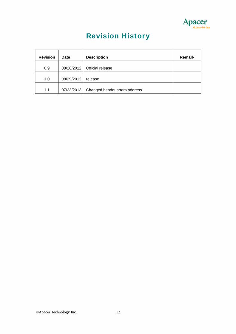
Revision History
Revision Date Description Remark
0.9 08/28/2012 Official release
1.0 08/29/2012 release
1.1 07/23/2013 Changed headquarters address

©Apacer Technology Inc. 13
Global Presence Taiwan (Headquarters)
Apacer Technology Inc.
1F., No.32, Zhongcheng Rd., Tucheng Dist.,
New Taipei City 236, Taiwan R.O.C.
Tel: +886-2-2267-8000
Fax: +886-2-2267-2261
U.S.A.
Apacer Memory America, Inc.
46732 Lakeview Blvd., Fremont, CA 94538
Tel: 1-408-518-8699
Fax: 1-510-249-9568
Japan
Apacer Technology Corp.
5F, Matsura Bldg., Shiba, Minato-Ku
Tokyo, 105-0014, Japan
Tel: 81-3-5419-2668
Fax: 81-3-5419-0018
Europe
Apacer Technology B.V.
Science Park Eindhoven 5051 5692 EB Son,
The Netherlands
Tel: 31-40-267-0000
Fax: 31-40-290-0686
China
Apacer Electronic (Shanghai) Co., Ltd.
Room D, 22/FL, No.2, Lane 600, JieyunPlaza,
Tianshan RD , Shanghai , 200051, China
Tel: 86-21-6228-9939
Fax:86-21-6228-9936
India
Apacer Technologies Pvt Ltd.
1874, South End C Cross,9th Block Jayanagar,
Bangalore-560069,INDIA.
Tel: 91-80-4152-9061/62
Fax: 91-80-4170-0215