
Datenblatt / Datasheet FS3L200R10W3S7F_B11
12
Datasheet Please read the Important Notice and Warnings at the end of this document V 3.0 www.infineon.com 2020-05-08 FS3L200R10W3S7F_B11 EasyPACK™ Modul mit TRENCHSTOP™ IGBT7 und CoolSiC™ Schottky Diode und PressFIT / NTC EasyPACK™ module with TRENCHSTOP™ IGBT7 and CoolSiC™ Schottky diode and PressFIT / NTC VCES = 950V IC nom = 100A / ICRM = 200A Potentielle Anwendungen Potential Applications • • 3-Level-Applikationen 3-level-applications • • Solar Anwendungen Solar applications • • USV-Systeme UPS systems Elektrische Eigenschaften Electrical Features • • CoolSiC TM Schottky Diode Gen 5 CoolSiC TM Schottky diode gen 5 • • Niedrige Schaltverluste Low switching losses • • Trenchstop TM IGBT7 Trenchstop TM IGBT7 Mechanische Eigenschaften Mechanical Features • • Al2O3 Substrat mit kleinem thermischen Widerstand Al2O3 substrate with low thermal resistance • • Integrierter NTC Temperatur Sensor Integrated NTC temperature sensor • • Kompaktes Design Compact design • • PressFIT Verbindungstechnik PressFIT contact technology Module Label Code Barcode Code 128 DMX - Code Content of the Code Digit Module Serial Number 1- 5 Module Material Number 6 - 11 Production Order Number 12 - 19 Datecode (Production Year) 20 - 21 Datecode (Production Week) 22 - 23
-
Upload
khangminh22 -
Category
Documents
-
view
0 -
download
0
Transcript of Datenblatt / Datasheet FS3L200R10W3S7F_B11

Datasheet PleasereadtheImportantNoticeandWarningsattheendofthisdocument V3.0www.infineon.com 2020-05-08
FS3L200R10W3S7F_B11
EasyPACK™ModulmitTRENCHSTOP™IGBT7undCoolSiC™SchottkyDiodeundPressFIT/NTCEasyPACK™modulewithTRENCHSTOP™IGBT7andCoolSiC™SchottkydiodeandPressFIT/NTC
VCES = 950VIC nom = 100A / ICRM = 200A
PotentielleAnwendungen PotentialApplications• •3-Level-Applikationen 3-level-applications• •SolarAnwendungen Solarapplications• •USV-Systeme UPSsystems
ElektrischeEigenschaften ElectricalFeatures• •CoolSiCTMSchottkyDiodeGen5 CoolSiCTMSchottkydiodegen5• •NiedrigeSchaltverluste Lowswitchinglosses• •TrenchstopTMIGBT7 TrenchstopTMIGBT7
MechanischeEigenschaften MechanicalFeatures• •Al2O3 Substrat mit kleinem thermischenWiderstand
Al2O3substratewithlowthermalresistance
• •IntegrierterNTCTemperaturSensor IntegratedNTCtemperaturesensor• •KompaktesDesign Compactdesign• •PressFITVerbindungstechnik PressFITcontacttechnology
ModuleLabelCodeBarcodeCode128
DMX-Code
ContentoftheCode DigitModuleSerialNumber 1-5ModuleMaterialNumber 6-11ProductionOrderNumber 12-19Datecode(ProductionYear) 20-21Datecode(ProductionWeek) 22-23

Datasheet 2 V3.02020-05-08
FS3L200R10W3S7F_B11
IGBT,Hochsetzsteller/IGBT,BoostHöchstzulässigeWerte/MaximumRatedValuesKollektor-Emitter-SperrspannungCollector-emittervoltage Tvj = 25°C VCES 950 V
ImplementierterKollektor-StromImplementedcollectorcurrent ICN 100 A
Kollektor-DauergleichstromContinuousDCcollectorcurrent TH = 65°C, Tvj max = 175°C ICDC 70 A
PeriodischerKollektor-SpitzenstromRepetitivepeakcollectorcurrent tP = 1 ms ICRM 200 A
Gate-Emitter-SpitzenspannungGate-emitterpeakvoltage VGES +/-20 V
CharakteristischeWerte/CharacteristicValues min. typ. max.
Kollektor-Emitter-SättigungsspannungCollector-emittersaturationvoltage
IC = 25 AVGE = 15 V VCE sat
1,271,331,33
1,55 VVV
Tvj = 25°CTvj = 125°CTvj = 150°C
Gate-SchwellenspannungGatethresholdvoltage IC = 1,67 mA, VCE = VGE, Tvj = 25°C VGEth 4,35 5,10 5,85 V
GateladungGatecharge VGE = -15 / 15 V, VCE = 600 V QG 0,23 µC
InternerGatewiderstandInternalgateresistor Tvj = 25°C RGint 1,5 Ω
EingangskapazitätInputcapacitance f = 100 kHz, Tvj = 25°C, VCE = 25 V, VGE = 0 V Cies 6,48 nF
RückwirkungskapazitätReversetransfercapacitance f = 100 kHz, Tvj = 25°C, VCE = 25 V, VGE = 0 V Cres 0,02 nF
Kollektor-Emitter-ReststromCollector-emittercut-offcurrent VCE = 950 V, VGE = 0 V ICES 0,031 mATvj = 25°C
Gate-Emitter-ReststromGate-emitterleakagecurrent VCE = 0 V, VGE = 20 V, Tvj = 25°C IGES 100 nA
Einschaltverzögerungszeit,induktiveLastTurn-ondelaytime,inductiveload
IC = 25 A, VCE = 500 VVGE = -15 / 15 VRGon = 10 Ω
td on0,0740,0710,062
µsµsµs
Tvj = 25°CTvj = 125°CTvj = 150°C
Anstiegszeit,induktiveLastRisetime,inductiveload
IC = 25 A, VCE = 500 VVGE = -15 / 15 VRGon = 10 Ω
tr0,0130,0150,015
µsµsµs
Tvj = 25°CTvj = 125°CTvj = 150°C
Abschaltverzögerungszeit,induktiveLastTurn-offdelaytime,inductiveload
IC = 25 A, VCE = 500 VVGE = -15 / 15 VRGoff = 10 Ω
td off0,1780,2750,308
µsµsµs
Tvj = 25°CTvj = 125°CTvj = 150°C
Fallzeit,induktiveLastFalltime,inductiveload
IC = 25 A, VCE = 500 VVGE = -15 / 15 VRGoff = 10 Ω
tf0,1070,1390,161
µsµsµs
Tvj = 25°CTvj = 125°CTvj = 150°C
EinschaltverlustenergieproPulsTurn-onenergylossperpulse
IC = 25 A, VCE = 500 V, Lσ = 35 nHdi/dt = 880 A/µs (Tvj = 150°C)VGE = -15 / 15 V, RGon = 10 Ω
Eon
0,5750,5890,596
mJmJmJ
Tvj = 25°CTvj = 125°CTvj = 150°C
AbschaltverlustenergieproPulsTurn-offenergylossperpulse
IC = 25 A, VCE = 500 V, Lσ = 35 nHdu/dt = 2700 V/µs (Tvj = 150°C)VGE = -15 / 15 V, RGoff = 10 Ω
Eoff
1,051,621,79
mJmJmJ
Tvj = 25°CTvj = 125°CTvj = 150°C
KurzschlußverhaltenSCdata
VGE ≤ 15 V, VCC = 600 VVCEmax = VCES -LsCE ·di/dt ISC 300 A
Tvj = 150°C
tP ≤ 0 µs,
Wärmewiderstand,ChipbisKühlkörperThermalresistance,junctiontoheatsink proIGBT/perIGBT RthJH 0,673 K/W
TemperaturimSchaltbetriebTemperatureunderswitchingconditions Tvj op -40 150 °C

Datasheet 3 V3.02020-05-08
FS3L200R10W3S7F_B11
Diode,Hochsetzsteller/Diode,BoostHöchstzulässigeWerte/MaximumRatedValuesPeriodischeSpitzensperrspannungRepetitivepeakreversevoltage Tvj = 25°C VRRM 1200 V
ImplementierterDurchlassstromImplementedforwardcurrent IFN 30 A
DauergleichstromContinuousDCforwardcurrent IF 25 A
PeriodischerSpitzenstromRepetitivepeakforwardcurrent tP = 1 ms IFRM 60 A
GrenzlastintegralI²t-value
VR = 0 V, tP = 10 ms, Tvj = 125°CVR = 0 V, tP = 10 ms, Tvj = 150°C I²t 88,4
66,0 A²sA²s
CharakteristischeWerte/CharacteristicValues min. typ. max.
DurchlassspannungForwardvoltage
IF = 25 A, VGE = 0 VIF = 25 A, VGE = 0 VIF = 25 A, VGE = 0 V
VF
1,321,551,70
1,85 VVV
Tvj = 25°CTvj = 125°CTvj = 150°C
RückstromspitzePeakreverserecoverycurrent
IF = 25 A, - diF/dt = 880 A/µs (Tvj=150°C)VR = 600 V IRM
16,416,416,4
AAA
Tvj = 25°CTvj = 125°CTvj = 150°C
SperrverzögerungsladungRecoveredcharge
IF = 25 A, - diF/dt = 880 A/µs (Tvj=150°C)VR = 600 V Qr
0,740,740,74
µCµCµC
Tvj = 25°CTvj = 125°CTvj = 150°C
AbschaltenergieproPulsReverserecoveryenergy
IF = 25 A, - diF/dt = 880 A/µs (Tvj=150°C)VR = 600 V Erec
0,2490,2490,249
mJmJmJ
Tvj = 25°CTvj = 125°CTvj = 150°C
Wärmewiderstand,ChipbisKühlkörperThermalresistance,junctiontoheatsink proDiode/perdiode RthJH 0,894 K/W
TemperaturimSchaltbetriebTemperatureunderswitchingconditions Tvj op -40 150 °C
Bypass-Diode/Bypass-DiodeHöchstzulässigeWerte/MaximumRatedValuesPeriodischeSpitzensperrspannungRepetitivepeakreversevoltage Tvj = 25°C VRRM 1200 V
DurchlassstromGrenzeffektivwertproChipMaximumRMSforwardcurrentperchip TH = 75°C IFRMSM 50 A
GleichrichterAusgangGrenzeffektivstromMaximumRMScurrentatrectifieroutput TH = 75°C IRMSM 50 A
StoßstromGrenzwertSurgeforwardcurrent
tp = 10 ms, Tvj = 25°Ctp = 10 ms, Tvj = 110°C IFSM 1070
957 AA
GrenzlastintegralI²t-value
tp = 10 ms, Tvj = 25°Ctp = 10 ms, Tvj = 110°C I²t 5770
4580 A²sA²s
CharakteristischeWerte/CharacteristicValues min. typ. max.
DurchlassspannungForwardvoltage Tvj = 150°C, IF = 45 A VF 0,85 V
SperrstromReversecurrent Tvj = 150°C, VR = 1200 V IR 1,00 mA
Wärmewiderstand,ChipbisKühlkörperThermalresistance,junctiontoheatsink proDiode/perdiode RthJH 0,870 K/W
TemperaturimSchaltbetriebTemperatureunderswitchingconditions Tvj op -40 110 °C

Datasheet 4 V3.02020-05-08
FS3L200R10W3S7F_B11
VerpolschutzDiodeA/Inverse-polarityprotectiondiodeAHöchstzulässigeWerte/MaximumRatedValuesPeriodischeSpitzensperrspannungRepetitivepeakreversevoltage Tvj = 25°C VRRM 1200 V
DurchlassstromGrenzeffektivwertproChipMaximumRMSforwardcurrentperchip TH = 70°C IFRMSM 30 A
GleichrichterAusgangGrenzeffektivstromMaximumRMScurrentatrectifieroutput TH = 70°C IRMSM 30 A
StoßstromGrenzwertSurgeforwardcurrent
tp = 10 ms, Tvj = 25°Ctp = 10 ms, Tvj = 110°C IFSM 378
326 AA
GrenzlastintegralI²t-value
tp = 10 ms, Tvj = 25°Ctp = 10 ms, Tvj = 110°C I²t 714
531 A²sA²s
CharakteristischeWerte/CharacteristicValues min. typ. max.
DurchlassspannungForwardvoltage Tvj = 150°C, IF = 15 A VF 0,89 V
SperrstromReversecurrent Tvj = 150°C, VR = 1200 V IR 1,00 mA
Wärmewiderstand,ChipbisKühlkörperThermalresistance,junctiontoheatsink proDiode/perdiode RthJH 1,31 K/W
TemperaturimSchaltbetriebTemperatureunderswitchingconditions Tvj op -40 110 °C
NTC-Widerstand/NTC-ThermistorCharakteristischeWerte/CharacteristicValues min. typ. max.
NennwiderstandRatedresistance TNTC = 25°C R25 5,00 kΩ
AbweichungvonR100DeviationofR100 TNTC = 100°C, R100 = 493 Ω ∆R/R -5 5 %
VerlustleistungPowerdissipation TNTC = 25°C P25 20,0 mW
B-WertB-value R2 = R25 exp [B25/50(1/T2 - 1/(298,15 K))] B25/50 3375 K
B-WertB-value R2 = R25 exp [B25/80(1/T2 - 1/(298,15 K))] B25/80 3411 K
B-WertB-value R2 = R25 exp [B25/100(1/T2 - 1/(298,15 K))] B25/100 3433 K
AngabengemäßgültigerApplicationNote.Specificationaccordingtothevalidapplicationnote.

Datasheet 5 V3.02020-05-08
FS3L200R10W3S7F_B11
Modul/ModuleIsolations-PrüfspannungIsolationtestvoltage RMS, f = 50 Hz, t = 1 min. VISOL 3,2 kV
InnereIsolationInternalisolation
Basisisolierung(Schutzklasse1,EN61140)basicinsulation(class1,IEC61140) Al2O3
KriechstreckeCreepagedistance
Kontakt-Kühlkörper/terminaltoheatsinkKontakt-Kontakt/terminaltoterminal 11,2
6,8 mm
LuftstreckeClearance
Kontakt-Kühlkörper/terminaltoheatsinkKontakt-Kontakt/terminaltoterminal 9,4
5,5 mm
VergleichszahlderKriechwegbildungComperativetrackingindex CTI > 400
RelativerTemperaturindex(elektr.)RTIElec.
Gehäusehousing RTI 140 °C
min. typ. max.
ModulstreuinduktivitätStrayinductancemodule LsCE 20 nH
LagertemperaturStoragetemperature Tstg -40 125 °C
Anzugsdrehmomentf.ModulmontageMountingtorqueformodulmounting
Schraube-Montagegem.gültigerApplikationsschriftScrew-Mountingaccordingtovalidapplicationnote M 1,30 1,50 Nm
GewichtWeight G 78 g
IGBT- and diode- RthJH parameters measured with thermal grease of λPaste = 3.3 W/(m·K)The current under continuous operation is limited to 25 A rms per connector pin.

Datasheet 6 V3.02020-05-08
FS3L200R10W3S7F_B11
AusgangskennlinieIGBT,Hochsetzsteller(typisch)outputcharacteristicIGBT,Boost(typical)IC=f(VCE)VGE=15V
VCE [V]
IC [A
]
0,0 0,5 1,0 1,5 2,00
5
10
15
20
25
30
35
40
45
50Tvj = 25°CTvj = 125°CTvj = 150°C
AusgangskennlinienfeldIGBT,Hochsetzsteller(typisch)outputcharacteristicIGBT,Boost(typical)IC=f(VCE)Tvj=150°C
VCE [V]
IC [A
]
0,0 0,5 1,0 1,5 2,00
5
10
15
20
25
30
35
40
45
50VGE = 19VVGE = 17VVGE = 15VVGE = 13VVGE = 11VVGE = 9V
ÜbertragungscharakteristikIGBT,Hochsetzsteller(typisch)transfercharacteristicIGBT,Boost(typical)IC=f(VGE)VCE=20V
VGE [V]
IC [A
]
4 5 6 7 80
5
10
15
20
25
30
35
40
45
50Tvj = 25°CTvj = 125°CTvj = 150°C
SchaltverlusteIGBT,Hochsetzsteller(typisch)switchinglossesIGBT,Boost(typical)Eon=f(IC),Eoff=f(IC)VGE=±15V,RGon=10Ω,RGoff=10Ω,VCE=500V
IC [A]
E [m
J]
0 5 10 15 20 25 30 35 40 45 500
1
2
3Eon, Tvj = 125°CEoff, Tvj = 125°CEon, Tvj = 150°CEoff, Tvj = 150°C

Datasheet 7 V3.02020-05-08
FS3L200R10W3S7F_B11
SchaltverlusteIGBT,Hochsetzsteller(typisch)switchinglossesIGBT,Boost(typical)Eon=f(RG),Eoff=f(RG)VGE=±15V,VCE=500V,IC=25A
RG [Ω]
E [m
J]
0 10 20 30 40 50 60 70 80 90 1000
1
2
3Eon, Tvj = 125°CEoff, Tvj = 125°CEon, Tvj = 150°CEoff, Tvj = 150°C
SchaltzeitenIGBT,Hochsetzsteller(typisch)switchingtimesIGBT,Boost(typical)tdon=f(IC),tr=f(IC),tdoff=f(IC),tf=f(IC)VGE=±15V,RGon=10Ω,RGoff=10Ω,VCE=500V,Tvj=150°C
IC [A]
t [µ
s]
0 5 10 15 20 25 30 35 40 45 500,001
0,01
0,1
1
10tdon
trtdoff
tf
SchaltzeitenIGBT,Hochsetzsteller(typisch)switchingtimesIGBT,Boost(typical)tdon=f(RG),tr=f(RG),tdoff=f(RG),tf=f(RG)VGE=±15V,RGon=10Ω,RGoff=10Ω,VCE=500V,IC=25A,Tvj=150°C
RG [Ω]
t [µ
s]
0 10 20 30 40 50 60 70 80 90 1000,01
0,1
1
10tdon
trtdoff
tf
TransienterWärmewiderstandIGBT,HochsetzstellertransientthermalimpedanceIGBT,BoostZthJH=f(t)
t [s]
Zth
JH [K
/W]
0,001 0,01 0,1 1 100,001
0,01
0,1
1ZthJH : IGBT
i:ri[K/W]:τi[s]:
10,0260,0006
20,0840,0105
30,2820,11
40,2810,11

Datasheet 8 V3.02020-05-08
FS3L200R10W3S7F_B11
SichererRückwärts-ArbeitsbereichIGBT,Hochsetzsteller(RBSOA)reversebiassafeoperatingareaIGBT,Boost(RBSOA)IC=f(VCE)VGE=±15V,RGoff=10Ω,Tvj=150°C
VCE [V]
IC [A
]
0 100 200 300 400 500 600 700 800 900 10000
20
40
60
80
100
120
140
160
180
200
220
240IC, ModulIC, Chip
DurchlasskennliniederDiode,Hochsetzsteller(typisch)forwardcharacteristicofDiode,Boost(typical)IF=f(VF)
VF [V]
IF [A
]
0,0 0,5 1,0 1,5 2,0 2,5 3,00
5
10
15
20
25
30
35
40
45
50Tvj = 25°CTvj = 125°CTvj = 150°C
SchaltverlusteDiode,Hochsetzsteller(typisch)switchinglossesDiode,Boost(typical)Erec=f(IF)RGon=10Ω,VCE=600V
IF [A]
E [m
J]
0 5 10 15 20 25 30 35 40 45 500,00
0,05
0,10
0,15
0,20
0,25
0,30
0,35
0,40
0,45
0,50Erec, Tvj = 125°C; Erec, Tvj = 150°C
SchaltverlusteDiode,Hochsetzsteller(typisch)switchinglossesDiode,Boost(typical)Erec=f(RG)IF=25A,VCE=600V
RG [Ω]
E [m
J]
0 10 20 30 40 50 60 70 80 90 1000,00
0,05
0,10
0,15
0,20
0,25
0,30
0,35
0,40
0,45
0,50Erec, Tvj = 125°C; Erec, Tvj = 150°C

Datasheet 9 V3.02020-05-08
FS3L200R10W3S7F_B11
TransienterWärmewiderstandDiode,HochsetzstellertransientthermalimpedanceDiode,BoostZthJH=f(t)
t [s]
Zth
JH [K
/W]
0,001 0,01 0,1 1 100,01
0,1
1
10ZthJH : Diode
i:ri[K/W]:τi[s]:
10,0470,0004
20,1160,0033
30,2170,0213
40,5140,121
DurchlasskennliniederBypass-Diode(typisch)forwardcharacteristicofBypass-Diode(typical)IF=f(VF)
VF [V]
IF [A
]
0,0 0,2 0,4 0,6 0,8 1,0 1,20
10
20
30
40
50
60
70
80
90Tvj = 25°CTvj = 110°CTvj = 150°C
TransienterWärmewiderstandBypass-DiodetransientthermalimpedanceBypass-DiodeZthJH=f(t)
t [s]
Zth
JH [K
/W]
0,001 0,01 0,1 1 100,01
0,1
1
10ZthJH: Diode
i:ri[K/W]:τi[s]:
10,0480,0018
20,1080,0163
30,3540,0869
40,360,238
DurchlasskennliniederVerpolschutzDiodeA(typisch)forwardcharacteristicofInverse-polarityprotectiondiodeA(typical)IF=f(VF)
VF [V]
IF [A
]
0,0 0,2 0,4 0,6 0,8 1,0 1,2 1,40
5
10
15
20
25
30Tvj = 25°CTvj = 110°CTvj = 150°C
Datasheet 10 V3.02020-05-08
FS3L200R10W3S7F_B11
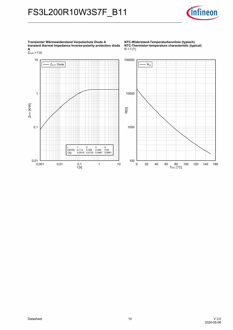
TransienterWärmewiderstandVerpolschutzDiodeAtransientthermalimpedanceInverse-polarityprotectiondiodeAZthJH=f(t)
t [s]
Zth
JH [K
/W]
0,001 0,01 0,1 1 100,01
0,1
1
10ZthJH: Diode
i:ri[K/W]:τi[s]:
10,1130,0016
20,3080,0135
30,4490,0861
40,440,0861
NTC-Widerstand-Temperaturkennlinie(typisch)NTC-Thermistor-temperaturecharacteristic(typical)R=f(T)
TNTC [°C]
R[Ω
]
0 20 40 60 80 100 120 140 160100
1000
10000
100000Rtyp

Datasheet 11 V3.02020-05-08
FS3L200R10W3S7F_B11
Schaltplan/Circuitdiagram
Gehäuseabmessungen/Packageoutlines
A-A ( 20 : 1 )B-B ( 5 : 1 )
A-A ( 20 : 1 )
B-B ( 5 : 1 )
B
B
AA
B
B
AA
DC1+
pcb hole pattern
DC1N DC1- DC2- DC2N DC2+
GC2PVC+
GA1
BSTA+
EA1
GA2
EC1GC1
BSTC+PVB-PVA-PVB+ BSTB+
PVA+ EA2
BSTA-
EB1 GB1
NTC1
NTC2
EC2
BSTC-
PVC-
BSTB- GB2
EB2
Katalogzeichnungrestricted
Toleranzrechnung: siehe Zeichnung D00132867
Kunststoffteile ausgelegt nach Toleranzgruppe 5
KundenzeichnungProdukt-Datenblatt-Zeichnung (PDZ)
109,90,45
620,45
5,4
0,1 2x
98,8965
01,6
20,824
1,64,8
14
20,824
0
14
20,824
4,8
20,82404,
087,28
20,08
23,28
32,88
36,08
47,43
7,28
10,48
20,08
23,28
29,68
32,88
36,08
0
4,08
7,28
13,68
20,08
23,28
36,08
7,28
20,08
23,28
32,88
36,08
47,43
16,447°
40
8
Laserbeschriftung 8mm x 40mm
109,850,3
5,4
0,1
620,2
(MP0
1-MP
02)
020
49,68 20 43
49,68
(0,866) 1 D E0,7
A
53x
pin grid 3,2mm
tolerance of pcb hole pattern if not specified otherwise
hole specification for contacts: see AN 2009-01
diameters of drill: 1,15mmcopper thickness in hole: 25-50µm
0,1
MP01
MP02
0,25
ABC
2x
14
47,425
5,4
0,1
0,25
ADE
0,25
ADE
A1 A2
A3 A4
Dimensions according to ISO 14405 GG (Method of Least Squares)
Geometrical features according to Method of Least Squares
Coordinates in the center of geometrical features
Evaluation direction complies the orientaion of the reference systems ABC
Reference geometry according to CAD geometry with general tolerance 0,1 A B C
0,1 A B C
14
0
14
20,824
4,8
20,824
01,6
20,824
1,64,8
14
20,824
98,8965
47,425
0
4,08
7,28
13,68
20,08
23,28
36,08
7,28
20,08
23,28
32,88
36,08
47,43
04,08
7,28
20,08
23,28
32,88
36,08
47,43
7,28
10,48
20,08
23,28
29,68
32,88
36,08
16,447°
Laserbeschriftung 8mm x 40mm
1
8
40
(0,866) 1,05 D E0,75
A
53x
A3
A1
A4
A2
5,4
0,1
5,4
0,1
109,850,45
0,25
ADE
020
49,68 20 43
49,68
0,25
ADE
Inspection characteristic XCD_01 as check dimension with Cpk >= 1,67.
Prüfmerkmal XCD_01 als Prüfmaß mit Cpk >= 1,67. Maße nach ISO 14405 GG (Methode der kleinsten Quadrate (MKQ)).Geometrieelemente nach Methode der kleinsten Quadrate (MKQ).Koordinaten in der Mitte der Geometrieelemente. Auswerterichtung entspricht der Orientierung des Bezugssystems A B CSollgeometrie nach CAD-Modell mit Allgemeintoleranz
620,45
(MP
01-M
P02)
2, Positionstolernaz Pine:Basis of the calculation.a, press-fit drill hole diameter 1,15 +0/-0,03mm (Application note: AN2009-01) With a copper thickness of 25µm to 50µm in the hole and a tin layer of about 1µm for tin applied chemically, an end hole diameter is obtained as the test dimension. Due to the thinner tin layer thickness, this diameter is alwayshighe than the value of 1mm stated in the standard (IEC 60352-5). The final hole diameter under consideration of the drilling diameter, copper thickness and tin layer, is typically between 1.02mm and 1.09mm. b, 2layer FR4 pcb TG150 1,6mm +/-10% thickness. Source: "PressFIT Pin Investigation" [T.Reiter, P.Bayer, 2011] c, - End hole diameter: ø1,05 - Tolerance of PCB pattern: ±0,05- Pin point dimensions: o0,3-0,15- Positional radial tolerances: ±0,2 - Pin inserted @45° =0,2+0,21 =0,41mm R=0,41 > ø0,82mm
0
44,4
47,4
49,7
44,4
47,4
49,7
0
14
26
14
26
Toleranzklassen
12,20,1
recommended design hight
12,20,1
recommended design hight12,20,1
recommended design hight 2
MP01
MP02
1,6
1,6
MP02
MP02
0
25
25
0
25
25
12
2x
accord
ing to s
crew h
ead w
asher
3,5 4x
0
4,88
11,2
20,824
4,88
11,214,417,6
24
0
4,08
7,28
10,48
13,68
16,88
20,08
23,28
29,68
32,88
36,08
4,08
7,28
10,48
13,68
16,88
20,08
23,28
29,68
32,88
36,08
(4,2)
B
(3,4)
C
(2,3) Dome0,25 A B C4x
dimensioned for EJOT Delta PT WN5451 25
choose length according to pcb thickness
4x
A
(12)
(16,4)

TrademarksAllreferencedproductorservicenamesandtrademarksarethepropertyoftheirrespectiveowners.
Edition2020-05-08
PublishedbyInfineonTechnologiesAG81726München,Germany
©2020InfineonTechnologiesAG.AllRightsReserved.
Doyouhaveaquestionaboutthisdocument?Email:[email protected]
WICHTIGERHINWEIS
DieindiesemDokumententhaltenenAngabenstellenkeinesfallsGarantienfürdieBeschaffenheitoderEigenschaftendesProduktes(“Beschaffenheitsgarantie“)dar.FürBeispiele,HinweiseodertypischeWerte,dieindiesemDokumententhaltensind,und/oderAngaben,diesichaufdieAnwendungdesProduktesbeziehen,istjeglicheGewährleistungundHaftungvonInfineonTechnologiesausgeschlossen,einschließlich,ohnehieraufbeschränktzusein,dieGewährdafür,dasskeingeistigesEigentumDritterverletztist.
DesWeiterenstehensämtliche,indiesemDokumententhaltenenInformationen,unterdemVorbehaltderEinhaltungderindiesemDokumentfestgelegtenVerpflichtungendesKundensowieallerimHinblickaufdasProduktdesKundensowiedieNutzungdesInfineonProduktesindenAnwendungendesKundenanwendbarengesetzlichenAnforderungen,NormenundStandardsdurchdenKunden.
DieindiesemDokumententhaltenenDatensindausschließlichfürtechnischgeschultesFachpersonalbestimmt.DieBeurteilungderEignungdiesesProduktesfürdiebeabsichtigteAnwendungsowiedieBeurteilungderVollständigkeitderindiesemDokumententhaltenenProduktdatenfürdieseAnwendungobliegtdentechnischenFachabteilungendesKunden.
SolltenSievonunsweitereInformationenimZusammenhangmitdemProdukt,derTechnologie,Lieferbedingungenbzw.Preisenbenötigen,wendenSiesichbitteandasnächsteVertriebsbürovonInfineonTechnologies(www.infineon.com).
WARNHINWEIS
AufgrunddertechnischenAnforderungenkönnenProduktegesundheitsgefährdendeSubstanzenenthalten.BeiFragenzudenindiesemProduktenthaltenenSubstanzen,setzenSiesichbittemitdemnächstenVertriebsbürovonInfineonTechnologiesinVerbindung.
SofernInfineonTechnologiesnichtausdrücklichineinemschriftlichen,vonvertretungsberechtigtenInfineonMitarbeiternunterzeichnetenDokumentzugestimmthat,dürfenProduktevonInfineonTechnologiesnichtinAnwendungeneingesetztwerden,inwelchenvernünftigerweiseerwartetwerdenkann,dasseinFehlerdesProduktesoderdieFolgenderNutzungdesProdukteszuPersonenverletzungenführen.IMPORTANTNOTICE
Theinformationgiveninthisdocumentshallinnoeventberegardedasaguaranteeofconditionsorcharacteristics(“Beschaffenheitsgarantie”).Withrespecttoanyexamples,hintsoranytypicalvaluesstatedhereinand/oranyinformationregardingtheapplicationoftheproduct,InfineonTechnologiesherebydisclaimsanyandallwarrantiesandliabilitiesofanykind,includingwithoutlimitationwarrantiesofnon-infringementofintellectualpropertyrightsofanythirdparty.
Inaddition,anyinformationgiveninthisdocumentissubjecttocustomer’scompliancewithitsobligationsstatedinthisdocumentandanyapplicablelegalrequirements,normsandstandardsconcerningcustomer’sproductsandanyuseoftheproductofInfineonTechnologiesincustomer’sapplications.
Thedatacontainedinthisdocumentisexclusivelyintendedfortechnicallytrainedstaff.Itistheresponsibilityofcustomer’stechnicaldepartmentstoevaluatethesuitabilityoftheproductfortheintendedapplicationandthecompletenessoftheproductinformationgiveninthisdocumentwithrespecttosuchapplication.
Forfurtherinformationontheproduct,technology,deliverytermsandconditionsandpricespleasecontactyournearestInfineonTechnologiesoffice(www.infineon.com).
WARNINGS
Duetotechnicalrequirementsproductsmaycontaindangeroussubstances.ForinformationonthetypesinquestionpleasecontactyournearestInfineonTechnologiesoffice.
ExceptasotherwiseexplicitlyapprovedbyInfineonTechnologiesinawrittendocumentsignedbyauthorizedrepresentativesofInfineonTechnologies,InfineonTechnologies’productsmaynotbeusedinanyapplicationswhereafailureoftheproductoranyconsequencesoftheusethereofcanreasonablybeexpectedtoresultinpersonalinjury.