
Hetero-oligomerization does not compromise ‘gain of function’ of tumor-derived p53 mutants
Upload
independentCategory
view
5download
0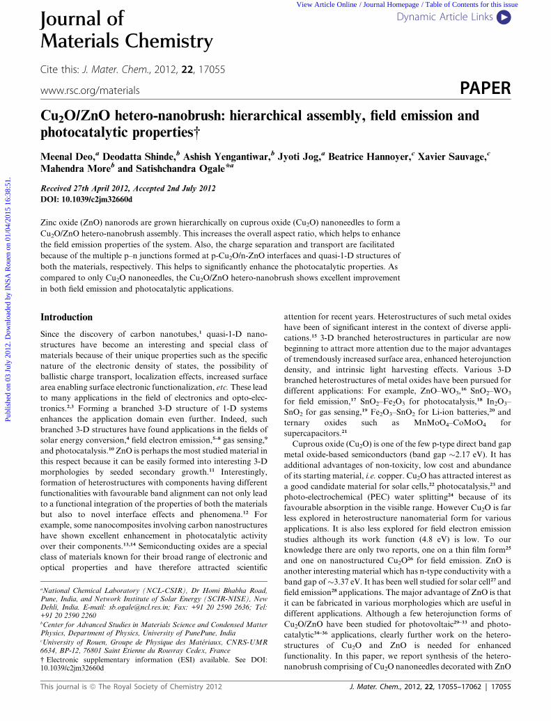
Dynamic Article LinksC<Journal ofMaterials Chemistry
Cite this: J. Mater. Chem., 2012, 22, 17055
www.rsc.org/materials PAPER
Publ
ishe
d on
03
July
201
2. D
ownl
oade
d by
IN
SA R
ouen
on
01/0
4/20
15 1
6:38
:51.
View Article Online / Journal Homepage / Table of Contents for this issue
Cu2O/ZnO hetero-nanobrush: hierarchical assembly, field emission andphotocatalytic properties†
Meenal Deo,a Deodatta Shinde,b Ashish Yengantiwar,b Jyoti Jog,a Beatrice Hannoyer,c Xavier Sauvage,c
Mahendra Moreb and Satishchandra Ogale*a
Received 27th April 2012, Accepted 2nd July 2012
DOI: 10.1039/c2jm32660d
Zinc oxide (ZnO) nanorods are grown hierarchically on cuprous oxide (Cu2O) nanoneedles to form a
Cu2O/ZnO hetero-nanobrush assembly. This increases the overall aspect ratio, which helps to enhance
the field emission properties of the system. Also, the charge separation and transport are facilitated
because of the multiple p–n junctions formed at p-Cu2O/n-ZnO interfaces and quasi-1-D structures of
both the materials, respectively. This helps to significantly enhance the photocatalytic properties. As
compared to only Cu2O nanoneedles, the Cu2O/ZnO hetero-nanobrush shows excellent improvement
in both field emission and photocatalytic applications.
Introduction
Since the discovery of carbon nanotubes,1 quasi-1-D nano-
structures have become an interesting and special class of
materials because of their unique properties such as the specific
nature of the electronic density of states, the possibility of
ballistic charge transport, localization effects, increased surface
area enabling surface electronic functionalization, etc. These lead
to many applications in the field of electronics and opto-elec-
tronics.2,3 Forming a branched 3-D structure of 1-D systems
enhances the application domain even further. Indeed, such
branched 3-D structures have found applications in the fields of
solar energy conversion,4 field electron emission,5–8 gas sensing,9
and photocatalysis.10 ZnO is perhaps the most studied material in
this respect because it can be easily formed into interesting 3-D
morphologies by seeded secondary growth.11 Interestingly,
formation of heterostructures with components having different
functionalities with favourable band alignment can not only lead
to a functional integration of the properties of both the materials
but also to novel interface effects and phenomena.12 For
example, some nanocomposites involving carbon nanostructures
have shown excellent enhancement in photocatalytic activity
over their components.13,14 Semiconducting oxides are a special
class of materials known for their broad range of electronic and
optical properties and have therefore attracted scientific
aNational Chemical Laboratory (NCL-CSIR), Dr Homi Bhabha Road,Pune, India, and Network Institute of Solar Energy (SCIR-NISE), NewDehli, India. E-mail: [email protected]; Fax: +91 20 2590 2636; Tel:+91 20 2590 2260bCenter for Advanced Studies in Materials Science and Condensed MatterPhysics, Department of Physics, University of PunePune, IndiacUniversity of Rouen, Groupe de Physique des Mat�eriaux, CNRS-UMR6634, BP-12, 76801 Saint Etienne du Rouvray Cedex, France
† Electronic supplementary information (ESI) available. See DOI:10.1039/c2jm32660d
This journal is ª The Royal Society of Chemistry 2012
attention for recent years. Heterostructures of such metal oxides
have been of significant interest in the context of diverse appli-
cations.15 3-D branched heterostructures in particular are now
beginning to attract more attention due to the major advantages
of tremendously increased surface area, enhanced heterojunction
density, and intrinsic light harvesting effects. Various 3-D
branched heterostructures of metal oxides have been pursued for
different applications: For example, ZnO–WO3,16 SnO2–WO3
for field emission,17 SnO2–Fe2O3 for photocatalysis,18 In2O3–
SnO2 for gas sensing,19 Fe2O3–SnO2 for Li-ion batteries,20 and
ternary oxides such as MnMoO4–CoMoO4 for
supercapacitors.21
Cuprous oxide (Cu2O) is one of the few p-type direct band gap
metal oxide-based semiconductors (band gap �2.17 eV). It has
additional advantages of non-toxicity, low cost and abundance
of its starting material, i.e. copper. Cu2O has attracted interest as
a good candidate material for solar cells,22 photocatalysis,23 and
photo-electrochemical (PEC) water splitting24 because of its
favourable absorption in the visible range. However Cu2O is far
less explored in heterostructure nanomaterial form for various
applications. It is also less explored for field electron emission
studies although its work function (4.8 eV) is low. To our
knowledge there are only two reports, one on a thin film form25
and one on nanostructured Cu2O26 for field emission. ZnO is
another interesting material which has n-type conductivity with a
band gap of�3.37 eV. It has been well studied for solar cell27 and
field emission28 applications. The major advantage of ZnO is that
it can be fabricated in various morphologies which are useful in
different applications. Although a few heterojunction forms of
Cu2O/ZnO have been studied for photovoltaic29–33 and photo-
catalytic34–36 applications, clearly further work on the hetero-
structures of Cu2O and ZnO is needed for enhanced
functionality. In this paper, we report synthesis of the hetero-
nanobrush comprising of Cu2O nanoneedles decorated with ZnO
J. Mater. Chem., 2012, 22, 17055–17062 | 17055
Publ
ishe
d on
03
July
201
2. D
ownl
oade
d by
IN
SA R
ouen
on
01/0
4/20
15 1
6:38
:51.
View Article Online
nanorods by a two step chemical method. We have examined
such a hetero-nanobrush system for field electron emission and
photocatalysis applications.
Experimental section
Synthesis of Cu2O/ZnO hetero-nanobrush on copper
The Cu2O nanoneedle film was grown directly on copper
substrate employing a protocol previously reported by us.37
Copper foil was anodized in the presence of 2MKOHwhich acts
as electrolyte and graphite rod as the counter electrode. This
leads to an evenly spread Cu(OH)2 nanoneedle film on the Cu
substrate, which on annealing at 450 �C in controlled oxygen
pressure (5 � 10�6 mbar) gets converted into Cu2O nanoneedles.
We carried out seed-assisted growth of ZnO on Cu2O to
achieve brush-like ZnO morphology. Thus a seed layer of ZnO
was deposited by Pulsed Laser Deposition (PLD) technique on
the Cu2O nanoneedle film. The deposition was carried out in an
oxygen pressure of 1� 10�4 mbar at the substrate temperature of
100 �C for better adherence of the ultrathin ZnO surface nano-
structure. For facile growth of ZnO on the seeded surface
of Cu2O, an equimolar (25 mM) solution of Zn(NO3)2 and
hexamethylene tetramine (HMT) was used for the reaction. The
reaction was carried out at 95 �C while stirring simultaneously
for only 15 minutes. The samples were then rinsed with de-
ionized water and dried in air. The Cu2O/ZnO heterostructure
films were then annealed in vacuum (5 � 10�5 mbar) at 250 �Cfor better adherence and better crystallinity of the nanostructure.
This growth procedure is schematically shown in Fig. 1. From
the high resolution SEM shown in Fig. 1(b), there are ZnO
nanoparticles formed all over the surface of the Cu2O nano-
needles by PLD, which ensures further growth of ZnO nanorods.
Fig. 1 Schematic of the growth procedure of Cu2O/ZnO hetero-nanob
17056 | J. Mater. Chem., 2012, 22, 17055–17062
The ZnO nanorod growth was carried out in the presence of
hexamethylene tetramine (HMT) which covers non-polar
surfaces of ZnO, other than the (002) plane system, to enhance
the nanorod growth in the direction of (002). Fig. 1(c) gives
the schematic and SEM image of the growth of ZnO
nanorods on the surface of the Cu2O nanoneedles. These heter-
ostructured films were further characterized by using XRD, SEM
and TEM.
General characterizations
Various techniques such as X-ray diffraction (XRD, Philips
X’Pert PRO), Field Emission Scanning Electron Microscopy
(FE-SEM, Hitachi S4800), UV-Vis spectro-photometer (Jasco
V-570) were used for characterizations. The analytical trans-
mission electron microscopy (TEM) was also performed with a
probe-corrected ARM200F JEOL microscope operated at
200 kV. Energy Dispersive X-ray Spectroscopy (EDS) was
performed with a JEOL JED2300 detector with a probe size
of 0.2 nm.
Field emission and photocatalysis experiments
The field emission (FE) current density–electric field (J–E)
characteristic measurements were carried in all-metal field
emission microscope with a load lock chamber. The FE studies
were carried out in a planar diode configuration, wherein Cu2O
nanoneedles or Cu2O/ZnO hetero-nanobrushes served as a
cathode and a semi-transparent cathodoluminescent phosphor
screen (ZnS : Cu Green Color) as an anode. The cathode was
pasted onto a sample holder using vacuum compatible con-
ducting silver paste and was held in front of the anode screen at a
distance of �500 mm. The emission current density–applied
rush. The bottom pictures show SEM images of each growth step.
This journal is ª The Royal Society of Chemistry 2012
Publ
ishe
d on
03
July
201
2. D
ownl
oade
d by
IN
SA R
ouen
on
01/0
4/20
15 1
6:38
:51.
View Article Online
electric field (J–E) characteristic measurements were carried out
at 1 � 10�8 mbar pressure using a Keithley 6514 electrometer
and a Spellman high-voltage DC power supply (0–40 kV). For
FE, we kept the area of the specimen at 1 cm2.
The photocatalysis measurements were done at room
temperature and in 10�5 M aqueous solution of methyl orange
(MO), used as a pollutant. The Cu2O nanoneedles and Cu2O/
ZnO heterostructure films of the same area were directly dipped
into the methyl orange solution. The solution was first stirred in
the dark in the presence of the film for 30 minutes before pho-
tocatalytic measurements so as to reach the adsorption–desorp-
tion equilibrium. Then it was continuously stirred under solar
simulator (AM 1.5, 100 mW cm�2) used for illumination. The
spectral intensity distribution was analyzed using UV-Vis spec-
tro-photometer for specific intervals of time for a total time of
2.5 hours.
Results and discussion
Characterization of Cu2O/ZnO heterostructure
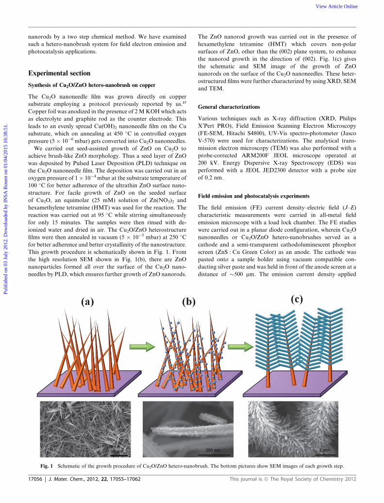
The morphology of the as-synthesized Cu2O/ZnO hetero-
structure was imaged by Field Emission Scanning Electron
Microscopy (FESEM). Fig. 2(a) shows the low magnification
SEM image, which reveals a uniform formation of brush-like
structures. From the high magnification SEM images, shown in
the inset of Fig. 2(a), it is seen that ZnO nanorods have been
decorated all over the Cu2O nanoneedle surface forming the
hetero-nanobrush morphology. It is also seen that the length of a
single ZnO nanorod is around 500 nm with a hexagonal cross
section having a diameter about 50 nm.
Fig. 2(b) shows the X-Ray Diffraction (XRD) pattern of
Cu2O/ZnO hetero-nanobrush. The XRD shows a polycrystalline
phase of Cu2O nanoneedles grown directly on copper. The
formation of the ZnO phase is also confirmed by XRD. During
the deposition of ZnO nanorods on these Cu2O nanoneedles,
even if the deposition is carried out at 95 �C in air, the Cu2O
phase does not get converted into CuO. This can be attributed to
Fig. 2 (a) Low-magnification FESEM image of Cu2O/ZnO hetero-nanobru
pattern of Cu2O/ZnO hetero-nanobrush. * represent copper substrate peaks.
This journal is ª The Royal Society of Chemistry 2012
uniform growth and surface coverage of the ZnO seed layer by
PLD, which also acts as a protecting layer for Cu2O avoiding its
further oxidation.
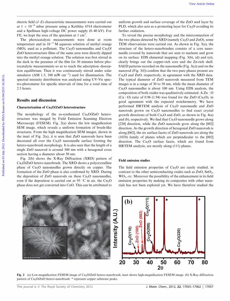
To reveal the precise morphology and the interconnection of
the two phases detected by XRD (namely Cu2O and ZnO), some
TEM observations were carried out. As shown in Fig. 3(a), the
structure of the hetero-nanobrushes consists of a core nano-
needle covered by nanorods that are seen to nucleate and grow
on its surface. EDS elemental mapping (Fig. 3(b), (d) and (e)),
clearly brings out the copper-rich core and the Zn-rich shell.
SAED patterns recorded on the nanoneedle (Fig. 3(c)) and on the
nanorod (Fig. 3(f)) confirm that the two pure phases present are
Cu2O and ZnO, respectively, in agreement with the XRD data.
The typical diameter of ZnO nanorods measured from TEM
images is in a range of 30 to 50 nm, while the mean diameter of
Cu2O nanoneedles is about 100 nm. Using EDS analysis, the
composition of both oxides was qualitatively estimated. A Zn : O
(Cu : O) ratio of 0.96 (1.94) was found for the ZnO (Cu2O), in
good agreement with the expected stoichiometry. We have
performed HRTEM analysis of Cu2O nanoneedle and ZnO
nanorods grown on Cu2O nanoneedles to find exact crystal
growth directions of both Cu2O and ZnO, as shown in Fig. 4(a)
and (b), respectively. We find that Cu2O nanoneedle grows along
[220] direction, while the ZnO nanorods grow along the [002]
direction. As the growth direction of hexagonal ZnO nanorods is
along [002], the six surface facets of ZnO nanorods are along the
(10�10) family of planes which are perpendicular to the [002]
direction. The Cu2O surface facets, which are found from
HRTEM analysis, are mostly along (111) planes.
Field emission studies
The field emission properties of Cu2O are rarely studied, in
contrast to the other semiconducting oxides such as ZnO, SnO2,
WO3, etc.Moreover the possibility of the enhancement in its field
emission properties by making its composites with other mate-
rials has not been explored yet. We have therefore studied the
sh; inset shows high-magnification FESEM image. (b) X-Ray diffraction
J. Mater. Chem., 2012, 22, 17055–17062 | 17057
Fig. 3 (a) Bright field STEM image of a Cu2O/ZnO hetero-nanobrush and (b) corresponding EDS elemental mapping showing the distribution of Zn
(green), Cu (red) and O (blue) within the structure, and separate elemental mapping of (d) Cu and (e) Zn; SAED pattern obtained with a small probe
located on the (c) cuprous oxide nano-needle and (f) on the zinc oxide nanorods, confirming that only two phases are present, namely Cu2O and ZnO.
Fig. 4 HRTEM images of (a) Cu2O nanoneedle and (b) ZnO nanorod.
Publ
ishe
d on
03
July
201
2. D
ownl
oade
d by
IN
SA R
ouen
on
01/0
4/20
15 1
6:38
:51.
View Article Online
field emission properties of Cu2O nanoneedles and also Cu2O/
ZnO hetero-nanobrushes.
Fig. 5(a) depicts the field emission current density as a function
of the applied electric field (J–E) plot. The turn-on field and
threshold field, defined respectively as the fields required to draw
an emission current density of �10 mA cm�2 and �100 mA cm�2,
are found to be �8.4 V mm�1 and �11.8 V mm�1 respectively for
Cu2O nanoneedles, and �6.5 V mm�1 and �8.9 V mm�1 respec-
tively for the Cu2O/ZnO nanobrush sample. The relatively lower
turn-on field for the Cu2O/ZnO heterostructure can be attributed
to its unique geometrical form (which controls the field distri-
bution) along with favourable band structure. As reported by
17058 | J. Mater. Chem., 2012, 22, 17055–17062
Ujjal Gautam et al.,38 in the case of such branched structures, the
applied primary field gets enhanced at the stems (Cu2O nano-
needles in our case) which successively act as a secondary field for
the branches (ZnO nanorods in our case), thereby enhancing the
local electric field.
Interestingly, the current density in the case of the Cu2O/ZnO
nanobrush is seen to have increased dramatically to �425 mA
cm�2 in comparison to �40 mA cm�2 in the case of Cu2O
nanoneedles at an applied electric field of �10.5 V mm�1. This
tremendous increase in the current density can be attributed to
the branched structure, which acts as multiple emitters. As
reflected from the basics of field emission, the emission current
density is mainly decided by the intrinsic property (work func-
tion) and the extrinsic property (shape and size) of the emitter
material. Thus for a better field emission performance the
material with low work function should be in quasi-1-D form
and preferably oriented perpendicular to the substrate i.e.
vertically aligned. As seen from the SEM image (Fig. 1(a)), the
random orientation of the Cu2O nanoneedles is also responsible
for their inferior FE characteristics as compared to Cu2O/ZnO
hetero-nanobrushes. On the other hand, in case of Cu2O/ZnO
nanobrush (Fig. 2(a)) there are relatively fair number of emitters
pointing towards the anode; thus the effective electric field
experienced by an individual ZnO nanorod will be more
compared to only an Cu2O nanoneedle and hence enhancement
in the field emission current is observed.
This journal is ª The Royal Society of Chemistry 2012
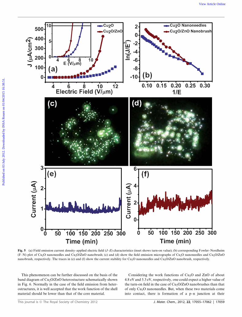
Fig. 5 (a) Field emission current density–applied electric field (J–E) characteristics (inset shows turn-on value); (b) corresponding Fowler–Nordheim
(F–N) plot of Cu2O nanoneedles and Cu2O/ZnO nanobrush; (c) and (d) show the field emission micrographs of Cu2O nanoneedles and Cu2O/ZnO
nanobrush, respectively. The traces in (e) and (f) show the current stability for Cu2O nanoneedles and Cu2O/ZnO nanobrush, respectively.
Publ
ishe
d on
03
July
201
2. D
ownl
oade
d by
IN
SA R
ouen
on
01/0
4/20
15 1
6:38
:51.
View Article Online
This phenomenon can be further discussed on the basis of the
band diagram of Cu2O/ZnO heterostucture schematically shown
in Fig. 6. Normally in the case of the field emission from heter-
ostructures, it is well accepted that the work function of the shell
material should be lower than that of the core material.
This journal is ª The Royal Society of Chemistry 2012
Considering the work functions of Cu2O and ZnO of about
4.8 eV and 5.3 eV, respectively, one could expect a higher value of
the turn-on field in the case of Cu2O/ZnO nanobrushes than that
of only Cu2O nanoneedles. But, when these two materials come
into contact, there is formation of a p–n junction at their
J. Mater. Chem., 2012, 22, 17055–17062 | 17059
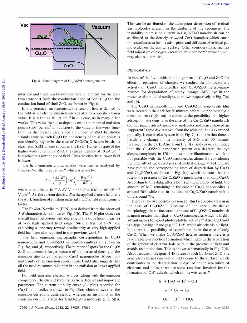
Fig. 6 Band diagram of Cu2O/ZnO heterojunction.
Publ
ishe
d on
03
July
201
2. D
ownl
oade
d by
IN
SA R
ouen
on
01/0
4/20
15 1
6:38
:51.
View Article Online
interface and there is a favourable band alignment for the elec-
tron transport from the conduction band of core Cu2O to the
conduction band of shell ZnO, as shown in Fig. 6.
In any practical measurement, the turn-on field is defined as
the field at which the emission current attains a specific chosen
value. It is taken as 10 mA cm:2 in our case, as in many other
works. This value then also depends on the number of emission
points (tips) per cm2 in addition to the value of the work func-
tion. In the present case, since a number of ZnO brush-like
strands grow on each Cu2O tip, the density of emission points is
considerably higher in the case of ZnO/Cu2O hetero-brush, as
clear from SEM images shown in the ESI.† Hence, in spite of the
higher work function of ZnO, the current density of 10 mA cm�2
is reached at a lower applied field. Thus the effective turn-on field
is lower.
The field emission characteristics were further analysed by
Fowler–Nordheim equation,39 which is given by:
J ¼�Ab2E2
4
�exp
�� B 43=2
bE
�
where A ¼ 1.54 � 10�6 A eV V�2 and B ¼ 6.83 � 103 eV�3/2
V mm�1, J is the current density, E is the applied electric field, 4 is
the work function of emitting material and b is field enhancement
factor.
The Fowler–Nordheim (F–N) plot derived from the observed
J–E characteristic is shown in Fig. 5(b). The F–N plot shows an
overall linear behaviour with decrease in the slope (non-linearity)
at very high applied field range. Such a type of F–N plot
exhibiting a tendency toward nonlinearity at very high applied
field has been also reported in our previous work.17
The field emission micrographs corresponding to Cu2O
nanoneedles and Cu2O/ZnO nanobrush emitters are shown in
Fig. 5(c) and (d), respectively. The number of spots for the Cu2O/
ZnO nanobrush is larger because of the increased density of the
emission sites as compared to Cu2O nanoneedles. More non-
uniformity of the emission spots in case Cu2O also suggests that
all the needles cannot take part in the emission at lower applied
fields.
For field emission electron sources, along with the emission
competence, the current stability is also a decisive and important
parameter. The current stability curve (I–t plot) recorded for
Cu2O nanoneedles is shown in Fig. 5(e), which shows that the
emission current is quite steady, whereas an instability in the
emission current is seen for Cu2O/ZnO nanobrush (Fig. 5(f)).
17060 | J. Mater. Chem., 2012, 22, 17055–17062
This can be attributed to the adsorption–desorption of residual
gas molecules present in the ambient of the specimen. The
instability in emission current in Cu2O/ZnO nanobrush can be
attributed to the densely crowded ZnO branches which cause
more surface area for the adsorption and diffusion of residual gas
molecules on the emitter surface. Other considerations, such as
field migration of oxygen vacancies, mild ion bombardment, etc.,
may also be operative.
Photocatalysis
In view of the favourable band alignment of Cu2O and ZnO for
efficient separation of charges, we studied the photocatalytic
activity of Cu2O nanoneedles and Cu2O/ZnO hetero-nano-
brushes for degradation of methyl orange (MO) dye in the
presence of simulated sunlight, as shown respectively in Fig. 7(a)
and (b).
The Cu2O nanoneedle film and Cu2O/ZnO nanobrush film
were treated in the dark for 30 minutes before the photocatalytic
measurements (light on) to eliminate the possibility that higher
adsorption site density in the case of the Cu2O/ZnO nanobrush
did not simply adsorb more dye molecules and hence showed an
‘‘apparent’’ rapid dye removal from the solution that is examined
optically. It can be clearly seen from Fig. 7(a) and (b) that there is
hardly any change in the intensity of MO after 30 minutes
treatment in the dark. Also, from Fig. 7(a) and (b) we can notice
that the Cu2O/ZnO nanobrush system can degrade the dye
almost completely in 120 minutes under illumination, which is
not possible with the Cu2O nanoneedles alone. By considering
the intensity of measured peak of methyl orange at 464 nm, we
have plotted the corresponding rates of degradation by Cu2O
and Cu2O/ZnO, as shown in Fig. 7(c), which indicates that the
rate in the presence of Cu2O/ZnO is much faster than only Cu2O.
According to this data, after 2 hours in the presence of light, the
amount of MO remaining in the case of Cu2O nanoneedles is
around 70% while that in the case of Cu2O/ZnO nanobrush is
only around 7%.
There can be two possible reasons for this fast photocatalysis in
the case of Cu2O/ZnO. Because of the special brush-like
morphology, the surface area in the case of Cu2O/ZnOnanobrush
is much greater than that of Cu2O nanoneedles which is highly
advantageous for good photocatalytic activity.40 Also, the Cu2O
is p-type, having a band gap of 2.1 eV, which absorbs visible light,
but there is a possibility of recombination in the case of only
Cu2O. When we make Cu2O/ZnO heterostructures there is a
favourable p–n junction formation which helps in the separation
of the generated electron–hole pairs in the presence of light and
avoids recombination. This is shown schematically in Fig. 7(d).
Also, because of the quasi-1-D nature of both Cu2O and ZnO, the
generated charges can very quickly come to the surface, which
contributes to the degradation of dye. After the separation of
electrons and holes, there are some reactions involved for the
formation of OH_ radicals, which can be written as:41
h+ + H2O / H+ + _OH
e� + O2 / _O2�
_O2� + H+ / HO2_
This journal is ª The Royal Society of Chemistry 2012
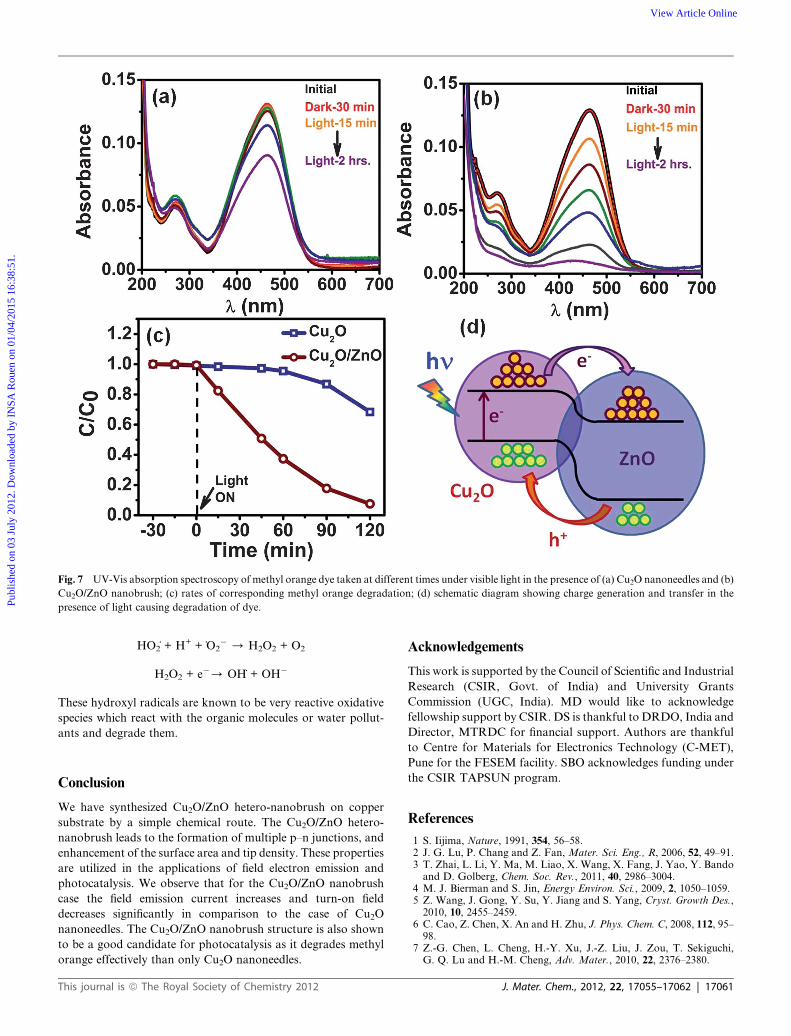
Fig. 7 UV-Vis absorption spectroscopy of methyl orange dye taken at different times under visible light in the presence of (a) Cu2O nanoneedles and (b)
Cu2O/ZnO nanobrush; (c) rates of corresponding methyl orange degradation; (d) schematic diagram showing charge generation and transfer in the
presence of light causing degradation of dye.Publ
ishe
d on
03
July
201
2. D
ownl
oade
d by
IN
SA R
ouen
on
01/0
4/20
15 1
6:38
:51.
View Article Online
HO2_+ H+ + _O2� / H2O2 + O2
H2O2 + e�/ OH_+ OH�
These hydroxyl radicals are known to be very reactive oxidative
species which react with the organic molecules or water pollut-
ants and degrade them.
Conclusion
We have synthesized Cu2O/ZnO hetero-nanobrush on copper
substrate by a simple chemical route. The Cu2O/ZnO hetero-
nanobrush leads to the formation of multiple p–n junctions, and
enhancement of the surface area and tip density. These properties
are utilized in the applications of field electron emission and
photocatalysis. We observe that for the Cu2O/ZnO nanobrush
case the field emission current increases and turn-on field
decreases significantly in comparison to the case of Cu2O
nanoneedles. The Cu2O/ZnO nanobrush structure is also shown
to be a good candidate for photocatalysis as it degrades methyl
orange effectively than only Cu2O nanoneedles.
This journal is ª The Royal Society of Chemistry 2012
Acknowledgements
This work is supported by the Council of Scientific and Industrial
Research (CSIR, Govt. of India) and University Grants
Commission (UGC, India). MD would like to acknowledge
fellowship support by CSIR. DS is thankful to DRDO, India and
Director, MTRDC for financial support. Authors are thankful
to Centre for Materials for Electronics Technology (C-MET),
Pune for the FESEM facility. SBO acknowledges funding under
the CSIR TAPSUN program.
References
1 S. Iijima, Nature, 1991, 354, 56–58.2 J. G. Lu, P. Chang and Z. Fan, Mater. Sci. Eng., R, 2006, 52, 49–91.3 T. Zhai, L. Li, Y. Ma, M. Liao, X. Wang, X. Fang, J. Yao, Y. Bandoand D. Golberg, Chem. Soc. Rev., 2011, 40, 2986–3004.
4 M. J. Bierman and S. Jin, Energy Environ. Sci., 2009, 2, 1050–1059.5 Z. Wang, J. Gong, Y. Su, Y. Jiang and S. Yang, Cryst. Growth Des.,2010, 10, 2455–2459.
6 C. Cao, Z. Chen, X. An and H. Zhu, J. Phys. Chem. C, 2008, 112, 95–98.
7 Z.-G. Chen, L. Cheng, H.-Y. Xu, J.-Z. Liu, J. Zou, T. Sekiguchi,G. Q. Lu and H.-M. Cheng, Adv. Mater., 2010, 22, 2376–2380.
J. Mater. Chem., 2012, 22, 17055–17062 | 17061
Publ
ishe
d on
03
July
201
2. D
ownl
oade
d by
IN
SA R
ouen
on
01/0
4/20
15 1
6:38
:51.
View Article Online
8 G. Li, T. Zhai, Y. Jiang, Y. Bando and D. Golberg, J. Phys. Chem. C,2011, 115, 9740–9745.
9 N. Zhang, K. Yu, Q. Li, Z. Q. Zhu and Q. Wan, J. Appl. Phys., 2008,103, 104305.
10 C. Fang, B. Geng, J. Liu and F. Zhan, Chem. Commun., 2009, 2350–2352.
11 S. H. Ko, D. Lee, H. W. Kang, K. H. Nam, J. Y. Yeo, S. J. Hong,C. P. Grigoropoulos and H. J. Sung, Nano Lett., 2011, 11, 666–671.
12 D. J. Milliron, S. M. Hughes, Y. Cui, L. Manna, J. Li, L.-W. Wangand A. P. Alivisatos, Nature, 2004, 430, 190–195.
13 J. Du, X. Lai, N. Yang, J. Zhai, D. Kisailus, F. Su, D. Wang andL. Jiang, ACS Nano, 2011, 5, 590–596.
14 S.Wang, L. Yi, J. E. Halpert, X. Lai, Y. Liu, H. Cao, R. Yu, D.Wangand Y. Li, Small, 2012, 8, 265–271.
15 J. Hu, Y. Bando and D. Golberg, J. Mater. Chem., 2009, 19, 330–343.16 H. Kim, S. Jeon, M. Lee, J. Lee and K. Yong, J. Mater. Chem., 2011,
21, 13458–13463.17 D. R. Shinde, P. G. Chavan, S. Sen, D. S. Joag, M. A. More,
S. C. Gadkari and S. K. Gupta, ACS Appl. Mater. Interfaces, 2011,3, 4730–4735.
18 M. Niu, F. Huang, L. Cui, P. Huang, Y. Yu andY.Wang,ACSNano,2010, 4, 681–688.
19 Y.-C. Her, C.-K. Chiang, S.-T. Jean and S.-L. Huang,CrystEngComm, 2012, 14, 1296–1300.
20 W. Zhou, C. Cheng, J. Liu, Y. Y. Tay, J. Jiang, X. Jia, J. Zhang,H. Gong, H. H. Hng, T. Yu and H. J. Fan, Adv. Funct. Mater.,2011, 21, 2439–2445.
21 L.-Q. Mai, F. Yang, Y.-L. Zhao, X. Xu, L. Xu and Y.-Z. Luo, Nat.Commun., 2011, 2, 381.
22 B. P. Rai, Sol. Cells, 1988, 25, 265–272.23 Y. Zhang, B. Deng, T. Zhang, D. Gao and A.-W. Xu, J. Phys. Chem.
C, 2010, 114, 5073–5079.
17062 | J. Mater. Chem., 2012, 22, 17055–17062
24 A. Paracchino, V. Laporte, K. Sivula, M. Gr€atzel and E. Thimsen,Nat. Mater., 2011, 10, 456–461.
25 Q. Tang, T. Li, X. Chen, D. Yu and Y. Qian, Solid State Commun.,2005, 134, 229–231.
26 H. Shi, K. Yu, F. Sun and Z. Zhu, CrystEngComm, 2012, 14, 278.27 Q. Zhang, C. S. Dandeneau, X. Zhou and G. Cao, Adv. Mater., 2009,
21, 4087–4108.28 G. Shen, Y. Bando, B. Liu, D. Golberg and C.-J. Lee, Adv. Funct.
Mater., 2006, 16, 410–416.29 B. D. Yuhas and P. Yang, J. Am. Chem. Soc., 2009, 131, 3756–3761.30 J. Cui and U. J. Gibson, J. Phys. Chem. C, 2010, 114, 6408–6412.31 H. Wei, H. Gong, Y. Wang, X. Hu, L. Chen, H. Xu, P. Liu and
B. Cao, CrystEngComm, 2011, 13, 6065–6070.32 K. P. Musselman, A. Marin, A. Wisnet, C. Scheu, J. L. MacManus-
Driscoll and L. Schmidt-Mende, Adv. Funct. Mater., 2011, 21, 573–582.
33 T.-J. Hsueh, C.-L. Hsu, S.-J. Chang, P.-W. Guo, J.-H. Hsieh andI.-C. Chen, Scr. Mater., 2007, 57, 53–56.
34 C. Xu, L. Cao, G. Su, W. Liu, H. Liu, Y. Yu and X. Qu, J. Hazard.Mater., 2010, 176, 807–813.
35 Y. Wang, G. She, H. Xu, Y. Liu, L. Mu and W. Shi, Mater. Lett.,2012, 67, 110–112.
36 Q. Zhu, Y. Zhang, F. Zhou, F. Lv, Z. Ye, F. Fan and P. K. Chu,Chem. Eng. J., 2011, 171, 61–68.
37 M. Deo, S. Mujawar, O. Game, A. Yengantiwar, A. Banpurkar,S. Kulkarni, J. Jog and S. Ogale, Nanoscale, 2011, 3, 4706.
38 U. K. Gautam, X. Fang, Y. Bando, J. Zhan and D. Golberg, ACSNano, 2008, 2, 1015–1021.
39 X. Fang, Y. Bando, U. K. Gautam, C. Ye and D. Golberg, J. Mater.Chem., 2008, 18, 509–522.
40 F. Lu,W. Cai and Y. Zhang,Adv. Funct. Mater., 2008, 18, 1047–1056.41 K.-i. Okamoto, Y. Yamamoto, H. Tanaka, M. Tanaka and A. Itaya,
Bull. Chem. Soc. Jpn., 1985, 58, 2015–2022.
This journal is ª The Royal Society of Chemistry 2012
Copyright © 2022 FDOKUMEN