Complexity and Correctness of a Super-Pipelined Processor
230
Complexity and Correctness of a Super-Pipelined Processor Dissertation zur Erlangung des Grades des Doktors der Ingenieurwissenschaften der Naturwissenschaftlich-Technischen Fakult¨ aten der Universit¨ at des Saarlandes Jochen Preiß [email protected] Saarbr¨ ucken, April 2005
-
Upload
khangminh22 -
Category
Documents
-
view
4 -
download
0
Transcript of Complexity and Correctness of a Super-Pipelined Processor

Complexity and Correctness
of a Super-Pipelined Processor
Dissertation
zur Erlangung des Gradesdes Doktors der Ingenieurwissenschaften
der Naturwissenschaftlich-Technischen Fakultatender Universitat des Saarlandes
Jochen Preiß[email protected]
Saarbrucken, April 2005

ii
Tag des Kolloquiums: 29. April 2005Dekan: Prof. Dr. Jorg Eschmeier
Vorsitzender des Prufungsausschusses: Prof. Dr. Gerhard WeikumErstgutachter: Prof. Dr. Wolfgang J. Paul
Zweitgutachter: Priv. Doz. Dr. Silvia M. Mullerakademischer Beisitzer: Dr. Sven Beyer

iii
Out Out!!You demons of stupidity!!
– Dogbert
DankeDiesen Abschnitt mochte ich all denen widmen, die zum Gelingen dieser Arbeit bei-getragen haben.
Zuallererst mochte ich meinen Eltern dafur danken, dass sie mich in allen Phasen mei-ner Ausbildung unterstutzt haben und mir gerade in schwierigeren Zeiten stets einRuckhalt waren.
Mein ganz besonderer Dank gilt auch Herrn Prof. Paul fur die Vergabe dieses interes-santen und herausfordernden Themas und fur die wissenschaftliche Unterstutzung.
Bei Christian Jacobi mochte ich mich fur das Korrekturlesen dieser Arbeit und dievielen Vorschlage, die mir geholfen haben, diese Arbeit immer weiter zu verbessern,bedanken.
Meinen Freunden von der Uni Werner Backes, Christoph Berg, SvenBeyer, MarkHillebrand, Thomas In der Rieden, Michael Klein und Dirk Leinenbach mochte ichdanken fur die fruchtbaren Diskussionen und das gute Klima, gefordert durch Tisch-fußball, Skat- und Doppelkopf-Abende und das Verschonen meines Rasens.
Meinen Kollegen bei IBM, insbesondere Cedric Lichtenau und Thomas Pfluger, giltmein Dank fur ihr Verstandnis und die Unterstutzung gerade in der letzten Phase mei-ner Dissertation.

iv

v
Abstract
This thesis introduces the DLXπ+, a super-pipelined processor with variable cycletime. The cycle time of the DLXπ+ may be as low as 9 gate delays (including 5gate delays for registers), which is assumed to be a lower bound for the cycle time.For the parts of the DLXπ+ that significantly differ form previous implementationscorrectness proofs are provided. Formulas are developed which compute restrictionsto the parameters of the DLXπ+, e.g., the maximum number of reservation stationentries for a given cycle time. The formulas also compute what modifications to thebase design have to be made in order to realize a certain cycle time and what theimpactis on the number of pipeline stages. This lays the foundation for computing the timeper instruction of the DLXπ+ for a given benchmark and different cycle times in futurework in order to determine the “optimum” cycle time.
Kurzzusammenfassung
In dieser Arbeit wird die DLXπ+ eingefuhrt, ein super-gepipelineter Prozessor mit va-riabler Zykluszeit. Die Zykluszeit der DLXπ+ kann bis auf 9 Gatter-Delays (inklusive5 Gatter-Delays fur Register) reduziert werden, was als untere Schranke fur die Zy-kluszeit angesehen wird. Fur die Teile der DLXπ+, die sich signifikant von bisherigenImplementierungen unterscheiden, werden Korrektheits-Beweise geliefert. Desweite-ren werden Formeln entwickelt, die Beschrankungen fur die Parameter der DLXπ+ wiezum Beispiel die maximale Anzahl von Reservation Station Eintragen fur eine gege-bene Zykluszeit berechnen. Die Formeln errechnen ausserdem welche Modifikationenam Basis-Design notwendig sind, um eine bestimmte Zykluszeit zu erreichen und wel-chen Einfluss dies auf die Anzahl der Pipeline-Stufen hat. Damit wird die Grundlagegelegt, um als zukunftige Arbeit die benotigte Zeit pro Instruktion der DLXπ+ fureinen gegebenen Benchmark bei verschiedenen Zykluszeiten zu berechenen und da-mit die “optimale” Zykluszeit zu bestimmen.

vi
Extended Abstract
In order to increase the performance of a processor regarding a specific benchmark onecan either decrease the cycle time of the processor or the CPI (cycles perinstruction)that the processor needs for the benchmark. Usual ways to decreasethe CPI are, e.g.,pipelining, out-of-order execution, branch prediction, or super-scalar designs. Thisthesis focuses on the cycle time.
The cycle time of a processor can be improved by increasing the number of pipelinestages of the processor and therefore decreasing the amount of workto be done in eachstage. This is called super-pipelining. Note that super-pipelining may increase the CPIfor several reasons. Due to the increased number of pipeline stages, data dependenciesmay have a larger impact. Also, the fewer amount of logic that fits into one cyclemayhave a negative impact on the micro-architecture, e.g., reduce the maximum numberof possible reservation stations entries. This may increase the frequency of stalls andtherefore increase the CPI. Thus, the minimum cycle time may not be the optimal cycletime for a design and a given benchmark.
This thesis introduces the DLXπ+, a super-pipelined processor with variable cycletime, i.e., with a variable number of pipeline stages. For computation of cycle timeand cost of the DLXπ+ the technology independent gate model from [MP00] is used.The cycle time of the DLXπ+ may be as low as 9 gate delays (including 5 gate delaysfor the registers). For comparison, a 16 bit addition (which has 12 combinational gatedelays in the used model) needs less than half a cycle in the deeply pipelined Pentium4 processor [HSU+01], but needs 3 cycles in the DLXπ+ with 9 gate delays cycle time.
The variant of the DLXπ+ with 9 gate delays cycle time is more a proof of conceptrather than it is assumed to have a good performance. Therefore, the mainpart of thisthesis only handles cycle times of at least 10 in order to simplify the design. A variantof the DLXπ+ with a cycle time smaller than 9 is not assumed to be possible, althoughno formal proof for this is provided.
In this thesis formulas are developed which compute restrictions to the parametersof the DLXπ+, e.g., the maximum number of reservation station entries for a givencycle time. Other formulas compute what modification to the base design have to bemade in order to realize a certain cycle time and what the impact is on the numberof pipeline stages. This lays the foundation to write a cycle-accurate DLXπ+ simu-lator, that computes the performance of the DLXπ+ for a given benchmark and dif-ferent cycle times in future work. Using this simulator the optimum cycle time of theDLXπ+ for the benchmark could be determined.
The DLXπ+is an out-of-order processor that uses the Tomasulo scheduler [Tom67].The design is based on the work of Kroning [Kro99]. The instruction set architecture(ISA) is taken from the MIPS R3000 processor [KH92] with small modifications sim-plifying the adaptation of the design. This allows a simulation of the DLXπ+withMIPS R3000 instruction traces [Hil95] of the SPEC92 benchmark [SPEC].
In order to realize the small cycle times, parts of the DLXπ+differ significantlyfrom the design presented by Kroning. In particular new stalling and forwarding tech-niques are used. If these techniques are used it is for example not longer obvious that aRAM access returns the correct result. Therefore, correctness proofs are provided forthe critical parts of the DLXπ+.

vii
Zusammenfassung
Um die Leistung eines Prozessors bezuglich eines spezifischen Benchmarks zu verbes-sern, kann man entweder die Zykluszeit oder die CPI (benotigte Anzahl von Zyklenpro Instruktion) des Prozessors reduzieren. Bekannte Methoden dieCPI zu reduzierensind zum Beispiel Pipelining, Out-of-order Execution, Branch Predictionoder super-skalare Designs. In dieser Arbeit geht es hingegen in erster Linie um dieReduzierungder Zykluszeit.
Die Zykluszeit eines Prozessors kann durch Erhohen der Anzahl von Pipeline-Stufen des Prozessors und damit durch Reduzierung der Arbeit, die in jeder dieser Stu-fen verrichtet werden muss, verbessert werden. Dies wird Super-Pipelining genannt.Man beachte, dass Super-Pipelining die CPI aus verschiedenen Grunden erhohen kann.Auf Grund der großeren Anzahl von Pipeline-Stufen konne Daten-Abhangigkeite einengroßeren Einfluß haben. Ausserdem kann die geringe Menge von Logik,die in einenZyklus passt, negative Auswirkungen auf die Mikro-Architektur des Prozessors haben,indem zum Beispiel die maximal mogliche Anzahl von Reservation Stations Eintragenreduziert wird. Dies kann die Haufigkeit von Stalls und damit die CPI erhohen. Dahermuss die minimale Zykluszeit nicht notwendigerweise die optimale Zykluszeit fur einDesign und einen gegebenen Benchmark sein.
In dieser Arbeit wird die DLXπ+ eingefuhrt, ein super-gepipelineter Prozessormit variabler Zykluszeit, das heisst mit variabler Anzahl von Pipeline-Stufen. Zur Be-rechnung von Zykluszeit und Kosten der DLXπ+ wird das von der Technologie un-abhangige Gatter Model aus [MP00] verwendet. Die Zykluszeit der DLXπ+ kann bisauf 9 Gatter-Delays (inklusive 5 Gatter-Delays fur die Register) reduziert werden. ZumVergleich, die Berechnung einer 16 bit Addition (die in dem benutzten GatterModel12 Gatter-Delays benotigt) braucht weniger als einen halben Takt im tief gepipelinetenPentium 4 Prozessor [HSU+01], aber braucht 3 Takte in der DLXπ+ mit 9 Gatter-Delays Zykluszeit.
Die Variante der DLXπ+ mit 9 Gatter-Delays Zykluszeit dient nur als Machbarkeits-Beweis. Es wird nicht erwartet, dass sie eine gute Leistung erreicht. Deshalb betrachtetder Hauptteil dieser Arbeit nur Zykluszeiten von mindestens 10 um das Design zu ver-einfachen. Eine Variante der DLXπ+ mit einer Zykluszeit von weniger als 9 wird nichtals moglich erachtet, auch wenn kein formaler Beweis dafur gegeben wird.
In dieser Arbeit werden Formeln entwickelt, die Beschrankungen fur die Parameterder DLXπ+wie zum Beispiel die maximale Anzahl von Reservation Station Eintragenin Abhangigkeit von der Zykluszeit berechnen. Andere Formeln errechnen, welcheModifikationen am Basis-Design notwendig sind um eine bestimmte Zykluszeit zuerreichen und welchen Einfluss dies auf die Anzahl der Pipeline-Stufenhat. Damitwird die Grundlage gelegt, um als zukunftige Arbeit einen Zyklus-genauen DLXπ+-Simulator zu schreiben, der die Leistung der DLXπ+ fur einen gegebenen Benchmarkund verschiedenen Zykluszeiten berechnet. Mit diesem Simulator ware es moglich, dieoptimale Zykluszeit der DLXπ+fur den Benchmark zu bestimmen.
Die DLXπ+ ist ein out-of-order Prozessor der den Tomasulo Scheduler [Tom67]benutzt. Das Design basiert auf der Arbeit von Kroning [Kro99]. Der Instruktions-Satzwurde mit kleinenAnderungen, die die Anpassung des Designs erleichtern, vom MIPSR3000 Prozessor [KH92]ubernommen. Dadurch ist es moglich, die DLXπ+ mit Hilfe

viii
von MIPS R3000 Traces [Hil95] des SPEC92 Benchmarks [SPEC] zu simulieren.Um die geringe Zykluszeit zu erreichen, mussen Teile der DLXπ+ gegenuber dem
Design von Kroning signifikant verandert werden. Insbesondere mussen neue Techni-ken zum Stallen und Forwarden einfuhrt werden. Durch den Einsatz dieser Technikenist es zum Beispiel nicht mehr offensichtlich, dass ein RAM-Zugriff die korrekten Da-ten liefert. Deshalb werden fur die kritischen Teile der DLXπ+ Korrektheits-Beweisegefuhrt.

Contents
1 Introduction 11.1 Outline . . . . . . . . . . . . . . . . . . . . . . . . . . . . . . . . . 3
2 Basics 52.1 Notation . . . . . . . . . . . . . . . . . . . . . . . . . . . . . . . . . 52.2 Cost and Delay Model . . . . . . . . . . . . . . . . . . . . . . . . . 62.3 Basic Circuits . . . . . . . . . . . . . . . . . . . . . . . . . . . . . . 72.4 Encodings . . . . . . . . . . . . . . . . . . . . . . . . . . . . . . . . 82.5 Pipelining . . . . . . . . . . . . . . . . . . . . . . . . . . . . . . . . 9
2.5.1 Stages . . . . . . . . . . . . . . . . . . . . . . . . . . . . . . 92.5.2 Computation of Stall Signals . . . . . . . . . . . . . . . . . . 112.5.3 Optimization of the Stall Computation . . . . . . . . . . . . . 132.5.4 Maximum Delay of Stall Inputs . . . . . . . . . . . . . . . . 17
2.6 Pipelining of RAM Blocks . . . . . . . . . . . . . . . . . . . . . . . 182.6.1 Forwarding . . . . . . . . . . . . . . . . . . . . . . . . . . . 192.6.2 Forwarding with Stalling . . . . . . . . . . . . . . . . . . . . 212.6.3 Pipelining of the Forwarding Circuits . . . . . . . . . . . . . 212.6.4 Cost and Delay . . . . . . . . . . . . . . . . . . . . . . . . . 25
3 Tomasulo Algorithm 273.1 Overview . . . . . . . . . . . . . . . . . . . . . . . . . . . . . . . . 273.2 Basic Data Structures . . . . . . . . . . . . . . . . . . . . . . . . . . 28
3.2.1 Functional Units . . . . . . . . . . . . . . . . . . . . . . . . 283.2.2 Register Files and Producer Tables . . . . . . . . . . . . . . . 283.2.3 Reservation Stations . . . . . . . . . . . . . . . . . . . . . . 293.2.4 Common Data Bus . . . . . . . . . . . . . . . . . . . . . . . 293.2.5 Reorder Buffer . . . . . . . . . . . . . . . . . . . . . . . . . 29
3.3 Instruction Execution . . . . . . . . . . . . . . . . . . . . . . . . . . 293.3.1 Decode . . . . . . . . . . . . . . . . . . . . . . . . . . . . . 293.3.2 Dispatch . . . . . . . . . . . . . . . . . . . . . . . . . . . . 313.3.3 Execute . . . . . . . . . . . . . . . . . . . . . . . . . . . . . 313.3.4 Completion . . . . . . . . . . . . . . . . . . . . . . . . . . . 313.3.5 Retire . . . . . . . . . . . . . . . . . . . . . . . . . . . . . . 31

x Contents
4 Processor Core 334.1 Decode . . . . . . . . . . . . . . . . . . . . . . . . . . . . . . . . . 33
4.1.1 Overview . . . . . . . . . . . . . . . . . . . . . . . . . . . . 334.1.2 Operands . . . . . . . . . . . . . . . . . . . . . . . . . . . . 354.1.3 Instruction Decoding Circuit . . . . . . . . . . . . . . . . . . 364.1.4 Operand Generation . . . . . . . . . . . . . . . . . . . . . . 374.1.5 Destination Computation . . . . . . . . . . . . . . . . . . . . 384.1.6 Instruction Issue . . . . . . . . . . . . . . . . . . . . . . . . 394.1.7 Stalling . . . . . . . . . . . . . . . . . . . . . . . . . . . . . 454.1.8 Cost and Delay . . . . . . . . . . . . . . . . . . . . . . . . . 47
4.2 Dispatch . . . . . . . . . . . . . . . . . . . . . . . . . . . . . . . . . 514.2.1 Entries . . . . . . . . . . . . . . . . . . . . . . . . . . . . . 524.2.2 Reservation Station Control . . . . . . . . . . . . . . . . . . 554.2.3 Pipelining . . . . . . . . . . . . . . . . . . . . . . . . . . . . 58
4.3 Functional Units . . . . . . . . . . . . . . . . . . . . . . . . . . . . . 634.4 Completion . . . . . . . . . . . . . . . . . . . . . . . . . . . . . . . 64
4.4.1 Arbiter . . . . . . . . . . . . . . . . . . . . . . . . . . . . . 644.4.2 Pipelining . . . . . . . . . . . . . . . . . . . . . . . . . . . . 664.4.3 Cost and Delay . . . . . . . . . . . . . . . . . . . . . . . . . 68
4.5 Retire . . . . . . . . . . . . . . . . . . . . . . . . . . . . . . . . . . 704.5.1 Overview . . . . . . . . . . . . . . . . . . . . . . . . . . . . 704.5.2 Tag Check . . . . . . . . . . . . . . . . . . . . . . . . . . . 724.5.3 Interrupt Handling . . . . . . . . . . . . . . . . . . . . . . . 724.5.4 Cost and Delay . . . . . . . . . . . . . . . . . . . . . . . . . 75
4.6 Reorder Buffer Environment . . . . . . . . . . . . . . . . . . . . . . 764.6.1 Overview . . . . . . . . . . . . . . . . . . . . . . . . . . . . 764.6.2 Pipelining of the Retiring-Context . . . . . . . . . . . . . . . 784.6.3 Forwarding . . . . . . . . . . . . . . . . . . . . . . . . . . . 794.6.4 Implementation of Forwarding . . . . . . . . . . . . . . . . . 814.6.5 Control . . . . . . . . . . . . . . . . . . . . . . . . . . . . . 824.6.6 Correctness . . . . . . . . . . . . . . . . . . . . . . . . . . . 874.6.7 Delay Optimizations . . . . . . . . . . . . . . . . . . . . . . 904.6.8 Cost and Delay . . . . . . . . . . . . . . . . . . . . . . . . . 93
4.7 Register File Environment . . . . . . . . . . . . . . . . . . . . . . . 944.7.1 Forwarding . . . . . . . . . . . . . . . . . . . . . . . . . . . 954.7.2 General Purpose Register File . . . . . . . . . . . . . . . . . 984.7.3 Floating Point Register File . . . . . . . . . . . . . . . . . . 994.7.4 Special Purpose Register File . . . . . . . . . . . . . . . . . 1004.7.5 Cost and Delay . . . . . . . . . . . . . . . . . . . . . . . . . 103
4.8 Producer Table Environment . . . . . . . . . . . . . . . . . . . . . . 1044.8.1 Forwarding . . . . . . . . . . . . . . . . . . . . . . . . . . . 1044.8.2 Cost and Delay . . . . . . . . . . . . . . . . . . . . . . . . . 107

Contents xi
5 Memory Unit 1095.1 Overview . . . . . . . . . . . . . . . . . . . . . . . . . . . . . . . . 1095.2 Overview of the Data Cache . . . . . . . . . . . . . . . . . . . . . . 110
5.2.1 Execution of Memory Accesses . . . . . . . . . . . . . . . . 1115.2.2 Cache Core and Main Memory . . . . . . . . . . . . . . . . . 1125.2.3 Speculation . . . . . . . . . . . . . . . . . . . . . . . . . . . 113
5.3 Hit Computation . . . . . . . . . . . . . . . . . . . . . . . . . . . . 1135.3.1 Overview of the Hit Signal Computation . . . . . . . . . . . 1145.3.2 Local Hit Signals . . . . . . . . . . . . . . . . . . . . . . . . 1165.3.3 Static Hit Signals . . . . . . . . . . . . . . . . . . . . . . . . 1175.3.4 Global Hit Signals . . . . . . . . . . . . . . . . . . . . . . . 1195.3.5 Actions . . . . . . . . . . . . . . . . . . . . . . . . . . . . . 1205.3.6 Stall Computation . . . . . . . . . . . . . . . . . . . . . . . 1225.3.7 Cost and Delay . . . . . . . . . . . . . . . . . . . . . . . . . 122
5.4 Cache Core . . . . . . . . . . . . . . . . . . . . . . . . . . . . . . . 1265.5 Update Queue . . . . . . . . . . . . . . . . . . . . . . . . . . . . . . 127
5.5.1 Entries . . . . . . . . . . . . . . . . . . . . . . . . . . . . . 1285.5.2 Control . . . . . . . . . . . . . . . . . . . . . . . . . . . . . 1305.5.3 Delay Optimizations . . . . . . . . . . . . . . . . . . . . . . 1335.5.4 Optimized Completion for Store Instructions . . . . . . . . . 1365.5.5 Cost and Delay . . . . . . . . . . . . . . . . . . . . . . . . . 137
5.6 Read Queue . . . . . . . . . . . . . . . . . . . . . . . . . . . . . . . 1405.6.1 Cost and Delay . . . . . . . . . . . . . . . . . . . . . . . . . 141
5.7 Stall Computation . . . . . . . . . . . . . . . . . . . . . . . . . . . . 1435.8 Cost and Delay . . . . . . . . . . . . . . . . . . . . . . . . . . . . . 143
6 Instruction Fetch 1496.1 Instruction Fetch Mechanism . . . . . . . . . . . . . . . . . . . . . . 149
6.1.1 Overview . . . . . . . . . . . . . . . . . . . . . . . . . . . . 1496.1.2 Clocking of the Instruction Fetch . . . . . . . . . . . . . . . 1506.1.3 Branch Prediction . . . . . . . . . . . . . . . . . . . . . . . . 150
6.2 Instruction Fetch Unit . . . . . . . . . . . . . . . . . . . . . . . . . . 1516.2.1 Overview . . . . . . . . . . . . . . . . . . . . . . . . . . . . 1516.2.2 Instruction Cache . . . . . . . . . . . . . . . . . . . . . . . . 1536.2.3 Computation of the Next Fetch-PC . . . . . . . . . . . . . . . 1556.2.4 Instruction Fetch Control . . . . . . . . . . . . . . . . . . . . 1586.2.5 Cost and Delay . . . . . . . . . . . . . . . . . . . . . . . . . 159
6.3 Instruction Fetch Queue . . . . . . . . . . . . . . . . . . . . . . . . . 1596.3.1 IFQ Entries . . . . . . . . . . . . . . . . . . . . . . . . . . . 1606.3.2 Control . . . . . . . . . . . . . . . . . . . . . . . . . . . . . 1616.3.3 Cost and Delay . . . . . . . . . . . . . . . . . . . . . . . . . 161
6.4 Instruction Register Environment . . . . . . . . . . . . . . . . . . . . 1626.5 Branch Checking Unit . . . . . . . . . . . . . . . . . . . . . . . . . 162
6.5.1 Stall Computation . . . . . . . . . . . . . . . . . . . . . . . 1656.5.2 Cost and Delay . . . . . . . . . . . . . . . . . . . . . . . . . 165
6.6 Processor Flush . . . . . . . . . . . . . . . . . . . . . . . . . . . . . 166

xii Contents
7 Discussion 1697.1 Stage depths below 5 . . . . . . . . . . . . . . . . . . . . . . . . . . 1697.2 Gate Model . . . . . . . . . . . . . . . . . . . . . . . . . . . . . . . 1737.3 Overall Cost and Delay . . . . . . . . . . . . . . . . . . . . . . . . . 1747.4 Related Work . . . . . . . . . . . . . . . . . . . . . . . . . . . . . . 178
8 Summary 1818.1 Future Work . . . . . . . . . . . . . . . . . . . . . . . . . . . . . . . 181
A Instruction set architecture 183A.1 Instructions . . . . . . . . . . . . . . . . . . . . . . . . . . . . . . . 183A.2 Encoding . . . . . . . . . . . . . . . . . . . . . . . . . . . . . . . . 184
B Emulation of a MIPS R3000 189
C Additional Circuits 191C.1 Basic Circuits . . . . . . . . . . . . . . . . . . . . . . . . . . . . . . 191
C.1.1 Design . . . . . . . . . . . . . . . . . . . . . . . . . . . . . 191C.1.2 Cost and Delay . . . . . . . . . . . . . . . . . . . . . . . . . 191
C.2 Instruction Decode . . . . . . . . . . . . . . . . . . . . . . . . . . . 193C.2.1 Decode . . . . . . . . . . . . . . . . . . . . . . . . . . . . . 194C.2.2 Destination computation . . . . . . . . . . . . . . . . . . . . 196
D Functional Units 199D.1 Integer ALU . . . . . . . . . . . . . . . . . . . . . . . . . . . . . . . 199D.2 Integer Multiplicative Unit . . . . . . . . . . . . . . . . . . . . . . . 201D.3 Floating Point Units . . . . . . . . . . . . . . . . . . . . . . . . . . . 203D.4 Memory Unit . . . . . . . . . . . . . . . . . . . . . . . . . . . . . . 205
D.4.1 Shift for Store . . . . . . . . . . . . . . . . . . . . . . . . . . 205D.4.2 Shift for Load . . . . . . . . . . . . . . . . . . . . . . . . . . 207
E Cost and Delay 209

Chapter 1
Introduction
Over the past fifty years the performance of microprocessors has dramatically in-creased. The advances in lithography allowed the building of constantly smaller tran-sistors. This made the transistors faster and also increased the number of availabletransistors. A larger number of transistors made it possible to additionally increase theperformance of the processor by implementing more advanced and complex designs.
The performance of a processor regarding a specific benchmark canbe measuredin TPI, the average time per instruction. The TPI can be computed as the productof the cycle time of the processor and the CPI (cycles per instruction). To increasethe performance of a processor one can either decrease the cycle time orthe CPI.Known techniques that may decrease the CPI are, e.g., pipelining, out-of-order execu-tion, branch prediction, or super-scalar designs. This thesis focuseson improving thecycle time of the processor.
If technology improvements are neglected and the total work for processing aninstruction is not changed, a lower cycle time can only be achieved by increasing thenumber of pipeline stages of the processor. Increasing the number of pipeline stagesover the 5 stages of a simple pipelined processor, e.g., the MIPS R3000 [KH92], iscalled super-pipelining. However, extensive super-pipelining in orderto minimize thecycle time does not necessarily maximize the TPI, since it may have a negative impacton the CPI.
An increased number of pipeline stages increases the number of cycles needed for“critical” loops, e.g, the execution of an ALU instruction and the forwardingof itsresult to the following instructions, or the resolving of a branch misprediction. Thus,the penalty for data dependencies or mispredicted branches becomes higher. This leadsto stall conditions occurring more often which increases the CPI. Note that aconstantpart of the cycle time is consumed by the register delay. Only the remaining partisavailable for useful work. Splitting the cycle time in half therefore reduces the usefulwork by more than the half. The number of cycles needed for a computation can bemore than doubled. Hence, the gain due to the lower cycle time may be lower than theloss due to the increased CPI.
Additionally, the decreased logic depth that fits into a cycle may have a negativeimpact on the micro-architecture of the processor. For example, if a register file accessmust be pipelined, forwarding of the write ports must be implemented which increasesthe combinational delay of the register file access. Also, it may happen that certain
2 Introduction
parameters of the micro-architecture such as the number of reservation stations entriesare bounded by the cycle time. Hence, for small cycle times it might be necessary toreduce the number of reservation station entries which could increase the CPI. Numer-ous other examples can be found throughout this thesis.
In order to investigate the side-effects and the limits of super-pipelining, this thesisintroduces the DLXπ+, a super-pipelined processor with a variable cycle time. The cy-cle time and the cost of the DLXπ+ is computed using the technology independent gatemodel from [MP00]. Additionally to the cycle time the DLXπ+ supports other vari-able parameters, e.g., cache size, number of functional units, or number of reservationstation entries.
The minimum cycle time of the DLXπ+ is only 9 gate delays (including 5 gate de-lays for the registers, thus leaving 4 gate delays for useful work). Notethat the deeplypipelined Pentium 4 processor can compute a 16 bit addition (which has 12 combina-tional gate delays in our model) in less than half a cycle [HSU+01]. Hence, based onour model the amount of useful work that can be done in one cycle of the Pentium 4 isat least six times higher than the 4 gate delays in one cycle of the DLXπ+ with mini-mum cycle time. Even though the delay model may not be accurate as it neglects wiredelay and fanout, the error is probably much less than a factor of six. Theminimumcycle time of the DLXπ+ is therefore assumed to be far smaller than the cycle time ofthe Pentium 4 processor.
Some critical circuits of the DLXπ+ need two levels of multiplexers which togetherhave 4 gate delays and hence use up all the useful work that can be done with minimumcycle time. Although no formal proof is provided, the author therefore assumes that itis not possible to build a DLXπ+ with a cycle time below 9 without sacrificing, e.g, abest-case CPI of 1. On the other hand, several trade-offs needed tobe made in orderto realize the DLXπ+ with 9 gate delays cycle time that can significantly increase theCPI for realistic benchmarks. Therefore for simplicity the main part of this thesis onlytreats cycle times of at least 10.
For cycle times of 10 and above this thesis develops formulas that define the behav-ior of the DLXπ+. Dependent on the cycle time these formulas compute the necessarymodifications, the number of pipeline stages of the different parts of the design, andthe cost of the processor. Additionally, formulas are developed that compute restric-tions to the parameters of the DLXπ+for a given cycle time. Using these formulas onecan write a cycle-accurate DLXπ+ simulator that computes the TPI of the DLXπ+ fora given benchmark and different cycle times. Hence, one can determine the “opti-mum” cycle-time giving maximum overall performance for the benchmark. This partis future work.
The design of the DLXπ+is based on Kroning’s out-of-order variant [Kro99] ofthe DLX [HP96] implementation by Muller and Paul [MP00]. The instruction setarchitecture (ISA) is taken from the MIPS R3000 processor [KH92] withsmall modi-fications simplifying the adaptation of the design. In contrary to the design of Mullerand Paul, the DLXπ+supports integer multiplications and divisions and does not usea delayed PC. The choice of the MIPS R3000 ISA allows for an accurate simula-tion of the DLXπ+by using MIPS R3000 instruction traces [Hil95] of the SPEC92benchmark [SPEC]. A complete listing of the DLXπ+instruction set can be found inappendix A.

1.1 Outline 3
The DLX implementation by Kroning is used as the starting point for the DLXπ+.However, most circuits of Kroning’s design have been redesigned. The changes eitherdecreased the combinational delay of the design or were necessary to allow smallcycle times. Especially an instruction fetch mechanism using branch predictionhad tobe introduced.
1.1 Outline
This thesis is structured as follows: the basics needed for the design of theDLXπ+ arepresented in chapter 2. Chapter 3 describes the Tomasulo algorithm that is used by theDLXπ+ in order to execute instructions out-of-order. The design of the processor coreof the DLXπ+ with a cycle time of 10 and above is presented in chapters 4 to 6. Chap-ter 4 details the core of the DLXπ+, chapters 5 and 6 detail the design of memory unitand instruction fetch. The results of this thesis including the modifications necessaryfor the DLXπ+ with a cycle time of 9 are discussed in chapter 7. A summary is givenin chapter 8.

4 Introduction

Chapter 2
Basics
In this chapter basic concepts used in this thesis are discussed. The notation and nam-ing conventions are summarized in section 2.1. Section 2.2 introduces the gate modelused to compute cost and delay of circuits. The basic circuits used in this thesis arepresented in section 2.3. Section 2.4 introduces half-unary encoding used through-out this thesis. Sections 2.5 and 2.6 discuss pipelining of circuits and RAM blocks.These techniques are essential for the design of the DLXπ+ processor and the generaldiscussion simplifies the description in the later chapters.
2.1 Notation
In this thesis the following naming conventions will be used for circuits and signals:
• Circuit names are written insans serif.
• Register and signal names are written initalic.
• The output signal of a registerreg is also denoted byreg. The data input signalis denoted byreg′.
• A busbus with indexes fromj to i is denoted bybus[j : i].
• Signals and busses can be combined to a multi-bus. A signalsig of a multi-busmbus is denoted bymbus.sig. The whole multi-bus is denoted bymbus.⋆.
• The outputs of a circuitCirc are often combined to the multi-busCirc.⋆.
• The concatenation of two signalssig1 andsig2 is denoted by{sig1, sig2}. Ifthe signals belong to the same multi-busmbus the notationmbus.{sig1, sig2}is used.
• If multiple signals are differentiated by an index (e.g.sig0 to sign), thensig⋆
denotes all signals of this kind.
For readability the usage of⋆ to denote all signals of a multi-bus or all indexesmay be used imprecisely if it is clear from the context which signals are meant. If thecontext differentiates the signalsmbus.a andmbus.⋆, thenmbus.⋆ means all signalsof the multi-bus except the signalmbus.a.

6 Basics
2.2 Cost and Delay Model
To compare the performance and the cost (i.e., the area) of different processor designsa simple gate model based on the gate model in [MP95] is used. All gates and registershave constant delay. Fanout is not taken into account. The cost and delay of the gatesare summarized in table 2.1. A register has a delay of4 for the outputs and additionallya setup time of1 for the inputs resulting in an overall delay of5.
INV NAND NOR AND OR MUX XOR XNOR REG
cost 1 2 2 2 2 3 4 4 8delay 1 1 1 2 2 2 2 2 4+1
Table 2.1: Cost and delay of gates
The delay of a combinational path in a circuit is defined as the sum of the delays ofthe gates on the path. The delay of a signal is the maximum delay of all combinationalpaths from a register to the signal (excluding the delay of the register). The delay of acircuit is the delay of the longest combinational path from an input or a register insidethe circuit to an output or a register inside the circuit. The following notations are usedfor cost and delay of gates, signals, and circuits:
• For a gateGATE or a registerREG, the delays are denoted byDGATE andDREG. The cost are denoted byCGATE andCREG.
• The delay of the signalsig is denoted byD(sig).
• D(sig1, sig2) denotes the maximum delay of two signalssig1 andsig2.
• For signalssig1 andsig2, D(sig1 sig2) denotes the maximum delay of allcombinational paths fromsig1 to sig2.
• For a circuitCirc, D(Circ) denotes the delay and C(Circ) denotes the cost of thecircuit.
INV NAND NOR AND OR MUX XOR XNOR REG
1 0
Table 2.2: Gate symbols
The symbols used for gates in this thesis are shown in table 2.2. Inverted linesareindicated by small circles at the input or output of gates or circuits (see e.g.the NORgate). All registers have a clock enable signal. The clock enable signal isconnectedto the triangle shape of the register symbol. If no signal is connected to the triangleshape, the clock enable is tied to one, i.e., the register is always clocked.
Registers are assumed to deliver both the negated and the non-negated value. Thus,it is possible to replace any AND or OR gate on the critical path by NAND and NORgates using de Morgan’s law. For the same reason all inverters on the critical path

2.3 Basic Circuits 7
can be removed. If a signal is used in multiple critical paths, it may be necessaryto compute both the negated and non-negated value. For the sake of readability in thedesigns AND- and OR-gates will be used, but with the reduced delay to reflect a designwith NAND- and NOR-gates. The revised delay of inverters, AND- and OR-gates issummarized in table 2.3.
INV AND OR
D 0 1 1
Table 2.3: Revised delay of inverters, AND-, and OR-gates
A RAM block with A lines,D data bits, and a single read/write port is denoted byRAM(A, D). Cost and delay of such a RAM block can be computed by the followingformula from [MP95]:
C(RAM(A, D)) = 3 · (A + 3) · (D + ⌈log log D⌉),
D(RAM(A, D)) =
{
⌈log D⌉ + ⌈A/4⌉ A ≤ 64
3 · ⌈log A⌉ + 10 A > 64.
RAM blocks may have multiple read and write ports. The write ports are numberedfrom 1 to w. If multiple write accesses have the same target address, the write portswith smaller index have higher priority.
A RAM block with r read ports andw write port is denoted byRAM(A, D, r, w).Cost and delay of this RAM block is based on the delay of a simple RAM block. Theformula is taken from [Kro99]:
C(RAM(A, D, r, w)) = C(RAM(A, D)) · (0.4 + 0.3 · (r + 2w)),
D(RAM(A, D, r, w)) = D(RAM(A, D)) · (0.5 + 0.25 · (r + 2w)).
At higher frequencies it is not possible to access a RAM block in a single cycle.A RAM block which needsc cycles for every access is denoted byRAM(A,D,r,w,c).The additional registers increases the cost of the RAM block by 10% per cycle.
C(RAM(A, D, r, w, c)) = C(RAM(A, D, r, w)) · (0.9 + 0.1 · c).
The design of pipelined RAM blocks that take multiple cycles for accesses is detailedin section 2.6. The given cost does not include any additional circuits needed forforwarding between the write and the read ports (see section 2.6.1).
2.3 Basic Circuits
Basic circuits such as adder, decoder, etc. which are used in this thesis are not dis-cussed in detail. For cost and delay of the basic circuits and the design of ahalf-unaryfind-last-one circuit see appendix C.1. The symbols for the basic circuits are shown intable 2.4

8 Basics
EncDec Decoder / Encoder
Sel Select Circuit (multiplexer with unary select signals)
FFO FLO Find-First-One Circuit / Find-Last-One Circuit
HFLO Half-unary Find-Last-One Circuit
ADD INC Adder / Incrementer
PP-ANDPP-ORParallel-Prefix-OR / Parallel-Prefix-AND
LS RS Left-Shifter / Right-Shifter
CLS CRS Cyclic-Left-Shifter / Cyclic-Right-Shifter
EQ =k? Equality Checker / Test against constant k
AND-Tree / OR-Tree
CircTree of associative circuitCirc
Table 2.4: Basic Circuits
2.4 Encodings
The binary encoding withn bits of a numberi with 0 ≤ i < 2n is denoted by(i)bin(n).If the width of the encoding is clear from the context, it can be omitted, i.e., the en-coding can be denoted by(i)bin. The number represented by an binary encodingv oflengthn is denoted by〈v〉. Thus:
〈v〉 =n−1∑
j=0
v[j] · 2j .
In multiple parts of the design of the DLXπ+unary respectively half-unary encod-ings are used to represent numbers. The unary or half-unary encoding of lengthn of anumberi is denoted by(i)un(n) respectively(i)hun. It is defined by:
(i)un(n) := 0n−i−2, 1, 0i,
(i)hun(n) := 0n−i−2, 1i+1.
The value represented by a vectorv in unary or half-unary encoding is denoted by〈v〉un respectively〈v〉hun. Thus, assumingv is a valid encoding it holds:
〈v〉un = j if v[j] = 1,
〈v〉hun = max{j|v[j] = 1}.

2.5 Pipelining 9
stallfull data
fullOut
fullIn dataIn
stall
clear
dataOut
logiccombinational
Figure 2.1: Stage
For unary and half-unary encodings, incrementers and decrementerscan be imple-mented by one bit shifters, which have a constant delay ofDMUX :
(i + 1)un = (i)un[n − 2 : 0], 0, (i − 1)un = 0, (i)un[n − 1 : 1],
(i + 1)hun = (i)un[n − 2 : 0], 1, (i − 1)hun = 0, (i)un[n − 1 : 1].
Unary and half-unary encodings additionally allows the comparison of the representedvalue against a given constant with zero delay since this information can bedirectlyderived from the signal with the corresponding index. Unary encodings are usuallyused if it must be checked whether the value is equal to the constant, half-unary en-codings are used if it must be checked whether the value is larger than a constant. Fora vectorv in unary respectively half-unary encoding and a numberj holds:
(v)un = j iff v[j] = 1,
(v)hun ≥ j iff v[j] = 1
Note that in half-unary encoding the bit0 is always one. Thus, it can often beremoved to reduced the size of the vector. In this case the value0 is represented by allbits being zero.
2.5 Pipelining
2.5.1 Stages
The circuits of the processor are divided intostages. A stage is a combinational circuitwith a set of input registers (see figure 2.1). The delay of the combinational circuit iscalledcombinational delayof the stage. Usually a stage has an explicitfull registerindicating whether the stage contains valid information. A stage is calledfull if the fullbit is set. The clear signalclear resets the full bit, thus invalidating the content of thestage. The stall signalstall is active if the registers of the stage may not be updated.
A sequence of numbered stages, where the outputs of stagei are used as inputs ofstagei + 1 is calledpipeline[Kog81] (see figure 2.2). If the signal namesig is used inmultiple stages, the index of the stage is added to the signal name (sigi) to distinguishthe signals. The combinational delay of a pipeline is the sum of the combinationaldelays of the stages. Usually all stages of a pipeline have a common clear signal.

10 Basics
clear
stall0
stalln−1
stall1
full0
full1
fulln−2
data0
data1
fullIn dataIn
fullOut dataOut
stage 0
stage 1
stage n-1dataOutfullOut
fullOut dataOut
fullOut dataOut
fullIn dataIn
dataInfullIn
fullIn dataIn
clear
stall
clear
clear
stall
stall
datan−2
Figure 2.2: Pipeline withn stages
If the clear signal is not active, the flow of information through the pipeline issteered by the stall signals. Assume the stagei is full. If the stagei + 1 is stalled(i.e., the signalstalli+1 is active) the information in stagei cannot proceed to the nextstage. Then the stagei must also be stalled because otherwise the information in stagei would be overwritten. If the stagei + 1 is not stalled, but the stagei is stalled (e.g.,due to a cache miss), the output full bit of stagei which is the input full bit of stagei+1 must be invalidated. Otherwise the information of stagei would be duplicated. Ifa stage is not full it does not have to be stalled, as no information could be overwrittenor duplicated.
The stall engine of [Kro01] also computes additional update enable signals thatcontrol the update of the data registers. The update enable signal of a stage i is acti-vated if the signalstalli is not active and the full bit of the stagei−1 is set. Hence, thestagei is only updated if valid information flow from stagei − 1 to i. However, this itnot necessary for correctness, since the content of the data registermay be arbitrary ifthe full bit is not set. Therefore, the update enable signals are omitted in this thesis.
In some circuits, parts of the registers of a stage have to be updated even ifthestage is stalled. These registers are not directly controlled by the stall signal, but thenew value of the registers often depends on the stall signal. Note that the delay of thestall signal may be large and may increase combinational delay of the stage.
In order to combine multiple pipelines, a pipeline has two additional stall signalsstallIn andstallOut. The input signalstallIn must be active if the pipeline maynot output data on its data outputdataOut. The output signalstallOut is active ifthe first stage of the pipeline cannot accept new data on its data inputdataIn, i.e.,stallOut = stall0.
Consider a stage with a combinational delayD. The input registers have a delayof DREG = 4. Due to the setup time of registers (which is 1), the stage bounds thecycle timeτ to be at leastD + 5. To allow cycle times smaller thanD + 5, the stagecan be replaced by a pipeline of multiple stages that computes the same outputs. Thisis done by splitting the combinational circuit in parts and adding registers whichstorethe intermediate results, called “pipelining the stage”.
If a certain cycle timeτ has to be reached, pipelining of the circuit must be done
2.5 Pipelining 11
such that the combinational delay of each stage may be at mostδ := τ − 5. This max-imum value for combinational delay of the stagesδ is calledstage depth. In this thesisδ is considered instead of the cycle timeτ to reflect the frequency of the processor.
The transformation of a circuit into a pipeline ofs stages changes the number ofcycles needed to compute the result. For many circuits presented in this thesis thevalue ofs is not relevant for the correctness of the processor. For example, it does notmatter if a floating point computation is divided into2 or 5 stages. It can be chosensuch that the pipeline adheres to the maximum stage depthδ. In this case this thesisonly describes the combinational circuit.
The transformation of a stage into a pipeline withc stages increases the cost of thecircuit (mainly) by the cost of the staging registers. Computing the exact number ofstaging registers is usually difficult and needs to be done for eachs separately, becauseit largely depends on the width of the intermediate results. In this thesis the additionalcost is only approximated by:
(c − 1) · ⌈(I + O)/2⌉ · CREG. (2.1)
where I is the number of inputs and O is the number of outputs of the combinationalcircuit. This includes all additional hardware of the pipelining including the stall com-putation and the buffer circuits (see the following section).
2.5.2 Computation of Stall Signals
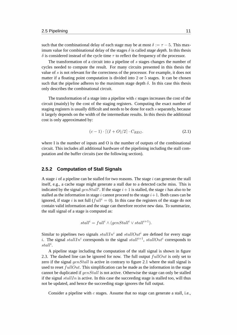
A stagei of a pipeline can be stalled for two reasons. The stagei can generate the stallitself, e.g., a cache stage might generate a stall due to a detected cache miss. This isindicated by the signalgenStalli. If the stagei+1 is stalled, the stagei has also to bestalled as the information in stagei cannot proceed to the stagei+1. Both cases can beignored, if stagei is not full (fulli = 0). In this case the registers of the stage do notcontain valid information and the stage can therefore receive new data. Tosummarize,the stall signal of a stage is computed as:
stalli = fulli ∧ (genStalli ∨ stalli+1).
Similar to pipelines two signalsstallIni andstallOuti are defined for every stagei. The signalstallIni corresponds to the signalstalli+1, stallOuti corresponds tostalli.
A pipeline stage including the computation of the stall signal is shown in figure2.3. The dashed line can be ignored for now. The full outputfullOut is only set tozero if the signalgenStall is active in contrary to figure 2.1 where the stall signal isused to resetfullOut. This simplification can be made as the information in the stagecannot be duplicated ifgenStall is not active. Otherwise the stage can only be stalledif the signalstallIn is active. In this case the succeeding stage is stalled too, will thusnot be updated, and hence the succeeding stage ignores the full output.
Consider a pipeline withc stages. Assume that no stage can generate a stall, i.e.,

12 Basics
data
dataIn
stallOutfull
fullIn
dataOut
genStall
stallIn
stallOut clear
stall
logiccombinational
fullOut
Figure 2.3: A stage with stall computation
genStalli = 0 for all i. This simplifies the computation of the stall signal to:
stalli = fulli ∧ stalli+1
=c−1∧
j=i
fullj ∧ stallIn
Thus, a stage can only be stalled if all succeeding stages are full. Assume stagei isthe non-full stage with the highest index. If the stall input of the pipeline is active allstages with index higher thani are stalled and all stages with index lower or equal toiare not stalled. This removes the invalid information in stagei (called pipeline-bubbleremoval).
Theorem 2.1. If the above implementation of the stall computation is used, the com-binatorial depthD of a pipeline may be at most:
D ≤ δ · 2δ
Proof. Let c be the number of stages of the pipeline. It must holdc ≥ D/δ. The stallsignal for stage0 is computed as AND of the full bits of all stages and the input bit.Thus, the delay is at leastDAND · ⌈log(c + 1)⌉. The stall signal must be computed inone cycle. Thus:
δ ≥ DAND⌈· log(c + 1)⌉ ≥ log(c) ≥ log(D/δ)
⇔ 2δ ≥ D/δ
⇔ δ · 2δ ≥ D
The combinational delay of the multiplicative floating point unit used in this thesisis 168. The theorem bounds the stage depthδ to be larger than5 since5 · 25 = 160.Hence, in order to reduce the stage depth to5 or below, a different implementation forstall computation must be found.

2.5 Pipelining 13
clear
fullBuf
dataOut
genStall
fullBuf
buffe
rci
rcui
tBuf
stallIn
stallIn fullOut dataOut
stallOut fullIn dataIn
1 0
dataBuf
logiccombinational
fullOut
full
fullInstallOut clear
datastallOutstall
dataIn
Figure 2.4: Stage with buffer circuit
2.5.3 Optimization of the Stall Computation
The simplest way to raise the bound given by the theorem is to change the computationof the stall signal such that pipeline-bubbles are no longer removed. Forcorrectness itis usually sufficient to compute the stall signal the following way:
stalli = genStalli ∨ stalli+1.
Yet the minimum stage depth is still bounded by the delay of the OR of all signalsgenStall⋆ and the delay of the stall input of the pipeline. The delay of the stall inputcan be significant, e.g., if the information in the last stage in the pipeline can flow intomultiple succeeding pipeline (as during decode where an instruction can be issued todifferent reservation station (see chapter 3). Then the stall input must be computedfrom the stall output of all acceding pipelines.
The bound given by the signalsgenStall⋆ and the stall input is highly implementa-tion dependent and therefore not treated in detail. Instead a more sophisticated solutionto reduce the bound for the stage depth is described. This solution reduces the delay ofthe stall signals by pipelining the stall computation itself, i.e., registers are inserted inthe stall computation circuit. This can be done by inserting a buffer circuit between theregisters of a stage and the combinational circuit, as shown in figure 2.4. The buffercircuit is inserted at the dashed line of figure 2.3.
As long as the stage is not stalled, the buffer circuit is transparent, i.e. the outputs ofthe buffer circuit are equal to the corresponding inputs. The signalfullBuf is then0and hence connects the data output with the data input. However, if the stageis stalled,the content of the full and data registers is saved in the buffer circuit. Thisenables thestage to receive data from the preceding stage into the input registers without loosing

14 Basics
the current information; the stall needs not to be propagated to the preceding stage. Ifthe buffer circuit contains a valid instruction, the output stall signal is active and thestage is stalled. Hence, the stage is stalled not earlier than one cycle after theinput stallsignal becomes active. As soon as the stage is no longer stalled, the savedinformationfrom the buffer circuit is sent, i.e., the buffer circuit is emptied, before thebuffer circuitgoes back into transparent mode.
The buffer circuit decreases the delay of the signalstallOut to the delay of anAND gate independent of the delay of the stall inputstallIn. It divides the pipelinein two pipelines with smaller stall circuits. Hence, the maximum combinational delayis not longer limited by the stall signals. Note that each buffer circuit increases thecombinational delay of the pipeline by the delay of a mux. The correctness ofthebuffer circuit is summarized in the following theorem. Note that the theorem onlyhandles the buffer circuit. Thus the signals used in the theorem as, e.g.,stallIn andstallOut describe the inputs and output of the buffer circuit and not the stage.
Theorem 2.2. Assume the inputs of the buffer circuit obey the following properties.The clear signal is active exactly in cycle 0:
clear(t) =
{
1 if t = 0
0 if t > 0. (P0)
The signalstallIn is live:
∀t > 0∃t′ : t′ > t ∧ stallIn(t′) = 0. (P1)
The data of all instructions which enter the buffer circuit are distinguishable:
∀t, t′ > 0 :fullIn(t) = fullIn(t′) = 1 ∧ stallOut(t) = stallOut(t′) = 0
∧ dataIn(t) = dataIn(t′) ⇒ t = t′. (P2)
Then the buffer circuit adheres to the following statements:The buffer circuit is empty in cycle1:
fullBuf (1) = 0. (S0)
The signalstallOut is live.
∀t > 0∃t′ : t′ > t ∧ stallOut(t′) = 0. (S1)
Every instruction which enters the circuit leaves the circuit exactly in the next possiblecycle:
∀t > 0 : fullIn(t) = 1 ∧ stallOut(t) = 0
⇒ {t′|fullOut(t′) = 1 ∧ stallIn(t′) = 0 ∧ dataOut(t
′) = dataIn(t)} (S2)
= {min{t′ ≥ t|StallIn(t′) = 0}}
The ability to distinguish the instruction is needed for statement (S2). It can bereached by adding a unique index to every instruction.1 Since this index has no influ-ence on the behavior of the buffer circuit, it must not be implemented in hardware toreach correctness. It is merely a means to state the theorem.
1It is a common trick to use a infinite set of tags for a completeness criterion.In can be proven lateron that a finite set suffices for correctness as, e.g., in [BJK+03].

2.5 Pipelining 15
Proof. Statement (S0): The statement follows directly from the construction of theclear signal.
Statement (S1): The output stall signal may only be active if the input stall signalwas active in the preceding cycle.
stallOut(t) = fullBuf (t)
= (fullBuf (t−1) ∨ full(t−1)) ∧ stallIn(t−1)
≤ stallIn(t−1)
The statement follows from property (P1).Statement (S2): The equivalence of the sets is proven in two steps.
“⊇” Let t be such thatfullIn(t) = 1 andstallOut(t) = 0. It follows:
fullBuf (t) = stallOut(t) = 0. (2.2)
Let t′ bemin{t′ ≥ t|StallIn(t′) = 0}. The following two cases can be distin-guished:
t′ = t: It follows:
fullOut(t′) = fullOut(t) = fullIn(t) ∨ fullBuf (t) (2.2)
= fullIn(t) = 1,
dataOut(t′) = dataOut(t) =
{
dataBuf (t) if fullBuf (t) = 1
dataIn(t) if fullBuf (t) = 0
(2.2)= dataIn(t).
t′ 6= t: Hence,stallIn(t) = 1. If follows:
fullBuf (t+1) = (fullBuf (t) ∨ fullIn(t)) ∧ stallIn(t) ≥ fullIn(t) = 1,
dataBuf (t+1) =
{
dataBuf (t) if fullBuf (t) = 1
dataIn(t) if fullBuf (t) = 0
(2.2)= dataIn(t).
By definition oft′ for all t with t < t < t′ holdsstallIn(t) = 1. For theset the following can be proven by induction:
fullBuf (t+1) = (fullBuf (t) ∨ full(t)) ∧ stallIn(t)
≥ fullBuf (t) (Ind.)= 1, (2.3)
dataBuf (t+1) =
{
dataBuf (t) if fullBuf (t) = 1
dataIn(t) if fullBuf (t) = 0
= dataBuf (t) (Ind.)= dataIn(t). (2.4)
16 Basics
Thus, the content of the registersfullBuf anddataBuf does not changeas long asstallIn andfullBuf are active. For the cyclet′ it follows:
fullOut(t′) = fullIn(t′) ∨ fullBuf (t′) (2.3)
= 1,
dataOut(t′) =
{
dataBuf (t′) if fullBuf (t′) = 1
dataIn(t′) if fullBuf (t′) = 0
(2.3)= dataBuf (t′) (2.4)
= dataIn(t).
Thus,t′ is in the set{t′|fullOut(t′) = 1 ∧ stallIn(t′) = 0 ∧ dataOut(t
′) =dataIn(t)}
“⊆” Let t′ be such thatfullOut(t′) = 1, stallIn(t′) = 0 anddataOut(t
′) = data(t).Let t′′ bemax{t′′ < t′|stallOut(t
′′) = 0}. It follows:
fullBuf (t′′) = stallOut(t′′) = 0 (2.5)
t′′ = t′: If follows:
fullIn(t′′) (2.5)= fullIn(t′′) ∨ fullBuf (t′′) = fullOut(t
′′)
= fullOut(t′) = 1
dataOut(t′) = dataOut(t
′′) =
{
dataBuf (t′′) if fullBuf (t′′) = 1
dataIn(t′′) if fullBuf (t′′) = 0
(2.5)= dataIn(t′′)
t′′ 6= t′: Hence,fullBuf (t′) = stallOut(t′) = 1. It follows:
dataOut(t′) =
{
dataBuf (t′) if fullBuf (t′) = 1
dataIn(t′) if fullBuf (t′) = 0
= dataBuf (t′)
By definition of t′′ for all t with t′′ < t < t′ holdsstallOut(t) = 1. Fortheset the following can be proven by induction:
fullBuf (t) = stallOut(t) = 1 (2.6)
stallIn(t) ≥ stallIn(t) ∧ (fullBuf (t) ∨ fullIn(t))
= fullBuf (t+1) (2.6)= 1
dataOut(t′) (Ind.)
= dataBuf (t+1) =
{
dataBuf (t) if fullBuf (t) = 1
dataIn(t) if fullBuf (t) = 0
(2.6)= dataBuf (t) (2.7)

2.5 Pipelining 17
genStallfullBuf ′
(a)
stallIn
genStall
≡
fullBuf
clear
full
fullBuf ′
stallIn
(b)
clear
full
fullBuf
Figure 2.5: Optimized computation offullBuf ′
For the cyclet′′ it follows:
fullBuf (t′′) = stallOut(t′′) = 0 (2.8)
stallIn(t′′) ≥ stallIn(t′′) ∧ (fullBuf (t′′) ∨ fullIn(t′′))
= fullBuf (t′′+1) (2.6)= 1
dataOut(t′) (2.7)
= dataBuf (t′′+1) =
{
dataBuf (t′′) if fullBuf (t′′) = 1
dataIn(t′′) if fullBuf (t′′) = 0
(2.8)= dataIn(t′′)
From the property (P2) it followst′′ = t. As stallIn(t) = 1 for all t ≤ t < t′ itfollows: t′ = min{t′ ≥ t|StallIn(t′) = 0}.
2.5.4 Maximum Delay of Stall Inputs
Let the stagei of a pipeline have a buffer circuit and assume none of the stagesj ∈{i + 1, . . . , n} for ann ≥ i has a buffer circuit. For all stagesj the AND-gate thatforces the clocking of the full register in case the clear signal is active (see figure 2.3)can be removed from the critical path by rebalancing. The computation of thestallsignal for stagei comprises the stall signals for all stagesj. Hence, the delay of thestall signals for all stagesj is at most as high as the delay of the input of the registerfullBuf in the buffer circuit of stagei (see figure 2.4). Thus, if the delay of this signalfullBuf i′ is at mostδ the stall signals for all stagesj can be computed in one cycle.Therefore, only the stages with a buffer circuits have to be checked whether the delayof the stall inputs is too large.
Figure 2.5(a) details the computation of the signalfullBuf ′ from figure 2.4. Thestall inputstallIn usually is computed by an AND-Tree. If the signalgenStall is notconstantly zero the OR-gate hinders the integration of the last AND-gate into this tree.If the order of the gates is switched using the distributive law as shown in figure 2.5(b),the AND-gate can be integrated into the tree in order to reduce the delay.
Figure 2.6 depicts an example of the integration into the AND tree if the stall inputis computed as AND of the signalsfull1 to fullk. The overall delay of the circuitis equivalent to the delay of the AND-tree of the full bits with1 + 2⌈DOR/DAND⌉
additional inputs (i.e.,3 additional inputs if the delay of AND and OR gates is equal as

18 Basics
clear
full1...k
⌈DOR/DAND⌉
≡
full1...k
clear
full
fullBuf
fullBuf
full
Figure 2.6: Merging logic into the tree of the stall input computation
in the gate model used in this thesis). Hence, if the input stall signal of a buffer circuitis computed by an AND-tree withk inputs and the stage with the buffer circuit cannotgenerate a stall, the signalfullBuf ′ can be computed in one cycle if:
δ ≥ D(AND-tree(k + 3)).
If the stage with the buffer circuit can generate a stall the delay of the inputofthe registerfullBuf increases be the rightmost OR-gate in figure 2.5(b). Thus, thefollowing equation must hold:
δ ≥ D(AND-tree(k + 3)) + DOR.
Let i be chosen as above andn be the length of the pipeline. Then, the input of theregisterfullBuf of stagei depends on the input stall signalstallIn of the pipeline.If the stagei cannot generate a stall, it holds:
fullbuf i′ = (fullBuf i ∨ fulli) ∧ clear ∧n∧
j=i+1
fullj ∧ stallIn
Thus, if the stall inputstallIn is computed by an AND-Tree withl inputs it must hold:
D(AND-Tree(n − i + 3 + l)) ≤ δ.
If stallIn cannot be merged into the AND-tree of the full signals it must hold:
D(AND-Tree(n − i + 3)) ≤ δ − DAND and
D(stallIn) ≤ δ − DAND. (2.9)
The delay of the stall computation increases by at leastDOR if any stagej fori ≤ j ≤ n can generate a stall. Thus, in order to minimize the restrictions for the stallinputstallIn, i should be chosen such that no such stagej can generate a stall. If laststage of a pipeline can generate a stall,i cannot be chosen as above. It must then hold:
D(stallIn) ≤ δ − (DOR + DAND). (2.10)
2.6 Pipelining of RAM Blocks
In order to reduce the access time of a RAM block it is mandatory to also pipelinethe RAM block. A schematic view of a RAM block withn address bits andm data

2.6 Pipelining of RAM Blocks 19
Decm
dataout
Select
2n
addr
n
m
write
datain
Decode
m · 2n
Update
Figure 2.7: Schematic view of a RAM block
Read.addr Write.⋆
W.⋆R.addrW.⋆R.addr
RAMdata
R.data
dataout
ForwardRAM
Figure 2.8: Forwarding of a write port
bits is shown in figure 2.7. A RAM block can be divided into three parts: the decodeof the address bus, the update of the data registers and the selection of theaddresseddata [KP95].
Inserting registers in the decode and the select stage allows for smaller cycle times.However a read access to such a pipelined RAM takes into account only thewriteaccesses that have been started before the read access. At the time the result of aread access is on the output data bus, the accessed address may already be overwrittenby a succeeding write access. Thus, the RAM only returns the value of theaccessedaddress at the time the read access entered the RAM. However in many applications inthis thesis the read access must return the value of the accessed addressat the time itleaves the RAM. To obtain the latest value of an address, all write accesses that havebeen started after the read access have to be forwarded to the output ofthat read.
2.6.1 Forwarding
If forwarding is used it could happen that an instruction does not enter or leave theRAM environment in the same cycle in which the instruction enters respectivelyleavesthe RAM block. In the following the term “a RAM access is started” always meansthat the access enters the RAM environment (which is usually as soon as allsignalsneeded for the access are available). “An access finishes” always means that the accessleaves the RAM environment.
The forwarding of a write portW to a read portR is done using the forwardingcircuit from figure 2.8. If the RAM block is pipelined intoc stages, the forwardingcircuit is also divided intoc stages. The stages of the forwarding circuit contain thedata corresponding to the read access in the corresponding stage of theRAM block.
In every cycle the forward circuit compares the newly started write access with all

20 Basics
datai
s−
1tim
es
dataUpdi−1
addri
TestTest.datai
forwi
TestTest.data0
Test.forward0
R.addr
dataUpdiforwUpdi
forwUpdi−1
Test.forwardi
forwOut dataOutaddrOut
RAM.data
W.{write, addr}
1
naddr
W.data
forward
data
EQ
m
n + 1
Test
W.{addr, write, data}
01
0 1
Figure 2.9: Forwarding circuit (with sub-circuitTest)
read accesses of all stages. If the write access overwrites the same address as a readaccess in the pipeline, the corresponding stage of the forwarding circuitis updated withthe new write data. At the last stage of the forwarding circuit the read result is selectedbetween the output of the RAM block and the data potentially saved in the forwardingcircuit. In that way any write data to the read address is forwarded.
The details of the forwarding circuit are shown in figure 2.9. The address of theread access in stagei is saved in the registeraddri. The registerforwi carries theinformation whether the stagei of the forwarding circuit holds valid forwarded writedata. In that case the data of the last forwarded write access is saved in the registerdatai. The stagei computes the updated valuesforwUpdi anddataUpdi, which takethe current write access onW.⋆ into account. The outputs of stagei are saved in theregisters of stagei + 1.
A write access is forwarded to the read access in stagei, if the write signal isactive and the address of the accesses are equal. This is indicated by thesignalTest.forwardi computed by the sub-circuitTest shown in the left part of figure2.9. For simplicity the circuit also bypasses the data of the write access to the outputTest.datai. Using the signalsTest.forwardi andTest.datai, the updated valuesforwUpdi anddataUpdi can be computed as:
forwUpdi = forwi ∨ Test.forwardi,
dataUpdi =
{
Test.datai if Test.forwardi = 1
datai if Test.forwardi = 0.
At the last stagec − 1 of the forwarding circuit, the signalforwUpdc−1 is active,if there has been a write access started after the read access, which hasoverwrittenthe content of the accessed address. In this case the signaldataUpdc−1 contains thenewest content of the RAM address. IfforwUdpc−1 is not active, the output of theRAM RAM.data contains the correct value. Hence, the current content of the ac-cessed address can be computed as:
dataOut =
{
dataUpdc−1 if forwUpdc−1 = 1
RAM.data if forwUpdc−1 = 0.
2.6 Pipelining of RAM Blocks 21
TestTest.forwardi
Test.datai
addri forwi datai
s−
1tim
es
stalli
stalli
W.{addr, write, data}
forwUpdi−1 dataUpdi−1
dataUpdiforwUpdi
01
0 10 1
TestTest.forward0
Test.data0
R.addr
0 1
RAM.data
forwOut dataOutaddrOut
Figure 2.10: Forwarding circuit with stalling
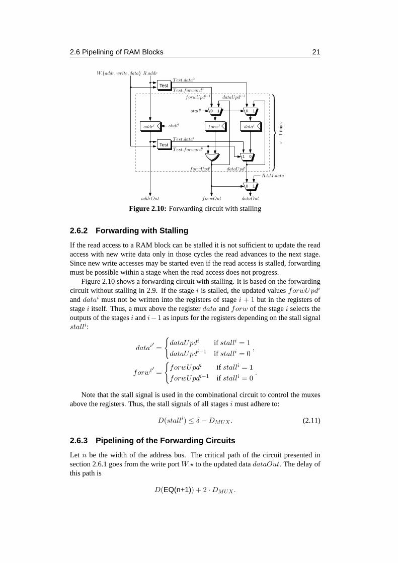
2.6.2 Forwarding with Stalling
If the read access to a RAM block can be stalled it is not sufficient to updatethe readaccess with new write data only in those cycles the read advances to the nextstage.Since new write accesses may be started even if the read access is stalled, forwardingmust be possible within a stage when the read access does not progress.
Figure 2.10 shows a forwarding circuit with stalling. It is based on the forwardingcircuit without stalling in 2.9. If the stagei is stalled, the updated valuesforwUpdi
anddatai must not be written into the registers of stagei + 1 but in the registers ofstagei itself. Thus, a mux above the registerdata andforw of the stagei selects theoutputs of the stagesi andi−1 as inputs for the registers depending on the stall signalstalli:
datai′ =
{
dataUpdi if stalli = 1
dataUpdi−1 if stalli = 0,
forwi′ =
{
forwUpdi if stalli = 1
forwUpdi−1 if stalli = 0.
Note that the stall signal is used in the combinational circuit to control the muxesabove the registers. Thus, the stall signals of all stagesi must adhere to:
D(stalli) ≤ δ − DMUX . (2.11)
2.6.3 Pipelining of the Forwarding Circuits
Let n be the width of the address bus. The critical path of the circuit presented insection 2.6.1 goes from the write portW.⋆ to the updated datadataOut. The delay ofthis path is
D(EQ(n+1)) + 2 · DMUX .

22 Basics
tmpUpdi−1
tmpUpdi+1
tmpi+1
1 0
Test
Test
W.⋆
dataUpdi
dataUpdi−1
addri
addri+1
tmpi forwi datai
1 0
datai+1forwi+1
forwUpdi−1
dataUpdi+1forwUpdi+1
forwUpdi
addri+1
addri−1
Figure 2.11: Pipelined forwarding circuit
010 0 1 0 1
stall
stall
Test1 Test2
addri tmp1i
1 0
tmp2i forwi datai
addri−1 tmp1Updi−1 tmp2Updi−1 forwUpdi−1 dataUpdi−1W.⋆
dataUpdiaddri tmp1Updi tmp2Updi forwUpdi
1
Figure 2.12: Pipelined forwarding circuit with stalling
To reduce the cycle time below this bound, the path from the write port to theupdated data must be pipelined. The intermediate results of the pipelined computationare stored in registers and flow together with address, forward bit and data through thepipeline of the forwarding circuit. Figure 2.11 depicts as an example the stages i andi + 1 of a forwarding circuit without stalling where the computation of the updateddata is split after the circuitTest. The registertmpi+1 is used to store the outputs ofthe circuitTest and to pipeline them into the next forwarding stage.
The forwarding circuit is now pipelined in two dimensions. Within the same cyclethe read access moves to the next stage of the forwarding circuit and the computationof the updated data moves to the next part of the computation (see the path highlightedin figure 2.11). While the computation of the updated data for one write accessmovesto the second part, a new computation can be started for the next write access.
In the forwarding circuit with stalling the forwarding of the write port must proceedto the next part of the computation even if the instruction does not move to the nextstage of the forwarding circuit. Therefore, above every register saving the temporaryresults a multiplexer is added. This multiplexer selects depending on the stall signalwhether the register is updated with the output of the current or the preceding stage(analogously to the multiplexers above the forward bit and the data registersin figure2.10).
Figure 2.12 depicts as an example a stagei of a forwarding circuit with stalling,where the circuitTest is divided into two circuitsTest1 and Test2 and pipelining

2.6 Pipelining of RAM Blocks 23
registers are added after both circuits. The path highlighted in the figure shows theforwarding of the write port if the stage is stalled twice.
In order to pipeline the computation of the updated data in the forwarding circuitwithout stalling (calledForward), the computation must be divided into parts witha combinational delay of at mostδ. In the forwarding circuit with stalling (calledForwardStall), every inserted pipelining register increases the combinational delayfrom the write input to the updated data by the delay of the multiplexer above theregister. Hence, for the circuitForwardStall the computation of the updated data mustbe divided into parts with a combinational delay of at mostδ − DMUX .
Note that the new values written into the registerforw anddata in the circuitForwardStall depend on the previous value of the registers. If a pipelining registerwould be added into this path, old data would be used to update the registers. Forthe data register this would mean that it holds the correct data only every other cycle.A general solution to pipeline these one-cycle dependencies cannot be given, but theresulting bound to the stage depth from this dependency is acceptable:
δ ≥ max{DOR, DMUX} + DMUX (2.12)
In our gate model this only requires thatδ ≥ 4.
Compensating the pipelining cycles
Assumek pipeline registers are inserted into each stage of the forwarding circuit. Thenthe forwarding circuit needsk + 1 cycles to forward the write port into the data regis-ters. Thus, the write accesses which have been started in the lastk cycles before theread access is finished are not taken into account for the read result. Due to the pipelin-ing it is not possible to take all writes into account that have been started before a readaccess, but it often suffices to take all those writes into account, that have entered theRAM block at the time the read access finishes.
For a read access in order to take into account all the write accesses thathaveentered the RAM block at the time the read is finished, forwarding must be started atleastk cycles before the write accesses enter the RAM block. This can be done bydelaying the write port byk cycles and forwarding the un-delayed writes (see figure2.13(a)).
Due to delaying of the write port, the up tok write accesses in the registersW1.⋆to Wk−1.⋆ have been started before the read access but not yet entered the RAMblock.If the read access directly enters the RAM block when its started, thesek writes arenot taken into account for the result of the RAM block. Therefore, the read port is alsodelayed byk cycles. The forwarding circuit must be increased byk stages to alignwith the read access.
Delaying the write port usually has no impact on the performance (as long astheun-delayed write is forwarded). The delaying of the read port of the RAM increasesthe overall delay of the read access and therefore the overall delay ofthe circuit wherethe RAM is used.
Figure 2.13(b) shows a solution to take thek writes started directly before the readaccess into account for the result without delaying the read access. Atthe time the readis started, the addresses, write signals and data of thesek write accesses are known and

24 Basics
W.⋆R.addr
RAMdata
R.data
RAM
(a)
W1.⋆
Wk−1.⋆
W.⋆
≡
R.addr
Forward
W.⋆R.addr
RAMdata
R.data
RAM
W⋆.⋆
W1.⋆
Wk−1.⋆
R.addr
(b)
W0.{addr, write, data} W0.{addr, write, data}
W.⋆
Forward
R.addr
Read.addrRead.addr
dataout
ForwardTree
dataout
Figure 2.13: Forwarding with pipelined forwarding circuit
forw
Forw
In1.forw In2.forw
R.addr W1.⋆ Wk.⋆
dataOut
RAM.data
Forw
01
data
In1.data In2.data
Test Test
01
Figure 2.14: Forwarding Tree
stored in the registersW1.⋆ to Wk−1.⋆. These write accesses are forwarded separatelyusing a forwarding tree.
A circuit for a forwarding tree withk inputs is depicted in figure 2.14. All writeaccesses are tested in parallel using the circuitTest. The circuitForw computes fromthe signalsforw anddata of two successive write accesses the combined values ofthe signalsforw anddata. The write access at inputIn1.⋆ is assumed to be startedafter the write access at inputIn2.⋆. Thus, the inputIn1.⋆ has higher priority. If theforward bitIn1.forw is active, the busIn1.data is the new data output, otherwise thebusIn2.data. The outputforw is active if either of the inputsIn⋆.forw is active.The circuitsForw can be arranged in a tree structure due to following lemma.
Lemma 2.3. The function
◦ : B2 × B
2 7→ B2, (f1, d1) ◦ (f2, d2) → (f1 ∨ f2, f1d1 ∨ f1d2)
is associative

2.6 Pipelining of RAM Blocks 25
Proof.
((f1, d1) ◦ (f2, d2)) ◦ (f3, d3) = (f1 ∨ f2, f1d1 ∨ f1d2) ◦ (f2, d2)
= (f1 ∨ f2 ∨ f3, (f1 ∨ f2)(f1d1 ∨ f1d2) ∨ (f1 ∨ f2)d3)
= (f1 ∨ f2 ∨ f3,
f1f1d1 ∨ f1f1d2 ∨ f2f1d1 ∨ f2f1d2 ∨ f1f2d3)
= (f1 ∨ f2 ∨ f3, f1d1 ∨ f1f2d2 ∨ f1f2d3)
= (f1 ∨ f2 ∨ f3, f1d1 ∨ f1(f2d2 ∨ f2d3))
= (f1, d1) ◦ (f2 ∨ f3, f2d2 ∨ f2d3)
= (f1, d1) ◦ ((f2, d2) ◦ (f3, d3))
Using the pipelined forwarding circuit it is possible to compute the content of aRAM block at the time a read access is returned even for a small stage depthδ. How-ever the write accesses which have been started but have not yet entered the RAMblock at the time the read access finishes cannot be forwarded. Additionally delayingthe write port may have further implications to the circuit writing the RAM. There-fore, in the following sections for every RAM it is discussed which and howthe writeports are forwarded to the read ports and why the forwarding sufficesto guarantee thecorrectness.
2.6.4 Cost and Delay
If forwarding can be done without using a forwarding tree, the read access to the RAMis delayed by an additional mux for selecting between the forwarding data and theRAM output into the forwarding circuit. If a forwarding tree is used (it is assumedto be faster than the RAM access), the access is delayed by two muxes for selectingbetween the RAM output, the data output of the forwarding tree and the data output ofthe forwarding circuit (see figure 2.13(b)).
The longest combinational path for both forwarding circuits is the path fromtheinputsW.⋆ to the outputsdataOut. Let n be the number of address bits. Then thedelay of the forwarding circuits are:
D(ForwardStall(n)) ≤ D(Test(n)) + 2 · DMUX ,
D(Forward(n)) ≤ D(Test(n)) + 2 · DMUX .
When pipelining the circuitForward with n address bits the computation of the out-puts from the inputsW.⋆ takes
cF (n) ≤
⌈
D(Forward(n))
δ
⌉
.
cycles. In order to pipeline the circuitForwardStall an additional mux is neededbefore every inserted register. Thus, the pathW.⋆ dataout must be divided into

26 Basics
parts with combinational delay ofδ − DMUX . In the last stage no additional mux isneeded. Thus, the computation of the outputs of the circuit takes
cFS(n) ≤
⌈
D(Forward(n)) − DMUX
δ − DMUX.
⌉
cycles (if it is not stalled).
Let n be the number of address bits,m the number of data bits, andc be thenumber of stages of the forwarding circuits. Without temporary registers the cost ofthe forwarding circuits is:
C(Forward(n, m, c)) ≤ C(Test) + m · CMUX + (c − 1) · (C(Test)
+ (m + n + 1) · CREG + COR + m · CMUX),
C(ForwardStall(n, m, c)) ≤ C(Forward(n, m, c)) + (c − 1) · (m + 1) · CMUX .
Let cF andcFS be the minimum number of cycles needed for forwarding respec-tively forwarding with stalling. The total cost of the forwarding circuits are(approxi-mated with equation 2.1):
C(Forward(n, m, c, cF ) ≤ C(Forward(n, m, c)) + (c − 1) · cF
· ⌈((m + n + n + 1) + (m + 1))/2 · CREG⌉
≤ C(Forward(n, m, c)) + (c − 1) · cF
· (m + n + 1) · CREG.
C(ForwardStall(n, m, c, cFS) ≤ C(ForwardStall(n, m, c)) + (c − 1) · cFS
· ⌈((m + n + n + 1) + (m + 1))/2⌉
· (CREG + CMUX)
≤ C(Forward(n, m, c))
+ (c − 1) · cF · (m + n + 1) · (CREG + CMUX).
The cost of the forwarding tree withk inputs (without registers) is:
C(ForwardTree(n, m, k)) ≤ k · C(Test) + (k − 1) · C(Forw) + m · CMUX .
The forwarding tree needs to be divided into as many stages as the RAM access. Letc be the number of stages of the RAM access. Then the total cost of the pipelinedforwarding tree is approximately:
C(ForwardTree(n, m, k, c) ≤ C(ForwardTree(n, m, k)) + (c − 1)
· ⌈((k · (m + n + n + 1)) + m + 1)/2⌉ · CREG
≤ C(ForwardTree(n, m, k))
+ (c − 1) · k · (n + m + 1) · CREG.

Chapter 3
Tomasulo Algorithm
The DLX variant presented by Kroning which the DLXπ+ is based on, uses the Toma-sulo algorithm [Tom67] to execute instructions out-of-order which allows for low CPIratios [MLD+99]. It is assumed that the reader is familiar with this algorithm. There-fore this chapter gives only an informal description of the algorithm to define the termsused throughout this thesis. A formal description including correctness proofs can befound, e.g., in [KMP99].
The description of the Tomasulo algorithm is divided into three parts. In section 3.1a general overview is given which defines the most important terms. Section3.2 de-scribes the basic data structures used by the algorithm. Finally in section 3.3 thealgo-rithm is presented in more detail showing the execution of an example instruction.
3.1 Overview
For the Tomasulo algorithm every instruction which is being processed needs to beidentified by a unique number. This number is calledtag. The instructions which areprocessed at a given time are calledactive instructions.
Figure 3.1 shows an overview of the Tomasulo hardware. The instruction fetch unitdoes not differ from in-order processors. It loads the instruction stream from the mainmemory and delivers it in-order to the decode environment. In the decode environmentthe operands of the instructions are determined. If an operand is not computed yet,the decode environment determines the tag of the instruction which will compute theoperand. Afterward the instruction is sent to a reservation station.
The instructions wait in the reservation stations until all operands are valid.Thereservation stations check if the CDB carries the result of an instruction thatis neededas operand for a waiting instruction. If this is the case the data is copied and theoperand is validated. This forwarding from the CDB is calledsnooping. As soon asall operands are valid, the instruction is sent to a functional unit, independent of theinstruction order.
The functional unit computes the result of the instruction and writes it to the com-mon data bus. The common data bus forwards the result to the reservation stations andwrites it in the reorder buffer. The reorder buffer reorders the instruction in programorder before it writes the result in the register file.

28 Tomasulo Algorithm
retire
complete
execute
dispatch
decode
fetch
Decode Environment
Instruction Fetch Unit
Register File Environment
Com
mon
Dat
aB
us
Reorder Buffer Environment
ReservationStation
FunctionalUnit
ReservationStation
FunctionalUnit
Figure 3.1: Overview of the Tomasulo hardware
mnemonic functional unitBCU branch checking unitMem memory unitIAlu integer ALUIMul integer multiplicative unitFAdd floating point additive unitFMul floating point multiplicative unitFMisc floating point miscellaneous unit
Table 3.1: Functional units types of the DLXπ+
3.2 Basic Data Structures
3.2.1 Functional Units
The functional units(FUs) perform the actual execution of the instructions. A proces-sor can have different FU types, each executing only subsets of the instruction set.Multiple FUs of the same type are supported. The FU types of the DLXπ+ are listedin table 3.1. Tables A.1 to A.7 in the appendix list all DLXπ+ instructions sorted bythe type of their functional unit.
3.2.2 Register Files and Producer Tables
The DLXπ+has three differentregister files(RF): the general purpose register file(GPR), the floating point register file (FPR), and the special purpose register file (SPR).For every register file entry, the Tomasulo algorithm additionally stores a validbit anda tag field. If no active instruction will write a register file entry, the content of theregister file can be used as operand of a new instruction. In this case the valid bit of theregister file entry is set to one. If one or more active instructions will write anentry,the valid bit is zero and the tag field stores the tag of the youngest active instructionwhich will write this entry.

3.3 Instruction Execution 29
The valid bits and the tag bits of the register file entries are saved in theproducertables(PT). Usually the producer tables have more access ports than the register files.Therefore, they are saved in different RAM blocks.
3.2.3 Reservation Stations
The reservation stations(RS) consist of multiple entries. Each entry can hold oneinstruction. The instructions wait in the entries until all operands are valid. To keeptrack of the state of the operands, each operand of an entry has a valid bit and a tag field,either indicating that the data in the entry is already valid or identifying the instructionwhich will eventually compute the value of the operand data.
The DLXπ+has exactly one reservation station (of multiple entries) for every func-tional unit. Therefore, the reservation station if often identified with its functional unit.It is also possible to use only one reservation station per instruction type or even onlyone global reservation station [HP96]. For simplicity the latter cases are nottreated inthis thesis.
3.2.4 Common Data Bus
All functional units write the instruction results to thecommon data bus(CDB). Toidentify the current result on the CDB, the CDB has a valid and tag field. Thisrelatesthe result to the instruction which computed that result. The common data bus writesthe result to the reorder buffer. Also, the result is forwarded to the reservation stations.This allows the reservation stations to snoop on the CDB, i.e., check whether the resultis needed as operand for a waiting instruction.
3.2.5 Reorder Buffer
The reordering of the instructions before the update of the register files isdone by thereorder buffer(ROB). For every instruction, an entry in the reorder buffer is allocatedin program order. For each entry the reorder buffer has a valid bit. This bit is activeif the result of the instruction has already been computed. If the valid bit of the oldestinstruction in the ROB is active, the instruction is removed from the ROB in orderto write its result to the register file. The address of the reorder buffer entry of aninstruction is used as tag for the instruction.
3.3 Instruction Execution
The execution of an instruction is done in six phases: fetch, decode, dispatch, execute,complete, and retire. The instruction fetch does not differ from in-orderprocessors.Let I be an instruction which is being executed by the processor.
3.3.1 Decode
In the decode phase the opcode of the instructionI is decoded and the valid bit, thetag, and the data field of the operands are determined. The producer tableentry ofthe destination register ofI is updated and a new entry forI is reserved in the reorder

30 Tomasulo Algorithm
buffer. Afterward the instruction is sent to the reservation stations. This last step iscalledissue.
The decoding of the instructionI is straightforward and does not differ much froman in-order processor. The decode environment computes the addresses of the operandand the destination registers as well as the control signals used by the functional units.
For each operand the decode phase must determine the valid bit, the tag, andthedata field. The correct value for the data field of an operand can be found at one offour different places:
• The register file: If no preceding active instruction writes the register file entry,the register file contains the valid data for the operand. In this case the validbit of the corresponding producer table entry is set. If the valid bit is not set,the valuetagP of the tag field of the producer table entry identifies the latestinstructionIP which will compute the value of the operand.
• The reorder buffer: If the instructionIP has already completed but is not retiredyet, the data for the operand can be found in the reorder buffer. This can betested by checking the valid bit of the reorder buffer entry of the instruction IP .Note that the address of the entry ofIP in the reorder buffer istagP .
• The common data bus: If the instructionIP is about to complete, the operandcan be found on the CDB. This is the case if the valid bit of the CDB is activeand the tag of the CDB equalstagP .
• The reservation stations or the functional units: In this case the value of theoperand is not computed yet.
In the first three cases the valid bit of the operand can be set to one and the data can betaken from the corresponding place. In the last case, the valid bit of the operand has tobe set to zero and the tag field of the operand is set totagP . Then the instruction willwait in the reservation station until the result of the instructionIP (identified bytagP )becomes available on the CDB.
In parallel to the determination of the operands, the decode phase reserves a newentry in the ROB for the instructionI. For this the valid bit of the entry is reset. All theinstruction’s information which are known at decode time (e.g., the destination registeraddress) are written into the corresponding ROB fields. Lettag be the address of thereorder buffer entry ofI.
For the succeeding instructions to use the correct data, the producer table entry ofthe destination register of the instructionI is updated. The valid bit of the entry is setto zero and the tag is set totag. This tells succeeding instruction that the new value ofthe register will be computed by instructionI.
At the end of the decode phase the instruction is sent to the reservation station ofthe functional unit that corresponds to the type of the instruction. If multiple func-tional units respectively reservation stations of one type exist, one of these reservationstations has to be chosen. In this thesis the first reservation station that is notfull isused.

3.3 Instruction Execution 31
3.3.2 Dispatch
The instructionI waits in the reservation station until all of its operands are valid.Assume an operand ofI is not valid and depends on instructionIP . The Decode phaseguarantees that in this case the instructionIP is in a reservation station or a functionalunit (see above). Hence, the result ofIP will eventually be sent via the common databus. The reservation station entry of instructionI snoops on the CDB for the tagtagP
of the instructionIP . If the tag of the CDB matchestagP and the valid bit of the CDBis active, the data of the CDB is copied to the data field of the operand and the operandis marked as valid in the reservation station.
As soon as all operands are valid, the instructionI is sent to the functional unit(dispatch). If multiple instructions in a reservation station are valid at the same time,the oldest instruction is dispatched.
3.3.3 Execute
During the execute phase, the actual execution of the instruction is performed. This isdone in the functional units. The functional units do not necessarily return the instruc-tions in the order they enter. For example a floating point multiplication can overtakea floating point division [Jac02].
3.3.4 Completion
During the completion phase the results of the functional units are written to the ROBand forwarded to the reservation stations via the CDB. The number of functional unitsis usually larger than the number of results which fit on the CDB. Therefore, an arbiterdecides which functional unit with an available result may write to the common databus. During the completion phase the valid bit of the ROB entry of the instructionisset to one.
3.3.5 Retire
The original Tomasulo algorithm [Tom67] writes the register files out-of-order. Forprecise interrupt handling it is necessary to be able to restore the contentof the registerfile as if the instructions would be executed in order. This can be very complex if in-structions write the register file out-of-order. Therefore, the instructionsare reorderedinto program order before updating the register files using the ROB [SP85].
To restore the program order, only the oldest instruction in the ROB is checkedfor whether it has already completed. In this case the instruction is taken outof thereorder buffer and the result is written into the destination register entry ofthe registerfiles. The valid bit of the register file can then be set to flag valid data unless ayoungeractive instruction writes to the same register.
In order to check whether a younger active instruction will write the same register,the producer table entry of the destination register is read. If the tag storedin theproducer table matches the tag of the instructionI no younger instruction may writethe same destination register. Otherwise it would have updated the tag of the producertable entry. In this case the valid bit of the producer table entry can be set.

32 Tomasulo Algorithm
In the retire phase the instruction is also checked whether it causes an interrupt orwhether a branch misprediction occurred. In these cases all succeedinginstructions areinvalid and the processor has to be flushed. Since the register file is in a sequentiallycorrect state, the producer table entries are all set to valid to indicate that no instructionswill write the registers.

Chapter 4
Processor Core
In this chapter the design of the DLXπ+ core (without instruction fetch unit) is pre-sented. The stage depth of the presented design is variable and is assumedto be atleast 5 gate delays. Sections 4.1 to 4.5 describe the hardware for the five phases of theinstruction processing in the core (decode, dispatch, execute, completion, and retire).Since the main RAM structures are accessed in multiple phases, they are describedafterwards in the sections 4.6 to 4.8.
The design of the core is based on the Tomasulo DLX of Kroning [Kro99]. Split-ting of the ROB into multiple smaller RAMs to reduce the number of ports was intro-duced by Hillebrand [Hil00]. Yet almost all non-trivial circuits had to be redesigned inorder to maximize the performance and to allow a stage depth of 5 gate delays.
4.1 Decode
4.1.1 Overview
The decode phase is divided into the two sub-phasesD1 andD2. In the sub-phaseD1 the instruction word is decoded and the control signals for the instruction are com-puted. The valid bit, the tag, and the data of the operands are read from thecurrentcontent of the producer tables respectively register files. In the sub-phaseD2 the in-struction is issued to a reservation station corresponding to the type of the instruction.In parallel the reorder buffer is checked if any of the instruction identified by the tagsof the operands have already completed. If this is the case, the valid bit andthe datafield of the operand are updated. The decode phase uses the instructionregister asinput. The instruction register environment is described in section 6.4 as part of thethe instruction fetch chapter.
Sub-phase D1
Figure 4.1 gives an overview of the sub-phaseD1. The sub-circuitDecode computesthe control signals for the current instruction. In parallel to the decodingthe operandsof the instruction are determined. For this the register files in the sub-circuitRF andthe corresponding producer tables in the sub-circuitPT are accessed. Each registerfile type (GPR, FPR, and SPR) is accessed speculatively under the assumption that theoperands are registers of this register file. The addresses of the accesses are computed

34 Processor Core
PT RFDR.⋆
OpGen
OP⋆.{valid, tag, data}
OP⋆. ⋆ .{valid, tag} OP⋆. ⋆ .data
OP⋆.{gpr, fpr, spr}OP⋆.imm
misc
R
DecodeR
W
IR
DestCmp
PT
Figure 4.1: Decode sub-phaseD11
inside the register file and producer table environments using the instruction registerIR. The design of the register files and the producer tables are described indetail insections 4.7 and 4.8.
The circuitOpGen selects for each operandi the register file which is used basedon the outputs of the circuitDecode. If none of the register files is selected an imme-diate constant computed byDecode is used as operand data.
To update the destination register entry of the producer table, the register file andthe address of the destination register must be known. Theses values arecomputedby the circuitDestCmp. Due to the delay of the circuitDestCmp, the update of theproducer table entry of the destination register is startedcDC ≥ 1 cycles after theread of the operand’s producer table entries. The read access to the producer tablesfor the operands must return the content of the producer table after the decoding of allpreceding instructions. Hence, to maintain correctness, the update of the destinationregister must be forwarded to the nextcDC instructions. This is done in the producertable environment (see section 4.8).
Apart from the instruction the instruction fetch unit delivers data to the decodephase which is needed for interrupts and branch checking, e.g., the PC of the instruc-tion and the predicted target of branches. This data is not modified by the decodesub-phaseD1.
Sub-phase D2
The design of the decode sub-phaseD2 differs from the design proposed in [Kro99].In Kroning’s work the instructions first access the ROB and are then issued to thereservation stations. For the correctness of the Tomasulo algorithm it is necessary thatno update of the ROB by the CDB is missed by the instruction until the instruction iswritten to a reservation station and starts to snoop on the CDB. This can be guaranteedeasily if the whole decode phase including issuing of the instruction fits into onecycleas in the design presented by Kroning. However, for a small stage depth it is difficultto forward the CDB while issuing.
Figure 4.2 shows an overview of the decode sub-phaseD2. The design presentedin this thesis issues the instructions in parallel to the ROB access. This can be donebecause the operands of an instruction have consistent values for the valid bit, the
1The producer table is accessed twice during decode. In order to emphasize that the two accesses arelargely independent the producer table environment is depicted twice in thefigure, even if it is imple-mented only once.

4.1 Decode 35
ROB ROBIssue
to RS
to RS
OP⋆.{valid, tag, data}, misc
WR
OP⋆.ROB.{valid, tag, data}
OP⋆.tag
Figure 4.2: Decode sub-phaseD22
tag and the data when the instruction leaves the decode sub-phaseD1, i.e., if valid isactive, the data field contains the correct operand data, otherwise the tagcontains thetag of the instruction that computes the operand. If the result of the read access to theROB by this instruction is available, it is used to update the instruction’s operanddatain the reservation station. For this the reservation stations snoop on the output of theROB access in the same way they snoop on the CDB.
The ROB access and the issuing must not be aligned, i.e., if issuing is stalled, theROB access can still progress. It must only be guaranteed, that the instruction is issuedbefore the ROB access finishes. Otherwise the instruction would miss the result of theROB access, as this only updates the reservation stations but not the instructions in theissue circuit. This may lead to a dead lock, since then the reservation station maywaitindefinitely for receiving valid operand data.
The ROB read access by an instruction must take all writes to the ROB by theCDB into account, that have been started until the instruction is issued to a reservationstation. This is guaranteed by the ROB environment (see section 4.6). Oncean in-struction is issued to a reservation station all updates to the ROB by the CDB areusedto update the instruction’s operands through snooping of the reservationstation.
In parallel to the read access to the ROB a new ROB entry must be allocated forthe instruction. This is done by resetting the valid bit of the ROB entry and writingall information about the instruction that is already known during decode intothisentry (e.g., the destination address, the PC of the instruction, or interrupts occurringduring fetch or decode). The design of the ROB environment is described in detail insection 4.6.
4.1.2 Operands
An instruction may have up to four operandsOpi for i ∈ {1, . . . 4}. The first twooperands have up to 64 bits for double precision operations. They are divided intoa low part andOpi.lo and a high partOpi.hi each 32 bits wide. The operandsOp3
andOp4 contain the floating point mask and the rounding mode which are needed byfloating point instructions. The floating point mask is 5 bits wide, the rounding modeis 2 bits wide. These operands are not divided into high and low part. Note that theoperandOp3 andOp4 always read the special register file.
In the Tomasulo algorithm each part of an operand consists of avalid bit, a tag,and adata field. The valid bit is set if thedata field contains valid data. If thevalid bit
2As in figure 4.1 the ROB environment is depicted twice to emphasize the two independent accessesto the ROB.

36 Processor Core
is not set, thetag field contains the tag of the instruction which computes this operand.In case an operand is not needed for an instruction, the valid bit is set to one in orderto prevent the reservation station from waiting and snooping for this operand.
Each operand can be either an immediate constant or an entry of one of the registerfiles GPR, FPR, andSPR. The signals for the operandOpi from the register file aredenoted byOpi.R.{valid, tag, data}. If the operand is an immediate constant the bus
Opi.CO.{valid, tag, data} := {1, 0lROB , Opi.imm}
is used, whereOpi.imm is the immediate constant forOpi computed by the circuitDecode.
The memory unitMem and the branch checking unitBCU may use a third operandas address offset. This operand is always an immediate constant, hence itis alwaysvalid and does not need to be updated in the reservation station. This operand maythus be treated like a control signal rather than as operand for the functional units.This saves the logic for this operand in the reservation station.
4.1.3 Instruction Decoding Circuit
The sub-circuitDecode of the decode sub-phaseD1 computes the following controlsignals for every instruction. The precise definition and the computation of thesignalis described in appendix C.2.1:
• FU.{Mem, IAlu, IMul, FAdd, FMul, FMisc, BCU}: These signals indi-cate to which functional unit type an instruction is sent. If an instruction hasbeen predicted to be a branch instruction (indicated by the signalIFQ.pb, seesection 6.3), the instruction is sent to the BCU, independent of the real opcode(see the BCU section 6.5). To simplify the ROB environment, all instructionsuse an FU, even if they do not produce a result, e.g., due to an instruction pagefault. Such instructions use the integer ALU as fake FU. This guarantees thatexactly one of the signalsFU.⋆ is active at any cycle.
• Opi.{gpr.fpr.spr}: These signals indicate from which register file the operandi is read (i ∈ {1, 2}). For each operand at most one of these signals may beactive. If none of the signals is active, the operand is assumed to be an immediateconstant.
• Opi.dbl: For operandsi ∈ {1, 2}, this signal is active if the operand is a doubleprecision floating point register.
• Opi.imm: If the operandi ∈ {1, 2} is an immediate constant, the value ofthis constant is encoded inOPi.imm. On an instruction memory interrupt theimmediate constant is set to the PC of the instruction. This simplifies the reorderbuffer (see section 4.5.3).
• ill: This signal is active if an illegal instruction occurred. This can happen,e.g.,due to an invalid opcode or due to a double precision floating point access toanodd register address.

4.1 Decode 37
• readIEEEf, writeIEEEf : These signals are active if the instruction is amove instruction that reads respectively writes the special registerIEEEf .
• FPstore: This signal is active for floating point stores.
Cost and Delay
Cost and delay of this circuit are (see appendix C.2.1):
C(Decode) ≤ 381 · CAND + 64 · COR + 32 · DMUX ,
D(Decode) ≤ 6 · DAND + 5 · DOR.
4.1.4 Operand Generation
The circuitOpGen determines the operands of the instruction. If one of the controlsignalsOPi.{gpr, fpr, spr} is active, the output for the operandi of the correspondingregister file is selected. If none of the control signals is active, the immediate constantOPi.CO.⋆ is used.
The operandsOP3 and OP4 are only used by floating point operations. Theyalways read the same special registers: the floating point mask bits (SPR[0]) and therounding mode (SPR[6]). Thus:
OPi.⋆ := OPi.SPR.⋆ for i ∈ {3, 4}
The high part of the operandsOP1 andOP2 is only used if the operand is a floatingpoint double precision register (indicated byOPi.dbl = 1). Thus, the high part alwaysreads the floating point register file:
OPi.hi.valid :=
{
OPi.FPR.hi.valid if OPi.dbl = 1
1 elsefor i ∈ {1, 2},
OPi.hi.{tag, data} := OPi.FPR.hi.{tag, data}.
The low part of the first two operands can be an immediate constant or a registerfrom any register file. The signalsOPi.{gpr, fpr, spr} from the circuitDecode de-termine which register file is used. At most one of these signals may be active.Thelow part of the first two operands can then be computed as:
OPi.lo.⋆ :=
OPi.GPR.⋆ if OPi.gpr = 1
OPi.FPR.lo.⋆ if OPi.fpr = 1
OPi.SPR.⋆ if OPi.spr = 1
OPi.CO.⋆ else
for i ∈ {1, 2}.
The reservation stations require four additional control signalsOPi.depDbl andOPi.odd for i ∈ {1, 2} to decide whether the data needed by an operand is on thelow or the high part of an instruction’s result. The signalOPi.depDbl is active if theoperandi depends on a 64 bit result. The signalOPi.odd indicates, that the address ofthe operandOPi is odd. Since 64 bit operands must read an even address it follows,that the operand is 32 bits wide and therefore only uses the low part of the operand. If

38 Processor Core
both signals are active, it follows, that the low part of the operand depends on the highpart of an 64 bit result (64 bit instructions always write its low part in an even registerand its high part in an odd register). In all other cases the low part of the operanddepends on the low part of the result. The high part of an operand can always read thehigh part of a result as 32 bit instructions write their result on both the high and thelow part of the CDB and the ROB (see section 4.3).
64 bit results are either written to the floating point register files or to the specialpurpose register file (by integer multiplications / divisions). The producertables ofthese register files return the signalsOPi.R.dbl indicating that an odd register is writ-ten by a 64 bit result fori ∈ {1, 2} andR ∈ {FRP, SPR}. The overall signalsOPi.depDbl andOPi.odd can be computes as:
OPi.depDbl :=
OPi.FPR.depDbl if OPi.fpr = 1
OPi.SPR.depDbl if OPi.spr = 1
0 else
.
The FPR and the SPR also return the lowest bit of the addresses used by the operands1 and2, OPi.R.addr[0]. Then the signalOPi.odd can be computed as:
OPi.odd :=
OPi.FPR.addr[0] if OPi.fpr = 1
OPi.SPR.addr[0] if OPi.spr = 1
0 else
.
Cost and Delay
The circuitOpGen is implemented as a unary select circuit. It is controlled by thesignalsOP⋆.{gpr, fpr, spr} and(OP⋆.gpr ∧ OP⋆.fpr ∧ OP⋆.spr). The last signalcan be computed by the circuitDecode, its delay is part of the delay of this circuit.Let lROB be the width of the tags. Cost and delay of the circuitOpGen are as follows:
C(OpGen) ≤ 2 · COR + 2 · 2 · CAND
+ 2 · (1 + 32 + lROB) · C(Sel(4)) + 4 · C(Sel(2)),
D(OpGen) ≤ D(Sel(4)).
4.1.5 Destination Computation
The circuitDestCmp computes the signalsD.⋆ needed for updating the producer tableentry of the destination register of the instruction. The valid bit of the producer tableentry is always set to zero and the tag field is set to the tag of the instruction. The tagof the instruction is the current tail pointer of the ROB:
D.valid := 0,
D.tag := ROB.tail.
For each register fileR the circuitDestCmp computes a write signalD.R.writeand an addressD.R.addr. It also computes a double signal for the register filesFPR

4.1 Decode 39
andSPR (integer multiplications / divisions write their 64 bit result into two SPR reg-ister). As for the circuitDecode the detailed computation for this circuit is describedin the appendix C.2.2.
At most one of the write signalsD.R.write is active. This signal determines theregister file that the result is written to. Thus, the actual address of the destinationregisterD.addr can be computed by selecting the addresses for the register files withthe write signals. An instruction writes a double precision result if the floating pointor the special purpose double bit is active. Thus:
D.addr :=
D.GPR.addr if D.GPR.write = 1
D.FPR.addr if D.FPR.write = 1
D.SPR.addr if D.FPR.write = 1
⋆ else
,
D.dbl := (D.FPR.dbl ∧ D.FPR.write) ∨ (D.SPR.dbl ∧ D.SPR.write).
The signalsD.addr, D.dbl, andD.R.write are saved in the ROB to define the desti-nation register for the retire phase.
Cost and Delay
The cost and the delay of the circuitDestCmp can be estimated as follows (see ap-pendix C.2.2):
C(DestComp) ≤ 58 · CAND + 16 · COR + 27 · CMUX ,
D(DestComp) ≤ max{2 · DOR, 2 · DAND, DMUX} + 2 · DOR.
4.1.6 Instruction Issue
The circuit Issue issues the instructions to the reservation stations. For simplicity anumber is assigned to every functional unit type (see table 4.1). The control signalFU.⋆ computed by the circuitDecode are renamed toFUi, i ∈ {0, . . . , 6}, wherei isthe number of the type of the functional unit (e.g.,FU.IAlu is renamed toFU1). Aninstruction which uses a functional unit of typei is called “instruction of typei”.
Due to restrictions in the dispatch order (see section 4.2.2) the processor musthave exactly one memory and one branch checking unit. For all other typesmulti-ple functional units are possible. The number of functional units of typei for i ∈{0, . . . , 6} is denoted byni. The functional units of typei are denoted byFUi,j forj ∈ {0, . . . ni−1}. The total number of functional unitsn is defined byn :=
∑6i=0 ni.
The processor has one reservation station per functional unit. The reservation sta-tion of a functional unit of typei is called “reservation station of typei”. The reser-vation station of functional unitFUi,j is denoted byRSi,j . All reservation stations ofone type have the same number of entries.
An instruction of typei is issued to the first reservation stationRSi,j which canaccept a new instruction (i.e.,RSi,j .stallOut = 0). The instruction is sent to thatreservation station by asserting its full input. If none of the reservation stations of typei can accept new instructions, issuing has to be stalled.

40 Processor Core
no mnemonic functional unit
0 Mem memory unit1 IAlu integer ALU2 IMul integer multiplicative unit3 FAdd floating point additive unit4 FMul floating point multiplicative unit5 FMisc floating point miscellaneous unit6 BC branch checking unit
Table 4.1: Functional unit numbers
In.full
FU0.stall
FFOout
zero
stallOut stallOutIn.full
RS6,0 RS6,n6−1
FU6.full
FU6,n6−1.fullFU6,0.full
In.full
FU6.stall
Sel
FU0,n0−1.full
stallOut fullInFU0...6
n0 n6FFOout
zero
stallOut stallOut
RS0,0 RS0,n0−1
In.full
FU0.full
FU0,0.full
Figure 4.3: Computation of stall signal and full bits for issue
Figure 4.3 gives an overview of the circuitIssue. It shows the computation of theoutput stall signalstallOut of the circuitIssue and the full signals for the functionalunits FUi,j .full. The full signals for the functional units are connected to the fullinputs of the corresponding reservation station. The data signals of the instructionto be issued (i.e.,tag, operands, andcontrol) are not shown in figure 4.3. The aresimply distributed to all reservation stations and connected to the corresponding inputbusses.
The selection of the reservation station is done as follows: first the signalfullIn(indicating that the input registers of the issue circuit contains a valid instruction) isAND-ed with the FU-type indicatorsFUi to obtainFUi.full for i ∈ {0, . . . , 6}. ThesignalFUi.full indicates that a valid instruction needs to be issued to a reservationstation of typei. Next, the numberj ∈ {0, . . . , ni} of the first reservation station oftypei that can accept an instruction is determined. This can be done by a find-first-onecircuit using the negated stall signals of the reservation stations of typei. The outputof the find-first-one circuit is AND-ed to the signalFUi.full to obtain the full signalsfor the functional unitsFUi,j .full for j ∈ {0, . . . , ni}.
The zero output of the find-first-one circuit for the typei indicates that no reser-vation stations of a type can accept a new instruction. It is used as stall signal for thefunctional unit typeFUi.stall. The overall stall signal for the circuitIssue is com-puted by selecting the stall signal of the type of the instruction to be issued (defined bythe FU-type indicatorFU0...6). This is done by the select circuit in figure 4.3.
If the number of the functional units of a typeni is one, the find-first-one circuit
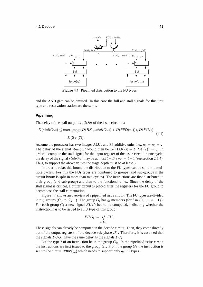
4.1 Decode 41
FUG0.stall
stallOut fullInFUG⋆
FUGg−1.stall
FUG0.full FUGg−1.full
FU(7−gg−1)...6FU0...(g0−1)
Issue(gg−1)
Buf
Sel
Buf
Issue(g0)
Figure 4.4: Pipelined distribution to the FU types
and the AND gate can be omitted. In this case the full and stall signals for this unittype and reservation station are the same.
Pipelining
The delay of the stall outputstallOut of the issue circuit is:
D(stallOut) ≤ max{max0≤i≤6
(D(RSi,⋆.stallOut) + D(FFO(ni))), D(FU⋆)}
+ D(Sel(7)).(4.1)
Assume the processor has two integer ALUs and FP additive units, i.e.,n1 = n3 = 2.The delay of the signalstallOut would then beD(FFO(2)) + D(Sel(7)) = 5. Inorder to compute the stall signal for the input register of the issue circuit in one cycle,the delay of the signalstallOut may be at mostδ−DAND = δ−1 (see section 2.5.4).Thus, to support the above values the stage depth must be at least6.
In order to relax this bound the distribution to the FU types can be split into mul-tiple cycles. For this the FUs types are combined to groups (and sub-groups if thecircuit Issue is split in more than two cycles). The instructions are first distributed totheir group (and sub-group) and then to the functional units. Since the delay of thestall signal is critical, a buffer circuit is placed after the registers for the FU group todecompose the stall computation.
Figure 4.4 shows an overview of a pipelined issue circuit. The FU types aredividedinto g groups (G0 to Gg−1). The groupGl hasgl members (forl in {0, . . . , g − 1}).For each groupGl a new signalFUGl has to be computed, indicating whether theinstruction has to be issued to a FU type of this group:
FUGl :=∨
i∈Gl
FUi.
These signals can already be computed in the decode circuit. Then, they come directlyout of the output registers of the decode sub-phaseD1. Therefore, it is assumed thatthe signalsFUG⋆ have the same delay as the signalsFU⋆.
Let the typei of an instruction be in the groupGk. In the pipelined issue circuitthe instructions are first issued to the groupGk. From the groupGk the instruction issent to the circuitIssue(gk) which needs to support onlygk FU types.

42 Processor Core
The buffer circuit inserted after the registers for a group decouples the stall signalfor the issuing to a group and the stall signals for the issuing from the groups to thereservation stations. Note that the stall signalsFUG⋆.stall are compute by AND-ingthe full bit of the register and the buffer circuit for that group and therefore have delayDAND (see figure 2.4 on page 13). For the sake of readability, this AND-gate is notshown in figure 4.4.
If issuing from the groupGk to the reservation station still cannot be done in onecycle, the groups can be further divided into sub-groups. The circuitIssue(gk) is thenbuild analogously to the pipelined issue circuit in figure 4.4. If the circuit fits into onecycles it is build analogously to the non-pipelined circuit in figure 4.3.
The computation of the full bit for the groupsFUG⋆.full and the output stall sig-nalstallOut based on the stall signals of the groupsFUG⋆.stall happens analogouslyto the computation for the instruction types in the non-pipelined case. Note that theinput signals for the circuitsIssue(⋆) come out of buffer circuits. For the equation(4.1) then holdsD(FU⋆) = DMUX (see figure 2.4).
The circuit described above pipelines the issuing of an instruction to its type,butnot the issuing from an instruction type to the reservation stations. In orderto pipelinethis part registers need to be inserted into the computation of the stall signal ofthe FUtypesFUi.stall. This would mean that also the computation of the signalsFUi,j .fullwould take several cycles. However, these signals are used inside the reservation sta-tion to compute the output stall signals of the reservation stations for the next cycle(see section 4.2.2) and therefore its own value for the next cycle.
Inserting registers into this computation can lead to inconsistencies due to the onecycle dependency, e.g., two instructions could be sent to a reservation station that canonly accept one instruction. In order to avoid this problem, issuing from theFU typeto the functional units of the type has to be done in one cycles. The bound implicatedby this is acceptable.
Cost and Delay
If the size of the group from which an instruction of typei is issued to the reservationstations is one, the full signal for the FU typeFUi.full can be directly derived fromthe full bit of the group. It does not have to be AND-ed with the FU type indicatorFUi. The delay of the full bit for the group isDOR from the buffer circuit. The find-first-one circuit and the AND-gate at its output are only needed ifni > 1. This reducesthe delay of the full signals for the FUsFUi,⋆.full to:
D(FU⋆,⋆.full) ≤ max{DOR, max0≤i≤6
(D(RSi,⋆.stallOut) + D(FFO(ni)))}
+
{
0 if ni = 1
DAND if ni > 1.
Let eRSibe the number of entries of the reservation stations of typei. Then the
delay of the stall output of these reservation stations isD(PP-OR(eRSi)) as will later
be derived in section 4.2.2. The input full signal to the reservation stationsmay haveat most the delayδ − DMUX (see section 4.2.1). Since the issuing from the FU type

4.1 Decode 43
to the reservation station is not pipelined,ni andeRSiare bounded by the following
equation:
δ ≥ DMUX + D(FUi,⋆.full)
≥ DMUX + max{DOR, max0≤i≤6
(D(PP-OR(eRSi)) + D(FFO(ni)))}
+
{
0 if ni = 1
DAND if ni > 1.
(4.2)
The input registers of the decode sub-phaseD2 are not assumed to have buffercircuits. This reduces the delay of the input signal to the issue circuitFU⋆ to zero.The delay of the output stall signal (see equation (4.1)) may be at mostδ − DAND.Let the variablepI be one, if the circuitIssue has to be pipelined. Hence:
pI =
0 ifδ ≥ max0≤i≤6(D(PP-OR(eRSi
)) + D(FFO(ni)))
+D(Sel(7)) + DAND
1 else
.
If pI is one, three numbersH, I, andJ have to be computed. The numberHdefines the maximum number of FU types to which an instruction can be issued in onecycle. The maximum number of groups an instruction can be issued to in one cycleis denoted byI. The maximum number of sub-groups an instruction can be issued tofrom a group is denoted byJ .
The delay of the data output of a buffer circuit isDMUX and the delay of the stalloutput of a buffer circuit isDAND. The delay of the output stall signal of an stage maybe at mostDAND, as it is computed by an select circuit and therefore the AND-gateof the buffer circuit cannot be merged into the computation (see section 2.5.4). Thus,H, I, andJ can be computed using the following equations:
H = max{h|δ ≥ max{max0≤i≤6
(D(PP-OR(eRSi)) + D(FFO(ni))), DMUX}
+ D(Sel(h)) + DAND},
I = max{i|δ ≥ DAND + D(Sel(i)) + DAND},
J = max{j|δ ≥ max{DAND, DMUX} + D(Sel(j)) + DAND}.
The value ofJ can be increased using the following optimization. Assume issuingtakescI cycles. Instead of clearing the issue circuit if the signalclear is active, itsuffices to clear the reservation stations forcI cycles when clear is active. After the firstclear cycle, the reservation stations do not produce a stall and therefore the instructionsin the issue circuit advance in at mostcI − 1 cycles to the reservation stations wherethey are cleared. Note that no valid instruction can enter the reservation stations in thecI cycles after a clear .
Therefore, it can be assumed, that the registers of the issue circuit do not haveto be cleared. Figure 4.5 (a) depicts the computation of the input of the registerFUG.fullBuf of a groupFUG that issues an instruction to the sub-groupsFUSG0
to FUSGJ−1 without taking the clear signal into account. The figure includes theOR-gate that is used inside the buffer circuit of the group to compute the fulloutput
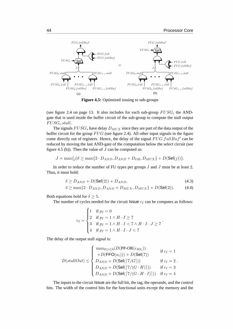
44 Processor Core
FUG.fullBuf ′
FUSG⋆
FUG.full
FUG.fullBufJ
(b)
FUG.fullBuf ′
FUSG⋆
J
(a)
≡
FUG.full
FUG.fullBuf
Sel
FUSG0.fullBuf
FUSG0.full
FUSG0.stall
FUSGJ−1.fullBuf
FUSGJ−1.full
FUSGJ−1.stall
Sel
FUSG0.fullBuf
FUSG0.full
FUSG0.stall
FUSGJ−1.fullBuf
FUSGJ−1.full
FUSGJ−1.stall
Figure 4.5: Optimized issuing to sub-groups
(see figure 2.4 on page 13. It also includes for each sub-groupFUSGi the AND-gate that is used inside the buffer circuit of the sub-group to compute the stall outputFUSGi.stall.
The signalsFUSG⋆ have delayDMUX since they are part of the data output of thebuffer circuit for the groupFUG (see figure 2.4). All other input signals in the figurecome directly out of registers. Hence, the delay of the signalFUG.fullBuf ′ can bereduced by moving the last AND-gate of the computation below the select circuit (seefigure 4.5 (b)). Then the value ofJ can be computed as:
J = max{j|δ ≥ max{2 · DAND, DAND + DOR, DMUX} + D(Sel(j))}.
In order to reduce the number of FU types per groupsI andJ must be at least2.Thus, it must hold:
δ ≥ DAND + D(Sel(2)) + DAND, (4.3)
δ ≥ max{2 · DAND, DAND + DMUX , DMUX} + D(Sel(2)). (4.4)
Both equations hold forδ ≥ 5.The number of cycles needed for the circuitIssue cI can be computes as follows:
cI =
1 if pI = 0
2 if pI = 1 ∧ H · I ≥ 7
3 if pI = 1 ∧ H · I < 7 ∧ H · I · J ≥ 7
4 if pI = 1 ∧ H · I · J < 7
.
The delay of the output stall signal is:
D(stallOut) ≤
max0≤i≤6(D(PP-OR(eRSi))
+D(FFO(ni))) + D(Sel(7))if cI = 1
DAND + D(Sel(⌈7/G⌉)) if cI = 2
DAND + D(Sel(⌈7/(G · H)⌉)) if cI = 3
DAND + D(Sel(⌈7/(G · H · I)⌉)) if cI = 4
.
The inputs to the circuitIssue are the full bit, the tag, the operands, and the controlbits. The width of the control bits for the functional units except the memory and the

4.1 Decode 45
branch checking units is approximated by 8. The memory unit needs an additional 16bit immediate constant. The branch checking unit needs and 24 bit immediate constant,the PC of the instruction, the predicted branch target, and the way of the branch targetbuffer as additional control signals (see chapter 6). Thus, the numberof input II andoutputsOI of the issue circuit are:
II = 1 + 7 · lROB + 64 + 64 + 5 + 2 + 8 + 24 + 32 + 32 + kBTB,
OI = n · (1 + 3 · lROB + 64 + 8) + (n3 + n4 + n5) · (4 · lROB + 64 + 5)
+ 16 + 24 + 32 + 32 + kBTB.
Then the approximated cost of the issue circuit is:
C(Issue) ≤6
∑
i=0
(C(FFO(ni)) + ni · CAND) + 7 · CAND + C(Sel(7))
+ (cI − 1) · ⌈(II + OI)/2⌉ · CREG.
4.1.7 Stalling
The first stage of the sub-phaseD1 has to be stalled if the ROB is full or if decodinghas to be stopped until a detected branch misprediction has retired. The ROBis fullif the signalROB.full computed by the ROB control (see section 4.6.5) is active.Decoding has to be stopped due to a misprediction if the signalIF.haltdec computedby the instruction register environment (see section 6.4) is active. Thus:
D1.genStall0 := ROB.full ∨ IR.haltdec, (4.5)
D1.stall0 := D1.full0 ∧ (D1.stallIn0 ∨ D1.genStall0). (4.6)
An instruction which reads the special registerIEEEf (indicated by the con-trol signalreadIEEEf computed in the circuitDecode) must wait until all floatingpoint operations have retired. This is due to the fact that all floating point instructionswrite the registerIEEEf implicitly. For simplicity the instructions reading that reg-ister wait until all preceding instructions have retired, which is indicated by the signalallRet computed by the ROB control. Instructions reading the registerIEEEf areconsidered rare, hence the performance impact can be neglected.
The instructions which read the registerIEEEf must wait in the pipeline stage ofthe decode sub-phaseD1 in which the register files in the circuitRF return the resultof the read access (denoted bycRF ). The SPR guarantees that the correct content ofregisterIEEEf is returned as soon as the signalallRet is active without restartingthe read access (see section 4.7.4). Thus:
D1.genStallcRF := readIEEEf ∧ allRet, (4.7)
D1.stallcRF := D1.fullcRF ∧ (D1.stallIncRF ∨ D1.genStallcRF ). (4.8)
As discussed in the overview section, the ROB access in sub-phaseD2 must notfinish before the corresponding instruction has been issued. Otherwisethe instructionwould miss the result of the ROB access. If issuing is done in one cycle, this can be

46 Processor Core
FU0.full, RS0.stall, FU0.tag
FU6.full, RS6.stall, FU6.tag
10, D2.ROB.tag
EQ
EQ
0 1
Out.issued
issued
stall
In.issued
newissue
Figure 4.6: Issue test
guaranteed without extra hardware. It suffices that the output stall signal of the issuecircuit is used as stall signal of the input register of the sub-phaseD2:
D2.stall0 := D2.full0 ∧ Issue.stallOut. (4.9)
An instruction then waits in the input register of the decode sub-phaseD1 until it isissued. The ROB access does not have to be stalled.
If issuing is pipelined additional hardware is needed to detect whether an instruc-tion has already been issued. For each stage of the ROB access, a circuit IssueTest(see figure 4.6) checks if the instruction which is in this stage is already issued to areservation station.
An instruction is issued to a functional unit of typei if the stall signal for thistypeRSi.stall is not active and the full bit for this typeFUi.full is active (see sec-tion 4.1.6). To check whether the issued instruction is the instruction in the ROBaccess stage, the tags are compared. The tag of the instruction in the ROB access stageis calledD2.ROB.tag in the figure. The signalnewissue is active if the instructionin the ROB access stage is issued to any functional unit. The values ofnewissue areaccumulated in the registerissued, i.e., issued is active if the instruction has beenissued in any previous cycle.
The registerissued has to be updated even if the stage of the ROB access is stalled.The update of this register is done analogously to the update of the registerforw inthe forwarding circuit with stalling (see section 2.6.3), i.e., if the ROB access stage isstalled, the registerissued is updated, otherwise the updated result is saved in the nextstage. The computation ofnewissue can be pipelined similar to the computation offorw in the forward circuit with stalling.
Let cD2 be the number of stages of the ROB read access in the decode sub-phaseD2. The output register of the ROB access has to be stalled if it is full and the registerissued is not active:
D2.stallcD2 := D2.fullcD2 ∧ D2.issuedcD2 .
This guarantees that the ROB read access of an instruction is held in the laststage ofthe access until the instruction is in the reservation station and snoops on the output ofthe ROB. The other stages are stalled as usual, i.e.,stallOut := stallIn∧full. Thus,the stall output of the ROB accessROB.stallOut can be computed as:
ROB.stallOut :=
cD2∧
i=1
D2.fulli ∧ D2.issuedcD2 (4.10)

4.1 Decode 47
The input register of the decode sub-phaseD2 is stalled if either the ROB accessor the issue circuit produce a stall:
D2.stall0 := D2.full0 ∧ (ROB.stallOut ∨ Issue.stallOut). (4.11)
Let cI be the number of cycles needed for issuing. Then, combining formulas 4.9and 4.11 one gets for stall output of the decode sub-phaseD2 (which is the stall signalof the first stage ofD2):
D2.stallOut :=
{
D2.full0 ∧ ROB.stallOut if cI = 1
D2.full0 ∧ (ROB.stallOut ∨ Issue.stallOut) if cI > 1
(4.12)
Let lROB be the width of the tags. The the delay of the circuitIssueTest is:
D(IssueTest) ≤ D(EQ(lROB + 1)) + D(OR-Tree(7)) + DOR.
Let cIT be the number of cycles needed for the circuitIssueTest. The number ofinputs and outputs are8 · lROB + 15 respectively 1. It holds
cIT = ⌈D(IssueTest)/(δ − DMUX)⌉,
C(Issue Test) ≤ 7 · C(EQ(lROB + 1)) + 8 · COR + CMUX + CREG
+ cIT · (4 · lROB + 8) · (CREG + CMUX).
4.1.8 Cost and Delay
The delay of the decode phase depends on the number of buffer circuitsthat have to beinserted in order to compute the stall signals within the cycle time. Up to two buffercircuits are inserted in order to reduce the delay of the stall signals. The first buffercircuit is inserted after the stagecRF in which the register files return the results. Thesecond buffer circuit is inserted somewhere before the stagecRF . To further decreasethe delay of the stall signal, more buffer circuits could be inserted into the stages ofD1 and the ROB access inD2; however, this is not necessary for a stage depth of 5and greater.
If no buffer circuit has to be inserted into the decode sub-phaseD1, its delay is:
D(D1) ≤ max{D(PT), D(RF), D(Decode)} + D(OpGen).
The values for the number of cycles of the sub-phaseD1 cD1 and for cRF can becomputed based on the number of buffer circuitsb:
cD1(b) = ⌈(D(D1) + b · DMUX)/δ⌉,
cRF (b) =
{
⌈D(SPR-RF)/δ⌉ if b ≤ 1
⌈(D(SPR-RF) + DMUX)/δ⌉ if b > 1.
If no buffer circuits are inserted in the sub-phaseD1, the stall signal for thefirst stage ofD1 (and therefore the output stall signal of the whole decode phaseD1.stallOut) is computed as (see equation 4.6):
D1.stallOut = D1.full0 ∧ (D1.stallIn0 ∨ D1.genStall0)(4.5)= D1.full0 ∧ (D1.stallIn0 ∨ ROB.full ∨ IR.haltdec).

48 Processor Core
The stages1 to cRF − 1 do not generate stall signals. Thus:
D1.stallOut = D1.full0 ∧ ((
cRF−1∧
i=1
D1.fulli ∧ D1.stallIncRF−1)
∨ ROB.full ∨ IR.haltdec).
This can be transformed using the distributive law to:
D1.stallOut = (
cRF−1∧
i=0
D1.fulli ∧ D1.stallIncRF−1)
∨ (D1.full0 ∧ (ROB.full ∨ IR.haltdec)).
Using formula 4.8 for the computation ofD1.stallcRF = D1.stallIncRF−1 it follows:
D1.stallOut = (
cRF∧
i=0
D1.fulli ∧ (D1.stallIncRF ∨ D1.genStallcRF ))
∨ (D1.full0 ∧ (ROB.full ∨ IR.haltdec))
(4.13)
(4.7)= (
cRF∧
i=0
D1.fulli ∧ (D1.stallIncRF ∨ (readIEEEf ∧ allRet)))
∨ (D1.full0 ∧ (ROB.full ∨ IR.haltdec))
The remaining stages of the sub-phaseD1 do not generate stalls. LetcD1 be thenumber of stages ofD1. Then, if no buffer circuits are inserted inD1, the stall outputof the decode phase can be computed as:
D1.stallOut = (
cRF∧
i=0
D1.fulli ∧ ((
cD1−1∧
j=cRF +1
D1.fulli ∧ D2.stallOut)
∨ (readIEEEf ∧ allRet)))
∨ (D1.full0 ∧ (ROB.full ∨ IR.haltdec))
Figure 4.7 shows the computation of the signalD1.stallOut.
Let cI be the number of stages needed for the circuitIssue andcD2 the numberof cycles needed for the ROB access in the decode sub-phaseD2. The value ofcD2
is computed in the ROB section 4.6. Then the delay of the output stall signal forthedecode sub-phaseD2 can be computed as:
D(ROB.stallOut)(4.10)
≤ D(AND-Tree(cD2)),
D(D2.stallOut)(4.12)
≤
D(Issue.stallOut) if cI = 1
max{D(ROB.stallOut),
D(Issue.stallOut)} + DOR
if cI > 1.

4.1 Decode 49
D1.stallIncRF
ROB.full
IR.haltdec
D1.stallOutD2.stallOut
AllRet
IEEEfRead
D1.full0
D1.genStall0
D1.full0...cRF
D1.fullcRF +1...cD1−1
Figure 4.7: Computation of the decode stall output without buffer circuit
The control signalsAllRet, IEEEfRead, andIR.haltdec come directly out ofregisters and therefore have delay zero. The signalROB.full has delayDMUX asdiscussed later in the section 4.6.7. The stall output of the decode phase mayat mosthave the delayδ − DMUX (see section 6.4). Thus, the number of buffer circuitsb canbe zero if the following equation holds:
δ − DMUX ≥ max{max{D(D2.stallOut), D(AND-Tree(cD1(0) − cRF (0) − 1))}
+ DAND + DOR,
D(AND-Tree(cRF (0) + 1)), D(ROB.full) + DOR}
+ DAND + DOR.
The first buffer circuit is inserted in the stage after the output of the register filesreturn the result of the read accesses, i.e.,cRF (1) + 1. This allows to split the stallcomputation at the signalD1.stallcRF +1 = D1.stallIncRF . In equation 4.13 thesignalD1.stallIncRF can then be computed as (see figure 2.4 on page 13):
D1.stallIncRF = D1.fullcRF +1 ∨ D1.fullBuf cRF +1.
The critical signal of the stall computation of the sub-phaseD1 for the stages below thestagecRF is then the input of the full bit of the buffer circuitD1.fullBuf cRF +1′. TheAND-gate in the buffer circuit that is needed for the computation of this signal (see fig-ure 2.4) can be incorporated into the AND-Tree for the signalsD1.fullcRF +1...cD1−1.This increases the number of inputs by 2 (see section 2.5.4). Figure 4.8 shows thecomputation of the critical signals of the stall computation if one buffer circuit isin-serted.
Thus, one buffer circuit is sufficient (b = 1) if the following equations holds:
δ ≥ max{D(D2.stallOut), D(AND-Tree(cD1(1) − cRF (1) + 1)) + DAND},
δ ≥ max{DAND + DOR, D(AND-Tree(cRF (1) + 1)), DMUX + DOR}
+ DAND + DOR + DMUX .
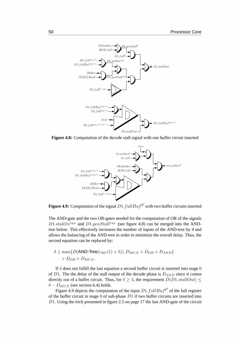
50 Processor Core
clear
D1.fullBuf cRF +1
D1.fullcRF +1
D1.fullcRF +2...cD1−1
D2.stallOut
D1.fullBuf cRF +1
D1.genStall0
D1.full0...cRF
D1.genStallcRF
D1.stallIncRF
IR.haltdec
ROB.full
AllRet
IEEEfRead
D1.fullcRF +1
D1.fullBuf cRF +1
D1.stallOut
D1.full0
Figure 4.8: Computation of the decode stall signal with one buffer circuit inserted
IR.haltdec D1.fullBuf0′
AllRet
IEEEfRead
D1.fullcSPR+1
D1.fullBuf cSPR+1
D1.full1...cSPR
clear
D1.fullBuf0
D1.full0
ROB.full
Figure 4.9: Computation of the signalD1.fullBuf0′ with two buffer circuits inserted
The AND-gate and the two OR-gates needed for the computation of OR of the signalsD1.stallIncRF andD1.genStallcRF (see figure 4.8) can be merged into the AND-tree below. This effectively increases the number of inputs of the AND-tree by 4 andallows the balancing of the AND-tree in order to minimize the overall delay. Thus, thesecond equation can be replaced by:
δ ≥ max{D(AND-Tree(cRF (1) + 5)), DMUX + DOR + DAND}
+ DOR + DMUX .
If δ does not fulfill the last equation a second buffer circuit is inserted into stage0of D1. The the delay of the stall output of the decode phase isDAND since it comesdirectly out of a buffer circuit. Thus, forδ ≥ 5, the requirementD(D1.stallOut) ≤δ − DMUX (see section 6.4) holds.
Figure 4.9 depicts the computation of the inputD1.fullBuf0′ of the full registerof the buffer circuit in stage0 of sub-phaseD1 if two buffer circuits are inserted intoD1. Using the trick presented in figure 2.5 on page 17 the last AND-gate of the circuit

4.2 Dispatch 51
can be removed from the critical path. This adds 3 more inputs to the AND-tree. Thus,if two buffer circuits are inserted, the following equations must hold:
δ ≥ max{D(D2.stallOut), D(AND-Tree(cD1(2) − cRF (2) + 1)) + DAND},
δ ≥ max{D(AND-Tree(cRF (2) + 7)), DMUX + DOR + DAND} + DOR.
These equations hold forδ = 5.
The inputs of the decode sub-phaseD1 consist of the full bit, the instruction regis-ter, and the signals used by the branch prediction. The width of the input is100+kBTB
(the full bit, the 32 bit instruction word, the 32 bit instruction address, the 32bit pre-diction result, two interrupt signals, a control signal, andkBTB bits for the branchtarget buffer way, see section 6.9). The outputs of the decode sub-phaseD1 consist ofthe inputs to the issue circuit and the data written into the ROB in sub-phaseD2. Thewidth of the output isII +15. The total cost for the decode sub-phaseD1 is (excludingthe RAM environments):
C(D1) ≤ C(Decode) + C(DestCmp) + C(OPGen)
+ cD1 · ⌈(115 + kBTB + II)/2⌉ · CREG.
Let cI be the number stages of the circuitIssue and letcD2 be the number of stagesof the read access to the ROB duringD2. The cost of the sub-phaseD2 not countingthe ROB environment is:
C(D2) ≤ C(Issue) + (II + 15) · CREG
+
{
0 if cI = 1
cD2 · C(IssueTest) if cI > 1.
4.2 Dispatch
As described in chapter 3 each functional unit has one reservation station of one ormore entries. The instructions wait in the reservation stations until all operands arevalid. The operands get valid by snooping on the CDB and on the output ofthe ROBaccess started during decode. The snooping on the ROB output is necessary since theinstructions are issued before the ROB access. As soon as all operands are valid, theinstruction is sent to the functional unit and the entry holding the instruction is cleared.
Figure 4.10 shows a reservation station witheRS entries. Each entry can hold oneinstruction. The circuits for the entriesRS-Entryk (k ∈ {0, . . . eRS − 1}) form aqueue. New instructions are always filled into entry0. Whenever possible instructionsmove to the next entry to make room for new instructions in entry0. Since instructionscannot overtake each other in the reservation station, the oldest instruction is alwaysin the entry with the highest number.
The bussesCDB.⋆ and D2.OP⋆.ROB.⋆ are connected to every entry. If thetag on one of the busses equals the tag of a not already valid operand of an entry, theoperand in the entry is updated. The data on the bus is saved and the operand is markedvalid. An arbitration of the two busses is not necessary, as they cannot update the same

52 Processor Core
In
RS-Entry0
D2.FU.⋆
RS-EntryeRS−1
CDB.⋆D2.OP⋆.ROB.⋆
Entry0.⋆
EntryeRS−1.⋆
stallIn
stallOut
RS.⋆
RS-Control
dispeRS−1, f illeRS−1
disp0, f ill0
In
Out
Figure 4.10: Reservation station
operand in the same cycle, since otherwise the instruction that is forwardedwould beon the CDB and in the ROB at the same time.
The reservation station is controlled by the circuitRS-Control. This circuit selectsthe oldest instruction which is ready (i.e., all operands are valid) and sends it to thefunctional unit via the busRS.⋆. This step is called dispatch of an instruction. Thereservation station control also controls the movement of the entries in the queue andcomputes the output stall signal of the reservation station.
4.2.1 Entries
The circuitRS-Entry for one reservation station entry is depicted in figure 4.11. Theinput busIn.⋆ equals the output bus of the preceding entry respectively the inputreceived from the issue circuit in case of the entry0. The output busOut.⋆ containsthe updated content of the entry. If the control signalfill is active, the entry is filledwith the content of the busIn.⋆. Otherwise the current content is updated and held inthat stage.
The registerfull indicates that the entry contains a valid instruction. It is set byfilling a valid instruction into the entry via the busIn.⋆. Thefull signal is reset ifthe instruction is dispatched to the functional unit (indicated bydisp = 1) or if thereservation station is cleared (clear = 1). The registercon contains information aboutthe instruction which are not altered by the reservation station, for example the tag andthe opcode of the instruction. Hence, it is only updated iffill = 1.
The circuitRS-Entry has a sub-circuitRS-Op for every operand. Each operandhas a valid bit, a tag and a data field. The number of operandso depends of the typeof the functional unit. The maximum number of operands is six for the floating pointunits. Table 4.2 maps the operands to theRS-Op circuits of the reservation stationentries for the functional units.
The operands are updated by the CDB busCDB.⋆ and the output of the ROB readaccess which was started in decode sub-phaseD2. Note that the ROB is accessed forevery operand in parallel and therefore computes one separate bus for every operand(see section 4.6). Similar to the forwarding circuit with stalling the CDB and the ROBupdate the output busOut.⋆ of the entry. Thus, if the instruction flows from entryito i + 1 the entryi + 1 is updated. If the instruction remains in entryi, this entry isupdated.
The busEntry.⋆ is sent to the control circuitRS-Control. The content of this bus

4.2 Dispatch 53
ROB.⋆In
CDB.⋆
In.Op1.⋆
D2.OP⋆.ROB.⋆
D2.OP1.ROB.⋆
In.Opo.⋆
In ROB.⋆CDB.⋆
Out
RS-Opo
CDB.⋆
Out
RS-Op1
D2.OPo.ROB.⋆
.data .data
.valid
.valid
full
In.full
disp
Out.full
req
con
In.con
Out.con
Entry.⋆
Out.Opo.⋆
fill
Out.Op1.⋆
ready
0 1
clear
Figure 4.11: Reservation station entry
RS-Op1 RS-Op2 RS-Op3 RS-Op4 RS-Op5 RS-Op6
width 32 32 32 32 5 2
Mem OP1.lo OP2.lo
IAlu OP1.lo OP2.lo
IMulDiv OP1.lo OP2.lo
FAdd OP1.hi OP1.lo OP2.hi OP2.lo OP3 OP4
FMulDiv OP1.hi OP1.lo OP2.hi OP2.lo OP3 OP4
FMisc OP1.hi OP1.lo OP2.hi OP2.lo OP3 OP4
BCU OP1.lo OP2.lo
Table 4.2: Mapping of the operands
is the same as the content of the busOut.⋆ with two differences: first, the full bit ofthe busEntry holds the content of the registerfull instead of the updated value. Thisold value of the full bit is used to decide whether new informations can be filledintothe entry (see section 4.2.2). Second, the busEntry.⋆ has an extra bitreq indicatingthat the entry contains a valid and ready (i.e., all operands are valid) instruction andhence requests that the instruction in this entry gets dispatched:
ready :=
o∧
j=1
Opj .valid,
req := full ∧ ready.
Let wC be the width of the registercon. Then the cost of an entry witho operandswith width w1 to wo can be estimated as:
C(RS-Entry(wC , o, w⋆)) ≤o
∑
j=1
C(RS-Op(wj)) + C(AND-Tree(o))
+ 2 · CAND + CMUX + (wC + 1) · CREG.

54 Processor Core
valid data
Out.valid Out.data
In.dataIn.valid
fill fill
tag
In.tag
Out.tag
Test
Test
fill
data
forward
forward
data
cdata
cforw
CDB.⋆
ROB.⋆
1 0
1 0 0 1
10
Figure 4.12: Single operand of a reservation station entry
1
forwardEQ
W.hi
W.lodata
odd
32
tag
W.{full, tag}lROB
lROB + 1
depDbl
0
1
Figure 4.13: Modified test circuit for low part operands reading double precision re-sults
Operands
Figure 4.12 shows the operand circuitRS-Op. The circuit saves the valid bit, the tagand the data of the operand in the respective registers. If thefill signal is active, thecontent of the input busIn.⋆ is saved into the registers, otherwise the current operandis held in the entry, i.e., the output busOut.⋆ with the updated values for the operandis latched.
Similar to the RAM forwarding circuit in section 2.6.1 the sub-circuitsTest com-pares the tag of the bussesCDB.⋆ andROB.⋆ with the tag of the operand. If the tagsmatch, the signalsCDB.full respectivelyROB.full indicate valid forwarding data,and the operand is not yet valid, the respective forwarding data are multiplexed intothe data outputOut.data. The new valid signal is computed as OR of the old validand the forward signals from the two test circuits.
Assume a 32 bit instruction uses the high part of a 64 bit result as operand. Thiscan happen if the 32 bit instruction depends on a 64 bit result and reads an odd register.64 bit results are either written into the floating point register file or the registers8 and9 of the special purpose register file (integer multiplication / division instructions) fileas target. The high part of these registers can only be used by the operand 2 of thememory unit and the integer ALU, and operands2 and4 of the floating point units.
For these operands, the circuitTest is replaced by a modified circuit that usesthe high part of the CDB respectively the ROB output if the instruction readsan oddaddress and the depends on 64 bit result (see figure 4.13). The signal depDbl indicatesthat the instruction that the operand depends on is a double precision instruction, the

4.2 Dispatch 55
FFOzero ffo
Entry0...eRS−1.full
PP-OR
EntryeRS−1...0.req
EntryeRS−1...0.⋆
stallIn
dispeRS−1...0
selecteRS−1...0
fill0...eRS−1 RS.⋆RS.full
Sel
Figure 4.14: Reservation station control
signalodd is active if the operand address is odd. These two signals are computedduring decode (see section 4.1.4) and are part of the control buscon of the reservationstation entries.
The cost of an operand circuit withw data bits can be estimated as:
C(RS-Op(w)) ≤ 2 · C(Test(lROB)) + 3 · w · CMUX + w · CREG
+ 2 · COR + CAND + CMUX + (1 + lROB) · CREG.
The additional costs for the entries of a reservation station of typei (i = 2 for aninteger ALU reservation station,i ∈ {4, 5, 6} for floating point reservation stations)are:
C(RS-Entry(o, w⋆, wC))+ ≤
32 · CMUX + CAND if i = 1
2 · (32 · CMUX + CAND) if i ∈ {3, 4, 5}
0 else
.
4.2.2 Reservation Station Control
The reservation station control circuitRS-Control (see figure 4.14) computes the con-trol signalsdisp⋆ andfill⋆ for the entries, the outputRS.⋆ of the reservation stationto the functional unit, and the stall signalstallOut to the issue circuit.
The entryk can be filled if the entry is not full (fullk) or the content is filled intothe next entry (fillk+1). The reservation station can accept new data if the first entrymay be filled. Since the last entry (numbereRS − 1) cannot be filled into any otherentry, it follows:
fillk :=
eRS−1∨
j=k
fullj ,
stallOut := fill0.
Note that the stall output only depends on the full bits of the entries. Hence,thereservation station splits the stall signal similar to the buffer circuit. The drawback isthat the issue circuit may be stalled even if an instruction is currently dispatched tothe functional unit and therefore its entry could be filled. Taking the dispatch signalsinto account for the computation of the fill and the stall signals would significantlyincrease the delay of the stall output. This could make it necessary to add a buffer

56 Processor Core
PP-OR FFOffo
0
EntryeRS−1...1.store EntryeRS−1...0.full
EntryeRS−1...0.req EntryeRS−1...0.full
stallIn stallIn
EntryeRS−1...0.ready
dispeRS−1...0
(b)(a)dispeRS−1...0selecteRS−1...0selecteRS−1...0
FFOffo
Figure 4.15: Dispatch computation for memory (a) and branch checking (b) unit
circuit above the reservation station. Instead one could just increase thesize of thereservation station by one entry to get the same effect.
If the stall inputStallIn from the functional unit is not active, the control circuitdispatches the oldest instruction in the reservation station which is ready to thefunc-tional unit. The entryk contains a valid and ready instruction if the signal requestsignal of this entryEntryk.req is active. A find-first-one circuitFFO using the re-quest signals computes as outputffo the entryk with the highest index that contains avalid and ready instruction. Hence, the signalsselect⋆ computed from the outputffounary select the entry containing the oldest ready instruction. The negation of the stallinput stallIn is AND-ed to this output obtaining the dispatch signalsdisp⋆. Thus, noinstruction is dispatched if the stall input is active.
The outputzero of the circuitFFO indicates that no entry is full and ready. If thissignal is not active, a valid instruction can be sent to the functional unit. Thus, negationof the zero output can be used asfull signal for the output busRS.⋆. The signalsselect⋆ are used to select from the entry outputsEntry⋆.⋆ the instruction which issent to the functional unit via the output busRS.⋆.
For the memory unit and the branch checking unit small changes have to be madeto the computation of the dispatch signals due to restrictions of the dispatch order. Notethat due to these restrictions the DLXπ+ must have exactly one memory and branchchecking unit.
The reservation station of the memory unit has to guarantee that no memory in-struction overtakes a store instruction, as the store may write to the same address.Note that the address of a memory access is computed inside the memory unit andtherefore not known by the memory reservation station. A memory instruction mayonly be dispatched if no older instruction is a store instruction. In order to check forall entries whether an older instruction is a store instruction, a parallel prefix OR of thesignalsEntry⋆.store ∧ Entry⋆.full indicating a valid store instruction is computed.The output of the parallel prefix OR is used to turn off the dispatch signal as computedfrom the find first one circuit (see figure 4.15 (a)).
The branch checking unit can check branches only in-order. Hence, the reservationstation of the branch checking unit must dispatch the instructions in order. Only the

4.2 Dispatch 57
clear
disp
fill
Entry.full
Out.full
In.full
0 1
full
Figure 4.16: Full bit computation for one entry
oldest valid instruction is checked if it is ready. The oldest valid instruction can becomputed using a find-first-one circuit on the full bits. The output of the find-first-onecircuit is AND-ed with the ready bits in order to check whether the oldest instruction isactually ready (see figure 4.15 (b)). Since only the oldest instruction may be dispatchedto the branch checking unit the signalsselect⋆ can be derived directly from the outputof the find-first-one circuit.
If the number of entrieseRS is 1, the requirements for memory and branch check-ing unit are automatically fulfilled. Thus, no special circuit is needed ifeRS is 1.Additionally the signalsfill anddisp cannot be active at the same time (the full bitmust be inactive forfill and active fordisp). This allows to move the AND gate whichresets the full bit on dispatch in figure 4.11 below the multiplexer controlled by the fillsignal (see figure 4.16). Hence, the delay of the path through the dispatch signal isfurther reduced.
The cost of the control circuitRS-Control for a reservation station of typei witho operands of widthw1 to wo andwC control bits is:
C(RS-Control(eRS , o, w⋆, wC)) ≤ C(PP-OR(eRS)) + C(FFO(eRS))
+ 2 · eRS · CAND
+ (o
∑
j=0
wj + wC + 1) · C(Sel(eRS))
+
C(PP-OR(eRS − 1))
+eRS · CAND
if i = 0
0 if i 6= 0
.

58 Processor Core
fill
full
In.full
req
clear
In.req
Entry.req
disp
Out.req Out.full
ready
0 1 0 1
Opo.valid
Op1.valid
Figure 4.17: Inserting a register after the request bit
4.2.3 Pipelining
For a integer ALU reservation station of type witheRS entries, the delay of the pathfrom the bussesCDB.⋆ andROB.⋆ to the full bit is:
D({ROB, CDB}.⋆ Entry⋆.full′) ≤ D(Test(lROB)) + 2 · DOR
(Out.valid, figure 4.12)
+ D(AND-TREE(2))(ready, figure 4.11)
+ DAND (req, figure 4.11)
+ D(FFO(eRS)) + DAND
(disp⋆, figure 4.14)
+ DAND + DMUX .
Even if the number of entries is1 (which deceases the delay by the find-first-one circuitand the multiplexer) this computation cannot be done in one cycle for a stage depth δof 5. Thus, the computation must be pipelined if the stage depth is too small.
No pipelining registers are inserted inside the last part of the computation startingat the signalreq⋆. The bound forδ given by the last part of the path is acceptable.The pipelining of the path until the signalready⋆ can be done similarly to the for-warding circuit with stalling, i.e., using two-dimensional pipelining (see section 2.6.3).In one dimension the path from the signals{ROB, CDB}.⋆ to the signalready⋆ ispipelined, the second pipelining dimension is the movement of the instruction throughthe reservation station queue.
In order to insert a pipelining register after the computation of the request signalsome modifications have to be made to the reservation station entries (see figure4.11)in order to maintain correctness. The modification to the entries is depicted in fig-ure 4.17. The request signal is reset whenever the full bit is reset due to a dispatch or aclear. Otherwise, if the valid bit is reset in the last cycle due to dispatching theinstruc-tion or a clear, the request bit would still be active. This could lead to dispatching an

4.2 Dispatch 59
instruction twice or dispatching invalid data if the construction of the reservation sta-tion entry from figure 4.11 would not be adjusted. Note that the extra logic asdepictedin figure 4.17 introduces an additional AND-gate on the path from the bussesCDB.⋆andROB.⋆ to the full bit. Also, the clear signal is AND-ed to the full bit before thefull bit is used to compute the request signal (in contrast to figure 4.11) since otherwisethe delay of the path would increase by a second AND-gate.
In the memory unit the computation of the dispatch signal also depends on theAND of the signalsEntry⋆.write andEntry⋆.full indicating valid store instructions.A register can be inserted after the computation of this AND similar to the register afterthe request bit. Thus, the minimum delay of the dispatch signals for the reservationstations of the memory and branch checking unit is only byDAND greater than for theother reservation stations.
In order to compute the minimum delay of the inputs to the full registers and there-fore the bound for the stage depthδ, the following assumptions are made: the inputstall signalstallIn from the FU comes directly out of a buffer circuit. Thus, the delayof this signal isDAND (see section 2.5.3). A register is added directly after the requestsignals as in figure 4.17, leading to delay of0 for these signals. Leti be the type of thereservation station (see table 4.1 on page 40, i.e.,i = 0 for the memory andi = 6 forthe branch checking reservation station). Then is must hold for a reservation stationwith eRS entries:
δ ≥
3 · DAND if eRS = 1
max{DAND, D(FFO(eRS))} + 2 · DAND + DMUX if eRS > 1 ∧ i 6∈ {0, 6}
max{DAND, D(FFO(eRS))} + 3 · DAND + DMUX if eRS > 1 ∧ i ∈ {0, 6}
.
(4.14)
Note that for a givenδ this bounds the number of entrieseRS of the reservation stations.
Cost and Delay
To compute the number of cycles needed for dispatching instructions, two paths haveto be considered. The path from the input busIn.⋆ to the registerfull determines theminimum number of cycles that an instruction has to stay in the reservation station,if all operands of the instruction are already valid during issue. The initial value ofthe request signalreq (i.e., the AND of the full bit and the operand valid signal) canbe computed during issue without increasing the delay of the issue circuit. Thus, anissued instruction for which the operands are all valid can be dispatched inthe nextcycle.3.
The path from the bussesROB.⋆ andCDB.⋆ to the full register determines theminimum number of cycles it takes from receiving the last operand (viaROB.⋆ orCDB.⋆) to dispatching of the instruction. In order to compute the delay of the paththe boolean variablepreq has to be introduced, which indicates whether a pipeliningregister is added after the computation of the request bit. Ifpreq is one (i.e., a registeris added), the delay increases by the delay of the AND which resets the request signalas in figure 4.17.
3The additional cost of C(AND-Tree(o+1)) is added to the cost of the reservation station
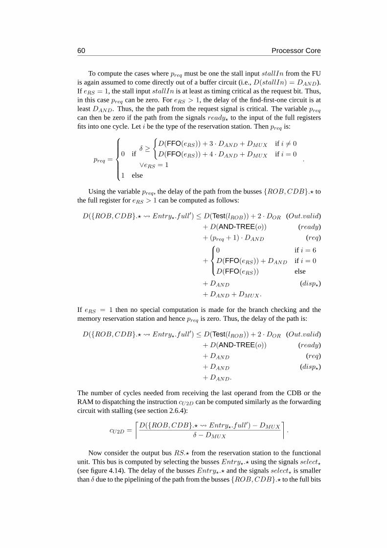
60 Processor Core
To compute the cases wherepreq must be one the stall inputstallIn from the FUis again assumed to come directly out of a buffer circuit (i.e.,D(stallIn) = DAND).If eRS = 1, the stall inputstallIn is at least as timing critical as the request bit. Thus,in this casepreq can be zero. ForeRS > 1, the delay of the find-first-one circuit is atleastDAND. Thus, the the path from the request signal is critical. The variablepreq
can then be zero if the path from the signalsready⋆ to the input of the full registersfits into one cycle. Leti be the type of the reservation station. Thenpreq is:
preq =
0 ifδ ≥
{
D(FFO(eRS)) + 3 · DAND + DMUX if i 6= 0
D(FFO(eRS)) + 4 · DAND + DMUX if i = 0
∨eRS = 1
1 else
.
Using the variablepreq, the delay of the path from the busses{ROB, CDB}.⋆ tothe full register foreRS > 1 can be computed as follows:
D({ROB, CDB}.⋆ Entry⋆.full′) ≤ D(Test(lROB)) + 2 · DOR (Out.valid)
+ D(AND-TREE(o)) (ready)
+ (preq + 1) · DAND (req)
+
0 if i = 6
D(FFO(eRS)) + DAND if i = 0
D(FFO(eRS)) else
+ DAND (disp⋆)
+ DAND + DMUX .
If eRS = 1 then no special computation is made for the branch checking and thememory reservation station and hencepreq is zero. Thus, the delay of the path is:
D({ROB, CDB}.⋆ Entry⋆.full′) ≤ D(Test(lROB)) + 2 · DOR (Out.valid)
+ D(AND-TREE(o)) (ready)
+ DAND (req)
+ DAND (disp⋆)
+ DAND.
The number of cycles needed from receiving the last operand from theCDB or theRAM to dispatching the instructioncU2D can be computed similarly as the forwardingcircuit with stalling (see section 2.6.4):
cU2D =
⌈
D({ROB, CDB}.⋆ Entry⋆.full′) − DMUX
δ − DMUX
⌉
.
Now consider the output busRS.⋆ from the reservation station to the functionalunit. This bus is computed by selecting the bussesEntry⋆.⋆ using the signalsselect⋆(see figure 4.14). The delay of the bussesEntry⋆.⋆ and the signalsselect⋆ is smallerthanδ due to the pipelining of the path from the busses{ROB, CDB}.⋆ to the full bits

4.2 Dispatch 61
of the entries (see above). Due to the additional delay of the select circuit,the delay ofthe output busRS.⋆ may be greater thanδ, but the select circuit can be pipelined easilysince it does not contain any loops. For simplicity this is done by adding the delay ofthe path that does not fit into one cycle to the delay of the functional unit. Notethatif the delay of the busRS.⋆ is smaller thanδ, the delay of the functional unit can bedecreased, because the functional unit can already do useful computations in the cycle,in which the instruction is dispatched.
In order to compute the delay of the busRS.⋆ the delay of the bussesEntry⋆.⋆ andthe signalsselect⋆ after pipelining of the reservation station must be computed. LetD′(Entry⋆.⋆) andD′(select⋆) denote the delay of these signals before any pipeliningregisters are inserted into the path from{ROB, CDB}.⋆ to the full bits of the entries.For the reservation station of the BCU (i = 6) the select signal only depends on the fullbits of the entries. For the other reservation stations the select signals depend on therequest signalsEntry⋆.req. The delay of this signal can be derived from the formulaabove for the path from the busses{ROB, CDB}.⋆ to the full bit of the entries. Thus:
D′(select⋆) ≤
{
D(Entry⋆.req) if i 6= 6
D(Entry⋆.full) if i = 6
+ D(FFO(eRS))
≤
D(Test(lROB)) + 2 · DOR + D(AND-Tree(o))
+(preq + 1) · DAND
if i 6= 6
0 if i = 6
+ D(FFO(eRS)).
The delay of the busEntry⋆.⋆ is dominated by the data of the operands. Thus, thedelay of the bus is (see busOut.data in figure 4.12).
D′(Entry⋆.⋆) ≤ D(Test(lROB)) + max{DOR + DAND, DMUX} + DMUX .
Due to the pipelining intocU2D stages the delay ofselect⋆ andEntry⋆.⋆ can be re-duced by up to(cU2D−1) ·(δ−DMUX). Since no pipelining registers are inserted be-tween the request signalsreq⋆ and the signalsselect⋆, the delay of the signalsselect⋆cannot get smaller than the delay from request signals. Thus, after inserting pipeliningregisters the delays are reduced to:
D(select⋆) ≤ max{D(FFO(eRS)) +
{
(1 − preq) · DAND if i 6= 6
0 if i = 6,
D′(select⋆) − (cU2D − 1) · (δ − DMUX),
D(Entry⋆.⋆) ≤ max{0, D′(Entry⋆.⋆) − (cU2D − 1) · (δ − DMUX)}.
If eRS = 1 no select signals are needed to compute the output busRS.⋆. Thus, thedelay added to the functional unit of the reservation station is:
D(FU(eRS))+ ≤
{
D(Entry⋆.⋆) − δ if eRS = 1
max{D(select⋆), D(Entry⋆.⋆)} − δ if eRS > 1.

62 Processor Core
Note that if this value is negative, the delay of the functional unit is effectively reduced,i.e., logic from the functional unit is pulled into the last cycle of dispatch.
The delay of the output stall signalstallOut is:
D(stallOut) ≤ D(PP-OR)(eRS).
In order to compute the maximum number of entrieseRS for a givenδ, the delay ofthe stall inputstallIn was assume to beDOR. For a giveneRS the delay of the stallinputstallIn from a functional unit of typei is bounded by:
D(stallIn) ≤ δ −
{
2 · DAND if eRS = 1
(2 · DAND + DMUX) if eRS > 1. (4.15)
The number of inputs and outputs of an entry witho operands of widthw1 to wo
andwC control signals is2 ·∑o
j=1 wj +o · (lROB +1)+33+ lROB +wC respectively∑o
j=1 wj + 3 + wC . Thus, the cost of the entries increases through pipelining by:
C(RS-Entry(o, w⋆, wC))+ ≤ (cU2D − 1) · (CMUX + CREG)
· ⌈(3 ·o
∑
j=1
wj + (o + 1) · (lROB + 1) + 2 · wC + 35)/2⌉.
The cost of a reservation station withr entries ando operands of widthw1 to wo
is:
C(RS(eRS , o, w⋆, wC) ≤ eRS · C(RS-Entry(o, w⋆, wC))
+ C(RS-Control(eRS , o, w⋆, wC))
+ C(AND-Tree(o + 1)).
Let ni be the number of functional units andeRSithe number of entries of the
reservations stations of typei ∈ {0, . . . , 6}. Using the width of the control signals asapproximated in section 4.1.6 the total cost of the dispatch phase is:
C(Dispatch) ≤ C(RS(eRS0 , 2, 32, 32, 24))
+ C(PP-OR(eRS0 − 1)) + eRS0 · CAND
+ n1 · C(RS(eRS1 , 2, 32, 32, 8 + lROB))
+ n2 · C(RS(eRS2 , 2, 32, 32, 8 + lROB))
+ n3 · C(RS(eRS3 , 6, 32, 32, 32, 32, 5, 2, 8 + lROB))
+ n4 · C(RS(eRS4 , 6, 32, 32, 32, 32, 5, 2, 8 + lROB))
+ n5 · C(RS(eRS5 , 6, 32, 32, 32, 32, 5, 2, 8 + lROB))
+ C(RS(eRS6 , 2, 32, 32, 96 + kBTB + lROB)).
Note the additional cost for the memory unit (i = 0) due to parallel prefix OR thatchecks for older store instructions in the queue.

4.3 Functional Units 63
FU CDB.hi CDB.lo case
BCU target PC resultALU result.lo result.loIMulDiv result.hi result.loFPU result.hi result.lo dbl
result.lo result.lo dbl
Mem effective address dpf ∨ dmal
result.lo result.lo (dpf ∨ dmal)
Table 4.3: Mapping of the FU output to the CDB
4.3 Functional Units
The processor has seven different types of functional units: memory unit, integer ALU,integer multiplier / divider, three different floating point unit types (additive, multi-plicative, and misc) and a branch checking unit. To comply with the fast processorcore, the fastest published additive and multiplicative floating point units aretakenfrom [Sei99]. The delay values for these FUs are taken from [Sei03].The miscella-neous floating point unit is not assumed to be critical and taken from [Jac02]. Delayvalues are from synthesis of the Verilog description [Lei02] using Synergy [Cad97].
Pipelining of the floating point and integer units is straightforward using buffercircuits if the stall path gets to long. These functional units are not described in detailhere. The delay value and the computation of the stall signals for these units can befound in appendix D. The memory unit is described in chapter 5, the branchcheckingunit is described together with the instruction fetch in section 6.5.
Table 4.3 shows the mapping of the outputs of the FUs to the CDB. In order toallow the high part of the reservation station operands to 32 bit results, 32 bit resultsare written to the high and the low part of the CDB. This is only needed for FUswhichmay write the floating point register file (Alu, Mem, and floating point FUs).
If the memory unit returns an interrupt, the effective address is saved onthe lowpart of the CDB. This allows to omit an additional exception data field in the ROBentries. The branch checking unit returns the target PC which is neededfor interruptsof type continue (see section 4.5.3) on the high part, and the result of a branch instruc-tion on the low part. A branch instruction produces a result if it writes to a registerfile entry: jump and link instructions write the address of the next instruction intothegeneral purpose register file; return-from exception instructions writethe value of thespecial register ESR (which is used as second operand of these instruction) into thespecial purpose register file.
Different units can produce different interrupts. For example only the floating pointunits can produceIEEEf interrupts. Hence, all interrupts which cannot occur for aunit are set to zero at the output of the unit. Then all interrupt signals have definedvalues for all units. The outputs of the functional units have width74+ lROB, (the fullbit, 64 data bits, 8 interrupt bits, a misprediction signal from the BCU, andlROB bitsfor the tag).

64 Processor Core
to RS
Arbiter
FU0 FUn − 1
stalln−1
FUn−1.⋆stall0
FU0.⋆
ROB
CDB
Figure 4.18: Completion phase
4.4 Completion
In the completion phase the functional units write their result to the CDB. If multiplefunctional units have results available, one unit is selected and may write its resultin the CDB register. The other functional units are stalled. The content of the CDBregister is written into the ROB and distributed to the reservation stations.
Figure 4.18 depicts an overview of the completion phase. For the completion phasethe type of a functional unit is irrelevant. For simplicity the FUs are numbered from 0to n − 1. The selection of the functional unit which may write to the registerCDB.⋆is done by the arbiter circuitArbiter. This arbiter assigns the CDB to the functionalunits round robin, i.e., starting from the unit that wrote to the CDB in the last cycle, itselects the next functional unit whose output is full. If the output of no functional unitwith higher index is full, the search is continued from index0. If none of the FUs hasa valid result ready the index is unchanged and the full bit of the CDB is setto 0.
Let j(t) denote the index of the last FU which has written to the CDB and letn bethe number of functional units. The indexj(t+1) of the next FU which may write tothe CDB can be computed by the following formula:
j(t+1) :=
min{i|(FUi.full = 1) ∧ (j(t) < i < n)} if∨n−1
i=j(t)+1FUi.full = 1
min{i|(FUi.full = 1) ∧ (0 ≤ i < n)} else if∨n−1
i=0 FUi.full = 1
j(t) else
.
(4.16)
The write access to the ROB is never stalled. Hence, the registerCDB.⋆ may beupdated every cycle and the arbiter has no stall input.
4.4.1 Arbiter
The circuit for the arbiter is shown in figure 4.19. The sub-circuitAck computes theacknowledge signalsAck which unary selects the FU that may write to the CDB. TheFUs that are not selected have to be stalled. Therefore, the negation of the acknowledgesignals can be used as stall input to the functional units. The circuitAck also computesthe full bit of the CDB.
The width of the data bus is73 + lROB (64 data bits, 8 interrupt signals, themisprediction bit, and the instruction tag). Thus, cost and delay of the arbitercircuit

4.4 Completion 65
FU⋆.⋆stall⋆FU⋆.full
AckSel
clear
full
Out.⋆
Ack(n)
Figure 4.19: Arbiter circuit
zero zero zero
In⋆.full
last
Out.full
Ack
FLOh FLOlHFLOh HFLOl
floflofloflo
1 0 1 0
Figure 4.20: Computation of the acknowledge signals
are:
D(Arbiter(n)) ≤ D(Ack(n)) + D(Sel(n)),
C(Arbiter(n)) ≤ C(Ack(n)) + CAND + (74 + lROB) · C(Sel(n)).
Acknowledge computation
Figure 4.20 shows the implementation of the circuitAck which computes the roundrobin acknowledge signals. It is a delay optimized version of the circuit in [Kro99]which is based on the formula (4.16). The indexj(t) of the last functional unit whichhas written on the CDB is saved in the registerlast in half-unary encoding (see section2.4), i.e., all bits of the registerlast with an index equal or lower thanj(t) are one, theother bits are zero. Thus, the AND-gate above the rightmost find-last-onecircuit FLOl
in figure 4.20 forces the full bits of those FUs to zero which have an index lower orequal toj(t). The circuitFLOl thus computes the following functions:
FLOl.f lo := (min{i|(FUi.full = 1) ∧ (j(t) < i < n)})un,
FLOl.zero :=n−1∧
i=j(t)+1
FUi.full.
If the minimum does not exist, the zero signal is active and the output of the find-last-one circuit with unmasked inputsFLOh is taken. If none of the full bits is active,the zero bit of the circuitFLOh is active. Hence, the negation of this signal becomesthe full bit for the CDB register.
For the registerlast, the index is needed in half-unary encoding. This is doneby the find-last-one circuits that return the result in half-unary encodingHFLO in the

66 Processor Core
left part of the circuit (see appendix C.1.1 for the construction of the circuit HFLO).4
The registerlast is only updated if a functional unit has written on the CDB, i.e.,CDB.valid = 1.
The delay and cost of the acknowledge computation are:
D(Ack(n)) ≤ DAND + D(FLO(n)) + DMUX , (4.17)
C(Ack(n)) ≤ 2 · C(FLOH(n)) + 2 · C(FLO(n))
+ n · (2 · CAND + 2 · CMUX + CREG).
4.4.2 Pipelining
The path from the acknowledge signals to the CDB register has no loops andcantherefore be pipelined easily; it is not treated in detail here. Yet the acknowledgesignalsAck are used to compute the stall inputs of the functional units and thereforethe delay must be small enough that the functional units can compute their stall signalswithin one cycle.
In order to compute the maximum delay allowed for the circuitAck(n), the follow-ing assumptions are made which minimize the delay of the inputs and the requirementsof the acknowledge signal: the last stage of all functional units is not assumed to gen-erate stall signals (i.e.,genStall = 0) and are not assumed to have a buffer circuit.Thus, for all functional unitsi D(FUi.full) = 0 holds true. The acknowledge signalsare not computed using an AND-Tree. Hence, in order to be able to computethe stallsignals in the functional units it must hold (see equation (2.9) in section 2.5.4):
δ − DAND ≥ D(Ack(n))(4.17)⇔ δ ≥ 2 · DAND + D(FLO(n)) + DMUX . (4.18)
Sincen must be at least7, the proposed circuit cannot be used at a stage depthof 5. The delay of the circuitAck can be reduced in two different ways. The arbitercan be replaced by a tree of arbiters, thus reducing the number of inputs of the singlearbiters or the full outputs of the functional units can be pre-computed onecycle aheadwhich allows to compute the acknowledge signals in two cycles. In this thesis onlythearbiter tree is presented.
Figure 4.21 depicts as an example an arbiter tree with two stages. The originalarbiter withn inputs is divided intos arbiters witht := ⌈n/s⌉ inputs in the first stageand one arbiter withs inputs in the second stage. All stages except the first stage ofthe arbiter tree have buffer circuits on their input registers in order to decouple the stallsignals in the tree.
In contrary to the arbiter on the root of the tree, the arbiters in the upper nodes needto process a stall input from the lower stages. If the stall input signal is active the buffercircuit cannot accept new data. Thus, none of the acknowledge signals of the arbitermay be active. The stall signal can be incorporated in the presented arbiter circuit withonly small changes that do not change the delay of the arbiter (see figure4.22). Due tothe half-unary encoding, the least significant bit of the registerlast is always 1. The
4The original arbiter in [Kro99] uses a parallel prefix OR over the busAck to compute the half-unaryencoding which increases the delay of the arbiter circuit.

4.4 Completion 67
FU0.⋆ FUt−1.⋆stallOut0 stallOutt−1stallOutn−t−1 FUn−t−1.⋆ FUn−1.⋆ stallOutn−1
stall
Buf0
stall
stall
Out.⋆
Buf0
stall
Arbiter(t) Arbiter(t)
Arbiter(s)
Figure 4.21: Arbiter tree
In⋆.full
zero zero zero
last
Ack
FLOh FLOlHFLOh HFLOl
stallIn
0
stallIn
Out.full
f lo flo flo flo
1 0 1 0
Figure 4.22: Acknowledge computation with stall input
least significant bit of the input of the rightmost find-last-one circuitFLOl is thereforealways 0 and can be ignored. Instead the stall inputstallIn is used as least significantbit of the input ofFLOl. Thus, ifstallIn is active the least significant bit of theflooutput ofFLOl is active. Since this bit is replaced by a0 in figure 4.22 and thezerooutput ofFLOl is not active, none of the acknowledge signals is active if the stall inputis active.
The registerlast is only updated if new data is written into the buffer circuit, i.e.,if the following signal is active:
updlast := stallIn ∧ Out.full
To allow for a small stage depth, the arbitration circuit for only two inputs can beoptimized using a binary encoding for the registerlast (see figure 4.23). For an op-timized delay the sub-circuitAck(2) computes different signals for stalling the inputsand for selecting between the two data ports. The stall outputsstall⋆ are computedexploiting that the value of the stall output may be arbitrary if the corresponding inputfull signal is not active, since in this case the input is not stalled anyway. Also, theselect signal for the data may be arbitrary if the input stall signal is active,since thenthe output data is not latched into the next stage anyway.

68 Processor Core
stallIn
stallInIn0.full In1.full In0.full In1.full
last
Ack(2)
stall0 stall1
0 1
0 1
clear
In0.⋆ In1.⋆
Out.full Out.⋆
Figure 4.23: Arbiter with stall for two inputs (with sub-circuitAck(2))
The delay of the stall input of the arbiter is at mostDAND since it comes directlyout of a buffer circuit. Thus, for the 2 input arbiter it holds (see figure 4.23):
D(Ack(2)) ≤ max{DMUX , 2 · DAND, DAND + DOR}, (4.19)
D(Arbiter(2)) ≤ 2 · DAND + DMUX ,
C(Arbiter(2)) ≤ 4 · DAND + 3 · COR + (74 + lROB) · CMUX + CREG.
Assume that the last stages of the functional units cannot generate a stall signal.Then for all stages of the buffer tree the delay of the input full signals is at mostDOR
(see figure 2.4). The delay of the stall outputs of the arbiters to the preceding stage ofthe tree respectively to the functional unit may be at mostδ−DAND (see equation 2.9)in section 2.5.4). Thus, using a tree of two-port arbiters, the bound forδ from equation(4.18) can be reduced to:
δ − DAND ≥ DOR + D(Ack(2))(4.19)⇔ δ ≥ DAND + DOR + max{DMUX , 2 · DAND, DAND + DOR},
(4.20)
which holds forδ ≥ 5. Note that this bound is independent of the number of functionalunitsn.
4.4.3 Cost and Delay
In order to compute the number of stages of the arbiter tree of the completion phase,two variables are introduced: the variabletL denotes the maximum number of inputsof the arbiters at the leaves of the tree,tI denotes the maximum number of inputs ofthe inner nodes of the tree.
For the computation oftL it is assumed that the last stages of the functional unitsdo not generate a stall and do not have buffer circuits. Thus, the delayof the fullsignals of the inputs is zero and the delay of the outputs may be at mostδ − DAND.Using equations (4.17) and (4.19)tL can be computed as:
tL = max{t|δ − DAND ≥ D(Ack(t))}
= max
{
t|
{
δ ≥ D(FLO(t)) + DMUX + 2 · DAND if t > 2
δ ≥ DAND + max{DMUX , 2 · DAND, DAND + DOR} if t = 2
}
.
(4.21)

4.4 Completion 69
datadata
FUn−t−1...n−1.dataFU0...t−1.full
full
Ack
full
Ack
stallOut0...t−1 stallOutn−t−1...n−1
FUn−t−1...n−1.fullFU0...t−1.data
Ack
Ack(t)
Ack(s)
Ack(t)
Sel(t) Sel(t)
Sel(s)
full
Out.dataOut.full
Figure 4.24: Arbiter tree with pipeline select circuits
For the inner nodes the delay of the input full signals isDOR due to the buffer circuitsbetween the stages (see section 2.5.3). Hence,tI can be computed as:
tI = max{t|δ − DAND ≥ DOR + D(Ack(t))}
= max
t|
δ ≥ DOR + D(FLO(t)) + DMUX + 2 · DAND if t > 2
δ ≥ DOR + DAND
+ max{DMUX , 2 · DAND, DAND + DOR}if t = 2
.
Then the number or arbiter stagescAT in the arbiter tree is:
cAT =⌈
logtI ⌈n/tL⌉⌉
.
The path from the acknowledge signals through the selection circuit to the dataoutput can be easily pipelined if necessary. Note that the delay of the acknowledgecomputationD(Ack(n)) is at least as large as the delay of the select circuitD(Sel(n)).Thus, the output of the arbiter can be computed in at most two cycles.
In an arbiter tree, the computation of the data output of stagei of the tree can bedone in parallel to the arbiter of stagei + 1 of the tree. See figure 4.24 for an examplewith 2 stages. In the figure, the select circuitsSel(t) compute the data for stage 1in parallel to the acknowledge computation circuitAck(s) of stage 2. Thus, only theselect circuit of root of the arbiter tree needs an additional stage.
Note that performing the selection of stagei in parallel to the arbitration of stageidelays the data inputs for the section of stagei + 1. Thus, even if the Arbiter of stagei + 1 itself would fit into one cycle, the selection must then be moved to the next stagedue to the delay of the data inputs. Thus, if the outputs of any arbiter in the treeiscomputed in two cycles, the overall number of cycles needed for the computation ofthe output of the arbiter tree is the number of stages of the tree plus one.
Let the boolean variablepAT be one if either the arbiters at the leaves or the arbitersat the inner nodes of the tree need two cycles to compute the data outputs. Forthe

70 Processor Core
arbiters at the leaves of the tree the delay of the full inputs is zero. For the innerarbiters of the tree the full bits come out of a buffer circuit and thereforehave delayDOR. Thus:
pAT =
{
1 if max{D(Arbiter(tL)), DOR + D(Arbiter(tI))} > δ
0 else.
The total number of stages for the completion phasecC is then:
cC = cAT + pAT .
Due to the buffer circuits the delay of the stall inputs of the arbiters on the leavesof the arbiter tree isDAND. Hence, the stall input is at most as critical as the full input(see figures 4.22 and 4.23). Since the full inputs of these arbiters do notcome out ofbuffer circuits it holds:
D(FU⋆.stallIn) ≤ D(Ack(tL))
≤
{
DAND + D(FLO(min{tL, n})) + DMUX if tL > 2
max{DMUX , 2 · DAND, DAND + DOR} if tL = 2
(4.22)
Let n be the number of functional units. The number of inputs of the completephase is approximatelyn · (74+ lROB), the number of outputs is74+ lROB. Then thecost of the completion phase can be approximated by:
C(Complete) ≤
C(Arbiter(n)) + (n + 1) · (74 + lROB) · CREG if tL ≥ n
⌈n/tL⌉ · C(Arbiter(tL))
+(tcAT−1I − 1)/(tI − 1) · C(Arbiter(tI))
+(cC + 1) · ⌈((n + 1) · (74 + lROB))/2⌉ · CREG
if tL < n.
4.5 Retire
During the retire phase the results of the instructions are written into the register files.In order to support branch prediction and precise interrupts, the instructions are re-ordered using the reorder buffer before they write the register file. Ifno succeedinginstruction writing the same register is processed at the time the register file is updated,the retiring instruction sets the valid bit of the producer table entry of the destinationregister.
4.5.1 Overview
An overview of the retire phase is depicted in figure 4.25. The retire phaseis dividedinto three sub-phasesRet1, Ret2, andRet3 such that in each phase only one RAMaccess is made. The following sections describe the three sub-phases.
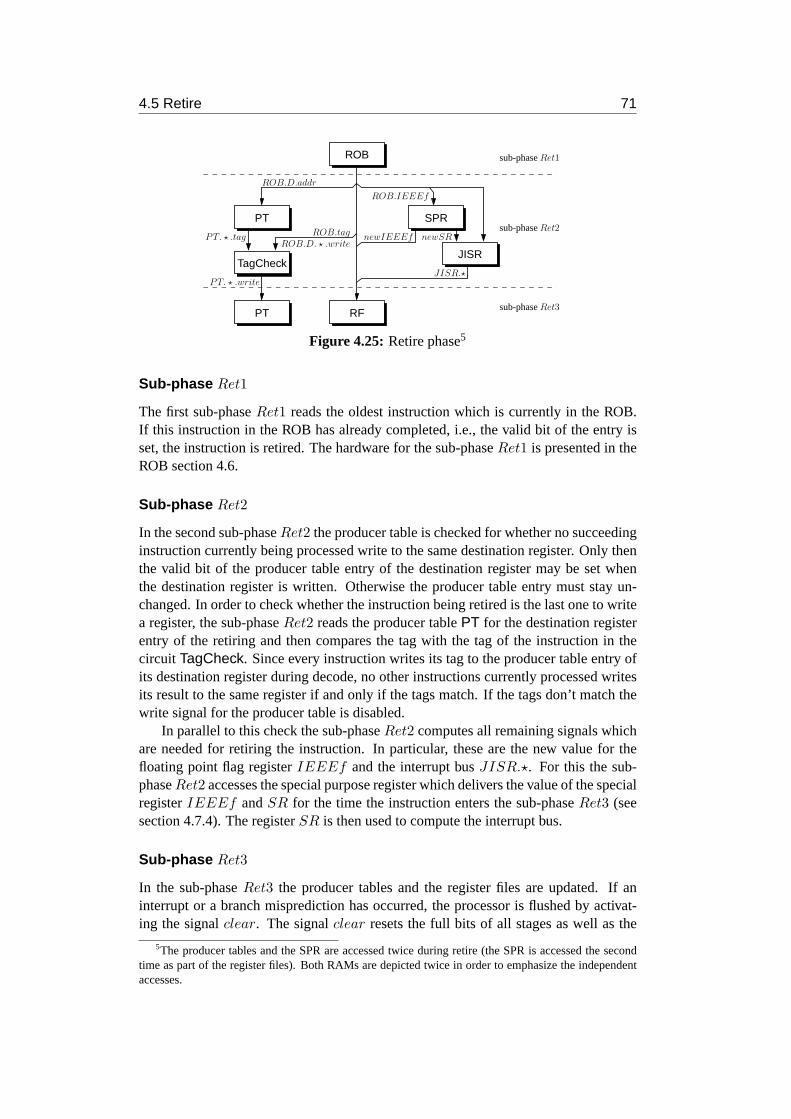
4.5 Retire 71
ROB.D.addr
ROB.tag
ROB.D. ⋆ .writePT. ⋆ .tag
TagCheck
PT. ⋆ .writeJISR.⋆
ROB.IEEEf
newIEEEf newSR
ROB
PT
RFPT
sub-phaseRet1
sub-phaseRet2
sub-phaseRet3
JISR
SPR
Figure 4.25: Retire phase5
Sub-phase Ret1
The first sub-phaseRet1 reads the oldest instruction which is currently in the ROB.If this instruction in the ROB has already completed, i.e., the valid bit of the entry isset, the instruction is retired. The hardware for the sub-phaseRet1 is presented in theROB section 4.6.
Sub-phase Ret2
In the second sub-phaseRet2 the producer table is checked for whether no succeedinginstruction currently being processed write to the same destination register. Only thenthe valid bit of the producer table entry of the destination register may be set whenthe destination register is written. Otherwise the producer table entry must stayun-changed. In order to check whether the instruction being retired is the lastone to writea register, the sub-phaseRet2 reads the producer tablePT for the destination registerentry of the retiring and then compares the tag with the tag of the instruction in thecircuit TagCheck. Since every instruction writes its tag to the producer table entry ofits destination register during decode, no other instructions currently processed writesits result to the same register if and only if the tags match. If the tags don’t match thewrite signal for the producer table is disabled.
In parallel to this check the sub-phaseRet2 computes all remaining signals whichare needed for retiring the instruction. In particular, these are the new value for thefloating point flag registerIEEEf and the interrupt busJISR.⋆. For this the sub-phaseRet2 accesses the special purpose register which delivers the value of the specialregisterIEEEf andSR for the time the instruction enters the sub-phaseRet3 (seesection 4.7.4). The registerSR is then used to compute the interrupt bus.
Sub-phase Ret3
In the sub-phaseRet3 the producer tables and the register files are updated. If aninterrupt or a branch misprediction has occurred, the processor is flushed by activat-ing the signalclear. The signalclear resets the full bits of all stages as well as the
5The producer tables and the SPR are accessed twice during retire (the SPR is accessed the secondtime as part of the register files). Both RAMs are depicted twice in order to emphasize the independentaccesses.

72 Processor Core
producer tables and the ROB. Since retire is done in order this leaves the processorin a consistent state. The computation of the clear signal depends on the handling ofbranch misprediction and is therefore presented in more detail in the instruction fetchchapter 6. The sub-phaseRet3 only consists of these RAM accesses and is presentedin the sections for the register file and the producer table (4.7 and 4.8).
4.5.2 Tag Check
The circuitTagCheck checks for all register filesR ∈ {GPR,FPR,SPR} if the tag ofthe destination registerPT.R.tag of the instruction equals the tagROB.tag of theinstruction read from the ROB. If the tags are equal and the write signal for the registerfile typeROB.D.R.write is active, the valid bit of the destination register entry mustbe set by writing to the producer table. Thus, the write signals for the producer tablesare computed as follows:
D.PT.R.write := D.R.write ∧ (ROB.tag = PT.R.tag).
Let I be an instruction in the retire sub-phaseRet2. The outputPT.R.tag ofthe read access to the producer table forI must contain the value of the entry at thetime the instructionI enters the sub-phaseRet3. Otherwise it could happen that anew instructionIn which updates the producer table during its decode phase is notrecognized. The updated value ofIn could be overwritten by the instructionI in sub-phaseRet3 which may lead to data inconsistencies. Hence, all write accesses to thePT during decode that start beforeI enters the sub-phaseRet3 must be forwarded tothe read access in the retire sub-phaseRet2. The forwarding of the producer tabledescribed in detail in section 4.8.
The cost and delay of the circuitTagCheck are:
C(TagCheck) ≤ 3 · C(EQ(lROB + 1)),
D(TagCheck) ≤ D(EQ(lROB + 1)).
4.5.3 Interrupt Handling
The circuit JISR computes all interrupt related signals. If an interrupt occurs, theprocessor is flushed and the instruction fetch is restarted at the start of the interruptservice routine (ISR). The service routine then executes code to reacton the interrupt(it “handles” the interrupt). The last instruction of the ISR is always a return-from-exception (rfe) instruction which returns to the code that caused the interrupt. In orderto allow precise interrupt handling some registers of the SPR defining address and typeof the interrupt must be updated when an interrupt occurs. A detailed description ofthe interrupt handling including a correctness proof can be found in [MP00].
The supported interrupts are shown in table 4.4 ordered by priority. If twodifferentinterrupts occur for one instruction, the interrupt with higher priority (lower index)is handled first. The internal interrupts (priority 1 to 12) are detected in the phasesinstruction fetch, decode, and execute. The corresponding signals are collected andsaved in the ROB. The external interrupts are assigned to the first instruction whichenters the retire sub-phaseRet2 after the interrupt occurred. As in [MP00], the external

4.5 Retire 73
name signal priority type maskable external
reset reset 0abort
no
yesillegal instruction ill 1
no
misaligned access mal 2page fault IM Ipf 3
repeatpage fault DM Dpf 4trap trap 5
continue
FXU overflow ovf 6
yes
FPU overflow fOV F 7FPU underflow fUNF 8FPU inexact result fINX 9FPU divide by zero fDBZ 10FPU invalid operation fINV 11FPU unimplemented uFOP 12 noexternal I/O exj 12+j yes yes
Table 4.4: Interrupts
interrupts signals are required to remain active until the processor is flushed. Theinternal and external interrupts are combined in the busCA[31 : 0] according to theirpriority:
CA[i] :=
pup if i = 0
ROB.ill if i = 1
ROB.dmal ∨ ROB.imal if i = 2
ROB.Ipf if i = 3
ROB.Dpf if i = 4
ROB.trap if i = 5
ROB.ovf if i = 6
ROB.IEEEf [i − 7] if 7 ≤ i ≤ 12
ex[i − 13] if i ≥ 13
Misaligned memory accesses can occur during instruction fetch (imal) or during datamemory accesses (dmal). Both interrupts are combined to the misaligned interruptsignalCA[2].
The interrupts 6 to 11 and 13 to 31 can be masked by the mask registerSR. Theseinterrupts are ignored if the corresponding bit of the registerSR is not set. The maskedinterrupt busMCA is defined as:
MCA[i] :=
{
CA[i] ∧ SR[i] if 6 ≤ i ≤ 11 ∨ 13 ≤ i
CA[i] if i ≤ 5 ∨ i = 12
The signaljisr indicates that a non-masked interrupt has occurred:
jisr := ROB.full ∧31∨
i=0
MCA[i]

74 Processor Core
An interrupt can be of one of the typesabort, repeat, or continue. If an abort inter-rupt occurs, the processor is restarted. If the interrupt is of type repeat, the instructionthat caused the interrupt has to be repeated after the interrupt has beenhandled bythe ISR. If the interrupt is of type continue, the processor continues at the succeedinginstruction after the execution of the ISR. Since the content of the register files is ir-relevant if the interrupt is of type abort, the processor core distinguishes only betweenthe types repeat and continue:
repeat := MCA[3] ∨ MCA[4] = CA[3] ∨ CA[4].
Repeat interrupts have higher priority than continue interrupts and are not maskable.Thus, the interrupt with highest priority cannot be of type continue ifrepeat is active.
The PC of the instruction which must be executed after the interrupt has been han-dled is stored in the special registerePC. For abort interrupts the value written intothis register may be arbitrary. If the interrupt is of type repeat, this is the PC of theinstruction that caused the interrupt. If the interrupt is of type continue, thisis thePC of the next instruction. The PC of the next instruction depends on the type of theinstruction for which the interrupt occurred. If the instruction is a branchinstruction(indicated by the signalbranch in the ROB entry), the branch target has been com-puted in the BCU, which delivers the target on the high part of the result bus (seetable 4.3). Otherwise the PC of the next instruction is the PC of the current instructionplus 4. The special registerePC is updated using the busePC which therefore isdefined by:
ePC :=
ROB.data.hi if repeat ∧ ROB.branch
ROB.PC + 4 if repeat ∧ ROB.branch
ROB.PC if repeat
.
If the interrupt is caused by a trap instruction, the registereData must be updatedwith the immediate constant of the instruction. If the interrupt is caused by a page faultor a misaligned memory access the registereData must be updated with the effectiveaddress of the memory access. In any case the value that has to be written into theregistereData can be found in the low part of the result busROB.data as explainedin the following.6
For instruction memory interrupts, the decode circuit sets the immediate constantto the PC of the instruction, i.e., the effective address of the memory access (see sec-tion 4.1.3). Thus for both trap instructions and instruction memory interrupts thereg-ister eData must be set to the value of the immediate constant. In both cases theinstruction causing the interrupt uses the integer ALU which then copies the imme-diate constant to the low part of the result bus. If a data memory interrupt occurs,the memory unit also stores the effective address on the low part of the result (seetable 4.3). The special registereData is updated using the buseData. Thus:
eData := ROB.data.lo.
6Thus, the ROB entries of the DLXπ+do not need an extra 32 bit field for the exception data as thedesigns proposed in [Kro99] and [Hil00].

4.5 Retire 75
Before the processor jumps into the ISR, all instructions preceding the instructionthat caused the interrupt must have updated the register files. This is guaranteed asretiring is done in order. The instruction causing the interrupt may only update theregister files if it is not of type repeat. Thus, the write signal for a registerfile R ∈{GPR,FPR,SPR} may not be active for interrupts of type repeat:
D.RF.R.write := D.R.write ∧ repeat.
The busJISR.⋆ updates the instruction fetch unit. The full bit must be active if aninterrupt occurred. It forces the instruction fetch unit to continue the instruction fetchat the start of the ISR, i.e., at addressJISR.sisr. This bus is set to the constant SISR(start of the interrupt service routine):
JISR.full := jisr,
JISR.sisr := SISR.
Stalling
The last stage of the retire sub-phaseRet2 has to be stalled if an interrupt occursand the instruction fetch unit cannot accept new data, which is indicated bythe signalIF.lastcycle (see section 6.1.2). If the retire sub-phaseRet2 is divided into multiplestages the stalling only affects the last stage. The other stages are never stalled. Sincethe interrupt flushes the whole processor core anyway, inconsistent data for the suc-ceeding instructions do not affect the correctness. LetcRet2 be the number of stages ofthe retire sub-phaseRet2. Then:
Ret2.stalli := 0 for i ∈ {0, . . . , cRet2 − 2},
Ret2.stallcRet2−1 := JISR.full ∧ IF.lastcycle.
Cost and Delay
The cost and delay of the circuitJISR are:
C(JISR) ≤ C(OR-Tree(32)) + C(INC(32)) + 32 · C(Sel(3)) + 30 · CAND + COR,
D(JISR) ≤ max{D(INC(32)), 2 · DAND + D(OR-Tree(32))}.
4.5.4 Cost and Delay
Sub-phase Ret1
For performance measurements the number of cycles needed to read out the ROBin the sub-phaseRet1 has no impact. The minimum number of cycles between thecompletion and the retiring of an instruction is defined by the number of cyclescC2R
it takes to forward the data on the CDB to the output of the ROB in the read access insub-phaseRet1. The value ofcC2R is computed in the ROB section 4.6. The retiresub-phaseRet1 needs no additional hardware apart of the ROB.

76 Processor Core
Sub-phase Ret2
The total delay and the number of stages needed for the the sub-phaseRet2 are:
D(Ret2) ≤ max{D(PT. ⋆ .tag) + D(TagCheck), D(SPR.newSR) + D(JISR),
D(SPR.newIEEEf)},
cRet2 ≤ ⌈D(Ret2)/δ⌉.
The inputs to the retire phaseRet2 are the outputs of ROB and producer table andthe external interrupts. Thus, the number of inputs is 140. The outputs of the retirephaseRet2 are the interrupt busJISR.⋆, the destination register busD.⋆, and theinterrupt signals for the special purpose register file. The number of output bits is 264.The cost of the sub-phase is:
C(Ret2) ≤ C(TagCheck) + C(JISR) + 5 · COR + cRet2 · 182 · CREG.
Sub-phase Ret3
The number of stages of the retire sub-phaseRet3 has no impact on the performanceof the processor. The cost of the sub-phaseRet3 is the cost of the input registers:
C(Ret3) ≤ 264 · CREG.
4.6 Reorder Buffer Environment
The reorder buffer is a queue used to rearrange instructions into program order beforethey are retired. This is needed for precise interrupt handling [SP85].New entries inthe ROB are allocated during decode. When an instruction completes, the validbit ofthe entry is set. If the oldest instruction in the ROB is valid, it is retired.
4.6.1 Overview
The ROB is implemented as a RAM block with head and tail pointer. The head pointeraddresses the oldest entry, the tail pointer points to the entry which should be filled nextwith a new instruction. When an instruction retires, the head pointer is incremented;when a new entry is allocated, the tail pointer is incremented. If the ROB is full no newinstructions are decoded (see section 4.1.7). Thus a new entries are onlyallocated, ifthe ROB is not full.
The ROB is read in two different contexts and written in two further contexts.Inorder to distinguish these four contexts a name is introduced for every context. Thefour different accesses to the ROB are listed in the following:
Allocation-context: During the decode sub-phaseD2 (see section 4.1.1) a ROB entryis allocated for the new instruction by writing to the ROB. The address of theentry which is allocated is given by the tail pointer. This access resets the validbit of the entry to indicate that the instruction has not yet completed and writesthe information for the instruction which are known during decode (e.g., theaddress of the destination register) into the ROB.

4.6 Reorder Buffer Environment 77
group name width purpose
valid valid 1 valid signal for entrydataLow data[31 : 0] 32 lower 32 bit of resultdataHi data[31 : 0] 32 upper 32 bit of result
onIssue
ill 1 illegal instructionimal 1 misaligned IMem accessipf 1 IMem page faulttrap 1 trap instructionuFOP 1 unimplemented FP instructionD.addr 5 destination addressD.dbl 1 double precision resultD.GPR.write 1 GPR destinationD.FPR.write 1 FPR destinationD.SPR.write 1 SPR destinationbranch 1 branch instructionwriteIEEEf 1 instruction writes IEEEf registerPC 32 instruction PC
onCompl
dmal 1 misaligned DMem accessdpf 1 DMem page faultovf 1 ALU overflowIEEEf 5 IEEE flagsmp 1 misprediction
Table 4.5: Components of an ROB entry
Operand-read-context: In parallel to the access-context the ROB is read for each ofthe (up to six) operands of the new instruction. If the entry read for the operandhas already completed, the result can be forwarded to the reservation station.
Completion-context: During completion the result of the instruction is written intothe ROB. This access also sets the valid bit of the ROB entry.
Retiring-context: In the retire sub-phaseRet1 the ROB entry addressed by the headpointer is read in order to retire the oldest instruction. If the valid bit of the readinstruction is set, the instruction is retired.
Table 4.5 lists the fields of the ROB entries. Not all fields are used in every context.The components which are used in the same contexts are combined into the followinggroups as proposed in [Hil00]:
valid: This group contains the valid bit of the entry. This bit indicates that the instruc-tion which is saved in this entry has already completed and hence the ROB entrycontains the valid result of this instruction. It is accessed in every context.
dataHi, dataLo: The two groups dataHi and dataLo contain the high respectively lowpart of the result. Both groups are read in the operand-read context and the retire-context and written in the completion-context. Note that data needed by the high

78 Processor Core
group ports widthallocation operand-read completion retiring
valid 1W 6R 1W 1R 1dataLo 3R 1W 1R 32dataHi 3R 1W 1R 32onIssue 1W 1R 48onCompl 1W 1R 9
Table 4.6: Data width and number of ports of the ROB groups
parts of the operandsOP1 andOP2 can only be found in the group dataHi (seesection 4.1.2). The low part of the operandsOP1 andOP2 can only be foundin the group dataLo. The operandsOP3 andOP4 can only be written by 32 bitresults and can therefore be found in both the groups dataHi and dataLo(seesection 4.3). In order to distribute the read ports evenly for the operandOP3
the group dataLo is read and for the operandOP4 the group dataHi is read.Therefore, only three read ports are needed for the operand-readcontext.
onIssue: All information about the instruction which do not change after the decodephase are combined in the group onIssue. This comprises the interrupt condi-tions which are detected during instruction fetch and decode, the informationabout the destination register, the PC of the instruction, thebranch bit indicat-ing a branch instruction (i.e., a branch or a jump), and the bitwriteIEEEfindicating a moveI2S instruction which writes the special registerIEEEf . Thegroup onIssue is written in the allocation-context and read in the retire-context.
onCompl: This group contains the interrupt conditions which are detected during ex-ecute and the branch misprediction signal. Since these informations are notneeded by succeeding instructions this group is not accessed in the operand-read context. Thus, the group is only accessed in the completion- and retiring-context.
Table 4.6 shows the width and the number of ports needed by the groups of theROB. The valid group needs seven read ports. To reduce the number of read ports thethree copies of the RAM block for the valid group are used with the same write portsbut less read ports. The first two RAM blocks with3 read ports each correspond to theRAM blocks of the groups dataLo and dataHi and are accessed in the samecontexts.The last RAM block has only one read port and is accessed in the retire context. Inorder for all sub-groups to have the same content, every sub-group has the same twowrite ports. Since the valid group consists of only one bit, the additional costfor theRAM blocks is not significant.
4.6.2 Pipelining of the Retiring-Context
Pipelining of the ROB access in the retiring-context must be done differentlyto allother RAM accesses as the decision which address has to be read next depends on thelast read result.

4.6 Reorder Buffer Environment 79
Let cRet1 be the number of cycles needed for a read access to the ROB in the retire-context. In [Kro99] the read access for the oldest instruction is restarted if the validbit of the oldest instruction is not set. Then no instruction could be retired for the nextcRet1 − 1 cycles. This degrades the performance ifcRet1 is larger than one. In order toavoid a restart of the read access, the read access of the oldest instruction I is stalledin the last stage of the ROB if theI has not completed yet. Upon completion ofI theresult is forwarded to this read access. The forwarding also sets the valid bit of thedata read from the ROB and the instruction can retire.
Since a read access for the ROB takescRet1 cycles, the read access for the second-oldest instruction must already have been started, when the oldest instruction is retired.Otherwise instructions could only be retired everycRet1 cycles. Lett be the tag of theoldest instruction in the ROB. In order to be able to retire an instruction everycycle,the read access for the entryt+1 must be in the second-last stage of the read access, theaccess for entryt + 2 in the third last and so on. If the processor is flushed, the oldestinstruction in the ROB will have the tag0. Thus, upon activation of the clear signal thepipeline of the read access is set up such that the last stage contains a read access forthe entry zero, the second last stage a read access for the entry one, and so on. Thus,the first stage of the read access in the retire context must contain a read access for theentrycRet − 1. The address of the first stage of the read access is determined by thehead pointer. Thus, the head pointer does not point to the oldest instruction, but to thecRet1 − 1-oldest instruction. If the oldest instruction is retired, all read accessesmoveto the next stage and the head pointer is incremented. Hence, ift is the tag of the oldestinstruction in the ROB, the stages0 to cRet1 − 1 of the read access in the retire-contextalways contain read accesses to the entriest + cRet1 − 1 to t.
Note that the read accesses in the retire context are started speculatively, i.e., a readaccess can be started even before the entry has been allocated for an instruction. Thus,the RAM will not return any valid data for the read access. In this case all informationof the instruction must be returned by means of forwarding.
4.6.3 Forwarding
In this section the forwarding of the write accesses in the allocation- and completion-contexts to the read accesses in the operand-read- and retiring-contexts is described.Every of the four possible combinations is discussed separately.
Allocation-Context to Operand-Read-Context
Only the valid bit of the ROB entries are written in the allocation-context and readin the operand-read context. The allocation-context disables the valid bit. Hence,forwarding of this bit would mean that the entry of an instructions that has alreadyretired is invalidated. Yet, the register file and producer table environments use the factthat the results of instructions that have been retired can still be read out of the ROB.This allows to omit forwarding in the register file and producer table environment fromthe retire phase to the decode phase (see section 4.7.1). Hence, no forwarding is donefrom the allocation-context to the read-context.
The read accesses in the operand-read-context can be stalled since ithas to waituntil the instruction is issued (see section 4.1.7). The write accesses in the allocation-

80 Processor Core
context is not stalled. Thus, a write accesses can overtake a read accesses. If the readaccess uses the same address as the write access, the read access would return the datawritten by the write access. Thus, even if no forwarding is done, the readaccess couldreturn data written by write accesses that have not been started before.In order toprevent this it must be guaranteed that the write accesses that can overtake a read donot use the same address as the read access.
The accesses in the allocation and operand-read-context for an instruction are bothstarted when the instruction enters the decode sub-phaseD2. The read access is stalledin the first stage ofD2 if the output stall signal of the issue circuit is active. The readaccess must not finish before an instruction is issued (see section 4.1.7).If issuing canbe done in one cycle the read access does not have to be stalled, once it enters thesecond stage ofD2. If issuing takes multiple cycles, the last stage of the ROB readaccess is stalled if the control signalissued is not active. Thus, in this case all stagesof the ROB access can be stalled.
The write access in the allocation-context is never stalled. In fact if the instructionis stalled in the first stage of the decode sub-phaseD2 multiple write accesses will bestarted for the instruction. Hence, if issuing can be done in one cycle, the read accessin the operand-read-context of an instructionI can be overtaken by the write access inthe allocation-context ofI itself. Once the read access is in the second stage no morewrite accesses can overtake the read. Thus, in this case it must be guaranteed that thetags of the operands ofI returned by the producer table may not have the same valueas the tag ofI.
If issuing takes multiple cycles, a read access can be stalled in every stage of theaccess. Hence, a read access in the operand-read-context of an instructionI can beovertaken by the write accesses in the allocation context of all instructions that can bein the decode sub-phaseD2 at the same time asI. Let cD2 be the number of cycles ofthe decode sub-phaseD2 and lett be the tag ofI. Since decode is done in order, thewrites that can overtake the read access in the operand-read-contextof I have the tagst + cD2 − 1 to t (modulo the size of the ROBLROB). Thus it must be guaranteed, thatthe instructionI does not depend on any instruction with these tags.
Completion-Context to Operand-Read-Context
If not all operands of an instructionI are valid, the results of all instructions thathave not updated the register files must be forwarded to the instructionI until alloperands are valid. The read access to the ROB RAM in the operand-read-context ofinstructionI returns the results of all instructions which have already completed at thetime the read access is started. As soon as the instructionI is in a reservation station,the forwarding is done by the reservation station by snooping on the CDB. Thus, theforwarding circuit for the ROB read access in the completion-context must take allinstructions into account that complete in the window from the start of the readaccessof the instructionI to the arrival ofI in the reservation station.
If issue is done in one cycle, the window consists of exactly the one cycle in whichthe instruction is issued. The forwarding of this cycle is done by a forwarding treewith one input. If the issuing takes multiple cycles, the CDB has to be forwardeduntilthe signalissued is active (see section 4.1.7). Since the read access can be stalled ifissuing takes multiple cycles, the forwarding is done by means of a forwarding circuit
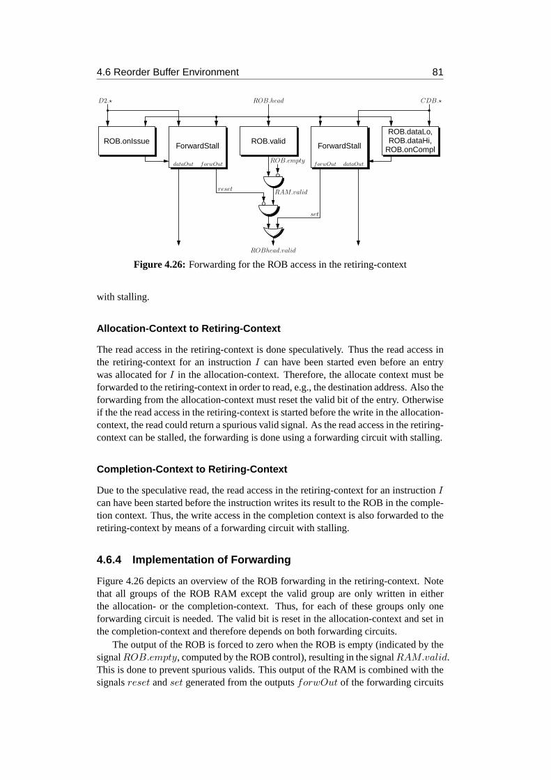
4.6 Reorder Buffer Environment 81
reset
dataOut forwOut
ForwardStall
set
forwOut dataOut
ForwardStall
CDB.⋆D2.⋆
ROB.valid
ROB.empty
ROB.head
RAM.valid
ROBhead.valid
ROB.onIssueROB.dataLo,ROB.dataHi,
ROB.onCompl
Figure 4.26: Forwarding for the ROB access in the retiring-context
with stalling.
Allocation-Context to Retiring-Context
The read access in the retiring-context is done speculatively. Thus the read access inthe retiring-context for an instructionI can have been started even before an entrywas allocated forI in the allocation-context. Therefore, the allocate context must beforwarded to the retiring-context in order to read, e.g., the destination address. Also theforwarding from the allocation-context must reset the valid bit of the entry. Otherwiseif the the read access in the retiring-context is started before the write in the allocation-context, the read could return a spurious valid signal. As the read accessin the retiring-context can be stalled, the forwarding is done using a forwarding circuitwith stalling.
Completion-Context to Retiring-Context
Due to the speculative read, the read access in the retiring-context for an instructionIcan have been started before the instruction writes its result to the ROB in the comple-tion context. Thus, the write access in the completion context is also forwarded to theretiring-context by means of a forwarding circuit with stalling.
4.6.4 Implementation of Forwarding
Figure 4.26 depicts an overview of the ROB forwarding in the retiring-context. Notethat all groups of the ROB RAM except the valid group are only written in eitherthe allocation- or the completion-context. Thus, for each of these groups only oneforwarding circuit is needed. The valid bit is reset in the allocation-context and set inthe completion-context and therefore depends on both forwarding circuits.
The output of the ROB is forced to zero when the ROB is empty (indicated by thesignalROB.empty, computed by the ROB control), resulting in the signalRAM.valid.This is done to prevent spurious valids. This output of the RAM is combined with thesignalsreset andset generated from the outputsforwOut of the forwarding circuits

82 Processor Core
TestTest.forwardi
Test.datai
forwi datai
stalli
forwUpdi dataUpdi
dataUpdi−1
(cRet1 − i)bin
clear
W.{tag, valid, data} addri−1
addri
addri
01
0 1
0 1
forwUpdi−1
0 1stalli
Figure 4.27: Stagei of the forwarding circuit for the ROB
for the allocate- respectively completion-context. These signals indicate that the laststage of the corresponding forwarding circuit contains data to be forwarded.
The signalreset is active if the allocation of the entry for an instructionI is doneafter the read access in the retire context forI has been started. Since the allocationresets the valid bit the signalreset forces the signalRAM.valid to zero. The signalset is active if the instruction stored in the ROB entry has completed since the RAMaccess has been started. This signal forces the signalRAM.valid to one, resulting inthe signalROBhead.valid. The signalset has higher priority than the signalreset asthe write in the completion-context for an instruction is always started after thewritein the allocation-context. The signalROBhead.valid indicates whether the oldestinstruction in the ROB is valid. It is used as full input of the retire sub-phaseRet2.
Note that upon activation of the clear signal the ROB access in the retiring-contextis not started from the beginning, but the whole pipeline is filled with the read requestsfor the ROB entriescRet1−1 to0 (see section 4.6.2). The valid outputROBhead.validof the RAM access in the retire-context depends on the forward signals of the forwardcircuits, hence these signals have to be reset upon clear. Figure 4.27 depicts a modifiedstage of the forwarding circuit for the read access in the retiring context(see figure 2.10on page 21 for the unmodified stage). If the signalclear is active, the stage resets thebit forw and sets the address of the access tocRet1 − i.
4.6.5 Control
Stall signals
The write accesses in the allocation- and the completion-context are never stalled. Thestalling of the ROB read accesses in the operand-read context has beendiscussed insection 4.1.7. The read-access in the retiring-context has to be stalled if thevalid bitROBhead.valid (see figure 4.26) of the oldest instruction (which is in the last stageof this read-access) is not active:
Ret1.stallIn := ROBhead.valid.
If ROBhead.valid is not active, the oldest instruction is stalled in the last stage ofthe read access in the retiring-context until the instruction completes and the forward-

4.6 Reorder Buffer Environment 83
ing circuit for the completion-context forces the signalROBhead.valid to one, asdepicted in figure 4.26.
This stall signal is used in a forwarding circuit with stalling. Thus it must hold (seeequation (2.11) on page 21):
D(ROBhead.valid) := D(Ret1.stallIn) ≤ δ − DMUX . (4.23)
The signalROBhead.valid is computed using the outputsforwOut of forwardingcircuits with stalling (see figure 4.26). The outputs are based on the updatedforwardbits of the last stage of forwarding circuit (see figure 4.27). Thus, the delay of theoutputforwOut must hold:
D(forwOut) + DOR + DAND ≤ D(ROBhead.valid)(4.23)
≤ δ − DMUX
⇔ D(forwOut) ≤ δ − (DMUX + DOR + DAND). (4.24)
If a pipelining register is added after the test circuit in the stages of the forwardingcircuit (see figure 4.27), the outputsforwUpd⋆ of the stages have delayDOR. Hencethe outputforwOut of the forwarding circuit has delayDOR and the equation holdstrue forδ = 5.
Head and tail pointer
The head and the tail pointer of the ROB are implemented using two counters in thecircuit HeadTail (see figure 4.28). The head pointer addresses the oldest instructionin the ROB. When this instruction is retired (i.e.,ROBhead.valid = 1), the headpointer is incremented. The tail pointer addresses the next free entry of the ROB. Ifa new instruction enters the core, the value of the tail pointer is assigned as tag to theinstruction and the tail pointer is incremented. A new instruction enters the coreif thefirst stage of the decode sub-phaseD1 is full and not stalled. The incrementation ofhead and tail pointer is controlled by the signalsheadce andtailce:
headce := ROBhead.valid,
tailce := D1.full0 ∧ D1.stall0
= D1.full0 ∧ D1.full0 ∧ (D1.stallIn0 ∨ D1.genStall0))
= D1.full0 ∧ (D1.stallIn0 ∨ D1.genStall0).
If the signalclear is active the head and the tail pointer are reset. The tail pointer isset to zero. Due to the pipelining of the ROB accesses the head pointer is setto cRet1−1, wherecRet1 is the number of stages of the retire sub-phaseRet1 (see section 4.6.2).
The delay of the computation of the new values for the head and tail pointer (seethe figure 4.28) isD(Inc(lROB)) + DMUX . If this cannot be computed in one cycle,the counter can be pipelined easily. Upon clear of the counters the pipeliningregistersmust be setup such that the counters increment correctly from0 respectivelycRet1−1.The cost of the circuitHeadTail can be estimated as:
C(HeadTail) ≤ 2 · (C(Inc(lROB) + COR + lROB · (CMUX + CREG)) + CAND.

84 Processor Core
tailtailce
IncInc
headcehead
lROB lROB
clearclear
0lROB (cRet1 − 1)bin
ROB.tail ROB.head
1 01 0
Figure 4.28: Head and tail pointer computation
Full and empty bit
The ROB control computes two signalsROB.full andROB.empty indicating thatthe ROB is full respectively empty. The signalROB.full is used as stall signal in thedecode phase, since new instruction may only enter the decode phase if theROB isnot full. If no instruction is in the ROB, the output of the ROB is invalid. In order toprevent an invalid instruction from retiring, the valid output of the ROB is ignored ifthe signalROB.empty is active as depicted in figure 4.26.
The computation of the full and empty bits is based on a circuit which counts thenumber of valid instructions in the ROB as proposed in [Lei99]. Due to the pipeliningof the decode and retire phases two separate counters have to be used for the compu-tation of the full and the empty signal.
The ROB full signal is used to guarantee tag-uniqueness, i.e., that no two instruc-tions with the same tag are active at the same time. Therefore, the counter for theROB full signal must take all instructions into account which have already entered thedecode sub-phaseD1 but have not yet written the register files, i.e., entered the retiresub-phaseRet3. These instructions are calledactiveinstructions.
The ROB empty signal is used to invalidate the ROB output if the ROB does notcontain any valid instruction. Therefore, the counter for the ROB empty signal mustonly count the instructions which really are in the ROB, i.e., the instructions forwhichthe write access in the allocation-context during decode has been started and the readaccess in the retiring-context has not yet finished. The write access in the allocatecontext is started in decode sub-phaseD2. The read access in the retiring-context isfinished if an instruction enters the retire sub-phaseRet2.
In [Lei99] decoding or retiring an instruction only takes one cycle. Thus,instruc-tions allocate a ROB entry in the same cycle they enter the decode phase and writethe register files in the same cycle they are read out of the ROB. Therefore, the samecounter can be used for the full and the empty bit in [Lei99].
Figure 4.29 depicts the circuitFullEmpty with the countersfcnt andecnt for thecomputation of the ROB full signalROB.full and ROB empty signalROB.empty.
Instructions get active when they enter the decode sub-phaseD1. This is indicatedby the signaltailce. Instructions get inactive when they enters the last retire sub-phaseRet3. Since this sub-phase is never stalled, this is indicated by the full bit of theinput registersRet3.full0. Hence, the signalstailce andRet3.full0 can be used toincrement respectively decrement the counterfcnt.

4.6 Reorder Buffer Environment 85
fcnt
ROB.full
ecnt
ROB.empty
tailce
Ret3.full0
inROB
headce
LS(1)
RS(1)
RS(1)
LS(1)
clearclear
cA2R − 1 times
inROBd
0
1 0
1
LROB LROB
Figure 4.29: Computation of the full and empty bit
An instruction is read out of the ROB if it the oldest instruction in the ROB andalready has completed. In this case the instruction enters the retire sub-phaseRet2.This is indicated by the signalheadce which thus determines whether the counterecnt shall be decremented. A new write access in the allocate-context is started ifaninstruction is in the first stage of the decode sub-phaseD2 and this stage is not stalled:
inROB := D2.full0 ∧ D2.stall0
Thus, the signalsinROB can be used to increment the counterecnt with the follow-ing small restriction: LetcA2R be the number of cycles needed for forwarding fromthe allocation-context to the retiring-context. Thus, it takescA2R cycles to clear thevalid output of the ROBROBhead.valid using forwarding (by the signalreset, seefigure 4.26). Then the signalinROB must be delayedcA2R−1 cycles and the delayedversioninROBd must be used to increment the counterecnt in figure 4.29. Other-wise the empty signal might become inactive before the write in the allocation-contextis forwarded to the retiring-context and has reset the valid outputRAM.valid of theROB. The valid bit stored in the ROB RAM could still be active from the last instruc-tion that used the entry. Thus the signalROBhead.valid could be active which wouldlead to a spurious retirement of an invalid ROB entry.
To reduce the delay of the countersfcnt andecnt, half-unary counters are used.This allows to increment the counter with a 1-bit left-shifterLS(1) and to decrementwith a 1-bit right-shifterRS(1) (see the figure 4.29). Since the last bit of the half-unaryencoding is always zero these bits is ignored for the counters, i.e., a0 is representedby all bits being zero. Both counters can be cleared using the signalclear.
The ROB empty signalROB.empty must be inactive if the value represented byecnt is at least one. Thus:
ROB.empty :=
{
0 if 〈ecnt〉hun ≥ 1
1 else
= ecnt[0].(4.25)

86 Processor Core
The ROB full signal must be computed differently depending on whether issuing canbe done in one cycle. LetcI be the number of cycles needed for issuing an instructionand letcD2 be the number of cycles needed for the read access to the ROB in theoperand-read-context. As described in section 4.6.3 up tocD2 writes in the allocation-context can overtake a read of the ROB in the operand-read context if issuing cannotbe done in one cycle (i.e.,cI > 1). Otherwise only the write access in the allocation-context of an instruction can overtake its own read access in the operand-read-context.
If issuing can be done in one cycle, the ROB full signal is set to one, ifLROB − 1instructions are active, otherwise it is already set to one ifLROB − cD2 instructionsare active. This is required by the correctness proofs of the forwarding for register fileand producer table. If follows:
ROB.full :=
1 if cI = 1 ∧ 〈fcnt〉hun ≥ LROB − 1
1 if cI > 1 ∧ 〈fcnt〉hun ≥ LROB − cD2
0 else
=
{
fcnt[LROB − 2] if cI = 1
fcnt[LROB − 1 − cD2] if cI > 1.
(4.26)
Note that the new value of the registersecnt andfcnt must be computed in onecycles based on the old value. Thus
δ ≥ D(LS(1)) + D(RS(1)) + DAND
= 2 · DMUX + DAND (4.27)
which holds forδ ≥ 5. The cost of the circuitFullEmpty is:
C(FullEmpty) ≤ 2 · LROB · (2 · CMUX + CAND + CREG)
+ (cA2R − 1) · CREG + CAND.
Check for oldest instruction
Instructions reading the special registerIEEEf must wait at the stagecRF of thedecode sub-phaseD1 until all preceding instructions have retired, which is indicatedby the signalallRet (see section 4.1.7). This is necessary as instructions write theregisterIEEEf implicitly, i.e., forwarding is not done using the Tomasulo algorithm.
Figure 4.30 shows the computation of the signalallRet. LetD1.tagcRF be the tagof the waiting instruction. The instruction is the oldest instruction in the ROB if the tagof the instruction in the last stage of the read access in the retiring-context of the ROBROB.tag matchesD1.tagcRF . No instruction is in the retire sub-phaseRet2 if allfull bits of Ret2 are zero. This is indicated by the signalRet2.clean. All instructionspreceding the waiting instructions have retired if the tags match andRet2.clean isactive.
The cost of the computation of the signalallRet is:
C(allRet) ≤ C(EQ(lROB)) + cRet2 · CAND + 2 · CREG.
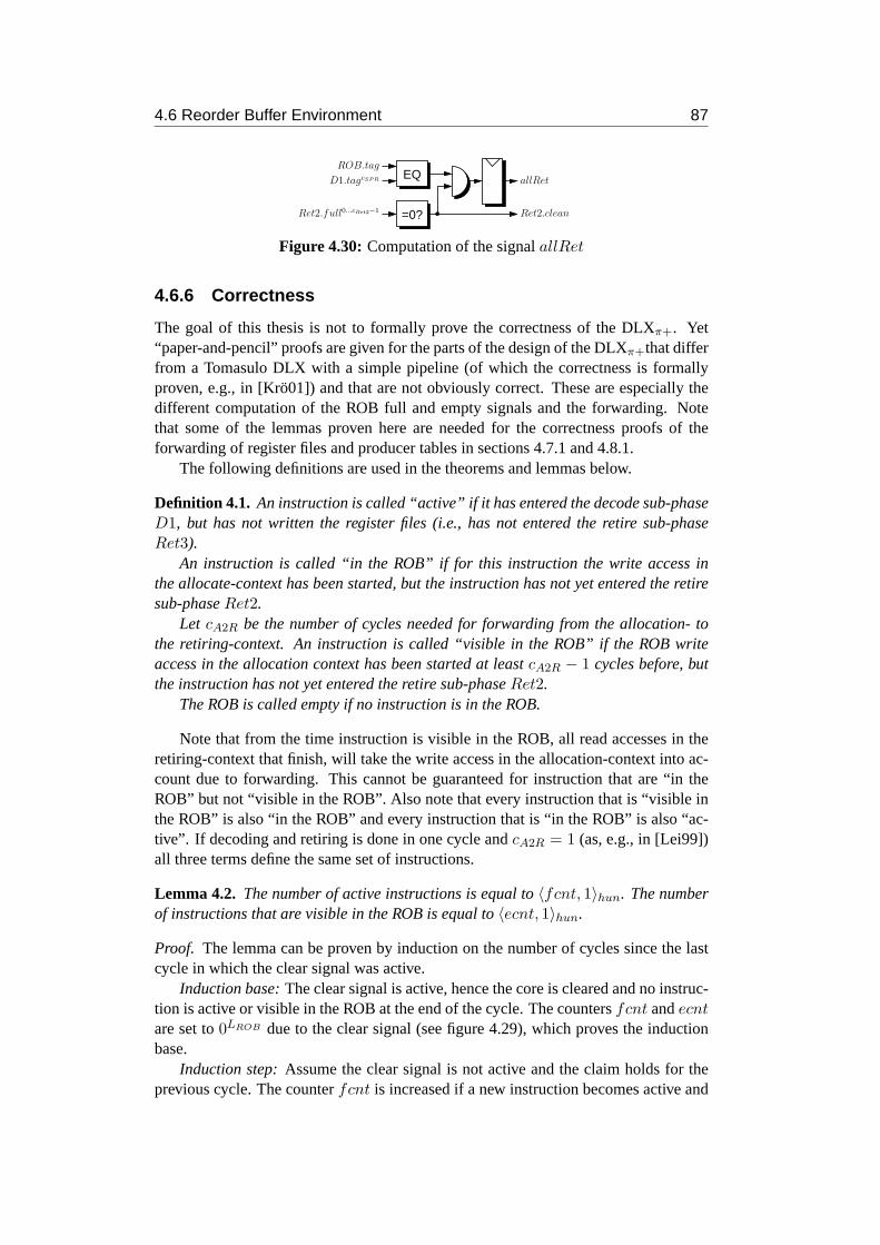
4.6 Reorder Buffer Environment 87
allRet
Ret2.clean
D1.tagcSPR
ROB.tagEQ
Ret2.full0...cRet2−1 =0?
Figure 4.30: Computation of the signalallRet
4.6.6 Correctness
The goal of this thesis is not to formally prove the correctness of the DLXπ+. Yet“paper-and-pencil” proofs are given for the parts of the design of the DLXπ+that differfrom a Tomasulo DLX with a simple pipeline (of which the correctness is formallyproven, e.g., in [Kro01]) and that are not obviously correct. These are especially thedifferent computation of the ROB full and empty signals and the forwarding.Notethat some of the lemmas proven here are needed for the correctness proofs of theforwarding of register files and producer tables in sections 4.7.1 and 4.8.1.
The following definitions are used in the theorems and lemmas below.
Definition 4.1. An instruction is called “active” if it has entered the decode sub-phaseD1, but has not written the register files (i.e., has not entered the retire sub-phaseRet3).
An instruction is called “in the ROB” if for this instruction the write access inthe allocate-context has been started, but the instruction has not yet entered the retiresub-phaseRet2.
Let cA2R be the number of cycles needed for forwarding from the allocation- tothe retiring-context. An instruction is called “visible in the ROB” if the ROB writeaccess in the allocation context has been started at leastcA2R − 1 cycles before, butthe instruction has not yet entered the retire sub-phaseRet2.
The ROB is called empty if no instruction is in the ROB.
Note that from the time instruction is visible in the ROB, all read accesses in theretiring-context that finish, will take the write access in the allocation-context into ac-count due to forwarding. This cannot be guaranteed for instruction that are “in theROB” but not “visible in the ROB”. Also note that every instruction that is “visible inthe ROB” is also “in the ROB” and every instruction that is “in the ROB” is also “ac-tive”. If decoding and retiring is done in one cycle andcA2R = 1 (as, e.g., in [Lei99])all three terms define the same set of instructions.
Lemma 4.2. The number of active instructions is equal to〈fcnt, 1〉hun. The numberof instructions that are visible in the ROB is equal to〈ecnt, 1〉hun.
Proof. The lemma can be proven by induction on the number of cycles since the lastcycle in which the clear signal was active.
Induction base:The clear signal is active, hence the core is cleared and no instruc-tion is active or visible in the ROB at the end of the cycle. The countersfcnt andecntare set to0LROB due to the clear signal (see figure 4.29), which proves the inductionbase.
Induction step:Assume the clear signal is not active and the claim holds for theprevious cycle. The counterfcnt is increased if a new instruction becomes active and

88 Processor Core
it is decreased if an instruction retires. The signalinROBd is active if the allocateaccess for an instruction has been started exactlycA2R cycles ago. This signal incre-ments the counterecnt. The signalheadce which is active if an instruction enters theretire sub-phaseRet2 decrements the counterecnt. Thus, it remains to show that thecounters do not overflow or underflow to prove the induction step.
If the signalROB.full is active, the first stage of the decode sub-phaseD1 isstalled (see section 4.1.7). Thus, no instruction can become active, the counterfcntcannot overflow. As every instruction that is visible in the ROB is also activethe valueof ecnt cannot be larger than the value offcnt and henceecnt cannot overflow, too. IfROB.empty is active, no instructions can enter the sub-phaseRet2. Thus, the counterecnt cannot underflow. Since an instruction cannot be visible in the ROB if it is notactive, the value offcnt must be larger than the value ofecnt and hencefcnt cannotunderflow.
Corollary 4.3. Let cD2 be the number of cycles needed for the ROB access in theoperand-read-context. If issuing is done in one cycle, at mostLROB instructions areactive at any time. If issuing is done in multiple cycles, at mostLROB − cD2 + 1instructions are active at any time.
Proof. If issuing is done in one cycle andLROB − 1 instructions are active, the signalROB.full := fcnt[LROB − 2] is active (see equation (4.26)). This stalls the firststage of decode sub-phaseD1. Thus, including the instruction in the first stage ofdecode sub-phaseD1, at mostLROB instructions can be active. If issuing is done inmultiple cycles the statement can be proven analogously from equation (4.26).
Corollary 4.4. No two instructions with the same tag can be active at the same time.
Proof. Assume two instructionsI, I ′ with the same tag are active. ThelROB bitwide tail counter is incremented whenever an instruction becomes active. Thus, atleastLROB − 1 = 2lROB − 1 instructions must have become active between the twoinstructionsI, I ′. The instructionsI and I ′ are active and therefore have not yetretired. Since retire is done in order it follows that the other instructions have not yetretired, too. Thus, at leastLROB + 1 instructions must be active which contradictscorollary 4.3.
Corollary 4.5. If the signalROB.empty is not active, the ROB is not empty. Let inthis caseI be the oldest instruction in the ROB. Then the allocate access forI hasbeen started at leastcA2R − 1 cycles before.
Proof. If ROB.empty is not active, the signalecnt[0] is one (see equation( 4.25)).Thus,〈ecnt, 1〉hun ≥ 1. It follows from lemma 4.2 that there is at least one instructionwhich is visible in the ROB. This instruction is therefore in the ROB and the ROB isnot empty.
Let I be the oldest instruction in the ROB. Since allocation is done in order, theinstructions that are visible in the ROB cannot have started the ROB access intheallocation-context beforeI. Hence,I must also be visible in the ROB.
Lemma 4.6. Let cD2 be the number of cycles needed for the ROB access in theoperand-read-context and letI be an active instruction with tagt. If issuing is done in

4.6 Reorder Buffer Environment 89
one cycle, no older active instruction can have the tagt. If issuing is done in multiplecycles no active instruction can have one of the tagst to t + cD2 − 1 (modulo the sizeof the ROBLROB).
Proof. Let I0 be an active instruction with tagt0 and letI1 be an instruction older thanI0 with tagt1. Let d be such thatt0 = t1 + d (mod LROB) for d ∈ {1, . . . , LROB}.The tail pointer assigning tags to the instruction is incremented for every instruction be-coming active. Since decoding and retiring are done in order, for everyj ∈ {0, . . . , d}an instructions with tagt := t1 +j (mod LROB) must be active. Hence, at least thosed + 1 instructions are active.
If issuing is done in one cycle, it follows from corollary 4.3 thatd < LROB andhencet0 6= t1. If issuing is done in multiple cycles, if follows from the corollary thatd < LROB − cD2 + 1. Hence, the instructiont1 cannot have one of the tagst0 tot0 + cD2 − 1 (moduloLROB).
The lemma guarantees that decoding is stopped before any ROB entries thatareread in the operand-read-context are invalidated by the allocation-accesses of succeed-ing accesses.
Theorem 4.7.LetLROB be the number of entries of the ROB and letcRet1 be the num-ber of cycles needed for the ROB read access in the retiring-context. IfLROB > cRet1
and the signalROBhead.valid is active, then the ROB is not empty and the instruc-tion in the last stage of the read access in the retire-phase has already completed.
Proof. Assume the signalROBhead.valid is active. For this either the signalset orthe output of the RAM must be active (see figure 4.26).
Case 1, the signalsset is not active. Then the output of the ROB valid RAM mustbe one and the signalsreset andROB.empty must be inactive. Thus, according tocorollary 4.5 the ROB is not empty. LetI be the oldest instruction in the ROB. Itfollows from corollary 4.5 that a write access in the allocation-context forI has beenstarted at leastcA2R − 1 cycles before. Sincereset is not active, this write accessmust have been started before the read access in the retiring-context has been started.Therefore, the RAM block returns the correct value for the valid bit of instructionI.Since the output of the RAM is active,I must have already completed.
Case 2, the signalset is active. Lett be the address (i.e., the tag) of the last stageof the ROB access in the retiring-context. If the signalset is active, an instructionI with tag t has completed after the ROB access in the retiring-context to the entrywith addresst has been started. An instruction can only complete if it has been is-sued before. The write access in the allocation-context is started when aninstructionis issued. Thus, the instructionI must already have started the write access in theallocation-context. This proves the first part ofI is in the ROB from definition 4.1.
In order to prove thatI is in the ROB it remains to show that instructionI has notyet retired. From the correctness of the Tomasulo algorithm follows that noinstructioncan complete twice. Sinceset is active the instructionI cannot have already completedbefore the read access in the retiring-context with tagt has been started. Thus, theinstructionI cannot have retired without setting the signalset of an read access in theretiring-context as proven in case 1. FromLROB > cRet1 it follows that no two stageswith the same address can exist in the retire access to the ROB. Thus, the result of the

90 Processor Core
instructionI can only have been forwarded to the read which is now in the last stageof the ROB access in the retiring-context. Hence, the instructionI cannot have retiredyet.
Since the instructionI has not yet retired, it must be in the ROB, the ROB is notempty. It follows that the instruction in the last stage of the retiring-context is theinstructionI, which has already completed.
Note that the requirementLROB > cRet1 of the theorem holds true for reasonablevalues ofLROB.
Theorem 4.8. If the ROB is not empty, the signalROBhead.valid gets active even-tually.
Proof. Let I be the oldest instruction in the ROB. Since the read access in the retiringcontext is stalled ifROBhead.valid is inactive, the instructionI remains the oldestinstruction unitROBhead.valid gets active.
The liveness of the Tomasulo algorithm guarantees that the instructionI completeseventually (as proved, e.g., in [Kro01]). If the read access in the retiring-context forIhas been started beforeI completes, the signalset gets active eventually which forcesROBhead.valid to one.
If the read access in the retiring-context forI has been started after the instructioncompletes, the ROB RAM for the valid bit returns a one. The write access in theallocation-context is started in parallel to the issue of an instruction. Thus, itmusthave been started before the instruction completes. According to corollary4.4 noother instruction with the same tag asI can be active. Therefore, no write access inthe allocate context can have been started to the entry of instructionI and henceresetcannot be active. Since the allocation access has already been started at most aftercA2R cycles the signalROB.empty gets inactive and henceROBhead.valid getsactive.
Cost
The total cost of the ROB control is (including the gates to compute the valid outputROBhead.valid):
C(ROB-Control) ≤ C(HeadTail) + C(FullEmpty) + C(allRet)
+ 2 · CAND + COR.
4.6.7 Delay Optimizations
The critical signals of the ROB control are the clock enables for the head and tailpointerheadce andtailce. In the described implementation the signalsheadce andtailce may have a delay of at mostδ− (DMUX +DAND) as they control the countersecnt andfcnt
The signalheadce is derived directly from the signalROBhead.valid which hasat most the delayδ − DMUX (see equation (4.23) on page 83). In the computationof the ROB empty signalROB.empty in figure 4.29 the AND gate for clearing thecounter can be moved above the right shifter controlled byheadce (see the left part

4.6 Reorder Buffer Environment 91
ROB.empty
inROB
clear
LROB
1
ecnt
cA2R − 1 times
ROB.full
LROB
1
Ret3.full0
fcnt1
fcnt
tailced
LS(1)
LS(1)
RS(1)
0
cleartailce
headce
inROBd
0
RS(1)
ecnt1
Figure 4.31: Optimized Computation of the full and empty bit
of figure 4.31). Even ifheadce is active while clearing the counter, the value of thecounter will still be set to all zeros as the right-shift only increases the number of zeros.Then the signalheadce may have a delay ofδ − DMUX .
The signaltailce is derived from the signalD1.stallIn0 ∨ D1.genStall0 (seesection 4.1.8) which is assumed to have a delay of at mostδ. On the other hand the de-lay of the signalROB.full was assumed to beDMUX in the computation of the stallsignals for the decode phase. This allows moving the left shifter in the computationfor the signalROB.full in figure 4.29 below the register and using a delayed versiontailced of the signaltailce to control the shifter (see the right part of figure 4.31). Ifthe counter is reset, the left-shift behind the register is prevented by forcing the signaltailced to zero on clear. The AND gate does not increase the delay of the signal as
tailce ∧ clear = D1.full0 ∧ (D1.stallIn0 ∨ D1.genStall0) ∧ clear
= ¬(D1.full0 ∨ D1.stallIn0 ∨ D1.genStall0 ∨ clear)
and the OR-Tree can be balanced such that the delay is the same as the delayof thesignalD1.stallIn0 ∨ D1.genStall0 (see figure 4.9 on page 50). Hence, in the circuitin figure 4.31 only boundsδ by the loops throughecnt andfcnt:
δ ≥ 2 · DMUX + DAND,
which holds true forδ = 5.
The signalheadce and tailce are also used to control the clocking of the headand tail pointers in figure 4.28. Due to the clear logic the delay of the signals maybe at mostδ − DOR, which is already achieved forheadce. However, to achievethis requirement for the signaltailce the logic for clearing the tail counter must bechanged (see figure 4.32). The circuit in the figure forces the output ofthe registertail to zero from the cycle after the clear signal has been active to the cycle where thefirst instruction enters the decode sub-phaseD1. As a side-effect the modification alsoforces the output to zero, whenever the input register of the decode sub-phaseD1 isnot full, but in this case the tail pointer may have arbitrary value.

92 Processor Core
1
0lROB
Inc
cleardclear
D1.full0
D1.genStall0
tail
D1.stallIn0
lROB
ROB.tail
0
Figure 4.32: Optimized clearing of the tail counter
The circuit delays the signalclear is delayed by one cycle. This allows to optimizethe computation of the clock enable signal of the registertail, since the signalclearresets the full bits of the decode stage, the ROB full signalROB.full, and the signalIR.haltdec (see section 6.4). Thus, when the delayed clear signalcleard is active, thesignalsD1.stallIn0 andD1.genStall0 are inactive, i.e.:
cleard = 1 ⇒ D1.stallIn0 ∨ D1.genStall0 = 0. (4.28)
Therefore, the signalcleard∨ tailce used to reset the output of the tail counter can besimplified as:
cleard ∨ tailce = cleard ∨ (D1.full0 ∧ (D1.stallIn0 ∨ D1.genStall0))
= (cleard ∨ D1.full0) ∧ (cleard ∨ (D1.stallIn0 ∨ D1.genStall0))(4.28)= (cleard ∨ D1.full0) ∧ (D1.stallIn0 ∨ D1.genStall0)
= ¬((cleard ∨ D1.full0) ∨ D1.stallIn0 ∨ D1.genStall0).
The OR-Tree can again be balanced such that the delay of the signalcleard ∨ tailcehas the same delay as the signalD1.stallIn0 ∨ D1.genStall0 which is at mostδ.
In order to force the signalROB.tail to zero until the first instruction enters thedecode sub-phaseD1 the registertail is also cleared if the signalD1.full is not active.Since the stall signal for the first stage cannot get active until the first instruction entersthe decode sub-phaseD1 the stall signal must not be taken into account.
Assume the number of cyclescI needed for issuing is greater than one. Then thewrite access in the completion-context must be forwarded to the read access in theoperand-read-context with a forwarding circuit with stalling. This requires that thestall signalsD2.stalli of all stagesi of the read access in the operand-read-contexthave at most delayδ − DMUX (see equation (2.11) on page 21). If the read accesstakescD2 cycles and the stall signals are computed the usual way, it must hold for thestall signal for the second stage:
δ − DMUX ≥ D(D2.stall1)
= D(ROB.stallOut)(4.10)= D(AND-Tree(cD2 + 1))
For lROB ≥ 6 andδ = 5 it holdscD2 > 7. Then, the equation does not hold.

4.6 Reorder Buffer Environment 93
To reduce the delay of the stall signal Instead pipeline bubbles are only removedin the last seven stages of the ROB read access, i.e., only the full bits of the last sevenstages are taken into account for computing the stall signals as proposed inthe firstpart of section 2.5.3. Thus, for all other stages the stall signal is computed as:
stall =
cD2∧
i=cD2−6
D2.fulli ∧ D2.issuedcD2
The additional cost for the delay optimizations are:
C(HeadTail)+ ≤ 2 · COR + CREG,
C(FullEmpty)+ ≤ CAND + CREG.
4.6.8 Cost and Delay
The delay of the ROB access in the operand-read context determines the delay of thedecode sub-phaseD2. The delay of the ROB access in the retire context determinesthe delay of the retire sub-phaseRet1. The delay of the ROB accesses are:
D(D2) ≤ max{D(RAM(LROB, 1, 3, 2)), D(RAM(LROB, 32, 4, 1))} + DMUX ,
D(Ret1) ≤ max{D(RAM(LROB, 1, 1, 2)) + 2 · DAND + DOR,
max{D(RAM(LROB, 32, 4, 1)), D(RAM(LROB, 48, 1, 1)),
D(RAM(LROB, 9, 1, 1))}
+ DMUX}.
Let cD2 andcRet1 be the number stages of the two ROB accesses respectively thecorresponding sub-phases. DefinecROB to be the maximum number of cycles neededfor any of the two ROB read accesses:
cD2 = ⌈D(D2)/δ⌉,
cRet1 = ⌈D(Ret1)/δ⌉,
cROB = max{cD2, cRet1}.
The number of stages for the retire sub-phaseRet1 is only needed for cost com-putations. The minimum number of cycles between the complete and the retire of aninstruction is bounded by the number of cycles needed for forwarding withstallingcC2R:
cC2R = ⌈(D(Test(lROB)) + 2 · DOR + DAND − DMUX)/(δ − DMUX)⌉.
The number of cyclescA2R needed to forward from the write accesses in the allocation-context is computed analogously, i.e.,cA2R = cC2R.
The cost of the ROB RAM blocks can be estimated as:
C(ROB-RAM) ≤ C(RAM(LROB, 1, 1, 2, cROB))
+ 2 · C(RAM(LROB, 1, 3, 2, cROB))
+ 2 · C(RAM(LROB, 32, 4, 1, cROB))
+ C(RAM(LROB, 48, 1, 1, cROB))
+ C(RAM(LROB, 9, 1, 1, cROB)).

94 Processor Core
For the retire context two forwarding circuits with stalling are needed. One for-warding circuit forwards the valid and the onIssue group from the allocate context(width 48), the other circuit forwards the valid, dataLo, dataHi, and the onComplgroup from the complete context (width 74). LetcI be the number of stages of theissue circuit. IfcI = 1 the forward circuit in the forward context consists of a For-warding Tree with one leaf for each operand. IfcI > 1 a forward circuit with stallingis needed for each operand.
Let cFS(lROB) be the number of cycles needed for forwarding with stalling (withlROB address bits). Then the cost of the forwarding circuits of the ROB can beesti-mated as:
C(ROB-Forward) ≤ C(ForwardStall(lROB, 48, cRet1, cFS))
+ C(ForwardStall(lROB, 74, cRet1, cFS))
+
4 · C(Forward-Tree(lROB, 32, 1, cD2))
+C(Forward-Tree(lROB, 5, 1, cD2))
+C(Forward-Tree(lROB, 2, 1, cD2))
if cI = 1
4 · C(ForwardStall(lROB, 32, cD2, cFS))
+C(ForwardStall(lROB, 5, cD2, cFS))
+C(ForwardStall(lROB, 2, cD2, cFS))
if cI > 1
.
The total cost of the ROB environment is:
C(ROB) ≤ C(ROB-RAM) + C(ROB-Control) + C(ROB-Forward).
4.7 Register File Environment
The processor has three different types of register files: the general purpose register fileGPR, the floating point register fileFPR, and the special purpose register fileSPR.All register files have one write port used in the retire sub-phaseRet3 to store theresult and multiple read ports used in the decode sub-phaseD1 to read the operands.The SPR has two additional read ports and one additional write port. The additionalread ports are used in the retire sub-phaseRet2. These read ports always read theregistersSR andIEEEf and therefore have constant address busses. The additionalwrite port is used in sub-phaseRet3 to store the new value of the registerIEEEfcomputed in the sub-phaseRet2 from the old value and the floating point exceptionsof the instruction. The standard port for storing the result cannot be used to write theregisterIEEEf as floating point compare instructions may write two special registers,namelyFCC for the comparison result andIEEEf for the exceptions.
The addresses of the read accesses during decode sub-phaseD1 are computed inthe register file environments from the instruction registerIR[31 : 0]. The encodingsof the addresses in the instruction words is listed in table A.8 in the appendix A. Theaddress and write signals used for the write access are computed in the retire sub-phaseRet2. They are combined in the busRet.D.⋆.

4.7 Register File Environment 95
OP⋆.FPR.data
GPR
IR
OP⋆.GPR.data OP⋆.SPR.data
Ret2.⋆
Forward
IEEEf, SR
Ret2.{newIEEEf, newSR}
Ret3.{full, newIEEEf, D.⋆}
SPRFPR
Figure 4.33: Register files
4.7.1 Forwarding
No forwarding is done from the write accesses in the retire sub-phaseRet3 writingthe instruction results to the read accesses in the decode sub-phaseD1 reading theoperands. This is not needed for the correctness as stated by the following theorem.
Theorem 4.9. The write accesses to the register files in the retire sub-phaseRet3need not to be forwarded to the read accesses to the register files ports in the decodesub-phaseD1.
Proof. Let ID be an active instruction in the decode phase that depends on the result ofan instructionIR. If IR has written its result to the register file beforeID starts its readaccess to the register file, no forwarding has to be done because the register file RAMwill return the result of the instructionIR. Thus, assume thatIR is still active (i.e., hasnot yet written the register file) at the timeID starts its read access to the register file.Then the producer table entry of the operand ofID that depends onIR still containsthe tag ofIR. Hence, the instructionID will check the ROB if it contains the result ofIR.
If IR has not completed before the instructionID starts the ROB read access inthe operand-read-context, it follows from the construction of the forwarding circuit forthe ROB (see section 4.6.3) that the result ofIR is forwarded toID. Thus, assumethat IR has completed beforeID starts the read access to the ROB. Thus, the ROBcontains the result ofIR. It remains to show that the read access to the ROB in theoperand-read-context of the instructionID returns the result ofIR.
At the timeID is in the first stage of decode sub-phaseD1, the instructionIR hasnot yet written the register file, i.e.,IR is active. Thus, from lemma 4.6 it follows thatno instruction older or equal toID and younger thanIR can have the same tag asIR
and therefore will not overwrite to the ROB entry ofIR and hence the ROB entry ofIR is still valid at the timeID starts the ROB read access in the operand-read-context.
If issue is done in one cycle, only the write access to the ROB in the allocation-context of the instructionID can overtake the read access to the ROB in the operand-read-context ofID as discussed in section 4.6.3. SinceID has not the same tag asIR
the write access in the allocation-context will not overwrite the entry ofIR. Hence, theread access returns the value of the ROB at the time the read access has been started,i.e., the valid result ofIR.
Let cD2 be the number of cycles needed for the read access to the ROB in theoperand-read-context. If issuing is done in multiple cycles also the write accesses tothe ROB in the allocation-context of thecD2−1 instructions followingID can overtakethe read access to the ROB ofID. From lemma 4.6 it follows that these instructions

96 Processor Core
d0 w0
1 0
dOut wOut
d1 w1
Figure 4.34: Forwarding circuitIEEEfC
cannot have the same tag asIR and thereforeID reads the valid result ofIR.
IEEEf
Let I be an instruction in the retire sub-phaseRet2. As discussed in section 4.5 thespecial purpose register must return the values of the special registersIEEEf andSR at the time the instructionI enters the retire sub-phaseRet3. The register filesare only written in the retire sub-phaseRet3. Thus, to obtain the value of the registersat the time the instructionI enters the sub-phaseRet3 it suffices to read the registerwhenI enters the sub-phaseRet2 and forward the writes to these registers of all olderinstructions in the sub-phaseRet2.
The forwarding for the registerSR can be done using a standard forwarding tree(see section 2.6.1). This forwarding tree combines the updates to the register SRof the instructions inRet2 which are older thanI in parallel toI ’s read access tothe registerSR. The outputs of the forwarding tree and the register access are thencombined to obtain the busnewSR containing the value of the registerSR at the timethe instructionI will enter the sub-phaseRet3.
To forward the registerIEEEf a modified forwarding tree must be used as theregisterIEEEf can be written in two different ways: if the instruction which retiresis a floating point operation, the new value ofIEEEf is computed by OR-ing thefloating point exception bits of the instruction to the old value ofIEEEf [IEEE]; ifthe instruction explicitly writes the registerIEEEf (e.g., a moveI2S instruction), theold value is overwritten.
The circuitIEEEfC (see figure 4.34) combines the updates to the registerIEEEfof two succeeding instruction. For this it uses the typesw and datad for updating theregisterIEEEf of an instruction. The typew of an instruction is one if the instructionexplicitly writes the registerIEEEf with the datad; if w is zero, the datad is to beOR-ed to the old value.
Let w1 andd1 be type and data of an instructionI1 that succeeds an instructionI0
with typew0 and datad0. The combined typewOut of the instructionsI1 andI0 isthe OR the types indicating that any of the instructionsI1 andI0 will directly write theregister. Ifw1 is one, the instructionI1 will overwrite the access done byI0. Thus,in this case the combined datadOut is the datad1 of instructionI1. If w1 is zerothe datad1 will be OR-ed to the datad0 of the instructionI0. In this case, ifw0 isactive, the preceding instructions will be overwritten with the OR of both instructions,otherwise the OR of both instructions will be OR-ed to the old vale. Thus, updatingthe registerIEEEf with the combined valueswOut anddOut has the same effect asthe sequential updates of instructionsI0 andI1.

4.7 Register File Environment 97
Using the fact that the circuitIEEEfC computes an associative function (proven inthe following lemma 4.10) a forwarding tree can be built with the circuitIEEEfC at thenodes. Using all instructions in the retire sub-phaseRet2 as inputs, this tree computesthe combined update of these instructions to the registerIEEEf . The output of thespecial purpose register RAM can then be combined with the output of the forwardingtree by anotherIEEEfC circuit obtaining the valuenewIEEEf of the register at thetime the youngest instruction in the tree retires.
The typew and datad for every instruction can be computed as follows. Astage in the sub-phaseRet2 contains amoveI2S instruction which writes the reg-isterIEEEf and therefore will explicitly write the register, if the stage is full and thesignalROB.writeIEEEf is active. Thus, the typew can be computed as:
w := full ∧ ROB.writeIEEEf.
If w is one, the data that has to be written into the registerIEEEf is located in thelowest 5 bits of the result busROB.data. Otherwise the floating point exception bitsread from the ROBROB.IEEEf are used. If the stage is not full the floating pointexception bits of the stage are set to zero. Then the datad used to update the registerIEEEf are:
d :=
{
ROB.D.data.lo[4 : 0] if w
ROB.IEEEf ∧ full if w
Hence, if the stage is not full the registerIEEEf is not changed as it is OR-ed with aconstant zero. Especially if no instruction is retiring the busnewIEEEf contains thevalue stored in the register file.
Lemma 4.10. The circuitIEEEfC computes an associative function.
Proof. Without loss of generality letd be only one bit wide. Let(w0, d0), (w1, d1),and(w2, d2) be in{0, 1}2. The function◦ computed by the circuitIEEEfC is:
(w1 , d1) ◦ (w0 , d0) = (w1 ∨ w0 , w1 ? d1 : (d1 ∨ d0))
= (w1 ∨ w0 , w1d1 ∨ w1(d1 ∨ d0))
It holds:
((w2 , d2) ◦ (w1 , d1)) ◦ (w0 , d0)
= (w2 ∨ w1 , w2d2 ∨ w2(d2 ∨ d1)) ◦ (w0 , d0)
= (w2 ∨ w1 ∨ w0 , (w2 ∨ w1)(w2d2 ∨ w2(d2 ∨ d1))
∨ (w2 ∨ w1)(w2d2 ∨ w2(d2 ∨ d1) ∨ d0))
= (w2 ∨ w1 ∨ w0 , w2d2 ∨ w2w1d2 ∨ w2w2(d2 ∨ d1) ∨ w2w1(d2 ∨ d1)
∨ w2w1(w2d2 ∨ w2(d2 ∨ d1) ∨ w2d0 ∨ w2d0))
= (w2 ∨ w1 ∨ w0 , w2d2 ∨ w2w1(d2 ∨ d1) ∨ w2w1(d2 ∨ d1 ∨ d0))
= (w2 ∨ w1 ∨ w0 , w2d2 ∨ w2(w1d2 ∨ w1d2 ∨ w1d1 ∨ w1(d1 ∨ d0)))
= (w2 ∨ w1 ∨ w0 , w2d2 ∨ w2(d2 ∨ w1d1 ∨ w1(d1 ∨ d0)))
= (w2 , d2) ◦ (w1 ∨ w0 , w1d1 ∨ w1(d1 ∨ d0))
= (w2 , d2) ◦ ((w1 , d1) ◦ (w0 , d0))
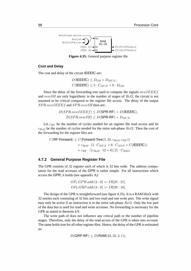
98 Processor Core
W1RAM
32×32
Ret3.full
Ret3.D.GPR.write
D1.OP1.GPR.data.lo
D1.OP2.GPR.data.lo
Ret3.D.{addr, data.lo}
IR[25 : 21] R2
IR[20 : 16] R1
Figure 4.35: General purpose register file
Cost and Delay
The cost and delay of the circuitIEEEfC are:
D(IEEEfC) ≤ DOR + DMUX ,
C(IEEEfC) ≤ 5 · CMUX + 6 · DOR.
Since the delay of the forwarding tree used to compute the signalsnewIEEEfandnewSR are only logarithmic in the number of stages ofRet2, the circuit is notassumed to be critical compared to the register file access. The delay of the outputSPR.newIEEEf andSPR.newSR then are:
D(SPR.newIEEEf) ≤ D(SPR-RF) + D(IEEEfC),
D(SPR.newSR) ≤ D(SPR-RF) + DMUX .
Let cRF be the number of cycles needed for an register file read access and letcRet2 be the number of cycles needed for the retire sub-phaseRet2. Then the cost ofthe forwarding for the register files are:
C(RF-Forward) ≤ C(Forward-Tree(5, 32, cRet2, cRF ))
+ cRet2 · (5 · CMUX + 6 · CAND + C(IEEEfC))
+ cRF · ⌈(cRet2 · 12 + 6)/2⌉ · CREG.
4.7.2 General Purpose Register File
The GPR consists of 32 register each of which is 32 bits wide. The addresscompu-tation for the read accesses of theGPR is rather simple. For all instructions whichaccess theGPR, it holds (see appendix A):
OP1.GPR.addr[4 : 0] := IR[25 : 21],
OP2.GRP.addr[4 : 0] := IR[20 : 16].
The design of the GPR is straightforward (see figure 4.35). It is a RAM block with32 entries each consisting of 32 bits and two read and one write port. The write signalmay only be active if an instruction is in the retire sub-phaseRet3. Only the low partof the data bus is used for read and write accesses. No forwarding is necessary for theGPR as stated in theorem 4.9.
The write path of does not influence any critical path or the number of pipelinestages. Therefore, only the delay of the read access of the GPR is takeninto account.The same holds true for all other register files. Hence, the delay of the GPRis estimatedas:
D(GRP-RF) ≤ D(RAM(32, 32, 2, 1)).

4.7 Register File Environment 99
Ret3.D.FPR.write.lo
0
1
W1
RAM16×32
R1
R2
W1
RAM16×32even
R2
R1
Ret3.D.{addr[4 : 1], data.hi}
Ret3.D.{addr[4 : 1], data.lo}
IR[19 : 16]
IR[14 : 11]
IR[20]
IR[15]
FPstore
oddD1.OP2.FPR.data.hi
D1.OP1.FPR.data.hi
D1.OP2.FPR.data.lo
D1.OP1.FPR.data.lo
Ret3.full
Ret3.D.FPR.write.hi
0
1
0
1Ret3.full
Figure 4.36: Floating point register file
Let cRF be the delay of a register file access. The cost of the GPR environment is:
C(GRP-RF) ≤ C(RAM(32, 32, 2, 1, cRF )) + CAND.
4.7.3 Floating Point Register File
The FPR holds 32 single precision registers with 32 bits. The 16 pairs of even andodd registers (i.e., the pairs 0 and 1 to 30 and 31) can also be accessed as64 bits widedouble precision registers using the address of the even register. Double precisionaccesses with an odd address raise an illegal instruction interrupt in the decode phase.
To support the two access modes, theFPR is divided in two register files of 16entries for even and odd registers (see figure 4.36). The lowest bit ofthe addresses ofthe two read ports select the outputs of the RAMs for the low parts of the two outputs.The high part always uses the odd RAM, as 64 bit register accesses always have evenaddresses.
The FPR uses the two separate write signals. The signalD.FPR.write.lo controlsthe RAM block containing the odd registers,D.FPR.write.hi controls the RAMblock containing the even registers. For 64 bit results (indicated byD.dbl), the writesignals for both RAM blocks must be active. For 32 bit results only the write signalfor the addressed RAM block may be active. Analogously to the GPR the writeportis only active if the retire sub-phaseRet3 is full. The write signalsD.FPR.write.loandD.FPR.write.hi are computed during the sub-phaseRet2 as:
D.FPR.write.lo := D.FPR.write ∧ D.addr[0],
D.FPR.write.hi := D.FPR.write ∧ (D.addr[0] ∨ D.dbl).
The low part of the resultD.data.lo is connected to the RAM block for the evenregisters, the high partD.data.hi is connected to the RAM block for the odd registers.Note that in order to write 32 bit results into the results must be available on both thehigh and the low part of the data bus (see table 4.3 on page 63).
For all instructions which read the FPR except floating point stores the address ofthe first operand isIR[20 : 16], the address of the second operand isIR[15 : 11] (seeappendix A). The floating point store instruction (indicated by the signalFPstore

100 Processor Core
computed in theDecode circuit) uses the the bitsIR[20 : 16] as second operand.Thus, the address of the floating point operands is:
OP1.FPR.addr := IR[20 : 16],
OP2.FPR.addr :=
{
IR[20 : 16] if FPstore
IR[15 : 11] if FPstore.
To hide the delay of the signalFPstore, the FPR is accessed under the assumptionthat the instruction in not a floating point store. If the instruction signalFPstore isactive, the output for the first operand is used as output for the second operand. This isdone by the multiplexer controlled by the signalFPstore in figure 4.36.
The selection of the operands using the signalFPstore can be combined withthe select circuit in the circuitOpGen (see section 4.1.4), which selects between theoutputs of the different register files. Hence, instead of a 4 input selectcircuit an 5input select circuit is used. The difference in delay and cost are added to the floatingpoint register file. It holds:
D(Sel(5)) − D(Sel(4)) = DOR,
C(Sel(5)) − C(Sel(4)) = DAND + DOR.
Hence, the delay of the last multiplexer for the computation ofD1.OP1.FPR.data.locan be replaced byDOR. The overall delay of the FPR RAM is:
D(FPR-RF) ≤ D(RAM(16, 32, 2, 1)) + DMUX + DOR.
Let cRF be the number of cycles for a register file access. The cost of the FPR includ-ing the computation of the write signals is approximated by:
C(FPR-RF) ≤ 2 · C(RAM(16, 32, 2, 1, cRF )) + 4 · CAND + COR
+ 64 · CMUX + 32 · (CAND + COR).
4.7.4 Special Purpose Register File
The special purpose register file consists of 10 register which are summarized in ta-ble 4.7. The register 0 to 4 are used for interrupt handling. The roundingmode forfloating point operations is stored in register 5. Register 6 collects the floatingpointexception flags. The result of floating point compares are stored in register 7, whichmay then be used by floating point branches. The registers 8 and 9 are used to storethe 64 bit wide results of integer multiplication and divisions.
When an interrupt occurs, the special purpose register file must perform the fol-lowing actions:
SR := 0,
ESR := SR,
EPC := Ret3.ePC,
ECA := Ret3.MCA,
EData := Ret3.eData.

4.7 Register File Environment 101
addr name purpose
0 SR status register (interrupt mask)1 ESR exception status register2 EPC exception program counter3 ECA exception cause register4 EData exception data register5 RM floating point rounding mode6 IEEEf IEEE interrupt flags7 FCC floating point condition code8 LO LO register9 HI HI register
Table 4.7: Special purpose registers
1 v
aria
ble
rea
d p
ort
6 c
on
stan
t re
ad p
ort
s
SPR[2]
D1.OP2.SPR.data
readIEEEf
rfe
D1.RS3.SPR.data
D1.RS4.SPR.data
D1.OP1.SPR.data
rfe
SPR[7]
SPR[1]
SPR[0]
SPR[5]
SPR[6]
Ret3.D.{addr[2 : 0], data.lo}
W1
RAMW1
1×32
1×32
RAM
8
9
W1
8×32RAM⋆
R2
0-7W2
Ret3.full
Ret3.full
Ret3.full
Ret3.D.SPR.write9
Ret3.D.SPR.write07
Ret3.D.SPR.write8
IR[13 : 11]
Ret3.D.data.lo
Ret3.D.data.hi
Ret3.newIEEEf
IR[14]IR[11]
1, 110, Ret3.newIEEEf
SR
IEEEf
0
1
1
0
1
0
0
1
1
0
Figure 4.37: Special purpose register file
The implementation of this operation is not discussed in detail here. It is assumed thata special RAM block can be used which performs these operations if the clear signalis activated. A construction for such a RAM block using discrete gates canbe found,e.g., in [Kro99].
The circuitSPR is depicted in figure 4.37. It consists of one RAM block with8entries and two RAM blocks with one entry7 for the registersLO andHI. Similarto an even / odd pair of floating point registers these two registers can be written inparallel to store the 64 bit wide result of an integer multiplication or division.
The following four instruction types have SPR registers as operands (see appen-dix A):
• moveS2I instructions: These instructions read an arbitrary special register assecond operand and save it in an general purpose register. The address of the
7A RAM block with only one entry is basically a single register and therefore need no address entry.For the sake of description they are yet treated as RAM blocks.

102 Processor Core
special register is encoded in the bits[15 : 11] of the instruction word.
• return-from-exception (rfe) instructions: The rfe instruction sets the PCto thevalue of the special registerEPC and copies the special registerESR intothe special registerSR. It uses the registerESR as first andEPC as secondoperand.
• branch on floating point condition code (BC1) instructions: TheBC1 instruc-tions are conditional branches that depend on the value of the special registerFCC. This register is used as first operand of the instruction.
• floating point instructions: These instructions depend on the special registersRM andSR as third and fourth operand.
Hence, the addresses of the four special purpose register operands are:
OP1.SPR.addr :=
{
00001 if rfe
00111 if rfe,
OP2.SPR.addr :=
{
00010 if rfe
IR[15 : 11] if rfe,
OP3.SPR.addr := 00101,
OP4.SPR.addr := 00000.
To implement this, the SPR has one variable read port and five constant read ports forthe entriesEPC, ESR, FCC, RM , andSR. Similar to the floating point store forthe FPR, a multiplexer controlled by the signalrfe indicating an rfe-instruction selectsthe data output for the first and second operand.
If the instruction is amoveS2I instruction which reads the registerIEEEf (in-dicated by the signalreadIEEEf ), the SPR returns the current content of the busRet3.newIEEEf and not the content of the register. Recall that an instruction read-ing the registerIEEEf waits in the pipeline stage of the decode phase in which theSPR return the result. These instructions wait there until all preceding instructionshave retired (see section 4.1.7). As soon as this happens, the SPR must return the cor-rect value of the registerIEEEf without restarting the read access. This can be doneby returning the busRet3.newIEEEf which then contains the correct value of theregister (see section 4.7.1).
Every instructionI which enters the retire sub-phaseRet2 must read the reg-istersSR and IEEEf from the SPR in order to compute the bussesnewSR andnewIEEEf containing the value of these registers at the time the instructionI entersthe sub-phaseRet3 (see section 4.7.1). The SPR has already a constant read port forthe registerSR, thus only one additional constant read port is needed for reading theregisterIEEEf .
The registers 8 and 9 must be written at the same time to store the 64 bit resultof integer multiplications or divisions. Therefore, these registers are treated separatelyfrom the registers 0 to 7. The registers 8 and 9 are divided into two RAM blocks,which may be written in parallel. If the register 9 is written with a 32 bit result (by the

4.7 Register File Environment 103
instructionmoveI2S), the data must be on the high part of the input data bus. SincemoveI2S instructions use the ALU which writes its results to both the high and lowparts of the result bus, this is already guaranteed (see table 4.3 on page 63).
To compute the write signals for the two RAM blocks the signalD.dbl computedby the circuitDestCmp is used. If the result is stored in the SPR this signal indicatesan integer multiplication or division. Thus, ifD.dbl is active the address bits of thedestination address can be ignored. IfD.dbl is not active, the bits0 and3 of the addressare used to decide which RAM block is written. As for the FPR, the write signalsareassumed to be computed during the retire sub-phaseRet2.
SPR.write07 := D.SPR.write ∧ D.dbl ∧ D.addr[3],
SPR.write8 := D.SPR.write ∧ (D.dbl ∨ (D.addr[3] ∧ D.addr[0])),
SPR.write9 := D.SPR.write ∧ (D.dbl ∨ (D.addr[3] ∧ (D.addr[0])).
The IEEEf register is written using an additional write port with constant ad-dress. If the retire sub-phase is not full, the value of the input busRet3.newIEEEfis the unchanged value of the previous instruction (see section 4.7.1). Thus, this writeport can be active in every cycle. Due to the construction of the forwarding circuit, theinputs of both write ports are identical if an instructions writes the registerIEEEfexplicitly. Hence, the priority of the write ports is irrelevant.
The rightmost multiplexers in figure 4.37 can be incorporated into select circuit ofthe circuitOpGen analogously to the FPR. Hence, the delay and cost of this multi-plexers can be replaced byDOR respectivelyCAND + COR. The delay of the SPRRAM is:
D(SPR-RF) ≤ max{D(RAM(8, 32, 2, 2)), D(RAM(1, 32, 1, 1)) + 2 · DMUX}
+ DMUX + DOR,
The cost and delay of the RAM block for the SPR registers 0 to 7 are approximatedby the cost and delay of RAM block with 2 variable read and write ports. LetcRF bethe number of cycles needed for a register files access. Then the cost and delay of thecircuit SPR can be approximated by:
C(SPR-RF) ≤ C(RAM(8, 32, 2, 2, cRF )) + 2 · C(RAM(1, 32, 1, 1, cRF ))
+ 5 · CAND + COR + 3 · 32 · CMUX + 2 · 32 · (CAND + COR).
4.7.5 Cost and Delay
The read accesses to the SPR in the retire sub-phaseRet2 are not assumed to be criticalfor the overall delay of the register file environment, as they use read ports with con-stant addresses. For the register file accesses in the decode sub-phaseD1 no forward-ing in necessary (see theorem 4.9). Hence, the delay of the register file environmentand the number of cycles needed for a register file accesscRF is:
D(RF) ≤ max{D(GPR-RF), D(FPR-RF), D(SPR-RF)},
cRF = ⌈D(RF)/δ⌉.
104 Processor Core
The cost of the register files is:
C(RF) ≤ C(GPR-RF) + C(FPR-RF) + C(SPR-RF).
4.8 Producer Table Environment
The producer tables are similar to their corresponding register files, but have one addi-tional read and one additional write port. The new write port is used duringthe decodesub-phaseD1 to write the tag of the instruction into the producer table. The additionalread port is used during the retire sub-phaseRet2 to check if no succeeding instructionhas overwritten the entry. All producer tables have a reset signal whichsets all validbits to one.
The environment of the RAM blocks itself is basically the same as for the registerfiles and therefore not discussed in detail. The address and write signalsfor the addi-tional ports are computed in advance by the circuitDestCmp. The priority of the newwrite access duringD1 is higher than the priority of the write access duringRet3.
The entries of the producer tables consist of the valid bit and the tag for thecor-responding register file entries. The entries for the odd registers of the floating pointproducer table and the register9 of the special purpose producer table need an extrabit dbl that indicates whether this register is written by a double precision result. TheoutputOPi.R.dbl for i ∈ {1, 2} andR ∈ {FPR, SPR} returns the value of this bit,if one of these registers is addressed by the operand, otherwise0. The output is neededby the reservation stations to decide if it needs to use the high or the low part toupdatean operand. The value of the bitdbl is set to the value of the signalD.R.dbl computedby the circuitDestCmp if one of the registers is written during the decode sub-phaseD1. It is set to0 if the producer table is written during the retire sub-phaseRet3.
4.8.1 Forwarding
The producer tables are accessed in four different contexts (operand-read, updating,checking, and retiring). In the decode sub-phaseD1 the producer tables are read toobtain the valid bit and the tag of the operands (operand-read-context). Also in thedecode sub-phaseD1 the tag of the new instruction is written into the producer tableentry of the destination register of the instruction (updating-context). In theretire sub-phaseRet2 the producer table entry of the destination register is read again to checkwhether a succeeding instruction will write the same register (checking-context). Ifno such instruction exists, in the retire sub-phaseRet3 the producer producer tableentry of the destination register is set valid in order to flag valid register file content(retiring-context). The following lemmas summarize the dependencies betweentheaccesses.
Lemma 4.11. The result of the read access to the producer table in the checking-context for an instructionI must take all write accesses to the producer table in theupdating-context into account that are started before the instructionI writes the pro-ducer table in the retiring-context.
Proof. All write accesses to the producer table that are started before the read access inthe checking-context starts are taken into account by construction of theRAM. Hence,

4.8 Producer Table Environment 105
let an instructionI1 write the producer table in the updating-context after an olderinstructionI0 has started the read access in the checking-context and beforeI0 startsthe write access in the retiring-context. LetI1 be the first instruction succeedingI0
that writes the same destination register asI0. If the write in the updating-context byI1 is not forwarded to the read access in the checking-context byI0, the instructionI0
will read its own tag. Thus,I0 will set the valid bit in the retiring-context, even if thecontent of the register is not valid as it will eventually be overwritten byI1.
Theorem 4.12.The write access to the producer table in the retiring-context does nothave to forwarded to the read access in the checking-context.
Proof. Let I0 be an instruction which writes its result into the register file in theretiring-context andI1 be an instruction which simultaneously reads the producer ta-ble in the checking-context. Assume the instructionsI0 andI1 write the same register.Then both instructions have written their tags to the producer table entry of thisreg-ister in the updating-context. As decode and retire are done in order, the instructionI1 has written the producer table entry after the instructionI0 in the updating-context.This update of the instructionI1 must have been forwarded to the read access in thechecking-context of instructionI1 (see lemma 4.11). Thus, the instructionI0 cannothave read its own tag in the check-context. Thus, the instructionI0 will not write theproducer table in the retire context.
Let cTC denote the number of cycles it takes from the start of the forwarding ofa write access in the updating-context to the end of the retire sub-phaseRet2. Thenin order to compute the content of the producer table at the time an instruction entersthe retire sub-phaseRet2, the write access in the updating-context must be delayed bycTC − 1 cycles (see section 2.6.3). As the content of the register does not depend onthe write access in the retire context (see theorem 4.12), this write port does not needto be delayed.
Theorem 4.13. The read access in the operand-read-context does not depend on thewrite access in the retiring-context.
The accesses in the operand-read-context and the retiring-context correspond tothe read and write accesses to the register files. Instead of forwarding the write accessthe data are read out of the ROB. Thus, this theorem can be proven analogously to thetheorem 4.9 on page 95.
Lemma 4.14.The read access in the operand-read-context must take exactly the writesin the updating-context into account that are started by preceding instruction.
Proof. An instruction must not depend on a succeeding instruction; therefore thewriteaccess in the updating-context by succeeding instruction must not be forwarded. Sincean instruction may depend on any preceding instruction the writes in the updating-context of all preceding instructions must be forwarded.
Figure 4.38 details the forwarding for the producer tables. The write access inthe retiring-context does not interfere with any other accesses and is therefore directlyconnected to the RAM blocks of the producer tables.

106 Processor Core
Ret2.D.addr0 Ret3.D.⋆0
W⋆.⋆W.⋆
Forward
R.addr R.addr W⋆.⋆ R.addr
R4.data
PT-RAM
W0.⋆R0 . . . 3.⋆W1.⋆
R4.⋆
R0 . . . 3.data
Ret2.PT. ⋆ .tag
DestCmp
ForwardForwardTree Tree
D1.IR0
D1.D.⋆cDC
D1.D.⋆cDC+1
D1.OP⋆. ⋆ .addrcDC
D1.OP⋆. ⋆ .addr0
D1.D.⋆cDC+cTC−1
D1.D.⋆cDC+cTC
D1.D.⋆2·cDC+cTC−1D1.OP⋆. ⋆ .{valid, tag}
Figure 4.38: Forwarding of the producer table
Due to the circuitDestCmp the address, data, and write signalD1.D.⋆ for thewrite access in the updating-context are not known before cyclecDC of D1. At thiscycle, the write access in the updating-context is forwarded to the read access in thechecking-context (to addressRet2.D.addr) analogous to figure 2.13 on page 24 usingthe forwarding circuit and the forwarding tree on the left side of figure 4.38. Note thatin order to realize this forwarding, the write access has to delayed by another cTC − 1cycles and hence enters the RAM blocks in cyclecDC + cTC − 1.
The read access in the operand-read-context enters the RAM blocks incycle0 ofthe decode sub-phaseD1. It must take all write accesses in the updating-context ofpreceding instructions into account. Since the write access in the updating-context isnot started before cyclecDC + cTC − 1, the RAM blocks do not return the data of thewrite accesses in the updating-context of thecDC + cTC − 1 preceding instructions.These write accesses must be forwarded using a forwarding tree.
The address and write signal of the write access in the updating-context isnotknown before cyclecDC of D1. Therefore the forwarding tree is delayed bycDC
cycles and compares the address of the read access in the operand-read-context incyclecDC D1.OP⋆. ⋆ .addrcDC with the addresses of the write access in the updating-context of the instructions in thecDC +cTC −1 succeeding stages (i.e., stagescDC +1to 2 · cDC + cTC − 1). Note that the delay of the circuitDestCmp is relatively smallin comparison to the delay of the RAM access. Therefore, it can be assumed that theforwarding tree needs less cycles than the RAM access even if it is delayed by cDC
cycles.

4.8 Producer Table Environment 107
4.8.2 Cost and Delay
Let b := lROB +1 be the width of the producer table entries. The delay of the producertables without forwarding can be estimated as:
D(GRP-PT) ≤ D(RAM(32, b, 3, 2)),
D(FPR-PT) ≤ D(RAM(16, b + 1, 3, 2)) + DMUX + DAND,
D(SPR-PT) ≤ max{D(RAM(8, b, 3, 3)), D(RAM(1, b + 1, 2, 2)) + 2 · DMUX}
+ DMUX + DAND,
D(PT-RAM) ≤ max{D(GPR-PT), D(FPR-PT), D(SPR-PT)}.
The delay of the read access in the operand-read context is:
D(D1.OP⋆. ⋆ .{valid, tag}) ≤ D(PT-RAM) + DMUX .
Let cTC be the number of cycles needed from forwarding the write port in theupdating-context to the end of the retire sub-phaseRet2. The producer table access isassumed to be the critical path of the retire sub-phaseRet2, otherwise it can be delayedsuch that it has the same delay as the critical path. In any casecTC is determined by thedelay of the forwarding circuit for5 address bits and the delay of the circuitTagCheck:
cTC = ⌈(D(Forward(5)) + D(TagCheck))/δ⌉.
If cTC = 1, the write in the updating-context does not have to be delayed and noadditional forwarding tree is needed for the read access in the checking-context. Inthis case the forwarding increases the delay of the read access in the checking-contextby the mux inside the forwarding circuit needed for merging the outputs of forwardingcircuit and RAM, otherwise by the two muxes for first merging the output of the RAMwith the output of the forwarding tree inside the forwarding tree and for merging withthe output of the forwarding circuit (see figure 4.38). Thus, the delay of the producertable access in the checking-context is:
D(Ret2.PT. ⋆ .tag) ≤ D(PT-RAM) +
{
DMUX if cTC = 1
2 · DMUX if cTC > 1.
The maximum delay of the read accesses to the producer table and the numberofcyclescPT needed is:
D(PT) ≤ max{D(D1.OP⋆. ⋆ .{valid, tag}), D(Ret2.PT. ⋆ .tag)},
cPT = ⌈D(PT )/δ⌉.

108 Processor Core
The costs of the producer tables without forwarding are:
C(GRP-PT) ≤ C(RAM(32, b, 3, 2, cPT )) + CAND,
C(FPR-PT) ≤ C(RAM(16, b, 3, 2, cPT )) + C(RAM(16, b + 1, 3, 2, cPT ))
+ 6 · CAND + COR + 6 · CMUX
+ 2 · b · CMUX + 2 · 2 · b · CAND,
C(SPR-PT) ≤ C(RAM(8, b, 3, 3, cPT ))
+ C(RAM(1, b, 2, 2, cPT )) + C(RAM(1, b + 1, 2, 2, cPT ))
+ 12 · CAND + 2 · COR + 3 · b · CMUX + 4 · b · CAND,
C(PT-RAM) ≤ C(GPR-PT) + C(FPR-PT) + C(SPR-PT).
The number of cycles needed for the computation of the destination registerscDC
is:
cDC = ⌈D(DestComp)/δ⌉.
The forward circuit for the read access in the checking-context consists of a forwardcircuit and a forwarding tree withcTC inputs for each PT. The forward circuit for theread access in the operand-read-context consists of a forwarding tree withcTC +cDC−1 leaves for each operand output of the PTs (note that the high parts of theFPR andthe SPR uses only 4 address bits). The total cost for the forwarding circuit of the PTare:
C(PT-Forward) ≤ 3 · C(Forward(5, b, cPT , cF (5)))
+ 3 · C(Forward-Tree(5, b, cTC , cPT ))
+ 4 · C(Forward-Tree(5, b, cDC + cTC − 1, cPT ))
+ 6 · C(Forward-Tree(4, b, cDC + cTC − 1, cPT ))
+ (cDT + cTC) · 38 · CREG.
The total cost for the producer tables is:
C(PT) ≤ C(PT-RAM) + C(PT-Forward).
Chapter 5
Memory Unit
This section describes the memory unit of the DLXπ+. An overview of the memoryunit is given in section 5.1. Sections 5.2 to 5.8 describe the non-blocking datacacheused in the memory unit.
5.1 Overview
The memory unit handles all load and store accesses to the main memory. The unitpresented in this thesis does not support virtual memory, i.e. the addresses sent by theprocessor can be directly used to address the main memory. Page fault interrupts arenot computed by the memory unit but are assumed to be computed by the main mem-ory. Furthermore the memory unit is not assumed to be able to write to the instructionmemory. Thus, no cache coherency protocol is needed between the instruction and thedata cache. Lines in the cache do not have to be invalidated.
The memory unit is divided into the three circuitsSh4S, DCache, andSh4L (seefigure 5.1). The data cache which does the actual memory access is contained in thecircuit DCache. All accesses to the data cache must be aligned to word-addresses.The adaption for instructions which do not access whole words are doneby the cir-cuits Sh4S and Sh4L. In contrary to the memory unit of the DLX by Muller andPaul [MP00] double word accesses are not supported by the MIPS R3000 ISA.
The memory unit gets as input the control buscon that defines the type of theaccess (including the signalwrite indicating a store and an immediate constantimm),the tag of the instruction, and the two operandsOP1 andOP2. The circuitSh4S first
Sh4L
DCache
Sh4S
Figure 5.1: Memory Unit

110 Memory Unit
computes the effective addressaddr of the access as sum of the first operand and theimmediate constant. If the memory access is misaligned, the circuitSh4S raises thedata access misaligned interruptDmal. In this case the instruction is sent directly tothe circuitSh4L. Thus, the data cache does not need to handle misaligned accesses.
Based on the lower bits of the effective address, the second operand isshifted tothe correct position for a word-wise access, resulting in the data busdata. In parallelthe circuitSh4S computes for every bytei ∈ {0, . . . , 3} of the data word a usage bitubi which marks the bytes used by the access. Hence, for loads the busub⋆ selects thebytes to be read, for storesub⋆ selects the bytes that are written.
The data cache uses the write bit, the effective address, the data bus, and the usagebits to perform the memory access. For load accesses the data cache returns the resulton the data bus. Along with the result, the data cache returns the effective addressof the access, the page fault interrupt signalDpf received from the main memory,and the control signals which are passed unchanged by the cache, e.g.,the tag of theinstruction.
The memory unit is able to handle load word left (LWL) respectively load wordright (LWR) instructions (see table A.1 in the appendix). These instructionsupdateonly parts of the target registers and are used to access misaligned words. Since theprocessor core updates always whole register entries, the destination register is alsoused as second operand. The result of the load access is combined with the content ofthe destination register to compute the result. Thus, for LWL/LWR instructions,thedata cache must return the content of the main memory for the bytes for whichub⋆ isactive, and the content of the second operand for the bytes for whichub⋆ is inactive.
The circuitSh4L shifts the result of the cache access as requested by the instructionbased on the lower bits of the effective address and the value of the control signals inthe buscon. The result of load accesses is returned to the processor on the high and thelow part of the CDB (see table 4.3 on page 63). If an interrupt occurredthe memoryunit returns the effective address on the low part of the CDB.
The construction and the pipelining of the circuitsSh4S andSh4L is straightfor-ward and not discussed in detail. The circuits can be found in the appendixD.4. Delayand cost of the circuits are:
D(Sh4S) ≤ max{D(Add(32)), D(Add(2)) + D(HDec(2)) + 2 · DMUX},
D(Sh4L) ≤ 4 · DMUX ,
C(Sh4S) ≤ C(Add(32)) + 2 · C(Dec(2)) + C(HDec(2))
+ 104 · CMUX + 11 · COR + 10 · CAND,
C(Sh4L) ≤ C(Inc(2)) + C(Dec(2)) + C(Sel(4))
+ 186 · CMUX + 3 · DOR + DAND.
5.2 Overview of the Data Cache
The data cache presented in this thesis is a “non-blocking write-through write-allocate”cache. In contrary to the simpler blocking caches, anon-blockingcache does not stallthe memory unit in case of a cache miss. It can service multiple misses at a time andreturn the result of a hit before a preceding miss has completed. Awrite-throughcache

5.2 Overview of the Data Cache 111
updates the main memory (or the next cache level) for every write access to the cache.Thus, the main memory always contains the same data as the cache. In contrary thewrite-back variant only updates the memory if a line that has been written is evictedout of the cache. A new cache-line is written into the cache whenever an access missesthe cache. This is calledwrite-allocate. A read-allocate cache would only write newlines into the cache for read-misses.
A cache-linecontainsSDC = 2sDC (aligned) bytes. On a miss always a wholecache-line is read from the main memory and saved in the cache. The data cache isassumed to be non-sectored, i.e. the width of the cache RAM equals the width of acache-line. Accesses to the cache RAM always write or read whole cache-lines. Thedata cache is aKDC-way set associative cache (KDC = 2kDC ). Every line of themain memory can be saved atKDC different locations in the cache. The location of acache-line currently saved in the cache is defined by thewayof the cache-line.
The basics of non-blocking caches were presented by Kroft [Kro81]. The pre-sented design of a non-blocking cache is based on the work of Sicolo [Sic92]. Inhis thesis Sicolo gives an overview of the basic structures of a non-blocking cache,but does not handle the gate-level implementation, pipelining and interrupts. To solvethese problems the design of Sicolo had to be adopted significantly.
The cache design presented by Sicolo combines two succeeding stores to the samecache-line to a single store. This is not possible for a first level cache aswrites haveto be executed in order due to interrupts. Also Sicolo uses a write-back strategy whichhas the following drawback not handled in his work: before a new cache-line is writteninto the cache it must be checked if any succeeding access will replace thisline. If thisis the case and the cache-line has been modified by a store the cache-line must not bewritten into the cache but back into the main memory.
Note that for the check the way in which the succeeding accesses write is needed.Hence, only those accesses can be taken into account for which the wayhas alreadybeen computed. To cover the remaining accesses, additionally every new access mustbe checked if it will overwrite a cache-line which is about to be written into the cache.This can only be done after the hit signal for the instruction has been computed andtherefore delays misses.
Figure 5.2 depicts an overview of the data cache. The cache consists of four sub-circuits: the hit computationHC, the update queueUpdQ, the read queueReadQ, andthe cache coreCore containing the actual cache RAM. The update queue combinesthe miss queue and the replace queue of the design presented in [Sic92].
The cache core contains the cache memory, the cache directory and the replace-ment circuit. The update queue holds all accesses that will update the cache coreeventually (i.e., store instructions and cache misses). The read queue contains all readmisses. The circuitHC computes the overall hit signal, taking the content of the queuesand the cache core into account.
5.2.1 Execution of Memory Accesses
Depending on the type of the memory access, different data are requiredfor the execu-tion of the access. Loads only require the data that are actually read. Stores require the

112 Memory Unit
ReadQ
MainMemory
Core
UpdQ
HC
Figure 5.2: Overview of the data cache
whole cache-line in order to update the cache core. This are called the required data ofthe access.
New memory accesses first enter the hit computation. The hit computation com-putes a hit signal indicating whether the required data of the access are in the cache.It may happen that only parts of the data needed by an access are in the cache, e.g., ifa load follows a store to the same address. In this case the access is treated as miss.Apart from the hit signal the hit computation also returns all required bytesof whichthe value is known. These bytes are marked valid using an additional valid bitper byte.
Based on the result of the hit computation the type of the access instructions aresent to different queues. Stores are sent to the update queue. Loadsmisses are sent toboth the update queue and the read queue. The load hits are directly returned to thememory unit. Hence, the data cache can return instructions out-of-order.
The misses in the update queue start read requests to the main memory. The mainmemory returns the result of the access on the result bus. The content ofthe result busis used to update the entries in the update queue as well as the read queue. As soonas all bytes of a load in the read queue are valid, the result is returned to thememoryunit. If all the bytes of a cache-line in the update queue are valid, the cachecore canbe updated. Since the cache is a write through cache, no cache-line must be evicted tothe main memory before it is overwritten. If the entry in the update queue is a store,the main memory is also updated and the store is returned to the memory unit.
5.2.2 Cache Core and Main Memory
The handling of misses is done outside the cache core macro. Therefore the data pathof the cache core can be the same as for a simple blocking cache. Additionallythecache core does not handle any data dependencies. This enables to easily pipelinethe core. The only problem may be the replacement circuit, which decides whichcache-line has to be overwritten. Advanced replacement algorithms (e.g., LRU) takeall preceding instructions into account and assume that the instructions in thecacheare handled in order. Yet a strict adherence of the replacement circuitaccording to

5.3 Hit Computation 113
the strategy is not needed for data-consistency. Therefore, in this thesis a pipelinedLRU algorithm that does forward the preceding instructions is used which simplifiesthe design of the cache core.
The main memory is not assumed to return the read accesses in order. This makesit possible to build multiple levels of non-blocking caches using the presented design.To identify the results returned from the main memory, the main memory must returnthe address of the request along with the data.
5.2.3 Speculation
If an instruction causes an interrupt or has been mispredicted, all succeeding instruc-tions must be aborted. Updates of the cache core or the main memory are not recover-able. Thus, a store instruction may not update the cache core or the main memory aslong as the instruction may be aborted. An instruction won’t be aborted if the instruc-tion does not cause a repeat interrupt (i.e., a page fault) and all preceding instructionshave retired, i.e. the instruction is the oldest active instruction.
The page fault interrupt is computed by the main memory. It can only be causedby accesses to cache-lines that are not in the cache. Thus the value of the page faultinterrupt is known before a store instruction updates the cache or the main memory,since the instruction first tries to fetch the cache-line from the main memory in case ofa miss. If this read access causes a page fault, the store instruction is not executed.
To guarantee that store instructions won’t update the cache core or the main mem-ory before they become the oldest active instruction, two solutions are possible. Thesimple solution is to stall a store instruction at the end of the hit computation until itbecomes the oldest active instruction. Due to the special memory reservationstation(see section 4.2.2) a store instruction is always the oldest memory instruction whenit enters the memory unit. Thus, no preceding instruction gets stalled and the storeinstruction eventually becomes the oldest active instruction.
This simple variant has some drawbacks: load instructions may not overtakestoreinstructions in the reservation station. Thus, a store instruction stalls all succeedingload instructions. Further more, before a store instruction can leave the hitcomputationall queues of the cache have to be emptied. This means especially that at mostone storeinstruction can be in the update queue.
A more efficient solution is to stall store instructions in the update queue just beforethey update the cache RAM or the main memory. The stores are stalled until theybecome the oldest instruction and it is clear that they did not cause an interrupt. Thismethod is used in the presented design and is described in more detail in the updatequeue section 5.5.
5.3 Hit Computation
The hit computation computes the two signalshit andsl. The signalhit (calledhitsignal) is active if the required data is already in the cache. The signalsl (calledsame-line signal) is active if a preceding instruction inside the cache accesses the same line.In this case even if the requested data is not yet in the cache, no new request to themain memory has to be made. The signalshit andsl may be active at the same time,

114 Memory Unit
e.g., if the cache-line containing the required data has been requested by aprecedinginstruction and has just been returned by the main memory. The hit signal hasa higherpriority.
If an memory access succeeds a store that writes some of the requested data of theaccess, it may happen that only parts of the requested data are known atthe time thehit computation returns the data for the access. Therefore, the circuitHC computes abyte-valid signalbvi for every bytei of the requested data. The signalbvi is active ifthe value of the bytei is known. The hit signalhit is active if the byte-valid signalsfor all required bytes of the access are active. The signalshit, sl, andbv⋆ together arecalledglobal hit signals.
For every bytei for which bvi is active, the hit computation returns the valuewritten by the last store being processed by the cache which updates this byte. If nosuch instruction exists, the hit computation returns the current content of the cacheRAM for this byte.
In order to later update the cache core, the hit computation also computes the busway which points to the way of the cache core which has to be written. If the cachecurrently processes an access that addresses the same cache-line, the way must bethe way computed for this access. Otherwise the value computed by the replacementcircuit of the cache core is used. Note that in case of a hit the replacementcircuitreturns the index of the way that contains the requested data.
Based on the type of the access and the value of the global hit signals, the hitcomputation computes the action to be done for the instruction. The instruction can besent to the update queue, the read queue, both queues, or can directly be returned tothe memory unit.
Note that an access is treated as hit whenever the requested data can be found inthe cache, even if it would be a miss if the accesses would be handled sequentially.Assume the cache core contains a cache-linel0 and an access to the cache-linel1 willreplace the cache-linel0. If a second access to the cache-linel0 is started before theline is replaced, this access is treated as hit as the cache core returns the correct data.If the access to the cache-linel0 is a store, it will update the cache core and therebyoverwrite the cache-linel1 written into the cache core by the preceding access. Sincethe cache is a write-through cache this can be done without checking if datawould belost.
5.3.1 Overview of the Hit Signal Computation
The requested data of an instruction can be located in four different places in the cache:in the cache core, in the update queue, on the result bus of the main memory, or as writedata of a preceding store in the hit computation itself. If the requested data cannot befound in any of these places, the data must be loaded from the main memory.
The update queue and the hit computation compute for every entry respectivelypipeline stage a local same-line signal and local byte-valid signals. The local same-line signal is active if the entry or stage contains an instruction which accesses thesame line as the instruction for which the global hit signals are being computed.LetSDC = 2sDC be the number of bytes of a cache-line. Then two instructions access thesame lines if the bits 31 tosDC of the addresses (calledline-address) are equal. The

5.3 Hit Computation 115
local byte-valid signals indicate that the entry or stage contains the correctvalue forthat byte. They may only be active if the local same-line signal is active. Forthe cachecore and the result bus of the main memory all bytes are valid on a hit. Therefore, thesecircuits only compute a local hit signal which is active if the requested line is found.
The global hit signals must reflect the content of the cache at the time the queuesare updated. The computation of the global hit signals may take multiple cycles due topipelining. Therefore, all changes to the content of the cache during thecomputationmust be forwarded in order to be reflected in the result. The cache core isonly updatedby the update queue. Thus, in order to forward all possible changes ofthe cache coreit suffices to forward the content of the update queue at the time the hit computation isstarted and all updates to the update queue.
The entries of the update queue are updated by the result bus of the main memoryand by the hit computation for allocating new entries. Note that stores are processedin order. Thus, only the instructions in the hit computation which are started beforethe instruction for which the global hit signals are being computed have to be takeninto account. Hence, all possible updates to the update queue by the hit computationare known at the time the hit computation for an access is started. The updatesto theupdate queue by the main memory are not known at the time the hit computation isstarted. They must be forwarded in every cycle of the hit computation.
Figure 5.3 shows an overview of the computation of the global hit signals. Forthe computation of the global hit signals, the hit computation first computesstaticand dynamic hit signals. The static hit signals are based on the content of the hitcomputation, the update queue, and the cache core. They must represent the valueof these circuits at the time an instruction enters the hit computation and have to becomputed only once. The dynamic hit signals are based on the content of theresultbus of the main memory and have to be computed in every cycle. Since all bytes of theresult bus are valid, the dynamic hit signals only consist of a hit signal (thedynamichit signal) without byte-valid signals.
The dynamic hit signal must be set if the line-addresses of the current data on theresult bus and the instruction for which the hit signals are being computed are equal.Assume the cache is a RAM block with32 − sDC address bits that is written by theresult bus of the main memory. If the computation of the global hit signal is seenasread to that RAM block the dynamic hit signal must be set exactly if the write portwould be forwarded to the read port of the RAM block. Thus, the computation of thedynamic hit signals can be done using a forwarding circuit (with stalling) of such aRAM with 32 − sDC address bits.
Let cM2H denote the number of cycles needed for the computation of the global hitsignals based on the content of the result bus of the main memory. In order totake alldata from the result bus into account that have updated the update queueat the time theglobal hit signals are computed, the result bus is delayed bycM2H − 1 cycles similarto the pipelined forwarding circuits (see section 2.6.3). The forwarding circuit thenuses the un-delayed result bus and thecM2H − 1 additional stages of the result bus areforwarded using a forwarding tree. This tree is included into the computationof thestatic hit signals.
The circuitstaticHC in figure 5.3 computes the static hit signalsssl (static same-line) andsbv⋆ (static byte-valid) along with the corresponding data bussessbyte⋆ and

116 Memory Unit
MM0.⋆
MM cM2H−1.⋆
MM1.⋆
UpdQCore
HC0.addr
R.addr W.⋆
ForwardStall
forwUpd dataUpd
dhit dbyte⋆
globalHC
staticHC
UpdQ.⋆Core.⋆
ssl, sbv⋆, sbyte⋆, sway
hit, sl, bv⋆, byte⋆, way
Figure 5.3: Overview of the hit signal computation
the waysway. For this computation, the cache core and the update queue are accessedto compute local hit signals. Additionally to these local hit signals the circuitstaticHCuses the stages1 to cM2H − 1 of the delayed result bus and the preceding instructionsin the hit computation to compute the static hit signals.
The dynamic hit signaldhit and the corresponding data bussesdbyte⋆ are com-puted using a forwarding circuit with stalling (ForwardStall). This circuit uses theun-delayed result bus. The outputs of the two circuitsstaticHC andForwardStall arecombined in the circuitglobalHC to compute the global hit signals, byte values andthe way.
5.3.2 Local Hit Signals
For the computation of the static hit signals, first local same-line and byte-validsignalsmust be computed for all stages of the hit computation and all update queue entries.These signals are calledHC.lsli (local same-line) andHC.lbv⋆,i (local byte-valid) forstagei of the hit computation andUpdQ.lsli respectivelyUpdQ.lbv⋆,i for the entryiof the update queue. For the stages of the delayed result bus of the main memory andthe cache core a local hit signal must be computed. These signals are called MM.lhiti(local hit) for the stagei of the delayed result bus, andCore.lhit for the cache core.
The local same-line signal indicates that the stage or entry holds an access whichaddresses the same cache-line as the access for which the hit signals arebeing com-puted. Which bytes of this cache-line are valid is defined by the local byte-valid sig-nals. The local hit signals for the result bus and cache core are activeif the requireddata is in the delayed result bus stage respectively cache core. The computation of thelocal signals for cache core and update queue are described in the section 5.4 and 5.5.
To compute the local hit signals for the hit computation stages, the busub⋆ indi-cating which bytes of a word are used must be extended to a whole line. Figure 5.4

5.3 Hit Computation 117
[0]4
[3] [0] [0][3]
byte3
data
32
[7 : 0]
byte0
[7 : 0] [31 : 24][31 : 24]
ub⋆
eub3 eub0
addr[sDC − 1 : 2]
[SDC/4 − 1]
eubSDC−1 byteSDC−1 eubSDC−4 byteSDC−4
Dec
Figure 5.4: Computation of the signalseub⋆ andbyte⋆
1
MM.lhiti
HC0.addr[31 : l] HCj.full HCj.addr[31 : l]
HC.lbv⋆,jHC.lslj
HCj.write HCj.eub⋆MM i.addr[31 : l]MM i.full
EQEQ
Figure 5.5: Computation of the local hit signals for a delayed result bus stagei and ahit computation stagej
depicts the computation of the extended usage-bitseub⋆. The byte4 · m + n form ∈ {0, . . . , L/4 − 1} andn ∈ {0, . . . , 3} of a line is used if the instruction accessesthe wordm of the line and the byten of the word is used. Which word of a cache-lineis accessed can be computed by decoding the bitssDC − 1 to 2 of the address. Ad-ditionally the circuit in figure 5.4 computes the byte bussesbyteSDC−1...0 by copyingthe data busSDC/4 times. The computation of the signalseub⋆ andbyte⋆ must onlybe done once for every instruction which enters the hit computation.
The circuit in figure 5.5 computes the local hit signals from the accesses in the hitcomputation and the stages of the delayed result bus. LetcHC be the number of cyclesof the hit computation. LetI be an instruction which enters the hit computation, i.e.,I is in stage 0. An instruction in stagej ∈ {1, . . . , cHC − 1} of the hit computationaccesses the same line asI if the line addressHCj .addr of the instruction in stagej is the equal to the line addressHC0.addr of the instructionI in stage0. If this isthe case and the stagej contains a valid access (HCj .full = 1) the signalHC.lslj isactivated. IfHC.lslj is active, the local byte-valid signals are activated for all byteswritten by the instruction in stagej (indicated byHCj .eub⋆ ∧HCj .write). Note thatthis disables all byte-valid signals if the access in stagej is a load.
The local hit signal for stagei ∈ {1, . . . , cM2H−1} of the delayed result bus can becomputed by comparing the line addresses of the delayed result bus stageMM i.addrwith the address ofI and checking the full bitMM i.full. Since all bytes of the resultbus are valid no byte-valid signals are needed.
5.3.3 Static Hit Signals
The static byte-valid signal for a bytek sbvk must be active if any local byte-validsignal for the bytek of a hit computation stage or an update queue entry is active orthe local hit signal for a delayed result bus stage or the cache core is active. If the

118 Memory Unit
Forw
Core.hit
MM1.bytek MM.lhitcM2H−1
MM.lhit1
Core.bytek
sbyteksbvk
MM cM2H−1.bytekUpdQ.bytek,e−1UpdQ.lbvk,0HCcHC−1.bytek
HC.lbvk,cHC−1
HC.lbvk,1
HC1.bytek UpdQ.lbvk,e−1UpdQ.bytek,0
qbvk qbytek
Forw
Figure 5.6: Computation of the signalssbvj andsbytej for a bytej
signalssbvk is active, the bussbytek for the corresponding data must contain the valueof the last instruction preceding to I which updates that byte. If no such instructionexist, the bussbytek must contain the current content of the main memory. Figure 5.6shows the computation of the signalssbvk andsbytek for a bytek.
The computation of the byte-valid signals and the corresponding bytes can be doneusing a tree as in the forwarding tree (see section 2.6.3). The tree computesan OR ofthe local byte-valid signals (respectively hit signals for cache core andresult bus).Parallelly the tree selects the first byte (from the left) for which the byte-validsignal isactive.
The outputs of the cache coreCore.lhit andCore.byte⋆ are assumed to be timingcritical as they depend on an access to the cache RAMs. Therefore, they are not usedbefore the last stage of the tree. The outputs of the tree which do not take the signalsfrom the cache core into account are calledqbv⋆ respectivelyqbyte⋆. Thus, for a bytek with 0 ≤ k ≤ SDC − 1 holds:
sbvk = qbvk ∨ Core.hit, (5.1)
sbytek =
{
qbytek if qbvk = 1
Core.bytek if qbvk = 0. (5.2)
The instructions in the hit computation have been started after the instruction inthe update queue and must have a higher priority in the tree. Since instructions enterhit computation and update queue in order and are not reordered within, the stagesrespectively entries with lower index must have higher priority. The resultbus ofthe main memory and the cache core only contain data written by already completedinstructions and therefore have a lower priority than hit computation and update queue.Since cache and main memory contain the same data due to the write-through strategy,the order is irrelevant for the result bus stages and the cache core.
The static same-line signalssl must be active if the local same-line signal is activefor any hit computation stage or update queue entry. The staticway must be the way ofthe last instruction for which the local same-line signal is active. If none ofthe same-line signals is active, the way must be set to the way output of the coreCore.way. Thecircuit for the computation of the signalsssl andsway is shown in figure 5.7.

5.3 Hit Computation 119
HC.lslcHC−1
HC.lsl1 UpdQ.lsl0
UpdQ.lsle−1
FFOzffo
HCcHC−1.way
HC1.way UpdQ.way0
UpdQ.waye−1
Core.way
sway ssl
Sel
Figure 5.7: Computation of the signalsssl andsway
Among other things, the static way of the instruction in stage 0 of the hit com-putationsway depends on the way of the instruction in stage 1 which is computedonly one cycle beforesway. Thus, the delay of the pathHC1.way sway must beat most one cycle. In order to minimize the delay on this path, the static way is notcomputed using a forward tree like the byte-valid signals and the data. Instead, thefirst instruction for which the local same-line signal is active is computed using a find-first-one circuit. If none of the local same-line signals is active the zero outputz of thefind-first-one circuit is active. Thus, the static same-line signal must be active, if thezero output is inactive. Using the outputffo which unary selects the first instructionwith active same-line signal, the way of this instruction is selected. If the zero outputis active, the way of the core is selected. In order to minimize the delay for the signalsHC1.way andCore.way, the select circuit is “unbalanced” accordingly.
5.3.4 Global Hit Signals
The global byte-valid signal for a bytek bvk has to be active if either the static byte-valid signal for this bytesbvk or the dynamic hit signaldhit is active. Since only theprocessor writes the main memory, the dynamic datadbyte⋆ from the main memorycannot be newer than the static datasbyte⋆ in the cache. Thus, if the static byte-validsignal is active, the static data have to be returned:
bvk = sbvk ∨ dhit, (5.3)
bytek =
{
sbytek if sbvk = 1
dbytek if sbvk = 0. (5.4)
The global hit signalhit must be active if all bytes required by the instructionare valid. For write instructions all bytes of the cache line are required in order toupdate the cache core. Yet the bytes of the line written by the instruction (indicated byHC0.eub⋆) are valid and need not to be found in the cache. For read instructions thebytes to be read (indicated byHC0.eub⋆) need to be valid:
hit =
SDC−1∧
k=0
(
bvk ∨ (HC0.eubk ⊕ HC0.write))
.
Note that the signalHC0.eub⋆ andHC0.write are known early in the hit com-putation and not as timing critical as the dynamic hit signal and the hit signal fromthe cache core. Therefore, the computation of the hit signal is optimized using the

120 Memory Unit
distributive law:
hit(5.3)=
SDC−1∧
k=0
(
dhit ∨ sbvk ∨ (HC0.eubk ⊕ HC0.write))
(5.1)=
SDC−1∧
k=0
(
dhit ∨ Core.hit ∨ qbvk ∨ (HC0.eubk ⊕ HC0.write))
= dhit ∨ Core.hit ∨
SDC−1∧
k=0
(
qbvk ∨ (HC0.eubk ⊕ HC0.write))
.
No dynamic way and same-line signal are computed for the result bus of the mainmemory. The static way and same-line signal are therefore used as global way andsame-line signal:
sl = ssl
way = sway
5.3.5 Actions
Based on the global hit signals the hit computation either directly returns the resultto the memory unit or allocates new entries in the read and the update queue. Ifanew update queue entry is allocated, also the bitsreq andrdy for this entry have tobe computed. The request bitreq has to be active if the entry must request the linefrom the main memory. The ready bitrdy indicates that the entry contains already thecorrect data. Based on the signalshit andmiss and the type of the access (indicatedby the signalwrite which is active for stores), the following actions have to be taken:
• write∧ hit: The instruction is a load-hit. The result of the load can be returnedfrom the hit computation directly to the memory unit.
• write ∧ hit ∧ sl: The instruction is a load-miss but a preceding instructionaccesses the same line. A new entry in the read queue has to be made. Since therequired data will be requested by a preceding instruction no new update queueentry is needed.
• write ∧ hit ∧ sl: The instruction is a load-miss and no preceding instructionaccesses the same line. New entries in the read queue and the update queuehaveto be made. The request bitreq of the new entry is set to one. The ready bitrdyof the entry is set to zero.
• write ∧ hit: The instruction is a store-hit. A new entry in the update queue hasto be made. The bitrdy is set to one and the bitreq is set to zero.
• write ∧ hit ∧ sl: The instruction is a store-miss but a preceding instructionaccesses the same line. A new entry in the update queue has to be made. Sinceno new read request for the cache-line has to be made, the bitsrdy andreq areset to zero.

5.3 Hit Computation 121
HC0.ub⋆
4
L/4:1
bv⋆ byte⋆
32HC0.data
01
L/4:1
Sh4L.dataReadQ.Byte⋆.dataReadQ.Byte⋆.bv
SDC 8 · SDC
HC0.addr[sDC − 1 : 2]
Figure 5.8: Computation of the data bus to the read queue and the memory unit
• write ∧ hit ∧ sl: The instruction is a store-miss and no preceding instructionaccesses the same line. A new entry in the update queue has to be made, whichrequests the required cache-line from the main memory. The bitrdy is set tozero and the bitreq is set to one.
The result of a load access is returned to the memory unit using the busSh4L.⋆.New entries for the update queue and the read queue are allocated using the bussesUpdQ.⋆ respectivelyReadQ.⋆. The full bit of the busses is active if the correspondingaction has to be taken. Based on the preceding list the full bits to the circuitSh4L andthe two queues as well as the bitsreq andrdy for the bus to the update queue can becomputed as follows:
Sh4L.full = write ∧ hit,
ReadQ.full = write ∧ hit,
UpdQ.full = write ∨ (hit ∧ sl),
UpdQ.rdy = hit,
UpdQ.req = hit ∧ sl.
(5.5)
The byte-valid signals and the corresponding data sent to the update queue arecalledUpdQ.Byte⋆.bv andUpdQ.Byte⋆.data. The valid signals for the bytes of theupdate queue must be active for all bytes for which the byte-valid signals of the hitcomputation are active or which are written by the instruction. The byte data for theupdate queue are the global byte values. For a bytek with 0 ≤ k ≤ SDC − 1 holds:
UpdQ.Bytek.bv = (HC0.eubk ∧ HC0.write) ∨ bvk,
UpdQ.Bytek.data =
{
HC0.bytek if HC0.eubk = 1
bytek if HC0.eubk = 0.
The data busReadQ.Byte⋆.data to the read queue is only 32 bits wide. Thus,the requested word must be selected out of the cache-line returned by theglobal hitcomputation. LetW be the index of the requested word in the cache-line, i.e.:
W := 〈HC0.addr[sDC − 1 : 2]〉.
Then, the bytesW to W + 3 have to be selected in order to compute the data bus tothe read queue. The byte-valid signals for the read queueReadQ.Byte⋆.bv must beactive for all bytes of the word which are valid or not used by the access(indicated by

122 Memory Unit
the un-extended usage bitsHC0.ub). Due to the LWL and LWR instructions the byteswhich are not used by the instruction have to be set to the value of the value of theinput data bus of the instruction. Hence, the bussesReadQ.Byte⋆.{bv, data} to theread queue can be computed as (0 ≤ k ≤ 3):
ReadQ.Bytek.bv = HC0.ubk ∨ bvW+k,
ReadQ.Bytek.data =
{
HC0.data[8 · k + 7 : 8 · k] if HC0.ubk = 1
byteW+k if HC0.ubk = 0.
The data on the busReadQ.Byte⋆.data contains all requested data in case of a cache-hit. Thus, the data bus to the memory unitSh4L.data can be directly derived from thebusReadQ.Byte⋆.data. The bus to the memory unit does not need byte-valid signals,since all bytes have to be valid for read hits. Figure 5.8 depicts the computationof thedata busses and the byte-valid signals to the read queue and the data bus to the memoryunit.
5.3.6 Stall Computation
The hit computation has to be stalled if the action for the access cannot as describedabove be performed. A result cannot be returned to the memory unit ifSh4L.stallOutis active. A new read or update queue entry cannot be made if the corresponding stallsignalsReadQ.stallOut or UpdQ.stallOut are active. Hence, the input stall signalfor the hit computation can be computed as:
HC.stallIn = (Sh4L.full ∧ Sh4L.stallOut)
∨ (ReadQ.full ∧ ReadQ.stallOut)
∨ (UpdQ.full ∧ UpdQ.stallOut).
5.3.7 Cost and Delay
The overall delay of the hit computation is dominated by the access to the cacheRAMin the cache core. Thus, the critical signals areCore.hit andCore.byte⋆. As one caneasily verify the output of the hit computation with the highest delay is the data bus tothe read queueReadQ.Byte⋆.data. Thus, the overall delay of the hit computation is:
D(HC) ≤ D(Core) (Core.byte⋆)
+ DMUX (sbyte⋆, equation (5.2))
+ DMUX (byte⋆, equation (5.4))
+ (sDC − 2) · DMUX + DMUX . (ReadQ.Byte⋆.data, figure 5.8)
To compute the number of cycles the result bus of the main memory has to bedelayed, the maximum delay from the first stage of the result busMM0.⋆ to the out-puts of the hit computation needs to be known. As above, the path from to the busReadQ.Byte⋆.data has the highest delay out of all paths that start atMM0.⋆. The

5.3 Hit Computation 123
=?
rbyte⋆
byte⋆
hit[31 : sDC ]
[sDC−1 : 2]
8 · SDC
32
1
addr
Mem.data
Mem0.write
Mem0.addr[31 : l]
Figure 5.9: Modified test circuit
delay this path is:
D(MM0.⋆ ReadQ.Byte⋆.data) ≤ D(EQ(33 − sDC)) + DMUX
(dbyte⋆, figure 5.3)
+ DMUX (byte⋆, equation (5.4))
+ (sDC − 2) · DMUX + DMUX .
This delay can be reduced, if the selection step from the cache-line to the accessedword in figure 5.8 is removed from the critical path. The selection for the cache-linesof the result bus can be done in parallel to the computation of the forward signal usinga modified circuitTest (see figure 5.9) in the forward tree. The circuit computes asecond data outputrbyte⋆ which contains the data needed by read accesses. Thisoutput is treated like the standard data in the forwarding circuit, i.e. the forwardingcircuit computes8 · SDC + 32 data bits. The additional byte busses computed by theforwarding circuit are calleddrbyte⋆.
Using the new busdrbyte⋆ the output to the read queue can be computed as follows(for a bytek with 0 ≤ k ≤ 3 andB := 8 · k):
ReadQ.Bytek.data =
{
HC0.data[B + 7 : B] if HC0.ubk = 1
byteW+k if HC0.ubk = 0
(5.4)=
HC0.data[B + 7 : B] if HC0.ubk = 1
sbyteW+k if HC0.ubk = 0 ∧ sbvW+k = 1
dbyteW+k else
=
HC0.data[B + 7 : B] if HC0.ubk = 1
sbyteW+k if HC0.ubk = 0 ∧ sbvW+k = 1
drbytek else
(5.2)=
HC0.data[B + 7 : B] if HC0.ubk = 1
qbyteW+k if HC0.ubk = 0 ∧ qbvW+k = 1
Core.byteW+k ifHC0.ubk = 0 ∧ qbvW+k = 0
∧Core.hit = 1
drbytek else
.
Note that the most critical bus on which the busReadQ.Byte⋆.data depends isdrbyte⋆
since it determines the delay of the path from the main memory to the read queue andtherefore determines the number of cycles the result bus has to be delayed. The second

124 Memory Unit
qbv⋆
dhit
Core.byte⋆qbyte⋆
L/4:1
HC0.ub⋆
ReadQ.Byte⋆.bv
4
Core.hit
L/4:1
HC0.data
HC0.addr[sDC − 1 : 2]
≡
HC0.addr[sDC − 1 : 2]
dbyte⋆
UpdQ.Byte⋆.bv UpdQ.Byte⋆.data
dhit
Core.hit
qbv⋆L/4:1
HC0.addr[sDC − 1 : 2]
drbyte⋆
HC0.ub⋆
01
01
SDC 8 · SDC
Read.Byte⋆.data
01
32 01
01
0 1
L/4:1 L/4:1
32HC0.data 32
qbyte⋆ Core.byte⋆
8 · SDC 8 · SDC
Figure 5.10: Optimized computation of the byte-valid and data signals for the readqueue
most critical signals are the outputs of the cache coreCore.⋆ since they determine theoverall delay of the hit computation.
Figure 5.10 depicts how the order of the multiplexers which compute the busReadQ.Byte⋆.data can be changed in order to use the critical signals as late in themultiplexer-tree as possible. The left side of the figure depicts the computationof thesignalsReadQ.Byte⋆.{data, bv} as described in the previous sections. This circuitcan be transformed into the circuit on the right side of the figure by moving themul-tiplexers for the signalsCore.byte⋆ anddbyte⋆ to the bottom (and replacingdbyte⋆
by drbyte⋆). Note that this also reduces the delay of the signalsReadQ.Byte⋆.bvthat also depends on the output of the cache core and the memory unit (via the signalsCore.hit respectivelydhit). The modifications depicted in figure can also be used inorder to reduce the delay of the busses to the update queueUpdQ.Byte⋆.{data, bv}.
Finally the delay of the reduction from the cache-line to the accessed word can bereduced if the address is decoded and a unary select circuit is used. Figure 5.11 showsa version of the global hit computation which takes all optimizations into account.
Using the circuit in figure 5.11 the overall delay of the hit computation is:
D(HC) ≤ D(Core) + D(Sel(SDC/4)) + 2 · DMUX . (5.6)
The delay of the path from the result bus to outputs of the hit computation are:
D(MM0.⋆ ReadQ.Byte⋆.data) ≤ max{D(EQ(33 − sDC)),
(sDC − 2) · DMUX}(hit, rbyte⋆, figure 5.9)
+ DMUX (drbyte⋆, figure 5.3)
+ DMUX .
Let cHC be the number of cycles needed for the hit computation, and letcM2H be thenumber of cycles needed to compute the outputs of the hit computation based onthe

5.3 Hit Computation 125
dbyte⋆
UpdQ.Byte⋆.data
SDC
HC0.addr[l − 1 : 2]
Dec
UpdQ.Byte⋆.bv ReadQ.Byte⋆.bv ReadQ.Byte⋆.data
qbyte⋆
HC0.byte⋆
1
HC0.ub⋆
HC0.eub⋆HC0.write
HC0.write
0
HC0.eub⋆
4 3232
drbyte⋆
0
qbv⋆
1
SelSel Sel
Core.byte⋆qbyte⋆
HC0.data
8 · SDC 8 · SDC
8 · SDC
8 · SDC 32
SDC/44
1 0
1
hit
Core.hit
dhit
0
10
10
SDC
Core.byte⋆
Figure 5.11: Delay optimized hit computation
result bus. Then:
cHC = ⌈D(HC)/δ⌉,
cM2H = ⌈D(MM.⋆ ReadQ.Byte⋆.data)/δ⌉.
The result bus must be delayed bycM2H − 1 cycles.
The delay of the hit computation depends on the width of the cache-linesSDC .It can be reduced without changingSDC be using a sectored cache. In a sectoredcache, the width of the cache-lines are a multiple of the width of the data RAM andthe data bus to the memory unit. Assumew ≥ 32 is the width of the data RAM andSDC = k · w. The cache core returns aw bit wide data bus and the delay of the hitcomputation is reduced to:
D(HC) ≤ D(Core) + D(Sel(w/4)) + 2 · DMUX .
The disadvantage of a sectored cache is that it takesk cycles to return the result of aread request from the main memory or to write a cache-line into the cache core. Thedetails of the necessary modifications are not discussed in this thesis.
Let KDC = 2kDC be the associativity of the cache core. ThuskDC is the width ofthe busway. Let eUQ be the number of entries of the update queue. The cost of thestatic hit computation is (excluding registers):
C(staticHC) ≤ C(Dec(sDC − 2)) + (SDC + 1) · CAND
+ (cHC − 1 + cM2H − 1) · C(EQ(33 − sDC)) + (cHC − 1) · CAND
+ C(ForwardTree(32 − sDC , 8 · SDC , cHC − 1 + eUQ + cM2H , cHC))
+ C(FFO(cHC − 1 + eUQ)) + kDC · C(Sel(cHC + eUQ)).

126 Memory Unit
The cost for the global hit computation is (excluding registers):
C(globalHC) ≤ 3 · CAND + COR + SDC · (CAND + CXNOR)
+ C(Dec(sDC − 2)) + 68 · C(Sel(SDC/4))
+ C(AND-Tree(SDC)) + (2 · SDC + 10) · COR
+ 3 · (SDC + 32) · CMUX .
The hit computation has32 + 32 + 4 + 1 + 1 inputs from the memory unit,8 ·SDC +kDC +1 inputs from the cache core,eUQ · (9 ·SDC +1) inputs from the updatequeue, and8 · SDC + 32 inputs from the result bus. The hit computation computes32 + 3 signals sent to the memory unit,9 · SDC + 5 signals sent to the update queue,and32 + 4 + 3 signals sent to the read queue. The total cost for the hit computation(including all registers) is thus estimated as:
C(HC) ≤ C(staticHC) + C(globalHC)
+ C(ForwardStall(32 − sDC , 8 · SDC + 32, cHC , cM2H))
+ (cHC − 1) · ⌈(25 · SDC + kDC + 182 + eUQ · (9 · SDC + 1))/2⌉ · CREG.
5.4 Cache Core
For the cache core the same hardware can be used as for simple blocking cache (ex-cluding the control and the interface to the main memory). The cache core is basicallya k way set associative cache. The design of the cache core is not discussed in thisthesis. It can be found, e.g., in [MP00]. The cache core must follow the behaviordescribed below.
The cache core has a read and a write port which are used by the hit computationfor reading and the update queue for writing. On a read access the cache core returnsadditionally to the data a hit signal and a way. The hit signalhit is active if therequested line is in the cache. Then the data outputdata contains the requested lineand the way outputway points the the way of the cache where the line is saved. Ifhitis inactive,way points to the way in which the requested line should be written. Thisis determined from the internal replacement algorithm of the cache core. For writeaccesses the address busaddr must contain the address of the line which is writtenand the input busway must point to the way in which the line is written. The busdatamust contain the current value of the line.
For correctness the replacement algorithm is irrelevant, e.g., a least recently used(LRU) algorithm can be used. It must only be made sure that a line is stored inat mostone way. Note that multiple accesses to the cache can be made between the compu-tation of the way for an access and the update of the cache by this access.Thus, foran LRU-algorithm at the time an access writes to the cache core the cache-linethat isoverwritten may not longer be the least recently used. For this to happen several ac-cesses to addresses that are stored in the same line of the cache core mustbe processedat the same time. Since this is considered rare and the replacement algorithm does notaffect the correctness it is acceptable.
Let SDC = 2sDC be the number of bytes of a line,LDC = 2lDC be the numberof lines, andKDC = 2kDC be the number of ways of the data cache. LetcHC be the

5.5 Update Queue 127
number of cycles of the hit computation. If a LRU algorithm is used, the cost for thereplacement circuitCore-Replace with 34− sDC + kDC inputs andkDC outputs are(formulas taken from [MP00]):
C(Core-Replace) ≤ C(RAM(LDC , KDC · kDC , 1, 1, cHC))
+ KDC · (C(EQ(kDC)) + CAND) + C(PP-OR(KDC))
+ KDC · kDC · 5 · CMUX + C(Enc(KDC))
+ ⌈34 − lDC + 2 · kDC/2⌉ · cHC · CREG.
The number of inputs to the cache core are33+kDC +SDC ·8, the number of outputsof the cache core are1 + kDC + SDC · 8. The cost and the delay of the cache core are:
D(Core) ≤ max{D(RAM(LDC , 8 · SDC , 1, 1),
D(RAM(LDC , 33 − lDC − sDC , 1, 1)) + D(EQ(33 − lDC − sDC)))}
+ D(Sel(KDC)),
C(Core) ≤ KDC · (C(RAM(LDC , 8 · SDC , 1, 1, cHC))
+ C(RAM(LDC , 33 − lDC − sDC , 1, 1, cHC))
+ C(EQ(33 − lDC − sDC)))
+ 8 · SDC · C(Sel(KDC)) + C(OR-Tree(KDC))
+ C(Dec(kDC)) + KDC · CAND
+
{
0 if KDC = 1
C(Core-Replace) if KDC > 1.
5.5 Update Queue
The update queue contains all cache accesses that will update the cacheRAM even-tually, i.e., load misses and stores. A store access may only update the cache RAMor the main memory if all preceding instructions have retired and no page faultinter-rupt occurred for the instruction. This is necessary for precise interrupts and branchspeculation.
Figure 5.12 depicts the update queue witheUQ entries. The update queue is builtsimilar to the reservation stations (see section 4.2). The update queue is controlled bythe circuitUpdQ-Control. The circuitsUpdQ-Entry⋆ form a queue and contain theupdate queue entries. New instructions are always filled into the entry0 in the circuitUpdQ-Entry0. An instruction proceeds to the next entry whenever this entry is empty.
If the update queue is full, the control raises the signalstallOut. This prevents thehit computation from filling new entries into the update queue. New entries are filledinto the update queue by the hit computation on the busHC.UpdQ.⋆.
The control circuit starts all read or write accesses to the main memory using thebusUpdQ.MM.⋆. The main memory can accept new requests, if the control signalMM.ack is active. The result of the read accesses are sent to all queue entriesusing theresult bus of the main memoryMM.⋆ similar to the CDB in the reservation stations.If the result bus is delayed, the last stage of the delayed result bus is used by the updatequeue (see figure 5.3 in section 5.3).

128 Memory Unit
UpdQ-Entry0
In
Out
In
HC.UpdQ.⋆
UpdQ.MM.⋆
MM.Ack
UpdQ-Control
stallOut
stallInUpdQ.{Core, Sh4L}.⋆
EntryeUQ−1.⋆
Entry0.⋆
UpdQ-EntryeUQ−1
fill0, sent0, rfq0
filleUQ−1, senteUQ−1, rfqeUQ−1
MM.⋆
Figure 5.12: Update queue
Out.con Out.rdy
upd
Out.write Out.full
Out.Byte0{bv, data}
Out.Dpf
upd
MM.Dpf
Out.req
sent
clear
ByteSDC−1 Byte0
In.Byte0{bv, data}
In.con
con
In.rdy
rdy write
In.write
full
In.full
Entry.⋆
fill
In.Dpf
Dpf
In.req
req
In.ByteSDC−1{bv, data}
Out.ByteSDC−1{bv, data}
EQaddr
MM.addrMM.full
1
updEQ
Ret2.clean
allRet
tagROB.tag
HitComp.addraddrfull
1
EQ lsl
0 1
rfq
0 1 0 10 10 1
Figure 5.13: Update queue entry
The update queue updates the cache core using the busUpdQ.Core.⋆ and returnsthe stores to the memory unit on the busUpdQ.Sh4L.⋆. Stores need to be returnedto the memory unit in order to be removed from the reorder buffer. Note thatstoresmust return the effective address in case of an interrupt and hence produce a result inthis case. This result then has to be written into the reorder buffer via the CDB. If thememory unit cannot accept an instruction, the signalstallIn is raised.
5.5.1 Entries
Figure 5.13 depicts the circuit for the update queue entries. The basic structure equalsthe reservation station entries. If the signalfill is inactive the updated values of theinstruction currently stored in the entry are written into the registers. If the signalfillis active the registers are overwritten with the updated values of the instruction in thepreceding entry (respectively the hit computation for the first entry).
For every bytek ∈ {0, . . . , SDC − 1} of a cache-line, the update queue entrieshave a sub-circuitBytek. These sub-circuits store for each byte a valid bit and thedata similar to the operands of the reservation station entries. Additionally eachentrycontains the following registers:

5.5 Update Queue 129
In.bv In.data
databv
fill
upd
Out.bv Out.data
1 0
MM.bytek
0 10 1
Figure 5.14: Update queue entry bytek
• full: This bit indicates that the entry contains a valid instruction. It is reset if theprocessor is flushed (indicated by the global control signalclear) or the entry isremoved from the queue (indicated by the signalrfq).
• write: This bit is active for store instructions.
• req: This bit indicates that a read request to the main memory has to be made.It is initialized with one for misses and zero for hits or same-line misses (seeequation (5.5) on page 121). The register is reset when the request is sent to themain memory (indicated by the signalsent).
• rdy: This bit is active if all bytes are valid and initialized with one for hits (seeequation (5.5) on page 121). The bit is set if the memory returns the requestedline (indicated by the signalupd).
• con: This field contains all information about the instruction which are not al-tered by the update queue. These are the address of the requested lineaddr, thetag of the instructiontag, and the opcode of the instruction.
• Dpf : This signal is active if the access caused a page fault interrupt. It is com-puted by the main memory and updated when the memory returns the requestedline.
The circuit Bytek for each bytek is shown in figure 5.14. For every byte thecircuit saves a valid bitbv. This valid bit is initialized with the value of the signalHC.UpdQ.bvk (see page 121).
The control signalsfill, sent, andrfq are computed by the update queue controlcircuit. The entry computes the control signalslsl, upd, andallRet. The signallslis active if the instruction in the entry accesses the same line as the instruction whichenters the hit computation. It is computed by the static hit computation. For the com-putation of the signallsl the addresses of the two instructions are compared and thefull bit of the entry is checked. The signalupd has to be active if the result bus returnsthe data needed to update the entry. This is the case if the cache-line addresses of theresult bus and the entry match and the full bit of the result bus is active. The signalallRet indicates, that all instructions preceding to the instruction in the entry have re-tired. This signal can be computed analogously to the signalallRet computed by theROB control (see section 4.6.5).

130 Memory Unit
Entry⋆.full
fill⋆ UpdQ.{lsl⋆, lbv⋆,⋆, lbyte⋆,⋆}
Entry⋆.{lsl, Byte⋆.⋆}
PP-OR
Figure 5.15: Update queue control (part 1)
Let SDC = 2sDC be the number of bytes of a cache line andLROB = 2lROB bethe number ROB entries. The cost of an update queue entry is (without pipelining):
C(UpdQ-Entry) ≤ SDC · (COR + 10 · CMUX + 9 · CREG)
+ 2 · C(EQ(33)) + C(EQ(lROB)) + CAND
+ COR + 3 · CAND + 5 · CMUX + (38 + lROB) · CREG.
5.5.2 Control
The control circuitUpdQ-Control controls the entries of the update queue and com-putes the global outputs. The entries are controlled by the signalsfill⋆, sent⋆, andrfq⋆ which are computed for every entry. The global outputs are the stall signal tothe hit computationstallOut, the busUpdQ.MM.⋆ which starts new read or writerequests to the main memory, the busUpdQ.HC.⋆ containing the local hit signals forthe hit computation, the busUpdQ.Core.⋆ which is used to update the cache core, andthe busUpdQ.Sh4L.⋆ which returns the results of a store instruction to the memoryunit.
Figure 5.15 shows the first part of the update queue control. The busUpdQ.HC.⋆sent to the hit computation can be computed directly by renaming the outputs of theentries according to the naming convention used in section 5.3. The signalsfill⋆controlling the movement of the instructions in the queue can be computed as in thereservation station. An instruction proceeds to the next entry whenever the next entry isempty. This is computed by the parallel-prefix OR in figure 5.15. The signalstallOutis active if the first entry cannot be filled:
stallOut = fill0.
The remaining signals computed by the update queue control depend on whichactions need to be performed for the instructions in the entries. If an instruction is notready it must start a read request to the main memory to load the needed line. Ifa storeinstruction is ready it must update the main memory and the cache core. As soonasa store instruction has updated main memory and cache core, it can be removed fromthe update queue and be returned to the memory unit. Load instructions updatethecache core as soon as they are ready. They can be removed from the update queueafterwards without being returned to the memory unit, since load misses are returnedto the memory unit by the read queue.
In order to simplify the coherency, all actions except the read request tothe mainmemory are done in one cycle. Thus, store instructions must update the main memoryand the cache core, be returned to the memory unit and be removed from thequeue at

5.5 Update Queue 131
the same time. Load misses are removed from the queue when they update the cachecore.
If an instruction accesses a non-valid page, the main memory activates the pagefault interruptMM.Dpf and returns invalid data. Yet the ready bit for the instructionsis set in order to return the instructions to the memory unit. To stay consistent, allupdates to the main memory or the cache core must be prevented if an instructionhascaused a page fault. Note that a page fault can only occur on a read request. When themain memory is updated by a store instruction, the cache-line is already in the cacheand therefore the access cannot cause a page fault.
The main memory is assumed to be single ported. Thus, at most one read orwrite request can be started in one cycle. The signalMM.ack indicates that the mainmemory can accept a new request. If the instruction in entryi sends a read request tothe main memory the signalsenti is activated. This signal resets the request bit of theinstruction to prevent the same request to be sent twice. If a store in entryi updatesthe main memory the signalrfqi is activated which removes the store from the queue.
If two entries need to start accesses of the same type, the entry with the higherindex (i.e., which holds the older instruction) is preferred. Read accesses have a higherpriority than write accesses. This is done to minimize the delay of loads, which areassumed to be performance critical.
To compute the control signalssent⋆ andrfq⋆ for all entries the requests madeby the update queue entries must be computed. Three different types of requests arepossible. If an entry contains an access that is not ready (i.e., not all data of the cache-line is valid) it must start a read request. If an entry contains a ready storethat mayupdate the main memory (since all preceding instructions have retired) a write requestmust be started. A write request also indicates that the store needs to updatethe cachecore, removed from the update queue and returned to the memory unit. If anentrycontains a ready load it must start a update request in order to update the cache coreand be removed from the update queue. Note that at any time only one of the threerequests may be active.
The entryi needs to start a read request if it contains a valid access and the requestbit req of the entry is set:
rreqi = Entryi.full ∧ Entryi.req. (5.7)
Note that the request bit is reset once the read request is granted in oder to prevent thatthe access starts a second read request.
The entryi needs to start a write request to the main memory (indicated bywreqi)if it is valid, a write instruction, all preceding instructions are retired, and allbytes arevalid. Thus:
wreqi = Entryi.full ∧ Entryi.write ∧ Entryi.allRet ∧ Entryi.rdy. (5.8)
Since the signalallRet can be active for at most one instruction,wreqi can by activefor at most one entryi.
If the full bit of the entryi is active an the write bit is inactive the entry must startupdate request indicated bycreqi:
creqi = Entryi.full ∧ Entryi.write ∧ Entryi.rdy.

132 Memory Unit
01 rreq
Sel
MM.Ack
FFO
rreq⋆
Entry⋆.⋆
ffo
sent⋆
UpdQ.MM.⋆
wreqrreq
UpdQ.MM.full
.Dpf
MM.Ack wreq⋆
stallIn
01
Sel
rreq wreq
FFOffo
creq⋆
Entry⋆.⋆ creq
rfq⋆ UpdQ.Core.full
.Dpf
UpdQ.{Sh4L, Core}.⋆ UpdQ.Sh4L.full
Figure 5.16: Update queue control (part 2)
From the construction of the update queue and the hit computation it follows thatthe bitsreq andrdy of a single entry cannot be active at the same time. Thus, at mostone of the request signals may be active for an entry at a certain time.
A read request must be ignored if the main memory cannot accept a new request,i.e., if the signalMM.Ack is inactive. A write request must be ignored ifMM.Ack isinactive or the store cannot be returned to the memory unit (indicated bystallIn). Thesignalsrreq⋆, wreq⋆, andcreq⋆ are combined to overall request signalsrreq, wreq,andcreq which are active if any of the entries wants to start a request of this type andthe request does not have to be ignored:
rreq =
eUQ−1∨
i=0
rreqi
∧ MM.Ack, (5.9)
wreq =
eUQ−1∨
i=0
wreqi
∧ MM.Ack ∧ stallIn, (5.10)
creq =
eUQ−1∨
i=0
creqi.
Read requests to the main memory have the highest priority. They are sent to themain memory even if an older write request wants to update the main memory. Notethat this is consistent since the data of the write has already been forwarded in thehit computation. Updates to the cache core are forwarded to the hit computation andtherefore not performance critical. Updates of the cache core by load instructions havelowest priority as the stalling the entry in the update queue does not preventthe readqueue from returning the result to the memory unit.
Figure 5.16 shows the second part of the update queue control. The main functionof this part of the control is to compute the bussessent⋆ andrfq⋆ (in the center of thefigure). For each request type the entry holding the oldest instruction witha requestof this type is computed. For the signalsrreq⋆ andcreq⋆ this is done using a find-first-one circuit. Since at most one of the write requestswreq⋆ may be active, thefind-first-one circuit may be omitted for these signals.

5.5 Update Queue 133
The write requests are ignored ifMM.Ack is inactive orstallIn is active. Forthe read requestsrreq⋆, the signalMM.Ack is used as most significant input of thefind-first-one circuit computing the oldest instruction with a read request. Thus, ifMM.Ack is inactive only the most significant bit of the output of the find-first-onecircuit is active. This bit is ignored and therefore no read request is sent if the signalMM.Ack is inactive.
The read requests to the main memory have the highest priority. Therefore,thesignalssent⋆ can be computed directly from the outputs of the find-first-one circuitfor the read requests. A store instruction can be removed from the updatequeue if awrite request to the main memory can be done (wreq is active) and no read request isdone (rreq is inactive). In this case the write requests are used to compute the signalrfq⋆. Otherwise the outputs of the find-first-one circuit using the request signalscreq⋆
are used.
The control circuit in figure 5.16 also computes the busses to the main memoryUpdQ.MM.⋆, the cache coreUpdQ.Core.⋆, and the memory unitUpdQ.Sh4L.⋆.An access to the main memory is made (indicated byUpdQ.MM.full) if rreq orwreq are active and the selected instruction did not cause a page fault interrupt (indi-cated by the signalDpf of the entry). Note that the signalDpf cannot be active forread accesses since it can only be activated when the memory returns the result of theread request. Ifrreq is active, the read requests are used to select the instruction whichaccesses the main memory, otherwise the write requests are used.
An instruction is returned to the memory unit (indicated byUpdQ.Sh4L.full ifa write request to the main memory is made. The cache core is updated (indicatedby UpdQ.Core.full) if an instruction is returned to the memory unit or the queuecontains a ready load instruction (creq is active). The cache core must not be updatedif the selected instruction caused a page fault. Cache core and memory unit are updatedby the same instruction and therefore use the same data. The instruction is selectedwith the signalsrfq⋆.
5.5.3 Delay Optimizations
The computation of the signalsrreq andwreq of an entry can be pipelined similar tothe signalreq in the reservation station entries (see section 4.2.3). The signalsrreq andwreq must be reset if the control signalssent respectivelyrfq are active or the updatequeue is cleared by the signalclear. Figure 5.17 shows the pipelined computation ofthe request signalsrreq andwreq for an update queue entry. Note that the updatequeue is then pipelined in two dimensions.
In order to fit into one cycle, the delay of the signalrfq⋆ in figure 5.17 must be atmostδ − DAND − DMUX . Due to the pipelining the delay of the signalswreq⋆ andrreq⋆ can be assumed to be 0. The first stage of the circuitSh4L is assumed to havehas a buffer circuit, thus the delay of the signalstallIn is equal toDAND. Using theproposed circuit for the update queue control bounds the stage depthδ to be at least(with the critical path going through the signalwreq (see equation (5.10)) on the right

134 Memory Unit
rreq
In.rreq
sent
Out.rreq
fill
full
In.full
Out.full
rfq
In.req
Entry.{wreq, rreq}
clear
Out.rdy
In.wreq
Out.wreq
rfq
In.write
Out.write
upd
allRet
0 1 0 10 1
req
In.req
Out.req
sent
0 1
wreq write
0 1
rdy
Figure 5.17: Pipelining of the request signals computation
side of figure 5.16):
δ − DAND − DMUX ≥ D(rfq⋆)
≥ D(wreq) + DAND + DMUX
≥ D(OR-Tree(eUQ)) + 2 · DAND + DMUX
⇔ δ ≥ D(OR-Tree(eUQ)) + 3 · DAND + 2 · DMUX
For δ = 5 this does not hold true.
To reduce the delay of the critical path of the control circuit the following restric-tion to the update queue is introduced: only the last entry of the update queuemayupdate the cache RAM or the main memory. Thus, no signalrfqi has to be computedfor i < eUQ−1. For load instructions this has no performance impact because the readqueue can already return the instruction to the memory unit while the instruction stillwaits in the update queue for updating the cache core. However, it might happen thatthe update queue is full more often. Write instructions are only delayed if the writeis the last active instruction and the data are valid before the instruction enters the lastentry. For small stage depth and small numbers of entries, this is not assumedto havea significant performance impact.
Figure 5.18 shows the delay optimized version of the second part of the updatequeue control using the above restriction. The restriction allows the following mod-ifications of the control circuit. If the last queue entry contains a ready load miss(indicated byEntryeUQ−1.write∧EntryeUQ−1.rdy), it can update the cache core inany case. Thus the instruction can be removed from the queue. This can be done byoverwriting the entry by activating the fill signal for this entryfilleUQ−1. The com-putation of the fill signals is adjusted accordingly. Thus, for the computation of thesignal rfqeUQ−1 load misses do not have to be taken into account. Since only thelast entry may update the main memory or the cache core, the page fault signalof theentry that does the update must not longer be computed with a select circuit. This re-duces the delay of the full signals for main memoryUpdQ.MM.full and cache coreUpdQ.Core.full.
Assume the delay of the request signals and the acknowledge signalMM.ack is 0and the delay of the stall signalstallIn is DAND. Then, the modifications reduce the

5.5 Update Queue 135
rreq
stallIn
MM.Ack
FFO
MM.Ack
Entry⋆.⋆
wreqeUQ−1
EntryeUQ−1.write EntryeUQ−1.rdy
creqeUQ−1rreq
EntryeUQ−1.Dpf
rreq⋆
sel⋆
UpdQ.Core.full
EntryeUQ−1.Dpf
UpdQ.Sh4L.full
rfqeUQ−1UpdQ.MM.⋆ sent⋆UpdQ.MM.full
wreqeUQ−10eUQ−1
Sel
01 rreq
EntryeUQ−1.⋆
UpdQ.{Core, Sh4L}.⋆
Entry⋆.full
PP-OR
fill⋆
Figure 5.18: Delay optimized update queue control (part 2)
rreq
sent
Out.rreq
full
Out.full
Entry.{wreq, rreq}
clear
Out.rdy Out.wreq Out.write
upd
allRet
Out.req
sent
rfq
In.rreq
fill
In.fullIn.req In.wreq In.write In.req
wreq writerdy req
0 10 1 0 1 0 10 1
Figure 5.19: Optimized clearing of full bit and write request for the last entry
delay of the signalrfqeUQ−1 to:
D(rfqeUQ−1) ≤ max{D(rreq), 2 · DAND} + DAND
(5.9)
≤ max{D(OR-Tree(eUQ)) + DAND, 2 · DAND} + DAND
≤ max{D(OR-Tree(eUQ)), DAND} + 2 · DAND
If rfqeUQ−1 is active it follows that the last entry is not empty and does not containa load miss. Hence, the signalfilleUQ−1 can not be active. This allows to move theAND-gates that clear the full and the write request signal of the last queue entry belowthe multiplexer controlled byfilleUQ−1. Figure 5.19 depicts the modification appliedto figure 5.17. With this modification, the bound forδ regarding the signalsrfq⋆ isreduced to:
δ − DAND ≥ D(rfq⋆) (5.11)
⇔ δ ≥ max{D(OR-Tree(eUQ)), DAND} + 3 · DAND. (5.12)

136 Memory Unit
ROB.valid
ROBhead.full
forwOut
set
ROB.headD2.⋆ CDB.⋆
UpdQ.EntryeUQ−1.rfq
UpdQ.EntryeUQ−1.Dpf
reset
forwOut
ForwardStall ForwardStallROB.valid
ROB.empty
Figure 5.20: Optimized completion for stores
Note that the signalsfill⋆ do not depend on the signalrfqeUQ−1 in order to re-duce the delay. Thus, if a store updates the cache core and the main memory the lastupdate queue entry is not filled in the next cycle. Hence, store instructionscan onlycomplete every other cycle. This is not assumed to have a performance impact as storeinstructions must wait until they are the oldest active instruction anyway.
5.5.4 Optimized Completion for Store Instructions
If a store instruction does not cause an interrupt, it does not produce aresult whichwould be forwarded to the succeeding instruction. Thus, it is not necessary to senda store instruction via the CDB. At the time the store instruction updates the cachecore and the main memory, it must be at the head of the ROB. Thus, to completea store instruction that did not cause an interrupt, it suffices to activate thesignalROBhead.valid indicating that the instruction at the ROB head has completed.
The modified completion of store instructions has the following advantages. Thenumber of cycles needed to complete stores can be reduced. If the instructions follow-ing the store have completed earlier, this can reduce the number of instructions in theROB. Also store instructions do not block the CDB for instructions of which the resultis needed by later instructions. The modifications to the ROB environment is shown infigure 5.20.
The simplest way to modify the update queue control accordingly is to set the fullsignal to the memory unitUpdQ.Sh4L.full to 0 for store instructions if their pagefault signalEntryeUQ−1.Dpf is inactive. This modification does not affect the delayof the update queue. However, stores are then stalled by the input signalstallIn evenif they do not use the circuitSh4L.
In order to complete store instructions even if the stall input is active, the com-putation of the signalsrfqeUQ−1, UpdQ.Sh4L.full, andUpdQ.Core.full must beadopted as shown in figure 5.21. Note that this modification increases the delay fromthe stall input to the signalrfqeUQ−1. Yet, if stallIn directly comes out of a buffercircuit the delay ofrfqeUQ−1 based onstallIn is DOR + 3 · DAND and thus it holdsD(rfqeUQ−1) ≤ δ − DAND for δ ≥ 5. Therefore, this second option can be used.

5.5 Update Queue 137
EntryeUQ−1.Dpf
creqeUQ−1
rreq
rreq
rfqeUQ−1 UpdQ.Core.full
stallIn EntryeUQ−1.Dpf MM.Ack wreqeUQ−1
EntryeUQ−1.DpfstallIn
UpdQ.Sh4L.full
Figure 5.21: Update queue control with optimized completion
5.5.5 Cost and Delay
For the bound toδ given by the update queue, the stall inputstallIn is assumedto come directly out of a buffer circuit, i.e., the delay ofstallIn is assumed to beDAND. Also it is assumed that a register is inserted after the computation of thesignalswreqeUQ−1 and rreq⋆. The delay of the signalrfqeUQ−1 may be at mostδ − DAND (see equation (5.11)). The modified computation of the signalrfqeUQ−1
from figure 5.21 increases the bound forδ to
δ ≥ max{D(OR-Tree(eUQ)), 2 · DAND} + 3 · DAND. (5.13)
The delay of the signalssent⋆ (computed in figure 5.18) may be not larger thanδ − DMUX − DAND (see figure 5.13). Thus, it must also hold:
δ ≥ D(FFO(eUQ + 1)) + DAND + DMUX . (5.14)
Note that the equations (5.13) and (5.14) imply a bound for the number of updatequeue entrieseUQ for a givenδ.
Let the boolean variableprrq andpwrq be zero if the requirements for the signalsrfqeUQ−1 and sent⋆ also hold if no register is added after the computation of thesignalsrreq⋆ andwreqeUQ−1. If no registers are added the delay from the full bits ofthe entries through the signalsrreq⋆ andwreqeUQ−1 to the signalrfqeUQ−1 (whichupdates the full bit of entryeUQ − 1) is (see equations (5.7), (5.8), and (5.9) andfigure 5.21):
D(Entry⋆.full rreq⋆ rfqeUQ−1) ≤ DAND (rreq⋆)
+ D(OR-Tree(eUQ))
+ DAND (rreq)
+ DAND, (rfq⋆)
D(Entry⋆.full wreqeUQ−1 rfqeUQ−1) ≤ 2 · DAND (wreqeUQ−1)
+ 3 · DAND.
The delay of the path from the request bits of the entries through the signalsrreq⋆ tothe signalssent⋆ is (see equation (5.7) and figure 5.18):
D(Entry⋆.req rreq⋆ sent⋆) ≤ DAND (rreq⋆)
+ D(FFO(eUQ+1)). (sent⋆)

138 Memory Unit
Thus, the variablesprrq andpwrq can be computed as:
prrq =
0 ifδ ≥ max{D(OR-Tree(eUQ)) + 4 · DAND,
D(FFO(eUQ + 1)) + 2 · DAND + DMUX}
1 else
,
pwrq =
{
0 if δ ≥ 6 · DAND
1 else.
The read request signalrreq⋆ (see equation (5.7)) of an entry that is filled into theupdate queue can already be computed during the hit computation (for an additionalcost ofCAND). Thus, it can be assumed that an access that is filled into the updatequeue can start a read request to the main memory within the following cycle.
Let cM2W be the minimum number of cycles needed between the update of theupdate queue by the result bus of the main memory and the retiring of a store instruc-tion. The number of cycles is defined by the delay of the path from the resultbus tothe full bit of the last entry of the update queue. The stall inputstallIn is not assumedto be timing critical, otherwise a buffer circuit can be inserted in the first stageof thememory unit. The delay of the path via the signalwreqeUQ−1 is (see equation (5.8)and figures 5.13 and 5.18) :
D(MM.⋆ wreqeUQ−1 EntryeUQ−1.full′) ≤ D(EQ(33)) (Entry⋆.upd)
+ DOR (Entry⋆.rdy)
+ (2 + pwrq) · DAND
(wreqeUQ−1)
+ 3 · DAND (rfqeUQ−1)
+ DAND.
Thus:
cM2W ≤
⌈
D(MM.⋆ wreqeUQ−1 EntryeUQ−1.full′) − DMUX
δ − DMUX
⌉
.
For read instructions the delay of the path from the memory unit to the full bit ofthe last entry via the signalfilleUQ−1 is (see figures 5.13 and 5.21):
D(MM.⋆ creqeUQ−1 EntryeUQ−1.full′) ≤ D(EQ(33)) (Entry⋆.upd)
+ DOR (Entry⋆.rdy)
+ DAND + DOR (filleUQ−1)
+ DMUX + DAND.
Let cM2R be the minimum number of cycles between the requested data being in thelast stage of the result bus and the update of the cache core by a load instruction. Thenit holds:
cM2R ≤
⌈
D(MM.⋆ creqeUQ−1 EntryeUQ−1.full′) − DMUX
δ − DMUX
⌉
.
5.5 Update Queue 139
The delay of the outputsUpdQ.MM.⋆ which does not fit into the cycle in whichthe entries are updated is added to the delay of the main memory. It depends onthesignalssel⋆ which select the entry sent to the main memory. The delay of the signalssel⋆ depends on whether the read or write request is critical and whether registers areadded after the request signals:
D(sel⋆) ≤ max{(1 − pwrq) · 2 · DAND + 2 · DAND,
D(EQ(33)) + DOR + 4 · DAND − (cM2W − 1) · δ,
(1 − prrq) · DAND + D(OR-Tree(eUQ)) + DAND,
D(EQ(33)) + DOR + 2 · DAND + D(OR-Tree(eUQ))
− (cM2R − 1) · δ} + DMUX .
Then the following delay has to be added to the delay of the main memory:
D(MM)+ ≤ D(Sel(eUQ)) + D(sel⋆) − δ.
The delay of the signalstallOut sent to the hit computation is:
D(stallOut) ≤ D(PP-OR(eUQ + 2)). (5.15)
If the optimized completion for stores is used and the control is modified as shown infigure 5.21 the delay of the stall inputstallIn is bounded by
δ ≥ D(stallIn) + 4 · DAND. (5.16)
Note that if the stall input is computed with an AND-tree the first AND-gate can bemerged into this tree. If this bound does not hold, the update queue controlcan not bemodified as in figure 5.21 and thus stores are stalled by the signalstallIn even if theyare not returned to the memory unit (see section 5.5.4).
Let SDC = 2sDC be the number of bytes of a cache-line. The number of inputs ofthe update queue from the main memory are33 + 8 · SDC . The number of outputs tothe update queue are5 + 8 ·SDC . The additional cost for the update queue entries dueto pipelining are approximated by:
C(UpdQ-Entry)+ ≤ (cM2W − 1) · (19 + 8 · SDC) · (CMUX + CREG) + 2 · CAND.
The cost of the update queue control are:
C(UpdQ-Control) ≤ C(FFO(eUQ + 1)) + C(PP-OR(eUQ + 1))
+ 2 · COR + 6 · CAND
+ (34 + 8 · SDC) · C(Sel(eUQ))
+ eUQ · 3 · CAND.
The overall cost for the update queue are:
C(UpdQ) ≤ eUQ · C(UpdQ-Entry) + C(UpdQ-Control).

140 Memory Unit
Out.Dpf
upd
Out.full
clear
rfq
Byte0
In.Byte0{bv, data}
In.con
con
In.rdy
rdy
In.Dpf
Dpf
fill
full
In.fullIn.Byte3{bv, data}
Byte3
Entry.⋆
req
0 10 1 0 1
0 1
EQaddr
MM.addrMM.full
1
upd
Out.Byte3{bv, data}
Out.Byte0{bv, data}
Out.con Out.rdy
updDpf
Figure 5.22: Read queue entry
5.6 Read Queue
The read queue holds one entry for each load miss. The load misses wait in the readqueue until the needed line is obtained from the main memory. When the main memorysends the required cache-line, the entry is updated and the load can be returned to thecircuit Sh4L of the memory unit (see figure 5.1). The main memory access will bestarted from the corresponding entry of the update queue. Note that dueto same-linemiss multiple loads and up to one store can share the same entry in the update queue(see section 5.3.5).
Similar to the update queue, the read queue entries have a valid bit for everybyteof the requested word. The bytes that are not needed by the load access and the bytesthat are valid at the time the load is filled into the read queue due to forwarding aremarked valid already during the hit computation (see figure 5.8). In order tovalidatethe other bytes, the read queue snoops on the result bus of the main memory.
If the result bus is delayed, the read queue must snoop on the last stage of thedelayed result result bus. Otherwise it could happen that a load which is filled into theread queue misses the cache-line required by this load. This would be the case if therequired line was requested by a preceding access and is already in the stages of thedelayed result bus at the time the second load is sent to the read queue. Therefore, theread queue must snoop on the last stage of the delayed result bus. In order to improvethe performance the read queue could additionally snoop on the un-delayed result bus.This optimization is not discussed in detail.
The general design of the read queue is very similar to the update queue orthereservation stations. Figure 5.22 shows a read queue entry. The read queue has oneByte sub-circuit for each of the four bytes of a word. The registerscon, Dpf , rdyandfull have the same meaning as the corresponding registers of the update queue.

5.6 Read Queue 141
FFOzero ffo
Sel
Entryr−1...0.⋆
Entryr−1...0.req
selectr−1...0
stallIn
fill0...r−1 rfqr−1...0 ReadQ.Sh4L.⋆ReadQ.Sh4L.full
Entry0...r−1.full
PP-OR
Figure 5.23: Read queue control
If the signalsfull andOut.rdy are active, the load in the entry can be returned to thememory unit. This is indicated by the signalreq.
The control of the read queue (see figure 5.23) is built analogously to thecontrolof the reservation stations (see section 4.2.2). An entry can be filled if it is not full.A find-first-one circuit selects the oldest load (i.e., the load in the entry with highestindex) for which the request bitreq is active. If the read queue is not stalled, theload can be returned to the circuitSh4L of the memory unit. Therefore, the outputselect⋆ of the find-first-one circuit is AND-ed with the negated stall input to computethe signalsrfq⋆ which clears the entry containing the load. The signalsselect⋆ canbe used to compute the outputReadQ.Sh4L.⋆ of the read queue, which is sent to thememory unit. The full bit of the bus to the memory unit is set if at least one entry isready (indicated by the negated zero output of the find-first-one circuit.
If the number of entries of the read queueeRQ is one, the same simplifications asfor the reservation station can be made to reduce the delay requirements forthe signalsrfq⋆.
5.6.1 Cost and Delay
Let eRQ be the number of read queue entries. The computation of the request signalreq⋆ := full⋆ ∧ rdy⋆ can be pipelined as in the reservation station (see section 4.2.3).Then, the maximum number of entries of the read queueeRQ is bounded by:
δ ≥
{
3 · DAND if eRQ = 1
max{DAND, D(FFO(eRQ))} + 2 · DAND + DMUX if eRQ > 1. (5.17)
The delay of the stall outputstallOut is:
D(stallOut) ≤ D(PP-OR(eRQ)). (5.18)
The variableprq is 1, if a register needs to be added in the computation of thesignalreq⋆, otherwise0. Thus:
prq =
{
0 if δ ≥ D(FFO(eRQ)) + 3 · DAND + DMUX ∨ eRQ = 1
1 else.
Let cM2R be the minimum number of cycles between the last stage of the resultbus containing the needed data and a read miss being returned to the memory unit.

142 Memory Unit
This number depends on the delay of the path from the result busMM.⋆ to the fullbits of the entries. The delay of this path foreRS > 1 is:
D(MM.⋆ Entry⋆.full′) ≤ D(EQ(33)) (Entry⋆.upd)
+ DOR (Entry⋆.rdy)
+ (1 + prq) · DAND (req⋆)
+ D(FFO(eRQ)) + DAND (rfq⋆)
+ DAND + DMUX .
If eRS = 1 the delay of the path is:
D(MM.⋆ Entry⋆.full′) ≤ D(EQ(33)) (Entry⋆.upd)
+ DOR (Entry⋆.rdy)
+ DAND (req⋆)
+ DAND (rfq⋆)
+ DAND.
It holds:
cM2Q ≤
⌈
D(MM.⋆ Entry⋆.full′) − DMUX
δ − DMUX
⌉
.
The delay of the outputsReadQ.Sh4L.⋆ to the memory unit which does not fitinto the cycle where the entries are updated is added to the delay of the circuitSh4L.The additional delay depends on the delay of the signalsrfq⋆. The delay ofrfq⋆ is:
D(rfq⋆) ≤ max{max D(stallIn), (1 − prq) · DAND + D(FFO(eRQ))},
D(MM.⋆ Entry⋆.full′) − (cM2Q − 1) · (δ − DMUX)}.
Then the additional delay for the circuitSh4L is:
D(Sh4L)+ ≤ max{0, D(rfq⋆) + D(Sel(eRQ)) − δ}.
The delay of the stall inputstallIn from the memory unit is bounded by:
δ ≥ D(stallIn) +
{
2 · DAND if eRS = 1
2 · DAND + DMUX if eRS > 1. (5.19)
The number of inputs of a read queue entry from the main memory are33 + 8 ·L.The number of outputs to the read queue control are35. The cost of a read queue entryare approximated by:
C(ReadQ-Entry) ≤ 4 · (COR + 10 · CMUX + 9 · CREG) + C(EQ(33)) + COR
+ 2 · CAND + 4 · CMUX + (36 + lROB) · CREG
+ (cM2R − 1) · (34 + 4 · L) · (CMUX + CREG).
The cost of the read queue control is:
C(ReadQ-Control) ≤ C(FFO(eRQ)) + C(PP-OR(eRQ))
+ 2 · eRQ · DAND + (67 + lROB) · C(Sel(eRQ)).
The overall cost for the read queue is:
C(ReadQ) ≤ eRQ · C(ReadQ-Entry) + C(ReadQ-Control).

5.7 Stall Computation 143
{Sh4S, UpdQ, HC, ReadQ}.full
FFOzero ffo
stallIn
{Sh4S, UpdQ, HC, ReadQ}.stall
Sh4S.Sh4L.⋆ UpdQ.Sh4L.⋆ HC.Sh4L.⋆ ReadQ.Sh4L.⋆
Sh4S.stall UpdQ.stall HC.stall ReadQ.stall
Sel
Sh4L.full Sh4L.⋆
PP-OR
Figure 5.24: Arbiter circuit to the memory unit
5.7 Stall Computation
Data can be returned from the data cache to the memory unit by the hit computation,the read queue, and the update queue. Additionally instructions are sent directly fromthe circuitSh4S to the output of the data cache in case of a misaligned access. A smallarbiter circuit is needed to select between the busses from the four circuits. Loads areassumed to be most performance critical. Therefore the read queue has the highestpriority, followed by the hit computation and the update queue. Misaligned accesseshave the lowest priority as they cause an interrupt anyway.
The arbiter circuit can be seen as part the circuitSh4L and is added to its costand delay. The circuit is depicted in figure 5.24. The find-first-one circuit selects theinput with the highest priority that wants to send an access (indicated by the full bit).An input is stalled if the full bit of the input is active and the full bit of any input withhigher priority (computed by a parallel-prefix OR) or the stall input of the circuit Sh4Lis active.
The total delay of the circuitSh4L (including the additional delay from the queues)is
D(Sh4L) ≤ max{D(FFO(4)), D(Sel(eRQ)) + D(ReadQ.rfq⋆) − δ}
+ D(Sel(4)) + 4 · DMUX .
The input stall signal of the hit computationHC is defined as
HC.stallIn = (Sh4L.full ∧ Sh4L.HC.stall)
∨ (ReadQ.full ∧ ReadQ.stallOut)
∨ (UpdQ.full ∧ UpdQ.stallOut).
The input stall signal for the circuitSh4S is defined as
Sh4S.stallIn = (Dmal ∧ Sh4L.Sh4S.stall) ∨ (Dmal ∧ HC.stallOut). (5.20)
5.8 Cost and Delay
Up to one buffer circuit in inserted into each of circuitsSh4S, Sh4L, andHC. Let thevariablesbSh4S , bSh4L, andbHC be one if a buffer circuit is inserted in the respective

144 Memory Unit
circuit, otherwise the variables are zero. Then the number of stagescSh4L, cSh4S , andcHC for the respective circuits are
cSh4L(bSh4L) = ⌈(D(Sh4L) + bSh4L · DMUX)/δ⌉,
cSh4S(bSh4S) = ⌈(D(Sh4S) + bSh4S · DMUX)/δ⌉,
cHC(bHC) = ⌈(D(HC) + bHC · DMUX)/δ⌉.
Let n be the number of functional units andtL be the number of inputs of the firststage of the arbiter tree in the completion circuit (see equation (4.21) on page68).Then the delay of the input stall signalMem.stallIn from the completion phase tothe functional unit is (see equation (4.22) on page 70)
D(Mem.stallIn) ≤
{
DAND + D(FLO(min{tL, n})) + DMUX if tL > 2
DAND + DOR if tL = 2.
Then for the four stall outputs of the circuitSh4L holds:
D(Sh4L.ReadQ.stall(bSh4L)) ≤ max{D(Mem.stallIn),
D(AND-Tree(cSh4L(bSh4L) + 1))}
+ DAND,
D(Sh4L.HC.stall(bSh4L)) ≤ max{D(Mem.stallIn),
D(AND-Tree(cSh4L(bSh4L) + 1))}
+ DAND + DOR,
D(Sh4L.UpdQ.stall(bSh4L)) ≤ max{D(Mem.stallIn), DOR + DAND,
D(AND-Tree(cSh4L(bSh4L) + 1))}
+ DAND + DOR,
D(Sh4L.Sh4S.stall(bSh4L)) ≤ max{D(Mem.stallIn), 2 · DOR + DAND,
D(AND-Tree(cSh4L(bSh4L) + 1))}
+ DAND + DOR.
The delay of the stall output of the hit computation is (see equations (5.15) and (5.18)for the delay of the stall outputs of the queues)
D(HC.stallOut(bHC)) ≤ max{max{D(UpdQ.stallOut), D(ReadQ.stallOut)}
+ DAND + 2 · DOR,
D(Sh4L.HC.stall) + DAND + DOR,
D(AND-Tree(cHC(bHC))), }
+ DAND.
Note that the delay of the path from the hit computation to the queues is onlyDMUX .Thus, inserting a buffer circuit at the output registers of the circuitHC to the queuesdoes not increase the delay. These output registers for cache misses can be stalledindependently from the output registers for cache hits to the circuitSh4L (which are

5.8 Cost and Delay 145
the input registers of the circuitSh4L). Then the stall outputs of the queues must obeythe following restriction:
δ ≥ max{D(UpdQ.stallOut), D(ReadQ.stallOut), DOR + DAND}
+ DAND + DOR
which holds true if the restrictions for the queues (equations (5.13) and (5.17)) arefulfilled. Thus, by inserting a buffer circuit at the output registers to the queues thedelay of the stall output of the circuitHC can be reduced to:
D(HC.stallOut(bHC)) ≤ max{2 · DAND + 2 · DOR,
D(Sh4L.HC.stall) + DAND + DOR,
D(AND-Tree(cHC(bHC))), }
+ DAND.
Finally for the stall output of the circuitSh4S respectively the memory unit itholds true:
D(Sh4S.stallOut(bSh4S , bHC)) ≤ max{max{D(HC.stallOut(bHC))
D(S4hL.Sh4S.stall)} + DMUX ,
D(AND-Tree(cSh4S(bSh4S)))} + DAND.
Let eRQ be the number of entries of the read queue andeRS1 be the number ofentries of the memory reservation station. Due to the restrictions of read queue (equa-tion (5.19)), update queue (equation (5.16)) and reservation station (equation (4.15) onpage 62) regarding the delay of the stall inputs, without any buffer circuit the followingequations must hold:
δ ≥ D(Sh4L.ReadQ.stall(0)) +
{
2 · DAND if eRQ = 1
2 · DAND + DMUX if eRQ > 1, (5.21)
δ ≥ D(Sh4L.UpdQ.stall(0)) + 3 · DAND, (5.22)
δ ≥ D(Sh4S.stallOut(0, 0)) +
{
2 · DAND if eRS1 = 1
3 · DAND + DMUX if eRS1 > 1. (5.23)
Note that the restriction for the update queue can be reduced as the first AND-gate onthe stall path of the update queue can be merged into the computation of the signalSh4L.UpdQ.stall using the distributive law.
The bounds forδ are successively reduced by setting firstbSh4L, thenbHC , andfinally bSh4S to one. The position of the buffer circuit in the circuitSh4L depends onδ. For δ = 5 the buffer circuit is placed in the first stage, forδ > 5 it is placed in thesecond stage.
If δ = 5 it must holdtL = 2 (see equation (4.21) on page 68) and thereforeD(Mem.stallIn) = DAND + DOR. Hence, the stall input from the completionphase is uncritical. For stall signal of the first stage of the circuitSh4L it must holdtrue:
δ ≥ max{3 · DOR, D(AND-Tree(cSh4l(1)) + DAND} + DOR + DAND
146 Memory Unit
which is assumed to hold forδ = 5. The equations (5.21) and (5.22) then hold byconstruction of read queue and update queue. The stall output to the circuit HC andSh4S come directly out of buffer circuits, thus:
D(Sh4L.{HC, Sh4S}.stall) = DAND.
If δ > 5 for the stall input from the completion phaseD(Mem.stallIn) it canonly be guaranteed thatD(Mem.stallIn) ≤ δ − DAND. Only the first stage of thecircuit Sh4L can generate a stall. Thus, if the buffer circuit is placed in the secondstage, the stall input fulfills the requirements for the stall signals of stage two andabove (see section 2.5.4). The delay of the stall outputs of the circuitSh4L then are:
D(Sh4L.ReadQ.stall) = DAND + DAND,
D(Sh4L.HC.stall) = DAND + DOR + DAND,
D(Sh4L.UpdQ.stall) = max{DAND, DOR} + DOR + DAND,
D(Sh4L.Sh4S.stall) = max{DAND, 2 · DOR} + DOR + DAND.
Thus, the equations (5.21) and (5.22) hold forδ > 5.
Buffer circuits are inserted into the circuitsHC andSh4S if the equation (5.23)does not hold for the new delay of the stall inputs to the circuitsHC andSh4S. Firsta buffer circuit is inserted into the first stage of the circuitHC. This replaces the equa-tion (5.23) by:
δ ≥ max{2 · DAND + 2 · DOR, D(AND-Tree(cHC(1) + 3))} + DAND, (5.24)
δ ≥ max{max{DAND, D(Sh4L.Sh4S.stall)} + DMUX ,
D(AND-Tree(cSh4S(0)))}
+ DAND +
{
2 · DAND if eRS1 = 1
2 · DAND + DMUX if eRS1 > 1.
(5.25)
Note that the number of cyclescHC needed for the hit computation is mainly deter-mined by the delay of the cache core (see equation 5.6). Yet, the equation (5.24) isassumed to hold true for allδ ≥ 5 for a reasonably large data cache. If the equation(5.25) does not hold, a buffer circuit is inserted into the first stage of thecircuit Sh4S.Forδ ≥ 5 the first AND-gate of equation (5.20) for the computation of the stall input ofthe circuitSh4S can be merged into the computation of the signalSh4L.Sh4S.stall.Then the equation (5.25) can be replaced by:
δ ≥ max{
{
D(Sh4L.Sh4S.stall) + DMUX if δ = 5
D(Sh4L.Sh4S.stall) + DOR if δ > 5,
D(AND-Tree(cSh4S(1) + 2))} + DAND.
(5.26)
which is assumed to be fulfilled for allδ ≥ 5. The requirements for the stall input ofthe reservation station then hold true by construction of the reservation station.
The inputs to the circuitSh4S are the full bit, the tag, the operands, a 16 bitimmediate constant and 8 bit control signals (89 + lROB bits in total). The outputs are

5.8 Cost and Delay 147
the full bit, the tag, the write data, the effective address, the busub⋆ and 8 bit controlsignals (77 + lROB bits in total). The cost of the circuitSh4S including pipelining isapproximated by (see appendix D.4.1):
C(Sh4S) ≤ C(Add(32)) + 2 · C(Dec(2)) + C(HDec(2))
+ 104 · CMUX + 11 · COR + 10 · CAND
+ (cSh4S(bS) − 1) · (83 + lROB) · CREG.
The inputs to the circuitSh4L are the full bit, a tag, 32 data bits, and 8 control bits forfrom the read queue as well as the hit computation, and a full bit, a tag, an interruptsignal, and the effective address fromSh4S and update queue (148 + 4 · lROB bitsin total). The outputs are the full bit, the tag, 64 bit data, and 2 interrupts signals(67 + lROB bits in total). Thus, the total cost of the circuitSh4L including pipeliningis (see appendix D.4.2):
C(Sh4L) ≤ C(Inc(2)) + C(Dec(2)) + C(Sel(4))
+ 186 · CMUX + 3 · DOR + DAND
+ C(PP-OR(4)) + C(FFO(4)) + (34 + lROB) · C(Sel(4))
+ (cSh4L(bL) − 1) · ⌈(215 + 5 · lROB)/2⌉ · CREG.
Let SDC be the width of the data cache-lines. The number of inputs of the hit com-putation is77 + lROB. The outputs are the full bit, the tag, effective address, the hitsignal, the cache-line and byte-valid signals to the update queue and the word withvalid signals to the read queue (38 + lROB + 9 · SDC bits in total). Then cost of thedata cache are:
C(DCache) ≤ D(HC) + D(Core) + D(UpdQ(eUQ)) + D(ReadQ(eEQ))
+ cHC(bH) · (105 + 2 · lROB + 9 · SDC) · CREG.
The overall cost of the memory unit is:
C(Mem) ≤ D(Sh4S) + D(DCache) + D(Sh4L).

148 Memory Unit

Chapter 6
Instruction Fetch
This chapter presents the circuits which perform the instruction fetch. Theinstruc-tion fetch mechanism and the branch prediction used by the DLXπ+is presented insection 6.1. Section 6.2 describes the instruction fetch unit, which delivers aparallelinstruction stream. The instruction fetch queue presented in section 6.3 serializes thestream and sends the instructions to the instruction register environment described insection 6.4. The branch checking unit presented in section 6.5 checks whether branchpredictions made by the instruction fetch unit are correct and initiates a rollback incase of a misprediction. The flush of the processor needed for the rollback is detailedin section 6.6.
6.1 Instruction Fetch Mechanism
6.1.1 Overview
The instruction fetch loads the instructions to be executed from the main memory.Ifa branch instruction (i.e., a conditional branch or a jump) is fetched, the address ofthe next instruction to be fetched is not known. Since waiting for the core to computethe target of the branch instruction would take several cycles, the address of the nextinstruction is predicted. To ensure the correctness, the branch checking unit (BCU)verifies the prediction and initiates a rollback in case it detects a misprediction.
The rollback of a mispredicted branch instruction is done in two steps. If the BCUdetects a misprediction, the program counter (PC) pointing to the address ofthe nextinstruction is set to the correct branch target of the branch instruction. To preventwrongly fetched instruction from initiating another rollback, all branch instruction fol-lowing the mispredicted branch are invalidated. This is done by clearing the BCU, thereservation station of the BCU, and the decode stage. Since decode and dispatch ofbranch instructions is done in order no instruction preceding to the branchinstructionis cleared.
The wrongly fetched instructions may have altered the producer tables. Thus, be-fore new instructions may enter the decode phase, the producer tables must be restored.The restore can be done when the mispredicted branch instruction retires.Since retireis done in order, all remaining instructions in the core have been wrongly fetched afterthe mispredicted branch and thus have to be invalidated. Hence, no valid instructions

150 Instruction Fetch
resetCLK
lastCycle
IFCLK
CLK
lastCycle IFCLK
Figure 6.1: Generation of the slow clock form = 4
are in the core after clearing and the producer table can simply be reset, i.e.all validbits are set to one. As soon as the producer table is reset, new instructionsfetched fromthe correct branch target address can enter the decode phase.
6.1.2 Clocking of the Instruction Fetch
To be able to fetch one instruction per cycle, the instruction fetch must predict theaddress of the next instruction within one cycle. If the stage depthδ goes down to 5gate delays a nontrivial branch prediction is not possible. Therefore,the cycle timeof the clock of the instruction fetch circuit (IFCLK) is an integer multiplem of thecycle time of the core clock (CLK). In each cycle of the slow clockIFCLK theinstruction fetch delivers up toFS = 2fs instructions, withFS ≥ m. The parallelinstruction stream is loaded into an instruction fetch queue (IFQ), from which everyCLK-cycle one instruction can be sent to the decode phase.
The divided clockIFCLK can be produced, e.g., by the circuit shown in fig-ure 6.1. This circuit also provides the signallastCycle which is active during the lastcycle of the fast clock before the rising edge of the slow clock. Note that the circuit infigure 6.1 does not generate a symmetric clock as shown in the timing diagram. Thisis not problematic as edge-triggered registers are used.
6.1.3 Branch Prediction
The instruction fetch mechanism is based on a design of an instruction fetch withbranch prediction for super-scalar processors proposed in [Yeh93]. As required inthe previous section, this mechanism delivers multiple instructions per cycle. Thebranch prediction is based on the division of the instruction stream intobasic blocks.A basic block is a sequence of non-branch instructions followed by a single branchinstruction. Since only the last instruction of a basic block is a branch, the instructionsof a basic block are stored in consecutive memory cells. Therefore, if thestart addressof the basic block is known, the whole basic block can be fetched without any branchprediction. The start address of the next basic block is predicted in parallel to thefetching of the basic block.
The instruction cache delivers up to one aligned block of sizeFS = 2fs words

6.2 Instruction Fetch Unit 151
respectively instructions per cycle, calledfetch block. A basic block may be distributedover multiple fetch blocks. In this case the fetching of the basic block has to bedonein multiple cycles. If the current fetch block does not contain a branch instruction, theinstruction fetch continues at the start of the next fetch block.
The address used to fetch a fetch block is calledfetch address. The branch pre-diction uses the fetch address to predict the fetch address for the next cycle and thenumber of instructions which belong to the current basic block. If the fetchblock isthe last fetch block of a basic block this number identifies the address of the branchinstruction of the basic block.
It is also possible to identify the branches by the start address of their basic block.This scheme is called basic block addressing in contrast to the fetch address scheme.More detailed information on the basic block addressing can be found, e.g.,in [Yeh93].
The prediction can be overruled by two events. If the branch checking unit detectsa misprediction, the instruction fetch continues at the correct target of the mispredictedbranch. The prediction circuit is then updated with the corrected result. Ifan interruptoccurs, the instruction fetch continues at the start of the interrupt service routine.
The prediction circuit presented in this thesis computes the prediction in one cy-cle. To implement more complex prediction circuits with a reasonable cycle time, theprediction must be done in multiple cycles. Then fetching usually continues by defaultat the beginning of the next fetch block. If the prediction circuit detects a taken con-ditional branch or a jump, the already fetched instructions are invalidated and fetchingcontinues at the target of the branch instruction. Details on branch prediction schemesrequiring multiple cycles are not treated in this thesis.
6.2 Instruction Fetch Unit
6.2.1 Overview
Figure 6.2 depicts an overview of the instruction fetch circuit. The circuit comprisesthe instruction cacheICache and the circuitNextPC which computes the PC for thenext cycle using branch prediction. The circuitNextPC computes the fetch-PCfPCcontaining the current fetch address. The fetch-PC is used to access the cache. Theoutputs of the two circuits are sent to the instruction fetch queue (IFQ), which serializesthe parallel instruction stream (see section 6.3).
The instruction cache delivers theFS = 2fs word wide fetch block, the page faultsignalIpf , and a hit signal. As long as the hit signal is zero the other signals are notvalid and the instruction fetch has to be stalled.
The instruction fetch queue expects the valid instructions to be right aligned.There-fore, the data returned by the instruction cache is shifted to the right if the fetch ad-dress does not point to the beginning of an aligned fetch block. The firstinstruc-tion in the fetch block which belongs to the current basic block is at word position〈fPC[fs + 1 : 2]〉. Thus, by shifting the fetch block by〈fPC[fs + 1 : 2]〉 wordsto the right, this first instruction is at the bit position[31 : 0] of the shifter out-put. The output of the shifter is then divided into the 32 bit wide bussesinstri fori ∈ {0, . . . , FS − 1} whereinstr0 contains the first instruction in the fetch block

152 Instruction Fetch
JISR.⋆MP.⋆
ICachedataIpfhit
Mem.⋆
from main memory from BCU from Ret2
R-Shift
to IFQ
IF.⋆
[fs + 1 : 2] [31 : fs + 2]
hitinstrFS−1...0
(FS − 1)bin(fs), . . . , (0)bin(fs)
FS · 32
PCFS−1...0[fs + 1 : 2]
mask, nPC, wayR-Shift
NextPC
fPC
Figure 6.2: Instruction Fetch Unit
���������������
���������������
���������������
���������������
instr0instr1instr2instr3
ICache.data
11 01 0010
PC3[3 : 1] PC2[3 : 1] PC1[3 : 1] PC0[3 : 1]
[127 : 96] [95 : 64] [63 : 32] [31 : 0]
[127 : 96] [95 : 64] [63 : 32] 11 0110
Figure 6.3: Instruction Shift forfs = 2 and〈fPC[fs + 1 : 2]〉 = 1
that belongs to the current basic block. See figure 6.3 for an example of this shift forfs = 2 and〈fPC[fs + 1 : 2]〉 = 1.
All instructions returned by the cache belong to the same (aligned) fetch block,thus the high order bits[31 : fs+2] of the addresses of these instructions are identical.Let PCi[fs + 1 : 2] denote the low order bits of the address of the instruction withindexi. The value ofPCi[fs + 1 : 2] can be computed by adding the value of the bitsfs+1 : 2 of the fetch-PC toi. Hence, the bussesPC⋆[fs+1 : 2] can be computed byshifting the constant vector(FS − 1)bin(fs), . . . , (0)bin(fs) by 〈fPC[fs + 1 : 2]〉 · fspositions to the right.
To invalidate the instructions following the predicted branch position in the fetchblock, the busmask computed by the circuitNextPC is used. It encodes the numberof instructions in the fetch block which belong to the current basic block in additionto the instruction addressed by the fetch-PC. The busmask uses half-unary encoding,thus if in totalj instructions of the fetch block belong to the current basic block, thebits mask[j − 1 : 0] are one, the bitsmask[FS − 1 : j] are zero. Note that thenumber of ones in the encoding is the number of valid instructions in the current fetchblock as bit0 of half-unary encodings is always one. Hence, the signalmask[i] fori ∈ {0, . . . , FS − 1} can be used as valid signal for the instruction businstri. Notethat by shifting the output of the cache to the right, invalid data are shifted into theleftmost 〈fPC[fs + 1 : 0]〉 instruction busses. Thus, the busmask may at mostencode the numberFS − 〈fPC[fs + 1 : 0]〉 − 1.
The circuitNextPC gets updated by the misprediction busMP.⋆ from the branchchecking unit (see section 6.5) and the interrupt busJISR.⋆ computed by the retire

6.2 Instruction Fetch Unit 153
Test
fPC Mem.⋆
F.⋆
hit
forw
W.⋆
forwohit
R.hit R.data
IC-Core
R.addrR.addr
ForwardStallF.data
F.Ipf
data
0RAM.data
Ipf, data
8 · SIC
data32 · FS
addr
[sIC : fs + 2]
=? forward1F.addr[31 : 5]F.valid
[31 : sIC + 1]
Figure 6.4: Instruction Cache
sub-phaseRet2 (see section 4.5.4). The busMP.⋆ contains information about allmispredicted branches, including instructions which have been wrongly predicted tobe branches. Using the busJISR.⋆, the instruction fetch is updated in case of aninterrupt.
The instruction fetch unit delivers apart from the actual instructions the addressesof the instructions, the predicted next fetch-PC, and the way of the branch target buffer(see section 6.2.3). These informations are needed by the branch checking unit (seesection 6.5) and for interrupt handling (see section 4.5.3) and are sent along with theinstructions through the processor.
6.2.2 Instruction Cache
The instruction cache is a simple blocking cache withSIC = 2sIC bytes per line(SIC ≥ 4 · FS), LIC = 2lIC lines, andKIC = 2kIC ways, similar to the cache coreof the data cache. Since instruction fetch is done in order a non-blocking cache has noadvantages. The instruction cache is only updated by the main memory. Forwardingcan be done by a forwarding circuit with stalling.
Figure 6.4 depicts the instruction cache. The cache core circuitIC-Core containsthe cache RAM including the replacement circuit. The cache core is assumedto benot sectored; the modifications for a sectored cache core are simple, butnot treated inthis thesis. The page fault signalIpf is computed by the main memory. It can not beactive if the data is already located in the cache core.
The sub-circuitTest of the forwarding circuit must be adopted ifSIC > FS.Then the requested fetch block is selected from the cache-line returned by the mainmemory. The same has to be done to the line returned by the cache core (not shown inthe figure).
Note that the memory might return data from a fetch request that was started beforethe instruction fetch has been cleared due to a misprediction or an interrupt. Thus, thereturned data may be not valid for the fetch. Thus, it is necessary that theaddress onthe result bus of the main memory is checked for each stage of the forwarding circuit.
If neither the core nor the forwarding circuit return valid data (ohit ∨ forw = 0)and the last stage of the forwarding pipeline contains a valid entry, the access is treatedas a miss. In this case the stage (and the preceding stages) are stalled and amemory

154 Instruction Fetch
req
p
req
Mem.Ack
hitfullcIF−1
Figure 6.5: Instruction Cache Control
request is started. When the memory returns the dataforw gets active and the validdata is sent to the output.
Figure 6.5 shows the computation of the request signal to the main memory. A newrequest to the main memory is started if a miss is in the last stage (fullcIF−1 ∧ hit)and no request is pending (reqp = 0). As soon as the main memory does not stall,i.e. Mem.Ack = 1, the request is accepted and the registerreqp is set. The registerreqp stays set until the request returns andhit gets active. The address for the mainmemory request can be taken from the last stage of the forwarding circuit.
Cost and Delay
Let LDC = 2lDC be the number of lines,SIC = 2sIC be the number of bytes of aline, andKIC = 2kIC be the number of ways of the instruction cache. LetcIF be thenumber of cycles of the instruction fetch. If an LRU algorithm is used for replacement,the cost and delay of the instruction cache can be computed similar to the cachecoreof the data cache. The delay and cost of such a cache are [MP00]:
D(IC-Core) ≤ max{D(RAM(LIC , 8 · SIC , 1, 1)),
D(RAM(LIC , 33 − lIC − sIC , 1, 1))
+ D(EQ(33 − lIC − sIC))}
+ D(Sel(KIC)),
C(IC-Core-Replace) ≤ C(RAM(LIC , KIC · kIC , 1, 1, cIF ))
+ KIC · (C(EQ(kIC)) + CAND) + C(PP-OR(KIC))
+ KIC · kIC · 5 · CMUX + C(Enc(KIC))
+ ⌈(34 − lIC + 2 · kIC)/2⌉ · cIF · CREG,
C(IC-Core) ≤ KIC · (C(RAM(LIC , 8 · SIC , 1, 1, cIF ))
+ C(RAM(LIC , 33 − lIC − sIC , 1, 1, cIF ))
+ C(EQ(33 − lIC − sIC)))
+ 8 · SIC · C(Sel(KIC)) + C(OR-Tree(KIC))
+ C(Dec(kIC)) + KIC · CAND
+
{
0 if KIC = 1
C(IC-Core-Replace) if KIC > 1.
Let FS be the number of instructions per fetch block and letcFS(32− sIC) be thenumber of cycles needed for forwarding with stalling for32 − sIC address bits. For

6.2 Instruction Fetch Unit 155
Pred.nPC
UpdPC
Pred
Pred.hit
[31 : fs + 2]
Pred.mask
[fs + 1 : 2]
HDec
mask
Default.mask
Default.nPC
pPC
MP.⋆ JISR.⋆
fPC
1 0
nPC
Inc
0fs+2
0 1
Figure 6.6: Next PC Circuit
the overall delay and cost of the instruction cache it holds:
D(ICache) ≤ D(IC-Core) + max{2 · DAND, DMUX} + DAND,
C(ICache) ≤ C(IC-Core)
+ C(ForwardStall(32 − sIC , 8 · SIC + 1, cIF , cFS(32 − sIC)))
+ DOR + (cIF + 1) · 32 · FS · C(Sel(4 · SIC/FS))
+ 5 · CAND + 2 · COR + CREG.
6.2.3 Computation of the Next Fetch-PC
Overview
The circuitNextPC is divided into two parts. The first part computes the current fetch-PC fPC based on the predicted fetch-PC from the last cycle (pPC) and the inputbussesMP.⋆ andJISR.⋆. The second part computes the fetch-PC for the next cycleand the number of valid instructions in the current fetch block using branchprediction.The branch prediction is based on the value offPC computed in the first part.
Figure 6.6 shows the circuitNextPC. The fetch-PCfPC is computed in the sub-circuit UpdPC. If an interrupt has occurred (indicated byJISR.full = 1), fPC is setto the start of the interrupt service routineJISR.sisr. Otherwise, if a mispredictionhas been detected by the BCU (indicated byMP.full), fPC is set to the correctedbranch targetMP.cPC. If neither an interrupt occurred nor a misprediction has beendetected the address predicted in the last cycle which is saved in the registerPC isused. Thus, the circuitUpdPC computes:
fPC =
JISR.sisr if JISR.full
MP.cPC if JISR.full ∧ MP.full
pPC if JISR.full ∧ MP.full
.
The fetch-PC is used in the circuitPred to predict the next fetch-PCnPC and thebusmask which encodes the number of valid instruction in the current fetch block. If

156 Instruction Fetch
the prediction circuit does not produce a valid prediction (indicated byPred.hit = 0)default values are used fornPC and mask. The default values are based on theassumption that the fetch block does not contain any branch instructions following theaddressfPC. Accordingly,nPC is set to the beginning of the next cache-line and allinstructions following the fetch address are assumed to be valid. The default value forthe next fetch-PC is:
default.nPC[31 : 0] = (〈fPC[31 : fs + 2], 0fs+2〉 + 2fs+2)bin(32).
The busmask must encode the number of valid instructions in the current fetch blockin half-unary encoding (not counting the instruction addressed by the fetch PC). Thecurrent fetch block containsFS−〈fPC[fs+1 : 2]〉−1 instructions that succeed theinstruction addressed by the fetch-PC. Thus, the default value for the bus mask can becomputed as:
default.mask[fs − 1 : 0] = (FS − 〈fPC[fs + 1 : 2]〉 − 1)hun(FS)
= (〈fPC[fs + 1 : 2]〉 (mod FS))hun(FS)
= (〈fPC[fs + 1 : 2]〉)hun(FS).
Hence, the default values can be computed using a half-decoder and anincrementer.Let FS = 2fs be the size of the fetch block in words. The cost and delay of the
circuit nextPC are:
D(fPC) ≤ D(UpdPC) ≤ 2 · DMUX ,
D(NextPC) ≤ D(fPC) + max{D(HDec(fs)), D(Pred), D(Inc(30 − fs))}
+ DMUX ,
C(UpdPC) ≤ 2 · 32 · CMUX ,
C(NextPC) ≤ C(HDec(fs)) + C(Inc(30 − fs)) + C(Pred) + C(UpdPC)
+ (32 + FS) · CMUX + 32 · CREG.
Prediction Circuit
The circuitPred does the actual branch prediction. In this thesis a simple branch targetbuffer (BTB) [LS84] is described. It is a cache which saves the last target address ofjumps and taken branches. More sophisticated algorithms using a return stack [Web88]or combining multiple prediction schemes [McF93] lie beyond the scope of this thesis.
For not-taken branches the fetching must continue at the next instruction.Thus,regarding the address of the next instruction not-taken branches can be treated like non-branch instructions. To exploit this fact the BTB does not contain entries for not-takenbranches. The BTB predicts the target of the first branch instruction in the currentfetch block which is a predicted to be taken branch. Hence, the prediction circuitcan correctly predict up toFS branch instructions in one cycle if the firstFS − 1instructions are not-taken branches.
The branch prediction reads the BTB every cycle in order to check whether itcontains information about the current fetch-PC. On a hit the BTB returnsthe predictedvalues formask andnPC and sets the signalhit to one. Otherwise the signalhit isset to zero.

6.2 Instruction Fetch Unit 157
F.⋆
forw
RAM.data
W.⋆
BTB-Forw
data
R.data
fPC
R.hit
R.addr R.addr
mask nPC way
BTB-Core
MP.{full, branch, cPC, PC, mask, way}
hit
Figure 6.7: Prediction circuit
The update of the BTB is controlled by the branch checking unit. The simpleBTB used here needs to be updated only in case of a misprediction. More complexprediction schemes also learn from correctly predicted branches, thus those schemesupdate the BTB for every branch instruction.
Two different cases of mispredictions must be kept apart. If the result of a branchwas predicted wrongly, the corrected result is saved in the branch target buffer. If thebranch target buffer contains an entry for a non-branch instruction or a branch thatshould be predicted to be not taken, the entry must be invalidated. Note that the firstcase may occur due to self-modifying code.
The BTB is built as aKBTB = 2kBTB way cache withLBTB = 2lBTB lines ofwidth 32 + FS (nPC andmask) and can be built similar to the instruction cache.Figure 6.7 shows the prediction circuitPred containing the BTB. The memory busused in the instruction cache is replaced by the busMP.⋆. In contrast to the instructioncache a miss does not produce a stall or a memory request.
The BTB has to be updated if the branch checking unit returns a misprediction(MP.full is active). The signalMP.branch indicates if the predicted branch wasindeed a branch. This signal is used to write the valid bit of the cache entry.The fieldsmask andnPC of the entry are updated with the values of the bussesMP.mask andthe correct branch targetMP.cPC. The busMP.fPC contains the fetch-PC of themispredicted branch and is used to select the line and update the cache directory.
The prediction circuit also computes returns way. Ifhit is active the way addressesthe BTB entry that caused the hit and that has to be updated in case of a misprediction.If hit is inactive the way indicates which entry has to be updated if a new entry is made.Since the updates of the BTB are started by the BCU, the way must be sent to the BCUalong with the instruction. The BCU then returns the way on the busMP.way thatdetermines, which way is written on an update of the BTB.
Pipelining of the circuit is not possible as the predicted PCnPC has to be com-puted in one cycle of the slow clockIFCLK. However, for performance reasonsforwarding is used in order to instantly use the results of the BCU. To support updatesand requests at the same time all RAM blocks have separated read and write ports.
If a basic block is distributed over multiple fetch blocks, the fetch-PC of the branchis always the address of the fetch block containing the branch. Hence, the probabilitythat the lastfs + 2 bits of the fetch-PC are all equal to zero is disproportionately high.

158 Instruction Fetch
For this reason the bits[fs + 3 : 4] are used to address the cache-lines instead of theusual bits[fs + 1 : 2]. This usually results in a better prediction, as shown in [Yeh93].
If KBTB = 2kBTB andLBTB = 2lBTB are the number of ways and lines of theBTB andFS = 2fs is the fetch size, the cost and delay of the core of the BTB can beestimated as:
D(BTB-Core) ≤ max{D(RAM(LBTB, 32 + fs, 1, 1)),
D(RAM(LBTB, 33 − lBTB, 1, 1))
+ D(EQ(33 − lBTB))}
+ D(Sel(KBTB)),
C(BTB-Core-Replace) ≤ C(RAM(LBTB, KBTB · kBTB, 1, 1, 1))
+ KBTB · (C(EQ(kBTB)) + CAND)
+ C(PP-OR(KBTB))
+ KBTB · kBTB · 5 · CMUX + C(Enc(KBTB))
+ ⌈(34 − lBTB + 2 · kBTB)/2⌉ · CREG,
C(BTB-Core) ≤ KBTB · (C(RAM(LBTB, 32 + FS, 1, 1, 1))
+ C(RAM(LBTB, 33 − lBTB, 1, 1, 1))
+ C(EQ(33 − lBTB)))
+ (32 + FS) · C(Sel(KBTB)) + C(OR-Tree(KBTB))
+ C(Dec(kBTB)) + KBTB · CAND
+
{
0 if KBTB = 1
C(BTB-Core-Replace) if KBTB > 1.
The overall delay and cost of the prediction circuit are:
D(Pred) ≤ D(BTB-Core) + max{2 · DAND, DMUX},
C(Pred) ≤ C(BTB-Core) + COR
+ C(ForwardStall(32, 33 + FS + kBTB, 1, cFS(32))).
6.2.4 Instruction Fetch Control
The instruction fetch control (see figure 6.8) computes the stall signals forthe instruc-tion fetch unit. Note that the branch prediction done in the circuitNextPC must bedone within one cycle. However, the access to the instruction cache can bepipelined asthe prediction does not depend on the result of the cache access. Thus, the instructionfetch unit can have multiple stages.
Additionally the instruction fetch control synchronizes between the fast clockCLKand the slower clockIFCLK. LetcIF be the number of stages of the instruction fetch.The synchronization of the clocks is done via the full signalIF.fullcIF for the outputregistersIF.⋆ of the instruction fetch unit (see figure 6.2). The full signalIF.fullcIF isupdated every cycle of the fast clockCLK. It is set to one if at the end of the lastCLKcycle before the rising edge ofIFCLK (indicated bylastcycle = 1) the instructioncache returns a hit and the preceding stage is full, i.e.IF.fullcIF ∧ IC.hit = 1.

6.3 Instruction Fetch Queue 159
IF.stallcIF ...0 Imal
IF.fullcIF−1
IC.hit
lastcycle
IF.stallcIF
IF.fullcIFIFQ.stallout IC.hit IF.fullcIF−1...0
PP-AND
fPC[1] fPC[0]
IF.fullcIF
Figure 6.8: Instruction Fetch Control
The output registers of the instruction fetch unit are stalled as long as the full signalIF.fullcIF is active and theIFQ cannot accept new data (IFQ.stallOut = 1). Notethat full signalIF.fullcIF is clocked with the fast clockCLK. Thus, as soon as thestall output of the IFQIFQ.stallOut becomes zero, the signalIF.fullcIF is resetin order to mark that the instructions in the output registers of the instruction fetchunit have been sent to the IFQ. Then the output registers can be updatedwith the nextrising edge of the slow clockIFCLK. The last stage ofIF can generate a stall if theinstruction cache returns a miss. The stall computation is adapted as usual.
The instruction fetch control also computes the interrupt signalImal indicating amisaligned fetch. It can be computed by OR-ing the two least significant bits ofthefetch address.
6.2.5 Cost and Delay
The new value for the registerPC has to be computed in one cycle. Thus, the delayof the circuitNextPC gives a lower bound for the cycle timem · τ of the instructionfetch clockIFCLK. Thus, it must hold:
m · τ − 5 ≥ D(NextPC).
The overall delay of the instruction fetch and the number of cyclescIF needed for theinstruction fetch are:
D(IF) ≤ max(D(fPC) + D(IC) + fs · DMUX , D(NextPC)),
cIF = ⌈D(IF)/(m · τ − 5)⌉.
The width of the registersIF.⋆ is 67 + FS · (33) + kBTB (full bit, two interrupts,fetch-PC, predicted PC,FS instructions including valid bit, and the way of the BTB).Thus, the cost of the instruction fetch is:
C(IF) ≤ C(IC) + C(NextPC) + (8 · SIC − FS) · CMUX
+ (67 + FS · 33 + kBTB) · CREG.
6.3 Instruction Fetch Queue
The instruction fetch queue (IFQ) serializes the parallel instruction stream deliveredby the instruction fetch unit. It is a parallelly loadable FIFO queue withFS entries.

160 Instruction Fetch
IFQ.update
nPC, way, hit, Ipf, Imal
IF.{fPC, nPC, way, hit, Ipf, Imal}
fPC[31 : fs + 2]
IFQ.{clear, update, fill}
IR.stallOut
IF.full
instrfull
IFQ-Core
PC[fs + 1 : 2]
IFQ.stallOut
PC
IF.{mask, instr⋆, PC⋆}
01
Figure 6.9: Instruction fetch queue
fill
update
IF.PCFS−1−i
In.PC
PC
Out.PC
fs
clear
fill
full
Out.full
clearupdateIF.full
In.full
32
IF.mask[FS − 1 − i]
01
1 0
01fill
IF.instrFS−1−i
update
instr
Out.instr
In.instr
1 0
01
Figure 6.10: IFQ entryi
New instructions are only filled into theIFQ if the queue is empty. This simplifies thedesign of the IFQ as an instructioninstri for i ∈ {0, . . . FS − 1} is always filled intothe entry numberFS − 1− i. Also all valid instructions in the queue share the signalsfPC[31 : fs + 2], nPC, way, hit, Ipf , andImal are the same, since these signalsare the same within a fetch block.
Figure 6.9 depicts an overview of the instruction fetch queue. The signalsfPC[31 :fs + 2], nPC, way, hit, Ipf , andImal are stored only once for all entries of thequeue. They are updated whenever new instructions are loaded into the queue (i.e., thequeue is empty). The instructionsinstr⋆ and the lower order bits of the instruction’saddressPC⋆[fs + 1 : 2] are stored in the sub-circuitIFQ-Core, which is built similarto the other queues, e.g., the reservation station. This circuit also computes the stalloutput of the IFQIFQ.stallOut, and the full bit which is sent to the instruction reg-ister environment. The addressPC of the instruction sent to the decode phase can beobtained by concatenating the common high order bitsfPC[31 : fs + 2] and the loworder bitsPC[fs + 1 : 2] of the instruction.
6.3.1 IFQ Entries
A single entry of the circuitIFQ-Core is shown in figure 6.10. New instructions andaddresses are filled into the IFQ when the signalupdate is active. The instructionFS − 1 − i is then filled into entryi for i ∈ {0, . . . FS − 1}. The instruction is validif the signalIF.mask[FS − 1− i] is active and the output of the instruction fetch unitis valid (indicated byIF.full).
If the signalfill is active, the content of the entry advances into the next entry.

6.3 Instruction Fetch Queue 161
Since the IFQ is only loaded parallelly the inputIn.full of entry0 has to be constantlyzero. The signalclear clears all entries of the IFQ, even if new entries are filled intothe IFQ.
6.3.2 Control
The instruction fetch aligns all valid instructions within a fetch block by shifting themto the right (see section 6.2.1). The rightmost instructioninstr0 is filled into entryFS − 1. Therefore, no invalid instruction is followed by a valid one inside the queue.Thus, it is not necessary to remove empty entries from the queue. Hence,if the instruc-tion register produces a stall (IR.stallout = 1), all entries of the queue are stalled.Thus, for each entryi ∈ {0, . . . FS − 1} of the IFQ it holds:
IFQ.fill = IR.stallout.
Note that in contrary to the reservation stations the fill signal directly depends on thestall input. This means that a new fetch block may be loaded into the queue, andsimultaneously the fill bit is active, i.e. the queue instructions in the queue advance.Thus, if the instruction register environment does not produce a stall whilethe IFQ isloaded, the instructioninstr0 is directly sent to the instruction register. The instructionFS − 1 − i is then filled into entryi + 1.
Since no full entry may follow an empty one in the IFQ, the whole queue is emptyif the last entry (numberFS − 1) is empty. New instructions are filled into theIFQif the queue is empty. The instruction fetch must be stalled if the IFQ is not empty.Hence,
IFQ.empty = fullFS−1,
IFQ.update = fullFS−1,
IFQ.stallOut = fullFS−1.
The decode phase also needs the signalIFQ.pb which indicates whether an in-struction was predicted to be a taken branch (see appendix C.2.1). This is the case ifthe hit signal of the prediction circuit was active and the instruction is the lastvalidinstruction in the fetch block. Thus:
IFQ.pb = IFQ.hit ∧ EntryFS−1.full ∧ EntryFS−2.full.
6.3.3 Cost and Delay
The critical path in the IFQ is the update of the full bits of the entries. This path boundsδ to be at least
δ ≥ 2 · DAND + DOR + DMUX . (6.1)
The cost of the IFQ entries and the IFQ control are:
C(IFQ-Entry) ≤ (65 + 2 · FS) · CMUX + (33 + FS) · CREG)
+ 4 · CAND + COR,
C(IFQ-Control) ≤ 2 · CAND + COR.

162 Instruction Fetch
haltdec
IR.haltdec
Ret2.mp MP.full
Figure 6.11: Instruction Register Control
The total cost of the IFQ is:
C(IFQ) ≤ FS · C(IFQ-Entry) + C(IFQ-Control)
+ (67 − FS + kBTB) · (CREG + CMUX).
This cost is added to the cost of the of instruction fetch unit.
6.4 Instruction Register Environment
The decoding of instructions must be stopped if a branch misprediction has been de-tected. Instruction decoding may be resumed with the correct instructions when themispredicted instruction has retired. This is done by the instruction register control(see figure 6.11).
The registerhaltdec is set if a misprediction occurred (i.e.,MP.full is active).If haltdec is active, the instruction register is stalled (see section 4.1.7). The registerhaltdec is reset again if the mispredicted instruction leaves the second retire phase.This is indicated by the signalRet2.mp.
The cost of the instruction register control is added to the cost of the decode sub-phaseD1:
C(D1)+ ≤ CREG + CAND + COR.
6.5 Branch Checking Unit
The branch checking unit (BCU) computes the target of branch instructions and checksif the branch prediction has correctly predicted that target. In order to check the pre-diction every instruction that has been predicted to be a branch instruction issent tothe BCU, even if the instruction is actually no branch instruction (see section 4.1.3).In case of a misprediction, the BCU initiates a rollback and updates the branchtargetbuffer. For jump-and-link and return-from-exception instruction the BCUalso com-putes a result that has to be written into the register files.
The BCU is divided into the two circuitsBComp and BCheck. The circuitBComp computes the result and the branch target of a branch instruction. The cir-cuit BCheck uses the outputs ofBComp to check whether the target of the branchinstruction has been predicted correctly.
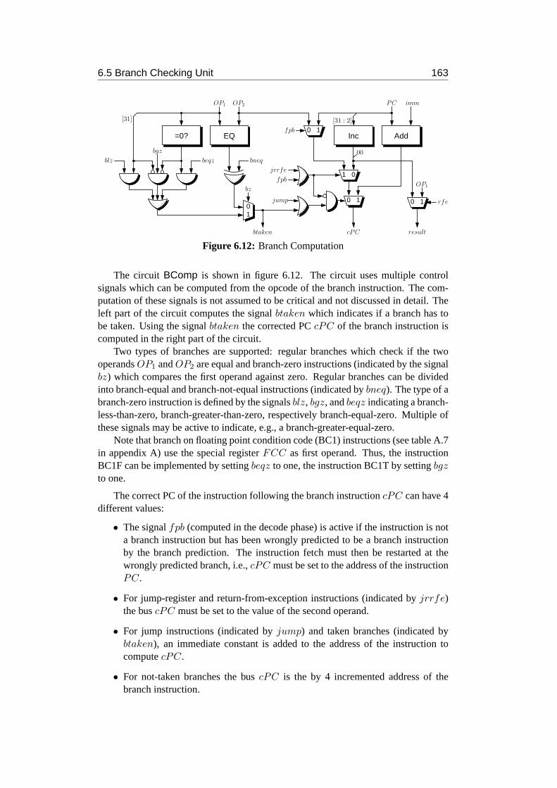
6.5 Branch Checking Unit 163
[31]
imm
[31 : 2]
cPCbtaken
bzOP1
rfe
result
bneqbeqzblz
bgz
Inc AddEQ=0?
00
OP1 PCOP2
10fpb
01
10
1 0jrrfe
fpb
jump 10
Figure 6.12: Branch Computation
The circuit BComp is shown in figure 6.12. The circuit uses multiple controlsignals which can be computed from the opcode of the branch instruction. The com-putation of these signals is not assumed to be critical and not discussed in detail. Theleft part of the circuit computes the signalbtaken which indicates if a branch has tobe taken. Using the signalbtaken the corrected PCcPC of the branch instruction iscomputed in the right part of the circuit.
Two types of branches are supported: regular branches which check if the twooperandsOP1 andOP2 are equal and branch-zero instructions (indicated by the signalbz) which compares the first operand against zero. Regular branches can be dividedinto branch-equal and branch-not-equal instructions (indicated bybneq). The type of abranch-zero instruction is defined by the signalsblz, bgz, andbeqz indicating a branch-less-than-zero, branch-greater-than-zero, respectively branch-equal-zero. Multiple ofthese signals may be active to indicate, e.g., a branch-greater-equal-zero.
Note that branch on floating point condition code (BC1) instructions (see table A.7in appendix A) use the special registerFCC as first operand. Thus, the instructionBC1F can be implemented by settingbeqz to one, the instruction BC1T by settingbgzto one.
The correct PC of the instruction following the branch instructioncPC can have 4different values:
• The signalfpb (computed in the decode phase) is active if the instruction is nota branch instruction but has been wrongly predicted to be a branch instructionby the branch prediction. The instruction fetch must then be restarted at thewrongly predicted branch, i.e.,cPC must be set to the address of the instructionPC.
• For jump-register and return-from-exception instructions (indicated byjrrfe)the buscPC must be set to the value of the second operand.
• For jump instructions (indicated byjump) and taken branches (indicated bybtaken), an immediate constant is added to the address of the instruction tocomputecPC.
• For not-taken branches the buscPC is the by 4 incremented address of thebranch instruction.
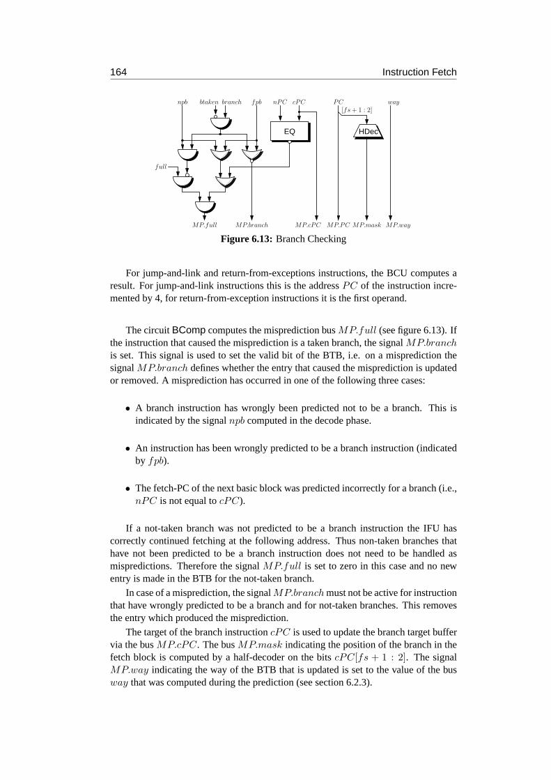
164 Instruction Fetch
cPCnPCfpbnpb
full
MP.branchMP.full MP.cPC MP.mask MP.way
wayPC
MP.PC
[fs + 1 : 2]btaken branch
HDecEQ
Figure 6.13: Branch Checking
For jump-and-link and return-from-exceptions instructions, the BCU computes aresult. For jump-and-link instructions this is the addressPC of the instruction incre-mented by 4, for return-from-exception instructions it is the first operand.
The circuitBComp computes the misprediction busMP.full (see figure 6.13). Ifthe instruction that caused the misprediction is a taken branch, the signalMP.branchis set. This signal is used to set the valid bit of the BTB, i.e. on a misprediction thesignalMP.branch defines whether the entry that caused the misprediction is updatedor removed. A misprediction has occurred in one of the following three cases:
• A branch instruction has wrongly been predicted not to be a branch. Thisisindicated by the signalnpb computed in the decode phase.
• An instruction has been wrongly predicted to be a branch instruction (indicatedby fpb).
• The fetch-PC of the next basic block was predicted incorrectly for a branch (i.e.,nPC is not equal tocPC).
If a not-taken branch was not predicted to be a branch instruction the IFUhascorrectly continued fetching at the following address. Thus non-taken branches thathave not been predicted to be a branch instruction does not need to be handled asmispredictions. Therefore the signalMP.full is set to zero in this case and no newentry is made in the BTB for the not-taken branch.
In case of a misprediction, the signalMP.branch must not be active for instructionthat have wrongly predicted to be a branch and for not-taken branches. This removesthe entry which produced the misprediction.
The target of the branch instructioncPC is used to update the branch target buffervia the busMP.cPC. The busMP.mask indicating the position of the branch in thefetch block is computed by a half-decoder on the bitscPC[fs + 1 : 2]. The signalMP.way indicating the way of the BTB that is updated is set to the value of the busway that was computed during the prediction (see section 6.2.3).

6.5 Branch Checking Unit 165
IF.lastcycle
to IFMP.full
BCheck
from / to Completion
BCheck.MP.⋆
BComp
BCU.⋆BCU.StallIn
to / from RS
BCU.StallOut
RS.⋆
MP.⋆
Figure 6.14: Branch Checking Unit
6.5.1 Stall Computation
If the BCU detects a misprediction, it must update the instruction fetch unit. The IFUcan only accept new data if the signallastcycle is active. In order not to affect thecompletion of correctly predicted branches an extra stage is added in whichmispre-dicted branches wait until the signallastcycle gets active (see figure 6.14). If thisstage contains a mispredicted branch, the BCU is cleared.
A branch instruction proceeds to the additional stage at the same time it enters thecompletion stage. If the branch instruction cannot proceed to the completion phase theadditional stage must not be filled. Otherwise if the branch instruction was mispre-dicted, the BCU would be cleared and the branch instruction does not complete, whichis needed for the rollback.
This additional stage does not have to stall the other stages of the BCU as allstages of the BCU are cleared anyway if a misprediction is in the additional stage(indicated by the signalBCU.mp). Thus, the other stages of the BCU are only stalledby the signalBCU.stallIn received from the completion phase. The additional stageis stalled by
MP.full ∧ IF.lastcycle.
Note that once a misprediction is in the additional stage, the stage is stalled until theinstruction fetch unit can be updated. Thus, the mispredicted branch in the additionalstage will not be overwritten be succeeding instructions.
6.5.2 Cost and Delay
The delay of the BCU is:
D(btaken) ≤ max{D(EQ(32)) + DXOR, D(Zero(32)) + 2 · DAND + DOR}
+ DMUX ,
D(BCU) ≤ max{D(Add(32)), D(Inc(32)) + DMUX ,
D(btaken) + DAND + DOR}
+ DMUX + D(EQ(32)) + DOR + DAND.

166 Instruction Fetch
Let the variablebBCU be one if a buffer circuit is added after the input registers ofthe BCU, otherwisebBCU is zero. The number of cyclescBCU needed for the BCU is:
cBCU (bBCU ) = ⌈(D(BCU) + bBCU · DMUX)/δ⌉.
Let BCU.stallIn be the stall input of the BCU from the completion phase. IfbBCU = 0, the delay of the output stall signalstallOut of the BCU is:
D(stallOut) ≤ max{D(AND-Tree(cBCU (0) + 1)), D(BCU.stallIn)} + DAND.
Let eRS7 be the number of entries of the reservation station of the BCU. The reserva-tion station then requires (see equation (4.15) on page 62):
δ ≥ D(BCU.stallOut) +
{
2 · DAND if eRS7 = 1
3 · DAND + DMUX if eRS7 > 1.
If this equation can not be fulfilled,bBCU must be one. This reduces the bound to:
δ ≥ max{D(AND-Tree(cBCU (1) + 2)), D(BCU.stallIn)} + DAND
which hold true forδ ≥ 5. The requirement for the input stall signal of the reservationstation are then fulfilled by construction of the reservation station.
The number of inputs of the BCU is161 + kBTB + lROB, the number of outputsis 97 + fs + kBTB + lROB. The cost of the BCU is approximated by:
C(BCU) ≤ C(Add(32)) + C(Inc(32)) + 2 · C(EQ(32)) + C(Zero(32))
+ 129 · CMUX + 9 · CAND + 7 · COR + CXOR
+ (32 + fs + kBTB) · CREG + 2 · CAND
+ (cBCU − 1) · ⌈(258 + fs + 2 · kBTB + 2 · lROB)/2⌉ · CREG.
6.6 Processor Flush
The processor must be flushed if an interrupt occurred or a mispredictionhas beendetected. Interrupts are detected during the retire sub-phaseRet2, mispredictions aredetected by the BCU. After a flush the processor must be in a state it would haveafter the execution of the instruction that caused the flushing (respectivelybefore theexecution depending on the type of the interrupt of misprediction) if all instructionswould be executed sequentially. This is done when the instruction enters the retiresub-phaseRet3 since then all registers have the correct value and the producer tablescan be reset.
In order to reduce the penalty of mispredictions, the instruction fetch is restartedat the correct address as soon as the misprediction is detected by the BCU.To guar-antee that no wrongly fetched instruction causes another misprediction the flush of theprocessor is done in two steps. As soon as a misprediction is detected all succeedingbranches are flushed. This is done by clearing the instruction fetch unit, the instructionfetch queue, the decode phase, and the BCU including the corresponding reservationstation. Since these parts of the processor execute instructions in-orderno precedinginstruction is cleared. After the clear the instruction fetch is resumed at the correct

6.6 Processor Flush 167
address, but the instruction succeeding the mispredicted instruction is stalledat the in-struction register (see section 6.4). When the mispredicted instruction entersthe retiresub-phaseRet3 the remaining parts of the processor are flushed and the succeedinginstruction can be decoded.
Interrupts are detected at the end of the retire sub-phaseRet2. Therefore, the flushof the processor is not done in two steps. When an instruction that causedan interruptenters the retire sub-phaseRet3 all parts of the processor are cleared.
Note that in parallel to first part of the flush due to a misprediction of the the flushdue to an interrupt the instruction fetch unit must be updated. This can only be doneif the signallastcycle is active. The flushing must not affect the additional stage ofthe BCU and the first stage of the retire sub-phaseRet3 since these stages containthe instructions that caused the flush. Note that interrupts have a higher priority thanmispredictions. Thus, if a mispredicted instruction is in the additional stage of theBCU at the same time an instruction that caused an interrupt is in the fist stage ofthesub-phaseRet3 the misprediction has no effect.
Also the remaining stages of the sub-phaseRet3 must not be flushed as they con-tain instructions preceding the instruction that caused the flush. However,the writesto the producer table duringRet3 are overwritten by the clear signal of the producertable. It follows:
IF.clearIFQ.clear
D1.clearD2.clear
RS6.clearFU6.clear
= (JISR.full ∨ MP.full) ∧ lastcycle,
RS0...5.clearFU0...5.clear
Complete.clearRet1.clearRet2.clearROB.clear
PT.clear
= (JISR.full ∧ lastcycle) ∨ Ret2.mp.
The clear signals are assumed to have a delay of zero. This is not a problem forthe signalsJISR.full, Ret2.mp, andlastcycle as they are not assumed to be critical.The signalMP.full is the critical signal of the BCU, but the OR- and AND-gate forthe computation of the clear signal can be put in the additional stage for mispredictedbranches and therefore have no impact on the delay of the BCU.

168 Instruction Fetch

Chapter 7
Discussion
This chapter discusses the results of the preceding chapters. In section7.1 the reduc-tion of the stage depth below five gate delay is investigated. Section 7.2 discusses theadvantages and disadvantages of the gate model used in this thesis. The cost and delayvalues of the DLXπ+ that can be derived from the formulas in the preceding chaptersare presented in section 7.3 and compared against the Tomasulo DLX from [Kro99]on which the DLXπ+ is based. Related work is discussed in section 7.4
7.1 Stage depths below 5
In this thesis all circuits of the DLXπ+ where designed in order to allow a stage depthδ ≥ 5 for the given gate model. This section describes possible enhancements in orderto allow a stage depth of4.
All basic bounds forδ regarding forwarding and stalling hold forδ = 4. If astage can generate a stall the stall input may have at most delay see equation(2.10) onpage 18)
D(stallIn) ≤ δ − (DOR + DAND).
If a stall signal is used in a forwarding circuit with stalling it must hold:
D(stall) ≤ δ − DMUX .
Since the delay of stall signals can be reduced toDAND by inserting buffer circuitsthese equations can be satisfied withδ = 4. The forwarding circuits require (seeequation (2.12) on page 23)
δ ≥ max{DMUX , DOR} + DMUX ,
which is fulfilled for δ = 4.
The equation (4.14) on page 59 boundsδ for a reservation station of typei asfollows:
δ ≥
3 · DAND if eRS = 1
max{DAND, D(FFO(eRS))} + 2 · DAND + DMUX if eRS > 1 ∧ i 6∈ {0, 6}
max{DAND, D(FFO(eRS))} + 3 · DAND + DMUX if eRS > 1 ∧ i ∈ {0, 6}
.

170 Discussion
This equation can be fulfilled forδ = 4 only if eRS = 1, i.e. all reservation stationsmay have at most one entry. The number of functional unitsni of a typei for a givenδ is bounded by equation (4.2) on page 43:
δ ≥ DMUX + max{DOR, max0≤i≤6
(D(PP-OR(eRSi)) + D(FFO(ni)))}
+
{
0 if ni = 1
DAND if ni > 1.
Hence, forδ = 4 the number of functional units of for each type may be at most2.The issue circuit also requires that in one cycle an instruction can be issued to at
least two groups (see equations (4.3) and (4.4) on page 44):
δ ≥ DAND + D(Sel(2)) + DAND,
δ ≥ max{2 · DAND, DAND + DMUX , DMUX} + D(Sel(2)).
Both equations hold true forδ ≥ 4. The requirements for the remaining stall signalsof the decode phase can be reduced by adding additional buffer circuits. Note that thiswould mean to add a buffer circuit into a RAM block (see figure 2.7) which is notnecessary forδ ≥ 5.
The completion phase can be built forδ = 4 if a tree of two-port arbiters is used.These arbiters reduce the requirements of the completion phase to the boundgiven byequation (4.20) on page 68:
δ ≥ 2 · DAND + 2 · DOR
which also holds true forδ = 4.
The retire phase has no additional requirements to the stage depthδ. However, theROB environment used in the retire phase introduces multiple bounds on delta.Thedelay of the outputforwOut of the forwarding circuits for the retire context of theROB access is bounded by (see equation (4.24) on page 83)
D(forwOut) ≤ δ − (DMUX + DOR + DAND).
In the standard implementation of the forwarding circuit the outputforwOut has atleast delayDOR and thus the equation does not hold forδ = 4. In order to fulfillthe bound, the signalforwOut must be derived from the registerforwcRet1−1 ofthe last stage of the forwarding circuit (see figure 4.27 on page 82) andnot from thesignalforwUpdcRet1−1 which has a delay of at leastDOR. This does not affect thecorrectness but increases the number of cyclescC2R andcA2R needed to forward fromthe write access in the completion- respectively allocation-context to the readaccessin the retiring-context by one.
The delay optimizations for the ROB control signalheadce and tailce in sec-tion 4.6.7 also apply forδ = 4. They only assume that equation (4.24) holds trueand the delay of the signalD1.stallIn0 ∨ D1.genStall0 is at mostδ, which can beachieved by inserting buffer circuits in the decode phase (see above).
The counters for the full and empty bits require (see equation (4.27) on page 86)
δ ≥ 2 · DMUX + DAND

7.1 Stage depths below 5 171
ecnt
ROB.empty
RS(1)
0
clear
01
headced
cA2R − 1 times
headce
inROB
LROB
fcnt
tailce
tailcedclear
Ret3.full0
ROB.full
LROB
4:1 4:1
LS(1) RS(1)
Dec
RS(1) LS(1)
10
clear
Dec
1
LS(1)
Figure 7.1: Optimized full and empty counter forδ = 4
due to the loop for the computing of the next counter value. This does not hold forδ = 4. Therefore, the counters for the full and empty bit must be modified as de-picted in figure 7.1. Both counter delay one of the control signals for incrementing anddecrementing (tailce respectivelyheadce) by one cycle and use the delayed signal tomodify the output of the counter (similar to the counter for the full bit in figure 4.31on page 91). Due to the delaying of the signalstailce andheadce all control signalsfor the counter come directly out of a register. This allows to use a 4 input selectioncircuit instead of two variable shifters to compute the next value of the counter. Basedon the value of the increment respectively decrement signals the selection circuit se-lects between the shifted or the un-shifted counter value. If only one of theincrementor decrement signals is active, the left- respectively right-shifted value isselected. Ifnone or both signals are active the un-shifted counter value is selected, since the left-and the right-shift eliminate each other. Note that the constant shifters in figure 7.1only consists of wiring and therefore have no delay. Thus, the modified counter onlybounds delta by:
δ ≥ max{D(Dec(2)), DAND} + D(Sel(4))
which holds true forδ = 4.
The update queue of the data cache boundsδ as follows (see equation (5.12) onpage 135):
δ ≥ max{D(OR-Tree(eUQ)), DAND} + 3 · DAND.
Thus, forδ = 4 the number of entries of the update queueeUQ must be one. If theoptimized completion for stores is used, the path from the stall input to the full bitofthe entry bounds the stage depth by (see equation (5.13) on page 137):
δ ≥ max{D(OR-Tree(eUQ)), 2 · DAND} + 3 · DAND.

172 Discussion
Out.PC
fs
1 0
01
32
fill
IF.instrFS−1−i
update
instr
Out.instr
In.instr
clear
fill
full
Out.full
IF.instrFS−1−i
In.full
01
IF.mask[FS − 1 − i] update
1 0
01fill
update
IF.PCFS−1−i
In.PC
PC
Figure 7.2: Optimized IFQ entry
Since this does not hold forδ = 4 the optimized completion cannot be used forδ = 4.The signalssent⋆ bound the stage depthδ by (see equation (5.14) on page 137)
δ ≥ D(FFO(eUQ + 1)) + DAND + DMUX
which holds true foreUQ = 1 andδ = 4.For the read queue it must hold (see equation (5.17) on page 141):
δ ≥
{
3 · DAND if eRQ = 1
max{DAND, D(FFO(eRQ))} + 2 · DAND + DMUX if eRQ > 1.
Thus, the number of read queue entrieseRQ must also be one forδ = 4.
The instruction fetch queue requires that the stage depth fulfills the equation(6.1)on page 161
δ ≥ 2 · DAND + DOR + DMUX
which does not hold forδ = 4. In order to be able to build the IFQ forδ = 4 thefollowing modifications have to be made: the AND-ing of the full bit and the maskis done in the instruction fetch unit. This can be done without increasing the delay,but upon activation of the clear signal all mask bits have to be reset. Then the circuitdepicted in figure 7.2 can be used for the entries of the instruction fetch queue. Notethat in this optimized version the entries might be filled even if the clear signal is active.Thus, the clear signal for the IFQ must be active at least two cycles.
Using the modifications described in this section it is possible to build the DLXπ+
with a stage depthδ of 4. However, equation (4.14) on page 59 bounds the number ofreservation station entries for all reservation stations to one. Note that the reservationstations stall output is active even if an instruction is currently dispatched, since other-wise the delay of the stall output would get too large. Thus, instructions canbe issuedto reservation stations with one entry only every other cycle.
Thus, in order to be able to issue one instruction of a type in every cycle theDLXπ+ needs two functional units of the type. Since the maximum number of func-tional units of a type is two due to equation (4.2) on page 43, at most two instructions

7.2 Gate Model 173
of a type can wait for their operands. Since for such a deep pipeline it is very likelythat the operands of an instruction are not valid at the time the instruction is issued,this is assumed to have a large performance impact.
Also, the optimization of the update queue from figure 5.21 on page 137 cannot bedone (see equation 5.16 on page 139). Thus, despite the optimized completion, storescan only be completed if the stall from the memory unit to the read queue of the datacache is inactive.
For these reasons and the large increase in the number of cycles neededit is veryunlikely that the performance of the DLXπ+ regarding a reasonable benchmark can beimproved by reducing the stage depth from5 to 4. Therefore, in this thesis only stagedepthsδ ≥ 5 were discussed in detail.
This thesis does not provide a formal proof that it is impossible to build the DLXπ+
with a stage depthδ = 3 without sacrificing fundamental aspects of the DLXπ+, e.g.,the out-of-order execution, the precise interrupts, or the possible bestcase CPI (cycles-per-instruction) of 1. However, the author thinks that it is at least very unlikely thatsuch a DLXπ+ is possible, since even after the described enhancements most equa-tions bound the stage depth to be at least4. In particular the bound given by the loopfor the data of the forwarding circuit with stalling (see equation (2.12) on page 23) thatbounds delta to
δ ≥ 2 · DMUX
is assumed to be hard to improve.
7.2 Gate Model
The gate model used in this thesis is rather simple, since it does not take fanout or wiredelays into consideration. Note that some of the path that bound the stage depth δ havelarge fanout, e.g., the signalROBhead.valid which stalls the whole ROB read accessin the retiring context. Due to the reduction of the device sizes in integrated circuitsthe delay of wires will have an increasing influence on the combinational delay ofsignals and therefore should not be neglected [HHM99]. This can also affect some ofthe critical paths (in particular stall signals) of the DLXπ+. Thus, the gate model usedin this thesis could be too optimistic regarding delay.
On the other hand the gate model only allows two-input gates and two-port muxes.Thus, using the more complex gates available in real designs like multi-input NANDsand NORs or wide transmission-gate-muxes [WH04] the delay of the critical pathcould be reduced. This could make up for the too optimistic estimations of the gatemodel due to the neglected fanout and wire delays.
Even if one assumes that the gate model is not very realistic, the degree of pipelin-ing presented in this thesis is still very high in comparison to previous work. Forexample in the deeply pipelined Pentium 4 processor a 16 bit addition (which has 12combinational gate delays in our model) can be in less than half a cycle [HSU+01].Thus, even if the used gate model is off by a factor of two, the amount of useful workthat can be done in a cycle of the Pentium 4 is still more than three times more thanthe 4 gate delays of the DLXπ+ with minimum cycle time.

174 Discussion
Variable Description
τ = δ + 5 cycle time of the DLXπ+
LROB = 2lROB # lines of the reorder bufferni # FU’s of typei (0 ≤ i ≤ 6)eRSi
# entries of the RSs of typei (0 ≤ i ≤ 6)LDC = 2lDC # lines of the data cacheSDC = 2sDC # bytes of the cache-lines of the data cacheKDC = 2kDC associativity of the data cacheeUQ # entries of the update queueeRQ # entries of the read queueLIC = 2lIC # lines of the instruction cacheSIC = 2sIC # bytes of the cache-lines of the instr. cacheKIC = 2kDC associativity of the instruction cacheLBTB = 2lBTB # lines of the branch target bufferKBTB = 2kBTB associativity of the branch target bufferFS = 2fs # instructions fetched perIFCLK cycle
Table 7.1: Parameters of the DLXπ+
The author thinks that even for a more realistic model (e.g., the logical effortmodel [SSH99]) it would still be possible to allow a similarly extensive super-pipelining.In addition to the techniques discussed in this thesis it would probably be necessary tofurther decrease the delay of stall signals, e.g., by pipelining the full bits ofan instruc-tion one cycle ahead of the actual data and thus computing the stall signal onecycleahead. Also the functional units (except the memory unit) would not need stall signalsif the number of CDBs were equal to the number of functional units and instructionscould not “collide” inside the functional units. Collisions could be prevented,e.g., byhandling divisions in software and therefore resolving loops, or by adapting the dis-patch logic.
7.3 Overall Cost and Delay
In this section the variables describing the pipelining of the DLXπ+ (e.g., the numberof cycles needed for decoding) in dependence of the parameters (e.g.,cycle time orROB size) are presented. The parameters of the DLXπ+ are listed in table 7.1. Thevariables describing the behavior of the DLXπ+ are listed in table 7.2.
Using the formulas presented in this thesis it is straightforward to write a smallprogram that computes the variables and the cost of the DLXπ+ in dependence of theparameters.1 In appendix E the values of the variables for some combinations of theparameters are described.
Table 7.3 compares the DLXπ+with the out-of-order DLX presented in [Kro99]which is in the following called DLXK . In order to match the DLXK , the followingparameters are chosen for the DLXπ+:
1The program can be found athttp://www-wjp.cs.uni-sb.de/leute/private homepages/jochen/DLX+.tgz.

7.3 Overall Cost and Delay 175
Variable Description
m multiplier for IFCLK
cIF # IFCLK cycles of the instruction fetchcD1 # cycles needed for the decode sub-phaseD1
cD2 # cycles needed for the ROB access in the decode sub-phaseD2
cI # cycles needed for issuingcT # cycles (needed ifcI > 1)cU2DM minimum # cycles from the update of an instruction in the memory RS
to the dispatch of the instructioncU2DI minimum # cycles from the update of an instruction in an integer or
BCU RS to the dispatch of the instructioncU2DF minimum # cycles from the update of an instruction in an FP RS to the
dispatch of the instructioncU2DB minimum # cycles from the update of an instruction in an branch check-
ing RS to the dispatch of the instructioncAT # cycles needed for the arbiter tree in the complete phasecC # cycles needed for the complete phasecC2R minimum # cycles from the completion to the retiring of an instructioncRet2 # cycles needed for the retire sub-phaseRet2
cSh4S # cycles needed for the shift for store circuitcHC # cycles needed for the hit computationcM2H # cycles the result bus must be delayedcM2W minimum # cycles between the returning of a memory request and the
update of the cache core by a store in the update queuecM2R minimum # cycles between the returning of a memory request and the
update of the cache core by a load in the update queuecM2Q minimum # cycles between the returning of a memory request and the
returning of a load by the read queuecSh4L # cycles needed for the shift for load circuitcIAlu # cycles needed for the integer ALUcIMul1 # cycles needed for the first part of the integer multiplicative unitcIMul2 # cycles needed for the second part of the integer multiplicative unitcIMul3 # cycles needed for the third part of the integer multiplicative unitcFPAdd # cycles needed for the FP additive unitcFPMul1 # cycles needed for the first part of the FP multiplicative unitcFPMul2 # cycles needed for the second part of the FP multiplicative unitcFPMul3 # cycles needed for the third part of the FP multiplicative unitcFPMul4 # cycles needed for the fourth part of the FP multiplicative unitcFPMisc # cycles needed for the FP miscellaneous unitcBCU # cycles needed for the branch checking unit
Table 7.2: Variables describing the behavior of the DLXπ+

176 Discussion
• The ROB has 16 entries.
• Every functional unit type is instantiated only once. In the DLXK the reservationstations of the floating point units have two entries, all other reservation stationshave four entries. The reservation stations of the DLXK can issue an instructioninto a reservation entry in the same cycle an instruction is dispatched from thereservation station, even if the reservation station is full. This is not possibleinthe DLXπ+, see section 4.2.2. Therefore, the number of entries is increased byone for the DLXπ+.
• The DLXK uses a common 16KB direct-mapped cache for data and instructions.In order to match the size, the DLXπ+ uses two 8KB direct-mapped caches forthe instruction fetch and the memory unit.
• The other parameters have no counterpart in the DLXK and are chosen as fol-lows: update queue and read queue have 4 entries, the BTB has 256 entries andis 4-way set associative. The instruction fetch unit fetches 8 instructionsperIFCLK-cycle.
The cycle time of the DLXK is 106 [Kro99]. The cycle timeτ of the DLXπ+ mustbe at least12 (δ = 7) in order to allow five reservation station entries (see sec-tion 4.2.3). Thus, for cycle timesτ ∈ {10, 11} the number of reservation stationsis set to at most2 respectively4. Note that in table 7.3 the columns for those values ofthe cycle timeτ have been omitted which would have the same entries as the columnfor the next smallerτ .
Only the variablesm andcIF change their value for cycle times greater the37.At a cycle timeτ = 50 the multiplierm can be set to one, but then the instructioncache access must be pipelined, i.e.,cIF becomes2. If τ = 68 both valuesm andcIF
can be one. Since the instruction fetch unit delivers up to8 instruction per instructionfetch cycle, is not assumed to be performance critical if the instruction fetchtakes twocycles. Therefore, in the following only cycles times of37 and below are investigatedfor the DLXπ+.
Note that the DLXK does not divide the decode phase into the sub-phasesD1 andD2. Therefore, the number of cycles needed for issuing and for the ROB access in thedecode sub-phaseD2 are set to zero for the DLXK . For cycles times of30 and above,the valuecIALU of the DLXπ+ is zero. This indicates that the integer ALU does notcontain any registers. Thus, the instruction can directly proceed from thereservationstation through the integer ALU to the CDB register. In the the DLXK all functionalunits must have a register, but the completion phase has no register, which has the sameeffect. In order to simplify the comparison the variablescIALU andcC of the DLXK
are set to the same value as for the DLXπ+ with a cycle time of30.The DLXπ+ with a cycle time of37 needs in the best case 5 cycles to process an
integer ALU instruction (instruction fetch not counted): 1 cycle decode, 1cycle issue,1 cycle dispatch + execution, 1 cycle completion, and 1 cycle retiring. This is onecycle more than needed for the DLXK which does decoding and issuing in the samecycle. However, the cycle time of the DLXK is roughly 3 times as large as the cycletime of this variant of the DLXπ+. Thus, even without super-pipelining the DLXπ+isassumed to have a much better performance than the DLXK .

7.3 Overall Cost and Delay 177
DLXπ+ DLXK
τ 10 11 12 13 14 15 16 17 18 20 21 23 25 30 34 35 37 50 68 106
m 5 5 5 4 4 4 4 3 3 3 3 3 2 2 2 2 2 1 1 1cIF 2 2 2 2 2 2 2 2 2 2 2 1 2 2 1 1 1 2 1 1cD1 7 6 5 4 4 4 3 3 3 2 2 2 2 2 2 1 1 1 1 1cD2 4 4 3 3 3 2 2 2 2 2 2 2 1 1 1 1 1 1 1 0cI 2 2 2 1 1 1 1 1 1 1 1 1 1 1 1 1 1 1 1 0
cU2DM 3 4 3 3 2 2 2 2 2 2 1 1 1 1 1 1 1 1 1 1cU2DI 4 4 3 3 2 2 2 2 2 1 1 1 1 1 1 1 1 1 1 1cU2DF 5 4 3 3 2 2 2 2 2 2 1 1 1 1 1 1 1 1 1 1cU2DB 3 3 2 2 2 2 2 1 1 1 1 1 1 1 1 1 1 1 1 1
cC 3 3 2 2 2 2 1 1 1 1 1 1 1 1 1 1 1 1 1 1cC2R 2 2 2 1 1 1 1 1 1 1 1 1 1 1 1 1 1 1 1 1cRet2 7 6 5 5 4 4 4 3 3 3 2 2 2 2 2 2 1 1 1 1
cIALU 4 3 3 2 1 1 2 2 1 1 1 1 1 0 0 0 0 0 0 0
Table 7.3: Comparison of selected variables of the DLXπ+ and DLXK
DLXπ+ DLXK
τ 10 11 12 15 18 25 37 106
IF/BCU 344895 342703 339568 337376 335337 334241 291155 189741Decode 22637 21125 17764 9001 7489 5977 4465 3970
Dispatch 216404 314301 272798 193953 169423 74372 74372 43679Complete 11776 12684 7268 7268 7268 7268 7268 196Ret./ROB 49464 43650 35197 28106 26648 16822 15364 19807
RF 23433 20055 18103 14722 14184 11856 11670 19545PT 29690 25117 19802 12320 12320 7083 4966 15574
Mem 1202498 973211 904068 601757 507442 329466 277848 225336IALU 4502 4038 4038 3110 3110 3110 2646 3693IMul 16813 15445 14533 14077 12709 12709 12253 na2
FPAdd 43447 38967 36279 32695 30903 27319 25527 23735FPMul 75333 69957 65477 59205 56517 52933 50245 47557
FPMisc 19510 18614 17718 16822 16822 15926 15926 18135Total 2060402 1899867 1752613 1330412 1200172 899082 793705 610968
Table 7.4: Comparison of the costs of the DLXπ+ and the DLXK
The critical path of the DLXK starts at the instruction register, goes through the de-code phase and finally updates the PC register which determines the address of the nextinstruction. The last part of this path has been removed for the DLXπ+ by using branchprediction. Then by splitting the decode phase into two sub-phases and improving thecircuits of the decode phase, the cycle time could be dramatically improved withoutincreasing the number of stages significantly.
Table 7.4 list the cost of the DLXπ+ and the DLXK for some selected cycle times
2The DLXK does not support integer multiplications and divisions.

178 Discussion
τ 10 11 12 15 18 25 37
IF/BCU 118.5% 117.7% 116.6% 115.9% 115.2% 114.8% 100.0%Decode 507.0% 473.1% 397.8% 201.6% 167.7% 133.9% 100.0%
Dispatch 291.0% 422.6% 366.8% 260.8% 227.8% 100.0% 100.0%Complete 162.0% 174.5% 100.0% 100.0% 100.0% 100.0% 100.0%Ret./ROB 321.9% 284.1% 229.1% 182.9% 173.4% 109.5% 100.0%
RF 200.8% 171.9% 155.1% 126.2% 121.5% 101.6% 100.0%PT 597.9% 505.8% 398.8% 248.1% 248.1% 142.6% 100.0%
Mem 432.8% 350.3% 325.4% 216.6% 182.6% 118.6% 100.0%IALU 170.1% 152.6% 152.6% 117.5% 117.5% 117.5% 100.0%IMul 137.2% 126.1% 118.6% 114.9% 103.7% 103.7% 100.0%
FPAdd 170.2% 152.7% 142.1% 128.1% 121.1% 107.0% 100.0%FPMul 149.9% 139.2% 130.3% 117.8% 112.5% 105.3% 100.0%
FPMisc 122.5% 116.9% 111.3% 105.6% 105.6% 100.0% 100.0%Total 259.6% 239.4% 220.8% 167.6% 151.2% 113.3% 100.0%
Table 7.5: Relative increase of the cost of the DLXπ+
from table 7.3. The cost of the cache of the DLXK were evenly distributed to theinstruction fetch and the memory unit. The higher cost of the DLXπ+ with cycle time37 compared to the DLXK is mainly due to the branch prediction and the non-blockingcache, which increase the cost of the instruction fetch respectively the memory unit.
Table 7.5 lists the relative increase of the cost for the DLXπ+ if the cycle time isreduced (normalized to the DLXπ+ with a cycle time of37). The increase of the costis only due to the additional forwarding circuits and registers, the number ofgates forthe actual computations is the same. The number of registers that has to be added dueto pipelining is reciprocal to the stage depth. Note that forwarding circuits and queuesuse two-dimensional pipelining, i.e., the number of registers increases quadratically ifthe stage depth is reduced.
Queues are used in the memory unit and the dispatch phase. Extensive forwardingis used in the ROB and the producer table environment. Therefore, these parts havea large relative increase. The cost of the dispatch get smaller again forτ ∈ {10, 11}since the number of reservation station entries has to be reduced for thesecycle times.The cost of the decode phase increases drastically if the issue circuit has to pipelined.The cost of the instruction fetch is not sensitive to the decrease of the cycle time asthe multiplierm for the instruction fetch clockIFCLK increases if the cycle timedecreases. Since the total cost of the instruction fetch is high this reducesthe relativeincrease of the DLXπ+.
7.4 Related Work
Super-pipelining is a well-known technique to improve processor performance. It isused in many commercial processors, e.g., in the succeeding generation ofthe MIPSR3000 processor on which the DLXπ+ ISA is based on [BLM91]. Other work com-bines super-pipelining with other techniques such as super-scalar designs [JCL94],multi-threading [GV95], or both [GV96]. However these studies use rather moderate

7.4 Related Work 179
super-pipelining which at least allows the computation of a 16-bit addition (which has12 combinational gate delays in our model) in a single cycle [GV95]. Note that inthedeeply pipelined Pentium 4 a 16-bit addition can be computed even with double thecore frequency [HSU+01].
Extreme super-pipelining as done in this thesis is considered in previous work thatstudies the optimum pipeline depth of a processor [KS86][HJF+02][SC02][HP02].Usually these studies are based on an existing processor. They compute the combi-national work to be done per instruction from the cycles needed and the stage depthof the processor. The cycles needed for other frequencies is then simplycomputed bydividing the combinational work by the corresponding stage depth. They do not takeinto account that the combinational work may depend on the stage depth, e.g.,if for-warding of RAM ports becomes necessary (see section 2.6.1). The optimalstage depthis obtained by simulating a benchmark suite for different processor frequencies. Noneof the studies details the effects on the logic if the cycle time is reduced or assumes alower bound for the stage depth. We now discuss the cited work in some more detail.
An initial study on the optimum pipeline depth of a processor was done by Kunkeland Smith [KS86]. Their work is based on a CRAY-1S supercomputer build fromdiscrete ECL gates. Kunkel and Smith assume that interlocking (i.e., stalling) must becomputed in one cycle and that central RAM blocks must be accessed in onecycle.These bounds can be overcome using the techniques used in this thesis. Limitations tothe minimum stage depth are noted in [KS86] but are later ignored in the simulations.They conclude that the maximum performance is achieved with a stage depth of8 ECLgate levels for scalar code (4 levels for vector code).
Hrishikesh et. al. [HJF+02] studied the optimum stage depth of an Alpha 21264with large register files and large cache. They assume that the instruction wakeup andinstruction select logic are critical circuits that bound the stage depth. In order to allowlower stage depths Hrishikesh et. al. propose to pipeline these circuits by dividingthe issue window in multiple stages. They do not discuss the consequences of thispipelining to the correctness of the logic, e.g., if an instruction moves from onestageto the next. Using these pipelined circuits and assuming that all other circuits can beperfectly pipelined into arbitrary stages Hrishikesh et. al. conclude the optimum stagedepth to be 6 FO43for integer benchmarks and 4 FO4 for floating point benchmarks.
Sprangle and Carmean [SC02] measured the performance losss for some criticalloops (ALU, branch prediction, cache accesses) if the loops are increased by one cycle.They model the performance loss for a loop withm additional cycles to be(1 − s)m.The total performance is computed as product of the losses for the loops.This modelmatches their simulations. They derive that the performance of a Pentium 4 proces-sor can be improved by 35 to 90% through implementing deeper pipelines and largercaches. Sprangle and Carmean assume that all circuits can be pipelined arbitrarily.They address the problem of forwarding in order to pipeline RAM accesses but donot handle pipelining of the forwarding itself and do not include forwarding in theirsimulations.
Hartstein and Puzak [HP02] developed an analytical formula for the performanceof a S/390 processor in dependence of the stage depth. The optimum stagedepth isfound by equating the derivation function to zero. Yet the formula uses some processor
3Fan-out-of-four (FO4) is defined as the delay of an inverter that drives four inverters of the same size.

180 Discussion
and benchmark dependent constants which are hard to determine. Also theformulaassumes that processor logic can be uniformly divided into an arbitrary number ofstages.
Recent studies [HP03] [SBG+02] also take power consumption into account. Sincelow stage depths dramatically increase the power consumption due to the large amountof necessary latches this generally leads to a larger optimum pipeline depth. Since thepower consumption depends in first order on the cost of processor, this can be includedin our model by not just optimizing the performance of the processor but a quality met-ric
Quality =1
Performance1−q · Costq
for a q ∈ [0; 1] as proposed by Grun [Gru94].
To the author’s best knowledge the theoretical limits of super-pipelining andtheminimum stage depth as presented in this thesis have not yet been studied. Alsotheconsequences to the logic if even the forwarding circuits are pipelined hasnot yet beendiscussed.
Chapter 8
Summary
In this thesis the basic techniques needed for super-pipelining of processors were de-scribed. These techniques comprise the insertion of buffer circuits to splitthe stalltrees and the pipelining of RAM blocks. In order to pipeline RAM blocks it is neces-sary to forward the data written by succeeding writes to ongoing read accesses. Theforwarding circuits presented in this thesis even allow to reduce the cycle time belowthe time needed for forwarding data by pipelining the forwarding circuit itself, whichintroduces two-dimensional pipelining.
Using these techniques the DLXπ+, an out-of-order processor with multiple vari-able parameters including the cycle time was presented. The cycle time of the DLXπ+
can be reduced to down to five gate delays, with restrictions even down to four gatedelays. Formulas were developed that compute the cost and the number of pipelinestages based on the cycle time. Correctness proofs were given for the parts that differsignificantly from the DLX presented in [Kro99]. In particular for every RAM block itwas proven that the forwarding circuits deliver the correct data needed for the overallcorrectness of the Tomasulo algorithm.
8.1 Future Work
Using the formulas presented in this thesis it is possible to compute the variables de-scribing the pipelining of the DLXπ+ in dependence of the parameters. The next stepwould be to write a simulator for the DLXπ+. This simulator could use instructiontraces of a benchmark suite in order to compute the average time per instruction(TPI)of the DLXπ+ configured to different cycle times, ROB sizes, etc. for this benchmarksuite. This would allow to examine the parameters of the DLXπ+ that deliver the bestTPI values. In particular the optimal cycle time for the DLXπ+ could be determined.
Apart from super-pipelining the number of active instructions in a processor canbe increased by issuing multiple instructions in one cycle (super-scalar processors).The DLXπ+ only supports issuing of one instruction per cycle. A super-scalar DLX ispresented in [Hil00], methods to reduce the cycles time of the central circuits of super-scalar processors can be found, e.g., in [PJS97]. An expansion of the DLXπ+ couldcombine multi-issuing and super-pipelining to investigate the advantages of the differ-ent approaches.
Modern processors are able to execute multiple threads at the same time. This al-

182 Summary
lows for better utilization of the resources. Using multi-threading in a super-pipelinedprocessor could decrease the optimum cycle time since useful work can bedone whilean instruction waits for data.
The DLXπ+ uses a rather simple branch prediction scheme. The performance im-pact of the branch prediction increases if the cycle time is reduced, since this increasesthe number of cycles needed for the roll-back of a mispredicted branch. Hence, in-creasing the hit-rate of the branch prediction would be worthwhile. Also the roll-backcould be improved, such that the mispredicted instruction do not need to retirebeforethe succeeding instructions from the corrected branch target can be decoded.
The cost and delay calculations of the DLXπ+ are based on a rather simple gatemodel that does not take fanout and wiring into account. Since the stall signals of theDLXπ+ have a large fanout, a gate model that includes fanout, e.g. the logical effortmodel [SSH99], could have significant impact on the bounds of the cycle time. Inorder to investigate the impact, the delay calculations of the DLXπ+ could be adoptedfor the logical effort model.

Appendix A
Instruction set architecture
A.1 Instructions
In this section the instructions which are supported by the processor are summarized.All instructions which do not handle special registers or the program counter. are di-rectly taken from the MIPS 32000 instruction set[KH92]. Since the processor doesnot support delayed branch, the control flow change instructions arealtered accord-ingly. Special register and interrupt handling are based on the DLX implementationby Muller and Paul [MP00].
The instructions of the processor are presented in the tables A.1 to A.7, orderedby the type of functional unit they use. If the bits[31 : 26] of the instruction indicatean floating point instruction, but the rest of the instruction matches none of the follow-ing opcodes, theuFOP (unimplemented floating point operation) interrupt is raised.Otherwise if the instruction matches none of the following opcodes, theill (illegalinstruction) interrupt is raised. In this case the instruction is not sent to an functionalunit but the valid bit of the ROB entry is set.
The instructions have up to four parameters: the destination register addressD,the two operand addressesOP1 andOP2, and an immediate constantimm. For thedescription of the instructions, the following abbreviations are used for theregisterfiles:
GD := GPR[D] FD := FPR[D] SD := SPR[D]
GOP1 := GPR[OP1] FOP1 := FPR[OP1] SOP1 := SPR[OP1]
GOP2 := GPR[OP2] FOP2 := FPR[OP2] SOP2 := SPR[OP2]
Gi := GPR[i] Si := SPR[i]
The following abbreviation is used to describe a memory location of variable width (ifthe memory is seen as an one-dimensional array):
M(addr, d) := M [8 · (addr + d) − 1 : 8 · addr]
The memory is usually addressed by the sum of the operand 1 and the immediateconstant. This sum is abbreviated byea. For the description of the instructionlwl,lwr, swl, andswr (load / store word left / right), the base addressba and the offset

184 Instruction set architecture
IR[31:26] Instr. Group Effect
100000 lb
Load
[GD] = [M(ea, 1)]100001 lh [GD] = [M(ea, 2)]100011 lw [GD] = [M(ea, 4)]100100 lbu 〈GD〉 = 〈M(ea, 1)〉100101 lhu 〈GD〉 = 〈M(ea, 2)〉
100010 lwlLoadLR
GD = M(ba, oa + 1), GD[23 − 8 · oa : 0]100110 lwr GD = GD[31 : 8 · (4 − oa)], M(ea, 4 − oa)
110001 lwc1 LoadFP [FD] = [M(ea, 4)]
101000 sbStore
M(ea, 1) = GOP2[7 : 0]101001 sh M(ea, 2) = GOP2[15 : 0]101011 sw M(ea, 4) = GOP2
101010 swlStoreLR
M(ba, oa + 1) = GOP2[31 : 8 · (3 − oa)]101110 swr M(ea, 4 − oa) = GOP2[8 · (4 − oa) − 1 : 0]
111001 swc1 StoreFP M(ea, 4) = FOP2
Table A.1: Memory instructions
addressoa are used:
ea := [GOP1] + [imm]
ba := ⌊ea/4⌋
oa := ea mod 4
A.2 Encoding
The table A.8 shows the encoding of the instructions parametersD, OP1, OP2, andimm. The parametersD, OP1, andOP2 have always width 5 bit. The width of theimmediate constantimm depends on the width of theimm field in the encoding.
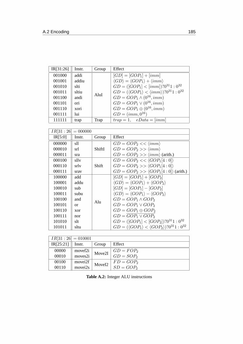
A.2 Encoding 185
IR[31:26] Instr. Group Effect
001000 addi
AluI
[GD] = [GOP1] + [imm]001001 addiu 〈GD〉 = 〈GOP1〉 + 〈imm〉001010 slti GD = ([GOP1] < [imm])?0311 : 032
001011 sltiu GD = (〈GOP1〉 < 〈imm〉)?0311 : 032
001100 andi GD = GOP1 ∧ (016, imm)001101 ori GD = GOP1 ∨ (016, imm)001110 xori GD = GOP1 ⊕ (016, imm)001111 lui GD = (imm, 016)
111111 trap Trap trap = 1, eData = [imm]
IR[31 : 26] = 000000
IR[5:0] Instr. Group Effect
000000 sllShiftI
GD = GOP2 << 〈imm〉000010 srl GD = GOP2 >> 〈imm〉000011 sra GD = GOP2 >> 〈imm〉 (arith.)000100 sllv
ShiftGD = GOP2 << 〈GOP1[4 : 0]〉
000110 srlv GD = GOP2 >> 〈GOP1[4 : 0]〉000111 srav GD = GOP2 >> 〈GOP1[4 : 0]〉 (arith.)100000 add
Alu
[GD] = [GOP1] + [GOP2]100001 addu 〈GD〉 = 〈GOP1〉 + 〈GOP2〉100010 sub [GD] = [GOP1] − [GOP2]100011 subu 〈GD〉 = 〈GOP1〉 − 〈GOP2〉100100 and GD = GOP1 ∧ GOP2
100101 or GD = GOP1 ∨ GOP2
100110 xor GD = GOP1 ⊕ GOP2
100111 nor GD = GOP1 ∨ GOP2
101010 slt GD = ([GOP1] < [GOP2])?0311 : 032
101011 sltu GD = (〈GOP1〉 < 〈GOP2〉)?0311 : 032
IR[31 : 26] = 010001
IR[25:21] Instr. Group Effect
00000 movef2iMove2I
GD = FOP2
00010 moves2i GD = SOP2
00100 movei2fMoveI2
FD = GOP2
00110 movei2s SD = GOP2
Table A.2: Integer ALU instructions
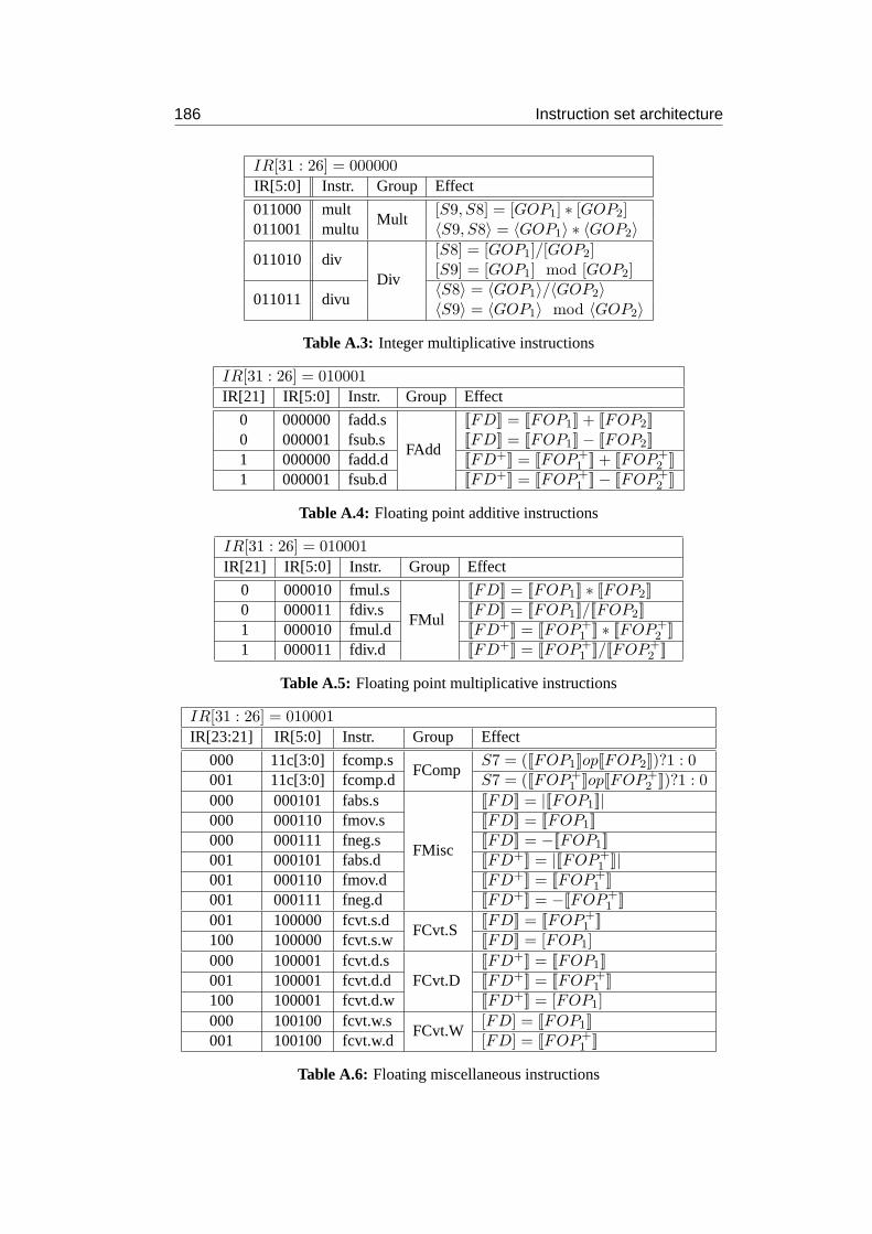
186 Instruction set architecture
IR[31 : 26] = 000000
IR[5:0] Instr. Group Effect
011000 multMult
[S9, S8] = [GOP1] ∗ [GOP2]011001 multu 〈S9, S8〉 = 〈GOP1〉 ∗ 〈GOP2〉
011010 divDiv
[S8] = [GOP1]/[GOP2][S9] = [GOP1] mod [GOP2]
011011 divu〈S8〉 = 〈GOP1〉/〈GOP2〉〈S9〉 = 〈GOP1〉 mod 〈GOP2〉
Table A.3: Integer multiplicative instructions
IR[31 : 26] = 010001
IR[21] IR[5:0] Instr. Group Effect
0 000000 fadd.s
FAdd
[[FD]] = [[FOP1]] + [[FOP2]]0 000001 fsub.s [[FD]] = [[FOP1]] − [[FOP2]]1 000000 fadd.d [[FD+]] = [[FOP+
1 ]] + [[FOP+2 ]]
1 000001 fsub.d [[FD+]] = [[FOP+1 ]] − [[FOP+
2 ]]
Table A.4: Floating point additive instructions
IR[31 : 26] = 010001
IR[21] IR[5:0] Instr. Group Effect
0 000010 fmul.s
FMul
[[FD]] = [[FOP1]] ∗ [[FOP2]]0 000011 fdiv.s [[FD]] = [[FOP1]]/[[FOP2]]1 000010 fmul.d [[FD+]] = [[FOP+
1 ]] ∗ [[FOP+2 ]]
1 000011 fdiv.d [[FD+]] = [[FOP+1 ]]/[[FOP+
2 ]]
Table A.5: Floating point multiplicative instructions
IR[31 : 26] = 010001
IR[23:21] IR[5:0] Instr. Group Effect
000 11c[3:0] fcomp.sFComp
S7 = ([[FOP1]]op[[FOP2]])?1 : 0001 11c[3:0] fcomp.d S7 = ([[FOP+
1 ]]op[[FOP+2 ]])?1 : 0
000 000101 fabs.s
FMisc
[[FD]] = |[[FOP1]]|000 000110 fmov.s [[FD]] = [[FOP1]]000 000111 fneg.s [[FD]] = −[[FOP1]]001 000101 fabs.d [[FD+]] = |[[FOP+
1 ]]|001 000110 fmov.d [[FD+]] = [[FOP+
1 ]]001 000111 fneg.d [[FD+]] = −[[FOP+
1 ]]
001 100000 fcvt.s.dFCvt.S
[[FD]] = [[FOP+1 ]]
100 100000 fcvt.s.w [[FD]] = [FOP1]
000 100001 fcvt.d.sFCvt.D
[[FD+]] = [[FOP1]]001 100001 fcvt.d.d [[FD+]] = [[FOP+
1 ]]100 100001 fcvt.d.w [[FD+]] = [FOP1]
000 100100 fcvt.w.sFCvt.W
[FD] = [[FOP1]]001 100100 fcvt.w.d [FD] = [[FOP+
1 ]]
Table A.6: Floating miscellaneous instructions

A.2 Encoding 187
IR[31:26] Instr. Group Effect
000100 beqBranch
[PC]+ = ([GOP1] = [GOP2])?[imm] : 4000101 bne [PC]+ = ([GOP1] 6= [GOP2])?[imm] : 4
000110 blezBranchZ
[PC]+ = ([GOP1] ≤ 0)?[imm] : 4000111 bgtz [PC]+ = ([GOP1] > 0)?[imm] : 4
000010 j Jump [PC]+ = [imm]
000010 jal JumpAL[PC]+ = [imm][G31] = [PC] + 4
111111 rfe RFE[PC] = [S2][S0] = [S1]
IR[31 : 26] = 000000
IR[5:0] Instr. Group Effect
001000 jr JumpR [PC]+ = [GOP1]
001001 jalr JumpALR[PC]+ = [GOP1][GD] = [PC] + 4
IR[31 : 26] = 000001
IR[20:16] Instr. Group Effect
00000 bltzBranchZ
[PC]+ = ([GOP1] < 0)?[imm] : 400001 bgez [PC]+ = ([GOP1] ≥ 0)?[imm] : 4
10000 bltzalBranchZAL
[PC]+ = ([GOP1] < 0)?[imm] : 4[G31] = [PC] + 4
10001 bgezal[PC]+ = ([GOP1] ≥ 0)?[imm] : 4[G31] = [PC] + 4
IR[31 : 26] = 010001 ∧ IR[25 : 21] = 01000
IR[20:16] Instr. Group Effect
00000 BC1FBC1
[PC]+ = ([S7] = 0)?[imm] : 400001 BC1T [PC]+ = ([S7] = 1)?[imm] : 4
Table A.7: Control flow change instructions
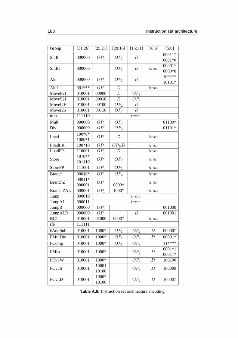
188 Instruction set architecture
Group [31:26] [25:21] [20:16] [15:11] [10:6] [5:0]
Shift 000000 OP1 OP2 D00011*0001*0
ShiftI 000000 OP2 D imm00001*0000*0
Alu 000000 OP1 OP2 D100***10101*
AluI 001*** OP1 D imm
MoveF2I 010001 00000 D OP2
MoveS2I 010001 00010 D OP2
MoveI2F 010001 00100 OP2 D
MoveI2S 010001 00110 OP2 D
trap 111110 imm
Mult 000000 OP1 OP2 01100*Div 000000 OP1 OP2 01101*
Load100*0*
OP1 D imm1000*1
LoadLR 100*10 OP1 OP2/D imm
LoadFP 110001 OP1 D imm
Store1010**
OP1 OP2 imm101110
StoreFP 111001 OP1 OP2 imm
Branch 00010* OP1 OP2 imm
BranchZ00011*
OP1 imm000001 0000*
BranchZAL 000001 OP1 1000* imm
Jump 000010 imm
JumpAL 000011 imm
JumpR 000000 OP1 001000JumpALR 000000 OP1 D 001001BC1 010001 01000 0000* imm
rfe 111111
FAddSub 010001 1000* OP1 OP2 D 00000*
FMulDiv 010001 1000* OP1 OP2 D 00001*
FComp 010001 1000* OP1 OP2 11****
FMisc 010001 1000* OP2 D0001*100011*
FCvt.W 010001 1000* OP2 D 100100
FCvt.S 01000110001
OP2 D 10000010100
FCvt.D 0100011000*
OP2 D 10000110100
Table A.8: Instruction set architecture encoding

Appendix B
Emulation of a MIPS R3000
Apart from interrupt handling, the ISA of the DLXπ+differs in the following pointsfrom the MIPS R3000 processor ISA [KH92]:
• The DLXπ+does not support delayed branch. The semantic of branch instruc-tions are altered accordingly.
• The DLXπ+does not have a co-processor 0 (memory management unit). CP0instructions cause an illegal instruction interrupt.
• All special registers (including floating point special registers and the registersHI and LO) are combined in the special register file. Instructions accessingspecial registers must be emulated by the instructionsmoves2i respectivelymovei2s.
• The floating point special register is divided into the special registerSR (floatingpoint mask),RM (rounding mode),IEEEf (floating point flags), andFCC(floating point condition code). Instructions accessing the floating point specialregister are assumed to access the special registerIEEEf .
The MIPS R3000 instructions which cannot be mapped directly are emulated assummarized in table B.1.
MIPS instruction DLXπ+instruction
syscall,break trapcfc1,mflo,mflo moves2i(OP1 = 6, 8, 9)
ctc1,mtlo,mthi movei2s(D = 6, 8, 9)
mfc1 movef2imtc1 movei2fbc0,cfc0,mfc0,mtc0,tlbr,tlbwi,tlbwr,tlbp not implemented
Table B.1: Translation of MIPS R3000 instructions

190 Emulation of a MIPS R3000

Appendix C
Additional Circuits
In this chapter all additional circuits needed for the design of the DLXπ+are described.
C.1 Basic Circuits
C.1.1 Design
Figure C.1 depicts the design of a half-unary find-last-one circuit. Note that the circuitcomputes additionally to the find-last-one outputflo an outputzero which indicatesthat all input signals are zero. Forn = 1 the design of the circuit is simple. Forn > 1the circuit is build from two half-unary find-last-one sub-circuits with only half of theinput bits. One circuit uses the upper half of the input bits, the other the lower half.The zero output is active if both zero outputs of the sub-circuit are active. If the lowerparts of the inputs contains a one (i.e., the zero output of the lower part is not active,the outputflo of the upper part must be forced to zero.
C.1.2 Cost and Delay
This section lists the formulas for the cost and delay of the basic circuits usedin thisthesis.
HFLO(⌈n/2⌉)
in[n − 1 : ⌊n/2⌋]
n > 1 n = 1in[⌊n/2⌋ − 1 : 0]
HFLO(⌊n/2⌋)flozero
in
1zero flo
floflo[⌈n/2⌉ − 1 : 0] zerozero flo[n − 1 : ⌈n/2⌉]
Figure C.1: Design of a half-unary find-last-one circuit

192 Additional Circuits
Find-Last-One / Find-First-One
D(FLO(n)) ≤ ⌈log n⌉ · DAND,
C(FLO(n)) ≤
0 if n ≤ 1
C(FLO(⌈n/2⌉)) + C(FLO(⌊n/2⌋))
+(⌈n/2⌉ + 1) · CAND
if n > 1,
D(FFO(n)) ≤ D(FLO(n)),
C(FFO(n)) ≤ C(FLO(n)),
D(HFLO(n)) ≤ D(FLO(n)),
C(HFLO(n)) ≤ C(FLO(n)),
Decoder / Encoder
D(Dec(n)) ≤ ⌈log n⌉ · DAND,
C(Dec(n)) ≤
{
0 if n ≤ 1
C(Dec(⌈n/2⌉)) + C(Dec(⌊n/2⌋)) + 2n · CAND if n > 1,
D(HDec(n)) ≤ n · max{DAND, DOR},
C(HDec(n)) ≤
{
0 if n ≤ 1
C(HDec(n − 1) + 2n−1 · (CAND + COR) if n > 1,
D(Enc(n)) ≤
{
0 if n ≤ 1
D(Enc(⌈n/2⌉)) + DMUX if n > 1,
C(Enc(n)) ≤
0 if n ≤ 1
C(Enc(⌈n/2⌉)) + C(Enc(⌊n/2⌋))
+CAND + (⌊n/2⌋) · CMUX
if n > 1.
Parallel Prefix
D(PP-FUNC(D(FUNC), n)) ≤ ⌈log n⌉ · D(FUNC),
C(PP-FUNC(C(FUNC), n)) ≤
0 if n ≤ 1
C(PP-FUNC(⌈n/2⌉))
+C(PP-FUNC(⌊n/2⌋))
+(n − 1) · C(FUNC) if n > 1
,
D(PP-AND(n)) ≤ D(PP-FUNC(DAND, n)),
C(PP-AND(n)) ≤ C(PP-FUNC(CAND, n)),
D(PP-OR(n)) ≤ D(PP-FUNC(DOR, n)),
C(PP-OR(n)) ≤ C(PP-FUNC(COR, n)),

C.2 Instruction Decode 193
Incrementer / Adder
D(Inc(n))
{
0 if n ≤ 1
≤ D(PP-AND(n − 1)) + DXOR if n > 1,
C(Inc(n)) ≤ C(PP-AND(n − 1)) + (n − 1) · CXOR,
D(Add(n)) ≤ DXOR + D(PP-FUNC(DMUX , n − 1)) + max{DMUX , DXOR},
C(Add(n)) ≤ C(PP-FUNC(CMUX , n)) + 2 · n · CXOR.
Trees
D(FUNC-Tree(D(FUNC), n)) ≤ ⌈log n⌉ · D(FUNC),
C(FUNC-Tree(C(FUNC), n)) ≤ (n − 1) · C(FUNC),
D(AND-Tree(n)) ≤ D(FUNC-Tree(DAND, n)),
C(AND-Tree(n)) ≤ C(FUNC-Tree(DAND, n)),
D(OR-Tree(n)) ≤ D(FUNC-Tree(DOR, n)),
C(OR-Tree(n)) ≤ C(FUNC-Tree(DOR, n)).
Checks
D(EQ(n)) ≤ DXOR + D(AND-Tree(n)),
C(EQ(n)) ≤ n · CXOR + C(AND-Tree(n)),
D(Zero(n)) ≤ D(OR-Tree(n)),
C(Zero(n)) ≤ C(OR-Tree(n)).
Selection Circuit
D(Sel(n)) ≤ DAND + D(OR-Tree(n)),
C(Sel(n)) ≤ n · CAND + C(OR-Tree(n)),
C.2 Instruction Decode
The instructions are decoded by the two circuitsDestCmp andDecode. The circuitDestCmp computes the busD.⋆ which contains all signals regarding the destinationaddress. Since these signals are needed to update the producer tables,they are consid-ered timing critical. The circuitDestCmp is therefore delay optimized. The remainingcontrol signals are computed by the circuitDecode.

194 Additional Circuits
C.2.1 Decode
This section only describes the control signals which are needed by the decode phase.The computation of the control signals used by the functional units is described in thetogether with the functional units.
The main purpose of the circuitDecode is to compute the following busses:FUtmp.{IAlu, IMul, Mem, BCU, FAdd, FMul, FMisc}, OP1.{gpr, fpr, spr},andOP2.{gpr, fpr, spr}. These busses define which FU should be used by an in-struction and from which register file the operands have to be taken. At most one ofa signal of a bus may be active. If none of the signalsOP1.⋆ or OP2.⋆ is active, animmediate constant is used as operand.
The computation of the control signals is based on the division of the instructionsinto instruction groups. The instruction group of a instruction is defined in table A.8along with the encoding for the group. Table C.1 shows for each instructiongroupwhich control signal must be active.
The circuitDecode computes for each instruction to which instruction group itbelongs. The control signals are computed as or of the instruction groupsin which thesignal is active. The last column of the table C.1 defines for which group additionalcontrol signals needed in the decode phase have to be valid.
If an instruction is a floating point instruction (i.e.,IR[31 : 25] = 0100011), butbelongs to no group, the signalFUunimp must be activated. If the instruction isnot a floating point instruction and belongs to no group, the signal illegal instructioninterruptill must be activated.
If the branch prediction assumes that an instruction is an control flow instruction(indicated byIFQ.pb), the instruction has to be sent to the branch checking unit inany case. Hence, the signalFU.BCU has to be active and the remaining signals ofthe busFU.⋆ must be 0. IfIFQ.pb is not active, the value ofFUtmp.⋆ can be usedto computeFU.⋆.
If the instruction is not an control flow instruction, the signalfpb is activatedto indicate an falsely predicted branch. If an instruction is a branch instruction butIFQ.pb is not active, the signalnpb (not-predicted branch) is activated. The signalsfpb andnpb are needed by the BCU. It follows:
FU.BCU = FUtmp.BCU ∨ IFQ.pb
FU.⋆ = FUtmp. ⋆ ∧ IFQ.pb
fpb = IFQ.pb ∧ FUtmp.BCU
npb = IFQ.pb ∧ FUtmp.BCU
The operands may only be double precision values, if the instruction is an floatingpoint instruction. For floating point instructions double precision operands are indi-cated by the bitIR[21]. If the first operand is an immediate constant, the constant isalways determined by the bitsIR[10 : 6]. The immediate constant for operand 2 is theaddress of the instruction if an instruction memory interrupt occurred, otherwise the

C.2 Instruction Decode 195
Group FUtmp. OP1. OP2.
Alu
IAlu
gpr gprAluI gprShift gpr gprShiftI gprMoveS2F fprMoveF2S gprMoveS2I sprMoveI2S gprTrap trap
MultIMul
gpr gprDiv gpr gpr
Load
Mem
gprLoadLR gpr gprLoadFP gprStore gpr gprStoreFP gpr fpr storeFP
Branch
BCU
gpr gprBranchZ gprBranchZAL gprJumpJumpALJumpR gprJumpALR gprBC1 sprRFE spr spr rfe
FAdd FAdd fpr fpr
FMul FMul fpr fpr
FComp
FMisc
fpr fprFMisc fprFCvt.W fprFCvt.S fprFCvt.D fpr
Table C.1: Active control signals
sign extended bitsIR[15 : 0].
OP1,2.dbl = IR[21],
OP1.imm = IR[10 : 6],
OP2.imm =
{
fPC if Ipf ∨ Imal
IR[15]16IR[15 : 0] if Ipf ∧ Imal.
The only instructions that explicitly read or write the special registerIEEEf aremoves2i respectivelymovei2s. These instruction access the registerIEEEf if the

196 Additional Circuits
Variable Meaning Value
λmax length of longest monomial in table A.8 17λsum accumulated length of all monomials in table A.8 395νmax maximum number of monomials per group in table A.82νsum number of monomials in table A.8 41γ number of groups in table C.1 32βmax maximum frequency of a control signal in table C.1 15βsum accumulated frequency of all control signals in table C.170ω number of output signals in table C.1 16
Table C.2: Variables of the Decode Computation
bits IR[15 : 11] encode the number of this register (6):
readIEEEf = MoveS2I ∧ IR[15 : 11] = 00110
writeIEEEf = MoveI2S ∧ IR[15 : 11] = 00110
Cost and delay of the circuitDecode can be computed using the variables fromtable C.2 derived from the tables A.8 and C.1:
C(Decode) ≤ (λsum − νsum) · CAND + (νsum − γ + βsum − ω) · COR
+ (12 + 8 + 7) · CAND + COR + 32 · CMUX
≤ 381 · CAND + 64 · COR + 32 · CMUX
D(Decode) ≤ ⌈log λmax⌉ · DAND + ⌈log(νmax · βmax)⌉ · DOR + DAND
≤ 6 · DAND + 5 · DOR
C.2.2 Destination computation
The computation of the signalsD.{gpr, fpr, spr}, D.addr, andD.dbl can be derivedfrom Table C.3. To avoid unnecessarily many stages of forwarding in the decode sub-phaseD1 the delay of the circuitDestCmp should be minimized.
The computation of the signals can be simplified using the fact, that the illegalinstruction signalill causes an abort interrupt. Thus the value of the write signalsmay be arbitrary for illegal instructions. For the implementationD.R.impl.write of awrite signalD.R.write of a register fileR it suffices if the following equation holds:
D.R.write ≤ D.R.impl.write ≤ DR.R.write ∨ ill
The other signals for the register fileR D.R.⋆ (excluding the write signal) need onlyto have correct values if the write signal is active. This simplifies the conditionfor theimplementation of these signalsD.R.impl.⋆ as follows:
D.R.impl.⋆ =
{
D.R.⋆ if D.R.write = 1
⋆ else
For the sake of simplicity the implementation of the above signals and their defin-ition will be identified. Figures C.2 to C.2 show the parts of the circuitDestCmp for

C.2 Instruction Decode 197
Group D. D.addr D.dbl
MoveI2F
fpr
IR[20 : 16]0
LoadFPFCvt.W
IR[10 : 6]
FCvt.SFAddSub
IR[21]FMulDivFMiscFCvt.D 1
AluI
gpr
IR[20 : 16]
0
MoveF2IMoveS2ILoadLoadLRAlu
IR[15 : 11]ShiftShiftIJumpALRBranchZAL
11111JumpAL
Mult
spr
01000 1DivMoveI2S IR[15 : 11]
0rfe 00000FComp 00111
Table C.3: Destination registers
GPR, FPR, and SPR. Cost and delay of the circuit are:
D(DestCmp) ≤ max{2 · DOR, 2 · DAND, DMUX} + 2 · DOR
C(DestCmp) ≤ 58 · CAND + 16 · COR + 27 · CMUX

198 Additional Circuits
D.GPR.write
1
0
=000
=000000IR[31 : 26]
IR[31 : 29]
IR[20 : 16]
IR[15 : 11]D.GPR.addr
IR[31 : 26] =000000
IR[0]
IR[4]
IR[3]
IR[5]
IR[31 : 29]
IR[31 : 29] =100
=001
IR[31, 29, 28, 26]
IR[30, 25 : 23]
=0001
=1000
IR[27]
IR[30]
IR[20]
Figure C.2: Destination computation for GPR
IR[31]
IR[25]
IR[20 : 16]
IR[10 : 6]
IR[0]
IR[21]
IR[5]
D.FPR.dbl
D.FPR.addr
IR[30 : 26] =10001
IR[25 : 21]
IR[4]
IR[5]
IR[25]
IR[31]
D.FPR.write
=00100
0
1
0
1
Figure C.3: Destination computation for FPR
D.SPR.write
0
1
0
1
0
1
IR[25]
IR[15 : 11]
00111
00000
01000
IR[30]
IR[31]
IR[31]
D.SPR.addr
IR[31 : 26] =000000 D.SPR.dbl
0
1
IR[31 : 26] =000000
IR[31 : 26]
IR[31 : 26]
=111111
=010001
IR[25]
IR[23]
IR[22]
IR[5]IR[4]
Figure C.4: Destination computation for SPR

Appendix D
Functional Units
The pipelining of the functional units is straightforward. The functional units usedby the DLXπ+are only listed for completeness and to compute the costs and numberof cycles for the computations. The design of the integer multiplicative unit andthefloating point units is not detailed here as it lies beyond the scope of this thesis.
D.1 Integer ALU
Figure D.1 depicts an overview of the integer ALU. It consists of an arithmeticunitAU, a shift unitSU, and a logic unitLU.
TheAU is detailed in figure D.2. It performs additions, subtractions and test opera-tions. TheAU consists of an 32 bit adder and some glue logic to compute subtractionsand the correct negative and overflow signals. Cost and delay of the arithmetic unitare:
D(AU) ≤ D(Add(32)) + 2 · DXOR,
C(AU) ≤ C(Add(32)) + 36 · CXOR + 2 · CAND.
TheSU (see figure D.3) uses a cyclic shifter to compute right and left shifts. Theshift amount for right shifts in computed by an incrementer. A mask replacesthe mostsignificant bits by zero of the sign bit for arithmetic shifts. Cost and delay ofthe shift
031
ovf
add
shift
log
OP1 OP2
result
SUsumovf neg
AU LU
10
10 10
Figure D.1: Integer ALU

200 Functional Units
cout
OP1
unsigned
test
OP2
test
sumovfneg
Add(32)
[31]
[31][31]
Figure D.2: Arithmetic unit
Out
sr
[32]sra
5
0
Inc
1 0
CLS
1 0
Flip
1 0
HDec
OP2 OP1[4 : 0]
Figure D.3: Shift unit
unit are computed as:
D(SU) ≤ 7 · DMUX ,
C(SU) ≤ C(Inc(5)) + 229 · DMUX + CAND.
TheLU (see figure D.4) computes logic operations on the operands depending onthe opcode. It also copies the second operand to the output for trap instructions. Costand delay of the logic unit are:
D(LU) ≤ DXOR + D(Sel(5)),
C(LU) ≤ 64 · CAND + 32 · COR + 32 · CXOR + 32 · CNOR + 32 · C(Sel(5)).
Let eRS2 be the number of entries of the integer ALU reservation station and letD(FU(eRS2))
+ be the additional delay to the integer ALU from the reservation station.Let n be the number of functional units and lettL be computed as in section 4.4. Thenthe delay of the integer ALU and the delay of the stall input from the completion phase

D.2 Integer Multiplicative Unit 201
OP1
trap
[15 : 0]
OP2
016
01
Sel lop
Out
Figure D.4: Logic unit
are:
D(IALU) ≤ D(FU(eRS2))+ + max{D(AU), D(SU), D(LU)} + 2 · DMUX ,
D(IALU.stallIn) ≤
{
DAND + D(FLO(min{tL, n})) + DMUX if tL > 2
DAND + DOR if tL = 2.
Let the variablebIALU be one if a buffer circuit needs to be added to the integerALU. This is the case if the following equation does not hold (similar to the BCU, seesection 6.5.2):
δ ≥ max{D(AND-Tree(⌈D(ALU)/δ⌉ + 1)), D(IAlu.stallIn)} + DAND
+
{
2 · DAND if eRS1 = 1
2 · DAND + DMUX if eRS1 > 1
Hence, the number of cyclescIALU and the cost of the integer ALU can be approxi-mated by:
cIALU = ⌈(D(ALU) + bIALU · DMUX)/δ⌉,
C(IALU) ≤ C(AU) + C(SU) + C(LU) + 96 · DMUX + CAND + COR
+ (cALU − 1) · ⌈(65 + 8 + 34 + lROB)/2⌉ · CREG.
D.2 Integer Multiplicative Unit
Figure D.5 depicts the integer multiplicative unit. The first part of the unit distrib-utes the instructions to either the multiplication of the division part of the unit. It alsocomputes the booth recoding for the multiplier. The second part of the integermulti-plicative unit consists of a Wallace tree for the multiplication and a SRT based dividecircuit (see, e.g., [HOH97]. In the last part the carry-save respectively carry-borrowresult of divisions or multiplications is compressed using a 64 bit adder. Thedesign ofthe divider circuit is not detailed here. It is assumed that it has the same delay as theWallace tree and computes 4 result digits. Thus, it has to be used 8 times to get the 32bit quotient and remainder.
The delay of the distribution part is given by the cost and the delay of the boothrecoding (see [MP00] for the formulas) and the additional delay introduced by the

202 Functional Units
to Completion
WallaceTree
OP1 OP2
Distribute
Divide
Compress
Figure D.5: Integer multiplicative unit
integer multiplicative reservation station. LeteRS3 be the number of entries of thereservation station andD(FU(eRS3)) be the additional cost. Then:
C(Distribute) ≤ 16 · (2 · CXOR + CNOR) + 33 · (3 · CNAND + CXOR),
D(Distribute) ≤ D(FU(eRS3)) + DXOR + DNOR + 2 · DAND + DXOR.
The delay and cost of a Wallace Tree with 32 bits can also be derived fromthe formulasin [MP00]:
C(WallaceTree) ≤ (35 · 14 + 2 · 2 · 16) · C(Add(1)),
D(WallaceTree) ≤ 2 · 3 · D(Add(1)).
The cost of the divider are approximated by the cost of 4 32 bit carry-save adders anda 64 bit shifter.
C(Divide) ≤ 4 · 32 · C(Add(1)) + 64 · (CMUX + CREG).
The circuitCompress in the last part of the unit also selects between the outputs ofthe wallace tree and the divider circuit. Therefore, cost and delay of thiscircuit areapproximated by:
D(Compress) ≤ DMUX + D(Add(64),
C(Compress) ≤ 64 · CMUX + C(Add(64).
Buffer circuits are added to the first stages of the circuitCompress andDistributeif necessary. Let the variablebIMul3 be one if a buffer circuit is inserted into thecircuit Compress, andbIMul1 be one if a buffer circuit is inserted into the circuitDistribute. Let IMul.stallIn be the stall input of the integer multiplicative unit fromthe completion phase. Then the delay of the stall output to the reservation station(design not detailed here) is assumed to be:
D(IMul.stallOut) ≤ max{max{D(AND-Tree(⌈D(Compress)/δ⌉)),
D(IMul.stallIn)}, D(AND-Tree(⌈D(WallaceTree)/δ⌉))}
+ DAND + DOR + DMUX + DAND.

D.3 Floating Point Units 203
If the equation
δ ≥ D(IMul.stallOut) +
{
2 · DAND if eRS1 = 1
2 · DAND + DMUX if eRS1 > 1
does not holdbIMul3 is set to one. This reduces the requirement to:
δ ≥ D(AND-Tree(⌈D(WallaceTree)/δ⌉) + 2) + DOR
+
{
2 · DAND if eRS1 = 1
2 · DAND + DMUX if eRS1 > 1
If this equation does not holdbIMul1 is also set to one. Then all requirements areassumed to hold forδ ≥ 5. Let cIMul1, cIMul2, cIMul3 be the number of cyclesneeded for the circuitsDistribute, WallaceTree, andCompress. It holds:
cIMul1 = ⌈(D(Distribute) + bIMul1 · DMUX)/δ⌉,
cIMul2 = ⌈D(Multiply)/δ⌉,
cIMul3 = ⌈(D(Compress) + bIMul3 · DMUX)/δ⌉,
C(IMul) ≤ C(Distribute) + C(Divide) + C(WallaceTree) + C(Compress)
+ (cIMul1 + cIMul2 + cIMul3) · ⌈(65 + 8 + 34)/2⌉ · CREG.
D.3 Floating Point Units
The delay of the additive and multiplicative floating point unit are from [Sei03]. Thedelay of the miscellaneous floating point unit is computed by synthesis using Syn-ergy [Cad97] from the Verilog source [Lei02] of the corresponding unit from [Jac02].The additive and the miscellaneous floating point units have straight pipelines. LeteRS4 and eRS6 be the number of entries of the reservation stations for the additiveand miscellaneous floating point units and letD(FU(eRS4)) andD(FU(eRS6)) be theadditional delay introduced by the reservation stations. The delay of the additive andmiscellaneous floating point units is approximated by:
D(FPAdd) ≤ D(FU(eRS4))+ + 114,
D(FPMisc) ≤ D(FU(eRS6))+ + 30.
A buffer circuit is inserted into the first stage of the additive and miscellaneousfloating point unit if the requirements for the stall input of the corresponding reser-vation stations do not hold. This is assumed to suffice for the miscellaneous floatingpoint unit and a stage depthδ = 5. However a second buffer circuit has to be insertedinto the additive floating point unit if the following equation does not hold:
δ ≥ max{D(FPAdd.stallIn), D(AND-Tree(⌈D(FPAdd)/δ⌉ + 1))} + DAND.
Let bFPAdd andbFPMisc be the number of buffers inserted into the respective floatingpoint units. Then the number of cyclescFPAdd andcFPMisc are approximated by:
cFPAdd = ⌈(D(FPAdd) + bFPAdd · DMUX)/δ⌉,
cFPMisc = ⌈(D(FPMisc) + bFPMisc · DMUX)/δ⌉.

204 Functional Units
Unpack
Multiply
to Complete
Round
Approx
OP2OP1
Figure D.6: Floating point multiplicative unit
An overview of the multiplicative floating point unit is depicted in figure D.6. Thefirst part of the unitUnpack unpacks the operands. The approximation circuit for thereciprocalApprox is only needed by divisions. The third part of the unit is the actualmultiplier circuit Multiply. While multiplication use this circuit only once, divisionsneed to use the circuit 5 times for single precision and 7 times for double precision.The last two multiplications of the divisions are independent and can be started intwo succeeding cycles. The last part of the unitRound rounds the result. LeteRS5
be the number of entries of the multiplicative floating point reservation station andlet D(FU(eRS5)) be the additional delay for the functional unit from the reservationstations. Then the delays of the circuits are as follows [Sei03]:
D(Unpack) ≤ D(FU(eRS5)) + 29,
D(Approx) ≤ 38,
D(Multiply) ≤ 67,
D(Round) ≤ 34.
The delay of the stall output (design not detailed here) if no buffer circuits areinserted is:
D(stallOut) ≤ max{D(FPMul.stallIn), D(AND-Tree(⌈34/δ⌉ + ⌈67/δ⌉ + 1))}
+ DAND + DOR + DAND + DMUX + DAND.
If this does not fulfill the requirements of the stall input of the reservation station, abuffer circuit in inserted into the first stage of the circuitMultiply. This reduces thedelay of the stall output to:
D(stallOut) ≤ max{DAND + DOR, D(AND-Tree(⌈38/δ⌉))}
DAND + DMUX + DAND.
If this also does not fulfill the requirements another buffer circuit is inserted into thefirst stage of the circuitUnpack. Let cFPMul1, cFPMul2, cFPMul3, andcFPMul4 bethe number of cycles needed for the circuitsUnpack, Approx, Multiply, andRound.Let the variablesbMul1 and bMul3 indicated if buffer circuits are inserted into the

D.4 Memory Unit 205
circuitsUnpack andMultiply. Then:
cFPMul1 = ⌈(D(Unpack) + bFPMul1 · DMUX)/δ⌉,
cFPMul2 = ⌈D(Approx/δ⌉,
cFPMul3 = ⌈(D(Multiply) + bFPMul3 · DMUX)/δ⌉,
cFPMul4 = ⌈D(Round/δ⌉,
The cost of the floating point circuits are approximated by the cost of the corre-sponding floating point units from [Lei99]. The number of inputs of the floating pointunits is146 + lROB, the number of outputs is70 + lROB. Then the costs of the unitsare approximated by:
D(FPAdd) ≤ 23735 + (cFPAdd − 1) · (108 + lROB) · CREG,
D(FPMisc) ≤ 15926 + (cFPMisc − 1) · (108 + lROB) · CREG,
D(FPMul) ≤ 47557 + (cFPMul1 + cFPMul2 + cFPMul3 + cFPMul4 − 4)
· (108 + lROB) · CREG.
D.4 Memory Unit
This section describes the circuits shift for storeSh4S and shift for loadSh4L usedby the memory unit.
D.4.1 Shift for Store
The shift for store circuitSh4S mainly computes the effective address of the memoryaccess and shifts the store data to the right position. The design of circuitSh4S isstraightforward except for the load / store word left / right instructions.Table D.1shows the mapping of the source bytes to the destination bytes for these instructions independence of the bits 0 to 1 of the effective address. The bold numbers for the loadinstructions are the bytes of the destination register (which is also operand two), thatmay not be changed.
The data cache can replace a bytei only with the bytei of the word loaded fromthe memory. Thus, the operand two has to be shifted before the cache access in a waythat the bytes which must not be replace are in the positions that are not written. Thecircuit Sh4L then shifts the bytes at the final position. Table D.2 shows the result ofthe data cache, if the bytes to be preserved are shifted at the positions thatare notoverwritten.
For default store instructions, the bytes to be written have to be shifted〈ea[1 : 0]〉bytes to the left. This also holds for store word right and load word right instructions.If cyclic shifters are used it suffices to pre-shift the data by one byte for load word leftand store word left instruction.
Figure D.7 shows the circuitSh4S. Apart from the effective addressea and thebusdata it computes the busub⋆ that indicates which bytes are used, and the datamisaligned interruptDmal. The circuit uses multiple control signals which can bederived from the opcode and are not assumed to be timing critical. The signals lwl

206 Functional Units
dest. byte3 2 1 0
3 3 2 1 02 3 2 11 3 2
〈ea[1
:0]〉
0 3
SWL
dest. byte3 2 1 0
3 02 1 01 2 1 0
〈ea[1
:0]〉
0 3 2 1 0
SWR
dest. byte3 2 1 0
3 3 2 1 02 2 1 0 01 1 0 1 0
〈ea[1
:0]〉
0 0 2 1 0
LWL
dest. byte3 2 1 0
0 3 2 1 31 3 2 3 22 3 3 2 1
〈ea[1
:0]〉
3 3 2 1 0
LWR
Table D.1: Mapping of source bytes to destination bytes
mem byte3 2 1 0
3 3 2 1 02 0 2 1 01 1 0 1 0
〈ea[1
:0]〉
0 2 1 0 0
LWL
mem byte3 2 1 0
3 3 3 2 12 3 2 3 21 3 2 1 3
〈ea[1
:0]〉
0 3 2 1 0
LWR
Table D.2: Result of the data cache access for load word left / right instructions
andswl indicate a load respectively store word left instruction. If the signalslwlr
1
10
hw
HDec
w
HDec
eadata ub⋆
Dec
CLS(8)
CLS(16)
CLS(8)
Add
Dmal
[0][1]
hww
[0]
[1]
lwl
swl
OP1 immOP2
[1 : 0]
2 2
slwlr
lwl
swl
[1] [1]
1
0
Figure D.7: Shift for Store

D.4 Memory Unit 207
is active, the instruction is a store / load word left / right instruction. Otherwise thesignalshw andw indicate a half-word respectivelyword wide access.
For standard accesses the computation of the busub⋆ based on the signalsea[1 : 0],hw, andw is straight-forward. For load / store word left / right instructions the buscan be computed with half-decoders. The interruptDmal must be active if the bitea[0] is active and the instruction is a half-word or word-wide access or the biteq[1]is active for a word-wide access. The the data misaligned interruptDmal is active theinstruction must not be sent to the data cache but to the circuitSh4L. Hence:
DCache.full = full ∧ Dmal,
Sh4L.full = full ∧ Dmal.
Note that only the lowest order bits of the effective addressea are used by the othercircuits. The delay and cost of the circuitSh4S are (including the computation of thecontrol signals):
D(Sh4S) ≤ max{D(Add(32)), D(Add(2)) + D(HDec(2)) + 2 · DMUX},
C(Sh4S) ≤ C(Add(32)) + 2 · C(Dec(2)) + C(HDec(2))
+ 104 · CMUX + 11 · COR + 10 · CAND.
D.4.2 Shift for Load
The shift for load circuitSh4L mainly receives the result from the data cache, shiftsthe bytes to be read to the right, and does a sign extension if necessary. The arbitercircuit to the memory unit which selects the source of the next data to be completed isdescribed in the section 5.7 of the memory unit. Figure D.8 shows the reset of the shiftfor load circuit.
The upper part of the circuit computes the result (including sign extension) forstandard read accesses. If the instruction is a load word left or load word right, theword must be shifted from the position in table D.2 to the position in table D.1. Thiscan be done using a cyclic shifter and an incrementer. If an interrupt occurred, thememory unit must return the effective address as result.
Note that the control signals are not critical as they can be computed during shiftfor store. Then the delay and cost of the circuitSh4L (including the computation ofthe control signals) are:
D(Sh4L) ≤ 4 · DMUX ,
C(Sh4L) ≤ C(Inc(2)) + C(Dec(2)) + C(Sel(4))
+ 186 · CMUX + 3 · DOR + DAND.

208 Functional Units
unsigned
dataIn[31, 23, 15, 7]
ea[1]
dataIn[31 : 24] dataIn[15 : 8]
ea[1]
ea[0]
hw
hw
ww
ldata[15 : 8]ldata[31 : 16]
8dataIn[31 : 16] 816
sext
SelDec
1 0
0 11 0
1 0
1 0
ea[1]
dataIn[31 : 0]
ea[0]
16
ldata[7 : 0]
10
Inc
0 1
0 1
CRSea[1 : 0]
dataIn
dataOut
Dpf
Dmal
lwl
lwr
ea
ldata
Figure D.8: Shift for Load
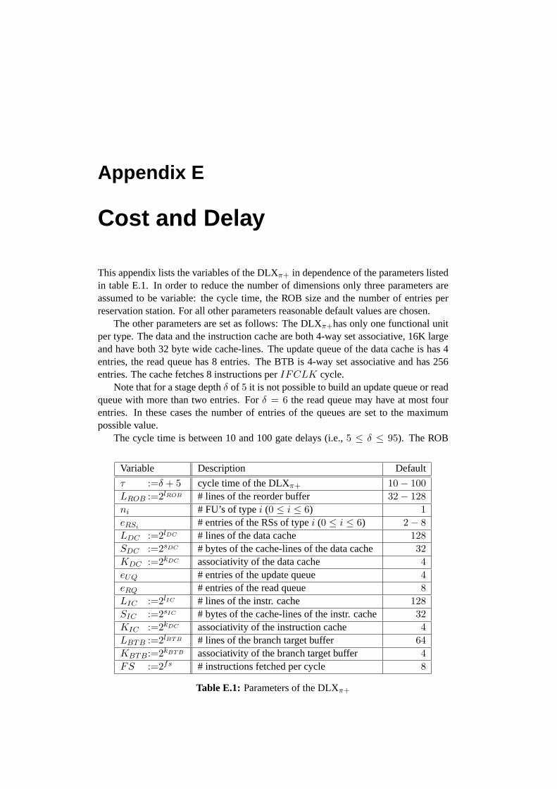
Appendix E
Cost and Delay
This appendix lists the variables of the DLXπ+ in dependence of the parameters listedin table E.1. In order to reduce the number of dimensions only three parameters areassumed to be variable: the cycle time, the ROB size and the number of entries perreservation station. For all other parameters reasonable default valuesare chosen.
The other parameters are set as follows: The DLXπ+has only one functional unitper type. The data and the instruction cache are both 4-way set associative, 16K largeand have both 32 byte wide cache-lines. The update queue of the data cache is has 4entries, the read queue has 8 entries. The BTB is 4-way set associativeand has 256entries. The cache fetches 8 instructions perIFCLK cycle.
Note that for a stage depthδ of 5 it is not possible to build an update queue or readqueue with more than two entries. Forδ = 6 the read queue may have at most fourentries. In these cases the number of entries of the queues are set to the maximumpossible value.
The cycle time is between 10 and 100 gate delays (i.e.,5 ≤ δ ≤ 95). The ROB
Variable Description Default
τ :=δ + 5 cycle time of the DLXπ+ 10 − 100
LROB :=2lROB # lines of the reorder buffer 32 − 128
ni # FU’s of typei (0 ≤ i ≤ 6) 1
eRSi# entries of the RSs of typei (0 ≤ i ≤ 6) 2 − 8
LDC :=2lDC # lines of the data cache 128
SDC :=2sDC # bytes of the cache-lines of the data cache 32
KDC :=2kDC associativity of the data cache 4
eUQ # entries of the update queue 4
eRQ # entries of the read queue 8
LIC :=2lIC # lines of the instr. cache 128
SIC :=2sIC # bytes of the cache-lines of the instr. cache 32
KIC :=2kDC associativity of the instruction cache 4
LBTB :=2lBTB # lines of the branch target buffer 64
KBTB:=2kBTB associativity of the branch target buffer 4
FS :=2fs # instructions fetched per cycle 8
Table E.1: Parameters of the DLXπ+
210 Cost and Delay
has between 32 and 128 lines. The reservation stations have between 2 and 8 entries.For simplicity all reservation stations have the same number of entries. Note thatforδ ∈ {5, 6} the all reservation stations except the memory and the branch checkingreservation station may have at most two respectively four entries. For thememoryand branch checking reservation station, the allowed number of entries is even less.Therefore, for theses reservation stations also the results for only oneentry is given.No results are given if the number of reservation station is larger than the maximumpossible number.
Tables E.2 and E.3 list the variables of the DLXπ+ in dependence of the three freeparameters. If the variables do not change if one of the parameters is increased, theline respectively column is omitted. Tables E.4 and E.5 list the overall cost of theDLXπ+ in dependence of the three free parameters.

211
τ 10 11 12 13 14 15 16 17 18 19 20 21 22 23 25 27 29 33 34 35 37 41 49 50 67 77 eRS⋆ LROB
m 5 5 5 4 4 4 4 3 3 3 3 3 3 3 2 2 2 2 2 2 2 2 2 1 1 1 * *cIF 2 2 2 2 2 2 2 2 2 2 2 2 2 1 2 2 2 2 1 1 1 1 1 2 1 1 * *cD1 7 6 5 4 4 4 3 3 3 3 2 2 2 2 2 2 2 2 2 1 1 1 1 1 1 1 * *cD2 6 5 4 4 4 3 3 3 3 2 2 2 2 2 2 2 2 1 1 1 1 1 1 1 1 1 * 32cD2 9 8 7 6 5 5 4 4 4 4 3 3 3 3 3 2 2 2 2 2 2 2 1 1 1 1 * 64cD2 15 12 11 9 8 8 7 6 6 6 5 5 5 4 4 4 3 3 3 3 3 2 2 2 2 1 * 128cI 1 1 1 1 1 1 1 1 1 1 1 1 1 1 1 1 1 1 1 1 1 1 1 1 1 1 1 *cI 2 1 1 1 1 1 1 1 1 1 1 1 1 1 1 1 1 1 1 1 1 1 1 1 1 1 2 *cI na 2 1 1 1 1 1 1 1 1 1 1 1 1 1 1 1 1 1 1 1 1 1 1 1 1 4 *cI na na 2 1 1 1 1 1 1 1 1 1 1 1 1 1 1 1 1 1 1 1 1 1 1 1 8 *cT 3 2 2 2 1 1 1 1 1 1 1 1 1 1 1 1 1 1 1 1 1 1 1 1 1 1 * *
cU2DM 3 3 2 2 2 2 1 1 1 1 1 1 1 1 1 1 1 1 1 1 1 1 1 1 1 1 1 *cU2DM na 4 3 2 2 2 2 2 2 1 1 1 1 1 1 1 1 1 1 1 1 1 1 1 1 1 2 *cU2DM na na 3 3 2 2 2 2 2 2 1 1 1 1 1 1 1 1 1 1 1 1 1 1 1 1 4 *cU2DM na na na 3 2 2 2 2 2 2 2 1 1 1 1 1 1 1 1 1 1 1 1 1 1 1 8 *cU2DI 4 3 3 2 2 2 2 2 1 1 1 1 1 1 1 1 1 1 1 1 1 1 1 1 1 1 2 *cU2DI na 4 3 2 2 2 2 2 2 1 1 1 1 1 1 1 1 1 1 1 1 1 1 1 1 1 4 *cU2DI na na 3 3 2 2 2 2 2 2 1 1 1 1 1 1 1 1 1 1 1 1 1 1 1 1 8 *cU2DF 5 4 3 3 2 2 2 2 2 2 1 1 1 1 1 1 1 1 1 1 1 1 1 1 1 1 2 *cU2DF na 4 3 3 2 2 2 2 2 2 2 1 1 1 1 1 1 1 1 1 1 1 1 1 1 1 4 *cU2DF na na 4 3 3 2 2 2 2 2 2 2 1 1 1 1 1 1 1 1 1 1 1 1 1 1 8 *cU2DB 3 3 2 2 2 2 1 1 1 1 1 1 1 1 1 1 1 1 1 1 1 1 1 1 1 1 1 *cU2DB na na na 2 2 2 2 1 1 1 1 1 1 1 1 1 1 1 1 1 1 1 1 1 1 1 8 *
cAT 3 2 1 1 1 1 1 1 1 1 1 1 1 1 1 1 1 1 1 1 1 1 1 1 1 1 * *cC 3 3 2 2 2 2 1 1 1 1 1 1 1 1 1 1 1 1 1 1 1 1 1 1 1 1 * *
cC2R 2 2 2 1 1 1 1 1 1 1 1 1 1 1 1 1 1 1 1 1 1 1 1 1 1 1 * *cRet2 7 6 5 5 4 4 4 3 3 3 3 2 2 2 2 2 2 2 2 2 1 1 1 1 1 1 * *
TableE
.2:Variablesofthe
DLXπ
+(part1)

212C
ostandD
elay
τ 10 11 12 13 14 15 16 17 18 19 20 22 23 24 25 26 27 28 29 30 31 33 34 35 38 39 43 45 46 47 48 62 65 72 eRS⋆
cSh4S 3 2 2 2 1 1 2 1 1 1 1 1 1 1 1 1 1 0 0 0 0 0 0 0 0 0 0 0 0 0 0 0 0 0 1cSh4S na 2 2 2 2 1 1 1 1 1 1 1 1 1 1 1 1 1 0 0 0 0 0 0 0 0 0 0 0 0 0 0 0 0 2cSh4S na na 2 2 2 1 1 1 1 1 1 1 1 1 1 1 1 1 1 0 0 0 0 0 0 0 0 0 0 0 0 0 0 0 4cSh4S na na na 2 2 1 1 1 1 1 1 1 1 1 1 1 1 1 1 1 0 0 0 0 0 0 0 0 0 0 0 0 0 0 8cHC 12 10 9 8 7 6 6 5 5 5 4 4 4 3 3 3 3 3 3 3 3 3 2 2 2 2 2 2 2 2 2 1 1 1 *
cM2W 4 3 3 2 2 2 2 2 2 2 1 1 1 1 1 1 1 1 1 1 1 1 1 1 1 1 1 1 1 1 1 1 1 1 *cM2R 3 3 2 2 2 2 2 2 2 1 1 1 1 1 1 1 1 1 1 1 1 1 1 1 1 1 1 1 1 1 1 1 1 1 *cM2Q 4 3 3 3 2 2 2 2 2 2 2 1 1 1 1 1 1 1 1 1 1 1 1 1 1 1 1 1 1 1 1 1 1 1 *cSh4L 3 2 2 2 1 1 1 1 1 1 1 1 1 1 1 1 1 1 1 1 1 1 1 1 1 1 1 1 1 1 1 1 1 1 *cIALU 4 3 3 2 1 1 2 2 1 1 1 1 1 1 1 1 1 1 1 0 0 0 0 0 0 0 0 0 0 0 0 0 0 0 *cIMul1 2 1 1 1 1 0 0 0 1 1 1 0 0 0 0 0 0 0 0 0 0 0 0 0 0 0 0 0 0 0 0 0 0 0 2cIMul1 na 1 1 1 1 0 0 0 0 1 1 1 0 0 0 0 0 0 0 0 0 0 0 0 0 0 0 0 0 0 0 0 0 0 4cIMul1 na na 1 1 1 1 0 0 0 0 1 1 1 0 0 0 0 0 0 0 0 0 0 0 0 0 0 0 0 0 0 0 0 0 8cIMul2 6 5 4 4 3 3 3 3 2 2 2 2 2 2 2 2 2 2 1 1 1 1 1 1 1 1 1 1 1 1 1 1 1 1 *cIMul3 4 3 2 2 2 2 2 1 1 1 1 1 1 1 1 1 1 1 1 1 1 1 1 1 1 1 1 1 1 1 1 1 1 1 *cFPAdd 23 18 15 14 12 11 9 9 9 8 7 6 6 6 5 5 5 5 4 4 4 4 4 3 3 3 3 2 2 2 2 2 1 1 *
cFPMul1 6 5 4 4 3 3 2 2 2 2 2 2 2 2 2 1 1 1 1 1 1 1 1 1 1 1 1 1 0 0 0 0 0 0 2cFPMul1 na 5 4 4 3 3 2 2 2 2 2 2 2 2 2 1 1 1 1 1 1 1 1 1 1 1 1 1 1 0 0 0 0 0 4cFPMul1 na na 4 4 3 3 3 2 2 2 2 2 2 2 2 2 1 1 1 1 1 1 1 1 1 1 1 1 1 1 0 0 0 0 8cFPMul2 8 7 6 5 5 4 4 4 3 3 3 3 3 2 2 2 2 2 2 2 2 2 2 2 2 2 1 1 1 1 1 1 1 1 *cFPMul3 14 12 10 9 8 7 7 6 6 5 5 4 4 4 4 4 4 3 3 3 3 3 3 3 3 2 2 2 2 2 2 2 2 1 *cFPMul4 7 5 4 4 4 3 3 3 3 2 2 2 2 2 2 2 2 2 2 2 2 1 1 1 1 1 1 1 1 1 1 1 1 1 *cFPMisc 5 4 3 3 2 2 2 1 2 2 2 1 1 1 1 1 1 1 1 1 1 1 1 1 0 0 0 0 0 0 0 0 0 0 *
cBCU 5 3 3 2 2 1 2 2 2 1 1 1 1 1 1 1 1 1 1 1 1 0 0 0 0 0 0 0 0 0 0 0 0 0 *
TableE
.3:Variablesofthe
DLXπ
+(part2)

213
10 11 12 13 14 15 16 17 18 19 20 eRS⋆ LROB
2748823 2428247 2247879 2067335 1899064 1784354 1748697 1649984 1637588 1563675 1447715 2 322820714 2503079 2319473 2123671 1936419 1830683 1783910 1685063 1672439 1607267 1479595 2 642971889 2633813 2445418 2227592 2030252 1920692 1870585 1760683 1744375 1678605 1550465 2 128
na 2599696 2402933 2217131 2002000 1887290 1851633 1742998 1742062 1651431 1555667 4 32na 2667841 2477693 2276523 2041597 1935861 1889088 1780209 1779257 1697045 1589943 4 64na 2788361 2606804 2383500 2137672 2028112 1978005 1857961 1853537 1770405 1663209 4 128na na 2775631 2551181 2342078 2093720 2058503 1929120 1928184 1860937 1731273 8 32na na 2846436 2617345 2388535 2146783 2100450 1970595 1969643 1911247 1769593 8 64na na 2967405 2731094 2491470 2243526 2193859 2052611 2048187 1989303 1846903 8 128
21 22 23 24 25 26 27 28 29 30 31 eRS⋆ LROB
1445719 1427559 1365538 1289197 1349252 1348348 1348348 1347444 1345292 1344820 1344820 2 321477599 1459407 1397386 1321037 1381084 1380172 1369087 1368175 1365999 1365519 1365519 2 641545013 1526789 1453850 1377493 1437532 1436612 1433156 1432236 1419113 1418625 1418625 2 1281486615 1468919 1406434 1330093 1390148 1389244 1389244 1388340 1386972 1385716 1385716 4 321519703 1501983 1439490 1363141 1423188 1422276 1411191 1410279 1408895 1407623 1407623 4 641588325 1570581 1497162 1420805 1480844 1479924 1476468 1475548 1463225 1461937 1461937 4 1281702613 1550805 1488784 1411979 1472034 1472034 1471130 1470226 1468858 1468386 1467602 8 321740493 1586285 1524264 1447443 1507490 1507490 1495493 1494581 1493197 1492717 1491925 8 641813907 1657299 1584360 1507523 1567562 1567562 1563186 1562266 1549943 1549455 1548655 8 128
TableE
.4:Costofthe
DLX
π+
(part1)

214C
ostandD
elay
32 33 34 35 37 38 39 41 43 45 46 eRS⋆ LROB
1342495 1331144 1198225 1195777 1194133 1193229 1192325 1192325 1191421 1190517 1189613 2 321362985 1360961 1228042 1225562 1223918 1223006 1222094 1222094 1221182 1220270 1219358 2 641415884 1413844 1280925 1278405 1273305 1272385 1271465 1260547 1259627 1258707 1257787 2 1281383391 1372040 1239121 1236673 1235029 1234125 1233221 1233221 1232317 1231413 1231413 4 321405089 1403065 1270146 1267666 1266022 1265110 1264198 1264198 1263286 1262374 1262374 4 641459196 1457156 1324237 1321717 1316617 1315697 1314777 1303859 1302939 1302019 1302019 4 1281465277 1453926 1321007 1318559 1316915 1316011 1315107 1315107 1314203 1313299 1313299 8 321489391 1487367 1354448 1351968 1350324 1349412 1348500 1348500 1347588 1346676 1346676 8 641545914 1543874 1410955 1408435 1403335 1402415 1401495 1390577 1389657 1388737 1388737 8 128
47 48 49 50 62 65 67 69 72 77 eRS⋆ LROB
1189613 1189613 1189613 1251634 1185290 1184386 1122365 1122365 1121461 1121461 2 321219358 1219358 1208272 1270293 1203949 1203037 1141016 1141016 1140104 1140104 2 641257787 1257787 1257787 1319808 1253464 1252544 1190523 1187067 1186147 1175224 2 1281230509 1230509 1230509 1292530 1226186 1225282 1163261 1163261 1162357 1162357 4 321261462 1261462 1250376 1312397 1246053 1245141 1183120 1183120 1182208 1182208 4 641301099 1301099 1301099 1363120 1296776 1295856 1233835 1230379 1229459 1218536 4 1281313299 1312395 1312395 1374416 1308072 1307168 1245147 1245147 1244243 1244243 8 321346676 1345764 1334678 1396699 1330355 1329443 1267422 1267422 1266510 1266510 8 641388737 1387817 1387817 1449838 1383494 1382574 1320553 1317097 1316177 1305254 8 128
TableE
.5:Costofthe
DLX
π+
(part2)

Bibliography
[BJK+03] Sven Beyer, Christian Jacobi, Daniel Kroning, Dirk Leinenbach, andWolfgang J. Paul. Instantiating uninterpreted functional units and memorysystem: functional verification of the VAMP. InCHARME 2003, volume2860 ofLNCS, pages 51–65. Springer, 2003.
[BLM91] Asghar Bashteen, Ivy Lui, and Jill Mullan. A superpipeline approach tothe MIPS architecture. InProceedings of the IEEE COMPCON, pages8–12, 1991.
[Cad97] Cadence Design Systems Inc.Synergy HDL Command Reference, 1997.
[Gru94] Thomas Grun. Quantitative Analyse von I/O-Architekturen. Disserta-tion (paul), Universitat des Saarlandes, Computer Science Department,Saarbrucken, 1994.
[GV95] Bernard Goossens and Duc Thang Vu. Further pipelining and multi-threading to improve risc processor speed. a proposed architecture andsimulation results. InProceedings of the 3rd International Conference ofParallel Computing Technologies, pages 326–340, September 1995.
[GV96] Bernard Goossens and Duc Thang Vu. Multithreading to improve cyclewidth and cpi in superpipelined superscalar processors. InProceedingsof the International Symposium on Parallel Architectures, Algorithms andNetworks, pages 36–42, June 1996.
[HHM99] M. Horowitz, R. Ho, and K. Mai. The future of wires. InInvited WorkshopPaper for SRC Conference, May 1999.
[Hil95] Mark Hill. SPEC92 Traces for MIPS R3000 processors. University ofWisconsin, Madison, 1995.ftp://tracebase.nmsu.edu/pub/tracebase4/r3000/.
[Hil00] Mark A. Hillebrand. Design and evaluation of a superscalar risc processor.Diplomarbeit, Universitat des Saarlandes, Computer Science Department,Saarbrucken, 2000.
[HJF+02] M.S. Hrishikesh, Norman P. Jouppi, Keith I. Farkas, Doug Burger,Stephen W. Keckler, and Premkishore Shivakumar. The optimal logicdepth per pipeline stage is 6 to 8 fo4 inverter delays. InProceedingsof the 29th Annual International Symposium on Computer Architecture,pages 14–24, May 2002.

216 Bibliography
[HOH97] David L. Harris, Stuart F. Oberman, and Mark H. Horowitz. SRT divi-sion architectures and implementations. InProceeding of the 13th IEEESymposium on Computer Arithmetic, pages 18–25, 1997.
[HP96] John L. Hennessy and David A. Patterson.Computer Architecture: AQuantitative Approach; second edition. Morgan Kaufmann, San Fran-cisco, California, 1996.
[HP02] A. Hartstein and Thomas R. Puzak. The optimum pipeline depth for a mi-croprocessor. InProceedings of the 29th Annual International Symposiumon Computer Architecture, pages 7–13, May 2002.
[HP03] A. Hartstein and Thomas R. Puzak. Optimum power/performancepipeline depth. InProceedings of the 36th International Symposium onMicroarchitecture, 2003.
[HSU+01] Glenn Hinton, Dave Sager, Mike Upton, Darrell Boggs, Doug Carmean,Alan Kyker, and Patrice Roussel. The microarchitecture of the pentium 4processor.Intel Technology Journal, First Quarter 2001.
[IEEE] Institute of Electrical and Electronics Engineers.ANSI/IEEE standard754-1985, IEEE Standard for Binary Floating-Point Arithmetic, 1985.
[Jac02] Christian Jacobi.Formal Verification of a Fully IEEE Compliant Float-ing Point Unit. Dissertation (paul), Universitat des Saarlandes, ComputerScience Department, Saarbrucken, 2002.
[JCL94] Stephan Jourdan, Dominique Carriere, and Daniel Litaize. A high out-of-order issue symmetric superpipeline superscalar microprocessor. InProceedings of the 20th Euromicro conference, pages 338–345, January1994.
[KH92] Gerry Kane and Joe Heinrich.MIPS RISC Architecture. Prentice Hall,New Jersey, 1992.
[KMP99] Daniel Kroning, Silvia M. Muller, and Wolfgang Paul. A rigorous correct-ness proof of the Tomasulo scheduling algorithm with precise interrupts.In Proceedings of the SCI’99/ISAS’99 International Conference, 1999.
[Kog81] Peter M. Kogge.The Architecture of Pipelined Computers. McGraw-Hill,1981.
[KP95] Jorg Keller and Wolfgang Paul.Hardware Design — Formaler EntwurfDigitaler Schaltungen. TEUBNER, 1995. (in German).
[Kro81] D. Kroft. Lockup-free instruction fetch/prefetch cache organization. InProceedings of the 8th International Symposium on Computer Architec-ture, pages 81–87, May 1981.
[Kr o99] Daniel Kroning. Design and evaluation of a risc processor with a tomasuloscheduler. Diplomarbeit, Universitat des Saarlandes, Computer ScienceDepartment, Saarbrucken, 1999.

Bibliography 217
[Kr o01] Daniel Kroning. Formal Verification of Pipelined Microprocessors. Dis-sertation (paul), Universitat des Saarlandes, Computer Science Depart-ment, Saarbrucken, 2001.
[KS86] Steven R. Kunkel and James E. Smith. Optimal pipelining in supercom-puters. InProceedings of the 13th Annual International Symposium onComputer Architecture, pages 404–411, June 1986.
[Lei99] Holger W. Leister.Quantitative Analysis of Precise Interrupt Mechanismsfor Out-Of-Order Execution Processors. Dissertation (paul), Universitatdes Saarlandes, Computer Science Department, Saarbrucken, 1999.
[Lei02] Dirk Leinenbach. Implementierung eines maschinell verifizierten prozes-sors. Diplomarbeit, Universitat des Saarlandes, Computer Science De-partment, Saarbrucken, 2002. (in German).
[LS84] Johnny K. F. Lee and Alan J. Smith. Branch prediction strategies andbranch target buffer design.IEEE Computer, pages 6–22, January 1984.
[McF93] Scott McFarling. Combining Branch Predictors. Technical Report TN-36,DEC Western Research Labratory, June 1993.
[MLD +99] Silvia M. Muller, Holger Leister, Peter Dell, Nikolaus Gerteis, and DanielKroning. The impact of hardware scheduling mechanisms on the perfor-mance and cost of processor designs. InProceedings of the 15th GI/ITGConference ’Architektur von Rechensystemen’ ARCS’99, pages 65–73.VDE Verlag, 1999.
[MP95] Silvia M. Muller and Wolfgang J. Paul.The Complexity of simple Com-puter Architectures. Springer, Berlin;Heidelberg;New York, 1995.
[MP00] Silvia M. Muller and Wolfgang J. Paul.Computer Architecture, Complex-ity and Correctness. Springer, Berlin;Heidelberg;New York, 2000.
[PJS97] Subbarao Palacharla, Norman P. Jouppi, and James E. Smith. Complexity-effective superscalar processors. InProceedings of the 24th Annual Inter-national Symposium on Computer Architecture, pages 206–218, 1997.
[SBG+02] Viji Srinivasan, David Brooks, Michael Gschwind, Pradip Bose, VictorZyuban, Philip N. Strenski, and Philip G. Emma. Optimizing pipelines forpower and performance. InProceedings of the 35th International Sympo-sium on Microarchitecture, pages 333–344, November 2002.
[SC02] Eric Sprangle and Doug Carmean. Increasing processor performance byimplementing deeper pipelines. InProceedings of the 29th Annual Inter-national Symposium on Computer Architecture, May 2002.
[Sei99] Peter-Michael Seidel.On the Design of IEEE Compliant Floating-PointUnits and Their Quantitative Analysis. Dissertation (paul), Universitatdes Saarlandes, Computer Science Department, Saarbrucken, 1999.

218 Bibliography
[Sei03] Peter-Michael Seidel. Delay of IEEE Compliant Floating Point Units.Personal Communication, March 2003.
[Sic92] James E. Sicolo. A multiported nonblocking cache for a superscalaruniprocessor. Ms thesis, University of Illinois, Department of ComputerScience, Urbana IL, 1992.
[SP85] James E. Smith and Andrew R. Pleszkun. Implementation of precise in-terrupts in pipelined processors. InProceedings of the 12th InternationnalSymposium on Computer Architecture, pages 36–44, June 1985.
[SPEC] Standard Performance Evaluation Corporation.The SPEC92 benchmarksuite. http://www.specbench.org.
[SSH99] Ivan Sutherland, Bob Sproull, and David Harris.Logical Effort: Design-ing Fast CMOS Circuits. Morgan Kauffman Publishers, 1999.
[Tom67] R.M. Tomasulo. An efficient algorithm for exploiting multiple arithmeticunits. IBM Journal Research and Development, 11:25–33, January 1967.
[Web88] C. F. Webb. Subroutine call/return stack. Technical Report 30(11), IBMTechnical Disclosure Bulletin, April 1988.
[WH04] Neil H. E. Weste and David Harris.CMOS VLSI Design: A Circuits andSystem Perspective. Addison-Wesley, 2004.
[Yeh93] Tse-Yu Yeh.Two-Level Adaptive Branch Prediction and Instruction FetchMechanisms for High Performance Superscalar Processors. PhD thesis,University of Michigan, Department of Electrical Engineering and Com-puter Science, 1993.