FORMAL VERIFICATION OF A 32-BIT PIPELINED RISC ...
105
FORMAL VERIFICATION OF A 32-BIT PIPELINED RISC PROCESSOR By MOHAMMAD MOSTAFA DARWISH B. Sc. (Computer Engineering) University of Petroleum & Minerals, 1991 A THESIS SUBMITTED IN PARTIAL FULFILLMENT OF THE REQUIREMENTS FOR THE DEGREE OF MASTER OF APPLIED SCIENCE in THE FACULTY OF GRADUATE STUDIES DEPARTMENT OF ELECTRICAL ENGINEERING We accept this thesis as conforming to the required standard THE UNIVERSITY OF BRITISH COLUMBIA July 1994 © MOHAMMAD MOSTAFA DARWISH, 1994
-
Upload
khangminh22 -
Category
Documents
-
view
0 -
download
0
Transcript of FORMAL VERIFICATION OF A 32-BIT PIPELINED RISC ...
FORMAL VERIFICATION OF A 32-BIT PIPELINED RISC PROCESSOR
By
MOHAMMAD MOSTAFA DARWISH
B. Sc. (Computer Engineering) University of Petroleum & Minerals, 1991
A THESIS SUBMITTED IN PARTIAL FULFILLMENT OF
THE REQUIREMENTS FOR THE DEGREE OF
MASTER OF APPLIED SCIENCE
in
THE FACULTY OF GRADUATE STUDIES
DEPARTMENT OF ELECTRICAL ENGINEERING
We accept this thesis as conforming
to the required standard
E.
THE UNIVERSITY OF BRITISH COLUMBIA
July 1994
© MOHAMMAD MOSTAFA DARWISH, 1994
In presenting this thesis in partial fulfilment of the requirements for an advanced
degree at the University of British Columbia, I agree that the Library shall make it
freely available for reference and study. I further agree that permission for extensive
copying of this thesis for scholarly purposes may be granted by the head of my
department or by his or her representatives. ,t is understood that copying or
publication of this thesis for financial gain shall not be allowed without my written
permission.
(Signature)
Department of e’cc4, a.—/
The University of British ColumbiaVancouver, Canada
Date ‘, 19911
DE-6 (2)88)
Abstract
Designing a microprocessor is a significant undertaking. Modern RISC processors are
no exception. Although RISC architectures originally were intended to be simpler than
CISC processors, modern RISC processors are often very complex, partially due to the
prominent use of pipelining. As a result, verifying the correctness of a RISC design is an
extremely difficult task. Thus, it has become of great importance to find more efficient
design verification techniques than traditional simulation. The objective of this thesis is
to show that symbolic trajectory evaluation is such a technique.
For demonstration purposes, we designed and implemented a 32-bit pipelined RISC
processor, called Oryx. It is a fairly generic first-generation RISC processor with a five-
stage pipeline and is similar to the MIPS-X and DLX processors. The Oryx processor
is designed down to a detailed gate-level and is described in VHDL. Altogether, the
processor consists of approximately 30,000 gates.
We also developed an abstract, non-pipelined, specification of the processor. This
specification is precise and is intended for a programmer. We made a special effort not
to over-specify the processor, so that a family of processors, ranging in complexity and
speed, could theoretically be implemented all satisfying the same specification.
We finally demonstrated how to use an implementation mapping and the Voss veri
fication system to verify important properties of the processor. For example, we verified
that in every sequence of valid instructions, the ALU instructions are implemented cor
rectly. This included both the actual operation performed as well as the control for
fetching the operands and storing the result back into the register file. Carrying out this
verification task required less than 30 minutes on an IBM RS6000 based workstation.
11
Table of Contents
Abstract ii
TABLE OF CONTENTS iii
LIST OF TABLES VI.
LIST OF FIGURES Vi
ACKNOWLEDGEMENTS ix
DEDICATION Xi
1 Introduction 1
1.1 Symbolic Trajectory Evaluation 2
1.2 Research Objectives 7
1.3 Related Work 7
1.4 Thesis Overview 11
2 Architecture 13
2.1 Memory Organization 13
2.2 Registers 16
2.2.1 General Registers 16
2.2.2 Multiplication and Division Register 16
2.2.3 Status and Control Registers 16
2.3 Instruction Formats 18
2.4 Addressing Modes 20
2.5 Operand Selection 20
2.6 Co-processor Interface 20
ill

2.7 Instructions.
2.7.1 Arithmetic Instructions .
2.7.2 Logical Instructions
2.7.3 Control Transfer Instructions
2.7.4 Miscellaneous Instructions
2.8 Interrupts
3 Formal Specification
3.1 Abstract Model
3.2 Formal Specification
3.2.1 Example I: Register File Specification
3.2.2 Example II: PC Specification . .
4 Implementation
4.1 Design Overview
4.2 The Control Path
4.3 The Data Path
5 Formal Verification
5.1 Verification Difficulty
5.2 Property Verification
5.3 Implementation Mapping
5.3.1 Cycle Mapping
5.3.2 Instant Abstract State Mapping . .
5.3.3 Combined Mapping
5.4 Verification Condition
5.5 Practical Verification
22
24
27
28
30
30
32
32
35
38
41
42
42
45
57
67
6768697070737474
iv
5.6 Design Errors.76
6 Concluding Remarks and Future Work 77
Bibliography 79
A The FL Verification Script 81
V
List of Tables
2.1 PSW bits definition 17
2.2 The Oryx processor instruction set 21
3.3 Function abbreviations 37
3.4 Operation definitions 37
4.5 The Oryx processor pipeline action during exceptions 48
4.6 The Oryx processor pipeline action during instruction squashing 50
4.7 Pipeline action during instruction processing phases 52
5.8 Some experimental results 76
vi
List of Figures
1.1 The state space partial order 3
1.2 The Voss verification system 6
1.3 A simple latch 9
2.4 Little Endian byte ordering 13
2.5 A system block diagram of the Oryx processor 14
2.6 The Oryx processor instruction formats 19
3.7 The abstract model of the Oryx processor 36
4.8 The Oryx processor pipeline 42
4.9 i&2 logic diagram 44
4.10 Program counter chain logic diagram 45
4.11 ‘b2FC logic diagram 46
4.12 The control path logic diagram 47
4.13 The exception FSM logic diagram 48
4.14 The squash FSM logic diagram 49
4.15 The PC chain FSM logic diagram 51
4.16 A typical instruction fetch timing diagram 51
4.17 ICache page fault timing diagram 53
4.18 The PC unit logic diagram 54
4.19 The TakeBranch signal logic diagram 55
4.20 A typical memory read timing 56
vii
4.21 The Oryx processor data path logic diagram 58
4.22 The Oryx processor register file logic diagram 59
4.23 A register file memory bit logic diagram 59
4.24 The NoDest signal logic diagram 60
4.25 The ALU logic diagram 61
4.26 The AU logic diagram 61
4.27 The LU logic diagram 62
4.28 The shifter logic diagram 63
4.29 A typical MD bit logic diagram 64
4.30 PSWCurrent-PSWOther pair 65
5.31 Time mapping 70
5.32 State mapping 71
5.33 Register file mapping 72
5.34 Combined mapping 73
viii

Acknowledgments
There are several people who were major forces in the completion of this work. First
and foremost, warm and very grateful thanks go to Carl Seger who introduced me to
formal verification and has nurtured my knowledge with amazing generosity and patience.
Rabab Ward believed in me and encouraged me to carry on with my work despite all
the difficulties. Carl and Rabab have provided support in times of crisis and criticism in
times of confidence.
I am heavily obliged to André lvanov, Scott Hazelhurst, and Alimuddin Mohammad
for donating their time, the most precious of all gifts, to help me improve the presentation.
Many ideas in this work come from fascinating discussions with Mark Greenstreet,
Andrew Martin, Nancy Day, John Tanlimco, and Gary Hovey.
Warm thanks go to my friends who made my life more enjoyable. In particular, I would
like to mention Ammar Muhiyaddin who has offered me his friendship over the years,
Nasir Aljameh who has always remembered his youth friend despite the distance, and
Rafeh Hulays who has been a good friend since the very first day I arrived in Vancouver.
I also would like to mention Mohammad Estilaei, Catherine Leung, Hélène Wong, Neil
Fazel, Mike Donat, Thomas Ligocki, Kevin Chan, Barry Tsuji, Andrew Bishop, Matthew
Mendelsohn, William Low, Kendra Cooper, Peter Meisl, Chris Cobbold, Robert Link,
and Jeff Chow. To those I have surely forgotten, I must apologize.
Special thanks go to the Original Beanery Coffee House where I wrote most of this
work. Gordon Schmidt has been kind enough to offer me a quiet place where I could sit
down and do all the thinking. I will let you discover the secrets of that place on your
own.
ix
I have been fortunate in obtaining support for my studies from the Semiconductor
Research Corporation as well as the Department of Electrical Engineering and the De
partment of Computer Science.
Finally, and above all, I owe a great debt of gratitude to my parents, Bedour and
Mostafa who inspired my life and pushed me to the limit. This work is my way of saying
thank you mother and father.
x

To my mother and father
xi

Chapter 1
Introduction
The arrival of very large scale integration (VLSI) technology has paved the way for
innovative digital system designs, like reduced instruction set computer (RISC) processors.
However, the design of RISC processors is very complex and demands considerable effort,
partially due to the problems that designers are faced with in specifying and verifying
this type of system.
From a marketing point of view, there is no doubt that any enterprise should release
new products on time in order to keep its market share. Unfortunately, the design time
of RISC processors, like other digital systems, is strongly influenced by the number of
design errors. The MIPS 4000, for example, was estimated to cost $3-$8 million for
each month of additional design time and 27% of the design time was spent verifying
the design [8]. This example clearly indicates the importance of finding better ways to
uncover design errors as early as possible to avoid any delay in releasing the product.
Today, design verification is done using (traditional) simulation [10]. A good design
of a RISC processor is composed of several smaller modules. Each module is simulated
using switch-level and gate-level simulators by trying relatively few test cases, one at a
time, and checking whether the results are correct. Towards the end of the design phase,
all modules are put together and the final design is simulated for an extended period of
time. This simulation is usually done using behavioral models of the components rather
than at the switch or gate level. A common approach is to run some reasonably large
programs (e.g. boot UNIX) on the simulated design. It is very common to spend months
1
Chapter 1. Introduction 2
simulating the final design on large computers [12].
In spite of this, traditional simulation is still inadequate for verifying RISC processors
as many design errors can be left undetected [1]. The deficiency of traditional simulation
is partially due to the introduction of aggressive pipelining and concurrently-operating
sub-systems, which make predicting the interactions between logically unrelated system
activities very difficult. For example, it is often impossible to simulate all possible instruc
tion sequences that might lead to a trap, because instructions, which could be logically
unrelated, all of a sudden are being processed in parallel and may even be processed out
of order.
In addition to the above, even the best design team can make mistakes. For example,
an early revision of the DLX processor contained a flaw in the pipeline despite that the
design was reviewed by more than 100 people and was taught at 18 universities. The
flaw was detected when someone actually tried to implement the processor. [11]
From the above discussion, we have established the need to find a more effective
technique for verifying RISC processors. When we say effective, we mean three things:
fast, automated (i.e. requires minimum human interveiltion), and thorough (i.e. uncover
all those design errors that cause the system to behave in a way other than according to
the system specification). Ideally, the method should allow the design team to be able
to go home at the end of the day with good confidence that the design is going to work
rather than having to come the next day to try yet another simulation run to uncover
more design errors.
1.1 Symbolic Trajectory Evaluation
A way to improve traditional simulation is to consider symbols rather than actual values
for the design under simulation, hence, the term symbolic simulation is used to distinguish

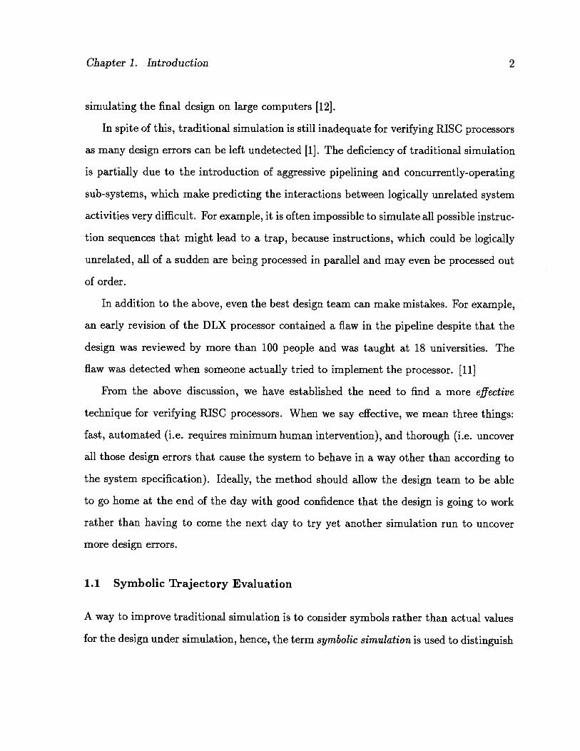
Chapter 1. Introduction 3
TZN
0 1
NZx
Figure 1.1: The state space partial order
it from traditional simulation.
Using symbolic simulation for circuit verification was first proposed by researchers at
IBM Yorktown Heights in the late 1970’s. However, the power of symbolic simulation
was not fully utilized until an efficient method of manipulating symbols emerged when
ordered binary decision diagrams (OBDD’s) [3] were developed for representing Boolean
functions.
Bryant and Seger [15] developed a new generation of symbolic simulators based on a
technique they called symbolic trajectory evaluation (STE). In this technique, the state
space of a system is embedded in a lattice {0,1,X,T}. The elements of the lattice are
partially ordered by their information content as shown in Figure 1.1, where X represents
no information about the node value, 0 and 1 represent fully defined information, and
T represents over-constrained values. As a result, the behavior of the system can be
expressed as a sequence of points in the lattice determined by the initial state and the
functionality of the system. The partial order between sequences of states is defined by
extending the partial order on the state space in the natural way.
The model structure of the system is a tuple M = [(S, ), Y], where (5, ) is
a complete lattice (S being the state space and IE a partial order on 5) and Y is
a monotone successor function Y: S —÷ S. A sequence is a trajectory if and only if
Y(u) 1 0.i+1 for i 0.

Chapter 1. Introduction 4
The key to the efficiency of trajectory evaluation is the restricted language that can be
used to phrase questions about the model structure. The basic specification language is
very simple, but expressive enough to capture the properties to be checked for in verifying
a RISC processor.
A predicate over $ is a mapping from $ to the lattice {false, true} (where false true).
Informally, a predicate describes a potential state of the system (e.g. a predicate might be
(A is x) which says that node A has the value x). A predicate is simple if it is monotone
and there is a unique weakest s E $ for which p(s) = true. A trajectory formula is defined
recursively as:
1. Simple predicates: Every simple predicate over $ is a trajectory formula.
2. Conjunction: (F1AF2) is a trajectory formula if F1 and F2 are trajectory formulas.
3. Domain restriction: (e —* F) is a trajectory formula if F is a trajectory formula
and e is a Boolean expression over some set of Boolean variables.
4. Next time: (NF) is a trajectory formula if F is a trajectory formula.
The truth semantics of a trajectory formula is defined relative to a model structure and
a trajectory. Whether a trajectory 5 satisfies a formula F (written as &M
F) is given
by the following rules:
1. g0g I=MP iffp(a°) = true.
2. o 1M (F1 A F2) iff o M F1 andM F2
3. ° M (e —* F) Hf (e) (u M F), for all mapping Boolean expressions to
{ true,false}.
4. u°&MNFiff&MF.

Chapter 1. Introduction 5
Given a formula F, there is a unique defining sequence, 5F, which is the weakest se
quence which satisfies the formula . The defining sequence can usually be computed very
efficiently. From 6F a unique defining trajectory, TF, can be computed (often efficiently).
This is the weakest trajectory which satisfies the formula — all trajectories which satisfy
the formula must be greater than it in terms of the partial order.
If the main verification task can be phrased in terms of “for every trajectory u that
satisfies the trajectory formula A, verify that the trajectory also satisfies the formula C”,
verification can be carried out by computing the defining trajectory for the formula A
and checking that the formula C holds for this trajectory. Such a result is written as
=M [A=>>C]. The fundamental result of STE is given below.
Theorem 1.1.1 Assume A and C are two trajectory formulas. Let TA be the defin
ing trajectory for formula A and let 6c be the defining sequence for formula C. Then
=M[A=>>C] iff6cTA.
A key reason why STE is an efficient verification method is that the cost of performing
STE is more dependent on the size of the formula being checked than the size of the
system model.
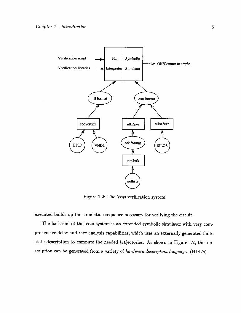
The Voss system [13], a formal verification system developed at the University of
British Columbia by Carl Seger, supports STE. Conceptually, the Voss system consists
of two major components, as shown in Figure 1.2.
The front-end of the Voss system is an interpreter for the FL language, which is the
command language of the Voss system. The FL language is a a strongly typed, polymor
phic, and fully lazy language. Moreover, the FL language has an efficient implementation
of OBDD’s built in. In other words, every object of type Boolean in the system is in
ternally represented as an OBDD. A specification is written as a program, which when1 “Weakest” is defined in terms of the partial order.
Chapter 1. Introduction 6
Figure 1.2: The Voss verification system
executed builds up the simulation sequence necessary for verifying the circuit.
The back-end of the Voss system is an extended symbolic simulator with very com
prehensive delay and race analysis capabilities, which uses an externally generated finite
state description to compute the needed trajectories. As shown in Figure 1.2, this de
scription can be generated from a variety of hardware description languages (HDL’s).
Verification script
Verification libraries
SymbolicOK/Counter example
Chapter 1. Introduction 7
1.2 Research Objectives
The goal of this research was to demonstrate that STE is an effective technique for
verifying RISC processors. To demonstrate the technique, we applied it to the Oryx
processor, which was designed and implemented for verification purposes. The Oryx
processor is a fairly generic model for RISC processors. The model is intended to capture
the RISC fundamental characteristics and it is very similar to other RISC processors, such
as the DLX [9] and the MIPS-X [5]. The Oryx processor is described in more details in
later chapters.
1.3 Related Work
In the formal methods community, there have been several efforts to verify RISC pro
cessors. The verification process of a RISC processor involves first writing a formal
specification of the processor. A hardware model of the RISC processor is then com
pared against the formal specification to prove the correctness of the design. So far, most
researchers have used extremely simple architectures as hardware models.
Tahar and Kumar [18] proposed a methodology for verifying RISC processors based
on a hierarchical model of interpreters. Their model is based on abstraction levels, which
are introduced between the formal specification and the circuit implementation. The
abstraction levels are called stage level, phase level, and class level. A stage instruction is
a set of transfers which occur during the corresponding pipeline segment, while a phase
instruction is the set of sub-transfers which occur during that clock phase. The top
level of the model is the class instruction, which corresponds to the set of instructions
with similar semantics. The model can be used to successively prove the correctness of
all phase, stage, and class instructions by instantiating the proofs for each particular
instruction. The specification of the DLX processor was described in HOL and parts of

Chapter 1. Introduction 8
the proof tasks were carried out.
Srivas and Bickford [16] used Clio, a functional language based verification system,
to prove the correctness of the Mini Cayuga processor. The Mini Cayuga is a three-stage
instruction pipelined RISC processor with a single interrupt. The correctness properties
of the Mini Cayuga were expressed in the Clio assertion language. The Clio system
supports an interactive theorem prover, which can be used to prove the correctness of
the properties.
The Mini Cayuga was specified at two levels, abstract specification and realization
specification. The abstract specification described the instruction level behavior from a
programmer’s point of view, while the realization specification described the processor’s
design by defining the activities that occur during a single clock cycle.
The abstract model of the Mini Cayuga is specified as a function that generates an
infinite trace of states over time as the processor executes instructions. The abstract
state of the Mini Cayuga is represented as a tuple with four components: the state of
the memory, the state of the register file, the next program counter, and the current
instruction. The progression of state as the processor executes instructions is done with
the help of the Step function, which takes as parameters a state and an interrupt list. This
function defines the effect of executing a single instruction on the state of the processor,
including the effect of the possible arrival of one or more interrupts during execution.
The correctness criterion of the Mini Cayuga requires proving that a realization state
and an abstract state of the processor are equivalent under some conditions.
Burch and Dill [4] described an automated technique for verifying the control path
of RISC processors assuming the data path computations are correct. They showed an
approach for extracting the correspondence between the specification and the implemen
tation. The statement of correspondence is written in a decidable logic of propositional
connectives, equality, and uninterpreted functions. Uninterpreted functions are used to
Chapter 1. Introduction 9
L
D
Figure 1.3: A simple latch
represent combinational logic, while propositional connectives and equality are used in
describing control in the specification and the implementation, and in comparing them.
This technique compares a pipelined implementation to an architectural description.
The description is written in a simple HDL based on a small subset of Common LISP and
is compiled through a kind of symbolic simulator to a transition function, which takes as
arguments a state and the current inputs, and returns the next state.
The Ph.D. dissertation of Beatty [1] addressed the processor correctness problem and
provided a step toward a solution. Because of the similarities between Beatty’s work and
our work, we will explain his method in some detail. To best illustrate the method, we
will consider the same example Beatty used in his dissertation.
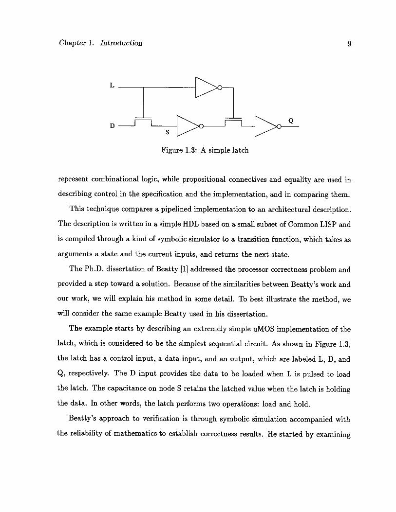
The example starts by describing an extremely simple nMOS implementation of the
latch, which is considered to be the simplest sequential circuit. As shown in Figure 1.3,
the latch has a control input, a data input, and an output, which are labeled L, D, and
Q, respectively. The D input provides the data to be loaded when L is pulsed to load
the latch. The capacitance on node S retains the latched value when the latch is holding
the data. In other words, the latch performs two operations: load and hold.
Beatty’s approach to verification is through symbolic simulation accompanied with
the reliability of mathematics to establish correctness results. He started by examining
S
Q
Chapter 1. Introduction 10
the nature of circuits and his simulation model of them to understand their properties,
which yielded requirements on his verification method.
By considering the latch and its timing diagram more closely, Beatty observed that
the basic timing of the latch is defined by the operations the latch performs and not by
clock signals. In other words, operations dictate their own timing and there is no need
to distinguish clock signals from other input signals. Therefore, the beginning and the
ending of each operation must be marked. This can be done by identifying the nominal
start and the nominal end of each operation.
Conceptually, the start marker of each operation is aligned with the end marker of
its predecessor to perform a sequence of operations. Moreover, these markers provide
a way to define the timing of state storage. For example, the state of the latch can be
considered at a particular time, such as at the nominal beginning of an operation.
The specification model Beatty used is an abstract Moore machine, structured as a
set of symbolic assertions, where each assertion corresponds to an operation. By using
symbols, a single assertion can concisely represent the operation for all possible data
values. The latch can be specified with two assertions:
((operation = load) A (D = b) 4 (Q = b)
((operation = hold) A (Q = c) z. (Q = c)
The left-hand side of the relation denotes the conditions on the system in the
current state, while the right-hand side denotes the conditions in its successor state.
Beatty showed that specifications expressed in such a language define an abstract machine
and the checks he made between specifications and circuits entail a formal relationship
between machines. The specifications are made sufficiently abstract, hence, they include
no particular details of a specific circuit implementation. Consequently, the same high
level specification can be used to verify several circuit implementations by providing some
Chapter 1. Introduction 11
formal relation between the specification and the circuit implementation.
Beatty designed a formal language to support such a style of specifications. The
language consists of writing assertions. Each assertion consists of two parts, an antecedent
and a consequent, which are written in a restricted logic. There are two kind of variables,
state and case. Case variables appear in the specifications, but are not components of
the state space. They simply keep the specifications concise. The abstract specification
of the latch is given bellow:
SMALversion 0 specification latchtypes
value word 1;operation enumeration load, hold.
state
op : operation;D value;
Q value.assertions
op = load /\ D = b:value > Q = b;op = hold /\ Q = c:value > Q = c.
Beatty used his methodology to verify the Hector, which is a 16-bit processor. Though
the Hector is a non-pipelined processor, the methodology can be applied to pipelined
systems as well. The physical layout of the Hector was extracted and used as a model
in the symbolic simulation. This can be a tedious and time consuming process, which
explains why Beatty did not use a more complex system to apply his methodology.
1.4 Thesis Overview
This thesis consists of six chapters with one appendix. In Chapter 2, we give an informal
description of the Oryx processor. This description is what usually can be found in
any programmer’s manual. Of course, this description is vague and cannot be used for
verifying the Oryx processor as it is just a natural language description of what the
Oryx processor does. In Chapter 3, we provide a more precise description of the Oryx
Chapter 1. Introduction 12
processor based on an abstract model. The abstract model is used to reason about the
behavior of the Oryx processor and to facilitate the verification process. In Chapter
4, we describe in details the implementation of the Oryx processor. In Chapter 5, we
explain the verification process and provides some experimental results. In Chapter 6,
we conclude the thesis by discussing some future work. The FL verification script of the
Oryx processor can be found in Appendix A.
Chapter 2
Architecture
This chapter describes the architectural features of the Oryx processor from a program
mer’s point of view. The chapter contains a section for each feature of the architecture
normally visible to the machine language programmer and the compiler writer.
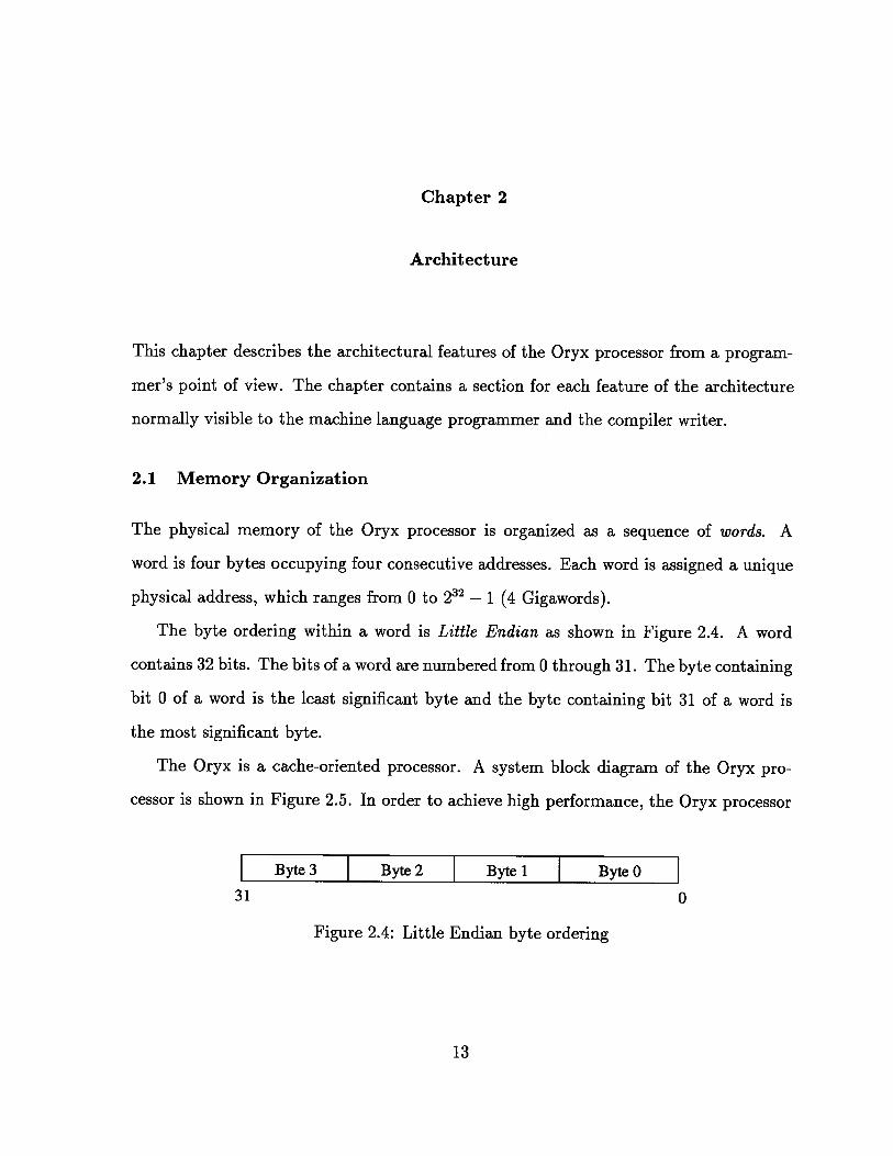
2.1 Memory Organization
The physical memory of the Oryx processor is organized as a sequence of words. A
word is four bytes occupying four consecutive addresses. Each word is assigned a unique
physical address, which ranges from 0 to 232— 1 (4 Gigawords).
The byte ordering within a word is Little Eridian as shown in Figure 2.4. A word
contains 32 bits. The bits of a word are numbered from 0 through 31. The byte containing
bit 0 of a word is the least significant byte and the byte containing bit 31 of a word is
the most significant byte.
The Oryx is a cache-oriented processor. A system block diagram of the Oryx pro
cessor is shown in Figure 2.5. In order to achieve high performance, the Oryx processor
Byte 3 Byte 2 Byte 1 Byte 0
31 0
Figure 2.4: Little Endian byte ordering
13
Chapter 2. Architecture 14
_____
RESULT BUS
H H
__
rDATA
REGISTERINSTRUION
UNIT
RLE 1 r UNIT
MEMORY
CACHE MANAGEMENT
UNIT
BUS CONTROL
MEMORY
CACHE MANAGEMENT
UNIT
BUS CONTROL
IT MEMORY BUS
I ORYX
INTEGER UNIT
I I SOURCE 1 BUS
SOURCE 2 BUS
BUS CONTROL BUS CONTROL
UFigure 2.5: A system block diagram of the Oryx processor
Chapter 2. Architecture 15
is provided with two high speed cache memory modules. One cache is dedicated to in
structions and the other to data. It is left to the system designer to decide what cache
memory sizes should be used. This is usually a performance-cost tradeoff.
The Oryx processor is designed with the assumption that the processor does not
directly address main memory. When the Oryx processor requires instructions or data,
it generates a request for that information and sends it to a memory management unit
(MMU). If the MMU does not find the necessary information in the cache memory, then
the Oryx processor waits while the MMU collects the information (i.e. instructions or
data) from main memory and moves it into the cache memory.
The Oryx processor is designed to support virtual memory. In other words, the Oryx
processor operates under the illusion that the system’s disk storage is actually part of
the system’s main memory.
The physical address space is broken into fixed blocks called pages. An address
generated by the Oryx processor is called a logical address. The logical address space is
mapped into the physical address space which is, in turn, mapped into some number of
pages.
A page may be either in main memory or on disk. When the Oryx processor issues
a logical address, it is translated into an address for a page in memory or an interrupt
is generated. The interrupt gives the operating system a chance to read the page from
disk, update the page mapping, and restart the instruction.
To provide the protection needed to implement an operating system, the physical
address space is divided into system space and user space. The Oryx processor reserves
the first 2 Gigawords of the physical memory for executing system programs and the
other 2 Gigawords for executing user programs.
Chapter 2. Architecture 16
2.2 Registers
The Oryx processor has thirty six registers, which are visible to the programmer. These
registers may be grouped as:
• General registers.
• Multiplication and division register.
• Status and control registers.
2.2.1 General Registers
The Oryx processor has thirty two 32-bit general registers R0,R1,. . . , R31. For architec
tural reasons, register R0 is permanently hardwired to a zero value. This register can be
read only. A write attempt into register R0 has no effect. Registers R1 to R31 are used
to hold operands for arithmetic and logical operations. They may also be used to hold
operands for address calculations.
2.2.2 Multiplication and Division Register
The multiplication and division (MD) register is used to facilitate the implementation of
shift-and-add integer multiplication and division algorithms. The MD register stores the
32-bit value of the multiplier for multiplication operations and the dividend for division
operations.
2.2.3 Status and Control Registers
The Oryx processor has one status and two control registers, which report and allow
modification of the state of the processor.
Chapter 2. Architecture 17
S CRA queue shift enableE Non-maskable interrupt flagI Maskable interrupt flagM Interrupt maskV Overflow mask0 Overflow flagU User/System modeIPF Instruction page fault flagDPF Data page fault flag
Table 2.1: PSW bits definition
Program Counter Register
The program counter (PC) register holds a 32-bit logical address of the next instruction
to be executed. The PC is not directly available to the programmer. It is controlled
implicitly by control-transfer instructions and interrupts.
Control Return Address Registers
The Oryx processor has four control return address (CRA) registers CRAO,CRA1,CRA2,
and CRA3. These registers form a queue with the CRA3 register being the head of the
queue and the CRA0 register being the tail. Every clock cycle, the value of the PC
register is shifted in the queue. When an interrupt occurs, the shifting of the queue is
disabled to give the programmer a chance to save the CRA registers. The actual content
of the CRA registers is implementation dependent.
Program Status Word Register
The program status word (PSW) register contains nine status bits, which control certain
operations and indicate the current state of the processor. Table 2.1 shows the definition
of these bits within the P5W register. The programmer (in supervisor mode) can set the

Chapter 2. Architecture 18
PSW register bits, which are also set by the hardware on an interrupt to a pre-determined
value.
2.3 Instruction Formats
The Oryx processor distinguishes four instruction formats: memory, branch, compute,
and compute immediate. An instruction format has various fixed size fields as shown
in Figure 2.6. The type and opcode fields are always present. The other fields may or
may not be present depending on the operation. The fields of an instruction format are
described below:
• Type: is a 2-bit field used to identify the instruction format.
• Opcode: is a 3-bit field used to specify the operation performed by the instruction.
Several instructions may have the same opcode. In this case, some bits of other
fields are used to distinguish between instructions.
• Source Register Specifiers: are 5-bit fields used to specify source register(s).
Instructions may specify one or two source registers. In memory instruction format,
one source register is used for address calculations.
• Destination Register Specifier: is also a 5-bit field used to specify a destination
register into which the result of an operation will be moved.
• Sq (Squash) Bit: is a 1-bit field used in branch instruction format only. When
set, it indicates that the branch is statically predicted to be taken.
• Offset: is a 17-bit field used in memory instruction format. This field holds a
signed value which is used to generate the logical address of a word in memory.
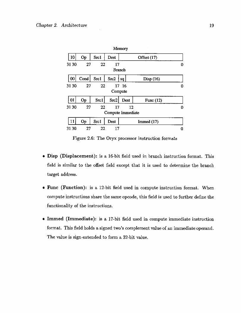
Chapter 2. Architecture 19
Memory
iol Op Srcl Dest Offset (17)
3130 27 22 17 0Branch
00 Cond Srcl Src2 sq Disp (16)
3130 27 22 17 16 0Compute
01 Op Src1 Src2 Dest Func(12) I3130 27 22 17 12 0
Compute Immediate
11 Op Src 1 Dest Immed (17)
3130 27 22 17 0
Figure 2.6: The Oryx processor instruction formats
• Disp (Displacement): is a 16-bit field used in branch instruction format. This
field is similar to the offset field except that it is used to determine the branch
target address.
• Func (Function): is a 12-bit field used in compute instruction format. When
compute instructions share the same opcode, this field is used to further define the
functionality of the instructions.
• Immed (Immediate): is a 17-bit field used in compute immediate instruction
format. This field holds a signed two’s complement value of an immediate operand.
The value is sign-extended to form a 32-bit value.
Chapter 2. Architecture 20
2.4 Addressing Modes
The Oryx processor supports only one addressing mode. The logical address is obtained
by adding the content of a base register to the address part of the instruction. The base
register is assumed to hold a base address and the address field, also known as the offset,
gives a displacement relative to this base register.
2.5 Operand Selection
An Oryx processor instruction may take zero or more operands. Of the instructions which
have operands, some specify operands explicitly and others specify operands implicitly.
An operand is held either in the instruction itself, as in compute immediate instructions,
or in a general register. Since no memory operands are allowed, access to operands is
very fast as they are available on-chip.
2.6 Co-processor Interface
The Oryx processor’s memory instructions can communicate with other types of hardware
besides the memory system. This is used to implement a simple co-processor interface.
Co-processor instructions use the memory instruction format. These instructions are
used to transfer data between the processor registers and the co-processor registers. It
is also possible to load and store the co-processor registers without using the processor
registers as an intermediate step.
The instruction bits for the co-processor are placed in the offset field of the memory
instruction. The co-processor can read these bits when they appear on the address lines
of the processor.
Chapter 2. Architecture 21
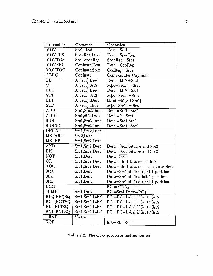
Instruction Operands OperationMOV Srcl,Dest Dest:=SrclMOVFRS SpecReg,Dest Dest: =SpecRegMOVTOS Srcl ,SpecReg SpecReg: =SrclMOVFRC Coplnstr,Dest Dest : =CopRegMOVTOC Coplnstr,Src2 CopReg: =Src2ALUC Coplnstr Cop executes CoplnstrLD X[Srcl],Dest Dest:=M[X+Srcl]ST X[SrclJ,Src2 M[X+Srcl]:= Src2LDT X[Srcl],Dest Dest:=M[X+SrcljSTT X[Srcl],Src2 M[X+Srcl]:=Src2LDF X[Srcl] ,fDest fDest : =M [X+SrclJSTF X[Srcl] ,fSrc2 M[X+Srcl] :=fSrc2ADD Srcl ,Src2,Dest Dest:=Srcl+Src2ADDI Srcl,#N,Dest Dest:=N+SrclSUB Srcl,Src2,Dest Dest:=Srcl-Src2SUBNC Srcl ,Src2,Dest Dest:=Srcl+Src2DSTEP Srcl,Src2,DestMSTART Src2,DestMSTEP Srcl,Src2,DestAND Srcl,Src2,Dest Dest:=Srcl bitwise and Src2BIC Srcl,Src2,Dest Dest:=J bitwise and Src2NOT Srcl,Dest Dest:=SrclOR Srcl,Src2,Dest Dest:= Srcl bitwise or Src2XOR Srcl,Src2,Dest Dest:= Srcl bitwise exclusive or Src2SRA Srcl,Dest Dest:=Srcl shifted right 1 positionSLL Srcl,Dest Dest:=Srcl shifted left 1. positionSRL Srcl,Dest Dest:=Srcl shifted right 1 positionIRET PC:= CRA3JUMP Srcl ,Dest PC:=Srcl ,Dest:=PC+1BEQ,BEQSQ Srcl,Src2,Label PC:=PC+Label if Srcl=Src2BGT,BCTSQ Srcl,Src2,Label PC:=PC+Label if Srcl>Src2BLT,BLTSQ Srcl,Src2,Label PC:=PC+Label if Srcl<Src2BNE,BNESQ Srcl,Src2,Label PC:=PC+Label if Src1LSrc2TRAP VectorNOP RO:=RO+RO
Table 2.2: The Oryx processor instruction set
Chapter 2. Architecture 22
2.7 Instructions
The Oryx processor provides programmers with a simple instruction set, which can be
used to write application programs for the processor. The Oryx processor instructions
are listed in Table 2.2. They are grouped by categories of related functionality. This
section describes the operation of each instruction and mentions the operands required.
Data Movement Instructions
These instructions provide convenient ways for transferring word quantities. They come
in two types:
1. Register-Register instructions.
2. Register-Memory instructions.
Register-Register Instructions
These instructions are used for transferring data along any of the following paths:
• Between general registers.
• Between general registers and special registers.
• Between general registers and co-processor registers.
The MOV (Move) instruction transfers a word between general registers. This in
struction, like the other instructions of its type, takes as operands a source register
address R and a destination register address Ri,, where 0 x, y <31.
The MOVFRS (Move From Special) instruction transfers a word from a special
register (e.g. MD register) to a general register. This instruction is useful for reading
special registers.
Chapter 2. Architecture 23
The PSW register is a special case as it has oniy nine bits. When this instruction is
executed, the high-order bits (i.e. bits 9 to 31) of the destination register are filled with
zeros.
The MOVTOS (Move To Special) instruction transfers a word from a general register
to a special register.
In the special case of the PSW register, only the low-order bits (i.e. bits 0 to 8) of the
general register are transferred. In user mode, the PSW is read-only where in supervisor
mode it is both readable and writable. The high-order bits (i.e. bits 9 to 31) are ignored.
The MOVTOC (Move To Co-processor) instruction transfers a word from a general
register to a co-processor register. This instruction is useful for loading the co-processor
registers.
The MOVFRC (Move From Co-processor) instruction transfers a word from a
processor register to a general register. This instruction is used to move the result of a co
processor operation to the processor when the co-processor has finished the computation.
The ALUC (ALU Co-processor) instruction provides the co-processor with some
instruction bits. This instruction results in the co-processor performing an operation as
specified by the instruction bits.
Register-Memory Instructions
In a way similar to previous instruction group, these instructions are useful for transfer
ring data along any of these paths:
• Between general registers and cache memory.
• Between general registers and main memory.
• Between co-processor registers and main memory.
Chapter 2. Architecture 25
Addition and Subtraction Instructions
These instructions take two source operands and a destination operand. The source
operands are two general registers. The ADDI (Add Immediate) instruction is an excep
tion. The second operand of this instruction is an immediate value. The result of the
computation is moved into the destination operand which can be any general register.
The PSW 0 status bit is updated according to the result of the operation.
The ADD (Add) replaces the destination operand with the sum of the two source
operands.
The ADDI (Add Immediate) computes the sum of a source operand and a 17-bit
sign extended immediate value.
The SUB (Subtract) subtracts the second source operand from the first source
operand and replaces the destination operand with the result.
The SUBNC (Subtract No Carry In) subtracts the second source operand from the
first source operand and replaces the destination operand with the result minus one.
Multiplication and Division Instructions
The Oryx processor supports signed multiplication. However, only unsigned division is
supported as signed division requires complex hardware.
Multiplication is done with the simple 1-bit shift-and-add algorithm except that the
computation is started from the most significant bit instead of the least significant bit of
the multiplier.
The MSTART (Multiplication Start) initializes the signed multiplication algorithm.
This instruction requires one source operand and a destination operand which can be
general registers only. The source register holds the multiplicand value and the multipli
cation result will be in the destination register.
Chapter 2. Architecture 24
The LD (Load) instruction trallsfers a word from a location in cache memory to
a general register. The instruction, like the other instructions of its type, takes three
operands: a base address register, a 17-bit offset, and a destination register address. The
base address register can be any of the processor general registers.
There is a delay of one instruction between a load instruction and the availability of
its result. The programmer must take this load delay into consideration.
The ST (Store) instruction transfers a word from a general register to a location in
cache memory.
The LDT (Load Through) instruction transfers a word from a location in main
memory to a general register. It requests the MMU to access main memory directly
without first looking in the cache memory.
This instruction is needed for memory mapped I/O. It also helps improve the perfor
mance of the system if the programmer knows in advance that the word is not available
in the cache memory. This way, the programmer can avoid the penalty of a cache miss.
The STT (Store Through) instruction transfers a word from a general register to a
location in main memory without writing it in the cache memory.
The LDF (Load Float) instruction transfers a word from a location in main memory
to a co-processor register.
The STF (Store Float) instruction transfers a word from a co-processor register to a
location in main memory.
2.7.1 Arithmetic Instructions
The arithmetic instructions of the Oryx processor operate on numeric data encoded in
binary. The Oryx processor supports both signed and unsigned binary integers. Two’s
complement representation is used to encode negative numbers.
Chapter 2. Architecture 26
For signed multiplication, this instruction tests the most significant bit (MSB) of
the MD register which holds the multiplier value. If this bit is equal to one, then the
multiplicand is subtracted from zero and the result is moved into the destination register.
Otherwise, the destination register is initialized to zero. The MD register is shifted 1-bit
to the left.
The MSTEP (Multiplication Step) implements one step of both the signed and un
signed multiplication algorithms. Contrary to the MSTART instruction, this instruction
requires one extra source operand. The destination register is also used as the first source
register. The second source register holds the multiplicand value.
This instruction also tests the MSB of the MD register. If this bit is equal to one
then the destination register is shifted 1-bit to the left and added to the multiplicand.
The partial result is moved back into the destination register. If the MSB of the MD
register is equal to zero, then the destination register is shifted 1-bit to the left. The MD
register is always shifted 1-bit to the left.
Division is done with a restoring division algorithm. The dividend is loaded into
the MD register and the register that will contain the remainder is initialized to zero.
The divisor is loaded into another register. The result of the division will be in the MD
register.
The DSTEP (Division Step) instruction implements a one step of the division al
gorithm. This instruction is similar to the MSTEP instruction. It requires two source
operands and a destination operand. The destination register holds the value of the re
mainder and serves as the first source register. The second source register holds the value
of the divisor. Each time this instruction is executed, it shifts the remainder register 1-bit
to the left and adds to it the MSB of the MD register. It also subtracts from the partial
result of shifting and addition the value of the divisor to generate a final result.
If the MSB of the final result is equal to one, then the remainder register gets the

Chapter 2. Architecture 27
value of the partial result. The MD register is shifted 1-bit to the left. On the other
hand, if the MSB of the final result is equal to zero, then then remainder register gets
the value of the partial result minus the value of the divisor. The MD register is shifted
1-bit to the left and one is added to it.
2.7.2 Logical Instructions
The logical instructions may have either two or three operands which can only be general
registers. These instructions come in two types:
1. Boolean operation instructions.
2. Shift instructions.
Boolean Operation Instructions
The Oryx processor provides several instructions which can be used to perform basic
booleall operations.
The NOT (Not) instruction forms the one’s complement of the source operand and
replaces the destinatioll operand with the result.
The AND (And) instruction performs the standard boolean bitwise “and” operation
on the two source operands and moves the result into the destination register.
The BIC (Bit Clear) instruction is similar to the previous instruction except that
it uses the one’s complement of the first source operand. This instruction is useful for
manipulating byte quantities.
The OR (Or) and the XOR (Exclusive Or) instructions perform the standard boolean
bitwise “or” and “exclusive or” operations, respectively.

Chapter 2. Architecture 28
Shift Instructions
The shift instructions can be used to rearrange the bits within an operand. They apply
either arithmetic or logical 1-bit shift to words. These instruction do not affect the PSW
0 status bit.
The SRA (Shift Right Arithmetic) instruction copies the sign bit into an empty bit
position on the upper end of the operand. This instruction is useful for performing simple
arithmetic such as integer divide by 2.
The SRL (Shift Right Logical) instruction is similar to the previous instruction except
that it fills the high-order bit positions with zeros.
The SLL (Shift Left Logical) instruction fills the low-order bit positions of an operand
with zeros.
2.7.3 Control Transfer Instructions
The Oryx processor provides both conditional and unconditional control transfer instruc
tions to direct the flow of execution.
Unconditional Transfer Instructions
The JUMP (Jump) instruction unconditionally transfers execution to the destination.
This instruction takes one source operand and one destination operand. Both operands
are general registers. The first operand specifies the address of the jump destination.
The return address is moved into the second operand. The same instruction can be used
to return from a subroutine by swapping the two operands.
The IRET (Return From Interrupt) instruction returns control to an interrupted
procedure. It also restores the state of the P5W processor which was saved when the
interrupt occurred.
Chapter 2. Architecture 29
The IRET instruction is followed by three slots. Instructions in these slots are not
executed. This is a mechanism to facilitate the return from interrupt.
The TRAP (Trap) instruction allows the programmer to specify a transfer of execu
tion to an interrupt service routine (TSR). This instruction specifies an 8-bit vector which
is used to lookup the address of the TSR in the interrupt vector table.
Conditional Transfer Instructions
Conditional transfer instructions are called branch instructions. There are several of
them. Each branch instruction specifies a condition, two source operands, and a 16-bit
displacement. A source operand can be any general register.
A branch instruction compares the values of the two source registers and takes some
action depending on the comparison result. If the result of the comparison is positive,
then a 16-bit sign extended displacement is added to the value of the PC register to
generate the branch target address. Otherwise, the PC register is incremented to point
at the next instruction.
The Oryx processor features a two-slot delayed branch scheme. This means that
branch instructions require two clock cycles from the time they were issued to evaluate
the branch condition. The Oryx processor issues an instruction every clock cycles. By
the time the comparison of the two source registers has been done, two instructions have
been issued. These instructions enter a ready queue and wait for execution.
The Oryx processor provides two versions of the branch instructions. One version
makes it possible to statically predict that the branch will be taken. This provides a
mechanism for squashing (or canceling) the instructions in the ready queue if the branch
is not taken. Consequently, the compiler should try to schedule useful instructions in the
delay slots to increase the performance of the system.
The BEQ, BEQSQ (Branch If Equal) instructions test for equality of the two source
Chapter 2. Architecture 30
registers. If the result of the test is positive, then the branch is taken.
The BGT, BGTSQ (Branch If Greater Than) instructions transfer control to the
destination if the first source register has a value which is greater than that of the second
source register.
The BLT, BLTSQ (Branch If Less Than) instructions are the complements of the
BGT and BGTSQ instructions, respectively. Control is transferred if the first source
register has a value which is less than that of the second source register.
The BNE, BNESQ (Branch If Not Equal) instructions transfer control to the des
tination if the source registers are not equal.
2.7.4 Miscellaneous Instructions
The NOP (No Operation) instruction increments the PC register to point at the next
instruction. This instruction does not change the status of the Oryx processor.
2.8 Interrupts
The Oryx processor has a mechanism to provide precise interrupts which means that
interrupts will be served in the order of their occurrence. Interrupts are either external or
internal. The Oryx processor supports four external interrupts: non-maskable, maskable,
data page fault, and instruction page fault. As for internal interrupts, the Oryx processor
supports two types: overflow and software interrupts.
When an interrupt occurs, the processor goes into supervisor mode, the PSW register
is saved, and control is transferred to execute the ISR, which is located at memory address
zero. While the Oryx processor is in supervisor mode, no other interrupts are accepted.
When the processor has finished executing the TSR, control is transferred back to the
interrupted procedure.

Chapter 2. Architecture 31
A typical ISR is given below:
MOVFRS PSW,Ra ; Read PSWMOVFRS MD,Rb ; Save MD registerMOVFRS CRA3,RC ; Save CRA3 registerMOVFRS CRA3,Rd ; Save CRA2 registerMOVFRS CRA3,Re ; Save CRA1 registerMOVFRS CRA3,Rf ; Save CRAO register
Body of the ISR.
MOVTOS Rb,MD ; Restore MD registerMOVTOS RC,CRAO ; Restore CRA3 registerMOVTOS Rd,CRAO ; Restore CRA2 registerMOVTOS Re,CRA0 ; Restore CRA1 registerMOVTOS Rf,CRAO Restore CRA0 registerIRET ; Return
The TSR reads the PSW register to determine what caused the interrupt. Then it
saves some registers which include the MD register and the CRA registers. The CRA
registers are saved by reading the CRA3 register four times while shifting the CRA queue.
The ISR does some work and when it is done it restores the registers it saved earlier.
The CRA registers are restored by writing to the CRA0 register four times. Finally, the
TSR returns control to the interrupted procedure by executing the IRET instructions.
Chapter 3
Formal Specification
An abstract model of the Oryx processor, as described in this chapter, provides a general
framework for writing the formal specification of the Oryx processor. This formal specifi
cation describes the architecture of the Oryx processor in a way similar to the description
that is given in the previous chapter. However, a formal specification is more precise,
which makes it suitable for reasoning about the behavior of the Oryx processor.
This chapter contains two sections. Section One describes the abstract model of the
Oryx processor from a programmer’s point of view and Section Two shows how this
abstract model is used for writing the formal specification of the Oryx processor.
3.1 Abstract Model
The circuit of the Oryx processor consists of several parts (i.e. control logic, registers,
input pins, output pins, etc...) some of which need to be visible to the programmer
and some need not. Therefore, abstraction is used to hide unnecessary details which the
programmer does not need to know.
Within our model, we have two abstraction types, structural and temporal. Structural
abstraction hides the implementation details such as pipelining. On the other hand,
temporal abstraction hides the actual timing of signal values in the implementation.
The natural way to model the Oryx processor is to view it as a state machine that
operates on a stream of inputs. The abstract state of the Oryx processor is modeled as
a record. The record contains a field for each part of the Oryx processor which is visible
32
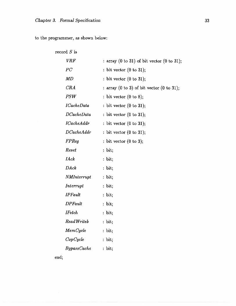
Chapter 3. Formal Specification 33
to the programmer, as shown below:
record S is
VRF : array (0 to 31) of bit vector (0 to 31);
PC : bit vector (0 to 31);
MD : bit vector (0 to 31);
CRA : array (0 to 3) of bit vector (0 to 31);
P5W : bit vector (0 to 8);
ICacheData : bit vector (0 to 31);
DCacheData : bit vector (0 to 31);
ICacheAddr : bit vector (0 to 31);
DCacheAddr : bit vector (0 to 31);
FPReg : bit vector (0 to 3);
Reset : bit;
JAck : bit;
DAck : bit;
NMlnterrupt : bit;
Interrupt : bit;
IPFault : bit;
DPFault : bit;
IFetch : bit;
Read Writeb : bit;
MemCycle : bit;
CopCycle : bit;
BypassCache : bit;
end;
Chapter 3. Formal Specification 34
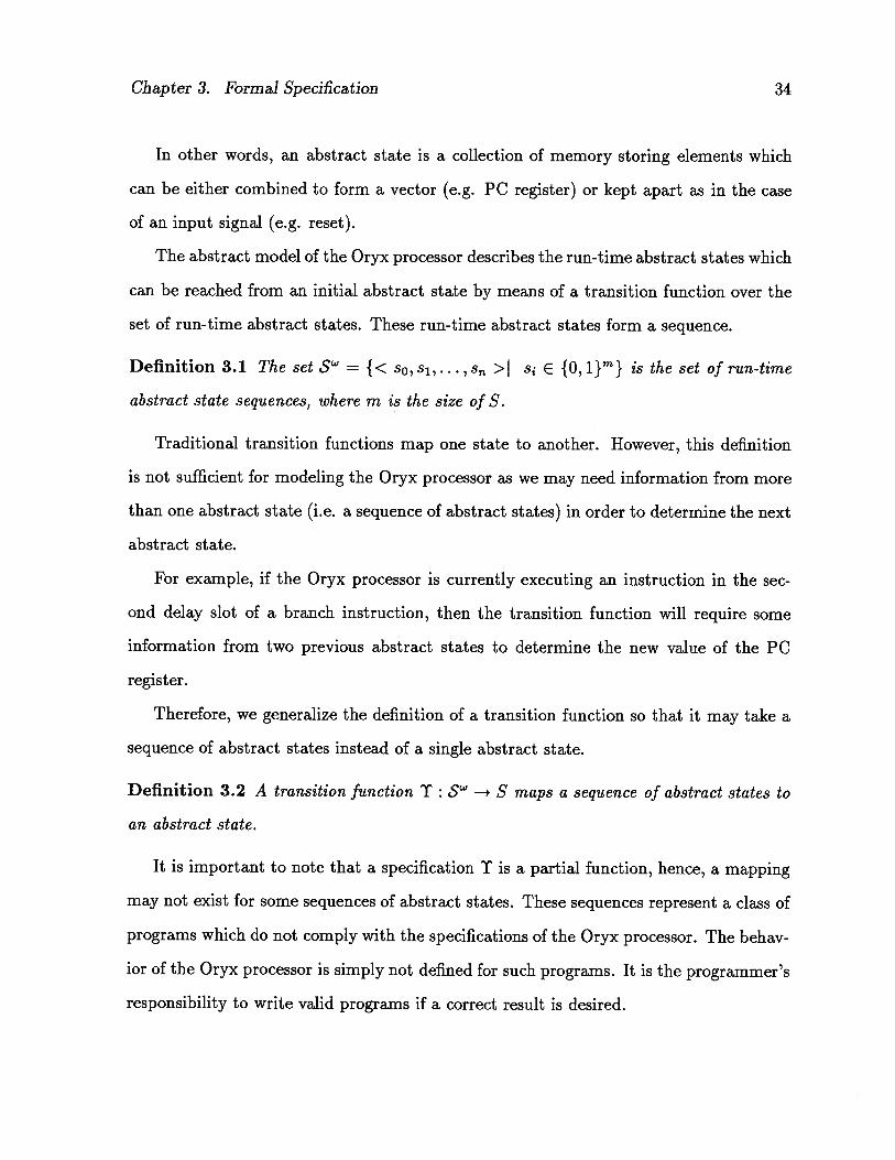
In other words, an abstract state is a collection of memory storing elemeilts which
can be either combined to form a vector (e.g. PC register) or kept apart as in the case
of an input signal (e.g. reset).
The abstract model of the Oryx processor describes the run-time abstract states which
can be reached from an initial abstract state by means of a transition function over the
set of run-time abstract states. These run-time abstract states form a sequence.
Definition 3.1 The set Sw = {< ,5k,. . . ‘Sn >1 . e {O, 1}m} is the set of run-time
abstract state sequences, where m is the size of S.
Traditional transition functions map one state to another. However, this definition
is not sufficient for modeling the Oryx processor as we may need information from more
than one abstract state (i.e. a sequence of abstract states) in order to determine the next
abstract state.
For example, if the Oryx processor is currently executing an instruction in the sec
ond delay slot of a branch instruction, then the transition function will require some
information from two previous abstract states to determine the new value of the PC
register.
Therefore, we generalize the definition of a transition function so that it may take a
sequence of abstract states instead of a single abstract state.
Definition 3.2 A transition function 1’ : S’ —* S maps a sequence of abstract states to
an abstract state.
It is important to note that a specification T is a partial function, hence, a mapping
may not exist for some sequences of abstract states. These sequences represent a class of
programs which do not comply with the specifications of the Oryx processor. The behav
ior of the Oryx processor is simply not defined for such programs. It is the programmer’s
responsibility to write valid programs if a correct result is desired.
Chapter 3. Formal Specification 35
To identify the sequences of abstract states which can be obtained by executing valid
programs only, we define what we call an abstract history.
Definition 3.3 (Abstract History) An abstract history A is a sequence of abstract
states such that each prefix of A is consistent with the transition function. More formally,
an abstract history A= {< > E $W Vj 0 <j < 1. T(< 8O,S1,”.,Sj >) =
A specification, as defined below, describes how the abstract state of the Oryx pro
cessor is affected by executing an instruction every cycle.
Definition 3.4 (Specification) A specification F : A —* A maps an abstract history to
a new abstract history.
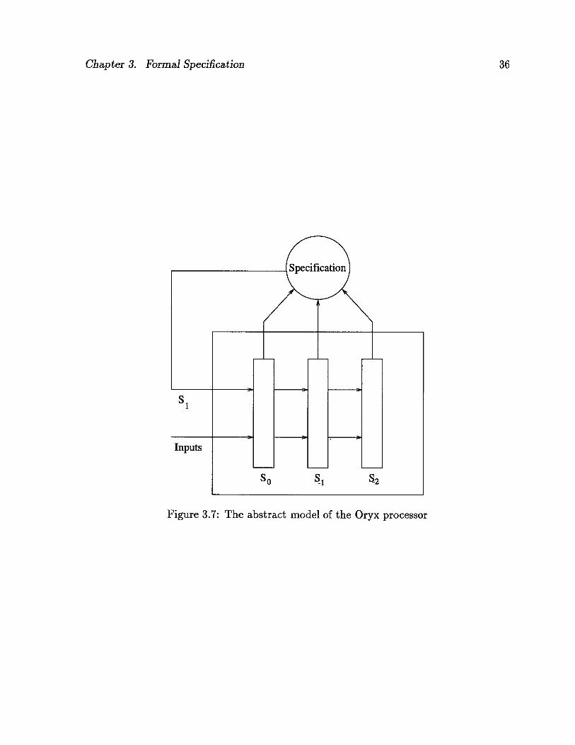
Keeping the above discussion in mind, we now present the abstract model of the Oryx
processor as depicted in Figure 3.7. Assuming that the Oryx processor is in a state So,
the specification determines what the next state 51 is going to be based on the current
(recent) history of the Oryx processor.
3.2 Formal Specification
This section shows how to write the formal specification of the Oryx processor by giving
an example. The full formal specification can be driven in a similar way. Before giving
the example, however, we introduce some notations and conventions, which will be used
throughout this section.
We write S1- to refer to the abstract state at time r. S0 refers to the current abstract
state. Negative indices are used to refer to previous abstract states. For example, S_
is the abstract state one instruction cycle ago, 8—2 is the abstract state two instruction
cycles ago, and so on. Similarly, positive indices are used to refer to next abstract states.
Chapter 3. Formal Specification 36
ification
Si -
Inputs -
S0 S S2
Figure 3.7: The abstract model of the Oryx processor
Chapter 3. Formal Specification 37
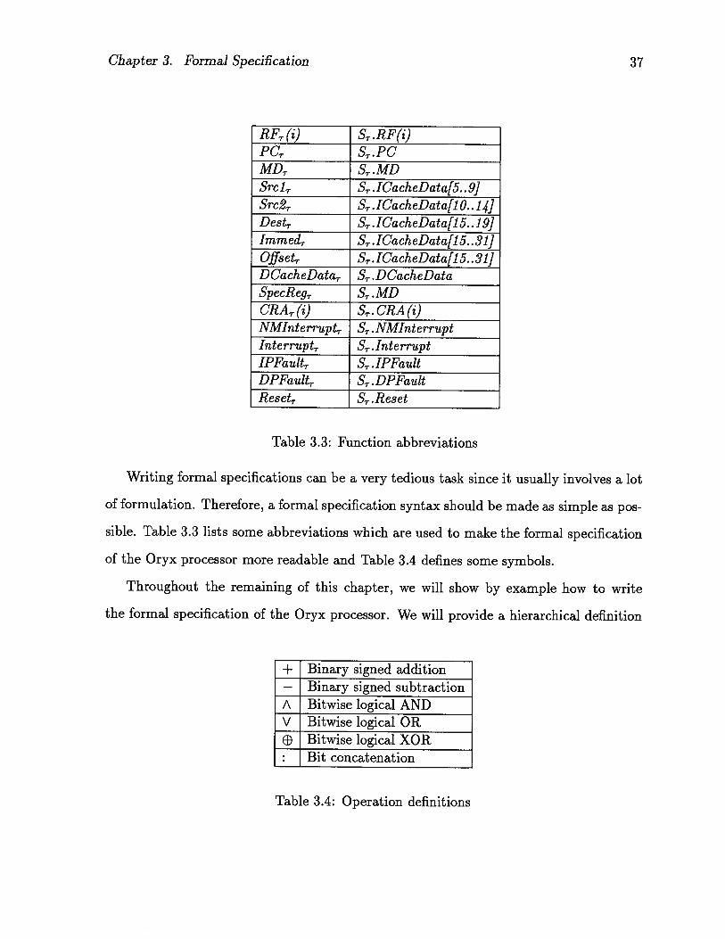
RF7(i) S7.RF(i)PC7 ST.PCMD7 ST.MDSrclT ST.ICacheData[5..9]Src27 ST.ICacheData[1O..14]Dest7 S,-.ICacheData[15..19]ImmedT ST.ICacheData[15. .31]Offset7 ST.ICacheData[15. .31]DCacheData7 S- .DCacheDataSpecRegT ST.MDCRAT (i) S. CRA (i)NMInterruptT S-. NMlnterruptInterrupt7 ST .InterruptIPFaultT S-. IFFaultDFFau1tT ST. DPFaultReset1- ST.Reset
Table 3.3: Function abbreviations
Writing formal specifications can be a very tedious task since it usually involves a lot
of formulation. Therefore, a formal specification syntax should be made as simple as pos
sible. Table 3.3 lists some abbreviations which are used to make the formal specification
of the Oryx processor more readable and Table 3.4 defines some symbols.
Throughout the remaining of this chapter, we will show by example how to write
the formal specification of the Oryx processor. We will provide a hierarchical definition
+ Binary signed addition— Binary signed subtractionA Bitwise logical ANDV Bitwise logical OR
Bitwise logical XOR: Bit concatenation
Table 3.4: Operation definitions

Chapter 3. Formal Specification 38
of two transition functions, namely the register file and the PC register, under normal
conditions (i.e. no interrupts and no reset). We then go down in the hierarchy and define
all functions which compose the top-level definition of these transition functions.
3.2.1 Example I: Register File Specification
I NewRF(S) if Dest0=i=
RF0(’i) Otherwise
ArithmRes(S) if Arithmlnstr(S)
LogicRes(S) else if Logiclnstr(S)
TransferRes(S) else if Transferlnstr(S)NewRF(S)=
MDRes(’S) else if MDlnstr(S)
ShifiRes(S) else if Shiftlnstr(S)
JumpRes(S) else if Jumplnstr(S)
Arithmlnstr(S) = InstrIsADD(Opcodeo) V
InstvIsADDI(Opcodeo) V
InstrIsSUB(Opcodeo) V
InstrIsS UBNC(Opcodeo)
Logiclnstr(S)= InstrIsAND(Opcodeo) V
InstrIsBIC(Opcodeo) V
InstrIsOR (Opcodeo) V
InstrIsXOR (Opcodeo) V
InstrlsNO T(Opcodeo)
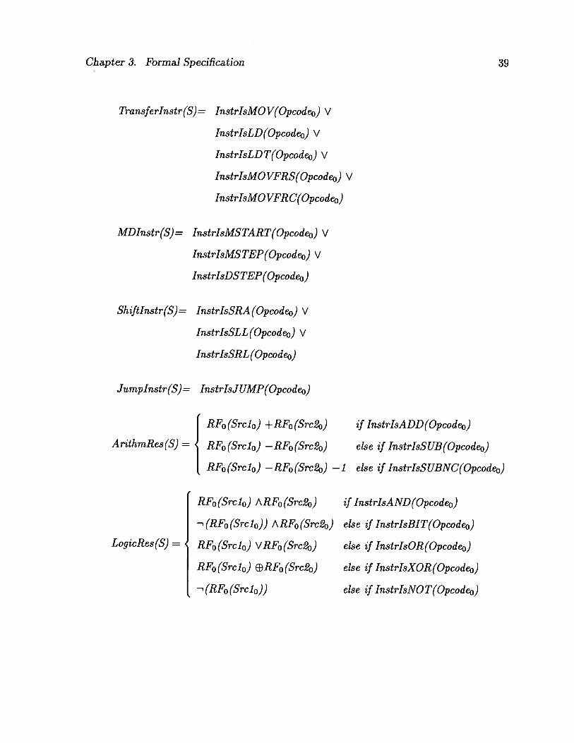
Chapier 3. Formal Specification 39
Transferlnstr(S)= InstrIsMO V(Opcodeo) V
InstrlsLD(Opcodeo) V
InstrlsLD T(Opcodeo) V
InstrIsMO VFRS(Opcodeo) V
InstrIsMO VFR C(Opcodeo)
MDlnstr(S)= InstrIsMSTA RT(Opcodeo) V
InstrfsMSTEP(Opcodeo) V
InstrIsDSTEP(Opcodeo)
Shiftlnstr(S) InstrIsSRA (Opcodeo) V
InstrIsSLL (Opcodeo) V
InstrIsSRL (Opcodeo)
Jumplnstr(S)= InstrlsJUMP(Opcodeo)
RF0(Srclo) +RF0(Src2o) if InstrIsADD(Opcodeo)
ArithmRes(S) = RF0(Srclo) —RF0(Src2o) else if InstrIsSUB(Opcodeo)
RF0(Srclo) — RF0(Src2o) —1 else if InstrIsSUBNC(Opcodeo)
RF0(Srclo) /\RF0(Src2o) if InstrIsAND(Opcodeo)
(RF0(Srclo)) ARE’0(Src2o) else if InstrIsBIT(Opcodeo)
LogicRes(S) = RF0(Srclo) VRF0(Src2o) else if InstrlsOR(Opcodeo)
RF0(Srclo) EDRF0(Src2o) else if InstrIsXOR(Opcodeo)
(RF0(Srclo)) else if InstrIsNOT(Opcodeo)
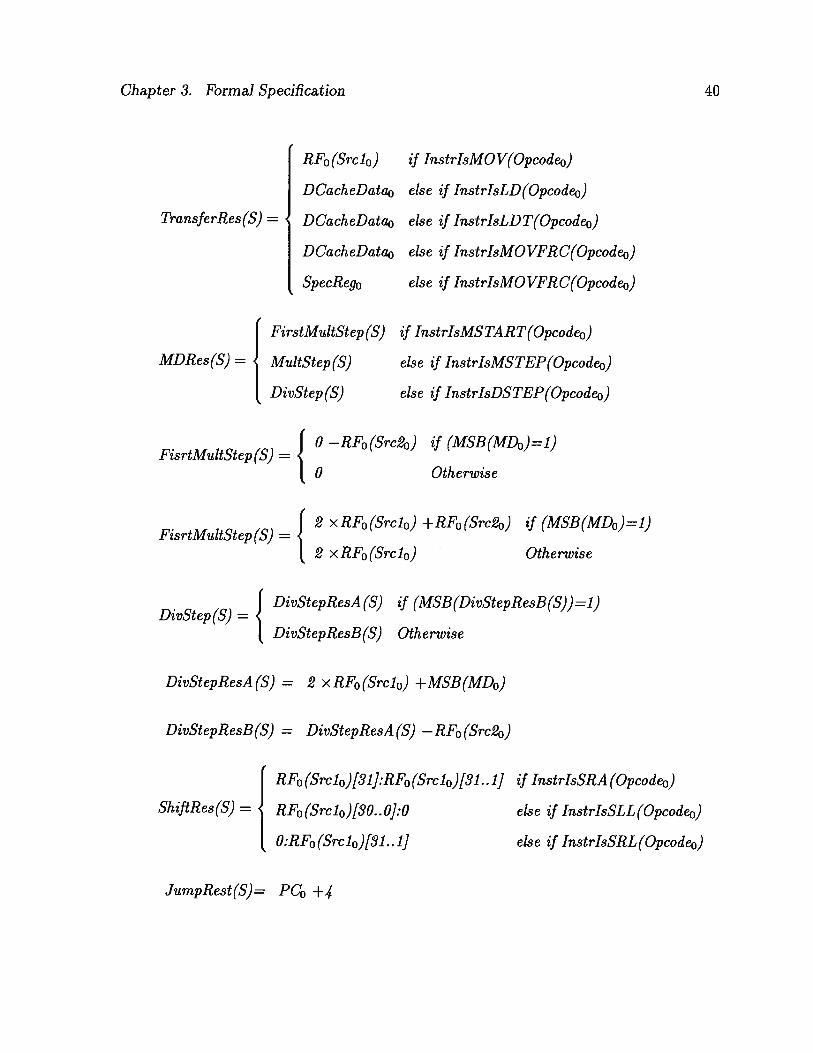
Chapter 3. Formal Specification 40
RF0(Srclo) if IristrlsMOV(Opcodeo)
DCacheData0 else if InstrlsLD(Opcodeo)
TransferRes(S) = DCacheDatao else if InstrIsLDT(Opcodeo)
DCacheData0 else if InstrIsMOVFRC(Opcodeo)
SpecRego else if InstrIsMOVFRC(Opcodeo)
FirstMultStep(S) if InstrIsMSTA RT(Opcodeo)
MDRes(S) MultStep(S) else if InstrIsMSTEP(Opcodeo)
DivStep (S) else if InstrIsDSTEP(Opcodeo)
1 0 — RF0(Src2o) if (MSB(MD0)=1)FisrtMultStep (S) =
1 0 Otherwise
1 2 xRF0(Srclo) +RF0(Src2o) if (MSB(MD0)=1)FisrtMultStep(S) =
( 2 xRF0(Srclo) Otherwise
I DivStepResA(S) if (MSB(DivStepResB(S))=1)DivStep(S) =
( DivStepResB(S) Otherwise
DivStepResA(S) = 2 xRFo(Srclo) +MSB(MD0)
DivStepResB(S) = DivStepResA(S) —RF0(’Src2o)
RF0(’Srclo)[Sl]:RFo(Srclo)[Sl..l] if InstrIsSRA(Opcodeo)
ShifiRes(S) = RF0(Srclo)[30. . 0]:0 else if InstrIsSLL(Opcodeo)
O:RF0(Srclo)[31. .1] else if InstrIsSRL (Opcodeo)
JumpRest(S)= PC0 +í
Chapter 3. Formal Specification 41
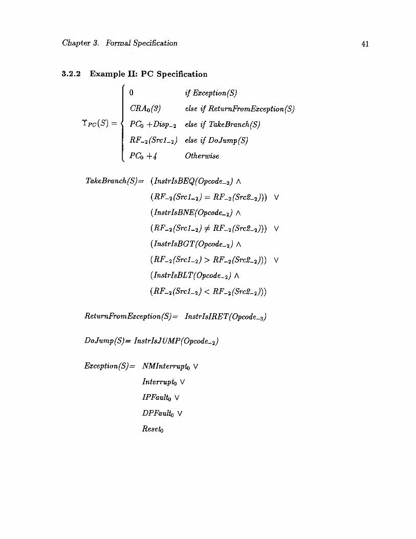
3.2.2 Example II: PC Specification
if Exception(S)
else if ReturnFromException(S)
else if TakeBranch(S)
else if DoJurnp(S)
Otherwise
(InstrIsBEQ(Opcode_2)A
(RF_2(Srcl_2)= RF_2(Src2_2)))
(InstrIsBNE(Opcode_2)A
(RF_2(Srcl_2) RF_2(’Src2_2)))
(InstrIsBGT(Opcode_2)A
(RF_2(SrcL2)> RF_2(Src2_2)))
(InstrIsBLT(Opcode_2)A
(RF_2(Srcl_2)< RF_2(Src_2)))
ReturnFromException (S) = InstrIsJRET(Opcode_3)
DoJump (S) = InstrIsJUMP(Opcode_2)
Exception (S) = NMlnterrupto V
Interrupt0 V
IPFault0 V
DPFault0 V
Reset0
0
CRA0(8)
Tpc(S) = PCO +Disp_2
RF_2(SrcL2)
TakeBranch (S) =
V
V
V

Chapter 4
Implementation
This chapter describes the implementation of the Oryx processor in the VHSIC hardware
description language (VHDL). The VHDL code is a detailed gate-level logic implemen
tation of the Oryx processor [6].
The logical way to describe the Oryx processor implementation is to divide it into
two parts: control path and data path. This chapter contains a section for each path,
but first we start by describing the Oryx processor from a designers’ point of view.
4.1 Design Overview
The Oryx is a pipelined processor. The pipeline consists of five stages as shown in
Figure 4.8. The pipeline stages are typically called the instruction fetch (IF) stage, the
instruction decode (ID) stage, the execute (EXE) stage, the memory (MEM) stage, and
the write-back (WB) stage, respectively.
IF ID EXE MEM WB
Clock
Figure 4.8: The Oryx processor pipeline
42

Chapter 4. Implementation 43
Each stage of the pipeline is a pure combinational circuit. High-speed interface latches
separate the pipeline stages. The latches are fast registers, which hold intermediate
results between the stages. A common clock is simultaneously applied to all the latches
to control information flow between adjacent stages.
The functionality of the pipeline stages is explained by describing what each stage
of the pipeline does from the time an instruction is issued to the time the instruction is
processed completely.
The IF stage reads the instruction from the instruction cache (ICache) memory using
an address in the PC register. The ID stage identifies the instruction and prepares its
operands.
The computation performed by the EXE stage depends on the instruction being exe
cuted. For compute or compute immediate instructions, this stage performs the obvious
computation. During the execution of memory instructions, the EXE stage computes
the address of the desired memory location. For branch instructions, the EXE stage
compares two registers to evaluate the branch condition.
The MEM stage reads from and writes into the data cache (DCache) memory. The
WB stage is the final stage in the pipeline where the result of the instruction is written
into the register file.
Pipelining is a form of temporal parallelism. Several instructions occupy different
pipeline stages at the same time. These instructions could very likely depend on each
other. Therefore, internal bypassing is provided so that an instruction does not have to
wait for previous instructions to write their results into the register file before being able
to access their results. With bypassing, two instructions can be issued in sequence even
if the second one uses the result of the first one. The only exception to this is the load
instructions.
The Oryx processor uses a two-phase non-overlapping clocking scheme. The two clock
Chapter 4. Implementation 44
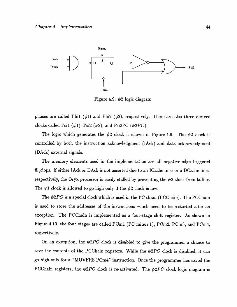
phases are called Phil (ql) and Phi2 (q2), respectively. There are also three derived
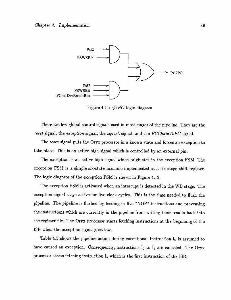
clocks called Psil (‘l), Psi2 (2), and Psi2PC (b2PC).
The logic which generates the b2 clock is shown in Figure 4.9. The b2 clock is
controlled by both the instruction acknowledgment (JAck) and data acknowledgment
(DAck) external signals.
The memory elements used in the implementation are all negative-edge triggered
flipflops. If either JAck or DAck is not asserted due to an ICache miss or a DCache miss,
respectively, the Oryx processor is easily stalled by preventing the ‘tt’2 clock from falling.
The L’l clock is allowed to go high only if the b2 clock is low.
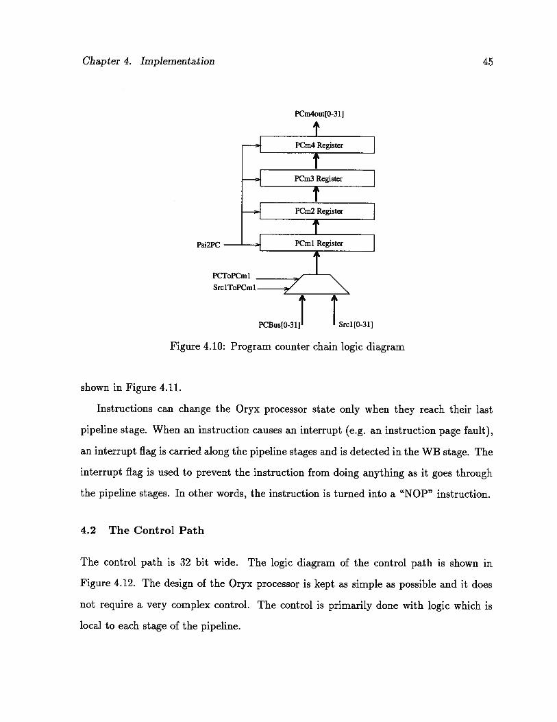
The ‘ib2FC is a special clock which is used in the PC chain (PCChain). The PCChain
is used to store the addresses of the instructions which need to be restarted after an
exception. The PCChain is implemented as a four-stage shift register. As shown in
Figure 4.10, the four stages are called PCm1 (PC minus 1), PCm2, PCm3, and PCm4,
respectively.
On an exception, the 2FC clock is disabled to give the programmer a chance to
save the contents of the PCChain registers. While the 2PC clock is disabled, it can
go high only for a “MOVFRS PCm4” instruction. Once the programmer has saved the
PCChain registers, the /2FC clock is re-activated. The ,1J2FC clock logic diagram is
Reset
JAck
DAck Psi2
Phi2
Figure 4.9: çb2 logic diagram
Chapter 4. Implementation 45
PCm4out[0-31]
PCm4 Register
PCm3 Register
I PCm2 Register
_J.____Psi2PC PCm1 Register
PCToPCrnI
________
SrclToPCml
PCBus[0-3 1] Srcl [0-3 1]
Figure 4.10: Program counter chain logic diagram
shown in Figure 4.11.
Instructions can change the Oryx processor state only when they reach their last
pipeline stage. When an instruction causes an interrupt (e.g. an instruction page fault),
an interrupt flag is carried along the pipeline stages and is detected in the WB stage. The
interrupt flag is used to prevent the instruction from doing anything as it goes through
the pipeline stages. In other words, the instruction is turned into a “NOP” instruction.
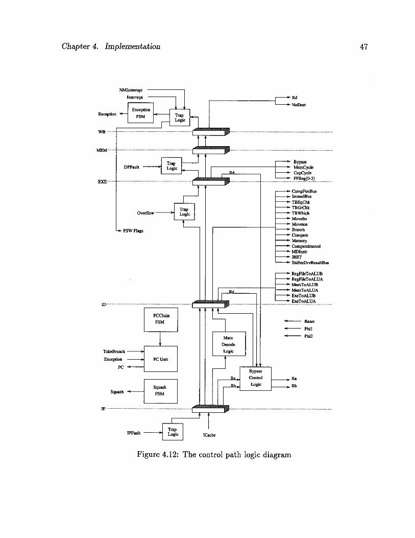
4.2 The Control Path
The control path is 32 bit wide. The logic diagram of the control path is shown in
Figure 4.12. The design of the Oryx processor is kept as simple as possible and it does
not require a very complex control. The control is primarily done with logic which is
local to each stage of the pipeline.
Chapter 4. Implementation 46
Psi2
PSWSBit
Psi2PC
Psi2PSWSBit
PCm4DrvResultBus
Figure 4.11: 2FC logic diagram
There are few global control signals used in most stages of the pipeline. They are the
reset signal, the exception signal, the squash signal, and the PCChainToPC signal.
The reset signal puts the Oryx processor in a known state and forces an exception to
take place. This is an active-high signal which is controlled by an external pin.
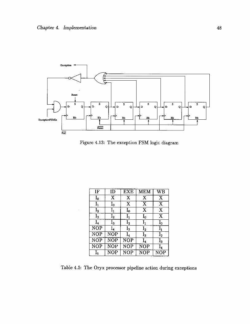
The exception is an active-high signal which originates in the exception FSM. The
exception FSM is a simple six-state machine implemented as a six-stage shift register.
The logic diagram of the exception FSM is shown in Figure 4.13.
The exception FSM is activated when an interrupt is detected in the WB stage. The
exception signal stays active for five clock cycles. This is the time needed to flush the
pipeline. The pipeline is flushed by feeding in five “NOP” instructions and preventing
the instructions which are currently in the pipeline from writing their results back into
the register file. The Oryx processor starts fetching instructions at the beginning of the
TSR when the exception signal goes low.
Table 4.5 shows the pipeline action during exceptions. Instruction T is assumed to
have caused an exception. Consequently, instructions Jo to 14 are canceled. The Oryx
processor starts fetching instruction T which is the first instruction of the TSR.
Chapter 4. Implementation
IPFauIt
CompFunBusImmedBusTBEqChkTBGrChk
—‘ TBWhichMovefrsMovetosBranch
• Compute• Memory• Computelinmed• MDlnstr• IRET• ShifterDrvResultBus
• RegFiIeToALUB• RegFiIeToALUA
MemToALUBMemToALUA
• ExeToALUB
47
NMlnterrupt
Interrupt
Exception
• Rd
NoDeat
Overflow
P5W Flags
ID
Takeflranch
Exception
PC
< Reset£ Phil
Phi2
SquashJh
FSM
Ra
Rb
ICache
Figure 4.12: The Control path logic diagram
Chapter 4. Implementation 48
ExceptionFSMln
Figure 4.13: The exception FSM logic diagram
IF ID EXE MEM WB‘0 X X X XIi jo X X X12 ‘1 ‘0 X X13 ‘2 ‘1 ‘0 X14 13 ‘2 Ii To
NOP 14 13 ‘2 IiNOP NOP 14 13 ‘2
NOP NOP NOP 14 13NOP NOP NOP NOP 14
15 NOP NOP NOP NOP
Psil
Table 4.5: The Oryx processor pipeline action during exceptions

Chapter 4. Implementation 49
SquashFSMln
Figure 4.14: The squash FSM logic diagram
The squash is an active-high signal which originates in the squash FSM. The squash
FSM is similar to the exception FSM. It is a three-state machine implemented as a
two-stage shift register. The logic diagram of the squash FSM is shown in Figure 4.14.
The squash FSM is activated when the instruction being executed is a squashing
branch instruction and the branch is not taken. The squash signal stays active for two
clock cycles. This is the time needed to cancel the two instructions which are in the delay
slots.
Table 4.6 shows the pipeline action during instruction squashing. Instruction 14 is
assumed to be a squashing branch instruction. The two instructions following 14 are
turned into “NOP” instructions. The Oryx processor starts fetching instruction 15 which
follows the two delay slots.
The PCChainToPC is an active-high signal which originates in the PCChain FSM.
The PCChain FSM is a five-state machine implemented as a four-stage shift register.
The logic diagram of the PCChain FSM is shown in Figure 4.15. The PCChain FSM is
triggered by an IRET instruction. The PCChainToPC signal stays active for four clock
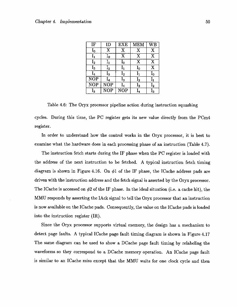
Chapter 4. Implementation 50
IF ID EXE MEM WB‘0 X X X XIi jo X X X12 ‘1 ‘0 X X13 ‘2 ‘1 ‘0 X14 13 ‘2 ‘1 ‘0
NOP 14 13 ‘2 ‘1
NOP NOP 14 13 ‘2
I NOP NOP 14 13
Table 4.6: The Oryx processor pipeline action during instruction squashing
cycles. During this time, the PC register gets its new value directly from the PCm4
register.
In order to understand how the control works in the Oryx processor, it is best to
examine what the hardware does in each processing phase of an instruction (Table 4.7).
The instruction fetch starts during the IF phase when the PC register is loaded with
the address of the next instruction to be fetched. A typical instruction fetch timing
diagram is shown in Figure 4.16. On 1 of the IF phase, the ICache address pads are
driven with the instruction address and the fetch signal is asserted by the Oryx processor.
The ICache is accessed on q2 of the IF phase. In the ideal situation (i.e. a cache hit), the
MMU responds by asserting the JAck signal to tell the Oryx processor that an instruction
is now available on the ICache pads. Consequently, the value on the ICache pads is loaded
into the instruction register (IR).
Since the Oryx processor supports virtual memory, the design has a mechanism to
detect page faults. A typical ICache page fault timing diagram is shown in Figure 4.17
The same diagram can be used to show a DCache page fault timing by relabeling the
waveforms so they correspond to a DCache memory operation. An ICache page fault
is similar to an ICache miss except that the MMU waits for one clock cycle and then
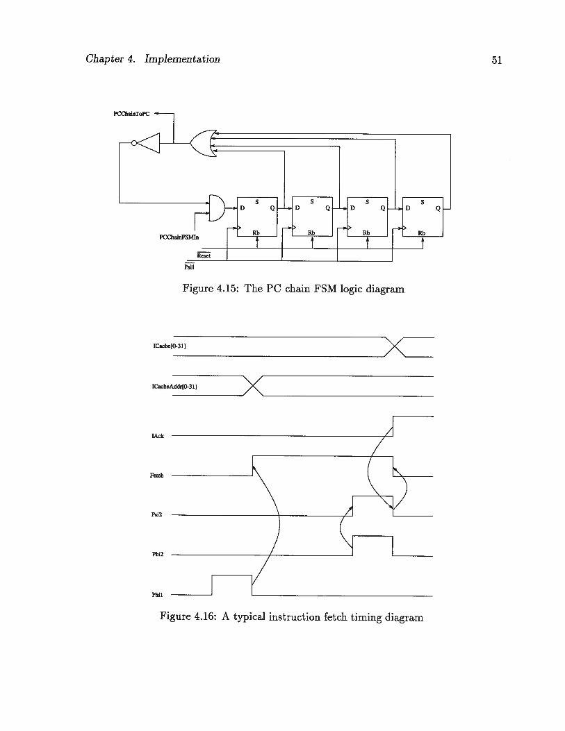
Chapter 4. Implementation
lCache[O-3l]
51
ICacheAddr[O-31]
lAck
Fetch
Psi2
Phi2
Phil
Figure 4.15: The PC chain FSM logic diagram
Figure 4.16: A typical instruction fetch timing diagram

Chapter 4. Implementation 52
Processing Phase Clock Phase Pipeline ActionIF q1 ICache address pads PC
42 Do ICache accessInstruction register ICache
ID q1 Calculate new PCDo bypass register comparisonsDetect squashing branch instructionsSrcl bus Srcl register or bypass registerSrc2 bus 4= Src2 register, bypass register oroffset field in memory instructions
42 No actionEXE qfl Do ALU operation or shift operation
Evaluate TakeBranch signal for branch instructions42 EXEout register 4= Result bus
SMDR Src2 busPCm1 PC
MEM No action
q2 Do DCache accessTEMP register 4= EXEout registerLMDR register 4= DCache input pads
WB Detect interrupts
q2 WBout register TEMP register or LMDRRegister file 4= WBout register
Table 4.7: Pipeline action during instruction processing phases
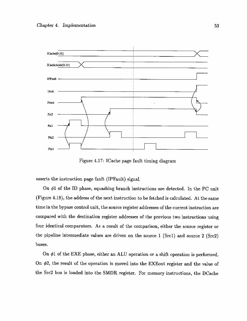
Chapter 4. Implementation 53
ICache[O-3 1]
ICacheAddr[O-3 1]
IPFault
JAck
Fetch
Psi2
Psil
Phi2
Phil
asserts the instruction page fault (IPFault) signal.
On ql of the ID phase, squashing branch instructions are detected. In the PC unit
(Figure 4.18), the address of the next instruction to be fetched is calculated. At the same
time in the bypass control unit, the source register addresses of the current instruction are
compared with the destination register addresses of the previous two instructions using
four identical comparators. As a result of the comparison, either the source register or
the pipeline intermediate values are driven on the source 1 (Srcl) and source 2 (Src2)
buses.
On q1 of the EXE phase, either an ALU operation or a shift operation is performed.
On q52, the result of the operation is moved into the EXEout register and the value of
the Src2 bus is loaded into the SMDR register. For memory instructions, the DCache
Figure 4.17: ICache page fault timing diagram
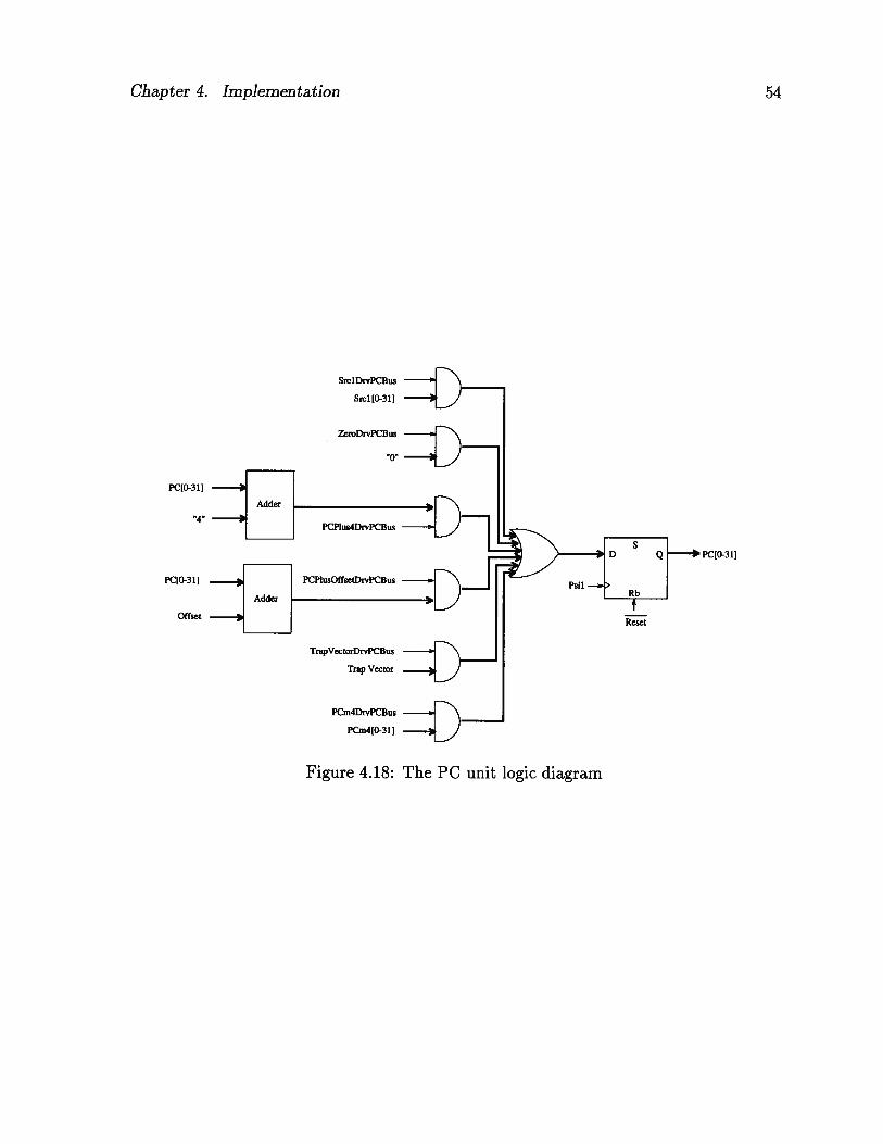
Chapter 4. Implementation
PC[O-31]
“4”
Pc[O-31J
Offset
PCm4DrvPCBus
PCm4[O-31J
Figure 4.18: The PC unit logic diagram
Pc[o-31]
54
SrclDrvPcBus
Srcl[O-31]
ZeroDrvPcBus
“0”
TrapVectorOrvPcBus
Trap Vector
Reset
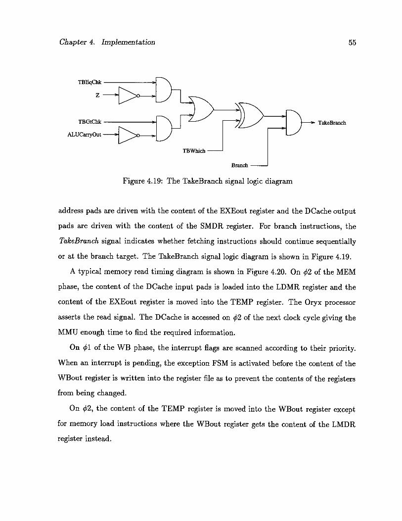
Chapter 4. Implementation 55
TakeBranch
Figure 4.19: The TakeBranch signal logic diagram
address pads are driven with the content of the EXEout register and the DCache output
pads are driven with the content of the SMDR register. For branch instructions, the
TakeBranch signal indicates whether fetching instructions should continue sequentially
or at the branch target. The TakeBranch signal logic diagram is shown in Figure 4.19.
A typical memory read timing diagram is shown in Figure 4.20. On q2 of the MEM
phase, the content of the DCache input pads is loaded into the LDMR register and the
content of the EXEout register is moved into the TEMP register. The Oryx processor
asserts the read signal. The DCache is accessed on q2 of the next clock cycle giving the
MMU enough time to find the required information.
On ql of the WB phase, the interrupt flags are scanned according to their priority.
When an interrupt is pending, the exception FSM is activated before the content of the
WBout register is written into the register file as to prevent the contents of the registers
from being changed.
On 2, the content of the TEMP register is moved into the WBout register except
for memory load instructions where the WBout register gets the content of the LMDR
register instead.
TBEqChk
z
TBWhich
Branch
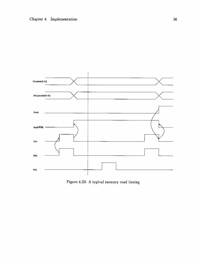
Chapter 4. Implementation 56
DCacheIn[O3)X(
DAck
Read)WñtC
Psi2
Phi2
Phil
Figure 4.20: A typical memory read timing

Chapter 4. Implementation 57
4.3 The Data Path
The width of data path is parameterized so it can take on a value which is equal to N,
where N=21, i {2, 3,4, 5}. The data path logic diagram is shown in Figure 4.21. It
mainly consists of two parts: the register file and the execute unit.
The register file provides the operands which are needed to perform an operation. It
is an M-word memory, where M=2t, i {1, 2,3,4, 5}, which can be accessed through
three ports, one of which is used for writing and the other two ports are used for reading.
As shown in Figure 4.22, the register file can be logically divided into three components:
the memory array, the destination address decoder, and the output multiplexors.
Each memory bit is a D-fiipfiop with an input multiplexor as shown in Figure 4.23.
The content of the memory bit is changed when the load signal becomes active. The N
load signals are grouped together to form a word address line which is connected to one
output of the address decoder.
The NoDest signal originates in the ID stage and is carried along the pipeline stages.
It is used to to prevent instructions which do not write into the register file from changing
the contents of the registers. The logic which generates the NoDest signal is shown in
Figure 4.24.
An M-to-1 word multiplexor is used for each of the register file output ports. Reading
from the register file is done asynchronously. When the source register address becomes
stable at the multiplexor select lines, the required memory word is made available at the
output port after some propagation delay.
The design of the register file is somewhat naive. The main reason being that the tools
which we used, specifically the VHDL compiler, do not support switch-level component
(i.e. transistors) which are necessary for a realistic implementation. In practice, the
register file should be implemented as a Dual-Ported RAM with pre-charge lines and
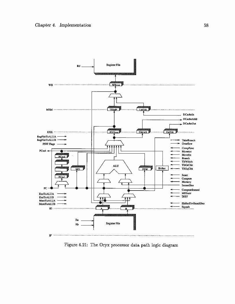
PC
ExeT0ALUAExeToALUBMemT0ALUAMemT0ALUB a’
ID
Ra
Rb
TakeBranchOverflow
CompFuncMovetosMovefrsBranchTBWhichTBGrChkTBEqChk
Reset- Compute* Memory
Immedflus
ComputelmmedMDlnstrWET
IF
Chapter 4. Implementation 58
Rd Register File
WB
MEM
EXE
RegFiIeT0ALUARegFiIeT0ALUB
PSW Flags a
PCm4
DCacheOut
3.
a
ShifterDrvResultBus
Register File
Figure 4.21: The Oryx processor data path logic diagram

Chapter 4. Implementation 59
Ra[O-4]WBout[O-3 1]
Register 0Srcl[0-31]
Register 1
Destination
Address Rd[0-4]
Decoder
Src2[0-311 Register 31 I 31
Rb[0-4]
NoDest Exception
Figure 4.22: The Oryx processor register file logic diagram
out(i)
LoadPsi2
Figure 4.23: A register file memory bit logic diagram
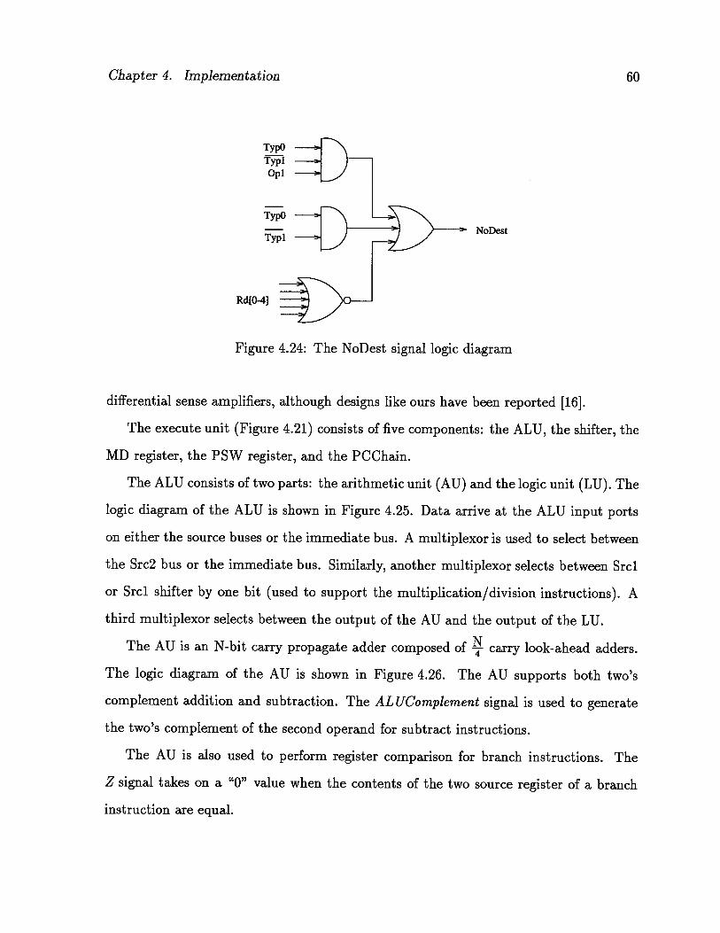
Chapter 4. Implementation 60
TypO
Typi
Op1
NoDest
Rd[O-4]
Figure 4.24: The NoDest signal logic diagram
differential sense amplifiers, although designs like ours have been reported [16].
The execute unit (Figure 4.21) consists of five components: the ALU, the shifter, the
MD register, the PSW register, and the PCChain.
The ALU consists of two parts: the arithmetic unit (AU) and the logic unit (LU). The
logic diagram of the ALU is shown in Figure 4.25. Data arrive at the ALU input ports
on either the source buses or the immediate bus. A multiplexor is used to select between
the Src2 bus or the immediate bus. Similarly, another multiplexor selects between Srcl
or Srcl shifter by one bit (used to support the multiplication/division instructions). A
third multiplexor selects between the output of the AU and the output of the LU.
The AU is an N-bit carry propagate adder composed of - carry look-ahead adders.
The logic diagram of the AU is shown in Figure 4.26. The AU supports both two’s
complement addition and subtraction. The AL UComplement signal is used to generate
the two’s complement of the second operand for subtract instructions.
The AU is also used to perform register comparison for branch instructions. The
Z signal takes on a “0” value when the contents of the two source register of a branch
instruction are equal.
TypO
Typl
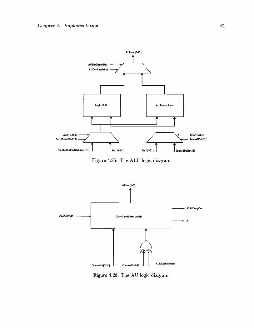
Chapter 4. Implementation 61
ALUout[O-31]
AUDrvResultflus
LUDrvResultBus —7”
Logic Unit
_
II—
_
Src1ToALU
SrclShiftedToALU
SrclBusShiftedByOne[O-311 srcl[o-311 Src2[O-31]
Figure 4.25: The ALU logic diagram
1 Arithmetic Unit
I I IISrc2ToALU
edToALU
I
AUout[O-31]
ALUCarryIn
ALUCarryOut
z
OperandA[O-31] OperandB[O-31]
Figure 4.26: The AU logic diagram
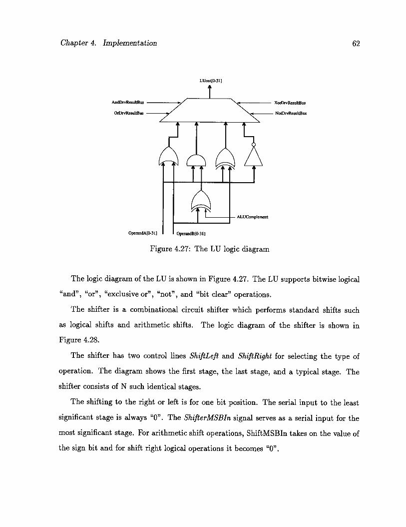
Chapter 4. Implementation 62
LUout[O-31]
AndDrvResultBus XorDrvResultBus
OrDrvResultBus NotDrvResultBus
OperandA[O-311 OperandB[O-31]
Figure 4.27: The LU
The logic diagram of the LU is shown in Figure 4.27. The LU supports bitwise logical
“and”, “or”, “exclusive or”, “not”, and “bit clear” operations.
The shifter is a combinational circuit shifter which performs standard shifts such
as logical shifts and arithmetic shifts. The logic diagram of the shifter is shown in
Figure 4.28.
The shifter has two control lines ShiftLeft and ShiftRight for selecting the type of
operation. The diagram shows the first stage, the last stage, and a typical stage. The
shifter consists of N such identical stages.
The shifting to the right or left is for one bit position. The serial input to the least
significant stage is always “0”. The ShifterMSBln signal serves as a serial input for the
most significant stage. For arithmetic shift operations, ShiftMSBIn takes on the value of
the sign bit and for shift right logical operations it becomes “0”.
logic diagram

Chapter 4. Implementation 63
ShiftLeft ShiftRight
Figui’e 4.28: The shifter logic diagram
Shifterout(3 1) Shifterout(i) Shifterout(O)
ShifterMSBln “O”
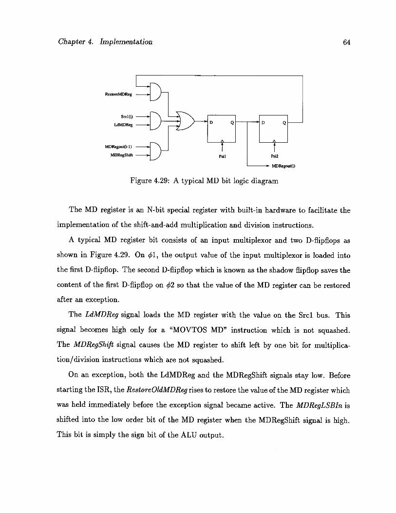
Chapter 4. Implementation 64
RestoreMDReg
SrcJ ()
LdMDReg
MDRegout(i-1)
MDRegShift
Figure 4.29: A typical MD bit logic diagram
The MD register is an N-bit special register with built-in hardware to facilitate the
implementation of the shift-and-add multiplication and division instructions.
A typical MD register bit consists of an input multiplexor and two D-fiipflops as
shown in Figure 4.29. On ql, the output value of the input multiplexor is loaded into
the first D-fiipfiop. The second D-fiipfiop which is known as the shadow fiipflop saves the
content of the first D-fiipfiop on so that the value of the MD register can be restored
after an exception.
The LdMDReg signal loads the MD register with the value on the Srcl bus. This
signal becomes high only for a “MOVTOS MD” instruction which is not squashed.
The MDRegShift signal causes the MD register to shift left by one bit for multiplica
tion/division instructions which are not squashed.
On an exception, both the LdMDReg and the MDRegShift signals stay low. Before
starting the ISR, the Restore OldMDReg rises to restore the value of the MD register which
was held immediately before the exception signal became active. The MDRegLSBIn is
shifted into the low order bit of the MD register when the MDRegShift signal is high.
This bit is simply the sign bit of the ALU output.

Chapter 4. Implementation 65
PSWout(i+I)
PSWout(i)
Psil
Figure 4.30: PSWCurrent-PSWOther pair
The PSW register consists of nine pairs of bits. The two bits of each pair are called
PSWCurrent and PSWOther, respectively. The logic diagram for each PSWCurrent
PSWOther pair is shown in Figure 4.30. The top D-flipflop makes up the PSWCurrent
bit and the bottom D-flipflop makes up the PSWOther bit. Each PSWcurrent bit can
be saved in and restored from its PSWOther bit.
On an exception, the PSWCurrent bits are saved in the PSWOther bits and a partic
ular value is forced into most of the PSWCurrent bits except the E, I, 0, IPF, and DPF
bits. These bits are forced to values which depend on whether or not the exception was
caused by a non-maskable interrupt, a maskable interrupt, an overflow, an ICache page
fault, or a DCache page fault, respectively.
The LdFSW signal loads the PSW register with the value on the Srcl bus. This
signal becomes high only for a “MOVTOS PSW” instruction executed when the Oryx
Srcl(i+1)
1-dPsw
ForcePSW
PSWOtherToPSW
ForcePSW
Srcl(i)
LdPSW

Chapter 4. Implementation 66
processor is in the system mode. The LdPSW signal stays low in case of an exception.
On an exception, the ForcePSW signal rises to save the PSWCurrent bits in their
respective PSWOther bits and force the PSWCurrent bits to predetermined values.
The PSWOtherToPSW signal is triggered by an IRET instruction as part of the
TSR return sequence. This signal restores the PSWCurrent bits with the values of their
PSWOther bits.
Chapter 5
Formal Verification
In this chapter, we demonstrate the application of symbolic trajectory evaluation for
verifying the Oryx processor. The chapter contains six sections. First, we briefly discuss
the inherent difficulty in carrying out the verification of the Oryx processor. Second,
we explain what it means to verify the processor. Third, we show how implementation
mappings can be used to overcome some of the difficulty in verifying the Oryx processor.
Fourth, we state the verification condition of the processor which allows us to establish
the correctness of the processor. Fifth, we show how the verification is actually done
and we then present some experimental results. Finally, we list some of the design errors
which were detected during the verification.
5.1 Verification Difficulty
In practice, the Voss system is used to carry out the verification task of the Oryx pro
cessor. Generally speaking, the formal specification of the Oryx processor is expressed in
the FL language and the simulation model needed by the Voss system is extracted from
the VHDL implementation of the processor.
One of the difficulties in verifying the correctness of the Oryx processor is that the
formal specification of the processor is very abstract so that it does not constrain the
implementation of the processor. On the other hand, our implementation of the Oryx
processor is fairly complex. Therefore, a major effort in the verification effort was to find
the relationship between the formal specification of the Oryx processor and its pipelined
67

Chapter 5. Formal Verification 68
implementation. In particular, we had to deal with both temporal abstraction and struc
tural abstraction.
In the abstract domain, time is measured in terms of instruction cycles. The processor
executes one instruction every cycle. In the implementation domain, however, time is
measured in terms of clock cycles. It takes an instruction several clock cycles to emerge
from the pipeline of the Oryx processor. For example, an ADD instruction takes 5 clock
cycles to complete in the implementation. Furthermore, each clock cycle consists of many
basic time units. Assuming that each clock cycle is equal to 1000 time units, we thus
need to map 1 abstract instruction cycle to 5000 implementation time units.
The problem imposed by structural abstraction is due to the fact that a data value in
the abstract domain could have several images in the implementation domain and which
image should be used at one point of time depends of the state of the Oryx processor. To
further illustrate the problem, consider the following example. In the abstract domain,
the value of the operands can be obtained from one source called the virtual register file.
In the implementation domain, however, the value of operands could be in the register
file or anywhere along the stages of the pipeline. We will return to this shortly.
5.2 Property Verification
If the programmer wants to use the Oryx processor to run a program, the implementation
of the processor should perform the “correct” function, as specified by the program. In
very general terms, answering this is the essential verification task of the Oryx processor.
However, carrying out the verification for any arbitrary program is impossible due
to the complexity of the problem. Instead, we will show how to verify properties of the
Oryx processor using bounded-length, arbitrary, but valid (i.e. written according to the
formal specification), instruction sequences. A property of the Oryx processor to verify
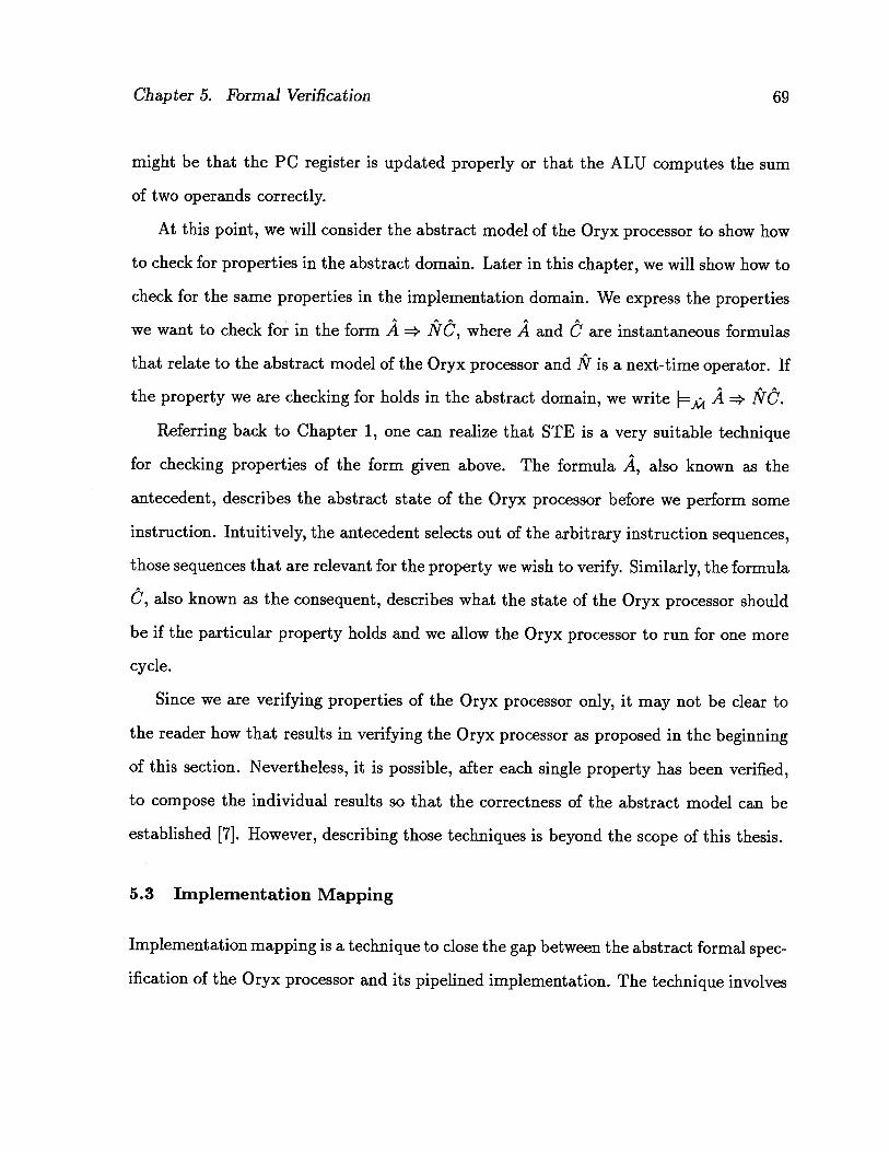
Chapter 5. Formal Verification 69
might be that the PC register is updated properly or that the ALU computes the sum
of two operands correctly.
At this point, we will consider the abstract model of the Oryx processor to show how
to check for properties in the abstract domain. Later in this chapter, we will show how to
check for the same properties in the implementation domain. We express the properties
we want to check for in the form A = NO, where A and 0 are instantaneous formulas
that relate to the abstract model of the Oryx processor and IC/ is a next-time operator. If
the property we are checking for holds in the abstract domain, we write = A NC.
Referring back to Chapter 1, one can realize that STE is a very suitable technique
for checking properties of the form given above. The formula A, also known as the
antecedent, describes the abstract state of the Oryx processor before we perform some
instruction. Intuitively, the antecedent selects out of the arbitrary instruction sequences,
those sequences that are relevant for the property we wish to verify. Similarly, the formula
O, also known as the consequent, describes what the state of the Oryx processor should
be if the particular property holds and we allow the Oryx processor to run for one more
cycle.
Since we are verifying properties of the Oryx processor only, it may not be clear to
the reader how that results in verifying the Oryx processor as proposed in the beginning
of this section. Nevertheless, it is possible, after each single property has been verified,
to compose the individual results so that the correctness of the abstract model can be
established [7). However, describing those techniques is beyond the scope of this thesis.
5.3 Implementation Mapping
Implementation mapping is a technique to close the gap between the abstract formal spec
ification of the Oryx processor and its pipelined implementation. The technique involves
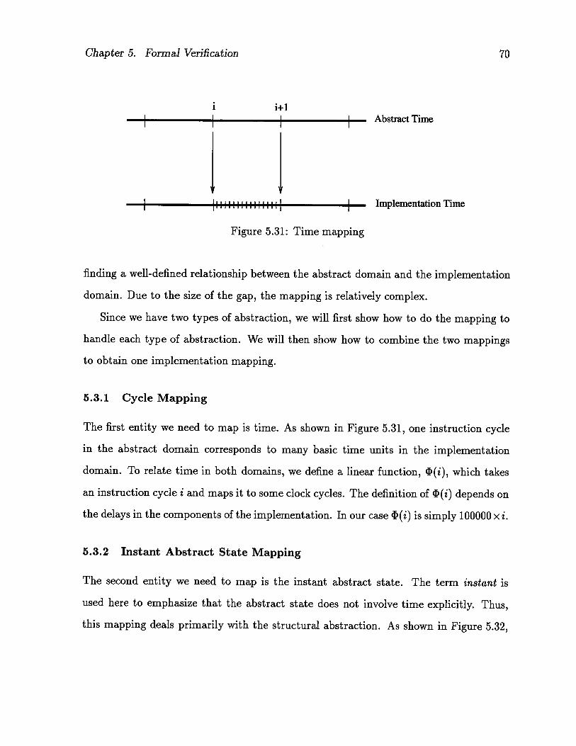
Chapter 5. Formal Verification 70
I I
I IiiiiiiiiiiiiiiI IFigure 5.31: Time mapping
finding a well-defined relationship between the abstract domain and the implementation
domain. Due to the size of the gap, the mapping is relatively complex.
Since we have two types of abstraction, we will first show how to do the mapping to
handle each type of abstraction. We will then show how to combine the two mappings
to obtain one implementation mapping.
5.3.1 Cycle Mapping
The first entity we need to map is time. As shown in Figure 5.31, one instruction cycle
in the abstract domain corresponds to many basic time units in the implementation
domain. To relate time in both domains, we define a linear function, (i), which takes
an instruction cycle i and maps it to some clock cycles. The definition of (i) depends on
the delays in the components of the implementation. In our case (i) is simply 100000 x i.
5.3.2 Instant Abstract State Mapping
The second entity we need to map is the instant abstract state. The term instant is
used here to emphasize that the abstract state does not involve time explicitly. Thus,
this mapping deals primarily with the structural abstraction. As shown in Figure 5.32,
i+1Abstract Time
Implementation Time
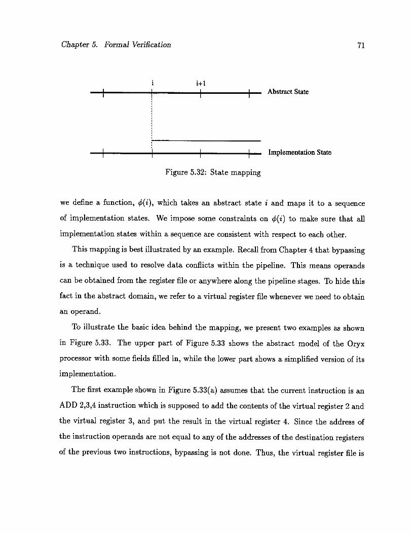
Chapter 5. Formal Verification 71
1 i+ I
I I Abstract State
Implementation State
Figure 5.32: State mapping
we define a function, q(i), which takes an abstract state i and maps it to a sequence
of implementation states. We impose some constraints on (i) to make sure that all
implementation states within a sequence are consistent with respect to each other.
This mapping is best illustrated by an example. Recall from Chapter 4 that bypassing
is a technique used to resolve data conflicts within the pipeline. This means operands
can be obtained from the register file or anywhere along the pipeline stages. To hide this
fact in the abstract domain, we refer to a virtual register file whenever we need to obtain
an operand.
To illustrate the basic idea behind the mapping, we present two examples as shown
in Figure 5.33. The upper part of Figure 5.33 shows the abstract model of the Oryx
processor with some fields filled in, while the lower part shows a simplified version of its
implementation.
The first example shown in Figure 5.33(a) assumes that the current instruction is an
ADD 2,3,4 instruction which is supposed to add the contents of the virtual register 2 and
the virtual register 3, and put the result in the virtual register 4. Since the address of
the instruction operands are not equal to any of the addresses of the destination registers
of the previous two instructions, bypassing is not done. Thus, the virtual register file is

Chapter 5. Formal Verification 72
/
Abstract Domain
(N
(a)
/
Abstract Domain
N
(b)
2 Src1
Src2
4 6 7 Dest-
- VRF[21
JL VRF[31
0
Src1Src2
4 3 7 Dest-
- -- VRF[2]
--u VRF[31
, S2
/ EXEout’
MEMout
I2 10 11
3 15 EXEout
MEMout
Figure 5.33: Register file mapping
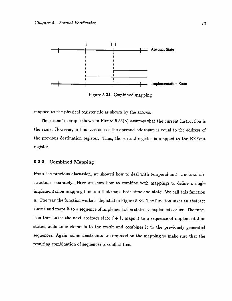
Chapter 5. Formal Verification 73
i+1I
‘ Abstract State
Implementation State
Figure 5.34: Combined mapping
mapped to the physical register file as shown by the arrows.
The second example shown in Figure 5.33(b) assumes that the current instruction is
the same. However, in this case one of the operand addresses is equal to the address of
the previous destination register. Thus, the virtual register is mapped to the EXEout
register.
5.3.3 Combined Mapping
From the previous discussion, we showed how to deal with temporal and structural ab
straction separately. Here we show how to combine both mappings to define a single
implementation mapping function that maps both time and state. We call this function
t. The way the function works is depicted in Figure 5.34. The function takes an abstract
state i and maps it to a sequence of implementation states as explained earlier. The func
tion then takes the next abstract state i + 1, maps it to a sequence of implementation
states, adds time elements to the result and combines it to the previously generated
sequences. Again, some constraints are imposed on the mapping to make sure that the
resulting combination of sequences is conflict-free.
Chapter 5. Formal Verification 74
5.4 Verification Condition
To establish the correctness of the Oryx processor, we need to show the following is true:
VA,O if A NO then j=M 1u(A= IrO)
This basically says that if some properties hold in the abstract domain, then we can
prove that the same properties hold in the implementation domain by using implemen
tation mapping.
5.5 Practical Verification
In this section, we demonstrate how to write implementation mapping functions in the
FL language. We also show how to use STE to prove properties of the Oryx processor.
To illustrate implementation mappings, consider the following simple example of an
output signal:
let DCacheAddris cyc dv = DCacheAddr isv dvfrom ((Phi2F (cyc+2))+LatchDelay)to ((Phi2F (cyc+4))+LatchDelay);
The DCacheAddris function takes two arguments, an abstract cycle number (cyc) and
a data vector (dv). This function basically says that the DCache address output pads
of the Oryx processor take on the value dv for a period of time. The abstract time is
mapped to implementation time with the help of the Phi2F function. The DCacheAddris
function also takes into account set-up time and hold time of the data value.
A more sophisticated example of implementation mapping is given below:
let VRegFile cyc addr dv instrlist =
let BypassFromEze = BypassFromExe addr instrlist inlet BypassFroniMem = BypassFromNem addr instrlist inlet NoBypass = (NOT BypassFromExe) AND (NOT BypassFromMem) in(if (BypassFromExe) (EXEoutis (cyc+1) dv))(if (BypassFromNem) (MEMoutis (cyc+1) dv)) @(if (NoBypass) (RegFileis (cyc+1) addr dv))
Chapter 5. Formal Verification 75
The VRegFile function takes four arguments: an abstract cycle number, a register
address, a data vector, and an instruction list. The function compares the register address
with the destination register address of the previous two instructions and determines the
bypassing conditions. Given the bypassing conditions, the function then asserts or checks
the appropriate values at the appropriate time.
At this point, we are ready to show how to verify a property of the Oryx processor.
Recall that the instructions of the Oryx processor fall into four classes of which the third
class is the ALU and shift instructions. Thus, we write a function called VerifyClass3lnstr
as shown below:
let VerifyClass3lnstr =
let Newlnstr = (hd NewlnstrList) inlet Ra = RaAddr Newlnstr inlet Rb = RbAddr Newlnstr inlet Rd = RdAddr Newlnstr inlet Ant =
(GenOryxClock Clocks) ®
(Reset is F from (Cycle 0) to (Cycle Clocks)) @(Exception is F from (Cycle 0) to (Cycle Clocks)) @(Squash is F from (Cycle 0) to (Cycle Clocks)) 0(AssignState 1 ControlList InstrList) 0(if (GlobalConstraint) (
(if (TakesTwoSources U V NewlnstrList OldlnstrList)((VRegFile (Target) Ra U OldlnstrList) 0(VRegFile (Target) Rb V OldlnstrList))) 0
(if (TakesOneSource U V NewlnstrList OldlnstrList)(VRegFile (Target) Ra U OldlnstrList))
)) inlet Cons =
(if (GlobalConstraint)
((if (TakesTwoSources U V NewlnstrList OldlnstrList)(EvaluateClass3lnstrFirst Target Rd Newlnstr OldlnstrList U V)) 0
(if (TakesOneSource U V NewlnstrList OldlnstrList)(EvaluateClass3lnstrSecond Target Rd Newlnstr OldlnstrList U V))
)) in(nverify Options Oryx VarList Ant Cons TraceList);
When we evaluate this function, it will check if the shifter and ALU perform correctly,
the control logic and bypass logic are correct, and reading from and writing to the register
file are done properly. The time it takes the Voss system to evaluate the function for
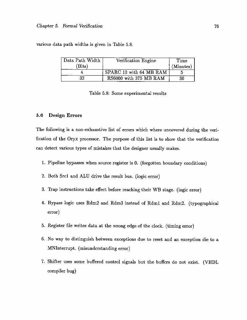
Chapter 5. Formal Verification 76
various data path widths is given in Table 5.8.
Data Path Width Verification Engine Time(Bits) (Minutes)
4 SPARC 10 with 64 MB RAM 532 RS6000 with 375 MB RAM 30
Table 5.8: Some experimental results
5.6 Design Errors
The following is a non-exhaustive list of errors which where uncovered during the veri
fication of the Oryx processor. The purpose of this list is to show that the verification
can detect various types of mistakes that the designer usually makes.
1. Pipeline bypasses when source register is 0. (forgotten boundary conditions)
2. Both Srcl and ALU drive the result bus. (logic error)
3. Trap instructions take effect before reaching their WB stage. (logic error)
4. Bypass logic uses Rdm2 and Rdm3 instead of Rdml and Rdm2. (typographical
error)
5. Register file writes data at the wrong edge of the clock. (timing error)
6. No way to distinguish between exceptions due to reset and an exception die to a
MNlnterrupt. (misunderstanding error)
7. Shifter uses some buffered control signals but the buffers do not exist. (VHDL
compiler bug)
Chapter 6
Concluding Remarks and Future Work
In this thesis, we established that symbolic trajectory evaluation is an effective and
practical technique for verifying even very complex digital systems. For demonstration
purposes, we designed and implemented a 32-bit RISC processor which is very similar to
many commercial RISC processors. We called it the Oryx processor.
Moreover, we showed how to describe the Oryx processor in an abstract domain.
The motivation for this is to avoid over-specifying the architecture and thus constrain
the implementation of the processor. In other words, our implementation of the Oryx
processor can be replaced with another implementation at any point of time without
having to change the specification. Only the circuit description and the implementation
mapping would have to be revised. We also showed how to relate the abstract model
of the Oryx processor to its pipelined implementation using implementation mappings.
Finally, we used the Voss system to carry out the practical verification of the Oryx
processor.
Although we have not completely verified the processor, the properties verified were
sufficiently complex that we do not foresee any major difficulties in completing the veri
fication. However, to complete the verification we estimate would require 3-6 additional
man months. Furthermore, the work has been a very good learning experience. We now
have a much better understanding of the verification problem which will be an asset
towards any future work.
77
Chapter 6. Concluding Remarks and Future Work 78
Like other related verification work, we realize the need to develop a general method
ology for verifying this type of systems. We have already began the development of such
methodology, but more research is still needed. First, due to the complexity of the sys
tems we are dealing with, it would be ideal if we can break down the major verification
task into smaller tasks and then use result composition to establish the correctness of the
system. Result composition can be used in the abstract domain or in the implementation
domain. However, showing that composing a sequence of results in the abstract domain
would give the same result if we compose the corresponding sequence in the implementa
tion domain is subject to future work. Second, finding the relation between the abstract
domain and the implementation domain is a very tedious job. A better way is needed to
analyze the mapping conditions to ensure correct mappings.
The application of symbolic trajectory evaluation for the verification of RISC proces
sors is only one example of what type of systems we can verify using this technique. The
general framework we presented can be adapted to verify other systems as well. This
work is by no means a complete solution to the verification problem. However, we think
that it is a good start and a very practical way to establish the correctness of this type
of systems.
Bibliography
[1] Derek Beatty. A Methodology for Formal Hardware Verification with Application toMicroprocessors. Ph.D. Thesis, CMU-CS-93-190, Department of Computer Science,Carnegie Mellon University, 1993.
[2] Graham Birtwistle and P.A. Subrahmanyam. VLSI Specification, Verification andSynthesis. Kiuwer Academic Publishers, Boston, 1988.
[3] Randal Bryant. “Graph-Based Algorithms for Boolean Function Manipulation”.IEEETC, Vol. C-35, No. 8, August 1986, pp. 677-691.
[4] Jerry R. Burch and David L. Dill. “Automatic Verification of Pipelined Microprocessor Control”. CAV ‘9j: Proceedings of the Sixth International Conference onComputer-Aided Verification. Lecture Notes in Computer Science 818, Springer-Verlag, June 1994, pp. 68-80.
[5] Paul Chow. The MIPS-X RISC Microprocessor. Kiuwer Academic Publishers,Boston, 1989.
[6] Mohammad Darwish. Design of a 32-bit Pipelined RISC Processor. Technical Reportin preparation.
[7] Scott Hazelhurst and Carl-Johan Seger. “Composing Symbolic Trajectory Evaluation Results”. CAV ‘94: Proceedings of the Sixth International Conference onComputer-Aided Verification. Lecture Notes in Computer Science 818, Springer-Verlag, June 1994, pp. 273-285.
[8] J. L. Hennessy. “Designing a computer as a microprocessor: Experience and lessonsfrom the MIPS 4000”. A lecture at the Symposium on Integrated Systems, Seattle,Washington, 1993.
[9] J. L. Hennessy and D. A. Patterson. Computer Architecture: A Quantitative Approach. Morgan Kaufman Publishers, San Mateo, 1990.
[10] Lee Howard. “The design of the SPARC processor”. A lecture at the University ofBritish Columbia, Vancouver, British Columbia, 1994.
[11] D. A. Patterson and 3. L. Hennessy. Computer Organization and Design: The Hardware/Software Interface. Morgan Kaufman Publishers, San Mateo, 1994.
79

Bibliography 80
[12] S. Mirapuri, M. Woodacre, and N. Vasseghi. “The MIPS R4000 Processor”. IEEEMicro, April 1992, pp. 10-22.
[13] Carl-Johan Seger. Voss - A Formal Hardware Verification System: User’s Guide.Technical Report UBC-CS-93-45, Department of Computer Science, University ofBritish Columbia, Vancouver, British Columbia, 1993.
[14] Carl-Johan Seger. An Introduction to Formal Hardware Verification. TechnicalReport UBC-CS-92-13, Department of Computer Science, University of BritishColumbia, Vancouver, British Columbia, 1992.
[15] Carl-Johan Seger and Randal Bryant. Formal Verification by Symbolic Evaluationof Partially-Ordered Trajectories. Technical Report UBC-CS-93-8, Department ofComputer Science, University of British Columbia, Vancouver, British Columbia,1993.
[16] Mandayam Srivas and Mark Bickford. “Formal Verification of a Pipelined Microprocessor”. IEEE Software, September 1990, pp. 52-64.
[17] Daniel Tabak. RISC Systems. Research Studies Press Ltd., England, 1990.
[18] Sofiene Tahar and Ramayya Kumar. “Implementing a Methodology for FormallyVerifying RISC Processors in HOL”. HUG ‘93: Proceedings of the Sixth InternationalWorkshop on Higher Order Logic Theorem Proving and its Applications. LectureNotes in Computer Science 780, Springer-Verlag, August 1993, pp. 281-294.
Appendix A
The FL Verification Script
II include some libraries
load “verification.fl”;load “arithm.f1”;load “HighLowEx f1”;load “OryxLib.f1”;
II define timing parameters
let ClockPeriod = 2000000;let ScaleFactor = 20;let CycleLength = ClockPeriod/ScaleFactor;let LatchDelay = 100000/ScaleFactor;let Setup = 100000/ScaleFactor;let Iold = lO/ScaleFactor;
// define clock phases
let PhilRof± = 10*CycleLength/100;
let PhilFoff = 36*CycleLength/100;
let Phi2Roff = 60*CycleLength/100;let Phi2Foff = 85*CycleLength/100;let PhilF i = (Cycle (i—1))+PhilFoff;let PhilR i = (Cycle (i—1))+Philftoff;let Phi2F i = (Cycle (i—1))+Phi2Foff;let Phi2R i = (Cycle (i—1))+Phi2Roff;let Cycle k = (k)*CycleLength;
II define implementation parameters
let DataWidth = 32;let InstrWidth = 32;let DataAddrWidth = 32;let InstrAddrWidth = 32;let FPRegAddrWidth = 5;let RxAddrWidth = 5;
81
Appendix A. The FL Verification Script 82
let RegFileSize = 32;let CompFiincWidth = 12;let OpcodeWidth = 5;
II short—hands for clock signals
let Phil = ‘1Phil”;let Phi2 = ‘Phi2’;
7/ define two-phase non—overlapping clock signals
letrec GenPhil n = (n0) > (UNC for 0) I(((((Phil is F for PhilRoff) then
(Phil is T for (PhilFoff — PhilRoff))) then(Phil is F for (Phi2Roff — PhilFoff))) then(Phil is F for (Phi2Foff — Phi2Roff))) then(Phil is F for (CycleLength — Phi2Foff))) then(GenPhil (n—l));
letrec GenPhi2 n = (n0) > (UNC for 0) I(((((Phi2 is F for PhilRoff) then
(Phi2 is F for (PhilFoff — PhilRoff))) then(Phi2 is F for (Phi2Roff — PhilFoff))) then(Phi2 is T for (Phi2Foff — Phi2Roff))) then(Phi2 is F for (CycleLength — Phi2Foff))) then(GenPhi2 (n—l));
let GenOryxClock n (GenPhil n) @ (GenPhi2 n)
II define histories of length (n)
letrec GenControl n 1 = (n0) > 1 Ilet new = [F,F,F,F,TT] inlet ni = new:l inGenControl (n—l) nl;
letrec GenData n 1 = (n0) > 1 Ilet new = (variable_vector (“DCacheln.”(int2str (n—l))”.”)
DataWidth) inlet nl = new:l inGenData (n—l) ni;
letrec Genlnstr n 1 = (n0) > 1 Ilet new = (variable_vector (“ICache.”(int2str (n—l))”.)
InstrWidth) inlet nl = new:l in
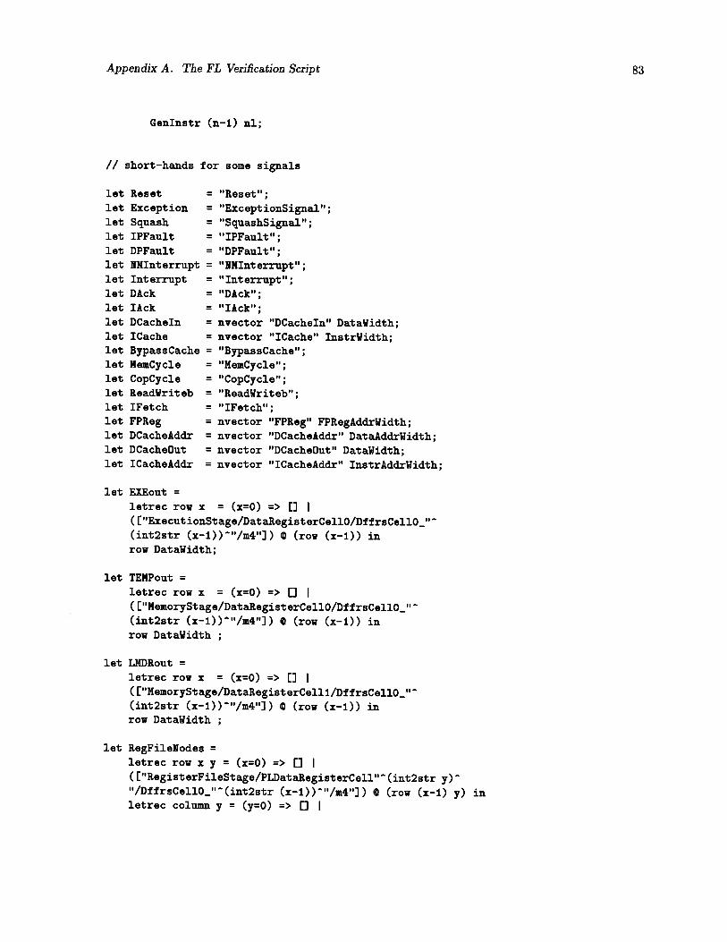
Appendix A. The FL Verification Script 83
Genlnstr (n—i) nl;
II short—hands for some signals
let Reset = “Reset”;let Exception = “ExceptionSignal”;let Squash = “SquashSignal”;let IPFault = “IPFault”;let DPFault = “DPFault”;let NMlnterrupt = “NMlnterrupt”;let Interrupt = “Interrupt”;let DAck = “DAck”;let lAck = “lAck”;let DCacheln = nvector “Dcacheln” DataWidth;let ICache = nvector “ICache” InstrWidth;let BypassCache = “BypassCache”;let MemCycle = “MemCycle”;let CopCycle = “CopCycle”;let ReadWriteb = “ReadWriteb”;let IFetch = “IFetch”;let FPReg = nvector “FPReg” FPRegAddrWidth;let DCacheAddr = nvector “DCacheAddr” DataAddrWidth;let OCacheOut = nvector “DCacheOut” DataWidth;let ICacheAddr = nvector “ICacheAddr” InstrAddrWidth;
let EXEout =
letrec row x = (x0) > E] I([“ExecutionStage/DataRegisterCellO/DffrsCellO_”(int2str (x—i)Y”/m4”]) Q (row (x—i)) inrow DataWidth;
let TEMPout =
letrec row x = (x0) > C] I(E”MemoryStage/DataRegisterCellO/DffrsCellO...”(int2str (x—i)Y”/m4”]) C (row (x—1)) inrow DataWidth
let LMDRout =
letrec row x = (x0) > C] I(C”MemoryStage/DataRegisterCelli/DffrsCellO_”(int2str (x—i)Y”/m4”]) C (row (x—i)) inrow DataWidth
let RegFileliodes =
letrec row x y = (x0) > C] I([“RegisterFileStage/PLDataRegisterCell”(int2str yY“/DffrsCellO...”(int2str (x—i)”/m4”]) C (row (x—i) y) inletrec column y = (y0) > C] I
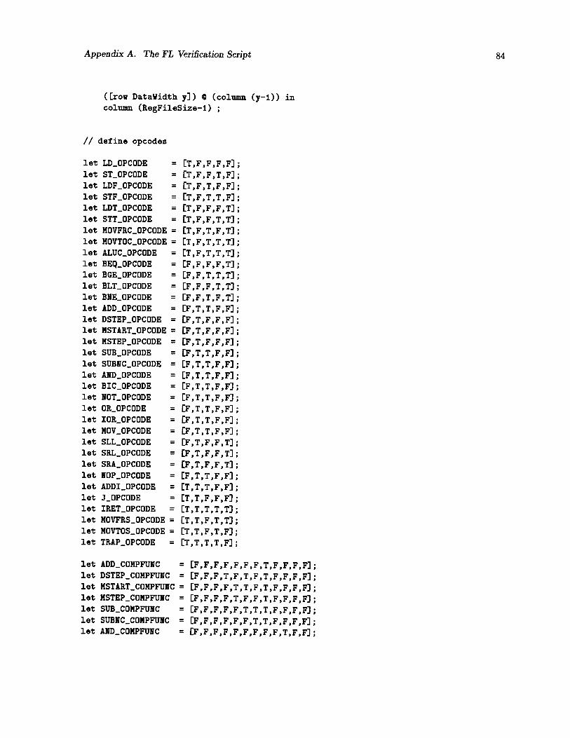
Appendix A. The FL Verification Script 84
([row DataWidth y]) C (column (y—i)) incolumn (RegFileSize—1)
II define opcodes
let L.D_OPCODE = [T,F,F,F,F];let ST_OPCODE = [T,F,F,T,F];let LDF_OPCODE = [T,F,T,F,F];let STF_OPCODE = ET,FT,T,F];let LDT_OPCODE = [T,F,F,F,T];let STT_OPCODE — [T,F,FIT,T],let MOVFRC_OPCODE = [T,F,T,F,T];let MOVTOC_OPCODE = [T,F,T,T,T];let ALUC_OPCODE = [T,F,T,T,T];let BEQ_OPCODE = [F,F,F,F,T];let BGE_OPCODE — [F,F,T,T,T],let BLT_OPCODE — [F,F,F,TIT],let BNE_OPCODE = [F,F,T,F,T];let ADD_OPCODE = [F,T,T,F,F];let DSTEP_OPCODE = EF,T,F,F,F];let MSTART_OPCODE = [F,T,F,F,F];let MSTEP_OPCODE = EF,T,F,F,F];let SUB_OPCODE = [F,T,T,F,F];let SUBNC_OPCODE — [F,T,T,F,F],let AND_OPCODE — [F,T,T,F,F],let BIC_OPCODE — [F,T,T,F,F],let NOT_OPCODE — [F,T,T,F,F],let OR_OPCODE = [F,T,T,F,F];let XOR_OPCODE = [F,T,T,F,F];let NOV_OPCODE = [F,T,T,F,F];let SLL_OPCODE = EF,T,F)F,T];let SRL_OPCODE = [F,T,F,F,T];let SRA_OPCODE = [F,T,F,F,T];let NOP_OPCODE
— [F,T,T,FIF],let ADDI_OPCODE — [T,T,T,F,F],let J_OPCODE = [T,T,F,F,F];let IRET_OPCODE = [T,T,T,T,T];let MOVFRS_OPCODE = [T,T,F,T,T];let MOVTOS_OPCODE = [T,T,F,T,F];let TRAP_OPCODE = ET,T,T,T,FJ;
let ADD_COMPFUNC = [F,F,F,F,F,F,F,T,F,F,F,F];let DSTEP_COMPFUNC — [F,F,F)T,F,T,F,T)F,F,F,F],let MSTART_COMPFUNC - [F,F,F,F,T,T,F,T,F,F,F,F],let NSTEP_COMPFUNC = [F,F,F,F,T,F,F,T,F,F,F,F];let SUB...COMPFUNC = [F,F,F,F,F,T,T,T,F,F,F,F];let SUBNC_COMPFUNC
— [F,F,F,F,F,F,T,T,F,F,F,F],let AND_COMPFUNC = [F,F,F,F,F,F,F,F,F,T,F,F];
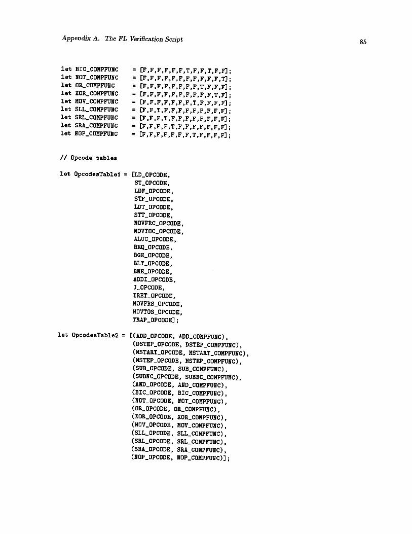
Appendix A. The FL Verification Script 85
let BIC_COMPFUNC = [F,F,F,F,F,F,T,F,F,T,F,F];let NOT_COMPFUNC = [F,F,F,F,F,F,F,F,F,F,F,T];let OR_COMPFUNC = EF,F,F,F,F,F,F,F,T,F,F,F];let XOR_COMPFUNC = [F,F,F,F,F,F,F,F,F,F,T,F];let MOV_COMPFUNC = [F,F,F,F,F,F,F,T,F,F,F,FJ;let SLL_COMPFUNC = EF,F,T,F,F,F,F,F,F,F,F,F],let SRLCOMPFUNC - EF,F,F,T,F,F,F,F,F,F,F,F],let SRA_COMPFUNC — CF,F,F,F,T,F,F,F,F,F,F,F],let NOP_COMPFUNC — [F,F,F,F,F,F,F,T,F,F,F,F],
II Opcode tables
let OpcodesTablel = CLD_OPCODE,ST...OPCODE,LDF_OPCODE,STF_OP CODE,LDT_OPCODE,STT_OPCODE,MOVFRC_OP CODE,MOVTOC_OPCODE,ALUC_OPCODE,BEQ_OPCODE,BGE_OPCODE,BLT_OPCODE,BNE_OPCODE,ADDI_OPCODE,J_OPCODE,IRET_OPCODE,MOVFRS.OPCODE,MOVTOS_OPCODE,TRAP_OPCODE];
let OpcodesTable2 = [(ADD_OPCODE, ADLLCOMPFUNC),(DSTEP_OPCODE, DSTEP_COMPFUNC),(MsTART_OPCODE, MSTART_COMPFUNC),(MsTEP_OPCODE, MSTEP_COZ1PFUNC),(SUB_OPCODE, SUB_COMPFUNC),(SUBNC_OPCODE, SUBNC_COMPFUNC),(AND_OPCODE, AND_COMPFUNC),(BIC_OPCODE, BIC_CONPFUNC),(NOT_OPCODE, NOT_COMPFUNC),(OR_OPCODE, OR_COMPFUNC),(XOR_OPCODE, XO&..COMPFUNC),(MOV_OPCODE, MOV_COMPFUNC),(SLL_OPCODE, SLL_CONPFUNC),(sRL_OPCODE, SRL_COMPFUNC),(SRA_OPCODE, SRA_COMPFUNC),(NOP_OPCODE, NOP.COMPFUNC)];
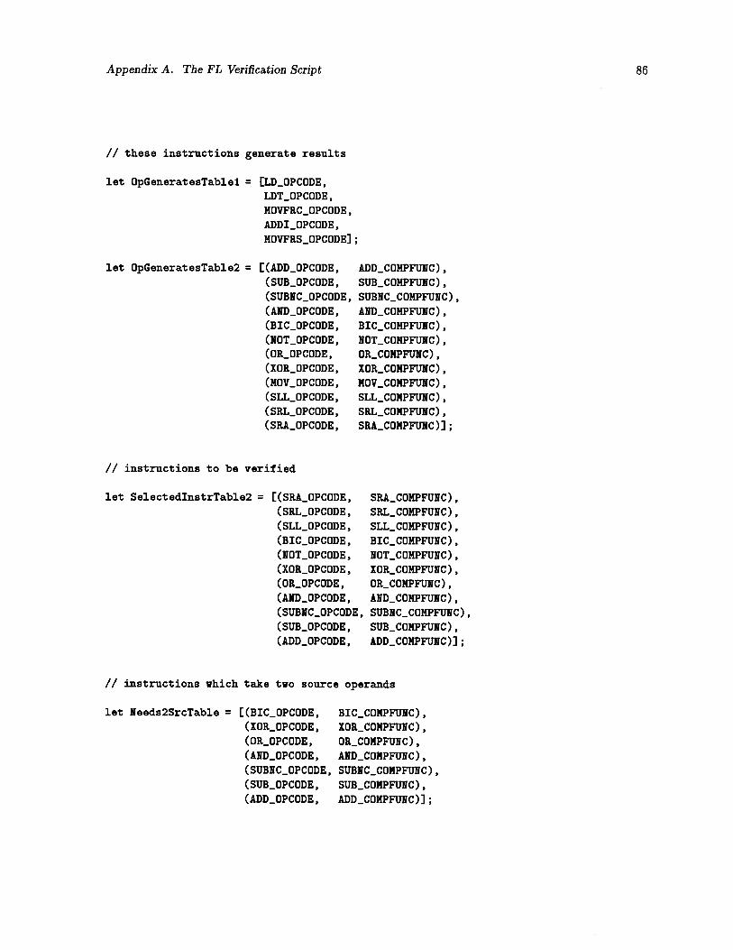
Appendix A. The FL Verification Script 86
II these instructions generate results
let OpGeneratesTablel = ELD_OPCODE,LDT_OPCODE,MOVFRC_OPCODE,
ADDI_OPCODE,
MOVFRS_OPCODE];
let OpGeneratesTable2 = C(ADD_OPCODE, ADD_COMPFUNC),
(sUB_0Pc0DE, SUB_COMPFUNC),(SUBNC_OPCODE, SUBNC_COMPFUNC),(AND_OPCODE, AND_COMPFUNC),(BIc_0Pc0DE, BIC_CONPFUNC),
(NOT_OPCODE, NOT_COMPFUNC),(0R_0Pc0DE, OR_COMPFUNC),
(XOR_OPCODE, XOR_COMPFUNC),
(MOV_OPCODE, MOV_COMPFUNC),(SLL_OPCODE, SLL_COMPFUNC),(SRL_OPCODE, SRL_COMPFUNC),(SRA_OPCODE, SRA_COMPFUNC)];
II instructions to be verified
let SelectedlnstrTable2 = E(SRA_OPCODE, SRA_COMPFUNC),(SRL_OPCODE, SRL.COMPFUNC),(SLL_OPCODE, SLL...COMPFUJC),(BIc_oPcoDE, BIC_COMPFUJC),(N0T_oPcooE, NOT_COMPFUNC),(x0R_oPcoDE, XOR_COMPFUNC),
(0R_oPcoDE, OR....COMPFUNC),(AND_OPCODE, AND_CONPFUNC),(SUBNC_OPCODE, SUBNC_COMPFUNC),(SUB_OPCODE, SUB_COMPFUNC),(ADD_OPCODE, ADD_COMPFUNC)];
II instructions which take two source operands
let Needs2SrcTable = E(BIC_OPCODE, BIC_COMPFUNC),
(xoR_0Pc0DE, XOR_COMPFUNC),
(oR_oPcoDE, OR_COMPFUNC),
(AND_OPCODE, AND_COMPFUNC),(SUBNC_OPCODE, SUBNC_COMPFUNC),
(SUB_OPCODE, SUB_COMPFUNC),
(ADD_OPCODE, ADD_COMPFUNC)J;
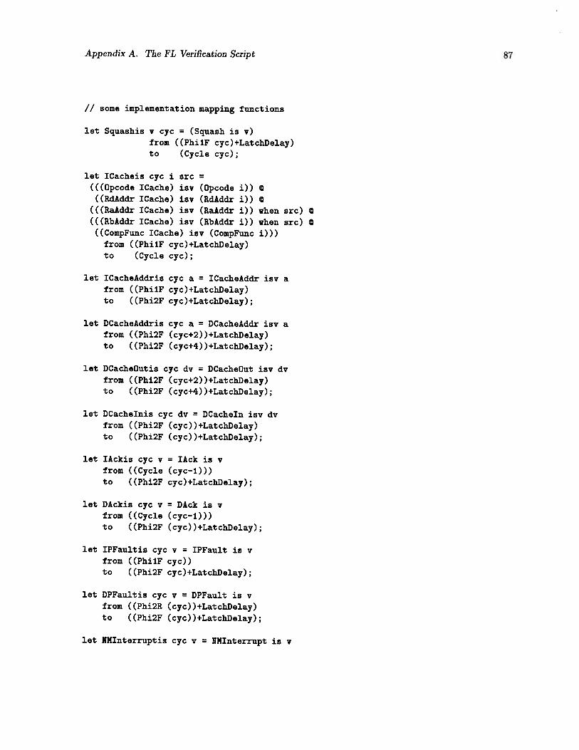
Appendix A. The FL Verification Script 87
II some implementation mapping functions
let Squashis v cyc = (Squash is v)from ((PhilF cyc)+LatchDelay)to (Cycle cyc);
let ICacheis cyc i src =
(((Opcode ICache) isv (Opcode i))((RdAddr ICache) isv (RdAddr i))
(((RaAddr ICache) isv (RaAddr i)) when src)(((RbAddr ICache) isv (RbAddr i)) when src) ®
((CompFunc ICache) isv (CompFunc i)))from ((PhilF cyc)+LatchDelay)to (Cycle cyc);
let ICacheAddris cyc a = ICacheAddr isv afrom ((PhilF cyc)+LatchDelay)to ((Phi2F cyc)+LatchDelay);
let DCacheAddris cyc a = DCacheAddr isv afrom ((Phi2F (cyc+2))+LatchDelay)to ((Phi2F (cyc+4))+LatchDelay);
let DCacheOutis cyc dv = DCacheOut isv dvfrom ((Phi2F (cyc+2))+LatchDelay)to ((Phi2F (cyc+4))+LatchDelay);
let DCachelnis cyc dv = DCacheln isv dvfrom ((Phi2F (cyc)H-LatchDelay)to ((Phi2F (cyc))+LatchDelay);
let lAckis cyc v = lAck is vfrom ((Cycle (cyc—1)))to ((Phi2F cyc)+LatchDelay);
let DAckis cyc v = DAck is vfrom ((Cycle (cyc—1)))to ((Phi2F (cyc))+L.atchDelay);
let IPFaultis cyc v = IPFault is vfrom ((PhilF cyc))to ((Phi2F cyc)+LatchDelay);
let DPFaultis cyc v = DPFault is vfrom ((Phi2R (cyc))+LatchDelay)to ((Phi2F (cyc))+LatchDelay);
let NMlnterruptis cyc v = NMlnterrupt is v
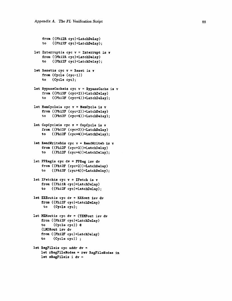
Appendix A. The FL Verification Script 88
from ((Phi2R cyc)+LatchDelay)to ((Phi2F cyc)+LatchDelay);
let Interruptis cyc v = Interrupt is V
from ((Phi2R cyc)+LatchDelay)to ((Phi2F cyc)+LatchDelay);
let Resetis cyc v = Reset is vfrom (Cycle (cyc—1))to (Cycle cyc);
let BypassCacheis cyc v BypassCache is vfrom ((Phi2F (cyc+2))+LatchDelay)to ((Phi2F (cyc+4))+LatchDelay);
let MemCycleis cyc v = NemCycle is vfrom ((Phi2F (cyc+2))+Latchoelay)to ((Phi2F (cyc+4))+LatchDelay);
let CopCycleis cyc v = CopCycle is vfrom ((Phi2F (cyc+2))+LatchDelay)to ((Phi2F (cyc+4))+Latchflelay);
let ReadWritebis cyc v = ReadWriteb is vfrom ((Phi2F (cyc+2))+LatchDelay)to ((Phi2F (cyc+4))+LatchDelay);
let FPRegis cyc dv = FPReg isv dvfrom ((Phi2F (cyc+2))+LatchDelay)to ((Phi2F (cyc+4))+LatchDelay);
let IFetchis cyc v = IFetch is vfrom ((PhilR cyc)+LatchDelay)to ((Phi2F cyc)+LatchDelay);
let EXEoutis cyc dv = EXEout isv dvfrom ((Phi2F cyc)+LatchDelay)to (Cycle cyc);
let MEMoutis cyc dv = (TEMPout isv dvfrom ((Phi2F cyc)+LatchDelay)to (Cycle cyc))
(LMDRout isv dvfrom ((Phi2F cyc)+LatchDelay)to (Cycle cyc))
let RegFileis cyc addr dv =
let rRegFileNodes = rev RegFileNodes inlet sRegFileis i dv =
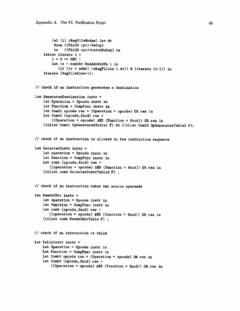
Appendix A. The FL Verification Script 89
(el (i) rRegFileNodes) isv dvfrom ((Phi2R cyc)—Setup)to ((Phi2R cyc)+LatchDelay) in
letrec iterate i =
i = 0 => UNC Ilet iv = num2bv RxAddrWidth i in
(if (iv = addr) (sRegFileis i dv)) (iterate (i—i)) initerate (RegFileSize—1);
// check if an instruction generates a destination
let GeneratesDestination instr =
let Operation = Opcode instr inlet Function = CompFunc instr inlet Combi opcode res = (Operation = opcode) OR res inlet Comb2 (opcode,fncd) res =
((Operation = opcode) AND (Function fncd)) OR res in(itlist Combi OpGeneratesTablel F) OR (itlist Comb2 OpGeneratesTable2 F);
II check if an instruction is allowed in the instruction sequence
let Selectedlnstr instr =
let operation = Opcode instr inlet function = CompFunc instr inlet comb (opcode,fncd) res =
((operation = opcode) AND (function = fncd)) OR res in(itlist comb SelectedlnstrTable2 F)
II check if an instruction takes two source operands
let Needs2Src instr =
let operation = Opcode instr inlet function = CompFunc instr inlet comb (opcode,fncd) res =
((operation = opcode) AND (function = fncd)) OR res in(itlist comb Needs2SrcTable F)
II check if an instruction is valid
let Validlnstr instr =
let Operation = Opcode instr inlet Function = CompFunc instr inlet Combi opcode res = (Operation = opcode) OR res inlet Comb2 (opcode,fncd) res =
((Operation = opcode) AND (Function = fncd)) OR res in
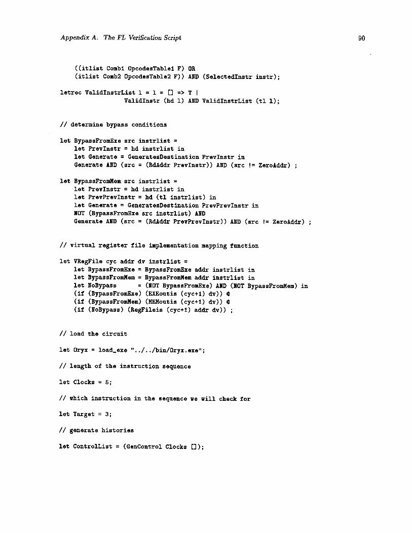
Appendix A. The FL Verification Script 90
((itlist Combi OpcodesTablel F) OR(itlist Comb2 OpcodesTable2 F)) AND (Selectedlnstr instr);
letrec ValidlnstrList 1 = 1 = C] > T IValidlnstr (hd 1) AND ValidlnstrList (tl 1);
II determine bypass conditions
let BypassFromExe src instrlist =
let Prevlnstr = hd instrlist inlet Generate = GeneratesDestination Prevlnstr inGenerate AND (src = (RdAddr Prevlnstr)) AND (src !t ZeroAddr)
let BypassFromMem src instrlist =
let Prevlnstr = hd instrlist inlet PrevPrevlnstr = hd (tl instrlist) inlet Generate = GeneratesDestination PrevPrevlnstr inNOT (BypassFromExe src instrlist) ANDGenerate AND (src = (RdAddr PrevPrevlnstr)) AND (src ZeroAddr)
II virtual register file implementation mapping function
let VRegFile cyc addr dv instrlist =
let BypassFromExe = BypassFromExe adds instrlist inlet BypassFromMem = BypassFromMem addr instrlist inlet NoBypass = (NOT BypassFromExe) AND (NOT BypassFromMem) in(if (BypassFromExe) (EXEoutis (cyc+1) dv)) @(if (BypassFromNem) (MEMoutis (cyc+1) dv)) ®(if (NoBypass) (RegFileis (cyc+1) addr dv))
/1 load the circuit
let Oryx = load_exe “. .1. ./bin/Oryx.exe”;
II length of the instruction sequence
let Clocks = 5;
II which instruction in the sequence we will check for
let Target = 3;
II generate histories
let ControlList = (GenControl Clocks []);
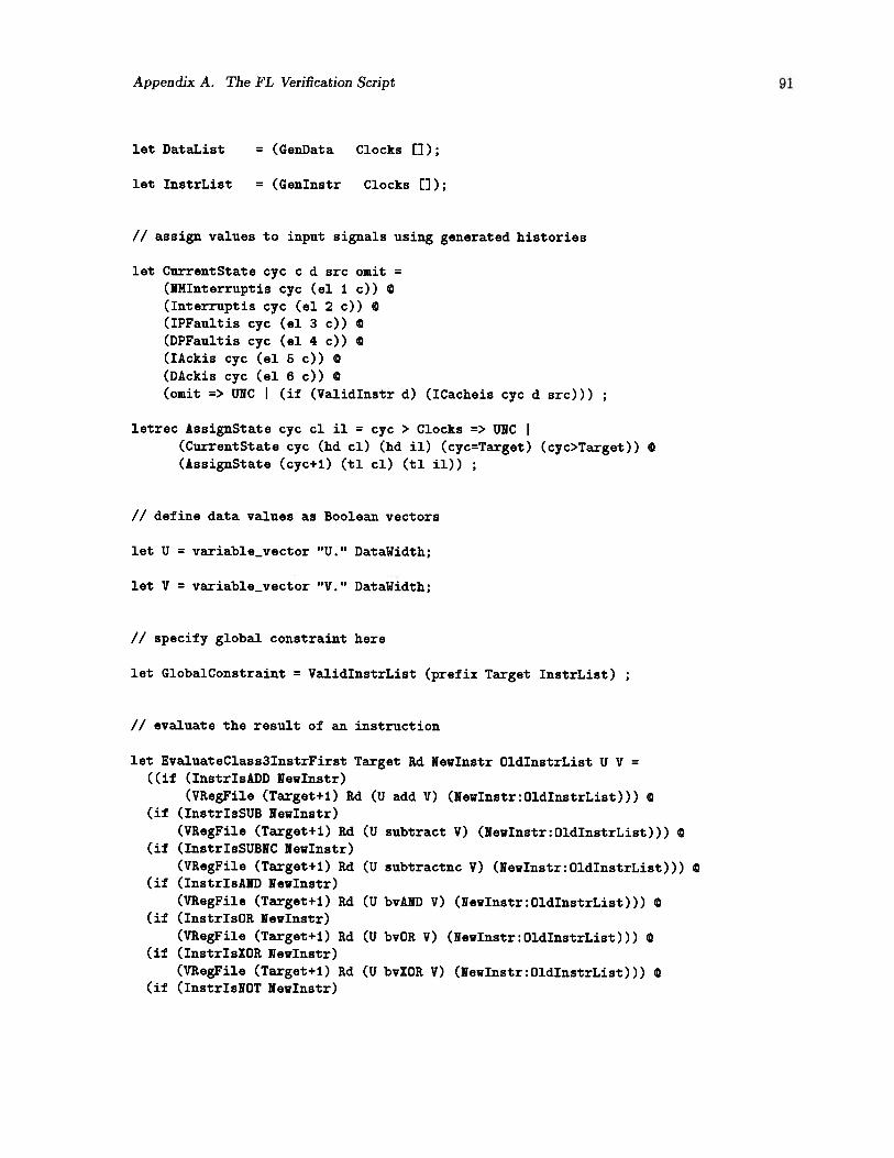
Appendix A. The FL Verification Script 91
let DataList = (GenData Clocks []);
let InstrList = (Genlnstr Clocks C]);
II assign values to input signals using generated histories
let CurrentState cyc c d src omit =
(NMlnterruptis cyc (el 1 c)) ®(Interruptis cyc (el 2 c)) 0(IPFaultis cyc (el 3 c)) 0
(DPFaultis cyc (el 4 c)) 0
(lAckis cyc (el 5 c)) 0
(DAckis cyc (el 6 c)) 0
(omit > UNC I (if (Validlnstr d) (ICacheis cyc d src)))
letrec AssignState cyc cl il = cyc > Clocks > UNC I(CurrentState cyc (hd cl) (hd il) (cyc=Target) (cyc>Target)) 0(AssignState (cyc+1) (tl cl) (tl il))
// define data values as Boolean vectors
let U = variable_vector “U.” DataWidth;
let V = variable_vector “V.” DataWidth;
II specify global constraint here
let GlobalConstraint = ValidlnstrList (prefix Target InstrList)
II evaluate the result of an instruction
let EvaluateClass3lnstrFirst Target Rd Newlnstr OldlnstrList U V =
((if (InstrIsADD Newlnstr)(VRegFile (Target+1) Rd (U add V) (Newlnstr:OldlnstrList))) 0
(if (InstrIsSUB Newlnstr)(VRegFile (Target+1) Rd (U subtract V) (Newlnstr:OldlnstrList))) 0
(if (InstrIsSUBNC Nevlnstr)(VRegFile (Target+1) Rd (U subtractnc V) (Newlnstr:OldlnstrList))) 0
(if (InstrIsAND Newlnstr)(VRegFile (Target+1) Rd (U bvAND V) (Newlnstr:OldlnstrList))) 0
(if (InstrlsOR Newlnstr)(VRegFile (Target+1) Rd (U bvOR V) (Newlnstr:OldlnstrList))) 0
(if (InstrIsXOR Newlnstr)(VRegFile (Target+1) Rd (U bvXOR V) (Newlnstr:OldlnstrList))) 0
(if (InstrIsNOT Newlnstr)
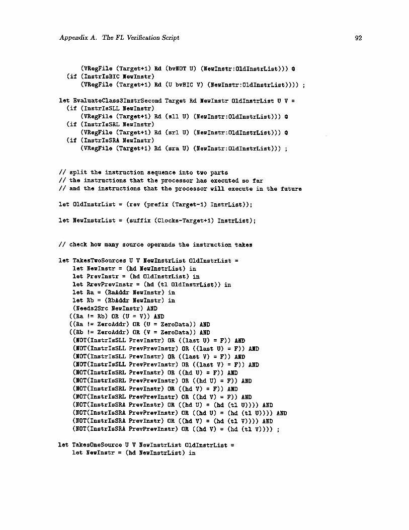
Appendix A. The FL Verification Script 92
(VRegFile (Target+i) Rd (bvNOT U) (Newlnstr:OldlnstrList)))
(if (InstrIsBIC Newlnstr)(VRegFile (Target+i) Rd (U bvBIC V) (Newlnstr:OldlnstrList))))
let EvaluateClass3lnstrSecond Target Rd Newlnstr OldlnstrList U V =(if (InstrIsSLL Newlnstr)
(VRegFile (Target+1) Rd (sll U) (Newlnstr:OldlnstrList)))
(if (InstrIsSRL Newlnstr)(VRegFile (Target+i) Rd (srl U) (Newlnstr:O].dlnstrList)))
(if (InstrIsSRA Newlnstr)(VRegFile (Target+i) Rd (sra U) (Newlnstr:OldlnstrList)))
II split the instruction sequence into two parts
// the instructions that the processor has executed so far
/1 and the instructions that the processor will execute in the future
let OldlnstrList = (rev (prefix (Target—i) InstrList));
let NewlnstrList = (suffix (Clocks—Target+i) InstrList);
II check how many source operands the instruction takes
let TakesTwoSources U V NewlnstrList OldlnstrList =let Newlnstr = (hd NewlnstrList) inlet Prevlnstr = (lid OldlnstrList) inlet PrevPrevlnstr = (hd (tl OldlnstrList)) inlet Ra = (RaAddr Newlnstr) inlet Rb = (RbAddr Newlnstr) in(Needs2Src Newlnstr) AND
((Ra Rb) OR (U = V)) AND((Ra = ZeroAddr) OR (U = ZeroData)) AND((Rb != Zerokddr) OR (V = ZeroData)) AND(NOT(InstrIsSLL Prevlnstr) OR ((last U) = F)) AND
(NOT(InstrIsSLL PrevPrevlnstr) OR ((last U) = F)) AND(NOT(InstrIsSLL Prevlnstr) OR ((last V) = F)) AND(NOT(InstrIsSLL PrevPrevlnstr) OR ((last V) = F)) AND(NOT(InstrIsSRL Prevlnstr) OR ((hd U) = F)) AND(NOT(InstrIsSRL Prevprevlnstr) OR ((hd U) = F)) AND(NOT(InstrIsSRL Prevlnstr) OR ((hd V) = F)) AND(NOT(InstrIsSRL Prevprevlnstr) OR ((hd V) = F)) AND(NOT(InstrIsSRA Prevlnstr) OR ((hd U) = (hd (tl U)))) AND(NOT(InstrIsSRA PrevPrevlnstr) OR ((lid U) = (hd (tl U)))) AND(NOT(InstrIsSRA Prevlnstr) OR ((hd V) = (hd (tl V)))) AND(NOT(InstrIsSRA PrevPrevlnstr) OR ((hd V) = (hd (tl V))))
let TakesOneSource U V NewlnstrList OldlnstrList =let Newlnstr = (hd NewlnstrList) in
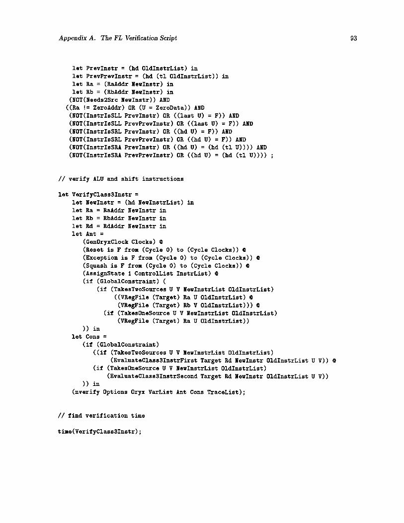
Appendix A. The FL Verification Script 93
let Prevlnstr = (hd OldlnstrList) inlet PrevPrevlnstr = (hd (tl OldlnstrList)) inlet Ra = (RaAddr Newlnstr) in
let Rb = (RbAddr Newlnstr) in(NOT(Needs2Src Newlnstr)) AND
((Ra ZeroAddr) OR (U = ZeroData)) AND
(NOT(InstrIsSLL Prevlnstr) OR ((last U) = F)) AND
(NOT(InstrIsSLL PrevPrevlnstr) OR ((last U) = F)) AND(NOT(InstrIsSRL Prevlnstr) OR ((hd U) = F)) AND(NOT(InstrIsSRL PrevPrevlnstr) OR ((hd U) = F)) AND(NOT(InstrIsSRA Prevlnstr) OR ((hd U) = (hd (tl U)))) AND(NOT(InstrIsSRA PrevPrevlnstr) OR ((hd U) = (hd (tl U))))
II verify ALU and shift instructions
let VerifyClass3lnstr =
let Newlnstr = (hd NewlnstrList) inlet Ra = RaAddr Newlnstr inlet Rb = RbAddr Newlnstr in
let Rd = RdAddr Newlnstr inlet Ant =
(GenOryxClock Clocks) 0
(Reset is F from (Cycle 0) to (Cycle Clocks)) 0(Exception is F from (Cycle 0) to (Cycle Clocks)) 0(Squash is F from (Cycle 0) to (Cycle Clocks)) 0(AssignState 1 ControlList InstrList) 0(if (GlobalConstraint) (
(if (TakesTwoSources U V NewlnstrList OldlnstrList)((VRegFile (Target) Ra U OldlnstrList) (0(VRegFile (Target) Rb V OldlnstrList))) (0
(if (TakesOneSource U V NewlnstrList OldlnstrList)(VRegFile (Target) Ra U OldlnstrList))
)) in
let Cons =
(if (GlobalConstraint)
((if (TakesTwoSources U V NewlnstrList OldlnstrList)(EvaluateClass3lnstrFirst Target Rd Newlnstr OldlnstrList U V)) 0
(if (TakesOneSource U V NewlnstrList OldlnstrList)(EvaluateClass3lnstrSecond Target Rd Newlnstr OldlnstrList U V))
)) in
(nverify Options Oryx VarList Ant Cons TraceList);
II find verification time
time(VerifyClass3lnstr);