A 50MS/s (35 mW) to 1-kS/s (15 /spl mu/W) power scaleable 10-bit pipelined ADC using rapid power-on...
10
2446 IEEE JOURNAL OF SOLID-STATE CIRCUITS, VOL. 40, NO. 12, DECEMBER 2005 A 50-MS/s (35 mW) to 1-kS/s (15 W) Power Scaleable 10-bit Pipelined ADC Using Rapid Power-On Opamps and Minimal Bias Current Variation Imran Ahmed, Student Member, IEEE, and David A. Johns, Fellow, IEEE Abstract—A novel rapid power-on operational amplifier and a current modulation technique are used in a 10-bit 1.5-bit/stage pipelined ADC in 0.18- m CMOS to realize power scalability between 1 kS/s (15 W) and 50 MS/s (35 mW), while maintaining an SNDR of 54–56 dB for all sampling rates. The current mod- ulated power scaling (CMPS) technique is shown to enhance the power scaleable range of current scaling by 50 times, allowing ADC power to be varied by a factor of 2500 while only varying bias currents by a factor of 50. Furthermore, the nominal power is reduced by 20%–30% by completely powering off the rapid power-on opamps during the sampling phase in the pipeline’s sample-and-holds. Index Terms—ADC, analog-to-digital conversion, CMOS, low power, pipeline, power reduction, power scaleable, reconfigurable, scaleable. I. INTRODUCTION A POWER-SCALEABLE ADC is motivated by flexible ap- plications where a single ADC is required to operate at different operating speeds. As ADCs are typically power opti- mized for only a single operating speed, a power scaleable ADC affords minimal power consumption over a broad range of op- erating speeds in a single circuit. In addition, a power-scaleable ADC is of great utility in reducing design efforts as a single ADC can be targeted for a variety of applications each with vastly different performance requirements with respect to power and speed. Thus, a power-scaleable ADC can reduce time to market and save costs associated in producing several individu- ally power-optimized ADCs. The power consumed by CMOS digital circuits explicitly scales with operating speed, , capacitive load, , and power supply , according to (ignoring leakage cur- rents). However, analog power (the dominant power consumer in ADCs) does not explicitly scale with sampling rate as it is mostly static in nature. Static analog power is a consequence of static bias currents used to bias transistors in the saturation region. Previous publications of high-speed power-scaleable Manuscript received April 15, 2005; revised July 1, 2005. This work was supported by the Natural Sciences and Engineering Research Council of Canada (NSERC). The authors are with the Department of Electrical and Computer Engi- neering, University of Toronto, Toronto, ON, M5S 3G4 Canada (e-mail: [email protected]; [email protected]). Digital Object Identifier 10.1109/JSSC.2005.856289 ADCs achieve power scalability by making operational ampli- fier (opamp) bias currents a function of sampling rate. In [1], opamp bias currents were varied by three orders of magnitude to achieve scaleable power between operating speeds of 20 kHz and 20 MHz in a pipeline/delta-sigma ADC. In [2], opamp bias currents were varied to reduce ADC power between sam- pling rates of 3 and 220 MS/s. Although effective for small variations in sampling rate, for large bias current variations (to maximize the power-scaleable range), current mirrors shift from strong to weak inversion resulting in reduced yield, increased sensitivity to noise, and multiple design corners; increasing design and verification time. The architecture of this work [3] was thus motivated by a desire to minimize the amount of bias current scaling required for large variations in power with sampling rate. The organization of discussion in this paper is as follows. Section II compares the tradeoffs in ADC performance when transistors operate in strong and weak inversion. Section III describes the architecture of this work to realize power scal- ability. Section IV details the circuit implementation of key circuit blocks in the ADC, where the functionality of a rapid power-on opamp required to attain power scalability at high sampling rates is detailed. Section V presents measurement re- sults of a prototype fabricated in 0.18- m CMOS, where while maintaining an signal-to-noise-plus-distortion ratio (SNDR) between 54 and 56 dB, the ADC was measured to have a power-scaleable range of 1:2500, while the bias currents were only varied by a factor of 50. Section VI concludes the paper. II. STRONG VERSUS WEAK INVERSION MOS transistors typically operate in strong inversion when is greater than 100 to 200 mV, and in weak in- version (subthreshold) when is negative [4]. In ADCs which rely on frequency-dependent biasing, large sampling rate vari- ations shift transistors biased in strong inversion to weak in- version for low sampling rates (thus, low bias currents). For a transistor operating in strong inversion, the rate of change of drain-source current with gate-source voltage is given approxi- mately as 0018-9200/$20.00 © 2005 IEEE
-
Upload
independent -
Category
Documents
-
view
3 -
download
0
Transcript of A 50MS/s (35 mW) to 1-kS/s (15 /spl mu/W) power scaleable 10-bit pipelined ADC using rapid power-on...

2446 IEEE JOURNAL OF SOLID-STATE CIRCUITS, VOL. 40, NO. 12, DECEMBER 2005
A 50-MS/s (35 mW) to 1-kS/s (15 �W) PowerScaleable 10-bit Pipelined ADC Using RapidPower-On Opamps and Minimal Bias Current
VariationImran Ahmed, Student Member, IEEE, and David A. Johns, Fellow, IEEE
Abstract—A novel rapid power-on operational amplifier and acurrent modulation technique are used in a 10-bit 1.5-bit/stagepipelined ADC in 0.18- m CMOS to realize power scalabilitybetween 1 kS/s (15 W) and 50 MS/s (35 mW), while maintainingan SNDR of 54–56 dB for all sampling rates. The current mod-ulated power scaling (CMPS) technique is shown to enhance thepower scaleable range of current scaling by 50 times, allowingADC power to be varied by a factor of 2500 while only varyingbias currents by a factor of 50. Furthermore, the nominal poweris reduced by 20%–30% by completely powering off the rapidpower-on opamps during the sampling phase in the pipeline’ssample-and-holds.
Index Terms—ADC, analog-to-digital conversion, CMOS, lowpower, pipeline, power reduction, power scaleable, reconfigurable,scaleable.
I. INTRODUCTION
APOWER-SCALEABLE ADC is motivated by flexible ap-plications where a single ADC is required to operate at
different operating speeds. As ADCs are typically power opti-mized for only a single operating speed, a power scaleable ADCaffords minimal power consumption over a broad range of op-erating speeds in a single circuit. In addition, a power-scaleableADC is of great utility in reducing design efforts as a singleADC can be targeted for a variety of applications each withvastly different performance requirements with respect to powerand speed. Thus, a power-scaleable ADC can reduce time tomarket and save costs associated in producing several individu-ally power-optimized ADCs.
The power consumed by CMOS digital circuits explicitlyscales with operating speed, , capacitive load, , and powersupply , according to (ignoring leakage cur-rents). However, analog power (the dominant power consumerin ADCs) does not explicitly scale with sampling rate as it ismostly static in nature. Static analog power is a consequenceof static bias currents used to bias transistors in the saturationregion. Previous publications of high-speed power-scaleable
Manuscript received April 15, 2005; revised July 1, 2005. This work wassupported by the Natural Sciences and Engineering Research Council of Canada(NSERC).
The authors are with the Department of Electrical and Computer Engi-neering, University of Toronto, Toronto, ON, M5S 3G4 Canada (e-mail:[email protected]; [email protected]).
Digital Object Identifier 10.1109/JSSC.2005.856289
ADCs achieve power scalability by making operational ampli-fier (opamp) bias currents a function of sampling rate. In [1],opamp bias currents were varied by three orders of magnitudeto achieve scaleable power between operating speeds of 20 kHzand 20 MHz in a pipeline/delta-sigma ADC. In [2], opampbias currents were varied to reduce ADC power between sam-pling rates of 3 and 220 MS/s. Although effective for smallvariations in sampling rate, for large bias current variations(to maximize the power-scaleable range), current mirrors shiftfrom strong to weak inversion resulting in reduced yield,increased sensitivity to noise, and multiple design corners;increasing design and verification time. The architecture ofthis work [3] was thus motivated by a desire to minimize theamount of bias current scaling required for large variations inpower with sampling rate.
The organization of discussion in this paper is as follows.Section II compares the tradeoffs in ADC performance whentransistors operate in strong and weak inversion. Section IIIdescribes the architecture of this work to realize power scal-ability. Section IV details the circuit implementation of keycircuit blocks in the ADC, where the functionality of a rapidpower-on opamp required to attain power scalability at highsampling rates is detailed. Section V presents measurement re-sults of a prototype fabricated in 0.18- m CMOS, where whilemaintaining an signal-to-noise-plus-distortion ratio (SNDR)between 54 and 56 dB, the ADC was measured to have apower-scaleable range of 1:2500, while the bias currents wereonly varied by a factor of 50. Section VI concludes the paper.
II. STRONG VERSUS WEAK INVERSION
MOS transistors typically operate in strong inversion whenis greater than 100 to 200 mV, and in weak in-
version (subthreshold) when is negative [4]. In ADCs whichrely on frequency-dependent biasing, large sampling rate vari-ations shift transistors biased in strong inversion to weak in-version for low sampling rates (thus, low bias currents). For atransistor operating in strong inversion, the rate of change ofdrain-source current with gate-source voltage is given approxi-mately as
0018-9200/$20.00 © 2005 IEEE

AHMED AND JOHNS: POWER SCALEABLE 10-BIT PIPELINED ADC USING RAPID POWER-ON OPAMPS AND MINIMAL BIAS CURRENT VARIATION 2447
Fig. 1. CMPS with constant bias currents. Dashed power line indicates instantaneous power of analog portion of ADC, and solid voltage line represents effectivesettling accuracy of the ADC.
and
in weak inversion (where is the thermal voltage , andis a scaling parameter). Due to the exponential dependence
of drain-source current with gate-source voltage in weak in-version, small variations of an opamp’s current source’s gate-source voltage from the nominal bias point due to (e.g.) noisecoupling from a nearby digital circuit, or processing-inducedthreshold mismatch, can cause opamp bias currents to fluctuatesignificantly (e.g. 30% for 3 sigma of total yield [5]). Sinceopamp bandwidth is a function of bias currents and the settlingaccuracy of a sample-and-hold is a strong function of opampbandwidth, weak inversion results in the accuracy of an ADCbeing highly sensitive to noise and process mismatch. Thus, de-signs which rely on current mirrors in weak inversion tend tosuffer from poor yield [5], and therefore are more costly to de-sign, verify, and test.
III. POWER-SCALEABLE ARCHITECTURE
A. Current Modulated Power Scaling (CMPS)
In a power-optimized ADC, just enough analog power (setby bias currents) is consumed by the ADC to allow the analogcircuits to settle to the desired accuracy. If, as the ADC sam-pling rate is decreased, the bias currents are kept constant, thetime required by analog circuits to settle to the desired accu-racy becomes a smaller percentage of the sampling period. Al-though ADCs are predominantly analog, ADC outputs are dig-ital. Hence, per ADC output only enough power to set the dig-ital outputs to the correct logic levels representing the sam-pled analog input is required. Thus, if bias currents are fixedas the sampling rate is reduced, the ADC’s digital outputs canbe latched after the desired settling accuracy is attained, and theanalog portion of the ADC powered down shortly thereafter, asshown in Fig. 1, and powered back on when the next input is
to be digitized. By powering off the analog portion of the ADCbetween conversions, the average power of the ADC is given by
where is the time the ADC is powered on, is the powerconsumed by the ADC during , , and is thepower consumed by circuits which are not powered off during
. Thus, lower power for lower samplingrates is attained only by changing the time the ADC is pow-ered off, which can be digitally controlled. As (and thus,bias currents) remain fixed for different sampling rates with thiscurrent modulated power scaling (CMPS) approach, strong in-version performance can be retained for lower sampling rates.With CMPS, the lowest power consumed by the ADC (thus,power-scaleable range) is limited only by , which is shownin Section IV-H to be relatively small. The highest sampling rateattainable with CMPS is limited by how quickly the ADC canpower-on after being in a state of minimal power consumptionduring —which is the key design challenge of this work.A rapid power-on also minimizes .
If, in addition to using CMPS, the bias currents are alsoscaled, as shown in Fig. 2, CMPS enhances the power-scaleablerange of bias current scaling. This is due to the fact that for anycurrent-scaled sampling rate, the ADC can always be poweredoff between conversions to yield a further reduction in ADCpower without further reductions in bias currents. For example,if current scaling is used to vary ADC power by a factor ofone to ten, and CMPS allows ADC power to be reduced by afactor of one to 50, application of CMPS to the lowest powerattainable with current scaling results in a minimum power of
th the maximum power. Thus, the CMPSapproach necessarily improves on any previous architecturewhich relies solely on current scaling to achieve power scal-ability. The lowest power attainable when CMPS is used inconjunction with current scaling is limited practically by howmuch current scaling can be tolerated by the application inquestion.
2448 IEEE JOURNAL OF SOLID-STATE CIRCUITS, VOL. 40, NO. 12, DECEMBER 2005
Fig. 2. CMPS used in conjunction with bias current scaling to enhance power-scaleable range.
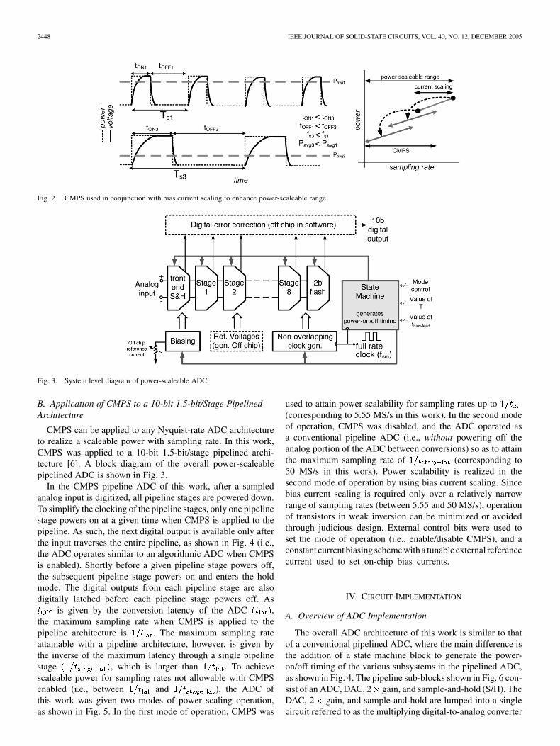
Fig. 3. System level diagram of power-scaleable ADC.
B. Application of CMPS to a 10-bit 1.5-bit/Stage PipelinedArchitecture
CMPS can be applied to any Nyquist-rate ADC architectureto realize a scaleable power with sampling rate. In this work,CMPS was applied to a 10-bit 1.5-bit/stage pipelined archi-tecture [6]. A block diagram of the overall power-scaleablepipelined ADC is shown in Fig. 3.
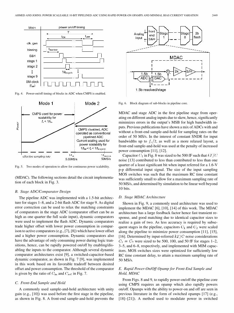
In the CMPS pipeline ADC of this work, after a sampledanalog input is digitized, all pipeline stages are powered down.To simplify the clocking of the pipeline stages, only one pipelinestage powers on at a given time when CMPS is applied to thepipeline. As such, the next digital output is available only afterthe input traverses the entire pipeline, as shown in Fig. 4 (i.e.,the ADC operates similar to an algorithmic ADC when CMPSis enabled). Shortly before a given pipeline stage powers off,the subsequent pipeline stage powers on and enters the holdmode. The digital outputs from each pipeline stage are alsodigitally latched before each pipeline stage powers off. As
is given by the conversion latency of the ADC ,the maximum sampling rate when CMPS is applied to thepipeline architecture is . The maximum sampling rateattainable with a pipeline architecture, however, is given bythe inverse of the maximum latency through a single pipelinestage , which is larger than . To achievescaleable power for sampling rates not allowable with CMPSenabled (i.e., between and ), the ADC ofthis work was given two modes of power scaling operation,as shown in Fig. 5. In the first mode of operation, CMPS was
used to attain power scalability for sampling rates up to(corresponding to 5.55 MS/s in this work). In the second modeof operation, CMPS was disabled, and the ADC operated asa conventional pipeline ADC (i.e., without powering off theanalog portion of the ADC between conversions) so as to attainthe maximum sampling rate of (corresponding to50 MS/s in this work). Power scalability is realized in thesecond mode of operation by using bias current scaling. Sincebias current scaling is required only over a relatively narrowrange of sampling rates (between 5.55 and 50 MS/s), operationof transistors in weak inversion can be minimized or avoidedthrough judicious design. External control bits were used toset the mode of operation (i.e., enable/disable CMPS), and aconstant current biasing scheme with a tunable external referencecurrent used to set on-chip bias currents.
IV. CIRCUIT IMPLEMENTATION
A. Overview of ADC Implementation
The overall ADC architecture of this work is similar to thatof a conventional pipelined ADC, where the main difference isthe addition of a state machine block to generate the power-on/off timing of the various subsystems in the pipelined ADC,as shown in Fig. 4. The pipeline sub-blocks shown in Fig. 6 con-sist of an ADC, DAC, 2 gain, and sample-and-hold (S/H). TheDAC, 2 gain, and sample-and-hold are lumped into a singlecircuit referred to as the multiplying digital-to-analog converter
AHMED AND JOHNS: POWER SCALEABLE 10-BIT PIPELINED ADC USING RAPID POWER-ON OPAMPS AND MINIMAL BIAS CURRENT VARIATION 2449
Fig. 4. Power-on/off timing of blocks in ADC when CMPS is enabled.
Fig. 5. Two modes of operation to allow for continuous power scalability.
(MDAC). The following sections detail the circuit implementa-tion of each block in Fig. 3.
B. Stage ADC/Comparator Design
The pipeline ADC was implemented with a 1.5-bit architec-ture for stages 1–8, and a 2-bit flash ADC for stage 9. As digitalerror correction can be used to relax the matching constraintsof comparators in the stage ADC (comparator offset can be ashigh as one quarter the full scale input), dynamic comparatorswere used to implement the flash ADC. Dynamic comparatorstrade higher offset with lower power consumption in compar-ison to active comparators (e.g., [7], [8]) which have lower offsetand a higher power consumption. Dynamic comparators alsohave the advantage of only consuming power during logic tran-sitions, hence, can be rapidly powered on/off by enabling/dis-abling the inputs to the comparator. Although several dynamiccomparator architectures exist [9], a switched-capacitor-baseddynamic comparator, as shown in Fig. 7 [9], was implementedin this work based on its favorable tradeoff between desiredoffset and power consumption. The threshold of the comparatoris given by the ratio of and in Fig. 7.
C. Front-End Sample and Hold
A commonly used sample-and-hold architecture with unitygain (e.g., [10]) was used before the first stage in the pipeline,as shown in Fig. 8. A front-end sample-and-hold prevents the
Fig. 6. Block diagram of sub-blocks in pipeline core.
MDAC and stage ADC in the first pipeline stage from oper-ating on different analog inputs due to skew, hence, significantlyminimizes errors in the output’s MSB for high bandwidth in-puts. Previous publications have shown a mix of ADCs with andwithout a front-end sample-and-hold for sampling rates on theorder of 50 MS/s. In the interest of constant SNDR for inputbandwidths up to , as well as a more relaxed layout, afront-end sample-and-hold was used at the penalty of increasedpower consumption [11], [12].
Capacitor in Fig. 8 was sized to be 500 fF such thatnoise [13] contributed to less than contributed to less than onequarter of a least significant bit when input referred for a 1.6-Vp-p differential input signal. The size of the input samplingMOS switches was such that the maximum RC time constantwas sufficiently small to allow for a maximum sampling rate of50 MS/s, and determined by simulation to be linear well beyond10 bits.
D. Stage MDAC Architecture
Shown in Fig. 9, a commonly used architecture was used toimplement the MDAC [6], [10], [14] of this work. The MDACarchitecture has a large feedback factor hence fast transient re-sponse, and good matching due to identical capacitor sizes torealize a gain of two. As less accuracy is required by subse-quent stages in the pipeline, capacitors and were scaledalong the pipeline to minimize power consumption [11], [15],[16]. Determined by input-referred noise considerations
were sized to be 500, 100, and 50 fF for stages 1–2,3–5, and 6–8, respectively, and implemented with MIM capac-itors. MOS switches sizes were optimized for sufficiently lowRC time constant delay, to attain a maximum sampling rate of50 MS/s.
E. Rapid Power-On/Off Opamp for Front-End Sample andHold, MDAC
From Figs. 8 and 9, to rapidly power-on/off the pipeline coreusing CMPS requires an opamp which also rapidly powerson/off. Opamps with the ability to power-on and off are seen inprevious literature in the form of switched opamps [17] (e.g.,[18]–[21]). A method used to modulate power in switched

2450 IEEE JOURNAL OF SOLID-STATE CIRCUITS, VOL. 40, NO. 12, DECEMBER 2005
Fig. 7. Switched capacitor based dynamic comparator used in 1.5-bit, and 2-bit flash ADCs.
Fig. 8. Front-end sample-and-hold architecture (shown single-ended but implemented fully differentially).
Fig. 9. MDAC architecture (shown single-ended but implemented fullydifferentially).
opamps is to switch the bias voltage of an opamp’s currentsource between the bias voltage and ground [17], [20] as shownin Fig. 10. Since bias nodes are typically loaded with largecapacitors to decouple supply noise (on the order of picofarads;
in Fig. 10) as well as parasitic capacitors ( , ),and are usually set by relatively small biasing currents (on theorder of micro-amps; in Fig. 10), the slew time given by
required when powering on the opamp isexcessive [21] for a of only MHz ns (notingthat for a rapid power-on ). Thus, although a short
Fig. 10. Switched bias approach to modulate current source power (currentsource powers down on PD high).
power-off time is realized with switched biasing, in practiceswitching bias voltages results in slow opamp power-on time.
To alleviate slew-rate-limited power-on time, a feed-back-based switching technique was developed to decreaseslew time, and combined with a folded cascode opamp, asshown in Fig. 11. This approach buffers the bias voltage,allowing for a copy of the bias voltage loaded with a relativelysmall capacitance to be switched, rather than the original biasvoltage which is loaded with a larger capacitance as shown inFig. 12. Since the copied bias voltage is loaded with a muchsmaller capacitance than the original bias voltage, and can beset by a relatively large current, the slew time at the switchingnode is much shorter than if the original bias voltage were

AHMED AND JOHNS: POWER SCALEABLE 10-BIT PIPELINED ADC USING RAPID POWER-ON OPAMPS AND MINIMAL BIAS CURRENT VARIATION 2451
Fig. 11. Schematic of rapid power-on opamp.
Fig. 12. Detail of current source in output of rapid power-on opamp.
switched. Furthermore, the large input resistance of the feed-back opamp isolates the original bias voltage from switchinginduced perturbations, thus, maintains the original bias voltageat the nominal value over the entire switching interval.
An added advantage of this approach is the feedback in-creases the output resistance of the current source by the gainof the feedback-opamp ( in Fig. 12) [22]. When feedbackbased switching is combined with a single-stage folded cascodeopamp, a DC gain-boosted architecture [23] results. As such,this approach satisfies two key design criteria for the opampof this work: a short power-on time, and large DC gain tominimize MDAC gain errors [22]. Furthermore, as a large gainis realized in only a single stage, simple load compensationand passive common-mode feedback are afforded, simplifyingthe design. A passive common-mode-feedback circuit basedon [18] was used in this work. As less settling accuracy isrequired by subsequent MDACs in the pipeline, the DC gainof the MDAC opamps were scaled to be 105, 73, and 52 dBfor stages 1–2, 3–5, and 6–8, respectively, noting that largeDC gains were used to minimize opamp DC gain inducednonlinearity errors. Opamp bandwidths were also designed toexceed minimum design constraints such that in simulation thesettling accuracy was 12 bits for stages 1–2, 10 bits for stages3–5, and 7 bits for stages 6–8. To reduce design complexity,the opamp of the first stage in the pipeline was re-used in thefront-end sample-and-hold. Switches S1–S4 in Fig. 11 wereused to decrease the time required to power off the opamp, and
switches S5 and S6 to avoid floating nodes when the opamppowers off.
To power off the feedback-opamp during , MOSswitches in series with the feedback- opamp’s current sources(e.g., [18], [19]) were used as shown in Fig. 12. Series currentswitching allows for rapid power on/off of the feedback-opampas bias voltages are not perturbed during switching events.The small-signal swing requirements of the feedback-opampallow for voltage drops across the series resistance of theswitches to have a negligible impact on the feedback-opamp’sperformance.
An alternative to using feedback-based switching in the mainopamp would be to use series current switching for rapid opamppower-on. Series current switching was not used in the currentsources at the output of the main opamp in the interest of maxi-mizing the opamp’s signal swing, and realizing a large DC gainin only a single stage. All tail current transistors in both the feed-back and main opamp, however, used series current switching(S7 in Fig. 11 for the main opamp), as opamp output signalswing is minimally affected by IR drops in the tail current path.
F. Reduced Power Consumption With Rapid Power-On/OffOpamps
By powering off both the main opamp and the feedbackopamps, the opamp of this work completely powers off during
. An advantage of an opamp which rapidly and completelypowers on and off is that it can be rapidly powered on onlywhen needed, and powered off when not required in high-speedapplications. The sample-and-hold and MDAC circuits of thiswork only require the opamp during the hold state, hence,to further reduce power, the opamps are powered off duringthe sampling phase of the MDACs and sample-and-hold. Toquantify the amount of power reduction afforded by poweringoff the opamps during the sampling phase, in the ADC modein which CMPS is disabled, the opamps can be programmed tobe powered on or off during the sampling phase. As high-speedADCs typically do not completely power off the opamps duringthe sampling phase, by measuring ADC power with the opampsalways on and always off in the sampling phase, respectively,the power savings afforded can be measured. Thus, the ADCof this work has a total of three modes of operation (where thespecific mode is set by programming the state machine withexternal control bits).Mode 1: CMPS enabled (used for sampling rates up to5.55 MS/s):
i) CMPS used to achieve power scalability, i.e., state ma-chine enabled;
ii) opamps only powered-on during hold phase in MDAC andsample-and-hold to reduce power.
Mode 2: CMPS disabled, pipelining enabled (used for samplingrates between 5.55 and 50 MS/s):
i) bias current scaling used to achieve power scalability, i.e.,state machine disabled;
ii) opamps powered off during sampling phase in MDAC andsample-and-hold to reduce power.
Mode 3: CMPS disabled, pipelining enabled (used for samplingrates between 5.55 and 50 MS/s):

2452 IEEE JOURNAL OF SOLID-STATE CIRCUITS, VOL. 40, NO. 12, DECEMBER 2005
i) bias current scaling used to achieve power scalability, i.e.,state machine disabled;
ii) opamps powered on during sampling phase in MDACand sample-and-hold to compare power reduction withmode 2.
To minimize the impact of supply variations induced byrapidly modulated currents (Ldi/dt supply noise [24]), a mixof decoupling MOS and MIM capacitors [24] were placedbetween and in all noncircuit-occupied areas in thefabricated chip. The total decoupling capacitance was on theorder of 100 pF.
G. Biasing Circuitry
The rapid power-on opamp developed in Section IV-E relieson bias voltages which are well settled before the opamp isrequired to power-on. As bias generating circuits have longpower-on times, they are powered-on before the front endsample-and-hold as shown in Fig. 4. The lead time ( inFig. 4, which is digitally programmable in the state machine)required for bias circuits to settle increases the minimumlatency of the pipeline ADC when operating with CMPS from4.5 to 9 clock cycles of the state machine’s clock. Thus, theminimum amount of current scaling required for continuouspower scalability is for sampling rates between 50 MS/s and50/9 5.55 MS/s (i.e., only 1:9). Bias circuits are poweredon/off by using switches in series with biasing currents.
H. Digital State Machine and Non-Overlapping ClockGenerator
A digital state machine is used to sequence the power-ontimes of each pipeline stage according to the timing of Fig. 4,where , and thus, , is digitally programmable. The set-tling time for each stage is equal to the pulsewidth ofthe clock supplied to the state machine . As the state ma-chine consumes power during , it limits the lowest powerachievable with CMPS. By reducing however, the power ofthe state machine can be reduced; e.g., with MHz,the state machine consumes 460 W; with MHz,the power is reduced to only 9 W. The state machine wasdesigned without commercial standard cells. It is conceivablethat if power-optimized standard cells were used to implementthe state machine, its power could be further reduced, thus in-creasing the power-scaleable range.
Non-overlapping clocks required for the sample-and-holdand MDACs were generated using a commonly used nonover-lapping clock generator (e.g., [10]). The block’s power wasmodulated by passing/blocking the input clock (from anoff-chip clock generator) via a transmission gate. The clockinput to the nonoverlapping clock generator was the same clockprovided to the state machine, i.e., .
I. Digital Error Correction/Reference Voltages
To make the prototype easily testable, digital error correctionand reference voltages were implemented off-chip. For digitalerror correction, the digital output from each pipeline stage wasrouted off chip, where a Matlab script was written to emulatedigital error correction on the captured digital output. With the
Fig. 13. Photograph of fabricated chip.
Fig. 14. Measured power versus sampling rate between 1 kS/s and 50 MS/s.
output of each stage available off chip, the functionality of eachpipeline stage could be quickly verified. The power consump-tion of the error correction and reference voltage blocks are notincluded in the measured results.
V. MEASURED RESULTS
A prototype of the power-scaleable ADC was fabricated ina 1.8-V 0.18- m CMOS process, and packaged in a standard44-pin CQFP package. The active area of the prototype was1.2 mm , and is shown in Fig. 13.
A. Measured Power and Accuracy
Fig. 14 shows the power of the ADC versus sampling ratebetween 1 kS/s and 50 MS/s. The measured power includes allblocks shown in Fig. 3 except off-chip blocks (which are shownin dashed boxes). With CMPS disabled, the power of the ADCat the maximum sampling rate of 50 MS/s was 35 mW. Using

AHMED AND JOHNS: POWER SCALEABLE 10-BIT PIPELINED ADC USING RAPID POWER-ON OPAMPS AND MINIMAL BIAS CURRENT VARIATION 2453
Fig. 15. Comparison of power of this work versus recently published andcommercial 10-bit ADCs.
Fig. 16. Measured SNDR versus sampling rate between 1 kS/s and 50 MS/s.
fixed bias currents and enabling CMPS with a 50–MHz clock,the power of the ADC was scaleable with sampling rate from
100 kS/s to 5.55 MS/s. As described in Section IV-H, thepower-scaleable range of the ADC is limited at lower samplingrates by the power of the state machine. To have a continuouspower-scaleable range as shown in Fig. 5, the bias currents werescaled by a factor of nine between 50 and 5.55 MS/s, where thepower for a given sampling rate is shown in Fig. 14. Note whenCMPS is disabled, the power shown in Fig. 14 is of mode 2, i.e.,opamps powered off during the sampling interval. When CMPSis applied to the current scaled sampling rate of 5.55 MS/s (i.e.,1/9th the bias current of 50 MS/s, and a state machine clockof 5.55 MHz), the power of the ADC was scaleable between617 and 3 kS/s, where only 77 W was consumed at 3 kS/s.To emphasize the power-scaleable range enhancement affordedby CMPS, bias currents were further reduced to 1/50th the biascurrent of 50 MS/s and CMPS applied to the current scaled sam-pling rate of 1 MS/s (i.e., 1-MHz state machine clock), wherethe ADC was measured at 1 kS/s to consume only 15 W (ofwhich 9 W was due to the digital state machine). Thus, al-though bias currents are scaled by a factor of 50, by additionallyusing CMPS, the power-scaleable range is enhanced 50 times,
Fig. 17. FFT of digital output at 50 MS/s.
Fig. 18. DNL and INL at 50 MS/s.
yielding a total power-scaleable range of . Theultimate limit in power-scaleable range is constrained by thepower consumption of the digital state machine, and the max-imum amount of current scaling tolerable by a given application.
Fig. 15 compares the power of the ADC of this work versusrecently published and commercial 10-bit ADCs between 1 kS/sand 50 MS/s. The similar power consumption compared to abroad array of 10-bit ADCs over a wide variation in operatingspeed verifies the techniques used in this work to achieve powerscalability are both effective at realizing a wide power-scaleablerange as well as attaining a low power for a given sampling rate.
Fig. 16 shows the measured SNDR of the ADC between1 kS/s and 50 MS/s. For all sampling rates, the SNDR isbetween 54 and 56 dB, and is virtually constant for a givendue to the fixed bias currents between different sampling rates.
Fig. 17 shows a 65 536 point fast Fourier transform (FFT) ofthe digital output at the maximum speed of 50 MS/s, where anSNDR of 55 dB was measured with a 1.6-V p-p input sinusoidat 20.94 MHz. The SFDR at 50 MS/s was measured to be 67 dB.Fig. 18 shows the measured DNL and INL at 50 MS/s, where thepeak INL was LSB, and peak DNLLSB.

2454 IEEE JOURNAL OF SOLID-STATE CIRCUITS, VOL. 40, NO. 12, DECEMBER 2005
TABLE IACCURACY AND POWER MEASUREMENTS OF ADC IN MODE 2 (OPAMPS POWERED OFF
DURING SAMPLING PHASE) AND MODE 3 (OPAMPS POWERED ON DURING SAMPLING PHASE)
B. Comparison of Power in Mode 2 and Mode 3
To measure the amount of power reduction afforded by pow-ering off the opamps during the sampling phase, the power ofthe ADC was measured in mode 2 and mode 3 (as describedin Section IV-F). The power and accuracy for current scaledsampling rates between 1 MS/s and 50 MS/s using modes 2and 3 are compared in Table I. For a given sampling rate, themaster off-chip reference current is identical between modes 2and 3, i.e., both modes have the same bias currents. The mea-sured results show the total power of the ADC is reduced be-tween 20%–30% by powering off the opamps during the sam-pling phase, without compromising accuracy in the ADC. Theamount of power saving is limited by the percentage of totalpower the opamps consume, and the nonoverlap time of thenonoverlapping clock generator (nonoverlap time reduces thehold phase to less than 50% of the total period) [34]. Highersampling rates show less power reduction in mode 2 as the fixednonoverlap time of 1.4 ns in this work is a larger percentageof the sampling period for faster clock rates. A small differencebetween measured SNDR in modes 2 and 3 at higher samplingrates was attributed to a clocking oversight which slightly re-duced the available settling time (hence, settling accuracy) by afixed amount in mode 3 compared to mode 2 [34].
As many switched-capacitor architectures have times inwhich the opamp is idle, it is conceivable the techniques usedto rapidly power on/off the opamp of this work could be usedto reduce power consumption in other high-speed switched-ca-pacitor circuits.
VI. CONCLUSION
A power-scaleable pipelined ADC which achieves a widepower-scaleable range without commensurate variations in biascurrent has been presented. By minimizing the required biascurrent variation for a wide power-scaleable range, poorer yielddue to weak inversion can be avoided. The keys to power scal-ability at high sampling rates were the use of a current-modu-lation-based architecture, and the development of a novel rapidpower-on opamp, which by virtue of a feedback approach is ableto completely and quickly power on/off. Measured results froma prototype fabricated in 0.18- m CMOS show the combinationof CMPS and current scaling result in the ADC having a powerthat is a function of sampling rate between 1 kS/s (15 W),and 50 MS/s (35 mW) while maintaining an SNDR of 54–56dB over the entire power-scaleable range. The rapid power-on
TABLE IISUMMARY OF ADC PERFORMANCE
opamp of this work was also shown to allow for reduced powerconsumption in high-speed switched-capacitor circuits, whereby powering off the opamps during the sampling phase of thepipeline’s sample-and-holds, a 20%–30% reduction in powercould be obtained. Table II summarizes the key measured re-sults of this work.
ACKNOWLEDGMENT
The authors acknowledge fabrication services from the Cana-dian Microelectronics Corporation (CMC).
REFERENCES
[1] K. Gulati and H. S. Lee, “A low-power reconfigurable analog-to-digitalconverter,” IEEE J. Solid-State Circuits, vol. 36, no. 11, pp. 1900–1911,Dec. 2001.
[2] B. Hernes et al., “A 1.2 V 220 MS/s 10 bit pipeline ADC implemented in0.13�m digital CMOS,” in IEEE Int. Solid-State Circuits Conf. (ISSCC)Dig. Tech. Papers, Feb. 2004, pp. 256–257.
[3] I. Ahmed and D. Johns, “A 50 MS/s (35 mW) to 1 kS/s (15 �W) powerscaleable 10 bit pipelined ADC with minimal bias current variation,”in IEEE Int. Solid-State Circuits Conf. (ISSCC) Dig. Tech. Papers, Feb.2005, pp. 280–281.
[4] D. M. Binkley et al., “A CAD methodology for optimizing transistorcurrent and sizing in analog CMOS design,” IEEE Trans. Comput.-AidedDes. Integr. Circuits Syst., vol. 22, no. 2, pp. 225–337, Feb. 2003.
[5] C. C. Enz and E. A. Vittoz, “CMOS low-power analog circuit design,” inProc. IEEE Int. Symp. Circuits and Systems (ISCAS), ch. 1.2, Tutorials,1996, pp. 79–133.
[6] S. H. Lewis, H. S. Fetterman, G. F. Gross Jr, R. Ramachandran, and T.R. Viswanathan, “A 10-bit 20-Msample/s analog-to-digital converter,”IEEE J. Solid-State Circuits, vol. 27, no. 3, pp. 351–358, Mar. 1992.
[7] K. Uyttenhove and M. S. J. Steyaert, “A 1.8-V 6-bit 1.3-GHz flash ADCin 0.25 �m CMOS,” IEEE J. Solid-State Circuits, vol. 28, no. 7, pp.1115–1122, Jul. 2003.

AHMED AND JOHNS: POWER SCALEABLE 10-BIT PIPELINED ADC USING RAPID POWER-ON OPAMPS AND MINIMAL BIAS CURRENT VARIATION 2455
[8] M. Choi and A. A. Abidi, “A 6-bit 1.3-Gsample/s A/D converter in0.35-�m CMOS,” IEEE J. Solid-State Circuits, vol. 36, no. 12, pp.1847–1858, Dec. 2001.
[9] L. Sumanen, M. Waltari, V. Hakkarainen, and K. Halonen, “CMOSdynamic comparators for pipeline A/D converters,” in Proc. IEEE Int.Symp. Circuits and Systems (ISCAS), vol. 5, May 2002, pp. 157–160.
[10] Y. Park, S. Karthikeyan, F. Tsay, and E. Bartolome, “A low power 10 bit,80 MS/s CMOS pipelined ADC at 1.8 V power supply,” in Proc.IEEEInt. Symp. Circuits and Systems (ISCAS), vol. 1, May 2001, pp. 580–583.
[11] T. B. Cho and P. R. Gray, “A 10 bit, 20 Msample/s, 35 mW pipeline A/Dconverter,” IEEE J. Solid-State Circuits, vol. 30, no. 3, pp. 166–172, Mar.1995.
[12] D. Y. Chang, “Design techniques for a pipelined ADC without using afront-end sample-and-hold amplifier,” IEEE Trans. Circuits Syst. I, Reg.Papers, vol. 51, no. 11, pp. 2123–2132, Nov. 2004.
[13] D. Johns and K. Martin, Analog Integrated Circuit Design. New York:Wiley, 1997.
[14] B. Song, M. F. Tompsett, and K. R. Lakshmikumar, “A 12-bit1-Msample.s capacitor error-averaging pipelined A/D converter,” IEEEJ. Solid-State Circuits, vol. 23, no. 12, pp. 1324–1333, Dec. 1988.
[15] D. W. Cline and P. R. Gray, “A power optimized 13-bit 5 Msample/spipelined analog-to-digital converter in 1.2 �m CMOS,” IEEE J. Solid-State Circuits, vol. 31, no. 3, pp. 294–303, Mar. 1996.
[16] P. T. F. Kwok and H. C. Luong, “Power optimization for pipelineanalog-to-digital converters,” IEEE Trans. Circuits Syst. II, AnalogDigit. Signal Process., vol. 36, no. 5, pp. 549–553, May 1999.
[17] J. Crols and M. Steyaert, “Switched-opamp: An approach to realize fullCMOS switched-capacitor circuits at very low power supply voltages,”IEEE J. Solid-State Circuits, vol. 29, no. 8, pp. 936–942, Aug. 1994.
[18] M. Waltari and K. A. I. Halonen, “1-V 9-Bit pipelined switched-opampADC,” IEEE J. Solid-State Circuits, vol. 6, no. 1, pp. 129–134, Jan. 2001.
[19] H. C. Kim, D. K. Jeong, and W. Kim, “A 30 mW 8 bit 200 MS/s pipelinedCMOS ADC using a switched-opamp technique,” in IEEE Int. Solid-State Circuits Conf. (ISSCC) Dig. Tech. Papers, Feb. 2005, pp. 284–285.
[20] R. Wang, K. Martin, D. Johns, and G. Burra, “A 3.3 mW 12 MS/s 10bit pipelined ADC in 90 nm digital CMOS,” in IEEE Int. Solid-StateCircuits Conf. (ISSCC) Dig. Tech. Papers, Feb. 2005, pp. 278–279.
[21] V. S. L. Cheung, H. C. Luong, and K. Wing-Hung, “A 1-V 10.7-MHzswitched-opamp bandpass �� modulator using double = sampling fi-nite-gain-compensation technique,” IEEE J. Solid-State Circuits, vol.37, no. 10, pp. 1215–1225, Oct. 2002.
[22] B. Razavi, Design of Analog CMOS Integrated Circuits. New York:McGraw-Hill, 2000.
[23] K. Bult and G. J. G. M. Geelen, “A fast settling CMOS op amp for SCcircuits with 90-dB DB gain,” IEEE J. Solid-State Circuits, vol. 25, no.12, pp. 1379–1384, Dec. 1990.
[24] W. Dally and J. Poulton, Digital Systems Engineering. Cambridge,U.K.: Cambridge Univ. Press, 2001.
[25] D. Miyazaki, S. Kawahito, and M. Furuta, “A 10-bit 30-MS/s low-powerpipelined CMOS A/D converter using a pseudodifferential architecture,”IEEE J. Solid-State Circuits, vol. 38, no. 2, pp. 369–373, Feb. 2003.
[26] D. Y. Chang and U. K. Moon, “A 1.4-V 10-bit 25 MS/s pipelined ADCusing opamp-reset switching technique,” IEEE J. Solid-State Circuits,vol. 38, no. 8, pp. 1401–1404, Aug. 2003.
[27] J. Arias et al., “Low-power pipeline ADC for wireless LANs,” IEEE J.Solid-State Circuits, vol. 39, no. 8, pp. 1338–1340, Aug. 2004.
[28] I. Mehr and L. Singer, “A 55-mW, 10-bit, 40-Msample/s Nyquist-rateCMOS ADC,” IEEE J. Solid-State Circuits, vol. 35, no. 3, pp. 318–325,Mar. 2000.
[29] J. Park, H. J. Park, K. Jae-Whui, S. Sangnam, and P. Chung, “A 1 mW10-bit 500 KSPS SAR A/D converter,” in Proc. IEEE Int. Symp. Circuitsand Systems, vol. 5, May 2000, pp. 581–584.
[30] G. Bonfini et al., “An ultralow-power switched opamp-based 10-B inte-grated ADC for implantable biomedical applications,” IEEE Trans. Cir-cuits Syst. I, Reg. Papers, vol. 51, no. 1, pp. 174–177, Jan. 2004.
[31] P. Confalonleri, M. Zarnprogno, F. Girardi, G. Nicollini, and A. Nagari,“A 2.7 mW 1 MSps 10 bit analog-to-digital converter with built-in ref-erence buffer and ILSB accuracy programmable input ranges,” in Proc.Eur. Solid-State Circuits Conf. (ESSCIRC), Sep. 2004, pp. 255–258.
[32] L. Dorrer, F. Kuttner, A. Wiesbauer, A. Di Giandomenico, and T.Hartig, “10-bit, 3 mW continuous-time sigma-delta ADC for UMTSin a 0.12 �m CMOS process,” in Proc. Eur. Solid-State Circuits Conf.(ESSCIRC), Sep. 2003, pp. 245–248.
[33] B. Nejati and O. Shoaei, “A 10-bit, 3.3-V, 60 MSample/s, combinedradix < 2 and 1.5-bit/stage pipelined analog-to-digital,” in IEEE Int.Symp. Circuits and Systems, May 2004, pp. 73–76.
[34] I. Ahmed, “A power scaleable and low power pipeline ADC usingpower resettable opamps,” Masters of Applied Science, Univ. ofToronto, Toronto, ON, Canada, 2004.
Imran Ahmed (S’00) received the B.A.Sc. degree(with honors) from the Division of Engineering Sci-ence and the M.A.Sc. degree from the Department ofElectrical and Computer Engineering of the Univer-sity of Toronto, Toronto, ON, Canada, in 2002 and2004, respectively. Currently, he is working towardthe Ph.D. degree at the same university.
Since 2000, he has spent a total of 24 monthsas a student intern at Snowbush Microelectronics,Toronto, working on various leading edge mixedsignal circuits. His research interests include re-
configurable analog design, digital calibration of ADCs, and very low-powermixed-signal circuits.
Mr. Ahmed is a recipient of the Natural Sciences and Engineering ResearchCouncil of Canada (NSERC) postgraduate scholarship, an Ontario GraduateScholarship (OGS), and a University of Toronto Fellowship. He received firstplace in the operational category and best overall submission in the 2005DAC/ISSCC student design competition.
David A. Johns (S’81–M’89–SM’94–F’01) re-ceived the B.A.Sc., M.A.Sc. and Ph.D. degrees fromthe University of Toronto, Toronto, ON, Canada, in1980, 1983, and 1989, respectively.
In 1988, he joined the University of Toronto wherehe is currently a Full Professor. He has ongoingresearch programs in the general area of analogintegrated circuits. His research work has resulted inmore than 40 publications. Together with academicexperience, he also has spent a number of years inthe semiconductor industry and is a co-founder of
Snowbush Microelectronics.Dr. Johns received the 1999 IEEE Darlington Award. He has served as a guest
editor of the IEEE JOURNAL OF SOLID-STATE CIRCUITS and an associate editorfor IEEE TRANSACTIONS ON CIRCUITS AND SYSTEMS, PART I and PART II. Hewas elected to Adcom for the IEEE Solid-State Circuits Society (SSCS) in 2002.