
Normal Operation Power-Down Full Power-Down Partial Power-Down (Internal Ref) Power Dissipation...
21
Information furnished by Analog Devices is believed to be accurate and reliable. However, no responsibility is assumed by Analog Devices for its use, nor for any infringements of patents or other rights of third parties which may result from its use. No license is granted by implication or otherwise under any patent or patent rights of Analog Devices. a AD7811/AD7812 One Technology Way, P.O. Box 9106, Norwood, MA 02062-9106, U.S.A. Tel: 781/329-4700 World Wide Web Site: http://www.analog.com Fax: 781/326-8703 © Analog Devices, Inc., 1998 +2.7 V to +5.5 V, 350 kSPS, 10-Bit 4-/8-Channel Sampling ADCs FEATURES 10-Bit ADC with 2.3 ms Conversion Time The AD7811 has Four Single-Ended Inputs that Can Be Configured as Three Pseudo Differential Inputs with Respect to a Common, or as Two Inde- pendent Pseudo Differential Channels The AD7812 has Eight Single-Ended Inputs that Can Be Configured as Seven Pseudo Differential Inputs with Respect to a Common, or as Four Independent Pseudo Differential Channels Onboard Track and Hold Onboard Reference 2.5 V 6 2.5% Operating Supply Range: +2.7 V to +5.5 V Specifications at 2.7 V–3.6 V and 5 V 6 10% DSP-/Microcontroller-Compatible Serial Interface High Speed Sampling and Automatic Power-Down Modes Package Address Pin on the AD7811 and AD7812 Allows Sharing of the Serial Bus in Multipackage Applications Input Signal Range: 0 V to V REF Reference Input Range: 1.2 V to V DD GENERAL DESCRIPTION The AD7811 and AD7812 are high speed, low power, 10-bit A/D converters that operate from a single +2.7 V to +5.5 V supply. The devices contain a 2.3 μs successive approximation A/D converter, an on-chip track/hold amplifier, a 2.5 V on-chip reference and a high speed serial interface that is compatible with the serial interfaces of most DSPs (Digital Signal Proces- sors) and microcontrollers. The user also has the option of using an external reference by connecting it to the V REF pin and set- ting the EXTREF bit in the control register. The V REF pin may be tied to V DD . At slower throughput rates the power-down mode may be used to automatically power down between conversions. The control registers of the AD7811 and AD7812 allow the input channels to be configured as single-ended or pseudo differential. The control register also features a software convert start and a software power-down. Two of these devices can share the same serial bus and may be individually addressed in a multipackage application by hardwiring the device address pin. The AD7811 is available in a small, 16-lead 0.3" wide, plastic dual-in-line package (mini-DIP), in a 16-lead 0.15" wide, Small Outline IC (SOIC) and in a 16-lead, Thin Shrink Small Out- line Package (TSSOP). The AD7812 is available in a small, 20-lead 0.3" wide, plastic dual-in-line package (mini-DIP), in a 20-lead, Small Outline IC (SOIC) and in a 20-lead, Thin Shrink Small Outline Package (TSSOP). PRODUCT HIGHLIGHTS 1. Low Power, Single Supply Operation Both the AD7811 and AD7812 operate from a single +2.7 V to +5.5 V supply and typically consume only 10 mW of power. The power dissipation can be significantly reduced at lower throughput rates by using the automatic power-down mode e.g., 315 μ W @ 10 kSPS, V DD = 3 V—see Power vs. Throughput. 2. 4-/8-Channel, 10-Bit ADC The AD7811 and AD7812 have four and eight single-ended input channels respectively. These inputs can be configured as pseudo differential inputs by using the Control Register. 3. On-chip 2.5 V (± 2.5%) reference circuit that is powered down when using an external reference. 4. Hardware and Software Control The AD7811 and AD7812 provide for both hardware and software control of Convert Start and Power-Down. FUNCTIONAL BLOCK DIAGRAMS REV. A CHARGE REDISTRIBUTION DAC CLOCK OSC AD7811 CONVST AGND V DD /3 COMP REF IN V DD DOUT DGND A0 V IN1 V IN2 V IN3 V IN4 DIN RFS TFS SCLK BUF CONTROL LOGIC MUX C REF SERIAL PORT 1.23V REF CHARGE REDISTRIBUTION DAC CLOCK OSC AD7812 AGND REF IN V DD DOUT DGND A0 DIN RFS TFS SCLK BUF CONTROL LOGIC MUX C REF SERIAL PORT V IN1 V IN2 V IN3 V IN4 V IN5 V IN6 V IN7 V IN8 CONVST V DD /3 COMP 1.23V REF
Transcript of Normal Operation Power-Down Full Power-Down Partial Power-Down (Internal Ref) Power Dissipation...

Information furnished by Analog Devices is believed to be accurate andreliable. However, no responsibility is assumed by Analog Devices for itsuse, nor for any infringements of patents or other rights of third partieswhich may result from its use. No license is granted by implication orotherwise under any patent or patent rights of Analog Devices.
aAD7811/AD7812
One Technology Way, P.O. Box 9106, Norwood, MA 02062-9106, U.S.A.
Tel: 781/329-4700 World Wide Web Site: http://www.analog.com
Fax: 781/326-8703 © Analog Devices, Inc., 1998
+2.7 V to +5.5 V, 350 kSPS, 10-Bit4-/8-Channel Sampling ADCs
FEATURES
10-Bit ADC with 2.3 ms Conversion Time
The AD7811 has Four Single-Ended Inputs that
Can Be Configured as Three Pseudo Differential
Inputs with Respect to a Common, or as Two Inde-
pendent Pseudo Differential Channels
The AD7812 has Eight Single-Ended Inputs that Can
Be Configured as Seven Pseudo Differential Inputs
with Respect to a Common, or as Four Independent
Pseudo Differential Channels
Onboard Track and Hold
Onboard Reference 2.5 V 6 2.5%
Operating Supply Range: +2.7 V to +5.5 V
Specifications at 2.7 V–3.6 V and 5 V 6 10%
DSP-/Microcontroller-Compatible Serial Interface
High Speed Sampling and Automatic Power-Down Modes
Package Address Pin on the AD7811 and AD7812 Allows
Sharing of the Serial Bus in Multipackage Applications
Input Signal Range: 0 V to VREF
Reference Input Range: 1.2 V to VDD
GENERAL DESCRIPTIONThe AD7811 and AD7812 are high speed, low power, 10-bitA/D converters that operate from a single +2.7 V to +5.5 Vsupply. The devices contain a 2.3 µs successive approximationA/D converter, an on-chip track/hold amplifier, a 2.5 V on-chipreference and a high speed serial interface that is compatiblewith the serial interfaces of most DSPs (Digital Signal Proces-sors) and microcontrollers. The user also has the option of usingan external reference by connecting it to the VREF pin and set-ting the EXTREF bit in the control register. The VREF pin maybe tied to VDD. At slower throughput rates the power-downmode may be used to automatically power down betweenconversions.
The control registers of the AD7811 and AD7812 allow theinput channels to be configured as single-ended or pseudodifferential. The control register also features a software convertstart and a software power-down. Two of these devices canshare the same serial bus and may be individually addressed ina multipackage application by hardwiring the device address pin.The AD7811 is available in a small, 16-lead 0.3" wide, plasticdual-in-line package (mini-DIP), in a 16-lead 0.15" wide, SmallOutline IC (SOIC) and in a 16-lead, Thin Shrink Small Out-line Package (TSSOP). The AD7812 is available in a small,20-lead 0.3" wide, plastic dual-in-line package (mini-DIP), in a20-lead, Small Outline IC (SOIC) and in a 20-lead, Thin ShrinkSmall Outline Package (TSSOP).
PRODUCT HIGHLIGHTS1. Low Power, Single Supply Operation
Both the AD7811 and AD7812 operate from a single +2.7 Vto +5.5 V supply and typically consume only 10 mW ofpower. The power dissipation can be significantly reduced atlower throughput rates by using the automatic power-downmode e.g., 315 µW @ 10 kSPS, VDD = 3 V—see Power vs.Throughput.
2. 4-/8-Channel, 10-Bit ADCThe AD7811 and AD7812 have four and eight single-endedinput channels respectively. These inputs can be configuredas pseudo differential inputs by using the Control Register.
3. On-chip 2.5 V (±2.5%) reference circuit that is powereddown when using an external reference.
4. Hardware and Software ControlThe AD7811 and AD7812 provide for both hardware andsoftware control of Convert Start and Power-Down.
FUNCTIONAL BLOCK DIAGRAMS
REV. A
CHARGEREDISTRIBUTION
DAC
CLOCKOSC
AD7811
CONVST
AGND
VDD/3 COMP
REFIN VDD
DOUT
DGND
A0
VIN1VIN2VIN3VIN4
DIN
RFSTFS
SCLK
BUF
CONTROLLOGIC
MUX
CREF
SERIALPORT
1.23VREF
CHARGEREDISTRIBUTION
DAC
CLOCKOSC
AD7812
AGNDREFIN VDD
DOUT
DGND
A0
DINRFS
TFSSCLK
BUF
CONTROLLOGIC
MUX
CREF
SERIALPORT
VIN1VIN2VIN3VIN4VIN5VIN6VIN7VIN8
CONVST
VDD/3 COMP
1.23VREF

–2– REV. A
AD7811/AD7812–SPECIFICATIONSParameter Y Version Units Test Conditions/Comments
DYNAMIC PERFORMANCE fIN = 30 kHz Any Channel, fSAMPLE = 350 kHzSignal to (Noise + Distortion) Ratio1 58 dB min VREF Internal or ExternalTotal Harmonic Distortion (THD)1 –66 dB maxPeak Harmonic or Spurious Noise1 –80 dB typIntermodulation Distortion1, 2 fa = 29 kHz, fb = 30 kHz
Second Order Terms –67 dB maxThird Order Terms –67 dB max
Channel-to-Channel Isolation1, 2 –80 dB typ fIN = 20 kHz
DC ACCURACY Any ChannelResolution 10 BitsMinimum Resolution for Which
No Missing Codes are Guaranteed 10 BitsRelative Accuracy1 ±1 LSB maxDifferential Nonlinearity1 ±1 LSB maxGain Error1 ±2 LSB maxGain Error Match1 ±0.75 LSB maxOffset Error1 ±2 LSB maxOffset Error Match1 ±0.75 LSB max
ANALOG INPUTInput Voltage Range 0 V min
VREF V maxInput Leakage Current2 ±1 µA maxInput Capacitance2 20 pF max
REFERENCE INPUTS2
VREF Input Voltage Range 1.2 V minVDD V max
Input Leakage Current ±3 µA maxInput Capacitance 20 pF max
ON-CHIP REFERENCE Nominal 2.5 VReference Error ±2.5 % maxTemperature Coefficient 50 ppm/°C typ
LOGIC INPUTS2
VINH, Input High Voltage 2.4 V min VDD = 5 V ± 10%VINL, Input Low Voltage 0.8 V max VDD = 5 V ± 10%VINH, Input High Voltage 2 V min VDD = 3 V ± 10%VINL, Input Low Voltage 0.4 V max VDD = 3 V ± 10%Input Current, IIN ±1 µA max Typically 10 nA, VIN = 0 V to VDD
Input Capacitance, CIN 8 pF max
LOGIC OUTPUTSOutput High Voltage, VOH ISOURCE = 200 µA
4 V min VDD = 5 V ± 10%2.4 V min VDD = 3 V ± 10%
Output Low Voltage, VOL ISINK = 200 µA0.4 V max
High Impedance Leakage Current ±1 µA maxHigh Impedance Capacitance 15 pF max
CONVERSION RATEConversion time 2.3 µs maxTrack/Hold Acquisition Time1 200 ns max
(VDD = +2.7 V to +3.6 V, VDD = +5 V 6 10%, GND = 0 V, VREF = +VDD
[EXT]. All specifications –408C to +1058C unless otherwise noted.)

–3–REV. A
AD7811/AD7812Parameter Y Version Units Test Conditions/Comments
POWER SUPPLYVDD 2.7 V min For Specified Performance
5.5 V maxIDD Digital Inputs = 0 V or VDD
Normal Operation 3.5 mA maxPower-DownFull Power-Down 1 µA maxPartial Power-Down (Internal Ref) 350 µA max See Power-Up Times Section
Power Dissipation VDD = 3 VNormal Operation 10.5 mW maxAuto Full Power-Down See Power vs. Throughput Section
Throughput 1 kSPS 31.5 µW maxThroughput 10 kSPS 315 µW maxThroughput 100 kSPS 3.15 mW max
Partial Power-Down (Internal Ref) 1.05 mW maxFull Power-Down 3 µW max
NOTES1See Terminology.2Sample tested during initial release and after any redesign or process change that may affect this parameter.
Specifications subject to change without notice.
TIMING CHARACTERISTICS1, 2
Parameter Y Version Units Conditions/Comments
tPOWER-UP 1 µs (max) Power-Up Time of AD7811/AD7812 After Rising Edge of CONVSTt1 2.3 µs (max) Conversion Timet2 20 ns (min) CONVST Pulsewidtht3 25 ns (min) SCLK High Pulsewidtht4 25 ns (min) SCLK Low Pulsewidtht5
3 5 ns (min) RFS Rising Edge to SCLK Rising Edge Setup Timet6
3 5 ns (min) TFS Falling Edge to SCLK Falling Edge Setup Timet7
3 10 ns (max) SCLK Rising Edge to Data Out Validt8 10 ns (min) DIN Data Valid to SCLK Falling Edge Setup Timet9 5 ns (min) DIN Data Valid after SCLK Falling Edge Hold Timet10
3, 4 20 ns (max) SCLK Rising Edge to DOUT High Impedancet11 100 ns (min) DOUT High Impedance to CONVST Falling Edge
NOTES1Sample tested to ensure compliance.2See Figures 16, 17 and 18.3These numbers are measured with the load circuit of Figure 1. They are defined as the time required for the o/p to cross 0.8 V or 2.4 V for V DD = 5 V ± 10% and0.4 V or 2 V for VDD = 3 V ± 10%.
4Derived from the measured time taken by the data outputs to change 0.5 V when loaded with the circuit of Figure 1. The measured number is then extrapolated backto remove the effects of charging or discharging the 50 pF capacitor. This means that the time, t 11, quoted in the Timing Characteristics is the true bus relinquishtime of the part and as such is independent of external bus loading capacitances.
Specifications subject to change without notice.
(VDD = +2.7 V to +5.5 V, VREF = +VDD [EXT] unless otherwise noted)
+2.1V
200 A
CL50pF
IOH
TOOUTPUT
PIN
IOL
200 A
Figure 1. Load Circuit for Digital Output Timing Specifications

AD7811/AD7812
–4– REV. A
ABSOLUTE MAXIMUM RATINGS*VDD to DGND . . . . . . . . . . . . . . . . . . . . . . . . . –0.3 V to +7 VDigital Input Voltage to DGND (CONVST, SCLK, RFS, TFS,
DIN, A0) . . . . . . . . . . . . . . . . . . . . . . . –0.3 V, VDD + 0.3 VDigital Output Voltage to DGND (DOUT)
. . . . . . . . . . . . . . . . . . . . . . . . . . . . . . . –0.3 V, VDD + 0.3 VREFIN to AGND . . . . . . . . . . . . . . . . . . . –0.3 V, VDD + 0.3 VAnalog Inputs
VIN1–VIN4 (AD7811) . . . . . . . . . . . . . . –0.3 V, VDD + 0.3 VVIN1–VIN8 (AD7812) . . . . . . . . . . . . . . –0.3 V, VDD + 0.3 V
Storage Temperature Range . . . . . . . . . . . . –65°C to +150°CJunction Temperature . . . . . . . . . . . . . . . . . . . . . . . . .+150°CPlastic DIP Package, Power Dissipation . . . . . . . . . . 450 mW
θJA Thermal Impedance . . . . . . . . . . . . . . . . . . . +105°C/WLead Temperature, (Soldering 10 sec) . . . . . . . . . . .+260°C
ORDERING GUIDE
Linearity Package PackageModel Error Descriptions Options
AD7811YN ±1 LSB 16-Lead Plastic DIP N-16AD7811YR ±1 LSB 16-Lead Small Outline IC (SOIC) R-16AAD7811YRU ±1 LSB 16-Lead Thin Shrink Small Outline Package (TSSOP) RU-16
AD7812YN ±1 LSB 20-Lead Plastic DIP N-20AD7812YR ±1 LSB 20-Lead Small Outline IC (SOIC) R-20AAD7812YRU ±1 LSB 20-Lead Thin Shrink Small Outline Package (TSSOP) RU-20
SOIC Package, Power Dissipation . . . . . . . . . . . . . . . 450 mWθJA Thermal Impedance . . . . . . . . . . . . . . . . . . . . . 75°C/WLead Temperature, Soldering
Vapor Phase (60 sec) . . . . . . . . . . . . . . . . . . . . . .+215°C Infrared (15 sec) . . . . . . . . . . . . . . . . . . . . . . . . .+220°C
TSSOP Package, Power Dissipation . . . . . . . . . . . . . 450 mWθJA Thermal Impedance . . . . . . . . . . . . . . . . . . . . 115°C/WLead Temperature, Soldering Vapor Phase (60 sec) . . . . . . . . . . . . . . . . . . . . . .+215°C Infrared (15 sec) . . . . . . . . . . . . . . . . . . . . . . . . .+220°C
ESD . . . . . . . . . . . . . . . . . . . . . . . . . . . . . . . . . . . . . . . . . 3 kV*Stresses above those listed under Absolute Maximum Ratings may cause perma-nent damage to the device. This is a stress rating only; functional operation of thedevice at these or any other conditions above those listed in the operationalsections of this specification is not implied. Exposure to absolute maximum ratingconditions for extended periods may affect device reliability.

AD7811/AD7812
–5–REV. A
PIN FUNCTION DESCRIPTIONS
Pin(s) Pin(s)AD7811 AD7812 Name Description
1 1 VREF An external reference input can be applied here. When using an external precisionreference or VDD the EXTREF bit in the control register must be set to logic one. Theexternal reference input range is 1.2 V to VDD.
2 2 CREF Reference Capacitor. A capacitor (10 nF) is connected here to improve the noiseperformance of the on-chip reference.
3, 5–7 3, 5–11 VIN1–VIN4(8) Analog Inputs. The analog input range is 0 V to VREF.4 4 AGND Analog Ground. Ground reference for track/hold, comparator, on-chip reference and
DAC.8 12 A0 Package Address Pin. This Logic Input can be hardwired high or low. When used in
conjunction with the package address bit in the control register this input allows twodevices to share the same serial bus. For example a twelve channel solution can beachieved by using the AD7811 and the AD7812 on the same serial bus.
9 13 DGND Digital Ground. Ground reference for digital circuitry.10 14 TFS Transmit Frame Sync. The falling edge of this Logic Input tells the part that a new
control byte should be shifted in on the next 10 falling edges of SCLK.11 15 RFS Receive Frame Sync. The rising edge of this Logic Input is used to enable a counter in
the serial interface. It is used to provide compatibility with DSPs which use a continuousserial clock and framing signal. In multipackage applications the RFS Pin can also beused as a serial bus select pin. The serial interface will ignore the SCLK until it receives arising edge on this input. The counter is reset at the end of a serial read operation.
12 16 DOUT Serial Data Output. Serial data is shifted out on this pin on the rising edge of the serialclock. The output enters a High impedance condition on the rising edge of the 11thSCLK pulse.
13 17 DIN Serial Data Input. The control byte is read in at this input. In order to complete aserial write operation 13 SCLK pulses need to be provided. Only the first 10 bits areshifted in—see Serial Interface section.
14 18 SCLK Serial Clock Input. An external serial clock is applied to this input to obtain serial datafrom the AD7811/AD7812 and also to latch data into the AD7811/AD7812. Data isclocked out on the rising edge of SCLK and latched in on the falling edge of SCLK.
15 19 CONVST Convert Start. This is an edge triggered logic input. The Track/Hold goes into its HoldMode on the falling edge of this signal and a conversion is initiated. The state of thispin at the end of conversion also determines whether the part is powered down or not.See operating modes section of this data sheet.
16 20 VDD Positive Supply Voltage +2.7 V to +5.5 V.
PIN CONFIGURATIONS
DIP/SOIC/TSSOP
14
13
12
11
17
16
15
20
19
18
10
9
8
1
2
3
4
7
6
5TOP VIEW
(Not to Scale)
AD7812
VREF
DIN
SCLK
VDD
CREF
VIN1
AGND
TFS
RFS
DOUTVIN2
VIN3
VIN4
VIN5
VIN6
VIN7VIN8
A0
DGND
CONVST
14
13
12
11
16
15
10
98
1
2
3
4
7
6
5TOP VIEW
(Not to Scale)
AD7811
VREF
DIN
SCLK
CONVST
VDD
CREF
VIN1
AGND
TFS
RFS
DOUTVIN2
VIN3
VIN4
A0 DGND

AD7811/AD7812
–6– REV. A
TERMINOLOGYSignal to (Noise + Distortion) RatioThis is the measured ratio of signal to (noise + distortion) at theoutput of the A/D converter. The signal is the rms amplitude ofthe fundamental. Noise is the rms sum of all nonfundamentalsignals up to half the sampling frequency (fS/2), excluding dc.The ratio is dependent upon the number of quantization levelsin the digitization process; the more levels, the smaller thequantization noise. The theoretical signal to (noise + distor-tion) ratio for an ideal N-bit converter with a sine wave inputis given by:
Signal to (Noise + Distortion) = (6.02N + 1.76) dB
Thus for a 10-bit converter, this is 62 dB.
Total Harmonic DistortionTotal harmonic distortion (THD) is the ratio of the rms sum ofharmonics to the fundamental. For the AD7811 and AD7812it is defined as:
THD (dB) = 20 log
V22 +V3
2 +V42 +V5
2 +V62
V1
where V1 is the rms amplitude of the fundamental and V2, V3,V4, V5 and V6 are the rms amplitudes of the second through thesixth harmonics.
Peak Harmonic or Spurious NoisePeak harmonic or spurious noise is defined as the ratio of therms value of the next largest component in the ADC outputspectrum (up to fS/2 and excluding dc) to the rms value of thefundamental. Normally, the value of this specification isdetermined by the largest harmonic in the spectrum, but forparts where the harmonics are buried in the noise floor, it willbe a noise peak.
Intermodulation DistortionWith inputs consisting of sine waves at two frequencies, fa andfb, any active device with nonlinearities will create distortionproducts at sum and difference frequencies of mfa ± nfb wherem, n = 0, 1, 2, 3, etc. Intermodulation terms are those forwhich neither m nor n are equal to zero. For example, thesecond order terms include (fa + fb) and (fa – fb), while thethird order terms include (2fa + fb), (2fa – fb), (fa + 2fb) and(fa – 2fb).
The AD7811 and AD7812 are tested using the CCIF standardwhere two input frequencies near the top end of the inputbandwidth are used. In this case, the second and third orderterms are of different significance. The second order terms are
usually distanced in frequency from the original sine waveswhile the third order terms are usually at a frequency close tothe input frequencies. As a result, the second and third orderterms are specified separately. The calculation of the inter-modulation distortion is as per the THD specification where it isthe ratio of the rms sum of the individual distortion products tothe rms amplitude of the fundamental expressed in dBs.
Channel-to-Channel IsolationChannel-to-channel isolation is a measure of the level ofcrosstalk between channels. It is measured by applying a full-scale 20 kHz sine wave signal to all nonselected input channelsand determining how much that signal is attenuated in the selectedchannel. The figure given is the worst case across all four oreight channels for the AD7811 and AD7812 respectively.
Relative AccuracyRelative accuracy, or endpoint nonlinearity, is the maximumdeviation from a straight line passing through the endpoints ofthe ADC transfer function.
Differential NonlinearityThis is the difference between the measured and the ideal1 LSB change between any two adjacent codes in the ADC.
Offset ErrorThis is the deviation of the first code transition (0000 . . . 000)to (0000 . . . 001) from the ideal, i.e., AGND + 1 LSB.
Offset Error MatchThis is the difference in Offset Error between any two channels.
Gain ErrorThis is the deviation of the last code transition (1111 . . . 110)to (1111 . . . 111) from the ideal, i.e., VREF – 1 LSB, after theoffset error has been adjusted out.
Gain Error MatchThis is the difference in Gain Error between any two channels.
Track/Hold Acquisition TimeTrack/hold acquisition time is the time required for the outputof the track/hold amplifier to reach its final value, within± 1/2 LSB, after the end of conversion (the point at which thetrack/hold returns to track mode). It also applies to situationswhere a change in the selected input channel takes place orwhere there is a step input change on the input voltage appliedto the selected VIN input of the AD7811 or AD7812. It meansthat the user must wait for the duration of the track/hold acquisi-tion time after the end of conversion or after a channel change/step input change to VIN before starting another conversion, toensure that the part operates to specification.

AD7811/AD7812
–7–REV. A
Control Register (AD7811)The Control Register is a 10-bit-wide, write only register. The Control Register is written to when the AD7811 receives a fallingedge on its TFS pin. The AD7811 will maintain the same configuration until a new control byte is written to the part. The controlregister can be written to at the same time data is being read. This latter feature enhances throughput rates when software control isbeing used or when the analog input channels are being changed frequently. The power-up default register contents are all zeros;therefore, when the supplies are connected, the AD7811 is powered down by default.
Control Register AD7811
9 0
X* A0 PD1 PD0 VIN4/AGND DIFF/SGL CH1 CH0 CONVST EXTREF
*This is a don’t care bit.
A0 This is the package address bit. It is used in conjunction with the package address pin to allow two AD7811s toshare the same serial bus. The AD7811 can also share the same serial bus with the AD7812. When a control wordis written to the control register of the AD7811 the control word is ignored if the package address bit in the con-trol byte does not match how the package address pin is hardwired. Only the serial port of the device that receivedthe last valid control byte, i.e., the address bit matched the address pin, will attempt to drive the serial bus on thenext serial read. When the part powers up this bit is set to 0.
PD1, PD0 These bits allow the AD7811 to be fully powered down and powered up. Bit combinations PD1 = PD0 = 0 andPD1 = PD0 = 1 override the automatic power-down decision at the end of conversion. These bits also decide thepower-down mode when the AD7811 enters a power-down at the end of a conversion. There are two power-downmodes—Full Power-Down and Partial Power-Down. See Power-Down Options section of this data sheet.
PD1 PD0 Description
0 0 Full Power-Down of the AD78110 1 Partial Power-Down at the End of Conversion1 0 Full Power-Down at the End of Conversion1 1 Power-Up the AD7811
VIN4/AGND The DIF/SGL bit in the control register must be set to 0 to use this option otherwise this bit is ignored. SettingVIN4/AGND to 0 configures the analog inputs of the AD7811 as four single-ended analog inputs referenced toanalog ground (AGND). By setting this bit to 1 the input channels VIN1 to VIN3 are configured as three pseudo-differential channels with respect to VIN4—see Table I.
DIF/SGL This bit is used to configure the analog inputs as single ended or pseudo differential pairs. By setting this bit to 0the analog inputs can be configured as single ended with respect to AGND, or pseudo differential with respect toVIN4 as explained above. Setting this bit to 1 configures the analog input channels as two pseudo differential pairsVIN1/VIN2 and VIN3/VIN4—see Table I.
CH1, CH0 These bits are used in conjunction with VIN4/AGND and DIF/SGL to select an analog input channel. The tableshows how the various channel selections are made—see Table I.
CONVST Setting this bit to a logic one initiates a conversion. A conversion is initiated 400 ns after a write to the controlregister has taken place. This allows a signal to be acquired even if the channel is changed and a conversioninitiated in the same serial write. The bit is reset after the end of a conversion.
EXTREF This bit must be set to a logic one if the user wishes to use an external reference or use VDD as the reference.When the external reference is selected the on chip reference circuitry powers down.

AD7811/AD7812
–8– REV. A
Control Register (AD7812)The Control Register is a 10-bit-wide, write only register. The Control Register is written to when the AD7812 receives a fallingedge on its TFS pin. The AD7812 will maintain the same configuration until a new control byte is written to the part. The controlregister can be written to at the same time data is being read. This latter feature enhances throughput rates when software control isbeing used or when the analog input channels are being changed frequently. The power-up default register contents are all zeros;therefore, when the supplies are connected, the AD7812 is powered down by default.
Control Register AD7812
9 0
A0 PD1 PD0 VIN8/AGND DIFF/SGL CH2 CH1 CH0 CONVST EXTREF
A0 This is the package address bit. It is used in conjunction with the package address pin to allow two AD7812s toshare the same serial bus. The AD7812 can also share the same serial bus with the AD7811. When a control wordis written to the control register of the AD7812 the control word is ignored if the package address bit in the con-trol byte does not match how the package address pin is hardwired. Only the serial port of the device which re-ceived the last valid control byte, i.e., the address bit matched the address pin, will attempt to drive the serial buson the next serial read. When the part powers up this bit is set to 0.
PD1, PD0 These bits allow the AD7812 to be fully powered down and powered up. Bit combinations PD1 = PD0 = 0 andPD1 = PD0 = 1 override the automatic power-down decision at the end of conversion. These bits also decide thepower-down mode when the AD7812 enters a power-down at the end of a conversion. There are two power-downmodes—Full Power-Down and Partial Power-Down. See Power-Down section of this data sheet.
PD1 PD0 Description
0 0 Full Power-Down of the AD78120 1 Partial Power-Down at the End of Conversion1 0 Full Power-Down at the End of Conversion1 1 Power-Up the AD7812
VIN8/AGND The DIF/SGL bit in the control register must be set to 0 in order to use this option otherwise this bit is ignored.Setting VIN8/AGND to 0 configures the analog inputs of the AD7812 as eight single-ended analog inputsreferenced to analog ground (AGND). By setting this bit to 1 the input channels VIN1 to VIN7 are configuredas seven pseudo differential channels with respect to VIN8—see Table II.
DIF/SGL This bit is used to configure the analog inputs as single ended or pseudo differential pairs. By setting this bit to 0the analog inputs can be configured as single ended with respect to AGND, or pseudo differential with respect toVIN8 as explained above. Setting this bit to 1 configures the analog input channels as four pseudo differential pairsVIN1/VIN2, VIN3/VIN4, VIN5/VIN6 and VIN7/VIN8—see Table II.
CH2, CH1, CH0 These bits are used in conjunction with VIN8/AGND and DIF/SGL to select an analog input channel. Table IIshows how the various channel selections are made.
CONVST Setting this bit to a logic one initiates a conversion. A conversion is initiated 400 ns after a write to the controlregister has taken place. This allows a signal to be acquired even if the channel is changed and a conversion initi-ated in the same write operation. The bit is reset after the end of a conversion.
EXTREF This bit must be set to a logic one if the user wishes to use an external reference or use VDD as the reference.When the external reference is selected the on-chip reference circuitry powers down and the current consumptionis reduced by about 1 mA.

AD7811/AD7812
–9–REV. A
Table I. AD7811 Channel Configurations
VIN4/AGND DIF/SGL CH1 CH0 Description
0 0 0 0 VIN1 Single-Ended with Respect to AGND0 0 0 1 VIN2 Single-Ended with Respect to AGND0 0 1 0 VIN3 Single-Ended with Respect to AGND0 0 1 1 VIN4 Single-Ended with Respect to AGND1 0 0 0 VIN1 Pseudo Differential with Respect to VIN4
1 0 0 1 VIN2 Pseudo Differential with Respect to VIN4
1 0 1 0 VIN3 Pseudo Differential with Respect to VIN4
X 1 0 0 VIN1(+) Pseudo Differential with Respect to VIN2(–)X 1 0 1 VIN3(+) Pseudo Differential with Respect to VIN4(–)X 1 1 0 Internal Test. SAR Input Equal to VREF/2X 1 1 1 Internal Test. SAR Input Equal to VREF
Table II. AD7812 Channel Configurations
VIN8/AGND DIF/SGL CH2 CH1 CH0 Description
0 0 0 0 0 VIN1 Single-Ended with Respect to AGND0 0 0 0 1 VIN2 Single-Ended with Respect to AGND0 0 0 1 0 VIN3 Single-Ended with Respect to AGND0 0 0 1 1 VIN4 Single-Ended with Respect to AGND0 0 1 0 0 VIN5 Single-Ended with Respect to AGND0 0 1 0 1 VIN6 Single-Ended with Respect to AGND0 0 1 1 0 VIN7 Single-Ended with Respect to AGND0 0 1 1 1 VIN8 Single-Ended with Respect to AGND1 0 0 0 0 VIN1 Pseudo Differential with Respect to VIN8
1 0 0 0 1 VIN2 Pseudo Differential with Respect to VIN8
1 0 0 1 0 VIN3 Pseudo Differential with Respect to VIN8
1 0 0 1 1 VIN4 Pseudo Differential with Respect to VIN8
1 0 1 0 0 VIN5 Pseudo Differential with Respect to VIN8
1 0 1 0 1 VIN6 Pseudo Differential with Respect to VIN8
1 0 1 1 0 VIN7 Pseudo Differential with Respect to VIN8
X 1 0 0 0 VIN1(+) Pseudo Differential with Respect to VIN2(–)X 1 0 0 1 VIN3(+) Pseudo Differential with Respect to VIN4(–)X 1 0 1 0 VIN5(+) Pseudo Differential with Respect to VIN6(–)X 1 0 1 1 VIN7(+) Pseudo Differential with Respect to VIN8(–)X 1 1 0 0 Internal Test. SAR Input Equal to VREF/2X 1 1 0 1 Internal Test. SAR Input Equal to VREF

AD7811/AD7812
–10– REV. A
CIRCUIT DESCRIPTIONConverter OperationThe AD7811 and AD7812 are successive approximation analog-to-digital converters based around a charge redistribution DAC.The ADCs can convert analog input signals in the range 0 V toVDD. Figures 2 and 3 show simplified schematics of the ADC.Figure 2 shows the ADC during its acquisition phase. SW2 isclosed and SW1 is in position A, the comparator is held in abalanced condition and the sampling capacitor acquires thesignal on VIN.
VIN
VDD/3
COMPARATOR
CONTROLLOGIC
CLOCKOSC
ACQUISITIONPHASE
SW1
A
BSW2
AGND
SAMPLINGCAPACITOR
CHARGEREDISTRIBUTION
DAC
Figure 2. ADC Acquisition Phase
When the ADC starts a conversion, see Figure 3, SW2 willopen and SW1 will move to position B causing the comparatorto become unbalanced. The Control Logic and the ChargeRedistribution DAC are used to add and subtract fixed amountsof charge from the sampling capacitor to bring the comparatorback into a balanced condition. When the comparator is rebal-anced, the conversion is complete. The Control Logic generatesthe ADC output code. Figure 10 shows the ADC transferfunction.
VIN
VDD/3
COMPARATOR
CONTROLLOGIC
CLOCKOSC
CONVERSIONPHASE
SW1
A
B
SW2
SAMPLINGCAPACITOR
AGND
CHARGEREDISTRIBUTION
DAC
Figure 3. ADC Conversion Phase
TYPICAL CONNECTION DIAGRAMFigure 4 shows a typical connection diagram for the AD7811/AD7812. The AGND and DGND are connected together atthe device for good noise suppression. The serial interface isimplemented using three wires with RFS/TFS connected toCONVST see Serial Interface section for more details. VREF isconnected to a well decoupled VDD pin to provide an analoginput range of 0 V to VDD. If the AD7811 or AD7812 is notsharing a serial bus with another AD7811 or AD7812 then A0(package address pin) should be hardwired low. The defaultpower up value of the package address bit in the control registeris 0. For applications where power consumption is of concern,the automatic power down at the end of a conversion should beused to improve power performance. See Power-Down Optionssection of the data sheet.
SUPPLY+2.7V TO +5.5V
10mF
µC/µP
THREE-WIRESERIALINTERFACE
10nF
VREF
DIN
SCLK
CONVST
VDD CREF
VIN1
AGNDTFS
RFS
DOUT
A0DGND
0.1mF
VIN2
VIN4(8)
AD7811/AD7812
0V TOVREF
INPUT
Figure 4. Typical Connection Diagram
Analog InputFigure 5 shows an equivalent circuit of the analog input struc-ture of the AD7811 and AD7812. The two diodes D1 and D2provide ESD protection for the analog inputs. Care must betaken to ensure that the analog input signal never exceeds thesupply rails by more than 200 mV. This will cause these diodesto become forward biased and start conducting current intothe substrate. 20 mA is the maximum current these diodes canconduct without causing irreversible damage to the part. How-ever, it is worth noting that a small amount of current (1 mA)being conducted into the substrate due to an overvoltage on anunselected channel can cause inaccurate conversions on a se-lected channel. The capacitor C2 in Figure 5 is typically about4 pF and can primarily be attributed to pin capacitance. Theresistor R1 is a lumped component made up of the on resistanceof a multiplexer and a switch. This resistor is typically about125 Ω. The capacitor C1 is the ADC sampling capacitor andhas a capacitance of 3.5 pF.
CONVERSION PHASE – SWITCH OPENTRACK PHASE – SWITCH CLOSED
VIN
D1
D2
VDD /3
C13.5pF
R1125V
C24pF
VDD
Figure 5. Equivalent Analog Input Circuit
The analog inputs on the AD7811 and AD7812 can be config-ured as single ended with respect to analog ground (AGND),as pseudo differential with respect to a common, and also aspseudo differential pairs—see Control Register section.

AD7811/AD7812
–11–REV. A
An example of the pseudo differential scheme using the AD7811 isshown in Figure 6. The relevant bits in the AD7811 ControlRegister are set as follows DIF/SGL = 1, CH1 = CH2 = 0, i.e.,VIN1 pseudo differential with respect to VIN2. The signal is ap-plied to VIN1 but in the pseudo differential scheme the samplingcapacitor is connected to VIN2 during conversion and not AGNDas described in the Converter Operation section. This inputscheme can be used to remove offsets that exist in a system. Forexample, if a system had an offset of 0.5 V the offset could beapplied to VIN2 and the signal applied to VIN1. This has theeffect of offsetting the input span by 0.5 V. It is only possible tooffset the input span when the reference voltage is less thanVDD–OFFSET.
VIN1
VDD/3
COMPARATOR
CONTROLLOGIC
CLOCKOSC
CONVERSIONPHASE
VOFFSET
SAMPLINGCAPACITORVIN+
VIN–
VIN2
VIN1
CHARGEREDISTRIBUTION
DAC
VOFFSET
Figure 6. Pseudo Differential Input Scheme
When using the pseudo differential input scheme the signal onVIN2 must not vary by more than a 1/2 LSB during the conver-sion process. If the signal on VIN2 varies during conversion, theconversion result will be incorrect. In single-ended mode thesampling capacitor is always connected to AGND during con-version. Figure 7 shows the AD7811/AD7812 pseudo differen-tial input being used to make a unipolar dc current measurement.A sense resistor is used to convert the current to a voltage andthe voltage is applied to the differential input as shown.
RL
RSENSEAD7811/AD7812
VIN+
VIN–
VDD
Figure 7. DC Current Measurement Scheme
DC Acquisition TimeThe ADC starts a new acquisition phase at the end of a conver-sion and ends on the falling edge of the CONVST signal. At theend of a conversion a settling time is associated with the sam-pling circuit. This settling time lasts approximately 100 ns. Theanalog signal on VIN+ is also being acquired during this settlingtime. Therefore, the minimum acquisition time needed is ap-proximately 100 ns.
Figure 8 shows the equivalent charging circuit for the samplingcapacitor when the ADC is in its acquisition phase. R2 repre-sents the source impedance of a buffer amplifier or resistivenetwork; R1 is an internal multiplexer resistance, and C1 is thesampling capacitor. During the acquisition phase the samplingcapacitor must be charged to within a 1/2 LSB of its final value.The time it takes to charge the sampling capacitor (TCHARGE) isgiven by the following formula:
TCHARGE = 7.6 × (R2 + 125 Ω) × 3.5 pF
C13.5pF
VIN+R1
125VR2
SAMPLINGCAPACITOR
Figure 8. Equivalent Sampling Circuit
For small values of source impedance, the settling time associ-ated with the sampling circuit (100 ns) is, in effect, the acquisi-tion time of the ADC. For example, with a source impedance(R2) of 10 Ω the charge time for the sampling capacitor isapproximately 4 ns. The charge time becomes significant forsource impedances of 2 kΩ and greater.
AC Acquisition TimeIn ac applications it is recommended to always buffer analoginput signals. The source impedance of the drive circuitry mustbe kept as low as possible to minimize the acquisition time ofthe ADC. Large values of source impedance will cause the THDto degrade at high throughput rates. In addition, better perfor-mance can generally be achieved by using an External 1 nFcapacitor on VIN.
ON-CHIP REFERENCEThe AD7811 and AD7812 have an on-chip 2.5 V referencecircuit. The schematic in Figure 9 shows how the referencecircuit is implemented. A 1.23 V bandgap reference is gained upto provide a 2.5 V ± 2% reference voltage. The on-chip refer-ence is not available externally (SW2 is open). An external refer-ence (1.2 V to VDD) can be applied at the VREF pin. However inorder to use an external reference the EXTREF bit in the con-trol register (Bit 0) must first be set to a Logic 1. When EXTREFis set to a Logic 1 SW2 will close, SW3 will open and the ampli-fier will power down. This will reduce the current consumptionof the part by about 1 mA. It is possible to use two differentreference voltages by selecting the on-chip reference or externalreference.
7pF
2.5V
EXTERNALCAPACITOR
1.23V
VREF
CREF
AGND
SW3
SW2
SW1
Figure 9. On-Chip Reference Circuitry

AD7811/AD7812
–12– REV. A
When using automatic power-down between conversions toimprove the power performance of the part (see Power vs.Throughput) the switch SW1 will open when the part enters itspower-down mode if using the internal on-chip reference. Thisprovides a high impedance discharge path for the external ca-pacitor (see Figure 9). A typical value of external capacitance is10 nF. When the part is in Mode 2 Full Power-Down, becausethe external capacitor holds its charge during power-down, theinternal bandgap reference will power up more quickly afterrelatively short periods of full power-down. When operating thepart in Mode 2 Partial Power-Down the external capacitor is notrequired as the on-chip reference stays powered up while therest of the circuitry powers down.
ADC TRANSFER FUNCTIONThe output coding of the AD7811 and AD7812 is straightbinary. The designed code transitions occur at successive inte-ger LSB values (i.e., 1 LSB, 2 LSBs, etc.). The LSB size is =VREF/1024. The ideal transfer characteristic for the AD7811 andAD7812 is shown in Figure 10.
000...000
0VANALOG INPUT
111...111
000...001000...010
111...110
111...000
011...111
1LSB +VREF–1LSB
1LSB = VREF/1024
AD
C C
OD
E
Figure 10. AD7811 and AD7812 Transfer Characteristic
POWER-DOWN OPTIONSThe AD7811 and AD7812 provide flexible power managementto allow the user to achieve the best power performance for agiven throughput rate.
The power management options are selected by programmingthe power-down bits (i.e., PD1 and PD0) in the control register.Table III below summarizes the options available. When thepower-down bits are programmed for Mode 2 Power Down (fulland partial), a rising edge on the CONVST pin will power upthe part. This feature is used when powering down betweenconversions—see Power vs. Throughput. When the AD7811and AD7812 are placed in partial power-down the on-chipreference does not power down. However, the part will powerup more quickly after long periods of power-down when usingpartial power-down—see Power-Up Times section.
Table III. AD7811/AD7812 Power-Down Options
PD1 PD0 CONVST* Description
1 1 x Full Power-Up0 0 x Full Power-Down0 1 0 Mode 2 Partial Power-Down
(Reference Stays Powered-Up)0 1 1 No Power-Down1 0 0 Mode 2 Full Power-Down1 0 1 No Power-Down
*This refers to the state of the CONVST signal at the end of a conversion.
POWER-UP TIMESThe AD7811 and AD7812 have a 1 µs power-up time whenusing an external reference or when powering up from partialpower-down. When VDD is first connected, the AD7811 andAD7812 are in a low current mode of operation. In order tocarry out a conversion the AD7811 and AD7812 must first bepowered up by writing to the control register of each ADC toset the power-down bits (i.e., PD1 = 1, PD0 = 1) for a fullpower-up. See the Quick Evaluation Setup section on the fol-lowing page.
Mode 2 Full Power-Down (PD1 = 1, PD0 = 0)The power-up time of the AD7811 and AD7812 after power isfirst connected, or after a long period of Full Power-Down, isthe time it takes the on-chip 1.23 V reference to power up plusthe time it takes to charge the external capacitor CREF—seeFigure 9. The time taken to charge CREF to the 10-bit level isgiven by the equation (7.6 × 2 kΩ × CREF). For CREF = 10 nFthe power-up time is approximately 152 µs. It takes 30 µs topower up the on-chip reference so the total power-up time ofeither ADC in either of these conditions is 182 µs. However,when powering down fully between conversions to achieve abetter power performance this power-up time reduces to 1 µsafter a relatively short period of power-down as CREF holds itscharge (see On-Chip Reference section). The AD7811 andAD7812 can therefore be used in Mode 2 with throughputrates of 250 kSPS and under.
Mode 2 Partial Power-Down (PD1 = 0, PD0 = 1)The power-up time of the AD7811 and AD7812 from a PartialPower-Down is 1 µs maximum. When using a Partial Power-Down between conversions, there is no requirement to connectan external capacitor to the CREF pin because the referenceremains powered up. This means that the AD7811 and AD7812will power up in 30 µs after the supplies are first connected asthere is no requirement to charge an external capacitor.
POWER VS. THROUGHPUTBy using the Automatic Power-Down (Mode 2) at the end of aconversion—see Operating Modes section of the data sheet,superior power performance can be achieved.
Figure 11 shows how the Automatic Power-Down is imple-mented using the CONVST signal to achieve the optimumpower performance for the AD7811 and AD7812. The AD7811and AD7812 are operated in Mode 2 and the control registerBits PD1 and PD0 are set to 1 and 0 respectively for Full Power-Down, or 0 and 1 for Partial Power-Down. The duration of theCONVST pulse is set to be equal to or less than the power-uptime of the devices—see Operating Modes section. As thethroughput rate is reduced, the device remains in its power-down state longer and the average power consumption over timedrops accordingly.
\
tPOWER-UP1ms
CONVST
tCONVERT2ms
100ms @ 10kSPS
POWER-DOWN
tCYCLE
Figure 11. Automatic Power-Down

AD7811/AD7812
–13–REV. A
For example, if the AD7811 is operated in a continuous sam-pling mode with a throughput rate of 10 kSPS, PD1 = 1,PD0 = 0 and using the on chip reference the power consump-tion is calculated as follows. The power dissipation during nor-mal operation is 10.5 mW, VDD = 3 V. If the power-up time is1 µs and the conversion time is 2.3 µs, the AD7811 can be saidto dissipate 10.5 mW for 3 µs (worst case) during each conver-sion cycle. If the throughput rate is 10 kSPS, the cycle time is100 µs and the average power dissipated during each cycle is(3/100) × (10.5 mW) = 315 µW.
Figure 12 shows the Power vs. Throughput Rate for automaticfull power-down.
THROUGHPUT – kSPS
10
1
0.010 5010
0.1
20 30 405 15 25 35 45
PO
WE
R –
mV
Figure 12. AD7811/AD7812 Power vs. Throughput
FREQUENCY – kHz
0
–10
–1000 12217 87 105
–40
–70
–80
–90
–20
–30
–60
–50
35 52 70 140 157 174
AD7811/12 2048 POINT FFT SAMPLING 357.142kHz fIN = 30.168kHz
dBs
Figure 13. AD7811/AD7812 SNR
QUICK EVALUATION SETUPThe schematic shown in Figure 14 shows a suggested configura-tion of the AD7812 for a first look evaluation of the part. Noexternal reference circuit is needed as the VREF pin can beconnected to VDD. The CONVST signal is connected to TFSand RFS to enable the serial port. Also by selecting Mode 2operation (see Operating Modes section) the power perfor-mance of the AD7812 can be evaluated.
10mF 10nF
VREF
DIN
SCLK
CONVST
VDD CREF
VIN1
AGND TFS
RFS
DOUT
A0DGND
0.1mF
VIN2
AD7812
0V TO VDD
INPUT
VIN7
VIN8
SUPPLYVDD
Figure 14. Evaluation Quick Setup
The setup uses a full duplex, 16-bit, serial interface protocol,e.g., SPI. It is possible to use 8-bit transfers by carrying out twoconsecutive read/write operations. The MSB of data is trans-ferred first.
1. When power is first connected to the device it is in a powereddown mode of operation and is consuming only 1 µA. TheAD7812 must first be configured by carrying out a serialwrite operation.
2. The CONVST signal is first pulsed to enable the serial port(rising and falling edge on RFS and TFS respectively—seeSerial Interface section).
3. Next, a 16-bit serial read/write operation is carried out. Bywriting 6040 Hex to the AD7812 the part is powered up, setup to use external reference (i.e., VDD) and the analog inputVIN1 is selected. The data read from the part during this read/write operation is invalid.
4. It is necessary to wait approximately 1 µs before pulsingCONVST again and initiating a conversion. The 1 µs is toallow the AD7812 to power up correctly—see Power-UpTimes section.
5. Approximately 2.3 µs after the falling edge of CONVST, i.e.,after the end of the conversion, a serial read/write can takeplace. This time 4040 Hex is written to the AD7812 and thedata read from the part is the result of the conversion. Theoutput code is in a straight binary format and will be leftjustified in the 16-bit serial register (MSB clocked out first).
6. By idling the CONVST signal high or low it is possible tooperate the AD7812 in Mode 1 and Mode 2 respectively.

AD7811/AD7812
–14– REV. A
DIN
DOUT
CONVST
VDD
6040 HEX
NOT VALID
4040 HEX
VALID DATA VALID DATA
4040 HEX
t POWER-UP1ms
t CONVERT2.3ms
t CONVERT2.3ms
Figure 15. Read/Write Sequence for AD7812
OPERATING MODESThe mode of operation of the AD7811 and AD7812 is selectedwhen the (logic) state of the CONVST is checked at the end ofa conversion. If the CONVST signal is logic high at the endof a conversion, the part does not power down and is operat-ing in Mode 1. If, however, the CONVST signal is broughtlogic low before the end of a conversion, the AD7811 and AD7812will power down at the end of the conversion. This is Mode 2operation.
Mode 1 Operation (High Speed Sampling)When the AD7811 and AD7812 are operated in Mode 1 theyare not powered down between conversions. This mode of op-eration allows high throughput rates to be achieved. The timingdiagram in Figure 16 shows how this optimum throughput rateis achieved by bringing the CONVST signal high before the endof the conversion.
The sampling circuitry leaves its tracking mode and goes intohold on the falling edge of CONVST. A conversion is also initi-ated at this time. The conversion takes 2.3 µs to complete. Atthis point, the result of the current conversion is latched into theserial shift register and the state of the CONVST signal checked.The CONVST signal should be logic high at the end of theconversion to prevent the part from powering down. The serialport on the AD7811 and AD7812 is enabled on the rising edgeof the first SCLK after the rising edge of the RFS signal—seeSerial Interface section. As explained earlier, this rising edge
should occur before the end of the conversion process if the partis not to be powered down. A serial read can take place at anystage after the rising edge of CONVST. If a serial read is initi-ated before the end of the current conversion process (i.e., attime “A”), the result of the previous conversion is shifted out onthe DOUT pin. It is possible to allow the serial read to extendbeyond the end of a conversion. In this case the new data willnot be latched into the output shift register until the readhas finished. The dynamic performance of the AD7811 andAD7812 typically degrades by up to 3 dBs while reading duringa conversion. If the user waits until the end of the conversionprocess, i.e., 2.3 µs after the falling edge of CONVST (Point“B”) before initiating a read, the current conversion result isshifted out. The serial read must finish at least 100 ns prior tothe next falling edge of CONVST to allow the part to accuratelyacquire the input signal.
Mode 2 Operation (Automatic Power-Down)When used in this mode of operation the part automaticallypowers down at the end of a conversion. This is achieved byleaving the CONVST signal low until the end of the conversion.Because it takes approximately 1 µs for the part to power-upafter it has been powered down, this mode of operation is in-tended to be used in applications where slower throughput ratesare required, i.e., in the order of 250 kSPS and improved powerperformance is required—see Power vs. Throughput section.There are two power-down modes the AD7811/AD7812 can
CURRENT CONVERSIONRESULT
A B t12
CONVST
DOUT
SCLK
t1
t2
Figure 16. Mode 1 Operation Timing Diagram

AD7811/AD7812
–15–REV. A
enter during automatic power-down. These modes are discussedin the Power-Up Times section of this data sheet. The timingdiagram in Figure 17 shows how to operate the part inMode 2. If the AD7811/AD7812 is powered down, the risingedge of the CONVST pulse causes the part to power-up.Once the part has powered up (~1 µs after the rising edge ofCONVST) the CONVST signal is brought low and a conver-sion is initiated on this falling edge of the CONVST signal. Theconversion takes 2.3 µs and after this time the conversion resultis latched into the serial shift register and the part powers down.Therefore, when the part is operated in Mode 2 the effectiveconversion time is equal to the power-up time (1 µs) and theSAR conversion time (2.3 µs).
NOTE: Although the AD7811 and AD7812 take 1 µs to powerup after the rising edge of CONVST, it is not necessary to leaveCONVST high for 1 µs after the rising edge before bringing itlow to initiate a conversion. If the CONVST signal goes lowbefore 1 µs in time has elapsed, then the power-up time is timedout internally and a conversion is then initiated. Hence theAD7811 and AD7812 are guaranteed to have always powered-up before a conversion is initiated, even if the CONVST pulse-width is <1 µs. If the CONVST pulsewidth is > 1 µs, then aconversion is initiated on the falling edge.
As in the case of Mode 1 operation, the rising edge of the firstSCLK after the rising edge of RFS enables the serial port of theAD7811 and AD7812 (see Serial Interface section). If a serialread is initiated soon after this rising edge (Point “A”), i.e.,before the end of the conversion, the result of the previous con-version is shifted out on pin DOUT. In order to read the resultof the current conversion, the user must wait at least 2.3 µs afterpower-up or at least 2.3 µs after the falling edge of CONVST,
(Point “B”), whichever occurs latest before initiating a serialread. The serial port of the AD7811 and AD7812 is still func-tional even though the devices have been powered down.
Because it is possible to do a serial read from the part while it ispowered down, the AD7811 and AD7812 are powered up onlyto do the conversion and are immediately powered down at theend of a conversion. This significantly improves the powerconsumption of the part at slower throughput rates—see Powervs. Throughput section.
SERIAL INTERFACEThe serial interface of the AD7811 and AD7812 consists of fivewires, a serial clock input, SCLK, receive data to clock syn-chronization input RFS, transmit data to clock synchronizationinput TFS, a serial data output, DOUT, and a serial data in-put, DIN, (see Figure 18). The serial interface is designed toallow easy interfacing to most microcontrollers and DSPs,e.g., PIC16C, PIC17C, QSPI, SPI, DSP56000, TMS320and ADSP-21xx, without the need for any gluing logic. Wheninterfacing to the 8051, the SCLK must be inverted. TheMicroprocessor/Microcontroller Interface section explainshow to interface to some popular DSPs and microcontrollers.
Figure 18 shows the timing diagram for a serial read and writeto the AD7811 and AD7812. The serial interface works withboth a continuous and a noncontinuous serial clock. The risingedge of RFS and falling edge of TFS resets a counter thatcounts the number of serial clocks to ensure the correct numberof bits are shifted in and out of the serial shift registers. Oncethe correct number of bits have been shifted in and out, theSCLK is ignored. In order for another serial transfer to takeplace the counter must be reset by the active edges of TFS and
CURRENT CONVERSIONRESULT
A B
t POWER-UP
CONVST
DOUT
SCLK
1ms t1
t2
Figure 17. Mode 2 Operation Timing Diagram
A
B
DIN
DB9 DB8
DB9
DB7
DB8 DB7
DB6 DB5 DB4 DB3 DB0
SCLK
RFS
DOUT
t3
t7
t4
t10
DB1DB2
1 1312111098765432
TFS
t8t9
t5
t6
DB6 DB5 DB4 DB3 DB2 DB1 DB0
Figure 18. Serial Interface Timing Diagram
AD7811/AD7812
–16– REV. A
RFS. The first rising SCLK edge after the rising edge of theRFS signal causes DOUT to leave its high impedance state anddata is clocked out onto the DOUT line and also on subsequentSCLK rising edges. The DOUT pin goes back into a high im-pedance state on the 11th SCLK rising edge—Point “A” onFigure 18. A minimum of 11 SCLKs are therefore needed tocarry out a serial read. Data on the DIN line is latched in onthe first SCLK falling edge after the falling edge of the TFSsignal and on subsequent SCLK falling edges. The controlregister is updated on the 13th SCLK rising edge—point “B” onFigure 18. A minimum of 13 SCLK pulses are therefore neededto complete a serial write operation. In multipackage applica-tions the RFS and TFS signals can be used as chip select sig-nals. The serial interface will not shift data in or out until itreceives the active edge of the RFS or TFS signal.
Simplifying the Serial InterfaceThe five-wire interface is designed to support many differentserial interface standards. However, it is possible to reduce thenumber of lines required to just three. By simply connecting theTFS and RFS pins to the CONVST signal (see Figure 4), theCONVST signal can be used to enable the serial port for read-ing and writing. This is only possible where a noncontinuousserial clock is being used.
MICROPROCESSOR INTERFACINGThe serial interface on the AD7811 and AD7812 allows theparts to be directly connected to a range of many differentmicroprocessors. This section explains how to interface theAD7811 and AD7812 with some of the more common micro-controller and DSP serial interface protocols.
AD7812/AD7811 to PIC16C6x/7xThe PIC16C6x Synchronous Serial Port (SSP) is configured asan SPI Master with the Clock Polarity bit = 0. This is doneby writing to the Synchronous Serial Port Control Register(SSPCON). See user PIC16/17 Microcontroller User Manual.Figure 19 shows the hardware connections needed to interfaceto the PIC16/17. In this example I/O port RA1 is being used topulse CONVST and enable the serial port of the AD7811/AD7812. This microcontroller transfers only eight bits of dataduring each serial transfer operation; therefore, two consecutiveread/write operations are needed.
CONVST
AD7811/AD7812*
DOUT
DIN
SCLK
RFS
TFS
PIC16C6x/7x*
SCK/RC3
SDO/RC5
SDI/ RC4
RA1
*ADDITIONAL PINS OMITTED FOR CLARITY
Figure 19. Interfacing to the PIC16/17
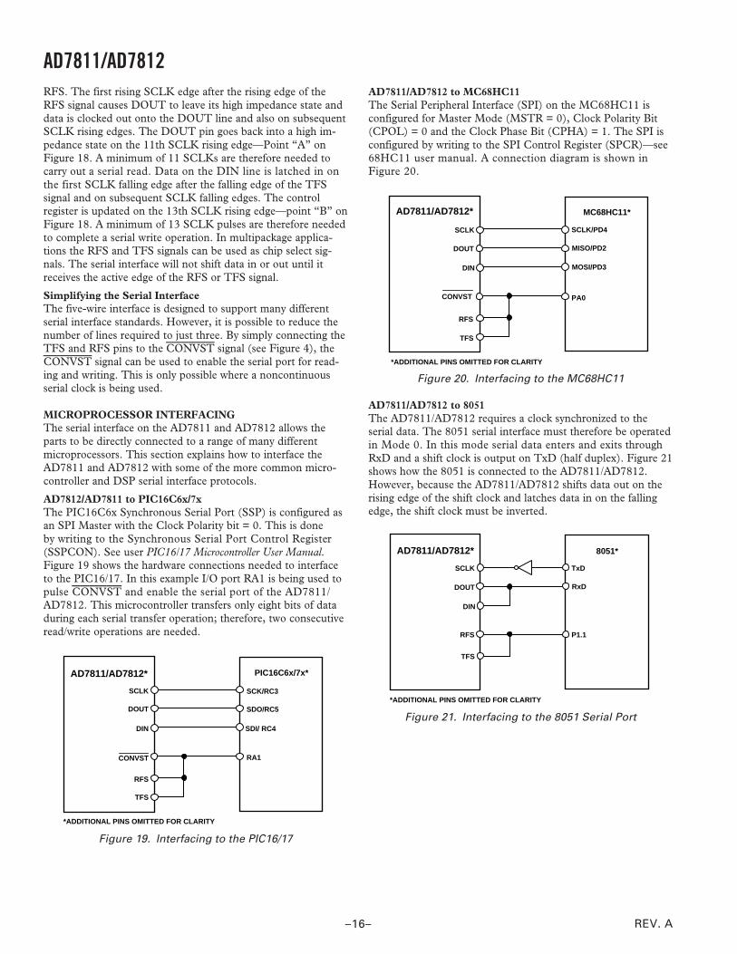
AD7811/AD7812 to MC68HC11The Serial Peripheral Interface (SPI) on the MC68HC11 isconfigured for Master Mode (MSTR = 0), Clock Polarity Bit(CPOL) = 0 and the Clock Phase Bit (CPHA) = 1. The SPI isconfigured by writing to the SPI Control Register (SPCR)—see68HC11 user manual. A connection diagram is shown inFigure 20.
CONVST
AD7811/AD7812*
DOUT
DIN
SCLK
RFS
TFS
MC68HC11*
SCLK/PD4
MISO/PD2
MOSI/PD3
PA0
*ADDITIONAL PINS OMITTED FOR CLARITY
Figure 20. Interfacing to the MC68HC11
AD7811/AD7812 to 8051The AD7811/AD7812 requires a clock synchronized to theserial data. The 8051 serial interface must therefore be operatedin Mode 0. In this mode serial data enters and exits throughRxD and a shift clock is output on TxD (half duplex). Figure 21shows how the 8051 is connected to the AD7811/AD7812.However, because the AD7811/AD7812 shifts data out on therising edge of the shift clock and latches data in on the fallingedge, the shift clock must be inverted.
AD7811/AD7812*
DOUT
DIN
SCLK
TFS
8051*
TxD
RxD
P1.1
*ADDITIONAL PINS OMITTED FOR CLARITY
RFS
Figure 21. Interfacing to the 8051 Serial Port

AD7811/AD7812
–17–REV. A
It is possible to implement a serial interface using the data portson the 8051. This would also allow a full duplex serial transferto be implemented. The technique involves “bit banging” anI/O port (e.g., P1.0) to generate a serial clock and using twoother I/O ports (e.g., P1.1 and P1.2) to shift data in and out—see Figure 22.
AD7811/AD7812*
DOUT
DIN
SCLK
RFS
TFS
8051*
P1.0
P1.1
P1.2
P1.3
*ADDITIONAL PINS OMITTED FOR CLARITY
Figure 22. Interfacing to the 8051 Using I/O Ports
AD7811/AD7812 to TMS320C5xThe serial interface on the TMS320C5x uses a continuous serialclock and frame synchronization signals to synchronizethe data transfer operations with peripheral devices like theAD7811. Frame synchronization inputs have been supplied onthe AD7811/AD7812 to allow easy interfacing with no extragluing logic. The serial port of the TMS320C5x is set up tooperate in Burst Mode with internal CLKX (Tx serial clock)and FSX (Tx frame sync). The Serial Port Control register(SPC) must have the following setup: F0 = 0, FSM = 1,MCM = 1 and TXM = 1. The connection diagram is shownin Figure 23.
AD7811/AD7812*
DOUT
SCLK
RFS
TFS
TMS320C5x*
CLKX
CLKR
FSX
*ADDITIONAL PINS OMITTED FOR CLARITY
FSR
DR
DIN DT
Figure 23. Interfacing to the TMS320C5x
AD7811/AD7812 to ADSP-21xxThe ADSP-21xx family of DSPs are easily interfaced to theAD7811/AD7812 without the need for extra gluing logic. TheSPORT is operated in normal framing mode. The SPORTcontrol register should be set up as follows:
TFSW = RFSW = 0, Normal FramingINVRFS = INVTFS = 0, Active High Frame SignalDTYPE = 00, Right Justify DataSLEN = 1001, 10-Bit Data WordsISCLK = 1, Internal Serial ClockTFSR = RFSR = 1, Frame Every WordIRFS = 0, External Framing SignalITFS = 1, Internal Framing Signal
The 10-bit data words will be right justified in the 16-bit serialdata registers when using this configuration. Figure 24 showsthe connection diagram.
AD7811/AD7812*
DOUT
DIN
SCLK
RFS
TFS
ADSP-21xx*
SCLK
DR
DT
RFS
*ADDITIONAL PINS OMITTED FOR CLARITY
TFS
Figure 24. Interfacing to the ADSP-21xx
AD7811/AD7812 to DSP56xxxThe connection diagram in Figure 25 shows how the AD7811and AD7812 can be connected to the SSI (Synchronous SerialInterface) of the DSP56xxx family of DSPs from Motorola. TheSSI is operated in Synchronous Mode (SYN bit in CRB =1)with internally generated 1-bit clock period frame sync for bothTx and Rx (FSL1 and FSL0 bits in CRB = 1 and 0 respectively).
AD7811/AD7812*
DOUT
SCLK
DSP56xxx*
SCK
SRD
*ADDITIONAL PINS OMITTED FOR CLARITY
DIN STD
SC2RFS
TFS
Figure 25. Interfacing to the DSP56xxx

AD7811/AD7812
–18– REV. A
OUTLINE DIMENSIONSDimensions shown in inches and (mm).
16-Lead Plastic DIP(N-16)
16
1 8
9
0.840 (21.33)0.745 (18.93)
0.280 (7.11)0.240 (6.10)
PIN 1
SEATINGPLANE
0.022 (0.558)0.014 (0.356)
0.060 (1.52)0.015 (0.38)
0.210 (5.33)MAX 0.130
(3.30)MIN
0.070 (1.77)0.045 (1.15)
0.100(2.54)BSC
0.160 (4.06) 0.115 (2.93)
0.325 (8.25)0.300 (7.62)
0.015 (0.381)0.008 (0.204)
0.195 (4.95)0.115 (2.93)
16-Lead Small Outline Package (SOIC)(R-16A)
16 9
81
0.3937 (10.00)0.3859 (9.80)
0.2550 (6.20)0.2284 (5.80)
0.1574 (4.00)0.1497 (5.80)
PIN 1
SEATINGPLANE
0.0098 (0.25)0.0040 (0.10)
0.0192 (0.49)0.0138 (0.35)
0.0688 (1.75)0.0532 (1.35)
0.0500(1.27)BSC
0.0099 (0.25)0.0075 (0.19)
0.0500 (1.27)0.0160 (0.41)
8°0°
0.0196 (0.50)0.0099 (0.25)
x 45°
16-Lead Thin Shrink Outline Package (TSSOP)(RU-16)
16 9
81
0.201 (5.10)0.193 (4.90)
0.25
6 (6
.50)
0.24
6 (6
.25)
0.17
7 (4
.50)
0.16
9 (4
.30)
PIN 1
SEATINGPLANE
0.006 (0.15)0.002 (0.05)
0.0118 (0.30)0.0075 (0.19)
0.0256(0.65)BSC
0.0433(1.10)MAX
0.0079 (0.20)0.0035 (0.090)
0.028 (0.70)0.020 (0.50)
8°0°

AD7811/AD7812
–19–REV. A
OUTLINE DIMENSIONSDimensions shown in inches and (mm).
20-Lead Plastic DIP(N-20)
20
1 10
11
1.060 (26.90)0.925 (23.50)
0.280 (7.11)0.240 (6.10)
PIN 1
SEATINGPLANE
0.022 (0.558)0.014 (0.356)
0.210 (5.33)MAX 0.130
(3.30)MIN
0.070 (1.77)0.045 (1.15)
0.100(2.54)BSC
0.160 (4.06)0.115 (2.93)
0.060 (1.52)0.015 (0.38)
0.325 (8.25)0.300 (7.62)
0.015 (0.381)0.008 (0.204)
0.195 (4.95)0.115 (2.93)
20-Lead Small Outline Package (SOIC)(R-20A)
SEATINGPLANE
0.0118 (0.30)0.0040 (0.10)
0.0192 (0.49)0.0138 (0.35)
0.1043 (2.65)0.0926 (2.35)
0.0500(1.27)BSC
0.0125 (0.32)0.0091 (0.23)
0.0500 (1.27)0.0157 (0.40)
8°0°
0.0291 (0.74)0.0098 (0.25)
x 45°
20 11
101
0.5118 (13.00)0.4961 (12.60)
0.41
93 (
10.6
5)0.
3937
(10
.00)
0.29
92 (
7.60
)0.
2914
(7.
40)
PIN 1
20-Lead Thin Shrink Outline Package (TSSOP)(RU-20)
20 11
101
0.260 (6.60)0.252 (6.40)
0.25
6 (6
.50)
0.24
6 (6
.25)
0.17
7 (4
.50)
0.16
9 (4
.30)
PIN 1
SEATINGPLANE
0.006 (0.15)0.002 (0.05)
0.0118 (0.30)0.0075 (0.19)
0.0256 (0.65)BSC
0.0433(1.10)MAX
0.0079 (0.20)0.0035 (0.090)
0.028 (0.70)0.020 (0.50)
8°0°

–20–
C31
38a–
0–11
/98
PR
INT
ED
IN U
.S.A
.

This datasheet has been download from:
www.datasheetcatalog.com
Datasheets for electronics components.