
Design and Implementation of a 32-bit RISC Microprocessor
66
Design and Implementation of a 32-bit RISC Microprocessor Osman Allam University of Applied Sciences Darmstadt (FHD) MSc in Electrical Engineering February 2006
-
Upload
khangminh22 -
Category
Documents
-
view
3 -
download
0
Transcript of Design and Implementation of a 32-bit RISC Microprocessor

Design and Implementation of a 32-bit RISC Microprocessor
Osman Allam
University of Applied Sciences Darmstadt (FHD)
MSc in Electrical Engineering
February 2006

Design and Implementation of a 32-bit RISC Microprocessor
Osman Allam
Supervisors:
• Prof. Dr. phil. nat. Bernard Hoppe, Course Director for Master of Science.
• Prof. Hermann Meuth, Ph.D., Associate Course Director for Master of Science.
This thesis submitted in partial fulfillment of the requirements of the University of Applied Sciences Darmstadt (FHD) for the degree of
Master of Science carried out in collaboration with IMEC. February, 2006.

Declaration I hereby declare, that this report was written solely by myself, and it has not been presented nor is it pending at any institution for the award of any degree. I also declare, that any help or assistance received or inferred was acknowledged or referenced in the report. Data:…………………… Signature: ……………………….

Acknowledgements
The opportunity to be able to complete my master thesis project with a company like IMEC has providedhighly valuable experience, and has allowed me to extend my knowledge and skills. I would like to thankeveryone who has been involved with allowing this to happen, and who assisted me during the course ofmy work. In particular:
• Prof. Dr. phil. nat. Bernard Hoppe, Course Director for Master of Science, Darmstadt University ofApplied Sciences.
• Prof. Hermann Meuth, Ph.D., Associate Course Director for Master of Science, Darmstadt Univer-sity of Applied Sciences.
• Ing. Steven Redant, ASIC design manager, IMEC-INVOMEC
• Ing. Tom Tassignon, ASIC design engineer, IMEC-INVOMEC
• Ir. Geert Vanwijnsberghe, Project engineer ASIC design, IMEC-INVOMEC
I would also like to express my deepest gratitude to my father for his constant support throughout the courseof my life and particularly the period I spent away from home.
2
Abstract
History has marked a large number of man endeavours towards building machines that are capable ofperforming arithmetic operations more efficiently than he can do himself. These started with very primitiveinstruments but evolved over the course of time due to the accumulative knowledge of man kind. In therecent decades, many computer architectures exhibiting various design methodologies and computationmodels have been developed. One of the most widely accepted of which is von-Neumann architecture.
The brilliant mathematician, John Louis von-Neumann (1903 - 1957) proposed - in 1945 - a model fora general purpose computer that provides programmability and re-programmability thanks to a memorystructure that stores programs and data. This thesis introduces Micro6, A microprocessor that adopts von-Neumann architecture and is implemented on FPGA. In addition to that, the thesis presents a softwaredevelopment environment for Micro6.
Micro6 exhibits the characteristics of a RISC (Reduced Instruction Set Computer). It has a small setof instructions and a limited number of addressing modes. Micro6 control unit follows the conventionalmodel as opposed to the microprogrammed one. Micro6 can perform arbitrary computations on integerdata but however, the size of the program is constrained by the size of the memory. An I/O Unit is attachedto Micro6 which facilitates basic I/O as well as DMA (Direct Memory Access) transactions.
Writing programs in high-level language like C is not supported by Micro6. However, this thesis intro-duces an assembler, known as VAS, that supports the assembly language of Micro6. The assembler outputfiles can be used for both simulation and implementation purposes. VAS can be used to write programsthat exploit almost all the microprocessor hardware resources. This is very important in the developmentstage.
3

Contents
Acknowledgements 2
Abstract 3
1. Computer architecture background 101.1. Classification of computer architectures . . . . . . . . . . . . . . . . . . . . . . . . . . . 10
1.1.1. Von Neumann Machines . . . . . . . . . . . . . . . . . . . . . . . . . . . . . . . 101.1.2. Non von-Neumann Machines . . . . . . . . . . . . . . . . . . . . . . . . . . . . 11
1.2. RISC machines . . . . . . . . . . . . . . . . . . . . . . . . . . . . . . . . . . . . . . . . 11
2. Micro6 specifications 132.1. Instruction Set Architecture ISA . . . . . . . . . . . . . . . . . . . . . . . . . . . . . . . 13
2.1.1. Instruction set . . . . . . . . . . . . . . . . . . . . . . . . . . . . . . . . . . . . . 132.1.2. Addressing modes . . . . . . . . . . . . . . . . . . . . . . . . . . . . . . . . . . 142.1.3. Register file . . . . . . . . . . . . . . . . . . . . . . . . . . . . . . . . . . . . . . 162.1.4. Data types . . . . . . . . . . . . . . . . . . . . . . . . . . . . . . . . . . . . . . . 17
2.2. System architecture . . . . . . . . . . . . . . . . . . . . . . . . . . . . . . . . . . . . . . 182.2.1. Central Processing Unit (CPU) . . . . . . . . . . . . . . . . . . . . . . . . . . . . 182.2.2. Main memory . . . . . . . . . . . . . . . . . . . . . . . . . . . . . . . . . . . . . 192.2.3. Memory traffic controller . . . . . . . . . . . . . . . . . . . . . . . . . . . . . . . 21
2.3. CPU architecture . . . . . . . . . . . . . . . . . . . . . . . . . . . . . . . . . . . . . . . 24
3. Instruction set 263.1. Operate group . . . . . . . . . . . . . . . . . . . . . . . . . . . . . . . . . . . . . . . . . 26
3.1.1. Arithmetic operations . . . . . . . . . . . . . . . . . . . . . . . . . . . . . . . . . 263.1.2. Logic operations . . . . . . . . . . . . . . . . . . . . . . . . . . . . . . . . . . . 263.1.3. Shift and rotate operations . . . . . . . . . . . . . . . . . . . . . . . . . . . . . . 27
3.2. Data transfer group . . . . . . . . . . . . . . . . . . . . . . . . . . . . . . . . . . . . . . 283.2.1. Copy Register CPR . . . . . . . . . . . . . . . . . . . . . . . . . . . . . . . . . . 283.2.2. Load from memory LD, LDM and LDX . . . . . . . . . . . . . . . . . . . . . . . 293.2.3. Storing data in the main memory ST, STX . . . . . . . . . . . . . . . . . . . . . . 31
3.3. Program control group . . . . . . . . . . . . . . . . . . . . . . . . . . . . . . . . . . . . 313.3.1. Branches . . . . . . . . . . . . . . . . . . . . . . . . . . . . . . . . . . . . . . . 313.3.2. Subroutines . . . . . . . . . . . . . . . . . . . . . . . . . . . . . . . . . . . . . . 323.3.3. Supported conditions . . . . . . . . . . . . . . . . . . . . . . . . . . . . . . . . . 323.3.4. Unconditional branch instruction BRA . . . . . . . . . . . . . . . . . . . . . . . 333.3.5. Unconditional jump to subroutine instruction JSR . . . . . . . . . . . . . . . . . . 333.3.6. Conditional branch instructions BEQ, BNQ, BGT, BLT, BGE, BV and BNV . . . 333.3.7. Conditional jump to subroutine instructions JEQ, JNQ, JGT, JLT, JGE, JV and JNV 333.3.8. Return from subroutine instruction RTN . . . . . . . . . . . . . . . . . . . . . . . 333.3.9. End of program instruction END . . . . . . . . . . . . . . . . . . . . . . . . . . . 343.3.10. Null instruction NLL . . . . . . . . . . . . . . . . . . . . . . . . . . . . . . . . . 34
3.4. I/O instructions . . . . . . . . . . . . . . . . . . . . . . . . . . . . . . . . . . . . . . . . 34
4

Contents
4. Data path 354.1. Register file . . . . . . . . . . . . . . . . . . . . . . . . . . . . . . . . . . . . . . . . . . 354.2. ALU . . . . . . . . . . . . . . . . . . . . . . . . . . . . . . . . . . . . . . . . . . . . . . 35
4.2.1. ALU operations . . . . . . . . . . . . . . . . . . . . . . . . . . . . . . . . . . . . 354.2.2. ALU operands . . . . . . . . . . . . . . . . . . . . . . . . . . . . . . . . . . . . 364.2.3. ALU computation result . . . . . . . . . . . . . . . . . . . . . . . . . . . . . . . 364.2.4. ALU control . . . . . . . . . . . . . . . . . . . . . . . . . . . . . . . . . . . . . 36
5. Control unit 375.1. Structure and pipelining . . . . . . . . . . . . . . . . . . . . . . . . . . . . . . . . . . . . 375.2. Fetch unit . . . . . . . . . . . . . . . . . . . . . . . . . . . . . . . . . . . . . . . . . . . 375.3. Decode unit . . . . . . . . . . . . . . . . . . . . . . . . . . . . . . . . . . . . . . . . . . 395.4. Execute unit . . . . . . . . . . . . . . . . . . . . . . . . . . . . . . . . . . . . . . . . . . 405.5. Stack . . . . . . . . . . . . . . . . . . . . . . . . . . . . . . . . . . . . . . . . . . . . . 40
6. I/O unit 426.1. I/O Instructions . . . . . . . . . . . . . . . . . . . . . . . . . . . . . . . . . . . . . . . . 426.2. Basic I/O . . . . . . . . . . . . . . . . . . . . . . . . . . . . . . . . . . . . . . . . . . . 426.3. Direct Memory Access DMA . . . . . . . . . . . . . . . . . . . . . . . . . . . . . . . . . 43
6.3.1. Loading the Starting Address Register SAR . . . . . . . . . . . . . . . . . . . . . 436.3.2. Loading the Device ID Register DIR . . . . . . . . . . . . . . . . . . . . . . . . . 436.3.3. Loading the Burst Length Register BLR and initiating DMA operations . . . . . . 44
6.4. I/O Unit interfaces . . . . . . . . . . . . . . . . . . . . . . . . . . . . . . . . . . . . . . 446.4.1. CPU Interface . . . . . . . . . . . . . . . . . . . . . . . . . . . . . . . . . . . . . 446.4.2. External devices interface . . . . . . . . . . . . . . . . . . . . . . . . . . . . . . 446.4.3. Memory interface . . . . . . . . . . . . . . . . . . . . . . . . . . . . . . . . . . . 45
6.5. UART . . . . . . . . . . . . . . . . . . . . . . . . . . . . . . . . . . . . . . . . . . . . . 456.5.1. UART functions: . . . . . . . . . . . . . . . . . . . . . . . . . . . . . . . . . . . 456.5.2. Attaching the UART to Micro6 I/O Unit . . . . . . . . . . . . . . . . . . . . . . . 46
7. Programming Micro6 487.1. Micro6 assembly language . . . . . . . . . . . . . . . . . . . . . . . . . . . . . . . . . . 48
7.1.1. Micro6 assembly language directives . . . . . . . . . . . . . . . . . . . . . . . . 487.2. Micro6 VAS assembler . . . . . . . . . . . . . . . . . . . . . . . . . . . . . . . . . . . . 48
7.2.1. VAS components . . . . . . . . . . . . . . . . . . . . . . . . . . . . . . . . . . . 487.2.2. VAS input files . . . . . . . . . . . . . . . . . . . . . . . . . . . . . . . . . . . . 497.2.3. VAS output files . . . . . . . . . . . . . . . . . . . . . . . . . . . . . . . . . . . 497.2.4. VAS operation . . . . . . . . . . . . . . . . . . . . . . . . . . . . . . . . . . . . 49
8. Realization 508.1. Design Entry . . . . . . . . . . . . . . . . . . . . . . . . . . . . . . . . . . . . . . . . . 51
8.1.1. Design Files . . . . . . . . . . . . . . . . . . . . . . . . . . . . . . . . . . . . . 518.1.2. Finite State Machine style . . . . . . . . . . . . . . . . . . . . . . . . . . . . . . 51
8.2. Functional Verification . . . . . . . . . . . . . . . . . . . . . . . . . . . . . . . . . . . . 528.3. Synthesis . . . . . . . . . . . . . . . . . . . . . . . . . . . . . . . . . . . . . . . . . . . 54
8.3.1. Device utilization . . . . . . . . . . . . . . . . . . . . . . . . . . . . . . . . . . . 548.3.2. Timing Summary . . . . . . . . . . . . . . . . . . . . . . . . . . . . . . . . . . . 55
8.4. Implementation . . . . . . . . . . . . . . . . . . . . . . . . . . . . . . . . . . . . . . . . 558.4.1. BlockRAM . . . . . . . . . . . . . . . . . . . . . . . . . . . . . . . . . . . . . . 558.4.2. DCM: Digital Clock Manager . . . . . . . . . . . . . . . . . . . . . . . . . . . . 558.4.3. Development board . . . . . . . . . . . . . . . . . . . . . . . . . . . . . . . . . . 56
8.5. On-chip Verification . . . . . . . . . . . . . . . . . . . . . . . . . . . . . . . . . . . . . . 56
5

Contents
9. Further developments 589.1. Pipelining the ALU . . . . . . . . . . . . . . . . . . . . . . . . . . . . . . . . . . . . . . 589.2. IO Operations . . . . . . . . . . . . . . . . . . . . . . . . . . . . . . . . . . . . . . . . . 589.3. IO devices . . . . . . . . . . . . . . . . . . . . . . . . . . . . . . . . . . . . . . . . . . . 58
10.References and Software tools 5910.1. References . . . . . . . . . . . . . . . . . . . . . . . . . . . . . . . . . . . . . . . . . . . 5910.2. Software packages . . . . . . . . . . . . . . . . . . . . . . . . . . . . . . . . . . . . . . 59
A. Final Synthesis Report 60
B. Sample program: Selection sort 62B.1. Source code . . . . . . . . . . . . . . . . . . . . . . . . . . . . . . . . . . . . . . . . . . 62B.2. Test data . . . . . . . . . . . . . . . . . . . . . . . . . . . . . . . . . . . . . . . . . . . . 63
6

List of Figures
1.1. Von-Neumann architecture approaches . . . . . . . . . . . . . . . . . . . . . . . . . . . 11
2.1. Register-direct addressing mode . . . . . . . . . . . . . . . . . . . . . . . . . . . . . . . 142.2. Register-indirect addressing mode . . . . . . . . . . . . . . . . . . . . . . . . . . . . . . 152.3. Register-indexed addressing mode . . . . . . . . . . . . . . . . . . . . . . . . . . . . . . 152.4. Stack-register addressing mode . . . . . . . . . . . . . . . . . . . . . . . . . . . . . . . . 162.5. Immediate addressing mode . . . . . . . . . . . . . . . . . . . . . . . . . . . . . . . . . 162.6. Micro6 register file . . . . . . . . . . . . . . . . . . . . . . . . . . . . . . . . . . . . . . 172.7. Internal representation of numbers . . . . . . . . . . . . . . . . . . . . . . . . . . . . . . 182.8. System architecture . . . . . . . . . . . . . . . . . . . . . . . . . . . . . . . . . . . . . . 182.9. Memory organization . . . . . . . . . . . . . . . . . . . . . . . . . . . . . . . . . . . . . 192.10. Memory Cycles . . . . . . . . . . . . . . . . . . . . . . . . . . . . . . . . . . . . . . . . 202.11. Memory handshaking - Write operation . . . . . . . . . . . . . . . . . . . . . . . . . . . 212.12. Memory handshaking - Read operation . . . . . . . . . . . . . . . . . . . . . . . . . . . . 212.13. Memory traffic controller . . . . . . . . . . . . . . . . . . . . . . . . . . . . . . . . . . . 232.14. CPU architecture . . . . . . . . . . . . . . . . . . . . . . . . . . . . . . . . . . . . . . . 24
3.1. Arithmetic shift right . . . . . . . . . . . . . . . . . . . . . . . . . . . . . . . . . . . . . 273.2. Arithmetic shift left . . . . . . . . . . . . . . . . . . . . . . . . . . . . . . . . . . . . . . 283.3. Logic shift right . . . . . . . . . . . . . . . . . . . . . . . . . . . . . . . . . . . . . . . . 283.4. Logic shift left . . . . . . . . . . . . . . . . . . . . . . . . . . . . . . . . . . . . . . . . . 293.5. Rotate right . . . . . . . . . . . . . . . . . . . . . . . . . . . . . . . . . . . . . . . . . . 293.6. Rotate left . . . . . . . . . . . . . . . . . . . . . . . . . . . . . . . . . . . . . . . . . . . 303.7. Condition Checking Circuit . . . . . . . . . . . . . . . . . . . . . . . . . . . . . . . . . . 33
4.1. ALU . . . . . . . . . . . . . . . . . . . . . . . . . . . . . . . . . . . . . . . . . . . . . . 35
5.1. Control unit structure . . . . . . . . . . . . . . . . . . . . . . . . . . . . . . . . . . . . . 375.2. Instruction pipeline . . . . . . . . . . . . . . . . . . . . . . . . . . . . . . . . . . . . . . 385.3. Fetch Unit state diagram . . . . . . . . . . . . . . . . . . . . . . . . . . . . . . . . . . . 395.4. Fetch Unit Interfaces . . . . . . . . . . . . . . . . . . . . . . . . . . . . . . . . . . . . . 395.5. Stack . . . . . . . . . . . . . . . . . . . . . . . . . . . . . . . . . . . . . . . . . . . . . 41
6.1. External devices interface . . . . . . . . . . . . . . . . . . . . . . . . . . . . . . . . . . . 456.2. UART Connection . . . . . . . . . . . . . . . . . . . . . . . . . . . . . . . . . . . . . . 47
8.1. Design Flow . . . . . . . . . . . . . . . . . . . . . . . . . . . . . . . . . . . . . . . . . . 508.2. FSM Style . . . . . . . . . . . . . . . . . . . . . . . . . . . . . . . . . . . . . . . . . . . 528.3. Full testbench . . . . . . . . . . . . . . . . . . . . . . . . . . . . . . . . . . . . . . . . . 538.4. Example of selection sort . . . . . . . . . . . . . . . . . . . . . . . . . . . . . . . . . . . 548.5. XUP Virtex-II Pro development board . . . . . . . . . . . . . . . . . . . . . . . . . . . . 56
A.1. Final synthesis report . . . . . . . . . . . . . . . . . . . . . . . . . . . . . . . . . . . . . 60A.2. Final synthesis report (continued) . . . . . . . . . . . . . . . . . . . . . . . . . . . . . . 61
B.1. Sample program . . . . . . . . . . . . . . . . . . . . . . . . . . . . . . . . . . . . . . . . 62B.2. Sample program (continued) . . . . . . . . . . . . . . . . . . . . . . . . . . . . . . . . . 63
7

List of Figures
B.3. Test data . . . . . . . . . . . . . . . . . . . . . . . . . . . . . . . . . . . . . . . . . . . . 64
8

List of Tables
2.1. Memory Traffic Controller - Priority scheme . . . . . . . . . . . . . . . . . . . . . . . . . 22
3.1. Arithmetic operations . . . . . . . . . . . . . . . . . . . . . . . . . . . . . . . . . . . . . 263.2. Logic operations . . . . . . . . . . . . . . . . . . . . . . . . . . . . . . . . . . . . . . . 263.3. Shift and rotate operations . . . . . . . . . . . . . . . . . . . . . . . . . . . . . . . . . . 273.4. Supported conditions . . . . . . . . . . . . . . . . . . . . . . . . . . . . . . . . . . . . . 323.5. Condition Mask . . . . . . . . . . . . . . . . . . . . . . . . . . . . . . . . . . . . . . . . 323.6. Condition Mask for the supported conditions . . . . . . . . . . . . . . . . . . . . . . . . 32
4.1. Condition Flags . . . . . . . . . . . . . . . . . . . . . . . . . . . . . . . . . . . . . . . . 36
6.1. DMA Registers . . . . . . . . . . . . . . . . . . . . . . . . . . . . . . . . . . . . . . . . 436.2. BLR operations . . . . . . . . . . . . . . . . . . . . . . . . . . . . . . . . . . . . . . . . 436.3. Control Lines from the CPU to the I/O Unit . . . . . . . . . . . . . . . . . . . . . . . . . 446.4. External devices interface . . . . . . . . . . . . . . . . . . . . . . . . . . . . . . . . . . . 456.5. UART I/O functions . . . . . . . . . . . . . . . . . . . . . . . . . . . . . . . . . . . . . . 46
8.1. Design Files . . . . . . . . . . . . . . . . . . . . . . . . . . . . . . . . . . . . . . . . . . 518.2. Device Utilization . . . . . . . . . . . . . . . . . . . . . . . . . . . . . . . . . . . . . . . 548.3. Timing Summary . . . . . . . . . . . . . . . . . . . . . . . . . . . . . . . . . . . . . . . 55
9

1. Computer architecture background
1.1. Classification of computer architectures
1.1.1. Von Neumann Machines
Perhaps the most significant characteristic of von-Neumann computer architecture is the use of a singleprogram counter (PC)1 to control the flow of executing programs. Program instructions are executed in thesame order as they appear in the main memory. Branching to subroutines or other programs is allowed.However, a return to the calling routine is usually made available.
Generally we can call a computer a von-Neumann machine if it satisfies the following requirements:
1. It is built of 3 basic units:
a) a CPU: Central Processing Unit
b) a Main memory
c) an I/O unit
2. Its programs are stored in the main memory. A program can manipulate its data which can reside inthe main memory as well.
3. It executes its programs sequentially and one instruction is executed at any given time.
Harvard architecture
Harvarad architecture is a class of von-Neumann computer organization. Whereas in conventional von-Neumann computers, the same set of buses (address and data) is used for both program instructions anddata, see figure 1.1 (a). In Harvard architecture,two separate sets of buses are used for program instructionsand data. In such architecture, program instructions and data appear to be accessed simultaneously, seefigure 1.1 (b).
1Also known as Instruction Counter in some literature.
10

1. Computer architecture background
Instruction and data
buses
CPU
Main Memory
I/O Unit
Instruction buses
Data buses
CPU
Main Memory
I/O Unit
(a) (b)
Figure 1.1.: Von-Neumann architecture approaches
(a) Conventional von-Neumann. (b)Harvard architecture.
1.1.2. Non von-Neumann MachinesVon-Neumann computers are also known as SISD (Single Instruction stream, Single Data stream) sinceonly one program that operates on, necessarily, a single flow of data can run at any given time. Accordingto Flynn’s (1966) classification of computer architectures2, there are yet 3 other categories:
1. SIMD: Single Instruction stream, Multiple Data streamSIMD computers are comprised of a number of PE’s (Processing Element) that run the same programbut they operate on different flows of data.
2. MISD: Multiple Instruction stream, Single Data streamThese computers employ several PE’s with different programs to operate on the same flow of data.
3. MIMD: Multiple Instruction stream, Multiple Data streamAs the name implies, there computers have more than one PE, each with running a different pro-gram and running on a different flow of data. Computers that belong to this family are essentiallymultiprocessors.
1.2. RISC machinesRISC stands for Reduced Instruction Set Computer. The term was coined in the early 1980s to refer tocomputers with relatively simple ISA (Instrcution Set Architecture). However, there is not any exact defi-nition for RISCs. A computer can qualify to be a RISC if it can meet most of the following characteristics:
2Flynn’s classification of computer architectures is based on a variety of characteristics, including number of processors, number ofprograms that can be run simultaneously and memory structures.
11

1. Computer architecture background
1. Instruction set is simple.
2. Instructions are of a uniform length.
3. Instruction set uses few instruction formats.
4. Little overlapping of instruction functionality.
5. Instruction set implements few addressing modes.
6. Few instructions move data to and from the main memory.
7. All operate instruction manipulate only data from the register file.
8. Instruction set supports a limited number of data types.
12

2. Micro6 specifications
Micro6 is a simple von-Neumann computer system. It is build of the 3 main units that characterize von-Neumann machines. Micro6 provides two separate sets of buses for program instructions and data, henceit implements the Harvard architecture. However, since Micro6 utilizes a single memory block, adoptingHarvard architecture does not alleviate von-Neumann bottleneck1 but it provides for instruction pipelining.Micro6 meets all the properties of the RISC presented in section 1.2.
In this chapter, we will present Micro6 specifications. The first section demonstrates the instruction setarchitecture (ISA). The majority of microprocessor designs start with specifying what the microprocessoris expected to be able to do, which is translated into its ISA. Designers may decide to choose an instructionset of an existing commercial microprocessor, so that they can make use of its software developmentenvironments. i.e. assemblers, high-level language compilers, debuggers, etc. However, for Micro6 thisis not the case. It supports its own instruction set. Hence, an assembler has to be developed as a basicsoftware development environment, see chapter 7 Programming Micro6.
The next two sections, we follow a top-down approach to illustrate the system and CPU architectureshighlighting their sub-components and their functionalities.
2.1. Instruction Set Architecture ISA
Instruction Set Architecture (ISA) defines the microprocessor from a machine-language programming per-spective, including the following:
• Instruction set
• Structure of the register file
• Addressing modes
• Data types and data representation
• Run-time operations (exceptions for instance)
This definition of the ISA makes the hardware structure and implementation details transparent to theprogrammer.
2.1.1. Instruction set
The design of an instruction set or rather a good instruction set is a challenging task since there is not anysystematic way for achieving this goal. It is usually an iterative process that involves balancing differentcontradicting factors in order to meet the microprocessor requirements in an optimum way.
Up to this point, instruction set design sounds hazy. In fact it is. However, there are a few properties thatan instruction set should meet to some extent. These are completeness, orthogonality, compatibility andexpandability.
1. CompletenessThat is, the instruction set must provide an instruction (or a short sequence of instructions) to meetall the functions specified in the microprocessor requirements.
1Von-Neumann bottleneck: The bandwidth (data transfer rate) between the CPU and memory is very small in comparison with theamount of memory. This is due to the separation between the CPU and memory.
13

2. Micro6 specifications
2. OrthogonalityThe instruction set does not include any unnecessary overlapping of the operations of individualinstructions.
3. CompatibilityIn a computer family, new instruction sets should be compatible with previous ones. That is, pro-grams that used to run on predecessor architectures should be able to run on the new ones.
4. ExpandabilityThe instruction set provides means to expand the addressing space.
During the design of Micro6 instruction set, the compatibility and expandability properties were not takengreatly into account. Because it is the first in its family and the addressing space can be extended laterprobably by utilizing different techniques, implementing virtual memory and caching for instance.
The instruction set of Micro6 is complete to the extent that all fundamental operations can be performedwith single instructions. Orthogonality is also achieved since no two instructions perform the same opera-tion.
The reader may have noticed that instruction set completeness and orthogonality are two contradictingproperties. Designers must make compromises to achieve design objectives and meet these two require-ments with varying degrees.
Micro6 instruction set is explained in more detail in chapter 3.
2.1.2. Addressing modes
Micro6 supports 5 modes of addressing as follows:
1. Register-directData is stored in the accumulator or a register of the register file2.
Instruction
DATA
Register
Figure 2.1.: Register-direct addressing mode
2. Register-indirectThe location of the data to be manipulated is stored in a register of the register file.
2Other registers in the design are made transparent to the user. Only the accumulator and the register file can be referenced by user’sprograms.
14

2. Micro6 specifications
Instruction Register
DATA
Figure 2.2.: Register-indirect addressing mode
3. Register-indexedSimilar to register-indirect but the memory address is expressed by the sum of the contents of ageneral-purpose register and the contents of an index register.
Instruction
DATA
Index register
Register
+
Figure 2.3.: Register-indexed addressing mode
4. Stack-registerData is stored in the stack segment of the main memory. A stack pointer is used to access data usingthis addressing mode.
15

2. Micro6 specifications
Instruction Stack pointer
DATA
Stack segment
Figure 2.4.: Stack-register addressing mode
5. ImmediateMicro6 does not actually support this addressing mode in a direct manner. Since instructions utilizingthe immediate addressing mode are made up of at least 2 memory words: 1 for the instruction and1 for the immediate data. In Micro6, all instruction occupy one memory word. To achieve thisobjective, immediate addressing mode is effectively replaced by page-0 addressing scheme. Thatis, all immediate data reside in the topmost page of the memory.
Immediate data must be declared as constants associated with symbols. Instructions can use these symbolsto reference immediate data. The symbol code is small so that the instruction and the symbol can fit in onememory word. Refer to chapter 7 for more details about using this addressing mode.
Instruction
DATA
Memory Page-0
Symbol
Figure 2.5.: Immediate addressing mode
2.1.3. Register file
The register file is a small and fast intermediate storage medium, usually implemented inside the CPU. Datain the register file is necessary for the operation of the ALU and the control unit. The size and function(s)of the register file are critical design parameters.
Micro6 register file is comprised of 28 general-purpose registers, 3 index-registers and a memory-stackpointer as shown in figure 2.6.
16

2. Micro6 specifications
R00
R01
R02
R27
IX0
IX1
IX2
STP
General purpose registers
Index registers
Stack pointer
{
32-bit
9-bit
Figure 2.6.: Micro6 register file
General-purpose registers:
These registers hold computation operands and results. Micro6 contains a relatively large number ofgeneral-purpose registers. This approach slows down the operation of the microprocessor when multi-tasking operating system is in use since most (if not all) the CPU current context needs to be saved whena context change is encountered i.e. task switching. However, multi-tasking operating systems are notsupported by the current version of Micro6.
The second problem of large register files is obviously the size of the design in terms of silicon area.A large register file is advantageous when running a program which operates on as many variables as theregister file can accommodate.
Index registers:
Index registers are basically used for register-indexed addressing mode. see section 2.1.2 Addressingmodes.
Memory-stack pointer:
This is a updown-counter. Its contents point to the next free location in the stack segment of the mainmemory. The stack pointer and hence the stack operations are controlled directly by the Control Unit (seechapter 5). Micro6 instruction set provides two instructions to push and pop data into and from the stack.
2.1.4. Data types
Signed integers
Integers range from -2147483648 to 2147483647. Negative numbers are represented by 2’s compliment.The internal bit representation is shown in figure 2.7.
17

2. Micro6 specifications
3 1
3 0
2 9
2 8
2 7
2 6
2 5
2 4
2 3
2 2
2 1
2 0
1 9
1 8
1 7
1 6
1 5
1 4
1 3
1 2
1 1
1 0 9 8 7 6 5 4 3 2 1 0
Figure 2.7.: Internal representation of numbers
Unsigned integers
Integers range from 0 to 4294967295. The internal bit representation is shown in figure 2.7.
Composite data types
Aggregations of data of signed- or unsigned- integer types are allowed in software. Micro6 provides hard-ware to easily manipulate arrays, using indexing for instance.
2.2. System architecture
Micro6 is comprised of the 3 sub-system that characterize a von-Neumann machine. These units communi-cated among themselves using global (system-level) buses. Note, however, that the memory buses (addressand data) are shared by the CPU and I/O unit. The Memory Traffic Controller (see section 2.2.3) makessure that data collision is not allowed on these buses. All other buses are not shared, they are rather used toconnect two units.
Figure 2.8.: System architecture
2.2.1. Central Processing Unit (CPU)
The Central Processing Unit CPU is the heart of the microprocessor. The computation operations as wellas generating control signals to control the rest of the machine are generated in this unit. An overview of
18

2. Micro6 specifications
the CPU and its subunits is presented in section 2.3.
2.2.2. Main memoryPeople concerned with software development view the existence of the main memory as a great advantageof the von-Neumann architecture. It provides the ability of running different programs on the same hard-ware architecture and hence using the computer in different applications. To illustrate this point, let’s lookat an example of a computer system that does not use any memory (or rather any program memory). Thedesk calculator is suitable for this purpose. You can use a desk calculator to perform arithmetic calcula-tions but you can not change its functionality to perform word processing, for instance, without changingits hardware circuitry.
Memory organization
Figure 2.9.: Memory organization
The main memory in Micro6 stores the program instructions, the data and the stack as shown in the figurebelow.
1. Boot instructions: The first word (0x000) is a jump instruction to the first instruction in the program(0x200) as specified in the second word (0x001).
2. Program constants and branches and subroutine addresses: This is the second part of page-0 and itcontains the constants declared in the program as well as labelled instructions which can be used forbranching or subroutine calls.
3. Program and Data segment: Contains the program instructions as they appear in the assembly pro-gram listing. It also contains the data manipulated during the program run time.
4. Stack segment: This area holds the data in LIFO manner. It should be accessed only using push andpop instructions. The pointer of this stack is R31 in the Register File.
19
2. Micro6 specifications
Memory Cycles
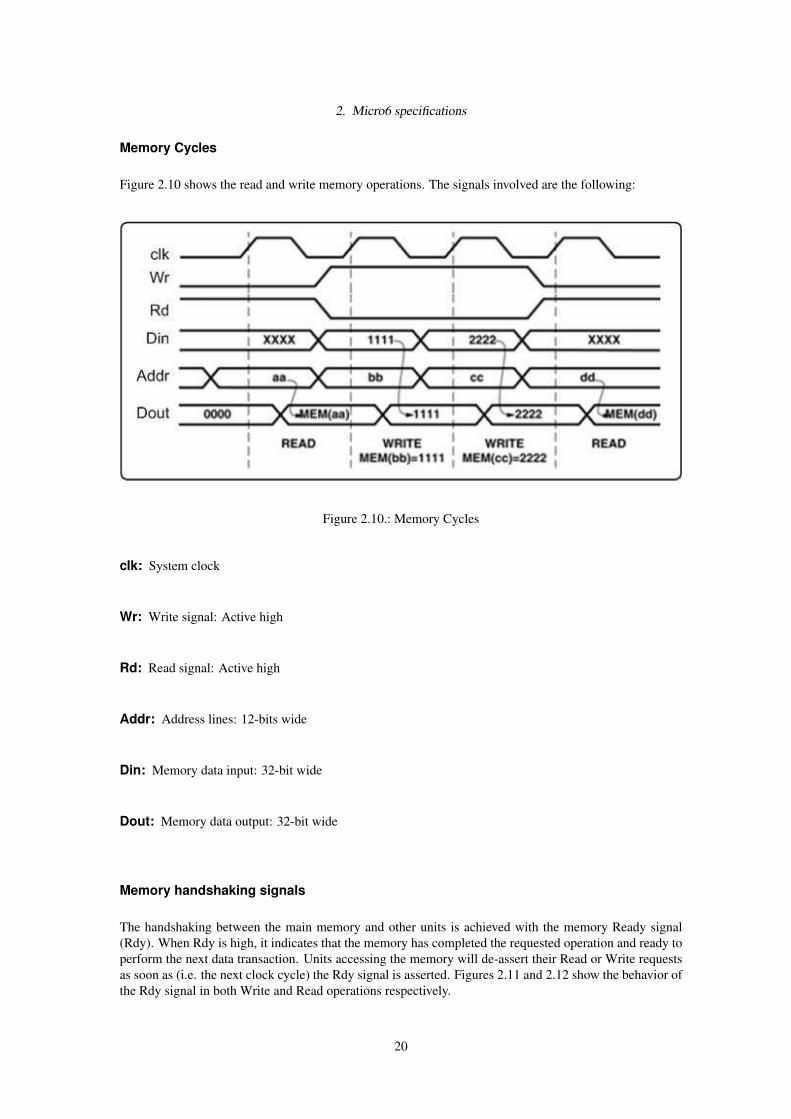
Figure 2.10 shows the read and write memory operations. The signals involved are the following:
Figure 2.10.: Memory Cycles
clk: System clock
Wr: Write signal: Active high
Rd: Read signal: Active high
Addr: Address lines: 12-bits wide
Din: Memory data input: 32-bit wide
Dout: Memory data output: 32-bit wide
Memory handshaking signals
The handshaking between the main memory and other units is achieved with the memory Ready signal(Rdy). When Rdy is high, it indicates that the memory has completed the requested operation and ready toperform the next data transaction. Units accessing the memory will de-assert their Read or Write requestsas soon as (i.e. the next clock cycle) the Rdy signal is asserted. Figures 2.11 and 2.12 show the behavior ofthe Rdy signal in both Write and Read operations respectively.
20

2. Micro6 specifications
Figure 2.11.: Memory handshaking - Write operation
Figure 2.12.: Memory handshaking - Read operation
Limitations of Micro6 memory organization
1. Micro6 does not provide any hardware means to protect the contents of any memory location againstaccident changes.
2. The maximum size of the program is variable and it depends on the initial amount of data it requires.The maximum possible program size assuming no initial data = size of the program and data segment= 3k.
3. The maximum number of constants + labelled instructions = 510.
2.2.3. Memory traffic controllerAs mentioned above, Micro6 is a Harvard machine since there are two pathways for accessing the mainmemory, one for instructions and the second for data. Conventionally, two units can not access the same
21

2. Micro6 specifications
memory simultaneously unless the memory has two ports. Arbitration can be used as an alternative. Insuch case, the two units do not actually access the memory simultaneously but each unit feels as if it hasexclusive access to memory. Mico6 Memory Traffic Controller arbitrates memory access between 3 masterunits as listed below in the order of their relative priorities:
1. Fetch unit: CPU sub-system (see section 5.2)
2. Data path: CPU sub-system (see chapter 4)
3. I/O Unit (see chapter 6)
The Memory Traffic Controller grants memory access to the competing units according to their priorities.However, the order shown above is adopted in the case when no unit is actively accessing the memory.When a unit is actively accessing the memory, it retains control until it is finished with all the memorytransactions it wishes to make. This means that the active unit assumes the highest priority.
The table below explains the priority scheme in detail.
Active UnitPriority Fetch Unit Data Path I/O Unit None
1 Fetch Unit Data Path I/O Unit Fetch Unit2 Data Path Fetch Unit Fetch Unit Data Path3 I/O Unit I/O Unit Data Path I/O Unit
Table 2.1.: Memory Traffic Controller - Priority scheme
The Memory Traffic Controller can be thought of as a set of multiplexers controlled by a finite statemachine. The current state of the FSM selects the input port of each multiplexer. However, the Rdy(memory ready) signal is treated in a special way. It is propagated from the memory to the active unit only.Other units receive a low Rdy signals.
22

2. Micro6 specifications
Figure 2.13.: Memory traffic controller
23

2. Micro6 specifications
2.3. CPU architecture
ALU
Register file
B
A
in
IR
Fetch Unit
MAR PC MBR
Control Unit
Stack
out
in
Data Bus
Memory instruction
bus
Memory data bus
Memory data address bus
Memory instruction
address bus
Figure 2.14.: CPU architecture
The CPU as shown in figure 2.14 is built of different components as listed below:
1. Register File: Holds intermediate computation data. It is explained in details in subsection 2.1.3.
2. ALU: Arithmetic and Logic Unit. It is explained in detail in section 4.2.
3. Fetch Unit: Fetches instructions from the memory. It is explained in detail in section 5.2.
4. IR: The Instruction Register: It holds the current instruction. 32-bit register.
5. Control Unit: It consists of the Decode Unit and the Execute Unit. Those are explained in detail inchapter 5.
6. PC: Program Counter3: 12-bit up-counter: It holds the address of the next instruction to be fetched.
7. Stack: Stores the contents of the Program Counter PC during subroutine calls and restores it whenreturning from subroutines. The Stack is explained in detail in section 5.5.
3In some literature, the existence of the PC is a significant feature of the von-Neumann architecture.
24

2. Micro6 specifications
8. MAR: Memory Address Register: 12-bit registers that holds the address of the memory location tobe accessed by the Data Path. The MAR is loaded from one or two registers of the Register Filewhen executing load (LD and LDX but not LDM) and store (ST, STX) instructions4. However, theMAR is loaded directly from the Control Unit when executing the LDM.
9. MBR: Memory Buffer Register: 32-bit registers that holds the data to be written or read to and fromthe main memory. It also holds the data to be transmitted or received to and from the I/O Unit.
10. Data Bus: 32-bit bus. It is implemented as a multiplexer since internal tri-state signals are notallowed in the majority of FPGA architectures. The Data Bus has 4 inputs: the ALU, the Stack, theControl Unit and the MBR. However, the term “Data Bus” does not explain its function completely.The Data Bus can carry memory addresses as well.
4For more information about these instructions, refer to chapter 3.
25
3. Instruction set
3.1. Operate groupThis group includes the instructions required to perform arithmetic and logic operations on data stored inone of the registers of the register file or the accumulator. Since Micro6 is strictly LOAD-STORE machine,instructions from the operate group use only register-direct addressing mode.
All instructions belonging to this group are performed by the ALU (Arithmetic and Logic Unit) but bydefinition, the implementation details are masked as long as the instruction set is concerned. Details ofimplementation are presented in section 4.2.
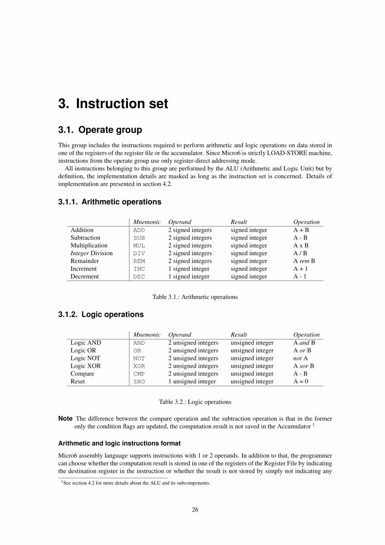
3.1.1. Arithmetic operations
Mnemonic Operand Result OperationAddition ADD 2 signed integers signed integer A + BSubtraction SUB 2 signed integers signed integer A - BMultiplication MUL 2 signed integers signed integer A x BInteger Division DIV 2 signed integers signed integer A / BRemainder REM 2 signed integers signed integer A rem BIncrement INC 1 signed integer signed integer A + 1Decrement DEC 1 signed integer signed integer A - 1
Table 3.1.: Arithmetic operations
3.1.2. Logic operations
Mnemonic Operand Result OperationLogic AND AND 2 unsigned integers unsigned integer A and BLogic OR OR 2 unsigned integers unsigned integer A or BLogic NOT NOT 2 unsigned integers unsigned integer not ALogic XOR XOR 2 unsigned integers unsigned integer A xor BCompare CMP 2 unsigned integers unsigned integer A - BReset ZRO 1 unsigned integer unsigned integer A = 0
Table 3.2.: Logic operations
Note The difference between the compare operation and the subtraction operation is that in the formeronly the condition flags are updated, the computation result is not saved in the Accumulator 1
Arithmetic and logic instructions format
Micro6 assembly language supports instructions with 1 or 2 operands. In addition to that, the programmercan choose whether the computation result is stored in one of the registers of the Register File by indicatingthe destination register in the instruction or whether the result is not stored by simply not indicating any
1See section 4.2 for more details about the ALU and its subcomponents.
26

3. Instruction set
result registers. However, in both cases, the result is stored in the Accumulator which retains its contentsuntil the next operation is executed.
Example:
ADD R1 R2 R3; -- Adds the contents of R1 and R2 and stores the result inR3.ADD R1 R2; -- Adds the contents of R1 and R2 but does not store the resultin any register.This is also possible with single operand instructions. However, in this case, the result is stored back inoperand registerINC R1 R3; -- Increments the contents of R1 and stores the result in R3INC R1; -- Increments the contents of R1 and updates them.
3.1.3. Shift and rotate operations
Mnemonic Operand Result OperationArithm. shift right SRA 1 signed, 1 unsigned signed integer A > > B; fig. 3.1Arithm. shift left SLA 1 signed, 1 unsigned signed integer A < < B; fig.3.2Logic shift right SRL 2 unsigned integers unsigned integer A > > B; fig. 3.3Logic shift left SLL 2 unsigned integers unsigned integer A < < B; fig. 3.4Rotate right RTR 2 unsigned integers unsigned integer fig. 3.5Rotate left RTL 1 unsigned integer unsigned integer fig. 3.6
Table 3.3.: Shift and rotate operations
these bits are lost
sign is extended
Figure 3.1.: Arithmetic shift right
Shift and rotate instructions format:
Micro6 supports barrel shifting and rotating operations. For this purpose, the programmer must indicatethe Shift Count in the instruction. The Shift Count can range from 1 to 31 (0 is basically accepted but itdoes not cause any shifting or rotating).
Shift Counts can be indicated in one of two possible ways:
1. Explicitly indicate the Shift Count as an integer value preceded by ’#’
2. Indicate a register whose 5 least significant bits are the Shift Count.
Remember that the same remark about storing or not storing the result applies for shift and rotate instruc-tions as well as for arithmetic and logic ones.
27

3. Instruction set
sign bit is reserved
0 0 0
these bits are lost
Figure 3.2.: Arithmetic shift left
0 0 0
these bits are lost
Figure 3.3.: Logic shift right
Examples
Assume that R2 = “1100 1010 0011 0101 1111 0000 1100 1110”If R2 is used as the Shift Count Register, then the Shift Count would be “0 1110”, i.e. decimal 14.SLA R1 R2 R3; -- Arithmetic shift left of the contents of R1 by 14 and storethe result in R3SLA R1 R2; -- like the above instruction but without saving the result.SLA R1 #6; -- Arithmetic shift left of the contents of R1 by 6 wihout storingthe result.
3.2. Data transfer group
This group includes the instructions required to move data to and from the main memory. Instructions ofthis group may utilize all supported addressing modes.
3.2.1. Copy Register CPR
CPR copies the contents of one of the Register File registers into another. In addition to that, the sourceor the destination register can be the Accumulator. Executing this instruction makes use of the ALU. Inthis way, no additional hardware resources must be provided inside the Register File to facilitate the datatransfer between two registers. Obviously, this instruction uses only the register direct addressing mode.
Example:
CPR R1 R2; -- Copies the contents of R1 into R2CPR ACC R3; -- Copies the contents of the Accumulator into R3
28

3. Instruction set
0 0 0
these bits are lost
Figure 3.4.: Logic shift left
Figure 3.5.: Rotate right
3.2.2. Load from memory LD, LDM and LDX
In order to be processed, data must be loaded from the main memory into the CPU. For this purpose, arange of instructions is provided to support different addressing modes. The destination of the loaded datais the Register File. This emphasizes the important role of the Register File as a temporary storage element.
LD
LD is the basic data loading instruction. Executing it results in moving data from the memory locationpointed to by the contents of the source register into the destination register.
Example:
LD R1 R2; -- Loads data from the memory location pointed to by R1 into registerR2.
Note: Since the width of the memory word is 32 bits, loading registers R28, R29, R30 (the IndexRegisters) and R31 (the Stack Pointer) whose width is 9 bits will result in moving the 9 least significantbits only. The hardware circuitry allows such transactions; however, loading the Stack Pointer is not advisedbecause it may cause improper operation conditions.
29

3. Instruction set
Figure 3.6.: Rotate left
LDM
LDM is the work around loading immediate data. All immediate data or constants from the programmingpoint of view are stored in the first memory page (512 locations). LDM instruction word contains theaddress of the constant which is 9 bits wide. In this way, LDM takes one memory word in addition tothe memory word in which the immediate data is stored but fetching this instruction takes one fetch cycle.Calling the data from the first memory page is performed by the Execute Unit which utilizes a separatepath to the memory.
Example:
.M1 #1234; -- This statement declares the constant M1 and assigns it thevalue 1234
Note here that the programmer does not provide any information of the physical location of the constantsin the program. The assembler does that and generates the 9-bit address for the LDM instructions that ref-erence to this particular constant.
LDM M1 R0; -- Causes the constant M1 (1234) to be loaded into registerR0.
The above two statements are equivalent to the statement below assuming the LDI stands for LoaDingImmediate data:
LDI 1234 R0
LDX
This version of load instructions uses the register indexed addressing mode. Before executing this instruc-tion, the programmer must make sure that the index register he intends to use is loaded with a valid value.The address of the data to be loaded is the sum of the contents of the index register and the source register.The data is loaded into the destination register.
30

3. Instruction set
Example
LDX R0 I1 R16; -- R0 is the source register, I1 is the index register 2 andR16 is the destination register.
The data in the memory location R0 + I1 is loaded into register R16.LDX is useful when loading elements of an array structure. The index register is not modified auto-
matically. The programmer must provide an instruction to increment or decrement the contents of theindex register before loading the next array element. This gives flexibility to the programmer to manipulateascending and descending array indices.
3.2.3. Storing data in the main memory ST, STX
During processing of data, results are stored in the Register File. Due to the limited size of the RegisterFile, data has to be stored in the main memory.
ST
This version uses the register indirect addressing mode. The contents of the source register are simplystored in the memory location pointed to by the destination register.
Example:
ST R1 R2; -- The contents of R1 are stored in the memory location whoseaddress is the contents of R2
STX
STX makes use of the indexed register addressing mode. The address of the destination memory locationis the sum of the contents of an Index Register and the destination register.
Example:
STX R7 I2 R9; -- The contents of R7 are stored in the memory location whoseaddress is (I2 + R9)
STX is useful when storing elements of an array structure. The index register is not modified auto-matically. The programmer must provide an instruction to increment or decrement the contents of theindex register before storing the next array element. This gives flexibility to the programmer to manipulateascending and descending array indices.
3.3. Program control group
These are the instructions, which control the flow of programs. Conditional branch/jump instructions readthe ALU condition flags, which are set by previous, operate instructions.
3.3.1. Branches
Branches in a program (or subroutine) cause the program flow to be routed to a different part of the programaccording to a condition. In terms of hardware, a branch involves loading the Program Counter PC withthe address of the target instruction. Executing the program instruction after modifying the PC continuesto be sequential, i.e. the PC is incremented after fetching each instruction.
2I0 is R28, I1 is R29 and I2 is R30 but the assembler VAS accepts referencing the indexregister with Ix only. Using Rx notation generates an error.
31

3. Instruction set
3.3.2. Subroutines
Calling a subroutine is similar to a branch. The difference is that subroutines must return to the callingprogram (or subroutine in case of nested subroutine calls). In hardware, this involves pushing the currentcontents of the Program Counter PC into the hardware Stack. Micro6 Stack is 16-slots deep which allowsnesting up to 16 subroutine calls.
3.3.3. Supported conditions
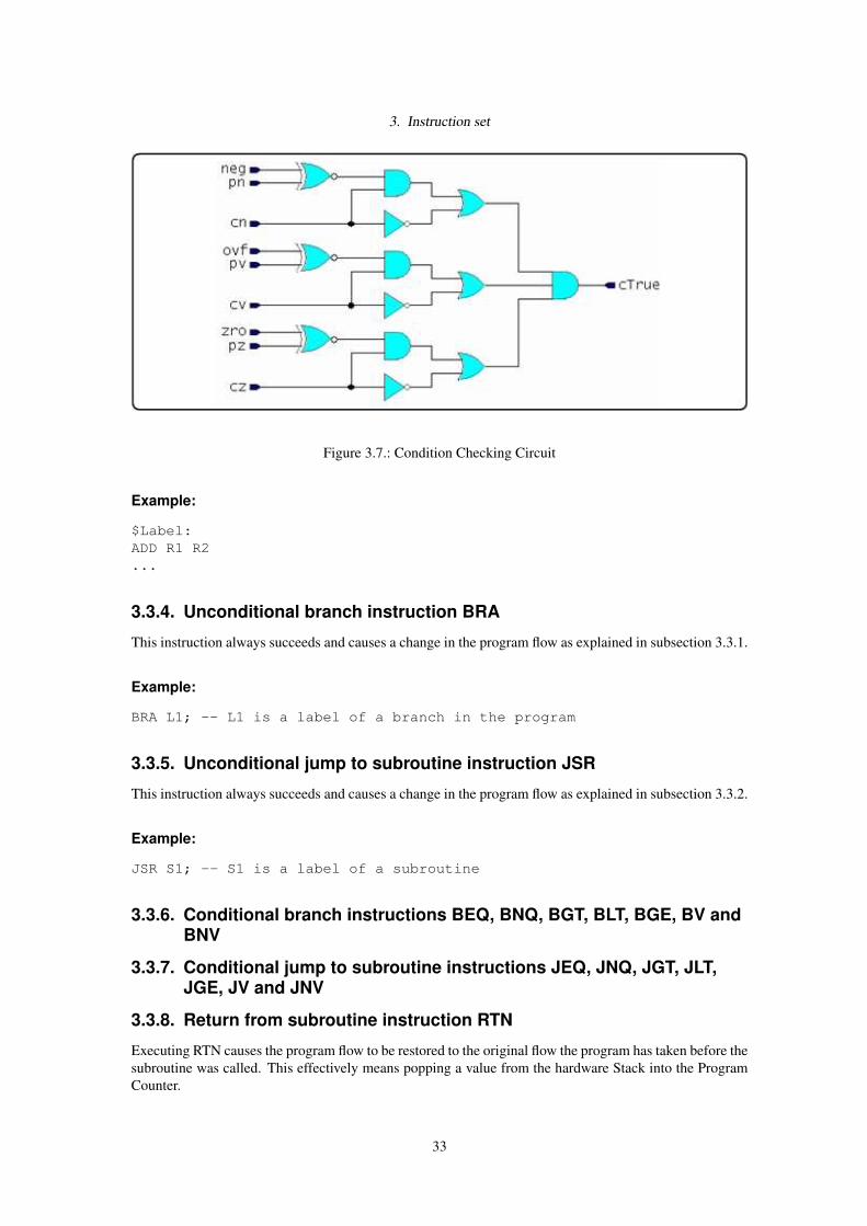
Micro6 assembly language and hardware resources support the following range of conditions to be usewith branches or subroutine calls:
Condition Abbreviation NEG OVF ZRO1 Equal (zero) EQ X X 12 Not Equal NQ X X 03 Greater than (positive) GT 0 X 04 Greater than or equal (nonnegative) GE 0 X X5 Less than LT 1 X 06 Overflow V X 1 X7 Not overflow NV X 0 X
Table 3.4.: Supported conditions
The assembler generates a 6-bit signature of the condition mentioned in the instruction. This 6-bitsignature is referred to as the Condition Mask. The Control Unit uses the Condition Mask together withactual status of the ALU Condition Flags to determine the success or failure of the encountered branchinstruction or subroutine call. The effective target addresses of these labels are calculated by the assemblerand included in the branch instructions or subroutine calls.
Bit ExplanationPN The expected polarity of the NEG flagPV The expected polarity of the OVF flagPZ The expected polarity of the ZRO flagCN Check the NEG flagCV Check the OVF flagCZ Check the ZRO flag
Table 3.5.: Condition Mask
Condition PN PV PZ CN CV CZEQ 0 0 1 0 0 1NQ 0 0 0 0 0 1GT 0 0 0 1 0 1GE 0 0 0 1 0 1LT 1 0 0 1 0 1V 0 1 0 0 1 0
NV 0 0 0 0 1 0
Table 3.6.: Condition Mask for the supported conditions
32
3. Instruction set
Figure 3.7.: Condition Checking Circuit
Example:
$Label:ADD R1 R2...
3.3.4. Unconditional branch instruction BRA
This instruction always succeeds and causes a change in the program flow as explained in subsection 3.3.1.
Example:
BRA L1; -- L1 is a label of a branch in the program
3.3.5. Unconditional jump to subroutine instruction JSR
This instruction always succeeds and causes a change in the program flow as explained in subsection 3.3.2.
Example:
JSR S1; -- S1 is a label of a subroutine
3.3.6. Conditional branch instructions BEQ, BNQ, BGT, BLT, BGE, BV andBNV
3.3.7. Conditional jump to subroutine instructions JEQ, JNQ, JGT, JLT,JGE, JV and JNV
3.3.8. Return from subroutine instruction RTN
Executing RTN causes the program flow to be restored to the original flow the program has taken before thesubroutine was called. This effectively means popping a value from the hardware Stack into the ProgramCounter.
33

3. Instruction set
Example:
RTN; -- Terminates the current (innermost, in case of nested subroutinecalls) subroutine and steers the program execution back to the calling subroutine.
3.3.9. End of program instruction ENDThis instruction terminates the program and causes the microprocessor to halt indefinitely (until it is resetagain). In case this instruction is missing, the Fetch Unit continues to fetch memory words after the lastprogram instruction word. This leads to undetermined operation.
Example:
END;
3.3.10. Null instruction NLLThis instruction causes the microprocessor to do nothing. It can be useful in some applications.
Example:
NLL;
3.4. I/O instructionsThese are explained in detail in chapter 6.
34

4. Data path
The data path of Micro6 is where the data is manipulated. It consists of the logic circuits necessary forperforming different operations on the data. It also consists of the registers used to hold intermediatecomputation data and results.
4.1. Register file
The Register File of Micro6 is explained in detail in subsection 2.1.3.
4.2. ALU
Micro6 ALU is built of a combinatinoal logic core and an Accumulator to hold the computation results.
Figure 4.1.: ALU
4.2.1. ALU operations
The operations supported by Micro6 ALU are the arithmetic, logic and shift operations explained in section3.1.
35

4. Data path
4.2.2. ALU operandsThe combinational logic core of the ALU receives one or two operands depending on the operation to beperformed. An operand can be either one of the following:
1. One of the Register File registers: indicated by Rx in the instruction. Where x is a number from 0 to31.
2. The Accumulator: indicated by ACC in the instruction.
3. Shift Count (for the shifter only)
4.2.3. ALU computation resultAs mentioned before, the ALU output is stored in the ACC before further manipulation or routing of thedata occurs. The ALU updates 3 Condition Flags according to its operation and result.
Flag ConditionNEG Negative The result is negativeOVF Overflow The result exceeds the representation range of 32-bit signed numberZRO Zero The result is zero
Table 4.1.: Condition Flags
Updating the Condition Flags or not updating them depends on the operation performed. This is to insurethat Condition Flags update is associated with computation operations only. That is, Condition Flags arenot updated during data transfer operation through the ALU for instance.
4.2.4. ALU controlThe ALU receives several control signals from the Control Unit as follows:
1. ALUSel (ALU Select): An unclocked signal that selects which operation to be performed. Possiblevalues are the range of operations supported by the ALU.
2. ACCEn (Accumulator Enable): A clocked signal to enable the Accumulator ACC when the operationhas been completed.
3. CFEn (Condition Flags Enable): A clocked signal to enable the Condition Flags CF when the com-putation operation has been completed.
4. AACC (A is ACC): An uncloced signal that determines whether the left operand is a register or theACC.
5. BACC (B is ACC): An uncloced signal that determines whether the right operand is a register or theACC.
6. ShiftCntSrc (Shift Count Source)(for the shifter only): An unclocked signals that determines thesource of the shift count. It could be either the B input of the Shift Count input.
36

5. Control unit
5.1. Structure and pipelining
The control unit of Micro6 can be split into 3 sub-units: fetch unit, decode unit and execute unit. Theindividual sub-units will be explained briefly in the next sections.
Fetch Unit
Execute Unit
Decode Unit
Control Unit outputs
Decode bundle
Execute bundle
Instruction word
Instruction word from
memory
clock
Figure 5.1.: Control unit structure
Micro6 provides for instruction pipelining. The pipeline is composed of 2 stages:
1. Fetching the instruction
2. Decoding and executing the instruction
The pipeline of Micro6 is one slot long only. This means that during decoding and executing a giveninstruction, the fetch unit should be busy fetching the next to next instruction from memory.
Implementing a longer pipeline for Micro6 would not be efficient because they exhibit significant branchpenalty. When a branch of jump instruction is encountered, the pipeline has to be cleared (flushed) andthe first instruction on the branch subroutine be pushed to the top of the pipeline. Pushing an instructionthrough the entire pipeline takes as many clock cycles as the number of pipeline slots. Unfortunately, thebranch penalty is inevitable and it is equal to the length of the pipeline. In Micro6, the branch penalty islimited to 1 clock cycle.
5.2. Fetch unit
The Fetch Unit fetches instructions from the memory. The Program Counter holds the address of theinstruction to be fetched. The Fetch Unit is implemented as a finite state machine FSM. It halts when
37

5. Control unit
text text Fetch Decode Execute
Stage 1 Stage 2
Figure 5.2.: Instruction pipeline
no instructions are needed to be fetched, this is the case when the Instruction Register IR holds the nextinstruction and the Execute Unit is busy with the current one.
Figure 5.3 shows the state diagram of the Fetch Unit FSM. In this figure, a signal name means that thissignal is asserted (active).
Figure 5.4 shows the interface lines between the Fetch Unit, the Execute Unit, Memory and ProgramCounter PC. The signals shown in the figure are:
memAddr: Memory address lines
memData: Memory data output
memReady: Memory Ready signal
memRd: Memory Read signal
IR: Instruction Register output
vldInstr: A one-clock wide pulse indicates that the IR lines carry Valid Instruction
readInstr: (Read Instruction): A one-clock wide pulse issued by the Execute Unit in order to requestfetching the next instruction.
38

5. Control unit
Figure 5.3.: Fetch Unit state diagram
Figure 5.4.: Fetch Unit Interfaces
5.3. Decode unit
The Decode Unit is a combinational logic circuit. It decodes the instructions by generating the DecodeBundle which consists of unclocked control signals and additional decoding signals to the Execute Unit.
39

5. Control unit
• The unclocked signals are those which don’t change during the instruction execution cycles.
• The additional decoding signals are those which are passed to the Execute Unit. The Execute Unituses them to generate clocked (synchorizing) signals to the different parts of the microprocessor.
5.4. Execute unitThe Execute Unit is a relatively large FSM (67 states). It is driven by the decoding signals from the DecodeUnit and it outputs the signals that control the operation of the rest of the microprocessor components.
5.5. StackThis is the hardware Stack. It is different from the stack segment in the main memory in that the formeris implemented in a set of registers inside the CPU. It also uses another stack pointer. This stack is usedto store the current contents of the Program Counter PC when a subroutine call is encountered and restorethem when returning from the subroutine so that the program can resume its original flow. The user doesnot have any access to this stack.
Micro6 Stack is built of 16 9-bit slots and a 4-bit updown counter. A simple FSM controls pushing andpopping data to and from the stack. The operation of Micro6 Stack follows the classical stack operation asexplained below:
Pushing data into the stack:
• First clock cycle: Storing the input data in the stack slot pointed to by the Stack Pointer.
• Second clock cycle: Incrementing the Stack Pointer.
Popping data from the stack:
• First clock cycle: Decrementing the Stack Pointer.
• Second clock cycle: Reading the contents of the stack slot pointed to by the Stack Pointer.
40

5. Control unit
Figure 5.5.: Stack
41

6. I/O unit
Micro6 I/O unit performs two primary functions. The first of which is managing data transfer between theCPU and the attached I/O devices. This function will be referred to as Basic I/O in the remainder of thisbook. The second primary function is facilitating Direct Access Memory DMA. Micro6 I/O unit makesit possible to transfer blocks of data from the main memory to the I/O devices and in the other directionwithout any CPU intervention.
Micro6 assembly language provides 4 instructions for all possible I/O operations as will be explainedshortly.
The data width of external buses connected to Micro6 is 8 bits. The reason is that the majority of I/Odevices and adaptors expect 8 bit communication paths with the CPU. For example, Intel ProgrammableParallel Interface PPI 8255 contains 4 registers (3 data, 1 control) each is 8 bits wide. It also has 3 8-bit I/O ports. Serial I/O devices usually provide 8-bit interface with the CPU. For example UniversalAsynchronous Receiver-Transmitters UARTs.
Micro6 allows receiving and transmitting 8-bit data as well as 32-bit data. 8-bit data communicationis straightforward whereas 32-bit data communication involves breaking the transmitted data into 4 bytesor assembling 4 received bytes to build a 32-bits word. The process of breaking and assembling data isperformed within the I/O unit without any intervention from the CPU. Having the I/O unit to perform thisprocess independently requires a handshaking protocol with the I/O devices to insure proper data transferand avoid data collision. The handshaking protocol uses two ready signals. Depending on the particularI/O device, none, 1 or both of the ready signals are utilized.
6.1. I/O Instructions
There are 4 instructions associated with I/O operations because Micro6 I/O Unit transmits and receivesdata in two different widths. The I/O instructions are as follows:
1. Input Byte INB: Receive a byte from an I/O device
2. Input Word (32-bit) INW: Receive a word from an I/O device.
3. Output Byte OUB: Transmit a byte to an I/O device.
4. Output Word (32-bit) OUW: Transmit a word to an I/O device.
The general format of I/O Instructions is
OPC DEV_ID [ SRC | DST ]
Where OPC is one of the opcodes shown above, DEV_ID is the Device ID (an identifier from D0 toD63), SRC is the source register in case of Output operations and DST is the destination register in case ofInput operations. SRC and DST can be any of the registers of the Register File (subsection 2.1.3).
6.2. Basic I/O
Basic I/O means simply transmitting or receiving a byte or a word to or from an I/O device. The basic unitis always a byte. Before transmitting or receiving a byte, the I/O Unit makes sure that the I/O device men-tioned in the instruction is ready for the transaction. This is indicated by high Pre-transaction Ready signal
42

6. I/O unit
(pre-ready). I/O Unit waits until the I/O device indicates the completion of the transaction by asserting thePost-transaction Ready signal (post-ready)1.
Word transaction is performed as if they were 4 byte transactions.When the transaction is complete (indicated by the I/O device), the I/O Unit declares this to the CPU by
asserting the Ready signal (see subsection 6.4.1).
6.3. Direct Memory Access DMAThe I/O Unit dedicates 3 registers for DMA operations as shown in table 6.1 . User programs write valuesinto these registers in exactly the same manner as if they were I/O devices. However, when DMA registersare selected, I/O instructions are interpreted in a different way. For example, writing and reading to theStarting Address Register SAR are equivalent; both operations effectively write into that register. The sameapplies for the Device ID Register DIR. The DMA operation is initiated when the Burst Length RegisterBLR is loaded. The direction of the transaction and width of the transaction data is determined by theopcode of the instruction that loads the BLR.
Register Description Instruction EffectSAR Starting Address Register INW D62 R0; and OUW D62 R0; SAR <- R0DIR Device ID Register INB D62 R1; and OUB D62 R1; DIR <- R0BLR Burst Length Register See table 6.2
Table 6.1.: DMA Registers
Instruction EffectINB D63 R2; BLR <- R2 and start receiving a burst of bytesINW D63 R2; BLR <- R2 and start receiving a burst of wordsOUB D63 R2; BLR <- R2 and start transmitting a burst of bytesOUW D63 R2; BLR <- R2 and start transmitting a burst of words
Table 6.2.: BLR operations
6.3.1. Loading the Starting Address Register SARYou load the SAR by writing (or reading) a WORD into device 62. An example is shown below assumingthat the starting address initially resides in R1
OUW D62 R1 or
INW D62 R1
6.3.2. Loading the Device ID Register DIRNote that loading the DIR is associated only with DMA operations. In Basic I/O operation, you specify thedevice ID in the instruction.
You load the DIR by writing (or reading) a BYTE into device 62. An example is shown below assumingthat the device ID initially resides in R1
OUB D62 R1 or
INB D62 R11Pre-transaction Ready and Post-transaction signals will be explained in detail in subsection 6.4.2.
43

6. I/O unit
6.3.3. Loading the Burst Length Register BLR and initiating DMAoperations
Loading the BLR initiates the DMA operation. So, you need to specify what kind of operation is requiredby using the appropriate I/O instruction as shown in the examples below. All the examples assume that theburst length initially resides in R1.
• Receiving a block of bytes: INB D63 R1
• Receiving a block of words: INW D63 R1
• Transmitting a block of bytes: OUB D63 R1
• Transmitting a block of words: OUW D63 R1
6.4. I/O Unit interfaces
6.4.1. CPU Interface
The I/O Unit is connected to the CPU by two sets of buses:
1. 2 data buses: 1 for input data from the CPU and 1 for output data to the CPU. In the CPU end, thesebuses are connected to the MBR (Memory Buffer Register).
2. Control lines: carry instructions from the CPU as well as the address of the I/O device.Table 6.3shows the CPU-I/O-Unit control lines in detail.
Signal Direction Functionrd in Read operationwr in Write operationready out I/O operation is completewordByte in Data is 32-bit words or 8-bit bytesdeviceID in Device ID
Table 6.3.: Control Lines from the CPU to the I/O Unit
6.4.2. External devices interface
External devices handshaking
External devices can use one or two lines for handshaking in order to guarantee the validity of data transfers:
Rdy_pre: Indicates that the selected I/O device is ready to initiate a data transaction.
Rdy_post: Indicates that the selected I/O device has successfully finished a data transaction.
External devices interface lines
Figure 6.1 shows an I/O external device connected to the I/O Unit. The example I/O device is able to inputand output data and it uses both Rdy_pre and Rdy_post handshaking lines2. Explanation of the shownsignals is given in table 6.4.
2This example is only for demonstration. Usually, I/O devices perform either input or output operations. They rarely perform bothand in that case, they are looked at as 2 separate I/O devices, one for input and the other for output data.
44

6. I/O unit
Figure 6.1.: External devices interface
Signal Width DescriptionExtDin 8 Data bus from the external devices to the I/O Unit
ExtDout 8 Data bus from the I/O Unit to the external devicesExtRd 1 A control line that instructs the external device to perform a read (input) operationExtWr 1 A control line that instructs the external device to perform a write (output) operation
Device-ID 6 External device selection linesRdy_pre 1 Handshaking lineRdy_post 1 Handshaking line
CS 1 Chip Select
Table 6.4.: External devices interface
6.4.3. Memory interface
The I/O Unit communicates with the Main Memory through the Memory Traffic Controller utilizing theregular memory access interface.
6.5. UART
To demonstrate the I/O functions of Micro6, a UART is attached to it. The UART design is available fordownload from the OpenCores website (www.opencores.org). However, since Micro6 I/O Unit does notsupport interrupts, the interrupts were removed from the original downloaded UART files. In addition tothat the baud rate generator was modified to support 115.200 Kbps baud rate.
6.5.1. UART functions:
The UART can perform either of 3 I/O functions as shown in table 6.5. For this reason, the I/O Unit seesthe UART as 3 I/O devices.
45

6. I/O unit
Function Device1 Receiving data D02 Transmitting data D13 Reporting its status D2
Table 6.5.: UART I/O functions
6.5.2. Attaching the UART to Micro6 I/O Unit
The UART is attached to Micro6 U/O Unit as shown in figure 6.2. The signals shown in the figure areexplained below:
ExtRd and ExtWr I/O Unit Read and Write signals respectively (active high)
nRD and nWr UART Read and Write signals respectively (active low)
ExtDin(0)..(2) I/O Unit data input buses (connected to a multiplexer)
Dout UART data output bus
ExtDout I/O Unit data output bus
Din UART data input bus
cs(0)..(2) I/O Unit chip select signals (output from a decoder)
cs UART chip select input
addr(0) and addr(1) UART address input
pre_rdy(0) and pre_rdy(1) I/O Unit pre_rdy signals (connected to a multiplexer)
Rdy UART Receiver Ready signal. It indicates that the UART is ready to perform a Receive operation
TBUFE UART Transmit Buffer Empty signal. It indicates that the UART is ready to perform a Transmitoperation
46

6. I/O unit
Figure 6.2.: UART Connection
47

7. Programming Micro6
7.1. Micro6 assembly language
Assembly language or simply assembly is a human-readable notation for the machine language that aspecific computer architecture uses. Machine language, a pattern of bits encoding machine operations, ismade readable by replacing the raw values with symbols called mnemonics. Mnemonics replace opcodesas well as references to operands, for example, register names and immediate data. An assembly languagestatement may convey additional information too, for example, addressing modes and cross references toother parts of the program.
Since Micro6 supports its own instruction set and instruction formats, an assembler was required. VASassembler was developed for this purpose. VAS is explained in detail in section 7.2.
7.1.1. Micro6 assembly language directives
In addition to codes of the machine instructions, Micro6 assembly languages provides extra directives forassigning address locations for instructions or code. For simplicity of programming, the layout of the pro-gram in memory is transparent to the programmer. However, instructions can be referenced symbolicallyby labels.
Micro6 assembly has a simple symbolic capability for defining immediate data as constants. Rememberthat Micro6 does not support immediate addressing mode but this mode is substituted by page-0 addressingmode as explained in section 2.1.2.
Like most computer languages, comments can be added to the source code; these often provide usefuladditional information to human readers of the code but are ignored by the assembler and so may be usedfreely.
7.2. Micro6 VAS assembler
VAS stands for VHDL Assembler because it was written in VHDL, exploiting the programming capabilitiesof the hardware description language. Moreover, the output of VAS is a VHDL package containing themachine code. VAS is not an executable program. It must be invoked, or rather loaded and run, by an HDLsimulator.
VAS is a 2-pass cross assembler:
2-pass assembler: VAS goes through the source code (in assembly language) twice. The internal database is built in the first pass, which is used later in the second pass. This is explained in detail in7.2.4.
Cross assembler: VAS produces machine code for the Micro6 microprocessor while it runs on a dif-ferent computer system. Cross assemblers and compilers are usually used with new computer ar-chitectures since running native compilers on such systems may produce unreliable results in earlydevelopment stages.
7.2.1. VAS components
VAS is composed of 3 VHDL units as follows:
1. VAS entity and architecture: this is the unit that is loaded by the simulator.
48

7. Programming Micro6
2. Assembler package: a package containing the functions and procedures used by the assembler.
3. VHDL templates of the output file.
7.2.2. VAS input files1. Assembly language program (Program segment)
2. Memory initial data (Data segment): this file is optional
7.2.3. VAS output files1. VHDL package that declares the initial memory contents as a deferred constant. Using deferred
constants makes recompiling other design units unnecessary. However, compiling the output file isstill necessary.
2. Memory Coefficients file (COE). This file is used by Xilinx CoreGen to generate the necessary BlockRAM modules and initialize their contents.
7.2.4. VAS operationShort DOS scripts were developed to run VAS through invoking ModelSim in batch mode. When exe-cuted, the script accepts the assembly program file and the memory initial data file, loads the assembler inModelSim, runs it. The script also compiles the output package.
49

8. Realization
Figure 8.1 shows the design flow adopted for realizing Micro6. Further details of each process are providedin the subsequent sections.
Figure 8.1.: Design Flow
50

8. Realization
8.1. Design Entry
8.1.1. Design Files
Micro6 is described in VHDL in a number of files. Each file contains either a package-package-body- oran entity-architecture pair. Packages contain declarations (and specifications) of constants, functions andprocedures that are shared by multiple entities, architectures and other packages.
Table 8.1 shows a list of the design files:
Compileorder
File name Description
1 micro_pk.vhd The main design package containing the general constants, func-tions and procedures declarations
2 micro_control_pk.vhd A package containing declarations related to the Control Unit +the Decode Unit
3 micro_comp_pk.vhd A Package declaring all components referenced in the structuraldescriptions of some units
4 register_en.vhd Register with asynchronous reset and enable inputs (variablewidth)
5 counter.vhd Up-counter with asynchronous reset input (variable width)6 counter_updown.vhd Updown-counter with asynchronous reset input (variable width)7 mux2bus.vhd 2-input multiplexer (variable width)8 mux4bus.vhd 4-input multiplexer (variable width)9 alu.vhd The ALU10 regFile.vhd The Register File11 stack.vhd The Stack12 fetch.vhd The Fetch Unit13 control.vhd The Control Unit (Decode Unit instantiation + Execute Unit)14 cpu.vhd The CPU (structural description)15 micro_ram_pk.vhd A package defining the initial memory contents for simulation
purposes16 memory.vhd A behavioural model (takes a long time for synthesis) of the
Main Memory17 micro6_ram.vhd A VHDL description of the BlockRAM generated by CoreGen18 main_memory.vhd A wrapper for the VHDL description of the BlockRAM gener-
ated by CoreGen19 dcm_1.vhd Digital Clock Manager20 dma.vhd The I/O Unit including the DMA functions21 memCtrl.vhd The Memory Traffic Controller22 baud.vhd The Baud Rate Generator for the UART23 TxUnit.vhd The UART Transmitter24 RxUnit.vhd The UART Receiver25 miniUART.vhd The UART top-level26 system.vhd Micro6 top-level27 assembler_pk.vhd The Assembler package28 assembler.vhd The Assembler entity-architecture pair
Table 8.1.: Design Files
8.1.2. Finite State Machine style
The FSM style adopted in designing almost all of the state machines of Micro6 is registered-outputs MooreFSM with the output decoded from the next state. This saves one clock cycle compared with decoding the
51

8. Realization
output from the current state. It also shows the advantages of registering the outputs, avoiding glitches forexample.
Figure 8.2.: FSM Style
8.2. Functional Verification
All the main modules of Micro6 (expect the Control Unit) were functionally verified using full test-benches1. The testbenches were written according to the functional specifications of the individual unitsunder test UUT.
1A full testbench is defined as a testbench that generates the input stimuli and verifies the outputs against their expected values.
52

8. Realization
Figure 8.3.: Full testbench
In order to verify the complete system, another approach was adopted: A few sample programs werewritten in Micro6 assembly language along with the expected outcome. The programs were run on Micro6and the outcome was compared with the expected one.
Sample program: Selection sort
Figure 8.4 shows an example of sorting a 6-element list using selection sort in ascending order.
53

8. Realization
Figure 8.4.: Example of selection sort
The purpose of this program is to verify a subset of Micro6 instructions. The program sorts a list ofnumbers using the selection sort algorithm in descending order. The list is identified by a memory locationwhich contains the number of elements. The elements of the list occupy consecutive memory locations.The program is built of the main function that calls two subroutines, the first of which swaps two listelements and the second finds the maximum element in a given sublist. The program source code and theinitial test data file are provided in appendix B.
The program is compiled using VAS which generates a memory model containing the program and thetest data. The microprocessor is then simulated and the memory contents are captured and compared withexpected values.
8.3. Synthesis
Since the target implementation technology is a Xilinx FPGA, ISE 7.1i is the selected implementationenvironment. Micro6 was synthesized on XST (Xilinx Synthesis Technology).
The Synthesis is targeted to a Xilinx Virtex2Pro30 (xc2vp30-7-ff896) FPGA. A few snippets of thesynthesis report are provided below. The final synthesis report is provided in A.
8.3.1. Device utilization
Item Total Count UtilizationSlices 13696 2006 (14%)Slice flip flops 27392 1574 (5%)4 input LUTs 27392 3160 (11%)Bounded IOBs 556 4 (0%)BRAMs 136 8 (5%)Multipliers (18x18) 136 1 (0%)GCLKs 16 2 (12%)DCM_ADVs 8 1 (12%)
Table 8.2.: Device Utilization
54

8. Realization
8.3.2. Timing Summary
Item ValueMinimum period 5.251nsMaximum frequency 190.454MHzMinimum input arrival time before clock 2.240nsMaximum output required time after clock 9.079nsMaximum combinational path delay 0
Table 8.3.: Timing Summary
8.4. Implementation
What is meant in this context is the broad concept of FPGA implementation which includes all the processesbeyond the logic synthesis down to generating the configuration bitstream. The detailed description of suchprocesses is outside the scope of this thesis.
Additional units are added only in the implementation stage. These include the block RAM and DCM.
8.4.1. BlockRAM
For efficient utilization of the hardware resources available on the target device, CoreGen is used to generatethe memory blocks. The options listed below are passed to CoreGen:
• Core type: Single Port Block Memory v6.1
• Port configuration: Read and Write
• Width: 32
• Depth: 4096
• Write mode: Read after Write
• Primitive selection: Optimize for Area
• Design options: Enable pin (NO); Handshaking pins (YES); Register inputs (NO)
• Active clock edge: Rising edge triggered
• Write enable: Active-high
• Coefficients file: ram.coe (Generated by VAS).
8.4.2. DCM: Digital Clock Manager
DCM is a digital clock manager that provides multiple functions. It can implement a clock delay lockedloop, a digital frequency synthesizer, digital phase shifter, and a digital spread spectrum.
A DCM is instantiated in the top level of Micro6 to provide the clock pulses only after phase lock2 hasbeen achieved.
2Phase lock: the input clock is in phase with the feedback clock.
55
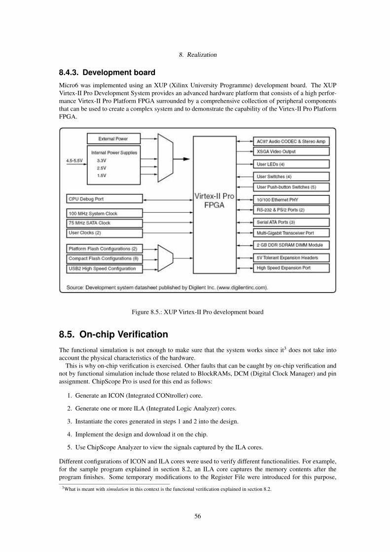
8. Realization
8.4.3. Development boardMicro6 was implemented using an XUP (Xilinx University Programme) development board. The XUPVirtex-II Pro Development System provides an advanced hardware platform that consists of a high perfor-mance Virtex-II Pro Platform FPGA surrounded by a comprehensive collection of peripheral componentsthat can be used to create a complex system and to demonstrate the capability of the Virtex-II Pro PlatformFPGA.
Figure 8.5.: XUP Virtex-II Pro development board
8.5. On-chip VerificationThe functional simulation is not enough to make sure that the system works since it3 does not take intoaccount the physical characteristics of the hardware.
This is why on-chip verification is exercised. Other faults that can be caught by on-chip verification andnot by functional simulation include those related to BlockRAMs, DCM (Digital Clock Manager) and pinassignment. ChipScope Pro is used for this end as follows:
1. Generate an ICON (Integrated CONtroller) core.
2. Generate one or more ILA (Integrated Logic Analyzer) cores.
3. Instantiate the cores generated in steps 1 and 2 into the design.
4. Implement the design and download it on the chip.
5. Use ChipScope Analyzer to view the signals captured by the ILA cores.
Different configurations of ICON and ILA cores were used to verify different functionalities. For example,for the sample program explained in section 8.2, an ILA core captures the memory contents after theprogram finishes. Some temporary modifications to the Register File were introduced for this purpose,
3What is meant with simulation in this context is the functional verification explained in section 8.2.
56

8. Realization
namely one of the registers was used as a debug register. The ILA core is triggered when the debug registeris loaded with a certain value.
ICON
ChipScope Pro achieves the communication between the PC (Personal Computer) and the FPGA chip overthe JTAG chain. The ILA cores are controlled by the ICON core which is connected to the JTAG chain. Atleast one ICON core must be implemented in order to use ChipScope Pro.
ILA
The amount of observability of the design performance that on-chip verification provides is constrained bythe configuration of the ILA cores and the size of BlockRAM assigned for them. Clearly, these in turnare constrained by the size of the target chip and that of the design. So, the designer has to use the ILAcores carefully to achieve the maximum possible view over the design with efficient use of the availableresources.
The ILA configuration parameters are:
1. The number of signals to be monitored.
2. The number of signals used to trigger the ILA. A combination of triggering conditions can be con-figured after implementation.
3. The amount of memory (BRAM blocks) assigned to store the values of the monitored signals.
57

9. Further developments
This chapter suggests some of the developments that can be done for Micro6 to improve its performanceor increase its functions.
9.1. Pipelining the ALUBarrel shifters are used to implement the shifting operations. Barrel shifters exhibit long propagation delaysand fall on the critical path of the design.
The current design allows shifting by up to 31 locations. Breaking it down into 3 stages is straightfor-ward. The control unit must be modified to control the pipeline. The control unit and ALU can be madeintelligent to steer the data in different paths and hence save 1 or 2 clock cycles according to the shift count.
9.2. IO OperationsThe current design causes the Control Unit to halt until the IO operation is complete. This is not efficient forsome operations. For example, in most cases, there is no need for the control unit to halt during outputtinglarge blocks of data. The control unit can be equipped with a means to decide whether to wait for the IOoperation to complete or not.
9.3. IO devicesAdditional IO devices can be attached to Micro6. Micro6 allows up to 62 devices. Further developers areencouraged to implement the following devices:
1. System clock and timer
2. Random number generator
3. Attaching a parallel interface such as Intel PPI (Programmable Peripheral Interface)
58

10. References and Software tools
10.1. References[1] Larry L Wear, James R Pinkert, Larry C Wear and William G Lane. An introduction to hardware andsoftware design. McGraw-Hill Education, 1991.
[2] Robert J. Baron and Lee Higbie. Computer architecture. Addison-Wesley publishing company, 1992.
[3] OpenCores website: www.opencores.org
10.2. Software packages[1] Xilinx ISE 7.1i[2] Mentor Graphics ModelSim SE 6.0a
59

A. Final Synthesis Report
Figure A.1.: Final synthesis report
60

A. Final Synthesis Report
Figure A.2.: Final synthesis report (continued)
61
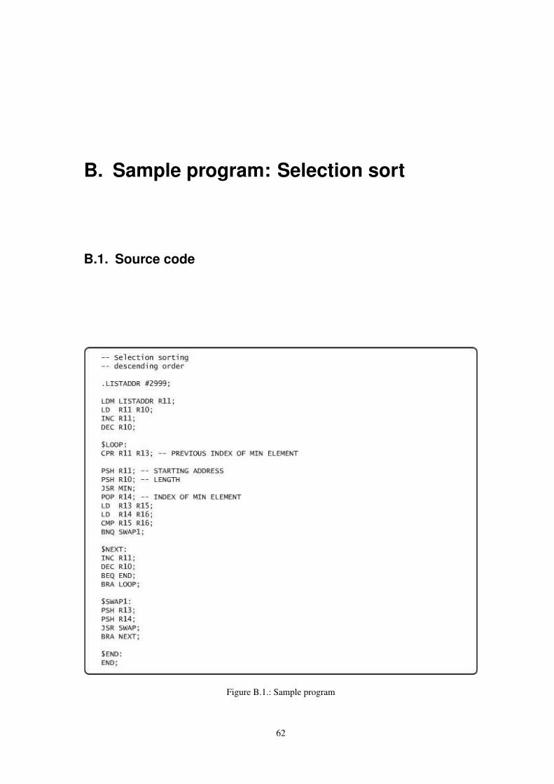
B. Sample program: Selection sort
B.1. Source code
Figure B.1.: Sample program
62

B. Sample program: Selection sort
Figure B.2.: Sample program (continued)
B.2. Test data
The figure below shows a portion of the test data file. The full set of data is 100 elements.
63

B. Sample program: Selection sort
Figure B.3.: Test data
64