Co-design of a differential transimpedance amplifier and ...
17
Research Article Vol. 28, No. 9 / 27 April 2020 / Optics Express 14038 Co-design of a differential transimpedance amplifier and balanced photodetector for a sub-pJ/bit silicon photonics receiver K E L I , 1,* S HENGHAO L IU, 1 X IAOKE RUAN , 2 DAVE J. T HOMSON , 1 YANG H ONG , 1 FAN YANG , 2 L EI Z HANG , 2 C OSIMO L ACAVA , 1 FANFAN MENG , 1 WEIWEI Z HANG , 1 P ERIKLIS P ETROPOULOS , 1 FAN Z HANG , 2 AND G RAHAM T. R EED 1 1 Optoelectronics Research Centre, University of Southampton, Southampton, SO17 1BJ, UK 2 State Key Laboratory of Advanced Optical Communication Systems and Networks, Frontiers Science Center for Nano-optoelectronics, Department of Electronics, Peking University, Beijing 100871, China * [email protected] Abstract: This paper presents the design and implementation of a fully differential optical receiver, which is aimed for short reach intensity modulation and direct detection (IMDD) transceiver links. A Si-Ge balanced photodetector (PD) has been co-designed and packaged with a novel differential transimpedance amplifier (TIA). The TIA design is realized with a standard 28 nm CMOS process and operates with a standard digital supply (1V). Without using any equalization or DSP techniques, the proposed receiver can operate up to 54 Gb/s with a BER less than the KP4 limit (2.2×10 -4 ) under an optical modulation amplitude (OMA) of -8.6 dBm, while the power efficiency has been optimized to 0.55 pJ/bit (0.98 pJ/bit if output buffer is included). Published by The Optical Society under the terms of the Creative Commons Attribution 4.0 License. Further distribution of this work must maintain attribution to the author(s) and the published article’s title, journal citation, and DOI. 1. Introduction Global interest in developing silicon photonic interconnects to meet the growing demands for short reach communication has increased dramatically over the last decade [1]. On the receiver side, this has led to significant research effort in developing direct detection receivers, including the development of high bandwidth, high responsivity silicon photonics photodetectors, high-speed, low noise transimpedance amplifiers, and advanced digital signal processing (DSP) techniques for complex modulation formats within an IMDD transceiver. While there has been a great deal of research effort on these individual topics, consideration of the integration of these design aspects is limited. In this work, we present an integrated silicon photonics receiver where the PD and TIA are co-designed synergistically in terms of process selection, device packaging, power efficiency, bandwidth, noise figure, and detection scheme. Generally, bandwidth and noise figure are the most critical parameters for the design of the TIA. In the past few years, many designs [2–6] using advanced BiCMOS technology have been reported. Using a 3.3V power supply, a 100 Gb/s differential BiCMOS TIA was reported with 8 pA/ √ Hz averaged input-referred noise current density in [5]. In [6], a differential optical receiver operating at 90 Gb/s with a sensitivity of -7.1 dBm OMA was reported by using a 55 nm BiCMOS process with a 3.3V power supply. Compared to the use of the BiCMOS process, the inclusion of the TIA design in a standard bulk CMOS process offers the advantages of lower cost and power consumption. Moreover, adopting the same standard CMOS process for the TIA in the optical receiver as for the subsequent DSP chips eliminates the need for interconnection between the two modules. #389889 https://doi.org/10.1364/OE.389889 Journal © 2020 Received 6 Feb 2020; revised 21 Mar 2020; accepted 26 Mar 2020; published 24 Apr 2020
-
Upload
khangminh22 -
Category
Documents
-
view
0 -
download
0
Transcript of Co-design of a differential transimpedance amplifier and ...
Research Article Vol. 28, No. 9 / 27 April 2020 / Optics Express 14038
Co-design of a differential transimpedanceamplifier and balanced photodetector for asub-pJ/bit silicon photonics receiver
KE LI,1,* SHENGHAO LIU,1 XIAOKE RUAN,2 DAVE J. THOMSON,1
YANG HONG,1 FAN YANG,2 LEI ZHANG,2 COSIMO LACAVA,1
FANFAN MENG,1 WEIWEI ZHANG,1 PERIKLIS PETROPOULOS,1
FAN ZHANG,2 AND GRAHAM T. REED1
1Optoelectronics Research Centre, University of Southampton, Southampton, SO17 1BJ, UK2State Key Laboratory of Advanced Optical Communication Systems and Networks, Frontiers ScienceCenter for Nano-optoelectronics, Department of Electronics, Peking University, Beijing 100871, China*[email protected]
Abstract: This paper presents the design and implementation of a fully differential opticalreceiver, which is aimed for short reach intensity modulation and direct detection (IMDD)transceiver links. A Si-Ge balanced photodetector (PD) has been co-designed and packaged witha novel differential transimpedance amplifier (TIA). The TIA design is realized with a standard28 nm CMOS process and operates with a standard digital supply (1V). Without using anyequalization or DSP techniques, the proposed receiver can operate up to 54 Gb/s with a BER lessthan the KP4 limit (2.2×10⁻⁴) under an optical modulation amplitude (OMA) of -8.6 dBm, whilethe power efficiency has been optimized to 0.55 pJ/bit (0.98 pJ/bit if output buffer is included).
Published by The Optical Society under the terms of the Creative Commons Attribution 4.0 License. Furtherdistribution of this work must maintain attribution to the author(s) and the published article’s title, journalcitation, and DOI.
1. Introduction
Global interest in developing silicon photonic interconnects to meet the growing demands for shortreach communication has increased dramatically over the last decade [1]. On the receiver side,this has led to significant research effort in developing direct detection receivers, including thedevelopment of high bandwidth, high responsivity silicon photonics photodetectors, high-speed,low noise transimpedance amplifiers, and advanced digital signal processing (DSP) techniquesfor complex modulation formats within an IMDD transceiver. While there has been a great dealof research effort on these individual topics, consideration of the integration of these designaspects is limited. In this work, we present an integrated silicon photonics receiver where the PDand TIA are co-designed synergistically in terms of process selection, device packaging, powerefficiency, bandwidth, noise figure, and detection scheme.Generally, bandwidth and noise figure are the most critical parameters for the design of the
TIA. In the past few years, many designs [2–6] using advanced BiCMOS technology have beenreported. Using a 3.3V power supply, a 100 Gb/s differential BiCMOS TIA was reported with8 pA/
√Hz averaged input-referred noise current density in [5]. In [6], a differential optical
receiver operating at 90 Gb/s with a sensitivity of -7.1 dBm OMA was reported by using a 55 nmBiCMOS process with a 3.3V power supply. Compared to the use of the BiCMOS process, theinclusion of the TIA design in a standard bulk CMOS process offers the advantages of lowercost and power consumption. Moreover, adopting the same standard CMOS process for the TIAin the optical receiver as for the subsequent DSP chips eliminates the need for interconnectionbetween the two modules.
#389889 https://doi.org/10.1364/OE.389889Journal © 2020 Received 6 Feb 2020; revised 21 Mar 2020; accepted 26 Mar 2020; published 24 Apr 2020
Research Article Vol. 28, No. 9 / 27 April 2020 / Optics Express 14039
In recent years, several CMOS based TIA designs [7–10] have been proposed. In [8], regulatedwith an on-chip voltage regulator which was powered from a 2.5V supply, a 112 Gb/s PAM4 TIAbuilt upon a 28 nm CMOS process was reported with an optical sensitivity down to -5.1 dBm. In[9], based on a 65 nm CMOS process with a 1.2V power supply, a 40 GHz TIA with 19.8 pA/
√Hz
averaged input-referred noise current density was demonstrated. While these CMOS basedTIA designs have achieved an excellent bandwidth together with a moderate noise figure, theyrequire excessively high power supplies, which leads to a requirement for additional interfacingcircuits (e.g. level shifter) between the analogue front-end circuits and the corresponding digitalfunctions. To the best of the authors’ knowledge, only the designs reported in [11,12] haveadopted standard CMOS power supply levels (∼1V). However, the design reported in [11] lacksintegration information. The design presented in [12] does include the integration work witha PD, but this optical receiver can only cope with a Non-Return-to-Zero (NRZ) signal. Thesingle-to-differential conversion scheme adopted in [12] introduces additional phase mismatchwithin the front end circuit and may limit the option to use different kinds of complex modulationformats.
In this work, we present the design and characterization of an optical receiver that is composedof a 28 nm CMOS TIA and a balanced Si-Ge photodetector. The electrical and optical unitswere co-designed and packaged, providing fully differential output signals. The proposed TIAcircuit operates with the standard CMOS supply (∼1.0V). Without using any equalization or DSPtechniques, the proposed receiver can operate up to 54 Gb/s NRZ with a BER less than the KP4limit (2.2×10⁻⁴) with an OMA of -8.6 dBm, whilst the power efficiency is 0.55 pJ/bit (or 0.98pJ/bit including the output buffer).This paper is organized as follows: Section 2 reviews existing optical receiver schemes for
direct detection systems and outlines the advantages of the proposed differential optical receiver.The detailed circuit topologies and design considerations are presented in Section 3, together withthe simulation results. The experimental setup and results are illustrated in Section 4, followedby a comparison with the current state-of-the-art direct-detection receivers. Section 5 discussesfuture work and concludes the paper.
2. Optical receiver architecture for direction detection
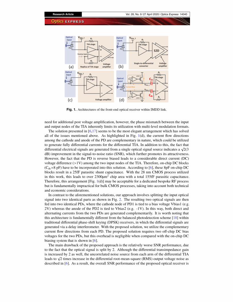
Differential circuit topologies together with truly differential I/O signals are essential for high-speed transceivers, not only because of their immunity to common-mode noise but also becauseof the corresponding digital circuits (e.g. Analogue to Digital Converter) favour truly differentialinputs. Thanks to the optical mixing of the input signal and local oscillator laser, as shown inprevious works [4,13], the generation of differential signals with a coherent optical receiveris relatively straightforward. However, within an IMDD link, since the PD is a single-endeddevice in nature, additional circuits have to be introduced to generate complementary signals.Regardless of the internal circuit topologies, the architectures of the front-end optical receiverwithin IMDD links could be categorized into four groups, which are shown in Fig. 1.
The most common solution is to incorporate dedicated electrical building blocks within thefront-end TIA circuit, either with a dummy input to a replica of the TIA stages [10,14,15] asshown in Fig. 1(a) or a single-to differential (S2D) amplifier [9,16], as shown in Fig. 1(b), or amixture of above two solutions [8]. However, both of these options suffer from transimpedancegain mismatch and bandwidth degradation issues. To overcome this limitation, the most commonsolution is to add several stages of differential voltage amplification within the receiver chain,albeit at an increase in receiver design complexity and the introduction of linearity challenges.As a result, most of these designs can only be used with NRZ signals. The design presented in [8]does demonstrate results using PAM-4, but this was achieved by including a dedicated variablegain amplifier (VGA). Another solution is to utilize the input node of the TIA as the negativeinput to the corresponding voltage amplifier [12], as shown in Fig. 1(c). This solution avoids the
Research Article Vol. 28, No. 9 / 27 April 2020 / Optics Express 14040
Fig. 1. Architectures of the front-end optical receiver within IMDD link.
need for additional post voltage amplification, however, the phase mismatch between the inputand output nodes of the TIA inherently limits its utilization with multi-level modulation formats.The solution presented in [6,17] seems to be the most elegant arrangement which has solved
all of the issues mentioned above. As highlighted in Fig. 1(d), the current flow directionsamong the cathode and anode of the PD are complementary in nature, which could be utilizedto generate fully differential currents for the differential TIA. In addition to this, the fact thatdifferential electrical signals are generated from a single optical signal source indicates a
√2(3
dB) improvement in the signal-to-noise ratio (SNR), which further promotes its attractiveness.However, the fact that the PD is reverse biased leads to a considerable direct current (DC)voltage difference (>1V) among the two input nodes of the TIA. Therefore, on-chip DC blocks(Cdc=8 pF) have to be incorporated into this solution. According to [6], these 8pF on-chip DCblocks result in a 25fF parasitic shunt capacitance. With the 28 nm CMOS process utilizedin this work, this leads to over 2300µm2 chip area with a total 155fF parasitic capacitance.Therefore, this arrangement [Fig. 1(d)] may be acceptable for a dedicated bespoke RF processbut is fundamentally impractical for bulk CMOS processes, taking into account both technicaland economic considerations.In contrast to the aforementioned solutions, our approach involves splitting the input optical
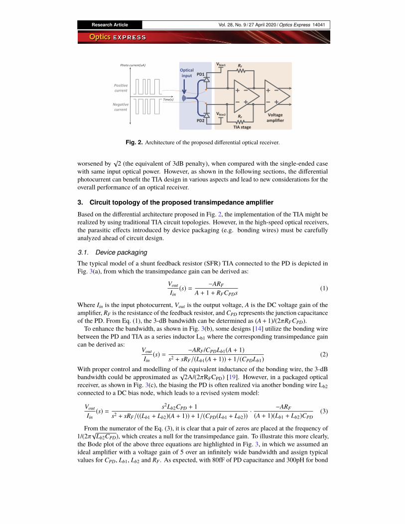
signal into two identical parts as shown in Fig. 2. The resulting two optical signals are thenfed into two identical PDs, where the cathode node of PD1 is tied to a bias voltage Vbias1 (e.g.2V) whereas the anode of the PD2 is tied to Vbias2 (e.g. -1V). In this way, both direct andalternating currents from the two PDs are generated complementarily. It is worth noting thatthis architecture is fundamentally different from the balanced photodetection scheme [18] withintraditional differential phase-shift keying (DPSK) receivers, in which the differential signals aregenerated via a delay interferometer. With the proposed solution, we utilize the complementarycurrent flow directions from each PD. The proposed solution requires two off-chip DC biasvoltages for the two PDs, but this overhead is negligible when compared with the on-chip DCbiasing system that is shown in [6].The main drawback of the proposed approach is the relatively worse SNR performance, due
to the fact that the optical signal is split by 2. Although the differential transimpedance gainis increased by 2 as well, the uncorrelated noise source from each arm of the differential TIAleads to
√2 times increase in the differential root-mean-square (RMS) output voltage noise as
described in [6]. As a result, the overall SNR performance of the proposed optical receiver is
Research Article Vol. 28, No. 9 / 27 April 2020 / Optics Express 14041
Fig. 2. Architecture of the proposed differential optical receiver.
worsened by√2 (the equivalent of 3dB penalty), when compared with the single-ended case
with same input optical power. However, as shown in the following sections, the differentialphotocurrent can benefit the TIA design in various aspects and lead to new considerations for theoverall performance of an optical receiver.
3. Circuit topology of the proposed transimpedance amplifier
Based on the differential architecture proposed in Fig. 2, the implementation of the TIA might berealized by using traditional TIA circuit topologies. However, in the high-speed optical receivers,the parasitic effects introduced by device packaging (e.g. bonding wires) must be carefullyanalyzed ahead of circuit design.
3.1. Device packaging
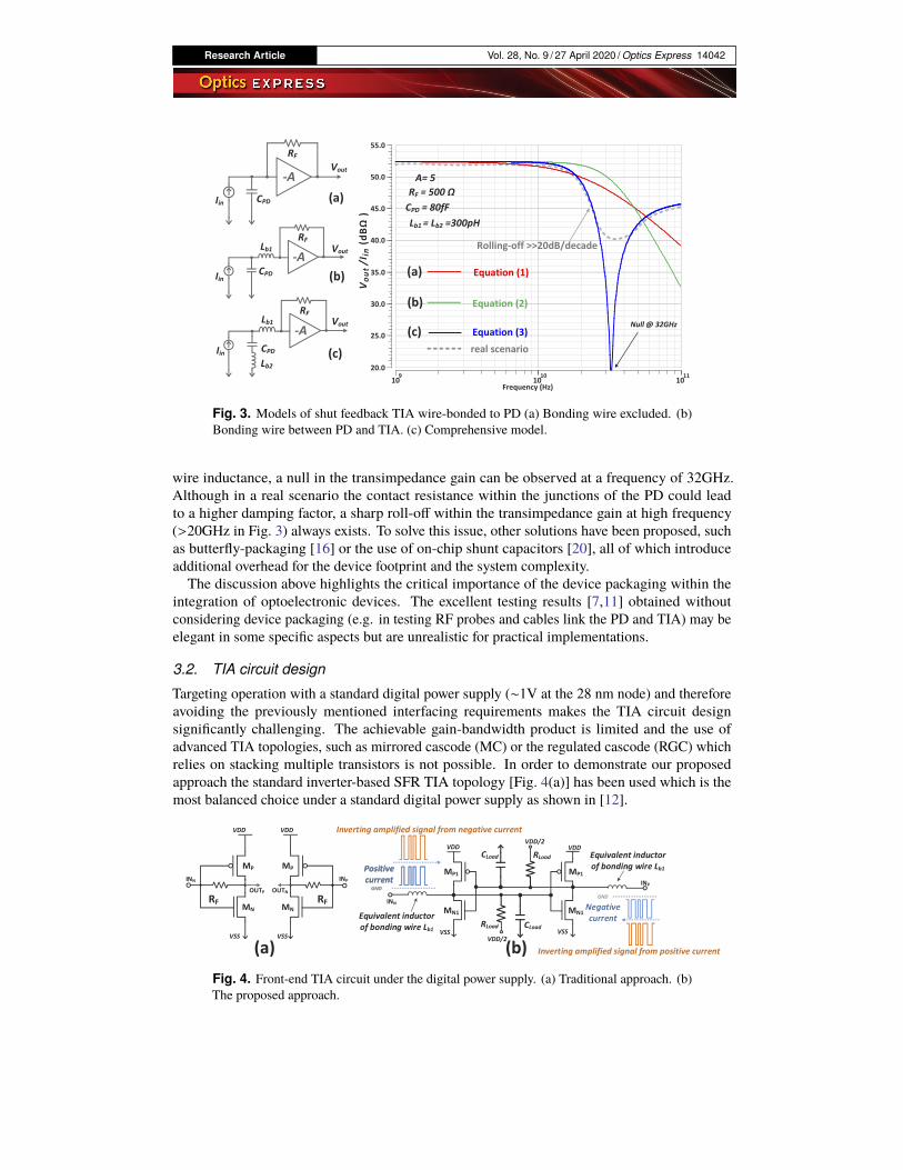
The typical model of a shunt feedback resistor (SFR) TIA connected to the PD is depicted inFig. 3(a), from which the transimpedance gain can be derived as:
Vout
Iin(s) =
−ARF
A + 1 + RFCPDs(1)
Where Iin is the input photocurrent, Vout is the output voltage, A is the DC voltage gain of theamplifier, RF is the resistance of the feedback resistor, andCPD represents the junction capacitanceof the PD. From Eq. (1), the 3-dB bandwidth can be determined as (A+ 1)/(2πRFCPD).
To enhance the bandwidth, as shown in Fig. 3(b), some designs [14] utilize the bonding wirebetween the PD and TIA as a series inductor Lb1 where the corresponding transimpedance gaincan be derived as:
Vout
Iin(s) =
−ARF/CPDLb1(A + 1)s2 + sRF/(Lb1(A + 1)) + 1/(CPDLb1)
(2)
With proper control and modelling of the equivalent inductance of the bonding wire, the 3-dBbandwidth could be approximated as
√2A/(2πRFCPD) [19]. However, in a packaged optical
receiver, as shown in Fig. 3(c), the biasing the PD is often realized via another bonding wire Lb2connected to a DC bias node, which leads to a revised system model:
Vout
Iin(s) =
s2Lb2CPD + 1s2 + sRF/((Lb1 + Lb2)(A + 1)) + 1/(CPD(Lb1 + Lb2))
·−ARF
(A + 1)(Lb1 + Lb2)CPD(3)
From the numerator of the Eq. (3), it is clear that a pair of zeros are placed at the frequency of1/(2π
√Lb2CPD), which creates a null for the transimpedance gain. To illustrate this more clearly,
the Bode plot of the above three equations are highlighted in Fig. 3, in which we assumed anideal amplifier with a voltage gain of 5 over an infinitely wide bandwidth and assign typicalvalues for CPD, Lb1, Lb2 and RF . As expected, with 80fF of PD capacitance and 300pH for bond
Research Article Vol. 28, No. 9 / 27 April 2020 / Optics Express 14042
Fig. 3. Models of shut feedback TIA wire-bonded to PD (a) Bonding wire excluded. (b)Bonding wire between PD and TIA. (c) Comprehensive model.
wire inductance, a null in the transimpedance gain can be observed at a frequency of 32GHz.Although in a real scenario the contact resistance within the junctions of the PD could leadto a higher damping factor, a sharp roll-off within the transimpedance gain at high frequency(>20GHz in Fig. 3) always exists. To solve this issue, other solutions have been proposed, suchas butterfly-packaging [16] or the use of on-chip shunt capacitors [20], all of which introduceadditional overhead for the device footprint and the system complexity.The discussion above highlights the critical importance of the device packaging within the
integration of optoelectronic devices. The excellent testing results [7,11] obtained withoutconsidering device packaging (e.g. in testing RF probes and cables link the PD and TIA) may beelegant in some specific aspects but are unrealistic for practical implementations.
3.2. TIA circuit design
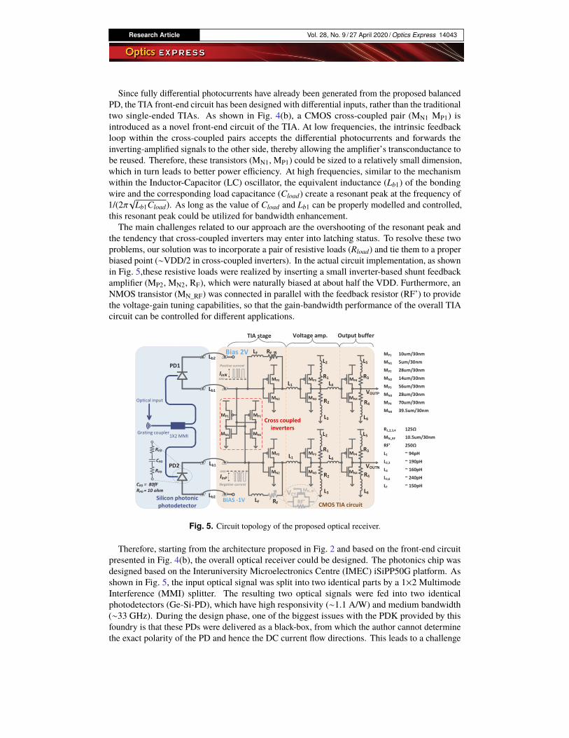
Targeting operation with a standard digital power supply (∼1V at the 28 nm node) and thereforeavoiding the previously mentioned interfacing requirements makes the TIA circuit designsignificantly challenging. The achievable gain-bandwidth product is limited and the use ofadvanced TIA topologies, such as mirrored cascode (MC) or the regulated cascode (RGC) whichrelies on stacking multiple transistors is not possible. In order to demonstrate our proposedapproach the standard inverter-based SFR TIA topology [Fig. 4(a)] has been used which is themost balanced choice under a standard digital power supply as shown in [12].
Fig. 4. Front-end TIA circuit under the digital power supply. (a) Traditional approach. (b)The proposed approach.
Research Article Vol. 28, No. 9 / 27 April 2020 / Optics Express 14043
Since fully differential photocurrents have already been generated from the proposed balancedPD, the TIA front-end circuit has been designed with differential inputs, rather than the traditionaltwo single-ended TIAs. As shown in Fig. 4(b), a CMOS cross-coupled pair (MN1 MP1) isintroduced as a novel front-end circuit of the TIA. At low frequencies, the intrinsic feedbackloop within the cross-coupled pairs accepts the differential photocurrents and forwards theinverting-amplified signals to the other side, thereby allowing the amplifier’s transconductance tobe reused. Therefore, these transistors (MN1, MP1) could be sized to a relatively small dimension,which in turn leads to better power efficiency. At high frequencies, similar to the mechanismwithin the Inductor-Capacitor (LC) oscillator, the equivalent inductance (Lb1) of the bondingwire and the corresponding load capacitance (Cload) create a resonant peak at the frequency of1/(2π
√Lb1Cload). As long as the value of Cload and Lb1 can be properly modelled and controlled,
this resonant peak could be utilized for bandwidth enhancement.The main challenges related to our approach are the overshooting of the resonant peak and
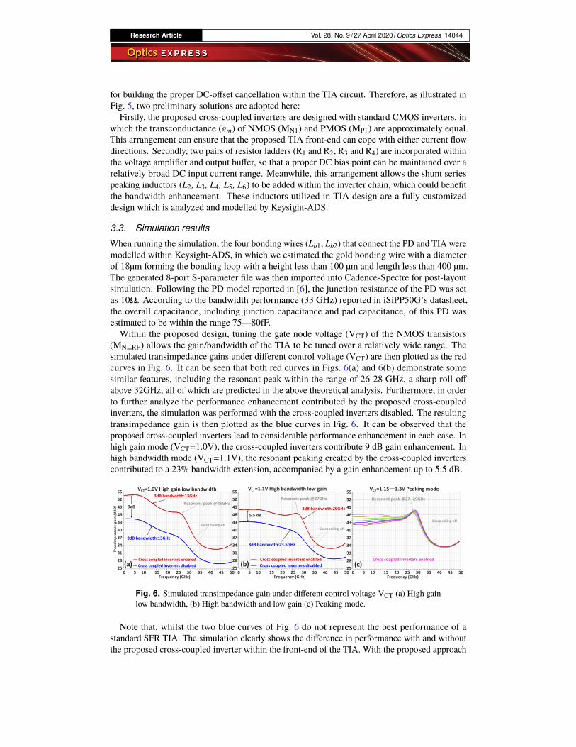
the tendency that cross-coupled inverters may enter into latching status. To resolve these twoproblems, our solution was to incorporate a pair of resistive loads (Rload) and tie them to a properbiased point (∼VDD/2 in cross-coupled inverters). In the actual circuit implementation, as shownin Fig. 5,these resistive loads were realized by inserting a small inverter-based shunt feedbackamplifier (MP2, MN2, RF), which were naturally biased at about half the VDD. Furthermore, anNMOS transistor (MN_RF) was connected in parallel with the feedback resistor (RF’) to providethe voltage-gain tuning capabilities, so that the gain-bandwidth performance of the overall TIAcircuit can be controlled for different applications.
Fig. 5. Circuit topology of the proposed optical receiver.
Therefore, starting from the architecture proposed in Fig. 2 and based on the front-end circuitpresented in Fig. 4(b), the overall optical receiver could be designed. The photonics chip wasdesigned based on the Interuniversity Microelectronics Centre (IMEC) iSiPP50G platform. Asshown in Fig. 5, the input optical signal was split into two identical parts by a 1×2 MultimodeInterference (MMI) splitter. The resulting two optical signals were fed into two identicalphotodetectors (Ge-Si-PD), which have high responsivity (∼1.1 A/W) and medium bandwidth(∼33 GHz). During the design phase, one of the biggest issues with the PDK provided by thisfoundry is that these PDs were delivered as a black-box, from which the author cannot determinethe exact polarity of the PD and hence the DC current flow directions. This leads to a challenge
Research Article Vol. 28, No. 9 / 27 April 2020 / Optics Express 14044
for building the proper DC-offset cancellation within the TIA circuit. Therefore, as illustrated inFig. 5, two preliminary solutions are adopted here:Firstly, the proposed cross-coupled inverters are designed with standard CMOS inverters, in
which the transconductance (gm) of NMOS (MN1) and PMOS (MP1) are approximately equal.This arrangement can ensure that the proposed TIA front-end can cope with either current flowdirections. Secondly, two pairs of resistor ladders (R1 and R2, R3 and R4) are incorporated withinthe voltage amplifier and output buffer, so that a proper DC bias point can be maintained over arelatively broad DC input current range. Meanwhile, this arrangement allows the shunt seriespeaking inductors (L2, L3, L4, L5, L6) to be added within the inverter chain, which could benefitthe bandwidth enhancement. These inductors utilized in TIA design are a fully customizeddesign which is analyzed and modelled by Keysight-ADS.
3.3. Simulation results
When running the simulation, the four bonding wires (Lb1, Lb2) that connect the PD and TIA weremodelled within Keysight-ADS, in which we estimated the gold bonding wire with a diameterof 18µm forming the bonding loop with a height less than 100 µm and length less than 400 µm.The generated 8-port S-parameter file was then imported into Cadence-Spectre for post-layoutsimulation. Following the PD model reported in [6], the junction resistance of the PD was setas 10Ω. According to the bandwidth performance (33 GHz) reported in iSiPP50G’s datasheet,the overall capacitance, including junction capacitance and pad capacitance, of this PD wasestimated to be within the range 75—80fF.Within the proposed design, tuning the gate node voltage (VCT) of the NMOS transistors
(MN_RF) allows the gain/bandwidth of the TIA to be tuned over a relatively wide range. Thesimulated transimpedance gains under different control voltage (VCT) are then plotted as the redcurves in Fig. 6. It can be seen that both red curves in Figs. 6(a) and 6(b) demonstrate somesimilar features, including the resonant peak within the range of 26-28 GHz, a sharp roll-offabove 32GHz, all of which are predicted in the above theoretical analysis. Furthermore, in orderto further analyze the performance enhancement contributed by the proposed cross-coupledinverters, the simulation was performed with the cross-coupled inverters disabled. The resultingtransimpedance gain is then plotted as the blue curves in Fig. 6. It can be observed that theproposed cross-coupled inverters lead to considerable performance enhancement in each case. Inhigh gain mode (VCT=1.0V), the cross-coupled inverters contribute 9 dB gain enhancement. Inhigh bandwidth mode (VCT=1.1V), the resonant peaking created by the cross-coupled inverterscontributed to a 23% bandwidth extension, accompanied by a gain enhancement up to 5.5 dB.
Fig. 6. Simulated transimpedance gain under different control voltage VCT (a) High gainlow bandwidth, (b) High bandwidth and low gain (c) Peaking mode.
Note that, whilst the two blue curves of Fig. 6 do not represent the best performance of astandard SFR TIA. The simulation clearly shows the difference in performance with and withoutthe proposed cross-coupled inverter within the front-end of the TIA. With the proposed approach
Research Article Vol. 28, No. 9 / 27 April 2020 / Optics Express 14045
the gain and bandwidth performance can be enhanced simultaneously, whereas in traditionalSFR TIA designs a trade-off between the gain and bandwidth performance has to be made[21]. Obviously, the pre-conditions to this are co-ordination in the design of the photonics (PD)and electronics (TIA), accompanied by an accurate and repeatable device packaging process.Besides the high gain and high bandwidth modes discussed above, as shown in Fig. 6(c), tuningthe control voltage (VCT) to a higher value could further lower the transimpedance gain at lowfrequencies, while the resonant peaking created by the bond wire and cross-coupled inverter canbe maintained. This feature creates an on-chip equalization function, which may compensate forany bandwidth limitation in the system.
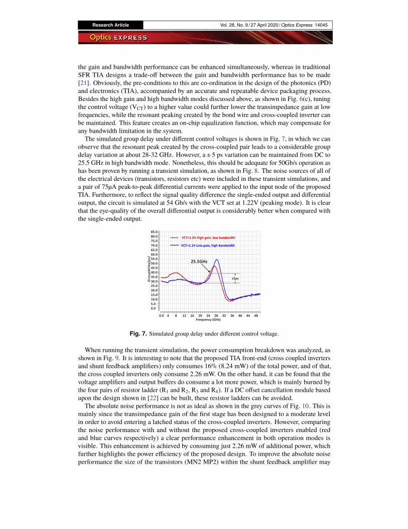
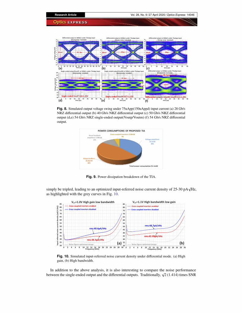
The simulated group delay under different control voltages is shown in Fig. 7, in which we canobserve that the resonant peak created by the cross-coupled pair leads to a considerable groupdelay variation at about 28-32 GHz. However, a± 5 ps variation can be maintained from DC to25.5 GHz in high bandwidth mode. Nonetheless, this should be adequate for 50Gb/s operation ashas been proven by running a transient simulation, as shown in Fig. 8. The noise sources of all ofthe electrical devices (transistors, resistors etc) were included in these transient simulations, anda pair of 75µA peak-to-peak differential currents were applied to the input node of the proposedTIA. Furthermore, to reflect the signal quality difference the single-ended output and differentialoutput, the circuit is simulated at 54 Gb/s with the VCT set at 1.22V (peaking mode). It is clearthat the eye-quality of the overall differential output is considerably better when compared withthe single-ended output.
Fig. 7. Simulated group delay under different control voltage.
When running the transient simulation, the power consumption breakdown was analyzed, asshown in Fig. 9. It is interesting to note that the proposed TIA front-end (cross coupled invertersand shunt feedback amplifiers) only consumes 16% (8.24 mW) of the total power, and of that,the cross coupled inverters only consume 2.26 mW. On the other hand, it can be found that thevoltage amplifiers and output buffers do consume a lot more power, which is mainly burned bythe four pairs of resistor ladder (R1 and R2, R3 and R4). If a DC offset cancellation module basedupon the design shown in [22] can be built, these resistor ladders can be avoided.
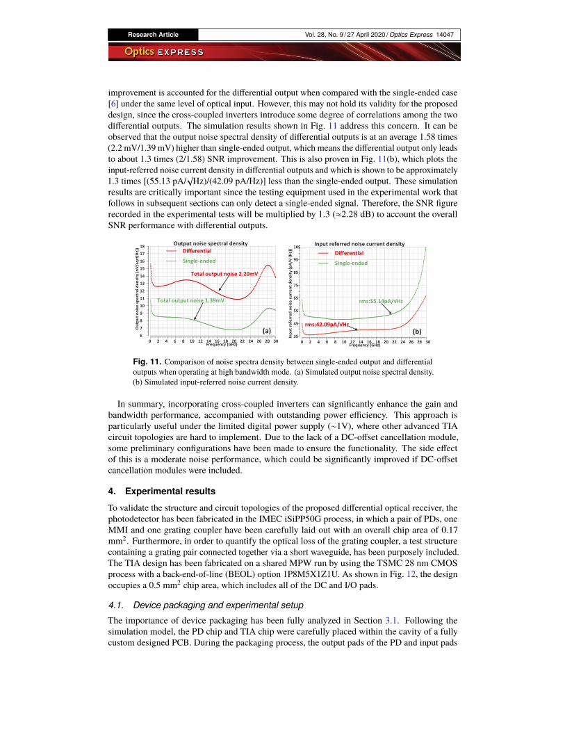
The absolute noise performance is not as ideal as shown in the grey curves of Fig. 10. This ismainly since the transimpedance gain of the first stage has been designed to a moderate levelin order to avoid entering a latched status of the cross-coupled inverters. However, comparingthe noise performance with and without the proposed cross-coupled inverters enabled (redand blue curves respectively) a clear performance enhancement in both operation modes isvisible. This enhancement is achieved by consuming just 2.26 mW of additional power, whichfurther highlights the power efficiency of the proposed design. To improve the absolute noiseperformance the size of the transistors (MN2 MP2) within the shunt feedback amplifier may
Research Article Vol. 28, No. 9 / 27 April 2020 / Optics Express 14046
Fig. 8. Simulated output voltage swing under 75uApp(150uAppd) input current (a) 28 Gb/sNRZ differential output (b) 40 Gb/s NRZ differential output (c) 50 Gb/s NRZ differentialoutput (d,e) 54 Gb/s NRZ single-ended output(Voutp/Voutm) (f) 54 Gb/s NRZ differentialoutput.
Fig. 9. Power dissipation breakdown of the TIA.
simply be tripled, leading to an optimized input-referred noise current density of 25-30 pA√Hz,
as highlighted with the grey curves in Fig. 10.
Fig. 10. Simulated input-referred noise current density under differential mode. (a) Highgain, (b) High bandwidth.
In addition to the above analysis, it is also interesting to compare the noise performancebetween the single-ended output and the differential outputs. Traditionally,
√2 (1.414) times SNR
Research Article Vol. 28, No. 9 / 27 April 2020 / Optics Express 14047
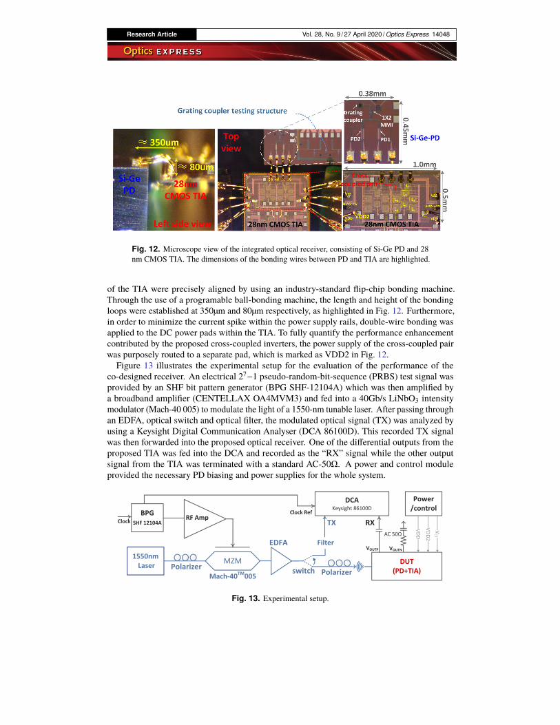
improvement is accounted for the differential output when compared with the single-ended case[6] under the same level of optical input. However, this may not hold its validity for the proposeddesign, since the cross-coupled inverters introduce some degree of correlations among the twodifferential outputs. The simulation results shown in Fig. 11 address this concern. It can beobserved that the output noise spectral density of differential outputs is at an average 1.58 times(2.2 mV/1.39 mV) higher than single-ended output, which means the differential output only leadsto about 1.3 times (2/1.58) SNR improvement. This is also proven in Fig. 11(b), which plots theinput-referred noise current density in differential outputs and which is shown to be approximately1.3 times [(55.13 pA/
√Hz)/(42.09 pA/Hz)] less than the single-ended output. These simulation
results are critically important since the testing equipment used in the experimental work thatfollows in subsequent sections can only detect a single-ended signal. Therefore, the SNR figurerecorded in the experimental tests will be multiplied by 1.3 (≈2.28 dB) to account the overallSNR performance with differential outputs.
Fig. 11. Comparison of noise spectra density between single-ended output and differentialoutputs when operating at high bandwidth mode. (a) Simulated output noise spectral density.(b) Simulated input-referred noise current density.
In summary, incorporating cross-coupled inverters can significantly enhance the gain andbandwidth performance, accompanied with outstanding power efficiency. This approach isparticularly useful under the limited digital power supply (∼1V), where other advanced TIAcircuit topologies are hard to implement. Due to the lack of a DC-offset cancellation module,some preliminary configurations have been made to ensure the functionality. The side effectof this is a moderate noise performance, which could be significantly improved if DC-offsetcancellation modules were included.
4. Experimental results
To validate the structure and circuit topologies of the proposed differential optical receiver, thephotodetector has been fabricated in the IMEC iSiPP50G process, in which a pair of PDs, oneMMI and one grating coupler have been carefully laid out with an overall chip area of 0.17mm2. Furthermore, in order to quantify the optical loss of the grating coupler, a test structurecontaining a grating pair connected together via a short waveguide, has been purposely included.The TIA design has been fabricated on a shared MPW run by using the TSMC 28 nm CMOSprocess with a back-end-of-line (BEOL) option 1P8M5X1Z1U. As shown in Fig. 12, the designoccupies a 0.5 mm2 chip area, which includes all of the DC and I/O pads.
4.1. Device packaging and experimental setup
The importance of device packaging has been fully analyzed in Section 3.1. Following thesimulation model, the PD chip and TIA chip were carefully placed within the cavity of a fullycustom designed PCB. During the packaging process, the output pads of the PD and input pads
Research Article Vol. 28, No. 9 / 27 April 2020 / Optics Express 14048
Fig. 12. Microscope view of the integrated optical receiver, consisting of Si-Ge PD and 28nm CMOS TIA. The dimensions of the bonding wires between PD and TIA are highlighted.
of the TIA were precisely aligned by using an industry-standard flip-chip bonding machine.Through the use of a programable ball-bonding machine, the length and height of the bondingloops were established at 350µm and 80µm respectively, as highlighted in Fig. 12. Furthermore,in order to minimize the current spike within the power supply rails, double-wire bonding wasapplied to the DC power pads within the TIA. To fully quantify the performance enhancementcontributed by the proposed cross-coupled inverters, the power supply of the cross-coupled pairwas purposely routed to a separate pad, which is marked as VDD2 in Fig. 12.
Figure 13 illustrates the experimental setup for the evaluation of the performance of theco-designed receiver. An electrical 27−1 pseudo-random-bit-sequence (PRBS) test signal wasprovided by an SHF bit pattern generator (BPG SHF-12104A) which was then amplified bya broadband amplifier (CENTELLAX OA4MVM3) and fed into a 40Gb/s LiNbO3 intensitymodulator (Mach-40 005) to modulate the light of a 1550-nm tunable laser. After passing throughan EDFA, optical switch and optical filter, the modulated optical signal (TX) was analyzed byusing a Keysight Digital Communication Analyser (DCA 86100D). This recorded TX signalwas then forwarded into the proposed optical receiver. One of the differential outputs from theproposed TIA was fed into the DCA and recorded as the “RX” signal while the other outputsignal from the TIA was terminated with a standard AC-50Ω. A power and control moduleprovided the necessary PD biasing and power supplies for the whole system.
Fig. 13. Experimental setup.
Research Article Vol. 28, No. 9 / 27 April 2020 / Optics Express 14049
4.2. Measurement results
Firstly, the optical loss of the grating coupler was characterized by using the grating-pair teststructure on the PD chip. The resulting 6dB optical loss was taken into account in the TX signalthat was obtained at each data rate.Traditionally, S-parameter testing results are used to derive the transimpedance gain and
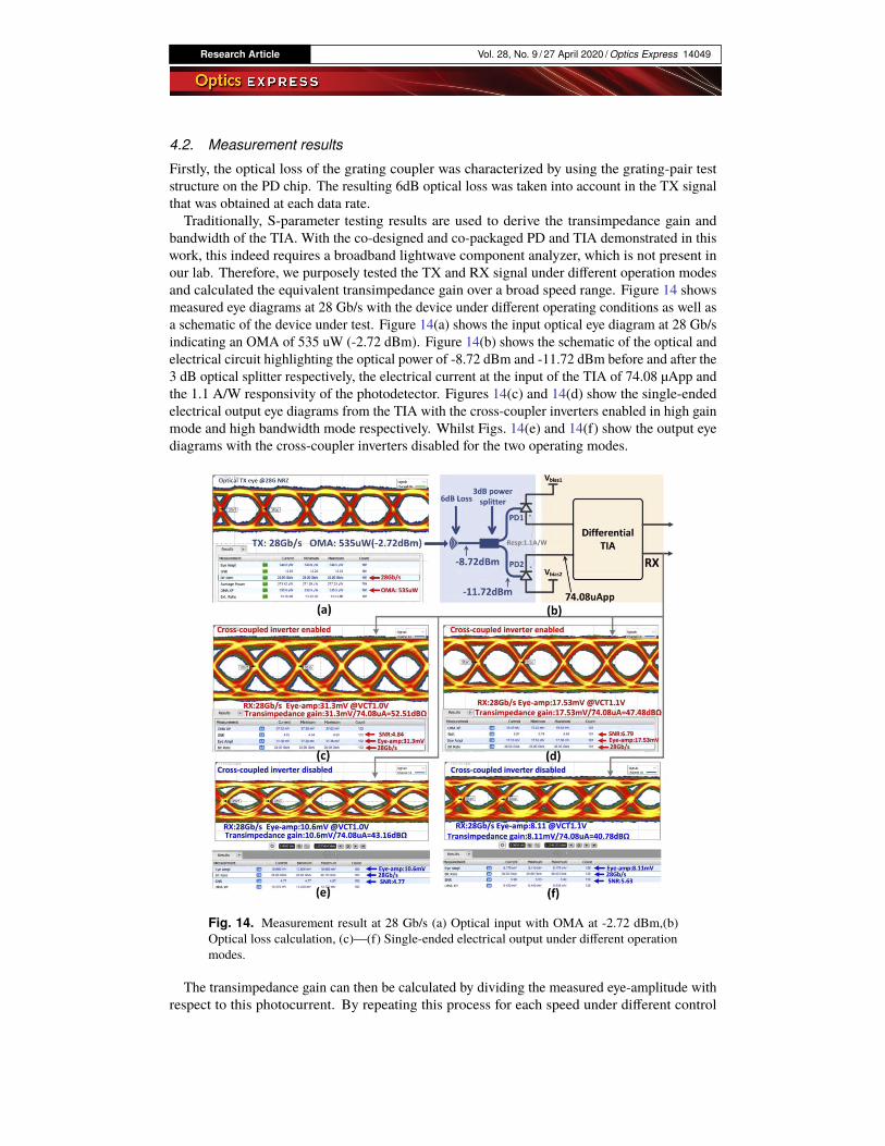
bandwidth of the TIA. With the co-designed and co-packaged PD and TIA demonstrated in thiswork, this indeed requires a broadband lightwave component analyzer, which is not present inour lab. Therefore, we purposely tested the TX and RX signal under different operation modesand calculated the equivalent transimpedance gain over a broad speed range. Figure 14 showsmeasured eye diagrams at 28 Gb/s with the device under different operating conditions as well asa schematic of the device under test. Figure 14(a) shows the input optical eye diagram at 28 Gb/sindicating an OMA of 535 uW (-2.72 dBm). Figure 14(b) shows the schematic of the optical andelectrical circuit highlighting the optical power of -8.72 dBm and -11.72 dBm before and after the3 dB optical splitter respectively, the electrical current at the input of the TIA of 74.08 µApp andthe 1.1 A/W responsivity of the photodetector. Figures 14(c) and 14(d) show the single-endedelectrical output eye diagrams from the TIA with the cross-coupler inverters enabled in high gainmode and high bandwidth mode respectively. Whilst Figs. 14(e) and 14(f) show the output eyediagrams with the cross-coupler inverters disabled for the two operating modes.
Fig. 14. Measurement result at 28 Gb/s (a) Optical input with OMA at -2.72 dBm,(b)Optical loss calculation, (c)—(f) Single-ended electrical output under different operationmodes.
The transimpedance gain can then be calculated by dividing the measured eye-amplitude withrespect to this photocurrent. By repeating this process for each speed under different control
Research Article Vol. 28, No. 9 / 27 April 2020 / Optics Express 14050
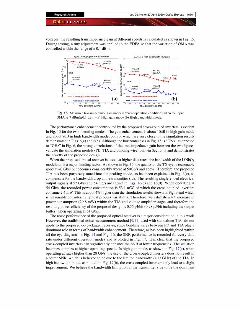
voltages, the resulting transimpedance gain at different speeds is calculated as shown in Fig. 15.During testing, a tiny adjustment was applied to the EDFA so that the variation of OMA wascontrolled within the range of± 0.1 dBm.
Fig. 15. Measured transimpedance gain under different operation conditions when the inputOMA -8.7 dBm(±0.1 dBm) (a) High gain mode (b) High bandwidth mode.
The performance enhancement contributed by the proposed cross-coupled inverters is evidentin Fig. 15 for the two operating modes. The gain enhancement is about 10dB in high gain modeand about 7dB in high bandwidth mode, both of which are very close to the simulation resultsdemonstrated in Figs. 6(a) and 6(b). Although the horizontal axis in Fig. 15 is “Gb/s” as opposedto “GHz” in Fig. 6, the strong correlations of the transimpedance gain between the two figuresvalidate the simulation models (PD, TIA and bonding wire) built-in Section 3 and demonstratesthe novelty of the proposed design.
When the proposed optical receiver is tested at higher data rates, the bandwidth of the LiNbO3modulator is a major limiting factor. As shown in Fig. 16, the quality of the TX eye is reasonablygood at 40 Gb/s but becomes considerably worse at 50Gb/s and above. Therefore, the proposedTIA has been purposely tuned into the peaking mode, as has been explained in Fig. 6(c), tocompensate for the bandwidth drop at the transmitter side. The resulting single-ended electricaloutput signals at 52 Gb/s and 54 Gb/s are shown in Figs. 16(c) and 16(d). When operating at54 Gb/s, the recorded power consumption is 53.1 mW, of which the cross-coupled invertersconsume 2.4 mW. This is about 4% higher than the simulation results shown in Fig. 9 and whichis reasonable considering typical process variations. Therefore, we estimate a 4% increase inpower consumption (29.8 mW) within the TIA and voltage amplifier stages and therefore theresulting power efficiency of the proposed design is 0.55 pJ/bit (0.98 pJ/bit including the outputbuffer) when operating at 54 Gb/s.
The noise performance of the proposed optical receiver is a major consideration in this work.However, the traditional noise measurement method [9,11] used with standalone TIAs do notapply to the proposed co-packaged receiver, since bonding wires between PD and TIA play adominant role in terms of bandwidth enhancement. Therefore, as has been highlighted withinall the eye-diagrams in Fig. 14 and Fig. 16, the SNR performance is recorded for every datarate under different operation modes and is plotted in Fig. 17. It is clear that the proposedcross-coupled inverters can significantly enhance the SNR at lower frequencies. The situationbecomes complex at higher operating speeds. In high gain mode, as shown in Fig. 17(a), whenoperating at rates higher than 28 Gb/s, the use of the cross-coupled inverters does not result ina better SNR, which is believed to be due to the limited bandwidth (≈13 GHz) of the TIA. Inhigh bandwidth mode, as plotted in Fig. 17(b), the cross-coupled inverters only lead to a slightimprovement. We believe the bandwidth limitation at the transmitter side to be the dominant
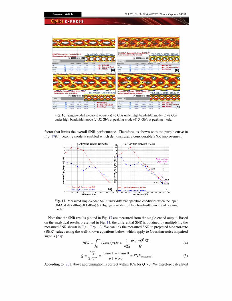
Research Article Vol. 28, No. 9 / 27 April 2020 / Optics Express 14051
Fig. 16. Single-ended electrical output (a) 40 Gb/s under high bandwidth mode (b) 48 Gb/sunder high bandwidth mode (c) 52 Gb/s at peaking mode (d) 54Gb/s at peaking mode.
factor that limits the overall SNR performance. Therefore, as shown with the purple curve inFig. 17(b), peaking mode is enabled which demonstrates a considerable SNR improvement.
Fig. 17. Measured single-ended SNR under different operation conditions when the inputOMA at -8.7 dBm(±0.1 dBm) (a) High gain mode (b) High bandwidth mode and peakingmode.
Note that the SNR results plotted in Fig. 17 are measured from the single-ended output. Basedon the analytical results presented in Fig. 11, the differential SNR is obtained by multiplying themeasured SNR shown in Fig. 17 by 1.3. We can link the measured SNR to projected bit-error-rate(BER) values using the well-known equations below, which apply to Gaussian-noise impairedsignals [23]:
BER =∫ ∞
QGauss(x)dx ≈
1√2π
exp(−Q2/2)Q
(4)
Q =VppS
2Vrmsn=
mean 1 − mean 0σ1 + σ0
= SNRmeasured (5)
According to [23], above approximation is correct within 10% for Q> 3. We therefore calculated
Research Article Vol. 28, No. 9 / 27 April 2020 / Optics Express 14052
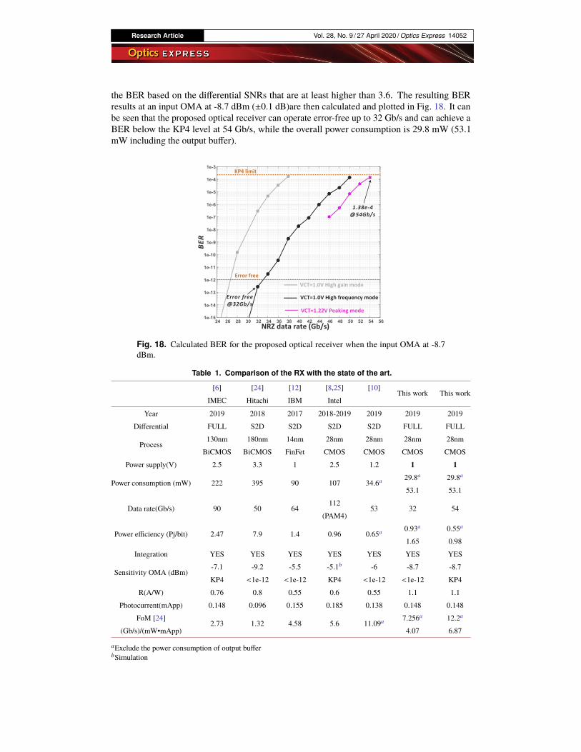
the BER based on the differential SNRs that are at least higher than 3.6. The resulting BERresults at an input OMA at -8.7 dBm (±0.1 dB)are then calculated and plotted in Fig. 18. It canbe seen that the proposed optical receiver can operate error-free up to 32 Gb/s and can achieve aBER below the KP4 level at 54 Gb/s, while the overall power consumption is 29.8 mW (53.1mW including the output buffer).
Fig. 18. Calculated BER for the proposed optical receiver when the input OMA at -8.7dBm.
Table 1. Comparison of the RX with the state of the art.
[6] [24] [12] [8,25] [10]This work This work
IMEC Hitachi IBM Intel
Year 2019 2018 2017 2018-2019 2019 2019 2019
Differential FULL S2D S2D S2D S2D FULL FULL
Process130nm 180nm 14nm 28nm 28nm 28nm 28nm
BiCMOS BiCMOS FinFet CMOS CMOS CMOS CMOS
Power supply(V) 2.5 3.3 1 2.5 1.2 1 1
Power consumption (mW) 222 395 90 107 34.6a29.8a 29.8a
53.1 53.1
Data rate(Gb/s) 90 50 64112
53 32 54(PAM4)
Power efficiency (Pj/bit) 2.47 7.9 1.4 0.96 0.65a0.93a 0.55a
1.65 0.98
Integration YES YES YES YES YES YES YES
Sensitivity OMA (dBm)-7.1 -9.2 -5.5 -5.1b -6 -8.7 -8.7
KP4 <1e-12 <1e-12 KP4 <1e-12 <1e-12 KP4
R(A/W) 0.76 0.8 0.55 0.6 0.55 1.1 1.1
Photocurrent(mApp) 0.148 0.096 0.155 0.185 0.138 0.148 0.148
FoM [24]2.73 1.32 4.58 5.6 11.09a
7.256a 12.2a
(Gb/s)/(mW•mApp) 4.07 6.87
aExclude the power consumption of output bufferbSimulation
Research Article Vol. 28, No. 9 / 27 April 2020 / Optics Express 14053
Table 1 summarises the performance of the fully integrated optical receivers that have beenpublished in recent years. Within this table, only fully packaged optical receivers are listed.Certain challenges were presented while comparatively reviewing prior works: Some of theworks only reported the BER at the KP4 threshold, whereas others have stated error-free testingresults. Furthermore, the power consumption within the output buffer is another factor that maylead to confusion. To avoid any confusion, we have listed all the operating conditions of ourproposed design. It is clear that the proposed work operates with the lowest power supply voltageand achieves the best power efficiency. Even though our design can only detect a 54 Gb/s at theKP4 limit, we believe this is mainly due to the limited bandwidth of the modulator used on thetransmitter side. Overall, the excellent figure-of-merit (FoM) [24] demonstrates the superiorityof the proposed design.
5. Future work and conclusion
In this work, we have demonstrated the design and implementation of a fully differential opticalreceiver, which is aimed for short reach intensity modulation and direct detection (IMDD)transceiver links. A Si-Ge balanced photodetector (PD) has been co-designed and packagedwith a novel differential transimpedance amplifier (TIA). Without using any equalization or DSPtechniques, the proposed receiver can operate up to 54 Gb/s NRZ with a BER less than the KP4limit (2.2×10⁻⁴) with an OMA of -8.6 dBm, whilst the power efficiency is 0.55 pJ/bit (or 0.98pJ/bit including the output buffer).Obviously, this work should be further optimized in various aspects. As has been indicated
in Section 3, a properly designed DC offset-cancellation module is essential and can lead toconsiderable performance enhancement in various aspects. However, we believe that the mostvaluable work for the next step is to adopt flip-chip bonding between the PD and TIA. Theobvious benefit is the bonding-wire induced inductance (Lb2) with the PD biasing node couldbe minimized, from which a higher bandwidth could be expected. Furthermore, the peakinginductor(Lb1) could be carefully modelled and designed by using on-chip inductors, which notonly allow the resonant peaking and group delay variation to be more precisely controlled, butalso benefit the TIA front-end circuit design, in which larger transistor could be used to enhancethe noise performance.In summary, from the perspective of electronic circuit design, the power efficiency may be
traded-off with other specifications, such as sensitivity or bandwidth. However, the limited powersupply is the determining factor that restricts the circuit design. In this work, besides the resultsthat have been thoroughly demonstrated in Table 1, the most crucial contribution is that we havedemonstrated a new design approach where photonic devices can be co-designed and co-packagedwith electronic devices, hence solving the challenges faced by electrical circuit designers. Ratherthan building a dedicated single-to-differential module in the electrical circuit, custom-designedphotonics devices can tackle the differential signal generation easily. Furthermore, the fullydifferential photocurrents could contribute to performance enhancement of the TIA, namely ofthe proposed approach to incorporate a cross-coupled inverter within the front-end of the TIA.
Funding
Engineering andPhysical SciencesResearchCouncil (EP/L00044X/1, EP/N013247/1, EP/P003990/1);National Natural Science Foundation of China (61535002); National Key Research and De-velopment Program of China (2018YFB1801204); State Key Laboratory of Advanced OpticalCommunication Systems and Networks.; Royal Society (University Research Fellowship).
Disclosures
The authors declare no conflicts of interest.
Research Article Vol. 28, No. 9 / 27 April 2020 / Optics Express 14054
References1. X. Chen, M. M. Milosevic, S. Stanković, S. Reynolds, T. D. Bucio, K. Li, D. J. Thomson, F. Gardes, and G. T. Reed,
“The emergence of silicon photonics as a flexible technology platform,” Proc. IEEE 106(12), 2101–2116 (2018).2. B. Moeneclaey, J. Verbrugghe, F. Blache, M. Goix, D. Lanteri, B. Duval, M. Achouche, J. Bauwelinck, and Y. Xin,
“A 40-Gb/s Transimpedance Amplifier for Optical Links,” IEEE Photonics Technol. Lett. 27(13), 1375–1378 (2015).3. I. Garcia Lopez, P. Rito, A. Awny, M. Ko, D. Kissinger, and A. C. Ulusoy, “A DC-75-GHz Bandwidth and 54 dBOhm
Gain TIA With 10.9 pA/√Hz in 130-nm SiGe:C BiCMOS,” IEEE Microw. Wireless Compon. Lett. 28(1), 61–63
(2018).4. A. Awny, R. Nagulapalli, M. Kroh, J. Hoffmann, P. Runge, D. Micusik, G. Fischer, A. C. Ulusoy, M. S. Ko, and
D. Kissinger, “A Linear Differential Transimpedance Amplifier for 100-Gb/s Integrated Coherent Optical FiberReceivers,” IEEE Trans. Microwave Theory Tech. 66(2), 973–986 (2018).
5. I. Garcia Lopez, A. Awny, P. Rito, M. Ko, A. C. Ulusoy, and D. Kissinger, “100 Gb/s Differential Linear TIAs WithLess Than 10 pA/
√Hz in 130-nm SiGe:C BiCMOS,” IEEE J. Solid-State Circuits 53(2), 458–469 (2018).
6. J. Lambrecht, H. Ramon, B. Moeneclaey, J. Verbist, M. Verplaetse, M. Vanhoecke, P. Ossieur, P. De Heyn, J. VanCampenhout, J. Bauwelinck, and X. Yin, “90-Gb/s NRZ Optical Receiver in Silicon Using a Fully DifferentialTransimpedance Amplifier,” J. Lightwave Technol. 37(9), 1964–1973 (2019).
7. K. Park and W. S. Oh, “A 40-Gb/s 310-fJ/b Inverter-Based CMOS Optical Receiver Front-End,” IEEE PhotonicsTechnol. Lett. 27(18), 1931–1933 (2015).
8. H. Li, G. Balamurugan, J. Jaussi, and B. Casper, “A 112 Gb/s PAM4 Linear TIA with 0.96 pJ/bit Energy Efficiencyin 28 nm CMOS,” Esscirc 2018 - Ieee 44th European Solid State Circuits Conference (Esscirc), 238–241 (2018).
9. S. G. Kim, C. Hong, Y. S. Eo, J. Kim, and S. M. Park, “A 40-GHz Mirrored-Cascode Differential TransimpedanceAmplifier in 65-nm CMOS,” IEEE J. Solid-State Circuits 54(5), 1468–1474 (2019).
10. L. Szilagyi, J. Pliva, R. Henker, D. Schoeniger, J. P. Turkiewicz, and F. Ellinger, “A 53-Gbit/s Optical ReceiverFrontend With 0.65 pJ/bit in 28-nm Bulk-CMOS,” IEEE J. Solid-State Circuits 54(3), 845–855 (2019).
11. J. Kim and J. F. Buckwalter, “A 40-Gb/s Optical Transceiver Front-End in 45 nm SOI CMOS,” IEEE J. Solid-StateCircuits 47(3), 615–626 (2012).
12. I. Ozkaya, A. Cevrero, P. A. Francese, C. Menolfi, T. Morf, M. Brandli, D. M. Kuchta, L. Kull, C. W. Baks, J. E.Proesel, M. Kossel, D. Luu, B. G. Lee, F. E. Doany, M. Meghelli, Y. Leblebici, and T. Toifl, “A 64-Gb/s 1.4-pJ/bNRZ Optical Receiver Data-Path in 14-nm CMOS FinFET,” IEEE J. Solid-State Circuits 52(12), 3458–3473 (2017).
13. M. G. Ahmed, T. N. Huynh, C.Williams, Y.Wang, P. K. Hanumolu, andA. Rylyakov, “34-GBd Linear TransimpedanceAmplifier for 200-Gb/s DP-16-QAM Optical Coherent Receivers,” IEEE J. Solid-State Circuits 54(3), 834–844(2019).
14. Q. Pan, Y. P. Wang, Z. X. Hou, L. Sun, Y. Lu, W. H. Ki, P. Chiang, and C. P. Yue, “A 30-Gb/s 1.37-pJ/b CMOSReceiver for Optical Interconnects,” J. Lightwave Technol. 33(4), 778–786 (2015).
15. T. C. Huang, T. W. Chung, C. H. Chern, M. C. Huang, C. C. Lin, and F. L. Hsueh, “A 28Gb/s 1pJ/b Shared-InductorOptical Receiver with 56% Chip-Area Reduction in 28 nm CMOS,” presented at the 2014 Ieee InternationalSolid-State Circuits Conference Digest of Technical Papers (Isscc) 2014.
16. J. Joo, K. S. Jang, S. H. Kim, I. G. Kim, J. H. Oh, S. A. Kim, G. S. Jeong, Y. Kim, J. E. Park, S. Kim, H. Chi, D. K.Jeong, and G. Kim, “Silicon photonic receiver and transmitter operating up to 36 Gb/s for lambda∼1550 nm,” Opt.Express 23(9), 12232–12243 (2015).
17. J. Lambrecht, H. Ramon, B. Moeneclaey, J. Verbist, M. Vanhoecke, P. Ossieur, P. De Heyn, J. Van Campenhout,J. Bauwelinck, and X. Yin, “A 106-Gb/s PAM-4 Silicon Optical Receiver,” IEEE Photonics Technol. Lett. 31(7),505–508 (2019).
18. J. S. Weiner, A. Leven, V. Houtsma, Y. Baeyens, Y. K. Chen, P. Paschke, Y. Yang, J. Frackoviak, W. J. Sung, A. Tate,R. Reyes, R. F. Kopf, and N. G. Weimann, “SiGe differential transimpedance amplifier with 50-GHz bandwidth,”IEEE J. Solid-State Circuits 38(9), 1512–1517 (2003).
19. B. Razavi, Design of Integrated Circuits for Optical Communications (Wiley, 2012).20. M. S. Hai, M. N. Sakib, and O. Liboiron-Ladouceur, “A 16GHz silicon-based monolithic balanced photodetector
with on-chip capacitors for 25 Gbaud front-end receivers,” Opt. Express 21(26), 32680–32689 (2013).21. E. Sackinger, “The Transimpedance Limit,” IEEE Trans. Circuits Syst. I 57(8), 1848–1856 (2010).22. S. Saeedi, S. Menezo, G. Pares, and A. Emami, “A 25 Gb/s 3D-Integrated CMOS/Silicon-Photonic Receiver for
Low-Power High-Sensitivity Optical Communication,” J. Lightwave Technol. 34(12), 2924–2933 (2016).23. E. Säckinger, Analysis and Design of Transimpedance Amplifiers for Optical Receivers (2017).24. T. Takemoto, Y. Matsuoka, H. Yamashita, Y. Lee, H. Arimoto, M. Kokubo, and T. Ido, “A 50-Gb/s High-Sensitivity
(−9.2 dBm) Low-Power (7.9 pJ/bit) Optical Receiver Based on 0.18-um SiGe BiCMOS Technology,” IEEE J.Solid-State Circuits 53(5), 1518–1538 (2018).
25. H. Li, B. Casper, G. Balamurugan, M. Sakib, J. Sun, J. Driscoll, R. Kumar, H. Jayatilleka, H. Rong, and J. Jaussi, “A112 Gb/s PAM4 Silicon Photonics Transmitter With Microring Modulator and CMOS Driver,” J. Lightwave Technol.38(1), 131–138 (2020).