
Circuits and Systems for Wireless Communications
404
-
Upload
khangminh22 -
Category
Documents
-
view
0 -
download
0
Transcript of Circuits and Systems for Wireless Communications


CIRCUITS AND SYSTEMS FOR WIRELESS COMMUNICATIONS

This page intentionally left blank

Circuits and Systems for WirelessCommunications
Edited by
Markus Helfenstein
andGeorge S. MoschytzSwiss Federal Institute of Technology, Zurich
KLUWER ACADEMIC PUBLISHERS NEW YORK, BOSTON, DORDRECHT, LONDON, MOSCOW

eBook ISBN: 0-306-47303-8Print ISBN: 0-792-37722-2
©2002 Kluwer Academic PublishersNew York, Boston, Dordrecht, London, Moscow
All rights reserved
No part of this eBook may be reproduced or transmitted in any form or by any means, electronic,mechanical, recording, or otherwise, without written consent from the Publisher
Created in the United States of America
Visit Kluwer Online at: http://www.kluweronline.comand Kluwer's eBookstore at: http://www.ebooks.kluweronline.com
Contents
Preface
Part I RF System Integration
1RF System IntegrationChris Toumazou
1.1 Introduction to the following papers
References
2RF System Board Level Integration for Mobile PhonesGordon J. Aspin
2.12.22.3
IntroductionDesign approachKey GSM system specs2.3.12.3.22.3.32.3.4
Transmitter phase errorTransmitter modulation spectrumTransmitter noise in the receiver bandReceiver blocking vs. sensitivity
2.42.5
Architecture choicesResults2.5.12.5.22.5.32.5.4
Transmitter phase errorTransmitter modulation spectrumReceive sensitivityBlocking performance
2.6 Future options
3Integration of RF Systems on a ChipPeter J. Mole
3.1 RF issues3.1.13.1.2
Receiver concernsTransmitter concerns
3.2 Radio architectures3.2.1 Receiver architectures
xv
3
3
7
9
910101011111313171718192021
23
2323252626
v

vi CIRCUITS AND SYSTEMS FOR WIRELESS COMMUNICATIONS
293132323334
35
37
38383941434545
46
49
49505354586062646468
69
73
73
75
76
3.2.23.2.3
Transmitter architecturesArchitectures overview
3.3 Some design issues3.3.13.3.23.3.3
Power supply and ground couplingSubstrate couplingOn-chip oscillators
References
4Towards the Full Integration of Wireless Front-End CircuitsMichiel Steyaert
4.14.24.34.44.54.64.7
IntroductionTechnologyFully integrated CMOS down-convertersThe synthesiserRF CMOS up-convertersFully integrated CMOS transceiversConclusions
References
5GSM Transceiver Front-End Circuits in 0.25 µm CMOSQiuting Huang, Paolo Orsatti, and Francesco Piazza
5.15.25.3
IntroductionTransceiver architecture and relevant GSM specificationsLow-noise amplifier5.3.15.3.2
Input stageOutput stage
5.45.55.65.75.8
Single and double-balanced mixerThe transmitter preamplifierPower consumptionMeasured resultsConclusions
References
Part II RF Front-End Circuits
6RF Front-End CircuitsQiuting Huang
6.1 Introduction to the following papers
7Phase-Noise-to-Carrier Ratio in LC OscillatorsQiuting Huang
7.1 Introduction

Contents vii
77
77
79
80
80
819197
102104
106
109
109110113113114116121121123124125125
126
127
127128131136137
138
141
7.2 The weaknesses of existing phase noise models7.2.1
7.2.2
7.2.3
7.2.4
Linear, frequency-domain analyses with noise sourcesadditive to the carrier signalLinear frequency domain analyses with noise sourcesadditive to the phase of the carrierTime-domain analyses with noise sources additive tothe carrier signalTime domain analyses with noise sources additive tothe phase of the carrier
7.3
7.47.57.67.7
General description of LC oscillator operation and determina-tion of oscillation amplitudeOscillator response to an interfering currentNoise-to-carrier ratio in a CMOS colpitts oscillatorExact design of RF oscillatorsConclusions
References
8Design Study of a 900 MHz/1.8 GHz CMOS Transceiver for Dual-
Band ApplicationsBehzad Razavi
8.18.28.3
IntroductionReceiver design considerationsReceiver building blocks8.3.18.3.2
LNA/mixerIF mixer
8.48.5
Transmitter design considerationsTransmitter building blocks8.5.18.5.28.5.38.5.4
First up-conversionSSB modulatorDifferential to Single-Ended ConverterOutput buffer
8.6 Conclusion
References
9Integrated Wireless Transceiver DesignMihai Banu, Carlo Samori, Jack Glas, and John Khoury
9.19.29.39.49.5
IntroductionIntegrated transceiver conventional wisdomIF sampling: Conditions and limitationsBand-pass A/D conversionConclusions
References
10Transmitter Concepts, Integration and Design Trade-Offs
viii CIRCUITS AND SYSTEMS FOR WIRELESS COMMUNICATIONS
Stefan Heinen and Stefan Herzinger141142144144149149152154
155
157
157158160161162163
169
169
172
173
173175176178178181182182185
185
187
10.110.210.3
IntroductionGSM transmitter requirementsBasic GMSK TX architectures10.3.110.3.210.3.3
Direct modulationIF modulationModulation loop
10.410.5
Implementation resultsConclusions and future requirements
References
11RF Challenges for Tomorrow’s Wireless TerminalsPetteri Alinikula
11.111.211.311.411.511.6
IntroductionCapacity for wireless multimediaMultiple radios in one unitThe smaller the better... for the lowest cost
Conclusions
Part III Wideband Conversion for Software Radio
12Wideband Conversion for Software RadioJosé E. Franca
12.1 Introduction to the following papers
References
13Wide-band Sub-Sampling A/D Conversion with Image RejectionC. Azeredo-Leme, Ricardo Reis, and Eduardo Viegas
13.113.213.313.413.5
IntroductionOversampled architecturesPower dissipation issuesIF sampling architecturesImage-rejection sub-samplinq ADC13.5.1 Case study
13.613.713.8
Digital tuningArchitecture simulationConclusions
References
14Wide-band A/D Conversion for Base StationsRaf L. J. Roovers

Contents ix
187188190193196
196
197
197199199200204210
210
215
215
217
218218218218222223225228
229
231
232232233235
14.114.214.314.414.5
IntroductionPerformance metrics for A/D convertersReceiver architecture and ADC specificationCase studyConclusions
References
15Low-Spurious ADC Architectures for Software RadioBang-Sup Song
15.1 Introduction15.1.115.1.2
Technical challenges in digital wirelessADC state of the art
15.215.315.4
Techniques for High-Resolution ADCsOutlookConclusions
References
Part IV Process Technologies for Future RF Systems
16Process Technologies for Future RF SytsemsUrs Lott
16.1 Introduction to the following papers
17Low-Cost Si and Si/Si1 _ xGex Heterostructure BiCMOS
Technologies for Wireless ApplicationsClifford A. King
17.117.2
IntroductionSilicon BiCMOS17.2.1 High-energy-implanted sub-collector
17.317.4
Lateral etching and amorphous Si refilling processSi/Si1_rGer heterostructure bipolar transistors17.4.117.4.2
Epitaxial growth and material properties of Si1-xGex
Si1-xGex bipolar transistor structures17.5 Summary
References
18GaAs-Based RFIC Technology for Consumer RadiosRob Christ
18.118.218.318.4
The RF-integration paradigm is differentWhere is RF integration being used?GaAs for mobile power applicationsGaAs in mobile receivers

X CIRCUITS AND SYSTEMS FOR WIRELESS COMMUNICATIONS
235238238240241
245
245245246248248249249251253257
259
263
263264264
265
266268269270270272272272273274275276
277
18.518.618.718.818.9
Testing the assumptionsAdvantages/disadvantages of different RFIC technologiesPredicting the future: Where are consumer radios going?Low-tech GaAs MESFETs: Cost-effective RF integrationConclusion
19Monolithic Integrated Transceiver Circuits for GHz FrequenciesUrs Lott and Werner Bächtold
19.1 Some myths about RF integrated circuits19.1.119.1.219.1.319.1.4
Is using a single technology an advantage?Present technologies for RF integrated circuitsTechnology choices for baseband circuitsPros and cons of complete integration
19.2 Examples of GHz transceiver circuits19.2.119.2.219.2.3
Low noise amplifiers in the 2 GHz range5 GHz LNA with switch for antenna diversity17 GHz PHEMT power amplifier
19.3 Conclusions
References
Part V DSP for Wireless Communications
20DSP for Wireless CommunicationsUrs Fawer and Gertjan Kaat
20.120.220.3
Introduction to the following papersTrendsPresentation overview
21Efficient Design Flow for Fixed-Point SystemsHolger Keding, Martin Coors, and Heinrich Meyr
21.121.221.3
IntroductionThe FRIDGE design flowFixed-C and local annotations21.3.121.3.221.3.3
The data type FixedThe data type fixedInterpolator directives
21.4 Interpolation21.4.121.4.2
Maximum precision interpolationUtilisation of statistical knowledge for interpolation
21.5 Back ends21.5.1 ANSI-C and fast-simulation back end
21.6 Conclusion
References

Contents xi
279
280280281283285285286
287
289
290291292294296297303305309311
311
317
318319319319321321322322323323
324
325
326326
22R.E.A.L DSPE. Lambers, C. Moerman, P. Kievits, J. Walkier, and R. Woudsma
22.122.222.322.422.522.622.7
IntroductionTowards a new DSP architectureThe R.E.A.L. DSP architectureThe R.E.A.L. DSP instruction setR.E.A.L. DSP development toolsR.E.A.L DSP ASIC implementationR.E.A.L. DSP facts and figures
References
23Dedicated VLSI ArchitecturesBruno Haller
23.123.223.323.4
IntroductionThe art of VLSI signal processingOverview on smart antennasQRD-RLS algorithm and systolic architectures23.4.123.4.223.4.323.4.4
QRD-RLS algorithmHardware implementation of the QRD-RLS algorithmApplication to temporal reference beamformingSimulation results
23.523.6
Application to adaptive DS-CDMA receiversSummary and conclusions
References
24Evolution of Speech Coding for Wireless CommunicationsGilles Miet
24.124.2
OverviewNarrow-band AMR24.2.124.2.224.2.3
Need for a new standardVariable bit rates for speech and channel codecsComplexity/performance compromise of the AMR
24.324.4
Multi-mode AMRWide-band AMR24.4.124.4.2
Wide-band versus narrow-band qualityMinimum bandwidth for speech to sound wide-band
24.5 Conclusion
References
25Digital Signal Processing and DSPJavier Sanchez
25.1 Introduction25.1.1 DSP functions and applications

xii CIRCUITS AND SYSTEMS FOR WIRELESS COMMUNICATIONS
327329330330331332333333
334
337
337
339
341
342342344345346
348
351
352353353355356357361
363
365
365366370
25.1.225.1.3
Characteristics of digital signal processingCharacteristics of digital signal processors
25.2 Benchmarks of digital signal processing routines25.2.125.2.225.2.325.2.4
Standard benchmark routinesDSP architectural featuresEvolution of features for DSP implementationGeneral-purpose versus application-specific DSPs
25.3 Conclusion
References
Part VI Blind Channel Equalization
26Blind Channel EqualizationRuey-wen Liu
26.1 Introduction to the following papers
References
27Adaptive Interference SuppressionH. Vincent Poor
27.127.227.327.427.5
IntroductionSignal modelAdaptive MOE detectionAdaptive subspace detectionEnhancements
References
28Channel Estimation and Equalization in Wireless ATMLang Tong
28.128.2
IntroductionWireless ATM28.2.128.2.2
SwitchingWireless ATM
28.3 Channel estimation and equalization in wireless ATM28.3.1 PACE: Protocol-aided channel equalization
28.4 Conclusion
References
29Blind Separation and Combination of High-Rate QAM SignalsJohn Treichler, C. R. Johnson, Jr., and S. L Wood
29.129.229.3
IntroductionThree related interference problemsA solution

Contents xiii
371372
373
375
29.429.5
PerformanceConclusions
References
30Glossary

This page intentionally left blank

Preface
This book contains revised contributions by the speakers of the 1st IEEE Workshop onWireless-Communication Circuits and Systems, held in Lucerne, Switzerland, fromJune 22–24, 1998. The aim of the workshop was to apply the vast expertise of theCAS Society in the area of circuit and system design to the rapidly growing field ofwireless communications. The workshop combined presentations by invited expertsfrom academia and industry with panel and informal discussions. The following topicswere covered:
RF System Integration (single-chip systems, CMOS RF circuits),
RF Front-End Circuits (CMOS RF oscillators, broadband design techniques),
Wideband Conversion for Software Radio (A/D conversion issues, wideband sub-sampling, low-spurious A/D conversion),
Process Technologies for Future RF Systems (Si, SiGe, GaAs, CMOS, packagingtechnologies),
DSP for Wireless Communications (DSP algorithms, fixed-point systems, DSP forbaseband applications),
Blind Channel Equalization (adaptive interference suppression, design techniques,channel estimation).
The workshop was a great success, with over 130 participants from 19 countries,from the U.S. to Europe and Asia, including a large contingent of participants fromindustry (60 %). Feedback from the participants showed that the carefully selectedcombination of tutorial-like lectures with lectures on specialized and advanced topicswas a feature of the workshop that was particularly appreciated. Due to the relativelystrong involvement of industry — both in the form of lecturers and listeners — a highlevel of discussion was attained in both panel sessions and informal gatherings.
xv

xvi CIRCUITS AND SYSTEMS FOR WIRELESS COMMUNICATIONS
By a stroke of luck, Philips Semiconductors, Zurich, Switzerland, celebrated their50th anniversary in 1998. With the well-deserved spirit of celebration and generos-ity that this anniversary triggered at Philips, and the goodwill and encouragement ofthe Board of Governors and Excom members of the CAS Society, the finances wereguaranteed at an early stage. For this the organizers were very grateful.
The format of this workshop and book has strongly been influenced by the AACDworkshop series organized by J. H. Huijsing, R. J. van de Plassche and W. Sansen.The editors greatly appreciate the inspiration provided by this series.
It is a pleasure to acknowledge the speakers and authors for making available theirexpertise. Our sincerest thanks go also to D. Arnold, M. Goldenberg, D. F. Lus-tenberger, H. Mathis, and H. P. Schmid for helping in the preparation of the workshopand book. Moreover, D. H. Mathis and H. P. Schmid were strongly involved inthe technical editing of this book, which the editors very gratefully acknowledge.
Zurich, September 1999Markus Helfenstein and George S. Moschytz

I RF System Integration

This page intentionally left blank
1 RF SYSTEM INTEGRATIONChris Toumazou
Dept. Elect. & Electron. Eng.Imperial College
Exhibition Rd.London SW7 2BT, U.K.
1.1 INTRODUCTION TO THE FOLLOWING PAPERS
The idea for this part of the book arose from a need to convey the intricacies of RFsystem integration in today’s wireless information system arena. The proliferation ofportable communication devices has created a high demand for small and inexpensivetransceivers with low power consumption. The Radio-Frequency (RF) and wireless-communications market has suddenly expanded to unimaginable dimensions. Sourcespredict that mobile telephony subscriptions will increase to over 350 Million in theyear 2000.
While this trend continues and challenges still exist, the RF practice at present isone which requires the so-called “green fingers” of design. System integration fromthe interconnection of sub-blocks at the front-end to the interconnection of metal lay-ers within the IC is all highly interactive. However, what has now become apparent atthe low-GHz frequency band is that as feature sizes of silicon devices shrink, there isa more natural move towards VLSI at high frequencies where lumped circuit designis beginning to find a new home. As we start integrating more of the board-level com-ponents onto a single chip, the board layout will then also form a major part of the“lumped” circuit.
3
4 CIRCUITS AND SYSTEMS FOR WIRELESS COMMUNICATIONS
Part I has brought together key engineers from industry and academia to shed lighton performance demands, board level design, and sub-micron silicon CMOS solutions,taking the reader through realistic design scenarios for RF system integration.
Devices and systems, such as pagers, cellular and cordless phones, cable modems,mobile faxes, PDAs (Personal Digital Appliances), wireless LANs, and RF identifica-tion tags are rapidly penetrating all aspects of our lives, evolving from luxury itemsto indispensable tools. Semiconductor and system companies, small and large, ana-logue and digital, have seen the statistics and are striving to capture their own marketshare by introducing various RF products. Today’s pocket phones contain more thanone million transistors, with only a small fraction operating in the RF range and therest performing low-frequency “base-band” analogue and digital signal processing.However, the RF section is still the design bottleneck of the entire system.
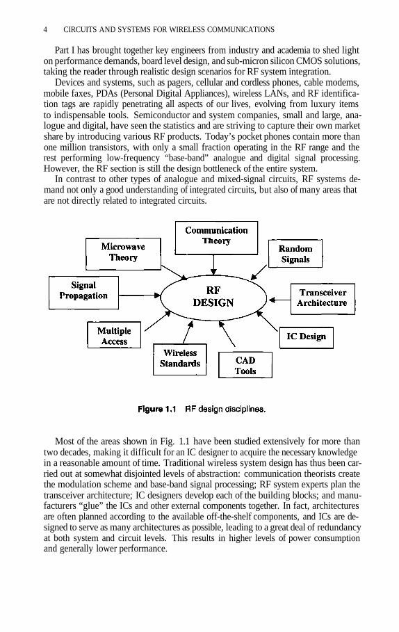
In contrast to other types of analogue and mixed-signal circuits, RF systems de-mand not only a good understanding of integrated circuits, but also of many areas thatare not directly related to integrated circuits.
Most of the areas shown in Fig. 1.1 have been studied extensively for more thantwo decades, making it difficult for an IC designer to acquire the necessary knowledgein a reasonable amount of time. Traditional wireless system design has thus been car-ried out at somewhat disjointed levels of abstraction: communication theorists createthe modulation scheme and base-band signal processing; RF system experts plan thetransceiver architecture; IC designers develop each of the building blocks; and manu-facturers “glue” the ICs and other external components together. In fact, architecturesare often planned according to the available off-the-shelf components, and ICs are de-signed to serve as many architectures as possible, leading to a great deal of redundancyat both system and circuit levels. This results in higher levels of power consumptionand generally lower performance.
RF SYSTEM INTEGRATION 5
Most recently, as the industry moves toward higher integration and lower cost, RFand wireless design increasingly demands more “concurrent engineering,” thereby re-quiring IC designers from both industry and academia to combine forces and to have asufficient and integrated knowledge of all the disciplines [1]. RF circuits must processanalogue signals with a wide dynamic range at high frequencies. It is interesting tonote that the signals must be treated as analogue even if the modulation is digital orthe amplitude carries no information.
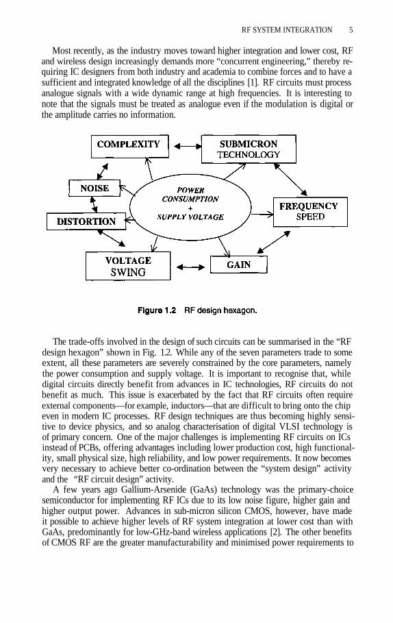
The trade-offs involved in the design of such circuits can be summarised in the “RFdesign hexagon” shown in Fig. 1.2. While any of the seven parameters trade to someextent, all these parameters are severely constrained by the core parameters, namelythe power consumption and supply voltage. It is important to recognise that, whiledigital circuits directly benefit from advances in IC technologies, RF circuits do notbenefit as much. This issue is exacerbated by the fact that RF circuits often requireexternal components—for example, inductors—that are difficult to bring onto the chipeven in modern IC processes. RF design techniques are thus becoming highly sensi-tive to device physics, and so analog characterisation of digital VLSI technology isof primary concern. One of the major challenges is implementing RF circuits on ICsinstead of PCBs, offering advantages including lower production cost, high functional-ity, small physical size, high reliability, and low power requirements. It now becomesvery necessary to achieve better co-ordination between the “system design” activityand the “RF circuit design” activity.
A few years ago Gallium-Arsenide (GaAs) technology was the primary-choicesemiconductor for implementing RF ICs due to its low noise figure, higher gain andhigher output power. Advances in sub-micron silicon CMOS, however, have madeit possible to achieve higher levels of RF system integration at lower cost than withGaAs, predominantly for low-GHz-band wireless applications [2]. The other benefitsof CMOS RF are the greater manufacturability and minimised power requirements to

6 CIRCUITS AND SYSTEMS FOR WIRELESS COMMUNICATIONS
drive off-chip loads. While integrated silicon BJT transceivers are still more desirablefor today’s products, CMOS RF solutions are looking very promising, with the real-istic prospect of a single-chip transceiver in a plastic package. Furthermore, newerdevice technologies such as Silicon Germanium are maturing rapidly and offer thehigh mobility necessary for today’s RF wireless products. This array of competingtechnologies offers system designers more creative opportunity, and the best wirelesstransceiver solutions may well emerge from system design evolving together with ar-chitecture, circuits, antennas, and power allocation plans. In the future, base-bandsignal processing will inevitably make up for imperfections in the front end (e.g. soft-ware radio).
Part I begins with a section by Gordon Aspin from TTP Communications, a com-pany with vast experience in RF system integration for cellular products. The sectiondescribes the realistic design of a part of a fully integrated transceiver IC from Hitachiwhich satisfies multi-band GSM RF specifications. Some of the subtleties of board-level integration are presented, coupled with a design approach which attempts tomake practical GSM handset design a more straightforward task. Emphasis is placedupon the importance of understanding total system-level requirements when designinga chip, and upon how board level design influences low-level requirements.
In the next section, Peter Mole from Nortel Semiconductors gives an overview ofsystem integration on a chip. Peter takes us through a number of practical RF design is-sues and then discusses general problems that radio systems must overcome to achieveacceptable performance. The section overviews practical concerns for both receiverand transmitter and how different radio architectures can be utilised to overcome someof the problems. The section concludes with a number of practical design issues forintegrating radio circuitry in silicon technology.
The final two sections concentrate on the design of fully integrated transceiver chipsin sub-micron and deep sub-micron Silicon CMOS technologies. Michiel Steyaertfrom the Katholieke Universiteit of Leuven introduces us to the arena of using deepsub-micron CMOS to create single-chip transceiver blocks and components such asLNAs, VCOs , up-converters , synthesisers etc. to satisfy cellular performance spec-ifications above 1 GHz. The section discusses all the bottlenecks and challenges ofRF CMOS using plain deep sub-micron devices for integration within systems such asDECT, GSM, and DCS 1800.
Finally, Qiuting Huang et. al. from the Integrated Systems Laboratory at ETHZurich presents a practical high-performance GSM transceiver front-end in a 0.25 µmCMOS process. This section concludes Part I by taking the reader through a practicalRF system integration example. The work demonstrates that excellent RF performanceis feasible with 0.25 µm CMOS, even in terms of the requirements of the super-hetero-dyne architecture. Design for low noise and low power for GSM handsets has beengiven particular attention.
In conclusion, Part I will give the reader a practical evaluation of state- of-the-artRF system design and integration for GHz wireless communications. The chapters inPart I encompass the failures, successes, and most of all the realistic RF challenges toenable total integration of portable future wireless information systems.

RF SYSTEM INTEGRATION 7
References
[1]
[2]
B. Razavi, “Challenges in Portable Transceiver Design”, Circuits and DevicesMagazine, IEEE 1996..
K. T. Lin, Private Communication, Imperial College 1999.

This page intentionally left blank

2 RF SYSTEM BOARD LEVELINTEGRATION FOR MOBILE PHONES
Gordon J. Aspin
TTP Communications Ltd.Melbourn Science Park
Royston, SG8 6EE, U.K.
Abstract: This paper highlights the importance of system design choices in thedevelopment of RF chip sets for cellular mobile phones. By way of example, the designof the BRIGHT family of RF chip sets for GSM is described. Performance results arepresented based on these chip sets.
2.1 INTRODUCTION
Traditionally, the RF system represents one of the most difficult challenges for compa-nies developing digital cellular phones, particularly for companies with limited devel-opment experience. It is now possible to buy more or less complete baseband-chip-setsolutions together with associated software from a number of vendors. However, al-though off-the-shelf radio-chip-set solutions are available, they nevertheless require asignificant level of design expertise on the part of the handset designer in order to re-alise a manufacturable product which meets the necessary performance requirements.This paper describes the results of some of our work to meet the challenge of realisingan RF chip set which makes designing a GSM mobile phone a straightforward task.
9

10 CIRCUITS AND SYSTEMS FOR WIRELESS COMMUNICATIONS
This work, the development of the RF chip set family, has been carried outin collaboration with Hitachi Semiconductor of Japan.
The initial devices were targeted at single-band products — the main GSM marketat that time. Even more important commercially, however, has been the emergence ofdual-band 900/1800 capability as a key market requirement. Fortunately, the BRIGHTarchitecture is particularly well suited to multi-band operation, and the latest-genera-tion devices, BRIGHT2, are designed to support this mode.
The objective of the development has been to achieve the maximum level of inte-gration in the radio system, compatible with the objectives of lowest total system cost,lowest part count, and ease of design and manufacture, within the available IC processtechnology. The approach is a systems approach with the focus upon achieving a de-vice design in which the radio requirements of the whole product are most simply andelegantly met.
2.2 DESIGN APPROACH
What makes RF IC design particularly interesting is that the silicon represents onlya small part of the total RF system but can make a very large difference to how easyor difficult it is to design the rest of the system. It is therefore vital to understand thetotal system requirements when designing the chip. It is also important to be able tovalidate the design at both device and system level. This is achieved by means of aSystem Evaluation Board — essentially a complete handset—on which all the systemperformance parameters can be measured and confirmed (Fig. 2.1). Validation of thesystem is often one of the most expensive parts of the development.
This radio System Evaluation Board is designed to be compatible with BasebandEvaluation Boards used for baseband chip set and protocol software developmentwork. The two boards can be plugged together to emulate complete handset opera-tion. As well as testing in our own laboratories we have even been able to take sucha system through “Type Approval” at a GSM test house to verify radio system perfor-mance.
2.3 KEY GSM SYSTEM SPECS
As with all modern radio standards, there are many specification points for GSM thatneed to be met in order for the radio to conform to the standard. However, a smallnumber of these specification points turn out to be critical to the radio architecture anddesign.
2.3.1 Transmitter phase error
As a digital phase modulation system, GSM controls how closely the transmitted phasefollows the ideal modulated phase trajectory. It does this by specifying the phase errorin terms of an RMS value (5°) and a peak value (20°), across the useful part of theburst. The phase error is a very critical parameter for the transmitter, because so manythings can contribute to it, including digital modulator phase error, synthesiser settling
1BiCMOS Radio IC for GSM by Hitachi and TTPCom

RF SYSTEM BOARD LEVEL INTEGRATION FOR MOBILE PHONES 11
time, switching transients, I/Q gain and phase imbalance, up-converter phase noiseand spurious modulation, and power amplifier AM–to–PM conversion, etc.
In putting together a radio system design, budgets are allocated to each of theseparameters. Some, however, can be difficult to quantify theoretically (e.g. switchingtransients) and may only become apparent once the design is realised in hardware. Thetask of the system designer is to identify a system architecture in which uncontrollableand unquantifiable effects are minimised.
A classic example of a problematic architecture is the direct-up-converter transmit-ter, in which a baseband I/Q modulator is mixed up to the final frequency in a singlestage. As a result, the up-converter’s local oscillator runs also at the final frequency.Maintaining sufficient isolation between the modulated power amplifier output and theunmodulated low-power local oscillator is very difficult, particularly within a minia-ture handset.
2.3.2 Transmitter modulation spectrum (Fig. 2.2)
Like the phase error, the modulation spectrum is affected by many factors, includingdigital modulator spectrum, I/Q gain and phase imbalance, up-converter phase noiseand spurious modulation, power amplifier AM–to–PM conversion, transmitter noisefloor, etc. A good system design will minimise these effects inherently in the design.
2.3.3 Transmitter noise in the receiver band (Fig. 2.3)
To avoid interference between handsets in close proximity, GSM limits the amount ofspurious radiation emitted from the antenna into the receive band. In the non-extendedband, this is limited to –79 dBm in a 100kHz bandwidth, or –129 dBm/Hz. Reflected

12 CIRCUITS AND SYSTEMS FOR WIRELESS COMMUNICATIONS
back to the input of the power amplifier this typically corresponds to a noise level of– 162 dBm/Hz or 12 dB above the ideal thermal noise floor. In practice, modulatorscannot achieve this level of performance, and typically around 20 dB or more of filter-ing is required in a duplexer—which is a relatively bulky and expensive component.
RF SYSTEM BOARD LEVEL INTEGRATION FOR MOBILE PHONES 13
In the extended GSM900 band, the specification is relaxed by around 12 dB toavoid even more severe duplexer filtering requirements. In the 1800MHz bands, thespecifications are comparable to the E-GSM requirements scaled by the frequency.
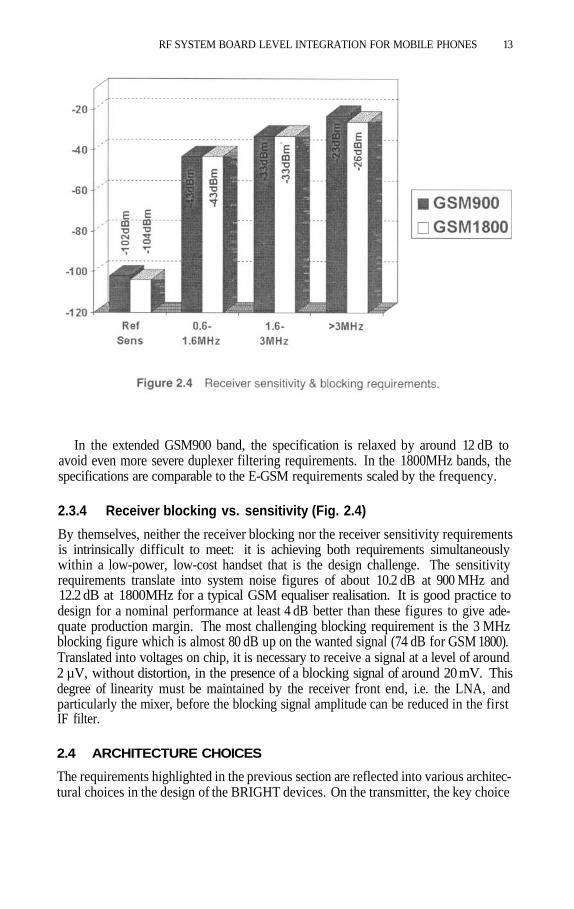
2.3.4 Receiver blocking vs. sensitivity (Fig. 2.4)
By themselves, neither the receiver blocking nor the receiver sensitivity requirementsis intrinsically difficult to meet: it is achieving both requirements simultaneouslywithin a low-power, low-cost handset that is the design challenge. The sensitivityrequirements translate into system noise figures of about 10.2 dB at 900 MHz and12.2 dB at 1800MHz for a typical GSM equaliser realisation. It is good practice todesign for a nominal performance at least 4 dB better than these figures to give ade-quate production margin. The most challenging blocking requirement is the 3 MHzblocking figure which is almost 80 dB up on the wanted signal (74 dB for GSM 1800).Translated into voltages on chip, it is necessary to receive a signal at a level of around2 µV, without distortion, in the presence of a blocking signal of around 20 mV. Thisdegree of linearity must be maintained by the receiver front end, i.e. the LNA, andparticularly the mixer, before the blocking signal amplitude can be reduced in the firstIF filter.
2.4 ARCHITECTURE CHOICES
The requirements highlighted in the previous section are reflected into various architec-tural choices in the design of the BRIGHT devices. On the transmitter, the key choice

14 CIRCUITS AND SYSTEMS FOR WIRELESS COMMUNICATIONS
is the use of an offset phase-locked loop. This approach has substantial benefits forsystems like GSM which employ constant envelope modulation.
As a result of the strict phase and modulation accuracy requirements of GSM, it isonly really feasible to perform transmit carrier modulation in the digital domain. Thismust then be converted into an analogue signal and translated to the required transmitfrequency. In a conventional approach, the frequency translation is performed in oneor more up-conversion stages. One of the problems of trying to do this operation in asingle stage, when the mixer’s local oscillator runs at the same frequency as the trans-mitted signal, is that of cross-coupling between the modulated high-level transmitterpower output and the unmodulated low-level VCO. A solution to this problem is to usemultiple conversions, but each conversion stage introduces spurious conversion prod-ucts which must be filtered out. A better approach is the one illustrated in Fig. 2.5. Inthis scheme, the required signal modulation is impressed upon a VCO by means of aphase locked loop. The modulated VCO output is mixed down to a suitable interme-diate frequency and compared with the signal from the digital modulator, which hasbeen up-converted to the same IF. The loop comparison frequency is not critical and ischosen to provide a suitable frequency plan. Channelisation is supported by steppingthe local oscillator as normal.
The bandwidth of the loop has a significant effect upon overall transmitter perfor-mance. The low-pass filter in the offset PLL must be chosen to optimise the followingparameters:
Minimum loop settling time (following frequency steps).Good phase tracking (to give minimum phase error).Minimum in-band spurii (to meet modulation spectrum requirements).Suppression of wide-band modulator noise (to meet transmit noise in receive bandrequirements).
Typically, a loop bandwidth of around 1 MHz is found to be optimum. Using a basicoffset PLL design of the form shown has clear benefits:
The VCO is inherently a constant-envelope device, hence no spurious amplitudemodulation occurs in the signal driving the PA, and therefore we find no spuriousPM generated in the PA through AM–PM conversion effects.
RF SYSTEM BOARD LEVEL INTEGRATION FOR MOBILE PHONES 15
The noise floor of the VCO is sufficiently low so that it can meet the receiver-bandnoise-floor requirements without further filtering. The duplex filter can be replacedby a simple low-pass harmonic filter and a transmit/receive switch, with consider-able cost and space savings.
Removing the duplex filter reduces the loss in the transmit path by around 1 dB.This implies up to 25% longer talk time for the handset.
Removing the duplex filter removes a major cause of ripple in the transmit band.This allows the handset manufacturer to make use of the margin in the transmitlevel specifications to operate the handset closer to the minimum level, thus givingfurther battery life improvements.
In the receiver, the architectural choice is mainly about the number of conversionstages and the frequency plan. A two-IF approach has been chosen for BRIGHT,with a 225 MHz SAW filter defining the first IF. The use of a relatively high firstIF means that image frequencies and other spurious responses from the first mixercause no particular problems. The majority of receiver gain occurs at the second IFof 45 MHz, and it is here also that the AGC is applied. This approach minimisespower consumption in the receiver. In our reference baseband solution (the AnalogDevices GSM baseband chip sets), the channel filtering occurs digitally as part of theanalogue–to–digital converter—another example of system design choices. Thus,at 45 MHz, only a relatively wide-band LC filter is required to provide protectionagainst blocking of subsequent stages. The architecture of the complete 900 MHzBRIGHT device is shown in Fig. 2.6. The main UHF local oscillator runs at 1150 to1185 MHz and drives both the receiver first mixer and the transmitter offset mixer. Byensuring that the receiver first IF and the transmitter offset loop comparison frequencyare spaced by the Tx/Rx duplex offset (i.e. 45 MHz) the pulling range of the first localoscillator is minimised to the operating bandwidth of 35 MHz.
The loop comparison frequency is chosen to be a multiple of 45 MHz (in this caseto give a simple scheme for generating all other required
frequencies by on-chip division as shown.In terms of integration, all the transmit and receive silicon functionality is integrated
onto a single device, but the PLL synthesiser functions for the two main oscillators areon a separate device. This choice was based on an assessment of the risk factors in-volved versus the benefits. There is virtually no difference in printed circuit board areawhether or not the synthesisers are integrated, yet there is a significant risk of noise inthe digital PLL synthesiser leaking into the analogue parts of the chip. Furthermore,the PLL synthesisers are established parts.
The front-end low noise amplifier is also not fully integrated within the BRIGHTdevice. Initial studies identified that it would be very difficult to achieve the necessarynoise figure and blocking performance from an integrated amplifier. Instead it wasdecided to integrate the bias function for the LNA, and to use an external transistoras the amplifying device. The final die for the BRIGHT 900 MHz part is shown inFig. 2.7. Some key process and packaging parameters are summarised in Tab. 2.1.
When the first BRIGHT devices were designed, the main market interest was inGSM900. However, support of other single-band standards, DCS 1800 and PCS 1900,was also of interest and was a factor in the choice of architecture. As a result, a high

16 CIRCUITS AND SYSTEMS FOR WIRELESS COMMUNICATIONS
frequency variant BRIGHT-HF was developed with improved high frequency mixerperformance. Only towards the end of 1997 did it become apparent that dual-bandwould become a major market requirement, and with that came the further develop-

RF SYSTEM BOARD LEVEL INTEGRATION FOR MOBILE PHONES 17
ment of the BRIGHT2 device. The BRIGHT architecture is well suited to dual-bandoperation, with only small adaptations. On the receive side, the only change is theinclusion of a second mixer to support the second band: the first IF and subsequentcircuitry is shared between both bands. On the transmit side, the only change is theinclusion of a different divide ratio for operation at 1800 MHz, giving an offset loopcomparison frequency of 135 MHz. For minimum VCO range, the difference betweentransmit and receive IFs should equal the Tx/Rx duplex offset. In this case, for the1800MHz operation, we have a 90 MHz IF separation, compared to a 75 MHz du-plex offset—thus giving around 20% excess pulling requirement over the theoreticalminimum.
All other areas of the architecture are essentially unchanged. For market reasons,however, a digital AGC is included in BRIGHT2, compared to the analogue AGCscheme used in the original BRIGHT. It is found that the digital AGC gives betterperformance than the analogue AGC, because the on-chip DAC can be better matchedto the characteristics of the AGC amplifier.
2.5 RESULTS
2.5.1 Transmitter phase error
Fig. 2.9 plots the measured peak phase error as a function of channel number in theGSM band. The RMS phase error is very consistent at around 3°, peaking up to justunder 4° in one place. The truly remarkable factor is the independence of the phaseerror with transmit power level. This is testimony to the real benefits of the offsetphase locked loop approach, where some of the sources of phase error, which causemajor problems with other architectures, are completely removed by design. Similarresults have also been reported to us for single-band GSM900 and DCS 1800 phones inproduction, based on the single-band BRIGHT variants. The peak phase error is alsowell within the specification of 20°. Comparable results are obtained at 1800MHz(see Fig. 2.10).

18 CIRCUITS AND SYSTEMS FOR WIRELESS COMMUNICATIONS
2.5.2 Transmitter modulation spectrum
Fig. 2.11 illustrates the typical modulation spectra achieved with the BRIGHT2 designat 900 MHz. The spectrum falls comfortably within the specification mask. Similarresults are obtained at 1800MHz.

RF SYSTEM BOARD LEVEL INTEGRATION FOR MOBILE PHONES 19
2.5.3 Receive sensitivity
Fig. 2.12 shows the measured receive sensitivity in both bands plotted as a functionof channel number. For GSM900, the specification is –102 dBm, for GSM1800, thespecification is –100dBm. A minimum margin of 4dB is achieved on these figures,with 5–7 dB typical margin. This provides sufficient margin for production and tem-perature tolerances.
The underlying sensitivity variation displayed in the graphs is due to ripple inthe front-end SAW filter. There are two well-known “deaf” channels in GSM900receivers, channels 5 and 70, at the and harmonic of the GSM referencefrequency of 13 MHz. These are clearly visible in the figure. The other deaf channelis thought to be due to a local GSM base station transmitting on this channel in thevicinity of the laboratory.

20 CIRCUITS AND SYSTEMS FOR WIRELESS COMMUNICATIONS
2.5.4 Blocking performance
Fig. 2.13 shows the blocking performance for BRIGHT2 in the 900 and 1800MHzbands. The specification points are 2% BER and –23 dBm for GSM900, –26 dBm

RF SYSTEM BOARD LEVEL INTEGRATION FOR MOBILE PHONES 21
for GSM1800. Around 2–3 dB margin is thus achieved in each band. The blockingperformance of BRIGHT2 in the GSM900 band is further illustrated in Fig. 2.14. Awanted signal is applied, 3 dB above the reference sensitivity level, and then the levelof blocking signal which causes the receiver BER to degrade to the nominal 2% level,is measured. The wanted signal is on channel 61, i.e. at 947.2MHz.
The GSM requirements are as follows:
The most difficult requirement is the 3 MHz blocker, and for this, a minimum of1.5 dB margin is demonstrated. Since these measurements were made, it was iden-tified that the first mixer was not particularly well-matched (hence the ripple), andsubsequently better performance with more than 3 dB margin has been demonstrated.
2.6 FUTURE OPTIONS
Looking to the future, there are a number of possible options. Firstly, the levels of inte-gration can be increased, for example by including on chip the VCOs or the basebandinterface. The challenge with putting VCOs on chip is to realise circuits of sufficientlyhigh Q to meet the phase noise requirements; also low-loss varactors are not normallyrealisable in a BiCMOS IC process. Nevertheless, there is much interest in this area.
Including the baseband interface within the RF chip is more straightforward inprinciple. Whether this makes commercial sense is more questionable — integration

22 CIRCUITS AND SYSTEMS FOR WIRELESS COMMUNICATIONS
does not help reduce the total number of pins in the package very much, and the areafor a 64-pin QFP is actually greater than for a 48-pin QFP plus a 20-pin SSOP. Also,because the baseband interface may be realised in smaller geometries than the RFdevice, the total power consumption may be increased by integration.
A more fruitful line is perhaps to consider greater functionality. In this regard,triple-band phones may be a market requirement soon, a requirement which may besupported as a further extension of the BRIGHT architecture.
In conclusion, it is clear that radio design remains one of the most challenging andexciting areas in this industry. Whatever happens in wireless communications over thenext decade, elegant design at both circuit and system level will continue to be a majorfactor in the success of products, as it has been to date with BRIGHT.

3 INTEGRATION OF RF SYSTEMSON A CHIP
Peter J. Mole
Nortel NetworksLondon Road
Harlow, Essex, CM 17 9NA, U.K.
3.1 RF ISSUES
Before considering the details of implementation of an RF system on a chip, it is worthspending some time discussing the problems that any radio system must overcome if toachieve an acceptable performance. The important aspect to remember is that the radiosystem never operates in isolation. It is not sufficient to think only of the transmitter,the link and the receiver, though many problems lie in this simple chain alone. It is alsoimportant to realise that the transmitter can interfere with other links, and a receivermay be unduly sensitive to unwanted, but entirely legitimate, signals.
3.1.1 Receiver concerns
In any system, a band is defined in which the receiver may receive signals. The re-ceiver must be able to reject signals outside the band without loss of performance.These signals may be very large (e.g. TV transmissions) and quite capable of over-loading a sensitive receiver. If the receiver is overloaded, amplifier compression willreduce the receiver gain and hence the ability to detect weak signals, or the non-lin-earities in the receiver that are excited by the overload will allow unwanted signalsto intermodulate. This may result in a distortion product falling onto the wanted sig-
23

24 CIRCUITS AND SYSTEMS FOR WIRELESS COMMUNICATIONS
nal and effectively masking it. It is therefore imperative that these signals are heavilyfiltered before the input to the receiver.
The receiver must respond to any signal in the system band, however, it must alsoreject unwanted in-band signals without suffering from overload. Such unwanted sig-nals may be significantly larger than the wanted; consider the situation when you aretrying to make a cellular phone link to your service provider’s remote base-station but,unfortunately, you are physically adjacent to a second service provider’s base-station.The system specification provides guidelines to the levels of signals which can exist.Fig. 3.1 shows the relative levels for signals in the DECT cordless phone system. Inthis system, where communication channels are allocated to both time and frequencyslots, the frequency channels are separated by 1.728 MHz. A weak signal, (defined inthe DECT specification as –73 dBm) must be receivable in the presence of a signal13 dB stronger in the neighbouring channel and 34 dB stronger in the next neighbour-ing channel. To achieve this rejection of neighbouring interferers, a tunable filter isrequired. In practice this is achieved by mixing the signal to a fixed intermediate fre-quency and then filtering. The specifications reflect the fact that it is more difficultto filter the neighbouring channel than more distant ones. Until the signals can befiltered, however, the radio must be designed so that the interferers do not create over-load. Unlike out-of-band blocking signals, in-band interferers cannot be filtered priorto the sensitive input of the receiver.
The frequency translation that is required in a receiver to move the radio frequencyinput to the required intermediate frequency for filtering is achieved with a mixer. Amixer effectively multiplies the RF input signal with a chosen local oscillator (LO)signal. Thus we can ideally represent the RF input by and the local oscillatorby Thus the output can be written as:
From this we can see immediately that an unwanted output is produced at the sumfrequency, but this is easily filtered because of the frequency difference. A more subtledefect is that two input frequencies can produce signals at the intermediatefrequency Thus there are two frequencies we are sensitive to, the wanted and the

INTEGRATION OF RF SYSTEMS ON A CHIP 25
image frequency. It is therefore essential that any signal present at the image frequencyis filtered out in front of the mixer.
In practice, to achieve efficient mixing, it is normal that the LO signal is close toa square wave. Thus the LO signal will contain the third harmonic of the LO (about9 dB lower in signal amplitude) which is also multiplied by the input signal. Thisimmediately means that signals at will also appear at the output as anintermediate-frequency signal. Other harmonics will behave similarly. Again inputsignals at these frequencies must be removed prior to mixing.
Another defect of the LO signal is that it suffers from phase noise (or jitter). Thismeans the LO is not a pure tone but a spectrum of signals centred on the desiredfrequency. Thus the mixer will respond to signals close to the wanted signal with asensitivity falling off with the phase-noise spectrum. This problem is known as recip-rocal mixing. Thus, to ensure that the receiver can reject neighbouring channels, it isimportant to provide an LO signal with low phase noise. These issues are illustratedin Fig. 3.2.
3.1.2 Transmitter concerns
The transmitter must efficiently produce enough output power to ensure that the sys-tem has sufficient range whilst ensuring that power is not transmitted into neighbour-ing channels. It is important to understand how power can be transmitted at unwantedfrequencies. Firstly, harmonics will be generated in an efficient power amplifier. Thesecan usually be filtered out before they reach the antenna, but it must be rememberedthat any filter will also attenuate the wanted output, hence reducing the overall effi-ciency and increasing the current consumption from the battery. Non-linearity in thepower amplifier will spread the spectrum of the signal into neighbouring bands. Thisbehaviour is known as spectral regrowth. It is worse with modulation schemes that are
26 CIRCUITS AND SYSTEMS FOR WIRELESS COMMUNICATIONS
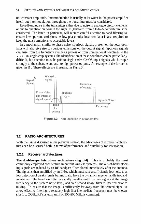
not constant amplitude. Intermodulation is usually at its worst in the power amplifieritself, but intermodulation throughout the transmitter must be considered.
Broadband noise in the transmitter either due to noise in analogue circuit elementsor due to quantisation noise if the signal is generated from a D-to-A converter must beconsidered. The latter, in particular, will require careful attention to band filtering toensure low spurious emissions. A low-phase-noise local oscillator is also required tokeep the noise emissions to acceptable levels.
In a mechanism similar to phase noise, spurious signals present on the local oscil-lator will also give rise to spurious emissions on the output signal. Spurious signalscan arise from the frequency synthesis process or from unintentional couplings to theVCO. On single-chip systems, the identification of these couplings can be particularlydifficult, but attention must be paid to single-ended CMOS input signals which couplestrongly to the substrate and also to high-power outputs. An example of the former isgiven in [1]. These effects are illustrated in Fig. 3.3.
3.2 RADIO ARCHITECTURES
With the issues discussed in the previous section, the advantages of different architec-tures can be discussed both in terms of performance and suitability for integration.
3.2.1 Receiver architectures
The double-superheterodyne architecture (Fig. 3.4). This is probably the mostcommonly employed architecture in current wireless systems. The out-of-band block-ing signals are reduced by an RF bandpass filter placed immediately after the antenna.The signal is then amplified by an LNA, which must have a sufficiently low noise to al-low detection of weak signals but must also have the dynamic range to handle in-bandinterferers. The bandpass filter is usually insufficient to reduce signals at the imagefrequency to the system noise level, and so a second image filter is inserted prior tomixing. To ensure that the image is sufficiently far away from the wanted signal toallow effective filtering, a relatively high first intermediate frequency must be chosen(for 1 to 2 GHz RF systems an IF of 100–200 MHz is common).

INTEGRATION OF RF SYSTEMS ON A CHIP 27
The mixer must still handle the complete dynamic range of the in-band signal.After the mixer, a SAW filter can be used to achieve the channel filtering. At thesefrequencies the SAW filter is small but usually has a large in-band loss when completechannel filtering is to be achieved. The output drive of the mixer must therefore boostthe signal level to allow for this loss.
Once the interfering channels have been attenuated, the signal can be boosted toa high level (it can be limited if a constant-amplitude modulation scheme is used).The signal is then reduced to baseband frequency for demodulation. It is of coursepossible to split the channel filtering between the two intermediate frequencies. Thiswill require a greater dynamic range in the second mixer.
This architecture requires the synthesis of two local oscillators, and their frequen-cies must be chosen so that spurious responses from the radio are kept to a minimum.This aspect of frequency planning, which will not be discussed in more detail here, isa well-understood design process which requires considerable care and experience.
This design requires several external filters and therefore does not lend itself to easyintegration as the pin count increases. Moreover, the filters are usually single ended—though this is not essential—and hence achieving isolation between pins becomes anissue. In particular, the channel filter will often need to provide 50 dB of attenuationat key frequencies, thus implying that greater isolation must be achieved between thepins and with respect to signal ground if the filter response is not to be degraded. Theimage filter can be eliminated if an image-rejecting mixer is used. This will preventthe need to come off chip after the LNA and makes an LNA plus image-reject mixer auseful integrated building block.
The direct-conversion architecture (Fig. 3.5). The direct-conversion receiver, be-cause of its simplicity, appears to offer the best opportunity for integrated systems.Some examples of its use in wireless systems do exist today, but it is not as simple inpractice.
Once again, an RF bandpass filter is placed at the input. The LNA’s output ispassed into the mixer. The LNA must handle the same dynamic range as for thesuperheterodyne architecture and it must have enough gain to lift weak signals abovethe noise of the mixer. The mixer however, now converts directly to baseband. Thusthe signal is its own image, and channel filtering can now be carried out by low-pass

28 CIRCUITS AND SYSTEMS FOR WIRELESS COMMUNICATIONS
baseband filters. Only one local-oscillator frequency needs to be synthesised, andfrequency planning is straightforward.
To achieve a precise conversion to baseband, it is important that good quadraturecan be achieved at the local-oscillator frequency. Unlike the superheterodyne architec-ture, this quadrature now needs to be achieved at the RF frequency, which poses someproblems that are generally soluble.
The main issue is associated with DC signals which are generated by defects in themixer. These signals are implicitly in-band, it is therefore difficult, and sometimes im-possible, to filter them from the wanted signal. It is necessary to keep them sufficientlybelow the signal. Unfortunately, the amplification that can be applied to the signal be-fore mixing is limited by the level of in-band interferers which must not overload themixer.
The DC offsets are caused by a collection of effects. Imbalance in the mixers willlead to a DC output. This is generally a constant quantity and could be cancelled withsuitable circuitry. Any leakage of the local oscillator to the input of the receiver willresult in a DC signal being generated. If this leakage is via radiation coupling into theantenna, then this may vary with the local environment. Finally, non-linearities in themixer may cause signals to be generated at DC from other interferers. The latter mech-anisms can be time varying, and any offset cancellation needs to be able to respondto time variation. It is only when special precautions are taken to cancel DC offsetsthat direct-conversion architectures can be used. More details of the direct-conversionissues are given in [2].
Digitisation at IF (Fig. 3.6). This architecture is still a research activity. After thefirst mixer the full dynamic range of the in-band signals may still exist. This full rangeneeds to be captured by the A-to-D converter. A bandpass sigma-delta converter offerspotential for a very flexible system as it does not place high demands on the anti-aliasfilter. With such a system, the final channel filtering can be made programmable in theDSP filter to allow a single radio architecture to adapt itself to a range of systems. Atpresent the complexity and power consumption in the A-to-D converters provide a sig-nificant challenge. As an alternative to bandpass sigma-delta converters, sub-sampledor pipeline converters may provide a viable alternative, but the dynamic range which
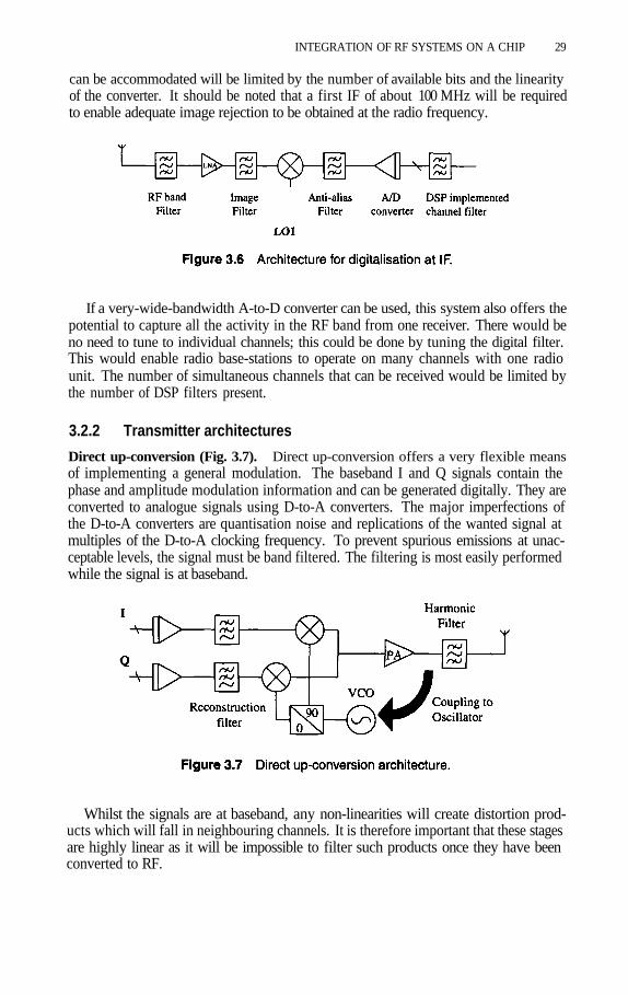
INTEGRATION OF RF SYSTEMS ON A CHIP 29
can be accommodated will be limited by the number of available bits and the linearityof the converter. It should be noted that a first IF of about 100 MHz will be requiredto enable adequate image rejection to be obtained at the radio frequency.
If a very-wide-bandwidth A-to-D converter can be used, this system also offers thepotential to capture all the activity in the RF band from one receiver. There would beno need to tune to individual channels; this could be done by tuning the digital filter.This would enable radio base-stations to operate on many channels with one radiounit. The number of simultaneous channels that can be received would be limited bythe number of DSP filters present.
3.2.2 Transmitter architectures
Direct up-conversion (Fig. 3.7). Direct up-conversion offers a very flexible meansof implementing a general modulation. The baseband I and Q signals contain thephase and amplitude modulation information and can be generated digitally. They areconverted to analogue signals using D-to-A converters. The major imperfections ofthe D-to-A converters are quantisation noise and replications of the wanted signal atmultiples of the D-to-A clocking frequency. To prevent spurious emissions at unac-ceptable levels, the signal must be band filtered. The filtering is most easily performedwhile the signal is at baseband.
Whilst the signals are at baseband, any non-linearities will create distortion prod-ucts which will fall in neighbouring channels. It is therefore important that these stagesare highly linear as it will be impossible to filter such products once they have beenconverted to RF.
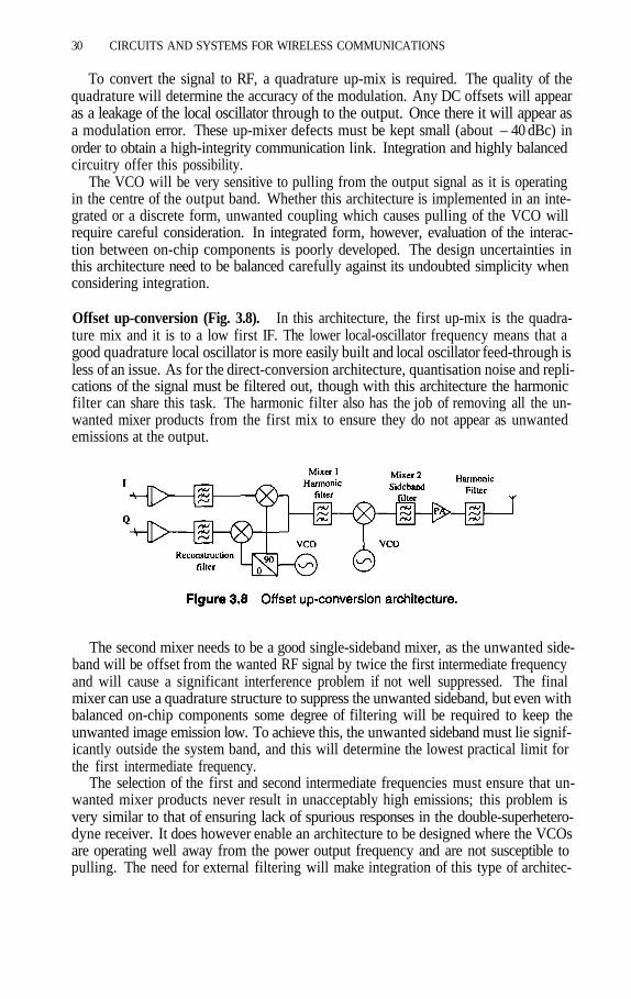
30 CIRCUITS AND SYSTEMS FOR WIRELESS COMMUNICATIONS
To convert the signal to RF, a quadrature up-mix is required. The quality of thequadrature will determine the accuracy of the modulation. Any DC offsets will appearas a leakage of the local oscillator through to the output. Once there it will appear asa modulation error. These up-mixer defects must be kept small (about – 40 dBc) inorder to obtain a high-integrity communication link. Integration and highly balancedcircuitry offer this possibility.
The VCO will be very sensitive to pulling from the output signal as it is operatingin the centre of the output band. Whether this architecture is implemented in an inte-grated or a discrete form, unwanted coupling which causes pulling of the VCO willrequire careful consideration. In integrated form, however, evaluation of the interac-tion between on-chip components is poorly developed. The design uncertainties inthis architecture need to be balanced carefully against its undoubted simplicity whenconsidering integration.
Offset up-conversion (Fig. 3.8). In this architecture, the first up-mix is the quadra-ture mix and it is to a low first IF. The lower local-oscillator frequency means that agood quadrature local oscillator is more easily built and local oscillator feed-through isless of an issue. As for the direct-conversion architecture, quantisation noise and repli-cations of the signal must be filtered out, though with this architecture the harmonicfilter can share this task. The harmonic filter also has the job of removing all the un-wanted mixer products from the first mix to ensure they do not appear as unwantedemissions at the output.
The second mixer needs to be a good single-sideband mixer, as the unwanted side-band will be offset from the wanted RF signal by twice the first intermediate frequencyand will cause a significant interference problem if not well suppressed. The finalmixer can use a quadrature structure to suppress the unwanted sideband, but even withbalanced on-chip components some degree of filtering will be required to keep theunwanted image emission low. To achieve this, the unwanted sideband must lie signif-icantly outside the system band, and this will determine the lowest practical limit forthe first intermediate frequency.
The selection of the first and second intermediate frequencies must ensure that un-wanted mixer products never result in unacceptably high emissions; this problem isvery similar to that of ensuring lack of spurious responses in the double-superhetero-dyne receiver. It does however enable an architecture to be designed where the VCOsare operating well away from the power output frequency and are not susceptible topulling. The need for external filtering will make integration of this type of architec-

INTEGRATION OF RF SYSTEMS ON A CHIP 31
ture more difficult, but if an external PA is used anyway, this constraint is not severe.The double up-mixer with external harmonic filter is a very useful integrated block.
Loop-locked and modulated VCO (Fig. 3.9). In this architecture the concept is toreduce the need for signal-path filtering by generating a pure modulated signal froma VCO. With this concept, since the modulation is effectively applied to the VCO in-put, amplitude modulation of the signal is not possible. However for phase/frequencymodulation schemes this is an attractive option.
To ensure that the modulation is precisely controlled about a desired centre fre-quency, the modulation is applied in a feedback loop. The aim of the loop is to ensurethat phase modulation sampled at the VCO output is in exact anti-phase with the phaseat the I and Q baseband inputs. This will then result in a constant-phase signal at thephase detector. Using the high-gain phase detector output to drive the VCO, the result-ing loop ensures that this condition is closely maintained. The spurii that can enter theVCO are limited by the bandwidth of the lowpass loop filter, enabling simple controlof spurious signals. Because the signal at the PA is very pure, this simplifies the fil-tering after the PA too. Here, only PA generated harmonics need be removed, whichrequires a lower-loss output filter and hence improved power efficiency.
The absolute frequency is determined by the reference oscillator and the frequencyoffset/division block. These need to be carefully planned. Offsetting the frequencyrequires down-mixing, and it is important to filter unwanted products, as for the su-perheterodyne receiver. The frequency planning will however ensure that the VCOsshould not be susceptible to pulling, and the main VCO is not susceptible as it is phasecoherent with the PA. It is not clear, however, whether for a given frequency require-ment, this architecture can produce a design with low-frequency external filter whichis easily integrable.
3.2.3 Architectures overview
The architectures under consideration are still very similar to those used in radiosbuilt from discrete components. SAW filters still play a significant role as they pro-vide good filter characteristics with a very wide dynamic range whilst consuming nopower themselves (though we should not overlook the power required to compensatefor their loss). Architectures which depend on many SAW filters place limits on the

32 CIRCUITS AND SYSTEMS FOR WIRELESS COMMUNICATIONS
integrability due to the need to get signals on and off chip, whilst maintaining goodsignal and ground isolation.
SAWs are also fixed-performance devices, thus if the radio is required to operateacross systems, several filter devices which can be switched into the path will be re-quired. Architectures which will allow the programming of the filters will be veryattractive in the future for such multi-mode systems. Architectures where the signal isdigitised with a wide dynamic range and is filtered and demodulated using the powerand low cost of data processing implemented in a small-dimension CMOS processlook attractive for this purpose. However, sufficiently high performance and suffi-ciently low power consumption has not been achieved in the analogue to digital con-version.
Implementation in integrated form offers significant advantages for matched andbalanced circuitry. Thus architectures which exploit this, for example image-rejectingmixer based circuits, will evolve as prime candidates for integrated radios. However,in any integrated radio, we need to be able to guarantee isolation between the sections.Currently, isolation is achieved by PCB and screened-compartment design. The moveto integration will require that isolation is achieved on chip. At present, design skillsin this area are low. The choice of architecture to minimise isolation requirements,and the development of techniques to calculate the isolation across the chip are goingto be key factors, if the level of integration of radios is to increase.
3.3 SOME DESIGN ISSUES
In this section, some of the design issues for integrating radio circuitry in silicon tech-nology are introduced.
3.3.1 Power supply and ground coupling
The essential problem here is that RF currents flowing in the power-supply and groundleads can drop significant potentials across track and bond inductances. Moreover, ca-pacitances can resonate with the bond/track inductances causing the impedance seenby the circuitry to become high at certain frequencies. These frequencies must be sep-arated from key circuit frequencies. Supply return currents may cause potentials to bedropped on signal grounds. This can give rise to feedback to the input, poor isolationand even instability. Fig. 3.10 shows the situation for power supply decoupling.
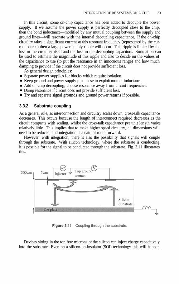
INTEGRATION OF RF SYSTEMS ON A CHIP 33
In this circuit, some on-chip capacitance has been added to decouple the powersupply. If we assume the power supply is perfectly decoupled close to the chip,then the bond inductance—modified by any mutual coupling between the supply andground lines—will resonate with the internal decoupling capacitance. If the on-chipcircuitry takes a significant current at this resonant frequency (represented by the cur-rent source) then a large power supply ripple will occur. This ripple is limited by theloss in the circuitry itself and the loss in the decoupling capacitors. Simulation canbe used to estimate the magnitude of this ripple and also to decide on the values ofthe capacitance to use (to put the resonance in an innocuous range) and how muchdamping to provide if the circuit does not provide sufficient loss.
As general design principles:Separate power supplies for blocks which require isolation.Keep ground and power supply pins close to exploit mutual inductance.Add on-chip decoupling, choose resonance away from circuit frequencies.Damp resonance if circuit does not provide sufficient loss.Try and separate signal grounds and ground power returns if possible.
3.3.2 Substrate coupling
As a general rule, as interconnection and circuitry scales down, cross-talk capacitancedecreases. This occurs because the length of interconnect required decreases as thecircuit compacts with scaling, whilst the cross-talk capacitance per unit length variesrelatively little. This implies that to make higher speed circuitry, all dimensions willneed to be reduced, and integration is a natural route forward.
However, with integration, there is also the possibility that signals will couplethrough the substrate. With silicon technology, where the substrate is conducting,it is possible for the signal to be conducted through the substrate. Fig. 3.11 illustratesthis.
Devices sitting in the top few microns of the silicon can inject charge capacitivelyinto the substrate. Even on a silicon-on-insulator (SOI) technology this will happen,

34 CIRCUITS AND SYSTEMS FOR WIRELESS COMMUNICATIONS
but a good SOI technology will have a low coupling capacitance. The major couplingwill be to nearby devices or local contacts. Some of the charge will be injected moredeeply and couple to distant circuit elements. This will be a source of interference.Finally, some charge will return via the rear die plate. The die plate potential will varyin response to the charge and the return path impedance (which will include capacitivecoupling to other parts of the circuit and the impedance to ground of the die plate).If the die plate does not have a low ground impedance then it can couple the injectedsignal effectively across the whole chip.
These effects are being studied now. Means of simulation are being developed (forexample, see [3]). As a general rule, balanced signals will always help injection, andlocal grounded substrate contacts are beneficial.
3.3.3 On-chlp oscillators
Oscillators on chip always need careful consideration. Although the maintaining am-plifier can be easily accommodated on chip, there is an advantage to keeping the wholeoscillator on chip. This however requires an on-chip resonator. The phase-noise per-formance is directly dependent on the resonator’s quality factor. Spiral inductors canbe manufactured on chip, but their quality factor is limited by the resistance of themetal used to wind the inductor (losses in the substrate are usually a smaller effect).Measurements of the phase noise achieved using a 2 µm-thick Al/Si/Cu metallisationshow that whilst the phase noise required for DECT is attainable, the requirements ofa system with much narrower bands such as GSM is rather too demanding.
The second issue to be considered with on-chip oscillators is pulling. The oscil-lator can be considered as a highly shaped and amplified noise source. Essentially,at the resonant frequency, the feedback circuit provides just enough gain to amplifythe natural circuit noise to the level required, so this gain is controlled by the limitingmechanism. Away from the natural resonant frequency, the loop gain falls away; thehigher the Q the more rapidly the gain falls off. This leads to two defect mechanisms:if a large signal close to resonance couples into the resonator, it will get amplifieduntil it causes the limiter to reduce the gain. The noise content at the output will fallaway, and the oscillator will have locked to the interferer. If an interferer is coupledin at a much lower level, then it will not trigger the limiting action; the shaped noisewill still exist, but the spurious tone will interact with the oscillations and modulatethe frequency. A side-tone will appear at the interferer frequency and a second one onthe other side of the main tone—characteristic of FM modulation. Now the sensitivityto such an interferer depends on how close to the main tone the interferer is. If it isat the resonant frequency itself, the coupling only needs to be at circuit noise levels,the level required increases as the coupling tone is offset in frequency. The higher theresonator’s Q the higher the level of the interfering signal that can be tolerated. Sincevery small signals may pull an oscillator, the choice of architecture is critical. Theaim, if an on-chip oscillator is to be included, will always be to ensure that spurioussignals which could pull or lock the VCO are not present.

INTEGRATION OF RF SYSTEMS ON A CHIP 35
References
[1]
[2]
[3]
Jeff Durec, “An Integrated Silicon Bipolar Receiver Subsystem for 900 MHz ISMBand Application”, JSSCC, vol. 33, Sept. 1998, pp. 1352–1372.Behzad Razavi, “Design Considerations for Direct Conversion Receivers”, IEEETransaction on Circuits and Systems-II, Vol. 44, June 1997, pp. 428–435.Ranjit Gharpurey and Robert G. Meyer, “Modeling and Analysis of SubstrateCoupling in Integrated Circuits”, IEEE JSSC, vol. 31, Mar. 1996, pp. 344–353.

This page intentionally left blank

4 TOWARDS THE FULLINTEGRATION OF WIRELESS
FRONT-END CIRCUITS INDEEP-SUBMICRON TECHNOLOGIES
Michiel Steyaert
K.U. Leuven, ESAT-MICASKardinaal Mercierlaan 94
B–3001 Heverlee, Belgium
Abstract: Research into the potentials of CMOS technologies for RF applicationshas been growing enormously in the past few years. The trend towards deep sub-microntechnologies allows operation frequencies of CMOS circuits above 1 GHz, which opensthe way to integrated CMOS RF circuits. Several research groups have developed highperformance down-converters, low phase noise voltage-controlled oscillators and dual-modulus pre-scalers in standard CMOS technologies. Research has already resultedin fully integrated receivers and VCO circuits with no external components, neithertuning nor trimming. Further research on low noise amplifiers, up-converters and syn-thesisers has recently resulted in fully integrated CMOS RF transceivers for DCS-1800applications.
37

38 CIRCUITS AND SYSTEMS FOR WIRELESS COMMUNICATIONS
4.1 INTRODUCTION
A few years ago, the world of wireless communications and its applications startedto grow rapidly. The driving force for this was the introduction of digital codingand digital signal processing in wireless communications. This digital revolution isdriven by the development of high performance, low cost CMOS technologies whichallow the integration of an enormous number of digital functions on a single die. Thisin turn allows the use of sophisticated modulation schemes, complex demodulationalgorithms and high-quality error detection and correction systems, resulting in high-performance, lossless digital communication channels. Low cost and a low powerconsumption are the driving forces, and they make the analog front-end the bottleneck in future RF designs. Both low cost and low power are closely linked to the trendtowards full integration. An ever higher level of integration renders significant space,cost and power reductions. Many different techniques to obtain a higher degree ofintegration for receivers, transmitters and synthesisers have been presented over thepast years [1–3].
Parallel to the trend to further integration, there is the trend to the integration ofRF circuitry in CMOS technologies. The mainstream use of CMOS technologies isthe integration of digital circuitry. If possible, using CMOS technologies to integratehigh-performance analog circuits has many benefits. The technology is cheap if usedwithout any special adaptations towards analog design. Plain CMOS has the additionaladvantage that the performance gap between devices in BiCMOS, nMOS devices indeep sub-micron CMOS, and even NMOS devices in the same BiCMOS process isbecoming smaller and smaller due to the much higher investments into the develop-ment of CMOS rather than bipolar technologies. Nowadays, NMOS devices haveeven higher transition frequencies than NPN devices.
Although some research has been done in the past on the design of RF circuitsin CMOS technologies [4], close attention has been given to it only in the past fewyears [5]. Today, several research groups at universities and in industry are researchingthis topic [2,3,6,7]. Since bipolar devices are inherently better than CMOS devices,RF CMOS is seen by some people as a possibility for only low performance systemswith reduced specifications (like ISM) [8]. Some say that the CMOS processes needadaptations, like substrate etching under inductors. Others feel, however, that thebenefits of RF CMOS can be much larger, and that it will be possible to use plaindeep sub-micron CMOS for the full integration of transceivers for high performanceapplications like GSM, DECT and DCS 1800 [2,3].
In this chapter, some trends, limitations and problems in technologies for high fre-quency design are analysed. Second, the down-converter topologies and implemen-tation problems are reviewed. Third, the design and trends towards fully integratedlow phase-noise PLL circuits are discussed. Finally, the design of fully integratedup-converters is addressed.
4.2 TECHNOLOGY
Due to the never ending progress in technology down-scaling and the requirementto achieve a higher degree of integration for DSP circuits, sub-micron technologiesare nowadays considered standard CMOS technologies. The trend is even towards
TOWARDS THE FULL INTEGRATION OF WIRELESS FRONT-END CIRCUITS 39
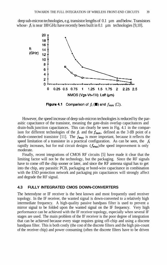
deep sub-micron technologies, e.g. transistor lengths of 0.1 µm and below. Transistorswhose is near 100 GHz have recently been built in 0.1 µm technologies [9,10].
However, the speed increase of deep sub-micron technologies is reduced by the par-asitic capacitance of the transistor, meaning the gate-drain overlap capacitances anddrain-bulk junction capacitances. This can clearly be seen in Fig. 4.1 in the compar-ison for different technologies of the and the defined as the 3 dB point of adiode-connected transistor [11]. The is more important, because it reflects thespeed limitation of a transistor in a practical configuration. As can be seen, therapidly increases, but for real circuit designs the speed improvement is onlymoderate.
Finally, recent integrations of CMOS RF circuits [5] have made it clear that thelimiting factor will not be the technology, but the packaging. Since the RF signalshave to come off the chip sooner or later, and since the RF antenna signal has to getinto the chip, any parasitic PCB, packaging or bond-wire capacitance in combinationwith the ESD protection network and packaging pin capacitances will strongly affectand degrade the RF signal.
4.3 FULLY INTEGRATED CMOS DOWN-CONVERTERS
The heterodyne or IF receiver is the best known and most frequently used receivertopology. In the IF receiver, the wanted signal is down-converted to a relatively highintermediate frequency. A high-quality passive bandpass filter is used to prevent amirror signal to be folded upon the wanted signal on the IF frequency. Very highperformance can be achieved with the IF receiver topology, especially when several IFstages are used. The main problem of the IF receiver is the poor degree of integrationthat can be achieved because every stage requires going off-chip and using a discretebandpass filter. This is both costly (the cost of the discrete filters and the high pin-countof the receiver chip) and power consuming (often the discrete filters have to be driven

40 CIRCUITS AND SYSTEMS FOR WIRELESS COMMUNICATIONS
by a signal source). Moreover, in CMOS RF circuit design input and output isbecoming a serious problem already in the lower GHz frequency range.
The homodyne or zero-IF receiver has been introduced as an alternative for the IFreceiver. It can achieve a much higher degree of integration. The zero-IF receiveruses a direct, quadrature down-conversion of the wanted signal to the baseband. Thewanted signal is its own mirror signal, and sufficient mirror signal suppression cantherefore be achieved even with a limited quadrature accuracy. Theoretically, thereis thus no discrete high-frequency bandpass filter required in the zero-IF receiver, al-lowing the realisation of a fully integrated receiver, especially if the down-conversionis performed in a single stage (e.g. directly from 900 MHz to the baseband) [6]. Theproblem of the zero-IF receiver is its poor performance compared to IF-receivers. Thezero-IF receiver is intrinsically very sensitive to parasitic baseband signals like DC-offset voltages and crosstalk products caused by RF and LO self-mixing. These draw-backs have kept the zero-IF receiver from being used on a large scale in new wirelessapplications. The use of the zero-IF receiver has therefore been limited to low-perfor-mance applications like pagers and ISM, in which the coding can be scrambled so thata high-pass filter can be inserted to avoid the DC offset problems. Another applicationis the use as a second stage in a combined IF/zero-IF receiver topology [12,13]. Ithas, however, been shown that with the use of dynamic non-linear DC-correction algo-rithms implemented in the DSP, the zero-IF topology can be used for high performanceapplications like GSM and DECT [1,14].
In recent years, new receiver topologies like the low-IF receiver [2,15] were in-troduced for use in high-performance applications. The low-IF receiver performs adown-conversion from the antenna frequency directly down to, as the name alreadyindicates, a low IF (i.e. in the range of a few 100 kHz) [2]. Down-conversion is donein quadrature and the mirror signal suppression is performed at low frequency, af-ter down-conversion, in the DSP. The low-IF receiver is thus closely related with thezero-IF receiver. It can be fully integrated (it does not require an HF mirror signalsuppression filter) and uses single stage direct down-conversion. The difference is thatthe low-IF receiver does not use baseband operation, resulting in a total immunity toparasitic baseband signals, resolving in this way the main disadvantage of the zero-IFreceiver. The drawback is that the mirror signal is different from the wanted signalin the low-IF receiver topology, but by carefully choosing the IF frequency, an adja-cent channel with low signal levels can be selected for which the typical mirror signalsuppression (i.e. a 3° phase accuracy) is sufficient.
Fig. 4.2 shows the block diagram of a fully integrated quadrature down-converterrealised in a 0.7 µm CMOS process [2]. The proposed down-converter does not requireany external components, nor does it require any tuning or trimming. It uses a newlydeveloped double-quadrature structure having a very high quadrature accuracy (lessthan 0.3° in a very large passband). The topology used for the down-converter isbased on NMOS transistors in the linear region [2,5]. In combination with capacitorson virtual ground, only a low-frequency opamp is required. Using the MOS transistorsin the linear region results in very high linearity for both the RF and the LO input. Thisis reflected in a very high third order intercept point (IP3) for the mixers, which is over+45 dBm. The advantages of such a high linearity on both inputs are that the mixer canhandle a very high third order intermodulation-free dynamic range IMFDR3, resultingin no need for any kind of HF filtering.

TOWARDS THE FULL INTEGRATION OF WIRELESS FRONT-END CIRCUITS 41
4.4 THE SYNTHESISER
The local oscillator is responsible for the correct frequency selection in the up- anddown-converters. Since the frequency spectrum in modern wireless communicationsystems must be used as efficiently as possible, channels are placed together veryclosely. The signal level of the desired receive channel can be very small, whereasadjacent channels can have very large power levels. Therefore the phase noise specifi-cations for the LO signal are very hard to meet.
Meanwhile, mobile communication means low power consumption, low cost andlow weight. This implies that a completely integrated synthesiser is desirable, where“integrated” means a standard CMOS technology without any external components orprocessing steps. Usually, the LO is realised as a phase-locked loop. The very hardspecs are reflected in the design of the Voltage-Controlled Oscillator (VCO) and theDual-Modulus Pre-scaler (DMP).
The phase noise of a VCO is one of the most important specificationsfor telecommunication applications. If there is sideband phase noise at an offsetequal to the channel spacing of the system, the down-converter will superimpose theadjacent channel onto the signal in the receive channel. As a result, this will reducethe signal to noise ratio (SNR) of the wanted signal.
For the realisation of a gigahertz VCO in a sub-micron CMOS technology, twooptions exist: ring oscillators or oscillators based on the resonance frequency of anLC-tank. The inductor in this LC-tank can be implemented as an active inductor or apassive one. It has been shown that for ring oscillators as well as active LC-oscillators,

42 CIRCUITS AND SYSTEMS FOR WIRELESS COMMUNICATIONS
the phase noise is inversely related to the power consumption [16].
Therefore, the only viable way to obtain a low-power, low-phase-noise VCO is anLC-oscillator with a passive inductor. In this case, the phase noise changes proportion-ally with the power consumption:
As could be expected, the limitation in this oscillator is the integrated passive induc-tor. Equation (4.2) shows that for low phase noise, the resistance R (i.e. the equivalentseries resistance in the LC-loop) must be as small as possible. Since the resistance Rwill be dominated by the contribution of the inductor’s series resistance, the inductordesign is critical. Three solutions exist:
1. Spiral inductors on a silicon substrate usually suffer from high losses in this sub-strate, which limit the obtainable Q-factor. Recently, techniques have been de-veloped to etch this substrate away underneath the spiral coil in a post-processingstep [17]. However, since this requires an extra etching step after normal processingof the ICs, this technique is not allowed for mass production.
2. For extremely low phase-noise requirements, the concept of bondwire inductors hasbeen investigated. Since a bondwire has a parasitic inductance of approximately
TOWARDS THE FULL INTEGRATION OF WIRELESS FRONT-END CIRCUITS 43
1 nH/mm and a very low series resistance, very-high-Q inductors can be created.Bondwires are always available in IC technology and can therefore be regardedas being standard CMOS components. Two inductors, formed by four bondwires,can be combined in an enhanced LC-tank to allow a noise/power trade-off [16]. Amicro-photograph of the VCO is shown in Fig. 4.3 [18]. The measured phase noiseis as low as –115 dBc/Hz at an offset frequency of 200 kHz from the 1.8-GHzcarrier. The power consumption is only 8 mA at 3 V supply. Although chip-to-chipbonds are used in mass commercial products, they are not characterised on yieldperformance for mass production. Therefore, the industry is reluctant to accept thissolution.
3. The most elegant solution is the use of a spiral coil on a standard silicon substratewithout any modifications. Bipolar implementations do not suffer from substratelosses, because they usually have a high-ohmic substrate [19]. Most sub-micronCMOS technologies use a highly doped substrate and have therefore large inducedcurrents in the substrate which are responsible for the high losses [20]. The ef-fects present in these low-ohmic substrates can be investigated with finite-elementsimulations. This analysis leads to an optimised coil design, which is used in thespiral-inductor LC-oscillator shown in Fig 4.4. Only two metal layers are available,and the substrate is highly doped. With a power consumption as low as 6 mW, aphase noise of – 116dBc/Hz at 600kHz offset from the 1.8-GHz carrier was ob-tained [21].
4.5 RF CMOS UP-CONVERTERS
Until now, mainly CMOS down-conversion mixers have been reported in the open lit-erature. It is only recently that CMOS converters are presented and results are demon-strated [22]. In classical bipolar transceiver implementations, the up- and down-con-verter mixers typically use the same four-quadrant topology. There are, however, somefundamental differences between up- and down-converters, which can be exploited toderive optimal dedicated mixer topologies. In a down-conversion topology, the twoinput signals are at a high frequency (e.g. 900 MHz for GSM systems) and the outputsignal is a low-frequency signal of at most a few MHz for low-IF or zero-IF receiversystems. This extra degree of freedom has been used in the design of a very successfuldown-converter-only CMOS mixer topology [5].
For up-conversion mixers, the situation is totally different. The high-frequency lo-cal oscillator (LO) and the low-frequency baseband (BB) input signal are multiplied toform a high-frequency output signal. All further signal processing has to be performedat high frequencies, which is very difficult and power consuming when using currentsub-micron CMOS technologies. Furthermore, all unwanted signals like the intermod-ulation products and LO leakage have to be limited to a level below e.g. –30dB of thesignal level.
Many published CMOS mixer topologies are based on the traditional variable-transconductance multiplier with cross-coupled differential modulator stages. Sincethe operation of the classical bipolar cross-coupled differential modulator stages isbased on the translinear behaviour of the bipolar transistor, the MOS counterpart canonly be effectively used in the modulator or switching mode. Large LO signals haveto be used to drive the gates, resulting in a huge LO feed-through. This is a problem

44 CIRCUITS AND SYSTEMS FOR WIRELESS COMMUNICATIONS
of CMOS down-converters as well; e.g. in [23] the output signal level is –23 dBmwith a LO feed-through signal of –30 dBm, which represents a suppression of only7 dB. This gives rise to very severe problems in direct up-conversion topologies. Theproblems above can be overcome in CMOS by linearly modulating the current of aMOS mixing transistor biased in its linear region. For a gate voltage of adrain voltage of and a source voltage of the current throughthe transistors is given by:
When the LO signal is connected to the gate, and the baseband signal to thecurrent contains frequency components around the LO due to the first term, and com-ponents of the baseband signal due to the second term in equation (4.3), respectively.Based on this principle, a 1 GHz up-converter has been presented in a standard CMOStechnology [22] (see Fig. 4.3).
All unwanted measured signals are below –30dBc. For example, the mixer of [12]is implemented in a 0.7 µm CMOS technology which achieves an of only 6 GHzfor a gate over-drive of 1 V or a gm/ I ratio of only 2. Typical bipolar technologiesused for the implementation of 900 MHz fully integrated transceivers have cut-offfrequencies of over 20GHz [12]. Due to the low gm/ I of present sub-micron tech-nologies suitable for high frequency operation, the power consumption of CMOS pre-amplifiers will be up to 20 times higher than of bipolar ones. However, thanks to therapid down-scaling of CMOS technologies, the present CMOS building block realiza-tions show that full CMOS transmitters with an acceptable power consumption arefeasible in very deep sub-micron CMOS, but some considerable research has still tobe performed.

TOWARDS THE FULL INTEGRATION OF WIRELESS FRONT-END CIRCUITS 45
4.6 FULLY INTEGRATED CMOS TRANSCEIVERS
Combining all the techniques described above has recently resulted in the developmentof single-chip CMOS transceiver circuits [24]. In Fig. 4.5, a micro-photograph of the0.25 µm CMOS transceiver is presented. The chip does not require a single externalcomponent, nor does it require any tuning or trimming. The objective of this design isto develop a complete system for wireless communications at 1.8 GHz that can be builtwith a minimum of surrounding components: only an antenna, a duplexer, a power am-plifier and a baseband signal processing chip are needed. The high level of integrationis achieved by using a low-IF topology for reception, a direct quadrature up-conver-sion topology for transmission, and an oscillator with on-chip integrated inductor. Thepresented chip has been designed for the DCS-1800 system, but the broadband natureof the LNA, the down-converter, the up-converter and the output amplifier makes thepresented techniques equally suitable for use at other frequencies, e.g. for use in aDCS-1900 or a DECT system. The presented circuit consumes 240 mW from a 2.5 Vsupply and occupies a die area of
4.7 CONCLUSIONS
The trend towards deep sub-micron technologies has resulted in the exploration ofthe possible use of CMOS technologies for the design of RF circuits by several re-search groups. Especially the development of new receiver topologies, such as low-IFtopologies, in combination with highly linear down-converters, has opened the way tofully integrated down-converters with no external filters or components. The trendstowards deep sub-micron technologies will allow to achieve those goals as long as theshort-channel effects will not limit the performance concerning linearity and intermod-ulation problems.
Fully integrated CMOS VCO circuits having high performance, low phase noiseand low power drain were shown in this paper. In a first step, the use of post processingtechniques has enabled the use of standard CMOS technologies, using bondwires asinductors.
Today, low phase noise performance can be achieved with optimised integratedspiral inductors in standard CMOS technologies even without any post-processing,

46 CIRCUITS AND SYSTEMS FOR WIRELESS COMMUNICATIONS
tuning, trimming or external components. This opens the way towards fully integratedreceiver circuits.
Recently, CMOS up-converters with moderate output power were presented in theopen literature. Again, thanks to the trends towards deep sub-micron, this opens theway towards fully integrated transceiver circuits in standard CMOS technologies.
References
[1]
[2]
[3]
[4]
[5]
[6]
[7]
[8]
[9]
[10]
[11]
[12]
[13]
[14]
J. Sevenhans, A. Vanwelsenaers, J. Wenin and J. Baro. “An integrated Si bipolartransceiver for a zero IF 900 MHz GSM digital mobile radio front-end of a handportable phone,” Proc. CICC, pp. 7.7.1–7.7.4, May 1991.
J. Crols and M. Steyaert. “A Single-Chip 900 MHz CMOS Receiver Front-endwith a High Performance Low-IF Topology,” IEEE J. of Solid-State Circuits, vol.30, no. 12, pp. 1483–1492, Dec. 1995.
P. R. Gray and R. G. Meyer. “Future Directions in Silicon ICs for RF PersonalCommunications,” Proc. CICC, May 1995.
Bang-Sup Song. “CMOS RF Circuits for Data Communications Applications,”IEEE JSSC, SC-21, no.2, pp. 310–317, April 1986.J. Crols and M. Steyaert. “A 1.5 GHz Highly Linear CMOS DownconversionMixer,” IEEE JSSC, SC-30, no.7, pp. 736–742, July 1995.
D. Rabaey and J. Sevenhans. “The challenges for analog circuit design in MobileRadio VLSI Chips,” Proc. of the AACD workshop, vol. 2, pp. 225–236, Leuven,March 1993.
F. Brianti et al. “High integration CMOS RF Transceivers,” Proc. of the AACDworkshop, Lausanne, April 1996.
C. H. Hull, R. R. Chu and J. L. Tham. “A Direct-Conversion Receiver for900MHz (ISM Band) Spread-Spectrum Digital Cordless Telephone,” Proc.ISSCC, pp. 344–345, San Francisco, Feb. 1996.
R. Yan et al. “High performance 0.1 micron room temperature Si mosfets,”Digest of technical papers, 1992 Symposium on VLSI technology, 2–4 June 1992.
J. Chen et al. “A high speed SOI technology with 12 ps/18 ps gate delay operationat 1.5 V,” Proceedings of IEEE International Electron Devices Meeting, SF, CA,13-16 Dec. 1992.
M. Steyaert and W. Sansen. “Opamp Design towards Maximum Gain-Band-width,” Proc. of the AACD workshop, pp. 63–85, Delft, March 1993.
T. Stetzler, I. Post, J. Havens and M. Koyama. “A 2.7 V to 4.5 V Single-ChipGSM Transceiver RF Integrated Circuit,” Proc. ISSCC, pp. 150–151, San Fran-cisco, Feb. 1995.
C. Marshall et al. “A 2.7 V GSM Transceiver ICs with On-Chip Filtering,” Proc.ISSCC, pp. 148–149, Feb. 1995.J. Sevenhans et al. “An Analog Radio front-end Chip Set for a 1.9 GHz Mo-bile Radio Telephone Application,” Proc. ISSCC, pp. 44–45, San Francisco,Feb. 1994.
TOWARDS THE FULL INTEGRATION OF WIRELESS FRONT-END CIRCUITS 47
[15]
[16]
[17]
[18]
[19]
[20]
[21]
[22]
[23]
[24]
M. Steyaert et al. “RF CMOS Design, Some untold pitfalls” Proc. of the AACDworkshop, Lausanne, April 1996.J. Craninckx and M. Steyaert. “Low-Noise Voltage Controlled Oscillators UsingEnhanced LC-tanks,” IEEE Trans. on Circuits and Systems - II: Analog andDigital Signal Processing, vol. 42, no. 12, pp. 794–804, Dec. 1995.A. Rofourgan, J. Rael, M. Rofourgan, and A. Abidi. “A 900-MHz CMOS LC-Oscillator with Quadrature Outputs,” Proc. ISSCC, pp. 392–393, Feb. 1996.J. Craninckx and M. Steyaert. “A 1.8-GHz Low-Phase-Noise Voltage-ControlledOscillator with Prescaler,” IEEE Journal of Solid-State Circuits, vol. 30, no. 12,pp. 1474–1482, Dec. 1995.N. M. Nguyen and R. G. Meyer. “A 1.8-GHz Monoithic LC Voltage- ControlledOscillator,” IEEE Journal of Solid-State Circuits, vol. 27, no. 3, pp. 444–450,March 1992.J. Crols, P. Kinget, J. Craninckx and M. Steyaert. “An Analytical Model of PlanarInductors on Lowly Doped Silicon Substrates for High Frequency Analog Designup to 3 GHz,” Proc. VLSI Circuits Symposium, June 1996.J. Craninckx and M. Steyaert. “A 1.8-GHz Low-Phase-Noise Spiral-LC CMOSVCO,” Proc. VLSI Symposium, June 1996.M. Borremans and M. Steyaert. “A 2V, Low Distortion, 1 GHz CMOS Upcon-version Mixer,” Proc. CICC, session 24.3, pp. 517–520, May 1997.A. N. Karanicolas. “A 2.7 V 900 MHz CMOS LNA and Mixer,” Proc. ISSCC,pp. 50-51, San Francisco, Feb. 1996.M. Steyaert et al. “A Single Chip CMOS Transceiver for DCS 1800 WirelessCommunications,” Proc. IEEE-ISSCC’98, Feb. 1998

This page intentionally left blank

5 GSM TRANSCEIVER FRONT-ENDCIRCUITS IN CMOS*
Qiuting Huang, Paolo Orsatti, and Francesco Piazza
Integrated Systems LaboratorySwiss Federal Institute of Technology (ETH) Zurich
ETH-Zentrum, CH–8092 Zurich, Switzerland
Abstract: So far, CMOS has been shown to be capable of operating at RF fre-quencies, although the inadequacies of the device-level performance often have to becircumvented by innovations at the architectural level that tend to shift the burden tothe circuit building blocks operating at lower frequencies. The RF front-end circuitspresented in this paper show that excellent RF performance is feasible withCMOS, even in terms of the requirements of the tried-and-true superheterodyne archi-tecture. Design for low noise and low current consumption targeted for GSM handsetshas been given particular attention in this paper. Low-noise amplifiers with sub-2 dBnoise figures, a double-balanced mixer with 12.6dB SSB NF, as well as sub-25mAcurrent consumption for the RF front-end (complete receiver), are among the mainachievements.
5.1 INTRODUCTION
The quest for miniaturized cellular telephone handsets has resulted in the developmentof commercial transceiver ICs of increasing integration levels in the last decade. Themore traditional RF front-ends comprising a single LNA or LNA-mixer combination,
*© 1999 IEEE. Reprinted, with permission, from IEEE Journal of Solid-State Circuits; Vol. 34, No. 3,pp. 292–303, March 1999
49
50 CIRCUITS AND SYSTEMS FOR WIRELESS COMMUNICATIONS
though they still have a strong presence in the market, are expected to slowly give wayto the more highly integrated front-ends that combine the RF mixer, or even the LNA,with the IF-strip and baseband demodulators in the receiver [1–5]. The dominanttechnology for commercial RF front-ends has so far been advanced bipolar junctiontransistor (BJT) technology.
The last five years have also seen CMOS, traditionally confined to the digital andbaseband part of radio transceivers, make successful in-roads into the RF sections. Atthe research level, highly integrated CMOS RF transceivers have been reported forwireless LAN and cordless telephones [6,7], that are highly innovative in terms ofarchitecture design. For cellular applications, where weight, size, and stand-by powerrequirements of the handset are much more demanding and the radio network envi-ronment more complex (less restricted in terms of possible interfering signals) andhostile, CMOS implementations of RF front-ends have still fallen far short of BJT per-formance, especially in terms of current consumption [6,8]. Compared to the typicalcurrent consumption of 50 mA in highly integrated BJT receivers, CMOS receiverspublished so far typically consume 100 mA, which makes them an unattractive alter-native to BJT solutions because of the corresponding drop in stand-by time or increasein battery size and weight.
In this work, we report a low-power CMOS RF front-end which is part of ouron-going effort to develop a complete RF transceiver in deep-submicron CMOS, andwhich not only meets the more stringent requirements of cellular telephony, but isalso competitive to BJT implementations in terms of current consumption. Instead oftaking on simultaneously the difficulties of the development of both a novel architec-ture and a low power implementation of RF circuits using CMOS, we have opted forthe path of first gaining experience in the latter. The receiver architecture for our RFfront-end is therefore the well-established and widely used superheterodyne receiver.Since more than 70% of the power in a typical receiver is consumed by the buildingblocks that operate at RF frequencies, our initial work has concentrated on the LNAand mixer for the receiver, and the preamplifier for the transmitter, which we reportin this paper. The IF-strip plus the baseband circuits will form another chip that willbe the subject of another report [9]. The ultimate goal of this work is to combine thecomplete receiver and transmitter into a single IC that meets at least the performancerequired for small mobile stations (MS).
The paper is organized as follows. Section 5.2 provides a general description ofthe transceiver chip architecture and the required performance. Design considerationsof the LNA and mixer, including the many trade-offs involved, are presented in Sec-tions 5.3 and 5.4, before the transmitter preamp design is described in Section 5.5.Sections 5.6 and 5.7 conclude the paper with discussions of the achieved power con-sumption and measured performance, respectively.
5.2 TRANSCEIVER ARCHITECTURE AND RELEVANT GSMSPECIFICATIONS [10]
Receiver planning typically consists of trade-offs, such as the number of IFs, the exactfrequency of each IF, and the distribution of gain, linearity, and NF to each block inthe chain, etc. In addition to the minimum performance for type approval, many other

GSM TRANSCEIVER FRONT-END CIRCUITS IN 0.25 µm CMOS 51
important parameters such as size, complexity, power consumption and cost must becarefully taken into consideration.
In our case, the partners responsible for system design have specified the single-IFsuperhet architecture shown by the block diagram in Fig. 5.1. The relatively high IF of71 MHz was primarily dictated by image-rejection requirements and the availability oflow-cost commercial filters. Realizing high gain at such a high frequency had raisedconcerns over the power consumption and stability of the IF AGC. Those concernshave been addressed when an earlier test chip [11] we implemented showed that with agood design, a relatively low-power IF amplifier is feasible at 71 MHz. Since completechannel filtering at the 71 MHz IF is not possible without using high-quality filters,whose price is not justified for this application, intermodulation performance of theIF amp is critical, adding further complexity to its design. To limit these problemsand achieve a feasible design, 32 dB of the total gain was allocated to baseband, andthe maximum gain of the IF amplifier has been limited to 60 dB. Eighty decibels ofAGC range is implemented in the IF amp which is digitally programmable from –20to +60 dB in 2 dB steps.
The large dynamic range of the input signal as specifiedin GSM standards, for which a must be maintained, requires at least87 dB of AGC range for the receiver to avoid saturating the baseband A/D converters,in addition to the necessary linearity. Allowing for a 10–15 dB margin, the receiverneeds to be designed with a 100 dB AGC range. Since the IF amplifier is program-mable over an 80 dB range, the additional 20 dB are implemented in the LNA with abypass switch.
The gains of the LNA and the RF mixer require another trade-off in receiver plan-ning. The main parameters to be taken into consideration are sensitivity, intermodu-lation and blocking performance, as well as power consumption. Using high gain inthe LNA helps to reduce the noise figure by compensating the insertion loss of the in-terstage filter and scaling down the noise contribution of the mixer. That is, however,at the expense of higher power consumption and risk of early overloading of both theLNA output stage and of the mixer.
The blocking signal levels that may overload the LNA are depicted in Fig. 5.2, asprescribed by GSM testing for type approval. At 20 MHz away from the MS receivebands, 0 dBm can be expected at the receiver front-end. After 25–30 dB attenuation

52 CIRCUITS AND SYSTEMS FOR WIRELESS COMMUNICATIONS
by a typical RF filter or duplexer, the blocking signal at the output of a 15 dB LNAcan still be as high as –10 dBm. For 5–10 mA output current, the –1 dB compressionpoint can not be expected to be much higher than –5 dBm in a environment atthe output of the LNA. If we expect the LNA to operate with blocking signals some6 dB below its compression point, then its gain must be limited to 15 dB. Since 3–4 dBloss is expected to come from the interstage filter after the LNA, the noise power ofthe mixer is only divided by 16 before it is added to the input noise of the LNA. If theoverall NF specification is tight, both the LNA and the mixer must also have low NF.
In digital wireless communications, the noise figure of the receiver is a particularlycritical parameter, because, at the boundary between very low and very high bit-errorrate, the transition can be effected by just 1–2 dB of signal-to-noise ratio. A lownoise figure enables satisfactory reception even for low levels of received signal powerwhich, in turn, allows lower-power transmission from the base station and lower levelsof interference in the radio environment in general.
For GSM type approval, a reference sensitivity of –102 dBm is specified for smallmobile stations. This means that for static additive white Gaussian noise (AWGN)channel conditions, a must be achieved when the input signal poweris –102 dBm. For the GMSK modulation scheme used in GSM, an SNR of about9 dB is required to reach such a BER, assuming an optimum maximum-likelihoodsequence estimation (MLSE) receiver. If a sub-optimal MSK-type detector is used, anSNR of 10 dB is required [12]. The simplicity of the MSK-type detector is of interesthere as it makes the latter well suited for low power implementation, while offeringessentially the same performance as MLSE, especially under conditions more realisticthan a static AWGN channel. Bearing in mind that the (antenna) source noise powerdensity at a temperature of 290 K is –174 dBm/Hz, a noise power of –121 dBmresults for a 200kHz channel. The required NF after the antenna can therefore becalculated in dB as
In order to attenuate blocking interferers an RF filter, or often a duplexer, is requiredbetween the antenna and the LNA. Its passband loss, however, translates directly intoa serious NF degradation for the receiver. A typical duplexer [13], like the one whichwe intend to use, has an insertion loss of 3.2 dB for the Rx path (1.2 dB for the TXpath). This leaves an overall NF of less than 6 dB at the LNA input.

GSM TRANSCEIVER FRONT-END CIRCUITS IN 0.25 µm CMOS 53
A typical RX image-reject interstage filter has an insertion loss of 3–4 dB (3.8 dBin [13]), which degrades the NF at the mixer input by the same amount. As a re-sult, even if the NFs of the LNA and mixer are as low as 2 dB and 12dB (singlesideband, SSB) respectively, the overall NF will still be 7.6 dB, leaving only a smallmargin for gain tolerances, insertion loss of the IF filter, noise contribution from theIF amplifier and the imperfect rejection of the LNA’s noise at the image frequency. Toprevent excessive NF contributions from the IF-strip, a gain of 10 dB is specified forthe mixer. If we restrict the NF of the IF-strip (including the IF filter’s insertion loss) to15 dB, the overall NF is just under 8 dB. The 15 dB limit can be met, for example, byan IF AGC with a NF of 8 dB [11] combined with an IF filter having 5.1 dB insertionloss [13], or a cheaper IF filter with 11.3 dB loss [13] could be tolerated with a betterAGC design with a 4 dB NF, which is more difficult. Should the gain of the LNA dropto 14 dB due to component variations, the overall NF becomes 8.5 dB, which is stillwithin specifications. The noise figures are therefore specified as 2dB and 12 dB SSBfor the LNA and the mixer respectively, both demanding values even for BJT or GaAstechnologies.
To save the interstage filter and eliminate the adverse effect of its insertion loss onNF, image-reject mixers can be used as an alternative. By operating two mixers inquadrature the image is usually attenuated by 30–35 dB, which is sufficient to preventnoise at the image frequency from contributing to the total NF excessively. Havingtwo mixers operating at 900 MHz and a phase shifter in both the local oscillator andIF paths, however, results in power consumption roughly 3–4 times higher than thatof one conventional mixer, which was considered unacceptable for the present design.
Compared to the receiver, the transmitter requirements are relatively simple. Themost difficult one is perhaps meeting the –36 dBm spurious signal emission limit.
Without any IF or image frequency, a direct up-conversion transmitter is less likelyto generate spurious signals. The filtering requirements to eliminate leakage are there-fore greatly relaxed. Power consumption, one of the disadvantages of direct conver-sion, is not as critical here, since it will be dominated by the power amplifier av-erage input power). The direct up-conversion architecture, shown in Fig. 5.1, is there-fore preferred.
Since the local oscillator will be integrated on the same chip as the transmitter,oscillator pulling may be an issue. Using an offset local oscillator will solve thisproblem, at the expense of an extra external filter.
The integrated part of the transmitter consists of a vector modulator driving a pre-amp via an external interstage SAW filter [13]. In the present front-end, only the trans-mitter preamp has been integrated to test the ability of CMOS to deliver the 2 mW ofpower which are typically required by commercial power amplifiers. Thanks to theconstant envelope modulation, linearity is not too critical, and the preamp can be dri-ven at the compression point for better efficiency. The nominal gain of the preamp is23 dB.
5.3 LOW-NOISE AMPLIFIER
In addition to the gain and noise figure, as discussed in the previous section, the re-quirements put on the LNA include 50 matching at both the input and output, small-signal linearity (IP3) and the large-signal linearity, which is described by the –1 dB

54 CIRCUITS AND SYSTEMS FOR WIRELESS COMMUNICATIONS
compression point. In addition, these performance parameters must be relatively in-sensitive to the variations of process parameters and values of passive componentssuch as the matching inductor and capacitors [14].
5.3.1 Input stage
The most important factor that determines our choice of the LNA configuration is theachievable noise figure. Although noise figures of 3 dB and better are usually quiteeasy to achieve given sufficient current, integrated LNAs do not often have NFs below2 dB even in GaAs and BJT technologies. This apparent barrier can be partially ex-plained by the definition of the noise figure itself, which results in a law of diminishingreturns.
Since the input-referred noise of a MOS transistor is given by withthe noise factor of a common gate (C-G) amplifier is given by The
minimum NF achievable by a C-G amplifier is therefore 2.2 dB. With the additionalnoise contributions of pads, the substrate and the output stage, the achievable NF iscloser to 3 dB, which is too high for the present application.
For a common source configuration, as shown in Fig. 5.3, the real part of the inputimpedance required for matching is generated by inductive degeneration [14-16]. The matching network formed by and and the gate capacitance givesa voltage gain between the LNA input (marked RF) and the gate-source of transistorM1 which is equal to the quality factor Q of the matching network at resonance.
If Q is greater than one, this gain may help reduce the contribution of the thermalnoise of M1’s channel, and of those noise sources from the LNA’s output stagewhich contribute to the overall LNA noise figure. For example, the NF contribution of

GSM TRANSCEIVER FRONT-END CIRCUITS IN 0.25 µm CMOS 55
alone is given under matching conditions by
where for long-channel devices. Even if the transconductance is set to only20 mS as in the case of the C-G configuration, the voltage gain of Q can still reducethe noise contribution from to very low levels. Indeed, this well-defined noisecontribution reduces to insignificant levels, even with only moderate values of Q andgm. The NF of common source LNAs, typically 1.5dB to 3 dB, (even if integratedin GaAs and BJT technologies) must be dominated by other less well-defined noisesources. This latter category of noise sources includes the contribution of substrateresistance through capacitances under bonding pads, gate-induced noise current [15]and the back-gating effect of the substrate resistance under the MOS transistor [17].
A more important reason to use to achieve some voltage gain is to reduce thecurrent level required for a given overall transconductance of the input stage. Undermatching conditions, and neglecting the parasitic capacitances associated with inputpads, the ratio between the output current of the input stage and the input voltage of theLNA is exactly the inverse of impedance, independent of the transconductance
of M1.
The overall voltage gain of the LNA is then given by the product of and theload (trans)impedance of the output stage. The latter impedance is constrained by theoutput matching requirement to about For a LNA gain of 15 dB,so that at 1 GHz the value of lies around 1 nH. This happens to be the value of atypical bond-wire, so that no board-level inductor is necessary to implement
Once this overall or bond-wire impedance is determined, the transconductanceof Ml is related to Q by Eq. (5.1). If we use the simple formula
to estimate the current consumption, and bear in mind one of the conditions for imped-ance matching,
then we see that the bias current I is inversely proportional to Q. This is important fora CMOS LNA design, because without this voltage gain (i.e. of Q were unity), 10 mAwould be needed for a of 120 mS even at a gate length of 0.25 µm. While a high Qmatching network allows the current consumption of the LNA input stage to be low,the level of reactance associated with the network inductors and capacitor becomeshigh. Although the nominal capacitive and inductive reactance should cancel eachother if designed for matching, the same 10% deviation from the nominal valuesresults in higher residual (uncanceled) reactance for higher Q. The variability of theinput reflection coefficient S11 is therefore also worse. One of the serious effects of

56 CIRCUITS AND SYSTEMS FOR WIRELESS COMMUNICATIONS
the increase in S11 and deviation from input resistance is the decrease of the RFfilter’s performance [14].
Measurements of a commercial duplexer [13] in Fig. 5.4 show thatcan both increase the filter’s pass-band loss by 0.5 dB, causing a corresponding in-crease in the overall noise figure, and at the same time degrade the stop-band attenu-ation by as much as 6 dB at 20 MHz away from the passband, at frequencies where0 dBm blocking signals are expected.
In our design, a fairly low quality factor of 2.5 is used for the input matching net-work, so that for the 10–20% tolerance expected of and the variabilityof S11 is still very low. On the other hand, the bias current of the first stage is reducedto 4 mA, which is sufficiently low in the context of the target current consumption of25-50 mA for the complete RF receiver.
Without the cascode transistor M2, the influence of M1’s Miller capacitance canadd quite significantly to that of the pad capacitance and cause the design to deviatefrom the ideal situations described by Eqs. (5.1)–(5.4). The bias current of Ml, forexample, increases from 4 mA to 6 mA. The cascode transistor, on the other hand, maycontribute some of its own noise to the amplifier, because M1’s output impedance islow due to the very short channel length and high current.
Having scaled down the contribution of the thermal noise of M1’s channel by theQ of the matching network, the design of the LNA input stage for low noise figure
GSM TRANSCEIVER FRONT-END CIRCUITS IN 0.25 µm CMOS 57
must then concentrate on parasitic noise sources that are not as well-defined asCharacterizing the transistors for NF before using them for the LNA, as is often donein traditional microwave LNA designs, is beyond our resources, because this wouldentail fabricating arrays of transistors of anticipated range of dimensions and biascurrents, with anticipated layout. Since such devices are not designed to match the
test environment, ‘de-embedding’ the influence of pads and other test fixturesand measuring the intrinsic noise figure at 1 GHz is a rather large undertaking. Theminimal noise figure measurements made by the CMOS process provider typicallycome from transistors which have a specific W/L ratio and layout and are biased atunrealistically high currents (40-50 mA), and therefore do not provide us with muchinformation either. In the absence of accurate RF models of MOS transistors backed byreliable experimental verification, the design for low NF of our LNAs had to combinegeneral care in noise minimization with some specific, controlled experiments thatwere conceived to extract some data on the relative importance of certain parasiticnoise sources in the overall noise figure.
One such source is the induced gate current [18,19]. This noise source is importantat higher microwave frequencies. Recently, a detailed analysis has been published [15]which not only points out that induced gate noise current is also important for CMOSat the low GHz frequency range, but also proposed ways of optimizing the LNA de-sign parameters, such as the matching network’s Q, to achieve minimum noise figure.Unfortunately, the predicted optimal NF was not confirmed out by the experimentalresults in [15] and so the subject is still wide open.
Another important source of noise in CMOS LNAs which was recently reported isthe backgating effect of the resistive substrate under the transistor channel [17]. In thecase of the 0.25 µm CMOS we used, the substrate resistivity has a fairly high valueof which could have an even higher influence. The experimental data givenin [17], however, reported a NF difference of 1 dB between a layout with sufficientsubstrate contacts to ground and a layout with fewer contacts, at a high level of 6–7 dBoverall noise figure. The important question for us was whether there will be muchdifference for LNAs which already have low noise figures.
In the initial stage of our development, we had succeeded in realizing a 0.25 µmCMOS LNA, which we refer to as LNA-1, for which care was taken in pad design,fingered gate layout, etc., so that the measured noise figure was as low as 2 dB. Thesubstrate around the gate of M1 was already well grounded by rows of contacts sur-rounding the periphery of the 600 µm gate formed by eighty 7.5 µm by 0.25 µm fin-gers, as shown in Fig. 5.5a. The input stage of LNA-1 did not use the cascode transistorM2, so that the bias current was 6 mA and the actual matching network Q was closeto unity due the influence of Miller capacitance.
To investigate the influence of substrate resistance on achievable NF, we integrateda second LNA, LNA-2, that is nominally identical to as LNA-1, except that the layoutof the gate of Ml was changed to allow more substrate contacts to be placed, as shownin Fig. 5.5b. The original LNA-1 was integrated again in the same run as a referenceto avoid confusing NF variation from run to run with the NF improvement due todifference in layout.
Realizing that M1’s Miller capacitance is causing a significant deviation of thematching network gain from that given in (5.1), which results in 6 mA instead of 4 mAin the input stage, we also introduced the cascode transistor M2 at this stage. In
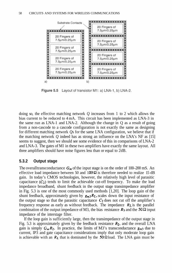
58 CIRCUITS AND SYSTEMS FOR WIRELESS COMMUNICATIONS
doing so, the effective matching network Q increases from 1 to 2 which allows thebias current to be reduced to 4 mA. This circuit has been implemented as LNA-3 inthe same run as LNA-1 and LNA-2. Although the change in Q as a result of goingfrom a non-cascode to a cascode configuration is not exactly the same as designingfor different matching network Qs for the same LNA configuration, we believe that ifthe matching network Q indeed has as strong an influence on the LNA’s NF as [15]seems to suggest, then we should see some evidence of this in comparisons of LNA-2and LNA-3. The gates of Ml in these two amplifiers have exactly the same layout. Allthree amplifiers should have noise figures less than or equal to 2dB.
5.3.2 Output stage
The overall transconductance of the input stage is on the order of 100–200 mS. Aneffective load impedance between 50 and is therefore needed to realize 15 dBgain. In today’s CMOS technologies, however, the relatively high level of parasiticcapacitance tends to limit the achievable cut-off frequency. To make the loadimpedance broadband, shunt feedback in the output stage transimpedance amplifierin Fig. 5.3 is one of the most commonly used methods [1,20]. The loop gain of theshunt feedback, approximately given by scales down the input resistance ofthe output stage so that the parasitic capacitance does not cut off the amplifier’sfrequency response as early as without feedback. The impedance is the parallelcombination of the output impedance of M3, the bias resistance and the inputimpedance of the interstage filter.
If the loop gain is sufficiently large, then the transimpedance of the output stage inFig. 5.3 is approximately given by the feedback resistance and the overall LNAgain is simply In practice, the limits of M3’s transconductance due tocurrent, IP3 and gate capacitance considerations imply that only moderate loop gainis achievable with an that is dominated by the load. The LNA gain must be
GSM TRANSCEIVER FRONT-END CIRCUITS IN 0.25 µm CMOS 59
designed on the basis of the more accurate design equation:
where is the output impedance of Ml or the M1-M2 cascode.The higher parasitics associated with PMOS transistors make them unsuitable for
biasing purposes and resistors and are used instead. The lack of voltage head-room combined with high bias currents constrain the values of and to a coupleof hundred ohms. In addition to (5.5), the choice of as well as areconstrained by two other important requirements: realizing a 50 output resistanceand providing a sufficiently high –1 dB compression point (CP). The CP is limited bythe maximum output voltage for a given bias current
where describes the impedance seen by the drain terminal of M3. Due to theinput impedance of the interstage filter, is less than This means that fora CP requirement of 0 dBm (300 mVp) the bias current must be no less than 6 mA.In practice and can not be very high because of both the voltage headroom andthe need to implement the output impedance for the LNA. In the worst case,can be as low as and twice as much current is needed. The constraint onand in terms of output impedance can be expressed as
where it can be seen that in the absence of M3’s transconductance theoutput impedance would have to be implemented completely by and inwhich case in (5.6) would be as low as The design of the output stage istherefore primarily a trade-off of resistance values to satisfy (5.5)–(5.7) and minimizethe required output current, while ensuring that M3’s gate overdrive is sufficiently highto maintain a high IP3. The latter requirement sets a limit to M3’s gate width.
For LNA-1, a higher CP was sought, which led to higher output current. In theabsence of the cascode, the current of the input stage is also higher, resulting in lowervalues of and This leads to an output bias current of 12 mA which gave usa measured output CP of -4 dBm. This output stage design has been left unchangedfor LNA-2 and LNA-3, so that only one thing is different between the two successivedesigns. Further optimization of the output stage, which took advantage of the lowerbias current of the input stage, allows the levels of and to be somewhathigher than before, so that only half as much bias current is needed for the outputstage, with only a slight drop in output compression point. The increase of resistancelevels is also expected to result in lower equivalent noise referred to the drain of M2, sothat the overall noise figure will be slightly lower. This design is referred to as LNA-4.The differences between the four designs and the key parameters of each design aresummarized in Tab. 5.1.

60 CIRCUITS AND SYSTEMS FOR WIRELESS COMMUNICATIONS
5.4 SINGLE AND DOUBLE-BALANCED MIXER
The chief requirements of an RF mixer in a superhet receiver such as ours are 50Ωmatching to the interstage filter, low noise figure, high IP3, and a moderate gain toreduce the noise contribution of subsequent stages to the receiver front-end. To satisfyall of the requirements, single-balanced (SBM) or double-balanced (DBM) mixersbased on the Gilbert cell are practically left as the only choice, as evidenced by thefact that they are found in virtually every BJT RF front-end IC.
In a single or double-balanced mixer (c.f. Fig. 5.6) the transconductor im-plemented by the (input) RF transistor(s) is followed by commutating switches thatperform the function of frequency translation. The effective conversion transconduc-tance of the mixer is for the single balanced configuration and for thedouble-balanced configuration, assuming ideal switching. Thus even in the ideal casethe switches introduce a loss of (–9.9 dB) for the SBM case andfor the DBM case. With sinusoidal LO signals the switching is much less than ideal,and the loss is more likely –12 dB for the SBM case and –6 dB for the DBM case.Because of this loss, the influence of noise current introduced by the switching transis-tors (during the time when each pair of switches remain in the on-state simultaneously,
GSM TRANSCEIVER FRONT-END CIRCUITS IN 0.25 µm CMOS 61
for example), exceeds the noise of the RF input transistor(s). Combined with the inher-ent 3 dB NF degradation due to aliasing of the noise in the image sideband, the noisefigure is therefore usually rather high for Gilbert mixers, 15 dB, for example, for BJTimplementations.
Because the expected NF is high for mixers, the input transistors’ contribution of2 dB or 3 dB to the overall NF is therefore not very critical. This justifies the use ofthe common gate configuration for the input stage, which can be designed to providea resistive input matching to the filter without any external components. Theof the input transistors is therefore 20 mS for the SBM case and 40 mS for the DBMcase.
In cellular applications, neighboring users often generate strong interfering signalsin channels adjacent to one’s own. Since such interferers cannot be filtered by theRF or interstage filters and will be amplified by the LNA, the small-signal linearity(IP3) of the mixer must be sufficiently high to prevent intermodulation from degradingthe bit-error rate. The type-approval requirement for GSM stipulates that the BERfor reference sensitivity must be met in the presence of two –49 dBm interferers at800 kHz and 1600 kHz away from the desired signal, respectively, when the latter’spower is –99 dBm. The mixer’s IP3 requirement is directly linked to the combinedreceiver front-end gain, before the mixer. If we assume again that 10 dB SNRis required to achieve the desired BER, then the required IP3 (in dBm) is bounded bythe following inequality:
Considering that within the passband of each filter the gain of the signal could bedifferent by 1 dB from that of the interferers due to passband ripple, the combined gain
could be 2–3 dB worse than the nominal value. The latter, assuming –3 dB pass-band loss for each filter and 15 dB for the LNA, is 9 dB. Thus the required IP3, assum-ing worst-case gain combinations for the signal and interference, should be –3 dBmto –2 dBm. Taking a 3 dB margin, the required IP3 for a small mobile station is inthe order of 0 dBm. For a standard mobile station, the desired signal is 2 dB weaker(–101 dBm) and the interferences are 4dB (–45 dBm) stronger, so that the IP3 re-quirement can be as high as 7 dBm.
In BJT implementations, such IP3s can only be achieved with some linearizationtechnique such as emitter degeneration. In a CMOS mixer, as long as the transistor hassufficient overdrive so that it stays in strong inversion, achieving more than 0 dBm IP3is not a problem [14]. For a given input transconductance as required by impedancematching, however, it imposes a minimum-current requirement. In our designs, 4 mAwas required for the single-balanced mixer and 6 mA for the double-balanced mixer,so that the transistor is biased halfway between weak and strong inversion.
Although the single-balanced mixer consumes less power, it provides less conver-sion transconductance, lower linearity and higher noise figure. The local oscillatorsignal is not suppressed properly by the mixer, so that it feeds through to the output.In a superhet receiver, however, this LO feedthrough is suppressed by the IF filter.Since a typical 71 MHz IF filter requires a matching load resistor on each port to its
characteristic impedance, the RF mixer sees a load at its output. Evenin the ideal case the conversion transconductance is 6.4 mS for the SBM and 12.7 mS

62 CIRCUITS AND SYSTEMS FOR WIRELESS COMMUNICATIONS
for the DBM, which is not enough to provide 10 dB conversion gain. A simple LCnetwork is therefore required to transform the load impedance to the desired level inany case, and the 6 dB difference between the conversion gms of single and double-balanced mixers is not critical as far as gain is concerned.
Because of the higher (by 6 dB) loss due to the switches, the SBM is expected tohave a higher NF than the DBM. Assuming that the noise current of the switches dom-inates the mixer noise figure, and taking into consideration that the DBM has twiceas many switches which therefore generate twice the noise power, the input-referrednoise figure of SBM is expected to be about 3 dB higher than the DBM.
Although we favor the DBM for its expected higher performance, we have alsoimplemented the SBM to check if the difference in NF is indeed as big as expected tojustify the 50% higher current of the DBM.
The design of the switches in the mixer is primarily a trade-off between havinghigh W/L ratios to reduce the overlapping period in which both switches in each pairremain on, having low thermal noise current during this period, and limiting the poleintroduced by the switches into the RF path outside the period, for a given current.In our design, the final switch sizes are similar to those of the input RF transistors,300 µm by 0.25 µm.
5.5 THE TRANSMITTER PREAMPLIFIER
Most modern GSM power amplifiers (PA) are constructed in a hybrid technology, us-ing bipolar or power-MOS transistors. They require 2 mW of driving power and a sup-ply voltage of 4.8 V (sometimes 6V). The mandatory power control is implementedin the PA, and the output power can be varied by adjusting the DC voltage applied toa control pin. The peak power of a class-4 PA is as high as 2 W. Although its averagetransmitted power can be much lower because the average distance between the mobileand the base station is much less than the maximum radius of the cells in the network,the average power consumption of a mobile station is still high, judging by the lowtalk time advertised for current commercial handsets. Given that power consumptionis dominated by the PA, the power consumption of the preamp and modulator is not ascritical as in the receiver case. However, attention is paid to low-power design in thepreamp so that the design will also be suitable for mobile stations with lower classesof PAs.
In this work, the transmit SAW filter required to remove the harmonics of the carrierand out of band noise is placed between the up-conversion mixers and the preamplifier.Since the loss of the filter precedes the preamp, the preamp is only required to deliver3 dBm power to the PA instead of 7.5 dBm. This will ease the problems of delivering asubstantial amount of power using CMOS, including efficiency and substrate coupling.
Since the efficiency of the preamp is not as critical as the PA, a class-C approachrequiring another expensive and lossy external filter before the PA is neither necessarynor does it save power. Due to the lack of good PMOS transistors, a class-B (push-pull) approach is also unavailable. If the preamp output harmonics that could degradethe PA efficiency are kept low, a class-A amplifier can drive the PA without the externalfilter. The primary requirements for our preamp, a two-stage class-A implementationas shown in Fig. 5.7, are thus matching at both the input and the output, a highgain of 23 dB, and a high power output (for CMOS) of 3 dBm with sufficient linearity.

GSM TRANSCEIVER FRONT-END CIRCUITS IN 0.25 µm CMOS 63
The first stage, comprising Ml, its biasing and the matching network, is similarto the input stage of the LNA, therefore the same design equations hold. The maindifference here is the relatively high input level of –18 dBm. Since IM3 is inverselyproportional to the overdrive of a MOS transistor, a relatively small transistor, biasedat 11 mA, has been used for M1. Because of the relatively large overdrive of Ml thatleaves little voltage headroom under a 2.5 V supply, no cascode transistor has beenused in this design to ensure that Ml stays in saturation.
The second stage is a transimpedance amplifier, biased at 16mA, as required todeliver 2 mW into the load with sufficient linearity. The relationship between therequired output compression point and the required bias current is similar to that ofthe LNA. Unlike the LNA, a resistive load is ruled out by bias voltage considerations,otherwise would have to be approximately which would make high gainvery difficult to achieve. Instead we use inductive loading, and the RF chokeresonates with the drain capacitance of M2 at 900 MHz so that the path to appearsto be open, and the formula for the output compression point (5.6) and the outputimpedance (5.7) can be used with set to infinity. In fact, and the couplingcapacitance could also be used as an impedance matching network at the sametime, so that the impedance seen by the drain of M2 could be higher. That wouldallow higher power to be delivered for a given current. Due to the low supply voltage(2.5 V) of the 0.25 µm CMOS technology, this option cannot be used in our design,because impedance scaling by the matching network also scales the voltage swing ofthe drain of M2. Another way of achieving higher output power in traditional preampdesigns is to combine such a matching network with biasing the drain of M2 atwhich doubles the allowable voltage swing. Since the margin between the breakdownvoltage and the actual supply voltage is small compared to the output swing in our0.25 µm CMOS case, this option (which entails swinging the drain of M2 substantiallyabove was also ruled out on reliability grounds. To bias M2 in the mid-supply,resistor of approx. is inserted before and AC-bypassed by as shown.At DC, also helps to stabilize the bias condition through
In many bipolar transceivers [3,5] a buffer capable of delivering 2 mW intohas been implemented, frequently as an emitter follower biased at about 10mA to

64 CIRCUITS AND SYSTEMS FOR WIRELESS COMMUNICATIONS
achieve high IP3. Implementing a 20 mS buffer in 0.25 µm CMOS, however,is not possible because of the large voltage swing required at the gate. Delivering2 mW to corresponds to having a voltage swing of 900 mV peak–to–peak atthe transistor’s source and 1.8V peat–to–peak at its gate. After adding the thresholdvoltage (400 mV) and some overdrive (200 mV) we have a peak voltage of 2.4 V, whichis already higher than the specified minimum supply voltage. To reduce the swing, alower impedance buffer followed by a matching network could be used, but this wouldresult in an excessive increase in current consumption.
In our class-A implementation, the total current consumption is only 27 mA. Sucha current level, required by linearity, is insignificant compared to that of the final PA.
5.6 POWER CONSUMPTION
Before describing the experimental results, it is perhaps appropriate to briefly revisitthe subject of power consumption of the transceiver. Earlier we stated that for CMOStechnologies to be seriously considered as a contender for RF front-ends in cellularapplications and as a competitor to BJT technologies, one must a) prove that thecomplete set of performance specifications can be met and b) do so with a currentconsumption comparable to today’s commercial solutions. In this section we wish tohighlight the current consumption aspect.
Low power consumption is most important in the receive mode, because it definesthe stand-by time. In transmit mode power consumption will be dominated by the PA.As the chief reason to purchase a mobile phone shifts from business use to private use,the toll charges serve as a natural barrier to reduce the occurrences of private usersoverrunning the, say, four hours of talk time possible on a single battery charge. Busi-ness and private users alike, however, may find a 40 hour or even a 72 hour stand-bytime inconvenient.
The designs reported here show that by combining LNA-4 and the double-balancedmixer, the nominal supply current of the front-end chip can be as low as 16 mA. On-going design and experimental work on the remaining part of the receiver gives usgood reasons to believe that the IF-strip plus the demodulator will consume no morethan 6 mA, which shows that the front-end is indeed the dominant consumer of power(over 70%) of the receiver. Even if we add the VCO and the prescaler, which domi-nate the current consumption in a synthesizer (3 mA in Rx mode), the total nominalcurrent consumption will only be 25 mA, i.e. 60 mW power consumption. This com-pares very favorably with existing chipsets, such as those reported in [2] (51 mA inthe paper, 46 mA total in the datasheet), [3] (57 mA), and even [4] (33 mA), for exam-ple. The last reference derives its high performance from an advanced 25 GHz bipolartechnology.
5.7 MEASURED RESULTS
All measurements were performed using bare chips assembled on a PCB with all theneeded external SMD components. The dies were directly glued to the PCB groundplane which provides an excellent ground connection to the chip substrate. Somecare was taken with the length of the bondwire to the source of Ml in each LNAand the preamplifier so that correct matching is achieved. No external trimming was

GSM TRANSCEIVER FRONT-END CIRCUITS IN 0.25 µm CMOS 65
performed. The supply voltage was set to its nominal value of 2.5 V. Among the chipsmeasured, one is a combination of LNA-1, the SBM mixer and an early version ofthe IF-AGC amplifier [11]. Fig. 5.8 shows its micrograph. The measured parametersof the implemented LNAs, mixers, the transmit preamplifier as well as the particularreceiver front-end are summarized in Tab. 5.2.
For the low-noise amplifiers, we are particularly interested in the noise figures,as well as the influence of the various refinements on the NF in our controlled ex-periments. The reference amplifier LNA-1 achieves again a low NF of 2dB, whileproviding the expected gain, input and output impedances and excellent linearity. Thefact that a 2 dB NF has been achieved over consecutive runs shows that the design is

66 CIRCUITS AND SYSTEMS FOR WIRELESS COMMUNICATIONS
suitable for manufacturing. With merely an increased number of substrate contacts,(of a transistor that already has many contacts,) LNA-2 shows a significant improve-ment in noise figure, to 1.74 dB. This demonstrates the significant contribution ofback-gate resistance to the overall NF, at least for the substrate of the technol-ogy we used. The main influence of the cascode transistor in the input stage (LNA-3)is a 30% reduction in current consumption in the first stage due to the higher Q andlower needed, and a 10 dB improvement in reverse isolation. The price paid is aslight increase of the noise figure which we believe to be due to the additional con-tribution of M2. No rapid improvement of the NF, as predicted for the particular0.35 µm LNA in [15] for a similar change of Q , is observed here. The last amplifier,LNA-4, achieves the best performance trade-off for our application in terms of gain,noise figure and power consumption, thanks to a better design of the output stage. Themeasured output compression point (–5 dBm oCP) has only decreased slightly (1 dB)from that of the other 3 LNAs despite saving half of the output stage current. A verylow noise figure of 1.6 dB is measured, which is near the optimum noise match. Thisis the best result reported to date for an integrated CMOS implementation. In Fig. 5.9,starting with the minimum noise figure close to the center of the Smith chart, con-stant NF and gain circles have been measured in terms of the source impedance seenfrom the noise-matched LNA. Thanks to the low-Q design, these circles are big and1widely separated for small increments of gain and NF. This means that variations theof matching network impedance due to component tolerances in production will notcause drastic degradation of gain and NF. Indeed, in power-matched conditions,the measurements of LNA-4 in Fig. 5.10 show that 15 dB gain, –8 dB S11 and 1.9 dBNF can be achieved simultaneously. Due to the effect of the bond pad, the protectiondiode and the PCB parasitic capacitances at both sides of the actual power-match conditions of the LNA are slightly different from the ideal equations (including(5.2) in this paper) normally described in recent publications [14–16].
Turning our attention to linearity, Fig. 5.11 shows the measured iCP and iIP3 ofLNA-2 and LNA-4. High IP3 values far exceeding requirements have been measured,confirming the intrinsic high linearity of MOS devices. The measured compressionpoints meet the requirements of the blocking test and are 3–4 dB below the limit setby the output current, as expected.
The measurements of the SB and DB mixers have been performed using –1.5 dBmof LO power with terminations at the LO ports. The measured conversionare 4.9 mS and 8.5 mS for the SB and the DB mixer, respectively. Due to imperfectswitching, they are about 30% lower than the theoretical maximum, which was ex-pected. Although the measured NF of 15.9dB for the SB mixer is higher than wewould like it to be, it is in line with most reported mixers with gain at this frequency,including BJT implementations [1,3]. The measured 12.6 dB SSB NF of the DB mixer,on the other hand, is one of the best reported to date for fully integrated mixers, andfacilitates the use of RF and interstage filters with moderate specs (and hence price)in superhet GSM receivers. The S11 measurements are shown in Fig. 5.12. The com-mon gate input guarantees excellent input matching with a broadband characteristicfor both mixers. Indeed, the measured S11 is limited by the balun needed to match theDB mixer, but nevertheless stays under –10 dB at all frequencies below 1.2 GHz. TheS11 degradation at higher frequencies is due to the increasing influence of parasiticcapacitances. Fig. 5.13 shows that the measured iIP3 is as high as 9 dBm, and iCP

GSM TRANSCEIVER FRONT-END CIRCUITS IN 0.25 µm CMOS 67
–4 dBm, for the DB mixer, which thus meets the specs outlined earlier by a comfort-able margin. This has been achieved, without source degeneration, by the right choiceof the ratio of the CMOS devices, and by differential implementation.
The measurements of the transmitting preamplifier show that high gain, adequate in-put and output impedances as well as good linearity can be achieved even if a relativelyhigh amount of power must be delivered. Fig. 5.14 shows the measured frequency re-sponse of the TX preamplifier. The measured iCP of the preamp is –14.6 dBm, whichcorresponds to +5.8 dBm oCP. This translates into more than 3.5 mW of power deliv-ered to the load at compression.

68 CIRCUITS AND SYSTEMS FOR WIRELESS COMMUNICATIONS
5.8 CONCLUSIONS
Power consumption is more important than the cost of chips in today’s cellular phones.To prove that CMOS is feasible and competitive with BJTs for implementing the RFfront-end of a GSM receiver, circuits operating at radio frequencies must show com-petitive current consumption while meeting all specs required for type approval. Typeapproval requirements have been discussed and translated into circuit specs wherenecessary, and measurements of the front-end integrated circuits reported in this papershow that they are indeed met. We have shown that current consumption lower thantoday’s BJT implementations is indeed feasible by carefully optimizing the front-enddesign. Excellent noise figures are also shown to be reproducibly obtained for CMOSLNAs and mixers. Controlled experiments also confirm that backgating by substrateresistance can degrade the NF, and as many contacts as possible should be used toground the substrate.

GSM TRANSCEIVER FRONT-END CIRCUITS IN 0.25 µm CMOS 69
Acknowledgments
The contributions to this project by T. Yoshitomi and T. Morimoto of Toshiba Co. and R. Rhei-ner of the ETH Zurich are gratefully acknowledged.
References
[1]
[2]
R. G. Meyer, W. D. Mack, “ A 1-GHz BiCMOS RF Front-End IC”, IEEE J.Solid-State Circuits, pp. 350–355, Vol. 29, No. 3, March 1994.
C. Marshall et al, “A 2.7V GSM Transceiver ICs with On-Chip filtering”, ISSCCDigest of Technical Papers, pp. 148–149, Feb. 1995, San Francisco, USA.

70 CIRCUITS AND SYSTEMS FOR WIRELESS COMMUNICATIONS
[3]
[4]
[5]
[6]
[7]
[8]
[9]
[10]
[11]
[12][13]
[14]
[15]
[16]
[17]
[18]
[19]
[20]
T. Stetzler et al, “A 2.7 V–4.5 V Single-Chip GSM Transceiver RF Integrated Cir-cuit”, IEEE J. Solid-State Circuits, pp. 1421–1429, Vol. 30, No. 12,,Dec. 1995.W. Veit et al, “A 2.7 V 800 MHz–2.1 GHz Transceiver Chipset for Mobile Ra-dio Applications in 25 GHz ft Si-Bipolar”, 1994 Bipolar/BiCMOS Circuits andTechnology Meeting.K. Irie et al, “A 2.7 V GSM Transceiver IC”, ISSCC Digest of Technical Papers,pp. 302–303, Feb. 1997, San Francisco, USA.A. Abidi et al, “The Future of CMOS Wireless Transceivers”, ISSCC Digest ofTechnical Papers, pp. 118–119, Feb. 1997, San Francisco, USA.J. Rudell et al, “A 1.9 GHz Wide-band IF Double Conversion CMOS IntegratedReceiver for Cordless Telephone Applications”, ISSCC Digest of Technical Pa-pers, pp. 304–305, Feb. 1997, San Francisco, USA.M. Steyaert et al, “A Single-Chip CMOS Transceiver for DCS-1800 WirelessCommunications”, ISSCC Digest of Technical Papers, pp. 48–49, Feb. 1998,San Francisco, USA.P. Orsatti et al, “A 0.25 µm CMOS Fully Integrated IF-Baseband-Strip for aSingle Superheterodyne GSM Receiver”, ESSCIRC Proceedings, pp. 64–67,Sept. 1998, The Hague, The Netherlands.GSM Standard—GSM 05.05 version 4.19.1, 11th Ed. ETSI, December 1997.F. Piazza et al, “A 2 mA/3 V 71 MHz IF Amplifier in 0.4 µm CMOS Programma-ble over 80 dB Range”, ISSCC Digest of Technical Papers, pp. 78–79, Feb. 1997,San Franciso, USA.R. Steele, Mobile Radio Communications, IEEE Press, New York, 1992.Datasheets: duplexer, Murata DFY2R902CR947BHGF, RX interstage filter, Mu-rata SAFC947.5MC70T, TX interstage filter, Murata SAFC902.5MA70N and IFfilter, Siemens B4556 and B4568.Q. Huang et al, “The Impact of Scaling Down to Deep-Submicron on CMOS RFCircuits”, IEEE J. Solid State Circuits, vol. 33, pp. 1023–1036, July 1998.D. Shaeffer and T. Lee, “A 1.5 V, 1.5 GHz CMOS Low Noise Amplifier”, IEEEJ. Solid-State Circuits, May 1997, pp. 745–759.A. Karanicolas, “A 2.7 V 900 MHz CMOS LNA and mixer”, ISSCC Dig. Tech.Papers, 1996, pp. 50–51.Y. Shin and K. Bult, “An Inductorless 900 MHz RF Low-Noise Amplifier in0.9 µm CMOS”, Proceedings CICC’97, pp. 513–516.A. van der Ziel, Noise in Solid Stase Devices and Circuits, Wiley, New York,1986.Y. Tsividis, Operation and Modeling of The MOS Transistor, McGraw-Hill, NewYork, 1987.A. Grebene, Bipolar and MOS Analog Integrated Circuit Design, Wiley, NewYork, 1984.

II RF Front-End Circuits

This page intentionally left blank

6 RF FRONT-END CIRCUITSQiuting Huang
Integrated Systems LaboratorySwiss Federal Institute of Technology (ETH)
ETH-Zentrum, CH–8092 Zurich, Switzerland
6.1 INTRODUCTION TO THE FOLLOWING PAPERS
To newcomers to the field of RF front-end design for wireless communications, thecombination of rapid change in commercial standards and requirements, the choiceof system architectures and frequency plans, and their relation to the performance ofindividual radio frequency circuits can be quite bewildering. The four contributionsincluded in this chapter address these issues from different perspectives in varyingdegrees of detail.
The first two contributions come from academia and are biased towards basic the-ory. The second two contributions come from industry, providing more insight into thecurrent state-of-the-art in wireless transceivers, and the overall system requirements interms of cost, size (volume), and performance.
Qiuting Huang focuses on the fundamental issue of phase noise in RF oscillators,which is particularly important for wireless transceivers as it strongly affects the rel-ative independence between different radio channels and services that transmit andreceive signals of varying strengths simultaneously. In addition to avoiding unsoundassumptions, the analyses of oscillation amplitude, oscillator response to interferingsignals, and the identification of white noise sources have all been backed up withcontrolled experiments.
Behzad Razavi exposes the fundamental issues of frequency planning in transceiverdesign, as well as recent trends in highly integrated RF circuit design, in the context
73

74 CIRCUITS AND SYSTEMS FOR WIRELESS COMMUNICATIONS
of a GSM/DCS dual-mode transceiver. The architecture is designed for a high level ofintegration, containing neither external image-reject filters nor IF filters. Quadraturemixers are therefore frequently used, and the LO signal is placed halfway between theGSM band and the DCS band to save hardware. In the transmitter part, the tutorialon GMSK modulation and influence of nonlinearity on the transmitted spectrum maybe a very useful starting material to read for people new to the field. The emphasis inimplementation is on CMOS, with extensive use of on-chip spiral inductors.
Petteri Alinikula shares with us the challenges of future wireless terminals from theviewpoint of one of the top three leading commercial companies in the market. Wide-band CDMA transceivers appear to be the next target for most, especially in light ofthe recent agreement between Ericsson and Qualcomm over IPR issues. Linear poweramplifiers, a sharp increase in DSP computing power, and multi-standard terminals areidentified as major challenges facing designers of next-generation terminals. The au-thor also shares with us his view of the evolution in state-of-the-art terminals, in termsof relative physical volume, component count and cost breakdown. Many readers willfind the corresponding figures interesting. Also interesting is a concrete example of adirect-conversion architecture being used to save discretes and filters.
Stephan Heinen and Stephan Herzinger take us back to the GSM transceiver again,from the perspective of industry. They echo the view from Alinikula that overall sys-tem optimization is more important than the focus on a particular technology, thesaving of a particular filter or the performance of a particular building block. In thediscussion of GSM transmitters, the general requirements by type approval are pre-sented in detail, as are the effects of nonlinearities on the transmitted spectrum. Thisagain gives a newcomer to the field a nice introduction, from an angle differing slightlyfrom Razavi’s. Direct up-conversion, IF up-conversion and modulation-loop VCO ar-chitectures are discussed in terms of their relative merits and disadvantages, and themodulation loop is identified as the transmitter architecture of choice for constant-envelope modulation schemes such as GMSK and is presented in detail.
The contributions in this chapter provide a good overview of the current issues inRF front-end design, as the field of RF-IC design moves towards maturity, and theindustry is poised to introduce the next generation of air-interface standards.
7 PHASE-NOISE-TO-CARRIERRATIO IN LC OSCILLATORS
Qiuting Huang
Integrated Systems LaboratorySwiss Federal Institute of Technology (ETH)
ETH-Zentrum, CH–8092 ZürichSwitzerland
Abstract: The following questions are addressed in this chapter using a CMOSColpitts oscillator as an example.
1. How does the carrier amplitude depend on the electrical parameters of the oscil-lator?
2. Does an additive interference, white noise for example, (always) become multi-plicative with the carrier in such a way that it deserves the name phase noise? Is theresponse to such an interference always inversely proportional to its frequency offsetfrom the carrier? Why?
3. How does the phase-noise-to-carrier ratio depend on the electrical parameters ofthe oscillator? Can such a dependence be described directly with the circuit parametersrather than intermediate quantities such as the signal power consumed by the tank, themean-squared voltage amplitude, or the noise factor of the oscillator?
Answers to the above questions afford us a better understanding of LC oscillatorsand enable us to predict the exact oscillator performance without resorting to numericalsimulation.
75

76 CIRCUITS AND SYSTEMS FOR WIRELESS COMMUNICATIONS
7.1 INTRODUCTION
The importance of phase noise in oscillators in RF and other communication circuitshas made it one of the most extensively studied subjects in electronics. Journal pa-pers on the subject [1–10] can be found from each of the last six decades, the earliestone [1] being as old as 1938, and the latest [10] as recent as 1998 The fact that paperson LC oscillators, too numerous in the last 60 years to cite exhaustively, keep appear-ing, serves to underline the fact that existing theories on phase noise have not beenuniversally found satisfactory.
Experimentally, the qualitative behaviour of phase noise has been well known. Anoscillator’s output power spectrum consists of a peak at the carrier frequency (mainoscillation, angular frequency surrounded by a noise skirt symmetrical to thecarrier frequency. Irrespective of the exact implementation, the noise skirt has thefollowing characteristics:
The noise spectral density is inversely proportional to the frequency offset from thecarrier, except very close to the carrier frequency, where the influence of up-con-verted flicker noise dominates or the presence of the strong carrier begins to limitthe measurement accuracy.
The same noise manifests itself in the time domain as jitter around the oscillation’szero-crossing points, which can only be caused by noise in the phase of the oscil-lation rather than that super-imposed on its amplitude. Oscillator noise is thereforeusually referred to as phase noise. The assumption of phase noise implies that thesideband spectrum above and below the carrier frequency must be equal in ampli-tude and opposite in sign. It also implies that output noise is multiplied with ratherthan added to the carrier.
It is widely believed [11] that doubling the quality factor of the LC tank roughlyimproves the oscillator’s carrier-to-noise spectral density (C/N) ratio by 6dB, al-though systematic experimental verification of such a belief is hard to find in openliterature.
Today, RF oscillators are implemented with high-quality inductors and capacitorsoutside the chip containing the active devices. This is the main reason for the wide-spread efforts in the integrated circuit community to improve the quality of fully in-tegrated inductors on silicon, especially in the last few years [11–25]. Despite theavalanche of research papers, the quality factor Q of on-chip inductors at 1 GHz hashardly improved by a factor of two (from to in the last 10 years. Re-ported N/C ratios, however, vary by as much as 20 dB at 100 kHz offset. This under-lines the fact that other factors than the Q of the tank also affect the N/C ratio strongly.Our understanding of these factors seems at times confused.
The confusion stems mainly from the inadequacy of existing phase noise models. Inthe next section, we will review typical existing models and analyze their weaknesses.This will be followed by our own analysis of a typical LC oscillator. The example usedis the well-known Colpitts oscillator implemented with MOS transistors. The analysisstarts in Section 7.3 with the general description of steady-state oscillation and thederivation of the exact oscillation amplitude as a function of circuit parameters. It willbe followed by Section 7.4, describing the response of the oscillator to a small, deter-ministic interfering signal. Section 7.5 identifies the spectral density of all white noise

PHASE-NOISE-TO-CARRIER RATIO IN LC OSCILLATORS 77
sources, leading to an analytical expression of oscillator output noise-spectral-den-sity-to-carrier ratio that is completely determined by circuit parameters. Experimentalresults will then be presented to validate the analytical expression, before the latter isused in the discussion of the exact design of RF oscillators.
7.2 THE WEAKNESSES OF EXISTING PHASE NOISE MODELS
Existing models in the last six decades can be grouped by the four typical methodsused to derive them:
Linear, frequency-domain analyses with noise sources additive to the carrier signal,
linear, frequency-domain analyses with noise sources additive to the phase of thecarrier,
time-domain analyses with noise sources additive to the carrier signal,
time-domain analyses with noise sources additive to the phase of the carrier.
Since all the models set out to fit the well-known experimental observations de-scribed in the previous section, the resulting expressions do qualitatively predict manyaspects of phase noise behaviour. It is in the validity of the reasoning that led to thoseexpressions that we find serious weaknesses.
7.2.1 Linear, frequency-domain analyses with noise sources additiveto the carrier signal
Linear analyses simply assume that noise is superimposed on the carrier and the trans-fer function from the noise source to the oscillator output is that of the resonator tank,modified by the equivalent linear transconductance of the active device. Fig. 7.1 showsthe equivalent circuit of the simplest case [9]. The V–I characteristic of a real activedevice, on the other hand, can generally be depicted as in Fig. 7.2, the shape serv-ing as a necessary feature to limit the oscillation amplitude [26]. The negative sloperepresenting the negative (trans)conductance required for start-up is usually found inthe middle. Since this V–I curve is usually highly nonlinear, the approaches to theequivalent linear transconductance have been different.

78 CIRCUITS AND SYSTEMS FOR WIRELESS COMMUNICATIONS
Earlier analyses [2] allow the equivalent to be quite different from the criticaltransconductance required to cancel the loss of the tank exactly. Such analysesresult in models that generally predict a bandpass characteristic centered at the carrierfrequency, flat at frequencies immediately adjacent to the carrier and rolling off at 6 dBper octave at higher offset frequencies. The corner between the two offset frequencyranges is typically of the order of the carrier frequency divided by the Q of the passivetank. One of the serious problems with such a model is that the predicted cornerfrequency, which can be 10 MHz for a 1 GHz oscillator and a Q of 100, is neverobserved in practice.
To fit them to experimental results, later analyses [8,9] assume that the transcon-ductance (or gain) of the active device, seen by the noise signal, is exactly the sameas that for the carrier, which in turn must be the same as that required to cancel thetank loss in steady state. The resulting equivalent circuit is an ideal, zero-loss linearresonator. The inverse dependency on offset frequency is now present all the way tothe carrier.
The fundamental objection to the use of the carrier’s is that the latter is only acrude large-signal concept indicating the ratio between the fundamental component ofa distorted output current of a transistor and the voltage applied to its input. The noisecomponent, being a smaller signal at a different frequency and phase, does not traversethe nonlinear V–I curve in Fig. 7.2 in the same way as the carrier, even though it issuperimposed on the latter. The distortion it experiences, or the average gm applicable,will therefore also be different from that of the carrier. A specific example of theCMOS Colpitts oscillator will be shown later to underline this point. If one still insistson linear superposition of the carrier and noise, there is no more justification left thanthe need to fit the theory to the observed characteristic. Even so, consistencythen requires that the small-signal at the center of Fig. 7.2 be used, because the

PHASE-NOISE-TO-CARRIER RATIO IN LC OSCILLATORS 79
noise signal is a very small signal. However, the small-signal at the center isnecessarily several times larger than the critical otherwise oscillation wouldnever have started! Further evidence that the type of linear analysis in [8,9] is wronglies in the fact that it predicts a response 6 dB too high at low offset frequencies. Thislast point will be shown later in this paper.
Fundamental objections can also be raised about the linear models for what theypredict. If noise were merely added to the oscillation signal, it would not cause thezero-crossing-point jitter normally observed, even if the characteristic is given.This is because the odd symmetry in phase with respect to the carrier frequency, inher-ent to modulation in phase, is absent in the predicted oscillator noise spectrum.
7.2.2 Linear frequency domain analyses with noise sources additiveto the phase of the carrier
Papers in this class also use a linear model, but consider the noise sources to be addeddirectly to the phase of the carrier [6,7]. The result is best known as Leeson’s Model orLeeson’s Formula. Although its original derivation is at best heuristic, it has becomethe most widely accepted model for phase noise in the last 30 years. In addition tobeing widely used in industry, it has been adopted in several reputable textbooks. Thereasons for its success seem to be three-fold: 1. It is derived from phase so that theodd symmetry is assumed to have been taken care of. 2. The characteristic isthere. 3. It predicts a perceived inverse dependence of the N/C ratio on the (loaded) Qof the tank. It is up to the users of the model to work out what the power level of thesignal and the effective noise figure (F) of the oscillator mean.
The fundamental problem with the model’s derivation lies with the noise sources.For white noise to be additive to the phase directly, it must be located at places whereit can influence the frequency or phase-setting elements of the oscillator, such as thejunction diodes (intentional or parasitic) in series or parallel with the main linear, pas-sive tank. Oscillators with negligible nonlinear LC elements would have no phasenoise, or zero effective noise figure F, if we have to express the noise in terms ofLeeson’s model, but we know this would contradict reality. Even for oscillators withnonlinear capacitors, it is quite unclear why the phase or frequency shift caused bywhite noise on the reverse bias of a junction diode would have to do with anythingother than the C–V characteristic of the capacitor and its importance relative to otherlinear capacitors in the tank in determining the oscillation frequency. The introduc-tion of into the “input phase noise” seems totally arbitrary, even though doing soresults in a model that seems to reflect its role in the final expression of the N/C ratioqualitatively. Numerical verifications with practical oscillators also show that noiselevels associated with junction diodes are too low compared to the noise observed atthe oscillator output, not least because good oscillators are designed to minimize theinfluence of parasitic diodes, and the bias circuits of frequency-setting varactors usu-ally have lowpass characteristics with cutoff frequencies well below the oscillationfrequency.

80 CIRCUITS AND SYSTEMS FOR WIRELESS COMMUNICATIONS
7.2.3 Time-domain analyses with noise sources additive to the carriersignal
Typical analyses [4,5] in this group model the nonlinearity of the active device witha third-order term and describe the dynamics of the oscillator with a Van-de-Pol dif-ferential equation driven by the noise source. Without pinpointing the precise flaws inthose usually complicated derivations, it suffices to say that a constant term in [4])is usually defined which is of the order of magnitude of the relative difference betweenthe small signal of the active device and This term divided by Q defines thecorner of the relative offset frequency (i.e. relative to the carrier) of the final outputnoise spectrum which has a bandpass shape. Again, the flat portion of the spectrumbelow such a corner frequency is never observed in practical oscillator measurements.
7.2.4 Time domain analyses with noise sources additive to the phaseof the carrier
In the most recent theoretical journal paper [10] on this subject, a general theory isproposed which claims to be applicable not only to LC oscillators, but also to all othertypes such as ring oscillators. We restrict the focus of our discussion on LC oscillators.The main weakness in the reasoning in this paper lies in the assumption that interfer-ence is added to the phase. The example given to support such an assumption is anideal tank, excited by a current impulse. The sinusoidal signal after a charge has beendeposited on the capacitor by the impulse is phase-shifted and changed in amplituderelative to the sinusoidal signal before the impulse, were the latter to continue. It iscorrect that both the phase shift and the amplitude change are periodic functions of thetime of the impulse, although the statement that at maximum phase shift the amplitudechange is zero is wrong, because it is not possible to add energyif is the total energy before the injection of charge) to an ideal tank withoutchanging the amplitude of the oscillation, no matter when the small charge is in-jected into the tank. The critical step of the paper’s argument comes when it is statedthat some form of AGC action always exists in an oscillator so that the amplitudefinally settles back to the same value independent of the impulse. For the ideal LCtank this statement is clearly wrong. For the lossy tank in a practical oscillator thismay be true, but we need to highlight the word finally, for it usually takes hundredsof oscillation cycles for the impulse to settle (precisely because AGCs, if needed, aredesigned to be insensitive to small-signal, high-frequency perturbations). This is instark contrast to the case of ring oscillators constructed by CMOS inverters, where theAGC function may consist of clipping at a reference voltage such as the power supply,which may be achieved within the same oscillation cycle.
Since the impulse response of the amplitude does not decay to zero instantly, itcontains as much information about the overall response of the LC tank to the injectedcurrent as the phase impulse response constructed in [10]. The same commentholds for the convolution between the impulse responses and the injected continu-ous-time current signal, which results in the amplitude and phase responses definedin [10]. The two responses are also strongly correlated. Throwing away the amplituderesponse, as it has been done in [10], destroys a part of the information needed tore-construct the overall response. The nonlinearity required to convert additive noise

PHASE-NOISE-TO-CARRIER RATIO IN LC OSCILLATORS 81
to phase noise and generate the double-sideband spectrum is thus created more by theAGC assumption than any real transistors. To demonstrate further the fallacy of throw-ing away the amplitude response and using only the phase response to construct theoutput spectrum, we note that even for an ideal, passive LC tank with zero loss andresonance frequency perturbed by an ideal sinusoidal current source ata response will appear at according to [10]! General theorems about linearsystems and the specific solution to the linear differential equation with a sinusoidaldriving function tell us this is not possible.
Even if an instantaneous AGC did exist, the model still has a serious problem. Sincethe derivation is independent of the offset frequency it should be valid even atoffsets reasonably far outside the tank’s passband, where the tank impedance becomesvery low. For a high- Q tank, the voltage produced on the tank by an interfering currentis so small at high offsets that the AGC should not have any influence. The attenuationis also going to be so high that the active device will not have sufficient to produceenough current to counteract the injected current. In such a situation, one would expectthe relationship between the interfering current and the voltage it produces on the tankto be the same as that of a passive tank without the active device. In this case, the modelbased on the linear analysis [9] must be valid, although the resulting interference canno longer be called phase noise due to the absence of the image sideband. The resultof [10] in this case is wrong by a factor of two.
Most models described above attempt to be general. In doing so they fail to includeinformation on parameters vital to the use of the models. A typical example is the ef-fective noise figure F, which must be calculated taking into account all noise sources,their location in the circuit and the amount of distortion the noise experiences priorto reaching the tank. Another example is oscillation amplitude or power, which maydepend on the Q of the tank. With the effective noise source and oscillation amplitudeas intermediate variables, the exact relationships between N/C ratio and the circuitparameters such as tank loss, L and C values and transistor gm are obscured. Thissometimes makes the models open to interpretation, which is not entirely satisfactoryto the designer.
In the following, we take the approach of analyzing a very specific oscillator, theColpitts oscillator in Fig. 7.3a, in the time domain, so as to remove as much ambiguityabout the assumptions as possible. Generalizations will be made only after the specificcase is well established. Noise currents or voltages as they are introduced by thesources such as resistors and transistors are treated exactly as they are in the physicalreality: additive to the carrier signal.
7.3 GENERAL DESCRIPTION OF LC OSCILLATOR OPERATION ANDDETERMINATION OF OSCILLATION AMPLITUDE
Before one attempts the analysis of the influence of noise on oscillation, it is helpful tostudy first how a typical LC oscillator operates in steady-state. In the CMOS case, thestudy will also have the benefit of revealing an analytical expression for the oscillationamplitude [27]. The determination of the CMOS LC oscillator amplitude had alwaysrelied on some form of numerical solution. The most straight-forward method is touse a circuit simulator such as SPICE. An earlier analysis [28] shed some light on theway a MOS transistor operates in a Colpitts oscillator, but stopped short at parametric

82 CIRCUITS AND SYSTEMS FOR WIRELESS COMMUNICATIONS
equations that require numerical solutions to obtain oscillation amplitude. The prob-lem with numerical solutions, however, is that insight into the way circuit parametersaffect the final amplitude is partially or completely lost.
Standard descriptions of LC oscillators are usually limited to the necessary condi-tion for oscillation. For small signals, the MOS transistor can be modeled as a linear
as shown in Fig. 7.3b. All the resistive losses of the tank have been lumped intoa single resistor The transistor forms a positive feedback loop with capacitors
and The equivalent impedance looking to the right of the dashed line inFig. 7.3b contains a negative real part:
The necessary condition for the oscillation to start is that the total resistance in theequivalent LC tank in Fig. 7.3c be negative,
where is defined as the critical transconductance for oscillation, andis the tank’s angular resonance frequency. The negative middle term in the circuit’scharacteristic equation results in the latter’s complex conjugate zeros having a positivereal part. The zero-input response of the circuit is therefore an exponentially increas-ing sinusoidal oscillation. Equation (7.2) does not tell us whether the oscillation willstabilize to a particular amplitude.
During start-up, the average current in transistor may not be the same as thebias current. The difference between the two flows into the capacitive network formedby and causing the DC bias voltage between the gate and source of to

PHASE-NOISE-TO-CARRIER RATIO IN LC OSCILLATORS 83
shift. This will in turn change the average current in the direction of the bias current.The steady state is reached when the two are balanced. Although the non-linearity of
V–I characteristic results in many harmonics in drain-source current, thelatter is periodic in steady state. Fourier series expansion can therefore be used in theanalysis. The steady-state oscillation amplitude between gate and source,and the DC bias are bound by two constraints if the quality factor of the passivetank is high, so that the voltage on gate is practically a pure sine wave.
1. The average current through is equal to the bias current corresponds toin Fig. 7.2.)
2. The ratio between the amplitude of AC current and that of its gate-sourcevoltage is exactly the transconductance of the passive tank between the branchand the branch in Fig. 7.3b at resonance, which happens to be
These two constraints allow us to set up two equations to solve for the two un-knowns in steady-state oscillation, the bias voltage and the oscillation amplitude
Since the values of the passive components in the tank and their resistive loss,which (we will show) have a direct impact on oscillation amplitude, typically havetolerances of 5–20 %, an analysis with much greater accuracy is unnecessary for prac-tical purposes. This provides us with the justification to describe relationshipwith the simple square law,
where is the AC part of the gate-source voltage and is the threshold voltage,below which the transistor cuts off and the current equals zero. The same justificationalso allows us to assume that because the tank’s quality factor Q is usually high,harmonics in drain-source current have been sufficiently filtered by the tank,so that is a pure sinewave. We shall experimentally verify the errors caused bysuch simplifying assumptions later.
If the steady-state bias is greater than as depicted in Fig. 7.4a, sothat never causes the transistor to cut off, then the average currentthrough is given by:

84 CIRCUITS AND SYSTEMS FOR WIRELESS COMMUNICATIONS
where x is defined as and The fundamental component of the ACcurrent at on the other hand, is given by:
Multiplying by the transimpedance between the branch and branch inFig. 7.3b, we obtain the steady-state oscillation amplitude:
Solving Eqs. (7.3) and (7.6) jointly, we obtain:
Re-organizing (7.7), the same relations can be expressed as:
From (7.7), we see that if one wanted to keep from cutting off, a combination ofa small transconductance coefficient and a large bias current would be the best way tomaintain a sufficiently large amplitude. The maximum is reached when the second

PHASE-NOISE-TO-CARRIER RATIO IN LC OSCILLATORS 85
half of (7.7) is satisfied with equality, in which case . Condition (7.8)shows that the range for the nominal transconductance gm0 is very small, so that a20% increase in can easily kill the oscillation.
To ensure start-up, as well as adequate amplitude, practical oscillators are designedto have a gm0 several times larger than . In this case the conditions in Eqs. (7.7)and (7.8) are no longer satisfied, and transistor M1 does get cut off during part of theoscillation, as depicted by Fig. 7.4b. Eqs. (7.3) and (7.5) must therefore be modifiedto account for the time in which is cut off. This is done by reducing the limit ofintegration to the time is on:
The average current through is now given by:
The oscillation amplitude, on the other hand, is given by:
Even without solving Eq. (7.13) explicitly for x, it can be seen from Eq. (7.12) thatthe oscillation amplitude is only a weak function of x, and thus also of the duty cycleof . As x varies within its limits the amplitude varies by no more thana third. One can thus say that is roughly proportional to the bias current andinversely proportional to the critical for oscillation, . Fig. 7.5 compares the

86 CIRCUITS AND SYSTEMS FOR WIRELESS COMMUNICATIONS
exact function and its approximation in Eq. (7.12). The maximumdifference is less than 2 %, occurring at which is a negligible error in termsof amplitude prediction. The approximate version of Eq. (7.12) has the advantage ofmuch greater simplicity.
Although a solution for x in explicit form is more difficult to obtain from Eq. (7.13),it is only a function of nominal transconductance gm0 normalized to the gmc ofthe passive tank. Thus x needs to be solved only once numerically versus a usefulrange of normalized and can be looked up once the ratio between and isknown. Fig. 7.6 shows the calculated x, as well as the corresponding duty cycle
. Note that the horizontal axis is on logarithmicscale to allow the low region to be better displayed. It can be seen that both xand the duty cycle are relatively steep functions when the normalized of is low.For a ratio of 3, which can easily be expected for practical designs,and The improvements of x and are much slower beyondresulting only in and so that setting transconductancemuch higher than the of the tank is inefficient as far as achieving better amplitudeis concerned. The limit in is achieved when tends to infinity, in whichcase x tends to unity and
It is interesting to note that this limit is independent of the detailed parameters of. In fact, the limit is exactly the same if in Fig. 7.3a is replaced by a bipolar
transistor [26]. It is also worth noting that the duty cycle of is 0 % in the limitand only 33 % for . This indicates that the active device, be it MOSor BJT, operates deeply in class-C mode in a typical LC oscillator. In other words,the active device behaves more like a switch than an amplifier. To demonstrate this,we replace the active transistor in the Colpitts oscillator by a switch in series with acurrent source as shown in Fig. 7.7a. The threshold of the switch is set relativeto the s-node of the circuit. If is larger than the DC voltage across capacitor

PHASE-NOISE-TO-CARRIER RATIO IN LC OSCILLATORS 87
will change relative to the threshold of the switch so as to restrict the period theswitch is turned on. The constraint is that the average current through the switch equalsthe bias current, If we increase the available current Ipulse furtherand further, the duty cycle of the switch becomes smaller and smaller, as depictedby Fig. 7.7b, until the current through the switch becomes a Dirac function of area
. Thus, irrespective of how the switch is constructed, as long as a large current isavailable during its on-period, the limit of the oscillation amplitude is:
The examples of BJT and MOS implementations show that the details of the switchconstruction determine how fast the limit in Eq. (7.15) is reached. As long as the activedevice, be it BJT, MOS or any other switch-like transistors, has sufficient transconduc-tance, the details are unimportant, as the amplitude will be close to the limit set byEq. (7.15). In practical designs, insight into the approximate amplitude dependence

88 CIRCUITS AND SYSTEMS FOR WIRELESS COMMUNICATIONS
on the circuit parameters can be obtained from Eq. (7.15), whereas a more preciseestimate can be obtained from Eq. (7.12).
To verify Eq. (7.12), SPICE simulations as well as experiments have been per-formed. The simulated amplitude agrees with Eq. (7.12) to within 1 % forFor a moderate Q of around 10, the simulated amplitude is about l–2 dB below thatpredicted by Eq. (7.12). To perform controlled experiments, a 78 MHz Colpitts os-cillator is constructed as shown in Fig. 7.8, where the values of the main oscillator,as well as those of biasing and coupling components, can be found. The choice ofthe oscillation frequency was made to be sufficiently low to allow values of the res-onator inductor and capacitors to be much higher than board-level parasitics, and yetsufficiently high so that the conclusions from the measurements can be extrapolated tohigh-frequency oscillators in the low gigahertz range. Other reasons against choosinga much lower frequency include suitability to high-frequency instruments that prefercircuits with low impedance levels in general, and oscillation frequency drift duringthe required measurement time for the same relative accuracy. Avoiding interferencescaused by strong broadcast stations was also a consideration in the choice of the oscil-lator frequency.
The transistor has a transconductance coefficient of and was pro-duced in a process. Before mounting the transistor, the equivalent par-allel resistance of the tank at resonance has been measured, and the value of theparallel resistance, , is selected accordingly to make the resulting exactly
at resonance. The gate bias voltage is adjusted by means of toensure that the measured DC current through is 0.5 mA during steady-state oscilla-tion. The corresponding According to Fig. 7.6, and the dutycycle whereas the oscillation amplitude is 0.44V according to Eq. (7.12).Fig. 7.9 shows the measured steady-state source and drain voltages of . The oscil-lation amplitude at the source is 450 mV, whereas the duty cycle, measured as the timebetween die two cursor positions of the drain voltage waveform divided by the oscil-lation period, is 0.414. Further measurements of a similar oscillator for four different

PHASE-NOISE-TO-CARRIER RATIO IN LC OSCILLATORS 89
versus bias current from to show that the amplitude predic-tion by Eq. (7.12) is always within 1 dB of measured values. Since normal tolerancesof both the resonance and the loss of LC tanks, whether made of SMD components orintegrated on silicon, can easily be 5–20 %, the tolerance in can easily be a cou-ple of dBs. The accuracy of Eq. (7.12) is therefore as good as necessary for practicaldesign purposes.
In the above oscillation amplitude derivation, the fact that signals are all periodicin the oscillator is exploited. An alternative way to derive the oscillation amplitude,which will also prove useful for analyzing small interfering signals at frequenciesdifferent from the main oscillation, is to represent the Colpitts oscillator in steadystate by a conceptually equivalent circuit, as shown in Fig. 7.10. To avoid the difficultyassociated with the piece-wise representation of V–I characteristic, we representthe cut-off period of with the switch shown in Fig. 7.10, driven by a gating functionhaving the same frequency as the main oscillation, but with an unknown duty cycle
. The current fed into the passive tank, , can now berepresented as:
The first term is the usual square-law V–I relationship for MOSFETs, except that weassume it is valid even if the sum inside the first brackets (the effective gate overdrive)is negative. Since the second term in Eq. (7.16), which represents the gating function,becomes zero whenever the effective gate overdrive is negative, Eq. (7.16) is the sameas the usual piece-wise representation of the MOS transistor’s V–I relationship. Thisis illustrated in Fig. 7.11.
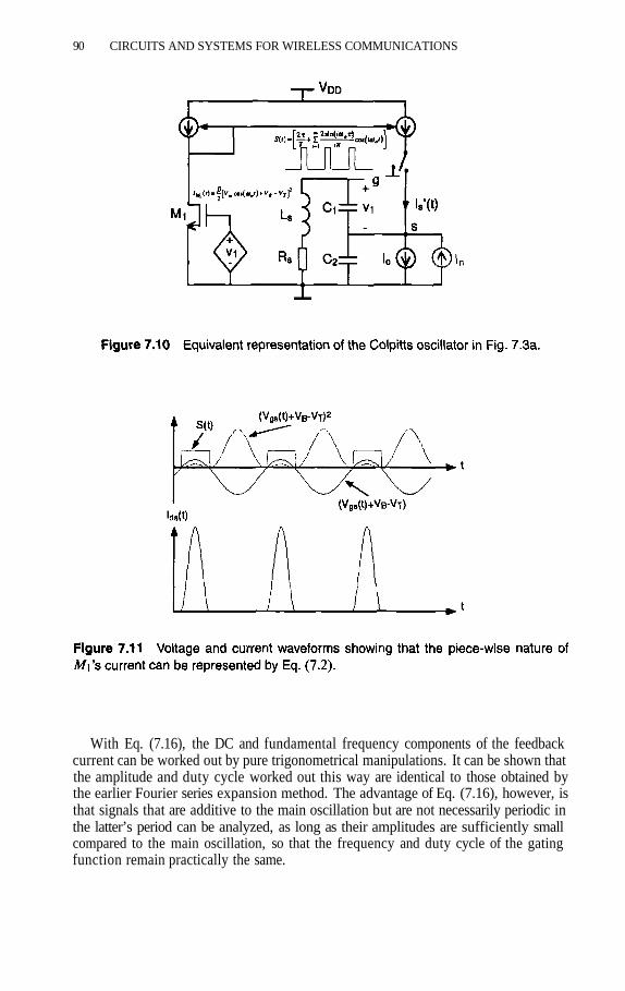
90 CIRCUITS AND SYSTEMS FOR WIRELESS COMMUNICATIONS
With Eq. (7.16), the DC and fundamental frequency components of the feedbackcurrent can be worked out by pure trigonometrical manipulations. It can be shown thatthe amplitude and duty cycle worked out this way are identical to those obtained bythe earlier Fourier series expansion method. The advantage of Eq. (7.16), however, isthat signals that are additive to the main oscillation but are not necessarily periodic inthe latter’s period can be analyzed, as long as their amplitudes are sufficiently smallcompared to the main oscillation, so that the frequency and duty cycle of the gatingfunction remain practically the same.

PHASE-NOISE-TO-CARRIER RATIO IN LC OSCILLATORS 91
7.4 OSCILLATOR RESPONSE TO AN INTERFERING CURRENT
Having established the oscillation amplitude as a function of the tank and transistorparameters as well as the bias current, and re-emphasized the fact that the active devicein most high-Q LC oscillators operates in class-C mode, we are now better placed totackle the phase noise in LC oscillators. Earlier on we objected to the linear analysis ofphase noise, which assumes that an interfering signal (sinusoidal current for example)will generate a response (voltage) on the tank, and that the transistor acts like a lineartransconductance equal to the critical of the tank so that the equivalent tank lossis zero. To demonstrate that this is wrong with a concrete example, we return to theColpitts oscillator and assume that an interfering voltage, ispresent at the gate:
Expanding Eq. (7.16) and collecting current terms only at we find:
Combining (7.18) with (7.11), we obtain:
Equation (7.19) clearly shows that, except in the very special case of |x | = 1, theequivalent transconductance of to the interfering voltage is not exactly thecritical required to cancel the tank loss. In fact, for small values of x, the secondterm in the square brackets in (7.19) is usually much larger than the first term.
Equation Eq. (7.16) also shows the more fundamental flaw of the linear analysis. Ifan interfering voltage at indeed appears, the resulting current will not onlyhave a component at the same frequency, but also one at its image frequency,due to the gating function. This second component will be fed back to the tank andgenerate a voltage component at the image frequency, so that a double-sideband re-sponse will result even if the interference is only single sideband. The voltage at theimage frequency will in turn be modulated by the gating function, to create its own im-age, that is at the original interfering frequency It is the interaction betweenthe component at which we refer to as the response, and the componentat which we refer to as the image, that holds the key to all the phase noisebehaviour which we have been trying to understand.
To analyze this double-sideband response to a single-sideband interference, let usinject a small current interference (shown in grey in Fig. 7.10),
into the s-node in Fig. 7.10. The main oscillation (carrier) serves as the reference,

92 CIRCUITS AND SYSTEMS FOR WIRELESS COMMUNICATIONS
so its phase is assumed to be zero. Although the phase of the injected current is notimportant, we assume it is for the sake of generality. The process in which theresponse and image are modulated back and forth is aided by the catalyst of the gatingfunction, so that it is reasonable to assume that the steady state is reached within asmall number of oscillation cycles. The imprecise word small is to be understood asmuch smaller than the number of clock cycles it takes for the response to an impulsiveinterference such as individual bursts caused by white noise to decay significantlyon a high-Q (low loss) tank, so that steady-state analysis is justified for bursty noisesources. At this stage we only know that there will be a voltage response at both
but their amplitude and phase in steady state, andfor the upper and lower sidebands, respectively, are unknown.
Assuming that and are much smaller than and referring to Fig. 7.10, thefeedback current in steady state is given by
Expanding Eq. (7.21), we find that only the terms at the carrier frequency inter-ference frequency and the image frequency are worth collecting,because they will be fed back to the gate of the tank to sustain the oscillation and in-terfering voltages. Those terms containing second-order combinations of andcan be neglected because they are much smaller than the rest. The terms around DCand higher harmonics of can also be neglected, because they will be heavily attenu-ated by the high-Q resonator and will not produce much voltage at the gate. Thus thesignificant part of is given by:
Applying Kirchhoff’s current law to the s-node in Fig. 7.10, we have:

PHASE-NOISE-TO-CARRIER RATIO IN LC OSCILLATORS 93
It can be shown that for
Combining Eqs. (7.11), (7.22) and (7.24) into Eq. (7.23), we obtain:
For Eq. (7.25) to be valid at all times, the coefficients for the sine and cosine terms atboth frequencies must be zero. This provides us with four simultaneous equations tosolve for the four unknowns in steady state, and
Solving Eqs. (7.26)–(7.29) jointly, we find:

94 CIRCUITS AND SYSTEMS FOR WIRELESS COMMUNICATIONS
Usually the offset frequency is relatively small,so that the upper- and lower-sideband responses are equal in amplitude and 180° outof phase, as shown by Eqs. (7.31) and (7.33). This is just the same as what would becreated by a modulation in phase, so that additive interference does create modulationin phase, due to the nonlinear and switching behaviour of For the same low offsetfrequencies,
Note that in Eq. (7.34) is half of what would be predicted by a linear analysis.The upper-sideband response is indeed inversely proportional to the offset frequency,as has been well known experimentally. This inverse dependency does, however, notcontinue uninterruptedly, according to Eq. (7.33). At sufficiently high offset frequen-cies outside the passive tank’s passband, and thetransistor no longer has sufficient to provide any significant feedback to counterthe interfering current, so that the relationship between the latter and the voltage re-sponse is purely that of a passive tank, and the image sideband disappears, accordingto Eqs. (7.32) and (7.33). The result is now identical to that predicted by a linearanalysis:
The transition point where the image sideband response becomes 3 dB smaller thanthe upper sideband response can also be derived from (7.32):
For oscillators with 100% current duty cycle, the corner frequency is zeroand the noise remains additive, because there is no more gating function and the squar-ing nonlinearity of the MOSFET only translates the upper-sideband interfering signalto frequencies around DC and the second harmonic of the carrier, which will be sup-pressed by the carrier. When x tends to 1, as in the case of a lossless resonator, thecorner frequency also tends to zero and the output noise remains additive. For mostpractical oscillators and noise becomes multiplicative, affecting the phase ofoscillation. The –3 dB offset frequency given in Eq.(7.36) is usually too high to beobserved in normal phase noise measurements, because the sideband spectral densityat such a frequency is already well below the noise floor of the measuring instruments.
It is important to note from Eqs. (7.34)–(7.36) that the detailed transistor parame-ters are only important in determining the boundary between the interferences that willmerely be super-imposed on the main oscillation and those that will cause the phaseof the oscillation to jitter. In the former case, the characteristic is merely due tothe impedance of the passive tank, decreasing outside its passband. In the latter case,it is the creation of the image response and the effective negative feedback loop be-tween the signals at the two frequencies that are responsible for canceling any excess
of that is not needed for compensating the loss of the passive tank. Although in

PHASE-NOISE-TO-CARRIER RATIO IN LC OSCILLATORS 95
both cases the response is inversely proportional to the offset frequency, the two casesdiffer by 6 dB and cause very different disturbances to the oscillator. In the phase jittercase, both the image response and its interaction with the response at the frequencyof interference are due to the active device’s nonlinearity, especially the switchingaction in most oscillators. Analyses attempting to bypass the explicit description ofthe transistor’s nonlinearity (a slowly varying AGC is a linear device in this context)therefore bypass the most fundamental mechanism of amplitude-to-phase-noise con-version. This tends to result in shaky foundations even though the resulting modelsof such analyses are good guesses for what a real oscillator’s noise spectrum wouldlook like. Our analysis shows that the modulation process is essential, yet the exactamount of and indeed the detailed shape of its large-signal V–I characteris-tic, are unimportant. Equations similar to (7.26)–(7.29) can be set up for transistorswith quite different characteristics. While the corner frequency will now be differentfrom that given by Eq. (7.36), Eq. (7.34) will still result at low offset frequencies. Inthis sense our analysis is general and is applicable to all high-Q LC oscillators.
To verify the results in this section, the oscillator in Fig. 7.8 is used to test its voltageresponse to an injected deterministic current. Since the equivalent input impedance atthe s-node can be very high close to the resonance frequency of the tank, injecting awell-known current is difficult. Instead of applying a current directly, we apply a sinu-soidal voltage as shown, and measure the voltages and The Norton equivalent ofthe circuit within the dashed box in Fig. 7.8 is shown in Fig. 7.12. Since the effectiveinjected current is given by the impedance Z looking into the s-node of theoscillator from the equivalent current source is the measured node voltage dividedby Since for low-loss tanks the current flowing throughand close to resonance is much higher than other current components flowing intothe s-node, the latter can be neglected and The transimped-ance can therefore be measured reliably, at least in the close vicinity ofthe carrier, via the voltage ratio Close to the carrier, the applied signal lev-els are kept very small to avoid pulling the main oscillation. As the offset frequencyis gradually increased, the voltage response gradually becomes so small that it sinksunder the noise floor of the spectrum analyzer. The interfering signal level is thenincreased whenever necessary just to keep the spectral peaks representing the voltageresponse above the noise floor by a few dBs. Also measured is the ratio between thevoltage response at the image frequency and the injected current, which we refer to asthe image transimpedance.
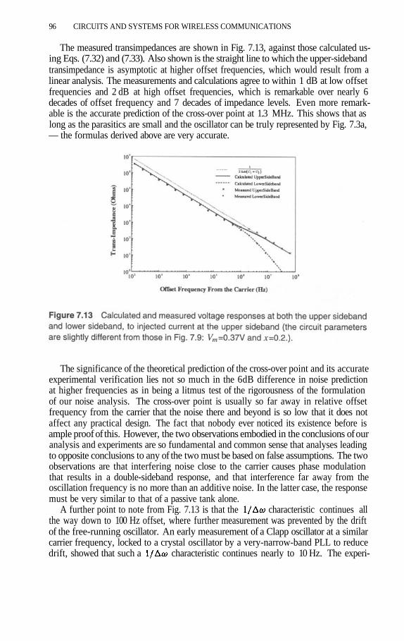
96 CIRCUITS AND SYSTEMS FOR WIRELESS COMMUNICATIONS
The measured transimpedances are shown in Fig. 7.13, against those calculated us-ing Eqs. (7.32) and (7.33). Also shown is the straight line to which the upper-sidebandtransimpedance is asymptotic at higher offset frequencies, which would result from alinear analysis. The measurements and calculations agree to within 1 dB at low offsetfrequencies and 2 dB at high offset frequencies, which is remarkable over nearly 6decades of offset frequency and 7 decades of impedance levels. Even more remark-able is the accurate prediction of the cross-over point at 1.3 MHz. This shows that aslong as the parasitics are small and the oscillator can be truly represented by Fig. 7.3a,— the formulas derived above are very accurate.
The significance of the theoretical prediction of the cross-over point and its accurateexperimental verification lies not so much in the 6dB difference in noise predictionat higher frequencies as in being a litmus test of the rigorousness of the formulationof our noise analysis. The cross-over point is usually so far away in relative offsetfrequency from the carrier that the noise there and beyond is so low that it does notaffect any practical design. The fact that nobody ever noticed its existence before isample proof of this. However, the two observations embodied in the conclusions of ouranalysis and experiments are so fundamental and common sense that analyses leadingto opposite conclusions to any of the two must be based on false assumptions. The twoobservations are that interfering noise close to the carrier causes phase modulationthat results in a double-sideband response, and that interference far away from theoscillation frequency is no more than an additive noise. In the latter case, the responsemust be very similar to that of a passive tank alone.
A further point to note from Fig. 7.13 is that the characteristic continues allthe way down to 100 Hz offset, where further measurement was prevented by the driftof the free-running oscillator. An early measurement of a Clapp oscillator at a similarcarrier frequency, locked to a crystal oscillator by a very-narrow-band PLL to reducedrift, showed that such a characteristic continues nearly to 10 Hz. The experi-

PHASE-NOISE-TO-CARRIER RATIO IN LC OSCILLATORS 97
ments therefore demonstrate that analyses predicting a much higher corner frequencyare wrong. Below such offsets, pulling must be dominant so that the exact shape ofthe phase noise should be immaterial. At the high offset end, our measurements showthat the characteristic continues until 64 MHz, further than 2/3 of the carrierfrequency itself! No flattening is observed, so that part of Leeson’s description of thephase noise spectrum is incorrect. Our experimental results are to be expected, though,for it would be very hard to imagine what noise mechanism would create a response ofconstant amplitude on a passive tank, while the latter’s impedance gradually declinesto zero! The flat noise spectrum we sometimes do see in practical oscillators musthave come from buffers rather than the LC oscillator proper.
7.5 NOISE-TO-CARRIER RATIO IN A CMOS COLPITTS OSCILLATOR
The analysis of the oscillator response to a single sinusoidal current can easily beextended to multiple signals at different frequencies. If the sum of all interferingsignals is small compared to the carrier, then one can assume that the interfering cur-rent at each frequency will generate a pair of response voltages at the gate, and theexpression of feedback current is similar to Eq. (7.21), except now there aremany pairs of response voltages at the gate that are unknown to us. As long as wecan neglect the second-order combinations of interfering voltage components after ex-panding the square-law function, the subsequent mathematical manipulations can beconsidered linear, because the multiplication by the gating function only results infrequency translations of each component. Thus each pair of voltage responses canbe solved individually, and will be related to the individual current component in thesame way as described by Eqs. (7.32) and (7.33). In this sense, the oscillator responseto composite current of different frequencies is the superposition of the responses tocurrent components at each frequency. This enables our noise analysis to follow allthe reasoning of noise analyses of common linear networks.
If the offset frequency is much higher than (Eq. (7.36)), the noise spectraldensity of the oscillator’s gate-source voltage at each frequency is simply given byEq. (7.35) times the spectral density of equivalent noise current at that frequency. Inthe much more important case that the offset frequency is below , the responseis given by Eq. (7.34) times the spectral density of equivalent noise current at the samefrequency plus the contribution due to the image of noise current component at theother side of the carrier.
In (7.36), C' represents the cross correlation factor between the two noise components.For white noise it is reasonable to assume that noise components at different frequen-cies are uncorrelated to each other, i.e. so that the noise voltage spectral densityis given by:

98 CIRCUITS AND SYSTEMS FOR WIRELESS COMMUNICATIONS
Experiments will be compared to Eq. (7.38) later to verify the assumptionNow that we have established the relationship between the phase noise spectrum andthe input white noise current, what remains to be done is to identify all major noisesources in the Colpitts oscillator. In the order of increasing importance, they are thenoise current associated with the bias transistor the noise current due to the lossresistance of the tank, and the noise current due to the main switching transistor
. If we can convert all three sources into equivalent current sources as shown inFig. 7.14, then the total output noise can be easily obtained by applying Eq. (7.38).
Since the drain of is directly connected to the s-node in Fig. 7.3a and its currentis constant, the noise current due to is the most straightforward,The noise contribution of can be worked out via the Norton equivalent current atthe s-node. Representing the noise of as a voltage source and short-circuiting thes-node, we can obtain the mean-squared current noise power spectral density (PSD)of the Norton equivalent circuit near the resonant frequency,
The time-varying nature of its drain-source current makes a more complexnoise source. Referring to Fig. 7.7b, the average drain-source current throughduring the time it is on is given by Eq. (7.39).
The average white noise power spectral density during on-time is therefore givenby Eq. (7.40). If a time-domain noise current n'(t) has the same power spectral densityas that given by Eq. (7.40), then the time-domain noise current for is equivalent to

PHASE-NOISE-TO-CARRIER RATIO IN LC OSCILLATORS 99
n'(t) gated by the switching function s(t) with duty cycle
Since n'(t) itself has a bandwidth much wider than the frequency of the gating func-tion, the power spectral density of n(t) around the oscillation frequency is approxi-mately that of n'(t), given by Eq. (7.40), scaled by the duty cycle of the gating func-tion [29].
A more accurate estimate of is possible by splitting on-time into infinitelysmall intervals, each wide, to allow the exact current to be used for each intervalinstead of the average in Eq. (7.39). Since the noise contribution of each intervalcan be calculated with a gating duty cycle of the overall noise PSD is the sumof the individual contributions, which amounts to an integration that leads to
Since most practical oscillators already have fairly low duty cycles, the difference be-tween Eqs. (7.42) and (7.43) is fairly small. For the circuit in Fig. 7.8, the overall noiseestimate using Eq. (7.43) is about 0.5 dB below that using Eq. (7.42). Equation (7.42)is therefore more preferable because it gives more insight into the relationship betweennoise and the nominal transconductance, as well as the current duty cycle. Both arelikely to be design parameters.
Replacing the noise current term in Eq. (7.38) with the sum of contributions fromthe bias transistor, the resistive loss of the tank, and that of the switching transistor
we obtain:
The ratio between the noise spectral density and the signal power can now be derivedby combining Eqs. (7.12) and (7.44):

100 CIRCUITS AND SYSTEMS FOR WIRELESS COMMUNICATIONS
For small duty cycles, x is close to unity, and Eq. (7.45) is then approximately givenby:
To verify Eq. (7.45), the parameters in Fig. 7.8 were used to calculate the oscillatoroutput spectral density due to thermal noise sources. The noise contributions in thesquare brackets in Eq. (7.45) are 0.17 mS for the bias resistor, 2 mS for the rest ofthe resistive loss of the passive tank that had been measured before was mounted,and 2.86 mS due to . The quality factor Q of the tank is slightly under 25. Thisgives a calculated phase noise of –115 dBc/Hz at 10 kHz offset. The calculated phasenoise is compared with measured results in Fig. 7.15, covering 4 octaves of offsetfrequency range.
Because the oscillator was designed to be relatively high-Q (to be close to the prac-tical situation that has been assumed in the derivations of this paper), the overall phasenoise is very low. The noise floor of the instrument and the onset of up-convertedflicker noise therefore limit the measurable thermal noise region to the last two oc-taves. This gives us three measurement points that are clearly on the 6 dB/oct line. To

PHASE-NOISE-TO-CARRIER RATIO IN LC OSCILLATORS 101
remove the influence of the noise from the instrument (HP 8563 E Spectrum Analyzer),the latter is calibrated by measuring an 80 MHz crystal oscillator at the correspondingoffset frequencies. Since the phase noise of an 80 MHz crystal oscillator is better than–110 dB at 300 Hz offset [30], the measured noise at offsets above 1 kHz is effectivelythat of the instrument. This uncorrelated noise contribution of the instrument is thensubtracted from the measured noise power at the 10 kHz and 20 kHz offset points. Asis typical of most noise measurements, the repeatability of the measured noise powerspectral density (with averaging) is about within 0.5–1 dB. The measurement accu-racy of the points shown in Fig. 7.15 can therefore be considered to be 1 dB. This isthe same accuracy with which the calculated thermal noise line in Fig. 7.15 predictsthe measurement. The measurement at 1.25 kHz is 16 dB higher than that at 5 kHz,showing this region to be strongly influenced by flicker noise. From the slope of themeasured noise PSD we can infer that the cross-over point between thermal noiseand flicker noise is around 1.5 kHz. Adding the inferred flicker noise to the calcu-lated white noise contribution, we have a calculated phase noise that also agrees withmeasurement within 1 dB for the first two octaves of measured offset frequency. Thiscan be seen as conclusive evidence that Eq. (7.45) accurately predicts the sidebandnoise-to-carrier ratio, not least because there are no parameters used in the calculationof Eq. (7.45) that have not been independently verified by measurement to the desiredaccuracy first. Since the relationship between an injected current and measured volt-age response has also been accurately verified in the previous section, the significanceof the measurement in Fig. 7.15 lies in verifying Eqs. (7.36) and (7.38), as well as thepower spectral densities of all the white noise sources in the oscillator, especially thatof . Equation (7.38) is 3 dB below what would be predicted by a linear analysissimilar to Eq. 17 in [9]. Fig. 7.16 shows a measured spectrum of the oscillator.

102 CIRCUITS AND SYSTEMS FOR WIRELESS COMMUNICATIONS
7.6 EXACT DESIGN OF RF OSCILLATORS
In addition to having been derived on a rigorous basis, Eq. (7.45) is completely basedon circuit parameters known to the designers. This makes the discussion of the exactdesign of RF oscillators most straightforward. Before this discussion, however, it isinteresting to compare Eq. (7.45) or Eq. (7.46) to the well-known Leeson’s formula,which designers have been using for the last 30 years, to examine the dependence onthe resonator’s quality factor Q in particular. In Leeson’s original paper, the signallevel at the input of the active device is not very clearly defined, so that it caneither be interpreted as the square of the oscillation voltage, or the power dissipatedby the resonator. In the former case we can see that for a constant oscillation voltage,the noise-to-carrier ratio will only scale with the noise power given in Eq. (7.44),which clearly does not scale with . In the latter case,Equation (7.46) can thus be rewritten as
which apparently is Leeson’s formula with an inverse dependence on Closer ex-amination of Eq. (7.47), however, shows that both the signal power PS and the noisefigure F so defined, far from being independent parameters, are usually also strongfunctions of Q. No conclusions could therefore really be drawn about the Q depen-dence of the oscillator noise performance on the basis of Leeson’s formulation.
In practical situations, one does sometimes find that doubling the Q of the tankimproves the N/C by exactly 6 dB, while the transistor and its bias current are un-changed. This can arise when the change of Q is purely due to improvement in theloss resistance and the middle term in the square brackets of Eq. (7.46) is muchsmaller than the other two terms. This may have been the case especially for designersusing discrete MOSFETs or BJT transistors, where the transconductance for a givencurrent is not within the designer’s control. For an integrated circuit designer this neednot be so, because the size of the transistor should be scaled down with to main-tain just the necessary range of 3–5 as explained earlier. In this case, thenoise factor F in Leeson’s formulation is unchanged, while the signal power hasdoubled. The improvement of N/C will be 9 dB each time Q is doubled by halving
On the other hand, N/C can be significantly changed by different combinations oftank parameters with the same quality factor Q. Assuming, as a typical example, thatthe loss resistance of the inductor dominates the loss of the tank and scales linearlywith the inductance Doubling the inductance and halving the capacitances thenleaves both the Q of the tank and its resonance frequency unchanged. The combinedchange in resistance and capacitance, however, causes in Eq. (7.46) to be halved,as well as the required so that 3 dB can be gained either in achievable N/C or in

PHASE-NOISE-TO-CARRIER RATIO IN LC OSCILLATORS 103
the required current consumption without improving the quality of the inductor! In-deed, we note that most recently published oscillators with integrated inductors havevery small capacitors, which gave them respectable phase noise performance at a rea-sonable current consumption even though the integrated inductors continue to have apoor quality factor between 3 and 6 at 1 GHz. One’s ability to improve phase noise byreducing capacitance, however, is limited by the parasitic capacitors associated withthe circuit, which have higher losses and which tend to increase the required tuningrange for the desired frequency. A higher tuning range in capacitance may also resultin higher variability of oscillation amplitude, which in turn affects N/C.
An additional advantage of the phase noise model described by Eq. (7.45) is thatthe role of current consumption (as opposed to power consumption , or the signalpower ) is explicitly stated. Indeed, there is an almost one-to-one relationship be-tween N/C and the bias current This point is important in RF oscillator designs formobile communications, where power consumption is extremely important.
For a local oscillator (LO) used in radio frequency circuits, especially those usedin cellular telephones, the three most important parameters are oscillation amplitude,phase-noise-to-carrier ratio and power consumption. For a given voltage supply, thelatter reduces to current consumption. A well-defined LO amplitude is required by themixers, which tend to exhibit a higher noise figure and less conversion gain both whenthe LO amplitude is too low and too high. Limiting amplifiers (buffers) are frequentlyused to remove variations of the LO amplitude due to the imprecise nature of thetank loss as well as the tuning of capacitors, but a well-designed worst-case amplituderange still results in the best power consumption. The phase noise of the oscillatorrelative to the carrier amplitude is responsible for reciprocal mixing of out-of-band,strong interfering signals to the same IF frequency as the desired RF signal. It alsoreduces the signal-to-noise ratio in the desired radio channel. Power consumption, onthe other hand, directly affects the lifetime of the battery. The latter is usually the mostexpensive item in a cellular telephone [31,32]. Bearing the above performance para-meters and Eqs. (7.12), (7.45) and Fig. 7.6 in mind, we can formulate the followingsystematic design procedure for RF oscillators:
1. Determine the lowest capacitance that can be used based on the knowledge of cir-cuit parasitics, variability of the capacitors themselves, required RF tuning range(for channel selection, for example) and the available variable capacitor tuningrange. (Note that this may be substantially larger for a production circuit thanthat for a laboratory experiment.)
2. Select or implement (in the case of fully integrated circuits) the inductor in sucha way that ensures the best worst-case Q for the resonator. The value of the in-ductance is determined by capacitances chosen in the previous step and the desirednominal frequency.
3. Set the value of the bias current to achieve the desired amplitude according toEq. (7.12) and using the worst-case (If the difference between best- and worst-case amplitudes exceeds what is acceptable by the mixer, then either a limitingamplifier must be used, or step 1 must be repeated to reduce the difference.)
4. Use Eq. (7.12) and the worst-case to calculate the ratio N/C at critical offsetfrequencies, assuming that will be 3–5 times If it exceeds the prescribed

104 CIRCUITS AND SYSTEMS FOR WIRELESS COMMUNICATIONS
limit by k dB, and a limiting amplifier is used to limit the LO amplitude, then biascurrent should be increased by 0.5k dB, to reduce N/C by k dB.
5. If no limiting amplifier is used, the bias current should then be increased by k dB instep 4, which reduces N/C by 2k dB. The design procedure must then be repeatedfrom step 1 to ensure that the best-case amplitude is not too high. This is done byincreasing the capacitances by 0.5k dB, so that is increased by k dB to bringamplitude down to the desired level. This increases the N/C by another k dB sothat the acceptable limit is just met.
3–5 times
7. The transconductance of the bias transistor should be made as small aspossible to reduce noise. Since the bias current is fixed, this means reducing itsW/L ratio. The latter is limited by the available voltage headroom for a givensupply to keep the transistor in the saturation region of operation.
With the accurate formulas derived in this paper, the Colpitts oscillator design be-comes a routine for the designer as of step 3 above. The designer can then concentrateon the less well-defined steps 1 and 2, estimate of parasitics and variability as well asimplementation of better inductors.
7.7 CONCLUSIONS
Despite numerous journal and conference papers published in the past 60 years, ourunderstanding of why the phase-noise-to-carrier ratio is inversely proportional to theoffset frequency from the carrier has been limited. This paper seeks to argue why thereasoning behind most of the phase-noise models has been based on shaky founda-tions. As a result, the models’ predictions of noise are wrong in one portion of thespectrum or the other for LC oscillators.
In this contribution, the oscillator is described in the time domain without any a pri-ori linearity assumption. Noise sources are introduced where they are first added tothe signal, to avoid assuming a conclusion (such as noise in phase) before the startof any analysis. The only assumption based more on intuition than rigour was theassumption that for bursty type of sinusoidal interferences, modulation by switchinghelps the responses reach steady state in much less than the natural decay time ofthe passive tank. Experiments seem to validate this assumption. All basic equationsset up in this paper are based on the Kirchhoff laws. The approximations that havebeen made include assuming high-Q resonators that will attenuate harmonics of theoscillation voltage on the resonator to negligible levels, a piece-wise square-law V–Icharacteristic for the MOS transistor, and that the interfering signals are sufficientlysmall compared to the main oscillation such that the duty cycle in which the transistorturns on remains virtually unchanged.
The active device in a typical LC oscillator operates heavily in class-C mode, turn-ing on for only a short fraction of each oscillation period to inject a current pulse intothe LC tank to maintain the steady state. In the limit, the oscillation amplitude of anybranch voltage within the tank is two times the average current through the branch ofthe switching active device divided by the transconductance between the two branches
6. Size according to the bias current, so that its nominal transconductance is

PHASE-NOISE-TO-CARRIER RATIO IN LC OSCILLATORS 105
at resonance. This limit is independent of the exact V–I characteristic of the active de-vice. Practical high-Q LC oscillators, such as those implemented with BJT or CMOStransistors, have oscillation amplitudes very close to this limit.
The highly nonlinear V–I characteristic of the active device that causes the latterto be switched by the main oscillation modulates any interfering signal to generate aresponse not only at the frequency of the interferer, but also at its mirror frequencywith respect to the carrier. This image response is in turn modulated by the oscillationthrough the transistor, which creates its own image at the frequency of the originalinterfering signal. This forms an additional negative feedback loop that cancels anyexcess positive feedback of the transistor. The response at the interfering frequenciesclose to the carrier thus becomes inversely proportional to its frequency offset from thelatter, irrespective of the exact V–I characteristic and the duty cycle of the switchingdevice, nor the passband width of the passive tank. Such a response and its image arepractically equal in amplitude and opposite in polarity. Their combined effect is there-fore equivalent to a modulation of the carrier in phase. At higher offset frequencies,the tank impedance becomes very small so that very little voltage is produced at thetransistor input. The transistor’s feedback current, which contains the image responsedue to modulation, is insignificant compared to the interfering current. The voltageresponse to the interference is therefore now virtually the same as that of a passivetank, which still decreases with the inverse of the offset frequency, with negligibleimage component. The effect of noise — far away from the carrier is therefore merelyadditive. The cross-over point between dominance of phase noise and dominance ofadditive noise is a function of the transistor and tank parameters.
Because of the existence of image response, phase noise due to white noise is 3 dBhigher than that due to noise components at frequencies above (or below) the carrieralone. The switching nature of the transistor also makes the noise generated by thelatter depend on the duty cycle, and hence on the parameters of the rest of the oscillator.All noise sources, including that of the switching transistor, have been calculated inthis chapter. The resulting expression for the phase-noise-to-carrier ratio comprisestherefore only original circuit parameters instead of intermediate variables that requiredetermination by simulation or experiments.
Controlled experiments have been carefully constructed to verify the theory de-rived in the paper. The predicted oscillation amplitude is consistently within 1 dB ofmeasurements. The predicted duty cycle also matches measured values by the sameaccuracy. The response of the oscillator to an injected interfering current as well as theimage response agree with what the theory predicts within the accuracy with whichparameters of the passive tank can be measured. In the 80 MHz range, this accuracyis better than 1 dB. The cross-over frequency between phase and additive noise, andindeed its very existence, have been confirmed by experiments. in practical designsMeasurements of the phase-noise-to-carrier ratio also show that the agreement withthe formula derived in this paper is within 1 dB, the repeatability of any phase noisemeasurement and the accuracy within which circuit parameters have been indepen-dently measured. The phase noise model in this paper can therefore be used withconfidence in practical designs.
Although the specific Colpitts oscillator has been used in deriving the formulas inthis paper, the basic reasoning behind the setting up of basic equations is not specificto Colpitts oscillators. Although for other LC oscillators, the determination of the

106 CIRCUITS AND SYSTEMS FOR WIRELESS COMMUNICATIONS
amplitude and duty cycle as well as the critical will be different, the basic ideasabout why the oscillator’s response to interference is phase noise for low and additivenoise for high offset frequencies and the role of the image in the inverse dependenceof phase noise on offset frequency will remain the same. In this sense, the analysis inthis paper is general for all LC oscillators.
Acknowledgments
The assistance of P. Basedau and R. Rheiner in carrying out the experiments presented inthis paper is gratefully acknowledged. The author also wishes to thank F. Piazza for usefuldiscussions on oscillator phase noise during the past two years.
References
[1] I. L. Berstein, “On fluctuations in the neighborhood of periodic motion of anauto-oscillating system”, Doklady Akad. Nauk., vol. 20, p. 11, 1938.
[2] A. Spälti, “Der Einfluss des thermischen Widerstandsrauschens und des Schrot-teffectes auf die Störmodulation von Oscillatoren”, Bulletin des SchweizerischenElektrotechnischen Vereins, vol. 39, pp. 419–27, June 1948.
[3] A. Blaquiére, “Spectre de Puissance d’un Oscillateur Non-Linéaire Perturbé perle Bruit”, Ann. Radio Elect., vol. 8, pp. 153–179, August 1953.
[4] Hafner, “The Effect of Noise in Oscillators”, Proc. IEEE, vol. 54, pp. 179–198,Feb. 1966.
[5] A. van der Ziel, Noise in Solid-State Devices and Circuits, W. 240–242, Wi-ley-lnterscience, New York, 1986.
[6] D. B. Leeson, “A Simple Model of Feedback Oscillator Noise Spectrum”, Proc.IEEE, pp. 329–330, Feb. 1966.
[7] G. Sauvage, “Phase Noise in Oscillators: A Mathematical Analysis of Leeson’sModel”, IEEE Trans. on Instrum. and Meas., vol. IM-26, Dec. 1977.
[8] J. Everard, “Low-noise power-efficient oscillators: theory and design”, IEEProceedings, vol.133, Pt. G, No. 4, pp. 172–180, August 1986.
[9] J. Craninckx and M. Steyaert, “Low Noise Voltage-Controlled Oscillators Us-ing Enhanced LC-Tanks”, IEEE Trans. Circ. & Syst., vol. 42, pp. 794–804,Dec. 1995.
[10] A. Hajimiri and T. Lee, “A General Theory of Phase Noise in Electrical Oscilla-tors”, IEEE J. Solid-State Circ., vol. 33, No. 2, pp. 179–194, Feb. 1998.
[11] N. Nguyen and R. Meyer, “A 1.8-GHz Monolithic LC Voltage-Controlled Oscil-lator”, IEEE J. Solid-State Circ., vol. 27, No. 3, pp. 444–450, March 1992.
[12] N. Nguyen and R. Meyer, “Si IC-Compatible Inductors and LC Passive Filters”,IEEE J. Solid-State Circuits, vol. 25, No. 4, pp. 1028–1031, Aug. 1990.
[13] P. Basedau and Q. Huang, “A 1GHz, 1.5V Monolithic LC Oscillator in l-µmCMOS”, Proc. 1994 European Solid-State Circuits Conf., pp. 172–175, Ulm,Germany, Sept. 1994.
[14] M. Soyuer et al, “A 2.4-GHz silicon bipolar oscillator with integrated resonator”,IEEE J. Solid-State Circuits, vol. 31, No. 2, pp. 268–270, Feb. 1996.

PHASE-NOISE-TO-CARRIER RATIO IN LC OSCILLATORS 107
[15] A. Ali and J. Tham, “A 900MHz Frequency Synthesizer with Integrated LCVoltage-Controlled Oscillator”, ISSCC Digest of Tech. Papers, pp. 390–391, SanFrancisco, USA, Feb. 1996.
[16] A. Rofougaran et al, “A 900MHz CMOS LC-Oscillator with Quadrature Out-puts”, ISSCC Digest of Tech. Papers, pp. 392–393, San Francisco, 1996.
[17] M. Soyuer et al, “A 3V 4GHz nMOS Voltage-Controlled Oscillator with Inte-grated Resonator”, ISSCC Digest of Tech. Papers, pp. 394–395, San Francisco,USA, Feb. 1996.
[18] B. Razavi, “A l.8GHz CMOS Voltage-Controlled Oscillator”, ISSCC Digest ofTech. Papers, pp. 388–389, San Francisco, USA, Feb. 1997.
[19] L. Dauphinee, M. Copeland and P. Schvan, “A Balanced l.5GHz Voltage Con-trolled Oscillator with an Integrated LC Resonator”, ISSCC Digest of Tech. Pa-pers, pp. 390–391, San Francisco, USA, Feb. 1997.
[20] J. Jansen et al, “Silicon Bipolar VCO Family for 1.1 to 2.2 GHz with Fully-Inte-grated Tank and Tuning Circuits”, ISSCC Digest of Tech. Papers, pp. 392–393,San Francisco, USA, Feb. 1997.
[21] J. Craninckx and M. Steyaert, “A 1.8 GHz Low-Phase-Noise CMOS VCO UsingOptimized Hollow Spiral Inductors”, IEEE J. Solid-State Circuits, vol. 32, No. 5pp. 736–744, May 1997.
[22] J. Craninckx and M. Steyaert, “A Fully Integrated Spiral-LC CMOS VCO Setwith Prescaler for GSM and DCS-1800 Systems”, Proc. Custom Integrated Cir-cuit Conference, pp. 403–406, Santa Clara, USA, May 1997.
[23] J. Parker and D. Ray, “A Low-Noise 1.6 GHz PLL with On-Chip Loop Filter”,Proc. CICC, pp. 407–410, Santa Clara, USA, May 1997.
[24] M. Zannoth et al, “A Fully Integrated VCO at 2 GHz”, ISSCC Digest of Tech.Papers, pp. 224–225, San Francisco, USA, Feb. 1998.
[25] P. Kinget, “A Fully Integrated CMOS VCO for 5 GHz WirelessApplications”, ISSCC Digest of Tech. Papers, pp. 226–227, San Francisco, USA,Feb. 1998.
[26] D. Pederson and K. Mayaram, Analog Integrated Circuits for Communication,Kluwer Academic Publishers, Boston, 1991.
[27] Qiuting Huang, “Power Consumption vs LO Amplitude for CMOS ColpittsOscillators”, Proc. CICC, pp. 255-258, Santa Clara, USA, May 1997.
[28] K. Mayaram and D. Pederson, “Analysis of MOS transformer-coupled oscilla-tors”, IEEE J. Solid-State Circ., vol. 22, No. 6 pp. 1155–1162, Dec. 1987.
[29] J. Fischer, “Noise Sources and Calculation Techniques for Switched CapacitorFilters”, IEEE J. Solid-State Circ., vol. SC-17, pp. 742–752, Aug. 1982.
[30] Q. Huang and P. Basedau, “Design Considerations for High-Frequency CrystalOscillators Digitally Trimmable to Sub-ppm Accuracy”, IEEE Trans. On VLSI,vol. 5, No. 4, pp. 408–416, Dec. 1997.
[31] S. Rogerson, “Where less is more”, Mobile Europe, vol. 7, pp. 27–30, Feb. 1997.[32] Q. Huang et al, “The Impact of Scaling Down to Deep Submicron on CMOS
RF Circuits”, IEEE J. Solid-State Circuits, vol. 33, No. 7, pp. 1023–1036, July1998.

This page intentionally left blank

8 DESIGN STUDY OF A900 MHz/1.8 GHz CMOS TRANSCEIVER
FOR DUAL-BAND APPLICATIONSBehzad Razavi
Electrical Engineering DepartmentUniversity of California
Los Angeles, USA
Abstract: This chapter describes the design of a CMOS transceiver targeting dual-band applications in the 900 MHz and 1.8 GHz bands. The receiver is based on a mod-ified Weaver architecture, and the transmitter incorporates new methods of quadratureup-conversion. The receiver and the transmitter have been fabricated in a CMOStechnology.
8.1 INTRODUCTION
The emergence of various wireless standards within the US and around the worldhas created a demand for RF transceivers that can operate in more than one mode.The standards deployed in the 900 MHz band are the TDMA standard IS-54 and theCDMA standard IS-95 (US) and the GSM standard (Europe). Additionally, with theavailability of the 1.8 GHz band for cellular networks, new standards such as PCS 1900and DCS 1800 have been introduced. Furthermore, the Global Positioning System(GPS) (1.5 GHz) and the European cord-less standard DECT (1.9 GHz) provide attrac-tive services that can be incorporated in mobile telephones. In addition to providing“roaming” capability, the use of two or more standards that operate in different bands
109

110 CIRCUITS AND SYSTEMS FOR WIRELESS COMMUNICATIONS
boosts the capacity of the network, thus lowering the probability of unsuccessful callsduring peak traffic hours. Thus, multi-standard RF transceivers are predicted to play acritical role in wireless communications in the 900–2000 MHz range.
This paper describes circuit and architecture design techniques for dual-standardRF transceivers with emphasis on CMOS implementations. Particular attention is paidto issues such as cost, level of integration, form factor, power dissipation, and time tomarket. These techniques are presented in the context of a dual-band system specifi-cally designed to operate with GSM and DCS 1800 standards. Both the receiver andthe transmitter have been fabricated in a CMOS technology. The experimentalresults obtained for each circuit are described in [1–3].
8.2 RECEIVER DESIGN CONSIDERATIONS
Accommodating two or more standards in one receiver generally requires substantialadded complexity in both the RF section and the baseband section, leading to a highcost. Thus, the system must be designed so as to share as much hardware as pos-sible. For this reason, both the architecture design and the frequency planning of amulti-standard transceiver demand careful studies and numerous iterations.
The GSM and DCS 1800 standards incorporate the same modulation format, chan-nel spacing, and antenna duplexing. Summarized in Table 8.1 are the characteristicsof each standard, indicating that a dual-band transceiver can exploit the propertiescommon to both so as to reduce the off-chip hardware.
In order to minimize the number of oscillators and synthesizers, the receivers andtransmitters in a dual-band system must be designed concurrently, with the frequencyplanning carried out such that the receive and transmit paths are driven by the samesynthesizers. Although GSM and DCS 1800 use frequency-division duplexing (FDD)at the front end, their actual operation is somewhat similar to time-division duplex-ing (TDD) because their receive and transmit time slots are set off by 1.73 ms (threetime slots) [4]. Thus the receiver and the transmitter can time-share the frequencysynthesizers.
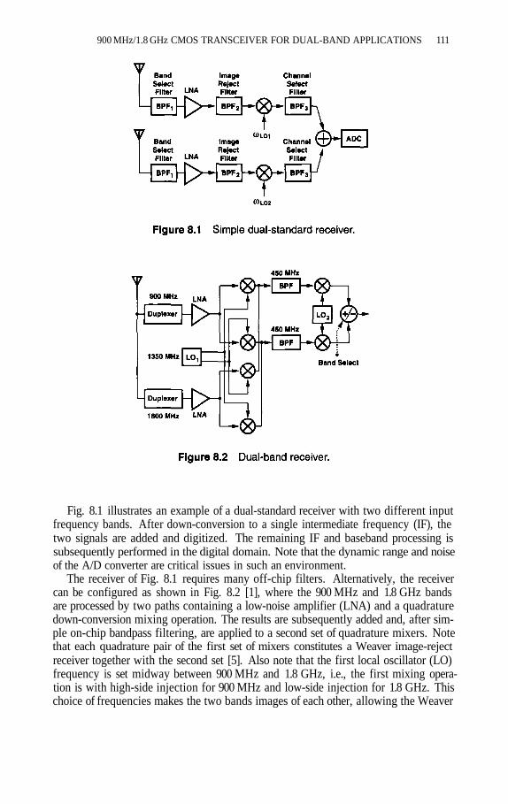
900 MHz/1.8 GHz CMOS TRANSCEIVER FOR DUAL-BAND APPLICATIONS 111
Fig. 8.1 illustrates an example of a dual-standard receiver with two different inputfrequency bands. After down-conversion to a single intermediate frequency (IF), thetwo signals are added and digitized. The remaining IF and baseband processing issubsequently performed in the digital domain. Note that the dynamic range and noiseof the A/D converter are critical issues in such an environment.
The receiver of Fig. 8.1 requires many off-chip filters. Alternatively, the receivercan be configured as shown in Fig. 8.2 [1], where the 900 MHz and 1.8 GHz bandsare processed by two paths containing a low-noise amplifier (LNA) and a quadraturedown-conversion mixing operation. The results are subsequently added and, after sim-ple on-chip bandpass filtering, are applied to a second set of quadrature mixers. Notethat each quadrature pair of the first set of mixers constitutes a Weaver image-rejectreceiver together with the second set [5]. Also note that the first local oscillator (LO)frequency is set midway between 900 MHz and 1.8 GHz, i.e., the first mixing opera-tion is with high-side injection for 900 MHz and low-side injection for 1.8 GHz. Thischoice of frequencies makes the two bands images of each other, allowing the Weaver

112 CIRCUITS AND SYSTEMS FOR WIRELESS COMMUNICATIONS
architecture to select one and reject the other by addition or subtraction of the outputsof the second set of mixers.
Owing to gain and phase mismatches, the image rejection ratio of the Weaver ar-chitecture is limited to 30 to 40 dB, inadequate for cellular applications such as GSMand DCS 1800. Nevertheless, since for each band the image is 900 MHz away, thefront-end duplexer filters provide more than 40 dB of rejection.
The distribution of gain, noise, and nonlinearity in the receiver chain plays a keyrole in the overall performance, necessitating iterations between architecture designand circuit design. Since channel-selection filtering is postponed to the stages fol-lowing the IF mixers, the third-order intercept point of each stage must scaleaccording to the total gain preceding that stage. With the initial estimate of thethe corresponding circuit is designed so as to minimize its noise contribution.
The problem of secondary images [4] constrains the choice of the second IF in theWeaver topology. We consider two scenarios here. The present design provides quad-rature down-conversions to allow translation to the baseband. This approach, however,suffers from some of the difficulties encountered in direct-conversion receivers. Forexample, DC offsets due to the self-mixing of the second LO, flicker noise in the ana-log baseband circuits, and I and Q mismatch corrupt the down-converted signals [6,7].
Another possibility for the second down-conversion exists by virtue of the specificchannelization in GSM and DCS 1800. As shown in the receiver interference maskof Fig. 8.3, the adjacent channels in a cell are unoccupied. This suggests that, if thesecond LO frequency is placed at the edge of the desired channel, then the secondaryimage coincides with one of the adjacent channels. Illustrated in Fig. 8.4, this tech-nique translates the center of the desired channel to 100 kHz instead of zero. Thus,flicker noise corrupts primarily the edge of the channel, and elimination of DC offsetsby AC coupling becomes feasible. Furthermore, the down-conversion in the analogdomain need not separate the signal into I and Q phases, thereby avoiding relatedmismatches.
The above approach does introduce a difficulty: the channel-select filter now re-quires much sharper selectivity because 43 dBm interferers appear closer to the de-sired channel. This issue may be resolved by partitioning the filtering between analogand digital domains, albeit at the cost of tightening the linearity requirements of theA/D converter.

900 MHz/1.8 GHz CMOS TRANSCEIVER FOR DUAL-BAND APPLICATIONS 113
8.3 RECEIVER BUILDING BLOCKS
8.3.1 LNA/mixer
In order to achieve a relatively low noise figure and a reasonable input match, theLNA employs a common-source cascode stage with inductive degeneration (Fig. 8.5).To avoid uncertainties due to bond-wire inductance, both the source inductor and thedrain inductor are integrated on the chip. The LNA draws approximately 5 mA from

114 CIRCUITS AND SYSTEMS FOR WIRELESS COMMUNICATIONS
the supply and exhibits a noise figure of less than 2.5 dB and an of greater than–2 dBm in each band. The parasitic capacitance of the drain junction and overlapcapacitance of and the input capacitance of the mixers resonate with at thefrequency of interest. With a Q of about 3, this resonance lowers the image signal byapproximately 10 dB.
The LNA directly drives the quadrature RF mixers, which are configured as single-balanced circuits. Employing inductive loads to minimize thermal noise, each mixerdrains 2 mA to achieve a reasonable trade-off between noise and nonlinearity.
With 22 dB of voltage gain in the LNA, it is desirable to realize an of greaterthan in the mixer, while maintaining its input-referred noisevoltage below roughly The dimensions of in Fig. 8.5 has a strongimpact on the performance of the RF mixer. Transistor is sized such that its over-drive voltage is sufficiently large to guarantee the required This is in contrast tobipolar implementations, where enormous emitter degeneration would be necessary toachieve an greater than The key point here is that for a given bias cur-rent and a properly sized MOS transistor exhibits a much higher transconductancethan a degenerated bipolar structure. Transistors and in Fig. 8.5 also influencethe noise and conversion gain of the mixer. The choice of the width of these devicesis governed by a trade-off between their switching time and the parasitic capacitancesthey introduce at node P. For a given (sinusoidal) LO swing, and are simulta-neously on for a shorter period of time as their width increases. A compromise is thusreached by choosing allowing the pair to turn off witha differential swing of 100 mV while degrading the conversion gain by less than 1 dB.
The interface between the LNA and the mixer merits particular attention. As shownin Fig. 8.5, to achieve a well-defined bias current in the mixer, the LNA incorporatesthe DC load with diode-connected devices and Neglecting the DC dropacross we note that Thus, proper ratioing of and
with respect to and defines as a multiple of Capacitor providesAC ground at the source of so that the output resistance ofdoes not degrade the Q of Realized as an NMOS transistor, consists of a largenumber of gate fingers to reduce the channel resistance, achieving a Q of greater than30 at the frequency of interest.
In contrast to AC coupling techniques, the above approach incurs no signal loss,but it consumes some voltage headroom. Interestingly, can serve as the currentsource for another circuit, e.g. an oscillator, thus re-using the bias current of the LNA.
8.3.2 IF mixer
The differential output of the RF mixers in Fig. 8.5 is capacitively coupled to the inputport of the IF mixers, allowing independent biasing. With an overall voltage gain ofabout 26 dB in the LNA and the RF mixers, the nonlinearity of the IF mixers tends tolimit the performance of the receiver. To this end, we note that a differential pair witha constant tail current exhibits higher third-order nonlinearity than a grounded-sourcepair using the same current and device dimensions. Shown in Fig. 8.6, the IF mixeris configured as a double-balanced circuit consisting of an input pair, a current multi-plexer, and a switching quad. The input devices draw a drain current of 1 mA and aresized to sustain an over-drive voltage of 500 mV, thereby achieving an of approx-

900 MHz/1.8 GHz CMOS TRANSCEIVER FOR DUAL-BAND APPLICATIONS 115
imately The low transconductance of these transistors togetherwith voltage headroom limitations ultimately results in a slight voltage conversionloss (about –2 dB) in the IF mixer. The switches in the current multiplexer negate thesignal current according to the logical state of band while sustaining a drain-sourcevoltage of approximately 35 mV.
An important concern in heterodyne and image-reject receivers is the translationof various interferers to the desired channel frequency after down-conversion. Owingto nonlinearities and switching operations in each mixer, an interferer at resultsin components at With two down-conversions using andthe down-converted spurs appear at (Fig. 8.7), many of whichmay fall into the desired baseband channel. Since in-band interferers are not filteredbefore channel selection, and since they are located on the same side of as thedesired signal, they are not suppressed by the image-rejection technique used in thereceiver. It is also important to note that the spurious response is not exercised ina simple noise figure measurement, but it reveals the performance of the receiver ina realistic environment. The spurious response of the dual-band receiver has beenexamined with the aid of a spreadsheet program. Five interference frequencies in eachband were found to be the most significant sources of down-converted spurs.
Another interesting phenomenon that results from the choice of the two LO fre-quencies is the in-band leakage to the antenna. The feed-through and the

116 CIRCUITS AND SYSTEMS FOR WIRELESS COMMUNICATIONS
low Q of the BPF give rise to a significant 1350 MHz component at the input of theIF mixer. Upon second mixing, this component is translated to both 900 MHz and1800 MHz, potentially appearing as in-band leakage to the antenna(s). However, byvirtue of differential signaling from the first IF onward, and by proper low-pass fil-tering at the output, this type of leakage can be suppressed to acceptably low values.
8.4 TRANSMITTER DESIGN CONSIDERATIONS
In order to minimize the number of oscillators and synthesizers, the receivers andtransmitters in a dual-band system must be designed concurrently, with the frequencyplanning made such that the receive and transmit paths are driven by the same syn-thesizers. Although GSM and DCS 1800 use frequency-division duplexing (FDD) atthe front end, their actual operation is somewhat similar to time-division duplexing(TDD) because their receive and transmit time slots are set off by 1.73 ms (three timeslots) (Fig. 8.8). Thus, frequency synthesizers can be time-shared between the re-ceiver and the transmitter. Since the dual-band receiver incorporates LO frequenciesof 1350 MHz and 450 MHz, it is desirable to utilize the same frequencies for the trans-mit path as well.
Before considering suitable transmitter architectures, we review Gaussian mini-mum shift keying (GMSK) modulation to arrive at some of the design implications.Fig. 8.9 conceptually illustrates frequency shift keying (FSK) and GMSK. In FSK,rectangular baseband pulses are directly applied to a frequency modulator, e.g. a volt-

900 MHz/1.8 GHz CMOS TRANSCEIVER FOR DUAL-BAND APPLICATIONS 117
age-controlled oscillator (VCO), thereby creating an output waveform given by
where is a constant denoting the “depth” of modulation and represents thebaseband signal.
An important drawback of FSK is the large bandwidth occupied by the modulatedsignal, partly because of the abrupt transitions in the frequency introduced by the sharpedges of the baseband pulses. We expect that if the frequency changes more smoothlyfrom one bit to the next, then the required bandwidth decreases. In fact, the spectrumof the signal expressed by Eq. 8.1 decays in proportion to , where n denotesthe highest continuous derivative of [9]. Based on this observation, GMSKmodulation alters the shape of the baseband pulses so as to vary the frequency grad-ually. As shown in Fig. 8.9(b), the rectangular pulses are first applied to a Gaussianfilter, thereby generating smooth edges at the input of the frequency modulator. Theresulting output is expressed as
where is the impulse response of the Gaussian filter.The conceptual method described by Fig. 8.9(b) and Eq. 8.2 is indeed employed in
some transmitters, e.g. for the Digital European Cordless Telephone (DECT) standard.However, if the amplitude of the baseband signal applied to the VCO or the gain ofthe VCO are poorly controlled, so is the bandwidth of the modulated signal. For thisreason, in high-precision systems such as GSM, the waveform in Eq. 8.2 is rewrittenas
where and and are generated using accuratemixed-signal techniques [4,10]. Equation 8.3 forms the basis for our transmitter de-sign.

118 CIRCUITS AND SYSTEMS FOR WIRELESS COMMUNICATIONS
In order to employ 450 MHz and 1350 MHz LO frequencies, we postulate that thetransmitter must incorporate two up-conversion steps: from baseband to an intermedi-ate frequency (IF) of 450 MHz and from 450 MHz to 900 MHz or l.8 GHz. We alsorecognize that a simple mixer driven by the 450 MHz IF and the 1350 MHz LO gener-ates the 900 MHz and 1.8 GHz signals with equal amplitudes, necessitating substantialfiltering to suppress the unwanted component. It is therefore desirable to perform thesecond up-conversion by single-sideband (SSB) mixing.
With the foregoing observations, we consider the topology shown in Fig. 8.10 asa possible solution. The baseband I and Q signals are converted up to 450 MHz andsubsequently separated into quadrature phases by means of an RC–CR network, result-ing in and Single-sidebandmixing of the IF and the second LO signals is then carried out by two mixers, withtheir outputs added or subtracted so as to produce the 900 MHz or 1800 MHz outputaccording to the band select command.
The architecture of Fig. 8.10 provides a compact solution for dual-band operation,but it suffers from several drawbacks. First, the RC–CR network introduces a loss of3 dB in the signal path and, more importantly, loads the first up-converter. Second,both of the outputs appear at the same port, making it difficult to utilize tuned narrow-band amplification at this port. Third, even with perfect matching between the quadra-ture paths in the SSB mixer, the variation of the absolute value of RC with process andtemperature leads to a considerable amplitude mismatch between and therebycreating a significant unwanted sideband at the output. For example, a 20 % error inRC results in an unwanted sideband only 20 dB below the wanted component.
The existence of an unwanted sideband 900 MHz away from the desired signalmay seem unimportant, because various filtering operations in the following poweramplifier (PA) and matching network provide further suppression. However, sec-ond-order distortion in the PA — a significant effect, because PAs are typically sin-gle-ended — may lead to a troublesome phenomenon in the generation of DCS 1800signals. Illustrated in Fig. 8.11, the issue arises because the second harmonic of the900 MHz sideband falls into the transmitted DCS1800 channel. Since, from Carson’srule [8], the second harmonic of a frequency-modulated signal occupies roughly twiceas much bandwidth as the first harmonic, the 1800 MHz output may exhibit substantial
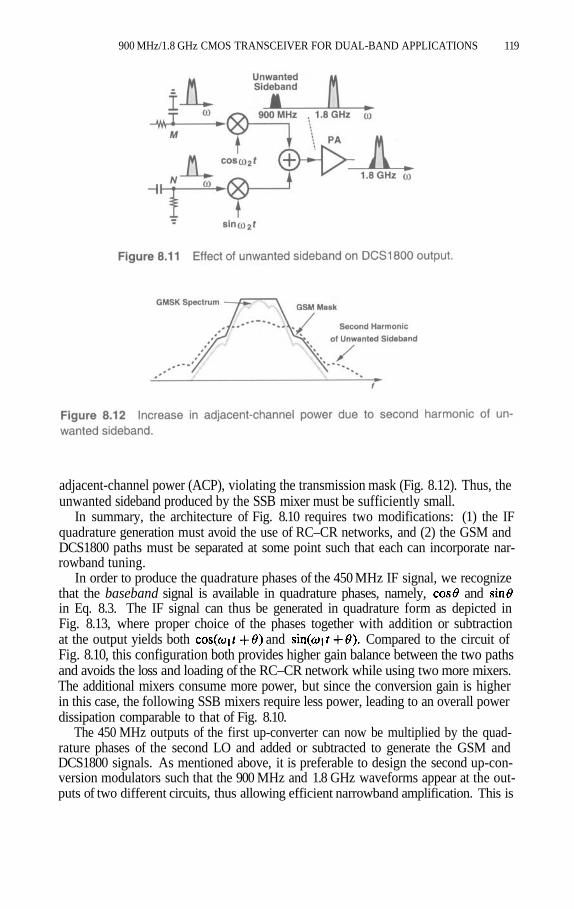
900 MHz/1.8 GHz CMOS TRANSCEIVER FOR DUAL-BAND APPLICATIONS 119
adjacent-channel power (ACP), violating the transmission mask (Fig. 8.12). Thus, theunwanted sideband produced by the SSB mixer must be sufficiently small.
In summary, the architecture of Fig. 8.10 requires two modifications: (1) the IFquadrature generation must avoid the use of RC–CR networks, and (2) the GSM andDCS1800 paths must be separated at some point such that each can incorporate nar-rowband tuning.
In order to produce the quadrature phases of the 450 MHz IF signal, we recognizethat the baseband signal is available in quadrature phases, namely, andin Eq. 8.3. The IF signal can thus be generated in quadrature form as depicted inFig. 8.13, where proper choice of the phases together with addition or subtractionat the output yields both and Compared to the circuit ofFig. 8.10, this configuration both provides higher gain balance between the two pathsand avoids the loss and loading of the RC–CR network while using two more mixers.The additional mixers consume more power, but since the conversion gain is higherin this case, the following SSB mixers require less power, leading to an overall powerdissipation comparable to that of Fig. 8.10.
The 450 MHz outputs of the first up-converter can now be multiplied by the quad-rature phases of the second LO and added or subtracted to generate the GSM andDCS1800 signals. As mentioned above, it is preferable to design the second up-con-version modulators such that the 900 MHz and 1.8 GHz waveforms appear at the out-puts of two different circuits, thus allowing efficient narrowband amplification. This is

120 CIRCUITS AND SYSTEMS FOR WIRELESS COMMUNICATIONS
accomplished as shown in Fig. 8.14, where two independent SSB modulators producethe two bands according to the band select command. Note that narrowband tuningalso suppresses the unwanted sideband resulting from mismatches in the SSB mixers.To save power consumption, only one of the modulators is active in either mode.
The overall architecture of the dual-band transmitter is shown in Fig. 8.15. Since allof the signals up to ports A and B are differential, each band incorporates a differentialto single-ended (D/SE) converter, applying the result to an output buffer. The trans-mitter requires external power amplifiers to deliver the high power levels specified byGSM and DCS1800.

900 MHz/1.8 GHz CMOS TRANSCEIVER FOR DUAL-BAND APPLICATIONS 121
8.5 TRANSMITTER BUILDING BLOCKS
In this section, we describe the transistor-level implementation of each building block,emphasizing the design constraints imposed by the architecture. The circuit topologiesare identical for both bands, but device dimensions and bias currents are chosen tooptimize the performance of each.
8.5.1 First up-conversion
The 450 MHz up-conversion modulator consists of two Gilbert cell mixers whose out-puts are added in the current domain. Shown in Fig. 8.16, the circuit utilizes resis-tive source degeneration, thereby improving the linearity in the baseband port of each

122 CIRCUITS AND SYSTEMS FOR WIRELESS COMMUNICATIONS
mixer. Two 100 nH inductors convert the output current to voltage. To minimize thearea occupied by each inductor, a stack of three spiral structures made of three metallayers (Fig. 8.16(b)) is used [1], reducing the area by approximately a factor of 8 [11].Since the polysilicon connection and the bottom spiral suffer from substantial parasiticcapacitance to the substrate, this node is connected to the supply voltage, increasingthe self-resonance frequency of the inductor. The quality factor of the inductor isestimated to be about 4 and the self-resonance frequency is about 600 MHz.
Why must the baseband ports be linearized? Let us return to Eq. 8.3 with theassumption that and experience third-order distortion. The resulting IFsignal can then be expressed as
where represents the amount of third-order nonlinearity. Grouping the terms inEq. 8.4, we obtain
Equation 8.5 reveals that third-order distortion gives rise to a component centeredaround but with a modulation index three times that of the ideal GMSK signal.Invoking Carson’s rule, we postulate that the second term occupies roughly three timesthe bandwidth, raising the power transmitted in adjacent channels. Fig. 8.17 showsthe simulated spectra of the two components in Eq. 8.5 with indicating thatthe unwanted signal indeed consumes a wider band. For this reason, as depicted inFig. 8.18, must be small enough such that the transmission mask is not violated.

900 MHz/1.8 GHz CMOS TRANSCEIVER FOR DUAL-BAND APPLICATIONS 123
In this design, the resistive degeneration and tail currents are chosen so as to ensurewith a baseband input, yielding a third-order component 40 dB below
the desired signal.
8.5.2 SSB modulator
The signals generated at nodes X and Y in Fig. 8.16 must be “routed” to one of theSSB modulators according to the band select command. As illustrated in Fig. 8.19, therouting is performed in the current domain to minimize signal loss due to the additionof the switches. Capacitively coupled to the output of the 450 MHz up-converter,the voltage–to–current converter employs grounded-source input devices to save thevoltage headroom otherwise consumed by a tail current source. The bias current ofthe circuit is defined by and Note that operate in deep triode region,sustaining a small voltage drop. Also, the linearity of this and subsequent stages is notcritical, because GMSK signals display a constant envelope and are quite insensitiveto spectral regrowth [4].
With the quadrature phases of the IF signal available in the current domain, SSBmixing assumes a simple topology. Shown in Fig. 8.20, the circuit senses the differen-tial current signals routed from each 450 MHz up-converter, performs mixing with the

124 CIRCUITS AND SYSTEMS FOR WIRELESS COMMUNICATIONS
second LO, adds the resulting currents with proper polarity, and converts the output tosingle-ended form.
8.5.3 Differential to Single-Ended Converter
In order to achieve a reasonable gain, it is desirable to employ tuning in the D/SEconverter. Fig. 8.21 depicts two realizations of such a circuit. In Fig. 8.21(a), a currentmirror together with two inductors creates resonance at nodes E and F, reducing theeffect of device capacitances. The difficulty here is the large gate-source capacitanceof the two PMOS devices, mandating a small value for and hence a low conversiongain. Fig. 8.2 l(b) presents an alternative topology where a PMOS device introduces anegative resistance in parallel with a floating inductor. It can be shown that
where and denote the total capacitance at nodes E and F, respectively [4]. Asa compromise between margin to oscillation and boost in gain, the negative resistance,
is chosen so as to increase the Q of the inductor by approximately afactor of two. Note that can assume a relatively large value because it sees and
in series. In this design, the signal is sensed at F because this port exhibits a loweroutput impedance. Simulations indicate that the topology of Fig. 8.21(b) providesabout three times the voltage gain of the circuit in Fig. 8.21(a).

900 MHz/1.8 GHz CMOS TRANSCEIVER FOR DUAL-BAND APPLICATIONS 125
8.5.4 Output buffer
The output buffer is shown in Fig. 8.22. Two common-source stages, andboost the signal level, driving the impedance of the external instrumentation. Thebias current of is defined by and and that of by and Neglectingthe AC drop across the inductor, we have that is,can be ratioed with respect to
8.6 CONCLUSION
The design of dual-band transceivers poses many challenges in terms of frequencyplanning and circuit building blocks. An image-reject receiver and a two-step transmit-ter architecture have been introduced that provide dual-band operation with 450 MHzand 1350 MHz LO frequencies. Also, circuit techniques for low-noise amplification,down-conversion mixing, generation of the quadrature phases of the transmit IF signal,and differential to single-ended conversion have been presented.

126 CIRCUITS AND SYSTEMS FOR WIRELESS COMMUNICATIONS
References
[1] S. Wu and B. Razavi, “A 900-MHz/1.8-GHz CMOS Receiver for Dual-BandApplications”, IEEE J. Solid-State Circuits, vol. 33, pp. 2178–2185, Dec. 1998;
[2] B. Razavi, “A 900-MHz/1.8-GHz CMOS Transmitter for Dual-Band Appli-cations”, Symposium on VLSI Circuits Dig. of Tech. Papers, pp. 128–131,June 1998;
[3] B. Razavi, “A 900-MHz/1.8-GHz CMOS Transmitter for Dual-Band Applica-tions”, IEEE Journal of Solid-State Circuits, vol. 34, pp. 573–579, May 1999;
[4] B. Razavi, RF Microelectronics, Upper Saddle River, NJ: Prentice-Hall, 1998;[5] D. K. Weaver, “A Third Method of Generation and Detection of Single-Sideband
Signals”, Proc. IRE, vol. 44, pp. 1703–1705, Dec. 1956;[6] B. Razavi, “Design Considerations for Direct-Conversion Receivers”, IEEE
Trans. Circuits and Systems, Part II, vol. 44, pp. 428–435, June 1997;[7] A. A. Abidi, “Direct-Conversion Radio Transceivers for Digital Communica-
tions”, IEEE Journal of Solid-State Circuits, vol. 30, pp. 1399–1410, Dec. 1995;[8] L. W. Couch, Digital and Analog Communication Systems, Fourth Edition, New
York: Macmillan Co., 1993;
[9] J. B. Anderson, T. Aulin, and C.-E. Sundberg, Digital Phase Modulation, NewYork: Plenum Press, 1986;
[10] K. Feher, Wireless Digital Communications, New Jersey: Prentice-Hall, 1995;[11] R. B. Merril, et al., “Optimization of High Q Inductors for Multi-Level Metal
CMOS”, Proc. IEDM, pp. 38.7.1–38.7.4, Dec. 1995;

9 INTEGRATED WIRELESSTRANSCEIVER DESIGN WITHEMPHASIS ON IF SAMPLING
Mihai Banu1, Carlo Samori3, Jack Glas1, and John Khoury2
Lucent Technologies600 Mountain Ave., Murray Hill, NJ 07974, USA
Lucent Technologies1247 S Cedar Crest Blvd., Allentown, PA 18103, USA
Dipartimento di Elettronica e InformazionePiazza L. da Vinci 32, 20133 Milano, Italy
9.1 INTRODUCTION
Digital wireless systems such as GSM are in wide use worldwide and will continue toexpand and replace the remaining analog systems at an increasing rate. The technicalfactors that have contributed to this success are fundamental capabilities such as easyuse of SSB (single-side-band) signals, efficient channel multiplexing (time or codedivision), increased capacity through compression, resilience against interference andnoise, and secure transmission. In addition, the development of relatively inexpensiveand low-power wireless transceivers has triggered a great proliferation of consumerportable units. Several key technologies are enabling the successful design and manu-facture of these devices. Examples include GHz-band Si RF ICs, mixed-signal CMOS
127

128 CIRCUITS AND SYSTEMS FOR WIRELESS COMMUNICATIONS
VLSI ICs, high-quality RF and IF passives, inexpensive plastic packaging, and DSP-based processing.
The block diagram of a typical modern transceiver is shown in Fig. 9.1. It consists
of analog RF, IF, and baseband sections and a digital section. The analog/digital inter-face (i.e. A/D and D/A converters) is placed at baseband, a choice dictated primarilyby cost and power dissipation considerations. Despite the usual preference for “digitalwhenever possible” designs, it is still to be shown that moving the analog/digital inter-face away from DC and closer to the antenna results in superior transceivers for handheld applications, for which cost and power dissipation are essential design specifica-tions. The hope is that, in the near future, advances in circuit fabrication technologyor new radio design techniques will lead to an increased digitization of the transceiverimplementation. In turn, this will bring more robust products with increased reliabilityand additional programmable features.
Assuming that IF sampling will eventually prevail in portable applications as a stepforward in the “more digital” design direction, this paper presents some basic issuesand tradeoffs of this approach. Similar aspects have been discussed in other placessuch as in [1–3]. The emphasis will be on the receive path. It is shown that a majorlimitation in moving the A/D conversion closer to the antenna comes from the filteringrequirements of the front end, a severe condition for inexpensive IC designs. However,contrary to a common belief, IF-sampled receivers do not require more stringent os-cillator jitter specifications than conventional receivers. Band-pass sigma-delta A/Dconverters with noise notch shaping at one quarter of the sampling frequency are wellsuited for IF sampling applications. In order to explain these facts, it is necessary toreview the key aspects of transceiver architectures and design methods.
9.2 INTEGRATED TRANSCEIVER CONVENTIONAL WISDOM
A successful GSM-quality transceiver front-end is shown in Fig. 9.2. The receiver pathconsists of a single IF superheterodyne tuner and an I/Q IF-to-baseband direct-conver-sion stage. The transmitter includes a direct modulator with offset. This architecture
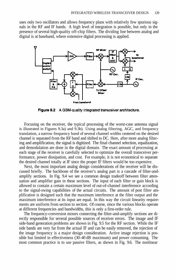
INTEGRATED WIRELESS TRANSCEIVER DESIGN 129
uses only two oscillators and allows frequency plans with relatively few spurious sig-nals in the RF and IF bands. A high level of integration is possible, but only in thepresence of several high-quality off-chip filters. The dividing line between analog anddigital is at baseband, where extensive digital processing is applied.
Focusing on the receiver, the typical processing of the worst-case antenna signalis illustrated in Figures 9.3a) and 9.3b). Using analog filtering, AGC, and frequencytranslation, a narrow frequency band of several channel widths centered on the desiredchannel is separated from the RF band and shifted to DC. Here, after more analog filter-ing and amplification, the signal is digitized. The final channel selection, equalization,and demodulation are done in the digital domain. The exact amount of processing ateach stage of the receiver is carefully selected to optimize the overall transceiver per-formance, power dissipation, and cost. For example, it is not economical to separatethe desired channel totally at IF since the proper IF filters would be too expensive.
Next, the most important analog design considerations of the receiver will be dis-cussed briefly. The backbone of the receiver’s analog part is a cascade of filter-and-amplify sections. In Fig. 9.4 we see a common design tradeoff between filter atten-uation and amplifier gain in these sections. The input of each filter or gain block isallowed to contain a certain maximum level of out-of-channel interference accordingto the signal-swing capabilities of the actual circuits. The amount of post filter am-plification is designed such that the maximum interference at the filter output and themaximum interference at its input are equal. In this way the circuit linearity require-ments are uniform from section to section. Of course, since the various blocks operateat different frequencies and bandwidths, this is only a first-order rule.
The frequency-conversion mixers connecting the filter-and-amplify sections are di-rectly responsible for several possible sources of receiver errors. The image and IFside-band generation problems are shown in Fig. 9.5 for the RF section. While the IFside bands are very far from the actual IF and can be easily removed, the rejection ofthe image frequency is a major design consideration. Active image rejection is pos-sible but limited in effectiveness (30–40 dB maximum) and power consuming. Themost common practice is to use passive filters, as shown in Fig. 9.6. The nonlinear

130 CIRCUITS AND SYSTEMS FOR WIRELESS COMMUNICATIONS
character of the actual mixer creates a further “image” problem due to mixing of LOharmonics with input signal harmonics. Fig. 9.7 demonstrates the generation of suchspurious responses at the first IF. Therefore, the choice of IF frequencies is of utmostimportance and involves compromises between filtering complexity and mixer spuri-
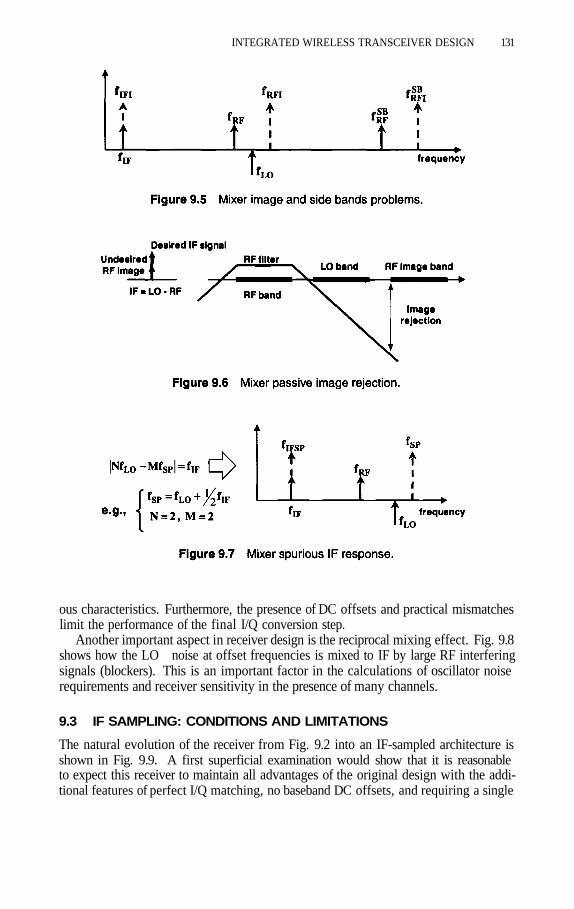
INTEGRATED WIRELESS TRANSCEIVER DESIGN 131
ous characteristics. Furthermore, the presence of DC offsets and practical mismatcheslimit the performance of the final I/Q conversion step.
Another important aspect in receiver design is the reciprocal mixing effect. Fig. 9.8shows how the LO noise at offset frequencies is mixed to IF by large RF interferingsignals (blockers). This is an important factor in the calculations of oscillator noiserequirements and receiver sensitivity in the presence of many channels.
9.3 IF SAMPLING: CONDITIONS AND LIMITATIONS
The natural evolution of the receiver from Fig. 9.2 into an IF-sampled architecture isshown in Fig. 9.9. A first superficial examination would show that it is reasonableto expect this receiver to maintain all advantages of the original design with the addi-tional features of perfect I/Q matching, no baseband DC offsets, and requiring a single
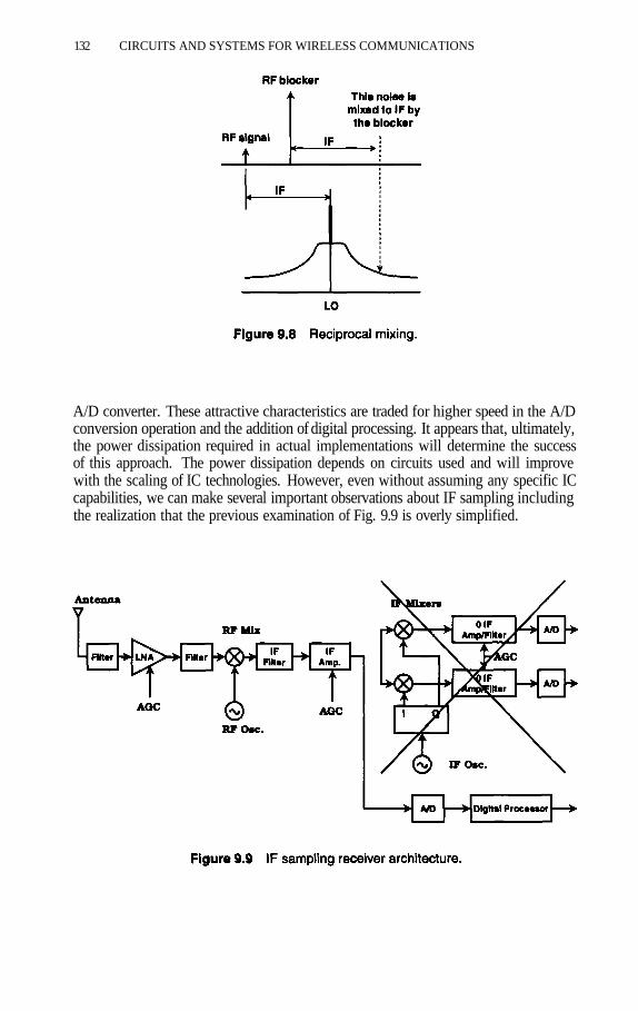
132 CIRCUITS AND SYSTEMS FOR WIRELESS COMMUNICATIONS
A/D converter. These attractive characteristics are traded for higher speed in the A/Dconversion operation and the addition of digital processing. It appears that, ultimately,the power dissipation required in actual implementations will determine the successof this approach. The power dissipation depends on circuits used and will improvewith the scaling of IC technologies. However, even without assuming any specific ICcapabilities, we can make several important observations about IF sampling includingthe realization that the previous examination of Fig. 9.9 is overly simplified.
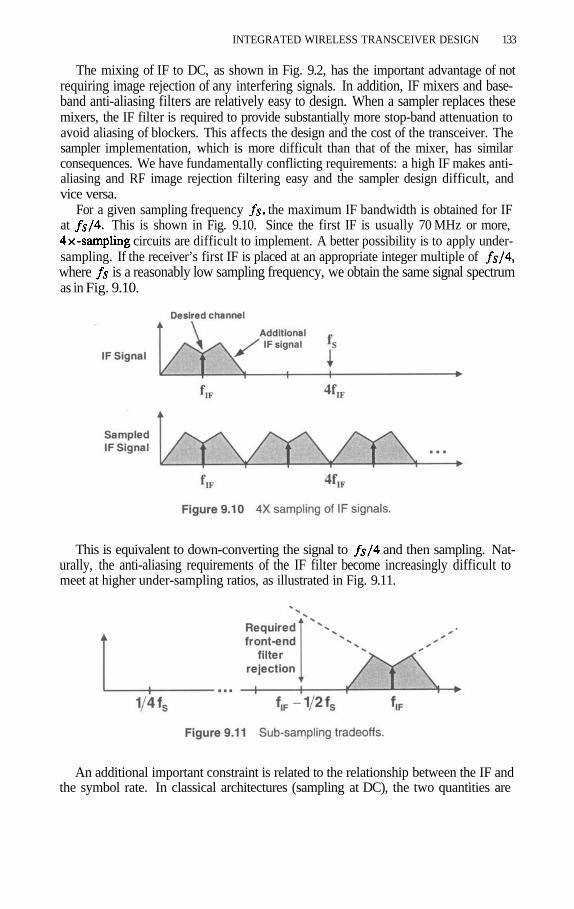
INTEGRATED WIRELESS TRANSCEIVER DESIGN 133
The mixing of IF to DC, as shown in Fig. 9.2, has the important advantage of notrequiring image rejection of any interfering signals. In addition, IF mixers and base-band anti-aliasing filters are relatively easy to design. When a sampler replaces thesemixers, the IF filter is required to provide substantially more stop-band attenuation toavoid aliasing of blockers. This affects the design and the cost of the transceiver. Thesampler implementation, which is more difficult than that of the mixer, has similarconsequences. We have fundamentally conflicting requirements: a high IF makes anti-aliasing and RF image rejection filtering easy and the sampler design difficult, andvice versa.
For a given sampling frequency the maximum IF bandwidth is obtained for IFat This is shown in Fig. 9.10. Since the first IF is usually 70 MHz or more,
circuits are difficult to implement. A better possibility is to apply under-sampling. If the receiver’s first IF is placed at an appropriate integer multiple ofwhere is a reasonably low sampling frequency, we obtain the same signal spectrumas in Fig. 9.10.
This is equivalent to down-converting the signal to and then sampling. Nat-urally, the anti-aliasing requirements of the IF filter become increasingly difficult tomeet at higher under-sampling ratios, as illustrated in Fig. 9.11.
An additional important constraint is related to the relationship between the IF andthe symbol rate. In classical architectures (sampling at DC), the two quantities are

134 CIRCUITS AND SYSTEMS FOR WIRELESS COMMUNICATIONS
independent, but in the IF sampling case, they are related by the condition. Thisassumes an integer number of samples per symbol for easy digital demodulation. Forexample, a GSM IF-sampled receiver should use an appropriate multiple of 13/4 MHzfor the IF and a multiple of 13 MHz for A 52 MHz sampling rate and a 65, 91, or117 MHz IF would fit this rule.
It is instructive to analyze further the potential limitations of under-sampling. Inparticular, the oscillator jitter is commonly alleged to be a trouble spot for this tech-nique. As illustrated in Fig. 9.12, we will do a comparison with the conventionalmixer. One can calculate the effect of oscillator jitter with the help of Figures 9.13and 9.14.
The output of the sampler S*(kT), produced in reality by the noisy sampling of apure input signal S(t), can be regarded as the noiseless sampling of an effectively jit-tery input Fig. 9.13 shows this equivalence, with being a low-pass randomprocess describing the oscillator jitter. If this process has the spectral density function
the oscillator and effective input SSCRs (signal-sideband-to-carrier ratios)are related as in Fig. 9.14. This is easily derived by observing that the variationof the oscillator output is proportional to its time derivative
and while the variation of the effective input signalis proportional to and the same Elimi-
nating this variable between the and expressions, the relationship between

INTEGRATED WIRELESS TRANSCEIVER DESIGN 135
the actual oscillator noise spectrum and the effective input signal spectrum is obtained.Graphically this dependence is represented in Fig. 9.15.
Applying the previous development to the RF input case in Fig. 9.16 shows clearlythat sampling large blockers superimposes substantial oscillator noise over the desiredRF signal.
This is similar to reciprocal mixing in conventional mixers. Furthermore, when wecompare the two effects in the equivalent frequency plans of Fig. 9.17 for the conven-tional and the IF-sampled cases, the oscillator jitter requirements become identical, asseen in Fig. 9.18.
An interesting observation is that under-sampling effectively acts as down-conver-sion to a second IF at In this view, the anti-aliasing conditions of the first IFfilter become “image rejection” conditions for the down-conversion to the second IF.This interpretation shows intuitively why under-sampling and mixing require identicaloscillator specifications.
Comparing the intrinsic noise performance of the two circuits in Fig. 9.12, we ob-serve that input noise folding is present in both cases, albeit through different (butrelated) mechanisms. The IF filters reduce these effects. A more severe sampler prob-lem absent from the mixer is the aliasing of self thermal noise. The in-channel portion

136 CIRCUITS AND SYSTEMS FOR WIRELESS COMMUNICATIONS
of this noise for a given sampling frequency is KT/C divided by the over-samplingratio with respect to the channel width. A potentially serious practical limitation forlarge under-sampling ratios is the use of small sampling capacitors dictated by circuitbandwidth requirements. Fortunately, in a well designed receiver, 70–80 dB of gainis present between the antenna and the sampler, reducing the KT/C noise effect toinsignificant levels. This is similar to conventional sampling at the baseband.
9.4 BAND-PASS A/D CONVERSION
The discussions regarding Fig. 9.10 and 9.17 point out that band-pass sigma-deltaA/D conversion is naturally suited for IF sampling. The circuit resources for obtaininghigh dynamic range are used only within the desired channel. The interfering inputsignals and the A/D quantization noise are filtered out in the decimator, whose digitalsignal processing capabilities mimic the conventional analog approach. The structureof Fig. 9.19 is identical to that of the discarded block in Fig. 9.9.
The block diagram of a conventional band-pass sigma-delta modulator is shown inFig. 9.20. It is important to verify the performance of this circuit in the presence ofblockers. Computer simulations, which have been checked with extensive measure-
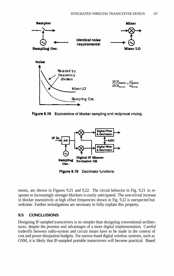
INTEGRATED WIRELESS TRANSCEIVER DESIGN 137
ments, are shown in Figures 9.21 and 9.22. The circuit behavior in Fig. 9.21 in re-sponse to increasingly stronger blockers is easily anticipated. The non-trivial increasein blocker insensitivity at high offset frequencies shown in Fig. 9.22 is unexpected butwelcome. Further investigations are necessary to fully explain this property.
9.5 CONCLUSIONS
Designing IF-sampled transceivers is no simpler than designing conventional architec-tures, despite the promise and advantages of a more digital implementation. Carefultradeoffs between radio-system and circuit issues have to be made in the context ofcost and power dissipation budgets. For narrow-band digital wireless systems, such asGSM, it is likely that IF-sampled portable transceivers will become practical. Based

138 CIRCUITS AND SYSTEMS FOR WIRELESS COMMUNICATIONS
on the considerations in this paper, it is reasonable to expect that such a solution willuse a moderate level of under-sampling and passive IF filters.
References
[1] R. Gregorian and G. Temes, Analog Integrated Circuits for Signal Processing,John Wiley & Sons, 1986;
[2] F. W. Singor and W. M. Snelgrove, “Switched-Capacitor Bandpass Delta-SigmaA/D Modulation at 10.7 MHz”, IEEE J. Solid-State Circuits, vol. 30, No. 3, March1995, pp. 184–192;
[3] A. Hairapetian, “An 81-MHz IF Receiver in CMOS”, IEEE J. Solid-State Circuits,vol. 31, No. 12, December 1996, pp. 1981–1986.

INTEGRATED WIRELESS TRANSCEIVER DESIGN 139

This page intentionally left blank

10 TRANSMITTER CONCEPTS,INTEGRATION AND DESIGN
TRADE-OFFSStefan Heinen and Stefan Herzinger
Infineon Technologies AG i. Gr.RF IC Design Center
Düsseldorf/Munich, Germany
Abstract: An overview of different transmit architectures is given. The major scopeare the concepts used in the GSM system. A comparison with respect to integrationlevel and system cost is given. The modulation loop concept commonly used today isdiscussed in detail, with respect to implementation details and trade-offs.
10.1 INTRODUCTION
The rapidly growing mobile communication market requires increasing the efforts toachieve higher integration levels. The ultimate goal is the integration of a completemobile on a single die — preferably on a CMOS die. The example given in Fig. 10.1is still a dream. Today, we are far away from this goal. RF CMOS is more or lessa research topic, although there are already a lot of publications dealing with thissubject [1–6]. A demonstration of a fully functional GSM-like high-end system is notyet in sight. This would require a circuit which achieves the system specificationswith respect to process, temperature and supply variations. Moreover, this target hasto be met in a real environment, including on-chip bias circuitry. For these reasons, we
141
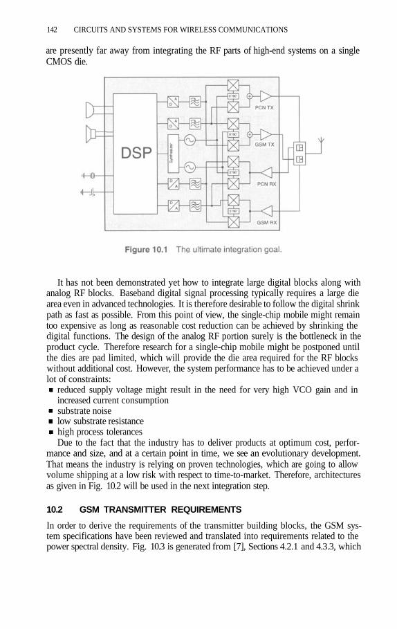
142 CIRCUITS AND SYSTEMS FOR WIRELESS COMMUNICATIONS
are presently far away from integrating the RF parts of high-end systems on a singleCMOS die.
It has not been demonstrated yet how to integrate large digital blocks along withanalog RF blocks. Baseband digital signal processing typically requires a large diearea even in advanced technologies. It is therefore desirable to follow the digital shrinkpath as fast as possible. From this point of view, the single-chip mobile might remaintoo expensive as long as reasonable cost reduction can be achieved by shrinking thedigital functions. The design of the analog RF portion surely is the bottleneck in theproduct cycle. Therefore research for a single-chip mobile might be postponed untilthe dies are pad limited, which will provide the die area required for the RF blockswithout additional cost. However, the system performance has to be achieved under alot of constraints:
reduced supply voltage might result in the need for very high VCO gain and inincreased current consumptionsubstrate noiselow substrate resistancehigh process tolerancesDue to the fact that the industry has to deliver products at optimum cost, perfor-
mance and size, and at a certain point in time, we see an evolutionary development.That means the industry is relying on proven technologies, which are going to allowvolume shipping at a low risk with respect to time-to-market. Therefore, architecturesas given in Fig. 10.2 will be used in the next integration step.
10.2 GSM TRANSMITTER REQUIREMENTS
In order to derive the requirements of the transmitter building blocks, the GSM sys-tem specifications have been reviewed and translated into requirements related to thepower spectral density. Fig. 10.3 is generated from [7], Sections 4.2.1 and 4.3.3, which
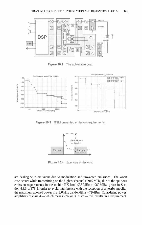
TRANSMITTER CONCEPTS, INTEGRATION AND DESIGN TRADE-OFFS 143
are dealing with emissions due to modulation and unwanted emissions. The worstcase occurs while transmitting on the highest channel at 915 MHz, due to the spuriousemission requirements in the mobile RX band 935 MHz to 960 MHz, given in Sec-tion 4.3.3 of [7]. In order to avoid interference with the reception of a nearby mobile,the maximum allowed power in a 100 kHz bandwidth is –79 dBm. Considering poweramplifiers of class 4 — which means 2 W or 33 dBm — this results in a requirement

144 CIRCUITS AND SYSTEMS FOR WIRELESS COMMUNICATIONS
of –162 dBc/Hz at 20 MHz offset as shown in Fig. 10.4. For DCS1800 mobiles, thisspecification is relaxed to –71 dBm.
10.3 BASIC GMSK TX ARCHITECTURES
The basic architectures shown in Fig. 10.5 are commonly used today. The aim of thissection is to give a comprehensive review of these architectures including a discus-sion of the advantages and disadvantages in terms of cost and implementation issues.Emphasis will be laid on spurious emissions with respect to nonlinearities. A qualita-tive study of the effects will be presented, helping to understand the design trade-offswhich occur in the implementation of the different architectures. The power amplifierwill not be included in this discussion.
10.3.1 Direct modulation
In this section, the basic behaviour of a direct-modulation system as shown in Fig. 10.6will be studied. Most of the basic characteristics discussed here will also apply to theother architectures using the basic vector modulator at a different frequency. The firsttarget of the modulator is to generate a GMSK modulation which is compliant with thesystem specification [7]. Moreover, the given modulation mask sub-clause 4.2.1o f [7]
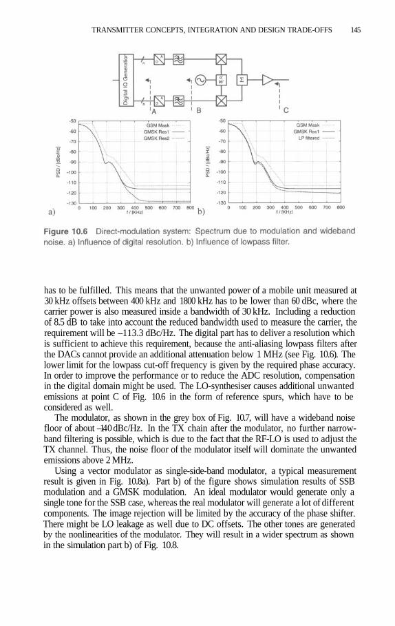
TRANSMITTER CONCEPTS, INTEGRATION AND DESIGN TRADE-OFFS 145
has to be fulfilled. This means that the unwanted power of a mobile unit measured at30 kHz offsets between 400 kHz and 1800 kHz has to be lower than 60 dBc, where thecarrier power is also measured inside a bandwidth of 30 kHz. Including a reductionof 8.5 dB to take into account the reduced bandwidth used to measure the carrier, therequirement will be –113.3 dBc/Hz. The digital part has to deliver a resolution whichis sufficient to achieve this requirement, because the anti-aliasing lowpass filters afterthe DACs cannot provide an additional attenuation below 1 MHz (see Fig. 10.6). Thelower limit for the lowpass cut-off frequency is given by the required phase accuracy.In order to improve the performance or to reduce the ADC resolution, compensationin the digital domain might be used. The LO-synthesiser causes additional unwantedemissions at point C of Fig. 10.6 in the form of reference spurs, which have to beconsidered as well.
The modulator, as shown in the grey box of Fig. 10.7, will have a wideband noisefloor of about –14 0 dBc/Hz. In the TX chain after the modulator, no further narrow-band filtering is possible, which is due to the fact that the RF-LO is used to adjust theTX channel. Thus, the noise floor of the modulator itself will dominate the unwantedemissions above 2 MHz.
Using a vector modulator as single-side-band modulator, a typical measurementresult is given in Fig. 10.8a). Part b) of the figure shows simulation results of SSBmodulation and a GMSK modulation. An ideal modulator would generate only asingle tone for the SSB case, whereas the real modulator will generate a lot of differentcomponents. The image rejection will be limited by the accuracy of the phase shifter.There might be LO leakage as well due to DC offsets. The other tones are generatedby the nonlinearities of the modulator. They will result in a wider spectrum as shownin the simulation part b) of Fig. 10.8.

146 CIRCUITS AND SYSTEMS FOR WIRELESS COMMUNICATIONS
Therefore, nonlinearity is of major concern in the implementation of a vector mod-ulator. In order to understand the basic influence of the different nonlinearities, thefirst step is to separate them.
Considering only limiting amplifiers in the input stage of the modulator as shownin Fig. 10.9 at first results in the tones given in the same figure. Assuming that the

TRANSMITTER CONCEPTS, INTEGRATION AND DESIGN TRADE-OFFS 147
input nonlinearity is hard limiting, the input signals are square waves with a phaseshift of 90 degree. It can be seen from the Fourier coefficients that the phase of theharmonics in one of the input paths will change by 180 degree, e.g., the 3rd harmonicscompared to the fundamental. This means for the 3rd harmonics the upper sidebandwill be rejected and the lower sideband located at will occur. In Fig. 10.10,only nonlinearities after the LO phase shifter and in the output stage are considered.
For reasons similar to the ones discussed previously, the input signal will be mod-ulated onto the lower sideband of the 3rd harmonics of the LO. That means a tonewill occur at Because of the output nonlinearity, an intermodulation prod-uct will be generated at which is mirrored to the positive frequency
Finally, taking the nonlinearity of the power amplifier into account, additional in-termodulation products will be generated as shown in Fig. 10.11.
What does this really mean for the system? The nonlinearities will generate a widerGMSK spectrum. There are two ways to meet the system specifications: The first is tomake the modulator as linear as possible, thereby avoiding the wider spectrum. This

148 CIRCUITS AND SYSTEMS FOR WIRELESS COMMUNICATIONS
results in an increase in power consumption. The second way is to make the poweramplifier more linear in order to reduce the intermodulation. However, the result withrespect to power is even worse. Accordingly, this is surely not the way to go for abattery-powered mobile.
Another quite important requirement is the wideband noise floor at the modulatoroutput. As shown in Fig. 10.3, the TX in band requirements are –133 dBc/Hz below20 MHz offset and –138 dBc/Hz above. In order to achieve these specifications, an

TRANSMITTER CONCEPTS, INTEGRATION AND DESIGN TRADE-OFFS 149
output power of about 0 dBm is required, which is hard to achieve when using a CMOSimplementation.
The direct-up-conversion architecture shown in Fig. 10.6 has the drawback that theRF-VCO operates at the output frequency. Therefore, depending on the quality ofshielding, a re-modulation may occur. This will result in a phase error which might betoo high. In order to avoid this problem, almost all commercially available implemen-tations use an offset mixing scheme in order to generate the desired output frequency.
10.3.2 IF modulation
In the last section, the basic characteristics of the vector modulator have been dis-cussed intensively in combination with direct up-conversion architecture. Most of theissues apply as well to the IF modulation architecture given in Fig. 10.12. The IF mod-ulation has a major advantage compared to the direct up-conversion. First, the re-mod-ulation problem does not occur and the isolation requirements are relaxed. Second,a narrow IF-SAW filter might be used to reduce the unwanted emissions. Moreover,the architecture is well suited for dual-band applications (GSM in combination withDCS1800). The IF-modulator will be used for both systems at a common IF, whereastwo up-conversion mixers are used to generated the different TX frequency bands.
As described in Section 10.2, a noise floor of –162 dBc/Hz has to be realizedin a GSM system. The direct-up-conversion architecture requires a duplexer in thefront-end because the noise floor generated by the modulator is quite high. The IF-modulation system comes up with a lower noise floor, which might be in the rangeof –160 dBc/Hz. In order to guarantee the performance in high-volume production,something like –165 dBc/Hz would be needed. Therefore, the IF-modulation archi-tecture cannot avoid the expensive duplexer. During the last few years, the modulationloop architecture has reached maturity and is the only system approach which avoidsthe duplexer.
10.3.3 Modulation loop
As already mentioned, the modulation-loop-based transmitter of Fig. 10.13 has be-come quite popular. The first reason is the fact that no duplexer is needed. A second

150 CIRCUITS AND SYSTEMS FOR WIRELESS COMMUNICATIONS
major advantage is the dual-band capability of the architecture. The modulation loopis more or less a PLL in which the reference of the phase detector is modulated. Inthe feedback path of the loop, a down-conversion mixer is used to provide the down-converted VCO signal to the phase detector. The RF-VCO provides the LO for thedown-conversion mixer, synthesised by a conventional PLL in order to adjust the de-sired channel.
Due to the high reference frequency of 100 MHz or higher (refer to Fig. 10.14)there are several hundred phase comparisons for one transmitted bit. Therefore theloop is able to copy the phase modulation of the reference path onto the output ofthe power VCO, which is within the loop. The GMSK modulation used in GSM-likesystems is a pure phase modulation and does not exhibit any amplitude modulation.The power-VCO provides a very low noise floor at 20 MHz offset — typically less than–165 dBc/Hz. This VCO is realized as a module and is capable of driving the poweramplifier directly without additional noisy buffer stages.
The configuration can be seen as a transformation of an RF bandpass into a lowpassfilter.
In Fig. 10.15, the principal block diagram of an up-conversion loop with modula-tion in the feedback loop is given along with its frequency plan. This configurationrequires that the output of the vector modulator within the feedback path does notexhibit any phase modulation. Accordingly, the VCO must have phase modulationwhich is cancelled by the vector modulator in order to fulfill the requirements of thephase-locked loop.

TRANSMITTER CONCEPTS, INTEGRATION AND DESIGN TRADE-OFFS 151
The GSM system requires an RMS phase accuracy of under 5 degrees, which callsfor a high cut-off frequency of the loop filter. On the other hand, only the VCO wide-band noise should be present at 20 MHz frequency offset. In Fig. 10.16, an APLACsimulation setup [8] is given which is used to study the different noise contributionswithin the modulation loop. The different noise sources, the corresponding transferfunctions and the resulting output noise contributions with respect to the major build-ing blocks of Fig. 10.15 are given in Fig. 10.17 and Fig. 10.18.
Outside the modulation bandwidth and below 5 MHz, the vector modulator is thedominant noise source, where the noise of the modulation itself is dominated by thedigital noise of the I-Q signal generation. Above 10 MHz, the noise is dominatedby the noise of the power VCO. The phase-noise requirements of the IF-LO and theRF-LO are relaxed due to the attenuation of the transfer function within the loop.
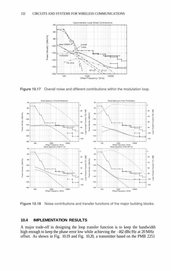
152 CIRCUITS AND SYSTEMS FOR WIRELESS COMMUNICATIONS
10.4 IMPLEMENTATION RESULTS
A major trade-off in designing the loop transfer function is to keep the bandwidthhigh enough to keep the phase error low while achieving the –1 6 2 dBc/Hz at 20 MHzoffset. As shown in Fig. 10.19 and Fig. 10.20, a transmitter based on the PMB 2251

TRANSMITTER CONCEPTS, INTEGRATION AND DESIGN TRADE-OFFS 153
modulation is able to achieve this goal. Detailed information on the application circuitand the measurement setup can be found in [9].
Fig. 10.21 shows the results of an SSB-modulation generated by the PMB 2251modulation loop. Due to the limiting behaviour of the type-4 PFD used in this appli-cation, the unwanted tones are symmetrical with respect to the wanted signal. ThePFD removes any AM components, meaning that only a PM component remains. TheIM3 components are quite low at –60 dBc. Therefore, the modulation mask can beachieved easily by using a power amplifier with relaxed specifications. The CMOS
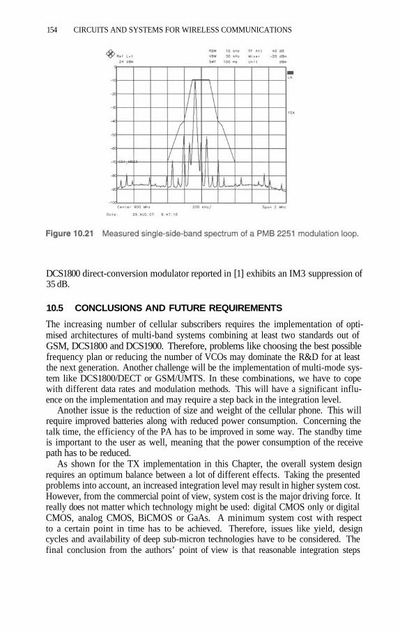
154 CIRCUITS AND SYSTEMS FOR WIRELESS COMMUNICATIONS
DCS1800 direct-conversion modulator reported in [1] exhibits an IM3 suppression of35 dB.
10.5 CONCLUSIONS AND FUTURE REQUIREMENTS
The increasing number of cellular subscribers requires the implementation of opti-mised architectures of multi-band systems combining at least two standards out ofGSM, DCS1800 and DCS1900. Therefore, problems like choosing the best possiblefrequency plan or reducing the number of VCOs may dominate the R&D for at leastthe next generation. Another challenge will be the implementation of multi-mode sys-tem like DCS1800/DECT or GSM/UMTS. In these combinations, we have to copewith different data rates and modulation methods. This will have a significant influ-ence on the implementation and may require a step back in the integration level.
Another issue is the reduction of size and weight of the cellular phone. This willrequire improved batteries along with reduced power consumption. Concerning thetalk time, the efficiency of the PA has to be improved in some way. The standby timeis important to the user as well, meaning that the power consumption of the receivepath has to be reduced.
As shown for the TX implementation in this Chapter, the overall system designrequires an optimum balance between a lot of different effects. Taking the presentedproblems into account, an increased integration level may result in higher system cost.However, from the commercial point of view, system cost is the major driving force. Itreally does not matter which technology might be used: digital CMOS only or digitalCMOS, analog CMOS, BiCMOS or GaAs. A minimum system cost with respectto a certain point in time has to be achieved. Therefore, issues like yield, designcycles and availability of deep sub-micron technologies have to be considered. Thefinal conclusion from the authors’ point of view is that reasonable integration steps

TRANSMITTER CONCEPTS, INTEGRATION AND DESIGN TRADE-OFFS 155
are required depending on the system requirements, time schedule and the availabletechnology.
Acknowledgments
We would like to thank Georg Lipperer, Stefan Beyer, and the other colleagues form theapplication group for helpful discussions and for their providing some of the material used inthis chapter.
References
[1] Steyaert et al., “A single-chip CMOS transceiver for DCS-1800 wireless commu-nications,” in Proceedings ISSCC98. ISSCC, Feb. 1998, IEEE, TP3.3.
[2] Rudell et al., “A 1.9 GHz wide-band IF double conversion CMOS integrated re-ceiver for cordless telephone applications,” in Proceedings ISSCC97. ISSCC, Feb.1997, IEEE, SA 18.3.
[3] Behzad Razavi, RF Microelectonics, Prentice Hall, 1998.[4] J. Craninckx and M. Steyaert, Wireless CMOS Frequency Synthesizer Design,
Kluwer Academic Publishers, 1998.[5] Thomas H. Lee, The Design of CMOS Radio-Frequency Integrated Circuits, Cam-
bridge University Press, 1998.[6] J. Crols, CMOS Wireless Transceiver Design, Kluwer Academic Publishers, 1997.
[7] GSM05.05, “GSM digital cellular telecommunication system (phase 2+): Radiotransmission and reception (GSM 05.05),” ETSI, July 1996, Version 5.2.0.
[8] Valtonen et al., “Aplac: An object-oriented analog circuit simulator and de-sign tools,” Helsinki University of Technology, Circuit Theory Laboratory, March1994, Version 6.2.
[9] Siemens Semiconductor Group, “Upconversion modulation loop PMB 2251vl.2,” Application Note, July 1997, Version 1.0.

This page intentionally left blank

11 RF CHALLENGES FORTOMORROW’S WIRELESS TERMINALS
Petteri Alinikula
Nokia Research CenterItämerenkatu 11-13, 00045 Helsinki, Finland
Abstract: Wireless telecommunications will enter a new era in the coming years.New systems and new customer needs are already introducing vast challenges, in par-ticular for the implementation of the terminals. The RF section is a major contributor tothe size and cost of the terminal. Consequently, the winning terminal implementationswill be those with the best RF section.
None of the implementation technologies alone seem to provide the full answer tothe RF challenges. Instead, the winning RF will be achieved by careful joint optimisa-tion of the overall technology portfolio with the proper radio architecture.
11.1 INTRODUCTION
From the early 1980s when the first generation of analog systems NMT, AMPS, andTACS were first introduced, the cellular phone market has exploded to be one of themajor consumer product markets. By the end of 1997 there were close to 207 millioncellular subscribers worldwide. There was an increase of 70 million during 1997alone. According to some predictions the number of cellular subscribers will exceedone billion by 2005 [Nokia Press Release, September 1998]. As a world record for thecellular phone penetration, Finland has just exceeded 50% of the population (August1998). Currently, digital narrow-band systems led by GSM continue to conquer theworld. In the near future, however, the voice-based second-generation cellular systemswill be complemented by new systems. The main interest in Europe is toward the
157
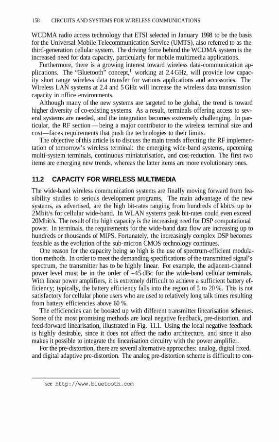
158 CIRCUITS AND SYSTEMS FOR WIRELESS COMMUNICATIONS
WCDMA radio access technology that ETSI selected in January 1998 to be the basisfor the Universal Mobile Telecommunication Service (UMTS), also referred to as thethird-generation cellular system. The driving force behind the WCDMA system is theincreased need for data capacity, particularly for mobile multimedia applications.
Furthermore, there is a growing interest toward wireless data-communication ap-plications. The “Bluetooth” concept,1 working at 2.4 GHz, will provide low capac-ity short range wireless data transfer for various applications and accessories. TheWireless LAN systems at 2.4 and 5 GHz will increase the wireless data transmissioncapacity in office environments.
Although many of the new systems are targeted to be global, the trend is towardhigher diversity of co-existing systems. As a result, terminals offering access to sev-eral systems are needed, and the integration becomes extremely challenging. In par-ticular, the RF section — being a major contributor to the wireless terminal size andcost—faces requirements that push the technologies to their limits.
The objective of this article is to discuss the main trends affecting the RF implemen-tation of tomorrow’s wireless terminal: the emerging wide-band systems, upcomingmulti-system terminals, continuous miniaturisation, and cost-reduction. The first twoitems are emerging new trends, whereas the latter items are more evolutionary ones.
11.2 CAPACITY FOR WIRELESS MULTIMEDIA
The wide-band wireless communication systems are finally moving forward from fea-sibility studies to serious development programs. The main advantage of the newsystems, as advertised, are the high bit-rates ranging from hundreds of kbit/s up to2Mbit/s for cellular wide-band. In WLAN systems peak bit-rates could even exceed20Mbit/s. The result of the high capacity is the increasing need for DSP computationalpower. In terminals, the requirements for the wide-band data flow are increasing up tohundreds or thousands of MIPS. Fortunately, the increasingly complex DSP becomesfeasible as the evolution of the sub-micron CMOS technology continues.
One reason for the capacity being so high is the use of spectrum-efficient modula-tion methods. In order to meet the demanding specifications of the transmitted signal’sspectrum, the transmitter has to be highly linear. For example, the adjacent-channelpower level must be in the order of –45 dBc for the wide-band cellular terminals.With linear power amplifiers, it is extremely difficult to achieve a sufficient battery ef-ficiency; typically, the battery efficiency falls into the region of 5 to 20 %. This is notsatisfactory for cellular phone users who are used to relatively long talk times resultingfrom battery efficiencies above 60 %.
The efficiencies can be boosted up with different transmitter linearisation schemes.Some of the most promising methods are local negative feedback, pre-distortion, andfeed-forward linearisation, illustrated in Fig. 11.1. Using the local negative feedbackis highly desirable, since it does not affect the radio architecture, and since it alsomakes it possible to integrate the linearisation circuitry with the power amplifier.
For the pre-distortion, there are several alternative approaches: analog, digital fixed,and digital adaptive pre-distortion. The analog pre-distortion scheme is difficult to con-
1see http://www.bluetooth.com
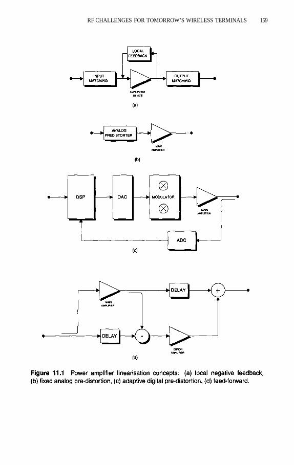
RF CHALLENGES FOR TOMORROW’S WIRELESS TERMINALS 159

160 CIRCUITS AND SYSTEMS FOR WIRELESS COMMUNICATIONS
trol over the variations of temperature, supply voltage, and circuit parameters. Withthe fixed digital scheme, the system can be taught for different conditions; still, ma-jor variations of the nonlinear characteristics of the transistors are extremely difficultto control. An adaptive concept would be flexible for varying conditions, but it suf-fers from the overall complexity. The digital pre-distortion schemes introduce mod-ifications to the whole transmitter chain: wider bandwidths of the filters and betterresolution of the D-to-A converters.
For achieving the ultimately linear operation, the feed-forward linearisation hasthe highest potential. The feed-forward linearisation is truly adaptive to the differentconditions. Still, the method suffers from the complicated control of the phase andamplitude characteristics of the two loops, and the power consumption can be unsatis-factorily high for hand-held terminals.
An additional difficulty, in particular for the CDMA systems, is the large powercontrol range, being in the order of 60 to 90 dB. Maintaining the high linearity overa wide range of power levels is a challenge for the power amplifier design. CDMAsystems do not often operate at the maximum power level. Maintaining an adequateefficiency at moderate output powers is therefore an extremely important objective.
The low efficiency combined with the increasing packaging density can lead to heattransfer problems. To overcome these problems, mechanical and thermal design haveto be integrated with the electrical design flow of future terminals.
Other new requirements of high bit-rate systems include fast-settling synthesisersfor variable-capacity TDMA systems and high-speed A-to-D and D-to-A convertersfor the baseband section.
11.3 MULTIPLE RADIOS IN ONE UNIT
As the wide-band systems are coming, it is important to notice that the R&D for thesecond generation terminals (GSM, GSM1800/1900, IS-136, IS-95, PDC ... ) contin-ues actively; the market is not showing any signs of saturation. Multiple systems willco-exist in the same geographical areas. Accordingly, there is a market need for termi-nals offering access to several systems. The non-compatibility of the different systemscauses difficulties for the implementation. In the baseband section, core platforms forseveral radio access protocols can be implemented, whereas in the RF section it ismore difficult to design core solutions cost-efficiently.
The key task in implementing the RF section for a multi-system multi-band termi-nal is to minimise the number of parallel functions. Many of the active functions,such as variable-gain amplifiers and mixers, can be designed to be adaptive to differ-ent specifications, whereas passive circuits, such as filters and matching circuits, needto be selectable for each designated frequency band. High-frequency filter technolo-gies are clearly the key for finding implementation solutions for future miniaturisedmulti-mode terminals. An example RF architecture of a dual-mode terminal is shownin Fig. 11.2.
None of the semiconductor technologies alone will provide an optimum platformfor the multi-mode transceivers. The best and only way to find the winning RF solu-tion is to optimise the whole RF technology portfolio including the ICs, packaging,substrates, passives, and filters with the RF architectures for the systems selected fora multi-system product. BJT, BiCMOS, CMOS, SiGe, GaAs, SOI, and others will all

RF CHALLENGES FOR TOMORROW’S WIRELESS TERMINALS 161
remain possible enabling technologies for the optimum RF solution, but not targets bythemselves. The micro-electro-mechanical systems (MEMS) will also eventually findtheir way into wireless terminals. Possibly, MEMS could offer the needed tunabilityfor the passive functions: filters and matching circuits.
In addition to the component technologies, radio architectures more suitable formulti-mode operation can be applied. As a part of the overall architecture, the selec-tion of reference clock frequencies is of utmost importance.
11.4 THE SMALLER THE BETTER
There seems to be more market demand on ultimately small phones than first pre-dicted. Moreover, miniature phone engines are vital for the multi-mode terminals inwhich the electronics of two or more terminals are integrated into one product, sincethe new multi-mode terminals cannot be larger than current high-end single-mode cel-lular phones.
Figure 11.3 shows the development of the volume of a typical GSM hand-portable.The corresponding component count in the RF section is shown in Fig. 11.4. The sig-nificant improvements in size and component count of the hand-held digital cellularphones have been achieved by increasing the level of integration in the phone. Cur-rently, all active functions are integrated, even in the RF section. On average, there arecurrently three RF ICs in a terminal. Simultaneously, there are approximately 100 pas-sive discrete components in the RF section, as can be seen in Fig. 11.4. These discretecomponents dominate the size; consequently, it is obvious that reducing the number ofdiscrete components is much more important than integrating the remaining ICs intoa single chip.
In the evolutionary prediction illustrated in Fig. 11.3 and 11.4, the main improve-ments are made by applying new packaging and interconnection technologies. Theold microwave hybrid technology is reborn with a slightly new appearance: customICs are assembled using chip-scale miniature packages, e.g. flip-chip, on a high-per-

162 CIRCUITS AND SYSTEMS FOR WIRELESS COMMUNICATIONS
formance substrate with passive filters, interconnections, and external discrete compo-nents.
More revolutionary improvements in the miniaturisation might be achieved with ad-vanced transceiver architectures shown in Fig. 11.5. The direct conversion architecturecan be applied to some systems to remove the bulky IF filters. An ultimate goal couldbe an all-digital transceiver adaptive to all major wireless systems. In the all-digitaltransceiver, the sampling is carried out at the signal frequency. For several reasons,the approach is not yet feasible. The power consumption of the required Gbit/s signalprocessing and the high-resolution high-speed A-to-D conversion exceeds many timesthe acceptable level for portable devices. Furthermore, the stopband rejection specifi-cation for the remaining RF filter becomes extremely demanding: approximately 100dB for narrow-band TDMA systems. With today’s technology, this would lead to afilter having a physical size too large for hand-portable terminals.
11.5 ... FOR THE LOWEST COST
The prices of the cellular phones have dropped by tens of per cent annually over the lastyears. In order to maintain the competitive edge, the total cost of the product needs tobe reduced. This trend will continue in the near future, and there is even more demandfor cost reduction since the more complex — and hence more expensive — wide-bandand multi-mode terminals are coming. It seems evident that customers are not willingto pay more for the new advanced terminals.

RF CHALLENGES FOR TOMORROW’S WIRELESS TERMINALS 163
Fortunately, the technologies that enable the miniaturisation provide, for the mostpart, also cost-reduction. The key issue is to optimise the radio architecture and thetechnology portfolio for the lowest total cost and still meet the specified performance.The production volumes of cellular phones have reached such high figures that in sometechnology areas, e.g. analog and RF ICs, the cellular phones have become the driverapplication. As a result, large terminal manufacturers can have a significant influenceon the price and the development of the technology. The cost breakdown of the typ-ical RF section is shown in Fig. 11.6. The cost implication of the direct-conversionapproach versus the super-heterodyne is also shown.
The duration of the design cycle is a major contributor to the total cost of the ter-minal’s RF section. A key goal, in particular in RF IC design with its long turnaroundtime, must be the first-time success. In this respect, the quality of the design envi-ronment and the device models play a critical role. The RF design environment mustbe highly integrated to offer seamless system- and transistor-level simulation capabil-ities, access to electro-magnetic simulation tools, and capability to extract parasiticsand substrate couplings from the layout. With the increasing packaging densities, theelectro-thermal simulation becomes a necessity as well.
11.6 CONCLUSIONS
The overall goal, namely to be able to design the world’s best miniature multi-modewide-band terminals with the ultimately lowest cost, is so challenging that it requiresRF designers to do miracles in the coming years. New technologies introduce new

164 CIRCUITS AND SYSTEMS FOR WIRELESS COMMUNICATIONS
solutions but, at the same time, also new problems. None of the implementation tech-nologies will, however, offer a clear winning RF solution. Only by improving allfactors — technologies, architectures, and design environment — the optimum lead-ing edge RF section can be developed. For innovative RF development, the designersmust master larger systems and there is a clear need for multi-discipline experts, e.g.,in RF, DSP, and materials areas. With hard work, good vision, and committed designteams we will see that these miracles will take place — as so many other technologicalbreakthroughs have in the past.

RF CHALLENGES FOR TOMORROW’S WIRELESS TERMINALS 165

This page intentionally left blank

III Wideband Conversion forSoftware Radio

This page intentionally left blank

12 WIDEBAND CONVERSION FORSOFTWARE RADIO
José E. Franca
IST Centre for MicrosystemsInstituto Superior Tecnico Av. Rovisco Pais, 1
1096 Lisboa Codex, Portugal
12.1 INTRODUCTION TO THE FOLLOWING PAPERS
Radio-frequency (RF) circuit design used to be realized using discrete bipolar devices,and later integrated bipolar technology was used as well. However, because of thedramatic growth of mobile communications and the need for providing highly minia-turised, cheaper equipment, there has been a recent surge of interest in realizing RFcircuits in CMOS technology.
One of the challenges in RF design concerns the design of the front-end receiversection, whose main role is to interface the radio frequency bands allocated for com-munication with the baseband unit, which performs the bulk of the information pro-cessing functions needed in modern radio communications. Conceptually, such an RFfront-end receiver can be viewed as a mixed-signal processing and conversion chainwhich combines a tunable bandpass filtering function, an analog–to–digital converter(ADC), and a digital signal processor (DSP), as schematically illustrated in Fig. 12.1.
Whilst previous sections of this book have been concerned with the practical real-ization of circuit and system solutions that provide the equivalent functionality of thetunable bandpass filter, this section is concerned with the design and integrated-circuitimplementation of the analog–to–digital conversion function. At a later stage, the de-
169

170 CIRCUITS AND SYSTEMS FOR WIRELESS COMMUNICATIONS
sign and implementation of dedicated DSP units for communication applications willalso be considered.
Most of the work and design solutions reported to date have addressed the prob-lem of narrow-band receivers, whereby only one channel is selected for basebandprocessing from the available multi-channel RF band [1]. Therefore, as indicated inTable 12.1, the effective channel bandwidth to be digitised by the ADC has variedtypically from about 25 kHz for narrow-band frequency modulated receivers to ap-proximately 1250 kHz for receivers based on spread-spectrum processing techniques.Neither represents a particularly stringent requirement for the design of integratedADCs [2–6].
The present conservative situation, however, is changing very rapidly, due to theinsatiable demand for wider-band mobile communication systems capable of support-ing high-speed data transmission as well as multimedia applications. Not too far in thefuture, the ADCs in radio receiver front-ends are expected to digitise effective signalbandwidths from a few MHz for hand-held terminals of the universal mobile telecom-munication system (UMTS) to as much as 20–30 MHz in base stations implementingthe software radio concept. High dynamic range, low spurious components, low-volt-age operation, and low power dissipation are additional requirements which, besideswide bandwidth, significantly add to the design complexity of such ADCs.
This part of the book addresses the problem of designing high-performance, wide-bandwidth integrated ADCs suitable for future generations of mobile communicationsystems. First, Roovers introduces the performance metrics that are needed to eval-uate the feasibility of receiver architectures with wide-band ADCs and compare therelative performance of alternative forms of realization. It is shown that when the per-

WIDEBAND CONVERSION FOR SOFTWARE RADIO 171
formance of an ADC is mapped onto the requirements of a receiver architecture withmulti-channel processing, it should be able to provide not only wide bandwidth butalso high dynamic range with respect to noise limitations, distortion, and spurious sig-nals. Since the combination of wide bandwidth and stringent dynamic range demandshigh power dissipation, such ADCs are not yet adequate for deployment in hand-heldterminals, where energy consumption is under tight control. Nevertheless, when suchADCs are used in combination with some form of digitally-controlled signal amplifi-cation, they can already find useful applications in base stations, as it is illustrated ina case-study developed for a GSM receiver. It is expected that the continuing researchof innovative circuit techniques combined with the availability of higher-performancetechnologies, including the emerging SiGe, will make such converters also widelyused in portable equipment in the not too distant future.
Bang-Sup Song examines the current status of high-performance ADCs and dis-cusses the fundamental techniques, namely pipeline-based and folding architectures,which are expected to enable the realization of at least 14 bit conversion linearity overan effective signal bandwidth higher than 25 MHz. The performance of pipeline ADCsis fundamentally limited by the speed and linearity of the interstage residue amplifiers,while the offset of the folding amplifier and overall circuit complexity appear to be themajor limitations of folding ADCs in achieving high-performance operation. For botharchitectures, several improvements are discussed in order to increase effectively boththe number of conversion bits and the conversion speed while dissipating significantlylower power than current solutions. Predictions based on recent work and trends indi-cate that high-performance pipeline ADCs will be capable of achieving 15 bit to 16 bitlinearity with a spurious-free dynamic range over 90 dB at a 100 MHz sampling rate,and which will, therefore, make the widespread use of software radios feasible.
In the last contribution to this part of the book, Azeredo-Leme et al. begin by exam-ining the contributions and requirements of different building blocks in a traditionalreceiver front-end architecture, with the aim of allowing a more relaxed realization offilters and synthesisers at the expense of a more complex ADC. For this purpose, theyintroduce the concept of an image-rejection sub-sampling ADC, which is a combina-tion of a highly oversampled ADC together with a sub-sampling block implementinga double-quadrature mixer. It is shown that, for present mobile communication stan-dards, this allows the digitisation of multiple radio frequency carriers and hence en-abling the final channel tuning operation to be carried out fully in the digital domain.An additional advantage offered by this approach is the digital control over selectivityand tuning resolution, which lead to simplified implementations of multi-mode termi-nals. It is further shown that no penalty to power dissipation arises when comparedwith classical implementations.

172 CIRCUITS AND SYSTEMS FOR WIRELESS COMMUNICATIONS
References
[1] J. Rapeli, “IC Solutions for Mobile Telephones”, book chapter in Design of VLSICircuits for Telecommunications and Signal Processing, edited by J. Franca andY. Tsividis, Prentice Hall 1994.
[2] Rabaey, J. Sevenhans, “The Challenges for Analog Circuit Design in MobileRadio VLSI Chips”, in Advances in Analog Circuit Design, edited by R. J. van dePlassche, W. M. Sansen, and J. H. Huijsing, Kluwer 1994.
[3] A. Abidi, “Low-Power Radio-Frequency ICs and System Architectures forPortable Communications”, book chapter in Low-power HF microelectronics:a unified approach, edited by G. A. Machado.
[4] Sheng et al., “Analog and Digital CMOS Design for Spread-Spectrum WirelessCommunications”, book chapter in Low-power HF microelectronics: a unifiedapproach, edited by G. A. Machado.
[5] “MOST RF Circuit Design”, contributed by several authors, Part I of AnalogCircuit, edited by W. Sansen, J. Huijsing, R. van de Plassche, Kluwer 1996.
[6] C. Rudell, et al., “ A 1.9 GHz wide-band IF double conversion CMOS integrated re-ceiver for cordless telephone applications”, in Digest Technical Papers ISSCC 97,February 1997.

13 WIDE-BAND SUB-SAMPLINGA/D CONVERSION WITH IMAGE
REJECTIONC. Azeredo-Leme, Ricardo Reis, and Eduardo Viegas
Instituto Superior Técnico, Microssystems CentreAv. Rovisco Pais 1,1096 Lisboa Codex, Portugal
13.1 INTRODUCTION
Mobile communications have enjoyed a very fast growth and acceptance virtuallyacross all continents. However, today we observe a multitude of standards with lit-tle or no compatibility with each other. They differ both in the allocated bands andin the modes of operation (FDMA, TDMA, CDMA to mention only the multiple ac-cess techniques) as shown in Tab. 13.1. This has created the need for multi-band andmulti-mode terminals.
However, the classical super-heterodyne architecture, with the large number of ac-curate frequency selective filters it requires, makes it difficult to build such a multi-standard radio in a way compatible with today’s demand for very high level of integra-tion and long stand-by times.
This led to the development of the concept of “Software Radio” where the func-tions of channel selection and filtering would be done digitally by software. For ex-ample, the telephone would have a memory module with the available standards at thepurchase date, and updates to new standards could be loaded later from a computerconnection.
173
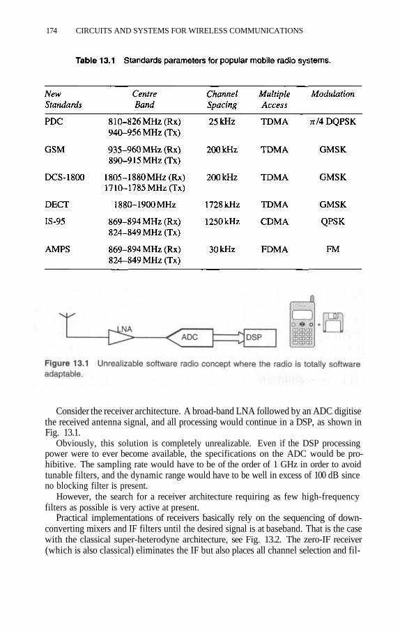
174 CIRCUITS AND SYSTEMS FOR WIRELESS COMMUNICATIONS
Consider the receiver architecture. A broad-band LNA followed by an ADC digitisethe received antenna signal, and all processing would continue in a DSP, as shown inFig. 13.1.
Obviously, this solution is completely unrealizable. Even if the DSP processingpower were to ever become available, the specifications on the ADC would be pro-hibitive. The sampling rate would have to be of the order of 1 GHz in order to avoidtunable filters, and the dynamic range would have to be well in excess of 100 dB sinceno blocking filter is present.
However, the search for a receiver architecture requiring as few high-frequencyfilters as possible is very active at present.
Practical implementations of receivers basically rely on the sequencing of down-converting mixers and IF filters until the desired signal is at baseband. That is the casewith the classical super-heterodyne architecture, see Fig. 13.2. The zero-IF receiver(which is also classical) eliminates the IF but also places all channel selection and fil-

WIDE-BAND SUB-SAMPLING A/D CONVERSION WITH IMAGE REJECTION 175
tering in front of the ADC. More sophisticated architectures, like low-IF and quasi-IF,relax the requirements placed on the IF filters by careful use of image rejection mixers,but still place the ADC after channel selection and filtering.
The result is that the ADC is the component with the most relaxed specifications inthe receiver, while the filters need to accommodate very large dynamic ranges and areof high order (and high Q in super-heterodyne architectures).
On the other hand, the need to perform the channel selection requires that the fre-quency synthesisers have a very fine frequency resolution equivalent to the channelspacing. Depending on the standard, the filters’ dynamic range can be above 100 dB,and the synthesiser’s frequency resolution can be as low as 30 kHz. The question wewant to answer here is this: “Is it possible to relax the requirements placed on thefilters and frequency synthesisers at the expense of a more complex ADC, but with nopenalty on power dissipation or monolithic compatibility?”
13.2 OVERSAMPLED ARCHITECTURES
It is better to place the ADC before the channel filters, as shown in Fig. 13.3. TheADC must then be highly oversampled in order not to alias high frequency interferersinto the baseband.

176 CIRCUITS AND SYSTEMS FOR WIRELESS COMMUNICATIONS
Irrespective of the receiver architecture, the baseband signal produced by the down-conversion mixer contains the channel signal at a weak level in addition to out-of-bandinterferers that can be much stronger that the desired channel itself. Depending on theIF filters’ selectivity and on the standard, these interferers can be as high as 70 dBabove the desired signal. Taking into account fast-fading effects and AGC margins,the ADC will have to support a large dynamic range of 60 to 90 dB.
The most convenient type of ADC to place at this point is a delta-sigma modulator(two are required, since the signal is in I and Q representation). Strong adjacent chan-nels are combined with quantisation noise and actually act as a dither source and helpto randomise the bit stream. The digital decimating filter will then serve the dual func-tion of attenuating both the quantisation noise and the adjacent channels interference.
In practice, the order of the baseband filter and the ADC has been interchanged.The filter is now implemented digitally, reusing existing hardware — the decimatingfilter. Only a simple anti-aliasing filter remains before the ADC, and the ADC hasbeen highly oversampled to avoid aliasing by unfiltered high-frequency interferersand noise. As a result, the dynamic range, which was supported by the filter in theclassical architecture, is now supported by the ADC.
The advantages of this architecture are numerous. The I/Q matching accuracy isvery good, depending basically on the matching of the two ADC input stages. Theportability between different technologies is facilitated since more of the signal pro-cessing is done digitally. The filters can have a very accurate frequency response anda linear phase characteristic important for digital modulation techniques. Besides, thechannel bandwidth can be easily programmed.
But the ADC is required to operate at a very high sampling rate and must achieve alarge dynamic range. We now compare the power dissipation of this ADC and that ofthe original filter it replaced.
13.3 POWER DISSIPATION ISSUES
The power dissipation of an analog circuit depends on many considerations, most ofthem related to the limitations of the technology being used. But it is instructive toconsider the fundamental limitations of analog signal processing.
The basic function of an analog circuit is to process a voltage (or current) signal,identified by its bandwidth B and amplitude, with a maximum degradation charac-terised by distortion and noise. Regarding distortion, there are no relevant physicallimits determining a minimum power dissipation level. But in the case of noise, thereis a clear relationship involving temperature, signal bandwidth and circuit dynamicrange. For the case of voltage signals and optimal supply voltage corresponding to thesignal amplitude, it is given by the following expression [1]:
where k is the Boltzmann constant and T is the absolute temperature. The dynamicrange, DR, is defined as the power ratio between the maximum signal amplitude (canbe an out of band interferer) to the thermal noise integrated over the signal band-width B. The power associated to (13.1) is dissipated by the necessary charging anddischarging of the capacitance on each circuit node carrying the signal. In a filter there
WIDE-BAND SUB-SAMPLING A/D CONVERSION WITH IMAGE REJECTION 177
are, as a minimum, N such nodes, where N is the filter order. In an ADC, only onesuch node is necessary as a minimum: the sampling node.
This analysis is valid irrespective of continuous-time or discrete-time circuits. Thepower dissipation is not affected by the actual sampling frequency of the ADC for afixed signal bandwidth and dynamic range. This leads to two conclusions:
1. The power dissipation of the ADC is not necessarily higher than that of the analogfilter it replaced.
2. The ADC can be oversampled by a large factor without penalty on the power dissi-pation.
This second conclusion is important because it allows to use a sufficiently largesampling frequency so that the ADC images will be far enough from the desired chan-nel for the anti-aliasing filters to be of simple construction. It means that for a fixedsignal bandwidth (the channel bandwidth) and fixed dynamic range, the sampling fre-quency can be increased without necessarily increasing the power consumption.
There are practical limits to this, however. In switched-capacitor (SC) circuits, asthe sampling frequency increases, the sampling capacitors can be decreased by thesame factor, to keep the thermal noise constant within the signal band. Thereduced load capacitors allow to keep the same amplifier slew rate at the original biascurrents, but the amplifier needs to have a higher gain-bandwidth product. That, inturn, cannot be made higher than the internal non-dominant poles of the amplifier,otherwise the phase margin will be reduced to unacceptable values.
Considering CMOS technology, the most power-efficient operating point of thetransconductance defining MOS transistors in an amplifier is in moderate inversionwith an over-drive voltage At this point the ratiois maximum. However, the transit frequency, of the transistors in the signal pathmust be above the sampling frequency by a factor of typically 20, at least, to preservephase margin.
In CMOS, of the transistors is a function of the operating point:
An NMOS transistor in a technology has an of about 2 GHz, allow-ing sampling frequencies approaching 100 MHz at optimum power dissipation, in thesense that the transistors responsible for poles are biased at the maximumoperating point. In fact, there are already several reports of delta-sigma modulatorsvalidated for sampling frequencies in excess of 50 MHz [2–4].
Above that frequency, the over-drive voltage of the transistors will have to be in-creased at least proportionally to the sampling frequency in order to keep their transitfrequency high enough. Since the MOS transconductance is of the form
the bias current will have to be increased as well in order to keep the transconductancevalues fixed. This makes the power consumption increase linearly with the sampling

178 CIRCUITS AND SYSTEMS FOR WIRELESS COMMUNICATIONS
frequency, until the over-drive voltage is large enough for the transistors to enter thevelocity saturation region. Then the power dissipation will increase very fast withincreases in sampling frequency. This is illustrated in Fig. 13.4.
13.4 IF SAMPLING ARCHITECTURES
IF sampling architectures directly interface the ADC to a signal band centred at IF.This leads to a convenient system partitioning where the IF is the interface betweenthe baseband signal processing chip and the RF front-end.
The analysis in the previous section showed that it is possible to efficiently increasethe sampling frequency of an SC circuit up to a frequency of 100 MHz. However, theIF frequencies are often above this frequency, requiring more advanced architecturesto allow direct sampling of the IF signal.
The solution is to operate in a sub-sampling mode. In this mode, the amplifiersoperate at a reduced rate, and only the input SC branches need to settle accuratelywith IF input signals. Since these are simple passive branches, their operating speedcan be much higher than that of the active charge transfers performed by the amplifiers,and can easily allow sampling signals well above 100 MHz.
There are several possible approaches to integrate the complete IF-sampling re-ceiver in CMOS.
One is to keep exactly the architecture of Fig. 13.3. The mixer could either be imple-mented as a classical Gilbert cell, using triode-region-biased transistors [6], or using asub-sampling SC circuit. Double-quadrature architectures can also be considered forimproved image rejection in the RF front-end providing I and Q IF.
13.5 IMAGE-REJECTION SUB-SAMPLING ADC
A more ambitious approach is to embed the sub-sampling SC mixer in the ADC, asshown in Fig. 13.5. The anti-aliasing filter is eliminated and its function is performedby the IF filters. This approach results in a significant reduction of receiver complexityand a potential power dissipation reduction since fewer blocks are required.
The IF filters can be strongly relaxed since they only need to attenuate the aliasingbands of the ADC. The sub-sampling SC mixer can be implemented by appropriatephasing of the input SC branches of the first integrator of the delta-sigma modulator.
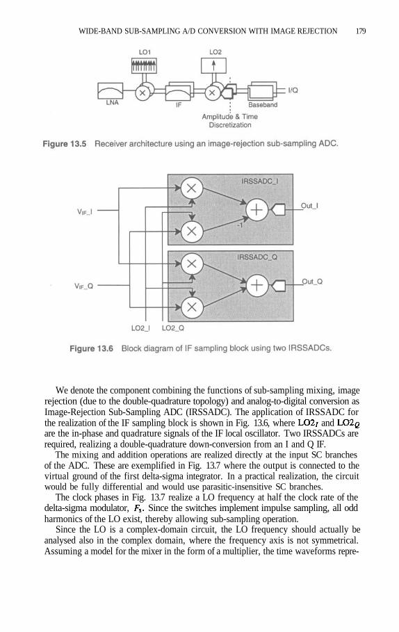
WIDE-BAND SUB-SAMPLING A/D CONVERSION WITH IMAGE REJECTION 179
We denote the component combining the functions of sub-sampling mixing, imagerejection (due to the double-quadrature topology) and analog-to-digital conversion asImage-Rejection Sub-Sampling ADC (IRSSADC). The application of IRSSADC forthe realization of the IF sampling block is shown in Fig. 13.6, where andare the in-phase and quadrature signals of the IF local oscillator. Two IRSSADCs arerequired, realizing a double-quadrature down-conversion from an I and Q IF.
The mixing and addition operations are realized directly at the input SC branchesof the ADC. These are exemplified in Fig. 13.7 where the output is connected to thevirtual ground of the first delta-sigma integrator. In a practical realization, the circuitwould be fully differential and would use parasitic-insensitive SC branches.
The clock phases in Fig. 13.7 realize a LO frequency at half the clock rate of thedelta-sigma modulator, Since the switches implement impulse sampling, all oddharmonics of the LO exist, thereby allowing sub-sampling operation.
Since the LO is a complex-domain circuit, the LO frequency should actually beanalysed also in the complex domain, where the frequency axis is not symmetrical.Assuming a model for the mixer in the form of a multiplier, the time waveforms repre-

180 CIRCUITS AND SYSTEMS FOR WIRELESS COMMUNICATIONS
senting the I and Q LO signal are as shown in Fig. 13.8. The arrows denote the Diracfunction corresponding to ideal impulse sampling.
Applying the Fourier transform, we obtain the frequency representation shown inFig. 13.9. As expected, the spectrum is not symmetrical. Since the IF signal is also ina complex representation, the relevant band is located in the positive frequency axis.The frequency band in the negative frequency axis corresponds to the image band.
The operation of this mixer is now clear: Consider the bands around... Since the local oscillator frequency, LO2, is these bands correspond
to the fundamental, 5th harmonic, 9th harmonic, etc., of LO2. Therefore, a sub-sam-pling operation by a factor of 1, 5, 9,..., is possible. If we eliminate the inversion inFig. 13.6, it can be similarly shown that the sub-sampling factors become 3, 7, 11,...
The presence of multiple input bands is typical of sampled systems and the desiredband should be selected by an anti-aliasing filter in front of the mixer. This filter can

WIDE-BAND SUB-SAMPLING A/D CONVERSION WITH IMAGE REJECTION 181
be the IF filter itself and should reject the bands times LO2 away from the centreIF band.
13.5.1 Case study
As a practical example, for an IF centre frequency of 150 MHz, and when operat-ing with a sub-sampling factor of 5, the local oscillator frequency is 30 MHz and thedelta-sigma modulator sampling frequency is 60 MHz. The IF filter should reject thealiasing bands around 30 MHz and 270 MHz.
Assuming a typical application such as GSM, where the baseband channel band-width is 100 kHz, the delta-sigma modulator would be operating with an oversamplingratio of 60000/200 = 300. This would easily allow to achieve a dynamic range in ex-cess of 90 dB [4]. This dynamic range is higher than the ratio of maximum blockinglevels (within GSM band) to the minimum signal level, which is about 80 dB.
The previous example confirms that the IF filters can be substantially relaxed sincetheir function is basically to reject aliasing bands.

182 CIRCUITS AND SYSTEMS FOR WIRELESS COMMUNICATIONS
13.6 DIGITAL TUNING
As already mentioned, the dynamic range of the ADC is increased by proper sizingof the sampling capacitance, which, for a large oversampling frequency, can be verysmall. This concerns the level of thermal noise. In delta-sigma modulators one mustalso consider the quantisation noise. In these circuits, the signal-to-quantisation-noiseratio (SQR) is a strong function of the oversampling ratio. By proper use of techniquessuch as
high order modulator loops,multi-bit quantising,data-weighted averaging linearisation,
an SQR above 90 dB can be easily achieved at a low oversampling ratio such as 16.This means that in the present application where the oversampling ratio is of the or-der of 100, the quantisation noise is negligible compared to thermal noise within thechannel bandwidth.
This motivates a more ambitious application of the IRSSADC. The idea is to usebroadband digitalisation where a group of channels is down-converted to a very lowIF. The channel selection is then performed by a third mixer, as shown in Fig. 13.10.At this point, signal processing is already digital, which allows much flexibility indefining channel spacing and channel filtering.
For example, in the case study above, the IRSSADC, at an oversampling ratio of16, can digitise a band of This allows to include 9 GSMchannels at once (the channel spacing is 200 kHz).
The high flexibility due to easy digital programmability of channel centre frequencyand spacing is very advantageous for implementing a multi-mode/multi-band terminal.
Furthermore, the RF frequency synthesiser can now have a coarse frequency reso-lution, which significantly relaxes its design specifications.
13.7 ARCHITECTURE SIMULATION
A Matlab/Simulink model has been developed to represent the architecture shown inFig. 13.11 consisting of an IF sub-sampling quadrature mixer, I and Q low-pass filters,I and Q Delta-Sigma modulators, digital decimating filters and digital tuning. The IFfilter is not included.

WIDE-BAND SUB-SAMPLING A/D CONVERSION WITH IMAGE REJECTION 183
The Delta-Sigma modulators are of third order with 3-bit quantisation. They use dy-namic data averaging linearisation of feedback multi-bit DACs. The GSM case-studypresented above is used here again.
The sub-sampling mixer is a switched-capacitor circuit that samples the signal atan of 60 MHz and mixes it with two sampled sine waves in quadrature with a fre-quency of This mixer generates I and Q sampled signals, which arefiltered by two anti-aliasing filters. The first one is a first-order switched-capacitor low-pass filter (actually it is embedded in the mixer), and the second is a continuous-timesecond-order Butterworth low-pass filter. The signal is then converted to the digitaldomain, using a third-order delta-sigma converter sampling at and decimated with asinc4 filter into 60/8 = 7.5 MHz. Afterwards, the signal is mixed digitally with a DDS-generated sine wave, converting the desired channel to base-band. Finally the signalis low-pass filtered and decimated by 16 to obtain the desired I and Q components ofthe signal.
The signals applied are:Desired signal at 150.8 MHz with an amplitude (0 dBref)Interferer 1 at 150.6 MHz (1 channel offset), amplitude (+9.5 dBref)Interferer 2 at 150.4 MHz (2 channels offset), amplitude 12mV (+41 dBref)Interferer 3 at 149.2 MHz (8 channels offset), amplitude 12mV (+41 dBref)Interferer 4 at 147.8 MHz (15 channels offset), amplitude 630mV (+76 dBref)Interferer 5 at 89.25 MHz (near 3/5 of IF), amplitude (–12 dBref)Interferer 6 at 119.8 MHz (near 4/5 of IF), amplitude 100mV (+60 dBref)The spectrum at the input of the Delta-Sigma modulator is shown in Fig. 13.12a,
where the signals around IF were shifted to DC by the sub-sampling mixer. The in-terferer I6 is down-converted but strongly attenuated by the anti-aliasing filters (notshown). The interferer 5 is down-converted withoutattenuation, because it lies aroundthe third harmonic of the IF local oscillator (90 MHz). If a complex IF were used, asin Fig. 13.5, this image would be strongly attenuated. Fig. 13.12b shows the spectrumat the output of the delta-sigma modulator, together with the transfer functions of theanti-aliasing filters (curve 1) and of the sinc4 decimating filter (curve 2). The signaldynamic range is still 76 dB (ratio between the strongest interferer, I4, and the desiredsignal).

Fig. 13.13a shows the resulting spectrum at the output of the decimating filter,before the digital mixer, together with the transfer function of the anti-aliasing filterplus sinc. The Delta-Sigma converter quantisation noise is well below the desiredsignal.
Fig. 13.13b represents the digital mixer output. Curve 1 corresponds to the com-bined transfer function of the anti-aliasing filter plus sinc4. Now the desired signalis centred at DC and all interferers are in the rejection band of the digital low-passdecimation filters (not shown for clarity).
In Fig. 13.14, the spectrum at the output of the system is shown with the interferersstrongly attenuated and the desired signal well above the noise level. The last digitallow-pass filter transfer function is also represented. The image of interferer 5 can alsobe seen, generated in the sub-sampling mixer, and the image of interferer 2 generatedin the last decimation by two in the digital filter. Since this filter has a stop-bandattenuation of 65 dB and the interferer is 41 dB above the desired signal, the image isattenuated to 23 dB below the desired signal.

WIDE-BAND SUB-SAMPLING A/D CONVERSION WITH IMAGE REJECTION 185
13.8 CONCLUSIONS
We introduced the concept of the image-rejection sub-sampling ADC, which is a com-bination of a highly oversampled ADC associated with a sub-sampling block imple-menting a double-quadrature mixer.
This allows to implement wide-band conversion for radio receivers with associatedadvantages. On the one hand, software tuning and selectivity becomes possible, simpli-fying implementation of multi-mode capability. On the other hand, the specificationsof the IF filters and of the RF frequency synthesiser can be relaxed, the former dueto the large dynamic range of the ADC that accepts a high level of blocking signals,the latter due to the software tuning that allows coarse frequency resolution in the RFfrequency synthesiser.
An analysis was presented that shows that these advantages should be possible withno penalty on power dissipation, and simulation results demonstrate the efficacy of theprinciple.
Acknowledgments
The authors wish to acknowledge the financial support of the European Commission underESPRIT project n. 25476, PAPRICA.
References
[1] R. Castello and P. Gray, “Performance Limitations in Switched-Capacitor Filters”,IEEE Transactions on Circuit and Systems, Vol. CAS 32, No. 9, Sep. 1985, pp.865–876.
[2] B. Brandt and Bruce Wooley, “A 50-MHz Multibit Sigma-Delta Modulator for12-b 2-MHz A/D Conversion”, IEEE J. Solid-State Circuits, Vol. 26, No. 12, Dec.1991, pp. 1746–1756.

186 CIRCUITS AND SYSTEMS FOR WIRELESS COMMUNICATIONS
[3] G. Yin and W. Sansen, “A High-Frequency and High-Resolution Fourth-OrderConverter in BiCMOS Technology ”, IEEE J. Solid-State Circuits, Vol.
29, No. 8, Aug. 1994, pp. 857–865.
[4] A. Marques, V. Peluso, M. Steyaert and W. Sansen, “A 15-b Resolution 2-MHzNyquist Rate in a CMOS Technology”, IEEE J. Solid-State Cir-cuits, Vol. 33, No. 7, Jul. 1998, pp. 1065–1075.
[5] A. Feldman, B. Boser and P. Gray, “A 13-Bit, 1.4-MS/s Sigma-Delta Modulatorfor RF Baseband Channel Applications”, IEEE J. Solid-State Circuits,Vol. 33,No. 10, Oct. 1998, pp. 1462–1469.
[6] J. Crols and M. Steyaert, “A Highly Linear CMOS Downconversion Mixer”, IEEEJ. Solid-State Circuits, Vol. 30, No. 7, Jul. 1995, pp. 736–742.
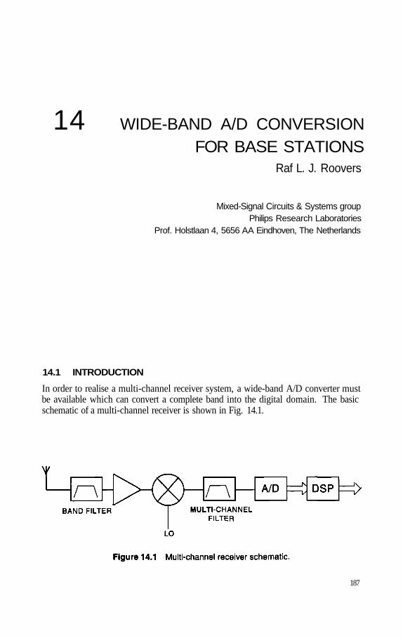
14 WIDE-BAND A/D CONVERSIONFOR BASE STATIONS
Raf L. J. Roovers
Mixed-Signal Circuits & Systems groupPhilips Research Laboratories
Prof. Holstlaan 4, 5656 AA Eindhoven, The Netherlands
14.1 INTRODUCTION
In order to realise a multi-channel receiver system, a wide-band A/D converter mustbe available which can convert a complete band into the digital domain. The basicschematic of a multi-channel receiver is shown in Fig. 14.1.
187
188 CIRCUITS AND SYSTEMS FOR WIRELESS COMMUNICATIONS
The multi-channel receiver has an antenna input (RF) followed by a band filter anda low noise amplifier (LNA). The RF signal is down-converted to an IF frequency andagain some filtering can be applied. The IF signal containing the complete signal bandis then converted to the digital domain by a wide-band A/D converter. The channelselectivity is implemented in the digital domain. The advantages of such a systemare obvious: increased flexibility and reduced analog hardware when more than onechannel is to be received simultaneously. These advantages of multi-channel receiverare particularly interesting for cellular base stations, where multiple channels are re-ceived. The signal at the input of the A/D converter combines a wide bandwidth witha large dynamic range. This large dynamic range is due to the fact that neither channelfiltering nor variable gain can be used before the A/D conversion in a multi-channelreceiver. This means that the converter has to handle at the same time maximumblocking and interfering signal levels while still receiving channels with signals atminimum power levels. This puts severe performance requirements on the linearityand noise contributions of the A/D converter,
14.2 PERFORMANCE METRICS FOR A/D CONVERTERS
There are two reasons to introduce performance metrics for A/D converters:to evaluate the feasibility of receiver architecture with a wide-band A/D converter,to compare different A/D converter realisations (benchmarking).The performance metrics used here are based on the effective performance in terms
of dynamic range, bandwidth, and power dissipation. These three parameters are com-bined into a global figure of merit. It should be clear to the reader that other parameterssuch as latency, power supply voltage, input range, input impedance, etc. are importantas well, but these are not included in the figure of merit. First the resolution bandwidthproduct of an A/D converter is introduced. The A/D converter can be regarded as ablack box: analog in, digital out as shown in Fig. 14.2.
Assuming that a full-scale, single-sine-wave input signal is applied to the A/D con-verter, the digital output can be analysed using its Fast Fourier Transform (FFT) spec-trum. This FFT spectrum contains the input signal together with noise and harmoniccomponents. From this FFT spectrum the SINAD (Signal to Noise And Distortion)is calculated. This SINAD can be translated in ENOB (Effective Number Of Bits),describing the effective resolution of the A/D converter:
This ENOB is measured in function of the input signal frequency (c.f. Fig. 14.2).The closer the ENOB approaches the nominal number of bits the better. The usefulbandwidth of the A/D converter can be limited in two ways: First, the Nyquist criteriongives a maximum bandwidth to be converted equal to half the sampling frequency
The second limitation is due to the fact that A/D converters tend to have areduced ENOB for high-frequency input signals. Therefore the effective resolutionbandwidth is defined as the minimum of the Nyquist frequency and the inputsignal frequency for which the ENOB is reduced by 0.5 bit comparedto the ENOB at low input frequencies The effective resolution bandwidth

WIDE-BAND A/D CONVERSION FOR BASE STATIONS 189
product (BWres) combines both the effective resolution and the effective resolutionbandwidth:
This product is proportional to the area in Fig. 14.2, where the difference to the nom-inal resolution-bandwidth becomes clear. The effective resolution-bandwidth productsfor some A/D converters are plotted in Fig. 14.3.
If the effective resolution bandwidth product is combined with the power dissipa-tion of the A/D converter a Figure of Merit (F.o.M.) can be defined:

190 CIRCUITS AND SYSTEMS FOR WIRELESS COMMUNICATIONS
The factor of 2 is introduced to be compatible with the existing F.o.M. based onnominal performance, i.e. The dimension of the F.o.Mis Joule per conversion, and for better performance its value should be as small aspossible. In Fig. 14.4 the evolution of this F.o.M. as a function of time is plotted.
The improvement in A/D converter performance over time is both due to designinnovations and technology improvements. At this moment, wide-band A/D convert-ers (10... 14 bit) that achieve a F.o.M. of 5 pJ per conversion are state of the art. TheF.o.M. can be used to estimate the A/D converter’s power dissipation for various appli-cations in a resolution-bandwidth graph as shown in Fig. 14.5. The lines of constantpower dissipation are based on a F.o.M. of 5 pJ per conversion.
The wide-band A/D converters to be used in base-station receivers require band-widths in the order of tens of MHz and resolutions in the order of 12 to 16 bit, de-pending on the IF frequency used and the amount of filtering in the analog part ofthe receiver. These A/D converters have a power consumption in the order of 1 Wattand are therefore not suitable for implementation in handsets. For base station applica-tion, these levels of power dissipation are acceptable, and the benefits of receivers withwide-band A/D converters can be exploited as multiple channels share the same analogfront-end plus A/D converter. The realisation of this A/D converter for multi-channelreceivers is the main challenge in A/D converter design.
14.3 RECEIVER ARCHITECTURE AND ADC SPECIFICATION
The resolution and bandwidth required for a multichannel receiver is explained withGSM as an example. The GSM signal spectrum is shown in Fig. 14.6.

WIDE-BAND A/D CONVERSION FOR BASE STATIONS 191
The 25 MHz signal band is divided into 200kHz-wide channels. The base stationhas to perform according to conformance test for blocking, interferers and sensitivity.The conversion to the digital domain of a complete band requires a dynamic range inthe order of 100 dB and a bandwidth larger than 25 MHz. If only a single channel is to

192 CIRCUITS AND SYSTEMS FOR WIRELESS COMMUNICATIONS
be converted, channel filtering and variable gain can be introduced in the analog signalpath to reduce the dynamic range requirements in the A/D converter [7].
Two architectures containing wide-band A/D converters are shown in Fig. 14.7.The difference between them is the presence of a (single) channel filter in the firstone. For this single channel receiver, a variable-gain amplifier can be introduced toreduce the required dynamic range of the A/D converter. The second architectureis a multi-channel architecture that does not allow variable gain in front of the A/Dconverter to reduce the A/D converter requirements.
When the performance of the ADC is mapped to the system requirements, twokinds of Dynamic Range (DR) should be distinguished: DR due to noise limitation(SNR) and DR due to distortion and spurious signals (SFDR). The theoretical perfor-mance of an A/D converter results in an SNR improvement of 6 dB per additional bit

WIDE-BAND A/D CONVERSION FOR BASE STATIONS 193
and an SFDR improvement of 9 dB/bit (3rd harmonic in ideal quantisation). For theSNR specification we have to take the “processing gain” into account: as the channelbandwidth is smaller than the Nyquist bandwidth, the noise outside the wanted channelwill be filtered out, resulting in an SNR improvement ofIn Fig. 14.8, the SNR and SFDR of a 12bit A/D converter is plotted as a function ofthe input signal level related to the full scale of the A/D converter (dBFS).
A real 12-bit converter typically achieves an SFDR of 80 dB (theoretically 108 dBSFDR), which is not sufficient for a multi-channel base station receiver. This requiresat least a highly linear 14-bit wide-band A/D converter to achieve an SFDR of about100 dB.
14.4 CASE STUDY: SINGLE-CHANNEL RECEIVER BASED ON A12-BIT WIDE-BAND A/D CONVERTER
The difference between real and ideal A/D converters is explained by a 12-bit A/Dconverter realisation [1]. This BiCMOS A/D converter is based on a cascaded fold-ing-interpolating architecture resulting in a power/area efficient implementation. Thefolding-interpolating quantiser is preceded by a wide-band Track-and-Hold to obtaina resolution bandwidth equal to The limiting factors in ENOB are contributedby various sources of noise and distortion: nonlinearity in the Track-and-Hold, INL er-rors due to mismatching in the quantiser, thermal noise, clock buffer noise, etc. Thesesources of noise and nonlinearity are often proportional (or quadratically proportional)to the power consumption. As an example, the breakdown of the contributions of noiseand distortion for the 12 bit A/D converter realisation is shown in Fig. 14.9.
Despite the state-of-the-art F.o.M. of 5 pJ per conversion, this 12-bit A/D converterhas not enough dynamic range to be used in a multi-channel receiver for cellular base-stations. However, this wide-band A/D converter can be used to realise a single-chan-

194 CIRCUITS AND SYSTEMS FOR WIRELESS COMMUNICATIONS
nel IF-to-digital conversion system. This system is shown in Fig. 14.10. The channelfilter at IF reduces the dynamic range requirements and allows the use of a variable-gain amplifier in front of the ADC. In this case, the variable gain amplifier is digitallycontrolled and has a gain variable from 6 to 30 dB in 6-dB steps. The basic schematicof the Digitally Controlled Variable Gain (DVGA) is shown in Fig. 14.11. This addi-tional gain range extends the dynamic range for noise of the single channel receiver toabout l00dB for a 200kHz channel.
This DVGA was designed for low noise, low distortion, and fast settling, and it re-places an input buffer amplifier to drive an A/D converter. The SFDR of the combinedDVGA and ADC is shown in Fig. 14.12.
While the SFDR of the A/D converter decreases with higher input signal levels, thedistortion of the DVGA increases. Since a channel filter is introduced in front of theconverter, the global SFDR of DVGA and ADC is sufficient to realise a single-channelIF-to-digital converter.

WIDE-BAND A/D CONVERSION FOR BASE STATIONS 195

196 CIRCUITS AND SYSTEMS FOR WIRELESS COMMUNICATIONS
14.5 CONCLUSIONS
A/D converters for multi-channel receiver base-stations is THE challenge in ADC de-sign. Based on performance metrics and observations of state-of-the-art A/D convert-ers, it can be concluded that the combined dynamic range and bandwidth requirementsfor multi-channel receivers will not be low power: these A/D converters will be hot. AsADCs for multi-channel receivers are not yet available, wide-band A/D converters canbe used in combination with DVGA to build IF-to-digital conversion for single-chan-nel receivers.
References
[1] P. Vorenkamp and R. Roovers, “A 12-b, 60Msample/s Cascaded Folding andInterpolating ADC”, IEEE J. Solid-State Circuits, vol. 32, pp. 1876–1886, Dec.1997.
[2] Datasheets Philips Semiconductors, TDA8760, TDA8768, TDA8718, TDA8790,TDA8792.
[3] Datasheets Analog Devices, AD6640 AD9042, AD9220.[4] Datasheets Harris Semiconductors, HI5905.
[5] Datasheets Sony, CXD3211, CXD3202.
[6] Datasheets Burr Brown, ADS805.
[7] R.Roovers, “Digital Controlled Variable Gain Amplifier (DVGA) for IF to DigitalConversion System” proc. ESSCIRC98, pp. 152–155, Sep. 1998.

15 LOW-SPURIOUS ADCARCHITECTURES FOR SOFTWARE
RADIOBang-Sup Song
Department of Electrical and Computer EngineeringUniversity of Illinois, Urbana, IL 61801, USA
15.1 INTRODUCTION
In digital wireless systems, a need to quantize a block of spectrum with low intermod-ulation has become one of many technically challenging problems. Implementing IFfilters digitally has already become a necessity in cell sites and base stations as ex-plained in Fig. 15.1. Even in hand-held units, placing data conversion blocks closerto the RF front end has many benefits. Substantial savings in system cost and com-plexity can be attained by implementing highly selective IF filters digitally. DigitalIF filtering can increase immunity to adjacent and alternate channel interferences, andthe RF transceiver architecture can be made independent of the system and adapted todifferent standards using software. However, all these predictions for the software ra-dio rely on the availability of low-spurious ADCs and DACs that consume low powerat low supply voltages.
Table 15.1 summarizes various RF communication standards. The fundamentallimit in quantizing the IF spectrum is crosstalk and overload, and the system perfor-mance heavily depends on the SFDR (spurious-free dynamic range) of the samplingADC. Spurious components result from two non-linearity sources during the quan-tization process. One is the differential non-linearity (DNL), and the other is the
197

198 CIRCUITS AND SYSTEMS FOR WIRELESS COMMUNICATIONS
integral non-linearity (INL). The former produces harmonically unrelated spuriouscomponents in the quantized spectrum while the latter produces intermodulation com-ponents. A possible solution to reduce spurious components resulting from the limitedDNL is a dithering method to spread the spurious components randomly [1]. On theother hand, the limited INL can only be improved by straightening the ADC trans-

LOW-SPURIOUS ADC ARCHITECTURES FOR SOFTWARE RADIO 199
fer characteristic. In general, only high-resolution techniques using oversampling orcalibration are known to improve INL.
15.1.1 Technical challenges In digital wireless
Fig. 15.2 explains why wide dynamic range is needed to quantize a weak signal em-bedded in strong interferences. To meet this growing demand, low-spurious ADCs arebeing actively developed in ever increasing numbers. Current commercial productsfor this purpose are only a few, such as Analog Devices’s AD6640 (12 b, 65 MHz) andNational’s CLC952 (12 b, 41 MHz), but more are being announced this year. Typi-cal performance currently possible with bipolar or BiCMOS technologies ranges from12 b to 14 b sampling at 65 MHz with a typical SFDR of 70 dB to 80 dB, althoughnumbers higher than 80 dB are often quoted for converters using a dithering method[1]- [3]. Typical power consumption of such parts is well over half a watt. For a14b-level dynamic range while sampling at over 50MHz, it is necessary to controlthe sampling jitter to below 0.3 ps. The low-jitter requirement is on the border lineof the bipolar chip performance, but very challenging for scaled CMOS technologies.However, unlike non-linearity that causes inter-channel mixing, the random jitter in IFsampling increases only the random noise floor. As a result, the random jitter is notconsidered as a fundamental problem in this application.
Considering the current state of the art in CMOS ADCs, most architectures knownto date are unlikely to achieve a high sampling rate of over 50 MHz even with 0.2 to
technologies [4–13], but the situation looks better for bipolar or BiCMOS [1–3,14–16]. The ADC architecture varies depending on system requirements.
15.1.2 ADC state of the art
Fig. 15.3 is a resolution-versus-speed plot showing the trend of ADC-developmentworks recently reported at the ISSCC. Three architectures stand out for three importantareas of applications. For example, the oversampling converter is exclusively used toachieve high resolution above 12 b level at low frequencies. The difficulty in achievingbetter than 12 b matching in conventional techniques gives a fair advantage to theoversampling technique. For medium speed with high resolution, pipeline ADCs arepromising. At extremely high frequencies, only flash and folding ADCs survive, but

200 CIRCUITS AND SYSTEMS FOR WIRELESS COMMUNICATIONS
with low resolution. As both semiconductor process and design technology advance,the performance envelope will be pushed further. Table 15.2 lists the state of the art of> 12 b ADCs in different technologies.
The ADC performance is often represented by a figure of merit L as shown inFig. 15.4. The higher L is, the more bits are obtained at higher speed with lowerpower. The plot of L versus year shows the low-power and high-speed trend both forintegrated CMOS and bipolar/BiCMOS ADCs published at the ISSCC during the lastdecade. Overall, the low-power trend is evident though not dramatic.
15.2 TECHNIQUES FOR HIGH-RESOLUTION ADCS
There exist many high-speed ADC techniques for a wide range of resolution andspeed. Table 15.3 summarizes some of them and their features. In general, the maincriteria of choosing ADC architectures are resolution and speed, but additional re-quirements such as power, chip area, supply voltage, latency, operating environment,or technology often limit the choices. The current trend is toward low-cost integrationwithout using expensive discrete technologies. Among many high-speed data conver-sion architectures, two high-speed candidate architectures, pipeline and folding, andtheir variations with new system approaches are potential candidates to challenge thelimit set by the software radio. This paper is focused on these two architectures andpresents two possible ways to improve their linearities.
In general, ADC design examples are so diverse that it is difficult to fit all of theminto a few fixed frames. While pipeline ADCs are limited by the DAC resolutionand residue amplifier gain, folding ADCs suffer from poor offset of the folding am-plifier. Therefore, high-resolution techniques should be tailored for each architecture.

LOW-SPURIOUS ADC ARCHITECTURES FOR SOFTWARE RADIO 201
Analog high-resolution techniques reported to date to improve ADC linearity are asfollows:
Dynamic matching (Plassche, JSSC, June 1979)Ratio-independent (Li, JSSC, Dec. 1984)Reference-feedforward (Sutarja, JSSC, Dec. 1988)Capacitor-error averaging (Song, JSSC, Dec. 1988)Current sampling (Schouwenaars, JSSC, Dec. 1988)Voltage sampling (Kerth, JSSC, April 1989)Inherently monotonic (Wu, ISCAS, 1994)The dynamic matching technique is efficient, but it generates high-frequency noise.
The ratio-independent, reference-feedforward, and inherently monotonic techniqueseither require more than two clock cycles or are limited to improvement in DNLonly. The capacitor-error averaging technique requires three clock cycles, and thevoltage/current sampling techniques are sensitive to clock sampling errors.
The ADC self-calibration concepts have originated from the direct code-mappingconcepts using memory. The code-mapping technique is to predistort the digital inputof the DAC so that the DAC output can match the ideal level from the calibration equip-ment. Due to the precision equipment needed, this method has limited use. The firstself-calibration concept applied to the binary-ratioed successive-approximation ADC

202 CIRCUITS AND SYSTEMS FOR WIRELESS COMMUNICATIONS
is to internally measure capacitor DAC ratio errors using a resistor-string calibrationDAC as shown in Fig. 15.5 [17]. Later, an improved concept of the digital-domain cal-ibration was developed for the multi-step pipeline ADC [6], and the trend continues tocalibrate ADCs in the background while ADCs are in operation [11,15].

LOW-SPURIOUS ADC ARCHITECTURES FOR SOFTWARE RADIO 203
The general concept of the digital-domain calibration is to measure code or bit er-rors, to store them in the memory, and to subtract them during the normal operation.

204 CIRCUITS AND SYSTEMS FOR WIRELESS COMMUNICATIONS
The concept is explained in Fig. 15.6 using a generalized N-bit MDAC using a capac-itor array [6]. If the DAC code increases by 1, the MDAC output should increase by
or if redundancy is used for digital correction. Any deviation from thisideal step is defined as a segment error. The code errors are obtained by accumulatingsegment errors. This segment-error measurement needs two cycles. The first cycleis to measure the switch-feedthrough error, and the next cycle is to measure the seg-ment error. The segment error is simply measured using the LSB-side of the ADC byincreasing the digital code by 1. In the case that N= 1, the segment error is the biterror. If binary bit errors are measured and stored, the code error should be calculatedfor subtraction during the normal operation. How to store DAC errors is a trade-offissue. Ways to measure binary and thermometer code errors are explained in Fig. 15.7.Examples of the digital calibration are well documented for the cases of the segmenterror [11] and bit error [14] measurements.
The static linearity can be improved using many techniques as discussed, but thespeed improvement is not straightforward. Although digital calibration can improvethe resolution of the pipeline ADC to over 15b, the settling time of the interstageresidue amplifier has been the bottleneck in achieving high conversion rate.
15.3 OUTLOOK
New circuit techniques and architectures will lead to the implementation of data con-verters for digital IF applications. Assume the goal is to realize an ADC that meets

LOW-SPURIOUS ADC ARCHITECTURES FOR SOFTWARE RADIO 205
the 14 b, 50MHz requirement using low-power CMOS technologies. New high-reso-lution CMOS ADC architectures need to be explored so that high linearity and speedcan be readily obtained with less hardware complexity. The following are identifiedas major factors limiting performance in two candidate architectures.
Pipeline ADC- Speed of the residue amplifier- Linearity and calibrationFolding ADC- Offset of the folding amplifier- Complexity for high resolution- Linearity and calibrationIn the pipeline ADC, the settling time of the interstage residue amplifier has been
the bottleneck in achieving high conversion rate. The system can be reconfigured sothat the interstage gain may be obtained using a transresistance amplifier to speedup. Also the resolution of the folding ADC can be improved using a subranging con-cept combined with cascaded folding. Subranging will greatly simplify the foldingarchitecture, and the idea of calibrating the folding ADC is feasible with manage-able complexity. These two approaches have never been applied to ADCs with morethan 14 bits. To achieve such a linearity at over 50MSample/s rate using CMOS, wehave to overcome numerous technical barriers. The ADC of this caliber has yet to bedemonstrated. An oversampling delta-sigma calibrator will enable all calibrations inthe background.
Fig. 15.8 illustrates a residue amplifier that can be used as a front-end of the pipelineADC. The system uses a current-domain residue amplifier, which has an added advan-tage of using a current DAC which can be controlled more accurately at high speedthan voltage DACs. In the proposed architecture, linearity is limited only by the match-ing between current sources and resistors. Since the matching in IC processing is notenough, we need to calibrate current sources in the background using an oversam-pling delta-sigma calibrator [15]. The ultimate limit of the conversion rate is set bythe settling time of the residue amplifier. For example, if the amplifier settles within10ns with a 12 b resolution, the closed-loop time constant is about 1.1 ns. This in turnrequires a closed-loop bandwidth of about 145 MHz. This closed-loop bandwidth isbelieved to be well within the reach of the current CMOS technologies. The systemdiffers from others having the following distinct features.
Current-domain residue amplifier for fast settlingBackground calibration of current-domain MDACOversampling delta-sigma calibratorThe overall system works as follows. The input sample-and-hold amplifier makes
a new sample ready for the residue amplification. The coarse digital values are alsoready to switch differential current DAC elements for the residue amplification. AnLSB stage is also assumed to be ideal within its resolution. One left-over phase of theresidue amplifier is used to calibrate the current DAC elements, where the output ofthe residue amplifier corresponding to is compared to the ideal using a delta-sigma modulator. The bitstream output from this modulator is counted and averagedto increment or decrement a small current DAC to trim the current source. Behavioralsimulation results of the quantized output show that without calibration, the spurious

206 CIRCUITS AND SYSTEMS FOR WIRELESS COMMUNICATIONS
level approaches –70dB assuming 0.2% component mismatch. However, with thecalibration engaged, the spurious level is suppressed to below – l00dB.

LOW-SPURIOUS ADC ARCHITECTURES FOR SOFTWARE RADIO 207

208 CIRCUITS AND SYSTEMS FOR WIRELESS COMMUNICATIONS
The folding architecture has been most frequently adopted for high-speed ADCs.The folding circuit simultaneously produces many zero crossing points, but they needto be as accurate as the resolution of the ADC. Two limiting factors are the accuracy ofthe folding thresholds and the linearity of the folding amplifier. Due to the difficultyof controlling these, folding architectures have been known for high speed but forresolution typically lower than 8 to 10 bits [18–20]. However, at a 14 b level, thesystem also becomes prohibitively complex, and a new efficient folding architectureis needed. In addition, the new architecture should be calibratable for high linearity.
Several improvements can be made on the basic folding and interpolation architec-ture to overcome its limitations. The following features can increase the number ofbits effectively.
Cascaded folding with an odd number of folding blocksSubranging concept in foldingBackground calibration of the reference and folding amplifier offsetsOversampling delta-sigma calibratorFor cascading, it is necessary to generate folded signals from the first folding am-
plifier, and a Gilbert-type multiplier circuit has been used [3]. However, the multiplierrequires level shifters and cascode circuits that make the implementation more com-plex and introduce errors in the folding process. This difficulty can be overcome byusing the same current switch as in the first folding amplifier for the intermediatestage. For this, the folding scheme needs to be modified so that the number of foldingblocks becomes an odd number. If the number is a multiple of an odd number, thesecond folding outputs can be generated by summing the first folding outputs. Sincethe summation of such outputs can be implemented using current switches, the samecircuitry used for the first folding amplifier can be used repeatedly. Using this and thesubranging concept, one solution to a calibratable cascaded folding architecture canbe configured as shown in Fig. 15.9. The number of output codes is not a power oftwo, but the number of folding current switches is reduced to only 84. The first-stagefolding amplifiers’ offsets are of interest and subject to calibration.
The linearity of the resistor ladder network can be calibrated without interferingwith the normal conversion using a delta-sigma calibrator [15]. An offset of the foldingamplifier has the same effect as the reference error, and it is the main source of errors.To achieve 50MSample/s conversion speed, it is necessary to have the reference plusfolding outputs settle within 10ns. To guarantee high resolution, a calibration schemeto cancel the folding amplifier offsets should be incorporated. Fig. 15.10 shows suchan implementation of the folding current switch. When one folding current switch isunder calibration, its output is separated from the second folding block and fed intoan error measurement block. The input to the folding amplifier under calibration isshorted to null the output. The output necessary for the second folding block is gen-erated by interpolation. The error measurement block measures the folding amplifieroutput, and the calibration logic adjusts the bias current of the folding current sourceuntil the output of the folding amplifier is nulled. Like most pipeline ADCs, redun-dancy can be used in the folding architecture for digital correction. A prototype of theLSB 10 b ADC to be used in this architecture is implemented separately to prove thespeed of this architecture. Fig. 15.11 shows the 19 MHz input sampled at 157 MHz,and its reconstructed waveform shows distinct steps.
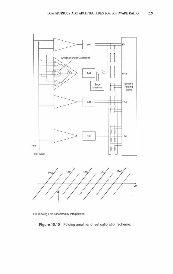
LOW-SPURIOUS ADC ARCHITECTURES FOR SOFTWARE RADIO 209

210 CIRCUITS AND SYSTEMS FOR WIRELESS COMMUNICATIONS
15.4 CONCLUSIONS
Digitization is now about to move into IF for wireless systems. The software-pro-grammable radio offers the technically most challenging tasks to the data acquisitiondesign community. Only high-performance ADCs and DACs, implementable in low-cost VLSI technologies and consuming one order of magnitude less power than currentcircuits, will make the wide-spread use of software radios feasible. CMOS data con-verters are not yet in this arena. However, two examples of high-resolution ADCsshown here prove that even CMOS ADCs can move into the 100 MHz range with highresolution if new robust architectures are developed. The current ADC art, estimatedby recent works, is projected to achieve a linearity of 15 b to 16 b with a SFDR of over90 dB at a 100 MHz range in the near future.
References
[1] R. Jewett, K. Poulton, K.-C. Hsieh, and J. Doernberg, “A 12b 128MS/S ADCwith 0.05LSB DNL,” in ISSCC Digest of Technical Papers, pp. 138–139, Feb.1997.
[2] F. Murden and R. Gosser, “12b 50MSample/s Two-Stage A/D Converter,” inISSCC Digest of Technical Papers, pp. 278–279, Feb. 1995.
[3] P. Vorenkamp and R. Roovers, “A 12-bits, 50 MSPS Cascaded Folding & In-terpolation ADC,” IEEE Journal of Solid-State Circuits, pp. 1876–1886, Dec.1997.
[4] Y.-M. Lin, B. Kirn, and P. R. Gray, “A 13-b 2.5-MHz Self-Calibrated PipelinedA/D Converter in CMOS,” IEEE Journal of Solid-State Circuits,vol. SC-26, pp. 628–636, Apr. 1991.
[5] B. Razavi and B. A. Wooley, “A 12-b 5-MSample/s Two-Step CMOS A/D Con-verter,” IEEE Journal of Solid-State Circuits, vol. 27, pp. 1667–1678, Dec. 1992.

LOW-SPURIOUS ADC ARCHITECTURES FOR SOFTWARE RADIO 211
[6] S.-H. Lee and B.-S. Song, “Digital-Domain Calibration of Multi-StepAnalog-to-Digital Converters,” IEEE Journal of Solid-State Circuits, vol. 27,pp. 1679–1688, Dec. 1992.
[7] S.-I. Lim, S.-H. Lee, and S.-Y. Hwang, “A 12b 10MHz 250mW CMOS A/DConverter,” in ISSCC Digest of Technical Papers, pp. 316–317, Feb. 1996.
[8] D. W. Cline and P. R. Gray, “A Power Optimized 13-b 5 Msamples/s PipelinedAnalog to Digital Converter in CMOS,” IEEE Journal of Solid-StateCircuits, vol. 31, pp. 294–303, Mar. 1996.
[9] L. A. Singer and T. L. Brooks, “A 14-Bit 10-MHz Calibration-Free CMOSPipelined A/D Converter,” 1996 Symposium on VLSI Circuis, Digest of Tech-nical Papers, pp. 94–95, June 1996.
[10] P. C. Yu and H.-S. Lee, “A 2.5-V, 12-b, 5-MSample/s Pipelined CMOS ADC,”IEEE Journal of Solid-State Circuits, vol. 31, pp. 1854–1861, Dec. 1996.
[11] S.-U. Kwak, B.-S. Song, and K. Bacrania, “A 15b 5-MSample/s Low-SpuriousCMOS ADC,” IEEE Journal of Solid-State Circuits, pp. 1866–1875, Dec. 1997.
[12] J. Ingino, Jr. and B. Wooley,“A Continuously-Calibrated l0MSample/s 12b 3.3VADC,” in ISSCC Digest of Technical Papers, pp. 144–145, Feb. 1998.
[13] I. Opris, L. Lweicki, and B. Wong, “A Single-Ended 12b 20MSample/s Self-Calibrating Pipelined A/D Converter,” in ISSCC Digest of Technical Papers,pp. 138–139, Feb. 1998.
[14] A. N. Karanicolas, H.-S. Lee, and K. L. Bacrania,“A 15-b 1-Msample/s DigitallySelf-Calibrated Pipeline ADC,” IEEE Journal of Solid-State Circuits, vol. 28,pp. 1207–1215, Dec. 1993.
[15] T.-H. Shu, B.-S. Song, and K. Bacrania, “A 13-b 10-Msample/s ADC DigitallyCalibrated with Oversampling Delta-Sigma Converer,” IEEE Journal of Solid-State Circuits, vol. 30, pp. 443–451, Apr. 1995.
[16] M. K. Mayes and S. W. Chin, “A 200 mW, 1 Msample/s, 16-b Pipelined A/DConverter with On-Chip 32-b Microcontroller,” IEEE Journal of Solid-StateCircuits, vol. 31, pp. 1862–1872, Dec. 1996.
[17] H.-S. Lee, D. A. Hodges, and P. R. Gray,“A Self-Calibrating 15 Bit CMOS A/DConverter,” IEEE Journal of Solid-State Circuits, vol. SC-19, pp. 813–819, Dec.1984.
[18] J. van Valburg and R. J. van de Plassche,“An 8-b 650-MHz Folding ADC,” IEEEJournal of Solid-State Circuits, vol. 27, pp. 1662–1666, Dec. 1992.
[19] B. Nauta and A. G. W. Venes, “A 70-MS/s 110-mW 8-b CMOS Folding andInterpolating A/D Converter,” IEEE Journal of Solid-State Circuits, vol. 30,pp. 1302–1308, Dec. 1995.
[20] M. P. Flynn and D. J. Allstot, “CMOS Folding A/D Converters with Cur-rent-Mode Interpolation,” IEEE Journal of Solid-State Circuits, vol. 31,pp. 1248–1257, Sept. 1996.

This page intentionally left blank

IV Process Technologiesfor Future RF Systems

This page intentionally left blank

16 PROCESS TECHNOLOGIESFOR FUTURE RF SYTSEMS
Urs Lott
Lab. for Electromagnetic Fields and Microwave ElectronicsSwiss Federal Institue of Technology (ETH)
Zurich, Switzerland
16.1 INTRODUCTION TO THE FOLLOWING PAPERS
Today, silicon CMOS, bipolar and BiCMOS technologies dominate the field of dig-ital and low-frequency analog monolithic integrated circuits. At RF frequencies of500MHz and above, the choice of technology is no longer so straightforward, as othertechnologies based on III-V semiconductors (GaAs, InP) or SiGe heterojunction de-vices show distinct advantages at least for certain building blocks like RF power am-plifiers. The advantages and disadvantages of each of these technologies with respectto performance, cost, ease of design, etc. are currently a subject of hot debate, both inindustrial companies and academic circles. Furthermore, the discussion with regard tothe optimum choice of integrated circuit technology for a certain part of an RF radiosystem partly overlaps with the — no less controversial — debate on the desirabilityand usefulness of the so-called “single-chip radio.” The overlap of both controver-sies about technology and the “right level of integration” also shows up in the threecontributions of this part.
Some contributions in this volume deal with aspects of the single-chip radio mainlyfrom a CMOS point of view. This seems natural because most of the push towardsthe “single chip radio” currently comes from the people working their way up fromCMOS baseband processing to include more and more RF functions. A glance at
215

216 CIRCUITS AND SYSTEMS FOR WIRELESS COMMUNICATIONS
the current publications on single-chip RF radios, which are too numerous to be citedhere, reveals, however, that most RF single chips presented still lack very importantparts of a complete transceiver, such as the final power stages, RF switches, selectivefilters, and, sometimes, oscillators.
The extent to which all these functions can be integrated in the future depends notonly on the advances made by RF circuit designers, but also on the general develop-ment of the silicon technology, which is driven by digital applications. It is not clearwhether the trends in digital CMOS, e.g. towards ever lower supply voltages (mainlydue to reduced gate length) and oxide thickness, do not contradict the requirements ofthe RF circuit designer.
The first contribution, written by C. A. King, highlights the importance of low-cost processing in advanced BiCMOS technology development. With a “CMOS first”philosophy, the additional processing steps for fabricating the bipolar devices are min-imized. Nevertheless, a peak for the bipolar devices of 30 GHz is achieved. Usingsimilar device structures with the same “CMOS first” philosophy, Si/SiGe heterostruc-ture bipolar transistors have been fabricated with a peak cut-off frequency of 54 GHz.The process steps for device fabrication are shown and some properties of the Si/SiGematerial system are discussed. The evaluation of the RF device performance and theextracted delay elements show that further improvements in should be possible byreducing the junction capacitances.
R. Christ’s contribution compares GaAs-Metal-Semiconductor-Field-Effect-Tran-sistor (MESFET) RF IC technology with competing technologies seen from the view-point of a commercial GaAs IC supplier. The transmitter linearity requirements inadvanced code-division multiple-access (CDMA) systems such as IS-95 are consid-erably higher than in the GSM (global system for mobile communications) system.Today, the IS-95 specifications can be met more easily with power amplifiers basedon the GaAs MESFET or GaAs Heterojunction Bipolar Transistor (HBT) than withsilicon devices. However, it is not clear whether the HBT or MESFET will be moreeconomical, as HBT technology generally has a higher cost per wafer, but achievessmaller die size for a given power output. In the following discussion of the singlechip radio, it is stated that full integration for its own sake makes no sense commer-cially. Aspects like development time, product life time, and design flexibility oftencall for less-than-maximum integration levels in commercial RF chip sets. Finally,the key parameters of a state-of-the-art GaAs RF MESFET process featuring enhance-ment and depletion MESFETs, high-Q inductors (> 17 at 1.9 GHz), MIM capacitors,and NiCr resistors are described.
In the third paper by U. Lott and W. Bächtold, different RF IC technologies arecompared regarding their frequency range of application and suitability for RF andbaseband integration. Thereafter, examples of RF ICs working at 2 GHz and aboveare described. Ultra-low-power, low-noise amplifiers (LNAs) have been realised inboth a silicon bipolar and a GaAs MESFET technology at 1.9 GHz. Another LNAincluding the switching function for a three-input-antenna diversity system at 4.5 GHzhas demonstrated low noise and low power performance. Finally, a 200 mW poweramplifier for 17 GHz using High-Electron-Mobility-Transistor (HEMT) technology isshown. These examples highlight the potential of advanced semiconductor technolo-gies for realising integrated circuits at multi-GHz frequencies, where RF CMOS willlag behind GaAs MESFET technology for several years to come.

17 LOW-COST Si ANDHETEROSTRUCTURE BiCMOS
TECHNOLOGIES FOR WIRELESSAPPLICATIONS
Clifford A. King
Bell LaboratoriesLucent Technologies
600 Mountain AvenueMurray Hill, NJ, 07974, USA
Abstract: BiCMOS for analog circuits is finding applications for which the hightransconductance, low noise, high output resistance, and additional speed of the bipo-lar devices yield a performance not easily obtained through a CMOS technology alone.However, for BiCMOS to remain a viable alternative for these applications, costs mustbe kept low. Our BiCMOS approach, MBiC (Modular BiCMOS), starts with a state-of-the-art CMOS technology and adds a bipolar transistor in a modular fashion whileminimizing additional process steps. Using process steps such as high-energy implan-tation in place of epitaxy over a heavily doped sub-collector, and amorphous-Si refilltechniques under the extrinsic base region, we produce Si homo-junction devices withcutoff frequencies of about 30 GHz with only three additional masking levels. Usingsimilar device structures with the same “CMOS first” philosophy, we also fabricatedSi/SiGe hetero-junction bipolar transistors with a cutoff frequency of 54 GHz.
217

218 CIRCUITS AND SYSTEMS FOR WIRELESS COMMUNICATIONS
17.1 INTRODUCTION
Si BiCMOS technology is important for wireless applications since it provides low-noise transistors with low power dissipation at microwave frequencies along withthe state-of-the-art CMOS needed for logic applications. This capability means thatBiCMOS technology provides the most likely opportunity to combine the radio andsignal-processing portions of wireless circuitry to make single-chip phones possible.While CMOS alone may provide this capability at the lower bands in the future, mar-kets will not wait for CMOS technology to evolve before striking a demand. There-fore, the development of BiCMOS technologies will continue for current wireless com-munication applications and for applications in emerging frequency bands.
17.2 SILICON BiCMOS
BiCMOS process development at Lucent Technologies follows a modular approach.The bipolar transistor is integrated into an existing CMOS process without changesto the core process so that re-qualification of the MOS devices is not necessary. Inaddition, the inclusion of the bipolar transistor is accomplished by adding as few litho-graphy levels and processing steps as possible, in order to keep costs low. Techniquessuch as high-energy implantation for sub-collector formation and poly-silicon refill-ing for extrinsic base contacts help to eliminate unnecessary processing steps whilepreserving device performance.
17.2.1 High-energy-implanted sub-collector
To reduce collector resistance in bipolar transistors, a buried layer, or sub-collectorlayer, is generally used. This low-resistivity layer is formed by implantation and dif-fusion into patterned areas on the substrate. These regions are subsequently coveredusing epitaxial growth by a layer having much higher resistivity to form the active col-lector region. A high-energy implantation process which eliminates many steps andtherefore reduces cost and process complexity can replace this diffusion and epitaxyprocess. Table 17.1 illustrates the device performance for the High-EnergyImplanted BiCMOS (HEIBiC) process of Lucent Technologies [1]. The change inthe cutoff frequency is strongly dependent on the breakdown voltage and thus on thecollector depletion layer transit time. A trade-off between the collector–emitter break-down voltage and the cutoff frequency is clearly evident from Table 17.1.
17.3 LATERAL ETCHING AND AMORPHOUS SI REFILLING PROCESS
Lateral etching of is important for the fabrication of electronic device and micro-machine structures. Micro-machines, which are mechanical surface or bulk devices,use the lateral etching of to free overlying structural layers made of polycrys-talline Si or Typical thicknesses of the oxide layer to be etched for micro-machine fabrication are in the range from while the lateral etch distancecan be hundreds of For the fabrication of high-performance transistor structures,lateral etching to remove an insulating region and replace it with a semiconductingregion is a useful process to lower costs and improve performance. In these devices,a cavity is first created by the removal of the insulator, usually using a solution

of HF acid. Subsequent to the lateral etching process, the cavity is filled with amor-phous Si or epitaxial Si to create an electrical contact to underlying layers. Thislateral-etch-and-refill procedure is especially important in Bipolar-CMOS (BiCMOS)processes where integration of a super self-aligned bipolar transistor with the MOSdevices must be accomplished with a minimum of steps to keep costs low [2,3].
In this work, we created extremely small cavity structures (down to only 2.5 nm)and refilled them with To the authors’ knowledge, these are the smallest struc-tures to be laterally etched and refilled. In addition, we report the etching and refillingcharacteristics of such small structures and compare the results to previous work. Priorwork investigating the etch rate dependence on the cavity height, which is determinedby the thickness of the oxide layer, is inconsistent. One group finds a dependence [4]while another does not [5]. In our work with very thin oxide layers, we see a depen-dence of etch distance on cavity height in the thickness range of 50 nm down to 2.5 nm.
LOW-COST Si AND BiCMOS FOR WIRELESS APPLICATIONS 219
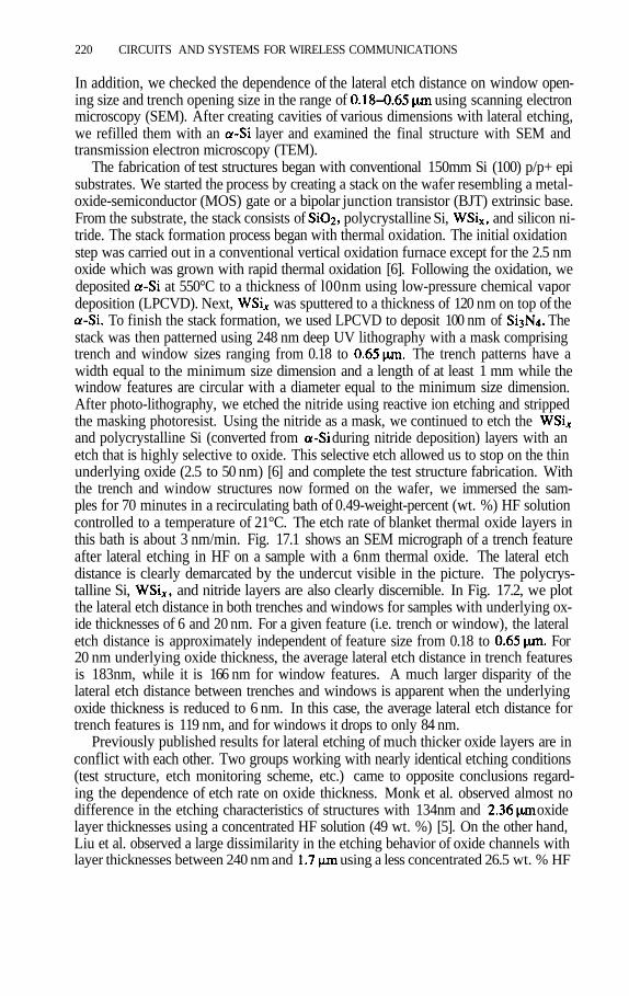
220 CIRCUITS AND SYSTEMS FOR WIRELESS COMMUNICATIONS
In addition, we checked the dependence of the lateral etch distance on window open-ing size and trench opening size in the range of using scanning electronmicroscopy (SEM). After creating cavities of various dimensions with lateral etching,we refilled them with an layer and examined the final structure with SEM andtransmission electron microscopy (TEM).
The fabrication of test structures began with conventional 150mm Si (100) p/p+ episubstrates. We started the process by creating a stack on the wafer resembling a metal-oxide-semiconductor (MOS) gate or a bipolar junction transistor (BJT) extrinsic base.From the substrate, the stack consists of polycrystalline Si, and silicon ni-tride. The stack formation process began with thermal oxidation. The initial oxidationstep was carried out in a conventional vertical oxidation furnace except for the 2.5 nmoxide which was grown with rapid thermal oxidation [6]. Following the oxidation, wedeposited at 550°C to a thickness of l00nm using low-pressure chemical vapordeposition (LPCVD). Next, was sputtered to a thickness of 120 nm on top of the
To finish the stack formation, we used LPCVD to deposit 100 nm of Thestack was then patterned using 248 nm deep UV lithography with a mask comprisingtrench and window sizes ranging from 0.18 to The trench patterns have awidth equal to the minimum size dimension and a length of at least 1 mm while thewindow features are circular with a diameter equal to the minimum size dimension.After photo-lithography, we etched the nitride using reactive ion etching and strippedthe masking photoresist. Using the nitride as a mask, we continued to etch theand polycrystalline Si (converted from during nitride deposition) layers with anetch that is highly selective to oxide. This selective etch allowed us to stop on the thinunderlying oxide (2.5 to 50 nm) [6] and complete the test structure fabrication. Withthe trench and window structures now formed on the wafer, we immersed the sam-ples for 70 minutes in a recirculating bath of 0.49-weight-percent (wt. %) HF solutioncontrolled to a temperature of 21°C. The etch rate of blanket thermal oxide layers inthis bath is about 3 nm/min. Fig. 17.1 shows an SEM micrograph of a trench featureafter lateral etching in HF on a sample with a 6nm thermal oxide. The lateral etchdistance is clearly demarcated by the undercut visible in the picture. The polycrys-talline Si, and nitride layers are also clearly discernible. In Fig. 17.2, we plotthe lateral etch distance in both trenches and windows for samples with underlying ox-ide thicknesses of 6 and 20 nm. For a given feature (i.e. trench or window), the lateraletch distance is approximately independent of feature size from 0.18 to For20 nm underlying oxide thickness, the average lateral etch distance in trench featuresis 183nm, while it is 166 nm for window features. A much larger disparity of thelateral etch distance between trenches and windows is apparent when the underlyingoxide thickness is reduced to 6 nm. In this case, the average lateral etch distance fortrench features is 119 nm, and for windows it drops to only 84 nm.
Previously published results for lateral etching of much thicker oxide layers are inconflict with each other. Two groups working with nearly identical etching conditions(test structure, etch monitoring scheme, etc.) came to opposite conclusions regard-ing the dependence of etch rate on oxide thickness. Monk et al. observed almost nodifference in the etching characteristics of structures with 134nm and oxidelayer thicknesses using a concentrated HF solution (49 wt. %) [5]. On the other hand,Liu et al. observed a large dissimilarity in the etching behavior of oxide channels withlayer thicknesses between 240 nm and using a less concentrated 26.5 wt. % HF

LOW-COST SiAND BiCMOS FOR WIRELESS APPLICATIONS 221
solution [4]. Liu attributed the thickness dependence of the etching to a liquid-solidinteraction between the silicon nitride over-layer and the HF solution. In our very thinoxide layers (less than 20 nm), we also see a pronounced reduction of the etch ratewith oxide thickness. It is not readily apparent that the oxide should be etched at allgiven the extremely small dimension of our thinnest sample (2.5 nm) which is on theorder of only 5 Si lattice constants. The etch solution may be forced into the cavity bycapillary action or it may be drawn in by the hydrophilic nature of the oxide surface.
The lateral etching of these cavities appears to be roughly described by simple mod-els for capillary flow. The speed of liquid flow into a capillary can be approximatedby [7]
where RH is the ratio between the volume and surface area of the cavity, andare surface free energies between the solid-vapor and solid-liquid interfaces, and isthe viscosity of the liquid. For a rectangular cross-section capillary with a length muchgreater than its height, the liquid penetration after time t is given by
where h is the cavity height. Therefore the extent of the lateral etch after time t isproportional to the square root of the cavity height. Based on the data of Fig. 17.2, theratio of lateral etch depths for the two different cavity heights of 20 and 6 nm varies

222 CIRCUITS AND SYSTEMS FOR WIRELESS COMMUNICATIONS
between 1.5 and 2, while the square root of the ratio of the cavity heights is 1.8. Thisresult suggests that capillary action may be important for the etching of these smallstructures, however, further investigation is necessary.
For transistor applications, the cavity formed by the lateral etch of the oxide mustbe refilled with a conducting film to facilitate a contact to the crystal region. As thegate length of Si CMOS technology scales downward, the gate oxide thickness of thetransistor also scales downward. In order to achieve the maximum cost reduction ina BiCMOS technology, the lateral etch and refill process must be accomplished usingthe gate oxide to form the cavity. Therefore, we studied oxide thicknesses down to2.5 nm to cover the low end of the range expected for the next few generations ofCMOS technology.
In our test structures, we refilled the cavity with deposited at 550°C usingLPCVD at 250mTorr. Fig. 17.3 exhibits the TEM results from the refill of intogaps ranging from 50 nm down to just 2.5 nm. Even in the thinnest sample, the refill ofthe cavity is complete without the appearance of large voids, which demonstrates thatthe deposition process is extremely conformal. This result shows that this techniqueindeed has great promise for future generations of BiCMOS technology. In the sam-ples with cavity thickness greater than 2.5 nm, the convergence of the top and bottomgrowth fronts is visible. In the 2.5 nm sample, however, the border of the growth frontsis not visible due to taper introduced into the gap before the refill process. This tapermay come about from native oxide formation and removal. In all the samples, one cannotice that the refilled region is slightly thicker than the oxide thickness, which maybe due to native oxide formation along the top and bottom of the cavity walls while
awaiting deposition. The native oxide is removed by a short etch in dilute HFimmediately prior to deposition, leaving behind a larger cavity, which is most easilyseen in the TEM images of the thinnest samples. We also note that other experimentsshow that the border created by the coalescence of the top and bottom growth frontsdisappears completely in all samples after a rapid thermal anneal (RTA) at 1050°C for10 seconds.
17.4 HETEROSTRUCTURE BIPOLAR TRANSISTORS
The gain in a Si bipolar transistor is expressed as
where D is the minority carrier diffusion coefficient, is the emitter thickness, isthe base thickness, and N is the doping concentration. Modern Si bipolar devices arequickly approaching vertical scaling limits with base widths in the order of 50–80 nmand base doping levels well above The desire to reduce the base thicknessfurther to increase device speed is hampered by two fundamental constraints.First, the base doping level cannot be raised substantially above aboutbecause of the onset of high tunneling currents at the emitter–base junction. A higherbase doping level is required to avoid punch-through between the emitter and collectorand is desired to minimize base resistance (increase Secondly, the need tomaintain sufficient current gain requires that the emitter doping (which is already atthe solid solubility) be substantially higher than the base doping.
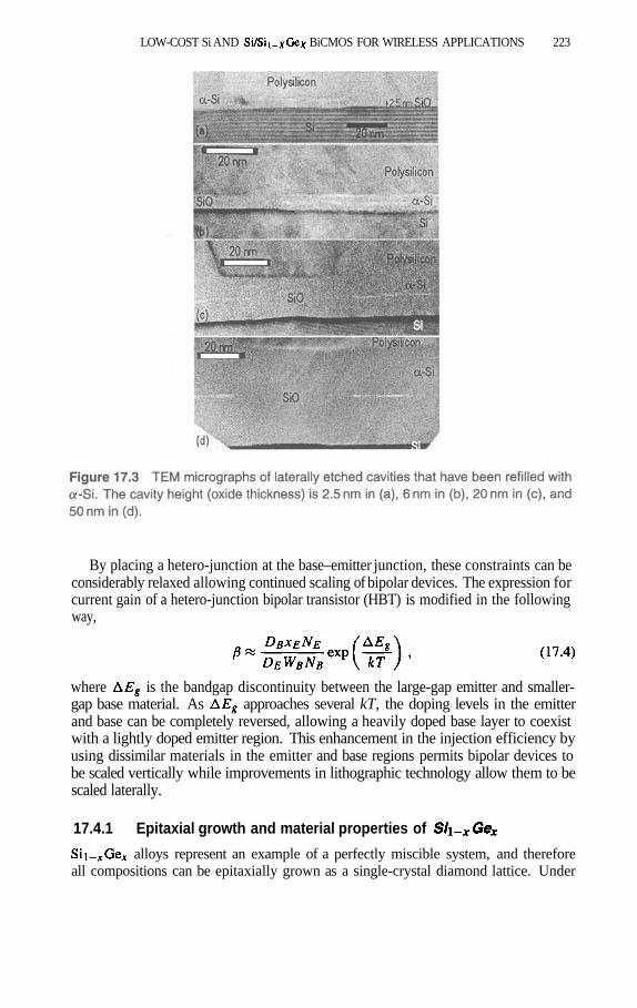
LOW-COST Si AND BiCMOS FOR WIRELESS APPLICATIONS 223
By placing a hetero-junction at the base–emitter junction, these constraints can beconsiderably relaxed allowing continued scaling of bipolar devices. The expression forcurrent gain of a hetero-junction bipolar transistor (HBT) is modified in the followingway,
where is the bandgap discontinuity between the large-gap emitter and smaller-gap base material. As approaches several kT, the doping levels in the emitterand base can be completely reversed, allowing a heavily doped base layer to coexistwith a lightly doped emitter region. This enhancement in the injection efficiency byusing dissimilar materials in the emitter and base regions permits bipolar devices tobe scaled vertically while improvements in lithographic technology allow them to bescaled laterally.
17.4.1 Epitaxial growth and material properties of
alloys represent an example of a perfectly miscible system, and thereforeall compositions can be epitaxially grown as a single-crystal diamond lattice. Under

224 CIRCUITS AND SYSTEMS FOR WIRELESS COMMUNICATIONS
certain growth conditions on silicon, such alloys will grow as isolated “islands” ratherthan as a continuous two-dimensional plane. This three-dimensional growth is appro-priately termed “island growth”. Early molecular beam epitaxy (MBE) investigationsinto the deposition of Ge on Si repeatedly encountered problems with island growth.Two-dimensional planar growth was not achieved until Kasper demonstrated that theislands disappear when alloys are grown on Si with Ge mole fractions lessthan 20 % [8–10]. Bean et al. later discovered that all compositions of willgrow island free, if the substrate temperature is kept within a window enclosed bypolycrystalline growth on one side and island growth on the other [11]. They foundthat a substrate temperature of 550°C is within this window for all Ge concentrations.The onset of island formation is dependent on the germanium fraction in the alloyand occurs at increasingly higher growth temperatures as the germanium fraction islowered. This ground-breaking discovery paved the way for future implementationsof alloys in devices.
Once two-dimensional planar growth is attained, there are still two options for themanner in which the alloy can grow on the Si substrate: strained and unstrained. Inthe case of an unstrained alloy on a Si substrate, the larger equi-librium lattice constant is maintained and, due to the difference in registration with theSi substrate, misfit dislocations occupy the inter-facial region. Misfit dislocations addenergy to the system in the form of dangling bonds, making the other mode of planargrowth, strained layer growth, energetically favorable under certain conditions.
For the case of strained layer growth of on a Si substrate, the in-plane lat-tice constant of the alloy layer compresses to match that of the underlying Si substrate.Because of the relative thicknesses of the epitaxial layer and the substrate, the changeof the lattice constant of the Si substrate is negligible. Strain also adds energy to thesystem since the bond angles are altered. Strain energy increases with layer volume.Consequently, at some layer thickness, the energy to maintain strain in the growinglayer will overcome the energy to produce misfit dislocations at the interface. Manyresearchers explain strained layer growth using equilibrium analysis. From equilib-rium calculations, one may find a critical thickness at the point where layer growthreverts from strained to unstrained.
Fig. 17.4 shows the observed critical thickness for a Si-capped alloy layeron Si as a function of Ge mole fraction. Grown thicknesses above the curve indicatemeta-stable or unstable layers that are prone to misfit dislocation formation. Layerthicknesses at or below the curve are completely stable and will not relax through theprocess of misfit dislocation formation. Relaxation can occur, however, through theprocess of Ge diffusion, which transpires at sufficient thermal treatments (1000°C forseveral minutes). On the other hand, boron diffusion of the base is a greater concernfor HBTs at these thermal budgets.
From Eq. (17.4), we noted that the bandgap discontinuity, is a very impor-tant parameter to determine the injection efficiency enhancement of an HBT devicestructure over that of a Si homo-junction structure. Fig. 17.5 displays the bandgapdiscontinuity for both strained [12] and unstrained [13] as a function of Gecomposition. In the unstrained material, the bandgap changes rather slowly with Gecomposition until a value of about 85 % is reached, at which point the bandgap dif-ference rises quickly. In the case of strained material, is large with even smallfractions of Ge and continues to rise. When the Ge fraction reaches values of only

LOW-COST Si AND BiCMOS FOR WIRELESS APPLICATIONS 225
60 % in the strained layer, the actual bandgap is smaller than that of pure Ge! There-fore, not only it is important for HBT applications to maintain complete strain in thealloy layer to avoid misfit dislocations, but also to obtain the maximum possiblefor a given Ge fraction.
17.4.2 bipolar transistor structuresSince the first results that appeared in 1988, many researchers have begun examin-ing the prospects of HBTs. Because other hetero-junction systems have

226 CIRCUITS AND SYSTEMS FOR WIRELESS COMMUNICATIONS
been studied for years, many of the ideas conceived for HBTs in those materials arebeing applied to the system. Compositional grading at the device junc-tions, compositional grading in the neutral base, and the use of a lightly doped emitterare among some examples of ideas retrofitted for hetero-junctions. Inaddition, since this hetero-junction system is silicon based, researchers apply manyconcepts from silicon technology as well. Processes and ideas include poly-siliconemitters, ion implantation, rapid thermal and furnace annealing, and selective epitax-ial growth. Most of the work to date can be divided into two groups. The first classof devices contains standard HBTs which utilize a single-crystal emitter and a base-emitter hetero-junction to achieve an increase in injection efficiency. The devices inthe second class use a poly-silicon emitter to increase injection efficiency and gradingof the bandgap in the neutral base region to introduce an electric field to speed thetransport of minority carriers across the base.
Graded-base bipolar transistors. Patton et al. [14,15] first introduceddevices employing a poly-silicon emitter with a graded Ge profile. These devices usea Ge profile in the base that is graded from 0 % at the base-emitter junction up to avalue of about 15 % at the base-collector junction. A secondary ion mass spectrom-etry (SIMS) plot of the Ge and boron profiles for this graded-base process is shownin Fig. 17.6. The graded Ge profile introduces a built-in electric field in the quasi-neutral base that reduces the transit time of injected electrons across the base therebyincreasing fT. The vertical doping profile, and thus the base sheet resistance, can-not be altered from the homo-junction case, since the band offset at the base-emitterjunction is near 0 eV.
Although grading the bandgap in the neutral base region lowers the base transittime, it does little to affect issues that address bipolar scaling. Since no hetero-junctionis formed (aside from the poly-silicon/single crystal Si interface) at the base-emitterjunction, base doping and current gain are still intimately coupled. Clearly, bandgap

hetero-junction bipolar transistors. The strained-alloy bases withmuch higher Ge fractions (~30%) [16, 17] which are used in Si/SiGe HBT struc-tures allow much higher base doping to ). HBTs havedemonstrated impressive figures of merit for both frequency response and noise per-formance [18]. However, these transistors were fabricated using blanket epitaxy cou-pled with a double-mesa process that makes integration very difficult. In our workat Lucent, we demonstrate a device structure usable for high-level integration whichutilizes an aggressive vertical profileand in a planar transistor.
Fig. 17.7 shows our device structure. We used rapid thermal epitaxy (RTE) to growthe layer structure, utilizing the limited-reaction-processing mode of growth [19]. Asecondary ion mass spectrometry (SIMS) plot after the device fabrication of a struc-ture with is illustrated in Fig. 17.8. The very narrow base widthis approximately 18 nm, which is below the equilibrium critical thickness for a capped
layer The boron base dop-ing is contained within the strained layer, indicating that transient enhanced diffusioneffects are not important. The As profile shown in Fig. 17.8 is interrupted in the
layer due to mass interference effects between Ge and As. These effectsalso lead to an exaggerated value of the As concentration close to the base-collectorjunction.
To evaluate the high-frequency performance of these transistors, we measured theS-parameters in common-collector mode from 2 to 18 GHz using a vector network an-alyzer and separated the effect of the parasitic pad capacitance using the Y-parametersubtraction technique. Devices with yielded fT = 54 GHz, andwith Extraction of the intrinsicdelay using vs. yields an intercept of 2.9 ps and a
LOW-COST Si AND BiCMOS FOR WIRELESS APPLICATIONS 227
grading increases fT over a homo-junction device, but it only weakly enhances injec-tion efficiency. Therefore, further scaling of the base width cannot be accomplishedwith neutral base bandgap grading alone. For high-speed bipolar circuits, both lowbase resistance and high cutoff frequency are important. Graded-base devices providea good initial step for using SiGe, since existing bipolar processes can largely be usedrequiring only the exchange of an implanted base with an epitaxially grown one. Thetrue performance limits of SiGe bipolar devices will be attained with Si/SiGe HBTs.
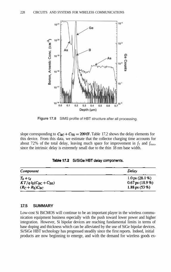
228 CIRCUITS AND SYSTEMS FOR WIRELESS COMMUNICATIONS
slope corresponding to Table 17.2 shows the delay elements forthis device. From this data, we estimate that the collector charging time accounts forabout 72% of the total delay, leaving much space for improvement in fT and fmax,since the intrinsic delay is extremely small due to the thin 18 nm base width.
17.5 SUMMARY
Low-cost Si BiCMOS will continue to be an important player in the wireless commu-nication equipment business especially with the push toward lower power and higherintegration. However, Si bipolar devices are reaching fundamental limits in terms ofbase doping and thickness which can be alleviated by the use of SiGe bipolar devices.Si/SiGe HBT technology has progressed steadily since the first reports. Indeed, initialproducts are now beginning to emerge, and with the demand for wireless goods ex-

quency measurements of a transistor yielded a peak fT of 54 GHz. Theperformance is expected to be greatly enhanced by reducing the junction capacitances(CBC and CTE) through minor changes in processing conditions.
References
[1] Y.-F. Chyan, M. S. Carroll, T. G. Ivanov, A. S. Chen, W. J. Nagy, S. Chaudhry,R. W. Dail, V. D. Archer, K. K. Ng, S. Martin, M. Oh, M. R. Frei, I. C. Kizilyalli,R. Y. Huang, M. J. Thoma, C. A. King, W. T. Cochran, and K. H. Lee, in Proc.of the Bipolar/BiCMOS Circuits and Technolgy Meeting, pp. 128–129, (1998).
[2] Y. Kinoshita, K. Imai, H. Yoshida, H. Suzuki, T. Tatsumi, and T. Yamazaki, inIEDM Tech. Digest, pp. 441–444, (1994).
[3] M. Ugajin, J. Kodate, Y. Kobayashi, S. Konaka, and T. Sakai, in IEDM Tech.Digest, pp. 735–738, (1995).
[4] J. Liu, Y.-C. Tai, J. Lee, K.-C. Pong, Y. Zohar, and C.-M. Ho, in Proceedings ofIEEE Micro Electro Mechanical Systems, Ft. Lauderdale, FL, 1993 (IEEE), pp.71–76.
[5] D. J. Monk, D. S. Soane, and R. T. Howe, “Hydrofluoric Acid Etching of SiliconDioxide Sacrificial Layers”, J. Electrochem. Soc., vol. 141, pp. 264–269, (1994).
[6] G. Timp, A. Agarwal, F. H. Bauman, T. Boone, M. Buonanno, R. Cirelli, V.Donnelly, M. Foad, D. Grant, M. Green, H. Gossman, S. Hillenius, J. Jackson,D. Jacobson, R. Kleiman, A. Kornblit, F. Klemens, J. T.-C. Lee, W. Mansfield,S. Moccio, A. Murrell, M. O’Malley, J. Rosamilia, J. Sepjeta, P. Silverman, T.Sorsch, W. W. Tai, D. Tennant, H. Vuong, and B. Weir, in IEDM Tech. Digest,pp. 930–931, (1997).
[7] E. Kim and G. M. Whitesides, “Imbibition and flow of wetting liquids in noncir-cular capillaries”, J. Phys. Chem. B, vol. 101, pp. 855–863, (1997).
[8] E. Kasper, H. J. Herzog, and H. Kibbel, “A one-dimensional SiGe superlatticegrown by UHV epitaxy”, Appl. Phys., vol. 8, pp. 199–205, (1975).
[9] E. Kasper and W. Pabst, “Profiling of SiGe superlattices by He backscattering”,Thin Solid Films, vol. 37, pp. L5–L7, (1976).
[10] E. Kasper and H. J. Herzog, “Elastic and misfit dislocation density in Si0.92Ge0.08films on Si substrates”, Thin Solid Films, vol. 44, pp. 357–370, (1977).
[11] J. C. Bean, T. T. Sheng, L. C. Feldman, A. T. Fiory, and R. T. Lynch, “Pseudo-morphic growth of on silicon by molecular beam epitaxy”, Appl. Phys.Lett., vol. 44, pp. 102–104, (1983).
[12] R. People, “Indirect band gap of coherently strained Si1–xGex bulk alloys on<100> silicon substrates”, Phys. Rev. B, vol. 32, pp. 1405–1408, (1985).
LOW-COST Si AND BiCMOS FOR WIRELESS APPLICATIONS 229
pected to expand in the coming years, the need for this technology will surely grow.Graded-base devices are a first step to increase the cutoff frequency, but further de-vice scaling will require an HBT structure with a high Ge fraction at the base-emitterjunction. In this paper, we introduced a process which utilizes selective and non-selec-tive rapid thermal epitaxy for growing a structure usable for high level integration andwhich uses a high Ge fraction of 30 % thereby permitting high base doping. High-fre-

230 CIRCUITS AND SYSTEMS FOR WIRELESS COMMUNICATIONS
[13] R. Braunstein, A. R. Moore, and F. Herman, “Intrinsic optical absorption ingermanium-silicon alloys”, Phys. Rev., vol. 109, pp. 695–710, (1958).
[14] G. L. Patton, D. L. Harame, J. M. C. Stork, B. S. Meyerson, G. J. Scilla, and E.Ganin, in Symp. on VLSI Technol. Dig. Tech. Papers, pp. 95–96, (1989).
[15] G. L. Patton, J. H. Comfort, B. S. Meyerson, E. F. Crabbé, G. J. Scilla, E. D.Fresart, J. M. C. Stork, J. Y.-C. Sun, D. L. Harame, and J. N. Burghartz, “75-GHzfT SiGe-base heterojunction bipolar transistors”, IEEE Electron Dev. Lett., vol.11, pp. 171–173, (1990).
[16] T. I. Kamins, K. Nauka, J. B. Kruger, J. L. Hoyt, C. A. King, D. B. Noble, C. M.Gronet, and J. F. Gibbons, “Small-geometry, high-performance, Si-Si1-xGex het-erojunction bipolar transistors”, IEEE Electron Dev. Lett., vol. 10, pp. 503–505,(1989).
[17] A. Schüppen, U. Erben, A. Gruhle, H. Kibbel, H. Schumacher, and U. König, inIEDM Tech. Digest, pp. 743–746, (1995).
[18] A. Schüppen, A. Gruhle, U. Erben, H. Kibbel, and U. König, in IEDM Tech.Dig., pp. 377–380, (1994).
[19] J. F. Gibbons, C. M. Gronet, and K. E. Williams, “Limited reaction processing:Silicon epitaxy”, Appl. Phys. Lett., vol. 47, pp. 721–723, (1985).

18 GaAs-BASED RFICTECHNOLOGY FOR CONSUMER
RADIOSRob Christ
TriQuint Semiconductor 2300 NEBrookwood Parkway Hillsboro
Oregon 97124, USA
Abstract: GaAs-based IC technologies are now firmly established in mobile phonesand wireless data transmission applications. The success of GaAs MESFET RFICs inrecent years comes from the need for improved performance for digital standards andfrom a significant reduction of the manufacturing costs for wafer fabrication. Whilethere is little doubt that the GaAs IC industry is important today, there are differingopinions about the role of RFIC technologies in future wireless systems. Some believethat GaAs MESFET technology will take over the entire RF section of future radios,while others believe the present foothold will be chipped away as higher performancesilicon technologies come on line. Yet others believe that alternate GaAs technolo-gies, such as pHEMT and HBT, will gain greater acceptance for specific RF functionalblocks. A minority believe that “radio on a chip” solutions in silicon will come to passand some think it will include SiGe. In this paper, the author discusses the future ofGaAs IC technologies in future commercial radio systems. The specific cost driversfor various process technologies are described and the key performance criteria that themobile phone makers demand are reviewed. The combination of these factors showstrends in system architectures for future mobile wireless systems.
231

232 CIRCUITS AND SYSTEMS FOR WIRELESS COMMUNICATIONS
18.1 THE RF-INTEGRATION PARADIGM IS DIFFERENT
As enabling components of the Information Age, wireless technologies are quicklymoving from mere curiosities and conveniences to indispensable pieces of modern life,much in the same way that digital technologies have made the computer the backboneof modern enterprise. The advent and maturing of silicon IC process technologieshave, over the last three decades, made the stunning achievements in modern com-puting possible. In hindsight it may seem that the current dominance of CMOS ICtechnologies was inevitable. However, only since the massive worldwide investmentin CMOS production capacity in the 1980’s has it become clear that the staggeringachievement represented in Moore’s Law (in which former Intel Chairman GordonMoore stated that the density of digital ICs would double at half the cost every threeyears) could be realized.
It is natural to extrapolate the success exemplified by Moore’s Law to all subse-quent IC technologies, but this ignores the fact that Moore’s Law has not worked forhigh-performance analog and RF ICs. RF applications especially have stubbornly re-sisted integration. Some workers in the analog IC community, well represented by theparticipants in this publication, believe that this resistance will be broken by the in-evitable improvements in the high-frequency performance of CMOS. This view takento its extreme gives rise to the dream of “radio on a chip” integration. Following thedigital integration paradigm, there are several assumptions built into the argument forultimate RF integration in CMOS. Some of these assumptions are:
1. All Silicon is Cheap
2. Transistor Frequency Performance is the Limiting Factor
3. “Radio on a Chip” is Possible or Desirable
It is shown below that these assumptions do not stand up to close scrutiny, and thatfuture wireless systems will contain a mixture of silicon and GaAs IC technologies.
18.2 WHERE IS RF INTEGRATION BEING USED?
Mobile telephones are currently the highest-volume application for high performanceRF circuits. Until recently RF front-end circuits have been dominated by discretedevices. As the complexity of mobiles has increased and as TDMA and CDMA digitalsystems have come on line, we have seen a dramatic increase in the level of integrationin the baseband and signal processing functions with the widespread use of DSP andintegrated silicon for low frequency IF and analog functions. This has resulted ina commensurate decrease in the number of components needed for these functions.However, the RF portion of the radio has resisted integration until very recently.
The greatest success for RF integration has been in receiver front-end circuits forGSM and DCS-1800 systems. Through the use of very sophisticated circuit designtechniques in high performance silicon BiCMOS, suppliers like Siemens and Philipshave successfully penetrated the market with modestly priced ICs. Dual band ICs forGSM and DCS-1800 are selling for approximately 2–3 US$ in million-piece quanti-ties. These circuits can be built mainly because the GSM standard is undemanding forIIP3 (input 3rd order intercept point) and Noise Figure, and because these ICs make use
GaAs-BASED RFIC TECHNOLOGY FOR CONSUMER RADIOS 233
of a large number of external discrete passive components. Current silicon BiCMOSreceiver ICs require more than 60 external components, for example.
Since GSM standards are very well established and mobile handsets are becomingmore like a commodity, there are few opportunities left for the introduction of new ICprocess technologies. The level of silicon integration in GSM and DCS-1800 handsetsis likely nearing its peak. It will be in the newer and less widespread standards, such asTDMA IS-136 in the US, narrow-band CDMA IS-95 and the new wide-band CDMAlikely to be used for 3rd generation systems, where most of the challenging IC technol-ogy choices will still be made. Unfortunately for integrated silicon, whether CMOS orBiCMOS, the requirements for noise, linearity and power efficiency are much tougherthan those for GSM. It is easy to have a GSM-centric viewpoint, especially outsidethe US, since GSM has become so dominant with so much popular appeal throughoutthe world. However, it is not a good idea to concentrate solely on GSM when lookingat trends for future systems. Other systems like IS-136 and IS-95 offer important ex-amples of the demands to be put on IC technologies for RF sections of future mobilephones. With this in mind, it is illustrative to compare what IC technologies are beingused in today’s digital mobile phones of different standards (see Table 18.1).
18.3 GaAs FOR MOBILE POWER APPLICATIONS
It is noteworthy that the GaAs content of an RF system increases generally as the lin-earity requirements of the system increases. This is true for both transmit and receivesides of the RF section. Based on the clear demand for maximum power efficiency,GaAs has dominated power amplifiers, especially in 3-volt systems. There has beensome competition from LDMOS (laterally diffused MOS) in integrated modules, pri-marily from Japanese manufacturers, but these have been limited to 5-volt systems (or3-volt systems with built-in voltage doubler) with lower linearity requirements.
With existing and emerging TDMA and CDMA systems, adjacent channel power(ACP) performance becomes much more important. This is where GaAs MESFETtechnology has a distinct advantage. For fully saturated power amplifiers, poweradded efficiency (PAE) values exceeding 60 % are routinely achieved, exceeding theefficiency of Bipolar and LDMOS power amplifiers. Narrow-band CDMA systemsin particular have very stringent ACP requirements. For these systems, especially at3 volts, no other process technology has achieved greater than 35 % PAE in commer-cially available circuits. This is a result of the very low “knee” voltage (voltage that de-notes the transition from linear to saturated operation of the FET) of GaAs MESFETs.State-of-the-art power MESFETs have or less, while silicon MOSFETshave or more. Therefore, as wide-band CDMA systems come into beingfor 3rd generation systems, it is clear that GaAs MESFET technology will continue tohave a bright future for mobile power amplifiers.
Two other GaAs technologies also show significant promise for power amplifiers.GaAs based hetero-junction bipolar transistors (HBT) are currently being used in highvolume power amplifiers for GSM and IS-136 mobiles. The major benefits of HBTtechnology are low leakage, high PAE and reasonable linearity with a single powersupply. The main disadvantages are the high cost and control issues associated withGaAs epitaxy growth. Much of this cost can be mitigated by the smaller die sizesachievable in HBT technology. It is not clear at this time whether MESFET or HBT

234 CIRCUITS AND SYSTEMS FOR WIRELESS COMMUNICATIONS
will, in the long run, be more economical for power amplifiers. The other GaAs-basedtechnology that has promise for power amplifiers is pseudo-morphic high electron mo-bility transistors (pHEMT). pHEMTs make the most power-efficient power amplifiers,especially at very low voltages and high frequencies. However, since pHEMT poweramplifiers cannot be made significantly smaller than MESFET power amplifiers, thehigh cost of epitaxy material limits the use of pHEMTs in L-band and S-band mobiles.pHEMTs will likely remain in the domain of high frequency systems, at X-band andabove.

GaAs-BASED RFIC TECHNOLOGY FOR CONSUMER RADIOS 235
18.4 GaAs IN MOBILE RECEIVERS
Even most “radio on a chip” proponents admit that GaAs has a strong future in poweramplifiers. However, they feel that small-signal RF parts, especially receivers, arethe eventual exclusive domain of integrated silicon. Again the picture is not so clear.As seen above, standards that require higher linearity (as designated by ACP specifi-cations) tend to use GaAs for receiver LNAs plus down-conversion mixers. CMOSsolutions, as presented by other authors in this book, require ever more elaborate cir-cuit techniques to meet even the very modest requirements of GSM and DCS-1800.Again, meeting the linearity requirements of more challenging standards with simul-taneously low current draw favors the use of GaAs MESFET technology. The currentconsumption of receiver circuits is critical, since receivers are continuously on in mo-bile systems during standby. Today’s extremely long standby times in IS-136 systems,for example, are largely due to the use of GaAs MESFET technology in receiver LNAplus mixer ICs. The four major specifications that are important for receivers are: 1)Noise figure, 2) Linearity (as in IIP3 or ACP), 3) Gain, and 4) Current draw. GaAsMESFETs allow the simultaneous optimization of all four of these specs in a waynot possible in CMOS. For example, the following specifications are only simultane-ously possible and commercially available in a GaAs MESFET based IC for 900 MHzIS-136:
ACP/ALT > –29dBc/ –49dBcRx LNA/Mixer I I P > –8.5 dBmNF<2.7dBG=18.5dBIdd < 10mA
(Refer to TriQuint’s TQ9222 data-sheet.)GaAs is not suitable for many of the low-frequency and digital functions of mobile
handsets, but the technology has significant applicability for Tx up-converters, driveramplifiers, power amplifiers, and Rx LNAs and down-converter mixers. If it is so clearthat technical advantages can be realized by using GaAs MESFET technology, whyis there so much talk about stopping the spread of GaAs circuits and even replacingGaAs in mobile systems? This effort is fueled largely by the silicon digital integrationparadigm discussed above.
18.5 TESTING THE ASSUMPTIONS
The mobile phone and wireless data hardware markets are brutally competitive. Anysmall cost advantage for performance that is “just good enough” is quickly exploited.With product life cycles of less than a year, there are continuous opportunities to insertnew components into these systems. These pressures have led to dramatic improve-ments for integrated DSP and baseband functions. But, as mentioned earlier, the RFsection has steadfastly resisted integration in silicon except in a few limited cases. Thereasons go to the heart of the assumptions built into the “radio on a chip“ paradigm.Let’s examine these assumptions.
Assumption #1: All Silicon is Cheap. This assumption comes from the notionthat all silicon processes can take advantage of the economies of scale available todigital circuits. For state-of-the-art processing, the lowest cost per comes fromCMOS used for memories and microprocessors. The costs for DRAM processing are

236 CIRCUITS AND SYSTEMS FOR WIRELESS COMMUNICATIONS
fairly well known since these costs are monitored by the United States Department ofCommerce as part of anti-dumping cases against Japanese and Korean DRAM makers.DRAM CMOS costs roughly 4 US cents per mm2 for 200 mm wafers depending onutilization and yields.
This may be well and good, but digital CMOS processes are not useful for RFICs.RF silicon is produced in much lower volumes, typically using 6-inch or smallerwafers. Rather than being defect-density limited, RFIC yields are strongly drivenby parametric specifications. As a result, even for the highest volume silicon RFprocesses the costs per mm2 are substantially higher. Unfortunately, these costs arenot as well reported, but judging from foundry prices, these costs are at least 50 %higher for high volume on 6-inch wafers, up to three or four times the cost for thehighest-performance (Ft> 20GHz) BiCMOS processes. These costs are similar to thecost of GaAs MESFET processing for 4-inch wafers in moderate volume.
There is little mystery about the cost drivers in the semiconductor industry, whetherCMOS, silicon bipolar or GaAs. If we assume that the cost of packaging and testingis roughly the same whether the chip is silicon or GaAs, it is the cost of the processedchip where the real cost differences arise. The cost of a processed RFIC chip is afunction of:
Materials: wafers, chemicals, metalsNumber of Masking Layers: time in the fab, equipment utilization, laborFab Capacity Utilization: spreading fixed costYield: wafer level, die levelThe primary disadvantage of GaAs has traditionally been the cost per mm2 of the
starting wafer, which can be 10 times the cost of a silicon wafer or about 4 to 5 timesthe cost of silicon epitaxy wafer. However, this is offset by the second componentof cost. GaAs MESFET processing is significantly shorter than competing siliconprocesses. For example, a GaAs process with 2 FET types, capacitors, thin film resis-tor and 3 layers of metal is 14 layers. By comparison, RF bipolar processes with thesame functionality have 21 layers, and BiCMOS processes run 25 or more layers. Themain advantage of silicon processing is that it is run in higher volumes with better fabcapacity utilization. As GaAs moves up the volume curve and to 6 inch wafers, thisadvantage of silicon will evaporate. Finally, yield is often the biggest lever in any fab,given the variable nature of yields in any analog processing line. For the larger-volumeGaAs suppliers, wafer line yields of 80–90 % are common today, equivalent to siliconRF processes.
Assumption #2: Transistor Frequency Performance is the Limiting Factor.There have been steady improvements in the frequency performance of CMOS andsilicon bipolar transistors. As gate lengths decrease to and below, the cutofffrequency of n-channel MOS transistors exceed 10 GHz, which is in the range ofsuitability for building RF circuits with usable gain. Likewise, RF bipolar processeswith are now commercially available. In the extreme, some SiGe HBTtransistors have While transistor frequency performance is important, itis important to look deeper. First, is a misleading, some would say irrelevant, para-meter for RF circuits as opposed to baseband linear circuits. Instead, is a bettermeasure of RF performance, since it applies to power gain. is proportional toby the factor of input resistance (Gate resistance for FETs, or Base resistance for bipo-lar). So while silicon technologies may have impressive values, the high resistance

GaAs-BASED RFIC TECHNOLOGY FOR CONSUMER RADIOS 237
of poly-silicon gates in MOS and thin bases in bipolar, limit the values to barelymore than and sometimes even less. It is difficult to find MOS or bipolar transistorswith values that exceed 20 GHz. In contrast, the very low gate resistance of GaAsMESFETs (typically less than give values 3 to 4 times For example, a
GaAs MESFET with has The importance of thisfor RF circuits cannot be overstated. High allows circuits to have enough gainoverhead to produce very low noise figure with high linearity simultaneously.
But even high is not enough to produce competitive RF circuits. The other im-portant factor is the influence of parasitics. The conductive silicon substrate severelylimits the ability to build high-Q passive structures and to achieve isolation on chip.As a result, all “radio on a chip” circuits still have a large number of external passivecomponents. Also, these circuits must use fully differential topologies in order to dealwith the cross-coupling and isolation issues. As a result, practical CMOS based RFcircuits ironically consume more current than discrete implementations. Therefore,the main advantage of GaAs MESFET RFICs is not necessarily higher performancethan silicon RFICs or discretes, rather it is achieving the performance standards forchallenging standards with lower current.
Assumption #3: “radio on a chip” is Possible or Desirable. The term “radio ona chip” is somewhat misleading. Even the strongest proponents of this approach, rep-resented in other chapters of this book, readily admit that many of the important partsof the radio cannot be effectively integrated in silicon. These include filters, high-Qpassive components, duplexers/switches, and most importantly power amplifiers. Ifthese are not considered part of the radio, then the definition of “radio on a chip” isarbitrarily limited to that which can be integrated in silicon. Since even the most in-tegrated approaches have many dozens of external components, pushing all functionsinto a single IC becomes merely an academic exercise.
It is telling that the only serious discussion of “radio on a chip” topologies is beingdone by university professors. One possibility for this may come from the belief thatit is only a matter of advancing research to the point where industry can implementthe new topologies. While this may be the case in some circumstances, “radio on achip” research in fact misses a key marketing reality. The more you integrate, themore flexibility is sacrificed. Creating a new IC product requires huge investments inengineering and time. Therefore, IC designs must be useful long enough to producean adequate return on investment. With the very short life cycle of mobile phones, ICdesigns must be useful for several generations. Also, it is impossible to completelyknow in advance exactly what performance and features ICs will need to have be-fore the mobile phone designs have been completely worked out. Therefore, flexibledesigns are crucial for making a commercially viable IC.
Digital circuits have overcome the need for flexibility in three ways:
1. When the function has become fully commoditized, like DRAM or Flash ROM.Therefore, the standards are known long in advance, de facto.
2. When the circuits are customizable or programmable. Programmable logic arraysand DSP can be used for several generations of systems, since their programs canbe changed.

238 CIRCUITS AND SYSTEMS FOR WIRELESS COMMUNICATIONS
3. When the standards are set by the semiconductor maker. Intel Corporation enjoysthe ability to make microprocessors that determine the direction of computer devel-opment. All others must follow.
None of these conditions are likely to be present in the RFIC market any time soon,if ever. When integration occurs, it will be driven by powerful economic and politicalforces. As of this writing, there are no compelling reasons for semiconductor makersto invest in a single-chip RF solution in CMOS, when a multiple-chip solution usingIC technologies optimized for different parts of the radio provide the flexibility andperformance that system makers desire. The goal for system makers is for optimumintegration, rather than total integration. Even in the digital world, chip partitioning isthe key for optimum cost and yield. For this reason, Pentium® II modules are actuallycomposed of multiple chips each optimized for different functions. Likewise, with thewidely divergent demands on IC technologies in RF systems, there is little incentiveto push all functions into a single sub-optimized CMOS IC.
18.6 ADVANTAGES AND DISADVANTAGES OF DIFFERENT RFICTECHNOLOGIES
Each RFIC technology has its advantages and disadvantages. Tab. 18.2 is a briefsummary of the features of each technology. As this is a simplistic list of “pluses”and “minuses” rather than a comprehensive analysis, and because these technologieswill change overtime, it is important to not read too much into the details of the list.Rather, the purpose of the list is to illustrate that each RFIC technology has its place inthe range of choices available for RF systems. Tab. 18.3 shows the relative advantagesand disadvantages of RFIC technologies for various RF blocks.
18.7 PREDICTING THE FUTURE: WHERE ARE CONSUMER RADIOSGOING?
With little doubt, the picture will remain complicated for mobile phones. As long asthere are multiple standards, and with product life cycles so short, there will remainmany opportunities for the various IC technologies to be used. Fig. 18.1 is a diagram ofa typical mobile today. It schematically illustrates the fact that the RF section remainsfragmented, dominated by discrete devices and single-function ICs.
Fig. 18.2 shows a likely scenario for future systems. There may be opportunities forfurther integration in digital and analog sections, but the greatest change will be in theRF section. Since there will be continuing needs for various technologies optimizedfor the different RF blocks, multi-chip RF modules pulling together these technologiesis a more likely than “radio on a chip” integration in CMOS.
Likely future RF developments favor increased use of GaAs for two major reasons:
1. Increased demand for linearity, noise and power efficiency performance as de-scribed above.
2. Insulating substrate allows for integration of high quality passives (Q > 17 @2 GHz, for example) and excellent pin to pin isolation.

GaAs-BASED RFIC TECHNOLOGY FOR CONSUMER RADIOS 239
As a result for half duplex TDMA systems, ICs merging PA plus Switch plus LNAin GaAs are attractive without compromising RF performance. For CDMA systems,which have very large dynamic power control requirements favoring GaAs, ICs merg--ing PA plus Driver Amp plus Up-converter in GaAs are also attractive. Since CDMAsystems are full duplex, it is unlikely that it will be possible to merge Rx and Tx in asingle IC of any technology, even GaAs. Therefore, receiver ICs will likely stay sepa-rate from transmit ICs in CDMA. Direct Conversion Rx in Si CMOS remains a strongpossibility for less challenging standards like GSM. Regardless of process technology,

240 CIRCUITS AND SYSTEMS FOR WIRELESS COMMUNICATIONS
it appears that RF circuits will modularize into commodity chip sets by standard. Onlythen will a consensus emerge. And only then will it be clear what the optimum levelof RF integration will be for each RF block.
18.8 LOW-TECH GaAs MESFETS: COST-EFFECTIVE RF INTEGRATION
The main reason why GaAs has successfully penetrated consumer radios is that ion-implanted MESFETs have become a main-stream IC technology. Using productionIC process tools and processing techniques including ion implantation, along withlow cost surface mount packaging, GaAs MESFET manufacturing can take advantageof the economies of scale of silicon IC manufacturing. When this is parleyed with theinherent RF advantages of an insulating substrate, low-loss metalization and low-dis-

GaAs-BASED RFIC TECHNOLOGY FOR CONSUMER RADIOS 241
tortion/low-noise FETs, GaAs MESFET technology provides a natural foundation foroptimum RF integration.
The state of the art in production ion implanted GaAs RFIC technology for mobilephones is well represented by TriQuint Semiconductor’s TQTRx process. As its nameimplies, the process is useful for receive and transmit applications. Currently, tens ofmillions of LNA, Mixer and Power Amplifier ICs built in TQTRx are being shippedper year. As shown in Tab. 18.4, TQTRx has Enhancement (normally off), Depletion(normally on) and Power FETs integrated with thin film resistors, MIM capacitorsand three layers of gold metalization. Fig. 18.3 shows a cross sectional diagram ofTQTRx.
18.9 CONCLUSION
The Role of GaAs in Consumer Radios: It is rare in any high-technology business tosee clear directions for which component technologies will dominate future systems.When a very promising new application arises, technology proponents and componentsuppliers scramble to take advantage of the opportunity. Wireless systems includingmobile phones, pagers and wireless data systems are certainly “killer applications” forthe late 1990s.
In the inevitable response to the opportunities in wireless, the proponents of vari-ous RFIC technologies have lined up to take part in the excitement. Some proponentsof highly integrated CMOS “radio on a chip” ICs are quick to say that the domi-nance of CMOS in digital systems will naturally extrapolate to RF. Even if it weretechnically possible to produce these circuits, to say that they would be commerciallyviable ignores some fundamental market realities. By testing the assumptions built

242 CIRCUITS AND SYSTEMS FOR WIRELESS COMMUNICATIONS
into the reasons for integration, it is clear that multiple IC technologies will be used

GaAs-BASED RFIC TECHNOLOGY FOR CONSUMER RADIOS 243
in consumer radios for the foreseeable future. This will be especially true as morechallenging standards come on line.
Because of the inherent advantages of GaAs IC processes for RF circuits, GaAshas a very bright future in the RF blocks in consumer radios. Instead of searching for“one size fits all” solutions, RF systems designers search for components that provideoptimum solutions, in both cost and performance, for each part of the system. As amature IC technology, GaAs MESFET provides many opportunities for low-cost sys-tem insertions with the necessary RF performance and higher power efficiency thansilicon. While virtually everyone admits that GaAs has advantages for power ampli-fiers, closer examination reveals that GaAs also offers significant power advantagesthroughout the RF section of mobile phones. These advantages will become enablingcomponents for 3rd generation systems based on wide-band CDMA. State-of-the-art,high-volume GaAs MESFET RFIC processes like TriQuint’s TQTRx will play an im-portant role to making these systems a reality.

This page intentionally left blank

19 MONOLITHIC INTEGRATEDTRANSCEIVER CIRCUITS FOR GHZ
FREQUENCIESUrs Lott and Werner Bächtold
Lab. for Electromagnetic Fields and Microwave ElectronicsSwiss Federal Institute of Technology (ETH) Zurich
ETH-Zentrum, CH–8092 Zurich, Switzerland
Abstract: Different RF IC technologies are compared regarding their application,frequency range, and suitability for RF and baseband integration. The fully monolithic“phone on a chip” may be technically challenging to realize, and its commercial successmay be challenged by progress in multi-chip integration. In the second part, examplesof state-of-the-art RF monolithic circuits for applications in the frequency range of 2 to17 GHz are presented.
19.1 SOME MYTHS ABOUT RF INTEGRATED CIRCUITS
19.1.1 Is using a single technology an advantage?
There is a lot of hype about the single technology which will enable a complete RFand baseband section of a radio transceiver to be integrated on a single chip. Thepresumed advantages of such a complete integration are stated as follows:
1. Complete integration will deliver a performance superior to a multi-chip radio.
2. Completely integrated radios will have a smaller size.
245

246 CIRCUITS AND SYSTEMS FOR WIRELESS COMMUNICATIONS
3. Complete integration will yield cheaper radio transceivers.
4. Completely integrated radio chips will be easier to apply in large quantities.
5. Complete integration will have a cost advantage over multi-chip solutions.
Before testing the validity of each of these statements, let us briefly analyse the tech-nologies available for RF integration and their future development over the next years.Then, a summary of current baseband IC technologies is needed for investigating apossible fully integrated transceiver chip.
19.1.2 Present technologies for RF Integrated circuits
Silicon bipolar. The Silicon Bipolar transistor (Si-Bip) in today’s technologies typi-cally has a transit frequency fT of approximately 27 GHz and a maximum frequencyof oscillation fmax on the order of 30 GHz. This technology is well suited for RF ap--plications up to 2.5 GHz, for some functions up to 10 GHz. It is readily available fromdifferent foundries as a full-custom or semi-custom (array-type) technology. Futureevolution will be towards hetero-junction bipolar devices, e.g. using SiGe as a basematerial. This will increase fT to over 50 GHz. Standard bipolar technology willgradually be replaced by CMOS.
Silicon CMOS. Today, CMOS technology is in a process of rapid reduction of theminimum gate length of the MOS transistor. This reduction is mainly driven by digitalCMOS applications, e.g. high-speed microprocessors, and the ever increasing storagedensity of dynamic random access memory (DRAM) chips. In line with the shrinkinggate length, the breakdown voltage and thus the operating voltage is reduced to below2.5V.
With the gate length transistors used in state-of-the-art microprocessorsit is possible to build RF circuits with good performance up to 1.. .2 GHz on stan-dard substrates. The intrinsic transistor will perform well up to 10 GHz,as has been shown by Silicon-on-Sapphire (SOS) CMOS circuits [1]. However, thesubstrates used in standard CMOS processes are highly lossy for RF. This reduces theperformance of passive elements or even the interconnections in RF circuits consider-ably.
Future and CMOS technologies will yield devices with a perfor-mance comparable to today’s GaAs MESFET device.
Silicon BiCMOS. BiCMOS technologies try to blend the high integration level ofCMOS with the current drive capabilities of the bipolar device. This generally resultsin a quite complex manufacturing process using more than 20 mask levels. BiCMOSis therefore more expensive than other technologies, particularly for low volume ap-plication-specific chips. In addition, some compromises have to be made in the designof the CMOS and bipolar transistors to make them compatible in a single process.
With the improved performance of plain CMOS at reduced gate lengths it is likelythat the bipolar device of the BiCMOS process is no longer needed in many applica-tions.

MONOLITHIC INTEGRATED TRANSCEIVER CIRCUITS FOR GHz FREQUENCIES 247
Gallium arsenide MESFET. The RF performance of Metal-Semiconductor FETs(MESFETs) can profit from the higher electron mobility of GaAs compared to silicon.A typical MESFET with gate length has an fT of approximately 20 GHz and anfmax of 40... 50 GHz. The higher fmax makes most RF functions feasible up to 5 GHz.An advantage of GaAs over silicon for RF integrated circuits is the high resistivity ofthe undoped substrate. Passive elements like inductors can be realized on chip withadequate performance. For RF circuits using reactive (L-C) matching, the limitingdevice figure of merit is fmax rather than fT. Technologies like GaAs MESFET withgood fmax and good passive elements have therefore a performance advantage notdirectly visible from fT alone.
GaAs and silicon germanium HBT. In a Hetero-junction Bipolar Transistor (HBT),the base is made of a different semiconductor material than the emitter and collectorregions, e.g. a GaAlAs emitter with a GaAs or InGaAs base for GaAs based transistorsor a SiGe base for silicon based devices. Due to the lower bandgap base material thebase can be doped higher without losing the current gain. The reduced base resistanceboosts fT and fmax towards 40 GHz and higher. GaAs based HBT ICs are alreadyin volume production [2], SiGe HBT processes are just becoming commercially avail-able [3].
High-electron-mobility transistor (HEMT). The HEMT is a field effect transistorin which the doping layer is separated from the conducting channel by using a speciallayer design with different bandgap materials, such as AlGaAs in the GaAs materialsystem. Thus the mobility of the electrons is higher in the channel compared to astandard MESFET. GaAs HEMTs can achieve an fT of above 60 GHz at gatelength, while HEMTs on Indium Phosphide reach an fT above 100 GHz at similargate lengths. Together with the high fmax (> 200 GHz) this allows to build circuitswith operating frequencies of 100 GHz and more.
Comparison of RF device technologies. Figure 19.1 compares the application fre-quency ranges of different semiconductor technologies available for advanced inte-grated RF subsystems. The broken bars in the chart indicate the foreseen future expan-sion of silicon based technologies towards higher frequencies.
248 CIRCUITS AND SYSTEMS FOR WIRELESS COMMUNICATIONS
Trying to avoid the common mistake of comparing a technology 3 years in the fu-ture with a competing one available today, one should be aware that today’s > 10 GHztechnologies (MESFET, HBT, HEMT) will also improve over time. However, mosthigh-volume commercial applications for RF ICs within the next 5 to 10 years will bein the frequency range up to 10 GHz.
19.1.3 Technology choices for baseband circuits
In the baseband IC sector, CMOS is expected to keep its leading role. With the shrink-ing gate length of the MOS transistor, higher performance CMOS digital circuits canbe designed. Thus the application areas for BiCMOS circuits are likely to diminishdue to the higher manufacturing complexity of BiCMOS processes.
When considering RF and baseband integration, the highest potential therefore ex-ists in the integration of pure CMOS RF and baseband circuits. The operating voltageof CMOS circuits is being reduced with shrinking gate length from 3.3 V down to2.5 V and 1.8 V, eventually going down to 1 V or less.
19.1.4 Pros and cons of complete RF and baseband Integration
Coming back to the often cited performance advantages of full RF and baseband inte-gration:
1. higher performance,
2. smaller size,
3. lower cost,
4. easier application,
and considering the diversity and high performance of the above-mentioned RF ICtechnologies, it may be difficult to achieve the first advantage very soon. Concerningthe other goals, there are also a few major obstacles, in particular related to the diverseproperties of RF and baseband circuits:
1. The development tools for RF and digital baseband circuits are still very different,with RF design tools usually not offering as many top-down design possibilities asdigital design tools.
2. As a result, development times for RF circuits are often longer.
3. Flexibility of a fully integrated solution can be much reduced over a multi-chipsystem, which is of special concern in applications that do not require millions ofidentical circuits.
4. Testing combined RF and baseband circuits can require a very complex and expen-sive equipment setup, it may not be possible to have test point access at all requiredinstances, and built-in-self-test for RF is still in its infancy.
5. Processes used for RF and baseband, even when both are CMOS, may still beincompatible, e.g. when combining a low voltage digital part with a power amplifierin the 1 W class.

MONOLITHIC INTEGRATED TRANSCEIVER CIRCUITS FOR GHz FREQUENCIES 249
6. Integration of RF and baseband requires a technology which can do both with goodperformance, high yield and low cost.
7. Since competing technologies like Multi-Chip Modules (MCM) are progressing aswell, the cost of a fully integrated radio may not be competitive for some time.
Even if many people are working on integrated RF and baseband transceivers, thefully integrated “radio on a chip” will need time to develop. The question is notif the technology allows to build it—it will soon—but rather if it is commerciallycompetitive with a set of a few optimised single chips. The decision for or againstfull RF-baseband integration will also be influenced by the manufacturing volume andthe flexibility needed in a particular product design. A device such as the proposed“Bluetooth” [4] could soon be integrated in a single chip, whereas a true single chipGSM phone is still a dream of the future—and may continue to be a dream.
In the following section, a few state of the art RF chips in the GHz frequency rangewill be reviewed.
19.2 EXAMPLES OF GHz TRANSCEIVER CIRCUITS
19.2.1 Low noise amplifiers In the 2 GHz range
LNA on Si bipolar array. As an example of a design on a silicon bipolar array, atwo-stage low noise amplifier (LNA) is shown in Fig. 19.2. A high-gain common emit-ter stage (E1-RL) is followed by an emitter follower output stage (E2). DC feedbackaround the first stage transistor is used for bias stabilisation. External inductors areused for RF noise and gain matching.
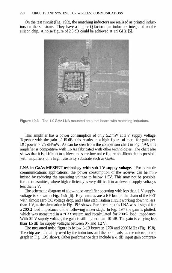
250 CIRCUITS AND SYSTEMS FOR WIRELESS COMMUNICATIONS
On the test circuit (Fig. 19.3), the matching inductors are realized as printed induc-tors on the substrate. They have a higher Q-factor than inductors integrated on thesilicon chip. A noise figure of 2.3 dB could be achieved at 1.9 GHz [5].
This amplifier has a power consumption of only 5.2 mW at 3 V supply voltage.Together with the gain of 15 dB, this results in a high figure of merit for gain perDC power of 2.9 dB/mW. As can be seen from the comparison chart in Fig. 19.4, thisamplifier is competitive with LNAs fabricated with other technologies. The chart alsoshows that it is difficult to achieve the same low noise figure on silicon that is possiblewith amplifiers on a high resistivity substrate such as GaAs.
LNA in GaAs MESFET technology with sub-1 V supply voltage. For portablecommunications applications, the power consumption of the receiver can be min-imised by reducing the operating voltage to below 1.5V. This may not be possiblefor the transmitter, where high efficiency is very difficult to achieve at supply voltagesless than 2 V.
The schematic diagram of a low-noise amplifier operating with less than 1 V supplyvoltage is shown in Fig. 19.5 [6]. Key features are a RF load at the drain of the FETwith almost zero DC voltage drop, and a bias stabilisation circuit working down to lessthan 1 V, as the simulation in Fig. 19.6 shows. Furthermore, this LNA was designed fora load impedance of the following mixer stage. In Fig. 19.7 the gain is plotted,which was measured in a system and recalculated for load impedance.With 0.9 V supply voltage, the gain is still higher than l0 dB. The gain is varying lessthan 1.5 dB for supply voltages between 0.7 and 1.2 V.
The measured noise figure is below 3 dB between 1750 and 2000 MHz (Fig. 19.8).The chip area is mainly used by the inductors and the bond pads, as the micro-photo-graph in Fig. 19.9 shows. Other performance data include a -1 dB input gain compres-

MONOLITHIC INTEGRATED TRANSCEIVER CIRCUITS FOR GHz FREQUENCIES 251
sion point of -14.5 dBm and an input third-order intercept point of -1.5 dBm at 0.9 Vsupply voltage.
19.2.2 5 GHz LNA with switch for antenna diversity
There are a number of proposals which require diversity reception in wireless mobileterminals. Most of them use separate low noise amplifiers and a diversity switch. Re-cently, a MCM integration of a diversity front-end was demonstrated. Power consump-tion and chip size of the receiver front-end can be further minimised with a monolithicone-chip integration of the LNA and the diversity switch function. The block diagramof such a “diversity LNA” is shown in Fig. 19.10.
The diversity LNA achieves a minimum noise figure of 3.5 dB at 4.5 GHz with amaximum gain of 14dB using the enhancement device of a standard E/D-MESFETfoundry process. For comparison, a single LNA was designed on the same process

252 CIRCUITS AND SYSTEMS FOR WIRELESS COMMUNICATIONS
showing very similar gain and noise performance [7]. Both chips use full on-chipmatching circuits. By comparison of the chip sizes in Fig. 19.11 and 19.12 it becomesclear that the designed diversity LNA requires at least 30 % smaller chip area than amulti-chip solution without performance penalty.
The ratio between the on and off state of a diversity channel is more than 20 dB(Fig. 19.13). The noise figure of each channel is plotted in Fig. 19.14. These measure-ments were made on chips mounted on a test board. Due to a longer bond wire, thefrequency response of one channel is shifted to a slightly lower frequency.
The diversity LNA uses a single 3.3 V supply voltage for compatibility with low-power CMOS circuits. Power consumption is 13 mW (4 mA from a 3.3 V supply) withone diversity channel switched on. This is a reduction of roughly 50% compared to aconventional diversity receiver using individual LNAs.

MONOLITHIC INTEGRATED TRANSCEIVER CIRCUITS FOR GHz FREQUENCIES 253
19.2.3 17 GHz PHEMT power amplifier
High-speed wireless local area networks (WLAN) for indoor use are becoming moreand more important. WLAN systems with a data rate up to 2Mb/s are already stan-

254 CIRCUITS AND SYSTEMS FOR WIRELESS COMMUNICATIONS
dardised in IEEE 802.11. To provide higher transmission capacity, new frequencybands have to be allocated. The emerging European HIPERLAN standard addressesfrequency spectra in the 5 GHz and 17 GHz range. In the European ACTS project“Wireless ATM Network Demonstrator”, a system with data rates of 20Mb/s in the5 GHz range has been developed [8] and investigations of the requirements for data

MONOLITHIC INTEGRATED TRANSCEIVER CIRCUITS FOR GHz FREQUENCIES 255
rates up to 155 Mb/s in the 17 GHz band have been made, taking into account systemarchitecture and technological constraints.
As one of the key components of a future 17 GHz wireless LAN, a monolithicintegrated power amplifier has been designed. A two-stage on-chip matched poweramplifier with 200 mW output power was realized on a commercial pseudo-morphicHEMT process (Philips D02AH). Fig. 19.15 shows a block diagram of the amplifier.
The transistor of the driver stage has a gate width of The input matching,the gate and drain biasing network as well as the interstage matching network are inte-grated on the chip. In the power stage, the transistor and its gate biasing andthe output matching network are integrated. The drain bias network is external dueto the high DC current required by the transistor. The low-pass-type output matchingnetwork, shown in the basic schematic diagram (Fig. 19.16), allows for external bias-ing. No harmonic tuning was done at the output. The output stage is designed to beconditionally stable. Negative feedback stabilises the driver stage.
The whole circuit was simulated with a harmonic balance simulator. The HEMTsare simulated with a Statz MESFET model modified with an RC network between

256 CIRCUITS AND SYSTEMS FOR WIRELESS COMMUNICATIONS
drain and source. Thus, small inaccuracies in the large signal simulation results areexpected.
As the chip photograph in Fig. 19.17 shows, via holes to the back metal providean optimum source grounding, but limit a maximum layout density by the minimumdistance required between two adjacent via holes of Nevertheless, the layoutis very compact with a chip size of 1 × 1.5 mm2.
The measured fundamental power, the power added efficiency and the drain effi-ciency at 17.2 GHz agree with the harmonic balance simulation as shown in Fig. 19.18.The output power at -1 dB gain compression is 20dBm, the saturated output power is23 dBm at 3.3 V supply voltage. The measured power added efficiency has a maxi-

MONOLITHIC INTEGRATED TRANSCEIVER CIRCUITS FOR GHz FREQUENCIES 257
mum of 20 % and the drain efficiency is 31.5 %. More measurement data can be foundin [9].
19.3 CONCLUSIONS
In the foreseeable future, special RF IC technologies will still be required for applica-tions in the GHz range, particularly when high transmit power or a low noise figure isimportant. For low-cost, lower performance applications such as the proposed Blue-tooth, full monolithic RF and baseband integration in CMOS must be the goal.

258 CIRCUITS AND SYSTEMS FOR WIRELESS COMMUNICATIONS
Acknowledgments
The authors would like to thank their colleagues Thomas Bös and Jakub Kucera for beingallowed to use some of their circuits as examples of today’s RF integrated circuits in the GHzrange.

MONOLITHIC INTEGRATED TRANSCEIVER CIRCUITS FOR GHz FREQUENCIES 259
References
[1] K-H. Kirn et al., “4 GHz and 13 GHz tuned amplifiers implemented in aCMOS technology on SOI and SOS substrates”, 1998 IEEE Solid-State CircuitsConference Digest, pp. 134–135.
[2] K. W. Kobayashi et al., “Sub-1.3dB noise figure direct-coupled MMIC LNAsusing a high-current gain 1 µm GaAs HBT technology”, IEEE 1997 GaAs ICSymposium Digest, pp. 240–243.
[3] M. Soyuer et al., “A cost-effective approach to a short-range, high-speed radiodesign in the U-NII 5.x GHz band”, IEEE 1998 Radio and Wireless ConferenceProceedings, pp. 133–136.
[4] see http://www.bluetooth.com[5] J. J. Kucera, U. Lott “Low-power silicon BJT LNA for 1.9 GHz”, IEEE Microwave
and Guided Wave Letters, vol. 8, no. 3, March 1998, pp. 136–137.[6] U. Lott, M. Schmatz, “2 GHz monolithic low noise amplifier using lower than
1V supply voltage”, Proceedings of the 1997 IEEE Wireless CommunicationsConference, pp. 138–140.
[7] U. Lott, “Triple input single chip LNA”, IEEE 1998 Radio and Wireless Confer-ence Proceedings, pp. 335–337.
[8] Information on the ACTS project WAND can be found on the internet athttp://www.tik.ee.ethz.ch/~wand
[9] T. A. Bös, U. Lott, W. Bächtold, “A two stage, monolithic integrated 200 mWHEMT amplifier for wireless ATM”, IEEE 1998 Radio and Wireless ConferenceProceedings, pp. 125–128.

This page intentionally left blank

V DSP for WirelessCommunications

This page intentionally left blank

20 DSP FOR WIRELESSCOMMUNICATIONS
Urs Fawer* and Gertjan Kaat
Philips Semiconductors AGBinzstrasse 44
CH–8045 Zürich, Switzerland
20.1 INTRODUCTION TO THE FOLLOWING PAPERS
Recently, wireless communication has turned into a very fast-growing market. GSM2
gives a good example with a total number of 135 million users world-wide by theend of 1998, of which 65 million new customers subscribed in the last year. Thisimpressive growth is based on the underlying technologies. The latter are the topic ofthis part: the study of complex communication functionality and related algorithms aswell as their realization in hardware and software.
Digital Signal Processors (DSPs) are a key component for implementing communi-cation algorithms. Very often, we encounter embedded DSP cores where the DSP isintegrated on a silicon chip together with a controller core, memories, hardware accel-erators, and dedicated periphery blocks. For many algorithms, the DSP represents theessential block in the implementation, e.g. voice codecs, channel equalizers, error cor-rection, encryption, interference suppression, multi-channel and multi-beam receptionas well as additional features like voice recognition. DSP performance is often mea-
*Urs Fawer is now with diAx, Birgistr. 4a, CH–8304 Wallisellen, Switzerland.2Global System for Mobile Communications; second-generation digital cellular mobile system
263

264 CIRCUITS AND SYSTEMS FOR WIRELESS COMMUNICATIONS
sured in terms of million instructions per second (MIPS). Since the influence of theconsidered architectures is not reflected in this MIPS figure, a benchmarking exercisebased on well-defined algorithms is recommended to compare DSP cores.
Wireless communication systems impose demanding requirements on the DSP, es--pecially for mobile terminals with inherent constraints on size, weight, and batterycapacity. In consumer applications, overall system cost and low power consumptionrepresent the main key driving factors.
20.2 TRENDS
The trend towards digitization will continue: functionality which was previously real-ized in the analog domain is more and more implemented by digital signal processing.This tendency follows the CMOS process road-map with continuously decreasing fea-ture size along the time axis. It also results in a continuous cost reduction in integratingdigital circuitry because the number of building blocks integrated on one piece of sil-icon can be further increased. This leads more and more to a fully integrated solutionwhich is often referred to as a “system on silicon.”
The demand for wireless transmission of data, and with it the need for more band-width, is growing. Yet, bandwidth is a limited resource. Therefore, the increasingcapacity demands for wireless voice and data transmission will result in a higher com-plexity and efficiency of future systems.
These trends clearly indicate that the requirements increase with respect to MIPSfigures, low power consumption, high-level design and programming approach. Im-proved support for implementing floating-point algorithms is another important issue.It addresses the rising numerical complexity and the short time-to-market require-ments. It will be interesting to see how all these trends will be realized. We cancertainly expect a lot of innovation from future DSP architectures and applications.
20.3 PRESENTATION OVERVIEW
The first contribution of H. Keding et al. deals with the implementation of floating-point algorithms in a fixed-point architecture.
The next two papers investigate different hardware solutions for implementing dig-ital signal processing algorithms. E. Lambers et al. present the “R.E.A.L. DSP,” a pro-grammable architecture with a flexible application-specific instruction set, which canbe tailored towards the algorithmic needs. Advanced algorithms for implementation inreceivers are described in B. Hailer’s contribution. They lead to a dedicated, yet con-figurable hardware approach. The fourth paper, authored by J. Sanchez, summarizesthe requirements and trends of cellular mobile communication terminals.
In the fifth contribution, G. Miet describes future implementations of speech codecsand their impact on the system complexity.
The last paper of this part, authored by R. L. J. Roovers, investigates wide-bandanalog-to-digital converters, which are fundamental building blocks of multi-channelreceivers.
21 EFFICIENT DESIGN FLOW FORFIXED-POINT SYSTEMS
Holger Keding, Martin Coors, and Heinrich Meyr
Institute for Integrated Systems in Signal Processing (ISS)Aachen University of Technology
Templergraben 55, 52056-Aachen, Germany
Abstract: The complexity of DSP systems grows at an ever-increasing rate whilethe implementation of these designs must meet criteria like minimum cost and a shorttime to market. Hence there is a growing need for efficient design automation and aseamless design flow that allows the execution of the design steps at the highest suitablelevel of abstraction.
Especially for the design of fixed-point algorithms and systems, tool support is veryrare, though for most digital systems the design has to result in a fixed-point implemen-tation. This is due to the fact that these systems are sensitive to power consumption,chip size and price per device. Fixed-point realizations outperform floating-point re-alizations by far with regard to these criteria. On the other hand, algorithm designstarts from a floating-point description in order to initially abstract from all fixed-pointeffects. The resulting gap between the floating-point prototype and the fixed-point im-plementation represents one of the major bottlenecks in today’s digital designs.
This paper will give a survey of FRIDGE1, a tool suite that permits a seamless de-sign flow, starting from an ANSI-C floating-point algorithm which is then converted to
1Fixed-point pRogramIng DesiGn Environment
265

266 CIRCUITS AND SYSTEMS FOR WIRELESS COMMUNICATIONS
a fixed-point description in fixed-C2. This bit-true description of the algorithm can fi-nally be mapped to different implementation targets, programmable DSPs or dedicatedhardware structures.
21.1 INTRODUCTION
Digital system design is characterised by ever-increasing complexity and ever-tighterschedules, resulting in minimum costs and short time to market. This requires a seam-less design flow that allows the execution of the design steps at the highest suitablelevel of abstraction.
For most digital systems, the design has to result in a fixed-point implementation,either in hardware or software. This is due to the fact that digital systems have to be op-timised with regard to power consumption, chip size, throughput and price per-device.Fixed-point realizations outperform floating-point realizations by far with regard tothese criteria.
A typical fixed-point design flow is shown in Fig. 21.1. Algorithm design startsfrom a floating-point description that is analysed by means of simulation. This abstrac-tion from all implementation effects allows an evaluation of the algorithm space with-
2fixed-C is a Fixed-Point Language based on ANSI-C, but with additional generic fixed-point datatypes.

EFFICIENT DESIGN FLOW FOR FIXED-POINT SYSTEMS 267
out taking into account the quantisation effects on the algorithmic behaviour. Thus,modeling efficiency is higher at the floating-point level, and the use of floating-pointmodels offers a maximum degree of re-usability.
The transformation to the fixed-point level is quite tedious and error-prone, since afixed word length and a fixed exponent needs to be assigned to every operand man-ually. To provide a more quantitative picture of this time-consuming process, inFig. 21.1 we exemplarily displayed the design times for the implementation steps foran OFDM receiver frequency synchronisation unit [1] developed at ISS. In much thesame way as for this example, often more than 50 % of the design time is spent onthe algorithmic transformation to the fixed-point level for complex designs once thefloating-point model has been specified. The major reasons for this bottleneck are:
There is no unique transformation from floating-point to fixed-point.
1. Different HW and SW targets put different constraints on the fixed-point speci-fication.
2. Optimisation for different design criteria, like throughput, chip size, memorysize, or accuracy, are in general mutually exclusive goals and result in a complexdesign space as sketched in Fig. 21.2.
3. The quantisation is generally highly dependent on the application, i.e. on theapplied test vectors.
The manual transformation of the floating-point algorithm to the fixed-point algo-rithm is known to be time-consuming and error-prone. Even for a single transfor-mation, modeling efficiency is very low. Therefore the manual floating-to-fixedconversion appears to be no longer acceptable.
The fixed-point simulation efficiency is low. This is due to the fact that the bit-truebehaviour of the target system has to be emulated on the host machine.
These inefficiencies have been the motivation for FRIDGE [2–4], an interactivedesign environment for the specification, simulation and implementation of fixed-pointsystems.

268 CIRCUITS AND SYSTEMS FOR WIRELESS COMMUNICATIONS
In this paper we describe the principles and elements of FRIDGE and outlinethe seamless design flow which becomes possible using this design environment.We also give a global picture of the FRIDGE design flow by highlighting its con-stituents, briefly describing the fixed-point language fixed-C and the way to annotateoperands with fixed-point attributes. Later we show the core algorithm of FRIDGE,the wordlength interpolation and the back ends, i.e. mapping the internal fixed-pointrepresentation of FRIDGE to a synthesisable/compilable description.
21.2 THE FRIDGE DESIGN FLOW
As pointed out above, a manual transformation into a fixed-point representation ishardly feasible. Since an efficient evaluation of the complex design space requiresmultiple transformations, this is even more of a design bottleneck.
In the FRIDGE design environment, system design starts from a floating-point al-gorithm in ANSI-C. The designer then may annotate single operands with fixed-pointattributes, as illustrated in Fig. 21.3.
Inserting these local annotations results in a hybrid description of the algorithm,i.e. some of the operands are specified bit-true, while the rest are still floating-point.A comparative simulation of the floating-point and the hybrid code within the samesimulation environment shows whether the local annotations are appropriate, or ifsome annotations have to be modified.
Once the hybrid program matches the design criteria, the remaining floating-pointoperands are transferred to fixed-point operands by interpolation, where interpolationdenotes the process of computing the fixed-point parameters of the non-annotated

EFFICIENT DESIGN FLOW FOR FIXED-POINT SYSTEMS 269
operands from the information that is inherent to the annotated operands and the oper-ations performed on them. Additionally, the interpolator has to observe a set of globalannotations, i.e. default restrictions for the calculation of fixed-point parameters. Thiscan be e.g. a default maximum wordlength that corresponds to the register length ofthe target processor.
The interpolation supplies a fully annotated program, where each operand and oper-ation is specified in a bit-true way. Co-simulating this algorithm with the original float-ing-point code will give an accuracy evaluation—and for any alterations only some ofthe local and global annotations have to be modified, while the rest is determined andkept consistent by the interpolator.
What is described above are the algorithmic level transformations as illustratedin Fig. 21.1 which change the behaviour or accuracy of an algorithm. The resultingcompletely bit-true algorithm in fixed-C is not yet suitable for implementation, thusit has to be mapped to a target, e.g. a processor’s architecture or an ASIC. This isan implementation level transformation, where the bit-true behaviour normally staysunchanged. Within the FRIDGE environment different back ends map the internalbit-true specification to different formats/targets, according to the purpose or goal ofthe quantisation process:
ANSI-C or fast simulation codeProcessor specific codeHDL code, e.g. behavioural VHDLThis framework allows a seamless design flow from algorithm development to im-
plementation and therefore tears down the well-known virtual brick wall that is oftento be found between system level design and implementation.
21.3 FIXED-C AND LOCAL ANNOTATIONS
Since ANSI-C offers no efficient support for fixed-point data types [5,6], we developedthe fixed-point language fixed-C, which is a superset of the ANSI-C language. Itcomprises different generic fixed-point data types, casting operators and interpolatordirectives. These properties enable fixed-C to be used for different purposes in theFRIDGE design flow:
Since ANSI-C is a subset of fixed-C, the additional fixed-point constructs can beused as bit-true annotations to dedicated operands of the original floating-pointANSI-C file, resulting in a hybrid specification. This partially bit-true code can beused for simulation or as input to the interpolator.
The bit-true output of the interpolator is represented in fixed-C as well. This allowsmaximum transparency of the results to the designer, since the changes to the codeare reduced to a minimum and the effects of the designer’s directives, such as localannotations in the hybrid code, become directly visible.
The language constructs to describe the bit-true behaviour are contained in a C++class library which can be used in any design and simulation environment that comeswith a C or C++ compiler, such as COSSAP [7], SPW [8] or Matlab/Simulink [9].
For a bit-true and implementation-independent specification of an operand, a three-tuple is necessary, the wordlength wl, the integer wordlength iwl, and the sign s, asillustrated in Fig. 21.4.

270 CIRCUITS AND SYSTEMS FOR WIRELESS COMMUNICATIONS
21.3.1 The data type Fixed
declaration:Fixed<wl, iwl, sign> d, *e,g[8] ;
The data type Fixed receives its format when it is declared, thus a Fixed vari-able behaves according to these fixed-point parameters throughout its lifetime. Thisconcept is called declaration-time instantiation (DTI). Similar concepts exist in otherfixed-point languages as well [10–12]. Pointers and arrays, as frequently used inANSI-C, are supported as well.
For every assignment to a Fixed variable, a data type check is performed:Example:
Fixed<6,3,s> a,b;Fixed<12,12,u> c;a = b; /* correct, both types match */c = b; /* type mismatch */
Fixed is the data type of choice e.g. for interfaces to other functionalities or forlook-up tables, since it behaves like a memory location of a specific length.
21.3.2 The data type fixed
In addition to the DTI data type concept, fixed-C provides the data type fixed whichis specially tailored for the float-to-fixed transformation process.
declaration: fixed a, *b, c [8] ;
A variable is declared to be of data type fixed, but no instantiation is performedand no fixed-point attributes are specified.
casting:a=fixed(wl, iwl, sign, cast, *b) ;
The variable a receives data of type <wl, iwl, sign>, the value of *b is castaccording to the casting mode cast. The casting mode specifies how to handle over-flow3 as well as quantisation4. The different casting modes are shown in Tab. 21.1.
3Overflow handling specifies the behaviour in case of a wordlength reduction at the MSB side.4Quantisation handling specifies the behaviour in case of a wordlength reduction at the LSB side.

EFFICIENT DESIGN FLOW FOR FIXED-POINT SYSTEMS 271
Every assignment to a variable overwrites all prior instantiations, i.e. one fixedvariable may have different context-specific bit-true attributes in the same scope. Thisconcept of Assignment-Time Instantiation (ATI) is motivated by the specific designflow: transformation starts from a floating-point program, where the designer abstractsfrom the fixed-point problems and does not think of a variable as a finite length regis-ter. Fig. 21.5 highlights the properties of ATI in a quantisation process.
For the first assignment to a, a fixed-point format <1, -2, u> is sufficient to repre-sent the constant 0.125, while for the second assignment a format <16,16, s> wouldbe necessary. With ATI, this information is accessible without code changes, while forDTI, two options exist:
merging over the fixed-point parameters for all assignments to the variable a to re-ceive a super-format that matches the fixed-point requirements wherever a is used.5
If this super-format were the input to an implementation tool, it would force the useof large registers, even when this is not necessary.
to use the context-specific information, a variable must be split up manually intoseveral different variables, which is a time-consuming and error-prone task as well.
In contrast, the concept of local annotations and ATI is an effective way to assigncontext-specific information without changing structures or variables when exploringthe fixed-point design space.
5For the example in Fig. 21.5: 2 fractional bits from the first assignment to a, 16 integer bits from thesecond, so the merged format is 18 bits long.

272 CIRCUITS AND SYSTEMS FOR WIRELESS COMMUNICATIONS
21.3.3 Interpolator directives
The interpolator can extract information about the fixed-point parameters not onlyfrom direct information about wordlength, integer wordlength and sign,6 but also fromindirect or user-supplied information. For example one could specify only the rangeof an operand:
a=fixed(minim(-2.35),maxim(4.74), *b );
This information is not sufficient for a bit-true simulation, since there is no informationextractable e.g. about the quantisation steps. Annotations like this are called incom-plete local annotation or interpolator directives. They are ignored by the simulator,but can provide additional information to the interpolation process.
21.4 INTERPOLATION
The interpolator is the core of the FRIDGE design environment. As shown in Fig. 21.3,it determines the fixed-point formats for all operands of an algorithm, taking as inputa user-annotated hybrid description of the algorithm and a set of global default rules,the global annotation file. Hence interpolation describes the computation of the fixed-point parameters of the non-annotated operands from the information that is inherentto the annotated operands.
21.4.1 Maximum precision interpolation
The interpolation concept is based on three key ideas:
Attribute propagation: The means of using the information inherent to the hybridcode to determine the fixed-point attributes of all operands.
Global annotations: The description of default rules and restrictions for attributepropagation.
Designer support: The interpolator supplies various feedback or reports to assist thedesigner to debug or improve the interpolation result.
For a better understanding, the first two points are now explained in more detail:
Attribute propagation. Given the information of the fixed-point attributes of someoperands, the type and the fixed-point format of other operands can be extracted fromthat. For example, if both the range and the relevant fractional wordlength are specifiedfor the inputs to an operation, the same attributes can be determined for the result.7 Asimple example for an addition is shown in Fig. 21.6.
Given the user-annotated ranges of variables a and b, FRIDGE automatically de-termines the range and the accuracy, i.e. the required number of fractional bits for thevariable c. Note that this is a worst-case or maximum-precision interpolation (MPI),
6As provided by casting operators described earlier.7An exception is the division, where the accuracy of the operation must be specified as well.

EFFICIENT DESIGN FLOW FOR FIXED-POINT SYSTEMS 273
so there is no way an overflow can occur. LSBs are only discarded if the wordlengthexceeds the maximum wordlength specified in the global annotation file.
The fixed-point parameters iwl and sign of an operand can be determined once itsrange [min, max] is known8 [13]:
Without the additional knowledge of fwl one has to spend one additional bit toguarantee that the maximum (minimum) can be represented.
wl is determined using the information about the fractional wordlength fwl = wl –iwl. It is only necessary to represent those fractional bits which actually carry anyinformation.
Global annotations. While local annotations express fixed-point information forsingle operands, global annotations describe default restrictions to the complete de-sign. For different targets, different global restrictions apply. For SW, the functionalunits to perform specific operations are already defined by the processor’s architec-ture. Consider a 16 ×16 bit multiplier writing to a 32-bit register. A global annotationcan inform the interpolator that the wordlength of a multiplication operand may notexceed 16 bits, while the result may have a wordlength of up to 32 bits.
21.4.2 Utilisation of statistical knowledge for Interpolation
With the MPI, the wordlengths of the operands increase considerably during interpo-lation, while in many cases the obtained large wordlengths do not correspond to anadequate precision. This is due to the fact that each fixed-point input x to the algo-rithm represents a quantised value x0, i.e. it consists of the exact value x0 and thequantisation error
8We assume a two’s complement representation here.

274 CIRCUITS AND SYSTEMS FOR WIRELESS COMMUNICATIONS
Taking this fact into account, one can compute a noise floor that can be used to judgethe information content of each bit. The statistical properties of the noise are prop-agated by the interpolative approach described above. Assuming the error PDF isknown for some operands, e.g. for the input, the resulting noise probability densityfunction (PDF) at every point of the algorithm is calculated. In principle, the PDF ofa linear arithmetic operation can be calculated if the input PDFs are known [14].9
To cut down this model to an implementable complexity we only take a few para-meters to describe the quantisation error of a variable x, expressed by its mean value
and variance The propagation of these parameters is governed by a set ofrules and the mean value and variance of each signal [15].
The effect of LSB reduction. The criterion for a wordlength reduction is its impacton the noise PDF. In other words: What is the deterioration of the ratio of signal
least significant bit (LSB)? If one additionally defines a global threshold thatmust not be exceeded when reducing the wordlength, one can decide whether the LSBhas to be preserved or not.
The PDF of the truncation error consists of two unit pulses at 0 andweighted with the set probabilities P(0) and P(1):
Thus the noise power and the loss of the signal-to-noise ratio for this operationcan be calculated:
therefore is a quantitative measure for the information content of the LSB.According to a user-specified threshold, the wordlength of an operand is eitherreduced or not, i.e. only if the calculated is lower than the LSB getstruncated. This is repeated recursively unless the sum of all calculated valuesexceeds the threshold.
This optional interpolation method allows quantitative assessment of the impact ofquantisation on the precision of operations and algorithms and permits the wordlengthsof the algorithm to be kept comparatively short [15]. With the SNR criterion, theresult is an optimised ratio of algorithm performance and the wordlengths used in thealgorithm.
21.5 BACK ENDS
As stated above, the fixed-C output of the interpolator is very well-suited for algorithmdesign or for a floating-to-fixed transformation. Nevertheless, it is not directly suited
9For example, the PDF of a sum of two statistically independent variables is obtained by convolvingthe PDFs of these variables.
power and quantisation noise (SNR) for a single operation if we skip the

EFFICIENT DESIGN FLOW FOR FIXED-POINT SYSTEMS 275
for implementation for HW Synthesis tools or for programmable architectures. Apartfrom the fact that there are as of yet only very few implementation tools that supportthe fixed-C language [16], there are other reasons that the fixed-C output is not directlysuited for implementation:
The fixed-C code contains all context-specific fixed-point information and retainsthe structure of the original floating-point code. For implementation purposes, mostinformation is not directly applicable, but is has to be refined. Often the structureof the code has to be changed according to this information, according to the im-plementation target and to the design goals.
The ATI concept is not supported by most imperative implementation languages,where each variable corresponds to some storage location.
The weight of bit pattern, i.e. the location of the binary point (lbp) (see Fig. 21.4) ina finite register is handled automatically by the fixed-point data types of the fixed-Clanguage. This is no longer the case for more implementation-related representa-tions, like ANSI-C or VHDL.
Hence, a back end which maps the implementation-independent fixed-C represen-tation to a specific target is necessary. It has to deal with embedding the fixed-pointoperands into registers, mapping them to signals or variables, optimising the codestructures for the implementation architecture, etc.
Currently there are different research and development activities going on at theInstitute for Integrated Signal Processing Systems. The main implementation targetsare
ANSI-C and fast-simulation back end,Processor-specific back end,Hardware-description-language back end.To describe all of those back ends would be clearly out of the scope of this paper.
Hence we focus on the ANSI-C and fast simulation back end as examples to highlightsome problems and solutions found in this area.
21.5.1 ANSI-C and fast-simulation back end
The ANSI-C output of this back end serves two purposes: the implementation on pro-grammable processors that come with a C compiler, and reduction of simulation timeon a host machine. Fixed-point simulation based on a C++ class library as describedearlier or in [8,12,17] increases the runtime by one or even two orders of magnitudecompared to the corresponding floating-point simulation. This is due to the fact thatthe fixed-point specification has to be emulated on the host machine that supports dif-ferent data types from the target.
The key idea for a fast fixed-point simulation is to take advantage of all compile-time10 information to minimise the processing effort that has to be spent at simulation-time. Two areas for compile-time optimisation have been integrated into FRIDGE:
10In this case, a floating-point algorithm is compiled into a fixed-point representation, i.e. compile-timemeans interpolation-time here.

276 CIRCUITS AND SYSTEMS FOR WIRELESS COMMUNICATIONS
casting optimisation and data type emulation. FRIDGE performs a casting mode op-timisation that has also been independently proposed by DeCoster [18]: whether anoverflow check is necessary depends on the range that the result of an operation cantake. If the possible range can be represented with the available wordlength, no over-flow processing is necessary. The same holds for quantisation handling.
In addition, FRIDGE analyses the necessary wl for each operand at compile-time.This information is used to embed it into an appropriate ANSI-C integer data type.As can be seen from Fig. 21.4, there is a degree of freedom embedding the wl into alonger machine wordlength (mwl)11, i.e. the significant bit pattern may be shifted inthe mwl.
Besides these degrees of freedom, there is also a set of restrictions describing howthe operands have to be embedded into the registers. For example, as demonstratedwith the expression tree in Fig. 21.7, one restriction for an addition is that the locationof the binary point (lbp) has to be the same for both input operands.
Using this concept it is possible to describe the transformation space by a set ofinequalities and conditions. With the goal of minimising the cost of the casting andshift operations, this states an optimisation problem that is essential for integer-basedC code generation [3], [2].
21.6 CONCLUSION
Traditional approaches make it necessary to annotate fixed-point specifications to alloperands manually, which is an error-prone and time-consuming task. This is hardlyacceptable even for a single transformation but becomes an unacceptable situation foran efficient evaluation of a complex design space. With the introduction of fixed-Clanguage and interpolative approach, an efficient transformation from a floating-pointinto a fixed-point algorithm becomes possible. With the support of FRIDGE, the de-
11mwl corresponds to the wordlength of the built-in data types on the host machine, e.g. short,int or long.

EFFICIENT DESIGN FLOW FOR FIXED-POINT SYSTEMS 277
signer may concentrate on the critical issues for this transformation, thereby beingable to explore the design space more efficiently.
The verification of the fixed-point algorithm has to be performed by means of sim-ulation. Existing fixed-point simulation concepts increase simulation-time by one oreven two orders of magnitude as compared to the corresponding floating-point simula-tion. The FRIDGE fast simulation back end applies advanced compile-time analysisconcepts, analyses necessary casting operations and selects the appropriate built-indata type on the host machine, thus simulation time can be reduced considerably.
These features, in combination with target-specific back ends for implementation,make FRIDGE a powerful design environment for the specification, evaluation andimplementation of fixed-point algorithms. This environment can easily be integratedinto existing C/C++ based design environments.
References
[1] T. Grötker, E. Multhaup, and O. Mauss, “Evaluation of HW/SW Tradeoffs UsingBehavioral Synthesis,” in Proceedings of the Int. Conf. on Signal ProcessingApplication and Technology (ICSPAT), Boston, Oct. 1996.
[2] H. Keding, M. Willems, M. Coors, and H. Meyr, “FRIDGE: A Fixed-Point De-sign and Simulation Environment,” in Proceedings of the European Conferenceon Design Automation and Test (DATE), Paris, Feb. 1998, pp. 429–435.
[3] M. Willems, V. Bürsgens, and H. Meyr, “FRIDGE Enables Floating-PointProgramming of Fixed-Point DSPs,” in Proceedings of the Int. Conf. on Sig-nal Processing Application and Technology (ICSPAT), San Diego, Sep. 1997,pp. 1000–1005.
[4] M. Willems, V. Bürsgens, H. Keding, T. Grötker, and H. Meyr, “System LevelFixed-Point Design Based on an Interpolative Approach,” in Proceedings of theDesign Automation Conference (DAC), Anaheim, Jun. 1997, pp. 293–298.
[5] W. Sung and K. Kum, “Word-Length Determination and Scaling Softwarefor a Signal Flow Block Diagram,” in Proceedings of the IEEE InternationalConference on Acoustics, Speech and Signal Processing (ICASSP), Apr. 1994,pp.457–460 (II).
[6] B. W. Kernighan and D. M. Ritchie, Programmieren in C, Carl Hanser Verlag,1990.
[7] Synopsys, Inc., 700 E. Middlefield Rd., Mountain View, CA 94043, USA, COS-SAP User’s Manual.
[8] Cadence Design Systems, 919 E. Hillsdale Blvd., Foster City, CA 94404, USA,SPW User’s Manual.
[9] Mathworks Inc., Simulink Reference Manual, Mar. 1996.[10] Mentor Graphics, 1001 Ridder Park Drive, San Jose, CA 95131, USA, DSP
Station User’s Manual.
[11] S. Kim, K. Kum, and W. Sung, “Fixed-Point Optimization Utility for C and C++Based Digital Signal Processing Programs,” in Workshop on VLSI and SignalProcessing ’95, Osaka, Nov. 1995, pp. 197–206.
278 CIRCUITS AND SYSTEMS FOR WIRELESS COMMUNICATIONS
[12] Frontier Design Inc., 9000 Crow Canyon Rd., Danville, CA 94506, USA, A\RTLibrary User’s and Reference Documentation, 1998.
[13] Markus Willems, Eine Methodik fuer den effizienten Entwurf von Festkommasys-temen, Dissertation an der RWTH-Aachen, 1998.
[14] A. Papoulis, Probability, Random Variables and Stochastic Processes, McGraw-Hill Book Company, 1991.
[15] H. Keding, F. Hürtgen, M. Willems, and M. Coors, “Transformation of Float-ing-Point into Fixed-Point Algorithms by Interpolation Applying a StatisticalApproach,” in Proceedings of the Int. Conf. on Signal Processing Applicationand Technology (ICSPAT), Toronto, Sep. 1998.
[16] M. Jersak and M. Willems, “Fixed-Point Extended C Compiler Allows MoreEfficient High-Level Programming of Fixed-Point DSPs,” in Proceedings of theInt. Conf. on Signal Processing Application and Technology (ICSPAT), Toronto,Sep. 1998.
[17] W. Sung and K.I. Kum, “Simulation-Based Word-Length Optimization Methodfor Fixed-Point Digital Signal Processing Systems,” IEEE Transactions on Sig-nal Processing, vol. 43, no. 12, pp. 3087–3090, Dec. 1995.
[18] L. DeCoster, M. Engels, R. Lauwereins, and J.A. Peperstraete, “Global Approachfor Compiled Bit-True Simulation of DSP-Applications,” in Proceedings of Euro-Par ’96, Lyon, Aug. 1996, vol. 2, pp. 236–239.

22 R.E.A.L. DSP:RECONFIGURABLE EMBEDDED DSPARCHITECTURE FOR LOW-POWER /
LOW-COST TELECOM BASEBANDPROCESSING
E. Lambers, C. Moerman, P. Kievits,J. Walkier, and R. Woudsma
Embedded Systems Technology Centre (ESTC) ASIC Service GroupPhilips Semiconductors
Prof. Holstlaan 4, 5656 AA Eindhoven, The Netherlands
Abstract: The R.E.A.L. DSP architecture for embedded applications features ahigh level of parallelism in the data path and the possibility to add specific peripheralmodules, or to integrate dedicated application-specific execution units. Program codeis compact by using a highly compressed instruction set, incorporating short (16-bit)instructions, orthogonal 32-bit instructions, and the possibility to define VLIW-typeapplication-specific instructions. By its unique and leading architecture the R.E.A.L.DSP core is especially targeted for telecom terminals, in particular cellular phones.The core has been implemented in several ASIC technologies for different embeddedapplications, showing excellent performance and power figures.
279

280 CIRCUITS AND SYSTEMS FOR WIRELESS COMMUNICATIONS
22.1 INTRODUCTION
As opposed to general-purpose, stand-alone DSPs introduced in the eighties, deeplyembedded DSP technology is characterised by a combination of high-functional per-formance, efficient chip area usage, high power efficiency, and a high degree of con-figurability. These characteristics are quite obvious when observing the key designconstraints for high-volume, consumer-type applications: low-cost, short time-to-mar-ket, and low-power operation.
Simply boosting up DSP speed would result in fast execution of typical DSP func-tions like filter or transform algorithms, but this could implicitly also involve severearea and supply current penalties. Consequently, it appears to be much more appropri-ate to start with a thorough analysis of the target application domain(s), and tune theDSP architecture such that an optimal balance between specific application require-ments and (re)programmability is achieved.
As Mobile Cellular Telephony is mainly driven by low power consumption and ahigh degree of integration, the above is especially true for this market.
The R.E.A.L. DSP core is optimised for cellular base-band processing in tele-corn terminals using instruction set colouring by means of application specific instruc-tions (ASIs), making a large amount of instruction-level parallelism accessible to theprogrammer, and application-specific execution units (AXUs), which can acceleratecarefully selected computationally intensive parts in DSP algorithms. Consequently,R.E.A.L. DSP firmware is very compact, resulting in smaller on-chip memories andsignificant power saving, since processing can be done in a relatively low number ofclock cycles. For instance, it takes only two cycles to calculate a Viterbi butterflysection.
22.2 TOWARDS A NEW DSP ARCHITECTURE
Philips has a long experience of developing DSP cores. The EPICS DSP architecturehas been developed for Cord-less Telephony and Digital Audio [1,2]. This architec-ture allows a high degree of customisation and a wide variety of data-word lengths(12-, 16-, 18-, 20- and 24-bit variants have been realised). The KISS DSP core, featur-ing a 16-bit wide data-path, has been developed for cellular base-band processing inTelecom Terminals [3].
A number of considerations have led to the development of a next-generation em-bedded DSP technology:
1. The EPICS instruction set is highly concurrent and orthogonal. This results in highparallel processing power, and in easy and transparent programming at assemblylevel. For highly complex applications, including big parts of irregular controlcode, this approach is less feasible, since program code size is becoming a criticaldesign and cost factor for embedded high-volume applications.
2. Increasing parallel processing power at the architecture level appears to be indis-pensable for boosting processor performance, either by adding more functionalunits operating in parallel, or by increasing the number of instruction pipelines.
3. There is a growing class of applications where different functions with divergingarchitecture requirements have to share the same DSP platform. Consequently, the

R.E.A.L. DSP 281
basic DSP core needs to be more generic than specific, while not destroying theadvantages of efficient area and power usage.
4. For a short time to market, a more fixed and generic DSP architecture compositionand associated instruction set must be applied, while still offering the option to addspecific extensions when proven profitable for a given application.
These considerations have been the basis for the development of the next-gener-ation DSP architecture. This new DSP is known as R.E.A.L. DSP (ReconfigurableEmbedded DSP Architecture at Low Power and Low Cost).
22.3 THE R.E.A.L. DSP ARCHITECTURE
The R.E.A.L. DSP shown in Fig. 22.1 is a dual Harvard architecture with 16-bit-widedata and address busses. Fig. 22.2 shows the heart of the DSP, the data computationunit (DCU), which contains two 16 x 16-bit signed multipliers and two 40-bit ALUs(32 data bits, 8 overflow bits). Depending on what type of instruction is executed, theALUs can also be used as four separate 16-bit ALUs. Four input registersare available to store values fetched from X and Y data memories. ALU results arestored in four 40-bit accumulators a0 through a3, which can also be used as eight 16-bitregisters r0 up to r7. To provide good performance, the results of the multipliers arestored in pipeline registers p0 and p1. These are explicitly visible to the programmer.Shift and saturation units are available at a number of locations in the data-path. Thesecan be configured with a control register.

282 CIRCUITS AND SYSTEMS FOR WIRELESS COMMUNICATIONS
A stripped down version of the R.E.A.L. DSP with only one multiplier and single40-bit ALU (configurable as two 16-bit ALUs) has been derived from this architecturefor low-cost applications like, for instance, cord-less telephony and a digital telephoneanswering machine.
A distinctive feature of the R.E.A.L. DSP is the possibility to add application-spe-cific execution units (AXU) to the data-path. A part of the instruction set has beenreserved to control such blocks. Among the AXUs already available are a 40-bit bar-rel shifter, a normalisation unit, and a division support unit.
The X and Y data memories can be as large as 64K words by 16 bits and are ac-cessed by two address calculation units (ACU). Each of these contains eight pointers,grouped in four banks of two registers. This makes it possible to provide efficientcontext switching in case of interrupts. Modulo addressing is controlled by registersspecifying the start and end addresses of each modulo buffer in memory. Applica-tion-specific hardware can be added here as well to make special addressing modespossible, such as accessing individual bits, nibbles or bytes in memory. The complexdata path is controlled by the PCU (program control unit). This unit fetches and de-codes instructions from memory, and handles program flow instructions. These areperformed with a minimum use of cycles and include subroutine calls and relative, ab-solute, and calculated jumps. Nested looping is controlled by a loop controller basedon an internal stack, with a depth specified by the customer. The contents of the loopstack (loop count, start and end address) can be saved to memory if an interrupt occurs.A repeat controller for single instruction repetition is also available and is used e.g. tomove blocks of data from program memory to data memory.

R.E.A.L. DSP 283
For interrupt-driven applications, one non-maskable and up to 16 maskable inter-rupt inputs can be used, with possibilities to prevent nested interrupts. Each maskableinterrupt line can be switched into a fast interrupt mode. This makes it possible tofetch data samples from an I/O port and store them in memory with a minimum ofoverhead. Automatic, implicit context switching of pointers is provided to enable fulluse of fast interrupts.
22.4 THE R.E.A.L. DSP INSTRUCTION SET
The R.E.A.L. DSP uses two different instruction widths. Because code size has tobe as small as possible, the most commonly used instructions are compressed into16 bits. Less common instructions, and those instructions containing immediate dataor absolute addresses, use a second 16-bit word. Several classes of instructions areavailable to control the multiplier, ALUs and parallel moves. The instruction class de-termines whether the data-path operates with 16-bit or 40-bit operands in the ALUs.The instruction compaction does limit flexibility in operand selection, but this is com-pensated by the presence of an additional, and more powerful, orthogonal double-wordinstruction class (32 bits).
To exploit the full parallelism provided by the dual-multiplier quadruple-ALU andAXUs, a special set of instructions, called application specific instructions (ASIs), canbe applied, see Fig. 22.3. ASI instructions may be regarded as VLIW instructions(very long instruction words), giving control over all the ALUs, multipliers and AXUsin parallel. Moreover, in ASIs, two fields are reserved to control the ACUs for parallelmoves. 16-bit as well as 40-bit arithmetic is supported. ASIs can be conditional. ASIsare stored in a table in the decoder, limiting the total number of ASIs.
The R.E.A.L DSP assembler is able to detect an ASI in the application source code.An entry in the ASI table is reserved automatically, and the contents of this entry aregenerated from the kind of ASI being selected. No additional entries are generated incase of duplicate ASIs used at different locations in the program. Before starting upan application on the R.E.A.L. DSP, the applied ASIs must be down-loaded into theASI table. This can be done under program control using two special registers. Forproduction platforms, to save area as well as energy, the ASI table may be fixed ineither ROM or special hardware.
As an example, we will explain how to program a block FIR filter taking advantageof the dual multiplier structure. The main difficulty when implementing the block FIRfilter using two multipliers is the memory bottleneck: in each cycle, only one sampleand one coefficient can be fetched from memory.
A straight-forward FIR filter can thus only calculate one product term per cycle.However, when doing block processing, two output samples can be calculated simul-taneously, reusing sample and coefficient values by keeping the previous input andsample values in registers. For example, the two terms in Example 1 can be calculatedat the same time, including the update of registers to set up for the next iteration.

284 CIRCUITS AND SYSTEMS FOR WIRELESS COMMUNICATIONS
A filter kernel would contain two single-cycle instructions, as in Example 2, eachcalculating one term of sample [n] and one of sample [n + 1] (ignoring pipe-lineset-up). By switching roles for the x0 and x1 register with regard to being the ‘old’ or‘new’ value, no data move is required to shift the sample, as is shown in Example 2(actual code).
In this way, the memory can keep up with the MAC section. A 64-tap FIR filterwith block size N implemented this way takes 8 + 37 * N cycles to execute, i.e. for a40-sample block it takes approx. 37 cycles per sample, including overhead. A single-

R.E.A.L. DSP 285
multiplier DSP would take at least 64 cycles, excluding any overhead. For many algo-rithms, block-based processing is feasible, and the R.E.A.L. DSP architecture halvesexecution time for such algorithms.
Another example of a block-based algorithm is the FFT transform. Again, thememory bandwidth is the bottleneck, and attention has to be paid to the effective use ofthe internal registers. However, due to the large register set (four 40-bit accumulators,each of which also can be used as two independent 16-bit accumulators), a radix-4 FFTimplementation can make full use of the dual multiplier architecture. This reduces thetime needed for a 1,024-point complex FFT to around 1,400 cycles.
Based on our experience, even a few ASIs may significantly improve cycle-countefficiency. This can be explained by the fact that most DSP algorithms are based onrepetitions of only a few time-critical instruction kernels. Therefore the ASI table isrestricted to make the optimal balance between efficiency and core size.
For comparison, the new TI TMS C320C62xx processor [4] takes approx. the samenumber of cycles for the same task.1 However, by using the ASI compression tech-nique, the R.E.A.L. DSP does not have the overhead of the massive VLIW programmemory requirements of the TI chip, nor the associated energy consumption.
22.5 R.E.A.L. DSP DEVELOPMENT TOOLS
To support program development, a tool set containing an assembler, a linker and asimulator has been developed in combination with a hardware board/debugger com-bination. To ease code development and maintenance, a C-style syntax is used tosupport readability. Obviously not having the freedom to write actual ANSI-C’, theprogrammer still has to take into account the actual instruction set and to know whichsource and destination registers are available for a given operation.
A highly procedural style of programming is supported, with block- and file-basedscope for functions and variables. This scoping is fully supported, also by the simu-lator and debugger tools. An optimising DSP C-compiler is currently under develop-ment, using the CoSy™ compiler development platform [5]. An ANSI-C compiler forthe R.E.A.L. DSP is already available to support high-level entry of control code.
22.6 R.E.A.L. DSP ASIC IMPLEMENTATION
A number of applications are being served by embedded R.E.A.L. DSP cores, with aninstruction rate in the range of 25 to 85 MHz, depending on the technology being usedand on the bandwidth performance of the on-chip memories.
To ease the integration of a R.E.A.L. DSP, the core comes in two flavours, soft andfirm. A soft core is distributed at VHDL RTL level, leaving the customer to do the tech-nology mapping. In case of a firm core the design is transferred as a netlist optimisedfor a given ASIC technology. By exploiting an automatic clock-gating technique onthe net-list, reductions in energy consumption of up to 20-25 % have been achieved.
The R.E.A.L. DSP features several hooks for integration on a chip. The DSP chipintegrator is free to define its own memory architecture. Using the stall facility, which
1 Based on TI stating for a 1K FFT on 200 MHz C62,TI web page http://www.ti.com/sc/docs/news/1997/97001a.htm
286 CIRCUITS AND SYSTEMS FOR WIRELESS COMMUNICATIONS
allows all DSP registers to be frozen within one cycle, all kind of memory wait-statecontrollers, cache controllers and bus arbiters can be connected without affecting thecontents of the core. Communication between the DSP and its peripherals is donethrough up to 64 IO registers. An interrupt mechanism is available to avoid the needfor software polling. By a special flag, the core signals to the outside world that it isready to go into sleep mode, allowing the DSP clock to be completely switched off.Any external interrupt reactivates the core.
A large number of peripherals is available. Using the debug support block, an ap-plication program can be debugged on the chip. Register and memory manipulation,hardware break-pointing on any DSP bus, and single stepping are supported. The de-bug support block is controlled by a JTAG port. Repair of embedded DSP applicationsoftware can be done by a DSP firmware repair block, allowing up to four firmwarebugs to be fixed without affecting the DSP as such. Furthermore, interrupt controllers,parallel I/O ports, (a-)synchronous serial I/O ports, programmable timers, and powermanagement units exist.
In order to meet critical ASIC design constraints, special attention is paid to thedevelopment and careful selection of target library elements such as an efficient celllibrary, optimised data-path modules, and embedded memories.
22.7 R.E.A.L. DSP FACTS AND FIGURES
In this section, some facts and figures regarding the implementation of and process-ing on the R.E.A.L. DSP RD1602x series is presented. The first implementationstarted a few years ago on a Philips Semiconductors 0.5µm in-house ASIC technol-ogy. Since then, the R.E.A.L. DSP has been improved continuously and mapped onseveral CMOS technologies. Results can be found in Table 22.1.
As an example, Table 22.2 lists the memory usage for GSM phone firmware pro-grammed on the R.E.A.L. DSP RD16022, in addition to worst-case clock-speed per-formance, and energy consumption. The firmware comprises amongst others equali-sation, channel coding, speech coding, and program control. Additional features liketone generation, voice recognition and hands-free are not taken into account. A distinc-tion is made between full-rate, enhanced full-rate, and half-rate speech coding. Thetriple codec case is also included. To determine the energy consumption, the core isassumed to run at the minimal frequency needed to process the worst-case part in the

R.E.A.L. DSP 287
GSM phone firmware. Furthermore, the power figures are based on a supply voltageof 1.2 V. All figures include the DSP memories.
Since the R.E.A.L. DSP discussed here is a soft core, performance and power fig-ures must be treated as indicative.
Acknowledgments
The R.E.A.L. DSP architecture, its ASIC implementation, the development tools, and productapplications are the result of a close co-operation between various Philips departments. Theauthors wish to acknowledge the highly valuable and indispensable contributions of manyPhilips colleagues.
References
[1] R. Woudsma et al. “EPICS, a Flexible Approach to Embedded DSP Cores”, Proc.5th Int’l Conf. On Signal Processing Applications and Technology, Dallas Texas,1994, Volume I, pp. 506–511.
[2] R. Beltman et al. “EPICS 10: Development Platform for Next Generation EPICSDSP Products”, Proc. 6th Int’l Conf. On Signal Processing Applications and Tech-nology, Boston, 1995, Volume I, pp. 810–814.
[3] D. Weinsziehr et al. “KISS-16V2: A One Chip ASIC DSP Solution for GSM”,Proc. IEEE Custom Integrated Circuits Conf., 1992, pp. 10.4.1.–10.4.
[4] TMS320C62xx Programmer’s Guide, Texas Instruments, July 1997.[5] ACE, Amsterdam “The CoSy Compilation System”, http://www.ace.nl

This page intentionally left blank

23 DEDICATED VLSIARCHITECTURES FOR ADAPTIVE
INTERFERENCE SUPPRESSION INWIRELESS COMMUNICATION
SYSTEMSBruno Haller
Communication Technology Laboratoryand Integrated Systems Laboratory
Swiss Federal Institute of Technology (ETH) ZurichETH-Zentrum, CH–8092 Zurich, Switzerland
Abstract: In this contribution we discuss adaptive signal processing algorithms forinterference suppression based on either spatial filtering using base station antenna ar-rays “smart” antennas) or a special form of transversal filtering linear equalis-ers for advanced DS-CDMA receivers). It is demonstrated that for reliable operation innon-stationary environments with different levels of interference, such as encounteredin mobile radio, RLS-based techniques are inevitable due to their superior transientbehaviour. In order to overcome the associated problems of numerical stability andlarge computational complexity, we propose to employ the QRD-RLS algorithm whichsolely relies on numerically robust transformations and can be implemented efficientlyin VLSI technology based on a network of simple CORDIC arithmetic units whichmakes extensive use of parallel processing. The hardware implementation of such a2D systolic array as well as an alternative pipelined linear array capable of real-time
289

290 CIRCUITS AND SYSTEMS FOR WIRELESS COMMUNICATIONS
operation in high data rate systems (> 2 Mbps) is presented together with bit-true per-formance assessments for applications involving adaptive antennas. Special attention isgiven to the interactive design process required to successfully develop advanced algo-rithms and dedicated hardware architectures for tackling demanding signal processingtasks.
23.1 INTRODUCTION
Wireless is currently the fastest growing segment of the globally booming telecommarket, and this trend will be further reinforced through the introduction of third-gen-eration mobile systems (UMTS and IMT-2000) enabling universal personal communi-cations, as well as upcoming high speed radio networks (WLL and RLANs) providingtetherless local access to broadband services [1,2]. Great increases in the capacityof current wireless technology will have to be made if such advanced systems are tobecome a reality. Since the radio spectrum is a scarce and consequently very pre-cious resource, its economical utilisation calls for the application of bandwidth-effi-cient modulation schemes together with powerful multiple access and channel assign-ment techniques. This implies that higher performance and efficiency is achievableby applying enhanced signal processing, typically in digital form at the baseband“digital receivers” [3,4]). Of course, the entailed increase in complexity must be keptwithin reasonable limits to retain cost-effective solutions, whereby the latter factor islargely influenced by the available technology. Luckily, the continual enormous ad-vancements of microelectronics in terms of circuit density and switching speed [5,6]have been able to provide system designers with the signal processing horsepower theyrequire to implement their ever more sophisticated algorithms, besides cutting downon the size, cost and current consumption of the components.
Principally, digital VLSI circuits for baseband processing in wireless equipmentcan be divided into three main categories [3]:
programmable general-purpose devices (digital signal processors, DSPs), accelerator-assisted DSP chips (application-specific signal processors, ASSPs), custom-tailored components (application-specific integrated circuits, ASICs).Today’s fixed-point DSPs deliver on the order of 50 MIPS. This amount of pro-
cessing power is sufficient to realise the baseband parts of the physical layer as wellas the speech coding in second-generation TDMA-based cellular terminals (GSM,IS-54/136) [7,8]. Specialised DSP chips for wireless systems, enhanced with acceler-ator hardware, e.g. an add-compare-select unit for Viterbi decoding, and equippedwith multiple arithmetic-logic units (ALUs), i.e. multiplier-accumulators (MACs),have been introduced on the market lately to help tackle high-data-rate applications[9–11]. While these leading-edge devices offer a great deal of flexibility, they areoften unable to satisfy the computational requirements of future broadband systems[12] demanding dedicated hardware solutions based on massively parallel processingand pipelining, which is the exclusive domain of ASICs [13, 15]. Therefore, in thiscontribution, we will be looking at the major engineering challenges imposed on thedesigners of dedicated VLSI circuits for the advanced digital signal processing neededin the next generation of high-capacity, high-data-rate wireless communication net-works. This will be illustrated based on the case study of special-purpose processorsfor digital beamforming, i.e. adaptive spatial filtering [16–19].

DEDICATED VLSI ARCHITECHTURES 291
The rest of this discourse is organised as follows. Section 23.2 briefly outlines someof the main problems involved with the design of dedicated VLSI signal processors. InSection 23.3 we give a short overview on “smart” antennas, followed in Section 23.4by a description of algorithms and systolic architectures for adaptively controlling(i.e. “steering”) the beam pattern of an antenna array, including a few representativeresults from (bit-level) computer simulations of the proposed structures. Subsequently,a quick look is taken at an alternative application of the described techniques regard-ing the implementation of advanced DS-CDMA receivers in Section 23.5. Finally,Section 23.6 concludes this presentation with a summary and discussion of the mostrelevant points.
The aim of this exposé is fourfold: (i) to advocate the use of adaptive antennasas an efficient and effective means for interference mitigation in radio systems; (ii)to motivate the use of RLS-based techniques for high-performance adaptive filteringin wireless communications; (iii) to explain the advantages of employing CORDICarithmetic, instead of the traditional MAC operation, in certain classes of DSP algo-rithms; and above all (iv) to demonstrate that it is essential to develop algorithms andhardware architectures concurrently in order to obtain practically viable solutions tocomputationally demanding signal processing problems.
23.2 THE ART OF VLSI SIGNAL PROCESSING
The current trend towards hardware intensive signal processing has uncovered a rela-tive lack of understanding of dedicated VLSI architectures. Many hardware-efficientalgorithms exist, but these are generally not well known due to the predominanceof software solutions employing general-purpose DSP chips which have been in thespotlight of interest over the past two decades. Unfortunately, algorithms optimisedfor these programmable devices do not always map nicely onto specialised hardware.Therefore, current work in the field of VLSI signal processing is focusing on the jointstudy of both algorithms and architectures for the custom implementation of DSP(sub-)systems, exploiting the interactions between the two to derive efficient solutionsand thereby bridging the gap between system and circuit level design [20–24]. Asa consequence, the common approach presently pursued by many companies and re-search institutions, which is to seperate the theory and system groups developing al-gorithms from DSP and VLSI groups implementing them, should be abandoned infavour of a more interdisciplinary design procedure, which means exploiting in a syn-ergistic manner the interrelations between the application, the required algorithms andthe underlying hardware architectures, as well as the technology based upon whichthe system is to be realised. This task calls for the “tall thin” engineer with a broadknowledge in many different fields rather than a specialist deeply involved in only oneof the above-mentioned areas [3, 25].
In order to solve the tough problems encountered in real-time signal processing forwireless communications, it is necessary to both devise “good” algorithms and find“good” circuit architectures which fit together well. A “good” DSP algorithm worksreliably and is numerically stable, i.e. it must perform satisfactorily under diverse op-erating conditions and be insensitive to finite-precision effects due to limited operand

292 CIRCUITS AND SYSTEMS FOR WIRELESS COMMUNICATIONS
word lengths and inaccurate computations.1 Furthermore, algorithms which possess ahigh degree of parallelism and permit pipelined operation are more directly amenableto high-throughput implementations. On the other hand, “good” circuit architecturesmust exploit the full potential of advanced VLSI technology as well as be suitablefor design automation ( “silicon compilation”) [27], which enables speedy develop-ment cycles to meet stringent time to market requirements. Key features of such VLSIarchitectures are regularity, modularity and extendability. All these properties supporta cell-based design approach where complex systems are constructed through repeateduse of a small number of (primitive) basic building blocks (“tiles”) with only local in-terconnections and simple control. This methodology forms the basis for buildingso-called “systolic arrays” [28, 29], which consist of a synchronously clocked regularnetwork of (preferably identical) processing elements—a concept originally proposedby H. T. Kung and C. E. Leiserson in 1978, targeted at performing different matrixcomputations fundamental to many modern signal processing schemes. For the pur-poses of our further discussion, we will now concentrate on the application of suchVLSI systolic array architectures to an important, representative problem within therealm of future wireless communications, namely the implementation of digital adap-tive beamformers, in the hope that this example will help to practically illustrate thepoints made in this section.
23.3 OVERVIEW ON SMART ANTENNAS
The quest for ever better usage of the limited radio spectrum to provide a rapidlygrowing subscriber population with a broad range of high-quality, increased-data-rateservices has recently fostered great, world-wide interest in smart antenna technology,making it one of the hottest topics in wireless communications research today. Yet itmust be stressed that adaptive antenna arrays have been studied extensively for morethan three decades, although work was mainly restricted to military applications, suchas radar and sonar systems, chiefly due to the high complexity and ensued large costsof the required equipment. Hereby, antenna arrays were primarily employed to com-bat intentional jamming, i.e. as an interference suppression technique. On the otherhand, multiple-antenna systems for mobile communications have also been studiedthoroughly in the past, as a means to mitigate fading by exploiting space diversity.The fusion of these two ideas, i.e. interference suppression in combination with di-versity combining is the essence of current R&D efforts on intelligent antennas forhigh-capacity mobile radio systems, as documented in [30–35] and the referencescited therein.
The aim of a smart antenna is to reinforce the signal of interest (SOI) while sup-pressing the undesired intersymbol and co-channel interference (ISI, CCI), which aredue to multipath propagation and concurrent transmissions from other users, respec-tively. Thus a smart antenna maximises the signal-to-interference-plus-noise ratio(SINR) at its output.
1 Using floating-point arithmetic for dedicated VLSI chips is most often too costly in terms of chip areaand power consumption [26].

DEDICATED VLSI ARCHITECHTURES 293
This can be interpreted as a process of adaptive beamforming where the radiationpattern (spatial response) of the antenna array is automatically adjusted according tothe prevailing signal environment, i.e. by steering the main lobe towards the SOI andsimultaneously placing nulls in the directions of strong sources of disturbance. Addi-tionally, with M antenna elements, an array generally provides an SNR enhancementby a factor of M (for spatially white noise) plus a diversity gain that depends on thecorrelation of the fading amongst the antennas (max. M-fold). To take best possibleadvantage of spatial diversity, the antennas have to be placed far enough apart to guar-antee low fading correlation, whereby the required separation depends on the angularspread of the desired signal, i.e. the angle over which it is dispersed as seen by thereceiver. Such an array can theoretically completely cancel interferers andachieve an -fold diversity gain [37]. Significant performance improvementsare even attainable when the number of interfering signals exceeds M.
There exists a vast number of different techniques to govern the operation of theadaptive processor that adjusts the weighting for each of the antenna element outputs.These can be categorised according to the chosen weight optimisation criterion—e.g.minimum- mean-square-error (MMSE), maximum SINR or minimum variance / out-put power ( MVDR, LCMV) [16,17]—which consequently determines the waythe signal components of interest are discriminated from the interference to protectthem against unintentional suppression. This issue can be solved either by incorpo-rating knowledge regarding “source location”, i.e. the direction of arrival (DOA) ofthe desired impinging waves ( spatial reference beamforming, SRB), or by supply-ing some form of reference signal which is highly correlated with the desired signaland uncorrelated with the interference ( temporal reference beamforming, TRB)[16, 36]. Alternatively, so-called “blind” methods have also been advocated whichrely on special signal properties such as constant modulus, cyclostationarity or finite-alphabet structure of the symbols [16, 36]. For practical reasons, we suggest to usethe reference signal approach, because of its lower computational complexity2 as wellas its reduced sensitivity with respect to array imperfections, and because trainingand synchronisation sequences to support channel estimation, or provide some formof source identification, or both, are present in all operational and foreseeable sys-tems. Additionally, temporal reference antenna control techniques can theoreticallyapproach optimum performance for any given antenna array topology ( no restric-tions regarding element spacing or positioning,3 which are critical factors both forattaining high space diversity gains as well as for the installation of an array) andhence offer better performance and more reliable behaviour than the spatial and blindmethods under most practical circumstances.
To obtain rapid weight adaptation in quickly time-varying situations with high lev-els of disturbance, we propose to adopt open-loop (direct-solution) techniques. Thecoefficients of the adaptive combiner are then found through recursive least squares(RLS) minimisation. The corresponding set of equations can be solved in a numeri-cally robust manner by means of orthogonal matrix triangularisation (i.e. QR decom-
2DOA estimation algorithms (e.g. MUSIC or ESPRIT [36]) are computationally very demanding.3 For SRB schemes to function correctly, the interelement spacing must be small so that the signalfading is fully correlated across the array, which excludes the possibility of exploiting space diversityin conjunction with these methods!

294 CIRCUITS AND SYSTEMS FOR WIRELESS COMMUNICATIONS
position, QRD). The recursive realisation of this scheme using Givens rotations isknown as the QRD-RLS algorithm. It can be mapped very elegantly onto efficient sys-tolic array architectures for high speed real-time operation. Considering the presentlevel of circuit integration, antenna array weight controllers based on such dedicatedhardware structures are on the verge of becoming economically feasible for use incommercial wireless communication systems. In the next section, we will present insome detail the algorithms required for temporal reference beamforming, a bit-truedescription of the associated VLSI architectures, and exemplary performance assess-ments for two simple operating scenarios.
23.4 QRD-RLS ALGORITHM AND SYSTOLIC ARCHITECTURES FORADAPTIVE WEIGHT CONTROL
A temporal reference-based digital adaptive beamformer is illustrated in Fig. 23.1.
The array consists of M identical, omnidirectional antenna elements. After quad-rature downconversion to baseband, the I and Q components of each array element’ssignal are separately processed by a matched filter (MF) whose output is sampledonce per symbol and subsequently digitised.4 Following this, adaptivecombining is carried out by applying complex (amplitude and phase) weights
to the individual element signals in the beamforming network.In TRB systems, where a priori knowledge about the transmitted training sequencesor the periodically inserted pilot/reference symbols is available, optimum combiningis achieved by selecting the complex weight vector according to the minimum-mean-square-error (MMSE) criterion. Hereby, the adaptive weight controller adjusts
4Oversampling can be employed to improve performance, especially when no feedback exists to con-trol the sampling clock or if several asynchronous SOIs are to be handled concurrently.

DEDICATED VLSI ARCHITECHTURES 295
so as to minimise the average power of the residual signal which is the dif-ference between the known desired signal d[i] and the combined array output signal
The optimum Wiener solution to this problem is givenby the matrix form of the Wiener-Hopf (or normal) equations [38]:
where represents the input data correlation matrix andis the cross-correlation vector between the array element signals
and the desired response d[i]. Eq. (23.1) forms the basis of the well-known direct/sample matrix inversion (DMI/SMI) algorithm (of complexity [39]:
which involves forming an estimate (time average) of the correlation matrix aswell as of the cross-correlation vector and subsequently computing the solutionto a set of linear equations. This type of algorithm is well suited for a programmablefloating-point DSP but extremely difficult to map onto a dataflow processor. Alterna-tively, several adaptive algorithms can be employed to perform the above-mentionedminimisation task directly. Despite its computational simplicity (it has complexityO(M)) and its favourable numerical behaviour, the popular least mean square (LMS)stochastic gradient technique is often unsuitable in nonstationary environments withvariable levels of interference and distortion,5 as is very common in mobile radio com-munications. This is due to its poor convergence properties and large misadjustment,resulting in a considerable loss of output SINR compared to the theoretically optimumWiener solution [38]. Fast convergence is especially essential for rapid weight adap-tation when short training sequences are used for transmission efficiency reasons, aswell as to guarantee quick retuning of the beamformer coefficients when new sourcesof disturbance emerge, or present ones disappear. In these situations the recursiveleast squares (RLS) algorithm is preferred because of its robustness with respect to thesignal environment and thanks to its superior speed of convergence. A vast amountof research has been devoted to reducing the demanding computational requirementsand overcoming the problematic numerical properties of the RLS algorithm in orderto increase its practical applicability. The method of choice for fast and numericallyrobust RLS filtering is based upon orthogonal triangularisation of the input data matrixvia QR decomposition (QRD) [38]. In situations where the data is to be processedon a sample by sample basis (as opposed to block-wise) QR -updating through a se-quence of Givens rotations is usually employed. The resulting QRD-RLS algorithmrequires operations per updating step. Its numerical robustness stems from thefact that it operates directly on the incoming data matrix, circumventing the need tocompute whereby the condition number of the data matrix would be squaredand the required word length doubled. Additionally, solely numerically stable unitarytransformations are used. In the following subsection we briefly review the QRD-RLSalgorithm and demonstrate how to compute the a posteriori (a priori) estimation error
without explicit computation of the weight vector.
5The input data correlation matrix then exhibits a large eigenvalue spread:

296 CIRCUITS AND SYSTEMS FOR WIRELESS COMMUNICATIONS
23.4.1 QRD-RLS algorithm
The function of the adaptive combiner in Fig. 23.1 may be defined mathematically interms of least-squares estimation (LSE). The aim of the RLS algorithm is to minimisethe sum of exponentially weighted squared errors,
The so-called “forgetting factor” is commonly used to discount old datafrom the computations (exponential downdating), in order to provide a certain trackingcapability when the system operates in a non-stationary environment. This is equiva-lent to determining the weight vector which minimises the -norm of the vectorof error residuals e[i],
where
with the data matrix
and the weighting matrix
Since the Euclidean vector norm is invariant with respect to unitary (orthogonal) trans-formations Q, with we apply the QRD to transform the weighted inputdata matrix into an upper triangular matrix
From this it can be seen that the minimum norm condition for the error residual e[i] isobtained when
This equation defines the least-squares weight solution for the adaptive linear com-biner. Since the matrix R[i] is upper triangular, the weight vector may be ob-tained via a process of back-substitution.
The quantities R[i] and u[i] in Eq. (23.9) can be calculated recursively on a sampleby sample basis according to the QRD-RLS algorithm summarised in Tab. 23.1.6
6A detailed mathematical derivation of the algorithm is contained in [40].

DEDICATED VLSI ARCHITECHTURES 297
The unitary update transformation denoted by represents a sequence of Mcomplex Givens rotations each one of which operates on two rows of the ma-trix. The rotation angles and are chosen such that the elements of the datasnapshot are successively zeroed whilst updating R[i] and u[i]. Note that the aposteriori (a priori) error can be evaluated without explicitly computing theweight vector and applying the result to Eq. (23.5).
23.4.2 Hardware implementation of the QRD-RLS algorithm
A highly efficient realisation of the QRD-RLS algorithm based on Givens rotations us-ing a parallel and pipelined triangular systolic processor array (tri-array) was first ex-plored by W. M. Gentleman and H. T. Kung [41] and later refined by J. G. McWhirter[42]. As indicated above, the main tasks of the processing elements are the evalu-ation and execution of plane rotations to annihilate specific matrix elements. WithMAC-type (multiply-and-accumulate) arithmetic units the computation of the rota-tion parameters requires either square-roots and divisions or some trigonometric func-tions, whereas the vector rotations themselves only need multiplications and addi-tions. This means that the determination of the former quantities takes many moreclock/instruction cycles than it does to apply them, leading to an unequal distributionof the work load within the array. An often used alternative method of performing
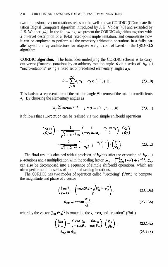
298 CIRCUITS AND SYSTEMS FOR WIRELESS COMMUNICATIONS
two-dimensional vector rotations relies on the well-known CORDIC (COordinate Ro-tation DIgital Computer) algorithm introduced by J. E. Volder [43] and extended byJ. S. Walther [44]. In the following, we present the CORDIC algorithm together witha bit-level description of a 16-bit fixed-point implementation, and demonstrate howit can be employed to perform all the necessary arithmetic operations in a fully par-allel systolic array architecture for adaptive weight control based on the QRD-RLSalgorithm.
CORDIC algorithm. The basic idea underlying the CORDIC scheme is to carryout vector (“macro”-)rotations by an arbitrary rotation angle via a series of“micro-rotations” using a fixed set of predefined elementary angles
This leads to a representation of the rotation angle in terms of the rotation coefficientsBy choosing the elementary angles as
it follows that a can be realised via two simple shift-add operations:
The final result is obtained with a precision of bits after the execution of-rotations and a multiplication with the scaling factor
can also be decomposed into a sequence of simple shift-add operations, which areoften performed in a series of additional scaling iterations.
The CORDIC has two modes of operation called “vectoring” (Vec.) to computethe magnitude and phase of a vector
whereby the vector is rotated to the and “rotation” (Rot .)

DEDICATED VLSI ARCHITECHTURES 299
in which case the vector is rotated by the angleObviously, the rotation angles and for a complex Givens rotation can be
determined using the CORDIC in vectoring mode, whereas the rotations themselvesare carried out using the CORDIC algorithm in rotation mode.
Tab. 23.2 contains the bit-level description of a 16-bit fixed-point CORDIC algo-rithm as specified in [45]. It forms the basis for the hardware implementations dis-cussed next and was employed for the bit-true simulations of the QRD-RLS-basedTRB to be presented in Subsection 23.4.4.
In addition to the CORDIC vectoring and rotation modes, Tab. 23.3 also showshow to elegantly implement the division operation (Div.) in a bit-serialfashion using the same shift-add operations. As can be seen in Tab. 23.1, a division isneeded to calculate the a priori estimation error
The actual hardware implementation of the CORDIC equations (23.12) may bedone in a number of ways [46] as depicted in Fig. 23.2.

300
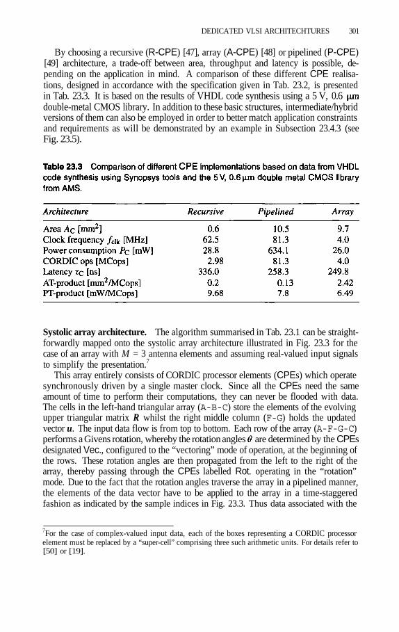
DEDICATED VLSI ARCHITECHTURES 301
By choosing a recursive (R-CPE) [47], array (A-CPE) [48] or pipelined (P-CPE)[49] architecture, a trade-off between area, throughput and latency is possible, de-pending on the application in mind. A comparison of these different CPE realisa-tions, designed in accordance with the specification given in Tab. 23.2, is presentedin Tab. 23.3. It is based on the results of VHDL code synthesis using a 5 V, 0.6double-metal CMOS library. In addition to these basic structures, intermediate/hybridversions of them can also be employed in order to better match application constraintsand requirements as will be demonstrated by an example in Subsection 23.4.3 (seeFig. 23.5).
Systolic array architecture. The algorithm summarised in Tab. 23.1 can be straight-forwardly mapped onto the systolic array architecture illustrated in Fig. 23.3 for thecase of an array with M = 3 antenna elements and assuming real-valued input signalsto simplify the presentation.7
This array entirely consists of CORDIC processor elements (CPEs) which operatesynchronously driven by a single master clock. Since all the CPEs need the sameamount of time to perform their computations, they can never be flooded with data.The cells in the left-hand triangular array (A-B-C) store the elements of the evolvingupper triangular matrix R whilst the right middle column (F-G) holds the updatedvector u. The input data flow is from top to bottom. Each row of the array (A-F-G-C)performs a Givens rotation, whereby the rotation angles are determined by the CPEsdesignated Vec., configured to the “vectoring” mode of operation, at the beginning ofthe rows. These rotation angles are then propagated from the left to the right of thearray, thereby passing through the CPEs labelled Rot. operating in the “rotation”mode. Due to the fact that the rotation angles traverse the array in a pipelined manner,the elements of the data vector have to be applied to the array in a time-staggeredfashion as indicated by the sample indices in Fig. 23.3. Thus data associated with the
7For the case of complex-valued input data, each of the boxes representing a CORDIC processorelement must be replaced by a “super-cell” comprising three such arithmetic units. For details refer to[50] or [19].

302 CIRCUITS AND SYSTEMS FOR WIRELESS COMMUNICATIONS
same index wanders through the array in the form of a “wavefront” which emanatesfrom the top left corner, spreads out and proceeds in the direction of the axisbefore disappearing again in the bottom right cell. The left middle column of cells(D-E) successively computes the “conversion factor” It is required for computingthe a priori error which is formed by dividing the “rotated error” by in the CPEmarked H, configured to the Div. mode of operation.
This fully parallel implementation of the array requires processors andachieves a throughput of O(l), i.e. it is capable of processing the input data streamat the sampling rate, thus fulfilling the real-time requirement independent of the num-ber of antennas. Of course, this comes at the price of O(2M) sampling periods latency,due to the intensive pipelining employed. The limiting factor governing the maximumsampling speed is given by the latency of the individual CORDIC cells, due to thefeedback loop (from to present for updating the contents of the array. Thisproblem is attacked in [51] by applying a technique based on “lookahead” computa-tions. Unfortunately, this approach requires a great deal of additional hardware.
Alternatively, this fully parallel 2D-array architecture may be mapped onto a lineararray of processors [50], whereby all the operations taking place within each row ofcells in the array of Fig. 23.3 are assigned to a single arithmetic unit, leading to aconsiderable reduction in the total number of required cells. The pipelined CORDICprocessor element (P-CPE) is ideally fitted to this structure, whereas the recursivevariant (R-CPE) is more suited for the fully parallel implementation. A comparisonof these two competing array realisations for a specific application example will bemade in the next subsection.
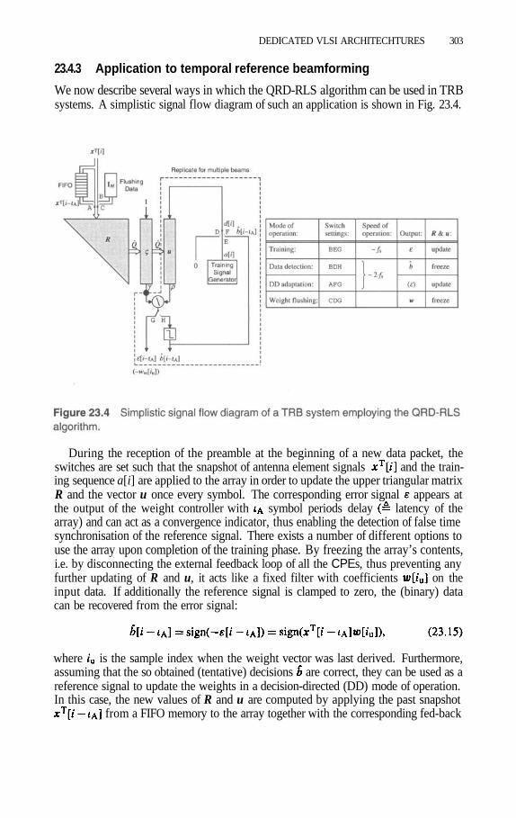
DEDICATED VLSI ARCHITECHTURES 303
23.4.3 Application to temporal reference beamforming
We now describe several ways in which the QRD-RLS algorithm can be used in TRBsystems. A simplistic signal flow diagram of such an application is shown in Fig. 23.4.
During the reception of the preamble at the beginning of a new data packet, theswitches are set such that the snapshot of antenna element signals and the train-ing sequence a[i] are applied to the array in order to update the upper triangular matrixR and the vector u once every symbol. The corresponding error signal appears atthe output of the weight controller with symbol periods delay latency of thearray) and can act as a convergence indicator, thus enabling the detection of false timesynchronisation of the reference signal. There exists a number of different options touse the array upon completion of the training phase. By freezing the array’s contents,i.e. by disconnecting the external feedback loop of all the CPEs, thus preventing anyfurther updating of R and u, it acts like a fixed filter with coefficients on theinput data. If additionally the reference signal is clamped to zero, the (binary) datacan be recovered from the error signal:
where is the sample index when the weight vector was last derived. Furthermore,assuming that the so obtained (tentative) decisions are correct, they can be used as areference signal to update the weights in a decision-directed (DD) mode of operation.In this case, the new values of R and u are computed by applying the past snapshot
from a FIFO memory to the array together with the corresponding fed-back

304 CIRCUITS AND SYSTEMS FOR WIRELESS COMMUNICATIONS
data decision For continual tracking of the weight coefficients withdecision-feedback, the array must be clocked at twice the normal speed, operatingalternately in data-detection and DD-adaptation mode within each symbol period. Thisallows to follow any variations of the environment whose temporal extension exceedsthe array latency i.e. whose rate of change is less than
Instead of using the array to perform the spatial filtering directly, this operationcan be assigned to a separate beamforming network consisting of complex multipliersat the baseband or phase shifters and attenuators/amplifiers at RF or IF ( analoguebeamforming). The combiner coefficients required by the beamforming network canbe very elegantly extracted from the array by the following simple “serial weight flush-ing” procedure. Since the weight vector is equal to the impulse response of the systolicarray when R and u are held fixed, we can obtain by exciting the array with a se-quence of M snapshots which together form the identity matrix along with a vectorof M zero reference symbols The negative weight coefficients then appear at theoutput one after another:
Note that some additional inputs (e.g. all zeros) are required to completely flush thepipeline. An alternative method, allowing a continual parallel extraction of the com-plete weight vector, is treated in [19] and [40].
Clearly, we can easily incorporate several reference signals into our scheme to en-able concurrent adaptation of K independent beams. To achieve this, we simply extendthe array by replicating the column containing the vector u K times and then applyinga K-dimensional vector of reference bits instead of a sin-gle one d[i] with every snapshot. This is equivalent to solving the system of equations(Eq. (23.9)) for different right-side vectors . Such a multibeam antenna can beemployed to allow the simultaneous reception of multiple signals, either originatingfrom different angularly distributed users or due to echoes arriving from different di-rections. Once isolated, the latter multipath components can be aligned in time andappropriately combined to reduce fading effects ( “2D/space-time rake”).
Up to now we have assumed that the local reference is ideally synchronised with thereceived signal of interest. In practice, sychronisation has to be established before theadaptive array can be trained. We now briefly present a simple and yet highly reliabletechnique based on the QRD-RLS algorithm to simultaneously establish timing syn-chronisation and adapt the array using a short, periodically repeated training sequencea[i] of length . symbols. To guarantee the best possible performance, we assumethat a[i] is orthogonal (uncorrelated) to its delayed replicas, thus making m-sequencesa very suitable choice. To achieve initial synchronisation, i.e. to estimate the timingof a[i], we first adapt the array according to the LSE criterion using the QRD-RLSalgorithm for each of the Ns possible time offset versions ofthe synchronisation sequence, and then select the one giving rise to the smallest meansquare a priori error (i.e. highest output SINR), where stands foraveraging over J consecutive values. This can be implemented very efficiently usingthe proposed multibeam weight controller for processing the offset versions of the
DEDICATED VLSI ARCHITECHTURES 305
synchronisation signal in parallel. is generated by the Div.-mode CPE labelledH in Fig. 23.3 and subsequently its squared magnitude is accumulated over J symbolintervals. As stated in [40], array adaptation and timing estimation together requireprocessing of approximately symbols, where is sufficient to guaranteea high probability of acquisition even at low SNRs.
We complete this subsection by briefly demonstrating how to implement a multi-beam TRB using a linear array of pipelined CORDIC processor elements. Fig. 23.5illustrates the basic architecture for an example with antennas and inde-pendent beams (again assuming real-valued signals), which means that three columns
are present on the right of the array in Fig. 23.4. The seven cells in the toprow of the corresponding 2D-array are all mapped onto P-CPE1, which comprisesseven pipeline stages with three CORDIC iterations performed between each register( mixture of pipelined and array CORDIC implementation). This way no additionaldummy data or clock cycles are needed to flush the CORDIC pipeline before applyingthe next valid inputs. Since the number of cells in each row decreases by one towardsthe bottom of the 2D-array, the utilisation of the associated P-CPEs is reduced accord-ingly (to 86% for P-CPE2 and 71% for P-CPE3 in our example).8 Two control bits,i.e. “feedback” (FB) and “vectoring/rotation” (V/R) determine the operation of eachP-CPE and the array as a whole, whereby the frozen mode is assumed whenand the -inputs are taken from the circular buffers (CBUF) external to the P-CPEs.In Tab. 23.4 a (rough9) complexity comparison is made between the fully parallel2D-array and the linear array solution for an adaptive antenna comprisingelements, capable of concurrently processing different beams.
23.4.4 Simulation results
We have conducted a large number of computer experiments to assess the performanceof the proposed techniques. A small selection of illustrative examples are presentedin the following. In the simulations described here the QRD-RLS algorithm was im-plemented using the 16-bit fixed-point CORDIC arithmetic specified in Tab. 23.2, inorder to take finite-precision effects into account. The antenna element signals arethereby digitised with a resolution of bits. All computations for the LMS algo-rithm are performed in floating-point format with unquantised inputs. The TRB underinvestigation employs a uniform linear array (ULA) with antennas having aninterelement spacing of half a carrier wavelength The theoretical arraygain offered by this configuration is 4.77 dB.
To illustrate the typical convergence behaviour of the RLS and LMS algorithm, welook at a situation where three signals with different power levels and directions ofarrival
8C. M. Rader shows how to build a sidelobe canceller using a folded linear array with 100% utilisationin [50].9Wiring for cell interconnection has been omitted, which makes the results for the R-CPE-basedrealisation overoptimistic. Furthermore, the external CBUFs are not included ( frozen op-modeunavailable).10SNRin stands for the signal-to-noise ratio at the output of the matched filters (MF) in each antennabranch, i.e. at the input to the adaptive combiner.

306 CIRCUITS AND SYSTEMS FOR WIRELESS COMMUNICATIONS

DEDICATED VLSI ARCHITECHTURES 307
10dB, but sharing the same carrier frequency are to be separated by areceiver through spatial filtering. In this specific case the eigenvalue spread of the inputdata correlation matrix takes on a large value of The simulated learningcurves in Fig. 23.6 show the average (over 250 runs) output SINR as a function of theadaptation time.
The QRD-RLS algorithm converges to within of the maximum SINR at-tainable with the optimal MMSE weight vector in approximately 10M iterations [38].As can be seen in the top graph of Fig. 23.6, this is true for all three signals. On theother hand, the LMS algorithm only works satisfactorily for the strongest signal. Con-vergence degrades considerably for the second strongest and becomes unacceptablefor the weakest one. This nicely illustrates the algorithm’s sensitivity regarding a largeeigenvalue spread. If all three received signals have the same SNRequal to 10 dB, the dotted learning curve plotted in the bottom of Fig. 23.6 is obtained.It shows improved but still inferior convergence compared to the QRD-RLS imple-mentation. Note also the loss in the maximal theoretically achievable output SINRincurred by the LMS algorithm (dashed lines) relative to the value resulting for theMMSE weight solution. This “misadjustment” is an additional weakness of the LMStechnique [38]. As far as the impact of finite-precision CORDIC arithmetic is con-cerned, the learning curves produced by the chosen QRD-RLS realisation may exhibita minor droop due to error accumulation. As can be observed in the top curve ofFig. 23.6, this effect is visible at high SNRs, where it leads to a gradual, very slightdecay in SINR with time, but gets concealed by noise for levels of SNR below about20 dB.
The bit error rate (BER) curves for user 1 obtained from simulations of the abovescenario for three signals of identical power
are plotted in Fig. 23.7.

308 CIRCUITS AND SYSTEMS FOR WIRELESS COMMUNICATIONS
Packetwise transmission is employed with a randomly chosen training sequence oflength 30 symbols preceding each data burst. No further decision-directedupdating is performed after initial weight adaptation. Obviously, the system with asingle antenna is useless even at high SNRs. Conversely, the BER of a TRB using theCPE-based implementation of the QRD-RLS algorithm remains close to the BPSKsingle-user bound. It merely shows a marginal performance degradation relative to theoptimal MMSE solution, which in fact is primarily due to the short training intervaland only secondarily a result of the signal quantisation and finite-precision calcula-tions. The LMS-controlled beamformer shows a greater loss because of the misadjust-ment associated with this algorithm. Additionally, the BER would rapidly increase(for the weak users) as the received signal powers become dissimilar.
All the above observations clearly underline the advantages of RLS-based tech-niques for adaptive antenna control in situations with severe interference where theirLMS counterparts fail to deliver satisfactory performance.
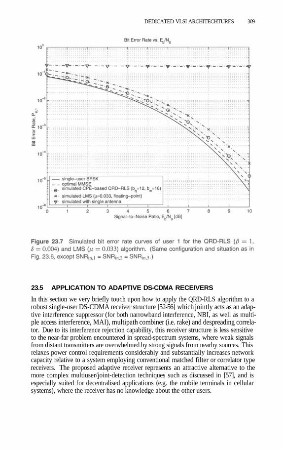
DEDICATED VLSI ARCHITECHTURES 309
23.5 APPLICATION TO ADAPTIVE DS-CDMA RECEIVERS
In this section we very briefly touch upon how to apply the QRD-RLS algorithm to arobust single-user DS-CDMA receiver structure [52-56] which jointly acts as an adap-tive interference suppressor (for both narrowband interference, NBI, as well as multi-ple access interference, MAI), multipath combiner (i.e. rake) and despreading correla-tor. Due to its interference rejection capability, this receiver structure is less sensitiveto the near-far problem encountered in spread-spectrum systems, where weak signalsfrom distant transmitters are overwhelmed by strong signals from nearby sources. Thisrelaxes power control requirements considerably and substantially increases networkcapacity relative to a system employing conventional matched filter or correlator typereceivers. The proposed adaptive receiver represents an attractive alternative to themore complex multiuser/joint-detection techniques such as discussed in [57], and isespecially suited for decentralised applications (e.g. the mobile terminals in cellularsystems), where the receiver has no knowledge about the other users.

310 CIRCUITS AND SYSTEMS FOR WIRELESS COMMUNICATIONS
Fig. 23.8 shows the block diagram of the considered adaptive receiver. It is essen-tially a linear equaliser with a tap spacing that equals the chip duration (or somerational fraction of it) and a total length of (at least) one symbol intervalcorresponding to a single period of the spreading code.
During the operation of the receiver, the contents of the tapped delay line (TDL) areadvanced by a full symbol period before computing each new output value y[i] (downsampling by a factor of and performing a weight update iteration. As a re-sult, a particular register of the TDL will always correspond to a received signal sampletaken at the same time instant within the symbol interval, assuming that the receiver’schip clock has a negligible frequency offset relative to that of the transmitter. In ourexample, each tap in the TDL contains the samples associated with a particular chip(i.e. a specific element of the spreading sequence). Obviously, the weight controlleroperates in exactly the same way as for the TRB treated before, therefore the samehardware architectures are applicable. It should be noted that the so-called “fast” RLSalgorithms [38] of lower complexity employed in traditional adaptive equalis-ers for TDMA receivers cannot be applied to this problem since these methods takeadvantage of the circumstance that the signals used to calculate consecutive outputsy[i] are time-shifted versions of the input sample sequence. This shifting property isnot present here due to the fact that the output is not generated at the same rate as theinput is clocked through the TDL. For a detailed treatment of algorithmic as well ashardware implementation issues related to this application please refer to [40,58–62].

DEDICATED VLSI ARCHITECHTURES 311
23.6 SUMMARY AND CONCLUSIONS
In this contribution we have described algorithms and systolic array architectures forhigh-speed, high-performance RLS-based digital adaptive beamforming (as well asrobust single-user DS-CDMA demodulation) using training sequences for initial adap-tation and decision feedback for weight updating during data transmission. The QRD-RLS algorithm has been identified as a very promising candidate for adaptive weightcontrol due to its positive numerical characteristics and the ability to perform the re-quired calculations in a parallel and pipelined manner. CORDIC arithmetic is advo-cated for the hardware implementation of the individual cells in a possible processorarray realisation, since the same number of cycles is required to perform all the neededoperations, resulting in a truly systolic data flow. Different possible CORDIC archi-tectures were compared with each other regarding area, throughput and latency, andapplied as building blocks to construct both a fully parallel 2D-array, as well as analternative linear array. Furthermore, a scheme for parallel control of multiple inde-pendent beams was briefly discussed together with its possible application for con-current reception of many signals, either from different angularly distributed users, ormultipath components of the SOI with different DOAs, which could be time alignedand combined to reduce the effect of fading. Additionally, it was shown how to em-ploy the QRD-RLS algorithm to simultaneously establish timing synchronisation ofthe training sequence and adapt the array. Finally, the results of computer simulationswere presented to illustrate the performance of the proposed techniques. It was clearlydemonstrated that RLS-based methods greatly outperform their LMS counterparts un-der severe interference conditions, even when employing finite-precision arithmetic.The same holds in highly time-varying scenarios. It was pointed out that it is impera-tive to design algorithms and architectures in a joint process, thereby taking advantageof the interrelation between the two, in order to be able to exploit the merits of ad-vanced signal processing techniques in practice at a reasonable cost.
References
[1] R. Prasad, Universal Wireless Personal Communications, Boston, MA: ArtechHouse, 1998.
[2] M. Shafi, A. Hashimoto, M. Umehira, S. Ogose, and T. Murase, “Wireless Com-munications in the Twenty-First Century: A Perspective,” Proc. IEEE, Vol. 85,No. 10, pp. 1622–1638, October 1997.
[3] H. Meyr and R. Subramanian, “Advanced Digital Receiver Principles and Tech-nologies for PCS,” IEEE Communications Magazine, Vol. 33, No. 1, pp. 68–78,January 1995.
[4] H. Meyr, M. Moeneclaey, and S. A. Fechtel, Digital Communication Receivers:Synchronization, Channel Estimation, and Signal Processing, New York: JohnWiley & Sons, 1998.
[5] Bell Labs Technical Journal Commemorative Issue: 50th Anniversary of theTransistor, Vol. 2, No. 4, Autumn 1997.
[6] Proceedings of the IEEE Special Issue on the Fiftieth Anniversary of the Transis-tor, Vol. 86, No. 1, January 1998.

312 CIRCUITS AND SYSTEMS FOR WIRELESS COMMUNICATIONS
[7] Z. Kostic and S. Seetharaman, “Digital Signal Processors in Cellular Radio Com-munications,” IEEE Communications Magazine, Vol. 35, No. 12, pp. 22–35, De-cember 1997.
[8] J. Sanchez and G. Miet, “An Overview of Digital Signal Processing and DigitalSignal Processors for Mobile Communications,” in this volume.
[9] N. Seshan, “High VelociTI Processing,” IEEE Signal Processing Magazine,Vol. 15, No. 2, pp. 86–101 & p. 117, March 1998.(http://www.ti.com/sc/docs/dsps/products/c6000/index.htm)
[10] M. Alidina, G. Burns, C. Holmqvist, E. Morgan, D. Rhodes, S. Simanapalli,and M. Thierbach, “DSP16000: A High Performance, Low Power Dual-MACDSP Core for Communications Applications,” in Proc. CICC ’98, Santa Clara,CA, May 11–14, 1998,pp. 119–122. (http://www. lucent .com/micro/dspl6000/)
[11] E. Lambers, C. Moerman, P. Kievits, J. Walkier, and R. Woudsma, “R.E.A.L.DSP: Reconfigurable Embedded DSP Architecture for Low-Power/Low-CostTelecom Baseband Processing,” in this volume.
[12] R. Baines, “The DSP Bottleneck,” IEEE Communications Magazine, Vol. 33,No. 5, pp. 46–54, May 1995.
[13] J. K. Hinderling, T. Rueth, K. Easton, D. Eagleson, D. Kindred, R. Kerr, andJ. Levin, “CDMA Mobile Station Modem ASIC,” IEEE J. Solid-State Circuits,Vol. SSC-28, No. 3, pp. 253–260, March 1993.(http://www.qualcomm.com/ProdTech/asic/msm.htm)
[14] K. H. Cho, J. Putnam, E. Berg, B. Daneshrad, and H. Samueli, “30Mbps Wire-less Data Transmission Using an Equalized 5-MBaud M-QAM Testbed,” in Proc.ICUPC ’97, San Diego, CA, October 12–16, 1997, Vol. 1, pp. 104–108.
[15] B. Daneshrad, “VLSI ASICs and Testbeds for High Speed Wireless DataCommunications,” presentation given at Bell Labs, Crawford Hill, Holmdel,August 5, 1997. (RealPlayer audio recording and slides available at URLhttp://www.bell-labs.com/topic/seminars/hoh.wcof/tree/97-08-05/index.htm)
[16] J. Litva and T. K.-Y. Lo, Digital Beamforming in Wireless Communications,Boston, MA: Artech House, 1996.
[17] B. D. Van Veen and K. M. Buckley, “Beamforming: A Versatile Approach toSpatial Filtering,” IEEE Acoust., Speech, Signal Processing Magazine, Vol. 5,No. 2, pp. 4–24, April 1988.
[18] J.-Y. Lee, H.-C. Liu, and H. Samueli, “A Digital Adaptive Beamforming QAMDemodulator 1C for High Bit-Rate Wireless Communications,” IEEE J. Solid-State Circuits, Vol. SSC-33, No. 3, pp. 367–377, March 1998.
[19] B. Haller, “Algorithms and VLSI Architectures for RLS-Based Time Refer-ence Beamforming in Mobile Communications,” in Proc. Int. Zurich Seminaron Broadband Communications IZS ’98, Zurich, Switzerland, February 17–19,1998, pp. 29–36.

DEDICATED VLSI ARCHITECHTURES 313
[20] K. K. Parhi, VLSI Digital Signal Processing Systems: Design and Implementa-tion, New York: John Wiley & Sons, 1999.
[21] K. K. Parhi, “Impact of Architecture on DSP Circuits,” in Proc. IEEE Region 10Int. Conf. TENCON’92, Melbourne, Australia, November 11–13, 1992, Vol. 2,pp. 784–788.
[22] G. Fettweis and H. Meyr, “On the Interaction Between DSP-Algorithms andVLSI-Architecture,” in Proc. 1990 Int. Zurich Seminar on Digital Communica-tions IZS ’90, Zurich, Switzerland, March 5–9, 1990, pp. 219–230.
[23] H. Meyr, “VLSI in Communications: Interactive Design of Algorithm and Ar-chitecture,” in Proc. 3rd Int. Workshop on Digital Signal Processing TechniquesApplied to Space Communications, ESTEC, Noordwijk, NL, September 23–25,1992, pp. 1.1–1.8.
[24] G. Fettweis, “On Implementing Digital Signal Processing Tasks of Communica-tions Systems in VLSI,” Digital Signal Processing, Vol. 3, No. 3, pp. 210–219,July 1993.
[25] M. Ismail and N. Tan (Eds.), “Chip Design for Wireless Communication (AnInterview with Ericsson’s Tord Wingren),” IEEE Circuits & Devices Magazine,Vol. 14, No. 1, pp. 8–9, January 1998.
[26] H. Keding, M. Coors, and H. Meyr, “Efficient Design Flow for Fixed Point Sys-tems,” in this volume.
[27] A. E. Dunlop, W. J. Evans, and L. A. Rigge, “Managing Complexity in 1C De-sign – Past, Present, and Future,” Bell Labs Technical Journal, Vol. 2, No. 4,pp. 103–125, Autumn 1997.
[28] S. Y. Kung, “VLSI Array Processors,” lEEEAcoust., Speech, Signal ProcessingMagazine, Vol. 2, No. 3, pp. 4–22, July 1985.
[29] S. Y. Kung, VLSI Array Processors, Englewood Cliffs, NJ: Prentice Hall, 1988.[30] T. Ohgane, “Spectral Efficiency Improvement by Base-Station Antenna Pattern
Control for Land Mobile Cellular Systems,” IEICE Trans. Communications,Vol. E77-B, No. 5, pp. 598–605, May 1994.
[31] A. F. Naguib, A. Paulraj, and T. Kailath, “Capacity Improvement with Base-Sta-tion Antenna Arrays in Cellular CDMA,” IEEE Trans. Vehicular Technology,Vol. VT-43, No. 3, Pt. II, pp. 691–698, August 1994.
[32] G. V. Tsoulos, M. A. Beach, and J. P. McGeehan, “Wireless Personal Commu-nications for the 21st Century: European Technological Advances in AdaptiveAntennas,” IEEE Communications Magazine, Vol. 35, No. 9, pp. 102–109, Sep-tember 1997.
[33] IEEE Signal Processing Magazine Special Issue on Space-Time Processing,Vol. 14, No. 6, November 1997.
[34] IEEE Personal Communications Special Issue on Smart Antennas, Vol. 5, No. 1,February 1998.
[35] L. C. Godara, “Applications of Antenna Arrays to Mobile Communications,Part I: Performance Improvement, Feasibility, and System Considerations,” Proc.IEEE, Vol. 85, No. 7, pp. 1031–1060, July 1997.

314 CIRCUITS AND SYSTEMS FOR WIRELESS COMMUNICATIONS
[36] L. C. Godara, “Applications of Antenna Arrays to Mobile Communications,Part II: Beam-Forming and Direction-of-Arrival Considerations,” Proc. IEEE,Vol. 85, No. 8, pp. 1195–1245, August 1997.
[37] J. H. Winters, J. Salz, and R. D. Gitlin, “The Impact of Antenna Diversity on theCapacity of Wireless Communication Systems,” IEEE Trans. Communications,Vol. COM-42, No. 2/3/4, Pt. III, pp. 1740–1751, Feb./Mar./Apr. 1994.
[38] S. Haykin, Adaptive Filter Theory, Upper Saddle River, NJ: Prentice Hall, 3rdEd., 1996.
[39] I. S. Reed, J. D. Mallett, and L. E. Brennan, “Rapid Convergence Rate inAdaptive Arrays,” IEEE Trans. Aerosp. Electron. Syst., Vol. AES-10, No. 6,pp. 853–863, November 1974.
[40] B. Haller, Algorithms and VLSI Architectures for Diversity Combining and Inter-ference Suppression in Wireless Communication Systems, Doctoral Dissertation,Swiss Federal Institute of Technology, Zurich, Switzerland, 1999.
[41] W. M. Gentleman and H. T. Kung, “Matrix Triangularization by Systolic Arrays,”in Real-Time Signal Processing IV (T. F. Tao, Ed.), Proc. SPIE Vol. 298, SanDiego, CA, August 1981, pp. 19–26.
[42] J. G. McWhirter, “Recursive Least-Squares Minimization Using a Systolic Ar-ray,” in Real Time Signal Processing VI (K. Bromley, Ed.), Proc. SPIE Vol. 431,San Diego, CA, August 1983, pp. 105–112.
[43] J. E. Volder, “The CORDIC Trigonometric Computing Technique,” IRE Trans.Electronic Computers, Vol. EC-8, No. 3, pp. 330–334, September 1959.
[44] J. S. Walther, “A Unified Algorithm for Elementary Functions,” in Proc. SpringJoint Computer Conf., Atlantic City, NJ, May 18–20, 1971, pp. 379–385.
[45] D. König and J. F. Böhme, “Optimizing the CORDIC Algorithm for Processorswith Pipeline Architecture,” in Proc. EUSIPCO ’90, Barcelona, Spain, Septem-ber 18–21, 1990, Vol. 3, pp. 1391–1394.
[46] Y. H. Hu, “CORDIC-Based VLSI Architectures for Digital Signal Processing,”IEEE Signal Processing Magazine, Vol. 9, No. 3, pp. 16–35, July 1992.
[47] D. Timmermann, H. Hahn, B. J. Hosticka, and G. Schmidt, “A ProgrammableCORDIC Chip for Digital Signal Processing Applications,” IEEE J. Solid-StateCircuits, Vol. SSC-26, No. 9, pp. 1317–1321, September 1991.
[48] H. M. Ahmed and K.-H. Fu, “A VLSI Array CORDIC Architecture,” in Proc.ICASSP ’89, Glasgow, Scotland, May 23–26, 1989, Vol. 4, pp. 2385–2388.
[49] D. Timmermann, B. Rix, H. Hahn, and B. J. Hosticka, “A CMOS Floating-point Vector-Arithmetic Unit,” IEEE J. Solid-State Circuits, Vol. SSC-29, No. 5,pp. 634–639, May 1994.
[50] C. M. Rader, “VLSI Systolic Arrays for Adaptive Nulling,” IEEE Signal Pro-cessing Magazine, Vol. 13, No. 4, pp. 29–49, July 1996.
[51] J. Ma, E. F. Deprettere, and K. K. Parhi, “Pipelined CORDIC Based QRD-RLSAdaptive Filtering Using Matrix Lookahead,” in Proc. 1997 IEEE Workshop onSignal Processing Systems Design and Implementation SiPS ’97 (M. K. Ibrahim,P. Pirsch, and J. McCanny, Eds.), Leicester, UK, November 3–5, 1997,pp. 131–140.

DEDICATED VLSI ARCHITECHTURES 315
[52] C. N. Pateros and G. J. Saulnier, “An Adaptive Correlator Receiver for Direct-Sequence Spread-Spectrum Communication,” IEEE Trans. Communications,Vol. COM-44, No. 11, pp. 1543–1552, November 1996.
[53] P. B. Rapajic and B. S. Vucetic, “Adaptive Receiver Structures for Asynchro-nous CDMA Systems,” IEEE J. Select. Areas Commun., Vol. SAC-12, No. 4,pp. 685–697, May 1994.
[54] S. L. Miller, “An Adaptive Direct-Sequence Code-Division Multiple-AccessReceiver for Multiuser Interference Rejection,” IEEE Trans. Communications,Vol. COM-43, No. 2/3/4, Pt. Ill, pp. 1746–1755, Feb./Mar./Apr. 1995.
[55] U. Madhow and M. L. Honig, “MMSE Interference Suppression forDirect-Sequence Spread-Spectrum CDMA,” IEEE Trans. Communications,Vol. COM-42, No. 12, pp. 3178–3188, December 1994.
[56] H. V. Poor, “Adaptive Interference Suppression for Wireless Multiple-AccessCommunication Systems,” in this volume.
[57] S. Verdú, Multiuser Detection, New York: Cambridge University Press, 1998.[58] L. He and U. Madhow, “Pipelined MMSE Equalizers for Direct-Sequence
Spread-Spectrum CDMA Channels," in Proc. 1CUPC ’96, Cambridge, MA, Sep.29 – Oct. 2, 1996, pp. 120–124.
[59] L. Lucke, L. Nelson, and H. Oie, “Adaptive CDMA Receiver Implementa-tion for Multipath and Multiuser Environments,” in VLSI Signal Processing IX(W. Burleson, K. Konstantinides, and T. Meng, Eds.), Piscataway, NJ: IEEEPress, 1996, pp. 159–168.
[60] C. Teuscher, Low Power Receiver Design for Portable RF Applications: Designand Implementation of an Adaptive Multiuser Detector for an Indoor, WidebandCDMA Application, Ph.D. Thesis, U.C. Berkeley, Berkeley, CA, 1998.
[61] C. Teuscher, D. Yee, N. Zhang, and R. Brodersen, “Design of a Wideband SpreadSpectrum Radio Using Adaptive Multiuser Detection,” in Proc. ISCAS ’98, Mon-terey, CA, May 31 – June 3, Vol. 4, pp. 593–599, 1998.
[62] H. V. Poor and X. Wang, “Code-Aided Interference Suppression for DS/CDMACommunications – Part II: Parallel Blind Adaptive Implementations,” IEEETrans. Communications, Vol. COM-45, No. 9, pp. 1112–1122, September 1997.

This page intentionally left blank

24 EVOLUTION OF SPEECHCODING FOR WIRELESS
COMMUNICATIONSA system standard: the AMR
(Adaptive Multi Rate codec)
Gilles Miet
Philips Consumer CommunicationsLe Mans, France
Abstract: The world-wide coverage of GSM-like networks led to an explosion ofthe number of subscribers, causing the saturation of some networks. Besides, the oldtechnology used in GSM systems provided the customer with an unsatisfactory audioquality in many common situations. In parallel, DSP computing capabilities and thestate of the art in speech and channel coding have improved. Therefore, to increaseboth the capacity and the quality of GSM networks, ETSI decided to standardise a newspeech transmission system: the AMR. This Adaptive Multi Rate system is a combina-tion of speech and channel codecs controlled by signalling means aimed at providingthe best audio quality under background noise and transmission errors. The first partof this chapter explains this concept in comparison with current GSM coders. Anotherpromising technology to achieve high quality speech transmission is wide-band cod-ing. Therefore ETSI is investigating a wide-band AMR mode. The second part of thischapter presents the quality gain that can be provided by wide-band AMR.
317
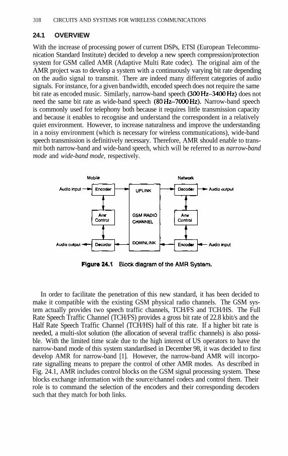
318 CIRCUITS AND SYSTEMS FOR WIRELESS COMMUNICATIONS
24.1 OVERVIEW
With the increase of processing power of current DSPs, ETSI (European Telecommu-nication Standard Institute) decided to develop a new speech compression/protectionsystem for GSM called AMR (Adaptive Multi Rate codec). The original aim of theAMR project was to develop a system with a continuously varying bit rate dependingon the audio signal to transmit. There are indeed many different categories of audiosignals. For instance, for a given bandwidth, encoded speech does not require the samebit rate as encoded music. Similarly, narrow-band speech does notneed the same bit rate as wide-band speech Narrow-band speechis commonly used for telephony both because it requires little transmission capacityand because it enables to recognise and understand the correspondent in a relativelyquiet environment. However, to increase naturalness and improve the understandingin a noisy environment (which is necessary for wireless communications), wide-bandspeech transmission is definitively necessary. Therefore, AMR should enable to trans-mit both narrow-band and wide-band speech, which will be referred to as narrow-bandmode and wide-band mode, respectively.
In order to facilitate the penetration of this new standard, it has been decided tomake it compatible with the existing GSM physical radio channels. The GSM sys-tem actually provides two speech traffic channels, TCH/FS and TCH/HS. The FullRate Speech Traffic Channel (TCH/FS) provides a gross bit rate of 22.8 kbit/s and theHalf Rate Speech Traffic Channel (TCH/HS) half of this rate. If a higher bit rate isneeded, a multi-slot solution (the allocation of several traffic channels) is also possi-ble. With the limited time scale due to the high interest of US operators to have thenarrow-band mode of this system standardised in December 98, it was decided to firstdevelop AMR for narrow-band [1]. However, the narrow-band AMR will incorpo-rate signalling means to prepare the control of other AMR modes. As described inFig. 24.1, AMR includes control blocks on the GSM signal processing system. Theseblocks exchange information with the source/channel codecs and control them. Theirrole is to command the selection of the encoders and their corresponding decoderssuch that they match for both links.

EVOLUTION OF SPEECH CODING FOR WIRELESS COMMUNICATIONS 319
24.2 NARROW-BAND AMR
24.2.1 Need for a new standard
Currently, TCH/FS is used to transmit encoded speech with two possible coders, theFR and the EFR. Since the FR (Full Rate codec) offers a mediocre quality at 13 kbit/s,the EFR (Enhanced Full Rate codec) was standardised later. EFR provides a goodquality at a bit rate of 12.2 kbit/s. However, quality goes down rapidly as transmissionerrors increase. Similarly, TCH/HS can be used for speech transmission with the HR(Half Rate codec) at 5.6kbit/s. This codec gives a very poor quality for both noisyspeech and bad radio conditions. For this reason, many operators are reluctant todeploy it on their networks. The narrow-band AMR codec was therefore defined toimprove the weaknesses of the existing GSM codecs. In TCH/FS, the target of AMRin Full-Rate mode is to offer more robustness to transmission errors than EFR, thegoal being toll quality in all radio conditions. This is a great advantage, but this wasnot the main reason to drive the AMR project. The motivation to build it up cameessentially from the need to have an acceptable codec in TCH/HS. Both European andUS operators need AMR to increase the capacity of their networks seamlessly for theirsubscribers.
24.2.2 Variable bit rates for speech and channel codecs
For a given channel, the narrow-band AMR is a combination of multi-bit rate speechand channel coding systems. This technique is necessary to reach an optimal speechquality for a certain gross bit rate. Indeed, low bit rate speech codecs are very sensitiveto the speech nature of the encoded signal because they model speech. When thebackground noise level increases, the speech codec has to use a higher bit rate tokeep up a given speech quality. Additional bits are then necessary to maintain it.Similarly, under bad channel conditions, the bit error rate increases if the protection ofencoded speech parameters is fixed. To reduce this error rate, a better protection hasto be provided. This is achieved by augmenting the redundancy of the transmitted bitstream, hence the channel codec produces a higher bit rate. Fig. 24.2 shows the effectof the source/channel partitioning under radio error conditions.
The highest source rate gives the best results under no error (speech is more ac-curately modelled) and the worst results under high error conditions (encoded speechis less protected). Therefore the source/channel bit rate partitioning should vary infunction of the environment to provide the best quality. The source or channel bit rateshould be increased in the presence of background noise or bad radio transmission,respectively. The curve called “AMR” in Fig. 24.2 represents the quality the AMRcodec would provide under transmission errors if it was based on codec A, B and C.With this system using several source/channel codecs, some signalling bits have to betransmitted to control a perfect matching between the coders and the decoders at anytime. The conditions in which speech is encoded and transmitted vary very quickly.Consequently, the signalling of the codec mode is transmitted in-band (it uses somebits instead of the source coder) for a given channel. This is shown in Fig. 24.3, wherethe channel encoder is fed by both encoded speech and signalling bits coming from

320 CIRCUITS AND SYSTEMS FOR WIRELESS COMMUNICATIONS
the codec selection block and the speech quality estimator1. Similarly, the channeldecoder outputs both signalling bits and encoded speech. Fig. 24.3 represents theprocessing carried out either in the network or in a mobile phone.
Current GSM systems consist of a speech codec, a channel codec, a modulatorand a demodulator. Although AMR follows this scheme, it differentiates significantly
1The speech quality estimator is a generic term that may represent, for instance, the speech to noiseratio or the background noise level.

EVOLUTION OF SPEECH CODING FOR WIRELESS COMMUNICATIONS 321
by the provision of several codec modes. AMR incorporates also codec selectionblocks fed by signalling and quality metrics to select the right codec modes. Thenarrow-band AMR system being in standardisation process, some uncertainties remainconcerning its final structure. They are represented in Fig. 24.3 by dotted lines. Forinstance, the radio quality metrics coming from the Viterbi equaliser and the speechquality estimator are optional. Effectively, radio quality metrics can be computed inthe channel decoder. The speech quality estimator is likely not to be used2 because theradio quality metrics may be sufficient to decide the codec mode to be selected. Thesemetrics provide the information about the channel protection that should be applied toencoded speech. Since speech sounds better when encoded with a high bit rate, thehighest source bit rate is selected by default and decreased in function of the radioquality metrics.
24.2.3 Complexity/performance compromise of the AMR
The complexity requirement of the AMR codec was initially defined globally. Then itwas decided to split this requirement between the source codec and the channel codec.This demonstrates very clearly the compromise between the compatibility with thecurrent GSM system and the expected improvements thanks to the AMR. Actually,the main driver for the compatibility is the network. The channel codec being in theBTS (Base Transceiver Station), the AMR system has been defined to enable the useof existing BTS without any change in the hardware. This high constraint prevents theuse of Turbo Codes which are the state of the art in channel coding. The complexityof the speech codec was less limited because the speech codec is located in the TRAU(Transcoder Unit) outside the BTS. The overall complexity is still of importance,especially because of the power consumption and price of mobile phones.
The FR AMR performance is targeted to a quality augmentation equivalent to upto 6 dB C/I increase in the radio channel with regard to the EFR. Similarly, HR AMRshould provide the same quality as today’s GSM FR, which is the most widely spreadGSM speech codec.
By doing this, the consumers are presented with a quality either similar (AMR HR)or better (AMR FR) than they are used to with the current GSM FR.
24.3 MULTI-MODE AMR
The current narrow-band system includes hooks in the bit rate control to be able to addwide-band speech and other codecs in a second step. Multi-mode AMR (see Fig. 24.4)can be defined as an audio processing tool box suited to as many audio services aspossible. Actually, very low bit rates can be sufficient to transmit non-conversationalspeech services like voice recognition or voice mails. Higher bit rates are necessary totransmit music or wide-band speech in full duplex. The definition of additional modesfor narrow-band AMR is currently quite vague. However, the wide-band AMR agendahas recently been set because of the high interest of this service.
2The AMR version recently selected has actually no speech quality estimator.

322 CIRCUITS AND SYSTEMS FOR WIRELESS COMMUNICATIONS
24.4 WIDE-BAND AMR
Wide-band speech was emphasised at ETSI because it enables to obtaina far better quality than narrow-band speech In fact, the higher band-
width increases the speech intelligibility (especially for fricativessuch as “s” or “f ”) and the naturalness of speech. The lower bandwidthprovides a higher listening comfort and naturalness [2,5]. A situation that demon-strates the quality difference between narrow-band and wide-band speech is the broad-cast of a phone call through FM radio. The listeners notice the difference of voicequality between the voices coming from the studio and the voice over the phone.
24.4.1 Wide-band versus narrow-band quality
The quality gain brought by wide-band speech with regard to narrow-band speech isstraightforward. However, the available bit rate on TCH/FS is very low to encodewide-band speech which might lead to strong degradations. Therefore, it is interest-ing to evaluate the compromise speech bandwidth/degradations. It was achieved byinformal listening tests. In this respect, the preference of wider band speech overnarrow-band speech was determined by comparing narrow-band speech signals withwider band speech signals generated as described in Fig. 24.5.

EVOLUTION OF SPEECH CODING FOR WIRELESS COMMUNICATIONS 323
The wider band speech signals consist of narrow-band speech signals combinedwith a distorted added band. Three experiments were carried out with three differentadded distorted bands. The first experiment consisted of the addition of the low band
Here the wider band signals were preferred even with a distortion of3.1dB. In the second experiment, the high band was added. In thiscase, the wider speech signals were also preferred with a distortion up to 5.9 dB. Thethird experiment, consisted of the combination of the two preceding experiments. Thewide-band signals were also preferred even with the same distortions as above.
These experiments demonstrate the benefits of widening the bandwidth even if thisprocess introduces significant but not annoying distortions.
24.4.2 Minimum bandwidth for speech to sound wide-band
As mentioned above, wide-band and narrow-band speech bandwidths correspond toand respectively. However, to provide single slot solu-
tions (compatible with TCH/FS), it might become necessary to lower this bandwidth.Indeed, the speech quality might suffer if the source coder bit rate is too low withregard to the bandwidth of the speech signal to transmit. Consequently, there is aninterest in identifying the minimum bandwidth of speech for it to “sound” wide-band.In this respect, there was an experiment undertaken in [4] and recently reported in [5].This experiment concludes that the lowest frequency should be below and thehighest frequency should be above Besides, the transmission of the lower band
was found particularly advantageous for male speakers. The higher part. was especially favourable to female speakers. It was also concluded that
the band does not bring any improvement. The contribution [5] thusconcluded that wide-band AMR should be targeted to transmit the bandThe transmission of was proposed as a fall-back solution.
24.5 CONCLUSION
AMR reveals the recent trend to develop telecommunication signal processing algo-rithms as a whole. Effectively, old standards have defined several processing blocksindependently. In contrast, the different blocks are now developed together, and in-teract with each other. This enables the designers to provide optimal solutions. Be-sides, AMR is a huge system that supplies a multiplicity of codecs to enable the GSMstandard to adapt to the numerous conditions and applications of wireless communi-cations. Narrow-band AMR increases the robustness under channel errors and limitsthe degradation with background noise (as compared to the current GSM system). Italso provides TCH/HS with an acceptable codec to increase network capacity. Wide-band AMR will be deployed for high quality speech transmission. Other modes (e.g.a mode including noise suppression) are currently being discussed.

324 CIRCUITS AND SYSTEMS FOR WIRELESS COMMUNICATIONS
References
[1] P. Gaskell, “AMR feasibility study report”, V. 1.0, November 1997.[2] W.B. Kleijn, K.K. Paliwal, “Speech coding and synthesis”, Elsevier, 1995[3] Y. Linde, A. Buzo, R. M. Gray, “An algorithm for vector quantizer design”, IEEE
Transactions on Communications, Vol. COM-28, No. 1, January 1980.[4] Dominique Pascal, “Comparative performances of two subjective methods for as-
sessing the fidelity of speech transmission systems”, AES 84th Convention, March1–4, Paris.
[5] ETSI TD SMG11 66/98, “Subjective effect of widening the telephone band from0 to 7 kHz for speech signal”.
25 DIGITAL SIGNAL PROCESSINGAND DIGITAL SIGNAL PROCESSORS
FOR MOBILE COMMUNICATIONS:BASIC CONCEPTS AND TRENDS
Javier Sanchez
Philips Consumer CommunicationsAdvanced Development Group
Route d'Angers72081 Le Mans Cedex 9, France
Abstract: The boom of wireless telecommunications arisen in this decade representsa fantastic engine for the technical evolution of Digital Signal Processors (DSP). Thisconstant progress is motivated by the complexity increase of signal processing algo-rithms, and the product properties required by the market. Indeed, both the rapid evo-lution of telecommunication standards (to achieve better quality of communications,higher capacity of networks, and new services) and the new features appearing on ter-minals are increasingly demanding digital signal processing algorithms. In an attemptto implement these algorithms in real-time applications, more elaborate DSP architec-tures had to be developed. Furthermore, especially in mobile telephony, there is a con-stant requirement to decrease power consumption and cost of DSPs. This presentationoutlines the evolution of such DSPs and tries to draw a trend for the near future.
325
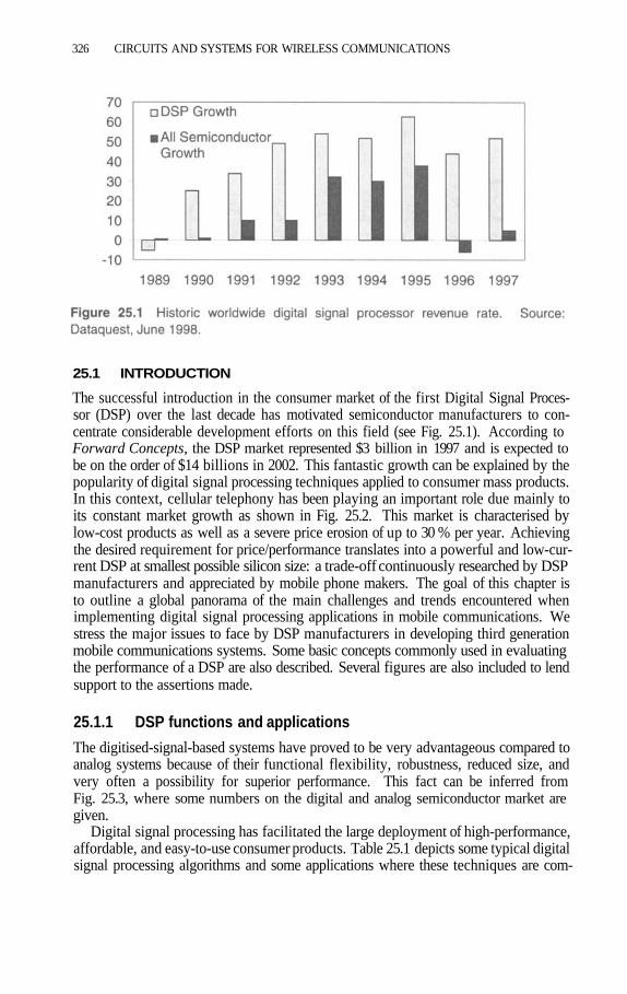
326 CIRCUITS AND SYSTEMS FOR WIRELESS COMMUNICATIONS
25.1 INTRODUCTION
The successful introduction in the consumer market of the first Digital Signal Proces-sor (DSP) over the last decade has motivated semiconductor manufacturers to con-centrate considerable development efforts on this field (see Fig. 25.1). According toForward Concepts, the DSP market represented $3 billion in 1997 and is expected tobe on the order of $14 billions in 2002. This fantastic growth can be explained by thepopularity of digital signal processing techniques applied to consumer mass products.In this context, cellular telephony has been playing an important role due mainly toits constant market growth as shown in Fig. 25.2. This market is characterised bylow-cost products as well as a severe price erosion of up to 30 % per year. Achievingthe desired requirement for price/performance translates into a powerful and low-cur-rent DSP at smallest possible silicon size: a trade-off continuously researched by DSPmanufacturers and appreciated by mobile phone makers. The goal of this chapter isto outline a global panorama of the main challenges and trends encountered whenimplementing digital signal processing applications in mobile communications. Westress the major issues to face by DSP manufacturers in developing third generationmobile communications systems. Some basic concepts commonly used in evaluatingthe performance of a DSP are also described. Several figures are also included to lendsupport to the assertions made.
25.1.1 DSP functions and applications
The digitised-signal-based systems have proved to be very advantageous compared toanalog systems because of their functional flexibility, robustness, reduced size, andvery often a possibility for superior performance. This fact can be inferred fromFig. 25.3, where some numbers on the digital and analog semiconductor market aregiven.
Digital signal processing has facilitated the large deployment of high-performance,affordable, and easy-to-use consumer products. Table 25.1 depicts some typical digitalsignal processing algorithms and some applications where these techniques are com-

DIGITAL SIGNAL PROCESSING AND DSP 327
monly used. Most of these techniques are frequently found as part of wireless com-munication products (e.g. paging, cellular telephony, wireless data networks). Thisfact has motivated DSP manufacturers to propose processors specifically adapted forwireless applications.
Note that, along with the increasing performance and size reduction of DSPs, mul-tidimensional digital signal processing techniques typically used in military applica-tions have recently aroused considerable interest in the wireless communication sector.
25.1.2 Characteristics of digital signal processing
Mobile phone consumers are constantly expressing demands for new digital signalprocessing features for whose development marketing, engineering, and manufactur-

328 CIRCUITS AND SYSTEMS FOR WIRELESS COMMUNICATIONS
ing departments must work together. It is worth mentioning that these demands essen-tially come from the base-band interface of the mobile phone handset. This tendencyis illustrated in Figs. 25.4 and 25.5.
A new digital signal processing feature is first proposed as an “abstract idea” whichthe engineering department has to represent and simulate from an unambiguous math-ematical model according to a specific algorithm. Up to this stage, neither real-timeimplementation constraints nor bit-level accuracy are considered, since the centralpoint is to evaluate the validity and performance of the algorithm itself. After this as-sessment step, the DSP platform where this new feature will be operating needs to bespecified. It is precisely at this stage that the gap between signal processing researchand signal processing development has to be closed. In some cases, it will be neces-sary to realize some modification to the proposed signal processing algorithm to adaptit to the available resources of the DSP despite a decrease of its performance.
Several parameters have then to be considered to evaluate the efficiency of the DSParchitecture in order to achieve the best trade-off between performance and implemen-tation complexity. These parameters are summarised in the following sub-section.

DIGITAL SIGNAL PROCESSING AND DSP 329
25.1.3 Characteristics of digital signal processors
Developing DSPs with better performance at lower cost is a multifaceted challenge formanufacturers. They have to respond to concrete demands of end customers imposingsome key driving factors that the DSP manufacturer has to deal with. These factorsare illustrated in Fig. 25.6.
When selecting a digital signal processor for implementing a specific digital signalprocessing algorithm, the first aspect to be considered is the end product for whichthe application was conceived. For example, in the mobile phone handset sector, the“best” DSP will be the one fitting the requirements of the application at the lowestcost. With this in mind, the developer is confronted with the problem of evaluating the

330 CIRCUITS AND SYSTEMS FOR WIRELESS COMMUNICATIONS
impact of the performance versus cost. Table 25.2 summarises some aspects that canbe considered in order to balance this trade-off.
Most of the features described in Table 25.2 are involved in the evaluation of theexecution speed of the DSP. Commonly, this parameter is measured by the numberof instructions in millions per second (MIPS) that the DSP can execute. Another im-portant concern of most cellular telephone manufacturers is the power consumptionof the DSP. This fact has motivated semiconductor vendors to propose DSPs operat-ing at reduced voltages and integrating programmable clock dividers and idle modes.These DSP features have an impact on its final cost, which is an important factor forthe choice of a DSP to be used in high volume consumer products. Ease of program-ming can also be an important aspect for the DSP-code developer, especially whenalgorithms are complex and the time for delivering is reduced.
Finally, the mobile phone manufacturers tend to keep some “extra” resources ofthe DSP in order to integrate “extra” digital signal processing functions into the endproduct. We can mention, for instance, the addition of easier-to-use user interfacesin the mobile phone handset (speech recognition) or by improving its audio qualities(background noise suppression, audio equalisation).
25.2 BENCHMARKS OF DIGITAL SIGNAL PROCESSING ROUTINESAND APPLICATIONS
25.2.1 Standard benchmark routines
In the previous section, we have seen the difficulties encountered in selecting the“right” DSP, and several of the considerations which have to be made. There is, how-ever, a more general approach to comparing the performance of a DSP architecturefrom the execution speed point of view. It consists of a standard set of digital signalprocessing routines defined by Berkeley Design Technology (BDT), Inc. These rou-

DIGITAL SIGNAL PROCESSING AND DSP 331
tines are listed in Table 25.3. Although some of the routines presented in this tableare functionally redundant, they form a basis for benchmarking more complex appli-cations such as speech and channel coders.
BDT also publishes benchmarking results of the performance of commercial DSPswhen used to implement these algorithms [1]. Obviously, it is the task of the pro-grammer to find an algorithm that is optimal for each benchmark. According to this,the benchmark results depend not only on the processor's efficiency, but also on theskill of the developer. Nevertheless, these benchmark results give information on theperformance and instruction set of the DSP.
25.2.2 DSP architectural features
In order to boost the overall performance of DSPs, several semiconductor manufac-turers propose additional architectural features presented as special instructions or in-dependent co-processing units. This is the case in speech and channel coding anddecoding which represent two major digital signal processing applications in a mobilephone handset. The Application-Specific Instruction (ASI) set of the Philips R.E.A.L.DSP is a good example of this trend [2,3]. Table 25.4 shows the number of MIPSrequired by the R.E.A.L. DSP 16020 to implement typical speech coding standardsused in cellular telephony with the aid of ASIs.

332 CIRCUITS AND SYSTEMS FOR WIRELESS COMMUNICATIONS
25.2.3 Evolution of features for DSP Implementation
Although mobile phone terminals are still being used for transmitting speech, cellulartelephony operators and manufacturers are striving to propose a “mobile multimedia”handset for the mass market. As part of this trend, most telecommunication standard-isation institutions are concentrating efforts on this matter either to upgrade currentstandards or to specify new ones. Table 25.5 illustrates the main standardisation ac-tivities in the cellular sector for the near future. Third generation mobile terminalswill have to be multi-mode, multimedia and multi-service. They will need to maintaincompatibility with second generation networks. The DSP will need to be able to faceprocessing rates beyond 1 GFlops!

DIGITAL SIGNAL PROCESSING AND DSP 333
25.2.4 General-purpose DSPs versus application-specific DSPs formobile phones
In the mobile phone market arena, some manufacturers are constrained to restrain theirchoice of a DSP technology to that proposed by external semiconductor vendors. Thissituation may induce a DSP solution not appropriate for the actual application needsof the customer. Conversely, when the mobile phone manufacturer is directly involvedin the designing specifications of his DSP architecture, the following advantages canbe observed:
Closely coupled relationship between application, architecture, ASIC implementa-tion, and development tools.
No dependency on external core vendor (neither technical nor commercial).
Attention points: In-house tool development, link to external application softwarelibraries.
Ability to customise the architecture to the application according to the actual needsin terms of cost and performance.
25.3 CONCLUSION
As a conclusion, we can say that the new DSPs will be continuing to integrate morenew features for increasing performance and for reducing cost, size and power con-sumption. Third generation terminals will require new user interfaces and consider-able intelligence. For the semiconductor manufacturers, these trends imply new tech-nological challenges to face the constantly growing cellular market demanding not

334 CIRCUITS AND SYSTEMS FOR WIRELESS COMMUNICATIONS
only low cost and high performance quality, but also upgradable and scalable process-ing platforms.
References
[1] Berkeley Design Technology, Inc., Buyer’s Guide to DSP Processors, 1997.[2] P. Kievits, E. Lambers, C. Moerman, and R. Woudsma, “R.E.A.L.: Philips Em-
bedded Digital Signal Processor”, Philips Research, Centre for Technical Train-ing, Eindhoven, The Netherlands, Oct. 1997.
[3] E. Lambers, C. Moerman, P. Kievits, and R. Woudsma, “R.E.A.L. DSP: Re-configurable Embedded DSP Architecture for Low-Power/Low-Cost TelecomBaseband Processing”, 1st IEEE CAS Workshop on Wireless-Communications,Circuits & Systems, Lucerne, Switzerland, June 1998.

VI Blind ChannelEqualization

This page intentionally left blank

26 BLIND CHANNELEQUALIZATION
Ruey-wen Liu
Department of Electrical EngineeringUniversity of Notre Dame
Notre Dame, IN 46556, USA
26.1 INTRODUCTION TO THE FOLLOWING PAPERS
There has been an increasing interest in the problems and the techniques related to theso-called “blind channel identification and equalization” tasks in recent years. Whilechannel identification and equalization have been studied extensively, their “blind”counterparts are relatively new.
A typical communication system consists of an information-bearing signal, a trans-mission channel, and the received signal. When the signal is known, then the systemfunction of the channel can be identified by using the received signal. This is knownas the problem of channel (system) identification. When the channel is known, then achannel equalizer can be designed in such a way that the complete system is an idealdelayer or the best estimator for the information-bearing signal. This process is knownas the problem of channel equalization. Both problems of channel identification andchannel equalization are well understood and well developed.
A typical communication system, however, is usually inherently blind, i.e., neitherthe information-bearing signal nor the channel is known. As such, the techniquesof channel identification and channel equalization can not be immediately applied.The current technology relies heavily on so-called training sequences, which are usedsolely for the purpose of the identification and equalization of the channel. These
337

338 CIRCUITS AND SYSTEMS FOR WIRELESS COMMUNICATIONS
training sequences are known to the receiver. With them, the channel can be identifiedand can then be equalized at the receiver’s end with the known techniques. Almost allcurrent communication systems are designed based on the use of training sequences.Since they do not bear information, they add to the overhead cost.
The ever-increasing demand for more speed and more kinds of functional communi-cation systems will sooner or later push the training sequence technology to or beyondits limits. This time may arrive rather sooner than later. In wireless communication,the channel varies rapidly, and hence training sequences have to be sent repeatedly inorder to track the channel. Using more training sequences decreases the informationthroughput, and hence increases the cost of information transmission. For example, inwireless ATM systems, the use of training sequence technology may impose substan-tial overheads.
As another example, in digital HDTV, digital signals are sent frame by frame. Thislimits how frequently the training signals can be sent, which in turn limits the perfor-mance of the HDTV in a fast-varying environment. A recent simulation study withairplane flutter [1] showed the need for blind equalization in dynamic channels thatcould not be handled adequately by the current standard, i.e. an equalizer training onthe training sequence alone. Blind equalization can improve the performance signifi-cantly.
In other applications, the source signal may not even be accessible, such as inbiomedical systems or the passive detection of signals in a multipath environment ifthe signal waveforms are unknown. In these cases, training-sequence technology cannot be applied.
All these examples show the need for blind channel equalization, which is man-dated by applications.
By blind channel identification and equalization we mean that the channel is identi-fied and equalized without the use of training sequences. Mathematically, it becomesa problem to find an “inverse” of the channel when knowing neither the channel itselfnor the input. At first glance, the problem seems to be ill-posed. It turns out that thisapparently intractable problem can have elegant solutions with efficient algorithms byexploiting some qualitative and statistical information on the channel and its inputsignals, together with a multiple-channel-transmission technology.
For more information about the subject, the recent special issue on Blind SystemIdentification and Estimation [2] may be a good place to start with.
This part of the book consists of three papers on current topics by prominent au-thors.
The first paper is on the subject of wireless multiple-access communication sys-tems. The author, Vincent Poor, is a leader in the field of adaptive interference sup-pression. His work set standards in the field.
The second contribution is on wireless ATM systems. The author, Lang Tong, is apioneer in the important field of multiple-channel technology. The application of blindmethods to ATM systems is relative new, and he again is a pioneer in the field.
The third paper is on the design of a blind demodulator. The author, John Treichler,is at the forefront of the research into the constant modulus algorithm, which is thefirst algorithm ever used for blind equalization as well as the most popular one inindustry. In his presentation, many practical issues are presented which are knownonly to experienced designers like him.

BLIND CHANNEL EQUALIZATION 339
References
[1] M. Ghosh, “Blind decision feedback equalization for terrestrial television re-ceivers”, Special issue on Blind Systems Identification and Estimation, Proceed-ings of the IEEE , pp. 2070–2081, Oct. 1998.
[2] Special Issue on Systems Identification and Estimation, Proceedings of the IEEE,edited by R.w. Liu and L. Tong, Oct. 1998.

This page intentionally left blank

27 ADAPTIVE INTERFERENCESUPPRESSION FOR WIRELESS
MULTIPLE-ACCESS COMMUNICATIONSYSTEMS*
H. Vincent Poor
Department of Electrical EngineeringPrinceton University, Princeton, NJ 08544, U.S.A.
Abstract: Future wireless communication systems will involve significant adaptivesignal processing capabilities to enhance the performance of high-rate transmissionthrough limited-bandwidth, dynamic multiple-access channels. Structured interferenceis a dominant, performance-limiting characteristic of such channels, and this paper pro-vides a brief overview of basic adaptive signal processing algorithms that are usefulfor combating this problem. We will focus primarily on adaptive linear methods forthe suppression of multiple-access interference, although we will also discuss brieflythe mitigation of such impairments as dispersion impulsive noise, and the exploitationof receiver diversity arising either from natural multipath or from the use of multipleantennas. Algorithms based on traditional techniques such as recursive-least-squaresand on more recently developed methods involving subspace tracking will both be de-scribed.
*This work was supported by the the U. S. National Science Foundation under Grant NCR-96-13108and by the U. S. Office of Naval Research under Grant N00014-94-1-0115.
341

342 CIRCUITS AND SYSTEMS FOR WIRELESS COMMUNICATIONS
27.1 INTRODUCTION
Systems for wireless communications are currently undergoing very rapid develop-ment due to a large number of emerging applications, such as third-generation cellulartelephony, personal communications, indoor wireless, nomadic computing, wirelesslocal subscriber loops, and peer–to–peer tactical communications. Many of these newsystems will incorporate considerable signal-processing intelligence in order to pro-vide advanced services such as multimedia transmission, see [10]. In order to makeoptimal use of available bandwidth for these services and to provide maximal flexi-bility, many such systems will operate as multiple-access systems, in which channelbandwidth is shared by many users on a random-access basis using protocols suchas code-division multiple-access (CDMA) signaling. Moreover, in order to supportthe high data rates inherent in such services, ratios of bit rates to bandwidths will bepushed to their limits. These stringent signaling requirements are made more difficultto attain by the fact that wireless channels can be very hostile media through which tocommunicate. Physical impairments such as multiple-access/co-channel interference,multipath transmission, amplitude fading, impulsive noise, and dispersion due to lim-ited bandwidth, all contribute to make it difficult to transmit data reliably and quicklythrough wireless channels. Moreover, the dynamism resulting from user mobility andthe above-noted random-access nature of mobile channels, amplify the effects of theseimpairments, and make them much more difficult to ameliorate. Solutions to these dif-ficulties lie in the use of adaptive algorithms to perform advanced signal processingfunctions, and this paper addresses one important issue in this context — namely, in-terference suppression.
In particular, we will discuss primarily the problem of suppressing multiple-accessinterference (MAI), known as multiuser detection. In this context, although adaptivenonlinear algorithms are discussed briefly, we will focus on adaptive linear methodsof multiuser detection, and in particular on two techniques: adaptive minimum out-put energy (MOE) detection, and linear detection based on subspace tracking. Ourdiscussion will necessarily be brief, and we refer the reader to the recent survey [3]for a general discussion of adaptive multiuser detection and, in particular, of the MOEapproach, and to [14] for a detailed description of the subspace approach. Similarly,the cited literature is representative rather than exhaustive, and the reader is referred to[3], [11] and [14] for more extensive bibliographies. In addition to the basic problemof MAI mitigation, we will also review very briefly algorithm enhancements whichdeal with multipath, receiver antenna diversity, intersymbol interference, and impul-sive noise.
27.2 SIGNAL MODEL
As a model, we consider a K-user binary communication system employing the di-rect-sequence, spread-spectrum CDMA (DS/CDMA) protocol. In the absence of otherchannel impairments, the signal received at a receiver in such a system is a superposi-tion of K data signals embedded in noise:
ADAPTIVE INTERFERENCE SUPPRESSION 343
where is the data signal of the k-th user and n(t) represents additive white Gauss-ian noise (AWGN). The signal is given by
where T denotes the information symbol interval, and where and de-note respectively the received amplitude, symbol stream, normalized signaling wave-form, and delay of the k-th user. The symbols are assumed to be binary and antipodal
In the DS/CDMA format, the signaling waveforms are of the form
where N is the processing gain; is a signature sequence of s assignedto the k-th user, and is a normalized chip waveform of duration We assumethroughout that K < N.
The basic problem of interest is to extract the data symbols of one or more usersfrom the received multiplex (27.1)-(27.2) when the signaling waveforms are non-orthogonal, as is typically the case in wireless CDMA applications. (It should be notedthat this problem is not limited to CDMA systems, as phenomena such as multipathand co-channel interference also give rise to nonorthogonal signaling constellations.Thus, the methods discussed in this paper may also be applicable in systems using for-mats that are nominally orthogonal.) Optimal methods for such data extraction, assum-ing complete knowledge of the signaling information, are discussed in [11]. The bestperformance in such systems comes from the use of maximum-likelihood detection,which can be implemented via a dynamic program having time complexity perbinary decision. The resulting performance improvement over conventional methodsattained by using this method can be dramatic. Lower complexity versions, includingiterative structures and methods that are primarily linear, can also result in significantperformance gains, albeit somewhat less than for fully optimal multiuser detectors.The techniques to be considered here are primarily of the linear variety, as will bedescribed below.
The performance gains of multiuser detection come at two costs — computationalcomplexity and informational complexity. Reduction of the first of these costs hasbeen the focus of considerable research, and has largely been solved through the useof linear and iterative multiuser detectors, as noted above. The second cost, i.e. in-formational complexity, arises because multiuser detection generally requires that thereceiver make use of features of the received signal not exploited by conventional de-tectors, and so more information about the signaling environment is needed in multi-user detection than is needed in the conventional case. This motivates the considerablerecent research on the development of adaptive techniques for multiuser detection tomitigate this problem. Adaptivity not only allows multiuser detection to be appliedwithout additional protocol overhead with respect to that required by conventionalmethods, but it also allows multiuser detectors to operate in the dynamic environmentsfound in many wireless applications, as noted in the Introduction. A broad spectrum

344 CIRCUITS AND SYSTEMS FOR WIRELESS COMMUNICATIONS
of methodologies has been brought to bear on this problem, including adaptive linearfiltering, neural networks, stochastic approximation, and the EM algorithm. Here, wewill focus on adaptive linear filtering. A review of some of the nonlinear adaptivemethods can be found in [6].
27.3 ADAPTIVE MOE DETECTION
Until further notice, we particularize the model of (27.1)–(27.2) to the synchronouscase, in which all signals arrive at the receiver with the same delay(The asynchronous case will be discussed further below.) In this case, we can reducethe continuous-time model of (27.1)–(27.2) to a discrete-time model by chip-matchedfiltering and chip-rate sampling. The resulting samples, in the i-th symbol interval,can be collected into an N-long vector
where is a vector containing the signature sequence of user k, and n(i) is a vectorof independent and identically distributed (i.i.d.) Gaussian noise samples.
Again, the basic problem of interest is to detect the symbol streams of one or moreof the users from the received signal. Due to the synchrony of transmission, in detect-ing symbols in the i-th signaling interval, we can restrict attention to the vector r(i) ofsamples received in that interval. Linear multiuser detection detects the i-th bit of thek-th user by quantizing a real-valued linear mapping of the received vector:
where the weight vector wk can be chosen according to one of several criteria. Themost useful of such detectors are the zero-forcing or decorrelating detector, whichchooses these weights to zero out the signals from interfering users, and the minimum-mean-square-error (MMSE) detector, which chooses the weights to minimize themean-square error (MSE) between the filter output and the desired bit [4,7]:
Each of these approaches can achieve significant performance gains over the conven-tional, or matched filter, detector, which corresponds to (27.5) with Thislatter detector is not designed to be resistant to multiple-access interference and canbecome MAI limited.
Both the decorrelator and the MMSE detector can be adapted in a straightforwardway through the use of training sequences. For example, the minimization of the MSEof (27.6) when the sequence is known is a classical problem in adaptive linearfiltering (e.g. [4]). However, the use of training sequences can be limiting in wirelessapplications (although some proposed systems involve the insertion of pilot symbolsat regular intervals). Thus, it is of interest to consider techniques which can blindlyadapt the weights of (27.6) without prior knowledge of the data stream of any user.

ADAPTIVE INTERFERENCE SUPPRESSION 345
Two basic techniques for blind adaptive multiuser detection are the minimum outputenergy (MOE) approach (e.g. [2,8,9]) and the subspace approach (e.g. [13,14]). Inthis section, we discuss the MOE approach; the subspace approach is discussed in thefollowing section.
In the MOE approach, it is recognized that minimizing the output energy of a linearmultiuser detector, within a projection constraint on the weights, is equivalent (for thepurposes of detection) to minimizing the MSE of (27.6). In particular, on using (27,4)and assuming that the symbols from different users are uncorrelated, we can write
From this expression, it is easily seen that MMSE detector weights can be found (upto a constant multiple) by minimizing the output energy
subject to the constraintSince the output energy can be measured directly without knowledge of the symbol
streams of any user, this property allows the use of standard methods to adapt the lineardetector blindly provided we know the signature sequence of the user of interest, i.e.
In particular, the MOE problem can be solved using an anchored form (to enforcethe constraint) of either least-mean-squares (LMS) [2] or recursive least-squares (RLS)[8]. Of course, RLS converges more rapidly than LMS, at the expense of greatercomplexity for RLS versus for LMS). This complexity, however, can bemanaged efficiently for the multiuser detection problem through the use of a systolicarray implementation described in [9]. Thus, in dynamic environments, or those withnarrowband interference (in which case LMS converges very slowly), RLS may be thebetter choice.
27.4 ADAPTIVE SUBSPACE DETECTION
An alternative to the MOE method of blind adaptive multiuser detection is provided bythe use of subspace methods. These methods exploit the fact that the multiple-accessinterference lies in a finite-dimensional subspace spanned by the interfering signals'waveforms. Subspace estimation and tracking techniques (e.g. [16]) can be used totrack this subspace, and then appropriate linear multiuser detectors can be constructedfrom information about this subspace. In principle, the subspace approach can outper-form the MOE approach, since the former adapts in lower dimensions than the latter,thereby producing gain against the noise.
To understand this approach, consider the covariance matrix of r(i):
where and where denotes the identity matrix. (Hereis the noise variance.) Since this matrix consists of the sum of the rank-K matrixand the rank-N identity, its eigendecomposition can be written in the form

346 CIRCUITS AND SYSTEMS FOR WIRELESS COMMUNICATIONS
where the columns of are the K principal orthonormal eigenvectors of C, andwhere the columns of are the remaining N – K orthonormal eigenvectors of C.The diagonal matrix has the K largest eigenvalues of C on its diagonal, and
Since the columns of form a basis for the span of wecan interpret as defining a signal subspace and as defining a noise subspace.
If we know the signal subspace, then the weights in (27.5) corresponding to thedecorrelator and MMSE detector for user k, can be written respectively as
and
where and are positive constants (which are irrelevant to detection). Thus, theselinear detectors can be viewed as operating by first projecting r(i) onto the signal sub-space: projecting ck onto the signal subspace and then forminga linear multiuser detector in the signal subspace by choosing weights , suchthat In this framework, the decorrelating detector and the linearMMSE detector are given in terms of the weight vectors
and
where is the projection of onto the signal subspace: and whereare the diagonal elements of
The quantities needed to specify the above detectors are, essentially, the signal sub-space parameters and the signaling waveform of the desired user. In principle, thesignal subspace can be estimated straightforwardly since C and its eigencomponentscan be estimated directly from the stream r(i) of received vectors. This implies that
and can be obtained blindly from r(i), together with knowledge of just asin the case of the MOE detector. However, eigenvalue decomposition or singular-valuedecomposition are of complexity and thus are computationally prohibitive fortypical system parameters. However, this problem can be solved by using one ofseveral subspace tracking algorithms which have been developedover the past few years. Experiments with the PASTd algorithm [16], reported in [14],show that this approach is quite promising. Not only is the complexity lower thanthat of MOE-RLS (which requires operations per update), but the convergedsignal–to–interference-plus-noise ratio (SINR) is larger due to the above-noted gainresulting from adaption of K, rather than N, parameters.
27.5 ENHANCEMENTS
As noted in the Introduction, practical wireless channels are impaired by a number ofsignificant phenomena beyond multiple-access interference. Among these are multi-path, fading, dispersion, narrowband interference, and impulsive noise. Also, practical
ADAPTIVE INTERFERENCE SUPPRESSION 347
receivers may have multiple antenna elements to take advantage of spatial diversity.All of these effects can be treated jointly with MAI mitigation using enhancements tothe techniques described above. Here, we will mention briefly some of these enhance-ments. Further details can be found in [3, 8, 12–15].
Path diversity. Adaptive subspace detectors are particularly easily modified to ac-count for many channel deviations from the basic model of (27.4). This is true, forexample, for channels exhibiting path diversity, such as arises from resolvable nondis-persive multipath or from multiple receiving antennas. In these situations, subspacetracking can be applied for each path (i.e. for each multipath delay, or each antennaelement) to yield per-path linear multiuser weights. The outputs of these per-path fil-ters give rise to a vector whose covariance matrix has, as its principal eigenvector, thevector of optimal path-combining weights. This phenomenon (discussed in [14] and[15]) allows for blind joint adaptive channel identification and multiuser detection inthese environments.
Dispersion. In dispersive channels, intersymbol interference (ISI) arises in additionto MAI. Such channels can be modeled by replacing the non-dispersed data signals
in (27. l)–(27.2) with versions mat have been dispersed by time-invari-ant linear filtering (corresponding to channel bandlimiting). Assuming that this filter-ing spans a finite number, say L, of symbol intervals, then this model gives rise toa multi-input/multi-output (MIMO) version of the synchronous channel model (27.4).(This formalism also allows for unknown, dissimilar delays.) As in the non-dispersive,synchronous case, this situation gives rise to a signal subspace structure, which can beexploited to blindly identify the MIMO channel, and then to perform combined equal-ization (i.e. ISI suppression) and multiuser detection. The details of this approach aredescribed in [13].
Impulsive noise. In many radio channels, the ambient noise (represented by n(i) in(27.4)) is decidedly non-Gaussian due to natural and man-made impulsive noise. Insuch channels, linear methods such as those described above often perform poorly interms of bit-error rate. This performance loss can be mitigated, and in fact perfor-mance can be improved over Gaussian-channel performance, if the impulsive noiseis properly accounted for in detector design. One way of doing this is to considerthe synchronous multiuser detection problem (in the context of (27.4)) as a regressionproblem of estimating from the observation
In particular, if we let be an estimate of then is an es-timate of the symbol By using robust regression in this context, we can guardagainst impulsive noise while retaining the advantages of multiuser detection. More-over, this type of detector can be adapted blindly via subspace methods. These tech-niques are described [12].

348 CIRCUITS AND SYSTEMS FOR WIRELESS COMMUNICATIONS
“Long-code” systems. As a final comment, we recall that the adaptive methods de-scribed in this paper have been derived from the model (27.2) in which the signalingwaveform repeats periodically at the symbol rate. In systems such as that describedby the IS-95 cellular standard, this model is not accurate because the basic signalingwaveform has a period much longer than a single symbol interval. Techniques fordealing with this issue have been the subject of several recent studies. These tech-niques primarily make use of chip-level structure that is invariant to the period of thespreading code. The reader is referred to [1] and [5] for recent approaches to adaptivesignal processing in such situations.
References
[1] C.D. Frank and E. Visotsky, “Adaptive interference suppression for CDMA withlong spreading codes”, Proc. 36th Allerton Conf. Commun. Contr. Comput., Uni-versity of Illinois, Monticello, IL, September 23–25, 1998.
[2] M. L. Honig, U. Madhow, and S. Verdú, “Adaptive blind multi-user detection”,IEEE Trans. Inform. Theory, Vol. 41, No. 4, pp. 944–960, 1995.
[3] M. L. Honig and H. V. Poor, “Adaptive Interference Suppression.” Chapter 2in [10], pp. 64–128.
[4] U. Madhow and M. L. Honig, “MMSE interference suppression for direct-sequence spread-spectrum CDMA”, IEEE Trans. Commun., Vol. 42, No. 12,pp. 3178–3188, 1994.
[5] U. Madhow, L. J. Zhu and L. Galup, “Differential MMSE: A new adaptive algo-rithm for equalization, interference suppression, and beamforming”, Proceedingsof the Thirty-third Asilomar Conference on Signals, Systems and Computers, Pa-cific Grove, CA, November 1–4, 1998.
[6] H. V. Poor, “Adaptivity in multiple-access communications”, Proc. 34th IEEEConf. Decision Contr., New Orleans, LA, December 13–15, 1995.
[7] H. V. Poor and S. Verdú, “Probability of error in MMSE multiuser detection”,IEEE Trans. Inform. Theory, Vol. 43, No. 3, pp. 858–871, 1997.
[8] H. V. Poor and X. Wang, “Code-aided interference suppression in DS/CDMAspread spectrum communications - Part I: Interference suppression capability”,IEEE Trans. Commun., Vol. 45, No. 9, pp. 1101–1111, 1997.
[9] H. V. Poor and X. Wang, “Code-aided interference suppression in DS/CDMAspread spectrum communications - PartII: Parallel blind adaptive implementa-tion”, IEEE Trans. Commun., Vol. 45, No. 9, pp. 1112–1122, 1997.
[10] H. V. Poor and G. W. Wornell, Wireless Communications: Signal ProcessingPerspectives. (Prentice-Hall: Upper Saddle River, NJ, 1998)
[11] S. Verdú, Multiuser Detection. (Cambridge University Press: New York, NY,1998)
[12] X. Wang and H. V. Poor, “Adaptive multiuser detection in non-Gaussian chan-nels”, Proc. 35th Allerton Conf. Commun. Contr. Comput., University of Illinois,Monticello, IL, September 29–October 1,1997, pp. 450–459. [See also: X. Wangand H. V. Poor, “Robust adaptive array for wireless communications”, IEEE J.Selected Areas in Commun., Vol. 16, No. 8, pp. 1352–1366, 1998.]

ADAPTIVE INTERFERENCE SUPPRESSION 349
[13] X. Wang and H. V. Poor, “Blind equalization and multiuser detection for CDMAcommunications in dispersive channels”, IEEE Trans. Commun., Vol. 46, No. 1,pp. 91–103, 1998.
[14] X. Wang and H. V. Poor, “Blind multiuser detection: A subspace approach”,IEEE Trans. Inform. Theory, Vol. 42, No. 2, pp. 677–690, 1998.
[15] X. Wang and H. V. Poor, “Blind adaptive multiuser detection in multipath CDMAchannels based on subspace tracking”, IEEE Trans. Signal Processing, Vol. 46,No. 11, pp. 3030–3044, 1998.
[16] B. Yang, “Projection approximation subspace tracking”, IEEE Trans. SignalProcessing, Vol. 44, No. 1, pp. 95–107, 1995.

This page intentionally left blank

28 CHANNEL ESTIMATION ANDEQUALIZATION IN WIRELESS ATM*
Lang Tong
School of Electrical Engineering326 Frank H.T. Rhodes Hall
Cornell UniversityIthaca, NY 14853, USA
Abstract: Wireless ATM has attracted considerable research attention in recentyears because of its promise of delivering multimedia traffic ubiquitously to mobileusers, and its seamless connection to the (land-line) broadband ISDN. However, orig-inally designed for time-invariant and high-quality physical links (such as fiber-opticnetworks), implementations of ATM in a wireless environment face several challenges.Of particular significance is the ability to provide a reliable physical layer without ex-cessive overhead. In this paper, we consider channel estimation and equalization prob-lems in wireless ATM. Our goal is to eliminate or greatly reduce the transmission oftraining signals associated with channel equalization. The proposed approach, dubbedProtocol-Aided Channel Equalization (PACE), exploits simultaneously the structure ofthe ATM cell, the medium access control (MAC), and information-carrying data sym-bols.
*This work was supported in part by the National Science Foundation under Contract NCR-9321813CCR-9804019 and by the Office of Naval Research under Contract N00014-96-1-0895.
351

352 CIRCUITS AND SYSTEMS FOR WIRELESS COMMUNICATIONS
28.1 INTRODUCTION
Since it was proposed in 1993 as a possible solution for the next-generation multi-media wireless networks, wireless ATM (Asynchronous Transfer Mode) has attractedworld-wide research interests. Like ATM itself, wireless ATM remains to be a subjectof debate. To its proponents, wireless ATM offers (i) the flexibility of assigning band-width on demand for multimedia traffic; (ii) the compatibility with land-line ATM;(iii) the small-size cell structure suitable for implementing ARQ (automatic repeatrequest), and other error protection measures which are indispensable in a wirelessenvironment. To its critics, wireless ATM suffers from, among others, high overheadsassociated with both the header of small-size ATM cells and the need for sending train-ing sequences for equalization, potentially for each cell. In contrast to conventionalTDMA cellular systems, where users are assigned to periodically spaced time slots,wireless ATM (and many communication networks for multimedia applications) is anasynchronous packet transmission network. By asynchronous we mean that differ-ent users transmit information asynchronously in time slots that may or may not bepre-determined. A user may be silent for an extended period of time and, when theneed arises, may want to transmit at a high data rate that occupies a large portion ofthe available bandwidth. Furthermore, the user may also want to have a guaranteedquality of service (QoS).
Adaptive receiver design is critical in asynchronous packet networks regardless ofwhether wireless ATM is a viable choice for the next-generation wireless multimedianetworks. The main challenge lies in the trade-off between performance, complexityand spectral efficiency. The constraints on spectral efficiency are much stronger ina multimedia asynchronous network, where not only channels change in time, butalso spatially. Specifically, users may transmit at an unpredictable time, and theirperformance requirement may be different. In synchronous networks, for example,the base-station can load channel or equalizer coefficients from previous time slots.This becomes unreliable for asynchronous networks because the channel may havechanged drastically from the last transmission. The QoS requirement in ATM alsoraises an interesting problem in receiver design. Real-time communication must havea short time delay, which requires the receiver to have a simple structure. In contrast,the transmission of e-mails and data files must have low error probability. In sucha case, a high-performance receiver with reasonable latency may be preferred. Eachmobile user can have multiple connections, e.g., a user may perform file transfer andhave a phone conversation at the same time. Therefore, even if the physical channel isthe same, the receivers for different connections from the same user may be different.
Most existing approaches to equalization in wireless ATM are conventional tech-niques that rely on the transmission of training signals. This, unfortunately, leadsto sometimes unreasonably high overhead. The importance of achieving adaptive re-ceiver design with minimum system overhead was pointed out succinctly by Ayanoglu,Eng, and Karol [2]:
For a burst-mode modem, the time-varying channel needs to be learned often, poten-tially each time a packet is to be transmitted, especially if packets are coming fromdifferent sources. This generates an overhead, which results in a necessary reductionin the efficiency of the system. Keeping this overhead to its minimum is a researchchallenge.

CHANNEL ESTIMATION AND EQUALIZATION IN WIRELESS ATM 353
In this paper, we discuss several issues in channel estimation and equalization forwireless ATM. Specifically, we investigate the possibility of eliminating the preambleat the beginning of each burst by using the so-called protocol-aided channel equaliza-tion (PACE). This is motivated by the fact that, in wireless ATM, cell headers are oftentransmitted and many MAC protocols [13,17,20] are designed, or may be modified,in such a way that headers are known a priori to the receiver. The key componentof PACE is a blind or semi-blind channel estimation that must have fast convergencerate, possibly achieving equalization within one data cell.
28.2 WIRELESS ATM
Asynchronous Transfer Mode (ATM) is a switching and multiplexing technique forBroadband Integrated Services Digital Networks (B-ISDN). Developed for communi-cations of multimedia traffic including data, voice, video, etc., ATM combines featuresof telephone networks, which provide guaranteed Quality-of-Service (QoS) once theconnection is made, and features of data networks, which offer flexibility to handle alarge number of users and have an efficient usage of bandwidth. Literature on ATM isextensive, and readers are referred to [26,27]. For our purposes, only a few propertiesof ATM are discussed.
28.2.1 Circuit switching, packet switching, and virtual circuit packetswitching
Traditional telecommunication systems such as the original telephone network arecircuit-switched networks. As connection-oriented services, circuit switching—as il-lustrated in Fig. 28.1—means that (i) the signal propagates through a fixed route de-termined at the time when the call is set up; (ii) once the route is determined, thereis a fixed allocation of the bandwidth to this particular connection. For example, ifa call is requested between A and D, the network, according to its current traffic, as-signs a route (e.g. ABHFD) along with a guaranteed bandwidth, say 64 Kbits/s. Beforethis call is completed, if another call is requested by G to I, and if links HF and DFhave already been allocated to their full capacity at the time of request, then this newcall cannot be established and will be rejected. Note that circuit-switched networksguarantee the QoS once the connection is set up.

354 CIRCUITS AND SYSTEMS FOR WIRELESS COMMUNICATIONS
One disadvantage of the circuit-switched network is its lack of efficient usage ofthe network resources. For example, suppose that the call between A and D is setup through route ABHFD, and suppose that there is no active traffic between the twonodes (user A may simply log in on a remote computer but not issue any command),the link HF, although fully allocated to its capacity, is not actually used to the capac-ity, and it could have been assigned to another connection. Unfortunately, since theresource allocation is determined at the time of call-setup, this link can not be shared.
Packet switching offers connection-less services, and it is widely used in data com-munication networks. The internet is one such example. If A wants to send data toD, the data will be segmented into packets of fixed or variable size. These packetsmay propagate through different paths (AEHFD and AEHBCD), and they may arriveat D at different time due to different traffic conditions on different routes. Buffersare usually needed by the nodes along the routes, and these packets are reassembled atthe destination. In contrast to circuit switching networks, packet switching networksdetermine the route for each packet independently according to the traffic conditionof the network. In other words, network resources are allocated dynamically. For theexample discussed earlier, connections AD and GI can both be accommodated by mul-tiplexing their packets on various routes. If HF is congested, a packet from A to D cantake AEHBCD.
One of the disadvantages of packet-switched networks is that the network does notguarantee that the packet will arrive on time. This is significant in multimedia applica-tions when certain communications such as voice and video require on-time delivery.Another complication of packet switching is that each packet must have an identifierthat indicates where it comes from and what its destination is. The transmission ofthis information imposes a tax to the network. Obviously, the longer the packet is, thelower is this tax.
As a compromise between the two, virtual circuit packet switching combines fea-tures of both circuit and packet switching. It is connection oriented; all signals from Ato D propagate through the same route determined at the time of request. In order toobtain flexibility and efficient use of network resources, the signal is segmented intopackets, and the network resource is allocated dynamically to each packet (althoughall packets travel through the same route). If A has no packet to send, then it will notoccupy any link in the route, and all links can be allocated to other users. On the otherhand, because there is a fixed route, all packets from A to D will arrive in sequence.Further, packets can be labeled by priorities. Voice-signal packets and data-file pack-ets will be treated differently. The former require minimum latency but possibly allowhigher error rates, while the latter require low error rate but allow a certain amount ofdelay.
ATM is virtual-circuit—often referred to as virtual-channel—packet switching, andit offers the flexibility of supporting multimedia traffic with QoS guarantee. Thepacket in ATM, the so-called ATM cell, has the fixed 53-byte size that includes a5-byte header and 48 bytes of payload. The header has a 2-byte virtual channel iden-tifier (VCI) and a one-byte virtual path identifier (VPI). Jointly, VCI and VPI specifythe routing of the ATM cell. The rest of the header includes control information, thetype of traffic, priority information and error control. Like packet switching, virtualcircuit packet switching also imposes a tax on the network. Because the requirementof QoS, the packet size cannot be too large. Indeed, one of the reasons of choosing the

CHANNEL ESTIMATION AND EQUALIZATION IN WIRELESS ATM 355
53-byte cell size is to minimize the delay involved in the packetization of voice sig-nals. Consequently, the overhead associated with the packet information can be quitesignificant. Therefore, while the network is efficiently used by multiplexing differentusers, it is inefficiently used by transmitting not only information-carrying signals, butalso signals that are not useful to the end-user.
28.2.2 Wireless ATM
The merge of communications and computing, the demand of multimedia services,and the perceived future proliferation of tether-less on-demand services such as high-definition television (HDTV) and World-Wide Web (WWW) prompted active researchin wireless ATM. Is ATM suitable for wireless applications? Can a technology orig-inally developed for bandwidth-rich applications be used in a bandwidth-constrainedenvironment? What is the impact of noise, interference, and time-varying fading onan ATM network? Although these questions have not been answered satisfactorily,there have been, since 1992, a number of proposals and prototypes that demonstratefeasibility and advantages of wireless ATM. Examples include NEC’s WATM [21],the Radio ATM by Olivetti Research Ltd [18], the BAHAMA by the Bell Laboratory[6], the WAND as part of the Advanced Communications Technologies and Services(ACTS) research program [8].
Wireless ATM is an active research field that covers not only the physical layer, butall layers of the network architecture. For our purposes, we mention here only a fewaspects of wireless ATM that are closely related to physical layer design. Interestedreaders may consult the excellent survey articles [1,2,19] and the references therein.
Most wireless ATM implementations share several common features. Usually, theyhave a cellular structure that involves a base-station and mobile users as shown inFig. 28.2. Through the base-station, each mobile user communicates with others insideand outside the cell. The base-stations are connected with Mobile ATM switches. Inmost cases, ATM cells are transmitted over the air between the base-station and mobileunits.

356 CIRCUITS AND SYSTEMS FOR WIRELESS COMMUNICATIONS
Physical layer designs of these systems are different. Roughly, they aim to pro-vide 20–25 Mbps in either the band. The bandwidth efficiencyshould be around 2–4 bits/s/Hz. Modulation being considered are QPSK, 16QAM,GMSK, OFDM and possibly spread-spectrum signals. The channel usually has a timespread of Time-division multiple access (TDMA) and time-division du-plex (TDD) are used in many of the systems.
Directly above the physical layer is the medium-access-control (MAC) layer wherethe MAC protocol determines how each mobile unit accesses the base-station in theup-link and how the base-station delivers information to mobile units in the down-link. Compared to traditional ATM, this part is unique in wireless communication.In designing MAC protocols, one must consider both the QoS requirements and theefficient utilization of the available bandwidth. Again, MAC protocols are differentfor various implementations. However, most prototypes have reservation-based MACprotocols [4,13,15,16,20], i.e., the allocation of time slots are based on requests ofmobile users.
28.3 CHANNEL ESTIMATION AND EQUALIZATION IN WIRELESS ATM
One of the most important functions of receiver design for communications over inter-ference channels is channel estimation and equalization. Interference can be causedby other users or by the signal itself through multi-path reflection and other channeldistortions. The latter is often referred to as inter-symbol interference (ISI). Sincemost wireless ATM implementations are based on TDMA, ISI is the primary concern,and we shall restrict our discussion to dealing with ISI.
While the need for equalization in wireless ATM is well known, few details aboutequalization in wireless ATM are reported in the open literature, although many proto-types suggest conventional training based equalization schemes (cf. [2,9,10,17,20]).Training-based methods rely on the transmission of so-called training signals whichthe receiver knows a priori. Based on the received signal and the known trainingsymbols, estimators can be formed directly, or in an indirect way, by estimating firstthe channel parameters. These approaches have the advantage of using well-testedequalization techniques and require no interaction between physical and upper layers.
There are several drawbacks of using training-based equalization in wireless ATM.First, bandwidth efficiency may be greatly affected [2]. For example [20], a trainingpreamble of 27 bytes may be needed for a single ATM cell of 53 bytes. Second, forreservation-based medium access control (MAC), the use of a preamble in access con-tention lengthens the request message. For a fixed contention period, this increasesthe probability of collision and decreases network efficiency. To improve the overallefficiency in bandwidth utilization, it is necessary to reduce or even eliminate the over-head associated with the training. Potentially, this can be achieved by the use of blindequalization methods [7,24]. Perhaps the first application of blind equalization wassuggested by Cox [5], where the constant modulus algorithm (CMA) was consideredpromising. Its simplicity and its close connection with the MMSE receiver make CMAan attractive solution for the mobile user. On the other hand, CMA lacks the conver-gence speed necessary for the equalization of up-link channels, especially for certaintraffic when there are significant channel variations between the transmission of adja-cent cells. For these applications, fast blind equalization techniques [12,14,24,25,29]

CHANNEL ESTIMATION AND EQUALIZATION IN WIRELESS ATM 357
that exploit both time and space diversity are preferred for short-data packet transmis-sions. Perhaps a much more interesting issue is the effect which sending training sig-nals has on the efficiency of bandwidth utilization. When the channel is time invariant,the training signal needs to be transmitted only once and, asymptotically, there is nodegradation in transmission throughput. On the other hand, when the channel varies,training signals must be sent repeatedly, which may greatly reduce the transmissionthroughput. Fig. 28.3 illustrates one such case with a high-frequency (HF) channel.The channel is a two-ray multi-path channel with variable-fading bandwidth under theWatterson model [28]. When the fading is time invariant, training needs to be doneonly once. Using the symbol error rate of as the threshold, increasingly frequenttransmission of training sequences is required as the fading bandwidth increases in or-der to maintain the symbol error rate at As shown in Fig. 28.3, if the normalizedDoppler spread is below about 10 % of the transmissions are used for training inorder to maintain the desired symbol error rate. Once the normalized Doppler spreadexceeds the throughput deteriorates rapidly.
28.3.1 PACE: Protocol-aided channel equalization
The Protocol-Aided Channel Equalization is motivated by the observation that inATM, most parts of the cell header for a fixed connection do not change from onecell to the next. For example, both VCI and VPI are fixed once the connection is setup. Other parts of the cell header change according to a predetermined pattern. Forexample, the ATM sequence number increases by one during regular transmission.Although MAC protocols can be used to aid channel equalization in various ways, weconsider here only the use of ATM cell headers.
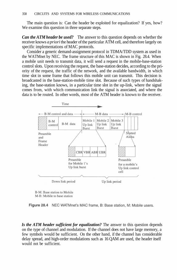
358 CIRCUITS AND SYSTEMS FOR WIRELESS COMMUNICATIONS
The main question is: Can the header be exploited for equalization? If yes, how?We examine this question in three separate steps.
Can the ATM header be used? The answer to this question depends on whether thereceiver knows a priori the header of the particular ATM cell, and therefore largely onspecific implementations of MAC protocols.
Consider a generic demand-assignment protocol in TDMA/TDD system as used inthe WATMnet by NEC. The frame structure of this MAC is shown in Fig. 28.4. Whena mobile unit needs to transmit data, it will send a request in the mobile-base-stationcontrol slots. Upon receiving the request, the base-station decides, according to the pri-ority of the request, the traffic of the network, and the available bandwidth, in whichtime slot in some frame that follows this mobile unit can transmit. This decision isbroadcasted in the base-station-mobile time slot. Because of such types of handshak-ing, the base-station knows, in a particular time slot in the up-link, where the signalcomes from, with which communication link the signal is associated, and where thedata is to be routed. In other words, most of the ATM header is known to the receiver.
Is the ATM header sufficient for equalization? The answer to this question dependson the type of channel and modulation. If the channel does not have large memory, afew symbols would be sufficient. On the other hand, if the channel has considerabledelay spread, and high-order modulations such as 16 QAM are used, the header itselfwould not be sufficient.

CHANNEL ESTIMATION AND EQUALIZATION IN WIRELESS ATM 359
To formulate this problem formally, we consider the indirect approach where thechannel impulse response is to be estimated first. At issue is whether the header aloneis sufficient for the identification of the channel. The concept of identifiability is funda-mental in estimation theory [22], and it can be described as follows: let h be the vectorcontaining channel parameters, x be the received signal vector, and f(x; h) be the like-lihood function. The channel is identifiable if impliesIn other words, identifiability means that there is no arbitrariness in the estimation ofthe channel parameter. In the up-link of a TDMA system, the so-called guard periodis usually inserted between signals from different users so that they will not interferewith each other. In the down-link, on the other hand, the signal is broadcasted fromthe base-station, and no guard period is necessary. The presence of guard periods doeshave an effect on channel estimation, because the receiver knows that the transmitteris silent during this period. It can be shown that if the channel has order L (there areL + 1 parameters), then the minimum length (in terms of number of symbols) for theheader must satisfy
It is clear that using a header alone offers only limited capability in estimating thechannel impulse response.
Can the payload portion of the cell be used for equalization? The answer to thisquestion is not trivial. Intuitively, although the receiver receives only the distortedversion of the transmitted signal, the received signal does contain certain informationabout the channel. The real issue is whether such information is sufficient for theidentification of the channel and how the identification can be performed.
We consider now the estimation of multiple channels as shown in Fig. 28.5, wherethe data symbols are transmitted through a vector of channels. This model can comefrom the presence of an array of receivers, or simply from sampling the received signalat a rate higher than the symbol rate. Denoting the vector impulse response by
we have the following system equations in the time domain
where yk is the received (noisy) signal. Depending on the type of traffic and the modeof transmission, the channel model takes slightly different forms.
When the payload part of the cell is used for channel estimation, the correspondingsymbols are unknown and we have the so-called blind channel identification problem,i.e., given can be identified (from the likelihood function) up to a constantfactor? Note that since the data symbols are unknown, the constant ambiguity isunavoidable unless the magnitude and phase of certain symbols are known. We thenhave the following identifiability results:
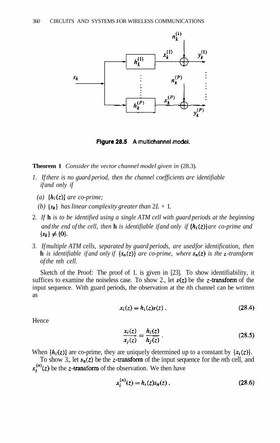
360 CIRCUITS AND SYSTEMS FOR WIRELESS COMMUNICATIONS
Theorem 1 Consider the vector channel model given in (28.3).
1. If there is no guard period, then the channel coefficients are identifiableif and only if
(a) are co-prime;
2. If h is to be identified using a single ATM cell with guard periods at the beginningand the end of the cell, then h is identifiable if and only if are co-prime and
3. If multiple ATM cells, separated by guard periods, are used for identification, thenh is identifiable if and only if are co-prime, where is the -transformof the nth cell.
Sketch of the Proof: The proof of 1. is given in [23]. To show identifiability, itsuffices to examine the noiseless case. To show 2., let be the of theinput sequence. With guard periods, the observation at the ith channel can be writtenas
Hence
When are co-prime, they are uniquely determined up to a constant byTo show 3., let be the of the input sequence for the nth cell, and
be the of the observation. We then have
(b) has linear complexity greater than 2L + 1.

CHANNEL ESTIMATION AND EQUALIZATION IN WIRELESS ATM 361
Using the same argument as above, replacing by one concludes thathence can be uniquely determined from up to a scaling factor.
Tab. 28.1 summarizes the comparison case when only the header is used in theidentification and when the payload is used in the identification. Here we compute themaximum channel length for that identification is possible. It is evident that the use ofthe payload portion of the ATM cell greatly enhances the channel’s identifiability.
Blind and semi-blind channel estimation for ATM. Having established the benefitof using the header as well as the payload part of the ATM cell for channel estimationand equalization, we now address the question how to exploit header and payloadstructures for channel estimation and equalization. This problem can be cast as a blindand semi-blind channel-estimation and equalization problem which has been an activeresearch area in recent years [24].
We outline here one of several possible implementations of PACE algorithms il-lustrated in Fig. 28.6. Details can be found in [3]. This approach is a combinationof (blind) channel estimation and block minimum-mean-square-error decision-feed-back equalization (MMSE-DFE) [11]. Given the received data from one cell or ablock of cells, an initial channel estimate is obtained by a maximum-likelihood-based blind-channel estimation (BCE). The initial channel estimate is then used in(MMSE-DFE) to produce a tentative decision of the payload. Using these detectedsymbols, the channel is re-estimated by a decision-directed channel estimator (DDCE)that uses standard techniques such as LMS or RLS. The improved channel estimate
is used next to provide the final symbol estimate Obviously, additional DDCE-MMSE can be used to improve performance with the price of increased complexity.
The role of the ATM cell header is twofold. In channel estimation, cell headers andtheir structure can be used to improve the quality of channel estimation. Although itmay be possible that a channel is estimated using only the cell header, the performancemay not be satisfactory. The use of blind channel estimation is important because itblocks possible channel estimation error propagation in the conventional block detec-tion schemes. In symbol detection, the knowledge of the ATM cell headers blocks thepropagation of detection errors that severely hinder the detection performance.
28.4 CONCLUSION
It is well known that channel estimation and equalization is vital in reliable com-munications over interference channels, and equalization techniques for single-user

362 CIRCUITS AND SYSTEMS FOR WIRELESS COMMUNICATIONS
point-to-point communications are mature. However, equalization for wireless ATMor other types of asynchronous networks present new challenges and new opportuni-ties. In this chapter, we addressed several aspects of this problem by examining therole of ATM cell structure in channel estimation and equalization. In order to exploitthe ATM cell structure for equalization, the incorporation of the MAC protocol is nec-essary. To a great extent, how to effectively integrate the physical layer with MACprotocol designs is an open research area.
Acknowledgments
The author wishes to acknowledge and thank the help of Mr. Jeffrey Bao in conducting simu-lation shown in Fig. 28.3 and many helpful discussions with him.

CHANNEL ESTIMATION AND EQUALIZATION IN WIRELESS ATM 363
References
[1] A. Acampora, “Wireless ATM: A Perspective on Issues and Prospects”, IEEEPersonal Communications, pp. 8–17, August 1996.
[2] E. Ayanoglu, Kai Y. Eng, and M. Karol, “Wireless ATM: Limits,Challenges,andProposals”, IEEE Personal Communications, pp. 18–34, August 1996.
[3] Q. Bao and L. Tong, “ Protocol-Aided Channel Equalization in Wireless ATM”,submitted to IEEE J. Select. Areas. Commun..
[4] F. Bauchot et. al., “MASCARA, a MAC Protocol for Wireless ATM”, In Proc.ACTS Mobile Summit, pp. 647–651, Granada, Spain, Nov. 1996.
[5] D.C. Cox, “Wireless Personal Communications: What is it?”, IEEE PersonalCommunications, 2(l):22–35, Feb 1995.
[6] K. Y. Eng et. al., “A Wireless Broadband Ad-Hoc ATM Local-Area Network”,ACM/Blatzer Wireless Networks J., 1(2): 161–174, 1995.
[7] C.R. Johnson et. al, “Blind equalization using the constant modulus criterion: Areview”, IEEE Proceedings, pp. 1927–1950, Oct 1998.
[8] Dravopoulos et. al, “The Magic WAND”, Technical report, ACTS ProjectAC085, August 1998.
[9] D. Falconer, “A system architecture for broadband milimeter wave access to anATM Lan”, IEEE Personal Communications, (8):36–41, August 1996.
[10] L. Fernandas, “Developing a system concept and technologies for mobile broad-band communications”, IEEE Personal Communications, 2(l):54–59, Feb 1995.
[11] G. K. Kaleh, “Channel equalization for block transmission systems”, IEEE J.Sel. Areas Comms., 13(1):110–121, January 1995.
[12] Y. Hua, “Fast maximum likelihood for blind identification of multiple FIR chan-nels”, IEEE Trans. Signal Processing, SP-44(3):661–672, March 1996.
[13] M. Karol, Z. Liu, and K. Eng, “Distributed Queuing Request Update MultipleAccess (DQRUMA) for Wireless Packet (ATM) Networks”, In Proc of Inter-national Conference on Communications, pages 1224–1231, Seattle, USA, June1995.
[14] E. Moulines, P. Duhamel, J.F. Cardoso, and S. Mayrargue, “Subspace-Meth-ods for the Blind Identification of Multichannel FIR Filters”, IEEE Trans. SP,SP-43(2):516–525, Feb. 1995.
[15] P. Narasimhan and etal, “Design and Performance of Radio Access Protocols inWATMnet, a Prototype Wireless ATM Network”, In Proc. ICUPC97 Conf., SanDiego, CA, Oct. 1997.
[16] D. Petras, “Medium Access Control protocol for wireless, transparent ATM ac-cess”, pp. 79–84, Long Island, NY, Nov 1995.
[17] J. Porter and etal, “The ORL Radio ATM system: Architecture and Implementa-tion”, Technical report, Olivetti Research Limitted, January 1996.
[18] J. Porter and A. Hopper, “An ATM based protocol for wireless LANs”, TechnicalReport 94.2, Olivetti Research Limitted, April 1994.
364 CIRCUITS AND SYSTEMS FOR WIRELESS COMMUNICATIONS
[19] D. Raychaudhuri, “Wireless ATM Networks: Architecture,System Design andPrototyping”, IEEE Personal Communications, pp. 42–49, August 1996.
[20] D. Raychaudhuri and et. al, “WATMnet: A Prototype Wireless ATM System forMultimedia Personal Communication”, IEEE J. Selected Areas in Communica-tions, 15(l):83–95, January 1997.
[21] D. Raychaudhuri and N.D. Wilson, “ATM-Based Transport Architecture for Mul-tiservices Wireless Personal Communication Networks”, IEEE J. Select. AreasCommun., 12:1401–1414, Oct. 1994.
[22] T.J. Rothenberg, “Identification in parametric models”, Econometrica, 39, 1971.[23] L. Tong and J. Bao, “Equalizations in Wireless ATM”, In Proc. 1997 Allerton
Conference on Communications, Control, and Computing, pp. 64–73, Urbana,IL, Oct. 1997.
[24] L. Tong and S. Perreau, “Multichannel blind channel estimation: From subspaceto maximum likelihood methods”, IEEE Proceedings, 86(10):pp. 1951–1968,October 1998.
[25] L. Tong, G. Xu, and T. Kailath, “Blind identification and equalization basedon second-order statistics: A time domain approach”, IEEE Trans. InformationTheory, 40(2):pp. 340–349, March 1994.
[26] M. Toy, Development and Applications of ATM: Selected Readings, IEEE Press,New York, 1996.
[27] J. Walrand and P. Varaiya, High-Performance Communication Networks, Mor-gan Kaufmann, San Francisco, 1996.
[28] C. C. Watterson, J. T. Juroshek, and W. D. Bensema, “Experimental con-firmation of an HF channel model”, IEEE Trans. Commun. Technology,18(6):pp. 792–803, December 1970.
[29] G. Xu, H. Liu, L. Tong, and T. Kailath, “A Least-Squares Ap-proach to Blind Channel Identification”, IEEE Trans. Signal Processing,SP-43(12):pp. 2982–2993, December 1995.

29 BLIND SEPARATION ANDCOMBINATION OF HIGH-RATE DIGITAL
QAM RADIO SIGNALSJohn Treichler, C. R.Johnson, Jr., and S. L.Wood
Applied Signal Technology, Inc., Sunnyvale, CA 94086, USACornell University, Ithaca, NY 14853, USA
Santa Clara University, Santa Clara, CA 95050, USA
Abstract: Blind signal separation is currently an active research topic, and manytechniques for accomplishing it have been discussed in the literature. In his excellentsurvey article [4], Cardoso describes blind signal separation (BSS) as the recovery of“unobserved signals of ‘sources’ from several observed mixtures”. This paper describesa particular implementation, a recently constructed two-channel processor capable ofoperating on convolutive mixtures of QAM signals running at symbol rates as fast as40 MHz. This processor has been applied to several practical problems, including thecancellation of cross-pole interference from a digital radio signal of interest and thediversity combination of signals received from two apertures or antenna feeds.
29.1 INTRODUCTION
The need to transmit growing amounts of information through channels of fixed band-width has encouraged the development of spectrally efficient transmission techniques.In digital microwave radio systems, for example, spectral efficiency can be attained bytransmitting multiple bits per symbol using quadrature amplitude modulation (QAM),by transmitting simultaneously on orthogonal signal polarizations at the same nominalcarrier frequency, or both. When doing both, it is commonly found that even though
365

366 CIRCUITS AND SYSTEMS FOR WIRELESS COMMUNICATIONS
the signals are transmitted on orthogonal polarizations, refraction and reflection en-countered during the signal’s propagation to the receiving antennas tends to additivelymix the two. Thus, each of the two signals is received in the presence of interferencefrom the other. While some interference can be tolerated, particularly when the modu-lations employed are simple (such as QPSK), this interference can badly degrade theaccurate reception and demodulation of high-order QAM signals. This practical prob-lem is an example of a class of theoretical problems which have come to be known as“blind signal separation (BSS)” [4]. We shall first treat the problem at hand and thendetermine how it fits into the more general BSS construct.
A number of papers and reports were published in the 1980s, for example [1–3,6],which addressed solutions to the problem of cross-pole interference. While techni-cally accurate, the recommendations made in those papers could not be applied to thedesign of digital microwave radio demodulators at the time, because the required high-speed semiconductor technology was not yet available. Its recent arrival, however, haspermitted the construction of such a demodulator. This unit, described in more detailin [7], accepts two intermediate frequency (IF) inputs and produces an output con-sisting of demodulated data symbols. The demodulator is capable of handling QAMsignals with constellations of up to 128 at symbol rates of greater than 40 MHz. Thedemodulator is capable of blind acquisition, implying that it can initialize all of itscontrol loops, including the channel equalizers and cross-pole interference cancellers,without the need for explicit or embedded training signals from the transmitter.
Section 29.2 describes the cross-pole interference problem in mathematical termsand states the analytical solution. There it is shown that two other practical problemscan be viewed as subsets of the “cross-pole” problem and that all fall under the rubricof blind signal separation. Section 29.3 briefly describes how a demodulator was builtto implement this solution. Some experimental results are shown in Section 29.4.
29.2 THREE RELATED INTERFERENCE PROBLEMS
Fig. 29.1 shows a simplified view of a microwave communications system employ-ing frequency reuse. Two separate input data streams are applied to two modulatorsoperating at exactly or nominally the same center frequency. The outputs of the twomodulators are then applied to the orthogonally polarized feeds of the same antenna.The receiving facility uses a similar dual-polarized antenna and is oriented so that therespective feeds at the transmitter and receiver are spatially aligned. In the absence ofimpairments such as multipath propagation, the signals recovered at the two orthogo-nal receiver feeds are essentially those transmitted. Even though they share the samebandwidth, their orthogonal polarizations allow them to be demodulated separatelyand without regard for the other. In fact, however, the two signals do contaminateeach other. This “cross-coupling” typically stems from one or two factors, mechanicalimperfections or misalignments of the antennas and reflection and scattering encoun-tered in the propagation from the transmitter to the receiver. The combination of thesefactors can be well modeled using the block diagram shown in Fig. 29.2. Each re-ceiver input is the sum of causally and possibly time-varyingly filtered versions ofeach of the transmitted signals. In a well designed transmission system the gainsof the two “direct” paths are much higher than those of the “cross-pole” paths, andtherefore mitigation of this coupling is not necessary, even though equalization of the

BLIND SEPARATION AND COMBINATION OF HIGH-RATE QAM SIGNALS 367
multipath-induced distortion in each direct path is. Many practical situations do arise,however, in which the cross-pole terms are commensurate or even larger than the directpaths. In these cases, processing of some sort must be performed to permit accuratedemodulation of the transmitted signals.
Estimation of either of the two transmitted signals in such a situation can be ad-dressed by posing it as a multichannel Wiener filtering problem. Given the two re-ceived signals, what linear combination of them produces the least-mean-squared dif-ference between it and a suitably delayed version of the transmitter input? Fig. 29.3repeats the model of the cross-pole channel and shows the two filters whose impulseresponses must be chosen. If the desired transmitted signal is available to the receiver,or if the demodulator’s output decisions are already accurate most of the time, thechoice of filter pulse responses can be determined using any number of techniques forminimizing the mean or average squared error. If these conditions are not satisfied,then blind adaptation rules must be applied.
There are two other problems commonly encountered in the reception of digital sig-nals, so-called “flat fading” and interference from narrowband signals. It is sometimespractical to solve these problems in the same way, that is, by providing the receivingprocessor with two versions of the transmitted signal. Even though the solution and itsimplementation are the same, the techniques for solving these problems go by differentnames. The problem of flat fading is usually addressed with “diversity combination”,the artful summation of two or more received versions of the same transmitted signal.These different versions are usually attained by using multiple antennas or sometimesby using orthogonal feeds on the same antennas (“polarization diversity”). If the flatfading characteristics encountered are statistically independent of each other, then thequality of the summed signal will be as good as (and often better than) any of theindividual received versions. Historically, the circuitry employed for diversity com-bination was capable of adjusting the gain and sometimes the phase of the diversityinputs, thus limiting the applicability of diversity combination to those cases in whichthe inputs did not encounter different propagation delays or dispersion. Consider nowFig. 29.4, a model for the signals received in a two-channel diversity receiving sys-tem. In principle, the two signals are received in the presence of different delay and

368 CIRCUITS AND SYSTEMS FOR WIRELESS COMMUNICATIONS
dispersion, as modeled by the filters and . The optimal Wiener receiver in thiscase is shown on the right side of Fig. 29.4. It consists of two properly chosen filters,whose outputs are summed to produce the input to the demodulator. A comparisonof Fig. 29.3 and 29.4 illustrates the fact that the diversity combination problem canbe viewed as a subset of the cross-pole problem. Even though there is no interfer-ence present, the optimal receiver is still a two-channel processor with the filter pulseresponses chosen to maximize SNR (or any other appropriate quality measure).
The third related problem is commonly called “sidelobe cancelling” and is illus-trated in Fig. 29.5. The signal of interest is received in the presence of an interferingsignal, often because the receiving antenna is not spatially selective enough to reject it.Also shown in Fig. 29.5 is a technique commonly employed to combat this problem,adaptive subtraction of the interferer using a signal obtained by an antenna aimed asdirectly as possible at the interferer. As in the diversity combination problem, the useof this “sidelobe cancellation” has traditionally presumed that the versions of interfer-ence present at the differencing node have been subjected to the same dispersion and

BLIND SEPARATION AND COMBINATION OF HIGH-RATE QAM SIGNALS 369
delay. Since this is rarely true, the utility of this approach has been limited to the caseof interference which is very narrowband compared to the signal of interest.
If we compare Fig. 29.3 to Fig. 29.5 we see that the sidelobe canceller can beviewed once again as a special case of the cross-pole canceller. Furthermore we seethat the dual-channel receiver architecture shown in Fig. 29.3 would permit delay anddispersion compensation between the two received versions of the interference, thus

370 CIRCUITS AND SYSTEMS FOR WIRELESS COMMUNICATIONS
making the system capable of operating successfully against wideband interferers.Thus we conclude that with the proper selection of filters and in Fig. 29.3,an adaptive combiner could address all three of these practical problems, and, in fact,extend the performance usually attainable with diversity combining and sidelobe can-celling systems, because of its ability to deal with differential delay and dispersion.
29.3 A SOLUTION
The problem of blind cross-pole combination was addressed in [3] in 1985 for fre-quency-modulated (FM) and QPSK signals. It employed the general architectureshown in Fig. 29.6 and used the Constant Modulus Algorithm (CMA) to adapt thefilters. Subsequent work, reported in [5], has shown that CMA can be used for“one-channel” equalization of higher-order QAM. In fact, as illustrated in this pa-per, CMA can also be used to direct the blind cross-pole combining of high-orderQAM, and can therefore be viewed as one method of solving the blind signal separa-tion problem [4]. It is interesting to note that the digital implementation implied byFig. 29.6 was not feasible at that time and only recently has become so for signals ofthe bandwidths typically employed in digital microwave radios.
Fig. 29.7 shows the block diagram of a cross-pole canceller built from a pair ofdemodulators which have been linked together to form a single output. This output isapplied to an adaptive law which is used to blindly and jointly adapt the two filters.Once adequately adapted, decisions based on the output signal itself can be consideredaccurate enough to be used as the reference signal for conventional dual-channel LMSadaptation. The general similarity of the architecture shown in Fig. 29.3 and 29.6 andthat seen in Fig. 29.7 are evident. The design seen in Fig. 29.7 reveals more detail,however, including the design of the individual demodulators and the linkage betweenthem needed to guarantee that both operate at exactly the same symbol rate. Factorsconsidered in the architecture of the individual demodulators are discussed in [5],
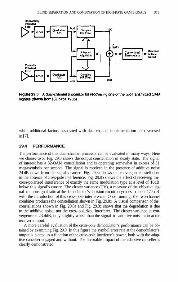
BLIND SEPARATION AND COMBINATION OF HIGH-RATE QAM SIGNALS 371
while additional factors associated with dual-channel implementation are discussedin [7].
29.4 PERFORMANCE
The performance of this dual-channel processor can be evaluated in many ways. Herewe choose two. Fig. 29.8 shows the output constellation in steady state. The signalof interest has a 32-QAM constellation and is operating somewhat in excess of 31megasymbols per second. The signal is received in the presence of additive noise24 dB down from the signal’s carrier. Fig. 29.8a shows the convergent constellationin the absence of cross-pole interference. Fig. 29.8b shows the effect of receiving thecross-polarized interference of exactly the same modulation type at a level of 18dBbelow this signal’s carrier. The cluster variance (CV), a measure of the effective sig-nal–to–nonsignal ratio at the demodulator’s decision circuit, degrades to about 17.5 dBwith the introduction of this cross-pole interference. Once running, the two-channelcombiner produces the constellation shown in Fig. 29.8c. A visual comparison of theconstellations shown in Fig. 29.8a and Fig. 29.8c shows that the degradation is dueto the additive noise, not the cross-polarized interferer. The cluster variance at con-vergence is 23.4dB, only slightly worse than the signal–to–additive noise ratio at thereceiver’s input.
A more careful evaluation of the cross-pole demodulator’s performance can be ob-tained by examining Fig. 29.9. In this figure the symbol error rate at the demodulator’soutput is plotted as a function of the cross-pole interferer’s power, both with the adap-tive canceller engaged and without. The favorable impact of the adaptive canceller isclearly demonstrated.

372 CIRCUITS AND SYSTEMS FOR WIRELESS COMMUNICATIONS
29.5 CONCLUSIONS
This paper has described the theoretical framework linking the problems of cross-poleinterference cancellation, dual-channel diversity combination, and sidelobe cancella-tion, and has shown that all three can be optimally addressed using a two-channeladaptive combiner.
This optimal architecture was used as the basis for the hardware discussed in Sec-tion 29.3. This processor accepts two inputs with bandwidths of up to anduses the Constant Modulus Algorithm [8] to give it the ability to acquire the signal ofinterest in the absence of training procedures initiated by the transmitter. The results

BLIND SEPARATION AND COMBINATION OF HIGH-RATE QAM SIGNALS 373
presented in Section 29.4 show that this implementation is in fact capable of blindsignal separation (BSS) in real time for wideband signals of significant complexity.
Acknowledgments
Many engineers have worked hard to design the hardware described in this paper and then tomake it work. The study work leading to this architecture was done in the late [6] withthe actual construction and testing being done over the past two years by a team led by JonBohanon and Tom Giovannini [7].
References
[1] J. Namiki and S. Takahara, “Adaptive receiver for cross-polarized digital trans-mission”, in Proc. ICC ’81, June 1982, pp. 46.31–46.35.
[2] J.R. Treichler and M.G. Larimore, “New Processing Techniques Based on the Con-stant Modulus Adaptive Algorithm”, IEEE Transactions on Acoustics, Speech,
374 CIRCUITS AND SYSTEMS FOR WIRELESS COMMUNICATIONS
and Signal Processing, Vol. ASSP-33, No. 2, April 1985, pp. 420–431.[3] J. Salz, “Data Transmission over Cross-coupled Linear Channels”, AT&T Techni-
cal Journal, Vol. 64, No. 6, July-August 1985, pp. 1147–1160.[4] J.F. Cardoso, “Blind Signal Separation: Statistical Principles”, Special Edition
of the Proceedings of the IEEE on Blind System Identification and Estimation,Vol. 86, No. 10, October 1998, pp. 2009–2025.
[5] J.R. Treichler, M.G. Larimore, and J.C. Harp, “Practical Blind Demodulatorsfor High-Order QAM Signals”, Special Edition of the Proceedings of the IEEEon Blind System Identification and Estimation, Vol. 86, No. 10, October 1998,pp. 1907–1926.
[6] “Diversity Study Final Report”, Applied Signal Technology Final ReportFR-023-88, 29 September 1988.
[7] J.R. Treichler and Jon Bohanon, “Blind Demodulation of High-order QAM Sig-nals in the Presence of Cross-pole Interference”, Proceedings of the 1998 MIL-COM Conference, Monterey, CA, June 3, 1998.
[8] J.R. Treichler and B.G. Agee, “A New Approach to the Multipath Correctionof Constant Modulus Signals”, IEEE Trans. On ASSP, Vol. ASSP-31, No. 2,April 1983, pp. 459–471.

30 GLOSSARY
A/D Analog to digital
AC-3 Audio coding standard for surround applications,version 3
ACELP Algebraic-code-excited linear prediction
ACP Adjacent channel power
ACR Absolute category rating
ACTS Advanced Communications Technologies and Services.European project. Information on the ACTS projectWAND can be found on the internet athttp://www.tik.ee.ethz.ch/~wand
ACU Address calculation unit
AC Alternate current
AD6640 Analog Devices’ AD6640 (12 b, 65 MHz)analog-to-digital converter
ADC Analog-to-digital converter
AGC Automatic gain control
ALT Alternate channel power
ALU Arithmetic-logic unit
AM Amplitude modulation
AMPS The AMPS family of wireless standards were intendedto be just another analog-radio-telephone standard (e.g.Advanced Mobile Phone Service followed IMTS:Improved Mobile Telephone Service).
AMR Adaptive modulation rate
ANSI-C Standardized C programming language
APLAC An object-oriented analog circuit simulator and designtools
ARQ Automatic repeat request
ASIC Application-specific integrated circuit
375

376 CIRCUITS AND SYSTEMS FOR WIRELESS COMMUNICATIONS
ASI Application-specific instructions
ASSP Application-specific signal processor
ATI Assignment-time instantiation
ATM Asynchronous transfer mode
AWGN Additive white Gaussian noise
AXU Application-specific eXecution Unit
BAHAMA Broadband Ad Hoc ATM Anywhere, a wirelessbroadband ad-hoc ATM local-area network
BB Base band
BDT Berkeley Design Technology (BDT), Inc.
BER Bit error rate
BJT Bipolar junction transistor
BPF Bandpass filter
BRIGHT Family of RF chipsets for GSM, BiCMOS Radio IC forGSM by Hitachi and TTPCom
BSS Blind signal separation
BTS Base transceiver station
BW Bandwidth
CBUF Circular buffer
CCI Co-channel interference
CD Compact disk
CDMA Code division multiple access
CLC952 National Semiconductor’s CLC952 (12 b, 41 MHz)analog-to-digital converter
CMA Constant modulus algorithm
CMOS Complementary metal oxide semiconductor
CORDIC Coordinate rotation digital computer
COSSAP Synopsys’ Digital signal processing design (DSP) toolsuite to create, explore, and test algorithms,architectures, and implementations for DSPapplications.
CP Compression point
CTS Cordless Telephony System
CV Cluster variance

GLOSSARY 377
DAC Digital-to-analog converter
dB Decibel
DC Direct current
DCS 1800 Digital communications system (GSM at 1800 MHz).The DCS 1800 and PCS 1900 systems are twoadaptations of the GSM standard.
DCU Data computation unit
DDCE Decision-directed channel estimator
DDS Decision-directed signal
DD Decision directed
DECT Digital Enhanced Cordless Telecommunicationsstandard maintaining a high speech and receptionquality.
DFE Decision-feedback equalization
DF Decision feedback
DMA Direct memory access
DMI Direct matrix inversion
DMP Dual-modulus prescaler
DNL Differential nonlinearity
DOA Direction of arrival
DQPSK Differential quadrature phase shift keying
DRAM Dynamic random access memory
DR Dynamic range
DS-CDMA Direct-sequence code-division multiple access
DSP Digital signal processing (or processor)
DTI Declaration-time instantiation
DTX Discontinuous transmission
DVGA Digitally controlled variable-gain amplifier
EDGE Enhanced data rates for global evolution
EM Evolutionary methods
EPICS DSP architecture, by Philips
ESD Electrostatic discharge
ETSI European Telecommunications Standards Institute

378 CIRCUITS AND SYSTEMS FOR WIRELESS COMMUNICATIONS
EVRC Enhanced variable rate-coder
FDD Frequency division duplexing
FDMA Frequency-division multiple access
FET Field-effect transistor
FFT Fast Fourier transform
FH-QPSK Frequency-hopping QPSK
FH Frequency hopping
FIFO First in first out
FIR Finite impulse response
FM Frequency modulation
FRIDGE Fixed-point pRogramIng DesiGn Environment, a toolsuite that permits a design flow from an ANSI-Cfloating-point algorithm to a fixed-point description.
FSK Frequency shift keying
GMSK Gaussian minimum shift keying
GPRS General Packet Radio Service
GPS Global Positioning System
GSM Global System for Mobile Communications
GSM-EFR GSM with Enhanced Full-Rate codec
GSM-FR GSM with Full-Rate codec
GSM-HR GSM with Half-Rate codec
GSM 1800 GSM in the 1800 MHz band
GSM900 GSM in the 900 MHz band
HBT Heterojunction bipolar transistor
HDTV High-definition television
HDL High description language
HEIBiC High-energy implanted BiCMOS
HEMT High-electron-mobility transistor
HF High frequency
HSCSD High-Speed Circuit Switched Data
HW Hardware
IB Bias current

GLOSSARY 379
IC Integrated circuit, collector current
IEEE The Institute of Electrical and Electronics Engineers
IF Intermediate frequency
IIP3 Input order intercept point
IIR Infinite impulse response
IMS order intermodulation
IMFDR3 order intermodulation free dynamic range
IMT-2000 International mobile telecommunications 2000
INL Integral non-linearity
IO Input/output
IPR Intellectual property rights
IP3 3rd order intercept point
IRSSADC Image-rejection sub-sampling ADC
IS (Interim Standard): A designation of the AmericanNational Standards Institute—usually followed by anumber—that refers to an accepted industry protocol;e.g. IS-95, IS-136, IS-54.
IS-54 A dual-mode standard for U.S. digital cellular systemand Advance Mobile Phone Service based ontime-division multiple access.
IS-95 The standard for code & vision multiple access.
IS-136 The latest generation of the digital standard timedivision
ISCAS International Symposium on Circuits and Systems
ISDN Integrated services digital network
ISI Intersymbol interference
ISM Integrated system management
ISS Institute for Integrated Systems in Signal Processing
ISSCC International Solid-State Circuits Conference
JSSC Journal of Solid-State Circuits
JTAG Standard instructions for performing functional andinterconnect tests of DSP chips on circuit boards.
JTIDS Joint tactical information distribution system
KISS A one-chip ASIC DSP solution for GSM

380 CIRCUITS AND SYSTEMS FOR WIRELESS COMMUNICATIONS
LAN Local area network. A group of client computersconnected to a server.
lbp Location of the binary point
LCMV Linearly constrained minimum variance
LC L for inductor, C for capacitor
LDMOS Laterally diffused metal oxide semicoductor
LMS Least mean square
LNA Low-noise amplifier
LO Local oscillator
LPCVD Low-pressure chemical vapor deposition
LQFP-48 Low-profile quad flat pack, 48-pin
LSB Least significant bit
LSE Least-squares estimation
LTP Long-term prediction
MAC Multiplier-accumulator
MAI Multiple-access interference
MBE Molecular-beam epitaxy
MBiC Modular BiCMOS
MCM Multi-chip module
MDAC Multiplying digital-to-analog converter
MEMS Micro-electro-mechanical systems
MESFET Metal-semiconductor FET
MF Matched filter
MIMO Multiple input multiple output
MIM Metal-insulator-metal
MIPS Million instructions per second
MLSE Maximum-likelihood sequence estimation
MMSE Minimum mean-square error
MOE Minimum output energy
MOSFET Metal-oxide-semiconductor field-effect transistor
MPEG Moving Picture Experts Group. The internationalconsortium of hardware, software and publishinginterests dedicated to developing internationalstandards for the compression of moving video imagesin digital systems.

GLOSSARY 381
MPI Maximum-precision interpolation
MSB Most significant bit
MSE Mean squared error
MSK Minimum shift keying
MS Mobile station
MVDR Minimum-variance distortionless response
NBI Narrowband interference
NB Narrowband
NF Noise figure
NMOS n-type metal oxide semiconductor
NPN n-type bipolar transistor
OFDM Orthogonal frequency division multiplex
OPLL Offset phase-locked loop
PA Power amplifier
PACE Protocol-aided channel equalization
PAE Power added efficiency
PCB Printed circuit board
PCS1900 Personal Communications Service. A two-way,1900MHz digital communications service.
PCU Program control unit
PC Personal computer
PDA Personal Digital Appliance
PDC Personal Digital Cellular. PDC is one of the world’sthree main digital wireless standards. Currently used inJapan.
PDF Probability density function
PFD Phase frequency detector
PHEMT p-type high-electron-mobility transistor
PLL Phase-locked loop
PMOS p-type metal oxide semiconductor
PM Phase modulation
PSD Power spectral density
QAM Quadrature amplitude modulation
382 CIRCUITS AND SYSTEMS FOR WIRELESS COMMUNICATIONS
QFP Quad flat pack
QPSK Quadrature phase shift keying
QRD QR (orthogonal-triangular) decomposition algorithm
RB Temporal-reference beamforming (or beamformer)
RD1602x DSP family by Philips Semiconductors
R.E.A.L. Reconfigurable DSP architecture by PhilipsSemiconductors
RF Radio frequency
RLAN Radio local area network
RLS Recursive least squares
RMS Root mean square
ROM Read-only memory
RTA Rapid thermal anneal
RTE Rapid thermal epitaxy
RTL Resistor-transistor logic
RX Receiver
R&D Research and development
SAW Surface acoustic wave
SBM Single-balanced mixer
SB Sideband
SC Switched-capacitor
SEM Scanning electron microscope
SFDR Spurious-free dynamic range
SIMS Secondary ion mass spectrometry
SINR Signal-to-interference-plus-noise ratio
SMD Surface-mounted device
SMI Sample matrix inversion
SNR Signal-to-noise ratio
SOI Signal of interest
SOS Silicon-on-sapphire
SPICE Simulation program with integrated circuit emphasis
SQR Signal-to-quantization-noise ratio

GLOSSARY 383
SSB Single sideband
SSOP Shrink small outline package (package type)
SW Software
TACS Total-Access Telecommunication System
TCH/FS Full-rate speech traffic channel
TCH/HS Half-rate speech traffic channel
TDD Time division duplexing
TDL Tapped delay line
TDMA Time-division multiple access
TEM Transmission electron microscope
TI Texas Instruments
TQ9222 TriQuint Semiconductor’s TQ9222 datasheet
TV Television
TX Transmitter
UHF Ultra-high frequency
ULA Uniform linear array
UMTS Universal mobile telecommunication system
UPC Universal Personal Communications
US United States
UV Ultraviolet
VAD Voice adaptive detection
VCI Virtual channel identifier
VCO Voltage-controlled oscillator
VHDL Very high description language
VLIW Very long instruction words
VLSI Very-large-scale Integration
VPI Virtual path identifier
VSELP Vector-Sum-Excited Linear Predictive
WAND Wireless ATM Network Demonstrator
WATM Wireless asynchronous transfer mode
WB Wideband
WCDMA Wideband code-division multiple access
WLAN Wireless local area network
WLL Wireless local loop
WWW World-wide web

This page intentionally left blank

Index
A/D converterband-pass, 136calibration techniques, 182,201case study: 12-bit ADC, 193DR, 192ENOB, 188figure of merit, 189for multichannel receiver, 190high resolution, 200IF sampling, 178image-rejection sub-sampling, 179oversampling, 175performance metrics, 188power dissipation, 176SFDR, 192SINAD, 188SNR, 192
adaptive beamforming, 293adaptive interference suppression, 289–311,
341–348adaptive multi-rate system (AMR), 317
multi-mode, 321narrow-band, 319wide-band, 322
ATM, 351–362equalization, 356switching, 353
baseband processingR.E.A.L. DSP, 279–287
beamformer, 294blind channel equalization, 337–373
adaptive MOE detection, 344adaptive subspace detection, 345enhancements, 346linear multiuser detection, 344MMSE, MSE, 344signal model, 342
blind separation, 365–373BRIGHT
architecture, 10process parameters, 15
buffer, 125
calibration techniques for ADC, 182, 201CMA, 370CORDIC algorithm, 297cost in cellular phones, 162coupling
ground, 32substrate, 33
DCS-1800, see GSMDECT, 24differential to single-ended converter, 124direct-conversion, see receiver, zero-IFdown-converter, see receiver
quadrature, 40DSP for wireless communication, 265
adaptive DS-CDMA receivers, 309adaptive interference suppression,
289–311fixed-point systems, 265–277FRIDGE, 265–277interpolation, 272QRD-RLS algorithm, 294
CORDIC algorithm, 297implementation, 297
R.E.A.L. DSP, 279–287architecture, 281ASIC, 285development tool, 285instruction set, 283performance, 286
smart antennas, 292temporal reference beamforming, 303VLSI signal processing, 291
dual-band system, 10, 109–125, 160
embedded DSP architecture, see DSP forwireless communication
385

386 CIRCUITS AND SYSTEMS FOR WIRELESS COMMUNICATIONS
ENOB, 188equalization, 351–362
frequency shift keying (FSK), 116FRIDGE, 265–277
GaAs MESFET, 240,246GaAs-based RFIC, 231–243Gaussian minimum shift keying (GMSK),
116GMSK TX architectures, 144GSM
architecture choices, 13blocking performance, 20DCS-1800, 45, 109key system specs, 10–13receive sensitivity, 19receiver sensitivity, 13transmitter, 141–155transmitter modulation spectrum, 11,
18transmitter noise, 11transmitter phase error, 10,17transmitter requirements, 142
HBT, 247HEMT, 247
IF sampling, 127–138conditions, limitations, 131
image-rejection sub-sampling ADC, 179inductor
bondwire, 42on-chip, 45, 122spiral, 42
interference suppression technique, 292, 366
linear multiuser detection, 344LNA, 113, 249
5 GHz circuit, 251sub-1 V circuit, 250
mixer, 43, 113MMSE, MSE, 344modulator, 123multi-band system, 10,185, 187
oscillatorcolpitts, 97LC,41,75
general description, 81on-chip, 34ring, 41voltage-controlled, 41
phase noise, 25,42,75frequency-domain analyses, 77
models, 77time-domain analyses, 80
power amplifier, 17 GHz PHEMT, 253
QRD-RLS algorithm, 294
R.E.A.L. DSP, 279–287, 331receiver
adaptive DS-CDMA receiver, 309ADC for multichannel receiver, 190all-digital, 162building blocks, 113–116digitisation at IF, 28double-superheterodyne, 26dual-band, 111GaAs RFIC, 235heterodyne, 39homodyne, 40low-IF, 39,40,45multi-channel, 187zero-IF, 27,40, 162
recursive, see recursiveRF
comparison of device technology, 247front-ends, 38–46,157–164system integration, 38
silicon BiCMOS, 246silicon bipolar, 246silicon CMOS, 246SINAD, 188smart antennas, 292software radio, 185, 187speech coding, 317–323synthesiser, 41
technology, 258BiCMOS A/D converter, 193choices for baseband circuits, 248comparison of device technology, 247different RFIC technologies, 238GaAs MESFET, 246GaAs MESFETs, low-tech, 240GaAs-based RFIC, 231–243graded-base Si1–xGex bipolar
transistors, 226HBT, 247HEMT, 247lateral etching, Si refilling, 218properties of Si1–xGex, 223RFIC for various RF blocks, 238Si/Si1–xGex bipolar transistor, 222,
227SiGe, low-cost, 217–229silicon BiCMOS, 218, 246silicon bipolar, 246silicon CMOS, 246sub-micron, 38

INDEX 387
transceiver, 45,127–138examples of GHz circuits, 249–257
transmitter, 25, 141–155buffer, 125building blocks, 121–125converter, differential to single-ended,
124design considerations, 116–120direct up-conversion, 29, 121dual-band, 120dual-band architecture, 120frequency shift keying (FSK), 116Gaussian minimum shift keying
(GMSK), 116GMSK architectures, 144
direct modulation, 144IF modulation, 149modulation loop, 149
loop-locked and modulated VCO, 31modulator, 123
offset phase-locked loop, 14offset up-conversion, 30power amplifier, 17 GHz PHEMT, 253two-step up-converter, 120
TriQuintprocess parameters, 241
VCO, 41VLSI signal processing, 291
wide-band conversion, 185, 187Wiener filter, 367wireless communication system
ATMchannel estimation, 351–362switching, 353
blind separation, 365–373capacity, 158channel equalization, 351–362speech coding, 317–323