charge collection mechanisms in silicon devices during
167
CHARGE COLLECTION MECHANISMS IN SILICON DEVICES DURING HIGH-LEVEL CARRIER GENERATION EVENTS By Nicholas C. Hooten Dissertation Submitted to the Faculty of the Graduate School of Vanderbilt University in partial fulfillment of the requirements for the degree of DOCTOR OF PHILOSOPHY in Electrical Engineering May, 2014 Nashville, Tennessee Approved: Robert A. Reed, Ph.D. Ronald D. Schrimpf, Ph.D. Robert A. Weller, Ph.D. Arthur F. Witulski, Ph.D. John A. Kozub, Ph.D.
-
Upload
khangminh22 -
Category
Documents
-
view
2 -
download
0
Transcript of charge collection mechanisms in silicon devices during

CHARGE COLLECTION MECHANISMS IN SILICON DEVICES DURING
HIGH-LEVEL CARRIER GENERATION EVENTS
By
Nicholas C. Hooten
Dissertation
Submitted to the Faculty of the
Graduate School of Vanderbilt University
in partial fulfillment of the requirements
for the degree of
DOCTOR OF PHILOSOPHY
in
Electrical Engineering
May, 2014
Nashville, Tennessee
Approved:
Robert A. Reed, Ph.D.
Ronald D. Schrimpf, Ph.D.
Robert A. Weller, Ph.D.
Arthur F. Witulski, Ph.D.
John A. Kozub, Ph.D.

Copyright ©2014 by Nicholas C. HootenAll Rights Reserved

How hard can it be? It’s just a diode.
-Robert Reed
iii

ACKNOWLEDGMENTS
Scientific progress happens collaboratively. With that in mind, it is with much gratitude
that I extend my thanks to the fine people who have helped make this work possible. Chief
among them is my advisor, Robert Reed, for his continued support of my research efforts.
The remaining members of the dissertation committee have also been a tremendous source
of guidance and assistance throughout my time at Vanderbilt University. The student mem-
bers of Vanderbilt’s Radiation Effects and Reliability group have been beyond helpful as
I’ve made the journey from new graduate student to effective researcher. At the risk of
leaving someone out, I’ll refrain from mentioning any one of you by name. However, I’d
wager that many of you will know who you are without my having to say so. I can only
hope that over the years I have given as much back to you as you have all given to me.
Scientific progress also requires financial support. Therefore, I would like to thank my
sponsoring agencies, NASA and the Defense Threat Reduction Agency through their basic
research program, for providing the funding that made this work possible.
A heartfelt thanks is also due to my friends and family for their unwavering support of
my educational pursuits. It is good to know that after many long hours in the lab or in front
of a computer, there are still folks willing to claim me as one of their own. For that, they
will always have my constant respect and gratitude.
And finally, my deepest appreciation is reserved for my wife, Lauren. Her endless well
of emotional support and constant motivation have helped to make this possible in ways
that nothing else ever could.
iv

TABLE OF CONTENTS
Page
ACKNOWLEDGMENTS . . . . . . . . . . . . . . . . . . . . . . . . . . . . . . iv
LIST OF TABLES . . . . . . . . . . . . . . . . . . . . . . . . . . . . . . . . . . viii
LIST OF FIGURES . . . . . . . . . . . . . . . . . . . . . . . . . . . . . . . . . . ix
Chapter
1 Introduction . . . . . . . . . . . . . . . . . . . . . . . . . . . . . . . . . . . 1
2 Background . . . . . . . . . . . . . . . . . . . . . . . . . . . . . . . . . . . 5
2.1 Charge Collection: A Brief Conceptual Overview . . . . . . . . . . . . . 52.2 The Historical Interpretation of Charge Collection at a Reverse-Biased
Junction . . . . . . . . . . . . . . . . . . . . . . . . . . . . . . . . . . . 82.3 Recent Developments in Charge Collection Mechanisms and Modeling . . 122.4 High LET Particles in the Space Radiation Environment . . . . . . . . . . 13
3 Total Collected Charge During High-Level Carrier Generation Events . . . 20
3.1 Chapter Introduction . . . . . . . . . . . . . . . . . . . . . . . . . . . . . 203.2 Two-Photon Absorption Measurements . . . . . . . . . . . . . . . . . . . 23
3.2.1 Test Structure and Setup . . . . . . . . . . . . . . . . . . . . . . . 243.2.2 Measurement Procedure . . . . . . . . . . . . . . . . . . . . . . . 25
3.3 Charge Collection During High-Level Carrier Generation Conditions . . . 263.3.1 Regional Partitioning . . . . . . . . . . . . . . . . . . . . . . . . 263.3.2 Regional Partitioning in Device-Level Simulations . . . . . . . . . 283.3.3 A Review of the ADC Model . . . . . . . . . . . . . . . . . . . . 33
3.4 Applying the Models to Experimental Data . . . . . . . . . . . . . . . . . 353.5 Results and Discussion . . . . . . . . . . . . . . . . . . . . . . . . . . . . 393.6 Chapter Summary . . . . . . . . . . . . . . . . . . . . . . . . . . . . . . 44
4 The Impact of Depletion Region Potential Modulation on Ion-Induced Cur-rent Transient Response . . . . . . . . . . . . . . . . . . . . . . . . . . . . . 45
4.1 Introduction . . . . . . . . . . . . . . . . . . . . . . . . . . . . . . . . . 454.2 Experimental Details . . . . . . . . . . . . . . . . . . . . . . . . . . . . . 464.3 Results and Discussion . . . . . . . . . . . . . . . . . . . . . . . . . . . . 50
v

4.3.1 Device Response to Strikes Near the Contacts . . . . . . . . . . . 504.3.2 Influence of Ion LET and Applied Bias on Current Transient Shapes 554.3.3 Transient Time Regimes and Current Saturation . . . . . . . . . . 62
4.3.3.1 Depletion Region Collapse . . . . . . . . . . . . . . . . 624.3.3.2 Fast Partial Recovery . . . . . . . . . . . . . . . . . . . 634.3.3.3 Slow Recovery . . . . . . . . . . . . . . . . . . . . . . 64
4.3.4 Estimating Current Saturation . . . . . . . . . . . . . . . . . . . . 654.4 Implications for Scaled Technologies . . . . . . . . . . . . . . . . . . . . 674.5 Chapter Summary . . . . . . . . . . . . . . . . . . . . . . . . . . . . . . 69
5 The Transient Response of Small Junctions During Broadbeam Heavy-ionIrradiation . . . . . . . . . . . . . . . . . . . . . . . . . . . . . . . . . . . . 71
5.1 Introduction . . . . . . . . . . . . . . . . . . . . . . . . . . . . . . . . . 715.2 Experimental Details . . . . . . . . . . . . . . . . . . . . . . . . . . . . . 735.3 Analytical Methods . . . . . . . . . . . . . . . . . . . . . . . . . . . . . 76
5.3.1 The Support Vector Machine . . . . . . . . . . . . . . . . . . . . 765.3.2 Applying SVM Techniques to Broadbeam Heavy-ion Data . . . . 80
5.4 Results and Discussion . . . . . . . . . . . . . . . . . . . . . . . . . . . . 835.4.1 A Geometric Verification of the SVM Approach Using TCAD . . . 835.4.2 The Physical Interpretation of SVM Classified Heavy-Ion Data . . 88
5.5 Chapter Summary . . . . . . . . . . . . . . . . . . . . . . . . . . . . . . 97
6 Device Response During Well Potential Modulation Events . . . . . . . . . 99
6.1 Introduction . . . . . . . . . . . . . . . . . . . . . . . . . . . . . . . . . 996.2 Background . . . . . . . . . . . . . . . . . . . . . . . . . . . . . . . . . 1006.3 Experimental Setup . . . . . . . . . . . . . . . . . . . . . . . . . . . . . 1036.4 Results and Discussion . . . . . . . . . . . . . . . . . . . . . . . . . . . . 105
6.4.1 Experimental Results . . . . . . . . . . . . . . . . . . . . . . . . 1056.4.2 WPM Effects in Device-Level Simulations . . . . . . . . . . . . . 110
6.5 Chapter Summary . . . . . . . . . . . . . . . . . . . . . . . . . . . . . . 116
7 Conclusions and Future Work . . . . . . . . . . . . . . . . . . . . . . . . . 118
Appendices . . . . . . . . . . . . . . . . . . . . . . . . . . . . . . . . . . . . . . . 124
A Theoretical Development of the ADC Model . . . . . . . . . . . . . . . . . 125
A.1 Low-Level, All Generated Charge in Quasi-Neutral Region . . . . . . . . 125A.2 High-Level, All Generated Charge in Quasi-Neutral Region . . . . . . . . 128A.3 Including Charge Generated in the Depletion Region . . . . . . . . . . . . 131
vi

B Two-Photon Absorption Laser SEE Testing at Vanderbilt University . . . . 132
B.1 Introduction . . . . . . . . . . . . . . . . . . . . . . . . . . . . . . . . . 132B.2 System Overview . . . . . . . . . . . . . . . . . . . . . . . . . . . . . . 132B.3 Laser Pulse Energy Measurement and Calibration . . . . . . . . . . . . . 140
REFERENCES . . . . . . . . . . . . . . . . . . . . . . . . . . . . . . . . . . . . 146
vii

LIST OF TABLES
Table Page
4.1 Total generated charge (Qgen), collected charge (Qcoll), and the chargecollection efficiency (Qcoll
Qgen) for the transients shown in Figure 4.6. The
generated charge was calculated using TRIM. . . . . . . . . . . . . . . . 58
5.1 Incident ion LET and range in Si for the 10 MeV/u ions used for themeasurements discussed in this chapter. Produced using the TRIM com-ponent of the SRIM software tools. . . . . . . . . . . . . . . . . . . . . 76
5.2 The miss distance for the small device for four incident ion species, ascalculated through the use of (5.1)-(5.3). . . . . . . . . . . . . . . . . . 85
5.3 The hit and miss ratios for the small device and the large device for fourincident ion species. The HMR is defined as the number of hits dividedby the number of misses, as determined by the SVM. . . . . . . . . . . . 90
B.1 The names and descriptions of the components of the TPA test system. . 135
B.2 The values of the coefficients shown in (B.1). . . . . . . . . . . . . . . . 145
viii

LIST OF FIGURES
Figure Page
2.1 The time evolution of a delta function of electron-hole pair generationdiffusing in intrinsic silicon. Due to ambipolar diffusion effects, thegenerated carriers diffuse from a higher concentration to a lower one asan ensemble of particles. . . . . . . . . . . . . . . . . . . . . . . . . . . 6
2.2 Potential contour plots showing the modulation of the potential typicallysupported by the depletion region following an α particle strike throughthe junction at (a) 0.1 ns and (b) 1.0 ns. This effect has been historicallyreferred to as “field-funneling”. . . . . . . . . . . . . . . . . . . . . . . 9
2.3 An illustrative voltage transient where the assumed drift-dominated anddiffusion-dominated portions have been labeled. . . . . . . . . . . . . . 10
2.4 The LET of various ionizing particles of interest. α particles have adistinctly different LET than typical heavy ions (such as iron, which isshown) that are found in the space environment. . . . . . . . . . . . . . 11
2.5 Relative abundance of the elements from hydrogen to the iron group,normalized to that of carbon (C=102 in the plot). The solid line repre-sents the cosmic-ray abundances measured near Earth. The dashed linerepresents the elemental abundances in the solar system of the GCR. . . 14
2.6 SRIM results for iron in silicon. The black curve is the computed LETversus ion energy for electronic stopping (direct ionization). The redcurve shows the predicted range. . . . . . . . . . . . . . . . . . . . . . . 15
2.7 Integral fluxes for iron cosmic rays versus LET for a 90% worse case(upper), solar minimum (middle), and solar maximum (lower). Thespectra are at 1 AU behind 25 mils of aluminum shielding. . . . . . . . . 16
2.8 LET versus energy per AMU for particles in silicon. . . . . . . . . . . . 17
3.1 Schematic showing individual region names (a) and relevant physicalcharacteristics of those regions (b) for a reverse-biased p-n junction dur-ing high-level conditions. These regions are described mathematicallyby the ADC model. For early times during the charge-collection pro-cess, the ambipolar region boundary corresponds approximately to thebottom of the generated carrier density. . . . . . . . . . . . . . . . . . . 21
3.2 An illustrative diagram of the diode and measurement procedure. Rela-tive sizes are not to scale. Exact doping levels can be seen in Figure 3.4.The device overlayers are not shown. . . . . . . . . . . . . . . . . . . . 23
ix

3.3 A custom-milled, brass package suitable for capturing high-speed tran-sient signals from irradiated devices. Relevant components are labeled. . 25
3.4 Two dimensional image showing a 20 µm by 20 µm section of the150 µm by 300 µm simulated bulk silicon N-well/P-substrate diode.The dashed line represents the depletion region thickness at a reversebias of 5 V. . . . . . . . . . . . . . . . . . . . . . . . . . . . . . . . . . 28
3.5 An example of regional partitioning in response to a high-level condi-tion in the simulated diode shown in Figure 3.4. The electric field inthe device in response to a 1.00 pC/µm track with a 10 µm length isshown 1 ns after the strike. Red regions are saturated on the color scale,meaning their actual values could be greater than 7x10³ V/cm. . . . . . . 30
3.6 The Z-component of the electron current density along the Z-axis shownin Figure3.5 for various times during the charge-collection process. Thediscontinuous slope that occurs at approximately 11 µm along the hori-zontal axis indicates the ambipolar region boundary. The zero value forelectron current density beyond this boundary confirms the existence ofthe high resistance region, which prevents the flow of minority carriersdeeper into the substrate. The large range of values seen in the y-axesof each figure emphasize that while the magnitude of the electron cur-rent density changes considerably as the device returns to its steady-stateconfiguration, the inflection point that signifies the existence of the highresistance region is present during the majority of the charge-collectionprocess. . . . . . . . . . . . . . . . . . . . . . . . . . . . . . . . . . . . 31
3.7 Collected charge as a function of focal plane position in the diode. No-tice the better agreement for the ADC model as the laser pulse energy isincreased enough to produce a plateau in charge collection. This plateauis a strong indication of regional partitioning effects occurring in thedevice. . . . . . . . . . . . . . . . . . . . . . . . . . . . . . . . . . . . 36
4.1 A to-scale, top-down view of the tested device taken from a GDSII lay-out file. Locations pertinent to the TPA measurements are shown. . . . . 47
4.2 The results of the knife-edge measurement at various focusing depthsaround the beam waist. The charge generation spot size at the waist isapproximately 1.2 µm. . . . . . . . . . . . . . . . . . . . . . . . . . . . 49
4.3 A comparison of transients at different strike locations on the DUT forboth TPA pulses and 4.5 MeV/u Ta ions. . . . . . . . . . . . . . . . . . 50
x

4.4 The simulated device used for determining the significance of the n-well contact for determining the device response and the simulated ionstrike direction and location. (a) shows the simulated device and itsdimensions and doping types. (b) is an expanded view of the regioncontained in the black square shown in (a) that denotes the applied biasvoltages and strike location. (c) is a cutplane through the device showingthe location and direction of the simulated ion strike as well as a cutlineindicating the location of the potential cutlines shown in Figure 4.5. . . . 52
4.5 Electrostatic potential along a cutline through the entire width of the n-well at three time points following a simulated ion strike. The ion strikeis located at approximately -27 µm along the horizontal axis. The simu-lated devices used in (a) and (b) are dentical, except that (a) simulates thecontacts as they are found in the real device, while the left-most topsidecontacts have been removed in (b). . . . . . . . . . . . . . . . . . . . . 53
4.6 The current transients exhibiting the greatest collected charge for eachincident ion. TPA measurements were used to verify that these transientsoccur as a result of ion strikes near the center of the diode. . . . . . . . . 56
4.7 TPA-induced current transients for two different laser pulse energies andbias conditions. Significant depletion region potential modulation givesrise to distinctly different transient shapes for the higher pulse energy. . . 59
4.8 An approximately 15 µm by 30 µm section of the simulated devicemade to resemble the device shown in Figure 4.1. The orange and blueregions are the N-well and P-well, respectively. The pink lines representthe N-well and P-well contacts. The simulated ion strike orientation anddirection are shown. . . . . . . . . . . . . . . . . . . . . . . . . . . . . 60
4.9 Device-level simulation results of the tested diode. Band diagrams takenalong a vertical cutline through the center of simulated the ion strike areshown at several points in the charge-collection process. The results fora simulated 4.5 MeV/u Ne strike are shown in b, c, and d. Similar resultsfor a simulated 4.5 MeV/u Ta strike are shown in f, g, and h. The solidblack lines (Ec and Ev) are the conduction and valence band edges, theblack dashed line (Ei) is the intrinsic Fermi level, and the red and bluelines (E f n and E f p) are the quasi-Fermi levels for electrons and holes,respectively. Only the region near the junction is shown. . . . . . . . . . 61
xi

5.1 To-scale, recolored GDSII file images showing the layout and geometryof the tested devices as viewed from the top surface. The device shownin (b) is the same device that was used in the experiments described inChapter 4. The device shown in (a) is similarly fabricated, only muchsmaller. The devices are on the same die. Each has an individuallyaccessible n-well contact. The p-well contacts of each device are tiedtogether. In the images, red regions denote n-well doping, white regionsdenote p-well doping, dark blue regions are n-well contacts, light blueregions are p-well contacts, and gray regions are metal interconnects thatdo not contact the silicon. . . . . . . . . . . . . . . . . . . . . . . . . . 74
5.2 A series of box and whisker plots of the peak current of recorded tran-sients for the small device for each tested ion species. (a) shows bothdirect hits to the junction and misses which still triggered the measure-ment setup. (b) shows the same data, only with the misses removed fromthe data set using the methods described in this section. Once misses areremoved from the data set, a noticeable trend with increasing LET canbe seen. . . . . . . . . . . . . . . . . . . . . . . . . . . . . . . . . . . . 77
5.3 An illustrative example of applying SVM techniques to an arbitrarydataset. Filled symbols represent training data (with two groups denotedby triangles and circles), while open symbols represent test data. In theleft figure, training data are used to train the SVM, which has been ap-plied to new test data in the right figure. The dashed line represents theSVM-predicted boundary between the two groups, and the solid linesare the largest margins. . . . . . . . . . . . . . . . . . . . . . . . . . . . 79
5.4 A histogram of peak transient current values resulting from broadbeam10 MeV/u Ar irradiation on the small device. The two-peaked natureof this histogram is typical of all ion irradiations performed on the smalldevice. The two bins having the most counts were chosen for the trainingdataset for the SVM. . . . . . . . . . . . . . . . . . . . . . . . . . . . . 81
5.5 The same histogram shown in Figure 5.4, except here, the dataset hasbeen classified into hits and misses using the SVM approach. . . . . . . 82
5.6 An illustrative diagram of a circular approximation to the tested devicesas viewed from the top. Here, rh is the sum of the junction radius andthe depletion region radius at the applied reverse bias, the miss distance(dm) is the difference between rh and rt , which is the sum of the tworadii. The depletion region boundary (DRB), n-well doping, and p-welldoping are labeled. . . . . . . . . . . . . . . . . . . . . . . . . . . . . . 84
xii

5.7 A representative diagram of the simulated device as viewed from thetop. The simulations were used to verify that the SVM performs asintended. The simulated device’s geometry and doping levels were de-termined from GDSII files and spreading resistance measurements ofa similar device fabricated in the same process. The depletion regionboundary (DRB), n-well doping, p-well doping, contacts, and relativestrike locations are shown. The image is not to scale. . . . . . . . . . . . 86
5.8 The peak current of the simulated transient response for the small devicefor a series of ion strike locations and two ion species. The results arein good agreement with the calculated miss distance using the output ofthe trained SVM shown in Table 5.2. . . . . . . . . . . . . . . . . . . . 87
5.9 A histogram of collected charge (as determined by numerically integrat-ing the recorded transients) for 10 MeV/u Ar irradiation on the small de-vice. This histogram has been classified using the same SVM approachthat produced Figure 5.5. . . . . . . . . . . . . . . . . . . . . . . . . . . 89
5.10 SVM classified histograms for 10 Mev/u Cu ions incident on the smalldevice (a) and the large device (b). Notice the number of misses versusthe number of hits for each device. . . . . . . . . . . . . . . . . . . . . 91
5.11 Box and whisker plots of peak transient current and total collected chargefor all tested ion species on both devices. All plots show the results ofSVM classification to remove miss transients from the dataset. . . . . . . 93
6.1 (a) Cross section of a modern PMOSFET device showing the parasiticbipolar device between the drain, substrate, and source and (b) a typicalMOSFET device showing the well contact. . . . . . . . . . . . . . . . . 101
6.2 A GDSII image of the PMOSFET device for studying the effect of wellpotential modulation on the transient current response. Specific deviceregions are shown in (a), while (b) shows device dimensions. . . . . . . 104
6.3 Results of the backside TPA measurements for the large PMOSFET de-vice. The top-side view of the device from its GDSII layout file is shownin a). The source, gate, and drain have been labeled. The letters shownin these regions (b, c, and d) correspond to the approximate location ofthe laser strikes that produced the transients shown in figures b, c, and drespectively. . . . . . . . . . . . . . . . . . . . . . . . . . . . . . . . . 106
6.4 The same transients shown in Figures 6.3b-d for a TPA hit to the source,gate, and drain of the large PMOSFET. Here, the axis limits have beenreduced to emphasize the smaller transienst shown in Figures 6.3. . . . . 108
xiii

6.5 A comparison of transients resulting from 10 MeV/u Xe irradiation onthe large PMOSFET device. a) shows a drain strike while b) shows asource strike. Strike locations were determined from TPA measurementresults. . . . . . . . . . . . . . . . . . . . . . . . . . . . . . . . . . . . 109
6.6 Two-dimensional TCAD model used for device-level WPM simulations.The device is a large-area PMOSFET fabricated in an n-well. Devicedopings were determined, where possible, through spreading resistancemeasurements. The geometry is a two-dimensional approximation tothe actual device used in the experiments. The contacts are shown inpink. The horizontal white line running beneath the n-well representsthe well/substrate depletion region boundary. . . . . . . . . . . . . . . . 111
6.7 The time evolution of the electrostatic potential along a cutline in the n-well due to a simulated 10 MeV/u Xe strike. The cutline is shown in grayand is approximately 400 nm below the top surface of the n-well. Thevertical, black dashed lines indicate the locations of the drain and sourcediffusion edges that are closest to the gate. The red arrow indicates theorientation and location of the simulated ion strike for each plot. Thelateral dimensions of the representative drawing of the device shown ineach plot are approximately to scale. The simulated bias conditions wereVdrain= 0 V, Vwell= 1 V, Vsource=1 V, Vgate = 1 V, and Vsub= 0 V. Thedifference between these bias conditions and the voltages shown in thefigure is due to TCAD’s internal voltage reference accounting for thebuilt-in potential. . . . . . . . . . . . . . . . . . . . . . . . . . . . . . . 112
A.1 Schematic showing individual region names (a) and relevant physicalcharacteristics of those regions (b) for a reverse-biased p-n junction dur-ing high-level conditions. These regions are described mathematicallyby the ADC model. For early times during the charge-collection pro-cess, the ambipolar region boundary corresponds approximately to thebottom of the generated carrier density. . . . . . . . . . . . . . . . . . . 126
B.1 A simplified block diagram of the TPA test setup. . . . . . . . . . . . . . 134
B.2 A schematic of the optical path used to calibrate the InGaAs photodioderesponse to the incident laser pulse energy. . . . . . . . . . . . . . . . . 141
B.3 The response of the InGaAs photodiode after calibration. The energyarriving at the photodiode has been corrected from the values measuredusing an optical energy meter by adjusting the energy meter readingsby the known optical losses along the optical path between the energymeter and the photodiode. . . . . . . . . . . . . . . . . . . . . . . . . . 143
B.4 The energy arriving at the DUT location as measured by an InGaAsphotodiode located in the reference position. . . . . . . . . . . . . . . . 144
xiv

CHAPTER 1
Introduction
As an ionizing particle passes through a semiconductor device junction, it generates ex-
cess electron-hole pairs in the device. These generated charge carriers then move through
the device via drift-diffusion processes, potentially resulting in a brief transient current at
the device terminals. These transient currents (and their associated collected charge values)
can have a significant impact on the characteristics and performance of individual semicon-
ductor devices and integrated circuits [1, 2]. This is of particular concern for devices and
circuits that are fielded in harsh radiation environments, such as at high-altitudes or outside
the Earth’s atmosphere [3].
This rapid generation of charge carriers due to a single particle strike and the result-
ing effects these carriers can have on device operation and performance have been called
Single Event Effects (SEEs) by the radiation effects in microelectronics community. The
term SEE has come to represent not only the rapid generation and subsequent collection of
charge following a particle strike, but also the wide range of ways in which these phenom-
ena can impact device performance and operation. For example, SEEs can range from the
collection of charge on a single device junction to effects involving the interaction of mul-
tiple junctions, such as single event-induced latchup [4], single event-induced burnout of
power MOSFET devices and high-voltage diodes [5], and various other undesirable effects.
Because of its potentially deleterious effect on device performance, researchers have
long sought to understand and explain the most basic physical mechanisms for charge col-
lection in semiconductor devices during an ionizing particle strike. A thorough under-
standing and interpretation of charge-collection mechanisms provides device and circuit
designers with the tools to make well-informed decisions about the specifics of designs
intended to operate within harsh radiation environments. It also assists in the creation of
1

analytical charge-collection models, which can be used to predict collected charge at a
particular device junction.
This work focuses on charge-collection mechanisms during high-level carrier genera-
tion events. Here, high-level carrier generation is taken to mean a carrier-generating event
(such as the passage of an energetic heavy ion, for example) that produces a carrier density
that is greater than the background doping density of the semiconductor material. These
events are of particular interest to the radiation effects community, as it is believed that
many heavy ions in the space radiation environment can produce high-level carrier densi-
ties in many types of devices. These events are also of interest because the introduction of
such a significant carrier density in the proximity of a reverse-biased junction can signifi-
cantly modulate the depletion region potential in the device, which has a significant impact
on the charge-collection process [1, 6–11].
Charge-collection studies on solid state devices have been published regularly since the
1950s. Some of the earliest work focused on charge-collection in semiconductor particle
detectors. However, following the discovery of single ionizing particles causing circuit-
level effects in the 1970s [12, 13], developing an understanding of charge-collection mech-
anisms became critical to the wider microelectronics industry. Early approaches to under-
standing charge-collection mechanisms provided a two-phase description of the process
[6, 7, 14]. The first was a prompt collection phase (sometimes referred to as a “drift”
phase), while the second was a longer term “diffusion” phase. Also, early efforts tended to
focus only on the struck device junction and assumed that the charge tracks created by the
passage of an ionizing particle were infinitely long, thus they passed through the entire de-
vice [15]. This allowed contributions to the charge-collection process from the distribution
of the electric field in the substrate to be effectively ignored.
While those early works were necessary building blocks to developing a more detailed
understanding of charge collection, later research efforts have indicated the importance of
considering the role of the entire device (not just the area near the junction) for charge
2

collection [16–21]. The majority of this more recent work draws conclusions from theory
[17–20] or device-level simulation results [16, 19, 21]. The small amount of experimental
work that examines charge collection with these ideas in mind tends to focus on specific
device types [22, 23], limiting its applicability to the charge-collection process in general.
This document describes a series of experimental measurements and theoretical de-
velopments necessary to provide further understanding of charge collection mechanisms
following a high-level carrier generation event. The majority of this work is concerned
with the understanding of these mechanisms as they apply to a single, reverse-biased bulk-
silicon junction, as the collection of charge at a reverse-biased junction is of incredible
importance for device-level SEEs. This is accomplished through experimental measure-
ments emphasizing both the total collected charge and the transient current response of a
device immediately following a carrier generation event. Where applicable, device level
technology computer aided design (TCAD) simulations are used to provide further insight
into these phenomena. One goal of seeking a deeper understanding of charge-collection
mechanisms is for the development of analytical models for charge-collection in devices.
To this end, this work will also discuss the development and application of analytical mod-
els for total collected charge and peak transient current following a carrier generation event.
The remainder of this document is briefly described as follows:
• Chapter 2 provides a brief summary of relevant topics from pioneering works pub-
lished in the 1970s and 80s to recent developments in charge-collection mechanisms
and modeling. This background provides the foundation that is necessary to under-
stand the work presented in later chapters.
• Chapter 3 describes experimental measurements of total collected charge on a large-
area reverse-biased bulk silicon diode and the corresponding theoretical framework
necessary to understand charge collection during high-level carrier generation events.
A specific contribution of the work in Chapter 3 is the explanation of charge-collection
phenomena following carrier generation via two-photon absorption (TPA) using the
3

development of an analytical charge-collection model that appropriately considers
the entire device substrate. Such a model is required in this case, due to the lack of
valid simplifying assumptions that can be made regarding the device structure and
generated carrier density.
• Chapter 4 extends the discussion of Chapter 3 to include the device-level current
transient response of a similar diode structure. The impact of depletion region po-
tential modulation from an incident particle strike on the shape of the device-level
current transient is discussed in detail using experimental measurements and device-
level simulations. As the heavy-ion induced carrier density increases, the peak tran-
sient current saturates. The origin of this saturation is explained through a discussion
of energy band diagrams following a heavy-ion strike.
• Chapter 5 investigates the current transient response and total collected charge as the
tested device is scaled down in size, and provides a means to analyze experimental
broadbeam ion-heavy data when the device under test (DUT) is small. The chap-
ter emphasizes the significance of properly accounting for transient events from ion
strikes that may have missed the device sensitive area, but still produced a measurable
current transient.
• Chapter 6 examines similar charge collection mechanisms as previous chapters, only
in the presence of multiple charge-collecting junctions. Specifically, the collected
charge and transient response at various device terminals for a large-area PMOSFET
is studied using experimental measurements. This chapter discusses device-level
current transients of a single device during a well potential modulation event, which
has not been directly shown in previous work. Device-level simulations are used to
emphasize the importance of the well potential for determining the device response.
• Chapter 7 Summarizes the primary conclusions of the work and suggests topics and
ideas for future study.
4

CHAPTER 2
Background
2.1 Charge Collection: A Brief Conceptual Overview
There has been a vast quantity of literature published concerning the collection of
charge at a reverse-biased junction in a microelectronic device. What is discussed below
is a general summary of these concepts as they apply to a reverse-biased p-n junction in
silicon. The emphasis here is on a large, (large compared to the size of the initial carrier
density generation by the ionization source) reverse-biased diode. The purpose of the dis-
cussion here is to describe charge-collection processes in a simple, conceptual way in order
to motivate the section that follows, which covers how the mechanisms discussed below
have been historically interpreted for the purpose of charge-collection modeling.
As an ionizing particle passes through a semiconductor, it loses energy to the direct cre-
ation of electron-hole pairs (called electronic, as opposed to nuclear, stopping [1]). These
generated electron-hole pairs are then free to move in the semiconductor material through
drift-diffusion processes. Determining how and where the individual holes and electrons
move is the crux of the charge-collection problem. For an ionizing particle that leads to
low-level carrier generation that does not pass directly through the device junction, carrier
motion is dictated by ambipolar diffusion [1, 24]. Here, low-level generation means that
the generated carrier density is approximately equal to or less than the background doping
density [24, 25]. Immediately following carrier generation, there exists a high density of
carriers having the same charge (i.e., a high density of electrons having a negative charge
and a high density of holes having a positive charge). Particles having the same charge
seek to repel one another. The electrons, having a higher mobility than the holes, rapidly
respond to this repulsive force by moving away from the location of carrier generation.
However, as the electrons move away, they begin to experience the influence of the gener-
5

Figure 2.1: The time evolution of a delta function of electron-hole pair generation diffusingin intrinsic silicon. Due to ambipolar diffusion effects, the generated carriers diffuse froma higher concentration to a lower one as an ensemble of particles. After [24].
ated holes (which they are attracted to due to the holes’ opposite charge). What results is
a total carrier density (holes and electrons) that diffuses as an ensemble of particles. Am-
bipolar diffusion is shown graphically in Figure 2.1. The significance of this process for
charge-collection is that if these carriers are able to reach a reverse-biased p-n junction be-
fore they recombine, the minority carriers can be swept across the junction by the electric
field there and manifest as a current transient on the node that is controlling the potential at
that junction. Keep in mind that ambipolar diffusion is a property of the generated carrier
density. During a high-level event, carriers generated outside the influence of an electric
field will move solely via ambipolar diffusion [24].
Continuing with the low-level generation case, the process is not much more compli-
cated if the ionizing particle passes directly through the junction. Rather than the resulting
charge-collection being dictated purely by the number of minority carriers able to diffuse
to the junction, it is, in this case, determined by the carriers that are able to diffuse to the
depletion region as well as the carriers generated directly within it. Due to the electric field
present in the depletion region, the carriers generated there are rapidly swept in opposite di-
rections (holes go in the same direction as the orientation of the field while electrons move
in the opposite direction). This separation of charge within the depletion region leads to
collected charge showing up at the node controlling the junction potential. What results is
6

a transient current due to both the carriers generated in the depletion region being collected
via drift and a portion of the carriers generated outside the depletion region diffusing to the
junction and being collected.
Because the carrier generation for the two cases discussed above is low-level, the de-
pletion region is not significantly perturbed by the generated carrier density and is able to
support its applied reverse-bias voltage for the duration of the charge-collection process.
However, when the generated carrier density exceeds the background doping density, the
charge-collection process can change dramatically, especially if the incident particle passes
through the depletion region. In this case, the high density of generated carriers can sig-
nificantly alter the potential distribution in the device. For instance, the potential that is
supported entirely by the depletion region during reverse bias can now, due to the high
conductivity of the generated carrier density, be modulated significantly. What results in
the semiconductor device is a dynamic, temporally-evolving collection mechanism that de-
pends on the magnitude of the generated carrier density, which rapidly decreases as the
generated carriers are collected or recombine. It is also possible that high-level carrier gen-
eration is capable of significantly modulating the junction potential, even if the generation
source does not pass through the depletion region. In this case, the generated carriers can
diffuse to the junction and, by virtue of their very high density, modulate the junction poten-
tial significantly. This was discussed for α particles in [7], and plays a role in experimental
results for two-photon absorption (TPA) laser SEE measurements discussed in Chapter 3.
High-level carrier generation capable of significantly modulating the depletion region
potential has historically been the focus of much work; some of which is discussed in
detail in the section that follows. This is a case that is of great importance for the SEE
community, as it is believed that a significant amount of ionizing particles found in the
space environment are capable of producing high-level conditions in many devices [1, 19,
26]. The remainder of this document will focus on those events capable of significantly
modulating the depletion region potential. However, where comparisons between low-
7

level and high-level carrier generation conditions are beneficial for understanding, low-
level events will be discussed.
2.2 The Historical Interpretation of Charge Collection at a Reverse-Biased Junction
Since the discovery of SEE phenomena in devices and circuits, researchers have worked
to understand and model fundamental charge collection mechanisms. One of the earliest
papers concerning SEE was published in 1975 [12] and included a section discussing the
basic mechanisms of cosmic ray induced upsets in satellites. The findings of [12] coupled
with the industry-changing discovery by May and Woods of α-particle induced upsets in
microelectronic devices due to contaminants in packaging materials [13], led the way for a
rich body of work on charge collection that consists of theoretical work, numerical simu-
lations, and various experimental techniques. The focus of this section will be on how the
charge-collection mechanisms discussed in Section 2.1 have been historically interpreted
by the community for the purposes of deeper understanding and modeling efforts.
The earliest efforts concerned with interpreting and modeling charge-collection did not
consider the effects of a modulated depletion region [14, 27]. These early models consid-
ered charge generated in the depletion region to be collected rapidly by drift, and charge
generated outside the depletion region to be collected by diffusion only. One of the earliest
works to consider the effects of a modulated depletion region was [6]. Using a combination
of numerical simulations and fast-transient measurements of Am-241 α particles incident
on a large-area n+/p diode, the authors noted that the distortion and subsequent recovery
of the depletion region during an ionizing particle strike played a profound role in total
charge collection. Specifically, the authors stated that immediately following the strike,
the junction field could be pushed down into the substrate, leading to what they termed
a “field-funneling” effect whereby carriers generated beneath the junction could be swept
up toward the junction in a drift process and be collected. The field-funnel is shown in
Figure 2.2 as a contour plot of the potential distribution at two different times following an
8

Figure 2.2: Potential contour plots showing the modulation of the potential typically sup-ported by the depletion region following an α particle strike through the junction at (a)0.1 ns and (b) 1.0 ns. This effect has been historically referred to as “field-funneling”.After [6].
α-particle strike. The authors describe early times in the charge-collection process as being
“drift-dominated” due to the presence of the electric field typically supported by the deple-
tion region in the device substrate. After the depletion region has recovered, the substrate is
predominately field-free, causing the authors to use the term “diffusion-dominated” when
describing charge collection for later times in the charge-collection process. Following the
publication of [6], this terminology propagated through the SEE literature, eventually being
used to describe transients produced by heavy ions [28].
Researchers soon set about developing analytical models to predict total collected charge
based on the field-funneling concept. One of the earliest was that of [15]. The model as-
sumed an effective funnel length, which was described as the distance beyond the depletion
region over which drift fields exist due to the modulation of the depletion region potential
by the heavy ion strike. The model also assumed the ion track was infinitely long, and there-
9

Figure 2.3: An illustrative voltage transient where the supposed drift-dominated anddiffusion-dominated portions have been labeled. After [28].
fore only considered the region of the device near the junction ( “near” being defined by the
effective funnel length). The model was shown to be in good agreement with certain sets of
experimental data, but later work has questioned the model’s applicability in some circum-
stances, and its interpretation of fundamental device physics [17, 20, 26, 29]. Regardless of
the model’s validity, the picture it presented of charge collection during heavy-ion strikes,
that of a high-field region extending down from the device junction to collect carriers via
drift, is one that has remained in the community ever since [1, 28, 30]. The concept of a
funnel-length, which [15] helped to introduce, has made an appearance in analytical models
for charge collection [31] and SEE rate prediction models [32].
Other early work, such as that of [33] attributed charge collection by heavy ions passing
directly through a reverse-biased junction to funneling effects. However, later theoretical
and simulation work questioned the assumption that charge collection due to an energetic
heavy ion strike could be attributed to the same field-funneling effects observed by [6] for
α particles [20, 29].
Another criticism of funneling was not of the effect itself, but rather misconceptions
surrounding the physical meaning of funneling; specifically of the idea of a funnel length.
10
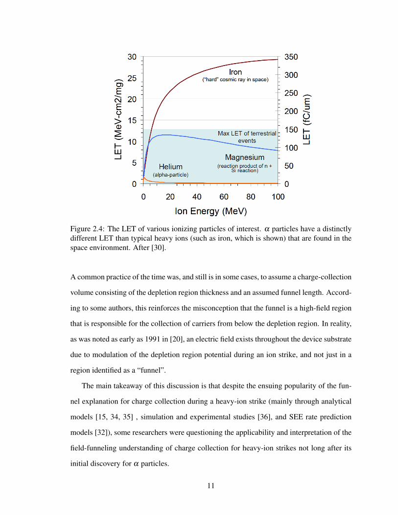
Figure 2.4: The LET of various ionizing particles of interest. α particles have a distinctlydifferent LET than typical heavy ions (such as iron, which is shown) that are found in thespace environment. After [30].
A common practice of the time was, and still is in some cases, to assume a charge-collection
volume consisting of the depletion region thickness and an assumed funnel length. Accord-
ing to some authors, this reinforces the misconception that the funnel is a high-field region
that is responsible for the collection of carriers from below the depletion region. In reality,
as was noted as early as 1991 in [20], an electric field exists throughout the device substrate
due to modulation of the depletion region potential during an ion strike, and not just in a
region identified as a “funnel”.
The main takeaway of this discussion is that despite the ensuing popularity of the fun-
nel explanation for charge collection during a heavy-ion strike (mainly through analytical
models [15, 34, 35] , simulation and experimental studies [36], and SEE rate prediction
models [32]), some researchers were questioning the applicability and interpretation of the
field-funneling understanding of charge collection for heavy-ion strikes not long after its
initial discovery for α particles.
11

It is important to remember that the original field-funneling effect discussed in [6] was
observed for α particles. Figure 2.4 shows why the distinction between α particle events
and heavy ion events is an important one. The figure shows the linear energy transfer (LET)
of various ionizing particles as a function of particle energy. The important conclusion is
that the LET of α particles is vastly different from that of iron (a typical heavy ion found
in the space environment) [37]. One of the aims of this work, which will be discussed in
detail later, is to address charge-collection mechanisms during strikes by particles such as
high-energy iron, which, as is suggested by Figure 2.4, can generate a very large carrier
density in silicon.
2.3 Recent Developments in Charge Collection Mechanisms and Modeling
Some recent work dealing with charge-collection mechanisms emphasizes that, con-
trary to the typical view of field-funneling, the entire device substrate should be considered
for charge collection in devices, not just the region near the junction [16, 17, 19, 23, 26].
While this is not a wholly new claim (one paper describing the significance of considering
the entire device substrate was published in 1984 [21]), if the list of recent publications is
any indication, the idea has gained traction in the community in recent years. The moti-
vation for considering the entire substrate is that during a high-level heavy-ion strike that
passes through the depletion region, the electric field along the track is weak, and, in cases
where the ion does not pass all the way through the device, the field that was initially sup-
ported by the reverse-biased depletion region is pushed down to the track end. Considering
charge collection in this way has been referred to in some papers as “regional partition-
ing” [17–19, 26]. Regional partitioning focuses on the electric field established directly
beneath and around the region of high carrier density generated by the radiation event that
accompanies the reduction in voltage that is typically supported by the depletion region.
The conditions that give rise to this regional partitioning scheme are discussed in greater
detail in Chapter 3; however a high field established at the end of an ion track can have
12

considerable implications for charge collection, especially in the case of short-range ions.
Many cases of practical interest involve particles that are relatively short range. One exam-
ple is the previously discussed iron, whose prominence in the space environment makes it
an interesting particle to consider for SEEs in devices (see Section 2.4). For many energies,
an iron ion would not pass completely through a typical device substrate. For example, a
100 MeV iron ion has a range of approximately 20 µm in silicon [1]. Charge collection due
to other short-track phenomena are also of practical interest, such as nuclear reaction prod-
ucts produced by collisions between an incident particle and back-end-of-line materials
[38], and some types of pulsed laser irradiation [39].
Previous theoretical work has considered regional partitioning concepts in the devel-
opment of an analytical model for charge collection [18, 19, 40, 41]. A discussion of the
concepts behind this model can be found in Chapter 3; however, it is noted here that re-
gional partitioning concepts and the resulting analytical model have been used to provide
valuable insight into simulation results [18] and pulsed laser measurements of an opto-
electronic device [22, 23, 42], as well as providing a valuable framework for interpreting
the experimental and simulation results described throughout this document. For the case
presented in Chapter 3, no other analytical charge collection model found in the literature
was able to sufficiently explain the trends in charge collection observed in experiments.
Significantly more will be said about this particular regional partitioning scheme, and the
insight it provides, in the chapters that follow.
2.4 High LET Particles in the Space Radiation Environment
The focus of this work is primarily on the interaction of high LET ions with silicon de-
vices. Therefore, understanding the prevalence of high LET ions in the space environment
is necessary to properly place the work in context. The goal of this section is to briefly
discuss the presence and abundance of high LET ions in the space environment.
Broadly, the space radiation environment consists of protons and heavy nuclei associ-
13

Figure 2.5: Relative abundance of the elements from hydrogen to the iron group, nor-malized to that of carbon (C=102 in the plot). The solid line represents the cosmic-rayabundances measured near Earth. The dashed line represents the elemental abundances inthe solar system of the GCR. After [3] (original in [43]).
14

Figure 2.6: SRIM results for iron in silicon. The black curve is the computed LET versusion energy for electronic stopping (direct ionization). The red curve shows the predictedrange. After [1].
ated with solar events, trapped radiation (e.g., the Van Allen belts near the Earth), galactic
cosmic rays (GCRs), neutrons, and photons [3]. Of these, the two most relevant to this
work are the heavy nuclei associated with solar events and the heavy ions found in GCRs.
Many of the ion species present in these two subsets of the space radiation environment are
capable of producing high-level carrier generation conditions in silicon devices (though a
third source of high-LET particles that is not specifically related to a particular environment
is discussed at the end of this section).
GCRs are highly energetic particles which originate outside of our solar system. They
are composed mainly of energetic protons and atomic nuclei. The exact processes by which
they are produced is unknown, although many suspect that some fraction of cosmic rays
likely originate from the supernovae of massive stars. Recent data from the Fermi space
telescope has been used as evidence in support of this claim [44]. As far as space electronics
are concerned, satellites in geo-synchronous orbits (approximately 36,000 km) and probes
operating in interplanetary space will be subject to GCRs. While the GCR spectrum is
15

Figure 2.7: Integral fluxes for iron cosmic rays versus LET for a 90% worse case (upper),solar minimum (middle), and solar maximum (lower). The spectra are at 1 AU behind 25mils of aluminum shielding. After [45].
predominately protons, a significant portion is heavy atomic nuclei.
Figure 2.5 shows the relative abundance of elements from the hydrogen to the iron
group in the GCR spectrum normalized to that of carbon. The solid line represents the
abundances measured near Earth while the dashed line represents the elemental abundances
in the solar system of the GCR spectrum. Hydrogen and helium are, by far, the most abun-
dant particles. However, the relatively low LET of these particles makes them of limited
use for this study. Other elements of interest in Figure 2.5 include carbon, oxygen, and
iron. Of the three, iron is especially interesting due to its increased abundance compared to
particles with a similar charge number and its LET. Figure 2.6 shows the LET and range for
iron in silicon as a function of particle energy. For example, a 100 MeV iron particle has
an LET of almost 30 MeV-cm2/mg and a range of approximately 20 µm in silicon, which
could lead to high-level carrier generation conditions in devices.
Figure 2.7 shows the Heinrich curve for iron in the GCR. The Heinrich curve shows the
16

Figure 2.8: LET versus energy per AMU for particles in silicon. After [45].
integral flux of a particular ion as a function of LET. The Heinrich curve shown in the figure
plots the integral flux of iron at solar maximum (lower), solar minimum (middle), and a
90% worst case (upper). All of the curves are at 1 AU behind 25 mils of aluminum shielding
[45]. This figure shows that, for iron, a reasonable flux of particles exists having an LET
of approximately 30 MeV-cm2/mg. Other particles of interest are shown in Figure 2.8,
which plots the stopping powers of various ions in silicon as a function of particle energy
per nucleon. Though the abundance of the other ions shown is less than that of iron, there
still exists a significant abundance of oxygen, neon, and argon (among others) in the GCR
spectrum measured near Earth and in the solar system (see Figure 2.5).
Another source of heavy ions are solar particle events (SPE). These events occur ran-
domly in time when very strong solar magnetic fields become critically unstable. As a way
to relax this instability, an energetic ejection of mass from the sun can occur. SPEs can
be rich in heavy ions ranging in energy from ∼1 MeV/nucleon to ∼10 GeV/nucleon with
17

intensities that are orders of magnitude greater than those of the GCR at similar energies
[3]. The integral flux for SPEs can also be several orders of magnitude greater than the
GCR integral flux at solar minimum (which is when the GCR flux is at a maximum) [3].
This constitutes a significant increase in the abundance of high LET particles in the space
radiation environment. Particles ejected during an SPE can follow magnetic field lines and
affect near-Earth electronics.
The mean composition of various heavy ion species found in SPEs relative to hydrogen
are the following: Fe (4.1 x 10⁻⁵), Cu (2.0 x 10⁻⁸), Kr (2.0 x 10⁻⁹), Xe (2.7 x 10⁻¹⁰), and
U (1.2 x 10⁻¹²) [45]. Of the ions listed, uranium and xenon comprise a very small fraction
of SPEs. However, their high LETs (see Figure 2.8) indicate that they could generate a
large density of excess carriers in silicon devices. Of the ions listed, iron and copper are
relatively common.
Recent work has also shown that energetic particle interactions with back end of line
(BEOL) materials can lead to the production of secondary particles through nuclear re-
actions. Depending on the BEOL material in question, short range, high LET secondary
particles from nuclear reactions can be generated. These secondaries can then go on to
generate carriers in the sensitive device fabricated underneath the BEOL materials. [46]
showed that energetic protons (which are commonly found in the space environment) can
interact with tungsten (a common BEOL metal) to generate forward-directed secondary
particles with a range of up to 20 µm and an LET greater than 40 MeV-cm2/mg in sili-
con. Such a particle could travel through the device overlayer materials and into the silicon
below, where it would be capable of generating a significant carrier density near a sen-
sitive device. In [47], secondary particles created through the interaction of heavy ions
with BEOL materials produced single-event upsets in an SRAM that had been hardened to
50 MeV-cm2/mg, indicating that low LET, highly energetic ions could lead to the produc-
tion of secondary particles capable of upsetting a hardened device. While the presence of
secondary particles generated through nuclear interactions between energetic particles and
18

BEOL materials does not constitute a radiation environment per se, it should be consid-
ered as a potential source of high LET particles capable of generating a large excess carrier
density in silicon devices.
19

CHAPTER 3
Total Collected Charge During High-Level Carrier Generation Events
3.1 Chapter Introduction
High-level carrier generation events, such as heavy-ion strikes, can produce carrier den-
sities that are orders of magnitude greater than the background doping density. The charge-
collection process at a reverse-biased device junction in response to such a condition is
complex and dynamic. In [16], device level simulations were used to assert that the electric
field along the track of charge produced by a ion passing through a junction and into the
device substrate is weak, and, in cases where the ion does not pass all the way through
the device, the field that was initially supported by the reverse-biased depletion region is
pushed down to the track end. A key conclusion of [16] is that understanding the physical
mechanisms of charge collection requires considerations of the entire device structure, and
not just regions near the junction. This was discussed briefly in Section 2.3.
Previous theoretical work has leveraged similar ideas in the development of an analyti-
cal model for charge collection [18, 19, 40, 41]. This model is built around the observation
that, for carrier-generating events of sufficient intensity, the device substrate can be parti-
tioned into regions that can be characterized by their relative carrier densities, potentials,
and electric fields [18, 19, 40], [48], [49]. A schematic of this partitioning and the rel-
evant physical properties of each region are shown in Figure 3.1, which is discussed in
greater detail in Section 3.3. This regional partitioning could be considered a similar phys-
ical framework to that of funneling in response to a heavy ion strike through the depletion
region of a device [15, 34, 50]. However, where the funnel model places emphasis on a
region of potential modulation surrounding the ion track (i.e., the funnel), regional parti-
tioning focuses on the electric field established directly beneath the region of high carrier
density generated by the radiation event. This electric field is due to the reduction in voltage
20

Figure 3.1: Schematic showing individual region names (a) and relevant physical charac-teristics of those regions (b) for a reverse-biased p-n junction during high-level conditions.These regions are described mathematically by the ADC model. For early times duringthe charge-collection process, the ambipolar region boundary corresponds approximatelyto the bottom of the generated carrier density.
that is typically supported by the depletion region.
In some analytical charge collection models (the funnel model of [15], for instance),
tracks passing through a device are considered to be “infinitely long”. In other words,
those models describe charge collection due to a particle that passes completely through the
device. This might lead to some confusion when discussing the electric field “beneath the
region of high carrier density”. However, many cases of practical interest involve particles
that are relatively short range. Several examples of short-range phenomena were mentioned
in Section 2.3. The concepts presented in this work are certainly not limited to short-track
phenomena, but such phenomena do provide good example cases for the ideas discussed
here.
The ambipolar diffusion with a cutoff (ADC) model is a first-principles, analytical
charge collection model that is based on the regional partitioning concepts discussed above
[18, 19, 40] and illustrated in Figure 3.1. As has been discussed using device-level simu-
lations [40], and is shown experimentally in this work through charge-collection measure-
ments for the first time, the ADC model is capable of producing reasonably accurate values
for total collected charge without many of the assumptions required by other analytical
21

charge collection models, which are discussed in Section 3.5. The ADC model focuses on
the physical mechanisms of charge collection during high-level carrier generation events.
This allows the ADC model to bridge the gap between simple analytical charge collec-
tion models, which provide little physical insight into the charge-collection process, and
comprehensive device-level simulations (e.g., TCAD tools).
Analytical charge collection models could also be advantageous to other modeling ef-
forts. There is recent and growing interest in simulation codes that use Monte-Carlo meth-
ods to analyze the interaction of radiation with matter (such as the MRED tools [51, 52]).
This analysis is then combined with information regarding charge collection and circuit
analysis methods to predict the circuit-level response of a device exposed to radiation.
Due to the computationally intensive nature of Monte-Carlo techniques, it is desirable to
use analytical models (as opposed to TCAD simulations) whenever possible to reduce the
computational overhead.
The charge-collection measurements described throughout this chapter were made via
high-speed transient capture [53] on a bulk silicon diode during exposure to high-irradiance
laser pulses. The pulse was at a sub-bandgap wavelength, so carrier generation was pro-
duced by TPA [39]. The data show that, for sufficiently high-energy laser pulses, nearly all
of the generated charge is collected, even when substantial carrier generation occurs only
well below the depletion region boundary. The ADC model is able to predict trends in col-
lected charge that are in good qualitative agreement with experimentally measured values
in this situation, which is an experimental condition that cannot be described accurately by
other analytical charge-collection models. Models that consider only certain device regions
(the depletion region, or a “funnel region” for example) can predict correct values for col-
lected charge in some cases. However, for the more general case of predicting the collected
charge due to an arbitrary carrier density near a reverse-biased junction during a high-level
carrier generation event, the response of the entire device must be considered.
Section 3.2 describes the experimental setup and measurement process. To aid in the
22

Figure 3.2: An illustrative diagram of the diode and measurement procedure. Relative sizesare not to scale. Exact doping levels can be seen in Figure 3.4. The device overlayers arenot shown.
understanding of the model used to analyze the experimental work, an overview of regional
partitioning is discussed in Section 3.3, which includes new device-level simulations, while
Section 3.4 discusses how the ADC model was applied to the experimental data. The
experimental results are discussed in Section 3.5. Appendix A contains a more detailed
derivation of the ADC model. The derivation shown in the appendix is intended to be
a summary of the more salient characteristics of the model, it has been compiled from
various works that discuss the model in even greater detail [17–19].
3.2 Two-Photon Absorption Measurements
Carrier injection by TPA was used to examine trends in charge collection for a simple
bulk silicon diode as a function of the intensity and location of the generated carrier den-
sity. This technique generates carriers that are spatially distributed in a way that may not
correspond to analytical charge collection models based on ion strikes that pass directly
23

through the depletion region of the device. Because TPA testing allows for a continuously
variable laser pulse energy over a wide range, it is a convenient test method for controlling
the magnitude of the generated charge in the device [39], [54]. Figure 3.2 is an illustrative
diagram of the test structure during sub-bandgap laser exposure. Several relevant features
are noted on the figure, including the approximate location of carrier generation in relation
to the beam focus, the relative doping levels and size of the structure, and the reference
Z=0 µm, which is discussed below.
3.2.1 Test Structure and Setup
All transient capture measurements were performed using a large-area (∼200 µm x
∼800 µm) bulk silicon diode fabricated in a 45 nm process. The physical location and
magnitude of each doping concentration was determined through spreading resistance mea-
surements. The diode consists of an n-well with a peak doping of ∼1018 cm−3 that is ap-
proximately 0.5 µm deep over a p-substrate with a doping of ∼1015 cm−3. The device
substrate did not contain any buried layers. To avoid any laser shadowing effects from
metal in the diode’s overlayers, the diode was irradiated from the backside, through the sil-
icon substrate [54]. The diode was maintained at a 5 V reverse bias for all measurements.
The diode’s reverse bias leakage current did not exceed 10 nA throughout the duration of
the experiment.
Measurements were made using a Tektronix DPO7254 2.5 GHz oscilloscope. Devices
were mounted in custom-milled metal packages with microstrip transmission lines and pre-
cision 2.92 mm K-connectors. An example of a similarly-designed and fabricated package
can be seen in Figure 3.3. The bias voltage was supplied using a Keithley 2410 SourceMe-
ter through a 50 Ω bias-tee. Cabling and other test fixtures were chosen for performance
and stability up to and exceeding the bandwidth of the oscilloscope.
The laser irradiations described in this chapter were performed at the Naval Research
Laboratory in Washington, DC using a Ti-Sapphire pumped optical parametric amplifier
24

Figure 3.3: A custom-milled, brass package suitable for capturing high-speed transientsignals from irradiated devices. Relevant components are labeled.
operating at a wavelength of 1.26 µm with a nominal pulse width of 150 fs. Because the
wavelength of the laser source is sub-bandgap for silicon, carrier generation is by TPA. The
beam is focused through a 100x (NA 0.5) objective, which produces a focused beam with
a confocal parameter of approximately 9.0 µm. This allows for the generation of carriers
only in close proximity to the focus where the pulse irradiance is greatest. The focused
Full-Width-Half-Max (FWHM) optical spot size was 1.4 µm. The details of the setup and
TPA test method are discussed in greater detail in [39] and [55].
3.2.2 Measurement Procedure
One goal of the experiments was to observe charge collection in the diode as a result
of moving the TPA-induced carrier density from the surface of the device to deep in the
substrate. Doing so requires an absolute reference for the position of the laser focal plane
25

in the diode. To define this reference position, the laser spot was focused visually on the
Si-SiO2 interface (the position labeled Z=0 µm in Figure 3.2). In the plots that show
collected charge as a function of Z-position (Figure 3.7, which is discussed later), 0 µm on
the horizontal axis represents the laser spot being focused on this interface, while values
greater than 0 µm represent a focal plane position that is within the device substrate as
shown in Figure 3.2. The error associated with this procedure is approximately ± 1 µm,
which is the smallest change in the spot size that can be detected visually. This error does
not significantly affect the interpretation of the results discussed below.
For each measurement, the focal plane of the laser was moved through the device in
3.5 µm steps in the vertical (“Z”) direction. At each step, approximately fifty current
transients were recorded. They were then numerically integrated to determine the mean
total collected charge at each position.
3.3 Charge Collection During High-Level Carrier Generation Conditions
3.3.1 Regional Partitioning
Previous work [18, 19, 40], [41], [22, 23, 42] has discussed the physical nature of re-
gional partitioning in response to events that generate high carrier concentrations. It occurs
as a result of high-level conditions in a device. While there is no rigorous definition of
how far above the background majority carrier concentration the generated carrier density
must be in order to produce high-level effects [17, 24, 25] regional partitioning effects for
the device used in this work were observed in device-level simulations in situations where
the generated carrier density was approximately one order of magnitude greater than the
background majority carrier concentration.
Regional partitioning describes the distribution of generated carriers in the quasi-neutral
region (QNR), which is the region of the device outside the depletion region (DR) bound-
ary (DRB) extending through the substrate. Here “quasi-neutral” is defined as a charge
imbalance that is less than the majority carrier density, but not necessarily so small that it
26
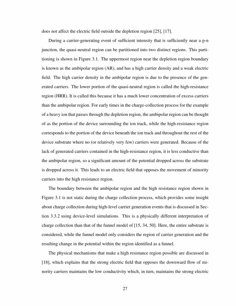
does not affect the electric field outside the depletion region [25], [17].
During a carrier-generating event of sufficient intensity that is sufficiently near a p-n
junction, the quasi-neutral region can be partitioned into two distinct regions. This parti-
tioning is shown in Figure 3.1. The uppermost region near the depletion region boundary
is known as the ambipolar region (AR), and has a high carrier density and a weak electric
field. The high carrier density in the ambipolar region is due to the presence of the gen-
erated carriers. The lower portion of the quasi-neutral region is called the high-resistance
region (HRR). It is called this because it has a much lower concentration of excess carriers
than the ambipolar region. For early times in the charge-collection process for the example
of a heavy ion that passes through the depletion region, the ambipolar region can be thought
of as the portion of the device surrounding the ion track, while the high-resistance region
corresponds to the portion of the device beneath the ion track and throughout the rest of the
device substrate where no (or relatively very few) carriers were generated. Because of the
lack of generated carriers contained in the high-resistance region, it is less conductive than
the ambipolar region, so a significant amount of the potential dropped across the substrate
is dropped across it. This leads to an electric field that opposes the movement of minority
carriers into the high resistance region.
The boundary between the ambipolar region and the high resistance region shown in
Figure 3.1 is not static during the charge collection process, which provides some insight
about charge collection during high-level carrier generation events that is discussed in Sec-
tion 3.3.2 using device-level simulations. This is a physically different interpretation of
charge collection than that of the funnel model of [15, 34, 50]. Here, the entire substrate is
considered, while the funnel model only considers the region of carrier generation and the
resulting change in the potential within the region identified as a funnel.
The physical mechanisms that make a high resistance region possible are discussed in
[18], which explains that the strong electric field that opposes the downward flow of mi-
nority carriers maintains the low conductivity which, in turn, maintains the strong electric
27

Figure 3.4: Two dimensional image showing a 20 µm by 20 µm section of the 150 µm by300 µm simulated bulk silicon N-well/P-substrate diode. The dashed line represents thedepletion region thickness at a reverse bias of 5 V.
field. Due to the orientation of this field, all minority carriers generated in the substrate
move toward the junction and are collected if a high resistance region is present (neglect-
ing recombination). The conditions required for the formation of a high resistance region
are discussed in more detail in Section 3.3.3.
3.3.2 Regional Partitioning in Device-Level Simulations
To demonstrate regional partitioning phenomena in a device similar to the one used for
this work, two-dimensional cylindrical (i.e., quasi-3D) TCAD simulations of a heavy ion
strike were performed using the Synopsys Sentaurus TCAD tools [56]. For cases where
the device geometry can be reasonably approximated by a cylindrical structure, cylindri-
cal simulations can dramatically reduce the computational burden while still producing a
device response that is approximately equal to a fully three-dimensional simulation [8].
28

Figure 3.4 shows a 20 µm x 20 µm cross-section of the simulated device, which is 150 µm
wide in the Y-direction and 300 µm long in the Z-direction. The color scale indicates the
device doping. The doping profile for the simulated device is the same as the actual device
used for the TPA experiments. The white dashed line represents the depletion region width
at a reverse bias of 5 V. The device is contacted using ideal contacts running the full width
of the device at the top of the n-well and the bottom of the p-substrate. The aim of the
simulations is to show that regional partitioning can occur in a device that is similar to the
one used for the TPA experiments, not to produce a quantitatively accurate comparison to
experimental results.
An incident ion linear charge deposition of 1.00 pC/µm, which approximately corre-
sponds to an incident ion linear energy transfer (LET) of 100 MeV-cm2/mg in silicon, was
chosen to ensure that the device was experiencing high-level conditions. The ion track was
injected 25 ps after the simulation began. The ion track was centered on the Z-axis in Fig-
ure 3.4, was perpendicular to the Y-axis, and originated at the n-well surface. The simulated
ion track had a constant generated charge density in the Z direction, was 10 µm long, and
had a Gaussian radial profile with a characteristic width of 100 nm. The physical models
governing carrier mobilities, recombination, and carrier-to-carrier scattering were identical
to those used in [42], which discussed regional partitioning phenomena in simulations of a
silicon optoelectronic device. For all simulations, the device was reverse biased at 5 V.
Figure 3.5 shows a contour plot of the magnitude of the electric field around the ion
track 1 ns after carrier generation. A high-field region can be seen at approximately the end
of the ion track. While this produces a similar plot to what has historically been described
as funneling [6], the emphasis here is on the field that is established below the low-field
(blue) region, and not on the low-field region itself. The field below the track opposes
the downward motion of minority carriers, effectively confining them in close proximity
to the junction for the ion track shown here. Also, this spatial distribution of the electric
field results in most of the voltage across the substrate being dropped beneath the ion track
29

Figure 3.5: An example of regional partitioning in response to a high-level condition inthe simulated diode shown in Figure 3.4. The electric field in the device in response toa 1.00 pC/µm track with a 10 µm length is shown 1 ns after the strike. Red regions aresaturated on the color scale, meaning their actual values could be greater than 7x10³ V/cm.
(i.e., in the high resistance region). This carrier confinement should not be confused with
ambipolar diffusion [24]. While the carrier densities discussed here would be subject to the
effects of ambipolar diffusion, the field that is established at the end of the ion track is due
to the potential that was previously supported by the reverse-biased depletion region being
dropped beneath the ion track, thus preventing minority carriers from moving deeper into
the substrate.
We cannot definitively conclude that the partitioning in Figure 3.5 separates an ambipo-
lar region from a high resistance region until we have answered the question of how strong
the electric field should be to imply the existence of a high resistance region. The ADC
30

Figure 3.6: The Z-component of the electron current density along the Z-axis shown inFigure3.5 for various times during the charge-collection process. The discontinuous slopethat occurs at approximately 11 µm along the horizontal axis indicates the ambipolar regionboundary. The zero value for electron current density beyond this boundary confirms theexistence of the high resistance region, which prevents the flow of minority carriers deeperinto the substrate. The large range of values seen in the y-axes of each figure emphasizethat while the magnitude of the electron current density changes considerably as the devicereturns to its steady-state configuration, the inflection point that signifies the existence ofthe high resistance region is present during the majority of the charge-collection process.
31

model (discussed in more detail in Section 3.3.3) answers this question with the statement
that the electric field near the ambipolar region boundary, when the high resistance region
exists, is strong enough to prevent minority carriers from entering the high resistance re-
gion. Therefore, a more definitive way to recognize the regional partitioning that separates
the ambipolar region from the high resistance region (which defines the boundary for mi-
nority carrier confinement) is to plot the minority-carrier current density. Figure 3.6 plots
the Z-component of this current along the Z-axis and through the track center at four time
points. The location of the ambipolar region boundary is the point where the current goes
to zero and remains at zero for all greater depths. The current is zero beyond this boundary
because the high electric field at the boundary has prevented carriers that were generated
during the simulated ion strike from moving into the high resistance region. This boundary
is sharp in the high-level limit (which is an infinite mathematical limit) but has some small
uncertainty for real (finite) cases. At the earlier time points in the figure, conditions resem-
ble the limiting case well enough to produce the appearance of a sharp boundary (e.g., at
11 µm at 0.10 ns as seen in Figure 3.6a). At later times, the carrier density decreases and
the exact location of the boundary becomes less clear, but it is still reasonably well defined
even at 10 ns and is at a depth of roughly 16 µm (Figure 3.6d).
Simulations of various ion track lengths (not shown here) produce a qualitatively simi-
lar increase in the electric field directly beneath the ion track for high LET ions that do not
pass completely through the device substrate. In these simulations, the ambipolar region
boundary is initially located near the bottom of the track; however, as the simulation ad-
vances in time, some movement in the boundary (similar to that shown in Figure 3.6) can
be seen. The significance of the motion of the boundary for charge collection is discussed
in more detail in [40]. The case of an ion track that passes all the way through the device
substrate is only slightly different, and ultimately leads to a similar regional partitioning as
the bottom portion of the track (near the substrate contact in the example given here) clears
away and a high resistance region is formed. This case is not particularly germane to the
32

discussion here, but it is described in more detail in [49].
3.3.3 A Review of the ADC Model
Previous work in [18, 19, 40, 41] discusses the development of the ADC model. This
section includes a brief overview of the model, as well as a low-level model (derived in
Appendix A) that is also compared to the experimental data in Section 3.5. Derivations and
more detailed discussions of the equations shown here are contained in Appendix A.
The original derivation of the ADC model in [18] pertains to steady-state carrier gen-
eration in a reverse-biased p-n junction silicon diode. More recent work in [19] considered
transient conditions produced when carriers are generated impulsively, and produced the
same charge-collection model as the steady-state theory.
Let Q represent the total collected charge, which is the time integral of the terminal
current in the device. Let PI(x) denote the density of generated electron-hole pairs as a
function of the three-dimensional spatial coordinate x. It is shown in Appendix A that, for
low-level conditions, the collected charge can be expressed as,
Q =∫
qPI(~x)Ω(~x)d3x (low level), (3.1)
where Ω is a position dependent weighting factor that determines the relative importance
of charge generated at one location compared to the same amount of charge generated at
another location and the volume integral on the right includes both the depletion region
and the quasi-neutral region. The weighting factor Ω equals 1 in the depletion region.
When carrier recombination in the device interior can be neglected, Ω in the quasi-neutral
region is the solution to Laplace’s equation, which ranges from 1 on the depletion region
boundary to 0 on the substrate contact. If the substrate contact were instead, for example,
on the topside of the device, the value for Ω would still be 0 at that contact. However, it
would be necessary to know what kind of boundary condition was present at the bottom
of the device, unless the substrate was thick enough to be treated as an infinite medium.
33
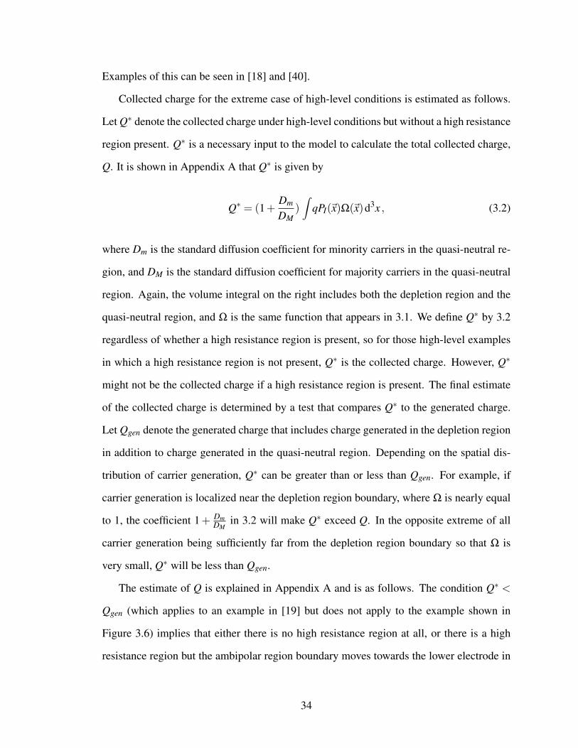
Examples of this can be seen in [18] and [40].
Collected charge for the extreme case of high-level conditions is estimated as follows.
Let Q∗ denote the collected charge under high-level conditions but without a high resistance
region present. Q∗ is a necessary input to the model to calculate the total collected charge,
Q. It is shown in Appendix A that Q∗ is given by
Q∗ = (1+Dm
DM)∫
qPI(~x)Ω(~x)d3x , (3.2)
where Dm is the standard diffusion coefficient for minority carriers in the quasi-neutral re-
gion, and DM is the standard diffusion coefficient for majority carriers in the quasi-neutral
region. Again, the volume integral on the right includes both the depletion region and the
quasi-neutral region, and Ω is the same function that appears in 3.1. We define Q∗ by 3.2
regardless of whether a high resistance region is present, so for those high-level examples
in which a high resistance region is not present, Q∗ is the collected charge. However, Q∗
might not be the collected charge if a high resistance region is present. The final estimate
of the collected charge is determined by a test that compares Q∗ to the generated charge.
Let Qgen denote the generated charge that includes charge generated in the depletion region
in addition to charge generated in the quasi-neutral region. Depending on the spatial dis-
tribution of carrier generation, Q∗ can be greater than or less than Qgen. For example, if
carrier generation is localized near the depletion region boundary, where Ω is nearly equal
to 1, the coefficient 1+ DmDM
in 3.2 will make Q∗ exceed Q. In the opposite extreme of all
carrier generation being sufficiently far from the depletion region boundary so that Ω is
very small, Q∗ will be less than Qgen.
The estimate of Q is explained in Appendix A and is as follows. The condition Q∗ <
Qgen (which applies to an example in [19] but does not apply to the example shown in
Figure 3.6) implies that either there is no high resistance region at all, or there is a high
resistance region but the ambipolar region boundary moves towards the lower electrode in
34

such a way as to not prevent the downward flow of minority carriers, as if there were no
high resistance region. In either case, Q∗ (which is the collected charge when there is no
high resistance region) is an estimate of Q. Also, the condition Q∗ > Qgen (which applies
to the example in Figure 3.6) implies that there is a high resistance region with a quasi-
stationary boundary, which in turn implies that an estimate of the collected charge is the
total generated charge. The result is the ADC model, which estimates Q from
Q =
Q∗ if Q∗ < Qgen,
Qgen if Q∗ > Qgen
(high level conditions). (3.3)
3.4 Applying the Models to Experimental Data
When applying the models discussed above to the experimental data, the desired output
is Q, or the position dependent total collected charge. The inputs to the model are the
total generated charge, which is discussed below, and the Ω weighting function described
in Section 3.3.3. Once the inputs are known, the model predictions can be calculated in
seconds using any modern computer programming language.
Figure 3.7 shows the mean collected charge for the TPA measurements along with the
model predictions for the data (red and blue lines). The results shown in Figure 3.7 are
discussed in detail in Section 3.5. The purpose of this section is to describe how the data
points shown in Figure 3.7 are related to the model predictions.
The model, as it is presented here, does not require the geometry and device doping
as explicit inputs. The geometric aspects of the device that are relevant to the analysis are
described by the Ω function. Appendix A shows that Ω can be calculated using (A.6);
however, it is also possible to estimate, rather than calculate, Ω using data from experi-
mental charge-collection measurements. The first step needed to estimate Ω from data is
to estimate the amount of generated charge when the laser spot is completely contained
in the silicon portion of the device. While analytical methods are available for calculating
35

Figure 3.7: Collected charge as a function of focal plane position in the diode. Noticethe better agreement for the ADC model as the laser pulse energy is increased enoughto produce a plateau in charge collection. This plateau is a strong indication of regionalpartitioning effects occurring in the device.
36

the TPA-induced carrier density when only the carrier generation term is considered [39],
these methods provide, at best, a rough approximation to the generated carrier density in the
device. An accurate analytical calculation to determine the amount of charge deposited dur-
ing the TPA process within a particular device is not presently available and is a difficult
problem that would require considerable computational effort. This complex calculation
can be avoided by assuming in the analysis that follows that the collected charge at the
maximizing focal plane position is an estimate of the total generated charge, regardless of
whether low-level or high-level conditions apply. Referring to the experimental data points
in Figure 3.7, the estimates of generated charge are
Qgen =
0.08 pC @ 0.43 nJ2
0.81 pC @ 2.59 nJ2
2.7 pC @ 4.12 nJ2
7.8 pC @ 10.43 nJ2
(data). (3.4)
Having estimated the generated charge for each laser energy used, the next step is to esti-
mate Ω.
Although a large amount of spatial resolution regarding laser intensity is needed to
calculate (as opposed to measure) the generated charge, less spatial resolution regarding the
initial generated charge is needed when using 3.1 or 3.2 to estimate the collected charge.
In particular, a sufficiently small laser spot can be approximated as a point source in the
latter calculations. This approximation will be used to estimate Ω. Also, it is assumed
here that the lowest laser intensity used in the measurements, which produced Figure 3.7a
and will be called the “low-intensity measurements”, produces low-level conditions so that
3.1 applies. Let QEXP(Z) be the experimentally measured collected charge from the low-
intensity measurements as a function of the focal plane depth Z. In other words, QEXP(Z)
is the set of points in Figure 3.7a. Using the point-source approximation (i.e., qPI is the
37
generated charge multiplied by the Dirac delta function centered at depth Z) with 3.1 gives
QEXP(Z) = QgenΩ(Z)
or
Ω(Z) =QEXP(Z)
Qgen(low intensity). (3.5)
Note that QEXP(Z) was measured only at the discrete values of Z indicated by the filled
black circles in Figure 3.7a. Estimates of Ω between these points are obtained from linear
interpolations. Once Ω was determined using the data points in Figure 3.7a, it could be used
along with 3.1-3.3 to develop the low-level (red) and ADC (blue) lines in Figures 3.7b-3.7d.
In other words, the only knowledge that the red and blue lines of Figure 3.7 have of the data
points in Figure 3.7 is what is shown in 3.4 plus the data points in Figure 3.7a used to con-
struct Ω. Were it possible to accurately calculate the charge deposited by TPA in the device
(Qgen) as opposed to using 3.4, the red and blue curves shown in Figure 3.7 would require
no knowledge of the data points in Figures 3.7b-3.7d whatsoever. The predictions could
be made using only the low-intensity TPA data (to define Ω) together with the calculated
values for Qgen.
The low-level curves in Figure 3.7 were calculated by combining 3.5 with 3.1. How-
ever, this calculation does not use the point-source approximation. If it did, the prediction
would exactly reproduce the points in Figure 3.7a because the points in Figure 3.7a were
used to define Ω. Instead, a smoother curve was produced by giving PI some spatial extent.
Specifically, it is treated as constant over a 12 µm range (6 µm on each side of the focal
plane depth). This is consistent with recent measurements of the TPA carrier generation
region’s “effective length” [57]. While the effective length of the TPA carrier generation
region does increase with increasing laser pulse energy, a 12 µm range is a reasonable
approximation for the laser pulse energies used here.
Similar calculations are used to obtain the blue curves, except that 3.1 is replaced by
38

3.2 and 3.3. This calculation requires an estimate of the diffusion-coefficient ratio Dm/DM,
which is related to the mobility ratio through the Einstein relation [25]. Because of (A.9),
accuracy is needed only in the ambipolar region portion of the quasi-neutral region, which
is a weak-field region, so we use low-field mobilities. For a p-type substrate, this ratio
is the low-field electron mobility divided by the low-field hole mobility. The ratio used
here is 2.8, which is consistent with mobilities reported in the literature for the doping
concentration used in the tested device [25].
3.5 Results and Discussion
Figure 3.7 shows the mean collected charge as a function of Z-position for four different
laser pulse energies. The error bars in the figure represent the statistical standard error for
each reported value of collected charge. For values of standard error that are less than
5% of the reported mean, error bars are not shown. Sources of systematic error were not
quantified. The red lines in Figure 3.7 represent calculated values for collected charge using
the low-level calculation explained in Section 3.4. The blue lines represent the same type
of calculation, only using the ADC model as explained in Section 3.4.
One might assume that as the peak carrier density moves away from the point of max-
imum charge collection, the total charge collection should decrease appropriately due to
the longer path carriers would have to take to diffuse to the junction to be collected. That
is consistent with Figures 3.7a-b, which show a decrease in collected charge immediately
following the peak charge collection. However, there is a plateau in the measured values for
collected charge within the first 21 µm of Figure 3.7d. The physical interpretation of this
is that when the focus of the laser is within this 21 µm region, almost all of the generated
charge can be collected. These data indicate that as long as the carrier generation is suffi-
ciently intense, nearly all of the generated charge can be collected, even if the peak of the
generated carrier density is many micrometers away from the depletion region boundary.
The ADC model is consistent with this observation. According to the model, if the focus
39
is sufficiently close to the upper junction (21 µm for Figure 3.7d), a high resistance region
will be created somewhere in the lower portion of the substrate and serve as a blocking
region that prevents minority carriers from reaching the lower electrode, so they are all
collected at the junction regardless of where in this upper region the focus is located. If
the focus is not sufficiently close to the junction to produce this effect, the collected charge
will be less than the generated charge and will decrease with increasing depth of the focus.
For the lowest tested pulse energy squared (0.43 nJ2, Figure 3.7a), the low-level model
is in better qualitative agreement with the charge-collection measurements than the high-
level model. This is a given because the data in Figure 3.7a were used to construct the Ω
function while assuming low-level conditions. The TPA data shown in Figure 3.7b are in
good agreement with the low-level model, indicating that 2.59 nJ2 pulses did not produce
a high-level condition in the diode. Figure 3.7c is not in good qualitative agreement with
either of the two models. In this case, 4.12 nJ2 pulses produced an intermediate case in the
diode where neither low-level theory nor the high-level theory provided by the ADC model
can reasonably predict the values of collected charge. For the highest pulse energy squared
shown (10.43 nJ2, Figure 3.7d), the ADC model is clearly a better qualitative fit to the data
than the low-level model, indicating that the diode was experiencing a high-level condition,
which produces regional partitioning effects in the diode.
When calculating ADC model predictions from low-level data, it was assumed that
the Ω in 3.2 is the same as the Ω in 3.1, so low-level data can be used to determine Ω
which in turn determines the prediction for high-level conditions. However, the theoretical
justification (in Appendix A) for this assumption applies when carrier recombination can
be neglected. It is not clear how recombination affects the validity of this assumption
because a version of the ADC model that includes recombination has not yet been derived.
Recombination is more important for deeper generation source locations, and it is possible
that this contributes to the difference between experimental data and theoretical calculations
in Figure 3.7d when the source is deeper than 21 µm. However, the qualitative agreement
40

is considered to be good enough to support the claims made here.
For this particular experimental case, it would be difficult or impossible to apply other
analytical models for charge collection to produce curves that are in reasonable agreement
with the experimental data shown in Figure 3.7. Determining a fixed charge collection
depth (which is common when using a simple RPP approach for rate prediction modeling
[32]) would be difficult based on the device geometry and doping, because it does not
have any buried layers that would truncate charge collection and help to define a fixed
charge collection depth. Predicting the collected charge using a fixed collection depth
model would also require knowledge of how much charge is generated by TPA within that
depth. When applying the ADC model here, it was assumed that the maximum collected
charge in Figures 3.7b-3.7d corresponds to the total generated charge. If we make the same
assumption for a fixed collection depth model, we still cannot use that model to predict
the data in Figure 3.7d, for example, without selecting a charge collection depth that fit the
data. Also, once a suitable number for that depth was found, it would only be a number
that was chosen to allow the model to agree with the data; it would not have any inherent
physical significance. Recall that the ADC model is able to predict the data in Figure 3.7d
with reasonable accuracy without any knowledge of the TPA data shown in Figure 3.7d,
other than the maximum collected charge.
Applying other, more refined analytical models would also be difficult. For example,
the model of [31] is intended only for structures with a lightly doped epitaxial layer over a
highly doped substrate. That model also assumes an incident ion track that has a constant
charge deposition over its entire track length and passes through the depletion region and
into the device substrate. Such an assumption cannot be made for the TPA data shown here,
especially in cases where the peak carrier generation of the TPA region is well below the
depletion region, and many micrometers deep in the substrate.
Another model to consider is the funnel model of [15], which describes charge collec-
tion in terms of a strong drift mechanism due to the presence of a funnel that is created
41
when the electric field that is normally supported by the depletion region is pushed down
into the quasi-neutral region following an ion strike. In addition to disagreeing with the
physical interpretation for charge collection provided by the ADC model (which regards
the electric field in the lower device region as being more significant than the field in the
upper region), it is ultimately not clear what the funnel model would predict for charge
collected from TPA pulses because the original funnel model in [15] was derived for tracks
that are effectively infinitely long. A later version in [34] has an empirical correction for
short tracks with high LET, but this correction was obtained from a specific set of test data
(with all tracks starting at the top of the device) and it is not clear how to use this for TPA
pulses that generate carriers at various depths in the device. Therefore, the funnel model as
described in [15] and [34] cannot be applied in this case.
Assuming that the effective length of the TPA-induced carrier density corresponds to
the confocal parameter of the beam (which is twice the distance from the beam waist to the
point where the beam radius has increased by a factor of√
2; or approximately 9 µm in this
case) or the measurements of the effective length of the TPA-induced carrier density shown
in [57] (approximately 12 µm for the pulse energies used here), the data of Figure 3.7d
suggest that when the focal plane is located at 21 µm, the TPA-induced carrier density does
not have sufficient vertical extent to generate a large number of carriers in the depletion
region directly; yet, in spite of this, almost all of the generated charge is collected. TCAD
simulations show that the depletion region thickness of this device is approximately 2 µm at
the 5 V reverse bias used during the measurements (shown in Figure 3.4). For carriers to be
generated within the depletion region when the laser focal plane was at 21 µm, the effective
length of the TPA-induced carrier density would have to be approximately 38 µm (19 µm
on either side of the focal plane). This is at odds with the funnel model, which assumes
that the carrier density generated within the depletion region modulates the potential and
causes the funnel effect.
While the ADC model does provide good agreement to the high-level TPA data shown
42

in Figure 3.7d, a potential trade-off is one of analytical complexity. The equations shown
in Section 3.3.3 and Appendix A suggest that the ADC model could be difficult to apply
to a dataset. This is due, in part, to its first-principles based approach to determining the
collected charge, which requires some knowledge of the Ω weighting function for deter-
mining the relative importance of charge generated at specific locations in the device. The
models presented in [15, 31, 32, 34] can only be used when the information required to
apply them is available. The advantage of the ADC model however, is that it is more gen-
erally applicable to charge-collection problems, assuming a reverse biased junction with
high-level carrier generation, which is often the case in many problems of interest. The ap-
plication of the ADC model does not require any geometric assumptions about the device,
such as assuming a charge collection depth based on the presence of buried layers or a well
boundary. Here, all geometrical considerations were handled by the Ω weighting function,
which was determined exclusively from low-intensity TPA data.
The large-area test structure used here is not representative of highly scaled devices, so
it is important to consider the applicability of the ADC model described here and the insight
it provides. There are many practical reasons for studying charge-collection phenomena
for large junctions; single-event latchup [4] and well potential modulation effects [58] are
two examples. Also, a thorough understanding of charge-collection by large junctions is a
helpful (and potentially necessary) element for understanding related phenomena in small
junctions, where small feature sizes can make interpretation of the data and application
of analytical charge-collection models more complicated. Charge collection for smaller
junctions is discussed in more detail in Chapter 5.
The experimental results of Figure 3.7 also provide insight about heavy-ion tests. For
example, high-level conditions were produced, for the device tested here, when the gen-
erated charge was approximately 8 pC. This is the same amount of charge that would be
generated by a heavy ion having a range of 20 µm (for example) and having an LET, aver-
aged over the ion range, of about 40 MeV-cm2/mg. Hence, it is reasonable to expect that
43

any ion having a range of 20 µm or more and having an average LET of 40 MeV-cm2/mg
or more will produce high-level conditions. Recall that this device is a test structure in
which the depletion region area is very large. High-level conditions are easier to produce
in smaller structures. Experimental and simulation results for heavy-ions are discussed in
Chapters 4 and 5.
3.6 Chapter Summary
This chapter has discussed the use of charge-collection measurements in a simple bulk
silicon diode to highlight the physical significance of high-level conditions for charge-
collection in devices. Specifically, high-level conditions can give rise to a region of position-
independent charge collection in a device where, due to the presence of a strong electric
field underneath the generated carrier density, almost all of the generated minority carri-
ers can be collected, even if the peak of the generated carrier density is located several
micrometers away from the depletion region boundary.
The ADC model is used to explain, via regional partitioning effects, the experimentally
observed collected charge due to TPA-laser induced high-level conditions. A qualitative
discussion of other analytical models for charge collection reveals that they would be dif-
ficult or impossible to apply in this case due to a violation of their primary assumptions or
the inability to apply them to the TPA-induced carrier density.
Using the results of Figure 3.7d, it is possible to gain some insight about high-level
conditions in a device as a result of real heavy-ion strikes. However, a more thorough
investigation of high-level carrier generation conditions for a reverse biased p-n junction in
response to a heavy-ion strike is discussed in Chapters 4 and 5.
44

CHAPTER 4
The Impact of Depletion Region Potential Modulation on Ion-Induced Current
Transient Response
4.1 Introduction
Chapter 3 dealt primarily with the total collected charge at a device junction following
a carrier generation event (heavy-ion strike, optical carrier generation, etc.). However, the
total collected charge is only one physical quantity of interest when discussing SEEs. An-
other is the device transient response. As it is typically encountered, the transient response
is a brief perturbation in the terminal current at a reverse-biased p-n junction that results
from the passage of an ionizing particle through the device. The characteristics of these
transients, and their temporal properties, can influence what effect they have on a partic-
ular device or circuit. SRAMs, for example, can be particularly sensitive to the temporal
characteristics of the ion-induced transient response [2]. In addition to providing insight
into circuit-level upsets, knowledge of how transient characteristics change as a function of
relevant ion parameters, such as the LET, is valuable for developing analytical models for
charge collection [18, 19, 26, 59].
The previous chapter discussed the significance of high-level carrier generation con-
ditions (such as those caused by a high LET ion strike) for charge collection in silicon
devices; however, the impact of high-level carrier generation conditions on the transient
current response was not described. Many ions in the space environment are capable of
producing high-level carrier generation conditions, making a study of the device-level tran-
sient response to such events valuable for furthering the understanding of charge-collection
mechanisms.
This chapter discusses high-speed transient capture measurements [53] on a bulk sil-
icon diode during heavy-ion irradiation and two-photon absorption (TPA) backside laser
45

exposure [39]. The experimental data described below show the influence of incident ion
LET on the characteristics of the generated transient. Specifically, increasing the heavy-ion
induced carrier density leads to significant depletion region potential modulation, which
has a profound impact on the characteristic shape of the current transient. Depending on
the applied bias voltage, a saturation in the peak transient current can be observed where
increasing the strength of the ionization source will no longer significantly increase the
peak current of the transient. This phenomenon is investigated through device-level simu-
lations and the application of an analytical model described in [48]. The device response
as a function of strike proximity to the n-well contacts is also studied, showing that strikes
closer to the n-well contacts can produce different transient pulse shapes.
4.2 Experimental Details
Unless otherwise stated, all transient capture measurements were performed using a
large-area (50 µm x 50 µm) bulk silicon n-well over p-substrate diode fabricated using
Jazz Semiconductor’s CA18HD process. This is a 180 nm non-epitaxial bulk CMOS pro-
cess featuring dual wells. While the transient response of a large-area diode is not neces-
sarily representative of the transient response of modern, highly-scaled technologies, there
are practical reasons for studying the transient response (and underlying charge-collection
mechanisms) of a large junction; specific examples include single-event latchup, multiple-
bit upsets, and other phenomena that could be attributed to well potential modulation ef-
fects. A thorough understanding of large-junction response is also helpful (and potentially
necessary) for understanding related phenomena in small junctions, where interpretation
of the response can be complicated by small feature sizes. A discussion of the transient
response for a smaller junction is included in Chapter 5.
A to-scale, recolored image of the diode from its GDSII layout file is shown in Fig-
ure 4.1. The light blue and dark blue vertical stripes correspond to p-well and n-well con-
tacts, respectively. The horizontal blue stripes are metal lines that do not contact the silicon.
46

Figure 4.1: A to-scale, top-down view of the tested device taken from a GDSII layout file.Locations pertinent to the TPA measurements are shown.
The vertical gray stripe near the bottom of the image represents a metal line that provides
bias to the n-well contacts. The dark red region corresponds to the n-well diffusion. Sev-
eral locations are labeled on the figure, which are significant for the TPA measurements
described later. The “center” position is the center of the n-well diffusion. The “LC” and
“RC” labels denote the locations of the left and right sets of n-well and p-well contacts,
respectively. The “start” and “stop” labels indicate the TPA laser scan beginning and end
points.
The location and magnitude of each doping concentration was determined through
spreading resistance measurements. The n-well is approximately 800 nm deep and has
a peak doping of approximately 5x1017 cm−3. This is a blanket p-well technology, there-
fore at any location where n-type dopants are not specifically implanted, the material is
p-type. The peak p-well doping is approximately 4x1017 cm−3. The p-substrate has a dop-
ing of approximately 2x1015 cm−3 and contains no buried layers. The diode is covered
by approximately 11 µm of SiO2 overlayer material and polysilicon fill. The overlayers
over the active diffusion have no metal fill. A representative cross-section of the device
produced during device-level simulations is shown in Figure 4.8 (the simulation setup and
47
results are discussed in Section 4.2). For all measurements, the diode was reverse biased at
1 V unless otherwise stated. The diode’s reverse bias leakage current did not exceed 10 nA
throughout the duration of the heavy ion irradiations or the TPA measurements.
Transients were recorded using a high-speed Tektronix TDS 6124C oscilloscope with
a 12 GHz bandwidth and 25 ps sampling resolution. Devices were packaged similarly to
what was described earlier (see Figure 3.3). The experimental setup was otherwise identical
to what was described in Chapter 3.
Heavy ion irradiations were performed in vacuum using Lawrence Berkeley National
Laboratories’ 88-inch cyclotron facility. All ions used for the experiments were from the
4.5 MeV/u cocktail. The incident LET values in Si for each ion species are as follows (in
units of MeV-cm2/mg): Ne, 5.8; Ar, 14; Y, 46; Ag, 58; Ta, 87. Each ion’s range in silicon
is approximately 50 µm.
Laser irradiations were performed at Vanderbilt University using an optical parametric
generator operating at a wavelength of 1260 nm with a nominal pulse width of approxi-
mately 150 fs. The wavelength is sub-bandgap for silicon, resulting in carrier generation
by TPA. The incident laser pulse energy is monitored in real time using a calibrated InGaAs
photodiode. The beam is focused through a 100x (NA 0.5) objective. For all measurements,
the device under test was mounted on an automated precision linear stage with a minimum
step size of 0.1 µm in the X, Y, and Z directions. More information about this setup is
included in Appendix B.
The charge generation spot size in silicon was measured in a manner consistent with
a typical knife-edge optical spot size measurement [60]. For this measurement, a separate
large-area bulk-silicon n-well over p-substrate diode fabricated on the same wafer as the
test structure shown in Figure 4.1 was used. Half of the diode’s active area is covered by
overlayer metal on metal layer one, while the other half is covered by SiO2 and polysilicon
fill only. Because the wavelength of the beam is sub-bandgap for silicon, the measurement
yields the charge generation spot size, rather than the true optical spot size. Having the
48

−4 −3 −2 −1 0 1 2 30.5
1
1.5
2
2.5
Z−position ( µm)
10−9
0 S
pot S
ize
(µm
)
Figure 4.2: The results of the knife-edge measurement at various focusing depths aroundthe beam waist. The charge generation spot size at the waist is approximately 1.2 µm.
metal “knife-edge” embedded in the device overlayers, and thus as close as possible to the
active silicon, helps to limit the effects of diffraction on the measurement results. This is
a similar approach to earlier work concerning measurements of the TPA effective spot size
in a bulk silicon device [57].
For this work, the charge generation spot size in the vicinity of the beam waist was
measured. This was determined by focusing the beam on top of the metal coverage and
then moving in small steps from the region covered by metal into the region with no metal
coverage. The TPA-induced current transients were recorded at each position, and their
peak values were plotted as a function of position. The convention chosen here for the spot
size is the distance between 10% and 90% of the maximum peak current when it is plotted
as a function of position. Repeating this scanning procedure at various focusing depths
around the waist and determining the spot size for each scan produces the data shown in
Figure 4.2. As indicated in the figure, the value for the charge generation spot size at the
beam waist is approximately 1.2 µm.
49

(a) Backside TPA transients (b) 10 MeV/u Xe transients
Figure 4.3: A comparison of transients at different strike locations on the DUT for bothTPA pulses and 4.5 MeV/u Ta ions.
4.3 Results and Discussion
4.3.1 Device Response to Strikes Near the Contacts
Irradiating the device in broadbeam using the same bias conditions and ion species pro-
duced transients with significantly different shapes (see Figure 4.3b, which is discussed
below). Because the ion beam area is approximately 10 cm in diameter (and thus signifi-
cantly larger than the DUT), it is impossible to know if strikes to a particular location on or
near the device produced these distinctly different transients without resorting to other test
methods. To investigate the dependence of the transient response on strike location, back-
side TPA testing was performed [39]. The laser spot was visually focused on the surface of
the active device and moved across the device in 0.5 µm steps. At each step, twenty tran-
sients were recorded. The approximate location and direction of the TPA measurements
are shown in Figure 4.1. The “start” and “stop” positions were 10 µm from the nearest
diffusion edge.
Recall that an InGaAs photodiode is used in the TPA measurements setup to record the
pulse energy (see Appendix B). For the TPA measurements described here, the InGaAs
photodiode response was averaged for the entire run to find the mean laser pulse energy.
50

To mitigate the effect of fluctuating pulse energy on the interpretation of the results, any
transients resulting from laser pulses with energies outside one standard deviation of the
mean pulse energy were not considered in the analysis. For this work, the mean pulse
energy is reported. The laser pulse energy that produced any single device-level transient
shown is within 5% of the reported mean.
Figure 4.3 shows a comparison of 4.5 MeV/u Ta induced transients and TPA-induced
transients. The TPA-induced transients have been used to deduce the strike locations of the
ion-induced transients. Three distinct groupings are apparent in Figure 4.3. One grouping,
labeled “Outside junction” shows transients resulting from strikes that missed the junction,
but still had significant carrier diffusion from the strike location to the depletion region to
produce a measurable transient current response. Correlating the TPA-induced transients
to their strike locations shows that the transients with the greatest peak current are the
result of TPA pulses incident on or very near the contacts (the LC and RC positions shown
in Figure 4.1). Strikes away from the contacts, toward the center of the device, produce
transients with lower peak current values that are significantly wider in time. Various scans
over the same area shown in Figure 4.1 at different laser pulse energies reveal that strikes
near the contacts cause the greatest peak current, regardless of the incident laser pulse
energy. This change in device response to strikes near the contacts can be used to infer the
location of the broadbeam ion strikes.
For the transients shown in Figure 4.3, the strikes near the center resulted in the greatest
total collected charge. For the 4.5 MeV/u Ta, the center strike resulted in 7.8 pC of total
collected charge while the strike near the contacts resulted in 6.5 pC of total charge collec-
tion. Because the contacts are located near the edge of the n-well diffusion, strikes there
could result in a significant amount of the total generated carrier density diffusing away
from the junction after the strike. For strikes to the center, the junction is situated above
the generated carrier density, therefore charge generated beneath the junction by the ion
strike has an increased likelihood of being collected as it diffuses outward from the strike
51

(a) (b)
(c)
Figure 4.4: The simulated device used for determining the significance of the n-well contactfor determining the device response and the simulated ion strike direction and location.(a) shows the simulated device and its dimensions and doping types. (b) is an expandedview of the region contained in the black square shown in (a) that denotes the appliedbias voltages and strike location. (c) is a cutplane through the device showing the locationand direction of the simulated ion strike as well as a cutline indicating the location of thepotential cutlines shown in Figure 4.5.
location.
The transients with higher peak currents near the contacts can be explained in terms of
well potential modulation (WPM) phenomenon [58, 61–63]. Ion strikes in an n-well can
significantly modulate the n-well potential. It has been shown that increasing the n-well
contact area and density can mitigate this effect by providing a shorter, lower-resistance
52

−60 −40 −20 0 20 40 60−0.5
0
0.5
1
1.5
X Location ( µm)
Ele
ctro
stat
ic P
oten
tial (
V)
Pre−Strike0.5 ns1.0 ns5.0 ns
(a)
−60 −40 −20 0 20 40 60−0.5
0
0.5
1
1.5
X Location ( µm)
Ele
ctro
stat
ic P
oten
tial (
V)
Pre−Strike0.5 ns1.0 ns5.0 ns
(b)
Figure 4.5: Electrostatic potential along a cutline through the entire width of the n-well atthree time points following a simulated ion strike. The ion strike is located at approximately-27 µm along the horizontal axis. The simulated devices used in (a) and (b) are dentical,except that (a) simulates the contacts as they are found in the real device, while the left-mosttopside contacts have been removed in (b).
path for generated carriers to leave the well (thus limiting their ability to significantly mod-
ulate the n-well potential) [58, 64, 65]. For the diode described here, the n-well contacts
are only near the left and right (when referring to Figure 4.1) sides of the n-well. For strikes
near the n-well contacts, their presence serves to hold the potential very near the bias volt-
age, limiting WPM effects. It also provides an efficient path for excess electrons to leave
the well. Both of these effects result in a transient with a shorter duration and a higher peak
for strikes near the n-well contacts.
The significance of striking near the contacts for the current transient response was
investigated through device-level simulations using the Synopsys Sentaurus TCAD tools
[66]. Because these simulations required the ion strike to pass through the contacts, rather
than the center of the device, full three-dimensional simulations were used. The simulated
device is shown in Figure 4.4a. Figure 4.4b is an expanded view of the region inside
the black rectangular box shown in Figure 4.4a. The simulated device was designed to
represent the device shown in Figure 4.1. The contacts are 1 µm wide, 1.6 µm apart, and
run the entire length of the n-well diffusion.
53

The ion used for these simulations was 4.5 MeV/u Ta. TRIM was used to determine
the charge density of the ion track along a linear coordinate in the direction of the ion
strike (i.e, the LET as a function depth in the silicon) [67]. This information was used to
define the heavy-ion induced carrier generation in the simulator. This allows for a better
approximation to the heavy-ion induced charge generation than assuming a constant LET
along the entire track length would. The simulated ion strike was assigned a Gaussian
radial profile with a characteristic diameter of 100 nm. The ion strike was normal to the
top surface of the device. Carrier mobility, recombination, and carrier-to-carrier scattering
models were identical to those used in Chapter 3. The ion strike was normal to the device
surface and originated at the location shown in Figures 4.4b and 4.4c. For all simulations,
the device was reverse biased at 1 V.
To determine the influence of the contacts on the device response, different contact
schemes were simulated. In each scheme, only the left-most contacts were altered (i.e., the
contacts shown in the black rectangle of Figures 4.4a). The right-most contacts on the top
surface, and the backside p-substrate contact were identical for all simulations.
The influence of the contacts is most readily observed in plots of the electrostatic po-
tential in the n-well. To demonstrate this, Figure 4.5 shows the potential along a cutline
that runs parallel to the top of the device and passes through the center of the n-well and ion
track (see Figure 4.4c). In the figure, identical strike and bias conditions are shown for two
different contact schemes. For the simulation results shown in Figure 4.5a, the contacting
scheme was identical to that shown in Figure 4.4a. In other words, the topside n-well and
p-well contacts are present as they can be found in the real device. In Figure 4.5b, the left-
most topside contacts have been removed from the simulated device. Otherwise, the two
simulated devices are identical. For both sets of simulations, the ion strike is positioned at
-27 µm, the center of the device is at 0 µm, the right-most contacts are at 27 µm, and the
left-most contacts (if present) are located at approximately -27 µm.
Figure 4.5a shows the potential at various times during the strike when both of the left-
54

most contacts are present. The presence of the n-well contact serves to hold the potential
very near the bias voltage (which is shown here as the applied bias plus the built-in junction
voltage) at the strike location throughout the duration of the strike. The n-well contact also
provides a nearby sink for excess carriers in the n-well. Figure 4.5b shows the potential
along an identical cutline as Figure 4.5a, only with the p-well and n-well contacts on the
top left side of the device removed. Without the presence of the n-well contact, the po-
tential in the well rapidly collapses. Without the n-well contact to provide a hard tie to
the bias voltage, a potential gradient forms between the generated carrier density and the
n-well contact on the other side of the well. This potential drop sets up a field that serves
to accelerate electrons toward the n-well contact. In the context of the results shown in
Figure 4.3, strikes to the center of the junction would lead to a similar well potential col-
lapse as the one shown in Figure 4.5b due to the strike location being far from either of
the topside n-well contacts. This is consistent with the typical description of WPM effects.
Device-level WPM effects are discussed in greater detail in Chapter 6.
4.3.2 Influence of Ion LET and Applied Bias on Current Transient Shapes
Figure 4.6 shows several current transients that result from ions striking near the center
of the junction. For ions below the LET of Y (approximately 46 MeV-cm2/mg), significant
increases in peak current and transient duration occur as the LET is increased. However,
once the ion LET reaches a threshold value (shown here to be the approximate LET of
4.5 MeV/u Y), the peak current value no longer increases significantly with increasing ion
LET. Instead, an increase in ion LET primarily increases the transient duration. This is
most obvious when comparing Y and Ta transients in Figure 4.6.
Earlier theoretical work regarding total collected charge predicts that, as carrier gener-
ation increases, the total collected charge increases without being limited by a saturation
value (when device bias conditions and the spatial distribution of carrier generation are held
constant) [18, 19]. This implies that once the threshold LET for peak current saturation is
55

0 5 10 15 20 250
0.25
0.50
0.75
1.00
1.25
1.50
Time (ns)
Cu
rren
t (m
A) Ta
Y
Ag
Ar
Ne
Increasing Ion LET
Figure 4.6: The current transients exhibiting the greatest collected charge for each incidention. TPA measurements were used to verify that these transients occur as a result of ionstrikes near the center of the diode.
reached, additional charge collection must contribute to the transient duration, rather than
increasing both the peak current and the duration.
Despite Ta having an LET of almost double that of Y, their peak current values are very
similar. This suggests that the underlying mechanisms of charge collection are dictated, in
part, by the magnitude of the carrier density generated by the incident ion. This has been
referred to as the “distortion” of current transient shapes as a function of increasing charge
generation. It has been discussed in the literature recently in terms of analytical modeling
to predict transient shapes [59] and in regards to single photon absorption laser testing on
a large area photodiode [68].
In [59], device-level simulations were used to show that ions having LET values larger
than approximately 10 MeV-cm2/mg in silicon could lead to significant modulation of the
depletion region potential of the struck junction, depending on device doping and geometry.
This resulted in a transient that was difficult to model accurately using the model described
in [59].
A conclusion from [68] was that given a laser-induced carrier density of sufficient mag-
56

nitude, the depletion region potential could be modulated in such a way as to deform tran-
sient shapes. The device tested in [68] had a depletion layer thickness of 19 µm (as com-
pared to a thickness of approximately 1 µm for the device used in this work) and significant
transient distortion was only shown for above bandgap laser pulses. The transients shown
here suggest that a similar effect can be observed for heavy ions in a mass-produced foundry
technology.
According to [18, 26], when carrier generation near the depletion region is sufficiently
intense, a low-field region (called the ambipolar region in [18, 26]) is produced above a
strong-field region (called the high-resistance region in [18, 26]). The voltage in the high-
resistance region subtracts from the voltage across the depletion region. This modulation of
the depletion region potential was quantified theoretically in [18] for a steady-state carrier
generation condition. The regional partitioning of a device substrate in response to a carrier
generation event is discussed in detail in Chapter 3.
A similar saturation of the peak transient current was not observed for ion strikes near
the top-side contacts. As was discussed earlier, striking near the contacts provides an effi-
cient, lower resistance path for carriers to exit the system. Also, because contact strikes are
near the edge of the n-well diffusion, it is likely that a significant amount of the generated
charge does not contribute to modulating the potential due to diffusing away from the strike
location (and thus away from the junction entirely).
The total collected charge for each of the current transients in Figure 4.6 is shown in
Table 4.1. The total generated charge for each ion was calculated using the TRIM compo-
nent of the SRIM tool [67]. For each of the ions shown, the total collected charge increases
correspondingly with increasing charge generation. However for Y, Ag, and Ta, the charge
collection efficiency is approximately 40%. The remainder of this work will focus on the
current transient response, as the effect of high-level carrier generation events on the total
collected charge was discussed in Chapter 3 and its accompanying references.
Figure 4.7 shows TPA-induced current transients due to strikes near the center of the
57

Table 4.1: Total generated charge (Qgen), collected charge (Qcoll), and the charge collec-tion efficiency (Qcoll
Qgen) for the transients shown in Figure 4.6. The generated charge was
calculated using TRIM.
Ion Qgen (pC) Qcoll (pC) QcollQgen
Ne 3.9 0.7 0.2Ar 7.0 2.1 0.3Y 15.2 6.0 0.4
Ag 18.5 6.5 0.4Ta 28.0 10.1 0.4
diode for two different laser pulse energies and reverse-bias conditions. For the 85 pJ en-
ergy pulses, both the 1 V and 5 V bias conditions produce similar transients. This suggests
that the TPA-induced carrier density at this energy is not sufficient to significantly modulate
the depletion region potential at either bias condition. Because of this, the resulting current
transients are not significantly distorted, and have nearly identical peak current values.
The 600 pJ pulses, on the other hand, have distinctly different transients at both bias
conditions. The 1 V reverse bias leads to a transient with a peak current that is approxi-
mately the same as that measured for the 4.5 MeV/u Ta ion strike. However, irradiation
at the 5 V reverse bias condition produces a transient that has a larger peak current and a
shorter duration than the transient produced with the same incident laser pulse energy for
the 1 V bias condition. This indicates that the applied reverse bias is an important param-
eter for determining the shape and peak value of the resulting current transient when the
generated carrier density is sufficiently intense to lead to significant depletion region po-
tential modulation. This mechanism, and its dependence on the applied bias, is discussed
in more detail in Section 4.3.4.
Device-level simulations were used to investigate the dependence of transient temporal
characteristics on generated charge. For computational efficiency, cylindrical, quasi-3D
simulations were used. Similar to the tested device used for the experiments described
in Chapter 3, this device can be well approximated by a comparable cylindrical structure,
making cylindrical simulations an appropriate and computationally economical approach
58

0 10 20 30 40 500
1
2
3
4
5
Time (ns)
Cu
rren
t (m
A)
1 V Bias, 600 pJ
5 V Bias, 600 pJ0 5 10 15 20 25
0
0.1
0.2
0.3
Time (ns)
Cu
rren
t (m
A)
1 V Bias, 85 pJ
5 V Bias, 85 pJA
A
Figure 4.7: TPA-induced current transients for two different laser pulse energies and biasconditions. Significant depletion region potential modulation gives rise to distinctly differ-ent transient shapes for the higher pulse energy.
for simulation ion strikes along the centerline of the device.
A portion of the simulated device is shown in Figure 4.8. The bounding dimensions of
the simulated device are much larger (approximately 150 µm by 100 µm). The n-well and
p-well dopings and the size and spacing of the contacts are identical to those found in the
tested device, except for the geometric approximations inherent to cylindrical simulations.
The n-well region is shown in orange, the p-well region is shown in dark blue, and the
contacts are shown in pink. The magnitude and location of the doping profiles are identical
to those determined through the spreading resistance measurements described earlier. The
contacts are 1 µm wide and 1.6 µm apart.
The ions used for these simulations were 4.5 MeV/u Ta and 4.5 MeV/u Ne. The simu-
lated charge density for each ion was produced using TRIM, as was described earlier. Each
simulated ion strike was normal to the top surface of the device and centered on the cylin-
drical axis of revolution (which corresponds to the center of the n-well diffusion). For all
simulations, the device was reverse biased at 1 V.
59

Figure 4.8: An approximately 15 µm by 30 µm section of the simulated device made toresemble the device shown in Figure 4.1. The orange and blue regions are the N-well and P-well, respectively. The pink lines represent the N-well and P-well contacts. The simulatedion strike orientation and direction are shown.
Simulation results are shown in Figure 4.9. Figure 4.9e shows the current transients
produced in response to simulated 4.5 MeV/u Ta and Ne ions. These transients are in good
agreement with similar transients observed experimentally (see Figure 4.6). The remaining
plots shown in Figure 4.9 are band diagrams taken along a vertical cutline through the
center of the incident ion track at various times during the charge-collection process. To
emphasize the impact of depletion region potential modulation on the device response, the
band diagrams show only the region near the device junction.
For the Ne ion simulation near 100 ps, the charge collection is assisted by a significant
electric field (this can be recognized by the slope of the band diagram in Figure 4.9b).
This is consistent with what has been historically described as “funneling”, where charge-
collection is assisted by a substantial electric field that is due to potential being dropped
along the ion track [6, 50]. At approximately 500 ps, there is a strong inflection in the
bands near 0.5 µm, indicating that the depletion region is well into recovery. For later
times (5 ns), the depletion region has fully recovered from the Ne strike and any remaining
charge will either be collected through diffusion from the substrate, or removed through
recombination processes.
60

05
10
15
20
25
0
0.2
0.4
0.6
0.81
1.2
1.4
1.6
Y (
µm
)Y
(µ
m)
01
23
45
0
0.51
1.52
2.53
Y (
µm
)
Energy (eV)
01
23
45
0
0.51
1.52
2.53
Y (
µm
)
Energy (eV)
Y (
µm
)
01
23
45
0
0.51
1.52
2.53
Y (
µm
)
Energy (eV)
50
12
34
50
0.51
1.52
2.53
Energy (eV)
4.5
MeV
/u N
e
01
23
45
0
0.51
1.52
2.53
Energy (eV)
4.5
MeV
/u N
e
01
23
45
0
0.51
1.52
2.53
Energy (eV)
4.5
MeV
/u N
e
01
23
40
0.51
1.52
2.53
Energy (eV)
Pre
-Str
ike
100
ps50
0 ps
5.00
ns
4.5
MeV
/u T
a4.
5 M
eV/u
Ta
4.5
MeV
/u T
a
Ec
Ev
Ei
Efn
Efp
4.5
MeV
/u T
a (s
imul
atio
n)
4.5
MeV
/u N
e (s
imul
atio
n) Tim
e (n
s)
Current (mA)
ab
cd
ef
gh
Figu
re4.
9:D
evic
e-le
vel
sim
ulat
ion
resu
ltsof
the
test
eddi
ode.
Ban
ddi
agra
ms
take
nal
ong
ave
rtic
alcu
tline
thro
ugh
the
cent
erof
sim
ulat
edth
eio
nst
rike
are
show
nat
seve
ralp
oint
sin
the
char
ge-c
olle
ctio
npr
oces
s.T
here
sults
fora
sim
ulat
ed4.
5M
eV/u
Ne
stri
kear
esh
own
inb,
c,an
dd.
Sim
ilarr
esul
tsfo
rasi
mul
ated
4.5
MeV
/uTa
stri
kear
esh
own
inf,
g,an
dh.
The
solid
blac
klin
es(E
can
dE
v)ar
eth
eco
nduc
tion
and
vale
nce
band
edge
s,th
ebl
ack
dash
edlin
e(E
i)is
the
intr
insi
cFe
rmil
evel
,and
the
red
and
blue
lines
(Efn
and
Efp
)ar
eth
equ
asi-
Ferm
ilev
els
fore
lect
rons
and
hole
s,re
spec
tivel
y.O
nly
the
regi
onne
arth
eju
nctio
nis
show
n.
61

For the Ta ion shown in Figures 4.9f-h, the potential drop in the depletion region dis-
appears for a significant portion of the transient duration. Examination of Figures 4.9f-g
shows that the only noticeable change near the vicinity of the pre-strike depletion region
location between 100 ps and 500 ps is a reduction of the magnitude of the generated carrier
density as charge is collected. Very little potential can be dropped along the Ta ion track,
as it is highly conductive. Because of this, the potential previously supported by the deple-
tion region is dropped almost entirely beneath the ion track, in the substrate of the device.
This is true for the simulation results shown in Figure 4.9f-h; however, the potential drop
below the track cannot be seen due to the limited range of the horizontal axes (which have
been chosen to emphasize the ion strike’s effect on the depletion region). The origin and
significance of the potential dropped beneath the generated carrier density are discussed in
more detail in Chapter 3.
4.3.3 Transient Time Regimes and Current Saturation
Examination of Figure 4.9 is consistent with previous work [48] which asserted that
the charge-collection process can be divided into transient time regimes that can be de-
scribed by the conditions inside the device; especially the state of the depletion region
(fully collapsed versus partially recovered, for example). Potential modulation of the de-
pletion region occurs in each time regime, but these time regimes are distinguished by the
dominant physical mechanisms responsible for this potential modulation. The three time
regimes, called depletion region collapse, fast partial recovery, and slow recovery, are dis-
cussed individually below.
4.3.3.1 Depletion Region Collapse
If a depletion region is directly hit by an ionizing particle, carriers will be generated
within the depletion region. The ion track is initially neutral because positive and negative
carriers are produced together, so the electric field in the depletion region immediately
following the carrier generation is the (typically) very strong field that was present prior to
62

the ion strike. Carriers then move in response to this strong field. The “depletion region
collapse” time regime refers to this charge rearrangement.
The carrier motion during this time regime produces a charge separation that modifies
the electric field in the depletion region and also changes the location of the boundary
that separates the depletion region from the quasi-neutral region (QNR). As discussed in
Chapter 3, quasi-neutrality is defined as a charge imbalance that is less than the majority
carrier doping density, but not so small that it does not affect the electric field outside
the depletion region [17, 25]. The result is that the depletion region width and depletion
region voltage, shortly after the charge rearrangement begins, are both significantly reduced
compared to conditions prior to the ion strike.
The collapse time regime ends at the time that the depletion region width and voltage
reach minimum values. The primary significance of the depletion region collapse time
regime is to establish the initial conditions that start the next time regime (fast partial re-
covery). Typically, a direct hit by an ionizing particle to a depletion region in a low- to
moderate-voltage microelectronic device produces a nearly complete collapse (which can
be recognized by the lack of a potential drop near the metallurgical junction, see Fig-
ure 4.9). In other words, the next time regime begins with the depletion region width and
voltage being almost zero.
4.3.3.2 Fast Partial Recovery
Depletion region recovery is a transient process that depends on initial conditions. For
later times in the recovery process (discussed below), the depletion region has a nearly
quasi-static response to conditions in the QNR and can typically be treated as an ideal
reverse-biased depletion region. However, between the initial conditions and this quasi-
static response, there is a transitional period in which the depletion region is significantly
influenced by the initial carrier generation within it. Specifically, during this time the volt-
age and width of the depletion region increase much faster than during the remainder of
63

the recovery process. This transitional period was called a fast partial recovery in [48] and
we continue with that terminology here. This is the first part of the two-part recovery time
regime (the second part, called the slow recovery, is discussed below).
The amount of charge collected during the fast partial recovery is not completely neg-
ligible compared to the total charge that will eventually be collected, but is typically small
enough so that the fast partial recovery is not the most important time regime if the quan-
tity of interest is total collected charge. However, this is the most important time regime if
the quantity of interest is peak current as measured experimentally by equipment unable to
resolve the depletion region collapse time regime. Keep in mind that the depletion region
collapse time regime is very short, therefore current during that time cannot be resolved by
measurement systems without sub-picosecond capabilities. This means that for this work,
and for most practical measurements of the transient current, the peak transient current
that is able to be realized experimentally will be the peak current measured during the fast
partial recovery regime.
4.3.3.3 Slow Recovery
As previously stated, following the fast partial recovery regime the depletion region has
a nearly quasi-static response to conditions inside the QNR. This behavior defines the slow
recovery regime. Most charge collection occurs during this time regime, making it the most
important regime if the quantity of interest is total collected charge.
Provided that there is adequate voltage applied at the device terminals to reverse bias
the depletion region, it can be roughly approximated as an ideal reverse-biased depletion
region during this time regime. An ideal reverse-biased depletion region is defined by the
property that the depletion region boundary blocks the majority-carrier current while also
being a perfect sink for excess minority carriers. Given the ideal case, the two boundary
conditions at the depletion region boundary (together with a complete set of boundary
conditions at all other boundaries surrounding the QNR) uniquely determine the solution
64

to the drift-diffusion equations within the QNR. This solution includes the voltage across
the QNR. This voltage is subtracted from the voltage at the device terminals to produce
the applied (total minus built-in) voltage across the depletion region. Hence, the depletion
region voltage is controlled by conditions in the QNR. This is quite different from earlier
time regimes in terms of cause and effect. During earlier times, the collapsed depletion
region is the cause while a QNR voltage is the effect. During the slow recovery, the QNR
voltage (which, in turn, is caused by currents within the QNR [18]) is the cause, while a
reduced depletion region voltage is the effect.
4.3.4 Estimating Current Saturation
It was stated earlier that the peak current (when experimentally defined by instrumen-
tation not having picosecond resolution) will occur during the fast partial recovery regime.
The conditions present during the fast partial recovery provide inputs that are usable by the
“modified Ohm’s law” model derived in [48], which can be used to predict peak saturation
current values. This equation is the same as V = IR except that V is a modified (to include
diffusion in addition to drift) potential as defined in [48]. This equation is used with the
following assumptions:
• Geometry: The depletion region boundary is regarded as a flat circular disk with
a radius on the order of 25 µm above a p-type substrate having depth and lateral
dimensions that are effectively infinite. The lower electrode is treated as an infinite
hemisphere below the depletion region boundary.
• Resistance: It is assumed that the presence of an ion track (in the geometry consid-
ered here) does not significantly affect the spreading resistance between the depletion
region boundary and lower electrode even in the limit as the ion-induced carrier den-
sity increases. Increasing the carrier density makes the track more like a conductive
wire, but the track still does not surpass (in terms of electrical conductance) the ideal
case of a narrow wire partially immersed in a conductive medium surrounding it.
65

Therefore, even when taking mathematical limits, we still use the approximation ob-
tained from using equilibrium carrier densities to calculate electrical resistance.
• The Limiting Case: The limiting case is a completely collapsed depletion region.
This means two things. First, because of the ion strike, all voltage (applied plus
built-in) across the depletion region before the ion strike is now across the QNR
[18, 19, 26]. The applied voltage is the power supply voltage. The built-in volt-
age for the doping profiles in this device is approximately 0.76 V. The power supply
has a reverse-biasing polarity, so the total voltage across the QNR (which is the
p-substrate) in the limiting case is the power supply voltage plus the built-in volt-
age. The other property of the limiting case is that the carrier density at the deple-
tion region boundary is the doping density in the heavily-doped side of the junction
(5x1017 cm−3).
To estimate the current from the above assumptions, we first calculate the electrical
resistance R between the depletion region boundary and lower electrode. The resistance
between a circular disk and the infinite lower hemisphere is given by R = 1/(4σrD), where
rD is the disk radius (25 µm in this application) and σ is the conductivity of the medium (the
p-substrate in this application). The doping density is 2x1015 cm−3 and the hole mobility
used to calculate σ is 460 cm2/V-s. Using these numbers gives R = 680 Ω.
The next step calculates the “modified voltage” across the QNR. The actual voltage,
in the limiting case, was stated above to be the applied voltage plus the built-in (1.76 V
for a 1 V applied bias, for example). The modified voltage includes the carrier density at
the depletion region boundary, which was stated above to be 5x1017 cm−3 for the limiting
case. These inputs are used to calculate the modified voltage according to [48, Eq. (15)].
These calculations require an electron mobility in addition to the hole mobility stated above.
The mobility of electrons in the p-substrate used for these calculations is 1400 cm2/V-s
[25]. Using these numbers, the modified voltage across the QNR in the limiting case for a
66

1 V bias is 1.67 V. Using this voltage with the resistance stated above, the current for the
limiting case is estimated to be 2.46 mA for a 1 V applied bias.
It is not surprising that the measured peak currents for the three highest LET ions shown
in Figure 4.6 are less than the predicted theoretical upper limit. The limiting case applies
when the entire depletion region is completely collapsed. A real case will produce a nearly
complete collapse over a portion of the depletion region near the ion strike, but this portion
will not extend to the full 25 µm radius. However, the predicted saturation current is
within a factor of two of the measured values, which is good considering the simplifying
assumptions made when calculating the values.
The modified Ohm’s law also explains the increase in the peak current as the bias is
increased under high-level carrier generation conditions (see the 600 pJ examples in Fig-
ure 4.7). Increasing the applied voltage increases the modified voltage across the QNR.
This allows for a larger current during the fast partial recovery transient time regime, which
serves to increase the peak current of the resulting transient as the bias is increased for the
same laser pulse energy. Because of this, increasing the applied bias serves to increase the
threshold pulse energy (or ion LET) for the onset of transient current saturation. This is a
theoretical explanation of the apparent saturation in peak current seen in Figure 4.6, and the
increase in peak current for the 600 pJ laser pulse energy at the 5 V reverse bias condition
compared to the same laser pulse energy at 1 V shown in Figure 4.7.
4.4 Implications for Scaled Technologies
The results discussed in this chapter apply directly to a large-area, bulk silicon diode.
However, it is beneficial to consider the insights that these results provide for the very
small junctions found in modern, highly scaled devices. Chapter 5 will discuss transient
characteristics for junctions smaller than the large-area one described here, however the
experimental devices described in Chapter 5, due to testing limitations, are still larger than
the junctions typically found in a modern, highly-scaled technology. The goal of this sec-
67

tion is to qualitatively describe the concepts and results found in previous sections and how
they could apply to a highly-scaled modern technology.
As indicated in Section 4.3.4 (and shown experimentally in Figure 4.7), the applied
bias is a critical parameter for determining the transient response from high-level carrier
generation. A lower applied bias will cause the peak transient current to saturate at a
lower ion LET. As technologies have scaled down in size, supply voltages have also been
reduced. This suggests that highly-scaled technologies could be more susceptible to the
peak transient current saturation behavior described above. This could be a concern for
devices and circuits that are adversely affected by increasing the transient duration, as the
transient duration increases with increasing charge generation beyond the onset of peak
transient current saturation.
In addition to the applied bias, the junction size must also be considered when calcu-
lating saturation current values using the modified Ohm’s law discussed above. Assuming
the diode used in this work were otherwise identical to one having a much smaller area,
decreasing the junction size would increase the overall resistance between the depletion
region boundary and the lower electrode. Much like decreasing the applied bias, increas-
ing this resistance serves to decrease the peak saturation current, which corresponds to a
decrease in the threshold ion LET required for the onset of peak current saturation. This is
because a completely collapsed depletion region is produced by a smaller generated carrier
density in smaller devices.
The role of device doping is also important to consider as doping and junction size af-
fect the overall resistance in the same direction (increasing both values decreases the overall
resistance). However, as devices have scaled down in size, junction sizes have decreased
while device dopings have tended to increase, indicating the importance of the interplay
of these two parameters for determining overall resistance between the depletion region
boundary and the lower electrode for a device structure similar to the one considered here.
The experimental devices used in this work were fabricated on a bulk silicon substrate
68

lacking any buried layers or other features that could be found in the substrate of a highly
scaled technology. In terms of analytical modeling and developing an understanding of the
fundamental physics involved with the transient response during high-level carrier genera-
tion conditions, a simpler substrate is more desirable. The addition of a buried doping layer
can affect the charge collection process. This could make the development and application
of analytical models more difficult and cloud understanding of the fundamental physical
processes of charge collection that define the transient response. The conclusions of this
work do not necessarily exclude modern processes featuring more complex substrates. In
the case of a high-level carrier generation condition near the depletion region, the potential
will be strongly modulated. This will affect the transient response, regardless of the nature
of the substrate.
4.5 Chapter Summary
The experimental results discussed in this chapter show that as ion LET increases, the
peak transient current saturates, while the transient duration continues to increase. This
effect is attributed to significant depletion region potential modulation by the ion-induced
carrier density. Device-level simulations show that low LET ions lead to a field-assisted
charge collection response whereby a significant field exists along the ion strike track.
This is in line with historical discussions of charge collection. High-LET ion strikes, on
the other hand, produce highly conductive tracks of charge, which are unable to sustain a
significant potential drop. This can result in the majority of the depletion region potential
being dropped beneath the ion track. This potential modulation has a profound impact on
the temporal characteristics of the charge-collection process, which can be seen not only
in the transient shape, but also in an investigation of band diagrams taken along the strike
path at various times during charge collection. The analytical model described in [48] can
be used to explain the saturating current behavior as well as provide estimates of the peak
transient current during saturation. Specifically, the peak transient current is limited by
69

the applied voltage. Whether or not this transient saturation will be realized during actual
device operation depends on the strength of the ionization source, device parameters (such
as doping and junction size), and the applied bias.
70

CHAPTER 5
The Transient Response of Small Junctions During Broadbeam Heavy-ion
Irradiation
5.1 Introduction
The previous chapter discussed the transient response of a large area, reverse-biased
n-well over p-substrate diode. The key conclusions of that chapter were that, for the tested
device, as the incident ion LET increased, the peak transient current saturated, while the
transient duration continued to increase. This was described in terms of significant de-
pletion region potential modulation caused by the large density of carriers created by the
passage of the incident ion through the device. The goal of this chapter is to describe sim-
ilar measurements made on a smaller, but similarly designed, device. The results of these
measurements are compared to similar measurements made on the larger device as well.
Successfully analyzing transients produced by broadbeam heavy-ion irradiation is dif-
ficult for small junctions. This is due to several experimental factors. For one, the small
size of the junction means the part is exposed to a much smaller portion of the total beam
fluence than a larger device would be. This can make collecting a large number of events
(which is valuable for making statistical arguments) difficult due to beam-time limitations.
Another issue is one of the junction size itself. As the junction size decreases, a significant
portion of the recorded transients can be due to ion strikes that actually missed the junction
and the device depletion region, but still had a significant amount of carriers diffuse to the
junction and produce a measurable transient response. Because the majority of charge-
collection physics discussions for single junctions deal with direct strikes to the junction, it
is necessary to develop a means of identifying these “miss” transients so as not to include
them in the analysis of the response of the junction to a direct ion strike. A portion of this
chapter will describe the analytical methods used to accomplish this task.
71

A key concept in the sections that follow concerns the “miss distance”. The miss dis-
tance is the distance outside the junction and depletion region edge that an ion strike is
capable of producing a transient response that can be detected by the measurement setup.
The depletion region edge is included in the definition of a hit transient due to the role that
the depletion region plays in determining the transient response (see Chapter 4). For the
devices tested in this work, the depletion region extends beyond the edge of the junction
when viewed from the top (see Figure 5.7, which is discussed later), and a strike to regions
outside the junction boundary, but still within the depletion region, are considered hits for
the sake of the sections that follow. Simulation results discussed later will show that it
is difficult to distinguish a hit directly to the junction from a hit outside the junction, but
still within the depletion region because the peak current response in each case is similar.
Therefore, in the discussion that follows, a “hit” is deemed to be an incident ion that passes
through the junction or the depletion region (or both), and a “miss” is deemed to be an
incident ion that does not pass through either the junction or the depletion region. In both
cases, the ion is assumed to be normally incident on the top surface of the device. The con-
cepts discussed below are not limited to the case of a normally incident ion, but considering
normally-incident ions makes the discussion easier to follow and is in line with the results
discussed in previous chapters.
The smallest device used in the work discussed in this chapter is still significantly larger
than many of today’s modern, highly-scaled technologies. It also lacks some features that
might be found in a more modern process such as buried oxides or complex well/substrate
dopings. However, the goal of studying the transient response of such a device is to com-
pare how the response differs from that of a much larger device. This provides some insight
into how the device response could continue to scale as feature sizes approach those of the
highly scaled technologies in use today.
After analyzing the collected transients and removing miss transients from the dataset,
the results show that the presence of the n-well contacts can have a significant effect on the
72

device response. For the case of the smallest tested device, the n-well contacts comprise
a majority of the overall device area, meaning their presence dominates the device tran-
sient response. The effect on the transient response of the smallest device is such that the
peak transient current is similar to that of the large device, despite the model presented in
Chapter 4 suggesting that the peak current should be lower than that seen in the similarly
fabricated large device. However, such findings are consistent with results reported for the
single-event transient response of inverter circuits [62, 69] and results dealing with the sig-
nificance of well potential modulation (WPM) in devices and circuits [58, 64, 70] when the
n-well contacts are considered.
Section 5.2 describes the experimental setup and measurements. The analytical meth-
ods used to separate direct junction hit transients from transients due to ion strikes that
missed the junction and depletion region are described in Section 5.3. The experimental
results are discussed in Section 5.4.
5.2 Experimental Details
All transient capture measurements were performed using two similarly fabricated diodes
that were different sizes. Recolored GDSII file images of both devices are shown in Fig-
ure 5.1. Each diode is an independently contacted n-well diffusion over a p-substrate. Both
diodes are square and the area of the device shown in Figure 5.1a is approximately 5.0 µm2,
while the area of the device shown in Figure 5.1b is approximately 3025 µm2. Because of
this, the diode shown in Figure 5.1a will be referred to as the “small device” and the device
shown in Figure 5.1b will be referred to as the “large device” from here on.
All n-well diffusions are individually accessible through bond pads on the die, while
the p-substrate is accessible through a separate bond pad. The dark red regions are n-wells,
dark blue regions are n-well contacts, bright blue regions are p-well contacts, and gray
regions are metal interconnects that do not contact the silicon. The device is packaged such
that the bottom of the backside substrate serves as a substrate contact to the package, which
73

(a) Small Device
(b) Large Device
Figure 5.1: To-scale, recolored GDSII file images showing the layout and geometry ofthe tested devices as viewed from the top surface. The device shown in (b) is the samedevice that was used in the experiments described in Chapter 4. The device shown in (a)is similarly fabricated, only much smaller. The devices are on the same die. Each has anindividually accessible n-well contact. The p-well contacts of each device are tied together.In the images, red regions denote n-well doping, white regions denote p-well doping, darkblue regions are n-well contacts, light blue regions are p-well contacts, and gray regionsare metal interconnects that do not contact the silicon.
74

is grounded during all measurements.
Each n-well diffusion is contacted by strip contacts along the left and right (as pictured)
sides. This was done to allow for a minimum of metal in the device overlayers. Metal in
device overlayers can block incident photons during laser testing, confuse the interpretation
of data due to reflections from metal lines during back side TPA testing [71], and nuclear
reactions between incident ionizing particles and metal in device overlayers can lead to
highly ionizing nuclear reaction products [38]. The first two of these issues could be a
problem for laser SEE testing of these devices, while the third issue is one that can be
avoided by minimizing metal in the device overlayers. Therefore, metal in the diodes’
overlayers was kept to a minimum by only placing contacts to the left and right outside
edges of the diodes. The TowerJazz process development kit (PDK) also allows the user
to specify metal-blocking regions. These metal-blocking layers were used over the active
areas of each diode (except for the areas where contacts were placed) to eliminate the
presence of dummy metal fill directly over the active areas of the diode. The doping profiles
of these devices are identical to the device described in Chapter 4.
Devices were packaged as shown in Figure 3.3. The measurement setup was otherwise
identical to what was described in Chapter 4.
Heavy ion irradiations were performed at Lawrence Berkeley National Laboratories’
88-inch Cyclotron Facility. Limitations at the facility during the test resulted in the use of
a few ion species from the 10 MeV/u cocktail only. On the whole, these ions produce a
lower incident LET value in Si than the ions from the 4.5 MeV/u cocktail used in the work
described in Chapter 4, but they are still sufficiently ionizing to provide some insight into
charge-collection mechanisms and facilitate comparisons between the two devices. The
specifics of the ions used are shown in Table 5.1.
75

Table 5.1: Incident ion LET and range in Si for the 10 MeV/u ions used for the mea-surements discussed in this chapter. Produced using the TRIM component of the SRIMsoftware tools.
Ion LET (MeV-cm2/mg) Range (µm)Ar 9.7 112.0Cu 21.2 92.9Kr 30.2 87.7Xe 58.8 78.3
5.3 Analytical Methods
5.3.1 The Support Vector Machine
Figure 5.2 shows a series of box and whisker plots of the peak transient current of the
small device for each tested ion species. The specifics of how the box and whisker plots
were constructed are discussed in Section 5.4.2. The goal of this section is to describe how
the data shown in Figure 5.2a can be analyzed to produce the data shown in Figure 5.2b.
How these results pertain to charge collection in this device is discussed in Section 5.4.2.
It is not easy (or even possible) to extract any relevant information concerning the effect
of increasing ion LET on the peak current response in Figure 5.2a. This is because tran-
sients that miss the device junction and depletion region can still produce a carrier density
significant enough to diffuse away from the strike location towards the device junction and
produce a measurable transient response at the device terminals. In terms of the box and
whisker plots shown in Figure 5.2, considering all recorded events leads to distributions
that show no noticeable trend with increasing ion LET. For most discussions of charge
collection physics, miss transients, while relevant, can cloud the interpretation of charge
collection mechanisms when the phenomenon of interest is a direct hit to the areas of the
device that can lead to significant depletion region potential modulation (see Chapter 4).
For this reason, it is important to develop a method of separating transients due to
hits from those due to misses. One particular approach that is in line with the traditional
methods used in the radiation effects community would be to use a TCAD tool to simulate
76

(a) Hits and Misses (b) Only Hits
Figure 5.2: A series of box and whisker plots of the peak current of recorded transients forthe small device for each tested ion species. (a) shows both direct hits to the junction andmisses which still triggered the measurement setup. (b) shows the same data, only with themisses removed from the data set using the methods described in this section. Once missesare removed from the data set, a noticeable trend with increasing LET can be seen.
ion strikes directly to and near the device junction. Doing this would allow us to determine
the typical peak transient currents due to strikes near the junction versus those due to strikes
directly to the junction. While this is one option, the threshold for what constitutes a miss
transient and what constitutes a hit transient would have to be determined for each incident
ion species and each tested device. Comprehensive simulations would be required for
each device/ion species combination. This could rapidly become an intractable solution if
more than a few ion species and devices were used. Also, it would require a high level
of confidence that the TCAD models and simulations were capable of producing results
that were accurate when compared to experimental data. In other words, such an approach
could require a tedious amount of device response calibration in addition to a large number
of individual simulations. A better approach would be to develop an analytical method for
quickly determining which transients were the result of hits and which were the result of
misses, and then using a much smaller number of device-level simulations to confirm that
the method was performing as intended. Support Vector Machines (SVMs) can provide
77

one such approach.
An SVM is a machine learning technique used to divide datasets into distinct groups
[72]. While not typically found in the radiation effects literature, SVMs are powerful, and
commonly used, tools in the world of machine learning and pattern recognition [73, 74].
SVMs have been used for facial recognition in images, automated handwriting analysis,
modeling financial markets, and various other applications [75]. Given the proper inputs,
they can be very powerful tools for accurately identifying to which group a particular mea-
surement belongs, especially in the case of two-group problems (such as separating hit
transients from miss transients, for instance). SVMs are also particularly valuable in that
they do not require an assumption of the underlying statistical distribution of the dataset to
be analyzed [72].
The purpose of this section is not to provide a detailed theoretical background for
SVMs, but to describe how the use of an SVM applies to this particular dataset. There
are numerous works that deal with the theoretical development of SVMs and their applica-
tion [72, 73, 75, 76]. References [75], [76], and [73] are particularly good introductions to
the topic.
SVMs operate on training data and test data. The training dataset is commonly a well
understood subset of the test data. The goal is to develop a model using well-classified
training data to predict the group that any particular observation in the test data belongs to.
In practice, one can select a subset of the test data that is well understood to serve as the
training data. Once the SVM is trained, it can then be applied to all of the test data.
Figure 5.3 is a graphical illustration of implementing an SVM on an arbitrary dataset.
In the left figure, the training data are shown as filled symbols. The training data are
comprised of two groups, each denoted by either a circle or a triangle. The goal of training
the SVM (in graphical terms) is to find a boundary between the two groups that has the
largest margin on either side. Finding the largest margin between the two groups represents
the best boundary for classification [72]. The name support vector machine comes from the
78

Figure 5.3: An illustrative example of applying SVM techniques to an arbitrary dataset.Filled symbols represent training data (with two groups denoted by triangles and circles),while open symbols represent test data. In the left figure, training data are used to trainthe SVM, which has been applied to new test data in the right figure. The dashed linerepresents the SVM-predicted boundary between the two groups and the solid lines are thelargest margins. After [76].
data points that are the closest to (but not inside) the solid lines in the figure on the left.
These points are referred to as “support vectors” in the machine learning literature.
In the figure on the right, the optimal boundary that was found using the training data
plotted in the left figure is applied to new test data. It is important to note that to which
group any particular observation in the test data belongs is unknown a priori (hence the
need for the SVM). It is not until the trained SVM from the left figure is applied to the test
data that it can be successfully divided into groups (circles and triangles) in the right figure.
However, the user must know (or assume with a high level of confidence) to which group
the observations in the training data belong. This is necessary for training the SVM.
The plots in Figure 5.3 show a relatively simple case of a linear function being able to
adequately divide the two groups in the dataset. The functions which are used as a basis
for dividing the two groups are referred to as kernel functions, and many exist beyond
the simple linear function shown here [75]. In practice, it is common to work in higher
dimensions (which requires finding the optimal hyperplane, as opposed to the optimal line),
and with functions that are not linear. However, for the level of understanding required here,
Figure 5.3 provides sufficient insight into the motivations and goals of developing an SVM.
79

5.3.2 Applying SVM Techniques to Broadbeam Heavy-ion Data
The case of distinguishing between a hit transient and a miss transient for the devices
used in this work is essentially the sort of two-group problem that SVMs were designed
for. Each captured transient has at least two properties that can be used for classification;
the peak current and the total collected charge determined by numerically integrating the
transient. Therefore, the peak current and collected charge become the two features by
which an SVM can be trained.
During each measurement, it was possible to capture anywhere from a few hundred
to a few thousand individual transients. The one key assumption that must be made for
selecting training data is to determine two subsets of the collected transients that we can
say, with a high level of confidence, resulted either from an ion missing the junction and
depletion region or an ion hitting those regions directly. Figure 5.4 shows a histogram of
peak transient current values resulting from 10 MeV/u Ar irradiation on the small device.
The two-peaked nature of the histogram is typical of all of the ion irradiations performed
on the small device (the physical significance of this will be discussed later). It is from
such a histogram that we can create a training dataset for the SVM.
The assumption made here is that the lower bin having the most counts (330 counts
at approximately 0.3 mA in Figure 5.4) corresponds to miss events, while the upper bin
having the most counts (200 counts at approximately 0.9 mA in Figure 5.4) corresponds
to hit events. Physically, this assumption makes sense. Transients resulting from ions that
miss are going to have a lower peak current than transients corresponding to hit events.
This is verified with TCAD simulations in Section 5.4.1. Striking away from the junction
requires that the generated carriers have to diffuse some distance away from the strike
location in order to cross the reverse-biased depletion region and be collected. This results
in a transient with a lower peak current than would be seen if the ion struck the junction
or depletion region directly. Striking the junction directly results in a much more efficient
collection of generated carriers, which leads to a higher peak current in the ion-induced
80

Figure 5.4: A histogram of peak transient current values resulting from broadbeam10 MeV/u Ar irradiation on the small device. The two-peaked nature of this histogramis typical of all ion irradiations performed on the small device. The two bins having themost counts were chosen for the training dataset for the SVM.
transient response.
The two bins mentioned in the previous paragraph represent the transients that were
used to train the SVM for this particular measurement. The SVM has no knowledge of
which group (hits or misses) that the transients represented by the other bins belong to.
Determining which two bins to use for training data is a relatively straight-forward pro-
cess algorithmically, and can be implemented using any modern computer programming
language or sufficiently robust data analysis software (or by visual inspection, if such an
approach is feasible). This procedure can be repeated for every broadbeam irradiation to
produce a unique training dataset for each measurement.
SVM training and classification algorithms were implemented in MATLAB through
the statistics toolbox [77]; however, other implementations exist and are freely available
for Python, R, C#, Java, and other modern programming languages [78]. The algorithm, as
implemented for this work, used a Gaussian radial basis function [77] with sequential min-
81

Figure 5.5: The same histogram shown in Figure 5.4, except here, the dataset has beenclassified into hits and misses using the SVM approach.
imal optimization. Input data were shifted and scaled to have a zero mean unit variance in
accordance with [76]. All other options were the standard default options for the MATLAB
SVM implementation, which are described in [79] and [80].
Figure 5.5 shows the same histogram that was described previously in Figure 5.4; how-
ever, it has now been classified into transients resulting from ion hits or misses. This
classification was performed using the SVM approach described in this section. This re-
sults in two distinct histograms, which have been plotted on the same axes for convenience.
Red bars correspond to miss transients, while blue bars correspond to hit transients. Purple
bars are the result of a red region and blue region overlapping in the same bins. Using
Figure 5.5 as an example, there are approximately twenty events that are classified as hits
in the bin containing transients with peak currents of approximately 0.6 mA, while there
are approximately forty events classified as misses in the same bin.
Figure 5.5 divides into two distinct groupings, as expected. Also, due to the provided
training data, we see that the miss events are associated with lower peak current transients,
82

while hit events are associated with higher peak current transients. Keep in mind, however,
that even though peak current is shown in Figure 5.5, events were also classified simul-
taneously by their collected charge values. This means that the collected charge and the
total peak current of each transient were considered when the SVM assigned a particular
transient to the hit or miss group.
5.4 Results and Discussion
5.4.1 A Geometric Verification of the SVM Approach Using TCAD
The ability to divide peak current and collected charge histograms into distinct groups
has obvious utility both in terms of statistically analyzing large datasets (see Figure 5.2b)
and in interpreting charge collection phenomena for the tested devices. However, as dis-
cussed in the previous section, applying an SVM to the dataset requires assuming a subset
of the data were due to either direct hits or misses. This assumption is required to develop
the training dataset. The goal of this section is to compare SVM results to a small set of
device-level TCAD simulations to determine the validity of this assumption.
Using SVM output, it is possible to calculate the miss distance, dm (i.e., the distance
away from the depletion region edge that an ion can strike and still produce a measurable
transient). To do this, a circular approximation to the tested device is used (see Figure 5.6).
A circular approximation simplifies the development of the mathematical argument that
follows, while still being a reasonable approximation to the geometry of the tested device.
In the figure, rh represents the sum of the radius of the junction (determined from GDSII
files) and the radius of the depletion region at the 1 V applied reverse bias (determined
through TCAD simulations). This could be thought of as the “hit area”, while the area
outside the depletion region boundary could be called the “miss area”.
The goal is to develop a simple mathematical expression for dm that can be calculated
using the outputs of the SVM. Once dm has been calculated, it can be verified through
TCAD simulations. Given the labeled dimensions in Figure 5.6, the miss distance can be
83

Figure 5.6: An illustrative diagram of a circular approximation to the tested devices asviewed from the top. Here, rh is the sum of the junction radius and the depletion regionradius at the applied reverse bias, the miss distance (dm) is the difference between rh and rt ,which is the sum of the two radii. The depletion region boundary (DRB), n-well doping,and p-well doping are labeled.
expressed as
dm = rt− rh. (5.1)
Assuming that the ratio of hit transients to miss transients is equal to the ratio of the hit
area to the miss area (a reasonable assumption given the randomly distributed nature of
individual ion strikes within the beam area),
πr2h
π(r2t − r2
h)= HMR, (5.2)
where HMR is the ratio of hit transients to miss transients, which can be found by dividing
the total number of hits by the total number of misses as determined by the SVM.
(5.1) and (5.2) can be combined to solve for rt , which yields
rt =
√r2
h(1+HMR)HMR
. (5.3)
84

Table 5.2: The miss distance for the small device for four incident ion species, as calculatedthrough the use of (5.1)-(5.3).
Ion Species Miss Distance, dm (µm)Ar 1.0Cu 1.4Kr 1.5Xe 1.7
All of the quantities in (5.2) can be determined through knowledge of the device layout
(for rh) and use of the SVM to determine the HMR. Once rt is known, calculating the miss
distance is a straightforward application of (5.1).
For the small device, rh is approximately 2 µm. 1.2 µm accounts for half of the junction
width, and 0.8 µm is the depletion region thickness at a 1 V reverse bias as determined
from TCAD simulations (which are described below). This 2 µm distance is taken to be
the radius rh when using the circular junction approximation shown in Figure 5.6. Table 5.2
shows the results of using (5.1)-(5.3) to calculate dm.
Calculating the miss distance is only half of the information needed to verify that the
SVM is properly categorizing hits and misses. TCAD can be used to determine if the
calculated miss distance is accurate. Figure 5.7 shows a representative diagram of the
simulated device structure and strike locations as viewed from the top of the device. The
simulated device’s geometry and doping levels were determined from a combination of
GDSII files and spreading resistance measurements of a similar device fabricated in the
same process. The device was simulated in full 3D, and the entire simulated volume had a
length of 35 µm, width of 40 µm and height of 40 µm.
Individual strike locations are shown with red “x” symbols in the figure. In each simula-
tion, a single strike was simulated that was perpendicular to the device surface and oriented
as shown in the figure. The simulated ion strikes had a 50 nm Gaussian radial profile and
the LET as a function of track length was constant along each track. The simulated ion
species were 10 MeV/u Xe and 10 MeV/u Ar, each having an LET of 58.8 and 9.7 MeV-
85

Figure 5.7: A representative diagram of the simulated device as viewed from the top. Thesimulations were used to verify that the SVM performs as intended. The simulated device’sgeometry and doping levels were determined from GDSII files and spreading resistancemeasurements of a similar device fabricated in the same process. The depletion regionboundary (DRB), n-well doping, p-well doping, contacts, and relative strike locations areshown. The image is not to scale.
cm2/mg, respectively. The simulated track length was 35 µm for each strike. This length is
significantly shorter than the actual range in silicon for either ion species. This means the
total generated charge, as simulated, is less than what the device would experience during
a real ion strike. However, the goal of these simulations is to determine the peak current
resulting from the ion strike. As was discussed in Chapter 4.3.3, the peak current is de-
termined early on in the device response, meaning it is affected more by the initial charge
generated in and around the depletion region than the total charge generated in the entire
device. Because of this, the ion tracks as defined in these simulations are sufficient for
determining the peak current response. For all simulations a 1 V reverse bias was used.
Figure 5.8 shows the results of a series of TCAD simulations shown schematically in
Figure 5.7 for the small device. Here, the horizontal axis is plotted in terms of distance
from the right-most depletion region edge (when referring to the diagram in Figure 5.7).
86

Figure 5.8: The peak current of the simulated transient response for the small device for aseries of ion strike locations and two ion species. The results are in good agreement withthe calculated miss distance using the output of the trained SVM shown in Table 5.2.
Therefore, -2 µm on the horizontal axis corresponds to a strike directly to the center of
the junction, 0 µm corresponds to striking the pre-strike DRB (as determined from TCAD
simulations), and 2 µm corresponds to striking 2 µm outside the DRB. The red and black
horizontal dashed lines represent the minimum current measured experimentally for the
small device for the given ion species. Experimentally, this minimum is defined as the
smallest peak transient current that the measurement system was able to record. This mini-
mum is determined by the trigger threshold set on the oscilloscope during the measurement,
which in this case was set to be slightly above the measurement noise floor for each indi-
vidual irradiation. This is why, for example, the minimum measured peak current is not the
same for both the 10 MeV/u Xe and the 10 MeV/u Ar measurements. The minimum peak
current is a critical parameter for determining the miss distance calculated by the SVM (see
Table 5.2).
Recall that the goal of these simulations was not to develop significant physical under-
87
standing of charge-collection mechanisms, but to verify the applicability of the SVM tech-
nique to successfully categorize broadbeam heavy-ion data. To that end, the peak transient
current from simulation results can be used to determine the experimental miss distance.
In terms of Figure 5.8, the miss distance would be the point at which the simulated peak
current becomes less than the values indicated by the horizontal dashed lines. For example,
for the 10 MeV/u Ar results shown in Figure 5.8, the point at which the simulated peak cur-
rent becomes less than the minimum measured experimental peak current is approximately
1.1 µm beyond the depletion region edge (if the results for 1 µm and 2 µm are linearly
interpolated). This value for the miss distance is approximately the same as the value of the
miss distance determined by the SVM, which is shown in Table 5.2. A similar conclusion
can be drawn for the simulated 10 MeV/u Xe data as well. The agreement between the
SVM calculated miss distance, and the miss distance as determined through TCAD simu-
lations is especially good given the assumptions used when developing the SVM and the
corresponding geometric approach to using the SVM output to calculate the miss distance.
This provides suitable verification that the SVM is correctly classifying hit and miss events
for this application.
5.4.2 The Physical Interpretation of SVM Classified Heavy-Ion Data
A classified histogram for collected charge is compared to a pre-classification histogram
of the same data in Figure 5.9. The data are due to 10 MeV/u Ar irradiation on the small
device. Here, the collected charge of each transient has been determined through numerical
integration. Comparing both of the plots reveals the utility of SVM classification. Based
on Figure 5.9a alone, one might interpret the bin with the most counts (approximately
0.3 pC) to be representative of direct hits to the device. However, the classified histogram
in Figure 5.9b shows that the bin with the most counts for ions that were actually hits is
centered around approximately 0.5 pC. Not classifying the data in Figure 5.9a and assuming
the peak of the histogram was significant for strikes directly to the junction would lead to a
88

(a) Original Dataset (b) Classified Dataset
Figure 5.9: A histogram of collected charge (as determined by numerically integrating therecorded transients) for 10 MeV/u Ar irradiation on the small device. This histogram hasbeen classified using the same SVM approach that produced Figure 5.5.
misinterpretation of the data.
The classified histogram in Figure 5.9b also indicates the importance of proper tran-
sient classification for small junctions. Referring to Table 5.2, the calculated miss distance
for the small device under 10 MeV/u Ar irradiation is approximately 1.0 µm. Using the
circular junction approximation shown in Figure 5.6, the combined radius of the junction
area and the depletion region (i.e., the hit area) is approximately 2 µm. Again, assuming a
cylindrical junction, the hit area is approximately 12 µm2 while the miss area is approxi-
mately 16 µm2. This means that given a sufficient number of ion strikes, there will always
be more misses than hits that are detected by the measurement system. The opposite is true
for a large device, where the hit area would be significantly larger than the miss area.
In the extreme of a very small junction (such as those that can be found in highly-scaled
technologies), the vast majority of recorded events will be due to misses. As the junction
scales down in size, the miss distance does not change significantly. This is because the
miss is determined by the smallest peak current that the measurement system can realize.
For example, the miss distance determined by the SVM is 1.4 µm for 10 MeV/u Cu irra-
89
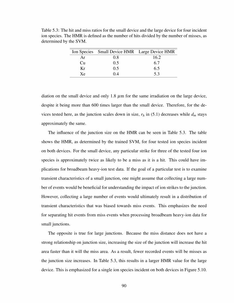
Table 5.3: The hit and miss ratios for the small device and the large device for four incidention species. The HMR is defined as the number of hits divided by the number of misses, asdetermined by the SVM.
Ion Species Small Device HMR Large Device HMRAr 0.8 16.2Cu 0.5 6.7Kr 0.5 6.5Xe 0.4 5.3
diation on the small device and only 1.8 µm for the same irradiation on the large device,
despite it being more than 600 times larger than the small device. Therefore, for the de-
vices tested here, as the junction scales down in size, rh in (5.1) decreases while dm stays
approximately the same.
The influence of the junction size on the HMR can be seen in Table 5.3. The table
shows the HMR, as determined by the trained SVM, for four tested ion species incident
on both devices. For the small device, any particular strike for three of the tested four ion
species is approximately twice as likely to be a miss as it is a hit. This could have im-
plications for broadbeam heavy-ion test data. If the goal of a particular test is to examine
transient characteristics of a small junction, one might assume that collecting a large num-
ber of events would be beneficial for understanding the impact of ion strikes to the junction.
However, collecting a large number of events would ultimately result in a distribution of
transient characteristics that was biased towards miss events. This emphasizes the need
for separating hit events from miss events when processing broadbeam heavy-ion data for
small junctions.
The opposite is true for large junctions. Because the miss distance does not have a
strong relationship on junction size, increasing the size of the junction will increase the hit
area faster than it will the miss area. As a result, fewer recorded events will be misses as
the junction size increases. In Table 5.3, this results in a larger HMR value for the large
device. This is emphasized for a single ion species incident on both devices in Figure 5.10.
90

(a) 10 MeV/u Cu on Small Device (b) 10 MeV/u Cu on Large Device
Figure 5.10: SVM classified histograms for 10 Mev/u Cu ions incident on the small device(a) and the large device (b). Notice the number of misses versus the number of hits for eachdevice.
Figure 5.10a is dominated by miss events. Were this histogram not classified with the
SVM, it could be difficult to draw any sort of conclusion about the collected charge for
the small device due to the shape of the distribution (relatively few counts with a large
amount of collected charge versus many counts with a small, but still significant amount,
of collected charge). Figure 5.10b, shows that relatively few events are misses for the large
device. This suggests that hit and miss classification for large junctions may not be strictly
necessary, however, the additional information that classification provides could still be
beneficial.
The HMR for 10 MeV/u Ar irradiation shown in Table 5.3 is particularly high when
compared to the HMR numbers for the other ion species. This is due to the statistical
nature of broadbeam irradiation. The dataset for 10 MeV/u Ar in this case had relatively
few SVM classified misses compared to the other ion species. In total, 2000 events were
recorded for 10 MeV/u Ar irradiation on the large device. Were more events recorded, it
is likely that the HMR would decrease and be more in line with the other three tested ion
91

species.
Figure 5.11 shows box and whisker plots of SVM classified peak current and total col-
lected charge data for all tested ion species and both devices. As before, the solid line
inside each box represents the median, the lower and upper boundaries of each box are the
first and third quartiles (i.e., the 25th and 75th percentiles), and the whiskers are defined
as Q1− 1.5× (Q3−Q1) for the lower whisker and Q3 + 1.5× (Q3−Q1) for the upper
whisker where Q3 and Q1 represent the third and first quartiles. Defining the whiskers in
such a way assures 99.3% coverage of the entire dataset, assuming the data are normally
distributed. The notched regions of individual box plots are useful as a rough guide for in-
terpreting the significance of the difference between the medians shown for each box plot.
The convention used to define the width of each notch is ±1.5× IQR÷√
n, where IQR
is the interquartile range (i.e., Q3−Q1) and n is the number of measurements represented
by the plot. If two notches do not overlap, it is generally safe to assume that the differ-
ence between the two medians is statistically significant [81]. In all of the plots shown in
Figure 5.11, the plotting of outliers has been suppressed.
In the figure, SVM classification reveals a clear trend with increasing incident ion LET
for the small device (compare the results of Figure 5.11a to Figure 5.2a, for example). The
peak current for the small device increases as a function of increasing ion LET, which is
to be expected for this device from work described previously in Chapter 4. However, two
things about Figure 5.11a are surprising given the results discussed in Chapter 4. The first
is that the peak current does not seem to saturate as a function of increasing ion LET. The
other is that the peak current values are very similar to those shown for the large device
(see Figure 5.11c).
Both of these issues are primarily influenced by the topside contacts for the small de-
vice. For an ion that strikes, for example, near the center of the small device, the topside
contacts are much closer to the generated carriers than the for a strike near the center of
the large device. Recall from Chapter 4 that the resistance to the contacts can be important
92

(a) The Small Device: Hits Only (b) The Small Device: Hits Only
(c) The Large Device: Hits Only (d) The Large Device: Hits Only
Figure 5.11: Box and whisker plots of peak transient current and total collected charge forall tested ion species on both devices. All plots show the results of SVM classification toremove miss transients from the dataset.
when determining R in the Modified Ohm’s Law equation used to calculate the maximum
theoretical peak current.
The effect of shrinking the junction on R are two-fold for the small device. For one, the
resistance to the backside substrate contact increases significantly compared to the large
device (1.5 kΩ versus 680 Ω, see Section 4.3.4 for calculation specifics). This is because
the resistance to the backside contact increases as the junction size decreases. However,
the resistance to the topside p-well contacts decreases as the junction scales down in size,
93

due to the p-well contacts being closer to the ion-induced carrier density (assuming a strike
within the hit area). This suggests that both the resistance to the backside substrate contact,
and the resistance to the topside p-well contacts play an important role for the small device.
For the small device, The resistance to the topside p-well contacts is more complex than
the resistance to the backside substrate contact. Ions striking within the hit area will have
some resistance the topside p-well contacts based on how close they strike to the topside
p-well contacts. An ion striking very near the junction edge will have a lower resistance to
the nearest p-well contact that a device striking near the center of the junction, for example.
The actual resistance that the generated ion track “sees” to the topside p-well contacts is
a complicated resistance that varies based on where the ion actually strikes. This makes
calculating a value for R in the Modified Ohm’s Law equation dependent upon knowing
where a particular ion struck within the hit area. Unfortunately, the results of the SVM are
only able to tell us that an ion struck within the hit area, and not where within the hit area
that the ion actually struck.
However, the net affect of shrinking the junction (and changing the aforementioned
resistances to the contacts) is to lower the value for R in the Modified Ohm’s Law equation
beyond what would be calculated by ignoring the presence of the topside p-well contacts.
For a lower R, the theoretical peak saturation current increases. This explains why, for the
results shown in Figure 5.11a, there is not an apparent saturation of the peak current values
(either for the median values, the quartiles, or the maximum reported values).
The topside n-well contacts for the small device will have a similar effect on the tran-
sient response as they do for the large device. As was discussed earlier, strikes near the
n-well contacts for the large device produce transients with higher peak currents and lower
total collected charge values. This was attributed to well potential modulation effects in
Chapter 4. Specifically, the potential in regions near the n-well contacts in the large device
is not significantly modulated during an ion strike. Therefore, for strikes near the contacts,
the potential modulates less and recovers faster than for strikes away from the contacts and
94

near the center of the device. For the small device, the n-well contacts cover a much larger
percentage of the total junction area (see Figure 5.1). The result will be transients that are
shorter in duration, but higher in peak current, than if the n-well contacts had been scaled
down in size to preserve the ratio between contact area and junction area found in the large
device (this was impossible due to limitations in the minimum size for metal layer one in
this particular technology).
The role of n-well contacts in determining the single-event response of devices and
circuits is well known. The discussion above is in line with previously reported findings.
Specifically, in the case of the single-event transient (SET) response of circuits, the n-
well contact density and spacing plays a critical role in mitigating SET pulse width and
upset frequency [62, 65, 69]. N-well contacts also play a role in controlling the extent
and duration of WPM effects [58], and the influence of well contacting schemes on the
response of single devices have also been reported [64, 70]. The results of this work are
related to these results through a discussion of the resistance to the n-well contacts. The
horizontal and vertical resistance seen by charge carriers exiting the well is a key factor
in the transient response of devices (see [64] and other references above). In terms of the
experimental results discussed in this chapter, decreasing the size of the well moves the
n-well contacts closer to the strike location, significantly reducing the horizontal resistance
to the n-well contacts experienced by charge carriers exiting the well through the n-well
contacts. Lowering this resistance, as discussed above, significantly affects the transient
response, which is in line with previously published work concerning the effects of n-well
contact location on the single-event response.
There is no apparent saturation shown in Figure 5.11c. This is likely due to the LET
values of the ion species used during the measurements. The highest LET of any of the
ions used was that of Xe, which is 58.8 MeV-cm2/mg. While this LET is higher than an
LET of approximately 45 MeV-cm2/mg, which produced the saturation behavior described
in Chapter 4, the next highest LET used during the measurements was that of Kr (which is
95

only 30 MeV-cm2/mg). Also, the data shown in Figure 5.11c considers all ion strikes that
were deemed by the SVM to be hits. Recall that the transient response of the large device
can vary based whether or not ion strikes occur near the topside n-well contacts. Because
of this, the box plots in Figure 5.11c include both strikes that result in the highest total
collected charge (i.e., strikes away from the n-well contacts and close to the center of the
junction) and the greatest peak transient current (i.e., strikes very near the n-well contacts).
Therefore, there is no saturation trend in the peak current values shown in Figure 5.11c.
In terms of total collected charge, Figures 5.11b and 5.11d show that the large device
collects much more charge than the small device for the same ion species. There are two
primary reasons for this. Recall from Chapter 4 that the majority of charge collection takes
place during the slow recovery phase of the transient response. The length of this phase
is determined by how quickly the depletion region can recover all of the potential that is
displaced by the highly conductive track of charge generated by the ion strike. In the case
of the small device, the potential is not as significantly modulated as the large device due
to the presence of the nearby n-well contacts. Therefore, the small device can recover
faster, resulting in less total collected charge. The other reason the large device collects
significantly more charge is simply geometry. Once the depletion region has recovered, a
significant amount of charge remains in the substrate of the device (see the quasi-Fermi
level for electrons in the substrate in Figures 4.9c-d). This charge will freely diffuse from a
higher concentration to a lower concentration. In doing so, much of the charge will diffuse
radially outward, away from the junction. The large device represents a larger sink for
the diffusing carrier concentration in the substrate. This ultimately results in more charge
collection than would be seen by the small device for the same ion species.
Figure 5.11 and the resulting discussion provide valuable insight into the role of contact
geometry on the device-level transient response. For example, despite the large device
being much larger than the small device, by virtue of having a larger ratio of its area covered
by contacts, the small device exhibits a peak transient current that is similar to that of
96
the large device. This is due to the n-well contacts’ ability to maintain the well potential
throughout the device recovery, which leads to higher peak transient current values. Being
able to maintain the well potential (coupled with the smaller size of the device) also allows
the small device to experience much less total charge collection than the large device.
5.5 Chapter Summary
Results in this chapter have shown that by careful application of SVM techniques, it is
possible to determine the relative location (i.e., a hit or a miss) of single ion strikes during
broadbeam heavy-ion irradiation. Using an SVM is beneficial as it allows for determina-
tion of the relative strike location while requiring only a few reasonable assumptions about
the underlying dataset. Compared to running a full complement of device-level TCAD
simulations (which could be impossible given the size of the simulation space required to
provide adequate physical insight), applying an SVM requires significantly less computa-
tional overheard and time investment. In this work, the applicability of the SVM approach
was verified with a much smaller set of TCAD simulations, which were used to show that
the SVM output was in good agreement with TCAD results.
For the case of broadbeam heavy-ion irradiation on a small device, not only is elim-
inating miss events from the dataset desirable, but it is potentially necessary in order to
draw valid conclusions from test data about ion strikes to the junction and depletion region.
Strikes to these regions are especially important when attempting to understand charge
collection phenomena for individual devices. Also, the small device tested in this work
was actually quite large by modern device standards, which only serves to emphasize the
importance of properly classifying events in broadbeam heavy-ion data sets.
SVM classified results for broadbeam heavy-ion irradiation for the small device tested
in this work show the significance of the chosen contact scheme for determining the overall
device transient response. For example, the discussion in Chapter 4 indicates that, as the
junction size decreases, the peak current response should decrease and saturate at lower
97

incident ion LET values. However, by virtue of the close proximity of the n-well contacts
to the strike location for hits to the small device, the peak current is very similar to that for
a much larger device for all tested ion species. This is because the n-well contacts serve to
limit the depletion region potential modulation caused by the passage of heavy ions through
the small device. This is in line with previously published experimental work. Limiting the
potential modulation leads to higher peak currents and less overall charge collection.
98

CHAPTER 6
Device Response During Well Potential Modulation Events
6.1 Introduction
Up to this point, the emphasis of this work has been on charge-collection mechanisms
(both in terms of total collected charge and the transient response) at a single junction. The
significance of understanding charge-collection mechanisms at a single junction for other
SEE phenomena was implied, but a direct application to a particular SEE phenomenon
was not discussed. Because SEEs at a single junction are not typically the case in practice
(due to device and circuit applications utilizing the interaction of multiple junctions), it is
valuable to consider the interaction of multiple junctions on the overall device response.
As discussed in previous chapters, during an SE strike, the local electrostatic potential
around the strike location can be significantly affected. This change in potential can have a
profound effect on nearby junctions.
One example of this is WPM [58], which was briefly discussed in Chapter 4. Due to
the direction of the electric field at an n-well/p-substrate junction, excess electrons gen-
erated by an ion strike are confined to the well region; their only way out of the well is
through the well contact. These excess electrons can significantly impact the single-event
response of a PMOS device in the well. This is because the excess carrier density can
lead to a strong potential gradient between the strike location and the well contacts. This
modulates the potential in the well, which has been shown to trigger parasitic bipolar ef-
fects in PMOS devices [58, 64, 69], influence the pulse widths of single-event transients
in inverter chains [65], and impact the single-event response of devices fabricated in triple
well technologies [70]. A similar redistribution of the electrostatic potential in the substrate
has also been shown in simulation to profoundly affect current transient shapes for NMOS
devices [82]. Mitigating WPM effects (e.g., through the use of guard bands or particular
99

well contacting schemes) has been shown to improve the single-event response of ICs fab-
ricated in advanced CMOS processes by stabilizing the well potential during an SE strike
[62, 64, 65, 69].
The goal of this chapter is to describe the results of backside two-photon absorption and
broadbeam heavy-ion irradiation on a large device containing multiple junctions. A large
device is used to make determining the strike-position sensitivity of the device possible.
The results of the TPA measurements show the transient response of the device following
a WPM event. Specifically, strikes to the drain of a PMOSFET biased in the off-state can
modulate that well potential such that the source/well junction can become forward biased,
giving rise to a small-magnitude current transient at the source terminal. This is consistent
with previous simulation studies of WPM effects in PMOSFET devices (see, for example,
[58]). The results also indicate that a similar transient response can be measured at the
drain terminal following a strike to the source and to both the drain and source terminals
following a strike to the channel region. This, however, is likely due to WPM-induced
capacitance changes at the drain/well junction. Device-level TCAD simulations are used
to explain this phenomenon. A similar device response is also observed during broadbeam
heavy-ion irradiation.
6.2 Background
Figure 6.1 shows a cross section of a PMOSFET fabricated in a modern technology as
well as a three-dimensional TCAD PMOSFET with features similar to the one shown in
Figure 6.1a. The parasitic bipolar device can be seen between the source (emitter), n-well
(base), and drain (collector). In the transistor’s off-state, the drain is grounded and the
source and n-well are biased high (typically at whatever VDD for the technology happens
to be). From the point of view of the parasitic bipolar device, the base/collector junction is
reverse-biased while the emitter/base junction sees the built-in potential of the junction.
During an ion strike of sufficient intensity to a n-well, for example, the electric field
100

(a) (b)
Figure 6.1: (a) Cross section of a modern PMOSFET device showing the parasitic bipolardevice between the drain, substrate, and source and (b) a typical MOSFET device showingthe well contact. Both after [64].
around the strike is significantly reduced and the generated electrons are swept out of the
well through the well contact. The flow of electrons through the well leads to a potential
gradient along their current path to the well contact (due to the current moving through
some finite well resistance to the contact) [58]. This potential gradient could result in a drop
in potential near the channel of the PMOSFET. Lowering the potential near the channel is
synonymous with lowering the built-in potential barrier at the parasitic bipolar device’s
emitter/base (source/n-well) junction. If the barrier is sufficiently lowered, the source can
begin to inject holes into the well, which can be collected by the reverse-biased n-well/drain
(base/collector) junction. This is a charge-enhancement effect commonly referred to as the
parasitic bipolar effect, which can cause the drain to collect additional charge, beyond that
which it would have collected had the parasitic bipolar device not turned on. This can be a
significant concern for PMOSFET devices fabricated in an n-well over a p-substrate. It is
less of a concern for NMOSFETs fabricated in a p-well over p-substrate, as the electrons
generated by the ion strike are not confined to the well, and are free to move deeper into
101
the substrate as well as to any nearby well contacts. This limits their ability to significantly
modulate the well potential.
Previous work concerning WPM effects has focused primarily on device-level or mixed-
mode simulations to study the device response of individual transistors during WPM events
[58, 62, 64, 69, 70], circuit-level measurements to examine the effects of WPM on circuit
response [65, 83, 84], or a combination of the two. Much of the device-level simulation
work focuses on ions with LET values less than 10 MeV-cm2/mg (however, at least one
study has examined device-level WPM effects in a triple well technology for a 40 MeV-
cm2/mg ion [70]). Also, many of the available device-level studies utilize device-level
simulations as opposed to experimental measurements. This is because WPM effects have
been primarily studied in the context of small devices fabricated in advanced technology
nodes. It can be difficult to determine the transient SE response of such devices experimen-
tally. Their small size makes device-level experimental measurements difficult.
While simulations provide valuable insight into the device-level response during WPM
events, experimental measurements of individual device response (e.g., through high-speed
transient capture) could further develop the understanding of WPM events.
As stated earlier, many device-level WPM studies focus on lower LET ions. Higher
LET ions have been used in circuit-level studies. One such study examined the circuit-
level effects attributed to WPM for LETs as high as 100 MeV-cm2/mg [62]. The high
LET values in that study corresponded to an effective ion LET due to changing the ion
angle of incidence. The actual ion LET was approximately 60 MeV-cm2/mg. Further-
more, the metric studied was single-event transient pulse width in an inverter chain, which,
while valuable for a circuit-level study, does not necessarily provide insight into the current
transient response of a single device as a result of WPM. However, device-level simulations
were used to describe the benefits of guard bands and high-density well contacting schemes
for reducing WPM effects.
This work provides a device-level experimental study of WPM effects following a high-
102

LET ion strike. To do this, a large-area PMOSFET device was fabricated in an n-well over a
p-substrate. While a large device will not experience the parasitic bipolar charge collection
enhancement described earlier (do to its long channel length), it will still be susceptible to
the effects of a significantly modulated well potential. This work uses backside TPA and
broadbeam heavy-ion measurements along with device-level TCAD simulations to exam-
ine the influence of modulating the well potential on the overall device response. Device-
level current transients exhibiting WPM effects are shown, and their origin is described.
Specifically, significant WPM can lead to a transient change in the junction capacitance.
For the large junctions used here, this can produce a measurable current transient. Also,
TCAD simulations show that the WPM following a high-LET heavy-ion strike is sufficient,
in some cases, to lower the source/well potential barrier, which could cause the source to
inject holes into the well.
6.3 Experimental Setup
Transient capture measurements were carried out on a large, bulk silicon PMOSFET
fabricated on the same die as the bulk silicon diodes discussed in Chapters 4 and 5. Fig-
ure 6.2 shows a recolored GDSII image of the device. In the figure, the large gray region
is the n-well, the green regions are p+ dopings intended to serve as a source and drain, and
the red region represents a polysilicon gate. Each p+ diffusion is contacted on the left and
right edges, as shown in the figure. The n-well contacts are on the left and right sides of
the well. The gate contact is along the left side of the gate. The source, drain, and well
regions are individually accessible via bond pads on the die. As with the diode structure
discussed in Chapters 4 and 5, metal blocking windows have been used over the device
(save for regions where metal contacts are required) to prevent the deposition of metal fill
in the device overlayers during fabrication.
As can be seen in Figure 6.2, the device is large, especially compared to modern CMOS
transistors. This device was designed for both focused backside laser and broadbeam
103

(a) (b)
Figure 6.2: A GDSII image of the PMOSFET device for studying the effect of well poten-tial modulation on the transient current response. Specific device regions are shown in (a),while (b) shows device dimensions.
heavy-ion testing. For the case of laser testing, a larger device is easier to hit, and be-
cause the device dimensions are larger than the focused laser spot size, it is possible to
determine the response of the device to laser strikes as a function of laser strike position.
For example, it will be possible with the device shown in Figure 6.2 to determine the re-
sponse of the device to strikes in the well or directly to the source or drain diffusions. Also,
the large dimensions of the device allow investigating the spatial sensitivity of WPM effects
during backside laser testing. As per the discussion of Chapter 5, using a large device for
broadbeam heavy-ion testing will ensure that the majority of recorded events are actually
due to strikes to the regions of interest, rather than strikes outside the regions of interest
that still produce a transient response.
While the device in Figure 6.2 is a MOSFET, it is not strictly intended to operate as one.
While using MOSFET terminology is convenient for describing the device, its primary
purpose is as a test device to study how the presence of the p+ diffusions affect charge-
104

collection mechanisms within the n-well, and interpreting these mechanisms in the context
of WPM phenomenon. The polysilicon gate serves to keep shallow trench isolation (STI)
from being deposited between the source and drain regions. Preventing the formation of
STI serves to promote interaction of the two junctions during an SE strike, which was a
goal of the measurements.
Heavy ion irradiations were performed at Lawrence Berkeley National Laboratories’
88-inch Cyclotron Facility using Xe from the 10 MeV/u cocktail. Laser irradiations were
performed at Vanderbilt University using the same experimental setup that is described in
Chapter 4 and Appendix B. The device packaging and measurement setup for both the TPA
and broadbeam heavy ion measurements was identical to that described in Chapters 4 and
5.
6.4 Results and Discussion
6.4.1 Experimental Results
Results of the backside TPA measurements are shown in Figure 6.3. Figure 6.3a is a
top view of the device taken from its GDSII layout file. The drain and source designations
assume an off-state bias condition. That is, Vdrain= 0 V, Vwell= 1 V, Vsource=1 V, Vgate =
1 V, and Vsub= 0 V. Three locations shown in Figure 6.3a are labeled with the letters b, c,
and d. The locations of these letters represent the approximate strike location that produced
the transients shown in Figures 6.3b-d. For the measurements shown in the figure, the laser
pulse energy was approximately 300 pJ. The laser spot was visually focused on the surface
of the device, similar to the procedure described in Chapter 3.
Figure 6.3b shows the transient response measured at the well, source, and drain termi-
nals when the laser spot is centered in the source region of the device (i.e., placed at location
b in Figure 6.3). At first glance, it appears that charge is not being appropriately conserved
(i.e., the integrals of the transients shown in each plot do not sum to zero). However, re-
call that the substrate current was not monitored during these measurements. The substrate
105

Figure 6.3: Results of the backside TPA measurements for the large PMOSFET device.The top-side view of the device from its GDSII layout file is shown in a). The source, gate,and drain have been labeled. The letters shown in these regions (b, c, and d) correspond tothe approximate location of the laser strikes that produced the transients shown in figuresb, c, and d respectively.
current would appropriately account for charge conservation during the measurements.
As was typical of the results described in Chapter 4, the well transients shown in Fig-
ure 6.3 are positive-going, which is indicative of the collection of electrons at the well/sub-
strate junction. The source transient is negative-going, indicating the collection of holes
at the source/well junction. This is an obvious result when it is compared to earlier re-
sults for the n-well/p-substrate diode. The collection of holes should result in a negative-
going transient because the collection of electrons at the well/substrate junction results in a
positive-going transient. Taken alone, the direction of any particular transient might not be
106

especially meaningful; however, their direction relative to one another is important as it can
be used to interpret charge collection mechanisms at a particular junction. For example, a
positive-going well/substrate transient for this particular experimental setup is indicative of
electron collection at that junction (which is apparent from discussions in earlier chapters).
Therefore, a negative-going transient at the source terminal should be expected, due to the
collection of holes at the source/well junction.
The large transients seen at the struck junctions are due to the direct collection of charge
carriers generated by TPA at those junctions. However, in addition to these transients,
Figures 6.3b-d show small positive-going transients occurring at junctions that were not
struck directly. For example, Figure 6.3b shows a small positive-going drain transient
following a strike to the source. A similar positive-going source transient can also be seen
for strikes to the drain (Figure 6.3d), and a strike to the gate region of the device can
produce small positive-going transients at both the source and the drain. These transients
are shown in greater detail in Figure 6.4, which shows the same transients as are shown in
Figure 6.3b-d, only with reduced axis limits to emphasize the smaller transients.
There is a small positive-going transient measured at the drain terminal. The fact that
it is opposite in polarity to the transient measured at the source terminal (which is due
to the collection of holes), might lead one to conclude that the drain is injecting holes
across the drain/well potential barrier. However, this is likely an erroneous conclusion.
The voltage drop across the drain/well junction is approximately 1.7 V, which is the applied
voltage at the well plus the built-in voltage drop across the junction. Following a carrier
generation event in the n-well, well potential modulation effects can significantly lower the
well potential in the region surrounding the carrier generation. Earlier work has shown
that, in some cases, the potential can be lowered enough to forward bias individual p-n
junctions in the well [58]. However, for the particular biases voltages used here, the well
potential cannot be lowered enough near the drain/well junction to ever forward bias the
drain/well junction. Said another way, the well potential near the drain cannot go lower
107

(a) Source Hit (b) Gate Hit
(c) Drain Hit
Figure 6.4: The same transients shown in Figures 6.3b-d for a TPA hit to the source, gate,and drain of the large PMOSFET. Here, the axis limits have been reduced to emphasize thesmaller transienst shown in Figures 6.3.
than the applied voltage at the drain following a strike to the source, which eliminates the
possibility of significant carrier injection by the drain following a strike to the source. This
is shown below using device-level TCAD simulations.
Figure 6.5 shows identically measured transients to Figures 6.3b-d, only under broad-
beam 10 MeV/u Xe irradiation instead of backside TPA exposure. Due to the nature of
broadbeam heavy ion testing, the only way to determine where an ion struck on the de-
vice is through interpretation of the device response. Using the TPA measurement results
108

(a) 10 MeV/u Xe Drain Strike (b) 10 MeV/u Xe Source Strike
Figure 6.5: A comparison of transients resulting from 10 MeV/u Xe irradiation on the largePMOSFET device. a) shows a drain strike while b) shows a source strike. Strike locationswere determined from TPA measurement results.
described earlier, we can infer that any ion strike giving rise to a positive well transient,
negative drain transient, and positive source transient is due to an ion strike to the drain
region. Similar reasoning can be applied to identifying current transients that are the result
of an ion strike to the source region. While we cannot be certain where in the drain or
source region a particular ion struck, we can know by the device response that a strike did
occur somewhere within those regions. What results is Figure 6.5a, which shows current
transients resulting from a Xe strike to the drain, and Figure 6.5b, which shows current
transients resulting from a strike to the source. The bias condition for the measurements
shown in the figure as the same as that for the measurements shown in Figure 6.3.
The key result of Figure 6.5 is that the same response seen during TPA testing is also
observed during heavy-ion irradiation. Well potential modulation effects can induce a tran-
sient response at junctions that were not directly hit by the ion strike. The impact of well
potential modulation on the overall transient response of this device is investigated through
device-level TCAD simulations in the section that follows.
109

6.4.2 WPM Effects in Device-Level Simulations
Device-level TCAD simulations were carried out to determine what role WPM effects
could have on the device response. Because of the large size of the device used in the
experimental measurements, a few concessions were required to produce computationally
tractable simulations. For one, the device was simulated in two-dimensions, which greatly
eases the computational overhead. The device, as simulated, is shown in Figure 6.6. The
figure shows a 20 µm by 60 µm section of the simulated device. The actual dimensions
of the simulated device were 60 µm by 150 µm. The device is intended to be a two-
dimensional cross-section along a cutplane running perpendicular to the source, gate, and
drain diffusions through the center of the device (when viewed from above). The most
significant difference between the actual device and the two-dimensional approximation
used in the simulations is the placement of the well contacts. For the simulations, the well
contacts are placed approximately 25 µm away from the center of the gate. In the actual
device, the well contacts are also approximately 25 µm from the center of the gate; how-
ever, they run parallel to the gate, meaning they would not intersect the cutplane described
above. This change in well contact placement is necessary to have n-well contacts in the
simulations. However, because the distance to the contacts has been preserved (only their
orientation has changed in the simulations), the effects of WPM observed in the simulated
device should be a reasonable approximation to those seen in the real device.
The device doping profiles were determined, where possible, using spreading resistance
measurements. Shallow drain/source diffusion dopings are typically difficult to resolve
using spreading resistance measurements. Therefore, for the source and drain diffusions, a
peak doping of 1 x 1020 cm−3 was assumed and assigned to a Gaussian doping profile to
produce the source and drain diffusions shown in Figure 6.6. The gate material is heavily
doped polysilicon, and the gate oxide was SiO2 with a thickness of approximately 5 nm.
While efforts were made to make the gate material and gate oxide as realistic as possible,
the impact of the gate structure on the overall WPM response is likely quite limited. While
110

Figure 6.6: Two-dimensional TCAD model used for device-level WPM simulations. Thedevice is a large-area PMOSFET fabricated in an n-well. Device dopings were deter-mined, where possible, through spreading resistance measurements. The geometry is atwo-dimensional approximation to the actual device used in the experiments. The contactsare shown in pink. The horizontal white line running beneath the n-well represents thewell/substrate depletion region boundary.
the precise doping levels of the source and drain and the exact nature of the gate stack
are assumptions, the geometry of the device (including the contact size and spacing) is
well known, and taken from its GDSII layout files. Not shown in Figure 6.6 is the backside
substrate contact, which runs along the entire bottom of the p-type substrate and is intended
to represent the conductive physical connection between the substrate and the brass high-
speed package used in the experiments.
For all simulations, the device was biased in the off-state, identically to what was used
during the experiments. The device response to a 10 MeV/u Xe strike was simulated. In
all cases, the strike was normally incident to the top surface of the device and extended
for approximately 90 µm into the device substrate. The assigned linear charge deposition
was 0.6 pC/µm, which corresponds approximately to the peak LET of 10 MeV/u Xe in
silicon. The charge track was assigned a Gaussian radial roll-off with a radius of 50 nm.
The models for carrier mobility were identical to those used in the simulations described in
111

(a) Simulated Source Strike (b) Simulated Gate Strike
(c) Simulated Drain Strike
Figure 6.7: The time evolution of the electrostatic potential along a cutline in the n-welldue to a simulated 10 MeV/u Xe strike. The cutline is shown in gray and is approximately400 nm below the top surface of the n-well. The vertical, black dashed lines indicate thelocations of the drain and source diffusion edges that are closest to the gate. The red arrowindicates the orientation and location of the simulated ion strike for each plot. The lateraldimensions of the representative drawing of the device shown in each plot are approxi-mately to scale. The simulated bias conditions were Vdrain= 0 V, Vwell= 1 V, Vsource=1 V,Vgate = 1 V, and Vsub= 0 V. The difference between these bias conditions and the voltagesshown in the figure is due to TCAD’s internal voltage reference accounting for the built-inpotential.
112

previous chapters.
Figure 6.7 shows the time evolution of the electrostatic potential in the well for the first
1 ns following the simulated heavy ion strike. The potential is plotted along a cutline that
is 400 nm from the top surface of the n-well that runs underneath the source and drain
diffusions. In other words, the cutline is approximately 50 nm below the bottom of the
source and drain diffusions. A representative drawing of the simulated device is shown
over each plot. The lateral dimensions are approximately to scale. The vertical, dashed
black lines in each figure represent the locations of the boundaries of the source and drain
diffusions closest to the gate. The vertical red arrow indicates the approximate location of
the simulated ion strike for each plot. The goal of the plots in Figure 6.7 is to understand
how a change in the well potential is related to the transient response of the unstruck device
junctions (i.e., the origin of the small, positive-going transients shown in Figure 6.4). The
likely source of these transients is a sudden potential change in the well producing a brief
change in the capacitance of the unstruck junction, which results in a small, measurable
transient current. This is explained in greater detail below.
Following a strike to the source (Figure 6.7a), the well potential is modulated signif-
icantly as the region of the well affected by the strike is no longer able to sustain the
bias voltage applied at the well contacts. In addition to this, the built-in potential at the
source/well junction can no longer be dropped across the pre-strike depletion region (due
to significant depletion region potential modulation as was discussed in Chapter 4). This
leads to the potential in the well beneath the source being pulled down significantly. What
results is a significant change in the well potential near the unstruck drain/well junction. In
the case of a strike to the source, the well voltage near the drain diffusion can lower by as
much as 0.5 V within the first 1 ns following the strike.
The effect is even more pronounced for a strike to the drain (Figure 6.7c), whereby
the well potential near the source can be lowered by as much as 0.8 V during the first
1 ns following the strike. This is because, for a drain strike, the reverse-biased drain is
113

effectively shorted to the grounded substrate. Due to the high carrier density in the well
following the strike, the region near the drain that is affected by the strike cannot sustain the
potential drop that is normally maintained by the drain/well depletion region. As a result,
the well potential near the drain drops significantly. As was discussed in detail in Chapter 3,
the potential drop that normally occurs near the drain/well junction will be pushed down
into the substrate. The same is true, of course, for the built-in voltage at the source/well
junction following a strike to the source. However, due to the magnitude of the potential
difference between the drain and the substrate, the effect is much more pronounced for a
strike to the drain. For a strike that does not hit the source or drain directly, the potential
in the well can still be lowered significantly near the source and drain diffusions (see, for
example, Figure 6.7b), giving rise to a small, measurable current transient at the source and
drain terminals.
To appropriately consider the origins of the small, positive-going transients shown in
Figure 6.4, it is necessary to keep the device dimensions in mind. Recall that the lateral
dimensions of the source and drain for the fabricated device are quite large (approximately
10 µm by 45 µm). The capacitance of a p-n junction can be expressed as
C =εs
xd, (6.1)
for small-signal ac conditions where one side of the junction is heavily doped compared
to the other [25]. In (6.1), εs is the permittivity of silicon and xd is the depletion region
width. The depletion region width varies as a function of the applied bias. For the device
in question, the thickness of the depletion region for the source and drain are slightly dif-
ferent due to the difference in the applied bias for the two junctions. For the case of the
drain/well junction, the depletion region thickness, as determined from simulation results,
is approximately 130 nm. Using (6.1), and multiplying by the junction area yields a junc-
tion capacitance of 4 pF for the reverse-biased drain/well junction. Following a strike that
114

significantly modulates the well potential (e.g., a strike to the source), the well potential
near the drain can change by as much as approximately 0.5 V. This amounts to an effective
decrease of the reverse bias potential at the drain/well junction. Qualitatively, the resulting
drain transient can be explained by
I(t) =CdV (t)
dt, (6.2)
which is simply the current through a parallel plate capacitor for a time-dependent change
in voltage. Following the strike, the rapidly changing well potential produces a small tran-
sient at the drain terminal as the drain/well capacitance first increases significantly due to
the decrease in the width of the drain/well depletion region in response to the well poten-
tial change and then recovers back to its pre-strike value. Simply solving (6.2) using the
previously calculated value for the junction capacitance and the 0.5 V potential drop that
occurs near the drain within 1 ns (Figure 6.7a) yields a current of 2 mA. The actual peak
current measured experimentally was approximately an order of magnitude less than this.
However, based on the nature of the assumptions made when applying (6.2), we would
expect it to overestimate the current. For instance, (6.2) assumes that the capacitance of the
junction is constant. In reality, the capacitance will change slightly throughout the strike
as the well potential changes (effectively changing the reverse bias). Also, and most im-
portantly, (6.2) assumes that the potential is modulated for the entire drain area. Clearly,
this is not the case, as the potential modulation is only localized around the strike location.
Because only some fraction of the well potential near the drain is actually modulated, the
transient current measured experimentally will be less than that calculated using (6.2).
A similar thought process can be used to explain the transients that result at the source
due to a strike to the drain and the transients that result at both the source and drain terminals
due to a strike near the gate region of the device. Also, due to the greater well potential
modulation that occurs near the source following a strike to the drain, we would expect
the resulting source transient to be of a greater magnitude than the drain transient resulting
115

from a strike to the source. This is true, and is shown in Figure 6.4.
Earlier work [85] has described the parasitic bipolar response of MOSFET devices
following a strike that is capable of significantly modulating the potential near source/drain
diffusions. Specifically, if the potential near a source diffusion is lowered enough through
WPM, the source/well junction can forward bias and inject carriers into the well. These
carriers can then cross the channel and be collected by the reverse-biased drain, resulting in
an enhanced charged collection compared to what would normally be collected by the drain
following an ion strike. For the large device in this work, following a strike to the drain,
it is likely that the well potential near the source can be lowered enough to briefly forward
bias the source. This would serve to increase the transient current seen at the source, as the
injection of holes across the source/well barrier would produce a positive-going transient.
In such an event, the transient current would be defined by the WPM-induced capacitance
change at the junction, as well as the brief injection of holes. The device used in this work
has a channel length that is much longer than those typically found in modern devices that
could fall victim to the parasitic bipolar effect. In the TCAD simulations that produced the
results shown in Figure 6.7, the hole density near the drain following a strike to the source
took approximately 5 ns to reach a density of 1x1017 cm−3 near the drain. This is due to
the diffusion of holes away from the strike location and indicates that it is unlikely that any
carriers injected by the source would be able to be collected by the drain on the timescale
shown in Figure 6.4.
6.5 Chapter Summary
The experimental results shown in this chapter emphasize the significance of well po-
tential modulation effects in determining the overall device response. Backside TPA mea-
surements are used to show the strike-location dependent nature of the transient response of
the source and drain diffusions of a large PMOSFET test structure. These results show that
the decrease in the well potential that typically accompanies an ion strike to the source,
116

drain, or well region, can lead to a transient being measured at the unstruck junction(s).
This is likely due to a brief change in the junction capacitance in response to the drop in
the well potential. However, in the case of a strike to a reverse-biased drain significantly
modulating the well potential near the source, the resulting transient measured at the source
terminal could also be due, in part, to the injection of holes from the source into the well in
response to a significantly lowered source/well barrier. Broadbeam heavy-ion irradiations
using 10 MeV/u Xe show that the same phenomenon occurs during a heavy-ion strike, and
is not limited to laser irradiation. Device level TCAD simulations are used to show the
extent of WPM following an ion strike.
These results represent device-level experimental measurements of WPM phenomena
in a single device. Previous results were either purely simulation based, or experimental
results for more complex circuit topologies. These results were made possible through
the use of a very large-area test structure. While this structure is not representative of
the sizes of today’s highly-scaled CMOS devices, it does provide valuable insight into
similar mechanisms that prior simulation results have shown occur in modern devices. The
advantage of the large structure is that it facilitates experimental investigation of these
phenomena for a single device.
117

CHAPTER 7
Conclusions and Future Work
This work describes experimental and simulation results and analytical modeling ef-
forts intended to advance the understanding of charge-collection mechanisms in bulk sil-
icon semiconductor devices in response to a highly-ionizing particle strike. This adds to
the already large body of work on charge-collection mechanisms by furthering the under-
standing of charge-collection mechanisms for a simple, reverse-biased p-n junction, which
is a fundamental building block of semiconductor devices and circuits. Understanding
their response to ionizing radiation is of critical importance for devices and circuits that
are intended to operate in harsh environments (e.g., at high altitudes or outside the Earth’s
atmosphere).
The earliest charge collection studies relied on simplistic interpretations of charge-
collection mechanisms when explaining experimental results or developing analytical mod-
els. While these approaches were necessary for developing a basic understanding of charge-
collection processes, more work was needed to understand the process in sufficient detail.
Later works expanded the interpretation of charge collection to consider the distribution of
relevant quantities (electrostatic potential, electric field, carrier densities, etc.) throughout
the entire device, providing a more detailed picture of the charge-collection process. How-
ever, these works were either purely theoretical (i.e., lacking experimental results for an
actual device), or so specific as to only apply to a limited number of devices (see Chap-
ter 1). This work builds on earlier efforts by coupling analytical models that leverage more
recent charge-collection theory with experimental work. The experimental work empha-
sizes devices that are general enough to provide insights into the charge-collection mecha-
nisms for a much broader class of devices. The experimental results are used to inform the
development of analytical models for charge collection and peak transient current. Ana-
118

lytical models can be useful for providing insightful interpretations of the relevant physics,
as well as being practically useful for providing approximations to the radiation-induced
device response to better inform (or completely replace) time-consuming and potentially
expensive experimental measurements.
Of critical importance to this work are particle strikes that can significantly modulate
the electrostatic potential that forms near the metallurgical junctions found in semiconduc-
tor devices. Strikes that generate an excess carrier density that is larger than the background
doping can significantly modulate these potentials, resulting in a transient current at the de-
vice terminals. Much of this work is concerned with providing a detailed explanation of
how these modulated potentials recover following an ionizing particle strike, and how that
recovery presents itself in terms of total collected charge at a device node or the transient
current response of the device as it recovers. While the two quantities are closely related
(one is, in fact, expressed as the time integral of the other), the total collected charge and
the transient response have been the means by which the radiation tolerance of devices have
historically been described. It is for that reason that the two quantities have been the focus
of much of the work described in earlier chapters.
Chapter 3 describes the use of charge-collection measurements on a large-area, reverse-
biased bulk silicon diode using backside TPA laser SEE testing. These measurements em-
phasize the significance of high-level carrier generation conditions for charge-collection in
irradiated devices. Specifically, once the carrier generation is sufficiently high, the deple-
tion region potential can be modulated in such a way as to give rise to a region of strong
electric field beneath the generated carrier density. The significance of this is that, because
of the presence of this field, the charge collection process can be highly efficient, resulting
in the collection of almost all of the generated minority carriers. It is possible for this to oc-
cur even if the initial charge generation does not occur within the device depletion region.
If the generated carrier density is large enough and close enough to the device depletion
region, significant carrier diffusion can result in the collapse of the depletion region poten-
119

tial, which will give rise to highly efficient charge collection, just as if the initial carrier
density had been generated within the depletion region. The ADC model is used to ex-
plain these phenomena, as it provides a general enough description of the charge collection
physics that it is able to be applied to a large TPA-induced carrier density in a bulk silicon
device (which is a situation that violates the basic assumptions of many previously devel-
oped models for charge-collection). A detailed derivation of the ADC model is included in
Appendix A.
In Chapter 4, the discussion of high-level carrier generation response expands to include
the device-level transient response. As in Chapter 3, a simple, large-area bulk silicon diode
is used. In addition to using backside TPA laser testing to determine the strike-position
dependent response of the device, the current transient response for broadbeam heavy ions
is measured and described. An important conclusion of Chapter 4 is that as the ion LET
increases, the peak transient current saturates while the transient duration continues to in-
crease. Using device-level simulations, this behavior can be attributed to significant de-
pletion region potential modulation in response to a high-LET ion strike. High-LET ion
strikes can produce highly conductive tracks of charge which are unable to sustain a signif-
icant potential drop. If this track of charge is present in the depletion region of a device, the
potential drop that normally occurs near the metallurgical device junction must redistribute
throughout the device substrate. An analytical model for the peak saturation current can
be used to show that the peak transient current is limited by the applied voltage, device
parameters (such as doping and junction size), and the strength of the ionization source.
Chapter 5 discusses broadbeam heavy ion results for a smaller (but still large by mod-
ern device standards) reverse-biased bulk silicon diode. An analysis of the data reveals that
many strikes that actually miss the junction are capable of producing device-level current
transients through carrier diffusion to the device junction. To understand charge collection
due to heavy ion strikes at the junction, it is necessary to remove the contribution of miss
events from the dataset. Chapter 5 discusses the use of an SVM for accomplishing this
120

task. Using an SVM in this case requires few assumptions about the underlying dataset
and saves significant computational time and effort compared to running a full complement
of device-level TCAD simulations to determine the contribution of miss events. Remov-
ing miss events from the dataset reveals trends in the device response (peak current and
collected charge) that scale appropriately with increasing ion LET. A significant portion of
Chapter 5 deals with the development and verification of the SVM approach for removing
miss events from the dataset. For the smallest tested device, removing miss events from
the dataset is essential for drawing any sort of conclusion from the broadbeam heavy-ion
measurements. Removing these miss events also helps to emphasize the significance of the
chosen contact scheme in determining the overall device response, which is in line with
previously published experimental work.
In Chapter 6, the interaction of multiple junctions following the generation of a large
carrier density is briefly described through a discussion of well potential modulation effects
in a large-area PMOSFET test structure. The key conclusions are that modulating the
depletion region potential of either the drain/well or source/well junctions can affect the
response of the unstruck junction via significantly lowering the well potential or through
brief, WPM-induced changes in the junction capacitance. This serves as one example of
how multiple junctions can interact with one another during an ion strike. However, it is
far from exhaustive.
While this work provides a detailed explanation of the device-level physical phenomena
that occur when a large carrier density is generated within (or in close proximity to) a
device junction, the discussion of charge-collection physics is far from concluded. As long
as semiconductor devices are fielded in radiation environments, the task of studying the
charge-collection response of these devices will continue. To that end, it is important to
place this work in context by pointing out potential areas for future study.
The focus of much of this work has been on the device response of a single bulk silicon
junction. While these junctions comprise the fundamental building blocks for more compli-
121

cated semiconductor devices and circuits, most devices are typically composed of multiple
junctions interacting with one another in some capacity. Therefore, it is critical to under-
stand the relevant physics that occur when one of multiple interacting junctions is struck by
an ionizing particle. Chapter 6 explores this briefly, but much can be done to build upon that
work. While studying the response of more advanced devices (MOSFETs, BJTs, HEMTs,
etc.) and single-event phenomena (multi-node charge collection, single-event latchup, etc.)
has been the focus of much work over the years, only recently has theoretical work sought
to develop a first principles understanding of the interaction of multiple junctions follow-
ing an ionizing particle strike [41]. Therefore, future work should use the work reported
here in addition to new theoretical work such as [41] to inform new experimental measure-
ments, simulation work, and analytical modeling to further understand charge-collection
phenomena for multiple interacting junctions.
Another issue is one of size. The devices used in this work were all quite large compared
to modern device sizes. For this work, large devices were beneficial as they provided a
way to study charge-collection mechanisms while bypassing the experimental difficulties
of studying similar phenomena for a much smaller device. For example, broadbeam heavy
ion testing of a single device is made much simpler when the device is large. If the device is
exceedingly small, not only will collecting a sufficient number of events be extraordinarily
time consuming, but, as discussed in Chapter 5, it is likely that many of the events that are
captured would be the result of an ion strike actually missing the device. For the case of
backside TPA measurements, it can often be difficult to determine the response of a small
device, as the laser optical spot size can quite easily be significantly larger than the feature
sizes of the device in question. This makes attributing the device response to strikes in
certain regions of the device difficult or impossible.
Also, as devices have scaled down in size, the current transient response of devices has
become much faster than the nanosecond scale transients seen in this work (see [86], for
example). Highly-scaled devices can have transient durations on the order of a few tens of
122

picoseconds. This presents a problem when trying to measure the transient response using
typical means (e.g., high-speed oscilloscope measurements), as many instruments do not
offer sufficient measurement resolution to capture the transient response in detail. However,
as devices continue to scale down in size and increase in complexity, understanding the
transient response of these devices will be of increasing importance. Future work in this
regard should focus on understanding how the charge-collection mechanisms presented
here can change in the presence of small feature sizes or the complex geometries found
in modern devices. Developing appropriate methods for measuring the response of such
highly-scaled devices efficiently in the laboratory will be of critical importance.
123

Appendices
124

Appendix A
Theoretical Development of the ADC Model
This section is a review of the theoretical development of the ADC model and compares
the extreme case of low-level conditions to the extreme case of high-level conditions. It
provides significantly more detail regarding the equations discussed in Section 3.3.3. In
particular, it explains why the Ω in (3.1) is the same as the Ω in (3.2). The analysis begins
with the case in which all generated charge is contained in the quasi-neutral region, i.e.,
it is outside the depletion region. Charge generated in the depletion region is discussed
at the end of this section. The reader is referred to Figure A.1 (which has been reprinted
here from Chapter 3 for convenience) and its accompanying text for the definitions of the
acronyms appearing in the equations below.
A.1 Low-Level, All Generated Charge in Quasi-Neutral Region
Consider low-level conditions with all generated charge generated in the quasi-neutral
region. The terminal current, denoted I, is then the minority-carrier diffusion current flow-
ing from the quasi-neutral region across the depletion region boundary and into the deple-
tion region. This current is the surface integral on the depletion region boundary of the
minority-carrier current density, with the latter quantity proportional to the gradient of the
carrier density. This gives
I =−qDm
∫DRB
~∇Pd~S (low level), (A.1)
where q is the elementary charge, Dm is the diffusion coefficient for minority carriers in the
quasi-neutral region (the diffusion coefficient for majority carriers will appear in later equa-
tions and is denoted DM) and P(x, t) is the excess carrier density (the same for electrons and
holes in the quasi-neutral region). The unit normal vector in the surface integral is directed
125

Figure A.1: Schematic showing individual region names (a) and relevant physical charac-teristics of those regions (b) for a reverse-biased p-n junction during high-level conditions.These regions are described mathematically by the ADC model. For early times duringthe charge-collection process, the ambipolar region boundary corresponds approximatelyto the bottom of the generated carrier density.
outward from the quasi-neutral region interior because this is the usual convention when
using Green’s theorem (used later), but this makes the integral negative so a negative sign
was inserted on the right side to produce a positive quantity. Under low-level conditions,
the carrier density satisfies the minority-carrier diffusion equation. Carrier recombination
in the device interior is neglected here, so the equation reduces to
Dm∇2P =
∂P∂ t
in QNR (low level). (A.2)
Carrier generation is considered to be impulsive and is described by an initial condition
instead of a generation rate. The initial density of excess carriers is the density of generated
carriers and is denoted PI(x). Boundary conditions are also needed. The lower electrode
(the substrate contact shown in Figure A.1), denoted ELE, is regarded as an ideal sink for
excess carriers. The depletion region is assumed to be reversed biased, so the depletion
region boundary is also approximated as an ideal sink for excess carriers. This gives
P = 0 on DRB and ELE, P = PI at t = 0. (A.3)
126

Any portion of the quasi-neutral region boundary that is not the depletion region boundary
or lower electrode is regarded as a reflective boundary, and P satisfies reflective boundary
conditions (the normal component of the gradient is zero) there.
The quantity to be solved is the collected charge, denoted Q, which is the time integral
of the current I. Taking the time integral of (A.1) gives
Q =−qDm
∫DRB
~∇T d~S (low level), (A.4)
where T (x) is defined to be the time integral of P(x, t) integrated from zero to infinity.
Integrating (A.2) while using (A.3) gives
Dm∇2T =−PI in QNR, T = 0 on DRB and ELE (A.5)
with reflective boundary conditions on reflective boundaries. An alternate expression for
the right side of (A.4) is obtained by defining a function Ω by
∇2Ω = 0 in QNR, Ω = 1 on DRB, Ω = 0 on ELE (A.6)
with reflective boundary conditions on reflective boundaries. The boundary conditions for
T and Ω imply ∫DRB
~∇T d~S =∮
Ω~∇T d~S−∮
T~∇Ωd~S
where the surface integrals on the right are over the closed boundary of the quasi-neutral
region. Applying Green’s theorem to the right side gives
∫DRB
~∇T d~S =∫
Ω∇2T d3x−
∫T ∇
2Ω d3x,
where the volume integrals are over the entire quasi-neutral region. Finally, we use the field
127

equations in (A.5) and (A.6) to rewrite the above equation as
Dm
∫DRB
~∇d~S =−∫
ΩPI d3x,
so (A.4) becomes
Q =∫
QNRqPI(~x)Ω(~x)d3x (low level). (A.7)
A.2 High-Level, All Generated Charge in Quasi-Neutral Region
Now consider high-level conditions with all generated charge generated in the quasi-
neutral region. The terminal current is calculated from the following considerations that ap-
ply when the depletion region is reversed-biased. A strong electric field inside the reverse-
biased depletion region prevents majority carriers from entering the depletion region, so
the electric field in the quasi-neutral region at locations near the depletion region boundary
becomes whatever is needed to make majority-carrier drift balance majority-carrier diffu-
sion. Stated another way, because the majority carriers cannot cross the depletion region
boundary, the net current for majority carriers (drift plus diffusion) at the depletion region
boundary is zero. Under high-level conditions, the electron and hole densities have nearly
equal values and gradients in the quasi-neutral region near the depletion region bound-
ary, so electron and hole drift currents are in the ratio of the mobilities, and electron and
hole diffusion currents are in the ratio of the mobilities. Therefore, an equality between
majority-carrier drift and majority-carrier diffusion implies an equality between minority-
carrier drift and minority-carrier diffusion. However, the latter two currents add to instead
of subtract from each other so half of the total current at the depletion region boundary is
minority-carrier drift, and the other half is minority-carrier diffusion. In other words, the
total current at the depletion region boundary is twice the minority-carrier diffusion current.
Therefore, the terminal current, denoted I, is given by
I =−2qDm
∫DRB
~∇Pd~Sd3x (high level). (A.8)
128

The equation governing P was explained in [19]. There will always be an ambipolar
region adjacent to the depletion region boundary although there may or may not be a high
resistance region adjacent to the lower electrode. It was shown in [19] that the excess
carrier density satisfies the ambipolar diffusion equation in the ambipolar region portion of
the quasi-neutral region. We use the approximation of treating the depletion region as an
ideal reversed-biased junction for the purpose of calculating the diffusion current, with the
ideal case characterized by the depletion region boundary being a perfect sink for excess
carriers, so P satisfies the boundary value problem 1
D∗∇2P =∂P∂ t
in AR (high level). (A.9)
P = 0 on DRB and ARB, P = PI at t = 0 (A.10)
where ARB (the ambipolar region boundary) is the boundary that separates the ambipolar
region from the high resistance region (when there is a high resistance region, otherwise
the ambipolar region boundary is the lower electrode), and D∗ is the ambipolar diffusion
coefficient defined by
D∗ ≡ 2DmDM
Dm +DM. (A.11)
Reflective boundary conditions on reflective boundaries of the quasi-neutral region are tac-
itly assumed for P.
A quantity that is useful for this analysis is denoted I∗ and is defined to be what the
current would be in the absence of a high resistance region. Its usefulness will be shown
shortly. Using (A.8) we obtain
I∗ =−2qDm
∫DRB
~∇P∗ d~S, (A.12)
1The more rigorous notation in [19] defines “normalized” quantities so that exact equations relate finitequantities when taking a mathematical limit intended to represent high-level conditions. In the notation here,P and PI are actual and finite quantities, so the equations listed here are approximations. The approximationsbecome accurate under high-level conditions.
129

where P∗ is what the carrier density would be if there was no high resistance region. The
equations governing P* are the same as (A.9) and (A.10) except that the ambipolar region
is the entire quasi-neutral region, and the ambipolar region boundary is the lower electrode.
Therefore
D∗∇2P∗ =∂P∗
∂ tin QNR (A.13)
and
P∗ = 0 on DRB and ELE, P∗ = PI at t = 0 (A.14)
with reflective boundary conditions on reflective boundaries. An analysis similar to the one
that converted (A.1) into (A.7), but now applied to (A.12) while using (A.13) and (A.14),
gives
Q∗ = (1+Dm
DM)∫
QNRqPI(~x)Ω(~x) d3x, (A.15)
where Q∗ is the time integral of I∗. The factor 1+Dm/DM in (A.15) accounts for a mismatch
of coefficients, with a 2Dm appearing in (A.8) and a D∗ appearing in (A.13). This mismatch
is a characteristic of high-level conditions.
The final estimate of the collected charge is determined by a test that compares Q∗,
defined by (A.15), to the total generated charge, denoted Qgen. First consider the case in
which Q∗ < Qgen. It was explained in [19] that this condition implies that either there is no
high resistance region at all, or there is a high resistance region but the ambipolar region
boundary moves to the lower electrode in such a way as to not prevent the downward flow
of minority carriers, as if there was no high resistance region at all. In either case, Q∗,
which is what the collected charge becomes when there is no high resistance region, is an
estimate of the actual collected charge Q. Now consider the case in which Q∗ > Qgen. Note
that Q cannot equal Q∗ for this case because the actual collected charge cannot exceed the
generated charge. Therefore, there must be a high resistance region with a quasi-stationary
130

boundary because otherwise Q would equal Q∗. 2 However, a high resistance region with a
quasi-stationary boundary prevents minority carriers from reaching the lower electrode, so
their only way out of the device is through the depletion region, implying that the collected
charge is all of the generated charge. The result is the ADC model, which estimates Q from
Q =
Q∗ if Q∗ < Qgen,
Qgen if Q∗ > Qgen
(high level conditions). (A.16)
A.3 Including Charge Generated in the Depletion Region
The above analysis includes only charge generated in the quasi-neutral region. Some
charge might also be generated in the depletion region and a correction is needed to include
this. The correction is obvious for the low-level case. We simply add the charge generated
in the depletion region to the collected charge calculated from (A.7) and the result is
Q =∫
QNRqPI(~x)Ω(~x) d3x+
∫DR
qPI(~x) d3x (low level). (A.17)
Note that this correction is equivalent to extending the domain of Ω so that it is defined in
the depletion region by defining it to be 1 in the depletion region and then let the volume
integral include both the quasi-neutral region and the depletion region. It was explained in
[41] that a similar correction is used for the high-level case. Specifically, we define Ω to be
1 in the depletion region and let the volume integral include both the quasi-neutral region
and the depletion region. The ADC model described in Chapter 3 includes this correction.
2Incidentally, the presence of a high resistance region with a quasi-stationary boundary implies that P∗
defined by (A.13) and (A.14) cannot be used as an estimate of P satisfying (A.9) and (A.10) because theambipolar region is not the entire quasi-neutral region.
131

Appendix B
Two-Photon Absorption Laser SEE Testing at Vanderbilt University
B.1 Introduction
Previous chapters discuss the use of the Two-Photon Absorption (TPA) Laser SEE Test-
ing Setup at Vanderbilt University to study the response of various semiconductor devices
to an optically-generated carrier density. The aim of this appendix is to describe the compo-
nents used in the setup, and discuss how the laser pulse energy is measured during testing.
From this point on, the setup in its entirety will be referred to as the “TPA Test Setup”.
The remainder of this appendix is divided into two sections. Section B.2 describes the
optical and mechanical components that comprise the system. Section B.3 describes the
process by which the InGaAs photodiode in the beamline (see Chapter 4) is calibrated to
measure the incident laser pulse energy. Together, these two sections represent the basic
knowledge necessary to understand how the the system works. There is also a substantial
software component of the TPA Test Setup which allows the user to conveniently set up
and execute a measurement. The software will not be discussed here, as that information
can be found elsewhere [87].
B.2 System Overview
A functional block diagram of the TPA test setup is shown in Figure B.1. Important
components are called out specifically with white numbers inside of black circles. More
information is provided about these components in Table B.1. In the block diagram, red
lines indicate the optical path traveled by the beam as it exits the laser source. Where
necessary, red triangles have been included in the diagram to indicate the direction of travel
of the beam at specific locations along the optical path. The dark blue line originating
from the focusing objective indicates the reflected light that is imaged by the near-infrared
camera (number 8 in Figure B.1). The light blue lines connecting the computer (11) to the
132

stage controllers (15 and 16) and the stage controllers to the stages (12 and 13) represent
electrical and data connections between these components.
Several components in the diagram are not called out with numbers. These are primarily
mirrors used to guide the beam along the optical path (M1 through M7) and beam splitters
used to direct the beam to the InGaAs photodiode that measures the pulse energy during
testing and the near-infrared camera (BS1 and BS2). A small focusing lens can be found
inside the black box (L1). The purpose of this lens is to maintain a known spot size on
the photodiode’s InGaAs detector element. The importance of this will be discussed in
Section B.3.
133

Figu
reB
.1:A
sim
plifi
edbl
ock
diag
ram
ofth
eT
PAte
stse
tup.
The
num
bere
dco
mpo
nent
sar
ede
scri
bed
inTa
ble
B.1
.
134

Table B.1: The names and descriptions of the components of the TPA test setup shown inFigure B.1.
TPA Test Setup Component List
Number Description
1 Laser Source
A TiS-pumped Optical Parametric Generator which pro-
duces a 150 fs pulse (nominal) with a 1260 nm wavelength
at a 1 kHz pulse rate.
2 Spatial Filter
A rail-mounted section of the optical path consisting of var-
ious components (irises, lens, pinhole) used to direct, align,
and shape the beam.
3 Periscope
Post-mounted mirrors intended to raise the optical height
and change the direction of the beam. Mirrors are Melles
Griot part number TLM2-1260-45P-1025.
4 Mounted Achromatic Half-Wave Plate
Provides continuous pulse energy adjustment. The primary
means by which the user adjusts the incident laser pulse
energy during testing. Part number AHWP05M-1600 from
Thor Labs.
Continued on next page.
135

Table B.1: (continued)
TPA Test Setup Component List
Number Description
5 Polarizer
Adjusts the beam polarization following the Half-Wave
plate. A means of controlling the incident pulse energy that
is not intended to be adjusted during measurements. The
polarizer crystal is Glan-Taylor (available via Thor Labs)
part number GT10-C. The mount is Thor Labs PRM1Gl10
with lens tube part number SM1PM10.
6 InGaAs Photodiode
The primary means by which the pulse energy is measured
during experiments. The photodiode peak current response
has been calibrated to the incident laser pulse energy at the
DUT location (see Section B.3). Part number ET-3020 from
EOT, Inc.
Continued on next page.
136

Table B.1: (continued)
TPA Test Setup Component List
Number Description
7 Black Box
A light-tight box responsible for directing the beam to the
focusing objective, InGaAs photodiode, and infrared cam-
era. A focusing lens is included in front of the InGaAs
photodiode to ensure that the entire beam is incident on the
InGaAs detector. The focusing lens is Thor Labs N-BK7
Plano-Convex with a 1” diameter and a 1” focal length (part
number LA1951). The beam splitters are Melles Griot part
number FABS-1260-45P-PW-1006-UV.
8 Near IR Camera
A near-infrared camera whose purpose is to image the DUT
and the laser spot of the focused 1260 nm beam.
9 Silicon Window
A thin, polished silicon window. The purpose of this com-
ponent is to absorb visible light (and pass infrared light)
back into the black box. This keeps stray visible light from
interfering with the near-infrared camera image. Part num-
ber is SI-W-25-1 from ISP Optics.
Continued on next page.
137

Table B.1: (continued)
TPA Test Setup Component List
Number Description
10 Broad Spectrum Light Source
Provides background illumination through the focusing ob-
jective for imaging devices under test. It is a Model 2900
Tungsten Halogen Light Source manufactured by Illumina-
tion Technologies.
11 Computer
A Windows-based PC that runs software for controlling the
X, Y, and Z stages. Also interfaces with various pieces of
measurement equipment for capturing and analyzing exper-
imental data. Instrument connection software is Agilent
Connection Expert. In-house software for automated data
collection and analysis is written using MATLAB. It is dis-
cussed in more detail in [87].
Continued on next page.
138

Table B.1: (continued)
TPA Test Setup Component List
Number Description
12, 15 Probe Station, XY-Stages and Controller
Modified probe station for mounting DUTs and probes (if
needed). The probe station was manufactured by Creative
Devices and modified in-house at Vanderbilt. The XY-
stages are mounted beneath probe station platen to move the
entire probe station surface. The XY-stages have a 0.1 µm
resolution. The stages were manufactured by Danaher, the
motion controller and software were manufactured by Galil
(model number 1826).
13, 16 Z-stage and Controller
Z-stage and controller manufactured by Newport. Controls
the Z-location of the focused laser spot. Model number for
stage motor is GTS30V. Model number for Z-stage con-
troller is Newport ESP301. The Z-stage has a 0.1 µm reso-
lution. The focusing objective is mounted to the stage using
a custom-milled metal bracket.
Continued on next page.
139

Table B.1: (continued)
TPA Test Setup Component List
Number Description
14 Focusing Objective
Focuses the incoming laser light to a small spot size. Two
objectives are common on this setup, the Mitutoyo Plan Apo
NIR 50X and the Mitutoyo Plan Apo NIR 100X. Of the two,
the 100X version is the most commonly used for SEE ex-
perimental work. Both are available from Edmund Optics.
17 Device Under Test
The DUT mounts to a custom-milled plate with a standard
optical hole pattern (1/4”-20, 1” on center). A large hole
in the center of the plate allows the beam to pass through
the plate and onto the DUT. Alternatively, mounting holes
are provided to accommodate the high-speed packages de-
scribed in Chapter 3.
B.3 Laser Pulse Energy Measurement and Calibration
When making measurements on devices using the TPA Test Setup, it is important to
know the incident laser pulse energy at the DUT. This is because the magnitude of the
generated carrier density in the device scales with the incident laser pulse energy (see, for
example, the experimental results shown in Chapter 3). Typically, it is also necessary to
record the laser pulse energy throughout the experiment as a common usage of the system
is to correlate incident laser pulse energy to a given device response. Therefore, the setup
requires a non-invasive measurement of the laser pulse energy in real-time throughout the
140

Figure B.2: A schematic of the optical path used to calibrate the InGaAs photodiode re-sponse to the incident laser pulse energy. The numbers shown in the figure are the same asthose shown in Table B.1 and Figure B.1.
duration of a given experiment. Many laser applications would use a readily-available
pulse energy meter for this purpose. However, because of the wavelength and energy scales
typically involved in a TPA SEE measurement, sufficient energy meters either do not exist
or are prohibitively expensive.
The approach used in the TPA Test Setup to measure the incident pulse energy is to use
an InGaAs photodiode (6 in Figure B.1). The advantage of the photodiode in this setup
is that it is sensitive to pulse energies typically used to make TPA SEE measurements.
However, for the output of the photodiode to be meaningful, it must be calibrated to the
laser pulse energy in some way. This can be achieved by using a standard pulse energy
meter at higher laser pulse energies, and then reducing the pulse energy by a known amount
before recording the response of the photodiode. A diagram is shown in Figure B.2 which
shows how this was performed for the TPA Test Setup. In the configuration shown in the
figure, a known portion of the incident pulse energy is allowed to pass through a beam
141

splitter mounted at a known angle. The amount of energy passed through the beam splitter
is high enough to be measured by a standard energy meter. The beam that is directed out
of BS1 in the figure goes on to another beam splitter mounted at a known angle.
The beam that is directed out of BS2 passes through a focusing lens intended to produce
an approximately 1 mm spot size on the surface of the InGaAs detector element. This is
because the response of the InGaAs photodiode is strongly dependent on the spot size of
the beam that is incident upon the InGaAs element. Forcing the incident spot size to be
1 mm ensures that the spot size is repeatable for later calibration steps. A lens tube is
used to reduce any parasitic background light that might be incident on the photodiode, as
various tests have shown the photodiode response to be sensitive to scattered infrared light.
By passing the beam through beam splitters mounted at known angles, it is possible to
calculate the amount of energy lost in the optical path between the energy meter and the
photodiode. The photodiode response is a transient voltage signal that can be measured on
an oscilloscope. The peak of this transient can be calibrated in terms of the energy meter
response (once optical losses in the path have been considered). What results are the data
shown in Figure B.3, which plots the pulse energy (corrected for the intentional losses in
the path) as a function of the photodiode peak transient voltage for a 1 mm spot size on the
InGaAs detector element.
The data shown in Figure B.3 represent the first step in calibrating the pulse energy
measurement for the TPA Test Setup. Once the response of the photodiode is known, it
must be inserted into the actual optical path for the TPA Test Setup, and the losses between
its insertion point and where an actual DUT would be placed during a measurement must
be accounted for. To do this, a second, identical InGaAs photodiode is placed in the DUT
location (17 in Figure B.1). The response of the second InGaAs diode was measured in
a manner similar to the method that produced the data shown in Figure B.3 to determine
its response as a function of a 1 mm spot size of varying energy incident on its InGaAs
detector element. The spot size incident on the detector element of the InGaAs photodiode
142

Figure B.3: The response of the InGaAs photodiode after calibration. The energy arrivingat the photodiode has been corrected from the values measured using an optical energymeter by adjusting the energy meter readings by the known optical losses along the opticalpath between the energy meter and the photodiode shown in Figure B.2.
in the DUT position was set to approximately 1 mm (by changing the location of the fo-
cusing objective mounted to the Z-stage). The first photodiode was mounted as shown in
Figure B.1 (i.e., in the position labeled 6, which will be called the reference position from
this point on). A focusing lens is mounted in front of this photodiode to maintain the 1 mm
spot size for which the photodiode was initially calibrated in the first step.
Once both photodiodes are mounted, it is possible to calibrate the response of the pho-
todiode in position 6 to the photodiode mounted in the DUT position. Doing this makes it
possible to determine the energy arriving at the DUT position as a function of the energy
measured by the photodiode in position 6. The data in Figure B.4 show this relationship.
The data have been over-fit with a polynomial fitting function to allow easy conversion be-
tween the energy arriving at the reference photodiode and the energy actually incident on
the DUT. The aim of this function is not to provide any significant physical insight about
the nature of the photodiode response. Instead, the intent is to reproduce the data points in
143

Figure B.4: The energy arriving at the DUT location as measured by an InGaAs photodiodelocated in the reference position (see location 6 of Figure B.1).
Figure B.4 as accurately as possible. The fitting function is
E = AV 6 +BV 5 +CV 4 +DV 3 +EV 2 +FV +G, (B.1)
where E is the pulse energy and V is the peak voltage in millivolts. The coefficients in
(B.1) are shown in Table B.2. This fitting function is implemented in the software used
to capture and post-process all data collected using the TPA Test Setup. This allows the
user to know the pulse energy of each incident laser pulse that produced a measured re-
sponse in the DUT (assuming the output of the reference diode is recorded). Converting
the photodiode response to laser pulse energy via (B.1) is handled automatically during
data post-processing (see [87] for more information about post-processing).
This calibration is only valid under certain conditions. Those conditions are the ones
most common to typical TPA SEE laser tests (i.e., the provided 100X focusing objective
is used and no additional neutral density filters or other optical components are added to
the beam path). Subtle shifts in the alignment of the optical path between the reference
144

Table B.2: The values of the coefficients shown in (B.1).
Coefficient ValueA 3.95×10⁻¹³
B −2.62×10⁻¹⁰
C 6.76×10⁻⁸
D −8.39×10⁻⁶
E 4.89×10⁻⁴
F −2.98×10⁻³
G 3.30×10⁻²
diode position and the DUT location over time can lead to an erroneous pulse energy mea-
surement using the calibration shown above. Therefore, the second part of this calibration
should be repeated directly before or after a long testing campaign, or if the TPA Test Setup
has not been used for a long period of time. The first part of the calibration shown in Fig-
ure B.2 should only need to be repeated if the photodiode response seems to change over
time or if repeated measurements using the same test setup and pulse energies are not in
good agreement.
145

REFERENCES
[1] R. A.Reed, “Fundamental mechanisms for single particle-induced soft errors,” Soft Errors:From the Ground Up, 2008 IEEE Nuclear Space and Radiation Effects Conference ShortCourse Notebook, pp. I–1–I–63, Jul. 2008.
[2] P. E. Dodd and L. W. Massengill, “Basic mechanisms and modeling of single-event upsetin digital microelectronics,” IEEE Trans. Nucl. Sci., vol. 50, no. 3, pp. 583 – 602, Jun.2003.
[3] H. B. Garrett and I. Jun, “Spacecraft environment interactions,” Space Radiation Environ-ments and Their Effects on Devices and Systems: Back to the Basics, 2011 IEEE Nu-clear Space and Radiation Effects Conference Short Course Notebook, pp. I–1–I–119,Jul. 2011.
[4] G. Bruguier and J.-M. Palau, “Single particle-induced latchup,” IEEE Trans. Nucl. Sci.,vol. 43, no. 2, pp. 522 –532, Apr. 1996.
[5] F. Sexton, “Destructive single-event effects in semiconductor devices and ics,” IEEE Trans.Nucl. Sci, vol. 50, no. 3, pp. 603 – 621, june 2003.
[6] C. M. Hsieh, P. C. Murley, and R. R. O’Brien, “A field-funneling effect on the collection ofalpha-particle-generated carriers in silicon devices,” IEEE Electron Device Lett., vol. 2,no. 4, pp. 103 –105, Apr. 1981.
[7] C.-M. Hsieh, P. C. Murley, and R. R. O’Brien, “Collection of charge from alpha-particletracks in silicon devices,” IEEE Transactions on Electron Devices, vol. 30, no. 6, pp. 686– 693, Jun. 1983.
[8] P. E. Dodd, “Device simulation of charge collection and single-event upset,” IEEE Trans.Nucl. Sci., vol. 43, no. 2, pp. 561 –575, Apr. 1996.
[9] ——, “Physics-based simulation of single-event effects,” Device and Materials Reliability,IEEE Transactions on, vol. 5, no. 3, pp. 343–357, 2005.
[10] P. Dodd, F. Sexton, and P. Winokur, “Three-dimensional simulation of charge collectionand multiple-bit upset in si devices,” IEEE Trans. Nucl. Sci., vol. 41, no. 6, pp. 2005–2017, dec. 1994.
[11] L. Edmonds, “A time-dependent charge-collection efficiency for diffusion,” IEEE Trans.Nucl. Sci., vol. 48, no. 5, pp. 1609 –1622, oct 2001.
[12] D. Binder, E. C. Smith, and A. B. Holman, “Satellite anomalies from galactic cosmic rays,”IEEE Trans. Nucl. Sci., vol. 22, no. 6, pp. 2675–2680, 1975.
[13] T. C. May and M. H. Woods, “Alpha-particle-induced soft errors in dynamic memories,”Electron Devices, IEEE Transactions on, vol. 26, no. 1, pp. 2–9, 1979.
146

[14] S. Kirkpatrick, “Modeling diffusion and collection of charge from ionizing radiation insilicon devices,” IEEE Trans. Electon Devices, vol. 26, no. 11, pp. 1742 – 1753, nov1979.
[15] F. B. McLean and T. R. Oldham, “Charge funneling in n- and p-type si substrates,” IEEETrans. Nucl. Sci., vol. 29, no. 6, pp. 2017–2023, Dec. 1982.
[16] G. Hubert, J.-M. Palau, P. Roche, B. Sagnes, J. Gasiot, and M. C. Calvet, “Study of basicmechanisms induced by an ionizing particle on simple structures,” IEEE Trans. Nucl.Sci., vol. 47, no. 3, pp. 519 –526, Jun. 2000.
[17] L. D. Edmonds, “Analytical solutions and approximations for the equation ydy/dx = (ay+b)h(x) with applications to drift-diffusion,” Jet Propulsion Laboratory California Instituteof Technology, Pasadena, California, Tech. Rep. JPL Publication 09-13, 2009. [Online].Available: http://trs-new.jpl.nasa.gov/dspace/bitstream/2014/41263/1/09-13.pdf
[18] ——, “A theoretical analysis of steady-state charge collection in simple diodes under high-injection conditions,” IEEE Trans. Nucl. Sci., vol. 57, no. 2, pp. 818–830, Apr. 2010.
[19] ——, “A theoretical analysis of the role of ambipolar diffusion in charge-carrier transportin a quasi-neutral region under high injection,” IEEE Trans. Nucl. Sci., vol. 58, no. 5, pp.2459–2469, Oct. 2011.
[20] ——, “A simple estimate of funneling-assisted charge collection,” IEEE Trans. Nucl. Sci.,vol. 38, no. 2, pp. 828 –833, Apr. 1991.
[21] H. L. Grubin, J. P. Kreskovsky, and B. C. Weinberg, “Numerical studies of charge collec-tion and funneling in silicon device,” IEEE Trans. Nucl. Sci., vol. 31, no. 6, pp. 1161–1166, Dec. 1984.
[22] J. Laird, S. Onoda, T. Hirao, and L. Edmonds, “Quenching of impact ionization in heavy-ion induced electron-hole pair plasma tracks in wide bandwidth avalanche photodetec-tors,” Journal of Applied Physics, vol. 107, no. 8, pp. 084 501–084 501–11, Apr. 2010.
[23] J. Laird, S. Onoda, T. Hirao, L. Edmonds, and T. Ohshima, “The role of ion track structureon high-injection carrier dynamics in high-speed si and III-V optoelectronic sensors,”IEEE Trans. Nucl. Sci., vol. 54, no. 6, Dec. 2007.
[24] J. P. McKelvey, Solid State and Semiconductor Physics. Krieger Pub Co, Jun. 1982.
[25] R. S. Muller, T. I. Kamins, and M. Chan, Device Electronics for Integrated Circuits, 3rd ed.Wiley, Oct. 2002.
[26] N. C. Hooten, L. D. Edmonds, W. G. Bennett, J. Ahlbin, N. Dodds, R. A. Reed, R. D.Schrimpf, and R. A. Weller, “The significance of high-level carrier generation conditionsfor charge collection in irradiated devices,” IEEE Trans. Nucl. Sci., vol. 59, no. 6, pp.2710–2721, Dec. 2012.
147

[27] G. A. Sai-Halasz and M. R. Wordeman, “Monte carlo modeling of the transport of ionizingradiation created carriers in integrated circuits,” IEEE Electron Device Letters, vol. 1,no. 10, pp. 211 – 213, Oct. 1980.
[28] S.Buchner, “Single-event transients in linear integrated circuits,” Evolving Issues for theApplication of Microelectronics in Space, 2005 IEEE Nuclear Space and Radiation Ef-fects Conference Short Course Notebook, pp. IV–1–IV–77, Jul. 2005.
[29] H. Dussault, J. Howard, J. W., R. C. Block, M. R. Pinto, W. J. Stapor, and A. R. Knudson,“Numerical simulation of heavy ion charge generation and collection dynamics,” IEEETrans. Nucl. Sci., vol. 40, no. 6, pp. 1926 –1934, Dec. 1993.
[30] R.Baumann, “Single-event effects in advanced CMOS technology,” Evolving Issues forthe Application of Microelectronics in Space, 2005 IEEE Nuclear Space and RadiationEffects Conference Short Course Notebook, pp. II–1–II–59, Jul. 2005.
[31] K. W. Golke, “Determination of funnel length from cross section versus LET measure-ments,” IEEE Trans. Nucl. Sci., vol. 40, no. 6, pp. 1910 –1917, Dec. 1993.
[32] J. C. Pickel, “Single-event effects rate prediction,” IEEE Trans. Nucl. Sci., vol. 43, no. 2,pp. 483 –495, Apr. 1996.
[33] G. C. Messenger, “Collection of charge on junction nodes from ion tracks,” IEEE Trans.Nucl. Sci., vol. 29, no. 6, pp. 2024 –2031, Dec. 1982.
[34] T. R. Oldham, F. B. McLean, and J. M. Hartman, “Revised funnel calculations for heavyparticles with high dE/dx,” IEEE Trans. Nucl. Sci., vol. 33, no. 6, pp. 1646–1650, Dec.1986.
[35] O. Musseau, “Semi-empirical modelization of charge funneling in a np diode,” in , FirstEuropean Conference on Radiation and its Effects on Devices and Systems, 1991.RADECS 91, Sep. 1991, pp. 429 –432.
[36] A. B. Campbell and A. R. Knudson, “Charge collection measurements for energetic ionsin silicon,” IEEE Trans. Nucl. Sci., vol. 29, no. 6, pp. 2067 –2071, Dec. 1982.
[37] J. R. Schwank, M. R. Shaneyfelt, and P. E. Dodd, “Radiation hardness assurance testingof microelectronic device and integrated circuits: Radiation environments, physicalmechanisms, and foundations for hardness insurance,” Sandia National Laobratories,Albuquerque, NM, Tech. Rep. SAND-2008-6851P, 2008. [Online]. Available:http://www.sandia.gov/mstc/services/documents/Sandia RHA Foundations FINAL.pdf
[38] N. A. Dodds, R. A. Reed, M. H. Mendenhall, R. A. Weller, M. A. Clemens, P. E. Dodd,M. R. Shaneyfelt, G. Vizkelethy, J. R. Schwank, V. Ferlet-Cavrois, J. H. Adams, R. D.Schrimpf, and M. P. King, “Charge generation by secondary particles from nuclearreactions in BEOL materials,” IEEE Trans. Nucl. Sci., vol. 56, no. 6, pp. 3172–3179,2009. [Online]. Available: 10.1109/TNS.2009.2034160
148

[39] D. McMorrow, W. T. Lotshaw, J. S. Melinger, S. Buchner, and R. L. Pease, “Subbandgaplaser-induced single event effects: carrier generation via two-photon absorption,” IEEETrans. Nucl. Sci., vol. 49, no. 6, pp. 3002– 3008, Dec. 2002.
[40] L. D. Edmonds, “A proposed transient version of the ADC charge-collection model testedagainst TCAD,” IEEE Trans. Nucl. Sci., vol. 58, no. 1, pp. 296–304, Feb. 2011.
[41] ——, “Extension of the ADC charge-collection model to include multiple junctions,”IEEE Trans. Nucl. Sci., vol. 58, no. 6, pp. 3333–3342, Dec. 2011. [Online]. Available:http://ieeexplore.ieee.org/lpdocs/epic03/wrapper.htm?arnumber=6060934
[42] J. S. Laird, T. Hirao, S. Onoda, H. Itoh, and A. Johnston, “Comparison of above bandgaplaser and MeV ion induced single event transients in high-speed si photonic devices,”IEEE Trans. Nucl. Sci., vol. 53, no. 6, pp. 3312 –3320, Dec. 2006.
[43] P. Meyer, R. Ramaty, and W. R. Webber, “Cosmic raysastronomy with energeticparticles,” Physics Today, vol. 27, no. 10, pp. 23–32, 1974. [Online]. Available:http://link.aip.org/link/?PTO/27/23/1
[44] M. Ackermann, M. Ajello, A. Allafort, L. Baldini, J. Ballet, G. Barbiellini, M. G. Baring,D. Bastieri, K. Bechtol, R. Bellazzini, R. D. Blandford, E. D. Bloom, E. Bonamente,A. W. Borgland, E. Bottacini, T. J. Brandt, J. Bregeon, M. Brigida, P. Bruel, R. Buehler,G. Busetto, S. Buson, G. A. Caliandro, R. A. Cameron, P. A. Caraveo, J. M. Casandjian,C. Cecchi, O. Celik, E. Charles, S. Chaty, R. Chaves, A. Chekhtman, C. C. Cheung,J. Chiang, G. Chiaro, A. N. Cillis, S. Ciprini, R. Claus, J. Cohen-Tanugi, L. R.Cominsky, J. Conrad, S. Corbel, S. Cutini, F. D’Ammando, A. Angelis, F. Palma,C. D. Dermer, E. Silva, P. S. Drell, A. Drlica-Wagner, L. Falletti, C. Favuzzi, E. C.Ferrara, A. Franckowiak, Y. Fukazawa, S. Funk, P. Fusco, F. Gargano, S. Germani,N. Giglietto, P. Giommi, F. Giordano, M. Giroletti, T. Glanzman, G. Godfrey, I. A.Grenier, M. Grondin, J. E. Grove, S. Guiriec, D. Hadasch, Y. Hanabata, A. K. Harding,M. Hayashida, K. Hayashi, E. Hays, J. W. Hewitt, A. B. Hill, R. E. Hughes, M. S.Jackson, T. Jogler, G. Johannesson, A. S. Johnson, T. Kamae, J. Kataoka, J. Katsuta,J. Knodlseder, M. Kuss, J. Lande, S. Larsson, L. Latronico, M. Lemoine-Goumard,F. Longo, F. Loparco, M. N. Lovellette, P. Lubrano, G. M. Madejski, F. Massaro,M. Mayer, M. N. Mazziotta, J. E. McEnery, J. Mehault, P. F. Michelson, R. P.Mignani, W. Mitthumsiri, T. Mizuno, A. A. Moiseev, M. E. Monzani, A. Morselli,I. V. Moskalenko, S. Murgia, T. Nakamori, R. Nemmen, E. Nuss, M. Ohno, T. Ohsugi,N. Omodei, M. Orienti, E. Orlando, J. F. Ormes, D. Paneque, J. S. Perkins,M. Pesce-Rollins, F. Piron, G. Pivato, S. Raino, R. Rando, M. Razzano, S. Razzaque,A. Reimer, O. Reimer, S. Ritz, C. Romoli, M. Sanchez-Conde, A. Schulz, C. Sgro, P. E.Simeon, E. J. Siskind, D. A. Smith, G. Spandre, P. Spinelli, F. W. Stecker, A. W. Strong,D. J. Suson, H. Tajima, H. Takahashi, T. Takahashi, T. Tanaka, J. G. Thayer, J. B.Thayer, D. J. Thompson, S. E. Thorsett, L. Tibaldo, O. Tibolla, M. Tinivella, E. Troja,Y. Uchiyama, T. L. Usher, J. Vandenbroucke, V. Vasileiou, G. Vianello, V. Vitale,A. P. Waite, M. Werner, B. L. Winer, K. S. Wood, M. Wood, R. Yamazaki, Z. Yang,and S. Zimmer, “Detection of the characteristic pion-decay signature in supernova
149

remnants,” Science, vol. 339, no. 6121, pp. 807–811, feb 2013, PMID: 23413352.[Online]. Available: http://www.sciencemag.org/content/339/6121/807
[45] J. Adams Jr., “Cosmic ray effect on microelectronics, part IV,” Naval ResearchLaboratory, Washington, DC, Tech. Rep. NRL Memorandum Report 5901, 1986.[Online]. Available: http://www.dtic.mil/cgi-bin/GetTRDoc?AD=ADA176611
[46] M. A. Clemens, N. C. Hooten, V. Ramachandran, N. A. Dodds, R. A. Weller, M. H.Mendenhall, R. A. Reed, P. E. Dodd, M. R. Shaneyfelt, J. R. Schwank, and E. W. Black-more, “The effect of high-z materials on proton-induced charge collection,” IEEE Trans.Nucl. Sci., vol. 57, no. 6, pp. 3212–3218, 2010.
[47] K. M. Warren, R. A. Weller, M. H. Mendenhall, R. A. Reed, D. R. Ball, C. L. Howe,B. D. Olson, M. L. Alles, L. W. Massengill, R. D. Schrimpf, N. F. Haddad, S. E. Doyle,D. McMorrow, J. S. Melinger, and W. T. Lotshaw, “The contribution of nuclear reac-tions to heavy ion single event upset cross-section measurements in a high-density SEUhardened SRAM,” IEEE Trans. Nucl. Sci., vol. 52, no. 6, pp. 2125–2131, 2005.
[48] L. D. Edmonds, “Electric currents through ion tracks in silicon devices,” IEEE Trans. Nucl.Sci., vol. 45, no. 6, pp. 3153 –3164, Dec. 1998.
[49] ——, “Charge collection from ion tracks in simple EPI diodes,” IEEE Trans. Nucl. Sci.,vol. 44, no. 3, pp. 1448 –1463, Jun. 1997.
[50] T. R. Oldham and F. B. McLean, “Charge collection measurements for heavy ions incidenton n- and p-type silicon,” IEEE Trans. Nucl. Sci., vol. 30, no. 6, pp. 4493–4500, Dec.1983.
[51] R. Weller, M. Mendenhall, R. Reed, R. Schrimpf, K. Warren, B. Sierawski, and L. Mas-sengill, “Monte carlo simulation of single event effects,” IEEE Trans. Nucl. Sci., vol. 57,no. 4, pp. 1726–1746, Aug 2010.
[52] K. M. Warren, A. L. Sternberg, R. A. Weller, M. P. Baze, L. W. Massengill, R. A. Reed,M. H. Mendenhall, and R. D. Schrimpf, “Integrating circuit level simulation and monte-carlo radiation transport code for single event upset analysis in SEU hardened circuitry,”IEEE Trans. Nucl. Sci., vol. 55, no. 6, pp. 2886 –2894, Dec. 2008.
[53] D. McMorrow, V. Ferlet-Cavrois, P. Paillet, O. Duhamel, J. Baggio, J. B. Boos, and J. S.Melinger, “Transient response of semiconductor electronics to ionizing radiation. Recentdevelopments in charge-collection measurement,” IEEE Trans. Nucl. Sci., vol. 54, no. 4,pp. 1010 –1017, Aug. 2007.
[54] D. McMorrow, S. Buchner, W. T. Lotshaw, J. S. Melinger, M. Maher, and M. W. Savage,“Demonstration of single-event effects induced by through-wafer two-photon absorp-tion,” IEEE Trans. Nucl. Sci., vol. 51, no. 6, pp. 3553– 3557, Dec. 2004.
150

[55] Dale McMorrow, William T. Lotshaw, Joseph S. Melinger, Stephen Buchner, Younes Boul-ghassoul, Lloyd W. Massengill, and Ron Pease, “Three dimensional mapping of single-event effects using two photon absorption,” IEEE Trans. Nucl. Sci., vol. 50, no. 6, pp.2199–2207, Dec. 2003.
[56] Synopsys, Sentaurus Device User Guide, version c-2009.06 ed. Synopsys, Jun. 2009.
[57] K. Shao, A. Morisset, V. Pouget, E. Faraud, C. Larue, D. Lewis, and D. McMorrow, “3Dknife-edge characterization of two-photon absorption volume in silicon for integratedcircuit testing,” Optics Express, vol. 19, no. 23, pp. 22 594–22 599, Oct. 2011.
[58] N. J. Gaspard, A. F. Witulski, N. M. Atkinson, J. R. Ahlbin, W. T. Holman, B. L. Bhuva,T. D. Loveless, and L. W. Massengill, “Impact of well structure on single-event wellpotential modulation in bulk CMOS,” IEEE Trans. Nucl. Sci., vol. 58, no. 6, pp. 2614–2620, 2011.
[59] W. G. Bennett, R. D. Schrimpf, N. C. Hooten, R. A. Reed, J. S. Kauppila, R. A. Weller,K. M. Warren, and M. H. Mendenhall, “Efficient method for estimating the characteris-tics of radiation-induced current transients,” IEEE Trans. Nucl. Sci., vol. 59, no. 6, pp.2704 –2709, Dec. 2012.
[60] “Knife-edge scanning measurements of subwavelength focused light beams,” vol. 16,no. 7.
[61] G. Gasiot, D. Giot, and P. Roche, “Multiple cell upsets as the key contribution to the totalSER of 65 nm CMOS SRAMs and its dependence on well engineering,” IEEE Trans.Nucl. Sci., vol. 54, no. 6, pp. 2468–2473, 2007.
[62] B. Narasimham, B. L. Bhuva, R. D. Schrimpf, L. W. Massengill, M. J. Gadlage, T. W.Holman, A. F. Witulski, W. H. Robinson, J. D. Black, J. M. Benedetto, and P. H. Eaton,“Effects of guard bands and well contacts in mitigating long SETs in advanced CMOSprocesses,” IEEE Trans. Nucl. Sci., vol. 55, no. 3, pp. 1708 –1713, Jun. 2008.
[63] L. W. Massengill, B. L. Bhuva, W. T. Holman, M. L. Alles, and T. D. Loveless, “Tech-nology scaling and soft error reliability,” in 2012 IEEE International Reliability PhysicsSymposium (IRPS), 2012, pp. 3C.1.1–3C.1.7.
[64] B. D. Olson, O. A. Amusan, S. DasGupta, L. W. Massengill, A. F. Witulski, B. L. Bhuva,M. Alles, K. M. Warren, and D. R. Ball, “Analysis of parasitic PNP bipolar transistormitigation using well contacts in 130 nm and 90 nm CMOS technology,” IEEE Trans.Nucl. Sci., vol. 54, no. 4, pp. 894–897, 2007.
[65] J. R. Ahlbin, N. M. Atkinson, M. J. Gadlage, N. J. Gaspard, B. L. Bhuva, T. D. Loveless,E. X. Zhang, L. Chen, and L. W. Massengill, “Influence of n-well contact area on thepulse width of single-event transients,” IEEE Trans. Nucl. Sci., vol. 58, no. 6, pp. 2585–2590, Dec. 2011.
[66] Synopsys, “Sentaurus device,” http://www.synopsys.com/. [Online]. Available: http://www.synopsys.com/Tools/TCAD/DeviceSimulation/Pages/SentaurusDevice.aspx
151

[67] J. F. Ziegler, M. Ziegler, and J. Biersack, “SRIM the stopping and range of ionsin matter (2010),” Nuclear Instruments and Methods in Physics Research SectionB: Beam Interactions with Materials and Atoms, vol. 268, no. 1112, pp. 1818– 1823, 2010. [Online]. Available: http://www.sciencedirect.com/science/article/pii/S0168583X10001862
[68] S. Buchner, N. Roche, J. Warner, D. McMorrow, F. Miller, S. Morand, V. Pouget, C. Larue,V. Ferlet-Cavrois, F. El Mamouni, H. Kettunen, P. Adell, G. Allen, and D. Aveline,“Comparison of single event transients generated at four pulsed-laser test facilities-NRL,IMS, EADS, JPL,” IEEE Trans. Nucl. Sci., vol. 59, no. 4, pp. 988 –998, Aug. 2012.
[69] O. A. Amusan, L. W. Massengill, B. L. Bhuva, S. Dasgupta, A. F. Witulski, and J. R.Ahlbin, “Design techniques to reduce SET pulse widths in deep-submicron combina-tional logic,” IEEE Trans. Nucl. Sci., vol. 54, no. 6, pp. 2060 –2064, Dec. 2007.
[70] T. Roy, A. F. Witulski, R. D. Schrimpf, M. L. Alles, and L. W. Massengill, “Single eventmechanisms in 90 nm triple-well CMOS devices,” IEEE Trans. Nucl. Sci., vol. 55, no. 6,pp. 2948–2956, 2008.
[71] N. A. Dodds, N. C. Hooten, R. A. Reed, R. D. Schrimpf, J. H. Warner, N. Roche, D. Mc-Morrow, S. Buchner, S. Jordan, J. A. Pellish, W. G. Bennett, N. J. Gaspard, and M. P.King, “SEL sensitive area mapping and the effect of reflections from metal lines on laserSEE testing,” IEEE Trans. Nucl. Sci. (in press), Jun. 2013.
[72] C. Cortes and V. Vapnik, “Support-vector networks,” Machine Learning, vol. 20, no. 3,pp. 273–297, Sep. 1995. [Online]. Available: http://link.springer.com/article/10.1007/BF00994018
[73] T. Fletcher, “Support vector machines explained,” Ph.D. dissertation, University CollegeLondon, London, England, Mar. 2009. [Online]. Available: http://www.tristanfletcher.co.uk/SVM%20Explained.pdf
[74] C. Burges, “A tutorial on support vector machines for pattern recognition,” Data Miningand Knowledge Discovery, vol. 2, no. 1384-5810, pp. 121–167, 1998. [Online].Available: http://dx.doi.org/10.1023/A%3A1009715923555
[75] N. Cristianini and J. Shawe-Taylor, An introduction to support vector machines andother kernel-based learning methods. Cambridge, U.K.; New York: CambridgeUniversity Press, 2000. [Online]. Available: http://proquest.safaribooksonline.com/?fpi=9781139636773
[76] C.-W. Hsu, C.-C. Chang, and C.-J. Lin, “A practical guide to support vector classification,”2010. [Online]. Available: http://www.csie.ntu.edu.tw/∼cjlin/papers/guide/guide.pdf
[77] MathWorks, “Support vector machines (SVM) - MATLAB & simulink.” [Online].Available: http://www.mathworks.com/help/stats/support-vector-machines-svm.html#bsr5b6n
152

[78] C.-C. Chang and C.-J. Lin, “LIBSVM – a library for support vector machines.” [Online].Available: http://www.csie.ntu.edu.tw/∼cjlin/libsvm/
[79] MathWorks, “Train support vector machine classifier - MATLAB svmtrain.” [Online].Available: http://www.mathworks.com/help/stats/svmtrain.html
[80] ——, “Classify using support vector machine (SVM) - MATLAB svmclassify.” [Online].Available: http://www.mathworks.com/help/stats/svmclassify.html?searchHighlight=svmclassify
[81] R. McGill, J. W. Tukey, and W. A. Larsen, “Variations of box plots,” TheAmerican Statistician, vol. 32, no. 1, pp. pp. 12–16, 1978. [Online]. Available:http://www.jstor.org/stable/2683468
[82] S. Dasgupta, A. F. Witulski, B. L. Bhuva, M. L. Alles, R. A. Reed, O. A. Amusan, J. R.Ahlbin, R. D. Schrimpf, and L. W. Massengill, “Effect of well and substrate potentialmodulation on single event pulse shape in deep submicron CMOS,” IEEE Trans. Nucl.Sci., vol. 54, no. 6, pp. 2407 –2412, Dec. 2007.
[83] O. A. Amusan, B. L. Bhuva, M. C. Casey, M. J. Gadlage, D. McMorrow, J. S. Melinger,and L. W. Massengill, “Test circuit for measuring single-event-induced charge sharing indeep-submicron technologies,” in Microelectronic Test Structures (ICMTS), 2010 IEEEInternational Conference on, 2010, pp. 114–117.
[84] O. Amusan, L. Massengill, M. Baze, B. Bhuva, A. Witulski, S. Dasgupta, A. Sternberg,P. Fleming, C. Heath, and M. Alles, “Directional sensitivity of single event upsets in 90nm cmos due to charge sharing,” IEEE Trans. Nucl. Sci., vol. 54, no. 6, pp. 2584 –2589,dec. 2007.
[85] B. D. Olson, D. R. Ball, K. M. Warren, L. W. Massengill, N. F. Haddad, S. E. Doyle,and D. McMorrow, “Simultaneous single event charge sharing and parasitic bipolar con-duction in a highly-scaled SRAM design,” IEEE Trans. Nucl. Sci., vol. 52, no. 6, pp.2132–2136, 2005.
[86] F. El-Mamouni, E. X. Zhang, N. D. Pate, N. Hooten, R. D. Schrimpf, R. A. Reed, K. F.Galloway, D. McMorrow, J. Warner, E. Simoen, C. Claeys, A. Griffoni, D. Linten, andG. Vizkelethy, “Laser- and heavy ion-induced charge collection in bulk FinFETs,” IEEETrans. Nucl. Sci., vol. 58, no. 6, pp. 2563–2569, Dec. 2011.
[87] W. G. Bennett, “Single event upset mechanisms in emerging memory technologies,” Ph. DDissertation, Vanderbilt University, Nashville, TN, Aug. 2014.
153