Characterization and design of two-dimensional electromagnetic band-gap structures by use of a...
11
IEEE TRANSACTIONS ON MICROWAVE THEORY AND TECHNIQUES,VOL. 51, NO. 3, MARCH 2003 941 Characterization and Design of Two-Dimensional Electromagnetic Band-Gap Structures by Use of a Full-Wave Method for Diffraction Gratings Fabrizio Frezza, Senior Member, IEEE, Lara Pajewski, and Giuseppe Schettini, Member, IEEE Abstract—In this paper, an accurate and efficient character- ization of a two-dimensional (2-D) electromagnetic band-gap (EBG) structures is performed, which exploits a full-wave diffrac- tion theory developed for one-dimensional diffraction gratings. EBG materials constituted by 2-D arrays of dielectric rods with arbitrary shape and lattice configuration are analyzed, and the transmission and reflection efficiencies are determined. The high convergence rate of the proposed technique is demonstrated. Results are presented for both TE and TM polarizations, showing the efficiencies as a function of frequency and physical parame- ters. Comparisons with other theoretical results reported in the literature are shown with a very good agreement, and the authors’ theory is also favorably compared with available experimental data. Useful design contour plots are reported by which a very im- mediate and accurate visualization of the band-gap configurations can be obtained, and design formulas are also included. Finally, the behavioral differences when a periodical defect is present are also highlighted. Index Terms—Electromagnetic band-gap (EBG) materials, electromagnetic diffraction, gratings, periodic structures. I. INTRODUCTION E LECTROMAGNETIC band-gap (EBG) materials [1], also called electromagnetic or photonic crystals or photonic band-gap materials, are periodic structures of great interest for their applications both in the microwave and infrared wave- length ranges. In EBG structures, periodic implants of material with a specific permittivity are embedded in a homogeneous background of different permittivity; the implants are compa- rable in size to the operation wavelength, and they may be di- electric or metallic, but also magneto-dielectric, ferromagnetic, ferroelectric, or active. As is known, electromagnetic-wave propagation in EBG materials is analogous to electron-wave propagation in semi- conductor crystals: the common feature is the presence of frequency bands within which the waves are highly attenuated and do not propagate [2]. This property is exploited in many electromagnetic and optical applications, such as microwave and millimeter-wave antenna structures [3]–[6], waveguides [7], filters [8], [9], planar reflectors [10], integrated circuits, Manuscript received March 1, 2002; revised October 15, 2002. F. Frezza and L. Pajewski are with the Department of Electronic Engineering, “La Sapienza” University of Rome, 00184 Rome, Italy (e-mail: [email protected]). G. Schettini is with the Department of Applied Electronics, “Roma Tre” University of Rome, 00146 Rome, Italy (e-mail: [email protected]). Digital Object Identifier 10.1109/TMTT.2003.808696 high- and low- resonators [11], quantum optical cavity ef- fects, optical nanocavities, and more. Sonic band-gap materials or artificial acoustic crystal substrates are also being studied [12]. In [13] and [14], reviews of early photonic band-gap research have been collected. In [15]–[17], research on theoretical and numerical methods for the analysis and design of photonic band-gap materials, and also on their applications in the mi- crowave and millimeter frequency range, have been published. The most commonly used techniques for the analysis and design of EBG materials are the plane-wave-expansion method [1], [18], [19] finite-difference method [20], finite-element method [21], [22], and transfer-matrix method [23], [24]. Various other techniques have been used, such as the effective medium theory [25], phased-array method [26], eigenmode expansion method [6], array scanning method [27], and hybrid methods [28], [29]. It is noted that most EBG applications deal with two-dimen- sional (2-D) structures, which are invariant along a longitudinal axis and periodic in the transverse plane [20], [30]. A 2-D-EBG structure is easier to manufacture than a three-dimensional one [31], [32]. Moreover, the characterization of structures of finite dimensions is obviously of major practical interest than the de- termination of absolute band-gaps in infinite structures. An EBG structure can be considered as a stack of diffrac- tion gratings separated by homogeneous layers, as pointed out in [33], where the rigorous coupled-wave method of Chateau and Hugonin [34], revisited by Peng and Morris [35], and based on a particular -matrix approach has been employed. The purpose of this paper is to show that accurate, versatile, and fast mod- eling of finite-thickness (i.e., infinitely extending only in two dimensions) 2-D-EBG structures can be performed by using the full-wave method for one-dimensional diffraction gratings used in [36]. We take advantage of recent calculation techniques to analyze and design, in a stable and rapidly convergent way, elec- tromagnetic crystals with rods that have an arbitrary shape; the rods can form rectangular, triangular, hexagonal, or whatever kind of lattice, and they can be made of isotropic or anisotropic dielectric, as well as metallic material. EBG materials with pe- riodic defects can be studied: EBG structures in which some layers of rods are missing, or are somehow different from the other ones, or else are not perfectly aligned. Defects may be present due to fabrication errors; very often, however, EBG ma- terials with defects are designed on purpose to act as filters or switches since the occurrence of a sharp transmission peak in the band-gap results from defect creation [9], [11]. 0018-9480/03$17.00 © 2003 IEEE
-
Upload
independent -
Category
Documents
-
view
1 -
download
0
Transcript of Characterization and design of two-dimensional electromagnetic band-gap structures by use of a...

IEEE TRANSACTIONS ON MICROWAVE THEORY AND TECHNIQUES, VOL. 51, NO. 3, MARCH 2003 941
Characterization and Design of Two-DimensionalElectromagnetic Band-Gap Structures by Use of
a Full-Wave Method for Diffraction GratingsFabrizio Frezza, Senior Member, IEEE, Lara Pajewski, and Giuseppe Schettini, Member, IEEE
Abstract—In this paper, an accurate and efficient character-ization of a two-dimensional (2-D) electromagnetic band-gap(EBG) structures is performed, which exploits a full-wave diffrac-tion theory developed for one-dimensional diffraction gratings.EBG materials constituted by 2-D arrays of dielectric rods witharbitrary shape and lattice configuration are analyzed, and thetransmission and reflection efficiencies are determined. The highconvergence rate of the proposed technique is demonstrated.Results are presented for both TE and TM polarizations, showingthe efficiencies as a function of frequency and physical parame-ters. Comparisons with other theoretical results reported in theliterature are shown with a very good agreement, and the authors’theory is also favorably compared with available experimentaldata. Useful design contour plots are reported by which a very im-mediate and accurate visualization of the band-gap configurationscan be obtained, and design formulas are also included. Finally,the behavioral differences when a periodical defect is present arealso highlighted.
Index Terms—Electromagnetic band-gap (EBG) materials,electromagnetic diffraction, gratings, periodic structures.
I. INTRODUCTION
E LECTROMAGNETIC band-gap (EBG) materials [1], alsocalled electromagnetic or photonic crystals or photonic
band-gap materials, are periodic structures of great interest fortheir applications both in the microwave and infrared wave-length ranges. In EBG structures, periodic implants of materialwith a specific permittivity are embedded in a homogeneousbackground of different permittivity; the implants are compa-rable in size to the operation wavelength, and they may be di-electric or metallic, but also magneto-dielectric, ferromagnetic,ferroelectric, or active.
As is known, electromagnetic-wave propagation in EBGmaterials is analogous to electron-wave propagation in semi-conductor crystals: the common feature is the presence offrequency bands within which the waves are highly attenuatedand do not propagate [2]. This property is exploited in manyelectromagnetic and optical applications, such as microwaveand millimeter-wave antenna structures [3]–[6], waveguides[7], filters [8], [9], planar reflectors [10], integrated circuits,
Manuscript received March 1, 2002; revised October 15, 2002.F. Frezza and L. Pajewski are with the Department of Electronic
Engineering, “La Sapienza” University of Rome, 00184 Rome, Italy (e-mail:[email protected]).
G. Schettini is with the Department of Applied Electronics, “Roma Tre”University of Rome, 00146 Rome, Italy (e-mail: [email protected]).
Digital Object Identifier 10.1109/TMTT.2003.808696
high- and low- resonators [11], quantum optical cavity ef-fects, optical nanocavities, and more. Sonic band-gap materialsor artificial acoustic crystal substrates are also being studied[12].
In [13] and [14], reviews of early photonic band-gap researchhave been collected. In [15]–[17], research on theoretical andnumerical methods for the analysis and design of photonicband-gap materials, and also on their applications in the mi-crowave and millimeter frequency range, have been published.
The most commonly used techniques for the analysis anddesign of EBG materials are the plane-wave-expansion method[1], [18], [19] finite-difference method [20], finite-elementmethod [21], [22], and transfer-matrix method [23], [24].Various other techniques have been used, such as the effectivemedium theory [25], phased-array method [26], eigenmodeexpansion method [6], array scanning method [27], and hybridmethods [28], [29].
It is noted that most EBG applications deal with two-dimen-sional (2-D) structures, which are invariant along a longitudinalaxis and periodic in the transverse plane [20], [30]. A 2-D-EBGstructure is easier to manufacture than a three-dimensional one[31], [32]. Moreover, the characterization of structures of finitedimensions is obviously of major practical interest than the de-termination of absolute band-gaps in infinite structures.
An EBG structure can be considered as a stack of diffrac-tion gratings separated by homogeneous layers, as pointed out in[33], where the rigorous coupled-wave method of Chateau andHugonin [34], revisited by Peng and Morris [35], and based on aparticular -matrix approach has been employed. The purposeof this paper is to show that accurate, versatile, and fast mod-eling of finite-thickness (i.e., infinitely extending only in twodimensions) 2-D-EBG structures can be performed by using thefull-wave method for one-dimensional diffraction gratings usedin [36]. We take advantage of recent calculation techniques toanalyze and design, in a stable and rapidly convergent way, elec-tromagnetic crystals with rods that have an arbitrary shape; therods can form rectangular, triangular, hexagonal, or whateverkind of lattice, and they can be made of isotropic or anisotropicdielectric, as well as metallic material. EBG materials with pe-riodic defects can be studied: EBG structures in which somelayers of rods are missing, or are somehow different from theother ones, or else are not perfectly aligned. Defects may bepresent due to fabrication errors; very often, however, EBG ma-terials with defects are designed on purpose to act as filters orswitches since the occurrence of a sharp transmission peak inthe band-gap results from defect creation [9], [11].
0018-9480/03$17.00 © 2003 IEEE

942 IEEE TRANSACTIONS ON MICROWAVE THEORY AND TECHNIQUES, VOL. 51, NO. 3, MARCH 2003
Fig. 1. Geometry of a multilevel grating.
In Section II, we explain how a rigorous diffraction theoryfor multilevel gratings can be used to model and characterize2-D-EBG materials. We briefly summarize the formulation ofthe employed full-wave theory. We also discuss the potentialityof such a method in the analysis and design of EBG structures.
In Section III, we first check the efficiency and accuracy ofthe approach and numerical implementation that we have devel-oped: convergence figures as well as comparisons with theoret-ical results and experimental data taken from the literature, arereported and commented on (see Section III-A). A rather com-plete study of EBG materials made of dielectric parallel rodswith a rectangular section is then presented: we investigate theeffects of the variation of geometrical and physical parameters,and we give several contour plots as well as design formulasfor such structures (see Section III-B). Moreover, we deal withEBG materials with periodic defects and present an example ofa structure showing polarization- and frequency-selective prop-erties (see Section III-C).
Finally, in Section IV, concluding remarks are given.
II. M ODELING OF 2-D-EBG STRUCTURESTHROUGH A
FULL-WAVE METHOD FORDIFFRACTION GRATINGS
A 2-D electromagnetic crystal may obviously be consideredas a stack of periodic grids of rods separated by homogeneouslayers, i.e., as a stack of one-dimensional diffraction gratings.As a consequence, it is clear that 2-D-EBG materials can beanalyzed and designed by using a rigorous diffraction theory formultilevel gratings. For a classical reference about the theory ofgratings, see [37].
The formulation of the employed method is described in de-tail in [36]. To summarize, consider a monochromatic planewave of wavelength (in a vacuum), impinging at an angle(in the -plane) on the multilevel grating of periodshownin Fig. 1. The typical layer , i.e., the layer located between
and ( , where is the numberof layers), is a binary grating including several alternate regionsof refractive indexes and , respectively. Since the re-fractive index of the th layer of the grating, say, , is a
periodic function, its square and the inverse of its square can beexpanded in Fourier series of the form
and
(1)
respectively, where and are the th-order Fourier co-efficients. The multilevel grating is bounded bytwo possibly different media having refractive indexesand
, respectively.The problem being 2-D, the incident polarization may be de-
composed into the two fundamental TE (electric field parallel tothe -direction) and TM (magnetic field parallel to) polariza-tions (see the insets in Fig. 1). The general approach for exactlysolving the electromagnetic problem associated with the diffrac-tion grating involves the solution of Maxwell’s equations in theincidence region, the grating layers, and the transmission re-gion.
In the first and last regions, a plane-wave expansion of theelectromagnetic fields is employed. For TE polarization, theelectric field in the incidence region, say, , and in thetransmission region, , can be written as follows:
(2)
and
(3)
respectively. In (2) and (3), (Floquetcondition) and
(4)
(5)
with and . The first term on theright-hand side (RHS) of (2) corresponds to the incident wave,while and are the complex amplitudes of theth diffrac-tion order in reflection and transmission, respectively.
In the th layer, we use a modal expansion for the electro-magnetic field. For TE polarization, we have
(6)
Here, and are the amplitudes of theth-order eigen-mode traveling in the - and -direction, respectively;is the th component of the th eigenvector, and is the

FREZZA et al.: CHARACTERIZATION AND DESIGN OF 2-D-EBG STRUCTURES BY USE OF FULL-WAVE METHOD FOR DIFFRACTION GRATINGS 943
(a)
(b)
Fig. 2. (a) With the described approach, it is possible to study electromagneticcrystals with rods having an arbitrary shape. (b) The rods can form rectangular,triangular, hexagonal, or whatever kind of lattice.
square root (with positive real part) of theth eigenvalue of thefollowing equation:
(7)
where is the Kronecker symbol and .The tangential electric- and magnetic-field components have
to be matched at all the boundary surfaces. The resulting equa-tion system is to be solved for the reflected and transmittedfield amplitudes and . To overcome numerical prob-lems due to ill-conditioned matrices obtained on imposing theboundary conditions, and to improve numerical stability and ef-ficiency of the implemented codes, we applied the techniquepresented in [38] to both polarizations.
For TM polarization, the expressions of the magnetic field inthe incidence and transmission regions, and in theth gratinglayer, are analogous to (2), (3), and (6), respectively.
As is known, the convergence for TM polarization is morecritical: to obtain a high convergence rate even in TM polariza-tion, we used the formulation of the eigenvalue problem pre-sented in [39] and [40].
The above-summarized full-wave theory provides a solutionof the problem of electromagnetic diffraction by grating struc-tures to an arbitrary degree of accuracy [41].
Our treatment of the EBG structures is very versatile sinceit allows us to study electromagnetic crystals with rods havingan arbitrary shape [see Fig. 2(a)]. Moreover, the rods can formwhatever kind of lattice, as sketched in Fig. 2(b). Of course,EBG materials made of holes in a host medium, instead of rods,may also be studied.
In case of EBG structures made of parallel rods with a rect-angular section, forming a rectangular or triangular lattice, theapplication of our method is straightforward and especially fastsince only one eigenvalue problem has to be solved.
In case of rods having any shape, the rod section has to bediscretized, as shown, e.g., in Fig. 3 for an EBG structure madeof parallel rods with a circular section forming a rectangular lat-tice. It is well known that one can approximate a continuous pro-file of a diffraction grating by dividing it into a large number of
Fig. 3. Discretization of parallel rods having a circular section.
thin planar binary gratings [33]: if each layer is thin enough, theoriginal structure can be analyzed to a high degree of accuracy.Thanks to the stability and robustness of the employed method,in such a discretization, no numerical instability occurs.
As pointed out in Section I, with our approach, EBG materialswith periodic defects can be studied. For example, structures inwhich some layers of rods (as well as layers of the homogeneousbackground) are missing may be characterized. Moreover, thepresence of rods with a shape somehow different from the otherones, as well as the occurrence of layers not perfectly aligned,may be taken into account.
III. N UMERICAL RESULTS
In order to check the efficiency and accuracy of our approachand numerical implementation, here we compare our numer-ical results with others in the literature, and we also report andcomment on some convergence data (see Section III-A). Wethen study EBG materials made of dielectric parallel rods witha rectangular section (see Section III-B), investigating the ef-fects of the variation of geometrical and physical parameters,and giving efficiency contour plots and design formulas. More-over, we consider EBG materials that have one periodic defect,showing their polarization- and frequency-selective properties(see Section III-C).
We now introduce some symbols that are used throughoutthis section (see Fig. 2): and are the dimensions, along
and , respectively, of a rectangular-section rod;and arethe periods, along and , respectively, of the electromagneticcrystal; is the radius of a circular-section rod. In a triangularlattice, we assume that there is a lateral shiftbetween twoneighboring layers of rods so thatcan vary from zero (whenthe triangular lattice degenerates in a rectangular one) to.For each geometrical configuration, it is customary to definethe so-called filling factor , which represents the fraction ofthe unit cell of the periodic structure filled by the rod. Theparameter NL represents the number of rod layers in the finiteEBG structure. For what concerns the involved materials,and are the refractive indexes of rod and background media,respectively. The discretization parameteris the number ofbinary gratings used to approximate a circular-section rod.Moreover, is the number of diffraction orders takeninto account in the calculation. We denote with the total

944 IEEE TRANSACTIONS ON MICROWAVE THEORY AND TECHNIQUES, VOL. 51, NO. 3, MARCH 2003
Fig. 4. Convergence of the transmission efficiency� as a function ofN foran EBG structure made of a stack ofNL = 10 layers made of rods with a squaresection:d = h = 0:7�; b = b = 0:5d; n = 3:5, andn = 1.
transmission efficiency of the EBG structure, which is the sum ofthe efficiencies of all the transmitted orders (the efficiency of the
th transmitted order is the ratio between the Poynting-vector-component of the th-order transmitted wave and that of
the incident wave). Analogously, we denote with the totalreflection efficiency. From a practical point-of-view, we state thepresence of a band-gap when . Unless otherwisespecified, the incident plane wave is supposed to impingenormally on the structure .
A. Convergence, Stability, and Accuracy of Our Approach
An example of convergence of the results, as a function of, is shown in Fig. 4 for an EBG structure made of a stack of
layers (i.e., ), made of rods with a square sec-tion . The rod refractive indexis and the host medium is supposed to be a vacuum
. From Fig. 4, it is seen that the convergence is fast,although the rod refractive index is high. Moreover, it can be ap-preciated that, using the formulation presented in [39] and [40],we obtain for TM polarization (circles) a rate of convergencesimilar to the TE-polarization one (crosses). With and
, convergence to the third decimal figure is obtainedin TE and TM polarization, respectively. With as-sumes a value that is exact within the fourth decimal figure inboth polarization cases.
We made a comparison with the results obtained by Peng andHwang in [42] for an EBG structure of dielectric square-sectionrods forming a square lattice. In this case, the geometrical andphysical parameters are and
. In Fig. 5(b), is shown as a function of for TEpolarization when (dotted line), (solid line),and (dashed line); the curves can be directly comparedwith the results of [42, Fig. 3], reported in Fig. 5(a). It can beseen that there is a very good agreement.
Let us consider the structure analyzed in Fig. 5, but with. In Fig. 6, we reported as a function of .
Even with such a high number of stacked layers, no numericalinstability occurs, showing the robustness of the approach andof the numerical implementation. The possibility to characterizea structure with a very high number of layers is interesting. Infact, the stopbands of such a structure closely approach those ofthe corresponding infinite EBG material.
(a)
(b)
Fig. 5. Comparison between the results obtained by: (a) Peng and Hwang[42] and (b) our results for an EBG structure of dielectric square-section rodsforming a square lattice:d = h; b = b = 0:5d; n = 2; andn = 1. Thetransmission efficiency� is shown as a function ofd=� for TE polarizationwhenNL = 10 (dotted line),NL = 20 (solid line), andNL = 30 (dashedline).
Fig. 6. Same as in Fig. 5, whenNL = 100.
To check our codes in the case of cylindrical rods, we made acomparison with the results obtained by Kushta and Yasumotoin [43] for a dielectric-cylinder array immersed in a vacuum; thecylinder radius is and the cylinder refractive index is
. In Fig. 7, the reflection efficiency of the array isshown as a function of for TE polarization; the curve canbe directly compared with the results of [43, Fig. 8] (reportedin the inset). It can be appreciated that, also in this case, theagreement is very good. We also show in Fig. 8, for the samearray of cylinders, with , the convergence of as afunction of for different values of the discretization parameter
.Finally, we checked our codes in the case of a photonic
band-gap structure made of a stack of cylindrical rods forming

FREZZA et al.: CHARACTERIZATION AND DESIGN OF 2-D-EBG STRUCTURES BY USE OF FULL-WAVE METHOD FOR DIFFRACTION GRATINGS 945
Fig. 7. Comparison with the results obtained by Kushta and Yasumoto [43](see the inset) for a one-dielectric-cylinder array:R = 0:3d; n =
p2, and
n = 1, TE polarization. The reflection efficiency� of the array is shown asa function ofd=�.
Fig. 8. Convergence of� as a function ofN for the same array of Fig. 7 whend = 0:9�. Different values of the discretization parameterD are considered:D = 10 (dots),D = 20 (stars),D = 50 (squares),D = 100 (crosses), andD = 200 (circles).
Fig. 9. Comparison with the experimental results obtained by Robertsonet al.[44] (dots) for TE polarization for a stack of dielectric-cylinder arrays withd =h = 1:87mm,R = 0:37mm,n = 2:98;n = 1, andNL = 7; � is shownversus the frequencyf .
a square lattice, performing a comparison with the experimentaldata obtained by Robertsonet al. in [44] using the coherentmicrowave transient spectroscopy technique. The geometricaland physical parameters are mm, mm,
, and ; the polarization is TE.The measurement results were obviously obtained for a finitearray of finite-length cylinders: in particular, the sample was25-columns wide transverse to the direction of propagation,and the rods were 100-mm long. Moreover, the diameter of therods was mm. In Fig. 9, the transmission efficiency
(a)
(b)
Fig. 10. (a) Transmission efficiency� as a function of = (!d)=(2�c); cbeing the light velocity in a vacuum for different values of the normalized shifts=d. The polarization is TE andNL = 20; the other geometrical and physicalparameters are the same as in Fig. 5. (b) Contour plot for� = 0:001 as afunction of ands=d for the same structure and polarization as in (a). Theband-gaps are localized by means of the letterG. The central line in the plot isa very little area in which� = 0:001.
is shown as a function of the frequency(in hertz); thesolid line represents our theoretical calculations, while the dotsindicate the measurement results. For what concerns the twodots nearest to GHz, it can be noticed that our resultspredict the presence of a quite pronounced stopband, which isnot seen experimentally (the dots are well above ). In[44], the authors explained that it was not possible to observethis stopband due to a limitation of their experimental setup.It can be affirmed that our theoretical calculations are ingood agreement with the experimental data, showing that ourapproach can be applied to practical cases.
B. Structures Made of Dielectric Parallel Rods With aRectangular Section
Starting from the EBG structure considered in Fig. 5, we in-vestigate the effects of the variation of the geometrical and phys-ical parameters. We also give several design contour plots andformulas for such structures.
First of all, we consider the variation of the shift. InFig. 10(a), the transmission efficiency is shown as a func-tion of the normalized frequencybeing the light velocity in a vacuum for different values of ;the polarization is TE and . In Fig. 10(b), a contourplot for as a function of and is shown for thesame structure and polarization as in Fig. 10(a); the band-gapsare localized by means of the letter. In Fig. 11, the same asin Fig. 10(b) is reported for TM polarization.

946 IEEE TRANSACTIONS ON MICROWAVE THEORY AND TECHNIQUES, VOL. 51, NO. 3, MARCH 2003
Fig. 11. Same as in Fig. 10(b) for TM polarization.
Fig. 12. Reflection efficiency� versus the incidence angle� for the samestructure as in Fig. 10, when = 0:378; s = 0 (solid line),s = 0:05d (dashedline), s = 0:1d (dotted line),s = 0:15d (dashed–dotted line), ands = 0:2d
(solid line with squares).
It can be noted that the parameterdoes not have a greateffect on the normalized-frequency band-gaps of the structure,especially when the details of the structure are small with respectto the incident wavelength ( small). Due to an averagingphenomenon, the behavior of the EBG structure, for givenpolarization and incidence angle, depends only on the fillingfactor and on the refractive index of the rod material, whilethe rod shape and position become less and less important.The TE gap centered on is not affected either inlocation or in amplitude by the variation of ; this stopbandis of particular interest due to its width , which is25.5% of the central frequency . The TM band-gap centeredon is also almost not affected by the variationof ; this stopband is wide, i.e., 7.86% of .For what concerns the TE gap, which can be seen at the topof the contour plot in Fig. 10(b), it is noted that a wideningof this stopband takes place as increases; at the sametime, a TM gap appears [see Fig. 11]. When reaches themaximum value 0.5, this gap is centered on andit is wide, i.e., 6.71% of .
The shift has an interesting effect on the angular bandwidthof the EBG material. 2-D structures with patterns characterizedby different values of show different performances as the in-cidence angle varies. To clarify this point, we show in Fig. 12the reflection efficiency versus the incidence anglefor thesame structure of Fig. 10 when [i.e., we are in thecenter of the band-gap visible at the bottom of the contour plotof Fig. 10(b)]. We consider several values of the shift
and . It is seen that there is an inci-
dence angle around which the structures with andyield a transmission peak; this angle is closer to
as increases, until it disappears. The structure having a pat-tern characterized by , in fact, exhibits total reflectionat any incidence angle, and the same happens for patterns witha higher value of . Therefore, since the value of has notan influence on the location and amplitude of the consideredstopband, one can conclude that, in order to obtain at every inci-dence angle total reflection, it is convenient to choose .It can be useful to give an explicit example showing the phys-ical dimensions of the EBG material that we are considering. At
GHz, in order to obtain , the period of thestructure should be mm; therefore, the dimen-sions of the square-section rod should be mmand the shift may be chosen as 0.8 mm or more. Such a struc-ture exhibits total reflection, in case of TE polarization, at everyincidence angle and from GHz to GHz.
In other cases, it happens that the incidence angles aroundwhich structures with various patterns do not yield a total re-flection are different, but present for any value of the normalizedshift . In these cases, one can design a composite structure,made of some layers of a rectangular lattice and some of a tri-angular lattice with a suitable value of in order to obtain a2-D-EBG material that exhibits total reflection at any incidenceangle and without affecting the frequency location and ampli-tude of the band-gap.
As is known, if band-gaps for both TE and TM polarizationstates are present and they overlap each other, then their inter-sections are called complete band-gaps [1]. A large completeband-gap for the structure of Fig. 10 is the one centered on
. This stopband is wide, i.e., 5.02%of . Moreover, this band-gap is not affected from the varia-tion of , as was just commented on. Another large completeband-gap is present when the shift approaches 0.5. It is cen-tered on with , i.e., 6.72% of .Once again, it can be explanatory to give an explicit exampleshowing the physical dimensions of the EBG structure that weare considering. At GHz, in order to obtain ,the period of the structure should be mm;therefore, the dimensions of the square-section rod should be
mm and the shift may be chosen as 0.83 mm ormore. Such a structure exhibits complete total reflection at everyincidence angle and from GHz to GHz.
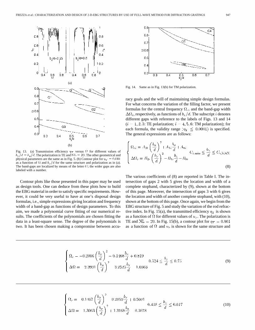
Now, we consider once more the EBG structure of Fig. 5and study the effects of the variation of the filling factor. InFig. 13(a), the transmitted efficiency is shown as a functionof for different values of ; the polarization isTE and . In Fig. 13(b), a contour plot foras a function of and is shown for the same structure andpolarization as in Fig. 13(a). Also in this case, the letterlocal-izes the band-gaps. Moreover, the wider gaps are labeled with anumber. In Fig. 14, the same as in Fig. 13(b) is reported for TMpolarization.
It can be noted that, for small values of , there is no TMgap. As the filling factor increases, there are up to three TMgaps. There are more and wider TE than TM stopbands for smallvalues of the . When the filling factor increases, however,there are less differences between the two polarization cases.
FREZZA et al.: CHARACTERIZATION AND DESIGN OF 2-D-EBG STRUCTURES BY USE OF FULL-WAVE METHOD FOR DIFFRACTION GRATINGS 947
(a)
(b)
Fig. 13. (a) Transmission efficiency� versus for different values ofb =d = b =d. The polarization is TE andNL = 20. The other geometrical andphysical parameters are the same as in Fig. 5. (b) Contour plot for� = 0:001as a function of andb =d for the same structure and polarization as in (a).The band-gaps are localized by means of the letterG; the wider gaps are alsolabeled with a number.
Contour plots like those presented in this paper may be usedas design tools. One can deduce from these plots how to buildthe EBG material in order to satisfy specific requirements. How-ever, it could be very useful to have at one’s disposal designformulas, i.e., simple expressions giving location and frequencywidth of a band-gap as functions of design parameters. To thisaim, we made a polynomial curve fitting of our numerical re-sults. The coefficients of the polynomials are chosen fitting thedata in a least-square sense. The degree of the polynomials istwo. It has been chosen making a compromise between accu-
Fig. 14. Same as in Fig. 13(b) for TM polarization.
racy goals and the will of maintaining simple design formulas.For what concerns the variation of the filling factor, we presentformulas for the central frequency and the band-gap width
, respectively, as functions of . The subscript denotesdifferent gaps with reference to the labels of Figs. 13 and 14( : TE polarization; : TM polarization); foreach formula, the validity range is specified.The general expressions are as follows:
(8)
The various coefficients of (8) are reported in Table I. The in-tersection of gaps 2 with 5 gives the location and width of acomplete stopband, characterized by (9), shown at the bottomof this page. Moreover, the intersection of gaps 3 with 6 givesthe location and width of another complete stopband, with (10),shown at the bottom of this page. Once again, we begin from theEBG structure of Fig. 5 and study the variation of the rod refrac-tive index. In Fig. 15(a), the transmitted efficiency is shownas a function of for different values of . The polarization isTE and . In Fig. 15(b), a contour plot foras a function of and is shown for the same structure and
(9)
(10)

948 IEEE TRANSACTIONS ON MICROWAVE THEORY AND TECHNIQUES, VOL. 51, NO. 3, MARCH 2003
TABLE ICOEFFICIENTS OF(8)
(a)
(b)
Fig. 15. (a) Transmission efficiency� versus for different values ofn .The polarization is TE andNL = 20. The other geometrical and physicalparameters are the same as in Fig. 5. (b) Contour plot for� = 0:001 as afunction of andn for the same structure and polarization as in (a). Theband-gaps are localized by means of the letterG. The wider gaps are also labeledwith a number.
polarization as in Fig. 15(a). The rod refractive index varies from1 to 5 so that most of the usually employed dielectric materialsare considered. Moreover, as in previous plots, the letterlocal-izes the band-gaps and the wider gaps are labeled with a number.In Fig. 16, the same as in Fig. 15(b) is reported for TM polariza-tion. As expected, when the rod refractive index increases,
Fig. 16. Same as in Fig. 15(b) for TM polarization.
TABLE IICOEFFICIENTS OF(11)
the global transmittance of the structure is reduced and the stop-bands become more pronounced and numerous in both polariza-tion cases.
Making a polynomial curve fitting of our numerical resultsplotted in Figs. 15 and 16, we derived some other design for-mulas of degree 2 or 3 giving location and frequency widthof the band-gaps as a function of. The general expressionsfor and are the following ( : TE polariza-tion; : TM polarization), shown in (11), at the bottomof this page. The various coefficients of (11) are reported inTable II. There are no complete band-gaps for results reportedin Figs. 15 and 16, up to . There is then a small com-plete band-gap for , which is the intersectionof gaps 2 and 4, with (12), shown at the bottom of this page.A larger complete band-gap extends in the intersection betweengaps 1 and 3. The design formulas giving central frequency andwidth of this complete stopband are shown in (13), at the top ofthe following page.
C. EBG Materials With Defects
In this section, we consider an example of an EBG structurethat has a periodic defect. As we pointed out in Section I, defectsmay be present in an electromagnetic crystal due to fabricationerrors. Moreover, since the occurrence of sharp transmissionpeaks in the stopbands results from defect creation, very often
(11)
(12)

FREZZA et al.: CHARACTERIZATION AND DESIGN OF 2-D-EBG STRUCTURES BY USE OF FULL-WAVE METHOD FOR DIFFRACTION GRATINGS 949
(13)
Fig. 17. Transmission efficiency� versusd=� for TE polarization (solidline: structure with a central defect; dashed line: structure without the defect).The geometrical and physical parameters areNL = 21 (so that ten is the numberof layers of rods located on each side of a central defect),n = 2; n = 1; b =
b = 0:25d; s = 0, and the refractive index of the defect isn = 2:4.
Fig. 18. Transmission efficiency� versus the incidence angle� for the samestructure of Fig. 17 whend=� = 0:438 (solid line: structure with a centraldefect; dashed line: structure without the defect). Note that for the structurewithout the defect, the dashed line is practically coincident with the�-axis.
EBG materials with defects are designed on purpose to act asfilters or switches [9]. Withour method, structures in which somelayers of rods (as well as layers of the homogeneous background)are missing can be accurately characterized. Moreover, thepresence of rods with a shape somehow different from theother ones and the occurrence of layers not perfectly alignedmay be taken into account.
We present here the case of an EBG material made of square-section dielectric rods forming a square lattice, in which the de-fect results from matter excess: in a structure made of an evennumber of rod layers, the central layer of homogeneous back-ground (i.e., the space between the two central layers of rods)is suppressed. This is equivalent to putting a layer of rods withan anomalous thickness in the middle of the structure. As it willbe apparent from the numerical results, such a structure showspolarization- and frequency-selective properties.
The presented structure corresponds to the following param-eters: (so that ten is the number of rod layers locatedon each side of the central defect),
, and the refractive index of the defect is(this example is chosen because of the existence, for the struc-ture without defect, of a complete band-gap). The transmission
efficiency (solid line) is shown in Fig. 17 as a function offor TE polarization. One notes, inside the stopband, the pres-ence of a sharp transmission peak (due to the defect) centeredon . The considered structure acts as a filter for TEpolarization, while forbidden propagation is kept for TM polar-ization. In this figure, the behavior of the same structure withoutthe defect is also shown (dashed line) for comparison.
In Fig. 18, is shown as a function of the incidence angle,when , i.e., in correspondence of the transmissionpeak.
IV. CONCLUSION
In this paper, a complete characterization of EBG structuresconstituted by a finite number of periodical layers has beencarried out. The analysis employs a very accurate and highlyconvergent full-wave technique that was developed for thestudy of diffraction gratings. In particular, we examined hereelectromagnetic crystals made by a finite number of stackedperiodical arrays of dielectric cylinders immersed in a hostdielectric medium. The presented results concern rectangular-and circular-section rods, but the technique may be employedfor any cross-sectional shape and lattice configuration.
The transmission and reflection efficiencies have been cal-culated for a variety of cases, and design contour plots andformulas have been reported that are very useful in the designprocedure. Comparisons were performed with theoretical re-sults available in the literature, showing very good agreement.A further comparison with some experimental data for a fi-nite-width array of finite-length cylinders is favorable, showingthe applicability of the proposed theory to practical devices.An example of a structure with a periodic defect has beenconsidered.
The results of this analysis can be employed in many mi-crowave applications, i.e., filter design, power dividers, planarreflectors, etc. The presented analysis may be applied to otherelement shapes or lattice configurations, anisotropic dielectricsor metallic materials, and lossy media.
REFERENCES
[1] J. D. Joannopoulos, R. D. Meade, and J. N. Winn,Photonic Crystals:Molding the Flow of Light. Princeton, NJ: Princeton Univ. Press, 1995.
[2] E. Yablonovitch, “Inhibited spontaneous emission in solid-state physicsand electronics,”Phys. Rev. Lett., vol. 58, pp. 2059–2062, 1987.
[3] W. Y. Leung, R. Biswas, S. D. Cheng, M. M. Sigalas, S. McCalmont,G. Tuttle, and K.-M. Ho, “Slot antennas on photonic band gap crystals,”IEEE Trans. Antennas Propagat., vol. 45, pp. 1569–1570, Oct. 1997.
[4] M. Thevènot, C. Cheype, A. Reinex, and B. Jecko, “Directive photonic-bandgap antennas,”IEEE Trans. Microwave Theory Tech., vol. 47, pp.2115–2122, Nov. 1999.
[5] R. Coccioli, F.-R. Yang, K.-P. Ma, and T. Itoh, “Aperture-coupled patchantenna on UC-PBG substrate,”IEEE Trans. Microwave Theory Tech.,vol. 47, pp. 2123–2130, Nov. 1999.
[6] H.-Y. D. Yang, “Theory of antenna radiation from photonic band-gapmaterials,”Electromagnetics, vol. 19, pp. 255–276, May/June 1999.
[7] J. G. Maloney, M. P. Kesler, B. L. Shirley, and G. S. Smith, “A simpledescription for waveguiding in photonic bandgap materials,”MicrowaveOpt. Technol. Lett., vol. 14, pp. 261–266, Apr. 1997.

950 IEEE TRANSACTIONS ON MICROWAVE THEORY AND TECHNIQUES, VOL. 51, NO. 3, MARCH 2003
[8] S. T. Chew and T. Itoh, “PBG-excited split-mode resonator bandpassfilter,” IEEE Microwave Wireless Comp. Lett., vol. 11, pp. 364–366,Sept. 2001.
[9] P. Dansas, N. A. Paraire, and S. Laval, “Feasibility of optical filters andswitches using plastic photonic bandgap structures,”Proc. SPIE, vol.3135, pp. 219–229, 1997.
[10] M. P. Kesler, J. G. Maloney, B. L. Shirley, and G. S. Smith, “Antenna de-sign with the use of photonic band-gap materials as all-dielectric planarreflectors,”Microwave Opt. Technol. Lett., vol. 11, pp. 169–174, Mar.1996.
[11] H. Contopanagos, N. G. Alexopoulos, and E. Yablonovitch, “HighQradio frequency structures using one-dimensionally periodic metallicfilms,” IEEE Trans. Microwave Theory Tech., vol. 46, pp. 1310–1312,Sept. 1998.
[12] C. Rubio, D. Caballero, J. V. Sanchez-Perez, R. Martinez-Sala, J. S. De-hesa, F. Meseguer, and F. Cervera, “The existence of full gaps and deafbands in two-dimensional sonic crystals,”J. Lightwave Technol., vol.17, pp. 2202–2207, Nov. 1999.
[13] J. Opt. Soc. Amer. B, Opt. Phys. (Special Issue), vol. 10, Feb. 1993.[14] J. Mod. Opt. (Special Issue), vol. 41, Feb. 1994.[15] Electromagnetics (Special Issue), vol. 41, Feb. 1999.[16] IEEE Trans. Microwave Theory Tech. (Special Issue), vol. 47, Nov.
1999.[17] J. Lightwave Technol. (Special Section), vol. 17, Nov. 1999.[18] K. M. Ho, C. T. Chan, and C. M. Soukoulis, “Existence of a photonic
bandgap in periodic dielectric structures,”Phys. Rev. Lett., vol. 65, pp.3152–3155, 1990.
[19] B. A. Munk and G. A. Burrell, “Plane-wave expansion for arraysof arbitrarily oriented piecewise linear elements and its applicationin determining the impedence of a single linear antenna in a lossyhalf-space,”IEEE Trans. Antennas Propagat., vol. AP-27, pp. 331–343,May 1979.
[20] H. Y. D. Yang, “Finite difference analysis of 2-D photonic crystals,”IEEE Trans. Microwave Theory Tech., vol. 44, pp. 2688–2695, Dec.1996.
[21] R. Coccioli, T. Itoh, and G. Pelosi, “A finite element-generalized net-work analysis of finite thickness photonic crystals,” inIEEE MTT-S Int.Microwave Symp. Dig., 1997, pp. 195–198.
[22] G. Pelosi, A. Cocchi, and A. Monorchio, “A hybrid FEM-based proce-dure for the scattering from photonic crystals illuminated by a Gaussianbeam,” IEEE Trans. Antennas Propagat., vol. 48, pp. 973–980, June2000.
[23] J. B. Pendry and A. MacKinnon, “Calculation of photon dispersion re-lations,”Phys. Rev. Lett., vol. 69, pp. 2772–2775, 1992.
[24] J. B. Pendry, “Photonic structures,”J. Mod. Opt., vol. 41, pp. 209–229,Feb. 1994.
[25] P. Lalanne, “Effective medium theory applied to photonic crystals com-posed of cubic or square cylinders,”Appl. Opt., vol. 35, pp. 5369–5380,Sept. 1996.
[26] C. Caloz, A. K. Skrivervik, and E. Gardiol, “An efficient method to de-termine Green’s functions of a two-dimensional photonic crystal excitedby a line source—The phased-array method,”IEEE Trans. MicrowaveTheory Tech., vol. 50, pp. 1380–1391, May 2002.
[27] T. Suzuki and P. K. L. Yu, “Emission power of an electric dipole in thephotonic band structure of the FCC latice,”J. Opt. Soc. Amer. B, Opt.Phys., vol. 12, pp. 570–582, Apr. 1995.
[28] S. D. Gedney, J. F. Lee, and R. Mittra, “A combined FEM/MoM ap-proach to analyze the plane wave diffraction by arbitrary gratings,”IEEETrans. Antennas Propagat., vol. 40, pp. 363–370, Feb. 1992.
[29] E. W. Lucas and T. P. Fontana, “A 3-D hybrid finite element/boundaryelement method for the unified radiation and scattering analysis of gen-eral infinite periodic arrays,”IEEE Trans. Antennas Propagat., vol. 43,pp. 145–153, Feb. 1995.
[30] M. Sarnowski, T. Vaupel, V. Hansen, E. Kreysa, and H. P. Gemuend,“Characterization of diffraction anomalies in 2-D photonic bandgapstructures,” IEEE Trans. Microwave Theory Tech., vol. 49, pp.1868–1872, Oct. 2001.
[31] S. Y. Lin, G. Arjavalingam, and W. M. Robertson, “Investigation of abso-lute photonic band-gaps in 2-dimensional dielectric structures,”J. Mod.Opt., vol. 41, pp. 385–393, Feb. 1994.
[32] J. B. Nielsen, T. Søndergaard, S. E. Barkou, A. Bjarklev, J. Broeng,and M. B. Nielsen, “Two-dimensional Kagomé structure, fundamentalhexagonal photonic crystal configuration,”Electron. Lett., vol. 35, pp.1736–1737, Sept. 1999.
[33] P. Dansas and N. Paraire, “Fast modeling of photonic bandgap structuresby use of a diffraction-grating approach,”J. Opt. Soc. Amer. A, Opt.Image Sci., vol. 15, pp. 1586–1598, June 1998.
[34] N. Chateau and J.-P. Hugonin, “Algorithm for the rigorous cou-pled-wave analysis of grating diffraction,”J. Opt. Soc. Amer. A, Opt.Image Sci., vol. 11, pp. 1321–1331, Apr. 1994.
[35] S. Peng and G. M. Morris, “Efficient implementation of rigorous cou-pled-wave analysis for surface-relief gratings,”J. Opt. Soc. Amer. A, Opt.Image Sci., vol. 12, pp. 1087–1089, May 1995.
[36] R. Borghi, F. Frezza, L. Pajewski, M. Santarsiero, and G. Schettini,“Full-wave analysis of the optimum triplicator,”J. Electromagn. WavesApplicat., vol. 15, pp. 689–707, May 2001.
[37] R. Petit, “Electromagnetic theory of gratings,” inTopics in CurrentPhysics, Berlin, Germany: Springer-Verlag, 1980.
[38] M. G. Moharam, D. A. Pommet, E. B. Grann, and T. K. Gaylord, “Stableimplementation of the rigorous coupled-wave analysis for surface-reliefgratings: Enhanced transmittance matrix approach,”J. Opt. Soc. Amer.A, Opt. Image Sci., vol. 12, pp. 1077–1086, May 1995.
[39] P. Lalanne and G. M. Morris, “Highly improved convergence of thecoupled-wave method for TM polarization,”J. Opt. Soc. Amer. A, Opt.Image Sci., vol. 13, pp. 779–784, Apr. 1996.
[40] G. Granet and B. Guizal, “Efficient implementation of the coupled-wavemethod for metallic lamellar gratings in TM polarization,”J. Opt. Soc.Amer. A, Opt. Image Sci., vol. 13, pp. 1019–1023, 1996.
[41] L. Li, “Justification of matrix truncation in the modal methods of diffrac-tion gratings,”Pure Appl. Opt., vol. 1, pp. 531–536, July 1999.
[42] S. T. Peng and R. B. Hwang, “Dispersion characteristics of two-dimen-sionally periodic structures,” inProc. URSI Int. Electromagnetic TheorySymp., Victoria, BC, Canada, May 2001, pp. 317–319.
[43] T. Kushta and K. Yasumoto, “Electromagnetic scattering from periodicarrays of two circular cylinders per unit cell,”PIER, vol. 29, pp. 69–85,2000.
[44] W. M. Robertson, G. Arjavalingam, R. D. Meade, K. D. Brommer, A. M.Rappe, and J. D. Joannopoulos, “Measurement of photonic band struc-ture in a two-dimensional periodic dielectric array,”Phys. Rev. Lett., vol.68, pp. 2023–2027, Mar. 1992.
Fabrizio Frezza (S’87–M’90–SM’95) received theLaurea degree (cum laude) in electronic engineeringand the Doctorate in applied electromagnetics from“La Sapienza” University of Rome, Rome, Italy, in1986 and 1991, respectively.
In 1986, he joined the Electronic EngineeringDepartment, “La Sapienza” University of Rome,where he was a Researcher from 1990 to 1998, atemporary Professor of electromagnetics from 1994to 1998, and an Associate Professor since 1998. Hismain research activity concerns guiding structures,
antennas and resonators for microwaves and millimeter waves, numericalmethods, scattering, optical propagation, plasma heating, and anisotropicmedia.
Dr. Frezza is a member of Sigma Xi, the Electrical and Electronic Italian As-sociation (AEI), the Italian Society of Optics and Photonics (SIOF), the ItalianSociety for Industrial and Applied Mathematics (SIMAI), and the Italian So-ciety of Aeronautics and Astronautics (AIDAA).
Lara Pajewski received the Laurea degree (cumlaude) in electronic engineering from the “RomaTre” University, Rome, Italy, in 2000, and is cur-rently working toward the Ph.D. degree in appliedelectromagnetics at “La Sapienza” University ofRome, Rome, Italy.
In 2000, she joined the Department of ElectronicEngineering, “La Sapienza” University of Rome. Hermain research interests are electromagnetic analysisof periodic structures, scattering problems, and nu-merical methods.

FREZZA et al.: CHARACTERIZATION AND DESIGN OF 2-D-EBG STRUCTURES BY USE OF FULL-WAVE METHOD FOR DIFFRACTION GRATINGS 951
Giuseppe Schettini (S’82–M’96) received theLaurea degree (cum laude) in electronic engineering,Ph.D. degree in applied electromagnetics, andLaurea degree (cum laude) in physics from “LaSapienza” University of Rome, Rome, Italy, in 1986,1992, and 1995, respectively.
Upon his graduation in electronic engineering, hejoined the Italian Energy and Environment Agency(ENEA), where he was initially involved with freeelectron generators of millimeter waves and then mi-crowave components and antennas for the heating of
thermonuclear plasmas. In 1992, he joined “La Sapienza” University as a Re-searcher of electromagnetics. From 1995 to 1998, he has been a temporary Pro-fessor of electromagnetics. Since 1998, he has been an Associate Professor ofantennas and of microwaves at the “Roma Tre” University of Rome, Rome, Italy.His scientific research is focused on scattering from cylindrical structures, ferriteresonators, electromagnetic analysis of diffractive optics, numerical methods,and antennas.
Dr. Schettini is a member of the IEEE Antennas and Propagation Society(IEEE AP-S) and the IEEE Microwave Theory and Techniques Society (IEEEMTT-S).