
ELECTROMAGNETIC WAVES SPECIAL ... - PIER Journals
237
ELECTROMAGNETIC WAVES SPECIAL ISSUE Special Issue In Memory of Robert E. Collin Chief Editors: Weng Cho Chew and Sailing He EMW Publishing Cambridge, Massachusetts, USA
-
Upload
khangminh22 -
Category
Documents
-
view
0 -
download
0
Transcript of ELECTROMAGNETIC WAVES SPECIAL ... - PIER Journals

ELECTROMAGNETIC WAVESSPECIAL ISSUE
Special Issue
In Memory ofRobert E. Collin
Chief Editors: Weng Cho Chew and Sailing He
EMW Publishing
Cambridge, Massachusetts, USA

Special Issue In Memory of Robert E. Collin
This is a special issue in memory of Robert E. Collin, a distinguished scholar, author, and mentor in thearea of electromagnetics. This special issue started at the suggestion of Professor Ioannis M. Besieris.The chief editors would like to thank all the authors for their contributions.
Robert E. Collin (October 24, 1928 – November 29, 2010) was the author or coauthor of more than150 technical papers and five books on electromagnetic theory and applications. His classic text, FieldTheory of Guided Waves, was also a volume in the series. Professor Collin had a long and distinguishedacademic career at Case Western Reserve University. In addition to his professional duties, he servedas chairman of the Department of Electrical Engineering and as interim dean of engineering.
Professor Collin was a life fellow of the IEEE, fellow of the Electromagnetic Academy, and memberof the Microwave Theory and Techniques Society and the Antennas and Propagation Society (APS).He was a member of U.S. Commission B of URSI and member of the Geophysical Society. Otherhonors include the Diekman Award from Case Western Reserve University for distinguished graduateteaching, the IEEE APS Distinguished Career Award (1992), the IEEE Schelkunoff Prize Paper Award(1992), the IEEE Electromagnetics Award (1998), and an IEEE Third Millennium Medal in 2000. In1990 Professor Collin was elected to the National Academy of Engineering.

Collection of Papers in Memory of Robert E. Collin
Numerically Efficient Technique For Metamaterial Modeling (Invited Paper)Ravi Kumar Arya, Chiara Pelletti, and Raj Mittra. . . . . . . . . . . . . . . . . . . . . . . . . . . . . . . . . . . . . .Progress In Electromagnetics Research, Vol. 140, 263–276, 2013
Dipole Radiation Near Anisotropic Low-Permittivity Media (Invited Paper)Mohammad Memarian and George V. Eleftheriades. . . . . . . . . . . . . . . . . . . . . . . . . . . . . . . . . . . . . .Progress In Electromagnetics Research, Vol. 142, 437–462, 2013
Circuit and Multipolar Approaches to Investigate the Balance of Powers in 2D ScatteringProblems (Invited Paper)Inigo Liberal, Inigo Ederra, Ramon Gonzalo, and Richard W. Ziolkowski. . . . . . . . . . . . . . . . . . . . . . . . . . . . . . . . . . . . . .Progress In Electromagnetics Research, Vol. 142, 799–823, 2013
A Wideband Frequency-Shift Keying Modulation Technique Using Transient State of aSmall Antenna (Invited Paper)Mohsen Salehi, Majid Manteghi, Seong-Youp Suh, Soji Sajuyigbe, and Harry G. Skinner. . . . . . . . . . . . . . . . . . . . . . . . . . . . . . . . . . . . . .Progress In Electromagnetics Research, Vol. 143, 421–445, 2013
Minimum Q for Lossy and Lossless Electrically Small Dipole Antennas (Invited Paper)Arthur D. Yaghjian, Mats Gustafsson, and B. Lars G. Jonsson. . . . . . . . . . . . . . . . . . . . . . . . . . . . . . . . . . . . . .Progress In Electromagnetics Research, Vol. 143, 641–673, 2013
Three-Parameter Elliptical Aperture Distributions for Sum and Difference AntennaPatterns Using Particle Swarm Optimization (Invited Paper)Arthur Densmore and Yahya Rahmat-Samii. . . . . . . . . . . . . . . . . . . . . . . . . . . . . . . . . . . . . .Progress In Electromagnetics Research, Vol. 143, 709–743, 2013
Differential Forms Inspired Discretization for Finite Element Analysis of InhomogeneousWaveguides (Invited Paper)Qi I. Dai, Weng Cho Chew, and Li Jun Jiang. . . . . . . . . . . . . . . . . . . . . . . . . . . . . . . . . . . . . .Progress In Electromagnetics Research, Vol. 143, 745–760, 2013
Localized Monochromatic and Pulsed Waves in Hyperbolic Metamaterials (Invited Paper)Ioannis M. Besieris and Amr M. Shaarawi. . . . . . . . . . . . . . . . . . . . . . . . . . . . . . . . . . . . . .Progress In Electromagnetics Research, Vol. 143, 761–771, 2013
Developing One-dimensional Electronically Tunable Microwave and Millimeter-WaveComponents and Devices towards Two-Dimensional Electromagnetically ReconfigurablePlatform (Invited Paper)Sulav Adhikari and Ke Wu. . . . . . . . . . . . . . . . . . . . . . . . . . . . . . . . . . . . . .Progress In Electromagnetics Research, Vol. 143, 821–848, 2013
Impact of Finite Ground Plane Edge Diffractions on Radiation Patterns of ApertureAntennas (Invited Paper)Nafati A. Aboserwal, Constantine A. Balanis, and Craig R. Birtcher. . . . . . . . . . . . . . . . . . . . . . . . . . . . . . . . . . . . . . . .Progress In Electromagnetics Research B, Vol. 55, 1–21, 2013
Progress In Electromagnetics Research, Vol. 140, 263–276, 2013
NUMERICALLY EFFICIENT TECHNIQUE FOR META-MATERIAL MODELING
Ravi K. Arya, Chiara Pelletti, and Raj Mittra*
EMC Lab, Department of Electrical Engineering, The PennsylvaniaState University, University Park, PA 16803, USA
Abstract—In this paper we present two simulation techniques formodeling periodic structures with three-dimensional elements ingeneral. The first of these is based on the Method of Moments (MoM)and is suitable for thin-wire structures, which could be either PECor plasmonic, e.g., nanowires at optical wavelengths. The second isa Finite Difference Time Domain (FDTD)-based approach, which iswell suited for handling arbitrary, inhomogeneous, three-dimensionalperiodic structures. Neither of the two approaches make use of thetraditional Periodic Boundary Conditions (PBCs), and are free fromthe difficulties encountered in the application of the PBC, as forinstance slowness in convergence (MoM) and instabilities (FDTD).
1. INTRODUCTION
Frequency Selective Surfaces (FSS) comprising of periodic arrays ofmetallic or dielectric elements, have been extensively developed andutilized in various applications for decades to control the transmissionof electromagnetic waves [1, 2]. They are also useful as ElectromagneticBand-Gap structures(EBG) and Metamaterials, that are currentlyfinding widespread use for various applications.
The periodic structures are typically modeled as infinite doubly-periodic arrays of scatterers, and are commonly analyzed by imposingperiodic boundary conditions to a unit cell to reduce the originalproblem to a manageable size [3]. The conventional Methodof Moments (MoM) [4, 5] is often the algorithm of choice forelectromagnetic scattering problems. It also provides efficient meansfor simulating FSSs, given the periodic elements are PEC and not
Received 13 May 2013, Accepted 31 May 2013, Scheduled 3 June 2013* Corresponding author: Raj Mittra ([email protected]).
Invited paper dedicated to the memory of Robert E. Collin.

264 Arya et al.
inhomogeneous and complex objects, the latter being more amenableto convenient analysis through the use of Finite Methods.
One caveat in using the Floquet-Bloch theorem to reduce thecomputational domain of infinite periodic structures to a single unit cellis that it leads to a slowly convergent series [6], which requires specialprocessing, e.g., the use of Ewald transform [7]. In addition, if the FSSelements have multi-scale features and are made of metallo-dielectricmaterials, the MoM matrices may suffer from ill-conditioning.
The technique proposed in this paper derives the solution to theinfinite doubly-periodic problem by first characterizing the currentdistribution over the element via the derivation of its CharacteristicBasis Functions (CBFs) [8, 9]. The solution for the periodic arrayis then derived by progressively enlarging the size of the truncatedstructure and extrapolating its solution via the use of signal processingtechniques [10, 11]. The CPU time and memory requirements in thisapproach were shown to be considerably less than those requiredby commercial periodic MoM codes that utilize the periodic Green’sfunction approach.
The ability to bypass an infinite summation, either in the spatial orspectral domains, is what leads to the computational efficiency realizedby using this method. In addition, the methodology we propose isvery general and is already been extended to geometries and range ofincident angles that are not always easily handled by the commercialcodes [12].
Next, we turn to the problem of modeling of periodic structureswith inhomogeneous and complex-shaped 3D elements (see Fig. 1). It iswell known that MoM-based methods can become very inefficient whenhandling such elements, and that 3D inhomogeneous FSS problems aremore amenable to convenient analysis via the use of Finite Methods.We choose to use the Finite Difference Time Domain method for
Figure 1. Representative geometry of an infinite doubly periodic arrayof inhomogeneous 3D elements.

Progress In Electromagnetics Research, Vol. 140, 2013 265
this purpose, because it provides us the simulation results over awide frequency band with a single run. We note, however, that theimposition of the PBC is not very straightforward in the FDTD, whichrequires a modification of the update equations when dealing withperiodic structures. Furthermore, FDTD is plagued by instabilityissues and the update algorithm requires that the time step beprogressively reduced as the angle of incidence of the plane waveimpinging upon the periodic structure becomes increasingly oblique.
To obviate these difficulties, we introduce yet again a techniquein this paper that bypasses the use of PBCs in the FDTD. Instead,in common with the MoM-based approach described above, we againsolve the problem of a truncated periodic structure to derive thesolution we seek for the original periodic structure.
Illustrative examples are also presented to demonstrate theaccuracy of the approach by comparing the results derived by using aFinite Element Method (FEM) based, PBC version of the commercialcode.
It is worthwhile to point out that the proposed technique isnaturally suited for handling truncated periodic structures that are thestarting points in the proposed approach, and are difficult to handleby using conventional methods. One of its main contributions is toshow how the solution to the limiting case of infinite doubly-periodicstructure can be accurately extracted from that of a correspondingfinite one, whose size is relatively small.
2. PROCEDURE FOR WIRE ELEMENTS
The technique begins by applying the Characteristic Basis FunctionMethod (CBFM) to a single unit cell of the grating (Fig. 2). Theelement is illuminated with a set of plane waves whose angles ofincidence span the [θ, φ] space. The number of incident angles isoverestimated to capture all the possible Degrees of Freedom (DoFs)
E i,1
E i,2
E i,3E i,4
E i,5
x
y
z
Figure 2. Geometry of the FSS unit cell with a spectrum of planewaves incident on it.

266 Arya et al.
present in the solutions for the induced currents. These solutionsare denoted as CBFs, namely high-level basis functions especiallyconstructed to fit the actual geometry by incorporating the physicsof the problem into their generation.
Only N linearly independent CBFs are retained for the problemat hand by applying a Singular Value Decomposition (SVD) procedureto filter out the total set of solutions. The number of surviving CBFsis relatively small, typically two or three in frequency ranges for whichthe size of the unit cell is smaller than one wavelength.
Once the CBFs are generated for the isolated array element,we invoke the Floquet’s theorem to argue that all of the elementscomprising the periodic structure must have the same currentdistribution, apart from a phase shift ψ which is determined by theangle of incidence of the plane wave impinging upon the grating.
Next, we construct the reduced CBF matrix ZkRED
and use it tosolve a series of truncated array problems, by progressively increasingits dimension k, with the objective of predicting the asymptotic limit ofthe weights of the current as k →∞ and the truncated array becomesa doubly-infinite periodic structure. The reduced matrix reads:
ZkRED
=
⟨(J1CBF
)t,∑R
k=0 Es,1k,CBF
⟩. . .
⟨(J1CBF
)t,∑R
k=0 Es,Nk,CBF
⟩
.... . .
...⟨(JNCBF
)t,∑R
k=0 Es,1k,CBF
⟩. . .
⟨(JNCBF
)t,∑R
k=0 Es,Nk,CBF
⟩
RHS =
⟨(J1CBF )t
), Ei,1
PW
⟩
...⟨(JNCBF
)t, Ei,N
PW
⟩
(1)
As indicated in (2), the matrix elements are generated by followinga Galerkin procedure applied only at the center (0, 0) cell, with Es,i
k,CBF
representing the field produced by i-th CBF J iCBF at U0,0. The
summation index k varies from 0 to R, where R is the number ofconcentric rings. The Right Hand Side (RHS) vector represents thetangential fields incident upon the center element of the array, testedwith the same CBFs. The weights wk of the CBFs are derived asfunctions of k, by imposing the continuity of the tangential E-fields atthe center element surface:
wk =(Zk
RED
)−1RHS (2)
Finally, the resulting current distribution at the center cell iscomputed as a weighted linear combination of the CBFs.

Progress In Electromagnetics Research, Vol. 140, 2013 267
2.1. Extraction of Periodic Array Result
The procedure for extracting the asymptotic value for the currentdistribution of the infinite array problem is based on processing theresults of a relatively small-size truncated array, comprising of only afew rings. A typical behavior of the magnitude distribution of theweight coefficients of the current, as a function of the number ofconcentric rings ranging from 1 to 40, i.e., up to an 81 × 81 array,is shown in Fig. 3. We observe that the coefficients exhibit a relativelyslow convergence behavior as we progressively increase the array size.
Magnitude of weight coefficients @ 3 GHz6.6 x 10
6.5 x 10
6.4 x 10
6.3 x 10
6 x 10
6.1 x 10
6.2 x 10
5.9 x 10
-5
-5
-5
-5
-5
-5
-5
-5
0 10 20 30 40number of rings
selected data f(k)interpolated data f(r)original data
V/m
Figure 3. Magnitude variation of the current coefficients in the unitcell as functions of the size of the array, at the operating frequencyof 3 GHz. Dashed marker: original data, line marker: interpolateddata f(r), dark round marker: f(r) evaluated at first two consecutivemaximum(minimum) and minimum(maximum) of its derivative (f(k)at k = k1 and k = k2).
The method proposed herein proceeds by smoothing themagnitude and phase values of the weight coefficients through cubicspline interpolation to construct fm(r) and fp(r) for the truncatedarray problem. Next, we take the derivative of these functions andselect a threshold t to filter out the contributions of the first t−1 ringswhich may contain artefacts. Finally, starting from r ≥ t, we find thefirst two consecutive maximum (minimum) and minimum (maximum)values of f ′(r), which correspond to the points of which the slope off(r) is maximum. We find two consecutive indices k = k1 and k = k2,for which the slope is maximum, and then take the average of f valuesevaluated at these two points as the asymptotic value we are seeking.
The reflection and transmission coefficients are defined as:
Γ =Escat
Eincand τ =
Etrans
Einc(3)
where Escat and Etrans represent the scattered and transmitted fields

268 Arya et al.
in the far-region. Our final step is to work with the induced currentsto derive the Γ and τ using (3), in a manner similar to that in [13].
The methods described above, for analyzing periodic structurescan also be applied to problems involving plasmonic materials, such asarrays of nanorods at optical frequencies, which find a wide range ofapplications in photonics [14].
3. PROCEDURE FOR THREE-DIMENSIONALSTRUCTURES
We will now turn to arbitrary three-dimensional elements that are notamenable to efficient analysis by using the Method of Moments andare best handled by Finite methods, e.g., the FEM or the FDTD.The FEM analysis applied in conjunction with the Periodic BoundaryCondition (PBC) is well established and will not be discussed here.The FDTD has also been applied in the past with the PBC, but isfraught with a number of difficulties, primarily encountered when theangle of incidence of the incident plane wave is not close to normal.Specifically, it is very common to run into instabilities in the FDTDtime-updating process, despite the reduction of the time-step, whichmust be done as the incident angle becomes more and more oblique.
The method described herein not only circumvents thesedifficulties with the instabilities and time-step reduction, but it alsodoes not require the introduction of auxiliary functions [15] in theFDTD update equations. As a first step, we modify the given doubly-infinite periodic structure to the truncated model as shown in Fig. 4.We place the truncated structure inside a parallel-plate waveguide; sothat it remains periodic in the y-direction by virtue of imaging by theparallel planes. An incident field which is polarized in the y-direction,with its k-vector in the x-z plane, impinges upon the structure at anarbitrary angle relative to the z-axis. Of course, this configurationrestricts us to change the incident angle only in the x-z plane.
The computational domain is terminated in the x-direction
Figure 4. Modified waveguide geometry.

Progress In Electromagnetics Research, Vol. 140, 2013 269
by using Perfectly Matched Layers (PML), as is the case for theconventional FDTD.
In common with the procedure described in Section 2.1 we againtruncate the doubly-periodic structure to a finite one and develop atechnique for extrapolating the results of the finite structure to that ofthe infinite doubly-periodic geometry. However, the original approach,which was based on the extrapolation of the weight coefficient of thecurrent distribution in the context of the Method of Moments mustbe tailored for the FDTD, since it deals with E and H fields, and notdirectly with induced currents. The details of the proposed procedureappear in Section 3.1.
3.1. FDTD-based Method for Computing Reflection andTransmission Coefficients
Our next step is to solve the waveguide structure scattering problemshown in Fig. 4 by using a Finite Method, e.g., the FDTD and tocompute the scattered fields along the longitudinal direction on a lineat the center of the waveguide as shown in Fig. 4.
We note that the total field on the incident side of the waveguide(z < 0) is a summation of the incident and scattered (reflected) fields,while only the transmitted fields exist in the forward direction (z > 0),as shown in Fig. 4.
Next, for the normal incidence case, we decompose the fieldsmeasured along the line z1-z2 (see Fig. 4) within region z < 0 into theirincident and reflected components by using the Generalized Pencil-Of-Function (GPOF) method [16]. For the oblique incidence case, thefields are measured along specular directions both in the reflection andthe transmission regions.
The weights of the transmitted and reflected fields associated withthe dominant Floquet harmonic determined by the GPOF algorithm,yield the transmission and reflection coefficients for the truncatedarray. The reflection and transmission coefficients, computed byusing (3), are tracked progressively by increasing the number ofelements in the transverse direction (see Fig. 5).
Our next step is to plot Γ and τ as functions of the number ofcells as shown in Fig. 5. These intermediate values are processednext to derive the asymptotic value for the reflection coefficientof the particular frequency for which we have measured the fields.This process is repeated for all the frequencies of interest and theextrapolated reflection coefficient values are plotted over the desiredfrequency band as shown below.

270 Arya et al.
Magnitude of Reflection Coefficient-3.5
-4
-4.5
-5
-5.5
-6
dB
original dataextrapolated data
4 6 8 10 12 14 16 18 20 222number of cell
Figure 5. Magnitude of the reflection coefficient as a function ofthe number of elements, in the x-direction; solid line: original data,dashed: extrapolated data.
4. NUMERICAL RESULTS
For the first test example, we consider a single-layer, planar, doubly-periodic FSS of infinite extent (in the x- and y-directions) withperiodicities Dx = Dy = 0.7λ0, where λ0 is the wavelength at 5 GHz.Each cell contains a PEC wire of λ0/2 in length, whose radius is λ0/500,and which is tilted out of plane at an angle of θ = 60 (see Fig. 6).
Figure 6. Representative geometry of the analyzed periodic array ofdipoles tilted out-of-plane (θ = 60).
An x-polarized plane wave, traveling along the −z direction, isnormally incident upon the grating. Only one CBF is found to besufficient to describe the current distribution over this type of element;hence, the related reduced matrix is just 1×1. The frequency range ofour interest spans from 3.5 to 6 GHz. The reflection and transmission

Progress In Electromagnetics Research, Vol. 140, 2013 271
Magnitude of Reflection coefficient Magnitude of Transmission coefficient
0
-5
-10
-15
-20
-25
0
-5
-10
-15
-20
-253.5 4 4.5 5 5.5 6 3.5 4 4.5 5 5.5 6
f (GHz) f (GHz)
this methodGPOF extrapolationcommercial MoMcommercial FEM
this methodGPOF extrapolationcommercial MoMcommercial FEM
dB
dB
(a) (b)
Figure 7. Magnitude of the (a) reflection coefficient and(b) transmission coefficient derived by using this method and comparedwith those obtained by using: GPOF extrapolation; and commercialMoM and FEM.
Table 1. Run-time performance for the dipole test example by usingthe present method (CBFM with truncation procedure), CBFM withGPOF extrapolation and commercial solvers implementing the MoMand the FEM.
Numerical method This method GPOF extrapolation MoM FEM
Normalized time 1 3.5 454.5 901.9
characteristics of the array are compared in Fig. 7.The agreement with the results obtained independently by using
GPOF extrapolation and software modules is seen to be good.Table 1 below lists the time comparison, to illustrate the advantage
of our method in terms of run-time, both over existing EM solvers andprevious published data. The normalized time has been defined asfollows:
Norm. time =Time for other methodTime for this method
(4)
Next, we present some representative results for the reflectioncharacteristics of 3D structures. In Fig. 8 we show the results foran array of PEC spheres whose diameters are 0.5λ0 with periodicity of0.75λ0, at the operating frequency of 5 GHz. The array is illuminatedby a plane wave at normal and 20 degree incidence angles, respectively.We also compare the obtained results against those derived by using acommercial FEM solver.
As it is well known, the FDTD can handle dielectric and PEC

272 Arya et al.
structures with ease, Fig. 9 shows the results for an array of dielectricspheres with εr = 9 and diameters of 0.5λ0 with periodicity of 0.75λ0
at the operating frequency of 5 GHz. Again, the results have beenderived for normal and 20 degree incidence angles, respectively.
Figure 10 also shows the results for PEC spheres coated witha dielectric layer, whose εr is 9. For this case, the PEC sphereshave diameters of 0.5λ0 and a periodicity of 0.75λ0 at the operatingfrequency of 5GHz. The thickness of the dielectric is λ0/20.
Magnitude of Reflection coefficient0
-5
-10
-15
-20
this method
dB
(a) (b)
f (GHz)
1 2 3 4 5
FEM (PBC)
Figure 8. Magnitude of Reflection coefficient for (a) normal incidenceand (b) 20 degrees incidence, derived by using the present method andcompared with those from a commercial FEM (PBC) solver for PECspheres.
Magnitude of Reflection coefficient
-5
-10
-15
-20
this method
dB
(a) (b)
f (GHz)1 2 3 4 5
FEM (PBC)5
0
-25
-30
Magnitude of Reflection coefficient
-5
-10
-15
-20
this method
dB
f (GHz)
1 2 3 4 5
FEM (PBC)
5
0
-25
-30
Figure 9. Magnitude of Reflection coefficient for (a) normal incidenceand (b) 20 degrees incidence, derived by using the present methodand compared with those from a commercial FEM (PBC) solver fordielectric spheres.

Progress In Electromagnetics Research, Vol. 140, 2013 273
Magnitude of Reflection coefficient
-10
-20
this method
dB
(a) (b)f (GHz)
62 3 4 5
FEM (PBC)
0
-30
Magnitude of Reflection coefficient
-5
-10
this method
dB
f (GHz)2 2.5 3 3.5 4
FEM (PBC)
0
-40
4.5 5
Figure 10. Magnitude of Reflection coefficient for (a) normalincidence and (b) 20 degrees incidence, derived by using the presentmethod and compared with those from a commercial FEM (PBC)solver for PEC spheres coated with dielectric material.
To further illustrate the versatility of this method, we have appliedthis technique to FSSs with 3D elements [17], as shown in Fig. 11. Thisstructure is somewhat different from the one presented in [17], in that itis tuned to a different frequency and is implemented with flat strips —as opposed to wires-supported by RO4003 (εr = 3.55) dielectric layerof thickness d. The flat strips at the top and bottom are connected byvias, as shown in Fig. 11(a). Fig. 12 shows the transmission coefficientof this structure. We note that there is slight difference at the low endof the frequency band between the simulated and measured results,and that the measured result shows a slightly wider bandwidth thanthe simulated one. This difference could be due to tolerances in thefabricated model, as well as due to conductor losses in the structure.It is interesting to note, however, that our results are closer to themeasured ones than those predicted by the commercial FEM (PBC)code.
It is evident from Figs. 8, 9, 10 and 12 that good agreement hasbeen achieved between the results obtained from a commercial FEMsolver and the proposed algorithm, despite the fact the use of PBCs istotally avoided in the present method and, hence, concerns regardinginstability and reduction in the time step are obviated. As mentionedearlier, working in the time domain, as we have done in the proposedmethod, enables us to generate the solution over a frequency bandwith a single run, but without the burden of instability and numericalinefficiency that plague the conventional FDTD/PBC analysis.

274 Arya et al.
X
Y
Z
Dxd
Dy
z
x
H
t
h
w
L
SY
X
(a)
(b) (c)
Figure 11. Geometry of analyzed FSS unit cell. (a) 3D view,(b) side view, (c) top view. Geometry parameters are: H = 18.96mm,d = 0.508mm, t = 1 mm, w = 1 mm, s = 2 ∗ 0.784mm, h = 0.76mm,L = 6.5mm and periodicity Dx = Dy = 24.29mm.
Magnitude of Transmission coefficient0
-10
-20
-30
-40
this method
6 7 84 5
FEM (PBC)measured
9 10
f (GHz)
Figure 12. Magnitude of transmission coefficient for normal incidencefrom the present method, a commercial FEM (PBC) solver andmeasured results.

Progress In Electromagnetics Research, Vol. 140, 2013 275
5. CONCLUSIONS
In this paper, we have introduced two simulation techniques formodeling periodic structures with three-dimensional elements. Theproposed first technique yields accurate results for the reflectionand transmission characteristics of the array, at a fraction of thecomputational cost when compared to those required by existing codesfor modeling periodic structures. The computational efficiency isrealized by totally bypassing the evaluation of the infinite summations,either in the spatial or in the spectral domains. Also, we haveintroduced a second technique to derive the response characteristicsof periodic arrays characterized by arbitrary 3D type of elements.This method yields results that are in good agreement with thoseobtained from commercial solvers, while it avoids the use of PBCs, thusbypassing the difficulties encountered in the FDTD with the increasein the solve-time, and with issues pertaining to the stability behavior.
Before closing, we mention that the techniques presented hereincan be modified to address the important problem of modeling periodicstructures with statistical variations in their geometries, as is typicallythe case with MTMs for optical wavelengths, where the difficultiesin their fabrication almost always introduce small variations in thedimensions of the elements that comprise the periodic array.
REFERENCES
1. Mittra, R., C. H. Chan, and T. Cwik, “Techniques for analyzingfrequency selective surfaces — A review,” IEEE Proc., Vol. 76,No. 12, 1593–1615, 1998.
2. Wu, T. K., Frequency Selective Surface and Grid Array, JohnWiley & Sons Inc., 1995.
3. Munk, B. A., Frequency Selective Surfaces: Theory and Design,Wiley, New York, 2000.
4. Peterson, A. F., S. L. Ray, and R. Mittra, Computational Methodsfor Electromagnetics, IEEE Press, New York, 1998.
5. Harrington, R. F., Field Computation by Moment Method, TheMacmillan Company, New York, 1968.
6. Blackburn, J. and L. R. Arnaut, “Numerical convergence inperiodic method of moments of frequency-selective surfaces basedon wire elements,” IEEE Trans. on Antennas and Propag., Vol. 53,3308–3315, Oct. 2005.
7. Stevanovic, I., P. Crespo-Valero, K. Blagovic, F. Bongard, andJ. R. Mosig, “Integral-equation analysis of 3-D metallic objects

276 Arya et al.
arranged in 2-D lattices using the Ewald transformation,” IEEETrans. on Microwave Theory and Tech., Vol. 54, No. 10, 3688–3697, Oct. 2006.
8. Prakash, V. V. S. and R. Mittra, “Characteristic basis functionmethod: A new technique for efficient solution of method ofmoments matrix equations,” Microwave and Optical TechnologyLetters, Vol. 36, No. 2, 95–100, Jan. 2003.
9. Wan, J. X., J. Lei, and C. H. Liang, “An efficient analysis of large-scale periodic microstrip antenna arrays using the characteristicbasis function method,” Progress In Electromagnetics Research,Vol. 50, 61–81, 2005.
10. Yoo, K., N. Mehta, and R. Mittra, “A new numerical techniquefor analysis of periodic structures,” Microwave and OpticalTechnology Letters, Vol. 53, No. 10, 2332–2340, Oct. 2011.
11. Mittra, R., C. Pelletti, N. L. Tsitsas, and G. Bianconi, “Anew technique for efficient and accurate analysis of FSSs, EBGsand metamaterials,” Microwave and Optical Technology Letters,Vol. 54, No. 4, 1108–1116, Oct. 2011.
12. Mittra, R., R. K. Arya, and C. Pelletti, “A new technique forefficient and accurate analysis of arbitrary 3D FSSs, EBGs andmetamaterials,” 2012 IEEE Antennas and Propagation SocietyInternational Symposium (APSURSI), 1–2, Chicago, IL, Jul. 2012.
13. Mittra, R., C. Pelletti, N. L. Tsitsas, and G. Bianconi, “Anew technique for efficient and accurate analysis of FSSs, EBGsand metamaterials,” Microwave and Optical Technology Letters,Vol. 54, No. 4, 1108–1116, Apr. 2012.
14. Rashidi, A., H. Mosallaei, and R. Mittra, “Numerically efficientanalysis of array of plasmonic nanorods illuminated by anobliquely incident plane wave using the characteristic basisfunction method,” J. Comput. Theor. Nanosci., No. 10, 427–445,2013.
15. Taflove, A. and S. C. Hagness, Computational Electrodynamics:The Finite-difference Time-domain Method, 3rd Edtion, ArtechHouse, Norwood, MA, 2005.
16. Hua, Y. and T. Sarkar, “Generalized pencil-of-functions methodfor extracting poles of an EM system from its transient response,”IEEE Trans. on Antennas and Propag., Vol. 37, No. 2, 229–234,Feb. 1989.
17. Pelletti, C. and R. Mittra, “Three-dimensional FSS elementswith wide frequency and angular responses,” IEEE Antennas andPropagation Society International Symposium, 1–2, Chicago, IL,Jul. 2012.

Progress In Electromagnetics Research, Vol. 142, 437–462, 2013
DIPOLE RADIATION NEAR ANISOTROPIC LOW-PERMITTIVITY MEDIA
Mohammad Memarian* and George V. Eleftheriades
The Edward S. Rogers Sr. Department of Electrical and ComputerEngineering, University of Toronto, 40 St. George Street, Toronto,Ontario M5S 2E4, Canada
Abstract—We investigate radiation of a dipole at or below theinterface of (an)isotropic Epsilon Near Zero (ENZ) media, akin tothe classic problem of a dipole above a dielectric half-space. Tothis end, the radiation patterns of dipoles at the interface of air anda general anisotropic medium (or immersed inside the medium) arederived using the Lorentz reciprocity method. By using an ENZhalf-space, air takes on the role of the denser medium. Thus weobtain shaped radiation patterns in air which were only previouslyattainable inside the dielectric half-space. We then follow the earlywork of Collin on anisotropic artificial dielectrics which readily enablesthe implementation of practical anisotropic ENZs by simply stackingsub-wavelength periodic bi-layers of metal and dielectric at opticalfrequencies. We show that when such a realistic anisotropic ENZ hasa low longitudinal permittivity, the desired shaped radiation patternsare achieved in air. In such cases the radiation is also much strongerin air than in the ENZ media, as air is the denser medium. Moreover,we investigate the subtle differences of the dipolar patterns when theanisotropic ENZ dispersion is either elliptic or hyperbolic.
1. INTRODUCTION
The radiation of antennas at the interface of media has been the subjectof numerous studies to date [1–13]. The scenario of interest is a classicproblem in electromagnetics dating back to the work of Sommerfeldin 1909, investigating the radiation of a source above a lossy half-space [1]. For instance in [12] the radiation of dipoles placed on anair-dielectric interface was studied and it was found that the radiation
Received 8 August 2013, Accepted 2 September 2013, Scheduled 11 September 2013* Corresponding author: Mohammad Memarian ([email protected]).
Invited paper dedicated to the memory of Robert E. Collin.

438 Memarian and Eleftheriades
mainly occurs inside the dielectric with interesting radiation patternshapes. The radiation pattern in the air-side primarily had a singlelobe, and more importantly, it was much weaker than the radiationin the dielectric, with an approximate power ratio of 1 : ε3/2 [9].Ref. [3] studied the problem of a dipole at the interface of an anisotropicplasma interface. Ref. [11] investigated the radiation patterns of bothhorizontal and vertical interfacial dipoles, deducing the location of thenulls and power ratios in either half-spaces. Other effects such assubsurface peaking was also explored by the same authors in [14]. Suchstudies have been intended for various applications such as GroundPenetrating Radar [15, 16], antennas for communication above earth orunder water [2, 13], antennas on semiconductors [9] or above dielectricsfor imaging [12], to only name a few.
Different techniques have been used thus far for analyzing thisproblem, mainly developing the Green’s function and using asymptoticapproximations to find the far-field radiation patterns inside the airor the dielectric regions. A great body of literature to date hasbeen dedicated to solving the Sommerfeld type integrals that arisein these problems, (e.g., see [10] for a review of various works). Thepoor convergence of Sommerfeld type integrals has been an importantreason for devising various efficient techniques for solving these typesof problems as done in [17] and using integral equations solved with theMethod of Moments [18, 19], and exact solutions such as [20]. FiniteDifference Time Domain (FDTD) methods have also been used toanalyze radiation patterns of such scenarios [16, 21], analyzing both thenear-field [21] and the far-field [16, 21], pointing out some ripple effectson the patterns obtained due to finite observation distances. Effectsof lateral waves were also explored in works such as [16, 22, 23]. Othertime domain techniques have also been used for solving the problem ofa source above a lossy half-space as in [24]. Furthermore, a few studieshave investigated radiation from anisotropic media [3, 4, 25, 26] mainlythrough developing the Green’s function of their scenario of interest.
Metamaterials (MTMs) — materials with constitutive parametersnot usually found in nature — have received significant attentionfor more than a decade now and have found various applications inoptics and electromagnetics. One type of MTMs relevant to thisstudy are the Epsilon Near Zero (ENZ) media, which have showninteresting properties such as tailoring the phase of the radiationpattern of arbitrary sources [27]. Such materials are in contrast tonormal dielectrics, which have permittivity values above the free spacepermittivity ε0.
In almost all the work to date such as [9, 11, 12], the study hasbeen on dipoles at the interfaces of dielectrics, which have permittivity

Progress In Electromagnetics Research, Vol. 142, 2013 439
greater than vacuum, εr > 1. In this work and our related work [28]however, we aim to systematically study the radiation pattern of adipole at the interface of an air-metamaterial (MTM), in which themetamaterial is a homogenized medium with an effective permittivitylower than free space, ε < ε0. Such materials would be classified asEpsilon Near Zero (ENZ) media. One motivation here is to obtainthe interesting dielectric-side radiation patterns of [9, 11, 12] in air.The argument for using ENZ is simple. By using an ENZ instead ofthe dielectric, air plays the role of the dielectric in [12]. Thereforethose patterns obtained inside the dielectric in [9, 11, 12], should beattainable now in the air side, as air now acts as the higher permittivitymedium compared to the MTM. Aside from the shape, the intensityof the radiation is also stronger in air, rather than in the ENZ. Thisis for instance very desirable in telecommunication applications. Wefurther generalize the problem to that of a dipole above an ‘anisotropicmedium’, with potentially low value(s) in the permittivity tensor.Since most ENZ media are realized with layered or wire medium typestructures, the resulting effective medium is inherently anisotropic andtypically similar to a uniaxial crystal with a well defined optical axis.
A simple approach for determining the radiation pattern is usingthe Lorentz Reciprocity Theorem, which has usually been used forfinding the radiation pattern of dipoles on isotropic dielectrics [12]. Inthis work and [28] we utilize the reciprocity method for systematicallystudying the dipole radiation above an anisotropic half-space, which ispotentially an ENZ medium. We expand the theory to solve for dipolesimmersed inside an ENZ medium. Realizations of ENZs are usuallyanisotropic, that is the near zero permittivity is achieved only alongone axis, e.g., using layered media. Based on the pioneering work ofCollin on artificial dielectrics [29, 30], the ENZs in this work are realizedby interleaving layers of metal and dielectric with a sub-wavelengthperiod. In [29] Collin showed that such a periodic structure can behomogenized into an effective medium with an anisotropic (uniaxial)permittivity tensor and derived simple expressions which have beenrediscovered and used extensively to date. In this work, the ENZrealizations are tailored for optical frequencies where it can enablevarious applications for better light emission, such as shaping theradiation of optical antennas or enhancing the radiation of fluorescentmolecules. Both elliptic and hyperbolic anisotropic ENZ media areconsidered and the subtle differences between the corresponding farfield patterns are highlighted.
A related scenario to our problem of interest is the work of [31],which utilizes a source immersed in a low permittivity MTM to achievehighly directive emission at microwaves. The structure was realized

440 Memarian and Eleftheriades
using a mesh grid, operating just above the plasma frequency resultingin 0 < εr < 1. In [31] however the source was fully immersed in theMTM. The propagating waves from the source inside the ENZ reachthe interface and refract close to normal in air due to Snell’s law.Therefore a highly directive beam is emitted in air. The work in [31]was demonstrated at microwaves, but such a scenario has potential atoptical frequencies. Our work extends to the case of fully immersedsources such as the scenario in [31] and shows potential realizations atoptical frequencies that enhances the radiation of the source in air. Inthis effort, the distinct difference between the patterns from interfacialand immersed dipoles is investigated.
2. THEORY
Consider Figure 1, where a dipole is radiating at the interface of airand a medium with an arbitrary permittivity tensor. We utilize theLorentz reciprocity method as done in [12], showing that such analysisis applicable to general anisotropic media as well. According to thereciprocity method, in order to find the radiated field E1 due to thedipole current I1, one can find the field E2 due to the far zone dipolecurrent I2. As long as the two currents are equal, so will be thetangential components of the field.
Air
MTM
z
xI1, E2
I2, E1
0
=
=
zr
yr
xr
0rε
ε
ε
ε
ε µ=µ µ
θ
Figure 1. Dipole at the interface of air and anisotropic metamaterial.
We are therefore solving the reciprocal problem, that is findingE2 which is the total field at the interface when I2 is radiating. Thefield from I2 is a spherical wave of the form e−jkr/4πr. For a sourceI2 in the far-zone, the wave from I2 incident on the interface canbe approximated as a plane wave Ei(θ). As shown in Figure 2(a),under plane-wave illumination the field at the interface is equal tothe field just below the interface. The total field just below theinterface is equal to τ(θ)Ei(θ), i.e., the incident field multiplied bythe transmission coefficient going from air to the MTM. The problem

Progress In Electromagnetics Research, Vol. 142, 2013 441
E irE i
iτE
E irE i
0z−jki
zτE e
z0
(a) (b)
Figure 2. Transmission and reflection from an MTM half-space, (a) atthe interface, (b) at a distance z0 below the interface.
therefore reduces to finding the Fresnel transmission coefficient τ(θ) ofan oblique incident plane wave on the interface of a general anisotropicmedium, under both polarizations. This is arguably an easier problemto solve than other techniques, hence the reason the reciprocity methodis a powerful and simple method especially for finding far-zone radiatedfields. Once E2(θ) is found from this reciprocal scenario, we haveessentially determined the desired radiation pattern of I1 in transmitmode. We only need to multiply by the free space angular pattern ofthe radiating element I1 (if any) to find out the overall transmit modepattern we originally desired.
2.1. Plane-wave Incidence
The Fresnel reflection and transmission coefficients for an interfacebetween air and a uniaxial crystal is found by enforcing the boundarycondition for the continuity of the tangential fields at the interface.One can formulate the expressions based only on the incident anglefrom air, θ. For example in the x-z plane of incidence, the reflectioncoefficient for the TM (Transverse Magnetic) or p-polarization is
rTM =cos θ −
√(µr/εxr − sin2 θ/εzr εxr )
cos θ +√
(µr/εxr − sin2 θ/εzr εxr )(1)
and for the TE (Transverse Electric) or s-polarization is
rTE =cos θ −
√µrεyr − sin2 θ
cos θ +√
µrεyr − sin2 θ(2)
The expressions presented in this form are applicable to any half-spacethat is an anisotropic medium, with arbitrary permittivity along itsdifferent axes.

442 Memarian and Eleftheriades
The main cases of interest in this work are anisotropic ENZs,i.e., media where the permittivity is close to zero, at least alongone axis. For TE polarization, the out-of-plane permittivity is onlyrelevant and can be close to zero. In TM polarization, two permittivityvalues (longitudinal and transverse) are relevant. Either of these twopermittivity values can be close to zero, and either can be positive ornegative, in general. Therefore there are eight dispersion cases for thispolarization, with εxr → 0±, εzr = ±1 or εxr → ±1, εzr → 0±.As will be explained later, in this work we are primarily interested inthe scenarios with low longitudinal permittivity (εzr → 0±). Three ofthese scenarios lead to propagation inside the ENZ which will be usedhere.
Figure 3(a) shows the magnitude of the TM reflection coefficient
0 5 10 15 20 25 30Angle of incidence (degrees)
xx = 1, zz = 0.1
xx = zz = 0.1
xx = zz = 2.25 (glass)
(a)
0 20 40 60 80
xx = 1, zz = −0.1
xx = zz = 0.1
xx = zz = 2.25 (glass)
(b)
0 20 40 60 80
xx = −1, zz = 0.1
xx = zz = 0.1
xx = zz = 2.25 (glass)
(c)
ε ε
ε ε
ε ε
ε ε
ε ε
ε ε
ε ε
ε ε
ε ε
0
0.2
0.4
0.6
0.8
1
Ref
lect
ion
0
0.2
0.4
0.6
0.8
1
Ref
lect
ion
0
0.2
0.4
0.6
0.8
1
Ref
lect
ion
Angle of incidence (degrees) Angle of incidence (degrees)
Figure 3. (a) Iso-frequency contours for refraction at the interface ofan ENZ with εxr = 0.1, εzr = 1 and air. (b) Reflection coefficient atthe interface of air and an anisotropic ENZ with εzr = 0.1, εxr = 1compared to the reflection from an isotropic MTM with εr = 0.1.

Progress In Electromagnetics Research, Vol. 142, 2013 443
at the interface of an anisotropic ENZ with εzr = 0.1, εxr = 1 (blackcurve). It also compares it to the reflection from an isotropic ENZwith εr = 0.1 (red curve). The figure shows that the reflection islower in the anisotropic case, for all angles below 15, compared to theisotropic ENZ of the same low permittivity. It also shows that the twomedia only accept plane waves that are incident up to a critical angleequal to sin−1√εzr . Beyond the critical angle the reflection coefficientgoing from air (dense medium) to the ENZ is 1 as the incident waveexperiences Total Internal Reflection (TIR) back into air. Hence forany angle beyond the critical angle up to 90 the transmitted wave intothe ENZ is an evanescent wave (only showing up to 30 for illustrationpurposes). There is also no Brewster’s angle (angle at which reflectionis zero) for the anisotropic case, while in the isotropic ENZ case thereexists a zero reflection angle of incidence close to the critical angleunder the TM (p-polarization). For comparison, reflection from atypical dielectric such as glass (blue curve) is also shown.
Figure 4(a) shows the corresponding iso-frequency contour andrefraction at the interface of air and the anisotropic ENZ with εxr = 1,εzr = 0.1. Such a medium has an elliptic iso-frequency curve asshown in the figure. An incident wave from air, phase matches atthe interface to another wave with equal lateral wave-number kx in theENZ. The wave-vector in the ENZ is the vector joining the origin tothe corresponding point on the elliptical iso-frequency contour. Thedirection of power flow (Poynting vector) is normal to the iso-frequency
x
z
Sair
kMTM
SMTM
kair
x
z
Sair
kMTM
SMTM
kair
x
z
Sair
kMTM
SMTM
kair
(a) (b) (c)
Figure 4. Iso-frequency contour showing wave-vectors and Poyntingvector for the interface of air and half-space ENZ with (a) ellipticεxr = +1, εxr = +0.1, (b) hyperbolic εxr = +1, εxr = −0.1, and(c) hyperbolic εxr = −1, εxr = +0.1 characteristic.

444 Memarian and Eleftheriades
contour at any given point as indicated in Figure 3(a). Althoughthe power flows in the direction of the wave-vector (and hence phasevelocity) in air, the power flow inside the ENZ is at an angle withrespect to the phase velocity due to the anisotropy.
If the signs of the two in-plane permittivity values agree, theiso-frequency contour is elliptic and if they are of opposite signs,the iso-frequency contour is hyperbolic giving rise to a hyperbolicmetamaterial (as in the hyperlens [32–34]). Two additional hyperboliccases with low longitudinal permittivity εxr → ±1, εzr → 0∓ areshown in Figures 4(b) and (c), showing refraction in each case. Inthe case of Figure 4(b), εxr = +1, εzr = −0.1, the medium is anindefinite medium. The magnitude of the reflection coefficient fromthis medium as a function of the incident angle is shown in Figure 3(b).We see that there is no critical angle in this case for all incident anglesfrom air such that the wave never experiences TIR back into air. Theamount of reflection coefficient increases gradually with the incidentangle in an almost linear trend. Reflection from a typical dielectricsuch as glass (blue curve) is also shown which has a Brewester’s angleat 56.3 in this polarization.
In the case of Figure 4(c), εxr = −1, εzr = +0.1, we have anotherhyperbolic ENZ with low longitudinal permittivity where the mediumacts somewhat strangely in terms of Total Internal Reflection. Whatis surprising in this case is that for all incident angles from broadsideup to a critical angle θ′c = sin−1√εzr , the wave experiences TIR backinto air because there is no allowed propagation in the ENZ. For allincident angles beyond that critical angle the wave phase matches toa propagating wave in the ENZ. This type of operation is quite theopposite of typical TIR in dielectrics (and even the elliptic ENZ), wherein fact the TIR occurs for angles beyond the critical angle. This isalso evident when inspecting the reflection coefficient in Figure 3(c).We see that the reflection magnitude for this ENZ (black curve) is 1for all angles up to θ′c (i.e., there is TIR back into air for anglesclose to broadside), while there is transmission into the ENZ for allangles above the critical angle with gradual increase in the reflectioncoefficient magnitude.
2.2. Interfacial Dipoles
Using the expressions obtained thus far we can find the radiationpatterns of a horizontal dipole placed at the interface of the two media.Depending on the orientation of the dipole relative to the anisotropicMTM, different polarization planes are realized. Here we are primarilyinterested in the principal planes which are the planes containing theprincipal axes of the MTM. Moreover, we are interested in the cases

Progress In Electromagnetics Research, Vol. 142, 2013 445
where the dipole is oriented along one of these major axes. Figure 5shows the four primary polarization planes for the horizontal dipoleabove the anisotropic MTM.
E-planeH-plane
=
zr
yrxr
E-planeH-plane
=
zr
yr
xr
ε εε
ε
ε
εε
ε (a) (b)
Figure 5. Four principal polarization planes for a dipole orientedalong the principal axes of an anisotropic MTM.
Given the chosen geometry of Figure 1 and the previouslydiscussed reciprocity method, the radiation pattern for an interfacialx-directed dipole in the x-z plane is found to be
SE-plane(θ) =
[cos θ
√µr − sin2 θ/εzr
cos θ√
εxr +√
µr − sin2 θ/εzr
]2
(3)
for the E-plane (E field in the x-z plane). The cos θ term in thenumerator is due to the element pattern of a horizontal dipole in freespace. The H-plane of such scenario is the y-z plane and the patternis:
SH-plane(θ) =
[µr cos θ
µr cos θ +√
µrεxr − sin2 θ
]2
. (4)
For a y-directed dipole (i.e., current out of x-z plane), the x-zplane is the H-plane and the radiation pattern (Ey only) is
SH-plane(θ) =
µr cos θ
µr cos θ +√
µrεyr − sin2 θ
2
. (5)
whereas the y-z plane is the E-plane and the radiation pattern is
SE-plane(θ) =
cos θ
√µr − sin2 θ/εzr
cos θ√
εyr +√
µr − sin2 θ/εyr
2
(6)

446 Memarian and Eleftheriades
This formulation now allows for the relative permittivity εxr , εyror εzr to be of different values and potentially less than 1. A similaranalysis may be applied to media with an anisotropic permeabilitytensor.
The theory assumes that the homogeneous MTM medium is aninfinite half space with no bounds and reflections. Such a scenario maybe attainable in practice by using a large enough medium, terminatedwith another matched medium or with absorbers.
2.3. Immersed Dipole in an ENZ
We can also extend the theory to account for the source buried belowthe interface of the MTM at a distance z0 below the surface. Revisitingthe reciprocity solution, in the reciprocal problem, the transmittedwave τ(θ)Ei(θ) now travels an extra longitudinal distance of z0 beforereaching the source plane, as depicted in Figure 2(b). Hence this waveneeds to be multiplied by an e−jkzz0 propagation factor. Moreover,this propagation occurs inside the anisotropic MTM. For instance inthe x-z plane, the propagation inside an anisotropic crystal for the TMcase is described by
k2x/εzr + k2
z/εxr = k20 (7)
and for the TE case it is governed by
k2x + k2
z = εyrk20 (8)
The transmitted wave just below the interface phase matches suchthat it has a transverse wave-number component equal to that of theincident wave, kx = k0 sin θ. Therefore the longitudinal component ofthe wavenumber is found from (7) or (8). The overall pattern of theimmersed dipole can be therefore approximated as
SE-plane(θ)|z0 = e−jkz(θ)z0SE-plane(θ)|0 (9)
in the x-z plane for the x-directed dipole and
SH-plane(θ)|z0 = e−jkz(θ)z0SH-plane(θ)|0 (10)
in the x-z plane for the y-directed dipole.A note of interest is that this additional exponential phase term
can become an attenuation factor. In fact, for all angles of incidencefrom air above the critical angle, the wave phase matches to anevanescent wave in the ENZ (due to TIR in air) which is characterizedby an exponentially decaying factor, e−|kz |z0 . As we shall see, in thetransmit mode where the dipole is radiating from within the ENZ, asufficiently distant source from the interface can lead to directive singlelobe radiation explaining the observations reported in [31].

Progress In Electromagnetics Research, Vol. 142, 2013 447
3. RADIATION PATTERNS
3.1. Dipole on an Isotropic ENZ
Using the derived radiation patterns for general anisotropic half-space,we can inspect radiation from both isotropic and anisotropic ENZ half-spaces. As a first example we inspect the radiation pattern of a dipoleat the interface of an isotropic ENZ as shown in Figure 6. The ENZis chosen to have a relative permittivity of εxr = εyr = εzr = 0.1.It can be seen that these radiation patterns closely resemble theradiation patterns that are typically attained inside dielectrics reportedin various works such as [9, 11–13]. However, these radiation patternsbehave oppositely to the dielectric half-space scenario, as air is nowthe denser medium compared to the ENZ. This means that a criticalangle occurs in air relative to the ENZ. We are primarily interested inthe radiation pattern in the air-side.
0.2
0.4
0.6
0.8
1
30
6090
120
150
180 0
ENZ
Air 0.2
0.4
0.6
0.8
1
30
6090
120
150
180 0
Air
ENZ
(a) (b)
Figure 6. (a) E-plane pattern and (b) H-plane pattern of a dipole atthe interface of an isotropic MTM with εr = 0.1, from [28].
The E-plane pattern has three lobes, a broadside lobe andtwo side-lobes beyond the critical angle of air. Another importantconsequence of air being the denser medium is that that the amount ofradiated power is also much stronger in the air-side. This is the reverseof the case of the dielectric half-space, where most power radiates intothe dielectric side. The H-plane pattern also exhibits the pointedradiation patterns that are typically attained in the H-plane patternof the dielectric half-space (e.g., see [9, 11–13]). The radiation in theENZ side is significantly weaker than in air as seen in the H-planepattern.

448 Memarian and Eleftheriades
3.2. Interfacial Dipole on an Anisotropic ENZ
As stated earlier, ENZs are usually anisotropic in practice. The derivedradiation patterns can handle such anisotropy for different orientationsof the dipole.
In H-plane, only the out-of-plane permittivity is relevant. Figure 7shows the H-plane radiation patterns for four values of 0 < εyr < 1,for a y-directed dipole. It can be seen that the angles at which the twopeaks occur in the pattern (which is determined by the critical anglein air), separate further for larger permittivity values.
0.2
0.4
0.6
0.8
1
30
6090
120
150
180 0
0.2
0.4
0.6
0.8
1
30
6090
120
150
180 0
0.2
0.4
0.6
0.8
1
30
6090
120
150
180 0
0.2
0.4
0.6
0.8
1
30
6090
120
150
180 0
(a) (b)
(c) (d)
Figure 7. H-plane radiation pattern in air. (a) εyr = 0.01, (b) εyr =0.2, (c) εyr = 0.5, (d) εyr = 0.7, from [28].
In the E-plane the anisotropy affects the patterns with twopermittivity values (transverse and longitudinal), as apparent in thepattern expressions (3) and (6). The four cases of low transversepermittivity, i.e., εxr → ±0 and εzr = ±1, do not lead to similarlyshaped E-plane radiation patterns but they rather yield a single lobe.The requirement is then to have a low longitudinal permittivity in orderto achieve the E-plane dielectric-side radiation patterns of [9, 11–13] inair, using an ENZ. Therefore for the scope of this paper, we primarilyinvestigate low transverse permittivity cases.
Figure 8 (solid blue curves) shows the E-plane radiation patternsfor four values of the longitudinal permittivity 0 < εzr < 1, while thetransverse permittivity is εxr = εyr = 1, for a x-directed dipole. Eachplot also contains a second trace (dashed red) showing the E-planeradiation pattern if the ENZ were isotropic with the correspondingrelative permittivity εr = εzr . We can see from these results that

Progress In Electromagnetics Research, Vol. 142, 2013 449
0.2
0.4
0.6
0.8
1
30
6090
120
150
180 0
0.2
0.4
0.6
0.8
1
30
6090
120
150
180 0
0.2
0.4
0.6
0.8
1
30
6090
120
150
180 0
0.2
0.4
0.6
0.8
1
30
6090
120
150
180 0
(a) (b)
(c) (d)
Figure 8. E-plane radiation pattern in air for a dipole above ananisotropic ENZ (solid blue curve) with εxr = εyr = 1, (a) εzr = 0.01,(b) εzr = 0.2, (c) εzr = 0.5, (d) εzr = 0.7, and (dashed red curve) forthe corresponding isotropic ENZ εr = εzr , from [28].
similarly shaped radiation patterns can be attained in air even in thepresence of this large anisotropy. This is particularly applicable topractical ENZ scenarios that exhibit large anisotropy, as shown later.
The E-plane radiation patterns for the hyperbolic ENZ case ofFigure 4(b) are shown in Figure 9, for varying values of −1 < εzr < 0,while εxr = 1. The patterns in this case do not have three lobes andnulls as in Figure 8, rather two merged lobes (without separating nulls)exist in the pattern and there is no main broadside lobe. The lack ofnulls (and hence lack of distinct lobes) is due to the absence of a criticalangle and no TIR into air for this type of hyperbolic ENZ (in orderfor the incident and reflected waves to cancel at the interface in thereciprocal problem). The two lobes merge further together into a singlelobe as εzr → −1.
The E-plane radiation patterns for the hyperbolic ENZ case ofFigure 4(c) are shown in Figure 10, for varying values of 0 < εzr < 1,while εxr = −1. A narrow broadside lobe and two prominent side-lobes exist in the pattern for εzr = 0.01 of Figure 10(a), with distinctseparating nulls due to TIR. The two side-lobes reduce in strengthrelative to the main lobe as εzr → +1, and the broadside lobe becomesdominant. The two side-lobes diminish more abruptly in this casecompared to the corresponding isotropic ENZ case of εr = εzr (dashedred curve).

450 Memarian and Eleftheriades
0.2
0.4
0.6
0.8
1
30
6090
120
150
0
0.2
0.4
0.6
0.8
1
30
6090
120
150
180 0
0.2
0.4
0.6
0.8
1
30
6090
120
150
180 0
0.2
0.4
0.6
0.8
1
30
6090
120
150
180 0
(a) (b)
(c) (d)
180
Figure 9. E-plane radiation pattern in air for a dipole above ananisotropic ENZ (solid blue curve) with εxr = 1, (a) εzr = −0.01,(b) εzr = −0.2, (c) εzr = −0.5, (d) εzr = −0.7, and (dashed red curve)for the corresponding isotropic ENZ εr = |εzr |.
0.2
0.4
0.6
0.8
1
30
6090
120
150
180 0
0.2
0.4
0.6
0.8
1
30
6090
120
150
180 0
0.2
0.4
0.6
0.8
1
30
6090
120
150
180 0
0.2
0.4
0.6
0.8
1
30
60
90120
150
180 0
(a) (b)
(c) (d)
Figure 10. E-plane radiation pattern in air for a dipole above ananisotropic ENZ (solid blue curve) with εxr = −1, (a) εzr = 0.01,(b) εzr = 0.2, (c) εzr = 0.5, (d) εzr = 0.7, and (dashed red curve) forthe corresponding isotropic ENZ εr = εzr .

Progress In Electromagnetics Research, Vol. 142, 2013 451
3.3. Dipole Immersed in an Anisotropic ENZ
Figure 11 shows the evolution of the radiation pattern in air as animmersed dipole is moved towards the interface (in the case of anelliptical ENZ). Figure 11(a) shows the H-plane pattern of an in-planedipole, while Figure 11(b) shows the case of E-plane pattern for anout of plane dipole. For the H-plane pattern, it can be seen thatwhen the dipole is fully immersed, a single directive lobe is primarilynoticeable in the radiation pattern. As the dipole is moved closerto the interface, the two side-lobes start to emerge. In the case ofan interfacial dipole the pattern has two prominent side-lobes and asmaller broadside lobe. The emergence of the side-lobes for interfacialdipoles, as well as those close to the interface, can be attributed to theevanescent near-field waves of the dipole. In such cases, the evanescentwaves of the dipole can couple to propagating waves beyond the critical
0.2
0.4
0.6
0.8
1
30
210
60
240
90
270
120
300
330
180
0.2
0.4
0.6
0.8
1
30
210
60
240
90
270
120
300
330
180 0
0.2
0.4
0.6
0.8
1
30
210
60
240
90
270
120
300
150
330
180 0z 0 = 0
z0= 0 /8
z 0= 0 /2
0.2 0.4
0.6 0.8
1
30
210
60
240
90
270
120
300
330
180 0
0.2 0.4
0.6 0.8
1
30
210
60
240
90
270
120
300
330
180 0
0.2 0.4
0.6 0.8
1
30
210
60
240
90
270
120
300
150
330
180 0z0 = 0
z0= 0 /8
z0= 0/2
(a)
(b)
−λ
−λ
−λ
−λ
0
z
Figure 11. Effect of interfacial versus immersed source in a ENZMTM. (a) E-plane pattern of an in-plane dipole. (b) H-plane patternof an out-of-plane dipole. Each graph shows the theoretical far-fieldpattern using the presented theory (solid curves) and the pattern fromfullwave simulation (dashed curves) at a finite observation distance.

452 Memarian and Eleftheriades
angle of air. This is while such evanescent waves become significantlyattenuated for larger distances from the interface. Hence in the caseof z0 = −λ0/2, there is almost no radiation beyond the critical angleof air with no noticeable side lobes. A similar scenario exists for theE-plane pattern. The pattern for the case of z0 = −λ0/2 has littleradiation strength beyond the critical angle with an almost flat-toptype radiation pattern. The pattern widens as the dipole moves closerto the interface, such that the familiar pointed radiation patterns ofthe interfacial case develops. The cases of z0 = −λ0/2 for the twoplanes essentially recover and explain the scenario of directive emissionusing ENZs as proposed by [31]. Only the propagating waves of theimmersed source reach the surface, all refracting close to normal dueto the Snell’s law, resulting in a directive broadside lobe.
The two figures also show a secondary dashed curve which is theresult of fullwave simulations using a finite size domain for validationpurposes. The slight discrepancy and ringing effects in the patternsare well known for finite size simulations and have previously beendemonstrated and studied for the dielectric half-space problem [16, 21].The fullwave simulation results in fact converge to the ideal far-fieldresults for larger observation spheres around the dipole. For instancethe results in the two figures are obtained for a radial observationdistance of robs = 50λ0. Despite this simulation aberration, it canbe seen that the fullwave results confirm the predicted interfacial andimmersed far-field patterns.
The immersed dipole results presented here closely resemble thepatterns of a dipole above a dielectric [13]. Such patterns were obtainedin [13] for the dielectric-side radiation patterns, for varying heights ofa source above an isotropic dielectric. The same patterns and trendsare now obtained in the air-side, by immersing the dipole inside anelliptic ENZ at different heights.
4. REALIZATION USING ANISOTROPIC ARTIFICIALDIELECTRICS
The expressions and pattern results presented so far are applicableto general anisotropic media using only the permittivity tensor,independent of the realization of the MTM. Depending on therealization of the MTM, the permittivity tensor may be effectivelyrelated to the geometry and material parameters of the underlyingunit cells of the actual MTM. The interest in this work has primarilybeen on ENZs, which may be realized with unit cells such as bi-layers,mesh grids, or wire media depending on the frequency of operation,typically showing some sort of anisotropy. Here we utilize the bi-layer

Progress In Electromagnetics Research, Vol. 142, 2013 453
media at optical frequencies.Collin showed in [29] that periodic sub-wavelength layers of two
dielectrics can be effectively homogenized as one dielectric with ananisotropic uniaxial permittivity tensor, in the investigations relatedto artificial dielectrics [29, 30]. Such artificial dielectrics were the fore-runners to what is now known as a type of Metamaterials.
To date this stacked bi-layer medium has been used in manystudies, especially at optical frequencies in the past decade [32–42],primarily due to their simple nature and ease of fabrication. The bi-layer concept has been particularly useful for the realization of EpsilonNear Zero MTMs [36] where the desired “close to zero permittivity”is typically achieved by interleaving sub-wavelength layers of amaterial with positive permittivity and a material with negativepermittivity, such that the effective medium is zero. This was thekey for realizing the highly anisotropic ENZs of the hyperlens [32–34],where the effective medium has a hyperbolic dispersion characteristic.Ref. [43] utilized such layered MTMs to propose extreme boundaryconditions such as perfect electric and magnetic conductors at opticalfrequencies and determined the radiation pattern of a dipole near alayered structure that is operating in the theoretical extreme limitεtangential →∞, εnormal → 0.
The desired anisotropic low permittivity MTMs in this work canalso be realized with sub-wavelength layers of a metal (negative realpermittivity) and a dielectric at the optical frequency of interest. Twoorientations of the layered structure are possible as shown in Figure 12.Primarily, horizontal stacks as in Figure 12(b) have been used in
Optical axis
x
zE
k
L
Ek Optical
axis
(a) (b)
Figure 12. TM light incident on stacked periodic layers realizing ananisotropic medium with two different principal axes having its opticalaxis oriented along (a) x-axis and (b) z-axis.

454 Memarian and Eleftheriades
the past [32–34] as transverse zero permittivity was required. Herewe utilize vertical layers as shown in Figure 12(a), as they offer anadvantageous capability for our purposes. The effective permittivityalong the two principal axes of such a structure can be found using thefollowing first order Effective Medium Theory (EMT) formulas [29]:
εaxis =εmεd
(1− p)εm + (p)εd(11)
ε⊥axis = pεm + (1− p)εd (12)
where εm and εd are the permittivity values of the metal and dielectriclayers respectively and ‘p’ is the filling ratio of the metal layer(thickness of the metal layer divided by the sum of the thicknessof metal and dielectric layers). A second order effective mediumapproximation was also presented in [29], however we use the first orderformulas to obtain initial values. The period used here is deeply sub-wavelength (L = λ0/22) and therefore the second order effects werefound not to cause noticeable difference in the effective permittivityvalues.
We utilize the case of vertical layers to realize zero longitudinal(z-axis) permittivity, mainly due to the fact that close to zero responsecan be easily achieved along the axis normal to the optical axis withreadily available optical materials. A trend of the variation of thecomplex permittivity as a function of the filling ratio of the metal isshown in Figure 13, utilizing the first order Effective Medium Theoryformulas as in [29]. The operation region of interest has been magnified
0.2 0.4 0.6 0.8Filling ratio of metal − p
real(εaxis)
imag(εaxis)
real(εnaxis )
imag(εnaxis)
0.4 0.41 0.42 0.43 0.44 0.45
X: 0.43Y: 13.28
Filling ratio of metal − p
X: 0.43Y: 0.2791
real(εaxis )
imag(εaxis )
real(εnaxis )
imag(εnaxis)
(a) (b)
εε
-30
-20
-10
0
10
20
30
40
50
0
5
10
15
20
Figure 13. (a) Variation of complex permittivity as a function ofmetal filling ratio “p” according to EMT expression, using bi-layersof Ag and PMMA at λ0 = 365 nm. (b) Operation region of interestyielding close to zero anisotropic permittivity with low losses.

Progress In Electromagnetics Research, Vol. 142, 2013 455
in Figure 13(b). The variation is dependent on the choice of the twomaterials. Here we have used Ag (εm = −2.4012 + 0.2488j) [34] andPMMA (Polymethyl methacrylate −εd = 2.301) at λ0 = 365 nm.
One drawback with using the EMT formulas of [29] is the lackof incorporating additional modes which can arise from rapid fieldvariations compared to the scale of the layers, especially in the opticalregime where the metal layer has negative permittivity [37–42]. Forexample, Surface Plasmon Polaritons can exist when a metal layerwith negative permittivity is next to a dielectric [38], creating a non-local response. Such non-local effects are known to give rise to spatialdispersion and have sparked research into providing corrections to thesimple EMT model [37–40, 42]. Depending on how sub-wavelength theperiod is, especially relative to the plasma wavelength, the effectivepermittivity values obtained from EMT can be significantly differentand also dependent on the direction of propagation. This can be betterseen by referring to the accurate dispersion equations governing thelayered media obtained using the transfer-matrix method for photoniccrystals (e.g., see [37, 38, 42]). However, the EMT formulas hold fora variety of angles when the period is sufficiently sub-wavelength(especially when well below the plasma wavelength of the metallayer) and are a good approximate first step when designing layeredstructures. A benefit of the general pattern expressions presentedearlier is that they can be used along with more refined effectivepermittivity expressions that incorporate nonlocal effects such as [38–40, 42] to arrive at more accurate radiation pattern expressions, ifrequired.
4.1. Radiation from a Finite Slab
The bi-layer structure of Ag and PMMA is tailored at λ0 = 365 nmwith a filling ratio of p = 0.43, and period L = λ0/22, whichleads to an effective permittivity of εxr = 13.27654 + 3.45504j andεzr = 0.27905+0.10698j using the EMT expressions. Figures 14 and 15show the radiation of a horizontal dipole placed at the interface of afinite slab made of such layered structure. The 2D fullwave simulationresults presented here are for a ‘finite’ slab (6λ0× 6λ0× 2λ0) as it is amore practical case to both simulate and potentially fabricate insteadof the infinite half-space case.
The inset in Figure 14(a) shows the vertical stacked layers as wellas the orientation of the dipole normal to the layers at the interface.The far-field radiation pattern in Figure 14(b) is an E-plane pattern.Three radiation patterns are shown in the figure. The blue curve marksthe theoretical patterns for the dipole at the infinite half-space usingthe theory presented earlier, with the permittivity values obtained from

456 Memarian and Eleftheriades
0.2
0.4
0.6
0.8
1
30
210
60
240
90
270
120
300
150
330
180 0
Theory (half space)Vertical bi layer (finite slab)EMT homogenization (finite slab)
(b)(a)
Figure 14. (a) Power density color map of an interfacial horizontaldipole on a slab made of stacked bi-layer of Ag and PMMA atλ0 = 365 nm. Inset shows the layered slab, dipole orientation normalto the layers, and pattern plane. (b) E-plane radiation pattern forthree cases: infinite half-space from theory (blue curve), an EMThomogenized finite slab (red curve) from fullwave simulations, and thevertically layered finite slab (black curve) from fullwave simulations.
the EMT expressions. The black curve shows the radiation patternof the actual finite slab made of layers of Ag and PMMA obtainedfrom fullwave simulations using the COMSOL 4.3a software package.The dashed red curve shows the pattern from fullwave simulation of afinite slab of the same size, filled with a homogeneous material havingpermittivity values from the EMT expressions. For the latter twocases, the dipole is placed at a slight distance above the interface inair (z0 = 0.009λ0) due to numerical issues with simulating a fullyinterfacial case. The discrepancy between the black and red curvesis most likely due to a combination of simulation inaccuracies andnon-local/spatial dispersion effects. Inaccuracies in simulation of thelayered slab (black curve) arise from simulating a large domain withextremely fine plasmonic features, which poses particular challenges asalso reported in [38], requiring dense meshing of a large domain. Asidefrom simulation inaccuracies, a contribution to this discrepancy may bedue to non-local effects such that the EMT homogenized slab does notfully capture the complete behavior of the actual layered slab. It shouldbe noted that the slab is illuminated with an adjacent source that hasa wide range of spatial frequency components, including propagating

Progress In Electromagnetics Research, Vol. 142, 2013 457
0.2
0.4
0.6
0.8
1
30
210
60
240
90
270
120
300
150
330
180 0
Theory (half space)Vertical bi layer (finite slab)EMT homogenization (finite slab)
(a) (b)
Figure 15. (a) Power density color map of an interfacial horizontaldipole on a slab made of stacked bi-layer of Ag and PMMA atλ0 = 365 nm. Inset shows the layered slab, dipole orientation parallelto the layers, and pattern plane. (b) H-plane radiation pattern forthree cases: infinite half-space from theory (blue curve), an EMThomogenized finite slab (red curve) from fullwave simulations, and thevertically layered finite slab (black curve) from fullwave simulations.
and evanescent waves, exemplifying the potential influence of non-localeffects and spatial dispersion (e.g., the excitation of TM SPPs).
Figure 15 shows the scenario of the interfacial dipole parallel tothe layers as shown in the inset of power intensity plot of Figure 15(a).Three H-plane radiation patterns are now presented in Figure 15(b).The patterns resemble the H-plane patterns of dielectric with twopointed peaks, with some roundening of the peaks due to losses. Thistime we see better agreement between the three cases, which showsthat the EMT expressions provide a more reliable description of thebehavior of the layered slab in the TE polarization than the TMpolarization where nonlocal effects are stronger.
From these results, it can be seen that shaped radiation patternscan be achieved in air, by placing the radiator on top of a finiteslab of an ENZ realized using the stacked bi-layer structure of [29]at optical frequencies. Such a scenario can enhance the radiated powerand tailor the radiation pattern of an optical radiator, e.g., an opticalantenna or a florescent molecule for better radiation into far-zone in air.Realizations of the ENZ concept using wire media and mesh grids [31]are also possible for microwave applications.

458 Memarian and Eleftheriades
5. CONCLUSIONS
The radiation of a source at the interface of, or immersed in ananisotropic Epsilon Near Zero (ENZ) Metamaterial is systematicallystudied. To this end, the radiation patterns of a dipole at or belowthe interface of air and a general anisotropic MTM half-space arederived using the Lorentz Reciprocity method. It is observed thatshaped radiation patterns, which were previously only attained insidedielectrics of high permittivity, are achieved in air by using an ENZhalf-space. The intensity of radiation is also much stronger in theair-side, due to role reversal of air as the denser medium. IsotropicENZs as well as anisotropic ENZs with low longitudinal permittivitywere studied for their effect on the radiation pattern in the relevantpolarization planes.
In the H-plane, two pointed peaks were observed in the air-sideradiation pattern, similar to those obtained in the H-plane patternsof dielectrics. In the E-plane, a dipole on either an isotropic ENZ,an anisotropic elliptic ENZ, or an anisotropic hyperbolic ENZ hastwo clear nulls in the air-side radiation pattern, as long as the ENZhas low and positive longitudinal permittivity. The nulls give riseto a broadside lobe and two side-lobes in air, resembling the E-plane radiation patterns of dielectrics. These pattern features wereexplained via the reciprocal problem and studying the iso-frequencycontours and reflection properties of the ENZ interface under planewave incidence. It was seen that as long as there is positive lowlongitudinal permittivity, a critical angle exists in air such that TotalInternal Reflection (TIR) occurs back into air for some range of incidentangles. The incident field and the totally reflected field cancel outat the interface for an incident angle corresponding to the angle ofthe null in the pattern of the dipole. The hyperbolic ENZ with lowpositive longitudinal permittivity showed a peculiar case of TIR belowthe critical angle, which is opposite to that of regular dielectrics. It wasalso shown that a dipole on a hyperbolic ENZ with low and negativelongitudinal permittivity has no nulls in the E-plane and only twomerged side-lobes. This is because with such an ENZ there is no criticalangle in air and TIR does not occur back into air for any incident angle.
The effect of varying the permittivity was shown to affect thecritical angle and therefore the patterns in both planes. The effect ofimmersing the source inside the ENZ was also shown to increase thedirectivity of the radiation and dampening of off-broadside radiation,both in the H-plane as well as in the E-plane for the isotropic andelliptic ENZ with low longitudinal permittivity. This was due to theoccurrence of TIR for all angles above the critical angle in the reciprocal

Progress In Electromagnetics Research, Vol. 142, 2013 459
problem, attenuating the waves that reach the source plane in the ENZ.Following the pioneering work of Collin, sub-wavelength periodic
alternating layers of metals and dielectrics were used for the realizationof an anisotropic elliptic ENZ at optical frequencies. It was observedthat radiation patterns from a finite slab of such medium in airprovides similarly shaped radiation patterns previously only attainablein dielectrics. The presented scenarios have applications in enhancingand shaping the radiation patterns of optical radiators such as opticalantennas and fluorescent molecules.
ACKNOWLEDGMENT
The authors thank Prof. Nader Engheta for useful discussions.Financial support from the Natural Sciences and Engineering ResearchCouncil of Canada (NSERC) is gratefully acknowledged.
REFERENCES
1. Sommerfeld, A., “Uber die ausbreitung der wellen in derdrahtlosen telegraphie,” Annalen der Physik, Vol. 333, No. 4, 665–736, 1909.
2. Norton, K., “The propagation of radio waves over the surfaceof the earth and in the upper atmosphere,” Proceedings of theInstitute of Radio Engineers, Vol. 24, No. 10, 1367–1387, 1936.
3. Felsen, L., “Radiation from a uniaxially anisotropic plasma halfspace,” IEEE Transactions on Antennas and Propagation, Vol. 11,No. 4, 469–484, 1963.
4. Kong, J., “Electromagnetic fields due to dipole antennas overstratified anisotropic media,” Geophysics, Vol. 37, No. 6, 985–996,1972.
5. Lukosz, W. and R. E. Kunz, “Light emission by magnetic andelectric dipoles close to a plane interface. I. Total radiated power,”J. Opt. Soc. Am., Vol. 67, No. 12, 1607–1615, 1977.
6. Lukosz, W. and R. E. Kunz, “Light emission by magnetic andelectric dipoles close to a plane dielectric interface. II. Radiationpatterns of perpendicular oriented dipoles,” J. Opt. Soc. Am.,Vol. 67, No. 12, 1615–1619, 1977.
7. Lukosz, W., “Light emission by magnetic and electric dipoles closeto a plane dielectric interface. III. Radiation patterns of dipoleswith arbitrary orientation,” J. Opt. Soc. Am., Vol. 69, No. 11,1495–1503, 1979.

460 Memarian and Eleftheriades
8. King, R. and G. Smith, Antennas in Matter: Fundamentals,Theory and Applications, MIT Press, Cambridge, MA, 1981.
9. Brewitt-Taylor, C., D. Gunton, and H. Rees, “Planar antennas ona dielectric surface,” Electronics Letters, Vol. 17, No. 20, 729–731,1981.
10. Rahmat-Samii, Y., R. Mittra, and P. Parhami, “Evaluation ofsommerfeld integrals for lossy half-space problems,” Electromag-netics Vol. 1, No. 1, 1–28, 1981.
11. Engheta, N., C. H. Papas, and C. Elachi, “Radiation patterns ofinterfacial dipole antennas,” Radio Science, Vol. 17, No. 6, 1557–1566, 1982.
12. Rutledge, D. and M. Muha, “Imaging antenna arrays,” IEEETransactions on Antennas and Propagation, Vol. 30, No. 4, 535–540, 1982.
13. Smith, G., “Directive properties of antennas for transmissioninto a material half-space,” IEEE Transactions on Antennas andPropagation, Vol. 32, No. 3, 232–246, 1984.
14. Engheta, N., C. Papas, and C. Elachi, “Interface extinction andsubsurface peaking of the radiation pattern of a line source,”Applied Physics B, Vol. 26, No. 4, 231–238, 1981.
15. Valle, S., L. Zanzi, M. Sgheiz, G. Lenzi, and J. Friborg, “Groundpenetrating radar antennas: Theoretical and experimentaldirectivity functions,” IEEE Transactions on Geoscience andRemote Sensing, Vol. 39, No. 4, 749–759, 2001.
16. Radzevicius, S. J., C.-C. Chen, L. Peters, Jr., and J. J. Daniels,“Nearfield dipole radiation dynamics through FDTD modeling,”Journal of Applied Geophysics, Vol. 52, No. 23, 75–91, 2003.
17. Sarabandi, K., M. D. Casciato, and I.-S. Koh, “Efficientcalculation of the fields of a dipole radiating above an impedancesurface,” IEEE Transactions on Antennas and Propagation,Vol. 50, No. 9, 1222–1235, 2002.
18. Xu, X.-B. and Y. Huang, “An efficient analysis of vertical dipoleantennas above a lossy half-space,” Progress In ElectromagneticsResearch, Vol. 74, 353–377, 2007.
19. Firouzeh, Z. H., G. A. Vandenbosch, R. Moini, S. H. H. Sadeghi,and R. Faraji-Dana, “Efficient evaluation of Green’s functionsfor lossy half-space problems,” Progress In ElectromagneticsResearch, Vol. 109, 139–157, 2010.
20. Parise, M., “Exact electromagnetic field excited by a verticalmagnetic dipole on the surface of a lossy half-space,” ProgressIn Electromagnetics Research B, Vol. 23, 69–82, 2010.

Progress In Electromagnetics Research, Vol. 142, 2013 461
21. Luan, L., P. R. Sievert, and J. B. Ketterson, “Near-field andfarfield electric dipole radiation in the vicinity of a planar dielectrichalf space,” New Journal of Physics, Vol. 8, No. 11, 264, 2006.
22. Felsen, L., “Lateral waves on an anisotropic plasma interface,”IRE Transactions on Antennas and Propagation, Vol. 10, No. 3,347–349, 1962.
23. Shavit, R. and E. Rosen, “Lateral wave contribution to theradiation from a dielectric half medium,” IEEE Transactions onAntennas and Propagation, Vol. 43, No. 7, 751–755, 1995.
24. Rafi, G. Z., R. Moini-Mazandaran, and R. Faraji-Dana, “Anew time domain approach for analysis of vertical magneticdipole radiation in front of lossy half-space,” Progress InElectromagnetics Research, Vol. 29, 57–68, 2000.
25. Tsalamengas, J. and N. Uzunoglu, “Radiation from a dipole neara general anisotropic layer,” IEEE Transactions on Antennas andPropagation, Vol. 38, No. 1, 9–16, 1990.
26. Saarinen, J. J. and J. E. Sipe, “A Green function approach tosurface optics in anisotropic media,” Journal of Modern Optics,Vol. 55, No. 1, 13–32, 2008.
27. Alu, A., M. G. Silveirinha, A. Salandrino, and N. Engheta,“Epsilon-near-zero metamaterials and electromagnetic sources:Tailoring the radiation phase pattern,” Phys. Rev. B, Vol. 75,155410, 2007.
28. Memarian, M. and G. V. Eleftheriades, “Radiation of dipoles atthe interface of low permittivity media,” Proc. IEEE InternationalSymp. on Antennas and Propagation, 2013.
29. Collin, R. E., “A simple artificial anisotropic dielectric medium,”IRE Transactions on Microwave Theory and Techniques, Vol. 6,No. 2, 206–209, 1958.
30. Collin, R. E., Field Theory of Guided Waves, IEEE Press Serieson Electromagnetic Wave Theory, Wiley, 1990.
31. Enoch, S., G. Tayeb, P. Sabouroux, N. Guerin, and P. Vincent,“A metamaterial for directive emission,” Physical Review Letters,Vol. 89, No. 21, 213902, 2002.
32. Salandrino, A. and N. Engheta, “Far-field subdiffraction opticalmicroscopy using metamaterial crystals: Theory and simulations,”Phys. Rev. B, Vol. 74, 075103, 2006.
33. Jacob, Z., L. V. Alekseyev, and E. Narimanov, “Optical hyperlens:Far-field imaging beyond the diffraction limit,” Opt. Express,Vol. 14, No. 18, 8247–8256, 2006.

462 Memarian and Eleftheriades
34. Liu, Z., H. Lee, Y. Xiong, C. Sun, and X. Zhang, “Far-field opticalhyperlens magnifying sub-diffraction-limited objects,” Science,Vol. 315, No. 5819, 1686, 2007.
35. Fang, A., T. Koschny, and C. M. Soukoulis, “Optical anisotropicmetamaterials: Negative refraction and focusing,” Phys. Rev. B,Vol. 79, 245127, 2009.
36. Engheta, N., “Pursuing near-zero response,” Science, Vol. 340,No. 6130, 286–287, 2013.
37. Elser, J., V. A. Podolskiy, I. Salakhutdinov, and I. Avrutsky,“Nonlocal effects in effective-medium response of nanolayeredmetamaterials,” Applied Physics Letters, Vol. 90, No. 19, 191109,2007.
38. Orlov, A. A., P. M. Voroshilov, P. A. Belov, and Y. S. Kivshar,“Engineered optical nonlocality in nanostructured metamateri-als,” Phys. Rev. B, Vol. 84, 045424, 2011.
39. Chebykin, A. V., A. A. Orlov, A. V. Vozianova, S. I. Maslovski,Y. S. Kivshar, and P. A. Belov, “Nonlocal effective medium modelfor multilayered metal-dielectric metamaterials,” Phys. Rev. B,Vol. 84, 115438, 2011.
40. Chebykin, A. V., A. A. Orlov, C. R. Simovski, Y. S. Kivshar,and P. A. Belov, “Nonlocal effective parameters of multilayeredmetaldielectric metamaterials,” Phys. Rev. B, Vol. 86, 115420,2012.
41. Naik, G. V., J. Liu, A. V. Kildishev, V. M. Shalaev, andA. Boltasseva, “Demonstration of Al : ZnO as a plasmoniccomponent for near-infrared metamaterials,” Proceedings of theNational Academy of Sciences, Vol. 109, No. 23, 8834–8838, 2012.
42. Chern, R.-L., “Spatial dispersion and nonlocal effective permit-tivity for periodic layered metamaterials,” Opt. Express, Vol. 21,No. 14, 16514–16527, 2013.
43. Alu, A. and N. Engheta, “Extremely anisotropic boundaryconditions and their optical applications,” Radio Science, Vol. 46,No. 5, 1–8, 2011.

Progress In Electromagnetics Research, Vol. 142, 799–823, 2013
CIRCUIT AND MULTIPOLAR APPROACHES TO IN-VESTIGATE THE BALANCE OF POWERS IN 2D SCAT-TERING PROBLEMS
Inigo Liberal1, Inigo Ederra1, Ramon Gonzalo1,and Richard W. Ziolkowski2, *
1Antenna Group, Public University of Navarra, Campus Arrosadıa s/n,Pamplona 31006, Spain2Department of Electrical and Computer Engineering, University ofArizona, Tucson, AZ 85721, USA
Abstract—Circuit and multipolar approaches are presented toinvestigate the correlation between absorption and scattering processesin 2D problems. This investigation was inspired by earlier works ofR. E. Collin, which pointed out deficiencies of the Thevenin/Nortoncircuit models to evaluate the scattered and absorbed powersassociated with receiving antennas and, thus, encouraged research onnew analytical tools to address these problems. Power balance resultsare obtained with both circuit and multipolar approaches that arefully consistent. This analysis serves to illustrate how the correlationbetween absorption and scattering processes results in upper boundsfor their power magnitudes, as well as stringent design trade-offs inboth far-field and near-field source and scattering technologies.
1. INTRODUCTION
The manner by which receiving antennas not only absorb butalso scatter electromagnetic fields has attracted the interest of theantenna community from its very foundation. Aside from thedesire to maximize the power received by an antenna, an antennadesigner must also be aware of its scattering properties. In manypractical applications, an understanding of an antenna’s scatteringcharacteristics is essential, for example, to reduce its visibility [1]
Received 14 August 2013, Accepted 13 October 2013, Scheduled 18 October 2013* Corresponding author: Richard W. Ziolkowski ([email protected]).
Invited paper dedicated to the memory of Robert E. Collin.

800 Liberal et al.
(e.g., cloaking devices), to mitigate its influence on neighboringsystems [2] (e.g., EMI/EMC behaviors), and/or to avoid an unwantedleakage of power to other channels in RFID and near-field wirelesspower transfer (WPT) systems [3] (e.g., energy harvesting).
The pioneering work of Dicke [4] was one of the first to point outthe importance of controlling the scattering by a receiving antenna.Inspired by this work, the topic would be investigated in the 60’sunder the label of minimum scattering antennas [5–8], mostly based ona scattering matrix approach. It was explored further in conjunctionwith antenna arrays and frequency selective surfaces, and their radarcross-section properties. Much of this work has been summarizednicely, for instance, in [9]. More recently, the discussion wasintensified when, in [10], the power extracted by a receiving antennawas associated to the power dissipated within its Thevenin/Nortonequivalent circuit models. This paper started a series of articlesdebating the matter: [10–16]. It is perhaps worth noting that thisextended use of Thevenin/Norton circuit models is also included in anumber of basic antenna textbooks [17, 18].
R. E. Collin also participated in this discussion [12, 14]. In ourview, he made two critical contributions to the resolution of thereceiving antenna problem. First, he pointed out the limitations ofthe Thevenin/Norton circuit models to retrieve the power scatteredby a receiving antenna. In particular, his detailed analysis ofthe Thevenin/Norton circuit models revealed that such models onlyretrieve the component of the scattered field originated by the re-radiation from the load of the receiving antenna. Second, heparaphrased Aharoni [19] to note that when two antennas are coupled,the scattered power does not exist as a separate quantity. Rather,he emphasized that it is a component of the total power radiatedaway towards infinity which also contains interaction terms describinginterference phenomena between the incident and scattered waves.As will be elucidated in this paper, this comment is of paramountimportance to understand the differences between the far-field (FF)and near-field (NF) interactions between a source of the incident waveand the scatterer, e.g., a receiving antenna.
In our opinion, the work of R. E. Collin greatly influenced laterinvestigations on the receiving antenna problem. For example, hiscautionary note on the inaccuracy of the Thevenin/Norton circuitmodels has stimulated research on new analytical tools to addressthis problem. In particular, these efforts include using the opticaltheorem [20] and spherical harmonic decompositions [3, 21, 22], toinvestigate the intimate correlation between the associated absorptionand scattering processes. In addition, his work has motivated the

Progress In Electromagnetics Research, Vol. 142, 2013 801
development of new circuit models that overcome the difficulties of theThevenin/Norton models, and provide an accurate description of thescattered power [22]. Complementary efforts include the completionof the analytical description of a receiving dipole antenna, includingall components of the scattered field, while ensuring a proper energybalance [23].
This paper presents both circuit and multipolar approaches toinvestigate the correlation between absorption and scattering processesin 2D source-scattering problems. It also serves as a review of recentadvances in the receiving antenna problem, particularizing them to 2Dgeometries. We emphasize that while physical bodies are naturally3D, a large number of scattering problems are better described by2D geometries. The latter include problems in which there are no orlittle field variations along one direction (e.g., parallel plate waveguidesor infinitely long cylinders) and/or problems in which the objectsare electrically large only along one particular direction (e.g., verythin rectangular waveguides or high aspect ratio, long cylinders). Insuch cases, the scattering problem can be more easily addressed byusing 2D geometries. Moreover, the upper bounds in the systemperformance are more accurately described in terms of cylindricalharmonics, as they adjust better to the volume efficiently occupiedby the object. Therefore, the study of 2D geometries is relevantfrom both fundamental and applied points of view. In addition, thediscussion will illustrate how the work of R. E. Collin advanced a betterunderstanding of this long-studied problem, which continues to havesignificant implications for many practical applications.
This article is organized as follows. Section 2 first introducesthe basic definitions of the power quantities involved in a generic2D scattering problem. Section 3 then summarizes the cylindricalharmonic representation of the related field and power quantities ina 2D space. Next, an equivalent circuit model for an electrically smallscatterer/receiving antenna that correctly determines the absorbed andscatterer powers is derived in Section 4. This model thus helps toextricate the correlations between both the scattered and absorbedpowers and their fundamental limits. Section 5 then presents a moregeneral analysis of the problem based on a multipolar decompositioninto cylindrical harmonics. This approach helps to extrapolate theresults of Section 4 to quite generic scatterers, as well as to clarifythe nuances of both the far-field and near-field scenarios. Finally,conclusions of the presented results are drawn in Section 6.

802 Liberal et al.
2. GEOMETRY AND DEFINITIONS
Let us consider the generic scattering problem depicted in Fig. 1: agiven distribution of sources (Ji, Ki), enclosed within a surface Si,produces an incident electromagnetic field (Ei, Hi) that illuminatesa scatterer/receiving antenna enclosed within a surface S. All ofthese surfaces are assumed to have outward pointing normals: ni, nS ,and n∞. In response to such an incident field, the currents excitedinside/on the scatterer/receiving antenna produce a certain scatteredfield (Es, Hs). The total field (Et, Ht) is equal to the combination ofthe incident plus scattered fields, i.e., (Et = Ei + Es, Ht = Hi + Hs).
This formulation emphasizes the complete parallelism betweengeneric scatterers and receiving antennas. Without any loss ofgenerality, a receiving antenna can be considered as an ordinaryobstacle in which part of the absorbed power has been abstracted andwritten in terms of circuit quantities. Consequently, receiving antennasmust obey the same physics that is associated with generic scatterers.
For the sake of simplicity, let us assume that both the sourcesand scatterer are immersed in free-space. As noted by Collin [12],the first point for the resolution of the problem is to establish aproper energy conservation statement. According to Fig. 1, powerconservation implies that all of the power supplied by the sources,Psup, is either radiated away from the system, Prad, or absorbed inside
Figure 1. Sketch of an arbitrary scattering problem. A givendistribution of free electric and magnetic sources (Ji, Ki), enclosedwithin a surface Si, illuminates an arbitrary scatterer enclosed withina surface S. The surface S∞ includes both the source and scattererregions.

Progress In Electromagnetics Research, Vol. 142, 2013 803
the scatterer, Pabs, i.e.,Psup = Prad + Pabs (1)
Both Prad and Pabs can be determined in terms of the flux ofthe Poynting vector field through the appropriate surface. Notethat since all source and field quantities will be represented in theirtime-harmonic form (with an exp (jωt) time dependence), all powerquantities are assumed to be their time-averaged (real) values, unlessotherwise noted, to simplify the terminology used in this discussion.On the one hand, Prad represents the power propagating away fromthe entire system; and thus it is found as the outward flux of the totalPoynting vector field through the surface S∞, which encloses both thesource and scatterer regions:
Prad = PS∞ =12
‹
S∞Re
Et × (
Ht)∗ · n∞dS (2)
On the other hand, Pabs represents the total absorbed power, i.e., thepower dissipated within the scatterer; and thus it is found as the inwardflux of the total Poynting vector field over a surface S, which enclosesonly the scatterer region:
Pabs = −12
‹
SRe
Et × (
Ht)∗ · nSdS (3)
It is worth investigating the individual contributions of theincident, scattered and cross-terms to the total radiated and absorbedpowers. To begin, Prad can be decomposed as
Prad =1
2
‹
S∞Re
Ei×
(Hi
)∗+Es×(Hs)∗+Ei×(Hs)∗+Es×
(Hi
)∗· n∞dS (4)
Next, the contribution from only the incident field is identified withthe power radiated by the free currents, i.e., the power supplied by thesources in the absence of the scatterer:
P0 =12
‹
Si
ReEi×(
Hi)∗·nidS =
12
‹
S∞Re
Ei×(
Hi)∗·n∞dS (5)
Then the contribution from the scattered field is identified with thepower radiated only by the scatterer, i.e., the scattered power:
Pscat =12
‹
SReEs×(Hs)∗·nSdS =
12
‹
S∞ReEs×(Hs)∗·n∞dS (6)
Finally, the contributions from the cross-terms are identified withinterference phenomena between the incident and scattered fields. Inparticular,
Pcross-terms =12
‹
S∞Re
Ei × (Hs)∗ + Es × (
Hi)∗ · n∞dS (7)

804 Liberal et al.
which means the total radiated power can be composed asPrad = P0 + Pscat + Pcross-terms (8)
As noted by Collin [12], the scattered power does not exist on itsown, and it is not a measurable quantity in this coupled scenario. It isjust part of the power radiated away from the system. This is explicitlyrevealed by (8). This result is an outcome of the fact that the scatteredfield does not exist on its own and it is not a measurable quantity, butonly is just a part of the total field. It is of particular relevance inthe analysis of NF wireless power transfer systems, in which the totalradiated power Prad represents a leakage of power that restricts thetransfer efficiency, i.e., the percentage of the power supplied by thesources that is absorbed by the scatterer/receiving antenna.
The situation can be treated differently for FF interactions, inwhich the sources, e.g., plane wave sources, are asymptotically placedat infinity. In that case the sources and scatterer/receiving antennaare effectively decoupled, and the fields generated by the latter donot affect the power supplied by the sources, i.e., Psup ' P0. Infact, the power absorbed by the scatterer is then only a very smallfraction of the power supplied by the sources Pabs ¿ Psup. From aphysical standpoint, the electromagnetic fields produced by the sourcesat infinity decouple from them and propagate away to the far zone,where they are then intercepted by the scatterer. In virtue of theoptical theorem [20, 24], the power intercepted by the scatterer isusually associated with the extracted power, defined as the additionof the scattered and absorbed powers and called the extinction power,i.e.,
Pext = Pscat + Pabs (9)
Within the FF approximation, Pext can be considered as a physicallysound quantity since it corresponds to the power depleted from theincident field. In fact, Pext is a measurable quantity (see, e.g., theexperiments carried out in [25]).
To relate the extracted power to the forward scattering behaviorin this FF scenario, let the incident field be of the form of a plane-wave with an electric field magnitude E0, which is propagating in free-space along the ki direction and is polarized along the p0 direction.In addition, let F(r) represent the amplitude of the scattered field inthe far zone along the direction r. Then the FF scattered electric fieldtakes the form:
Es =e−jk0r
k0 rF (r) (10)
where k0 = ω√
µ0ε0 and η0 =√
µ0/ε0 are the free-space propagationconstant and wave impedance, respectively. The associated magnetic

Progress In Electromagnetics Research, Vol. 142, 2013 805
field is Hs = r×Es/η0. According to the optical theorem [20, 24], Pext
is related to the forward amplitude of the scattered field as:
Pext = Pscat + Pabs =8πη0
k20 |E0|2
Im[p0 · F
(ki
)](11)
Equation (11) is the classical formulation of the optical theorem. Morerecent formulations of the optical theorem generalize this result for awide range of incident fields [26] and background media [27].
Here we note that although Collin [14] did not directly refer tothe optical theorem as a tool to elucidate the power balance in FFinteractions, he followed many times a parallel thought process, e.g.,when explaining the shadow of a parabolic-reflector antenna. This ismost clearly evident in the following paragraph extracted from [14]:“The power interaction between the incident field and the forward-scattered field occurs over a vanishingly small solid angle, centeredon the axis in the forward direction, as the observation point movestowards infinity. This interaction represents the removal of power fromthe incident field, and balances the absorbed and scattered powers”.
3. DECOMPOSITION IN CYLINDRICAL HARMONICS
Exterior to the free source and scatterer regions, the fields are solutionsto the homogeneous Maxwell Equations. Therefore, for a 2D problem,they can be decomposed as a series of cylindrical harmonics [28].As will be demonstrated, this decomposition is particularly usefulto compute the power quantities of interest, as well as to elucidatethe correlations between the absorbed and scattered powers and theirfundamental limits. In particular, assuming that the origin of thecoordinate system is centered within S, the fields can be written as [28]
Ei=∞∑
n=−∞e−jnφ
[zATM≶
n M≶n (k0r)−ATE≶
n
(φM≶′
n (k0r)−rjnM
≶n (k0r)
k0r
)](12)
Hi=− j
η0
∞∑n=−∞
e−jnφ
[zATE≶
n M≶n (k0r)+ATM≶
n
(φM≶′
n (k0r)−rjnM
≶n (k0r)
k0r
)](13)
Es=∞∑
n=−∞e−jnφ
[zBTM
n H(2)n (k0r)−BTE
n
(φH(2)′
n (k0r)−rjnH
(2)n (k0r)
k0r
)](14)
Hs=− j
η0
∞∑n=−∞
e−jnφ
[zBTE
n H(2)n (k0r)+BTM
n
(φH(2)′
n (k0r)− rjnH
(2)n (k0r)
k0r
)](15)
The terms: ATZ≶n and BTZ
n , Z = E, M , are the incident and scatteredfield coefficients, respectively, with electric field units. The A
TZ≶n

806 Liberal et al.
coefficients are defined by the properties of the sources of the incidentfield, and the BTZ
n coefficients are functions of the geometrical andelectromagnetic properties of the scatterer. In general, the BTZ
ncoefficients are found by solving the boundary value problem definedrelative to the surface of the scatterer. The M
≶n (z) functions represent
Bessel functions, with M<n (z) = Jn(z) being the Bessel function of
the first kind and order n, and M>n (z) = H
(2)n (z) being the Hankel
function of the second kind and order n. The ≶ index indicates therepresentation for the r < r′ and r > r′ regions, with r′ being thedistance from the origin of the coordinates to a point in the sourceregion.
We emphasize that, being a 2D problem, all the aforementionedpower quantities will correspond to power per unit length magnitudes,with W/m units. Hereafter, this fact is emphasized by using asuperscript L. Furthermore, due to the orthogonality of the cylindricalharmonics, a total power quantity is equal to the sum of the samepower quantity associated with each mode [28]. Specifically, aftera substantial number of mathematical details which are readilyreproduced, the powers: PL
abs, PLscat, PL
ext, PLrad, can be rewritten
explicitly as the multipole sums:
PLabs=−
2η0k0
∞∑n=−∞
∑
Z=E,M
Re
[ (ATZ<
n
)∗BTZ
n
]+
∣∣BTZn
∣∣2
(16)
PLscat=
2η0k0
∞∑n=−∞
∑
Z=E,M
∣∣BTZn
∣∣2 (17)
PLext=−
2η0k0
∞∑n=−∞
∑
Z=E,M
Re[(
ATZ<n
)∗BTZ
n
](18)
PLrad=
2η0k0
∞∑n=−∞
∑
Z=E,M
∣∣BTZn + ATZ>
n
∣∣2 (19)
4. CIRCUIT MODEL APPROACH
Inspired by [12] in which the deficiencies of the Thevenin/Nortoncircuit models in determining the scattered power were pointed out, weattempted to find circuit models that provide an accurate descriptionof the balance of powers in scattering problems. For example, circuitmodels to describe the scattering of spherical bodies of arbitrary sizewere presented in [22]. To illustrate this concept further, this sectionpresents a circuit model to describe the scattering of electrically small

Progress In Electromagnetics Research, Vol. 142, 2013 807
2D bodies. While a similar circuit model was introduced in [32–34] toexplain the peculiarities in the scattering of ferromagnetic wires, thissection provides a step forward by illustrating how this circuit modelactually holds for objects with arbitrary constitutive parameters, andhow it can help to describe the balance of powers in 2D problems.
4.1. Derivation of the Circuit Model
Let us consider then an electrically small 2D body illuminated by aplane wave of magnitude E0 with the electric field polarized along z.For this electrically small obstacle, the scattered field is dominated bythe n = 0 TM mode, so that it can be simply written as
Es|n=0 = zBTM0 H
(2)0 (k0r) (20)
Additional insight can be obtained by examining the equivalent sourceswhich can produce such a field. In particular, the electric field givenby (20) can be identified with the electric field produced by an electricline source zIeq, which is given by the expression [29]:
Eline = −zη0k0
4IeqH
(2)0 (k0r) (21)
The magnitude and phase of the equivalent current, Ieq, aredefined by the geometrical and electromagnetic properties of thescatterer. This simple field equivalence allows us to derive a equivalentcircuit model. To this end, note that the scattered field produced bythe obstacle is equal to that of any structure supporting the samecurrent distribution. For example, the electric field produced byan impedance-loaded perfect electric conductor (PEC) wire is givenby [30, 31]:
Elw = −zη0k0
4E0
α−10 + Z
H(2)0 (k0r) (22)
where
α−10 =
η0k0
4
1 + j
2π
[ln
(2
k0a
)− γ
](23)
is the susceptibility of this PEC wire, E0 the field acting on thewire, γ ' 0.5772 the Euler constant, and Z the effective distributedimpedance associated with this scatterer. By comparing (20) and (22)it is found that the fields produced by our generic electrically smallobstacle are equivalent to those of a PEC wire with an equivalentdistributed impedance given by
Z = −η0k0
4E0
BTM0
− α−10 (24)

808 Liberal et al.
In this manner, we can describe the scattering problem as theexcitation of a line source current whose magnitude and phase arefound from the equivalent circuit represented in Fig. 2. The equivalentcircuit corresponds to a voltage source connected to a load. Onthe one hand, the voltage source is defined by the incident electricfield. This source representation is convenient to describe the far-field interactions in which the sources and the scatterer/receivingantenna are decoupled. On the other hand, the load is describedin terms of several components connected in series. These includea generic distributed impedance, Z, which describes the physicalphenomena taking place within the scatterer/receiving antenna, andan impedance consisting of a resistance and an inductance, i.e.,Rscat +jωL = α−1
0 . The latter describe, respectively, the radiation andstored magnetic energy produced by the equivalent electric line source,i.e., the dominant physical phenomena outside the scatterer/receivingantenna.
Zw
Rscat
j ωL
E0
Figure 2. Equivalent circuit model of the scattering by an electricallysmall 2D body.
Since the equivalent model constructs the same fields outsidethe receiving antenna/scatterer, any magnitude associated with suchexternal fields can be also determined through the circuit model. Forexample, (3)–(6) reveal that the absorbed and scattered powers can becomputed through the incident and scattered fields. Therefore, it canbe readily shown that the absorbed and scattered powers can also becomputed in terms of the equivalent circuit model as follows:
PLabs=
12Re [Z] |Ieq|2 (25)
PLscat=
12Rscat |Ieq|2 (26)
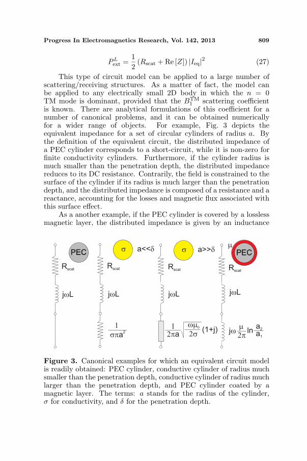
Progress In Electromagnetics Research, Vol. 142, 2013 809
PLext =
12
(Rscat + Re [Z]) |Ieq|2 (27)
This type of circuit model can be applied to a large number ofscattering/receiving structures. As a matter of fact, the model canbe applied to any electrically small 2D body in which the n = 0TM mode is dominant, provided that the BTM
1 scattering coefficientis known. There are analytical formulations of this coefficient for anumber of canonical problems, and it can be obtained numericallyfor a wider range of objects. For example, Fig. 3 depicts theequivalent impedance for a set of circular cylinders of radius a. Bythe definition of the equivalent circuit, the distributed impedance ofa PEC cylinder corresponds to a short-circuit, while it is non-zero forfinite conductivity cylinders. Furthermore, if the cylinder radius ismuch smaller than the penetration depth, the distributed impedancereduces to its DC resistance. Contrarily, the field is constrained to thesurface of the cylinder if its radius is much larger than the penetrationdepth, and the distributed impedance is composed of a resistance and areactance, accounting for the losses and magnetic flux associated withthis surface effect.
As a another example, if the PEC cylinder is covered by a losslessmagnetic layer, the distributed impedance is given by an inductance
Figure 3. Canonical examples for which an equivalent circuit modelis readily obtained: PEC cylinder, conductive cylinder of radius muchsmaller than the penetration depth, conductive cylinder of radius muchlarger than the penetration depth, and PEC cylinder coated by amagnetic layer. The terms: a stands for the radius of the cylinder,σ for conductivity, and δ for the penetration depth.

810 Liberal et al.
proportional to the magnetic layer permeability. Finally, note thatit can also be applied to an ideal PEC wire periodically loaded withlumped elements of impedance Zlumped , in which case the distributedimpedance would be given by Zlumped/p, with p being the periodicityof the load [30]. Since lumped elements could perfectly represent theport of a receiving antenna, this example illustrates that there is nophysical difference between generic scatterers and receiving antennas.
4.2. Implications of the Circuit Model Representation
Formulating power quantities in circuital terms, as in (25)–(27),not only provides a straightforward way to compute the absorbed,scattered and extracted powers, but also helps to extricate thecorrelations between the absorbed and scattered powers, as well as theirfundamental limits. Moreover, it helps an antenna engineer understandthe practical implications of a design.
The scattering resistance in Fig. 2 for the 2D plane wave excitationproblem, Rscat = η0k0/4, is real, positive and non-vanishing. Morestrikingly, it is independent of the wire and incident field properties.Therefore, it can be concluded that there is an inherent radiativecomponent associated with the equivalent current distribution thatforms the scattered field. Consistently, there cannot be absorptionwithout scattering. In connection with the optical theorem, the reasonfor this fact is that the power carried by the incident field outside thescatterer must be reduced by the amount of absorbed power, whichcan only be done through a destructive interference produced by thescattered field. In this regard, the necessity of the scattered fieldto produce this destructive interference in the forward direction wasillustrated by Collin [14] in a number of scattering problems, includingtypical obstacles such as reflectors and disks.
In circuital terms, if there is a certain amount of current Ieq flowingon the circuit, then there must also be scattered power given by (26):12Rscat |Ieq|2. Since Rscat cannot be controlled either by the wiregeometry or its electromagnetic properties, the amount of scatteredpower can only be manipulated through the amount of current. Thisfact leads to limitations and inter-dependencies between the absorbedand scattered powers.
Since Rscat cannot be zero, the absorbed power is maximized whenthe effective distributed impedance Z is the complex conjugate of thescattering impedance, i.e., when Z = Rscat − jωL. In this maximalcase, the absorbed power per unit length (25) is equal to
PL,MAXabs =
12|E0|24Rscat
=|E0|22η0k0
(28)

Progress In Electromagnetics Research, Vol. 142, 2013 811
Moreover, with Rscat = Rabs, it then directly follows that the scatteredand absorbed powers are equal when the absorbed power is maximized,i.e.,
if Pabs = PL,MAXabs then Pscat = Pabs (29)
This necessary condition for maximizing the absorbed power has far-ranging practical implications beyond simply receiving antennas.
It is worth remarking that the extracted power, which is identifiedas the total power dissipated within the equivalent circuit, is not aconstant; but it changes as a function of the scatterer properties, i.e.,it depends on the distributed impedance Z. Specifically, the powerdissipated within the circuit is maximized when there is no reactance,and the resistance is made as low as possible, i.e., when Z = −jωL.Strikingly, the extracted power is maximized for the lossless, zeroabsorption case. In such a particular case, the extracted power canbe written as
PL,MAXext =
12|E0|2Rscat
=2 |E0|2η0k0
(30)
Moreover, since the extracted power is maximized in the lossless case,the extracted and scattered powers are equal in this idealized limit,i.e., PL
ext = PLscat. Consequently, the maximal scattered power is also
given by (30), i.e., in the lossless limit PL,MAXext = PL,MAX
scat .Since the maximal extracted power is obtained for the lossless case,
it must be concluded that the presence of absorption actually limitsthe amount of power that can be extracted from the incident field.Specifically, it is found by comparing (30) and (28) that the maximumabsorbed power is a quarter of the maximum extracted power. Thismeans that no scatterer can absorb more than 25% of the maximumamount of power that can be extracted from the same incident field,i.e., from (28) and (30), one finds:
PL,MAXabs =
14
PL,MAXext (31)
To finalize this discussion, this fact should not lead one to thewrong conclusion that the absorbed power can never exceed 50% of thepower extracted from the incident field. On the contrary, absorptionefficiencies larger than 50% are perfectly possible. This was recognizedby Collin [14]. Green’s antenna [6] is but one of the many examples inwhich the absorbed power is larger than a 50% of the extracted power.This possibility is also illustrated by the circuit model presented herein,in which the ratio between the absorbed and scattered powers is equalto the ratio between the distributed and scattering resistances, i.e.,
PLabs
PLscat
=Re [Z]Rscat
=PL
abs
PLext − PL
abs
(32)

812 Liberal et al.
As the losses are increased so that PLabs → PL
ext, this ratio can be madeas large as desired. However, when constrained by (30) and its losslesslimit, this outcome comes at the cost of reducing PL
abs. Consequently,there is a compromise between the absorbed power (i.e., effective area)and the visibility of a receiving antenna. Cloaked [1] and forward-scattering [20] sensors are examples of strategies to efficiently solvethis design trade-off.
5. MULTIPOLAR APPROACH
One may wonder up to which point the conclusions extracted bymeans of the equivalent circuit model can be extrapolated to other 2Dstructures. Admittedly, the equivalent circuit model has been derivedfor electrically small 2D structures. However, because the limits seemso natural when a circuit model representation is considered, one mightanticipate that similar conclusions could be drawn for the scatteringby a large number of, if not all, 2D objects.
As indicated earlier, the work of R. E. Collin motivated the useof tools, such as the optical theorem and multipolar approaches, asalternatives to the circuit models. As a matter of fact, a more generic,albeit more mathematical, derivation of the demonstrated limits onthe absorbed and scattered powers can be accomplished by followinga purely multipolar approach. This section presents the 2D derivationin terms of the cylindrical harmonic decomposition, which is the mostconvenient for 2D geometries. The analogous 3D analysis based onspherical harmonics was presented in [3]. The following 2D analysisallow us to emphasize the differences between the 2D and 3D problems.
5.1. Far-field Interactions
Let us address the limits of the absorbed, scattered and extractedpowers in FF interactions on the basis of their multipolar sums (16)–(19). Let us first inspect the multipolar representation of the absorbedpower (16). To find the maximum absorbed power for a generic source,defined by the coefficients A
TZ≶n , one can take derivatives of (16) with
respect to the terms Re[BTZn ] and Im[BTZ
n ]. This approach leads to theconclusion that the absorbed power PL
abs is maximized for the followingcondition between the source and scattering coefficients:
BTZn = −1
2ATZ<
n (33)

Progress In Electromagnetics Research, Vol. 142, 2013 813
which means the maximum absorbed power is given explicitly by theexpression:
PL,MAXabs =
12η0k0
∞∑n=−∞
∑
Z=E,M
∣∣ATZ<n
∣∣2 (34)
In consistency with the circuit model representation, it is foundby introducing (33) into (17) that the absorbed and scattered powersare equal when the absorbed power is maximized, which means theabsorbed power is 50% of the extracted power. On the other hand, asnoted earlier, in many cases the absorbed power can be much largerthan 50% of the extracted power. This fact can also be checkedin the multipolar formulation by taking the limit: BTZ
n → 0, andnoting that the scattered power (17) decreases faster than the absorbedpower (16). Therefore, arbitrarily large ratios between the absorbedand scattered powers are indeed feasible, though at the cost of asimilar decrease in the absorbed power. In fact, it is also apparentfrom (17) that a zero scattered power can only be achieved in the exactlimit: BTZ
n = 0. However, it is found from (16) that BTZn = 0 also
implies a zero absorbed power. Consequently, the cylindrical harmonicrepresentation ratifies the principle that there can not be absorptionwithout scattering.
Summarizing, the considerations on the absorbed power derivedthrough the circuit model are fully consistent with those derived bymeans of the multipolar approach. However, the latter results are muchmore general. They have been derived for 2D scatterers of arbitrarysize, shape and constitutive parameters, as well as for arbitrary incidentfields. Thus, the multipolar approach allows us to generalize the resultsintuitively obtained with the circuit model representation to general 2Dscatterers.
As a particular example, consider a uniform plane wavepropagating along the x-axis with an electric field magnitude: E0, andpolarized along the wire axis (z-axis). It has the expansion coefficients:ATM<
n = jnE0, ATE<n = 0 [29]. (Note that the ATZ>
n coefficients donot exist because the sources of the plane wave are located at infinity.)Introducing these coefficients into (34), the maximum (limit) of theabsorbed power for this particular excitation is given explicitly by
PL,MAXabs
∣∣∣pw
=1
2η0k0
∞∑n=−∞
|E0|2 (35)
It can be immediately verified that for electrically small structures,i.e., scatterers for which only the n = 0 TM cylindrical harmonic is

814 Liberal et al.
non-trivial, (35) reduces to (28), i.e., that
PL,MAXabs,elecsmall
∣∣∣pw
=1
2η0k0|E0|2 (36)
In other words, the limit derived based on the multipolar approachis fully consistent with the limit derived on the basis of the circuitmodel. Consider also a finite-size scatterer able to efficiently couplewith a number of multipoles up to order n = N . The limit of absorbedpower is then given by
PL,MAXabs,N-multipoles
∣∣∣pw
=|E0|22η0k0
(2N + 1) (37)
Similarly, for electrically large scatterers, a rule of thumb employed forthe truncation of this series is N = k0a [28]. With this truncation rule,the absorbed power limit becomes:
PL,MAXabs,eleclarge
∣∣∣pw
=
|E0|22η0
2a (38)
which corresponds to the integration of the density of the incidentpower over the diameter of the circumference which circumscribes thescatterer. In other words, the derived limit consistently recovers thegeometrical optics limit for electrically large structures.
Note that the maximal absorbed power (35) is infinite, i.e., (37)diverges as N → ∞. This is an artifact that is due to the infiniteamount of energy artificially carried by an ideal plane wave. Inpractice, as the effective area of the scatterer grows, the assumption ofuniform illumination over the effective area of the scatterer no longerholds; and the plane-wave model cannot be employed. As a matterof fact, within the range of applicability of the plane-wave excitation,the scatterer is typically extracting only a small fraction of the powerproduced by the plane wave sources.
To emphasize further, this cylindrical harmonic formulation allowsus to accentuate the differences between the 2D and 3D geometriesand to illustrate why the upper bounds of objects that are electricallylarge only along one particular direction are more accurately describedwith it. Specifically, one finds from (37) that the upper bound ofabsorbed power for 2D objects increases as 2N + 1 along with thenumber of harmonics N , while it was found to increase as N2 + 2Nfor 3D geometries [22]. Thus, it can be concluded that the growth rateper harmonic is much smaller in 2D geometries. This behavior alsoillustrates the difficulty of examining structures having a high aspectratio with the more general 3D spherical harmonics decomposition.To this end, let us consider an arbitrary cylinder with electrically large

Progress In Electromagnetics Research, Vol. 142, 2013 815
length L, but much smaller cross-section, whose size suggests the useof N0 harmonics, i.e., whose electrical length k0L À N0. According tothe 3D spherical decomposition, the upper bound of absorbed powerwould be as high as [|E0|2/(2η0)] · L/k0 · π(k0L + 1), while thedecomposition into cylindrical harmonics would lead to the tighterbound [|E0|2/(2η0)] · L/k0 · (2N0 + 1).
Let us now focus on the limits of the scattered and extractedpowers. Inspecting (17) reveals that PL
scat grows along with thecoefficients BTZ
n , and thus it cannot be maximized through the samederivation approach that was used for the absorbed power PL
abs. Infact, the generality of the scatterer will be restricted in our analysisfrom now on to enable the derivation of the limits for the scatteredand extracted powers. Specifically, let us assume that the scatterer ispassive, linear, and that its surface allows the cylindrical harmonics tointeract independently. In such a case, the scattered field coefficientsare proportional to the incident field coefficients in the region of thescatterer, i.e.,
BTZn = bTZ
n ATZn (39)
and passivity holds independently for each multipole, i.e.,
PL,TZabs,n = − ∣∣ATZ
n
∣∣2
Re[bTZn
]+
∣∣bTZn
∣∣2
> 0 (40)
Thus, positive definiteness of the absorbed power: PL,TZabs,n > 0, imposes
the conditions: Re[bTZn ] < 0 and |Re[bTZ
n ]| ≥ |bTZn |2. Furthermore,
since |Re[bTZn ]| ≤ |bTZ
n |, it also requires that |bTZn | ≤ 1. Therefore, the
condition on the bTZn coefficients to achieve the maximum scattered
power can be written as∣∣bTZ
n
∣∣2 = 1 −→ bTZn = −1 (41)
Therefore, the maximal scattered power per unit length is given by
PL,MAXscat =
2η0k0
∞∑n=−∞
∑
Z=E,M
∣∣ATZn
∣∣2 (42)
Again, the maximum scattered power is found to be four times largerthan the maximum absorbed power, i.e.,
PL,MAXscat = 4 PL,MAX
abs (43)
Moreover, the assumption (39) also allows us to write the extractedpower as
PL,TZext,n = − 2
η0k0
∞∑n=−∞
∑
Z=E,M
∣∣ATZn
∣∣2 Re[bTZn
](44)

816 Liberal et al.
Equation (44) reveals that extracted power increases along withRe[bTZ
n ]. Therefore, its upper limit is reached when bTZn = −1. In
this manner the multipolar approach generalizes the result that theextracted and scattered powers share the same upper bound. Thus, itcan be concluded that the extracted power per unit length is maximizedfor the ideal lossless case; and, therefore, the presence of losses limitsthe amount of power that can be extracted from the incident field.
Throughout the multipolar discussion of the scattered andextracted powers, the balance of powers for each multipole has beenconsidered independently, assuming (39). This condition is rigorouslysatisfied for cylindrical objects, and it is approximately satisfiedby 2D objects with soft surfaces. However, the limit of absorbedpower (34) has been derived for completely arbitrary scatterers. Itwas found, according to (33), that the absorbed power is maximizedunder a condition in which the balance of powers for each multipoleis considered independently. This result encourages us to believe thatthe results in terms of the scattered and extracted powers can indeedbe generalized to arbitrary scatterers.
5.2. Near-field Interactions
In contrast with FF interactions, the source and scatterer/receivingantenna are coupled in NF interactions. Therefore, the scatterer affectsthe power supplied by the sources, PL
sup. Consequently, the magnitudeof interest for an efficient transmission of energy is typically the powertransfer efficiency, which is defined as the fraction of the power suppliedby the sources that is absorbed by the scatterer:
PTE =PL
abs
PLsup
(45)
In FF interactions this ratio is very small, and the PTE is maximizedby increasing the absorbed power, no matter how much power isscattered. On the other hand, maximizing PL
abs does not necessarilylead to the highest PTE in NF interactions. In particular, anuncontrolled leakage of power into the radiated field (possibly producedby the scattered power which is inevitably associated to the absorbedpower) could decrease the overall PTE .
Following Collin’s description of the process [12], powerconservation implies that all the supplied power is either absorbed bythe scatterer or radiated away from the system, i.e.,
PLsup = PL
abs + PLrad (46)
This simple statement suggests two main strategies to asymptoticallyget a 100% power transfer. First, one would want to suppress PL
rad by

Progress In Electromagnetics Research, Vol. 142, 2013 817
destructive interference. Second, one would want to obtain an absorbedpower much larger than the power radiated away from the system, i.e.,PL
abs/PLrad À 1.
Let us analyze both possibilities through the cylindrical harmonicrepresentation of the power magnitudes (16)–(19). In view of (19), webegin with the condition that the multipolar coefficients must satisfyto achieve zero radiated power, PL
rad = 0, which is:
BTZn = −ATZ>
n (47)
This condition (47) means that the contributions from each of themultipoles associated with the sources and the scatterer must beequal in magnitude, but out-of-phase. This results in a net radiatedfield that is equal to zero due to destructive interference. Due tothe degrees of freedom provided by the coefficients of the incidentfield, ATZ>
n , and the scatterer, BTZn , in their exterior regions, the
condition (47) is compatible with the net absorbed power result.Therefore, there are configurations in which all of the power suppliedby the sources is absorbed by the scatterer. Moreover, in theory, thecondition (47) is indeed compatible with the absorbed power beingmaximized. Consequently, there are configurations leading to a 100%PTE , while keeping the absorbed power at a maximum. In particular,this is achieved when the following combined condition is satisfied
BTZn = −ATZ>
n = −12ATZ<
n (48)
Unfortunately, the combined condition (48), though possible,imposes very stringent limits on the sources of the incident field.When the sources are close to the scatterer (i.e., only NF interactionsexist between the sources and the scatterer), the absolute values ofthe source coefficients for the r < r′ region are much larger thanthe corresponding absolute values of the source coefficients in ther > r′ region, i.e., |AlTZ<
nm | À |AlTZ>nm |. Therefore, it can be concluded
that (48) cannot be satisfied in near-field interactions. In other words,it is not possible to simultaneously suppress the radiated power andkeep the absorbed power to be at its maximum in NF interactions.Moreover, the multipolar approach applied to the 3D case concludedthat the combined condition (48) cannot be satisfied when a Hertziandipole excites a finite scatterer [3]. Therefore, it can be inferredthat (48) can not be satisfied with small devices.
This conclusion led us to the second strategy to asymptoticallyget a 100% PTE. Comparing (16) and (19), one finds that whilethe coefficient ATZ<
n is present in the multipolar formulation of theabsorbed power, this coefficient is not present in the multipolarformulation of the radiated power. Therefore, if ATZ<
n À ATZ>n

818 Liberal et al.
and ATZ<n À BTZ
n , it is possible to asymptotically approach thePTE = 100% limit. On the one hand, the condition ATZ<
n À ATZ>n
also means that the incident field in the region of the scatterer is muchlarger than the field radiated by the sources into the exterior region.This condition can be satisfied by simply placing a poor radiator (e.g.,one with a large reactive field) in the vicinity of the scatterer. On theother hand, the condition ATZ<
n À BTZn means that the scattered field
is significantly weaker than the incident field on its surface, and thatthe absorbed power is well below its maximum value (33). Thus, thePTE can approach the desired 100% limit, but the actual total amountof absorbed power must be much lower than what the scatterer couldactually handle.
This result exemplifies how the correlations between absorbedand scattered powers also influence the transfer of power in NFinteractions. In essence, unless there is a perfect destructiveinterference configuration, a large absorbed to scattered power ratiois needed to avoid a leakage of power in the form of radiated power.However, as was found in the FF interactions, it was demonstratedthat such large ratios can only be achieved with absorbed powersmuch smaller than the upper bound. Therefore, the optimal receiverto realize a large PTE in the very NF case features a poor performancein FF interactions. Nevertheless, note that reducing the possibleabsorbed power would also make the system more vulnerable againstundesired parasitic losses.
6. CONCLUSIONS
This work has introduced circuit and multipolar approaches toinvestigate the correlations between absorption and scatteringprocesses in 2D scattering problems. Both formulations weredescribed with the intent to illustrate the tools that can be usedto straightforwardly compute the set of powers involved in anyscattering process. They also provide a means to investigate theassociated balance of powers and the fundamental limits on eachcontribution. This work therefore completes previous studies based on3D geometries [3, 21, 22]. Specifically, we have presented upper boundsof the absorbed, scattered and extracted power for 2D geometries, thusrevealing the main similarities and differences between the 2D and 3Dscenarios, as well as the difficulties of analyzing 3D objects with highaspect ratio by using a vector spherical harmonic decomposition.
We have also intended with this analysis to illustrate how theseminal work of R. E. Collin has led to an improvement in theunderstanding of the long-standing problem of the powers associated

Progress In Electromagnetics Research, Vol. 142, 2013 819
with a receiving antenna, and how it stimulated research seeking outnew and more adequate tools to address it. In this manner, thisarticle also serves to review recent advances in this receiving antennaproblem. In summary, we believe there is a consensus that, due toenergy conservation issues exemplified by the optical theorem, therecannot be absorption without scattering. In addition, this correlationbetween the absorption and scattering processes leads to the fact that,when the absorbed power is maximized, the absorbed and scatteredpowers must be equal. Despite this fact, it also was demonstrated thatthe ratio between the absorbed and scattered powers can be arbitrarilylarge, although at the cost of decreasing the actual amount of powerabsorbed. Cloaked and forward scattering sensors are examples of howobtain such large ratios, while minimizing the sacrifice in terms of theabsorbed power. As discussed, it can also be demonstrated that themaximal extracted and scattered powers are equal, which means thatthe maximum extracted power is four times larger than the maximalabsorbed power. Consequently, despite its seemingly contradiction,the presence of losses actually limits the amount of power that can beextracted by any scatterer/receiving antenna.
Aside from being of fundamental interest, the correlation betweenthe absorption and scattering processes in a scatterer/receivingantenna scenario has far-reaching technological implications in bothFF and NF scenarios. In FF interactions, such correlations imposea compromise between the effective area and the visibility of areceiving antenna. In NF interactions, the leakage of radiation froma coupled system can, in theory, be totally suppressed by means ofdestructive interference or by emphasizing reactive effects. However,the correlations between the absorption and scattering processes alsoimpose practical trade-offs in NF systems. Specifically, it is foundthat a total suppression of the radiated power can only be achievedby sacrificing both the PTE for larger distances and the robustnessof the system against undesired dissipation for smaller distances.Recognizing these FF and NF tradeoffs, an antenna engineer has abetter perspective from which to design an optimal receiving antennasystem for a specific application.
Finally, it was shown that all of the aforementioned conclusionshold for both 2D and 3D geometries. Nonetheless, it was alsodemonstrated that the dissimilarities between both the 2D and 3Dgeometries lead to quantitative differences on the upper bounds ofthe absorbed, scattered and extracted powers. As a consequence, italso was demonstrated how important it is to select the appropriateapproach to describe the problem, e.g., choosing either the cylindricalor spherical harmonics approach to analyze the problem as a function

820 Liberal et al.
of the aspect ratio of the object under consideration.
ACKNOWLEDGMENT
This work was supported in part by the Spanish Ministry of Scienceand Innovation, Projects No. TEC2009-11995 and No. CSD2008-00066and by the NSF Contract No. ECCS-1126572. Prof. R. W. Ziolkowskiwould like to give special thanks to Prof. I. M. Besieris for his invitationto contribute to this special issue in honor of Prof. R. E. Collin andto Prof. W. Chew for helping make this issue a reality. He recalls hisoriginal impressions in awe of Prof. Collin while learning waveguidetheory from his textbook [35] as a graduate student at the Universityof Illinois at Urbana-Champaign in the late 1970’s. He was introducedto Prof. Collin by Prof. Besieris and interacted with him at severalIEEE International Symposium on Antennas and Propagation andU. R. S. I. Meetings in the 1980’s and 1990’s. It was his great pleasureto find that Prof. Collin was a wonderful person in addition to being anexceptionally talented electromagnetic theorist. While at the LawrenceLivermore National Laboratory in the 1980’s, he was on the receivingend of Prof. Collin’s many insightful comments on his aperture couplingwork and his localized wave work with Prof. Besieris. He later usedProf. Collin’s chapter on “Artificial Dielectrics” in [35] during hisinitial efforts on artificial atoms and molecules in the 1990’s and onmetamaterials in this century. He is delighted to acknowledge thecontinuing impact of Prof. Collin’s numerous books and publicationson his students at the University of Arizona and their enduring impacton students worldwide.
REFERENCES
1. Alu, A. and N. Engheta, “Cloaking asensor,” Phys. Rev. Lett.,Vol. 102, No. 23, 233901, 2009.
2. Vehmas, J., P. Alitalo, and S. A. Tretyakov, “Experimentaldemonstration of antenna blockage reduction with a transmission-line cloak,” IET Microwaves, Antennas Propag., Vol. 6, No. 7,830–834, 2012.
3. Liberal, I., I. Ederra, R. Gonzalo, and R. W. Ziolkowski,“A multipolar analysis of near-field absorption and scatteringprocesses,” IEEE Trans. Antennas Propag., Vol. 61, No. 10, 5184–5199, Oct. 2013.

Progress In Electromagnetics Research, Vol. 142, 2013 821
4. Montgomery, C. G., R. H. Dicke, and E. M. Purcell, “Principles ofmicrowave circuits,” Radiutiotz Laboratory Series, Vol. 8, 317–333,McGraw-Hill, New York, 1948.
5. Kahn, W. K. and H. Kurss, “Minimum scattering antennas,”IEEE Trans. Antennas Propag., Vol. 13, No. 5, 671–675,Sep. 1965.
6. Green, R. B., “Scattering from conjugate-matched antennas,”IEEE Trans. Antennas Propag., Vol. 14, No. 1, 17–22, Jan. 1966.
7. Wasylkiwskyj, W. and W. K. Kahn, “Theory of mutual couplingamong minimum-scattering antennas,” IEEE Trans. AntennasPropag., Vol. 18, No. 2, 204–216, Mar. 1970.
8. Rogers, P. G., “Application of the minimum scattering antennatheory to mismatched antennas,” IEEE Trans. Antennas Propag.,Vol. 34, No. 10, 1223–1228, Oct. 1986.
9. Munk, B. A., Finite Antenna Arrays and FSS, John Wiley & Sons,New York, 2003.
10. Love, A. W., “Comment: On the equivalent circuit of a receivingantenna,” IEEE Antennas Propag. Mag., Vol. 44, No. 5, 124–126,2002.
11. Van Bladel, J., “On the equivalent circuit of a receiving antenna,”IEEE Antennas Propag. Mag., Vol. 44, No. 1, 164–165, 2002.
12. Collin, R. E., “Limitations of the Thevenin and Norton equivalentcircuits for a receiving antenna,” IEEE Antennas Propag. Mag.,Vol. 45, No. 2, 119–124, 2003.
13. Love, A. W., “Comment: Limitations of the Thevenin and Nortonequivalent circuits for a receiving antenna,” IEEE AntennasPropag. Mag., Vol. 45, No. 4, 98–99, Aug. 2003.
14. Collin, R. E., “Remarks on: Limitations of the Theveninand Norton equivalent circuits for a receiving antenna,” IEEEAntennas Propag. Mag., Vol. 45, No. 4, 99–100, Aug. 2003.
15. Andersen, J. B. and R. G. Vaughan, “Transmitting, receiving, andscattering properties of antennas,” IEEE Antennas Propag. Mag.,Vol. 45, No. 4, 93–98, Aug. 2003.
16. Pozar, D. M., “Scattered and absorbed powers in receivingantennas,” IEEE Antennas Propag. Mag., Vol. 46, No. 1, 144–145, Feb. 2004.
17. Balanis, C. A., Antenna Theory: Analysis and Design, 3rdEdition, John Wiley & Sons, New York, 2005.
18. Kraus, J. D., Antennas, 2nd Edition, McGraw Hill, New York,1988.

822 Liberal et al.
19. Aharoni, I., Antennae, an Introduction to Their Theory, 164–176,Clarendon Press, Oxford, 1946.
20. Andersen, J. B. and A. Frandsen, “Absorption efficiency ofreceiving antennas,” IEEE Trans. Antennas Propag., Vol. 53,No. 9, 2843–2849, Sep. 2005.
21. Kwon, D. H. and D. M. Pozar, “Optimal characteristics ofan arbitrary receive antenna,” IEEE Trans. Antennas Propag.,Vol. 57, No. 12, 3720–3727, 2009.
22. Liberal, I. and R. W. Ziolkowski, “Analytical and equivalentcircuit models to elucidate power balance in scattering problems,”IEEE Trans. Antennas Propag., Vol. 61, No. 5, 2714–2726, 2013.
23. Alu, A. and S. Maslovski, “Power relations and a consistentanalytical model for receiving wire antennas,” IEEE Trans.Antennas Propag., Vol. 58, No. 5, 1436–1448, 2010.
24. Newton, R. G., “Optical theorem and beyond,” Am. J. Phys.,Vol. 44, No. 7, 639–642, 1976.
25. Gustafsson, M., J. B. Andersen, G. Kristensson, and G. F. Peder-sen, “Forward scattering of loaded and unloaded antennas,” IEEETrans. Antennas Propag., Vol. 60, No. 12, 5663–5668, 2012.
26. Carney, P., J. Schotland, and E. Wolf, “Generalized opticaltheorem for reflection, transmission, and extinction of power forscalar fields,” Phys. Rev. E, Vol. 70, 036611, 2004.
27. Marengo, E. A., “A new theory of the generalized optical theoremin anisotropic media,” IEEE Trans. Antennas Propag., Vol. 61,No. 4, 2164–2179, Apr. 2013.
28. Harrington, R. F., Time-harmonic Electromagnetic Fields,McGraw-Hill, New York, NY, USA, 1961.
29. Balanis, C. A., Advanced Engineering Electromagnetics, Wiley,New York, NY, USA, 2012.
30. Belov, P. A., C. R. Simovski, and S. A. Tretyakov, “Two-dimensional electromagnetic crystals formed by reactively loadedwires,” Phys. Rev. E, Vol. 66, 036610, 2002.
31. Belov, P. A., S. A. Tretyakov, and A. J. Viitanen, “Dispersion andreflection properties of artificial media formed by regular latticesof ideally conducting wires,” Journal of Electromagnetic Wavesand Applications, Vol. 16, No. 8, 1153–1170, 2002.
32. Liberal, I., I. S. Nefedov, I. Ederra, R. Gonzalo, andS. A. Tretyakov, “Electromagnetic response and homogenizationof grids of ferromagnetic microwires,” J. Appl. Phys., Vol. 110,No. 6, 064909, Sep. 2011.
Progress In Electromagnetics Research, Vol. 142, 2013 823
33. Liberal, I., I. S. Nefedov, I. Ederra, R. Gonzalo, andS. A. Tretyakov, “On the effective permittivity of arrays offerromagnetic wires,” J. Appl. Phys., Vol. 110, No. 10, 104902,Nov. 2011.
34. Liberal, I., I. Ederra, C. Gomez-polo, A. Labrador, J. I. Perez-landazabal, and R. Gonzalo, “A comprehensive analysis of theabsorption spectrum of conducting ferromagnetic wires,” IEEETrans. Microwave Theory Tech., Vol. 60, No. 7, 2055–2065,Jul. 2012.
35. Collin, R. E., Field Theory of Guided Waves, 2nd Edition, IEEEPress, New York, 1991.

Progress In Electromagnetics Research, Vol. 143, 421–445, 2013
A WIDEBAND FREQUENCY-SHIFT KEYING MODULA-TION TECHNIQUE USING TRANSIENT STATE OF ASMALL ANTENNA
Mohsen Salehi1, Majid Manteghi1, *, Seong-Youp Suh2,Soji Sajuyigbe2, and Harry G. Skinner2
1Bradley Department of Electrical and Computer Engineering,Virginia Polytechnic Institute and State University, VA 24061, USA2Intel Labs, Intel Corp., Hillsboro, OR 97124, USA
Abstract—The rate of wireless data transmission is limited by theantenna bandwidth. We present an efficient technique to realizea high-rate direct binary FSK modulation by using the transientproperties of high-Q antennas. We show that if the natural resonanceof a narrowband resonant-type antenna is switched at a high rate,the radiating signal follows the variation of resonant frequency andprovides a high-rate data-transmission regardless of the narrowbandcharacteristics of the antenna. The bit-rate in this method isdictated by the switching speed rather than the impedance bandwidth.Since the proposed technique employs the antenna in a time-varyingarrangement, carrier frequencies are not required to be simultaneouslywithin the antenna bandwidth. When demanded, the antenna is tunedto required carrier frequency according to a sequence of digital data.Moreover, if the switching frequency is properly chosen such thatthe stored energy in the near-zone is not dramatically disturbed, anyvariation in the antenna resonance will instantaneously appear in thefar-field radiation due to the previously accumulated energy in thenear field. Therefore, depending on the Q factor and switching speed,radiation bandwidth of the antenna can be improved independentlyfrom the impedance bandwidth. Furthermore, we show that a singleRF source is sufficient to excite both carrier frequencies and the needfor a VCO is obviated. Experimental results are presented to validatethe feasibility of the proposed technique.
Received 22 October 2013, Accepted 18 November 2013, Scheduled 20 November 2013* Corresponding author: Majid Manteghi ([email protected]).
Invited paper dedicated to the memory of Robert E. Collin.

422 Salehi et al.
1. INTRODUCTION
Wireless communication techniques have been widely developed duringthe past decades due to their extensive applications. One desirablecharacteristic of most wireless systems is a wide bandwidth. Thisproblem becomes significant when a high-rate data-transmission isrequired along with a very small-size antenna. Therefore, designingultra-wideband (UWB) antennas which are capable of transmittinghigh data-rate information while occupying a small volume, is oneof the challenges that has drawn a great deal of attention. Forinstance, biomedical implants are among the most critical devicesthat are required to be shrunk in the size while transmitting highdata-rate information. Particularly, devices that interact with thenervous systems such as cochlear and visual prostheses need totransmit a large amount of data in order to provide high-resolutionsensing for the user [1–3]. Even though a high data-rate can beachieved in broadband systems by increasing the carrier frequency,in low-frequency applications such as biomedical implantable devices,wideband data-transmission remains an open challenge. It is well-understood that in linear time-invariant (LTI) structures, antennabandwidth is in contradiction with the size. Hence, small-size antennassuffer from narrow bandwidth [4–6]. Our team has been involved inresearch to break through the fundamental limits of antennas by usingnonlinear time-variant techniques [7–13].
The technique proposed in this paper employs an antenna in atime-varying fashion such that the data-rate is not correlated to thetraditional definition of the impedance bandwidth. We show that fora high-Q antenna, if the fundamental natural resonance is shifted overthe time, the electromagnetic fields that construct the stored energyin the near-zone simultaneously shift to a new resonant frequency.Since the radiative power is tightly coupled to the stored energy ofthe antenna, far-field radiation responds to any abrupt variation ofthe antenna resonant frequency provided that the total stored energydoesn’t decay dramatically. Therefore, if the resonant frequency ofthe antenna is switched at a high rate, a fast frequency-shift keying(FSK) modulation can be directly realized. We also show that ahigh-Q antenna can be used in the transient mode by imposing initialconditions on the current distribution and therefore, a single RF sourceis sufficient to excite both resonant frequencies when operating inthe transient mode. Hence, an FSK signal can be generated andtransmitted by exciting the antenna by only a single-tone sourcewithout needing to use a VCO.
To demonstrate this idea, we utilize a high-Q miniaturized antenna

Progress In Electromagnetics Research, Vol. 143, 2013 423
loaded by switched capacitors as tuning elements. In order to providea comprehensive analysis, we first study the transient characteristicsof a high-Q switched-resonator as an equivalence of small antennas.We show that if a reactive component in a high-Q resonator which ismatched and fed at frequency f1 is switched to a different value, thefrequency of the voltage waveform at the resistive load shifts to a newresonant frequency, f2, as well. Thus, the frequency can be modulatedby the switching signal which is coded by a sequence of digital dataand an FSK modulation can be generated directly by the antenna.The maximum realized bit-rate is therefore a function of switchingrate rather than impedance bandwidth of the antenna.
In Section 2, we present an analogy between a resonant-typeantenna and its equivalent circuit model in the time domain and showthat the transient characteristics of the antenna can be mimicked bythe circuit model. In Section 3, the principles of switched resonatorsare studied. The proposed direct modulation technique is presentedin Section 4. Experimental results are given in Section 5 in order tovalidate the simulation results. Full-wave simulations in this paper arecarried out in CST Microwave Studio while Agilent ADS is used toperform the transient circuit simulations.
2. CIRCUIT MODEL FOR SMALL ANTENNAS
Modeling the antennas by lumped-element equivalent circuit has beenextensively studied. Wheeler [14] introduced the concept of LC circuitequivalence in a parallel or series arrangement for TM01 and TE01
modes, respectively. Schaubert [15] applied Prony’s method to Time-Domain Reflectometer (TDR) data to synthesize a rational functionwith real coefficients that describes the input impedance of the antennaas the summation of poles. Schelkunoff [16] introduced a generalrepresentation of impedance functions based on an arbitrary number ofresonant frequencies and developed a wideband equivalent circuit. Kimand Ling [17] used a rational-function approximation in conjunctionwith Cauchy method [18] to find the coefficients by using the frequency-domain data. Also, the Singularity Expansion Method (SEM) [19] andMethod of Moments (MoM) [20] have been used to derive equivalentcircuit for antennas. Many different approaches to find broadbandequivalent circuit for antennas have been proposed as well [21–26].
Nevertheless, high-Q small antennas excite only one sphericalmode and the input impedance can be matched only at thefundamental resonant frequency. A self-resonant small antenna canbe represented by an RLC circuit. Although an equivalent circuit isfound by mimicking the input impedance of the antenna by that of an

424 Salehi et al.
RLC circuit, transient properties of the radiated fields such as dampingfactor (or time constant) are also similar to those of the circuit model.Since the radiation resistance of the antenna is lumped into a resistor,one can compare the radiated fields of an antenna excited at the nthresonant mode with the load voltage of an equivalent RLC circuit thatis tuned to the resonant frequency of the antenna and resembles theantenna input impedance. Figure 1 shows an antenna that operates ina single resonant mode (nth mode) and its equivalent circuit with thesame input impedance. Current distribution on the antenna surfacefor the tuned mode can be expressed as:
Jn
(r′, s
)=
Jn (r′)(s− sn)(s− s∗n)
(1)
where sn and s∗n are the unloaded conjugate poles associated withthe nth resonance of the antenna, and Jn(r′) is the spatial currentdistribution. Assuming that the current distribution is known, electricfar field can be expressed as:
En (r, s) =µ
4πr
∫
S′s · Jn
(r′, s
)e−
r−r·r′c
sdS′
=µ
4πr
s
(s− sn) (s− s∗n)
∫
S′Jn
(r′
)e−
r−r·r′c
sdS′ (2)
Equation (2) denotes that the electric field in the far-field zone has thesame poles as the surface current. These poles can be found by usingthe equivalent RLC circuit as depicted in Figure 1(b). Input currentand the input impedance of the RLC circuit can be expressed as:
Iin =Vs
Rs + Zin(3)
Zin =1C s
(s− sn)(s− s∗n)(4)
(a) (b)
Rs
Vs
Z in
E (r,s)ffr
Rs
Vs
Z in
Cn Ln Rn Vo
Figure 1. (a) A single-mode excited antenna and (b) equivalent circuitmodel.

Progress In Electromagnetics Research, Vol. 143, 2013 425
where:
sn = − ω0n
2Qn+ jω0n
√1− 1
4Q2n
(5)
ω0n and Qn are the resonant frequency and unloaded Q factor of thecircuit and are defined as:
ω0n =1√
LnCn; Qn = RnCnω0n (6)
The load voltage can be now expressed as:
Vo = Zin · Iin =1
RsC s · Vs
(s− snloaded)(s− s∗nloaded
) (7)
where loaded poles are:
snloaded= − ω0n
2Qnloaded
+ jω0n
√1− 1
4Q2nloaded
(8)
Qnloadedis the loaded quality factor, and is equal to Qnloaded
=(Rn ‖ Rs)Cnω0n. Equation (8) gives the electric far-field poles ofany arbitrary small antenna that operates in single mode at resonantfrequency, ω0n, with corresponding Q factor, Qnloaded
. The equivalentcircuit model can be constructed based on simulated or measured inputimpedance. Since the poles of the modal currents are preserved inthe far zone, the equivalent circuit can be employed to evaluate thetransient characteristics of the antenna in the far field. Even thoughthe circuit model doesn’t account for the time delay, free-space loss nordirectional aspects of the radiation such as polarization and directivity,these parameters don’t contribute to the radiation poles and affect onlythe residue of each pole, i.e., magnitude of the electric fields. Moreover,electric near-field can be also represented by the same poles. Generally,if the current distribution is expanded by the antenna’s natural poles,any time-derivation or integration of Maxwell’s equations will notimpact the location of the poles. In other words, damping factor of thefields for each resonant mode is identical at any measurement point.
Equation (8) suggests that the damping factor for the electricfields of the nth resonance is equal to:
αn =ω0n
2Qnloaded
(9)
In small antennas with Q À 1, Q can be well approximated by theinverse of 3-dB impedance bandwidth as [27]:
Qnloaded=
1BW3 dB
=f0n
∆fn3 dB
(10)

426 Salehi et al.
where ∆fn3 dB= fH−3 dB−fL−3 dB. Equation (9) implies that damping
factor is inversely proportional to the loaded Q of the antenna. Since athigher order resonances, electrical size of the antenna, i.e., ka, is larger,Q factor will be smaller [28]. Therefore, the lowest damping factor isassociated with the fundamental mode. By combining Equations (9)and (10) one finds:
αn = π ·∆fn3 dB(11)
Equation (11) shows that the damping factor of the nth resonantfield can be found by knowing the absolute 3-dB bandwidth of theantenna. It should be emphasized that Equation (11) is based on theequivalent circuit model and is valid only if the antenna is narrowbandsuch that Equation (10) holds, which is the case in a typical small-sizeantenna.
In order to validate Equation (11) we shall study the time-domainelectric fields of two typical resonant-type antennas: dipole and PlanarInverted-F Antenna (PIFA). Figure 2 shows the antenna structures.The dipole is a half-wavelength center-fed with a diameter of 0.2 mmand the dimensions of the PIFA are L×W × h = 13 cm× 7 cm× 5 cmon a 0.3λ×0.6λ ground plane. Both antennas are designed to resonateat 300 MHz. To excite the antennas, a power source matched to 50Ωwith a Gaussian pulse voltage is used in the simulations. As shownin Figure 3, the full-width at half-maximum (FWHM) of the inputpulse is chosen to be τFWHM = 1.35 ns to ensure that high order modesare not excited and only the fundamental resonance contributes to theradiation.
L
h
W
(a) (b)
Figure 2. Simulated antenna structures: (a) PIFA and (b) half-wavelength center-fed dipole antenna
Figure 4 shows the return loss for each antenna. According toEquation (10), Q factors of the dipole and PIFA can be found about3.9 and 22, respectively. Based on the circuit model, i.e., Equation (9)or (11), damping factor of the radiated fields for the dipole and PIFA

Progress In Electromagnetics Research, Vol. 143, 2013 427
Time [ns]
0 2 3 6
Inpu
t pul
se [V
]
0.00
0.25
0.50
0.75
1.00
541
Figure 3. Input Gaussian pulseused to excite the PIFA anddipole.
Frequency [MHz]
0 100 200 300 400 500 600
S
[dB
]11
-20
-15
-10
-5
0
DipolePIFA
Figure 4. Simulated return lossfor the PIFA and dipole.
Time [ns]
0 10 20 30 40
Mag
nitu
de [V
/m]
-1.0
-0.5
0.0
0.5
1.0Electric fielde-αdipole(t-t )d
Time [ns]
0 40 80 120 160
Mag
nitu
de [V
/m]
-0.2
-0.1
0.0
0.1
0.2Electric field
(a) (b)
e-α PIFA(t-t )d
Figure 5. Time-domain z-component of the electric fields in theazimuth plane measured at 2 meters from the antennas: (a) dipoleand (b) PIFA.
is αdipole = 0.23/ns and αPIFA = 0.04/ns. Figure 5 shows the time-domain z-component of the electric fields in the azimuth plane of eachantenna which is measured at a distance of 2 m from the antennas.For comparison, the decaying exponential function, E0e
−α(t−td), isshown as well. E0 is the magnitude of the field at the first peakand td accounts for the travelling time delay and is set to the firstpeak time. As illustrated in Figure 5, damping factor of the electricfields agrees with that predicted by the circuit model. Moreover,Equation (8) indicates that the damped resonant frequency of thecircuit model (transient oscillations) is approximately equal to thesteady-state resonant frequency if Q À 1. Therefore, for the resonant-

428 Salehi et al.
type small antennas we can utilize the equivalent circuit to evaluatethe transient characteristics of the antenna.
3. THE PRINCIPLES OF SWITCHED-CAPACITORRESONATORS
Switching a reactive component in a network rearranges the locationof the poles and hence, one should expect a variation in dampingfactor and resonant frequency after the switching instant. Since theinput reactance of a switched resonator changes due to the change of areactive component, the resonator will be tuned out with respect to thesource frequency and the input impedance deviates from the matchingcondition. Figure 6(a) shows an RLC circuit with a switched capacitorfed by a matched source RL = RS at frequency f1 = 1/2π
√L1C1. At
t = ts, the capacitor C2 is added to C1 which was resonating togetherwith the inductor L. The switched capacitor will change the steady-state resonant frequency to f2 = 1/2π
√L1(C1 + C2) where the new
input reactance is zero and hence, the source will be mismatched withrespect to the input impedance of the new circuit topology. As aresult, a small fraction of the power from the source leaks into theresonator and will be dissipated in the load. If the mismatch factoris high enough, the source will be totally isolated from the resonator.However, the stored energy in the capacitor and inductor before theswitching instant will be discharged to the load at a different frequencywhich is determined by the switched capacitor. Figures 6(b)–(c) showthe equivalent topology of the circuit before and after the switchingmoment.
After switching, i.e., t > ts, voltage at the load is composed oftwo frequency components. The first component is a leakage from thesource at frequency f1. Transmission coefficient from the source to theload after the switching instant can be expressed as:
|T | = 1√1 + K2
; T = −tan−1K (12)
where:
K = Q2f21 − f2
2
f1f2(13)
Q2 is the new loaded quality factor and is equal to RL2
√C1+C2
L .Equations (12) and (13) show that if either the secondary Q factor(Q2) or the difference of the squares of f1 and f2 which is determinedby the value of switched capacitor, C2, is sufficiently large such thatthe power transmission from the source to the load is negligible, circuit

Progress In Electromagnetics Research, Vol. 143, 2013 429
(a)
C2
L R LC1V
t=ts
Rs
Rs
C1 L R L
V0
C + C1 2
I0 L RL||R S
(b) (c)
s
Vs
Figure 6. (a) Topology of the switched RLC circuit fed by a matchedsource (RL = RS) at frequency f1 and its equivalent topologies:(b) before and (c) after the switching moment.
topology after the switching is equivalent to a source-free RLC circuitas depicted in Figure 6(c).
The second frequency component f2 is due to a transient responseproduced by the initial conditions of the inductor and capacitor at theswitching time. The voltage across the load according to the equivalenttopology in Figure 6(c) can be expressed as:
vR
(t′)
= e−αt′ [V1 sin(ωdt
′) + V2 cos(ωdt
′)] (14)
where t′ = t− ts. α and ωd are damping factor and damped resonantfrequency, respectively:
α =ω2
2Q2; ωd = ω2
√1− 1
4Q22
(15)
V1 and V2 are determined by initial conditions and can be found as:
V1 =1ω d
(αV0 +
I0
C
); V2 = V0 (16)
where C is total capacitance, defined as C1 + C2, and Q2 is the loadedquality for t > ts. To find the initial conditions, one must satisfy thecontinuity of the electric charge and magnetic flux, i.e.,
q(t+s
)= q
(t−s
); ϕ
(t+s
)= ϕ
(t−s
)(17)

430 Salehi et al.
From (17), V0 and I0 are found as:
V0 = vR
(t+s
)=
C1
C1 + C2vR
(t−s
)(18)
I0 = iL(t+s
)= iL
(t−s
)(19)
Equation (18) indicates that in order to satisfy the charge continuity,a voltage discontinuity occurs across the capacitors to compensate theabrupt variation of the capacitance. The voltage discontinuity in turn,imposes an energy loss in the capacitors and causes the energy to bereflected back to the source. Therefore, by switching a capacitor att = ts, part of the electric stored energy in the capacitor dissipatesin the source impedance. Since the inductor current is continuousaccording to (19), stored magnetic energy is not interrupted at theswitching time and therefore, the amount of energy reduction can beexpressed as the variation of stored electric energy:
∆W = ∆W e = We|t=t+s− We|t=t−s
=12C1
∣∣vR
(t−s
)∣∣2 − 12
(C1 + C2)∣∣vR
(t+s
)∣∣2
=12C1
∣∣vR
(t−s
)∣∣2(
11 + C1/C2
)(20)
Equation (20) suggests that if vR(t−s ) = 0, the entire stored energywill be preserved. In fact, if the switching time is synchronous withthe zero-crossing of the capacitor voltage at the switching instant, ts,total energy is stored in the inductor in the form of magnetic energyand a capacitance discontinuity will not affect the total stored energy.Therefore, one may set the switching time such that the voltage acrossthe capacitor is zero and the current of the inductor is maximum atthe switching moment, i.e.,
V0 = 0; I0 =Vs
2Lω1(21)
Substituting these initial conditions in (16) and (14), the voltage acrossthe load can be expressed as:
vR
(t′)
=Vs
2LCω1ωde−αt′ sin
(ωdt
′) =Vs
2ω2
2
ω1ωde− ω2
2Q2t′ sin
(ωdt
′) (22)
If the resonator is high-Q (Q À 1), damped resonant frequency ωd
can be approximated by steady-state resonant frequency ω2, accordingto (15) and the load voltage can be simplified as:
vR
(t′)
=ω2
ω1e− ω2
2Q2t′
[Vs
2sin
(ω2t
′)]
(23)

Progress In Electromagnetics Research, Vol. 143, 2013 431
Time [ns]
480 490 500 510 520
Vol
tage
[V]
-0.75
-0.50
-0.25
0.00
0.25
0.50
0.75
Time [ns]
480 490 500 510 520
Vol
tage
[V]
-0.75
-0.50
-0.25
0.00
0.25
0.50
0.75
(a) (b)
Figure 7. Voltage across the load resistor around the switchingmoment at ts = 500 ns, (a) the switch connects C2 to C1 and (b)the switch disconnects C2 from C1.
Figure 7 shows the voltage across the load resistor around theswitching moment at ts = 500 ns in a switched resonator withcomponent values equal to C1 = 2546 pF, C2 = 1431 pF, L = 39.8 pHand RL = RS = 50 Ω. For these values, the 1st and 2nd resonantfrequencies are f1 = 500 MHz and f2 = 400 MHz with Q1 = 200 andQ2 = 250.
In order to study the effect of opening and closing the switch, twocases are shown. In the first case, as shown in Figure 7(a), the sourcefrequency is set to f1 and at ts = 500 ns capacitor C2 is connectedto C1. In the second case, the source frequency is set to f2 and atts = 500 ns capacitor C2 is disconnected from C1 and the resonantfrequency shifts to f1 as depicted in Figure 7(b). In both cases thesource amplitude is 1 V.
As illustrated, right after the switching instant, resonant frequencychanges according to the capacitance variations. From (23), the firstpeak of the transient response right after the switching occurs atωt′ = π
2 and its value is equal to:
Vpeak =ω2
ω1· Vs
2e− π
4Q2 (24)
Since Qs are much larger than 1, Vpeak can be approximated byω2ω1· Vs
2 . The amplitude of the steady-state voltage before the switchingis equal to Vs
2 , therefore the ratio of consequent peaks before and afterthe switching instant is equal to the ratio of frequencies:
Vpeak(>ts)
Vpeak(<ts)≈ f2
f1(25)

432 Salehi et al.
It should be emphasized that in addition to the secondary resonantfrequency after the switching moment, there is a small component inthe transient response due to the imperfect mismatch between thesource and the circuit topology in the transient mode. The amplitudeof this component is found using (12) and (13) equal to 9 mV and11mV for the simulated voltage waveforms in Figures 7(a) and (b),respectively. However, since this component is much smaller than thesecond frequency component, one may neglect it. Damping factor ofthe transient response can be also calculated from (11).
It is obvious that since the absolute impedance bandwidth,∆fn3 dB
, is inversely proportional to the Q factor at a certain resonantfrequency, a high-Q resonator has a smaller damping factor. Therefore,if the resonator has a sufficiently high Q, we can switch betweentwo frequencies according to a sequence of digital data. Due to thesmall decay rate in the transient mode, a frequency-shift keying (FSK)modulator can be realized by switching the capacitor ON and OFF
(a)
(c) (d)
Time [ns]
850 900 950 1000
Vol
tage
[V]
-0.50
-0.25
0.00
0.25
0.50
920 940 960 980 1000
Time [ns]
940 950 960 970 980 990 1000
Time [ns]
960 965 970 975 980 985 990 995 1000
(b)Time [ns]
Vol
tage
[V]
-0.50
-0.25
0.00
0.25
0.50
Vol
tage
[V]
-0.50
-0.25
0.00
0.25
0.50
Vol
tage
[V]
-0.50
-0.25
0.00
0.25
0.50
Figure 8. Load voltage for different switching frequencies:(a) 10 MHz, (b) 25MHz, (c) 50 MHz, and (d) 100 MHz.

Progress In Electromagnetics Research, Vol. 143, 2013 433
based on a data-coded controlling signal.In order to preserve the stored energy, both switch-ON and switch-
OFF instants should be synchronous with the zero-crossing of thecapacitor voltage. In other words, the switching frequency mustbe a common factor of two resonant frequencies. Figure 8 showsthe load voltage for different switching frequencies, 10, 25, 50 and100MHz. Duty cycle of the modulating pulse is 50% and each pulserepresents a pair of 0 and 1 with bit duration of Tb, where 2Tb is thepulse period. In order to generate orthogonal FSK signals, separationbetween frequencies should be an integer multiplication of switchingfrequency fs = 1/Ts [29]. Since each switching pulse represents a pairof 0 and 1, bit-rate is twice the switching frequency. In fact, by using afast switching mechanism, a simple narrowband RLC resonator excitedby a single-tone source can be employed to generate a high data-rateFSK signal. 1st frequency is the same as the source frequency and 2ndfrequency can be tuned by the switched capacitor.
4. DIRECT FSK MODULATION USING A NARROW-BAND SWITCHED-ANTENNA
As discussed in Section 2, a single-mode small antenna can be modeledby an RLC resonator that mimics the antenna in both time andfrequency domain. As a result, the switched-capacitor techniquepresented in Section 3 can be applied to a small antenna in orderto realize a high bit-rate direct FSK modulation. A great benefitof employing the switched-capacitor technique to create a directantenna modulation is that the data-rate is not limited by the antennabandwidth. Figure 9 shows the block diagram of the direct BFSKmodulation. Two capacitors, C1 and C2 are used to tune the antennaat f1 and f2, respectively. The antenna is fed at f1 and a single pole-double throw (SPDT) switch controlled by the data sequence is usedto switch between the resonant frequencies.
Starting at t = 0, C1 loads the antenna and reactive energy beginsto build up at frequency f1. A portion of the energy is stored in C1
and the rest is stored in the near-field zone of the antenna. At themoment of zero-crossing of the capacitor voltage, the switch changesits state to connect C2 and shifts the fundamental natural resonanceof the antenna to f2. Hence, the antenna will operate in the transientmode and radiating fields shift to f2. Since the capacitor C1 doesn’tface a voltage discontinuity, the stored electric energy is not disturbedand if the capacitor is high-Q, the entire stored energy is preserveduntil the next cycle of charging.
Depending on the time constant, after several cycles, stored energy

434 Salehi et al.
in the near-field and capacitors builds up to a maximum. During thetransient operation of the antenna, the stored energy within the near-field decays slightly and provides the radiative power. The amountof energy decay depends on the Q factor of the antenna. Therefore,if the antenna has a high Q, total amount of near-field stored energywill not change dramatically and the bandwidth of the antenna willbe decoupled from the stored energy, i.e., any abrupt variation in thesurface current distribution will appear in the far-field momentarily, ifthe transmission delay is ignored.
By using a pulse train as the switch control signal where a pair of“0” and “1” can be represented by each pulse cycle, f1 associated withC1 represents a “1” and C2 associated with f2 represents a “0”.
In contrast with the resonator, an antenna may excite higherorder modes. Even though the higher order modes have largerdamping factors, part of the input power may couple to thesemodes and high-order resonances appear in the radiated fields. Asmall antenna typically excites the fundamental mode; however, forswitching application an antenna structure with only one excitednatural resonance is required. Recently, an electrically-coupled loopantenna (ECLA) has been introduced as a dual for planar inverted-F antenna (PIFA) [30]. Since ECLA uses an electrically coupledfeeding mechanism, further impedance matching is not required andthe antenna can be highly miniaturized. As a result, the antenna canoperate at a single resonance with a very high Q factor. In addition,ECLA shows excellent radiation efficiency compared to its counterpart,PIFA. These considerations make the ECLA a suitable choice for theproposed modulation technique.
Figure 10 shows the structure of ECLA. The antenna is fed viaa capacitive plane (Wf ) which is used to match the input impedance.
Source(f )1
High-Q antennaRadiation(f & f )1 2
DataSequence SPDT Switch
C1 C2
Figure 9. Block diagram of the proposed direct BFSK modulation.
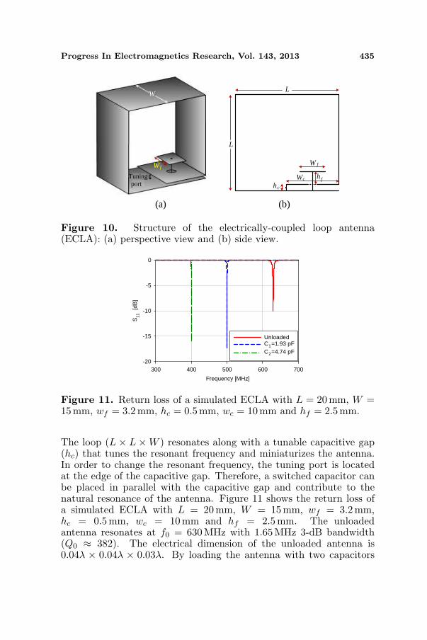
Progress In Electromagnetics Research, Vol. 143, 2013 435
(a)
(b)
W f
L
L
Wc
hc
fh
W
W f
Tuningport
Figure 10. Structure of the electrically-coupled loop antenna(ECLA): (a) perspective view and (b) side view.
Frequency [MHz]
300 400 500 600 700
S11
[dB
]
-20
-15
-10
-5
0
UnloadedC1=1.93 pFC2=4.74 pF
Figure 11. Return loss of a simulated ECLA with L = 20 mm, W =15mm, wf = 3.2mm, hc = 0.5mm, wc = 10 mm and hf = 2.5mm.
The loop (L × L ×W ) resonates along with a tunable capacitive gap(hc) that tunes the resonant frequency and miniaturizes the antenna.In order to change the resonant frequency, the tuning port is locatedat the edge of the capacitive gap. Therefore, a switched capacitor canbe placed in parallel with the capacitive gap and contribute to thenatural resonance of the antenna. Figure 11 shows the return loss ofa simulated ECLA with L = 20 mm, W = 15 mm, wf = 3.2mm,hc = 0.5mm, wc = 10 mm and hf = 2.5mm. The unloadedantenna resonates at f0 = 630 MHz with 1.65 MHz 3-dB bandwidth(Q0 ≈ 382). The electrical dimension of the unloaded antenna is0.04λ × 0.04λ × 0.03λ. By loading the antenna with two capacitors

436 Salehi et al.
C1 = 1.93 pF and C2 = 4.74 pF, resonant frequency can be tunedat f1 = 500 MHz and f2 = 400 MHz with a 3-dB bandwidth ofB1 = 1.6MHz and B2 = 0.8MHz (Q1 = 312.5 and Q2 = 500).
Figure 12 shows the simulation set-up for the switched antenna.A small dipole is placed 1 meter away from the antenna in the E-planeto measure the electric field. The measuring dipole is aligned with theco-pol direction and terminated by a high impedance. As discussedin Section 3, in order to preserve the stored energy in the capacitors,switching moment must be synchronous with the zero-crossing of thecapacitors voltage. This requires the resonant frequencies to be integermultiples of the switching frequency.
Source (500 MHz)
VRInput port
C =4.74 pF2
Tuning port
1 m +
-
Vc1
Vc2
C =1.93 pF1SPDT Switch
Figure 12. Simulation set-up for the switched antenna.
It is worthwhile to point out that due to the transmission-line delay, voltage zero-crossings may slightly change. This can becompensated by delaying the switch signal such that the switchingmoments coincide with the voltage zero-crossing of the capacitors.Figure 13 shows the voltage of the capacitors in conjunction withswitching signal at 50 MHz. Since the distance between the feeding andtuning ports is small, transmission-line delay would not be significantwith this configuration.
The switching signal is a two-level voltage waveform. “0” indicatesthe OFF state of the switch which is associated with the capacitor C1
and frequency f1, while “1” indicates the ON state of the switch whichputs the capacitor C2 in charge of the transient radiation at frequencyf1.
Figure 14 shows the received signal by the measuring dipole for4 different switching frequencies: 10, 25, 50 and 100MHz. Since eachpulse represents two bits, the bit-rate is twice the switching frequency.

Progress In Electromagnetics Research, Vol. 143, 2013 437
.
Time [µs]0.95 0.96 0.97 0.98 0.99 1.00
Cap
acito
r V
olta
ge [V
]
-0.6
-0.3
0.0
0.3
0.6
VC1
VC2
Time [µs]0.95 0.96 0.97 0.98 0.99 1.00
Sw
itch
sign
al [V
]
0.00
0.25
0.50
0.75
1.00
Figure 13. Voltage of the capacitors in conjunction with switchingsignal at 50MHz.
It can be seen that regardless of the extremely narrow bandwidth ofthe antenna, bit-rate can be as high as the carrier frequency. Thishigh bit-rate achievement is mainly due to two factors. Firstly, thetime-varying property of the antenna obviates the need for coveringthe carrier frequency deviation, ∆f = f2 − f1. In other words, theantenna is instantaneously tuned to f1 and f2 when logic “0” and“1” are to be transmitted, respectively. Secondly, since the loadingcapacitors change the natural resonances of the antenna, near-fieldreactive energy switches between different frequencies. After severalswitching cycles, the stored energy reaches a maximum and afterwards,the fields shift between two resonant frequencies due to variation of theantenna’s fundamental resonance, resulting in radiative power shiftsbetween the two frequencies. The nature of this frequency shiftingarises from the variation of antenna poles and is not linked to theantenna input signal. Therefore, if the antenna is sufficiently high-Qand the switching moment is properly chosen such that during thetransient mode the stored energy doesn’t discharge dramatically and

438 Salehi et al.
1.30 1.35 1.40 1.45 1.50
Vol
tage
[mV
]
-0.6
-0.3
0.0
0.3
0.6
1.46 1.47 1.48 1.49 1.50 1.460 1.465 1.470 1.475 1.480 1.485 1.490 1.495 1.500
Time [µs] Time [µs]
1.30 1.35 1.40 1.45 1.50
Vol
tage
[mV
]
-0.6
-0.3
0.0
0.3
0.6
Vol
tage
[mV
]
-0.6
-0.3
0.0
0.3
0.6
Vol
tage
[mV
]
-0.6
-0.3
0.0
0.3
0.6
(a)
(c) (d)
(b)
Time [µs] Time [µs]
Figure 14. Simulated received signals by the measuring dipoleat switching frequencies: (a) 10 MHz, (b) 25MHz, (c) 50MHz and(d) 100 MHz.
remains close to its maximum, the conventional impedance bandwidthwill not limit the radiation bandwidth and the antenna is able torespond to any fast frequency shifting caused by switching the naturalresonances.
5. EXPERIMENTAL RESULTS
To validate the proposed technique, an ECLA was prototyped andmeasured. The experiments are performed at a low frequency inorder to implement a high-Q antenna and achieve a good isolationbetween the two alternating frequencies. In addition, realizing anultra-fast and high-Q switching mechanism is a challenge as most ofthe commercial RF switches suffer from a relatively high insertion lossand low speed. Nevertheless, ultra-fast switching can be addressedby recently developed technologies such as SiGe transistors [31]. The

Progress In Electromagnetics Research, Vol. 143, 2013 439
(a) (b)
Figure 15. (a) Prototyped antenna with dimensions: L = 100 mm,W = 30mm, wf = 25 mm, hc = 0.51mm, wc = 30 mm andhf = 2.5mm, (b) switching circuitry attached to the antenna on aRT/Duroid 5880 with thickness 20 mil.
Switchsignal
LPF
C1pf
L1pfC t
PIN diode
Antenna
RFsource
Figure 16. Switching circuitry.
prototyped antenna is shown in Figure 15 with dimensions: L =100mm, W = 30mm, wf = 25 mm, hc = 0.51 mm, wc = 30 mmand hf = 2.5 mm. The bottom side of the antenna that includes theswitch circuitry is supported by a 20 mil Rogers RT/duroid 5880. Inour experiment, we use a low-loss PIN diode (Avago HSMP-482) in ashunt arrangement as depicted in Figure 16 which shows the switchingcircuitry. The switching signal is separated from the antenna by alow pass filter. When the PIN diode is in reverse bias (switch-OFF),tuning port is open-circuited and the antenna is not loaded. Thereforethe antenna resonates at its original resonant frequency, f1. In theforward-bias state (switch-ON), the antenna is loaded by the capacitorCt through a 0.6 Ω resistance of the forward-biased PIN diode andresonates at the lower frequency, f2.
Although the capacitors and PIN diode are chip components,however due to relatively low-Q properties, particularly for thecapacitors, measurement shows that the loaded Q is considerablyaffected. Figure 17 compares the measured return loss with the results
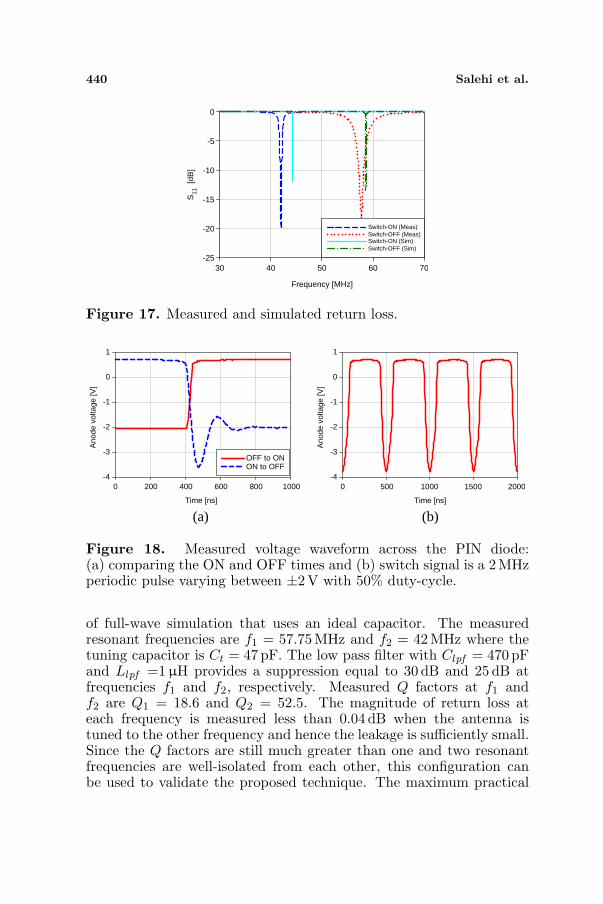
440 Salehi et al.
Frequency [MHz]
30 40 50 60 70
S
[dB
]11
Switch-ON (Meas)Switch-OFF (Meas)Switch-ON (Sim)Switch-OFF (Sim)
-25
-20
-15
-10
-5
0
Figure 17. Measured and simulated return loss.
Time [ns]
0 200 400 600 800 1000
Ano
de v
olta
ge [V
]
-4
-3
-2
-1
0
1
OFF to ONON to OFF
Time [ns]
0 500 1000 1500 2000
Ano
de v
olta
ge [V
]
-4
-3
-2
-1
0
1
(a) (b)
Figure 18. Measured voltage waveform across the PIN diode:(a) comparing the ON and OFF times and (b) switch signal is a 2MHzperiodic pulse varying between ±2 V with 50% duty-cycle.
of full-wave simulation that uses an ideal capacitor. The measuredresonant frequencies are f1 = 57.75 MHz and f2 = 42 MHz where thetuning capacitor is Ct = 47 pF. The low pass filter with Clpf = 470 pFand Llpf =1µH provides a suppression equal to 30 dB and 25 dB atfrequencies f1 and f2, respectively. Measured Q factors at f1 andf2 are Q1 = 18.6 and Q2 = 52.5. The magnitude of return loss ateach frequency is measured less than 0.04 dB when the antenna istuned to the other frequency and hence the leakage is sufficiently small.Since the Q factors are still much greater than one and two resonantfrequencies are well-isolated from each other, this configuration canbe used to validate the proposed technique. The maximum practical

Progress In Electromagnetics Research, Vol. 143, 2013 441
bit-rate in our experiment depends on the switching speed which isdetermined by the PIN diode rise and fall time. Figure 18(a) showsthe measured response of the utilized PIN diode to a step-like functionvarying between ±2V. The ON and OFF time based on 0 to 0.65Vand vice versa is measured about 65 ns. This limits the switching speedto about 15MHz. Also, the PIN diode exhibits an overshoot about 1.5times the biasing voltage at the falling edge causing the OFF timeto be shortened. The switch signal measured as the anode voltage atfrequency 2 MHz is shown in Figure 18(b). Even though the duty cycleof the pulse is 50%, the switch-ON duration associated with the lowerfrequency, f2, is approximately twice the switch-OFF duration thatrepresents the higher frequency, f1.
Figure 19 shows the voltage waveform at the receiving dipole whenthe switched ECLA is in transmitting mode. The RF source is an R&S
1.0 1.2 1.4 1.6 1.8 2.0
Rec
eive
d vo
ltage
[mV
]
-2
-1
0
1
2
Rec
eive
d vo
ltage
[mV
]
-2
-1
0
1
2
1.5 1.6 1.7 1.8 1.9 2.0
Rec
eive
d vo
ltage
[mV
]
-2
-1
0
1
2
1.5 1.6 1.7 1.8 1.9 2.0
Rec
eive
d vo
ltage
[mV
]
-2
-1
0
1
2
Time [µs] Time [µs]
(a)
(c) (d)
(b)
Time [µs] Time [µs]
1.0 1.2 1.4 1.6 1.8 2.0
Figure 19. Measured voltage waveform received by a small dipolefor different switching frequencies: (a) fs = 2 MHz, (b) fs = 4 MHz,(c) fs = 8 MHz, and (d) fs = 12 MHz.

442 Salehi et al.
ZVA50 vector network analyzer in the CW mode which excites theantenna at the frequency f2 = 42MHz. A Tektronix AFG3252 signalgenerator is used to provide a periodic pulse as the switching signal.Time-domain electric fields are measured by a Tektronix MSO4102oscilloscope with 1 MΩ input impedance. The electric fields shown inFigure 19 are measured at switching frequencies 2 MHz, 4MHz, 8 MHzand 12 MHz. It can be seen that even though the antenna bandwidthis measured about 3 MHz at the upper band, an FSK modulation witha bit-rate equal to R = 2×12 = 24 Mb/s is realized. The restriction onthe switching frequency is due to the time constant of the low-pass filterand also the ON and OFF time of the PIN diode. Hence, the bit-ratecan be further improved by using a faster switch and improving thefilter performance. For demonstration purposes, the antenna has alsobeen measured in the receiving mode. Figure 20 shows the receivedvoltage at the input port of the ECLA when connected to a 1 MΩoscilloscope. Both frequencies are on the air with the same powerlevel. Similar to the transmitting mode, the switched antenna receivesboth frequencies according to the switching frequency.
1.0 1.2 1.4 1.6 1.8 2.0Rec
eive
d vo
ltage
[mV
]
1.0 1.2 1.4 1.6 1.8 2.0Rec
eive
d vo
ltage
[mV
]
-100
-50
0
50
100
Time [µs] Time [µs]
(a) (b)
-100
-50
0
50
100
Figure 20. Measured voltage waveform received by the ECLA whenoperating in Rx mode at different switching frequencies: (a) fs =5MHz and (b) fs = 10 MHz.
6. CONCLUSION
A new technique to realize a wideband data-transmission by usinga narrowband antenna was presented. The proposed technique usesthe transient property of a high-Q antenna to implement a binaryFSK modulation with a high data-rate. The properties of a switchedresonator was studied and it was shown that if the Q factor issufficiently high such that the transient damping factor is small, theresonator or antenna can be switched to the transient mode andgenerate a binary FSK signal by using only a single source with aproper switching frequency. An electrically coupled loop antenna wasprototyped and measured to validate the proposed technique.

Progress In Electromagnetics Research, Vol. 143, 2013 443
ACKNOWLEDGMENT
This work is supported in part by Intel Corp.. The authors thankShyam C. Nambiar for his help in preparing this manuscript.
REFERENCES
1. Ghovanloo, M. and K. Najafi, “A wideband frequency-shift keyingwireless link for inductively powered biomedical implants,” IEEETransactions on Circuits and Systems I: Regular Papers, Vol. 51,No. 12, 2374–2383, Dec. 2004.
2. Miranda, H., V. Gilja, C. A. Chestek, K. V. Shenoy, andT. H. Meng, “HermesD: A high-rate long-range wireless transmis-sion system for simultaneous multichannel neural recording appli-cations,” IEEE Transactions on Biomedical Circuits and Systems,Vol. 4, No. 3, 181–191, Jun. 2010.
3. Lee, S. B., M. Yin, J. R. Manns, and M. Ghovanloo, “A widebanddual-antenna receiver for wireless recording from animals behavingin large arenas,” IEEE Transactions on Biomedical Circuits andSystems, Vol. 60, No. 7, 1993–2004, Jul. 2013.
4. Chu, L. J., “Physical limitations on omni-directional antennas,”Journal of Applied Physics, Vol. 19, 1163–1175, Dec. 1948.
5. Harrington, R. F., “Effect of antenna size on gain, bandwidth,and efficiency,” Journal of Research of the National Bureau ofStandards, Vol. 64D, 1–12, Jan.–Feb. 1960.
6. McLean, J. S., “A re-examination of the fundamental limits on theradiation Q of electrically small antennas,” IEEE Transactions onAntennas and Propagation, Vol. 44, No. 5, 672–675, May 1996.
7. Salehi, M. and M. Manteghi, “Utilizing non-linear inductors forbandwidth improvement,” URSI-USNC National Radio ScienceMeeting, Boulder, CO, 2011.
8. Salehi, M. and M. Manteghi, “Bandwidth enhancement usingnonlinear inductors,” 2011 IEEE Antennas and PropagationSociety International Symposium (APSURSI), 1–4, 2011.
9. Manteghi, M., “An inexpensive phased array design usingimpedance modulation,” URSI-USNC National Radio ScienceMeeting, Boulder, CO, 2010.
10. Manteghi, M., “Non-LTI systems, a new frontier in electromag-netics theory,” 2010 IEEE Antennas and Propagation Society In-ternational Symposium (APSURSI), 1–4, 2010.

444 Salehi et al.
11. Manteghi, M., “Antenna miniaturization beyond the fundamentallimits,” URSI-USNC National Radio Science Meeting, Boulder,CO, 2009.
12. Manteghi, M., “A switch-band antenna for software-defined radioapplications,” IEEE Antennas and Wireless Propagation Letters,Vol. 8, 3–5, 2009.
13. Manteghi, M., “Antenna miniaturization beyond the fundamentallimits using impedance modulation,” 2009 IEEE Antennas andPropagation Society International Symposium, (APSURSI), 1–4,2009.
14. Wheeler, H. A., “Fundamental limitations of small antennas,”Proceedings of the IRE, Vol. 35, No. 12, 1479–1484, Dec. 1947.
15. Schaubert, D. H., “Application of Prony’s method to time-domain reflecto-meter data and equivalent circuit synthesis,”IEEE Transactions on Antennas and Propagation, Vol. 27, No. 2,180–184, Mar. 1979.
16. Schelkunoff, S. A., “Representation of impedance functions interms of resonant frequencies,” Proceedings of the IRE, Vol. 32,No. 2, 83–90, Feb. 1944.
17. Kim, Y. and H. Ling, “Equivalent circuit modeling of broadbandantennas using a rational function approximation,” Microwaveand Optical Technology Letter, Vol. 48, No. 5, 950–953, May 2006.
18. Adve, R. S., T. K. Sarkar, S. M. Rao, E. K. Miller, andD. R. Pflug, “Application of the cauchy method for extrapolat-ing/interpolating narrow-band system responses,” IEEE Transac-tions on Microwave Theory and Techniques, Vol. 45, No. 5, 837–845, May 1997.
19. Michalski, K. A. and L. W. Pearson, “Equivalent circuit synthesisfor a loop antenna based on the singularity expansion method,”IEEE Transactions on Antennas and Propagation, Vol. 32, No. 5,433–441, May 1984.
20. Simpson, T. L., J. C. Logan, and J. W. Rockway, “Equivalentcircuits for electrically small antennas using LS-decompositionwith the method of moments,” IEEE Transactions on Antennasand Propagation, Vol. 37, No. 12, 1632–1635, Dec. 1989.
21. Hamid, M. and R. Hamid, “Equivalent circuit of dipole antennaof arbitrary length,” IEEE Transactions on Antennas andPropagation, Vol. 45, No. 11, 1695–1696, Nov. 1997.
22. Love, A. W., “Equivalent circuit for aperture antennas,”Electronics Letters, Vol. 23, No. 13, 708–710, 1987.

Progress In Electromagnetics Research, Vol. 143, 2013 445
23. Vainikainen, P., J. Ollikainen, O. Kivekas, and I. Kelander,“Resonator-based analysis of the combination of mobile handsetantenna and chassis,” IEEE Transactions on Antennas andPropagation, Vol. 50, No. 10, 1433–1444, Oct. 2002.
24. Tang, T. G., Q. M. Tieng, and M. W. Gunn, “Equivalent circuit ofa dipole antenna using frequency-independent lumped elements,”IEEE Transactions on Antennas and Propagation, Vol. 41, No. 1,100–103, Jan. 1993.
25. Streable, G. W. and L. W. Pearson, “A numerical study onrealizable broad-band and equivalent admittances for dipoleand loop antennas,” IEEE Transactions on Antennas andPropagation, Vol. 29, No. 5, 707–717, Sep. 1981.
26. Liu, G. K. H. and R. D. Murch, “Compact dual-frequency PIFAdesign using LC resonators,” IEEE Transactions on Antennas andPropagation, Vol. 49, No. 7, 1016–1019, Oct. 2001.
27. Chu, L. J., “Physical limitations of omni-directional antennas,”Journal of Applied Physics, Vol. 19, 1163–1175, Dec. 1948.
28. Davis, W. A., T. Yang, E. D. Caswell, and W. L. Stutzman,“Fundamental limits on antenna size: A new limit,” IETMicrowaves, Antennas & Propagation, Vol. 5, No. 11, 1297–1302,2011.
29. Proakis, J. G. and M. Salehi, Digital Communications, 5thEdition, McGraw Hill, NY, 2008.
30. Manteghi, M., “Electrically coupled loop antenna as a dual for theplanar inverted-F antenna,” Microwave and Optical TechnologyLetters, Vol. 55, No. 6, 1409–1412, Jun. 2013.
31. Hancock, T. M. and G. M. Rebeiz, “Design and analysis of a 70-ps SiGe differential RF switch,” IEEE Transactions on MicrowaveTheory and Techniques, Vol. 53, No. 7, 2403–2410, Jul. 2005.

Progress In Electromagnetics Research, Vol. 143, 641–673, 2013
MINIMUM Q FOR LOSSY AND LOSSLESS ELECTRI-CALLY SMALL DIPOLE ANTENNAS
Arthur D. Yaghjian1, *, Mats Gustafsson2,and B. Lars G. Jonsson3
1Electromagnetics Research Consultant, 115 Wright Road, Concord,MA 01742, USA2Department of Electrical and Information Technology, LundUniversity, Box 118, SE-221 00 Lund, Sweden3School of Electrical Engineering, KTH Royal Institute of Technology,Teknikringen 33, SE-100 44 Stockholm, Sweden
Abstract—General expressions for the quality factor (Q) of antennasare minimized to obtain lower-bound formulas for the Q of electricallysmall, lossy or lossless, combined electric and magnetic dipoleantennas confined to an arbitrarily shaped volume. The lower-bound formulas for Q are derived for dipole antennas with specifiedelectric and magnetic dipole moments excited by both electric andmagnetic surface currents as well as by electric surface currents alone.With either excitation, separate formulas are found for the dipoleantennas containing only lossless or “nondispersive-conductivity”material and for the dipole antennas containing “highly dispersivelossy” material. The formulas involve the quasi-static electric andmagnetic polarizabilities of the associated perfectly conducting volumeof the antenna, the ratio of the powers radiated by the specified electricand magnetic dipole moments, and the efficiency of the antenna.
1. INTRODUCTION
The lower bounds on the quality factor (Q) of antennas obtainedby Wheeler [1–3] and Chu [4] in the 1940s and 1950s, and in 1960by Harrington [5], were based on circuit models for spherical andcircular cylindrical wave functions. This circuit-model approach tofinding the minimum Q has the advantage of reducing a complex
Received 31 October 2013, Accepted 4 December 2013, Scheduled 10 December 2013* Corresponding author: Arthur D. Yaghjian ([email protected]).
Invited paper dedicated to the memory of Robert E. Collin.

642 Yaghjian, Gustafsson, and Jonsson
problem in electromagnetic theory to the systematic investigation ofa ladder network of RLC circuits [6, 7]. However, the circuit modelswere restricted to representing spherical and circular cylindrical modesand thus the lower bounds on Q were for spheres or circular cylinderscircumscribing the antennas.
In 1964, Robert E. Collin, to whom this issue of PIER isdedicated, and S. Rothschild evaluated the Q of antennas by judiciouslysubtracting the infinite energy of the radiation field from the infiniteenergy of the total field of antennas to obtain a finite “reactive energy”of the antenna [8]. Although Collin and Rothschild also limitedtheir method to finding the lower bounds on the Q for sphericaland circular cylindrical volumes, their work provides the fundamentalunderstanding for not only the general definitions of quality factor forany antenna [9–11] but also for the lower bounds on the Q for antennasconfined to an arbitrarily shaped volume [12, 13].
The primary purpose of the present paper is to generalize thelower-bound formulas obtained in [13, 14] for a single electric-dipoleor magnetic-dipole, lossless antenna to a lossy electric and magneticdipole antenna, with specified electric and magnetic dipole moments,p and m, confined to an arbitrarily shaped volume Va. A secondarypurpose of the paper is to correct the error, found by Jonssonand Gustafsson [15], that was made in the derivation of one ofthe main lower-bound formulas in [13] and resulted in that formulaapplying exactly to only ellipsoidal volumes. (All the comparisonsthat were made in [13] with the sum-rule lower bounds of Gustafsson,Sohl, and Kristensson [12, 16] showed excellent agreement because thecomparisons were made for different shaped ellipsoids.)†
The Q lower-bound formulas derived in this paper, like thosein [13, 14], are limited to electrically small antennas with ka . 5, wherea is the minimum circumscribing radius of the antenna volume Va andk is the free-space wavenumber. Recently, Gustafsson and Nordebo [17]have obtained lower bounds on Q for larger antennas using the “convexoptimization” of current distributions [18]. Also, Thal [7] has obtainedlower bounds on the Q of spherical electric and magnetic dipoleantennas under subsidiary conditions that maximize the gain of theantenna and increase the lower bounds by requiring extra internaltuning to maintain the proper phase between the single-port electriccurrents that feed the electric and magnetic dipoles. For example, Thalhas shown that the lower-bound formula for the Q of an electricallysmall spherical Huygens source (equal-power, perpendicular, cophasal† In the paragraph preceding Section 2.1 of [13], it was erroneously stated that the Q of anelectric dipole moment perpendicular to the plane of a thin oblate spheroid approaches ∞,whereas it actually approaches 9π/[4(kas)3], where as is the radius of the oblate spheroid.

Progress In Electromagnetics Research, Vol. 143, 2013 643
electric and magnetic dipole moments) is twice that of the generallower bound on Q derived for equal-power electric and magnetic dipoles(the general lower bound occurring when the electric and magneticdipole moments are 90 degrees out of phase so that their feed currentsare cophasal) because extra internal tuning (in addition to the tuningnecessary to make the input reactance of the antenna zero) is needed tomaintain the required 90-degree phase difference between the electriccurrents feeding the cophasal electric and magnetic dipole moments.In the present paper, the general lower bounds on Q are determined forelectric and magnetic dipole antennas, allowing for both electric andmagnetic surface currents, without regard for extra internal tuningthat may be required to maintain the phase differences between thegiven electric and magnetic dipole moments. Lower bounds on Qare also determined for electrically small, electric and magnetic dipoleantennas excited by electric surface currents only. These “electric-current lower bounds” are equal to or greater than the general lowerbounds obtained for electric and magnetic dipole antennas excited byelectric and magnetic surface currents (magnetization being equivalentto magnetic current).
2. GENERAL EXPRESSIONS FOR QUALITY FACTOR
In [11] expressions for internal energy density were derived fromMaxwell’s equations and their frequency derivatives in order todetermine a quality factor of antennas that is approximately equal totwice the inverse of the matched VSWR (voltage standing wave ratio)half-power fractional impedance bandwidth of antennas. In particular,the Q of a one-port, linear, passive, lossy or lossless antenna tuned ata frequency ω (so that the input reactance X(ω) = 0) to resonance(X ′(ω) > 0) or antiresonance (X ′(ω) < 0) was given in [11] as
Q(ω) =ω|W (ω)|PA(ω)
= ηω|W (ω)|PR(ω)
(1)
where the power accepted PA(ω) by the antenna is the power radiatedby the antenna plus power lost in the antenna (PA = PR +PL = PR/η,where η is the radiation efficiency; for lossless antennas, η = 1) andthe internal energy is found from
W (ω) = We(ω) + Wm(ω) + Wme(ω) (2)
with
We =14
limr→∞
[ ∫
Vo(r)
Re[E∗ · (ωε)′ ·E]dV − ε0r
∫
4π
|F|2dΩ]
(3a)

644 Yaghjian, Gustafsson, and Jonsson
0S
ShieldedPowerSupply
Antenna
Figure 1. One-port, linear, passive antenna with feed and shieldedpower supply.
Wm =14
limr→∞
[ ∫
Vo(r)
Re[H∗ · (ωµ)′ ·H]dV − ε0r
∫
4π
|F|2dΩ]
(3b)
Wme =14
∫
Va
ReE · [ω(νt + τ ∗)]′ ·H∗ dV. (3c)
Stars (∗) denote the complex conjugate, and primes (′) denotedifferentiation with respect to the angular frequency ω. The vectors(E, D) and (B, H) are the usual time-harmonic (e−iωt, ω > 0)Maxwellian electric and magnetic fields related by bianisotropicconstitutive parameters
D(r) = ε(r) ·E(r) + τ (r) ·H(r) (4a)B(r) = µ(r) ·H(r) + ν(r) ·E(r) (4b)
where ε(r), µ(r), and [ν(r), τ (r)] are the spatially nondispersivepermittivity dyadic, permeability dyadic, and magneto-electricdyadics, respectively. Like the fields, they are, in general, functionsof frequency ω and position r within the media.‡
As shown in Fig. 1, Va is the volume of the antenna material thatlies outside the shielded power supply and the feed waveguide referenceplane S0. Any tuning elements are included in Va. For the purpose of‡ We restrict our attention to the quality factor of linear, passive antennas at isolatedresonances (or antiresonances) and thus ignore increases in bandwidth that can be achieved,in principle, with overlapping multiresonances [19–21] or with nonlinear and/or activedevices [22].

Progress In Electromagnetics Research, Vol. 143, 2013 645
defining an isolated antenna volume Va in free space, we can assumethat an arbitrarily small shielded power supply is contained withinVa. The surface Sa of the volume Va contains the waveguide referenceplane as a subsurface. The volume Vo(r), which includes the volumeVa, is the entire volume outside the shielded power supply and referenceplane S0 out to a large sphere in free space of radius r that surroundsthe antenna system. As r → ∞, the volume Vo(r) becomes infinite.The solid angle integration element is dΩ = dS/r2 = sin θdθdφ with(r, θ, φ) being the usual spherical coordinates of the position vector r,and the complex far electric field pattern F(θ, φ) is defined by
F(θ, φ) = limr→∞ re−ikrE(r) (5)
where k = ω/c = 2π/λ with c being the free-space speed of light andλ the free-space wavelength.
For the following simple scalar constitutive relations
D = (εr + iεi)E, B = (µr + iµi)H, (ν = τ = 0) (6)
the magnetic, electric, and magneto-electric internal energies in (3a)–(3c) reduce to
We =14
limr→∞
[ ∫
Vo(r)
(ωεr)′|E|2dV − ε0r
∫
4π
|F|2dΩ]
(7a)
Wm =14
limr→∞
[ ∫
Vo(r)
(ωµr)′|H|2dV − ε0r
∫
4π
|F|2dΩ]
(7b)
Wme = 0. (7c)
We showed in [11] that the Q in (1), which depends on thedefinition of the internal energy in (3) or (7), was approximatelyequal to twice the inverse of the matched VSWR half-power fractionalbandwidth (FBW hp), that is
Q(ω) = ηω|W (ω)|PR(ω)
≈ 2FBW hp(ω)
(8)
for a sufficiently isolated resonance or antiresonance with Q À 1(Q & 2 often suffices), except when the antenna is dominated by lossydispersive materials; see, for example, [11, Fig. 19]. However, it isnoted that hypothetical materials with conductivities (σe ≥ 0, σm ≥0) independent of frequency such that εi(ω) = εei(ω) + σe/ω andµi(ω) = µmi(ω) + σm/ω, where εei(ω) and µmi(ω) are equal to or

646 Yaghjian, Gustafsson, and Jonsson
greater than zero for all frequencies as well as equal to zero in afrequency window (band) about the ω of interest, should not be includedin the exceptions because these nondispersive conductivities do notaffect the internal energy [23]. They merely change the efficiencyη in (8) to maintain the high accuracy of the inverse relationshipin (8) between bandwidth and Q. This is further corroborated inthe improved formulas (11) where a frequency independent σe or σm
does not contribute to the Q-energy because (ωεi)′ = σ′e = 0 and(ωµi)′ = σ′m = 0. We shall refer to antennas containing materialcharacterized by a scalar permittivity ε(ω) = εr(ω)+iεei(ω)+iσe/ω anda scalar permeability µ(ω) = µr(ω)+iµmi(ω)+iσm/ω with constant σe
and σm for all frequencies as nondispersive-conductivity antennas (orantennas containing nondispersive-conductivity material). All otherantennas or antenna material will be referred to as highly dispersivelossy antennas or antenna material. The µr, µi, εr, εi (σe, σm, εei,µmi) can all be functions of the position vector r.
For antennas containing materials with highly dispersive conduc-tivities, it was found in [24] that a quality-factor energy§ or simplyQ-energy |WQ(ω)|, given in the following formulas, proves to be a re-placement for |W (ω)| that produces a Q that maintains the accuracy ofthe relationship between Q and matched VSWR half-power fractionalbandwidth in (8)
Q(ω) = ηω|WQ(ω)|
PR(ω)(9)
§ The term “quality-factor energy” or simply “Q-energy” was introduced in [24] as analternative to the term “internal energy” to describe the generalized formulas appliedto highly dispersive lossy media because these formulas involve dispersive dissipativeenergy as well as stored energy per unit volume. Regardless of the terminology, thepurpose is to define energy densities, which when integrated, will produce a total Q-energy that determines with reasonable accuracy the inverse-bandwidth Q of antennasincluding those that contain highly dispersive lossy materials. The quality-factor energydensities defined here are not circuit-model dependent [25, 26] but depend only on themacroscopic constitutive parameters and fields of the antenna media (and thus are usefulfor antenna design). The Q-energy differs considerably from both the equivalent-circuitenergy of Tretyakov [25, 26] and the energy obtained by Vorobyev [27] in determiningelectromagnetic wave velocities in lossy dispersive material, but only slightly from themagnetic electrodynamic energy of Boardman and Marinov [28] in the frequency rangewhere their magnetic energy is positive.

Progress In Electromagnetics Research, Vol. 143, 2013 647
with
WQ(ω) =14
limr→∞
[ ∫
Vo(r)
E∗ · (ωε)′ ·E + H∗ · (ωµ)′ ·H
+[E∗ ·(ωτ )′ ·H+H∗ ·(ων)′ ·E]
dV−2ε0r
∫
4π
|F|2dΩ
](10)
instead of (2)–(3),‖ and WQ(ω) = WQe (ω) + WQ
m(ω) + WQme(ω) with
WQe =
14
limr→∞
[ ∫
Vo(r)
(ωε)′|E|2dV − ε0r
∫
4π
|F|2dΩ
](11a)
WQm =
14
limr→∞
[ ∫
Vo(r)
(ωµ)′|H|2dV − ε0r
∫
4π
|F|2dΩ
](11b)
WQme = 0 (11c)
instead of (7). We note that for highly dispersive lossy material, thevalues of the real and imaginary parts of (ωε)′ and (ωµ)′ can be lessthan ε0 and µ0, respectively, and even less than or equal to zero.
If the medium is lossless (η = 1) in a frequency window aboutω, not only does ε = ε∗t , µ = µ∗t , and ν = τ ∗t , but also ε′ = ε′∗t ,µ′ = µ′∗t , and ν ′ = τ ′∗t (subscript t denoting the transpose). Then (10)and (11) reduce to (2)–(3) and (7), respectively. This can be provenby showing that the imaginary parts of E∗ ·(ωε)′ ·E, H∗ ·(ωµ)′ ·H, andE∗ ·(ωτ )′ ·H+H∗ ·(ων)′ ·E are zero. In addition, we have [14, Eqs. (44)and (46)]
ReH∗ ·(ωµ)′ ·H+E∗ · (ωε)′ ·E+E·[(ω(νt+τ ∗)]′ ·H∗
≥µ0|H|2+ε0|E|2 (12a)
Re[E∗ · (ωε)′ ·E]
= E∗ · (ωε)′ ·E ≥ ε0|E|2 (12b)
Re[H∗ · (ωµ)′ ·H]
= H∗ · (ωµ)′ ·H ≥ µ0|H|2 (12c)
‖ The [E∗ · (ωτ )′ ·H + H∗ · (ων)′ ·E] term in (10) was mistakenly written as |E · [(ω(νt +τ∗)]′ ·H∗| in [24, Eqs. (13) and (17a)]. Also, the absolute value signs in [24, Eqs. (13) and(17a)], as well as in [14, Eqs. (59)–(60)], should have been placed outside the integrals asin (9)–(11).

648 Yaghjian, Gustafsson, and Jonsson
in a lossless frequency window about ω. In lossless frequency windows,we also have the inequalities [14, Eqs. (39) and (42)]¶
(ωεr)′ − ε0 ≥ ωε′r2≥ 0 (14a)
(ωµr)′ − µ0 ≥ ωµ′r2
≥ 0 (14b)
for scalar permittivities and permeabilities.+
3. SIMPLIFICATIONS FOR ELECTRICALLY SMALLANTENNAS
The expressions given in (1) or (9) do not define Q uniquely [11]. Inparticular, these expressions for Q depend on the position chosen forthe origin of the coordinate system in which the integration of thefields are performed unless
∫4π r|F|2dΩ = 0 (for example, if the far-
field pattern |F| is symmetric about the origin — as in the case ofa single spherical multipole). Also, the Q of an antenna as definedin (1) or (9) can be increased with “surplus” capacitors and inductorswithout changing the input impedance and thus without changing thebandwidth of the antenna [32, p. 176]. Both of these ambiguities inthe definition of Q can be dealt with effectively, if necessary, by theprocedure given in [11, Section 4.6]. However, for electrically smallantennas (ka . 5, a being the minimum circumscribing radius) wherethe quasi-static fields dominate the stored energy or Q-energy, the¶ The inequalities in (14) are equivalent to those derived by Landau and Lifshitz [29, p. 287]from the first Kramers-Kronig causality relations
εr(ω)− ε0 =2
π∫ ∞
0
νεi(ν)
ν2 − ω2dν, µr(ω)− µ0 =
2
π∫ ∞
0
νµi(ν)
ν2 − ω2dν (13)
given that εi(ν) and µi(ν) are zero in a frequency window about ω (and using the passivityconditions, εi(ν) ≥ 0 and µi(ν) ≥ 0). For hypothetical material with nondispersiveconductivity (ε(ν) = εr(ν) + iεei(ν) + iσe/ν and µ(ν) = µr(ν) + iµmi(ν) + iσm/ν withσe and σm independent of frequency, εei(ν) ≥ 0 and µmi(ν) ≥ 0, and εei(ν) = 0 andµmi(ν) = 0 in a frequency window about ω), one can subtract and add σe/(ν2 − ω2) inthe first integrand of (13) and σm/(ν2 − ω2) in the second integrand of (13), then use theresult that
∫∞0 1/(ν2−ω2)dν = 0 to obtain integrands that are zero in the frequency band
about ω so that the inequalities in (14) also hold for nondispersive-conductivity material.+ For diamagnetic µ produced by induced, microscopic, Amperian magnetic dipolemoments rather than by the alignment of initially randomly oriented permanentmicroscopic magnetic dipoles, the µ0|H|2 terms on the right-hand sides of (12a) and (12c)change to |B|2/µ0, and the µ0 in (14b) changes to µ2
r/µ0 [30]. It is possible for (14b) toremain valid for lossless diamagnetic material if µ0 is changed to µ∞ = µ(ω = ∞) suchthat µr(ω → 0) ≥ µ∞. However, this possibility is unrealistic for spatially nondispersivecontinua because the magnetic dipole moment of a given molecule or inclusion excited bya free-space incident field usually goes to zero as ω →∞ and thus µ∞ = µ0 [31].

Progress In Electromagnetics Research, Vol. 143, 2013 649
origin dependence of the expressions for Q is virtually eliminated bychoosing the origin within the antenna volume so that the equation forthe Q-energy in (10) reduces to
WQ(ω) ≈ 14
∫
V∞
E∗ · (ωε)′ ·E + H∗ · (ωµ)′ ·H
+[E∗ · (ωτ )′ ·H + H∗ · (ων)′ ·E]
dV (15)
and in (11) to
WQe ≈ 1
4
∫
V∞
(ωε)′|E|2dV (16a)
WQm ≈ 1
4
∫
V∞
(ωµ)′|H|2dV (16b)
WQme = 0 (16c)
where V∞ denotes all space and the fields in (15)–(16) are the quasi-static fields of the electrically small antenna. Also, for the sake ofobtaining lower bounds on Q, surplus capacitors and inductors areavoided. Neglecting the far-field terms in (15)–(16) for a sphericalvolume Va with the origin at the center of the sphere amounts toneglecting terms in Q of order ka [11, Eqs. (C4)–(C5)].
These simplified equations can be rewritten in terms ofintegrations over the volume Va of the material of the antenna andthe free space outside the antenna, Vout = V∞ − Va; for example, (15)can be rewritten as
WQ(ω) ≈ 14
∫
Va
E∗ · (ωε)′ ·E + H∗ · (ωµ)′ ·H +
[E∗ · (ωτ )′ ·H
+H∗ · (ων)′ ·E] dV +
14
∫
Vout
(ε0|E|2 + µ0|H|2
)dV. (17)
For electrically small dipole antennas, the quasi-static electric andmagnetic fields, Ee and Hm, produced by the sources of the electricand magnetic dipole moments, respectively, dominate the fields outside

650 Yaghjian, Gustafsson, and Jonsson
the antenna volume Va, so that (17) becomes
WQ(ω) ≈ 14
∫
Va
E∗ · (ωε)′ ·E + H∗ · (ωµ)′ ·H +
[E∗ · (ωτ )′ ·H
+H∗ · (ων)′ ·E] dV +
14
∫
Vout
(ε0|Ee|2 + µ0|Hm|2
)dV (18)
and the quality factor from (9) is
Q(ω) ≈ ηω
4(Pe + Pm)
∣∣∣∣∣∫
Va
E∗ · (ωε)′ ·E + H∗ · (ωµ)′ ·H
+[E∗ ·(ωτ )′ ·H+H∗ · (ων)′ ·E]
dV+∫
Vout
(ε0|Ee|2+µ0|Hm|2
)dV
∣∣∣∣∣ (19)
where Pe and Pm are the powers radiated by the electric and magneticdipole moments, p and m, respectively.
Since the antenna is assumed to be tuned at the frequency ω, thatis, its input reactance is zero, we also have the relationship [11, Eq. (53)]
X(ω)=ω
|I(ω)|2 Re∫
V∞
[H·µ∗ ·H∗−E · ε∗ ·E∗+H · (ν∗−τt) ·E∗] dV = 0
(20a)or
Re∫
Va
[H · µ∗ ·H∗ −E · ε∗ ·E∗ + H · (ν∗ − τt) ·E∗] dV
≈∫
Vout
(ε0|Ee|2 − µ0|Hm|2
)dV (20b)
where I(ω) is the input current to the antenna. The approximationsin (19) and (20b) become increasingly more accurate with decreasingelectrical size of the antenna. A comparison of (20) and (3) shows thatthe input reactance is not necessarily proportional to the differencesof electric and magnetic energies (and differences between magneto-electric energies) unless the constitutive parameters are temporallynondispersive.

Progress In Electromagnetics Research, Vol. 143, 2013 651
4. EXPRESSIONS FOR MINIMIZING THE QUALITYFACTOR
Imagine that we have found the minimum Q in (19) for a given Va andgiven values of the efficiency η and the ratio of the powers radiated bythe given electric and magnetic dipole moments, p and m. One couldthen replace the volume of this minimum-Q antenna with equivalentelectric and magnetic surface currents on the surface Sa of Va to keepthe fields outside Va the same while reducing the fields inside Va tozero. Thus, this thought experiment using the “extinction theorem”appears to indicate that the minimum-Q antenna has zero fields insideVa. However, all the fields inside Va cannot be zero, because if thefields inside Va are zero, the zero-reactance condition in (20b) cannotbe satisfied (unless the right-hand side of (20b) is equal to zero).
4.1. Highly Dispersive Lossy Antennas
Despite the foregoing considerations, suppose the fields inside Va arefirst made to equal zero by means of equivalent electric and magneticsurface currents, and that the right-hand side of (20b) is greater thanzero. Then a tuning inductor with a core of scalar permeabilityµ(ω) = µr(ω) + iµi(ω) could be added to Va such that
∫
Va
µr|H|2dV =∫
Vout
(ε0|Ee|2 − µ0|Hm|2
)dV. (21)
Furthermore, assume a µ(ω) satisfying (ωµ)′ = 0 so that the integralover Va in (19) is zero; that is
∫
Va
(ωµ)′|H|2dV = 0. (22)
A permeability with a nondispersive magnetic conductivity woulddisallow (22) because of the inequality in (14b) along with the footnotesassociated with (14). Nonetheless, it is conceivable that using magneticmaterial with highly dispersive lossy permeability, the integral overVa in (22) can be made zero (at the single frequency of interest ω)∗while maintaining the tuned condition in (21). Similarly, if the right-hand side of (20b) is less than zero, a dielectric material with a highlydispersive lossy permittivity could presumably tune the antenna (at thesingle frequency of interest ω) while increasing the Q-energy negligibly.∗ For example, the Lorentzian permeability or permittivity function, f(ω) = B1+2b2/[1−(ω/ω0)2 − 2ib(ω/ω0)] has (ωf)′ = 0 at ω = ω0.

652 Yaghjian, Gustafsson, and Jonsson
In either case, one obtains the following expression for the minimumvalue of Q in (19) for a highly dispersive lossy electric and magneticdipole antenna
Qhdllb (ω) = ηωMin
∫Vout
(ε0|Ee|2 + µ0|Hm|2
)dV
4(Pe + Pm)
(23)
minimized for a fixed η and power ratio Pm/Pe of the electric andmagnetic dipole moments, p and m (on Va), which are assumedgiven to within a constant factor. The subscript “lb” stands for“lower bound” and the superscript “hdl” stands for “highly dispersivelossy” constitutive parameters. The minimization problem in (23)is equivalent to minimizing the Q of a dipole antenna with zerofields inside the volume Va but without the requirement of tuning theantenna.
The minimization of the quotient in (23) involving the integralover the quasi-static fields is done assuming that the shape of Va isgiven along with the radiation efficiency η and power ratio Pm/Pe
for the electric and magnetic dipole moments, p and m, specified towithin a constant factor (since p and m are proportional to the voltageor current applied to the antenna). There is an infinite set of differentelectric and magnetic surface-current distributions on the surface Sa
of Va that will produce zero fields inside Va and radiate predominantlyelectric and magnetic dipole moments p and m. Each surface-currentdistribution will produce approximately the same dipolar fields awavelength or so outside the sphere that circumscribes the givenvolume Va. However, between the surface Sa of Va and a wavelength orso outside the surface of the circumscribing sphere, different surface-current distributions can produce very different fields and thus verydifferent values of the integral in (23) and very different values of thequotient in the square brackets of (23). The Q lower-bound is givenby the surface-current distribution that produces the minimum valueof this quotient. This minimum value will be determined in Section 5.
4.2. Lossless and Nondispersive-Conductivity DipoleAntennas
For lossless or nondispersive-conductivity antennas with conductivities(σe ≥ 0, σm ≥ 0) independent of frequency such that εi(ω) =εei(ω)+σe/ω and µi(ω) = µmi(ω)+σm/ω, where εei(ω) and µmi(ω) areequal to or greater than zero for all frequencies as well as equal to zeroin a frequency window (band) about the ω of interest, the inequalities

Progress In Electromagnetics Research, Vol. 143, 2013 653
in (14) do not allow the integral in (22) to equal zero. In fact, we shallnow show that for antennas with nondispersive-conductivity materials(which include lossless materials as a subset)
(ωµr)′ ≥ µr (24a)(ωεr)′ ≥ εr (24b)
in the above stated frequency window. Because of (21) and thecorresponding equation with εr for a tuning capacitor, the values ofµr and εr must be positive. To prove (24a), assume the contradiction;that is, µr > (ωµr)′ in the above stated frequency window. Fromthis inequality, we find ωµ′r < 0, which violates the second inequalityin (14b) and, thus, (24a) holds; similarly for (24b).
Combining the inequality in (24a) with the equations in (21)and (22) yields for the tuning inductor∫
Va
(ωµ)′|H|2dV ≥∫
Va
µr|H|2dV =∫
Vout
(ε0|Ee|2 − µ0|Hm|2
)dV ≥ 0. (25)
Consequently, the minimum value of Q in (19) for a nondispersive-conductivity electric and magnetic dipole antenna with
∫Vout
ε0|Ee|2dV ≥∫Vout
µ0|Hm|2dV is
Qnce,lb(ω) =
ηω
2(1 + Pm/Pe)Min
∫Vout
ε0|Ee|2dV
Pe
(26a)
where the superscript “nc” stands for “nondispersive conductivity”(which includes the lossless case) and the subscript “e” denotes thatthe electric energy dominates.
Likewise, if the magnetic energy dominates, that is,∫Vout
µ0|Hm|2dV ≥∫Vout
ε0|Ee|2dV, then
Qncm,lb(ω) =
ηω
2(1 + Pe/Pm)Min
∫Vout
µ0|Hm|2dV
Pm
. (26b)
The equations in (26) can also be rewritten in terms ofMax[WQ
e , WQm ] by noting that tuning the antenna amounts to replacing∫
Vout(ε0|Ee|2 + µ0|He|2)dV/4 with 2Max[WQ
e , WQm ]. The criterion
∫
Vout
ε0|Ee|2dV ≥∫
Vout
µ0|Hm|2dV or∫
Vout
µ0|Hm|2dV ≥∫
Vout
ε0|Ee|2dV

654 Yaghjian, Gustafsson, and Jonsson
does not necessarily imply that Pe ≥ Pm (|p|2/ε0 ≥ µ0|m|2) orPm ≥ Pe (µ0|m|2 ≥ |p|2/ε0), respectively, except for the special caseof a spherical volume Va.
5. DETERMINATION OF THE MINIMUM Q FORDIPOLE ANTENNAS
In this section, we determine the minimum values of the dipolarexpressions for quality factor in (23) and (26), beginning with thenondispersive-conductivity expressions in (26).
5.1. Minimization for the Quasi-static Electric Field of theElectric Dipole
The quasi-static electric-dipole electric field Ee of an electrically smallelectric and magnetic dipole antenna dominates the electric field bothinside and outside the surface Sa of the antenna Va. Since thesurface Sa contains the equivalent electric and magnetic currents thatreduce the fields to zero inside Va, one can divide Ee into separatecontributions, Ee1 and Ee2, respectively, from electric and magneticsurface currents on Sa; that is,
Ee(r) = Ee1(r) + Ee2(r) (27)
such that Ee(r) ≈ 0 for r ∈ Va with the approximation becoming moreaccurate as ka gets smaller. In the far field, both Ee1 and Ee2 representelectric dipoles with dipole moments that can be designated as
p = p1 + p2. (28)
The total power radiated by these electric dipoles is given by [33, p. 437]
Pe =ωk3
12πε0|p|2 =
ωk3
12πε0|p1 + p2|2. (29)
We also have from (27) that∫
Vout
ε0|Ee|2dV = ε 0
∫
Vout
(|Ee1|2 + |Ee2|2 + 2Re [Ee1 ·E∗e2])dV
= ε 0
∫
V∞
(|Ee1|2 + |Ee2|2 + 2Re [Ee1 ·E∗e2])dV. (30)

Progress In Electromagnetics Research, Vol. 143, 2013 655
The second equality in (30) holds because Ee ≈ 0 inside Va.Substitution from (29) and (30) into (26a) gives
Qnce,lb(ω)=
6πε20η
k3(1+Pm/Pe)Min
∫V∞
(|Ee1|2+|Ee2|2+2Re [Ee1 ·E∗e2])dV
|p1 + p2|2
(31)as an expanded minimization expression for the nondispersive-conductivity, electric-energy dominated (WQ
e ≥ WQm) lower bound on
Q for dipole antennas with electric and magnetic dipole moments, pand m, radiating powers in the ratio Pm/Pe.
In order to minimize the ratio in (31), we ask what quasi-staticfields incident upon the electrically small volume Va will produce ascattered quasi-static electric field outside Va with the least energy(represented by the integrals in (30) and (31) for a given electric dipolemoment p). The fields Ee1 and Ee2 are produced, respectively, byelectric and magnetic surface currents on Sa and thus they can beinduced, respectively, by an electric field E01 incident on a perfectelectric conductor (PEC) filling the volume Va and an electric field E02
incident on a perfect magnetic conductor (PMC) filling the volume Va.The total field is zero inside a PEC or a PMC. Therefore, it followsthat the combined scattered field inside Va is −(E01+E02), which mustequal zero because inside Va we have Ee1 = −E01, Ee2 = −E02, andEe = Ee1 + Ee2 = 0; that is, E01 + E02 = 0.
Divide either of these two incident electric fields within Va intothe sum of a uniform electric field, which is not a function of r inVa, and a nonuniform electric field whose spatial average over Va
is zero. The uniform electric field applied to the PEC or PMCin Va will induce predominantly electric-dipole fields a fraction of awavelength (typically λ/(2π)) outside the sphere that circumscribesVa, and reactive fields between the surface Sa of Va and a fractionof a wavelength outside the circumscribing sphere. The nonuniformelectric field applied to the PEC or PMC will induce predominantlyquadrupole and higher-order multipole fields a fraction of a wavelengthoutside the circumscribing sphere, and reactive fields between Sa and afraction of a wavelength outside the circumscribing sphere, but with aratio of the energy stored in the reactive fields to the power radiated bythe electric dipole that increases faster with decreasing electrical sizeof Va than the same ratio for the fields induced by the uniform electricfield [4]. In other words, for ka ¿ 1, a nonuniform incident electricfield will produce scattered fields that add significantly to the reactiveenergy while contributing negligible power to the radiated electric-dipole fields. Therefore, for ka ¿ 1, the minimum possible Q for an

656 Yaghjian, Gustafsson, and Jonsson
antenna confined to Va will be obtained with spatially uniform incidentelectric fields
E0 = E01 = −E02. (32)
The electric dipole moments, p1 and p2, are determined by the uniformelectric field E0 under the conditions in (32).
The spatially uniform quasi-static electric field E0 must satisfyMaxwell’s equations; in particular
∇×E0 = 0 = iωB0 − Jm0 (33a)
∇×B0 = −iωµ0ε 0E0 ⇒ B0 = iωµ0ε 0r×E0/2. (33b)
The hypothetical magnetic volume current density Jm0 is required inthe first Maxwell equation of (33a) to enable B0(r) to satisfy the secondMaxwell equation in (33b).
The quasi-static electric field Ee1 induced by the PEC is producedby electric charge-current and thus satisfies the quasi-static equations
∇×Ee1 = iωBe1 = O(ω2
) ⇒ Ee1 = −∇ψ + O(ω2
)(34a)
∇ ·Ee1 = σδ(n−ns)/ε 0 ⇒ ∇2ψ= −σδ(n− ns)/ε 0+O(ω2
)(34b)
where σ is the induced surface electric charge density on the surface ofthe PEC and ψ is the electric scalar potential. The variable n in theargument of the delta function is the normal coordinate for the familyof surfaces parallel to Sa such that n = ns defines the surface Sa. TheO(ω2) term (which is of order ω2 rather than ω because Be1 for anelectric dipole approaches zero as ω [33, p. 436]) becomes negligible asω → 0 or, alternatively, as ka → 0. Then with the help of Green’s firstidentity and (34), we have
∫
V∞
|Ee1|2dV
=∫
V∞
|∇ψ|2dV + O[(ka)2
]= −
∫
V∞
ψ∗∇2ψdV + O[(ka)2
]
=1ε0
∫
Sa
ψ∗σdS + O[(ka)2
]= − 1
ε0
∫
Sa
ψ∗0σdS + O[(ka)2
]
=1ε0
E∗0 ·∫
Sa
σrdS+O[(ka)2
]=
1ε0
E∗0 ·p1+O[(ka)2
] ka→0→ 1ε0
E∗0 ·p1 (35)

Progress In Electromagnetics Research, Vol. 143, 2013 657
where use has been made of the total electric charge on the PEC beingzero (
∫Sa
σdS = 0) and the total electric scalar potential being constanton Sa, namely ψ(r) + ψ0(r) = constant, r ∈ Sa with ψ0(r) = −E0 · r.(The surface integrals at an infinite radius in Green’s first identityvanish because ψ decays as 1/r and thus ψ∗∇ψ decays as 1/r3 asr →∞.)
Expressing the electric dipole moment p1 in terms of the therealvalued, symmetric [34] electric polarizability dyadic αe of a PECvolume Va in a uniform electric field E01 = E0, namely
p1 = ε0αe ·E0 ⇒ E0 = α−1e · p1/ε 0 (36)
recasts (35) into the form∫
V∞
|Ee1|2dV = p1 · α−1e · p∗1/ε20. (37)
The electric polarizability of a PEC volume Va is equal to the magneticpolarizability of a PMC volume Va. Note that for a diagonal electric-PEC (magnetic-PMC) polarizability dyadic [αe =
∑3j=1 αejxjxj , xj =
(x, y, z)], Eq. (37) implies that the scalar polarizabilities are equal toor greater than zero (αej ≥ 0, j = 1, 2, 3).
The quasi-static electric field Ee2 induced by the PMC is producedby magnetic charge-current and thus satisfies the quasi-static equations
∇×Ee2 = iωBe2 −Kmδ(n− ns)
= −Kmδ(n− ns) + O[(ka)2
](38a)
Ee2 = − ∇×Be2
(iωµ0ε 0)⇒ ∇×∇×Be2
= iωµ0ε 0Kmδ(n−ns) + O[(ka)3
](38b)
where Km is the induced surface magnetic current density on thesurface of the PMC. With the help of the vector analogue of Green’s

658 Yaghjian, Gustafsson, and Jonsson
first identity and (38), we have∫
V∞
|Ee2|2dV =1
(ωµ0ε 0)2
∫
V∞
|∇ ×Be2|2dV
=1
(ωµ0ε 0)2
∫
V∞
B∗e2 · ∇ ×∇×Be2dV
=i
ωµ0ε 0
∫
Sa
B∗e2 ·KmdS+O
[(ka)2
]
= − i
ωµ0ε 0
∫
Sa
B∗02 ·KmdS + O
[(ka)2
]
= E∗0 ·12
∫
Sa
Km × rdS+O[(ka)2
]
=1ε 0
E∗0 ·p2+O[(ka)2
] ka→0→ 1ε 0
E∗0 ·p2 (39)
where use has been made of the total tangential B-field being zero onSa, namely [Be2(r) + B02(r)]tan = 0, r ∈ Sa with B02(r) = −B0 =−iωµ0ε0r × E0/2. (The surface integrals at an infinite radius in thevector Green’s first identity vanish because Be2 decays as 1/r2 andthus B∗
e2 · ∇ ×Be2 decays as 1/r5 as r →∞.)Expressing the electric dipole moment p2 in terms of the
realvalued, symmetric [34] electric polarizability dyadic αm of a PMCvolume Va in a uniform quasi-static electric field E02 = −E0, namely
p2 = −ε0αm ·E0 ⇒ E0 = −α−1m · p2/ε 0 (40)
recasts (39) into the form∫
V∞
|Ee2|2dV = −p2 · α−1m · p∗2/ε20. (41)
The electric polarizability of a PMC volume Va is equal to the magneticpolarizability of a PEC volume Va and, thus, the traditional subscript“m” on αm. Note that for a diagonal electric-PMC (magnetic-PEC)polarizability dyadic [αm =
∑3j=1 αmjxjxj , xj = (x, y, z)], Eq. (41)
implies that the scalar polarizabilities are equal to or less than zero(αmj ≤ 0, j = 1, 2, 3).
Before substituting the volume integrals from (37) and (41)into (31), we shall show that the third term in the volume integral

Progress In Electromagnetics Research, Vol. 143, 2013 659
of (31) is zero.∫
V∞
Ee1 ·E∗e2dV =−1
iωµ0ε 0
∫
V∞
∇ψ · ∇ ×B∗e2dV + O
[(ka)2
]
=−1
iωµ0ε 0
∫
V∞
∇ · (B∗e2 ×∇ψ)dV + O
[(ka)2
]
=−1
iωµ0ε 0
∫
S∞
n · (B∗e2 ×∇ψ)dS + O
[(ka)2
]. (42)
Since the quasi-static fields Be2 and∇ψ both decay as 1/r2, the surfaceintegral over S∞ in (42) is zero and we are left with
∫
V∞
Ee1 ·E∗e2dV = O[(ka)2
] ka→0→ 0. (43)
The results in (37), (41), and (43) allow (31) to be re-expressed as
Qnce,lb(ω) =
6πη
k3(1 + Pm/Pe)
[p1 · α−1
e · p∗1 − p2 · α−1m · p∗2
|p1 + p2|2]
=6πη
k3(1 + Pm/Pe)
[E0 · (αe − αm) ·E∗0|(αe − αm) ·E0|2
](44)
for the nondispersive-conductivity, electric-energy dominated (WQe ≥
WQm) lower bound on Q for dipole antennas with E0 determined by the
specified p. Reciprocity implies that αe and αm are real symmetricdyadics [34] and thus the xyz coordinate system of Va can be orientedto make αe or αm a diagonal dyadic with three principal directions. Ifthe symmetry of Va is such that the three principal directions for αe
and αm are the same, and E0 (and thus p1 and p2) are in one of theseprincipal directions, then (44) reduces to
Qnce,lb(ω) =
6πη
k3(1 + Pm/Pe)
[1
αe − αm
](45)
where, as we proved above, αe ≥ 0 and αm ≤ 0. Since p and m aregiven to within a constant factor, the ratio Pm/Pe is fixed and, thus,the ratio WQ
e /WQm is also fixed (and assumed ≥ 1 in (44)–(45)).
The scalar quasi-static electric-PEC (magnetic-PMC) andmagnetic-PEC (electric-PMC) polarizabilities can be determined ana-lytically and numerically, for example, for ellipsoids [35] and for regular
660 Yaghjian, Gustafsson, and Jonsson
polyhedra [36]. For a sphere, αe = 3V , αm = −1.5V and (45) gives
Qnc,sphe,lb (ω) =
4πη
3k3V (1 + Pm/Pe)=
η
(ka)3(1 + Pm/Pe)(46)
the generalization of Chu’s lower bound for combined lossy(nondispersive conductivities) electric and magnetic dipoles withelectric energy dominating. For Pm = 0 and radiation efficiencyη = 1, (46) reduces to the original Chu lower bound for electricallysmall electric dipoles. The lower bound for an electric-dipole antennaconfined to a sphere is less than that of any other volume Va
circumscribed by the sphere because of the extra stored energy betweenVa and its circumscribing sphere. (For ka = 0.5, the 1/(ka) term inthe more accurate Chu lower bound given by 1/(ka)3 + 1/(ka) [4, 37]adds an amount equal to 25% of the 1/(ka)3 term. This percentagedecreases rapidly with decreasing ka.)
The polarizabilities of a PEC ellipsoid for the direction of thedipole moment p parallel to one of its principal axes can be foundfrom [35] as
αe = Va/N0 (47a)1
αm=
1αe− 1Va
(47b)
where N0 is the depolarization factor for a given principal-axis directionand Va = 4πasbscs/3 with as, bs, and cs equal to the lengths of theprincipal semi-axes. Consequently, for an ellipsoid, the lower boundin (45) can be written as
Qnc,elpe,lb (ω) =
6πη
k3(1 + Pm/Pe)αe
(1− Va
αe
). (48)
The expression in (48) for the Q lower bound of an electricallysmall ellipsoid holds only approximately for volume shapes other thanellipsoids. However, in our original article [13] on the subject oflower bounds for arbitrarily shaped electrically small antennas, weobtained (48) as a generally valid result. This mistake was discoveredby Jonsson and Gustafsson in their work with determining storedenergies [15] from optimized current integrals [18]. The derivationin [13] proceeded along the lines of the present derivation of (44)–(45)but with the implicit assumption that the magnetic surface current,which nulls the fields inside the volume Va, produce essentially thesame dipole-field distribution outside Va as the electric surface current.This assumption holds perfectly for ellipsoids but only approximatelyfor other shapes.

Progress In Electromagnetics Research, Vol. 143, 2013 661
The minimum value, with respect to different directions of E0 (or,equivalently, different directions of p), of the quotient in the squarebrackets of the last line of (44) is given in terms of the maximumeigenvalue (call it αem) of the positive-semidefinite matrix (αe − αm),namely
Qnce,Min(ω) =
6πη
k3(1 + Pm/Pe)αem(49)
for E0 equal to the corresponding eigenvector Eem0 , where αem ≥
(αe − αm). Of course, choosing E0 = Eem0 determines the direction of
p, so that the minimum Q in (49) cannot be obtained for an arbitraryp.
5.2. Minimization for the Quasi-static Magnetic Field of theMagnetic Dipole
The magnetic-dipole magnetic field Hm of an electrically small electricand magnetic dipole antenna dominates the magnetic field bothinside and outside the surface Sa of the antenna Va. Since thesurface Sa contains the equivalent magnetic and electric currents thatreduce the fields to zero inside Va, one can divide Hm into separatecontributions, Hm1 and Hm2, respectively, from magnetic and electricsurface currents on Sa (similarly to what we did for the electric-dipoleelectric fields in the previous subsection) in order to evaluate theminimum Qnc
m,lb(ω) in (26b). Since the steps are entirely analogousto those for evaluating Qnc
e,lb(ω) in Subsection 5.1, we shall presentonly the final results, namely
Qncm,lb(ω) =
6πη
k3(1 + Pe/Pm)
[m1 · α−1
e ·m∗1 −m2 · α−1
m ·m∗2
|m1 + m2|2]
=6πη
k3(1 + Pe/Pm)
[H0 · (αe − αm) ·H∗
0
|(αe − αm) ·H0|2]
(50)
for the nondispersive-conductivity, magnetic-energy dominated (WQm ≥
WQe ) lower bound on Q for dipole antennas (with H0 determined by
the specified m), where m1 = αe ·H0 and m2 = −αm ·H0 are themagnetic dipole moments of the magnetic surface current (induced bythe uniform magnetic field H0 on a PMC in Va) and electric surfacecurrent (induced by the uniform magnetic field −H0 on a PEC in Va)producing Hm1 and Hm2. The total power radiated by the magneticdipoles is given analogously to (29) as [33, p. 438]
Pm =ωk3µ0
12π|m|2 =
ωk3µ0
12π|m1 + m2|2. (51)

662 Yaghjian, Gustafsson, and Jonsson
If the symmetry of Va is such that the three principal directions forαe and αm are the same, and H0 (and thus m1 and m2) are in one ofthese principal directions, then (50) reduces to
Qncm,lb(ω) =
6πη
k3(1 + Pe/Pm)
[1
αe − αm
]. (52)
Since p and m are given to within a constant factor, the ratio Pe/Pm
is fixed and, thus, the ratio WQm/WQ
e is also fixed (and assumed ≥ 1in (50) and (52)).
For a sphere, αe = 3V , αm = −1.5V and (52) gives
Qnc,sphm,lb (ω) =
4πη
3k3V (1 + Pe/Pm)=
η
(ka)3(1 + Pe/Pm). (53)
The only difference between Qncm,lb in (50)–(52), which applies if
the magnetic energy dominates, and Qnce,lb in (44)–(45), which applies
if the electric energy dominates, is the interchange of Pm and Pe. Thelower bounds in (46) and (53) for the sphere with η = 1 were givenpreviously in [14, Eq. (73)]. When Pe = Pm, the spherical antennaradiates equal power in the electric and magnetic dipole fields and bothQnc,sph
e,lb and Qnc,sphm,lb become equal to one half the minimum Q of a single
electric or magnetic dipole because the two spherical dipoles form aself-tuned antenna requiring no external tuning capacitor or inductor.(As mentioned in the Introduction, for cophasal electric and magneticdipole moments forming a Huygens source, Thal [7] has shown thatextra internal tuning, which adds to the Q-energy, is required to feedthese Huygens-source electric and magnetic dipole moments with acommon electric current.)
The minimum value, with respect to different directions of H0 (or,equivalently, different directions of m), of the quotient in the squarebrackets of the last line of (50) is given in terms of the maximumeigenvalue (αem) of the positive-semidefinite matrix (αe−αm), namely
Qncm,Min(ω) =
6πη
k3(1 + Pe/Pm)αem(54)
for H0 equal to the corresponding eigenvector Hem0 , where αem ≥
(αe −αm). Of course, choosing H0 = Hem0 determines the direction of
m, so that the minimum Q in (54) cannot be obtained for an arbitrarym.
5.3. Minimization for the Highly Dispersive Lossy Antennas
Although it is conjectural that practical highly dispersive lossymaterials could be found to realize the highly dispersive lossy lower

Progress In Electromagnetics Research, Vol. 143, 2013 663
bound on Q given in (23), for the sake of completeness, we can use theresults in (44)–(45) and (50)–(52) to immediately evaluate (23). Firstrewrite (23) as
Qhdllb (ω)
=ηωPe
4(Pe+Pm)Min
∫Vout
ε0|Ee|2dV
Pe
+
ηωPm
4(Pe+Pm)Min
∫Vout
µ0|Hm|2dV
Pm
(55)
where the minimum of the sum of the positive integrals in (23) is equalto the sum of the minimum of the integrals because, to within theapproximation of electrically small antennas, the value of the electricfield of the magnetic dipole, and the value of the magnetic field of theelectric dipole is negligible. Then we can use the foregoing results foreach of these minimizations to obtain
Qhdllb (ω) =
3πηPe/Pm
k3(1 + Pe/Pm)
[p1 · α−1
e · p∗1 − p2 · α−1m · p∗2
|p1 + p2|2]
+3πηPm/Pe
k3(1 + Pm/Pe)
[m1 · α−1
e ·m1 −m2 · α−1m ·m∗
2
|m1 + m2|2]
=3πηPe/Pm
k3(1 + Pe/Pm)
[E0 · (αe − αm) ·E∗0|(αe − αm) ·E0|2
]
+3πηPm/Pe
k3(1 + Pm/Pe)
[H0 · (αe − αm) ·H∗
0
|(αe − αm) ·H0|2]
(56)
for the highly dispersive lossy lower bound on Q of dipole antennaswith E0 and H0 determined by the specified p and m, respectively.If the symmetry of Va is such that the principal directions of αe andαm are the same, and the applied uniform fields E0 and H0 (and thusp1, p2, m1, and m2) are in one of these principal directions, then (56)reduces to
Qhdllb (ω) =
3πη
k3
[1
αe − αm
](57)
which makes sense because it is equal to the least possible value ofQnc
e,lb in (45) or Qncm,lb in (52) obtained when Pe = Pm, which for
a sphere is Qhdl,sphlb = η/[2(ka)3], the value of (57) obtained for a
sphere in [14, Eq. (70)]. However, (57) holds for any ratio Pe/Pm andthus applies to a single electric or magnetic dipole. The factor of two

664 Yaghjian, Gustafsson, and Jonsson
reduction in the Chu lower bound for a single dipole brings to mindthe approximate factor of two increase in half-power bandwidth forelectrically small antennas using Bode-Fano matching networks [19, 20](π/ ln(s + 1/s − 1) = 1.95 ≈ 2 for half-power voltage standing waveratio s = 5.828). In principle, the Bode-Fano networks create a losslessmulti-resonance antenna rather than a single resonance antenna withhighly dispersive lossy material required by the lower bound in (57).
The minimum value of (56), with respect to different directions ofE0 and H0 (or, equivalently, different directions of p and m), of thequotients in the square brackets of the last two lines of (56) is givenin terms of the maximum eigenvalue (αem) of the positive-semidefinitematrix (αe − αm), namely
QhdlMin(ω) =
3πη
k3αem(58)
for E0 and H0 equal to the corresponding eigenvectors Eem0 and Hem
0 ,where αem ≥ (αe−αm). Of course, choosing E0 = Eem
0 and H0 = Hem0
determines the direction of p and m, so that the minimum Q in (58)cannot be obtained for an arbitrary p and m.
6. MINIMUM Q WITH ELECTRIC SURFACECURRENTS ONLY
The lower bounds on the quality factor given in Section 5 for electricand magnetic dipole antennas confined to an electrically small volumeVa were derived assuming the possibility of magnetic as well as electricsurface currents on the surface Sa of the volume Va. Since magneticcharge does not exist per se, magnetic surface currents would haveto be produced as thin layers of magnetization in natural magneticmaterial or in metamaterials synthesized from small Amperian currentloops (or possibly slots in electrically conducting surfaces). Althoughit has been shown that high-permeability magnetic material can, inprinciple, be used to approach the lower bounds for spherical electricdipoles [38] as well as magnetic dipoles [39], low-loss magnetic materialmay be difficult to obtain for frequencies above a few MHz (andmagnetic material with high enough loss to approximate a PMC mayalso be difficult to obtain). Therefore, in this section, the lower-boundexpressions in Section 5 will be modified to obtain the lower bounds onthe quality factor for electric and magnetic dipole antennas confinedto an arbitrarily shaped free-space (except for the tuning inductoror capacitor) volume Va with applied electric surface currents aloneon the surface Sa of Va. Thal has determined the lower bounds
Progress In Electromagnetics Research, Vol. 143, 2013 665
of lossless electrically small spherical antennas allowing only globalapplied electric surface currents in free space [6, 40].
6.1. Highly Dispersive Lossy, Electric-Current-Only LowerBound
With the volume inside Va consisting of free space, the lower bound onquality factor using a tuning inductor or capacitor filled with highlydispersive lossy material that does not contribute to the Q-energy (asdiscussed in Section 4.1) can be written immediately from (19) as
Qhdl,eclb (ω) = ηωMin
∫V∞
(ε0|Ee|2 + µ0|Hm|2
)dV
4(Pe + Pm)
(59)
minimized for a given Va, η, and power ratio Pm/Pe of the given electricand magnetic dipole moments p and m, where the additional “ec”superscripts indicate that now the minimization is restricted to usingelectric surface current only. Note that (59) is identical to (23) exceptthat the integration of the quasi-static fields in (59) is over all space(V∞ = Va + Vout) because the restriction to electric surface currentsonly implies nonzero fields inside Va. Rewriting (59) as
Qhdl,eclb (ω)
=ηωPe
4(Pe + Pm)Min
∫V∞
ε 0|Ee|2dV
Pe
+
ηωPm
4(Pe + Pm)Min
∫V∞
µ0|Hm|2dV
Pm
(60)
we obtain instead of (56)
Qhdl,eclb (ω) =
3πηPe/Pm
k3(1 + Pe/Pm)
[p · α−1
e · p∗|p|2
]
− 3πηPm/Pe
k3(1 + Pm/Pe)
[m · α−1
m ·m∗
|m|2]
=3πηPe/Pm
k3(1+Pe/Pm)
[E0 · αe ·E∗0|αe ·E0|2
]
− 3πηPm/Pe
k3(1+Pm/Pe)
[H0 · αm ·H∗
0
|αm ·H0|2]
(61)
because without magnetic surface currents p2 = 0 and m1 = 0, sothat p1 = p and m2 = m. If the symmetry of Va allows a principal

666 Yaghjian, Gustafsson, and Jonsson
direction of αe and αm to be the same, and p and m are in thisdirection, then (61) reduces to
Qhdl,eclb (ω) =
3πη
k3(Pe + Pm)
(Pe
αe+
Pm
|αm|)
. (62)
(Recall that αe ≥ 0 and αm ≤ 0.) If |αm/αe| < 1, as for a sphere,then the least lower bound (with respect to different values of Pm/Pe)in (62) occurs when Pm = 0, that is for the electric dipole. For aspherical electric dipole (Pm = 0), this highly dispersive lossy, electric-current-only, least lower bound is 3η/[4(ka)3], half the Thal [6] lowerbound (times η) for an electric dipole. The highly dispersive lossy,electric-current-only, lower bound for the spherical magnetic dipole(Pe = 0) is 3η/[2(ka)3], again half the Thal [6] lower bound (times η)for a magnetic dipole.
The minimum value of (61), with respect to different directionsof E0 and H0 (or, equivalently, different directions of p and m), ofthe quotients in the square brackets of the last line of (61) is given interms of the maximum eigenvalues (αee and −αmm) of the positive-semidefinite matrices (αe and −αm), namely
Qhdl,ecMin (ω) =
3πη
k3(Pe + Pm)
(Pe
αee+
Pm
|αmm|)
(63)
for E0 and H0 equal to the corresponding eigenvectors Eee0 and Hmm
0 ,where αee ≥ αe and |αmm| ≥ |αm|. Of course, choosing E0 = Eee
0and H0 = Hmm
0 determines the directions of p and m, so that theminimum Q in (63) cannot be obtained for an arbitrary p and m.
6.2. Lossless and Nondispersive-Conductivity,Electric-Current-Only Lower Bounds
Next we consider the more conventional case of a tuning inductoror capacitor filled with lossless or nondispersive-conductivity materialthat adds to the Q-energy of the dipole antenna but still assuming thatthe dipolar fields are produced by electric surface current only in freespace. In that case, it is required that the energy in the tuning elementbe equal to
14
∫
V∞
∣∣ε 0|Ee|2 − µ0|Hm|2∣∣ dV. (64)
Therefore, if ∫
V∞
(ε 0|Ee|2 − µ0|Hm|2
)dV ≥ 0 (65)

Progress In Electromagnetics Research, Vol. 143, 2013 667
that is, the electric energy dominates, then the lower-bound expressionsin (59)–(61) are replaced by
Qnc,ece,lb (ω)
= ηωMin
∫V∞
ε 0|Ee|2dV
2(Pe + Pm)
=
ηωPe
2(Pe + Pm)Min
∫V∞
ε 0|Ee|2dV
Pe
=6πηPe/Pm
k3(1 + Pe/Pm)
[p · α−1
e · p∗|p|2
]=
6πηPe/Pm
k3(1 + Pe/Pm)
[E0 · αe ·E∗0|αe ·E0|2
]
(66)
for the lossless or nondispersive-conductivity, electric-current-only,electric-energy dominated (WQ
e ≥ WQm) dipole antenna with E0
determined by the specified p. If p is in one of the principal directionsof αe, then (66) reduces to
Qnc,ece,lb (ω) =
6πηPe/Pm
k3(1 + Pe/Pm)αe(67)
where, as we proved above, αe ≥ 0 and αm ≤ 0. From (29) and (37),it follows that
∫V∞ε 0|Ee|2dV = 12πPe/(ωk3αe) and, similarly, if m is
in a principal direction,∫V∞µ0|Hm|2dV = 12πPm/(ωk3|αm|), so that
the inequality in (65) can be rewritten as
Pe ≥ αe
|αm|Pm. (68)
For a sphere, αe = 3V and (67) gives
Qsph,ece,lb (ω) =
3ηPe/Pm
2(ka)3(1 + Pe/Pm)(69)
the generalization of Thal’s lower bound [6] for combined lossy (nondis-persive conductivities), electric-current-only electric and magneticdipoles under the inequality in (68), which for a sphere is simplyPe ≥ 2Pm.
The minimum value of (66), with respect to different directions ofE0 (or, equivalently, different directions of p), of the quotients in thesquare brackets of the last line of (66) is given in terms of the maximumeigenvalue (αee) of the positive-semidefinite matrix αe, namely
Qnc,ece,Min(ω) =
6πηPe/Pm
k3(1 + Pe/Pm)αee(70)

668 Yaghjian, Gustafsson, and Jonsson
for E0 equal to the corresponding eigenvector Eee0 , where αee ≥ αe. Of
course, choosing E0 = Eee0 determines the direction of p, so that the
minimum Q in (70) cannot be obtained for an arbitrary p.If instead of (65), the fields obey the inequality for magnetic energy
dominating, namely∫
V∞
(µ0|Hm|2 − ε0|Ee|2
)dV ≥ 0 (71)
then the electric-energy lower-bound expression in (66) is replaced bythe corresponding magnetic-energy one, namely
Qnc,ecm,lb (ω) = ηωMin
∫V∞
µ0|Hm|2dV
2(Pe + Pm)
=ηωPm
2(Pe + Pm)Min
∫V∞
µ0|Hm|2dV
Pm
=−6πηPm/Pe
k3(1 + Pm/Pe)
[m · α−1
m ·m∗
|m|2]
=−6πηPm/Pe
k3(1 + Pm/Pe)
[H0 · αm ·H∗
0
|αm ·H0|2]
(72)
for the lossless or nondispersive-conductivity, electric-current-only,magnetic-energy dominated (WQ
m ≥ WQe ) dipole antenna with H0
determined by the specified m. If m is in one of the principal directionsof αm, then (72) and (71) reduce to
Qnc,ecm,lb (ω) =
6πηPm/Pe
k3(1 + Pm/Pe)|αm| (73)
and if p is in a principal direction
Pm ≥ |αm|αe
Pe. (74)
Note that for Pm = |αm|Pe/αe, the electric and magnetic energies areequal, the antenna is self-tuned, and the quality factors in (67) and (73)are equal. For a sphere, αm = −1.5V and (73) gives
Qsph,ecm,lb (ω) =
3ηPm/Pe
(ka)3(1 + Pm/Pe)(75)

Progress In Electromagnetics Research, Vol. 143, 2013 669
the generalization of Thal’s lower bound [6] for combined lossy (nondis-persive conductivities), electric-current-only electric and magneticdipoles under the inequality in (74), which for a sphere is simplyPm ≥ Pe/2.
For a self-tuned, free-space, electric-current, spherical dipoleantenna, Pe = 2Pm and both (69) and (75) give the lower-boundquality factor
Qsph,eclb (ω) =
η
(ka)3(76)
which agrees with the self-tuned, free-space, electric-current, sphericaldipole lower bound determined in [23] by direct integration.
The minimum value of (72), with respect to different directions ofH0 (or, equivalently, different directions of m), of the quotients in thesquare brackets of the last line of (72) is given in terms of the maximumeigenvalue (−αmm) of the positive-semidefinite matrix −αm, namely
Qnc,ecm,Min(ω) =
6πηPm/Pe
k3(1 + Pm/Pe)|αmm| (77)
for H0 equal to the corresponding eigenvector Hmm0 , where |αmm| ≥
|αm|. Of course, choosing H0 = Hmm0 determines the direction of m,
so that the minimum Q in (77) cannot be obtained for an arbitrary m.
7. CONCLUSION
Beginning with the general expressions for the quality factor of lossy orlossless antennas derived in [11, 24], simplifications of these expressionsare derived for electrically small antennas and, in particular, forelectrically small dipole antennas confined to an arbitrarily shapedvolume Va. These latter expressions are recast in a form convenientfor the minimization of the quality factor of highly dispersive lossydipole antennas as well as lossless or nondispersive-conductivity dipoleantennas. The antennas are allowed to have arbitrary combinations ofelectric and magnetic dipole moments p and m. The minimizations areaccomplished through the use of scalar and vector Green’s identitiesapplied to the quasi-static fields of the dipole antennas. Convenientformulas for the lower bounds on the quality factor are given interms of the quasi-static electric and magnetic perfectly conductingpolarizabilities of the volume Va, the ratios of the powers radiatedby the electric and magnetic dipoles, and the efficiency of the antenna.Expressions are also found for the lower bounds further minimized withrespect to varying the directions of p and m relative to the volume Va.

670 Yaghjian, Gustafsson, and Jonsson
The lower-bound formulas for quality factor are first derivedassuming the possibility of both electric and magnetic surface currents(or effective magnetic surface currents in the form of magnetization)on the surface Sa of the volume Va of the antenna. These generallower bounds are found for nondispersive-conductivity antennas in theformulas (44)–(45) if the electric energy of the dipoles dominates and inthe formulas (50), (52) if the magnetic energy of the dipoles dominates.For highly dispersive lossy antennas, the general formulas for the Qlower bounds are given in (56)–(57), which, in principle, can havea smaller value than the lossless or nondispersive-conductivity lowerbounds on Q.
Lastly, analogous formulas for lower bounds on quality factor arederived allowing only for electric surface currents in free space on thesurface Sa of the volume Va of the antenna. These electric-current-onlylower bounds on Q are equal to or larger than the general lower boundson Q and are given for electric-energy-dominated and magnetic-energy-dominated, nondispersive-conductivity dipole antennas in (66)–(67)and (72)–(73), respectively. For highly dispersive lossy, electric-current-only antennas, the formulas for the lower bounds on Q aregiven in (61)–(62).
ACKNOWLEDGMENT
The paper benefited greatly from discussions with ProfessorO. Breinbjerg of the Technical University of Denmark. The researchof A. D. Yaghjian was supported under the US Air Force Officeof Scientific Research (AFOSR) grant FA 9550-12-1-0105 throughDr. A. Nachman.
REFERENCES
1. Wheeler, H. A., “Fundamental limitations of antennas,” Proc.IRE, Vol. 35, 1479–1484, Dec. 1947.
2. Wheeler, H. A., “The spherical coil as an inductor, shield orantenna,” Proc. IRE, Vol. 46, 1595–1602, Sep. 1958; Correction,Vol. 48, 328, Mar. 1960.
3. Wheeler, H. A., “Small antennas,” Antenna EngineeringHandbook, 3rd edition, R. C. Johnson and H. Jasik (eds.), Ch. 6,McGraw-Hill, New York, 1993.
4. Chu, L. J., “Physical limitations of omni-directional antennas,” J.Appl. Phys., Vol. 19, 1163–1175, Dec. 1948.

Progress In Electromagnetics Research, Vol. 143, 2013 671
5. Harrington, R. F., “Effect of antenna size on gain, bandwidth, andefficiency,” J. Res. Nat. Bur. Stand., Vol. 64D, 1–12, Jan. 1960.
6. Thal, H. L., “New radiation Q limits for spherical wire antennas,”IEEE Trans. on Antennas and Propagat., Vol. 54, No. 10, 2557–2761, Oct. 2006.
7. Thal, H. L., “Gain and Q bounds for coupled TM-TE modes,”IEEE Trans. on Antennas and Propagat., Vol. 57, No. 7, 1879–1885, Jul. 2009.
8. Collin, R. E. and S. Rothschild, “Evaluation of antenna Q,”IEEE Trans. on Antennas and Propagat., Vol. 12, No. 1, 23–27,Jan. 1964.
9. Levis, C. A., “A reactance theorem for antennas,” Proc. IRE,Vol. 45, 1128–1134, Aug. 1957.
10. Fante, R. L., “Quality factor of general ideal antennas,” IEEETrans. on Antennas and Propagat., Vol. 17, No. 2, 151–155,Mar. 1969.
11. Yaghjian, A. D. and S. R. Best, “Impedance, bandwidth, and Qof antennas,” IEEE Trans. on Antennas and Propagat., Vol. 53,No. 4, 1298–1324, Apr. 2005.
12. Gustafsson, M., C. Sohl, and G. Kristensson, “Physical limitationson antennas of arbitrary shape,” Proc. Roy. Soc. A, Vol. 463,2589–2607, 2007.
13. Yaghjian, A. D. and H. R. Stuart, “Lower bounds on the Q ofelectrically small dipole antennas,” IEEE Trans. on Antennas andPropagat., Vol. 58, No. 10, 3114–3121, 2010.
14. Yaghjian, A. D., “Internal energy, Q-energy, Poynting’s theorem,and the stress dyadic in dispersive material,” IEEE Trans. onAntennas and Propagat., Vol. 55, No. 6, 1495–1505, Jun. 2007.
15. Jonsson, B. L. G. and M. Gustafsson, “Stored energies for electricand magnetic currents with applications to Q for small antennas,”Proc. of the Intn’l Symp. on Electromagnetic Theory, 1050–1053,Hiroshima, Japan, 2013.
16. Gustafsson, M., C. Sohl, and G. Kristensson, “Illustrations of newphysical bounds on linearly polarized antennas,” IEEE Trans. onAntennas and Propagat., Vol. 57, No. 5, 1319–1327, May 2009.
17. Gustafsson, M. and S. Nordebo, “Optimal antenna currentsfor Q, superdirectivity, and radiation patterns using convexoptimization,” IEEE Trans. on Antennas and Propagat., Vol. 61,No. 3, 1109–1118, Mar. 2013.
18. Vandenbosch, G. A. E., “Reactive energy, impedance, and Qfactor of radiating structures,” IEEE Trans. on Antennas and

672 Yaghjian, Gustafsson, and Jonsson
Propagat., Vol. 58, No. 4, 1112–1127, 2010.19. Fano, R. M., “Theoretical limitations on the broadband matching
of arbitrary impedances,” J. Franklin Inst., Vol. 249, 57–54,Jan. 1950.
20. Hujanen, A., J. Holmberg, and J. C.-E. Sten, “Bandwidthlimitations of impedance matched ideal dipoles,” IEEE Trans. onAntennas and Propagat., Vol. 53, No. 10, 3236–3239, Oct. 2005.
21. Stuart, H. R., S. R. Best, and A. D. Yaghjian, “Limitations inrelating quality factor to bandwidth in a double resonance smallantenna,” IEEE Antennas Wireless Propagat. Letts., Vol. 6, 460–463, 2007.
22. Hrabar, S., Z. Sipus, and I. Malcic, “Broadening of cloakingbandwidth by passive and active techniques,” TransformationElectromagnetics and Metamaterials, D. H. Werner and D.-H. Kwon, Eds., Ch. 12, Springer, London, 2014.
23. Hansen, T. V., O. S. Kim, and O. Breinbjerg, “Quality factorand radiation efficiency of dual mode self-resonant sphericalantennas with lossy magnetodielectric cores,” IEEE Trans. onAntennas and Propagat., Vol. PP, No. 99, 1, 2013, DOI10.1109/TAP.2013.2287290.
24. Yaghjian, A. D., “Improved formulas for the Q of antennaswith highly lossy dispersive materials,” IEEE Antennas WirelessPropagat. Lett., Vol. 5, No. 1, 365–369, Online, Aug. 2006.
25. Tretyakov, S. A., “Electromagnetic field energy density in artificialmicrowave materials with strong dispersion and loss,” Phys. Letts.A, Vol. 343, 231–237, Jun. 2005.
26. Ikonen, P. M. T. and S. A. Tretyakov, “Generalized permeabilityfunction and field energy density in artificial magnetics using theequivalent ciruit method,” IEEE Trans. MTT, Vol. 55, 92–99,January 2007.
27. Vorobyev, O. B., “Energy density and velocity of electromagneticwaves in lossy chiral medium,” J. Opt., Vol. 16, 015701-1–015701-9, November 2013.
28. Boardman, A. D. and K. Marinov, “Electromagnetic energy in adispersive metamaterial,” Phys. Rev. B, Vol. 73, 165110-1–165110-7, April 2006.
29. Landau, L. D., E. M. Lifshitz, and L. P. Pitaevskii, Electrodynam-ics of Continuous Media, 2nd edition, Butterworth-Heinemann,Oxford, 1984.
30. Yaghjian, A. D. and S. Maci, “Alternative derivation ofelectromagnetic cloaks and concentrators,” New Journal of

Progress In Electromagnetics Research, Vol. 143, 2013 673
Physics, Vol. 10, 115022, Nov. 2008; Corrigendum, Vol. 11,039802, Mar. 2009.
31. Yaghjian, A. D., A. Alu, and M. G. Silveirinha, “Anisotropicrepresentation for spatially dispersive periodic metamaterialarrays,” Transformation Electromagnetics and Metamaterials,D. H. Werner and D.-H. Kwon, Eds., Ch. 13, Springer, London,2014.
32. Karni, S., Network Theory: Analysis and Synthesis, Allyn andBacon, Boston, 1966.
33. Stratton, J. A., Electromagnetic Theory, McGraw-Hill, New York,1941.
34. Sohl, C., M. Gustafsson, and G. Kristensson, “Physical limitationson broadband scattering by heterogeneous obstacles,” J. Phys. A:Math. Theor., Vol. 40, 1165–1182, 2007.
35. Lee, K. S. H., “Relations between electric and magneticpolarizabilities and other related quantities,” Radio Science,Vol. 22, 1235–1238, Sep. 2004.
36. Sihvola, A., P. Yla-Oijala, S. Jarvenpaa, and J. Avelin,“Polarizabilities of platonic solids,” IEEE Trans. on Antennas andPropagat., Vol. 52, No. 9, 2226–2233, Sep. 2004.
37. McLean, J. S., “A re-examination of the fundamental limits onthe radiation Q of electrically small antennas,” IEEE Trans. onAntennas and Propagat., Vol. 44, No. 5, 672–676, May 1996.
38. Stuart, H. R. and A. D. Yaghjian, “Approaching the lower boundson Q for electrically small electric-dipole antennas using highpermeability shells,” IEEE Trans. on Antennas and Propagat.,Vol. 58, No. 12, 3865–3872, Dec. 2010.
39. Kim, O. S., O. Breinbjerg, and A. D. Yaghjian, “Electricallysmall magnetic-dipole antennas with quality factors approachingthe Chu lower bound,” IEEE Trans. on Antennas and Propagat.,Vol. 58, No. 6, 1898–1906, Jun. 2010.
40. Hansen, R. C. and R. E. Collin, “A new Chu formula for Q,”IEEE Antennas Propagat. Mag., Vol. 51, No. 5, 38–41, Oct. 2009.

Progress In Electromagnetics Research, Vol. 143, 709–743, 2013
THREE-PARAMETER ELLIPTICAL APERTURE DIS-TRIBUTIONS FOR SUM AND DIFFERENCE ANTENNAPATTERNS USING PARTICLE SWARM OPTIMIZATION
Arthur Densmore and Yahya Rahmat-Samii*
Department of Electrical Engineering, University of California, LosAngeles, Los Angeles, CA 90095-1594, USA
Abstract—This paper presents a unified analysis of the three-parameter aperture distributions for both sum and difference antennapatterns, suitable for communications or telemetry applications witheither a stationary or tracking antenna, and with the parametersautomatically determined by Particle-Swarm Optimization (PSO).These distributions can be created, for example, by reflector, phasedarray, or other antenna systems. The optimizations involve multipleobjectives, for which Pareto efficiency concepts apply, and areaccelerated by compact, analytical closed-form equations for keymetrics of the distributions, including the far-field radiation patternand detection slope of the difference pattern. The limiting cases of thethree-parameter distributions are discussed and shown to generalizeother distributions in the literature. A derivation of the generalizedvector far fields provides the background for the distribution studyand helps clarify the definition of cross-polarization in the far-field. Examples are given to show that the three-parameter (3P)distributions meet a range of system-level constraints for variousapplications, including a sidelobe mask for satellite ground stationsand maximizing pointing error detection sensitivity while minimizingclutter from sidelobes for tracking applications. The equations for therelative angle sensitivity for the difference pattern are derived. A studyof the sensitivity of the 3P parameter values is presented.
Received 31 October 2013, Accepted 27 December 2013, Scheduled 3 January 2014* Corresponding author: Yahya Rahmat-Samii ([email protected]).
Invited paper dedicated to the memory of Robert E. Collin.

710 Densmore and Rahmat-Samii
1. INTRODUCTION
Unlike its other chapters, chapter seven of the book Antenna Theory,by Collin and Zucker [1], deals uniquely with antenna pattern synthesis— the determination of an antenna aperture distribution to producea given radiation characteristic — and points out that there are manymethods of antenna synthesis, each of which is developed in responseto a given class of problems. This paper provides a unified methodfor antenna pattern synthesis for the broad classes of antennas havinga single main beam, with some constraint on the sidelobe levels, andincluding tracking antennas. This 3P unification provides closed-formequations for key metrics associated with each aperture distribution,including the radiation patterns for both sum and difference patterns,allowing quick calculation analytically rather than by brute forceintegration.
An antenna’s radiation characteristics are largely determined byits aperture fields, which are respectively determined by the antenna’sdesign and construction. When a realistic, comprehensive model ofaperture field distribution is available with a relatively small numberof parameters, the overall antenna design process can be effectivelydivided into two sequential steps: first identifying an aperturedistribution model that meets the given system-level design constraints(considering antenna system metrics such as beamwidth, sidelobe level,and pointing error detection sensitivity) and subsequently designingthe antenna to provide the chosen aperture distribution. Ideally sucha model would provide analytical relationships between the apertureparameters and the system metrics, and this paper provides thoserelationships as equations for the 3P distribution, generalized forsum and difference patterns. The three parameters are α, β, and c.With just a few parameters for the aperture distribution the top-levelantenna system design can be completed quickly.
The 3P distribution, as originally published [2], applies only tosum patterns. Here we extend it to include difference patterns as welland analyze both the sum and difference distributions in a unifiedmanner. The 3P distributions provide considerable flexibility, as theremainder of this paper shows: the 3P sum distribution generalizesseveral other distributions in the literature, including Hansen’s 1Pdistribution [3], the parabolic 2P, and the Bickmore-Spellmire 2P: all asdiscussed in [2]. These other distributions are represented by limitingcases of the 3P general distribution, as discussed below. What is meantby a sum pattern is the radiation pattern from the fields in the entireaperture, all in phase (adding constructively). On the other hand,the difference pattern negates the sign of the fields on one side of the

Progress In Electromagnetics Research, Vol. 143, 2013 711
aperture so as to cancel out the fields on the other side and produce adifference pattern null in the central direction that coincides with thesum pattern’s main beam. Antenna tracking systems track the nullin the difference pattern to keep the main (sum) beam peaked on thesignal.
An antenna’s radiation pattern is determined from the aperturefields by the field equivalence principle according to Maxwell’sequations. A radiation pattern varies in shape as a function ofdistance from the aperture: reactive near field zone closest to theantenna, radiating near field (Fresnel zone) and radiating far-field(Fraunhofer) zone. Beyond a certain distance from the aperture, whichdepends on the antenna size, the radiation pattern remains effectivelyconstant in shape. In this paper the true (infinitely distant) far-fields are considered. The radiation characteristics of taper efficiency,beamwidth, sidelobe level, and the asymptotic trend of the far-outsidelobe levels are addressed for the 3P distributions.
The 3P model assumes a planar aperture, and there are severalmethods by which to synthesize planar apertures, e.g., [1] Chapter 7,[3], or [4] Chapter 6, that must relate the aperture parameters toa given set of design constraints. A manual design of an aperturedistribution can require considerable time, and as Hansen mentions [3]can result in a suboptimal result. An optimizer that automaticallysearches the available range of distribution model parameter valuescan significantly reduce the time and effort required to meet particulardesign constraints — even finding unexpected solutions that might bemissed if designed manually.
Metaheuristic optimization is discussed, identifying the commonmethods currently in use, followed by a discussion of the fundamentalsof the PSO algorithm [5–10], and several examples are given for 3Pdistributions designed by PSO to meet common design constraints,which can involve multiple competing factors. Multiple-objectiveoptimization is addressed from the perspective of Pareto efficiency [9].The PSO algorithm serves the purposes of 3P distribution design quitewell, as the examples reveal.
A number of mathematical appendices are included, in whichthe closed form equations discussed in the body of the text are eachderived, in order to make the paper more complete. The followingspecial functions are used:
Jv (z) = Bessel function of the first kind, of order v.
Iv (z) = modified Bessel function of the first kind, of order v.Hv (z) = Struve function, of order v.pFq (g1, . . . , gp; h1, . . . , hq; z) = generalized hypergeometric series.

712 Densmore and Rahmat-Samii
2. CONSTRUCTING FAR-FIELDS FROM APERTUREDISTRIBUTION
In this section the aperture geometry is summarized, a set of equationsthat represent the vector far-fields in a general form are derived(applicable to both sum and difference, and providing insight regardingthe issue of the definition of cross-polarization), basic conceptspertaining to antenna radiation patterns are presented, includingdirectivity, and the particulars regarding both sum and differencedistributions are discussed, relating the model equations presented hereto real-life applications.
2.1. Aperture Geometry
Consider an elliptical aperture, representing an exit aperture of areflector or an array antenna, with major and minor axes, a and b,centered about the origin in the xy-plane bounded by
(x
a
)2+
(y
b
)2= 1 (1)
Any point inside the planar aperture is represented by a relative radialterm, t, an angle, ψ, and vector ~ρ ′.
~ρ ′ = xx′ + yy′, wherex′ = at cosψ, y′ = bt sinψ, t ∈ [0, 1], ψ∈ [0, 2π](2)
2.2. Generalized Vector Far-Fields
This section reviews the construction of the vector far-field equationsfor an elliptical aperture distribution. The time-convention is exp[jωt],where j =
√−1. The real-valued aperture distribution functionQ(t, ψ) represents the magnitude and sign of unidirectional (e.g.,x- or y-directed) aperture fields, ~Eap and ~Hap, assuming transverseelectromagnetic mode (TEM) [11], with constant aperture phaseother than a possible sign reversal defined by the distribution. Theassumption of TEM mode in the aperture imposes
η ~Hap = n× ~Eap, (3)
where η is the free-space impedance and n the outward aperture surfacenormal vector — the z-axis in this paper. The aperture distributiondefines the aperture fields as a function of the aperture coordinatesaccording to (4), where p is the polarization orientation of the electricfield in the aperture.
~Eap (t, ψ) /√
2η = pQ (t, ψ) , (4)

Progress In Electromagnetics Research, Vol. 143, 2013 713
The Schelkunoff field equivalence theorem [12] relates the aperturefield, given by the distribution, to equivalent electric and magneticcurrents tangential to the aperture and related to vector potentials.The vector potentials then determine the radiating far-fields associatedwith the given aperture distribution. The equivalent currents relate tothe aperture fields by the following equations.
~Jeq = n× ~Hap and ~Meq = −n× ~Eap (5)
Following (6-95), (6-101), and (6-102) from [11], the radiated electricfar-field, ~Eff , is proportional to the magnetic and electric vectorpotentials as given by the equations below, where the magnetic vectorpotential in the far-field is Aff , the electric vector potential Fff , µfree-space permeability, ε free-space permittivity, k = 2π/λ, λ isthe wavelength, and ds′ the elemental aperture surface area. Thevector from the origin in the center of the aperture to a given far-fieldobservation point is ~r (r, θ, φ), with corresponding unit vector r.
~Eff = ~EAff + ~EFff ≈[θθ ·+φφ·
]jω
(− ~Aff + η r × ~Fff
), (6)
where
~Aff =exp [−jkr]
4πrµ
∫∫~Jeq exp
[jk(~ρ′ · r)] ds′, (7)
and
~Fff =exp [−jkr]
4πrε
∫∫~Meq exp
[jk
(~ρ′ · r)] ds′. (8)
These equations reduce in the far-field to
~Eff =jk exp [−jkr]
4πr
[θθ ·+ φφ·
] ∫∫ [η
(−n× ~Hap
)
+r ×(−n× ~Eap
)]exp
[jk(~ρ′ · r)] ds′. (9)
Working out the math for the two primary polarizations yields aconditional equation:
~Eff√2η
=jk exp [−jkr]
4πr(1 + cos θ) T
θ cosφ− φ sinφ, ~p = x;θ sinφ + φ cosφ, ~p = y;
and ~Hff = r ×~Eff
η. (10)
Equation (10) shows that the θ and φ TEM spherical components ofthe far-field radiated from a TEM aperture are related via sine andcosine, which is a definition of a Huygens source [13] (18), for which

714 Densmore and Rahmat-Samii
the Ludwig third definition of cross-polarization [14] applies. T in (10)is defined as
T (θ, φ) =∫∫
Q (t, ψ) exp[jk(~ρ′ · r)] ds′, (11)
or
T (θ, φ) =∫ 2π
0
∫ 1
0Q (t, ψ) exp [jk (at cosψ sin θ cosφ
+bt sinψ sin θ sinφ)] abt dtdψ. (12)
Substituting
u(θ, φ) = kB(φ) sin θ, (13)
where
B (φ) =√
a2 cos2 φ + b2 sin2 φ, (14)
and
Φ (φ) = arctan [(b sinφ) / (a cosφ)] , (15)
and noting that u(θ, φ) is the normalized radian angle, simplifies (12)to
T (u) =∫ 2π
0
∫ 1
0Q (t, ψ) exp [jut cos(ψ − Φ)] abt dtdψ. (16)
In order to generalize for both sum and difference patterns, Q is definedby (17), where R(t) ≥ 0 and n is zero for sum patterns or unity fordifference patterns. ψ = ∆ is the orientation of the plane perpendicularto the aperture in which the difference pattern is intended.
Q (t, ψ) = R (t) cos [n (ψ −∆)] ; n = 0 or 1 (17)
With the help of [15] (3.915.2) (16) reduces to
T (u) |n=0 or 1 = 2πabjn cos [n (∆− Φ)]∫ 1
0R (t)Jn (ut) tdt. (18)
The superscript norm is used to denote normalization by aperture area;e.g.,
T normS = TS/ (πab) . (19)
The above equations specify the form of the vector far-fields in sphericalcoordinates for a general elliptical aperture distribution Q. n = 0produces a sum pattern and n = 1 a difference pattern. If the apertureis electrically large (yielding a pattern with a narrow beamwidthcentered at θ = 0) then the (1− cos θ) term, referred to as elementfactor of a Huygens source, can be neglected: in that case a study ofthe radiation patterns associated with various aperture distributions

Progress In Electromagnetics Research, Vol. 143, 2013 715
can focus entirely on T , the radiation pattern space factor, and that isthe path taken in this paper.
In the remainder of this paper the properties of the space factorare studied for two distinctly different types of distributions: that forproducing a radiation pattern with a main beam central peak (referredto as a sum pattern and commonly used for data communications), andalso that for producing a radiation pattern with a central null (referredto as a difference pattern and typically used to detect antenna pointingerror for tracking). The distribution and space factor functionsassociated with the sum pattern type are respectively distinguishedas QS and TS ; whereas, those for the difference pattern type as QD
and TD.
2.3. Radiation Pattern Characteristics
In reference to the radiation patterns there are a few terms to define.A sum pattern has a central peak on-axis (zero angle), and a differencepattern has a central null. The angular width of a sum pattern’s mainbeam at the points where the radiated power pattern drops to half itspeak value is the half-power beamwidth, or HPBW. A radiation patternfrom an aperture with uniform phase typically has pattern nulls atregular angular intervals off-axis. The angular distance between thetwo first off-axis nulls, one on each side of the axis, is the pattern’s first-null beamwidth (FNBW). Other than the main central beam of a sumpattern — or dual off-axis main beams of a difference pattern — thesub-beams between the off-axis nulls are the sidelobes, and the level ofthe highest sidelobe in the pattern, with respect to the level of the mainbeam(s), is the peak sidelobe level (PSLL). Taper (or illumination)efficiency, et, is defined by (20), which for an aperture with uniform-phase and zero crosspol is the ratio of the effective radiating area tothe physical area. Zero crosspol occurs when the aperture fields, allthroughout the aperture, are all oriented in the same direction, as givenin (4).
et.=
∣∣∣∣∫∫
Qds
∣∣∣∣2
Aap
∫∫|Q|2 ds
(20)
Equation (14) in [2] gives the taper efficiency as the ratio of the squaredmagnitude of the aperture-area-normalized on-axis space factor dividedby the aperture-area-normalized area integral of the square of thedistribution.
Aperture directivity is 4πr2 times the ratio of the power radiatedin one direction to the total power radiated in all directions. The

716 Densmore and Rahmat-Samii
directivity is approximated in [2], for electrically large apertures,by (21), below, where Pap is the total TEM aperture power.
D (θ, φ) ∼ D0|T norm|2P norm
ap
(1 + cos θ
2
)2
, (21)
where
D0 = πab4π
λ2, (22)
and
P normap =
Pap
πab
.=
12
∫∫ ∣∣∣ ~Eap × ~Hap
∣∣∣ ds′
πab=
∫∫|Q|2 ds′
πab. (23)
Borrowing terminology from antenna array theory, the T term in(10) is referred to as the radiation pattern’s space factor [16], andthe (1 + cos θ) term in (10) as the element factor, or obliquityfactor, of a Huygen’s source [17]. The aperture-power normalizeddirectivity pattern of an electrically large aperture (with narrowbeamwidth), for sum or difference in general, is thereby approximatedby |T norm|2/P norm
ap , the squared magnitude of the area-normalizedspace factor divided by the area-normalized aperture power.
A simple normalization is suitable to provide a basic comparison ofthe radiation patterns among candidate aperture distributions. Sincesidelobe level with respect to the beam peak is typically one of themost significant requirements for an antenna, a suitable normalizationis simply with respect to the peak of the sum pattern, so that allnormalized sum patterns peak at unity (zero dB). Difference patterns,on the other hand, don’t have a main beam peak: A natural alternativenormalization for a difference pattern is with respect to the peak ofits matching sum pattern, which places the difference pattern’s dualpeaks at a level of about −2 dB. The difference patterns plotted inthe figures simply normalize to the pattern peak, in order emphasizethe relative sidelobe levels. The matching sum pattern results from ahypothetical aperture distribution equal to the absolute value of thedifference pattern’s aperture distribution, and its on-axis peak value isdenoted T|D|(0), defined in (24). RD(t) is a difference pattern’s radialdistribution according to (17).
T|D| (0) .=∫∫
|QD| ds′ =∫ 2π
0
∫ 1
0RD (t) |cos (ψ −∆)| abt dtdψ
= 4ab
∫ 1
0RD (t) tdt (24)
Progress In Electromagnetics Research, Vol. 143, 2013 717
Equation (25), the taper efficiency of a difference pattern, isconstructed using (20), (23), and (24).
etD.=
[T norm|D| (0)
]2
P normapD
(25)
One of the most important features of the difference distribution isthe slope of its radiation pattern about its central null. That slopedetermines the sensitivity of its detection of pointing error and isthe primary coefficient in any feedback tracking control system thatuses the antenna pointing error detected by this slope. Equation (26)represents the slope normalized by aperture area.
Snorm .=dT norm
D (u)du
∣∣∣∣u=0
(26)
For the purpose of comparing slopes among candidate aperturedistributions it’s appropriate to further normalize Snorm by
√P norm
apD
or T norm|D| (0). Normalizing with respect to the square root of the area-
normalized aperture power would effectively reduce the slope by thetaper efficiency; whereas, the normalization of (27) by the peak of thematching sum pattern sets the (dual) peaks of all difference patternsat the same level of about −2 dB and so provides normalizationindependent of the taper efficiency. Bayliss [18] suggests comparingdistributions by relative angle sensitivity, defined as normalizing bythe maximum possible slope. The relative angle sensitivity, basedon normalization by the matching sum pattern, is defined in (28),where SnormT
max is the maximum matching-sum-pattern-normalized anglesensitivity for the class of aperture distributions in consideration.
SnormT = Snorm/T norm|D| (0) (27)
Srelative .= SnormT/SnormTmax (28)
3. SUM AND DIFFERENCE PATTERN 3PDISTRIBUTIONS
The terms 3PS and 3PD distinguish between a 3P distribution intendedrespectively for a sum and difference pattern.
3.1. Basic Sum and Difference Patterns
The simplest aperture distribution that produces a sum pattern is aconstant, and in that case the resulting space factor T is solved with

718 Densmore and Rahmat-Samii
the help of [15] (5.52.1) as
T normS |QS=1 = 2
J1 (u)u
. (29)
The simplest elliptical aperture distribution that produces a differencepattern effectively involves the difference rather than the sum of thefields on either side of the aperture. Distinguishing respective sidesimplies the choice of a particular φ angle, in which phi-plane pattern cutthe difference pattern is intended, and that angle is defined as φ = ∆.The line that divides the two halves of the aperture is at an angleperpendicular to ∆. Instead of simply negating the sign of the fieldson one half of the aperture, the method given in [4] is used to create adifference pattern from a radial aperture distribution: by multiplyingthe radial distribution by cosψ. In this manner, the simplest exampleof a distribution that produces a difference pattern is a constant timescosψ, in which case (30) is the space factor for the resulting differencepattern, determined using [15] (6.561.1), where H0(z) and H1(z) arerespectively the Struve functions of order zero and one.
T normD |QD=cos(ψ−∆) =jπ cos (∆− Φ)
J1(u)H0(u)−H1(u)J0(u)u
(30)
3.2. Sum Pattern Distributions (3PS)
The 3PS distribution, introduced in [2], is defined over an ellipticalaperture, depicted in Figure 1. Each unique 3P distribution isrepresented by a triplet of parameter values: α, β and c. For the 3PSdistributions these three parameters represent respectively: α) the tail
Figure 1. Elliptical aperture geometry, with generic sum anddifference patterns.
Progress In Electromagnetics Research, Vol. 143, 2013 719
shape, β) steepness, and c) pedestal height of the distribution. Each 3Pdistribution has a characteristic radiation pattern that is convenientlyexpressed by a modest closed-form equation. The fact that the 3Pdistribution has a closed-form radiation pattern equation providesfaster convergence for any optimization algorithm that utilizes it: ineach cycle of an iterative optimization the candidate three-parameterdistribution is quickly evaluated (in closed-form) as the optimizationalgorithm proceeds. Without the closed-form equation the far-fieldradiation pattern of the distribution would have to be computedby numerical integration, which tends to require substantially morecompute time.
The 3P sum distribution is defined in [2] as Q(t) and here renamedQS(t).
QS(t) = c + (1− c)(√
1− t2)α Iα
(β√
1− t2)
Iα (β), (31)
where the domains of the three parameters (α, β, c) are α ≥ 0, β ≥ 0,0 ≤ c ≤ 1. The far-field radiation integral for the 3P sum distributionis solved in closed form using [15] (6.683.2).
T normS (u) = 2c
J1 (u)u
+ (1− c)2βαJα+1
(√u2 − β2
)
Iα (β)(√
u2 − β2)α+1 (32)
The asymptotic behavior of TS for large u describes the level of thefar-out sidelobes, and for the 3PS distribution that behavior is in (33).Note that for large argument, z, Jν(z) ∼ z−1/2.
TS (u)|u→∞ ∼
u−3/2, c 6= 0;u−3/2−α, c = 0.
(33)
The normalization of the 3P sum distribution is discussed in [2], wherethe choice is made to normalize by the square root of the normalizedaperture power integral. The aperture-area normalized power integralis
P normapS = c2 + 4c (1− c)
Iα+1 (β)βIα (β)
+(1− c)2
2α + 1
(1− I2
α+1 (β)I2α (β)
). (34)
The limiting cases for the 3PS distribution are discussed in [2] andbecome the Bickmore-Spellmire distribution when c = 0, the parabolic2P model when β = 0, and the 1P model when α = 0 and c = 0. Thesethree limiting cases are given respectively by (35), (36), and (37), andseveral example distributions for each case are displayed respectively

720 Densmore and Rahmat-Samii
in Figures 2–4.
B-SQS(t) =(√
1− t2)α Iα
(β√
1− t2)
Iα (β)(35)
2PQS(t) = c + (1− c)(1− t2
)α (36)
1PQS(t) =I0
(β√
1− t2)
I0 (β)(37)
Since the broad classes of antennas that the 3P distributions applyto are mainly concerned with tradeoffs between directivity and PSLL,an appreciation of the main distinctions between the three limitingcases can be obtained by considering the uniquely different tradeoffthat each case provides between PSLL and FNBW/2, the angle (u)at which the first off-axis null occurs, which is an indirect measure of
Figure 2. Example distributionsfor 3PS limiting case of c = 0.
Figure 3. Example distributionsfor 3PS limiting case of β = 0.
Figure 4. Example distributions for 3PS limiting case of α = c = 0.

Progress In Electromagnetics Research, Vol. 143, 2013 721
(a) (b)
Figure 5. (a) PSLL versus FNBW/2 Pareto fronts for 3PS limitingcases of c = 0, a = c = 0, and β = c = 0. (b) PSLL versus FNBW/2Pareto front for 3PS limiting case of β = 0.
directivity. A multi-objective optimization, such as a tradeoff betweenPSLL and FNBW, is effectively summarized by a Pareto front [19, 20].Pareto fronts for the radiation patterns of these three limiting cases ofthe 3PS distribution are given by the perimeters of sample-populatedareas presented respectively in Figures 5(a) and 5(b). The case ofc = 0 appears as essentially a fan sector and fills the region betweenthe curves, and that of β = 0 has particularly detailed features. Forreduction of the radiation pattern (32) in the limiting case of β → 0,note that
limβ→0
[βα/Iα (β)] = 2αΓ (α + 1) . (38)
3.3. Difference Pattern Distributions (3PD)
The most commonly referenced distribution for a difference patternappears to be that of Bayliss [18], which presents a two-parametercircular aperture distribution as an analog to the Taylor n sumdistribution [17]. Section IV in [3] references the discussion in [4]of a circular Bayliss distribution based on multiplying by cosψ.This is a natural method of producing a difference pattern, judgingby the fact that the higher-order mode (HE21) linearly-polarizedfields in the mouth of a large corrugated horn (commonly used fordetecting tracking error in satellite earth stations) have the cosψdependence [21]. A difference pattern distribution for a line sourceis suggested in [22] as a complement to the 3P sum distribution in [2].That suggestion is basically to multiply the radial Q(t) distributionin [2] by t. Heeding that suggestion, along with the cosψ factor, the

722 Densmore and Rahmat-Samii
3P difference pattern distribution reviewed in this paper for a generalelliptical aperture is defined as
QD (t, ψ) .= cos (ψ −∆) c + (1− c)t [QS (t)|c=0] , (39)
or
QD(t, ψ)=cos(ψ−∆)
c+(1−c) t
(√1−t2
)α Iα
(β√
1−t2)
Iα(β)
. (40)
The 3P difference pattern far-field is solved using [15] (3.915.2, 6.561.1,and 6.682.2):
T normD (u) = 2j cos (∆− Φ)
c
π
2u[J1 (u) H0(u)−H1(u)J0(u)]
+(1− c)uβαJα+2
(√u2 − β2
)
Iα (β)(√
u2 − β2)α+2
. (41)
The asymptotic behavior of T for large u describes the level of thefar-out sidelobes, and for the 3P difference distribution that behavioris given in (42). This is steeper than for the sum distribution whenc = 0.
TD (u)|u→∞ ∼
u−3/2, c 6= 0;u−5/2−α, c = 0.
(42)
On-axis field strength of the matching sum pattern corresponding tothe absolute value of the 3PD distribution, solved using [15] (6.683.6),is
T norm|D| (0) = 2
c
π+ (1− c)
√2π
Iα+3/2(β)β3/2Iα(β)
. (43)
The total aperture power in the 3PD distribution is similarly found:
P normapD =
c2
2+
2c (1−c)β3/2
√π
2Iα+3/2 (β)
Iα (β)+
(1− c)2
2
1− I2α+1 (β)I2α (β)
2α + 1−
β2α2F3
[2α + 2, α + 1/2] ;[2α+1, 2α+3, α+1] ;
β2
22α+1 (α + 1) Γ2 (α + 1) I2α (β)
(44)
The limiting cases for the 3PD distribution that correspond to the sameaforementioned cases as for 3PS, (35)–(37), are presented in (45)–(47),

Progress In Electromagnetics Research, Vol. 143, 2013 723
Figure 6. Example distributionsfor 3PD limiting case of c = 0.
Figure 7. Example distributionsfor 3PD limiting case of β = 0.
Figure 8. Example distributions for 3PD limiting case of α = c = 0.
and example distributions for each case are displayed respectively inFigures 6–8.
c=0RD(t) = t(√
1− t2)α Iα
(β√
1− t2)
Iα (β)(45)
2PRD(t) = c + (1− c) t(1− t2
)α (46)
1PRD(t) = tI0
(β√
1− t2)
I0 (β)(47)
Pareto fronts that reveal the uniquely different tradeoff that each caseprovides between PSLL and FNBW are presented in Figures 9(a)and 9(b). The case of c = 0 appears as a fan sector, and that ofβ = 0 has particularly detailed features. Pareto fronts revealing thetradeoffs between PSLL and relative angle sensitivity are presented inFigures 10(a) and 10(b). The case of c = 0 is similar in shape to

724 Densmore and Rahmat-Samii
(a) (b)
Figure 9. (a) PSLL versus FNBW/2 Pareto fronts for 3PD limitingcases of c = 0, a = c = 0, and β = c = 0. (b) PSLL versus FNBW/2Pareto front for 3PD limiting case of β = 0.
(a) (b)
Figure 10. (a) PSLL versus relative angle sensitivity Pareto frontsfor 3PD limiting cases of c = 0, α = c = 0, and β = c = 0. (b) PSLLversus relative angle sensitivity Pareto front for 3PD limiting case ofβ = 0.
the former set of Pareto fronts; although, in Figure 10(a) what wasin Figure 9(a) a nearly straight fan sector is seen to be significantlycurved.
Snorm = 2j cos (∆− Φ)
c
6+
(1− c) Iα+2 (β)β2Iα (β)
(48)
The aperture area normalized slope of the 3PD pattern is presentedin (48). Further normalizing by the peak of the matching sum patternand also the maximum possible slope results in the relative anglesensitivity of the distribution, given in (50). The maximum matching-

Progress In Electromagnetics Research, Vol. 143, 2013 725
sum-pattern-normalized angle sensitivity, SnormTmax , for a 3PD pattern
occurs in the limit as all three of the 3P parameters approach zero, inwhich case the 3PD distribution has a triangular shape peaking at theaperture edge.
SnormTmax =
limα=β=c→0
Snorm
limα=β=c→0
T norm|D| (0)
=√
π
2Γ
(52
)
Γ (3)(49)
Srelative = SnormT
/[√π
2Γ
(52
)
Γ (3)
](50)
4. METAHEURISTIC OPTIMIZATION METHODS
Optimization techniques used in the electromagnetic engineeringcommunity are often metaheuristic because of the complexity ofthe tradeoffs involved. Metaheuristic methods involve stochasticoptimization to distinguish global from local optimal solutions, asopposed to classical optimizers that are meant to produce exactsolutions for simpler classical models with local extrema, which ifapplied to real-world engineering problems tend to get stuck on localoptimum solutions.
A basic overview of metaheuristic methods is provided in [23].Such methods include Ant Colony Optimization [24], CovarianceMatrix Adaptation Evolution Strategy (CMA-ES) [25], GeneticAlgorithms (GA) [26], Invasive Weed Optimization (IWO) [27],PSO [5–10], Simulated Annealing [28], and Tabu Search [29]. Amongthese optimization techniques, the PSO is a practical balance betweenmodel simplicity and robust, rapid, global solution convergence.Examples of the state of the art of the application of PSO to fractaland adaptive phased-array antennas are given in [30–32].
Optimization can pertain to a system with one or more variableswith one or more optimization objectives, goals, or constraints. Withonly one objective the optimization can evaluate it with a fitnessfunction. If there are multiple (competing) objectives evaluationof the optimality becomes more complicated. There are generallytwo approaches to multi-objective optimization: 1) combining fitnessfunctions and 2) referring to a Pareto front [9, 19, 20]. A classicalway of combining multiple objectives into a single fitness functionis a weighted sum of fitness functions — one from each objective —where the result of the overall optimization can depend on the choiceof weighting. An example is given in (51), which involves the twocompeting objectives of peak sidelobe level and first-null beamwidth.Pareto optimality represents the trade-off between multiple goals: A

726 Densmore and Rahmat-Samii
solution is Pareto optimal when it is not possible to improve one goalwithout degrading at least one of the others. Optimization by Paretofront involves more intensive numerical investigation to determine theactual boundary of optimality between competing objectives, and afew examples of Pareto fronts are given below. In general there is nosingly optimal solution to a multi-objective optimization: the set ofPareto optimal multi-objective solutions is called a Pareto front.
4.1. Particle Swarm Optimization (PSO)
The PSO algorithm is similar to the concept of a swarm of bees in afield, effectively communicating their individual findings and so guidingthe swarm as a whole ever closer to a suitable location to convergeupon. A PSO algorithm directs the search and evaluates a fitnessfunction, customized for the particularly specified goal(s), to evaluatethe merit of each candidate solution considered by any member of theswarm. Example PSO convergence plots are shown in Figures 11(a)and 11(b), using respective fitness functions given by (51) and (52),and each with twenty agents per swarm and thirty swarm trials periteration. These two are comparable since they both have the same goalof −40 dB PSLL; although, one is for a sum pattern and the other fora difference pattern. Note that the convergence plot in Figure 11(a)involves a fitness function that is not conditional; whereas, that inFigure 11(b) is conditional: in the former case the average fitness isconsiderably larger than in the latter; although, the rate of convergence
(a) (b)
Figure 11. (a) PSO convergence for design of 3PS pattern with−40 dB PSLL and minimum FNBW. (b) PSO convergence for designof 3PD pattern with −40 dB PSLL and minimum FNBW.
Progress In Electromagnetics Research, Vol. 143, 2013 727
appears to be a bit faster in the former than the latter.
fitness 11(a) = (PSLL (dB)− goal)2 + FNBW(u) /2, (51)
fitness 11(b) =
FNBW(u) /2, if PSLL ≤ goal;999, otherwise. , (52)
The position, in model parameter space, of the search agent (swarmmember) with the best fitness value among the swarm at any iterationis the global best for that iteration. Each search agent moves about theparameter space and its flight path is pulled toward that global best.It is also pulled toward its own personal best location, and its flightpath is also affected by its own inertia and random motion.
Consider the flight trajectory of any particular swarm member(“search agent”, or “bee”) in the PSO model n-dimensional parameterspace, letting n = 2 here for simplicity. Applying real-world physicsand assuming each bee naturally counteracts the force of gravity, weimagine that each bee has some linear momentum that Newton’s Lawpreserves until external forces are applied or the bee alters its path.External winds and individual bee behavior combine to provide aseeming randomness to the individual flight paths. By means of thewaggle dance a bee communicates to its hive-mates in which directionwith respect to the Sun and how far it flew to reach the food sourceit found. So we can imagine that each bee’s flight path is affectedby 1) Newton’s Law, 2) random motion, 3) its own knowledge ofthe best place at which it has found food (personal best, or pbest),and 4) the best overall location found by any member of the swarm(the global best, or gbest). This is represented by (53) for the motionof any PSO search agent. vn represents the search agent’s velocityvector in the current (nth) iteration, xn represents its current positionvector, w is the momentum factor, c1 and c2 effectively represent springconstants pulling the search agent respectively towards its personaland the overall swarm’s global best locations, and rand () is a strictly-positive valued random number function ranging between the zero andone. ∆t is a discrete step representing the time between iterations.
xn+1 = xn + vn∆t, andvn+1 = wvn + c1rand () (pbest − xn) + c2rand () (gbest − xn) (53)
5. PARTICLE SWARM OPTIMIZATION OF 3PDISTRIBUTIONS
The goal for the 3P distribution is to provide an antenna aperturedistribution that provides specified radiation pattern characteristics,such as beamwidth, PSLL, taper efficiency, sidelobe level limit (mask)

728 Densmore and Rahmat-Samii
as a function of angle, and for the difference pattern: relativeangle sensitivity. These characteristics are translated into a fitnessfunction for the optimizer, which by convention the PSO minimizes.Throughout the optimization process the PSO varies the 3P parametervalues automatically, within any parameter value constraints imposedon the algorithm. Convergence is faster when any of the 3P parametersare constrained to within a range known to provide the desired solution.
Several examples of the application of PSO to the 3P distributionsare given. Two examples of the design of 3PS distributions by PSOare presented: maximizing aperture taper efficiency while satisfying asidelobe mask, and minimizing the beamwidth with the peak sidelobelevel (PSLL) set to a target value. A study of the sensitivity ofthe 3P parameter values is presented, followed by examples of 3PDdistributions design by PSO for a range of PSLL constraints.
5.1. Example 1: 3PS Maximum Gain with a Sidelobe Mask
The first example maximizes the gain with a sidelobe constraint.Given a uniform phase aperture, which the 3P distribution assumes,maximum gain is associated with peak taper efficiency. A formalconstraint for the sidelobes of a geostationary satellite ground stationantenna is the FCC 25.209 mask [33], which starts at 1.5 degfrom beam peak with sidelobe directivity constraint of twenty-ninedecibels isotropic gain minus twenty-five decibels times the base tenlogarithm of the pattern angle in degrees (for conventional Ku- or Ka-band geostationary service ground stations). The conditional fitness
Figure 12. PSO 3PS radiationpattern achieving maximum taperefficiency while also meeting asidelobe mask.
Figure 13. PSO 3PS distribu-tion and radiation pattern achiev-ing PSLL of −30 dB peak withminimum beamwidth.

Progress In Electromagnetics Research, Vol. 143, 2013 729
function which PSO minimizes for this example is
fitness 12 =−et, if all sidelobes below the mask;
999, otherwise. (54)
If any sidelobe exceeds the mask then the candidate 3P distributionis deemed out-of-bounds and discarded with a very large fitnessvalue. This out-of-bounds treatment is the same as how search agentsthat wander outside an acceptable range of parameter values can bedealt with in the PSO algorithm by applying invisible boundaries [6].Figure 12 shows the 3P distribution and radiation pattern from thisPSO run, which yielded 3P parameter values of alpha = 1.9389, beta= 1.6928, and c = 0.5581. The locus of the sidelobe peaks is seento follow the mask, and a 96.6% taper efficiency is achieved with anaperture diameter of 68 wavelengths.
5.2. Example 2: 3PS Minimum Beamwidth with SpecifiedPSLL
The second example provides a 3P antenna aperture distribution thatachieves a radiation pattern with sidelobe level (PSLL) less than−30 dB peak while minimizing beamwidth. For this example the fitnessfunction is the square of the difference between the PSLL and the goal,in dB, plus the angle, u, of the first null.
fitness 13 = (PSLL− goal)2 + FNBW/2, (55)
where the PSLL goal is −30 dB peak. The 3P parameters producedby one PSO run meeting these constraints are alpha = 2.002, beta= 2.877, and c = 0.306, and the resulting radiation pattern and 3Pdistribution are shown in Figure 13. This figure also superimposes(light shading) the uniform-amplitude aperture radiation pattern forcomparison — in which case the sidelobes would be considerably higherthan that provided by the optimized 3P distribution.
5.3. Example 3: 3PS Family of PSO Solutions
PSO typically yields a family of solutions, all of which satisfy theconstraints to some degree. Figure 14 shows such a family, with a PSLLof −40 dB. The selected family of solutions is: 1) alpha = 2.2390, beta= 0.5625, c = 0.139, 2) alpha = 1.2196, beta = 3.7930, c = 0.1015,and 3) alpha = 0.6207, beta = 4.5970, c = 0.0757. This familyrepresent only three of many PSO solutions that were found to meetthe given requirements, and these three were chosen because of thesubstantial variation in their alpha parameter values, to show that thecombination of a high alpha value and low beta value can provide a

730 Densmore and Rahmat-Samii
Figure 14. PSO 3PS distributions and radiation patterns for a familyof PSO solutions all achieving PSLL of −40 dB peak with minimumbeamwidth.
similar distribution as the combination of a low alpha value and highbeta. There is little difference between the distributions of each of thesefamily members, as the inset distribution shows (since they all meetthe same design requirements). The fitness function is given by (55).
5.4. Example 4: 3P Pattern Sensitivity to Variation ofParameter Values
A practical design must account for implantation error, and so asensitivity analysis was conducted to determine how sensitive the 3Pdistribution might be to variations in each of the parameter values.The first PSO family member 3PS solution in Figure 14 is used as thebasis for the parameter sensitivity analysis. Figure 15(a) shows thata 10% variation in the alpha parameter value can cause as much as5–10 dB variation in the level of the first sidelobe. Figure 15(b) showsthat the beta parameter value is the least sensitive to variation of itsvalue: only a fewdB variation in the level of the first sidelobe levelresult from a significant variation in the beta value from −100% to+300%. Figure 15(c) shows that the 3P c-parameter has intermediatesensitivity. The level of the first sidelobe level varies several dB with a10% variation in the value of the c-parameter value. The correspondingvariations in 3PD patterns are comparable to those given here for 3PS.
5.5. Examples 5–7: 3PD Maximum Angle Sensitivity withSpecified PSLL
PSO examples are presented in Figures 16(a)–(c) for 3PD distributionswith PSLL design goals of respectively −30, −48 and −55 dB, while

Progress In Electromagnetics Research, Vol. 143, 2013 731
(a) (b)
(c)
Figure 15. (a) PSO parameter sensitivity, showing variation ofradiation pattern when only the 3PS alpha parameter value is changedfrom the PSO solution value by ±10%. (b) PSO parameter sensitivity,showing variation of radiation pattern when only the 3PS betaparameter value is changed by −100% and +300%. (c) PSO parametersensitivity, showing variation of radiation pattern when only the 3PSc parameter value is changed from the PSO solution value by ±10%.
simultaneously maximizing the relative angle sensitivity, using thefitness function of (56). The 3P parameter values for Figure 16(a)are alpha = 1.9949, beta = 0.0194, and c = 0.0804, in which case arelative angle sensitivity of 79% is achieved with −30 dB PSLL. Thosefor Figure 16(b) are alpha = 2.3292, beta = 1.3064, and c = 0.0460, inwhich case a relative angle sensitivity of 75% is achieved with −38 dBPSLL. The 3P parameter values for Figure 16(c) are alpha = 0.0318,beta = 8.3484, and c = 0.0031, in which case a relative angle sensitivityof 67% is achieved with −55 dB PSLL. The 3PD distribution can meeteven considerably deeper PSLL limits than given by these examples,indicated by Figure 9(a). These optimal multi-objective solutions are

732 Densmore and Rahmat-Samii
(a) (b)
(c)
Figure 16. (a) PSO 3PD designed for −30 dB PSLL and maximumrelative angle sensitivity. The inset 3PD distribution is shownnormalized to its peak height. (b) PSO 3PD designed for −38 dB PSLLand maximum relative angle sensitivity. The inset 3PD distributionis shown normalized to its peak height. (c) PSO 3PD designed for−55 dB PSLL and maximum relative angle sensitivity. The inset 3PDdistribution is shown normalized to its peak height.
typically found on the edge of a Pareto front. Bayliss [18] revealsthat for a difference pattern to realistically achieve maximum relativeangle sensitivity with a given maximum PSLL requires that its firstsidelobes be of uniform level, and Figures 16(a)–(c) show that the 3PDdistributions determined by PSO with those constraints have that verycharacteristic.
fitness 16 =
− (relative angle sensitivity) , if PSLL ≤ goal;
999, otherwise.(56)

Progress In Electromagnetics Research, Vol. 143, 2013 733
6. CONCLUSION
The 3P distribution is presented for both sum and difference patternsin the context of providing a versatile amplitude distribution modelof for an entire class of uniform-phase elliptical antenna apertures.Analytical closed form equations for several characteristics of a general3PS or 3PD distribution were derived: the far-field radiation pattern,taper efficiency, aperture power, asymptotic sidelobe level, and forthe 3PD also the relative angle sensitivity. The PSO algorithm wasdiscussed, and references for other metaheuristic optimization methodswere given. Several examples of designing 3P distributions by PSOdemonstrate that the 3P distribution can meet a range of real-worlddesign constraints. The PSO algorithm converges to a solution in eachcase with different 3P antenna aperture design constraints. Radiationpatterns and distributions for a family of solutions which all satisfy thesame requirements were presented, and the sensitivity of each of the 3Pparameter values was investigated. The PSO optimized 3P patternsmeet peak sidelobe, taper efficiency and sidelobe mask requirements.The PSO optimized 3P patterns display the ideal characteristic ofuniform close-in sidelobe levels when in addition to constraining theoptimization by a specified PSLL it is also additionally constrained bymaximum taper efficiency, in the case of a sum pattern, or by maximizeangle sensitivity in the case of a difference pattern. The versatility ofthe 3P distribution and PSO’s utility as a metaheuristic optimizercombine to provide customized aperture distributions for a versatilerange of applications.
ACKNOWLEDGMENT
Rahmat-Samii’s reflection: I am delighted to contribute thispaper to the special issue of PIERS dedicated to the memory ofProf. Robert E. Collin, whose contributions and services to theelectromagnetic community are immeasurable. We have all benefittedfrom his wisdom and his technical excellence. His papers are original,mathematically detailed and always address some interesting concepts.His books have inspired and provided solid foundation for the educationof numerous students worldwide. I have also tremendously enjoyedmy encounters with Prof. Collin. When I was a graduate student atthe University of Illinois Urban-Champaign, Prof. Collin was a guestspeaker and delivered a paper on the Dyadic Green’s function andits singularities. His talk inspired me to write a short paper on thissubject based on the application of distribution theory and the paperhas been one of my most referenced papers [34]. In 2000, Prof. Collinand I organized two millennium sessions at the IEEE Antennas and

734 Densmore and Rahmat-Samii
Propagation Society Annual International Symposium held in SaltLake City, Utah. These sessions were tremendously successful andwe were able to blend some of the pioneering developments alongwith more recent advances. (The contributors for session I wereJ. Van Bladel, M. Iskander, C. Butler, M. Stuchly, Y. Rahmat-Samii,K. Warble, R. C. Hansen, J. Huang, T. Sarkar, L. Katehi and thecontributors for session II were, S. Gillespie, G. Hindman, R. Collin,A. Ishimaru, H. Bertoni, T. Senior, P. Pathak, R. Harrington,A. Taflove, W. Cho. These are some of biggest names in ourprofession). I had a great time organizing these sessions alongwith Prof. Collin. It is so humbling to be able to dedicate thispaper to the memory of Prof. Collin. My Ph.D. student, ArthurDensmore, and I have assembled this paper in order to provide arevisit and also enhancement of the utilization of 3-parameter (3P)aperture distributions for both sum and difference antenna patterns.In particular, the mathematical development has been made foran elliptical aperture whereby a circular aperture is a special case.Additionally the power of Particle Swarm Optimization (PSO) methodis used to design some very interesting aperture distributions forvarious applications. It is in the spirit of Prof. Collin’s research styleto strive for mathematical rigor and apply it to engineering problems. Iam also thankful to Prof. Weng Cho Chew for extending the invitationto contribute this paper.
APPENDIX A. MATHEMATICAL APPENDICES
A.1. Derivation of (18), the Generalized Space FactorIntegral
T (θ, φ)|n=0 or 1 = 2πabjn cos [n (∆− Φ)]∫ 1
0R (t)Jn (ut) tdt (A1)
From (16) and (17),
T (θ, φ) = I1
∫ 1
0R (t) abt dt, (A2)
where after substituting x = ψ − Φ,
I1 =∫ 2π
0cos (nx) cos [n (Φ−∆)]
− sin (nx) sin [n (Φ−∆)] exp [jut cosx] dx. (A3)Using [15] (3.915.2), and noting that the term with sine is zero becauseit’s an odd function:
I1 = 2πjn cos [n (Φ−∆)]Jn (ut) (A4)Q.E.D.

Progress In Electromagnetics Research, Vol. 143, 2013 735
A.2. Derivation of (30), the Space Factor of the SimplestDifference Pattern
T normD |QD=cos(ψ−∆) =jπ cos(∆− Φ)
J1(u)H0(u)−H1(u)J0(u)u
(A5)
From (18):
T normD (θ, φ)=2j cos (∆− Φ)
∫ 1
0R(t)J1(ut)tdt =
∫ 1
0J1(ut)tdt. (A6)
[15] (6.561.1) provides∫ 1
0xvJv (ax) dx = 2v−1a−vπ
12 Γ
(v+ 1
2
)[Jv(a)Hv−1(a)−Hv(a)Jv−1(a)] ,
(A7)thus
T normD (θ, φ) = 2j cos(∆−Φ)
(√π
uΓ(
32
))[J1 (u) H0(u)−H1(u)J0(u)] .
(A8)where Γ
(32
)=√
π/2. Q.E.D.
A.3. Derivation of (32), the 3PS Radiation Pattern SpaceFactor
T normS (u) = 2c
J1 (u)u
+ (1− c)2βαJα+1
(√u2 − β2
)
Iα (β)(√
u2 − β2)α+1 (A9)
From (18)
T normS (θ) = 2
∫ 1
0R (t)J0 (ut) tdt
= 2∫ 1
0
c + (1− c)
(√1− t2
)α Iα
(β√
1− t2)
Iα (β)
J0 (ut) tdt
(A10)
Consider first the constant term, utilizing [15] (5.52.1):
(5.52.1):∫
xp+1Zp (x) dx = xp+1Zp+1 (x) (A11)

736 Densmore and Rahmat-Samii
Thereby,
2c
∫ 1
0J0 (ut) tdt = 2c
J1 (u)u
(A12)
Let I2 symbolize the second term on the RHS of (A10), utilizing [15](6.683.2).
I2 =2 (1− c)Jα (jβ)
∫ 1
0
(√1− t2
)αJα
(jβ
√1− t2
)J0 (ut) tdt (A13)
Then substitute√
1− t2 = sin x:
I2 =2 (1− c)Jα (jβ)
∫ π/2
0Jα (jβ sinx) J0 (u cosx) sinα+1 x cosxdx (A14)
(6.683.2):∫ π/2
0Jv (z1 sinx) Ju (z2 cosx) sinv+1 x cosu+1 xdx
=zv1zu
2 Jv+u+1
(√z21 + z2
2
)√(
z21 + z2
2
)v+u+1(A15)
Thus
I2 =2 (1− c)Jα (jβ)
(jβ)α Jα+1
(√u2 − β2
)√
(u2 − β2)α+1
= (1− c)2βαJα+1
(√u2 − β2
)
Iα (β)√
(u2 − β2)α+1, (A16)
Q.E.D.
A.4. Derivation of (34), the 3PS Aperture Power Integral
P normapS = c2 + 4c (1− c)
Iα+1 (β)βIα (β)
+(1− c)2
2α + 1
(1− I2
α+1 (β)I2α (β)
)(A17)
The aperture power integral according to (23) is
PapS =∫ 2π
0
∫ 1
0Q2
S (t, ψ)abtdtdψ, (A18)
where
QS (t, ψ) = c + (1− c)(√
1− t2)α Iα
(β√
1− t2)
Iα (β). (A19)

Progress In Electromagnetics Research, Vol. 143, 2013 737
Thus
P normapS = 2
∫ 1
0
c + (1− c)
(√1− t2
)α Iα
(β√
1− t2)
Iα (β)
2
tdt. (A20)
Let
P normapS
.= c2 + 4c (1− c)Jα (jβ)
I3 +(1− c)2
J2α (jβ)
I4, (A21)
where
I3 =∫ 1
0Jα
(jβ
√1− t2
)(√1− t2
)αtdt, (A22)
and
I4 = 2∫ 1
0J2
α
(jβ
√1− t2
) (1− t2
)αtdt. (A23)
I3 is solved by change of variables x = jβ√
1− t2 to reduce it to theform of (A11).
I3 =1
(jβ)α+2
∫ jβ
0xα+1Jα (x) dx =
Jα+1 (jβ)jβ
(A24)
For I4 let x = 1− t2 to put it into a form that Maple solves:
I4 =∫ 1
0J2
α
(jβ√
x)xαdx =
J2α (jβ) + J2
α+1 (jβ)2α + 1
(A25)
Q.E.D.
A.5. Derivation of (41), the 3PD Radiation Pattern SpaceFactor
T normD (u) = 2j cos (∆−Φ)
c
π
2u[J1 (u) H0 (u)−H1 (u) J0 (u)]
+(1− c)uβαJα+2
(√u2 − β2
)
Iα (β)(√
u2 − β2)α+2
(A26)
From (18),
T normD (θ, φ) = 2j cos (∆− Φ)
∫ 1
0R (t)J1 (ut) tdt (A27)

738 Densmore and Rahmat-Samii
where
RD (t) = c + (1− c) t(√
1− t2)α Iα
(β√
1− t2)
Iα (β)(A28)
The first term on the RHS with the c coefficient was derived abovestarting with (A5). For the second term, define
I5 =∫ 1
0
t
(√1− t2
)α Iα
(β√
1− t2)
Iα (β)
J1 (ut) tdt. (A29)
Let t = sinx:
I5 =1
jαIα (β)
∫ π/2
0J1 (u sinx) Jα (jβ cosx) sin2 x cosα+1 xdx (A30)
Utilizing (A15),
I5 =uβαJα+2
(√u2 − β2
)
Iα (β)√
(u2 − β2)α+2(A31)
Q.E.D.
A.6. Derivation of (43), 3PD Matching Sum Pattern SpaceFactor
T norm|D| (0) = 2
c
π+ (1− c)
√2π
Iα+3/2 (β)β3/2Iα (β)
(A32)
From Equation (24),
T norm|D| (0) =
1π
∫ 2π
0
∫ 1
0RD (t) |cos (ψ −∆)| t dtdψ
=4π
∫ 1
0RD(t)tdt (A33)
=4π
∫ 1
0
c+(1−c)t
(√1−t2
)α Iα
(β√
1−t2)
Iα(β)
tdt(A34)
Let t = cos θ:
T norm|D| (0) =
2c
π+
4 (1− c)πJα (jβ)
∫ π/2
0Jα (jβ sin θ) sinα+1 θ cos2 θdθ (A35)

Progress In Electromagnetics Research, Vol. 143, 2013 739
Using [15] (6.683.6)
(6.683.6):∫ π/2
0Ju (a sin θ) (sin θ)u+1 (cos θ)2p+1 dθ
2pΓ (p + 1) a−p−1Jp+u+1 (a) (A36)
T norm|D| (0)=
2c
π+
4(1−c)πJα(jβ)
[2
12 Γ
(32
)(jβ)−3/2Jα+3/2(jβ)
](A37)
Q.E.D.
A.7. Derivation of (44), the 3PD Aperture Power Integral
P normapD =
c2
2+
2c (1− c)β3/2
√π
2Iα+3/2 (β)
Iα (β)+
(1− c)2
2
1− I2α+1(β)I2α(β)
2α + 1−
β2α2F3
[2α+2, α+1/2] ;[2α+1, 2α+3, α+1] ;
β2
22α+1(α+1)Γ2(α+1)I2α(β)
(A38)
The aperture power integral according to (23) is
PapD =∫ 2π
0
∫ 1
0Q2
D (t, ψ)abtdtdψ, (A39)
where
QD(t, ψ)=cos(ψ−∆)
c+(1− c)t
(√1−t2
)α Iα
(β√
1−t2)
Iα(β)
. (A40)
Thus
P normapD =
∫ 1
0
c + (1− c) t
(√1− t2
)α Iα
(β√
1− t2)
Iα (β)
2
tdt. (A41)
Let
P normapD
.=c2
2+ 2
c (1− c)Jα (jβ)
I6 +(1− c)2
2J2α (jβ)
I7, (A42)
where
I6 =∫ 1
0Jα
(jβ
√1− t2
)(√1− t2
)αt2dt, (A43)

740 Densmore and Rahmat-Samii
and
I7 = 2∫ 1
0J2
α
(jβ
√1− t2
) (1− t2
)αt3dt. (A44)
For I6 let x =√
1− t2 to yield a form that Maple and Mathematicawill solve:
I6 =∫ 1
0Jα (jβx) xα+1
√1− x2dx =
√π
2Jα+3/2 (jβ)
(jβ)3/2. (A45)
For I7 let x = 1− t2:
I7 =∫ 1
0xαJ2
α
(jβ√
x)dx−
∫ 1
0xα+1J2
α
(jβ√
x)dx
.= I8 − I9 (A46)
From Maple:
I8 =∫ 1
0xαJ2
α
(jβ√
x)dx =
J2α (jβ) + J2
α+1 (jβ)2α + 1
(A47)
Maple:
I9 =(jβ)2α
2F3
([2α + 2, α + 1
2
]; [2α + 1, 2α + 3, α + 1] ;β2
)
22α+1 (α + 1)Γ2 (α + 1)(A48)
Q.E.D.
A.8. Derivation of (48), the Slope of the Difference Pattern
Dnormslope
.=dT norm
D (u)du
∣∣∣∣u=0
=2j cos(∆−Φ)
c
6+
(1− c)Iα+2(β)β2Iα(β)
(A49)
Recalling (41):
T normD (u)
2j cos (∆− Φ)=
c
π
2u[J1 (u) H0 (u)−H1 (u)J0 (u)]
+ (1− c)uβαJα+2
(√u2 − β2
)
Iα (β)(√
u2 − β2)α+2
(A50)
Equation (26) defines the slope:
Dnormslope
.=dT norm
D (u)du
∣∣∣∣u=0
(A51)
Using either Maple, Mathematica or working out the arithmetic byhand, noting that lim
x→0H0(x)/x = 2/π and lim
x→0H1(x)/x2 = 2/(3π),
yields the given result.

Progress In Electromagnetics Research, Vol. 143, 2013 741
REFERENCES
1. Collin, R. E. and F. J. Zucker, Antenna Theory, Volume 2,McGraw-Hill Companies, New York, 1969.
2. Duan, D.-W. and Y. Rahmat-Samii, “A generalized three-parameter (3-P) aperture distribution for antenna applications,”IEEE Transactions on Antennas and Propagation, Vol. 40, No. 6,697–713, 1992.
3. Hansen, R. C., “Array pattern control and synthesis,” Proceedingsof the IEEE, Vol. 80, No. 1, 141–151, 1992.
4. Elliott, R. S., Antenna Theory and Design, Englewood Cliffs, NewJersey, 1981.
5. Kennedy, J. and R. Eberhart, “Particle swarm optimization,”IEEE International Conference on Neural Networks Proceedings,Vol. 4, 1942–1948, 1995.
6. Robinson, J. and Y. Rahmat-Samii, “Particle swarm optimizationin electromagnetics,” IEEE Transactions on Antennas andPropagation, Vol. 52, No. 2, 397–407, Feb. 2004.
7. Xu, S., Y. Rahmat-Samii, and D. Gies, “Shaped-reflector antennadesigns using particle swarm optimization: An example of a direct-broadcast satellite antenna,” Microwave and Optical TechnologyLetters, Vol. 48, No. 7, 1341–1347, 2006.
8. Yen, G. G. and W.-F. Leong, “Dynamic multiple swarms inmultiobjective particle swarm optimization,” IEEE Transactionson Systems, Man and Cybernetics, Part A: Systems and Humans,Vol. 39, No. 4, 890–911, 2009.
9. Goudos, S. K., Z. D. Zaharis, D. G. Kampitaki, I. T. Rekanos,and C. S. Hilas, “Pareto optimal design of dual-band base stationantenna arrays using multi-objective particle swarm optimizationwith fitness sharing,” IEEE Transactions on Magnetics, Vol. 45,No. 3, 1522–1525, 2009.
10. Chen, M., “Second generation particle swarm optimization,”IEEE Congress on Evolutionary Computation, (IEEE WorldCongress on Computational Intelligence), CEC 2008, 90–96, 2008.
11. Balanis, C., Advanced Engineering Electromagnetics, Wiley, 1989.12. Schelkunoff, S. A., “Some equivalence theorems of electromag-
netics and their application to radiation problems,” Bell SystemTechnical Journal, Vol. 15, No. 1, 92–112, 1936.
13. Koffman, I., “Feed polarization for parallel currents in reflectorsgenerated by conic sections,” IEEE Transactions on Antennas andPropagation, Vol. 14, No. 1, 37–40, 1966.
742 Densmore and Rahmat-Samii
14. Ludwig, A., “The definition of cross polarization,” IEEETransactions on Antennas and Propagation, Vol. 21, No. 1, 116–119, Jan. 1973.
15. Gradshteyn, I. S. and I. M. Ryzhik, Table of Integrals, Series andProducts, 2nd Edition, Academic Press Inc., 1980.
16. Schelkunof, S. A., “A mathematical theory of linear arrays,” BellSystem Technical Journal, Vol. 22, No. 1, 80–107, Jan. 1943.
17. Taylor, T. T., “Design of circular apertures for narrowbeamwidth and low sidelobes,” IRE Transactions on Antennasand Propagation, Vol. 8, No. 1, 17–22, 1960.
18. Bayliss, E. T., “Design of monopulse antenna difference patternswith low sidelobes,” Bell System Technical Journal, Vol. 47, No. 5,623–650, 1968.
19. Mostaghim, S. and J. Teich, “Covering Pareto-optimal frontsby subswarms in multi-objective particle swarm optimization,”Congress on Evolutionary Computation, CEC2004, Vol. 2, 1404–1411 2004.
20. Jin, Y. and B. Sendhoff, “Pareto-based multiobjective machinelearning: An overview and case studies,” IEEE Transactionson Systems, Man, and Cybernetics, Part C: Applications andReviews, Vol. 38, No. 3, 397–415, May 2008.
21. Densmore, A., Y. Rahmat-Samii, and G. Seck, “Corrugated-conical horn analysis using aperture field with quadratic phase,”IEEE Transactions on Antennas and Propagation, Vol. 59, No. 9,3453–3457, Sep. 2011.
22. Guo, Y. and N. Lin, “A three-parameter distribution for differ-ence pattern,” Antennas and Propagation Society InternationalSymposium, AP-S. Digest, Vol. 3, 1594–1597, 1993.
23. Yang, X.-S., Introduction to Mathematical Optimization: FromLinear Programming to Metaheuristics, Cambridge InternationalScience Publishing, 2008.
24. Dorigo, M., M. Birattari, and T. Stutzle, “Ant colonyoptimization,” IEEE Computational Intelligence Magazine, Vol. 1,No. 4, 28–39, 2006.
25. Gregory, M. D., Z. Bayraktar, and D. H. Werner, “Fastoptimization of electromagnetic design problems using thecovariance matrix adaptation evolutionary strategy,” IEEETransactions on Antennas and Propagation, Vol. 59, No. 4, 1275–1285, 2011.
26. Rahmat-Samii, Y. and E. Michielssen, Electromagnetic Optimiza-tion by Genetic Algorithms, J. Wiley, 1999.

Progress In Electromagnetics Research, Vol. 143, 2013 743
27. Karimkashi, S. and A. A. Kishk, “Invasive weed optimization andits features in electromagnetics,” IEEE Transactions on Antennasand Propagation, Vol. 58, No. 4, 1269–1278, Apr. 2010.
28. Wang, Y., W. Yan, and G. Zhang, “Adaptive simulatedannealing for the optimal design of electromagnetic devices,”IEEE Transactions on Magnetics, Vol. 32, No. 3, 1214–1217, 1996.
29. Fanni, A., A. Manunza, M. Marchesi, and F. Pilo, “Tabusearch metaheuristics for global optimization of electromagneticproblems,” IEEE Transactions on Magnetics, Vol. 34, No. 5, 2960–2963, 1998.
30. Azaro, R., F. De Natale, M. Donelli, E. Zeni, and A. Massa,“Synthesis of a prefractal dual-band monopolar antenna for GPSapplications,” IEEE Antennas and Wireless Propagation Letters,Vol. 5, No. 1, 361–364, 2006.
31. Azaro, R., G. Boato, M. Donelli, A. Massa, and E. Zeni, “Designof a prefractal monopolar antenna for 3.4–3.6 GHz Wi-Max bandportable devices,” IEEE Antennas and Wireless PropagationLetters, Vol. 5, No. 1, 116–119, 2006.
32. Donelli, M., R. Azaro, F. G. B. De Natale, and A. Massa, “Aninnovative computational approach based on a particle swarmstrategy for adaptive phased-arrays control,” IEEE Transactionson Antennas and Propagation, Vol. 54, No. 3, 888–898, 2006.
33. “Code of Federal Regulations, Title 47 Telecommunications,Chapter 1 Federal Communications Commission, Subchapter BCommon Carrier Services, Part 25 Satellite Communications,Subpart C Technical Standards, Section 25.209 AntennaPerformance Standards,” US Government Printing Office.
34. Rahmat-Samii, Y., “On the question of computation of the dyadicGreen’s function at the source region in waveguides and cavities(short papers),” IEEE Transactions on Microwave Theory andTechniques, Vol. 23, No. 9, 762–765, 1975.
Progress In Electromagnetics Research, Vol. 143, 745–760, 2013
DIFFERENTIAL FORMS INSPIRED DISCRETIZATIONFOR FINITE ELEMENT ANALYSIS OF INHOMOGE-NEOUS WAVEGUIDES
Qi I. Dai1, 2, Weng Cho Chew2, *, and Li Jun Jiang1
1The University of Hong Kong, Pok Fu Lam Road, Hong Kong, China2University of Illinois at Urbana-Champaign, Urbana, IL 61801, USA
Abstract—We present a differential forms inspired discretization forvariational finite element analysis of inhomogeneous waveguides. Thevariational expression of the governing equation involves transversefields only. The conventional discretization with edge elements yieldsan unsolvable generalized eigenvalue problem since one of the sparsematrix is singular. Inspired by the differential forms where the Hodgeoperator transforms 1-forms to 2-forms, we propose to discretize theelectric and magnetic field with curl-conforming basis functions onthe primal and dual grid, and discretize the magnetic flux densityand electric displacement field with the divergence-conforming basisfunctions on the primal and dual grid, respectively. The resultanteigenvalue problem is well-conditioned and easy to solve. The proposedscheme is validated by several numerical examples.
1. INTRODUCTION
Since their introduction in the early 20th century, electromagneticwaveguides have been intensively studied, and find a variety ofapplications at different frequency bands ranging from radio-frequency(RF) and microwaves up to optical frequencies [1]. Advances inwaveguides technology have called for numerical analysis of variouswave guiding structures, e.g., metallic waveguides, microstrip linesand fiber optics. To list a few, [2] used a combination of numericaland analytical methods to solve for the waveguide eigenmodes; [3]and [4] used surface and volume integral equation methods to solvedielectric waveguide problems, respectively; finite-difference [5–10] and
Received 18 October 2013, Accepted 9 January 2014, Scheduled 17 January 2014* Corresponding author: Weng Cho Chew ([email protected]).
Invited paper dedicated to the memory of Robert E. Collin.

746 Dai, Chew, and Jiang
finite element [11–18] techniques are powerful and flexible in modelinga wide variety of waveguides.
In the finite element related publications, Cendes and Sil-vester [11], and Ahmed and Daly [12] solved the problem with Ez-Hz
formulation which suffers from the occurrence of spurious modes. Thisdifficulty was overcome by using the transverse field formulation [7, 13].For example, Nasir and Chew [13] presented a variational analysisof anisotropic and inhomogeneous waveguides where only transversefields are involved. Their method is limited by the usage of nodal basisfunctions which fail to deal with structures with sharp discontinuities.Lee [18] proposed a hybrid finite element analysis where the trans-verse and z components of the electric field are discretized with edgeelements and nodal basis functions, respectively. This hybrid formula-tion results in a larger eigenvalue problem to solve since the unknownsfor Ez are also included.
The variational expression suggested in [13, 20, 21] has the beautyof mathematical symmetry and clear physical meaning in each ofits terms. However, the edge element based discretization for thisvariational problem is rarely documented in the literature. Onepossible reason is that the divergence terms in the variational formrequire the basis functions to be divergence-conforming while edgeelements used to expand the fields are curl-conforming. Also, a naiveimplementation of the vector basis functions results in a singularmatrix giving rise to an unsolvable generalized eigenvalue problem.Fortunately, these difficulties can be overcome by using a differentialforms inspired discretization. Differential forms has been increasinglyadopted in deriving stable FEM schemes in recent years. Hopefully,it will serve as useful guidance on the finite element discretization incomplicated variational problems. In this paper, we adopt notationsof differential forms in Section 2.2. The rest sections are written innotations of vector calculus.
2. FORMULATIONS
2.1. Variational Eigenvalue Problem
It follows from [13, 20, 21] that the governing wave equation for aninhomogeneous and anisotropic waveguide is
∇× µ−1 · ∇ ×E− ω2ε ·E = 0, (1)where the waveguide is assumed to have reflection symmetry in thepropagation z direction such that [19, 21]
ε =[εs 00 εzz
], (2)

Progress In Electromagnetics Research, Vol. 143, 2013 747
and
µ =[µs 00 µzz
]. (3)
Using the divergence condition
ikzEz = −ε−1zz ∇s · εs ·Es (4)
to eliminate Ez, the transverse electric field Es satisfies
µs · z ×∇s × µ−1zz ∇s ×Es − z ×∇sε
−1zz ∇s · εs ·Es
−ω2µs · z × εs ·Es + k2z z ×Es = 0 (5)
The transpose equation of (5) is given by
ε ts · z ×∇s × ε−1
zz ∇s ×Has − z ×∇sµ
−1zz ∇s · µt
s ·Has
−ω2ε ts · z × µ t
s ·Has + k2
z z ×Has = 0 (6)
The variational expression for eigenvalue problems (5) and (6) is
−k2z =
〈Has, LEs〉
〈Has, BEs〉 , (7)
where
L = µs · z×∇s×µ−1zz ∇s×−z ×∇sε
−1zz ∇s · εs · −ω2µs · z × εs·, (8a)
B = z × . (8b)
The reaction inner product is define as 〈f ,g〉 =∫S f · g dΩ where S
is the cross section of the waveguide. Moreover, it is easy to find thetranspose operators of L and B to be
Lt = −εts · z×∇s × ε−1
zz ∇s×+z×∇sµ−1zz ∇s ·µt
s ·+ω2εts · z×µt
s·, (9a)Bt = −z × . (9b)
Hence, We can write Equation (7) as
−〈Has, z ×Es〉 k2
z = − ⟨z∇s · µ t
s ·Has, µ−1
zz ∇s ×Es
⟩
+⟨ε−1zz ∇s ×Ha
s, z∇s · εs ·Es
⟩
−ω2 〈Has, µs · z × εs ·Es〉 (10)
A straightforward implementation of the vector basis functions isto expand both transverse fields Es and Ha
s in Equation (10) with the2-D curl-conforming Rao-Wilton-Glisson (RWG) elements [32] (edgeelements) wj . Since the divergence terms in Equation (10) prohibit thedirect use of curl-conforming RWG’s, the transverse εs ·Es and µt
s ·Has
are expanded with divergence-conforming RWG’s fj = z × wj . Themain problem of this discretization scheme is that the matrix resultedfrom 〈Ha
s, z × Es〉 is singular, where the diagonal entries 〈fj , z × fj〉are all zero.

748 Dai, Chew, and Jiang
2.2. Differential Forms
In differential forms [22–30], Maxwell’s equations (source-free case) arewritten as
dE = iωB, (11a)dB = 0, (11b)dH = −iωD, (11c)dD = 0, (11d)
where E and H are electric and magnetic intensity 1-forms; D andB are electric and magnetic flux 2-forms; d is the metric-free exteriorderivative operator [25, 30]. The constitutive relations are written interms of Hodge operators as D = ?εE and H = ?µ−1B, where thecontinuum Hodge (star) operators give rise to an isomorphism betweenp-forms and (n− p)-forms in a n-dimensional space [24].
On the discrete level, both the 1-form E and 2-form D cannotbe represented simultaneously in the same mesh [24]. The remedyis to assign E and D on a pair of dual grids, which also applies toH and B. In 3-D applications [24, 30], E is associated with primaledges (1-cells), and B is associated with primal faces (2-cells), wherethe primal grid is a cell complex which can be simplices, rectangularboxes, polyhedra, and so on. In the dual lattice which yields one-to-onecorrespondence with the primal one between p-cells and (n − p)-cells,H is associated with dual edges (1-cells), and D is associated with dualfaces (2-cells). The dual grid of a simplicial mesh can be chosen basedon a barycentric subdivision, or in some cases, based on a Delaunay-Voronoi construction [24].
One can discretize Maxwell’s equations (11) by expanding E andB with Whitney forms as [31]
E =∑
j
ejW1j , (12a)
B =∑
j
bjW2j , (12b)
where W pj is the Whitney p-form associated with the ith p-cell. The
discrete constitutive equations are written as
D = [?ε]E, (13a)H = [?µ−1 ]B, (13b)
where E, H, D, and B are column vectors whose elements are thedegrees of freedom (DoFs) of the problem, and the discrete Hodge

Progress In Electromagnetics Research, Vol. 143, 2013 749
operators have entries as
[?ε]ij =∫
ΩεW 1
i ∧ ?W 1j , (14a)
[?µ−1 ]ij
=∫
Ω
1µ
W 2i ∧ ?W 2
j , (14b)
where ∧ is the exterior product.
2.3. Differential Forms Inspired Discretization
To implement the variational finite element analysis of inhomogeneousand anisotropic waveguides, we apply the Rayleigh-Ritz procedure toEquation (10). Inspired by the differential forms, in terms of vectorcalculus, we expand the transverse fields Es with curl-conformingprimal basis functions wj as
Es =N∑
j=1
ejwj , (15)
and Has with curl-conforming dual basis functions wj as
Has =
N∑
j=1
hjwj . (16)
On the other hand, we expand transverse µ ts · Ha
s with divergence-conforming primal basis functions fj as
µ ts ·Ha
s =N∑
j=1
bjfj , (17)
and εs ·Es with divergence-conforming dual basis functions fj as
εs ·Es =N∑
j=1
dj fj . (18)
We choose fj and fj to be RWG basis functions [32] and Buffa-Christiansen (BC) basis functions [33], respectively, both of whichare divergence-conforming, and can be considered as the 2-D vectorcalculus version of Whitney 2-forms W 2
j on the primal and dual grids,respectively†. The divergence-conforming and curl-conforming basis† Another possibility is to use Chen-Wilton (CW) basis functions [34].

750 Dai, Chew, and Jiang
functions satisfy
fj = z ×wj , (19a)
fj = z × wj , (19b)
where wj and wj can be considered as the 2-D vector calculus versionof Whitney 1-forms W 1
j on the primal and dual grids, respectively.Defined on the primal grid, the curl-conforming RWG’s wj and
the divergence-conforming RWG’s fj are illustrated in Figures 1(a)and (b), respectively. On the other hand, the dual basis function isconstructed on the barycentric mesh. Defined on the dual grid, thecurl-conforming BC’s wj and the divergence-conforming BC’s fj areillustrated in Figures 2(a) and (b), respectively. Also of note is thatwj is quasi-divergence-conforming, while fj is quasi-curl-conforming.
Testing both sides of (18) with wi yields∑
j
〈wi, εs ·wj〉 ej =∑
j
⟨wi, fj
⟩dj , i = 1, . . . , N, (20)
(a) (b)
Figure 1. Basis functions on the primal grid. (a) Curl-conformingRWG’s (edge elements) wi. (b) Divergence-conforming RWG’s fi.
(b)(a)
Figure 2. Basis functions on the dual grid. (a) Curl-conforming andquasi-divergence-conforming BC’s wi. (b) Divergence-conforming andquasi-curl-conforming BC’s fi.

Progress In Electromagnetics Research, Vol. 143, 2013 751
or more compactly, in a matrix form as
[?ε] · E = [G] · D, (21)
where the discrete Hodge operator [?ε] has elements
[?ε]ij = 〈wi, εs ·wj〉 , (22)
which are consistent with their 3-D differential forms counter-parts (14a). The Gramian matrix [G] has elements
[G]ij =⟨wi, fj
⟩, (23)
which are consistent with those obtained in the multiplicative Calderonpreconditioner for integral equation problems [35]. Moreover, thearrays of DoFs on primal and dual grids E and D have elements ej
and dj , respectively. Thus, we have
D = [G]−1 · [?ε] · E. (24)
Similarly, we can obtain
[?µ] ·H = −[G]t · B, (25)
orB = − (
[G]t)−1 · [?µ] ·H, (26)
where the discrete Hodge operator [?µ] has elements
[?µ]ij =⟨wi, µ t
s · wj
⟩, (27)
and the arrays of DoFs on primal and dual grids B and H have elementsbj and hj , respectively. Here, [G]−1 can be replaced with the sparseapproximate inverse of [G], detail of which is provided in Appendix A.
Substituting Equations (15) to (17) into (10), we have
− ⟨z∇s · µ t
s ·Has, µ−1
zz ∇s ×Es
⟩
= −⟨
z∇s ·∑
j
bjfj , µ−1zz ∇s ×
∑
j
ejwj
⟩
= −Bt · [K1] · E = Ht · [?µ]t · [G]−1 · [K1] · E = Ht · [L1] · E (28)
where [L1] = [?µ]t · [G]−1 · [K1], and matrix [K1] has elements [K1]ij =〈z∇s · fi, µ−1
zz ∇s ×wj〉.Similarly, we have⟨
ε−1zz ∇s ×Ha
s, z∇s · εs ·Es
⟩= Ht · [L2] · E, (29)
−ω2 〈Has, µs · z × εs ·Es〉 = Ht · [L3] · E, (30)
〈Has, z ×Es〉 = Ht · [B] · E, (31)

752 Dai, Chew, and Jiang
where [L2] = [K2]·[G]−1·[?ε], and matrix [K2] has elements that [K2]ij =〈ε−1
zz ∇s× wi, z∇s · fj〉, and moreover, [L3]ij = −ω2〈wi, µs · z×εs ·wj〉,and [B]ij = 〈wi, fj〉.
Hence, the discrete variational problem of (7) can be written as
−k2z =
Ht · [L] · EHt · [B] · E , (32)
where [L] = [L1] + [L2] + [L3]. We require that the first variations ofEquation (32) with respect to the ej ’s and hj ’s vanish. The optimalsolution of the variational problem is then given by the solution of thefollowing eigenvalue problems(
[L] + k2z [B]
) · E = 0, (33)([L]t + k2
z [B]t) ·H = 0, (34)
where [L]t and [B]t can also be obtained by using Equations (9a), (9b),(15) to (18).
3. NUMERICAL RESULTS
3.1. Circularly Cylindrical Waveguide
The radius of the circularly cylindrical waveguide is set to a = 1mm.Totally 1,938 triangular elements are generated by ANSYS, and the
Table 1. First few lowest eigenvalues ks of circularly cylindricalwaveguide.
Mode Computed (×103) Analytical (×103) Error (%)
TE(1)11 1.8631 1.8412 1.19
TE(2)11 1.8624 1.8412 1.15
TM01 2.4417 2.4048 1.53
TE(1)21 3.0952 3.0542 1.34
TE(2)21 3.0951 3.0542 1.34
TE01 3.8576 3.8317 0.68
TM(1)11 3.8881 3.8317 1.47
TM(2)11 3.8876 3.8317 1.46
TE(1)31 4.2686 4.2012 1.60
TE(2)31 4.2688 4.2012 1.61
TM(1)21 5.2259 5.1356 1.76
TM(2)21 5.2251 5.1356 1.74

Progress In Electromagnetics Research, Vol. 143, 2013 753
number of unknowns is 2,853. By setting the working frequency tozero, eigenvalues ks are the nth root of Jm(x) = 0 or J ′m(x) = 0 whereJm(x) are Bessel functions of the first kind. The superscripts (1) and (2)
denote the degeneracy. The first few computed eigenvalues ks and theanalytical values are given in Table 1. The electric field distributionsof several modes are illustrated in Figure 3. We then obtain the kza-k0a diagram for several guided modes in Figure 4, where the computedresults (red squares) agree well with the theoretical results (solid lines).
3.2. Rectangular Dielectric Waveguide
We model a rectangular dielectric waveguide enclosed by a large PECbox with the proposed variational analysis. The aspect ratio is set to
(a) (b) (c) (d)
Figure 3. Examples of eigenmodes in a circularly cylindricalwaveguide. (a) TM01. (b) TE(1)
21 . (c) TE(2)21 . (d) TE01.
Figure 4. kza-k0a diagramfor guided modes in a circularlycylindrical waveguide.
Figure 5. Dispersion curvesfor the lowest few propagatingmodes in a rectangular dielectricwaveguide.

754 Dai, Chew, and Jiang
2, and the permittivity is εr = 2.25. The results obtained by our FEMmethod agree well with those calculated by FDM [9] and Goell [37], asshown in Figure 5. Here, parameters Ps and B are defined as
Ps =k2
z − k20
k21 − k2
0
, (35a)
B =b
π
√k2
1 − k20, (35b)
respectively.
3.3. Triple-conductor Stripline
The geometry of a multilayered triple-conductor stripline is shownin Figure 6, where we set ε1 = ε3 = 9.7ε0, ε2 = 4ε0, w/h = 1.0,s/h = 0.1, and d = h. The dispersion curves obtained by the proposedFEM are in good agreement with those calculated by FDM [9] and byYang et al. [38], as shown in Figure 7. The effective permittivity iscomputed as simple as
εeff =k2
z
k20
. (36)
Figure 6. Triple-conductorstripline.
Figure 7. Dispersion curves forthe triple-conductor stripline.
3.4. Dual-plate Triple Microstrip Structure
We analyze a dual-plate triple microstrip line as shown in Figure 8,with εx1 = εx2 = 9.4ε0, εy1 = εy2 = 11.6ε0, εz1 = εz2 = 9.4ε0,h = 4.0mm, a = 10.0mm, and s = 2.0mm. The dispersion curves

Progress In Electromagnetics Research, Vol. 143, 2013 755
Figure 8. Dual plate triplemicrostrip structure.
Figure 9. Dispersion curves forthe dual plate triple microstripstructure.
Table 2. Normalized propagation constants computed by FDM andFEM.
Frequency (GHz) FDM FEM Difference (%)6 3.2321 3.2294 0.083512 3.2972 3.2949 0.069818 3.3337 3.3315 0.066024 3.3591 3.3571 0.059530 3.3795 3.3777 0.0533
computed by the proposed method and by the FDM [9] are in goodagreement, as shown in Figure 9.
When some off-diagonal components in εs are introduced (εxy1 =εyx1 = 2.0ε0), the normalized propagation constants kz/k0 for mode Iare computed by both the proposed FEM and Radhakrishnan’s FDM,where good agreements are shown in Table 2.
With a typical finite element discretization, the numbers ofunknowns in the waveguide problems (from Section 3.3 to 3.6) arein the order of 103 to 104, which are similar to those generated inRadhakrishnan’s publication [9]. The resulted generalized eigenvalueproblems can be easily solved with the conventional eigensolvers suchas Lanczos and Arnoldi methods. The MATLAB embedded ARPACKis applied to these problems, and the CPU times are only a few minuteseven for a small computer.

756 Dai, Chew, and Jiang
4. CONCLUSIONS
In this paper, a differential forms inspired discretization for variationalfinite element analysis of inhomogeneously loaded waveguides isproposed. In the variational expression which involves transverse fieldsonly, the electric field Es and magnetic field Hs are expanded withcurl-conforming RWG’s and curl-conforming BC’s, respectively, whilethe electric displacement field Ds and magnetic flux density Ba
s areexpanded with divergence-conforming BC’s and divergence-conformingRWG’s, respectively. The DoFs of Ds and Ba
s are connected to those ofEs and Hs by the Galerkin’s discrete Hodges and the Gramian matrix.By using the sparse approximate inverse of the Gramian matrix, theresultant eigensystem involve sparse matrices only, which can be easilysolved with conventional eigensolvers. Besides, this work offers usefulinsight that differential forms may serve as precise design rules fordiscretization in complicated variational problems.
APPENDIX A. SPARSE APPROXIMATE INVERSE
Matrix [A] has a good sparse approximate inverse [M] provided thatmost entries in [A]−1 are relatively small. An approach to finding [M]is to minimize
‖[A][M]− [I]‖2F =
N∑
k=1
‖([A][M]− [I]) eα‖22 , (A1)
where the subscript F denotes the Frobenius norm, and eα is acolumn vector satisfying eαt = (0, . . . , 0, 1, 0, . . . , 0) where the α-thentry is 1. We cast such a problem into N independent least squaresproblems as
minMα
‖[A]Mα − eα‖2 , α = 1, . . . , N, (A2)
where Mα is the α-th column of [M]. The above holds since thecolumns of [M] are independent of one another.
The procedure to compute Mα is as follows [36]: First, one needsto prescribe a sparsity pattern for Mα. In this work, we assume thatthe sparse approximate inverse of [G] has the same sparsity patternof [G] or [G]2. Next, we let J be the set of indices j such that thej-th entry of column vector Mαj 6= 0. We denote the reduced vectorMαJ by Mα. We let I be the set of indices i such that [A]iJ isnot identically zero. We denote the submatrix [A]IJ as [A], and eαIas eα, respectively. Hence, solving (A2) is equivalent to solving
minMα
∥∥[A]Mα − eα∥∥
2. (A3)

Progress In Electromagnetics Research, Vol. 143, 2013 757
If the n1 × n2 matrix [A] is full rank ([A] is nonsingular), we have
[A] = [Q][[R][0]
], (A4)
which is the QR decomposition for [A]. Let c = [Q]teα, we canobtain
Mα
= [R]−1c1:n2 . (A5)
The sparse approximate inverse [M] can be improved byaugmenting its sparsity structure. More detail can be found in [36].
ACKNOWLEDGMENT
The paper is dedicated to the memory of Prof. Robert E. Collin. Thesecond author (WCC) has benefited from the works of Bob Collinharking back to his student days at MIT. WCC enjoys the books whichBob has written with physical lucidness. WCC has developed a lifelonginterest in waveguide theory primarily due to Bob Collin’s work in thearea, and Bob Collin’s tome on the subject. WCC was impressedby Bob Collin’s clarity of mind when he had interacted with him inthe past. Bob took time to correspond with WCC even though hewas a rather junior professor then at U of Illinois. Hence, WCC isforever grateful to the energy that Bob has had and his care for juniorprofessors in the field.
This work was supported in part by the National ScienceFoundation under Award Number 1218552, in part by the ResearchGrants Council of Hong Kong (GRF 711609 and 711508), and in partby the University Grants Council of Hong Kong (Contract No. AoE/P-04/08).
REFERENCES
1. Collin, R. E., Field Theory of Guided Waves, IEEE Press, 1991.2. Chew, W. C., “Analysis of optical and millimeter wave dielectric
waveguide,” Journal of Electromagnetic Waves and Applications,Vol. 3, No. 4, 359–377, 1989.
3. Eyges, L., P. Gianino, and P. Wintersteiner, “Modes of dielectricwaveguides of arbitrary cross-sectional shape,” J. Opt. Soc. Am.,Vol. 698, 1226–1235, 1979.
4. Bagby, J. S., D. P. Nyquist, and B. C. Drachman, “Integralformulation for analysis of integrated dielectric waveguides,” IEEETrans. Microw. Theory Tech., Vol. 33, 906–915, 1985.

758 Dai, Chew, and Jiang
5. Galick, A. T., T. Kerkhoven, and U. Ravaioli, “Iterative solutionof the eigenvalue problem for a dielectric waveguide,” IEEETrans. Microw. Theory Tech., Vol. 40, 699–705, 1992.
6. Schulz, N., K. Bierwirth, F. Arndt, and U. Koster, “Finite-difference method without spurious solutions for the hybrid-mode analysis of diffused channel waveguides,” IEEE Trans. Mi-crow. Theory Tech., Vol. 38, 722–729, 1990.
7. Bierwirth, K., N. Schulz, and F. Arndt, “Finite-differenceanalysis of rectangular dielectric waveguide structures,” IEEETrans. Microw. Theory Tech., Vol. 34, 1104–1114, 1986.
8. Schweig, E. and W. B. Bridges, “Computer analysis ofdielectric waveguides: A finite-difference method,” IEEETrans. Microw. Theory Tech., Vol. 32, 531–541, 1984.
9. Radhakrishnan, K., “Analysis of dielectric waveguides andmicrostrip lines using Krylov subspace based techniques,”Ph.D. Thesis, U. Illinois, Urbana-Champaign, USA, 1999.
10. Radhakrishnan, K. and W. C. Chew, “Efficient analysis of waveg-uiding structures,” Fast Efficient Algorithms in Comp. Electrom.,461–485, Chapter 10, Artech House, Inc., Boston, 2001. Reprintedby EML, Univ. Illinois, 2006.
11. Cendes, Z. J. and P. Silvester, “Full-wave analysis of multiconduc-tor transmission lines on anisotropic inhomogeneous substrates,”IEEE Trans. Microw. Theory Tech., Vol. 18, 1124–1131, 1970.
12. Ahmed, S. and P. Daly, “Finite element method for inhomoge-neous waveguides,” IEE Proc., Vol. 116, 1661–1664, 1969.
13. Chew, W. C. and M. A. Nasir, “A variational analysisof anisotropic, inhomogeneous dielectric waveguides,” IEEETrans. Microw. Theory Tech., Vol. 37, 661–668, 1989.
14. Ikeuchi, M., H. Swami, and H. Niki, “Analysis of open typedielectric waveguide by the finite element iterative method,” IEEETrans. Microw. Theory Tech., Vol. 29, 234–239, 1981.
15. Rahman, B. M. A. and J. B. Davies, “Finite-element analysis ofoptical and microwave waveguide problems,” IEEE Trans. Mi-crow. Theory Tech., Vol. 32, 20–28, 1984.
16. Koshiba, M., K. Hayata, and M. Suzuki, “Approximatescalar finite-element analysis of anisotropic optical waveguideswith off-diagonal elements in a permittivity tensor,” IEEETrans. Microw. Theory Tech., Vol. 32, 587–593, 1984.
17. Lee, J. F., D. K. Sun, and Z. J. Cendes, “Full-wave analysisof dielectric waveguides using tangential vector finite elements,”IEEE Trans. Microw. Theory Tech., Vol. 39, 1262–1271, 1991.

Progress In Electromagnetics Research, Vol. 143, 2013 759
18. Lee, J. F., “Finite element analysis of lossy dielectric waveguides,”IEEE Trans. Microw. Theory Tech., Vol. 42, 1025–1031, 1994.
19. Feynman, R., R. B. Leighton, and M. L. Sands, The FeynmanLectures on Physics, Vol. I, Chapter 52, Addison-WesleyPublishing Co., 1965.
20. Chew, W. C., Waves and Fields in Inhomogeneous Media, IEEEPress, 1995.
21. Chew, W. C., “Inhomogeneously filled waveguides,” Theory ofGuided Waves, Note of Course at U. Illinois, Urbana-Champaign,2012.
22. Warnick, K. F., R. H. Selfridge, and D. V. Arnold, “Teachingelectromagnetic field theory using differential forms,” IEEE Trans.Educ., Vol. 40, 53–68, Feb. 1997.
23. Flanders, H., Differential Forms with Applications to the PhysicalSciences, Dover Publications, Mineola, NY, 1963.
24. Tarhasaari, T. and L. Kettunen, “Some realizations of a discreteHodge operator: A reinterpretation of finite element techniques,”IEEE Trans. Magn., Vol. 35, 1494–1497, 1999.
25. Teixeira, F. L. and W. C. Chew, “Lattice electromagnetic theoryfrom a topological viewpoint,” J. Math. Phys., Vol. 40, 169–187,1999.
26. Bossavit, A., “Whitney forms: A class of finite elements forthree-dimensional computations in electromagnetism,” IEE Proc.,Vol. 135, 493–500, 1998.
27. Bossavit, A., “Generating Whitney forms of polynomial degreeone and higher,” IEEE Trans. Magn., Vol. 38, 314–344, 2000.
28. He, B. and F. L. Teixeira, “On the degree of freedom of latticeelectrodynamics,” Phys. Lett. A, Vol. 336, 1–7, 2005.
29. He, B. and F. L. Teixeira, “Geometric finite element discretizationof Maxwell equations in primal and dual spaces,” Phys. Lett. A,Vol. 349, 1–14, 2006.
30. He, B., “Compatible discretizations for Maxwell equations,”Ph.D. Thesis, Ohio State U., USA, 2006.
31. Kim, J. and F. L. Teixeira, “Parallel and explicit finite-element time-domain method for Maxwell’s equations,” IEEETrans. Antennas Propag., Vol. 59, 2350–2356, 2011.
32. Rao, S. M., D. R. Wilton, and W. A. Glisson, “Electromagneticscattering by arbitrarily shaped three dimensional homogeneouslossy dielectric objects,” IEEE Trans. Antennas Propag., Vol. 30,409–418, 1982.

760 Dai, Chew, and Jiang
33. Buffa, A. and S. Christiansen, “A dual finite element complex onthe barycentric refinement,” Math. Comput., Vol. 40, 1743–1769,2007.
34. Chen, Q. and D. R. Wilton, “Electromagnetic scattering by three-dimensional arbitrary complex material/conducting bodies,”Antennas Propag. Soc. Int. Symp., 1990.
35. Andriulli, F. P., K. Cools, H. Bagci, F. Olyslager, A. Buffa,S. Christiansen, and E. Michielssen, “A multiplicative Calderonpreconditioner for the electric field integral equation,” IEEETrans. Antennas Propag., Vol. 56, 2398–2412, 2008.
36. Grote, M. J. and T. Huckle, “Parallel preconditioning with sparseapproximate inverses,” SIAM J. Sci. Comp., Vol. 18, 838–853,1997.
37. Goell, J. E., “A circular-harmonic computer analysis ofrectangular dielectric waveguides,” Bell Syst. Tech. J., Vol. 48,2133–2160, 1969.
38. Yang, J. J., G. E. Howard, and Y. L. Chow, “A simple tech-nique for calculating the propagation dispersion of multiconductortransmission lines in multilayer eielectric media,” IEEE Trans. Mi-crow. Theory Tech., Vol. 40, 622–627, 1992.

Progress In Electromagnetics Research, Vol. 143, 761–771, 2013
LOCALIZED MONOCHROMATIC AND PULSED WAVESIN HYPERBOLIC METAMATERIALS
Ioannis M. Besieris1, * and Amr M. Shaarawi2
1The Bradley Department of Electrical and Computer Engineering,Virginia Polytechnic Institute and State University, Blacksburg,VA 24060, USA2Department of Physics, The American University of Cairo,P. O. Box 74, New Cairo 11835, Egypt
Abstract—It is established in this article that a special class ofmetamaterials known as hyperbolic media allow the propagation oflarge classes of novel monochromatic and pulsed localized waves.Illustrative explicit solutions are given of “accelerating” oblique Airybeams, as well as nondiffracting and nondispersive spatiotemporallylocalized “all-speed” X-shaped and MacKinnon-type waves.
1. INTRODUCTION
Consider the time-harmonic Maxwell equations in a source-free regionof a canonical uniaxially anisotropic nonmagnetic medium, viz.,
∇× ~E (~r, ω) = −iωµ0~H (~r, ω) ,
∇× ~H (~r, ω) = iωε0εr (ω) · ~E (~r, ω) ,
∇ ·[εr (ω) · ~E (~r, ω)
]= 0,
∇ ·[~H (~r, ω)
]= 0.
(1)
Here, ε0 and µ0 denote the permittivity and permeability of vacuum,respectively, and εr(ω) = ~ax~axεrx(ω) + ~ay~ayεry(ω) + ~az~azεrz(ω) is therelative permittivity dyadic, which is characterized by the constraintthat the “transverse” permittivity elements εrx(ω) and εry(ω) are equal
Received 21 December 2013, Accepted 12 January 2014, Scheduled 25 January 2014* Corresponding author: Ioannis M. Besieris ([email protected]).
Invited paper dedicated to the memory of Robert E. Collin.

762 Besieris and Shaarawi
but distinct from the element εrz(ω) describing the properties of themedium along the axis of symmetry.
In order to examine transverse-magnetic (TM) waves in theuniaxial medium, an electric Hertz vector potential is introduced as~H(~r, ω) = iωε0∇× ~Πe(~r, ω), with the additional restriction ~Πe(~r, ω) =Πe(~r, ω)~az. From the first Maxwell curl equation, it follows, then, that
∇× ~E (~r, ω) = −iωµ0
[iωε0∇× ~Πe (~r, ω)
]= k2∇× ~Πe (~r, ω) , (2)
where k = ω/c, c being the speed of light in vacuum. Eq. (2) suggests
the relationship ~E(~r, ω) = k2 ~Πe(~r, ω) + ∇Φ(~r, ω), where the scalarpotential function Φ(~r, ω) is to be determined. From the secondMaxwell curl equation it follows that
∇× ~H (~r, ω) = iωε0∇×∇× ~Πe (~r, ω) = iωε0εr (ω) · ~E (~r, ω) . (3)
It should be noted, however, that the last term on the right hand sidecan be rewritten as
iωε0εr · ~E = iωε0
(εrxEx~ax + εrxEy~ay + εrzEz~az
)
= iωε0
[εrx
~E + (εrz − εrx) Ez~az
]
= iωε0
[εrx
(k2 ~Πe+∇Φ
)+(εrz−εrx)
(k2Πe+
∂
∂zΦ)
~az
]. (4)
Upon introduction of this form into Eq. (3), one obtains
∇×∇× ~Πe =∇∇ · ~Πe −∇2 ~Πe
= εrx
(k2 ~Πe+∇Φ
)+(εrz−εrx)
(k2Πe+
∂
∂zΦ
)~az. (5)
The divergence of the vector Hertz potential ~Πe as well as the scalarpotential Φ have not been specified up to this point. Benefitingfrom this freedom, the following relationship is introduced: ∇ · ~Πe =εrxΦ, or, equivalently, Φ = ε−1
rx (∂Πe/∂z). Based on this constraint,the monochromatic electric and magnetic fields corresponding to theextraordinary mode are given by
~E (~r, ω) = k2 ~Πe +1
εxr (ω)∇∇ · ~Πe (~r, ω) ,
~H (~r, ω) = iωε0∇× ~Πe (~r, ω) ,
(6)

Progress In Electromagnetics Research, Vol. 143, 2013 763
and the scalar Hertz potential component Πe(~r, ω) satisfies theequation
[∇2
t +εzr (ω)εxr (ω)
∂2
∂z2+ εzr (ω) k2
]Πe (~r, ω) = 0, (7)
where ∇2t denotes the transverse (with respect to the symmetry axis
z) Laplacian operator.
2. HYPERBOLIC MEDIUM
The dispersion relation corresponding to the expression governingΠe(~r, ω) in Eq. (7) is given by
(−k2
x − k2y −
εzr
εxrk2
z + εzrk2
)= 0. (8)
The iso-frequency topology in wavenumber space embodied in thisrelation depends on the properties of the transverse and longitudinalrelative permittivity elements. If both permittivity elements arepositive, the wavenumber surface associated with the dispersionrelation of the extraordinary mode is an ellipsoid. However, it may turnout that within a certain frequency band one diagonal permittivityelement is positive and the other negative. Then, the dispersionrelation is described by a hyperboloid (see Fig. 1). Under theseconditions, the material is referred to as a hyperbolic medium. Theexpression in Eq. (7) is a de Broglie-like equation for εxr(ω) < 0 andεzr(ω) > 0, and a Klein-Gordon (Fock)-like equation for εxr(ω) > 0and εzr(ω) < 0. The coordinate z is timelike in both cases.
The physical importance of hyperbolic wave dispersion wasfirst recognized in the 50’s in connection with electromagnetic
(a) (b) (c)
Figure 1. Topology in wavenumber space for different properties ofthe transverse and longitudinal relative permittivities.

764 Besieris and Shaarawi
wave propagation in the ionosphere and in stratified artificialmaterials. Recently, however, hyperbolic anisotropic metamaterialscharacterized by dielectric permittivities of different signs in orthogonaldirections have attracted significant attention due to their particularphysical properties, e.g., negative refraction, and potential physicalapplications, such as subwavelength imaging (enhanced hyperlensing).Hyperbolic media in the visible and near-infrared frequency regimecan physically be realized with metal (plasmonic)-dielectric nanolayersor nanowire composites [1–3]. Extensive studies have been carriedout of monochromatic plane wave and beam propagation in hyperbolicmedia [4, 5]; also, of the reflection and refraction of plane waves incidenton the interface of an isotropic and a hyperbolic metamaterial [6].It has been established that a uniaxial anisotropic material withεxr(ω) < 0 and εzr(ω) > 0 exhibits negative refraction behaviorfor TM polarization for all incident angles, but the TE polarizationbehaves altogether differently [7, 8]. Conditions have been derivedfor a uniaxial anisotropic plasma metamaterial to support a Faradayeffect [9]. Monochromatic radiation in an unbounded hyperbolicmaterial has been studied analytically [10, 11].
Since z is a timelike coordinate in Eq. (7) for both cases ofhyperbolic behavior, one has a (2 + 1)-dimensional Lorentz symmetrywith variable metric [12]. One can use well-known solutions to thequantum mechanical Klein-Gordon and de Broglie equations in orderto establish monochromatic solutions describing wave propagation ina hyperbolic medium governed by Eq. (7). Our specific aim in thisexposition is to explore the feasibility of novel monochromatic andpulsed localized waves in hyperbolic media. One class of the former isstudied in the next section. Several classes of the latter are examinedin Section 4.
3. MONOCHROMATIC LOCALIZED WAVES
We consider a paraxial approximation of Eq. (7) along the y direction;specifically [13, 14],
Πe (~r, ω) ≈ ψ (~r, ω) exp [ik√
εzry] ;
2ik√
εzr∂
∂yψ (~r, ω) +
∂2
∂x2ψ (~r, ω) +
εzr
εxr
∂2
∂z2ψ (~r, ω) = 0.
(9)
Under the assumptions that εxr(ω) < 0 and εzr(ω) > 0, the equationfor the slowly varying envelope function ψ(~r, ω) can be brought into

Progress In Electromagnetics Research, Vol. 143, 2013 765
the following nondimensional form:
i∂
∂Yψ
(~R, ω
)+
∂2
∂X2ψ
(~R, ω
)− ∂2
∂Z2ψ
(~R, ω
)=0; ~R=X, Y, Z;
X =x
x0, Z =
z
x0, Y =
y
2kx20
; y =y√εzr
, z = z
√|εxr|εzr
.
(10)
Thus, a parabolic approximation of the de Broglie-like equationalong the y direction yields a hyperbolic Schrodinger-like equationanalogous to that arising in the study of normal temporal dispersionor bidispersion. Using the hyperbolic rotation ς = X coshφ+Z sinhφ,ξ = X sinhφ + Z coshφ, a broad class of skewed, nonspreading,“accelerating” Airy solutions can be obtained [15]. Specifically,
ψ (X,Y, Z) = Ai
[ζ (X, Z)√
2− Y 2
4
]Ai
[ξ (X, Z)√
2− Y 2
4
]
× exp(
iY
2√
2[ζ (X, Z)− ξ (X, Z)]
). (11)
The new coordinates are no longer mutually orthogonal, but insteadintersect at the obliquity angle θ defined by the relation φ =−(1/2) tanh−1(cos θ). Fig. 2 shows |ψ(X, Y, 0)| for (a) θ = 90,(b) θ = 45 and (c) θ = 135.
Finite-energy, slowly diffracting oblique Airy solutions to Eq. (10)can be obtained by analogy to those in the case of bidispersive mediagiven in [15]. Fig. 3 shows the propagation behavior of a finite-energyAiry beam when θ = 45 on the planes Z = 0 and Z = 3.
(a) (b) (c)
Figure 2. Airy beam intensity profiles for (a) θ = 90, (b) θ = 45and (c) θ = 135 on the plane Z = 0.

766 Besieris and Shaarawi
(a) (b)
Figure 3. |ψ(X, Y, Z)| for θ = 45 on the planes (a) Z = 0 and(b) Z = 3.
4. PULSED LOCALIZED WAVES
The study of propagation of localized pulsed signals in hyperbolicmedia is complicated, in general, due to the frequency dependenceof the permittivity matrix elements. Consider, however, a canonicalsituation whereby the permittivity matrix elements are constant withina certain frequency regime. Then, approximately, one has
(∇2
t −|εzr|εxr
∂2
∂z2+ |εzr| 1
c2
∂2
∂t2
)Πe (~r, t) = 0 (12)
in the time domain for εxr > 0 and εzr < 0. A large classof spatiotemporally nonsingular localized luminal, subluminal andsuperluminal pulsed solutions to this equation can be derived. Thesesolutions differ substantially from analogous ones in isotropic freespace. In the case of propagation along the z direction, the roles ofsubluminality and superluminality are interchanged by comparison tothe propagation of the same structures in free space. A subluminalwave packet is X shaped whereas a superluminal one has the form ofa sinc function.
More interesting forms of spatiotemporally localized waves inhyperbolic media arise from specific choices of frequency dependenceof the permittivity matrix elements. Consider the case where [16]
εxr = −α + 1α− 1
, εzr = α
(1− ω2
p
ω2
); α > 1, ω > ωp. (13)
These two expressions for the relative permittivities are introducednext into the dispersion relation given in Eq. (8) and, furthermore,the constraint kz = ω/v, where v is a free parameter with units ofspeed, is used. As a consequence, an exact solution for the space-time

Progress In Electromagnetics Research, Vol. 143, 2013 767
Hertz potential wave function Πe(~r, t) can be obtained by means ofthe Fourier-Hankel spectral superposition
Πe (ρ, φ, τ) = eimφ
∞∫
ωp
dω eiωτJm
(ρq
√ω2 − ω2
p
)F (ω) ;
τ ≡ t− z
v, q ≡
√α
v2
(v2
c2+
α− 1α + 1
) (14)
in cylindrical coordinates. The simplest exact solution can be obtainedfor m = 0 and by choosing the temporal spectrum F (ω) = exp(−a1ω),where a1 is a positive parameter. It is given explicitly as
Πe (ρ, τ) =e−ωp
√(ρq)2+(a1−iτ)2
√(ρq)2 + (a1 − iτ)2
. (15)
It represents a nonsingular wave function propagating in the zdirection, with a constant speed 0 < v < ∞, without sustainingany spreading due to diffraction or dispersion. The modulus of thisexpression versus τ and ρ is shown in Fig. 4. The form of the solution
Figure 4. |Πe(ρ, τ)| versus τ and ρ for the parameter values a1 =10−8 s, v = 2c, ωp = 107 rad/s and α = 106.

768 Besieris and Shaarawi
in Eq. (15) as well as its shape closely resemble those of the X wavesolution to the Klein-Gordon equation, and for ωp = 0 the X wavesolution of the scalar wave equation in free space. The latter twosolutions are restricted to superluminal speeds v > c [17–19], whereasthe one given in Eq. (15) for a hyperbolic medium is an “all-speed”X-shaped solution.
The reason for this significant difference is that the Hertz potentialΠe(~r, t) corresponding to the two permittivity matrix elements inEq. (13) is an exact solution to the equation(
− ∂2
∂t2∇2
t + αα− 1α + 1
∂4
∂t2∂z2+ α
α− 1α + 1
ω2p
∂2
∂z2+
α
c2
∂4
∂t4
+α
c2ω2
p
∂2
∂t2
)Πe (~r, t) = 0. (16)
Consider, next, the situation where
εxr = −α− 1α + 1
, εzr = −α
(1− ω2
p
ω2
); α > 1, ω < ωp. (17)
Proceeding as in the previous case and using the constraint kz = ω/vleads to the Fourier-Hankel synthesis
Πe (ρ, φ, τ) = eimφ
ωp∫
0
dωeiωτJm
(ρq
√ω2
p − ω2)
F (ω) ;
τ ≡ t− z
v, q =
√α
v2
(v2
c2+
α− 1α + 1
).
(18)
The simplest explicit exact solution is given by
Πe (ρ, τ) =sin
(ωp
√(ρq)2 + (a1 − iτ)2
)
√(ρq)2 + (a1 − iτ)2
. (19)
Again, this represents a nonsingular wave function propagating in thez direction, with a constant speed 0 < v < ∞, without sustainingany spreading due to diffraction or dispersion. The modulus of thisexpression versus τ and ρ is shown in Fig. 5. The form of thesolution in Eq. (19) as well as its shape closely resemble those of theMacKinnon wave solutions to the Klein-Gordon and the scalar waveequations. The latter two solutions are restricted to subluminal speedsv < c and, furthermore, are modulated by a plane wave propagatingin the z direction with the superluminal speed c2/v [17–19]. Incontradistinction, the expression given in Eq. (19) for a hyperbolicmedium is an “all-speed” envelope MacKinnon-type solution.
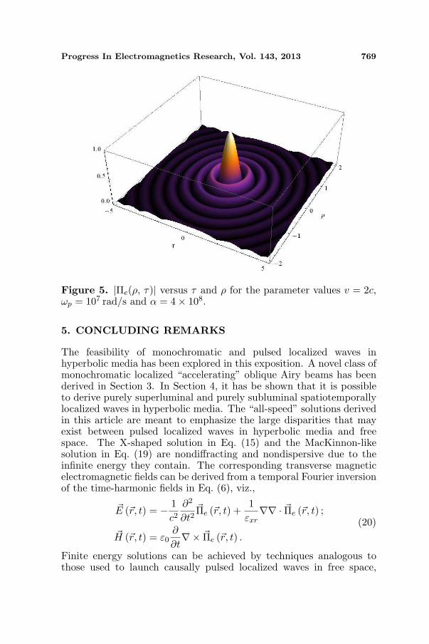
Progress In Electromagnetics Research, Vol. 143, 2013 769
Figure 5. |Πe(ρ, τ)| versus τ and ρ for the parameter values v = 2c,ωp = 107 rad/s and α = 4× 10⁸.
5. CONCLUDING REMARKS
The feasibility of monochromatic and pulsed localized waves inhyperbolic media has been explored in this exposition. A novel class ofmonochromatic localized “accelerating” oblique Airy beams has beenderived in Section 3. In Section 4, it has be shown that it is possibleto derive purely superluminal and purely subluminal spatiotemporallylocalized waves in hyperbolic media. The “all-speed” solutions derivedin this article are meant to emphasize the large disparities that mayexist between pulsed localized waves in hyperbolic media and freespace. The X-shaped solution in Eq. (15) and the MacKinnon-likesolution in Eq. (19) are nondiffracting and nondispersive due to theinfinite energy they contain. The corresponding transverse magneticelectromagnetic fields can be derived from a temporal Fourier inversionof the time-harmonic fields in Eq. (6), viz.,
~E (~r, t) = − 1c2
∂2
∂t2~Πe (~r, t) +
1εxr
∇∇ · ~Πe (~r, t) ;
~H (~r, t) = ε0∂
∂t∇× ~Πe (~r, t) .
(20)
Finite energy solutions can be achieved by techniques analogous tothose used to launch causally pulsed localized waves in free space,

770 Besieris and Shaarawi
e.g., from finite apertures constructed on the basis of the Huygensprinciple [20, 21].
The discussion in this article has been restricted to idealizedlossless hyperbolic metamaterials. However, dissipation is present insuch media and must be accounted for. This task is relatively easy inthe case of the monochromatic localized beams discussed in Section 3.The incorporation of dissipation in the study of pulsed localized wavesin hyperbolic media is a much more difficult problem. One possibleapproach is to begin with the dispersion relation in Eq. (8), incorporatephysically meaningful models of the complex relative permittivitiesεrx(ω) and εrz(ω), and finally resort to a slowly varying envelopeapproximation.
REFERENCES
1. Noginov, M., M. Lapine, V. Podolskiy, and Y. Kivshar, “Focusissue: Hyperbolic metamaterials,” Opt. Express, Vol. 21, 14895–14897, 2013.
2. Drachev, V. P., V. A. Podolskiy, and A. V. Kildishev, “Hyperbolicmetamaterials: New physics behind a classical problem,” Opt.Express, Vol. 21, 15048–15064, 2013.
3. Poddubny, A., I. Iorsh, P. Belov, and Y. Kivshar, “Hyperbolicmetamaterials,” Nature Photon., Vol. 7, 948–957, 2013.
4. MacKay, T. G., A. Lakhtakia, and R. A. Depine, “Uniaxialdielectric media with hyperbolic dispersion relations,” MicrowaveOpt. Tech. Lett., Vol. 48, 363–367, 2005.
5. Sun, J., J. Zeng, and N. M. Litchinitser, “Twisting light withhyperbolic metamaterials,” Opt. Express, Vol. 21, 14975–14981,2013.
6. Hu, L. and S. T. Chui, “Characteristics of electromagneticwave propagation in uniaxially anisotropic left-handed materials,”Phys. Rev. B, Vol. 66, 085108-1–7, 2002.
7. Hoffman, A. J., L. Alekseyev, S. S. Howard, K. J. Franz,D. Wasserman, V. A. Podolskiy, E. E. Narimanov, D. L. Sivco,and C. Gmachl, “Negative refraction in semiconductor metama-terials,” Nature Mater., Vol. 6, 946–950, 2007.
8. Guo, B., “Negative refraction in the terahertz region usingplasma metamaterials,” Journal of Electromagnetic Waves andApplications, Vol. 26, Nos. 17–18, 2445–2451, 2012.
9. Guo, B., “Faraday effect on negative refraction in uniaxialanisotropic plasma metamaterials,” Chin. Phys. Lett., Vol. 30,105201-1–4, 2013.
Progress In Electromagnetics Research, Vol. 143, 2013 771
10. Potemkin, A. S., A. N. Poddubny, P. A. Belov, and Y. S. Kivshar,“Green function for hyperbolic media,” Phys. Rev. A, Vol. 86,023848-1–9, 2012.
11. Silveirinha, M. G. and S. I. Maslovski, “Radiation from elementarysources in a uniaxial wire medium,” Phys. Rev. B, Vol. 85, 155125-1–10, 2012
12. Smolyaninov, I. I. and E. E. Narimanov, “Metric signaturetransitions in optical metamaterials,” Phys. Rev. Lett., Vol. 105,067402-1–4, 2010.
13. Fleck, Jr., J. A. and M. D. Feit, “Beam propagation in uniaxialanisotropic media,” J. Opt. Soc. Am., Vol. 73, 920–926, 1973.
14. Hacyan, S., “Derivation of the paraxial equation for extraordinarywaves in uniaxial media,” J. Opt. Soc. Am. A, Vol. 27, 602–604,2010.
15. Eichekraut, T. J., G. A. Siviloglou, I. M. Besieris, andD. N. Christodoulides, “Oblique airy wave packets in bidispersiveoptical media,” Opt. Lett., Vol. 35, 3655–3557, 2010.
16. Mohseni, M., “Photon gas with hyperbolic dispersion relations,”J. Opt., Vol. 15, 035102-1–6, 2013.
17. Hernandez-Figueroa, H., M. Zamboni-Rached, and E. Recami,Localized Waves, Wiley, New York, 2008.
18. Hernandez-Figueroa, H., M. Zamboni-Rached, and E. Recami,Non-diffracting Waves, Wiley, New York, 2013.
19. Besieris, I. M., M. Abdel-Rahman, A. M. Shaarawi, andA. Chatzipetros, “Two fundamental representations of localizedpulse solutions to the scalar wave equation,” Progress InElectromagnetics Research, Vol. 19, 1–48, 1998.
20. Ziolkowski, R. W., I. M. Besieris, and A. M. Shaarawi, “Aperturerealizations of exact solutions to homogeneous wave equations,”J. Opt. Soc. A, Vol. 10, 75–87, 1993.
21. Reivelt, K. and P. Saari, “Optically realizable localized wavesolutions of the homogeneous scalar wave equation,” Phys. Rev.E, Vol. 65, 046622-1–7, 2002.
Progress In Electromagnetics Research, Vol. 143, 821–848, 2013
DEVELOPING ONE-DIMENSIONAL ELECTRONICALLYTUNABLE MICROWAVE AND MILLIMETER-WAVECOMPONENTS AND DEVICES TOWARDS TWO-DIMENSIONAL ELECTROMAGNETICALLYRECONFIGURABLE PLATFORM
Sulav Adhikari* and Ke Wu
Poly-Grames Research Center, Ecole Polytechnique de Montreal, QC,Canada
Abstract—An overview of state-of-the-art frequency tunable tech-nologies in the realization of tunable radio frequency (RF) and mi-crowave tunable circuits is presented with focus on filter designs. Thoseenabling techniques and materials include semiconductors, micro-electro-mechanical systems (MEMS), ferroelectric and ferromagneticmaterials. Various performance indicators of one-dimensional tun-able filters are addressed in terms of tunability, losses, signal in-tegrity and other aspects. Fundamental limitations of the classicalone-dimensional tuning method are discussed, which makes use ofonly one type of tunable elements such as either electric or magnetictuning/controlling of circuit parameters. Requirements of simultane-ous electric and magnetic two-dimensional tuning techniques are high-lighted for achieving an unprecedented and advantageous wider modaltuning. It is believed that this emerging scheme will lead its way inthe realization of future highly efficient and tunable RF and microwavecomponents and devices.
1. INTRODUCTION
Since the past decades, there has been a significant development ofelectronically reconfigurable or tunable devices and circuits in thefield of radio frequency (RF) and microwave wireless systems, whichis even now moving towards the millimeter-wave domain. This hasbeen fuelled by the emerging needs for multi-band and multi-functionspecifications within the same compact-structured design platform.
Received 30 December 2013, Accepted 7 February 2014, Scheduled 10 February 2014* Corresponding author: Sulav Adhikari ([email protected]).
Invited paper dedicated to the memory of Robert E. Collin.
822 Adhikari and Wu
Indeed, current communication devices are able to offer multiplefunctionalities that are generally operating in different frequencybands. In addition to the popular 3G and 4G communicationsystems, for example, a portable handheld device also supports WLANand Bluetooth applications. Therefore, it is obvious that wirelesssystems are becoming more complex and smart due to the inclusionor convergence of multiple standards and applications into a singledevice. In order to meet the stringent design requirements of thosewireless systems, the related RF front ends must be adaptive andflexible in nature, which could become standard design requirementsin future generation wireless systems. The quality of RF front-end isdirectly responsible for the performances of an entire system as it isdirectly related to critical electrical specifications of the system suchas noise, dynamic range and channelization. This becomes much moreinvolved in multi-band and multi-function systems as the performancesshould be consistent and uniform for all system states. An adaptiveRF front-end has been recognized as a viable and effective solutionin incorporating multi-band and/or multi-channel circuits with multi-functions to satisfy several wireless system standards. One desirableway of realizing such multi-band or multi-channel systems is throughdeploying fast and tunable RF and microwave components and circuits,which should be enabled electronically. For example, a frequencyagile filter with embedded tuning elements can carry out a switchingfunction between several individual filters in order to have more thanone frequency response. Compared with a bulky bank of filters, a singletunable filter offers higher flexibility, better functionality, lighter weightand denser integration. The same hardware circuitry can be used tocope with the requirement of multiple purposes, which also reduces thetotal cost and size of related components and systems. In addition,such a circuit tuning allows an easier controlling of systems throughbaseband signal processing, which can add attractive “features” ofsmartness and multi-format.
There are basically two different methods of electronically tuningcomponents and circuits. In the first method, tuning elements like PINdiodes and MEMS switches are used to obtain discrete tuning states.The use of switches does not support a continuous tuning of devicewith fine details. Therefore, it would not cover the entire frequencytuning range when switches are used in a tunable filter. In the secondmethod, a continuous tuning of device is achieved by using tunableelements such as varactor diodes, MEMS capacitors, ferroelectric andferromagnetic materials. In this case, fine frequency details can bedescribed through electronic tuning. Of course, the switchable tuningand continuous tuning may be combined to offer a broadband tuning

Progress In Electromagnetics Research, Vol. 143, 2013 823
capability. Those classical tuning techniques should be said to be onlyone-dimensional, which means that only either electric or magneticparameters are tuned. In the design of a coupled cavity filter, forexample, such one-dimensional tuning is made through the changingof electric or magnetic fields in cavities and/or in connection with inter-cavity coupling sections. In fact, this creates a perturbation scenarioon resonant modes rather than a true modal tuning.
In order to realize the RF and microwave tunable devices, a specialtuning element has to be integrated into the device circuitry. The mostwidely and commercially used tuning elements include but not limitedto: semiconductors (varactor diodes, PIN diodes, and transistor),micro-electro-mechanical systems (MEMS), ferroelectrics materials,and ferromagnetic materials. Each of these tuning elements has theirown advantages and disadvantages. Their use largely depends upon therequired type of tunability (discrete or continuous), operating power,design frequency, and also manufacturing complexity and total cost.The RF and microwave systems are made up of number of componentsand devices including: oscillator, antenna, phase-shifter, amplifieretc.. Each of these devices can be made tunable by incorporatingany one of the above mentioned tuning elements. To cover all of themicrowave tunable devices is beyond the scope of this paper. Therefore,a general overview of each tuning element in the realization of a tunablemicrowave filter is only presented.
In this paper, a brief overview of state-of-art tunable filtersis discussed with highlights on the one-dimensional techniques. InSection 2, selected tunable devices using semiconductor based tuningelements such as PIN diode, varactor diode and transistor aredescribed. In Section 3, the use of MEMS techniques as tuningelements is discussed. Section 4 provides an overview of tunable devicesbased on ferroelectric materials. In Section 5, tunable components andcircuits based on ferromagnetic materials are summarized. Finally inSection 6, an emerging tuning concept now known as two-dimensionaltuning of microwave components and circuits is presented where bothelectric and magnetic tuning schemes are simultaneously used in adevice to achieve the highest possible tuning range in connection withthe best possible tuning performance. In Section 7, a conclusion ispresented where an overall discussion on all the tuning techniques ismade.
2. SEMICONDUCTOR TUNING ELEMENTS
In this section, a detailed discussion on RF and microwave tunabletechniques that make use of semiconductor devices as building tuning

824 Adhikari and Wu
elements is presented. Semiconductor is known to be the mostpopular and widely used technology in the realization of fast tunableintegrated RF and microwave components and circuits. They arealways associated with low cost, light weight and small footprint,and most importantly they are known to offer a very wide tuningrange with adaptive options, depending on diodes and transistordesign platforms. However, they can only offer a low Q factor atmicrowave frequencies [1]. For example, the Q factor of a varactordiode is proportional to frequency and junction capacitance at lowfrequencies (1 MHz) whereas it is inversely proportional at higherfrequency (> 100MHz) values [2]. Moreover, parasitic series resistanceof the diode caused by packaging also increases at higher frequency.Thus, the use of varactor techniques is generally limited to frequenciesbelow 10GHz as they suffer from higher insertion loss. However, anattempt has been made to compensate the loss and increase the Qfactor by incorporating FETs as a negative resistance device [3]. Ofcourse, any active compensation can be made possible at the expense ofadditional power consumption and potential nonlinear effects. Thereare basically three reported types of semiconductor devices that areintegrated inside a microwave circuit as tuning elements, which includevaractor diode, PIN diode, and field effect transistor (FET). Naturally,any active diodes and transistors can be used as tuning elements,depending on their technical merits. The tuning elements are usedin the realization of tunable devices that are made either in discretemode or in continuous mode.
2.1. Varactor Diodes
Varactor diode is also known as a variable reactor, which means adevice whose reactance can be made variable by the application of aDC bias voltage. The reactance in the case of a varactor diode is asimple depletion layer capacitance, which is formed at the junctionof p-type and n-type semiconductor materials. Depending upon thepolarity and the strength of the applied bias voltage, the depletion layerwidth is changed, which in turn also changes the junction capacitancevalue. Since the capacitance value of the varactor diode can be changedeven by a slight variation of applied bias voltage, it finds applicationas a continuously tunable device. Varactor diodes are very useful inrealizing a variety of devices including tunable filter, tunable phaseshifter, voltage-controlled oscillator (VCO), parametric amplifier, andmixer. In this paper, a brief overview of tunable filters based onvaractor diodes is discussed and presented.
There is a growing interest in the design and realization ofRF and microwave systems that have multi-channel and multi-band

Progress In Electromagnetics Research, Vol. 143, 2013 825
functionalities. Since filter is one of the most critical parts of thesystem design, it is highly beneficial to realize such a filter that isfully adaptive to any changes in connection with the system behaviour.Tunable filter can reduce the complexity of a system design by avoidingthe need of filter banks, which consist of multiple filters with distinctfilter responses for each frequency band. The use of a tunable filterallows the coverage of the whole frequency bandwidth. Early workof tunable filter designs involved the tuning of center frequency usingvarious kinds of tuning devices and materials. Presently, the focus oftunable filter design has not only been on changing the center frequencybut also on making it fully reconfigurable in terms of bandwidthand selectivity. Varactor diode has been one of the most promisingtechnologies that have been widely used in the realization of a widevariety of electronically tunable filters. In the early work of varactortuned filter developments, the center frequency was tuned by loadingthe varactor diodes at the ends of resonating stubs [4]. It was noticedthat, the bandstop characteristic of the filter was largely dependentupon the coupling gap between the feeding transmission line and theparallel stubs. Since the coupling gaps of the parallel stubs are highlyfrequency dependent, it was suggested in [4], to tune the capacitanceof the gaps in accordance with the tuning capacitances in order topreserve the bandstop characteristics. In [5], a varactor tuned ringresonator filter using microstrip technology was presented. The centerfrequency of the filter was configured by changing both filter’s couplingand tuning capacitances. In [6] and [7], a continuously frequency andbandwidth tunable bandpass filter using compact hairpin resonatorsand a combline structure was described. In [8], a fully adaptablebandstop filter, which is able to reconfigure its center frequency,bandwidth, and selectivity, was demonstrated. The bandwidth tuningis achieved by varactor diodes that are used in coupling resonators totransmission line while the center frequency is controlled by varactordiodes connected at the end of transmission line resonators.
Since the varactor diodes are made up of semiconductor materials,they suffer from non-linearity when injected with high power signals.Despite non-linear behaviours of semiconductor materials, it has beendemonstrated that the varactor diodes can also be used for realizinghigh power filters [9] at UHF band. Recently, a varactor tunedbandpass filter with improved linearity has been presented in [10]. Thefilter topology consists of an open-ended transmission line with back-to-back varactor diodes loaded at one end. The back-to-back varactordiodes enhance the linearity of filter while the mixed electric andmagnetic coupling scheme keeps the absolute bandwidth at a constantvalue when the frequency of the filter is tuned. Thus, varactor diode

826 Adhikari and Wu
presents itself a very promising low cost, highly tunable, and adaptivesemiconductor tuning element that can be used in realizing efficienttunable filters at relatively low tuning voltage.
2.2. PIN Diodes
PIN diodes are semiconductor-based tuning devices, which arepopularly used to produce discrete states reconfigurable filters. Inthis section, a brief review of tunable filters based on PIN diodes ispresented. In [11], a PIN diode based reconfigurable filter for wirelessapplications is demonstrated. The designed filter falls into a categoryof admittance inverter coupled resonator filter, with two discretebandwidths at 5.6 GHz. In [12], a bandpass filter which is switchablebetween two central frequency states is presented. The designed filteruses PIN diodes for switching, such that in each frequency statesa constant bandwidth is maintained. In Figure 1, the fabricatedprototype of the switchable bandpass filter is illustrated. By changingthe polarity of the bias voltage, the filter is switched between 1.5 GHzand 2 GHz center frequencies, respectively [12].
In [13] a miniaturized reconfigurable and switchable band passfilter is presented. By shorting the open stubs of the filter using PINdiodes, the UWB filter is reconfigured from bandpass to bandstopresponse. Moreover, with the addition of half-wavelength stub tothe existing reconfigurable filter, it is switched from UWB to 2.4 GHznarrowband filter response. A new type switchable bandpass filterbased on SIW technology and using PIN diodes is presented in [14].The two-pole bandpass filter is switched between six states rangingfrom 1.55GHz to 2.0GHz. The SIW cavity resonators are equipped
Figure 1. Photograph of thefabricated switchable bandpassfilter [12].
Figure 2. Fabricated SIW filterwith via posts islands for theconnection of PIN diodes [14].

Progress In Electromagnetics Research, Vol. 143, 2013 827
with multiple via posts, which are either connected or disconnectedfrom the top metal layers using PIN diodes, thus producing differentswitching states. In Figure 2, the fabricated prototype of the SIWbased filter is illustrated.
Another SIW-based digitally tunable bandpass filter is demon-strated in [15], where discrete frequency tuning with nearly 8 equalspaced frequency responses from 4–4.4 GHz is obtained. In [16], switch-able bandpass filter using stepped impedance resonator is presented.The designed operates between two states, in the first stated the filterproduces a band-stop response. By switching the PIN diodes to ONstate, the filter response then changes from band-stop to all-pass filtercharacteristics.
2.3. Transistors
In [17], using the concept of three-terminal MESFET varactor tunableactive bandpass filter is demonstrated. In the two pole filterconfiguration, one transistor is used to provide center frequency tuning,while the other is used to provide the negative resistance to thecircuit. The negative resistance of the transistor improves the overallQ factor and improved filter response. In [18], wideband tunablecombline filter using gallium arsenide field effect transistor as a tuningelement is presented. The filter resonators are loaded with field effecttransistors to produce the desired tunability. A systematic approachin designing tunable combline filters and the non-ideal effects in theoverall performance of the filter are also discussed.
In [19] a high Q tunable with a single transistor active inductor
(a) (b)
Figure 3. Wideband tunable combline filter. (a) Fabricated filterprototype, (b) schematic diagram of filter [18].

828 Adhikari and Wu
(AI) is presented. The first order bandpass filter has a centralfrequency of 2400GHz, the total frequency tuning range is 100MHz.
3. MEMS TECHNIQUES
Although it has been studied since early 60s, MEMS has becomesa re-emerging technology that is very useful in realizing variablecapacitors, switches, and reconfigurable RF and microwave devices.Compared with semiconductors, ferrites and ferromagnetic materialsbased tunable devices; MEMS techniques offer much higher Q factorwith very low power consumption. Moreover, as opposed to the solidstate devices, they offer a linear signal transmission with low signaldistortion. Hence, MEMS schemes have attracted much attention,which present a very promising scheme in realizing a wide range ofRF and microwave tunable components and devices. In the literature,many types of tunable devices based on MEMS technology can befound, including phase shifters [20, 21], antennas [22] and filters [23–39]. In this paper, a short overview regarding the current status ofMEMS based tunable filters is presented. Tunable filters, realized byusing MEMS technology generally make use of MEMS switch or MEMSvaractors as tuning elements. This section show several filter topologiesto produce discrete and continuous tuning of the filter parameters.
3.1. Tunable Filters Using MEMS Switch
MEMS switches are generally used for re-routing RF signals and alsothey are widely used in realizing tunable filters. Since MEMS-basedswitches operate in only two states: on and off, the tunability offilters designed using MEMS switches are discrete in nature. Fromthe structure point of view, such switches are either cantilever types orbridge types. An example of cantilever type MEMS switch is illustratedin Figure 4.
The electrical performance of a cantilever type switch largelydepends upon the quality of contact in the ON state as illustratedin Figure 4(b). There are basically two types of electrical contactsused in MEMS switches: direct contact and contact through acapacitive membrane also known as Metal-Insulator-Metal (MIM)contact. Compared to the MIM contact, the direct contact switcheshave lower insertion loss and better isolation. However, due to directcontacts between metals, the direct contact switch suffers from metalcorrosion and has a shorter life time compared to MIM switches [24].Two well-known problematic issues in the development of MEMSdevices are related to high actuation voltage and relatively low speed

Progress In Electromagnetics Research, Vol. 143, 2013 829
because of a mechanical process. In addition, MEMS techniques maynot be well suitable for high-power applications even though significantresearch efforts have been invested to remedy this situation.
In this section, tunable filters using direct and MIM contact-based MEMS switches are presented. The cantilever type MEMSswitch illustrated in Figure 4 is used to realize a tunable hairpin linefilter in [23]. The filter tunability is achieved by loading identicalMEMS switches at the end of hairpin resonators. When the switchesare changed between the on and off states, the equivalent electricallength of resonators are also changed, thereby making the filtertunable. In [25], another reconfigurable hairpin bandpass filter using
(a) (b)
Figure 4. Schematic of electro-statically actuated cantilever type RFMEMS switch. (a) OFF state, (b) ON State [23].
(a) (b)
Figure 5. Schematic of electro-statically actuated cantilever typeRF MEMS switch. (a) Layout of the filter, (b) simulation andmeasurement results illustrating three states of tuning [26].

830 Adhikari and Wu
MEMS switches was presented. The MEMS switches in this filterare used to change inter-resonator coupling, which in turn changesthe bandwidth of filter. Therefore, the filter presented in [25] is abandwidth tunable filter. Another example of tunable filter usingMEMS switch was described in [26], where the filter is switchedbetween three states. It is a good example in which MEMS switchesare used in controlling resonant frequency, input/output couplings,and couplings between resonators to achieve a fully-reconfigurable
Figure 6. Fabricated tunable SIW-based low-frequency band-passfilter using direct contact MEMS switches [27].
(a) (b)
Figure 7. Measurement results of tunable band-pass pass filter [27].

Progress In Electromagnetics Research, Vol. 143, 2013 831
bandpass filter at microwave frequency. The measured filter responseshows three different states of filters at 8, 9 and 10 GHz, respectively.In Figure 5(a), the filter layout with tuning elements is presented, andits simulation and measurement results are presented in Figure 5(b).A new type of tunable filter based on substrate integrated waveguide(SIW) technology was presented in [27]. As illustrated in Figure 6, thefilter topology consists of two SIW cavities that are coupled to eachother via an iris window. Commercially available packaged RF MEMSswitches are surface-mounted in each cavity to tune them separately.From the measurement result presented in Figure 7, the two-pole filterimplemented using two-layer SIW circuit has a total tuning range of28% with reflection loss better than 15 dB.
MEMS switches are also used in realizing tunable filters thatare of lumped element and periodic structure types. In [28], acommercially available MEMS switch was used to realize tunable high-pass and low-pass filters. The designed filters cover the frequencytuning range over 6–15GHz. During the synthesis of the filter, alumped element model was first derived that was later converted intoa microstrip line model. Another example of a lumped-element filterpresented in [29] also uses commercially available MEMS switches astuning elements. The designed filter covers a frequency tuning rangefrom 25 to 75MHz [30]. A coplanar waveguide (CPW)-based fullyreconfigurable filter was studied in [31]. The filter topology consists ofcascaded CPW-based periodic structures which are loaded with MEMSswitches for tunability. By a suitable combination of MEMS switches,3-unit CPW lines are combined to form a single-cell low pass filter. Inthis way, the length of the filter is increased by three-times the originallength, and subsequently reducing the low-pass cut-off frequency alsoby three-times. In a similar way, a reconfigurable bandpass filter wasalso realized in [31], where three bandpass units are cascaded togetherusing MEMS switches to realize a single larger bandpass filter havinga filter response at low frequency region.
3.2. Tunable Filters Using MEMS Switch Capacitors
In this section, an overview of tunable filters based on MEMS switchcapacitors is presented. Similar to the direct contact counterparts, theswitch capacitors can also be cantilever or bridge type as illustratedin Figure 4. However, in the MEMS switch capacitors, an electricalconnection is established not through an ohmic contact but througha capacitive membrane. Therefore, the switch operates between twodifferent capacitance values: one for the ON state and the other for theOFF state. A central frequency and bandwidth controlled filter usingMEMS cantilever type capacitive switches was presented in [32]. The

832 Adhikari and Wu
switches are loaded at the end of coplanar resonators to achieve twocenter frequency states. A high Q tunable filter based on microstriptechnology for a wireless local area network (WLAN) system wasdiscussed in [33]. The filter is composed of microstrip based highQ resonators, which are loaded with RF MEMS switch capacitorsfor tunability. A total tuning range of 5% over 5.15–5.70GHz wasdemonstrated. A tunable dielectric resonator bandpass filter withembedded MEMS tuning elements was also shown in [34]. The MEMStuning element is used herewith to perturb the field surrounding thedielectric resonator. Compared to the MEMS tunable planar filters,the designed dielectric resonator filter offers a very high Q of 1300.Moreover, the filter requires a relatively low tuning voltage for tuningand the tuning speed is relatively high. By changing the heightor the distance of the tuning disc from the dielectric resonator, thefield surrounding the dielectric is varied thereby making it frequencytunable. This operation is similar to the MEMS switch capacitorswhere the position of the cantilever or air bridge determines the valueof gap capacitance. The MEMS switch capacitors are also used inrealizing the lumped element type tunable filters.
A lumped element type tunable filter using MEMS capacitiveswitch was demonstrated in [35] for WLAN applications. Thefilter is designed to select frequency bands at 2.4 and 5.1 GHz. InFigure 8, the fabricated prototype of the lumped element filter and itsequivalent circuit are illustrated. In [36], a lumped-element filter withfrequency coverage from 600MHz–1 GHz was demonstrated. To obtain
(a)
(b)
Figure 8. Lumped element filter using MEMS switch capacitors fortuning. (a) Fabricated prototype, (b) equivalent circuit [35].

Progress In Electromagnetics Research, Vol. 143, 2013 833
a continuous tuning, 12 electro-statically actuated MEMS capacitorswere used in the structure.
3.3. Tunable Filters Using MEMS Varactors
MEMS varactors present an advanced form of MEMS capacitiveswitches. Similar to the MEMS capacitive switches, they are alsocomposed of capacitive membrane between the two metal contacts.Unlike the capacitive switches that operate only between ON orOFF states, MEMS varactor capacitance membrane can be tunedcontinuously with an applied analog voltage. From the operation pointof view, they are very similar to semiconductor biased varactor diodesand are useful in realizing continuously tunable RF/microwave filters.They are more attractive than semiconductor varactor diodes in termsof Q factor, power consumption and linearity. However, they havelower tuning speed and are more sensitive to environmental conditionsfor example temperature, moisture and vibration. A lumped elementtype tunable K-band filter using MEMS bridge varactor was presentedand discussed in [37]. The filter consists of J-inverters and shunt-typeresonator sections. The variable capacitors are loaded in the shunttype resonators to vary the center frequency of the filter.
In [38], a distributed type bandpass filter was designed usingbridge type MEMS varactors. The coplanar transmission line isloaded with MEMS varactors to reconfigure the center frequency of thefilter. A coplanar waveguide tunable band-stop filter using RF MEMSvariable capacitor was also presented in [39]. The filter is designedto operate from 8.5 to 12.3GHz with 35% of tunability. This filter isanother example of MEMS varactors-loaded distributed type of filter.In Figure 9, the fabricated prototype of the filter is presented.
Figure 9. Fabricated tunable bandpass filter [39].

834 Adhikari and Wu
4. TUNABLE FILTERS USING FERROELECTRICMATERIALS
Ferroelectrics are one of the most promising materials in realizingelectronically tunable RF and microwave components and circuits forwireless front-end applications. A number of tunable devices includingphase shifters, oscillators, and filters have been demonstrated byusing ferroelectric materials as key tuning elements. The dielectricconstant of ferroelectric materials varies with the applied DC voltage,ranging from a few hundreds to a few thousands. Therefore, adevice incorporating ferroelectric material or loaded with ferroelectricmaterial locally generally in the form of thin-films becomes tunablewith respect to the effective permittivity change. Compared to MEMS,ferroelectric materials offer a very fast tuning time like semiconductortechniques, but they have lower Q-factor. Their figure of merit isalways limited by the conflict of a better tuning range associated with apoorer line loss. In addition, the quality and properties of ferroelectricthin-films can be strongly dependent on processing techniques. Themost commonly used ferroelectric material in microwave regime isBarium-Strontium-Titanate oxide (BST). In this section, a brief reviewof tunable microwave filters based on BST is presented.
Before beginning with the design of tunable RF and microwavedevices using ferroelectric material, it is very important to firstcharacterize in terms of tunability and losses. In [40], a computer-aided-design model is developed, to characterize the BST thin films inthe frequency range from 1 to 16 GHz. Coplanar waveguides (CPWs)and inter-digital capacitors (IDCs) are fabricated on BST thin films,to determine the complex dielectric constants, voltage tunability andK-factor. Once the material is correctly characterized, very accuratedesigns of the tunable devices can be realized at a given frequency. Atheoretical analysis in connection with the use of ferroelectric materialsin the realization of a constant bandwidth tunable filter was presentedin [41]. The influence of loss factor of a ferroelectric capacitor on theoverall performance of the filter was discussed. A tunable comblinebandpass filter loaded with BST varactor diodes for tunability waspresented in [42]. The BST varactor diodes are loaded at the endof resonators to tune center frequency of the filter from 2.44 GHzto 2.8 GHz. In [43], a slow-wave miniaturized tunable 2-pole filteroperating from 11.5 GHz to 14 GHz was demonstrated. The filterconsists of a section of coplanar transmission line that is loaded withseveral ferroelectric BST high Q capacitors. The total insertion lossof the realized device varies from 5.4 to 3.3 dB in the tuning rangeof the filter. A DC variation between 0–30 V is applied to achieve

Progress In Electromagnetics Research, Vol. 143, 2013 835
(a)
(b)
Figure 10. Tunable combline bandpass filter. (a) Fabricatedprototype, (b) periodic area along CPW line loaded with BST [43].
the tunability of the filter. In Figure 10, the fabricated prototype ofa slow wave tunable filter loaded with BST as a tuning element ispresented [43]. In order to achieve high tunability using ferroelectricmaterial, in [44] a study is performed to establish a correlation betweenthe lattice parameter of BST films with the dielectric tunability. Itwas concluded that, a broad tunability can be achieved on low costmicrowave devices based on BST films provided the internal elasticstress of the film is low. In [45], a ferroelectric based lumped elementtunable filter/switch was presented. The ferroelectric filter was grownon silicon substrate. With the application of an external DC voltagebias, the dielectric constant of Ba0.25Sr0.75TO3 is varied, thus makingthe filter cut-off frequency tunable. When used as a switch, a totalisolation of 18 dB at 25 GHz was obtained. A comparative studybetween tunable microwave filters based on discrete ferroelectric andsemiconductors were presented in [46]. The two tunable filters arecompared to each other in terms of tuning range, losses and matching.A microstrip-based tunable filter with improved selectivity was studiedin [47]. The frequency tuning of the filter is achieved by loading BST-based varactor diodes on microstrip resonators. From the frequencyresponse, it was demonstrated that the designed filter had a betterfrequency response compared to the conventional combline filter interms of frequency selectivity.
In [48], a two-pole X-band tunable filter with constant fractional
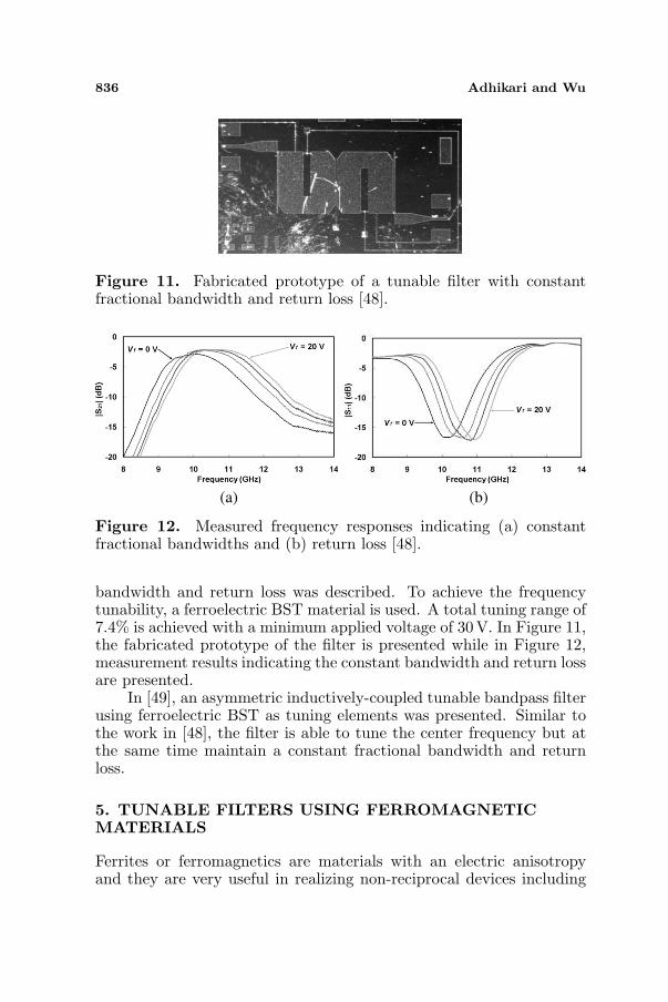
836 Adhikari and Wu
Figure 11. Fabricated prototype of a tunable filter with constantfractional bandwidth and return loss [48].
(a) (b)
Figure 12. Measured frequency responses indicating (a) constantfractional bandwidths and (b) return loss [48].
bandwidth and return loss was described. To achieve the frequencytunability, a ferroelectric BST material is used. A total tuning range of7.4% is achieved with a minimum applied voltage of 30 V. In Figure 11,the fabricated prototype of the filter is presented while in Figure 12,measurement results indicating the constant bandwidth and return lossare presented.
In [49], an asymmetric inductively-coupled tunable bandpass filterusing ferroelectric BST as tuning elements was presented. Similar tothe work in [48], the filter is able to tune the center frequency but atthe same time maintain a constant fractional bandwidth and returnloss.
5. TUNABLE FILTERS USING FERROMAGNETICMATERIALS
Ferrites or ferromagnetics are materials with an electric anisotropyand they are very useful in realizing non-reciprocal devices including

Progress In Electromagnetics Research, Vol. 143, 2013 837
circulators, isolators and gyrators. Such non-reciprocal devices aregenerally fixed frequency types, which are designed for particularapplications. The frequency of operation for a ferrite material largelydepends upon the external DC magnetic bias that is applied on it.Therefore, the non-reciprocal devices operating at a constant frequencyconstitute a fixed permanent magnet that delivers a constant value ofmagnetic bias to the ferrite material. When the applied magnetic biasvalue is changed, however, effective permeability value presented by theferrite material also changes. Note that permeability and permittivitypresent the same contributions to the change of transmission phase orpropagation constant. Since the frequency of an electromagnetic waveis directly proportional to the square root of permeability, any changesin permeability also changes the frequency. Therefore, ferrite materialsare not only useful in realizing fixed frequency non-reciprocal devicesbut they present also similar features as ferroelectrics in realizingtunable RF, microwave and millimeter wave components and circuits.The evolution of tunable filters based on ferromagnetic materials andtheir present status are discussed in the following.
From mid-1950’s, ferrite materials have drawn considerableinterest in the realization of tunable devices including tunable cavities,filters and frequency modulated signals [50, 51]. It can be observedthat in both works presented in [50] and [51], rectangular waveguidetechnology is used to realize the desired tunable devices. The higherpower handling capabilities, lower loss, and more convenient of biasingferrites could have been few of the reasons why rectangular waveguidetechnology would have been used. Moreover, within the rectangularwaveguide, the positions of electric and magnetic fields for a givenmode of operation (TE10, for example) are clearly defined. Sinceferrite materials strongly interact with magnetic fields, they can beplaced at positions of the highest magnetic field strength withoutperturbing electric fields. In this section, tunable filters based onrectangular waveguide technology and their subsequent evolutions intoplanar forms are briefly discussed.
In [51], a magnetically tunable cavity resonator based onrectangular waveguide technology was described. The tunability isachieved by placing a slab of YIG along one sidewall of the rectangularwaveguide where the magnetic field component of TE101 mode isdominant. By the application of an external DC magnetic bias, theresonant frequency of the cavity is tuned towards higher frequency.The magnetically tunable cavity resonator presented in [51] makesuse of a block YIG slab to achieve the desired tunability. Since theferrite blocks are usually made of a polycrystalline material thereforethey suffer from losses when used in microwave and millimeter wave

838 Adhikari and Wu
regions. In order to improve the total tuning range and also toreduce the losses, a magnetically-tunable filter consisting of single-crystal YIG was proposed and demonstrated in [52]. It is shownthat single-crystal YIG techniques are very useful in realizing low lossand highly tunable microwave filters. In [52], a filter with adjustable3 dB bandwidth and center frequency tunability was demonstrated.However, the filter has a low tuning speed, and possesses certainfabrication difficulties in precisely placing and biasing the single-crystal YIG sphere. Following the earlier work of filter design usingrectangular waveguide technology, interest has slowly been shiftedtowards incorporating the ferrite materials in planar form, therebyrealizing magnetically tunable planar filter circuits. In [53], tunablebandpass filter using YIG film that is grown by Liquid Phase Epitaxy(LPE) was investigated. A total wide tuning range from 0.5 GHzto 4 GHz has been achieved with a low insertion loss. The filterstructure and the measurements presented in [53] are also illustratedin Figure 13. A tunable resonator based on ferromagnetic resonancewas discussed in [54]. The designed cavity resonator is tunabledue to magnetoelectric interactions between the layers of ferrite andferroelectric, which make up the resonator. In [55] a tunable resonatorfabricated on a polycrystalline ferrite substrate was presented. It isdemonstrated, the applied stress can influence the magnetization ofthe ferrite material. Frequency tunability is achieved by an applicationof stress on the ferrite substrate. Maximum tunability of 300MHz wasexperimentally achieved. In [56], tunable bandpass and bandstop filters
(a) (b)
Figure 13. Structure of a planar tunable filter using ferromagneticdisks. (a) Filter structure, (b) frequency response [51].

Progress In Electromagnetics Research, Vol. 143, 2013 839
Figure 14. Schematic of a tunable microwave band-stop filter basedon FMR [56].
(a) (b)
Figure 15. Fabricated prototypes of SIW magnetically tunableresonators. (a) Single ferrite slab loaded cavity, (b) two ferrite slabsloaded cavity [57].
based on ferromagnetic resonance (FMR) absorption were reported.The schematic of the studied tunable bandstop filter topology ispresented in Figure 14.
As illustrated in Figure 14, the bandstop filter consists of aYIG/GGG layer placed upon the microstrip line which is fabricated ona GaAs substrate. A bandstop characteristic of the filter occurs whenthe incoming microwave signal is absorbed by the YIG/GGG substratelayer. This takes place when the FMR frequency of the YIG/GGGsubstrate coincides with the frequency of the incoming signal. Amagnetically tunable cavity resonator based on SIW technology wasreported in [57]. Planar YIG slabs are loaded along the sidewallsof SIW where the strength of the magnetic field is highest. A totalfrequency tuning range of 10% with unloaded Q factor better than 150is measured at X-band.
In Figure 15, fabricated prototypes of the resonator are presented.The measured S-parameters of a single ferrite loaded cavity resonator

840 Adhikari and Wu
Figure 16. Measured S-parameters of SIW cavity resonator loadedwith a single ferrite slab [57].
are presented in Figure 16. It can be noticed in Figure 16, with theapplication of external DC magnetic bias, the resonant frequency ofthe ferrite loaded cavity resonator shift towards the higher frequencyvalue. At 0.45 T of external magnetic bias, the YIG slab is operatingnear the ferromagnetic resonance region (FMR) therefore the resonatorsuffers from higher losses.
The magnetically tunable filters presented so far, either use pureYIG as a pure single crystal or in a polycrystalline form. But there arealso other ferrite materials that are composed of iron oxides togetherwith various other elements including aluminium, cobalt, manganeseand nickel. In [58], a magnetically tunable dielectric bandpass filterbased on nickel ferrite was presented. The filter is tunable from 18–36GHz and has an insertion loss between 2–5 dBm. A magneticallytunable bandpass filter with partially magnetized ferrite was shownin [59]. A total frequency tuning range of 7% is achieved from 5.77to 6.2 GHz. Due to a partially magnetized ferrite; the requirement ofhigh magnetic bias for the tunability of the filter is reduced. A total of100Oe of magnetic bias is adequate to achieve the desired tuning range.One well-pronounced advantage of the magnetically tuned filters is thatsuch structures are known to support high-power operations, whichdepend on material properties and geometrical shapes.
6. SIMULTANEOUS ELECTRIC AND MAGNETICTWO-DIMENSIONAL TUNING
Since the inception of tunable techniques, all tuning mechanisms arebased on the above-described one-dimensional parametric tuning suchas electric parameters such as permittivity or magnetic parameterssuch as permeability. Such one-dimensional tuning techniques have

Progress In Electromagnetics Research, Vol. 143, 2013 841
been very successfully but they suffer from a number of problemsincluding limited tuning ranges and augmented tuning complexity.
In [60], an emerging two-dimensional tuning technique wasproposed and demonstrated successfully with SIW structures. In thiscase, tunable SIW cavity resonator and bandpass filter consisting offerromagnetic material and varactor diodes as combined electric andmagnetic tuning elements were presented and studied. Similar to theSIW cavity resonator presented in [57], rectangular ferrite slabs areloaded along the sidewalls of the cavity to produce the magnetic tuning.In order to produce the proposed simultaneous electric and magnetictwo-dimensional tuning, a capacitor and a varactor diode are loadedin the central region of the cavity where the electric field strength ishighest.
With the simultaneous tuning of electric and magnetic fields atthe same time, the total frequency tuning range of the SIW cavityresonator can be increased. In Figures 17(a) and 17(b), the fabricatedprototype of the cavity resonator and the measured frequency curvesare presented. It can be observed from Figures 16 and 17(b), withsuch a two dimensional tuning, the total frequency tuning range hasincreased almost two-folds from 8% to 16%, which was not optimized.It is also demonstrated that, by the use of a simultaneous electric andmagnetic tuning, a frequency tunable bandpass filter with a tunableconstant bandwidth can be realized without additional elements forcontrolling the coupling between cavities. In fact, this attractivephenomenon can be explained by the fact that the proposed two-dimensional tuning is indeed the tuning of cavity modes or modaltuning in connection with electric and magnetic fields. This is asopposed to the one-dimensional scheme in which either electric or
(a) (b)
Figure 17. Simultaneous electric and magnetic two dimensionallytuned SIW cavity resonator. (a) Fabricated prototype, (b)measurement results [60].

842 Adhikari and Wu
magnetic field would be modified, perturbed or changed. Therefore,one field remain unchanged during the process. This would havedistorted the profile of resonant or propagating modes in the structure,which leads to a poor or limited tuning range. In addition, naturalmodal tuning would change the coupling between adjacent cavities aswell as the resonant frequency in this cascaded cavity filter topology.Therefore, the frequency bandwidth response profile can be preservedwhile the center frequency can be tuned.
Table 1. Comparison between different tuning technologies.
Tunable
elementQ-factor Tunability
Power
consumption
Response
time
Semiconductor Moderate High Poor Fast
MEMS Very high Low Excellent Slow
Ferroelectric ModerateLow to
MediumExcellent Very fast
Ferromagnetic High Very High Moderate Moderate
7. CONCLUSION
Based on the brief overviews of different tuning elements andtechniques that have been widely used in the realization of tunablemicrowave cavities and filters, it can be concluded that each schemehas its own advantages and limitations in performance. In Table 1, thekey parameters of each tuning scheme are compared and summarizedin terms of losses, tunability, power consumption and response time,when they are used in the realization of tunable filters.
Semiconductor diodes present lower cost, light weight, easybiasing, low voltage, and small footprint. However, they wouldinherently produce non-linear effects and suffer from inter-modulationnoises and transmission losses. MEMS techniques, on the other hand,are highly linear in comparison to semiconductor schemes. However,the response or the switching time of MEMs is much slower comparedto semiconductor counterparts. They are also vulnerable to high-powerand environmental conditions, for example, temperature, vibration inwhich they operate. Thus, they may require a stringent packagingcondition. Ferroelectric materials are highly suitable for integratedmicrowave devices because they can be made in thin-film or thick filmforms, and they also offer a relatively high tunability. Nevertheless, thedielectric loss tangent of ferroelectric materials is generally very high

Progress In Electromagnetics Research, Vol. 143, 2013 843
and the inherent permittivity of ferroelectric materials may presenthighly dispersive behavior, which may not be good for a wide-rangedfrequency tuning. Thus, they offer a very low Q-factor with limitedbandwidth applications. Tunable devices based on ferromagneticmaterials can handle more power compared to semiconductors andMEMS technologies, and they are highly tunable and higher Q.However, biasing the ferrite materials requires the use of solenoidswounded with current carrying coils or large permanent magnets.Therefore, the tunable circuit using ferrite materials can sometimesbe bulky.
It has been found that the one-dimensional electric or magnetictuning may not be effective in terms of tuning range and designcomplexity. The proposed two-dimensional tuning technique maypresent an attractive and emerging alternative for simultaneous electricand magnetic tuning, which may fundamentally change the designlandscape of tuning structures and circuits. This will be critical forfuture generation RF and wireless circuits and systems.
REFERENCES
1. Torregrosa-Penalva, G., G. Lopez-Risueno, and J. I. Alonso,“A simple method to design wide-band electronically tunablecombline filters,” IEEE Trans. on Microw. Theory and Techn.,Vol. 50, No. 1, Jan. 2002.
2. Norwood, M. H. and E. Shatz, “Voltage variable capacitor tuning:A review,” Proceedings of the IEEE, Vol. 56, No. 5, May 1968.
3. Chandler, S. R., I. C. Hunter, and J. G. Gardiner, “Activevaractor tunable bandpass filter,” IEEE Microwave and GuidedWave Letters, Vol. 3, No. 3, Mar. 1993.
4. Hunter, I. C. and J. D. Rhodes, “Electronically tunable microwavebandpass filters,” IEEE Trans. on Microw. Theory and Techn.,Vol. 30, No. 9, Sep. 1982.
5. Makimoto, M. and M. Sagawa, “Varactor tuned bandpass filtersusing microstrip-line ring resonators,” IEEE MTT-S InternationalMicrowave Symposium Digest, 411–414, Jun. 1986.
6. Chung, M.-K., I.-S. Kim, and S.-W. Yun, “Varactor-tuned hairpinbandpass filter with an attenuation pole,” Asia Pacific MicrowaveConf., Dec. 2005.
7. Sanchez-Renedo, M., R. Gomez-Garcia, J. I. Alonso, and C. Briso-Rodriguez, “Tunable combline filter with continuous control ofcenter frequency and bandwidth,” IEEE Trans. on Microw.Theory and Techn., Vol. 53, No. 1, Jan. 2005.

844 Adhikari and Wu
8. Musoll-Anguiano, C., I. Llamas-Garro, Z. Brito-Brito, L. Pradell,and A. Corona-Chavez, “Fully adaptable band-stop filter usingvaractor diode,” Microwave and Optical Technological Letters,Vol. 52, Mar. 2002.
9. Swartz, G. A., D. W. Wern, and P. H. Robinson, “Large-area varactor diode for electrically tunable, high-power UHFbandpass filter,” IEEE Trans. on Electron Devices, Vol. 27, No. 11,Nov. 1980.
10. Yu, F. L., X. Y. Zhang, and Y. B. Zhang, “Frequency-tunablebandpass filters with constant absolute bandwidth and improvedlinearity,” Progress In Electromagnetics Research Letters, Vol. 33,131–140, 2012.
11. Lugo, C. and J. Papapolymerou, “Electronic switchable bandpassfilter using PIN diodes for wireless low cost system-on-a-packageapplications,” IEE Proceedings on Microwave Antenna andPropagation, Vol. 151, No. 6, 2004.
12. Brito-Brito, Z., I. Llamas-Garro, L. Pradella-Cara, andA. Corona-Chavez, “Microstrip switchable bandstop filter usingPIN diodes with precise frequency and bandwidth control,” Pro-ceedings of European Microwave Week (EUMA), 1707–1711, 2008.
13. Karim, M. F., Y. X. Guo, Y.-X. Chen, and L. C. Ong,“Miniaturized reconfigurable and switchable filter from UWB to2.4GHz WLAN using PIN diodes,” IEEE MTT-S InternationalMicrowave Symposium Digest, 509–512, 2009.
14. Armendariz, M., V. Sekar, and K. Entesari, “Tunable SIWbandpass filters with PIN diodes,” Proceedings of EuropeanMicrowave Conference, 830–833, 2010.
15. Sirci, S., J. D. Martinez, and V. E. Boria, “Low-loss 3-bittunable SIW filter with PIN diodes and integrated bias network,”Proceedings of the European Microwave Conference, 1211–1214,2013.
16. Bakhit, A. A. and P. W. Wong, “Switchable microwave band-stopto all pass filter using stepped impedance resonator,” Progress InElectromagnetics Research B, Vol. 52, 99–115, 2013.
17. Lin, J. and T. Itoh, “Tunable active bandpass filters usingthree-terminal MESFET varactors,” Proceedings of IEEE MTT-SInternational Microwave Symposium, Vol. 2, 921–924, 1–5, 1992.
18. Torregrosa-Penalva, G., G. Lopez-Risueno, and J. I. Alonso,“A simple method to design wide-band electronically tunablecombline filters,” IEEE Trans. on Microw. Theory and Techn.,Vol. 50, No. 1, Part 1, 172–177, Jan. 2002.

Progress In Electromagnetics Research, Vol. 143, 2013 845
19. Pantoli, L., V. Stornelli, and G. Leuzzi, “A single-transistortunable filter for bluetooth applications,” Proceedings of EuropeanMicrowave Integrated Circuits Conference, 889–892, 2012.
20. Siegel, C., V. Zieglerl, U. Prechtel, B. Schonlinner, andH. Schumacher, “A Ka-band RF-MEMS phase shifter approachbased on a novel dual-state microstrip line,” Proceedings ofEuropean Microwave Conference, 1221–1224, Oct. 2007.
21. Unlu, M., S. Demir, and T. Akin, “A 15–40-GHz frequencyreconfigurable RF MEMS phase shifter,” IEEE Trans. on Microw.Theory and Techn., Vol. 1, 2865–2877, Aug. 2013.
22. Lucyszyn, S. and S. Pranonsatit, “RF MEMS for antenna ap-plications,” European Conference on Antennas and Propagation,1988–1992, Apr. 2013.
23. Ocera, A., P. Farinelli, P. Mezzanotte, R. Sorrentino, B. Margesin,and F. Gaicomozzi, “A novel MEMS-tunable hairpin linefilter on silicon substrate,” Proceedings of European MicrowaveConference, 803–806, Sep. 2006.
24. Marsan, E., J. Gauthier, M. Chaker, and K. Wu, “Tunablemicrowave device: Status and perspective,” IEEE-NEWCASConference, 279–282, Jun. 2005.
25. Gentili, F., L. Pelliccia, F. Cacciamani, P. Farinelli, andR. Sorrentino, “RF MEMS bandwidth-reconfigurable hairpinfilters,” Proceedings of Asia Pacific Microw. Conf., 735–737,Dec. 2012.
26. Chan, K. Y., S. Fouladi, R. Ramer, and R. R. Mansour, “RFMEMS switchable interdigital bandpass filter,” IEEE Microwaveand Wireless Comp. Lett., Vol. 22, No. 1, Jan. 2012.
27. Sekar, V., M. Armendariz, and K. Entesari, “A 1.2–1.6GHzsubstrate-integrated-waveguide RF MEMS tunable filter,” IEEETrans. on Microw. Theory and Techn., Vol. 59, No. 4, Apr. 2011.
28. Pillans, B., A. Malczweski, R. Allison, and J. Brank, “6–15GHz RF MEMS tunable filters,” IEEE MTT-S InternationalMicrowave Symposium Digest, 919–922, Jun. 2005.
29. Entesari, K., K. Obeidat, A. R. Brown, and G. M. Rebeiz, “A25–75-MHz RF MEMS tunable filter,” IEEE Trans. on Microw.Theory and Techn., Vol. 55, No. 11, Nov. 2007.
30. Minin, I., Microwave and Millimeter Wave Technologies fromPhotonic Bandgap Devices to Antenna and Applications, Chap-ter 7, 159–184, InTech, Mar. 2010.
31. Park, J.-H., S. Lee, J.-M. Kim, H.-T. Kim, Y. Kwon, andY.-K. Kim, “Reconfigurable millimeter-wave filters using CPW-

846 Adhikari and Wu
based periodic structures with novel multiple-contact MEMSswitches,” Journal of Microelectromechanical Systems, Vol. 14,No. 3, Jun. 2005.
32. Fourm, E., et al., “Bandwidth and central frequency controlon tunable bandpass filter by using MEMS cantilevers,” IEEEMTT-S International Microwave Symposium Digest, 523–526,Jun. 2003.
33. Park, S.-J., K.-Y. Lee, and G. M. Rebeiz, “Low-loss 5.15–5.7 GHzRF MEMS switchable filter for wireless LAN applications,” IEEETrans. on Microw. Theory and Techn., Vol. 54, No. 11, Nov. 2006.
34. Yan, W. D. and R. R. Mansour, “Tunable dielectric resonatorbandpass filter with embedded MEMS tuning elements,” IEEETrans. on Microw. Theory and Techn., Vol. 55, No. 1, Jan. 2007.
35. Kim, J.-M., et al., “Digitally frequency-controllable dual-bandWLAN filters using micro-machined frequency-tuning elements,”IEEE Intern. Conf. on Micro. Electro. Mechanical Systems, 158–161, 2006.
36. Shim, Y., J. Ruan, Z. Wu, and M. Rais-Zadeh, “An integratedRF MEMS tunable filter,” IEEE MTT-S International MicrowaveSymposium Digest, 523–526, Jun. 2003.
37. Kim, J.-M., S. Lee, J.-H. Park, and J.-M. Kim, “Low loss K-bandtunable bandpass filter using micromachined variable capacitors,”Digest of Technical Papers in Solid-State Sensors, Actuators andMicrosystems, Vol. 1, 1071–1074, Jun. 2005.
38. Abbaspour, T., L. Dussopt, and G. M. Rebeiz, “Miniature andtunable filters using MEMS capacitors,” IEEE Trans. on Microw.Theory and Techn., Vol. 51, No. 7, 1878–1885, Jul. 2003.
39. Zhang, N., Z. Deng, and F. Sen, “CPW tunable band-stop filterusing hybrid resonator and employing RF MEMS capacitors,”IEEE Trans. on Electron Devices, Vol. 60, No. 8, Aug. 2013.
40. Ouaddari, M., S. Delprat, F. C. Vidal, C. Mohamed, and K. Wu,“Microwave characterization of ferroelectric thin-film materials,”IEEE Trans. on Microw. Theory and Techn., Vol. 53, No. 4, 1390–1397, 2005.
41. Vendik, I., O. Vendik, V. Pleskachev, A. Svishvhev, andR. Wordenweber, “Design of tunable ferroelectric filters witha constant fractional bandwidth,” IEEE MTT-S InternationalMicrowave Symposium Digest, Vol. 3, 1461–1464, May 2001.
42. Nath, J., D. Ghosh, J.-P. Maria, A. I. Kingon, W. Fathelbab,P. D. Franzon, and M. B. Steer, “An electronically tunablemicrostrip bandpass filter using thin-film Barium-Strontium-

Progress In Electromagnetics Research, Vol. 143, 2013 847
Titanate (BST) varactors,” IEEE Trans. on Microw. Theory andTechn., Vol. 53, No. 9, Sep. 2005.
43. Papapolymerou, J., C. Lugo, Z. Zhiyong, and X. Wang,“A miniature low-loss slow-wave tunable ferroelectric bandpassfilter from 11–14 GHz,” IEEE MTT-S International MicrowaveSymposium Digest, 556–559, 2006.
44. Delprat, S. L., C. Durand, J. Oh, M. Chaker, and K. Wu,“Correlation between the lattice parameter and the dielectrictunability in nonepitaxial Ba0.5Sr0.5TiO3 thin films,” AppliedPhysics Letters, Vol. 91, 063513–063513-3, 2007.
45. Wang, X., P. Bao, M. J. Lancaster, and T. J. Jackson, “Fer-roelectric lumped element filter/switch for microwave applica-tions,” Proceedings of 38th European Microwave Conference, 43–46, Oct. 2008.
46. Wang, X., P. Bao, T. J. Jackson, and M. J. Lancaster, “Tunablemicrowave filters based on discrete ferroelectric and semiconductorvaractors,” IET Microwave, Antennas and Propagation, Vol. 5,No. 7, 776–782, May 2011.
47. Lourandakis, E., M. Schmidt, G. Fischer, and R. Weigel, “Aferroelectric tunable combline filter with improved stopbandtransitions,” IEEE Radio and Wireless Symposium, 340–343,Jan. 2009.
48. Courreges, S., Y. Li, Z. Zhao, K. Choi, A. T. Hunt, andJ. Papapolymerou, “Two-pole X-band-tunable ferroelectric filterswith tunable center frequency, fractional bandwidth and returnloss,” IEEE Trans. on Microw. Theory and Techn., Vol. 57, No. 12,Dec. 2009.
49. Jiang, H., B. Lacroix, K. Choi, Y. Wang, A. T. Hunt, andJ. Papapolymerou, “A compact ferroelectric tunable bandpassfilter with flexible frequency responses,” IEEE Intern. Conf. onWireless Information Techn. and Systems, 2012.
50. Jones, G. R., “Magnetic tuning of resonant cavities and widebandfrequency modulation of klystrons,” Proceedings of the IRE,Vol. 44, 1431–1438, Oct. 1956.
51. Fay, C. E., “Ferrite-tuned resonant cavities,” Proceedings of theIRE, Vol. 44, 1446–1449, Oct. 1956.
52. Carter, P. S., “Magnetically-tunable microwave filters usingsingle-crystal Yttrium-Iron-Garnet resonators,” IEEE Trans. onMicrow. Theory and Techn., Vol. 9, 252–260, 1961.
53. Murakami, Y., T. Ohgihara, and T. Okamoto, “A 0.5–0.4-GHz tunable bandpass filter using YIG film grown by LPE,”

848 Adhikari and Wu
IEEE Trans. on Microw. Theory and Techn., Vol. 35, 1192–1198,Dec. 1987.
54. Tatarenko, A. S., V. Gheevarughese, and G. Srinivasan,“Magnetoelectric microwave bandpass filter,” Electronics Letters,Vol. 42, 540–541, Apr. 2006.
55. Oates, D. E., G. F. Dionne, and R. L. Slattery, “Voltagetunable microwave filter resonator,” IEEE MTT-S InternationalMicrowave Symposium Digest, 641–644, Jun. 2009.
56. Tai, C. S. and G. Qiu, “Wideband microwave filters usingferromagnetic resonance tuning in flip-chip YIG-GaAs layerstructures,” IEEE Transactions on Magnetics, Vol. 45, 656–660,Feb. 2009.
57. Adhikari, S., Y.-J. Ban, and K. Wu, “Magnetically tunableferrite loaded substrate integrated waveguide cavity resonator,”IEEE Microwave and Wireless Comp. Letters, Vol. 21, 139–141,Mar. 2011.
58. Popov, M. A., D. V. B. Murthy, I. V. Zavislyak, and G. Srinivasan,“Magnetic field tunable 18–36 GHz dielectric bandpass filter,”Electronic Letters, Vol. 48, No. 2, Jan. 2012.
59. Yang, X., J. Wu, S. Beguhn, Z. Y. Zhou, J. Lou, andN. X. Sun, “Novel C-band tunable bandpass filter with low biasmagnetic fields using partially magnetized ferrites,” IEEE MTT-SMicrowave Symposium Digest, Jun. 2012.
60. Adhikari, S., A. Ghiotto, and K. Wu, “Simultaneous electric andmagnetic two-dimensionally tuned parameter-agile SIW devices,”IEEE Trans. on Microw. Theory and Techn., Vol. 61, No. 1, 423–435, Jan. 2013.

Progress In Electromagnetics Research B, Vol. 55, 1–21, 2013
IMPACT OF FINITE GROUND PLANE EDGE DIFFRA-CTIONS ON RADIATION PATTERNS OF APERTUREANTENNAS
Nafati A. Aboserwal, Constantine A. Balanis*,and Craig R. Birtcher
School of Electrical, Computer and Energy Engineering, Arizona StateUniversity, Tempe, AZ 85287-5706, USA
Abstract—In this study, the impact of finite ground plane edgediffractions on the amplitude patterns of aperture antennas isexamined. The Uniform Theory of Diffraction (UTD) and theGeometrical Optics (GO) methods are utilized to calculate theamplitude patterns of a conical horn, and rectangular and circularwaveguide apertures mounted on square and circular finite groundplanes. The electric field distribution over the antenna aperture isobtained by a modal method, and then it is employed to calculate thegeometrical optics field using the aperture integration method. TheUTD is then applied to evaluate the diffraction from the ground planes’edges. Far-zone amplitude patterns in the E and H planes are finallyobtained by the vectorial summation of the GO and UTD fields. Inthis paper, to accurately predict the H-plane amplitude patterns ofcircular and rectangular apertures mounted on square ground planes,the E-plane edge diffractions need to be included because the E-planeedge diffractions are much more intense than those of the H-plane edgeregular and slope diffractions. Validity of the analysis is establishedby satisfactory agreement between the predicted and measured dataand those simulated by Ansoft’s High Frequency Structure Simulator(HFSS). Good agreement is observed for all cases considered.
Received 27 August 2013, Accepted 18 September 2013, Scheduled 23 September 2013* Corresponding author: Constantine A. Balanis ([email protected]).
Invited paper dedicated to the memory of Robert E. Collin.
2 Aboserwal, Balanis, and Birtcher
1. INTRODUCTION
Aperture antennas are most commonly used at microwave frequencies.They are very practical for space applications, where they can beconveniently integrated on the surface of the spacecraft or aircraftwithout affecting its aerodynamic profile. They are also used asa feed element for large radio astronomy, satellite tracking, andcommunication dishes. Their openings are usually covered with adielectric material to protect them from environmental conditions [1, 2].Because of the aforementioned reasons, aperture antennas have becomeone of the important microwave antennas. An investigation of theimpact of finite ground planes on aperture antenna performance willaid in understanding when the antenna is placed in more complexstructures.
In this paper, the UTD method is utilized to calculate the far-zone amplitude patterns in the E and H planes, and to examine theimpact of the square and circular ground plane edges on the amplitudepatterns of a conical horn, and rectangular and circular waveguideantennas. A modal technique is used to calculate the electric fielddistribution over the antenna aperture. After the field distribution overthe antenna aperture is obtained, the GO field can be easily calculated,and the UTD is employed to account for the diffracted fields from theedges of the ground plane. The main contributions of this paper are:
• Predict accurately the H-plane amplitude pattern of rectangularand circular apertures mounted on a ground plane with straightedges over a dynamic range of 0–60 dB. Previously the H-planepattern has been computed using slope diffraction as the regularfirst-order diffraction in this plane is zero, but only over a dynamicrange of 0–40 dB. However, slope diffraction is not sufficient for 0–60 dB dynamic range prediction and, as shown and contributed inthis paper, diffractions from the edges of the E plane (which areparallel to the H plane) must be included for the H-plane patternto compare favorably with measurements and simulations usingHFSS.
• Compare the amplitude patterns of rectangular and circularapertures when mounted on square and circular ground planes. Itis shown that along the symmetry axis in the back region (near andat θ = 180) the patterns of the apertures, when they are mountedon a circular ground plane are, 10–13 dB more intense than thepatterns of the same apertures, mounted on a square ground plane.The diameter of the circular ground plane is equal to the length ofone side of the square ground plane. This difference is attributedto the formation of a “ring radiator” by the circular ground plane.

Progress In Electromagnetics Research B, Vol. 55, 2013 3
The analytical results are validated by comparing them withmeasurements and data simulated using Ansoft’s HFSS [3]. Goodagreement is observed for all the cases considered. Edge diffractionshave a significant impact on the far side and back lobes but do notaffect significantly the forward main lobe.
The organization of this paper is as follows. The geometricaloptics method is briefly reviewed in Section 2, followed by a detaileddescription of the Uniform Theory of Diffraction in Section 3. InSection 4, radiation patterns calculated by the method of this paperare compared with measurements and numerical simulations. Finally,Section 5 concludes the paper. Throughout this paper, the timeconvention exp(jωt) is used, and it is suppressed.
2. GEOMETRICAL OPTICS
One of the most versatile and useful ray-based, high-frequency,techniques is the Geometrical Optics (GO). The Geometrical Opticsray field consists of direct, refracted, and reflected rays. It iswell known that electromagnetic waves are physically continuous, inmagnitude and phase, in the time and space domains. However,the geometrical optics has limitations in which the GO yields fieldsthat are discontinuous across the shadow boundaries created by thegeometry of the problem. GO is insufficient to describe completelythe scattered field in practical applications due to the inaccuraciesinherent to GO near the shadow boundaries and in the shadow zone.The radiated fields from aperture antennas are determined from aknowledge of the fields over the aperture of the antenna. The aperturefields become the sources of the radiated fields. This is a variationof the Huygens’s principle which states that points on each wavefrontbecome the sources of secondary spherical waves propagating outwardsand whose superposition generates the next wavefront.
To find far-zone radiation characteristics of aperture antennas,the equivalence principle, in terms of equivalent current densities Js
and Ms, can be utilized to represent the fields at the aperture of theantenna. When the antenna is not mounted on an infinite groundplane, an approximate equivalent is utilized in terms of both Js and/orMs [1]. When the antenna is mounted on an infinite ground plane, anexact equivalent is formed, utilizing only Ms expressed in terms of thetangential electric fields at the aperture [1].
Aperture antennas are usually excited by waveguides. Forrectangular and circular aperture antennas, rectangular and circularwaveguides are, respectively, used as feeds. An analytical study of theradiation characteristics of an aperture antenna, mounted on a ground

4 Aboserwal, Balanis, and Birtcher
plane, requires accurate amplitude and phase expressions for the fieldsover the aperture. For the conical horn, a spherical phase term,representing the spherical phase variations over the aperture, is addedto the waveguide-derived fields as if the aperture fields have emanatedfrom a virtual source located at the vertex inside the waveguide [1].
The total fields in space are a combination of the componentsof GO and UTD. Depending on the geometry of the problem, UTDcan provide other diffraction mechanisms (slope diffraction, equivalentcurrent contribution) to increase the prediction accuracy. The totalfield in space at a give observation point can be represented by
ETotal = EDirect + EReflected + EDiffracted
ETotal = EGO + EUTD
where GO represents the direct and reflected fields and UTD representsthe diffracted fields. By summing vectorially the GO and UTD fields,the total field is computed at a given observation point.
Since the UTD is an extension of Geometrical Optics usedto describe diffraction phenomena, we will first briefly review theGeometrical Optics fields of a conical horn mounted on an infiniteground plane. In addition, the Geometrical Optics fields radiated byrectangular and circular waveguides, mounted on an infinite groundplane, will be illustrated.
2.1. Infinite Ground Plane Solution of Conical HornAntenna
As shown in Figure 1(a), a circular aperture of radius a of a conicalhorn antenna is mounted on a perfectly electric conducting (PEC)ground plane. The fields over the aperture of the horn are those ofa TE11 mode for a circular waveguide. The only difference is theinclusion of a complex exponential term which represents the sphericalphase distribution over the aperture. Throughout this the paper, thespherical coordinate system, shown in Figure 1(c), is used to representthe radiated field from the antenna.
To find the radiation characteristics of a conical horn, theequivalence principle, in terms of an equivalent magnetic currentdensity Ms, can be utilized to represent the fields at the aperture ofthe horn. Because the horn aperture is mounted on an infinite groundplane, only the equivalent magnetic current density is nonzero over theaperture [1, 4]. By using the aperture integration method, the far-zonefields for the conical horn antenna on an infinite ground plane are givenby
Eθ = jk
2πre−jkrsinφLθ (1)

Progress In Electromagnetics Research B, Vol. 55, 2013 5
(a) (b)
(c)
Figure 1. Geometry of a conical horn antenna, (a) mounted on aninfinite ground plane, (b) in free space, and (c) the spherical coordinatesystem.
Eφ = jk
2πre−jkrcos θcosφ Lφ (2)
where
Lθ =∫ a
0
[ρ′J0
(kρρ
′)J0
(kρ′ sin θ
)−ρ′J2
(kρρ
′)J2
(kρ′sin θ
)]e−jkδ(ρ′)dρ′(3)
Lφ=∫ a
0
[ρ′J0
(kρρ
′)J0
(kρ′ sin θ
)+ρ′J2
(kρρ
′)J2
(kρ′sin θ
)]e−jkδ(ρ′)dρ′(4)
and δ(ρ′) is the spherical path length term [5, 6]. k = 2π/λ, λ is thefree-space wavelength, kρ = 1.8412/a, Jm(x) is the Bessel functionof first kind of order m, (r, θ, φ) are the spherical polar coordinates,and the ρ′ indicates the radial cylindrical coordinate of the equivalentexcitation source over the antenna aperture as shown in Figure 1(b).These components, (1)–(4), represent the fields radiated in the forwardregion (0 ≤ θ ≤ π/2).

6 Aboserwal, Balanis, and Birtcher
2.2. Infinite Ground Plane Solution of Rectangular andCircular Waveguide Antennas
The geometry of a rectangular waveguide of dimensions a and b, anda circular waveguide of radius a, mounted on an infinite ground plane,are shown in Figure 2. The coordinate system is located at the centerof the aperture. The fields over the aperture are assumed to be theTE10-mode fields for the rectangular waveguide and the TE11-modefields for the circular waveguide.
(a) (b)
Figure 2. Geometry of (a) rectangular and (b) circular waveguidesmounted on an infinite ground plane.
These fields are assumed to be known and are produced by thewaveguide which feeds the aperture antenna mounted on the infiniteground plane. The fields radiated from the aperture can be computedby using the field equivalence principle [1], which states that theaperture fields may be replaced by equivalent electric and magneticsurface currents whose radiated fields can then be calculated using thetechniques of Section 12.2 of [1].
The far-zone fields radiated by waveguides mounted on an infiniteground plane can be written as [1]
Eθ =−jkabE0e
−jkr
4rsinφ
cosX
X2 − (π2
)2
sinY
Y(5)
Eφ =−jkabE0e
−jkr
4rcos θ cosφ
cosX
X2 − (π2
)2
sinY
Y(6)
for the rectangular waveguide, and
Eθ =jkaE0e
−jkr
rsinφJ1(χ′11)
J1(ka sin θ)ka sin θ
(7)
Eφ =jkaE0e
−jkr
rcos θ cosφJ1(χ′11)
J ′1(ka sin θ)
1−(
ka sin θχ′11
)2 (8)

Progress In Electromagnetics Research B, Vol. 55, 2013 7
for the circular waveguide, where X = ka2 sin θ cosφ, Y = kb
2 sin θ sinφ,χ′11 = 1.8412, Jm(x) is the Bessel function of first kind of order m,J ′m(x) is the derivative of Jm(x) with respect to the entire argumentx, and E0 is the normalized amplitude of the incident electric field.
3. GEOMETRICAL THEORY OF DIFFRACTION FORAN EDGE ON A PERFECTLY CONDUCTING SURFACE
As is well known, the Geometrical Optics has some limitations becauseit does not predict the fields in the shadow region. Also, GOis inaccurate in the vicinity of the shadow boundaries. The GOpredicts zero diffracted fields everywhere and zero direct and reflectedfields in the shadow region. Therefore, the Geometrical Theory ofDiffraction (GTD) is required to overcome these deficiencies. The GTDsupplements and enhances Geometrical Optics by adding contributionsdue to edge diffraction at perfectly conducting edges. The introductionof the Geometrical Theory of Diffraction by Keller [7] and its modifiedversion, the Uniform Theory of Diffraction (UTD), introduced byKouyoumjian and Pathak [8], have proved to be very valuable insolving antenna problems that otherwise may be intractable. The UTDcorrects for the singularities of the diffracted field along the incidentand reflection shadow boundaries. The application of this theory on aλ/4 monopole mounted on infinitely thin, perfectly conducting, finitesquare and circular ground planes has been examined in [4]. However,the edges may have significant thickness in terms of wavelengths athigher microwaves frequencies. The impact of the thick finite groundplane on the radiation patterns of a λ/4 monopole has been studiedby Ibrahim and Stephenson in [9]. The uniform theory of diffractionwas used in [10] to calculate the edge diffracted fields from the finiteground plane of a microstrip antenna. These techniques have alsobeen applied to horn antennas in free space [11–19]. In addition, theradiation patterns of an infinitesimal monopole mounted on the tip of aperfectly conducting, finite length cone was calculated using diffractiontechniques [20].
In this paper, the UTD analysis of the far-zone E-plane andH-plane amplitude patterns of a conical horn, and rectangular andcircular waveguide antennas mounted on finite square and circularground planes is presented. The study enables one to predictaccurately the far-zone E- and H-plane amplitude patterns over themain beam, near and far sidelobes, and backlobes. The fields radiatedby these antennas when mounted on infinite ground planes, which arewell known, are supplemented by the fields diffracted at the edges ofthe finite ground planes. The UTD is utilized to calculate the diffracted

8 Aboserwal, Balanis, and Birtcher
field components. The circular edge of the circular ground plane hasa caustic along its axis, and the UTD predicts an infinite field there,which physically does not exist. This deficiency can be overcome bythe use of equivalent edge currents [21]. These currents flow along theedge, and their integration around the circular rim produces a finitefield value in the caustic region.
3.1. Diffracted Field Solution
The total field can be calculated by summing the GO field anddiffracted fields from the edges of the ground plane. According to theUniform Theory of Diffraction [4], the diffracted field can be expressedas
Ed = Ei(Qd) · ¯D√
ρc
s(ρc + s)exp(−jks) (9)
where Ei(Qd) is the electric field incident at a point Qd on the edge,and ¯D is the dyadic diffraction coefficient ¯D = −β′0β0D
s − φ′φDh,where Ds and Dh are, respectively, the soft and hard polarizationdiffraction coefficients. ρc is the distance between the caustic at theedge and the second caustic of the diffracted ray. The unit vectorsβ′0, β0, φ′, φ, together with ρc, are illustrated in Figures 13–31 of [4].ρc is represented by
1ρc
=1ρi
e
− n · (s′ − s)ρg sin2 β′0
(10)
where ρie is the radius of curvature of the incident wavefront at Qd
taken in the plane containing the incident ray and the unit vectortangent to the edge at Qd; ρg is the radius of curvature of the edgeat Qd; n is the unit normal to the edge directed away from the centerof curvature; β′0 is the angle between the incident ray and the tangentto the edge at Qd; and s′ and s are, respectively, unit vectors in thedirection of incidence and diffraction. The soft and hard polarizationdiffraction coefficients are represented by [4]
Ds,h =−e−jπ/4
2n√
2πk sinβ′0
(cot
[π + (ξ−)
2n
]F [kLig+(ξ−)]
+cot[π−(ξ−)
2n
]F[kLig−
(ξ−
)]∓cot
[π+(ξ+)
2n
]F[kLrng+
(ξ+
)]
+cot
[π − (ξ+)
2n
]F
[kLrog−(ξ+)
])
(11)

Progress In Electromagnetics Research B, Vol. 55, 2013 9
where F (x) is the Fresnel integral, given by
F (x) = 2j√
xejx
∫ ∞√
xe−jt2dt (12)
g±(ξ) = 1 + cos(2nπN± − ξ), ξ± = φ ± φ′; N± is the positive ornegative integer or zero which most nearly satisfies
2nπN+ − ξ = +π
2nπN− − ξ = −π
n is a parameter that determines the wedge angle. For the presentproblem, n = 2 where the wedge has zero interior angle. For thedefinitions of distance parameters (Li, Lrn , and Lro), refer to [4].Because the intersecting surfaces forming the edges are plane surfaces,the distance parameters are equal, that is,
Li = Lro = Lrn = L (13)
For far-field observations, L is given by
L ≈ s′ s À s′ (14)
where s′ is the source distance to the diffracting points in the E andH planes.
3.2. Edge Diffraction of Aperture Antennas Mounted onFinite Ground Planes
In this section, two geometries, aperture antennas mounted on squareand circular ground planes, are treated similarly. Far-zone E- andH-plane amplitude patterns are analytically calculated for the squareand circular ground planes following the procedure as described in theprevious section. Also, it should be noted that since the incident fieldis at grazing incidence, the total GO field is multiplied by a factor of1/2 [1, 4]. To investigate the influence of the ground plane geometryon the E- and H-plane amplitude patterns, a comparison of squareand circular ground planes, where the side of the square is equal to thediameter of the circular, is carried out.
The incident field at points Qd1 and Qd2, as shown in Figure 3,is found from (1)–(6) after substituting θ = π/2 and r = w; w is thehalf width of the square ground plane or the radius of the circularground plane. ρc1 and ρc2 are the distances between the caustic at thediffraction points (Qd1 and Qd2) and second caustic of diffracted ray,and they are found from (10). For the aperture antennas mounted ona square ground plane:
ρc1 = ρc2 = w (15)
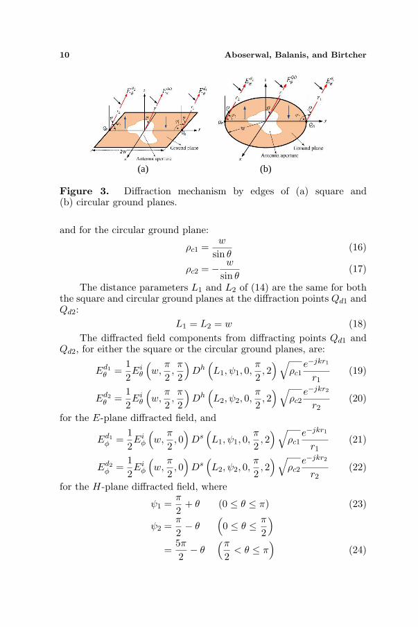
10 Aboserwal, Balanis, and Birtcher
(a) (b)
Figure 3. Diffraction mechanism by edges of (a) square and(b) circular ground planes.
and for the circular ground plane:
ρc1 =w
sin θ(16)
ρc2 = − w
sin θ(17)
The distance parameters L1 and L2 of (14) are the same for boththe square and circular ground planes at the diffraction points Qd1 andQd2:
L1 = L2 = w (18)The diffracted field components from diffracting points Qd1 and
Qd2, for either the square or the circular ground planes, are:
Ed1θ =
12Ei
θ
(w,
π
2,π
2
)Dh
(L1, ψ1, 0,
π
2, 2
)√ρc1
e−jkr1
r1(19)
Ed2θ =
12Ei
θ
(w,
π
2,π
2
)Dh
(L2, ψ2, 0,
π
2, 2
)√ρc2
e−jkr2
r2(20)
for the E-plane diffracted field, and
Ed1φ =
12Ei
φ
(w,
π
2, 0
)Ds
(L1, ψ1, 0,
π
2, 2
)√ρc1
e−jkr1
r1(21)
Ed2φ =
12Ei
φ
(w,
π
2, 0
)Ds
(L2, ψ2, 0,
π
2, 2
)√ρc2
e−jkr2
r2(22)
for the H-plane diffracted field, where
ψ1 =π
2+ θ (0 ≤ θ ≤ π) (23)
ψ2 =π
2− θ
(0 ≤ θ ≤ π
2
)
=5π
2− θ
(π
2< θ ≤ π
)(24)

Progress In Electromagnetics Research B, Vol. 55, 2013 11
For far-field observations
r1 ' r − w cos(π
2− θ
)= r − w sin θ (25)
r2 ' r + w cos(π
2− θ
)= r + w sin θ (26)
for phase terms, andr1 ' r2 ' r (27)
for amplitude terms.Therefore, the diffracted fields from the diffracting points Qd1 and
Qd2 reduce to
Ed1θ =
12Ei
θ
(w,
π
2,π
2
)Dh
(L1, ψ1, 0,
π
2, 2
)√ρc1e
+jw sin θ e−jkr
r(28)
Ed2θ =
12Ei
θ
(w,
π
2,π
2
)Dh
(L2, ψ2, 0,
π
2, 2
)√ρc2e
−jw sin θ e−jkr
r(29)
for the far-zone E plane, and
Ed1φ =
12Ei
φ
(w,
π
2, 0
)Ds
(L1, ψ1, 0,
π
2, 2
)√ρc1e
+jw sin θ e−jkr
r(30)
Ed2φ =
12Ei
φ
(w,
π
2, 0
)Ds
(L2, ψ2, 0,
π
2, 2
)√ρc2e
−jw sin θ e−jkr
r(31)
for the far-zone H plane.So far, the diffraction effects of this study are accounted for by
using only the diffraction which depends on the magnitude of theincident field. However, this indicates that the diffracted field would bezero if the incident field is zero. Physically, the diffracted fields do notgo to zero. Thus a second-order diffraction, due to the rapid changeof the GO field near the edge, can be incorporated into the analysis.In the H plane for the square and circular ground planes, it is notedthat the first-order diffracted fields are zero because the electric fieldon the surface of a conductor wedge vanishes for a grazing incidentwave. Therefore, the slope diffracted fields, second-order diffractedfields, from the diffraction points are given by [4]
Eslopeθ =
1jk
[∂Ei
θ(Qd)∂n
] (∂Dh
∂φ′
) √ρc
s(ρc + s)e−jks (32)
Eslopeφ =
1jk
[∂Ei
φ(Qd)∂n
](∂Ds
∂φ′
)√ρc
s(ρc + s)e−jks (33)
where∂Ei
θ∂n |Qd
= n · ∇Eiθ|Qd
= − 1s′
∂Eiθ
∂φ′ |Qd= slope of incident field for
hard polarization.

12 Aboserwal, Balanis, and Birtcher
∂Eiφ
∂n |Qd= n · ∇Ei
φ|Qd= − 1
s′∂Ei
φ
∂φ′ |Qd= slope of incident field for
soft polarization.n is unit normal in φ′ direction.s′ is the distance from the aperture center to the diffraction point.s is the distance from the diffraction point to the observation point.∂Dh,s
∂φ′ = slope diffraction coefficient for hard and soft polarization,respectively, given by
Ds,hslope =
−e−jπ/4
2n2√
2πk sinβ′0
(csc2
[π + (ξ−)
2n
]Fs
[kLg+
(ξ−
)]
− csc2
[π − (ξ−)
2n
]Fs[kLg−(ξ−)]
±
csc2
[π + (ξ+)
2n
]Fs
[kLg+
(ξ+
)]
− csc2
[π − (ξ+)
2n
]Fs[kLg−(ξ+)]
)(34)
where
Fs(x) = 2jx[1− F (x)] (35)
and F (x) is presented by (12).Due to the circular symmetry of the circular ground plane’s edge,
the edge behaves as a continuous ring radiator which leads to theformation of a caustic where the diffracted field is infinity. Therefore,a caustic correction is needed for angles at and near the axis of theantenna. The UTD can be used to correct for this caustic. Ryanand Peters [21] showed that UTD equivalent currents can be usedto correct for this caustic. Using this method, equivalent magneticand electric currents are created on the edge of the aperture. Thenradiation integrals are used to obtain fields due to these currents,which correct the diffracted fields at and near the symmetry axis ofthe antenna. The electric and magnetic equivalent currents take theform of
Ieφ = −
√8πk
ηke−jπ/4DsEi
φ(Qd) (36)
Imφ = −
√8πk
ke−jπ/4DhEi
θ(Qd) (37)
The fields radiated by each of the equivalent currents can beobtained using techniques of Chapter 5 of [1]. Thus the radiated field
Progress In Electromagnetics Research B, Vol. 55, 2013 13
for a loop carrying an electric current Ie are given by
Eeθ = −jωµa
4πrcos θe−jkr
∫ 2π
0Ie(φ′) sin(φ− φ′)ejka cos(φ−φ′) sin θdφ′ (38)
Eeφ = −jωµa
4πre−jkr
∫ 2π
0Ie(φ′) cos(φ− φ′)ejka cos(φ−φ′) sin θdφ′ (39)
The duality theorem can be applied to obtain the fields radiatedby a magnetic current Im, rather than an electric current Ie, and itleads to
Emθ =−η
jωεa
4πre−jkr
∫ 2π
0Im(φ′) cos(φ− φ′)ejka cos(φ−φ′) sin θdφ′ (40)
Emφ =η
jωεa
4πrcos θe−jkr
∫ 2π
0Im(φ′) sin(φ− φ′)ejka cos(φ−φ′) sin θdφ′ (41)
Now, numerically integrating (38)–(41), corrected diffracted fieldsare obtained at and near the symmetry axis of the antenna.
The electric current is zero because the incident field (GO field) iszero at the edge. Therefore, the radiated fields of the electric currentare zero. The corrected diffracted fields in the E and H planes due toa magnetic current around the ground edge are obtained at and nearthe symmetry axis of the antenna by computing numerically (40)–(41).
For the square ground plane, the slope diffraction does notsignificantly improve the radiation pattern in the backlobe region of theH-plane amplitude radiation pattern. Therefore, one needs to includethe contributions from the E-plane edge diffractions because the E-plane edge diffractions have a much greater magnitude than those ofthe H-plane edge diffractions. This contribution can be calculated byusing the equivalent current method that was described previously.
4. RESULTS AND VALIDATION: PREDICTIONS,SIMULATIONS AND MEASUREMENTS
All measurements were performed in the ElectroMagnetic AnechoicChamber (EMAC) facility at Arizona State University. Models forthe square and circular ground planes with rectangular and circularaperture antennas mounted at the center have been constructed. Theground planes are made of aluminum. A computer program waswritten in Matlab to calculate the normalized far-zone field amplitudepatterns in the E and H planes for all cases considered in this work.

14 Aboserwal, Balanis, and Birtcher
4.1. Conical Horn Antennas Mounted on Square andCircular Ground Planes
The width of the square ground plane and diameter of the circularground plane are 12.2 in. Using a dynamic range of 100 dB, theagreement between theory, experiment, and HFSS simulations is goodin the E and H planes for the X-band conical horn, having a totalflare angle of 35 and an axial length L = 8.2 in. The frequency atwhich the measurements were preformed is 10.3 GHz. The diameterof the horn aperture is 5.36 in. The diameter of the waveguides (usedfor the measurements and HFSS simulations) is 0.9 in. Numerical andmeasured data are compared with simulated data based on Ansoft’sHigh Frequency Structure Simulator (HFSS).
Figure 4 displays the far-zone E-plane amplitude patterns of theconical horn antenna mounted on the square and circular groundplanes. The GO field in the forward region (0 ≤ θ ≤ π/2) is calculatedusing (1) and (3) [because (2) vanishes in the E plane (φ = 90)].The edge diffractions from the E-plane edges are included in the totalamplitude pattern using (28) and (29). Very good agreement betweentheory, experiment and simulations is indicated; the total field consistsof the GO and first-order diffracted fields. In addition, the fieldsassociated with the equivalent currents of (38) and (40) are includedfor the circular ground planes.
The same comparison for the far-zone H-plane amplitude patterns
(a) (b)
Figure 4. Far-zone E-plane amplitude patterns of an X-band conicalhorn antenna at 10.3GHz (L = 8.2 in, 2α0 = 35, 2w = 12.2 in)mounted on (a) square and (b) circular ground planes.

Progress In Electromagnetics Research B, Vol. 55, 2013 15
is illustrated in Figure 5. As shown in the figure, there is goodagreement between predictions, measurements, and simulations; thetotal analytical field consists of the GO field given by (2) and (4)[because (1) vanishes in the H plane (φ = 0)], first-order diffractedfields obtained by using (30) and (31), and slope diffracted fields givenby (33). The edge diffraction contributions using (30) and (31) onthe overall amplitude pattern are zero where the amplitude patternis similar to that of the infinite ground plane. In the back region(π/2 ≤ θ ≤ π) of the H-plane pattern of antennas mounted onthe square ground planes, the contributions from the E-plane edgediffractions should be included because the E-plane edge diffractionsare more intense than those of the H-plane edge slope diffractions.Using (39) and (41), the fields associated with the equivalent currentsare included for the circular ground planes to correct for the causticformed by the diffracted fields at and near the symmetry axis of theantenna.
(a) (b)
Figure 5. Far-zone H-plane amplitude patterns of an X-band conicalhorn antenna at 10.3GHz (L = 8.2 in, 2α0 = 35, 2w = 12.2 in)mounted on (a) square and (b) circular ground planes.
4.2. Rectangular and Circular Waveguides Mounted onSquare and Circular Ground Planes
The rectangular and circular aperture antennas have been, respec-tively, excited by the TE10-mode rectangular and the TE11-mode cir-cular waveguides. The width of the square ground plane and diameterof the circular ground plane is 12 in. Validity of the radiation pattern

16 Aboserwal, Balanis, and Birtcher
analysis over the main beam and the near and far sidelobes presentedabove has been verified by calculating the far-zone E- and H-planeamplitude patterns of the aperture antennas. The frequency at whichmeasurements are performed is 10 GHz. The dimensions of the rect-angular aperture are a = 0.9 in and b = 0.4 in, and the diameter ofthe circular aperture is 0.938 in. A comparison between the predicted,measured, and simulated results has been made.
Figures 6 and 7 show, respectively, the far-zone E-plane amplitudepatterns of rectangular and circular waveguide antennas mounted onthe square and circular ground planes. Computed amplitude patternsare compared with experimental and simulated data, and a goodagreement is indicated. The total field consists of the GO given by (5)and (7) for the rectangular and circular waveguides [because (6) and (8)vanish in the E plane (φ = 90)], respectively, and first-order diffractedfields from two diffraction points given by (28) and (29), depending onwhich ground plane is being considered. In addition, the diffractedfields associated with the equivalent currents for the circular groundplanes are included at and near the symmetry axis of the antennausing (38) and (40).
Unlike the E-plane diffraction, there is no diffraction contributionfrom the H-plane edges because the incident waves at the diffractionpoints, given by (6) and (8) when θ = 90, are zero. However,second-order diffracted fields given by (33) from the diffraction points(Qd1 and Qd2) are included to improve the total amplitude pattern
(a) (b)
Figure 6. Far-zone E-plane amplitude patterns of a rectangularwaveguide at 10GHz (a = 0.9 in, b = 0.4 in, 2w = 12 in), (a) squareand (b) circular ground planes.

Progress In Electromagnetics Research B, Vol. 55, 2013 17
(a) (b)
Figure 7. Far-zone E-plane amplitude patterns of a circularwaveguide at 10 GHz (a = 0.469 in, 2w = 12 in), (a) square and(b) circular ground planes.
(a) (b)
Figure 8. Far-zone H-plane amplitude patterns of a rectangularwaveguide at 10GHz (a = 0.9 in, b = 0.4 in, 2w = 12 in), (a) squareand (b) circular ground planes.
especially in the back region. The far-zone H-plane amplitude patternsof rectangular and circular waveguide antennas mounted on the squareand circular ground planes, respectively, are shown in Figures 8 and 9.The GO fields are calculated using (6) and (8) for the rectangularand circular waveguides, respectively. Very good agreement between

18 Aboserwal, Balanis, and Birtcher
(a) (b)
Figure 9. Far-zone H-plane amplitude patterns of a circularwaveguide at 10 GHz (a = 0.469 in, 2w = 12 in), (a) square and(b) circular ground planes.
theory, experiment and simulations is indicated; the total field consistsof the GO, first-order diffracted, and slope diffracted fields. Forthe square ground plane, the contributions from the E-plane edgediffractions should be included to calculate the H-plane amplitudepattern. Also, the fields associated with the equivalent currents of (39)and (41) are included for the circular ground planes.
In all studied cases, it is very obvious that the magnitude ofthe amplitude pattern of the circular ground plane at and near thesymmetry axis of the antenna, below the ground plane, is much largercompared to that of the square ground plane. Because of the symmetryof the circular ground plane, there is a ring radiator along the circularedge contributing about 10–13 dB greater at and near the symmetryaxis of the circular ground plane, compared to that of the squareground plane.
5. CONCLUSIONS
In this investigation of conical horn, and rectangular and circularwaveguide antennas mounted on finite ground planes, the edgesof the finite ground plane influence the radiation patterns in thediffraction zone. This effect has been examined both analytically andexperimentally. Two ground planes, square and circular, were chosenfor this study. The study indicates that the finite ground plane does not

Progress In Electromagnetics Research B, Vol. 55, 2013 19
influence greatly the forward main pattern. Its primary impact appearsin far side and back lobes regions. The aperture integration method,augmented by the Uniform Theory of Diffraction for the predictionof aperture antenna radiation, has been presented. The UTD edgediffractions are included for the finite ground plane in both the E-and H-plane predictions. In the E plane, single edge diffractions plusthe direct GO field contribute to the total field. In the H plane,the total field consists of the direct GO field, single edge diffractions,slope diffracted field, and E-plane edge equivalent current field. Inaddition, the contributions of the electric and magnetic equivalentcurrents must be included for the circular ground plane to correctthe caustics created by the the diffracted fields at and near the axis ofthe antenna. Numerical results obtained by our method are comparedwith measured data and those simulated by Ansoft’s High FrequencyStructure Simulator (HFSS). The measured and simulated resultsindicate that the predictions based on the analytical formulations, forboth square and circular ground planes, are in very good agreement.This work demonstrates that the impact of the edges must be includedin the calculation to obtain very accurate results of the amplitudepatterns, especially for extended dynamic ranges.
For all studied cases, the H-plane electric field component of theincident field vanishes along the ground plane edge (grazing incidence).Thus, only diffraction by the E-plane edges contributes significantlyto the E- and H-plane diffraction patterns. To obtain the far-zone E-plane amplitude pattern, only the diffraction from the midpoints of theE-plane edge contributes to the amplitude pattern. For the far-zoneH-plane amplitude pattern, diffraction accruing at all points along theE-plane edge, non-normal and normal incidence of the incident GOfields at the edge, must be taken into consideration.
The discrepancies between the theoretical and measured results inthe backward region of the far-zone E- and H-plane amplitude patternscan be attributed to the inability to accurately model the structurefeeding the aperture antennas as well as the structure used to supportthe antenna during the measurements.
REFERENCES
1. Balanis, C. A., Antenna Theory: Analysis and Design, John Wileyand Sons, New Jersey, 2005.
2. Kraus, J. D. and R. J. Marhefka, Antennas for All Applications,McGraw-Hill, New York, 2002.
3. OnlineAvailable: http://www.ansoft.com/products/hf/hfss/AnsoftCorporation HFSS.

20 Aboserwal, Balanis, and Birtcher
4. Balanis, C. A., Advanced Engineering Electromagnetics, JohnWiley and Sons, New Jersey, 2012.
5. Aboserwal, N. A., C. A. Balanis, and C. R. Birtcher, “Conicalhorn: Gain and amplitude patterns,” IEEE Trans. AntennasPropagat., Vol. 61, No. 7, 3427–3433, Jul. 2013.
6. Love, A. W., Electromagnetic Horn Antennas, IEEE Press, NewYork, 1976.
7. Keller, J. B., “Geometrical theory of diffraction,” J. Opt. Soc.Amer., Vol. 52, 116–130, Feb. 1962.
8. Kouyoumjian, R. G. and P. H. Pathak, “A uniform geometricaltheory of diffraction for an edge in a perfectly conducting surface,”Proceedings IEEE, Vol. 62, No. 11, 1448–1461, Nov. 1974.
9. Ibrahim, H. M. and D. T. Stephenson, “Radiation patterns of aλ/4 monopole mounted on thick finite square and circular groundplanes,” Int. J. Electronics, Vol. 64, No. 3, 345–358, Jul. 1988.
10. Huang, J., “The finite ground plane effect on the microstripantenna radiation patterns,” IEEE Trans. Antennas Propagat.,Vol. 31, No. 4, 649–653, Jul. 1983.
11. Narasimhan, M. S. and M. Sheshadri, “GTD analysis of theradiation patterns of conical horns,” IEEE Trans. AntennasPropagat., Vol. 26, No. 6, 774–778, Nov. 1978.
12. Ali, M., S. Sanyal, and S. Park, “Analysis of horn radiationpattern using UTD edge and corner diffraction,” Progress InElectromagnetics Research M, Vol. 17, 87–99, 2011.
13. Menendez, R. and S. W. Lee, “Analysis of rectangular hornantennas via uniform asymptotic theory,” IEEE Trans. AntennasPropagat., Vol. 30, No. 2, 241–250, Mar. 1982.
14. Narsimhan, M. S. and S. K. Rao, “GTD analysis of the near-fieldpatterns of pyramidal horns,” Proceedings IEEE, Vol. 126, No. 12,1223–1226, Dec. 1979.
15. Balanis, C. A., “Pattern distortion due to edge diffractions,” IEEETrans. Antennas Propagat., Vol 18, 561–563, Jul. 1970.
16. Ali, M. and S. Sanyal, “A finite edge GTD analysis of the H-plane horn radiation pattern,” Proceedings IEEE, Vol. 58, No. 3,969–973, Mar. 2010.
17. Yu, J. S. and R. C. Rudduck, “H-plane pattern of a pyramidalhorn,” IEEE Trans. Antennas Propagat., Vol. 17, No. 5, 651–652,Sep. 1969.
18. Yu, J. S., R. C. Rudduck, and L. Peters, “Comprehensive analysisfor E-plane of horn antennas by edge diffraction theory,” IEEETrans. Antennas Propagat., Vol. 14, No. 2, 138–149, Mar. 1966.

Progress In Electromagnetics Research B, Vol. 55, 2013 21
19. Russo, P. M., R. C. Rudduck, and L. Peters, “A method forcomputing E-plane patterns of horn antennas,” IEEE Trans.Antennas Propagat., Vol. 13, No. 2, 219–224, Mar. 1965.
20. Balanis, C. A., “Radiation from conical surfaces used for high-speed spacecraft,” Radio Science, Vol. 7, No. 2, 339–343,Feb. 1972.
21. Ryan, C. and L. Peters, “Evaluation of edge-diffracted fieldsincluding equivalent currents for the caustic regions,” IEEE Trans.Antennas Propagat., Vol. 17, No. 3, 292–298, May 1969.