MODELLING DIFFRACTION IN OPTICAL INTERCONNECTS
242
MODELLING DIFFRACTION IN OPTICAL INTERCONNECTS A DISSERTATION SUBMITTED FOR THE DEGREE OF DOCTOR OF PHILOSOPHY AT THE UNIVERSITY OF QUEENSLAND IN June 2004 BY Novak S. Petrovi´ c, BE (Elec) Hons I OF SCHOOL OF INFORMATION TECHNOLOGY AND ELECTRICAL ENGINEERING
-
Upload
khangminh22 -
Category
Documents
-
view
1 -
download
0
Transcript of MODELLING DIFFRACTION IN OPTICAL INTERCONNECTS

MODELLING DIFFRACTION
IN OPTICAL INTERCONNECTS
A DISSERTATION
SUBMITTED FOR THE DEGREE OF
DOCTOR OF PHILOSOPHY
AT
THE UNIVERSITY OF QUEENSLAND
IN
June 2004
BY
Novak S. Petrovic, BE (Elec) Hons I
OF
SCHOOL OF INFORMATION TECHNOLOGY
AND ELECTRICAL ENGINEERING

Statement of Originality
The work in this thesis is, to the best of the candidate’s knowledge and belief, original, except
as acknowledged in the text, and the material has not been submitted, either in whole or in
part, for a degree at this or any other university.
Petrovic Novak
ii

Abstract
Short-distance digital communication links, between chips on a circuit board, or between dif-
ferent circuit boards for example, have traditionally beenbuilt by using electrical interconnects
– metallic tracks and wires. Recent technological advances have resulted in improvements in
the speed of information processing, but have left electrical interconnects intact, thus creat-
ing a serious communication problem. Free-space optical interconnects, made up of arrays of
vertical-cavity surface-emitting lasers, microlenses, and photodetectors, could be used to solve
this problem.
If free-space optical interconnects are to successfully replace electrical interconnects, they
have to be able to support large rates of information transfer with high channel densities. The
biggest obstacle in the way of reaching these requirements is laser beam diffraction. There
are three approaches commonly used to model the effects of laser beam diffraction in opti-
cal interconnects: one could pursue the path of solving the diffraction integral directly, one
could apply stronger approximations with some loss of accuracy of the results, or one could
cleverly reinterpret the diffraction problem altogether.None of the representatives of the three
categories of existing solutions qualified for our purposes.
The main contribution of this dissertation consist of, first, formulating the mode expansion
method, and, second, showing that it outperforms all other methods previously used for mod-
elling diffraction in optical interconnects. The mode expansion method allows us to obtain the
optical field produced by the diffraction of arbitrary laserbeams at empty apertures, phase-
shifting optical elements, or any combinations thereof, regardless of the size, shape, position,
or any other parameters either of the incident optical field or the observation plane. The mode
expansion method enables us to perform all this without any reference or use of the traditional
Huygens-Kirchhoff-Fresnel diffraction integrals.
When using the mode expansion method, one replaces the incident optical field and the
diffracting optical element by an effective beam, possiblycontaining higher-order transverse
modes, so that the ultimate effects of diffraction are equivalently expressed through the complex-
valued modal weights. By using the mode expansion method, onerepresents both the incident
iii

and the resultant optical fields in terms of an orthogonal setof functions, and finds the un-
known parameters from the condition that the two fields have to be matched at each surface
on their propagation paths. Even though essentially a numerical process, the mode expansion
method can produce very accurate effective representations of the diffraction fields quickly
and efficiently, usually by using no more than about a dozen expanding modes.
The second tier of contributions contained in this dissertation is on the subject of the anal-
ysis and design of microchannel free-space optical interconnects. In addition to the proper
characterisation of the design model, we have formulated several optical interconnect perfor-
mance parameters, most notably the signal-to-noise ratio,optical carrier-to-noise ratio, and
the space-bandwidth product, in a thorough and insightful way that has not been published
previously. The proper calculation of those performance parameters, made possible by the
mode expansion method, was then performed by using experimentally-measured fields of the
incident vertical-cavity surface-emitting laser beams. After illustrating the importance of the
proper way of modelling diffraction in optical interconnects, we have shown how to improve
the optical interconnect performance by changing either the interconnect optical design, or by
careful selection of the design parameter values. We have also suggested a change from the
usual ‘square’ to a novel ‘hexagonal’ packing of the opticalinterconnect channels, in order to
alleviate the negative diffraction effects.
Finally, the optical interconnect tolerance to lateral misalignment, in the presence of mul-
timodal incident laser beams was studied for the first time, and it was shown to be acceptable
only as long as most of the incident optical power is emitted in the fundamental Gaussian
mode.
iv

Publications
The following is a list of publications and presentations bythe candidate on matters deemed
relevant relating to this dissertation (in chronological order):
• N. S. Petrovic, A. D. Rakic, and M. L. Majewski: “Free-space optical interconnects with
an improved signal-to-noise ratio,”Proceedings of 27th European Conference on Optical
Communication (ECOC 2001), vol. 3, pp. 292-293, Amsterdam (The Netherlands), 30
September – 4 October 2001. Available online through an author-search for ‘Petrovic
N. S.’ from IEEEXploreR©, http://ieeexplore.ieee.org.
• N. S. Petrovic: “Free-space optical interconnects,”Presentation made as a part of the
University of Queensland School of Physics Seminar Series, Brisbane, August 2002.
• N. S. Petrovic and A. D. Rakic: “Channel density in free-space optical interconnects,”
Proceedings of 2002 IEEE Conference on Optoelectronic and Microelectronic Materials
and Devices (COMMAD 2002), vol. 1, pp. 133-136, Sydney, 11 – 13 December 2002.
Available online from IEEEXploreR©, http://ieeexplore.ieee.org.
• N. S. Petrovic and A. D. Rakic: “Modelling diffraction effects by the mode expansion
method,”Proceedings of 2002 IEEE Conference on Optoelectronic and Microelectronic
Materials and Devices (COMMAD 2002), vol. 1, pp. 129-132, Sydney, 11-13 December
2002. Available online from IEEEXploreR©, http://ieeexplore.ieee.org.
• N. S. Petrovic: “Modal expansion in optical communications,” Presentation made at the
University of Queensland Electromagnetics and Imaging Retreat, Brisbane, July 2003.
• N. S. Petrovic and A. D. Rakic: “Modelling diffraction in free-space optical intercon-
nects by the mode expansion method,”Applied Optics, vol. 42, no. 26, pp. 5308-5318,
September 2003. Available online from http://ao.osa.org/abstract.cfm?id=74228.
• N. S. Petrovic, C. J. O’Brien and A. D. Rakic: “Derivation and examination of a compre-
hensive free-space optical interconnect link equation,”Proceedings of SPIE, vol. 5277,
v

pp. 251-260, presented at the2003 SPIE International Symposium on Microelectronics,
MEMS, and Nanotechnology, Perth, 9 – 12 December 2003.
• F.-C. F. Tsai, N. S. Petrovic and A. D. Rakic: “Comparison of stray-light and diffraction-
caused crosstalk in free-space optical interconnects,”Proceedings of SPIE, vol. 5277,
pp. 320-327, presented at the2003 SPIE International Symposium on Microelectronics,
MEMS, and Nanotechnology, Perth, 9 – 12 December 2003.
• N. S. Petrovic, C. J. O’Brien and A. D. Rakic: “Analysis of free-space optical intercon-
nect misalignment tolerance in the presence of multimode VCSEL beams,”Proceedings
of the 24th IEEE International Conference on Microelectronics (MIEL 2004), vol. 1, pp.
337-340, Nis (Serbia and Montenegro), 16 – 19 May 2004. Available onlinefrom IEEE
XploreR©, http://ieeexplore.ieee.org.
• N. S. Petrovic, C. J. O’Brien and A. D. Rakic: “Analysis of the effect of transverse modes
on free-space optical interconnect performance,”Special issue of Smart Materials and
Structures, submitted for publication, May 2004.
• N. S. Petrovic and A. D. Rakic: “Modelling diffraction and imaging of laser beams by
the mode expansion method,”Journal of the Optical Society of America B, accepted for
publication, October 2004. Available online from http://josab.osa.org.
• F.-C. F. Tsai, N. S. Petrovic, and A. D. Rakic, “Modelling stray-light crosstalk noise
in free-space optical interconnects,”Optics Communications, submitted for publication,
December 2004.
• F.-C. F. Tsai, C. J. O’Brien, N. S. Petrovic, and A. D. Rakic: “The effect of higher-
order modes on optical crosstalk in free-space optical interconnects,”Proceedings of
2004 IEEE Conference on Optoelectronic and MicroelectronicMaterials and Devices
(COMMAD 2004), to be printed in 2005, Brisbane, 8–10 December 2004. Available
online from IEEEXploreR©, http://ieeexplore.ieee.org.
vi

Acknowledgements
I wish to express sincere gratitude to my advisor Dr Aleksandar D. Rakic for his encourage-
ment, guidance, and friendship during the course of my research. Under the supervision of Dr
Rakic I have not only ‘learnt the craft,’ but also immensely grownas a person. Furthermore,
I wish to acknowledge the contributions of the members of theMicrowave and Photonics Re-
search Group at the University of Queensland: Christopher J.O’Brien for his experimental
measurements and our very fruitful collaboration, Feng-Chuan Frank Tsai for his work in
Code V, Richard R. Taylor for his advice and support during our numerous technical and not-
so-technical discussions, and Dr Marian Ł. Majewski for theprecious insights that put life in
perspective. I also wish to acknowledge the help, in the initial stages of my research, of Prof.
Kazumasa Tanaka of Nagasaki University, Prof. Anthony E. Siegman of Stanford University,
and Prof. Charles A. DiMarzio of the Northeastern University.
As a great building can only stand on good foundations, I believe that I would not have
been able to achieve anything without the love, utmost dedication, and countless sacrifices that
my mother Dusanka has made for my upbringing, education, and wellbeing.I am grateful to
my father Simica for encouraging me to think originally and positively, as well as to my sister
Jelena for her love, understanding and support. My greatestinspiration and encouragement,
however, have come from the heart of my wife Florencia, who has taught me what love and
real happiness are.
vii

Contents
Statement of Originality . . . . . . . . . . . . . . . . . . . . . . . . . . . . .. . . ii
Abstract . . . . . . . . . . . . . . . . . . . . . . . . . . . . . . . . . . . . . . . . iii
Publications . . . . . . . . . . . . . . . . . . . . . . . . . . . . . . . . . . . . . . v
Acknowledgements . . . . . . . . . . . . . . . . . . . . . . . . . . . . . . . . . . vii
Table of Contents . . . . . . . . . . . . . . . . . . . . . . . . . . . . . . . . . . . vii
List of Figures . . . . . . . . . . . . . . . . . . . . . . . . . . . . . . . . . . . . . x
1 Introduction 1
1.1 Electrical versus optical interconnects . . . . . . . . . . . .. . . . . . . . . 2
1.2 Diffraction in optical interconnects . . . . . . . . . . . . . . .. . . . . . . . 15
1.3 Dissertation outline . . . . . . . . . . . . . . . . . . . . . . . . . . . . .. . 20
2 The problem of diffraction in optical interconnects 22
2.1 Mathematical basis . . . . . . . . . . . . . . . . . . . . . . . . . . . . . . .23
2.2 Problem formulation . . . . . . . . . . . . . . . . . . . . . . . . . . . . . .30
2.3 Existing solutions . . . . . . . . . . . . . . . . . . . . . . . . . . . . . . .. 42
2.3.1 Solution by direct integration . . . . . . . . . . . . . . . . . . .. . . 48
2.3.2 Solution by further approximation . . . . . . . . . . . . . . . .. . . 51
2.3.3 Solution by equivalent representation . . . . . . . . . . . .. . . . . 59
2.4 Summary and conclusion . . . . . . . . . . . . . . . . . . . . . . . . . . . .62
3 Novel way of modelling diffraction 64
3.1 Modal expansion of the exact solution . . . . . . . . . . . . . . . .. . . . . 65
viii

3.2 Alternative approach to modal expansion . . . . . . . . . . . . .. . . . . . . 69
3.3 Mode expansion method . . . . . . . . . . . . . . . . . . . . . . . . . . . . 73
3.3.1 Derivation of the method . . . . . . . . . . . . . . . . . . . . . . . . 73
3.3.2 Guidelines for practical application . . . . . . . . . . . . .. . . . . 84
3.3.3 Other approaches to modal expansion . . . . . . . . . . . . . . .. . 91
3.4 Numerical illustration and verification . . . . . . . . . . . . .. . . . . . . . 93
3.5 Summary and conclusion . . . . . . . . . . . . . . . . . . . . . . . . . . . .115
4 Application in optical interconnects 116
4.1 Design model . . . . . . . . . . . . . . . . . . . . . . . . . . . . . . . . . . 117
4.2 Experimental details . . . . . . . . . . . . . . . . . . . . . . . . . . . . .. 137
4.3 Evaluation of optical interconnect performance . . . . . .. . . . . . . . . . 151
4.4 Tolerance to misalignment . . . . . . . . . . . . . . . . . . . . . . . . .. . 170
4.5 Summary and conclusion . . . . . . . . . . . . . . . . . . . . . . . . . . . .175
5 Conclusion 178
5.1 Summary of dissertation findings . . . . . . . . . . . . . . . . . . . .. . . . 179
5.2 Further goals and direction . . . . . . . . . . . . . . . . . . . . . . . .. . . 184
A Electromagnetic considerations 186
A.1 Review of fundamentals . . . . . . . . . . . . . . . . . . . . . . . . . . . . 186
A.2 Derivation of the diffraction formula . . . . . . . . . . . . . . .. . . . . . . 193
B Additional expressions 198
B.1 Hermite-Gaussian coefficients . . . . . . . . . . . . . . . . . . . . . .. . . 198
Bibliography 201
ix

List of Figures
1.1 Schematic diagram of an electrical interconnect. . . . . .. . . . . . . . . . . 3
1.2 Conceptual block diagram of an optical interconnect. . . .. . . . . . . . . . 8
1.3 Macrochannel free-space optical interconnect. . . . . . .. . . . . . . . . . . 11
1.4 Microchannel free-space optical interconnect. . . . . . .. . . . . . . . . . . 12
1.5 Minichannel free-space optical interconnect. . . . . . . .. . . . . . . . . . . 13
1.6 Schematic diagram of a generic optical interconnect. . .. . . . . . . . . . . 16
1.7 Schematic diagram of the lensless free-space optical interconnect [1]. . . . . 17
1.8 Illustration of laser beam diffraction [1]. . . . . . . . . . .. . . . . . . . . . 18
1.9 Schematic diagram of a microchannel free-space opticalinterconnect. . . . . 19
2.1 In order to find the characteristics of the electromagnetic field at the observa-
tion pointP , the contributions from all the sources withinS must be integrated,
by applying Eqs (2.11) and (2.12). . . . . . . . . . . . . . . . . . . . . . .. 26
2.2 Given a field distribution at surfaceSn, Eq. (2.17) allows us to calculate the
optical field distribution at any subsequent surfaceSn+1. . . . . . . . . . . . 27
2.3 The complete optical interconnect channel (and hence the whole optical inter-
connect) can be represented as a collection of surfaces withdifferent material
properties. The surfaces are best interpreted as parts of spheres, as shown in
(a). If we allow the radii of the spheres to increase to infinity, the surfaces
become practically flat and orthogonal to the axis of propagation, as shown in
(b). . . . . . . . . . . . . . . . . . . . . . . . . . . . . . . . . . . . . . . . . 28
x
2.4 Illustration of the path-integral approach to solving diffraction problems [2].
All possible paths that the photon can take from the source tothe destination
are considered (with the shape of the obstacle taken into consideration), the
action of the path given by Eq. (2.71) is calculated, and the phasors associated
with each path are added up, as shown by Eq. (2.69). The resultof the process
in the probability of a source photon going to the destination. . . . . . . . . . 47
2.5 Schematic diagram that aids the understanding of the wayin which the the
solution by further approximation was applied in Ref. [3]. . .. . . . . . . . . 57
2.6 Schematic diagram that aids the understanding of the wayin which the method
of Belland and Crenn works. . . . . . . . . . . . . . . . . . . . . . . . . . . 61
3.1 Illustration of application of the mode expansion method: the incident laser
beam and the diffracting surface, as shown in (a), are replaced by an effective
laser beam, as shown in (b). The parameters of the effective laser beam are
written in bold. In this particular example the diffractingsurface was assumed
to consist of a circular apertureA, of radiusa. . . . . . . . . . . . . . . . . . 94
3.2 The behaviour of the magnitude of the first four expansioncoefficients assum-
ing that the incident laser beam is a Laguerre-Gaussian(0, 0) mode. The inset
on the left shows the the intensity profile of the TEM00 mode at the plane of the
diffracting aperture, assuming the usual parameter values. (Note the difference
in the coordinate range in Figs 3.2, 3.3, and 3.4.) . . . . . . . . .. . . . . . 95
3.3 The behaviour of the magnitude of the first four expansioncoefficients assum-
ing that the incident laser beam is a Laguerre-Gaussian(1, 1) mode. The inset
on the left shows the the intensity profile of the TEM00 mode at the plane of the
diffracting aperture, assuming the usual parameter values. (Note the difference
in the coordinate range in Figs 3.2, 3.3, and 3.4.) . . . . . . . . .. . . . . . 96
xi

3.4 The behaviour of the magnitude of the first four expansioncoefficients assum-
ing that the incident laser beam is a Laguerre-Gaussian(2, 2) mode. The inset
on the left shows the the intensity profile of the TEM00 mode at the plane of the
diffracting aperture, assuming the usual parameter values. (Note the difference
in the coordinate range in Figs 3.2, 3.3, and 3.4.) . . . . . . . . .. . . . . . 97
3.5 Approximating the diffraction field (solid line) by the mode expansion method
(large dots): in the profile-matching sense (a), and in the encircled power sense
(b). If the profile of the intensity in the diffraction field isto be approximated,
generally more modes are required; fewer modes are requiredif only the en-
circled power in the diffraction field is to be found. . . . . . . .. . . . . . . 99
3.6 Encircled power calculated directly and by the mode expansion method, with
different number of modes in the expanding beam. Using one expanding mode
only approximates the encircled power in the diffraction field well only in the
cases of weak diffraction; if more modes are added to the effective beam, the
approximation becomes progressively better. . . . . . . . . . . .. . . . . . . 100
3.7 Similarly to Fig. 3.1, this figure illustrates the application of the mode expan-
sion method. The stress here is, however, on the fact that we want to calculate
power in the diffraction field, both on the on-axis encircling areaS, as well as
the off-axis areaN . . . . . . . . . . . . . . . . . . . . . . . . . . . . . . . . 101
3.8 Encircled power calculated using different methods on (a) receiverS, and (b)
on receiverN : direct integration (solid line), mode expansion method (large
dots), the method of Belland and Crenn (small dots), and the method of Tang
et al. (broken line). ApertureA is empty and the distance to the fromA to the
observation plane isd = 2.6 mm. . . . . . . . . . . . . . . . . . . . . . . . . 102
xii

3.9 Encircled power calculated using different methods on (a) receiverS, and (b)
on receiverN : direct integration (solid line), mode expansion method (large
dots), the method of Belland and Crenn (small dots). ApertureA contains a
thin lens withf = 800 µm, and the distance fromA to the observation plane
is d = 10.4 mm. . . . . . . . . . . . . . . . . . . . . . . . . . . . . . . . . . 103
3.10 Calculations of encircled power vs. receiver radiusaS for 0 ≤ aS ≤ 125 µm
and for three different clipping ratios calculated by: direct integration (solid
line), mode expansion method (large dots), and the method ofBelland and
Crenn (broken line). ApertureA is empty andd = 10.4 mm. . . . . . . . . . 105
3.11 Illustration of the way in which the optimal parametersof the expanding beam
set, p are found. In the case of TEM00 mode incidence, the optimalws and
zs are the ones that maximise the fundamental-to-fundamentalcoupling coef-
ficient. The expanding set almost always has to be found numerically, but in
some cases simple analytic expressions may be used. . . . . . . .. . . . . . 106
3.12 Changes inp (ws is shown in (a), andzs is shown in (b) above), due to changes
in the clipping ratio at the diffracting aperture. Broken lines in both (a) and (b)
represent thep values obtained by the application of the ABCD Law. . . . . . 107
3.13 Approximating the diffraction field with an increasingnumber of effective
modes, in the case whenκ = 1.0, the observation distance is 20.8 mm: (a)
1 mode, (b) 4 modes, (c) 6 modes, and (d) 12 modes. . . . . . . . . . . .. . 109
3.14 Diffraction field of an incident TEM20 produced by the mode expansion method.
There are two most notable differences in the profiles of the diffraction field
in the case of TEM00 and TEM20 incidence: (i) the TEM20 diffraction field
carries less energy close to the propagation axis(and the first local minimum
of the field occurs at a smaller radial distance), and (ii) thesecond local max-
imum is much more pronounced than in the case of incidence of the TEM00
mode. . . . . . . . . . . . . . . . . . . . . . . . . . . . . . . . . . . . . . . 110
xiii
3.15 Given a sufficient number of expanding modes, the mode expansion method
is capable of approximating even extreme diffraction situations. This figure
shows the diffraction field in the case whenκ = 0.1, and the observation
distance, measured from the diffracting aperture is 0.1 mm (a10th of its usual
value). 33 modes were used to construct the expanding beam. .. . . . . . . . 110
3.16 Plots of the ‘direct’ approximation difference,Eint( ˆNM), as given by Eq. (3.73),
and the ‘adaptive’, or ‘change’ difference,Cint( ˆNM, ˆNM + ∆ ˆNM), as given
by Eq. (3.75).Eint measures the average relative difference between the mea-
sured and approximated diffraction field, whileCint measures the change in the
approximated field resulting from adding more modes. . . . . . .. . . . . . 111
3.17 Plots of the ‘direct’ approximation difference,Eep( ˆNM), as given by Eq. (3.76),
and the ‘adaptive’, or ‘change’ difference,Cep( ˆNM, ˆNM + ∆ ˆNM), as given
by Eq. (3.77), in the case of approximating the encircled power in the diffrac-
tion field. This is different from the results shown in Fig. 3.16 where we were
examining the error that occurs in approximating the intensity of the diffrac-
tion field. . . . . . . . . . . . . . . . . . . . . . . . . . . . . . . . . . . . . 112
3.18 The results presented here are exactly the same in principle as the ones pre-
sented in Fig. 3.17; the only difference is that the weightedgoodness-of-fit
criteria, given by Eqs. (3.78) and (3.79) are used. The important messages
conveyed by Fig. 3.18 are the same as the ones conveyed by Fig.3.17, the
main difference is the lower overall level of approximationerror. . . . . . . . 113
3.19 The results of the simplest, energy-conversion argument, given by Eq. (3.83),
is used to estimate how many expanding modes need to be used inorder to
account for all the power that carried by the light beam that goes through the
diffracting aperture. . . . . . . . . . . . . . . . . . . . . . . . . . . . . . . .114
3.20 The number of modes required, at each different clipping ratioκ, to properly
account for 99% of the power in the diffraction field. . . . . . . .. . . . . . 114
xiv

4.1 Schematic diagram of the interconnect configuration whose performance is
evaluated by using the mode expansion method. . . . . . . . . . . . .. . . . 117
4.2 Schematic diagram of the representative channelC0. . . . . . . . . . . . . . 119
4.3 The optical crosstalk noise, indicated by cross-hatching, and made up of the
stray-light crosstalk noise (introduced at the transmitter microlens plane) and
the diffraction-caused crosstalk noise (introduced at thereceiver microlens
plane), is a major limiting factor in the design of optical interconnects. . . . . 121
4.4 The portion of the incident laser power that crosses overinto neighbouring
channels at the transmitter microlens plane (the stray-light crosstalk noise) is
always imaged in such a way that it never ends up on the photodetector for
which it was intended. . . . . . . . . . . . . . . . . . . . . . . . . . . . . . 122
4.5 Schematic diagram indicating the arrangement of elements (VCSELs, receiver
and transmitter microlenses, and photodetectors) in the planes making up the
interconnect. The footprint of all elements is circular; while ∆ (array pitch)
has to be the same for all planes,a (generic element radius) can vary from
plane to plane, but not within one. . . . . . . . . . . . . . . . . . . . . . .. 124
4.6 Illustration of the equivalence principle used for calculation of the SLCN and
the DCCN. The crosstalk noise from any channelCn that ends up inC0, as
shown in (a), can equivalently be calculated as the noise fromC0 that ends up
in Cn, as shown in (b). . . . . . . . . . . . . . . . . . . . . . . . . . . . . . 127
4.7 Schematic diagram of the experimental setup used for measuring the VCSEL’s
light-current characteristic. . . . . . . . . . . . . . . . . . . . . . . .. . . . 139
4.8 Experimentally-measured and numerically-fitted results of the VCSEL’s light-
current characteristic. . . . . . . . . . . . . . . . . . . . . . . . . . . . . .. 139
4.9 Schematic diagram of the experimental setup used for measuring the VCSEL
beam’s modal and spectral characteristics. . . . . . . . . . . . . .. . . . . . 140
4.10 Experimentally-measured VCSEL’s modal and spectral characteristics. . . . . 141
4.11 Modally resolved VCSEL’s light-current characteristic. . . . . . . . . . . . . 142
xv

4.12 Wavelength of each laser beam mode, obtained from the data presented in
Fig. 4.10. . . . . . . . . . . . . . . . . . . . . . . . . . . . . . . . . . . . . 143
4.13 Schematic diagram of the experimental setup used for spectrally-resolved modal
measurements. . . . . . . . . . . . . . . . . . . . . . . . . . . . . . . . . . 144
4.14 Profiles of VCSEL transverse modes, with the polariser set to 15 polarisation. 145
4.15 Profiles of VCSEL transverse modes, with the polariser set to 15 polarisation. 146
4.16 Profiles of VCSEL transverse modes, with the polariser removed from the setup.147
4.17 Schematic diagram of the experimental setup used for the relative intensity
noise measurements. . . . . . . . . . . . . . . . . . . . . . . . . . . . . . . 147
4.18 The results of relative intensity noise measurements.. . . . . . . . . . . . . 148
4.19 The graph for explaining the choice of the input distance. . . . . . . . . . . . 150
4.20 Proper modelling of diffraction in the design of optical interconnects is very
important. The topmost solid line (labelled ‘clipping’) shows the expected
OCNR when the incident laser beam is assumed only to be clippedby the
transmitter microlens aperture; the top broken line (labelled ‘1 mode’) shows
the calculated OCNR when MEM with only one expanding mode is used; the
bottom broken line (labelled ‘6 modes’) shows the calculated OCNR when
MEM with 6 expanding modes is used; and the bottom solid line (labelled ‘12
modes’) shows the calculated OCNR when MEM with 12 expanding modes
is employed. Standard parameter values, maximum-waist configuration, and
fundamental-mode incidence were assumed. The OCNRs were normalised to
the diffraction-free value of 54 dB. . . . . . . . . . . . . . . . . . . . . .. . 152
4.21 Design curves of the optical interconnect signal-to-noise ratio as a function of
the interconnect density and distance. Given a particular required SNR we can
use this graph to estimate what sort of a device we can make. The SNR con-
tours are all 3 dB less than the previous one, starting from the 33 dB contour.
Typical parameter values, symmetrical maximum-throw configuration, and the
fundamental-mode incidence were assumed. . . . . . . . . . . . . . .. . . . 156
xvi

4.22 For any given required SNR, an optimal balance betweenL andD can be
obtained by maximising the optical interconnect space-bandwidth product.
In this figure, the required SNR was set to 10 dB, the channel density to
4 channels/mm2, andL was changed to fine-tune the design. The incident
optical field was assumed to be the fundamental Gaussian beam. . . . . . . . 158
4.23 Design curves of the optical interconnect signal-to-noise ratio as a function
of the interconnect density and distance. Given a particular required SNR we
can use this graph to estimate what sort of a device we can make. The SNR
contours are all 3 dB less than the previous one, starting from the 33 dB con-
tour. Typical parameter values, symmetrical maximum-throw configuration,
and the measured laser beam composition were used (with VCSELdrive cur-
rent of 10 mA, modal weightsW00 = 0.37, W01 = 0.315, W10 = 0.315, and
the wavelength of 845 nm, as per the findings of Sec. 4.2). . . . .. . . . . . 160
4.24 For any given required SNR, an optimal balance betweenL andD can be
obtained by maximising the optical interconnect space-bandwidth product.
In this figure, the required SNR was set to 10 dB, the channel density to
4 channels/mm2, andL was changed to fine-tune the design. The incident
optical field was measured laser beam modal composition. . . .. . . . . . . 161
4.25 The maximum attainable interconnect length and density can be increased
even further if the placement of the transmitter microlens array relative to the
VCSEL array is allowed to depart from the two limiting cases (indicated by
the vertical dashed lines). . . . . . . . . . . . . . . . . . . . . . . . . . . .. 162
4.26 The density of optical interconnect channels can be increased if the wavelength
of laser light is decreased, or if the incident beam waist is increased. Both of
these changes, however, can be interpreted by the corresponding changes in
the clipping ratioκ. . . . . . . . . . . . . . . . . . . . . . . . . . . . . . . . 164
xvii

4.27 So far, we have assumed that the arrangement of elementsin arrays follows a
‘square’ pattern. By sliding each of the columns with respectto each other we
can ultimately reach the ‘hexagonal’ arrangement, decrease the amount of the
optical crosstalk noise, and hence improve the performanceof the interconnect. 166
4.28 The relative sliding of the columns illustrated in Fig.4.27 is measured by the
amount that the element centres are offset with respect to each other. The
square arrangement corresponds to 0 % offset, while the hexagonal arrange-
ment corresponds to 100 % offset. Sliding the columns upwards results in a
positive offset value, while sliding the columns downwardsresults in a nega-
tive offset value. In both cases, offsetting the columns by more than∆/2 (half
the array pitch) can be interpreted by changing the offset sign. . . . . . . . . 167
4.29 In the case of the TEM00 mode incidence a better optical interconnect perfor-
mance is obtained (by about 5 %) if a hexagonal arrangement ofarray elements
is used. . . . . . . . . . . . . . . . . . . . . . . . . . . . . . . . . . . . . . 167
4.30 In the case of the TEM11 mode incidence a better optical interconnect perfor-
mance is obtained (by about 6 %) if a hexagonal arrangement ofarray elements
is used. . . . . . . . . . . . . . . . . . . . . . . . . . . . . . . . . . . . . . 168
4.31 In the case of the TEM22 mode incidence a better optical interconnect perfor-
mance is obtained (by about 5 %) if a hexagonal arrangement ofarray elements
is used. . . . . . . . . . . . . . . . . . . . . . . . . . . . . . . . . . . . . . 169
4.32 Schematic diagram of the misalignment mechanism in optical interconnects.
Here we assume that the lateral misalignment occurs betweenthe two sides of
the interconnect, and that the VCSEL and transmitter microlens array, as well
as the receiver microlens array and the photodetector arrayare, respectively,
aligned. . . . . . . . . . . . . . . . . . . . . . . . . . . . . . . . . . . . . . 171
xviii

4.33 The effect of lateral misalignment on the signal-to-noise ratio of the optical
interconnect in two cases: when the fundamental Gaussian beam is incident,
and when the TEM11 higher-order mode is incident. As soon as the incident
field distribution is changed from the smooth Gaussian function, the tolerance
to misalignment dramatically decreases. The amount of lateral misalignment
is defined by Eq. (4.64). . . . . . . . . . . . . . . . . . . . . . . . . . . . . . 172
4.34 The measured modal composition of the incident laser beam, represented in
terms of the amount of power that each mode carries relative to the power
carried in the fundamental mode. Beam Composition Numbers describe the
laser pumping level, and are proportional to(I − Ith), whereI is the laser
driving current, andIth is the laser threshold current. . . . . . . . . . . . . . 173
4.35 Changes in the SNR resulting from the changes in the incident beam modal
composition (empty circles, associated with the vertical axis on the right), and
the amount of lateral misalignment that can be tolerated before the SNR drops
to 10 % of its misalignment-free value. . . . . . . . . . . . . . . . . . .. . . 174
A.1 Notation used in the application of Green’s theorem. . . .. . . . . . . . . . 194
xix

+
xx

Chapter 1
Introduction
Light, practically synonymous with life, has been used for communication throughout human
history: from the fire beacons and relay stations used by the ancient civilisations, via the op-
tical telegraph of Claude Chappe, to our current golden age of laser-powered systems. We
have witnessed upheavals, as mere prospects of a ‘fibre revolution’ started making and break-
ing millionaires, driving economies, and transforming ourlives. Whether we like it or not,
our business wants have swayed to the point where, in many applications, optical technology
can no longer be viewed just as an entrepreneurial dream, butas the very means of progress.
One particular area of application are the high-speed, short-distance communication intercon-
nections between information-processing centres, such aselectronic chips on a motherboard,
traditionally built by using metallic wires.
In Sec. 1.1 of this chapter we identify what in particular is wrong with the current approach
to building communication links, and what benefits and difficulties we can expect from optical
solutions. As the transportation of any research idea into adesign routine is only as good as the
tracks of tested theories, we turn our attention in Sec. 1.2 to the research that has been carried
out into the ways of modelling these novel devices. In particular, we examine the issues of
modelling laser beam propagation and diffraction, and conclude that there is scope for a novel
approach and invigoration. In Sec. 1.3 we present the program of this dissertation, and state
exactly what we intend to contribute to the body of knowledge.
1

2 CHAPTER 1. INTRODUCTION
1.1 Electrical versus optical interconnects
The continuous improvements in the size, speed, and sophistication of digital information-
processing devices, very well characterised by Moore’s Law[4], have not been closely fol-
lowed by corresponding improvements in the performance of information-processing systems.
As the strength of a chain is determined by its weakest link, the primary cause for this im-
balance lies in poor communication links within the systems. The communication links, or
interconnects, have traditionally been built by using metallic strips (wires), through which the
information is transferred by electromagnetic waves with ‘electrical frequencies.’ The numer-
ous problems associated with the traditional electrical interconnects, mainly due to unforgiving
losses at high frequencies, have resulted in that nowadays all telecommunication links are built
by using optical interconnects. Optical interconnects arein principle the same as the traditional
electrical interconnects; the main difference between thetwo concepts is that the frequency of
electromagnetic radiation used to transfer information isconsiderably higher in optical inter-
connects. Nonetheless, this seemingly small difference has resulted in numerous physical,
technical, and technological advantages of optical over electrical interconnects. While ubiq-
uitous in telecommunications and becoming wide-spread in medium-distance applications,
optical solutions to the communication bottleneck problemcaused by electrical interconnects
are relatively slowly gaining entry at the short-distance end of the scale. Our understanding
of ‘the short-distance end of the scale’ is the set of applications where the communication
distances range from several millimetres to several tens ofcentimetres; these communication
links would typically be used for building on-chip, chip-to-chip and PCB-to-PCB (printed cir-
cuit board) communication links. As we shall see later, the reasons for the delayed diffusion
of optical interconnects into the small-scale arena are many, some of which will successfully
be addressed in this study.
The study of optical interconnects started with a paper by Goodmanet al. [5], and was
continued by examination of potential benefits and limitations that would result from using
optics for interconnection [6, 7, 8, 9, 10, 11, 12, 13, 14, 15,16, 17], analysing the relative
benefits of optics over electronics [6, 18, 19, 20, 21, 22, 23,7, 24, 25, 26, 27], and comparing

1.1. ELECTRICAL VERSUS OPTICAL INTERCONNECTS 3
chip
chip
electrical
interconnect
on a PCB
l
A
Figure 1.1: Schematic diagram of an electrical interconnect.
the different kinds of approaches against one another [28, 29, 30, 31]. The findings of an
excellent and very thorough paper by D. A. B. Miller [32], on the rationale and challenges
for optical interconnects to electronic chips, are used here as the backbone of the introductory
argument. Following the fashion of Ref. [32], the benefits of future optical interconnects, given
the present status of electrical interconnects, can be grouped into several categories, each of
which can sometimes be further subdivided:
Scaling benefits.The scaling benefits of optical over electrical interconnects stem from the
aspect ratio limitation of electrical interconnects. Given an electrical interconnect, as
shown in Fig. 1.1 (whose actual shape, assumed to be square inFig. 1.1 is not very
important in general considerations), it has been shown [6]that the rate of information
transfer that the interconnect can support is intimately related to its length,, and cross-
sectional area,A. For capacitive-resistive (RC) lines, the limit to the total number of
bits per second that can be communicated,B, depends on the ratio of the length of
the interconnect to the square of the total cross-sectionalarea, the ratio known as the
‘aspect ratio’. As a rough approximation,B ≈ B0 A/`2, whereB0 is a constant of
proportionality roughly equal to1016 bit/s for unequalised lines. For inductive-capacitive
(LC) lines formula is the same, the only difference being thatB0 is slightly smaller
(about1015 bit/s) due to further skin-effect limits.
Clock distribution and synchronisation benefits. There are fewer problems with clocking
and synchronisation in optical interconnects, than there are in electrical interconnects,
for two main reasons. First, the predictability of timing inoptical interconnects is much
better than in electrical interconnects, due to the nonexistent temperature dependence of

4 CHAPTER 1. INTRODUCTION
signal and clock paths in optical interconnects (as opposedto a very strong dependence
in electrical interconnects). Second, the power and area used for clock distribution in
optical interconnects is much smaller that those used in electrical interconnects. Because
of this predictability of timing of optical signals, it could even be physically possible to
altogether eliminate the synchronising circuits [32].
Design simplification benefits.As clock speed and communication requirements increase,
the process of designing electrical interconnects becomesmore complex. One of the
more implied benefits of optics is that the process of designing optical interconnects
could end up being much simpler than the process of designingelectrical interconnects.
There are two main reasons for this:
1. Absence of ‘electrical’ electromagnetic phenomena.Most of the difficulties associ-
ated with impedance matching and wave reflections in electrical interconnects can
be avoided in optical interconnects (by using antireflection coatings for example);
the problems are further alleviated due to the phenomenon ofquantum impedance
conversion, which is intrinsic to all optoelectronic devices. Quantum impedance
conversion allows optoelectronic devices to match their impedance for wave ab-
sorption, while still being matched to the impedance of electronic devices [21].
Finally, optical interconnects are immune to radio-frequency signals and interfer-
ence, in stark contrast to electrical interconnects.
2. Frequency independence of optical interconnects.As the carrier frequency in op-
tical interconnects is so high, there is essentially no degradation or change in the
propagation of signals, since the modulation frequency is only a small fraction of
the carrier frequency. This allows for using the same optical interconnect design,
regardless of the modulation frequency.
Other performance benefits. Other performance benefits of optical interconnects can be di-
vided into six groups, as follows:
1. Architectural advantages.The physical properties of optical interconnects allow

1.1. ELECTRICAL VERSUS OPTICAL INTERCONNECTS 5
for altering the traditional communication architectures. If we define a ‘synchronous
zone’ [32] as an area in a system in which the clock time delay is predictable, then it
follows that larger synchronous zones may be achieved in thesystem where optical
interconnects are used. It has also been shown [33] that, dueto the parallel optical
interface, an improvement of two to three orders of magnitude in the throughput
performance is possible by using optical interconnects, compared to all-electronic
solutions. Other examples of how optical interconnects canbe used in the imple-
mentation of advanced computing concepts are given in Refs [34, 35, 36, 37]. The
relevance of introducing optical interconnects in monoprocessors and multiproces-
sors has been thoroughly studied from an architectural point of view in Ref. [38].
2. Reduction of power dissipation.Because of the effect of quantum impedance con-
version, and as confirmed by various studies of power dissipation in optical inter-
connects [19, 24, 31], power dissipation in optical interconnects is reduced. The
role of re-synchronisation circuits is optical interconnects, as discussed previously,
is not as important as in electrical interconnects, hence resulting in further power
savings. Numerous analyses of the ‘break-even’ interconnection lengths at which
optical interconnects are favourable over electrical interconnects have been per-
formed [39], and, depending on the assumptions made, the break-even lengths vary
from tens of micrometres to tens of centimetres.
3. Voltage isolation.The dielectric nature of interconnect channels, optical sources
and detectors results in the fact that optical interconnects intrinsically provide volt-
age isolation between the different parts of the system.
4. Larger interconnection density.In an experimental study [40], with 4000 commu-
nication channels in an area of 49 mm2, it was confirmed that optics can offer very
large overall interconnection densities. Electrical interconnects, while still able to
provide denser links on ultra-short distances, are ultimately limited by the number
of multiple pins in each interconnect. In optical interconnects, however, the ulti-
mate limit on the channel density is very likely to be the power dissipation in the

6 CHAPTER 1. INTRODUCTION
receiver and transmitter circuitry [23].
5. Testing benefits.Testing of optically-interconnected chips is easier than the same
sort of testing performed on electrically-interconnectedchips, as optical implemen-
tations can be tested in a non-contact optical test set.
6. Benefits of short optical pulses.Using optical interconnects for building chip-to-
chip and other short-distance communication links opens upthe possibility of using
short optical pulses to power optical interconnects. Usingshort pulses also offers a
radically new method for making wavelength-division-multiplexed communication
links [41, 42, 43].
One could attempt to solve the problems intrinsically associated with electrical intercon-
nects by using methods other than changing the physical means of interconnection. For ex-
ample, architectures could be changed to minimise interconnection length, design approaches
could pay special attention to the interconnection layout,or signalling on wires could be im-
proved by using techniques such as equalisation [44, 45, 6].Furthermore, the resistance in
information-processing chips and circuits could be decreased by using cryogenic cooling, for
example, the number of metal levels could be increased, off-chip wiring layers could be used
in addition to the on-chip wiring, or the information-processing centres could be stacked ver-
tically. Even with considerable technological and practical challenges, such as the bulkiness
of cooling equipment, additional power consumption in intricate coding schemes, and cooling
difficulties in exotic architectures, each of these quick-fix approaches do not address compre-
hensively all of the electrical interconnect deficiencies in the way an optical approach does.
Even with issues that still have to be solved, such as low power dissipation, small latency
and physical size, and integrability with mainstream silicon devices, an optical solution to the
growing communication bottleneck problem seems imminent.
In addition to the technological and cost-derived issues noted above, Miller also notes two
other very important challenges that face optical interconnects [32]. First, the systems that
could make the most advantage of optics currently have architectures very different to the ar-
chitectures that need to be built around the strengths of optical interconnects; this is mostly

1.1. ELECTRICAL VERSUS OPTICAL INTERCONNECTS 7
due to the fact that designers of current systems may not necessarily be on top of most recent
developments in optical technologies. Second, the advantages and disadvantages of optics are
frequently misinterpreted by those who are not involved in the most recent research work, as
is often the case for a new technology. Both of these bad habitsare partly to blame on two
trends: a rapid generation of an enormous amount of written material in any ‘hot’ research
field, and an insistence on using familiar concepts and tools, which may not necessarily be the
most suitable ones, to acquaint oneself with the behaviour of new devices and systems. Each
of these two trends can be redirected by constructing simpleyet accurate, suitable models of
optical interconnects. In addition to the information presented here, numerous other exam-
inations of the idea of using optics for communication have been performed, both formally
and informally [46, 47, 48, 49, 50, 51, 52, 53]. However, there has not been a single study
which seriously warned against optical interconnects, highlighted an important limitation or
problem with optical-interconnection technology, or useda fundamentally different argument
in favour of using optics for interconnecting electronic devices. In addition to the theory
and experience-based arguments, many experimental investigations into the performance of
optical interconnects, in various configurations and for various purposes were successfully
performed [54, 55, 56, 57, 58, 59, 60, 61, 62].
We shall start our consideration of optical interconnects from a conceptual block diagram,
as shown in Fig. 1.2, rather than from a specific optical interconnect considered theoretically or
experimentally before. The labels in Fig. 1.2 were purposefully written in plural, to allow for
the fact that an optical interconnect will almost exclusively consists of many densely-packed
communication channels. An optical interconnect, in its simplest form, consists of three ele-
ments: optical source, medium, and destination. The function of the source is to generate an
optical field which contains, in some predetermined way, theinformation that is to be trans-
mitted by the interconnect. The functions of the propagation medium is to guide the optical
field, with as little interaction as possible, all the way to its intended destination. At the desti-
nation, the optical field is detected and the encoded data is retrieved, and passed on for further
processing. An optical interconnect could be one-directional or two-directional. In most cases

8 CHAPTER 1. INTRODUCTION
DRIVINGCIRCUITRY
OPTICALSOURCES
OPTICALSYSTEM
OPTICALDETECTORS
RECEIVINGCIRCUITRY
A
B
DATA
DATA
Figure 1.2: Conceptual block diagram of an optical interconnect.
a two-way communication link will be required between the information-processing centres,
and either two one-directional interconnects, or one two-directional interconnect with different
channels transmitting in different directions could be used. We shall assume that the numer-
ous optical sources and detectors are arranged in two-dimensional arrays, and that there is a
predetermined way in which data is directed to the appropriate channel by the driving elec-
tronic circuitry. The purpose of the driving circuitry, with one driver most probably attached
to each optical source it to translate the electrical signals presented to it into the language
that can change the operational characteristics of the optical source. Similarly, the purpose of
the receiving circuitry is to interpret the results of the photodetection process as meaningful
information.
The most likely candidate for the role of the optical source in an optical interconnect is the
vertical-cavity surface-emitting laser (VCSEL), whose characteristics have improved signifi-
cantly over the past few years, with sub-mA threshold currents [63], and arrays of devices [64]
readily achievable. Rather than dwelling on the good characteristics of VCSELs for too long,
we shall mention several of its characteristics that may turn out to be sources of problems in
future optical interconnects. Dense arrays of VCSELs with high current densities may have
thermal problems. Furthermore, it is likely necessary to achieve threshold currents of tens of
micro amperes in order to avoid the turn-on delay problems [63]. On the other hand, low-

1.1. ELECTRICAL VERSUS OPTICAL INTERCONNECTS 9
threshold VCSELs will produce very small beams, thus making the alignment and optome-
chanical design more difficult. As it will be elaborated uponlater, the presence of higher-order
transverse lasing modes in VCSELs is undesirable in optical interconnects, as it contributes
to the generation of noise. Similarly, the ability to control VCSELs’ polarisation properties,
an area that still remains a subject of research [65, 66, 67],is important as it may also further
contribute to the generation of noise. Finally, separate bias supplies may be required for VC-
SELs, as there are likely to be problems in achieving low power supply voltages required in
a complementary metal-oxide (CMOS) environment. In spite ofthe mentioned possible dif-
ficulties VCSELs are still the preferred source in optical interconnects, partially due to their
rich heritage in telecommunication applications.
The choice of a suitable photodetector in optical interconnects is not so straightforward.
Analyses on the basis of several different assumptions [23,30] have shown that the receiver
power dissipation may well turn out to be the largest in the whole interconnect. Hence, in-
tegration of photodetectors with receivers is very important for the receiver performance, if
the problem of power dissipation is to be contained. In particular, it is highly desirable to ob-
tain receivers with low capacitances, which would ensure that both the receiver circuits and the
power dissipation remain small. While photodetectors made in silicon qualify for the detection
task in optical interconnects, an alternative solution is to use GaAs detectors, as this material
is a good absorber at 850 nm. With GaAs it is also possible to obtain very fast responses,
with the internal quantum efficiency being close to unity. Metal-semiconductor-metal (MSM)
photodetectors would also lead to fast, efficient, and low-capacitance photodetectors.
Study of the interaction of the optical field with the medium,or optical system, used to
guide and support the propagation of the optical field in an optical interconnect, defined as
being everything between the logical pointsA andB in Fig. 1.2, is the main subject of this
thesis. The main function of the optical system betweenA andB is to ensure that most of the
signal power emitted by each VCSEL in the optical source arrayis detected by its associated
photodetector in the optical detector array. In doing so, the optical system generally has to be
such that:

10 CHAPTER 1. INTRODUCTION
• the distance between the two ends of the interconnect (the transmitting and the receiving
end) is long enough to satisfy the application requirements
• the density of channels in the optical interconnect is largeenough
• it does not interfere with the optical field in any way that could compromise the correct
decoding of the messages communicated
• it does not further complicate neither the alignment, nor the optomechanical design of
the interconnect.
In a chip-to-chip communication application, the interconnect would have to satisfy the fol-
lowing typical ‘physical layer’ requirements [68]: interconnection distances of at least about
4 cm, communication channel counts of about 16 to 512 channels, connection densities of up
to 1250 channels/cm2, and data rates of up to 1 Gbit/s/channel. The actual way in which the
optical system is built primarily depends on the nature and the requirements of the intended
application. However, elements such as microlens and minilens arrays, fibre image guides,
optomechanical holders, beam splitters, prisms, as well asmacro and compound lenses are
likely to be found. We note here that our perception of the role of the optical interconnect in
a system is purely constrained to a communication role, as opposed to some views where data
manipulation is also allowed in the optical layer.
Two main categories of optical systems used in optical interconnects can readily be iden-
tified: the free-space category and the guided-wave category. In a free-space optical intercon-
nect, the optical field travels through a physically unconfined (as far as the spatial character-
istics of the field are concerned) region between the opticalsource and detector planes in the
interconnect. The region may be filled with air or some dielectric material, and it may also
feature free-space optical elements such as lenses; the important fact is that the way in which
the optical field propagates through the interconnect is determined by the propagation charac-
teristics of the free space. On the other hand, in guided-wave optical interconnects, such as in
an optical fibre array or optical fibre image guide, the propagation characteristics of the optical
field are determined by the physical characteristics of the waveguiding medium. The ultimate

1.1. ELECTRICAL VERSUS OPTICAL INTERCONNECTS 11
LA
SE
RA
RR
AY
PH
OT
OD
ET
EC
TO
RA
RR
AY
Figure 1.3: Macrochannel free-space optical interconnect.
purpose of both categories of optical systems, however, is the same: it is to periodically relay,
refocus, and direct the beam so that most of the power emittedby the optical sources reaches
the appropriate photodetectors.
Among the numerous schemes that can be used to implement the point-to-point free-space
optical interconnects [69, 46], three distinct approachesare evident: macro-optical, micro-
optical, and clustered, or mini-optical approach. In the macro-optical approach [70, 71], il-
lustrated in Fig. 1.3, there is only one aperture stop in the entire optical system. The plane
of the optical sources is simply inverted and imaged, with unit magnification, onto the optical
detector plane. Although simple to design and build with standard components, the macro-
optical approach has several disadvantages, such as the lack of scalability [69, 72], aberration
problems, frequent need to use compound lens elements, as well as bulkiness of the resulting
system, especially if larger interconnection distances are required. The problems associated
with the macro-optical approach can to some extent be alleviated by using gradient refractive
index lenses [73, 74], however, they too may become excessively long for larger source and
detector arrays. In the micro-optical approach [75, 76], asillustrated in Fig. 1.4, one pair of
microlenses is used in each channel. The main advantage of this approach is that each lens
operates with the field of view of a single source, rather thanthe entire array. Also, the number

12 CHAPTER 1. INTRODUCTION
LA
SE
RA
RR
AY
PH
OT
OD
ET
EC
TO
RA
RR
AY
Figure 1.4: Microchannel free-space optical interconnect.
of optical interconnect channels can be increased easily, without the need to revise the overall
optical design. The main disadvantage of the micro-lens approach is the issue of increased
diffraction of incident laser beams by the microlens pair, which may lead to limits in the in-
terconnection distances attainable, as well as to corruption of the information carried by the
laser beams. The second disadvantage of the microchannel system is its poor tolerance to
misalignment.
A good balance between macro-optical and micro-optical approach can be achieved by
using the hybrid mini-optical approach [77, 78, 69, 79]. As illustrated in Fig. 1.5, in the opti-
cal systems of this type, optical sources and detectors are arranged in clusters, each of which
is imaged by a single lens (minilens). This type of system seeks to combine the relatively
long optical throw and misalignment tolerance of the macro-optical approach with the scala-
bility and moderate field-of-view requirements of the microchannel systems. The most notable
disadvantage of this approach is a more complicated design process in which the additional
parameters, due to a larger number of degrees of freedom (such as the size of each individual
minilens, their focal lengths,etc), need to be balanced carefully.
The common characteristic of the free-space optical interconnect category is that they al-
ways require a mechanical structure that cross-referencesthe imaging arrays. This charac-

1.1. ELECTRICAL VERSUS OPTICAL INTERCONNECTS 13
LA
SE
RA
RR
AY
PH
OT
OD
ET
EC
TO
RA
RR
AY
Figure 1.5: Minichannel free-space optical interconnect.
teristic hence makes them unsuitable in applications wherethe physical location of the opti-
cal sources and detectors spans several different mechanical subsystems, within the common
information-processing infrastructure. Typical examples would include the situations where
different frames, shelves, or boxes would need to be interconnected. In these situation an em-
bodiment of the guided-wave optical interconnect category[80, 71, 81, 82, 83, 84, 85] may
be more suitable. However, the two main problems associatedwith the guided-wave optical
interconnect category — the problems that make them unsuitable for our purpose — are their
inherent bulkiness, and the inability to scale to a large number of channel densities that would
be required of an optical interconnect.
Soon after the commencement of research into optical interconnects, and in parallel with
the studies of benefits and performance characteristics of various optical interconnection schemes,
there has been a very important line of inquiry into appropriate methods and techniques for
analysis, design, and optimisation of optical interconnects [86, 87, 88, 89]. One of the first
attempts at a formalised analysis and design methodology was presented in Ref. [86]. The
author considers a point-to-point interconnection scheme, and investigates the effects of free-
space beam expansion and optical alignment on the optical interconnect system parameters
such as the optical crosstalk, channel density, optical power, and bit error rate; the final out-

14 CHAPTER 1. INTRODUCTION
come of this particular work is one instance of the design model for a board-to-board optical
interconnect. This relatively simple treatment was further expanded in Ref. [90], where the
basic framework was further enriched, most notably by adding models of optical elements that
could be used in an optical interconnect, but that were not considered previously. The analysis
and design of a more complicated (hologram-based, but with otherwise the same characteris-
tics as considered before) optical interconnect architecture was performed in [91], while the
original analysis performed by Kostuk was extended in Ref. [92] to include the space-time
optimisation of the interconnect, as well as the consideration of the possibility of using clever
coding techniques to improve the interconnect performance. Of the more recent vintage, we
deem Ref. [93, 94, 95, 96] as appropriate to illustrate the wayin which the process of optical
interconnect design was approached. Among all the early works on the optical interconnect
modelling process, the most notable one is the work of McCormick et al. [75, 76]; therein the
issue of laser beam diffraction in the context of optical interconnects, both due to the free-space
propagation, and due to the interaction with optical elements, was formally addressed for the
first time. Since then the issue of laser beam diffraction wasfurther explored in Refs [97, 3], as
well as in a substantial part of the literature nominally dealing with the problems of alignment
in optical interconnects [98, 99, 100]. The problem of laserbeam diffraction, particularly in
free-space optical interconnects using microlenses (microchannel free-space optical intercon-
nects) where it has an important effect on the performance ofthe device, has also been in-
cluded, with varying degrees of depth, in the overall process of design and analysis [101, 102].
In some cases, the problem of laser beam diffraction was intentionally completely ignored,
most likely due to the non-existence of tools appropriate inthe case where designers do not
have time to refresh their knowledge of the diffraction theory, but still need to know its effect
on their devices.
Given that the problem of laser beam diffraction in microchannel free-space optical in-
terconnects was identified, fairly early on, as an importantfactor affecting the overall perfor-
mance of the device, the apparent lack of an appropriate ‘black box’ model is striking. By
studying all of the above cases where diffraction is taken into account in the process of de-

1.2. DIFFRACTION IN OPTICAL INTERCONNECTS 15
signing a microchannel free-space optical interconnect, two clear approaches are evident. In
the first case the designers are happy to quote some of the well-known diffraction equations
based on the Huygens principle, but without furnishing great many details on the specifics of
their calculations. In the second case the calculations areperformed by using one (and the
same) approximate method whose ease of application was obtained by trading off some of
the theoretical rigour and numerical accuracy. As an elaborate mathematical prelude is neces-
sary before the characteristics of these two methods becomeclear, their detailed examination
is deferred until Ch. 2, where the problem of laser beam diffraction in optical interconnects
is formally defined. Despite the importance of proper modelling of laser beam diffraction in
optical interconnects, there has been, to the best of the author’s knowledge, no attempt so
far to examine and evaluate the (very numerous) existing ways of modelling diffraction, and
come up with a method most appropriate in the context of microchannel free-space optical
interconnects.
1.2 Diffraction in optical interconnects
As we have seen, the design of a particular embodiment of the generic optical interconnect
shown in the (repeated) Fig. 1.6 is a task flavoured electrically, optically, as well as mechani-
cally. First, the designer must be aware of the electrical characteristics of the optical sources
and the associated circuitry; in particular, his responsibility is to know how the VCSELs’
electrical characteristics will affect the production andmodulation of the high-frequency laser
beam. Second, once the laser beam is produced and emitted into the optical system (pointA
in Fig. 1.6), the designer has to switch into the ‘optical mode’ and ensure that the optical field
inside the system does not get corrupted. Third, once the laser beam exits the optical system
(pointB in Fig. 1.6), the designer has to switch back into the ‘electrical mode’ of thinking,
in order to be able to properly deal with the process of extracting electrical signals from the
optical laser beam carrier. The two processes of electricaland optical modelling, inherently
present in designing any interconnect, are very different from each other in both their signifi-

16 CHAPTER 1. INTRODUCTION
DRIVINGCIRCUITRY
OPTICALSOURCES
OPTICALSYSTEM
OPTICALDETECTORS
RECEIVINGCIRCUITRY
A
B
DATA
DATA
Figure 1.6: Schematic diagram of a generic optical interconnect.
cance and methodology. However, it is possible to perform them separately and then integrate
the findings into an overall performance equation, with a varying level of detail. Finally, an
optoelectrically well conceived optical interconnect canonly be made if its mechanical proper-
ties are sound; it will work successfully only if no violations of the mechanical common sense
are made.
In most general terms, the process of optical modelling of optical interconnects consists of
knowing the quality of the optical field produced by the laserin any part of the optical system
between the logic pointsA andB in Fig. 1.6. Given the characteristics of the laser beam
produced by each VCSEL in the interconnect, as well as the organisation and characteristics
of all of the optical elements, the designer has to be able to predict the evolution of the field
as it carries information through the interconnect. In the most ideal case possible, the laser
beam will be such that it does not change whatsoever once it exits the VCSEL resonator.
The particular laser beam profile recorded at the plane of theVCSEL output window would
remain the same at any arbitrary plane perpendicular to the beam’s direction of propagation,
regardless of the distance from the VCSEL. By using this very ideal VCSEL beam we would
be able to transmit information as far away as we wish, just byhaving the optical energy
travel through free space, without the need for any correcting optical elements. In other words,
the electromagnetic field detected by the photodetector, inthis ideal case, would always be

1.2. DIFFRACTION IN OPTICAL INTERCONNECTS 17
L1 W1
W2
W3
W4
W5
W6
W7
W8
L2
L3
L8
L7
L6
L5
L4
L SW
Figure 1.7: Schematic diagram of the lensless free-space optical interconnect [1].
a perfect image of the information-enhanced electromagnetic field produced by the VCSEL.
If this was the case, if we had these laser beams whose energy always remained focussed
around the axis of propagation, we would not need to look for any other elements or clever
schemes for optical interconnect implementation. This idea of a lensless free-space optical
interconnect, whose quality of operation primarily depends on the good behaviour of laser
beams is illustrated in Fig. 1.7 [93]. The performance of this optical interconnect configuration
has been studied previously [93] and, not surprisingly, it was found that it falls short of the
envisaged ideal interconnect. The performance of the interconnect was not only found to
deteriorate as the interconnection length was increased even after several millimetres, but it
was also found to deteriorate due to any undesirable changesin the quality of the VCSEL
beams.
The principle behind this discrepancy between the desired performance and the practical
reality is found everywhere in the Nature: nothing will stayfocussed and orderly if no constant
care and energy is dedication to it. Left unattended, laser beams will tend to disperse, seem-
ingly aimlessly, into the surrounding space, thus resulting in the photodetector seeing only a
cropped version of the original laser beams. We will refer tothis general process of dilution
of the beam power, illustrated in Fig. 1.8, as laser beam diffraction. The process illustrated
in Fig. 1.8, which ultimately limits the performance of the lensless free-space optical inter-

18 CHAPTER 1. INTRODUCTION
Figure 1.8: Illustration of laser beam diffraction [1].
connect, is, more precisely, laser beam diffraction duringpropagation. Laser beams diffract
not only during propagation, but also while interacting with obstacles in their way, such as
microlenses, mirrors, or prisms. However, while the situation in which it appears may be dif-
ferent, the process of laser beam diffraction is phenomenologically and effectively always the
same. In the context of optical interconnects, the phenomenon of diffraction, regardless of
how it is caused, always acts in such a way as to remove the practical optical interconnect far
from its ideal archetype.
In the hope of alleviating the negative effect of diffraction on the performance of the lens-
less free-space optical interconnect, we can use microlenses to refocus the incident laser beams
before they spread too far and disappear into ‘thin air’, as shown in Fig. 1.9. By using the mi-
crochannel configuration of Fig. 1.9 we can defer the dilution of laser beam power for some
time and hence increase the total interconnection distance. However, this luxury of a decreased
laser beam diffraction during propagation is paid by the requirement to dedicate special at-
tention to the size, shape, position, and other characteristics of the microlenses; solving the
problem of laser beam diffraction by introducing another potential source of diffraction makes
no sense. If the microlenses are too small, positioned too far away from the laser beam source,
misaligned, or improperly placed with respect to each other, the incident laser beam suffers
greater diffractive distortions than those the microlenses are meant to prevent. After acknowl-
edging that the main imaging function of a microlens is also abyproduct of the diffractive

1.2. DIFFRACTION IN OPTICAL INTERCONNECTS 19
Figure 1.9: Schematic diagram of a microchannel free-spaceoptical interconnect.
interaction of the incident laser beam with the element, then the optical part of designing opti-
cal interconnects primarily consists of determining how the process of diffraction, in its various
forms, will affect the performance of the optical interconnect. If we wish to constructively use
microlenses to fix the problem of propagative diffraction, we may need to consider putting
the interconnect channels further apart, or placing special requirements on the quality of the
beams produced by the VCSELs. This, in turn, will change the overall performance character-
istics of the optical interconnect, as well as the operational benefits it is meant to bring into an
information-processing system.
The problem of diffraction, and of laser beam diffraction specifically, has been considered
previously at great lengths. Despite the existence of this large volume of literature, very few of
the findings where used for the purpose of modelling laser beam diffraction in microchannel
free-space optical interconnects. From the original consideration of the effect of laser beam
diffraction [75, 76], the subsequent publications have either simply propagated the method
used before them, or hinted at some numerical scheme, without delving deeply into the prac-
tical implementation details. The issue is not the one of there not existing a way to somehow
calculate how diffraction would change the performance of an optical interconnect; the issue
lies in how to formulate a method that is most suitable given the requirements of modelling
diffraction in optical interconnects. This discrepancy byno means negates or diminishes the
quality of the work published so far, but it rather highlights an important characteristic of the

20 CHAPTER 1. INTRODUCTION
problem of diffraction in optical interconnects. The problem is highly complex and there are
many different formalisms and mind sets which can be used to approach and rationalise it.
This leads to difficult research situations where the work carried out in one particular manner
cannot easily be related to the work started from another perspective. The level of theoretical
and mathematical complexity of the general diffraction problem rarely allows, and especially
in the case of optical interconnects, for a derivation of a set of simple ‘rules’ that could easily,
if not completely accurately, help us achieve the cost and time-constrained aims of the modern
industrial world.
1.3 Dissertation outline
The explicit aim of this dissertation is twofold, it is to
1. present the concept and the construction of a new method ofmodelling diffraction in
optical interconnects; and to
2. illustrate the application of the method in the evaluation of the overall performance of
an optical interconnect.
By the general term ‘optical interconnect’ here we mean the microchannel free-space optical
interconnect, as the effect of diffraction is most significant, and most easily understood, in the
context of that particular optical interconnect configuration. Our findings, however, can easily
be extended to any other optical interconnect configuration. In further text, we will also use the
term ‘channel modelling’ in optical interconnects to hint at the broader meaning an importance
of diffraction, as indicated before, in order to allow for breaking away from the usual negative
overtones associated with diffraction.
The introduction to the problem of diffraction in optical interconnects presented in Sec. 1.2
is extended in Ch. 2 in which the problem of laser beam diffraction is placed on a firm math-
ematical basis, and the existing approaches are examined inmore detail. The problem that is
solved in this dissertation is essentially a mathematical problem rooted deeply in the theory of

1.3. DISSERTATION OUTLINE 21
diffraction; as such, a complete chapter is necessary for its presentation, as well as for the pre-
sentation of the way it affects us today. The solution of the problem of laser beam diffraction
in optical interconnects, in the form of the mode expansion method, is presented in Ch. 3. The
application of the mode expansion method with the aims of evaluating the performance of an
optical interconnect, and establishing the foundations for future designs, is presented in Ch. 4.
Chapter 5 concludes this work.

Chapter 2
The problem of diffraction in optical
interconnects
In a stark contrast to the understanding of the basic principles of electromagnetism, their prac-
tical application, especially in most ‘real-life’ situations, can be quite complicated. Thus the
image, appeal, and usefulness of the theory are reduced. On the other hand, even though simu-
lations of electromagnetic problems in sophisticated programs usually lead to correct solutions,
they provide little insight into the behavioural intricacies of the considered configuration. The
most suitable approach in the application of the theory is half-way between the two extremes.
It consists of, first, applying the basic principles in the old-fashioned way until the problem be-
comes very specific, and, second, of using novel, and possibly computer-aided ways of solving
it.
In this chapter we apply the first principles of the electromagnetic theory to the problem
of channel modelling in optical interconnects, and end up with a very accurate description of
the problem that we have to solve. Starting from the presentation of the mathematical basis in
Sec. 2.1, we proceed to, in Sec. 2.2, formulate our problem. In Sec. 2.3 we review the most rel-
evant existing solutions of our problem, and in particular the three categories of solutions that
we identified; a representative from each category is considered in Sec. 2.3.1, 2.3.2, and 2.3.3,
respectively. Section 2.4 concludes the chapter.
22
2.1. MATHEMATICAL BASIS 23
2.1 Mathematical basis
The problem of channel modelling in optical interconnects consists of being able to determine
the electromagnetic field at any point in the device, given its particular initial distribution. The
two fundamental principles governing the behaviour of the field are given as [103]
∇ × E = −Jm − ∂B
∂t, (2.1)
and
∇ × H = J +∂D
∂t, (2.2)
whereE is the electric field vector,B is the magnetic field vector,D is the electric displace-
ment vector, andH is the auxiliary magnetic field vector.J andJm represent the (electric)
and magnetic current densities respectively. A basic summary of consequences of Eqs (2.1)
and (2.2) is given in Sec. A.1 and A.2 of App. A. The principlesof the electromagnetic theory
presented here are based primarily on the material presented in Ref. [103], which, in turn, was
based on the work previously done by J. A. Stratton [104].
In an isotropic, linear, and homogeneous medium, with all time variations assumed to be
harmonic, Eqs (2.1) and (2.2) simplify to
∇ × E + jωµH = −Jm, (2.3)
and
∇ × H − jωεE = J , (2.4)
whereω is the angular frequency of the electromagnetic field,ε is the electric permittivity, and
µ is the magnetic permeability. After a lengthy sequence of manipulations, it can be shown
that Eqs (2.3) and (2.4) can be transformed into a pair of so-called vector Helmholtz equations,

24 CHAPTER 2. THE PROBLEM OF DIFFRACTION IN OPTICAL INTERCONNECTS
given by
∇ × ∇ × E − k2E = −jωµJ − ∇ × Jm, (2.5)
and
∇ × ∇ × H − k2H = −jωµJm + ∇ × J , (2.6)
where the propagation constantk is given by
k = ω√µε =
2π
λ. (2.7)
The last equality in Eq. (2.7) holds only in lossless media, which we consider our optical
interconnects are composed of. In a source-free medium, thevector Helmholtz equations
become
∇2E + k2E = 0, (2.8)
and
∇2H + k2H = 0. (2.9)
As written above, Eqs (2.8) and (2.9) imply that each rectangular component of the field vec-
tors,U , satisfies the scalar Helmholtz equation:
∇2U + k2U = 0. (2.10)
Solutions of the scalar Helmholtz equation tell us what sortof an optical field could be
present in a ‘continuous’ region of space, filled with an isotropic, linear, homogeneous, and
source-free medium. They do not, however, contain any information relating to the ultimate

2.1. MATHEMATICAL BASIS 25
sources of that field. LetS be a surface that encloses all the sources of the electromagnetic
field relevant to a particular situation. The two componentsof the field at any pointP , due to
the field insideS are given by
EP =1
4π
∫
S
[−jωµ(n × H)ψ + (n × E) × ∇ψ + (n · E)∇ψ] dS
= − 1
4π
∫
S
(
ψ∂E
∂n− E
∂ψ
∂n
)
dS, (2.11)
and
HP =1
4π
∫
S
[jωε(n × E)ψ + (n × H) × ∇ψ + (n · H)∇ψ] dS
= − 1
4π
∫
S
(
ψ∂H
∂n− H
∂ψ
∂n
)
dS, (2.12)
wheren is a positive unit vector normal toS, integration is performed overS, andψ is an
auxiliary function used in the application of the Green’s theorem, as shown in Sec. A.2:
ψ =e−jkρ
ρ. (2.13)
ρ in Eq. (2.13) represents the distance between a point onS, denoted by(x0, y0, z0), and the
observation pointP = (x, y, z), as shown in Fig. 2.1:
ρ =√
(x− x0)2 + (y − y0)2 + (z − z0)2. (2.14)
As in the case of the scalar Helmholtz equation, each of the rectangular components of vectors
E andH, denoted byU , must obey the scalar relation
UP = − 1
4π
∫
S
(
ψ∂U
∂n− U
∂ψ
∂n
)
dS. (2.15)
Equations (2.11) and (2.12) can be interpreted as the mathematical formulation of the Huygens-
Kirchhoff diffraction principle for electromagnetic waves. Equation (2.15) can be interpreted

26 CHAPTER 2. THE PROBLEM OF DIFFRACTION IN OPTICAL INTERCONNECTS
S
P x, y, z( )
( )x , y , z0 0 0
dS
r
Figure 2.1: In order to find the characteristics of the electromagnetic field at the observa-tion pointP , the contributions from all the sources withinS must be integrated, by applyingEqs (2.11) and (2.12).
as the mathematical formulation of the same principle for scalar waves. We shall concentrate
on Eq. (2.15) for two reasons. First, the added mathematicalcost of a full vectorial treatment
does not necessarily justify the information benefits in thecontext of interconnect channel
modelling. Second, an insight into the vectorial behaviouris gained more easily once we
ascertain the behaviour of the field in the scalar domain.
Equation (2.15) states that the field amplitude atP can be expressed as a sum of con-
tributions from all elementsdS of surfaceS. The first part of the integral in Eq. (2.15) is
a summation of amplitudes of isotropic spherical wavelets arising from sources of strength
proportional to(∂U/∂n) dS. For the second part of the integral we note that:
∂ψ
∂n=
d
dρ
(
e−jkρ
ρ
)
cos(n,eρ) = −(
jk +1
ρ
)
e−jkρ
ρcos(n,eρ), (2.16)
whereeρ is a unit vector in the direction ofρ. Hence, the second part of the integral in
Eq. (2.15) can be interpreted as a summation of anisotropic wavelets arising from sources
of strength proportional tou dS. The remaining factorcos(n,eρ) = n · eρ represents the
directivity of the sources for both parts of the integral. With Eq. (2.16) substituted in Eq. (2.15),
our formulation of the diffraction principle for scalar waves becomes:
UP = − 1
4π
∫
S
e−jkρ
ρ
[
U
(
jk +1
ρ
)
n · eρ +∂U
∂n
]
dS. (2.17)
Given a field distribution at surfaceSn, Eq. (2.17) allows us to calculate the optical field

2.1. MATHEMATICAL BASIS 27
Sn Sn+1 Sn+2
Eq. (2.17) Eq. (2.17)
fiel
d
fiel
d
fiel
d
x
y
z
Figure 2.2: Given a field distribution at surfaceSn, Eq. (2.17) allows us to calculate the opticalfield distribution at any subsequent surfaceSn+1.
distribution at any subsequent surfaceSn+1, as shown in Fig. 2.2. Given a field distribution at
Sn+1 we can calculate the field atSn+2, and so on. As illustrated in Fig. 2.3, an interconnect
channel can be perceived as a set of surfaces,S1, S1 . . . , Sn, with different material properties.
The problem of channel modelling then consists of finding accurate and effective ways of
evaluating Eq. (2.17) for eachSn.
Let us be more specific with what we mean by ‘the given field distribution’ U and ‘the
enclosing surface’S. U will generally be of the form
U = M exp(−jk0φ), (2.18)
whereM represents the field magnitude,φ = const. represent equiphase surfaces,k0 = 2π/λ0
is the free-space propagation constant, andλ0 is the free-space wavelength of the scalar field.
U will also satisfy the scalar Helmholtz equation. Note that:
∂U
∂n= n · ∇U = −jk0Un · ∇φ+ U
1
M
∂M
∂n. (2.19)
If the free-space wavelength,λ0, is short,k0 is large and the second term in Eq. (2.19) may be
neglected compared to the first term:
∂U
∂n≈ −jk0Un · ∇φ. (2.20)
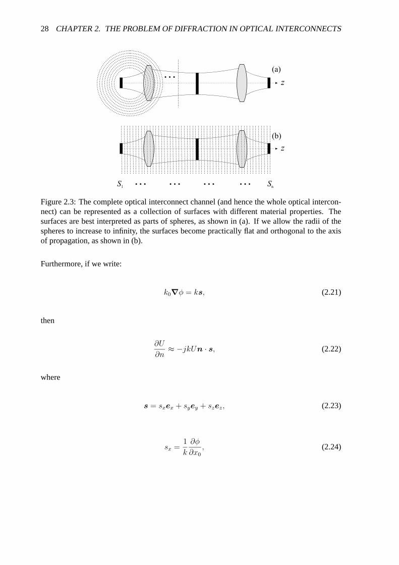
28 CHAPTER 2. THE PROBLEM OF DIFFRACTION IN OPTICAL INTERCONNECTS
z
z
(a)
(b)
S1 Sn
Figure 2.3: The complete optical interconnect channel (andhence the whole optical intercon-nect) can be represented as a collection of surfaces with different material properties. Thesurfaces are best interpreted as parts of spheres, as shown in (a). If we allow the radii of thespheres to increase to infinity, the surfaces become practically flat and orthogonal to the axisof propagation, as shown in (b).
Furthermore, if we write:
k0∇φ = ks, (2.21)
then
∂U
∂n≈ −jkUn · s, (2.22)
where
s = sxex + syey + szez, (2.23)
sx =1
k
∂φ
∂x0
, (2.24)

2.1. MATHEMATICAL BASIS 29
sy =1
k
∂φ
∂y0
, (2.25)
and
sz =√
1 − s2x − s2
y. (2.26)
Vectorsex, ey, ez represent unit vectors in thex, y, andz direction respectively. The above
consideration make Eq. (2.17) become
UP =1
4π
∫
S
e−jkρ
ρ
[
U
(
jk +1
ρ
)
n · eρ + jkUn · s]
dS. (2.27)
Let us fix now thez axis so as to go right through the centre of the interconnect channel. If
each surfaceS is taken to be the surface of a sphere of radius sufficiently large to effectively
makez⊥S, as illustrated in Fig. 2.3, Eq. (2.27) becomes
UP =1
4π
∫
S
U · e−jkρ
ρ
[(
jk +1
ρ
)
ez · eρ + jk ez · s]
dS, (2.28)
where we noted that nown = ez.
The surface of an infinitely large sphere centred onz, in a region close toz, can effectively
be represented by the surface of a square. Hence, the integration in Eq. (2.28) need only be
performed over a rectangular surface:
UP =1
4π
∫
S
U · e−jkρ
ρ
[(
jk +1
ρ
)
ez · eρ + jk ez · s]
dxdy. (2.29)
It is generally not required to painstakingly perform the integration at every single infinitesi-
mally thin surface that makes up the interconnect. In homogeneous regions it is sufficient to
examine the field at the bounding surfaces only; in the homogeneous region itself we always
know that the field will satisfy the Helmholtz equation. We also know that the effect of a col-
lection of surfaces may be equivalently represented by its ‘action’ at only one representative
surface. The action of the surface is usually taken to be suchas to affect the phase ofU . Typi-

30 CHAPTER 2. THE PROBLEM OF DIFFRACTION IN OPTICAL INTERCONNECTS
cal examples of such compound surfaces would be apertures, lenses and mirrors. If we denote
the action of a surface byϕ(x, y) Eq. (2.29) becomes:
U(x, y, z) =1
4π
∫
∞
−∞
∫
∞
−∞
U(x0, y0, z0)ϕ(x0, y0)
·e−jkρ
ρ
[(
jk +1
ρ
)
ez · eρ + jk ez · s]
dx0dy0, (2.30)
where we used zero subscripts to clearly distinguish valuesat the surface in question. While
more user-friendly than Eq. (2.17), Eq. (2.30) is still a very general statement about the be-
haviour of the optical field in an interconnect. In the following section we shall reformulate it
into a concrete objective by specifying each of the terms in Eq. (2.30) more precisely.
2.2 Problem formulation
In an optical interconnect the field produced by the VCSEL willalways be emitted into a
homogeneous medium, such as the free space or a substrate, where we know that it has to
obey the scalar Helmholtz equation. A suitably chosen solution of the wave equation in the
destination medium can hence be used to give us the initial optical field distribution in the inter-
connect. Once the distribution at the initial surface is known, the fields at all other surfaces can
be determined, by following the process described in the previous section. Very suitable solu-
tions have been found in terms of the free space modes, given either in rectangular coordinates
by the Hermite-Gaussian functions, or in polar coordinatesby the Laguerre-Gaussian func-
tions. Experimental measurements have shown that in small-diameter VCSELs, such as the
ones used in optical interconnects, it is far more common to observe Hermite-Gaussian modes
in the output beam rather than Laguerre-Gaussian modes. Fora laser to support Laguerre-
Gaussian modes its resonator must possess a high degree of circular symmetry [105]. This
requirement is made difficult by birefringence and astigmatism of the lasing medium, as well
as by the device structural anisotropy. In large-diameter VCSELs, however, both families of
modes are frequently observed [106].

2.2. PROBLEM FORMULATION 31
Hermite-Gaussian modes of the free space, are given by [107]
ψHGnm(x, y, z) =
1
w
√
1
2n+m−1 π(n!)(m!)
· exp
[
−j(n+m+ 1) arctanz − zs
zR
]
·Hn
[√2 x
w
]
Hm
[√2 y
w
]
· exp
[−(x2 + y2)
w2+jk(x2 + y2)
2R
]
, (2.31)
where
zR =kw2
s
2(2.32)
is the beam Rayleigh range, andws is the laser beam waist located atz = zs. At any observa-
tion plane, the laser beam radius and the radius of curvatureare given by
w = w(z) = ws
1 +
[
λ(z − zs)
πz2s
]2
, (2.33)
and
R = R(z) = z
1 +
[
πω2s
λ(z − zs)
]2
. (2.34)
Hν(x) represents the Hermite polynomials of orderν, given by [108]
Hν(x) = (−1)ν exp(x2)dν
dxνexp(−x2). (2.35)
Each member of the Hermite-Gaussian family of functions hasa different shape, but they all
share the same beam waist size and position. These two valuesdistinguish one set of Hermite-
Gaussian functions from another. This pair of values will infurther text frequently be referred
to as the set of beam parameters, and denoted byp = ws, zs.

32 CHAPTER 2. THE PROBLEM OF DIFFRACTION IN OPTICAL INTERCONNECTS
In further discussion, mainly for mathematical purposes, we shall frequently make use of
an alternative formulation of the Hermite-Gaussian modes [109]. The alternative formulation,
with exactly the same meaning as the formulation given by Eq.(2.31), is given by [110]
ψHGnm(x, y, z) =
η√
2n+m π(m!)(n!)
· exp[−jk(z − zs)]
· exp[j(n+m+ 1) arctan ξ]
·Hn(ηx)Hm(ηy)
· exp
[
−1
2η2σ2(x2 + y2)
]
, (2.36)
where
ξ =2(z − zs)
kw2s
, (2.37)
η =
√2
ws
√
1 + ξ2, (2.38)
and
σ2 = 1 + jξ. (2.39)
The set of all Hermite-Gaussian modes,ψHGnm(x, y, z), forms an orthonormal set of func-
tions:
∫
∞
−∞
∫
∞
−∞
ψHGnm(ψHG
pl )∗ dxdy = δnpδml, (2.40)

2.2. PROBLEM FORMULATION 33
whereδnp andδml are Kronecker delta functions, given by
δµν =
1 if µ = ν
0 otherwise.(2.41)
On the other hand, the Laguerre-Gaussian modes of the free space are given by
ψLGnm(r, θ, z) =
2 exp [−jk(z − zs)]
w√
π(1 + δ0m)
√
n!
(n+m)!
(
r√
2
w
)m
· exp
[
j(2n+m+ 1) arctan(z − zs)
zR
]
· exp
(
− r2
w2− j
kr2
2R
)
L(m)n
(
2r2
w2
)
cos(mθ)
sin(mθ)
=2 exp [−jk(z − zs)]
w√
π(1 + δ0m)
√
n!
(n+m)!
(
r√
2
w
)m
· exp
[
j(2n+m+ 1) arctan(z − zs)
zR
]
· exp
(
− r2
w2− j
kr2
2R
)
L(m)n
(
2r2
w2
)
cos(mθ), (2.42)
whereL(m)n (x) is the generalised Laguerre polynomial with radial numbern and azimuthal pa-
rameterm, and where we have indicated our preference for the cosinusoidal form of Laguerre-
Gaussian modes. [111] Again, an alternative formulation ofEq. (2.42) will frequently be found
to be mathematically more beneficial [110]:
ψLGnm(r, θ, z) = exp [−jk(z − zs)]
√
2(n!)
πεm(n+m)!
· exp [j(2n+m+ 1) arctan ξ]
· exp
[
−1
2η2σ2r2
]
η (ηr)m L(m)n (η2r2) cos(mθ), (2.43)
where
εm =
2 for m = 0
1 for m 6= 0,(2.44)

34 CHAPTER 2. THE PROBLEM OF DIFFRACTION IN OPTICAL INTERCONNECTS
all other symbols have the same meaning as before, andp = ws, zs is still referred to as the
beam parameter set. The generalised Laguerre polynomials are given by [108]
L(m)n (x) =
n∑
i=0
(
n+m
n− i
)
(−x)i
i!, (2.45)
where(
n+mn−i
)
is the binomial coefficient. The family of Laguerre-Gaussian functions,ψLGnm(r, θ, z),
also forms an orthonormal set:
∫ 2π
0
∫
∞
0
ψLGnm(ψLG
pl )∗ rdrdθ = δnpδml. (2.46)
Since both sets of modes form complete sets, one can easily express one in terms of the other,
as has been shown in the general case [111]. Recently [112], the third complete family of exact
and orthogonal solutions of the paraxial wave equation was presented. The transverse shape of
these modes is described by the Ince polynomials, and is structurally stable during propagation.
Ince-Gaussian modes constitute the exact and continuous transition modes between Laguerre-
Gaussian and Hermite-Gaussian modes.
The optical field produced by the laser will not generally be perfectly equal to just one
Hermite-Gaussian or Laguerre-Gaussian mode. Hence, we will always have to express the
field as a weighted sum of the member functions:
Ψ($, z) =∞∑
n=0
∞∑
m=0
Wnmψnm($, z), (2.47)
where$ is used to denote either(x, y) or (r, θ) (as required),Wnm are the complex weight-
ing coefficients, andψnm($, z) denote member function of either the Hermite-Gaussian,
ψHGnm(x, y, z), or Laguerre-Gaussian,ψLG
nm(r, θ, z), mode set. The dominant mode in the beam
of a small-diameter VCSEL is the fundamental Gaussian TEM00 mode,ψ00($, z) = ψHG00 (x, y, z) =
ψLG00 (r, θ, z). In literature it is frequently assumed that it is the only mode present, i.e. that
Ψ($, z) = ψ00($, z). The presence of higher-order modes (HOMs) in the laser beam, in
addition to the fundamental one, affects the performance ofan optical interconnect greatly. In

2.2. PROBLEM FORMULATION 35
Sec. 4.2 we present the results of experimental measurementof transverse mode content in a
laser beam, and use the measured composition to study diffraction in optical interconnects.
The action of a compound surfaceΣ, denoted byϕ(x0, y0), as shown in Eq. (2.30), is given
as
ϕΣ(x0, y0) =
fΣ(x0, y0) if (x0, y0) ∈ Σ0
0 otherwise,(2.48)
whereΣ0 is used to denote the optically transparent part of the infinitely largeΣ, which may
consist of a number of disjoint surfaces. In the case of a simple aperture, the action is given as
ϕA(x0, y0) =
1 if (x0, y0) ∈ A
0 otherwise,(2.49)
whereA could stand for a circle, rectangle, or any other shape that the aperture may have.
With S assumed to be an empty aperture of arbitrary shape, Eq. (2.30) becomes
U(x, y, z) =1
4π
∫∫
A
Ψ(x0, y0, z0)e−jkρ
ρ
·[(
jk +1
ρ
)
ez · eρ + jkez · s]
dx0dy0, (2.50)
where we have noted that nowU(x0, y0, z0) = Ψ(x0, y0, z0). Without a loss of generality we
shall first consider the (simpler) case of diffraction at common aperture shapes, such as circles.
Once we reach a solution we shall turn our attention to more complicated situations.
Before attempting to solve Eq. (2.50), we ought to contemplate what is it that we are
seeking to obtain. We should also examine, based on typical optical interconnect parameter
values, which factors in Eq. (2.50) will affect the solutionmost. Some factors are bound to have
more bearing than others, and some will become more adaptable or altogether dispensable. It
is generally accepted that the solution of Eq. (2.50) can be divided into three regions, based
on the position of the observation plane relative to the diffraction plane. The three zones
are determined by the nature of approximations that can be made to the factors making up

36 CHAPTER 2. THE PROBLEM OF DIFFRACTION IN OPTICAL INTERCONNECTS
Eq. (2.50). The boundaries between the zones are very blurryand vary from one scenario to
another, but the diffraction field features clearly distinguish one region from another.
The first zone is the near-field region in the immediate neighbourhood of the aperture. To
obtain the field in this region no simplifying assumptions inthe diffraction integral can be
made. In the process of derivation of Eq. (2.50) we have already made, in Eq. (2.20), the
assumption that the wavelength of the incident optical fieldis small, as compared to the di-
mensions of the diffracting aperture. A small wavelength implies a large propagation constant,
k, hence making all terms multiplied byk dominant. Given that, due to a largek, we have
already written:
−jk0Un · ∇φ+ U1
M
∂M
∂n≈ −jkUn · s, (2.51)
it seems logical to attempt to simplify the integrand of Eq. (2.50) by writing:
(
jk +1
ρ
)
≈ jk. (2.52)
However, in the near field even this approximation may not be appropriate, since there is an
appreciable area of the aperture where1/ρ term is not negligible compared withk. This region
extends several wavelengths outward from the aperture, andhence the variation ofez ·eρ must
also always be taken into account in this first zone.
Numerical explorations of the diffraction field in the near region are not many; the diffi-
culties associated with evaluating Eq. (2.50) are acknowledged by many not to be worth the
new insights. From the knowledge gained so far, it can safelybe assumed that the near field is
determined by geometrical propagation of incident light rays through the aperture. The mean
value of the field intensity has been found to differ little from that of the geometrically propa-
gated field, with a very distinct boundary between the near field and the geometrical shadow.
As typical wavelength of laser beams in an optical interconnect is aboutλ = 850 nm, sev-
eral wavelengths from the aperture takes us negligibly little into the interconnect to be of any
practical importance.

2.2. PROBLEM FORMULATION 37
After the near-field zone, we pass into the Fresnel region of the diffraction field. The Fres-
nel region is by far the most important one in the study of diffraction, and the approximations
made are such that the handling of calculations is considerably simplified. On the other hand,
the approximations made are not strong in the sense that the meaning that we can draw from
the results is heavily restricted. It should be noted, however, that by simplifying Eq. (2.50)
in any way, we still introduce errors in numerical results, and that the order of magnitudes of
those error have to be examined in each case separately. Basedon typical optical interconnect
parameter values, the origin of which will be considered in more detail in Ch. 4, we shall now
consider the approximations characteristic of the diffraction field in the Fresnel region.
As mentioned, we fix the wavelength of VCSEL laser beams toλ = 850 nm; this automat-
ically results in a large wavenumber value ofk ≈ 7.4 ·106 m−1. Based on an optical argument,
that will be considered in more detail in Chapter 4 (and that isclosely related to the action of
a thin microlens assumed to be located in the apertureA), the distance from the laser beam
waistws to apertureA, denoted by , will be in the range:
f ≤ ` ≤ f + zR, (2.53)
wheref is fixed to the range from about600 to 1000 µm, with typically f ≈ 800 µm. The
Rayleigh range, given defined by Eq. (2.32), with the laser beam waist to a typical value of
ws = 3 µm is equal tozR = 33.3 µm. The distance from apertureA to the observation plane,
denoted here byd, will be (again based on the action of a fictitious microlens)in the range
f ≤ d ≤ 4
(
f +f 2
2zR
)
. (2.54)
The radial distance from the beam propagation axis to the observation point,r =√
x2 + y2,
is closely related to the spacing between the individual interconnect channels, and will be in
the range
0 ≤ r ≤ 3∆, (2.55)

38 CHAPTER 2. THE PROBLEM OF DIFFRACTION IN OPTICAL INTERCONNECTS
where the array pitch∆ is taken to be from about100 to 300 µm.
Due to quite a large value of the wavenumberk, the most obvious approximation target
is thejk + 1/ρ term in Eq. (2.30); we suspect thatjk + 1/ρ ≈ jk. The1/ρ term will be
maximum whenρ is minimum. Remembering thatρ =√
(x− x0)2 + (y − y0)2 + d2, we
haveρmin = dmin = f = [600 µm, 1000 µm] ≈ 800 µm. Hence,(1/ρ)max ≈ 1250 m−1. This
is most certainly negligible when compared tok ≈ 7.4 · 106 m−1.
The second approximation concerns theρ term itself. Note thatρ can be written as
ρ =√
(x− x0)2 + (y − y0)2 + d2
= d ·
√
1 +
(
x− x0
d
)2
+
(
y − y0
d
)2
= d ·[
1 +
(
x− x0√2d
)2
+
(
y − y0√2d
)2
+
+
(
x− x0√3d
)3
+
(
y − y0√3d
)3
+ . . .
]
= d+(x− x0)
2
2d+
(y − y0)2
2d+
+(x− x0)
3
3d2+
(y − y0)3
3d2+ . . . (2.56)
where the square root was replaced with the sum [108]:
√1 + b2 = 1 +
b2
2+b3
3+ . . . , (2.57)
which holds true for all|b| < 1. In our case this assumption holds true since(x − x0)max =
(y − y0)max = 3√
2 · ∆ ≈ 1.1 mm = 0.0011 < 1. The actual approximation (the ‘Fresnel
approximation’) consists of retaining terms only up to the second order in Eq. (2.56):
ρ ≈ d+(x− x0)
2
2d+
(y − y0)2
2d
= d+ %. (2.58)
If the observation plane is far from the diffracting aperture, we could go even one step further

2.2. PROBLEM FORMULATION 39
and assume that
ρ ≈ d, (2.59)
but this step has to be taken cautiously. We will be on the safeside if we use first approxima-
tion, given by Eq. (2.58), in the exponential term, while thesecond one, given by Eq. (2.59),
in the ratio. The exponential term is much more sensitive to small variations in its exponent,
and that is why we will leave the stricter case as the working one.
With the above approximations, Eq. (2.50) becomes
U(x, y, z) =jk exp [−jk(z − z0)]
4π(z − z0)
∫∫
A
Ψ(x0, y0, z0) exp (−jk%)
· [cos (α) + ez · s] dx0dy0, (2.60)
where
cos(α) = ez · eρ =z − z0
ρ
=z − z0
z − z0 + %≈ z − z0
z − z0
= 1. (2.61)
This last approximation is justified by the same argument used for simplifying theρ in the
ratio. The diffraction field given by Eq. (2.60) generally differs from the expressions for the
Fresnel field generally found in the literature in the presence of the termez · s which arises
from a nonuniform phase distribution over the aperture. A phase distribution widely deviate
from a constant phase has a highly dispersed system of rays associated with it. Under such
conditions the assumption that the energy in the diffraction field is concentrated around the
z axis is not valid and the approximations made previously maynot be justified. Hence, the
phase distribution of the incident field over the diffracting aperture,Ψ(x0, y0, z0), has to be
examined more closely.
Since we do not really know what the exact modal composition of the field is, but since we
are aware that most of the power is contained in the fundamental mode, we will assume that

40 CHAPTER 2. THE PROBLEM OF DIFFRACTION IN OPTICAL INTERCONNECTS
Ψ(x0, y0, z0) = ψ00(x0, y0, z0). Note that we haveψLG00 = ψHG
00 , and it does not matter which
one take into consideration. So we have
φ0 = φ00(x0, y0, z0) = arctanz0
zR
− k(x20 + y2
0)
2R0
, (2.62)
sx =1
k
∂φ0
∂x0
=−x0
R0
, (2.63)
and
sy =1
k
∂φ0
∂y0
=−y0
R0
, (2.64)
from which it follows that
sz =
√
1 − x20 + y2
0
R20
. (2.65)
With typical values,(x20 + y2
0)max ≈ 22.5 nm; from Eq. (2.32),R20,min ≈ 642.2 nm. Hence we
have
sz ≈ 1. (2.66)
With this final approximation, Eq (2.60) becomes
U(x, y, z) =jk exp[−jk(z − z0]
2π(z − z0)
·∫∫
A
Ψ(x0, y0, z0) exp(−jk%) dx0dy0. (2.67)
In polar coordinates, more suitable in the case when the Laguerre-Gaussian functions are

2.2. PROBLEM FORMULATION 41
used, Eq. (2.60) takes the form
U(r, θ, z) =jk
2π(z − z0)exp[−jk(z − z0)]
·∫ 2π
0
∫ a
0
exp
−jk[r2 + r2
0 − 2rr0 cos(θ − θ0)]
2(z − z0)
·Ψ(r0, θ0, z0) r0dr0dθ0. (2.68)
We shall refer to Eqs (2.67) and (2.68) as the Fresnel diffraction integral, in rectangular and
polar coordinates, respectively.
The solution of Eq. (2.50) in the third, Fraunhofer region isobtained by making several
other approximations in addition to the Fresnel approximations. As the Fraunhofer diffraction
integral is obtained by further simplifying the Fresnel diffraction integral, it represents only a
special case of Eqs (2.67) and (2.68). We shall consider these additional approximations in
a later section, but here we point out that we will not be interested in solving the Fraunhofer
diffraction integralper se. This is due to the fact that the conditions needed to validate the far
field (Fraunhofer) approximations can be very restrictive in the case of application of the theory
in the design of optical interconnects, as illustrated in Sec. 2.3.2. Our primary concern, in the
context of modelling diffraction in optical interconnects, is solving the (Fresnel) diffraction
integral.
An ideal solution of the diffraction integral, the one that we are seeking and that will
ultimately be found, has the following characteristics:
• Accurate description of the diffraction field can be obtained with little numerical effort,
and with no knowledge of the subtleties of the diffraction theory;
• The solution is such that the results it produces can easily be incorporated into the gen-
eral expressions used for evaluating the overall optical interconnect performance;
• The method of solution could be used in the same way in all situations of interest in
the design and analysis of optical interconnects: diffraction at apertures of perfect or
imperfect (serrated) shape, diffraction in the presence ofthin lenses, and diffraction at

42 CHAPTER 2. THE PROBLEM OF DIFFRACTION IN OPTICAL INTERCONNECTS
multiple apertures;
• The method of solution could easily be used to calculate the optical interconnect per-
formance parameters of practical importance, such as tolerance to misalignment, or the
effect of the presence of higher-order modes in the laser beams on the optical intercon-
nect performance.
2.3 Existing solutions
The subject of optical diffraction has been treated exhaustively in numerous publications, since
the 17th century, when Christiaan Huygens (1629-1695) proposed whatwe today refer to as
the Huygens’ principle. Today, one would start any serious study of the subject from any of
a number of ‘classical’ texts [113, 114, 115]. One of the problems with the textbook-level
approach to the subject of diffraction is that the results are almost exclusively developed for
the case of planar or spherical-wave incidence, sometimes even without explicit mention. As
laser beams are very different from those simple waves [116], most of the easily-recognisable
results have to be handled very cautiously. We shall (considerably) limit our review of existing
solutions only to that subset which specifically deals with the problem of diffraction of laser
beams, where special care was taken to properly represent the field of the incident beams. As
far as the planar and spherical-wave diffraction goes, an excellent in-depth treatment can be
found in Ref. [117].
Most of the publications on the topic of laser beam diffraction can be traced back to the
early works of Kogelnik and Li [107], Campbell and DeShazer [118], Olaofe [119], and Dick-
son [120]. The primary aim of Refs. [118, 119, 120] was to investigate the behaviour of
a diffracted Gaussian beam in the Fresnel region, given the previous studies where diffrac-
tion in the Fraunhofer diffraction was the primary focus. The driving force behind both
types of studies was the facilitation of laser development.Most of the earlier work on laser
beam diffraction was performed in the practical context of laser and maser resonator analy-
sis [121, 122, 123, 107]. Investigations of ‘optical beam wave guides,’ which today are not

2.3. EXISTING SOLUTIONS 43
really used in their original form, established good foundations for the tools used to describe
the laser beams [110, 124].
The early work on laser beam diffraction, performed in conjunction with the development
of numerous laser-based applications, adequately addressed the most important aspects of the
problem. Finer aspects, such as examination of the validityof various approximation made in
the process of stating the laser beam diffraction problem [125, 126, 127, 128], and diffraction-
caused focal shift (relative to the position of the focus predicted by geometrical optics, as well
as focal shift due to aperturing of the incident beam) [129, 130, 131, 132, 133]. Similar issues
were considered in the case of incidence of not only the fundamental mode, but also higher-
order laser beam modes [134, 135, 136], and experimental investigations confirmed all of the
theories that they were tested against [137, 138, 139, 140, 141]. Very interesting (and still very
much inviting) excursions were also made into the field of applying the traditional techniques
on previously-unexplored diffracting structures of fractal nature [142, 143, 144, 145, 146].
In order to be able to process the large amounts of published information effectively, and
select the most likely candidate theories for application in optical interconnects, we have iden-
tified three categories that most of the existing literaturecan be classified into. The approach
taken in a great portion of the literature, including most ofthe works cited so far in this sec-
tion, is very like the approach we started in Sec. 2.2. Namely, the diffraction problem is first
stated as a mathematical problem in the form of one of the equations in the hierarchical chain
spanning the principal electromagnetic equations and the Fresnel diffraction integral. An at-
tempt is then made to solve the problem analytically, or at least evolve it to a more transparent
and informative form, so that the meaning it carries becomesclear. The outcomes of the pro-
cess of solving the diffraction problem, in this first approach, hugely depend on the chosen
starting point in the consideration, as well as the parameters of the problem being considered
(such as the type and characteristics of the incident optical field, aperture characteristics,etc).
Small deviations at the beginning of the process, and differences in the assumptions made
often mean that the final results obtained will be applicableonly to the particular situation
considered, rather than a more general situation that the reader is usually interested in. The

44 CHAPTER 2. THE PROBLEM OF DIFFRACTION IN OPTICAL INTERCONNECTS
development of the diffraction problem presented in Sec. 2.2 is by no means the only correct
path that we could have taken; it is a valid option that is suitable given the characteristics of
our problem. Due to the nature of the diffraction problem andthe existing solutions of the first
kind, it is frequently easier to set up the infrastructure for one’s particular problem from the
first principles, rather than to try to adapt solutions worked out for other situations.
We have termed the procedures using this first approach as ‘solutions by direct integration,’
due to the characteristic sequence of setting up the diffraction problem as an integral, and
then attempting to solve it analytically. In addition to thepublications cited so far, for the
sake of completeness, we include several other works typical for this category; first the ones
performed with the aim of obtaining only the on-axis intensity of the diffraction field [147,
148, 149], and then the more traditional considerations of diffraction problems [150]. The
constantly-expanding list of all relevant works in this category is much longer than the one
included here. However, due to the incompatibility problems caused by the noted lack of
standardisation, the sheer quantity does not indicate a user-friendly quality; it even makes
it easier to loose one’s way deciphering the intricacies of each individual work, as well as
comparing the merits of one work against all the others. Mainly for this reason, we have
selected, fairly early on in the research process, the collected work of Tanakaet al. as a very
suitable, accurate and comprehensive representative of all solutions by direct integration [151,
152, 153, 154, 155, 156, 157]. The work of Tanakaet al., fully compatible with our formulation
of the laser beam diffraction problem presented in this chapter, provided excellent starting and
reference material for our considerations of the problem oflaser beam diffraction in optical
interconnects. However, as we shall see in Sec. 2.3.1, it is also not the optimal way of solving
our problem.
The second category of approach that we frequently encountered in searching the relevant
literature, termed ‘solutions by further approximation,’is very similar to the first category.
Namely, the process of first mathematically formulating thediffraction problem, and then
trying to solve it analytically is still present. The difference lies in the fact that further approx-
imations, in addition to the type of approximations presented in Sec. 2.2, are made at various

2.3. EXISTING SOLUTIONS 45
stages in the process. The most significant characteristic of this method is that the inaccu-
racies and limitations introduced by those approximationsare readily accepted in exchange
for the benefits of easy computation and increased transparency. The typical example of this
kind of approach, which will be examined in more detail in Sec. 2.3.2, used specifically to
model diffraction in optical interconnects, is the one of Ref. [3]. Other examples of this cate-
gory include, most notably, the earlier attempts to find a compromise between the geometrical
and wave interpretations of the phenomenon of diffraction [158, 159], as well as all of the
(simplified) studies of the diffraction field in the far field [160, 161, 162].
The third category of approaches to solving the problem of diffraction in optical intercon-
nects is characterised by the fact that the procedure encountered in the previous two approaches
is no longer present. The main characteristic of this approach is that the original incident laser
beam and diffracting aperture are replaced by an effective laser beam which has the same
functional form but different parameter values. In that waythe effects of diffraction are inter-
preted, to some extent, as changes in the parameters of the incident laser beam. The principal
representative of this approach, given in Ref. [163], is reviewed in detail in Sec. 2.3.3; the rep-
resentatives of the previous two approaches are reviewed inSec. 2.3.1 and 2.3.2, respectively.
The results of Ref. [163], even though not particularly much better than any of other results
from the same category, were almost exclusively used in the published literature discussing
diffraction in optical interconnects. One reason for this is in the fact that, in the case where no
clear choice for a particular task is evident, previous choices made in similar situations tend to
prevail. Another very interesting solution of the diffraction problem that falls under this cate-
gory, and that has been exploited very little, includes the solution by expansion in Chebyshev
polynomials [164].
Our review of existing solutions of the problem of diffraction cannot be complete if we do
not mention the numerous numerical solutions that have beenproposed over the years, even
though we do not intend to consider them for our purposes. Various approaches based on
the Hankel transform were proposed [165, 166, 167, 168, 169,170]. Also, a range of other
methods were considered with varying ranges of success [171, 172, 173, 174, 175, 176, 177,

46 CHAPTER 2. THE PROBLEM OF DIFFRACTION IN OPTICAL INTERCONNECTS
178, 179, 180]. However, in the context of our modern times and priorities, a numerical in-
vestigation of diffraction will yield much better results if started from an existing commercial
simulator (whose algorithms are based on the accepted worksof others), rather than if started
independently ‘from scratch.’
An evaluation of proposed solutions of the problem of diffraction would not be complete with-
out mentioning the approach based on a completely differenttheory. All of the solutions
mentioned so far are based on the classical electromagneticview of the world, which, after
all, is just a model that helps us rationalise our experiences. While it has been shown over the
years to be very useful, the electromagnetic paradigm should by no means be considered to be
the only possible or perfectly complete one; by changing ourfirst principles we could end up
with easier solutions of a whole group of practical problems. The more practical answers we
can obtain, given the same amount of invested effort, the better the model is, no matter how
wildly different from the classical electromagnetic interpretation it may be. A set of different
principles that could be applied to the general problem of diffraction of light can be found in
the context of quantum mechanics, and the path integrals in particular [181]. We have exam-
ined the characteristics of this approach, primarily basedon the very practical and noteworthy
work presented in Ref. [2]. We shall summarise here the basic idea of path integrals, on the
basis of the material contained in Ref. [2].
The basic statement of Feynman’s path-integral formulation is that the probability ampli-
tude for a particle starting at one location, say pointa, to arrive at another location, say pointb,
is the sum of all the phasors corresponding to each possible path froma to b. Each phasor, on
the other hand, is a complex number with a magnitude inversely proportional to the (physical)
path length and a phase equal to the action of the (same) path,divided byh = h/2π, whereh
in the Planck’s constant. Mathematically, this can be written as
K(b, a) = C∑
[b,a]
exp jS[b,a]h
[b, a], (2.69)

2.3. EXISTING SOLUTIONS 47
Sourcepoint a
Destinationpoint b
Paths notallowed
Paths notallowed
Aperture
Allowedpaths
Figure 2.4: Illustration of the path-integral approach to solving diffraction problems [2]. Allpossible paths that the photon can take from the source to thedestination are considered (withthe shape of the obstacle taken into consideration), the action of the path given by Eq. (2.71)is calculated, and the phasors associated with each path areadded up, as shown by Eq. (2.69).The result of the process in the probability of a source photon going to the destination.
whereC is a normalising constant,[b, a] represents a path from pointa to pointb, [b, a] is the
(physical) length of[b, a], and the actionS [b, a] is defined by a line integral on[b, a]:
S [b, a] =
∫
[b,a]
L dt, (2.70)
whereL is the Lagrangian for the particles in question, which, in our case, are photons of
wavelengthλ originating from a single point. As the photons have no rest mass, and as their
potential energy is nearly unchanged during propagation, their total energy is equal to their
kinetic energy, soL = hc/λ, wherec is the speed of light in vacuum. After usingdt = ds/c,
we have
S [b, a] =hc
λ
∫
[b,a]
ds
c=
2πh
λ
∫
[b,a]
ds =2πh
λ[b, a], (2.71)
which which is a very simple expression and can readily be substituted into the starting
Eq. (2.69). Equation (2.69) now gives us the probability amplitude of a photon of wavelength
λ getting from one point in space to another. The situation is illustrated in Fig. 2.4.
Our initial perception of the path-integral approach to diffraction was a refreshingly posi-

48 CHAPTER 2. THE PROBLEM OF DIFFRACTION IN OPTICAL INTERCONNECTS
tive one; it seemed that most of the practical diffraction problems, such as the ones in optical
interconnects, could be solved by repeating the procedure outlined by Eqs (2.69) to (2.71)
over and over again, until the solution is reached. As the principle behind this method is very
simple and easy to understand, it seemed that the obstacles would come from the numerical
perspective, rather than from complicated concepts and mathematics. The fact is that a very
large number of paths needs to be considered if an accurate solution is sought, and that this
could pose a big problem in the practical application of pathintegrals. Some of the issues
associated with the numerical aspect of the path-integral approach are addressed in Ref. [2],
where a novel and more efficient algorithm for automaticallyfinding paths given an arbitrary
aperture shape was also proposed. However, our main reason for abandoning the path-integral
approach is not due to the numerical intensity of the process; our main problem was caused
by uncertainties of how to relate the standard electromagnetic concepts to the results obtained
by Feynman’s method, and vice versa. The only solid point of reference is the fact that the
probability of a photon going froma to b can be related to the concept of light intensity at point
b due to the source ata. However, none one the numerous very important practical issues were
ever addressed in the literature. For example, how does one take into account the fact that our
sources are not point sources, but that they have, at best, a Gaussian distribution? How does
one account for the presence of a phase-shifting element in the aperture? How do we relate
all this to the concepts of power and phase? While everything was clear in principle, it was a
big gamble, which we did not dare to take, to leave everythingelse and flesh out the details
required for a practical application of the method. It is still the belief of the author that, given
enough time and support, this is a very promising method thatcould be used to further explore
into the phenomenon of diffraction.
2.3.1 Solution by direct integration
After substituting the expressions for the incident field, given by Eq. (2.43), into our starting
diffraction integral given by Eq. (2.68), and after integration with respect todθ0, the diffraction

2.3. EXISTING SOLUTIONS 49
field assumes the form
Unm(r, θ, z) =
√
2n!
π(1 + δ0m)(n+m)!· cos(mθ)
· kjm+1
2η0(z − z0)· exp [−jk(z − zs)]
· exp
[
j(2n+m+ 1) arctan ξ0 −jkr2
2(z − z0)
]
·∫ a
0
(η0r0)m+1L(m)
n (η20r
20)
· exp
(−η20τ
20 r
20
2
)
· Jm
(
krr0z − z0
)
dr0, (2.72)
where
ξ0 =2(z0 − zs)
kw2s
, (2.73)
η0 =
√2
ws
√
1 + ξ20
, (2.74)
and
τ 2 = 1 + jξ0 +jk
η20(z − z0)
. (2.75)
After expanding the Bessel and Laguerre functions into theirpower series, given by [108]
Jν(x) =xν
2ν
∞∑
µ=0
(−1)µ x2µ
22µ · µ! · (ν + µ)!, (2.76)

50 CHAPTER 2. THE PROBLEM OF DIFFRACTION IN OPTICAL INTERCONNECTS
and Eq. (2.45), respectively, Eq. (2.72) becomes
Unm(r, θ, z) =
√
2n!
π(1 + δ0m)(n+m)!exp[−jk(z − zs)]
· kjm+1
2η0(z − z0)cos(mθ)
[
kr
2η0(z − z0)
]m
· exp
[
j(2n+m+ 1) arctan ξ0 −jkr2
2η0(z − z0)
]
·∞∑
p=0
n∑
q=0
(
n+m
n− q
)
(−1)p+q(p+ q +m)!
p!q!(p+m)!
·[
kr
2η0(z − z0)
]2p(2
τ 2
)p+q+m+1
·[
1 − exp
(−η20τ
2a2
2
) p+q+m∑
s=0
1
s!
(
η20τ
2a2
2
)s]
. (2.77)
Equation (2.77) constitutes our first complete solution forthe diffraction integral. While easily
obtainable, Eq. (2.77), however, does not meet the requirements set before us in Sec. 2.2. The
reasons are as follows:
• unless we provide a proper proof, based on l’Hospital’s rulefor example, we do not
know for certain if the infinite sum in Eq. (2.77) converges ordiverges; hence we cannot
be fully confident in the results that it gives us
• given that the sum converges (following a qualitative power-conservation argument, for
example) we still do not know what would be a minimum number ofits terms required
to obtain accurate results in any particular situation; we suspect that the number of terms
increases with decreasinga, increasingr, and increasing order of the incident mode,
(n,m)
• given the field distribution at a surfaceSn, in interconnect modelling we are required to
find the field distribution at any subsequent surfaceSn+1 ; this implies a very dreadful
prospect of feeding Eq. (2.77) back into Eq. (2.68), as the expression for the starting
field, and solving the resulting integral over and over againfor each surfaceSn+1
• Eq. (2.77) is only valid for a simple circular aperture; the weight of the previous three

2.3. EXISTING SOLUTIONS 51
statements would only increase if we attempted to consider amore complicated forms
of ϕ(x0, y0), such as irregular shapes or thin lenses
• finally, Eq. (2.77) is not transparent; we cannot easily deduce the qualitative information
about the effect of the diffracting surface on the incident beam.
In order to get around these difficulties it is common to attempt further simplification of
Eq. (2.68) in a way similar to the one carried out in Sec. 2.2. With the expectation that the
solution of a simplified Eq. (2.68) would also end up less cumbersome, we pursue this inquiry
in the following section.
2.3.2 Solution by further approximation
In the process of derivation of Eq. (2.68),
U(x, y, z) =jk exp[−jk(z − z0)]
2π(z − z0)
·∫∫
A
Ψ(x0, y0, z0) exp(−jk%) dx0dy0, (2.78)
we made the assumption thatρ ≈ %, where
% =(x− x0)
2
2d+
(y − y0)2
2d
=(x2 + y2)
2d+
(x20 + y2
0)
2d− 2(x · x0 + y · y0)
2d. (2.79)
Since the first term in Eq. (2.79) does not depend on the integration variables, it can be taken
outside of the integral. Now, if we assume that the position of the observation plane,z, is such
that
d = (z − z0) k · max(x2
0 + y20)
2, (2.80)

52 CHAPTER 2. THE PROBLEM OF DIFFRACTION IN OPTICAL INTERCONNECTS
then the second term in Eq. (2.79) will become ignorably small:
x20 + y2
0
2d≈ 0. (2.81)
The value ofd required for Eq. (2.81) to hold true needs to be examined in each particular
scenario. In our case, based on the values discussed previously, we need to have
d k · max(x20 + y2
0)
2≈ 7.4 · 106 m−1 · 125 · 10−6 m2
8= 115.625 m, (2.82)
wheremax(x20 + y2
0) represents the maximum radial extent of the diffracting aperture, which
we related in Eq. (2.82) to typical channel spacing in optical interconnects. (Note that in the
case of a circular aperture of radiusa, we havemax(x20 + y2
0) = a2.) Equation (2.82) is also
known as the Fraunhofer condition. Assuming that it holds, and thus evaluating Eq. (2.78),
would give us the field in the Fraunhofer region behind the diffracting aperture. As observed
previously, diffraction field in the Fraunhofer region is not really what we need to properly
model optical interconnect channels.
Equation (2.82) is sometimes in the literature expressed less stringently by the ‘antenna
designer’s formula’, which we formulate here for ana-radius circular diffracting aperture:
d >8a2
λ, (2.83)
where the sign was intentionally replaced by the> sign. With the same typical values used,
the antenna designer’s condition translates to the observation plane having to be approximately
14.7 cm away from the diffracting plane. The condition givenby Eq. (2.83) is certainly more
forgiving than the original Fraunhofer condition. However, it still puts us just outside the
region of the diffraction field that we are most interested in.
Fraunhofer diffraction patterns are known to have been observed at distances much closer
than implied by Eqs (2.82) and (2.83) [114]. The far-field condition can be met by having the
diffracting aperture illuminated by a spherical wave converging towards the observer, or by

2.3. EXISTING SOLUTIONS 53
having a positive lens properly situated between the observer and the aperture. While suitable
in many important practical situations, these two reformulations of the Fraunhofer condition
still fall short of reaching the aim set before us. Despite the apparent inferiority, however, we
shall persist in finding out what happens to Eq. (2.78) if we assume that the relation given by
Eq. (2.81) is valid. The resulting Fraunhofer diffraction integral may not give us the precise
distribution of the diffraction field, but it will endow us with a reasonable qualitative insight.
Furthermore, as we already noted, this approach has been previously used to study the effects
of diffraction in optical interconnects, and hence qualifies for an investment of our efforts.
Assuming that Eq. (2.81) holds, ‘our best result so far’ becomes
Unm(x, y, z) =jk
2πzexp
[
−jk(
z +x2 + y2
2z
)]
·∫∫
A
Ψ(x0, y0, z0)
· exp
[
jk(xx0 + yy0)
z
]
dx0dy0, (2.84)
in rectangular coordinates; in polar coordinates it becomes
Unm(r, θ, z) =jk
2πzexp
[
−jk(
z +r2
2z
)]
·∫∫
A
Ψ(r0, θ0, z0)
· exp
[
jkrr0 cos(θ − θ0)
z
]
r0dr0dθ0. (2.85)
After substituting the laser beam formula given by Eq. (2.43) into Eq. (2.85), and after ex-
panding the Bessel and Laguerre functions into their power series, as was done in Sec. 2.3.1,

54 CHAPTER 2. THE PROBLEM OF DIFFRACTION IN OPTICAL INTERCONNECTS
Eq. (2.85) transforms to
Unm(r, θ, z) =
√
2n!
π(1 + δ0m)(n+m)!exp[−jk(z − zs)]
· kjm+1
2η0(z − z0)cos(mθ)
[
kr
2η0(z − z0)
]m
· exp
[
j(2n+m+ 1) arctan ξ0 −jkr2
2η0(z − z0)
]
·∞∑
p=0
n∑
q=0
(
n+m
n− q
)
(−1)p+q(p+ q +m)!
p!q!(p+m)!
·[
kr
2η0(z − z0)
]2p(2
σ20
)p+q+m+1
·[
1 − exp
(−η20σ
20a
2
2
) p+q+m∑
s=0
1
s!
(
η20σ
20a
2
2
)s]
, (2.86)
where
σ20 = 1 + jξ0. (2.87)
The only mathematical difference between Eq. (2.86) and Eq.(2.77) is that eachτ 2 in Eq. (2.77)
is replaced byσ20 in Eq. (2.86) [182].
Equation (2.86) is our second solution of the Huygens-Kirchhoff formula, and it gives us
the diffraction field in the Fraunhofer region behind the diffracting aperture. Unfortunately, all
the problems that plagued our first solution, given by Eq. (2.77), continue to plague Eq. (2.86).
In order to obtain at least some sensible results we proceed here to make yet another assump-
tion. It is common, especially in introductory texts on diffraction and beam propagation, to
assume that the field at the diffracting plane is planar, i.e.that Ψ(r0, θ0, z0) = 1 · exp(j 0).
While it is clear that laser beams are not planar, this assumption makes sense if we remember
that any arbitrary field distribution can be expressed as a sum of planar waves. Summing up
such a representation in practice, however, is a completelydifferent matter. With allψnm now

2.3. EXISTING SOLUTIONS 55
eliminated from considerations, Eqs (2.84) and (2.85) become
U(x, y, z) =jk
2πzexp
[
−jk(
z +x2 + y2
2z
)]
·∫∫
A
exp
[
jk(xx0 + yy0)
z
]
dx0dy0, (2.88)
and
U(r, θ, z) =jk
2πzexp
[
−jk(
z +r2
2z
)]
·∫∫
A
exp
[
jkrr0 cos(θ − θ0)
z
]
r0dr0dθ0. (2.89)
Both Eq. (2.88) and (2.89) are easily solvable, for instance by straight-forward invoca-
tion of Mathematica’s symbolic integration command [183]. Assuming thatA is a rectangle
whose end points, in an anticlockwise fashion starting fromthe lower left corner, are given by
(x1, y1), (x2, y1), (x1, y2), (x2, y2), Eq. (2.88) concludes to
U(x, y, z) =jz
2πkxyexp
[
−jk(
z +r2
2z
)]
·[
exp
(
jkxx1
z
)
− exp
(
jkxx2
z
)]
·[
exp
(
jkyy2
z
)
− exp
(
jkyy1
z
)]
; (2.90)
assuming thatA is a circle of radiusa, Eq. (2.89) concludes to
U(r, θ, z) =jak
4r· J1
(
2ar
z
)
· exp
[
−jk(
z +r2
2z
)]
. (2.91)
Diffraction field intensity, obtained from Eq. (2.91), and given by
I(r, θ, z) = |U(r, θ, z)|2 =
[
ak
4r· J1
(
2ar
z
)]2
. (2.92)
is probably the best known, and most frequently quoted solution of the diffraction integral. It is

56 CHAPTER 2. THE PROBLEM OF DIFFRACTION IN OPTICAL INTERCONNECTS
referred to as the Airy pattern — a pattern of dark and bright rings around a very pronounced
central lobe, where the first dark ring is located at a distance of 1.22λz/a from the axis of
propagation. We note here that Eq. (2.92) is exactly the sameas Eq. (4-31) in [114]. Given
that all occurrences of ‘j’ are replaced by ‘−j’, Eq. (2.92) would correspond precisely to
Eq. (4-30) in Ref. [114]. Equations (2.91) and (2.92) can respectively be interpreted as the
Fourier and Fourier-Bessel, or Hankel, transforms of the field over the aperture.
From Ref. [114], the expression for the diffraction field in the Fraunhofer region from a
unit-amplitude incident field is given as
U(r, θ, z) = exp (jkz) · exp
(
jkr2
2z
)
· πa2
jλz·[
2 · J1(kar/z)
kar/z
]
, (2.93)
and the intensity is given as
I(r, θ, z) =
(
πa2
λz
)2
·[
2 · J1(kar/z)
kar/z
]2
. (2.94)
In the work of Tanget al. [3], it is assumed that the optical wave emitted from the VCSEL
diode can be assumed to be a plane wave diffracted by an outputwindow of finite extent.
They are also using the diffraction integral in the Fraunhofer approximation and hence need to
have lens in the aperture, and the laser needs to be positioned at the focal length, i.e. = f .
The schematic diagram of the situation is shown in Fig. 2.5. The normalised amplitude of the
electrical field distribution is given by the Bessel-Fouriertransform of the incident laser field,
evaluated at spatial frequency ofr0/λf , and given by
E(r0) = B E(rtx) =J1(katxr0/`)
katxr0/`, (2.95)
where
E(rtx) = circ
(
rtxatx
)
=
1 if rtx ≤ atx
0 otherwise,(2.96)

2.3. EXISTING SOLUTIONS 57
zatx
rtx r0
a0 arx
rrx
l = f d d 2f( = )
pla
ne
wav
e
same p
ow
er assum
edon th
e photo
detecto
r
Figure 2.5: Schematic diagram that aids the understanding of the way in which the the solutionby further approximation was applied in Ref. [3].
B stands for the Bessel-Fourier transformation,circ(rtx/atx) accounts for the finite extent
of the laser output window with radiusatx, andrtx andr0 are the radii in polar coordinates
in the plane of the laser output window and the plane of microlens, respectively. All other
symbols have the same meaning as before. Note that only the amplitude of the resulting field
is considered, and that the phase is ignored. Also, in Ref. [3], the amplitude of the incident
field is assumed to be(2πa2tx)
−1. Such choice of the amplitude results in the total power that
goes through the laser output window to be normalised to1/2.
The point of the above considerations was to find the shape of the incident laser beam;
now we have to consider the effect of diffraction at the microlens. The field at the microlens
is modified slightly to account for the finite size of the microlens aperture,a0, to give
E(r0) = E(r0) · circ(
r0a0
)
. (2.97)
The final field in the observation (diffraction) plane is obtained by Bessel-Fourier-transforming
Eq. (2.97):
E(rrx) = B E(r0) =`dλ2
2πatxrrx· J1
(
2πa0atx
`λ
)
· J1
(
2πa0rrxdλ
)
, (2.98)
where all the symbols have the same meaning as before. The above equation was not actually

58 CHAPTER 2. THE PROBLEM OF DIFFRACTION IN OPTICAL INTERCONNECTS
explicitly given in the paper of Tanget al. What is given, the reason for which will become
clear in Chapter 4, are the powers encircled by the diffracting microlens, and an a circular
aperture in the observation plane. As pointed above, only one normalisation was done in the
above calculations, and that was the normalisation of the amplitude of the plane electric used
to model the laser beams. After that all other electric field amplitudes are obtained as explained
above. However, in the paper of Tanget al. all field amplitudes are normalised by adding a
constant in front of the expressions so that the total power in the diffraction field equals to1.
If the laser field is diffracted by a microlens aperture of radius a0, at a distance of from
the laser, the power encircled by a receiver of radiusarx at distanced away from the aperture
is given by [3]
P (arx) = P (a0)
1 −[
J0
(
ka0arx
d
)]2
−[
J1
(
ka0arx
d
)]2
, (2.99)
where
P (a0) = 1 −[
J0
(
katxa0
`
)]2
−[
J1
(
katxa0
`
)]2
, (2.100)
and all other symbols have the same meaning as before. Equation (2.100) also represents the
power contained in a microlens aperture of radiusa0.
Solutions by ‘further approximation’ are probably the mostfamiliar type of solutions of
diffraction problems; anyone with a basic knowledge of physics and mathematics would be
comfortable in applying them in a practical situation. The main reason for such high status
and popularity of solutions by further approximation is primarily due to the simplicity of the
relations expressing these solutions. For example, Eqs (2.90) and (2.91) can be applied straight
away in any software package in a practical context. However, as we have seen at the begin-
ning of this section, Eqs (2.90) and (2.91) are true only in the case when the plane at which
we observe the diffraction field is at a large (very large) distance from the diffracting aperture,
and when the incident optical field is a plane wave. As soon as we try to improve the situation
by using the more complicated laser beam functions (while still believing that our observation

2.3. EXISTING SOLUTIONS 59
plane is very far away from the diffracting plane), the benefits of easy expressions are lost
immediately, as can be seen from Eq. (2.86). Hence, the main advantage of the solutions by
further approximation is that they are easy to understand and apply. Their main disadvantage
is the environment of heavy restrictions that surrounds them. In the case of the optical in-
terconnect design, one could perhaps tolerate these heavy approximations in order to quickly
estimate the order of importance of diffraction effects. Anything else than an estimate cannot
be guaranteed, and a more appropriate model needs to be used;using strong approximations
without constantly checking their validity could also turnout to lead to faulty designs. The
inability to be fully confident in the results obtained through ‘solutions by further approxima-
tion’ is the main reason why they are inappropriate to use in modelling diffraction in optical
interconnects, and why it is worthwhile to go on looking for more suitable solutions.
We close this section by remembering that the diffraction field in the Fraunhofer region is
only a subset of the diffraction field in the Fresnel region. While making the Fraunhofer as-
sumption allowed us to make a breakthrough in obtaining a useable formulation of the diffrac-
tion field, our primary concern is still the solution in the Fresnel region; the Fraunhofer solution
is contained in the Fresnel solution. If we are successful insolving the problem of diffraction
in optical interconnects in the general case, modifying it to cover particular subsets of the
problem space is trivial.
2.3.3 Solution by equivalent representation
The ‘equivalent representation’ approach undertaken by Belland and Crenn, as detailed in
Ref. [163], is fundamentally different than the top-down approach we used to obtain the first
and second solution of the diffraction equation. The difference stems from the fact that Belland
and Crenn aimed to identify the changes in the incident laser beam due to diffraction at an
aperture, rather than to work out the full form of the diffraction field.
In the method due to Belland and Crenn, laser beams are are assumed to be purely Gaus-

60 CHAPTER 2. THE PROBLEM OF DIFFRACTION IN OPTICAL INTERCONNECTS
sian, and they are characterised by their transverse intensity profile, given by:
I(r, z) = I0 exp(−r2/ω2), (2.101)
whereI0 is the on-axis intensity,r is the radial coordinate, andω is the local1/e beam intensity
radius. The1/e intensity radius is related to the1/e field radius,w, by ω = w/√
2. The
minimum value of the beam intensity radius, the beam waist, is denoted byωs, while the beam
divergence characteristic,θs is defined by
θs ' tan θs = 1/kωs. (2.102)
With this notation, the total beam power is given as
P =
∫ 2π
0
∫
∞
0
I0 exp(r2/ω2)rdrdφ
= πω2I0 = πω2s Is, (2.103)
whereIs represents the beam on-axis intensity at the beam waist plane. The two values, beam
waist size and on-axis intensity at the beam waist plane, constitute the beam parameter set,
pBC = (ws, Is).
Belland and Crenn have considered what happens to the laser beam given by Eq. (2.101)
passing through and being diffracted by a coaxial, planar, and circular apertureA of radiusa.
In order to represent the extent of diffraction atA, they define the clipping ratio,κ, as
κ =a
w(z0)=
a
w0
, (2.104)
wherew0 represents the beam waist radius at the aperture plane,z = z0. Apart from few
special cases, their results can be summarised as follows:
Case 1:κ > 2.12 Diffraction effects are negligible, and the characteristics of the Gaussian
beam are unchanged behind the aperture.

2.3. EXISTING SOLUTIONS 61
w0
w Is s&
zs zs
z z l0 s= +
w Is s&
a
Figure 2.6: Schematic diagram that aids the understanding of the way in which the method ofBelland and Crenn works.
Case 2:1.13 < κ < 2.12 The weakly diffracted Gaussian beam, in the far field, looks like
a Gaussian beam, with a different set of parameter values,p = (ws, Is)
Case 3:κ < 1.13 Diffraction effects become large, so that the diffracted profile is no longer
Gaussian, and the new set of parameter values is no longer valid.
The new parameter values can be obtained by
ws
ws
= 1 − exp
−a2
w2s
[
1 + (2`/kw2s)
2]
cos
ka2
2`[
1 + (kw2s/2`)
2]
, (2.105)
and
IsIs
= 1 − 2 exp
−a2
w2s
[
1 + (2`/kw2s)
2]
cos
ka2
2`[
1 + (kw2s/2`)
2]
, (2.106)
where` represents the distance from the plane of the laser beam waist to the plane of the
diffracting aperture, = z0 − zs, all other symbols have the same meaning as before, and
the process is illustrated in Fig. 2.6. Note that the position of the beam waist in the effective
beam remains the same as in the incident beam. Belland an Crenn have also found that with
a relative power loss of only 1% only through the aperture (equivalent to a clipping ratio of
κ ≈ 1.56), diffraction effects can already modify the angular beam divergence by about 10%.
Consequently, the criterion of small losses of beam power through the aperture is not sufficient
to assume that the beam has not suffered any modification.

62 CHAPTER 2. THE PROBLEM OF DIFFRACTION IN OPTICAL INTERCONNECTS
The two most important positive characteristics of the method by Belland and Crenn, as
related to optical interconnect modelling are:
• it is numerically simple and easily applicable, even in the case of diffraction of a se-
quence of circular apertures
• it expresses the effect of diffraction on the incident beam in terms of changes inpBC, the
set of incident beam parameters.
The list of negative characteristics is, unfortunately, somewhat longer:
• the method is very inflexible since only the intensity of the incident and diffraction fields
are considered
• diffraction of higher-order modes,ψnm($, z), cannot be considered, as we would gen-
erally like to in optical interconnects
• since the method relies on a particular direct solution of the diffraction integral, any
possible extensions to situations involving more complex diffracting surfaces cannot
easily be made
• the method only provides solution for a limited range ofκ, which may not necessarily
be sufficient for our purposes.
The method of Belland and Crenn should not, however, be completely dismissed. The whole
idea of equivalent representation, as we shall see in Ch. 3, will play a crucial role in the
formulation of an appropriate method for optical channel modelling.
2.4 Summary and conclusion
We applied two fundamental principles of electromagnetic theory, as given by Eqs (2.1) and (2.2),
to the problem of channel modelling in optical interconnects. The result is the diffraction for-
mula, given by Eq. (2.30). After consideration of typical parameter values, we concluded that

2.4. SUMMARY AND CONCLUSION 63
the diffraction equation need only be solved in the Fresnel region, where it assumes the form
of Eq. (2.67) in cartesian coordinates, and the form of Eq. (2.68) in polar coordinates. Suitable
and numerically efficient solution of the Eq. (2.67), and theequivalent Eq. (2.68), is the key to
successful channel modelling in optical interconnects.
Existing solutions of Eq. (2.68) abound, yet we were able to identify three classes: di-
rect, approximate, and effective-beam solutions. The prototype of the direction solution is
given by Eq. (2.77), and the prototype of the approximate solution is given by Eq. (2.98). The
most notable example of solution by equivalent representation is summarised in Eqs (2.105)
and (2.106). While accurate and important in their own right,all of the three classes of solu-
tions were found to be lacking; they did not meet the requirements of channel modelling in
optical interconnects.
While not perfectly aligned with our aim, the approach by Belland and Crenn, however,
offers an alternative to the algebra-dominant solutions first considered. It is also the method
that has most frequently been used to model the optical performance of interconnects. Its main
strength lies in a radically different and more natural formulation of the diffraction field; its
primary deficiency is the limited range of possible application. In the following chapter we
shall examine an even more general equivalent solution which will turn out to be very suitable
for modelling diffraction in optical interconnects.

Chapter 3
Novel way of modelling diffraction
The aim of this thesis is to formulate a suitable method for modelling diffraction in optical
interconnects. As we saw in the previous chapter, this translates into finding a most optimal
way of solving the diffraction formula in the Fresnel region. While none of various existing
solutions were found to fully meet our requirements, the effective-representation approach of
Belland and Crenn has been identified as the most promising one.In this chapter we shall
pursue this effective-representation line of inquiry, as it seems to be the one most suitable for
optical interconnect channel modelling. However, while our approach may conceptually be
similar to the method of Belland and Crenn, it is technically very different. Our approach
is based on an orthogonal, or modal expansion of the direct solution found in the previous
chapter. The orthogonal expansion not only expedites the numerical evaluation of the direct
solution, but it allows us to altogether reinterpret the meaning of the diffraction integral and
hence reach the thesis goal. While the idea of using modal expansion to reformulate and ratio-
nalise a difficult problem is not a freshly conceived one, theway in which we have connected
it with the diffraction problem, especially in the context of optical interconnects, is novel. The
structure of this chapter is as follows. In Sec. 3.1 we present the process of modal expansion
and comment on the results. In Sec. 3.2 we present an alternative and more insightful approach
to the expansion. In Sec. 3.3 we formalise our findings as the mode expansion method, and in
Sec. 3.4 we verify and illustrate its performance.
64

3.1. MODAL EXPANSION OF THE EXACT SOLUTION 65
3.1 Modal expansion of the exact solution
We can express any diffraction fieldU($, z) by a set of normal functionsψn($):
U($, z) =∞∑
n=0
Cn ψn($, z), (3.1)
where$ = (x, y), or $ = (r, θ), depending which coordinate system is more appropriate,
and whereCn are the expansion coefficients. As the Hermite-Gaussian andLaguerre-Gaussian
families of functions were noted to be orthogonal, diffraction field of each particular free-space
mode,Unm($, z), may be written as:
Unm($, z) =∞∑
n, m=0
Cnm ψnm($, z), (3.2)
whereCnm are the expansion coefficients, andψnm is the set of modes used to decompose
the diffracted field, andψnm is the set of modes used to decompose the incident field. (Note
thatUnm($, z) represents the diffraction field of each incident beamψnm($, z) and that the
whole diffraction field is given by:
U($, z) =∞∑
n,m=0
Wnm Unm($, z), (3.3)
whereWnm are the weights representing each modeψnm($, z) in the complete laser beam
Ψ($, z), as Eq. (2.47) shows.) The expanding set of functions may either be taken to be
Hermite-Gaussian,ψnm($, z) = ψHGnm(x, y, z), or it may taken to be Laguerre-Gaussian,
ψnm($, z) = ψLGnm(r, θ, z). The choice primarily depends on the nature and geometry of
the diffraction problem in question. Any other set of orthogonal functions may be considered,
however, we expect quick convergence of the sum in Eq. (3.2) if the incident and the expanding
set of functions have the same form.

66 CHAPTER 3. NOVEL WAY OF MODELLING DIFFRACTION
Continuing our established preference for Laguerre-Gaussian modes we write
Unm(r, θ, z) =∞∑
n, m=0
Cnm ψLGnm(r, θ, z)
=∞∑
n=0
∞∑
m=0
Cnm ψnm(r, θ, z), (3.4)
where the second line in the above equation indicates that wewill drop theLG superscript in
later equations, for practical reasons, and where the direct solution of the diffraction integral
in the Fresnel region is given by Eq. (2.77), which we repeat here for easier reference:
Unm(r, θ, z) =
√
2n!
π(1 + δ0m)(n+m)!exp[−jk(z − zs)]
· kjm+1
2η0(z − z0)cos(mθ)
[
kr
2η0(z − z0)
]m
· exp
[
j(2n+m+ 1) arctan ξ0 −jkr2
2η0(z − z0)
]
·∞∑
p=0
n∑
q=0
(
n+m
n− q
)
(−1)p+q(p+ q +m)!
p!q!(p+m)!
·[
kr
2η0(z − z0)
]2p(2
τ 2
)p+q+m+1
·[
1 − exp
(−η20τ
2a2
2
) p+q+m∑
s=0
1
s!
(
η20τ
2a2
2
)s]
, (3.5)
and the set of Laguerre-Gaussian laser beam functions is given by Eq. (2.43), which we also
repeat for easier reference:
ψnm(r, θ, z) = exp [−jk(z − zs)]
√
2(n!)
πεm(n+ m)!
· exp[
j(2n+ m+ 1) arctan ξ]
· exp
[
−1
2η2σ2r2
]
η (ηr)m L(m)n (η2r2) cos(mθ). (3.6)
As indicated by the hats in Eq. (3.6), the beam parameters of the expanding beam set,p =
ws, zs, do not generally coincide with the parameters of the incident beam set.

3.1. MODAL EXPANSION OF THE EXACT SOLUTION 67
The expansion coefficients can be evaluated by inverting Eq.(3.4):
Cnm(z) =
∫ 2π
0
∫
∞
0
Unm(r, θ, z) ψ∗
nm(r, θ, z) rdrdθ, (3.7)
where the asterisk denotes complex conjugation. If we substitute Eqs. (3.5) and (3.6) into
Eq. (3.7), the coupling coefficients assume the first the formof
Unm(r, θ, z) =
√
2n!
π(1 + δm0)(n+m)!exp[−jk(z − zs)]
kjm+1
(z − z0)
· exp
[
j(2n+m+ 1) arctan ξ0 −jkr2
2(z − z0)
]
· cos(mθ) ·∫ a
0
(η0r0)m+1L(m)
n (η20r
20)
· exp
(
−1
2η2
0τ2r2
0
)
Jm
(
krr0z − z0
)
dr0, (3.8)
and then the form of
Cnm =
√
n!
(n+m)!
√
n!
(n+m)!exp[−jk(zs − zs)]δmm
· exp[j(2n+m+ 1) arctan ξ0 − j(2n+m+ 1) arctan ξ]
· kjm+1
2η0(z − z0)
∞∑
p=0
n∑
q=0
n∑
t=0
(−1)p+q(p+ q +m)!
p!q!(p+m)!
·(
n+m
n− q
)(
2
τ 2
)p+q+m+1 [k
2η0(z − z0)
]m
·[
kr
2η0(z − z0)
]2p
ηm+1
(
n+m
n− t
)
(−η2)t
t!
·2m+p+t(Bη2)−1−m−p−t(m+ p+ t)!
·[
1 − exp
(−η20τ
20a
2
2
) p+q+m∑
s=0
1
s!
(
η20τ
20a
2
2
)s]
, (3.9)
where
τ 2 = 1 + jξ20 +
jk
η20(z − z0)
(3.10)

68 CHAPTER 3. NOVEL WAY OF MODELLING DIFFRACTION
B = 1 − jξ +jk
(z − z0)η2. (3.11)
The orthogonal reformulation of Eq. (3.5) was performed in the hope that the resulting
expression for the weighting coefficients would turn out to be simpler and more suitable for
application in modelling diffraction in optical interconnects. However, the coefficients given
by Eq. (3.9) suffer from the same problems as the direct solution of the diffraction integral
given by Eq. (3.5). The most important issues are:
• without an explicit proof we cannot assume that the infinite sum in Eq. (3.9) will con-
verge; the issue of convergence is more important in Eq. (3.9) than in Eq. (3.5) due to
the fact that an infinite number of modes is summed up to obtainthe diffraction field
• the coefficients given by Eq. (3.9) are only valid for diffraction at a circular aperture;
if any parameter of the diffraction problem changes we need to re-derive the weighting
coefficients
• if any parameter of the diffraction problem changes, weighting coefficients can be ex-
plicitly found only if an analytic expression for the solution of the diffraction integral
for that particular case exists
• sinceB is a function ofz, the value of each coefficient depends on the position of the
observation plane, and hence needs to be recalculated frequently.
On the other hand, the problem of sequential-aperture diffraction is handled much easier by
the orthogonally-expanded solution. Once eachCnm is calculated it can be combined with
Wnm to form the weighting factor,Wnm, for each mode in the ‘new’ incident beam at each
subsequent aperture. The initial disappointment notwithstanding, we shall continue our pursuit
of an optimal way of equivalent representation in the next section, with the hope that a craftier
mathematical insight will result in a better solution of ourmodelling problem.

3.2. ALTERNATIVE APPROACH TO MODAL EXPANSION 69
3.2 Alternative approach to modal expansion
Orthogonal expansion of the diffraction field has been considered previously, particularly by
Tanakaet al. [182]. The approach undertaken in Ref. [182] differs from our conventional
approach assumed previously in the fact that a special relationship between the Bessel and
Laguerre functions is used, rather than each one of them being directly expanded into an
infinite sum. This special relationship is given as [108]:
Jm(2√tx) = exp(−t)
∞∑
p=0
L(m)p (x)tp
(p+m)!
(√tx)m
. (3.12)
If in Eq. (3.12) we let
x = A2r2, (3.13)
and
t =k2r2
0
4A2(z − z0)2, (3.14)
the Bessel function becomes
Jm
(
krr0z − z0
)
= exp
[ −k2r20
4A2(z − z0)2
] [
krr02(z − z0)
]m
·∞∑
p=0
L(m)p (A2r2)
(p+m)!
[
k2r20
4A2(z − z0)2
]p
, (3.15)

70 CHAPTER 3. NOVEL WAY OF MODELLING DIFFRACTION
whereA is an arbitrary constant. After substituting Eq. (3.15) into Eq. (3.7) the solution of the
diffraction integral becomes
Unm(r, θ, z) =
√
2n!
π(1 + δ0m)(n+m)!exp[−jk(z + zs)]
kjm+1
2η0(z − z0)
· cos(mθ) exp
[
j(2n+m+ 1) arctan ξ0 −jkr2
2(z − z0)
]
·[
kr
2η0(z − z0)
]m ∞∑
p=0
n∑
q=0
L(m)p (A2r2)
(p+m)!
[
k2
4A2η20(z − z0)2
]p
·(
n− q
n+m
)
(−1)q(p+ q +m)!
q!
(
2
B
)p+q+m+1
·[
1 − exp
(
−1
2η2
0a2B
) p+q+m∑
s=0
1
s!
(
η20a
2B
2
)s]
, (3.16)
where all the symbols have the same meaning as before. Equation (3.16) is equivalent to
Eq. (3.7), given thatA is large enough.
After substituting Eq. (3.16) into Eq. (3.8), and after performing thedθ part of integration,
the coefficients are given by
Cnm =
√
2n!
(n+m)!
√
2n!
(n+m)!
kjm+1
2η0(z − z0)δmm
· exp[−jk(zs − zs) + j(2n+m+ 1) arctan ξ0
−j(2n+m+ 1) arctan ξ]
·∞∑
p=0
n∑
q=0
(−1)q(p+ q +m)!
(p+m)!q!
(
n+m
n− q
)
·(
2
B
)p+q+m+1 [k2
4A2η20(z − z0)2
]p
·[
1 − exp
(−η20a
2B
2
) p+q+m∑
s=0
1
s!
·(
η20a
2B
2
)s] ∫ ∞
0
[
kr
2η0(z − z0)
]m
(ηr)m+1
· exp
(−η2Cr2
2
)
L(m)p (A2r2) L
(m)n (η2r2) dr. (3.17)

3.2. ALTERNATIVE APPROACH TO MODAL EXPANSION 71
After rewriting the integral in Eq. (3.17) as
I1 =
∫
∞
0
[
kr
2η0(z − z0)
]m
(ηr)m+1
· exp
(−η2Cr2
2
)
L(m)p (A2r2) L
(m)n (η2r2) dr
=1
2η
[
k
2η0η(z − z0)
]m(2
C
)m+1
·∫
∞
0
exp(−x)xmL(m)p
(
2A2x
η2C
)
L(m)n
(
2x
C
)
dx, (3.18)
setting the arbitrary constantA to
A2 =Cη2
2, (3.19)
and by using the formula
L(m)n (xy) =
n∑
t=0
(
n+m
t
)
(1 − x)txn−tL(m)n−t(y), (3.20)
the coupling coefficients are transformed to
Cnm =
√
n
(n+m)!
√
n
(n+m)!exp[−jk(zs − zs)δmm
+j(2n+m+ 1) arctan ξ0 + j(m+ 1)π
2
−j(2n+m+ 1) arctan ξ]
·n∑
p=0
n∑
q=0
(−1)q(p+ q +m)!
p!q!
(
n+m
n− q
)
·(
n+m
n− p
)(
2
B
)p+q+m+1(2
C
)p+m+1
·(
C − 2
C
)n−p [k2
4η20A
2(z − z0)2
]p
·[
k
2η0η(z − z0)
]m+1 [
1 − exp
(−η20a
2B
2
)
·p+q+m∑
s=0
1
s!
(
η20a
2B
2
)2]
. (3.21)

72 CHAPTER 3. NOVEL WAY OF MODELLING DIFFRACTION
By noting that:
C =k
η0η(z − z0)exp
−j arctan
[
ξ − k
η2(z − z0)
]
, (3.22)
and
arctan ξ − arctan
[
ξ − k
η2(z − z0)
]
= arctank
η2(z − z0)(1 + ξ2) − kξ
= − arctan
(
1
ξ0
)
, (3.23)
the final expression can be simplified to
Cnm(z) =
√
n!
(n+m)!
√
n!
n+m)!exp[−jk(zs − zs)δmm
+j(2n+m+ 1) arctan ξ0
−j(2n+m+ 1) arctan ξ0
·n∑
p=0
n∑
q=0
(−1)p + q(p+ q +m)!
p!q!
(
n+m
n− q
)
·(
n+m
n− p
) (
2
B
)p+q+m+1 (η0
η0
)2p+m+1
·[
1 − exp
(−η20a
2B
2
) p+q+m∑
s=0
1
s!
(
η20a
2B
2
)2]
, (3.24)
where all the symbols have the same meaning as before.
The expression for the coupling coefficients given by Eq. (3.24) is mathematically equiv-
alent to the expression given by Eq. (3.9). However, the infinite sum present in Eq. (3.9) is
eliminated from Eq. (3.24), thus clearing up any convergence doubts (and hence implicitly
proving that the infinite sum in Eq. (3.9) does indeed converge). Unfortunately, Eq. (3.24)
inherited all other problems originally associated with Eq. (3.9). Nonetheless, a crucial devel-
opment presented in the next section will finally allow us to make a break-through in our quest
for the most optimal way of working out the expansion coefficients in any given scenario.

3.3. MODE EXPANSION METHOD 73
3.3 Mode expansion method
3.3.1 Derivation of the method
Thez dependence of the coupling coefficients, as given by Eq. (3.24), comes throughB, which
was defined by Eq. (3.11):
B = 1 +k2
2A2η20(z − z0)2
+ j
[
ξ0 +k
η20(z − z0)
]
, (3.25)
whereA was assumed to be an arbitrary constant. SinceA has subsequently been defined by
Eq. (3.19):
A2 =1
2η2
0 − j
[
1
2ξ0η
20 −
k
2(z − z0)
]
, (3.26)
B is more accurately given by
B =η2
0 + η20
η20
+ jξ20η
20 − ξ2
0 η20
η20
. (3.27)
Equation (3.27) is quite remarkable since we see thatB was wrongly interpreted to be a func-
tion of z. AsB is independent of the position of the observation plane, so are the weighting
coefficients given by Eq. (3.24). This not only eliminates one of the problems listed at the end
of Sec. 3.1, but also opens up a new avenue for interpretationof the diffraction phenomenon.
We now turn to the idea of modal expansion with the aim of reformulating the direct solu-
tion of the diffraction integral in the Fresnel region,Unm(r, θ, z), in a more suitable way:
Unm(r, θ, z) =∞∑
n=0
∞∑
m=0
Cnm(z) ψnm(r, θ, z), (3.28)
where the coefficients were supposed to be obtained by inverting the above equation:
Cnm(z) =
∫ 2π
0
∫
∞
0
Unm(r, θ, z) ψ∗
nm(r, θ, z) rdrdθ. (3.29)

74 CHAPTER 3. NOVEL WAY OF MODELLING DIFFRACTION
In Eqs. (3.28) and (3.29)z represents the position of the observation plane. Mathematical
formalism and initial results indicated that the weightingcoefficients,Cnm, changed depending
on where we wanted to observe the diffraction field. This meant that we had to solve Eq. (3.29)
at each observation plane. Since thez dependence of weighting factors was eliminated by a
proper choice ofA, Eq. (3.29) need only be worked out once, on one arbitrary surface inside
the interconnect (as there is noz dependence it does not matter which surface). Let that
arbitrary surface be the surface just to the right of the diffracting element, located atz = z0.
In that case Eq. (3.29) becomes:
Cnm =
∫ 2π
0
∫
∞
0
Unm(r, θ, z+0 ) ψ∗
nm(r, θ, z+0 ) rdrdθ, (3.30)
where ‘just to the right of’ was indicated by the ‘+’ in the superscript. As we defined each
surface within the interconnect to be infinitesimally thin,it follows that the diffraction field
distribution just after the diffracting surface is the sameas the field distributionexactlyover
the diffracting surface:
Unm(r, θ, z+0 ) = Unm(r0, θ0, z0). (3.31)
The same reasoning allows us to conclude that the field distribution exactly over the diffracting
surface is given as the incident field distribution just before it, multiplied by the action of the
surface. As our diffracting element is still an empty aperture, we have
Unm(r0, θ0, z0) = ψnm(r, θ, z−0 ) ϕA(r0, θ0), (3.32)
whereϕA(r0, θ0) was first introduced in Ch. 2, and is also given by Eq. 3.45. Substitution of
Eqs. (3.31) and (3.32) into Eq. (3.30) leads to
Cnm =
∫ 2π
0
∫
∞
0
ψnm(r, θ, z−0 ) ϕA(r0, θ0) ψ∗
nm(r, θ, z+0 ) rdrdθ. (3.33)
If we extend our thin-surface reasoning to both the incidentfield as well as the expanding

3.3. MODE EXPANSION METHOD 75
functions:
ψnm(r, θ, z−0 ) = ψnm(r, θ, z+0 ) = ψnm(r0, θ0, z0), (3.34)
ψnm(r, θ, z+0 ) = ψnm(r, θ, z−0 ) = ψnm(r0, θ0, z0), (3.35)
and
ψ∗
nm(r, θ, z+0 ) = ψ∗
nm(r, θ, z−0 ) = ψ∗
nm(r0, θ0, z0), (3.36)
Eq. (3.29) finally becomes:
Cnm =
∫ 2π
0
∫
∞
0
ψnm(r0, θ0, z0) ϕA(r0, θ0) ψ∗
nm(r0, θ0, z0) rdrdθ
=
∫ 2π
0
∫ a
0
ψnm(r0, θ0, z0) ψ∗
nm(r0, θ0, z0) r0dr0dθ0. (3.37)
The message of Eq. (3.37) is extremely pleasant and central to our solution of the problem
of channel modelling in optical interconnects. By substituting Eq. (3.37) into Eq. (3.28) we
obtain
Unm(r, θ, z) =∞∑
n=0
∞∑
m=0
ψnm(r, θ, z)
·∫ 2π
0
∫ a
0
ψnm(r0, θ0, z0) ψ∗
nm(r0, θ0, z0) r0dr0dθ0, (3.38)
which means that the optical field at any point in the interconnect can be obtained without any
use of the previously-formulated diffraction formula or any of its solutions. Equation (3.38)
tells us that the diffraction field can be found from the incident field distribution and the knowl-
edge of the expanding modes. Before analysing the consequences of this finding, let us confirm
it by a reverse procedure; let us see if the evaluation Eq. (3.37) will lead us back to the result
given by Eq. (3.24).

76 CHAPTER 3. NOVEL WAY OF MODELLING DIFFRACTION
After substituting the modal expressions into Eq. (3.37), and after integrating with respect
to dθ0 we obtain
Cnm =
√
2n!
(n+m)!
√
2n!
(n+m)!exp[−jk(zs − zs)]
·(η0η0)m+1 exp[j(2n+m+ 1) arctan ξ0 − j(2n+m+ 1) arctan ξ0]
·∫ a
0
r2m+1 Lmn (η2
0r2) Lm
n (η20r
2) exp[−ςr2] dr, (3.39)
where
ς =η2
0 + η20
2+ j
η20ξ0 − η2
0 ξ02
. (3.40)
Integration with respect todr0 yields
Cnm =
√
2n!
(n+m)!
√
2n!
(n+m)!exp[−jk(zs − zs)]
· exp[j(2n+m+ 1) arctan ξ0 − j(2n+m+ 1) arctan ξ0]
·n∑
p=0
n∑
q=0
(
n+m
n− p
) (
n+m
n− p
)
(−1)p+q
p!q!
·η2p+m+10 η2q+m+1
0
ςm+p+q+1γ(m+ p+ q + 1, a2ς). (3.41)
If we note that
ς =η2
0B
2(3.42)
and that [108]
γ(m+ p+ q + 1, a2ς) = (m+ p+ q)![
1 − exp
(
−1
2η2
0a2B
) p+q+m∑
s=0
1
s!
(
η20a
2B
2
)s]
, (3.43)

3.3. MODE EXPANSION METHOD 77
Eq. (3.37) assumes the form
Cnm =
√
n!
(n+m)!
√
n!
(n+m)!exp[−jk(zs − zs)
+j(2n+m+ 1) arctan ξ0
+j(2n+m+ 1) arctan ξ0]n∑
p=0
n∑
q=0
(−1)p+q(p+m+ q)!
p!q!
(
n+m
n− q
)
(
n+m
n− q
)(
2
B
)p+q+m+1(η0
η0
)2p+m+1
[
1 − exp
(
−1
2η2
0a2B
) p+q+m∑
s=0
1
s!
(
η20a
2B
2
)s]
. (3.44)
The fact that Eq. (3.44) is identical to Eq. (3.24) completesour reverse-engineered proof.
The benefits of finding the optical field due to diffraction at an aperture by using Eq. (3.38)
over any other method examined so far are many. In addition tothe benefits of the modal
expansion approach in general, we note that:
• the diffraction field can be found just by calculating the coupling coefficients and sum-
ming up the weighted expanding modes; there is no need to solve or numerically evaluate
the diffraction formula
• the position, size, or shape of the diffracting aperture makes no difference in the calcula-
tion process since the evaluation of the coupling coefficients takes place over the whole
diffracting surface
• the coupling coefficients can be found either by using the explicit expression given by
Eq. (3.44), or by straightforward numerical integration.
The mode expansion method, as given by Eq. (3.38), however, still does not posses all the
characteristics of a method suitable for channel modellingin optical interconnects. Its most
notable drawback is that it still does not offer any insight into how to deal with diffracting
elements different from simple apertures. Let us thereforeconsider the case in which the

78 CHAPTER 3. NOVEL WAY OF MODELLING DIFFRACTION
diffracting apertureA considered so far is replaced by a circular and coaxial thin lens of radius
a, denoted byL. While the action of a diffracting aperture was given by
ϕA(r0, θ0) =
1 if (r0, θ0) ∈ A
0 otherwise,(3.45)
whereA represented the aperture region, the action of a diffracting thin lens is given by
ϕL(r0, θ0) =
fL(r0, θ0) if (r0, θ0) ∈ L
0 otherwise,(3.46)
whereL represents the thin lens region (for now assumed to be a coaxial circle of radiusa),
and
fL(r0, θ0) =kr2
0
2f. (3.47)
In Eq. (3.47),f represents the lens focal length. Since we changed the form of the element
action, the formulation for the diffraction integral in theFresnel region also changes from
UAnm(r, θ, z) =
jk
2π(z − z0)exp[−jk(z − z0)]
·∫ 2π
0
∫
∞
0
ψnm(r0, θ0, z0) ϕA(r0, θ0)
· exp
−jk[r2 + r2
0 − 2rr0 cos(θ − θ0)]
2(z − z0)
·r0dr0dθ0 (3.48)

3.3. MODE EXPANSION METHOD 79
in the case of an aperture, to
ULnm(r, θ, z) =
jk
2π(z − z0)exp[−jk(z − z0)]
·∫ 2π
0
∫
∞
0
ψnm(r0, θ0, z0) ϕL(r0, θ0)
· exp
−jk[r2 + r2
0 − 2rr0 cos(θ − θ0)]
2(z − z0)
·r0dr0dθ0 (3.49)
in the case of a thin lens.
The initial solution of Eq. (3.48) was obtained relatively easily by direct integration, and is
given by Eq. (3.5). That may not necessarily be the case for Eq. (3.49), due to its additionalr0
andθ0 dependence introduced throughϕL(r0, θ0). Instead of first attempting to solve Eq. (3.49)
by direct integration, as we did in the case of Eq. (3.48), we immediately assume that the
resulting solution can be written in terms of functions of anorthogonal set:
ULnm(r, θ, z) =
∞∑
n,m=0
Qnm ψnm($, z), (3.50)
whereQnm now represent the expansion coefficients. As before, the expansion functions are
the Laguerre-Gaussian functions:
ψnm($, z) = ψLGnm(r, θ, z) = ψnm(r, θ, z), (3.51)
and the expansion coefficients can be found by inverting Eq. (3.50):
Qnm(z) =
∫ 2π
0
∫
∞
0
ULnm(r, θ, z) ψ∗
nm(r, θ, z) rdrdθ. (3.52)
While we were able to find the analytic expressions for the expansion coefficients in the
aperture-diffraction case, we may not necessarily be able to do so for thin-lens diffraction.
However, the whole point of finding the expression for the expansion coefficients in the previ-
ous section turned out to be just a stepping stone; we only needed the explicit expressions for

80 CHAPTER 3. NOVEL WAY OF MODELLING DIFFRACTION
the coupling coefficients until we realised that they did nothave anyz dependence. Once we
realised that, it was relatively simple to show how the same coefficients can be obtained in an
alternative and much easier way. As long as we can prove that theQ’s, worked out by solving
Eq. (3.52), do not depend onz we can apply the same reasoning as in the case of theC ’s.
The proof turns out to be much simpler than expected. We note that the only difference
between Eq. (3.48) and Eq. (3.49) is in the element action. AsϕL(r0, θ0) does not depend on
z, there is no newz dependence introduced by going from Eq. (3.48) to Eq. (3.49). Hence, the
expansion coefficients given by Eq. (3.52) will also not depend onz, and can easily be worked
out as
Qnm =
∫ 2π
0
∫ a
0
ψnm(r0, θ0, z0) ϕL(r0, θ0) ψ∗
nm(r0, θ0, z0) rdrdθ, (3.53)
without any need for explicit integration. By responsibly substituting Eq. (3.6) into Eq. (3.53)
we can find an expansion coefficient expression in the same wayas we obtained Eq. (3.44).
Similarly, the alternative equivalent formulation of Laguerre-Gaussian laser beams, given by
Eq. (2.42), and repeated here for convenience:
ψnm(r, θ, z) =2 exp [−jk(z − zs)]
w√
π(1 + δ0m)
√
n!
(n+m)!
(
r√
2
w
)m
· exp
[
j(2n+m+ 1) arctan(z − zs)
zR
]
· exp
(
− r2
w2− j
kr2
2R
)
L(m)n
(
2r2
w2
)
cos(mθ) (3.54)
could be used to obtain the expression for the coupling coefficients. By substituting Eq. (3.54)

3.3. MODE EXPANSION METHOD 81
into Eq. (3.53) we obtain:
Qnm = Anm(z0)Knm A∗
nm(z0) Knm
·(βγ)m/2 δmm (1 + δ0m) π
·n∑
p=0
n∑
q=0
(−1)p+q βp γq
p! q!
·(
n+m
n− p
) (
n+ m
n− q
)
·σ−1−m−p−q
2γ(m+ p+ q + 1, a2σ), (3.55)
where
Anm(z0) = exp
j
[
(2n+m+ 1) arctan
[
λ(z0 − zs)
πw2s
]
− k(z0 − zs)
]
, (3.56)
A∗
nm(z0) = exp
−j[
(2n+m+ 1) arctan
[
λ(z0 − zs)
πw2s
]
− k(z0 − zs)
]
, (3.57)
Kνµ =
√
ν!
(ν + µ)!, (3.58)
β =2
w20
, (3.59)
γ =2
w20
, (3.60)
σ =1
w20
+1
w20
+jk
2R0
− jk
2R0
− jπ
λf, (3.61)
and all other symbols have the same meaning as before. Hence,the same mode expansion

82 CHAPTER 3. NOVEL WAY OF MODELLING DIFFRACTION
method can be applied regardless of what the element action is, as long as it does not intro-
duce any newz dependence. Also, by settingf → ∞ Eq. (3.55) becomes an alternative
equivalent expression for the expansion coefficients in thecase of an empty circular aperture.
Let us formulate the mode expansion method formally. Due to the equivalence of the Laguerre-
Gaussian and Hermite-Gaussian modes, we shall formulate the equations in a general form
that is applicable to both. The specific coefficient expressions for the most important element
functions, in the case that the incident and expanding modesare Hermite-Gaussian, are given
in Sec. B.1 of App. B. The central two statements of the mode expansion method are as
follows. Given a general incident laser beam
Ψnm($, z) =∞∑
n=0
∞∑
m=0
Wnm ψnm($, z), (3.62)
and a diffracting surfaceΣ located atz = z0 whose action is given byϕ($), the resulting
optical field is given by
U($, z) =∞∑
n=0
∞∑
m=0
Wnm Unm($, z), (3.63)
where the diffraction field of each individual mode is given by
Unm($, z) =∞∑
n=0
∞∑
m=0
Cnm ψnm($, z), (3.64)
and where the general coupling coefficients,Cnm, are given as
Cnm =
∫∫
Σ
ψnm($0, z0) ϕ($0) ψ∗
nm($0, z0) d$0. (3.65)
In any practical calculations the number of modes used to represent the laser beam, and the
number of modes used to represent the diffraction field will be finite. The complete diffraction

3.3. MODE EXPANSION METHOD 83
field then becomes:
U($, z) =N∑
n=0
M∑
m=0
Wnm ·N∑
n=0
M∑
m=0
Cnm ψnm($, z)
=N∑
n=0
M∑
m=0
(
N∑
n=0
M∑
m=0
Wnm
)
Cnmψnm($, z)
=N∑
n=0
M∑
m=0
(
N∑
n=0
M∑
m=0
Wnm Cnm
)
ψnm($, z)
=N∑
n=0
M∑
m=0
Wnm ψnm($, z), (3.66)
where
Wnm =N∑
n=0
M∑
m=0
Wnm Cnm, (3.67)
for each expanding mode(n, m). In the case of compound diffracting elements that consist of
more than one surface, we can simply repeat the whole processat each surface, thus ending up
with
U (p)(r, θ, z) =N∑
n=0
M∑
m=0
W(p)nm ψnm(r, θ, z) , (3.68)
where
W(p)nm =
N∑
n=0
M∑
m=0
W (p−1)nm Cnm . (3.69)
Equations (3.62) to (3.69) form the mode expansion method (MEM). MEM allows us to treat
any problem related to channel modelling in optical interconnects. We can examine diffrac-
tion at apertures of any size, position, or shape, even including composite apertures that con-
sist of several disjoint regions. This is due to the fact thatthe coupling coefficients, given by
Eq. (3.65), are found by integration over the whole of the diffracting surfaceΣ, whose char-
acteristics are hence irrelevant. The MEM is not just capable of dealing with empty apertures,

84 CHAPTER 3. NOVEL WAY OF MODELLING DIFFRACTION
but it also allows for the action of the surface to be specifiedthroughϕ($). In that way the
effect of thin lenses, graded-index structures, or variousaberrations may be examined. Even
with the action of the diffracting surface is specified, the MEM still allows us to construct
and move it around as we please. The process of application ofthe MEM does not depend
on the number, or relative position of the diffracting surfaces. Hence, multiple diffraction, or
diffraction at compound elements containing a number of surfaces may be examined.
3.3.2 Guidelines for practical application
One final issue, however, needs to be examined before we can start applying the MEM in
practical situations. The set of modes used to decompose thediffraction field,ψnm($, z),
was always assumed to have the same functional form as the modes used to represent the
incident laser field,ψnm($, z). The only difference, as indicated by the hats, is in the beam
parameters of the two sets:p = ws, zs for the incident modes andp = ws, zs for the
expanding modes. While we can safely assume that the incidentbeam parameters are known,
the process of choosing the set of expanding beam parametersneeds to be examined in more
detail. Theoretically, any choice ofp would suffice and is not necessarily an issue; in the first
testing case one is most likely to takep = p. Practically, however, the choice ofp is closely
related to the minimum number of expanding modes required touse in order to accurately
represent the diffraction field. In Eq. (3.66), the order of the highest expanding mode was
denoted by(N , M), we shall write ˆNM to denote the actual number of the expanding modes
needed. A proper choice ofp results in minimum ˆNM . Exactly the same observations can
be made regarding the relation betweenp, the set of incident beam parameters, andNM , the
minimum number of modes needed to represent the incident laser field. After all, the nature
of the two problems is common. We assume that the modal composition of the incident field
and its parameter values are known either a priori, or by experimental measurement (as indeed
will be the case in Ch. 4).
Let a diffraction field obtained by experimental measurement (or perhaps numerical inte-
gration of one of the solutions of the diffraction integral)be denoted byU($, z). Let the same

3.3. MODE EXPANSION METHOD 85
field be approximated by the MEM, and denoted byM($, z). The difference between these
two functions, and hence the quality of the representation by the mode expansion method, can
be defined in numerous ways. For example, the simple difference at each point at a particular
observation plane is given by
D1($, z) = U($, z) −M($, z), (3.70)
while the difference in the intensities of the two fields, also at each point at a particular obser-
vation plane, is given by
D2($, z) = |U($, z)|2 − |M($, z)|2. (3.71)
For either of the above two definitions, the total differenceat the given observation planeΣ is
given as
D(z) =
∫∫
Σ
D<1, 2>($, z) d$. (3.72)
One could also go a step further and find the total difference over entire interconnect space by
performing adz integration. Other similar definitions could also be formulated. However, the
problem with each goodness-of-fit criterion of the type given by Eqs. (3.70) and (3.71) is that
they require an a priori knowledge of the resulting diffraction field, which we will generally not
have. What we have is the incident field, description of each diffracting surface, and the MEM
representation of the diffraction field. Let us see if we can develop a qualitative argument
around the knowledge of those three values.
Our alternative efforts start by first noting that in our practical application of the MEM we
will primarily be concerned with approximating the intensity of the diffraction field, as well as
the closely-related encircled power, as (i) they are most relevant in the study of optical inter-
connects, and (ii) they can relatively easily be determinedexperimentally. However, the same
reasoning could be applied to approximating other quantities, such as the field amplitude or

86 CHAPTER 3. NOVEL WAY OF MODELLING DIFFRACTION
phase. Second, we note that the integral in Eq. (3.72) will always have to be replaced by a sum
calculated at a finite number of points in the observation plane, mainly in order to simplify
the calculation of the total approximation error. Finally,we note that our considerations will
be made easier if we restrict the incident optical field to axially (θ-wise) symmetric modes.
This is due to the fact that the resulting expression will be clearer, as there is only one inde-
pendent variable in the observation plane (the radial distance of the observation point from the
propagation axis,r =√
x2 + y2). Generalisation to the incidence of any mode can easily be
made in all equations, by simply summing up with respect to the other spatial variable. Given
the above conditions, a simple but very stringent criterioncould be used to compare the two
diffraction fields (one obtained by numerical integration or experimental measurement, and
the other by the MEM) at each point on the observation plane. According to this criterion, the
total difference as an average percentile difference per point is given as
Eint =∆r · 100%
rmax − rmin
·rmax∑
r=rmin
|Im(r, z) − I(r, z;N)|Im(r, z)
, (3.73)
whereIm(r, z) represents the intensity of the ‘measured’ diffraction field U($, z), I(r, z) is
the intensity of the diffraction field obtained by the mode expansion method,z remains fixed
as the position of the observation plane, and the interval[rmin, rmax] represents the region of
interest in the observation plane, through whichr is swept in steps of∆r:
r = rmin, rmin + ∆r, rmin + 2∆r, rmin + 3∆r, . . . , rmax. (3.74)
We use ˆNM here to indicate the number of modes used by the MEM. The number of test
points,(rmax − rmin)/∆r is increased if the step∆r is made finer. As indicated by Eq. (3.73),
at each test point we calculate the percentage of how different the approximate diffraction in-
tensity is from the ‘measured’ intensity, ignoring the signof the difference as irrelevant. We
then add up all those percentile differences and divide by the total number of points considered
in order to obtain an average difference per point. If we pickany observation point in the inter-
val [rmin, rmax], a particular numerical value ofEint tells us what is the most probable difference

3.3. MODE EXPANSION METHOD 87
between the measured and approximated diffraction fields atthat particular observation point.
The main problem withEint(N), as defined by Eq. (3.73), is, still, the need for an a priori
knowledge ofIm(r, z). As we shall see later, in the case of fundamental-mode incidence we
have the benefit of knowing the measured distribution, but inthe case that other modes are
incident, or that a different diffraction configuration is considered, we may not have the same
information at our disposal. Hence, in order to work out whento stop adding modes, we can
only use the information provided by the MEM, and hence an adaptive criterion may be more
suitable:
Cint( ˆNM + ∆ ˆNM) =∆r · 100%
rmax − rmin
·rmax∑
r=rmin
|I(r, z; ˆNM) − I(r, z; ˆNM + ∆ ˆNM)|I(r, z; ˆNM)
. (3.75)
In Eq. (3.75), we are also determining the average percentile difference per point as in Eq. (3.73),
but now between the approximate intensity obtained by the MEM with ˆNM , and ˆNM +
∆ ˆNM number of modes. By using Eq. (3.75) we want to determine how big a difference
would adding a few modes make in the already existing approximation. Assuming that each
new mode contributes to the approximation in the best possible way, then a small value of
C( ˆNM + ∆ ˆNM) indicates that the fit with ˆNM modes is already good, and that adding an
additional∆ ˆNM modes does not improve the situation considerably. Hence, the approxima-
tion could relatively safely stop atˆNM modes.
In the same way as we definedEint( ˆNM) andCint( ˆNM, ˆNM + ∆ ˆNM) for intensity, we
can define them for the purpose of approximating the encircled power, however without the
need for the ‘per point’ refinement:
Eep( ˆNM) =|Pm(r, z) − P (r, z; ˆNM)|
Pm(r, z)· 100%, (3.76)
88 CHAPTER 3. NOVEL WAY OF MODELLING DIFFRACTION
and
Cep( ˆNM, ˆNM + ∆ ˆNM) =|P (r, z; ˆNM) − P (r, z; ˆNM + ∆ ˆNM)|
P (r, z; ˆNM)· 100%. (3.77)
In our original goodness-of-fit criteria, we assumed that the difference in the MEM ap-
proximation at each point in the observation plane is equally important. In frequent cases,
such as in the design of optical interconnects, this may prove to be too strict, as we are gener-
ally more concerned by fitting the portions of the diffraction field that carry more power. We
may then choose to weigh the contribution of each test point to the total error, which results in
the following reformulations:
Eint, w( ˆNM) =∆r · 100%
rmax − rmin
·rmax∑
r=rmin
|Im(r, z) − I(r, z; ˆNM)|Im(r, z)
· exp
(−r2
w2
)
, (3.78)
and
Cint, w( ˆNM + ∆ ˆNM) =∆r · 100%
rmax − rmin
· exp
(−r2
w2
)
·rmax∑
r=rmin
|I(r, z; ˆNM) − I(r, z; ˆNM + ∆ ˆNM)|I(r, z; ˆNM)
, (3.79)
wherew = w(z) represents the spot size of the effective beam at the observation plane, and the
subscript ‘w’ indicates that a weighted criterion is used. We choose the Gaussian weighting
function since it emphasises the error close to the axis of propagation, at the expense of the
laterally removed points, which is exactly what we were after.
Alternatively to all the previous criteria, the most intuitive way to determine the number
of expanding modes needed is to consider an energy conservation argument. The total power
that goes through a diffracting surface is given by
Pin =
∫∫
Σ
|Ψ($0, z0)|2 ϕ($0, z0) d$0, (3.80)
whereΣ represents the whole area of the surface, andϕ($0, z0) represents the shape of the

3.3. MODE EXPANSION METHOD 89
transparent portion of the surface, regardless of the type of action of the transparent portion
(we indicated this by usingϕ($0, z0) rather thanϕ($0, z0), the complete surface action). On
the other hand, the total power contained in the MEM representation of the diffraction field is
given by
Pout =
∫∫
Σ
|M(d$, z)|2 d$
=
∫∫
Σ
∣
∣
∣
∣
∣
∣
N∑
n=0
M∑
m=0
Cnm ψnm($, z)
∣
∣
∣
∣
∣
∣
2
d$, (3.81)
whereΣ represents the observation plane. Note that, even though not specifically stated, the
limits of integration in Eqs. (3.80) and (3.81) cover the whole area ofΣ. Our energy conser-
vation argument is that we expect to have
limˆNM→∞
(Pin − Pout) = 0. (3.82)
As we will never have an infinite number of expanding modes, there will always be a difference
betweenPin andPout:
D( ˆNM) = Pin − Pout. (3.83)
For each given number of expanding modes,ˆNM , there always exists an optimal set of pa-
rameters of expanding modes,p, which will result in the smallest difference (as the pool from
which we can choosep is infinite):
Dmin = minp
D( ˆNM). (3.84)
The principles of choosing the expanding parameter set on the basis of Eq. (3.84) in practice
will be illustrated in the following section.
Given that the incident laser beam is the fundamental Gaussian, and diffracting aperture is
infinitely-large the beam will propagate through the aperture unchanged and we will simply

90 CHAPTER 3. NOVEL WAY OF MODELLING DIFFRACTION
havePin = Pout for p = p. If the aperture is slightly decreased, most of the incidentpower
will remain in the effective fundamental mode, and the rest of the power will be redistributed
among the higher-order effective modes. The more the aperture size is decreased, the less
power will remain in the fundamental mode. So, the nature of the problem is such that most of
the power will always be coupled into the expanding mode of the same order as the incident
mode, and findingp then consists of maximising the incident-to-incident coupling coefficient
as a function ofp. In the case of empty-aperture diffraction, this conditiontranslates into
solving simultaneously [182]
ξ0η20a
2 = ξ0η20a
2, (3.85)
and
(η20a
2 − η20a
2)
1 − exp
[
−1
2(η2
0a2 + η2
0a2)
]
+η20a
2(η20a
2 + η20a
2) exp
[
−1
2(η2
0a2 + η2
0a2)
]
= 0, (3.86)
for ξ andη (by first solving forξ0 andη0). Equations (3.85) and (3.86) can actually be analyt-
ically solved [182], andp can explicitly be found to be
ws =
√2
η0
√
1 + ξ20
, (3.87)
and
zs =kξ0a
2
η20a
2(1 + ξ20)
− z0. (3.88)
Similarly, when we are considering diffraction at a microlens the optimal parameter set can
be found by minimising (or equivalently maximising its negative)
L =2 exp(−ϑa2) cos(ζa2) + exp(−2ϑa2) − 1
(βγ)−1(ϑ2 + ζ2), (3.89)

3.3. MODE EXPANSION METHOD 91
where
ϑ =1
w20
+1
w20
, (3.90)
ζ =k
2R0
− k
2R0
− π
λf, (3.91)
and all other symbols have the same meaning as before. While wewere able to derive the
expression for some simple cases analytically, a numericalapproach is best suited in other
situations.
3.3.3 Other approaches to modal expansion
The original method of beam mode expansion of Tanakaet al. [182] was developed in the
context of diffraction of (principally) Laguerre-Gaussian and (secondary) Hermite-Gaussian
laser beams by an empty aperture. The main objective of the work was to show how to refor-
mulate the obtained analytic solution for the diffraction field by using modal expansion, and
not to explicitly illustrate how to solve any (related) diffraction problems by using the same
technique. While there are some indications of how the methodshould be developed further,
the general impression is that the authors stopped short of formally generalising their con-
clusions. Also, no attempts were initially made to apply themethod in a variety of practical
situations, test its efficiency, and formulate guidelines for its practical application. Slightly
modified groups of authors did, however, perform further studies of the workings of the mode
expansion method. First [151, 184], the mode expansion method was applied to study the
transmission of a laser beam through a system of two apertures. The main aim of the study
was to establish the conditions for optimum transmission (through the two aperture stops) of
the power carried by the fundamental Gaussian beam. However, the diffraction fields behind
both of the apertures were represented by using only one (fundamental Gaussian) expanding
mode. Second [185], the same modal expansion idea was used tostudy the transmission and

92 CHAPTER 3. NOVEL WAY OF MODELLING DIFFRACTION
reflection of a Gaussian beam at oblique incidence on a dielectric slab. The main objective of
the study was to find out the differences in the transmission and reflection of Gaussian beams
(with finite spot sizes), and the transmission and reflectionof plane waves (with infinite spot
sizes). While the nature of this work is not exactly aligned with our present purposes, it is still
worthwhile mentioning as further proof of the usefulness ofthe mode expansion method. Fi-
nally [186, 153, 154, 155, 156, 187, 157], the mode expansionmethod was applied in a range
of situations closely aligned with our present aim.
The mode expansion method was found to approximate the diffraction field, in the Fraun-
hofer region, due to a fundamental-mode laser beam passing through a circular aperture very
well [154]. Again, only one expanding mode (the fundamentalGaussian beam) was used.
The diffraction field due to focussing a Gaussian beam through a finite aperture lens was also
well approximated by the mode expansion method [186]. However, the procedure used in
Ref. [186] was different than the procedure proposed in Sec. 3.3.1. Namely, in Ref. [186] the
diffraction field was found in two steps: first, the effect of an empty-aperture diffraction was
considered by using the mode expansion method and an effective multimodal beam was ob-
tained; second, the effective beam obtained in the first stepwas imaged (by using the ABCD
law [188]) by the lens now assumed be of infinitely large diameter. While this alternative pro-
cedure is likely to also lead to correct results, the additional efficiency and insights obtained by
using the procedure of Sec. 3.3.1 are lost. The applicability of the (single-expanding-mode)
mode expansion method in the cases of empty-aperture diffraction was also experimentally
confirmed [156]. The method presented in Sec. 3.3.1 and the studies mentioned in this section
so far all share the same root: the results contained in Ref. [182]. However, the method pre-
sented in this thesis has a more general character, higher flexibility, and improved numerical
efficiency.
Interestingly, and in a sharp contrast to the work based on Ref. [182], essentially the same
formulations of the expanding coefficients were found without any explicit mention of the
diffraction equation [189]. The coefficients presented in Ref. [189] were derived for the pur-
pose of calculating the efficiency with which laser beam power can be coupled from one prop-

3.4. NUMERICAL ILLUSTRATION AND VERIFICATION 93
agation structure to another, and not for the explicit purpose of studying their diffraction fields.
An especially fertile ground for application of the idea of modal expansion was found in the
domain of quasi optics [190], with the most illustrative examples of application in the study
of millimetre-wave systems [191, 192, 193, 194]. However, in all these works, as is the case
in Ref. [189], the emphasis was placed on using the effective beams to study the transfer of
power, and not the approximation of the diffraction field as such. The details of the great
number of other cases where modal expansion was used, ranging from acoustical problems to
atmospheric propagation of laser beams, have the same philosophical thrust behind them, but
fall outside the scope of our present concerns.
3.4 Numerical illustration and verification
The application of the mode expansion method is illustratedin Fig. 3.1. As it is shown in
Fig. 3.1, the mode expansion method consists of replacing the incident laser beam and the
diffracting surface by an effective laser beam. The opticalfield due to the effective laser beam
at any observation plane is the same as the field due to the interaction of the incident laser
beam and the diffracting surface. Modelling the propagation of light in an optical channel
hence consists of ‘working through’ each diffracting surface that makes up the interconnect.
The effect of each consecutive surface is incorporated intothe effective beam, which is then
simply propagated to the final observation plane.
Let us now apply the mode expansion method to diffraction at an empty aperture, in a
situation illustrated in Fig. 3.1(a). The wavelength of theincident laser beam isλ = 850 nm,
the beam waist size isws = 3 µm, the beam waist is located atzs = 0, and the beam is
travelling toward the diffracting surface at a distance ofd ≈ 800 µm away. With the given
laser beam parameters and the input distanced, the diffracting apertureA has to have a radius
of a = 100 µm in order to give a relatively ‘weak’ clipping ratio ofκ = 1.5, while it has
to have a radius ofa = 50 µm to give a ‘strong’ clipping ratio ofκ = 1.0. (The clipping
ratio κ is the ratio of the radius of the diffracting aperture and thebeam radius at the plane

94 CHAPTER 3. NOVEL WAY OF MODELLING DIFFRACTION
l, w , zs s
d l
d - z - z + l( )s s
(a)
(b)
2a
l, w , zs s
Figure 3.1: Illustration of application of the mode expansion method: the incident laser beamand the diffracting surface, as shown in (a), are replaced byan effective laser beam, as shownin (b). The parameters of the effective laser beam are written in bold. In this particular examplethe diffracting surface was assumed to consist of a circularapertureA, of radiusa.

3.4. NUMERICAL ILLUSTRATION AND VERIFICATION 95
-100 0 100x @µmD
-100
0
100
y@µ
mD
TEM00 intensity profile
Figure 3.2: The behaviour of the magnitude of the first four expansion coefficients assumingthat the incident laser beam is a Laguerre-Gaussian(0, 0) mode. The inset on the left shows thethe intensity profile of the TEM00 mode at the plane of the diffracting aperture, assuming theusual parameter values. (Note the difference in the coordinate range in Figs 3.2, 3.3, and 3.4.)
of the aperture, as first defined by Eq. 2.104 in Ch. 2.) All of theabove parameter values,
were chosen since they represent typical parameter values in an optical interconnect. We shall
use them for illustration and verification purposes in the rest of this chapter. The reasons for
choosing those particular values are discussed in more detail in the following Ch. 4. We use
the equations presented in Sec. 3.3.2 to find the optimal set of beam waist size and position
for the expanding modes. In the case of the situation shown inFig. 3.1(a), and with the given
parameter values, it turns out that the the least number of expanding modes is required when
p = p.
The behaviour of the expansion coefficients, assuming that the incident laser beam consists
of only the fundamental Gaussian TEM00 mode, is shown in Fig. 3.2. If the diffracting aperture
is more than roughly twice the beam spot size at the diffracting surface, resulting inκ > 2,
the only expansion coefficient present is the fundamental-to-fundamental coupling coefficient
C00. This means that the incident beam goes through the apertureunaffected. As the extent of

96 CHAPTER 3. NOVEL WAY OF MODELLING DIFFRACTION
-200 -100 0 100 200x @µmD
-200
-100
0
100
200
y@µ
mD
TEM11 intensity profile
Figure 3.3: The behaviour of the magnitude of the first four expansion coefficients assumingthat the incident laser beam is a Laguerre-Gaussian(1, 1) mode. The inset on the left shows thethe intensity profile of the TEM00 mode at the plane of the diffracting aperture, assuming theusual parameter values. (Note the difference in the coordinate range in Figs 3.2, 3.3, and 3.4.)
diffraction increases,|C00| decreases and other modes start figuring more prominently. Note
that the number of expanding modes is always infinite; we haveonly shown the most prominent
ones. Furthermore, note that each combination of parametervalues that leads to the sameκ,
in the scenario depicted in Fig. 3.1(a), will result in the same coefficient behaviour. This fact
may be used to reduce the number of times that each coefficientneeds to be evaluated.
Figures 3.3 and 3.4 show the behaviour of the coefficients assuming that the incident laser
beam consists of only one Laguerre-Gaussian mode of order(1, 1) and(2, 2), respectively.
From the results shown in Figs. 3.3 and 3.4 we see that the minimumκ required for unperturbed
transmission of the wider incident modes is larger than 2. Hence, in the case of multimode
laser beams, the condition for diffraction-free travel through circular apertures must carefully
be examined. It may not be sufficient to assume that diffraction effects are negligible as long
asκ > 2. There are several other interesting features of the results presented in Fig. 3.3.
First, we note that no coupling coefficient magnitude goes tozero whenκ is in the vicinity of

3.4. NUMERICAL ILLUSTRATION AND VERIFICATION 97
-300 -200 -100 0 100 200 300x @µmD
-300
-200
-100
0
100
200
300
y@µ
mD
TEM22 intensity profile
Figure 3.4: The behaviour of the magnitude of the first four expansion coefficients assumingthat the incident laser beam is a Laguerre-Gaussian(2, 2) mode. The inset on the left shows thethe intensity profile of the TEM00 mode at the plane of the diffracting aperture, assuming theusual parameter values. (Note the difference in the coordinate range in Figs 3.2, 3.3, and 3.4.)
κ = 2.0; this is in stark contrast to Fig. 3.2 where both|C20| and|C30| disappear in the region
whereκ ≈ 1. This indicates that any sort of ‘modal filtering’ would become more complicated
in the presence of higher-order modes in the laser beam. Second, if the incident laser mode
is ψ11(r, θ, z), higher expansion coefficients, such asC12 andC13 gain prominence quicker
than lower coefficients such asC00. This means that in the determination of the number of
required modes we always need to start from the order of the (most prominent) incident mode.
Furthermore, whileψ00(r, θ, z) is always the dominant effective mode in Fig. 3.2,ψ11(r, θ, z)
gives way toψ10(r, θ, z) at the (seemingly characteristic)κ = 1 point. Finally, coefficient
variations were much ‘neater’ in Fig. 3.2; there seems to be no obvious trend in Fig. 3.3. Most
of the statements relating to Fig. 3.3 apply to Fig. 3.4 as well, the most notable exception being
the fact that|C20| = 0 at one point. This only confirms overly general statements about the
behaviour of the coefficients should not be made. Their characteristics should be examined on
a case-by-case basis.

98 CHAPTER 3. NOVEL WAY OF MODELLING DIFFRACTION
Figure 3.5(a) shows how the mode expansion method can be usedto successfully calculate
the intensity of the diffraction field on a screen located a distanced = 10.4 mm away from
the diffracting surface. The overall setup is still the sameas shown in Fig. 3.1(a); we fixed
the clipping ratio toκ = 1.6 (with a = 120.3 µm), and we used 20 expanding modes in
both cases. The incident laser beam was taken to be theψ00(r, θ, z) mode. We compared our
values to the solution obtained by numerical evaluation of the Huygens-Kirchhoff diffraction
integral, by using the procedure outlined in Ref. [186]. The number of expanding modes that
need to be used varies depending on the desired outcome of theapproximation. If we desire to
approximate the diffraction field close to the diffracting surface, at large radial distances (away
from the propagation axis), or with lowκ values, the number of required modes increases. In
layman’s terms, the more ripples there are in the desired region of the field distribution, the
more modes we need to employ. The results obtained with the MEM will never be completely
incorrect, they always give us some information about the distribution of the diffraction field.
For example, Fig. 3.5(b) shows how the MEM approximates the diffraction field when only one
mode is used. When few modes are used the intensity profiles areclearly different, however,
the power (the area underneath the curves) that they deliverto a particular area is exactly
the same. If we wish to approximate the diffraction field in the encircled power sense, as is
frequently the case in optical interconnects, not more thanabout a dozen expanding modes are
required in the expanding beam, as shown in Fig. 3.6.
We now compare the performance of the mode expansion method against the method of
Tang et al. (an example of a ‘solution by further approximation’ presented in Sec. 2.3.2),
and the method of Belland and Crenn (an example of ‘solution by equivalent representation’
presented in Sec. 2.3.3). We compare the methods by considering how they approximate the
encircled power in the diffraction field. There are two encircling areas we are interested in:
a circle coaxial with the propagation axis (the signal receiver S), and an offset circle (the
noise receiverN ), as shown in Fig. 3.7(b). Radii of both circles areaS,N = 125 µm, and the
distance between their centres is2√
2 × aS,N. All other values are same as before. We first
consider the case of where apertureA remains empty, and then we look into the situation where

3.4. NUMERICAL ILLUSTRATION AND VERIFICATION 99
-300 -200 -100 0 300200100transverse radius@ΜmD
6.5
6.0
5.5
5.0
inte
nsity@a
.u.D
HbL
-300 -200 -100 0 300200100transverse radius@ΜmD
6.5
6.0
5.5
5.0
inte
nsity@a
.u.D
HaL
Figure 3.5: Approximating the diffraction field (solid line) by the mode expansion method(large dots): in the profile-matching sense (a), and in the encircled power sense (b). If theprofile of the intensity in the diffraction field is to be approximated, generally more modes arerequired; fewer modes are required if only the encircled power in the diffraction field is to befound.

100 CHAPTER 3. NOVEL WAY OF MODELLING DIFFRACTION
0.5 1.0 1.5 2.0clipping ratio Κ
0.03
0.13
0.23
0.33
norm
aliz
edsi
gnal
pow
er
12 modes
3 modes
1 mode
integral
Figure 3.6: Encircled power calculated directly and by the mode expansion method, with dif-ferent number of modes in the expanding beam. Using one expanding mode only approximatesthe encircled power in the diffraction field well only in the cases of weak diffraction; if moremodes are added to the effective beam, the approximation becomes progressively better.
apertureA contains a thin lens with focal lengthf = 800 µm. TheS andN encircled powers
obtained by the four different methods are compared in Fig. 3.8. The mode expansion method
approximates both the signal and noise powers very well overthe whole range ofκ values,
i.e. from the case of diffraction-free operation to the caseof very strong diffraction effects.
The method of Tanget al. overestimates the signal power and underestimates the noise power
over the whole clipping range. The method of Belland and Crenn provides rapidly-oscillating
values for the signal power in the region of strong diffraction, but the values converge as
diffraction effects weaken. However, the method of Belland and Crenn clearly overestimates
the noise power over the whole clipping range. The mode expansion method hence evaluates
the encircled power of interest in optical interconnects much better. The conclusions for the
thin-lens case, as shown in Fig. 3.9 (when apertureA contains a thin lens) are the same as for
Fig. 3.8. The method of Belland and Crenn provides rapidly-oscillating values for the signal
power which disappear as diffraction effects weaken, but itunderestimates the noise power
completely. The mode expansion method models both the signal and noise powers very well
over the whole range of clipping ratio values.

3.4. NUMERICAL ILLUSTRATION AND VERIFICATION 101
l, w , zs s
d
S
l (a)
(b)
2a
l, w , zs s
d - z - z + l( )s s
Figure 3.7: Similarly to Fig. 3.1, this figure illustrates the application of the mode expan-sion method. The stress here is, however, on the fact that we want to calculate power in thediffraction field, both on the on-axis encircling areaS, as well as the off-axis areaN .

102 CHAPTER 3. NOVEL WAY OF MODELLING DIFFRACTION
0.0 0.5 1.0 1.5 2.0 2.5clipping ratio Κ
0.1
0.5
0.9
1.3
1.7
2.1
2.5
norm
aliz
edno
ise
pow
er10
2
0 1 2
2
4
6
8
HbL
0.0 0.5 1.0 1.5 2.0clipping ratio Κ
0.1
0.3
0.5
0.7
0.9
1.1
norm
aliz
edsi
gnal
pow
erHaL
Figure 3.8: Encircled power calculated using different methods on (a) receiverS, and (b) onreceiverN : direct integration (solid line), mode expansion method (large dots), the method ofBelland and Crenn (small dots), and the method of Tanget al. (broken line). ApertureA isempty and the distance to the fromA to the observation plane isd = 2.6 mm.

3.4. NUMERICAL ILLUSTRATION AND VERIFICATION 103
0.5 1.0 1.5 2.0clipping ratio Κ
0.0
0.5
1.0
1.5
2.0
2.5
norm
aliz
edno
ise
pow
er10
3
HbL
0.5 1.0 1.5 2.0clipping ratio Κ
0.1
0.3
0.5
0.7
0.9
1.1
1.3
1.5
norm
aliz
edsi
gnal
pow
er
HaL
Figure 3.9: Encircled power calculated using different methods on (a) receiverS, and (b) onreceiverN : direct integration (solid line), mode expansion method (large dots), the method ofBelland and Crenn (small dots). ApertureA contains a thin lens withf = 800 µm, and thedistance fromA to the observation plane isd = 10.4 mm.

104 CHAPTER 3. NOVEL WAY OF MODELLING DIFFRACTION
Figure 3.10 also shows encircled power calculations, but asthe encircling radius of the sig-
nal receiver S is changed. In the diffraction-free mode of operation (κ = 2.0, Fig. 3.10(a)) both
the method of Belland and Crenn and the mode expansion method approximate the directly-
calculated curve well. Some deviations start occurring in the method of Belland and Crenn
in the weak diffraction region (κ = 1.5, Fig. 3.10(b)). However, considerable difference is
present in the strong diffraction region (κ = 1.0, Fig. 3.10(c)). The mode expansion method,
on the other hand, approximates the encircled power well over the whole clipping-ratio range.
In all of the above cases when a thin lens was present in aperture A, the beam parame-
ters, p were found by maximising the expression given by Eqs (3.89)—(3.91), at the end of
Sec. 3.3.2. As shown in Fig. 3.11, the maximisation step turns out not to be a difficult one,
as there is only one clearly prominent maximum present. The unique and prominent max-
imum value occurs whenws = 50.97 µm, and zs = 9.54 mm, which we worked out by
usingMathematica’s FindMinimum[183] numerical optimisation routine. Due to the effect of
diffraction, the obtained values are clearly different from the values ofzs, ABCD = 11.25 mm
andws, ABCD = 51.02 µm, obtained by the ABCD Law. The value of the fundamental expan-
sion coefficient, for different values ofws andzs is shown in Fig. 3.11. The optimal value ofp
changes with decreasing clipping ratio, as shown in Fig. 3.12. As shown in Fig. 3.12, whenκ
is sufficiently large,p becomes identical topABCD. As we decreaseκ, and increase the extent
of diffraction, the effective beam waist first comes to a maximum, only to then monotonically
decrease, at the same time moving closer to the diffracting aperture. The phenomenon where
the focus of the diffraction field, produced by an incident field being imaged and diffracted
by a lens, has been studied previously, and, depending on thedefinition of the focus, various
quantifications of the phenomenon exist. One possible interpretation of the phenomenon by
using the mode expansion method could be proposed. To the best of our knowledge, this inter-
pretation of the diffraction-caused focal shift has not been considered so far. We consider this
idea as far-reaching, as the process of working out the focalshift would be the same regardless
of the diffraction conditions, or the order of the incident mode, unlike the methods proposed

3.4. NUMERICAL ILLUSTRATION AND VERIFICATION 105
0 10 20 30 40 50 60encircling radius@ΜmD
0.00
0.01
0.02
0.03
0.04
0.05
0.06
0.08
norm
aliz
edsi
gnal
pow
er
Κ = 1.0
HcL
60 80 100 120
0.1
0.2
0 10 20 30 40 50 60encircling radius@ΜmD
0.00
0.01
0.02
0.03
0.04
0.05
0.06
0.08
norm
aliz
edsi
gnal
pow
er
Κ = 1.5
HbL
60 80 100 120
0.1
0.2
0 10 20 30 40 50 60encircling radius@ΜmD
0.00
0.01
0.02
0.03
0.04
0.05
0.06
0.08
norm
aliz
edsi
gnal
pow
erΚ = 2.0
HaL
60 80 100 120
0.1
0.2
Figure 3.10: Calculations of encircled power vs. receiver radiusaS for 0 ≤ aS ≤ 125 µm andfor three different clipping ratios calculated by: direct integration (solid line), mode expansionmethod (large dots), and the method of Belland and Crenn (broken line). ApertureA is emptyandd = 10.4 mm.

106 CHAPTER 3. NOVEL WAY OF MODELLING DIFFRACTION
1 4 7 10 13 16 19imaged beam waist position@mmD
10
25
40
55
70
85
100
imag
edbe
amw
aist
size@ΜmD
Figure 3.11: Illustration of the way in which the optimal parameters of the expanding beamset,p are found. In the case of TEM00 mode incidence, the optimalws andzs are the ones thatmaximise the fundamental-to-fundamental coupling coefficient. The expanding set almostalways has to be found numerically, but in some cases simple analytic expressions may beused.
previously.
In Fig. 3.13 we give some indication of how the MEM approximates the intensity of the
diffraction field with an increasing number of expanding modes, in the case when a thin lens
is present in the aperture. Our reference, ‘measured’ diffraction field was obtained by numeri-
cally solving the diffraction integral, by using the procedure outlined in Ref. [186]. Essentially,
the diffraction integral was reformulated so that any possible numerical difficulties are avoided:
Vm(r, z) =1
a
√
2
π
jF
α(1 −M)
· exp
[
−jk(z − zs) + j arctanχ− jFR2
2(1 −M)
]
·∫ 1
0
R1 exp
(
− τ 2
α2R2
1
)
J0
(
FRR1
1 −M
)
dR1, (3.92)

3.4. NUMERICAL ILLUSTRATION AND VERIFICATION 107
0.5 0.8 1.1 1.4 1.7 2.0clipping ratio Κ
33.0
37.6
42.2
46.8
51.4
56.0
imag
edbe
amw
aist
size@ΜmD
HaL
0.5 0.8 1.1 1.4 1.7 2.0clipping ratio Κ
-1
1
3
5
7
9
11
imag
edbe
amw
aist
pozi
tion@m
mD
HbL
Figure 3.12: Changes inp (ws is shown in (a), andzs is shown in (b) above), due to changesin the clipping ratio at the diffracting aperture. Broken lines in both (a) and (b) represent thepvalues obtained by the application of the ABCD Law.
where
χ =2(z0 − zs)
kw2s
, (3.93)
R =r
a, (3.94)
α =w0
a, (3.95)
F =ka2
f, (3.96)
M =f − z
f, (3.97)

108 CHAPTER 3. NOVEL WAY OF MODELLING DIFFRACTION
and
τ 2 = 1 + jχ+jα2FM
2(1 −M). (3.98)
We note straight away that Eq. (3.92) is formulated specifically for the fundamental-mode in-
cidence, and it cannot be used to calculate the diffraction field in any other cases. Even in
extreme situations, as shown in Fig. 3.15, the mode expansion method still works very well,
given that a few more modes are added to the sum. We have also used the mode expansion
method to approximate the diffraction field in the case that the incident field is not the fun-
damental Gaussian beam, as shown in Fig. 3.14. In this case wedo not have a reference
‘measured’ value, but have to use another criterion, in thiscase the one given by Eq. (3.79), to
determine when a sufficient number of expanding modes were included in the approximation.
As shown in Fig. 3.13, with the fundamental Gaussian mode present in the effective beam,
only the central lobe in the diffraction field is correctly fitted, but none of the other inten-
sity variations are followed. With a sufficient number of modes, the MEM approximation
converges to the ‘measured’ value, in the given observationregion. The results shown in
Figs. 3.13 and 3.15 suggest a simple, but somewhat crude pattern: the more ripples there are
in the diffraction field, the more modes are required in the approximate expression. Hence,
in the cases of strong diffraction, when the lateral observation distance is large, or when the
observation plane is close to the diffraction plane, we expect to have to use a larger number of
modes, ˆNM , in the effective beam.
In the verification of the mode expansion method performed sofar, we have had the luxury
of knowing the expected result, and we just added a sufficientnumber of modes, depending
on what we wanted to achieve. Frequently, we will not be in thesame situation, and we will
not know what the outcome of the approximation should be. In that case we can use one of
the criteria presented in the previous section. Figure 3.16shows the behaviour ofEint( ˆNM),
as given by Eq. (3.73), andCint( ˆNM, ˆNM + ∆ ˆNM), as given by Eq. (3.75). The results
show that with less than about a dozen modes in the effective beam the average error is more

3.4. NUMERICAL ILLUSTRATION AND VERIFICATION 109
Figure 3.13: Approximating the diffraction field with an increasing number of effective modes,in the case whenκ = 1.0, the observation distance is 20.8 mm: (a) 1 mode, (b) 4 modes,(c) 6modes, and (d) 12 modes.

110 CHAPTER 3. NOVEL WAY OF MODELLING DIFFRACTION
Figure 3.14: Diffraction field of an incident TEM20 produced by the mode expansion method.There are two most notable differences in the profiles of the diffraction field in the case ofTEM00 and TEM20 incidence: (i) the TEM20 diffraction field carries less energy close to thepropagation axis(and the first local minimum of the field occurs at a smaller radial distance),and (ii) the second local maximum is much more pronounced than in the case of incidence ofthe TEM00 mode.
Figure 3.15: Given a sufficient number of expanding modes, the mode expansion method iscapable of approximating even extreme diffraction situations. This figure shows the diffractionfield in the case whenκ = 0.1, and the observation distance, measured from the diffractingaperture is 0.1 mm (a10th of its usual value). 33 modes were used to construct the expandingbeam.

3.4. NUMERICAL ILLUSTRATION AND VERIFICATION 111
Figure 3.16: Plots of the ‘direct’ approximation difference,Eint( ˆNM), as given by Eq. (3.73),and the ‘adaptive’, or ‘change’ difference,Cint( ˆNM, ˆNM + ∆ ˆNM), as given by Eq. (3.75).Eint measures the average relative difference between the measured and approximated diffrac-tion field, whileCint measures the change in the approximated field resulting fromadding moremodes.
than 50% at each point. Increasing the number of modes from 20to 50 results in the error
dropping from 3% to 1%, while the minimum of 0.3% (with no morethan 100 modes ever
used) is reached at about 80 modes in the effective beam. On the other hand, as also shown
in Fig. 3.16, the local minima ofCint( ˆNM, ˆNM + ∆ ˆNM) coincide with the local minima of
Eint( ˆNM), hence reinforcing the validity of the assumption underlying Eq. (3.75). Namely,
when the approximation is relatively good (indicated by a local minimum ofEint( ˆNM)), the
change in the approximation (indicated by a local minimum inCint( ˆNM, ˆNM + ∆ ˆNM)) is
also minimal. Hence, we can determine the number of requiredmodes in any situation by
looking for the local minima ofCint( ˆNM, ˆNM + ∆ ˆNM). Depending on required accuracy,
the smallest or the largest local minimum can be used.
We also note, in relation to Fig. 3.16, that the approximation errorE( ˆNM) decreases in a
very characteristic spiral fashion. At the beginning, as weadd more modes, the decrease in the
error is very sharp and rapid. However, we soon reach a point where the approximation is good,
except for a particularly stubborn peak or a valley (probably far away from the propagation axis

112 CHAPTER 3. NOVEL WAY OF MODELLING DIFFRACTION
Figure 3.17: Plots of the ‘direct’ approximation difference,Eep( ˆNM), as given by Eq. (3.76),and the ‘adaptive’, or ‘change’ difference,Cep( ˆNM, ˆNM + ∆ ˆNM), as given by Eq. (3.77),in the case of approximating the encircled power in the diffraction field. This is different fromthe results shown in Fig. 3.16 where we were examining the error that occurs in approximatingthe intensity of the diffraction field.
for which modes of much higher order are required). Once those modes are incorporated into
the effective beam, the problematic region is fixed. However, all the other approximations,
previously correct, are now disturbed. The ensuing disturbances are fixed by adding even
more modes, until another problematic fold is reached, at which point the process is repeated
but at a much lower error scale.
In the case that we are interested in approximating the encircled power in the diffraction
field, we can use Eqs. (3.76) and (3.77), in the same way as we used Eqs. (3.73) and (3.75).
The results are shown in Fig. 3.17. While the previously-exhibited trend of the minima ofE
following the minima ofC is no longer present, we see that even with only one or two modes
present in the effective beam, the error is less than 10%. It seems reasonable to say that as soon
as the adaptive change drops below 1%, the number of modes aresufficient, as the overall error
is less than 1% too. By adding no more than 20 or 30 modes, the error can be decreased to
even below 1%.
The criteria used to produce Figs. 3.16 and 3.17 are, as notedin the previous section,

3.4. NUMERICAL ILLUSTRATION AND VERIFICATION 113
Figure 3.18: The results presented here are exactly the samein principle as the ones pre-sented in Fig. 3.17; the only difference is that the weightedgoodness-of-fit criteria, given byEqs. (3.78) and (3.79) are used. The important messages conveyed by Fig. 3.18 are the same asthe ones conveyed by Fig. 3.17, the main difference is the lower overall level of approximationerror.
very strict, as they assign the same importance both to the points close and far away from the
propagation axis in the observation plane. As a way of remedying that problem we introduced,
in Eqs. (3.78) and (3.79), the weighted approximation criteria. As we can see from the results
shown in Fig. 3.18, using a weighted fitting function resultsin the same overall behaviour of
the approximation error, but with intrinsically smaller errors. Finally, if we use the simplest
energy-conservation criterion given by Eq. (3.83), as shown in Fig. 3.19, we see that indeed
very few modes are needed to make sure that nearly all of the incident power is carried through
by the modes used to approximate the diffraction field.
We conclude this chapter by noting that, as indicated by Fig.3.5, and confirmed by Fig. 3.20,
even only one expanding mode can be used to properly represent the power contained in the
diffraction field, given that the diffraction situation is not too harsh.

114 CHAPTER 3. NOVEL WAY OF MODELLING DIFFRACTION
Figure 3.19: The results of the simplest, energy-conversion argument, given by Eq. (3.83), isused to estimate how many expanding modes need to be used in order to account for all thepower that carried by the light beam that goes through the diffracting aperture.
Figure 3.20: The number of modes required, at each differentclipping ratioκ, to properlyaccount for 99% of the power in the diffraction field.

3.5. SUMMARY AND CONCLUSION 115
3.5 Summary and conclusion
The aim of this chapter was to further investigate the equivalent-representation solution of
the diffraction integral formulated in the previous chapter. This particular way of solving the
diffraction integral, in the context of channel modelling in optical interconnects, was identified
in Ch. 2 as the most promising one. Our particular aim was to examine the idea of modally
expanding the direct solution of the diffraction integral,thus not only expediting its numerical
evaluation, but also better understanding the effect of diffraction. The process was started, in
Sec. 3.1, by a ‘blind’ orthogonal expansion, which did not produce the result we needed. In
Sec. 3.2 we turned to a conceptually equivalent, but technically different orthogonal expansion,
first performed by Tanakaet al. This new technique, whose main feature is the establishment
of a relationship between the Bessel and Laguerre functions,led us to the crucial observation
that the expansion coefficients were independent of the position of the plane at which the
diffraction field was observed. In Sec. 3.3 we cashed-in on this finding and formulated the
mode expansion method, defined succinctly by Eqs. (3.62) to (3.69). In Sec. 3.4 we illustrated
the application of the MEM in the context of optical interconnect channel modelling, and
we also successfully verified its numerical performance. The mode expansion method was
also found to outperform all other methods previously used to model diffraction in free-space
optical interconnects. We have hence reached the goal of ourquest, as defined in Ch. 2. All
that remains to be done now is to use this novel method to studythe old problem of diffraction
and channel modelling in optical interconnects.

Chapter 4
Application in optical interconnects
In the previous chapter we have creatively solved the problem of laser beam diffraction, and
thus the problem of channel modelling in optical interconnects. The mode expansion method
was shown to be accurate, easy to use, as well as to outperformother methods previously used
for the same purpose. In this chapter we use the mode expansion method with the aim of
evaluating the optical interconnect performance. Based on experimentally-measured and typi-
cal parameter values, we use the mode expansion method to calculate the optical interconnect
performance parameters, such as the maximum achievable length, density, space-bandwidth
product, signal-to-noise ratio, and the optical carrier-to-noise ratio.
To this end, in Sec. 4.1 we present our optical interconnect design model, specify the scope
of our inquiry, and the way in which the mode expansion methodis applied. In Sec. 4.2 we
present the experimental setup and measured parameter values. In Sec. 4.3 we quantify the
effect of diffraction and examine the device performance with various combinations of param-
eter values; tolerance to misalignment is examined in Sec. 4.4. In Sec. 4.5 we summarise our
findings, and draw conclusions about the optical interconnect design process. The significance
of this chapter is twofold: first, we illustrate how the mode expansion method can be applied
in a practical situation and used to obtain important parameter values; second, we present and
evaluate an interconnect design model that facilitates their design process, as well as shows
that optical interconnects are feasible and well suited forpractical deployment.
116

4.1. DESIGN MODEL 117
LA
SE
RA
RR
AY
PH
OT
OD
ET
EC
TO
RA
RR
AY
C0
C2
C6
TRANSMITTERMICROLENS
ARRAY
RECEIVERMICROLENS
ARRAY
Figure 4.1: Schematic diagram of the interconnect configuration whose performance is evalu-ated by using the mode expansion method.
4.1 Design model
The schematic diagram of the optical interconnect that we are going to use throughout this
chapter is shown in Fig. 4.1. We have only shown three representative channels, denoted
by C0, C2, andC6. The three dots above and below each plane indicate that the rest of the
channels were omitted from the diagram. Furthermore, we have only shown the longitudinal
cross-sectional profile of the three-dimensional interconnect.
While we allow for each channel in the interconnect to operateindependently, we assume
that all channels are identical and that it is sufficient to study the operation and performance of
only one representative channel. ChannelC0, as shown in Fig. 4.1, is chosen as the represen-
tative channel. It is outside the scope of this dissertationto examine in detail the way in which
information is encoded onto laser beams. We shall simply assume that a modulation scheme
with direct intensity modulation is employed. In our interconnect, in most general terms, each
of the VCSELs will be electrically biased to the midpoint of its linear output region, and its
output optical power will be modulated by varying the current around that bias point.
With laser clipping eliminated, the most dominant source ofelectrical noise within the

118 CHAPTER 4. APPLICATION IN OPTICAL INTERCONNECTS
VCSEL is the relative intensity noise (RIN). RIN is caused by thecoupling of spontaneous
emission from the VCSEL into the stimulated emission. This coupling causes unwanted fluc-
tuations in the optical power level, and hence generates a noise current in the receiver circuit.
RIN is usually measured in a finite optical bandwidth, and expressed in dB/Hz. Because of the
extremely high reflectivity of the VCSEL mirrors, RIN is generally very low, typically around
-125 dB/Hz [195, 196]. However, RIN is known to increase by about 10—20 dB by having
the VCSEL light reflected back into the cavity. Even though in our interconnect configuration,
as shown in Fig. 4.1, there is a possibility of laser light reflecting back into the VCSEL from
the transmitter microlens, we shall assume that the reflected power is negligible, and that it
does not affect the RIN. In our considerations we are primarily interested in the optical side
of interconnect design; the electrical parameters are included for completeness and to obtain a
relative sense of values, not to open up another avenue of in-depth research.
The most important VCSEL-related characteristic required for a comprehensive intercon-
nect analysis is the laser beam modal content. A VCSEL is essentially a high finesse Fabry-
Perot resonator with two high reflectivity distributed Braggreflector (DBR) mirrors [1]. The
mirrors are separated by a multiple ofλ/2, typically by one whole wavelength, and an active
medium, such as multiple quantum wells, fills the cavity. Dueto the shortness of the cavity,
only one longitudinal resonant mode of the cavity spectrally overlaps with the gain spectrum
of the active medium. This leads to the VCSEL producing only one longitudinal mode of
operation. As the length of the cavity isλ, and the diameter of the DBR mirrors is about 10
to 100λ, it is reasonable to assume that the DBR mirrors have infinite diameter. A Fabry-
Perot resonator with infinite-diameter plane mirrors should support no transverse modes of
oscillation. The VCSEL should ideally emit light in only one of the transverse cavity modes.
However, since the very inception of VCSELs, the presence of more than one transverse mode
in the output beam was observed experimentally. This is believed to be due to several different
phenomena, such as: diffraction effects on DBR mirrors, reflection, absorption, and spatial
gain distribution. It is also known that the transverse modal spectrum not only depends on the
resonator structure, but also on the temperature and carrier distribution in the cavity. Due to

4.1. DESIGN MODEL 119
w0
VC
SE
LP
INP
D
w0wsws
zz0 z0zs zs
z
zs
wsw0
z0
Figure 4.2: Schematic diagram of the representative channel C0.
the fact that the laser beam consists of many modes, as we haveassumed throughout Chs 2
and 3, we describe the emitted laser beams as a weighted sum ofmodes of the free space:
Ψ($, z) =∞∑
n=0
∞∑
m=0
Wnm ψnm($, z)
=∞∑
n=0
∞∑
m=0
Wnm ψnm(x, y, z), (4.1)
whereΨ($, z) is the field distribution of the emitted laser beam,ψnm($, z) are modes of the
free space, andWnm are the modal weights. As indicated by Eq. (4.1), it is most likely that
the laser beams will be easier to describe in terms of the Hermite-Gaussian, rather than the
Laguerre-Gaussian functions, as already indicated in Ch. 2.Experimental measurements, in-
cluding the ones presented in Sec. 4.2, have shown that in small-diameter VCSELs, it is much
more common to observe Hermite-Gaussian modes in the outputbeam rather than Laguerre-
Gaussian modes. For a laser to support Laguerre-Gaussian modes its resonator must possess
a high degree of circular symmetry. This requirement is madedifficult by birefringence and
astigmatism of the lasing medium, as well as by the device structural anisotropy.
Now that we have identified which VCSEL parameters we considerimportant and relevant
to the design of optical interconnects, we turn our attention to the issues of channel modelling
in optical interconnects. We have already assumed that all interconnect channels are equivalent
in their characteristics and operation, and that it is sufficient just to consider one representative
channel. Our representative channel, denoted byC0, is shown in more detail in Fig. 4.2.
The optical interconnect is situated in such a way that the ‘absolute’z axis coincides with

120 CHAPTER 4. APPLICATION IN OPTICAL INTERCONNECTS
the optical propagation axis ofC0, as shown in Fig. 4.2. The laser beam waistws is located at
z = zs, which is taken as the ‘beginning’ of the interconnect. We also assume that the vertical
plane containing the beam waist coincides with the plane of the VCSEL top mirror. From its
beam waist position, the laser beam travels to the transmitter microlens, located atz = z0,
where its beam radius, increased due to diffractive spreading during propagation, is denoted
byw0. The transmitter microlens images the incident beam to the new beam waistws, located
at z = zs. From the position of its new beam waist, the laser beam continues travelling to the
receiver microlens located atz = z0, which focuses is onto its final beam waistw′
s, located at
z = z′s. Fromw′
s the laser beam travels to the photodetector, located atz = z′0, where its beam
waist assumes the final value ofw′
0. In many situations, the interconnect may be designed so
that the position of the photodetector will coincide with the position of the final beam waist
(z′0 = z′s).
Depending on the characteristics of the laser beam, the sizeand the position of each ele-
ment inC0, a particular portion of the power emitted by the VCSEL will reach the photodetec-
tor. If the radii of the transmitter and receiver microlenses are large enough, all of the incident
power is collected by the microlenses, and transferred intoa new beam whose parameters can
be calculated by the ABCD law. Since the microlens radii are finite, and sometimes such that
they clip the incident beam considerably, the structure of the imaged beam changes and the
size and position of its beam waist cannot be determined by the simple ABCD law any longer.
Hence, the mode expansion method needs to be used to determine the optimal placement of
the planes so that most of the power emitted by the VCSEL reaches the photodetector. The
situation is complicated further by the fact that an interconnect consists of an array of chan-
nels, as shown in the (repeated) Fig. 4.3. As illustrated in Fig. 4.3, the transverse profile of
laser beams is generally such that a considerable portion oftheir power crosses over into the
neighbouring channels, both at the transmitter and the receiver microlens planes. The portion
of power that crosses over into the neighbouring channels isthe optical crosstalk noise (OCN),
and its presence further complicates the process of opticalinterconnect design. The portion of
the OCN power that crosses over into the neighbouring channels at the transmitter microlens

4.1. DESIGN MODEL 121
LA
SE
RA
RR
AY
PH
OT
OD
ET
EC
TO
RA
RR
AY
C0
C2
C6
TRANSMITTERMICROLENS
ARRAY
RECEIVERMICROLENS
ARRAY
Figure 4.3: The optical crosstalk noise, indicated by cross-hatching, and made up of the stray-light crosstalk noise (introduced at the transmitter microlens plane) and the diffraction-causedcrosstalk noise (introduced at the receiver microlens plane), is a major limiting factor in thedesign of optical interconnects.
plane is the stray-light crosstalk noise (SLCN), and the portion of the OCN power that crosses
into neighbouring channels at the receiver microlens planeis the diffraction-caused crosstalk
noise (DCCN).
The origin of the term ‘stray-light crosstalk noise’ comes from the fact that the light that
crosses over at the transmitter microlens plane is always imaged in such a way that it never
returns back to its original channel. As illustrated in Fig.4.4, and as shown by simulations
in Code V[197], the light that crosses over from one channel into another at the transmitter
microlens plane will always stray away from its original channel, and thus always contribute
to the OCN.
The origin of the term ‘diffraction-caused crosstalk noise’ is due to the diffractive spreading
of laser beams during propagation. Once the laser beam is imaged to its intermediate beam
waist, ws at z = zs, and the SLCN is accounted for, the beam continues propagating to the
receiver microlens plane. As illustrated in Fig. 4.3 forC0, the cross-sectional profile of the laser
beam spreads during propagation, and a part of its power endsup on the receiver microlenses
of the surrounding channels. The microlenses then focus that power onto their receivers in the
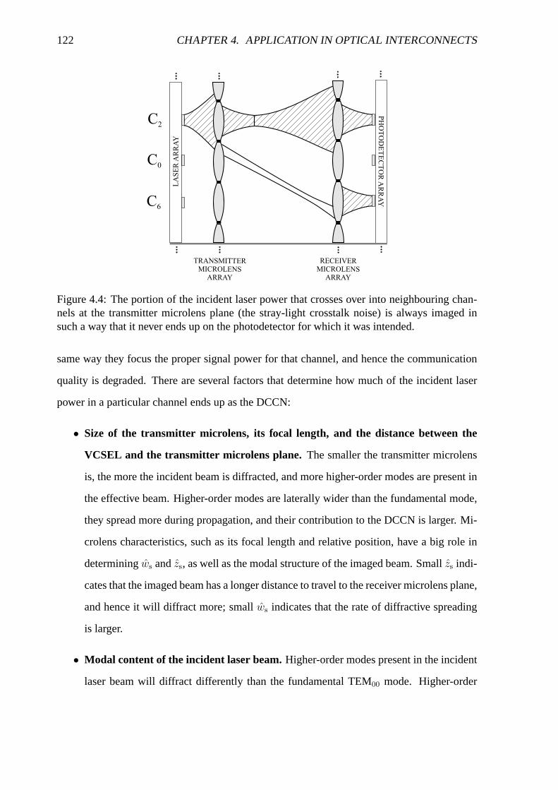
122 CHAPTER 4. APPLICATION IN OPTICAL INTERCONNECTS
LA
SE
RA
RR
AY
PH
OT
OD
ET
EC
TO
RA
RR
AY
C0
C2
C6
TRANSMITTERMICROLENS
ARRAY
RECEIVERMICROLENS
ARRAY
Figure 4.4: The portion of the incident laser power that crosses over into neighbouring chan-nels at the transmitter microlens plane (the stray-light crosstalk noise) is always imaged insuch a way that it never ends up on the photodetector for whichit was intended.
same way they focus the proper signal power for that channel,and hence the communication
quality is degraded. There are several factors that determine how much of the incident laser
power in a particular channel ends up as the DCCN:
• Size of the transmitter microlens, its focal length, and thedistance between the
VCSEL and the transmitter microlens plane. The smaller the transmitter microlens
is, the more the incident beam is diffracted, and more higher-order modes are present in
the effective beam. Higher-order modes are laterally widerthan the fundamental mode,
they spread more during propagation, and their contribution to the DCCN is larger. Mi-
crolens characteristics, such as its focal length and relative position, have a big role in
determiningws andzs, as well as the modal structure of the imaged beam. Smallzs indi-
cates that the imaged beam has a longer distance to travel to the receiver microlens plane,
and hence it will diffract more; smallws indicates that the rate of diffractive spreading
is larger.
• Modal content of the incident laser beam.Higher-order modes present in the incident
laser beam will diffract differently than the fundamental TEM00 mode. Higher-order
4.1. DESIGN MODEL 123
modes in the incident beam will produce even more higher-order modes in the effective
beam, and hence increase the DCCN.
• Spacing between the channels and the position of the receiver microlens plane.
Clearly, the closer the channels are spaced, the easier it is for the laser beam to cross
over. The effect of the location of the receiver microlens plane is the same as the effect
of zs: the farther the plane is, the more ‘time’ the beam has to diffract.
• Size of the receiver microlens, its focal length, and the distance from the receiver
microlens to the photodetector plane.In the same way as for the transmitter microlens,
this will determine how the beam will finally be imaged onto the photodetector. How-
ever, as the photodetector is in most cases positioned so that z′0 ≈ z′s, the crosstalk noise
introduced at the photodetector plane can generally be ignored. In our considerations,
we will simply assume that all the power that falls on a particular receiver microlens will
duly be focused onto its associated photodetector.
In the case when the optical interconnect consists of one channel only, as shown in Fig. 4.2,
the design problem consists of positioning the optical elements so that most of the laser beam
power emitted by the VCSEL is collected by the photodetector.However, as we add more
channels the design problem complicates, since we have to take into consideration the optical
crosstalk noise as well.
The plane of output mirrors of all VCSELs, transmitter microlens plane, receiver microlens
plane, and the plane of the photodetector will have the same overall layout, as shown in
Fig. 4.5. The elements in each plane (VCSELs, microlenses, and photodetectors) are arranged
in ‘square’ arrays as Fig. 4.5 depicts. Each channel is designated an area of∆2, where∆
represents the spacing between the channel centres (the array pitch). All elements in each of
the arrays are circular, with the generic radius denoted bya. In particular, we shall denote the
radius of the VCSEL output window byas, radius of the transmitter microlens bya0, radius of
the receiver microlens bya0, and the photodetector radius bya′0, all in correspondence with the
symbols used in Fig. 4.2. All radii within an array will be assumed to be identical, and∆’s for

124 CHAPTER 4. APPLICATION IN OPTICAL INTERCONNECTS
D
C1C2
C8C0C4
C5 C6 C7
2a
Figure 4.5: Schematic diagram indicating the arrangement of elements (VCSELs, receiver andtransmitter microlenses, and photodetectors) in the planes making up the interconnect. Thefootprint of all elements is circular; while∆ (array pitch) has to be the same for all planes,a(generic element radius) can vary from plane to plane, but not within one.
all arrays of course have to be the same. As in Fig. 4.3, we onlyshowed a section of the array,
centred around the representative channelC0. The way in which the channels are numbered,
which may have been unclear previously is now more evident. Starting fromC0, and looking
in the direction of beam propagation, the first channel up andto the right ofC0 is namedC1.
The layer of channels immediately surroundingC0 is numbered in an anti-clockwise manner,
starting fromC1. The next layer of channels is numbered in an anti-clockwisespiral fashion
starting fromC9, which is immediately up and to the right ofC1.
At each plane we can define the fill factorυ, a ratio of element diameter to the array pitch,
that indicates how much of the available channel area each array element occupies. For the
VCSEL array we have
υs =2as
∆, (4.2)
4.1. DESIGN MODEL 125
for the transmitter microlens plane we have
υ0 =2a0
∆, (4.3)
for the receiver microlens plane we have
υ0 =2a0
∆, (4.4)
and for at the photodetector plane we have
υ′0 =2a′0∆, (4.5)
where the nomenclature is consistent with our previous definitions. A fill factor of less than
unity not only results form the production requirements, but it may also be used as another
degree of freedom in the design process. In addition to the fill factors, we also define clipping
ratios at both the transmitter and the receiver microlens plane,κ andκ. The two clipping ratios
are useful measures of the extent to which the incident laserbeam is diffracted at each plane,
and have already been introduced in Ch. 3. At the transmitter microlens plane we have
κ =a0
w(z0)=a0
w0
, (4.6)
while at the receiver microlens plane we have
κ =a0
w(z0)=a0
w0
, (4.7)
where thew’s represent the beam radii at the respective microlens planes. In the context of
this dissertation (and as is the commonly-accepted practice in the literature), ‘beam radius’ will
always represent the beam radius of the fundamental TEM00 mode, as defined by Eq. (2.33).
As such, is not equivalent with the beam radius of any higher-order mode, which is generally
larger, and for which exist numerous definitions [116].

126 CHAPTER 4. APPLICATION IN OPTICAL INTERCONNECTS
The total amount of the crosstalk noise that enters our representative channelC0 from all
the neighbouring channels can be calculated as the sum of thetotal stray-light crosstalk noise
and the total diffraction-caused crosstalk noise:
N = Nsl +Ndc, (4.8)
whereN represents the total OCN,Nsl represents the total SLCN, andNdc represents the
total DCCN. In our present considerations, as indicated previously, we assume that the optical
field that falls onto a particular receiver microlens will duly be focussed onto the associated
photodetector. This practically means that we ignore the relatively small contribution to the
crosstalk noise introduced at the photodetector plane.Nsl is given by
Nsl = Nsl,1 +Nsl,2 +Nsl,3 + · · · +Nsl,ℵ (4.9)
whereNsl,n represents the amount of power from channelCn that crosses over intoC0 at the
transmitter microlens plane, andℵ is the total number of channels surroundingC0. In turn,
eachNsl,n can be calculated as the integral of the intensity of the laser beam from channelCn
over the surface of theC0 transmitter microlens (C0TML):
Nsl,n =
∫∫
C0TML
|Ψn(u, v, z0)|2 dudv. (4.10)
The explicit usage of the ordered pair(u, v) instead of the rectangular coordinates(x, y) indi-
cates a coordinate transform may need to be used in integration, as the commonz axis goes
only through the centre ofC0. The diffraction-caused crosstalk noise can be found in exactly
the same way:
Ndc = Ndc,1 +Ndc,2 +Ndc,3 + · · · +Ndc,ℵ, (4.11)

4.1. DESIGN MODEL 127
(a) (b)
Figure 4.6: Illustration of the equivalence principle usedfor calculation of the SLCN and theDCCN. The crosstalk noise from any channelCn that ends up inC0, as shown in (a), canequivalently be calculated as the noise fromC0 that ends up inCn, as shown in (b).
where
Ndc,n =
∫∫
C0RML
| Ψn(u, v, z0)|2 dudv, (4.12)
whereC0RML denotes the area of theC0 receiver microlens.
Fortunately, the fact that we treat all of the interconnect channels as identical may be used
to facilitate the evaluation of Eqs. (4.10) and (4.12). Since all channels in the interconnect
are equivalent, then the amount of (both stray-light and diffraction-caused) crosstalk noise in-
troduced fromCn into C0 is equivalent to the amount of the crosstalk noise introduced from
C0 into Cn [93]. This equivalence principle is illustrated in Fig. 4.6. Note that the principle
holds for all channels, even though only the channels immediately surroundingC0 are shown.
Fig. 4.6(a) shows the OCN interpreted as being the portion of power from surrounding chan-
nels that ends up inC0; Fig. 4.6(b) shows the crosstalk noise equivalently interpreted as being
the portion of power fromC0 that ends up in the surrounding channels. The interpretation
shown in Fig. 4.6(b) is more suitable for calculating the crosstalk noise in an interconnect as
there is no need for any coordinate transformation. As before, we write
N = Nsl +Ndc, (4.13)

128 CHAPTER 4. APPLICATION IN OPTICAL INTERCONNECTS
where
Nsl = Nsl,1 +Nsl,2 +Nsl,3 + · · · +Nsl,ℵ, (4.14)
and
Ndc = Ndc,1 +Ndc,2 +Ndc,3 + · · · +Ndc,ℵ. (4.15)
However, now we have
Nsl,n =
∫∫
CnTML
|Ψ(x, y, z0)|2 dxdy, (4.16)
and
Ndc,n =
∫∫
CnRML
|Ψ(x, y, z0)|2 dxdy. (4.17)
In the same way as Eqs. (4.13)—(4.17) prescribe the way in which the optical noise can be
calculated, we can write an equation for calculating the optical signal power that is successfully
transmitted from the VCSEL to the photodetector inC0:
S =
∫∫
C0PD
|Ψ(x, y, z′0)|2 dxdy, (4.18)
where the only difference is that the integration is performed over the area of theC0 photode-
tector (C0PD). In Eq. (4.18) we have not used the simplifying assumption that we used in the
calculation of the total optical crosstalk noise. Even though the more accurate Eq. (4.18) will
not change the numerical results considerably, it will aid in the illustration of the principle
should our original assumption be found not to be suitable insome situations.
We are in a position now to define several optical interconnect performance parameters.
The parameter easiest to calculate is the interconnect distance,L, defined as the distance be-

4.1. DESIGN MODEL 129
tween the VCSEL plane and the photodetector plane:
L = z′0 − zs. (4.19)
The second parameter is the channel density,D, given as the number of interconnect channels
per unit area:
D =1
∆2. (4.20)
Given a particular required data transfer rate, as well as all other interconnect parameters, the
most general optical interconnect design goal is to maximise its length,L, and channel density,
D. Laser beam diffraction, quantified as the optical channel crosstalk noise, is the main factor
that limits bothL andD. As noted previously, there are three main factors affecting the OCN:
spacing between channels (channel density), spacing between microlens planes (interconnect
length), and the way in which the incident laser beams are imaged by the microlenses. Small
channel spacings and large inter-planar distances result in more OCN, as the beams stray
and diffractively spread more. While intrinsically relatedto the channel density, the effect
of imaging on OCN is, however, much more subtle. Given that a microlens aperture is large
enough, the incident beam is, according to the ABCD law, transformed into a beam with the
same functional form as the incident beam, but with different beam parameters. The purpose
of the microlens transformations is to periodically re-focus the beam and hence allow it to
travel a greater distance. As the size of the microlens aperture is decreased, and as it starts
to ‘clip’ more of the incident beam power, the incident beam is not only imaged but also
diffracted by the microlens. Depending on the extent of diffraction, the diffraction field will
generally have a wider starting lateral power distribution, and it will spread diffractively more,
thus unequivocally resulting in more OCN. Ultimately, however, the effect of imaging and
diffraction results in limitation of the maximum interconnect length and density.
L andD are closely related and dependent on each other: given a verylarge channel
spacing (and hence wasteful interconnect design), the beams will travel long distances; given

130 CHAPTER 4. APPLICATION IN OPTICAL INTERCONNECTS
a short required length (and hence an inflexible design), thechannel density can be made very
large. Having in mind a particular receiver bandwidth, closely related to the main information-
transfer purpose of the interconnect, it therefore makes sense to combineL andD into one
performance parameter, the space-bandwidth product, SBP:
SBP = B · L ·D. (4.21)
SBP gives us an indication of the information transfer rate, measured in Hz, per unit area, mea-
sured in metres, and unit channel density, measured by the number of interconnect channels
per square metre.
Further interconnect performance parameters may be defined, one of them being the optical
carrier-to-noise ratio (OCNR), defined as
OCNR =S
N, (4.22)
whereS is calculated by using Eq. (4.18) andN is calculated by using Eq. (4.13). The OCNR
measures the importance of the OCN relative to the useful received signal power, and hence
gives an indication of the interconnect optical performance. However, our most important and
most comprehensive performance parameter is the (complete) signal-to-noise ratio (SNR), in
which both the optical and electrical characteristics of the interconnect are taken into account.
The interconnect signal-to-noise ratio is given as [195, 198]
SNR =X(RS)2
H, (4.23)
where
H = RIN · (R · S +R · N)2 ·B + 2 · e · (R · S +R · N + Id) ·B
+(4 · kB · T/Req) ·B · Ft +X · (R · N)2, (4.24)
and where:

4.1. DESIGN MODEL 131
• X is the ‘modified’ extinction ratio, defined byX = (ER− 1)/(ER+ 1), whereER is
the ‘real’ extinction ratio [198]
• R is the photodiode responsivity [W/A]
• S is the optical signal average power [W]
• RIN is the VCSEL relative intensity noise [dB/Hz]
• N is the optical crosstalk noise power [W]
• B is the receiver bandwidth [Hz]
• e is the charge on an electron,e = 1.60218 · 10−19 C
• Id is the photodiode dark current [A]
• kB is the Boltzmann’s constant,1.3807 · 10−23 J/K
• T is the operating temperature [K]
• Req is the equivalent resistance of the photodetector load and preamplifier [Ω]
• Ft is the preamplifier noise figure [dB].
The signal-to-noise ratio, commonly used to measure the performance of communication sys-
tems, is essentially the ratio of the modulated power (whichcarries the transmitted informa-
tion) and the total noise power. The first term in the denominator in Eq. (4.23) represents the
RIN portion of the noise in the received signal (which is due toboth the optical signal and
crosstalk noise incident powers). The second term accountsfor the photodiode noise, the third
term is due to the preamplifier noise, while the final term accounts for the current produced
due to the optical crosstalk noise. In practical calculation of the SNR, as given by Eq. (4.23),
the most important issue is the calculation of the (real) signal and noise powers,S and N .
These powers are obtained from the ‘normalised’ optical signal and crosstalk noise powers,S
andN . It is in the way thatS andN are calculated that the relevance and strength of the mode

132 CHAPTER 4. APPLICATION IN OPTICAL INTERCONNECTS
expansion method comes to prominence; without MEM the calculation ofS,N , and hence the
complete SNR would be very difficult and impractical.
For the sake of generality and rigour, and as will be confirmedby the experimental mea-
surements presented in Sec. 4.2, we have to assume that the beam produced by the VCSEL
will contain an unknown number of modes. The modal weights which determine the modal
make-up of the incident beam, as introduced in Eq. (4.1), canbe organised in the vector form
as follows
W = (W00,W01, . . . ,W0µ,W10,W11, . . . ,W1µ, . . . ,Wν0,Wν1, . . . ,Wνµ) (4.25)
where the order of the highest-order mode is now representedby νµ (sinceN is already taken),
and the modes are ordered first with respect toν, and then with respect toµ. The total number
of modes, as in Ch. 3 is denoted byνµ. Theoretically, eachWnm has to be a complex value in
order to account for the relative phase differences betweenthe modes emitted by the VCSEL.
Practically, we can (easily) only measure the relative power carried by each mode,|Wnm|2;
special procedures need to be employed if the phase differences are to be measured. While the
mode expansion method is capable of dealing with complex-valuedWnm’s, we will simplify
our considerations and assume that for eachWnm we have:
Wnm =√
|Wnm|2. (4.26)
If we denote the total optical power emitted by the VCSEL asPtot, and the vector containing
the watt power in each mode as
P = (P00, P01, . . . , P0µ, P10, P11, . . . , P1µ, . . . , Pν0, Pν1, . . . , Pνµ) , (4.27)
then eachPnm is given as
Pnm = Ptot · |Wnm|2, (4.28)
4.1. DESIGN MODEL 133
where bothPtot andWnm =√
|Wnm|2 are experimentally measured. As our expression for
the modes of the free space,ψnm($, z), are power-normalised, it also follows that
||W ||2 = (||W ||2)2 = 1, (4.29)
where|| · || represents the vector norm.
We can use similar notation for the values of the stray-lightcrosstalk noise. If the stray-
light crosstalk noise,Λnm, of each pure mode,ψnm(x, y, z), is in the manner of Eq. (4.16),
given by
Λnm =ℵ∑
q=0
∫∫
CqTML
|ψnm(x, y, z0)|2 dxdy, (4.30)
then the setΛnm can also be written in vector form as
Λ = (Λ00,Λ01, . . . ,Λ0µ,Λ10,Λ11, . . . ,Λ1µ, . . . ,Λν0,Λν1, . . . ,Λνµ) . (4.31)
The normalised SLCN of the multimodal incident beam is then given as
Nsl = |W |2 · ΛT , (4.32)
whereT signifies the transpose operation, and| · |2 is performed on each individual element of
W . The real, watt SLCN is given by
Nsl = P · ΛT , (4.33)
where we have, as before, used the hat to distinguish betweenthe normalised optical power
and the received watt power.
Similarly, the normalised DCCN can be calculated as
Ndc = |W |2 · ΥT , (4.34)

134 CHAPTER 4. APPLICATION IN OPTICAL INTERCONNECTS
and the DCCN in watts can be calculated as
Ndc = P · ΥT . (4.35)
In Eqs. (4.34) and (4.35), vectorΥ,
Υ = (Υ00,Υ01, . . . ,Υ0µ,Υ10,Υ11, . . . ,Υ1µ, . . . ,Υν0,Υν1, . . . ,Υνµ) , (4.36)
denotes the diffraction-caused crosstalk noise of each pure laser beam mode,ψnm(x, y, z),
with
Υnm =ℵ∑
q=0
∫∫
CqRML
|ψnm(x0, y0, z0)|2 dx0dy0, (4.37)
in the manner of Eq. (4.17) and similarly to Eq. (4.30). However, the key thing in the proper
calculation of the DCCN is the determination ofW and P , which we can do by using the
mode expansion method.W , explicitly given as
W =(
W00, W01, . . . , W0µ, W10, W11, . . . , W1µ, . . . , Wν0, Wν1, . . . , Wνµ
)
, (4.38)
contains the complex-valued modal coefficients of the diffracted and imaged laser beam, in the
same way asW describes the modal composition of the incident laser beam.W is worked
out as
W T = Q · W T , (4.39)

4.1. DESIGN MODEL 135
whereQ,
Q =
Q0000 Q00
01 · · · Q000µ · · · Q00
ν0 Q00ν1 · · · Q00
νµ
Q0100 Q01
01 · · · Q010µ · · · Q01
ν0 Q01ν1 · · · Q01
νµ
......
......
......
......
...
Q0µ00 Q0µ
01 · · · Q0µ0µ · · · Q0µ
ν0 Q0µν1 · · · Q0µ
νµ
......
......
......
......
...
Qν000 Qν0
01 · · · Qν00µ · · · Qν0
ν0 Qν0ν1 · · · Qν0
νµ
Qν000 Qν0
01 · · · Qν00µ · · · Qν0
ν0 Qν0ν1 · · · Qν0
νµ
......
......
......
......
...
Qνµ00 Qνµ
01 · · · Qνµ0µ · · · Qνµ
ν0 Qνµν1 · · · Qνµ
νµ
, (4.40)
represents the modal expansion coefficients used to accountfor the effects of imaging and
diffraction. As shown in Ch. 3, each coefficient can be worked out as:
Qnmnm =
∫∫
C0ML
ψnm(x0, y0, z0) · φ(x0, y0, z0) · ψ∗
nm(x0, y0, z0) dx0dy0, (4.41)
where(n,m) indicates the order of the incident mode, and(n, m) the order of the expand-
ing mode. If we denote the total number of incident modes byνµ, and the total number of
expanding modes byνµ, the the dimension of each matrix is given as:
dim(W ) = νµ× 1, (4.42)
dim(Q) = νµ× νµ, (4.43)
and
dim(W ) = νµ× 1. (4.44)
136 CHAPTER 4. APPLICATION IN OPTICAL INTERCONNECTS
In our calculations, somewhat at the expense of modelling diffraction of higher-order incident
modes, we assume that the total number of expanding modes is fixed, for example atνµ = 20.
This number of expanding modes, as shown in Ch. 3 is usually sufficient. Finally,P is given
as
P =(
P00, P01, . . . , P0µ, P10, P11, . . . , P1µ, . . . , Pν0, Pν1, . . . , Pνµ
)
, (4.45)
with each coefficient explicitly given as
Pnm = Ptot · |Wnm|2. (4.46)
Needless to say, whileP is a physically measurable quantity, the physical existence ofP , even
though also measured in watts, should be meditated upon withcaution. It is a strong belief of
the author thatP does exist physically; its elements, however, may not necessarily be given
by Eq. (4.46) as our chosen orthonormal set may not be the mostoptimal one.
By combining Eqs. (4.33) and (4.35),
N = Nsl + Ndc, (4.47)
we solve the first problem associated with the practical calculation of the SNR; the remaining
problem involves the calculation ofS. Following the logic and conventions used to findN , we
have:
S = |W ′|2 · ΦT , (4.48)
where
Φ = (Φ00,Φ01, . . . ,Φ0µ,Φ10,Φ11, . . . ,Φ1µ, . . . ,Φν0,Φν1, . . . ,Φνµ) , (4.49)

4.2. EXPERIMENTAL DETAILS 137
Φnm =
∫∫
C0RML
|ψnm(x0, y0, z0)|2 dxdy, (4.50)
and
S = P ′ · ΦT = Ptot · S. (4.51)
Instead ofP andW , we now haveP ′ andW ′, due to the fact that diffraction occurs at two
consecutive apertures.W ′ is calculated by repeating the process used to calculateP :
(W ′)T = Q · W T , (4.52)
where eachQnm can be calculated by using Eq. (4.41), with the only difference that the inte-
gration is performed at the receiver microlens plane. Each element ofP ′, on the other hand is
given as
P ′
nm = Ptot · |W ′
nm|2. (4.53)
With the framework for a application of the mode expansion method in place, we can now
commence the task of finding appropriate parameter values, so that reasonable performance
estimates can be obtained.
4.2 Experimental details
The following three measurements were performed in order toobtain realistic parameter values
to be used in Eq. (4.23):
• measurement of the VCSEL light-current characteristic
• measurement of the laser beam spectrum and modal composition
• measurement of the VCSEL relative intensity noise.

138 CHAPTER 4. APPLICATION IN OPTICAL INTERCONNECTS
All measurements were performed on aMode 8085-2020laser. The primary tools employed
in laser characterisation were [199]:
• Agilent 84140B Optical Spectrum Analyser
• Hewlett Packard 8565E RF and Microwave Spectrum Analyser
• Agilent 86100A Oscilloscope
• Anritsu ML9001A Power Metre
• Hewlett Packard 8510C Network Analyser
• Newport Model 8000 Laser Driver
• Agilent 8133A Pattern Generator
• Various optical components (as shown in experimental setupdiagrams) andLabView,
National Instruments’graphical programming language used to interface with the mea-
suring equipment.
The experimental setup used to measure the VCSEL light-current (LIV) curve is shown in
Fig. 4.7, where the laser power and input voltage were measured at intervals of 0.05 mA. The
measurement results are shown in Fig. 4.8. Figure 4.8 also shows how the measured data was
fitted to a simplified form of the rate equations, that is knownto be a reasonable approximation
of a laser’s actual light-current curve, given by [200]
Φ2 P 2 − Φ (I − Ith − Is) − Is I = 0, (4.54)
where
Φ =2 · e · λh · c · η , (4.55)
e is the charge of an electron,λ is the wavelength of laser light (the actual value used for fitting
wasλ = 850 nm),h = 6.626068 ·10−34 Js is the Planck’s constant,c = 2.99793 ·108 m/s is the

4.2. EXPERIMENTAL DETAILS 139
Labview
Laser Driver
Laser Mount
VCSEL Power Meter
Experiment
Parameters
Temperature
Control
Current
Power Measurements
Electrical Signal
Optical Signal
Figure 4.7: Schematic diagram of the experimental setup used for measuring the VCSEL’slight-current characteristic.
Figure 4.8: Experimentally-measured and numerically-fitted results of the VCSEL’s light-current characteristic.

140 CHAPTER 4. APPLICATION IN OPTICAL INTERCONNECTS
Figure 4.9: Schematic diagram of the experimental setup used for measuring the VCSELbeam’s modal and spectral characteristics.
speed of light in vacuum, andη represents the laser efficiency. The measured data was fitted
to Eq. (4.54) by using a nonlinear fitting function inMathematica[183], and the following
parameter values were extracted:Ith = 4.47 mA, Is = 6.73 µA, andη = 0.715 W/A.
The fitting of the measured data to Eq. (4.54) is valid if the laser is considered to emit light
in the fundamental mode only, which is generally not the case. In reality, the light-current
characteristic shown in Fig. 4.8 is the result of activity and combination of multiple modes,
with each mode having its own threshold current and efficiency. The presence of higher-order
modes is hinted to in Fig. 4.8 by the gradient discontinuities evident in the measured results.
In particular, the gradient discontinuities can be found at6 mA and 14 mA, and hence we
suspect that higher-order modes appear at those currents. However, this can only be confirmed
by further spectral measurements of the laser beam.
The experimental setup used for modal and spectral measurements is shown in Fig. 4.9. As
in the case of light-current measurements, laser spectra were sampled and examined at various
currents, as shown in Fig. 4.10. As we see from the presented results, the laser started single-
mode operation right after the threshold current, but more efficient modes of higher order
appeared at 6 mA and 14 mA, as first guessed by observing the light-current characteristic.
By the time the current reached 16 mA, four different higher-order modes were present in
the laser beam. While the light-current and spectral measurements enabled us to confirm the
presence of higher-order modes in the laser beam, they cannot yet be used to identify those
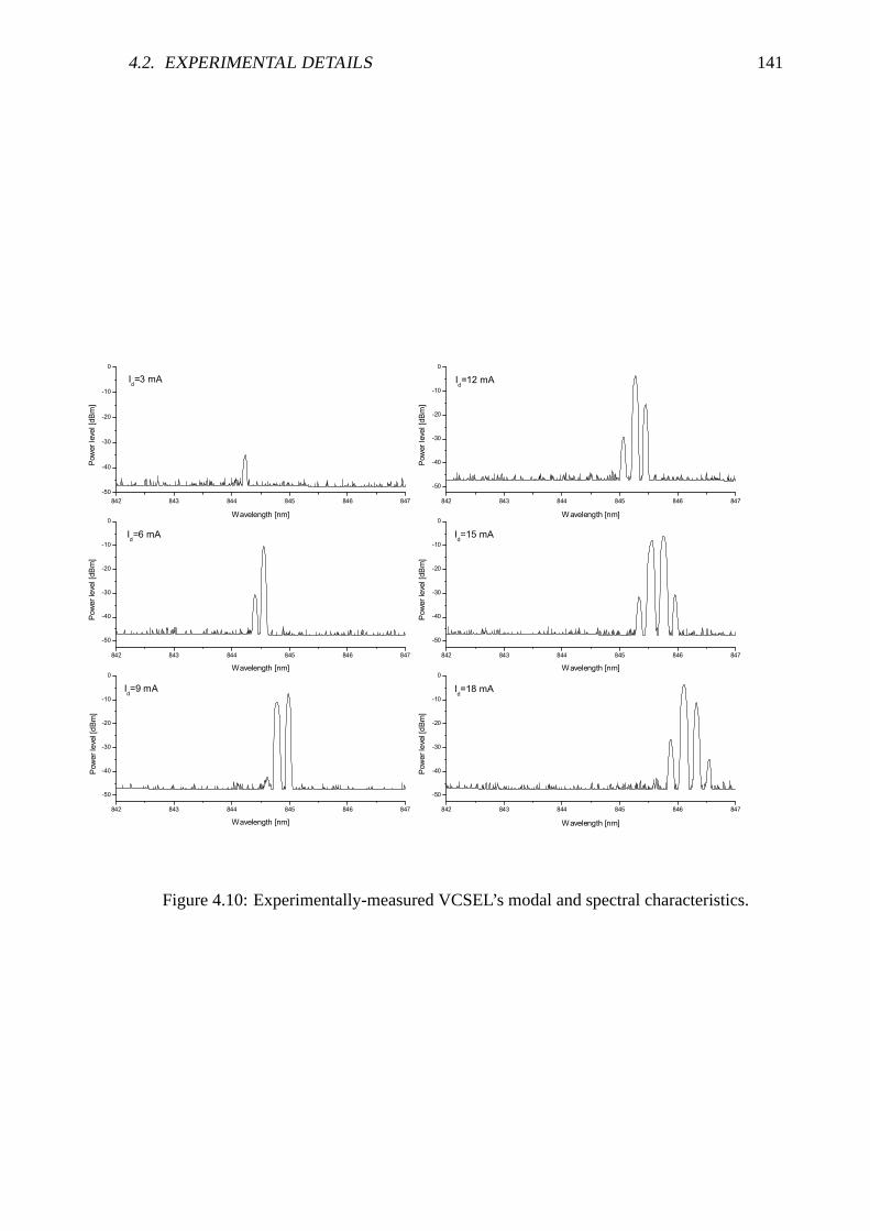
4.2. EXPERIMENTAL DETAILS 141
Figure 4.10: Experimentally-measured VCSEL’s modal and spectral characteristics.

142 CHAPTER 4. APPLICATION IN OPTICAL INTERCONNECTS
Figure 4.11: Modally resolved VCSEL’s light-current characteristic.
modes. Moreover, multiple transverse modes may exist at thesame frequency. In addition to
confirming the presence of higher-order modes in the laser beam, the spectral measurements
shown in Fig. 4.10 also show the symptoms of adiabatic chirp.Adiabatic chirp consists of
the lasing frequency of each higher-order mode being shifted at higher drive currents, due to
a change in the refractive index of the material [201]. The effect of the adiabatic chirp on an
optical communication system is twofold. First, the cavityand material gain peaks become
unaligned, resulting in power roll-off for the fundamentalmode, and higher gain for higher-
order modes. Second, when directly modulated, adiabatic chirp results in dispersion penalties
due to the different optical wavelengths that are transmitted for high and low pulses.
The magnitude and position of the peaks shown in Fig. 4.10 wasextracted automatically at
every current, and a modally-resolved light-current curvewas constructed. The curve is shown
in Fig. 4.11. In Fig. 4.11, the power content of each mode (calculated by integrating the area
beneath the spectral peaks) was first found. Then the power content of each mode was added
and compared to a scaled version of the light current measurement. If the two curves resemble
each other, we can conclude that the laser modal behaviour was correctly interpreted. The
adiabatic chirp was constant for all modes, and it was determined to be 0.3 nm/mA. However,

4.2. EXPERIMENTAL DETAILS 143
Figure 4.12: Wavelength of each laser beam mode, obtained from the data presented inFig. 4.10.
in our further considerations we shall ignore the effect of adiabatic chirping on the performance
of the optical interconnect.
Figure 4.11 still does not offer us a full insight into the modal behaviour of the laser beams.
While we are able to establish the presence of higher-order modes in the laser beam, we still
are not able to identify which modes they are, in terms of our standard Hermite-Gaussian or
Laguerre-Gaussian modes of the free space. In order to analyse the modes further, we have to
capture the incident beam by a CCD camera, process it by a beam profiler, and examine the
obtained beam profile. The experimental setup is shown in Fig. 4.9. By analysing the captured
beam profiles, and comparing their changes to that of the spectrum, it is possible to determine
which transverse modes are present. Most of the modes can be identified in this manner, but
not all of them as multiple modes sometimes lase simultaneously. Alternatively, a scanning
spectrum analyser probe could be used instead of the CCD camera, as shown in Fig. 4.13. The
wavelength of each mode, as it changes with the drive current, is shown in Fig. 4.12.

144 CHAPTER 4. APPLICATION IN OPTICAL INTERCONNECTS
Figure 4.13: Schematic diagram of the experimental setup used for spectrally-resolved modalmeasurements.
In Fig. 4.13, computer controlled actuators are used to scana two-dimensional area, record
the spectrum at each point, and in this way reconstruct a spectrally-resolved near-field image
of the laser beam. Such image could consequently be analysedeasily, and the modal distri-
bution would be established more precisely [202, 203, 204, 205, 206, 207, 208, 209, 196].
Furthermore, laser beam spot size and divergence would alsobe easier to analyse by using this
technique.
Figures 4.14, 4.15, and 4.16 show laser beam profiles taken atvarious drive currents, and
with various polarisations, by using the experimental setup shown in Fig. 4.13. By comparing
the changes in the beam profiles to the changes in the spectrum, the following transverse
higher-order (Hermite-Gaussian) modes were identified:
• TEM00, which appears at threshold,
• TEM01 and TEM10, which appear simultaneously, with different polarisations, at ap-
proximately 6 mA,
• TEM20, which appears at approximately 14 mA.
From Figs 4.14, 4.15, and 4.16 it can be seen that the identification of a particular mode
by a camera is not easy, especially if the mode is not dominantat least in polarisation at a
particular current. In addition to the highest identified mode (TEM20) there probably exist, at

4.2. EXPERIMENTAL DETAILS 145
3 mA 4 mA 5 mA 6 mA
7 mA 8 mA 9 mA 10 mA
11 mA 12 mA 13 mA 14 mA
15 mA 16 mA
Figure 4.14: Profiles of VCSEL transverse modes, with the polariser set to 15 polarisation.
the same wavelength, other degenerate modes that cannot be isolated due to their low power.
However, regardless of their shortcomings, the laser light-current and spectral measurements
have enabled us to establish the modal properties of the laser beam, as relevant to the design
and analysis of optical interconnects.
The experimental setup used to measure the final parameter needed, the relative intensity
noise, is shown in Fig. 4.17. A laser driven with a perfectly stable source will still exhibit
fluctuations in its output power, which are mainly due to the variations in photon density. In
the experimental procedure used to measure the RIN, the photodetector output is first separated
into DC and AC streams that represent the laser power and laser noise respectively. Then, a
high quality electrical amplifier and spectrum analyser areused to amplify and measure the
noise over a large range of frequencies. As in the case of spectral measurements, the presence
of the optical isolator prevents the undesired back-reflections which significantly alter laser
performance [210, 211]. The results of RIN measurements are shown in Fig. 4.18.

146 CHAPTER 4. APPLICATION IN OPTICAL INTERCONNECTS
3 mA 4 mA 5 mA 6 mA
7 mA 8 mA 9 mA 10 mA
11 mA 12 mA 13 mA 14 mA
15 mA 16 mA
Figure 4.15: Profiles of VCSEL transverse modes, with the polariser set to 15 polarisation.
The following conclusions, in relation to the evaluation ofthe SNR Eq. (4.23), can be
drawn from our experimental measurements:
• The total laser output power,Ptot, ranges from 0 mW to 6 mW, for the laser drive current
ranging from 4 mA to 16 mA, as shown in Fig. 4.8. The middle of the linear output re-
gion occurs for the drive current of about 10 mA, for which theVCSEL produces output
power of about 3.0 mW. We choose the ordered pair(Id, Ptot) = (10 mA, 3.0 mW) as
our operating point.
• Depending on the particular drive current, as shown in Fig. 4.11, one or more transverse
modes may be present in the laser beam. Generally, the probability of finding a higher-
order mode in the laser beam is higher when the laser is producing more power. At the
drive current of 10 mA, there are two modes present in the VCSELbeam: the fundamen-
tal mode and the first higher-order mode. As noted previously, the fundamental mode
can be modelled by the TEM00 Hermite-Gaussian mode of the free space, while the first

4.2. EXPERIMENTAL DETAILS 147
3 mA 4 mA 5 mA 6 mA
7 mA 8 mA 9 mA 10 mA
11 mA 12 mA 13 mA 14 mA
15 mA 16 mA
Figure 4.16: Profiles of VCSEL transverse modes, with the polariser removed from the setup.
Figure 4.17: Schematic diagram of the experimental setup used for the relative intensity noisemeasurements.

148 CHAPTER 4. APPLICATION IN OPTICAL INTERCONNECTS
Figure 4.18: The results of relative intensity noise measurements.
HOM can be modelled as a combination of the TEM01 and TEM10 Hermite-Gaussian
modes.
• At the drive current of 10 mA, as shown in Fig. 4.11, the power carried by the fun-
damental mode is equal to 1.13 mW (37% of the total emitted power), while the power
carried by the first order mode is 1.92 mW (63% of the total optical power emitted by the
VCSEL). Furthermore, we assume that the total power carried by the first higher-order
mode is split equally between the TEM01 and TEM10 modes. According to our general
model, explained in Sec. 4.1, we have:W00=0.37,W01 =0.315, andW10=0.315.
• Depending on the value of the drive current, each mode will lase at a slightly different
wavelength, as shown in Fig. 4.12. At our chosen drive current of 10 mA, we see that
all of our modes will have, approximately, a wavelength ofλ=845 nm.
• An average value ofRIN = −130 dB/Hz, as indicated in Fig. 4.18, will be used for the
laser relative intensity noise.

4.2. EXPERIMENTAL DETAILS 149
In addition to the above experimentally-measured values, the following conclusions will
also be taken into account in the evaluation of Eq. (4.23):
• The photodiode responsivity used is the typical responsivity of theEmcore’s 8485-1400
four-channel Gallium Arsenide PIN photodiode, namelyR = 0.5 A/W (given assuming
that the incident power level will be between 3 and -26 dBm, andfor the light wavelength
of 850 nm).
• The dark current for the same photodiode isId = 0.3 nA.
• Typical (matched) equivalent resistance of the photodetector load and preamplifier is
Req = 50 Ω, while a typical preamplifier noise figure isFt = 3 dB.
• A typical receiver bandwidth isB = 1 GHz.
• The operating temperature can safely be assumed to be equal to the room temperature
of 290 K.
The following values were taken quite arbitrarily, as typical representative values, and can
easily be changed, depending on the design requirements at hand:
• modified extinction ratio,X = 0.125
• array pitch,∆ = 250 µm
• transmitter and receiver microlens array fill factors,υ0 = υ0 = 0.95
• microlens focal length,f = 800 µm.
The final, and probably the most important ‘geometrical’ factor are the relative positions of
the planes inside the optical interconnect. As indicated earlier, the position of the laser plane
will be taken as the reference plane. Based on the ABCD law, thereare two limiting cases in
which the microlens can be placed, where Fig. 4.19 is provided for better reference:
1. d = z0 − zs = f
In this case the position of the imaged beam waist is given as` = zs − z0 = f , while

150 CHAPTER 4. APPLICATION IN OPTICAL INTERCONNECTS
w0
VC
SE
L
ws
z0zs
z
zs
ws
Figure 4.19: The graph for explaining the choice of the inputdistance.
the size of the imaged beam waist is given asws = ws|f |/√
d2 + z2R. In the setup
where both the input and the output distances are the same, the imaged beam waist has
the maximum size, and hence the minimum rate of increase during propagation further
alongz.
2. d = z0 − zs = f + zR
In this case the position of the imaged beam waist is given as` = f + f 2/2zR, while
the size of the imaged beam waist is given asws = ws|f |/√
d2 + z2R. If we move the
transmitter microlens away from the focal length by a relatively small distance, the effect
is that of the ‘maximum throw’ whereby the position of the imaged beam waist, relative
to the position of the transmitter microlens, is greatest.
The first configuration will generally be referred as the ‘maximum waist configuration’, while
the second one will be referred to as the ‘maximum throw configuration’.
The position of the other planes in the interconnect may be determined in several different
ways. The simplest approach would be to position the rest of the optical elements symmet-
rically. Namely, if we set the receiver microlens array so that d = z0 − zs = `, then, given
that diffraction does not occur, the distance from the receiver microlens to the final beam waist
image isˆ = z′s − z0 = d. As d = ` and ˆ = d the system is rightly called symmetrical. The
particular choice of the input distance does not make any difference in symmetrical systems,
i.e. either the limiting case (1), (2), or any other combination in between, could be used. The
problem with systems that rely on their symmetry for proper operation lies in the difficulties
4.3. EVALUATION OF OPTICAL INTERCONNECT PERFORMANCE 151
associated with the maintenance of the symmetry. Alternatively, as we shall see in the follow-
ing section, the planes may be positioned in such a way as a particular optical interconnect
performance parameter, most likely the overall SNR, is optimised.
In the next section, where we evaluate the optical interconnect performance, the ‘standard’
set of parameter values consists of all the parameter valueslisted above, with the geometrical
configuration taken to be the maximum-throw configuration.
4.3 Evaluation of optical interconnect performance
Our first aim in this section is to demonstrate the importanceof the proper modelling of
diffraction in the calculation of the overall optical interconnect performance. Figure 4.20
shows the OCNR for an optical interconnect with standard parameter values, and a symmet-
rical maximum-waist configuration. In order to change the extent to which the incident laser
beam is diffracted (i.e. in order to changeκ), we change the fill factor of theC0 transmitter
microlens, while all other values, including the fill factors of all other elements are kept the
same. While, for purposes of easier calculations, we assumedthat the incident laser beam was
the fundamental TEM00 mode, our conclusions can easily be extended to the case whenthe in-
cident laser beam contains HOMs too. Due to their wider cross-sectional profiles, HOMs will
diffract more than the fundamental mode, and hence a proper modelling of their diffraction is
even more important. We first calculate the interconnect OCNRby assuming that the incident
laser beam was only ‘clipped’, i.e. that, regardless ofκ, it always remains a Gaussian. The
beam parameters of the imaged beam were calculated by using the ABCD law, again regard-
less ofκ, and the total power of the imaged beam was taken to be equal tothe power of the
incident beam that passes through the transmitter microlens aperture. With this relation, and
with the knowledge of the imaged laser beam parameters we areable to fully reconstruct the
imaged beam.
As it can be seen from Fig. 4.20, this fairly naive interpretation of diffraction in optical
interconnects leads to a prediction that the OCNR will not drop by more than about 10%

152 CHAPTER 4. APPLICATION IN OPTICAL INTERCONNECTS
0.5 1 1.5 2 2.5clipping ratioΚ
10
16
22
25
28
OC
NR@d
BD
clipping
1 mode 12 modes
6 modes
Κ=rΜlensΩΜlens
Figure 4.20: Proper modelling of diffraction in the design of optical interconnects is veryimportant. The topmost solid line (labelled ‘clipping’) shows the expected OCNR when theincident laser beam is assumed only to be clipped by the transmitter microlens aperture; thetop broken line (labelled ‘1 mode’) shows the calculated OCNRwhen MEM with only oneexpanding mode is used; the bottom broken line (labelled ‘6 modes’) shows the calculatedOCNR when MEM with 6 expanding modes is used; and the bottom solid line (labelled ‘12modes’) shows the calculated OCNR when MEM with 12 expanding modes is employed.Standard parameter values, maximum-waist configuration, and fundamental-mode incidencewere assumed. The OCNRs were normalised to the diffraction-free value of 54 dB.

4.3. EVALUATION OF OPTICAL INTERCONNECT PERFORMANCE 153
even in the cases of extremely strong diffraction. Choosing to model diffraction in this way
would hence lead to an overestimation in the expected interconnect performance. We now
consider using the MEM to model diffraction, but with only one expanding mode. As shown
in Fig. 4.20, this leads to an improved estimate of interconnect performance in the region of
strong diffraction, and an reiteration of the clipping-only results in other diffraction regions.
Considering the minimal operational change brought by the one-mode MEM, as compared
to the clipping-only model, the resulting improvement is very significant. Let us, as before,
denote the fundamental-mode incident laser beam asψ00(x, y, z;ws, zs), and the diffracted
and imaged fundamental-mode beam asC · ψ00(x, y, z; ws, zs), whereC is a complex-valued
constant. In both the clipping-only and one-mode MEM methods we model diffraction by
assigning appropriate values toC, ws, and zs. In the clipping-only method we do this by
stating that:
ws = ws, ABCD, (4.56)
zs = zs, ABCD, (4.57)
and that
∫∫
∞
−∞
|C ψ00(x, y, z; ws, zs)|2 dA =
∫∫
C0TML
|ψ00(x, y, z0;ws, zs)|2 dA
⇐⇒ |C|2 =
∫∫
C0TML
|ψ(x, y, z0;ws, zs)|2 dA, (4.58)
where the ‘ABCD’ subscript indicates that the values were calculated by the ABCD law,z can
take on any value in between the transmitter and the receivermicrolens arrays,z = z0 is the
location of the transmitter microlens array,dA = dxdy, andC0TML represents the area of the
central channel (C0) transmitter microlens. As we can see from Eq. (4.58), in theclipping-only
method we can only work out the absolute value ofC, rather than its full complex value. On

154 CHAPTER 4. APPLICATION IN OPTICAL INTERCONNECTS
the other hand, the same parameter values in the one-mode MEMare worked out as follows:
ws = ws, opt, (4.59)
zs = zs, opt, (4.60)
and
C = Q00, (4.61)
wherews, opt andzs, opt are the two ‘optimal’ values that maximise|C00|2, and all other values
have the same meaning as before; note that Eq. (4.61) gives usnow the complete value ofC,
not just its absolute value. While the operational characteristics of both methods are the same,
as we are in both cases perceiving the diffracted and imaged beam as a fundamental mode,
the way in which we chose to calculate the characteristics ofthat beam have clearly made a
considerable difference in the final results. This subtle difference already demonstrates the
strength of the mode expansion method, even in the case that just one mode is used to model
the diffraction field.
In relation to Fig. 4.20, we finally note that adding more modes to the effective beam, in
the way described in Ch. 3, quickly makes the OCNR curve converge to shape that closely
resembles the one obtained by using a dozen modes in the effective beam. In the diffraction-
free region, i.e. whenκ ≥ 2.0, all four lines converge to the same OCNR value, as there
diffraction is practically nonexistent. As soon as we get out of the diffraction-free region, the
diffraction effects affect the OCNR greatly, in such a way that both the clipping-only and one-
mode MEM methods lead to gross over-estimations. The results obtained even with only six
expanding modes are remarkably close to the results obtained by using twice the number of
expanding modes, hence indicating that a proper inclusion of diffraction effects in the optical
interconnect design can easily be obtained by the MEM.

4.3. EVALUATION OF OPTICAL INTERCONNECT PERFORMANCE 155
Next we examine the performance of the whole interconnect, as measured by the signal-to-
noise ratio, given by Eq. (4.23). Figure 4.21 shows the optical interconnect SNR as a function
of bothL, the interconnect distance, andD, the channel density. In producing Fig. 4.21 we
assumed all the typical parameter values, a symmetrical maximum-throw configuration, and a
fundamental-mode incidence. The position of the transmitter microlens plane relative to the
laser plane, as well as the position of the photodetector plane relative to the receiver microlens
plane, were always kept fixed at the prescribed value ofd = f + zR. The position of the
transmitter microlens plane relative to the receiver microlens plane, however, was increased
irrespectively of the original maximum-throw prescription, in order to increaseL. As noted
previously, this does open up the possibility of introducing small errors in the calculation
of the optical crosstalk noise, as the position of the photodetector is not actively adjusted
depending on the position of the receiver microlens array. The channel density was increased
by changing∆ for all arrays, while keeping all fill factor values the same.As noted previously,
L andD are the two most important optical interconnect design parameters. The interconnect
distance, usually approximated as being simply the distance from the transmitter to the receiver
microlens arrays, determines how far apart can the two communication ends be. This will
ultimately determine the design of the components that the interconnect is meant to connect.
The further apart the two planes are, i.e. the longer the interconnect distance is, the more
will the laser beams be allowed to spread and more optical crosstalk noise will be introduced
in the system. The spacing between the individual channels,which solely determines the
interconnect channel densityD, has the same sort of importance asL. A close channel spacing
will result in small and compact interconnects, with a largecapacity for data communication.
However, as the channels are brought closer together, the laser beams need travelling smaller
distances before crossing over into the neighbouring channels, and thus contributing to the
optical crosstalk noise.
Figure 4.21 clearly shows that there is a nearly linear trade-off between the maximum
attainable channel density, for any given interconnect distance, and vice versa. Practically,
almost anyL can be achieved, given that the channel spacing is large enough. As we increase

156 CHAPTER 4. APPLICATION IN OPTICAL INTERCONNECTS
27 29 31 33 35 37 39 41 43 45 47 49 51L @mmD
25
23
21
19
17
15
13
11
9
7
5
D@c
hann
els
per
mm2D
33 dB
Figure 4.21: Design curves of the optical interconnect signal-to-noise ratio as a function ofthe interconnect density and distance. Given a particular required SNR we can use this graphto estimate what sort of a device we can make. The SNR contoursare all 3 dB less thanthe previous one, starting from the 33 dB contour. Typical parameter values, symmetricalmaximum-throw configuration, and the fundamental-mode incidence were assumed.

4.3. EVALUATION OF OPTICAL INTERCONNECT PERFORMANCE 157
the density of channels, we need to sacrifice some of the interconnect distance, and bring the
transmitter and receiver arrays closer together. Similar argument could be presented for any
interconnect density: practically any value ofD may be obtained given thatL can be set to
arbitrarily small values. Finding an optimal balance betweenL andD, given a particular target
performance value, is the key task of a successful optical interconnect design; the purpose of
the mode expansion method is to allow the designer to accurately and efficiently determine the
relationship between the two most important values. All other interconnect parameter values,
such as various fill factors and very precise optical layouts, play a much less important role
in the process of interconnect design for two main reasons. First, as will be shown later, fine
adjustments of the remaining parameter values only leads tovery small improvements in the
overall interconnect performance. Second, the problems associated with practical realisations
of those fine adjustments easily outweigh their benefits.
The relationship betweenL andD values resulting in the same SNR, as shown in Fig. 4.21,
is nearly perfectly linear. For example, if the desired SNR is 30 dB, the maximum interconnect
density that can be achieved is given by
D ≈ −1.23 · L+ 54.21, (4.62)
whereL is measured in mm, andD in channels per mm2. If L is increased by 1 mm,D has to
be decreased by 1.23 channels/mm2, in order to keep the same SNR of 30 dB.
Our other performance measure, the space-bandwidth product (SBP), builds up on the spe-
cial relationship betweenL andD. SBP is the product of the receiver bandwidthB, measured
in Hz and taken to indicate the electrical information-handling capability of the whole inter-
connect, and ofL andD, for a particular value of the interconnect SNR. SBP gives us an
indication of the overall interconnect information-handling capability. The ‘space’ factor is
L · D, whereL andD regulate each other in the manner indicated before. The ‘bandwidth’
factor is the utilised portion of the total receiver bandwidth. If we aim to increase the inter-
connect spatial characteristics, such as to increase its length or density, and if we have to keep
the same overall value, we have to decrease the utilised receiver bandwidth. A reduction in

158 CHAPTER 4. APPLICATION IN OPTICAL INTERCONNECTS
1 9 17 25 34 42 51 59 67L @mmD
1
10
20
30
40
50
SB
P@T
Hz
.mm
.ch
.mm-
2D
Figure 4.22: For any given required SNR, an optimal balance betweenL andD can be obtainedby maximising the optical interconnect space-bandwidth product. In this figure, the requiredSNR was set to 10 dB, the channel density to 4 channels/mm2, andL was changed to fine-tunethe design. The incident optical field was assumed to be the fundamental Gaussian beam.
the bandwidth will result in a decreased rate at which the interconnect transfers information.
Alternatively, if we wish to improve the transfer of information, we have to relax either of the
two spatial interconnect characteristics. As the SBP essentially represents a balance of two
competing factors, there must be a particular set of values,B, L, andD that results in an opti-
mal SBP. In Fig. 4.22 we show the behaviour of the SBP for the sameinterconnect described
by Fig. 4.21. While keeping the SNR at 10 dB, and the channel density at 4 channels/mm2, we
changed the interconnect distanceL and observed the change in SBP, as shown in the resulting
Fig. 4.22. As expected, there exists a maximum SBP value of 50.8 THz·mm·channels/mm2,
that occurs whenL = 48.7 mm. The value ofL = 48.7 mm does not represent the maximum
interconnect distance attainable, as shown by the results in Fig. 4.21 (this can be seen by vi-
sually extending the second-last contour in Fig. 4.21 to thepoint whenD = 4 channels/mm2,
which certainly occurs for anL that is much larger than 48.7 mm.).
The SBP offers an alternative way of reaching the optimal choice of parameters when de-
signing an optical interconnect. In Fig. 4.21 we examined the relationship between the two
most important parameters, the interconnect lengthL and densityD, and found that they are

4.3. EVALUATION OF OPTICAL INTERCONNECT PERFORMANCE 159
related in a very special way. Given a particular value ofD, there exists one particular maxi-
mum value ofL that will result in the required SNR, and vice versa. However,this approach to
the design of optical interconnects handles only the spatial interconnect characteristics, with-
out any considerations their temporal, or information-transfer characteristics. Using the space-
bandwidth product as the measure of interconnect performance, as shown in Fig. 4.22, allows
us to choose such a set of parameter values that results in an optical interconnect designed to
support the maximum possible rate of information transfer.
However, both in Figs. 4.21 and 4.22 we accepted the widely-made assumption that the
incident laser beam consists of only the fundamental Gaussian TEM00 mode, which is not sup-
ported by the experimental results presented in Sec. 4.2. Werecalculate the SNR, in the same
way as we did in the production of Fig. 4.21, but now assuming that the incident laser beam
has a particular modal composition, as explained in Sec. 4.2. The resultant values are shown
in Fig. 4.23. The results shown in Fig. 4.23 follow the trend set by the results of Fig. 4.21; the
most notable distinction being that the contours in Fig. 4.21 are shifted up and to the left. This
indicates that an optical interconnect with the same SNR canbe designed even if the lasers
emit multimodal beams, but that the resulting maximum interconnect lengths and densities are
much smaller. The compromise betweenL andD, in the case of a multimodal laser beam and
for the same value of SNR is still roughly linear. However, the slope of the contour lines is
much greater in the multimodal regime of operation, indicating that a higher price in density
needs to be paid for each increase in the interconnect length. For the previously-examined
SNR of 30 dB, the maximum interconnect density that can be achieved is given by
D ≈ −1.44 · L+ 56.88, (4.63)
whereL is still measured in mm, andD in channels/mm2. So, ifL is increased by 1 mm,D
has to be decreased by 1.44 channels/mm2. Finally, the equi-SNR contours are much closer in
Fig. 4.23 than in Fig. 4.21, indicating that an optical interconnect operating in the multimodal
regime is much more sensitive to variations inL andD.
Figure 4.24 shows the relationship between the SBP andL, in the case of multimodal laser

160 CHAPTER 4. APPLICATION IN OPTICAL INTERCONNECTS
27 29 31 33 35 37 39 41 43 45 47 49 51L @mmD
25
23
21
19
17
15
13
11
9
7
5
D@c
hann
els
per
mm2D
33 dB
Figure 4.23: Design curves of the optical interconnect signal-to-noise ratio as a function ofthe interconnect density and distance. Given a particular required SNR we can use this graphto estimate what sort of a device we can make. The SNR contoursare all 3 dB less thanthe previous one, starting from the 33 dB contour. Typical parameter values, symmetricalmaximum-throw configuration, and the measured laser beam composition were used (withVCSEL drive current of 10 mA, modal weightsW00 = 0.37, W01 = 0.315, W10 = 0.315, andthe wavelength of 845 nm, as per the findings of Sec. 4.2).

4.3. EVALUATION OF OPTICAL INTERCONNECT PERFORMANCE 161
1 5 9 13 17 21 25 29 33 37 41 45 47 53L @mmD
2
9
16
23
30
37
SB
P@T
Hz
.mm
.ch
.mm-
2D
Figure 4.24: For any given required SNR, an optimal balance betweenL andD can be obtainedby maximising the optical interconnect space-bandwidth product. In this figure, the requiredSNR was set to 10 dB, the channel density to 4 channels/mm2, andL was changed to fine-tunethe design. The incident optical field was measured laser beam modal composition.
operation, in the same way as Fig. 4.22 illustrates the SBP behaviour in the case of single-
mode operation. As shown in Fig. 4.24, the maximum SBP occurs at L ≈ 42.6 mm, and
SBP ≈ 37.9 THz·mm·channels/mm2. The maximum space-bandwidth product has decreased
significantly, compared to the single-mode case, indicating that a multimodal VCSEL reduces
the interconnect information-carrying capacity.
We turn our attention now to other, slightly less significantparameters that, nonetheless,
affect the optical interconnect performance, as measured by the SNR. The first issue that we
concentrate on is the issue of the relative placement of various arrays in the interconnect.
As we discussed previously, the most important value is the distance from the laser array to
the transmitter microlens array, as that distance will determine most of the other distances
in the interconnect. We also noted that there were two limiting cases: the maximum-waist
configuration, whered = f , and the maximum-throw configuration, whered = f + zR. So
far we have mainly been concerned only with one of those two limiting values, most notably
the maximum-throw configuration, as it is directly related to our desire for larger values of
interconnect distances,L. However, it may be interesting to see if there was a particular

162 CHAPTER 4. APPLICATION IN OPTICAL INTERCONNECTS
0.99 1.01 1.03 1.05df
36
40
44
48
leng
th@m
mD
0.99 1.01 1.03 1.05df
8
10
12
14
16
18
dens
ity@c
hann
els
per
mm2D
d = f d = f + zR
Figure 4.25: The maximum attainable interconnect length and density can be increased evenfurther if the placement of the transmitter microlens arrayrelative to the VCSEL array isallowed to depart from the two limiting cases (indicated by the vertical dashed lines).
distanced = z0 − zs, such thatf < d < f + zR, that would allow us to obtain a longer
interconnect distanceL, or a larger densityD, for the same value of the SNR. By a longerL,
or a largerD, we meanL andD values greater than the ones obtained by assuming one of the
two conventional situations, as shown in Figs. 4.21 and 4.23.
Figure 4.25 shows the effect of changing the first input distanced, on the maximum attain-
able interconnect lengthL, and densityD. When calculating the results shown in Fig. 4.25
we used the typical parameter values, except for the input distance, and we also assumed the
fundamental-mode incidence. As the limiting values for theinput distance are effectively de-
termined by another parameter, the focal lengthf , we normalisedd by dividing it byf , in order
to get a more general result that would not depend on the particular choice for the numerical
value of the focal length. As shown by the two vertical lines in Fig. 4.25, the maximum-waist
configuration corresponds tod/f = 1, while the maximum-throw configuration is found at
d/f ≈ 1.04. Note that the two lines shown together in Fig. 4.25 were calculated separately,
but shown together only for easier comparison. When calculating L, for each particulard/f
value we moved the receiver microlens array as far as possible, in very small steps, until the
SNR dropped to our desired value of 15 dB. The interconnect distanceL which resulted in the

4.3. EVALUATION OF OPTICAL INTERCONNECT PERFORMANCE 163
15 dB SNR was recorded on the graph. We used a similar procedure when calculatingD: for
each value ofd/f we assumed a symmetrical configuration of other planes, and decreased the
channel spacing until the SNR dropped to 15 dB, at which point the maximum channel density
was recorded.
Several conclusion may be drawn from the results shown in Fig. 4.25. Indeed there is a
particular value ofd/f that lies in between the two conventional values and that allows us to
slightly increase the total interconnection distance. Assuming either one of the two conven-
tional configurations is employed, we would haveL ≈ 44 mm. By tweaking the input distance
slightly, to the point whered/f ≈ 1.017, we see from Fig. 4.25 that an interconnection distance
of L ≈ 48 mm can be achieved. Similarly, by settingd/f ≈ 1.038 we see that we can obtain
a channel density ofD ≈ 18 channels/mm2, which is only slightly higher than the value of
D ≈ 17.5 channels/mm2, which can be obtained in the maximum-throw configuration. How-
ever, the fact that in both cases there exists an optimal value of d/f , that lies in between the
two known configurations, is important as it proves our initial assumption. We are now in a
position to hypothesise that for any other performance parameter value, such as for example
the SNR, or the SBP, there are yet otherd/f values that would lead to the optimisation of those
performance parameters. However, the practical gains obtained by assuming an optimald/f
value (in particular a gain inL of about 4 mm, and a gain inD of about 0.5 channels/mm2)
are very small in comparison to the problems potentially arising from trying to place the trans-
mitter microlens plane at a distance ofd = 1.1017f , or d = 1.1038f away from the laser
array. Any disturbances in the precise position, possibly due to temperature or manufacturing
tolerances, would quickly lead to losses of the benefits gained through optimisation. Note,
however, that the sensitivities of the interconnect lengthand/or density to changes ind/f are
smallest ford = 1.1017f , or d = 1.1038f ; this may be turn out to be the strongest reason for
using those values in practice.
Figure 4.25 contains yet another feature that deserves additional attention. Namely, it is in-
teresting to realise that the maximum interconnect distance that is obtained in the two limiting
configurations is roughly the same,L ≈ 44 mm, contrary to the popular expectation that the

164 CHAPTER 4. APPLICATION IN OPTICAL INTERCONNECTS
3 4 5 6waist @µmD
15
20
25
30
35
dens
ity@c
hann
els
per
mm2D
600 700 800 900wavelength@nmD
Figure 4.26: The density of optical interconnect channels can be increased if the wavelengthof laser light is decreased, or if the incident beam waist is increased. Both of these changes,however, can be interpreted by the corresponding changes inthe clipping ratioκ.
maximum-throw configuration would always lead to a larger overallL. While the intermediate
beam waists are well placed in the maximum-throw configuration, they are relatively small,
thus resulting in the imaged beam spreading quickly, and hence soon reaching the maximum
interconnect distance. In the case of the maximum-waist configuration, on the other hand, the
beam waists are imaged closer to the transmitter microlens,but they spread slower and reach
larger interconnection distances due to their large beam waists. On the other hand, Fig. 4.25
shows that a larger interconnect density can be obtained in the maximum-throw configuration,
which effectively makes it the preferred arrangement.
Figure 4.26 shows the effect of the incident laser beam wavelength and beam waist size
on the interconnect channel density. Similarly to the case of d/f these two parameters would
be very difficult to change in a practical situation, and hence their manipulation does not have
much importance in the design process. We briefly examine their effect so that a better overall
insight into the interconnect behaviour can be obtained. All other parameter values used in
drawing Fig. 4.26 were standard, the maximum-throw configuration was used, and the channel
density was increased by decreasing the spacing between thechannels. As Fig. 4.26 shows,
we see that using laser beams with larger beam waists increases the maximum channel density

4.3. EVALUATION OF OPTICAL INTERCONNECT PERFORMANCE 165
that can be achieved. If the beam waist is doubled from its current value of 3µm to to about
6 µm, the maximum achievable channel density also doubles from15 channels/mm2 to about
35 channels/mm2. Similarly to the case of the maximum-waist configuration, larger laser beam
waists indicate that the beams diffractively spread sloweras they propagate, thus contributing
less to the total optical crosstalk noise, and allowing for higher densities to be reached. It is
interesting to notice in Fig. 4.26 that the relationship between the beam waist value and the
channel density is roughly linear.
Figure 4.26 also shows that the effect of changing the laser beam wavelength on the max-
imum channel density attainable is very similar to the effect of changing the beam waist size.
As the laser wavelength is decreased (and their frequency increased) the channel density in-
creases, but at a slightly less rate than the one for changingthe size of the beam waist. As
the radiation frequency increases, the beams become more directional and spread less as they
propagate. The relationship between the channel density and beam wavelength is also nearly
linear. This means that changing either the beam waist size,or the wavelength will have the
same effective result, and hence it would make sense to introduce a normalised beam param-
eterws/λ, or λ/ws, and hence decrease the total number of design parameters. This comes
as no surprise as bothws andλ figure inκ, our overall measure of the extent of diffraction,
although not necessarily as a ratio. Changing either one of these two parameters, or one of
their combinations, given that all other parameter values stay the same, effectively amounts to
simply changingκ. Larger values ofκ, regardless of how they are obtained, always indicate
less diffraction at any one particular aperture, hence allowing the whole interconnect to be
configured for a better overall performance.
The final point of interest in this section is the illustration of the effect that changing one
small geometrical parameter of the interconnect can have onthe overall performance of the
device. So far we have intuitively assumed that the arrangement of the elements in each of
the arrays making up the interconnect is very regular and ‘square’, as shown in Fig. 4.27.
However, we could assume that the elements are arranged in a different pattern, such as the
hexagonal one, as also shown in Fig. 4.27. In order to cover a wider range of possible element

166 CHAPTER 4. APPLICATION IN OPTICAL INTERCONNECTS
HEXAGONAL
ARRANGEMENT
Figure 4.27: So far, we have assumed that the arrangement of elements in arrays follows a‘square’ pattern. By sliding each of the columns with respectto each other we can ultimatelyreach the ‘hexagonal’ arrangement, decrease the amount of the optical crosstalk noise, andhence improve the performance of the interconnect.
arrangements within the arrays (each array, of course, has to have the same configuration),
we have interpreted the hexagonal arrangement as being the result of sliding one column of
elements with respect to the reference one. The reference column can be taken to be the one
that containsC0. The amount that one column is shifted with respect to the reference one, can
be measured by the value of ‘offset’, which is the shift introduced between the channel centres,
as shown in Fig. 4.28, and the offset can either be positive ornegative.
Figure 4.29 shows the effect of changing the array configuration on the OCNR, assuming
that the incident beam is a pure fundamental Gaussian mode. All standard parameters and a
maximum-throw arrangement were used, as in the case of Fig. 4.20. If the array configuration
is changed fully from the rectangular to a hexagonal one, an increase of about 5% in the OCNR
can be achieved. The change in the OCNR is fairly monotonic, which is understandable since
the cross-sectional profile of the fundamental mode does notcontain any unusual geometric
features.
The effect of changing the column offset proves to be more interesting if we assume that the
incident beam is a higher-order mode, with more complex cross-sectional profiles. Figure 4.30
shows the improvement in the OCNR if we assume that the incident beam is the Hermite-
Gaussian TEM11 mode. We purposefully chose this mode, and assumed that it was the only

4.3. EVALUATION OF OPTICAL INTERCONNECT PERFORMANCE 167
POSITIVE OFFSET
NEGATIVE OFFSET
0 % OFFSET
100 % OFFSET
Figure 4.28: The relative sliding of the columns illustrated in Fig. 4.27 is measured by theamount that the element centres are offset with respect to each other. The square arrangementcorresponds to 0 % offset, while the hexagonal arrangement corresponds to 100 % offset. Slid-ing the columns upwards results in a positive offset value, while sliding the columns down-wards results in a negative offset value. In both cases, offsetting the columns by more than∆/2 (half the array pitch) can be interpreted by changing the offset sign.
Figure 4.29: In the case of the TEM00 mode incidence a better optical interconnect perfor-mance is obtained (by about 5 %) if a hexagonal arrangement ofarray elements is used.

168 CHAPTER 4. APPLICATION IN OPTICAL INTERCONNECTS
Figure 4.30: In the case of the TEM11 mode incidence a better optical interconnect perfor-mance is obtained (by about 6 %) if a hexagonal arrangement ofarray elements is used.
one present in the laser beam, in order to accentuate the illustration of the offset phenomenon.
Again, the best OCNR, some 7% better than the ‘rectangular’ OCNR,is achieved if we assume
a fully hexagonal element configuration. In contrast to Fig.4.29 we see that the change of
OCNR in Fig. 4.30 is not monotonic at all. The rectangular configuration does not result in
the lowest OCNR, which occurs for an offset of about 30%.
Finally, Fig. 4.31 shows the effect of changing the column offset in the case that the
Hermite-Gaussian TEM22 mode is assumed to be the only one present in the incident laser
beam. The trend displayed in Fig. 4.30 is similar to the trendshown in Fig. 4.31. The OCNR
is again about 5% higher in the hexagonal than in the rectangular array configuration. Further-
more, the rectangular configuration again does not result inthe worst OCNR, which occurs
when two adjacent columns are 50% offset. Some general conclusions can be drawn from
the results presented in Figs 4.29—4.31. First, it is clear that, depending on the geometrical
properties of the incident beam, the array configuration could be adjusted so as to maximise
(or even minimise) the interconnect OCNR. So far we have observed that hexagonal configura-
tions almost exclusively lead to improvements of about 5—7%in the OCNR. Second, in order
to observe even a slightest change in the OCNR, the presence of HOMs in the laser beams,

4.3. EVALUATION OF OPTICAL INTERCONNECT PERFORMANCE 169
Figure 4.31: In the case of the TEM22 mode incidence a better optical interconnect perfor-mance is obtained (by about 5 %) if a hexagonal arrangement ofarray elements is used.
unfortunately, has to be very pronounced. The whole idea of offsetting the array columns is
based on the exploitation of the geometrical shape of cross-sectional profiles of various modes.
Finally, the practical significance of column offsets is notparticularly great, as the small gains
obtained may easily be cancelled out by variations in other parameter values, not to mention an
inherent decrease in channel density. While the channel density is easily calculated in the case
of a rectangular array configuration, it not only drops in a hexagonal configuration, but it is
also quite difficult to precisely calculate. As we shall see in Sec. 4.4, for example, even small
changes in the alignment of the arrays in the interconnect can wipe out the offset benefits.
Nonetheless, we should not forget that so far we have only examined the effects of parameter
variations independently of all other changes. It may well be the case that best-performance
interconnect design can be reached when an optimal combination of parameter values is used,
and this can only be verified by including global optimisation in the design process.
In this section we have examined the effect of various designparameters on the perfor-
mance of the optical interconnect, as measured by the OCNR, SNR,or the SBP. The mode
expansion method, derived and presented in Ch. 3 has enabled us to do these calculations,
which otherwise would be very difficult to accurately perform. The examination of the optical

170 CHAPTER 4. APPLICATION IN OPTICAL INTERCONNECTS
interconnect performance behaviour allows us to gain a better insight into the way in which
we should go about the design and global optimisation of these devices. However, before at-
tempting to precisely formulate an optical interconnect design procedure, we have to consider
the variations in its performance due to yet another parameter: the misalignment between the
arrays. Once an optical interconnect is designed with particular global characteristics, such as
its length, density, and the space-bandwidth product, careful relative placement of arrays, or
adjustment of elements arrangements, could lead to improvements in its overall performance.
However, all those improvements can very easily be lost if improper regard is given to the
commercial aspects of the design, such as the manufacturing, assembly, or temperature toler-
ances.
4.4 Tolerance to misalignment
The issue of tolerance of optical interconnects to misalignment has been a subject of many
studies [100, 99, 212, 62, 47, 98]. This particular tolerance has been identified as the most
important factor preventing a mass production and deployment of optical interconnects, in a
range of practical systems. In these studies, apart from onetreatment employing theM2 for-
malism [99], the VCSEL beam has been assumed to have the fundamental Gaussian intensity
profile. While theoretical and experimental agreements werefound to be in relatively good
agreement (with the Gaussian-beam assumption) [100], in some practical systems the optical
crosstalk noise was measured to be substantially higher than expected, possibly due to the
presence of higher-order modes [62]. Here we examine the optical interconnect tolerance to
misalignment when the properly measured beam composition is used. We shall restrict our
examination of the effect of tolerance to the case of diagonal lateral misalignment, as illus-
trated in Fig. 4.32. In our calculations we assumed that the VCSEL array and the transmitter
microlens array were always properly aligned, and that the receiver microlens array and the
photodetector arrays were also always properly aligned. Hence, the misalignment considered
was the misalignment between the transmitter and receiver microlens arrays. All other pa-

4.4. TOLERANCE TO MISALIGNMENT 171
d
D
x
y
Figure 4.32: Schematic diagram of the misalignment mechanism in optical interconnects. Herewe assume that the lateral misalignment occurs between the two sides of the interconnect, andthat the VCSEL and transmitter microlens array, as well as thereceiver microlens array andthe photodetector array are, respectively, aligned.
rameter values were standard. As a measure of misalignment we take the ratio of the actual
misalignment distanceδ and channel spacing∆:
Lateral Misalignment =δ
∆· 100%. (4.64)
In order to illustrate the mode-dependent behaviour of the interconnect misalignment tol-
erance we first assumed that the incident beam consisted of either only a TEM00, or a TEM11
mode, and calculated the SNR. The result is shown in Fig. 4.33.If the VCSEL beam is as-
sumed to be purely the fundamental Gaussian mode, our optical interconnect has been shown
to tolerate lateral misalignment of up to about 10% very well. However, if the incident beam is
assumed to be the TEM11 mode, the interconnect can virtually tolerate no misalignment at all.
Figure 4.33 also shows that assuming the TEM11 incidence dramatically worsens the overall
interconnect performance, as well. TEM11 mode has a very different cross-sectional profile
than the TEM00 mode, and it is hence imaged and diffracted very differently. Furthermore, the

172 CHAPTER 4. APPLICATION IN OPTICAL INTERCONNECTS
Figure 4.33: The effect of lateral misalignment on the signal-to-noise ratio of the optical inter-connect in two cases: when the fundamental Gaussian beam is incident, and when the TEM11higher-order mode is incident. As soon as the incident field distribution is changed from thesmooth Gaussian function, the tolerance to misalignment dramatically decreases. The amountof lateral misalignment is defined by Eq. (4.64).
amount of the optical crosstalk noise introduced by the TEM11 mode, for the same channel
spacing, is significantly larger. An improvement in the misalignment tolerance and the overall
interconnect performance, in the presence of HOMs, can be obtained by increasing the channel
spacing, and hence decreasing the interconnect density.
Following our initial experiment, we study the interconnect misalignment tolerance by
using the measured beam composition, as shown in Fig. 4.34. Figure 4.34 was produced by
using the same data used for Fig. 4.11, the only difference being that the power was normalised
to the total output power, and the particular drive current values were replaced by ‘Beam
Composition Numbers’. Beam Composition Numbers describe the laser pumping level, and
are proportional to(I − Ith), whereI is the laser driving current, andIth is the laser threshold
current. Normalisation by the total output power helps us tosee the relative relationships
between the modes, and beam composition identifiers help us to easily address each particular
composition.
The interconnect tolerance to misalignment in the case whenthe measured beam compo-

4.4. TOLERANCE TO MISALIGNMENT 173
Figure 4.34: The measured modal composition of the incidentlaser beam, represented in termsof the amount of power that each mode carries relative to the power carried in the fundamentalmode. Beam Composition Numbers describe the laser pumping level, and are proportional to(I − Ith), whereI is the laser driving current, andIth is the laser threshold current.
sition is used in calculations is shown in Fig. 4.35. The interconnect parameter values used in
the production of Fig. 4.35 were the standard ones, including a symmetrical maximum-throw
configuration. The only difference is that the channel spacing was increased from the standard
value of∆ = 250 µm to a slightly higher value of∆ = 300 µm. This was done so that
relatively reasonable SNR values can be obtained in the presence of higher-order modes in the
laser beam. We first assume that the two parts of the interconnect were properly aligned, and
observed what happens to the SNR. The result is shown by the top(SNR) curve in Fig. 4.35.
The SNR value then slowly decreases from its maximum value of34 dB, as the power in the
fundamental mode diminishes (as the Beam Composition Number increases), and the power
in the first transverse mode increases. This trend continuesto the point when the fundamen-
tal mode is no longer present in the laser beam; by this time the SNR only dropped several
decibels, to about 30 dB. As soon as the second transverse modeappears in the laser beam,
the SNR drops sharply by about 3dB, and continues dropping at amuch higher rate than pre-
viously, as the modal composition is changed further. For the highest drive current, the SNR
is roughly half of its original value. Differences in the beam profiles are hence sufficient to

174 CHAPTER 4. APPLICATION IN OPTICAL INTERCONNECTS
Figure 4.35: Changes in the SNR resulting from the changes in the incident beam modalcomposition (empty circles, associated with the vertical axis on the right), and the amount oflateral misalignment that can be tolerated before the SNR drops to 10 % of its misalignment-free value.
completely ruin a particular interconnect design. It should be noted that the higher laser output
power associated with higher drive currents is not sufficient to neutralise the decrease in the
SNR due to the presence of higher-order modes.
As seen from Fig. 4.35, when almost all of the VCSEL power is emitted in the TEM00
mode, the SNR decreases by 10% when the planes are misalignedby about 18% (note that
different channel spacings were used in Fig. 4.35 than in Fig. 4.33). As soon as the amount
of VCSEL power emitted in the TEM00 mode drops to about 80%, the misalignment tolerance
is halved. With just less than a half of the optical power emitted in the fundamental mode
(Beam Composition Number 75 in Fig. 4.34) the misalignment tolerance is only about 7%.
Figure 4.35 also shows that the interconnect misalignment tolerance primarily depends on the
portion of the total power emitted in the fundamental mode. Any subtle change in the TEM00
power is faithfully reflected in the misalignment tolerance, as can be seen by comparing the
features of the curves shown in Figs 4.34 and 4.35. The general trend of decreasing SNR
values with decreases in the power emitted in the fundamental Gaussian mode can also be
noticed in Fig. 4.35 (values indicated by empty circles). However, all values are above the

4.5. SUMMARY AND CONCLUSION 175
relatively-standard good-performance value of about 12 dB.With the proper knowledge of the
tolerance of optical interconnects to misalignment, the design process will lead to working
devices much quicker.
4.5 Summary and conclusion
In this chapter we have presented a practical optical interconnect design model, and success-
fully evaluated the device performance. The achievements of this chapter are built on the
strong foundations of the mode expansion method, developedin the previous chapter. Our op-
tical interconnect design model is very comprehensive, as we have accounted for both optical
and electrical parameter values. In the process of evaluation of optical interconnect perfor-
mance, we have established the following facts:
• proper modelling of diffraction in optical interconnects is very important, and the best
way to model diffraction is to use the mode expansion method;using any other method,
or using the mode expansion method with too few expanding modes leads to erroneous
results
• the basic and most common approach to the design of optical interconnects consists of
determining the maximum possible interconnect lengthL, or channel densityD, given
a set of particular parameter values and the required overall performance characteristic;
the mode expansion method allows us to draw optical interconnect design curves from
which it is easy to work out possible combinations ofL andD, given a required value
of the signal-to-noise ratio
• the optical interconnect design can be simplified by using the space-bandwidth product
as the main performance parameter; the spatial (length and density) and temporal (band-
width) optical interconnect characteristics are combinedin the SBP, which has been
shown to be a maximum only for one set of optical interconnectparameter values
• both approaches to the design of optical interconnects (thedesign curves, and the SBP

176 CHAPTER 4. APPLICATION IN OPTICAL INTERCONNECTS
approach) are complicated in the case when the VCSEL beam contains higher order
modes; due to their increased diffraction, the presence of higher-order modes results in
a diminished quality of optical interconnect performance
• the optical interconnect performance can be fine-tuned by adjusting any one of a number
of parameter values, or combinations thereof, such asd1/f , ws/λ, or column offset; the
improvements are generally not large and their exploitation has to be weighted carefully
against the increased difficulty of production
• the tolerance of optical interconnects to lateral misalignment has been found to be
strongly related to the portion of the VCSEL power emitted in the fundamental Gaus-
sian mode; in the case that the fundamental mode is dominant,the optical interconnect
is reasonably immune to misalignment, in the case that most of the power is emitted in
higher-order modes, the tolerance to misalignment is practically lost.
The above findings can best interpreted in the context of a general optical interconnect design
procedure, which we have employed throughout this chapter.This general procedure can be
summarised as follows:
1. set up a design model, denote all the parameters, identifywhich phenomena are most
likely to affect the optical interconnect performance, anddetermine the measure of op-
tical interconnect performance (such as the OCNR, SNR, or the SBP)
2. experimentally measure or otherwise procure parameter values
3. calculate the optical interconnect performance, and calculate its tolerance to misalign-
ment; if the resultant values are not acceptable, relax the performance requirements, or
change some of parameter values
4. while keeping the interconnect performance and tolerance above the required level, vary
the less fixed set of parameters to see if the chosen performance measure can be opti-
mised; critically evaluate the benefit of the obtained improvement over the production
complications that it may cause.

4.5. SUMMARY AND CONCLUSION 177
In this chapter we have gone through each of the above four steps, and suggested a way in
which the steps can practically be executed. The way in whichthe optical interconnect design
model and the measure of performance are set up could vary from one case to another, depend-
ing on the design aims that need to be achieved. However, the essence of the procedure is the
same in each case, and the benefits of the mode expansion method are evident.

Chapter 5
Conclusion
The continuing exponential development of information-processing systems, in terms of their
processing power, size, and cost, depends not only on the continuing development of individ-
ual information-processing centres, but also on the development of the communication links
between them. While the development of integrated electronic circuits, according to industrial
assessments, is likely to continue unabated, the electrical interconnects used for communica-
tion between chips at medium and short distances have been identified as being in need of
urgent improvement. Currently, the most effective solutionfor the communication bottleneck
caused by the poor performance of electrical interconnectsis a radical shift to a technology
utilising a higher frequency band, in the form of optical interconnects. Numerous theoretical
and experimental studies of optical interconnection schemes performed so far indicate a bright
future for these new devices.
While the humanity has a reasonably good grasp of the principles of electromagnetism, a
lot of work still remains to be done on devising and organising procedures for trouble-free and
independent application of those principles. It was noted,early on in the research on optical
interconnects, that the problem of laser beam diffraction will need to be dealt with decisively
if an optimum in the performance of optical interconnects isto be attained. However, even
though diffraction has been investigatedad nauseam, accessible tools for solving practical
diffraction problems still have not been produced. This dissertation rectifies this.
178

5.1. SUMMARY OF DISSERTATION FINDINGS 179
5.1 Summary of dissertation findings
We formulated the problem of diffraction in optical interconnects as essentially a mathemati-
cal problem of appropriately solving the laser beam diffraction integral in the Fresnel region.
This diffraction integral is a direct consequence of application, manipulation, simplification
and approximation of the first principles of electromagnetism in the microchannel optical in-
terconnect configuration. While the way from the first principles to the specific diffraction
formula is well known in principle, we have followed it with typical optical interconnect pa-
rameters in mind; we have shown the reasoning behind and the significance of each approx-
imation. The treatment of this process is sometimes very sketchy, or altogether omitted in
many textbook-level publications dealing with diffraction. However, its proper understanding
and verification is necessary in order to obtain a proper perspective of the problem that needs
to be solved. Furthermore, by showing how to do it in the case of the microchannel optical
interconnect configuration, we have made the commencement of the treatment of diffraction
in other interconnect configurations easier.
After formulating the problem specifically, we turned our attention to the existing ways
of solving it. The first problem that we encountered was how todeal with the vast amount
of literature that has been published on the subject. The problem of optical diffraction, after
all, is older even than the theory of electromagnetism itself. Judging by the mere number of
publications we expected to straight away find a procedure, or ready software packages, that
anyone working at the ‘system level,’ equipped with a computer and the basic knowledge of
the field, would be able to implement easily. However, that was not the case. Perhaps our
‘basic knowledge’ was not extensive enough, or the evaluation methodology and the overall
approach were ill conceived and poorly planned. Whatever thereason, the attainment of the
enabling power that the results presented in the previous chapters gave us, ultimately rewarded
the efforts motivated by this initial failure.
In an attempt to rationalise the current state of the art in the area of optical diffraction,
we decided to divide the existing approaches into three different categories. This division
is by no means overwhelmingly general, and it may not be applicable to other projects of

180 CHAPTER 5. CONCLUSION
similar kind; it was inspired by the nature of the problem of diffraction in optical interconnects,
as well as the nature of the publications that we originally encountered. The first approach
consists of ‘direct solutions.’ The studies of this kind start from somewhere in the deductive
chain spanning the first principles and one of many mathematical formulations of the scalar
diffraction principle. The starting point is very much likethe mathematical formulation of our
problem presented in Ch. 2. However, as several equally validmathematical arguments can be
used to arrive at the diffraction formula, the results in thepapers of this first category frequently
appear incompatible with each other. Quite a bit of insight is frequently needed to establish the
relationships between different mathematical formulations of the same meaning, especially if
the normalising and other factors are omitted. This was initially considered an obstacle in our
project, but after a while clear trends emerged. After choosing a suitable starting point, all
direct solutions proceed to analytically solve the diffraction problem. Depending on how the
problem was mathematically formulated, as well as on the choice of the formulation of the
incident optical field, various integration techniques areapplied in order to get to a meaningful
and useful result, which is then numerically implemented toshow behavioural trends. The
main problem with this type of approach is that the results obtained are usually only valid for
the specific situation considered, not to mention the numerical traps that are associated with
them. If we desire to change any of the parameters of the problem, including the incident
optical field formulation, or the characteristics of the diffracting plane, the whole procedure
needs to be repeated.
The second category of solutions that we identified are the solutions obtained by further
approximation of the diffraction formula that we chose as our starting point in Ch. 2. The
motivation behind this approach is that the simplification of the mathematics associated with
diffraction problems is frequently worth the benefits gained in the transparency and the ease
of application. In this category of solutions we included all the solutions of the diffraction
problem in the far field, also known as the Fraunhofer diffraction. While we acknowledged
that these solutions are excellent for preliminary considerations, our main fear was that the
further approximations made to the diffraction formula aretoo strong in the optical intercon-

5.1. SUMMARY OF DISSERTATION FINDINGS 181
nect context. The primary goal of the first-category solutions is to maintain a suitable level of
accuracy in the derivations all the way through to the final result, and as such are not much
used at the system level. On the other hand, the simplified second-category approach might
be attractive from the engineering perspective, but then one can never be sure what exactly is
missing. In the sense of the mathematical approach and the tools used, the solutions belonging
to this category are very similar to the solutions that belong to the first category. The process
of integration is still pursued, and the outcome depends on the chosen starting point, all the
approximations, and the choice of the representation of theincident optical field.
The third category of solutions that we identified, termed ‘solutions by equivalent repre-
sentation,’ consisted of all the solutions that followed a philosophy radically different from
the first two. Instead of trying to ‘formulate and integrate,’ the solutions in this category were
found to utilise unusual mathematical equalities, as well as to premeditate the characteristics
of the expected solutions. This approach very much fitted in with what we desired, and was by
far the approach most used in earlier studies on modelling diffraction in optical interconnects.
While it possessed the easy-going nature of the solutions obtained by further approximation, it
lacked the accuracy and the rigour associated with the first category. In this class of solutions,
the main focus was on understanding and modelling the effects of diffraction, as they may be
relevant in a practical device, and trying to achieve those same effects by alternative means.
Out of all the solutions in each of the three categories, we selected and reviewed a class
representative that could have and has been used to model diffraction in optical interconnects.
The first category of solutions was represented by the work ofTanakaet al., the second cat-
egory was represented by the work of Tanget al., and the third category was represented by
the work of Belland and Crenn. In the work of Tanakaet al. laser beams were represented
by Laguerre-Gaussian functions and full analytic integrations were performed with the result
being an infinite-sum representation of the diffraction field; in the work of Tanget al. the laser
beam was represented by a plane wave diffracted by an apertures, and the simplified Fraun-
hofer diffraction field was obtained; in the work of Belland and Crenn the laser beam was
represented by Gaussian functions, and the (weak) diffraction was interpreted as consisting of

182 CHAPTER 5. CONCLUSION
changes in the parameters of that incident Gaussian beam. None of those approaches qualified
as appropriate for modelling diffraction in optical interconnects.
The most significant contributions of this dissertation arethe formulation of the mode
expansion method, and its validation as the optimal tool formodelling diffraction in optical
interconnects. The derivation of the mode expansion methodwas approached from the philo-
sophical point of the third-category solutions described above. Rather than plunging straight
into the intricate manipulation of equations, we started from the assumption that the resultant
diffraction field, regardless of how it was produced can be interpreted as a weighted sum of
functions of an orthonormal set. This idea, mathematicallyand in principle, is not new, but
the full credit for its first formal pursuit in the context of laser beam diffraction has to be given
to the work of Tanakaet al. Furthermore, as we have seen in Ch. 3, the application of the
modal-expansion principle is not a straight-forward matter; one has to resort to some clever
tactics if a truly new meaning is to be unveiled.
The mode expansion method enables us to model diffraction effects without solving the
traditional diffraction integral, or evaluating one of itsexisting solutions. The crux of the
method consists of, first, representing the the optical field, both behind and after the diffracting
aperture, in terms of weighted sums of suitably chosen sets of orthogonal functions; second,
the two field representations are matched at the diffractingsurface, thus allowing us to work out
the unknown coefficients and parameters. The mode expansionmethod was formulated with
the intrinsic assumption that the diffracting aperture is infinitesimally thin, and that it can be
accounted for through its ‘action.’ However, the method canequally well be applied to the case
of any composite aperture. The strengths of the mode expansion method are many, especially
in the context of modelling diffraction in optical interconnects. Namely, the incident optical
field is not constrained to any predefined form, such as planar, spherical, or purely Gaussian
beams; the aperture shape, size, position, and the transmission function are also irrelevant, as
the derivation of the mode expansion method was not related to any particular kind of aperture.
Most importantly, however, the diffraction field obtained by the mode expansion method is
given by using the same functional forms used to represent the incident optical field. Hence,

5.1. SUMMARY OF DISSERTATION FINDINGS 183
the phenomenon of diffraction can be interpreted in terms ofchanges in the parameters of
the incident beam, rather than in terms of new functional forms. As such, the mode expansion
method allows us to investigate diffraction at multiple andwildly different diffraction surfaces,
by simply repeating the same process over and over again.
While the ideas of modal expansion have been investigated previously by researchers in
various fields closely related to the subject of laser beam diffraction, we point out that the
true novel contribution of this dissertation lies in the fact that we formally showed how to
arrive at the mode expansion method, starting from the beginning of the theory. We proved
that the mode expansion method truly gives the same results as the direct application of the
diffraction integral, and that the mode expansion method can be applied regardless of the
choice of incident beam functions, or the diffraction surface.
The final set of contributions detailed in this dissertationwas made in the area of optical
interconnect design. We have proposed the microchannel optical interconnect configuration,
identified the parameters important in the design, as well asformulated appropriate parameters
that can be used to evaluate the device performance. The ideas of the signal-to-noise ratio,
optical signal-to-noise ratio, and the space-bandwidth product are certainly not new, but they
have not been applied in the case of optical interconnect design in the way that we have applied
them here. This is especially true in the case of the space-bandwidth product which was
introduced to the study of optical interconnect performance in the present volume. By applying
the mode expansion method in the design of optical interconnects we were able to precisely
quantify the effect of laser beam diffraction, evaluate thedevice performance, and establish the
performance limitations caused by the diffraction phenomena. We have also used the mode
expansion method to investigate other important aspects ofoptical interconnect performance,
such as its sensitivity to misalignment. We have, in this dissertation, indicated clearly, in
all of its details, how the mode expansion method is to be applied in a microchannel optical
interconnect configuration.
For the first time to the best of our knowledge, we considered the effects of diffraction of
experimentally measured VCSEL’s higher-order modes on the performance of optical inter-

184 CHAPTER 5. CONCLUSION
connects; without the mode expansion method this outcome would not be possible. We also
examined, for the very first time, the effects of diffractionof higher-order modes on the space-
bandwidth product, as well as the tolerance of optical interconnects to misalignment. In all
of the cases we found that diffraction effects, especially if higher-order modes are present in
the laser beam, played an important role in the performance of optical interconnects. None of
these findings would have been possible without the mode expansion method.
5.2 Further goals and direction
The true value of the mode expansion method will be realised only through its further devel-
opment and application in practical situations. The first steps in the acquisition of any new
technique are usually the hardest; however, the time invested in laying the foundations pays
off manyfold when it comes to applying the technique in new and exciting cases, that may not
even be evident now.
Several directions may be pursued in terms of incremental contributions in the develop-
ment of the mode expansion method, as each aspect of the method may be further probed and
refined. For example, one could look at more exotic ways of representing laser beams, investi-
gate ways of representing diffraction-free beams, or look into the situation where the incident
optical field is produced and emitted by several sources. Diffraction caused by non-clinical
diffracting surfaces, such as aberration-prone thick lenses, mirrors, or other compound and
multiple elements. Finally, the produced diffraction fieldcould be examined diagnostically
and the relationships between the characteristics of the diffraction field, on one hand, and the
incident field and the diffracting surface, on the other hand, could be sought.
The more exciting applications of the mode expansion methodhas to be connected with
promising new devices and systems, such as the free-space optical interconnects; one always
has to look for the situations where diffraction is likely tooccur, and where it is likely to have
some effect on the overall performance. Luckily, with the constant trend of device minia-
turisation, as well as with the penetration of optical technologies in our daily lives, this will

5.2. FURTHER GOALS AND DIRECTION 185
become increasingly easier. The ultimate triumph of the mode expansion method, regardless
of the practical situation in which it is used, would be to allow the designer to come up with
novel and unusual physical structures and combinations which would allow him to neutralise
the negative effects of diffraction, and capitalise on the positive.

Appendix A
Electromagnetic considerations
The electromagnetic considerations presented here are based primarily on the material pre-
sented in Ref. [103].
A.1 Review of fundamentals
The electromagnetic principles, in their differential form, can be written as
∇ × E = −Jm − ∂B
∂t, (A.1)
and
∇ × H = J +∂D
∂t, (A.2)
whereE is the electric field vector,D is the electric displacement vector,B is the magnetic
field vector, andH is the auxiliary magnetic field vector.J represents the (electric) current
density, andJm represent the magnetic current density.
By taking the divergence of Eqs (A.1) and (A.2), and having in mind the two equations of
186

A.1. REVIEW OF FUNDAMENTALS 187
continuity,
∇ · J +∂ρ
∂t= 0, (A.3)
and
∇ · Jm +∂ρm
∂t= 0, (A.4)
two immediate consequences of Eqs (A.1) and (A.1) are:
∇ · B = ρm (A.5)
and
∇ · D = ρ. (A.6)
In the above equations,ρ and ρm represent the (electric) and magnetic charge density per
unit volume respectively. Magnetic current density,Jm, and magnetic charge density,ρm, are
introduced as mathematical formalisms, not necessarily existing in nature, with the aim of
facilitating further derivation.
The relationships between the two pairs of field vectors,E andD, andB andH, are
determined on the basis of the medium wherein the field exists. Straight away we assume
that all media of interest in the context of our problem are isotropic; we assume that vectors
E andD, andB andH have the same direction at any point in the interconnect. Ratios of
magnitudes of these two pairs of vectors:
ε =D
E, (A.7)

188 APPENDIX A. ELECTROMAGNETIC CONSIDERATIONS
and
µ =B
H, (A.8)
generally in function of field intensity and frequency, formthe constitutive parameters of the
medium. In Eq. (A.7),ε represents the permittivity of the medium, and in Eq. (A.8),µ repre-
sents the permeability of the medium. The constitutive parameters are frequently normalised
to their constant values in vacuum:
ε0 = (1/36π) · 10−9 F/m,
µ0 = 4π · 10−7 H/m, (A.9)
and termed the relative permittivity (or dielectric constant):
εr =ε
ε0, (A.10)
and the relative magnetic permeability:
µr =µ
µ0
. (A.11)
While µr ≈ µ for practically all materials of interest in optical interconnects,ε is generally
assumed to be a complex number,
ε = εre − jεim, (A.12)
in order to keep track of the relative phase difference betweenE andD. The phase difference
is due to the molecular structure of the medium.
Values ofε andµ at any point in a medium are generally dependent of the strength of
the field at that point, as well as on the relative position of the observation point. In case
that the constitutive parameters are independent of the field strength, all relations between the

A.1. REVIEW OF FUNDAMENTALS 189
field vectors become linear, and the superposition principle may be used. If the constitutive
parameters do not depend on the relative position within themedium, the medium is said to be
homogeneous, and the constitutive parameters can be treated as constants. We assume that all
materials of interest in optical interconnects are both linear and homogeneous.
Assuming that only conduction currents are be present in themedium, without any con-
vection currents, the electric field vector can be related tothe current density vector:
J = σE, (A.13)
whereσ, in general frequency dependent, is the conductivity of themedium.
In order to be able to properly define an electromagnetic fieldin R3, apart from the field
and source equations, we also must know the relations that exist at a boundary where the
properties of the medium change discontinuously. Consider two adjoining media,M1 and
M2, with two sets of constitutive parameters:p1 = ε1, µ1, σ1, andp2 = ε2, µ2, σ2. The
boundary surface betweenM1 andM2 is denoted byS12, and the positive unit vector,n,
normal toS12, is directed from mediumM1 into mediumM2. The boundary conditions that
must be satisfied on the boundary betweenM1 andM2 are as follows.
Boundary condition 1: The tangential component of the electric field is continuousacross
the boundary:
n × (E2 − E1) = 0. (A.14)
In general, the electric fieldE penetrates into a conducting medium a distance inversely
proportional to√σ, the square root of the conductivity of the medium. Hence, ifM1 is
a perfect conductor (σ1 = ∞), E1 must be zero. Boundary condition 1 in that case can
be reduced to:
n × E2 = 0. (A.15)

190 APPENDIX A. ELECTROMAGNETIC CONSIDERATIONS
Boundary condition 2: There is a discontinuity in the normal component ofD at the bound-
ary if there exists a surface layer of charge:
n · (D2 − D1) = n · (ε2E2 − ε1E1) = η, (A.16)
whereη represents charge density per unit area. Generally, layersof charge occur when
one of the media has infinite conductivity.
Boundary condition 3: The normal component ofB varies continuously across a boundary:
n · (B2 − B1) = n · (µ2H2 − µ1H1) = 0. (A.17)
Boundary condition 4: A discontinuity in the tangential component ofH occurs only where
there is a surface-current sheet on the boundary:
n × (H2 − H1) = K, (A.18)
whereK is the surface-current density. Generally, current sheetsexist only if one of the
media is infinitely conducting. In that case, from Boundary Condition 1, it follows that
the field cannot penetrate the medium, and hence that:
H1 = 0, (A.19)
from which it follows that
n × H2 = K, (A.20)
and
n · B2 = 0. (A.21)

A.1. REVIEW OF FUNDAMENTALS 191
Note that Eqs (A.19), (A.20), and (A.21) are written assuming thatM1 is infinitely con-
ducting, i.e. thatσ1 = ∞.
We proceed now to derive several other expressions that willbe useful in further consid-
erations of the electromagnetic field. By taking the curl of Eq. (A.1), and by eliminating the
magnetic field vectorB by means of Eqs (A.2) and (A.8), we obtain
∇ × ∇ × E + µε∂2E
∂t2= −µ∂J
∂t− ∇ × Jm. (A.22)
Similarly, by interchanging the roles of Eqs (A.1) and (A.2), we get
∇ × ∇ × H + µε∂2H
∂t2= −ε∂Jm
∂t+ ∇ × J . (A.23)
By using the vector identity
∇ × ∇ × P = ∇ (∇ · P ) − ∇2P , (A.24)
and after replacing∇ · E with ρ/ε, and∇ ·H with ρm/µ, Eqs (A.22) and (A.23) become
∇2E − µε
∂2E
∂t2= µ
∂J
∂t+ ∇ × Jm +
1
ε∇ρ, (A.25)
and
∇2H − µε
∂2H
∂t2= ε
∂Jm
∂t− ∇ × J +
1
µ∇ρm. (A.26)
Equations (A.25) and (A.26) still have the same general meaning as the starting Eqs (A.1)
and (A.2). Very frequently, as indeed is the case in the studyof optical interconnects, we have
to deal with electromagnetic fields in a medium different to the one where they were produced.
Assuming that the medium of interest contains no sources, Eqs (A.25) and (A.26) reduce to

192 APPENDIX A. ELECTROMAGNETIC CONSIDERATIONS
the homogeneous vector wave equations:
∇2E − µε
∂2E
∂t2= 0, (A.27)
and
∇2H − µε
∂2H
∂t2= 0. (A.28)
So far, no restrictions were placed on the time dependence ofany of the quantities. An
arbitrary function can always be represented by a combination of functions with harmonic time
dependence. With the harmonic-time assumption, expressedthrough the (suppressed) factor
ejωt = cos(ωt) + j sin(ωt), the vector relations, given by Eqs (A.25) and (A.26), simplify to a
pair of vector Helmholtz equations:
∇ × ∇ × E − k2E = −jωµJ − ∇ × Jm, (A.29)
and
∇ × ∇ × H − k2H = −jωµJm + ∇ × J , (A.30)
where the propagation constant,k, is given by
k2 = ω2µε. (A.31)
Again, in a source-free medium, Eqs (A.29) and (A.30) simplify to a pair of homogeneous
vector Helmholtz equations:
∇2E + k2E = 0, (A.32)

A.2. DERIVATION OF THE DIFFRACTION FORMULA 193
and
∇2H + k2H = 0. (A.33)
As written above, Eqs (A.32) and (A.33) imply that each rectangular component of the field
vectors,U , satisfies the scalar Helmholtz equation:
∇2U + k2U = 0. (A.34)
This equation is usually solved by making the paraxial assumption, i.e. that the power
carried byψ is concentrated along the axis of propagation, here taken tobe thez axis. When
dealing with the behaviour of electromagnetic fields in optical interconnects, we will always
assume that they do not extend laterally much past a small circle around the axis of propaga-
tion. The most well-known waveforms satisfying Eq. (A.34) are the plane, cylindrical, and
spherical waves, all described by a family of equiphase surfaces.
A.2 Derivation of the diffraction formula
The field equations presented in the previous section apply in regions of space free of charge
and current distributions; they do not contain informationabout their ultimate sources, which
are exist outside of their domain of validity. Solving the problem of laser beam diffraction
consists of the more general task of characterising the electromagnetic field, the diffraction
field, due to a known field distribution associated with the diffracting surface. The application
of electromagnetic equations in this more general case consists of utilising the vector Green’s
theorem. We Consider a volumeV , bounded by surfacesS1, S2, . . . , Sn, as shown in Fig. A.1,
and introduceF andG as two vector functions of position inV . BothF andG are considered
to be continuous and to have continuous first and second derivatives inV , as well as on the
boundary surfaces. As shown in Fig. A.1,n represents unit vectors normal to the bounding

194 APPENDIX A. ELECTROMAGNETIC CONSIDERATIONS
S1
P
S2
n
n
S3
r
n
Figure A.1: Notation used in the application of Green’s theorem.
surfaces, and directed intoV . According to the vector Green’s theorem, we then have:
∫
V
(F · ∇ × ∇ × G − G · ∇ × ∇ × F ) dV
= −∫
S1+S2+...+Sn
(G × ∇ × F − F × ∇ × G) · n dS. (A.35)
The ultimate purpose of applying the Green’s theorem is to express the field at an arbitrary
pointP in the volumeV in terms of the field sources within this volume and the valuesof the
field over the boundaries of the region. After assuming that
G =e−jkr
r= ψa, (A.36)
wherer is the distance fromP to any other point in the region, anda is an arbitrary but
otherwise constant vector, and after a very lengthy sequence of manipulations, we obtain the

A.2. DERIVATION OF THE DIFFRACTION FORMULA 195
field atP as
EP = − 1
4π
∫
V
(
jωµψJ + Jm × ∇ψ − ρ
ε∇ψ
)
dV
+1
4π
∫
S1+S2+...+Sn
jωµψ (n × H) dS
+1
4π
∫
S1+S2+...+Sn
(n × E) × ∇ψ dS
+1
4π
∫
S1+S2+...+Sn
(n · E) ∇ψ dS, (A.37)
and
HP = − 1
4π
∫
V
(
jωεψJm + J × ∇ψ − ρm
µ∇ψ
)
dV
+1
4π
∫
S1+S2+...+Sn
jωεψ (~n× E) dS
+1
4π
∫
S1+S2+...+Sn
(n × H) × ∇ψ dS
+1
4π
∫
S1+S2+...+Sn
(n · H) ∇ψ dS, (A.38)
where all symbols have the same meaning as before. The fields at observation pointP have
thus been expressed as the sum of contributions from the sources distributed through region
V and from fields existing on the bounding surfaces. Equations(A.37) and (A.38) describe
radiation fields in their direct relation to the sources. However, we are frequently interested
in a simpler problem, as is indeed the case in our consideration of the laser beam diffraction
problem. The simple problem is this: Given the values of the electric and magnetic field
vectors over an equiphase surface, how can we determine the field vectors at a specified point?
Let the fields be specified over an equiphase surfaceS which encloses all sources of the
field, and letP be the field point at which the vectorsE andH are to be determined. The
solution to our simplified problem can be obtained by application of Eqs (A.37) and (A.38) to
the region bounded byS and infinity. Since the sources of the field lie outside this region, the

196 APPENDIX A. ELECTROMAGNETIC CONSIDERATIONS
two volume integrals vanish as follows:
EP =1
4π
∫
S
−jωµ (n × H)ψ
+ (n × E) × ∇ψ + (n · E) ∇ψ dS, (A.39)
and
HP =1
4π
∫
S
−jωε (n × E)ψ
+ (n × H) × ∇ψ + (n · H) ∇ψ dS. (A.40)
Equations (A.39) and (A.40) may be regarded as an analyticalformulation of the Huygens-
Fresnel diffraction principle, which serves generally as abasis for the study of wave propa-
gation. The Huygens-Fresnel principle states that each point on a given wavefront can be
regarded as a secondary source which gives rise to a spherical wavelet; the wave at a field
point is to be obtained by superposition of these elementarywavelets, with due regard to their
phase differences when they reach the observation point.
Given that surfaceS is completely closed, Eqs (A.39) and (A.40) can be rewrittenas
EP = − 1
4π
∫
S
(
ψ∂E
∂n− E
∂ψ
∂n
)
dS, (A.41)
and
HP = − 1
4π
∫
S
(
ψ∂H
∂n− H
∂ψ
∂n
)
dS. (A.42)
If U stands for any rectangular component ofE or H, we may also write a scalar relation
corresponding to Eqs (A.39) and (A.40):
UP = − 1
4π
∫
S
(
ψ∂U
∂n− U
∂ψ
∂n
)
dS. (A.43)
Equation (A.43) may be regarded as the mathematical expression of the Huygens’ principle

A.2. DERIVATION OF THE DIFFRACTION FORMULA 197
for a scalar wave, and is practically taken as the starting point for our considerations of laser
beam diffraction in optical interconnects.

Appendix B
Additional expressions
B.1 Hermite-Gaussian coefficients
So far we have derived the expansion coefficients only in terms of the Laguerre-Gaussian
modes. Generally, due to the equivalence between the two sets of modes we expect that all the
results we can simply express the Laguerre-Gaussian functions in terms of Hermite-Gaussian
functions, and hence obtain the Hermite-Gaussian formulations. We present here, for the sake
of completeness, the expansion coefficients for an empty square aperture of lengtha in terms
of the Hermite-Gaussian laser beam modes. All the symbols have the same meaning as before,
the only difference is that the diffracting aperture is a square rather than a circle. As before,
the diffraction field can be approximated as
Unm(x, y, z) =N∑
n=0
M∑
m=0
Cnm ψnm(x, y, z), (B.1)
with coefficients given by inverting Eq. (B.1)
Cnm =
∫
∞
−∞
∫
∞
−∞
Unm(x, y, z) ψ∗
nm(x, y, z) dxdy
= Cn Cm. (B.2)
198

B.1. HERMITE-GAUSSIAN COEFFICIENTS 199
Assuming thata → ∞, each of the ‘half-coefficients’Cn andCm is given by one of the
Eqs (B.3)–(B.5), depending on the values ofn andm (where we have assumed that the incident
mode isψnm(x, y, z), and< ν, µ > means ‘a choice of eitherν or µ’):
(1) if 〈n,m〉 + t = odd,
Ct = 0, (B.3)
(2) if 〈n,m〉 = 2ν andt = 2µ,
Ct =
(−1
2
)ν+µ(2
w0w0s
)1/2
·(2ν + 2µ)!(s− β)ν(s− γ)µ
sν+µ(ν + µ)!√
2ν!2µ!
·F[
−ν;−µ;−ν − µ+1
2,s(s− β − γ)
(s− β)(s− γ)
]
, (B.4)
(3) if 〈n,m〉 = 2ν + 1 andt = 2µ+ 1,
Ct =
(−1
2
)ν+µ(2
w0w0s
)3/2
· (2ν + 2µ+ 1)!(s− β)ν(s− γ)µ
sν+µ(ν + µ)!√
(2ν + 1)!(2µ+ 1)!
·F[
−ν;−µ;−ν − µ− 1
2,s(s− β − γ)
(s− β)(s− γ)
]
, (B.5)
where
s =1
w20
+1
w20
+jk
2R0
− jk
2R0
, (B.6)
the hypergeometric series is given by [108]
F (a, b; c, z) = 1 +ab
cz +
a(a+ 1)b(b+ 1)
c(c+ 1)2!z2 + · · · , (B.7)

200 APPENDIX B. ADDITIONAL EXPRESSIONS
and all other symbols have the same meaning as before. The coefficients for the case that the
aperture contains a thin lens are best obtained numerically(since the action of a square thin
lens is not exactly the same as the action of a circular thin lens of the same focal length), but
an estimate can be obtained by changings to σ in the above equations.
The optimal parameter set of the expanding Hermite-Gaussian modes (the parameter setp
that maximises the incident-to-incident coupling coefficient), assuming that the incident opti-
cal field is the fundamental Gaussian beam, can be found by simultaneously solving Eqs (B.8)
and (B.9), given by [182]
ξ0η20a
2 = ξ0η20a
2, (B.8)
(η20a
2 − η20a
2)
√
π(η20a
2 + η20a
2)
2Φ
(
1
2
√
η20a
2 + η20a
2
)
+η20a
2(η20a
2 + η20a
2) exp
[
−1
2(η2
0a2 + η2
0a2)
]
= 0, (B.9)
where the error function is given by [108]
Φ(x) =1√2π
∫ x
0
exp(−y2)dy. (B.10)

Bibliography
[1] A. D. Rakic. Investigation Into Optical Characteristics of Vertical-Cavity Surface-
Emitting Lasers for Applications in Optical Communications. PhD thesis, University of
Queensland, 2000.
[2] D. E. Dauger. Simulation and study of Fresnel diffraction for arbitrary two-dimensional
apertures.Computers in Physics, 10(6):591–604, 1996.
[3] S. Tang, R. T. Chen, L. Garrett, D. Gerold, and M. M. Li. Design limitations
of highly parallel free-space optical interconnects basedon arrays of vertical cavity
surface-emitting laser diodes, microlenses, and photodetectors.J. Lightwave Technol.,
12(11):1971–1975, 1994.
[4] G. E. Moore. Cramming more components onto integrated circuits. Proc. IEEE,
86(1):82–85, 1998.
[5] J. W. Goodman, F. J. Leonberger, S.-Y. Kung, and R. A. Athale. Optical interconnec-
tions for VLSI systems.Proc. IEEE, 72(7):850–866, 1984.
[6] D. A. B. Miller and H. M. Ozaktas. Limit to the bit-rate capacity of electrical inter-
connects from the aspect ratio of the system architecture.J. Parallel Distrib. Comput.,
41(1):42–52, 1997.
[7] D. A. B. Miller. Invited paper: Physical reasons for optical interconnection.Int. J.
Optoelectron., 11(3):155–168, 1997.
201

202 BIBLIOGRAPHY
[8] L. A. Bergman, W. H. Wu, A. R. Johnston, R. Nixon, S. C. Esener, C.C. Guest, P. Yu,
T. J. Drabik, M. R. Feldman, and S. H. Lee. Holographic opticalinterconnects for VLSI.
Opt. Eng., 25(10):1109–1118, 1986.
[9] W. H. Wu, L. A. Bergman, A. R. Johnston, C. C. Guest, S. C. Esener,P. K. L. Yu, M. R.
Feldman, and S. H. Lee. Implementation of optical interconnections for VLSI. IEEE
Trans. Electron. Devices, 34(3):706–714, 1987.
[10] H. M. Ozaktas and J. W. Goodman. Lower bound for the communication volume re-
quired for an optically interconnected array of points.J. Opt. Soc. Am. A, 7(11):2100–
2106, 1990.
[11] H. M. Ozaktas and J. W. Goodman. Implications of interconnection theory for optical
digital computing.Appl. Opt., 31(26):5559–5567, 1992.
[12] H. M. Ozaktas and J. W. Goodman. Elements of a hybrid interconnection theory.Appl.
Opt., 33(14):2968–2987, 1994.
[13] T. J. Drabik. Optoelectronic integrated systems basedon free-space interconnects with
an arbitrary degree of space variance.Proc. IEEE, 82(11):1595–1622, 1994.
[14] F. A. P. Tooley. Challenges in optically interconnecting electronics. IEEE J. Select.
Topics Quantum Electron., 2(1):3–13, 1996.
[15] H. M. Ozaktas. Toward an optimal foundation architecture for optoelectronic comput-
ing: 1. regularly interconnected devices planes.Appl. Opt., 36(23):5682–5696, 1997.
[16] H. M. Ozaktas. Toward an optimal foundation architecture for optoelectronic comput-
ing: 2. Physical construction and application platforms.Appl. Opt., 36(23):5697–5705,
1997.
[17] J. Jahns. Free-space optical digital computing and interconnection. Progress Opt.,
38:419–513, 1998.

BIBLIOGRAPHY 203
[18] J. W. Goodman. Fan-in and fan-out with optical interconnections. Opt. Acta,
32(12):1489–1496, 1985.
[19] M. R. Feldman, S. C. Esener, C. C. Guest, and S. H. Lee. Comparison between opti-
cal and electrical interconnects based on power and speed considerations.Appl. Opt.,
27(9):1742–1751, 1988.
[20] M. R. Feldman, C. C. Guest, T. J. Drabik, and S. C. Esener. Comparison between
electrical and free-space optical interconnects for fine-grain processor arrays based on
interconnect density capabilities.Appl. Opt., 28(18):3820–3829, 1989.
[21] D. A. B. Miller. Optics for low-energy communication inside digital processors:
Quantum detectors, sources, and modulators as efficient power converters.Opt. Lett.,
14(2):146–148, 1989.
[22] F. E. Kiamilev, P. Marchand, A. V. Krishnamoorthy, S. C. Esener, and S. H. Lee. Per-
formance comparison between optoelectronic and VLSI multistage interconnection net-
works. J. Lightwave Technol., 9(12):1674–1692, 1991.
[23] A. V. Krishnamoorthy and D. A. B. Miller. Scaling optoelectronic-VLSI circuits into the
21st century: A new technology roadmap.IEEE J. Select. Topics Quantum Electron.,
2(1):55–76, 1996.
[24] G. I. Yayla, P. J. Marchand, and S. C. Esener. Speed and energy analysis of digital
interconnections: Comparison of on-chip, off-chip, and free-space technologies.Appl.
Opt., 37(2):205–227, 1998.
[25] E. Berglind, L. Thylen, B. Jaskorzynska, and C. Svensson. Acompariosn of dissipated
power and signal-to-noise ratios in electrical and opticalinterconnects.J. Lightwave
Technol., 17(1):68–73, 1999.
[26] J. Tanida, K. Nitta, T. Inoue, and Y. Ichioka. Comparisonof electrical and optical
interconnection for large fan-out communication.J. Opt. A, 1(2):262–266, 1999.

204 BIBLIOGRAPHY
[27] T. J. Drabik. Balancing electrical and optical interconnection resources at low levels.J.
Opt. A, 1(2):330–332, 1999.
[28] L. J. Camp, R. Sharma, and M. R. Feldman. Guided-wave and free-space optical in-
terconnects for parallel-processing systems: A comparison. Appl. Opt., 33(26):6168–
6180, 1994.
[29] C. Fan, B. Mansoorian, D. A. Vanblerkom, M. W. Hansen, V. H.Ozguz, S. C. Esener,
and G. C. Marsden. Digital free-space optical interconnections: A comparison of trans-
mitter technologies.Appl. Opt., 34(17):3103–3115, 1995.
[30] D. A. Van Blerkom, C. Fan, M. Blume, and S. C. Esener. Transimpedance receiver
design optimization for smart pixel arrays.J. Lightwave Technol., 16(1):119–126, 1998.
[31] O. Kibar, D. A. VanBlerkom, C. Fan, and S. C. Esener. Power minimization and tech-
nology comparisons for digital free-space optoelectronicinterconnections.J. Lightwave
Technol., 17(4):546–555, 1999.
[32] D. A. B. Miller. Rationale and challenges for optical interconnects to electronic chips.
Proc. IEEE, 88(6):728–749, 2000.
[33] D. Fey, W. Erhard, M. Gruber, J. Jahns, H. Bartelt, G. Grimm, L. Hoppe, and
S. Sinzinger. Optical interconnects for neural and reconfigurable VLSI architectures.
Proc. IEEE, 88(6):838–848, 2000.
[34] S. Araki, M. Kajita, K. Kasahara, K. Kubota, K. Kurihara, I. Redmond, E. Schenfeld,
and T. Suzaki. Experimental free-space optical network formassively parallel comput-
ers.Appl. Opt., 35(8):1269–1281, 1996.
[35] M. Kajita, K. Kasahara, T. J. Kim, D. T. Neilson, I. Ogura, I. Redmond, and E. Schen-
feld. Wavelength-division multiplexing free-space optical interconnect networks for
massively parallel processing systems.Appl. Opt., 37(17):3746–3755, 1998.

BIBLIOGRAPHY 205
[36] N. McArdle, M. Naruse, H. Toyoda, Y. Kobayashi, and M. Ishikawa. Reconfigurable
optical interconnections for parallel computing.Proc. IEEE, 88(6):829–837, 2000.
[37] J. H. Collet, W. Hlayhel, and D. Litaize. Parallel optical interconnects may reduce
the communication bottleneck in symmetric multiprocessors. Appl. Opt., 40(20):3371–
3378, 2001.
[38] J. H. Collet, D. Litaize, J. van Campenhout, C. Jesshope, M.Desmulliez, H. Thienpont,
J. Goodman, and A. Louri. Architectural approach to the roleof optics in monoproces-
sor and multiprocessor machines.Appl. Opt., 39(5):671–682, 2000.
[39] M. Yoneyama, K. Takahata, T. Otsuji, and Y. Akazawa. Analysis and application of a
novel model for estimating power dissipation of optical interconnections as a function
of transmission bit error rate.J. Lightwave Technol., 14(1):13–21, 1996.
[40] A. L. Lentine, K. W. Goossen, J. A. Walker, L. M. F. Chirovsky, L. A. D’Asaro, S. P.
Hui, B. T. Tseng, R. E. Leibenguth, D. P. Kossives, D. W. Dahringer, D. D. Bacon, T. K.
Woodward, and D. A. B. Miller. Arrays of optoelectronic switching nodes comprised
of flip-chip-bonded MQW modulators and detectors on siliconCMOS circuitry. IEEE
Photon. Technol. Lett., 8(2):221–223, 1996.
[41] M. Gerken and D. A. B. Miller. Wavelength demultiplexer using the spatial dispersion
of multilayer thin-film structures.IEEE Photonics Technol. Lett., 15(8):1097–1099,
2003.
[42] M. Gerken and D. A. B. Miller. Multilayer thin-film stackswith steplike spatial beam
shifting. J. Lightwave Technol., 22(2):612–618, 2004.
[43] B. E. Nelson, G. A. Keeler, D. Agarwal, N. C. Helman, and D. A. B. Miller. Wavelength
division multiplexed optical interconnect using short pulses. IEEE J. Select. Topics
Quantum Electron., 9(2):486–491, 2003.
[44] W. J. Dally and J. Poulton. Transmitter equalisation for 4-Gbps signaling.IEEE Micro,
17(1):48–56, 1997.

206 BIBLIOGRAPHY
[45] M. Horowitz, C. K. K. Yang, and S. Sidiropoulos. High-speed electrical signaling:
Overview and limitations.IEEE Micro, 18(1):12–24, 1998.
[46] H. S. Hinton, T. J. Cloonan, F. B. McCormick Jr., A. L. Lentine, and F. A. P. Tooley.
Free-space digital optical systems.Proc. IEEE, 82(11):1632–1649, 1994.
[47] Y. S. Liu. Lighting the way in computer design.IEEE Circuits and Devices Magazine,
14(1):23–31, 1998.
[48] R. Lytel, H. L. Davidson, N. Nettleton, and T. Sze. Optical interconnections within
modern high-performance computing systems.Proc. IEEE, 88(6):758–763, 2000.
[49] A. F. J. Levi. Optical interconnects in systems.Proc. IEEE, 88(6):750–757, 2000.
[50] S. Esener and P. Marchand. Present status and future needs of free-space optical inter-
connects.Mat. Sci. Semicon. Proc., 3(5-6):433–435, 2000.
[51] R. Baets and L. Vanwassenhove. 2D inter-chip optical interconnect.Opt. Mater., 17(1-
2):227–233, 2001.
[52] M. Forbes, J. Gourlay, and M. Desmulliez. Optically interconnected electronic chips:
A tutorial and review of the technology.Electronics and Communication Engineering
Journal, 14(10):221–232, 2001.
[53] N. Savage. Linking with light.IEEE Spectrum, 39(8):32–36, 2002.
[54] J.-H. Yeh, R. K. Kostuk, and K.-Y. Tu. Hybrid free-space optical bus system for board-
to-board interconnections.Appl. Opt., 35(32):6354–6364, 1996.
[55] E. M. Strzelecka, D. A. Louderback, B. J. Thibeault, G. B. Thompson, K. Bertilsson,
and L. A. Coldren. Parallel free-space optical interconnectbased on arrays of vertical-
cavity lasers and detectors with monolithic microlenses.Appl. Opt., 37(14):2811–2821,
1998.

BIBLIOGRAPHY 207
[56] X. Zheng, P. J. Marchand, D. Huang, O. Kibar, N. S. E. Ozkan, and S. C. Esener.
Optomechanical design and characterization of a printed-circuit-board-based free-space
optical interconnect package.Appl. Opt., 38(26):5631–5640, 1999.
[57] X. Zheng, P. J. Marchand, D. Huang, and S. C. Esener. Free-space parallel multichip
interconnection system.Appl. Opt., 39(20):3516–3524, 2000.
[58] H. Thienpont, C. Debaes, V. Baukens, H. Ottevaere, P. Vynck, P. Tuteleers, G. Verschaf-
felt, B. Volckaerts, A. Hermanne, and M. Hanney. Plastic microoptical interconnection
modules for parallel free-space inter- and intra-MCM data communication.Proc. IEEE,
88(6):769–779, 2000.
[59] M. W. Haney, M. P. Christensen, P. Milojkovic, G. J. Fokken, M. Vickberg, B. K.
Gilbert, J. Rieve, J. Ekman, P. Chandramani, and F. Kiamilev. Description and evalua-
tion of the FAST-net smart pixel-based optical interconnection prototype.Proc. IEEE,
88(6):819–828, 2000.
[60] Y. Awatsuji and T. Kubota. Two-dimensional h-tree parallel optical interconnect for
two-dimensional image by using optical iterative processing. IEEE Photon. Technol.
Lett., 13(1):79–81, 2001.
[61] A. Goulet, M. Naruse, and M. Ishikawa. Simple integration technique to realize parallel
optical interconnects: Implementation of a pluggable two-dimensional optical data link.
Appl. Opt., 41(26):5538–5551, 2002.
[62] M. Chateauneuf, A. G. Kirk, D. V. Plant, T. Yamamoto, and J. D. Ahearn. 512-
channel vertical-cavity surface-emitting laser based free-space optical link.Appl. Opt.,
41(26):5552–5561, 2002.
[63] D. Cutrer and K. Lau. Ultralow power optical interconnect with zero-biased, ultralow
threshold laser – How low a threshold is low enough?IEEE Photon. Technol. Lett.,
7(1):4–6, 1995.

208 BIBLIOGRAPHY
[64] R. Pu, C. Duan, and C. Wilmsen. Hybrid integration of VCSEL’sto CMOS integrated
circuits. IEEE J. Select. Topics Quantum Electron., 5(2):201–208, 1999.
[65] J. Martinregalado, F. Prati, M. Sanmiguel, and N. B. Abraham. Polarization properties
of vertical-cavity surface-emitting lasers.IEEE J. Quantum Electron., 33(5):765–783,
1997.
[66] H. Uenohara, K. Tateno, T. Kagawa, Y. Ohiso, H. Tsuda, T.Kurokawa, and
C. Amano. Polarization-controlled 850-nm-wavelength vertical-cavity surface-emitting
lasers grown on (311)B substrates by metal-organic chemical vapor deposition.IEEE
J. Select. Topics Quantum Electron., 5(3):537–545, 1999.
[67] S. Bandyopadhyay, Y. Hong, P. S. Spencer, and K. A. Shore.VCSEL polarization
control by optical injection.J. Lightwave Technol., 21(10):2395–2404, 2003.
[68] D. V. Plant and A. G. Kirk. Optical interconnects at the chip and board level: Challenges
and solutions.Proc. IEEE, 88(6):806–818, 2000.
[69] A. W. Lohmann. Image formation of dilute arrays for optical information processing.
Opt. Commun., 86:365–370, 1991.
[70] C. B. Kuznia, J.-M. Wu, C.-H. Chen, H. Hoanca, L. Cheng, A. G. Weber, and
A. A. Sawchuck. Two-dimensional parallel pipeline smart pixel array cellular logic
(SPARCL) processors – Chip design and system implementation.IEEE J. Select. Top-
ics Quantum Electron., 5(2):376–386, 1999.
[71] T. Maj, A. G. Kirk, D. V. Plant, J. F. Ahadian, C. G. Fonstad, K. L. Lear, K. Tatah, M. S.
Robinson, and J. A. Trezza. Interconnection of a two-dimensional array of vertical-
cavity surface-emitting lasers to a receiver array by meansof a fiber image guide.Appl.
Opt., 39(5):683–689, 2000.
[72] D. T. Neilson and C. P. Barrett. Performance trade-offs for conventional lenses in free-
space digital optics.Appl. Opt., 35(8):1240–1248, 1996.

BIBLIOGRAPHY 209
[73] K. Hamanaka. Optical bus interconnection system usingselfoc lenses. Opt. Lett.,
16(16):1222–1224, 1991.
[74] N. McArdle, M. Naruse, and M. Ishikawa. Optoelectronicpipeline computing using
optically interconnected pipelined processor arrays.IEEE J. Select. Topics Quantum
Electron., 5(2):250–260, 1999.
[75] F. B. McCormick, F. A. P. Tooley, T. J. Cloonan, J. M. Sasian,H. S. Hinton, K. O.
Mersereau, and A. Y. Feldblum. Optical interconnections using microlens arrays.Opt.
Quatum Electron., 24(4):S465–S477, 1992.
[76] F. B. McCormick, F. A. P. Tooley, T. J. Cloonan, J. M. Sasian,H. S. Hinton, K. O.
Mersereau, and A. Y. Feldblum. Corrigendum: ‘Optical interconnections using mi-
crolens arrays’.Opt. Quantum Electron., 24:1209–1212, 1992.
[77] D. R. Rolston, B. Robertson, H. S. Hinton, and D. V. Plant. An optimization technique
for a smart pixel interconnect using window clustering.Appl. Opt., 35(8):1220–1233,
1996.
[78] D. R. Rolston, B. Robertson, H. S. Hinton, and D. V. Plant. Analysis of a microchan-
nel interconnect based on the clustering of smart-pixel-device windows. Appl. Opt.,
35(8):1220–1233, 1996.
[79] M. W. Haney and M. P. Christianson. Performance scaling comparison for free-space
optical and electrical interconnection approaches.Appl. Opt., 37(14):2886–2894, 1998.
[80] H. Hamam. A two-way optical interconnection network using a single mode fiber array.
Opt. Commun., 150:270–276, 1998.
[81] D. M. Chiarulli, S. P. Levitan, P. Derr, R. Hofmann, B. Greiner, and M. Robinson.
Demonstration of a multichannel optical interconnection by use of imaging fiber bun-
dles butt coupled to optoelectronic circuits.Appl. Opt., 39(5):698–703, 2000.

210 BIBLIOGRAPHY
[82] R. T. Chen, L. Lin, C. Choi, Y. J. Liu, B. Bihari, L. Wu, S. Tang, R. Wickman, B. Picor,
M. K. Hibbs-Brenner, J. Bristow, and Y. S. Liu. Fully embedded board-level guided-
wave optoelectronic interconnects.Proc. IEEE, 88(6):780–793, 2000.
[83] M. Gruber, J. Jahns, E. M. el Joudi, and S. Sinzinger. Practical realization of massively
parallel fiber-free-space optical interconnects.Appl. Opt., 40(17):2902–2908, 2001.
[84] R. K. Kostuk and J. Carriere. Interconnect characteristics of fiber image guides.Appl.
Opt., 40(5):2428–2434, 2001.
[85] M. Nakamura, K.-I. Kitayama, Y. Igasaki, N. Shamoto, and K. Kaneda. Image fiber op-
tic space-CDMA parallel transmission experiment using 8x8 VCSEL/PD arrays.Appl.
Opt., 41(32):6901–6906, 2002.
[86] R. K. Kostuk. Simulation of board-level free-space optical interconnects for electronic
processing.Appl. Opt., 31(14):2438–2445, 1992.
[87] J. Shamir, H. J. Caulfield, and B. Johnson. Massive holographic interconnection net-
works and their limitations.Appl. Opt., 28(2):311–324, 1989.
[88] T. Sakano, K. Noguchi, and T. Matsumoto. Optical limitsfor spatial networks using
2-D optical array devices.Appl. Opt., 29(8):1094–1100, 1990.
[89] A. K. Ghosh. Alignability of optical interconnects.Appl. Opt., 29(35):5253–5261,
1990.
[90] A. Louri and M. C. Major. Generalized methodology for modeling and simulating
optical interconnection networks using diffraction analysis. Appl. Opt., 34(20):4052–
4064, 1995.
[91] H. J. Zhou, V. Morozov, J. Neff, and A. Fedor. Analysis ofa vertical-cavity surface emit-
ting laser-based bidirectional free-space optical interconnect.Appl. Opt., 36(17):3835–
3853, 1997.

BIBLIOGRAPHY 211
[92] M. A. Neifeld and R. K. Kostuk. Error correction for free-space optical interconnects:
Space-time resource optimization.Appl. Opt., 37(2):296–307, 1998.
[93] R. Wang, A. D. Rakic, and M. L. Majewski. Analysis of lensless free-space optical
interconnects based on multi-transverse mode vertical-cavity-surface-emitting lasers.
Opt. Commun., 167:261–271, 1999.
[94] G. Kim, X. Han, and R. T. Chen. An 8-Gb/S optical backplane bus based on microchan-
nel interconnects: Design, fabrication, and performance measurements.J. Lightwave
Technol., 18(11):1477–1486, 2000.
[95] G. Kim, X. Han, and R. T. Chen. Crosstalk and interconnection distance considerations
for board-to-board optical interconnects using 2-D VCSEL and microlens array.IEEE.
Photon. Technol. Lett., 12(6):743–745, 2000.
[96] R. Wang, A. D. Rakic, and M. L. Majewski. Design of microchannel free-space op-
tical interconnects based on vertical-cavity surface-emitting laser arrays.Appl. Opt.,
41(17):3469–3478, 2002.
[97] C. J. Kuo, Y. S. Su, and H. T. Chang. Wavelength-division microlens interconnection
using weakly diffracted gaussian beam.Opt. Quantum Electron., 28(4):381–394, 1996.
[98] D. Zaleta, S. Patra, V. Ozguz, J. Ma, and S. H. Lee. Tolerancing of board-level free-
space optical interconnects.Appl. Opt., 35(8):1317–1327, 1996.
[99] D. T. Neilson. Tolerance of optical interconnections to misalignment. Appl. Opt.,
38(11):2282–2290, 1999.
[100] F. Lacroix, M. Chateauneuf, X. Xue, and A. G. Kirk. Experimental and numerical
analyses of misalignment tolerances in free-space opticalinterconnects.Appl. Opt.,
39(5):704–713, 2000.

212 BIBLIOGRAPHY
[101] Y. Liu, B. Robertson, G. C. Boisset, M. H. Ayliffe, R. Iyer, and D. V. Plant. Design,
implementation, and characterization of a hybrid optical interconnect for a four-stage
free-space optical backplane demonstrator.Appl. Opt., 37(14):2895–2914, 1998.
[102] X. Zheng, P. J. Marchand, D. Huang, O. Kibar, and S. C. Esener. Cross talk and
ghost talk in a microbeam free-space optical interconnect system with vertical-cavity
surface-emitting lasers, microlenses, and metal-semiconductor-metal detectors.Appl.
Opt., 39(26):4834–4841, 2000.
[103] S. Silver.Microwave Antenna Theory and Design. Dover, New York, 1965.
[104] J. A. Stratton.Electromagnetic Theory. McGraw-Hill, New York, 1941.
[105] A. B. Coates, C. O. Weiss, C. Green, E. J. D’Angelo, J. R. Tredicce, M. Brambilla,
M. Catteneo, L. A. Lugiato, R. Pirovano, F. Prati, A. J. Kent, and G.-L. Oppo. Dynam-
ical transverse laser patterns. II. Experiments.Phys. Rev. A, 49(2):1452–1466, 1994.
[106] H. Hua-Li, T. L. Lucas, J. G. McInerney, and R. A. Morgan.Transverse modes and
patterns of electrically pumped vertical-cavity surface-emitting semiconductor lasers.
Chaos, Solitons and Fractals, 4(8-9):1619–1636, 1994.
[107] H. Kogelnik and T. Li. Laser beams and resonators.Appl. Opt., 5(10):1550–1567, 1966.
[108] I. S. Gradshteyn and I. M. Ryzhik.Table of Integrals, Series, and Products. Academic
Press, San Diego, 2000.
[109] G. D. Boyd and J. P. Gordon. Confocal multimode resonatorfor millimeter through
optical wavelength.Bell. Syst. Tech. J., 40:489–508, 1961.
[110] G. Goubau and F. Schwering. On the guided propagation of electromagnetic wave
beams.IRE Trans. Antennas Propagat., AP-9(3):248–256, 1961.
[111] I. Kimel and R. L. Elias. Relations between Hermite and Laguerre Gaussian modes.
IEEE J. Quantum Electron., 29(9):2562–2567, 1993.

BIBLIOGRAPHY 213
[112] M. A. Bandres and J. C. Gutierres-Vega. Ince-Gaussian modes of the paraxial wave
equation and stable resonators.J. Opt. Soc. Am. A, 21(5):873–880, 2004.
[113] M. Born and E. Wolf.Principles of Optics : Electromagnetic Theory of Propagation,
Interference and Diffraction of Light. Cambridge University Press, Cambridge, 1999.
[114] J. W. Goodman.Introduction to Fourier Optics. McGraw-Hill, New York, 1996.
[115] E. Hecht.Optics. Addison-Wesley, Reading, Massachusetts, 1998.
[116] A. E. Siegman.Lasers. University Science Books, Mill Valley, California, 1986.
[117] C. J. Bouwkamp. Theoretical and numerical treatment of diffraction through a circular
aperture.IEEE Trans. Antennas Propag., AP-18(2):152–176, 1970.
[118] J. P. Campbell and L. G. DeShazer. Near fields of truncated-gaussian apertures.J. Opt.
Soc. Am., 59(11):1427–1429, 1969.
[119] G. O. Olaofe. Diffraction by gaussian apertures.J. Opt. Soc. Am., 60(12):1654–1657,
1970.
[120] L. D. Dickson. Characteristics of a propagating gaussian beam.Appl. Opt., 9(8):1854–
1861, 1970.
[121] A. G. Fox and T. Li. Resonant modes in a maser interferometer. Bell Syst. Tech. J.,
40:453–488, 1961.
[122] H. Kogelnik. Imaging of optical modes – resonators with internal lenses.Bell Syst.
Tech. J., 44:455–494, 1965.
[123] T. Li. Diffraction loss and selection of modes in maserresonators with circular mirrors.
Bell Syst. Tech. J., 40:917–932, 1965.
[124] J. R. Christian and G. Goubau. Experimental studies on a beam waveguide for millime-
ter waves.IRE Trans. Antennas Propagat., AP-9(3):256–263, 1961.

214 BIBLIOGRAPHY
[125] W. H. Southwell. Validity of the Fresnel approximation in the near field.J. Opt. Soc.
Am., 71(1):7–14, 1981.
[126] W. G. Rees. The validity of the Fresnel approximation.Eur. J. Phys., 8:44–48, 1987.
[127] A. M. Steane and H. N. Rutt. Diffraction calculations inthe near field and the validity
of the Fresnel approximation.J. Opt. Soc. Am. A, 6(12):1809–1814, 1989.
[128] G. W. Forbes. Validity of the Fresnel approximation inthe diffraction of collimated
beams.J. Opt. Soc. Am. A, 13(9):1816–1826, 1996.
[129] W. H. Carter. Focal shift and concept of effective Fresnel number for a Gaussian laser
beam.Appl. Opt., 21(11):1989–1994, 1982.
[130] Y. Li and E. Wolf. Focal shift in focused truncated Gaussian beams.Opt. Commun.,
42:151–156, 1982.
[131] Y. Li. Oscillations and discontinuity in the focal shift of Gaussian laser beams.J. Opt.
Soc. Am. A, 3(11):1761–1765, 1986.
[132] Y. Li. Focal shift formula for focused, apertured Gaussian beams. J. Mod. Opt.,
39(8):1761–1764, 1992.
[133] B. Lu and R. Peng. Focal shift in Hermite-Gaussian beams based on the encircled-power
criterion. Opt. Laser Technol., 35(6):435–440, 2003.
[134] R. L. Phillips and L. C. Andrews. Spot size and divergencefor Laguerre-Gaussian
beams of any order.Appl. Opt., 22(5):643–644, 1983.
[135] J. P. Tache. Derivation of ABCD law for Laguerre-Gaussian beams.Appl. Opt.,
26(14):2698–2700, 1987.
[136] W. H. Carter and M. F. Aburdene. Focal shift in Laguerre-Gaussian beams.J. Opt. Soc.
Am. A, 4(10):1949–1952, 1987.

BIBLIOGRAPHY 215
[137] J. S. Horng and Y. Li. Diffraction by truncated Gaussian apertures: An experimental
study.J. App. Phys., 64(10):4824–4831, 1988.
[138] N. M. Gagina, D. B. Hann, and B. S. Rinkevichius. A peculiarity of diffraction mea-
surements using Gaussian laser beam.Opt. Laser Technol., 29(8):463–468, 1997.
[139] F. Xiaoyong, C. Maosheng, Z. Yan, B. Yongzhi, and Q. Shiming. Fine structure in Fres-
nel diffraction patterns and its application in optical measurement.Opt. Laser Technol.,
29(7):383–387, 1997.
[140] L. Onural. Sampling of the diffraction field.Appl. Opt., 39(32):5929–5935, 2000.
[141] J. I. Garcıa-Sucerquia, R. Castaneda, F. F. Medina, and G. Matteucci. Distinguishing
between Fraunhofer and Fresnel diffraction by the Young’s experiment.Opt. Commun.,
200:15–22, 2001.
[142] C. Allain and M. Cloitre. Optical diffraction on fractals.Phys. Rev. B, 33(5):3566–3569,
1986.
[143] Y. Kim, H. Grebel, and D. L. Jaggard. Diffraction by fractally serrated apertures.J.
Opt. Soc. Am. A, 8(1):20–26, 1991.
[144] J. Uozumi, H. Kimura, and T. Asakura. Fraunhofer diffraction by Koch fractals: The
dimensionality.J. Mod. Opt., 38(7):1335–1347, 1991.
[145] D. A. Hamburger-Lidar. Elastic scattering by deterministic and random fractals: Self-
affinity of the diffraction spectrum.Phys. Rev. E, 54(1):354–370, 1996.
[146] G. H. C. New, M. A. Yates, J. P. Woerdman, and G. S. McDonald. Diffractive origin of
fractal resonator modes.Opt. Commun., 193:261–266, 2001.
[147] D. A. Holmes, P. V. Avizonis, and K. H. Wrolstad. On-axisirradiance of a focused,
apertured Gaussian beam.Appl. Opt., 9(9):2179–2180, 1970.

216 BIBLIOGRAPHY
[148] D. A. Holmes, J. E. Korka, and P. V. Avizonis. Parametric study of apertured focused
Gaussian beams.Appl. Opt., 11(3):565–574, 1972.
[149] V. N. Mahajan. Axial irradiance and optimum focusing of laser beams.Appl. Opt.,
22(19):3042–3053, 1983.
[150] C. Campbell. Fresnel diffraction of Gaussian laser beams by circular apertures.Opt.
Eng., 26(3):270–275, 1987.
[151] K. Tanaka and O. Fukumitsu. Transmission of an opticalwave beam through a system
of two aperture stops.IEEE Trans. Microwave Theory Tech., MTT-22(2):81–86, 1974.
[152] T. Takenaka, K. Tanaka, and O. Fukumitsu. Signal-to-noise ratio in optical heterodyne
detection for Gaussian fields.Appl. Opt., 17(21):3466–3471, 1978.
[153] K. Tanaka, N. Saga, and K. Hauchi. Focusing of a Gaussian beam through a finite
aperture lens.Appl. Opt., 24(8):1098–1100, 1985.
[154] K. Tanaka, N. Saga, and H. Mizokami. Field spread of a diffracted Gaussian beam
through a circular aperture.Appl. Opt., 24(8):1102–1106, 1985.
[155] K. Tanaka and O. Kanzaki. Focus of a diffracted Gaussian beam through a finite aperture
lens: Experimental and numerical investigations.Appl. Opt., 26(2):390–395, 1987.
[156] K. Tanaka, K. Yoshida, and M. Taguchi. Analytical and experimental investigations of
the diffraction field of a Gaussian beam through a sequence ofapertures: Applicability
of the beam mode expansion method.Appl. Opt., 27(7):1310–1312, 1988.
[157] K. Tanaka, Y. Ezaki, and M. Taguchi. Investigation of amplitude and phase distributions
of a diffracted Gaussian beam through an annular lens.Appl. Opt., 28(1):173–177,
1989.
[158] J. B. Keller. Geometrical theory of diffraction.J. Opt. Soc. Am., 52(2):116–130, 1962.

BIBLIOGRAPHY 217
[159] J. J. Stamnes. Uniform asymptotic theory of diffraction by apertures.J. Opt. Soc. Am.,
73(1):96–109, 1983.
[160] P. Kuttner. Image quality of optical systems for truncated Gaussian laser beams.Opt.
Eng., 25(1):180–183, 1986.
[161] G. Lenz. Far-field diffraction of truncated higher-order Laguerre-Gaussian beams.Opt.
Commun., 123:423–429, 1996.
[162] E. M. Drege, N. G. Skinner, and D. M. Byrne. Analytical far-field divergence angle of
a truncated Gaussian beam.Appl. Opt., 39(27):4918–4925, 2000.
[163] P. Belland and J. P. Crenn. Changes in the characteristicsof a Gaussian beam weakly
diffracted by a circular aperture.Appl. Opt., 21(3):522–527, 1982.
[164] G. Toker, A. Brunfeld, and J. Shamir. Diffraction of apertured Gaussian beams: Solution
by expansion in Chebyshev polynomials.Appl. Opt., 32(5):4706–4712, 1993.
[165] A. E. Siegman. Quasi fast Hankel transform.Opt. Lett., 1(1):13–15, 1977.
[166] G. P. Agrawal and M. Lax. End correction in the quasi-fast Hankel transform for optical-
propagation problems.Opt. Lett., 6(4):171–173, 1981.
[167] V. Magni, G. Cerullo, and S. Desilvestri. High-accuracy fast Hankel transform for
optical beam propagation.J. Opt. Soc. Am. A, 9(11):2031–2033, 1992.
[168] C. J. R. Sheppard and K. G. Larkin. Similarity theorems for fractional Fourier trans-
forms and fractional Hankel transforms.Opt. Commun., 154:173–178, 1998.
[169] R. Barakat, E. Parshall, and B. H. Sandler. Zero-order Hankel transformation algorithms
based on filon quadrature philosophy for diffraction opticsand beam propagation.J.
Opt. Soc. Am. A, 15(3):652–659, 1998.
[170] J. Markham and J.-A. Conchello. Numerical evaluation of hankel Transforms for oscil-
lating functions.J. Opt. Soc. Am. A, 20(4):621–630, 2003.

218 BIBLIOGRAPHY
[171] J. A. Hudson. Fresnel-Kirchhoff diffraction in optical systems: An approximate com-
putational algorithm.Appl. Opt., 23(14):2292–2295, 1984.
[172] J. J. Stamnes. Hybrid integration technique for efficient and accurate computation of
diffraction integrals.J. Opt. Soc. Am. A, 6(9):1330–1342, 1989.
[173] K.-H. Brenner and W. Singer. Light propagation throughmicrolenses: A new simulation
method.Appl. Opt., 32(26):4984–4988, 1993.
[174] E. Carole, S. Bosch, and J. Campos. Analytical and numerical approximations in Fres-
nel diffraction: Procedures based on the geometry of the Cornu spiral. J. Mod. Opt.,
40(6):1091–1106, 1993.
[175] L. A. D’Arcio, J. J. M. Braat, and H. J. Frankena. Numerical evaluation of diffraction
integrals for apertures of complicated shape.J. Opt. Soc. Am. A, 11(10):2664–2674,
1994.
[176] C. Kopp and P. Meyrueis. Near-field Fresnel diffraction: Improvement of a numerical
propagator.Opt. Commun., 158:7–10, 1998.
[177] K. D. Mielenz. Algorithms for Fresnel diffraction at rectangular and circular apertures.
J. Res. Natl. Inst. Stand. Technol., 103(5):497–509, 1998.
[178] D. Mas, J. Garcia, C. Ferreira, L. M. Bernardo, and F. Marinho. Fast algorithms for
free-space diffraction patterns calculation.Opt. Commun., 164:233–245, 1999.
[179] S. Bosch and J. Ferre-Borrull. Geometrical-numerical approach to diffractionphenom-
ena.Opt. Lett., 26(4):181–183, 2001.
[180] A. Rohani, A. A. Shishegar, and S. Safavi-Naeini. A fastGaussian beam tracing method
for reflection and refraction of general vectorial astigmatic Gaussian beams from gen-
eral curved surfaces.Opt. Commun., 232:1–10, 2004.
[181] R. P. Feynman and A. R. Hibbs.Quantum Mechanics and Path Integrals. McGraw-Hill,
New York, 1965.

BIBLIOGRAPHY 219
[182] K. Tanaka, M. Shibukawa, and O. Fukumitsu. Diffraction of a wave beam by an aper-
ture. IEEE Trans. Microwave Theory Tech., MTT-20(11):749–755, 1972.
[183] S. Wolfram.The Mathematica Book. Cambridge University Press, Cambridge, 1996.
[184] K. Tanaka, M. Tanaka, and O. Fukumitsu. Application ofthe beam mode expansion
to the analysis of noise reduction structure.IEEE Trans. Microwave Theory Tech.,
23(7):595–598, 1975.
[185] M. Tanaka, K. Tanaka, and O. Fukumitsu. Transmission and reflection of a Gaussian
beam at oblique incidence on a dielectric slab.J. Opt. Soc. Am., 67(6):819–825, 1977.
[186] N. Saga, K. Tanaka, and O. Fukumitsu. Diffraction of a Gaussian beam througha finite
aperture lens and the resulting heterodyne efficiency.Appl. Opt., 20(16):2827–2831,
1981.
[187] K. Tanaka, O. Kanzaki, and M. Taguchi. Effect of lens and receiver apertures on the
encircled energy of a diffracted Gaussian beam.Appl. Opt., 27(8):1380–1381, 1988.
[188] Rudolf Kingslake. Applied Optics and Optical Engineering. Academic Press, New
York, 1965.
[189] O. O. Andrade. Mode coupling by circular apertures.Appl. Opt., 15(11):2800–2803,
1976.
[190] P. F. Goldsmith.Quasioptical Systems: Gaussian Beam Quasioptical Propagation and
Applications. IEEE Press, New York, 1998.
[191] S. Withington and J. A. Murphy. Analysis of diagonal horns through Gaussian-Hermite
modes.IEEE Trans. Antennas Propag., 40(2):198–206, 1992.
[192] J. A. Murphy, S. Withington, and A. Egan. Mode conversion at diffracting apertures
in millimeter and submillimeter wave optical systems.IEEE Trans. Microwave Theory
Tech., 41(10):1700–1702, 1993.

220 BIBLIOGRAPHY
[193] J. A. Murphy, A. Egan, and S. Withington. Truncation inmillimeter and submillimeter-
wave optical systems.IEEE Trans. Antennas Propag., 41(10):1408–1413, 1993.
[194] S. Withington and J. A. Murphy. Modal analysis of partially coherent submillimeter-
wave quasi-optical systems.IEEE Trans. Antennas Propag., 46(11):1651–1659, 1998.
[195] G. Keiser.Optical Fiber Communications. McGraw-Hill, Boston, 2000.
[196] L.-G. Zei, S. Ebers, J.-R. Kropp, and K. Petermann. Noise performance of multimode
VCSELs.J. Lightwave Technol., 19(6):884–892, 2001.
[197] Optical Research Associates (Pasadena, California, USA). Company internet presenta-
tion. http://www.opticalres.com/, Last accessed: 28 May 2004.
[198] D. Derickson.Fiber Optic Test and Measurement. Prentice Hall PTR, Upper Saddle
River, N.J., 1998.
[199] C. J. O’Brien. VCSEL characterisation for use in optical interconnects. PhD Confirma-
tion Report, School of Information Technology and Electrical Engineering, University
of Queensland, 2003.
[200] L. Bjerkan, A. Royset, L. Hafskjaer, and D. Myhre. Measurement of laser parameters
for simulation of high-speed fiberoptic systems.J. Lightwave Technol., 14(5):839–850,
1996.
[201] C. Wilmsen, H. Temkin, and L. A. Coldren.Vertical-Cavity Surface-Emitting Lasers.
Cambridge University Press, Cambridge, 1999.
[202] C. J. Chang-Hasnain, M. Orensetin, A. V. Lehmen, L. T. Florez, and J. P. Harbison.
Transverse mode characteristics of vertical-cavity surface-emitting lasers.Appl. Phys.
Lett., 57(3):218–220, 1990.
[203] C. J. Chang-Hasnain, C. E. Zah, G. Hasnain, J. P. Harbison,L. T. Florez, N. G. Stoffel,
and T. P. Lee. Effect of operating electric power on the dynamic behavior of quantum
well vertical-cavity surface-emitting lasers.Appl. Phys. Lett., 58(12):2147–1249, 1991.

BIBLIOGRAPHY 221
[204] C. J. Chang-Hasnain, J. P. Harbison, G. Hasnain, A. C. V. Lehmen, L. T. Florez, and
N. G. Stoffel. Dynamic, polarization, and transverse mode characteristics of vertical-
cavity surface-emitting lasers.IEEE J. Quantum Electron., 27(6):1402–1409, 1991.
[205] V. E. Boros, A. D. Rakic, and M. L. Majewski. Measurement automation for charac-
terising VCSELs. InConference on Optoelectronic and Microelectronic materials and
Devices COMMAD’98, pages 392–395, Perth, WA, 1999. IEEE Press.
[206] A. D. Rakic, V. B. Boros, M. L. Majewski, and M. I. Cohen. Cooperatively frequency-
locked multimode operation in proton implanted VCSELs. InConference on Optoelec-
tronic and Microelectronic materials and Devices COMMAD’98, pages 116–119, Perth,
WA, 1999. IEEE Press.
[207] C. Degen, I. Fischer, and W. Elsaber. Transverse modes in oxide confined VCSELs: In-
fluence of pump profile, spatial hole burning and thermal effects.Opt. Express, 5(3):38–
47, 1999.
[208] J. E. Epler, S. Gehrsitz, K. H. Gulden, M. Moser, H. C. Sigg, and H. W. Lehmann.
Mode behavior and high resolution spectra of circularly-symmetric GaAs-AlGaAs air-
post vertical-cavity surface-emitting lasers.Appl. Phys. Lett., 69(6):722–724, 1996.
[209] Y. Satuby and M. Orenstein. Mode-coupling effects on the small signal modulation of
multitransverse-mode vertical-cavity semiconductor lasers.IEEE J. Quantum Electron.,
35(6):944–954, 1999.
[210] D. M. Kuchta, J. Gamelin, J. D. Walker, J. Lin, K. Y. Lau,and J. S. Smith. Relative-
intensity noise of vertical-cavity surface-emitting lasers.Appl. Phys. Lett., 62(11):1194–
1196, 1993.
[211] D. Tauber, G. Wang, R. S. Geels, J. E. Bowers, and L. A. Coldren. Large and small
signal dynamics of vertical-cavity surface-emitting lasers. Appl. Phys. Lett., 62(4):325–
327, 1993.

222 BIBLIOGRAPHY
[212] F. Lacroix and A. G. Kirk. Tolerance stackup effects infree-space optical interconnects.
Appl. Opt., 40(29):5240–5247, 2001.