
CHAPTER4 - UoM IR
28
- CHAPTER4 Micro Controller Unit for motor controls 4 .1 MClJ Types for Motor Controls Smgle chip microcontrollcr devices are ideal for motor control applications. The advantage of a MCU for motor control design is that the MCU's program can be changed revised by changing a few lines of text in the source code. This source code is then converted into machine code by software compiler or assembler and is programmed into MCU. The microcontroller is a single-chip computer. It operates as stored program machine; that is, it must read its program code and data values from its memory in order to operate. Two common methods arc used to accomplish this. One is called Von Neumann architecture and has been employed in many MCU's . This method uses one data bus and memory space for both program code and data values, saving cost but slowing down the code execution. The other approach, called Harvard architecture, separates the program code and data values into two memory structures, allowing parallel loading or both at the same time. This technique speeds up execution time but requires more data pins. There arc some modified MCU versions of the Harvard architecture that usc only one external memory bus but usc both program and data buses internally. 18
-
Upload
khangminh22 -
Category
Documents
-
view
3 -
download
0
Transcript of CHAPTER4 - UoM IR

-
CHAPTER4
Micro Controller Unit for motor controls
4 .1 MClJ Types for Motor Controls
Smgle chip microcontrollcr devices are ideal for motor control applications. The advantage
of a MCU for motor control design is that the MCU's program can be changed revised by
changing a few lines of text in the source code. This source code is then converted into
machine code by software compiler or assembler and is programmed into MCU.
The microcontroller is a single-chip computer. It operates as stored program machine; that
is, it must read its program code and data values from its memory in order to operate. Two
common methods arc used to accomplish this. One is called Von Neumann architecture and
has been employed in many MCU's . This method uses one data bus and memory space for
both program code and data values, saving cost but slowing down the code execution.
The other approach, called Harvard architecture, separates the program code and data values
into two memory structures, allowing parallel loading or both at the same time. This
technique speeds up execution time but requires more data pins. There arc some modified
MCU versions of the Harvard architecture that usc only one external memory bus but usc
both program and data buses internally.
18

The MCU can measure the motor's current, voltage, speed, temperature, and even magnetic
flux and can then compute the best operating strategy for the motor. The MCU can allow the
motor's speed or torque to be managed with high precision and can protect against or at lest
detect motor fault conditions.
4.2 PIC 18F4431 Microcontroller
PIC 18F443 I microcontrollers offers high computational performance at an economical
price, with the addition of high endurance enhanced Flash program memory and a high
speed 10-bit AID converter. On top of these features, the PIC18F443 1 introduces design
enhancements that make these microcontroUers a logical choice for many high performance,
power control and motor control applications. These special peripherals include:
• 14-bit resolution Power Control PWM Module (PCPWM) with programmable dead time
insertion
• Motion Feedback Module (MFM), including a 3-channel Input Capture (IC) Module and
Quadrature Encoder Interface (QEI)
• High-speed I O-bit A/D Converter (HSADC)
The PCPWM can generate up to eight complementary PWM outputs with dead-band time
insertion. Overdrive current is detected by off-chip analog comparators or the digital fault
inputs. The MFM Quadrature Encoder Interface provides precise rotor position feedback
and/or velocity measurement.
19
'}' I )
:-, ! ,) l "

PIC 18F4431 devices also feature Flash program memory and an internal RC oscillator with
built-in Low power modes.
4.2.1 Features of t8:F443l Microcontrollcr
1. Nano Watt technology
The PIC 18F443l microcontrollcr incorporates a range of features that can si!:,111ificantly
reduce power consumption during operation.
Key items include:
• Alternate Run Modes:
By clocking the controller from the Timerl source or the internal oscillator block, power
consumption during code execution can be reduced by as much as 90%.
Multiple Idle Modes:
The controller can also run with its CPU core disabled, but the peripherals are still
active. In these states, power consumption can be reduced even further, to as little as 4%
or normal operation requirements.
On-the-fly Mode Switching:
The power-managed modes arc invoked by user code during operation, allowing the user
to incorporate power saving ideas into their application's software design.
20

.,.
Lower Consumption in Key Modules:
The power requirements for both Timerl and the Watchdog Timer have been reduced by
up to SO<Yo, with typical values of 1.1 and 2.1 ~JA, respectively.
2. Multiple Oscillator options
The PIC 18F4431 mierocontroller otTers nine different oscillator options, allowing users a
wtde range of choices in developing application hardware. These include:
• Four crystal modes, using crystals or ceramic resonators.
• Two external clock modes, offering the option of using two pins (oscillator input and a
divide-by-4 clock output) or one pin (oscillator input, with the second pin reassit,rned as
general 1/0).
• Two external RC oscillator modes, with the same pin options as the external clock modes.
• An internal oscillator block, which provides an 8 MHz clock and an INTRC source
(approximately 31 kHz, stable over temperature and VDD), as well as a range of 6 user
selectable clock frequencies (from 125 kHz to 4 MHz) for a total of 8 clock frequencies.
Besides its availability as a clock source, the internal oscillator block provides a stable
reference source that gives the family additional features for robust operation:
• )<'ail-Safe Clock Monitor
This option constantly monitors the main clock source against a reference signal provided
by the internal oscillator. If a clock failure occurs, the controller is switched to the internal
oscillator block, allowing for continued low speed operation or a safe application shutdown.
21

• Two-Speed Start-up
This option allows the internal oscillator to serve as the clock source from Power-on Reset
or wake-up from Sleep mode, until the primary clock source is available. This allows for
code execution during what would otherwise be the clock start-up interval, and can even
allow an application to perfonn routine Background activities and return to Sleep without
rcturnmg to full power operation.
3. Other Special Features
• Memory Endurance:
The enhanced Flash cells for both program memory and data EEPROM arc rated to last
l'l)r many thousands of erase/write cycles - up to l 00,000 for program memory and
I ,000,000 for EEPROM. Data retention without refresh is conservatively estimated to be
greater than l 00 years.
• Self-programmability:
These devices can write to their own program memory spaces under internal software
control. By using a bootloader routine located in the protected Boot Block at the top of
program memory, it becomes possible to create an application that can update itself in the
field.
• Power Control PWM Module:
In PWM mode this module provides l, 2 or 4 modulated outputs f()r controlling half
bridge and full-bridge drivers. Other features include Auto-Shutdown on fault detection
and Auto-Restart to reactivate outputs once the condition has cleared.
22

• Enhanced (JSART:
This serial communication module is capable of standard RS-232 operation using the
internal oscillator block, removing the need for an external crystal (and its accompanying
power requirement) in applications that talk to the outside world.
• High-speed 1 O-bit AID Converter:
This module incorporates Programmable Acquisition Time, allowing for a channel to be
selected and a conversion to be initiated without waiting for a sampling period and thus,
reducing code overhead.
• Motion Feedback Module (MFM):
This module features a Quadrature Encoder Interface (QEI) and an Input Capture (IC)
module. The QEI accepts two phase inputs (QEA, QEB) and one index input (INDX) fi-om
an incremental encoder. The QEI supports high and low precision positton tracking,
direction status and change of direction interrupt, and velocity measurement The input
capture features 3 channels of independent input capture with Timer5 as the time base, a
special event trigger to other modules, and an adjustable noise filter on each IC input
• Extended Watchdog Timer (WDT):
This enhanced version incorporates a 16-bit prescaler, allowing a time-out range from 4
ms to over 2 minutes, that is stable across operating voltage and temperature.
23

IJ;,IR Lclr:IJ
Hi
[;>--~--- ··." (lSC2/CLKO f
G"J -·-,. lJSC 1/C.'LI<I LJ (:'9---• ( \• r lOS I
t>s}•-·-rloso
MCLR/Vrrtx;J
lf\111, lfss ~-<]-
lie -~ 1
/ ... TablE) f"oinler<:2_1>]
.r= ___ iL__
[ lf1[1L~rlC_i:i_l
Jl~--
A
8 J.l-8
__ [)ala Bu~_<B>.
--------[~=---
Dnta Lalcil
Dala RI\M (708 bytes)
PORT/\
IJ t ..
PORTB
]
----=··---
'iT
RA0/1\NO Rl\ 111\N 1 RI\2/I\N2/VHEHCI\P 1/INDX R/\:1/1\N:l/VHEF+/C/\P:!/OEI\ RI\4/I\N4/CI\P3/0EB RI\5/I\N5/LVDIN OSC:!/CLKO/RI\6 OSC1/CLKI/RI\7
RBO/PWMO (;;;'1 R81/PWMI
RB2/f'WM2 RB3/PWM3 RB4/KBIO/PWM5 R85/KBI1/PWM4/P(;M(dl
--•\(?1 RBG/KBI:!/f'GC .... !XI RB7/K813/PGD
RCO/T1 OSO/T1CKI _ --~ --~-~~ .lit '11-J {i_t ~- ' ~ ---I f ... Lj ··--
"' __ _ __ -_-- -- r ''ROQB[PRCJ_Q ""·'""'''"" •r· ,,.,_! j l De(odel& ~ ' r-; "' MoH•ply JUPOR"fD __ Cml•o I ' L ... ~ (:;:: " - ·
t tJt t t L __ l~~J~er-u;-11 V_ --f ,_ =---;-~~ til
RC1 (T1 OSI/CCP2/FLTAI21
RC2/CCP1/FLTR RC3/TOCI\I/T5CKI/INTOI31 RC4/INT1/SDI/SDI\(3)
RC5/INT2/SCKJSCL( 31 RCH/TX/CI\/SS RC7/RX/DT/SDO'
rnner -- I T-OP I cti~ 8 . -- Bl __ ~
- t8 1 \ __ ·:r o - r r--==-=
Power-on f---v-- __
"'""' II \:.~LU<B~ II __ ~4XPLL}n
Band Gap --'--v-'
F(00/ITOCI\I/T5CKI RD11SDO RD2/SDIISDI\ RD3/SCI\ISCL RD4/FLTI\(21 RD5/PWM4(d) RDG/PWM6 RD7/PWM7
I Prm:i,;ion r
_Reference _ 1 '-:::-=------:--===' I Power 1 l __ ~~~~a~~~c . - •fXl RE1/I\N7
=c'l.> - !'01 ,.,E2/I\N8 ·-- .. \/'\/ " .• (1[
-- -- - fv\Cln/VPP/REJ 1
- INTRC --~ osc
1'1111er0 I I __ nn:er I I [_ -~r~e~u I [ 11mer5 J Lc{ISAil~:~-------1~-- Cx~Aifllll, 1\Vr;s
_j( IL _____ L ____ =-~-~\
~ I DAICJ EE
I
fr' ____ _ II -. V.._-
CCf'1 l CCP2 [ -~-J I ~~] [_tl ']l"
___ V_~
\
SyncllmnousJ. Serial Port --- ·---- -~---·-
Figure 4.1- Block diagram of PIC 18F4431
24

4.2.2 Power Control PWM Module
The Power Control PWM module simplifies the task of generating multiple, synchronized
pulse width modulated (PWM) outputs for use in the control of motor controllers and power
conversion applications. In particular, the following power and motion control applications
arc supported by the PWM module:
• Three-phase and Single-phase AC Induction Motors
• Switched Reluctance Motors
• 13rushless DC (BLOC) Motors
• Uninterruptible Power Supplies (UPS)
• Multiple DC Brush Motors
The PWM module has the following features:
• Up to eight PWM 1/0 pins with four duty cycle generators. Pins can be paired io get a
complete half-bridge control.
• Up to 14-bit resolution, depending upon the PWM period.
• "On-the-lly" PWM frequency changes.
• Edge- and Center-aligned Output modes.
• Single-pulse Generation mode.
• Programmable dead time control between paired PWMs.
• Interrupt support f()r asymmetrical updates in Center-aligned mode.
25

·Output overrides for Electrically Commutatcd Motor (ECM) operation; for example,
Brushless DC motors.
·Special Event comparator for scheduling other peripheral events.
• PWM outputs disable feature sets PWM outputs to their inactive state when in Debug
mode.
I he Power Control PWM module supports four PWM generators and eight output channels
on PIC llH--4431 device. A simplil'ied block diagram of the module is shown in Figure 4.2
shows how the module hardware is configured lor each PWM output pair for the
complementary output mode.
26

L
illiPrnCJI DCJia Bus
' n t \- ~t: L _ __PWMCONO _]
II
I, 'J I I PWMCON1 I I , , -, l - -~ ~- -
PWM Enable and Mode
fl
:/~-·\ DTCON .. -~-~~I Dead Tirne Control
r ~ ..... ~ ~-- .... ~- ~----~] ' L/~'···1 FLTCON ',,! --l,'- --------------------------
Fault Pin Control
fl . . . ~ ~ -~·
: ;: L OVD~ON<~~~ .. ] PWM Manual Control
PWM Generator #3(1) r - - - - - - - - - - - , 8
I -~-:~~~~~-+--··~- =~==;)f -- ~-PDCJ-B~ff~~~~.] I
I -- ~--p; - ~.
ll t / r"' ,l· I I ~I· ~-
PTMR
l' \-
[ Cornparntor J -·--r PTPER
1 [. -- ___ _tt_ ---~~ PDC3 I
-----.-] ... ~-~- .. - I
I I
'-----1--c;~parato~}-~~ Channel 3 ... ~. -_ L:-=--~~-=-=· ~ __ ; Defld Tirne Genemtor.
-~~ and Override Logicl2l ~ -----·-------
-!SJ PWMl(2)
-- ['<J PWM6(2)
~ PWM Generator----~ --ci18~r~812-- -~ - -[g] PWM5 ~~~- ~.-~· -- -~ .... f
#2 Dead Time Generator ·---~- ··~---~-- L~[ and Override Logic __..Outpull-- .. ~:><j PWM4 Drrver
PWM Generator -~1 #1
--~~ --~ charmei1----~,_~ Dead Time Generator
· ~- ~ flnd Override Logic ·~
Block
~ -1 lf -- ..
B ~-__rr ___ ._ • ~~- :~ PTPER Buffer ]
PWM Generator ~--1--~~~Ch. anne! 0 . ·-· -~-~---~! #0 Dead Time Generator
___... __ all_d _ _?v~rr~d~~~Ojl_ic;~
PWM1
'< 1 PWMO
B I I I
r f-,
s '- I~,,
r / \
PTCON 1 ----.. -----~---C2:J FLTA
[)<.) fLTB(2)
l .. Cor;lft,~ator-~ --~~· .r .... ·)----{spa~i~IE~~-n.t.J-~ Special Event Trigger ·----r.·--·-.·. ltL- Postscf!ler T SEVTDIR ~ I ~- . -- ~ ~
. SEVTCMP- --~..~ PTDIR .. -
Figure 4.2 - Block diagram of Power Control PWM module
27

L
voo
1
1-=:Bi.;;;;;,, ~~~;;~,~ 4 ~ ~''""-"""t,,; "''""'_] I· . ,
~~:~::·:~;~~ D-Faull A p1n [(J-~ 1 L J -. _- Faull Pm Assignment ~-
Loq'c F au II B pin ~~-- -
·~---------~~--
---__ _
1_
1;:!
1
] -·~ 'W"'
cbl ~l ~~~} . ·~ CWMO
f1Ir>-t1 LPOL-~
Figure 4.3 - PWM module block diagram, one output pair, Complementary
.t.2.3 Control Registers
The operation or the PWM module is controlled by a total of 22 registers. Eight of these are
used to configure the features ofthe module:
• PWM T1mer Control register 0 (PTCONO)
• PWM Timer Control register I (PTCON I)
• PWM Control register 0 (PWMCONO)
• PWM Control register l (l'WMCON I)
• Dead Time Control register (DTCON)
• Output Override Control register (OVDCOND)
• Output State register (OVDCONS)
• hwlt Contlguration register (FLTCONFIG)
28
There are also 14 registers that are configured as seven register pairs of 16 bits. These are
used for the configuration values of specific features. They are:
• PWM Time Base Registers (PTMRH and PTMRL)
• PWM Period Registers (PTPERH and PTPERL)
• PWM Special Event Compare Registers
(SEVTCMPII and SEVTCMPL)
• PWM Duty Cycle #0 Registers
(PDCOH and PDCOL)
• PWM Duty Cycle# I Registers
( PDC I H and PDC I L)
• PWM Duty Cycle 112 Registers
(PDC2H and PDC2L)
• PWM Duty Cycle #3 registers
(PDCJH and PDCJL)
All of these register pairs are double-buffered.
4.2.4 Module Functionality
The PWM module supports several modes of operation that arc beneficial for specific power
and motor control applications. Each mode of operation is described in subsequent sections.
TI1c PWM module is composed of several functional blocks. The operation of each is
explained separately in relation to the several modes of operation:
• PWM Time Base
29
• PWM Time Base Interrupts
• PWM Period
• PWM Duty Cycle
• Dead Time Generators
• PWM Output Overrides
• PWM Faull Inputs
• PWM Special Event Trigger
4.2.5 PWM Time Base
The PWM time base is provided by a 12-bit timer with prescaler and postscaler functions. A
simplified block diagram ofthe PWM time base is shown in Fig 4.4. The PWM time base is
configured through the PTCONO and PTCON I registers. The time base is enabled or
disabled by respectively setting or clearing the PTEN bit in the PTCON I register.
JO

[ PTMR Regrsler --c--- ----- PTMR Clock
Timer RESET
__ __::s._;-_:_ __ J '"" "''lch ~-Up/Uowr~J [ Comparator --- -- --~I rrmer ___________!
-----~--'----- Drreclron --~ PTDIR
Control "' .
[_--~0;:~~~~~ _] __jj~-~
[ ______ PTP~~-- ____ J ---- }{ ~-~-~e_r_ro_d_lo~_cl ------cJ-__ -_-__ ----==-=-=--=---
_]~L ______ J [~-=~-~~~~~~:~
Period malcil
1---~ Duly Cycle Load
Update disable (UDIS)---
Clock 1--~ PTMR clock Control
Fosc/4 __ _~---- Prescaler ~~ PTMODO --~1, 1.4, UG, 1 7~---------------~
Zero r11<11Cil _____ _
fJerrod mulch
P!MOD1 PTMODO
--c--~P!EN
~
'"'"'"'' t~ J Control ~ ~ -~ ------ --" J/\ /
Figure 4.4- PWM Time base block diagram
The PWM time base can be configured for four difiCrcnt modes of operation:
• hcc Running mode
• Single-shot mode
·Continuous Up/Down Count mode
• Continuous Up/Down Count mode with interrupts for double updates
31
P rtF

These four modes are selected by the PTMODl :PTMODO bits in the PTCONO register. The
rrec Running mode produces edge-aligned PWM generation. The up/down counting modes
produce center-aligned PWM generation. The Single-shot mode allows the PWM module to
support pulse control of certain electronically commutated motors (ECMs) and produces
edge-aligned operation.
4.2.6 PWM Period
The PWM period is defined by the PTPER register pair (PTPERL and PTPERH). The
PWM period has 12-bit resolution by combining 4 LSBs of PTPERH and 8-bits of PTPERL.
PTPER is a double-buffered register used to set the counting period for the PWM time base.
The PTPER butler contents are loaded into the PTPER register at the following times:
• Free Running and Single-shot modes: when the PTMR register is reset to zero alter a
match with the PTPER register.
Up/Down Counting modes: When the PTMR register is zero. The value held in the
PTPER buffer is automatically loaded into the PTPER register when the PWM time base
is disabled (PTEN = 0).
The PWM period can be calculated from the following formulas:
PWM period for free running mode
. !'pwm= ( PTPER + I ) Fosc/(PTMRps/4)
or
Tpwm =~ !J:JPER I I) x PTMRps Fosc/4
32
PWM period for free lJp/Down counting mode
TPWM c= (2 x PTPER) Fosc/(PTMRPS/4)
The PWM frequency is the inverse of period~ or
PWM frequency PWM period
.f.2.7 PWM Duty Cycle
PWM duty cycle is defined by PDCx (PDCxL and PDCxH) registers. There are a total of 4
PWM Duty Cycle registers for 4 pairs of PWM channels. The Duty Cycle registers have 14-
hit resolution by combining 6 LSbs of PDCxH with the 8 bits of PDCxL. PDCx is a double-
buffered register used to set the counting period for the PWM time base.
4.2.8 PWM Duty Cycle Registers
There are four 14-bit special function registers used to specify duty cycle values for the
PWM module:
• PDCO (PDCOL and PDCOH)
• PDCI (PDCILand PDCIH)
• PDC2 (PDC2L and PDC2ll)
• PDC3 (PDC3L and PDC3ll)
33

..
!'he value in each Duty Cycle register determines the amount of time that the PWM output
1s in the active state. The upper 12 bits of PDCn hold the actual duty cycle value from
PTMRII/L<Il :0>, while the lower 2 bits control which internal Q-clock the duty cycle
match occurs.
In l~dgc-aligned mode, the PWM period starts at Ql and ends when the Duty Cycle register
matches the PTMR register as follows. The duty cycle match is considered when the upper
12 bits of the PDC is equal to the PTMR.
-t.2.9 Edge-Aligned PWM
hige-aligned PWM signals are produced by the module when the PWM time base is in the
Free Running mode or the Single-shot mode. For edge-aligned PWM outputs, the output
ror a given PWM channel has a period specified by the value loaded in PTPER and a duty
cvclc spcciJied by the appropriate Duty Cycle register (sec Figure 4.5). The PWM output is
Jnvcn active at the beginning of the period (PTMR = 0) and is driven inactive when the
value in the Duty Cycle register matches PTMR. A new cycle is started when PTMR
matches the PTPER as explained in the PWM period section. If the value in a particular
Duty Cycle register is zero, then the output on the corresponding PWM pin will be inactive
I(Jr the entire PWM period. In addition, the output on the PWM pin will be active for the
entire PWM period if the value in the Duty Cycle register is greater than the value held in
the PTPER register.
34

NEr·;/ Duty Cycle Latcl1ed
' ' PTPER-:------ -,-- -.,'--------- -,· ~ ' //,-' ,/ ~··· I I // //
PDC I PTr·.,:lR I/ _/
-------~-------------fold\ 1 '-/alue ...... /, 1 . •
. / I ,/. I //
I /, I /,
PDC I ,.' I /' • _ -.- _/L ______ - - _ ,L.... .......... ..__ ._ .__ ._ ......._ ~-
l't•le'-·';1 / 1 ,/ , .• ( j / / · · I ,/ I .~
I /,.,.. I /
0 _r.::._----- - 1--- /---------
I
__ _,I Duty- Cycle [ l ..,, ' ,:T ..... .....
/ Activ1:: Jt !)E•~Iinl'lil' ~ )f p~r eel
Peciod • .,..
figure 4.5 --Generation ofPWM waveform
4.2.1 0 Complementary PWM Operation
I
The Complementary mode of PWM operation is useful to drive one or more power switches
in half-bridge configuration as shown in Figure 4.6. This inverter topology is typical for a
3-phase induction motor, brushless DC motor or a three-phase Unintcrruptible Power
Supply (UPS) control applications. Each upper/lower power switch pmr IS fed by a
complementary PWM signal. Dead time may be optionally inserted during device
switching where both outputs are inactive for a short period. In Complementary mode, the
duty cycle comparison units are assigned to the PWM outputs as follows:
35

• PDCO register controls PWM 1/PWMO outputs
• PDC l register controls PWM3/PWM2 outputs
• PDC2 register controls PWM5/PWM4 outputs
• PDCJ register controls PWM7/PWM6 outputs
PWM 1/3/5/7 arc the main PWMs that are controlled by the PDC registers and PWM0/2/4/6
arc the complemented outputs. When using the PWMs to control the half bridge, the odd
numbcr PWMs can be used to control the upper power switch and the even numbered
PWMs for the lower switches.
+V
0 ~ ~ Q_
~® Q_ -
3 Phase
I~ ~
Figure 4.6- Typical Load for Complementary PWM outputs
36

i he Complementary mode is selected for each PWM 1/0 pin pair by clearing the appropriate
I 'MODx bit in the PWMCONO register. The PWM 1/0 pins are set to Complementary mode
\w default upon all kinds of device resets.
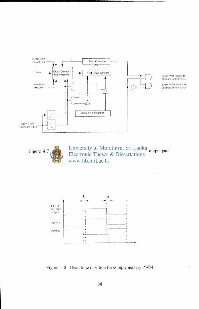
4.2.11 Dead Time Generators
In power inverter applications where the PWMs are used in Complementary mode to control
the upper and lower switches of a half-bridge, a dead time insertion is highly recommended.
The dead time insertion keeps both outputs in inactive state for a brief time. This avoids any
overlap in the switching during the state change of the power devices due to TON and TOFF
characteristics.
l3ccausc the power output devices cannot switch instantaneously, some amount of time must
be provided between the turn-off event of one PWM output in a complementary pair and the
tum-on event of the other transistor. The PWM module allows dead time to be programmed.
Dead Time Insertion
Each ~omp\ementary output pair for the PWM module has a 6-bit down counter used to
produce the dead time insertion. As shown in Figure 4.7, each dead time unit has a rising
and falling edge detector connected to the duty cyc\e comparison output. The dead time is
loaded into the timer on the detected PWM edge event. Depending on whether the edge is
rising or falling, one of the transitions on the complementary outputs is delayed until the
timer counts down to zero. A timing diagram indicating the dead time insertion for one pair
ofPWM outputs is shown in Figure 4.8.
37
Dead Ttrne ~ , /--:;:: Selecl Btls -~--tl_l ~---~Corn pare j
[ }-Jt
F 1 Clock Control c sc -~ and Pre scaler ~ 6-Btl Down Counter
Ueild Ttme ---~ff _____ ---Prescale -- ·- -·-
""" c'"" ~~j[sl]] Conl~lfHe lr1pU\ __ ,~.,. ·---
1 ---
!
--------co--~ -1>X]---~
Odd f'WM Stqrwllo Oulpul Cnnlrol Block
Even PWM Stpnal In Oulpul Conlrnl fliiH:k
Figure 4.7- Dead Time control unit block diagram for one PWM output pair
f0 DC1 comp;-rre output
PWM1
fJWMO
~
ld ttl. -~· ,,.._ _ .. , ,...,.._
J~------1' ----~- : ~·---------
'I 1 I I
-----~r-- --- -L-~~ I I 1 I I
~--l, : ~--~--~ ~-----------,-- t
-----~-~~~----------------~_1---~
Figure 4.8- Dead tllnc insertiOn for complementary PWM
38

4.J Control Strategy
~.3. \ V/f Control with Current Feedback
i\ lhsadvantage of open-loop Vir control is that the motor can stall if the speed is ramped up
\l)l) q\.nck\:~ or \he hmL\ otherwise changes rapiu\y. Wi\hou\ sorne form o[ feedback, 1\ is
\\\lflOssi\1\1.:: \.\) c\e\ec\. \\1\\c\.her \he n1o\m \S \uming, as expcc\.cl\, or \\' \\ is s\a\kd. 1\ s\a\\
'~ntscs high currents and. the motor loses torque. By monitoring current, excessive slip can
hL' detected, and the motor frequency can be adjusted downward accordingly. J\ high-current
'lllh.lition may also be caused by a malfunction of the inverter bridge. I r a high-current
• ondition persists, the drive should be shut down to prevent motor overheating or other
-latn<lgc
\ cunceptual d1agram IS illustrated 111 Figure 4.9. The speed reference is provided by the
•N't. 111 this case via a potentiometer connected to an ADC channel. The V/1' !'unction in
r 1 rm ware calculates the maxi mum PWM duty cycle (am pi i tude) based upon the speed
'L'Icrcnce. The DC bus (bridge) current is measured using a shunt resistor, which produces a
\ oltagc proportional to the current through it. This voltage is amplitled and compared with
o~11 external comparator to a rclercnce level that corresponds to the maximum allowable bus
, urrcnt. The comparator output drives the Fault J\ input of the PIC 18F4431. 1r the F;ault
tgnal is asserted, the PWM output is inhibited for the following PWM period.
Speed ...... f V/f ;:nell. on 1-~~-....f--;~:--J >; .., 3-Phaso ___ [/ ___ )_ lleference \. \. Invertor---~.,... ACIM
---------- ~~~;~nl t_-~f~!~""' '~'''"'"" D<tdg•~j ---- ~---'-Current ---~--Limit
Figure 4.9 Block diagram of VSD with current Iced back
39

-t.3.2 V/f Control of blower motor with Air temperature Feedbacl<
!~lock diagram of closed-loop speed control of air blower is illustrated in Figure 4. J 0. The
,· 1 c!Crcncc temperature is set by a potentiometer. This signal is used as ref'erence value for the
1\ UC module of microcontrollcr. Air temperature feed back signal is generated by
temperature sensor and it is used as input to ADC module.
lhe temperature error signal is then used as an input to a proportional controller, which
detenmnes the desired drive frequency to the motor windings. The standard V(( process
determines the amplitude of the drive wavel~mn. The drive frequency and amplitude arc
then used to update the PWM duty cycles of the six PWM channels that drive the three-
phase bridge.
\ ClliJ!Cillll
Rdcn·ncc -~\
"" l'ropotional controller
Tcmpcmlurc fccdbook
~ V/F ... Function
Propotionnl controller
3-Phase ... PWM 6 .... inverter .l ....
bridge
Air temperature 5cn~ing ... ....
Figure 4. lO -Block diagram for closed loop Air blower speed control
40
3-pl Bhr Mol

4.4 Initializing The Power Control PWM Module And ADC
Module
The Power Control PWM module simplifies the task of driving a 3-phase inverter bridge by
providing three pairs of complementary PWM outputs, with dead time inserted between
complimentary channels. To initialize the PCPWM module:
I. Conllgure the PCPWM time base:
a) Select a PWM time base postscalc value of I: 1.
b) Select a PWM time base prescale value input of 1: I (FOSC/4 ).
c) Configure the PWM time base for Free-Running mode (for edge-aligned operation).
1 Load the PTPERH:PTPI~RL register pair to obtain a PWM frequency.
3. Contlgure the PCPWM output.
a) Enable PWMO through PWM7 as outputs.
b) Set the PWM 1/0 pairs (PWM0/1, 2/3 and 6/7) as complementary pairs.
4. Configure the special event trigger:
a) Set the special event trigger postscalcr to 1: I.
b) Configure the special event trigger to occur when the time base is counting upwards.
c) Enable updates from duty cycle and period buller registers.
d) Configure for asynchronous overrides from the OVDCON register.
5. Configure the PCPWM dead time:
a) Select FOSC/2 as the dead-time prescalcr.
b) Load DTCON<5 :0> with a dead-time value to achieve a 2 ~ts dead time. The actual
value depends on the controller's clock frequency; refer to the data sheet to determine
the proper value.
41

11 Disable the output overrides on the PWM pins by setting bits POVD<5:0>.
·.1 Clear the special duty cycle register pair (SEVTCMPI I:SEVTCMPL).
X l'lcar all of the regular PWM duty cycle register pairs (PDCxH:PDCxL) to set the duty
cvclcs to 0.
q Enable the PWM time base.
4.5 Initializing the ADC n1odule
One analog values is measured in this application:
• ;\ N I ( LM 35DZ temperature sensor input for the speed reference)
!"hi~ high-speed ADC incorporates several features, such as Auto-Conversion mode and a
Fl FO result buftCr, that reduce the firmware overhead associated with monitoring multiple
analog channels and enhance ADC throughput.
To initialize the IISADC module:
1. Configure ADC operation:
a) Enable Continuous Loop mode.
b) l~nable single-Channel mode.
c l Asstgn VREFI and VREF-.
d) Enable the FIFO buffer.
c) Select the lefl-justi11ed format for the A/D result.
I) Set the A/D acquisition time to 12 TAD (required for sequential conversion).
g) Set the A/D conversion clock to FOSC/32
h) Turn on the ADC.
42

4.6 V /F Control Firmware
I he heart of the ACIM control is accomplished with the PCPWM peripheral operated in
\ 'omplimcntary mode. The duty cycle of the three PWM channels are changed in a regular
manner using a TimerO interrupt to synthesize the three-phase waveforms that drive the
motor. A sine table is stored in program memory. It is transferred to data memory during
1111ttalization for faster access. Three registers are used as offsets to the table through indirect
addressing. Each of the offset values points to one of the values in the table, such that there
1s always a 120-degrcc phase shift between the phases.
In this application, the potentiometer detennines the target motor speed retcrencc signal.
4.7 PWM Wavefonn Synthesis
The sinusoidal waveform is created by constantly changing the PWM duty cycle for each
output. The motor drive frequency determines how often the PWM duty cycle values arc
updated and thus, the frequency of the synthesized waveform. The peak-to-peak drive
amplitude corresponds to the maximum PWM duty cycle, as this generates the maximum
voltage output of each half bridge of the inverter. 'T'he duty cycle determines the drive
amplitude at any given point in the cycle. The duty cycle update rate is set by modilying the
T1merO reload value. This determines the interval until next TimerO overflow. The PWM
Dut:v Cycle (PDC) registers ofthe three PWM units arc modified as follows:
43

When a TimerO interrupt occurs, an updated target drive frequency is determined by
F ~(i\DRESII/4)
The sine value for each phase is read from the sine table, pointed to by the offset value
for that phase.
~' The PWM duty cycle for a particular phase is calculated by multiplying the sine value
from the table by the updated motor drive frequency. The 16-bit product is stored in the
PDC register for that phase. Steps 2 and 3 arc repeated for each phase.
4. The offset values arc updated for the next table access.
'i The TimerO reload value is calculated based on the updated motor drive frequency ,
where/is the drive frequency. In this program , the number of sine table entries is set at
19. The reload value determines the value at which the PWM duty cycle is updated.
6 The new PWM duty cycle values take effect at the beginning of the next PWM period.
The duty cycle determines the drive amplitude at any given point in the cycle.
44

+5V
<1 - llfl.ntron £:::--1
lOk
f I I 150pF I
PWM5 MCLR
PWM4 ANI
8EEv" 7 IIINJ
i UNJ _,_
I I I 470k Vrel~
PWMJ
Vref• 'I I I 1nn; -('r) PWM2 >I I I L!NJ
"'1" Vdd "'1" ~ i'WMI
v~, 00 - 'I I IIIN!
OSCI PWMO if I UN! I ~ ·-' t" • ...- ___._ I I
4---
zo l\1Hz / IOSC2 Vdd I I Tempernture
sensor v~ ..
RDI
v ... 4.7k
ON/OFF
LED ' ' TW7
47k .L1
Figure 4. I I - Circuit diagram of Micro Controller
45