Author's personal copy Structural, electrical and optical properties of indium chloride doped ZnO...
7
This article appeared in a journal published by Elsevier. The attached copy is furnished to the author for internal non-commercial research and education use, including for instruction at the authors institution and sharing with colleagues. Other uses, including reproduction and distribution, or selling or licensing copies, or posting to personal, institutional or third party websites are prohibited. In most cases authors are permitted to post their version of the article (e.g. in Word or Tex form) to their personal website or institutional repository. Authors requiring further information regarding Elsevier’s archiving and manuscript policies are encouraged to visit: http://www.elsevier.com/copyright
Transcript of Author's personal copy Structural, electrical and optical properties of indium chloride doped ZnO...
This article appeared in a journal published by Elsevier. The attachedcopy is furnished to the author for internal non-commercial researchand education use, including for instruction at the authors institution
and sharing with colleagues.
Other uses, including reproduction and distribution, or selling orlicensing copies, or posting to personal, institutional or third party
websites are prohibited.
In most cases authors are permitted to post their version of thearticle (e.g. in Word or Tex form) to their personal website orinstitutional repository. Authors requiring further information
regarding Elsevier’s archiving and manuscript policies areencouraged to visit:
http://www.elsevier.com/copyright

Author's personal copy
Structural, electrical and optical properties of indium chloride doped ZnO filmssynthesized by Ultrasonic Spray Pyrolysis technique
E. Zaleta-Alejandre a,⁎, J. Camargo-Martinez a, A. Ramirez-Garibo a, M.L. Pérez-Arrieta b,R. Balderas-Xicohténcatl a, Z. Rivera-Alvarez a, M. Aguilar-Frutis c, C. Falcony a
a Centro de Investigación y de Estudios Avanzados-IPN, Departamento de Física, Apdo, Postal 14-470, Del. Gustavo A. Madero, C.P. 07000, México, D.F., Mexicob Universidad Autónoma de Zacatecas, Unidad Académica de Física, Calzada Solidaridad esq. Paseo, La Bufa s/n, C.P. 98060, Zacatecas, México, Mexicoc Centro de Investigación en Ciencia Aplicada y Tecnología Avanzada-IPN, Legaria 694, Col. Irrigación, Del. Miguel Hidalgo, México, D.F., Mexico
a b s t r a c ta r t i c l e i n f o
Article history:Received 16 November 2011Received in revised form 11 September 2012Accepted 19 September 2012Available online 5 October 2012
Keywords:Ultrasonic Spray PyrolysisIndium chloride doped zinc oxideTransparent conductive filmsAcetic acid
Indium chloride doped zinc oxide (ZnO:In) thin films were deposited onto glass substrates using zinc acetateby Ultrasonic Spray Pyrolysis technique. The effect of substrate temperature, deposition time and acetic acidadded to the spraying solution on the structural, electrical and optical properties of these ZnO:In films isreported. The films were in all cases polycrystalline with a hexagonal (wurtzite) structure, a transparencyover 80% and resistivity of the order of 10!3–10!2!·cm. The resistivity was dependent on the volume %of acetic acid added to the spraying solution. The minimum resistivity value was obtained with a 5 vol.% aceticacid (pH=3.71) at substrate temperature of 450 °C. The deposition rates obtained were as high as 180 Å·min!1
at a substrate temperature of 450 °C.© 2012 Elsevier B.V. All rights reserved.
1. Introduction
With an energy band-gap of 3.4 eV, ZnO is one of the most attrac-tive transparent conductive oxides today [1–3]. Doped and undopedZnO is a multifunctional material, which has widely been used forsensors, liquid crystal displays, electronic and optoelectronic devices,transparent conducting materials and other applications [4–7]. Theparameters and conditions of growth and the addition of electricallyactive impurities to a wide band gap semiconductor often bring dra-matic changes in its structural, electrical and optical properties [8–11].ZnO thin films aremostly deposited by R–F sputtering [12,13], ChemicalVapor Deposition [14], Pulsed Laser Deposition [15], sol–gel processes[16,17] and methods like Ultrasonic Spray Pyrolysis (USP) [18–20]among others. The spray pyrolysis or pyrosol deposition technique[21–25] is based on thepyrolysis of an aerosol produced froma sprayingsolution by an ultrasonic generator operating at frequencies in therange of 0.8 MHz to 1.2 MHz. The drop size generated by a cavitationeffect is dependent on the ultrasonic vibration frequency (the dropsize decreases as the frequency is increased) and the size distributionis quite narrow as opposed to pneumatic aerosol generation in whichthe drop size spreads over a wide range of sizes. The net results are amore uniform smoother surface of the film deposited by USP. The mainadvantages of this technique are its ease of operation, its low cost andthe high quality of the coatings obtained as a result of the homogeneityof the droplet size distribution. In addition, the technique can be used to
coat large area substrates, because of its characteristic to work under at-mospheric pressure environments. Many authors have investigated indi-um doped zinc oxide using different reactive sources of indium [26–30].In this work, indium chloride was used to dope ZnO films deposited onglass substrates using the USP technique. The influence of deposition pa-rameters such as substrate temperature, deposition time and in particularthe acetic acid added to the spraying solution was studied over the re-sistivity, optical transmittance, crystallographic orientation, grain size,surface morphology, thickness and roughness as reported.
2. Experimental procedure
The ZnO:In films were deposited by the Ultrasonic Spray Pyrolysistechnique. This technique has been described in detail previously [22].The experimental arrangement consists of anultrasonic generator oper-ated at 1.2 MHz for the aerosol generation from a spraying solution, thisaerosol is transported to the hot substrate surface by a carrier gasthrough a 1′D flexible plastic hose to a 10 cm long 1′D glass tube thatacts as nozzle and directs the aerosol flow over the substrate (1′!1′Corning 7059 glass slide in this case). The carrier gas was nitrogen at aflow rate of 10 l·min!1. The nozzle was located approximately 1 cmabove the substrate. The substrate was set on a tin bath heated by elec-trical resistances controlled by a temperature regulator and a K-typethermocouple (tin is melted at temperatures above 230 °C providingan excellent thermal contact to the substrate). The whole experimentalset up is enclosed in an exhaust chamber. These experimental conditionsrendered filmswith uniform optical appearance over thewhole substratearea, i.e. no rainbow like look associated with uneven light interference
Thin Solid Films 524 (2012) 44–49
⁎ Corresponding author. Tel.: +55 5747 3800; fax: +55 5747 3800x6171.E-mail address: [email protected] (E. Zaleta-Alejandre).
0040-6090/$ – see front matter © 2012 Elsevier B.V. All rights reserved.http://dx.doi.org/10.1016/j.tsf.2012.09.050
Contents lists available at SciVerse ScienceDirect
Thin Solid Films
j ourna l homepage: www.e lsev ie r .com/ locate / ts f
Author's personal copy
due to a non-homogeneous film thickness. The spraying solution used inthis work was prepared using zinc acetate [Zn(C2H3O2)2·2H2O] fromSigma Aldrich diluted in a mixture of water and acetic acid (CH3COOH)at a 0.1 M concentration. Doping was performed by adding indium chlo-ride (InCl3) in 3 mol% ratio, which was found to introduce the optimumamount of indium concentration in the deposited ZnO films for low resis-tivity purposes, in agreement with previous reports [10,11,20,26,28]. Thesubstrate temperatures (Ts) during depositionwere 350, 450 and 550 °C;the deposition times (Td) were 7.5, 10 and 12.5 min and spraying solu-tion pH values 5.9, 4.1, 3.71, 3.35 and 2.94 corresponding to 0, 2.5, 5, 10and 20 vol.% of acetic acid (AA) in water for the spraying solution, re-spectively (see Table 1). The substrates used were Corning 7059 glassslides. The carrier gas was nitrogen at a flow rate of 10 l·min!1. Thenozzle was located approximately 1 cm above the substrate. The struc-tural properties of the films were analyzed with a Siemens D-5000X-ray diffractometer (1.5406 Å wavelength radiations) using Braggconfiguration. The optical transmittance spectra were obtained by aPerkin Elmer Lambda 25 spectrophotometer in a wavelength range of200–1100 nm and a Thermo Scientific Nicolet 6700 FT-IR spectro-photometer in a wavelength range of 1100–3000 nm. The surfacemorphology and atomic percent content of the zinc and indium ofthe samples were obtained by a JEOL JSM-6300 Scanning ElectronMicroscope (SEM) equipped with an Energy Dispersion Spectrometer(EDS) attached for chemical composition measurements; the accelera-tion voltage was 15 kV. The EDS data was obtained by a current of20 mA and a scanning surface of 60 μm2. The average roughness was de-termined by an atomic force microscope Autoprobe CP-Research usingthe contactmode and SiN coated silicon tipwith 20 Å of curvature radius.The thicknesses were measured on a film step using a KLA Tencor modelP-15 profilometer. The electrical parameters were determined by anEcopia Hall Effect Measurement System HMS-3000, using electrical con-tacts of Sn–In, at an electrical current of 1 mAandmagneticfield intensityof 0.55 T.
3. Results and discussion
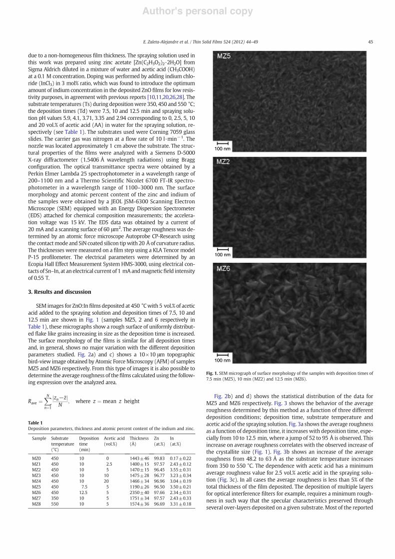
SEM images for ZnO:Infilms deposited at 450 °Cwith 5 vol.% of aceticacid added to the spraying solution and deposition times of 7.5, 10 and12.5 min are shown in Fig. 1 (samples MZ5, 2 and 6 respectively inTable 1), these micrographs show a rough surface of uniformly distribut-ed flake like grains increasing in size as the deposition time is increased.The surface morphology of the films is similar for all deposition timesand, in general, shows no major variation with the different depositionparameters studied. Fig. 2a) and c) shows a 10!10 μm topographicbird-view image obtained by Atomic ForceMicroscopy (AFM) of samplesMZ5 and MZ6 respectively. From this type of images it is also possible todetermine the average roughness of thefilms calculated using the follow-ing expression over the analyzed area.
Rave !XN
n!1
zn!!zj jN
; where z ! mean z heightFig. 2b) and d) shows the statistical distribution of the data for
MZ5 and MZ6 respectively. Fig. 3 shows the behavior of the averageroughness determined by this method as a function of three differentdeposition conditions; deposition time, substrate temperature andacetic acid of the spraying solution. Fig. 3a shows the average roughnessas a function of deposition time, it increases with deposition time, espe-cially from 10 to 12.5 min, where a jump of 52 to 95 Å is observed. Thisincrease on average roughness correlates with the observed increase ofthe crystallite size (Fig. 1). Fig. 3b shows an increase of the averageroughness from 48.2 to 63 Å as the substrate temperature increasesfrom 350 to 550 °C. The dependence with acetic acid has a minimumaverage roughness value for 2.5 vol.% acetic acid in the spraying solu-tion (Fig. 3c). In all cases the average roughness is less than 5% of thetotal thickness of the film deposited. The deposition of multiple layersfor optical interference filters for example, requires a minimum rough-ness in such way that the specular characteristics preserved throughseveral over-layers deposited on a given substrate. Most of the reported
Table 1Deposition parameters, thickness and atomic percent content of the indium and zinc.
Sample Substratetemperature(°C)
Depositiontime(min)
Acetic acid(vol.%)
Thickness(Å)
Zn(at.%)
In(at.%)
MZ0 450 10 0 1443±46 99.83 0.17±0.22MZ1 450 10 2.5 1400±15 97.57 2.43±0.12MZ2 450 10 5 1470±15 96.45 3.55±0.31MZ3 450 10 10 1475±28 96.77 3.23±0.34MZ4 450 10 20 1466±34 96.96 3.04±0.19MZ5 450 7.5 5 1190±26 96.50 3.50±0.21MZ6 450 12.5 5 2350±40 97.66 2.34±0.31MZ7 350 10 5 1751±34 97.57 2.43±0.33MZ8 550 10 5 1574±36 96.69 3.31±0.18
Fig. 1. SEM micrograph of surface morphology of the samples with deposition times of7.5 min (MZ5), 10 min (MZ2) and 12.5 min (MZ6).
45E. Zaleta-Alejandre et al. / Thin Solid Films 524 (2012) 44–49

Author's personal copy
works on ZnO films deposited by pneumatic SP have surface roughnessabove few tens of nanometers as opposed to the 10 nm or less surfaceroughness reported for the films deposited using the USP technique.The effect of the addition of acetic acid has been described by otherauthors [31] when indium acetate is used instead of indium chlorideas the indium source for the doping of the ZnO films. In particular inthat case, the pH of the spraying solution is 6.1 when no acetic acid isadded and 4.2 when 10 vol.% acetic acid is added into the precursor so-lution, while in this work the pH is changed from 5.9 to 3.35 for similarvol.% amounts of acetic acid in the spraying solution. Also the growth
rate was reported to increase up to 7 nm·min!1 with the addition ofacetic acid, while in this work, no noticeable change is observed onthe growth rate (180 Å·min!1 (MZ6), see Table 1) with the additionof acetic acid. However the incorporation of indium in the films is defin-itively affected, as reported in the case of indium acetate, by the addi-tion of acetic acid (see Table 1), although in this work the maximumis 3.55 at.% at 5 vol.% of acetic acid added to the spraying solution. TheX-ray diffractograms revealed the polycrystalline nature of the deposit-ed films with a hexagonal (wurtzite) structure for zinc oxide with noclear evidence of crystalline phases corresponding to indium or itsoxide [32]. There was no major dependence on the crystallinity or ori-entation of the films with deposition times or substrate temperaturesin the ranges studied of these parameters (data not shown), but thiswas not the case for the acetic acid vol.% added to the spraying solutionas shown in Fig. 4, where the X-ray diffractograms for films depositedwith different amounts of acetic acid in spraying solution are shown.The addition of acetic acid results on an increase of the crystallinity ofthe films and an increase of the peak associated with the (002) crystal-line orientation with respect to the (101) peak as the amount of aceticacid is further increased. Fig. 5 shows the grain size dependence on thethree deposition parameters considered. The grain size of the films wascalculated from the (100) peak on the X-ray diffractograms using the
Fig. 2. a) and c) correspond to AFM micrograph of surface morphology of the MZ5 andMZ6 samples respectively; b) and d) correspond to statistical distribution of the datafor MZ5 and MZ6 respectively.
a
b
c
Fig. 3. Average roughness as a function of: a) deposition time (Td), b) substrate tem-perature (Ts) and c) acetic acid (AA).
46 E. Zaleta-Alejandre et al. / Thin Solid Films 524 (2012) 44–49

Author's personal copy
Scherrer formula [33]. From this figure it is possible to observe thatthe grain size increases monotonically with deposition time and sub-strate temperature and presents aminimum at an acetic acid value of2.5 vol.%. This behavior is similar with that observed on the surfaceroughness of the films, suggesting that there is a correlation betweenthese two structural characteristics. The resistivity as well as the carrierconcentration and the mobility as determined by Hall measurementsfor the ZnO:In films studied is listed in Table 2. It was determined thatthe carriers were electrons (n-type) and the resistivity values were inthe 10!3–10!2 !·cm range depending on the deposition parameters.The lowest resistivity value, 8!10!3 !·cm corresponds to a sampledeposited at 450 °C during 12.5 min with 5 vol.% of acetic acid (MZ6).Fig. 6 shows the behavior of the resistivity as a function of depositiontime; substrate temperature and acetic acid volume percentage. It isobserved that the resistivity has a soft dependence on deposition time(film thickness) with a tendency to decrease as the deposition time in-creases. This behavior may be related to a lower participation of surfacescatteringmechanisms thatmight interferewith electrical charge trans-port in the films [34]. The behavior of the resistivity with substratetemperature and acetic acid on the other hand shows a minimum at atemperature of 450 °C and 5 vol.% respectively for sampleswith a depo-sition time of 10 min. These deposition parameters correspond to themaximum incorporation of indium in the films (Table 1). In the caseof the dependence with substrate temperature, higher temperature re-sults in a reduction of indium incorporation in the films for tempera-tures above 450 °C. This implies reduction on carrier concentrationthat as a whole could lead to a higher resistivity in the films; accordingto the relationship for the resistivity is ρ=1/μηe, where η is the carrierconcentration and μ is the mobility [34]. With respect to the acetic acidin spraying solution, it is clear from the EDS results listed in Table 1, thatthe addition of acetic acid favors the incorporation of indium in the ZnOfilms up to a maximum incorporation at 5 vol.%, larger amounts ofacetic acid slightly decrease the amount of incorporated indium. Thisbehavior is similar to that reported for films dopedwith indium acetate,where the addition of acetic acid to the spraying solution is associatedwith the generation of [CH3COO!] and H+ radicals, the formation of[Zn2+] and [In3+] complexes with [CH3COO!] is thought to reducethe formation Zn-OH precipitates in the spraying solution and to bustthe growth of the ZnO film as well as the incorporation of indium asdopant [31]. Since in the present work InCl3 was used as indium source,there is the presence of [Cl!] as well, which could result in a further re-duction of the Zn-OH precipitates and larger growth rates for the film.Fig. 7 shows the plots of the UV–Vis and IR optical transmittance forthe ZnO:In thin films for different deposition times (different thick-nesses). The optical energy band gap was calculated by the extrapola-tion of the linear region of the square of the absorption coefficientcurves (not presented here) as a function of the photon energy at theabsorption edge [35,36] for all samples, the results oscillated between3.2 and 3.4 eV. In all cases, the % transmission in the visible range andfor longer wavelengths up to 1500 nmwas higher than 80%, for wave-lengths above 1500 nm the % transmission is smaller for those samplesthat show larger carrier concentration (lower resistivity), this effect is
Fig. 4. X-ray diffractograms for ZnO:In films deposited at function of acetic acid (AA).
a
b
c
Fig. 5. Grain size as a function of: a) deposition time (Td), b) substrate temperature(Ts) and c) acetic acid (AA).
Table 2Electrical properties of the ZnO:In films.
Sample Carriertype
Resistivityρ (!·cm)
Carrier concentrationN (!1020cm!3)
Mobilityμ (cm2·V!1·S!1)
MZ0 n 0.0592 0.397 2.651MZ1 n 0.0396 0.150 10.50MZ2 n 0.0135 1.151 4.010MZ3 n 0.0341 0.347 5.268MZ4 n 0.0867 0.440 1.635MZ5 n 0.0240 0.386 6.730MZ6 n 0.0080 1.230 6.167MZ7 n 0.0621 0.226 4.437MZ8 n 0.444 0.380 0.369
47E. Zaleta-Alejandre et al. / Thin Solid Films 524 (2012) 44–49

Author's personal copy
most likely related to interaction with the free electron plasma in thefilms [37].
4. Conclusions
Indium chloride doped ZnO thin films with transparency above 80%in the visible region, with an average roughness below 100 Å and resis-tivity values as low as 8!10!3 !·cmwere deposited by USP technique.The addition of acetic acid was found to have an important role on theoverall physical properties of the films. In particular the incorporationof indium into the films was strongly dependent on the vol.% of aceticacid added to the spraying solution. The deposition rates achievedwere as high as 180 Å·min!1. The films were nano-crystalline with ahexagonal-wurtzite structure. The morphology studies show in allcases an increase in the average roughness with increasing substratetemperature and deposition time, and a characteristic behavior withthe acetic acid percentage of the spraying solution that seems to be cor-relatedwith the crystalline grain size of the films. The resistivity presentsa behavior that follows the dependence of the indium incorporation inthe film with substrate temperature and acetic acid vol.% added to thespraying solution.
Acknowledgments
The authors are thankful to the CONACyT and Physics Departmentof CINVESTAV-IPN for the financial support. We are also grateful toMarcela Guerrero, Rogelio Fragoso, Ana Soto,Miguel Galvan andGilbertoAlarcon for the technical support provided. M. Aguilar-Frutis acknowl-edges CONACYT-Mexico through grant number CB-2009-129227.
References
[1] Anderson Janotti, Chris G. Van de Walle, Rep. Prog. Phys. 72 (2009) 126501.[2] Li-Wen Lai, Ching-Ting Lee, Mater. Chem. Phys. 110 (2008) 393.[3] T. Prasada Rao, M.C. Santhosh Kumar, A. Safarulla, V. Ganesan, S.R. Barman, C.
Sanjeeviraja, Physica B 405 (2010) 2226.[4] Byeong-Yun Oh, Min-Chang Jeong, Tae-Hyoung Moon, Woong Lee, Jae-Min
Myoung, Jeoung-Yeon Hwang, Dae-Shik Seo, J. Appl. Phys. 99 (2006) 124505.[5] Fawzy A. Mahmoud, G. Kiriakidis, J. Ovonic Res. 5 (2009) 15.[6] M. Suchea, S. Christoulakis, K. Moschovis, N. Katsarakis, G. Kiriakidis, Thin Solid
Films 515 (2006) 551.[7] Afishah Alias, Kouta Hazawa, Nobuaki Kawashima, Hisashi Fukuda, Katsuhiro
Uesugi, Jpn. J. Appl. Phys. 50 (2011) 01BG05.[8] A. Chakraborty, T. Mondal, S.K. Bera, S.K. Sen, R. Ghosh, G.K. Paul, Mater. Chem.
Phys. 112 (2008) 162.[9] M.A. Lucio-López, M.A. Luna-Arias, A. Maldonado, M. de la L. Olvera, D.R. Acosta,
Sol. Energy Mater. Sol. Cells 90 (2006) 733.[10] M. de la L. Olvera, H. Gómez, A. Maldonado, Sol. Energy Mater. Sol. Cells 91 (2007)
1449.[11] J. Wienke, A.S. Booij, Thin Solid Films 516 (2008) 4508.[12] Dong Hun Kim, Nam Gyu Cho, Ho Gi Kim, Won-Youl Choi, J. Electrochem. Soc. 154
(2007) H939.[13] Shinho Cho, Trans. Electr. Electron. Mater. 10 (2009) 185.[14] Xu Ying, Ma Penghua, Dou Yubo, Cai Yanqing, Adv. Mater. Res. 239 (242) (2011)
881.[15] Cheng-Ji Xian, Jun-Ku Ahn, Nak-Jin Seong, Soon-Gil Yoon, Ki-Hyuk Jang, Won-Ho
Park, J. Phys. D: Appl. Phys. 41 (2008) 215107.[16] K.J. Chen, F.Y. Hung, S.J. Chang, Z.S. Hu, Appl. Surf. Sci. 255 (2009) 6308.[17] Mujdat Caglar, Saliha Ilican, Yasemin Caglar, Thin Solid Films 517 (2009) 5023.[18] V.V. Kireev, L.N. Dem′yanets, L.E. Li, V.V. Artemov, Inorg. Mater. 46 (2010) 154.[19] Periyasamy Thilakan, D. Mohan Radheep, K. Saravanakumar, G. Sasikala, Semicond.
Sci. Technol. 24 (2009) 085020.[20] Satish S. Badadhe, I.S. Mulla, Sens. Actuators B 143 (2009) 164.[21] Pramod S. Patil, Mater. Chem. Phys. 59 (1999) 185.[22] M. Aguilar-Frutis, M. García, C. Falcony, G. Plesch, S. Jimenez-Sandoval, Thin Solid
Films 389 (2001) 200.[23] Gérard Blandenet, Michel Court, Yves Lagarde, Thin Solid Films 77 (1981) 81.[24] M. Langlet, J.C. Joubert, in: C.N.R. Rao (Ed.), Chemistry of AdvancedMaterials, Black-
well Science Oxford, England, 1993, p. 55.[25] K.L. Chopra, R.C. Kainthla, D.K. Pandya, A.P. Thakoor, in: G. Hass, M.H. Francombe,
J.L. Vossen (Eds.), Physics of Thin Film, vol. 12, Academic Press, New York, 1982,p. 201.
[26] S.S. Shinde, P.S. Shinde, C.H. Bhosale, K.Y. Rajpure, J. Phys. D: Appl. Phys. 41 (2008)105109.
[27] S. Ilican, Y. Caglar, M. Caglar, B. Demirci, J. Optoelectron. Adv.Mater. 10 (2008) 2592.[28] K. Yoshino, T. Fukushima, M. Yoneta, J. Mater. Sci. Mater. Electron. 16 (2005) 403.[29] S.M. Rozati, F. Zarenejad, N. Memarian, Thin Solid Films 520 (2011) 1259.
a
b
c
Fig. 6. Resistivity as a function of: a) deposition time (Td), b) substrate temperature(Ts) and c) acetic acid (AA).
Fig. 7. UV–Vis and IR transmission spectra for ZnO:In films for different deposition times.
48 E. Zaleta-Alejandre et al. / Thin Solid Films 524 (2012) 44–49

Author's personal copy
[30] L. Castañeda, A. Maldonado, A. Escobedo-Morales, M. Avendaño-Alejo, H. Gómez,J. Vega-Pérez, M. de la L. Olvera, Mater. Sci. Semicond. Process. 14 (2011) 114.
[31] B.C. Jiao, X.D. Zhang, C.C. Wei, J. Sun, Q. Huang, Y. Zhao, Thin Solid Films 520 (2011)1323.
[32] A. Hafdallah, F. Yanineb, M.S. Aida, N. Attaf, J. Alloys Compd. 509 (2011) 7267.[33] B.D. Cullity, in: Morris Cohen (Ed.), Elements of X-ray Diffraction, Addison-Wesley
Publishing Company Inc., Reading M.A., 1956, p. 99.
[34] H.L. Hartnagel, A.L. Dawar, A.K. Jain, C. Jagadish, in: Semiconducting TransparentThin Films, Institute of Physics Publishing, Bristol and Philadelphia, 1995, p. 137.
[35] J.I. Pankove, in: Optical Processes in Semiconductors, Prentice Hall, EnglewoodCliffs, N.J., 1971, p. 44.
[36] U. Alver, T. Kilinç, E. Bacaksiz, T. Küçükömero!lu, S. Nezir, I.H. Mutlu, F. Aslan, ThinSolid Films 515 (2007) 3448.
[37] Claes G. Granqvist, Sol. Energy Mater. Sol. Cells 91 (2007) 1529.
49E. Zaleta-Alejandre et al. / Thin Solid Films 524 (2012) 44–49