
Aravind Nanotech 2011
6
Imaging conduction pathways in carbon nanotube network transistors by voltage-contrast scanning electron microscopy This article has been downloaded from IOPscience. Please scroll down to see the full text article. 2011 Nanotechnology 22 265715 (http://iopscience.iop.org/0957-4484/22/26/265715) Download details: IP Address: 130.233.181.33 The article was downloaded on 13/08/2011 at 11:57 Please note that terms and conditions apply. View the table of contents for this issue, or go to the journal homepage for more Home Search Collections Journals About Contact us My IOPscience
Transcript of Aravind Nanotech 2011

Imaging conduction pathways in carbon nanotube network transistors by voltage-contrast
scanning electron microscopy
This article has been downloaded from IOPscience. Please scroll down to see the full text article.
2011 Nanotechnology 22 265715
(http://iopscience.iop.org/0957-4484/22/26/265715)
Download details:
IP Address: 130.233.181.33
The article was downloaded on 13/08/2011 at 11:57
Please note that terms and conditions apply.
View the table of contents for this issue, or go to the journal homepage for more
Home Search Collections Journals About Contact us My IOPscience
IOP PUBLISHING NANOTECHNOLOGY
Nanotechnology 22 (2011) 265715 (5pp) doi:10.1088/0957-4484/22/26/265715
Imaging conduction pathways in carbonnanotube network transistors byvoltage-contrast scanning electronmicroscopyAravind Vijayaraghavan1,2, Marina Y Timmermans3,6,Kestutis Grigoras4, Albert G Nasibulin3, Esko I Kauppinen3 andRalph Krupke2,5
1 School of Computer Science, The University of Manchester, Manchester M13 9PL, UK2 Institut fur Nanotechnologie, Karlsruhe Institute of Technology, 76021 Karlsruhe, Germany3 Department of Applied Physics and Center for New Materials, Aalto University, Espoo,Finland4 Department of Micro and Nanosciences, Aalto University, Espoo, Finland5 DFG Center for Functional Nanostructures (CFN), 76028 Karlsruhe, Germany
E-mail: [email protected]
Received 3 February 2011, in final form 10 April 2011Published 18 May 2011Online at stacks.iop.org/Nano/22/265715
AbstractThe performance of field-effect transistors based on single-walled carbon nanotube (SWCNT)networks depends on the electrical percolation of semiconducting and metallic nanotubepathways within the network. We present voltage-contrast scanning electron microscopy(VC-SEM) as a new tool for imaging percolation in a SWCNT network with nano-scaleresolution. Under external bias, the secondary-electron contrast of SWCNTs depends on theirconductivity, and therefore it is possible to image the preferred conduction pathways within anetwork by following the contrast evolution under bias in a scanning electron microscope. Theexperimental VC-SEM results are correlated to percolation models of SWCNT-bundlenetworks.
S Online supplementary data available from stacks.iop.org/Nano/22/265715/mmedia
1. Introduction
Individual single-walled carbon nanotube (SWCNT) basedfield-effect transistors (FETs) are characterized by highmobility (fast switching) and large on–off ratios [1],making them excellent candidates for next-generation nano-electronic devices. Recent success in sorting and assemblingsemiconducting SWCNTs in a scalable fashion has furtherstrengthened their prospects [2–4]. However, certainlimitations such as low on-state conductance due to contactresistance, variation in performance due to polydispersity aswell as cost of material and fabrication still remain. Oneapproach toward the large-scale, cost-effective commercial
6 Previously published as Marina Y Zavodchikova.
application of SWCNT-based FETs is as network or thin-filmtransistors (TFTs) comprised of multiple conduction pathwaysin parallel [5]. In particular, TFTs fabricated by sheer-flow alignment of 99% semiconducting SWCNTs have setexcellent performance benchmarks [6]. Direct deposition ofSWCNTs after their growth in an aerosol (floating-catalyst)chemical vapor deposition (CVD) system onto a variety ofsubstrates including flexible and transparent ones has recentlybeen demonstrated [7–9].
One of the considerations in TFTs is the presence ofmetallic SWCNTs which act as ‘short-circuit’ conductionpathways and affect device performance by diminishing theon–off ratio. Different deposition methods also yield differentnetwork morphologies, which in turn affect the metallic andsemiconducting nanotube percolation. Therefore, the mapping
0957-4484/11/265715+05$33.00 © 2011 IOP Publishing Ltd Printed in the UK & the USA1
Nanotechnology 22 (2011) 265715 A Vijayaraghavan et al
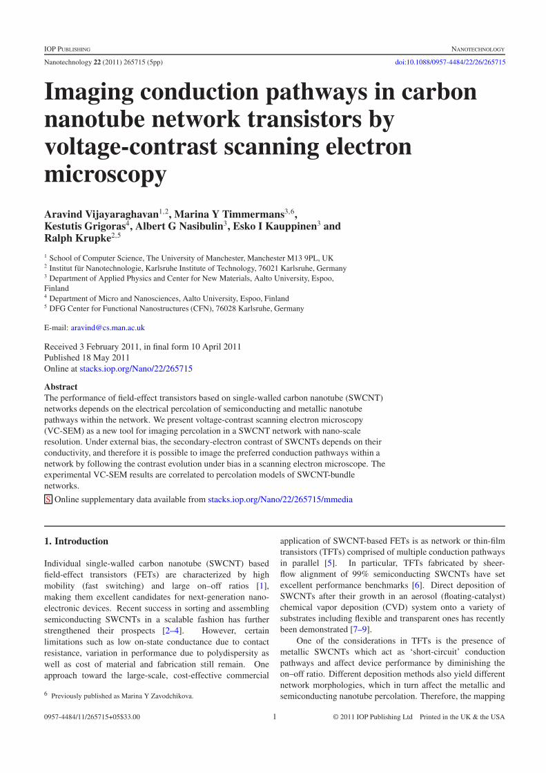
Figure 1. (a) Schematic of a SWCNT network FET, with two Ti/Au surface electrodes (yellow) as source and drain, a Si/SiO2 substrate asback-gate (gray/blue) and a protective surface Al2O3 layer (brown). (b) Transfer characteristics of one such network FET showing an on/offratio of 103. The two curves represent the forward and reverse sweeps of the gate voltage, as indicated in the figure.
(This figure is in colour only in the electronic version)
of electronic percolation pathways in SWCNT TFTs is anessential characterization requirement. At present, this isaccomplished by scanning probe techniques such as Kelvin-force microscopy (KFM) [10, 11] and conducting-probeatomic force microscopy (C-AFM) [12, 13]. These techniquesare limited in their application owing to slow scan speedsand a trade-off between imaging area and imaging resolution.Voltage-contrast scanning electron microscopy (VC-SEM) hasbeen recently demonstrated as a rapid, user-friendly, visualelectronic characterization technique for individual SWCNTsand in locating and characterizing electronically active defectsin SWCNTs in their device configuration [14, 15]. Here,we demonstrate how this technique can be applied to mapelectronic percolation pathways in SWCNT TFTs. In additionto overcoming the above-mentioned limitations of scanningprobe techniques, we also demonstrate that VC-SEM can beeffective in mapping sub-surface SWCNT networks, which isthe case when a top-gate dielectric or passivating layer has beenused to cover the SWCNT network.
2. Results and discussion
2.1. CNT network transistors
A schematic illustration of the SWCNT TFT fabrication stepsis presented in figure S1 (supporting information available atstacks.iop.org/Nano/22/265715/mmedia). SWCNTs grown inan aerosol (floating-catalyst) CVD reactor at 1050 ◦C weredirectly deposited at room-temperature onto a substrate asdescribed in detail elsewhere [7]. The substrate here iscomprised of 100 nm SiO2 dielectric over a degenerately dopedSi which acts as a back-gate. Before further processing, theSWCNT network was covered with a thin (20 nm) layer ofAl2O3 grown by an atomic layer deposition (ALD) techniqueat 220 ◦C in a Beneq TFS-500 reactor using TMA as a metalprecursor and water for oxidation. Source and drain contactregions were defined by photolithography, the Al2O3 layerin this region was removed using a developer. The contactmetal stack (5 nm Ti, 45 nm Au) was deposited using anIM9912 e-beam evaporator, followed by lift-off. CNTs outsidethe device area were removed in an additional step involving
photolithography, Al2O3 removal by developer and CNTetching by an O2 plasma in an Oxford 80+ reactive ion etcher.Devices were loaded in a ceramic chip-carrier and contactedby wire-bonding. The chip-carrier was loaded into the SEM ina specifically designed sample-holder capable of individuallybiasing each contact. Electronic characterization was carriedout using an Agilent 4155A semiconductor parameter analyzer.
SWCNT TFTs with an active device area of 50 µm ×50 µm, comprised of SWCNT bundles of 1.3 ± 0.8 µmaverage length, 2–7 SWCNTs per bundle, 300 nm averagelength of individual SWCNTs within a bundle and an arealdensity of about five SWCNT bundles per µm2 were usedhere [9]. A schematic of such a TFT and the correspondingelectronic characterization is presented in figure 1. An on–off ratio of ∼103 and sub-threshold slope of 1–2 V/decadeare typically observed in such devices. Systematic study ofAl2O3 ALD on SWCNT bundles and device characterizationof such SWCNT TFTs has been published elsewhere [16]and optimum conditions determined from those results areemployed here. However, unlike earlier reports, the ALDis performed here as the first step of the device fabricationprocess, immediately after SWCNT collection from the reactorto protect the SWCNT network from further processing stepsand adsorption of moisture and other atmospheric gases.As a result, extremely low hysteresis and ambipolar devicecharacteristics are observed as is expected in the absence ofcharge-injection and doping effects [17, 18]. Hysteresis as lowas 2 V between forward and reverse sweeps has been observedfor ±10 V sweep of the gate voltage. A single lithographystep was used to first dissolve away the Al2O3 in the electroderegions, and then deposit the Ti/Au metal stack, in order for theelectrodes to form direct contact to the SWNTs while the restof the network that is exposed to the environment is protectedby the ALD layer.
2.2. Voltage-contrast scanning electron microscopy
VC-SEM is carried out in three-terminal device configurationsimilar to FET characterization. The source electrode isgrounded and bias (VG) is applied to the back-gate electrode.The drain electrode, however, is floating (unbiased) [14]. The
2
Nanotechnology 22 (2011) 265715 A Vijayaraghavan et al
potential of the drain electrode is determined in competitionbetween the resistance of the gate-dielectric to leakage currentand the resistance of the SWCNT network channel, whichcan be tuned by the applied gate voltage [14]. In thisconfiguration, it is possible to maintain large source–drainbiases of a few volts in order to get sufficient voltage-inducedsecondary-electron contrast, since the current flowing throughthe SWCNT network is always limited to the leakage currentthrough the SiO2 dielectric layer. The detailed analysis ofthe mechanism of VC-SEM as well as optimum imagingconditions can be found in earlier reports on individualSWCNT devices [14]. A 10 keV electron-beam at a low arealdose of 2 µC cm−2 was used here to minimize electron-beamirradiation effects on SWCNT device performance as wellas charging-related contrast artifacts. The in-lens secondary-electron detector was used for imaging. For comparable scansizes, scanning probe techniques are limited to 512 pixel ×512 pixel resolution, while VC-SEM can record images at2048 pixel×2048 pixel density, which is 16 times higher. VC-SEM can also achieve lower magnifications, i.e. larger scanarea, if required, compared to scanning probe methods whichare usually limited to 50 µm × 50 µm per scan.
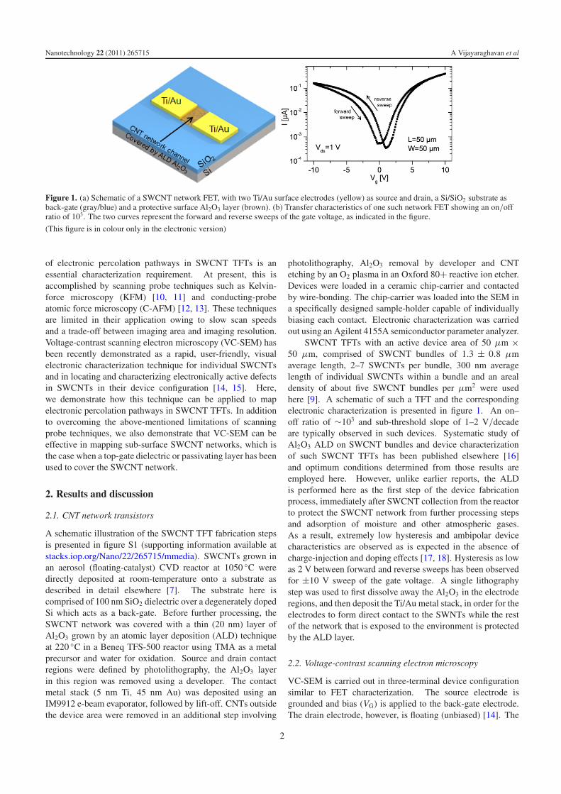
Figure 2 shows the VC-SEM images of a 25 µm ×17 µm region at the center of the SWCNT TFT, excludingregions adjacent to the metal contacts at either end, obtainedat gate bias of 3, 6 and 9 V. The contrast evolution inanother such device for VG = 3–8 V in 1 V stepsis shown in figure S2 (supporting information availableat stacks.iop.org/Nano/22/265715/mmedia). The groundedsource is at the bottom while the floating drain is at thetop of the network. Due to the low magnification, as wellas the Al2O3 surface layer, the SWCNTs are not visiblein the SEM when no bias is applied to the device (figureS3, supporting information available at stacks.iop.org/Nano/22/265715/mmedia). At low positive gate bias (<3 V), theSWCNTs adjacent to the grounded electrode (bottom) becomebrighter, i.e. have enhanced secondary-electron (SE) emission.At intermediate positive gate voltages, the region of brightSWCNTs advances toward the floating electrode (top) until, athigh gate bias (>9 V), the entire SWCNT network acquiresbright contrast. For negative gate voltages, a similar trendis observed, except that the SWCNTs darken relative to thesubstrate. In the false-color images of figure 2, red representshigh SE emission, green represents lower SE emission whileblue represents the substrate, which due to the positive gatebias applied directly to it, has the lowest SE emission.Note that gate voltage dependence of the surface potentialenhanced SE emission across the network correlates withthe switching-on characteristics obtained through electron-transport measurements. We explain the observed contrastevolution and its correlation to device switching in section 2.3.
2.3. Mechanism of contrast evolution
As a first approximation, we ignore the surface Al2O3
passivation layer and concentrate on the buried SWCNTnetwork. The effect of the Al2O3 will be discussedsubsequently. Most efforts to model SWCNT network
Figure 2. Pseudo-color VC-SEM images of the SWCNT FETnetwork at three different gate voltages (a) 3 V, (b) 6 V and (c) 9 V.The potential is non-uniform at low gate bias of 3 V and does notpercolate all the conduction channels bottom to top. At 6 V, thepotential percolates to the top, but is still non-uniformly distributedand drops from bottom to top. At 9 V, the device turns completelyon, and the potential percolates and equilibrates throughout thenetwork. The grounded source is at the bottom while the floatingdrain is at the top of the network.
transistors have focused on networks comprised of individualSWCNTs, in which case the conduction pathways can beclearly modeled as comprised of metallic and semiconductingsegments [19, 20]. In the present case, however, the conductionpathways are comprised of bundles of a few SWCNTs, whichcan be entirely metallic or semiconducting or a mixture.While individual SWCNTs are on average 300 nm long,the bundles themselves are much longer (1.3 ± 0.8 µm)and therefore have SWCNTs both in series as well as inparallel within the same bundle, in addition to inter-bundlejunctions. A detailed model of such a system was recentlyconstructed, and the FET performance with various bundleand network parameters was modeled [21]. Accordingto this model, a SWCNT network under the category of‘concurrent metallic and semiconducting percolation’, where
3
Nanotechnology 22 (2011) 265715 A Vijayaraghavan et al
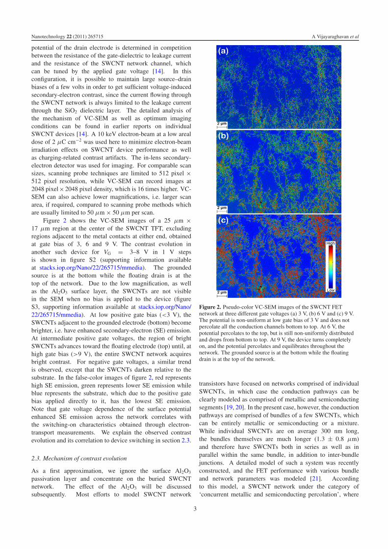
Figure 3. Potential drop across inter-nanotube junctions and alongthe length of a nanotube bundle under different gate bias conditions.
neither purely metallic nor purely semiconducting segmentsachieve percolation across the entire network, is relevant here.Despite being comprised of bundles, such a network is capableof on–off ratios of 103–105. The lack of independent metallicor semiconducting percolation is evident in VC-SEM imaging.Metallic percolation would appear as a bright trace acrossthe network from source to drain even at low gate voltages,which is not observed in our images. Closer inspection of thenetwork shows three types of potential gradients (figure 3).In some cases, long segments of the SWCNT turn brightsimultaneously, without any gradient in contrast along itslength. These segments are metallic and contribute to themetallic percolation pathways. Some SWCNTs turn brightgradually with VG and show non-uniform contrast alongtheir length at low gate bias. These bundles constitute thesemiconducting percolation pathways. Additionally, voltagedrop occurs at inter-bundle junctions across the tunnelingbarrier between SWCNT bundles. Taken together, theoverall conductance of the network mimics that of a singlesemiconducting entity, which is the rough ‘bundle-equivalent’to the ‘blocked conduction’ described in [8], where this wasmodeled for individual SWCNT networks and subsequentlyimaged by C-AFM. The model in [21] only considers metallicand semiconducting segments involved in percolation, anddoes not incorporate the effect of inter-bundle junctions, sowe cannot adopt it quantitatively to fit the results observedhere. Therefore, a comprehensive model of nanotube bundlenetworks is required.
It should also be noted that the percolation depends onnetwork density. When the bundle density is higher, thereare more parallel conduction channels available and thereforethe resistance is lower. The potential percolates quicker andreaches the other end at lower gate voltages. This meansthat the voltage front does not develop uniformly across the
network; for instance, the bright contrast (high voltage) infigure 2 reaches the top electrode quicker along the right sideof the network than the left.
As seen from electronic transport measurements, theSWCNT network transistor is ambipolar, with minimumhysteresis effects. This is reflected in VC-SEM as similareffects under positive and negative gate bias. As notedearlier, under positive gate bias, the SWCNT network acquiresbrighter contrast. Under negative gate bias, the networkacquires a darker contrast. We have previously demonstratedwith individual SWCNT devices that the lateral resolutionof contrast around a SWCNT under positive gate bias issignificantly higher than under negative gate bias [14]. Forthis reason, the results and analysis presented here focus onthe positive gate bias conditions.
2.4. Imaging buried networks
We now discuss the ability of VC-SEM to image SWCNTsburied under a protective surface dielectric layer, such as Al2O3
in this case. The mean escape depth of secondary electrons(SEs) from insulators is 10–20 nm which is comparable tothe Al2O3 thickness, while the maximum escape depth is∼75 nm, which includes the buried SWCNT network [22].Therefore, changes in the SE yield from the SWCNTs willcontribute to changes in overall SE yield. While the potentialof the Al2O3 far away from a SWCNT is determined bythe bias applied to the substrate, the Al2O3 surface potentialclosely surrounding a SWCNT is influenced by that of theSWCNT, and therefore, SE yield from the Al2O3 adjacent tothe SWCNT is affected in the same sense as the SE yield fromthe SWCNT itself. Additionally, SE yield is also affectedby deflection of emitted SEs under the influence of stronglocal electric fields generated by the small dimensions ofthe SWCNT cross-section, as shown previously with finite-element modeling [14]. This deflection, sometimes referred toas voltage-contrast type III, also affects SE yield, reinforcingthe direct effect of the potential on SE yield. These threefactors combined allow us to image the potential distributionin SWCNTs and their networks buried under protective surfacedielectric layers, which would be impossible with techniquessuch as C-AFM which requires direct contact of the probeto the nascent SWCNT. Additionally, as indicated previously,buried SWCNT networks are invisible at low magnificationand offer poor contrast at high magnifications (figure S3,supporting information available at stacks.iop.org/Nano/22/265715/mmedia). This is especially true of thinner bundlesand thick ALD layers. Some very thick bundles might still bevisible under the dielectric due to the resultant undulation onthe ALD layer. Under bias, however, SWCNT networks can beimaged clearly even at the lowest SEM magnification.
3. Conclusions
To conclude, we have demonstrated how VC-SEM can beused to image electronic conduction percolation pathwaysthrough SWCNT networks under various gate bias conditionstoward understanding the mechanisms determining electronic
4
Nanotechnology 22 (2011) 265715 A Vijayaraghavan et al
transport within the network. Such characterization issignificant particularly in light of recent developments inflexible high-performance SWCNT-network based integratedcircuits [23]. The techniques can be used effectively even whenthe SWCNT is buried under a protective surface dielectriclayer. We discuss the conduction mechanism in our SWCNTnetworks and correlate it to the observed features in the VC-SEM images.
Acknowledgments
RK acknowledges funding by the Helmholtz-GemeinschaftDeutscher Forschungszentren (HGF-VH-NG-126). This workwas supported by ’08 NEDO Grant and partially by theAcademy of Finland (Pr. No. 128445).
References
[1] Heinze S, Radosavljevic M, Tersoff J and Avouris P 2003 Phys.Rev. B 68 235418
[2] Vijayaraghavan A et al 2010 ACS Nano 4 2748–54[3] Vijayaraghavan A, Blatt S, Weissenberger D, Oron-Carl M,
Hennrich F, Gerthsen D, Hahn H and Krupke R 2007 NanoLett. 7 1556–60
[4] Hersam M C 2008 Nat. Nanotechnol. 3 387–94[5] Snow E S, Novak J P, Campbell P M and Park D 2003 Appl.
Phys. Lett. 82 2145–7[6] Engel M, Small J P, Steiner M, Freitag M, Green A A,
Hersam M C and Avouris P 2008 ACS Nano 2 2445–52[7] Zavodchikova M Y, Kulmala T, Nasibulin A G, Ermolov V,
Franssila S, Grigoras K and Kauppinen E I 2009Nanotechnology 20 085201
[8] Moisala A, Nasibulin A G, Brown D P, Jiang H,Khriachtchev L and Kauppinen E I 2006 Chem. Eng. Sci.61 4393–402
[9] Kaskela A et al 2010 Nano Lett. 10 4349–55[10] Topinka M A, Rowell M W, Goldhaber-Gordon D,
McGehee M D, Hecht D S and Gruner G 2009 Nano Lett.9 1866–71
[11] Jeong H, Gweon H M, Kwon B J, Ahn Y H, Lee S andPark J-Y 2009 Nanotechnology 20 345202
[12] Biswas S K, Schowalter L J, Jung Y J, Vijayaraghavan A,Ajayan P M and Vajtai R 2005 Appl. Phys. Lett. 86 183101
[13] Kodama Y, Sato R, Inami N, Shikoh E, Yamamoto Y, Hori H,Kataura H and Fujiwara A 2007 Appl. Phys. Lett. 91 133515
[14] Vijayaraghavan A, Blatt S, Marquardt C, Dehm S, Wahi R,Hennrich F and Krupke R 2008 Nano Res. 1 321–32
[15] Vijayaraghavan A, Marquardt C W, Dehm S, Hennrich F andKrupke R 2010 Carbon 48 494–500
[16] Grigoras K, Zavodchikova M Y, Nasibulin A G, Kauppinen E I,Ermolov V and Franssila S 2011 J. Nanosci. Nanotechnol.11 1–8
[17] Vijayaraghavan A, Kar S, Soldano C, Talapatra S,Nalamasu O and Ajayan P M 2006 Appl. Phys. Lett.89 162108
[18] Kar S, Vijayaraghavan A, Soldano C, Talapatra S, Vajtai R,Nalamasu O and Ajayan P M 2006 Appl. Phys. Lett.89 132118
[19] Kocabas C, Pimparkar N, Yesilyurt O, Kang S J, Alam M Aand Rogers J A 2007 Nano Lett. 7 1195–202
[20] Kumar S, Murthy J Y and Alam M A 2005 Phys. Rev. Lett.95 066802
[21] Seppala S, Hakkinen E, Alava M J, Ermolov V andSeppala E T 2010 Europhys. Lett. 91 47002
[22] Seiler H 1983 J. Appl. Phys. 54 R1–18[23] Sun D-M, Timmermans M Y, Tian Y, Nasibulin A G,
Kauppinen E I, Kishimoto S, Mizutani T and Ohno Y 2011Nat. Nanotechnol. 6 156–61
5