Time-Interleaved Digital-to-Analog Converters for UWB Signal Generation
Upload
khangminh22Category
view
0download
0
ANALOG AND DIGITAL ELECTRONICS18CS33PROF. ANAND S. HIREMATH,DEPT. OF CSE, BLDEA’S CET, VIJAYAPURHTTP://[email protected]
1
For more study materials visit www.guidemic.in

MODULE-4Introduction to VHDL, Latches and Flip-Flops
2

WARNING
• KEEP YOUR MOBILE PHONE SWITCH OFF IN CLASS.
3

Books Referred/Source
• Charles H Roth and Larry L Kinney, Analog and Digital Electronics,Cengage Learning,2019
• Charles H Roth and Larry L Kinney, Fundamental of Logic Design,Cengage Learning, 2017.
• Donald P Leach, Albert Paul Malvino & Goutam Saha: DigitalPrinciples and Applications, 7th Edition, Tata McGraw Hill, 2015
• Anil K. Maini: Digital Electronics Principles, Devices andApplications, 2007, John Wiley & Sons, Ltd.
• Thomas L. Floyd: Digital Fundamentals, 9th Edition., PearsonInternational Edition.
• M. Morris Mano, Michael D. Ciletti : Digital Design With anIntroduction to the Verilog HDL, 5th Edition, Pearson Education, Inc.
• Ronald J. Tocci, Neal S. Widmer, Gregory L. Moss: Digital systems :principles and applications—10th Edition, Pearson EducationInternational
4

INTRODUCTION TO VHDL
5
Objective
1. Represent gates and combinational logic by concurrent VHDL statements.
2. Given a set of concurrent VHDL statements, draw the corresponding c ombinational logic circuit.
3. Write a VHDL module for a combinational circuit a. by using concurrent VHDL statements to represent logic
equations
b. by interconnecting VHDL components
6

Introduction
• As integrated circuit technology has improved to allow moreand more components on a chip, digital systems havecontinued to grow in complexity.
• As digital systems are complex and detailed design of thesystems at the gate and flip-flop level has become very tediousand time consuming.
• For this reason, the use of Hardware Description Languages(HDL) in the digital design process continues to grow inimportance.
• A hardware description language allows a digital system to bedesigned and debugged at a higher level beforeimplementation at the gate and flip-flop level.
• The use of computer-aided design tools to do this conversionis becoming more widespread.
• The two most popular hardware description languages areVHDL and Verilog.
7

Introduction
• VHDL or VHIC HDL or Very High Speed IntegratedCircuit Hardware Description Languages .
• VHDL can describe a digital system at several differentlevels—behavioral, data flow, and structural.• For example, a binary adder could be described
• at the behavioral level in terms of its function of adding twobinary numbers, without giving any implementation details.
• The same adder could be described at the data flow level by givingthe logic equations for the adder.
• The adder could be described at the structural level by specifyingthe interconnections of the gates which make up the adder.
8
Introduction
• VHDL is a top-down design methodology in which thesystem is first specified at a high level and tested using asimulator.
• VHDL was designed to be technology independent.• If a design is described in VHDL and implemented in today’s
technology, the same VHDL description could be used as a startingpoint for a design in some future technology.
• VHDL is not case sensitive.
9

VHDL Description of Combinational Circuits
• A VHDL signal is used to describe a signal in a physicalsystem.
• E.g. The gate circuit of figure has five signals: A, B, C, D,and E.
10

VHDL Description of Combinational Circuits
11
• Behavioral Level
E <= D or (A and B);
• Dataflow Level
C <= A and B after 5 ns;
E <= C or D after 5 ns;
• Structural Level
Gate1: AND2 port map(A, B, C);
Gate2: OR2 port map (C, D, E);

VHDL Description of Combinational Circuits
• The symbol “<=” is the signal assignment operator whichindicates that the value computed on the right-hand side isassigned to the signal on the left side.
signal_name <= expression [after delay];
• The square brackets indicate that after delay is optional; theyare not part of the statement. If after delay is omitted, then thesignal is scheduled to be updated after a delta delay.
• The VHDL simulator monitors the right side of each concurrentstatement, and any time a signal changes, the expression on theright side is immediately re-evaluated. The new value isassigned to the signal on the left side after an appropriate delay
• VHDL signal assignment statements is concurrent statements.
12

VHDL Description of Combinational Circuits
• A Dataflow description of the circuit where it is assumed thateach gate has a 5-ns propagation delay.
• Unlike a sequential program, the order of the above concurrentstatements is unimportant. If we write
E <= C or D;C <= A and B;
• Statement without propagation delays.• If we write
C <= A and B;E <= C or D;
• this implies that the propagation delays are 0 ns.• In this case, the simulator will assume an infinitesimal delay referred
to as Δ (delta).• Assume that initially A = 1 and B = C = D = E = 0. If B is changed to 1 at
time = 1 ns, then C will change at time 1 +Δ and E will change at time 1+ 2Δ.
13

VHDL Description of Combinational Circuits
• A Structural description of the circuit requires that a two-input AND-gate component and a two-input OR-gatecomponent be declared and defined.• Components may be declared and defined either in a library or
within the architecture part of the VHDL code.
• Instantiation statements are used to specify how components areconnected.
• Each copy of a component requires a separate instantiationstatement to specify how it is connected to other components andto the port inputs and outputs.
• An instantiation statement is a concurrent statement that executesanytime one of the input signals in its port map changes.
• port map define input and output signal
• The order in which the instantiation statements appear isirrelevant.
14

VHDL Description of Combinational Circuits
• Signal names and other VHDL identifiers may containletters, numbers, and the underscore character (_).
• An identifier must start with a letter, and it cannot endwith an underscore.
• E.g.• C123 , ab_23 are legal
• 1ABC and ABC_ are not legal
• Anything following a double dash (--) is treated as acomment.
• and, or, and after are reserved words (or keywords)
• VHDL does not specify an order of precedence for thelogic operators but applicable for arithmetic operators.
15
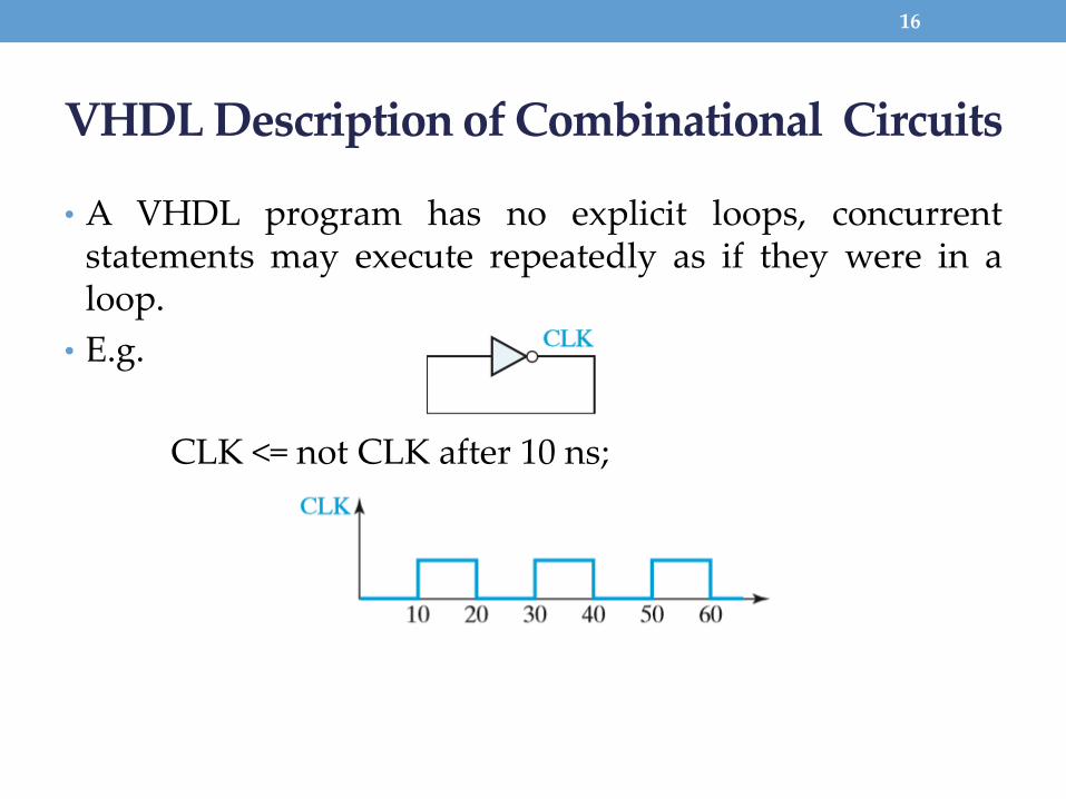
VHDL Description of Combinational Circuits
• A VHDL program has no explicit loops, concurrentstatements may execute repeatedly as if they were in aloop.
• E.g.
CLK <= not CLK after 10 ns;
16
VHDL Description of Combinational Circuits
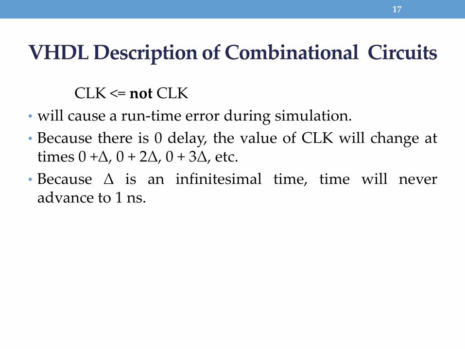
CLK <= not CLK
• will cause a run-time error during simulation.
• Because there is 0 delay, the value of CLK will change attimes 0 +Δ, 0 + 2Δ, 0 + 3Δ, etc.
• Because Δ is an infinitesimal time, time will neveradvance to 1 ns.
17

VHDL Description of Combinational Circuits
• The “after delay” creates an inertial delay model.
• Consider a device with an inertial delay of D time units.• If an input change to the device will cause its output to change,
then the output changes D time units later.
• However, this is not what happens if the device receives two inputchanges within a period of D time units and both inputchanges should cause the output to change.
• In this case the device output does not change in response to eitherinput change.
18
VHDL Description of Combinational Circuits
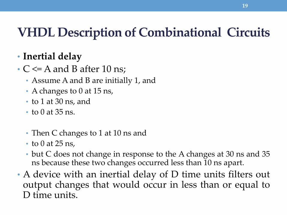
• Inertial delay
• C <= A and B after 10 ns;• Assume A and B are initially 1, and
• A changes to 0 at 15 ns,
• to 1 at 30 ns, and
• to 0 at 35 ns.
• Then C changes to 1 at 10 ns and
• to 0 at 25 ns,
• but C does not change in response to the A changes at 30 ns and 35ns because these two changes occurred less than 10 ns apart.
• A device with an inertial delay of D time units filters outoutput changes that would occur in less than or equal toD time units.
19

VHDL Description of Combinational Circuits
• Ideal (transport) delay.
• Output changes caused by input changes to a device exhibitingan ideal (transport) delay of D time units are delayed by D timeunits, and the output changes occur even if they occur within Dtime units.
• signal_name <= transport expression after delay
• As an example,
• C <= transport A and B after 10 ns;
• Assume A and B are initially 1 and A changes to 0 at 15 ns, to 1at 30 ns, and to 0 at 35 ns.
• Then C changes to 1 at 10 ns, to 0 at 25 ns, to 1 at 40 ns, and to 0at 45 ns.
• Note that the last two changes are separated by just 5 ns.
20

VHDL Description of Combinational Circuits
• Three Gates with a Common Input and DifferentDelays
• -- when A changes, these concurrent
• -- statements all execute at the same time
• D <= A and B after 2 ns;
• E <= not A after 1 ns;
• F <= A or C after 3 ns;• The three concurrent statements execute simultaneously whenever
A changes (signal A as a common input ), just as the three gatesstart processing the signal change at the same time.
• However, if the gates have different delays, the gate outputs canchange at different times.
21
VHDL Description of Combinational Circuits
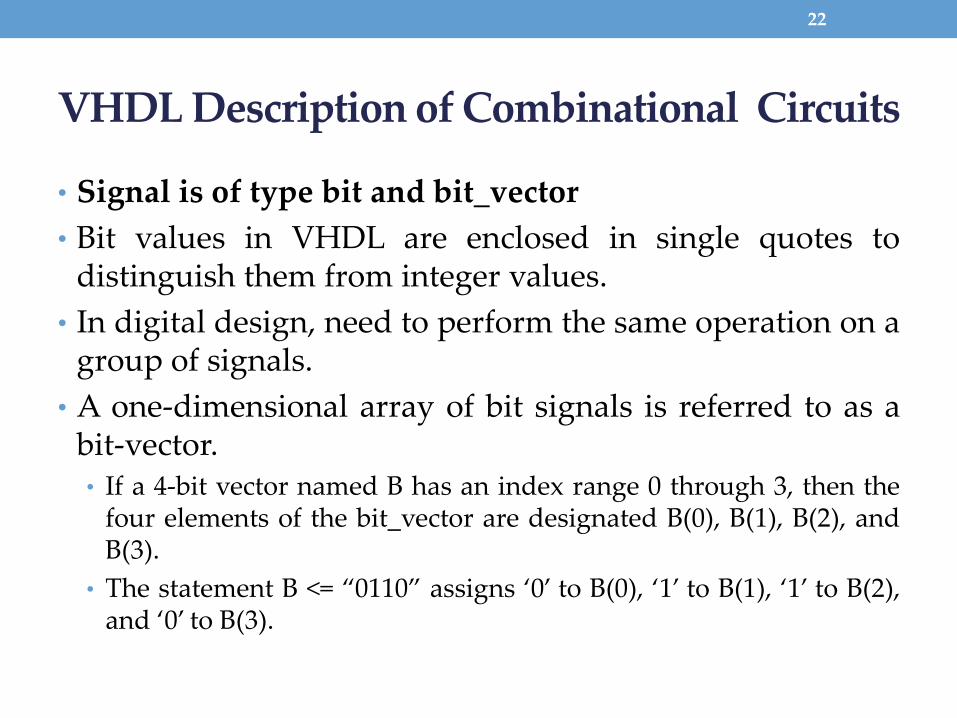
• Signal is of type bit and bit_vector
• Bit values in VHDL are enclosed in single quotes todistinguish them from integer values.
• In digital design, need to perform the same operation on agroup of signals.
• A one-dimensional array of bit signals is referred to as abit-vector.• If a 4-bit vector named B has an index range 0 through 3, then the
four elements of the bit_vector are designated B(0), B(1), B(2), andB(3).
• The statement B <= “0110” assigns ‘0’ to B(0), ‘1’ to B(1), ‘1’ to B(2),and ‘0’ to B(3).
22

VHDL Description of Combinational Circuits
• Array of AND Gates
• -- the hard way
• -- type bits signal A and B
• C(3) <= A(3) and B(3);
• C(2) <= A(2) and B(2);
• C(1) <= A(1) and B(1);
• C(0) <= A(0) and B(0);
• -- the easy way
• -- type bit-vectors signal A and B
• C <= A and B;
23

VHDL Models for Multiplexers
• F = A′I0 + AI1
• --The corresponding VHDL statement is
• F <= (not A and I0) or (A and I1);
• Alternatively
• -- conditional signal assignment statement
• F <= I0 when A = '0' else I1;
• The MUX output is I0 when A = ‘0’, and else it is I1.
• In the conditional statement, I0, I1, and F can either be bits or bit-vectors.
24

VHDL Models for Multiplexers
• The general form of a conditional signal assignmentstatement is
• signal_name <= expression1 when condition1
• else expression2 when condition2
• [ else expressionN];
25

VHDL Models for Multiplexers
• Cascaded 2-to-1 MUXes
• F <= A when E = '1'
• else B when D = '1'
• else C;
26
VHDL Models for Multiplexers
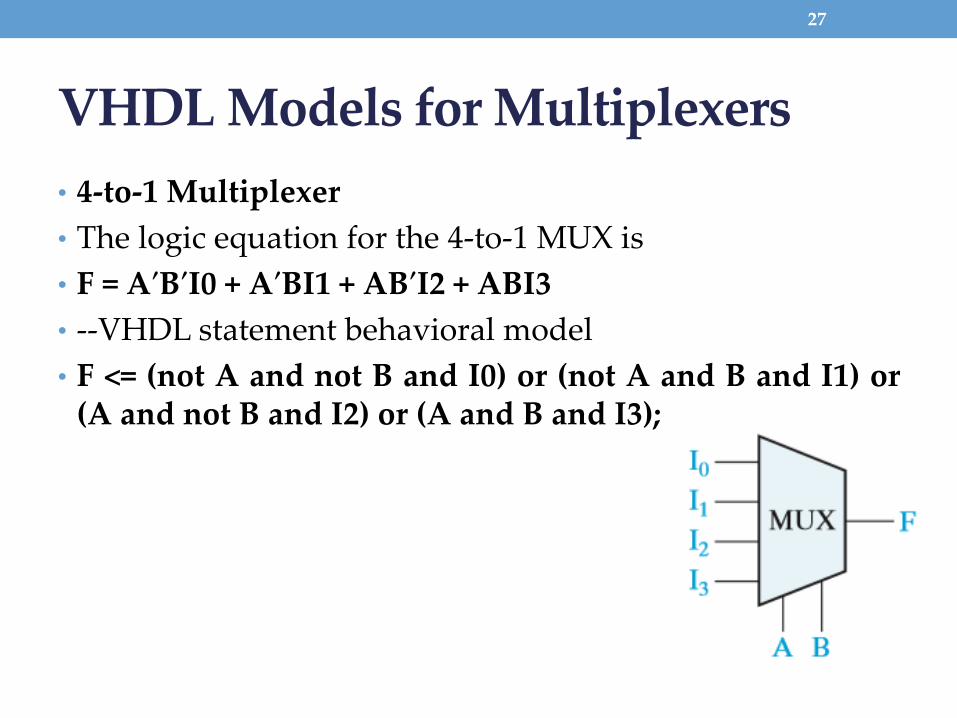
• 4-to-1 Multiplexer
• The logic equation for the 4-to-1 MUX is
• F = A′B′Ι0 + A′BI1 + AB′I2 + ABI3
• --VHDL statement behavioral model
• F <= (not A and not B and I0) or (not A and B and I1) or(A and not B and I2) or (A and B and I3);
27

VHDL Models for Multiplexers
28
• Conditional AssignmentStatement
F <= I0 when A&B = “00” else I1 when A&B = “01” else I2 when A&B = “10” else I3;
• Conditional AssignmentStatement
F <= I0 when A = ‘0’ and B = ‘0’ else I1 when A = ‘0’ and B = ‘1’ else I2 when A = ‘1’ and B = ‘0’ else I3;
• Selected Signal Assignment Statement
sel <= A&B;
-- selected signal assignment statement with sel select
F <= I0 when "00",
I1 when "01",
I2 when "10",
I3 when "11";
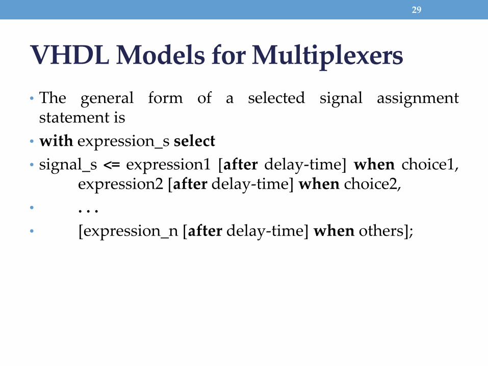
VHDL Models for Multiplexers
• The general form of a selected signal assignmentstatement is
• with expression_s select
• signal_s <= expression1 [after delay-time] when choice1,expression2 [after delay-time] when choice2,
• . . .
• [expression_n [after delay-time] when others];
29

VHDL Modules
• VHDL Program Structure
• Entity declarations of the form:
• entity entity-name is
• [port(interface-signal-declaration);]
• end [entity] [entity-name];
• Architecture declarations of the form
• -- Each entity is associated with one or more architecture
• architecture architecture-name of entity-name is
• [declarations]
• begin
• architecture body
• end [architecture] [architecture-name];
30

VHDL Modules
• In VHDL, must specify an entity and an architecture at the top level,and also specify an entity and architecture for each of the componentmodules that are part of the system.
• Each entity declaration includes a list of interface signals that can beused to connect to other modules or to the outside world.
• Declare all of the input and output signals using an entity declaration
• The interface-signal-declaration normally has the following form: list-of-interface-signals:
• mode type [: = initial-value]
• {; list-of-interface-signals: mode type [: = initial-value]};
• Input signals are of mode in, out, and inout.
• E.g.
• port(A, B: in integer : = 2; C, D: out bit);• indicates that A and B are input signals of type integer that are initially set to 2, and
C and D are output signals of type bit that are initialized by default to ‘0’.
31

VHDL Modules
• In Architecture the declarations section, we can declare signals andcomponents that are used within the architecture.
• The architecture body contains statements that describe the operationof the module.
32

VHDL Modules
• How to defined components?
• The component specification is very similar to the entity declaration.
• Components used within the architecture are declared at thebeginning of the architecture, using a component declaration of theform
• component component-name
• port (list-of-interface-signals-and-their-types);
• end component;
• The connections to each component used in a circuit are specified byusing a component instantiation statement of the form
• label: component-name port map (list-of-actual-signals);
• The list of actual signals must correspond one-to-one to the list ofinterface signals specified in the component declaration.
33

VHDL Modules
• VHDL Module with Two Gates
• entity two_gates is
• port (A,B,D: in bit; E: out bit);
• end two_gates;
• architecture gates of two_gates is
• signal C: bit;
• begin
• C <= A and B; -- concurrent
• E <= C or D; -- statements
• end gates;
• The signal C is declared within the architecture because it is an internalsignal.
• The two concurrent statements that describe the gates are placed betweenthe keywords begin and end.
34

VHDL Modules
• Sum = X ⊕ Y ⊕ Cin
• Cout = YCin + XCin + XY
• --Entity Declaration for a Full Adder Module
• entity FullAdder is
• port (X,Y,Cin: in bit; -- Inputs
• Cout, Sum: out bit); -- Outputs
• end FullAdder;
• --The operation of the full adder is specified by an architecture
• --declaration:
• architecture Equations of FullAdder is
• begin
• -- concurrent assignment statements
• Sum <= X xor Y xor Cin after 10 ns;
• Cout <= (X and Y) or (X and Cin) or (Y and Cin) after 10 ns;
• end Equations;
35

VHDL Modules
• Lab Experiment
• Write VHDL code for Half adder, Full Adder, HalfSubtractor and Full Subtractor.
36

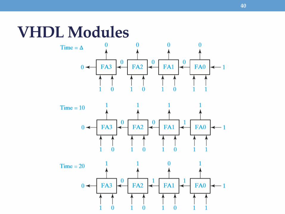
VHDL Modules
• 4-Bit Binary Adder• entityAdder4 is• port (A,B:in bit_vector(3 downto 0);Ci:in bit; -- Inputs• S:out bit_vector(3 downto 0);Co:out bit); -- Outputs endAdder4;• architecture Structure ofAdder4 is• component FullAdder• port (X,Y,Cin:in bit; -- Inputs Cout,Sum:out bit); -- Outputs• end component;• signal C:bit_vector(3 downto 1); • begin -- instantiate four copies of the FullAdder• FA0:FullAdder port map (A(0),B(0),Ci,C(1),S(0));• FA1:FullAdder port map (A(1),B(1),C(1),C(2),S(1)); • FA2:FullAdder port map (A(2),B(2),C(2),C(3),S(2)); • FA3:FullAdder port map (A(3),B(3),C(3),Co,S(3)); • end Structure;
37

VHDL Modules
• 4-Bit Binary Adder
• entityAdder4 is
• port (A,B:in bit_vector(3 downto 0);Ci:in bit; -- Inputs
• S:out bit_vector(3 downto 0);Co:out bit); -- Outputs endAdder4;
• architecture Structure ofAdder4 is
• component FullAdder
• port (X,Y,Cin:in bit; -- Inputs Cout,Sum:out bit); -- Outputs
• end compoent;
• signal C:bit_vector(3 downto 1);
• begin -- instantiate four copies of the FullAdder
• FA0:FullAdder port map (A(0),B(0),Ci,C(1),S(0));
• FA1:FullAdder port map (A(1),B(1),C(1),C(2),S(1));
• FA2:FullAdder port map (A(2),B(2),C(2),C(3),S(2));
• FA3:FullAdder port map (A(3),B(3),C(3),Co,S(3));
• end Structure;
38
VHDL Modules
• In preparation for simulation, we can place the entity andarchitecture for the FullAdder and for Adder4 together inone file and compile.
• Alternatively, we could compile the FullAdder separatelyand place the resulting code in a library which is linked inwhen we compile Adder4.
39
VHDL Modules
40

VHDL Modules
41
• Lab Experiment
• Write VHDL code for 8 to 1 MUX.

VHDL Modules
42
• Design a 4-to-1 MUX using only three 2-to-1 MUXes.Write an entity- architecture pair to implement a 2-to-1MUX. Then write an entity-architecture pair to implementa 4-to-1 MUX using three instances of your 2-to-1 MUX.(Hint: The equation for a 4-to-1 MUX can be rewritten as
F = A′(I0B′ + I1B) + A(I2B′ + I3B).)
• Use the following port definitions:
• For the 2-to-1 MUX:
• port (i0, i1: in bit; sel: in bit; z: out bit);
• For the 4-to-1 MUX:
• port (i0, i1, i2, i3: in bit; a, b: in bit; f: out bit);

VHDL Modules
43
1. Write VHDL statements that represent the following circuit:
a. (a) Write a statement for each gate.
b. (b) Write one statement for the whole circuit.

VHDL Modules
44
1. Draw the circuit represented by the following VHDLstatements:
• F <= E and I;
• I <= G or H;
• G <= A and B;
• H <= not C and D;
2. Implement the following VHDL conditional statementusing two 2-to-1 MUXes:
• F <= A when D = ‘1’ else B when E = ‘1’ else C;
3. Write a VHDL module that implements a full adderusing an array of bit_vectors to represent the truthtable.

VHDL Modules
45
1. (a) Draw the circuit represented by the following VHDLstatements:
• T1 <= not A and not B and I0;
• T2 <= not A and B and I1;
• T3 <= A and not B and I2;
• T4 <= A and B and I3;
• F <= T1 or T2 or T3 or T4;
2. (b) Draw a MUX that implements F. Then write aselected signal assignment statement that describes theMUX.

VHDL Modules
46
1. Assume that the following are concurrent VHDLstatements:
• (a) L <= P nand Q after 10 ns;
• (b) M <= L nor N after 5 ns;
• (c) R <= not M;
• Initially at time t = 0 ns, P = 1, Q = 1, and N = 0. If Q becomes 0 attime t = 4 ns,
• (1) At what time will statement (a) execute?
• (2) At what time will L be updated?
• (3) At what time will statement (c) execute?
• (4) At what time will R be updated?

LATCHES AND FLIP-FLOPS
47
Objective
1. Explain in words the operation of S-R and gated Dlatches.
2. Explain in words the operation of D, D-CE, S-R, J-K,and T flip-flops.
3. Make a table and derive the characteristic (next-state)equation for such latches and flip-flops. State anynecessary restrictions on the input signals.
4. Draw a timing diagram relating the input and output ofsuch latches and flip-flops.
5. Show how latches and flip-flops can be constructedusing gates. Analyze the operation of a flip-flop that isconstructed of gates and latches.
48

Introduction
• Sequential switching circuits have the property that theoutput depends not only on the present input but also onthe past sequence of inputs.
• In effect, these circuits must be able to “remember”something about the past history of the inputs in order toproduce the present output.
• Latches and flip-flops are commonly used memorydevices in sequential circuits.
• A memory element that has no clock input is often calleda latch.
• A memory element that has clock input is often called aFlip-Flop.
49

Introduction
• The switching circuits that we have studied so far havenot had feedback connections.
• By feedback we mean that the output of one of the gates isconnected back into the input of another gate in thecircuit so as to form a closed loop.
• Sequential circuits must contain feedback, but not allcircuits with feedback are sequential.
• There are a few circuits containing feedback that arecombinational.
50
Introduction
51
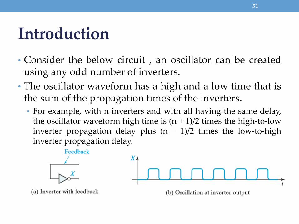
• Consider the below circuit , an oscillator can be createdusing any odd number of inverters.
• The oscillator waveform has a high and a low time that isthe sum of the propagation times of the inverters.• For example, with n inverters and with all having the same delay,
the oscillator waveform high time is (n + 1)/2 times the high-to-lowinverter propagation delay plus (n − 1)/2 times the low-to-highinverter propagation delay.

Introduction
• Consider a feedback loop,
• In this case, the circuit has two stable conditions, oftenreferred to as stable states.
• The simple loop of two inverters lacks (absence of) anyexternal means of initializing the state to one of the stablestates.
52

Questions
• Assume that the inverter in the given circuit has apropagation delay of 5 ns and the AND gate has apropagation delay of 10 ns. Draw a timing diagram forthe circuit showing X, Y, and Z. Assume that X is initially0, Y is initially 1, after 10 ns X becomes 1 for 80 ns, andthen X is 0 again.
53

Set-Reset Latch
• NOR-Gate latch
• The basic flip-flop can be improved by replacing theinverters with either NAND or NOR gates.
• The additional inputs on these gates provide a convenientmeans for application of input signals to switch the flip-flop from one stable state to the other.
54
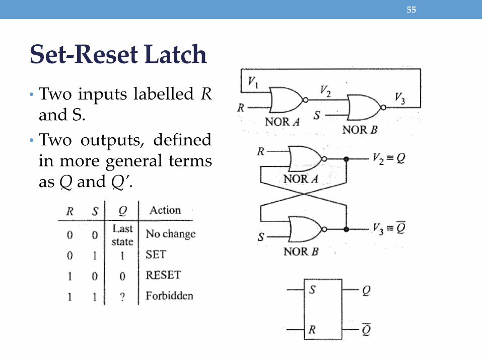
Set-Reset Latch
• Two inputs labelled Rand S.
• Two outputs, definedin more general termsas Q and Q’.
55

Set-Reset Latch
• To aid in understandingthe operation of thiscircuit, recall that an H = 1at any input of a NOR gateforces its output to an L =0.
• The first input condition inthe truth table is R = 0 andS = 0. Since a 0 at the inputof a NOR gate has no effecton its output, the flip-flopsimply remains in itspresent state; that is, Qremains unchanged.
56

Set-Reset Latch
• The second inputcondition R = 0 and S = 1forces the output ofNOR gate B low.
• Both inputs to NOR gateA are now low, and theNOR-gate output mustbe high.
• Thus a 1 at the S input issaid to SET the flip-flop,and it switches to thestable state where Q = 1.
57

Set-Reset Latch
• The third inputcondition is R = 1 and S =0. This condition forcesthe output of NOR gateA low, and since bothinputs to NOR gate B arenow low, the outputmust be high.
• Thus a 1 at the R input issaid to RESET the flip-flop and it switches tothe stable state where Q= 0 (or Q’ = 1).
58
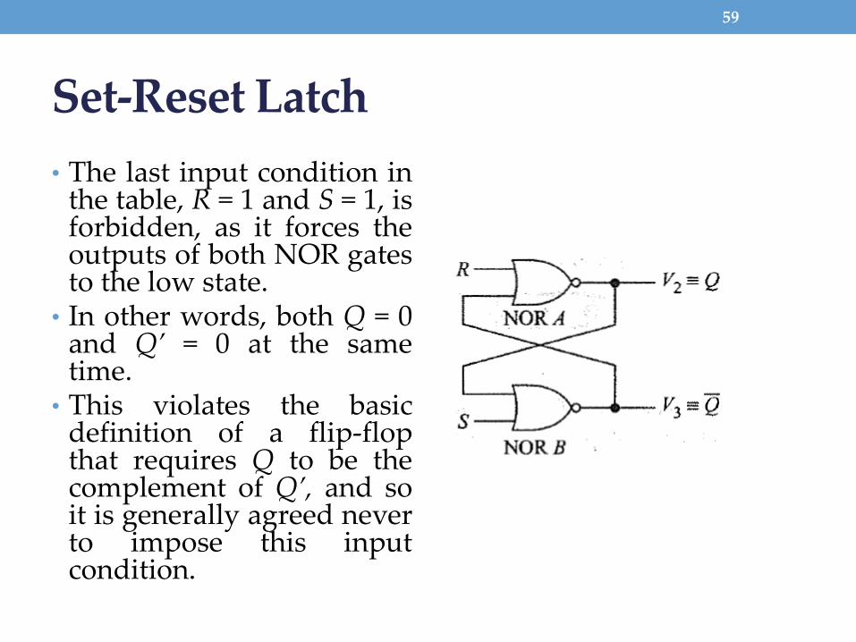
Set-Reset Latch
• The last input condition inthe table, R = 1 and S = 1, isforbidden, as it forces theoutputs of both NOR gatesto the low state.
• In other words, both Q = 0and Q’ = 0 at the sametime.
• This violates the basicdefinition of a flip-flopthat requires Q to be thecomplement of Q’, and soit is generally agreed neverto impose this inputcondition.
59

Set-Reset Latch• Timing Diagram for S-R Latch
• At t1, S = 0→ 1, Q = 0 → 1 a short time (ε) later.• ε represents the response time or delay time of the latch.• At t2, S = 1→ 0, Q = No change (NC).• At t3, R = 0 → 1, and Q = 1→ 0 a short time (ε) later.• The duration of the S (or R) input pulse must normally be at least as great
as ε in order for a change in the state of Q to occur.• If S = 1 for a time less than ε, the gate output will not change and the latch
will not change state.`
60

Set-Reset Latch
• Metastable State:
• Two-inverter circuit and the set-reset circuit can exist athird stable state called metastable state.
• This is the situation where the voltage level at the outputof the two inverters or gates is approximately halfwaybetween the voltage levels for a logic 0 and a logic 1.
• This state is referred to as a metastable state.
• It is metastable because any noise existing in the circuitwill cause the circuit to transition to one of the truly stablestates.
61

Set-Reset Latch
• Metastable State:
• However, certain events can cause the latch to enter themetastable state for a short time.
• The simultaneous change in S and R from 1 to 0 in theset-reset latch can cause the latch to enter the metastablestate.
• Starting with Q = 0 and applying a pulse on S with alength on the borderline between being too short tocause Q to change and just long enough to cause Q tochange may cause the circuit to enter the metastable state.
• Events causing the circuit to enter the metastable statemust be avoided
62

Set-Reset Latch
• The term present state to denote the state of the Q outputof the latch or flip-flop at the time any input signalchanges, and the term next state to denote the state of theQ output after the latch or flip-flop has reacted to theinput change and stabilized.
• Let Q(t) represent the present state and Q(t +ε) or Qn orQ+ represent the next state, an equation for Q(t+ε) can beobtained from the circuit can write:
63

Set-Reset Latch
• Derivation of Q+ for an S-R Latch
• Next-state equation or characteristic equation is
• Q+ = S + R′Q
64

Questions
• This problem illustrates the improper operation that can occur if bothinputs to an S-R latch are 1 and are then changed back to 0. For Figureshown below, complete the following timing chart, assuming thateach gate has a propagation delay of exactly 10 ns. Assume thatinitially P = 1 and Q = 0. Note that when t = 100 ns, S and R are bothchanged to 0. Then, 10 ns later, both P and Q will change to 1. Becausethese 1’s are fed back to the gate inputs, what will happen afteranother 10 ns?
65

• Complete the following timing diagram for an S-R latch. Assume Q begins at 1.
66

Set-Reset Latch
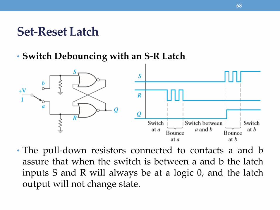
• Switch Debouncing with an S-R Latch
• When a mechanical switch is opened or closed, the switchcontacts tend to vibrate or bounce open and closed severaltimes before settling down to their final position.
• This produces a noisy transition, and this noise caninterfere with the proper operation of a logic circuit.
67
Set-Reset Latch
• Switch Debouncing with an S-R Latch
• The pull-down resistors connected to contacts a and bassure that when the switch is between a and b the latchinputs S and R will always be at a logic 0, and the latchoutput will not change state.
68

Set-Reset Latch
• Switch Debouncing with an S-R Latch
• The timing diagram shows what happens when the switch is flipped from ato b.
• As the switch leaves a, bounces occur at the R input; when the switch reachesb, bounces occur at the S input.
• After the switch reaches b, the first time S becomes 1, after a short delay thelatch switches to the Q = 1 state and remains there.
• Thus Q is free of all bounces even though the switch contacts bounce.
69

Set-Reset Latch
• 𝐒 𝐑 latch
70
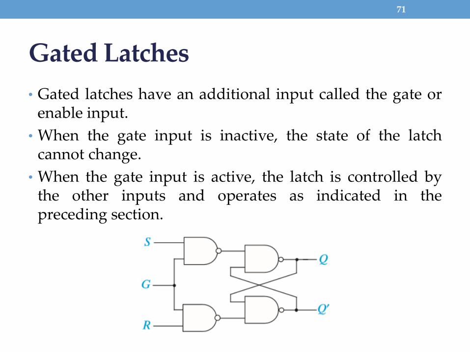
Gated Latches
• Gated latches have an additional input called the gate orenable input.
• When the gate input is inactive, the state of the latchcannot change.
• When the gate input is active, the latch is controlled bythe other inputs and operates as indicated in thepreceding section.
71

Gated Latches
• Race Condition in the Gated S-R Latch
• Another reason for disallowing the S = R = 1 input combinationis illustrated by considering a change in G from 1 to 0 with S =R = 1.
• When G changes, both inputs to the basic S-R latch changefrom 0 to 1. This causes both gates in the basic S-R latch toattempt to change from 1 to 0; a race condition exists and thepropagation delays of the gates determine whether the latchstabilizes with Q = 0 or Q = 1.
72

Gated Latches
• Q+ has a static 1-hazard for the input combinations
• G = 1, S = 1, R = 1, Q = 1 and G = 0, S = 1, R = 1, Q = 1.
• when G changes from 1 to 0 (or 0 to 1) between these twoinput combinations, it is possible for Q to change from 1to 0 so, the hazard may cause a glitch in Q,
73

Gated Latches
• Catching Problem:
• This is restriction in gated S-R latches.
• The S and R inputs must not be changing or contain glitcheswhile G = 1.
• For example, assume Q = 0 when G = 0→ 1 and S = 0 and R = 0.
• If S = R = 0 until G returns to 0, then Q remains at 0.
• If S contains a 1 glitch, due to a static 1-hazard then Q may beforced to a 1 and will remain there after G becomes 0.
• A similar problem occurs if S does not change from 1 to 0 untilafter G changes to 1.
• This is referred to as the 1’s catching problem.
• So to avoid S=R=1 next is D-Latch
74

Gated Latches
• Gated D Latch (or Transparent latch)
• It can be obtained from a gated S-R latch by connecting Sto D and R to D′.
75

Gated Latches
• Unreliable Gated D Latch Circuit
• Most digital systems use a clock signal to synchronize thechange in outputs of the system’s flip-flops to an edge ofthe clock signal, either the positive (0 to 1) or the negative(1 to 0) edge of the clock.
• Flip-flops where the clock signal is connected to the gateinputs of the latches
76

Gated Latches
• In the circuit shown,
• when the Clk = 1 so Q = Q′ when the input x = 1
• and Q = Q when x = 0.
• When Clk = 1 and x = 1, D = Q′ causes Q to change and, ifClk remains 1, the change in Q will feed back and cause Qto change again. If Clk remains at 1, Q will oscillate.
• Consequently, the circuit will only operate as intended ifClk remains at 1 for a short time; it has to 1 just longenough to allow Q to change but short enough to preventthe change from feeding back and causing a secondchange.
77

Gated Latches
• With a single latch, it may be possible to control the clock hightime so the latch operates as intended, but in a system withseveral latches, the variation in gate delays would make itimpossible to provide the correct clock width to all latches.
• To avoid this timing problem, more complicated flip-flopsrestrict the flip-flop outputs to only change on an edge of theclock, and the outputs cannot change at other times even ifthe inputs change.
• If the inputs to the flip-flop only need to be stable for a shortperiod of time around the clock edge, this refer to the flip-flopas edge-triggered.
• The term master-slave flip-flop refers to a particularimplementation that uses two gated latches in such a way thatthe flip-flop outputs only change on a clock edge.
78

• Design a gated D latch using only NAND gates and one inverter.
79

Edge-Triggered D Flip-Flop
• If the output of flip-flop can change in response to a 0 to 1transition on the clock input, we say that the flip-flop istriggered on the rising edge (or positive edge) of theclock. (rising-edge trigger)
• If the output can change in response to a 1 to 0 transitionon the clock input, we say that the flip-flop is triggeredon the falling edge (or negative edge) of the clock.(falling-edge trigger).
• The term active edge refers to the clock edge (rising orfalling) that triggers the flip-flop state change.
80

Edge-Triggered D Flip-Flop
• D Flip-Flops
• Timing for D Flip-Flop (Falling-Edge Trigger)
81

Edge-Triggered D Flip-Flop
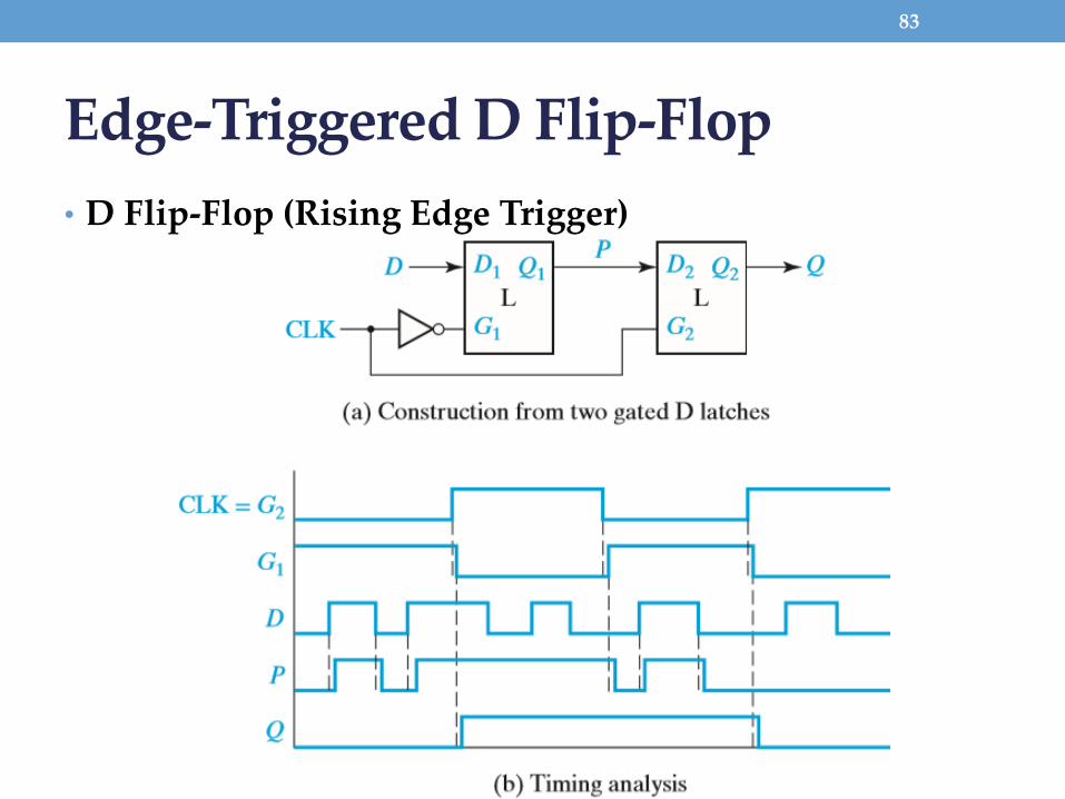
• D Flip-Flop (Rising Edge Trigger)
• A rising-edge-triggered D flip-flop can be constructedfrom two gated D latches and an inverter
82
Edge-Triggered D Flip-Flop
• D Flip-Flop (Rising Edge Trigger)
83

Edge-Triggered D Flip-Flop
• D Flip-Flop (Rising Edge Trigger)
• When CLK = 0, G1 = 1, and the first latch P = D input.
• Because G2 = 0, the second latch holds the current value ofQ.
• When CLK = 0 → 1, G1 =1 → 0, and the current value of Dis stored in the first latch, at same time G2 = 1, the value ofQ = P.
• When CLK changes back to 0, the second latch takes onthe value of P and holds it and, then, the first latch startsfollowing the D input again.
• If the first latch starts following the D input before thesecond latch takes on the value of P, the flip-flop will notfunction properly.
84

Edge-Triggered D Flip-Flop
• D Flip-Flop (Rising Edge Trigger)
• Therefore, the circuit designers must pay careful attentionto timing issues when designing edge-triggered flip-flops.
• With this circuit, output state changes occur onlyfollowing the rising edge of the clock.
• The value of D at the time of the rising edge of the clockdetermines the value of Q, and any extra changes in Dthat occur between rising clock edges have no effect on Q.
85

Edge-Triggered D Flip-Flop
• Because a flip-flop changes state only on the active edge of theclock, the propagation delay of a flip-flop is the time betweenthe active edge of the clock and the resulting change in theoutput.
• There are also timing issues associated with the D input.
• To function properly:• The D input to an edge-triggered flip-flop must be held at a constant
value for a period of time before and after the active edge of the clock.
• If D changes at the same time as the active edge, the behavior isunpredictable.
• The amount of time that D must be stable before the activeedge is called the setup time (tsu),
• The amount of time that D must hold the same value afterthe active edge is the hold time (th).
86
Edge-Triggered D Flip-Flop
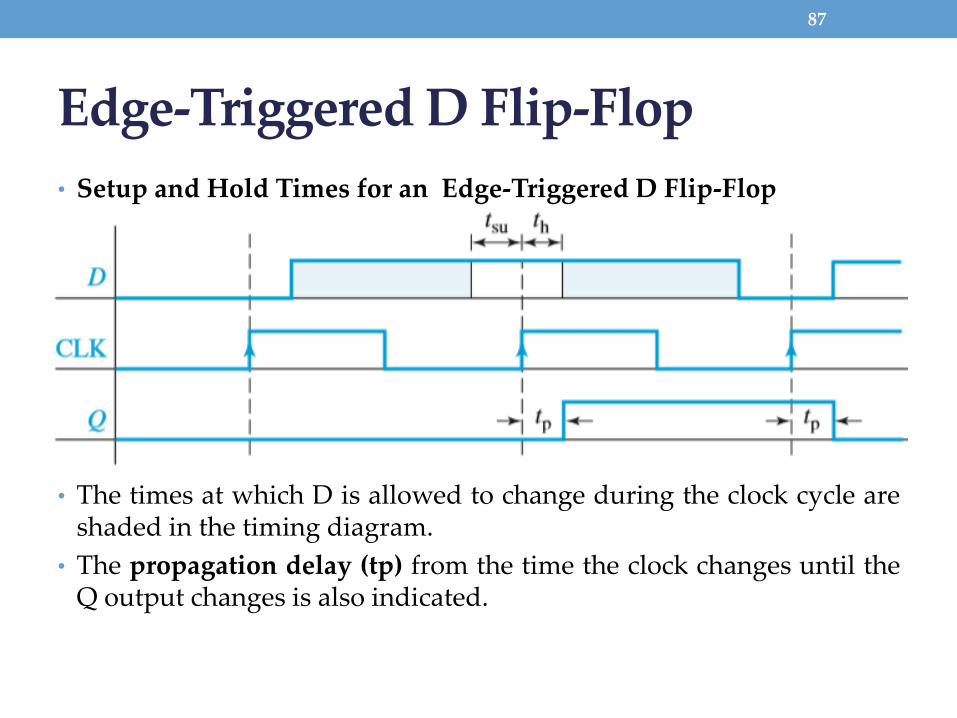
• Setup and Hold Times for an Edge-Triggered D Flip-Flop
• The times at which D is allowed to change during the clock cycle areshaded in the timing diagram.
• The propagation delay (tp) from the time the clock changes until theQ output changes is also indicated.
87

Edge-Triggered D Flip-Flop
• The setup time allows a change in D to propagate through thefirst latch before the rising edge of Clock. The hold time isrequired so that D gets stored in the first latch before Dchanges.
88

Edge-Triggered D Flip-Flop
• Determination of Minimum Clock Period
• Suppose the inverter has a propagation delay of 2 ns,
• The flip-flop has a propagation delay of 5 ns and a setuptime of 3 ns.
89

Edge-Triggered D Flip-Flop
• Determination of Minimum Clock Period
• That the clock period is 9 ns, i.e., the time between successive active edges (rising edges for thisfigure).
• Then, 5 ns after a clock edge, the flip-flop output will change, and 2 ns after that, the output of theinverter will change.
• Therefore, the input to the flip-flop will change 7 ns after the rising edge, which is 2 ns before thenext rising edge.
• But the setup time of the flip-flop requires that the input be stable 3 ns before the rising edge;therefore, the flip-flop may not take on the correct value.
90

Edge-Triggered D Flip-Flop
• Determination of Minimum Clock Period
• Now the clock period is 15 ns
• Again, the input to the flip-flop will change 7 ns after the rising edge.
• However, because the clock is slower, this is 8 ns before the next rising edge.
• Therefore, the flip-flop will work properly.
• Note in Figure (c) that there is 5 ns of extra time between the time the D input iscorrect and the time when it must be correct for the setup time to be satisfied.
91

Edge-Triggered D Flip-Flop
• Determination of Minimum Clock Period
• We can use a shorter clock period, and have less extra time, or no extra time.
• Figure (d) shows that 10 ns is the minimum clock period which will work forthis circuit.
92

Questions
• What change must be made in following circuit toimplement a falling-edge-triggered D flip-flop? Completethe following timing diagram for the modified flip-flop.
93

Questions
• Fill in the timing diagram for a falling-edge-triggered S-R flip-flop. Assume Q begins at 0.
94

S-R Flip-Flop
• An S-R flip-flop is similar to an S-R latch in that S = 1 setsthe Q output to 1, and R = 1 resets the Q output to 0.
• The essential difference is that the flip-flop has a clockinput, and the Q output can change only after an activeclock edge.
95

S-R Flip-Flop
• S-R Flip-Flop Implementation and Timing
96

S-R Flip-Flop
• S-R Flip-Flop Implementation and Timing
• This flip-flop changes state after the rising edge of the clock.
• The circuit is often referred to as a master-slave flip-flop.
• When CLK = 0, the S and R inputs set the outputs of the masterlatch to the appropriate value while the slave latch holds theprevious value of Q.
• When CLK = 0 → 1, the value of P is held in the master latchand this value is transferred to the slave latch.• The master latch holds the value of P while CLK = 1, and, hence, Q
does not change.
• When the clock changes from 1 to 0, the Q value is latched inthe slave, and the master can process new inputs.
• In timing diagram Initially, S = 1 and Q changes to 1 at t1. ThenR = 1 and Q changes to 0 at t3.
97

S-R Flip-Flop
• S-R Flip-Flop Implementation and Timing
98

S-R Flip-Flop
• S-R Flip-Flop Implementation and Timing
• For a rising-edge-triggered flip-flop the value of theinputs is sensed at the rising edge of the clock, and theinputs can change while the clock is low. For the master-slave flip-flop, if the inputs change while the clock is low,the flip-flop output may be incorrect.• For example, in timing diagram
• At t4, S = 1 and R = 0, so P = 1.
• At t5, S = 0 , but P does not change, Q = 1 after the rising edge ofCLK.
• However, at t5, S = R = 0, so the state of Q should not change.
• We can solve this problem if we only allow the S and Rinputs to change while the clock is high.
99

100

J-K Flip-Flop
• Master-Slave J-K Flip-Flop (Q Changes on Rising Edge)
• Two S-R latches connected in a master-slave arrangement except Sand R have been replaced with J and K, and the Q and Q′ outputs arefeeding back into the input gates.
• Because S = J·Q′·CLK′ and R = K·Q·CLK′, only one of S and R inputs tothe first latch can be 1 at any given time.
101

J-K Flip-Flop
102

J-K Flip-Flop
• Lab Experiment:
• Realize a J-K Master-Slave Flip-Flop using NAND gatesand verify its truth table.
103
CLK
J
K
Q
Q
Input Output
J K Qn+1
0 0 Qn
0 1 0
1 0 1
1 1 𝑸𝒏

J-K Flip-Flop
• Lab Experiment: Write HDL code for a J-K Master-Slave Flip-Flop.
104
entity JK_FF_VHDL isport( J,K: in std_logic;
Clock: in std_logic;Output: out std_logic);
end JK_FF_VHDL;
architecture Behavioral of JK_FF_VHDL is
signal temp: std_logic;begin
process (Clock) begin
if rising_edge(Clock) then
if (J='0' and K='0') thentemp <= temp;
elsif (J='0' and K='1') thentemp <= '0';
elsif (J='1' and K='0') thentemp <= '1';
elsif (J='1' and K='1') thentemp <= not (temp);
end if;end if;
end process;Output <= temp;
end Behavioral;

• Complete the following timing diagram for the flip-flopshown below.
105
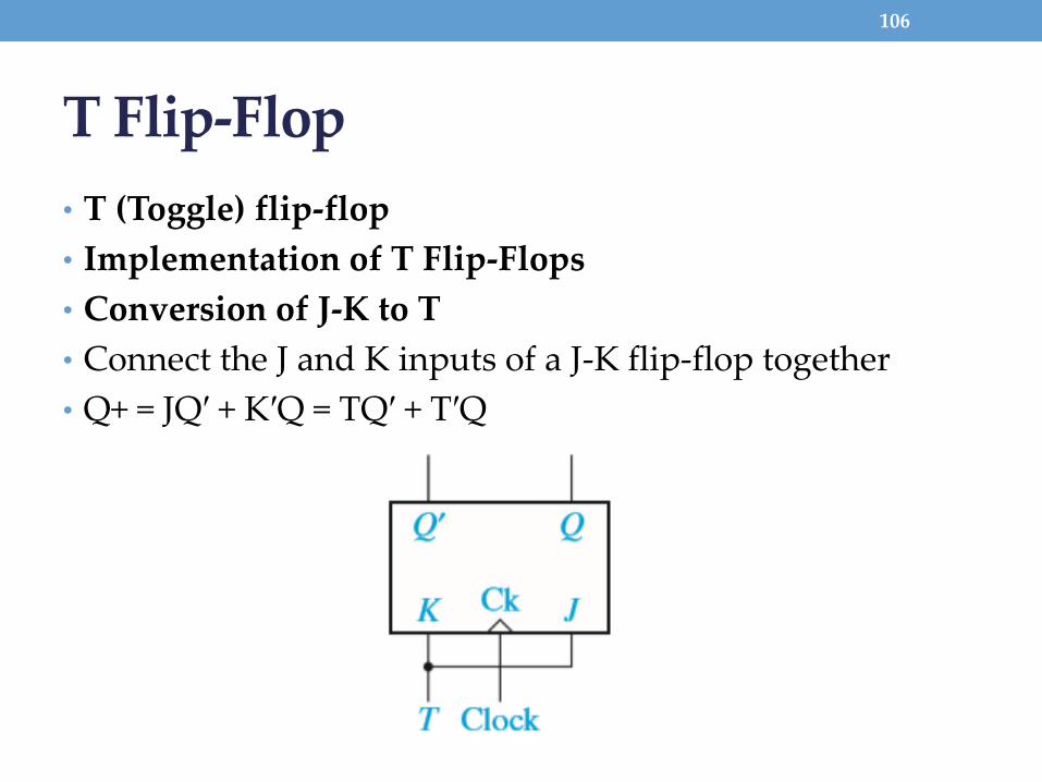
T Flip-Flop
• T (Toggle) flip-flop
• Implementation of T Flip-Flops
• Conversion of J-K to T
• Connect the J and K inputs of a J-K flip-flop together
• Q+ = JQ′ + K′Q = TQ′ + T′Q
106

T Flip-Flop
• Implementation of T Flip-Flops
• Conversion of D to T
• Q+ = Q ⊕ T = TQ′ + T′Q
107

T Flip-Flop
108

109

Flip-Flops with Additional Inputs
• Flip-flops often have additional inputs which can be usedto set the flip-flops to an initial state independent of theclock.
• Clear (Clr) and Preset (Pre) Input
• Clr and Pre are often referred to as asynchronous clearand preset inputs because their operation does notdepend on the clock.
• Clr will reset the flip-flop to Q = 0,
• Pre will set the flip-flop to Q = 1.
110

Flip-Flops with Additional Inputs
111
ClrN or PreNto indicate active-low clear and preset inputs

Flip-Flops with Additional Inputs
• The clear and preset inputs can also be synchronous, i.e.,the clear and set operations occur on the active edge ofthe clock.
• Often a synchronous clear or preset will override theother synchronous inputs, e.g., a D flip-flop with asynchronous clear input will clear on the active edge ofthe clock when the clear input is active independent of thevalue on D.
112

Flip-Flops with Additional Inputs
• D Flip-Flop with Clock Enable (D-CE)
• In synchronous digital systems, the flip-flops are usuallydriven by a common clock so that all state changes occurat the same time in response to the same clock edge.
• When designing such systems, we frequently encountersituations where we want some flip-flops to hold existingdata even though the data input to the flip-flops may bechanging.
• One way to do this is to gate the clock
113

Flip-Flops with Additional Inputs
• D Flip-Flop with Clock Enable (D-CE)
• Gating the Clock:
• This method has two potential problems.
• First, gate delays may cause the clock to arrive at some flip-flops at different times than at other flip-flops, resulting in aloss of synchronization.
• Second, if En changes at the wrong time, the flip-flop maytrigger due to the change in En instead of due to the change inthe clock, again resulting in loss of synchronization.
114

Flip-Flops with Additional Inputs
• D Flip-Flop with Clock Enable (D-CE)
• Rather than gating the clock, a better way is to use a flip-flop with a clock enable (CE).
• A D flip-flop with a clock enable, which we will call aD-CE flip-flop.
• Q+ = Q·CE′ + D·CE
115

• Complete the following timing diagram for a J-K flip-flop with a falling-edge trigger and asynchronous ClrN and PreN inputs.
116
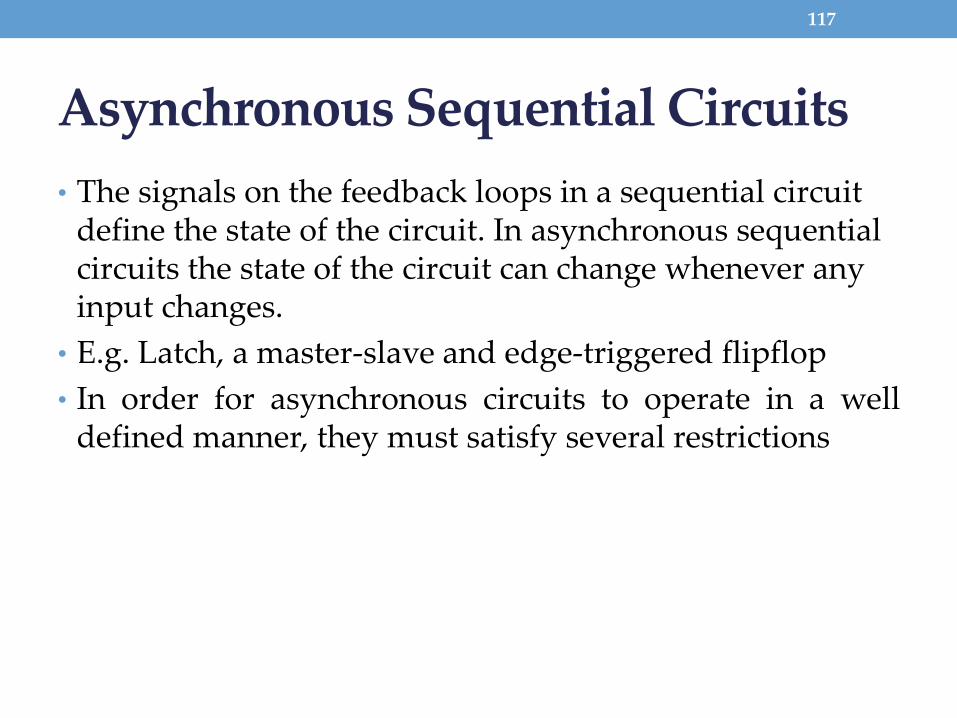
Asynchronous Sequential Circuits
• The signals on the feedback loops in a sequential circuit define the state of the circuit. In asynchronous sequential circuits the state of the circuit can change whenever any input changes.
• E.g. Latch, a master-slave and edge-triggered flipflop
• In order for asynchronous circuits to operate in a welldefined manner, they must satisfy several restrictions
117

Asynchronous Sequential Circuits
• P+ = x′P + xQ
• Q+ = x′P′ + xQ
• Note that both equationscontain static 1-hazards.
• P+ contains a static 1-hazard for xPQ = 111 ↔011.
• Figure shows next-statetable with the stable statescircled.
118

Asynchronous Sequential Circuits
• Stable state xPQ = 111 andchanging x to 0.
• The table indicates thatthe next state is PQ = 10(i.e., P does not changeand Q changes to 0).
• When x changes to 0, theoutput of Gate 2 changesto 0 causing the outputs ofboth gates 4 and 5 tochange to 0.
119

Asynchronous Sequential Circuits
• When the x inverteroutput changes to 1, P = 0prevents the output ofGate 1 from changing to 1so P remains 0; however,the output of Gate 3changes to 1 and Qbecomes 1.
120

Asynchronous Sequential Circuits
• The circuit stabilizes in state PQ =01. This incorrect state transitionis due to the static 1-hazard in P+,which causes a 0 glitch in P if thex inverter delay is large and,because of the feedback, P neverchanges back to 1.
• This problem can be eliminatedby designing the circuits to befree of hazards.
• Even if the circuit is free ofhazards, delays in the “wrong”places in the circuit can causeincorrect state transitions.
121

VARIOUS REPRESENTATIONS OF FLIP-FlOPS
• Characteristic Equations of Flip-flops• The characteristic equations of flip-flops are useful in analyzing
circuits made of them. Here, next output Qn+1 is expressed as afunction of present output Qn and input to flip-flops.
122

Introduction to Counter
• A counter driven by a clock can be used to count the number ofclock cycles.
• Since the clock pulses occur at known intervals, the counter canbe used as an instrument for measuring time and thereforeperiod or frequency.
• There are basically two different types of counters-synchronousand asynchronous.
• Serial, or asynchronous counter is defined as each flip-flop istriggered by the previous flip-flop, and thus the counter has acumulative settling time.
• An increase in speed of operation can be achieved by use of aparallel or synchronous counter. Here, every flip-flop istriggered by the clock (in synchronism), and thus settlingtime is simply equal to the delay time of a single flip-flop.
• Serial and parallel counters are used in combination tocompromise between speed of operation and hardware count.
123

ASYNCHRONOUS COUNTERS-1• The term asynchronous refers to events that do not have a fixed time relationship with
each other and, generally, do not occur at the same time.
• An asynchronous counter is one in which the flip-flops (FF) within the counter do notchange states at exactly the same time because they do not have a common clock pulse.
• The clock input of an asynchronous counter is always connected only to the LSB flip-flop.
• A 2-Bit Asynchronous Binary Counter
• Figure shows a 2-bit counter connected for asynchronous operation. Notice that theclock (CLK) is applied to the clock input (C) of only the first flop-flop, FF0, which isalways the least significant bit (LSB). The second flip-flop, FF1, is triggered by the 𝑄0out-put of FF0. FF0 changes state at the positive-going edge of each clock pulse, but FF1changes only when triggered by a negative-going transition of the Q0 output of FF0.
124

ASYNCHRONOUS COUNTERS-2
• Ripple Counters (Up Counter)
• Figure shows (Next slide) three negative edge- triggered, JK flip-flopsconnected in cascade.
• The system clock, a square wave, drives flip-flop A. The output of Adrives B, and the output of B drives flip-flop C. All the J and K inputsare tied to +VCC· This means that each flip-flop will change state(toggle) with a negative transition at its clock input.
• When the output of a flip-flop is used as the clock input for thenext flip-flop, we call the counter a ripple counter, or asynchronouscounter.
• The A flip-flop must change state before it can trigger the B flip-flop,and the B flip-flop has to change state before it can trigger the C flip-flop.
• If each flip-flop in this three-flip-flop counter has a propagation delaytime of 10 ns, the overall propagation delay time for the counter is 30ns.
125

ASYNCHRONOUS COUNTERS-3
126

ASYNCHRONOUS COUNTERS-4
127
• The waveform at the output of flip-flop A is one-half theclock frequency.
• The waveform at the output of flip-flop B is one-half thefrequency of A and one-fourth the clock frequency.
• The frequency of the waveform at C is one-half that at B,but it is only one-eighth the clock frequency.
• What is the clock frequency, if the period of the waveformat C is 24 μs?
• Since there are eight clock cycles in one cycle of C, theperiod of the clock must be 24/8 = 3 μs. The clockfrequency must then be l/(3 x 10-6) = 333 kHz.
ASYNCHRONOUS COUNTERS-5
128
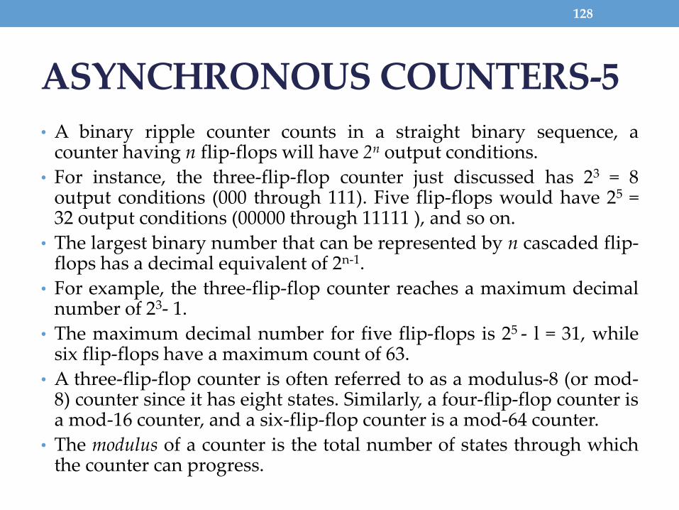
• A binary ripple counter counts in a straight binary sequence, acounter having n flip-flops will have 2n output conditions.
• For instance, the three-flip-flop counter just discussed has 23 = 8output conditions (000 through 111). Five flip-flops would have 25 =32 output conditions (00000 through 11111 ), and so on.
• The largest binary number that can be represented by n cascaded flip-flops has a decimal equivalent of 2n-1.
• For example, the three-flip-flop counter reaches a maximum decimalnumber of 23- 1.
• The maximum decimal number for five flip-flops is 25 - l = 31, whilesix flip-flops have a maximum count of 63.
• A three-flip-flop counter is often referred to as a modulus-8 (or mod-8) counter since it has eight states. Similarly, a four-flip-flop counter isa mod-16 counter, and a six-flip-flop counter is a mod-64 counter.
• The modulus of a counter is the total number of states through whichthe counter can progress.

ASYNCHRONOUS COUNTERS-6
129
• How many flip-flops are required to construct a mod-128 counter? A mod-32? What is the largest decimalnumber that can be stored in a mod-64 counter?
• A mod-128 counter must have seven flip-flols, since27 = 128.
• Five flip-flops are needed to construct a mod-32counter.
• The largest decima1 number that can be stored in asix-flop flip counter (mod-64) is 111111 = 63.
• Note carefully the difference between the modulus (total number of states) and the maximum decimalnumber.

ASYNCHRONOUS COUNTERS-8
130
• Example

ASYNCHRONOUS COUNTERS-9
131
• Ripple Counters (Down Counter)• In 3-bit ripple up counter the system clock is still used at the
clock input to flip-flop A, but the complement of A, A’, is usedto drive flip-flop B, likewise; B’ is used to drive flip-flop C.

ASYNCHRONOUS COUNTERS-10
132
• Ripple Counters (4-bit Down Counter)

DECADE COUNTERS-1
• A Mod-5 Counter
133

DECADE COUNTERS-2
• A Mod-5 Counter
• A modulo – 5 counter, the counter should reset when itreaches state 101.
• The inputs to the NAND gate should be connected to theoutputs Q1 and Q3.
• When the output of both these stages attains 1, then theoutput of the NAND gate is 0 and this resets the counter.
134
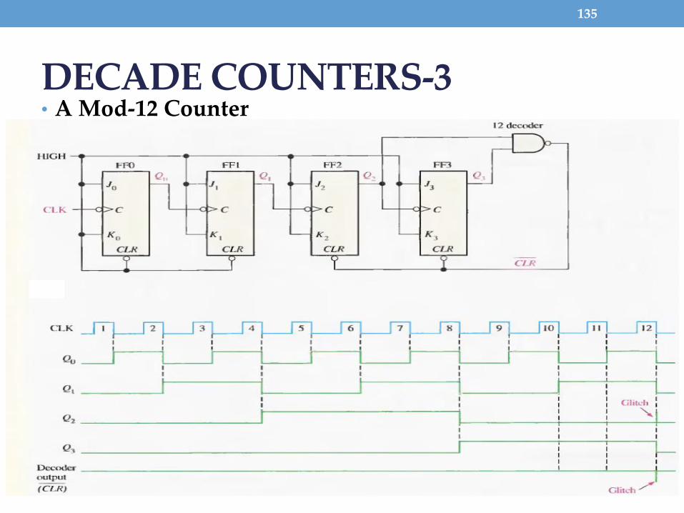
DECADE COUNTERS-3• A Mod-12 Counter
135

DECADE COUNTERS-4• Lab Experiment: The 7490
136
In Lab We Use this
Table

DECADE COUNTERS-5
• Lab Experiment: The 7490
• MOD-10 Counter
137
ClockOutput
QD QC QB QA0 0 0 0 01 0 0 0 12 0 0 1 03 0 0 1 14 0 1 0 05 0 1 0 16 0 1 1 07 0 1 1 18 1 0 0 09 1 0 0 1
14,INPUT A 05,VCC
CLK +5V
01,INPUT B 12
09
08
11
QA
QB
QC
QD
06, Rq1
07, RO1
10,GND
IC 7490
DECADE COUNTER
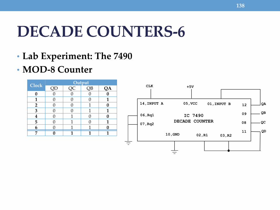
DECADE COUNTERS-6
• Lab Experiment: The 7490
• MOD-8 Counter
138
ClockOutput
QD QC QB QA0 0 0 0 01 0 0 0 12 0 0 1 03 0 0 1 14 0 1 0 05 0 1 0 16 0 1 1 07 0 1 1 1
14,INPUT A 05,VCC
CLK +5V
01,INPUT B 12
09
08
11
QA
QB
QC
QD
06,Rq1
07,Rq2
10,GND
IC 7490
DECADE COUNTER
02,R1 03,R2
Copyright © 2022 FDOKUMEN